
A new technique for optimizing orientation dependent etching ...
58
A new technique for optimizing orientation dependent etching of silicon: Process and method Item type text; Thesis-Reproduction (electronic) Authors Mazdiyasni, Parviz, 1960- Publisher The University of Arizona. Rights Copyright © is held by the author. Digital access to this material is made possible by the University Libraries, University of Arizona. Further transmission, reproduction or presentation (such as public display or performance) of protected items is prohibited except with permission of the author. Downloaded 6-Mar-2016 08:02:42 Link to item http://hdl.handle.net/10150/276606
-
Upload
khangminh22 -
Category
Documents
-
view
3 -
download
0
Transcript of A new technique for optimizing orientation dependent etching ...

A new technique for optimizing orientation dependent etching ofsilicon: Process and method
Item type text; Thesis-Reproduction (electronic)
Authors Mazdiyasni, Parviz, 1960-
Publisher The University of Arizona.
Rights Copyright © is held by the author. Digital access to thismaterial is made possible by the University Libraries,University of Arizona. Further transmission, reproductionor presentation (such as public display or performance) ofprotected items is prohibited except with permission of theauthor.
Downloaded 6-Mar-2016 08:02:42
Link to item http://hdl.handle.net/10150/276606

INFORMATION TO USERS
This reproduction was made from a copy of a document sent to us for microfilming. While the most advanced technology has been used to photograph and reproduce this document, the quality of the reproduction is heavily dependent upon the quality of the material submitted.
The following explanation of techniques is provided to help clarify markings or notations which may appear on this reproduction.
1. The sign or "target" for pages apparently lacking from the document photographed is "Missing Page(s)". If it was possible to obtain the missing page(s) or section, they are spliced into the film along with adjacent pages. This may have necessitated cutting through an image and duplicating adjacent pages to assure complete continuity.
2. When an image on the film is obliterated with a round black mark, it is an indication of either blurred copy because of movement during exposure, duplicate copy, or copyrighted materials that should not have been filmed. For blurred pages, a good image of the page can be found in the adjacent frame. If copyrighted materials were deleted, a target note will appear listing the pages in the adjacent frame.
3. When a map, drawing or chart, etc., is part of the material being photographed, a definite method of "sectioning" the material has been followed. It is customary to begin filming at the upper left hand corner of a large sheet and to continue from left to right in equal sections with small overlaps. If necessary, sectioning is continued again—beginning below the first row and continuing on until complete.
4. For illustrations that cannot be satisfactorily reproduced by xerographic means, photographic prints can be purchased at additional cost and inserted into your xerographic copy. These prints are available upon request from the Dissertations Customer Services Department.
5. Some pages in any document may have indistinct print. In all cases the best available copy has been filmed.
University Microfilms
International 300 N. Zeeb Road Ann Arbor, Ml 48106


Order Number 1332470
A new technique for optimizing orientation dependent etching of silicon: Process and method
Mazdiyasni, Parviz, M.S.
The University of Arizona, 1987
U M I 300 N. Zeeb Rd. Ann Arbor, MI 48106


PLEASE NOTE:
In all cases this material has been filmed in the best possible way from the available copy. Problems encountered with this document have been identified here with a check mark V .
1. Glossy photographs or pages.
2. Colored illustrations, paper or print
3. Photographs with dark background ^
4. Illustrations are poor copy
5. Pages with black marks, not original copy
6. Print shows through as there is text on both sides of page
7. Indistinct, broken or small print on several pages
8. Print exceeds margin requirements
9. Tightly bound copy with print lost in spine
10. Computer printout pages with indistinct print
11. Page(s) lacking when material received, and not available from school or author.
12. Page(s) seem to be missing in numbering only as text follows.
13. Two pages numbered . Text follows.
14. Curling and wrinkled pages
15. Dissertation contains pages with print at a slant, filmed as received
16. Other


A NEW TECHNIQUE FOR OPTIMIZING ORIENTATION DEPENDENT ETCHING OF SILICON:
PROCESS AND METHOD
by
Parviz Mazdiyasni
A Thesis Submitted to the Faculty of the
DEPARTMENT OF ELECTRICAL AND COMPUTER ENGINEERING
In Partial Fulfillment of the Requirements For the Degree of
MASTER OF SCIENCE WITH A MAJOR IN ELECTRICAL ENGINEERING
In the Graduate College
THE UNIVERSITY OF ARIZONA
1987

STATEMENT BY AUTHOR
This thesis has been submitted in partial fulfillment of requirements for an advanced degree at The University of Arizona and is deposited in the University Library to be made available to borrowers under rules of the Library.
Brief quotations from this thesis are allowable without special permission, provided that accurate acknowledgment of source is made. Requests for permission for extended quotation from or reproduction of this manuscript in whole or in part may be granted by the head of the major department or the Dean of the Graduate College when in his or her judgment the proposed use of the material is in the interests of scholarship. In all other instances, however, permission must be obtained from the author.
SIGNED: ̂
APPROVAL BY THESIS DIRECTOR
This thesis has been approved on the date shown below:
Walter J.\Fahey ( \ Professor of Electrical and Computer
Date
Engineering

DEDICATION
TO MY PARENTS
Mr.&Mrs. MAZDIYASNI
iii

ACKNOWLEDGMENT
I wish to express my gratitude and appreciation to the people who helped and encouraged me in the preparation of this thesis. I would like to begin by expressing my special thanks to Dr. James Fordemwalt for his assistance and advice in the planning, organization, and completion of this thesis.
Special thanks to Dr. Walter Fahey who on such short notice has accepted my request for studying this thesis. His concern and assistance has been a source of great encouragement to me. I would also like to thank Dr. Mehrdad Zomorrodi for his inputs and editing of the thesis.
This dissertation would never have been attempted but for the effort of my parents, who with their love and support have provided me the opportunity for high-level education, Mr. and Mrs. Mazdiyasni, and my family who all deserve to be recognized here, in particular, my sister Parvaneh.
iv

TABLE OF CONTENTS
Page
LIST OF ILLUSTRATIONS vi
LIST OF TABLES ix
ABSTRACT x
1. INTRODUCTION 1
2. PROCESS ARCHITECTURE 12
3. CHARACTERIZATION OF THE ETCHANT 24
4. CONCLUSION 34
APPENDIX A: TABLES OF ETCHANTS 36
REFERENCES 40

LIST OF ILLUSTRATIONS
Figure Page
1.1 The schematic of ink jet printer 1
1.2 Crystallography of silicon substrate orientations 4
1.3 Low order crystallographic planes of silicon 4
1.4 Angle of (1 1 1) etch planes to (1 0 0) surface 5
1.5 SEM picture of a very well aligned mask to the
silicon orientation 7
1.6 SEM picture of a misaligned mask to the
silicon orientation 7
1.7 Intersection of (1 00) plane with the other planes 8
1.8 Etch structure resulting when the mask edge is aligned to the
intersection of (1 0 0) planes 9
1.9 The intersection of the different planes in a Silicon Crystal ... 10
vi

vii
LIST OF ILLUSTRATIONS- CONTINUED
Figure Page
2.1 Anisotropic etching of holes in silicon of (1 00) orientation 13
2.2 Attacked exterior corners 13
2.3a Terminated etch pit 14
2.3b An SEM picture of a terminated etch pit 14
2.4a Through etch pit 15
2.4b An SEM picture of a through etch pit 15
2.5 The SEM picture of an etched figure which was the result of a
pin hole in the mask. Note that it was slightly misaligned with
respect to the crystal orientation 16
2.6 Aligningthe wafer with laser marks to the mask 18
2.7 Depth of the etched groove 20
2.8 Perpendicularity of (1 1 1) and (1 0 0) intersection 21

viii
LIST OF ILLUSTRATIONS--CONTINUED
Figure Page
2.9 The size of an etched hole increases by the misalignment of
the opening in surface masking 22
2.10 Process architecture of silicon etch 23
3.1 Etch rate in 44% KOH solution, showing 400:600:1 ratio 25
3.2 Undercut vs. misalignment 28
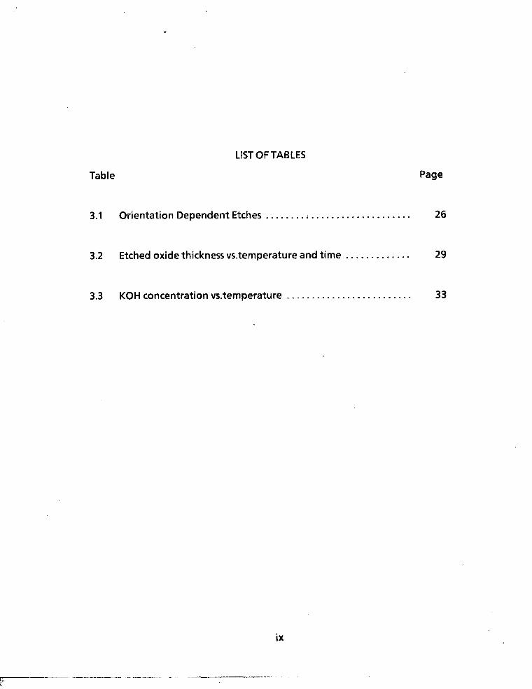
LIST OF TABLES
Table Page
3.1 Orientation Dependent Etches 26
3.2 Etched oxide thickness vs.temperature and time 29
3.3 KOH concentration vs.temperature 33
ix
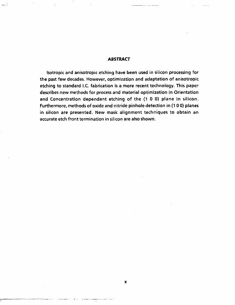
ABSTRACT
Isotropic and anisotropic etching have been used in silicon processing for
the past few decades. However, optimization and adaptation of anisotropic
etching to standard I.C. fabrication is a more recent technology. This paper
describes new methods for process and material optimization in Orientation
and Concentration dependent etching of the (1 0 0) plane in silicon.
Furthermore, methods of oxide and nitride pinhole detection in (1 0 0) planes
in silicon are presented. New mask alignment techniques to obtain an
accurate etch front termination in silicon are also shown.
x
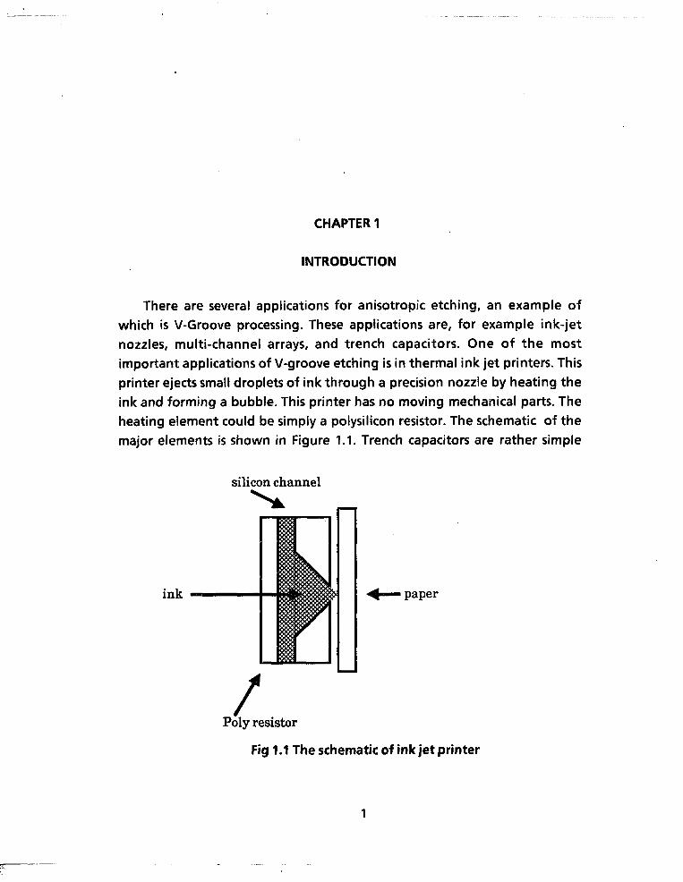
CHAPTER 1
INTRODUCTION
There are several applications for anisotropic etching, an example of
which is V-Groove processing. These applications are, for example ink-jet
nozzles, multi-channel arrays, and trench capacitors. One of the most
important applications of V-groove etching is in thermal ink jet printers. This
printer ejects small droplets of ink through a precision nozzle by heating the
ink and forming a bubble. This printer has no moving mechanical parts. The
heating element could be simply a polysilicon resistor. The schematic of the
major elements is shown in Figure 1.1. Trench capacitors are rather simple
silicon channel
ink paper
Poly resistor
Fig 1.1 The schematic of ink jet printer
1

because they require only vertical groove etching, grown or deposited oxide,
and metal deposition in the etched area. The metal deposition in the grooves
is the most difficult step. Capacitance gain of 100 or more are possible
through use of very long and narrow grooves. Higher capacitance gains could
be achieved by depositing Ta on the silicon surface and performing
anodization to form Ta20s which has a much higher dielectric constant than
SiC>2. The electronic portions of these applications use conventional IC
processing; however, conventional IC processing, up to now, has not offered
a cost effective technique for V-Groove etching.This thesis will describe a cost
effective and optimized process for V-groove etching as a part of
conventional processing with minimal additional steps(4) (16).
The etching technology, in general, falls into two categories; isotropic
and preferential etching or anisotropic etching. Isotropic etching is a simple
and fast technique for evaluating the structural perfection of single crystal
wafers. For silicon crystals, such a technique is widely used to delineate crystal
defects generated during crystal growth and device hot processing. A reliable
isotropic etch is extremely valuable in crystal growth technology and device
failure analysis. Although isotropic etching is useful in polish etching, it can
not be used for "Orientation Dependent Etching" because it etches silicon at
the same rate in all crystailographic directions.
On the other hand, the anisotropic etching of silicon is a controlled etch
in which the rate of etching of the silicon is very different in the various
crystailographic directions. To take the maximum advantage of this
characteristic, the silicon is usually etched through a mask, typically a window
cut into the oxide or nitride layer covering the silicon wafer. One of the early
applications of this technique, fabrication of electrical isolation region in the
high voltage transistors, is an example of this feature. With the excellent
control of etched profiles provided by anisotropic etching, the need for
diffusion as a method of electrical isolation was eliminated, giving the
advantage of reduced parasitic capacitance resulting in improved
performance^). Since anisotropic etching depends on the crystailographic

structure of silicon, the rest of this chapter will be spent describing the crystal
properties of silicon.
Silicon belongs to the family of crystal which has the diamond cubic
crystal structure. In the cubic structure, the crystallographic directions are
defined as being perpendicular to the crystal planes. Figure 1.2 shows some
of the planes and their positions in the cubic structure. Planes number one,
three, and seven are the three planes most commonly used in silicon device
processing. Figure 1.3 shows one of each of the planes in the cube, that is
(1 0 0), (1 1 0), and (1 1 1). The (1 1 1) direction has a very high atomic packing
density in its plane. The (1 0 0) direction is 54.75° from the (1 1 1) direction
(Figure 1.4) and the (1 1 0) direction is 90° from the original (1 1 1) direction.
The atomic packing density is less dense in the (110) plane and is much lower
in the (1 0 0) plane compared to the (111) plane. By examining the crystal
projection of the silicon (1 0 0) plane, it is observed that the (10 0) surface has
four-fold symmetry. That is, the high atomic packing density (1 1 1) planes are
an equal distance out from the (1 0 0) surface plane at equal angles and they
are at a 90° angle to each other (Figure 1.3). Also it is determined that the
(1 1 1) planes intersect the (1 0 0) planes with an angle of 54.75°<4). Sequential
photographs of the edges in a groove during the etching process indicate
that the major etching that occurs on slightly disoriented (111) planes is due
to the etching of the disorientation ledges. A perfectly oriented (111)
surface has very low etch rate using an appropriate etching solution^). On a
surface slightly disoriented from the (1 1 1) plane essentially all the etching is
due to the disorientation ledges. These situations are illustrated by Scanning
Electronic Microscope (SEM) pictures in Figures 1.5 and 1.6. The etched area
for Figure 1.5 is perfectly aligned with the perpendicular (1 1 1) plane. Perfect
alignment of the mask with the (1 0 0) plane guarantees no undercutting on
the (111) walls of the groove. A novel method of such alignment will be
described in later chapters. Failure to achieve alignment will cause crystal
ledges to form and these ledges etch slowly. Figure 1.6 shows a groove which
is misaligned by the small angle of 1.7 degree.

(110) (2 21) (111) (3 3 4) (112) (114) (10 0)
J/£ \ X/rr.
a 11 \ /' .• i. \ / • / ' ; • 7 \ / / / !, ! . » N.
/ ' i 1. '.'?i ' / / / 1 . * / /.J V •' / 1
' /„•- ;.v *. / 2 v y> • / / *.
/ \ / / »' \ / •
Fig 1.2 Crystallography of silicon substrate orientations
0) (110) (111)
Fig 1.3 Low order crystallographic planes of silicon

5
(10 0) (111)
54.7 54.7
Fig 1.4 Angle of (11 1)etch planes to (1 0 0) surface
Either the (1 0 0) plane or (1 1 0) plane could be the fastest etching plane
depending on which etchant is used. However, in the next chapter it will be
shown that the best choice is the (10 0) plane, because the best-known
etchant etches the (1 0 0) planes(?).
The structure of the etched surface depends upon the etch composition,
but the shape of the edge of the etched region, the "cliff" between etched
and unetched surfaces, depends on the orientation of the masking pattern
with respect to the (1 1 1) planesOA The intersection of the (1 1 1) plane with
the (1 0 0) is chosen for this work, in preference to the other intersection of
the (1 1 1) plane such as (1 1 0) plane because the angle of the (1 0 0)
interception is larger than that with the (1 1 0) plane, resulting in better etch

control. Typically, when the (1 0 0) plane is chosen, and the edge of the mask
is aligned accurately to the intersection with the (1 1 1) plane, a good "V-
groove" structure will result(6). A cross section perpendicular to the surface
and length of the channel is shown in Figure 1.7. This figure shows the
different planes of silicon in the etched channel. The reason for these
different structures is that there are two limiting shapes, and one does not
change upon further etching. This limiting shape has one of two forms
depending on whether, as the etching proceeds, the resulting surface formed
is concave or convex, which is dependent on the shape of the pattern in the
mask. For example, a simple rectangle will always form a concave structure,
whereas a more complex shape may result in convex structures. On etching a
concave surface the limiting shape is bounded by the slowest etching planes
with faster etching planes forming the corners and edges as shown in figure
1.8.

Fig 1.5 SEM picture of a very well aligned mask to the silicon orientation
Fig 1.6 SEM picture of a misaligned mask to the silicon orientation

Fig 1.7 intersection of (1 0 0) plane with the other planes

9
On a convex surface, the limiting shape is bounded by the fastest etching
planes with the slower etching planes forming the corners and edges.
Coo i)
Fig 1.8 Etch structure resulting when the mask edge is aligned to the
intersection of (1 0 0) planes.

10
Figure 1.9 shows all the planes discussed so far and more. In order to
show these planes, a piece of single crystal silicon was ground into a sphere
and etched for many hours at the boiling point in a mixture of N2H4 and H20.
The centers of the faces were determined to be (1 0 0) planes by x-ray
reflection and the corners point in (1 1 1) directions.
<
<
Fig 1.9 The intersections of the different planes in a Silicon Crystal

A number of chemical etchants have been introduced, which, dependent
on their composition and concentration, etch the different directions of the
silicon crystal at different rates. These etchants consist of an oxidant, which
oxides the silicon, and a complex agent which reacts with the oxidized silicon
to form a soluble complex ion and water. The reactant, which functions as a
base, has (OH) ions for the oxidation. Ethylene-diamine, hydrazine, and
potassium hydroxide are the best candidates for orientation- dependent
etching. Chemicals such as pyro-catechol and iso-2-propyl alcohol are
examples of complex agents(i6).
All of the etchants which have been introduced for orientation-
dependent etching, so called ODE, of silicon have much higher etch rates on
the (1 0 0) planes than on the (1 1 1) planes. The highest experimentally
achieved etch rate ratio on these planes is R100. R1U =600:1 using mixture of
about 33% KOH and the balance water. It has been shown that the etch rates
is about 400:1 using 44% KOH and water. Furthermore, it has been shown
that a linear relationship exists between the etch rate on the (1 1 1) plane and
the degree of crystal misalignment.
The results of these experiments are used in the next chapters in the
selection of the optimum procedure and architecture for the ODE processing.
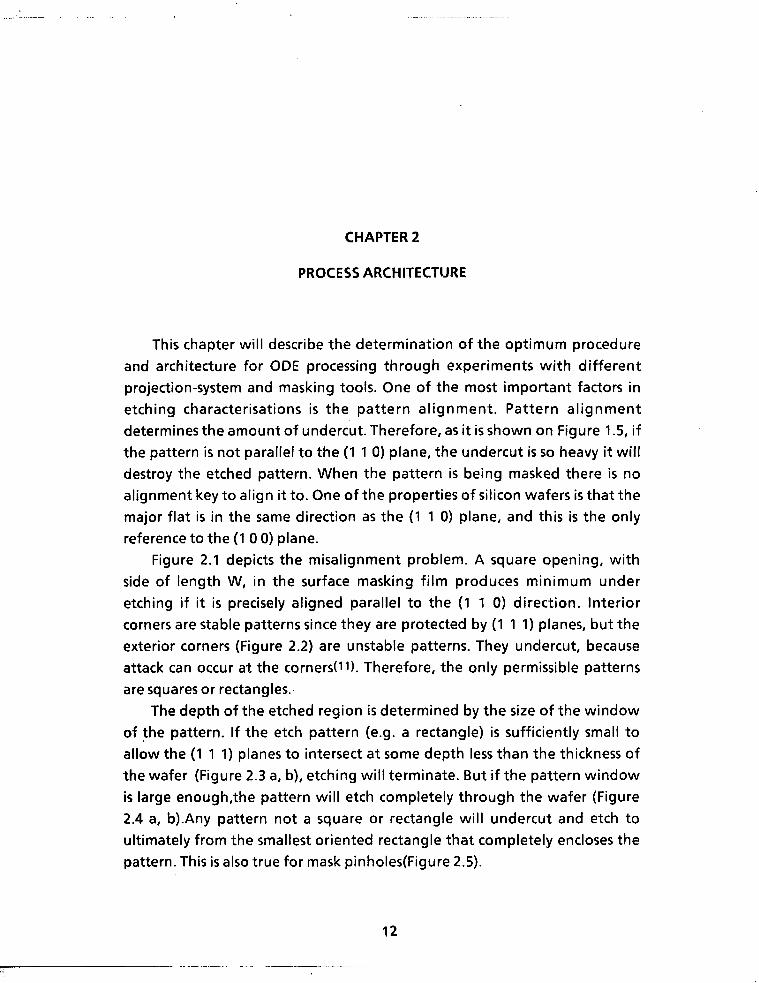
CHAPTER 2
PROCESS ARCHITECTURE
This chapter will describe the determination of the optimum procedure
and architecture for ODE processing through experiments with different
projection-system and masking tools. One of the most important factors in
etching characterisations is the pattern alignment. Pattern alignment
determines the amount of undercut. Therefore, as it is shown on Figure 1.5, if
the pattern is not parallel to the (1 1 0) plane, the undercut is so heavy it will
destroy the etched pattern. When the pattern is being masked there is no
alignment key to align it to. One of the properties of silicon wafers is that the
major flat is in the same direction as the (1 1 0) plane, and this is the only
reference to the (1 0 0) plane.
Figure 2.1 depicts the misalignment problem. A square opening, with
side of length W, in the surface masking film produces minimum under
etching if it is precisely aligned parallel to the (1 1 0) direction. Interior
corners are stable patterns since they are protected by (1 1 1) planes, but the
exterior corners (Figure 2.2) are unstable patterns. They undercut, because
attack can occur at the corners(n). Therefore, the only permissible patterns
are squares or rectangles.
The depth of the etched region is determined by the size of the window
of the pattern. If the etch pattern (e.g. a rectangle) is sufficiently small to
allow the (1 1 1) planes to intersect at some depth less than the thickness of
the wafer (Figure 2.3 a, b), etching will terminate. But if the pattern window
is large enough,the pattern will etch completely through the wafer (Figure
2.4 a, b).Any pattern not a square or rectangle will undercut and etch to
ultimately from the smallest oriented rectangle that completely encloses the
pattern. This is also true for mask pinholes(Figure 2.5).
12

10)
(10 0)
SI
1 1 1 1 )
Square orifice
Wafer flat
Fig 2.1 Anisotropic etching of holes in silicon of (1 0 0) orientation
Interior corner
Exterior corner
\ \\
/ ,
Etch attack
Etch attack
Fig 2.2 Attacked exterior corners

14
Fig 2.3a Terminated etch pit
Fig 2.3b An SEM picture of a terminated etch pit

Fig 2.4a Through etch pit
Fig 2.4b An SEM picture of a through etch pit

Fig. 2.5 The SEM picture of an etched figure which was the result of a pinhole
in the mask. Note that it was slightly misaligned with respect to the crystal
orientation

In the semiconductor industry, two methods of exposing the photoresist
pattern on the wafer are commonly in use. These are the scanning-projection
exposure systems, such as the Perkin-Elmer aligner, and the stepping
projection aligners, such as the GCA-6400 DES. One problem that has been
encountered using the scanning projection aligner is that it is difficult to
locate the flat (which defines the orientation of the intersection of the (1 0 0)
and (1 1 1) planes), so that the pattern may be accurately aligned to the flat.
On the other hand, with a stepping projection aligner, it is convenient to
align the pattern to the flat.
A technique used to assure proper alignment, is to initially expose a set
of alignment keys. The alignment of these keys to the flat is then carefully
checked. If the alignment is within the acceptable limits, then the ODE
pattern is aligned to the keys and exposed.
Another method of aligning the mask to a wafer is to have marks on the
wafer which are accurately aligned to the flats. This method has been tested
successfully. Two marks are made parallel to the major flat by laser at
specified places on the wafer by the vendor. The distance between the two
marks is constant and a known distance from the center of the wafer. On the
mask, two dies, the same distance from the center of the Perkin-Elmer mask
at the laser mark locations have been placed . By aligning these dies to the
laser marks, optimum alignment can be achieved (Figure 2.6)
If the pattern has a window of size W, the depth of the etched groove
could be simply calculated using Figure 2.7 and equation 2.1. Since the angle
between the two planes is fixed, the depth of the groove can be determined
by the width of the opening at the (1 0 0) plane. The intersections of the four
(1 1 1)planes with the (1 0 0) wafer surface are perpendicular to each other.
This means that in order to avoid undercut of the pattern, all pattern lines
must be parallel or perpendicular to these intersections as shown in Figure
2.8.
X = Tan 54.7 (W/2) (2.1)

18
• •••• LASER MARKS ON THE WAFER
REFERENCE DIES ON THE MASK
REFERENCE DIES ALIGNED TO THE LASER MARKS
Fig 2.6 Aligning the wafer with laser marks to the mask

19
or
X = 0.706W
A misalignment of 0 results in an increase to W' = W (Sin e+ Cos e) which
reaches a maximum at 6 =45° as shown in figure 2.9. Accurate alignment of
the surface pattern is accomplished when the straight sides of openings are
parallel to the intersections of the (1 1 1) planes with the accurately oriented
surface plane. One of the characteristics of this process is that the size of the
etched hole in the silicon substrate will increase if the pattern is misaligned to
the wafer. The increase in size is caused by under etching of the film opening
which enlarges the hole until it is determined by the angle to the nearest
(1 1 1) planes which enclose the opening05) (8). For example, a small square
opening, size W, in a nitride film on a (1 0 0) silicon surface forms a square
etched hole whose size ranges from W tO\/Tw as the angle is increased from
0° to 45° relative to the (1 1 0) direction. For any angle e, the side dimension
of the etched square hole in the silicon surface is W (Sin 8 + Cose).
High-quality silicon wafers of (1 0 0) orientation, accurately
oriented within +1° of their crystal axes, are readily available in the
commercial market in a wide range of diameter, thickness, and resistivity.
Figure 2.10 shows the process architecture of the silicon etch. One could use
the proposed process along with the conventional IC process to achieve
highly accurate alignment with optimum etch rate with minimum extra
masking steps which will be described in the next chapter(2).

X = Tan 54.7( W/2)
Fig 2.7 Depth of etched groove

( I l l ) a n d ( 1 0 0 ) i n t e r s e c t i o n
( 1 1 I X
Fig 2-8 Perpendicularity of (1 11) and (1 0 0) intersection

22
TT
•
N
\ /
/ 9 / w
V \/ \ . . •rf- II — • ~"F
W =W(Sine +Cose )
W'
- • ( 1 1 0 )
W'
Fig 2.9 The size of an etched hole increases by the misalignment of the opening in surface masking

SILICON SUBSTRATE
NITRIDE DEPOSITION
PHOTORESIST
EXPOSE RESIST
Wa
NITRIDE ETCH
1 1 11 H i III I NITRIDE ETCH
STRIP RESIST
SILICON ETCH
NITRIDE STRIP
Fig 2.10 Process architecture of silicon etch

CHAPTER 3
CHARACTERIZATION OF THE ETCHANT
This chapter describes the results of a number of experiments to
determine the optimum temperature for different types of chemicals.
When silicon is etched in certain solutions, the silicon is attacked
anisotropically. That is, certain planes are more resistive to being attacked
than others. Figure 3.1 shows a wide range of etch rates, depending on the
direction of attack. This figure shows that (1 0 0) and (1 1 0) planes are much
more readily attacked than the (1 1 1) planes. In fact in 44% KOH, the etch
rates are 400: 600: 1 respectively. This anisotropy means that (1 1 1) planes
are essentially not attacked in KOH solution. The mechanism is believed to be
related to the observation that (1 1 1) surfaces oxidize much more rapidly
than other surfaces. This oxide formation can, in effect, pasivate the (1 1 1)
planes and block dissolution. This mechanism is supported by the fact that the
etch rate of a (1 1 1) silicon surface at 85°C is of the same order of magnitude
as that of Si02-
Table 3.1 shows the chemicals used for orientation-dependent-etching.
Dash etch is an etch consisting of hydroflouric, nitric, and acetic acid which
etches silicon at about 7 um/min at room temperature. This planar etch will
etch at approximately the same rate in all crystallographic directions.
Experiments show that the orientation dependent etching is faster in doped
silicon wafers, (P+or N+type greater than 5 X 10¹⁸) than lightly doped P or N-
type silicon. Appendix B shows a list of anisotropic etching solutions with
high etch rates on single crystal siliconO) (7).
24

25
2 Etch rate in u/min
( 1 1 0 )
1 (10 0)
( 1 1 1 )
60 20 40 80
% of KOH in H20
Fig 3.1 Etch rates in 44% KOH solution, showing 400:600:1

Table 3.1 Orientation Dependent Etchants
26
ETCHANT COMPOSITION ETCH PART
DASH ETCH Hydroflouric Acid, 1 part
ISOTROPIC Nitric Acid, 3 parts
Acetic Acid, CH3OOH 15 parts
KOHETCH Potassium Hydroxide, KOH 250
ANISOTROPIC Normal 200
Deionized Water, 800
EDA ETCH Ethylenediamine, NH2(CH2)2NH2 35 parts
ANISOTROPIC Pyrocatechol, CH(OH)2 4 parts
Deionized Water, 61 parts
PLANAR ETCH Hydroflouric Acid, 8 parts
ISOTROPIC Nitric Acid, 73 parts
Acetic Acid, CH3OOH 19 parts

A very strong orientation dependent etch used for etching (1 0 0) silicon
is Ethylene diamine, pyrocatechol and Dl water (EPW). This solution etches
(1 0 0) silicon at 1.1 um/min at 100°C. This etchant also etches Si02 at about
10Ao/min at the same temperature.
Three etching systems are specified: PSE - 100 is hydrazine based, PSE -
200 is alkali-based, is faster to use and has the fastest etch rate. PSE - 300 is
ethylenediamine-based and has a moderate etch rate, which is safer to use
than PSE -100.
PSE-100 or hydrazine operates at temperatures of 95 to 120°C and
directly affects the (1 0 0) plane while its effect is negligible on other planes.
At 120°C the silicon etch rate is about 200 um/hr, but it does not effect the
oxide substantially. Contamination of the processing lab is not an issue.
Hydrazine and the silicon wafer can be cleaned using a water rinser.
The Alkali solution is an odorless liquid which etches the (1 1 0) plane as
well as the (1 0 0) plane and attacks the silicon at 80-100° temperature. This
solution will etch silicon at the rate of 270 um/hr at 100°C, but it does not
attack oxide so oxide could be used as a mask.
Ethylene diamine will etch silicon at 100°C and etch (1 0 0) plane at 25
um/hr although it can be used for (1 1 0) plane, but it has negligible effect on
the (1 1 1) plane. It's effect on oxide is negligible also.
The etching process using PSE-100 and PSE-300 is best carried out in a
flask fitted with a reflux condenser. Oxide present on the silicon wafer may
interfere with all etching; a preliminary dip in HF or buffered HF is desirable.
All these chemicals can be highly toxic, and are not recommended for
production lines. Appendix A givesthe general information about these
chemicals04)(i2) (5).
Another candidate for orientation dependent etch used for etching the
(1 0 0) silicon plane is potassium Hydroxide, and Dl water. This etch can be
masked by Si02, or if deep etching and high temperature is required, Si3N4.
This etch rate in the (10 0) direction is at least one hundred times faster than
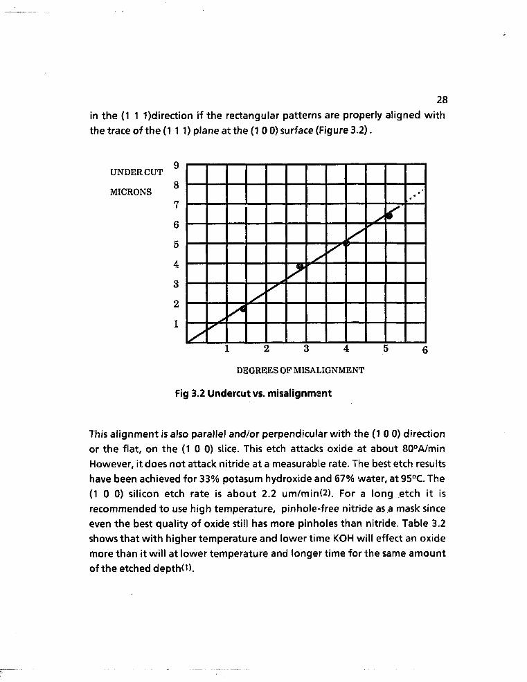
28
in the (1 1 1)direction if the rectangular patterns are properly aligned with
the trace of the (1 1 1) plane at the (1 0 0) surface (Figure 3.2).
UNDERCUT
MICRONS
9
8
7
6
5
4
3
2
1
• •
•
y
y
y* s
< I t t i 6
DEGREES OF MISALIGNMENT
Fig 3.2 Undercut vs. misalignment
This alignment is also parallel and/or perpendicular with the (10 0) direction
or the flat, on the (1 0 0) slice. This etch attacks oxide at about 80°A/min
However, it does not attack nitride at a measurable rate. The best etch results
have been achieved for 33% potasum hydroxide and 67% water, at 95°C. The
(1 0 0) silicon etch rate is about 2.2 um/min(2). For a long etch it is
recommended to use high temperature, pinhole-free nitride as a mask since
even the best quality of oxide still has more pinholes than nitride. Table 3.2
shows that with higher temperature and lower time KOH will effect an oxide
more than it will at lower temperature and longer time for the same amount
of the etched depthO).

Table 3.2 Etched oxide thickness vs. temperature and time
WAFER NUMBER
TIME MIN.
TEMPERATURE DEGREE C
THICKNESS A (etched away)
#1 10 95 475 A
#2 10 95 501A
#3 10 95 521A
#4 15 75 420 A
#5 15 75 447 A
#6 15 75 453 A
#7 20 60 344 A
#8 20 60 360 A
#9 20 60 386 A

Procedure for optimum etchant of (1 0 0) plane:
30
A procedure was devised based on several experiments done to define
the optimum etchant of the (1 0 0) plane. This procedure uses a 5000 cc, Pyrex
beaker was used as the reaction vessel. The beaker then is placed in a
stainless steel heater jacket with magnetic striller. Below is the process
sequence for fabricating one step channel wafers.
1) Aquet scrub wafers.
2) Pre-diffusion clean (RCA) wafers, followed by 1:50 HF dip.
3) Deposit LPCVD silicon nitride film (1000 -1500 A).
4) Apply photo resist to both sides of the wafer, pre-bake, expose, develop.
Double side coating is required for avoiding pin hole in nitride at the
back of wafers.
5) Plasma descum in O2 plasma, etch nitride in CF4/O2.
6) Strip resist, rinse and dry wafers.
7) Etch exposed silicon pattern in 33% KOH at 95°C until fill-holes break
through while agitating with the magnetic striller. The agitation will
expedite the etch time. The etch rate is the slope of a graph of depth
versus time.
8) Strip nitride film either by AMI nitride etcher or hot phosphoric acid
(180°C).
The defect analysis of this process is divided into 4 main groups:
A) silicon nitride layer
B) photolithography
C) anistropic etching

D) nitride removal. 31
The source of particles are usually found to be etch defects. In an experiment,
three nitride wafers were placed in KOH etch for 1.5 hours to reveal any
defects associated with the nitride layer. No defects could be found in the
body of the wafer although a few pin-holes were found at the surface area.
The photolithography defects were in three categories:
a) cracks
b) gel particles
c) voids/pin holes.
These appear to be the major yield-limiting problems, the origin of cracks
is presently unknown. Gel particles arose in the resist as a result of facility
temperature fluctuations or long term storage. A photo resist filter on the
resist coater will remove any gel particles. Voids are tiny dewetting spots that
results in rounded pin-holes in the nitride after CF4 Plasma etching. Voids
appear to be related to the photo resist and not the nitride layer, since the
resist is deposited on nitride fresh out of the nitride tube..
Pre-bake time, exposure time, and development time can all change
photo pattern line width, which changes etched channel width. Optimizing
these parameters ensures etched channel width and reproducibility.
CF4 plasma etch related problems includes inadequate descum. This can
result in nitride remaining in a patterned area so KOH etching cannot occur.
Also the nitride can be thinned sufficiently that no interference color is
observed (the nitride is invisible) but enough of it remains to prevent to KOH
from etching.
In monitored wafers, it was found that a full ODE etch (2-3 hours) only
removes 100A from the nitride mask. While this demonstrates the excellent

masking qualities of the nitride, it is also clear that any trace nitride left on a
patterned area will be sufficient to prevent proper etching.
In processing the nitride wafers, etch defects on the unpatterned side of
the wafer can etch completely through the wafers and effect the overall
yield, these were found to be a result of cracks generated on the back surface
due to the plasma etch step. To prevent this problem, coating the back of the
wafer with photo resist is necessary so that it never gets abraded.
The important parameters of KOH etching are concentration and
temperature. Agitation is not a parameter since the process of etching
liberates a large quantity of gas which acts exactly like a purge system to
guarantee agitation. Table 3.3 shows the results of a small matrix of
temperatures (95°C, 75°C) and concentrations (15% KOH, 30% KOH) for a
thorough etch experiment. The best anisotropy, (smallest undercut) was
observed for the 30% KOH at 95°C. Also the 30% KOH etch rate is not
substantially lower than the 15% KOH etch rate.

33
Table 3.3 KOH Concentration vs. temperature
Bath Temperature
KOH Concentration 95°c 75°C
A = 2.4um/mi A = l.Oum/mi
15% B = 9.5um B = 14um
C = 200min C = 555min
A = 2.3um/mi A = 0.8um/mi
30% B = 7.5um B = 9.5um
C = 235min C = 645min
A = etch rate B = undercut of a nitride edge after a through etch C = time to etch through a 500 um thick wafer
After etching is completed, the silicon nitride must be removed, primarily
to avoid the undercut nitride from breaking off in the etched areas. This is
done by either plasma etch (CF4/O2) or by hot (180°C) phosphoric acid. In case
of CF4 plasma etch, over etch can happen. Over etch in turn can attack the
silicon, leaving a roughened surface. However, this can be avoided by not
over etching or by using SiF4/02 instead of CF4. On the other hand, hot
phosphoric acid does not attack the silicon unless the temperature goes well
above 180°C. At temperature well above 180°C phosphoric acid begins to
attack silicon and it also breaks down to form insoluble particles.

CHAPTER 4
CONCLUSION
Results of the anisotropically etched V-grooves in silicon are shown in
previous chapters. The advantage of anisotropic etching of silicon over the
isotropic etch is that the anisotropic etch is a controlled etch in which the etch
rate of the silicon is different in the various crystallographic directions. For
O.D.E. etching, the silicon is etched through a window which is cut in to a
nitride or oxide mask that is covering :he silicon wafer. The angle between
the (1 0 0) surface and the (1 1 1) side wall is 54.7°. The (1 0 0) and (1 1 1)
crystal planes that define the grooves are identified on SEM pictures. The
intersection of the crystal planes is very sharp, and the surfaces of these
planes are very smooth. It was pointed out earlier that the quality of the
V-groove etch will depend on the alignment of the mask pattern along the
required (1 1 0) direction. The effect of slight misalignment from the (1 1 0)
direction causes some undercutting leaving a mask layer, oxide or nitride,
overhang. If the original pattern was, say, 10um this would make the pattern
geometry at the end of the etch slightly larger than 10um. Such widening of
the pattern cannot be tolerated for line widths of the order of a few microns.
The misalignment issue and its cause and effect were analyzed and two new
methods of alignment were proposed which minimize the undercut and
produce a sharp edge along the desired directions. In one of the methods
using the stepper, it was proposed to expose alignment marks on the wafer
and then align the mask to those marks. The second method proposes to
align the mask to the laser marks on the wafer which have already been
made parallel to the major flat by the vendor. The depth of the etched
channel can easily be calculated using equation 2.1.
Different types of chemicals for Orientation Dependent Etching were
introduced which are used in industry. A set of experiments and their results
34

35
were presented. As a result of analyzing and optimizing, a set of parameters
for anisotropically etched V-grooves, types of etchant, etch rates,
temperatures, masking materials and the best planes to be etched were
defined. The optimum experimented process is 33% concentration Potassium
Hydroxide in Dl water at 95°C. This solution gives the best etch result and
minimum undercut on (1 0 0) plane of the silicon. The conventional etch
process is to use high temperature nitride as a mask during the anisotropic
etching of silicon. After the silicon is etched in etchant, the nitride is removed
by phosphoric acid or plasma nitride etcher.

APPENDIX A
SILICON ETCHES
ETCH COMPOSITION USE ETCH RATE
Pyracatecol Etch Si without etching Si02 At 100°C 5000A/min
97:3 97 ml HF:3 HN03 Etch Si without etching Si02 much lOOOA/min
CP-8 50 ml HN03:35 ml Acetic Polish etch 1 mil/min
CP-4 240 ml Acetic:7 drop Br2:400ml HN03:240 ml HF
Polish etch 1 mil/min
AH 9 100 ml H20:100mg NaOH Polish etch
AIL16 40 ml HN03:10ml HF Chemical polish etch 3.3 mil/min
AILW1 40 ml 3% Hg(N03)2:40 ml HF:20 ml HNO3
Chemical polish etch
HCL 1% HCL gas in H2 Remove polishing damage At 1150°C 5000A/min
Safeguard IBr:HN O3 :HF: Acetic Polishing etch
u> c*

PREFERENTIAL ETCHES
ETCH COMPOSITION USE ETCH RATE
AH 2 100ml H20:lgmNa0H Reveals (111) surface At 90°C 5min
AH5 100ml H2O:10gm NaOH Reveals (110) surface At 90°C 5min
Lang etch 300 ml HF:1320 Acetic:1200 HN03:40gm 12
Reveal stacking faults 0.1 mil/min
EIL1 35 ml Acetic:35 ml HN03:30 ml HF:50mlH20
Reveals dislocation 1 min
EIL3 25 ml Acetic:40 ml HN03:25 ml HF Reveals dislocation on (10 0) lmin
EIL4 40 ml Acetic:15 ml HN03:5 ml HF Reveals spirals on (111) 12 hours
Sirtl 50 gm Cr03:100ml H20:75 ml HF Reveals dislocation on (10 0) 0.1 mil/min
Dash 13 ml HN03:1 ml HF:12 ml Acetic Reveals dislocation 12 hours
West - Ag 40 ml HF:20 ml HN03:20gm AgN03 Reveals dislocation 4 hours

STAINING ETCHES
COMPOSITION USE ETCH RATE
24 ml H202:21 ml HF:5ml H20 Stains p Silicon Quick swab with Q-tip
90 ml Saturated CuS04:10 ml HF Stains n Silicon Swab
One drop Chlorox Stains p GaAs Swab

ANISOTROPIC ETCHES
COMPOSITION USE ETCH RATE
157g KOH:525 ml H20 Etch (1 0 0), but not (111) At 80°C 9000A/min
36% Hydrazine:64% H2O Etch (10 0), but not (111) At 100°C 7500A/min
25% Tetramethyl ammonium hydroxide solition in H2O
Etch (10 0), but not (111) At 100°C is greater than lOOOOA/min

REFERENCES
1) R. G. Sweet, Rev. Sci. Instrum., 36,131
2) IBM J. Res. Dev., Special Issue on Ink Jet Printing, (1977)
3) E. Bassous, H. H. Taub, and L. kuhn, Applied Physics, Lett., 31, 135
(1977)
4) D. F. Wirauch, J. Applied Physics, 46,1478
5) M. J. Decjercq, L. Gerzberg, and J. D. Mindel, This Journal, 122, 545
(1975)
6) K. E. Peterson, Micromechanical light modulator array fabricated on
silicon, Applied Physics Lett., vol.31, no. 8, pp. 521-523, (1977)
7) W. Anacker, E. Bassous,F.F. Fang, R. E. Mundie, and H. N. Yu.
Fabrication of multiprobe miniature eletrical connector, IBM Tech. vol.
19 no. 1 pp. 372-374, (1976)
8) K. E. Bean and W. R. Runyan. Dielectric isolation: comprehensive,
current and future, J. Electrochem. Soc., vol. 124, no. 1, pp.5c-12c,
(1977)
9) R. M. Finne and D. L. Klein, A water amine complexing agent system
for etching silicon, E.C.S. J., vol.114,
10) B. Schwarts and H. robbin. Chemical etching of silicon , the system FH,
HNO3, H2O and HC2H3O2, J. Electrochem. Soc. vol 106, no.6, pp. SOS-
SOS
11) R. L. Smeltzer, D. L.Kendell.lEEE. PhotovoltaicSpecialisistConf.
12) D.L. Kendall, F. A. Padovani, K. E. Bean, W. T. Matzen Trans. IEEE ED-
20:1177. Appl. Phys.Lett. 26:195-98 Electrochem. Soc.
13) D.Y.Tseng, Appl. Opt. 12:2050-53
14) S. C. Terry. A gas chromotography system fabricated on a silicon wafer
using integrated circuit technology. PhD thesis. Stanford Univ.
40

41
15) J. W. Faust. In the surface chemistry of metal and semicondoctors. ed.
H.C. Gatos, p. 151. New york: Wiley
16) R. M. Finne, D. L. Klein J. Electrochem. Soc.114:965-70
17) M. S. Hu, Appl. Phys. lett. 27:165-67 (1976)
18) K. Knop, Opt. Commun. 18:298-303 (1976)