RE EMERGENCE OF RUSSIA: CHALLENGES WITHIN US-DOMINATED UNIPOLAR WORLD CHAPTER-I INTRODUCTION

Surface & Coatings Technology xxx (2014) xxx–xxx
SCT-19868; No of Pages 9
Contents lists available at ScienceDirect
Surface & Coatings Technology
j ourna l homepage: www.e lsev ie r .com/ locate /sur fcoat
Correlation between plasma electrolytic oxidation treatment stages andcoating microstructure on aluminum under unipolar pulsed DC mode
Vahid Dehnavi a,⁎, Ben Li Luan b,c,e,1, Xing Yang Liu d,2, David W. Shoesmith e,3, Sohrab Rohani f,4
a Department of Chemical and Biochemical Engineering, The University of Western Ontario, London, ON N6A 5B9, Canadab National Research Council Canada, 800 Collip Circle, London, ON N6G4X8, Canadac Department of Chemistry, The University of Western Ontario, London, ON N6A 5B7, Canadad National Research Council Canada, 800 Collip Circle, London ON, N6G4X8, Canadae Surface Science Western, Department of Chemistry, The University of Western Ontario, London, ON N6A 5B7, Canadaf Department of Chemical and Biochemical Engineering, The University of Western Ontario, London, ON N6A 5B9, Canada
⁎ Corresponding author. Tel.: +1 519 702 5582.E-mail addresses: [email protected], vdehnavi@gmail
[email protected] (B.L. Luan), XingYang.Liu@[email protected] (D.W. Shoesmith), [email protected] (
1 Tel.: +1 519 430 7043.2 Tel.: +1 519 430 7042.3 Tel.: +1 519 661 2111x86366.4 Tel.: +1 519 661 4116.
http://dx.doi.org/10.1016/j.surfcoat.2014.11.0070257-8972/Crown Copyright © 2014 Published by Elsevie
Please cite this article as: V. Dehnavi, et al., S
a b s t r a c t
a r t i c l e i n f oAvailable online xxxx
Keywords:Plasma electrolytic oxidationElectrical parametersVoltage–time responseMorphologyMicrohardnessCoating
Alumina coatings were deposited on 6061 aluminum alloy substrates using plasma electrolytic oxidation (PEO)in an alkaline silicate electrolyte. Different electrical parameters, including frequency, duty cycle, and currentdensity were applied to obtain PEO coatings. Scanning electron microscopy (SEM) and microhardness testswere used to investigate the coating microstructure and properties. For each sample, the voltage–time responseof the PEO process was obtained and compared with surface morphology, and coating cross sections and thick-nesses. Special consideration was given to the connection between the electrical parameters, different stages ofthe PEO process, and themorphology andmicrostructure of the coatings. Applying different electrical parameterschanged theduration and ratio of the PEO stages in the voltage–time response curve and affected the growth rate,surface morphology, microstructure and microhardness of the coatings. We report the new finding of a correla-tion between the stage of the PEO process and the microstructure and morphology of the coating.
Crown Copyright © 2014 Published by Elsevier B.V. All rights reserved.
1. Introduction
Plasma electrolytic oxidation (PEO) is a surface modification tech-nique capable of producing oxide coatings with desirable propertieson the surface of valve metals and alloys. PEO is an electrochemicalprocess in which coatings are formed as a result of the oxidation ofthe substratematerial via a series of localized electrical discharge eventsin an aqueous electrolyte [1–3].
Coatings prepared by PEO have been successfully produced on alu-minum, magnesium and titanium substrates. Recently researchershave applied this technique to zirconium [4–6] and tantalum [7,8] aswell. PEO coatings have existing and potential applications in a widerange of industry sectors. Examples of these applications include wear[9–12] and corrosion [13–15] resistant coatings, thermal barrier coat-ings [3,16,17], coatings for infrared concealment [18] and biocompatiblecoatings for implants [19–21].
.com (V. Dehnavi),rc.gc.ca (X.Y. Liu),S. Rohani).
r B.V. All rights reserved.
urf. Coat. Technol. (2014), ht
Different techniques and methods have been employed by vari-ous researchers to study the PEO coating growth behavior and thephenomena occurring during the process. To study the micro-discharge behavior during PEO treatment of various substrate mate-rials, researchers have used real-time imaging techniques. The re-sults of the studies on different substrates such as aluminum [22,23], magnesium [24], titanium [25,26] and zirconium [5,27] revealedthe spatial density, intensity, distribution and lifetime of the micro-discharges. Optical emission spectroscopy (OES) has been utilizedto identify the elements present in the plasma and also to estimatethe plasma temperature during PEO in aluminum [28–30], magne-sium [31] and titanium [32].
Generally up to four stages are reported during PEO [28,33]. PEOtypically starts with an abrupt linear increase in the voltage, which cor-responds to the conventional anodic oxidation, followed by the appear-ance of micro-discharges on the surface of the sample as a result ofdielectric breakdown after the breakdown voltage is reached. As theplasma coating process proceeds, the characteristics of the micro-discharges including their intensity, spatial density and color vary dur-ing subsequent stages of the process. The individual and collective char-acteristics of the micro-discharges, generated during the PEO process,determine the thermal and chemical conditions of the coating processand as a result play a key role in the formation of the oxide coatingsand affect the structure, morphology, phase formation and distributionin the coatings [5].
tp://dx.doi.org/10.1016/j.surfcoat.2014.11.007

2 V. Dehnavi et al. / Surface & Coatings Technology xxx (2014) xxx–xxx
The phenomenon and mechanism happening in each stage duringPEO and the resulting effects on the oxide layer growth behavior aredifferent. Applied process parameters can change the duration andratio of these stages which in turn could result in coatingswith differentmorphology, microstructure and phase composition [34].
Different applications require PEO coatings with unique properties.A dense coating, free from pores and defects could be a good candidatefor corrosion protection, and the porosity in the PEO layer could be usedas a base for sealants and primers to improve corrosion protection [35].Microporosity in the coatings on the surface of implants is beneficial andcould have several functions including helping bone tissue in-growthand acting as a depot for bioactive constituents [36]. Controlling thePEO process to yield the desired morphology and microstructure forspecific applications is a key requirement for the success of this methodin industry.
The voltage–time response of the PEO process can provide readilymeasurable and useful information about the different stages occurringduring PEO. Investigating the correlation between coating characteris-tics and different stages of PEO can improve understanding of, and pro-videmore control over, the process. Despite the useful information thatcould be derived from the voltage–time response, studies addressingthe correlation between voltage–time curves and coating propertiesare very scarce. This research investigates the effect of electrical param-eters, including applied current density, frequency and duty cycle, onthe voltage–time behavior during PEO and its correlation with themorphology and microstructure of the coatings.
2. Materials and methods
A unipolar, pulsed DC PEO coating unit was used to coat 6061 alumi-num alloy (nominal chemical composition (wt%): 0.40–0.80% Si, 0.70%Fe, 0.15–0.40% Cu, 0.15% Mn, 0.80–1.20% Mg, 0.04–0.35% Cr, 0.25% Zn,0.15% Ti, and balance Al) disk coupons with an average diameter of~30mmand a thickness of ~8mm. The couponsweremanually groundup to 600 grit using silicon carbide abrasive papers. After cleaning withisopropanol, theywere rinsed anddried using compressed air. The coat-ings were prepared in an aqueous alkaline electrolyte containing 2 g/lNa2SiO3 and 2 g/l KOH in deionized water. The temperature of theelectrolyte was kept below 40 °C by an external heat exchanger/chiller.Samples were treated at two frequencies, 50 and 1000 Hz, at duty cy-cles (Dt) of 20% and 80%with current densities (J) of 5, 10, 15, 20, and25 A/dm2. The duty cycle (Dt) is the percentage of the on-time, ton,during a single pulse. A schematic of the pulse wave form and thecorresponding electrical parameters of the unipolar pulsed powersource can be found elsewhere in the literature [37]. All sampleswere treated for 30 min under galvanostatic conditions, i.e. thecurrent was kept constant during the entire process and the anodepotential was allowed to vary. Sample codes and the correspondingelectrical parameters used for each one are presented in Table 1.
Scanning electron microscopy (Hitachi S-3500N operating at 20 kV)was used to study the coating surface morphology and cross sections.The samples were sputter-coated with a gold film before SEM analysis.Coating thickness measurements were performed using an Eddy cur-rent gauge. For each sample twenty measurements were taken on thecoated surface. Statistical treatments were applied to extract the meandata values and the scatter.
Table 1Electrical parameters and sample codes for PEO treatment on 6061 Al alloy.
Sample code Frequency (Hz) Dt (%) ton (ms) *: J (A/dm2)
S12–* 1000 20 0.2 5, 10, 15, 20, 25S18–* 1000 80 0.8S52–* 50 20 4S58–* 50 80 16
Please cite this article as: V. Dehnavi, et al., Surf. Coat. Technol. (2014), ht
Microhardness measurements were made on polished cross-sectionsof the PEO coatings using a Vickers diamond indenter mounted on aBuehler Micromet II microhardness tester under loads of 25 and 50 g,applied for 10 s. The average of ten measurements is reported for eachmicrohardness value.
3. Results and discussion
3.1. Voltage–time behavior and coating thickness
Typically, up to four stages are distinguished during the PEO process[28,33,38]. Fig. 1 illustrates the voltage–time response of sample S12–25containing all four stages.
During stage I, an abrupt linear increase in the voltage is observedwithin a short period of time. This stage is similar to conventional anod-ization which involves the rapid electrochemical formation of an initialthin oxide film [23,38]. At the end of stage I, the breakdown voltage isreached, which corresponds to the dielectric breakdown of the oxidefilm.
In stage II, after breakdown has occurred, a large number of smallmicro-discharges with a white color appear, covering the entire surfaceof the sample evenly. Sparks are characteristic of the PEO process andplay a crucial role in the formation of the coatings. Seconds after thebeginning of the PEO process, intense gas generation is observed onthe surface of the sample. The slope of the voltage–time curve decreasesduring stage II.
In stage III, the rate of voltage change increases as compared to stageII. The micro-discharges become more intense and their color changesfromwhite to yellow and then gradually to orange in subsequent stagesof the process.
In stage IV, the rate of voltage increase becomes slightly slower thanthat in stage III. Sparks become even stronger while their populationdecreases and their color remains orange. It is believed [5,28] that thestrong and long-lasting sparks could have a detrimental effect on thecoatings in some cases. During stage IV, voltage fluctuations appear inthe voltage–time curve, as can be seen in the inset in Fig. 1, and hasbeen reported by other researchers [39,40]. The onset of voltage fluctu-ations could be considered an indication of the beginning of stage IV.
The voltage–time response of coatings treated at different electricalparameters and the measured thicknesses are illustrated in Figs. 2 and3. The oxide layers had average thicknesses ranging from 5 to 74 μm.Increasing the current density (J) at constant frequency and duty cycleresulted in thicker coatings.
Comparing the voltage–time response of samples coated at differentelectrical parameters (Figs. 2 and 3) revealed that increasing the current
Fig. 1. A typical voltage–time response of a PEO coated 6061 Al alloy sample (S12–25)showing the four different stages occurring during PEO.
tp://dx.doi.org/10.1016/j.surfcoat.2014.11.007
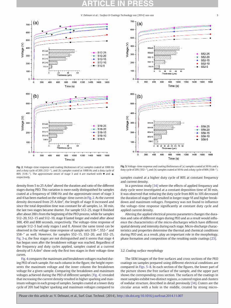
Fig. 2. Voltage–time response and coating thicknesses of (a) samples coated at 1000 Hzand a duty cycle of 20% (S12–*), and (b) samples coated at 1000 Hz and a duty cycle of80% (S18–*). The approximate onset of stage 3 and 4 are marked with ♥ and ,respectively.
Fig. 3.Voltage–time response and coating thicknesses of (a) samples coated at 50Hz and aduty cycle of 20% (S52–*), and (b) samples coated at 50Hz and a duty cycle of 80% (S58–*).
3V. Dehnavi et al. / Surface & Coatings Technology xxx (2014) xxx–xxx
density from 5 to 25 A/dm2 altered the duration and ratio of the differentstages during PEO. This variation is more easily distinguished for samplescoated at a frequency of 1000 Hz and the approximate onset of stage 3and4has beenmarkedon the voltage–time curves in Fig. 2. As the currentdensity decreased from 25 A/dm2, the length of stage II increased andsince the total deposition time was constant for all samples, i.e. 30 min,the last two stages became shorter. For sample S12–25, stage II finishedafter about 200 s from thebeginning of the PEOprocess,while for samplesS12–20, S12–15 and S12–10, stage II lasted longer and ended after about300, 450 and 800 seconds, respectively. The voltage–time response ofsample S12–5 had only stages I and II. Almost the same trend can beobserved in the voltage–time response of sample sets S18–*, S52–* andS58–* as well. However, for samples S52–15, S52–20, and S52–25,Fig. 3-a, the four stages are not distinguished and it seems that stage 4has begun soon after the breakdown voltage was reached. Regardless ofthe frequency and duty cycles applied, samples coated at a currentdensity of 5 A/dm2 show only the first two stages in their voltage–timecurves.
Fig. 4 compares themaximumandbreakdownvoltages reached dur-ing PEO of each sample. For each column in the figure, the height repre-sents the maximum voltage and the inner column the breakdownvoltage for a given sample. Comparing the breakdown and maximumvoltages achieved during the PEO of different samples (Fig. 4) revealedthat increasing the current density resulted in higher sparking andmax-imumvoltages in each group of samples. Samples coated at a lower dutycycle of 20% had higher sparking and maximum voltages compared to
Please cite this article as: V. Dehnavi, et al., Surf. Coat. Technol. (2014), ht
samples coated at a higher duty cycle of 80% at constant frequencyand current density.
In a previous study [34] where the effects of applied frequency andduty cycle were investigated at a constant deposition time of 30 min,it was observed that reducing the duty cycle from 80% to 10% decreasedthe duration of stage II and resulted in longer stage VI and higher break-down and maximum voltages. Frequency was not found to influencethe voltage–time response significantly at constant duty cycle andapplied current density.
Altering the applied electrical process parameters changes the dura-tion and ratio of different stages during PEO and as a result would influ-ence the characteristics of the micro-discharges which have differentspatial density and intensity during each stage. Micro-discharge charac-teristics and properties determine the thermal and chemical conditionsduring PEO and, as a result, play an important role in the morphology,phase formation and composition of the resulting oxide coatings [23].
3.2. Coating surface morphology
The SEM images of the free surfaces and cross sections of the PEOcoatings on samples prepared using different electrical conditions arecompared in Figs. 5–8. In each section of the figures, the lower part ofthe picture shows the free surface of the sample, and the upper partshows the corresponding cross section. The surfaces of the coatings inmost samples exhibit two distinct regions, a cratered region and clustersof nodular structure, described in detail previously [34]. Craters are thecircular areas with a hole in the middle, created by strong micro-
tp://dx.doi.org/10.1016/j.surfcoat.2014.11.007

Fig. 4.Maximumand breakdown voltages reached during PEO of 6061 aluminumalloy samples using different electrical parameters (in each column, the height represents themaximumvoltage and the inner column represents the breakdown voltage).
4 V. Dehnavi et al. / Surface & Coatings Technology xxx (2014) xxx–xxx
discharges, and the nodular structure is composed of patches of lightergray areas, asmarked in Fig. 6-e. Themorphology and size of the craters,aswell as their ratio relative to the nodular structure, vary dependingonthe processing conditions applied.
Comparing the surface morphologies of samples coated at differentconditions, Figs. 5–8, it can be observed that samples coated at currentdensities above 5 A/dm2 exhibit almost similarmorphologies consistingof craters and nodular structures with varying ratios.
Samples coated at a current density of 5 A/dm2, S12–5, S18–5, S52–5,and S58–5, contain elongated open pores on the surface of the coatings.This pore morphology was also observed by other researchers on alumi-num [41,42] and magnesium [38,43] alloy substrates. Open pores aregenerally observed at short processing times when the PEO coating
Fig. 5. SEM images of the free surface (lower part) and cross sections (upper part) of coatingssamples (a) S12–5, (b) S12–10, (c) S12–15, (d) S12–20, and (e) S12–25.
Please cite this article as: V. Dehnavi, et al., Surf. Coat. Technol. (2014), ht
thickness is low. The voltage–time responses of samples treated at 5 A/dm2 (Figs. 2 and 3) contain only the first two stages, I and II, and thethickness of these coatings is below 10 μm after 30 min of PEO coatingwhich is considerably lower than for other samples. Formation of theopen poresmay be due to the low thickness of the coating and good ther-mal conductivity of the substrate which causes the molten material pro-duced by the micro-discharges to be quickly quenched allowingformation of the open-pore structure [5]. These results indicate that thesurface of samples whose voltage–time curve fell in stage II were com-posed of open micro-pores.
Comparing the surfacemorphology of samples coated at a frequencyof 1000 Hz and a duty cycle of 20%, Fig. 5, b-e, suggests that increasingthe current density from 10 to 25 A/dm2 affected the morphology of
prepared at a frequency of 1000 Hz, duty cycle of 20% and different current densities on
tp://dx.doi.org/10.1016/j.surfcoat.2014.11.007

Fig. 6. SEM images of the free surface (upper part) and cross sections (lower part) of coatings prepared at a frequency of 1000 Hz, duty cycle of 80% and different current densities onsamples (a) S18–5, (b) S18–10, (c) S18–15, (d) S18–20, and (e) S18–25.
5V. Dehnavi et al. / Surface & Coatings Technology xxx (2014) xxx–xxx
the PEO coatings in addition to their thickness, Fig. 2-a. The surface ofsample S12–10 is mainly composed of a large number of craters withvery small areas of nodular structure. Each crater has a discharge chan-nel in the centre through which the molten material flowed onto thesurface of the coating. The results of EDX analyses on 6061 aluminumalloy substrates coated by PEO in silicate containing electrolytes, sug-gested that craters were rich in Al, while the nodular structure wasrich in Si [34,44].
In samples S12–10 to S12–25, (Fig. 5-b to e) as the current densityincreased, the size of the craters increased and the nodular structure
Fig. 7. SEM images of the free surface (upper part) and cross sections (lower part) of coatings pr(a) S52–5, (b) S52–10, (c) S52–15, (d) S52–20, and (e) S52–25.
Please cite this article as: V. Dehnavi, et al., Surf. Coat. Technol. (2014), ht
covered a larger area fraction of the PEO coating surface. As discussedin Section 3.1, increasing the current density shrank stage II and resultedin a longer stage IV. The surface of the coating on sample S12–10 whichwas in stage III after 30 min was mainly composed of craters, Fig. 5-b.Samples S12–15, S12–20, and S12–25 were in stage IV after 30 min,Fig. 2-a, and the length of stage IV was extended by increasing the cur-rent density. Examining the surface morphology of these samples inFig. 5, c–d, shows that the relative area fraction of the nodular structurecovering the surface of the coating also grewwith increasing the currentdensity.
epared at a frequency of 50Hz, duty cycle of 20% and different current densities on samples
tp://dx.doi.org/10.1016/j.surfcoat.2014.11.007

Fig. 8. SEM images of the free surface (lower part) and cross sections (upper part) of coatings prepared at a frequency of 50Hz, duty cycle of 80% and different current densities on samples(a) S58–5, (b) S58–10, (c) S58–15, (d) S58–20, and (e) S58–25.
6 V. Dehnavi et al. / Surface & Coatings Technology xxx (2014) xxx–xxx
Samples S18–* (Fig. 6), coated at the same frequency of 1000 Hz asS12–* but a higher duty cycle of 80%, exhibit the same trend. However,at an equal current density, the craters are bigger in size and the nodularstructure covers a larger portion of the coating surface area as comparedto samples S12–*.
Samples coated at the lower frequency of 50 Hz and duty cycles of20% and 80%, Figs. 7 and 8 respectively, follow the same behavior asthose coated at 1000 Hz. Again, for both duty cycles of 20% and 80%,higher current densities resulted in thicker coatings, bigger craters,and more nodular structures on the surface of the coatings.
It was observed that at both frequencies, 50 and 1000 Hz, higherduty cycle of 80% (Figs. 6 and 8) produced bigger craters andmore nod-ular structure at a constant current density compared to the lower dutycycle of 20%. These observations are confirmed by a previous study [34]in which EDX elemental maps andmeasurements of crater radius wereused to study the effect of duty cycle on Al/Si ratio and the size of craterson the surface of the samples. The larger crater size in samples coated athigher duty cycle and current densities at both frequencies could beattributed to the effect of the electrical parameters on the coating thick-ness and structure. Craters are the result of micro-discharges generatedby dielectric breakdown at weak and defective spots in the oxide coat-ing and increasing the thickness of the coatings reduces the number ofweak sites. The increased size of craters, indicative of stronger micro-discharges, is ascribed to the reduced number of discharging sitesthrough which higher current is able to pass [5,30,45]. The longer tonat the higher duty cycle of 80% compared to lower duty cycle of 20%provides more time for the gases to leave the molten material, thuscreating a coating with less porosity and fewer sites for micro-discharges to occur, as evident in cross-sectional SEM images inFigs. 5–8. Increasing J in each set of samples resulted in thicker coatings(Figs. 2 and 3). In a thicker oxide coating, higher energy is required topass through the coating and with reduced weak points the current islocalized in fewer locations, resulting in stronger sparks creating biggercraters [30,34].
Please cite this article as: V. Dehnavi, et al., Surf. Coat. Technol. (2014), ht
3.3. Cross-sectional micro-structures of the coatings
The cross-sections of the PEO coatings examined by SEM are pre-sented in Figs. 5–8 for different processing conditions. PEO coatingsare typically comprised of up to three layers. Adjacent to the substrate,there is a very thin inner layer which is termed “the barrier layer”followed by a thicker layer of variable thickness or the “functionallayer” which provides the main thermo-mechanical and tribologicalfunctionality of the coating [35,46]. In addition to the barrier and func-tional layer, found in the majority of samples in this study, a thirdporous and loose layer can also be formed in PEO coatings. The looseouter layer, located on top of the functional layer (Fig. 9-b), was ob-served on a few samples. The outer loose layer, also reported elsewherein the literature [46,47], can be removed after PEO treatment to exposethe dense functional layer [48]. However, it is suggested that the poros-ity in the outer loose layer could be used as a base for sealants andprimers for corrosion protection [35].
For all samples, the interface between the coatings and the substratehad a wavy appearance which might be the result of dissolution of thesubstrate in the early stages of the process [49] given the high pH(around 12) of the electrolyte. Large pores, which are connected insome areas and possibly enlarged during polishing, are present betweenthe inner and outer layers of the coatings (the dark area between thebarrier layer and functional layer in Fig. 9-b). Coatings with similarcross-sectional structure containing large pores between the inner andouter layers were also observed in studies using PEO on aluminum[29,50] and magnesium [51,52] alloy substrates, specifically when ap-plying a DC or unipolar pulsed DC current modes. On the other hand,such a pore structure was not observed in coatings on titanium alloysafter PEO [32]. Such morphology is normally not observed when usingthe bipolar pulsedDCmode. In studies investigating the effect of currentmode on the microstructure of PEO coatings [52–55], the improvedquality of coatings produced using a bipolar pulsed DC compared to aunipolar pulsed DC was attributed to the fact that, in the bipolar pulsed
tp://dx.doi.org/10.1016/j.surfcoat.2014.11.007

Fig. 9. SEM images showing (a) the free surface, and (b) the cross-section of sample S58–25.
7V. Dehnavi et al. / Surface & Coatings Technology xxx (2014) xxx–xxx
DCmode, the strongest plasma discharges and the average plasma tem-perature were reduced resulting in a more compact structure withfewer defects.
A possible mechanism for the formation of pores between the innerand outer layers of the coatings when a unipolar pulsed DC is employedcan be proposed. Aluminum is a reactivemetalwith a negative standardelectrode potential of−1.66 vs. SHE, but the oxide film formed on alu-minum is protective in the pH range ~4 to 8.5 as indicated by thePourbaix diagram. However, acids and bases can attack the protectivefilm leading to the dissolution of the base metal [56]. It was previouslyreported that increasing the concentration of KOH in the electrolytedecreased the film growth rate on an aluminum substrate significantlydue to the increased rate of anodic dissolution [57]. In the early stagesof the PEO process, after the breakdown voltage has been reached,micro-discharges are formed on the surface of the substrate. Eachmicro-discharge ejects molten materials out on to the surface andsince the coating is still thin and in contactwith the aluminumsubstratewith a high thermal conductivity, the molten material solidifies veryrapidly, creating open micropores on the surface. Examination ofthe surface morphologies of samples coated at a current density of5 A/dm2 (S12–5, S18–5, S52–5, and S58–5), Fig. 5 to Fig. 8, reveals thatall these samples contain open micropores and the coating thicknessesare less than 10 μm (Figs. 2 and 3). As the coating thickens, less heat istransferred to the aluminum substrate since more is absorbed by thecoating, allowing themoltenmaterial to solidifymore slowly thus creat-ing the typical crater structure. The alkaline electrolyte used has a highpH of ~12, which is well above the pH range in which the aluminumoxide film formed is protective. The alkaline electrolyte can reach theunderlying layers through the open pores formed in the early stagesof the process leading to dissolution of the coating and corrosion ofthe substrate and the creation of the voids observed. The negativeportion of the pulse in the pulsed bipolar current mode can inhibit thetransformation of the coating to easily dissolved compounds or preventdirect dissolution of the coating [58].
It is worth noting that although the pulsed bipolar current modeproduces denser coatings with enhanced tribomechanical properties,the coating porosity could be an asset in applications such as poly-mer–ceramic composite coatings and thermal barrier coatings.
SEM images of the cross-sections of PEO coatings (Figs. 5–8) showchannels across the coatings created by individual discharge eventsand also scattered pores in the functional layer. Pores may form due tothe entrapment of oxygen [59] or other types of gases that are formedduring the strong discharges [29] in molten alumina.
The coatings produced with the shortest ton time, Fig. 5, containmore porosity and discharge channels in the coatings as compared toother samples coated at longer ton times. This is more obvious whencomparing the cross-sectional microstructure of S12–25 (Fig. 5-e) pro-duced at a ton time of 0.2 ms with S18–25 (Fig. 6-e), S52–25 (Fig. 7-e),
Please cite this article as: V. Dehnavi, et al., Surf. Coat. Technol. (2014), ht
and S58–25 (Fig. 8-e) with ton times of 0.8, 4, and 16 ms, respectively.The longer ton times can create longer strong discharges which wouldmake it easier for the gases to escape the molten material and couldresult in a better sintering and thus denser coating.
The coating growth is the result of the molten materials flowingthrough discharge channels. The central hole in the cratered regions isthe discharge channel through which the molten material was ejectedand rapidly solidified upon contact with the electrolyte [54,60]. Area“C” in Fig. 9-b shows a discharge channel in the coating cross sectionthat created a crater (Area “B” in Fig. 9-a) in sample S58–25. The coatinggrowth rate is a function of the number and intensity of discharge chan-nels. Thickness measurements (Figs. 2 and 3) show that the coatinggrowth rate increased when higher current densities were applied ineach set of samples. The average thickness of sample S58–25 (Fig. 3-b),~74 μm, was considerably higher than other samples. The SEM imageof the free surface of S58–25 show that the nodular structure (as seenin Area “A” in Fig. 9-a) covered a large portion of the area in this sample.The cross-sectional view of S58–25 in Fig. 9-b revealed that the looseouter layer is actually the nodular structure with a thickness highenough to be observed in the cross section of the coating. The presenceof the thicker nodular structure forming the loose outer layer in S58–25could be one of the reasons for the high thickness readings on this sam-ple. A previous study of phase composition and distribution in PEO coat-ings prepared with conditions similar to the present work [37], showedthe outer surface was composed of mullite and amorphous phases. Theloose outer layer is an incomplete layer of nodular structure clusters onthe surface and is therefore not suitable for applications where goodmechanical properties are required: e.g., wear applications. Due to itspoor bonding to the functional layer as a result of interfacial porosity,the outer loose layer can be easily removedwhen in contact with a slid-ing surface and should be removed prior to application to expose theinner functional layer with superior wear resistance [46,50].
The outer loose layer was also observed in some areas in the crosssectional views of other samples coated at high current densities,namely samples S18–25, S52–20, S52–25, and S58–20 in Figs. 6-e,7-d-e, and 8-d, respectively, but its thickness was lower than thatof sample S58–25.
In a detailed study on the effect of electrical parameters on phaseformation and distribution in PEO coatings on 6061 aluminum substrate[37] it was found that increasing the pulse on-time by employing alower frequency and higher duty cycle resulted in coatings containingmullite and an amorphous phase in addition to α- and γ-Al2O3. Depthprofiling of the coated samples suggested that mullite (3Al2O3–2SiO2)and the amorphous phase were concentrated near the outer surface ofthe coatings. The formation of mullite and Si-rich amorphous phasewas attributed to increased Si concentration as a result of longer pulseon-time. Our proposed mechanism [34] suggests that when ton is long,the negative ions like SiO3
2− have more time to get adsorbed on the
tp://dx.doi.org/10.1016/j.surfcoat.2014.11.007

Fig. 10. Cross sectional Vickersmicrohardness values in functional layer of PEO coatings on6061 Al alloy as a function of electrical parameters.
8 V. Dehnavi et al. / Surface & Coatings Technology xxx (2014) xxx–xxx
surface of the anode. This, in addition to lower spatial density of sparkson the surface of samples coated at longer ton times, would result inhigher concentration of Si rich species on the surface of the coatings.
3.4. Coating microhardness
Microhardness values determined from Vickers indentations onthe cross sections of the coatings in the functional layer areas aregiven in Fig. 10. Coatings on samples treated at current densities of5 and 10 A/dm2 were very thin compared to the size of the indenta-tion. To prevent error in the readings caused by low thickness, onlyhardness values of samples with enough thickness are reported.
The average coating hardness values ranged from 1000Hv (9.8 GPa)to around 1600 Hv (15.7 GPa) in sample S58–25. These values are ap-preciably higher than the hardness of conventional anodising coatings(~4–6 GPa [61,62]). The improved hardness of PEO coatings comparedto conventional anodic alumina is attributed to the reduced porosityand the existence of crystalline alumina phases, namely α-Al2O3. PEOcoatings on aluminum alloys are normally a mixture of α-Al2O3 (~26GPa), γ-Al2O3 (~17 GPa), mullite (~10.5 GPa), and amorphous alumina(~4–6 GPa) [50,60,63]. Themeasured hardness in PEO coatings is lowerthan in dense bulk alumina phases due to the presence of porositycaused by the entrapment of gases in the coating during the treatmentprocess, and channels created by individual micro-discharges (demon-strated in Fig. 9-b) in PEO coatings.
The microhardness test results (Fig. 10) suggest that increasing tonresulted in higher average hardness values. As given in Table 1, ton dura-tion for S12–*, S18–*, S52–*, and S58–* samples are 0.2, 0.8, 4, and16 ms, respectively. It can also be deduced from Fig. 10 that except forS12-* samples, coated at a frequency of 1000 Hz and a Dt of 20%, in allother samples increasing the current density from 15 to 25 A/dm2
resulted in higher average hardness.The hardness of the PEO coating is a function of the nature of the
dominant phases present, as well as their ratio and distribution, andthe porosity and density of micro-cracks in the coatings. As discussedin Section 3.3, the coatings produced at 1000 Hz and a duty cycle of20% had the shortest ton time (0.2 ms) and contained more porosityand discharge channels in the coatings (Fig. 5) as compared to othersamples coated at longer ton times. Longer ton times can create longerdischarges, making it easier for the gases to escape the molten materialthus causing better sintering and a denser coating. It was previouslyreported [37] that increasing the pulse on-time and current densityenhanced the γ → α-Al2O3 phase transformation resulting in moreα-Al2O3, which is the hardest alumina phase, in the coatings. Coat-ings on samples PEO treated at a frequency of 1000 Hz and a dutycycle of 20% with different current densities contained essentially
Please cite this article as: V. Dehnavi, et al., Surf. Coat. Technol. (2014), ht
only γ-Al2O3. Increasing the duty cycle to 80% at the same frequency re-sulted in the formation of α-Al2O3 in addition to γ-Al2O3. In samplestreated at 50 Hz, α-Al2O3 was identified in all samples at a currentdensity greater than 5 A/dm2 in addition to γ-Al2O3.
PEO coatings on samples treated at 1000 Hz contained a higher levelof porosity andmicro-crackswith respect to other samples (Fig. 5). Var-iation in the coating microhardness values of S12–* samples is possiblymore dependent on the amount of porosity and micro-cracks in thesecoatings since the phase composition of these coating was the sameand composed only of γ-Al2O3. In other samples, however, the micro-hardness seems to be influenced by phase composition and contentmore than porosity because the cross sectional SEM micrographs(Figs. 6–8) show relatively dense structures in the functional layer ofthe coatings. In samples S18–*, S52–*, and S58–*, the relative α-Al2O3
content in the coating increased by applying a longer ton and higher cur-rent density [37] which is indicative of the positive effect of increasedrelative content of α-Al2O3 on the coating hardness.
4. Conclusions
PEO was performed on the 6061 aluminum alloy in an alkalinesilicate electrolyte using a pulsed unipolar currentmode under galvano-static conditions. Samples were coated at different frequencies, dutycycles, and current densities. For each sample the voltage–time re-sponse of the PEO process was obtained and compared with the surfacemorphology, cross-sectional view, and thickness of the coating. Vickersmicrohardness test was used to study the effect of the electrical param-eters on the hardness of the coatings. Special considerationwas given tothe connection between the electrical parameters, different stages ofthe PEO process, and the morphology and microstructure of the coat-ings. The following conclusions can be drawn from this study:
1. Voltage–time curves of samples coated with different electrical pa-rameters showed up to four different stages. Applying different elec-trical parameters changed the duration and ratio of these stagesduring PEO and affected the surface morphologies of the coatings.
2. The surfaces of the coatings in most samples exhibited two distinctregions, craters and clusters of nodular structure. The size of thecraters, as well as the area fraction of the cratered region and thenodular structure changed when different electrical parameterswere applied.
3. For samples treated at a current density of 5 A/dm2 the voltage–timecurves exhibited only two stages, I and II. Elongated open micro-pores were observed on the surface of all these samples. The lowthickness of the coating together with the good thermal conductivityof the substrate could suggest the formation of such pores is due tothe rapid solidification of the molten material.
4. Increasing the current density from 10 to 25 A/dm2 decreased theduration of stage II and increased the extent of the last stage in thevoltage–time response resulting in bigger craters and increasedarea fractions of the nodular structure on the PEO coating surfaces.
5. The application of higher current densities and longer pulse-ontimes, by employing higher duty cycles and a lower frequency,improved the microhardness of the coatings. This could be due toan enhanced γ → α-Al2O3 phase transformation resulting in moreα-Al2O3 in the oxide layer and an increased density of the functionallayer due to the reduction of porosity.
Acknowledgments
This research was supported by the National Research CouncilCanada (NRC) and Ontario Graduate Scholarship (OGS). The authorswould like to thank Marco Zeman and Mike Meinert (of Automotiveand Surface Transportation, National Research Council Canada,London, ON, Canada) for their help with the tests.
tp://dx.doi.org/10.1016/j.surfcoat.2014.11.007
9V. Dehnavi et al. / Surface & Coatings Technology xxx (2014) xxx–xxx
References
[1] D. Shen, G. Li, C. Guo, J. Zou, J. Cai, D. He, et al., Appl. Surf. Sci. 287 (2013) 451–456.[2] F. Monfort, A. Berkani, E. Matykina, P. Skeldon, G.E. Thompson, H. Habazaki, et al.,
Corros. Sci. 49 (2007) 672–693.[3] J.A. Curran, H. Kalkancı, Y. Magurova, T.W. Clyne, Surf. Coat. Technol. 201 (2007)
8683–8687.[4] Y. Cheng, E. Matykina, R. Arrabal, P. Skeldon, G.E. Thompson, Surf. Coat. Technol. 206
(2012) 3230–3239.[5] Y. Cheng, F. Wu, E. Matykina, P. Skeldon, G.E.E. Thompson, Corros. Sci. 59 (2012)
307–315.[6] W. Simka, M. Sowa, R.P. Socha, A. Maciej, J. Michalska, Electrochim. Acta 104 (2012)
518–525.[7] M. Petković, S. Stojadinović, R. Vasilić, L. Zeković, Appl. Surf. Sci. 257 (2011)
10590–10594.[8] C. Wang, F. Wang, Y. Han, Surf. Coat. Technol. 214 (2013) 110–116.[9] Y. Cheng, F. Wu, J. Dong, X. Wu, Z. Xue, E. Matykina, et al., Electrochim. Acta 85
(2012) 25–32.[10] L.R. Krishna, A.S. Purnima, G. Sundararajan, Wear 261 (2006) 1095–1101.[11] M. Treviño, R.D. Mercado-Solis, R. Colás, A. Pérez, J. Talamantes, A. Velasco, Wear
301 (2012) 434–441.[12] G. Rapheal, S. Kumar, C. Blawert, N.B. Dahotre, Wear 271 (2011) 1987–1997.[13] X. Li, X. Liu, B.L. Luan, Appl. Surf. Sci. 257 (2011) 9135–9141.[14] S. Moon, J. Solid State Electrochem. (2013) 3–8.[15] W. Xue, C. Wang, H. Tian, Y. Lai, Surf. Coat. Technol. 201 (2007) 8695–8701.[16] T. Akatsu, T. Kato, Y. Shinoda, F. Wakai, Surf. Coat. Technol. 223 (2013) 47–51.[17] J.A. Curran, T.W. Clyne, Surf. Coat. Technol. 199 (2005) 177–183.[18] F.-Y. Jin, K. Wang, M. Zhu, L.-R. Shen, J. Li, H.-H. Hong, et al., Mater. Chem. Phys. 114
(2009) 398–401.[19] Y. Yan, J. Sun, Y. Han, D. Li, K. Cui, Surf. Coat. Technol. 205 (2010) 1702–1713.[20] A. Krząkała, K. Służalska, M. Widziołek, J. Szade, A. Winiarski, G. Dercz, et al.,
Electrochim. Acta 104 (2013) 407–424.[21] S.A. Alves, R. Bayón, A. Igartua, V.S. De Viteri, L.A. Rocha, Tribocorrosion behaviour of
anodic titanium oxide fi lms produced by plasma electrolytic oxidation for dentalimplants, Lubr. Sci. 26 (2014) 500–513.
[22] A.L. Yerokhin, L.O. Snizhko, N.L. Gurevina, A. Leyland, A. Pilkington, A. Matthews,Surf. Coat. Technol. 177–178 (2004) 779–783.
[23] J. Jovović, S. Stojadinović, N.M. Šišović, N. Konjević, J. Quant. Spectrosc. Radiat. Transf.113 (2012) 1928–1937.
[24] S. Stojadinović, R. Vasilić, M. Petković, I. Belča, B. Kasalica, M. Perić, et al., Electrochim.Acta 59 (2012) 354–359.
[25] E. Matykina, A. Berkani, P. Skeldon, G.E. Thompson, Electrochim. Acta 53 (2007)1987–1994.
[26] M. Göttlicher, M. Rohnke, A. Helth, T. Leichtweiß, T. Gemming, A. Gebert, et al., ActaBiomater. 9 (2013) 9201–9210.
[27] S. Stojadinović, R. Vasilić, M. Petković, I. Belča, B. Kasalica, M. Perić, et al., Electrochim.Acta 79 (2012) 133–140.
[28] R.O. Hussein, X. Nie, D.O. Northwood, A. Yerokhin, A. Matthews, J. Phys. D. Appl.Phys. 43 (2010) 105203–105216.
[29] R.O. Hussein, D.O. Northwood, X. Nie, J. Vac. Sci. Technol. A 28 (2010) 766–773.
Please cite this article as: V. Dehnavi, et al., Surf. Coat. Technol. (2014), ht
[30] S. Stojadinovic, R. Vasilic, I. Belca, M. Petkovic, B. Kasalica, Z. Nedic, et al., Corros. Sci.52 (2010) 3258–3265.
[31] L. Wang, L. Chen, Z. Yan, W. Fu, Surf. Coat. Technol. 205 (2010) 1651–1658.[32] R.O. Hussein, X. Nie, D.O. Northwood, Mater. Chem. Phys. 134 (2012) 484–492.[33] L. Wang, X. Nie, Thin Solid Films 494 (2006) 211–218.[34] V. Dehnavi, B.L. Luan, D.W. Shoesmith, X.Y. Liu, S. Rohani, Surf. Coat. Technol. 226
(2013) 100–107.[35] E. Matykina, R. Arrabal, A. Mohamed, P. Skeldon, G.E. Thompson, Corros. Sci. 51
(2009) 2897–2905.[36] Y.K. Pan, C.Z. Chen, D.G. Wang, X. Yu, J. Biomed. Mater. Res. B Appl. Biomater. 100
(2012) 1574–1586.[37] V. Dehnavi, X.Y. Liu, B.L. Luan, D.W. Shoesmith, S. Rohani, Surf. Coat. Technol. 251
(2014) 106–114.[38] R.O. Hussein, X. Nie, D.O. Northwood, Electrochim. Acta 112 (2013) 111–119.[39] F. Monfort, E. Matykina, A. Berkani, P. Skeldon, G.E. Thompson, H. Habazaki, et al.,
Surf. Coat. Technol. 201 (2007) 8671–8676.[40] Y. Guan, Y. Xia, G. Li, Surf. Coat. Technol. 202 (2008) 4602–4612.[41] G. Sundararajan, L. Rama Krishna, Surf. Coat. Technol. 167 (2003) 269–277.[42] S. Moon, Y. Jeong, Corros. Sci. 51 (2009) 1506–1512.[43] U. Malayoglu, K.C. Tekin, S. Shrestha, Surf. Coat. Technol. 205 (2010) 1793–1798.[44] M.M.S. Al Bosta, K. Ma, H. Chien, Infrared Phys. Technol. 60 (2013) 323–334.[45] W. Xue, Z. Deng, Y. Lai, R. Chen, J. Am. Ceram. Soc. 81 (1998) 1365–1368.[46] F.C. Walsh, C.T.J. Low, R.J.K. Wood, K.T. Stevens, J. Archer, A.R. Poeton, et al., Trans.
Inst. Met. Finish. 87 (2009) 122–135.[47] A.L. Yerokhin, A. Shatrov, V. Samsonov, P. Shashkov, A. Pilkington, A. Leyland, et al.,
Surf. Coat. Technol. 199 (2005) 150–157.[48] E. Matykina, R. Arrabal, P. Skeldon, G.E. Thompson, Electrochim. Acta 54 (2009)
6767–6778.[49] R.O. Hussein, X. Nie, D.O. Northwood, Mater. Chem. Phys. 134 (2012) 484–492.[50] Y. Cheng, Z. Xue, Q.Wang, X.-Q.Wu, E. Matykina, P. Skeldon, et al., Electrochim. Acta
107 (2013) 358–378.[51] Y. Gao, A. Yerokhin, A. Matthews, Surf. Coat. Technol. 234 (2013) 132–142.[52] R.O. Hussein, D.O. Northwood, J.F. Su, X. Nie, Surf. Coat. Technol. 215 (2013) 421–430.[53] R.O. Hussein, X. Nie, D.O. Northwood, Surf. Coat. Technol. 205 (2010) 1659–1667.[54] F. Jaspard-mécuson, T. Czerwiec, G. Henrion, T. Belmonte, L. Dujardin, A. Viola, et al.,
Surf. Coat. Technol. 201 (2007) 8677–8682.[55] L. Wang, J. Zhou, J. Liang, J. Chen, Appl. Surf. Sci. 280 (2013) 151–155.[56] Y. Cheng, M. Mao, J. Cao, Z. Peng, Electrochim. Acta 138 (2014) 417–429.[57] L. Snizhko, A. Yerokhin, A. Pilkington, N. Gurevina, D. Misnyankin, A. Leyland, et al.,
Electrochim. Acta 49 (2004) 2085–2095.[58] J. Chen, Z. Wang, S. Lu, Rare Met. 31 (2012) 172–177.[59] J.A. Curran, T.W. Clyne, Acta Mater. 54 (2006) 1985–1993.[60] R.H.U. Khan, A. Yerokhin, X. Li, H. Dong, A. Matthews, Surf. Coat. Technol. 205 (2010)
1679–1688.[61] G. Alcalá, P. Skeldon, G.E. Thopson, A.B.Mann, H. Habazaki, K. Shimizu, Nanotechnol-
ogy 13 (2002) 451–455.[62] P.U. Skeldon, H.W. Wang, G.E. Thompson, Wear 206 (1997) 187–196.[63] H. Kalkancı, S.C. Kurnaz, Surf. Coat. Technol. 203 (2008) 15–22.
tp://dx.doi.org/10.1016/j.surfcoat.2014.11.007
Copyright © 2022 FDOKUMEN