
Controlled On-Time Zero Current Power Factor Correction
13
-
Upload
khangminh22 -
Category
Documents
-
view
1 -
download
0
Transcript of Controlled On-Time Zero Current Power Factor Correction

Controlled ON- Time, Zero Current Switched
Power Factor Correction Technique
Bill Andreycak
sion specifically targets the high harmonic contentof switching power supply capacitor input filters.This proposed spec defines limits for each harmoniccomponent of the mains current, thereby requiringpower factor correction circuitry. IEC 555-2 har-monic current limits are proportional to power inputbelow 300W, but current limits are absolute above300W. This imposes especially severe requirementson high power supplies.
When legislation such as IEC555 does not apply,it is tempting to rationalize that harmonic currentswill "get lost" among the other (resistive?) loadsconnected to the same branch circuit. But in anindustrial or office environment, it is not unusual forbranch circuits to be loaded by many low powerswitching power supplies. Harmonic currents willadd cumulatively, reducing the load capability of thesingle phase branch and perhaps exceeding theneutral rating of the 3-phase distribution system.
PFC Techniques-General OverviewPower factor correction
can be accomplished byanyone of the numerouspower conversion tech-niques[2,3]. The more pop-ular methods used in the
industry today incorporatethe boost topology operat-ing in the continuous con-duction mode (CCM) forhigh power applications, orthe discontinuous conduc-tion mode (DCM) forlower output power. Theboost converter outputvoltage (VoUT) must be
Abstract:
A general overview of various Power Factor
Correction techniques and typical application issues
is first presented. Emphasis is then focused on a
controlled on-time, non-resonant zero current
switched (ZCS) technique. The control algorithm,
design equations, required circuitry and general
performance will be detailed. Experimental test
results of power factor and total har1fWnic distortion
using this approach and a Zero Voltage Switched
(ZVS) derivative will be de1fWnstrated and com-
pared to the 1fWre conventional fixed frequency,
continuous current boost PFC technique.
Introduction
Active power factor correction techniques have
become an increasingly more demanded feature in
off-line industrial equipment. Legislation could soon
be enacted to mandate correction of the mains
current waveforms[l]. A proposed IEC 555-2 revi-
r-t>f-.~
104--
~'YYY.I
r--.
-
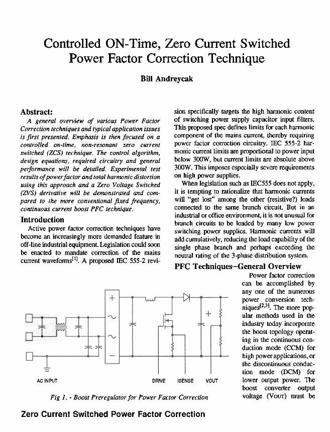
AC INPUT DRIVE ISENSE VOUT
Fig 1. -Boost Preregulator for Power Factor Correction
Zero Current Switched Power Factor Correction
greater than the peak input voltage (VIN) and non-isolated. Other conversion options include theflyback topology, a derivative of the boost convert-er. With this technique, the output voltage can begreater or less than the peak input voltage depend-ing on the inductor turns ratio. Galvanic isolationcan also be obtained since two coupled windings onthe inductor are used in the step-up or step-downprocess. A simple buck regulator can be employedfor a low voltage, non-isolated application withfavorable results. Isolation with a buck derivedtopology like the forward converter can be obtained,however is more difficult due to high voltageexcursions encountered to facilitate the core reset.
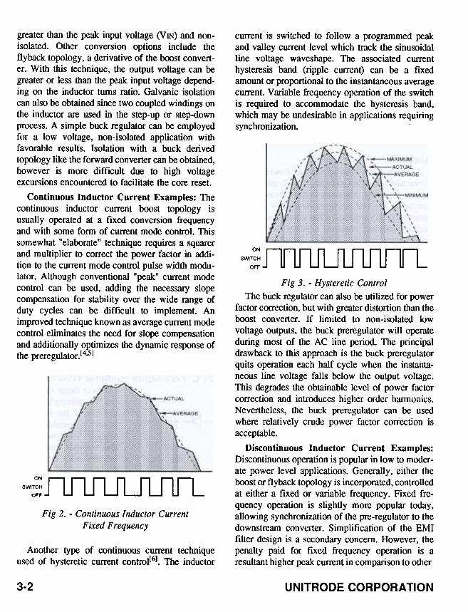
Continuous Inductor Current Examples: Thecontinuous inductor current boost topology isusually operated at a fixed conversion frequencyand with some form of current mode control. Thissomewhat "elaborate" technique requires a squarerand multiplier to correct the power factor in addi-tion to the current mode control pulse width modu-lator. Although conventional "peak" current modecontrol can be used, adding the necessary slopecompensation for stability over the wide range ofduty cycles can be difficult to implement. Animproved technique known as average current modecontrol eliminates the need for slope compensationand additionally optimizes the dynamic response ofthe preregulator.[4,5]
cmrent is switched to follow a programmed peakand valley current level which track the sinusoidalline voltage waveshape. The associated currenthysteresis band (ripple current) can be a fixedamount or proportional to the instantaneous averagecurrent. Variable frequency operation of the switchis required to accommodate the hysteresis band,which may be undesirable in applications requiring
synchronization.
ON mnJL nJ~SWITCH
OFF
Fig 3. -Hysteretic Control
The buck regulator can also be utilized for powerfactor correction, but with greater distortion than theboost converter. If limited to non-isolated lowvoltage outputs, the buck preregulator will operateduring most of the AC line period. The principaldrawback to this approach is the buck preregulatorquits operation each half cycle when the instanta-neous line voltage falls below the output voltage.This degrades the obtainable level of power factorcorrection and introduces higher order harmonics.Nevertheless, the buck preregulator can be usedwhere relatively crude power factor correction is
acceptable.
Discontinuous Inductor Current Examples:Discontinuous operation is popular in low to moder-ate power level applications. Generally, either theboost or flyback topology is incorporated, controlledat either a fixed or variable frequency. Fixed fre-quency operation is slightly more popular today,allowing synchronization of the pre-regulator to thedownstream converter. Simplification of the EMIfilter design is a secondary concern. However, thepenalty paid for fixed frequency operation is aresultant higher peak current in comparison to other
ON n ruuL1lJTLSWITCH
OFF
Fig 2. -Continuous Inductor Current
Fixed Frequency
Another type of continuous current techniqueused of hysteretic current control[6J. The inductor
3-2 UNITRODE CORPORATION
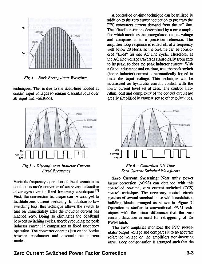
A controlled on-time technique can be utilized inaddition to the zero current detection to program thePFC converters current demand from the AC line.The "fixed" on-time is determined by a error ampli-fier which monitors the preregulators output voltageand compares it to a precision reference. Theamplifier loop response is rolled off at a frequencywell below 20 Hertz, so the on-time can be consid-ered "fixed" for one AC line cycle. Therefore, asthe AC line voltage traverses sinusoidally from zeroto its peak, so does the peak inductor current. Witha fixed inductance and on-time, tON, the peak switch(hence inductor) current is automatically forced totrack the input voltage. This technique can beenvisioned as hysteretic current control with thelower current level set at zero. The control algo-rithm, cost and complexity of the control circuit aregreatly simplified in comparison to other techniques.
Vp
VD..
Fig 4. -Buck Preregulator Waveform
techniques. This is due to the dead-time needed atcertain input voltages to remain discontinuous overall input line variations.
ON nnn n nnn
SWITCHJ U U U ~ U U LOFFsw:;JlJUUL fLru1
Fig 5. -Discontinuous Inductor CurrentFixed Frequency
Variable frequency operation of the discontinuousconduction mode converter offers several attractiveadvantages over its fixed frequency counterpart.l7]First, the conversion technique can be arranged tofacilitate zero current switching. In addition to lowswitching loss, this technique allows the switch toturn on immediately after the inductor current hasreached zero. Doing so eliminates the deadbandbetween switching cycles, thereby reducing the peakinductor current in comparison to fixed frequencyoperation. The converter operates just on the borderbetween continuous and discontinuous currentmodes.
Fig 6. -Controlled ON-TimeZero Current Switched Waveforms
Zero Current Switching: Near unity powerfactor correction (>0.98) can obtained with thiscontrolled on-time, zero current switched (ZCS)control technique. The necessary control circuitconsists of several standard pulse width modulationbuilding blocks arranged as shown in Figure 7.Operation is similar to conventional PWM tech-niques with the minor difference that the zerocurrent detection is used for retriggering of thePWM latch.
The error amplifier monitors the PFC prereg-ulator output voltage and compares it to an accuratereference voltage on the amplifiers non-invertinginput. Loop compensation is arranged such that the
3-3Zero Current Switched Power Factor Correction
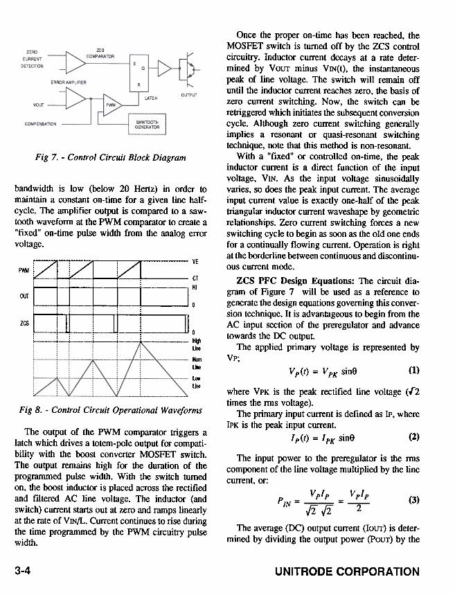
Fig 7. -Contro/ Circuit B/ock Diagram
bandwidth is low (below 20 Hertz) in order tomaintain a constant on-time for a given line half-cycle. The amplifier output is compared to a saw-tooth waveform at the PWM comparator to create a"fixed" on-time pulse width from the analog error
voltage.
YEP1"'-4
CTHI
OUT
ZCS, 0
~---+--+-- i -t H9I..i liie
, Nan
lre
l~lile
Once the proper on-time has been reached, theMOSFET switch is turned off by the ZCS controlcircuitry. Inductor current decays at a rate deter-mined by VoUT minus VIN(t), the instantaneouspeak of line voltage. The switch will remain offuntil the inductor current reaches zero, the basis ofzero current switching. Now, the switch can beretriggered which initiates the subsequent conversioncycle. Although zero current switching generallyimplies a resonant or quasi-resonant switchingtechnique, note that this method is non-resonant.
With a "fixed" or controlled on-time, the peakinductor current is a direct function of the inputvoltage, VIN. As the input voltage sinusoidallyvaries, so does the peak input current. The averageinput current value is exactly one-half of the peaktriangular inductor current waveshape by geometricrelationships. Zero current switching forces a newswitching cycle to begin as soon as the old one endsfor a continually flowing current. Operation is rightat the borderline between continuous and discontinu-ous current mode.
ZCS PFC Design Equations: The circuit dia-gram of Figure 7 will be used as a reference togenerate the design equations governing this conver-sion technique. It is advantageous to begin from theAC input section of the preregulator and advancetowards the DC output.
The applied primary voltage is represented byVp.,
~
(1)v p(t) = v PK sine
Fig 8. -Control Circuit Operational Waveforms
where VPK is the peak rectified line voltage (1"2
times the rms voltage).
The primary input current is defined as IP, where
IPK is the peak input current
I P (t) = I PK sine (2)The output of the PWM comparator triggers a
latch which drives a totem-pole output for compati-bility with the boost converter MOSFET switch.The output remains high for the duration of theprogrammed pulse width. With the switch turnedon, the boost inductor is placed across the rectifiedand filtered AC line voltage. The inductor (andswitch) current starts out at zero and ramps linearlyat the rate of VIN/L. Current continues to rise duringthe time programmed by the PWM circuitry pulsewidth.
The input power to the preregulator is the nuscomponent of the line voltage multiplied by the linecurrent, or:
-Vplp
/2/2-~
The average (DC) output current (IOUT) is deter-
mined by dividing the output power (POUT) by the
(3)P'1J = Vplp
3-4 UNITRODE CORPORATION

Vp
IL
Ip
Fig 9. -ZCS Switch Waveforms
In steady state, closed loop operation, the re-quired on time is defined by:
-ILL (7A)(,,1\1 -
specified output voltage (VoUT).p our = Vour/our (4)
The input power can now be equated to theoutput power with an assumption that the conver-sion efficiency is very high (>95%).
PIN = P our (4A)
VplpPour = ~ (5)
Solving for the peak input current, IF:
-2P oW' (SA)lp -Vp
It has already been demonstrated that the peakinductor current is twice that of its average primaryCUlTent for this ZCS/pFC conversion technique.
Therefore, the peak inductor current lL(pk):
IL(Pk) = 2lp (6)
v;
Inserting equation 6A for IL results in:
4P out LION = (78)
V2p
where L is the inductor value in Henries.The instantaneous off time can be derived by
substituting the inductor voltage during its discharge(VoUT -VIN) for voltage in equation 7.
-IL(t)L( 8
)IOFF -
VOlff -V P(t)
which expands to the form of :
-4 P Olff L sine( 8A
)IOFF -.
Vp(VOlff-Vpsme)
The switching period is obtained by combining
the results of equations 7B and 8A.
Substituting equation SA for IP:
4 PourI L(Pk) =
Vp
1 sine-+
V2 Vp(VOlff-Vpsine)P
(9)t = 4POlffL
(6A)
Zero Current Switched Power Factor Correction
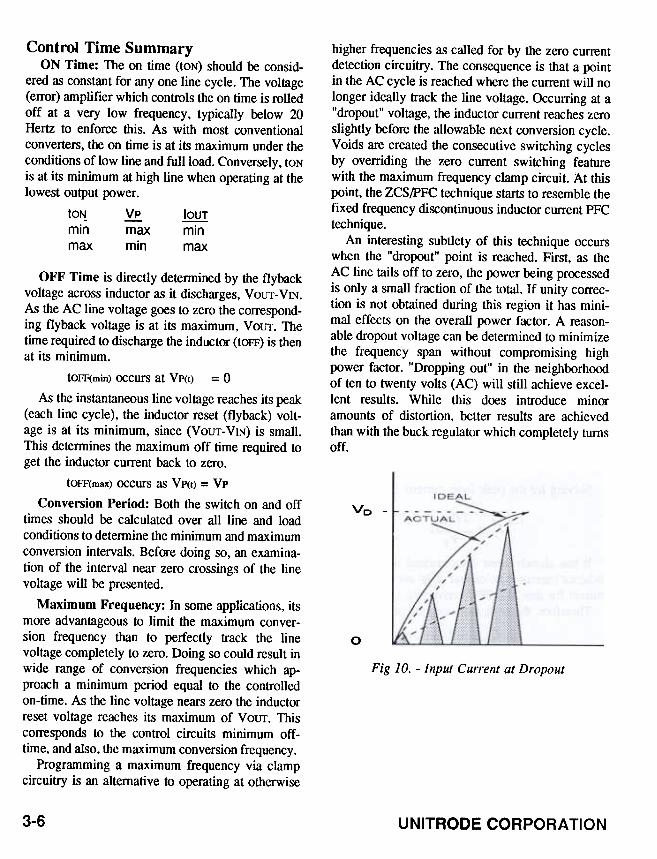
Control Time SummaryON Time: The on time (tON) should be consid-
ered as constant for anyone line cycle. The voltage(error) amplifier which controls the on time is rolledoff at a very low frequency, typically below 20Hertz to enforce this. As with most conventionalconverters, the on time is at its maximum under theconditions of low line and full load. Conversely, tONis at its minimum at high line when operating at thelowest output power.
toN. YE lour,min maxmax min
min
max
higher frequencies as called for by the zero currentdetection circuitry. The consequence is that a pointin the AC cycle is reached where the current will nolonger ideally track the line voltage. Occurring at a"dropout" voltage, the inductor current reaches zeroslightly before the allowable next conversion cycle.Voids are created the consecutive switching cyclesby overriding the zero current switching featurewith the maximum frequency clamp circuit. At thispoint, the ZCS/pFC technique starts to resemble thefixed frequency discontinuous inductor current PFC
technique.An interesting subtlety of this technique occurs
when the "dropout" point is reached. First, as theAC line tails off to zero, the power being processedis only a small fraction of the total. If unity correc-tion is not obtained during this region it has mini-mal effects on the overall power factor. A reason-able dropout voltage can be determined to minimizethe frequency span without compromising highpower factor. "Dropping out" in the neighborhoodof ten to twenty volts (AC) will still achieve excel-lent results. While this does introduce minoramounts of distortion, better results are achievedthan with the buck regulator which completely turnsoff.
IDEAL
Ac:;:~7
VD -
tr~..
OFF Time is directly detennined by the flybackvoltage across inductor as it discharges, VOUT-VIN.As the AC line voltage goes to zero the correspond-ing flyback voltage is at its maximum, VOUT. Thetime required to discharge the inductor (tOFF) is thenat its minimum.
tOFF(min) occurs at VP(t) = O
As the instantaneous line voltage reaches its peak(each line cycle), the inductor reset (flyback) volt-age is at its minimum, since (VOUT-VIN) is small.This detennines the maximum off time required toget the inductor current back to zero.
tOFF(max) occurs as VP(t) = VP
Conversion Period: Both the switch on and offtimes should be calculated over all line and loadconditions to detennine the minimum and maximumconversion intervals. Before doing so, an examina-tion of the interval near zero crossings of the linevoltage will be presented.
Maximum Frequency: In some applications, itsmore advantageous to limit the maximum conver-sion frequency than to perfectly track the linevoltage completely to zero. Doing so could result inwide range of conversion frequencies which ap-proach a minimum period equal to the controlledon-time. As the line voltage nears zero the inductorreset voltage reaches its maximum of VOUT. Thiscorresponds to the control circuits minimum off-time, and also, the maximum conversion frequency.
Programming a maximum frequency via clampcircuitry is an alternative to operating at otherwise
0
Fig 10. -Input Current at Dropout
3-6 UNITRODE CORPORATION
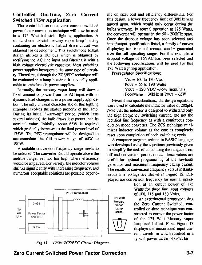
Controlled On- Time, Zero Current
Switched 175w ApplicationThe controlled on-time, zero current switched
power factor correction technique will now be usedin a 175 Watt industrial lighting application. Astandard commercial mercury vapor lamp housingcontaining an electronic ballast drive circuit wasobtained for development. This switchmode ballastdesign utilizes a DC bus which is obtained byrectifying the AC line input and filtering it with ahigh voltage electrolytic capacitor. Most switchingpower supplies incorporate the same type of circuit-ry .Therefore, although the ZCS/pFC technique willbe evaluated in a lamp housing, it is equally appli-cable to switchmode power supplies.
Normally, the mercury vapor lamp will draw afixed amount of power from the AC input with nodynamic load changes as in a power supply applica-tion. The only unusual characteristic of this lightingexample involves the startup property of the lamp.During its initial "warm-up" period (which lastsseveral minutes) the bulb draws less power than itsnominal value. Initially, about 65W is requiredwhich gradually increases to the final power level of175W. The PFC preregulator will be designed toaccommodate the full power range of 65W to190W.
A suitable conversion frequency range needs tobe selected. The converter should operate above theaudible range, yet not too high where efficiencywould be impaired. Conversely, the inductor volumeshrinks significantly with increasing frequency, andnumerous acceptable solutions are possible depend-
, .
1 PFC Preregulator i, ,, ,, ,
.-.J"TTT"r\.-~'175 Watt
'-'ercuryVaporLamp
Ballast
ing on size. cost and efficiency differentials. Forthis design. a lower frequency limit of 30kHz wasagreed upon. which would only occur during thebulbs warm-up. In normal operation at 175 Watts.the converter will operate in the 50 -200kHz span.Once the dropout voltage has been selected andinput/output specification listed. a family of curvesdisplaying tON. tOFF and tPERIOD can be generatedover the full operating ranges. For this example. adropout voltage of 15V AC has been selected andthe following specifications will be used for this175 Watt lighting application.
PrereguJator Specifications:VIN = 100 to 130 V ACPOUT = 65 to 190 WattsVOUT = 320 VDC +/-5% (nominal)FCONV(min) = 30kHz at POUT = 65W
Given these specifications. the design equationswere used to calculate the inductor value of 2OOpH.Note that the inductor is designed to withstand onlythe high frequency switching current. and not therectified line frequency as with a continuous con-duction mode converter. The ZCS technique mini-mizes inductor volume as the core is completelyreset upon completion of each switching cycle.
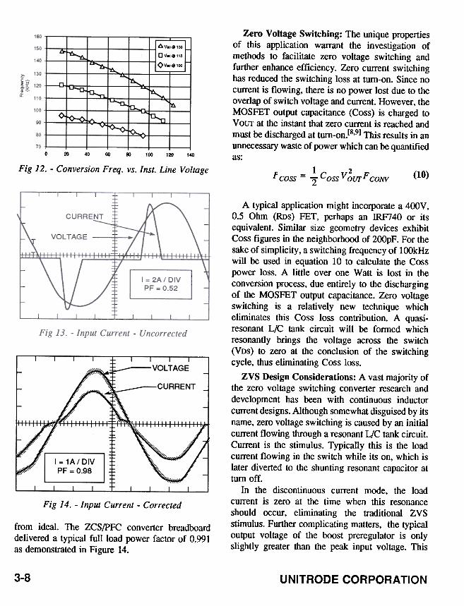
A computer program written in BASIC languagewas developed using the equations previously givento simplify the task of calculating the ranges of on.off and conversion period times. These values areuseful for optimal programming of the sawtoothgenerator and maximum frequency clamp circuit.The results of conversion frequency versus instanta-neous line voltage are shown in Figure 12. Dis-played are conversion frequency for normal opera-
tion at an output power of 175Watts for three line input voltagesof 100.115 and 130 Volts.
An experimental prototype usingthe Zero Current Switched. con-trolled on-time technique was con-structed to correct the power factorof the 175 Watt Mercury vaporlamp and ballast. First. Figure 13displays the uncorrected input cur-rent waveform which resulted in atypical power factor of 0.62. far
--?--
To
AC
Line
1!-
\Q7I-t-- --t---i :
175W ZCS/PFC Circuit DiagramFig 11
Zero Current Switched Power Factor Correction 3-7
Zero Voltage Switching: The unique propertiesof this application warrant the investigation ofmethods to facilitate zero voltage switching andfurther enhance efficiency. Zero current switchinghas reduced the switching loss at turn-on. Since nocurrent is flowing, there is no power lost due to theoverlap of switch voltage and current. However, theMOSFET output capacitance (Coss) is charged toVour at the instant that zero current is reached andmust be discharged at turn-on.[8,9] This results in anunnecessary waste of power which can be quantifiedas:
~j't.:t
~
~--a.~
~ ~~
~~ ~*-'*
~~
20 40 60 80 100 120 140
Fig 12. -Conversion Freq. vs. lnst. Line Voltage
(10)p1 2
COSS = -CossVOurFCONV
2
VOLTAGE
k--CURRENTc~
I 1~-1A/DIV II PF = 0.98 I
A typical application might incorporate a 400V,0.5 Ohm (RDs) PET, perhaps an IRF740 or itsequivalent. Similar size geometry devices exhibitCoss figures in the neighborhood of 200pF. For thesake of simplicity, a switching frequency of lOOkHzwill be used in equation 10 to calculate the Cosspower loss. A little over one Watt is lost in theconversion process, due entirely to the dischargingof the MOSPET output capacitance. Zero voltageswitching is a relatively new technique whicheliminates this Coss loss contribution. A quasi-resonant L/C tank circuit will be formed whichresonantly brings the voltage across the switch(VDS) to zero at the conclusion of the switchingcycle, thus eliminating Coss loss.
ZVS Design Considerations: A vast majority ofthe zero voltage switching converter research anddevelopment has been with continuous inductorcurrent designs. Although somewhat disguised by itsname, zero voltage switching is caused by an initialcurrent flowing through a resonant L/C tank circuit.Current is the stimulus. Typically this is the loadcurrent flowing in the switch while its on, which islater diverted to the shunting resonant capacitor atturn off.
In the discontinuous current mode, the loadcurrent is zero at the time when this resonanceshould occur, eliminating the traditional ZVSstimulus. Further complicating matters, the typicaloutput voltage of the boost preregulator is onlyslightly greater than the peak input voltage. This
Fig 14. -Input Current -Corrected
from ideal. The ZCS/pFC converter breadboarddelivered a typical full load power factor of 0.991as demonstrated in Figure 14.
3-8 UNITRODE CORPORATION
also be beneficial in lowering the EMI/RFI noise
generated.
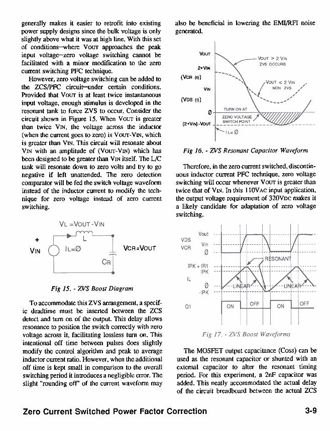
VOur'.t)UT > 2 VIN
ZVS OCCURS2.VIN
(VCR (1»
generally makes it easier to retrofit into existingpower supply designs since the bulk voltage is onlyslightly above what it was at high line. With this setof conditions-where Your approaches the peakinput voltage-zero voltage switching cannot befacilitated with a minor modification to the zerocurrent switching PFC technique.
However, zero voltage switching can be added tothe ZCS/pFC circuit-under certain conditions.Provided that Your is at least twice instantaneousinput voltage, enough stimulus is developed in theresonant tank to force ZYS to occur. Consider thecircuit shown in Figure 15. When YOUT is greaterthan twice YIN, the voltage across the inductor(when the current goes to zero) is YOUT-YIN, whichis greater than YIN. This circuit will resonate aboutYIN with an amplitude of (YOur-YIN) which hasbeen designed to be greater than YIN itself. The L/Ctank will resonate down to zero volts and try to gonegative if left unattended. The zero detectioncomparator will be fed the switch voltage waveforminstead of the inductor current to modify the tech-nique for zero voltage instead of zero cuITent
switching.
VIN
(VDS (I) )
I VOUT < 2 VIN
NON ZVS'
" .-',--~.-
0ZERO VOLTAGE /SWITCH POINT
(2.VIN)-VOUT
Fig 16. -ZVS Resonant Capacitor Waveform
Therefore, in the zero current switched, discontin-uous inductor current PFC technique, zero voltageswitching will occur whenever VOUT is greater thantwice that of VIN. In this 110V AC input application,the output voltage requirement of 320VDC makes ita likely candidate for adaptation of zero voltage
switching.
+VCR=VOUTVIN
Fig 15. -ZVS Boost Diagram
To accommodate this ZVS arrangement, a specif-ic deadtime must be inserted between the ZCSdetect and turn on of the output. This delay allowsresonance to position the switch correctly with zerovoltage across it, facilitating lossless turn on. Thisintentional off time between pulses does slightlymodify the control algorithm and peak to averageinductor current ratio. However, when the additionaloff time is kept small in comparison to the overallswitching period it introduces a negligible error. Theslight "rounding off' of the current waveform may
The MOSFET output capacitance (Coss) can beused as the resonant capacitor or shunted with anexternal capacitor to alter the resonant timingperiod. For this experiment. a 2nF capacitor wasadded. This neatly accommodated the actual delayof the circuit breadboard between the actual ZCS
3-9Zero Current Switched Power Factor Correction
ConclusionsThe controlled on time, zero current switched
PFC technique is applicable to numerous low powerapplications and offers promising results. Addition-ally, the inherent simplicity of this technique is alsoattractive, luring the attention from cost sensitiveindustries, such as the under 300 watt power supplyand even industrial lighting manufacturers. Experi-mental laboratory results demonstrate an obtainablepower factor in excess of 0.99 at a power levels of175 Watts in an typical application. Finally, withproper selection of output voltage, based on theinput AC mains, the conversion technique can beexpanded to exhibit lossless Zero Voltage Switchingof the PFC preregulator switch. The continuation ofresearch and development in low cost power con-version solutions will overcome the challenges ofobtaining high performance in a variety of lowpower and cost sensitive applications.
detect comparator and turn-on of the switch. Thiswas also enough capacitance to divert current fromthe switch to the resonant capacitor at turn-off, thusreducing the corresponding PET losses.
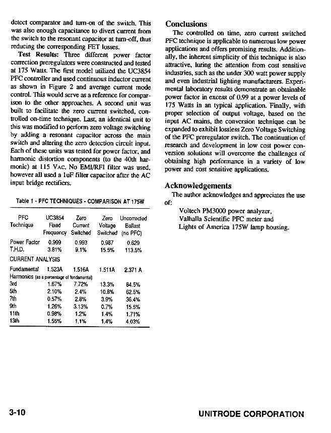
Test Results: Three different power factorcorrection preregulators were constructed and testedat 175 Watts. The fIrst model utilized the UC3854PFC controller and used continuous inductor currentas shown in Figure 2 and average current modecontrol. This would serve as a reference for compar-ison to the other approaches. A second unit wasbuilt to facilitate the zero current switched, con-trolled on-time technique. Last. an identical unit tothis was modified to perform zero voltage switchingby adding a resonant capacitor across the mainswitch and altering the zero detection circuit input.Each of these units was tested for power factor, andharmonic distortion components (to the 40th har-monic) at 115 V AC. No EMI/RFI fIlter was used,however all used a luF filter capacitor after the ACinput bridge rectifiers.
AcknowledgementsThe author acknowledges and appreciates the use
Table 1 .PFC TECHNIQUES. COMPARISON AT 175W of:
Voltech PM3()()() power analyzer,
Valhalla Scientific PFC meter and
Lights of America 175W lamp housing.
PFC UC3854 Zero Zero Uncorrected
Technique Fixed Currenl Vollage BaJlasl
Frequency Swilched Swilched (no PFC)
Power Factor 0.999 0.993 0.987 0.629
T.H.D. 3.81% 9.1% 15.5% 113.5%
CURRENT ANAL YSIS
FundamenlaJ 1.523A 1.516A 1.511A 2.371 A
Harmonics (as a percentage of fundamentaQ
3rd 1.67% 7.7~/o 13.3%
51h 2.10% 2.4% 10.8%
71h 0.57% 2.8% 3.9%
9Ih 1.26% 3.13% 0.7%
111h 0.98% 1.~/0 1.4%
131h 1.55% 1.1% 1.4%
84.5%62.5%36.4%15.5%1.71%4.03%
3-10 UNITRODE CORPORATION
the PFC techniques shown in the beginning of thispaper are equally applicable to the flyback topology.
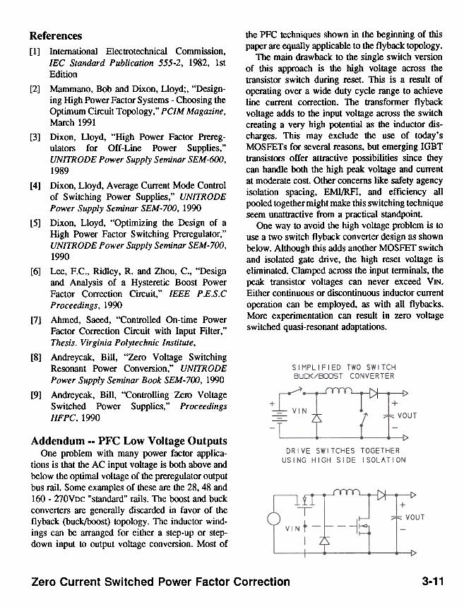
The main drawback to the single switch versionof this approach is the high voltage across thetransistor switch during reset. This is a result ofoperating over a wide duty cycle range to achieveline current correction. The transformer flybackvoltage adds to the input voltage across the switchcreating a very high potential as the inductor dis-charges. This may exclude the use of today'sMOSFETs for several reasons, but emerging IGBTtransistors offer attractive possibilities since theycan handle both the high peak voltage and currentat moderate cost. Other concerns like safety agencyisolation spacing, EMI/RFI, and efficiency allpooled together might make this switching techniqueseem unattractive from a practical standpoint
One way to avoid the high voltage problem is touse a two switch flyback converter design as shownbelow. Although this adds another MOSFET switchand isolated gate drive, the high reset voltage iseliminated. Clamped across the input terminals, thepeak transistor voltages can never exceed VIN.Either continuous or discontinuous inductor currentoperation can be employed, as with all flybacks.More experimentation can result in zero voltageswitched quasi-resonant adaptations.
References
[1] International Electrotechnical Commission,IEC Standard Publication 555-2, 1982, IstEdition
[2] Mammano, Bob and Dixon, Lloyd;, "Design-ing High Power Factor Systems -Choosing theOptimum Circuit Topology ," PCIM Magazine .March 1991
[3] Dixon, Lloyd, "High Power Factor Prereg-ulators for Off-Line Power Supplies,"UNITRODE Power Supply Seminar SEM-600,1989
[4] Dixon, Lloyd, A verage Current Mode Controlof Switching Power Supplies," UNITRODEPower Supply Seminar SEM-700, 1990
[5] Dixon, Lloyd, "Optimizing the Design of aHigh Power Factor Switching Preregulator,"UNITRODE Power Supply Seminar SEM- 700,1990
[6] Lee, F.C., Ridley, R. and Zhou, C., "Designand Analysis of a Hysteretic Boost PowerFactor Correction Circuit," IEEE P.E.S.CProceedings, 1990
[7] Ahmed, Saeed, "Controlled On-time PowerFactor Correction Circuit with Input Filter,"Thesis. Virginia Polytechnic Institute,
[8] Andreycak, Bill, "Zero Voltage SwitchingResonant Power Conversion," UNITRODEPower Supply Seminar Book SEM-700, 1990
[9] Andreycak, Bill, "Controlling Zero VoltageSwitched Power Supplies," ProceedingsHFPC, 1990
Addendum --PFC Low Voltage OutputsOne problem with many power factor applica-
tions is that the AC input voltage is both above andbelow the optimal voltage of the preregulator outputbus rail. Some examples of these are the 28,48 and160 -270VDC "standard" rails. The boost and buckconverters are generally discarded in favor of theflyback (buck/boost) topology. The inductor wind-ings can be arranged for either a step-up or step-down input to output voltage conversion. Most of
3-11Zero Current Switched Power Factor Correction

IMPORTANT NOTICE
Texas Instruments and its subsidiaries (TI) reserve the right to make changes to their products or to discontinueany product or service without notice, and advise customers to obtain the latest version of relevant informationto verify, before placing orders, that information being relied on is current and complete. All products are soldsubject to the terms and conditions of sale supplied at the time of order acknowledgment, including thosepertaining to warranty, patent infringement, and limitation of liability.
TI warrants performance of its products to the specifications applicable at the time of sale in accordance withTI’s standard warranty. Testing and other quality control techniques are utilized to the extent TI deems necessaryto support this warranty. Specific testing of all parameters of each device is not necessarily performed, exceptthose mandated by government requirements.
Customers are responsible for their applications using TI components.
In order to minimize risks associated with the customer’s applications, adequate design and operatingsafeguards must be provided by the customer to minimize inherent or procedural hazards.
TI assumes no liability for applications assistance or customer product design. TI does not warrant or representthat any license, either express or implied, is granted under any patent right, copyright, mask work right, or otherintellectual property right of TI covering or relating to any combination, machine, or process in which suchproducts or services might be or are used. TI’s publication of information regarding any third party’s productsor services does not constitute TI’s approval, license, warranty or endorsement thereof.
Reproduction of information in TI data books or data sheets is permissible only if reproduction is withoutalteration and is accompanied by all associated warranties, conditions, limitations and notices. Representationor reproduction of this information with alteration voids all warranties provided for an associated TI product orservice, is an unfair and deceptive business practice, and TI is not responsible nor liable for any such use.
Resale of TI’s products or services with statements different from or beyond the parameters stated by TI forthat product or service voids all express and any implied warranties for the associated TI product or service,is an unfair and deceptive business practice, and TI is not responsible nor liable for any such use.
Also see: Standard Terms and Conditions of Sale for Semiconductor Products. www.ti.com/sc/docs/stdterms.htm
Mailing Address:
Texas InstrumentsPost Office Box 655303Dallas, Texas 75265
Copyright 2001, Texas Instruments Incorporated