Contribution of structural order-disorder to the green photoluminescence of PbWO4
11
Contribution of structural order-disorder to the green photoluminescence of PbWO 4 M. Anicete-Santos, 1,2, * E. Orhan, 3 M. A. M. A. de Maurera, 4 L. G. P. Simões, 1 A. G. Souza, 4 P. S. Pizani, 5 E. R. Leite, 1 J. A. Varela, 6 Juan Andrés, 2 A. Beltrán, 2 and E. Longo 6 1 LIEC, Department of Chemistry, Federal University of São Carlos (UFSCAR), P.O. Box 676, 13565-905, São Carlos, São Paulo, Brazil 2 Departament de Ciències Experimentals, Universitat Jaume I, P.O. Box 224, 12080, Castelló, Spain 3 Science des Procédés Céramiques et de Traitements de Surface, UMR CNRS 6638, Faculté des Sciences et Techniques, Université de Limoges, 87060 Limoges Cedex, France 4 Department of Chemistry, Federal University of Paraíba, 58059-900, João Pessoa, Paraíba, Brazil 5 Department of Physics, UFSCAR, P.O. Box 676, 13565-905, São Carlos, São Paulo, Brazil 6 LIEC, Institute of Chemistry, UNESP, P.O. Box 355, 14801-907, Araraquara, São Paulo, Brazil Received 25 September 2006; revised manuscript received 15 January 2007; published 11 April 2007 An intense and broad visible photoluminescence PL band was observed at room temperature in structurally disordered PbWO 4 thin films. The scheelite lead tungstate PbWO 4 films prepared by the polymeric precursor method and annealed at different temperatures were structurally characterized by means of x-ray diffraction and atomic force microscopy analysis. Quantum-mechanical calculations showed that the local disorder of the network modifier Pb has a very important role in the charge transfer involved in the green PL emission. The experimental and theoretical results are in good agreement, both indicating that the generation of the intense visible PL band is related to simultaneous structural order and disorder in the scheelite PbWO 4 lattice. DOI: 10.1103/PhysRevB.75.165105 PACS numbers: 71.15.Mb, 71.20.Nr, 71.23.An, 78.55.Ap I. INTRODUCTION There is an increasing demand for light-emitting devices for displays and communication. In many optoelectronic de- vices, noncrystalline semiconductors can replace crystalline ones, mainly when they present better optical properties. Numerous investigations of the PL property of scheelite lead tungstate PbWO 4 PWO crystals have been carried out for several decades. 1–15 In particular, the undoped PWO crystal has attracted much interest because of plans to use it as a scintillation detector at the Large Hadron Collider in CERN. 4,6,10,16–19 Nevertheless, the understanding of PWO spectral behav- ior is still debated and some problems are left unsolved. 20–23 For example, numerous experimental works directed at iden- tifying several types of defects and their spectral roles in PWO have recently been published. 24–29 Particularly, there are discussions 30,31 over the contribu- tion of color centers to the photoluminescence PL emission band, mainly to the green emission band. Groenink and Blasse 2 and Korzhik’s group 4,7,32,33 concluded that the green emission originated from the WO 3 + F center in undoped PWO crystal, where F is an electron bound to a negative ion vacancy. Sokolenko et al. 34 attributed the green-red emission to WO 3 · V O ·· oxygen-deficient complexes, and Sinelnikov et al. 35 suggest that the WO 4 tetrahedra distorted upon the for- mation of oxygen vacancies V O ·· are responsible for the green luminescence band. On the other hand, Shi and co-workers 30,31,36 suggest the WO 4 +O i center as the green luminescence center, while Huang et al. 37 conclude that the interstitial oxygen O i enhances the green luminescence. These different interpretations are supported by distinct syn- thesis conditions and methods so that they are not contradic- tory but rather complementary. Although there have been numerous studies on the PWO material, the literature has not yet reported on the PL prop- erty in noncrystalline structurally disordered PWO. In this paper, we present measurements of an intense and broad visible PL band at room temperature in structurally disordered PWO thin films that have undergone insufficient thermal annealing to reach crystallization. These thin films were prepared by means of polymeric precursor method. 38–41 This process offers advantages over several synthesis tech- niques such as low cost, good compositional homogeneity, high purity, low processing temperatures, and the ability to coat large substrate areas. The origin of the intense and broad PL band in PWO compound containing simultaneous struc- tural order and disorder order-disorder in its lattice is in- vestigated in terms of electronic structure calculations real- ized in the framework of ab initio periodic quantum- mechanical techniques. The aim of our synergistic strategy between experimental and theoretical results is not to explain all the possible PL mechanisms that occur during the photon excitation and decay processes, as many valid hypotheses already exist in the literature, but to discuss the role of struc- tural order-disorder in the PL mechanism and why it pro- vides favorable conditions for the generation of an intense and broad band. The layout of the paper is as follows: In Sec. II, the ex- perimental methods of the PWO preparation are described, together with spectral measurement techniques. Section III presents the computational details, while Sec. IV gives the crystal structure and periodic models used in the calcula- tions. In Sec. V, the results are discussed, attempting to ex- plain that the PL emission depends from the structural order- disorder degree in the PWO lattice. Finally, Sec. VI resumes the main lines of our hypothesis on the origin of the strong PL at room temperature in PWO thin films. II. EXPERIMENT The flowchart of the PWO synthesis used in this study is outlined in Fig. 1. Tungsten citrate was formed by dissolu- PHYSICAL REVIEW B 75, 165105 2007 1098-0121/2007/7516/16510511 ©2007 The American Physical Society 165105-1
-
Upload
independent -
Category
Documents
-
view
1 -
download
0
Transcript of Contribution of structural order-disorder to the green photoluminescence of PbWO4
Contribution of structural order-disorder to the green photoluminescence of PbWO4
M. Anicete-Santos,1,2,* E. Orhan,3 M. A. M. A. de Maurera,4 L. G. P. Simões,1 A. G. Souza,4 P. S. Pizani,5 E. R. Leite,1
J. A. Varela,6 Juan Andrés,2 A. Beltrán,2 and E. Longo6
1LIEC, Department of Chemistry, Federal University of São Carlos (UFSCAR), P.O. Box 676, 13565-905, São Carlos, São Paulo, Brazil2Departament de Ciències Experimentals, Universitat Jaume I, P.O. Box 224, 12080, Castelló, Spain
3Science des Procédés Céramiques et de Traitements de Surface, UMR CNRS 6638, Faculté des Sciences et Techniques,Université de Limoges, 87060 Limoges Cedex, France
4Department of Chemistry, Federal University of Paraíba, 58059-900, João Pessoa, Paraíba, Brazil5Department of Physics, UFSCAR, P.O. Box 676, 13565-905, São Carlos, São Paulo, Brazil
6LIEC, Institute of Chemistry, UNESP, P.O. Box 355, 14801-907, Araraquara, São Paulo, Brazil�Received 25 September 2006; revised manuscript received 15 January 2007; published 11 April 2007�
An intense and broad visible photoluminescence �PL� band was observed at room temperature in structurallydisordered PbWO4 thin films. The scheelite lead tungstate �PbWO4� films prepared by the polymeric precursormethod and annealed at different temperatures were structurally characterized by means of x-ray diffractionand atomic force microscopy analysis. Quantum-mechanical calculations showed that the local disorder of thenetwork modifier �Pb� has a very important role in the charge transfer involved in the green PL emission. Theexperimental and theoretical results are in good agreement, both indicating that the generation of the intensevisible PL band is related to simultaneous structural order and disorder in the scheelite PbWO4 lattice.
DOI: 10.1103/PhysRevB.75.165105 PACS number�s�: 71.15.Mb, 71.20.Nr, 71.23.An, 78.55.Ap
I. INTRODUCTION
There is an increasing demand for light-emitting devicesfor displays and communication. In many optoelectronic de-vices, noncrystalline semiconductors can replace crystallineones, mainly when they present better optical properties.
Numerous investigations of the PL property of scheelitelead tungstate �PbWO4 �PWO�� crystals have been carriedout for several decades.1–15 In particular, the undoped PWOcrystal has attracted much interest because of plans to use itas a scintillation detector at the Large Hadron Collider inCERN.4,6,10,16–19
Nevertheless, the understanding of PWO spectral behav-ior is still debated and some problems are left unsolved.20–23
For example, numerous experimental works directed at iden-tifying several types of defects and their spectral roles inPWO have recently been published.24–29
Particularly, there are discussions30,31 over the contribu-tion of color centers to the photoluminescence �PL� emissionband, mainly to the green emission band. Groenink andBlasse2 and Korzhik’s group4,7,32,33 concluded that the greenemission originated from the �WO3+F� center in undopedPWO crystal, where F is an electron bound to a negative ionvacancy. Sokolenko et al.34 attributed the green-red emissionto �WO3·VO
·· � oxygen-deficient complexes, and Sinelnikov etal.35 suggest that the WO4 tetrahedra distorted upon the for-mation of oxygen vacancies VO
·· are responsible for the greenluminescence band. On the other hand, Shi andco-workers30,31,36 suggest the �WO4+Oi� center as the greenluminescence center, while Huang et al.37 conclude that theinterstitial oxygen Oi enhances the green luminescence.These different interpretations are supported by distinct syn-thesis conditions and methods so that they are not contradic-tory but rather complementary.
Although there have been numerous studies on the PWOmaterial, the literature has not yet reported on the PL prop-
erty in noncrystalline �structurally disordered� PWO.In this paper, we present measurements of an intense and
broad visible PL band at room temperature in structurallydisordered PWO thin films that have undergone insufficientthermal annealing to reach crystallization. These thin filmswere prepared by means of polymeric precursor method.38–41
This process offers advantages over several synthesis tech-niques such as low cost, good compositional homogeneity,high purity, low processing temperatures, and the ability tocoat large substrate areas. The origin of the intense and broadPL band in PWO compound containing simultaneous struc-tural order and disorder �order-disorder� in its lattice is in-vestigated in terms of electronic structure calculations real-ized in the framework of ab initio periodic quantum-mechanical techniques. The aim of our synergistic strategybetween experimental and theoretical results is not to explainall the possible PL mechanisms that occur during the photonexcitation and decay processes, as many valid hypothesesalready exist in the literature, but to discuss the role of struc-tural order-disorder in the PL mechanism and why it pro-vides favorable conditions for the generation of an intenseand broad band.
The layout of the paper is as follows: In Sec. II, the ex-perimental methods of the PWO preparation are described,together with spectral measurement techniques. Section IIIpresents the computational details, while Sec. IV gives thecrystal structure and periodic models used in the calcula-tions. In Sec. V, the results are discussed, attempting to ex-plain that the PL emission depends from the structural order-disorder degree in the PWO lattice. Finally, Sec. VI resumesthe main lines of our hypothesis on the origin of the strongPL at room temperature in PWO thin films.
II. EXPERIMENT
The flowchart of the PWO synthesis used in this study isoutlined in Fig. 1. Tungsten citrate was formed by dissolu-
PHYSICAL REVIEW B 75, 165105 �2007�
1098-0121/2007/75�16�/165105�11� ©2007 The American Physical Society165105-1
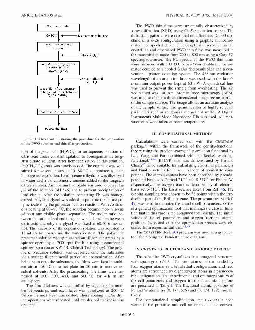
tion of tungstic acid �H2WO4� in an aqueous solution ofcitric acid under constant agitation to homogenize the tung-sten citrate solution. After homogenization of this solution,Pb�CH3CO2�2 salt was slowly added. The complex was wellstirred for several hours at 70–80 °C to produce a clear,homogeneous solution. Lead acetate trihydrate was dissolvedin water and a stoichiometric amount added to the tungstencitrate solution. Ammonium hydroxide was used to adjust thepH of the solution �pH 5–6� and to prevent precipitation oflead citrate. After the solution containing Pb was homog-enized, ethylene glycol was added to promote the citrate po-lymerization by the polyesterification reaction. With continu-ous heating at 80–90 °C, the solution became more viscouswithout any visible phase separation. The molar ratio be-tween the cations lead and tungsten was 1:1 and that betweencitric acid and ethylene glycol was fixed at 60:40 �mass ra-tio�. The viscosity of the deposition solution was adjusted to15 mPa s by controlling the water content. The polymericprecursor solution was spin coated on silicon substrates by aspinner operating at 7000 rpm for 40 s using a commercialspinner �spin coater KW-4B, Chemat Technology�. The poly-meric precursor solution was deposited onto the substratesvia a syringe filter to avoid particulate contamination. Afterbeing spun onto the substrates, the films were kept in ambi-ent air at 150 °C on a hot plate for 20 min to remove re-sidual solvents. After the preannealing, the films were an-nealed at 200, 300, 400, and 500 °C for 4 h in airatmosphere.
The film thickness was controlled by adjusting the num-ber of coatings, and each layer was pyrolyzed at 200 °Cbefore the next layer was coated. These coating and/or dry-ing operations were repeated until the desired thickness wasobtained.
The PWO thin films were structurally characterized byx-ray diffraction �XRD� using Cu K� radiation source. Thediffraction patterns were recorded on a Siemens D5000 ma-chine in a �-2� configuration using a graphite monochro-mator. The spectral dependence of optical absorbance for thecrystalline and disordered PWO thin films was measured inthe transmission mode from 200 to 800 nm using a Cary 5Gspectrophotometer. The PL spectra of the PWO thin filmswere recorded with a U1000 Jobin-Yvon double monochro-mator coupled to a cooled GaAs photomultiplier and a con-ventional photon counting system. The 488 nm excitationwavelength of an argon-ion laser was used, with the laser’smaximum output power kept at 60 mW. A cylindrical lenswas used to prevent the sample from overheating. The slitwidth used was 100 �m. Atomic force microscopy �AFM�was used to obtain a three-dimensional image reconstructionof the sample surface. The image allows an accurate analysisof the sample surface and quantification of highly relevantparameters such as roughness and grain diameter. A DigitalInstruments MultiMode Nanoscope IIIa was used. All mea-surements were taken at room temperature.
III. COMPUTATIONAL METHODS
Calculations were carried out with the CRYSTAL03
package42 within the framework of the density-functionaltheory using the gradient-corrected correlation functional byLee, Yang, and Parr combined with the Becke3 exchangefunctional,43,44 �B3LYP� that was demonstrated by Hu andChong45 to be suitable for calculating structural parametersand band structures for a wide variety of solid-state com-pounds. The atomic centers have been described by pseudo-potential basis sets Durand-21G* and 8-51G* for Pb and W,respectively. The oxygen atom is described by all electronbasis set 6-31G*. The basis sets are taken from Ref. 46. Thek-point sampling was chosen to be 36 points within the irre-ducible part of the Brillouin zone. The program OPTIM �Ref.47� was used to optimize the a and c cell parameters. OPTIM
is a general optimization tool that minimizes a chosen func-tion that in this case is the computed total energy. The initialvalues of the cell parameters and oxygen fractional atomicpositions �x, y, and z� in the optimization process were ob-tained from experimental data.48,49
The XCRYSDEN �Ref. 50� program was used as a graphicaltool for ploting the band-structure diagrams.
IV. CRYSTAL STRUCTURE AND PERIODIC MODELS
The scheelite PWO crystallizes in a tetragonal structure,with space group I41/a. Tungsten atoms are surrounded byfour oxygen atoms in a tetrahedral configuration, and leadatoms are surrounded by eight oxygen atoms in a pseudocu-bic configuration. The experimental and optimized values ofthe cell parameters and oxygen fractional atomic positionsare presented in Table I. The fractional atomic positions ofPb and W atoms are �0, 1 /4, 5 /8� and �0, 1 /4, 1 /8�, respec-tively.
For computational simplification, the CRYSTAL03 codeworks in the primitive unit cell rather than in the conven-
FIG. 1. Flowchart illustrating the procedure for the preparationof the PWO solution and thin-film production.
ANICETE-SANTOS et al. PHYSICAL REVIEW B 75, 165105 �2007�
165105-2
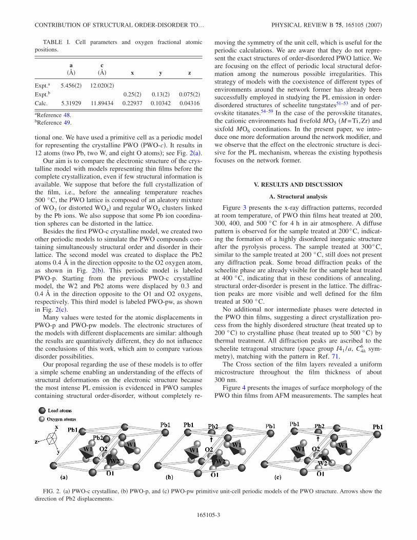
tional one. We have used a primitive cell as a periodic modelfor representing the crystalline PWO �PWO-c�. It results in12 atoms �two Pb, two W, and eight O atoms�; see Fig. 2�a�.
Our aim is to compare the electronic structure of the crys-talline model with models representing thin films before thecomplete crystallization, even if few structural information isavailable. We suppose that before the full crystallization ofthe film, i.e., before the annealing temperature reaches500 °C, the PWO lattice is composed of an aleatory mixtureof WO3 �or distorted WO4� and regular WO4 clusters linkedby the Pb ions. We also suppose that some Pb ion coordina-tion spheres can be distorted in the lattice.
Besides the first PWO-c crystalline model, we created twoother periodic models to simulate the PWO compounds con-taining simultaneously structural order and disorder in theirlattice. The second model was created to displace the Pb2atoms 0.4 Å in the direction opposite to the O2 oxygen atom,as shown in Fig. 2�b�. This periodic model is labeledPWO-p. Starting from the previous PWO-c crystallinemodel, the W2 and Pb2 atoms were displaced by 0.3 and0.4 Å in the direction opposite to the O1 and O2 oxygens,respectively. This third model is labeled PWO-pw, as shownin Fig. 2�c�.
Many values were tested for the atomic displacements inPWO-p and PWO-pw models. The electronic structures ofthe models with different displacements are similar: althoughthe results are quantitatively different, they do not influencethe conclusions of this work, which aim to compare variousdisorder possibilities.
Our proposal regarding the use of these models is to offera simple scheme enabling an understanding of the effects ofstructural deformations on the electronic structure becausethe most intense PL emission is evidenced in PWO samplescontaining structural order-disorder, without completely re-
moving the symmetry of the unit cell, which is useful for theperiodic calculations. We are aware that they do not repre-sent the exact structures of order-disordered PWO lattice. Weare focusing on the effect of periodic local structural defor-mation among the numerous possible irregularities. Thisstrategy of models with the coexistence of different types ofenvironments around the network former has already beensuccessfully employed in studying the PL emission in order-disordered structures of scheelite tungstates51–53 and of per-ovskite titanates.54–59 In the case of the perovskite titanates,the cationic environments had fivefold MO5 �M =Ti,Zr� andsixfold MO6 coordinations. In the present paper, we intro-duce one more deformation around the network modifier, andwe observe that the effect on the electronic structure is deci-sive for the PL mechanism, whereas the existing hypothesisfocuses on the network former.
V. RESULTS AND DISCUSSION
A. Structural analysis
Figure 3 presents the x-ray diffraction patterns, recordedat room temperature, of PWO thin films heat treated at 200,300, 400, and 500 °C for 4 h in air atmosphere. A diffusepattern is observed for the sample treated at 200°C, indicat-ing the formation of a highly disordered inorganic structureafter the pyrolysis process. The sample treated at 300°C,similar to the sample treated at 200 °C, still does not presentany diffraction peak. Some broad diffraction peaks of thescheelite phase are already visible for the sample heat treatedat 400 °C, indicating that in these conditions of annealing,structural order-disorder is present in the lattice. The diffrac-tion peaks are more visible and well defined for the filmtreated at 500 °C.
No additional nor intermediate phases were detected inthe PWO thin films, suggesting a direct crystallization pro-cess from the highly disordered structure �heat treated up to200 °C� to crystalline phase �heat treated up to 500 °C� bythermal treatment. All diffraction peaks are ascribed to thescheelite tetragonal structure �space group I41/a, C4h
6 sym-metry�, matching with the pattern in Ref. 71.
The Cross section of the film layers revealed a uniformmicrostructure throughout the film thickness of about300 nm.
Figure 4 presents the images of surface morphology of thePWO thin films from AFM measurements. The samples heat
TABLE I. Cell parameters and oxygen fractional atomicpositions.
a��
c�� x y z
Expt.a 5.456�2� 12.020�2�Expt.b 0.25�2� 0.13�2� 0.075�2�Calc. 5.31929 11.89434 0.22937 0.10342 0.04316
aReference 48.bReference 49.
FIG. 2. �a� PWO-c crystalline, �b� PWO-p, and �c� PWO-pw primitive unit-cell periodic models of the PWO structure. Arrows show thedirection of Pb2 displacements.
CONTRIBUTION OF STRUCTURAL ORDER-DISORDER TO… PHYSICAL REVIEW B 75, 165105 �2007�
165105-3
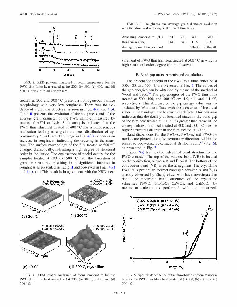
treated at 200 and 300 °C present a homogeneous surfacemorphology with very low roughness. There was no evi-dence of a granular structure, as seen in Figs. 4�a� and 4�b�.Table II presents the evolution of the roughness and of theaverage grain diameter of the PWO samples measured bymeans of AFM analysis. Such analysis indicates that thePWO thin film heat treated at 400 °C has a homogeneousnucleation leading to a grain diameter distribution of ap-proximately 50–60 nm. The image in Fig. 4�c� evidences anincrease in roughness, indicating the ordering in the struc-ture. The surface morphology of the film treated at 500 °Cchanges dramatically, indicating a high degree of structuralorder in the lattice. The coalescence of nuclei occurs for thesamples treated at 400 and 500 °C with the formation ofgranular structures, resulting in a significant increase inroughness as presented in Table II and observed in Figs. 4�c�and 4�d�. and This result is in agreement with the XRD mea-
surement of PWO thin film heat treated at 500 °C in which ahigh structural order degree can be observed.
B. Band-gap measurements and calculations
The absorbance spectra of the PWO thin films annealed at300, 400, and 500 °C are presented in Fig. 5. The values ofthe gap energies can be obtained by means of the method ofWood and Tauc.60 The gap energies of the PWO thin filmstreated at 500, 400, and 300 °C are 4.5, 4.4, and 4.1 eV,respectively. This decrease of the gap energy value was as-sociated by Wood and Tauc with the existence of localizedstates in the band gap due to structural defects. This behaviorindicates that the density of localized states in the band gapof the film heat treated at 300 °C is greater than those of thecorresponding films heat treated at 400 and 500 °C due thehigher structural disorder in the film treated at 300 °C.
Band dispersions for the PWO-c, PWO-p, and PWO-pwmodels are plotted along five symmetry directions within theprimitive body-centered-tetragonal Brillouin zone61 �Fig. 6�,as presented in Fig. 7.
Figure 7�a� features the calculated band structure for thePWO-c model. The top of the valence band �VB� is locatedon the � direction, between X and � point. The bottom of theconduction band �VB� is on the � segment. The crystallinePWO thus present an indirect band gap between � and �, asalready observed by Zhang et al. who have investigated indetail the electronic band structures of the crystallinescheelites PbWO4, PbMoO4 CaWO4, and CaMoO4, bymeans of calculations performed with the linearized-
TABLE II. Roughness and average grain diameter evolutionwith the structural ordering of the PWO thin films.
Annealing temperatures �°C� 200 300 400 500
Roughness �nm� 0.41 0.42 1.15 9.31
Average grain diameter �nm� 50–60 260–270
FIG. 3. XRD patterns measured at room temperature for thePWO thin films heat treated at �a� 200, �b� 300, �c� 400, and �d�500 °C for 4 h in air atmosphere.
FIG. 4. AFM images measured at room temperature for thePWO thin films heat treated at �a� 200, �b� 300, �c� 400, and �d�500 °C.
FIG. 5. Spectral dependence of the absorbance at room tempera-ture for the PWO thin films heat treated at �a� 300, �b� 400, and �c�500 °C.
ANICETE-SANTOS et al. PHYSICAL REVIEW B 75, 165105 �2007�
165105-4
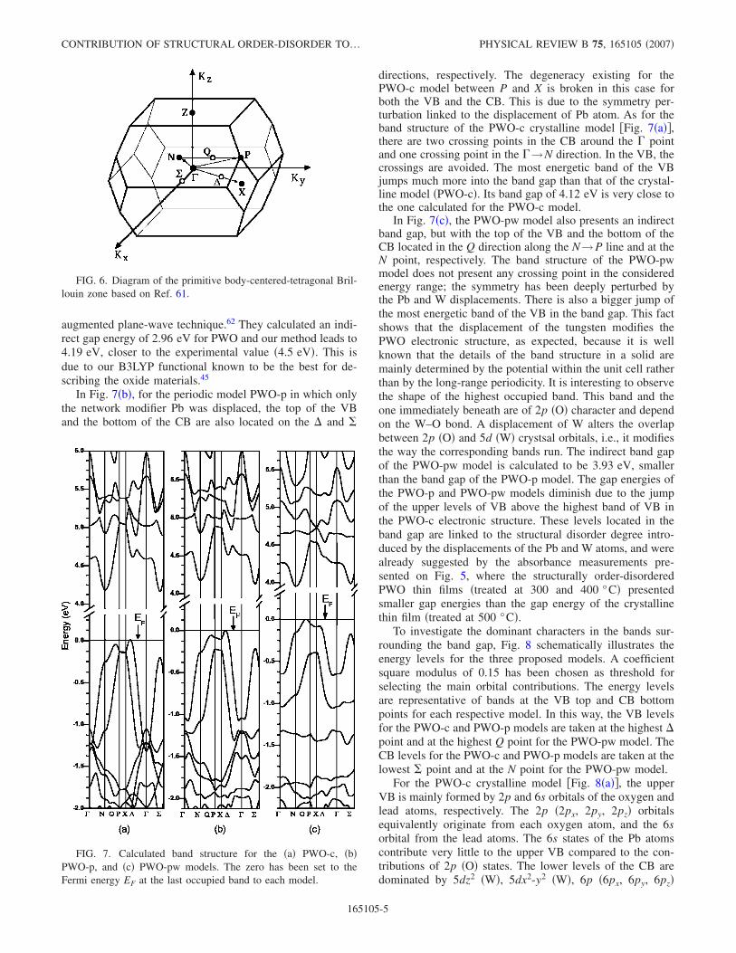
augmented plane-wave technique.62 They calculated an indi-rect gap energy of 2.96 eV for PWO and our method leads to4.19 eV, closer to the experimental value �4.5 eV�. This isdue to our B3LYP functional known to be the best for de-scribing the oxide materials.45
In Fig. 7�b�, for the periodic model PWO-p in which onlythe network modifier Pb was displaced, the top of the VBand the bottom of the CB are also located on the � and �
directions, respectively. The degeneracy existing for thePWO-c model between P and X is broken in this case forboth the VB and the CB. This is due to the symmetry per-turbation linked to the displacement of Pb atom. As for theband structure of the PWO-c crystalline model �Fig. 7�a��,there are two crossing points in the CB around the � pointand one crossing point in the �→N direction. In the VB, thecrossings are avoided. The most energetic band of the VBjumps much more into the band gap than that of the crystal-line model �PWO-c�. Its band gap of 4.12 eV is very close tothe one calculated for the PWO-c model.
In Fig. 7�c�, the PWO-pw model also presents an indirectband gap, but with the top of the VB and the bottom of theCB located in the Q direction along the N→P line and at theN point, respectively. The band structure of the PWO-pwmodel does not present any crossing point in the consideredenergy range; the symmetry has been deeply perturbed bythe Pb and W displacements. There is also a bigger jump ofthe most energetic band of the VB in the band gap. This factshows that the displacement of the tungsten modifies thePWO electronic structure, as expected, because it is wellknown that the details of the band structure in a solid aremainly determined by the potential within the unit cell ratherthan by the long-range periodicity. It is interesting to observethe shape of the highest occupied band. This band and theone immediately beneath are of 2p �O� character and dependon the W–O bond. A displacement of W alters the overlapbetween 2p �O� and 5d �W� crystsal orbitals, i.e., it modifiesthe way the corresponding bands run. The indirect band gapof the PWO-pw model is calculated to be 3.93 eV, smallerthan the band gap of the PWO-p model. The gap energies ofthe PWO-p and PWO-pw models diminish due to the jumpof the upper levels of VB above the highest band of VB inthe PWO-c electronic structure. These levels located in theband gap are linked to the structural disorder degree intro-duced by the displacements of the Pb and W atoms, and werealready suggested by the absorbance measurements pre-sented on Fig. 5, where the structurally order-disorderedPWO thin films �treated at 300 and 400 °C� presentedsmaller gap energies than the gap energy of the crystallinethin film �treated at 500 °C�.
To investigate the dominant characters in the bands sur-rounding the band gap, Fig. 8 schematically illustrates theenergy levels for the three proposed models. A coefficientsquare modulus of 0.15 has been chosen as threshold forselecting the main orbital contributions. The energy levelsare representative of bands at the VB top and CB bottompoints for each respective model. In this way, the VB levelsfor the PWO-c and PWO-p models are taken at the highest �point and at the highest Q point for the PWO-pw model. TheCB levels for the PWO-c and PWO-p models are taken at thelowest � point and at the N point for the PWO-pw model.
For the PWO-c crystalline model �Fig. 8�a��, the upperVB is mainly formed by 2p and 6s orbitals of the oxygen andlead atoms, respectively. The 2p �2px, 2py, 2pz� orbitalsequivalently originate from each oxygen atom, and the 6sorbital from the lead atoms. The 6s states of the Pb atomscontribute very little to the upper VB compared to the con-tributions of 2p �O� states. The lower levels of the CB aredominated by 5dz2 �W�, 5dx2-y2 �W�, 6p �6px, 6py, 6pz�
FIG. 6. Diagram of the primitive body-centered-tetragonal Bril-louin zone based on Ref. 61.
FIG. 7. Calculated band structure for the �a� PWO-c, �b�PWO-p, and �c� PWO-pw models. The zero has been set to theFermi energy EF at the last occupied band to each model.
CONTRIBUTION OF STRUCTURAL ORDER-DISORDER TO… PHYSICAL REVIEW B 75, 165105 �2007�
165105-5
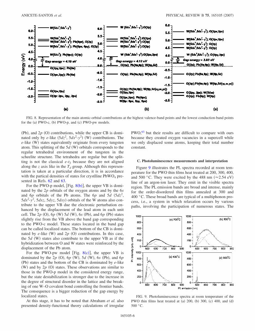
�Pb�, and 2p �O� contributions, while the upper CB is domi-nated only by e-like �5dz2, 5dx2-y2� �W� contributions. Thee-like �W� states equivalently originate from every tungstenatom. This splitting of the 5d �W� orbitals corresponds to theregular tetrahedral environment of the tungsten in thescheelite structure. The tetrahedra are regular but the split-ting is not the classical e-t2 because they are not alignedalong the z axis like in the Td group. Although this represen-tation is taken at a particular direction, it is in accordancewith the partical densities of states for crystlline PbWO4 pre-sented in Refs. 62 and 63.
For the PWO-p model, �Fig. 8�b��, the upper VB is domi-nated by the 2p orbitals of the oxygen atoms and by the 6sand 6p orbitals of the Pb atoms. The 6p and 5d �5dz2,5dx2-y2, 5dxz, 5dyz, 5dxy� orbitals of the W atoms also con-tribute to the upper VB due the electronic perturbation en-hanced by the displacement of the lead atom in each unitcell. The 2p �O�, 6p �W� 5d �W�, 6s �Pb�, and 6p �Pb� statesslightly rise from the VB above the band gap correspondingto the PWO-c model. These states located in the band gapcan be called localized states. The bottom of the CB is domi-nated by e-like �W� and 2p �O� contributions. In this case,the 5d �W� states also contribute to the upper VB as if thehybridization between O and W states were reinforced by thedisplacement of the Pb atom.
For the PWO-pw model �Fig. 8�c��, the upper VB isdominated by the 2p �O�, 6p �W�, 5d �W�, 6s �Pb�, and 6p�Pb� states and the bottom of the CB is dominated by e-like�W� and by 2p �O� states. These observations are similar tothose in the PWO-p model in the considered energy range,but the state destabilization is stronger due to the increase inthe degree of structural disorder in the lattice and the break-ing of one W–O covalent bond controlling the frontier bands.The consequence is a bigger reduction of the gap energy bylocalized states.
At this stage, it has to be noted that Abraham et al. alsopresented density-functional theory calculations of irregular
PWO,63 but their results are difficult to compare with oursbecause they created oxygen vacancies in a supercell whilewe only displaced some atoms, keeping their total numberconstant.
C. Photoluminescence measurements and interpretation
Figure 9 illustrates the PL spectra recorded at room tem-perature for the PWO thin films heat treated at 200, 300, 400,and 500 °C. They were excited by the 488 nm ��2.54 eV�line of an argon-ion laser. They emit in the visible spectraregion. The PL emission bands are broad and intense, mainlyfor the order-disordered thin films annealed at 300 and400 °C. These broad bands are typical of a multiphonon pro-cess, i.e., a system in which relaxation occurs by variouspaths, involving the participation of numerous states. The
FIG. 8. Representation of the main atomic-orbital contributions at the highest valence-band points and the lowest conduction-band pointsfor the �a� PWO-c, �b� PWO-p, and �c� PWO-pw models.
FIG. 9. Photoluminescence spectra at room temperature of thePWO thin films heat treated at �a� 200, �b� 300, �c� 400, and �d�500 °C.
ANICETE-SANTOS et al. PHYSICAL REVIEW B 75, 165105 �2007�
165105-6
crystalline thin film heat treated at 500 °C almost does notpresent PL emission. The most intense PL emission is ob-tained for the structure that is neither highly disordered �heattreated at 200 °C� nor highly ordered �heat treated at500 °C�, i.e., for the film treated at 400 °C. This indicatesthat the PL intensity is linked to the structural order-disorderdegree in the lattice.
The emission bands can be decomposed into two compo-nents, two broad bands, one with peak maximum in therange 520–562 nm �green�, and another band with peakmaximum in the range 589–649 nm �red�, as presented inFig. 9. The green band area represents 23%, 29%, and 31%of the experimental PL band area for the thin films treated at200, 300, and 400 °C, respectively, as shown in Table III.The intensity of the PL emission increases �about 2.5 times�for the sample treated at 200 °C compared to the othertreated at 300 °C, increasing the green band area from 23%to 29% and decreasing the red band area from 76% to 70%.The PWO sample treated at 400 °C presents the most intensePL band emission. For this sample, the green band area in-creases to 31% while the red band area decreases to 67%.The decrease of the red emission fraction due the structuralordering has also been recently observed for perovskitetitanates54,64 �CaTiO3:Sm, PbZr0.53Ti0.47O3� and for scheelitetungstates52,53 �SrWO4, CaWO4�.
The DRX diagrams, the AFM analysis, and the decompo-sitions of the PL emission bands indicate that the red fractionof the emission band is related to the high structural disorder
degree in the PWO lattice, because the smaller the heat treat-ment temperature �the greater the disorder degree�, thegreater the red emission fraction. The components of the PLemission band are probably linked to specific atomic ar-rangements.
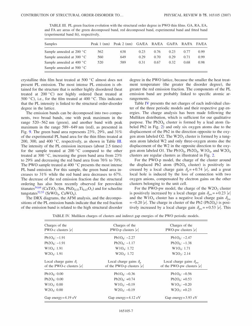
Table IV presents the net charges of each individual clus-ter of the three periodic models and their respective gap en-ergies. The charge analysis has been made following theMulliken distribution, which is sufficient for our qualitativepurpose. The Pb2O6 cluster is formed by a lead atom �la-beled Pb2 in Fig. 2� and only six oxygen atoms due to thedisplacement of the Pb2 in the direction opposite to the oxy-gen atom labeled O2. The W2O3 cluster is formed by a tung-sten atom labeled W2 and only three-oxygen atoms due thedisplacement of the W2 in the opposite direction to the oxy-gen atom labeled O1. The Pb1O8, Pb2O8, W1O4, and W2O4clusters are regular clusters as illustrated in Fig. 2.
For the PWO-p model, the charge of the cluster aroundthe displaced Pb2 atom �Pb2O6 cluster� is positively in-creased by a local charge gain �p= +0.74 �e�, and a greatlocal hole is induced by the loss of connection with twooxygen anions, compensated by electron gains on the otherclusters belonging to the unit cell.
For the PWO-pw model, the charge of the W2O3 clusteris positively increased by a local charge gain �pw= +0.23 �e�and the W1O4 cluster has a negative local charge gain �pw=−0.20 �e�. The charge in cluster of the Pb2 �Pb2O6� is posi-tively increased by a local charge gain �pw= +0.53 �e�. This
TABLE III. PL green fraction evolution with the structural order degree in PWO thin films. GA, RA, EA,and FA are areas of the green decomposed band, red decomposed band, experimental band and fitted band�experimental band fit�, respectively.
Samples Peak 1 �nm� Peak 2 �nm� GA/EA RA/EA GA/FA RA/FA FA/EA
Sample annealed at 200 °C 562 638 0.23 0.76 0.23 0.77 0.99
Sample annealed at 300 °C 560 649 0.29 0.70 0.29 0.71 0.99
Sample annealed at 400 °C 520 589 0.31 0.67 0.32 0.68 0.98
Sample annealed at 500 °C
TABLE IV. Mulliken charges of clusters and indirect gap energies of the PWO periodic models.
Charges of thePWO-c clusters �e�
Charges of thePWO-p clusters �e�
Charges of thePWO-pw clusters �e�
Pb1O8: −1.91 Pb1O8: −2.27 Pb1O8: −2.47
Pb2O8: −1.91 Pb2O6: −1.17 Pb2O6: −1.38
W1O4: 1.91 W1O4: 1.72 W1O4: 1.71
W2O4: 1.91 W2O4: 1.72 W2O3: 2.14
Local charge gains �c
of the PWO-c clusters �e�Local charge gains �p
of the PWO-p clusters �e�Local charge gains �pw
of the PWO-pw clusters �e�
Pb1O8: 0.00 Pb1O8: −0.36 Pb1O8: −0.56
Pb2O8: 0.00 Pb2O6: +0.74 Pb2O6: +0.53
W1O4: 0.00 W1O4: −0.19 W1O4: −0.20
W2O4: 0.00 W2O4: −0.19 W2O3: +0.23
Gap energy=4.19 eV Gap energy=4.12 eV Gap energy=3.93 eV
CONTRIBUTION OF STRUCTURAL ORDER-DISORDER TO… PHYSICAL REVIEW B 75, 165105 �2007�
165105-7
charge gain of the Pb2O6 cluster is smaller than the chargegain of the Pb2O6 cluster in the model PWO-p, because thedisplacement of W2 tungsten atom induces a charge compen-sation. These results point out that the local hole is greater inthe case of one local deformation �PWO-p� than in the caseof two local deformations �PWO-pw� in each unit cell due tothe charge compensations by other adjacent clusters. Thisbehavior indicates that the structures containing a lesser de-gree of structural disorder have greater local holes and con-sequently are more favorable for the intense PL emission,because great local holes are more favorable to electrontransfers when submitted to photon excitation.
The structural transformations occurring from disorderedto ordered phases start from the early stage of the polyesteri-fication of the citrate solution containing the tungsten andlead ions. The crystallization process occurs by heat treat-ment. The tungsten atom tends ideally to bond with fouroxygen atoms �WO4�, and the lead atom tends ideally tobond with eight oxygen atoms �PbO8 pseudocubic configu-ration�. The tungsten, which is the lattice former, organizessooner than the lead. In the structure just before the complete
crystallization there exist various coordination environmentsfor the Pb while the tungsten clusters are already regular. ThePWO structure annealed at 400 °C, just before completecrystallization, presented a favorable condition for the mostintense PL emission. When the crystallization is reached,only WO4 and PbO8 regular clusters exist and the PL van-ishes, showing that a complete order is not suitable for in-tense visible PL emission at room temperature.
The visible PL spectra show that the highly disorderedand highly ordered structures are not favorable for an intensePL emission. It should be underlined that the excitation en-ergy used �2.54 eV; 488 nm� is smaller than that correspond-ing to the 420 nm ��2.95 eV� blue emission frequently at-tributed in the literature to the WO4 regular tungstategroup,4,30–32,65 and for this reason cannot be observed.
The quantum-mechanical theoretical and absorbancespectra analyses point out that the apparition of localizedstates in the band gap of order-disordered PWO structuresand the increase of the structural disorder degree diminishthe gap energy, as seen in Table IV and Fig. 5. The structuraldisorder can favor PL emission with excitation energy
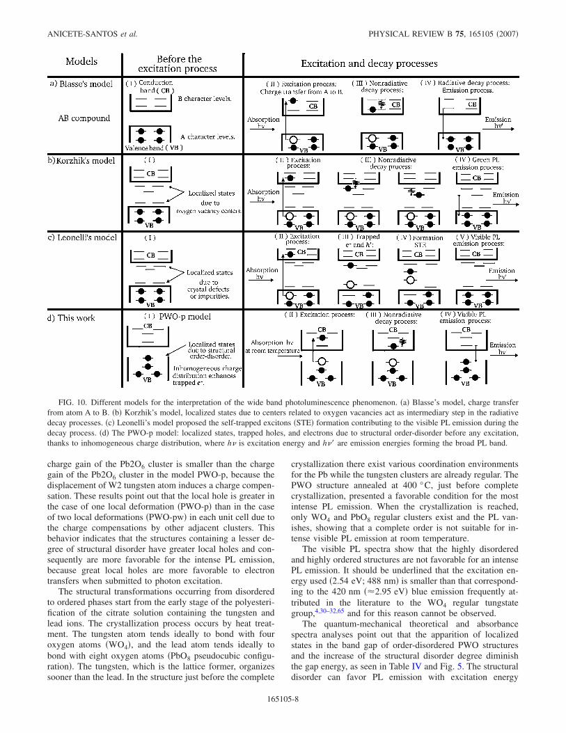
FIG. 10. Different models for the interpretation of the wide band photoluminescence phenomenon. �a� Blasse’s model, charge transferfrom atom A to B. �b� Korzhik’s model, localized states due to centers related to oxygen vacancies act as intermediary step in the radiativedecay processes. �c� Leonelli’s model proposed the self-trapped excitons �STE� formation contributing to the visible PL emission during thedecay process. �d� The PWO-p model: localized states, trapped holes, and electrons due to structural order-disorder before any excitation,thanks to inhomogeneous charge distribution, where h� is excitation energy and h�� are emission energies forming the broad PL band.
ANICETE-SANTOS et al. PHYSICAL REVIEW B 75, 165105 �2007�
165105-8
smaller than the crystalline gap energy. But this sole effect isinsufficient for enhancing the intense visible PL at room tem-perature, as can be seen in the more disordered sample�treated at 200 °C� which presents a smaller PL intensitythan the other order-disordered samples �treated at 300 and400 °C�. The experimental gap energies of the PWO thinfilms containing structural order-disorder are higher than theexcitation energy used for collecting the PL spectra �2.54 eV,488 nm�; such observation confirms the fact pointed out byMontoncello et al.66 that PL often highlights features thatabsorption measurements would rarely define as the proper-ties of the energy levels lying within the band gap of a ma-terial.
The charge gradient �polarization� and the presence of thelocalized states provide very good conditions for the trappingof electrons and holes, which can allow PL radiative recom-bination in the structurally order-disordered compounds. Asexplained by Blasse and Grabmaier,3 the PL arises from aradiative return to the ground state, a phenomenon that isenhanced by the presence of charge trapping at room tem-perature. Blasse and Grabmaier indeed showed the PL be-havior of perovskite-type oxides at low temperature �45 K�,where less energy is lost for the vibration of the lattice sothat the radiative recombination is encouraged. At room tem-perature, however, if no charge trapping promotes the radia-tive recombination, the energy is used for the lattice vibra-tions.
Figure 10 compares some models exposed by differentauthors to explain their views on the PL emission. We com-pare them before the photon excitation process with thePWO-p model for illustrating that the structural order-disorder is a favorable condition to PL emission. It has to beemphasized that other authors have proposed PL mechanismmodels frequently dealing with low-temperature measure-ments and have barely discussed the conditions prior to ex-citation. In the present study, the synergistic analysis of ex-perimental and theoretical results shows that the keys to anefficient photoluminescence emission at room temperatureare defined before excitation.
The model proposed by Blasse and co-workers3,67,68 isbased on a charge transfer from the atom having its maincontribution in the VB to the atom forming the CB. Thedifferent steps of the process are depicted in Fig. 10�a�.
Korzhik et al.7 have assumed that localized states linkedto local defects such as oxygen vacancies exist in the bandgap for the undoped crystalline PWO compound. During theexcitation and radiative decay processes, those levels areused as intermediary steps �Fig. 10�b�� and some of themcontribute to the green PL emission. In the model presented
by Leonelli and Brebner,69 some of the electrons are pro-moted to the CB by absorption of photon from small po-larons. The polarons interact with holes of the defect levels�crystal defect or impurity levels� in the crystal forming self-trapped excitons �STEs� that contribute to the visible PLemission �Fig. 10�c��. The STE can also form in an ideal�nondefective� crystal when an excited electron and hole canlower their energy by creating a localized defect in the lat-tice; this is an example of spontaneous symmetry breaking.70
Our order-disordered model, in particular, the PWO-pmodel, is presented at last. The most important events hap-pen before excitation. The structural order-disorder generateslocalized states and inhomogeneous charge distribution inthe cell, thus allowing the trapping of electrons and holes.Those localized levels are energetically distributed, so thatvarious energies are able to excite the trapped electrons. Theradiative decay must occur through the same pathway, lead-ing to a wide band emission.
VI. CONCLUSIONS
The increase of structural ordering of the PWO thin filmsby annealing from 200 to 500 °C was identified by means ofXRD, absorbance spectra, and AFM measurements.
The PL emission in crystalline PWO was practically ab-sent. For the sample containing the highest structural disor-der, the intense PL emission is also not favored. The intenseand broad PL emissions were evidenced in PWO thin filmscontaining simultaneously order and disorder in the struc-ture. The broad PL bands present green and red emissions.The experimental results also show that the red PL emissionis associated with high structural disorder and the green PLemission is associated with smaller structural disorder degreein the PWO lattice. The most intense PL emission was favor-able to PWO structure annealed at temperature just before tothe crystallization temperature.
The theoretical calculations indicate that locally disor-dered Pb clusters are more favorable for the PL effect due togreat local electronic holes induced by smaller distortions inthe lattice, favoring electron transfers when submitted tophoton excitation. The experimental and theoretical resultsindicate that green PL emission is related to locally disor-dered Pb atoms.
ACKNOWLEDGMENTS
The work was partially supported by the Brazilian agen-cies FAPESP/CEPID, CNPq, CAPES, and by the FundaciónBancaixa �Project No. P1-1B2005-20�.
*Electronic address: [email protected] F. A. Kroger, Some Aspects of the Luminescence of Solids
�Elsevier, Amsterdam, 1948�.2 J. A. Groenink and G. Blasse, J. Solid State Chem. 32, 9 �1980�.3 G. Blasse and B. C. Grabmaier, Luminescent Materials �Springer-
Verlag, Berlin, 1994�.
4 P. Lecoq, I. Dafinei, E. Auffray, M. Schneegans, M. V. Korzhik,O. V. Missevitch, V. B. Pavlenko, A. A. Fedorov, A. N. Annen-kov, V. L. Kostylev et al., Nucl. Instrum. Methods Phys. Res. A365, 291 �1995�.
5 A. N. Belsky, V. V. Mikhailin, A. N. Vasilev, I. Dafinei, P. Lecoq,C. Pedrini, P. Chevallier, P. Dhez, and P. Martin, Chem. Phys.
CONTRIBUTION OF STRUCTURAL ORDER-DISORDER TO… PHYSICAL REVIEW B 75, 165105 �2007�
165105-9
Lett. 243, 552 �1995�.6 M. Nikl, K. Nitsch, K. Polak, E. Mihokova, I. Dafinei, E. Auffray,
P. Lecoq, P. Reiche, R. Uecker, and G. P. Pazzi, Phys. StatusSolidi B 195, 311 �1996�.
7 M. V. Korzhik, V. B. Pavlenko, T. N. Timoschenko, V. A. Katcha-nov, A. V. Singovskii, A. N. Annenkov, V. A. Ligun, I. M. Sol-skii, and J. P. Peigneux, Phys. Status Solidi A 154, 779 �1996�.
8 G. Tamulaitis, S. Buracas, V. P. Martinov, V. D. Ryzhikov, H. H.Gutbrod, and V. I. Manko, Phys. Status Solidi A 157, 187�1996�.
9 M. Kobayashi, M. Ishii, K. Harada, Y. Usuki, H. Okuno, H.Shimizu, and T. Yazawa, Nucl. Instrum. Methods Phys. Res. A373, 333 �1996�.
10 R. Y. Zhu, D. A. Ma, H. B. Newman, C. L. Woody, J. A. Kier-stead, S. P. Stoll, and P. W. Levy, Nucl. Instrum. Methods Phys.Res. A 376, 319 �1996�.
11 V. Murk, M. Nikl, E. Mihokova, and K. Nitsch, J. Phys.: Con-dens. Matter 9, 249 �1997�.
12 D. Millers, S. Chernov, L. Grigorjeva, and V. Pankratov, Radiat.Meas. 29, 263 �1998�.
13 M. Nikl, P. Strakova, K. Nitsch, V. Petricek, V. Mucka, O.Jarolimek, J. Novak, and P. Fabeni, Chem. Phys. Lett. 291, 300�1998�.
14 M. Martini, F. Meinardi, G. Spinolo, A. Vedda, M. Nikl, and Y.Usuki, Phys. Rev. B 60, 4653 �1999�.
15 O. Antonenko, O. Chukova, Y. Hizhnyi, S. Nedilko, and V.Scherbatskyi, Opt. Mater. �Amsterdam, Neth.� 28, 643 �2006�.
16 M. Kobayashi, M. Ishii, Y. Usuki, and H. Yahagi, Nucl. Instrum.Methods Phys. Res. A 333, 429 �1993�.
17 G. Blasse, Chem. Mater. 6, 1465 �1994�.18 P. Lecoq, Nucl. Instrum. Methods Phys. Res. A 537, 15 �2005�.19 V. G. Baryshevsky, M. V. Korzhik, V. I. Moroz, V. B. Pavlenko,
A. S. Kobko, A. A. Fyodorov, V. A. Kachanov, V. L. Solov-janov, B. I. Zadneprovsky, V. A. Nefyodov et al., Nucl. Instrum.Methods Phys. Res. A 322, 231 �1992�.
20 B. G. Han, X. Q. Feng, G. Q. Hu, Y. X. Zhang, and Z. W. Yin, J.Appl. Phys. 86, 3571 �1999�.
21 M. Nikl, K. Nitsch, J. Hybler, J. Chval, and P. Reiche, Phys.Status Solidi B 196, K7 �1996�.
22 M. Nikl, J. Rosa, K. Nitsch, H. R. Asatryan, S. Baccaro, A. Ce-cilia, M. Montecchi, B. Borgia, I. Dafinei, M. Diemoz et al.,Mater. Sci. Forum 239–242, 271 �1997�.
23 A. Annenkov, E. Auffray, M. Korzhik, P. Lecoq, and J. P. Peig-neux, Phys. Status Solidi A 170, 47 �1998�.
24 V. N. Shevchuk and I. V. Kayun, Phys. Solid State 47, 632�2005�.
25 T. Y. Liu, Q. R. Zhang, and S. L. Zhuang, J. Electron Spectrosc.Relat. Phenom. 142, 139 �2005�.
26 Q. R. Zhang, T. Y. Liu, J. Chen, and X. Q. Feng, Phys. Rev. B 68,064101 �2003�.
27 M. Nikl, Phys. Status Solidi A 178, 595 �2000�.28 M. Nikl, K. Nitsch, S. Baccaro, A. Cecilia, M. Montecchi, B.
Borgia, I. Dafinei, M. Diemoz, M. Martini, E. Rosetta et al., J.Appl. Phys. 82, 5758 �1997�.
29 A. N. Annenkov, A. A. Fedorov, P. Galez, V. A. Kachanov, M. V.Korzhik, V. D. Ligun, J. M. Moreau, V. N. Nefedov, V. B. Pav-lenko, J. P. Peigneux et al., Phys. Status Solidi A 156, 493�1996�.
30 Z. M. Qi, C. S. Shi, D. F. Zhou, H. G. Tang, T. Liu, and T. D. Hu,Physica B 307, 45 �2001�.
31 C. Shi, Y. Wei, X. Yang, D. Zhou, C. Guo, J. Liao, and H. Tang,Chem. Phys. Lett. 328, 1 �2000�.
32 A. A. Annenkov, M. V. Korzhik, and P. Lecoq, Nucl. Instrum.Methods Phys. Res. A 490, 30 �2002�.
33 S. Baccaro, B. Borgia, A. Cecilia, I. Dafinei, M. Diemoz, P. Fa-beni, M. Niki, M. Martini, M. Montecchi, G. Pazzi et al., Nucl.Phys. B 61, 66 �1998�.
34 E. V. Sokolenko, V. M. Zhukovskii, E. S. Buyanova, and Y. A.Krasnobaev, Inorg. Mater. 34, 499 �1998�.
35 B. M. Sinelnikov, E. V. Sokolenko, and V. Y. Zvekov, Inorg.Mater. 32, 999 �1996�.
36 Y. H. Chen, C. S. Shi, and G. Q. Hu, J. Appl. Phys. 87, 1503�2000�.
37 Y. L. Huang, W. L. Zhu, and X. Q. Feng, J. Electron Spectrosc.Relat. Phenom. 133, 39 �2003�.
38 M. Kakihana, T. Okubo, M. Arima, Y. Nakamura, M. Yashima,and M. Yoshimura, J. Sol-Gel Sci. Technol. 12, 95 �1998�.
39 M. Kakihana and M. Yoshimura, Bull. Chem. Soc. Jpn. 72, 1427�1999�.
40 F. M. Pontes, J. H. G. Rangel, E. R. Leite, E. Longo, J. A. Varela,E. B. Araujo, and J. A. Eiras, Thin Solid Films 366, 232 �2000�.
41 F. M. Pontes, E. Longo, J. H. Rangel, M. I. Bernardi, E. R. Leite,and J. A. Varela, Mater. Lett. 43, 249 �2000�.
42 V. R. Saunders, R. Dosevi, C. Roetti, R. Orlando, C. M. Zicovich-Wilson, N. M. Harrison, K. Doll, B. Civalleri, I. J. Bush, P.D’Arco et al., CRYSTAL2003 User’s Manual �University ofTorino, Torino, 2003�.
43 C. Lee, W. Yang, and R. G. Parr, Phys. Rev. B 37, 785 �1988�.44 A. D. Becke, J. Chem. Phys. 98, 5648 �1993�.45 C. H. Hu and D. P. Chong, Encyclopedia of Computational
Chemistry �Wiley, Chichester, 1998�.46 http://www.crystal.unito.it47 V. L. Cabal, OPTIM User’s Manual �Departamento de Quimica
Fisica y Analitica, University of Oviedo, Oviedo, 1998�.48 J. M. Moreau, P. Galez, J. P. Peigneux, and M. V. Korzhik, J.
Alloys Compd. 238, 46 �1996�.49 E. Gurmen, E. Daniels, and J. S. King, J. Chem. Phys. 55, 1093
�1971�.50 A. Kokalj, J. Mol. Graphics Modell. 17, 176 �1999�.51 M. Anicete-Santos, F. C. Picon, M. T. Escote, E. R. Leite, P. S.
Pizani, J. A. Varela, and E. Longo, Appl. Phys. Lett. 88, 211913�2006�.
52 E. Orhan, M. Anicete-Santos, M. A. M. A. Maurera, F. M. Pontes,C. O. Paiva-Santos, A. G. Souza, J. A. Varela, P. S. Pizani, andE. Longo, Chem. Phys. 312, 1 �2005�.
53 E. Orhan, M. Anicete-Santos, M. A. M. A. Maurera, F. M. Pontes,A. G. Souza, J. Andres, A. Beltran, J. A. Varela, P. S. Pizani, C.A. Taft et al., J. Solid State Chem. 178, 1284 �2005�.
54 A. T. de Figueiredo, S. de Lazaro, E. Longo, E. C. Paris, J. A.Varela, M. R. Joya, and P. S. Pizani, Chem. Mater. 18, 2904�2006�.
55 E. Orhan, J. A. Varela, A. Zenatti, M. F. C. Gurgel, F. M. Pontes,E. R. Leite, E. Longo, P. S. Pizani, A. Beltran, and J. Andres,Phys. Rev. B 71, 085113 �2005�.
56 E. Longo, E. Orhan, F. M. Pontes, C. D. Pinheiro, E. R. Leite, J.A. Varela, P. S. Pizani, T. M. Boschi, F. Lanciotti, A. Beltran etal., Phys. Rev. B 69, 125115 �2004�.
57 E. Orhan, F. M. Pontes, E. R. Leite, P. S. Pizani, J. A. Varela, andE. Longo, ChemPhysChem 6, 1530 �2005�.
58 E. Orhan, F. M. Pontes, M. A. Santos, E. R. Leite, A. Beltran, J.
ANICETE-SANTOS et al. PHYSICAL REVIEW B 75, 165105 �2007�
165105-10
Andres, T. M. Boschi, P. S. Pizani, A. Varela, C. A. Taft et al., J.Phys. Chem. B 108, 9221 �2004�.
59 M. Anicete-Santos, L. S. Cavalcante, E. Orhan, E. C. Paris, L. G.P. Simoes, M. R. Joya, I. L. V. Rosa, P. R. de Lucena, M. R. M.C. Santos, L. S. Santos-Junior et al., Chem. Phys. 316, 260�2005�.
60 D. L. Wood and J. Tauc, Phys. Rev. B 5, 3144 �1972�.61 C. J. Bradley and A. P. Cracknell, The Mathematical Theory of
Symmetry in Solids �Clarendon, Oxford, 1972�.62 Y. Zhang, N. A. W. Holzwarth, and R. T. Williams, Phys. Rev. B
57, 12738 �1998�.63 Y. B. Abraham, N. A. W. Holzwarth, R. T. Williams, G. E. Mat-
thews, and A. R. Tackett, Phys. Rev. B 64, 245109 �2001�.64 M. S. Silva, M. Cilense, E. Orhan, M. S. Goes, M. A. C.
Machado, L. P. S. Santos, C. O. Paiva-Santos, E. Longo, J. A.Varela, M. E. Zaghete et al., J. Lumin. 111, 205 �2005�.
65 W. Vanloo, Phys. Status Solidi A 27, 565 �1975�.66 F. Montoncello, M. C. Carotta, B. Cavicchi, M. Ferroni, A. Gib-
erti, V. Guidi, C. Malagu, G. Martinelli, and F. Meinardi, J.Appl. Phys. 94, 1501 �2003�.
67 F. Kellendonk and G. Blasse, J. Chem. Phys. 75, 561 �1981�.68 S. H. M. Poort, W. P. Blokpoel, and G. Blasse, Chem. Mater. 7,
1547 �1995�.69 R. Leonelli and J. L. Brebner, Phys. Rev. B 33, 8649 �1986�.70 S. Ismail-Beigi, Phys. Status Solidi C 10, 3365 �2006�.71 JCPDS-International Center for Diffraction Data, Card No. 8-490
�unpublished�.
CONTRIBUTION OF STRUCTURAL ORDER-DISORDER TO… PHYSICAL REVIEW B 75, 165105 �2007�
165105-11