
Configuration-Dependent Electrically Tunable Van der Waals ...
8
FULL PAPER © 2016 WILEY-VCH Verlag GmbH & Co. KGaA, Weinheim 5499 wileyonlinelibrary.com cells, etc., p–n junctions are the funda- mental of modern electronic technology. Considering the impossibility of using traditional method to dope the ultrathin bodies of 2DLMs, vdWH is one of the best ways to achieve p–n junctions in this sce- nario. In addition, taking advantages of the novel properties of individual 2DLMs (a) high carrier mobility because of the absent surface scattering from dangling bonds, [8,9] (b) wide coverage of band gaps (≈0.3–6 eV), [10,11] and (c) high compatibility with traditional devices fabrication process as well as flexible substrates resulting from their 2D geometry, vdW p–n junc- tions exhibit promising potentials for next generation of electronic and optoelec- tronic devices. [2] What is more, vdW p–n junctions usually show strong light-matter interaction as the fact that most 2DLMs can form type II band alignment and their 2D configuration endows them ultrahigh specific surface areas. [6,11–13] Taking MoS 2 / WS 2 heterostructure as an example, it takes only 50 fs for photo-stimulated holes to transfer from the valence band of MoS 2 to the WS 2 layer. [14] Inspired by these advantages, a number of vdW p–n junctions, such as WSe 2 /MoS 2 , [7,15,16] black phosphorus/MoS 2 , [17] WS 2 / MoS 2 , [18] GaTe/MoS 2 , [19] and MoTe 2 /MoS 2 [20] have been fabri- cated and demonstrated with extraordinary performances. For instance, using GaTe and MoS 2 as holes and electrons pro- viders, our group recently fabricated GaTe/MoS 2 vdW p–n junc- tions which exhibited rectification ratio (RF), external quantum efficiency, and selective detectivity of as high as 4 × 10 5 , 61.68%, and 8.4 × 10 13 Jones, respectively. [19] Moreover, due to their ultrathin thickness and steep interfacial charge carrier gra- dient, 2D vdW p–n junctions show strong electrical tunability on electronic and optoelectronic properties, which offers a way to achieve the functional ends and, more importantly, to under- stand the underlying working mechanisms. [7,21,22] In addition to the advantages displayed on electronic and optoelectronic devices, vdW p–n junctions also show novel phe- nomena due to their ultrathin thickness. For example, unlike the built-in potential and space charge region in conventional p–n junctions, it was found that the tunneling-assisted inter- layer recombination of the majority carriers may be responsible for the electrically tunable rectification and PV effects observed in atomically thin WSe 2 /MoS 2 p–n junction. [7,16] Being a newly emerged research field, even though many works have already Configuration-Dependent Electrically Tunable Van der Waals Heterostructures Based on MoTe 2 /MoS 2 Feng Wang, Lei Yin, Zhen Xing Wang, Kai Xu, Feng Mei Wang, Tofik Ahmed Shifa, Yun Huang, Chao Jiang, and Jun He* Van der Waals heterostructures (vdWHs), obtained by artificially stacking 2D layered material (2DLM) plains upon each other, are brand new struc- tures that have exhibited novel electronic and optoelectronic properties and attracted a great deal of attention. So far, the results are only based on devices with symmetrical configurations: devices predominated by vdWH parts, or cross-like configurations combined with both vdWHs and extra individual 2DLM layers. Quite different gate tunable phenomena have been observed for these two configurations even though 2DLMs with similar band alignments were used, which may be due to the different device configura- tions utilized. For a deeper understanding, rational investigation on configu- ration-dependent properties of vdWHs is needed. Here, using MoTe 2 /MoS 2 as an example, vdWH device is artificially designed with two asymmetrical configurations. Through comparing the respective results, it is found that the properties that stem only from the vdWH, i.e., the rectification behavior and open voltage in photovoltaic effect, are independent of the device structures. However, other properties, i.e., drain currents, short circuit currents, and photoreponse performances, strongly depend on the configuration used. These results give a guideline on studying the intrinsic properties of vdWHs and optimizing the device structures for better performances. DOI: 10.1002/adfm.201601349 F. Wang, L. Yin, Prof. Z. X. Wang, K. Xu, F. M. Wang, T. A. Shifa, Y. Huang, Prof. C. Jiang, Prof. J. He CAS Key Laboratory of Nanosystem and Hierarchical Fabrication National Center for Nanoscience and Technology Beijing 100190, P.R. China E-mail: [email protected] 1. Introduction By artificially stacking isolated planes of different 2D layered materials (2DLMs) on top of each other, one can obtain het- erostructures with thickness of only a few nanometers. [1–4] Due to the dangling bonds free surfaces of 2DLMs, the as fab- ricated heterostructures are vertically kept together by van der Waals forces between adjacent planes. [3] Hence they are also known as van der Waals heterostructures (vdWHs). [1] Theoreti- cally, vdWHs can be made up with any 2DLM planes in any sequences, which greatly enriches the choices of materials with desired properties. [1,5,6] Specially, through assembling p- and n-type 2DLMs together, we can fabricate atomically sharp van der Waals p–n junctions. [7] As the most essential building blocks of logic circuits, light emitting diodes (LEDs) and solar Adv. Funct. Mater. 2016, 26, 5499–5506 www.afm-journal.de www.MaterialsViews.com
-
Upload
khangminh22 -
Category
Documents
-
view
2 -
download
0
Transcript of Configuration-Dependent Electrically Tunable Van der Waals ...

FULL P
APER
© 2016 WILEY-VCH Verlag GmbH & Co. KGaA, Weinheim 5499wileyonlinelibrary.com
cells, etc., p–n junctions are the funda-mental of modern electronic technology. Considering the impossibility of using traditional method to dope the ultrathin bodies of 2DLMs, vdWH is one of the best ways to achieve p–n junctions in this sce-nario. In addition, taking advantages of the novel properties of individual 2DLMs (a) high carrier mobility because of the absent surface scattering from dangling bonds, [ 8,9 ] (b) wide coverage of band gaps (≈0.3–6 eV), [ 10,11 ] and (c) high compatibility with traditional devices fabrication process as well as fl exible substrates resulting from their 2D geometry, vdW p–n junc-tions exhibit promising potentials for next generation of electronic and optoelec-tronic devices. [ 2 ] What is more, vdW p–n junctions usually show strong light-matter interaction as the fact that most 2DLMs can form type II band alignment and their 2D confi guration endows them ultrahigh specifi c surface areas. [ 6,11–13 ] Taking MoS 2 /WS 2 heterostructure as an example, it takes only 50 fs for photo-stimulated holes
to transfer from the valence band of MoS 2 to the WS 2 layer. [ 14 ] Inspired by these advantages, a number of vdW p–n junctions, such as WSe 2 /MoS 2 , [ 7,15,16 ] black phosphorus/MoS 2 , [ 17 ] WS 2 /MoS 2 , [ 18 ] GaTe/MoS 2 , [ 19 ] and MoTe 2 /MoS 2 [ 20 ] have been fabri-cated and demonstrated with extraordinary performances. For instance, using GaTe and MoS 2 as holes and electrons pro-viders, our group recently fabricated GaTe/MoS 2 vdW p–n junc-tions which exhibited rectifi cation ratio (RF), external quantum effi ciency, and selective detectivity of as high as 4 × 10 5 , 61.68%, and 8.4 × 10 13 Jones, respectively. [ 19 ] Moreover, due to their ultrathin thickness and steep interfacial charge carrier gra-dient, 2D vdW p–n junctions show strong electrical tunability on electronic and optoelectronic properties, which offers a way to achieve the functional ends and, more importantly, to under-stand the underlying working mechanisms. [ 7,21,22 ]
In addition to the advantages displayed on electronic and optoelectronic devices, vdW p–n junctions also show novel phe-nomena due to their ultrathin thickness. For example, unlike the built-in potential and space charge region in conventional p–n junctions, it was found that the tunneling-assisted inter-layer recombination of the majority carriers may be responsible for the electrically tunable rectifi cation and PV effects observed in atomically thin WSe 2 /MoS 2 p–n junction. [ 7,16 ] Being a newly emerged research fi eld, even though many works have already
Confi guration-Dependent Electrically Tunable Van der Waals Heterostructures Based on MoTe 2 /MoS 2
Feng Wang , Lei Yin , Zhen Xing Wang , Kai Xu , Feng Mei Wang , Tofi k Ahmed Shifa , Yun Huang , Chao Jiang , and Jun He *
Van der Waals heterostructures (vdWHs), obtained by artifi cially stacking 2D layered material (2DLM) plains upon each other, are brand new struc-tures that have exhibited novel electronic and optoelectronic properties and attracted a great deal of attention. So far, the results are only based on devices with symmetrical confi gurations: devices predominated by vdWH parts, or cross-like confi gurations combined with both vdWHs and extra individual 2DLM layers. Quite different gate tunable phenomena have been observed for these two confi gurations even though 2DLMs with similar band alignments were used, which may be due to the different device confi gura-tions utilized. For a deeper understanding, rational investigation on confi gu-ration-dependent properties of vdWHs is needed. Here, using MoTe 2 /MoS 2 as an example, vdWH device is artifi cially designed with two asymmetrical confi gurations. Through comparing the respective results, it is found that the properties that stem only from the vdWH, i.e., the rectifi cation behavior and open voltage in photovoltaic effect, are independent of the device structures. However, other properties, i.e., drain currents, short circuit currents, and photo reponse performances, strongly depend on the confi guration used. These results give a guideline on studying the intrinsic properties of vdWHs and optimizing the device structures for better performances.
DOI: 10.1002/adfm.201601349
F. Wang, L. Yin, Prof. Z. X. Wang, K. Xu, F. M. Wang, T. A. Shifa, Y. Huang, Prof. C. Jiang, Prof. J. He CAS Key Laboratory of Nanosystem and Hierarchical Fabrication National Center for Nanoscience and Technology Beijing 100190 , P.R. China E-mail: [email protected]
1. Introduction
By artifi cially stacking isolated planes of different 2D layered materials (2DLMs) on top of each other, one can obtain het-erostructures with thickness of only a few nanometers. [ 1–4 ] Due to the dangling bonds free surfaces of 2DLMs, the as fab-ricated heterostructures are vertically kept together by van der Waals forces between adjacent planes. [ 3 ] Hence they are also known as van der Waals heterostructures (vdWHs). [ 1 ] Theoreti-cally, vdWHs can be made up with any 2DLM planes in any sequences, which greatly enriches the choices of materials with desired properties. [ 1,5,6 ] Specially, through assembling p- and n-type 2DLMs together, we can fabricate atomically sharp van der Waals p–n junctions. [ 7 ] As the most essential building blocks of logic circuits, light emitting diodes (LEDs) and solar
Adv. Funct. Mater. 2016, 26, 5499–5506
www.afm-journal.dewww.MaterialsViews.com

FULL
PAPER
5500 wileyonlinelibrary.com © 2016 WILEY-VCH Verlag GmbH & Co. KGaA, Weinheim
been done, the fundamental mechanism of vdW p–n junctions is still unclear and the top limit of their performances is also remained unexplored hitherto. So far, two kinds of artifi cially stacked symmetry device structures have been used to study the vdW p–n junctions, both of which displayed strong electri-cally tunable electronic and optoelectronic properties. The fi rst one is cross-like device structure, in which the whole device is a series connection of overlapping part (vdW p–n junction) and extra individual 2DLMs parts. [ 7,19,21 ] However, due to the strong gate tunability of individual 2DLMs parts as well, the observed phenomena were probably not only from the vdW p–n junc-tions but a superposition of these two parts, which have been ignored by the authors. On the other hand, devices predomi-nated by vdW p–n junction parts were also fabricated. Notably, compared with the cross-like device structure, quite different gate tunable properties were observed, both in WSe 2 /MoS 2 and black phosphorus/MoS 2 , although materials with similar band alignment were used. [ 16,17 ] One reason for this inconsistence may be due to the different device structures used. For a deeper understanding of vdW p–n junctions, rational investigation on device structure-dependent properties of vdW p–n junctions is needed.
Here we report confi guration-dependent electrically tunable MoTe 2 /MoS 2 vdWHs. The vdWHs show gate voltage tunable rectifi cation characteristics, photovoltaic (PV) effects, and photo-response properties. More importantly, by designing the devices with two asymmetry structures at the same time, we found that the rectifi cation behavior and open voltage are independent of
the confi guration used. However, the drain currents, short cir-cuit currents, and photoreponse performances strongly depend on the device structures. Higher PV effects, photoresponsivity, and faster photoresponse times were observed in the device that vdWH part predominate the structure. On the other hand, device with extra individual part exhibits higher selective photo-detctivity. These results provide a guideline on studying the intrinsic properties of vdWHs and optimizing the device struc-tures for better desired performances.
2. Results and Discussion
2.1. Device Characterization
All the devices used in the experiments were fabricated by mechanical exfoliation combined with directional transfer method (see the Experimental Section for detail). [ 19,23 ] To study the effect of confi guration on the device performances, we arti-fi cially designed an asymmetric device structure. Figure 1 a,d shows the schematic diagram and the optical microscope image of the fi nal device, respectively. Due to the asymmetric device structure, two different circuit models (Figure 1 b,c) will be induced while using different source/drain electrodes (E1–E4 shown in Figure 1 d). To be specifi c, MoS 2 is one of the most studied n-type 2DLMs. [ 8 ] On the other hand, MoTe 2 is a recently discovered ambipolar 2DLMs with distinctive properties. [ 24,25 ] As shown in the inset of Figure 1 a, the two 2DLMs share a
Adv. Funct. Mater. 2016, 26, 5499–5506
www.afm-journal.dewww.MaterialsViews.com
Figure 1. a) Schematic diagram of the MoTe 2 (cyan)/MoS 2 (pink) vdWH device. Few-layer MoS 2 was exfoliated on the top of the MoTe 2 fl ake, and 8/60 nm Cr/Au was used as electrode. The inset shows the enlarged crystalline structures of MoTe 2 and MoS 2 , with cyan, yellow, and brown balls representing Mo, S, and Te atoms, respectively. Band diagrams of devices while using b) E1/E2 and c) E3/E4 as source/drain electrode pairs. A type II band alignment formed at the overlapping region. The corresponding equivalent circuit diagrams are shown at the bottom. d) Optical microscope image of the device, where E1–E4 show the four electrodes. e) Spatially resolved Raman maps for the MoTe 2 (top panel, Raman shift at 234 cm −1 ) and the MoS 2 fl akes (bottom panel, Raman shift at 384 cm −1 ). f) Raman spectra collected from the different positions of the device: the blue, red, and brown lines come from the MoTe 2 , MoS 2 , and the overlapping region respectively.
FULL P
APER
5501wileyonlinelibrary.com© 2016 WILEY-VCH Verlag GmbH & Co. KGaA, Weinheim
similar crystal structure: hexagonally packed planes of Mo atoms sandwiched with two planes of chalcogen (S or Te) atoms. Due to the band positions of the two materials, a vdWH with a type II band alignment would form at the overlapping region, as shown in Figure 1 b,c. [ 13,26 ] For the case where E3 and E4 were used as source/drain electrode pair, the vdWH would dominate the device performances. On the contrary, if E1 and E2 were used, the extra MoTe 2 part would act as an adjustable resistor and may affect the overall device performances. Note that there are also two tiny parts of extra MoS 2 for using E1/E2 as well as E3/E4 electrode pairs. However, considering the comparable and relatively small sizes of these two parts (6–7 times smaller than the overlapped part and the extra MoTe 2 part), we ignored their infl uences, which we believe would not affect the fi nal results that based on comparative study of E1/E2 and E3/E4. Figure 1 b,c depicts the respective band dia-grams and equivalent circuit models (see the following discus-sions). In addition, according to our recent works on MoTe 2 and MoS 2 , we chose Cr as the direct contact metal, having a matched work function with both of these two materials which enables it to reduce the Schottky barriers at the semiconductor/electrode interfaces and highlight the role of the channels. [ 19,27 ] The thicknesses of the MoTe 2 and MoS 2 fl akes are around 1.5 (about two layers) and 3.8 nm (about 10 layers), respectively, as defi ned by atomic force microscope (AFM, see Figure S1, Sup-porting Information). Raman spectroscopy was used to confi rm the quality of the vdWH. The Raman maps (Figure 1 e) further illustrates the structure of our device. Obvious changes in the intensity of the peaks were observed at the overlapping region, which probably emanates from the interaction between the two fl akes. [ 19 ] The Raman spectrum of the overlapping part (brown line in Figure 1 f) is a combination of bottom MoTe 2 (blue line in Figure 1 f, at Raman shifts of about 234 and 298 cm −1 ) [ 28 ] and top MoS 2 (red dot dot line in Figure 1 f, at Raman shifts of about 384 and 405 cm −1 ), [ 29 ] demonstrating the formation of the vdWH.
2.2. Confi guration-Dependent Electronic Properties of the MoTe 2 /MoS 2 vdWHs
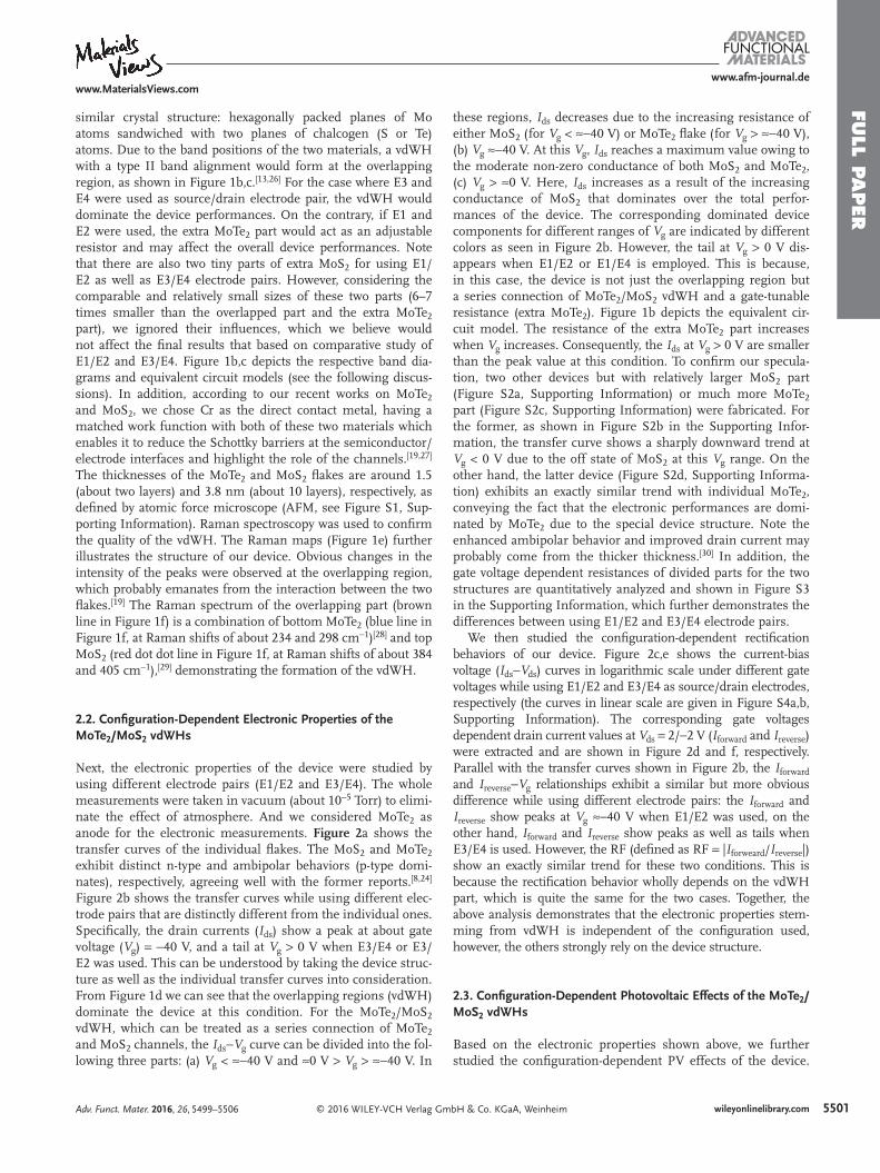
Next, the electronic properties of the device were studied by using different electrode pairs (E1/E2 and E3/E4). The whole measurements were taken in vacuum (about 10 −5 Torr) to elimi-nate the effect of atmosphere. And we considered MoTe 2 as anode for the electronic measurements. Figure 2 a shows the transfer curves of the individual fl akes. The MoS 2 and MoTe 2 exhibit distinct n-type and ambipolar behaviors (p-type domi-nates), respectively, agreeing well with the former reports. [ 8,24 ] Figure 2 b shows the transfer curves while using different elec-trode pairs that are distinctly different from the individual ones. Specifi cally, the drain currents ( I ds ) show a peak at about gate voltage ( V g ) = −40 V, and a tail at V g > 0 V when E3/E4 or E3/E2 was used. This can be understood by taking the device struc-ture as well as the individual transfer curves into consideration. From Figure 1 d we can see that the overlapping regions (vdWH) dominate the device at this condition. For the MoTe 2 /MoS 2 vdWH, which can be treated as a series connection of MoTe 2 and MoS 2 channels, the I ds − V g curve can be divided into the fol-lowing three parts: (a) V g < ≈−40 V and ≈0 V > V g > ≈−40 V. In
these regions, I ds decreases due to the increasing resistance of either MoS 2 (for V g < ≈−40 V) or MoTe 2 fl ake (for V g > ≈−40 V), (b) V g ≈−40 V. At this V g , I ds reaches a maximum value owing to the moderate non-zero conductance of both MoS 2 and MoTe 2 , (c) V g > ≈0 V. Here, I ds increases as a result of the increasing conductance of MoS 2 that dominates over the total perfor-mances of the device. The corresponding dominated device components for different ranges of V g are indicated by different colors as seen in Figure 2 b. However, the tail at V g > 0 V dis-appears when E1/E2 or E1/E4 is employed. This is because, in this case, the device is not just the overlapping region but a series connection of MoTe 2 /MoS 2 vdWH and a gate-tunable resistance (extra MoTe 2 ). Figure 1 b depicts the equivalent cir-cuit model. The resistance of the extra MoTe 2 part increases when V g increases. Consequently, the I ds at V g > 0 V are smaller than the peak value at this condition. To confi rm our specula-tion, two other devices but with relatively larger MoS 2 part (Figure S2a, Supporting Information) or much more MoTe 2 part (Figure S2c, Supporting Information) were fabricated. For the former, as shown in Figure S2b in the Supporting Infor-mation, the transfer curve shows a sharply downward trend at V g < 0 V due to the off state of MoS 2 at this V g range. On the other hand, the latter device (Figure S2d, Supporting Informa-tion) exhibits an exactly similar trend with individual MoTe 2 , conveying the fact that the electronic performances are domi-nated by MoTe 2 due to the special device structure. Note the enhanced ambipolar behavior and improved drain current may probably come from the thicker thickness. [ 30 ] In addition, the gate voltage dependent resistances of divided parts for the two structures are quantitatively analyzed and shown in Figure S3 in the Supporting Information, which further demonstrates the differences between using E1/E2 and E3/E4 electrode pairs.
We then studied the confi guration-dependent rectifi cation behaviors of our device. Figure 2 c,e shows the current-bias voltage ( I ds − V ds ) curves in logarithmic scale under different gate voltages while using E1/E2 and E3/E4 as source/drain electrodes, respectively (the curves in linear scale are given in Figure S4a,b, Supporting Information). The corresponding gate voltages dependent drain current values at V ds = 2/−2 V ( I forward and I reverse ) were extracted and are shown in Figure 2 d and f, respectively. Parallel with the transfer curves shown in Figure 2 b, the I forward and I reverse − V g relationships exhibit a similar but more obvious difference while using different electrode pairs: the I forward and I reverse show peaks at V g ≈−40 V when E1/E2 was used, on the other hand, I forward and I reverse show peaks as well as tails when E3/E4 is used. However, the RF (defi ned as RF = | I forweard / I reverse |) show an exactly similar trend for these two conditions. This is because the rectifi cation behavior wholly depends on the vdWH part, which is quite the same for the two cases. Together, the above analysis demonstrates that the electronic properties stem-ming from vdWH is independent of the confi guration used, however, the others strongly rely on the device structure.
2.3. Confi guration-Dependent Photovoltaic Effects of the MoTe 2 /MoS 2 vdWHs
Based on the electronic properties shown above, we further studied the confi guration-dependent PV effects of the device.
Adv. Funct. Mater. 2016, 26, 5499–5506
www.afm-journal.dewww.MaterialsViews.com
FULL
PAPER
5502 wileyonlinelibrary.com © 2016 WILEY-VCH Verlag GmbH & Co. KGaA, Weinheim
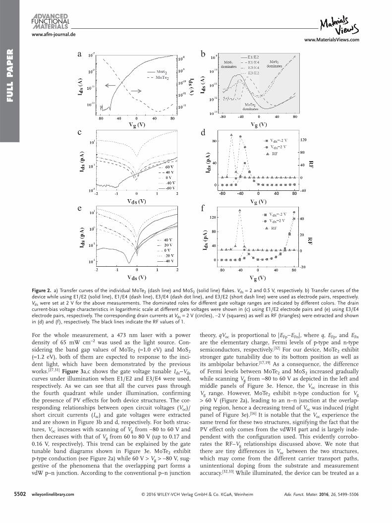
For the whole measurement, a 473 nm laser with a power density of 65 mW cm −2 was used as the light source. Con-sidering the band gap values of MoTe 2 (≈1.0 eV) and MoS 2 (≈1.2 eV), both of them are expected to response to the inci-dent light, which have been demonstrated by the previous works. [ 27,31 ] Figure 3 a,c shows the gate voltage tunable I ds − V ds curves under illumination when E1/E2 and E3/E4 were used, respectively. As we can see that all the curves pass through the fourth quadrant while under illumination, confi rming the presence of PV effects for both device structures. The cor-responding relationships between open circuit voltages ( V oc )/short circuit currents ( I sc ) and gate voltages were extracted and are shown in Figure 3 b and d, respectively. For both struc-tures, V oc increases with scanning of V g from −80 to 60 V and then decreases with that of V g from 60 to 80 V (up to 0.17 and 0.16 V, respectively). This trend can be explained by the gate tunable band diagrams shown in Figure 3 e. MoTe 2 exhibit p-type conduction (see Figure 2 a) while 60 V > V g > −80 V, sug-gestive of the phenomena that the overlapping part forms a vdW p–n junction. According to the conventional p–n junction
theory, qV oc is proportional to | E Fp − E Fn |, where q , E Fp , and E Fn are the elementary charge, Fermi levels of p-type and n-type semiconductors, respectively. [ 32 ] For our device, MoTe 2 exhibit stronger gate tunability due to its bottom position as well as its ambipolar behavior. [ 17,19 ] As a consequence, the difference of Fermi levels between MoTe 2 and MoS 2 increased gradually while scanning V g from −80 to 60 V as depicted in the left and middle panels of Figure 3 e. Hence, the V oc increase in this V g range. However, MoTe 2 exhibit n-type conduction for V g > 60 V (Figure 2 a), leading to an n–n junction at the overlap-ping region, hence a decreasing trend of V oc was induced (right panel of Figure 3 e). [ 16 ] It is notable that the V oc experience the same trend for these two structures, signifying the fact that the PV effect only comes from the vdWH part and is largely inde-pendent with the confi guration used. This evidently corrobo-rates the RF– V g relationships discussed above. We note that there are tiny differences in V oc between the two structures, which may come from the different carrier transport paths, unintentional doping from the substrate and measurement accuracy. [ 32,33 ] While illuminated, the device can be treated as a
Adv. Funct. Mater. 2016, 26, 5499–5506
www.afm-journal.dewww.MaterialsViews.com
Figure 2. a) Transfer curves of the individual MoTe 2 (dash line) and MoS 2 (solid line) fl akes. V ds = 2 and 0.5 V, respectively. b) Transfer curves of the device while using E1/E2 (solid line), E1/E4 (dash line), E3/E4 (dash dot line), and E3/E2 (short dash line) were used as electrode pairs, respectively. V ds were set at 2 V for the above measurements. The dominated roles for different gate voltage ranges are indicated by different colors. The drain current-bias voltage characteristics in logarithmic scale at different gate voltages were shown in (c) using E1/E2 electrode pairs and (e) using E3/E4 electrode pairs, respectively. The corresponding drain currents at V ds = 2 V (circles), −2 V (squares) as well as RF (triangles) were extracted and shown in (d) and (f), respectively. The black lines indicate the RF values of 1.
FULL P
APER
5503wileyonlinelibrary.com© 2016 WILEY-VCH Verlag GmbH & Co. KGaA, Weinheim
power source series connected with a gate adjustable load. As a result, when E3/E4 are used as source/drain pair, I sc increases gradually for V g > 0 V because of the increasing power supply ( V oc ) as well as the decreasing load (Figure 2 f, the above anal-ysis). On the contrary, although V oc increased, I sc was basically fl at due to the increasing load (Figure 2 d) while using E1/E2. Similar relationships of V oc / I sc − V g have been also observed in another device (see Figure S5a,b, Supporting Information), demonstrating the representativeness of the PV effects shown here. Electrical power ( P el ), defi ned as P el = I ph V ph , and fi lling factor (FF), defi ned as FF = P el,max / I sc V oc , where I ph , V ph , and P el, max are photocurrent, photovoltage, and the maximum elec-trical power, respectively, are also two other fi gures of merit to
evaluate PV effect. [ 16,19 ] The P el, max − V g and FF– V g relationships were calculated and the result is shown in Figure S4c,d, respec-tively in the Supporting Information. Both of these two merits demonstrate a better performance while using E3/E4 (an average FF of 0.27 for E3/E4 compared with 0.25 for E1/E2), which is probably because of the extra load of E1/E2 structure.
2.4. Confi guration-Dependent Photoresponse of the MoTe 2 /MoS 2 vdWHs
The confi guration-dependent photoresponse properties of the device were also studied. Figure 4 a,b shows the corresponding
Adv. Funct. Mater. 2016, 26, 5499–5506
www.afm-journal.dewww.MaterialsViews.com
Figure 3. The enlarged partial drain current-bias voltage characteristics at different gate voltages (80, 40, 0, −40 and −80 V) while under illumination were shown in (a) using E1/E2 and (c) using E3/E4 electrode pairs, respectively. b,d) The extracted short circuit currents (squares) and open circuit voltages (circles). e) Band alignment profi les of the MoTe 2 /MoS 2 vdWHs at gate voltages � 0 V (left panel), = 60 V (middle panel) and >60 V (right panel). The solid and open circles stand the electrons of holes, respectively. For the measurement, a 473 nm laser with a diameter of 5 mm was used as light source.

FULL
PAPER
5504 wileyonlinelibrary.com © 2016 WILEY-VCH Verlag GmbH & Co. KGaA, Weinheim
transfer curves under dark and illuminated states while using E1/E2 and E3/E4 electrodes, respectively. Like the individual transfer curves under dark state, the curves in the illuminated case show
similarly ambipolar behavior but with distinctive difference between two structures. The negative photoresponse phenomena while V g > 40 V for E1/E2 structure and −6 V > V g > −50 V for
Adv. Funct. Mater. 2016, 26, 5499–5506
www.afm-journal.dewww.MaterialsViews.com
Figure 4. The transfer curves under dark (solid lines) and illuminated (dash lines) states while using a) E1/E2 and b) E3/E4 electrode pairs. V ds were set as 2 V. c) Gate voltage dependent photocurrents for devices using E1/E2 (solid line) and E3/E4 (dash line) electrode pairs. The inset shows the corresponding gate voltage dependent photoresponsivities of the two device structures. d) Gate voltage dependent selective detectivity for devices using E1/E2 (solid line) and E3/E4 (dash line) electrode pairs. e) The time-dependent drain currents under periodic illumination for devices using E1/E2 (solid line) and E3/E4 (dash line) electrode pairs, respectively. f) Time resolved photoresponse characteristics for devices using E1/E2 (squares) and E3/E4 (squares) electrode pairs. The respective response times were extracted and shown in the fi gure. V ds = 2 V. And a 473 nm laser with a diameter of 5 mm was used as light source.

FULL P
APER
5505wileyonlinelibrary.com© 2016 WILEY-VCH Verlag GmbH & Co. KGaA, WeinheimAdv. Funct. Mater. 2016, 26, 5499–5506
www.afm-journal.dewww.MaterialsViews.com
E3/E4 structure may come from the photogating effect. [ 27,34,35 ] For convenience, we hereby only discuss the positive photo response parts. Figure 4 c shows the photocurrent ( I ph )− V g relationships of two device structures. Compared with E1/E2, the I ph show an ‘ambipolar’ behavior for E3/E4 due to the on states of the both ends of V g . Note that a 473 nm (corresponds to phonon energy of about 2.8 eV) laser was used as light source, which can generate the photo-stimulated electron–hole pairs both in MoTe 2 (with E g ≈ 1 eV) and MoS 2 (with E g = ≈1.2 eV). Hence a comparable max-imum I ph (≈1.1 × 10 −9 A) was detected for both device structures. The corresponding V g -dependent photoresponsivities ( R ), defi ned as R = I ph / P ph , where P ph is the incident light power, were calcu-lated and given in the inset of Figure 4 d. [ 34,36 ] Alike with I ph , R − V g relationships show a similar difference between these two struc-tures: a maximum R of 47 mA W −1 was achieved at V g = −76 V for E1/E2, however the highest R of 64 mA W −1 was achieved at V g = 80 V for E3/E4. The comparable peak I ph and different R values indicate that the vdWH part obtain a higher photo-electric conversion effi ciency. Specifi c detectivity ( D *), defi ned as D * = ( A Δ f ) 1/2 /NEP, where A is the effective detecting area in cm 2 , Δ f is the electrical bandwidth in Hz, and NEP is the noise equivalent power, is another important parameter to evaluate the photo response performances. [ 37,38 ] By assuming that dark cur-rent is the major contributor to shot noise, D * can be expressed as I ph A 1/2 / PA (2 qI dark ) 1/2 . [ 38 ] The calculated corresponding D * are shown in Figure 4 d. Unlike the I ph and R , E1/E2 structure shows a higher maximum D * of 1.6 × 10 10 Jones, which is due to the lower dark current compared with E3/E4 structure. Figure 4 e shows the time dependence of I ds under periodic illumination for the two device structures. Both of them display a good stability of photoresponse with photo switching on/off ratio of ≈2. The time-resolved photoresponse performances were also studied. As shown in Figure 4 f, a faster response time (defi ning as the time differences between the off-/on-state currents) of ≈385 ms was detected for E3/E4 structure, which is probably due to the higher dissociation effi ciency of vdWHs as well as shorter trans-port path of E3/E4 compared with E1/E2 structure. The relatively slow response speed is probably attributed to the charge trap defects at the material/substrate and material/electrode inter-faces during device fabrication. In addition, the good stability of photoresponse and response speed were also observed in another independent device, as shown in Figure S5c,d in the Supporting Information, which demonstrates the representativeness of the photo response performances shown here.
3. Conclusion
In summary, using MoTe 2 /MoS 2 as a sample, the confi guration-dependent electrically tunable electronic and optoelectronic prop-erties of vdWHs were studied. Through comparing the properties from two different vdWH device structures, we found that the properties that only emanate from the vdWHs, i.e., the rectifi -cation behavior and open voltage of PV effect, are independent of the device structures. However, other property, i.e., drain cur-rents, short circuit currents, and photo reponse performances, strongly depend on the type of structures employed. The device dominated by vdWH part exhibits higher PV effects, photo-responsivity, and faster photoresponse times. On the other hand,
device with extra individual part exhibits higher selective photode-tectivity. These results give a guideline on studying the intrinsic properties of vdWHs as well as optimizing the device structures.
4. Experimental Section Device Fabrication : The devices were fabricated by mechanical
exfoliation and a targeted transfer method. Firstly, few-layer MoTe 2 was exfoliated by standard scotch method from the bulk crystal (99.995%, HQ Graphene) onto 300 nm SiO 2 /Si wafers, which had been cleaned with a piranha solution for 2 h. The thickness of the MoTe 2 was verifi ed by OM and AFM. Then, PVA and PMMA were sequentially spin-coated on the top of another SiO 2 /Si substrate. After that, MoS 2 (purchased from SPI) was then exfoliated onto the SiO 2 /PVA/PMMA substrate. After dissolving the PVA layer in DI-water, the PMMA fi lm carrying exfoliated MoS 2 was fl oated and then mounted on the arm of a micromanipulator. MoS 2 was then transferred directionally to the target MoTe 2 fl ake. During the transfer, the target wafer was heated to 180 °C to ensure a good adhesion between the PMMA and the bottom wafer. The PMMA was removed by acetone. Finally, the heterostructure was annealed in hydrogen/argon environment (H 2 :Ar = 5:95) at 200 °C for 2 h to eliminate any possible contamination at the MoTe 2 /MoS 2 interface. Electrode patterns were defi ned by standard EBL, and 8/60 nm Cr/Au electrodes were deposited by thermal evaporation.
Device Characterization : The morphology, material quality, and thickness characterizations were performed by OM (Olympus BX51 M), Raman spectroscopy (Renishaw InVia, 532 nm excitation laser), and AFM (Veeco Multimode), respectively. The electrical transport measurements were carried out on a probe station (Lakeshore, TTP4) equipped with a vacuum pump and a semiconductor characterization system (Keithley 4200). The optoelectronic properties were measured using a 473 nm laser with a diameter of 5 mm and maximum light intensity of 12.77 mW (RGBLase).
Supporting Information Supporting Information is available from the Wiley Online Library or from the author.
Acknowledgements This work was supported by the National Natural Science Foundation of China (Nos. 21373065, 61474033, and 61574050), Strategic Priority Research Program of the Chinese Academy of Sciences (Grant No. XDA09040201), 973 Program of the Ministry of Science and Technology of China (No. 2012CB934103), and CAS Key Laboratory of Nanosystem and Hierarchical Fabrication. The authors also gratefully acknowledge the support of Youth Innovation Promotion Association CAS.
Received: March 16, 2016 Revised: May 9, 2016
Published online: May 30, 2016
[1] A. K. Geim , I. V. Grigorieva , Nature 2013 , 499 , 419 . [2] a) W. J. Yu , Z. Li , H. L. Zhou , Y. Chen , Y. Wang , Y. Huang ,
X. F. Duan , Nat. Mater. 2013 , 12 , 246 ; b) L. Britnell , R. V. Gorbachev , R. Jalil , B. D. Belle , F. Schedin , A. Mishchenko , T. Georgiou , M. I. Katsnelson , L. Eaves , S. V. Morozov , N. M. R. Peres , J. Leist , A. K. Geim , K. S. Novoselov , L. A. Ponomarenko , Science 2012 ,

FULL
PAPER
5506 wileyonlinelibrary.com © 2016 WILEY-VCH Verlag GmbH & Co. KGaA, Weinheim
335 , 947 ; c) W. J. Yu , Y. Liu , H. L. Zhou , A. X. Yin , Z. Li , Y. Huang , X. F. Duan , Nat. Nanotechnol. 2013 , 8 , 952 .
[3] a) H. Wang , F. C. Liu , W. Fu , Z. Y. Fang , W. Zhou , Z. Liu , Nanoscale 2014 , 6 , 12250 ; b) F. Wang , Z. X. Wang , Q. S. Wang , F. M. Wang , L. Yin , K. Xu , Y. Huang , J. He , Nanotechnology 2015 , 26 , 292001 .
[4] Y. Cao , A. Mishchenko , G. L. Yu , E. Khestanova , A. P. Rooney , E. Prestat , A. V. Kretinin , P. Blake , M. B. Shalom , C. Woods , J. Chapman , G. Balakrishnan , I. V. Grigorieva , K. S. Novoselov , B. A. Piot , M. Potemski , K. Watanabe , T. Taniguchi , S. J. Haigh , A. K. Geim , R. V. Gorbachev , Nano. Lett. 2015 , 15 , 4914 .
[5] T. Roy , M. Tosun , J. S. Kang , A. B. Sachid , S. B. Desai , M. Hettick , C. M. C. Hu , A. Javey , ACS Nano 2014 , 8 , 6259 .
[6] F. Withers , O. Del Pozo-Zamudio , A. Mishchenko , A. P. Rooney , A. Gholinia , K. Watanabe , T. Taniguchi , S. J. Haigh , A. K. Geim , A. I. Tartakovskii , K. S. Novoselov , Nat. Mater. 2015 , 14 , 301 .
[7] C. H. Lee , G. H. Lee , A. M. van der Zande , W. C. Chen , Y. L. Li , M. Y. Han , X. Cui , G. Arefe , C. Nuckolls , T. F. Heinz , J. Guo , J. Hone , P. Kim , Nat. Nanotechnol. 2014 , 9 , 676 .
[8] B. Radisavljevic , A. Radenovic , J. Brivio , V. Giacometti , A. Kis , Nat. Nanotechnol. 2011 , 6 , 147 .
[9] X. Cui , G. H. Lee , Y. D. Kim , G. Arefe , P. Y. Huang , C. H. Lee , D. A. Chenet , X. Zhang , L. Wang , F. Ye , F. Pizzocchero , B. S. Jessen , K. Watanabe , T. Taniguchi , D. A. Muller , T. Low , P. Kim , J. Hone , Nat. Nanotechnol. 2015 , 10 , 534 .
[10] a) X. Huang , Z. Y. Zeng , H. Zhang , Chem. Soc. Rev. 2013 , 42 , 1934 ; b) M. S. Xu , T. Liang , M. M. Shi , H. Z. Chen , Chem. Rev. 2013 , 113 , 3766 .
[11] Q. H. Wang , K. Kalantar-Zadeh , A. Kis , J. N. Coleman , M. S. Strano , Nat. Nanotechnol. 2012 , 7 , 699 .
[12] a) H. Fang , C. Battaglia , C. Carraro , S. Nemsak , B. Ozdol , J. S. Kang , H. A. Bechtel , S. B. Desai , F. Kronast , A. A. Unal , G. Conti , C. Conlon , G. K. Palsson , M. C. Martin , A. M. Minor , C. S. Fadley , E. Yablonovitch , R. Maboudian , A. Javey , Proc. Natl. Acad. Sci. USA 2014 , 111 , 6198 ; b) H. Jiang , J. Phys. Chem. C 2012 , 116 , 7664 .
[13] J. Kang , S. Tongay , J. Zhou , J. B. Li , J. Q. Wu , Appl. Phys. Lett. 2013 , 102 , 012111 .
[14] X. P. Hong , J. Kim , S. F. Shi , Y. Zhang , C. H. Jin , Y. H. Sun , S. Tongay , J. Q. Wu , Y. F. Zhang , F. Wang , Nat. Nanotechnol. 2014 , 9 , 682 .
[15] a) R. Cheng , D. H. Li , H. L. Zhou , C. Wang , A. X. Yin , S. Jiang , Y. Liu , Y. Chen , Y. Huang , X. F. Duan , Nano Lett. 2014 , 14 , 5590 ; b) M. H. Chiu , C. D. Zhang , H. W. Shiu , C. P. Chuu , C. H. Chen , C. Y. S. Chang , C. H. Chen , M. Y. Chou , C. K. Shih , L. J. Li , Nat. Commun. 2015 , 6 , 7666 .
[16] M. M. Furchi , A. Pospischil , F. Libisch , J. Burgdorfer , T. Mueller , Nano Lett. 2014 , 14 , 4785 .
[17] Y. X. Deng , Z. Luo , N. J. Conrad , H. Liu , Y. J. Gong , S. Najmaei , P. M. Ajayan , J. Lou , X. F. Xu , P. D. Ye , ACS Nano 2014 , 8 , 8292 .
[18] a) Y. J. Gong , J. H. Lin , X. L. Wang , G. Shi , S. D. Lei , Z. Lin , X. L. Zou , G. L. Ye , R. Vajtai , B. I. Yakobson , H. Terrones , M. Terrones , B. K. Tay , J. Lou , S. T. Pantelides , Z. Liu , W. Zhou , P. M. Ajayan , Nat. Mater. 2014 , 13 , 1135 ; b) X. D. Duan , C. Wang , J. C. Shaw , R. Cheng , Y. Chen , H. L. Li , X. P. Wu , Y. Tang , Q. L. Zhang , A. L. Pan , J. H. Jiang , R. Q. Yu , Y. Huang , X. F. Duan , Nat. Nanotechnol. 2014 , 9 , 1024 ; c) N. J. Huo , J. Kang , Z. M. Wei , S. S. Li , J. B. Li , S. H. Wei , Adv. Funct. Mater. 2014 , 24 , 7025 .
[19] F. Wang , Z. X. Wang , K. Xu , F. M. Wang , Q. S. Wang , Y. Huang , L. Yin , J. He , Nano Lett. 2015 , 15 , 7558 .
[20] a) K. A. Zhang , T. N. Zhang , G. H. Cheng , T. X. Li , S. X. Wang , W. Wei , X. H. Zhou , W. W. Yu , Y. Sun , P. Wang , D. Zhang , C. G. Zeng , X. J. Wang , W. D. Hu , H. J. Fan , G. Z. Shen , X. Chen , X. F. Duan , K. Chang , N. Dai , ACS Nano 2016 , 10 , 3852 ; b) A. Pezeshki , S. H. H. Shokouh , T. Nazari , K. Oh , S. Im , Adv. Mater. 2016 , 28 , 3216 .
[21] S. Rathi , I. Lee , D. Lim , J. W. Wang , Y. Ochiai , N. Aoki , K. Watanabe , T. Taniguchi , G. H. Lee , Y. J. Yu , P. Kim , G. H. Kim , Nano Lett. 2015 , 15 , 5017 .
[22] H. M. Li , D. Lee , D. S. Qu , X. C. Liu , J. J. Ryu , A. Seabaugh , W. J. Yoo , Nat. Commun. 2015 , 6 , 6564 .
[23] C. R. Dean , A. F. Young , I. Meric , C. Lee , L. Wang , S. Sorgenfrei , K. Watanabe , T. Taniguchi , P. Kim , K. L. Shepard , J. Hone , Nat. Nanotechnol. 2010 , 5 , 722 .
[24] Y. F. Lin , Y. Xu , S. T. Wang , S. L. Li , M. Yamamoto , A. Aparecido-Ferreira , W. W. Li , H. B. Sun , S. Nakaharai , W. B. Jian , K. Ueno , K. Tsukagoshi , Adv. Mater. 2014 , 26 , 3263 .
[25] S. Cho , S. Kim , J. H. Kim , J. Zhao , J. Seok , D. H. Keum , J. Baik , D. H. Choe , K. J. Chang , K. Suenaga , S. W. Kim , Y. H. Lee , H. Yang , Science 2015 , 349 , 625 .
[26] a) T. Boker , R. Severin , A. Muller , C. Janowitz , R. Manzke , D. Voss , P. Kruger , A. Mazur , J. Pollmann , Phys. Rev. B 2001 , 64 , 235305 ; b) C. Ruppert , O. B. Aslan , T. F. Heinz , Nano Lett. 2014 , 14 , 6231 .
[27] L. Yin , X. Zhan , K. Xu , F. Wang , Z. Wang , Y. Huang , Q. Wang , C. Jiang , J. He , Appl. Phys. Lett. 2016 , 108 , 043503 .
[28] M. Yamamoto , S. T. Wang , M. Y. Ni , Y. F. Lin , S. L. Li , S. Aikawa , W. B. Jian , K. Ueno , K. Wakabayashi , K. Tsukagoshi , ACS Nano 2014 , 8 , 3895 .
[29] a) Y. H. Lee , X. Q. Zhang , W. J. Zhang , M. T. Chang , C. T. Lin , K. D. Chang , Y. C. Yu , J. T. W. Wang , C. S. Chang , L. J. Li , T. W. Lin , Adv. Mater. 2012 , 24 , 2320 ; b) H. Li , Q. Zhang , C. C. R. Yap , B. K. Tay , T. H. T. Edwin , A. Olivier , D. Baillargeat , Adv. Funct. Mater. 2012 , 22 , 1385 .
[30] D. J. Perello , S. H. Chae , S. Song , Y. H. Lee , Nat. Commun. 2015 , 6 , 7809 .
[31] a) Z. Y. Yin , H. Li , H. Li , L. Jiang , Y. M. Shi , Y. H. Sun , G. Lu , Q. Zhang , X. D. Chen , H. Zhang , ACS Nano 2012 , 6 , 74 ; b) O. Lopez-Sanchez , D. Lembke , M. Kayci , A. Radenovic , A. Kis , Nat. Nanotechnol. 2013 , 8 , 497 .
[32] D. Cheyns , J. Poortmans , P. Heremans , C. Deibel , S. Verlaak , B. P. Rand , J. Genoe , Phys. Rev. B 2008 , 77 , 165332 .
[33] a) H. J. Snaith , L. Schmidt-Mende , M. Gratzel , M. Chiesa , Phys. Rev. B 2006 , 74 , 045306 ; b) G. Garcia-Belmonte , J. Bisquert , Appl. Phys. Lett. 2010 , 96 , 113301 .
[34] F. H. L. Koppens , T. Mueller , P. Avouris , A. C. Ferrari , M. S. Vitiello , M. Polini , Nat. Nanotechnol. 2014 , 9 , 780 .
[35] C. H. Liu , Y. C. Chang , T. B. Norris , Z. H. Zhong , Nat. Nanotechnol. 2014 , 9 , 273 .
[36] Z. X. Wang , K. Xu , Y. C. Li , X. Y. Zhan , M. Safdar , Q. S. Wang , F. M. Wang , J. He , ACS Nano 2014 , 8 , 4859 .
[37] W. Zhang , M. H. Chiu , C. H. Chen , W. Chen , L. J. Li , A. T. S. Wee , ACS Nano 2014 , 8 , 8653 .
[38] K. K. Manga , S. Wang , M. Jaiswal , Q. L. Bao , K. P. Loh , Adv. Mater. 2010 , 22 , 5265 .
Adv. Funct. Mater. 2016, 26, 5499–5506
www.afm-journal.dewww.MaterialsViews.com