Theoretical modeling of dendrite growth from conductive wire ...
Upload
khangminh22Category
view
1download
0
1
Electrically Conductive 2D Material Coatings for Flexible &
Stretchable Electronics: A Comparative Review of Graphenes
& MXenes
Vicente Orts Mercadillo, Kai Chio Chan, Mario Caironi, Athanassia Athanassiou, Ian A.
Kinloch, Mark Bissett *, Pietro Cataldi *
Vicente Orts Mercadillo, Kai Chio Chan, Prof. Ian Kinloch, Dr. Mark Bissett, Dr. Pietro Cataldi
Henry Royce Institute, National Graphene Institute, Department of Materials, The University
of Manchester, Oxford Road, M13 9PL, U.K.
Email Address: [email protected]; [email protected]
Dr. Mario Caironi, Dr. Pietro Cataldi
Center for Nano Science and Technology @PoliMi, Istituto Italiano di Tecnologia, Via Pascoli
70/3, Milan, 20133 Italy
Dr. Athanassia Athanassiou, Dr. Pietro Cataldi
Smart Materials, Istituto Italiano di Tecnologia, Via Morego 30, Genova, 16163 Italy
Keywords: strain sensing, supercapacitors, thermoelectric, electromagnetic interference
shielding, wearable electronics

2
Abstract
There is growing interest in transitioning electronic components and circuitry from stiff and
rigid substrates to more flexible and stretchable platforms, such as thin plastics, textiles, and
foams. In parallel, the push for more sustainable, biocompatible, and cost-efficient conductive
inks to coat these substrates, has led to the development of formulations with novel
nanomaterials. Among these, 2D materials, and particularly graphenes and MXenes, have
received intense research interest due to their increasingly facile and scalable production, high
electrical conductivity, and compatibility with existing manufacturing techniques. They enable
a range of electronic devices, including strain and pressure sensors, supercapacitors,
thermoelectric generators, and heaters. These new flexible and stretchable electronic devices
developed with 2D material coatings are poised to unlock exciting applications in the wearable,
healthcare and Internet of Things sectors. This review has surveyed key data from more than
200 articles published over the last 6 years, to provide a quantitative analysis of recent progress
in the field and shade light on future directions and prospects of this technology. We find that
despite the different chemical origins of graphenes and MXenes, their shared electrical
properties and 2D morphology, guarantee intriguing performance in end applications, leaving
plenty of space for shared progress and advancements in the future.
Table 1: Definition of acronyms used.
Acronym Definition
AC Activated Carbon
Ag NPs Silver Nanoparticles
Ag NWs Silver Nanowires
APP Ammonium Polyphosphate
C60 Buckminster Fullerene
CB Carbon Black
CCF Carbonised Cotton Fabric
CMC Carboxymethyl Cellulose
CNF Carbon Nanofibres
CNTs Carbon Nanotubes
Co NPs Cobalt Nanoparticles

3
CTAB Cetrimonium bromide
Cu NPs Copper Nanoparticles
Cu NWs Copper Nanowires
DMF Dimethylformamide
DMSO Dimethyl sulfoxide
ECG Electrochemically Exfoliated Graphene
EG Ethylene glycol
FLG Few Layer Graphene
GNP Graphene Nanoplatelets
GNR Graphene Nanoribbons
GO Graphene Oxide
Hf-SiO2 Superhydrophobic Fumed Silica
HIPS High Impact Polystyrene
HPMC Hypromellose
IPA 2-Propanol
MIT Methylisothiazolinone
MOF Metal Organic Framework
Ni-MOF Nickle Metal Organic Framework
Ni/Fe LDH Nickle / Iron Layered Double Hydroxide
NMP N-Methyl-2-pyrrolidone
PAA Polyacrylic acid
PAI Polyamide
PANI Polyaniline
PANI NWs Polyaniline Nanowires
PDA Polydopamine
PDAC Polydiallyldimethylammonium chloride
PDMS Polydimethylsiloxane
PEDOT Poly(3,4-ethylenedioxythiophene)
PEDOT:PSS Poly(3,4-ethylenedioxythiophene)
PEG Polyethylene Glycol
PEI Polyethyleneimine
PEN Polyethylene naphthalate
PET Polyethylene terephthalate
PI Polyimide
PP Polypropylene
PPy Polypyrrole
PS Polystyrene
PSS Poly(styrenesulfonate)
PTFE Polytetrafluoroethylene
PU Polyurethane
PVA Polyvinyl alcohol
PVDF Polyvinylidene fluoride
PVP Polyvinylpyrrolidone
rGO reduced Graphene Oxide
SA Sodium Alginate
SC Sodium Cholate
SDBS Sodium Dodecylbenzene Sulfonate (SDBS)
SDC Sodium Deoxycholate (SDC)
SDS Sodium Dodecyl Sulfate (SDS)
SrGO Sulphonated Reduced Graphene Oxide
Ti3C2Tx Titanium Carbide
TPU Thermoplastic polyurethane
WPU Water-Borne Polyurethane
ZnO NPs Zinc Oxide Nanoparticles
4
1.0. Introduction
The growing demand for seamlessly integrated wearable devices and the Internet of Things has
fuelled interest in transitioning electronic circuits away from traditional stiff and rigid
substrates and onto flexible and stretchable materials.[1-2] Typically, printed circuit boards are
fabricated using an epoxy glass-fibre panel onto which conductive copper tracks are patterned
and etched to connect electronic components.[3] This approach is incompatible with flexible
and stretchable platforms due to the difference in stiffness between the electronic connection
and the substrates.[4-6] As such, the focus has turned to developing conductive inks to coat and
pattern electronics circuits on flexible structures, that are capable of flexing with the substrate
while remaining adhered to it, retaining their electrical properties, while also enabling
synergistic effects through the combination of binders and complementing conductive fillers
into hybrid systems.[7]
The closest substitute to etched copper tracks are metal-based conductive inks. Typically, these
inks consist of metal (e.g., gold, silver, platinum, or copper) micro or nanoparticles, a binder
to increase the inter-particle bonding and adhesion to the substrate, and a solvent to carry the
dispersion.[8] The solvent and the binder often also stabilise the metal particle dispersion,
restrict oxidation and agglomeration, and act as reducing agents in the post-printing sintering
process, which also serves to form the conductive network and improves the electrical
conductivity. These inks benefit from the low electrical resistance of the metal particles, which
are usually only 2 – 3 times less conductive than their bulk counterparts, with sheet resistances
reaching the µΩ /sq. range and resistivities below 10-7 Ω m.[9-10]
Currently, nonmetal inks are more electrically resistive than metal inks, generally reaching 10-
1 Ω /sq. and 10-5 Ω m, as shown in section 2.3. However, they have other essential advantages.

5
The category of nonmetal conductive inks can encompass a wide range of organic conductive
fillers, including conductive polymers (e.g., poly(3,4-ethylenedioxythiophene), polystyrene
sulfonate (PEDOT: PSS) or polyaniline (PANI)) and different dimensionality nanocarbons
such as 0D fullerenes, 1D nanotubes, or 2D platelets. [11] These nonmetal inks do not require a
post-coating sintering step, which can reach damaging temperatures for common flexible
polymer substrates such as polyethylene terephthalate (PET) and cellulose. They are generally
easier to be dispersed and create a stable conductive ink with time, and in some instances, are
biocompatible, enabling easier processing and a more comprehensive range of applications.
They are less costly than inks that employ precious metal particles as, for example, gold and
silver ones. Furthermore, generally they can also be more easily formulated using fewer and
more environmental- and human-friendly solvents such as water or alcohols.
Conductive inks with 2D material-based formulations have drawn particular attention due to
the features enabled by their flake-like shape and high aspect ratio.[12] In thin-film coatings on
flat, transparent, and flexible polymer substrates (e.g., PET), they can display high optical
transmissivity and good electrical conductivity, enabling their use in transparent, stretchable
electronics. They adhere well to many textiles and foams, forming conductive networks
consisting of nanoplatelet stacks that can slip and slide over one another, resulting in unique
micromechanical properties that can be exploited for strain and pressure sensing. Advances in
scalable manufacturing processes for 2D material nanoplatelets, particularly liquid-phase
exfoliation, are enabling large production quantities and competitive price points[13]; graphene
screen sprinting pastes can cost half the price of silver alternatives.[14] Furthermore, the large
and growing family of solution-processable 2D materials encompasses materials with different
electronic properties: from conductors, e.g., graphene, to semi-conductors, e.g., tungsten
disulphide (WS2) or molybdenum disulphide (MoS2) and insulators, e.g., hexagonal boron

6
nitride (hBN) or graphene oxide (GO). Additionally, MXenes, a family of conductive 2D
transition metal carbides / nitrides, have been shown to combine the low resistivities of metal
inks with the platelet morphology and easier processability of 2D inks. These factors are
generating excitement, investments, and rapid technological advances.
Flexible, conductive coatings can be directly utilized (e.g., for EMI shielding capabilities) or
controlled to perform a function (e.g., for sensing or heating). Furthermore, the coatings can be
patterned to leverage conducting geometries (e.g., for interdigitated electrodes in
supercapacitors or strain sensing). Many existing large area coating techniques can be used
with compatible conductive inks such as screen printing, spray coating, or dip coating. The
technique chosen will depend on the substrate being used, the desired coating properties and
the necessity to scale production. Inkjet printing is among the most actively researched
techniques for manufacturing flexible electronics. Progress in inkjet printing 2D
nanomaterials-based inks has been detailed in multiple recent reviews [8, 15-21] and as such will
not be considered here. The facile application of novel 2D nanomaterials-based ink
formulations has enabled the quick prototyping of devices across a wide range of fast-growing
fields, including motion/tactile sensing[22], supercapacitors[23-24], heat generation[25-27],
strain/pressure sensors[28-29], thermoelectric generators[30-31], and EMI shielding[32].
The ground-breaking isolation of graphene at The University of Manchester in 2004 spurred a
boom in 2D materials research. The discovery of MXenes at Drexel University in 2011, drove
a subsequent explosion in growth in the last decade, which has particularly picked up pace over
the last five years (see Figure 1).[33] As these two 2D material families bridge the gap from lab
to industry, consolidating recent progress enables us to assess the state of the art. This review
surveys more than 200 articles published in the last six years (2015 – 2021) that report coating
7
of flexible or stretchable substrates with inks containing graphenes or MXenes for electronic
applications. The sustainability of common ink formulations, considering solvent, binders, and
conductive fillers, as well as the possible environmental implications of their adoption are
explored. Reviewed articles are grouped by the principal application described: strain sensing,
pressure sensing, supercapacitors, thermoelectric generation, joule heaters, or electromagnetic
interference (EMI) shielding. Crucial values are summarised in tables for each application
field. Where the data was available, essential information was gathered into composite plots to
help establish aggregate trends and spot outliers and provide a reader-friendly and instant
picture of the state-of-the-art.
2.0. Coatings
2.1 Techniques
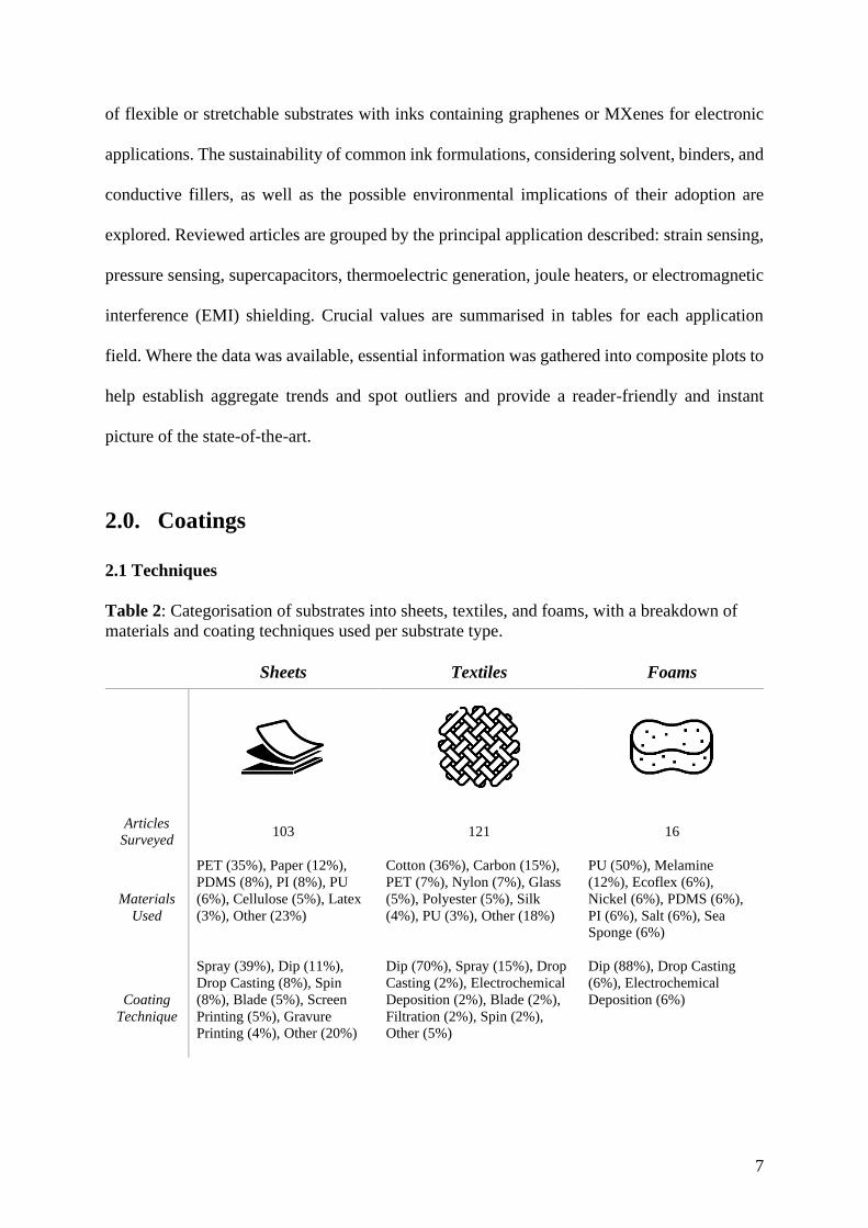
Table 2: Categorisation of substrates into sheets, textiles, and foams, with a breakdown of
materials and coating techniques used per substrate type.
Sheets Textiles Foams
Articles
Surveyed 103 121 16
Materials
Used
PET (35%), Paper (12%),
PDMS (8%), PI (8%), PU
(6%), Cellulose (5%), Latex
(3%), Other (23%)
Cotton (36%), Carbon (15%),
PET (7%), Nylon (7%), Glass
(5%), Polyester (5%), Silk
(4%), PU (3%), Other (18%)
PU (50%), Melamine
(12%), Ecoflex (6%),
Nickel (6%), PDMS (6%),
PI (6%), Salt (6%), Sea
Sponge (6%)
Coating
Technique
Spray (39%), Dip (11%),
Drop Casting (8%), Spin
(8%), Blade (5%), Screen
Printing (5%), Gravure
Printing (4%), Other (20%)
Dip (70%), Spray (15%), Drop
Casting (2%), Electrochemical
Deposition (2%), Blade (2%),
Filtration (2%), Spin (2%),
Other (5%)
Dip (88%), Drop Casting
(6%), Electrochemical
Deposition (6%)

8
There is a wide range of coating techniques available for coating flexible and stretchable
substrates. The technique used are influenced by the substrate material and form, with 45
different materials being used across the surveyed literature. These have been assigned into
three categories related to their form: sheets, textiles, and foams. Sheets consist of a flat surface,
making for a smooth, laminar support on which to coat thin films. Textiles consist of threads
arranged into a fabric, providing a permeable support network for inks to adhere onto. Foams
consist of porous structures that readily soak up and adsorb inks. Table 2 shows the material
breakdown for these three forms. The same material may be engineered into multiple forms,
e.g., PET can be woven into a fabric or made into flat transparent sheets. There are clear
engineering preferences for certain materials across each category: PET sheets, cotton textiles,
and polyurethane (PU) foams. Table 2 shows that the coating techniques can be used
interchangeably between the categories. Specific techniques are adjusted to the properties of
particular substrates. The data shows that spray coating was the most popular technique for
coating sheets (∼40%), while researchers mostly opted for dip coating when coating textiles
(∼70%) and foams (∼88%). Other methods have key advantages for specific uses: screen
printing enables complex patterns to be coated simply, repeatedly, and consistently, while blade
coating allows for fine control of coating thickness over flat surfaces. These are summarised in
Table 3.
Table 3: Main coating techniques used in surveyed literature.
Dip Spray Screen Blade
Application
Holding the
substrate to be
coated in a bath of
ink solution and
allowing for the
dispersed phase to
adhere onto the
substrate surface.[34]
Loading a spray gun
with ink solution
and using
compressed air (or
similar) to direct a
cloud of airborne
material onto the
substrate surface.[34]
Squeezing an ink
paste through a
mesh placed above
a substrate by
applying a shear
pressure with a
squeegee.[35]
Dragging a pool of
ink across the flat
substrate surface
using a mechanical
blade.[34]

9
Patterning Cutting substrate
into shape.
Mask on the
substrate.
Mask applied to
screen.
Cutting substrate
into shape.
Ink Properties Low surface
tension.
Fast evaporating
and low viscosity of
1 – 10 mPa s.[36]
High viscosity ∼1
Pa s, to resemble a
paste
High viscosity 1 –
10 Pa s.[37]
Articles
Surveyed 111 57 7 7
Solvents Used
Water (89%),
Ethanol (2%), IPA
(2%), NMP (2%),
Other (5%)
Water (52%), DMF
(13%), Ethanol
(11%), Chloroform
(10%), IPA (8%),
Acetone (3%),
NMP (3%)
Water (71%),
Dibasic Esters
(14%), NMP (14%)
Water (50%), NMP
(38%), Diethylene
Glycol (12%)
2.2 Formulations, Challenges and Sustainability
Figure 1: (a) The absolute number and (b) year-on-year percentage change of published articles
with graphene, MXene (or Ti3C2Tx) and flexible or stretchable in the title, keywords or abstract
over the last 15 years from the Web of Science (data collected on 27/05/2022).
All 2D materials share an atomically thin flake-like shape, which at the platelet level unlocks
a high aspect ratio (i.e., the ratio of lateral size to thickness) and accessible surface area (~2600
m2 g-1 in completely exfoliated graphene[38]). There are billions of individual platelets at the
powder macroscale, each with its lateral size, atomic thickness, and surface chemistry.
Understanding and controlling the unique interactions brought about by this two-
dimensionality, both between platelets and between their surroundings, is crucial to

10
successfully leverage their properties. Conductive inks benefit from stable, homogeneous
formulations that allow for consistent coating behaviour and performance. Achieving a good
dispersion of 2D platelets in a solvent, while controlling stability, electrical conductivity and
viscosity with stabilisers, binders, and additives can make for a challenging formulation.
Furthermore, different 2D material families have different atomic compositions which affect
these properties, and thus their use in practice as summarised in Table 4. Figure 1 shows the
absolute number (a) and year-on-year percentage change (b) of articles referencing graphene
and MXenes, alongside keywords ‘flexible’ or ‘stretchable’ over the last 15 years to show how
academic interest in these materials has evolved. MXenes, first isolated in 2011, are
experiencing an almost identical rate of uptake in the field of stretchable and flexible
electronics to graphene, isolated 7 years earlier. In absolute terms graphene articles outpace
MXene articles by an order of magnitude, although growth has plateaued. It will be interesting
to observe whether MXenes will continue to follow graphene’s trend as the field develops.
Table 4: Breakdown of 2D materials in surveyed literature. GNP and GO chemical
structures adapted with permission.[39] Copyright (2021) MDPI. Ti3C2Tx chemical structure
adapted with permission.[40] Copyright (2021), Wiley–VCH.
Graphene Graphene Oxide Ti3C2Tx
Chemical
Structure
Articles
Sampled 68 96 50
Solvents
Used
Water (55%), Chloroform
(11%), IPA (7%), Ethanol
(5%), DMF (4%), NMP
(4%), Acetone (3%), Other
(11%)
Water (78%), DMF (9%),
Ethanol (7%), Other (6%)
Water (76%), NMP (12%),
Ethanol (4%), IPA (4%),
DMF (2%), DMSO (2%)

11
Polymer
Additives
Used
None (48%), PEDOT:PSS
(10%), WPU (5%), Acrylic
Binder (4%), PU (4%), PVP
(4%), TPU (4%), Other
(12%)
None (87%), PVDF (3%),
PDA (2%), PSS (2%), Other
(6%)
None (88%), PVDF (8%),
PPy (2%), PTFE (2%)
Graphene is a 2D allotrope of graphite consisting of a single atomic layer of carbon – carbon
bonds arranged in a honeycomb lattice.[41] This sp2 hybridisation imparts strong mechanical
properties (namely a 1 TPa Young’s modulus) from the σ bonding, and low electrical resistivity
(∼ 10-8 Ω m) from the π bonding.[42] It is possible to isolate close to ideal single-layer graphene
(SLG) sheets through both top-down, e.g., micromechanical exfoliation such as the scotch-tape
method), and bottom-up techniques, e.g., chemical vapour deposition (CVD). The graphene
produced via mass production techniques (i.e., kilotons/year)[43], e.g., liquid phase, shear or
electrochemical exfoliated, mainly consists of thicker flakes categorised as few-layer (4 to 10
layers) or multi-layer (> 10 layers), with lateral sizes ranging from 1 to 50 μm[44], and is
generally commercially distributed as graphene nanoplatelets (GNPs)[45]. Obtaining SLG from
these mass-production techniques requires additional ultracentrifugation steps to single out
only the thinner flakes.[46] While GNPs do not match the exceptional properties of SLG, they
can reach a high surface area (up to 1000 m2 g-1[44]) and low resistivity (∼ 10-4 Ω m[47]). GNPs
are usually sold in batches of similar lateral size, e.g., First Graphene Ltd. sells their PureGraph
GNP in 5, 10, or 20 μm sizes, or surface area, e.g., XGSciences sells their grade C GNP in 300,
500, or 750 m2 g-1 areas.[44] The lateral size, thickness, and surface chemistry of these flakes
will influence how well they disperse. For example, GNPs that are thinner, smaller, or
decorated with hydrophilic surface chemistry will best disperse in water. However, 86% of
surveyed articles used organic solvents, binders, or surfactants to assist with GNP dispersibility
in water. Whereas this dropped to 27% when using GO or its reduced form rGO.

12
GO is a chemical derivative of graphene where the basal plane and edges are decorated with
defects and oxygen-containing functional groups. This surface chemistry allows GO to disperse
homogeneously in water, and thus is often used in inks without stabilising additives. It can also
assist adherence to the substrate surface through improved chemical compatibility. The rise in
sp3 character affects the material properties, notably drastically increasing the electrical
resistivity (∼ 108 Ω m) through the loss of conducting π bonds. As such, GO cannot be used as
a conductive coating until it has been reduced to recover more sp2 hybridisation, resulting in
resistivity values up to five orders of magnitude higher, ~103 Ω.[48] GO can be manufactured at
scale (i.e., hundred tonnes / year)[49] via a modified Hummer’s method, involving the use of
heavy acids to surface treat exfoliated graphitic material and selectively filtering thin flakes.[50]
It can also be produced via simultaneous electrochemical exfoliation and oxidation.[51]
Reduction to rGO can be carried out using thermal (16%), chemical (76%), electrochemical
(5%), or plasma/microwave (3%) techniques (the values in brackets referencing surveyed
articles), applied to either the GO dispersion or coated substrate. It is usually preferred to first
coat with GO and subsequently reduce the coated platelets to rGO, making the most of GO’s
improved dispersibility. Achieving sustainable chemical production and reduction of GO
requires manufactures to displace dangerous ingredients and chemicals.[52] Green reducing
agents actively being researched as alternatives include microorganisms, amino acids, and
ascorbic acid, to name a few.[53] These green substitutes often use also low temperatures (below
50°C), further improving their sustainability. However, this comes at the cost of speed and
reduction extent. [54] A hybrid approach that uses green reducing agents in combination with
fewer quantities of traditional reducing supporting agents, could be a positive compromise.

13
MXenes are 2D metal carbides or nitrides. They can reach lower resistivities than any other
solution-processed 2D material, down to ∼ 10-6 Ω m,[55] due to their metallic nature, have
strong mechanical properties (330 GPa Young’s Modulus), and feature an oxide-like surface
that imparts hydrophilic properties for good dispersibility in water. Most surveyed papers
(60%) dispersed MXenes in water alone. There are many MXene materials, typically following
the formula Mn+1XnTx, where M is an early transition metal (e.g., titanium, vanadium or
molybdenum), X is carbon and / or nitrogen, T is a functional group (e.g., -OH, -F, -Cl, or =O),
and n can vary from 1 to 4.[56] The first MXene to be isolated was Ti3C2Tx[57], and despite 29
other forms having been experimentally synthesised[33], it was used in all surveyed MXene
articles. MXenes are mainly manufactured via top-down etching of Mn+1AXn, i.e., MAX
phases, where Ti3AlC2 is used for Ti3C2Tx. The element represented by A (usually found in
groups 13 or 14) is selectively etched away, leaving the metal carbide or nitride layers, which
can subsequently be delaminated in solutions of cation intercalants, down to single-layer
sheets, reaching lateral sizes of up to 10 μm.[58] Acidic solutions containing fluorides tend to
be used as a chemical etchant, primarily hydrofluoric acid (HF)[56]. Alternative etching
techniques include molten salt[59], hydrothermal[60], halogen[61] and electrochemical etching[62].
MXenes have yet to reach the tons / year scale of GNPs, with current scale reaching 50g batch
reactors.[63] The surface terminations that impart hydrophilicity also cause MXenes to oxidise,
limiting their environmental stability. An aqueous Ti3C2Tx dispersion exposed to air will
completely oxidise to TiO2 within days, and this can be observed by a colour change from
brown to white due to the precipitation of titania from the flakes.[64] To minimise this issue,
dispersions can be stored at low temperatures extending stability to over a month, and under
argon for over 6 months.[65]

14
The research effort of the research community towards more sustainable production of MXenes
is still at an embryonal stage, which is not surprising considering the more recent development
of MXenes. This effort includes the production of MXene with more safe chemicals, ideally
water-based, compared to hydrogen fluoride, which is toxic.[66] Researchers recently also
proposed using the weight percent of residues consisting of unetched MAX and unexfoliated
multi-layered MXene (that can be up to 80–90% of the total starting weight) instead of trashing
this sediment away.[67]
There is a clear preference among surveyed articles (70%) to use water as a solvent where
possible, since it is easily accessible, not hazardous, and environmentally friendly. The next
most popular solvents were ethanol (8%), dimethylformamide (DMF) (6%), isopropyl alcohol
(IPA) (6%) and n-methyl-2-pyrrolidone (NMP) (5%). The latter three are polar aprotic solvents
that have been shown to aid graphene exfoliation and make the dispersed flakes less prone to
agglomerate. On the other hand, water and ethanol are polar protic solvents, thus dispersing
hydrophilic material (e.g., GO and Ti3C2Tx) well. Additives were generally used to either tune
rheological properties and improve binding between flakes and substrate (e.g., polyvinylidene
fluoride (PVDF), polyurethane (PU), or polyvinylpyrrolidone (PVP)) or to stabilise dispersions
(e.g., sodium dodecyl sulphate (SDS), sodium dodecylbenzene sulfonate (SDBS), sodium
deoxycholate (SDC) or sodium cholate (SC)). Their use has to be moderate, as they can also
degrade electrical properties and reduce the flake active surface area and thus functionality.[68]
Degradable and bio-based dispersing agents and binders should be preferred compared to
others.[69] An example is the valorization of wool wastes from the agricultural sector to extract
keratin that is employed as a dispersant and binder for making environmentally friendly water-
based conductive inks based on GNPs.[70]

15
Hybrid formulations combine 2D materials with other conductive fillers to enhance electrical
properties or create synergies between conduction mechanisms. Around 40% of surveyed
coatings used a hybrid ink formulation, these included conductive polymers, e.g., PEDOT:PSS,
PANI, nanometals, e.g., silver nanowires (AgNWs) and nanoparticles (AgNPs), and other
nanocarbons, e.g., carbon black (CB) and carbon nanotubes (CNTs). Very rarely graphene and
MXenes were used in the same coating [71-74].
Understanding the biodegradability of the 2D nanomaterials and thus their end-of-life toxicity
to humans and wildlife will be a crucial hurdle in enabling their mass adoption.[75] It is known
that low concentrations of horseradish peroxidase (HRP) could degrade GO, whereas rGO was
not affected.[76] Kurapati et al.[77] exhibited enhanced degradation of GO if functionalized with
catechol and coumarin, which naturally bond with HRP. The same authors also displayed that
myeloperoxidase, a human enzyme, can degrade GO. The size (lateral dimension and
thickness) was critical, with aggregated samples more challenging to be degraded.[78]
Microbials can also degrade graphenes, and this does not demand specific conditions such as a
control on the temperature and pH.[75] For example, Lalwani et al.[79] documented that GO and
rGO nanoribbons were degraded by lignin peroxidase, an enzyme released from fungi.
Regarding MXene, the toxicity and effects of MXenes on human beings and the environment
have not been thoroughly investigated, and the toxicity mechanism is not clear up till now.[80]
2.3 Electrical Properties

16

17
Figure 2: Plots of (a,b) electrical conductivity and (c,d) sheet resistance for coatings surveyed
in the literature (reference number labelled in the x-axes). The marker shape corresponds to the
substrate type used: square () for sheets, triangle () for textiles, and circle () for foams.
The values in bold are conductive materials in addition to graphenes or MXenes used in the
coating. The values in italics are the substrate, followed by any polymer binders in brackets.
The electrical properties of thin coatings can be measured accurately using the four-point probe
technique, whereby equidistant, linearly separated, electrical connections are made with the
material surface. Current (𝐼) flows across the outer pair of electrodes, and the voltage drop (𝑉)
is measured at high impedance (i.e., at I = 0 A) across the inner pair. The determination of a
value for electrical conductivity then requires considering the sample physical dimensions
relative to the probe set-up. Both the thickness (𝑡) of the sample and its length (𝑙), must be
considered. If the thickness of the sample is a factor of ten lower than the inter-probe spacing
(𝑡/𝑙 < 0.1), for the sake of simplicity the sample can be considered ‘infinitesimally thin’, and
the sheet resistance (𝑅𝑠) can be approximated by using[81]:
𝑅𝑠 =𝜋
ln 2⋅
𝑉
𝐼 (1)
Any thicker sample (𝑡/𝑙 > 0.1) requires the bulk conductivity (𝜎) to be determined, using the
appropriate equations[82] and correction factors, which relate to the sample geometry.[83] The
sheet resistance can then be found from the measured bulk conductivity, assuming the thickness
is also known:
𝑅𝑠 =1
𝜎𝑡 (2)
In sheet substrates, the coating is usually deposited on top as a thinner layer and the sheet
resistance is typically reported. In textiles, the coating can infiltrate deeper into the network of
fibres, so either sheet or bulk values are given. Whereas the 3D nature of foams means the
electrical properties can only be reported as bulk conductivity.

18
The bulk conductivities and sheet resistances of the surveyed articles are reported in Figure 2
and Table 5. Conductive inks formulated with binders have tuneable electrical properties
depending on the proportion of conductive fillers used. Some articles report conductivity as a
function of filler loading[22, 31, 55, 84-92], and the most conductive formulations are shown for
these cases. Sheet based coatings show the highest electrical conductivities, reaching 106 S m-
1, with the closest textile displaying two orders of magnitude lower values[93] than the best
performing sheet[94] in terms of bulk conductivity. This is due to the coating not having to form
a percolative conductive network around the substrate, as is the case in textiles or foams. A
sheet-based coating can thus also require less or no binder, since the 2D nature of the
nanosheets can lead to good adherence onto compatible surfaces.
The most electrically conductive coating surveyed (1.2 × 10⁶ S m-1) consisted of a 4.3 µm
thick Ti3C2Tx film spray coated onto a PET sheet.[94] Coatings enhanced with additional
conductive fillers tend to reach higher conductivities: generally, graphene based coatings are
more often used alongside additional conductive fillers (39%), over MXene based coatings
(12%). The most electrically conductive graphene based coating surveyed (8.7 × 10⁵ S m-1)
was enhanced with metal based conductive fillers, copper nanoparticles (Cu NPs) and silver
nitrate (AgNO3), blade coated onto a PET sheet and sintered.[95] Similarly, the most electrically
conductive based textile coating surveyed ( 6.4 × 10⁴ S m-1) used rGO enhanced with
PEDOT:PSS.[93] While the most electrically conductive foam (59 S m-1) used rGO enhanced
with silver nanowires (AgNWs) and polydopamine (PDA).
The tendency of MXenes to oxidise can be problematic not just for dispersion stability, but
also conductivity performance within a matrix. Habib et al. (2019)[96] demonstrated that while

19
Ti3C2Tx oxidises faster in liquid media, a notable decrease in performance was observed in a
PVA matrix at 10 and 50 wt.% loadings with conductivity values dropping to 7 and 40% of the
initial conductivity respectively. Unfortunately, most studies do not consider the long-term
stability of these MXene nanocomposites. The issue is further complicated as the humidity,
UV exposure, voltages used, and frequency of use may all affect rate and extent of oxidation.
Future work on conductive MXene coatings should account for long-term electrical stability,
enabling a wider understanding of the extent of the problem across different matrix systems
and with different flake surface chemistries.
Table 5. Electrical conductivity values from surveyed literature
2D Material Substrate Other Conductive
Materials
Sheet Resistance
(Ohm/Sq.)
Electrical
Conductivity (S m-
1)
Ref.
Graphene Foam (Latex, Natural Rubber)
1.56E+00 [97]
Foam (PDMS)
1.00E-01 [98]
Foam (PI)
4.00E-01 [99]
Foam (PU)
1.00E-03 [100-
101] Foam (PU) CNTs
1.06E-01 [102]
Foam (PU) CNTs
1.30E+00 [103]
Foam (Sea
Sponge)
PDA, Ag NWs 5.90E+01 [104]
Sheet () Co NPs
2.17E+02 [105]
Sheet (Acrylic Paint) 2.10E+01 3.97E+04 [106]
Sheet (Cellulose) 1.48e+00 to 1.00e+01 [70, 84]
Sheet (Epoxy)
1.00E+03
[107]
Sheet (Glass)
6.00E+04
[108]
Sheet (Glass) PEDOT:PSS 4.63E+01 7.20E+04 [109]
Sheet (Nitrile)
1.00e+01 to
3.22e+01
1.55E+03 [22, 32]
Sheet (Organic)
1.86E+02 [110]
Sheet (PDMS)
5.00e+01 to 1.50e+03 [111-
112] Sheet (PET)
2.67e-01 to 1.50e+04 [72,
113-
114] Sheet (PET) Ag NWs 1.00E+02
[115]
Sheet (PET) CNTs 1.98e+01 to
1.11e+02
3.00E+04 [90,
116-
117] Sheet (PET) Cu NWs 3.00E+01
[118]

20
Sheet (PET) PANI,
PEDOT:PSS
9.00E+01 4.57E+03 [119]
Sheet (PET) Ag NWs 1.60e+00 to 2.06e+01 [120-
121] Sheet (PET) Carbon Black 6.64E+00 2.15E+04 [122]
Sheet (PET) Cu NPs, AgNO3 8.70E+05 [95]
Sheet (PET) PDA, PEDOT:PSS,
CNTs
5.22E+01
[123]
Sheet (PET) PEDOT:PSS 1.60e+01 to
6.40e+02
1.00E+01 [36, 89,
124] Sheet (PET) PEDOT:PSS,
PANI, CNTs
5.60E+00 1.79E+05 [31]
Sheet (PI)
5.76E+01
[125-
127] Sheet (PI) CB 2.35E+02 4.37E+02 [87]
Sheet (Paper)
2.00e+00 to 4.41e+01 [86,
128] Sheet (Paper) CNF 1.20E+02
[129]
Sheet (Paper) CNTs 1.54E+03 6.50E+02 [130]
Sheet (Wood)
1.30E+01 [131]
Textile ()
7.10E+05
[132-
134] Textile (Aramid) 2.70E+03
[135]
Textile
(Carbon
Cloth)
PANI
7.70E+00 [136]
Textile
(Carbon
Cloth)
PEDOT:PSS
6.40E+04 [93]
Textile (Cellulose) 1.00E+01
[137]
Textile (Cotton) 1.00E+08
[138-
140]
[26, 85,
141]
[142-
144]
[145-
147]
[148-
149] Textile
(Cotton)
Ni 8.00E-01
[144]
Textile
(Cotton)
ZnO NPs 1.44E+02 1.58E+03 [92]
Textile
(Cotton)
CNTs 2.70E+01 3.86E+01 [150]
Textile
(Cotton)
MnO2
9.00E+01 [25]
Textile
(Cotton)
PEDOT:PSS 1.50E+02
[30, 88,
151]
[152] Textile (Glass)
5.00E-03 [153-
155]
[156] Textile (Nylon) 1.12E+05
[157-
159]
[160-
162]

21
Textile
(Nylon)
PPy 2.40E+02
[162]
Textile (PET) AgNO3 6.78E-01
[163]
Textile (PET) Graphite 1.00E+03
[164]
Textile (PU)
1.24E+02 [165]
Textile (PU) Ag NPs 1.00E+01
[166-
167] Textile (PU, Polyester)
1.60E+00 [168]
Textile (Polyester) 2.53E+05
[169-
171] Textile (Silk)
1.50E+03 3.06E-04 [172-
174]
[175] Textile (Spandex)
1.00E+01 [176]
Textile (TPU)
1.00E+00 [177]
Graphene +
MXene
Sheet (Polyester)
1.20E+05 [178]
MXene Sheet (Acrylate) 2.99E+02 5.77E+04 [91]
Sheet (Filter Paper)
2.76E+03 [179]
Sheet (PET)
5.21E+00 4.50E+05 [23, 72,
94] Sheet (PET) CNTs 6.15E+00 1.05E+06 [55]
Sheet (PTFE)
1.00E+03 [180]
Sheet (Paper)
1.67e+01 to
2.23e+03
2.04E+02 [181-
182] Sheet (Paper) CB 6.25E-01 1.28E+04 [183]
Textile
(CNTs)
CNTs
2.60E+03 [184]
Textile (Carbon Cloth) 6.50E+00 8.50E+02 [185]
Textile
(Carbon
Cloth)
CNTs 2.77E+00 9.55E+02 [186]
Textile (Cellulose) 3.31E+02 4.40E+02 [187]
Textile (Cotton) 5.00E+00
[188-
190] Textile (Nylon) 2.10E+02
[191]
Textile (PET)
2.15e+02 to 5.00e+03 [192-
193] Textile (PET) PPy 2.33E+00 1.00E+03 [194]
Textile (Silk) Ag NWs 8.00E-01 1.04E+04 [195]
3 Applications
3.1 Sensors
3.1.1 Strain Sensors
22
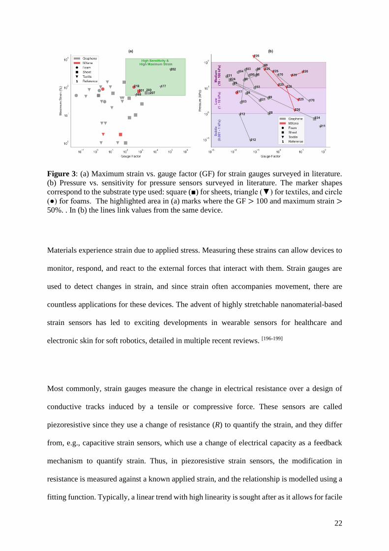
Figure 3: (a) Maximum strain vs. gauge factor (GF) for strain gauges surveyed in literature.
(b) Pressure vs. sensitivity for pressure sensors surveyed in literature. The marker shapes
correspond to the substrate type used: square () for sheets, triangle () for textiles, and circle
() for foams. The highlighted area in (a) marks where the GF > 100 and maximum strain >
50%. . In (b) the lines link values from the same device.
Materials experience strain due to applied stress. Measuring these strains can allow devices to
monitor, respond, and react to the external forces that interact with them. Strain gauges are
used to detect changes in strain, and since strain often accompanies movement, there are
countless applications for these devices. The advent of highly stretchable nanomaterial-based
strain sensors has led to exciting developments in wearable sensors for healthcare and
electronic skin for soft robotics, detailed in multiple recent reviews. [196-199]
Most commonly, strain gauges measure the change in electrical resistance over a design of
conductive tracks induced by a tensile or compressive force. These sensors are called
piezoresistive since they use a change of resistance (R) to quantify the strain, and they differ
from, e.g., capacitive strain sensors, which use a change of electrical capacity as a feedback
mechanism to quantify strain. Thus, in piezoresistive strain sensors, the modification in
resistance is measured against a known applied strain, and the relationship is modelled using a
fitting function. Typically, a linear trend with high linearity is sought after as it allows for facile

23
calculations. The gradient of this linear fit is a measure of the sensor sensitivity, known as the
gauge factor (GF), and expressed as:
𝐺𝐹 =𝛥𝑅/𝑅0
𝜖 (3)
𝛥𝑅 is the modification in electrical resistance after the strain 𝜖 was applied, and 𝑅0 is the
resistance at zero strain.[198] The strain range over which the sensor can operate (i.e., working
range) is a measure of its stretchability. A sensor might operate across multiple strain ranges,
with a different fit for each one. Ideally, a strain sensor should have a high sensitivity, over an
extended linear working range, experience minimal hysteresis, good cyclability, be
biocompatible and robust enough to withstand its environment, all while being small and cheap.
In practice, achieving all these properties simultaneously presents a significant challenge.[198]
Conventional metal- and semiconductor-based piezoresistive strain sensors are limited by their
intrinsically low stretchability (< 0.6%), defined as the maximum strain at which the sensor
can reliably and repeatedly measure strain.[198] Coating flexible and stretchable platforms (e.g.,
elastomers or textiles) with conductive nanomaterials enables strain sensors with large elastic
regions achieving stretchability values between 10% to 800%.[198] As with conventional
sensors, the working principle behind these conductive coatings is a function of the intrinsic
piezoresistive effect and sensor geometry, i.e., the change in resistance due to the strain
disrupting the substrate’s mechanical integrity, most evident in the case of woven textiles
where adjacent fibres might be pulled apart, creating gaps in the electrical network. However,
there are also contributions from the conductive filler interactions with itself and surroundings.
There are three main mechanisms of note; crack propagation, slippage disconnection, and
tunnelling.[198] In the first, the conductive particles are pulled apart, causing cracks to appear

24
and propagate through the network as the applied strain intensifies, increasing the electrical
resistance. Once the sensor is relaxed, it pulls the network back together again. In the second,
the applied strain causes stacks of overlapping conductive material to move out of contact in a
slipping motion, reducing the inter-particle connectivity of the network and increasing
resistance. In the third, electrons can travel through a non-conductive matrix by quantum
tunnelling between densely packed conductive fillers. An applied strain can change the packing
density and thus change the probability of tunnelling. An issue with resistive nanomaterial-
based strain sensors is that strain cycling can lead to permanent and significant changes in the
network that affect operation (hysteresis) over time. Moreover, it is difficult for these micro-
mechanical deformations to affect the sensor area homogeneously and maintain sensor
linearity.[197]
Inherent to this micromechanical deformation is the dimensionality of the materials involved.
The same application of strain will affect a network of 0D fullerenes differently from 1D
nanotubes and 2D nanoplatelets. Indeed, each distinct particle changes shape and re-arrange in
the bulk network differently. Conductive 2D materials, and in particular graphenes and
MXenes, have gathered particular interest as their large aspect ratio, resulting from their paper-
like nanoplatelet shape, is particularly efficient in strain sensing application because of the
possibility to benefit on the three mechanism of strain detection, i.e., crack, slippage, and
tunnelling.
The performance of strain sensors from 36 different articles has been summarised in Figure
3(a). The bulk of these surveyed literature values fall outside the green box that delineates a
high sensitivity (GF > 100) and high maximum strain (> 50%). Generally, they either achieve

25
a higher maximum strain at lower sensitivities or a high sensitivity at a lower maximum strain.
This behaviour has been reported for thin-film sensors[200] and is a consequence of the three
mechanisms discussed previously. When crack propagation dominates, the sensor is
susceptible to minimal changes in strain (< 20%).[200] However, the propagation of cracks can
quickly disrupt the network to the point where the increase in resistance cannot be managed.
When slipping dominates, a considerable strain is required to induce significant enough
resistance changes to measure, resulting in low sensitivities (GF < 100). [200] Therefore,
achieving high sensitivity in conjunction with high stretchability is a significant challenge.
Figure 4: (a) Device fabrication process. Adapted with permission.[201] Copyright 2018,
American Chemical Society. (b) Sensing mechanism schematics, with accompanying SEM
images, showcasing the layer slippage induced due to addition of C60. Adapted with
permission.[200] Copyright 2018, Wiley. (c) SEM images of the uncoated fabric and fibres (top),
and graphene + CB coated fabrics and fibres (bottom). Adapted with permission.[202] Copyright
2018, Royal Society of Chemistry.
One of the strain sensors surveyed with the most extensive working range is Cai et al.’s [201]
MXene + CNT hybrid on latex. In order to retain the advantages of both crack formation and
slipping disconnection mechanisms, the authors spray-coated bilayers of Ti3C2Tx and CNTs

26
onto a 20 x 5 mm2 latex sheet with a polyimide mask, as shown in Figure 4(a). The MXene
nanoplatelets are sensitive to crack propagation, ensuring good sensitivity at low strains (GF =
4.35 at 0.1 – 0.6 % strain). While the CNTs act as conductive bridges that block layers of
MXene from re-stacking and agglomerating, allowing the sensor to retain both structural and
electrical integrity over higher strains (GF = 772.6 at 30 – 70 % strain) where slipping
dominates. The authors have demonstrated the sensor range by measuring physiological signals
of different magnitudes, monitoring the stretching of skin at the neck to distinguish different
spoken words, and flexing the knee joint while exercising.
Shi et al. [200] also leveraged the different nanomaterials dimensionality, going further and
incorporating a 0D material, C60 fullerenes, alongside 1D AgNWs and 2D GO. In a one-step
screen printing process, all three nanomaterials were combined in a hybrid water-based ink
with fluorosurfactant and coated onto a 200 x 3.5 mm polyurethane sheet. The AgNWs form a
conductive network supported by the layered GO structure. As expected, this combination
allows for high sensitivity to low strains due to crack propagation (GF = 466.2 at 3 – 35 %
strain). However, the addition of 0D fullerenes suppresses the density and magnitude of crack
propagation by acting as a lubricant to promote interlayer slipping instead, as shown in Figure
4(b). This combination of mechanisms increases the working strain range of the sensor while
maintaining the high sensitivity (GF = 2392.9 at 52 – 62 % strain).
The most sensitive strain sensor at higher loadings surveyed is Souri et al.’s [202] graphene +
CB hybrid on cotton fabric. The sensor was manufactured out of a 100 x 7 mm2 dog bone-
shaped cotton fabric cut-out, with a notch at the centre, dip-coated in graphene + CB water-
based ink, with sodium dodecyl benzene sulfonate (SDBS) surfactant. The coated cotton was

27
subsequently encapsulated in ecoflex silicone polymer. Before undergoing characterisation, the
sensor underwent rupture training whereby the cotton was cracked and even completely
fractured at the notch following 5 cycles at 400% strain. Consequently, these rupture trained
sensors operate via a substrate-driven mechanism, whereby breaking these weakened yarns at
high strain levels disrupts the electrical network and increases resistance, enabling high
sensitivity at high strain (GF = 102351 at 342 – 400 % strain). This mechanism also yields
good sensitivities at low strain (GF = 11.82 at 0.5 – 1 % strain) due to the interaction of the
fractured fibres, arranged in a tentacle-like manner at the notch, that are distanced from each
other with strain.
Table 6: Performance of Surveyed Strain Sensors.
2D
Material
s
Substrat
e
Other
Conductiv
e
Materials
Maximum Strain (%) Gauge Factor Ref.
Graphen
e
Foam
(PU) 3.00E-01 4.00E+00 [100]
Foam
(PU) CNTs
7.50e-01, 5.00e-01,
2.50e-01
1.75e+00, 8.60e-01,
9.60e-01 [102]
Foam
(PU) CNTs
1.00e+00, 8.60e-01,
5.00e-01
-2.30e+00, -2.13e+00,
5.00e-02 [103]
Foam
(Sea
Sponge)
PDA, Ag
NWs 5.00E-01 1.50E+00 [104]
Sheet (Ecoflex) 1.50e+00, 1.00e+00 8.16e+01, 2.97e+01 [203]
Sheet
(Epoxy) 1.00E-02 1.00E+02 [107]
Sheet
(PDMS) 5.00E-01 1.55E+00 [204]
Sheet
(PDMS) 1.00E-01 4.66E+02 [205]
Sheet
(PDMS) 4.00e-01, 3.00e-01,
2.00e-01, 1.00e-01
1.73e+02, 3.70e+01,
1.10e+01, 7.00e+00 [112]
Sheet
(PI) 2.50e-01, 1.70e-01 1.24e+03, 2.36e+02 [126]
Sheet
(PU) CNTs 8.00E-02 1.81E+02 [206]
Sheet
(PU)
C60, Ag
NWs
6.20e-01, 5.20e-01,
3.50e-01, 3.00e-02
2.39e+03, 1.00e+03,
4.66e+02, 2.50e+01 [200]
Sheet
(TPU) 6.00E-01 1.44E+01 [29]
Textile (Cotton) 5.70e-01, 4.00e-01 3.67e+03, 4.16e+02 [207]

28
Textile (Cotton) 3.00E-01 2.49E+00 [140]
Textile
(Cotton) CB 1.50e+00, 1.20e+00 6.05e+00, 1.67e+00 [208]
Textile
(Cotton) CB
1.00e-02, 2.00e-02,
2.31e+00, 3.42e+00,
4.00e+00
1.18e+01, 1.73e+01,
9.56e+01, 2.18e+03,
1.02e+05
[202]
Textile
(Glass) 0.00e+00, 1.00e-02 1.13e+02, 2.95e+01 [156]
Textile
(Hair) 5.00E-02 4.46E+00 [209]
Textile
(Lycra) PANI 4.00E-01 6.73E+01 [210]
Textile (Nylon) 1.00e-01, 1.80e-01 1.85e+01, 1.21e+01 [161]
Textile (Nylon) 4.60e-01, 3.30e-01,
1.20e-01
2.20e-01, 7.00e-02, 8.00e-
02 [158]
Textile
(PAI) 1.00e-01, 8.00e-01 1.63e+00, 3.70e-01 [211]
Textile
(PET) 1.00E-02 -7.10E+00 [212]
Textile
(PU) Ag NPs 5.00E-01 4.90E+02 [166]
Textile
(PU) CNTs, CB 1.00E+00 2.14E+00 [213]
Textile (PU, Polyester) 1.00e+00, 1.00e-01,
5.00e-02
9.65e+00, 2.50e+00,
2.60e+00 [168]
Textile
(PVA) PDA 1.00E-02 2.30E+00 [214]
Textile (Polyester) 1.00e-02, 5.00e-02 6.42e+00, 2.58e+00 [215] Textile (Spandex) 4.00E-01 5.01E+01 [176]
Textile
(Spande
x)
PANI 3.00e-01, 1.50e-01 6.03e+01, 6.80e+00 [216]
Textile
(TPU) 9.80e-01, 1.50e-01 2.25e+04, 1.80e+02 [177]
MXene Foam
(PU) 8.50e-01, 4.50e-01,
3.10e-01
3.00e+00, 2.30e-01,
1.70e-01 [217]
Foam
(Salt) CNTs 1.00E+00 3.63E+02 [218]
Sheet
(Latex) CNTs
7.00e-01, 3.00e-01,
1.00e-02
7.73e+02, 6.46e+01,
4.35e+00 [201]
Sheet
(PI) 1.00e-02, 2.00e-02 9.48e+01, 4.59e+01 [219]
Textile (Cellulose) -2.00E-01 6.20E+00 [187] Textile (Cotton) 2.00e-02, 1.00e-02 3.18e+00, 1.16e+00 [189]
3.1.2 Pressure Sensors

29
Figure 5: (a) Schematic of MXene textile device. (b) Change in relative current against applied
pressure for the device. (c) Operating principle of device under pressure. Adapted with
permission.[220] Copyright 2019, Royal Society of Chemistry. (d) Deformation schematic of
the rGO + MWNT coated sponge, under no, low and high pressure. The red lines show the
conductive network, the white lines indicate crack formation in the rGO. (e) Change in relative
resistance against applied pressure for the device. Adapted with permission.[103] Copyright
2018, American Chemical Society. (f,g) SEM images of the rGO + PANI NW coated sponge.
Adapted with permission.[221] Copyright 2018, Royal Society of Chemistry.
Pressure sensing enables the measurement of interfacial pressure between two surfaces. The
growing interest in robotics and wearable healthcare increased demand for low-power,
lightweight and flexible pressure sensors.[222] These applications demand sensitivity within
different pressure ranges, categorised by Zang et al. [223] into the following regimes: Ultra-low,
below 0.001 kPa, e.g., sound pressure, for applications in hearing aids; subtle, from 0.001 to 1
kPa; low, from 1 kPa to 10 kPa, e.g., light to gentle touch pressures, for applications in e-skin
(electronic skin); medium, from 10 kPa to 100 kPa, e.g., blood pulse and body-weight
pressures, for heart rate monitoring and body pressure mapping applications. Several
technologies are available to sense pressure, such as capacitive, electromagnetic, and
piezoelectric, but piezoresistive is the most diffuse.

30
Piezoresistive pressure sensing works analogously to strain sensing, the key difference being
that a compressive force (𝐹) is applied perpendicular to the sensor surface area (𝐴) and reported
as a unit of pressure (𝑃), where 𝑃 = 𝐹/𝐴. Consequently, rather than the dimensionless GF, the
sensitivity is given in units of kPa−1 as strain is displaced by pressure in Equation 3. Note that
the same mechanism can be reported under the category of strain sensing by recording a
negative strain.[103] The chosen approach generally depends on the application being targeted
and the measurement tools available. As with strain sensing, the use of conductive nanomaterial
coatings on flexible and stretchable platforms enables high sensitivities through micro-
mechanical changes in the filler network. Although typically applying compressive stress
causes the resistance to decrease as inter-filler distance also decreases, rather than vice-versa.
The performances of 17 pressure sensors from surveyed literature are shown in Figure 3(b).
Most papers reported limits of detection as high as the medium regime and sensitivities below
0.5 kPa−1. Generally, their working range is split over at least two linear regions, with many
devices operating across both medium and low regimes. Most of the pressure sensing devices
surveyed are based on foams, and this is due to their ability to modulate the operating range of
the device through their stiffness, recover their initial shape once the load is released, and
readily adsorb the conductive coating into their porous network. The latter is particularly
important as it increases the surface area over which the filler network can form and break
connections, increasing sensitivity. The higher surface area of 2D materials over 0D or 1D
materials, further promotes this effect as it enables better adhesion to the pores’ surface.[220]
Li et al.’s [220] was the best performing MXene device among the pressure sensors surveyed.
The piezoresistive sensor was manufactured by dip-coating cotton fabric in Ti3C2Tx solution

31
and subsequently placing it over an interdigitated molybdenum electrode, on top of a polyimide
(PI) substrate, secured with PI tape as shown in Figure 5(a). An array design is also presented,
combining 16 pixels for pressure mapping. The sensors had a working range up to 40 kPa, split
into two regions with high sensitivities: 3.84 kPa−1 and 12.10 kPa−1, per region, respectively,
shown in Figure 5(b). The first of these is attributed to a reduction in contact resistance between
the coated cotton and electrode (𝑅𝑐𝑜𝑛𝑡𝑎𝑐𝑡), and the second builds on this with a reduction in
inter-filler distance between Ti3C2Tx flakes in the cotton fabric ( 𝑅𝑓𝑖𝑙𝑚 ), summarised as:
𝑅𝑡𝑜𝑡𝑎𝑙 = 𝑅𝑐𝑜𝑛𝑡𝑎𝑐𝑡 + 𝑅𝑓𝑖𝑙𝑚.
Tewari et al. [103] combined different dimensionality nanomaterials, rGO and multi-walled
CNTs (MWNTs), into a low-cost, polyurethane (PU) sponge through dip-coating a hybrid
aqueous (10:1 rGO to MWNTs by volume) dispersion, connected via indium tin oxide coated
PET electrodes attached to either end. Silver paste was applied to the connections in order to
eliminate 𝑅𝑐𝑜𝑛𝑡𝑎𝑐𝑡. MWNTs were used to increase the device conductivity (from 2 × 10⁻³ to
1.3 S m−1). The sensor response stretches the medium and low regimes, and is broken down
into three sections, shown in Figure 5(e). Increasing pressure to 2.7 kPa caused resistance to
increase slightly, and this is attributed to the expansion of microcracks in the rGO flakes
breaking conductive pathways. Beyond 2.7 kPa, the effect was the opposite: as the coated PU
foam skeleton is compressed tightly against itself, the resistance drops significantly. The
proposed mechanism is shown in Figure 5(d).
Ge et al. [221] also leverage different dimensionality nanomaterials, in this case growing PANI
nanowires in-situ on an rGO coated melamine sponge, wired up using copper tape and silver
paste. This manufacturing technique resulted in a rough coating morphology, with porous
32
cavities among the forests of nanowires observed under SEM, shown in Figure 5(f, g), further
increasing the accessible contact area. The compression of these small airgaps was attributed
to the second pressure regime observed, with its broad working range (from 12.32 kPa to 27.39
kPa) and low sensitivity (0.0049 kPa-1). Furthermore, mechanical analysis was carried out to
demonstrate that coating the sponges lowers their elastic modulus and increases their
compressibility.
As with the surveyed strain sensors, these devices were used to demonstrate applications in
wearable human-machine interfaces, recording finger movements and speech. Table 7
summarises all the pressure sensing applications surveyed, displaying the variety of substrates
and conductive material combinations used. Textile substrates were most used for strain-
sensors, as their component fibres provide a network for deformation, enabling higher
sensitivities. Foam substrates were most used for pressure-sensors, as they can modulate the
applied force through their porous structure. Dip-coating with a water-based dispersion was
most common across both sensor types, as textiles and foams readily adsorb graphenes and
Mxenes into their structures, making it a facile approach to large-area coating.
While there is unlikely to be a one-size-fits-all solution to flexible strain and pressure sensing,
the use of hybrid conductive fillers, combining different dimensionality nanomaterials, is
unlocking increased sensitivities over more extensive working ranges, expanding the possible
potential applications. The ability to tune conductive filler loadings and binders, enables
devices to be optimised for certain regimes and applications. A key challenge will be in
developing a better understanding of how these micro-mechanical electrical networks make
and break conductive pathways both under extension and compression, when hybrid

33
dimensionality fillers are used. Industrial uptake will require reliability and reproducibility; as
such, more focus should be given to cyclic stretch-release tests, establishing the effects of
hysteresis and changes to sensor response and recovery through repeated wear. The use of
appropriate encapsulation materials will enable better mechanical durability, washability, and
UV and humidity resistance.
Table 7: Performance of Surveyed Pressure Sensors
2D
Material
s
Substrate
Other
Conductiv
e
Materials
Maximum Pressure
(kPa)
Maximum Gauge
Factor Ref.
Graphen
e
Foam
(Melamine
)
PANI
NWs 3.24e+00, 2.74e+01 1.52e-01, 5.00e-03 [221]
Foam
(PDMS) 7.00e+01, 5.00e+01,
3.00e+01, 2.00e+01
2.30e-01, 1.10e-01,
1.00e-01, 3.00e-02 [98]
Foam (PI) 4.00e+00, 1.40e+01 3.60e-01, 1.00e-02 [99]
Foam
(PU) 3.00E+01 5.00E-02 [100]
Foam
(PU) 1.00E+00 3.80E-01 [28]
Foam
(PU) CB 6.00E+00 3.80E-02 [28]
Foam
(PU) CNTs
5.00e+01, 1.00e+01,
2.70e+00
3.40e-02, 8.80e-02,
2.20e-02 [103]
Foam (Sea
Sponge)
PDA, Ag
NWs 4.00E+01 1.60E-02 [104]
Sheet
(PEN) 6.30e-01, 2.00e+01 4.08e+01, 7.00e-03 [224]
Textile
(PAI) 3.00E-01 7.20E+01 [211]
Textile
(PET) 8.80e-01, 8.80e-02 1.90e-02, 5.70e-02 [212]
Textile (Polyester) 3.00e+01, 3.00e+00 9.37e-01, 2.34e+01 [170]
MXene Foam
(PU) 6.50e+00, 8.51e+01,
2.46e+02
1.40e-02, -1.50e-02, -
1.00e-03 [217]
Textile (Airlaid Paper) 3.30e+00, 1.22e+01,
5.00e+01
7.65e+00, 9.80e-01,
2.40e-01 [225]
Textile (Cotton) 4.00e+01, 2.90e+01 1.21e+01, 3.84e+00 [220]
Textile (Cotton) 1.60e+02, 4.07e+01,
1.02e+01, 1.30e+00
8.00e-02, 5.70e-01,
2.27e+00, 5.30e+00 [226]
Textile (Nylon) 1.40e+02, 1.10e+02,
4.50e+01
2.88e+03, 3.63e+04,
6.41e+03 [191]
3.2 Energy Generation & Storage
3.2.1 Supercapacitors

34
Supercapacitors (SCs) or electrochemical capacitors are an important energy storage
component capable of storing 10,000 times the energy of regular capacitors, while still
operating at higher power densities than batteries. Typically, SCs are made up of two electrodes
one charged negative and the other one positive. There are two principal SC operating
principles: nonfaradaic electrochemical double layer capacitance (EDLC) and faradaic in
origin pseudocapacitance. In nonfaradaic (capacitive), processes charge is progressively stored
at the interphase, with no electron exchange between bulk phases.[227] Whereas, in faradaic
processes, a continuous current will flow, as long as a supply of ions at the interphase exchange
electrons with the conducting bulk phase.
In EDLC, electrolyte ions diffuse towards and adsorb onto the surface of the oppositely charged
electrode via electrostatic attraction. This creates an electric double layer at the interphase,
consisting of electrolyte anions and cations, and an excess or deficit of conduction band
electrons on the electrode surface.[228] The speed at which charge is released by the SC when
discharged (i.e. the power), is limited by the movement of these ions between the electrode
surfaces. This process is both faster than the diffusion limited faradaic redox reactions that
power traditional lithium-ion batteries, and takes place in a lighter package, enabling higher
power densities in SCs.[229] The electrodes are generally made up of a highly conductive,
porous and high surface area material, as the charge stored is proportional to the specific surface
area, i.e. to the capacitance.[230] For such reason, extensive use has been made of high surface
area nanocarbons, including activated carbon (AC), CNTs and CB. Despite this, their energy
density is typically lower than lithium-ion batteries, due to the limited accessible surface space
relative to intercalated ions. The high surface area and electrical conductivity of graphene,
alongside its many favourable structural thin-film properties, e.g., mechanical strength,
flexibility and transparency, make them desirable EDLC active materials.[231] The theoretical

35
gravimetric capacitance of a fully utilised graphene layer is 550 F g−1.[232] The main processing
challenge involves keeping its high surface area accessible, as it is prone to stack and re-
agglomerate.
In pseudocapacitors, electrosorbed or intercalated ions undergo reversible chemical redox
reactions with the electrode interphase surface. Despite the faradic nature of this process, it is
termed a pseudo capacitor and distinguished from battery charging or discharging, due to the
finite active surface, which leads to complex electrochemical behaviour with capacitive
properties.[228, 233] This is observed experimentally with quasi-rectangular cyclic voltammetry
(CV) curves and linear galvanostatic charge-discharge plots.[56] There is ongoing debate as to
the appropriate scope of pseudocapacitance.[234] Pseudocapacitive materials include transition
metal oxides, e.g., ruthenium oxide (RuO 2 ) and manganese oxide (MnO 2 ), as well as
conductive polymers, e.g., PANI, poly(3,4-ethylenedioxythiophene) (PEDOT) and polypyrrole
(PPy). More recently, the transition metal oxide surface of MXenes was found to be redox
active, unlocking pseudocapacitive behaviour in acidic electrolytes, e.g., sulphuric acid
(H2SO4).[230, 235-236] This mechanism is enhanced through the intercalation of the electrolyte
between MXene layers, providing a source of protons to the redox active surface, and enabling
for example Ti3C2Tx to reach a theoretical gravimetric pseudocapacitance of 1116 F g−1.[237]
Achieving this capacitance in practice is difficult due the low oxidation potential of MXenes,
which restricts their operating voltage range, and thus the energy density of the SC. [230, 233]
Generally, EDLCs have higher power densities but lower energy densities than
pseudocapacitors since pseudocapacitors are similar to batteries enabled by kinetically slow
redox reactions.[238] In practice these two operating principles occur simultaneously to different

36
extents[228], e.g., functional moieties on the surface of graphene can undergo redox reactions,
and Ti3C2Tx sheets can serve as an EDLC surface. Engineering hybrid systems that combine
both mechanisms can result in significantly improved SC performance. The chemical
compatibility, mechanical stability, high capacitance, surface area and conductivity of 2D
materials[239] such as graphenes and MXenes make them ideal electrode materials for SC
applications, in particular when incorporating them onto flexible platforms.
There are various ways of characterising these devices: the principal tests include cyclic
voltammetry (CV) and galvanostatic charge discharge (GCD). The shape of both plots can be
used to identify the charge storage mechanisms used by the device. EDLCs show a linear
voltage-time response and rectangular CV profile. The redox reactions occurring in
pseudocapacitors are several, resulting in a quasi-rectangular CV profile which is the
interpolation of the single peak pairs. On the other hand, the CV profile in batteries shows a
single pair of peaks. [240] Energy storage devices can also be characterised by the power and
energy they store per unit size, visualised on a Ragone plane. Batteries have high specific
energy densities and low specific power densities, capacitors the inverse. The characteristic
time, i.e. energy-power ratio, is representative of the charge / discharge period: high for
batteries (minutes – hours) and low for capacitors (milliseconds – seconds).[241]
Most devices within the surveyed literature fall under the sub-category of micro-
supercapacitors (MSCs) since the application of flexible conductive coatings is well suited to
low-power electronics, as such they will be the focus of the subsequent analysis. However,
there were also examples of MSCs with solution-based electrolytes[127, 149-150, 162, 242-246], parallel
plate capacitors[22, 70], and fibre-supercapacitors[184, 187, 245, 247-251]. The use of small mass

37
loadings (< 1 mg cm-2) and thin electrodes (< 100 µm) in MSCs, necessitates the capacitance
value to be normalised over its dimensions, e.g., area (CA, mF cm-2) or volume (CV, F cm-3) if
the thickness can be accurately measured.[240]
The areal capacitance values for the surveyed devices are summarised in Figure 6 and Table
8. The test conditions have been quoted where possible to discern between the use of CV or
GCD methods. Most surveyed articles use either MXene or graphene-based electrodes, around
a quarter of surveyed devices used asymmetric configurations, and the setup was evenly
divided between cofacial and coplanar configurations (in the former electrodes are vertically
stacked and in the latter electrodes are parallel). Volumetric capacitance results are also
summarised in Table 9.
Figure 6: Areal capacitance values for surveyed supercapacitors. The marker shape
corresponds to the substrate type used; square () for sheets, triangle () for textiles, and circle
(∘) for foams. The bar annotation details the device set-up, beginning with the conductive
electrode materials, asymmetric electrodes are separated by ‘//’. After the ‘|’ any current
collectors are detailed, as well as the electrolyte composition in brackets. The test conditions
are quoted above the bars.

38
Table 8: Areal Capacitance (CA) Values for Surveyed Articles
2D
Material Substrate
Other
Conductive
Materials
CA mF cm-2 Ref.
Graphen
e Foam (Ecoflex) 3.87E+01 [252]
Sheet (Acrylic Paint) 6.72E+01 [106] Sheet (PET) CNTs 8.80E+00 [253]
Sheet (PET)
Carbon
Aerogel,
MnO2
8.70E+00 [254]
Sheet (PET) PEDOT:PSS 7.70E+00 [89]
Sheet (PI) 1.50e+00 to
3.75e+01
[127, 255-256]
[125]
Sheet (PP) 1.08E+02 [257] Sheet (PU) PEDOT:PSS 2.30E+01 [258] Sheet (Paper) PANI 1.23E+02 [259] Sheet (Paper) CNTs 7.70E+00 [130]
Sheet (Paper) MnO2,
PEDOT:PSS 3.60E+00 [260]
Sheet (Paper) PANI,
PEDOT:PSS 7.63E+00 [260]
Sheet (Paper) PEDOT:PSS 4.89E+00 [260] Sheet (Wood) 1.02E+02 [131] Textile (CNF) 5.88E+01 [250] Textile (Carbon Cloth) 1.51E+01 [247]
Textile
(Carbon
Cloth)
PPy 9.85E+02 [261]
Textile
(Carbon
Cloth)
PEDOT:PSS 3.00E+03 [93]
Textile
(Cellulose) MnO2 1.39E+02 [262]
Textile (Cotton) 2.50e+00 to
8.75e+01 [138, 142, 242]
Textile
(Cotton) Ni 5.70E+01 [144]
Textile
(Cotton) PANI 2.46E+02 [251]
Textile
(Cotton) CNTs 5.70E+02 [150]
Textile (PET) 7.56E-01 [24]
Textile
(Polyester) Ni-MOF 9.50E+01 [246]

39
Graphen
e +
MXene
Sheet (PET) 2.40e+00 to
3.26e+00 [72-73]
MXene Sheet (Ni) 6.65E+01 [263] Sheet (Ni) CB 5.20E+01 [263]
Sheet (PET) 5.00e-01 to
2.41e+02
[23, 264]
[265]
Sheet (PET) CNTs 1.40E+00 [55]
Sheet (Paper) 5.00e+00 to
2.73e+01 [181-182, 266]
Sheet (Paper) CB 2.50e+01 to
2.85e+01 [183, 267]
Sheet (Scotch Tape) 2.70E+01 [268]
Textile
(CNTs) CNTs
5.54e+02 to
3.19e+03 [184]
Textile (Carbon Cloth) 3.62e+02 to
4.13e+02 [269-270]
Textile (Cellulose) 1.87E+03 [187] Textile (Cotton) 5.19E+02 [271]
Table 9: Volumetric Capacitance Values (Cv) for Surveyed Articles.
2D Material Substrate Other Conductive
Materials CV F cm-3 Ref.
Graphene Sheet (PET) PANI, PEDOT:PSS 6.10E+01 [119]
Sheet (PET) Carbon Aerogel,
MnO2 4.37E+01 [254]
Sheet
(Paper) CNTs 7.73E+01 [130]
Sheet
(Paper) MnO2, PEDOT:PSS 1.46E+01 [260]
Sheet
(Paper) PANI, PEDOT:PSS 3.68E+01 [260]
Sheet
(Paper) PEDOT:PSS 1.55E+01 [260]
Textile
(CNF) 1.28E+01 [250]
Textile (CNTs) 2.63E+02 [249]
Textile (Cotton) 1.29e+00 to
5.53e+00 [242]
Textile
(Cotton) Ni 6.82E+01 [248]
Graphene +
MXene Sheet (PET) 3.30e+01 to
8.00e+01 [72-73]
Sheet (Polyester) 6.98E+02
MXene Sheet (PS) 9.50E+01 [272]
Sheet (Scotch Tape) 3.57E+02 [268]
40
Textile
(CNTs) CNTs
2.03e+02 to
1.08e+03 [184]
Textile (Cellulose) 1.42E+03 [187]
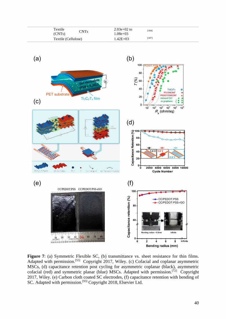
Figure 7: (a) Symmetric Flexible SC, (b) transmittance vs. sheet resistance for thin films.
Adapted with permission.[55] Copyright 2017, Wiley. (c) Cofacial and coplanar asymmetric
MSCs, (d) capacitance retention post cycling for asymmetric coplanar (black), asymmetric
cofacial (red) and symmetric planar (blue) MSCs. Adapted with permission.[72] Copyright
2017, Wiley. (e) Carbon cloth coated SC electrodes, (f) capacitance retention with bending of
SC. Adapted with permission.[93] Copyright 2018, Elsevier Ltd.
41
Zhang et al. [55] leveraged the thin film properties of Ti3C2Tx to produce both symmetric and
asymmetric (CNT anode), transparent and flexible layered SCs on PET substrates, as seen in
Figure 7(a). To optimise transparency and SC performance, Ti3C2Tx coatings of increasing
thicknesses were evaluated for sheet resistance, light transmittance, and intrinsic capacitance.
The findings, shown in Figure 7(b), demonstrated that the Ti3C2Tx thin films were able to avoid
the percolative effects seen at high transmittance (> 90%) in graphene, i.e., continue operating
in a bulk-like conductivity regime. In practice, a coating was found to balance a high 91%
transmittance with high areal capacitance 0.48 mF cm-2.
Couley et al. [72] manufactured binder and current collector free asymmetric MSCs with a
Ti3C2Tx cathode and rGO anode in both coplanar and co-facial configurations, by spray coating
PET sheets using masks for patterning as seen in Figure 7(c). They found increased power and
energy densities over a symmetric Ti3C2Tx configuration, and this performance gain is
unlocked through the extended voltage window available to the rGO. Cycling tests, shown in
Figure 7(d), evidenced improved electrochemical stability using the rGO anode, as the
symmetric Ti3C2Tx device saw capacitance drop to 75% after 10,000 cycles as opposed to 97%
for the asymmetric set-ups. The coplanar configuration was better able to sustain performance
at higher scan rates, and this is attributed to the architecture enabling in-plane diffusion of ions.
Kumar et al. [93] developed large area (up to 25 cm2) cofacial textile-based supercapacitors by
spray coating conductive carbon cloth with aqueous PEDOT:PSS and rGO dispersions, as
shown in Figure 7(e) and subsequently treating with phosphoric acid. This latter step unlocked
a larger operating window (0 to 2 V), which in turn enabled higher power and energy densities.

42
The addition of 20 wt.% rGO increased the areal capacitance from 1600 to 3000 mF cm-2, as
well as cycled capacitance retention from 93% to 100% after 2000 cycles. This device retained
94% capacitance at a bending radius of 0.5 mm, as shown in Figure 7(f), thus retaining some
of the textile’s flexibility in practice.
Flexible supercapacitors are an essential energy storage component for enabling novel
wearable electronics applications. The practical application and promising capacitive
properties of conductive 2D material dispersions, make them ideal electrode components. The
advantages of these 2D material electrodes, such as high capacitance, good processability and
large surface area, are balanced against their disadvantages, such as flake stacking, re-
agglomeration and, in the case of MXenes, oxidation limiting the potential window. The use
of asymmetric systems and hybrid electrodes has unlocked synergies for higher energy and
power densities as well as improved capacitance retention. However, the complexity behind
correctly identifying and characterising capacitive processes, in combination with the many
combinations of device sizes, set-ups and configurations, make comparing performance a
significant challenge and slowing progress. Further work should be done to standardise
methodologies and reporting practices.
3.2.2 Thermoelectric Generators
Countless devices and manufacturing procedures develop heat as a side effect to their function,
e.g., air conditioners, microprocessors, combustion engines, industrial furnaces, and server
rooms, to cite a few. The energy dissipated by this heat is wasted and is distant from being
negligible. For example, the industrial heat waste in the US was estimated to be between 20 to
50% of the entire industrial energy consumed[273], and the total waste heat in the EU is

43
quantified to be about 300 TWh/year[274], which, considering the average consume of a EU
household to be around 3500 KWh/year would permit to power about 85 M houses. Therefore,
utilizing heat waste is a huge opportunity to reduce energy consumption and increase
sustainability of many sectors.
One of the most promising approach to use heat waste is exploiting the thermoelectric effect,
which transforms a temperature difference in an electric voltage. To perform such task,
thermoelectric (TE) materials are fundamental, and massive research effort has been conducted
to optimize the existing solid-state TE materials and create new opportunities translating the
TE design to flexible and conformable. Engineering a good TE material is not trivial because
it should have a high electrical conductivity (𝜎) and Seebeck coefficient (S) and a low thermal
conductivity (k) following the dimensionless TE figure of merit (𝑧𝑇)[275]:
𝑧𝑇 = 𝜎𝑆2𝑇
𝑘 (4)
Where T is the temperature. Another essential quantity to characterize a TE material is the
power factor which is the product of 𝜎 and S2. TE materials can be p-type or n-type depending
on the electrical charge carrier, exhibiting a positive and a negative Seebeck coefficient,
respectively. The most common TE generator is constituted by p- and n-type materials joined
at their end thermally in parallel and electrically in series.
Most performing and commonly used TE materials are rigid and bulky alloys of inorganic
semiconducting tellurium, lead, and germanium that are p-/n-doped. These materials present
issues linked to their sustainability, fabrication challenges, price, and availability.[30] Moreover,
considering that more than 60 % of excess global heat is below 100°C, and the colder it is, the

44
more difficult it is to extract valuable energy from it, one of the biggest technological
challenges is pulling energy from the diversified spectrum of waste heat.[276] Considering this,
an expansion of the TE material family is needed, possibly also to flexible and compliant
materials that are more versatile to be interfaced with such diverse waste heat forms that
diverge in terms of the frequency of occurrence, the temperature range, and the state (i.e., fluid
and gaseous).[276-277] Layered 2D nanomaterials, which ensure the possibility to create flexible
materials with many of the abovementioned properties, represent an interesting opportunity.
Hence, in the last years, especially carbon-based nanomaterials such as graphenes have
increased interest in the research community, especially in the case of coating of flexible
substrate and textiles and hybridized with other carbon-based nanomaterials such as carbon
nanotubes, as shown in Table 10. Mxenes for thermoelectric energy generation were predicted
to have a good potential in light of the high electrical conductivity and Seebeck coefficient, but
were not investigated thoroughly yet, especially in the form of coating.[278]
Cho C. et al.[31] dip-coated flexible PET substrates in a layer by layer fashion with PANi, GNPs,
and CNTs from aqueous dispersion, obtaining a fully-organic TE material, as shown in Figure
8(a). GNPs and CNTs were stabilized using electrically conductive PEDOT:PSS. 1 micron
thick layer comprising PANi/GNPs‐PEDOT:PSS/PANi/CNTs‐PEDOT:PSS repeating units
displays a high electrical conductivity (σ ≈ 1.9 × 10⁵ S m−1) and Seebeck coefficient (S ≈ 120
μV K−1), as shown in Table 10, yielding a power factor of 2710 μW m−1 K−2. The authors of
the papers claim that this water‐based TE nanocomposite has power factors competitive with
bismuth telluride at room temperature and has the benefit that could be applied as a coating to
flexible surface (e.g., textiles). The authors also claim that this novel TE nanocomposites
discloses opportunities in powering portable electronics with clothing that transforms wasted
body heat to significant voltage.

45
The same authors developed an n-type organic TE material[90] that is a polymer nanocomposite
assembled by dip-coating one after the other flexible PET with CNTs, stabilized with
polyethyleneimine (PEI), and GO from aqueous solutions. The obtained material is flexible
and can withstand bending and twisting (see Figure 8(b)). A thin film of 610 nm thickness
showed an electrical conductivity of 2730 S m−1 and a Seebeck coefficient of −30 µV K−1,
resulting in a power factor of 2.5 µW m−1 K−2. A heat curing for 30 minutes at 150 °C reduces
the GO and boosts the electrical conductivity and Seebeck coefficient to 46000 S m−1 and −93
µV K−1, respectively, providing a power factor of 400 µW m−1 K−2. The authors claim that this
is among the highest power factors recorded for a fully organic negative Seebeck TE material.
Furthermore, the authors demonstrate that depositing a polymer-clay thin film onto the TE
materials provides air‐stability over an extended period. They state that this n‐type
nanocomposite is promising for low‐cost, scalable, flexible, environmentally benign, and
efficient TE materials.
A previous work of ours[30] enabled the fabrication of p‐type and n‐type flexible thermoelectric
textiles produced with low-cost and sustainable materials and scalable and green processes.
Cotton was spray-coated with TE inks made with biopolyester and carbon nanomaterials.
Different nanofillers permitted to achieve positive or negative Seebeck coefficient, with
graphene nanoplatelets, showing a positive value of 16 µV K-1. The best coating allows to
perform repeated bending and washing cycles with an increase of their electrical resistance by
five times after repeated bending cycles and only by 30% after washing. In‐plane flexible
thermoelectric generators coupling the best p‐ and n‐type materials were fabricated (see Figure
8(c)), resulting in an output voltage of ≈1.65 mV and maximum output power of ≈1.0 nW by
connecting only two p/n thermocouples at a temperature difference of 70 °C. With their ease

46
of fabrication, green manufacturing, and the biocomposites flexibility and sustainability, such
proposed TE materials showed a path for a future generation of wearable TE devices, more
harmless for the environment and more easily disposable.
Table 10: Resume on the composition of the conductive materials, employed techniques,
substrate, and important features of the thermoelectric coating based on 2D nanomaterials. σ,
Rs, t, and S correspond to the maximum electrical conductivity, the minimum sheet resistance,
the thickness, and the Seebeck coefficient at room temperature, respectively.
2D
material
Substrate Other
Conductive
Materials
σ
(S m-1)
Rs
(Ohm sq-1)
t
(µm)
S
(µV K-1)
Ref.
GNP Textile
(Cotton)
PEDOT:PSS
5.44E+02 8.00E+01 2.30E+01 1.60E+01
[30]
GNP Sheet
(PET)
CNTs,
PEDOT:PSS,
PANi 1.79E+05 5.60E+00 9.98E-01 1.20E+02
[31]
rGO Sheet
(PET)
CNTs
4.59E+04 3.30E+01 4.47E-01 -9.30E+01
[90]
GNP Sheet
(PET)
CNTs,PANi
1.08E+05 1.98E+01 4.68E-01 1.30E+02
[117]
GNP Sheet
(PET)
CNTs
3.00E+04 1.11E+02 3.00E-01 -8.00E+01
[116]
GNP Textile
(Cotton)
PANi
2.80E+01 - - 1.20E+01
[279]
GNP Sheet
(Paper)
PEDOT:PSS,
Ionic Liquid 7.50E+03 - - 3.10E+01
[280]
Figure 8: a) Schematic of the layer‐by‐layer deposition process followed to obtain a flexible
p-type organic TE coating based on 2D nanomaterials on PET. Homogenous dispersions of
PANi in water are deposited first. Afterward, graphene and CNTs in aqueous PEDOT:PSS
solutions are dip-coated. This procedure is repeated several times to obtain a layer-by-layer

47
structure. Adapted with permission.[31]Copyright 2016, Wiley. b) Photos displaying the
mechanical compliance of multilayer thin films of CNTs, stabilized with polyethyleneimine
(PEI), and GO from aqueous solutions. Adapted with permission.[90]Copyright 2018, Wiley. c)
Cotton‐based in‐plane TE device with 2 TE elements composed of p‐type GNP/carbon
nanofibers coatings and n‐type CnTs coating (red box = hot plate; blue box = room temperature
plate). Reused with permission.[30] Copyright 2019, Wiley.
3.3 Other Applications of Flexible and Conductive 2D Material-based Coatings
3.3.1 Electromagnetic Interference Shielding
Miniaturization of electronics is boosting the performances of microprocessors, but, at the same
time, it is increasing the density of electronics components. Too close components can interfere
and modify/disrupt the functioning of devices.[281] Electromagnetic Interference (EMI)
shielding is therefore necessary for electronic devices used daily. At the same time, it can be
crucial for the safe functioning of large appliances, such as aircrafts in which lightning, solar
flares, radar, or even communications can interfere and endanger passengers' security. Hence,
airplanes need shielded enclosures, harnessers, and connectors.
EMI shielding is, therefore, an issue that can occur at different scales, and, as such, it could
benefit from the versatility of coating techniques that are diversified in terms of the resolution
of the deposition, of tuneable electro-mechanical properties, and of adhesions of the inks.
Furthermore, an additional benefit could be given by applying flexible and lightweight coatings
on curved and motile parts of the airplanes, reducing the weight sensibly and thus the fuel
consumption.
When an electromagnetic wave travels and passes through a material, reflection, absorption,
multiple internal reflection, and transmission occur. The total EMI shielding effectiveness (SE)
depends on these quantities following[282]

48
𝑆𝐸 = 𝑆𝐸𝑅 + 𝑆𝐸𝐴 = 10 log (1
𝑇) (5)
Where SER characterises the reflection contribution, SEA represents the absorption and internal
reflections, and T is the transmittance that denotes the fraction of incident electromagnetic
wave transmitted. An ideal EMI shielding material should have a high EMI SE while being the
thinnest possible. The threshold for practical commercial application is a shielding
effectiveness ≥ 20 dB.[45]
The most widely used materials for EMI shielding are metals in the form of sheets, foams, or
coatings.[283] Most exploited are copper, silver, steel, tin, brass, and nickel. Metals ensure high
performances but have drawbacks mainly in terms of costs. Besides, they generally have high
density, low resistance to oxidation/corrosion, and high processing expenses, and therefore are
not adaptable to ensure lightweight and a capillary diffusion required in specific EMI shielding
devices.[284] Furthermore, in the form of inks constituted of carrier material loaded with small
metallic particulates typically of copper or nickel, these dispersions are challenging to be stable
and generally require stabilizer and sintering post-processing after deposition.
In this context, coatings made with simple procedures on flexible and lightweight materials
such as plastics, textiles, or foams, and constituted by conductive 2D nanomaterials such as
graphenes and MXenes represent a significant opportunity to decrease the costs of inks for EMI
shielding, reduce the weight of shielding components and enable the shield of flexible, curved,
and deformable components with thin conductive materials.[284-286]
Valles C. et al. [114] spray-coated micrometric film of alternating electrically conductive
negatively charged rGO and a positively charged polyelectrolyte (PEI) on PET in a scalable,
thin, and layer by layer fashion. They demonstrated that the EMI shielding properties of such

49
structures could be adjusted by changing the electrical characteristics of the graphene employed
and the number of layers deposited. Excellent EMI shielding features were observed for these
coatings through a mechanism of absorption. They obtained a maximum EMI SE of 29 dB for
a 6 μm thick (PEI/RGO) multilayer structure corresponding to 10 coatings of the double
component, with 19 vol % loading of rGO flakes with diameter of ∼ 3 μm. Normalizing by the
thickness, the EMI SE is ≥ 4830 dB/mm. The authors claim that this performance exceeds those
previously reported for thicker graphene papers and graphene/polymer composite films with
higher GRM contents. They claim that this achievement represents an appropriate step to
fabricating lightweight and thin, high-performance EMI shielding structures.
Wang Y. et al.[287] dip-coated cotton into thiol-modified rGO and waterborne polyurethane
(WPU) solutions. The WPU molecules were changed with -ene group and acted as polymer
matrix to covalently bind the conductive nanofiller and the textile with a thiol-ene click
reaction. The authors claim that the interconnected network in the rGO-WPU/cotton sample
imparted it with a satisfying value of sheet resistance reaching ~4 kΩ/sq and enhancing the
mechanical properties. The EMI SE of the material reached 48 dB at only 2 wt% concentration
of the modified-rGO, a higher value compared to the same sample made with simple rGO that
reached 32.5 dB. The authors claim that the high EMI shielding feature of the samples is due
to the better dispersion of the nanofillers modified with the thiol group that increased the
interfaces for multiple reflections and scattering. The presented fabric can withstand multiple
stresses (1000 cycle bending, 10 cycles of washing/friction), still preserving excellent EMI SE
(>90% of the initial value).
Shen B. et al.[101] dip-coated polyurethane sponges with GO and afterwards reduced the
nanoflakes chemically and thermally, as shown in Figure 9(a). The obtained composite foam

50
was compressible and ultralightweight, showing a ∼0.027–0.030 g/cm3 density, and exhibited
EMI shielding features dominated by absorption. The compression of the foams ensured the
tuning of the shielding properties. Indeed, different compressive strains, i.e., 0, 25, 50, and
75%, decreased the EMI SE from 39.4 dB to 34.9, 26.2, and 23.4 dB, respectively, as shown
in Figure 9(a). The authors justify this reduction with the shrinkage of the conductive graphene
network under compression that decreases the foams void spaces and significantly weakens the
scattering and multiple reflections of EM waves between the cell surfaces. This diminution
occurs despite the slight increase of the electrical conductivity with compression. Notably, the
SE of the foams did not change during 50 cycles of stress-release, indicating outstanding
cycling stability. This finding indicated that the foams SE could be adjusted reversibly by
compression or release, enabling adjustable EMI shielding. The authors claim that the
simplicity of manufacturing could promote the large-scale production of such lightweight and
deformable material for EMI shielding.
In a previous work of ours[32], deformable conductive coatings were manufactured by spray-
coating a GNP–elastomer (thermoplastic polyurethane) suspension onto a nitrile rubber
substrate, as displayed in Figure 9(b). The electrical resistance of the conductors displayed an
increase of 40% after 20 folding-unfolding cycles because of crack formation. On the contrary,
it decreased by around 5% after thousands of bending events due to favourable recombination
of the conductive GNP in the elastomer matrix. The conformable coatings double their
electrical resistance at 12% strain and are washable without modifying their electrical features.
The production process can be modified by stretching the nitrile substrate before spraying. This
procedure meant that the electrical resistance doubles at 25% strain. The as-produced coatings
provide an EMI SE of 20 dB in the 8–12 GHz electromagnetic band. The physical and
electrical properties of the flexible conductors, deteriorate upon stretch-release cycling but are

51
restored to the initial value upon heating the coating. For example the EMI SE is reduced by
25 % upon 9 cycles of stretch release, but restores the initial EMI shielding after a heating
procedure, as shown in Figure 9(b). Such conformable conductive coatings with healable
electrical features could permit the realization of truly deformable printed circuit boards,
actuators, and tactile sensors.
Figure 9: EMI shielding of graphene-related materials coated on elastic substrates. a) Top:
Overall manufacturing method of the rGO-functionalized foams, comprising dip-coating GO

52
nanoflakes on the sponge structures and reducing hydrothermally with hydrazine vapor.
Middle: Compress-release process of the rGO foam, exhibiting outstanding compressibility.
Bottom from left to right: Total Shielding effectiveness (SE), absorption SE, and reflection SE
of the polyurethane sponge under various compressions. Adapted with permission.[101]
Copyright 2016, American Chemical Society. b) Top: a schematic of the preparation of the
electrode and its flexibility. Thermoplastic Polyurethane (TPU) mixed with GNP constitutes
the conductive inks sprayed onto nitrile rubber substrates followed by heating by a heat gun.
Bottom Left: EMI SE of the GNP–TPU coating before and after 9 stretch–release cycles at
100% elongation. Bottom right: healing of the EMI SE with a heat gun process similar to the
fabrication method for the GNP–TPU coatings. Adapted with permission.[32] Copyright 2020,
Wiley.
Hu D. et al.[179] manufactured an electrically and thermally conductive MXene coating on
cellulose via dip-coating. The as-obtained paper displays electrical conductivity of ~ 2750 S/m.
After a PDMS coating, the sample can sustain 2000 bend-release cycles and decrease only of
the 10% the starting EMI SE of 43 dB measured between 8 and 18 GHz. Besides, a planar
thermal conductivity of ~3.9 W/(m⋅K) is achieved, being 540% higher than the material
without MXenes. By cumulative dip-coating cycles, the EMI SE and thermal conductivity can
be finely tuned. The authors claim that their material can be fabricated on a large scale and
with green production methods. They add that considering the flexibility, multifunctionality,
and remarkable EMI shielding performances, the nanocomposite paper can have applications
in electronics and aerospace.
Uzun S. et al.[288] dip-coated cotton or linen in colloidal dispersion of Ti3C2Tx MXene dyes
dispersed in water, soaking the ink into the textiles and attaching it to the hydrophilic fabrics,
as shown in Figure 10(a). Increasing dip-coating steps increased the conductive filler
concentration and the electrical conductivity of the textiles. The samples with four dip-coating
steps deposited a coating weight corresponding to ~ 15 wt% of the fabrics, reaching an EMI
SE of ∼40 dB over the X-band range (8-12 GHz). After 24 coating, the EMI SE augmented to
∼80 dB. The authors showed that the MXene-based fabrics display better performances than

53
commercial metal-based conductive ones. After storing under ambient conditions for two
years, the EMI SE of MXene-coated fabrics only decreased by ∼8% and ∼13% for cotton and
linen, respectively, as shown in Figure 10(a). Besides, the conductive fabrics were
demonstrated to shield mobile phone communication. The authors claim that such technology
enables the scalable and straightforward transferal of advantageous MXene features to textile-
based goods, such as clothes, laptop cases, and wallets, to shield people from electromagnetic
pollution or protect digital information. They affirm that their work proposes an attractive
alternative to metal-based conductive textiles and presents helpful insights into producing
environmentally durable wearable EMI shielding fabrics.
Li Y. et al.[74] fabricated an ultra-stretchable conductor depositing a crumple-textured coating
made of Ti3C2Tx nanoflakes and SWNTs on a pre-stretched latex rubber balloon, as shown in
Figure 10(b). A GO layer was deposited before the MXene-SWNT layer to improve the
adhesion of the conductive sheet to the latex. The resulting conductors can sustain up to an
800% areal strain and display strain-invariant resistance profiles through a 500-cycle fatigue
experiment, as shown in Figure 10(b). A layer of the stretchable conductor (1 µm thick)
demonstrated strain-insensitive EMI shielding properties of 30 dB under broad areal strains
(up to 800%), and the shielding feature was augmented to 47 and 52 dB by layering 5 and 10
films of the MXene conductors, respectively. The authors also demonstrated the manufacturing
of a dipole antenna composed of stretchable MXene-based conductors. With a uniaxial stretch
of 150%, the antenna resonant frequency was changed from 1.575 to 1.375 GHz, while the
reflection |S11| stayed constant at −30 dB, corresponding to steadily reflected powers smaller
than 0.1%. Combining the EMI absorbers and the stretchable antennas permitted the authors to
demonstrate a wearable wireless device that produced mechanically stable wireless
communication while attenuating EM absorption by humans.
54
Figure 10: EMI shielding of MXenes coated on diverse substrates. a) Top: manufacturing
procedure of the fabrics based conductive material and SEM images of the cotton or linen based
material. The materials just slightly change the EMI SE after two years that were fabricated.
Reused with permission.[288] Copyright 2021, Elsevier. b) Left: SEM pictures and photos of the
SWNT-MXene coating on latex under different areal strains. Right: EMI SE of the stretchable
SWCT-MXene-based material through 500 stretch-release cycles with areal strain up to 800%.
Adapted with permission.[74] Copyright 2020, Wiley.
Table 11: EMI Shielding Applications in Surveyed Literature.
2D Material Substrate Other Conductive
Materials EMI SE (dB) Ref.
Graphene Foam (Latex, Natural Rubber) 2.40E+01 [97] Foam (PU) 5.80E+01 [101] Sheet () Co NPs 5.50E+01 [105] Sheet (Cellulose) 4.00E+01 [69] Sheet (Nitrile) 1.70E+01 [32]
Sheet (PET) 1.50e+01 to
2.90e+01 [114]
Sheet (PET) Ag NWs 4.29E+01 [120] Sheet (Paper) 3.60E+01 [86]
Textile (Carbon Cloth) 3.79e+01 to
4.00e+01 [71]
Textile (Cellulose) 4.50E+01 [137]
Textile (Cotton) 2.00e+01 to
4.81e+01
[141, 287,
289] Textile (Cotton) Ag NPs 2.74E+01 [290] Textile (Cotton) ZnO NPs 5.47E+01 [92]

55
Textile (PET) AgNO3 6.50E+01 [163] Textile (Polyester) 2.60E+01 [171] Textile (Wool) PPy 2.20E+01 [291]
Graphene +
MXene Sheet (Latex) CNTs
3.00e+01 to
5.20e+01 [74]
Textile (Carbon Cloth) 3.77E+01 [71]
MXene Sheet (Filter Paper) 2.46e+01 to
4.30e+01 [179]
Sheet (PTFE) 5.07E+01 [180] Textile (Carbon Cloth) 4.32E+01 [185]
Textile (Carbon
Cloth) CNTs 4.67E+01 [186]
Textile (Cotton) 2.60e+01 to
8.00e+01
[188-189,
288]
[292]
Textile (Linen) 4.00e+01 to
8.00e+01 [288]
Textile (PET) PPy 4.20e+01 to
9.00e+01 [194]
Textile (Silk) Ag NWs 4.20e+01 to
8.50e+01 [195]
From Table 11, textiles results by far as the prevalent adopted substrates (66%), followed by
sheets (31%), while foams are only the 3% of the surveyed literature. The appeal to realize
wearable conductive EMI shields reflects these numbers, together with the ease of
functionalizing fabrics that absorb liquid inks.
3.3.2 Joule Heaters
When a current flows through a media of finite electrical resistance under an applied voltage,
resistive heating takes place following the first Joule law
𝑃 ∝ 𝐼2 𝑅 ∝𝑉2
𝑅 (6)
where P is the power that corresponds to the thermal energy generated per unit of time. This
phenomenon is called Joule heating and is often a side effect in applications such as air
conditioners, microprocessors of laptops, smartphones, etc. In contrast, it is the basic principle
exploited for the functioning of appliances such as hot plates, ovens, floor heating, toasters,

56
and hair dryers, to name a few.[293] It is sometimes used for de-icing aerodynamic and structural
surfaces, especially in the aeronautic and wind turbine sectors.[294-295]
Joule heating points of strength are the high release of heat in a small volume, the remarkable
heating uniformity/non-uniformity and tuneable heating time depending on the design of the
resistive path, the easiness of the power control (i.e., voltage-driven), and the high temperature
achievable depending on the resistive material used that can reach even thousands of °C. The
most commonly used materials for Joule heating are metal alloys such as nickel-chrome and
iron-chromium-aluminum compounds (known as Nichrome and Kanthal, respectively),
ceramics, and semiconductors such as molybdenum disilicide and silicon carbide. Such
materials ensure heat resistance, high-temperature strength (i.e., absence of deformation during
operation), an adequate electrical resistivity, and low thermal expansion coefficient. As such,
they are ideal also for high-performance applications since they can sustain temperatures
between 1000 and 1300 °C, needed in large industrial furnaces. Nevertheless, they are rigid
and difficult to be incorporated as heaters in flexible and wearable devices, and in motile parts
of robots.[296] Therefore, materials designed ad-hoc to comply with flexibility and
conformability necessities are needed.
Electrical conductive coatings appear as a natural candidate to fill the gap between existing
rigid heating materials and flexible ones.[293] Indeed the versatility of coating techniques in
terms of surface (plane, curved, rough, and porous) and materials (rigid, flexible, and wearable)
that can be coated, and the compatibility with the existing industrial processes, ensure a
potentially short-term and straightforward expansion of heaters to the field of wearables and
flexibles.[297] In this context, graphene- and MXene-based electrically conductive inks
represent a great chance of realizing flexible Joule heating coating on a curved surface and

57
achieve conformable and/or bendable materials that can be heated simply through an applied
voltage. Indeed, nanostructured materials allow an exceptional spreading of the heating
spots.[298] Hence, 2D nanomaterials are emerging as extraordinarily beneficial and favourable
for Joule heaters expansion, as shown in Table 12.[294, 299]
Hao Y. et al.[26] developed a cotton-based heater spraying in sequence water-dispersed
polyurethane (WPU), a GNP-tourmaline-WPU composite, and a final WPU protective layer,
as shown in Figure 11(a). In the composite layer, tourmaline and GNP displayed a synergistic
effect, with superior electro-thermal features than single-component fabrics, achieving a
temperature of ~75 °C in 30 s under 10 V, while the pure GNP achieved ~ 45 °C at the same
conditions, as shown in Figure 11(a). The composite fabric showed a high heating power
density of 2 × 10³ W/m2. The flexible heater was significantly abrasion resistant, resulting in
21 % electrical conductivity reduction after a 2500-cycles abrasion test, far less than the 87 %
of fabrics without a protective WPU layer. The single components were all necessary since: i)
GNPs provided the electrical conductivity and supported high electro-thermal efficacy, ii)
cotton ensured the flexibility and wearability of the material, iii) WPU acted as a binder that
also contributed to the composite fabrics abrasive resistance, and iv) adding tourmaline
nanoparticles enhanced prominently the maximum temperature reached at 10 V. The authors
forecast application of the proposed Joule heater as medical electro-heating wearable devices
and functional protective garments.
Karim N. et al.[300] displayed a process to make conductive graphene-coated glass fibre roving
with fast de-icing features. The graphene ink is obtained through a large scale technique based
on a microfluidic exfoliation. Such ink is coated using a dip-dry-cure technique that the authors
claim to be potentially suitable for the industry. The graphene-coated glass roving can heat up

58
rapidly to a required temperature. For example, it can heat up at 72 °C in 30 s at 10 V, it can
reach 101 °C after 180 seconds, and 120°C after ~ 10 minutes. The authors integrated these
graphene-coated glass rovings into a vacuum-infused epoxy–glass fabric composite and
demonstrated their use for de-icing applications. They dipped it into a container full of ice and
compared the melting of ice with another bucket containing only ice, applying 10 V. A rapid
increase in the speed of the melting of ice in the bowl containing graphene-based composites
by Joule heating was observed. Indeed, the temperature increases to 27 °C within 5 minutes,
whereas the bucket temperature containing only ice remains constant even after 30 minutes.
Ahmed A. et al.[152] presented a mass and straightforward producible dip-coating technique to
obtain an electro-conductive stretchable composite based on cotton with rGO and PEDOT:PSS
as a conductive additive, as shown in Figure 11(b). The authors claim that the composite
exhibited exceptional heating even after mechanical deformation. Indeed the heaters maintain
their value of sheet resistance of ~ 154 Ω/sq after 100 folding cycles and decrease their heating
performance of 4 °C (from 40 to 36 °C) at 60% applied strain, and under a voltage of 15 V.
The heater provided rapid response and a consistent heat supply in the heating zone at low
voltage. Indeed, under different voltages (ranging from 5 to 30 V), the maximum temperature
was reached in 15 to 25 s with the highest temperature of 70 °C at 30 V, as shown in Figure
11(b). The materials exhibited durable heating/cooling performance under repeated cycle (10)
and excellent stability to wash, increasing the initial value of sheet resistance by ~ 1% after 15
washing cycles.
The possibility to combine the mechanical properties of flexible substrates and
multifunctionality of 2D nanofillers coatings, is enabling new multifunctional materials that
are able to address several problems and tasks with a single configuration. For example,

59
coatings containing MXenes with applications as Joule heaters and, at the same time, a
combination of EMI shielding, strain sensing, hydrophobic, and transparency features are a
growing trend in literature. [189, 193-194, 301]
Wang Q.-W. et al.[194] fabricated an electrically conductive flexible PET fibrous textile (~1000
S m−1) dip-coating it with polypyrrole and MXene. A PDMS treatment was then performed to
ensure hydrophobicity (water contact angle of ~126°) and prevent the degradation/oxidation of
the MXene at high humidity while retaining the considerable air permeability of the textile.
The authors claim that the coating ensures effective Joule heating performance together with
high EMI shielding (~90 dB with a 1.3 mm thick sample). Polypyrrole improves the adhesion
of the MXene nanoflakes and the PET fibers and increases the EMI shielding performance.
The Joule heating of the multifunctional textile needs low voltage for an efficient control.
Indeed, changing the input voltage to 2, 3, and 4 V permits reaching a saturated temperature of
40, 57, and 79 °C, respectively. Therefore, high tunability of the temperature in a range of
voltages that are safe for operation is ensured. The authors show that stable cyclic heating
performances are achieved during 50 cycles. Thus, they claim that such material is suitable for
thermotherapy and personal heating garments. Moreover, in light of the high electrical
conductivity, flexibility, and water‐resistant features, flexible electronics, wearable smart
clothes, and EMI shielding garments are highly promising.

60
Figure 11: a) left: process to fabricate a sandwich structure with heating properties given by a
GNP (G)-tourmaline (T) - water-dispersed polyurethane (WPU) composite. The substrate and
the protective layer are realized with pure WPU. Right: temperature variation of samples with
different T:G weight ratio under 10 V voltage; in black, the sample with only G. In green the
best sample (weight ratio T:G=6:4). Adapted with permission.[26] Copyright 2018, American
Chemical Society. b) Left: scheme to fabricate the conductive coating made of rGO and
PEDOT:PSS. Right: Electro-thermal characterization of the as-obtained heater under different
applied voltages (5 to 30 V). Adapted with permission.[152] Copyright 2020, Royal Society of
61
Chemistry. c) Left: assembly of MXene-decorated cotton textile by spray-coating technique.
Right: time-temperature curves of the sample with an applied voltage changing from 1 to 6 V.
Reused with permission.[189] Copyright 2020, American Chemical Society. d) Top: diagram of
the production of hydrophobic and transparent Joule heaters. Spin-coating hydrophobic fumed
silica nanoparticles achieved hydrophobicity on top of a spray coated layer of Mxene. Bottom
left: infrared images of the sample under mechanical deformation and with 8 voltage applied.
Bottom right: change of the coating temperature in time under voltages ranging from 2 to 13
V. Adapted with permission.[301] Copyright 2021, Elsevier.
Zhang X. et al.[189] spray-coated Ti3C2Tx nanosheets on cotton (Figure 11(c)), obtaining low
sheet resistance (5 Ω sq–1 at 6 wt.% nanoflakes loadings) and breathable fabrics. The material
had remarkable Joule heating performance at low applied voltages. In particular, the
temperature changed from 29 to 150 °C with voltage varying from 1 to 6 V (Figure 11(c)),
which the authors claim exceed the change of most of the previously reported textile heaters
coated with other conductive fillers. The Joule heating stability was also studied by subjecting
the samples to 100 cycles at the voltage of 4 V, exhibiting remarkable durability. The flexible
heaters were stitched onto diverse wearables, displaying to warm up very homogeneously to
60°C, as shown in Figure 11(c). The coating provided multifunctional properties to the cotton
that exhibited outstanding EMI shielding features, up to 36 dB, and bend-induced strain sensing
that monitored human motions. Therefore, the authors claim that their work detailed
multifunctional and wearable textiles promising flexible voltage-driven heaters, EMI shielding
clothes, and integrated strain-sensitive garments.
Zhou B. et al.[301] realized a flexible hydrophobic MXene-based transparent material with
applications as a Joule heater and in EMI shielding. MXene inks were spray-coated on
transparent polycarbonate substrates (Figure 11(d)). Afterward, spin-coating was employed to
deposit hydrophobic fumed silica and obtain superhydrophobic (contact angle of 150.7°) and
self-cleaning (sliding angle of 3°) surfaces that also prevented the oxidation of MXenes. The
multilayer structure displays low sheet resistance (~35.1 Ω/sq) with performance diminishing

62
only by 10% after 1000 bending cycles, a transmittance of 33%, and electromagnetic
interference shielding effectiveness major of 20 dB. The material was exposed to outdoor
conditions for 100 days without significant change of its properties. In particular, the coating
showed rapid Joule heating at safe voltages. At voltages between 4 and 13 V, the steady
temperature changed from 32 to 101 °C, as shown in Figure 11(d). The time needed to reach
101 °C was ~15 s and ~30 s to cool down. The temperature change was stable under several
cycles. The authors claim that such a mixture of properties, comprising the outdoor stability
for 100 days, bode well for a straightforward application of the material in many fields such as
smart windows, flexible devices, and electrical heating systems.
Table 12: Joule Heater Coatings in Surveyed Literature.
2D
Materials Substrate
Other
Conductive
Materials
Temperature
(C) Voltage (V) Ref.
Graphene Sheet
(PDMS) 1.80E+02 8.00E+01 [302]
Sheet (PET) Ag NWs 2.80E+02 1.20E+01 [121]
Textile (Cotton) 7.50E+01 1.00E+01 [26]
Textile (Cotton) 1.63E+02 1.20E+01 [303]
Textile
(Cotton) CB 1.03E+02 2.00E+01 [208]
Textile
(Cotton) MnO2 3.70E+01 1.50E+01 [25]
Textile
(Cotton) PEDOT:PSS 7.00E+01 3.00E+01 [152]
Textile
(Glass) 1.20E+02 1.00E+01 [300]
Textile (PET) 1.39E+02 1.40E+01 [27]
MXene Sheet (PTFE) 2.00E+00 3.96E+01 [180]
Sheet (Polycarbonate) 1.00E+02 1.30E+01 [301]
Textile (Cotton) 6.43E+01 4.00E+00 [188]
Textile (Cotton) 1.50E+02 6.00E+00 [189]
Textile (PET) 1.29E+02 1.50E+01 [193]
Textile (PET) PPy 7.90E+01 4.00E+00 [194]
As a general trend, textiles (77% of the surveyed literature) involving electrically conductive
coatings are predominant with respect to sheets as a Joule heating substrate. This is due to the

63
intrinsic wearable characteristic of such substrates that enable thermal therapy and intelligent
garments. MXenes are so far rarer but exhibit performance advantages, as shown in Figure 12.
Figure 12: Plot of the Temperature versus voltage of the surveyed literature in Table 12. In the
figure square () represents sheets and triangle () textiles.
4 Conclusions and Future Perspectives
The more than decade-long momentum behind the continuous growth of 2D materials is due
in part to the vast array of applications. As such, this review has sought to compare the progress
of two of the most promising families of conductive coatings comprising 2D materials:
graphenes and MXenes. A wide range of applications in the field of large-area flexible and
stretchable electronics is summarized. This has enabled trends to be drawn both within and
across diverse sectors, providing a comparative reference of past progress and insight into
future possibilities.

64
We surveyed three key components; the formulation of the 2D material ink, the coating
technique and substrate used, and the performance of the final device. In terms of ink
formulations, water is generally preferred since it is easily sourced, non-toxic, and renewable.
The next most popular solvents are ethanol, DMF, IPA, and NMP. GNP dispersibility in water
is usually assisted with solvents, binders, or surfactants to ensure stable inks, whereas GO,
rGO, and MXenes are more easily dispersible. Hybrid formulations combining 2D materials
with other conductive fillers to enhance electrical properties or create synergies between
conduction mechanisms are often exploited. Conductive polymers, nanometals, or other
nanocarbons (i.e., carbon black and CNTs) are often used for such purposes.
We find that dip coating is preferred for flexible textiles and for deformable foams due to the
self-soaking nature of these substrates, which permit an efficient coverage. Spraying is mostly
selected for sheets because it enables a precise deposition through masking and prevents
smearing and staining since the inks are almost dry when they impact the target surface. Dip
coating is preferably performed with water-based conductive inks, while spray coating needs
solvents that partially/fully evaporate before reaching the substrate to ensure sufficient
substrate contact and prevent nonuniformity. It is promising that most large area coating
techniques used for 2D material inks research are already readily scalable, and thus do not need
a special integration effort for their assimilation in production processes. Their ease of use also
facilitates the exploration of multiple variables e.g., different coating thicknesses and
compositions, as such articles often compare multiple device configurations. This is
advantageous as many performance comparisons can be within a single article. However, as is
often the case, these lab-based devices are usually crude compared to industrially ready

65
devices, e.g., lacking encapsulation and packaging. Meaning that scaling performance can be
difficult, slowing technological uptake.
The rapid growth and intense interest in the field flexible electronics has so far outpaced
industrial standardisation. As such, there is no clear approach for evaluating performance, e.g.,
most articles measure the intended application performance while the device is mechanically
relaxed, and separately showcase the device’s ability to flex and stretch. However, in practice
a flexible and stretchable electronic device whether an energy storage component or, EMI
shield or heater is likely to be required to operate under strain. This is set to change, as over
the last three years the IPC (association connecting electronics industries) has begun to release
a series of standards relating to eTextiles and SEMI (the global industry association that unites
the electronics design and manufacturing supply chain) has established a technical committee
to draft future standards.[304-305]
The combination of fillers with different dimensionality has been used to exploit the various
micro-mechanical mechanisms that make and break percolating conductive pathways in
flexible strain and pressure sensing devices. Achieving high, linear, and reliable sensitivities
across a large working range, requires synergetic effects across the conductive fillers and
substrate used. Textile substrates were most used for strain-sensors, as their component fibres
provide a network for deformation, enabling higher sensitivities. Foam substrates were most
used for pressure-sensors, as they can modulate the applied force through their porous structure.
The use of asymmetric and hybrid supercapacitor electrodes configured in cofacial, coplanar
or fibrous set-ups has led to a diverse array of flexible SCs and MSCs that utilise graphenes

66
and MXenes. The advantages of these 2D material electrodes, such as high capacitance, good
processability and large surface area, are balanced against their disadvantages, such as flake
stacking, re-agglomeration and, in the case of MXenes, oxidation limiting the potential
window.
In thermoelectrics, graphene-based coatings are explored, while MXenes ones are not. GRMs
are mixed with organic conductive polymers such as PEDOT:PSS and PANi to boost the
performance of organic TE inks. A recent trend consists in functionalizing textiles to realize
wearable thermoelectric materials. The high value of the graphene’s thermal conductivity is
hampering the generation of high power with TE generators based on such materials. The
diminution of the high thermal conductivity of GRMs could rely on the functionalization of
these 2D nanoparticles with additives with low thermal conductivity. However, the possibility
of coating large surfaces and developing flexible and wearable devices is not reachable with
state-of-the-art solid-state TE materials that are mainly based on bulk bismuth and tellurium
alloys. Thus, graphene-based inks are of interest for the development of the field. MXenes have
the potential to perform well in TE generations due to their high electrical conductivity and
Seebeck coefficient.[278]
Regarding EMI shielding applications, textiles are the prevailing substrates, accompanied by
sheets, while foams are only a few % of the examined reports. A recent trend for this application
with 2D materials relies upon making stretchable electromagnetic shielding coatings, more
frequent with sheets or foams. Flexibility, stretchability, and, in some cases, even healability[32]
of the conductive EMI shielding coatings made with 2D materials establish valuable
improvements compared to conventional metallic ones.
67
As a general trend, across most applications surveyed, the use of MXenes is gaining traction
as they combine high electrical conductivity with key structural and processability advantages:
They do not need the thermal or chemical reduction process required for GO, they readily
disperse in aqueous substrates without the aid of additives unlike GNPs, all while sharing many
of graphene’s advantages, including good adhesion to substrates, high electrical conductivity
and 2D morphology. In Joule heaters this translates to lower potential requirements to achieve
the desired temperatures than that of graphenes, even rivalling that of metallic
nanomaterials.[306] In EMI shielding their improved conductivity enables higher signal
attenuation at the same thickness than that of graphenes.[284, 307-308] However, the tendency of
MXenes to oxidise and degrade electrically, even within polymer matrices, may require further
research effort to engineer more robust surface chemistry and larger lateral sizes.[309] It is worth
nothing that Ti3C2Tx[57] is the only form of MXene used in all the surveyed literature, despite
29 other forms having been experimentally synthesised[33]. This fact leaves wide room for
further explorations for this class of materials in all the applications surveyed.
There were fewer examples of coatings made up of a combination of graphene and MXene in
the literature than initially expected. [71-74] Although, this makes sense considering their many
similarities leave little potential for synergy at the cost of added system complexity. In practice,
there is ample opportunity to share progress in experimental technique and theoretical
understanding between 2D materials. As such, we encourage researchers to not limit their
literature study to any one material family. Additionally, the composites plots presented for the
different applications, show that despite the diverse array of materials used, device
performance tends to cluster within 1 or 2 orders of magnitude. Further permutations of ink
formulations, coating techniques and substrate types that do not significantly advance

68
performance, should instead pay greater focus to developing theoretical understanding and
challenging proof-of-concept devices with more robust industry-level testing.
Acknowledgments
This work was supported by the Graphene NOWNANO CDT and Haydale Ltd. The authors
acknowledge “Graphene Core 2” and “Graphene Core 3” GA: 785219 and GA:881603,
respectively, which are implemented under the EU-Horizon 2020 Research & Innovation
Actions (RIA) and are financially supported by EC-financed parts of the Graphene Flagship.
P. C. and M. C. acknowledge the partial support of the European Research Council (ERC)
under the European Union's Horizon 2020 research and innovation programme “ELFO”, Grant
Agreement No. 864299. P.C. acknowledges funding from the Marie Skłodowska-Curie actions
(project name: BioConTact, grant agreement no. 101022279) under the European Union’s
Horizon 2020 research and innovation programme. I.A.K. thanks the Royal Academy of
Engineering (RCSRF1819\7\3) and Morgan Advanced Materials for funding this Chair. Table
1 first and second icon made by Freepik from www.flaticon.com. Table 1 third icon made by
monkik from www.flaticon.com.
References
[1] W. Wong, A. Salleo, Flexible Electronics: Materials and Applications, Springer US,
2009.
[2] M. S. Ergoktas, G. Bakan, P. Steiner, C. Bartlam, Y. Malevich, E. Ozden-Yenigun, G.
He, N. Karim, P. Cataldi, M. A. Bissett, I. A. Kinloch, K. S. Novoselov, C. Kocabas,
Nano Lett 2020, 20, 5346.
[3] M. Kaya, in Electronic Waste and Printed Circuit Board Recycling Technologies, DOI:
10.1007/978-3-030-26593-9_2 2019, Ch. Chapter 2, p. 33.
[4] D. F. Fernandes, C. Majidi, M. Tavakoli, J Mater Chem C 2019, 7, 14035.
[5] D. Grosso, Journal of Materials Chemistry 2011, 21, 17033.
[6] A. Nathan, A. Ahnood, M. T. Cole, S. Lee, Y. Suzuki, P. Hiralal, F. Bonaccorso, T.
Hasan, L. Garcia-Gancedo, A. Dyadyusha, S. Haque, P. Andrew, S. Hofmann, J.

69
Moultrie, D. Chu, A. J. Flewitt, A. C. Ferrari, M. J. Kelly, J. Robertson, G. A. J.
Amaratunga, W. I. Milne, Proceedings of the IEEE 2012, 100, 1486.
[7] B. Wang, A. Facchetti, Adv Mater 2019, 31, 1901408.
[8] Q. Huang, Y. Zhu, Adv Mater Technologies 2019, 4, 1800546.
[9] V. K. R. R, V. A. K, K. P. S, S. P. Singh, Rsc Adv 2015, 5, 77760.
[10] M. Zenou, L. Grainger, in Additive Manufacturing (Eds: J. Zhang, Y.-G. Jung),
Butterworth-Heinemann 2018, p. 53.
[11] J. Kim, R. Kumar, A. J. Bandodkar, J. Wang, 2017, 15.
[12] F. Torrisi, J. N. Coleman, Nat Nanotechnol 2014, 9, 738.
[13] G. Hu, J. Kang, L. W. T. Ng, X. Zhu, R. C. T. Howe, C. G. Jones, M. C. Hersam, T.
Hasan, Chem Soc Rev 2018, 47, 3265.
[14] Conductive Pastes, https://www.jesolutionsconsultancyltd.com/conductive-pastes,
accessed: 29th November, 2021.
[15] L. Nayak, S. Mohanty, S. K. Nayak, A. Ramadoss, J Mater Chem C 2019, 7, 8771.
[16] E. Jabari, F. Ahmed, F. Liravi, E. B. Secor, L. Lin, E. Toyserkani, 2d Mater 2019, 6,
042004.
[17] V. Beedasy, P. J. Smith, Materials (Basel) 2020, 13.
[18] C. Cano-Raya, Z. Z. Denchev, S. F. Cruz, J. C. Viana, Appl Mater Today 2019, 15, 416.
[19] H.-Y. Jun, S.-J. Kim, C.-H. Choi, Nanomaterials-basel 2021, 11, 3441.
[20] Y. Z. Zhang, Y. Wang, Q. Jiang, J. K. El-Demellawi, H. Kim, H. N. Alshareef, Adv
Mater 2020, 32, e1908486.
[21] S. Abdolhosseinzadeh, X. Jiang, H. Zhang, J. Qiu, C. Zhang, Mater Today 2021, 48,
214.
[22] P. Cataldi, S. Dussoni, L. Ceseracciu, M. Maggiali, L. Natale, G. Metta, A.
Athanassiou, I. S. Bayer, Adv Sci (Weinh) 2018, 5, 1700587.
[23] Q. Jiang, N. Kurra, K. Maleski, Y. Lei, H. Liang, Y. Zhang, Y. Gogotsi, H. N.
Alshareef, Adv Energy Mater 2019, 9, 1901061.
[24] G. Wang, V. Babaahmadi, N. He, Y. Liu, Q. Pan, M. Montazer, W. Gao, J Power
Sources 2017, 367, 34.
[25] M. Tian, M. Du, L. Qu, K. Zhang, H. Li, S. Zhu, D. Liu, J Power Sources 2016, 326,
428.
[26] Y. Hao, M. Tian, H. Zhao, L. Qu, S. Zhu, X. Zhang, S. Chen, K. Wang, J. Ran, Ind Eng
Chem Res 2018, 57, 13437.
[27] D. Wang, D. Li, M. Zhao, Y. Xu, Q. Wei, Appl Surf Sci 2018, 454, 218.
[28] Y. Huang, X. He, L. Gao, Y. Wang, C. Liu, P. Liu, Journal of Materials Science:
Materials in Electronics 2017, 28, 9495.
[29] P. Wang, B. Sun, Y. Liang, H. Han, X. Fan, W. Wang, Z. Yang, J Mater Chem A 2018,
6, 10404.
[30] P. Cataldi, M. Cassinelli, J. A. Heredia‐Guerrero, S. Guzman‐Puyol, S. Naderizadeh,
A. Athanassiou, M. Caironi, Adv Funct Mater 2019, 30, 1907301.
[31] C. Cho, K. L. Wallace, P. Tzeng, J.-H. Hsu, C. Yu, J. C. Grunlan, Adv Energy Mater
2016, 6, 1502168.
[32] P. Cataldi, D. G. Papageorgiou, G. Pinter, A. V. Kretinin, W. W. Sampson, R. J. Young,
M. Bissett, I. A. Kinloch, Advanced Electronic Materials 2020, 6, 2000429.
[33] Y. Gogotsi, B. Anasori, Acs Nano 2019, 13, 8491.
[34] E. Shim, in Smart Textile Coatings and Laminates (Second Edition), DOI:
https://doi.org/10.1016/B978-0-08-102428-7.00002-X (Ed: W. C. Smith), Woodhead
Publishing 2019, p. 11.

70
[35] J. J. Licari, in Coating Materials for Electronic Applications, DOI:
https://doi.org/10.1016/B978-081551492-3.50005-2 (Ed: J. J. Licari), William Andrew
Publishing, Norwich, NY 2003, p. 201.
[36] T. Carey, C. Jones, F. Le Moal, D. Deganello, F. Torrisi, ACS Appl Mater Interfaces
2018, 10, 19948.
[37] R. Cherrington, J. Liang, in Design and Manufacture of Plastic Components for
Multifunctionality, DOI: https://doi.org/10.1016/B978-0-323-34061-8.00002-8 (Eds:
V. Goodship, B. Middleton, R. Cherrington), William Andrew Publishing, Oxford
2016, p. 19.
[38] S. Stankovich, D. A. Dikin, G. H. Dommett, K. M. Kohlhaas, E. J. Zimney, E. A. Stach,
R. D. Piner, S. T. Nguyen, R. S. Ruoff, Nature 2006, 442, 282.
[39] A. Kausar, Journal of Composites Science 2021, 5, 292.
[40] A. Zamhuri, G. P. Lim, N. L. Ma, K. S. Tee, C. F. Soon, BioMedical Engineering
OnLine 2021, 20, 33.
[41] K. S. Novoselov, Science 2004, 306, 666.
[42] I. A. Kinloch, J. Suhr, J. Lou, R. J. Young, P. M. Ajayan, Science 2018, 362, 547.
[43] H. Döscher, T. Schmaltz, C. Neef, A. Thielmann, T. Reiss, 2d Mater 2021, 8, 022005.
[44] A. Kovtun, E. Treossi, N. Mirotta, A. Scidà, A. Liscio, M. Christian, F. Valorosi, A.
Boschi, R. J. Young, C. Galiotis, I. A. Kinloch, V. Morandi, V. Palermo, 2d Mater
2019, 6.
[45] P. Cataldi, P. Steiner, T. Raine, K. Lin, C. Kocabas, R. J. Young, M. Bissett, I. A.
Kinloch, D. G. Papageorgiou, ACS Applied Polymer Materials 2020, 2, 3525.
[46] P. Cataldi, A. Athanassiou, I. Bayer, Applied Sciences 2018, 8, 1438.
[47] D. Verma, K. L. Goh, in Functionalized Graphene Nanocomposites and their
Derivatives, DOI: https://doi.org/10.1016/B978-0-12-814548-7.00011-8 (Eds: M.
Jawaid, R. Bouhfid, A. e. Kacem Qaiss), Elsevier 2019, p. 219.
[48] S. Stankovich, D. A. Dikin, R. D. Piner, K. A. Kohlhaas, A. Kleinhammes, Y. Jia, Y.
Wu, S. T. Nguyen, R. S. Ruoff, Carbon 2007, 45, 1558.
[49] Y. Zhu, H. Ji, H.-M. Cheng, R. S. Ruoff, National Science Review 2018, 5, 90.
[50] D. C. Marcano, D. V. Kosynkin, J. M. Berlin, A. Sinitskii, Z. Sun, A. Slesarev, L. B.
Alemany, W. Lu, J. M. Tour, Acs Nano 2010, 4, 4806.
[51] J. Cao, P. He, M. A. Mohammed, X. Zhao, R. J. Young, B. Derby, I. A. Kinloch, R. A.
W. Dryfe, Journal of the American Chemical Society 2017, 139, 17446.
[52] D. Beloin-Saint-Pierre, R. Hischier, The International Journal of Life Cycle Assessment
2021, 26, 327.
[53] K. De Silva, H.-H. Huang, R. Joshi, M. Yoshimura, Carbon 2017, 119, 190.
[54] M. Aunkor, I. Mahbubul, R. Saidur, H. Metselaar, Rsc Advances 2016, 6, 27807.
[55] C. J. Zhang, B. Anasori, A. Seral-Ascaso, S. H. Park, N. McEvoy, A. Shmeliov, G. S.
Duesberg, J. N. Coleman, Y. Gogotsi, V. Nicolosi, Adv Mater 2017, 29, 1702678.
[56] B. Anasori, Y. Gogotsi, 2D Metal Carbides and Nitrides (MXenes) Structure,
Properties and Applications, Springer International Publishing, 2019.
[57] M. Naguib, M. Kurtoglu, V. Presser, J. Lu, J. Niu, M. Heon, L. Hultman, Y. Gogotsi,
M. W. Barsoum, Adv Mater 2011, 23, 4248.
[58] M. W. Barsoum, MAX Phases : Properties of Machinable Ternary Carbides and
Nitrides, John Wiley & Sons, Incorporated, Weinheim, GERMANY 2013.
[59] L. Liu, M. Orbay, S. Luo, S. Duluard, H. Shao, J. Harmel, P. Rozier, P.-L. Taberna, P.
Simon, Acs Nano 2021, DOI: 10.1021/acsnano.1c08498.
[60] C. Wang, H. Shou, S. Chen, S. Wei, Y. Lin, P. Zhang, Z. Liu, K. Zhu, X. Guo, X. Wu,
P. M. Ajayan, L. Song, Adv Mater 2021, 33, 2101015.

71
[61] A. Jawaid, A. Hassan, G. Neher, D. Nepal, R. Pachter, W. J. Kennedy, S.
Ramakrishnan, R. A. Vaia, Acs Nano 2021, 15, 2771.
[62] W. Sun, S. A. Shah, Y. Chen, Z. Tan, H. Gao, T. Habib, M. Radovic, M. J. Green, J
Mater Chem A 2017, 5, 21663.
[63] C. E. Shuck, A. Sarycheva, M. Anayee, A. Levitt, Y. Zhu, S. Uzun, V. Balitskiy, V.
Zahorodna, O. Gogotsi, Y. Gogotsi, Adv Eng Mater 2020, 22.
[64] O. Mashtalir, K. M. Cook, V. N. Mochalin, M. Crowe, M. W. Barsoum, Y. Gogotsi, J
Mater Chem A 2014, 2, 14334.
[65] C. J. Zhang, S. Pinilla, N. McEvoy, C. P. Cullen, B. Anasori, E. Long, S.-H. Park, A.
Seral-Ascaso, A. Shmeliov, D. Krishnan, C. Morant, X. Liu, G. S. Duesberg, Y.
Gogotsi, V. Nicolosi, Chem Mater 2017, 29, 4848.
[66] S. Yang, P. Zhang, F. Wang, A. G. Ricciardulli, M. R. Lohe, P. W. Blom, X. Feng,
Angewandte Chemie 2018, 130, 15717.
[67] S. Abdolhosseinzadeh, R. Schneider, A. Verma, J. Heier, F. Nüesch, C. Zhang,
Advanced Materials 2020, 32, 2000716.
[68] S. Abdolhosseinzadeh, J. Heier, C. Zhang, Journal of Physics: Energy 2020, 2, 031004.
[69] P. Cataldi, F. Bonaccorso, A. Esau del Rio Castillo, V. Pellegrini, Z. Jiang, L. Liu, N.
Boccardo, M. Canepa, R. Cingolani, A. Athanassiou, I. S. Bayer, Advanced Electronic
Materials 2016, 2, 1600245.
[70] P. Cataldi, O. Condurache, D. Spirito, R. Krahne, I. S. Bayer, A. Athanassiou, G.
Perotto, Acs Sustain Chem Eng 2019, 7, 12544.
[71] K. Raagulan, R. Braveenth, H. J. Jang, Y. Seon Lee, C. M. Yang, B. Mi Kim, J. J.
Moon, K. Y. Chai, Materials (Basel) 2018, 11, 1803.
[72] C. Couly, M. Alhabeb, K. L. Van Aken, N. Kurra, L. Gomes, A. M. Navarro-Suárez,
B. Anasori, H. N. Alshareef, Y. Gogotsi, Advanced Electronic Materials 2018, 4,
1700339.
[73] H. Li, Y. Hou, F. Wang, M. R. Lohe, X. Zhuang, L. Niu, X. Feng, Adv Energy Mater
2017, 7, 1601847.
[74] Y. Li, X. Tian, S. P. Gao, L. Jing, K. Li, H. Yang, F. Fu, J. Y. Lee, Y. X. Guo, J. S. Ho,
P. Y. Chen, Adv Funct Mater 2019, 30, 1907451.
[75] B. Fadeel, C. Bussy, S. Merino, E. Vázquez, E. Flahaut, F. Mouchet, L. Evariste, L.
Gauthier, A. J. Koivisto, U. Vogel, ACS nano 2018, 12, 10582.
[76] G. P. Kotchey, B. L. Allen, H. Vedala, N. Yanamala, A. A. Kapralov, Y. Y. Tyurina, J.
Klein-Seetharaman, V. E. Kagan, A. Star, ACS nano 2011, 5, 2098.
[77] R. Kurapati, F. Bonachera, J. Russier, A. R. Sureshbabu, C. Ménard-Moyon, K.
Kostarelos, A. Bianco, 2d Mater 2017, 5, 015020.
[78] R. Kurapati, J. Russier, M. A. Squillaci, E. Treossi, C. Ménard‐Moyon, A. E. Del Rio‐
Castillo, E. Vazquez, P. Samorì, V. Palermo, A. Bianco, Small 2015, 11, 3985.
[79] G. Lalwani, W. Xing, B. Sitharaman, Journal of Materials Chemistry B 2014, 2, 6354.
[80] J. Chen, Q. Huang, H. Huang, L. Mao, M. Liu, X. Zhang, Y. Wei, Nanoscale 2020, 12,
3574.
[81] I. Miccoli, F. Edler, H. Pfnur, C. Tegenkamp, J Phys Condens Matter 2015, 27, 223201.
[82] S. Yilmaz, Journal of Semiconductors 2015, 36, 082001.
[83] H. Topsoe, in Bulletin, Vol. 472-13, Haldor Topsoe Semiconductor Division, 1968.
[84] P. Cataldi, I. S. Bayer, F. Bonaccorso, V. Pellegrini, A. Athanassiou, R. Cingolani,
Advanced Electronic Materials 2015, 1, 1500224.
[85] P. Cataldi, L. Ceseracciu, A. Athanassiou, I. S. Bayer, ACS Appl Mater Interfaces 2017,
9, 13825.
[86] J. E. Mates, I. S. Bayer, M. Salerno, P. J. Carroll, Z. Jiang, L. Liu, C. M. Megaridis,
Carbon 2015, 87, 163.

72
[87] X. Yang, X.-M. Li, Q.-Q. Kong, Z. Liu, J.-P. Chen, H. Jia, Y.-Z. Liu, L.-J. Xie, C.-M.
Chen, Sci China Mater 2019, 63, 392.
[88] M. Zahid, E. L. Papadopoulou, A. Athanassiou, I. S. Bayer, Mater Design 2017, 135,
213.
[89] H. U. Lee, S. W. Kim, J Mater Chem A 2017, 5, 13581.
[90] C. Cho, N. Bittner, W. Choi, J. H. Hsu, C. Yu, J. C. Grunlan, Advanced Electronic
Materials 2018, 5, 1800465.
[91] E. J. Ward, J. Lacey, C. Crua, M. K. Dymond, K. Maleski, K. Hantanasirisakul, Y.
Gogotsi, S. Sandeman, Adv Funct Mater 2020, DOI:
10.1002/adfm.2020008412000841.
[92] S. Gupta, C. Chang, A. K. Anbalagan, C.-H. Lee, N.-H. Tai, Compos Sci Technol 2020,
188, 107994.
[93] N. Kumar, R. T. Ginting, J.-W. Kang, Electrochim Acta 2018, 270, 37.
[94] K. AlHassoon, M. Han, Y. Malallah, V. Ananthakrishnan, R. Rakhmanov, W. Reil, Y.
Gogotsi, A. S. Daryoush, Appl Phys Lett 2020, 116, 184101.
[95] A. Sandwell, Z. Kockerbeck, C. I. Park, M. Hassani, R. Hugo, S. S. Park, Flexible Print
Electron 2020, 5, 015005.
[96] T. Habib, X. Zhao, S. A. Shah, Y. Chen, W. Sun, H. An, J. L. Lutkenhaus, M. Radovic,
M. J. Green, npj 2D Materials and Applications 2019, 3.
[97] Y. Sun, L. Ma, Y. Song, A. D. Phule, L. Li, Z. X. Zhang, European Polymer Journal
2021, 147.
[98] A. Rinaldi, A. Tamburrano, M. Fortunato, M. S. Sarto, Sensors (Basel) 2016, 16, 2148.
[99] J. Yang, Y. Ye, X. Li, X. Lü, R. Chen, Compos Sci Technol 2018, 164, 187.
[100] C. S. Boland, U. Khan, M. Binions, S. Barwich, J. B. Boland, D. Weaire, J. N. Coleman,
Nanoscale 2018, 10, 5366.
[101] B. Shen, Y. Li, W. Zhai, W. Zheng, ACS Appl Mater Interfaces 2016, 8, 8050.
[102] Z. Ma, A. Wei, J. Ma, L. Shao, H. Jiang, D. Dong, Z. Ji, Q. Wang, S. Kang, Nanoscale
2018, 10, 7116.
[103] A. Tewari, S. Gandla, S. Bohm, C. R. McNeill, D. Gupta, ACS Appl Mater Interfaces
2018, 10, 5185.
[104] X. Dong, Y. Wei, S. Chen, Y. Lin, L. Liu, J. Li, Compos Sci Technol 2018, 155, 108.
[105] Z. Xu, M. Liang, X. He, Q. Long, J. Yu, K. Xie, L. Liao, Compos Part Appl Sci Manuf
2019, 119, 111.
[106] J. Xu, J. Chen, M. Zhang, J.-D. Hong, G. Shi, Advanced Electronic Materials 2016, 2,
1600022.
[107] S. Luo, Y. Wang, G. Wang, F. Liu, Y. Zhai, Y. Luo, Carbon 2018, 139, 437.
[108] G. Jia, J. Plentz, M. Presselt, J. Dellith, A. Dellith, S. Patze, F. J. Tölle, R. Mülhaupt,
G. Andrä, F. Falk, B. Dietzek, Adv Mater Interfaces 2017, 4, 1700758.
[109] Q. Chen, F. Zabihi, M. Eslamian, Synthetic Met 2016, 222, 309.
[110] D. S. Saidina, S. A. Zubir, S. Fontana, C. Hérold, M. Mariatti, Journal of Electronic
Materials 2019, 48, 5757.
[111] H. Zhao, M. Yang, D. He, Y. Liu, J. Bai, J. Bai, Mater Res Express 2019, 6, 0850g1.
[112] Y. J. Yun, J. Ju, J. H. Lee, S.-H. Moon, S.-J. Park, Y. H. Kim, W. G. Hong, D. H. Ha,
H. Jang, G. H. Lee, H.-M. Chung, J. Choi, S. W. Nam, S.-H. Lee, Y. Jun, Adv Funct
Mater 2017, 27, 1701513.
[113] T. Tomašević-Ilić, J. Pešić, I. Milošević, J. Vujin, A. Matković, M. Spasenović, R.
Gajić, Opt Quant Electron 2016, 48, 319.
[114] C. Vallés, X. Zhang, J. Cao, F. Lin, R. J. Young, A. Lombardo, A. C. Ferrari, L. Burk,
R. Mülhaupt, I. A. Kinloch, Acs Appl Nano Mater 2019, 2, 5272.
[115] C.-H. Huang, Y.-Y. Wang, T.-H. Lu, Y.-C. Li, Polymers-basel 2017, 9, 28.

73
[116] C. Cho, M. Culebras, K. L. Wallace, Y. Song, K. Holder, J.-H. Hsu, C. Yu, J. C.
Grunlan, Nano Energy 2016, 28, 426.
[117] C. Cho, B. Stevens, J. H. Hsu, R. Bureau, D. A. Hagen, O. Regev, C. Yu, J. C. Grunlan,
Adv Mater 2015, 27, 2996.
[118] A. Aliprandi, T. Moreira, C. Anichini, M. A. Stoeckel, M. Eredia, U. Sassi, M. Bruna,
C. Pinheiro, C. A. T. Laia, S. Bonacchi, P. Samori, Adv Mater 2017, 29.
[119] W.-H. Khoh, B.-H. Wee, J.-D. Hong, Colloids Surfaces Physicochem Eng Aspects
2019, 581, 123815.
[120] C.-C. Huang, S. Gupta, C.-Y. Lo, N.-H. Tai, Mater Lett 2019, 253, 152.
[121] B. Sharma, J.-S. Kim, A. Sharma, Mater Res Express 2019, 6, 066312.
[122] L. Liu, Z. Shen, X. Zhang, H. Ma, J Colloid Interface Sci 2021, 582, 12.
[123] T. Wang, L.-C. Jing, Q. Zhu, A. Sagadevan Ethiraj, Y. Tian, H. Zhao, X.-T. Yuan, J.-
G. Wen, L.-K. Li, H.-Z. Geng, Appl Surf Sci 2020, 500, 143997.
[124] X. Fang, Z. Fan, Y. Gu, J. Shi, M. Chen, X. Chen, S. Qiu, F. Zabihi, M. Eslamian, Q.
Chen, J Shanghai Jiaotong Univ Sci 2018, 23, 106.
[125] Q. Chang, L. Li, L. Sai, W. Shi, L. Huang, Advanced Electronic Materials 2018, 4,
1800059.
[126] A. Chhetry, M. Sharifuzzaman, H. Yoon, S. Sharma, X. Xuan, J. Y. Park, Acs Appl
Mater Inter 2019, 11, 22531.
[127] C. Huang, L. Kang, J. Zhang, J. Li, S. Wan, N. Zhang, H. Xu, C. Wang, Y. Yu, C. Luo,
X. Wu, Acs Appl Energy Mater 2018, 1, 7182.
[128] V. Kumar, S. Forsberg, A.-C. Engström, M. Nurmi, B. Andres, C. Dahlström, M.
Toivakka, Flexible Print Electron 2017, 2, 035002.
[129] X. Wu, P. Steiner, T. Raine, G. Pinter, A. Kretinin, C. Kocabas, M. Bissett, P. Cataldi,
Advanced Electronic Materials 2020, 6, 2000232.
[130] J.-K. Chih, A. Jamaluddin, F. Chen, J.-K. Chang, C.-Y. Su, J Mater Chem A 2019, 7,
12779.
[131] S. Lv, F. Fu, S. Wang, J. Huang, L. Hu, Electron Mater Lett 2015, 11, 633.
[132] M. Akter Shathi, C. Minzhi, N. A. Khoso, H. Deb, A. Ahmed, W. Sai Sai, Synthetic
Met 2020, 263, 116329.
[133] J. Zhang, Y. Cao, M. Qiao, L. Ai, K. Sun, Q. Mi, S. Zang, Y. Zuo, X. Yuan, Q. Wang,
Sensors and Actuators A: Physical 2018, 274, 132.
[134] S. Zang, Q. Wang, Q. Mi, J. Zhang, X. Ren, Sensors and Actuators A: Physical 2017,
267, 532.
[135] H. Kim, S. Lee, Fiber Polym 2018, 19, 2351.
[136] Y. Wang, S. Tang, S. Vongehr, J. A. Syed, X. Wang, X. Meng, Sci Rep 2016, 6, 12883.
[137] P. Cataldi, J. A. Heredia-Guerrero, S. Guzman-Puyol, L. Ceseracciu, L. La Notte, A.
Reale, J. Ren, Y. Zhang, L. Liu, M. Miscuglio, P. Savi, S. Piazza, M. Duocastella, G.
Perotto, A. Athanassiou, I. S. Bayer, Adv Sustain Syst 2018, 2, 1800069.
[138] S. Afroj, S. Tan, A. M. Abdelkader, K. S. Novoselov, N. Karim, Adv Funct Mater 2020,
30, 2000293.
[139] X. Hu, M. Tian, L. Qu, S. Zhu, G. Han, Carbon 2015, 95, 625.
[140] Y. Zheng, Y. Li, Y. Zhou, K. Dai, G. Zheng, B. Zhang, C. Liu, C. Shen, ACS Appl
Mater Interfaces 2020, 12, 1474.
[141] M. Tian, M. Du, L. Qu, S. Chen, S. Zhu, G. Han, Rsc Adv 2017, 7, 42641.
[142] A. M. Abdelkader, N. Karim, C. Vallés, S. Afroj, K. S. Novoselov, S. G. Yeates, 2d
Mater 2017, 4, 035016.
[143] N. Karim, S. Afroj, S. Tan, P. He, A. Fernando, C. Carr, K. S. Novoselov, Acs Nano
2017, 11, 12266.
[144] P. Zhang, H. Zhang, C. Yan, Z. Zheng, Y. Yu, Mater Res Express 2017, 4, 075602.

74
[145] G. Cai, Z. Xu, M. Yang, B. Tang, X. Wang, Appl Surf Sci 2017, 393, 441.
[146] A. Chatterjee, M. Nivas Kumar, S. Maity, J Text Inst 2017, 108, 1910.
[147] S. He, B. Xin, Z. Chen, Y. Liu, Text Res J 2018, 89, 1038.
[148] L.-L. Xu, M.-X. Guo, S. Liu, S.-W. Bian, Rsc Adv 2015, 5, 25244.
[149] J. Xu, D. Wang, Y. Yuan, W. Wei, L. Duan, L. Wang, H. Bao, W. Xu, Org Electron
2015, 24, 153.
[150] Y. Liang, W. Weng, J. Yang, L. Liu, Y. Zhang, L. Yang, X. Luo, Y. Cheng, M. Zhu,
RSC Adv. 2017, 7, 48934.
[151] M. Tian, X. Hu, L. Qu, S. Zhu, Y. Sun, G. Han, Carbon 2016, 96, 1166.
[152] A. Ahmed, M. A. Jalil, M. M. Hossain, M. Moniruzzaman, B. Adak, M. T. Islam, M.
S. Parvez, S. Mukhopadhyay, J Mater Chem C 2020, 8, 16204.
[153] R. Moriche, A. Jiménez-Suárez, M. Sánchez, S. G. Prolongo, A. Ureña, Compos Sci
Technol 2017, 146, 59.
[154] V. B. Mohan, D. Bhattacharyya, Int J Smart Nano Mater 2020, 11, 78.
[155] V. B. Mohan, K. Jayaraman, D. Bhattacharyya, Adv Polym Tech 2018, 37, 3438.
[156] Y. F. Fu, Y. Q. Li, Y. F. Liu, P. Huang, N. Hu, S. Y. Fu, ACS Appl Mater Interfaces
2018, 10, 35503.
[157] E. Barjasteh, C. Sutanto, D. Nepal, Langmuir 2019, 35, 2261.
[158] M. Tian, R. Zhao, L. Qu, Z. Chen, S. Chen, S. Zhu, W. Song, X. Zhang, Y. Sun, R. Fu,
Macromol Mater Eng 2019, 304, 1900244.
[159] M. K. Yapici, T. E. Alkhidir, Sensors (Basel) 2017, 17, 875.
[160] M. K. Yapici, T. Alkhidir, Y. A. Samad, K. Liao, Sensors and Actuators B: Chemical
2015, 221, 1469.
[161] G. Cai, M. Yang, Z. Xu, J. Liu, B. Tang, X. Wang, Chem Eng J 2017, 325, 396.
[162] C. Zhao, K. Shu, C. Wang, S. Gambhir, G. G. Wallace, Electrochim Acta 2015, 172,
12.
[163] C. Wang, C. Xiang, L. Tan, J. Lan, L. Peng, S. Jiang, R. Guo, Rsc Adv 2017, 7, 40452.
[164] S. J. Woltornist, F. A. Alamer, A. McDannald, M. Jain, G. A. Sotzing, D. H. Adamson,
Carbon 2015, 81, 38.
[165] F. Sun, M. Tian, X. Sun, T. Xu, X. Liu, S. Zhu, X. Zhang, L. Qu, Nano Lett 2019, 19,
6592.
[166] X. Li, H. Hu, T. Hua, B. Xu, S. Jiang, Nano Res 2018, 11, 5799.
[167] S.-T. Hsiao, C.-C. M. Ma, H.-W. Tien, W.-H. Liao, Y.-S. Wang, S.-M. Li, W.-P.
Chuang, Compos Sci Technol 2015, 118, 171.
[168] Q. Mi, Q. Wang, S. Zang, G. Mao, J. Zhang, X. Ren, Smart Mater Struct 2018, 27,
015014.
[169] G. Manasoglu, R. Celen, M. Kanik, Y. Ulcay, J Appl Polym Sci 2019, 136, 48024.
[170] Y. Lu, M. Tian, X. Sun, N. Pan, F. Chen, S. Zhu, X. Zhang, S. Chen, Compos Part Appl
Sci Manuf 2019, 117, 202.
[171] B. Shen, Y. Li, D. Yi, W. Zhai, X. Wei, W. Zheng, Carbon 2017, 113, 55.
[172] L. Zulan, L. Zhi, C. Lan, C. Sihao, W. Dayang, D. Fangyin, Advanced Electronic
Materials 2019, 5, 1800648.
[173] Z. Lu, C. Mao, H. Zhang, J Mater Chem C 2015, 3, 4265.
[174] J. Cao, C. Wang, Appl Surf Sci 2017, 405, 380.
[175] Y. Ji, Y. Li, G. Chen, T. Xing, Mater Design 2017, 133, 528.
[176] H. Montazerian, A. Rashidi, A. Dalili, H. Najjaran, A. S. Milani, M. Hoorfar, Small
2019, 15, 1804991.
[177] H. Liu, Q. Li, Y. Bu, N. Zhang, C. Wang, C. Pan, L. Mi, Z. Guo, C. Liu, C. Shen, Nano
Energy 2019, 66, 104143.
[178] L. Liao, D. Jiang, K. Zheng, M. Zhang, J. Liu, Adv Funct Mater 2021, 31.

75
[179] D. Hu, X. Huang, S. Li, P. Jiang, Compos Sci Technol 2020, 188, 107995.
[180] Q. Gao, Y. Pan, G. Zheng, C. Liu, C. Shen, X. Liu, Advanced Composites and Hybrid
Materials 2021, 4, 274.
[181] H. Hu, J Mater Chem A 2017, 11.
[182] E. Quain, T. S. Mathis, N. Kurra, K. Maleski, K. L. Van Aken, M. Alhabeb, H. N.
Alshareef, Y. Gogotsi, Adv Mater Technologies 2019, 4, 1800256.
[183] N. Kurra, B. Ahmed, Y. Gogotsi, H. N. Alshareef, Adv Energy Mater 2016, 6, 1601372.
[184] Z. Wang, S. Qin, S. Seyedin, J. Zhang, J. Wang, A. Levitt, N. Li, C. Haines, R. Ovalle-
Robles, W. Lei, Y. Gogotsi, R. H. Baughman, J. M. Razal, Small 2018, 14, e1802225.
[185] K. Raagulan, R. Braveenth, H. J. Jang, Y. S. Lee, C. M. Yang, B. M. Kim, J. J. Moon,
K. Y. Chai, B Korean Chem Soc 2018, 39, 1412.
[186] K. Raagulan, R. Braveenth, L. R. Lee, J. Lee, B. M. Kim, J. J. Moon, S. B. Lee, K. Y.
Chai, Nanomaterials-basel 2019, 9, 519.
[187] S. Uzun, S. Seyedin, A. L. Stoltzfus, A. S. Levitt, M. Alhabeb, M. Anayee, C. J. Strobel,
J. M. Razal, G. Dion, Y. Gogotsi, Adv Funct Mater 2019, 29, 1905015.
[188] W. Cheng, Y. Zhang, W. Tian, J. Liu, J. Lu, B. Wang, W. Xing, Y. Hu, Ind Eng Chem
Res 2020, 59, 14025.
[189] X. Zhang, X. Wang, Z. Lei, L. Wang, M. Tian, S. Zhu, H. Xiao, X. Tang, L. Qu, ACS
Appl Mater Interfaces 2020, 12, 14459.
[190] B. Wang, X. Lai, H. Li, C. Jiang, J. Gao, X. Zeng, ACS Appl Mater Interfaces 2021,
13, 23020.
[191] C. Deng, S. Zhao, E. Su, Y. Li, F. Wu, Adv Mater Technologies 2021, 6.
[192] H. An, T. Habib, S. Shah, H. Gao, M. Radovic, M. J. Green, J. L. Lutkenhaus, Sci Adv
2018, 4, eaaq0118.
[193] T. H. Park, S. Yu, M. Koo, H. Kim, E. H. Kim, J. E. Park, B. Ok, B. Kim, S. H. Noh,
C. Park, E. Kim, C. M. Koo, C. Park, Acs Nano 2019, 13, 6835.
[194] Q.-W. Wang, H.-B. Zhang, J. Liu, S. Zhao, X. Xie, L. Liu, R. Yang, N. Koratkar, Z.-Z.
Yu, Adv Funct Mater 2019, 29, 1806819.
[195] L. X. Liu, W. Chen, H. B. Zhang, Q. W. Wang, F. Guan, Z. Z. Yu, Adv Funct Mater
2019, 29, 1905197.
[196] S. Huang, Y. Liu, Y. Zhao, Z. Ren, C. F. Guo, Adv Funct Mater 2019, 29, 1805924.
[197] M. Amjadi, K.-U. Kyung, I. Park, M. Sitti, Adv Funct Mater 2016, 26, 1678.
[198] A. Qiu, P. Li, Z. Yang, Y. Yao, I. Lee, J. Ma, Adv Funct Mater 2019, 29, 1806306.
[199] H. Souri, H. Banerjee, A. Jusufi, N. Radacsi, A. A. Stokes, I. Park, M. Sitti, M. Amjadi,
Advanced Intelligent Systems 2020, 2, 2000039.
[200] X. Shi, S. Liu, Y. Sun, J. Liang, Y. Chen, Adv Funct Mater 2018, 28, 1800850.
[201] Y. Cai, J. Shen, G. Ge, Y. Zhang, W. Jin, W. Huang, J. Shao, J. Yang, X. Dong, Acs
Nano 2018, 12, 56.
[202] H. Souri, D. Bhattacharyya, J Mater Chem C 2018, 6, 10524.
[203] S. Chun, S. B. Cho, W. Son, Y. Kim, H. Jung, Y.-J. Kim, C. Choi, Nanotechnology
2020, 31, 085303.
[204] H. Lee, M. J. Kim, J. H. Kim, J.-Y. Lee, E. Ji, A. Capasso, H.-J. Choi, W. Shim, G.-H.
Lee, Mater Res Express 2020, 7, 045603.
[205] T. Sakorikar, M. K. Kavitha, P. Vayalamkuzhi, M. Jaiswal, Sci Rep-uk 2017, 7, 2598.
[206] S. Lu, J. Ma, K. Ma, X. Wang, S. Wang, X. Yang, H. Tang, Appl Phys 2019, 125, 471.
[207] B. Yin, Y. Wen, T. Hong, Z. Xie, G. Yuan, Q. Ji, H. Jia, ACS Appl Mater Interfaces
2017, 9, 32054.
[208] H. Souri, D. Bhattacharyya, ACS Appl Mater Interfaces 2018, 10, 20845.
[209] W. Yuan, Q. Zhou, Y. Li, G. Shi, Nanoscale 2015, 7, 16361.
[210] Y. Huang, L. Gao, Y. Zhao, X. Guo, C. Liu, P. Liu, J Appl Polym Sci 2017, 134, 45340.

76
[211] W. Yuan, J. Yang, K. Yang, H. Peng, F. Yin, ACS Appl Mater Interfaces 2018, 10,
19906.
[212] D. Du, P. Li, J. Ouyang, J Mater Chem C 2016, 4, 3224.
[213] Y. Huang, Y. Zhao, Y. Wang, X. Guo, Y. Zhang, P. Liu, C. Liu, Y. Zhang, Smart Mater
Struct 2018, 27, 035013.
[214] D. Kang, Y.-E. Shin, H. J. Jo, H. Ko, H. S. Shin, Part Amp Part Syst Charact 2017, 34,
1600382.
[215] M. Bai, Y. Zhai, F. Liu, Y. Wang, S. Luo, Sci Rep 2019, 9, 18644.
[216] Y. Zhao, Y. Huang, W. Hu, X. Guo, Y. Wang, P. Liu, C. Liu, Y. Zhang, Smart Mater
Struct 2019, 28, 035004.
[217] X. P. Li, Y. Li, X. Li, D. Song, P. Min, C. Hu, H. B. Zhang, N. Koratkar, Z. Z. Yu, J
Colloid Interface Sci 2019, 542, 54.
[218] H. Wang, R. Zhou, D. Li, L. Zhang, G. Ren, L. Wang, J. Liu, D. Wang, Z. Tang, G. Lu,
G. Sun, H. D. Yu, W. Huang, Acs Nano 2021, 15, 9690.
[219] Y. Ma, N. Liu, L. Li, X. Hu, Z. Zou, J. Wang, S. Luo, Y. Gao, Nat Commun 2017, 8,
1207.
[220] T. Li, L. Chen, X. Yang, X. Chen, Z. Zhang, T. Zhao, X. Li, J. Zhang, J Mater Chem
C 2019, 7, 1022.
[221] G. Ge, Y. Cai, Q. Dong, Y. Zhang, J. Shao, W. Huang, X. Dong, Nanoscale 2018, 10,
10033.
[222] Y. Guo, M. Zhong, Z. Fang, P. Wan, G. Yu, Nano Lett 2019, 19, 1143.
[223] Y. Zang, F. Zhang, C.-a. Di, D. Zhu, Mater Horizons 2015, 2, 140.
[224] S. Chun, H. Jung, Y. Choi, G. Bae, J. P. Kil, W. Park, Carbon 2015, 94, 982.
[225] D.-J. Yao, Z. Tang, L. Zhang, Z.-G. Liu, Q.-J. Sun, S.-C. Hu, Q.-X. Liu, X.-G. Tang, J.
Ouyang, J Mater Chem C 2021, 9, 12642.
[226] Y. Zheng, R. Yin, Y. Zhao, H. Liu, D. Zhang, X. Shi, B. Zhang, C. Liu, C. Shen, Chem
Eng J 2021, 420.
[227] P. M. Biesheuvel, S. Porada, J. E. Dykstra, arXiv:1809.02930 [physics.chem-ph] 2021.
[228] B. E. Conway, Electrochemical Supercapacitors, Springer, Boston, MA 1999.
[229] P. Simon, Y. Gogotsi, B. Dunn, Science 2014, 343, 1210.
[230] M. R. Lukatskaya, S. Kota, Z. Lin, M.-Q. Zhao, N. Shpigel, M. D. Levi, J. Halim, P.-
L. Taberna, M. W. Barsoum, P. Simon, Y. Gogotsi, Nature Energy 2017, 2, 17105.
[231] Y. Liu, X. Peng, Applied Materials Today 2017, 8, 104.
[232] J. Xia, F. Chen, J. Li, N. Tao, Nat Nanotechnol 2009, 4, 505.
[233] F. Beguin, E. Frackowiak, Supercapacitors: Materials, Systems, and Applications,
2013.
[234] C. Costentin, J.-M. Savéant, Chemical Science 2019, 10, 5656.
[235] C. Zhan, M. Naguib, M. Lukatskaya, P. R. C. Kent, Y. Gogotsi, D.-e. Jiang, The Journal
of Physical Chemistry Letters 2018, 9, 1223.
[236] M. R. Lukatskaya, S.-M. Bak, X. Yu, X.-Q. Yang, M. W. Barsoum, Y. Gogotsi, Adv
Energy Mater 2015, 5, 1500589.
[237] M. Hu, R. Cheng, Z. Li, T. Hu, H. Zhang, C. Shi, J. Yang, C. Cui, C. Zhang, H. Wang,
B. Fan, X. Wang, Q.-H. Yang, Nanoscale 2020, 12, 763.
[238] U. Gulzar, S. Goriparti, E. Miele, T. Li, G. Maidecchi, A. Toma, F. De Angelis, C.
Capiglia, R. P. Zaccaria, J Mater Chem A 2016, 4, 16771.
[239] P. Forouzandeh, S. C. Pillai, Mater Today Proc 2021, 41, 498.
[240] T. S. Mathis, N. Kurra, X. Wang, D. Pinto, P. Simon, Y. Gogotsi, Adv Energy Mater
2019, 9, 1902007.
[241] T. Christen, M. W. Carlen, J Power Sources 2000, 91, 210.
[242] Q. Zhou, X. Ye, Z. Wan, C. Jia, J Power Sources 2015, 296, 186.

77
[243] B. B. Etana, S. Ramakrishnan, M. Dhakshnamoorthy, S. Saravanan, P. C Ramamurthy,
T. A. Demissie, Mater Res Express 2020, 6, 125708.
[244] M. Li, R. Jijie, A. Barras, P. Roussel, S. Szunerits, R. Boukherroub, Electrochim Acta
2019, 302, 1.
[245] M. Khalid, A. M. B. Honorato, J Energy Chem 2018, 27, 866.
[246] C. Cheng, J. Xu, W. Gao, S. Jiang, R. Guo, Electrochim Acta 2019, 318, 23.
[247] J. Kim, J. Yin, X. Xuan, J. Y. Park, Micro Nano Syst Lett 2019, 7, 4.
[248] L. Liu, Y. Yu, C. Yan, K. Li, Z. Zheng, Nat Commun 2015, 6, 7260.
[249] Q. Zhou, X. Chen, F. Su, X. Lyu, M. Miao, Ind Eng Chem Res 2020, 59, 5752.
[250] J.-h. Liu, X.-y. Xu, J. Yu, J.-l. Hong, C. Liu, X. Ouyang, S. Lei, X. Meng, J.-N. Tang,
D.-Z. Chen, Electrochim Acta 2019, 314, 9.
[251] C. Jin, H.-T. Wang, Y.-N. Liu, X.-H. Kang, P. Liu, J.-N. Zhang, L.-N. Jin, S.-W. Bian,
Q. Zhu, Electrochim Acta 2018, 270, 205.
[252] I. K. Moon, B. Ki, J. Oh, Chem Eng J 2020, 392, 123794.
[253] B. C. Kim, H. T. Jeong, C. J. Raj, Y.-R. Kim, B.-B. Cho, K. H. Yu, Synthetic Met 2015,
207, 116.
[254] M. Z. Esfahani, M. Khosravi, J Power Sources 2020, 462, 228166.
[255] Y. Xiao, L. Huang, Q. Zhang, S. Xu, Q. Chen, W. Shi, Appl Phys Lett 2015, 107,
013906.
[256] Q. Zhang, L. Huang, Q. Chang, W. Shi, L. Shen, Q. Chen, Nanotechnology 2016, 27,
105401.
[257] N. Wang, G. Han, Y. Xiao, Y. Li, H. Song, Y. Zhang, Electrochim Acta 2018, 270, 490.
[258] F. Tehrani, M. Beltrán‐Gastélum, K. Sheth, A. Karajic, L. Yin, R. Kumar, F. Soto, J.
Kim, J. Wang, S. Barton, M. Mueller, J. Wang, Adv Mater Technologies 2019, 4,
1900162.
[259] K. Li, X. Liu, S. Chen, W. Pan, J. Zhang, J Energy Chem 2019, 32, 166.
[260] X. Shi, Z. S. Wu, J. Qin, S. Zheng, S. Wang, F. Zhou, C. Sun, X. Bao, Adv Mater 2017,
29, 1703034.
[261] Z. Chen, W. Liao, X. Ni, Chem Eng J 2017, 327, 1198.
[262] Z. Li, M. Tian, X. Sun, H. Zhao, S. Zhu, X. Zhang, J Alloy Compd 2019, 782, 986.
[263] N. Wang, J. Liu, Y. Zhao, M. Hu, R. Qin, G. Shan, Chemnanomat 2019, 5, 658.
[264] C. J. Zhang, M. P. Kremer, A. Seral-Ascaso, S.-H. Park, N. McEvoy, B. Anasori, Y.
Gogotsi, V. Nicolosi, Adv Funct Mater 2018, 28, 1705506.
[265] S. Abdolhosseinzadeh, J. Heier, C. Zhang, ChemElectroChem 2021, 8, 1911.
[266] H. Huang, X. Chu, H. Su, H. Zhang, Y. Xie, W. Deng, N. Chen, F. Liu, H. Zhang, B.
Gu, W. Deng, W. Yang, J Power Sources 2019, 415, 1.
[267] S. Xu, Y. Dall’Agnese, G. Wei, C. Zhang, Y. Gogotsi, W. Han, Nano Energy 2018, 50,
479.
[268] Y.-Y. Peng, B. Akuzum, N. Kurra, M.-Q. Zhao, M. Alhabeb, B. Anasori, E. C. Kumbur,
H. N. Alshareef, M.-D. Ger, Y. Gogotsi, Energ Environ Sci 2016, 9, 2847.
[269] M. Hu, T. Hu, R. Cheng, J. Yang, C. Cui, C. Zhang, X. Wang, J Energy Chem 2018,
27, 161.
[270] L. Wang, D. Shao, J. Guo, S. Zhang, Y. Lu, Energy Technol-ger 2020, 8, 1901003.
[271] A. Levitt, D. Hegh, P. Phillips, S. Uzun, M. Anayee, J. M. Razal, Y. Gogotsi, G. Dion,
Mater Today 2020, 34, 17.
[272] T. H. Chang, T. Zhang, H. Yang, K. Li, Y. Tian, J. Y. Lee, P. Y. Chen, Acs Nano 2018,
12, 8048.
[273] I. Johnson, W. T. Choate, A. Davidson, BCS, Inc., Laurel, MD (United States), 2008.
[274] M. Papapetrou, G. Kosmadakis, A. Cipollina, U. La Commare, G. Micale, Applied
Thermal Engineering 2018, 138, 207.

78
[275] A. F. Ioffe, L. S. Stil'bans, E. K. Iordanishvili, T. S. Stavitskaya, A. Gelbtuch, G.
Vineyard, Physics Today 1959, 12, 42.
[276] C. Forman, I. K. Muritala, R. Pardemann, B. Meyer, Renewable and Sustainable
Energy Reviews 2016, 57, 1568.
[277] L. Zhang, X.-L. Shi, Y.-L. Yang, Z.-G. Chen, Mater Today 2021.
[278] Y. Wang, T. Guo, Z. Tian, K. Bibi, Y. Z. Zhang, H. N. Alshareef, Advanced Materials
2022, 2108560.
[279] R. Amirabad, A. R. Saadatabadi, M. H. Siadati, Materials for Renewable and
Sustainable Energy 2020, 9, 1.
[280] S. Mardi, P. Cataldi, A. Athanassiou, A. Reale, Applied Physics Letters 2022, 120,
033102.
[281] L.-C. Jia, C.-G. Zhou, W.-J. Sun, L. Xu, D.-X. Yan, Z.-M. Li, Chem Eng J 2020, 384,
123368.
[282] Z. Li, Z. Wang, W. Lu, B. Hou, Metals 2018, 8, 652.
[283] D. Chung, Materials Chemistry and Physics 2020, 123587.
[284] F. M. Oliveira, R. Gusmao, Acs Appl Electron Mater 2020, 2, 3048.
[285] X. Wu, B. Han, H.-B. Zhang, X. Xie, T. Tu, Y. Zhang, Y. Dai, R. Yang, Z.-Z. Yu,
Chem Eng J 2020, 381, 122622.
[286] Y. Wang, H.-K. Peng, T.-T. Li, B.-C. Shiu, H.-T. Ren, X. Zhang, C.-W. Lou, J.-H. Lin,
Chem Eng J 2021, 412, 128681.
[287] Y. Wang, W. Wang, R. Xu, M. Zhu, D. Yu, Chem Eng J 2019, 360, 817.
[288] S. Uzun, M. Han, C. J. Strobel, K. Hantanasirisakul, A. Goad, G. Dion, Y. Gogotsi,
Carbon 2021, 174, 382.
[289] Z. Nooralian, M. Parvinzadeh Gashti, I. Ebrahimi, Rsc Adv 2016, 6, 23288.
[290] S. Ghosh, S. Ganguly, P. Das, T. K. Das, M. Bose, N. K. Singha, A. K. Das, N. C. Das,
Fiber Polym 2019, 20, 1161.
[291] L. Zou, S. Zhang, X. Li, C. Lan, Y. Qiu, Y. Ma, Adv Mater Interfaces 2016, 3, 1500476.
[292] L. Geng, P. Zhu, Y. Wei, R. Guo, C. Xiang, C. Cui, Y. Li, Cellulose 2019, 26, 2833.
[293] J.-G. Lee, J.-H. Lee, S. An, D.-Y. Kim, T.-G. Kim, S. S. Al-Deyab, A. L. Yarin, S. S.
Yoon, J Mater Chem A 2017, 5, 6677.
[294] Q. Zhang, Y. Yu, K. Yang, B. Zhang, K. Zhao, G. Xiong, X. Zhang, Carbon 2017, 124,
296.
[295] O. Redondo, S. Prolongo, M. Campo, C. Sbarufatti, M. Giglio, Compos Sci Technol
2018, 164, 65.
[296] B. Zhou, X. Han, L. Li, Y. Feng, T. Fang, G. Zheng, B. Wang, K. Dai, C. Liu, C. Shen,
Compos Sci Technol 2019, 183, 107796.
[297] J. Park, Polymers-basel 2020, 12, 189.
[298] P. Yang, T. Xia, S. Ghosh, J. Wang, S. D. Rawson, P. J. Withers, I. Kinloch, S. Barg,
2d Mater.
[299] T. Xia, D. Zeng, Z. Li, R. J. Young, C. Vallés, I. A. Kinloch, Compos Sci Technol 2018,
164, 304.
[300] N. Karim, M. Zhang, S. Afroj, V. Koncherry, P. Potluri, K. S. Novoselov, Rsc Adv
2018, 8, 16815.
[301] B. Zhou, Z. Li, Y. Li, X. Liu, J. Ma, Y. Feng, D. Zhang, C. He, C. Liu, C. Shen, Compos
Sci Technol 2021, 201, 108531.
[302] Q. Bu, Y. Zhan, F. He, M. Lavorgna, H. Xia, J Appl Polym Sci 2016, 133, n/a.
[303] M. Tian, Y. Hao, L. Qu, S. Zhu, X. Zhang, S. Chen, Mater Lett 2019, 234, 101.
[304] IPC, in IPC-8921, IPC, 2019.
[305] SEMI, SEMI, 2020.
[306] A. S. Farooq, P. Zhang, Compos Part Appl Sci Manuf 2020, 106249.

79
[307] A. Iqbal, P. Sambyal, C. M. Koo, Adv Funct Mater 2020, 30, 2000883.
[308] F. Shahzad, M. Alhabeb, C. B. Hatter, B. Anasori, S. M. Hong, C. M. Koo, Y. Gogotsi,
Science 2016, 353, 1137.
[309] A. Iqbal, J. Hong, T. Y. Ko, C. M. Koo, Nano Converg 2021, 8, 9.
Copyright © 2022 FDOKUMEN