"Conductive Polymer Composites". In - Free
46
652 COMBINATORIAL METHODS FOR POLYMER SCIENCE Vol. 5 CONDUCTIVE POLYMER COMPOSITES Introduction to Electrically Conductive Adhesives Electrically conductive adhesives (ECAs) are composites of polymeric matrices and electrically conductive fillers. Polymeric matrices have excellent dielectric proper- ties and thus are electrical insulators. The conductive fillers provide the electrical properties and the polymeric matrix provides mechanical properties. Therefore, electrical and mechanical properties are provided by different components, which is different from metallic solders that provide both electrical and mechanical prop- erties. ECAs have been with us for some time. Metal-filled thermoset polymers were first patented as ECAs in the 1950s (1–3). Recently, ECA materials have been identified as one of the major alternatives for lead-containing solders for microelectronics packaging applications. There are two types of conductive adhe- sives: anisotropically conductive adhesives (ACAs) and isotropically conductive adhesives (ICAs). Utilization of both types of conductive adhesives as lead-free al- ternatives for flip chip, surface mount technology (SMT), chip scale package (CSP), and ball grid array (BGA) applications are reviewed here. Anisotropically Conductive Adhesives Anisotropically conductive adhesives (ACAs) represent the first major division of polymer bonding agents. The anisotropic class of adhesives provides unidirec- tional electrical conductivity in the vertical or z-axis. This directional conduc- tivity is achieved by using a relatively low volume loading of conductive filler (5–20 vol%) (4–6). The low volume loading is insufficient for interparticle contact Encyclopedia of Polymer Science and Technology. Copyright John Wiley & Sons, Inc. All rights reserved.
-
Upload
khangminh22 -
Category
Documents
-
view
0 -
download
0
Transcript of "Conductive Polymer Composites". In - Free

652 COMBINATORIAL METHODS FOR POLYMER SCIENCE Vol. 5
CONDUCTIVE POLYMER COMPOSITES
Introduction to Electrically Conductive Adhesives
Electrically conductive adhesives (ECAs) are composites of polymeric matrices andelectrically conductive fillers. Polymeric matrices have excellent dielectric proper-ties and thus are electrical insulators. The conductive fillers provide the electricalproperties and the polymeric matrix provides mechanical properties. Therefore,electrical and mechanical properties are provided by different components, whichis different from metallic solders that provide both electrical and mechanical prop-erties. ECAs have been with us for some time. Metal-filled thermoset polymerswere first patented as ECAs in the 1950s (1–3). Recently, ECA materials havebeen identified as one of the major alternatives for lead-containing solders formicroelectronics packaging applications. There are two types of conductive adhe-sives: anisotropically conductive adhesives (ACAs) and isotropically conductiveadhesives (ICAs). Utilization of both types of conductive adhesives as lead-free al-ternatives for flip chip, surface mount technology (SMT), chip scale package (CSP),and ball grid array (BGA) applications are reviewed here.
Anisotropically Conductive Adhesives
Anisotropically conductive adhesives (ACAs) represent the first major divisionof polymer bonding agents. The anisotropic class of adhesives provides unidirec-tional electrical conductivity in the vertical or z-axis. This directional conduc-tivity is achieved by using a relatively low volume loading of conductive filler(5–20 vol%) (4–6). The low volume loading is insufficient for interparticle contact
Encyclopedia of Polymer Science and Technology. Copyright John Wiley & Sons, Inc. All rights reserved.

Vol. 5 CONDUCTIVE POLYMER COMPOSITES 653
Conductive particle
Polymeric resin
Chip
Chip carrier
(a)
Cured polymeric resin Chip
Chip carrier
(c)
Heat
Pressure
Heat
(b)
Fig. 1. A series of schematics illustrating the steps in forming an ACA joint. (a) Compo-nent parts: a bumped die and mating carrier with ACA spread over the surface. (b) Dieis mounted with the carrier and held in place when cured. (c) Side view of the completedassembly.
and prevents conductivity in the x–y plane of the adhesive. The z-axis adhesive,in film or paste form, is interposed between the surfaces to be connected. Applica-tion of heat and pressure to this stack-up causes conductive particles to be trappedbetween opposing conductor surfaces on the two components. Once electrical con-tinuity is achieved, the dielectric polymer matrix is hardened by chemical reac-tion (thermosets) or by cooling (thermoplastics). The hardened dielectric polymermatrix holds the two components together and helps maintain the pressure con-tact between component surfaces and conductive particles. A series of sketches inFigure 1 illustrates the attachment steps in achieving ACA joints.
Broadly ACAs fall into two categories: those that are anisotropically conduc-tive before processing and those whose anisotropy arises as a result of processing.Their characteristics can be summarized as follows:
(1) Preprocessing anisotropy results from materials characterized by an or-dered system of conductor elements interspersed in an adhesive matrix film.They are always in the form of tape or sheet and are evidently complicatedto manufacture, requiring an adhesive film to be laser-drilled or etched thenfilled with conducting materials. They provide predictable contacts and aretypically applied to a substrate as preforms.

654 CONDUCTIVE POLYMER COMPOSITES Vol. 5
(2) Postprocessing anisotropy results from materials that are a homogeneousmix of conductive fillers and adhesive matrix and that have no internalstructure or order prior to processing. All adhesive pastes and some tapesfall into this category.
Adhesive Matrix. The adhesive matrix is used to form a mechanical bondat an interconnection. Both thermosetting and thermoplastic materials are used.Thermoplastic adhesives are rigid materials at temperatures below the glass-transition temperature (Tg) of a polymer. Above the Tg, polymers exhibit flowcharacteristics. Thus, the Tg must be sufficiently high to avoid polymer flow dur-ing the application conditions, but the Tg must be low enough to prevent thermaldamage associated with chip carrier and devices during assembly. The principaladvantage of thermoplastic adhesives is the relative ease with which intercon-nections can be disassembled for repair operations (7,8). However, thermoplasticACAs suffer from many disadvantages. One of the most serious issues is thatadhesion is not sufficient to hold the conductive particles in position, causing thecontact resistance to increase after thermal shocks (7,8). Moreover, a phenomenoncalled spring back increases the contact resistance while the adhesive layer re-covers from the stress caused by pressing of an ACA onto the components duringbonding. This phenomenon, a creep characteristic exhibited by thermoplastic elas-tomers, occurs much after an ACA film has been heated to create the electricaljoints. The contact resistance sometimes increases to more than three times theinitial resistance during spring back (ie unloading) (7).
Thermosetting adhesives, such as epoxies and silicones, form a three-dimensional cross-linked structure when cured under specific conditions. Curetechniques include heat, UV light, and added catalysts. As a result of the cure re-action which is irreversible, the initial uncross-linked material is transformed intoa rigid solid. The themosetting ACAs are stable at high temperatures and, moreimportantly, provides a low contact resistance. This results from a compressiveforce that maintains the conductive particles in intimate contact after the cure.That is, the shrinking caused by the cure reaction achieves a low contact resistancewith long time stability. The ability to maintain strength at high temperature androbust adhesive bonds are the principal advantages of these materials. However,because the cure reaction is not reversible, rework or repair of interconnectionsis not an option (7,8). The choice of adhesive matrix and its formulation is criticalto the long-term life properties of a composite. In practice, many options exist forthe adhesive matrix. Acrylics can be used in low temperature applications (under100C), while epoxies are more robust and can be used at higher temperatures (upto 200C). Polyimide is used in the harshest environments where the temperatureapproaches 300C (6).
Conductive Fillers. Conductive fillers are used to provide the adhesivewith electrical conductivity. The simplest fillers are metal particles such as gold,silver, nickel, indium, copper, chromium, and lead-free solders (SbBi) (6,7,9–11).The particles are usually spherical and range 3–15 µm in size for ACA applications(12). Needles or whiskers are also quoted in some patents (6).
Some ACA systems employ nonconductive particles with a thin metal coat.The core material is either plastic or glass with a metal coating consisting of gold,silver, nickel, aluminum, or chromiun. The basic particle shape of these systems is

Vol. 5 CONDUCTIVE POLYMER COMPOSITES 655
Adhesive(Matrix)
Chip
Chip carrier
Chip bump
Carrier pad
Insulating layer Metal filler particle
Fig. 2. Schematic depicting the cross section of an interconnection using an MCF-filledACA.
also spherical. Plastic-cored particles deform when compressed between opposingcontact surfaces, and thus provide a large contact area. Polystyrene (PS) is oftenselected as the core material because the coefficient of thermal expansion (CTE)of metal-coated PS beads is very close thermoset adhesives. The combination ofepoxy resin and metal-plated PS beads results in a large improvement in thermalstability (7). In addition, glass can also be selected as the core material. Glass-cored particles coated with metal lead to a controlled bond-line thickness becausethe glass core is not deformable. Since the conductive particle size is known, theconductivity of the joint can be predicted.
To achieve fine pitch connections, a metal sphere or metal-coated plasticsphere coated with an insulating resin fillers were developed. The insulating resinlayer is broken only under pressure to expose the underlying conductive surfaces,referred to as a microcapsule filler- (MCF). A higher filler loading can be achievedwith MCFs for fine pitch applications, which avoid creating electrical short circuitconditions between printed circuit features (7,12). A typical cross section of anACA interconnection with MCF material is illustrated in Figure 2.
Flip Chip Applications Using ACAs
In traditional flip chip packages, solder bumps provide electrical connections be-tween a chip and chip carrier. To achieve high reliability, organic underfill mate-rials are usually required to fill the gap between the chip and chip carrier. Thecured underfills create a monolithic structure that evenly distributes the stressover all the material in the gap, not just on the solder connections. In the past sev-eral years, much research has been conducted to develop flip chip packages, usingACAs in place of solder bumps. The primary advantages of ACA over lead-bearingsolder for flip chips include ACAs’ fine pitch capability, lead-free, low processingtemperature, absence of flux residue, and generally lower cost. Also, ACA flip chiptechnology does not require an additional underfilling process because the ACAresin acts as an underfill.
ACA flip chip technology has been employed in many applications whereflip chips are bonded to rigid chip carriers (13). This includes bare chip assemblyof ASICs in transistor radios, personal digital assistants (PDAs), sensor chip indigital cameras, and memory chip in lap-top computers. In all the applications,the common feature is that ACA flip chip technology is used to assemble barechips where the pitch is extremely fine, normally less than 120 µm. For these fineapplications, it is apparently the use of ACA flip chip instead of soldering whichis more cost effective.

656 CONDUCTIVE POLYMER COMPOSITES Vol. 5
ACA flip chip bonding exhibits better reliability on flexible chip carriers be-cause the ability of flex provides compliance to relieve stresses. For example, theinternal stress generated during resin curing can be absorbed by the deformationof the chip carrier. ACA joint stress analysis conducted by Wu and co-workersindicated that the residual stress is larger on rigid substrates than on flexiblesubstrates after bonding (14).
ACA Flip Chip for Bumped Dies.Comparison of ACAs with Hard and Soft Fillers. Kishimoto and co-
workers reported (15) ACA pastes using two different fillers: Au-coated rubberparticles (soft) and nickel particles (hard). The ACAs were used to bond a flip chipwith Au plated bumps to a board with copper metallization. With the applicationof pressure, the soft particles were brought into contact with surface pads andwere deformed, which lowered this contact resistance. The hard particles, how-ever, deformed the bumps and pads, and thus were also in intimate contact withthe surfaces to help reduce this contact resistance. Their study showed that theirchoice of both hard and soft fillers in ACA materials had similar voltage–currentbehavior, and both exhibited stable contact resistance values after 1000 cycles ofthermal cycling and 1200 h of 85C/85% RH aging conditions (15).
Coated Plastic Filler. Casio developed an advanced ACA film called the Mi-croconnector (Fig. 3) (16–18). This adhesive contains conductive particles madeby coating plastic spheres with a thin layer of metal, followed by an additional10-nm-thick layer of insulating polymeric material. The insulating layer consistsof a large number of insulating micropowder particles which electrically insulatethe outer surface of the spheres. The thin insulation layer is formed by causinginsulating micropowder particles to adhere to the surface of the metal layer viaelectrostatic attraction. The base adhesive resin is thermoplastic or thermosetting,
Insulating layer
Metal layer
Polymer ball
Chip carrier
ChipACF
Bump
Al pad
Fig. 3. Schematic depicting Casio’s ACF technology – Microconnector.

Vol. 5 CONDUCTIVE POLYMER COMPOSITES 657
producing compressive force when cured. When heat and pressure are applied dur-ing bonding, the insulating layer, which is in contact with the bump surface of anIC, is broken. However, the insulating layer remains intact on conductive particlesnot crushed by the bonding pads, thereby producing only Z-axis electrical inter-connections and preventing lateral short circuit conditions. With an additionalinsulating layer, a fine pitch and low contact resistance can be achieved withoutthe risk of lateral short circuiting by increasing the filler percentage (ie amountof particles per unit volume base adhesive resin or film). Casio is manufacturingpocket TVs with a liquid crystal using this material (18).
Solder Filler Systems. Unlike most commercial ACAs, where the electricalconductivity is based on the degree of mechanical contact achieved by pressing con-ductive particles to contact pads on board and chip bumps, solder-filled ACAs es-tablish microscopic metallurgical interconnections. The advantage of these jointsis that the metallurgical bonds that are established prevent electrical disconti-nuities from occurring should the adhesive polymeric matrix undergo relaxationduring the operational lifetime. Therefore, solder-filled ACAs combine the bene-fits of both soldering and adhesive joining resulting in more reliable ACA joints.Furthermore, better electrical performance is achieved as a result of lower contactresistance established through metallurgical bonds (19).
Joints made with SnBi- and Bi-filled ACAs experience brittle intermetalliccompound formation and have problems with typical conductor and coating mate-rials such as copper, nickel, gold, and palladium (20). But Bi and BiSn are compat-ible with tin, lead, zinc, and aluminum. However, Zn and Al are easily oxidized,and so in practice only Sn and Pb are suitable surface finish materials for SnBi-and Bi-filled ACA applications (Fig. 4). Vuorela demonstrated that high qualityinterconnections were formed by metallurgical bonding SnPb-bumped chips onSnPb-coated substrates at relatively low temperature and pressure utilizing a
BiBi
BiBi
Sn
Sn
Bi precipitates
(b) (c) (d)
ChipPolymericmatrix
Bi particleSnPbor Sn
Chip carrier
(a)
Fig. 4. Schematic illustration of the formation of electrical interconnects between abumped chip and a mating carrier using a Bi-filled ACA. (a) The chip is aligned and placedon a chip carrier. (b) The Bi particle is deformed between a chip bump and a carrier padwhen a bonding pressure is applied. (c) The Bi particle dissolves into the liquid lentils uponexposure of heat. (d) Bi diffuses into the Sn–Pb matrix and forms fine solid precipitates.
658 CONDUCTIVE POLYMER COMPOSITES Vol. 5
0
−2
−4
−6
−8
−10
−12
S 21,
dB
0 5 10 15 20 25
Frequency, GHz
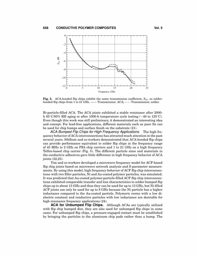
Fig. 5. ACA-bonded flip chips exhibit the same transmission coefficient, S21, as solder-bonded flip chips from 1 to 21 GHz. —— Transmission: ACA; - - - - Transmission: solder.
Bi-particle-filled ACA. The ACA joints exhibited a stable resistance after 2000-h 85C/85% RH aging or after 1000-h temperature cycle testing (−40 to 125C).Even though this work was still preliminary, it demonstrated an interesting ideaand concept. For lead-free applications, different materials such as pure Sn canbe used for chip bumps and surface finish on the substrate (21).
ACA Bumped Flip Chips for High Frequency Applications. The high fre-quency behavior of ACA interconnections has attracted much attention in the pastseveral years. Sihlbom and co-workers demonstrated that ACA-bonded flip chipscan provide performance equivalent to solder flip chips in the frequency rangeof 45 MHz to 2 GHz on FR4 chip carriers and 1 to 21 GHz on a high frequencyTelfon-based chip carrier (Fig. 5). The different particle sizes and materials inthe conductive adhesives gave little difference in high frequency behavior of ACAjoints (22,23).
Yim and co-workers developed a microwave frequency model for ACF-basedflip chip joints based on microwave network analysis and S-parameter measure-ments. By using this model, high frequency behavior of ACF flip chip interconnec-tions with two filler particles, Ni and Au-coated polymer particles, was simulated.It was predicted that Au-coated polymer-particle-filled ACF flip chip interconnec-tions exhibited comparable transfer and loss characteristics to solder bumped flipchips up to about 13 GHz and thus they can be used for up to 13 GHz, but Ni-filledACF joints can only be used for up to 8 GHz because the Ni particle has a higherinductance compared to the Au-coated particle. Polymeric resins with a low di-electric constant and conductive particles with low inductance are desirable forhigh resonance frequency applications (24).
ACA for Unbumped Flip Chips. Although ACAs are typically utilizedwith flip chip bumped dice, they are also used for unbumped flip chips in somecases. For unbumped flip chips, a pressure-engaged contact must be establishedby bringing the particles to the aluminum chip pads rather than a bump. The

Vol. 5 CONDUCTIVE POLYMER COMPOSITES 659
pressure must be sufficient to break the oxide on the aluminum pads. A suffi-cient quantity of particles must be trapped in the contact pad area and remain inplace during bonding and curing to achieve a reliable interconnection. In additionto maximizing the number of particles in the contact area the number of parti-cles located between adjacent pads must be minimized so as to prevent electricalshorts. An additional factor that must be in the case of unbumped flip chips isadhesive flow during bonding and curing. It is essential to control the tempera-ture heating to be sufficiently slow when the polymeric resin is curing so that theconductive filler particles can migrate from the chip carrier side to the chip sidepad (25).
Ni/Au Coated Silver Bumps. A flip chip technology developed by ToshibaCorp. utilized an anisotropic conductive film (ACF) to attach bare unbumped chips(with Al pads) onto a printed circuit board (PCB) with bumps formed from a silverpaste screen printed on the PCB (26). After curing, Ag bumps were formed (70-µm diameter, 20-µm height), which were subsequently overplated with Ni/Au. Itwas determined that ACF with a low CTE (28 ppm/C), low water absorption rate(1.3%), and that utilized a Au-plated plastic ball worked best. It was also foundthat Ni/Au plated Ag-paste formed bumps exhibited a smaller initial connectionresistance (22 and 48 µ for Ag bumps with and without Ni/Au overplating, re-spectively) and a smaller connection resistance increase compared to Ag-pasteformed bumps which were not overplated with Ni/Au after 1000-h acceleratedthermal cycling (ATC) testing (ie the final connection resistances after aging are294 and 717 µ for Ag bumps with and without Ni/Au overplating, respectively).
Conductive Columns. Nitto Denko Corp. developed an ACF for fine pitchflip chip applications (27). The features of this ACF were (1) connectability betweenbumpless chips and fine pitch PCB; (2) high electrical conductivity; (3) repairabil-ity (easy to peal off chips from a printed circuit board at elevated temperatures);(4) high reliability; and (5) potential storage at room temperature. There are othernotable features too: (1) ACF is usable at pitches down to 25 µm, (2) the conduc-tive elements are micrometallic columns as opposed to random-shaped particles,and (3) this adhesive matrix consists of a thermoplastic polymer resin, conduc-tive columns coated with an insulator, and a high Tg polymer, which completelyseparates the columns from the adhesive (Fig. 6).
It is easy to change the diameter of the conductive columns in order to makethe film compatible with a variety of pitches. Sn/Pb or other solder materials areplated on both the top and bottom of the conductive columns (usually copper). Theplated solder on the both ends of the conductive columns melts and forms met-allurgical connections between the conductive columns and metal pads on a chipand the mating chip carrier, which ensure a good connection. Figure 6a illustratesthe cross section of the film structure. A rough surface, a result of plating, has theadvantage of providing a good connection with the terminal pads it is in contactwith. A typical terminal pad structure of a chip without bumps is shown in Figure6b. To achieve a good connection, the height of the conductive columns must belarger than the thickness of the passivation layer (tp). Since tb (the distance froma Cu pad surface of the chip carrier to the passivation layer surface of the chip) isusually smaller than ta (the distance from solder mask surface of the chip carrierto the passivation layer surface of the chip), the conductive columns will assumean inclined position during bonding if the thickness of the conductive columns

660 CONDUCTIVE POLYMER COMPOSITES Vol. 5
(c)
Polymeric resin
Conductive column(Cu)
Insulating material Solder
tACF
(a)
Board
Cu pad
Passivation
Chip
Al pad
tp
tc
tbta
(b)
Fig. 6. Illustration of a scheme for fine pitch, flip chip interconnection. (a) An ACF filledwith micrometallic columns. (b) A typical cross-sectional structure of a chip without bumpsand the mating chip carrier. (c) A cross section of an interconnect formed between anunbumped chip and the mating chip carrier.
is larger than the ACF thickness (tACF). It is important to adjust the thicknessof board or chip carrier pads and ACF thickness to achieve good connection andadhesion. Reliability results indicated that the ACF possessing an adhesive ma-trix with a high Tg (282C) exhibited high reliability and the contact resistanceremained unchanged after 1000 cycles of ATC testing (−25 to 125C). Figure 6c isa photography of a cross section of a joint formed between an unbumped die anda chip carrier using this ACF flip chip interconnection method.

Vol. 5 CONDUCTIVE POLYMER COMPOSITES 661
ACAs for CSP and BGA Applications
Area Bonding Conductive Adhesives. Aiming at the CSP applicationmarket, Merix Corp. and Auburn University collaborated to develop an ACA calledarea bonding conductive (ABC) adhesives. ABC adhesive is a two-region thermosetadhesive with ECA pads surrounded by a continuous oxide-filled dielectric adhe-sive to form a total area bond. Both regions are solvent-free, B-staged, nontackyepoxies supplied on a Mylar carrier release film. In contrast to conventional ACAs,conductive areas of ABC adhesive are only at bond pad locations. The assemblyprocess for using ABC adhesives is shown in Figure 7. The ABC adhesives poten-tially can provide a reliable, low cost, low temperature, low pressure process forflip chip and CSP applications (28).
Au-Stud vs Electroless Ni/Au Bumps. As the demand for miniatur-ization has increased dramatically, concentrated efforts have been made to findcheaper alternatives to established technologies of area array solder bumps.
Area bond chip ABC preform
Carrier filmElectrically conductiveadhesive dot
Oxide-filleddielectric adhesive
(a)
Area bond chip
(b)
Area bond chip
(c)
Chip carrier
Area bond chip
Chip carrier
(d)
Fig. 7. Schematic depicting a flip chip assembly processing utilizing ABC adhesive. (a)A chip is aligned to the ABC preform which is on a carrier film. (b) The ABC preform istacked to the die at 100C and under a pressure of 150 g for 30 s, and then the carrier filmis removed after the chip is cooled down. (c) The chip with ABC preform is aligned to amating chip carrier (FR4 board). (d) The chip/ABC preform is attached to the chip carrierat 100C and under a pressure of 150 g for 30 s, and then the package is cooled down.

662 CONDUCTIVE POLYMER COMPOSITES Vol. 5
ACF Chip
Bumps
Solder balls
Organic chip carrier (CSP, PBGA)
Fig. 8. Schematic depicting the side view construction of a ChipPAC CSP package thatutilizes an ACF.
ChipPAC, Inc., demonstrated an alternate process/package concept covering bothCSP and PBGA package formats whose construction is illustrated in Figure 8.The concept package consisted essentially of three parts: ACF, metallic bumps onthe die bond pads, and an organic chip carrier (29).
Although this packaging solution was not entirely unique, reducing it to ahigh volume assembly and packaging process, where low cost and high reliabilitywere key, was innovative. This configuration provides an appealing package solu-tion, based on several factors. First, the connection can be implemented at a muchfiner pitch (∼100 µm) compared to conventional solder bumps, and so there is apotential for a die-size reduction in flip chip IC designs that are normally imple-mented as multirow perimeter arrays using conventional solder bumps. Second,the ACF interconnect approach allows the use of inexpensive bumping technolo-gies, thereby greatly reducing the wafer bumping cost portion of the overall pack-age cost.
The combination of cured adhesive interconnection, bumps, and organic sub-strate provides a reliable, cost-effective flip chip CSP. It was determined thatAu-stud bumps were preferable to Ni/Au bumps because of the former’s compli-ant nature. Since the planarity control of organic chip carriers is difficult, giventhe nature of the material, it was simpler to change the interconnection method,ie, using Au-stud bumps. However, electroless Ni/Au bumps are still an option,if the material properties of the ACF and/or chip carrier are altered to providecompliancy.
Double-Layered ACF. Motorola developed a low cost and low profile flipchip on flex (FCOF) CSP package using ACFs (30). The package has the flexibilityto utilize the existing wire-bonding pad configuration without adding prohibitiveredistribution and wafer solder bumping costs, and eliminated the need for under-chip encapsulation. Two types of ACF film were studied: double layer films withthe second layer loaded with Ni/Au plated polystyrene–divinylbenzene (PS–DVB)spheres, and solid Ni particles. The film structure, consisting of a nonfilled and aconducting particles-filled adhesive layers, is illustrated in Figure 9. The double-layer design reduces the particle density in x–y spacing of interconnection pads,which serve to enhance the x–y plane insulation characteristics. At the same time,the double-layer film provides more adhesive volume that helps to entrap moreparticles on the bonding interconnection pads. Both calculated and observed val-ues show that the number of conducting particles trapped is much higher thanthose in single-layer ACF. This indicate that even though particle density in a
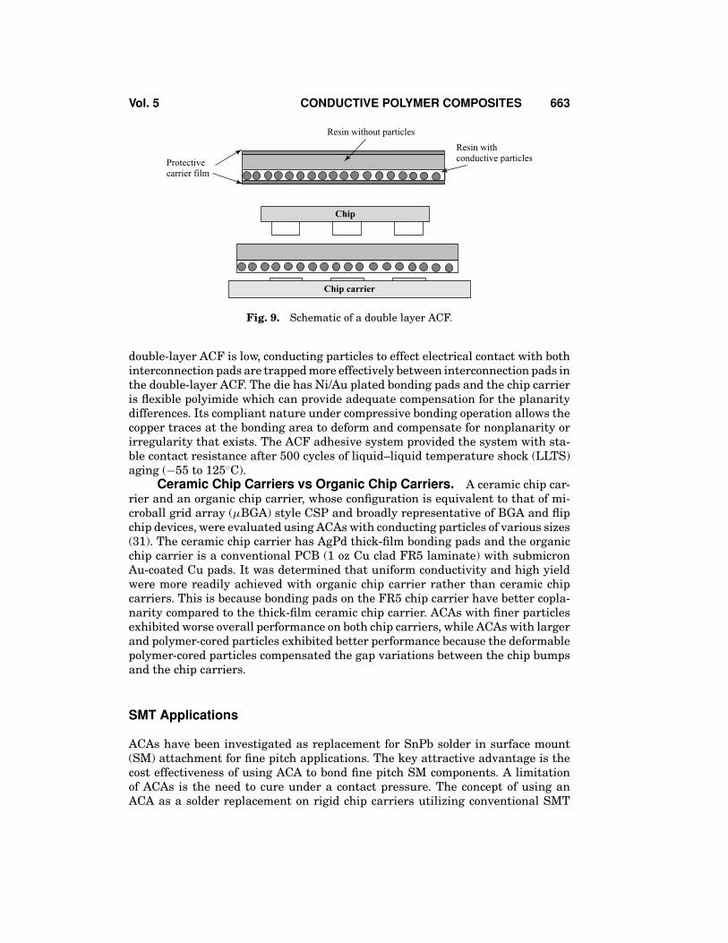
Vol. 5 CONDUCTIVE POLYMER COMPOSITES 663
Chip
Chip carrier
Resin without particles
Resin withconductive particlesProtective
carrier film
Fig. 9. Schematic of a double layer ACF.
double-layer ACF is low, conducting particles to effect electrical contact with bothinterconnection pads are trapped more effectively between interconnection pads inthe double-layer ACF. The die has Ni/Au plated bonding pads and the chip carrieris flexible polyimide which can provide adequate compensation for the planaritydifferences. Its compliant nature under compressive bonding operation allows thecopper traces at the bonding area to deform and compensate for nonplanarity orirregularity that exists. The ACF adhesive system provided the system with sta-ble contact resistance after 500 cycles of liquid–liquid temperature shock (LLTS)aging (−55 to 125C).
Ceramic Chip Carriers vs Organic Chip Carriers. A ceramic chip car-rier and an organic chip carrier, whose configuration is equivalent to that of mi-croball grid array (µBGA) style CSP and broadly representative of BGA and flipchip devices, were evaluated using ACAs with conducting particles of various sizes(31). The ceramic chip carrier has AgPd thick-film bonding pads and the organicchip carrier is a conventional PCB (1 oz Cu clad FR5 laminate) with submicronAu-coated Cu pads. It was determined that uniform conductivity and high yieldwere more readily achieved with organic chip carrier rather than ceramic chipcarriers. This is because bonding pads on the FR5 chip carrier have better copla-narity compared to the thick-film ceramic chip carrier. ACAs with finer particlesexhibited worse overall performance on both chip carriers, while ACAs with largerand polymer-cored particles exhibited better performance because the deformablepolymer-cored particles compensated the gap variations between the chip bumpsand the chip carriers.
SMT Applications
ACAs have been investigated as replacement for SnPb solder in surface mount(SM) attachment for fine pitch applications. The key attractive advantage is thecost effectiveness of using ACA to bond fine pitch SM components. A limitationof ACAs is the need to cure under a contact pressure. The concept of using anACA as a solder replacement on rigid chip carriers utilizing conventional SMT

664 CONDUCTIVE POLYMER COMPOSITES Vol. 5
has been demonstrated by Liu and co-workers (32). Fine pitch SM componentswere bonded to FR4 boards with ACAs using a fine pitch bonder and then compo-nents with larger pitches were bonded with ICAs using standard SM equipment.The study demonstrated that standard surface-mounting tools could be used toassemble conductive adhesives. The connection resistance of solder-plated, plasticcomponents (0.65 mm pitch) with ACAs bonded did not change after an acceler-ated temperature cycling (ATC) test conducted at −40 to 85C. However, similarparts failed under conditions of −55 to 125C for 1000 cycles (33). The mechanicalstability problem may have been the result of an improper joint geometry, ie notoptimized for ACA bonding.
Failure Mechanism
Since the adhesive matrix is a nonconductive material, interconnection joints relyto some extent on pressure to assure contact for conventional ACAs. Adhesiveinterconnections therefore exhibit different failure mechanisms compared to sol-dered connections, where the formation of intermetallic compounds and coarsen-ing of grains are associated with the main mechanisms. Basically there are twomain failure mechanisms that can affect the contacts. The first is the formation ofan insulating film on either the contact areas or conductive particle surfaces. Thesecond is the loss of mechanical contact between the conductive elements due toeither a loss of adherence or relaxation of the compressive force.
Oxidation of Nonnoble Metals. Electrochemical corrosion of nonnoblemetal bumps, pads, and conductive particles results in the formation of insulatingmetal oxides and significant increase in contact resistance. Electrochemical cor-rosion only occurs in the presence of moisture and metals that possess differentelectrochemical potentials. Humidity generally accelerates oxide formation and sotoo the increase in contact resistance. Reliability test results for FCOF using goldbumps and ACFs filled with Ni particles indicated that the connection resistanceincreased with time under elevated temperature and humidity storage conditions(34). In this case, the gold bump acts as cathode and the Ni particle as an anode.A nickel oxide, which is electrically insulating, eventually forms on the surface ofthe Ni particles.
Loss of Compressive Force. The compressive forces acting to maintaincontact among the conductive components are partly achieved because of curingshrinkage achieved when curing the polymeric matrix of ACAs. Both the cohesivestrength of the adhesive matrix and the interfacial adhesion strength between theadhesive matrix and the chip and chip carrier must be sufficient to maintain thecompressive force. However, the thermal expansion of adhesives, their swellingdue to moisture adsorption, and mechanical stresses due to applied loads tend todiminish this compressive force created as a result of curing. Moreover, water notonly diffuses into the adhesive layer but also penetrates to the interface betweenadhesive and chip/chip carrier, causing a reduction in adhesion strength. As aresult, the contact resistance increases and can even result in a complete loss ofelectrical contact (35).

Vol. 5 CONDUCTIVE POLYMER COMPOSITES 665
Isotropic Conductive Adhesives
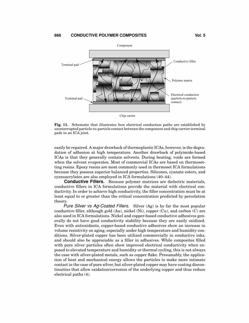
Percolation Theory of Conduction. Isotropic conductive adhesives(ICAs), also called as polymer solder, are composites of polymer resin and con-ductive fillers. The conductive fillers provide the composite with electrical con-ductivity through contact between the conductive particles. With increasing fillerconcentrations, the electrical properties of ICAs transform from an insulator toa conductor. Percolation theory has been used to explain the electrical propertiesof ICA composites. At low filler concentrations, the resistivities of ICAs decreasegradually with increasing filler concentration. However, the resistivity drops dra-matically above a critical filler concentration, Vc, called the percolation thresh-old. It is believed that at this concentration, all the conductive particles contacteach other and form a three-dimensional network. The resistivity decreases onlyslightly with further increases in the filler concentrations (36–38). A schematicexplanation of resistivity change of ICAs based on percolation theory is shownin Figure 10. In order to achieve conductivity, the volume fraction of a conduc-tive filler in an ICA must be equal to or slightly higher than the critical volumefraction. Similar to solders, ICAs provide the dual functions of electrical connec-tion and mechanical bond in an interconnection joint. In an ICA joint (Fig. 11),the polymer resin provides mechanical stability and the conductive filler provideselectrical conductivity. Filler loading levels which are too high cause mechanicalintegrity of adhesive joints to deteriorate. Therefore, the challenge in formulatingan ICA is to maximize conductive filler content to achieve a high electrical con-ductivity without adversely affecting the mechanical properties. In a typical ICAformulation, the volume fraction of the conductive filler is about 25–30% (4,5).
Adhesive Matrix. Polymer matrices of ICAs are similar to ACAs. An idealmatrix for ICAs should exhibit a long shelf life (good room temperature latency),fast cure, relatively high glass-transition temperature (Tg), low moisture pickup,and good adhesion (39).
Both thermoplastic and thermoset resins can be used for ICA formulations.The main thermoplastic resin used for ICA formulations is polyimide resin. Anattractive advantage of thermoplastic ICAs is that they are reworkable, eg, can
Res
istiv
ity
Volume fraction of filler, %
Vc
Fig. 10. Effect of filler volume fraction on the resistivity of ICA systems.
666 CONDUCTIVE POLYMER COMPOSITES Vol. 5
Component
Chip carrier
Terminal pad
Terminal pad
Conductive filler
Polymer matrix
Electrical conduction(particle-to-particlecontact)
Fig. 11. Schematic that illustrates how electrical conduction paths are established byuninterrupted particle-to-particle contact between the component and chip carrier terminalpads in an ICA joint.
easily be repaired. A major drawback of thermoplastic ICAs, however, is the degra-dation of adhesion at high temperature. Another drawback of polyimide-basedICAs is that they generally contain solvents. During heating, voids are formedwhen the solvent evaporates. Most of commercial ICAs are based on thermoset-ting resins. Epoxy resins are most commonly used in thermoset ICA formulationsbecause they possess superior balanced properties. Silicones, cyanate esters, andcyanoacrylates are also employed in ICA formulations (40–44).
Conductive Fillers. Because polymer matrices are dielectric materials,conductive fillers in ICA formulations provide the material with electrical con-ductivity. In order to achieve high conductivity, the filler concentration must be atleast equal to or greater than the critical concentration predicted by percolationtheory.
Pure Silver vs Ag-Coated Fillers. Silver (Ag) is by far the most popularconductive filler, although gold (Au), nickel (Ni), copper (Cu), and carbon (C) arealso used in ICA formulations. Nickel and copper-based conductive adhesives gen-erally do not have good conductivity stability because they are easily oxidized.Even with antioxidants, copper-based conductive adhesives show an increase involume resistivity on aging, especially under high temperature and humidity con-ditions. Silver-plated copper has been utilized commercially in conductive inks,and should also be appreciable as a filler in adhesives. While composites filledwith pure silver particles often show improved electrical conductivity when ex-posed to elevated temperature and humidity or thermal cycling, this is not alwaysthe case with silver-plated metals, such as copper flake. Presumably, the applica-tion of heat and mechanical energy allows the particles to make more intimatecontact in the case of pure silver, but silver-plated copper may have coating discon-tinuities that allow oxidation/corrosion of the underlying copper and thus reduceelectrical paths (4).

Vol. 5 CONDUCTIVE POLYMER COMPOSITES 667
Particle Shape and Size. The most common morphology of conductivefillers used for ICAs is flake because flakes tend to have a large surface area,and more contact spots and thus more electrical paths than spherical fillers. Theparticle size of ICA fillers generally ranges from 1 to 20 µm. Larger particles tendto provide the material with a higher electrical conductivity and lower viscosity(45). A new class of silver particles, porous nano-sized silver particles, has beenintroduced in ICA formulations (46,47). ICAs made with this type of particlesexhibited improved mechanical properties, but the electrical conductivity is lessthan ICAs filled with silver flakes. In addition, short carbon fibers have beenused as conductive fillers in conductive adhesive formulations (36,48). However,carbon-based conductive adhesives show much lower electrical conductivity thansilver-filled ones.
Silver-Copper Fillers. In 1992, a powder with a specific structure was in-troduced as a filler for conductive adhesives (49). A powder particle consists of twometallic components, copper and silver. Silver is highly concentrated on the par-ticle surface and concentration gradually decreases from the surface to the innerof the particle, but always contains a small amount of silver. Conductive adhesivepaste filled with this powder exhibits excellent oxidation resistance, ie can be ex-posed to oxygen content about 100 ppm in a nitrogen atmosphere. It also exhibitshigher solderability than commercially available copper pastes, sufficient adhe-sion strength even after heating and/or cooling test, and least migration, almostsame degree to pure copper paste (49).
Low-Melt Fillers. In order to improve electrical and mechanical properties,low-melting-point alloy fillers have been used in ICA formulations. A conductivefiller powder is coated with a low-melting-point metal. The conductive powder isselected from the group consisting of Au, Cu, Ag, Al, Pd, and Pt. The low-melting-point metal is selected from the group of fusible metals, such as Bi, In, Sn, Sb, andZn. The filler particles are coated with the low-melting-point metal which can befused to achieve metallurgical bonding between adjacent particles, and betweenthe particles and the bond pads that are joined using the adhesive material (50,51).
Flip Chip Applications Using ICAs
A key factor in achieving a low cost, flip chip technology is the use of ICAs. Incomparison to the classical flip chip technologies, the use of ICAs for the bumpingand joining provide numerous advantages:
(1) The simplification of the processing and the reduction of indexing steps bythe omission of activation and purification process
(2) The smaller temperature load on elements and wiring carriers(3) The availability of a large spectrum of possible material pairs and combi-
nations(4) The broad range of applicable adhesive systems and thus the selection of
different processing parameters and joining characteristics(5) Few requisites for under bump metallization (UBM) since alloy phase for-
mation does not have to be considered
668 CONDUCTIVE POLYMER COMPOSITES Vol. 5
Unbumped Flip Chip Joints.Polymer Flip Chip. Several flip chip bumping and joining techniques have
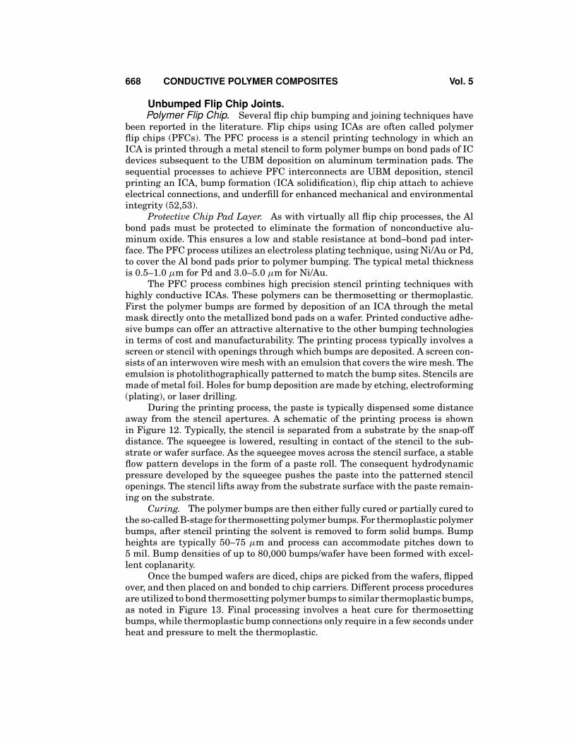
been reported in the literature. Flip chips using ICAs are often called polymerflip chips (PFCs). The PFC process is a stencil printing technology in which anICA is printed through a metal stencil to form polymer bumps on bond pads of ICdevices subsequent to the UBM deposition on aluminum termination pads. Thesequential processes to achieve PFC interconnects are UBM deposition, stencilprinting an ICA, bump formation (ICA solidification), flip chip attach to achieveelectrical connections, and underfill for enhanced mechanical and environmentalintegrity (52,53).
Protective Chip Pad Layer. As with virtually all flip chip processes, the Albond pads must be protected to eliminate the formation of nonconductive alu-minum oxide. This ensures a low and stable resistance at bond–bond pad inter-face. The PFC process utilizes an electroless plating technique, using Ni/Au or Pd,to cover the Al bond pads prior to polymer bumping. The typical metal thicknessis 0.5–1.0 µm for Pd and 3.0–5.0 µm for Ni/Au.
The PFC process combines high precision stencil printing techniques withhighly conductive ICAs. These polymers can be thermosetting or thermoplastic.First the polymer bumps are formed by deposition of an ICA through the metalmask directly onto the metallized bond pads on a wafer. Printed conductive adhe-sive bumps can offer an attractive alternative to the other bumping technologiesin terms of cost and manufacturability. The printing process typically involves ascreen or stencil with openings through which bumps are deposited. A screen con-sists of an interwoven wire mesh with an emulsion that covers the wire mesh. Theemulsion is photolithographically patterned to match the bump sites. Stencils aremade of metal foil. Holes for bump deposition are made by etching, electroforming(plating), or laser drilling.
During the printing process, the paste is typically dispensed some distanceaway from the stencil apertures. A schematic of the printing process is shownin Figure 12. Typically, the stencil is separated from a substrate by the snap-offdistance. The squeegee is lowered, resulting in contact of the stencil to the sub-strate or wafer surface. As the squeegee moves across the stencil surface, a stableflow pattern develops in the form of a paste roll. The consequent hydrodynamicpressure developed by the squeegee pushes the paste into the patterned stencilopenings. The stencil lifts away from the substrate surface with the paste remain-ing on the substrate.
Curing. The polymer bumps are then either fully cured or partially cured tothe so-called B-stage for thermosetting polymer bumps. For thermoplastic polymerbumps, after stencil printing the solvent is removed to form solid bumps. Bumpheights are typically 50–75 µm and process can accommodate pitches down to5 mil. Bump densities of up to 80,000 bumps/wafer have been formed with excel-lent coplanarity.
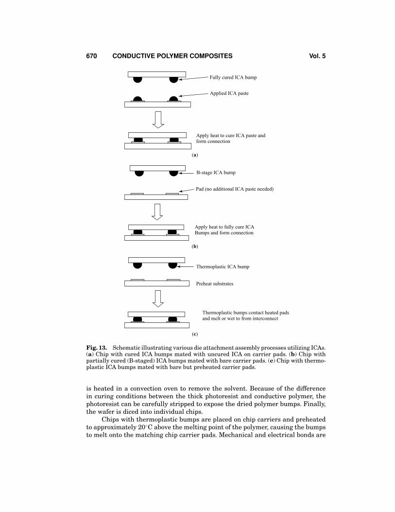
Once the bumped wafers are diced, chips are picked from the wafers, flippedover, and then placed on and bonded to chip carriers. Different process proceduresare utilized to bond thermosetting polymer bumps to similar thermoplastic bumps,as noted in Figure 13. Final processing involves a heat cure for thermosettingbumps, while thermoplastic bump connections only require in a few seconds underheat and pressure to melt the thermoplastic.

Vol. 5 CONDUCTIVE POLYMER COMPOSITES 669
Squeegee
Stencil
Substrate
ICA paste
Fig. 12. Schematic depicting the ICA paste stencil printing process.
Underfill. An underfill is then injected into the gap between the chip andchip carrier and then cured to complete the flip chip process. The function of theunderfill or encapsulation as it is sometimes referred to is to provide mechani-cal integrity and environmental protection to a flip chip assembly. Studies havedemonstrated that both thermoset and thermoplastic ICAs can offer low initialjoint resistances of less than 5 m and stable joint resistances (Au-to-Au flipchip bonding) during all the accelerated reliability testing listed in Table 1. Thereliability results have indicated that there is no substantial difference in theperformance of thermoset and thermoplastic bumps and both types of polymersapparently offer reliable flip chip electrical interconnections (53).
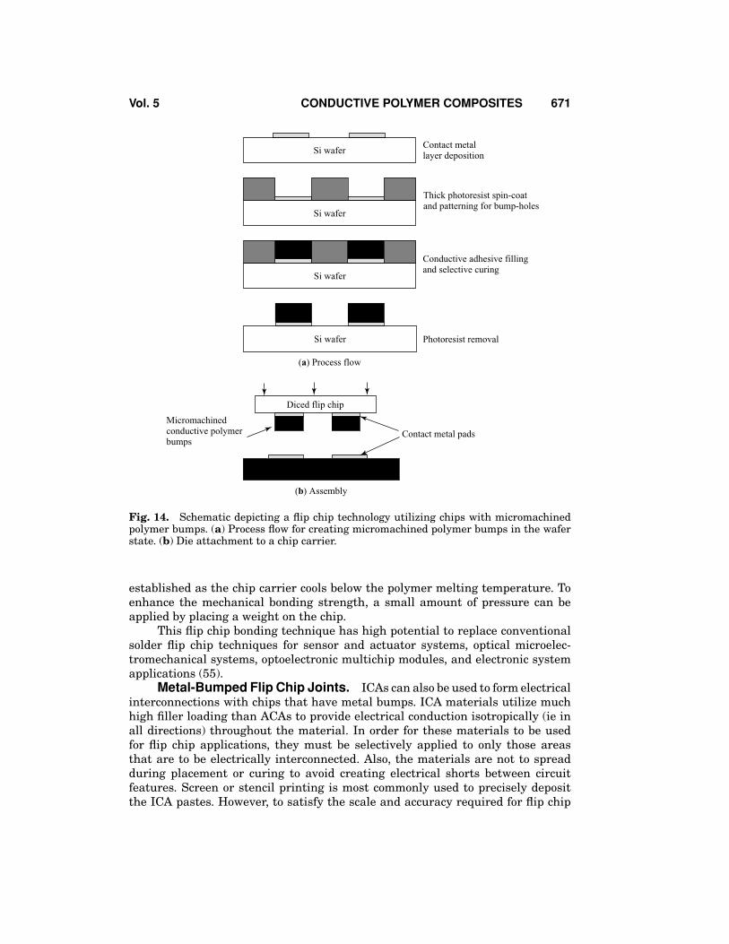
Micromachined Bumping. A PFC bumping process is known as microma-chined bumping (54,55). The bumping procedure is illustrated in Figure 14. Ini-tially Cr/Au contact metal pads for conductive polymer bumps are deposited onSi wafers, followed by patterning a thick photoresist to create bump holes. A highaspect ratio and straight side-wall patterns are very important in shaping theconductive polymer bumps. After the lithography, thermoplastic conductive poly-mer material, usually thermoplastic paste filled with Ag flake, is applied by eitherdispensing or screen printing the paste into the bump-hole patterns. The wafer
Table 1. Accelerated Reliability Testing
Test Condition Time
Temperature cycle −55 to 150C 1000 cycleThermal shock −55 to 125C 500 cycleElevated temperature and humidity 85C/85% RH 1000 hPressure cooker 121C/15 psi 168 h
670 CONDUCTIVE POLYMER COMPOSITES Vol. 5
Fully cured ICA bump
Applied ICA paste
Apply heat to cure ICA paste and form connection
(a)
B-stage ICA bump
Pad (no additional ICA paste needed)
Apply heat to fully cure ICABumps and form connection
(b)
Thermoplastic ICA bump
Preheat substrates
Thermoplastic bumps contact heated padsand melt or wet to from interconnect
(c)
Fig. 13. Schematic illustrating various die attachment assembly processes utilizing ICAs.(a) Chip with cured ICA bumps mated with uncured ICA on carrier pads. (b) Chip withpartially cured (B-staged) ICA bumps mated with bare carrier pads. (c) Chip with thermo-plastic ICA bumps mated with bare but preheated carrier pads.
is heated in a convection oven to remove the solvent. Because of the differencein curing conditions between the thick photoresist and conductive polymer, thephotoresist can be carefully stripped to expose the dried polymer bumps. Finally,the wafer is diced into individual chips.
Chips with thermoplastic bumps are placed on chip carriers and preheatedto approximately 20C above the melting point of the polymer, causing the bumpsto melt onto the matching chip carrier pads. Mechanical and electrical bonds are
Vol. 5 CONDUCTIVE POLYMER COMPOSITES 671
Contact metallayer deposition
Thick photoresist spin-coatand patterning for bump-holes
Conductive adhesive fillingand selective curing
Photoresist removal
Si wafer
Si wafer
Si wafer
Si wafer
Diced flip chip
Contact metal pads
Micromachinedconductive polymerbumps
(b) Assembly
(a) Process flow
Fig. 14. Schematic depicting a flip chip technology utilizing chips with micromachinedpolymer bumps. (a) Process flow for creating micromachined polymer bumps in the waferstate. (b) Die attachment to a chip carrier.
established as the chip carrier cools below the polymer melting temperature. Toenhance the mechanical bonding strength, a small amount of pressure can beapplied by placing a weight on the chip.
This flip chip bonding technique has high potential to replace conventionalsolder flip chip techniques for sensor and actuator systems, optical microelec-tromechanical systems, optoelectronic multichip modules, and electronic systemapplications (55).
Metal-Bumped Flip Chip Joints. ICAs can also be used to form electricalinterconnections with chips that have metal bumps. ICA materials utilize muchhigh filler loading than ACAs to provide electrical conduction isotropically (ie inall directions) throughout the material. In order for these materials to be usedfor flip chip applications, they must be selectively applied to only those areasthat are to be electrically interconnected. Also, the materials are not to spreadduring placement or curing to avoid creating electrical shorts between circuitfeatures. Screen or stencil printing is most commonly used to precisely depositthe ICA pastes. However, to satisfy the scale and accuracy required for flip chip

672 CONDUCTIVE POLYMER COMPOSITES Vol. 5
bonding very accurate pattern alignment is required. To overcome this difficultrequirement, Matsushita developed the transfer method (56).
Raised studs or pillars are required on either the die or the chip carrier.Matsushita uses a conventional ball bonder to form Au-stud bumps. Bumpingis significantly faster than creating a complete wire bonds. A ball bumping pro-cess eliminates the need for traditional sputtering and plating processes used forstandard bump formation. To prevent the bond area from becoming too large, thebumps are formed in a conical shape. The stud-bump bonding process is illustratedin Figures 15–18. The bumps are pressed level by a flat surface which adjusts bothheight and planarity. The ICA is selectively transferred on the bump tips by con-tacting the face of the die to a flat thin film of the ICA which is produced by screenprinting and whose transfer thickness is controlled by changing the printed filmthickness. Then the die is picked, aligned, and placed on a chip carrier. The wholeassembly is exposed to heat to cure the ICA and form connections between the
Chip
Chip carrier
Chip carrier
Planarized tips ofAu-stud bumps
An ICA paste layer
ICA paste
Underfill
Chip
Chip
Chip
Fig. 15. Schematic of the process flow of forming joints with stud-bumped flip-chips usingICAs. (a) Planarize the tips of the gold-stud bumps formed with a wire bond tool. (b) Dipthe planarized bumps into a thin layer of ICA. (c) Withdraw the chip leaving the bumpscoated with ICA. (d) The chip is placed on mating pads of a chip carrier with pressurerequired during curing. (e) An underfill (an insulating adhesive) is dispensed and cured.

Vol. 5 CONDUCTIVE POLYMER COMPOSITES 673
Chip
Chip carrier
Low-melting-alloy filler
High-melting-alloy filler
Terminal pad
Polymer matrix
(a)
Chip
Chip carrier
Molten low-melting-alloyfiller
Partially dissolvedhigh-melting-alloy filler
(b)
Chip
Chip carrier
Solidified network
(c)
Fig. 16. Schematic of a joint formed using transient liquid phase sintering conductiveadhesives. (a) Initial state after chip attachment and before temperature reach the melt-ing point of the low-melting-alloy filler. (b) The low-melting-alloy fillers start to melt anddissolve the high-melting-alloy filler. (c) After the high-melting-alloy fillers are completelydissolved, the liquid metal phase solidifies and forms a three-dimensional network in thejoint.
die and chip carrier. Finally, an underfill (an insulating adhesive) is dispensedbetween the die and the chip carrier and cured. This method offers the optionsof oven curing an assembly since bonding pressure is not required. A speciallyformulated ICA is used to avoid silver migration, containing 20% palladium in asilver–palladium alloy. This is done to avoid silver migration. A schematic of theprocess flow of forming joints with stud-bumped flip chips using ICAs is shown inFigure 15.
Another process for bonding a flip chip with metal bumps consists of screenprinting an ICA on a chip carrier, aligning and placing the chip, curing the ICAto form bonds, and underfilling. By using this approach, SINTEF Electronics con-ducted a comparison study between an ICA-bonded and solder-bonded flip chipson FR4 chip carrier with Ni/Au metallization. The number of thermal cycles (−55to 125C) to failure for both solder and ICA flip chip circuits was compared. Thestudy showed that stable contacts could be maintained for at least 1000–2000

674 CONDUCTIVE POLYMER COMPOSITES Vol. 5
Nonnoble metal pad
Ag flake
Polymer binder
Good electrical conduction
(a) Before corrosion
Condensed water solution
Ag flake
Metal hydroxide or oxideformed at the interface
(b) After corrosion
Poor electrical conduction
Fig. 17. Schematic depicting the effect of galvanic corrosion of a nonnoble metal pad onelectrical conduction of a silver-filled ICA. (a) Good electrical conduction before corrosion.(b) Poor electrical conduction due to the formation of a metal hydroxide or oxide formationas a result of galvanic corrosion.
450.00
350.00
250.00
150.00
50.00
−50.000 200 400 600 800 1000 1200 1400 1600
With the corrosion inhibitor
Without the corrosion inhibitor
Aging time, h
Con
tact
res
ista
nce
shif
t per
cent
age
Fig. 18. Effect of a corrosion inhibitor on contact resistance between an ICA and a Sn–Pbsurface with time. Aging condition: 85C/85% RH.
cycles for ICA flip chip joints. This is comparable to the lifetime for solder flip chipjoints. However, the variation among ICA samples was very high and optimiza-tion of assembly processes is needed in order to achieve more reproduciable jointresistance (57).

Vol. 5 CONDUCTIVE POLYMER COMPOSITES 675
Other Applications of ICAs
Surface Mount Applications. Tin–lead solders (Sn–Pb) are the standardmaterials used to interconnect electronic components on PCBs. The most commonreflow soldering process is SMT which uses tin–lead solder pastes (58–61). Thepressure to reduce the industrial use of lead is growing, particularly in Europe,since it poses as a hazard to human health (62).
Thus, the use of tin–lead solder paste in SMT processes must be reduced oreliminated to both satisfy legislative actions and market-driven pressures as well.Lead-free and environmentally sound interconnect bonding processes are urgentlyneeded. Among the possibilities are ECAs and lead-free solders (63–65). Comparedto soldering technology, ECA technology can offer numerous advantages such asfewer processing steps which reduces processing cost, lower processing temper-ature which makes the use of heat-sensitive and low cost chip carriers possible,and fine pitch capability (64).
However, conductive adhesive technology is still in its infancy, and con-cerns and limitations do exist. The main limitations of commercial ICAs includelower conductivity than that of solder materials, an unstable contact resistancewith nonnoble metal finished components, and poor impact performance. Theelectrical conductivity (∼104 − 1·cm− 1) of an ICA is lower than Sn–Pb solders(∼105 − 1·cm− 1). Although generally adequate for most electronics applications,the electrical conductivity of ICAs must be improved. Contact resistance betweenan ICA and nonnoble metal (such as Sn/Pb, Sn, and Ni) finished components isnoted to dramatically increase with time especially under elevated temperatureand humidity aging conditions (66–69). In addition, PCB assemblies are often sub-ject to significant mechanical shock during assembly, handling, and throughouttheir product life. Packages cannot survive without adequate impact resistance.However, most microelectronic commercial ICAs exhibit poor impact performance.Components assembled using ICAs tend to separate from the substrate when thepackage experiences a sudden shock (68,70). For conductive adhesive technologyto provide an acceptable solution as a solder replacement, new conductive adhe-sives with the desired overall properties must be developed (68). There has beena considerable effort to improve the properties of ICAs and to make them morereliable materials. These improvements are described in the following sections.
CSP Applications. Matsushita Electric Industrial Co., Ltd., developedsolderless joining technologies using nickel-filled ICAs to mount a ceramic chipscale package (CSP-C) onto a FR4 board (71). Nickel was selected instead of Agbecause, unlike Ag, nickel does not migrate. A significant CTE mismatch existedbetween the CSP-C ceramic chip carrier (CTS = 7 ppm) and the FR4 organic chipcarrier (CTE = 16 ppm). This CTE mismatch resulted in large stress to be gen-erated within the solder joints during ATC testing which resulted in early failuredue to solder fatigue. ICAs usually exhibit better thermomechanical propertiesthan solders. Also, metal-migration between joints is a great concern because thejoints in a CSP area array package are arranged with a close pitch (ie in closeproximity).
The packaging procedure was as follows: (1) the ICA was screen-printed onthe area array lands of the FR4 motherboard; (2) the CSP-C was mounted; (3) andthe ICA was cured to form bonds. The Ni-filled conductive adhesive demonstrated

676 CONDUCTIVE POLYMER COMPOSITES Vol. 5
a much higher resistance to metal migration compared to Ag-filled IACs, andequivalent to solder joints. However, the thermal fatigue life of the Ni-filled ICAjoints was five times greater than comparable solder joints.
Performance of ICAs
High Frequency Performance of ICA Joints. Only very limited workhas been conducted to investigate the high frequency behaviors of ICA joints.Felba and co-workers (72) investigated a formulation of ICA that performed wellas a solder replacement in microwave applications. The study involved in variousdifferent adhesive base materials and several types of main (silver flakes, nickel,and graphite) and additional (soot and silver semiflake powder) filler materials. Inorder to assess the usefulness of a given adhesive formulation, an additional gapin the gold strip of a standard microstrip bandpass filter was made and bridgedby an adhesive bonded silver jumper. Both the quality factor (Q) and loss factor(L) of the filter with the bonded jumper were measured at a frequency of 3.5GHz in a preliminary experiment and at 3.5 and 14 GHz in a final experiment. Itwas determined that silver flake powders are the best filler materials for ICA formicrowave applications because ICAs filled with the silver flake powders exhibitthe highest Q-factor and lowest L-factor. Also, addition of soot should be avoidedsince it decreases the quality factor (72).
A study was made at Georgia Tech, of a flip chip test vehicle mounted ona FR4 chip carrier with a gold-plated copper transmission lines (73). The per-formance of eutectic Sn–Pb and ICAs were evaluated and compared using thistest device. Both ICAs and eutectic Sn–Pb solder were determined to exhibit al-most the same behavior at a frequency range of 45 MHz to 2 GHz and the mea-sured transmission losses for both materials were minimal. It was also foundthat the S11 characteristics of both Sn–Pb and ICAs after exposure to 85C/85%RH aging for 150 h did not vary from the previous signals prior to aging, butS12 value of the Sn–Pb joints deviated more than that of ICA joints after theaging.
Fatigue Life of ICA Joints. There have been several studies investigat-ing the fatigue life of ICA joints. Aiming to understand the performance of ICAinterconnects under fracture and fatigue loading, Constable and co-workers (74)investigated performance of ICA interconnects under fracture and fatigue loadingby monitoring resistance changes (microohm sensitivity) of ICA joints during pulland fatigue testing (cyclic loading up to 1000 cycles). Observation of the fracturesurface suggested that the ICA joint life depended upon the adhesive failure ofthe bond to the metal surface. It was observed that fracture strains for the ICAswere in the range of 20–38%, and resistance remained approximately constantin the elastic region, but the resistance started to increase rapidly as soon asthe pull-force departed from linear elastic behavior. For fatigue tests, linear dis-placement was ramped up the preprogrammed maximum displacement and rampback to the starting position. It was observed that the shear strain for ICA jointssurviving 1000 cyclic loading was typically 10%, which is about an order of mag-nitude greater than solders. This suggests that using conductive adhesives maybe advantageous for some flip chip. It is believed that since silver filler particles of

Vol. 5 CONDUCTIVE POLYMER COMPOSITES 677
ICAs cannot accommodate this large strain, the silver filler particles must moverelative to one another as the epoxy matrix is strained. The most common patternof resistance change was only increased to a point corresponding to about a 70%loss in interface contact resistance before sudden failure. This was an indicationthat the interface crack slightly propagated into the adhesive (74).
In an effort to gain a fundamental understanding of the fatigue degradationof ICAs, Gomatam and co-workers (75) studied the behavior of ICA joints undertemperature and humidity conditions. The fatigue life decreased at elevated tem-perature and high humidity conditions. It was also observed that the fatigue lifeof the ICA joints decreased considerably as the temperature cycle frequency wasdecreased. This effect was attributed to the fact that as the frequency was de-creased, the propagating crack was exposed to higher loads for longer periods oftime, effectively resulting in high creep loading (75).
Improvement of Electrical Conductivity of ICAs
Electrical conductivity of ICAs is inferior to solders (76). Even though the conduc-tivity of ICAs is adequate for most applications, a higher electrical conductivityof ICAs is still needed. To develop a novel ICA for modern electronic interconnectapplications, a thorough understanding of the materials is required.
Eliminate Lubrication Layer. An ICA is generally composed of a polymerbinder and Ag-flake filler material. A thin layer of organic lubricant is present onthe surface of the Ag flakes. This lubricant layer plays an important role in theperformance of ICAs, including the dispersion of Ag flakes in adhesives, and therheology of the adhesive formulations (45,76–78). The organic layer consist of aAg salt formed between the Ag surface and the lubricant, which typically is afatty acid such as stearic acid (78,79). This lubricant layer affects the conductivityof an ICA because it is electrically insulating (78,79). To improve conductivity,the organic lubricant layer must be partially or fully removed through the use ofchemical substances that can dissolve the organic lubricant layer (78–80). How-ever, the viscosity of an ICA paste may increase if the lubricant layer is removed.An ideal chemical substance (or lubricant remover) should be latent (does not re-move the lubricant layer) at room temperature, but be active (capable of removingthe lubricant layer) at a temperature slightly below the cure temperature of thepolymer binder. The lubricant remover can be a solid short-chain acid, a high-boiling-point ether such as diethylene glycol monobutyl ether or diethylene glycolmonoethyl ether acetate, and a polyethylene glycol with a low molecular weight(78–80). These chemical substances can improve electrical conductivity of ICAs byremoving the lubricant layer on the Ag-flake surfaces and providing an intimateflake–flake contact (78,79).
Increase Shrinkage. In general, ICA pastes exhibit low electrical conduc-tivity before cure, but the conductivity increases dramatically after they are cured.ICAs achieve electrical conductivity during the cure process, mainly through amore intimate contact between Ag flakes caused by the shrinkage of polymerbinder (81). Accordingly, ICAs with a high cure shrinkage generally exhibit thebest conductivity. Therefore, increasing the cure shrinkage of a polymer binderis another method for improving electrical conductivity. For ICAs based on epoxy

678 CONDUCTIVE POLYMER COMPOSITES Vol. 5
resins, a small amount of a multifunctional epoxy resin can be added into anICA formulation to increase cross-linking density, shrinkage, and thus increaseconductivity (81).
Apply Electric Field. The electrical conductivity of ICAs can be improvedsignificantly by applying an electrical field before or while curing them. However,the exact reasons for this improvement are not yet clear (82).
Transient Liquid Phase Fillers. Another approach for improving electri-cal conductivity is to incorporate transient liquid-phase sintering metallic fillersin ICA formulations. The filler used is a mixture of a high-melting-point metalpowder (such as Cu) and a low-melting-point alloy powder (such as Sn–Pb). Thelow-melting-alloy filler melts when its melting point temperature is achieved. Theliquid phase dissolves the high-melting-point particles. The liquid exists only fora short period of time and then forms an alloy and solidifies. The electrical con-duction is established through a plurality of metallurgical connections formed insitu from these two powders in a polymer binder. The polymer binder fluxes boththe metal powders and the metals to be joined and facilitates the transient liquidbonding of the powders to form a stable metallurgical network for electrical con-duction, and also forms an interpenetrating polymer network providing adhesion(Fig. 16). High electrical conductivity can be achieved using this method (83–85).The ICA joints formed include metallurgical alloying to the junctions as well aswithin the adhesive itself. This provides a stable electrical connection during ele-vated temperature and humidity aging. In addition, the ICA joints showed goodimpact strength due to the metallurgical interconnection between the conductiveadhesive and the components. One critical limitation of this technology is thatthe numbers of combinations of low melt and high melt fillers are limited. Onlycertain combinations of two metallic fillers which are mutually soluble exist toform this type of metallurgical interconnections.
Improvement of Contact Resistance Stability
Contact resistance between an ICA (generally a Ag-flake-filled epoxy) and non-noble metal finished components increases dramatically during an elevated tem-perature and humidity aging, especially at 85C/85% RH. The National Centerof Manufacturing and Science (NCMS) defined the stability criterion for solderreplacement conductive adhesives as a contact resistance shift of less than 20%after aging at 85C/85% RH conditions for 500 h (67).
Causes for Resistance Increase. Two main mechanisms, simple oxi-dation and corrosion of the nonnoble metal surfaces, have been proposed in theliterature as the possible causes for the increase in contact resistance of ICA jointsduring elevated temperature and humidity aging. Simple oxidation of the nonno-ble metal surfaces is claimed to be the main reason for the observed increasedresistance. Corrosion is claimed to be the possible mechanism for resistance in-crease only by several investigators (65,66,68,86,87). One study strongly indicatesthat galvanic corrosion rather than simple oxidation of the nonnoble metal at theinterface between an ICA and nonnoble metal is the main reason for the shift incontact resistance of ICAs (Fig. 17) (88,89). The nonnoble acts as the anode, andis reduced to a metal ion (M − n e− = Mn+) because of the loss of electrons. The
Vol. 5 CONDUCTIVE POLYMER COMPOSITES 679
noble metal acts as a cathode, and its reaction generally is 2 H2O + O2 + 4 e− =4 OH− . Then Mn+ combines with OH− to form a metal hydroxide or metal oxide.As a result of this electrochemical (corrosion) process, a layer of metal hydroxideor metal oxide is formed at the interface which is electrically insulating, causingthe contact resistance to increase dramatically (88,89).
Prevention. Galvanic corrosion requires the presence of moisture. An elec-trolyte solution must be formed at the interface before galvanic corrosion can occur.Therefore, one way to prevent galvanic corrosion at the interface between an ICAand the nonnoble metal surface is to lower the moisture pickup of the ICA. ICAsthat have a low moisture absorption generally exhibit more stable contact resis-tance on nonnoble surfaces compared with those with high moisture absorption(90,91). Without the electrolyte, galvanic corrosion rate is very low. The electrolytein this case is mainly from the impurity of the polymer binder (generally epoxyresins). Therefore, ICAs formulated with high purity resins should perform better.
Use of Corrosion Inhibitors. Another method of preventing galvanic cor-rosion is to introduce organic corrosion inhibitors into ICA formulations (89–92).In general, organic corrosion inhibitors act as a barrier layer between the metaland environment, forming a film over the metal surfaces (93–96). Some chelat-ing compounds are especially effective in preventing metal corrosion (95). Mostorganic corrosion inhibitors react with the epoxy resin at a specific temperature.Therefore, if an ICA is epoxy-based, the corrosion inhibitors must not react withthe epoxy resin during curing, which would cause them to be consumed and losetheir effect. Organic corrosion inhibitors are thoroughly discussed in the literature(94,96). Figure 18 shows the effect of a chelating corrosion inhibitor on the contactresistance between an ICA and a Sn–Pb surface. It can be seen that this corrosioninhibitor is very effective in stabilizing the contact resistance.
Use of Oxygen Scavengers. Since oxygen accelerates galvanic corrosion,oxygen scavengers can be added into ICA formulations to slow down the corrosionrate (93). When oxygen molecules diffuse through the polymer binder, they reactwith the oxygen scavenger and are consumed. However, when the oxygen scav-enger is completely depleted, then oxygen can again diffuse into the interface andaccelerate the corrosion process. Therefore, oxygen scavengers can only delay thegalvanic corrosion process. Similar to corrosion inhibitors, the oxygen scavengersused must not react with the epoxy resin at its cure temperature. The commonoxygen scavengers utilized are listed below (93,97–100):
(1) hydrazine(2) carbohydrazide(3) hydroquinone(4) oximes(5) gallic acid(6) propyl gallate(7) hydroxylamines and related compounds(8) dihydroxyacetone(9) 1,2-dihydro-1,2,4,5-tetrazines
(10) erythorbic acid

680 CONDUCTIVE POLYMER COMPOSITES Vol. 5
Fig. 19. Schematic depicting an ICA joint containing oxide-penetrating particles and sil-ver filler particles.
Sharp-Edge Filler Particles. Another approach of improving contact resis-tance stability during aging is to incorporate some electrically conductive parti-cles, which have sharp edges and referred as oxide-penetrating fillers, into theICA formulations. Force must be provided to drive the oxide-penetrating particlesthrough the oxide layer of adjoining particles and metal pads, and keep them inposition. This can be accomplished by employing polymer binders that show highshrinkage when cured (Fig. 19) (101). This concept is used in Poly-Solder which hasgood contact resistance stability with standard surface-mounted devices (SMDs)on both solder-coated and bare circuit boards (101).
Improvement of Impact Performance
The ability to resist a performance degradation when subjected to mechanicalshock is a critical property that solder replacement ICAs must possess. Thereare ongoing efforts to develop ICAs that exhibit acceptable impact strength, iecapable of passing the standard drop test used to evaluate the impact strength ofcomponents attached to a PCB. Among the methods are:
(1) Decrease in the filler loading to improve the impact strength (102), andreduction in the electrical conductivity of the conductive adhesives. A de-velopment was reported where conductive adhesives were formulated usinglow modulus resins that absorb the impact energy developed during a drop(103), but the electrical properties was not noted.
(2) Conformal coating of the SMDs to improve mechanical strength. A studydemonstrated that a conformal coating improved the impact strength ofconductive adhesives joints (104).
Vol. 5 CONDUCTIVE POLYMER COMPOSITES 681
40 60 80 100 12020
500
1000
1500
2000
2500
3000
0.1
0.2
0.3
0.4
0.5
Temperature, °C
Stor
age
mod
ulus
, MPa
tan
δ
Fig. 20. Changes of tan δ and the storage modulus with temperature of an ETPU-basedconductive adhesive as measured by a dynamic mechanical analyzer. To convert MPa toPsi, multiply by 145.
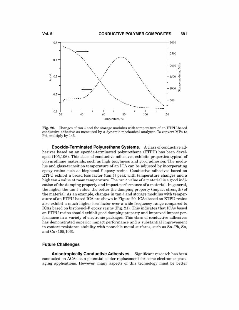
Epoxide-Terminated Polyurethane Systems. A class of conductive ad-hesives based on an epoxide-terminated polyurethane (ETPU) has been devel-oped (105,106). This class of conductive adhesives exhibits properties typical ofpolyurethane materials, such as high toughness and good adhesion. The modu-lus and glass-transition temperature of an ICA can be adjusted by incorporatingepoxy resins such as bisphenol-F epoxy resins. Conductive adhesives based onETPU exhibit a broad loss factor (tan δ) peak with temperature changes and ahigh tan δ value at room temperature. The tan δ value of a material is a good indi-cation of the damping property and impact performance of a material. In general,the higher the tan δ value, the better the damping property (impact strength) ofthe material. As an example, changes in tan δ and storage modulus with temper-ature of an ETPU-based ICA are shown in Figure 20. ICAs based on ETPU resinsalso exhibit a much higher loss factor over a wide frequency range compared toICAs based on bisphenol-F epoxy resins (Fig. 21). This indicates that ICAs basedon ETPU resins should exhibit good damping property and improved impact per-formance in a variety of electronic packages. This class of conductive adhesiveshas demonstrated superior impact performance and a substantial improvementin contact resistance stability with nonnoble metal surfaces, such as Sn–Pb, Sn,and Cu (105,106).
Future Challenges
Anisotropically Conductive Adhesives. Significant research has beenconducted on ACAs as a potential solder replacement for some electronics pack-aging applications. However, many aspects of this technology must be better

682 CONDUCTIVE POLYMER COMPOSITES Vol. 5
Fig. 21. The effect of frequency on the loss factor for two ICA materials.
understood before it can be widely used to replace lead-bearing solders. Somecritical issues that must be addressed in the future are discussed below:
Materials Development. Develop new ACA materials that have good ad-hesion, high Tg, fast curing, storage stability at ambient, and stable contact resis-tance after various conditions frequently encountered in the field such as thermalaging and cycling, thermal shock, high temperature/high humidity/bias, etc. Also,ACAs with low CTE are required. Commercially available ACAs typically exhibitvery high CTEs because of the low filler loading levels utilized. Some preliminarystudies have shown that ACAs with a low CTE created by introducing nonconduc-tive silica fillers have a lower shear strain and better contact resistance stabilityduring thermal cycling test (107).
High Frequency Compatibility. The number of high frequency applicationsand utilizations are increasing rapidly; thus it is important to characterize thecross talk between particles, coupling with semiconductor devices, and other fun-damental behavior of ACAs under high frequency conditions. It is also necessaryto maximize the current carrying capability of ACAs at high frequency range, andafter exposure to various environment tests.
Reliability. It is necessary to understand the effect of the chip carrier ma-terial on ACA join reliability. This is a key issue before ACA technology is widelyutilized in manufacturing (ie in high volume and low cost applications). It is alsonecessary to establish failure rate prediction models for ACA joints for a wide va-riety of field conditions. It is essential to gain full understanding on effects of highcurrent and high power on ACA joints, degradation, and stress relaxation of poly-meric matrices; and the effects of temperature, humidity, and other environmentson matrix materials and the effects of fillers.
Isotropically Conductive Adhesives. There have also been a significantnumber of studies to improve ICA technology. However, several critical issuesassociated with this technology must also be addressed before it can be used as areplacement for soldering technology:

Vol. 5 CONDUCTIVE POLYMER COMPOSITES 683
Electrical Characteristics. The electrical conductivity of ICAs must bevastly improved since their electrical conductivity is typically 1 or 2 orders ofmagnitudes lower than that of solders. Silver-filled ICAs achieve their electri-cal conductivity through a physical contact among the Ag flaks. Because of thehigh particle–particle contact resistance, ICAs exhibit a high bulk resistivity. Al-though some preliminary work has been done to improve electrical conductivityby introducing low-melting-point alloys which form metallurgical interconnetionswith the Ag flakes, additional work is necessary to achieve the desired electricalconductivity. Also, the behavior of ICA joints under high current or high powerconditions, and high temperature/humidity/bias is not clear.
High Frequency Performance. The high frequency behavior of ICAs overa wide frequency range must be investigated and compared to that of solders.
Reliability. Silver-filled ICAs have a potential for silver migration, whichcause electrical shorts especially in fine pitch applications. A palladium-treatedsilver filler exhibited a much improved antimigration characteristics compared tostandard silver-filled ICAs. However, the preparation of the Pd-coated silver parti-cles is expensive. Some low cost approaches must be developed. More comprehen-sive understanding of the fatigue resistance of ICA joints is required. Activitiesin this area have been limited and nonconclusive.
Manufacturability and Yields. Since most commercial ICAs are epoxybased, they are thermosetting materials and thus not reworkable. ICAs with re-workability must be developed by using thermoplastic or thermally degradableresins. Because of their high surface tension, SnPb solders have a self-alignmentcapability during solder reflow operations. However, conventional ICAs cannotself-align. Therefore, components that are bonded using ICAs require a high place-ment accuracy. Some preliminary research has been conducted to improve the self-alignment capability of ICAs (108,109), but much more work needs to be done.
Conductive Polymer Composites with Large Positive TemperatureCoefficient
Conductive polymer composites (110,111) that contain conductive fillers such asmetal powder, carbon black, and other highly conductive particles in a noncon-ductive polymer matrix have been widely used in electrostatic dissipation (ESD)and electromagnetic interference shielding (EMIS). A special group among electri-cally conductive polymer composites are conductive polymer composites that havelarge positive temperature coefficients (PTCs), which in some cases are called pos-itive temperature coefficient resistance. The resistivity of this kind of compositeincreases several orders of magnitude in a narrow temperature range, as shownin Figure 22. The transition temperature (Tt) is defined by intersection betweenthe tangent to the point of inflection of the resistivity versus temperature curveand the horizontal from the resistivity at 25C (ρ25). This kind of smart materialcan change from a conductive material to an insulating material or vice versaupon heating or cooling, respectively. The smartness of this kind of material notonly lies in this large PTC amplitude (defined as the ratio of maximum resistivityat the peak or the resistivity right after the sharp increase to the resistivity at
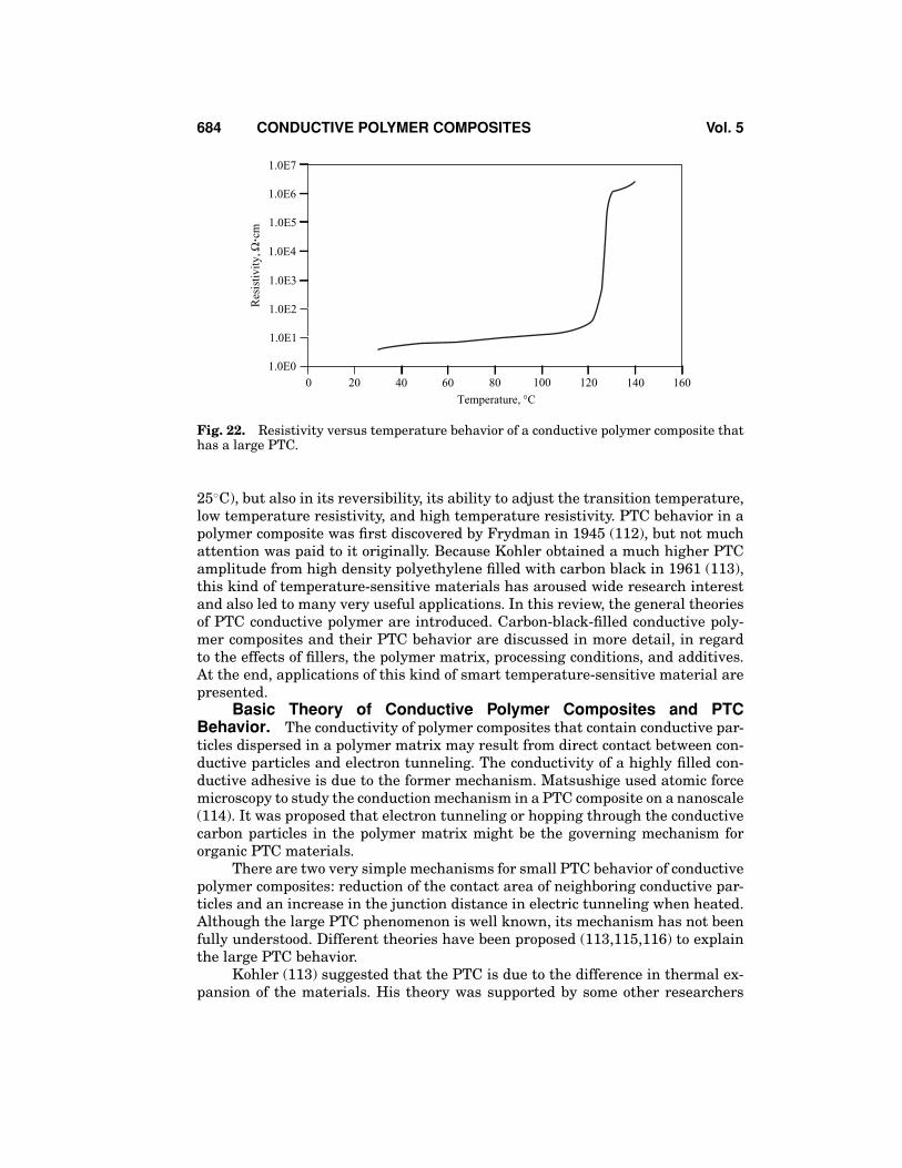
684 CONDUCTIVE POLYMER COMPOSITES Vol. 5
1.0E0
1.0E1
1.0E2
1.0E3
1.0E4
1.0E5
1.0E6
1.0E7
0 20 40 60 80 100 120 140 160
Temperature, °C
Res
istiv
ity,Ω
cm
Fig. 22. Resistivity versus temperature behavior of a conductive polymer composite thathas a large PTC.
25C), but also in its reversibility, its ability to adjust the transition temperature,low temperature resistivity, and high temperature resistivity. PTC behavior in apolymer composite was first discovered by Frydman in 1945 (112), but not muchattention was paid to it originally. Because Kohler obtained a much higher PTCamplitude from high density polyethylene filled with carbon black in 1961 (113),this kind of temperature-sensitive materials has aroused wide research interestand also led to many very useful applications. In this review, the general theoriesof PTC conductive polymer are introduced. Carbon-black-filled conductive poly-mer composites and their PTC behavior are discussed in more detail, in regardto the effects of fillers, the polymer matrix, processing conditions, and additives.At the end, applications of this kind of smart temperature-sensitive material arepresented.
Basic Theory of Conductive Polymer Composites and PTCBehavior. The conductivity of polymer composites that contain conductive par-ticles dispersed in a polymer matrix may result from direct contact between con-ductive particles and electron tunneling. The conductivity of a highly filled con-ductive adhesive is due to the former mechanism. Matsushige used atomic forcemicroscopy to study the conduction mechanism in a PTC composite on a nanoscale(114). It was proposed that electron tunneling or hopping through the conductivecarbon particles in the polymer matrix might be the governing mechanism fororganic PTC materials.
There are two very simple mechanisms for small PTC behavior of conductivepolymer composites: reduction of the contact area of neighboring conductive par-ticles and an increase in the junction distance in electric tunneling when heated.Although the large PTC phenomenon is well known, its mechanism has not beenfully understood. Different theories have been proposed (113,115,116) to explainthe large PTC behavior.
Kohler (113) suggested that the PTC is due to the difference in thermal ex-pansion of the materials. His theory was supported by some other researchers
Vol. 5 CONDUCTIVE POLYMER COMPOSITES 685
in percolation theory (110). The conductivity of conductive polymer compositesincreases as the volume fraction of the conductive filler increases. For a polymerfilled with conductive particles, a critical volume fraction of filler may exist, whichis called the percolation volume fraction. The resistance of the conductive poly-mer composite whose filler volume fraction is higher than the percolation volumefraction is several orders of magnitude less than that of the composite whose fillervolume faction is less than the percolation volume fraction. In the region of lowfiller concentration, the filler particles are distributed homogeneously in the insu-lating polymer matrix. There is no contact between adjacent filler particles. Theresistance decreases slowly as the volume fraction of filler particles increases. Asthe filler concentration further increases, filler particles begin to contact other par-ticles and agglomerate. At a certain filler concentration, the growing agglomeratesform one-, two-, or three-dimensional network of the conducting phase within theinsulating polymer matrix. At this range, the resistivity of the mixture shows adeep decrease to the low value of the conductive network. After the formation ofthe continuous conductive network, the resistivity of the mixture increases slowlybecause of the slightly improved quality of the conductive network as the fillercontent increases.
Many models have been proposed (117) to explain the electrical conductivityof mixtures composed of conductive and insulating materials. Percolation concen-tration is the most interesting of all of these models. Several parameters, such asfiller distribution, filler shape, filler/matrix interactions, and processing technique,can influence the percolation concentration. Among these models, the statisticalpercolation model (118) uses finite regular arrays of points and bonds (betweenthe points) to estimate percolation concentration. The thermodynamic model (119)emphasizes the importance of interfacial interactions at the boundary between in-dividual filler particles and the polymeric host in the network formation. The mostpromising ones are the structure-oriented models, which explain conductivity onthe basis of factors determined from the microlevel structure of the as-producedmixtures (120).
Because the thermal expansion coefficient of a polymer matrix is generallyhigher than that of the conductive particles, the volume fraction of a conductivefiller in conductive polymer composite decreases as temperature increases; thus,the resistivity increases. If a conductive polymer composite is made of semicrys-talline polymer as an insulator and a filler of conducting particles, whose concen-tration is just above the percolation volume fraction, the relatively large changein specific volume of the polymer at its melting temperature may bring the volumefraction of the conductive filler down below the critical volume fraction when thecomposite is heated beyond the melting temperature of the polymer crystal. Thus,the resistivity increases greatly. Kohler’s theory cannot explain the very smallrise in resistance exhibited by such filled polymer systems when they are strainedto an amount equivalent to that found at the crystalline melting point. And thePTC amplitude should be a direct function of volume change according to Kohler’stheory; however, it is not the case in reality.
Ohe proposed a more complex theory (115). He stated that PTC phenomenoncould be explained by the increase of the intergrain gap among the carbon blackparticles caused by thermal expansion. He visualized that the distribution of theintergrain gaps in conductive composite is rather uniform at low temperature,
686 CONDUCTIVE POLYMER COMPOSITES Vol. 5
and the gap is small enough for extensive tunneling to occur, but the distributionat high temperature becomes random due to thermal expansion. Although theaverage gap distance does not change greatly, the presence of a significant amountof gap distance too large to allow electron tunneling will result in a great increasein resistance.
Meyer’s theory was based on the assumption that a thin (300 A) crystallinefilm of polymer is much more conductive than an amorphous film of polymer. Itwas shown that carbon black particles remain in the amorphous region betweencrystallites in a conductive composite. The high conductivity at low temperature isdue to tunneling through the thin crystallite, and the PTC phenomenon is causedby a preliminary change in state of these crystallites just before the crystallinemelting point that leads to a sharp reduction in the ease of tunneling and thusmuch higher resistivity.
Large thermal expansion during crystal melting surely contributes to a largeamplitude of PTC behavior. But it contributes only to a limited level. Ohe’s visionof the change from uniform distribution of carbon particle to random distributionis groundless and cannot be justified. Actually, as is shown later, cross-linkingcan eliminate the redistribution of carbon black after melting and stabilizes PTCbehavior. PTC behavior takes place at the same time as melting, rather than beforecrystalline melting, as stated by Meyer. It probably is true that tunneling is easierin a crystalline region than in an amorphous region. The difference is probablydue to polymer chain mobility. The work function of the conductive particle at theinterface between the conductive particle and polymer matrix may increase aftercrystal melting due to the high mobility of the polymer chain. The same theory canexplain PTC behavior in conductive polymer composites as well as the conductivityphenomenon in an ECA after curing (80). Before conductive adhesive is cured,the resin matrix has high mobility and prohibits tunneling between conductiveparticles. After curing, the mobility of the polymer chain is greatly reduced andthus allows tunneling between conductive particles.
Effect of Conductive Fillers on PTC Conductive Polymer. Differentconductive fillers have been used as in PTC conductive polymers. Metallic powdersthat are stable at high temperature, such as tin, gold, and silver, were suggestedas conductive fillers in PTC materials (121). In addition, ceramic powder such astungsten carbide was also used as a filler in PTC conductive polymer composites(122). It was found that V2O3 has several phase transitions (110). At 160 K, it istransformed from an antiferromagnetic insulator (AFI) to a paraelectric metallicconductor (PMC), accompanied by a resistivity change from 105 to 10− 2 ·cm.At 400 K, it changes from a PMC to a PI (paraelectric insulator) whose resis-tivity is 103 – 104 ·cm. Most interestingly, low density polyethylene filled withV2O3 shows a square well in the resistivity versus temperature profile by combin-ing a sharp NTC (negative temperature coefficient) around −110C, and a sharpPTC around 100C (110,123–125). A PTC transition temperature of conductivepolymer composites filled with V2O3 was also reported in other polymer system(121,122). The Tt of a V2O3-filled system changes in the following manner: 100C(low density polyethylene) < 150C (polypropylene) < 260C (polytetrafluoroethy-lene). However, the fillers mentioned before are expensive. Work has been doneto develop alternative less expensive PTC conductive polymer composites. Most

Vol. 5 CONDUCTIVE POLYMER COMPOSITES 687
of the conductive polymers for ESD and EMIS applications are thermoplasticsfilled with carbon black or carbon graphite because of their very low cost. Carbonblack is also one of the major fillers used in so-called PTC conductive polymers(126–128).
There are several important parameters of carbon black (129): particle size(surface area), aggregate structure (carbon black particles aggregate to form agrapelike structure), porosity, crystallinity, and surface functionality. Small par-ticle size and high structure lead to more difficult dispersion. The initial grape-like structure of carbon black formed during the manufacturing of carbon blackis highly stable and can be destroyed only by very intensive processing such asgrinding in a ball mill. For a given loading of carbon black, a smaller particlesize would add more particles to the composite than that using carbon black oflarger particle size. Thus, carbon blacks of smaller particle size would produce acomposite that has a smaller separation between carbon particles (as well as theprobability of more carbon particles in contact), resulting in greater conductivity.Small particle size gives a low critical volume for a carbon-black-filled polymer sys-tem (110). However, for fiberlike conductive fillers, large filler particles favor theformation of conducting paths at a low percolation concentration. High structurecarbon blacks tend to produce a larger number of aggregates in contact, as well assmaller separation distances that result in greater conductivity. For a given carbonblack loading, the more porous carbon black generally provides a larger numberof aggregates to the composite. This results in a smaller interaggregate distanceand higher conductivity. The increase in the degree of carbon black structuringis found more efficient than the increase of the specific surface of carbon blackin conductive polymers. Carbon blacks that have higher oxygen content carbonparticles have higher resistance. Removal of the surface oxides increases the con-ductivity of the original carbon black much more than heat treatment to producegraphitization. Higher graphite content in carbon black leads to higher electricalconductivity.
Although carbon black of small particles size and high aggregated structure(such as BP2000 with a average particle diameter of 12 nm manufactured by CabotCorp.) can give polymer composites that have low resistivity, this kind of compositedoes not show large PTC amplitude because the aggregated structure cannot bebroken down by the thermal expansion of the polymer (Fig. 23). On the contrary,a polymer composite filled with carbon black that has a large particle size and lowaggregate structure (such as N660 with an average particle diameter of 70 nmmanufactured by Columbia Chemicals) shows high room temperature resistivity,but high PTC amplitude (130). To obtain a PTC conductive polymer composite thathas both lower room temperature resistance and high PTC transition amplitude,porous carbon black is much better than nonporous carbon black. Ueno and co-workers reported that etching a carbon black at an elevated temperature to removethe less crystalline portion and therefore to increase the surface area can improvethe PTC characteristics of a conductive polymer filled with carbon black, and thismaterial was suitable for use as a resettable fuse (126).
The PTC amplitude depends on the loading of carbon black. It was shown thatfor different carbon blacks, a different loading exists at which the composite hasa maximum PTC amplitude (131). The carbon black concentration that gives the

688 CONDUCTIVE POLYMER COMPOSITES Vol. 5
1.0E0
1.0E1
1.0E2
1.0E3
1.0E4
1.0E5
1.0E6
1.0E7
1.0E8
0 20 40 60 80 100 120 140 160
Temperature, °C
1.0E9
Res
istiv
ity,Ω
cm
Fig. 23. Resistivity versus temperature of conductive polymer composite with differentcarbon blacks (the weight percentage of carbon black is 30). —— Filled with BP2000 carbonblack; - - - - filled with N660 carbon black.
optimum PTC intensity can be predicted approximately from room temperaturedata (132).
Effect of Polymer Matrix on PTC Behavior. Polymers used as the ma-trix in electrically conductive polymer composites can vary from elastomers tothermoplastics and thermosets that have crystallinity varying between 0 and 80%.As mentioned in the previous section, the large PTC anomaly is due to the largethermal expansion of the polymer matrix, especially during melting of a polymercrystal. The PTC transition temperature is determined by the melting point ofthe polymer matrix. Because polymers that have low and high melting points areavailable for use in conductive polymer composites, the transition temperaturecan be controlled by selecting and compounding the matrix polymer for differentapplications that require different transition temperatures (133). A PTC conduc-tive composite based on high density polyethylene whose melting peak temper-ature is 129–131C and whose specific volume increases by approximately 10%due to melting across a narrow temperature range showed a maximum resistiv-ity at 129–131C (130). The transition temperature can be slightly adjusted byusing a copolymer or polymer blend that has more than one homopolymer. A com-pound of 40 parts weight of carbon black, 60 parts of melted olefin copolymer(ethylene–ethyl acrylate copolymer), and an organic peroxide, had a Tt of 82C(114). Another reported recipe (134) is a composite of carbon black dispersed inhigh density polyethylene and poly(ethylene vinyl acetate), whose Tt is 120C.Ultrahigh molecular weight polyethylene reportedly enhanced the PTC behav-ior (127). Thermosetting material such as thermosetting polyester resin that wascross-linked by a free-radical reaction, was also reportedly used as a polymer ma-trix for a PTC conductive polymer composite (135).
The PTC amplitude depends on crystallinity. Meyer (136) showed that crys-talline trans-polybutadiene filled with carbon black has low room temperatureresistivity and a significant anomaly, whereas the amorphous cis-polybutadienefilled with the same amount of carbon black has much higher resistivity and no

Vol. 5 CONDUCTIVE POLYMER COMPOSITES 689
1.0E0
1.0E1
1.0E2
1.0E3
1.0E4
1.0E5
1.0E6
1.0E7
0 20 40 60 80 100 120 140 160
Temperature, °C
Res
istiv
ity,Ω
cm
Fig. 24. Resistivity versus temperature for a PTC conductive polymer composite duringheating and cooling cycles. —— Heating; - - - - cooling.
anomaly. Within a polymeric family, a polymer that is more crystalline has higherPTC amplitude. But different classes of polymers that have the same crystallinitydo not exhibit identical PTC behavior and no relationship was correlated. PTCamplitude depends on polymer type. PTC amplitude increases in the following or-der with respect to the polymer matrix: nylon-6,6 < polypropylene < polyethyleneoxide < low density polyethylene < high density polyethylene.
As mentioned before, the mechanism for the PTC anomaly in semicrystallinepolymer composites is accompanied by a relatively large change in specific volumeof the polymer at its melting temperature. The resistivity versus temperaturecurve can be well matched by the specific volume–temperature curve. Crystal-lization during cooling of a polymer is the reverse of melting of polymer crystalduring heating. The PTC transition of this kind of smart material is reversible.During cooling, the same material shows a sharp decrease in resistivity, as shownby Figure 24. The thermal expansion of a polymer depends on its heating and cool-ing cycle. Because the melting temperature of a polymer crystal is always higherthan the recrystallization temperature, the PTC transition of a conductive poly-mer composite is always higher in the heating cycle than that during the coolingcycle (110). The difference is about 18C for polyethylene, 34C for polyoxymethy-lene, and 50C for polypropylene. Actually, all factors that affect the melting andrecrystallization behavior, such as pressure and heating and cooling rates, influ-ence the PTC behavior of a conductive polymer composite. Meyer showed thatthe PTC transition temperature increases and PTC amplitude decreases as thepressure increases (136).
In some conductive polymer composites, the NTC effect follows, for example,the resistivity decreases as the temperature increases further after PTC tran-sition. The NTC effect is probably due to the reorientation, reaggregation, or re-assembling of carbon black. Initially dispersed particles may become mobile in thetemperature range of polymer melting to repair the broken percolation network.The measurement of resistance versus the temperature behavior of the conductive
690 CONDUCTIVE POLYMER COMPOSITES Vol. 5
composite was repeated for the same sample(134,137). Tang (134) observed thatthe PTC intensity and the base resistance decrease with thermal cycles. The rea-son is obviously reorganization of carbon at the high temperature.
Radiation was used to cross-link a carbon-black-filled conductive polymercomposite. The NTC effect can be alleviated or reduced by cross-linking, and thePTC amplitude is stabilized (the resistance at lower temperature is stabilized)after cross-linking (110,134). The organization of carbon black is hampered in across-linked polymer network.
Effect of Processing Conditions and Additives. The effect of mixingtime on the resistivity–temperature behavior was also investigated (134). Boththe PTC effect and the reproducibility were improved greatly when the samplewas mixed for a long time. It was suggested that the improvement is due to in-creasing absorption of the polymer on the carbon black surface and this absorptionforms a polymer layer outside the carbon black particle. The room temperatureresistivity increases with mixing time at constant carbon black concentration.It can also be explained that structures are broken down during mixing; thus,the resistivity increases. If the power consumption during mixing is too high, thecomposition would have too high resistivity at a temperature below Tg and haveunsatisfactory electrical stability on aging at elevated temperature. If the powerconsumption is too low, it can also result in a composition that has a low PTCamplitude.
Tang (134) studied the effect of the interaction between carbon black andthe polymer on electrical behavior. The absorption of polymer on the carbon blacksurface may be physical or chemical. The latter is caused by free-radical reactionbetween the polymer and carbon black, and it can occur during radiation or thepreparation of the composite. In carbon-black-filled high density polyethylene, thecross-linked network of the polymer restricts the freedom of movement of carbonblack. The free-radical reaction enhances the binding force between the polymerand carbon black.
Polymeric materials may be broken down under high voltage. The voltagestability of a cross-linked PTC conductive polymer is improved by incorporating apolymerizable monomer such as triallyisocyanurate before it is cross-linked (138).Antimony oxide, which does not degrade the PTC characteristics, can be usedas a flame-retardant agent (121). A semiconductive inorganic substance such assilicon carbide or boron carbide was used to improve the high voltage stability(139). Alumina trihydrate can be added to a PTC conductive polymer compositeto prevent dielectric breakdown, arcing, and carbon tracking under high voltage(138).
Application of PTC Conductive Polymer Composite. There are manyapplications for PTC conductive polymer composites, including thermistors (122),circuit protection devices (140), and self-regulating heaters (141). Because thematerial both heats and controls the temperature, it can be used to manufacturea self-regulating heating device. As the temperature increases, the resistance in-creases, and thus the power decreases. This kind of self-regulating heater can beused to prevent freezing of water and pipes used in chemical processing. It hasalso been used to manufacture a heater for heating a hot-melt adhesive to seal acable splice case (142) as well as a hair curler (143). Self-regulating heaters can be
Vol. 5 CONDUCTIVE POLYMER COMPOSITES 691
manufactured into different forms. The blanket form of PTC conductive polymercomposite can allow precise temperature control across larger areas. This kindof device has been used in the repair of thermally complex aircraft structures(141,144).
Another application of PTC conductive polymers is in over-temperature andover-current protection. A device manufactured from a PTC conductive polymercomposite has low resistance and much less resistance than the rest of the circuit;thus it has no influence on normal performance. But at high temperature, thesedevices become highly resistant or insulating; thus they dominate the circuit, re-duce the current, and protect the circuit. For large abnormal current, the devicecan rapidly self-heat to a high resistance state, and thus reduces the current. Thesmartness lies in the over-temperature and over-current protection and also liesin its resettability. After the current drops and the temperature of the device de-creases, the device returns to a low resistance state and allows current to pass.A resettable fuse made from a PTC conductive polymer has been on the mar-ket. This kind of resettable fuse has been used in battery chargers to terminatethe charging function based on the battery temperature and protect the batteryfrom overheating. It is also used in telecommunication equipment, computers, andpower supplies.
Summary. A temperature-sensitive PTC conductive polymer composite isa true smart material. Its property can be tailored by the selecting filler, polymermatrix, and processing conditions. Its transition temperature is determined bythe melting point of the polymer matrix. Its room-temperature resistivity, hightemperature resistivity, and PTC transition amplitude can be adjusted by thefiller and its combination with the polymer matrix. PTC transition behavior canbe stabilized by cross-linking of the polymer matrix. This kind of smart materialcan be used in many temperature-sensitive applications such as thermistors, self-regulating heaters, and circuit protection devices.
BIBLIOGRAPHY
1. U.S. Pat. 2,774,747 (1956), H. Wolfson and G. Elliot.2. U.S. Pat. 2,849,631 (1958), K. R. Matz.3. U.S. Pat. 2,866,057 (1958), D. P. Beck.4. K. Gilleo, Soldering Surface Mount Technol. (19), 12–17 (Feb. 1995).5. P. G. Hariss, Soldering Surface Mount Technol. (20), 19–21 (May 1995).6. A. O. Ogunjimi, O. Boyle, D. C. Whalley, and D. J. Williams, J. Electron. Manuf. 2,
109–118 (1992).7. S. Asai, U. Saruta, M. Tobita, M. Takano, and Y. Miyashita, J. Appl. Polym. Sci. 56,
769–777 (1995).8. D. D. Chang, P. A. Crawford, J. A. Fulton, R. McBride, M. B. Schmidt, R. E. Sinitski,
and C. P. Wong, IEEE Trans. Components Hybrids Manuf. Technol. 16, 320–326 (Dec.1993).
9. Eur. Pat. 0 147 856 (1985), H. Ando, N. Kobayashi, H. Numao, Y. Matsubara, andK. Suzuki.

692 CONDUCTIVE POLYMER COMPOSITES Vol. 5
10. Eur. Pat. 0 265 077 (1987), K. Gilleo.11. U.S. Pat. 5,136,365 (1992), R. Pennisi, M. Papageorge, and G. Urbisch.12. H. Date, Y. Hozumi, H. Tokuhira, M. Usui, E. Horikoshi, and T. Sato, in Proceedings
of ISHM’94, Bologna, Italy, Sept. 1994, pp. 570–575.13. J. Liu, in Proceedings of 4th International Conference on Adhesive Joining and
Coating Technology in Electronics Manufacturing, Helsinki, Finland, June 2000,pp. 1–15.
14. C. M. L. Wu, J. Liu, and N. H. Yeung, in Proceedings of 4th International Conferenceon Adhesive Joining and Coating Technology in Electronics Manufacturing, Helsinki,Finland, June 2000, pp. 101–106.
15. Y. Kishimoto and K. Hanamura, in Proceedings of 3rd International Conference onAdhesive Joining and Coating Technology in Electronics Manufacturing, Binghamton,New York, Sept. 1998, pp. 137–143.
16. U.S. Pat. 4999460 (Mar. 12, 1991) (to Casio).17. U.S. Pat. 5123986 (June 23, 1992) (to Casio).18. U.S. Pat. 5180888 (Jan. 19, 1993) (to Casio).19. R. Nagle, Int. J. Microelectron. Packag. 1, 187–196 (1998).20. J. K. Kivilahti, in J. Liu, ed., Conductive Adhesives for Electronics Packag-
ing, Electrochemical Publications Ltd., Port Erin, British Isles, 1999, pp. 153–183.
21. M. Vuorela, M. Holloway, S. Fuchs, F. Stam, and J. Kivilahti, in Proceedings of 4thInternational Conference on Adhesive Joining and Coating Technology in ElectronicsManufacturing, Helsinki, Finland, June 2000, pp. 147–152.
22. R. Sihlbom, M. Dernevik, Z. Lai, J. P. Starski, and J. Liu, IEEE Trans. Components,Packag. Manuf. Technol., Part A 20, 469–477 (Sept. 1998).
23. M. Dernevik, R. Sihlbom, K. Axelsson, Z. Lai, J. Liu, and P. Starski, in Proceedings of48th IEEE Electronic Components and Technology Conference, Seattle, Washington,D.C., May 1998, pp. 1026–1030.
24. M. J. Yim, W. Ryu, Y. D. Jeon, J. Lee, J. Kim, and K. Paik, in Proceedings of 49thElectronic Components and Technology Conference, San Diego, Calif., May 1999,pp. 488–492.
25. K. Gustafsson, S. Mannan, J. Liu, Z. Lai, D. Whalley, and D. Williams, in Proceedingsof 47th Electronic Components and Technology Conference, San Jose, Calif., May1997, pp. 561–566.
26. H. Hirai, T. Motomura, O. Shimada, and Y. Fukuoka, in Proceedings of Internationalsymp on Electronic Materials and Packaging, Hong Kong, China, Nov.–Dec. 2000,pp. 1–6.
27. Y. Hotta, M. Maeda, F. Asai, and F. Eriguchi, in Proceedings of 48th IEEE Elec-tronic Components and Technology Conference, Seattle, Washington, D.C., May 1998,pp. 1042–1046.
28. G. Connell, R. L. D. Zenner, and J. A. Gerber, in Proceedings of 47th ElectronicComponents and Technology Conference, San Jose, Calif., May 1997, pp. 274–278.
29. K. M. Kim, in Proceedings of 50th Electronic Components and Technology Conference,Las Vegas, Nev., May 2000, pp. 1122–1132.
30. L. Li and T. Fang, in Proceedings of 4th International Conference on Adhesive Joiningand Coating Technology in Electronics manufacturing, Helsinki, Finland, June 2000,pp. 129–135.
31. A. Ogunjimi, S. Mannan, D. Whalley, and D. Williams, IEEE Trans. ComponentsPackag. Manuf. Technol., Part C 19, 257–263 (Oct. 1996).
32. J. Liu, L. Ljungkrona, and Z. Lai, IEEE Trans. Components Packag. Manuf. Technol.,Part B 18, 313–319 (May 1995).

Vol. 5 CONDUCTIVE POLYMER COMPOSITES 693
33. J. Liu, Circuit World 19(4), 4–15 (1993).34. Y. C. Chan, K. C. Hung, C. W. Tang, and C. M. L. Wu, in Proceedings of 4th In-
ternational Conference on Adhesive Joining and Coating Technology in Electronicsmanufacturing, Helsinki, Finland, June 2000, pp. 141–146.
35. H. Kristiansen and J. Liu, IEEE Trans. Components Packag. Manuf. Technol., Part A21, 208–214 (June 1998).
36. P. B. Jana, S. Chaudhuri, A. K. Pal, and S. K. De, Polym. Eng. Sci. 32, 448–456 (Mar.1992).
37. A. Malliaris and D. T. Tumer, J. Appl. Phys. 42, 614–618 (1971).38. G. R. Ruschau, S. Yoshikawa, and R. E. Newnham, J. Appl. Phys. 73, 953–959
(1992).39. J. C. Jagt, IEEE Trans. Components Packag. Manuf. Technol., Part A 21, 215–225
(1998).40. M. A. Lutz and R. L. Cole, Hybrid Circuits (23), 27–30 (Sept. 1990).41. J. M. Pujol, C. Prudhomme, M. E. Quenneson, and R. Cassat, J. Adhesn. 27, 213–229
(1989).42. J. Ivan, J. Gonzales, and M. G. Mena, in Proceedings of 47th Electronic Components
and Technology Conference, San Jose, Calif., May 1997, pp. 525–535.43. I. Y. Chien and M. N. Nguyen, in Proceedings of 1994 Electronic Components and
Technology Conference, San Diego, Calif., May 1994, pp. 580–584.44. D. P. Galloway, M. Grosse, M. N. Nguyen, and A. Burkhart, in Proceedings
of the IEEE/CPMT International Electronic Manufacturing Technology (IEMT)Symposium, Austin, Tex., Oct. 1995, pp. 141–147.
45. S. M. Pandiri, Adhesiv. Age 31–35 (Oct. 1987).46. B. Gunther and H. Schafer, in Proceedings of the 2nd International Conference on
Adhesive Joining and Coating Technology in Electronics Manufacturing, Stockholm,Sweden, June 1996, pp. 55–59.
47. S. Kotthaus, R. Haug, H. Schafer, and B. Gunther, in Proceedings of the 2nd In-ternational Conference on Adhesive Joining and Coating Technology in ElectronicsManufacturing, Stockholm, Sweden, June 1996, pp. 14–17.
48. P. K. Pramanik, D. Khastgir, S. K. De, and T. N. Saha, J. Mater. Sci. 25, 3848–3853(1990).
49. A. Yokoyama, T. Katsumata, A. Fujii and T. Yoneyama, in IMC 1992 Proceedings,1992, pp. 376–38.
50. S. K. Kang, R. Rai, and S. Purushothaman, in Proceedings of 47th Electronic Compo-nents and Technology Conference, San Jose, Calif., May 1997, pp. 565–570.
51. S. K. Kang, R. Rai, and S. Purushothaman, IEEE Trans. Components Packag. Manuf.Technol., Part A 21(1), 18–22 (Mar. 1998).
52. J. Lin, J. Drye, W. Lytle, T. Scharr, R. Subrahmanyan, and R. Sharma, in Proceedingsof 46th Electronic Components and Technology Conference, Orlando, Fla., May 1996,pp. 1059–1068.
53. R. H. Estes, in Proceedings of 3rd International Conference on Adhesive Joiningand Coating Technology in Electronics Manufacturing, Binghamton, New York, Sept.1998, pp. 229–239.
54. K. E. Oh, IEEE J. Selected Top. Quantum Electron. 5(1), 119–126 (Jan.–Feb.1999).
55. M. Gaynes, R. Kodnani, M. Pierson, P. Hoontrakul, and M. Paquette, in Proceed-ings of 3rd international Conference on Adhesive Joining and Coating Technol-ogy in Electronics Manufacturing, Binghamton, New York, Sept. 1998, pp. 244–251.
56. Y. Bessho, in Proceedings of International Microelectronics Conference, May 1990,pp. 183–189.
694 CONDUCTIVE POLYMER COMPOSITES Vol. 5
57. J. B. Nysaether, Z. Lai, and J. Liu, in Proceedings of 3rd International Conference onAdhesive Joining and Coating Technology in Electronics Manufacturing, Binghamton,New York, Sept. 1998, pp. 125–131.
58. H. H. Manko, Solders and Soldering, Materials, Design, Production, and Analysis forReliable Bonding, 2nd ed., McGraw-Hill, New York, 1979.
59. K. Brindley and M. Judd, Soldering in Electronic Assembly, 2nd ed., Butterworth-Heinemann, Woburn, Mass., Mar. 1999.
60. R. Tummala, E. Rymaszeski, and A. Klopfenstein, Microelectronics Packaging Hand-book, 2nd ed., Kluwer Academic Publishers, Boston, 1997.
61. L. P. Lambert, Soldering for Electronic Assemblies, Marcel Dekker, New York, Oct.1987.
62. B. Trumble, IEEE Spectrum 55–60 (May 1998).63. B. T. Alpert and A. J. Schoenberg, Electron. Packag. Prod. 130–132 (Nov.
1991).64. R. Cdenhead and D. DeCoursey, Int. J. Microelectron. 8(3), 14 (1985).65. G. Nguyen, J. Williams, F. Gibson, and T. Winster, in Proceedings of Interna-
tional Electronic Packaging Conference, San Diego, Calif., Sept. 1993, pp. 479–486.
66. J. C. Jagt, P. J. M. Beric, and G. F. C. M. Lijten, IEEE Trans. Components, Packag.Manuf. Technol., Part B 18, 292–298 (1995).
67. M. Zwolinski, J. Hickman, H. Rubon, and Y. Zaks, in Proceedings of the 2nd In-ternational Conference on Adhesive Joining and Coating Technology in ElectronicsManufacturing, Stockholm, Sweden, June 1996, pp. 333–340.
68. H. Botter, in Proceedings of the 2nd International Conference on Adhesive Joiningand Coating Technology in Electronics Manufacturing, Stockholm, Sweden, June 3–5,1996, pp. 30–37.
69. C. P. Wong, D. Lu, S. Vona, and Q. K. Tong, in Proceedings of the 1st IEEE Interna-tional Symposium on Polymeric Electronics Packaging, Norrkoping, Sweden, 1997,pp. 80–85.
70. J. Bolger and S. Morano, Adhesiv. Age 17–20 (June 1984).71. H. Takezawa, M. Itagaki, T. Mitani, Y. Bessho, and K. Eda, in Proceedings of 4th
International Symposium and Exhibition on Advanced Packaging Materials, Pro-cesses, Properties and Interfaces, Braselton, Ga., Mar. 1999, pp. 11–15.
72. J. Felba, K. P. Friedel, and A. Moscicki, in Proceedings of 4th International Conferenceon Adhesive Joining and Coating Technology in Electronics manufacturing, Helsinki,Finland, June 2000, pp. 232–239.
73. S. Liong, Z. Zhang, and C. P. Wong, in Proceedings of 51th ElectronicComponents and Technology Conference, Orlando, Fla., May 2001, pp. 1236–1240.
74. J. H. Constable, T. Kache, H. Teichmann, S. Muhle, and M. A. Gaynes, IEEE Trans.Components Packag. Technol. 22(2), 191–199 (June 1999).
75. R. Gomatam, E. Sancaktar, D. Boismier, D. Schue, and I. Malik, in Proceedings of4th International Symposium and Exhibition on Advanced Packaging Materials, Pro-cesses, Properties and Interfaces, Braselton, Ga., Mar. 2001, pp. 6–12.
76. L. Smith-Vargo, Electron. Packag. Prod. 48–49 (Aug. 1986).77. E. M. Jost and K. McNeilly, in Proceedings of ISHM, Bournemouth, England, June
1987, pp. 548–553.78. D. Lu, Q. K. Tong, and C. P. Wong, IEEE Trans. Components Packag. Manuf. Technol.,
Part A 22, 365–371 (1999).79. D. Lu, Q. Tong, and C. P. Wong, in Proceedings of 4th International Symposium and
Exhibition on Advanced Packaging Materials, Processes, Properties and Interfaces,Braselton, Ga., Mar. 1998, pp. 256–260.

Vol. 5 CONDUCTIVE POLYMER COMPOSITES 695
80. A. J. Lovinger, J. Adhesn. 10, 1–15 (1979).81. D. Lu, Q. K. Tong, and C. P. Wong, IEEE Trans. Components Packag. Manuf. Technol.,
Part C 22, 223–227 (1999).82. J. Morris and C. Cook, in Proceedings of 2nd IEEE International Symposium on Poly-
meric Electronic Packaging, Gothenburg, Sweden, Oct. 1999, pp. 15–26.83. C. Gallagher, G. Matijasevic, and J. F. Maguire, in Proceedings of 47th Electronic
Components and Technology Conference, San Jose, Calif., May 1997 pp. 554–560.
84. J. W. Roman and T. W. Eagar, in Proceedings of ISHM, San Francisco, Calif., Oct.1992, pp. 52–57.
85. U.S. Pat. 5863622 (Aug. 1998), C. Gallagher, G. Matijasevic, and A. Capote.86. K. Gilleo, Circuits Assembly 50–51 (1994).87. K. Gilleo, Circuits Assembly 51–53 (1994).88. D. Lu, Q. K. Tong, and C. P. Wong, IEEE Trans. Components Packag. Manuf. Technol.,
Part C 22, 228–232 (1999).89. Q. K. Tong, G. Fredrickson, R. Kuder, and D. Lu, in Proceedings of the 49th Elec-
tronic Components and Technology Conference, San Diego, Calif., May 1999, pp. 347–352.
90. D. Lu and C. P. Wong, J. Appl. Polym. Sci. 74, 399–406 (1999).91. D. Lu and C. P. Wong, in Proceedings of 4th International Symposium and Exhibition
on Advanced Packaging Materials, Processes, Properties and Interfaces, Braselton,Ga., Mar. 1999, pp. 288–294.
92. U.S. Pat. (Mar. 1999), Q. K. Tong, A. Xiao, and D. Lu.93. H. Leidheiser Jr., J. Coat. Technol. 53(678), 29–39 (1981).94. G. Trabanelli and V. Carassiti, in M. G. Fontana and R. W. Staehle, eds., Advanced
Corrosion Science and Technology, Vol. 1, Plenum Press, New York, 1970, pp. 147–229.
95. G. Trabanelli, in F. Mansfeld, ed., Corrosion Mechanisms, Marcel Dekker, New York,1987, pp. 119–164.
96. O. L. Riggs Jr., in C. C. Nathan, ed., Theoretical Aspects of Corrosion Inhibitorsand Inhibition, National Association of Corrosion Engineers, Houston, Tex., 1973,pp. 2–27.
97. P. A. Reardon, in Corrosion’86 (Paper No. 175), National Association of CorrosionEngineers, Houston, Tex., 1986.
98. M. G. Noack, in Corrosion’89 (Paper No. 436), National Association of CorrosionEngineers, Houston, Tex., 1989.
99. P. A. Reardon and W. E. Bernahl, Corrosion’87 (Paper No. 438), National Associationof Corrosion Engineers, Houston, Tex., 1987.
100. S. Romaine, in Proceedings of the American Power Conference, Chicago, Ill., Apr.1986, pp. 1066–1073.
101. U.S. Pat. 5180523 (Nov. 1989), D. Durand, D. Vieau, A. L. Chu, and T. S. Weiu.102. S. Macathy, in Proceedings of Surface Mount International, San Jose, Calif., Aug.
1995, pp. 562–567.103. S. A. Vona and Q. K. Tong, in Proceedings of 4th International Symposium and
Exhibition on Advanced Packaging Materials, Processes, Properties and Interfaces,Braselton, Ga., Mar. 1998, pp. 261–267.
104. J. Liu and B. Weman, in Proceedings of the 2nd International Symposiumon Electronics Packaging Technology, Shanghai, China, Dec. 1996, pp. 313–319.
105. D. Lu and C. P. Wong, IEEE Trans. Components Packag., Manuf. Technol. Part C 22,324–330 (1999).

696 CONDUCTIVE POLYMER COMPOSITES Vol. 5
106. D. Lu and C. P. Wong, Encyclopedia of Smart Materials, John Wiley & Sons, Inc., NewYork, in press.
107. M. Yim and K. Paik, IEEE Trans. Components Packag. Manuf. Technol. 24(1), 24–32(Mar. 2001).
108. J. Wu, K. Moon, and C. P. Wong, in Proceedings of 51st Electronic Components andTechnology Conference, Orlando, Fla., May 2001, pp. 571–575.
109. K. Moon, J. Wu, and C. P. Wong, in Proceedings of International Symposium onAdvanced Packaging Materials: Processes, Properties and Interfaces, Braselton, Ga.,Mar. 2001, pp. 341–346.
110. X. Yi, G. Wu, and Y. Pan, Polym. Int. 44, 117 (1997).111. V. E. Gul, Structure and Properties of Conducting Polymer Composites, VSP BV, the
Netherlands, (1996).112. U.K. Pat. 604,695 (1945), E. Frydman.113. U.S. Pat. 3,243,753 (1961), F. Kohler.114. K. Matsushige, K. Kobayashi, N. Iwami, T. Horiuchi, E. Shitamori, and M. Itoi, Thin
Solid Films 273, 128 (1996).115. K. Ohe and Y. Naito, Jpn. J. Appl. Phys. 10, 99 (1971).116. J. Meyer, Polym. Eng. Sci. 14, 706 (1974).117. F. Lux, J. Mater. Sci. 28, 285 (1993).118. R. Zallen, The Physics of Amorphous Solids, John Wiley & Sons, Inc., New York, 1983,
Chapt. “4”.119. M. Sumita, K. Sakata, S. Asai, K. Miyasaka, and H. Nakagawa, Polym. Bull. 25, 265
(1991).120. K. Yoshida, J. Phys. Soc. Jpn. 59, 4087 (1990).121. U.S. Pat. 3,673,121, J. Meyer.122. U.S. Pat. 5,793,276, H. Tosaka, M. Takaya, S. Moriya, H. Kobuke, and M. Hamada.123. K. A. Hu, J. Runt, A. Safari, and R. E. Newnham, Ferroelectrics 68, 115
(1986).124. Y. Pan and G. Z. Wu, J. Zhejiang Univ. 4, 613 (1994).125. M. Narkis, A. Ram, and F. Flashner, J. Appl. Polym. Sci. 25, 1515 (1980).126. U.S. Pat. 5,171,774, A. Ueno, M. Takata, N. Yamazaki, and S. Sugaya.127. U.S. Pat. 5,554,679, T. Cheng.128. U.S. Pat. 5,174,924, M. Yamada, S. Isshiki, and Y. Kurosawa.129. K. Kinoshita, Carbon Electrochemical and Physicochemical Properties, John Wiley &
Sons, Inc., New York, (1988).130. S. Luo and C. P. Wong, IEEE Trans. Components Packag. Technol. 23, 151
(2000).131. M. Narkis, A. Ram, and F. Flashner, J. Appl. Polym. Sci. 22, 1163 (1978).132. M. Narkis, A. Ram, and F. Flashner, Polym. Eng. Sci. 18, 649 (1978).133. U.S. Pat. 4,668,857, J. Smuckler.134. H. Tang, Z. Y. Liu, J. H. Piao, X. F. Chen, Y. X. Lou, and S. H. Li, J. Appl. Polym. Sci.
51, 1159 (1994).135. U.S. Pat. 5,545,679, P. Bollinger Jr., D. Mueller, J. Smith, and H. Wehrli III.136. J. Meyer, Polym. Eng. Sci. 13, 462 (1973).137. F. Geng, L. Gao, and W. Guo, Proc. Symp. Electr. Insul. Mater. 133 (1995).138. U.S. Pat. 4,188,276, B. Lyons and Y. Kim.139. U.S. Pat. 4,732,701, M. Nishii, H. Miyake, and H. Fujii.140. A. Au, in Annual Technical Conference, Society of Plastics, Brookfield Center, Conn.,
1985, pp. 412–413.141. W. Robert, Proc. Nat. SAMPE Symp. Exhibition 30, 1441 (1985).142. U.S. Pat. 4,880,962, J. Nolf, J. Vansant, and M. Jensen.

Vol. 5 CONTROLLED RELEASE TECHNOLOGY 697
143. U.S. Pat. 3,689,736, J. Meyer.144. L. H. Mccarty, Des. News 42(20), 108 (1986).
DAOQIANG LU
SHIJIAN LUO
C. P. WONG
Georgia Institute of Technology
CONFORMATION AND CONFIGURATION. See Volume 2.
CONTACT LENSES. See HYDROGELS.
CONTROLLED MICROSTRUCTURE. See SINGLE SITE CATALYSTS.