Sub-surface imaging of carbon nanotube–polymer composites using dynamic AFM methods
14
Sub-surface imaging of carbon nanotube–polymer composites using dynamic AFM methods This article has been downloaded from IOPscience. Please scroll down to see the full text article. 2013 Nanotechnology 24 135706 (http://iopscience.iop.org/0957-4484/24/13/135706) Download details: IP Address: 184.17.94.205 The article was downloaded on 04/04/2013 at 11:26 Please note that terms and conditions apply. View the table of contents for this issue, or go to the journal homepage for more Home Search Collections Journals About Contact us My IOPscience
-
Upload
independent -
Category
Documents
-
view
2 -
download
0
Transcript of Sub-surface imaging of carbon nanotube–polymer composites using dynamic AFM methods

Sub-surface imaging of carbon nanotube–polymer composites using dynamic AFM methods
This article has been downloaded from IOPscience. Please scroll down to see the full text article.
2013 Nanotechnology 24 135706
(http://iopscience.iop.org/0957-4484/24/13/135706)
Download details:
IP Address: 184.17.94.205
The article was downloaded on 04/04/2013 at 11:26
Please note that terms and conditions apply.
View the table of contents for this issue, or go to the journal homepage for more
Home Search Collections Journals About Contact us My IOPscience
IOP PUBLISHING NANOTECHNOLOGY
Nanotechnology 24 (2013) 135706 (13pp) doi:10.1088/0957-4484/24/13/135706
Sub-surface imaging of carbonnanotube–polymer composites usingdynamic AFM methods
Maria J Cadena1, Rocio Misiego2, Kyle C Smith3, Alba Avila1,Byron Pipes2, Ron Reifenberger4 and Arvind Raman3
1 Department of Electrical and Electronic Engineering, Universidad de los Andes, Bogota, Colombia2 School of Materials Engineering, Purdue University, West Lafayette, IN 47907, USA3 School of Mechanical Engineering and Birck Nanotechnology Center, Purdue University, WestLafayette, IN 47907, USA4 Department of Physics and Birck Nanotechnology Center, Purdue University, West Lafayette, IN47907, USA
Received 28 September 2012, in final form 23 January 2013Published 12 March 2013Online at stacks.iop.org/Nano/24/135706
AbstractHigh-resolution sub-surface imaging of carbon nanotube (CNT) networks within polymernanocomposites is demonstrated through electrical characterization techniques based ondynamic atomic force microscopy (AFM). We compare three techniques implemented in thesingle-pass configuration: DC-biased amplitude modulated AFM (AM-AFM), electrostaticforce microscopy (EFM) and Kelvin probe force microscopy (KPFM) in terms of the physicsof sub-surface image formation and experimental robustness. The methods were applied tostudy the dispersion of sub-surface networks of single-walled nanotubes (SWNTs) in apolyimide (PI) matrix. We conclude that among these methods, the KPFM channel, whichmeasures the capacitance gradient (∂C/∂d) at the second harmonic of electrical excitation, isthe best channel to obtain high-contrast images of the CNT network embedded in the polymermatrix, without the influence of surface conditions. Additionally, we propose an analysis ofthe ∂C/∂d images as a tool to characterize the dispersion and connectivity of the CNTs.Through the analysis we demonstrate that these AFM-based sub-surface methods probesufficiently deep within the SWNT composites, to resolve clustered networks that likely play arole in conductivity percolation. This opens up the possibility of dynamic AFM-basedcharacterization of sub-surface dispersion and connectivity in nanostructured composites, twocritical parameters for nanocomposite applications in sensors and energy storage devices.
(Some figures may appear in colour only in the online journal)
1. Introduction
High-performance polymer nanocomposites are of greatinterest today, with applications in electronics, materialscience, aviation and transportation industries [1–3]. Thesematerials exhibit two phases, a polymer matrix and a dispersephase comprised of fillers with nanometric dimensions, suchas carbon nanotubes (CNTs), nanoclays, nano-oxides andother nanoparticles [4]. CNTs are widely used to improvethe mechanical [5], thermal [6], optical [7] and electricalproperties of a polymer matrix [8] and are the focus of
the present research, even though the methods and analysispresented below are applicable to a much wider class ofnanofillers.
A key requirement to realize the improved propertiesof CNT nanocomposites is to achieve a homogeneousdistribution within the entire polymer matrix [9]. However,ensuring uniform CNT dispersion within the nanocompositefilm remains a challenge that requires the definition ofa quality dispersion indicator. The study of dispersionquality of CNT nanocomposite films needs analyticalinstruments that enable the characterization of CNT networks
10957-4484/13/135706+13$33.00 c© 2013 IOP Publishing Ltd Printed in the UK & the USA
Nanotechnology 24 (2013) 135706 M J Cadena et al
within the matrix at different length scales. Severalimaging techniques have been suggested, such as Ramanspectroscopy, scanning electron microscopy (SEM) andtransmission electron microscopy (TEM) [10–12]. Non-invasive electrical techniques based on AFM have alsobeen used to attain sub-surface imaging and characterizationof CNTs in diverse polymer nanocomposites [13–15]. Forinstance, a double-pass method has been used for thesub-surface imaging of individual single-walled carbonnanotubes (SWNTs) suspended in a matrix of poly-methylmethacrylate (PMMA) [13] and SWNTs embeddedin polyimide nanocomposite films [14]. On the otherhand, a recent technique, named DC-biased multifrequencydynamic AFM, has been applied to study 2D and 3Dnetworks of SWNTs and doubled-walled nanotubes (DWNTs)respectively, underneath a polymer mix (SEBS-PS) [15].Another known technique is KPFM, which has beenmostly used to study the electrical properties of CNTsand charge transport at the nanotube-contact interfaces [16,17]. It has also been applied to identify dissimilarcomponents in heterogeneous materials [18], and to studythe dynamic variation of the local work function atthe nanoscale in a poly(3,4-ethylenedioxypyrrole)/carbonnanotube composite [19]. At the microscopic scale, Kelvinprobe microscopy (not AFM based) has been used to revealthe distribution of induced conductive networks of carbonblack (CB) and CNTs in epoxy polymers [20]. Given therecent surge of interest in the use of dynamic electricalAFM techniques for nanocomposite characterization, thereis a strong need to understand the fundamentals ofimage formation in these techniques, their spatial anddepth resolution, and their experimental advantages anddisadvantages.
By way of background it is useful to review the maindynamic electrical AFM techniques. In DC-biased AM-AFMa bias voltage is applied to the tip (or the sample) andthe CNTs can be distinguished by a contrast observed inthe phase images [15]. This is caused by Joule dissipationin the sample while the tip is in the attractive regime ofoscillation. In EFM, an AC electrical voltage is applied acrossthe tip–sample system and the amplitude and phase of thecantilever response at this electrical excitation frequency arerecorded. In KPFM the cantilever response at the electricalexcitation frequency is nulled by applying a DC bias equalingthe contact potential difference between the tip and thesample. In this technique, the amplitude of the cantileveroscillation at the second harmonic of electrical excitationyields information regarding the capacitance gradient of thesample (∂C/∂d), which can be related to the local filmthickness and dielectric constant. Meanwhile, the phase ofthe cantilever oscillation at the second harmonic of electricalexcitation provides information on dielectric losses in thesample [18, 21]. These techniques can be used either in thesingle-pass mode or in the two-pass mode. In the former, onlyone scan is used to acquire simultaneously the topographyof the sample and the response at the electrical excitationfrequency. In the latter, a second scan is performed at acertain lift-off height from the sample topography, with a
corresponding decrease in image resolution [22, 23]. Muchremains to be understood and explored about the mentionedtechniques, as tools to characterize CNT nanocomposites, inparticular for sub-surface characterization.
For this reason, we have performed a systematiccomparison of three single-pass techniques: DC-biasedAM-AFM, EFM, and KPFM, applied for sub-surfaceimaging of SWNT networks dispersed in polyimide–SWNTnanocomposite films (PI–SWNT). On one hand, we clarify thephysics of image formation that enables sub-surface imagingin each technique, taking into account the input and outputsignals. On the other hand, we clearly demonstrate the relativeadvantages and disadvantages of each method. The resultsindicate that the ∂C/∂d channel using KPFM is the mostrobust channel to capture sub-surface CNT networks becauseit is impervious to the electrostatics introduced by surfacecharges and contamination.
Finally, we address a key issue of how an analysis of thevisualized CNT networks can lead to valuable metrics to judgethe quality of CNT dispersion in polymer nanocomposites.This process is based on image processing and statisticalfunctions applied to the SWNT sub-surface maps, in order tocharacterize the networks formed by connected SWNTs in thepolymer matrix.
2. Materials and methods
2.1. Polyimide nanocomposite films
To synthesize PI–SWNT nanocomposites, SWNTs with di-ameters approximately of 1.5 nm (Carbon NanotechnologiesInc.) are bath sonicated in dymethylacetamide (DMAc, Acrosorganics) for 2 h before adding 4-4′ oxydianiline (Chriskrev),3-3′, 4-4′ benzophenone tetracarboxylic dianhydride (AcrosOrganics) and sodiumdodecylbenzene sulfonate surfactant(Aldrich, 0.2 weight per cent (%wt) with respect to polymer).After 3 h of polymerization under sonication, films are cast onglass plates, DMAc is removed at 80 ◦C under vacuum and thepolymer is thermally imidized by a series of isothermal stepsfrom 150 to 350 ◦C, thereby obtaining PI–SWNT films of25–35 µm thicknesses. The flexible polymer films producedin this way appear yellow or opaque, depending on theSWNT concentrations. Occasionally, the film surface requiredcleaning by gentle wiping using a lint-free cloth soaked withisopropanol.
Samples with different concentrations of SWNTs wereprepared and, based on volume and surface conductivitymeasurements, the percolation threshold was achieved at arelatively low concentration of SWNTs (at around 0.1 wt%of SWNTs) [24]. This implies that there is at least oneconductive path of connected SWNTs in the nanocompositefilm through which electric charge can flow [12]. It is possibledue to the high aspect ratio, high specific surface area,and conducting properties of CNTs [25–27]. In section 3,a comparative study of the three electrical dynamic AFMtechniques is performed on films with 1 wt% of SWNTs. Insection 4, a dispersion analysis on PI–SWNT films is focused
2
Nanotechnology 24 (2013) 135706 M J Cadena et al
on the dependence of SWNTs concentration: 0.3, 0.5 and1 wt% of SWNTs.
For the electrical measurements silver paint electrodes(PELCO Conductive Silver 187, from Ted Pella Inc.) areplaced over the PI–SWNT top film surface and then connectedto ground. The separation between the two electrodes wastypically 2.5 mm. Mostly, the electrodes were used on top ofthe film, although electrodes at the bottom of the film werealso tested.
2.2. AFM techniques
The techniques described below are performed using anAgilent 5500 atomic force microscope (AFM) with theMAC III accessory, characterized by having three dualphase lock-in amplifiers (LIA), useful for multifrequencymeasurements [22]. Imaging is performed with siliconconductive cantilevers, model AC240TM from Olympus,designed for electrical measurements. The probe is platinum(Pt) coated with a nominal tip radius of 28± 10 nm, a nominalspring constant (k) in the range of 0.5–4.4 N m−1 and aresonance frequency (ω0) between 45 and 95 kHz.
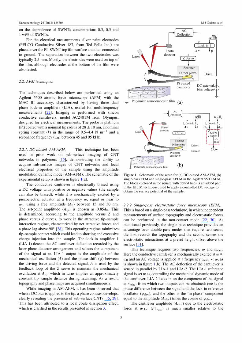
2.2.1. DC-biased AM-AFM. This technique has beenused in prior work on sub-surface imaging of CNTnetworks in polymers [15], demonstrating the ability toacquire sub-surface images of CNT networks and localelectrical properties of the sample using the amplitudemodulation dynamic mode (AM-AFM). The schematic of theexperimental setup is shown in figure 1(a).
The conductive cantilever is electrically biased usinga DC voltage with positive or negative values (the samplecan also be biased), while it is mechanically excited by apiezoelectric actuator at a frequency ω, equal or near toω0, using a free amplitude (A0) between 15 and 30 nm.The set-point amplitude (Asp) is chosen as 0.85A0. Thisis determined, according to the amplitude versus Z andphase versus Z curves, to work in the attractive tip–sampleinteraction regime, characterized by net attractive forces anda phase lag above 90◦ [28]. This operating regime minimizestip–sample contact which could lead to shorting and excessivecharge injection into the sample. The lock-in amplifier 1(LIA-1) detects the AC cantilever deflection recorded by thelaser photo-detector arrangement and selects the componentof the signal at ω. LIA-1 output is the amplitude of themechanical oscillation (A) and the phase shift (φ) betweenthe driving force and the detected signal. A is used by thefeedback loop of the Z servo to maintain the mechanicaloscillation at Asp, which in turns implies an approximatelyconstant tip–sample distance during scanning. As a result,topography and phase maps are acquired simultaneously.
While imaging in AM-AFM, it has been observed thatwhen a DC bias is applied to the tip, a phase contrast develops,clearly revealing the presence of sub-surface CNTs [15, 29].This has been attributed to a local Joule dissipation effect,which is clarified in the results presented in section 3.
Figure 1. Schematic of the setup for (a) DC-biased AM-AFM, (b)single-pass EFM and single-pass KPFM in the Agilent 5500 AFM.The block enclosed in the square with dotted lines is an added partin the KPFM technique, used to apply a controlled DC voltage toobtain the surface potential of the sample.
2.2.2. Single-pass electrostatic force microscopy (EFM).This is based on a single-pass technique, in which independentmeasurements of surface topography and electrostatic forcescan be performed in the non-contact mode [22, 30]. Asmentioned previously, the single-pass technique provides anadvantage over double-pass modes that require two scans,the first records the topography and the second senses theelectrostatic interactions at a preset height offset above thesurface [31].
This technique requires two frequencies, ω and ωelec.Here the conductive cantilever is mechanically excited at ω ≈ω0 and an AC voltage is applied at a frequency ωelec < ω, asis shown in figure 1(b). The AC deflection of the cantilever issensed in parallel by LIA-1 and LIA-2. The LIA-1 referencesignal is set to ω, controlling the mechanical dynamic mode ofthe cantilever. LIA-2 locks-in on the component of the signalat ωelec, from which two outputs can be obtained: one is thephase difference between the signal and the lock-in referenceoscillator (φelec), and the other is the ‘in-phase’ componentequal to the amplitude (Aelec) times the cosine of φelec.
The cantilever amplitude (Aelec) due to the electrostaticforce at ωelec (F|ωelec) is much smaller relative to the
3

Nanotechnology 24 (2013) 135706 M J Cadena et al
Table 1. Comparison between the electrical dynamic AFM techniques for sub-surface imaging of CNT networks in nanocomposites.
Method What is detected?Cantileverdrive Tip bias (dc) Tip bias (ac) Lock-ina Measured quantity
DC-biasedAM-AFM
Energydissipation at ω
At resonance(ω ≈ ω0)
Yes(Vdc = constant)
No 1 Phase lag(φ)
EFM(Single-pass)
Electrostaticforce at ωelec
At resonance(ω ≈ ω0)
Yes(Vdc = constant)
Yes(Vac =
constant at ωelec)
1, 2 Electrostaticforce(Aelec cosφelec)
KPFM(Single-pass)
Electrostaticforce at ωelec
At resonance(ω ≈ ω0)
Yes(feedbackcontrolled)
Yes(Vac =
constant at ωelec)
1, 2 Surface potential(VS (x, y))
Electrostatic forceat 2ωelec
3 ∂C/∂d
a Lock-in 1: topography and phase lag at ω. Lock-in 2: electrostatic force at ωelec. Lock-in 3: electrostatic force at 2ωelec.
average tip–sample gap Z, which is approximately Asp. Thiscan be explained using a well-cited expression, F|ωelec =
1∂C2∂d
∣∣∣∣d=Z
(1V)2 [22, 23, 30, 32], where d is the instantaneous
tip–sample gap, indicating that this interaction is proportionalto the capacitance variations with respect to tip–sample gap∂C/∂d evaluated at the mean tip–sample separation Z andto the square of the potential difference 1V2. When a biasvoltage composed of a DC offset voltage (Vdc) and an ACvoltage (V0 sin(welect)) is applied to the tip, then 1V =Vs(x, y)− [Vdc + V0 sin(welect)], where Vs(x, y) is the surfacepotential of the sample. DC and frequency responses at ωelecand 2ωelec can be obtained, but in this case the component ofthe detected electrostatic force at ωelec is of particular interest
F|ωelec =∂C
∂d
∣∣∣∣d=Z
(Vs(x, y)− Vdc)Vac sin(ωelect). (1)
Therefore, EFM can be used to acquire compositional mapsof the PI–SWNT film, based on the force experienced by thetip as a result of the tip–sample capacitance gradient and thepotential difference between the tip and the sample. Since∂C/∂d depends on both the local dielectric constant and thefilm thickness, the EFM contrast maps then reflect a combinedvariation in these properties and the surface potential.
2.2.3. Single-pass Kelvin force microscopy (KPFM). Thistechnique is based on the principle of the macroscopic Kelvinprobe method to measure contact potential difference [33],which has been adapted to the nanoscale [34]. In thistechnique an AC voltage is applied at a frequency ωelec <
ω to electrically bias the cantilever as in single-pass EFM(figure 1(b)). The difference lies in the implementation of afeedback circuit constituted by a KPFM servo, which appliesa DC voltage (Vdc) to nullify in real time the component of theelectrostatic force at ωelec. From equation (1), the amplitudeof the electrostatic force at ωelec is described by F|ωelec =∂C∂d Vac(Vs(x, y) − Vdc), which vanishes when Vs(x, y) = Vdc.Thus, knowing Vdc, the local surface potential of the samplecan be measured [35].
The second harmonic of ωelec (2ωelec) is detected usinga third lock-in amplifier (LIA-3), which is connected to the
photo-detector. This component is given by
F|2ωelec = −1∂C
4∂d
∣∣∣∣d=Z
V2ac[1− cos(2ωelect)]. (2)
Equation (2) shows that F|2ωelec does not depend on thetip–sample contact potential difference and for fixed Vacits variations are due to relative changes in the tip–samplecapacitance, providing information about the local dielectricproperties [36]. It is assumed that the cantilever amplitude atthe second harmonic of ωelec (A2ωelec) is much lower than theaverage tip–sample gap (Z).
This technique allows the simultaneous mapping of thetopography and phase from the ω signal while the surfacepotential and the capacitance gradient are mapped separatelyfrom the ωelec and 2ωelec signals respectively. Drawing onsurface potential and capacitance gradient maps, single-passKPFM has been used in compositional mapping of severalheterogeneous polymer materials in dry and humid air [18].For the purpose of this work, both these channels of KPFMare used to analyze the polyimide matrix with embeddedSWNT networks. There are some optimization proceduresthat have been taken into account for EFM and KPFMmeasurements, which are described in more detail in [37].These include proper tuning of the phase of LIA-2 tomaximize the ‘in-phase’ component signal, and the setting ofan adequate offset voltages to eliminate any surface potentialdependence on tip–sample distance that could contributeto surface potential measurements from the cantilever andsample.
Table 1 summarizes the key points of the techniquesexplained above.
3. Comparative studies of sub-surface CNT imagingin nanocomposites using three different techniques
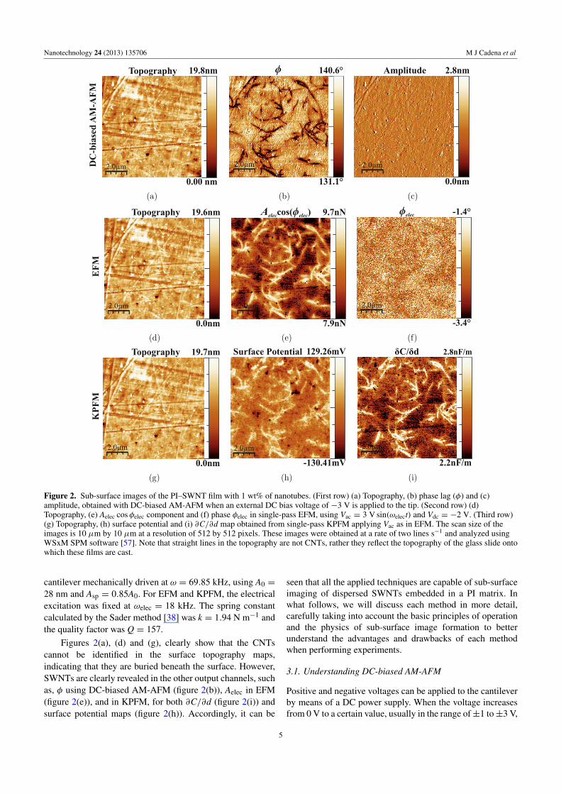
We next compare the advantages and disadvantages ofthese methods with respect to sub-surface imaging of CNTnetworks in nanocomposites. Figure 2 shows the same regionof the PI–SWNT film with 1 wt% of SWNTs, which wasscanned by means of the three single-pass electrical dynamictechniques described above. Data was acquired with the
4
Nanotechnology 24 (2013) 135706 M J Cadena et al
Figure 2. Sub-surface images of the PI–SWNT film with 1 wt% of nanotubes. (First row) (a) Topography, (b) phase lag (φ) and (c)amplitude, obtained with DC-biased AM-AFM when an external DC bias voltage of −3 V is applied to the tip. (Second row) (d)Topography, (e) Aelec cosφelec component and (f) phase φelec in single-pass EFM, using Vac = 3 V sin(ωelect) and Vdc = −2 V. (Third row)(g) Topography, (h) surface potential and (i) ∂C/∂d map obtained from single-pass KPFM applying Vac as in EFM. The scan size of theimages is 10 µm by 10 µm at a resolution of 512 by 512 pixels. These images were obtained at a rate of two lines s−1 and analyzed usingWSxM SPM software [57]. Note that straight lines in the topography are not CNTs, rather they reflect the topography of the glass slide ontowhich these films are cast.
cantilever mechanically driven at ω = 69.85 kHz, using A0 =
28 nm and Asp = 0.85A0. For EFM and KPFM, the electricalexcitation was fixed at ωelec = 18 kHz. The spring constantcalculated by the Sader method [38] was k = 1.94 N m−1 andthe quality factor was Q = 157.
Figures 2(a), (d) and (g), clearly show that the CNTscannot be identified in the surface topography maps,indicating that they are buried beneath the surface. However,SWNTs are clearly revealed in the other output channels, suchas, φ using DC-biased AM-AFM (figure 2(b)), Aelec in EFM(figure 2(e)), and in KPFM, for both ∂C/∂d (figure 2(i)) andsurface potential maps (figure 2(h)). Accordingly, it can be
seen that all the applied techniques are capable of sub-surfaceimaging of dispersed SWNTs embedded in a PI matrix. Inwhat follows, we will discuss each method in more detail,carefully taking into account the basic principles of operationand the physics of sub-surface image formation to betterunderstand the advantages and drawbacks of each methodwhen performing experiments.
3.1. Understanding DC-biased AM-AFM
Positive and negative voltages can be applied to the cantileverby means of a DC power supply. When the voltage increasesfrom 0 V to a certain value, usually in the range of±1 to±3 V,
5

Nanotechnology 24 (2013) 135706 M J Cadena et al
a clear contrast appears in the φ image (figure 2(b)), revealingthe SWNT network located underneath the film surface asdarker features compared to the PI matrix. The scale barindicates that, during the scan, the microscope was operatingin the attractive regime (phase lag φ > 90◦).
The relation between the energy dissipated (Ets) duringtip–sample interaction and the phase lag (φ) for a cantileverwith a spring constant k, quality factor Q, sinusoidally drivenat a set-point amplitude Asp and a frequency ω, can be writtenas [15, 39]
Ets = −πkAspA0
Q
[sin(φ)−
Asp
A0
]. (3)
Meanwhile the virial of the interaction (Vts), which is ameasure of the tip–sample conservative interactions, is givenby
Vts = −kAspA0
2Qcos(φ). (4)
This has two important implications. The first is that inthe absence of any dissipation, sin(φ) = Asp/A0, regardlessof how local conservative electrostatic interactions changeover the sample. But in the attractive regime of operation, theformation of phase contrast implies a simultaneous contrast indissipation and conservative interactions over the sample [39].This raises the second interesting question, as to the origin ofthis energy dissipation mechanism with minimal tip–samplecontact. Considering that there is a voltage between thetip and the sample, this dissipation mechanism has beenidentified as arising from Joule dissipation caused by a localleakage current [29, 40]. In turn this AC leakage currentappears when a bias voltage is applied because the airgap capacitance is modulated by the cantilever oscillation.Thus the phase contrast arises due to spatial variationsin local capacitance and resistance. The Joule dissipationmechanism has been identified as the main contributor toenergy dissipation in DC-biased AM-AFM [15], and is relatedto Ohmic losses [41], or electrostatic damping [42].
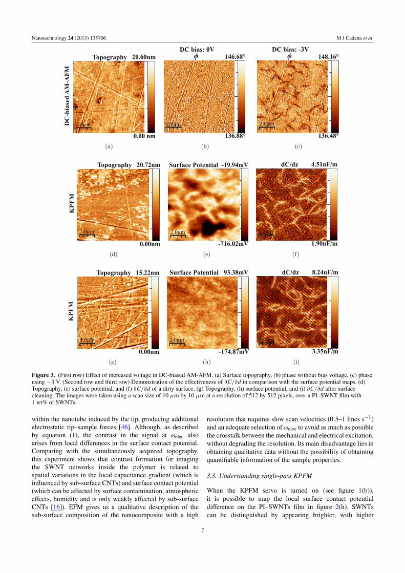
Dissipation can also depend nonlinearly on the voltageapplied between the tip and the sample [29]. This situationis shown for a location of the PI–SWNT film in the first rowof figure 3. As expected, without bias there is no contrast inthe phase image (figure 3(b)). When the voltage is increased,phase contrast emerges, revealing the SWNTs beneath thesurface that were not initially detected. Here it is shown thatthe image obtained with the clearest contrast is for −3 Vbias voltage (figure 3(c)). When a higher voltage is used, thesub-surface nanotubes also show up in the surface topographyimage, which can be considered as an artifact [15].
Taking into account the scheme of operation discussedabove (figure 1(a)) and the experimental results (figure 2(b)),the main benefit of this technique for sub-surface imagingof CNTs in a nanocomposite film is that it is a traditionalAM-AFM mode that requires only one LIA. However, thephase image may be affected by the morphology and defectsof the surface (figures 2(b) and 3(c)). Moreover, effectiveJoule dissipation usually requires a sufficiently high CNTconcentration to ensure the presence of a percolation threshold
and the grounding of the CNT network being imaged. Whena better defined contrast is required, it is useful to subtract thephase images obtained with and without bias or with differentapplied voltages.
In this case, placing the electrodes on the top surface ofthe PI–SWNT film ensures a better grounding of the sample,considering that the thickness of the film is on the order of≈30 µm. This is important because ground connection is aprecondition for the Joule dissipation mechanism, where thedissipation contrast is affected by the capacitance modulation.The greater the thickness of the film the lower the dissipationcontrast [15]. When electrodes were placed at the bottom, aphase contrast could be observed, but using higher DC biasvoltages (≥± 7 V).
3.2. Understanding single-pass EFM
Using single-pass EFM, the CNT network underneath thesurface can be visualized in the Aelec cos(φelec) channel(figure 2(e)). Through the cantilever oscillation amplitude(Aelec) at the electrical drive frequency, this channel basicallycaptures the magnitude of the oscillating electrostatic force(F|ωelec ) at the frequency ωelec, since φelec changes very littleover the sample. The electrostatic force F|ωelec is proportionalto the capacitance gradient and the potential 1V between thetip and the sample, as described in equation (1), where nowVac = V0 sin(ωelect) with V0 = 3 V and Vdc = −2 V, whichare held constant during a scan.
Assuming a tip as a truncated cone ended by a sphericalapex, the total capacitance can be modeled as the sum of thetip–apex contribution (Capex) and the stray capacitance givenby the cone and the cantilever (Cstray). Capex depends on thelocal dielectric properties of the sample and has been definedas [43]
Capex(d, εr, h) = 2πε0R ln
(1+
R(1− sin θ)
d + hεr
), (5)
where ε0 is the vacuum permittivity, R is the effectiveradius, θ is the cone angle of the tip, d is the instantaneoustip–surface gap, εr is the relative dielectric constant and h isthe thickness of the nanocomposite film. Cstray is independentof the local properties of the dielectric medium when h is inthe nanometer range and, for small cantilever displacements,this capacitance is linear in d [44]. Moreover, when d <R/2, the influence of the cone and the cantilever can benegligible [23]. Consequently, the capacitance gradient isapproximately given by [45]∣∣∣∣∂C
∂d
∣∣∣∣d=Z=
2πε0R2(1− sin θ)
(Z + hεr)(Z + h
εr+ R(1− sin θ))
. (6)
Considering that SWNTs have a higher dielectricconstant compared with the PI matrix, the tip–samplecapacitance is altered by the presence of SWNTs [13, 14].Thus, the amplitude of F|ωelec varies depending on whether ornot there are sub-surface nanotubes within the local volume ofthe nanocomposite film probed by the AFM tip. Furthermore,when the tip is over a CNT, there is a charge modulation
6
Nanotechnology 24 (2013) 135706 M J Cadena et al
Figure 3. (First row) Effect of increased voltage in DC-biased AM-AFM. (a) Surface topography, (b) phase without bias voltage, (c) phaseusing −3 V. (Second row and third row) Demonstration of the effectiveness of ∂C/∂d in comparison with the surface potential maps. (d)Topography, (e) surface potential, and (f) ∂C/∂d of a dirty surface. (g) Topography, (h) surface potential, and (i) ∂C/∂d after surfacecleaning. The images were taken using a scan size of 10 µm by 10 µm at a resolution of 512 by 512 pixels, over a PI–SWNT film with1 wt% of SWNTs.
within the nanotube induced by the tip, producing additionalelectrostatic tip–sample forces [46]. Although, as describedby equation (1), the contrast in the signal at ωelec alsoarises from local differences in the surface contact potential.Comparing with the simultaneously acquired topography,this experiment shows that contrast formation for imagingthe SWNT networks inside the polymer is related tospatial variations in the local capacitance gradient (which isinfluenced by sub-surface CNTs) and surface contact potential(which can be affected by surface contamination, atmosphericeffects, humidity and is only weakly affected by sub-surfaceCNTs [16]). EFM gives us a qualitative description of thesub-surface composition of the nanocomposite with a high
resolution that requires slow scan velocities (0.5–1 lines s−1)and an adequate selection of ωelec to avoid as much as possiblethe crosstalk between the mechanical and electrical excitation,without degrading the resolution. Its main disadvantage lies inobtaining qualitative data without the possibility of obtainingquantifiable information of the sample properties.
3.3. Understanding single-pass KPFM
When the KPFM servo is turned on (see figure 1(b)),it is possible to map the local surface contact potentialdifference on the PI–SWNTs film in figure 2(h). SWNTscan be distinguished by appearing brighter, with higher
7

Nanotechnology 24 (2013) 135706 M J Cadena et al
Table 2. Advantages and disadvantages of the electrical techniques for sub-surface characterization of CNT networks in PI–SWNT films.
Method Pros Cons
DC-biased AM-AFM • Uses traditional AM-AFM plusDC tip bias
• Topography can leak into phase channel
• Easy implementation, one lock-inamplifier
• Inherently qualitative
• Higher scan velocity • Requires higher voltages for nonconducting orthicker samples
•Works under ambient conditions • Higher voltage generates artifacts and blurring effects
Single-pass EFM • High contrast in sub-surfaceimages of CNTs
• Inherently qualitative
• No feedback required on ACelectrical signal
• Careful selection of ωelec required
•Works under ambient conditions • Slow scan velocity
Single-pass KPFM • High contrast in sub-surfaceimages of CNTs
• Requires three lock-in amplifiers
• Quantitative method • Requires tuning of two feedback loops•Measures surface potential • Surface potential influenced by surface conditions•Measures ∂C/∂d • Careful selection of ωelec required• Robust technique • Slow scan velocity
relative potential values compared to the polymer matrix (darkregions). This feature can be explained by considering theCNTs as conductive fillers [16, 20, 47]. In addition, fromthe amplitude response of the electrostatic force at 2ωelec(see equation (2)), ∂C/∂d can be measured and mappedas in figure 2(i). The higher magnitude of the electrostaticforce on the SWNTs compared with the polymer indicatesthat ∂C/∂d increases when the local effective dielectricconstant increases [18, 36], described by equation (6). It canbe observed that these SWNTs are the same as those infigure 2(e), which confirms the dependence of F|ωelec on thecapacitance gradient.
Our experiments also suggest that care must be takenin the surface potential measurement, since it can beinfluenced by many factors, such as sample preparation andstorage, contaminants, stress, temperature, trapped charges, ormodifications of the tip and the sample [18, 48]. Here, it wasexperimentally observed how the surface potential is sensitiveto surface treatment. For instance, the surface potential mapof figure 3(e) shows a clear contrast between the CNTs andthe polymer, this was taken in a region of the film withevidence of debris (figure 3(d)). After cleaning the surfacewith isopropanol (figure 3(g)), the nanotubes were no longerdistinguishable in the surface potential map as before, and therelative values of surface potential decreased (figure 3(h)).Nevertheless, ∂C/∂d images always reveal the nanotubeslocated below the surface for both cases (figures 3(f) and (i)).
Based on the experimental results presented in figures 2and 3, we conclude that KPFM can be considered thebest technique to visualize sub-surface CNT networks innanocomposite films, with ∂C/∂d being the most robustchannel for the following reasons: the morphology ofthe surface is separated from the electrical measurementsand, as opposed to single-pass EFM, the topography isnot influenced by the electrostatic tip–sample interaction,since it is nullified. ∂C/∂d can be used to detect the
sub-surface nanotubes regardless of the surface conditionsor the conductive nature of the sample. Data regardingthe local dielectric constant of dissimilar materials can becalculated from the ∂C/∂d maps for thin (h < 1 µm) andhomogeneous samples using equation (6) [43–45]. For thickhomogeneous samples finite-element calculations have beenused based on a truncated cone with hemispherical apex probegeometry [49, 50]. Unfortunately, such finite-element modelsfor electrostatic interactions with random heterogeneousmedia like the CNT nanocomposites considered here are notyet well developed.
Table 2 summarizes the advantages and disadvantages ofthe techniques discussed above, with respect to sub-surfaceimaging of CNT networks in nanocomposites.
4. Dispersion analysis of CNT networks in polymernanocomposites
As mentioned in section 2, electrical percolation is achieved atrelatively low concentrations of SWNTs in our nanocompositefilms and electrical conductivity was increased by severalorders of magnitude. The performance of the nanocompositeis influenced by the quality of the CNT dispersion in thepolymer matrix. In general, a good dispersion of highlyconducting constituents in two-phase heterogeneous mediaincreases conductivity [51]. However, evaluating the qualityof dispersion of CNT networks, especially with respect totheir electrical connectivity, continues to be a challengingissue, for which different techniques have been proposed inthe literature.
Here we summarize some methods in the literaturewhere TEM, SEM and optical confocal microscopy havebeen used to evaluate the dispersion of CNT nanocomposites.A quantitative method to study the dispersion of carbonnanofiber (CNF) and CNT-reinforced polymer matrixcomposites has been proposed [11, 51], based on the
8

Nanotechnology 24 (2013) 135706 M J Cadena et al
measurement of the spacing between the inclusions ofthe matrix in TEM images. Sample preparation requiresultramicrotomy or ion milling processes, depending on thetype of material (soft or hard), that in general cut the sampleinto slices. The dispersion quantities are calculated usingthe frequency distribution of the spacing data, taking intoaccount that a higher dispersion grade will be characterizedby uniform spacing. On the other hand, the dispersion ofMWNT in polymer matrix has been studied using opticalmicroscopy of polished sections of the nanocomposite, basedupon the frequency of occurrence of agglomerates [10].The dispersion is evaluated in the range from 1 to 10,where the latter indicates the absence of agglomeratesand a uniform density distribution. SEM images obtainedfrom SWNTs dispersed in polymer matrices are analyzedthrough image processing techniques, where the bundlesize, persistence length, and spacing between the bundleswith the fractal dimension are calculated to determine thedegree of dispersion [52]. Other methods based on materialhomogeneity, using UV spectroscopy of PMMA/SWNTnanocomposites, and statistical analysis of images taken byoptical confocal microscopy, have also been used [53].
In comparison with other microscopy methods, theelectrical AFM techniques used in this work providehigh-resolution sub-surface imaging of CNT networks formedin the polymer matrix, with minimal sample preparation,and are non-invasive/non-destructive, which allows the re-useof the sample after the characterization. Here we presenta method to analyze the quality of dispersion, using asa criterion the length and frequency of occurrence ofagglomerates or networks formed by connected CNTs. Fromthe proven observation that ∂C/∂d is the most robust channelfor sub-surface imaging CNT networks, the network topologyof ∂C/∂d maps are analyzed with image processing toolsin Matlab [54–56], from which statistical distributions ofconnected cluster sizes are computed.
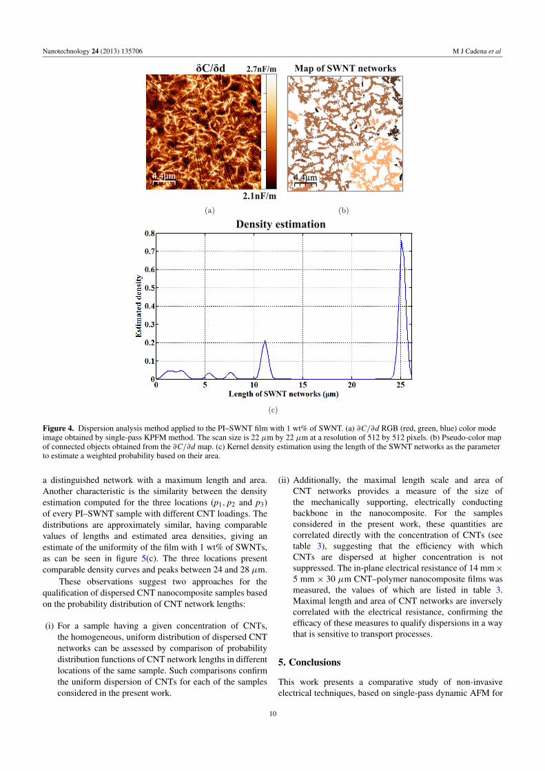
A ∂C/∂d RGB color mode image (processed byWSxM [57]) is taken from an scanned area of the PI–SWNTfilm with 1 wt% of SWNTs, as is indicated in figure 4(a).Image processing functions in MATLAB are employedto transform the image into grayscale, and the contrastis enhanced through histogram equalization and gammacorrection. Based on a threshold, the resulting image isthen converted to a binary map, in which the pixels thatcompose the CNT network features are substituted by 1,and the background consisting of the polymer with 0 [55].Then, in the binary image the connectivity of SWNTs isevaluated, based on how the pixels are related to each otherand form continuous boundaries. For 2D images, there aretwo methods, one is called 4-connected and the other is8-connected neighborhood [58]. On this occasion, due to therandom orientation of CNTs, the 8-connected approximationhas been chosen, where the pixels can be adjacent to eachother in the horizontal, vertical and diagonal orientation [55].From this topological analysis, a scalar geometric measureof the networks formed by the connected SWNTs can bedetermined. A variety of distinct SWNT clusters are presentin samples, as illustrated in figure 4(b).
Defining the connected networks formed by the SWNTin the polymer matrix allows the characterization of the CNTdispersion for quality control purposes. Specifically, given avolume fraction of SWNTs, the length and area distributionsof networks in a given sample can be evaluated at differentlocations. Here we estimate the probability density of aSWNT cluster length through a kernel function, using thecluster area as the assigned weight of each length. The kerneldensity estimate is a non-parametric tool in statistical analysisof data [59, 60], described by f̂ (x, h) = 1
nh
∑ni=1K( x−Xi
h ),i.e. the density estimate is the sum of scaled normal densities,which are contributions of each data point to the overalldensity estimate. Each contribution is determined by 1/ntimes a normal density with mean Xi, and standard deviationh, also known as the bandwidth or smoothing parameter.
While conventional histograms require sorting of samplesinto discrete bins, the present method requires no suchbiasing of the distribution, yielding more accurate estimatesof probability density. We employ the MATLAB functionksdensity to estimate the probability density with Gaussiankernels of optimal kernel width h [55]. The resultingprobability distribution of length for the map of 1 wt% ofSWNTs in figure 4(b) is depicted in figure 4(c). The largestCNT network, with a length above 25 µm, is marked by thehighest peak, which occupies the biggest area in the image.There are also shorter CNT networks marked by lower peaksthat can be observed, but they possess substantially less areafraction in the microstructure than the largest cluster. Suchbehavior of a single large cluster is generally observed inpercolating systems [61].
Hence, now that the analysis process has beendemonstrated using as a sample a PI–SWNT with 1 wt%loading of SWNTs, we look at the distribution of PI–SWNTfilms with 0.3, 0.5 and 1 wt% of SWNTs, at three differentlocations within each sample. The results based on AFMmeasurements for these samples are shown in figure 5. It canbe seen that the maximal length of connected CNT clustersis proportional to the SWNT concentration, for example,0.3 wt% distributions exhibit the shortest lengths with amaximum value between 10 and 15 µm (figure 5(a)). The0.5 wt% sample exhibits maximum lengths of approximately20 µm (figure 5(b)) and the 1 wt% sample exhibits CNTnetworks with the largest extents among all samples of24–28 µm (figure 5(c)). The trend among these samples isexplained by the tendency of increased CNT concentrationsto increase the formation of larger networks. From theseobservations it is clear that the sub-surface probing depthachieved by the present method is sufficient to resolvesub-surface SWNT cluster structures. Table 3 indicates thelengths and areas of the SWNT networks, for polymernanocomposite films with different loadings of SWNTs.
For the three concentrations of SWNTs it is also evidentthat the longer lengths correspond to the largest areas.The connected SWNT networks of length between 0 and15 µm have small areas denoted by an estimated densitybetween 0 and 0.2. This means that for all the samplesthere are small areas of grouped CNTs with shorter lengths(figure 5). However, there is a remarkable peak indicating
9
Nanotechnology 24 (2013) 135706 M J Cadena et al
Figure 4. Dispersion analysis method applied to the PI–SWNT film with 1 wt% of SWNT. (a) ∂C/∂d RGB (red, green, blue) color modeimage obtained by single-pass KPFM method. The scan size is 22 µm by 22 µm at a resolution of 512 by 512 pixels. (b) Pseudo-color mapof connected objects obtained from the ∂C/∂d map. (c) Kernel density estimation using the length of the SWNT networks as the parameterto estimate a weighted probability based on their area.
a distinguished network with a maximum length and area.Another characteristic is the similarity between the densityestimation computed for the three locations (p1, p2 and p3)of every PI–SWNT sample with different CNT loadings. Thedistributions are approximately similar, having comparablevalues of lengths and estimated area densities, giving anestimate of the uniformity of the film with 1 wt% of SWNTs,as can be seen in figure 5(c). The three locations presentcomparable density curves and peaks between 24 and 28 µm.
These observations suggest two approaches for thequalification of dispersed CNT nanocomposite samples basedon the probability distribution of CNT network lengths:
(i) For a sample having a given concentration of CNTs,the homogeneous, uniform distribution of dispersed CNTnetworks can be assessed by comparison of probabilitydistribution functions of CNT network lengths in differentlocations of the same sample. Such comparisons confirmthe uniform dispersion of CNTs for each of the samplesconsidered in the present work.
(ii) Additionally, the maximal length scale and area ofCNT networks provides a measure of the size ofthe mechanically supporting, electrically conductingbackbone in the nanocomposite. For the samplesconsidered in the present work, these quantities arecorrelated directly with the concentration of CNTs (seetable 3), suggesting that the efficiency with whichCNTs are dispersed at higher concentration is notsuppressed. The in-plane electrical resistance of 14 mm×5 mm × 30 µm CNT–polymer nanocomposite films wasmeasured, the values of which are listed in table 3.Maximal length and area of CNT networks are inverselycorrelated with the electrical resistance, confirming theefficacy of these measures to qualify dispersions in a waythat is sensitive to transport processes.
5. Conclusions
This work presents a comparative study of non-invasiveelectrical techniques, based on single-pass dynamic AFM for
10

Nanotechnology 24 (2013) 135706 M J Cadena et al
Figure 5. Probability density estimate of the length of connectedobjects in PI–SWNT films at (a) 0.3 wt%, (b) 0.5 wt%, and (a)1 wt% loadings of SWNTs. For each film, three different areas(p1, p2, p3) where selected to compare the distribution, using a scansize of 22 µm by 22 µm at a resolution of 512 by 512 pixels.
sub-surface imaging SWNT networks formed in a PI matrix.These methods are characterized by relatively minimumsample preparation when compared with other microscopymethods and offer non-destructive and high-resolutioncapabilities under ambient conditions. Single-pass DC-biasedAM-AFM, single-pass EFM, and single-pass KPFM arecompared based on input and output signals and the physicsof sub-surface image formation, in polymer nanocompositesin general and in particular PI–SWNT films. From theexperimental results and taking into account the principlesof operation, it is suggested that each technique opens up abroad range of options to characterize nanocomposites, using
Table 3. Parameters of the CNT networks encountered at differentpositions of PI–SWNT films for dissimilar wt% of SWNTs. Theelectrical film resistance of each sample was measured by atwo-point measurement method using an ohmmeter.
wt%SWNTs Location
Max.length(µm)
Max. area(µm2)
Resistance(k�)
0.3 p1 13.2 21.4375.3p2 14.8 16.2
p3 14.3 16.2
0.5 p1 20.9 51.0123.8p2 19.8 34.2
p3 19.8 27.2
1 p1 27.0 125.016.2p2 24.5 144.6
p3 26.4 147.1
the sub-surface compositional images to extract informationabout CNT connectivity, dispersion, and the local surfacepotential. We conclude that ∂C/∂d is the most robust channelfor sub-surface CNT visualization and characterization,obtained from the second harmonic of electrical excitationwhen single-pass KPFM is applied.
Finally, we present an image processing method of∂C/∂d maps, to analyze the quality of dispersion of CNTs andtheir connectivity distribution. The computed parameters andthe uniformity of the CNT network distribution evaluated atdifferent locations, are strong indicators of how well dispersedand connected the CNTs are within the polymer matrix.Additionally, the present results demonstrate that sub-surfaceAFM measurements are highly sensitive to percolation inheterogeneous media. We expect that the results presentedhere will be of broad significance to the high-resolutionsub-surface characterization of complex nanocompositesusing electrical dynamic AFM methods.
Acknowledgments
Financial support for this research under grant DMR 0826356‘Cyber-Enabled Predictive Models for Polymer Nanocompos-ites: Multiresolution Simulations and Experiments’ from theNational Science Foundation is gratefully acknowledged. Theauthors would also like to acknowledge the financial supportprovided by the Engineering Faculty through the InternationalInternship Fund for master students of the Universidad de losAndes.
References
[1] Rahman A, Ali I, Al Zahrani S M and Eleithy R H 2011 Areview of the applications of nanocarbon polymercomposites Nano: Brief Rep. Rev. 6 185–203
[2] Paul D R and Robeson L M 2008 Polymer nanotechnology:nanocomposites Polymer 49 3187–04
[3] Gao F 2004 Clay/polymer composites: the story Mater. Today7 50–5
11
Nanotechnology 24 (2013) 135706 M J Cadena et al
[4] Marquis D, Guillaume E and Chivas-Joly C 2011Nanocomposites and Polymers with Analytical Methods(New York: InTech) (Properties of Nanofillers in Polymer)
[5] Coleman J N, Khan U and Gunko Y K 2006 Mechanicalreinforcement of polymers using carbon nanotubes Adv.Mater. 18 689–706
[6] Kashiwagi T, Du F, Winey K, Grotha K M, Shieldsa J R,Bellayera S P, Kimc H and Douglas J F 2005 Flammabilityproperties of polymer nanocomposites with single-walledcarbon nanotubes: effects of nanotube dispersion andconcentration Polymer 46 471–81
[7] Ichida M, Mizuno S, Kataura H, Achiba Y and Nakamura A2004 Anisotropic optical properties of mechanically alignedsingle-walled carbon nanotubes in polymer Appl. Phys. A78 1117–20
[8] Barrau S, Demont P, Peigney A, Laurent C and Lacabanne C2003 DC and AC conductivity of carbonnanotubes-polyepoxy composites Macromolecules36 5187–94
[9] Moniruzzaman M and Winey K 2006 Polymernanocomposties containing carbon nanotubesMacromolecules 39 5194–205
[10] Andrews R and Jacques D 2002 Fabrication of carbonmultiwall nanotube/polymer composites by shear mixingMacromol. Mater. Eng. 287 395–403
[11] Luo Z P and Koot J H 2008 Quantitative study of thedispersion degree in carbon nanofiber/polymer and carbonnanotube/polymer nanocomposites Mater. Lett. 62 3493–6
[12] Potschke P, Bhattacharyya A R and Janke A 2004 Meltmixing of polycarbonate with multiwalled carbonnanotubes: microscopic studies on the state of dispersionEur. Polym. J. 40 137–48
[13] Jespersen T and Nygard J 2007 Mapping of individual carbonnanotubes in polymer nanotube composites usingelectrostatic force microscopy Appl. Phys. Lett. 90 3
[14] Zhao M, Gu X, Lowther S, Park C, Jean Y C and Nguyen T2010 Subsurface characterization of carbon nanotubes inpolymer composites via quantitative electric forcemicroscopy Nanotechnology 21 225702
[15] Thompson H, Barroso F, Gomez-Herrero J,Reifenberger R and Raman A 2013 Subsurface imaging ofcarbon nanotube networks in polymers with DC-biasedmultifrequency dynamic atomic force microscopyNanotechnology at press
[16] Gil A, De Pablo P J, Colchero J, Gomez-Herrero J andBaro A M 2002 Electrostatic scanning force microscopyimages of long molecules: single-walled carbon nanotubesand DNA Nanotechnology 13 309–13
[17] Melin T, Zdrojek M and Brunel D 2010 Scanning ProbeMicroscopy in Nanoscience and Nanotechnologyed B Bhushan (Berlin: Springer) pp 89–126 (Electrostaticforce microscopy and Kelvin force microscopy as a probeof the electrostatic and electronic properties of carbonnanotubes)
[18] Magonov S and Alexander J 2011 Single-pass Kelvin forcemicroscopy and dC/dZ measurements in the intermittentcontact: applications to polymer materials Beilstein J.Nanotechnol. 2 15–27
[19] Reddy B N and Deepa M 2012 Unraveling nanoscaleconduction and work function in apoly(3,4-ethylenedioxypyrrole)/carbon nanotube compositeby Kelvin probe force microscopy and conducting atomicforce microscopy Electrochim. Acta 70 228–40
[20] Prasse T, Ivankov A, Sandler J, Schulte K andBauhofer W 2001 Imaging of conductive filler networks inheterogeneous materials by scanning Kelvin microscopy J.Appl. Polym. Sci. 82 3381–6
[21] Magonov S and Alexander J 2011 Multifrequency atomicforce microscopy: compositional imaging with electrostaticforce measurements Microsc. Microanal. 17 587–97
[22] Magonov S and Alexander J 2008 Advanced atomic forcemicroscopy: exploring measurements of local electricproperties Technical Report Agilent Technologies
[23] Girard P 2001 Electrostatic force microscopy: principles andsome applications to semiconductors Nanotechnology12 485–90
[24] Misiego C R 2012 Carbon nanotube dispersion andcharacteristics: thermo-mechanical properties andconductivity of polyimide nanocomposites PhD ThesisSchool of Chemical Engineering Purdue University
[25] Landi B, Raffaelle R, Castro S and Bailey S 2005 Single-wallcarbon nanotube-polymer solar cells Prog. Photovolt., Res.Appl. 13 165–72
[26] Banda S 2008 Electric field manipulation of polymernanocomposites: processing and investigation of theirphysical characteristics PhD Thesis Texas A&M UniversityDiciembre
[27] Dai H, Wong E W and Lieber C M 1996 Probing electricaltransport in nanomaterials: conductivity of individualcarbon nanotubes Science 272 523–6
[28] Garcia R and San Paulo A 1999 Attractive and repulsivetip–sample interaction regimes in tapping-mode atomicforce microscopy Phys. Rev. B 60 4961–7
[29] Loppacher C, Bennewitz R, Pfeiffer O, Guggisberg M,Bammerlin M, Schar S and Barwich V 2000 Experimentalaspects of dissipation force microscopy Phys. Rev. B62 13674–9
[30] Martin Y, Abraham D W and Wickramasinghe H K 1988 Highresolution capacitance measurement and potentiometry byforce microscopy Appl. Phys. Lett. 52 1103–5
[31] Yan M and Bernstein G H 2007 A quantitative method fordual-pass electrostatic force microscopy phasemeasurements Surf. Interface Anal. 39 354–8
[32] Arnason S B, Rinzler A G, Hudspeth Q and Hebard A F 1999Carbon nanotube-modified cantilevers for improved spatialresolution in electrostatic force microscopy Appl. Phys.Lett. 75 2842–4
[33] Zisman W A 1932 A new method of measuring contactpotential differences in metals Rev. Sci. Instrum. 3 367–70
[34] Nonnenmacher M, O’Boyle M P and Wickramasinghe H K1991 Kelvin probe force microscopy Appl. Phys. Lett.58 2921–3
[35] Nonnenmacher M, O’Boyle M P and Wickramasinghe H K1992 Surface investigations with a Kelvin probe forcemicroscope Ultramicroscopy 42–44 268–73
[36] Fumagalli L, Ferrari G, Sampietro M, Casuso I, Martinez E,Samitier J and Gomila G 2006 Nanoscale capacitanceimaging with attofarad resolution using AC current sensingatomic force microscopy Nanotechnology 17 4581–7
[37] Kibel A 2011 KFM user’s guide Technical Report AgilentTechnologies
[38] Sader J, Chon J and Mulvaney P 1999 Calibration ofrectangular atomic force microscope cantilevers Rev. Sci.Instrum. 70 3967–9
[39] Cleveland J P, Anczykowski B, Schmid A E andElings V B 1998 Energy dissipation in tapping-modeatomic force microscopy Appl. Phys. Lett. 72 2613–5
[40] Denk W and Pohl D W 1991 Local electrical dissipationimaged by scanning force microscopy Appl. Phys. Lett.59 2171–3
[41] Barois T, Ayari A, Siria A, Perisanu S, Vincent P,Poncharal P and Purcell S T 2012 Ohmic electromechanicaldissipation in nanomechanical cantilevers Phys. Rev. B85 075407:1-7
[42] Stowe T A, Kenny T W, Thomson D J and Rugar D 1999Silicon dopant imaging by dissipation force microscopyAppl. Phys. Lett. 75 2785–7
[43] Fumagalli L, Ferrari G, Sampietro M and Gomila G 2007Dielectric-constant measurement of thin insulating films at
12

Nanotechnology 24 (2013) 135706 M J Cadena et al
low frequency by nanoscale capacitance microscopy Appl.Phys. Lett. 91 243110:1–3
[44] Gramse G, Casuso I, Toset J, Fumagalli L and Gomila G 2009Quantitative dielectric constant measurement of thin filmsby DC electrostatic force microscopy Nanotechnology20 395702:1–8
[45] Kumar B, Bonvallet J C and Crittenden S R 2012 Dielectricconstants by multifrequency non-contact atomic forcemicroscopy Nanotechnology 23 025707
[46] Bockrath M, Markovic N, Shephard A, Tinkham M,Gurevich L, Kouwenhoven L P, Wu M W and Sohn L 2002Scanned conductance microscopy of carbon nanotubes andλ-DNA Nano Lett. 2 187–90
[47] Bachtold A, Fuhrer M S, Plyasunov S, Forero M,Anderson E H, Zettl A and McEuen P L 2000 Scannedprobe microscopy of electronic transport in carbonnanotubes Phys. Rev. Lett. 84 6082–5
[48] Jacobs H O, Leuchtmann P, Homan O J and Stemmer A 1998Resolution and contrast in Kelvin probe force microscopy J.Appl. Phys. 84 1168–73
[49] Fumagalli L, Gramse G, Esteban-Ferrer D, Edwards M A andGomila G 2010 Quantifying the dielectric constant of thickinsulators using electrostatic force microscopy Appl. Phys.Lett. 96 183107:1–3
[50] Gramse G, Gomila G and Fumagalli L 2012 Quantifying thedielectric constant of thick insulators by electrostatic forcemicroscopy: effects of the microscopic parts of the probeNanotechnology 23 205703:1–7
[51] Luo Z P and Koot J H 2007 Quantifying the dispersion ofmixture microstructures J. Microsc. 225 118–25
[52] Lillehei P T, Kim J, Gibbons L J and Park G 2009 Aquantitative assessment of carbon nanotube dispersion inpolymer matrices Nanotechnology 20 1–7
[53] Kashiwagi T et al 2007 Relationship between dispersionmetric and properties of PMMA/SWNT nanocompositesPolymer 48 4855–66
[54] McAndrew A 2004 An Introduction to Digital ImageProcessing with Matlab
[55] Mathworks 2012 Image Processing Toolbox User’s GuideR2012a Matlab
[56] Mathworks 2012 Statistics Toolbox User’s Guide R2012aMatlab
[57] Horcas I, Fernandez R, Gomez-Rodriguez J M, Colchero J,Gomez-Herrero J and Baro A M 2007 WSxM: a softwarefor scanning probe microscopy and a tool fornanotechnology Rev. Sci. Instrum. 78 013705:1–8
[58] Velho L, Frery A C and Gomes J 2009 Image Processing forComputer Graphics and Vision (Berlin: Springer)
[59] Sheather S 2004 Density estimation Stat. Sci. 19 588–97[60] Silverman B W 1986 Density Estimation for Statistics and
Data Analysis (Monographs on Statistics and AppliedProbability) (London: Chapman and Hall)
[61] Stauffer D and Aharony A 1994 Introduction to PercolationTheory (London: Taylor & Francis)
13