
Integration of Conductive Materials and SMD-Components ...
159
Integration of Conductive Materials and SMD-Components into the FDM Printing Process for Direct Embedding of Electronic Circuits Dissertation zur Erlangung des akademischen Grades Dr. rer. nat an der Fakultät für Mathematik, Informatik und Naturwissenschaften der Universität Hamburg Eingereicht beim Fachbereich Informatik von Florens Wasserfall Oktober 2019
-
Upload
khangminh22 -
Category
Documents
-
view
1 -
download
0
Transcript of Integration of Conductive Materials and SMD-Components ...

Integration of Conductive Materials andSMD-Components into the FDM Printing Process
for Direct Embedding of Electronic Circuits
Dissertationzur Erlangung des akademischen Grades
Dr. rer. natan der Fakultät für Mathematik, Informatik und
Naturwissenschaftender Universität Hamburg
Eingereicht beim Fachbereich Informatikvon Florens Wasserfall
Oktober 2019


Gutachter:Prof. Dr. Jianwei ZhangProf. Dr. Eric MacDonald
Tag der Disputation: 27.01.2020


Abstract
Additive manufacturing has changed the way we develop and prototype things. It has openedup a new perspective to solve technical problems or sometimes just allows for a more appealingdesign, as fabricating complex and intricate structures does not require additional effort or ma-chinery. Additive processes are increasingly used to actually produce parts in small lot sizes,replacing traditional manufacturing methods.
This thesis reports on the successful development of a Fused Deposition Modelling (FDM) 3Dprinter that combines processing of plastic and conductive materials with a pick and place sys-tem to build objects with integrated electronics in a single production step. The printer has beenextended with a syringe extruder for conductive paste and a vacuum gripper; both mounted onindividual micro z-stages to avoid collisions. Two cameras and a feeding system for electroniccomponents were integrated, along with a new control software for vision aided placing of com-ponents. In addition to the description of all individual hardware solutions, the selection andcharacterization of suitable materials is presented.
The core contribution of this work is a combined slicing and design software to support thearrangement of printable 3D circuits inside of physical objects. The software allows to positionelectronic components from imported existing schematics in a preview of the tool path, whichis then executed by the printer. Cavities, solid surfaces around components, and channels forconductive wires are automatically generated under consideration of important process param-eters (layer thickness, extrusion width, etc.).
Based on the component positions and additional user-defined waypoints a novel routing algo-rithm generates collision-free 3D wire routes. The trajectories follow the object contour wherepossible and are optimized for the parameters of the current printer configuration. After thebasic slicing step, the routing algorithm translates the contour information of all layers into agraph representation. An A*-based search algorithm is then employed to find suitable pathswithin that graph. The search algorithm is modified to use only eligible, i.e., printable transi-tions between adjacent layers.
As the electronics are mostly covered by plastic once the object is printed, testing often is notpossible. The integrated camera is used to record high-resolution images of each layer automat-ically. A vision algorithm compares these images with the G-code to identify potential defectsbefore the next layer is printed.
Several objects with 3D electronics have been successfully printed. Among them are two casestudies for an academic research project and an industrial application.
5

6

Kurzfassung
Die additive Fertigung verändert die Art und Weise wie Dinge entworfen und entwickelt wer-den. Sie eröffnet ganz neue Möglichkeiten um technische Probleme zu lösen oder auch nur Din-ge ansprechender zu gestalten, da keine aufwändigen zusätzlichen Arbeitsschritte und Gerätenötig sind um komplexe oder aufwändige Strukturen herzustellen. Additiv gefertigte Bauteilewerden, zumindest für kleine Stückzahlen, zunehmend häufig in Endprodukten eingesetzt.
Diese Dissertation berichtet von der Entwicklung eines Fused Deposition Modelling (FDM)3D Druckers, der sowohl Kunststoff als auch leitfähiges Material verarbeiten kann und überein Bestückungssystem verfügt um Gegenstände mit integrierter Elektronik in einem einzelnenProduktionsschritt herzustellen. Der Drucker wurde zu diesem Zweck um einen Spritzenextru-der für leitfähige Paste und einen Vakuumgreifer erweitert, die beide auf zusätzlichen Mikro-z-Achsen montiert sind um Kollisionen zu vermeiden. Zusätzlich wurden zwei Kameras undeine Ablage für elektronische Komponenten integriert, zusammen mit einer Software für daskameragestützte Positionieren der Bauteile. Neben der Beschreibung der einzelnen Hardware-komponenten wird die Auswahl und Charakterisierung geeigneter Materialien beschrieben.
Ein zentraler Teil dieser Arbeit ist die Entwicklung einer kombinierten Slicing- und Design-Software, die bei der Anordnung druckbarer 3D Schaltungen in physischen Objekten unter-stützt. Diese Software ermöglicht das räumliche Positionieren elektronischer Bauteile in einerVorschau des Druckpfades, wie er später von der Maschine ausgeführt werde. Für die Bauteileund elektrischen Leitungen werden automatisch Aussparungen und geschlossene Oberflächenüber- und unterhalb der Objekte erzeugt, dabei werden wichtige Prozessparameter wie Schicht-dicke oder Extrusionsbreite berücksichtigt.
Basierend auf den Positionen der vom Benutzer platzierten Komponenten und zusätzlicher Weg-punkte generiert ein neuer Routing-Algorithmus kollisionsfreie 3D Pfade für die verbindendenLeitungen. Wo es möglich ist folgen die so erzeugten Trajektorien den vorhandenen Kontu-ren des Objekts. Sie werden dabei für die Prozessparameter des Druckers optimiert, mit demdas Objekt gebaut wird. Nach dem Slicing-Schritt erzeugt der Routing-Algorithmus aus denKonturen der einzelnen Schichten eine Graphenrepräsentation des Objekts. Auf diesem Gra-phen wird anschließend ein A*-basierter Suchalgorithmus ausgeführt um geeignete Pfade fürdie Leitungen zu finden. Dabei werden nur solche Übergänge zwischen benachbarten Schichtenberücksichtigt die auch tatsächlich druckbar sind.
Die fertig gedruckten Schaltungen sind meistens mit Kunststoff überdeckt, daher ist eine Funk-tionsprüfung in vielen Fällen nachträglich nicht mehr möglich. Um trotzdem eine Überprüfungdurchzuführen werden nach jeder Schicht mit der im Drucker integrierten Kamera hoch auf-
7

lösende Bilder der Oberfläche aufgenommen. Diese Bilder werden automatisiert mit dem zudruckenden G-code abgeglichen, um potenzielle Defekte zu finden bevor die nächste Schichtgedruckt wird.
Mit der entwickelten Technik wurden erfolgreich mehrere Gegenstände mit integrierter 3DElektronik gedruckt. Darunter zwei Fallstudien mit Objekten für ein wissenschaftliches For-schungsprojekt und eine industrielle Anwendung.
8

Contents
1 Introduction 131.1 Motivation . . . . . . . . . . . . . . . . . . . . . . . . . . . . . . . . . . . . . 131.2 Aim of this Thesis . . . . . . . . . . . . . . . . . . . . . . . . . . . . . . . . . 161.3 Research Question and Contribution . . . . . . . . . . . . . . . . . . . . . . . 171.4 Structure of the Thesis . . . . . . . . . . . . . . . . . . . . . . . . . . . . . . 171.5 Related Publications . . . . . . . . . . . . . . . . . . . . . . . . . . . . . . . 18
2 State of the Art in Printed Electronics 212.1 Additive Manufacturing . . . . . . . . . . . . . . . . . . . . . . . . . . . . . . 21
2.1.1 Fused Deposition Modelling . . . . . . . . . . . . . . . . . . . . . . . 212.1.2 Stereolithography . . . . . . . . . . . . . . . . . . . . . . . . . . . . . 222.1.3 Powder Bed Fusion and Binder Jetting . . . . . . . . . . . . . . . . . . 222.1.4 Material Jetting . . . . . . . . . . . . . . . . . . . . . . . . . . . . . . 22
2.2 Wire Generation . . . . . . . . . . . . . . . . . . . . . . . . . . . . . . . . . . 222.2.1 Integration with FDM . . . . . . . . . . . . . . . . . . . . . . . . . . 242.2.2 Integration with SLA . . . . . . . . . . . . . . . . . . . . . . . . . . . 272.2.3 Integration with Powder-Based Processes . . . . . . . . . . . . . . . . 292.2.4 Material Jetting . . . . . . . . . . . . . . . . . . . . . . . . . . . . . . 29
2.3 3D-Design Concepts . . . . . . . . . . . . . . . . . . . . . . . . . . . . . . . 302.4 Process Monitoring . . . . . . . . . . . . . . . . . . . . . . . . . . . . . . . . 33
3 Experimental Printing Platform 373.1 3D Printer Hardware . . . . . . . . . . . . . . . . . . . . . . . . . . . . . . . 38
3.1.1 Demonstrator Platforms . . . . . . . . . . . . . . . . . . . . . . . . . 383.1.2 Conductive Material Extrusion . . . . . . . . . . . . . . . . . . . . . . 443.1.3 Bonding Characteristics . . . . . . . . . . . . . . . . . . . . . . . . . 483.1.4 Component Handling . . . . . . . . . . . . . . . . . . . . . . . . . . . 49
3.2 Control Software . . . . . . . . . . . . . . . . . . . . . . . . . . . . . . . . . 513.2.1 Firmware & Print Server . . . . . . . . . . . . . . . . . . . . . . . . . 513.2.2 Pick and Place . . . . . . . . . . . . . . . . . . . . . . . . . . . . . . 52
3.3 Calibration . . . . . . . . . . . . . . . . . . . . . . . . . . . . . . . . . . . . 56
4 Integration of Electronics and Mechanical Objects 614.1 Design Methods . . . . . . . . . . . . . . . . . . . . . . . . . . . . . . . . . . 614.2 Slicing Software . . . . . . . . . . . . . . . . . . . . . . . . . . . . . . . . . . 62
4.2.1 Existing Software Projects . . . . . . . . . . . . . . . . . . . . . . . . 624.2.2 Slic3r Electronics Fork . . . . . . . . . . . . . . . . . . . . . . . . . . 63
9

CONTENTS
4.2.3 Slicing Software Fundamentals . . . . . . . . . . . . . . . . . . . . . 644.3 Import and Representation of eCAD-Data . . . . . . . . . . . . . . . . . . . . 684.4 SMD-Component Integration . . . . . . . . . . . . . . . . . . . . . . . . . . . 704.5 Wire Integration . . . . . . . . . . . . . . . . . . . . . . . . . . . . . . . . . . 73
4.5.1 Static Wire Routing . . . . . . . . . . . . . . . . . . . . . . . . . . . . 744.5.2 Channel Generation . . . . . . . . . . . . . . . . . . . . . . . . . . . 75
5 Object-Topology Aware Wire Routing 835.1 Related Approaches . . . . . . . . . . . . . . . . . . . . . . . . . . . . . . . . 85
5.1.1 VLSI and PCB routing . . . . . . . . . . . . . . . . . . . . . . . . . . 855.1.2 Path Planning in Robotics . . . . . . . . . . . . . . . . . . . . . . . . 86
5.2 Intra-Layer Connections . . . . . . . . . . . . . . . . . . . . . . . . . . . . . 885.2.1 Data Representation . . . . . . . . . . . . . . . . . . . . . . . . . . . 885.2.2 Perimeters . . . . . . . . . . . . . . . . . . . . . . . . . . . . . . . . 895.2.3 Direct Connections . . . . . . . . . . . . . . . . . . . . . . . . . . . . 915.2.4 Expanding Grid Search . . . . . . . . . . . . . . . . . . . . . . . . . . 93
5.3 Inter-Layer Connections . . . . . . . . . . . . . . . . . . . . . . . . . . . . . 975.3.1 Direct Linear Connections . . . . . . . . . . . . . . . . . . . . . . . . 975.3.2 Dynamically Exploring Connections . . . . . . . . . . . . . . . . . . . 995.3.3 Heuristic Guidance . . . . . . . . . . . . . . . . . . . . . . . . . . . . 104
5.4 Wire Collisions . . . . . . . . . . . . . . . . . . . . . . . . . . . . . . . . . . 1065.5 Algorithms Summarized . . . . . . . . . . . . . . . . . . . . . . . . . . . . . 108
6 Process Documentation and Verification 1136.1 Image Recording during the Print-process . . . . . . . . . . . . . . . . . . . . 1146.2 Feature Segmentation . . . . . . . . . . . . . . . . . . . . . . . . . . . . . . . 1156.3 Defect Detection . . . . . . . . . . . . . . . . . . . . . . . . . . . . . . . . . 116
7 Experimental Applications and Evaluation 1197.1 Plastics . . . . . . . . . . . . . . . . . . . . . . . . . . . . . . . . . . . . . . 1197.2 Demonstrators . . . . . . . . . . . . . . . . . . . . . . . . . . . . . . . . . . . 120
7.2.1 Basic Functional Tests . . . . . . . . . . . . . . . . . . . . . . . . . . 1217.2.2 Case Study: Integrated User Interface . . . . . . . . . . . . . . . . . . 1237.2.3 Case Study: Instrumented Object . . . . . . . . . . . . . . . . . . . . 126
7.3 Performance . . . . . . . . . . . . . . . . . . . . . . . . . . . . . . . . . . . . 129
8 Conclusions and Outlook 1338.1 Limitations . . . . . . . . . . . . . . . . . . . . . . . . . . . . . . . . . . . . 1348.2 Future Research . . . . . . . . . . . . . . . . . . . . . . . . . . . . . . . . . . 134
References 137
List of Web-Adresses 147
List of Figures 151
List of Tables 155
10

CONTENTS
Glossary 157
11

CONTENTS
12

Chapter 1
Introduction
1.1 Motivation
Throughout the history of mankind, humans have created necessary, useful or just beautifulthings, shaping them from raw material by removing all unwanted matter. Subtractive manufac-turing has evolved from simple carving to modern, multi-axis high precision CNC machining.The opposite approach of assembling an object from very small quantities of material, depositedright into the desired shape, is a relatively young concept.
As has been the case often, the idea was first contemplated in science fiction literature. In 1945,George O. Smith’s Special Delivery pictures the dystopian effect of a “duplicator”, developedbased on martian technology, disrupting the production processes of an entire interplanetarymanufacturing industry within only a few weeks [A77]. The device is capable to scan an exist-ing object and create exact copies from the recorded information, which can also be transmittedto other devices somewhere in the galaxy. The “replicator” was brought to a wider audienceby the popular Star Trek TV-show, where it developed from a simple food synthesizer into auniversal tool to produce, copy and recycle objects. In Neal Stephenson’s The Diamond Ageevery household owns a matter compiler to synthesize almost everything, from food to com-puters from a set of basic molecules [A80]. The matter compiler draws a stream of energy andmolecules from the Feed, a system of tubes, similar to public water or network supplies.
Contrary to the systems imagined in science fiction, the first actual additive manufacturingmachines were not able to assemble an item atom by atom or molecule by molecule. In fact,only a single material could be used and the resolution was rather coarse.The widely used Stereolithography (SLA) and FDM methods were mainly developed in thelate 70s and 80s of the last century and patented in 1984 (SLA) and 1992 (FDM). A variety ofpowder based processes was developed in parallel, starting with Selective Laser Sintering (SLS)in the 1980s and followed by Selective Laser Melting (SLM) and inkjet based binder jetting inthe early 1990s.The term “3D printing” was originally used by MIT researchers for their binder jetting pro-cess, but increasingly recognized by a wider public when the RepRap project [A38] ignited atremendous movement to build low cost, mostly FDM based 3D printers, easily available toprofessionals, researchers and interested hobbyists. In this thesis, “3D printing” is used in a
13
CHAPTER 1. INTRODUCTION
broad sense, as synonym for different additive processes, including but not limited to binderjetting technology.
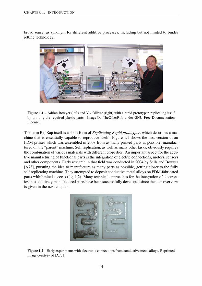
Figure 1.1 – Adrian Bowyer (left) and Vik Olliver (right) with a rapid prototyper, replicating itselfby printing the required plastic parts. Image ©: TheOtherRob under GNU Free DocumentationLicense.
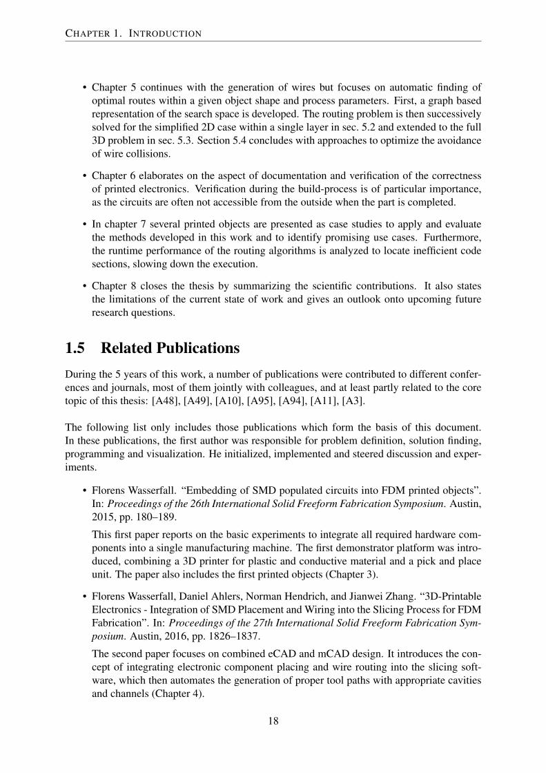
The term RepRap itself is a short form of Replicating Rapid prototyper, which describes a ma-chine that is essentially capable to reproduce itself. Figure 1.1 shows the first version of anFDM-printer which was assembled in 2008 from as many printed parts as possible, manufac-tured on the “parent” machine. Self replication, as well as many other tasks, obviously requiresthe combination of various materials with different properties. An important aspect for the addi-tive manufacturing of functional parts is the integration of electric connections, motors, sensorsand other components. Early research in that field was conducted in 2004 by Sells and Bowyer[A73], pursuing the idea to manufacture as many parts as possible, getting closer to the fullyself replicating machine. They attempted to deposit conductive metal alloys on FDM-fabricatedparts with limited success (fig. 1.2). Many technical approaches for the integration of electron-ics into additively manufactured parts have been successfully developed since then, an overviewis given in the next chapter.
Figure 1.2 – Early experiments with electronic connections from conductive metal alloys. Reprintedimage courtesy of [A73].
14

1.1. MOTIVATION
Besides the question of electrical conductivity, a number of other properties are essential: color,stiffness, elasticity, surface quality or transparency, to name a few important examples. Manyproblems are solved better by a combination of additive and established, traditional methods,e.g. by drilling a precise hole, inserting a screw or embedding an integrated microcontroller in-stead of printing single transistors. A major trend in recent years therefore is the integration ofdifferent manufacturing principles into a single process, usually referred to as hybrid manufac-turing [A99]. The term hybrid manufacturing is not well defined. It is mostly used to describea combination of different established manufacturing processes (e.g. injection moulding andmilling), but also for a combination of material deposition and melting or multi material de-position with different heads in a single machine. The integration of electronic circuits duringan additive manufacturing process, involving at least a structural and a conductive material andhandling of electric components is considered a hybrid manufacturing process under all populardefinitions.
During our own research on a printable modular robot (PMR) [A48, A49] and a 3D printed hu-manoid robot [A10] for the RoboCup soccer competition [B27], it became increasingly evidentthat the integration of electronics is a key aspect for the prototyping and rapid development oftechnical systems and robotics in particular. While the rapid additive manufacturing of purelymechanical parts posed no major issues thanks to increasingly maturing and affordable 3Dprinting technology, assembling the electronic connections and particularly integrating sensorsrequired a significant share of the time spent for the project. The electric interfaces of eachPMR module as shown in fig. 1.3 require the assembly of 16 connection points, each consistingof 5 individual components, resulting in 80 pieces per module.
Figure 1.3 – The Printable Modular Robot, developed in an earlier project [A49]. The modules aremechanically and electrically connected via magnetic interfaces, requiring a high amount of manualassembling.
15

CHAPTER 1. INTRODUCTION
1.2 Aim of this ThesisAlthough a number of research results has proven the technical feasibility of different ap-proaches to 3D print electronics, from insertion of traditional wires [A8] to the actual additivemanufacturing of an LED itself [A46], basically no commercial products are available yet. Theresearch is mostly focused on the physical printing process itself, while the complex problem ofintegrating mechanic and electric designs into a single part still suffers applicable solutions. Sofar, most of the printed demonstrator objects have been carefully designed and prepared witha substantial amount of manual work, which is not a feasible option for broader commercialapplication of additively fabricated electronics.The aim of this thesis is to create a toolchain to print an object with integrated electronics,covering all steps from design to automatic assembly of components. To achieve this, severalindividual developments from mechanical engineering, computer science and software devel-opment must be combined:
1. A hardware platform capable to print structural (plastic) material, conductive materialand to manipulate additional components.
2. Design software to support the spatial arrangement of an electric circuit under the con-straints of the manufacturing process.
3. Algorithms for routing of electric connections in 3D-space.
4. Translation of the integrated 3D-model into a sequence of machine commands.
5. Automatic placement of electronic components during the print process.
6. Quality control and verification of the build process.
The mid-term vision is an autonomous, integrated production cell, where a design can be up-loaded and the entire build process is executed without human intervention. Such a systemcould be integrated as a very flexible part of a conventional industrial production process, butthe primary intended use case is prototyping and individualized single pieces.
Given the diversity of available additive manufacturing methods, the choice of an appropriatebase technique is important and has major implications on what can or cannot be achieved.Light (including laser) based processes provide very high precision and resolution, but usuallyrequire a powder bed or liquid filled basin. As a side effect, it is very difficult to combine twoor more materials. Inkjet based processes also provide high resolution and are very suitable tocombine multiple materials by using one cartridge per material. Unfortunately, the UV-curedmaterial is brittle, lacks long term stability and machines are proprietary and expensive.The FDM technology is considered to be well suited for integration of multiple materials andparts for several reasons: the surface is always flat and open during the build process, no liquidsor powders are covering the workspace, interruption and resuming of the print is possible with-out cleaning or registration of the workpiece. FDM technology is comparably cheap and widelyavailable, increasing the number of potential users. Both hard- and software can be purchasedoff the shelf, ready to use, still often distributed as open source, facilitating modifications andextensions.
16

1.3. RESEARCH QUESTION AND CONTRIBUTION
1.3 Research Question and Contribution
Mechanical Engineering & Integration: How to design and operate an additive manufactur-ing system, that is capable of printing complex physical objects with integrated wiringand autonomous assembly of electronic components? Which materials are suitable forsuch a process? With regard to potential industrial automation, the entire build process issupposed to be performed without any human interaction.
3D-Electronics Design: How to combine existing mechanic Computer Aided Design (mCAD)and electronic Computer Aided Design (eCAD) approaches in such a way that the result isproducible on additive manufacturing systems while preserving the intended mechanicaland electrical specifications?
2D & 3D Wire Routing algorithms: How to route wires within or at the surface of arbitraryand complex 3D-Objects, constraint by limited process resolution, with a strong focus onthe FDM-Process?
Process Verification: How to ensure that a circuit, fully or partly immersed in plastic, has nodefects and works as intended?
1.4 Structure of the Thesis
The remaining parts of this thesis are organized as follows:
• Chapter 2 provides an overview over the fundamental methods for additive fabricationof electronics and reviews existing related work. A focus is set on the introduction ofseveral approaches to integrate conductive traces and electronic components into differentadditive manufacturing processes. It also covers methods for the co-design of eCAD andmCAD for integrated 3D circuits and closes with a description of approaches for qualitycontrol and process monitoring.
• Chapter 3 covers all aspects of the hardware systems. The general architecture of theproduction system is explained and the two experimental printing platforms which weredeveloped during this work are introduced. Different conductive and plastic materials,paste extruders, vacuum grippers and cameras were evaluated on a heavy CNC-gantrysystem. With the experience gathered in this first phase, an integrated demonstrator plat-form was build, based on a commercial FDM printer. All software directly running onthe machine is also described in the hardware chapter, this includes the firmware, im-age processing for component handling and machine control and the G-code based dataexchange. Finally, some remarks on calibration conclude the hardware related section.
• Chapter 4 first introduces the general functionality of slicing software, which is thenextended to import schematics, place components and wire electric connections. Oncethe positions are set, the extrusion trajectories are iteratively re-generated with cavitiesfor components and channels for conductive wires. It is described how solid surfaces areautomatically inserted where required, to support the extrusion of liquid paste.
17
CHAPTER 1. INTRODUCTION
• Chapter 5 continues with the generation of wires but focuses on automatic finding ofoptimal routes within a given object shape and process parameters. First, a graph basedrepresentation of the search space is developed. The routing problem is then successivelysolved for the simplified 2D case within a single layer in sec. 5.2 and extended to the full3D problem in sec. 5.3. Section 5.4 concludes with approaches to optimize the avoidanceof wire collisions.
• Chapter 6 elaborates on the aspect of documentation and verification of the correctnessof printed electronics. Verification during the build-process is of particular importance,as the circuits are often not accessible from the outside when the part is completed.
• In chapter 7 several printed objects are presented as case studies to apply and evaluatethe methods developed in this work and to identify promising use cases. Furthermore,the runtime performance of the routing algorithms is analyzed to locate inefficient codesections, slowing down the execution.
• Chapter 8 closes the thesis by summarizing the scientific contributions. It also statesthe limitations of the current state of work and gives an outlook onto upcoming futureresearch questions.
1.5 Related PublicationsDuring the 5 years of this work, a number of publications were contributed to different confer-ences and journals, most of them jointly with colleagues, and at least partly related to the coretopic of this thesis: [A48], [A49], [A10], [A95], [A94], [A11], [A3].
The following list only includes those publications which form the basis of this document.In these publications, the first author was responsible for problem definition, solution finding,programming and visualization. He initialized, implemented and steered discussion and exper-iments.
• Florens Wasserfall. “Embedding of SMD populated circuits into FDM printed objects”.In: Proceedings of the 26th International Solid Freeform Fabrication Symposium. Austin,2015, pp. 180–189.
This first paper reports on the basic experiments to integrate all required hardware com-ponents into a single manufacturing machine. The first demonstrator platform was intro-duced, combining a 3D printer for plastic and conductive material and a pick and placeunit. The paper also includes the first printed objects (Chapter 3).
• Florens Wasserfall, Daniel Ahlers, Norman Hendrich, and Jianwei Zhang. “3D-PrintableElectronics - Integration of SMD Placement and Wiring into the Slicing Process for FDMFabrication”. In: Proceedings of the 27th International Solid Freeform Fabrication Sym-posium. Austin, 2016, pp. 1826–1837.
The second paper focuses on combined eCAD and mCAD design. It introduces the con-cept of integrating electronic component placing and wire routing into the slicing soft-ware, which then automates the generation of proper tool paths with appropriate cavitiesand channels (Chapter 4).
18

1.5. RELATED PUBLICATIONS
• Florens Wasserfall. “Topology-Aware Routing of Electric Wires in FDM-Printed Ob-jects”. In: Proceedings of the 29th International Solid Freeform Fabrication Symposium.Austin, 2018, pp. 1649–1659.
This publication dives further into the details of the electronic slicing software and de-scribes an approach for semi-automatic wire routing in a printed 3D-object (Chapter 5).
• Florens Wasserfall, Norman Hendrich, and Daniel Ahlers. “Optical In-Situ Verificationof 3D-Printed Electronic Circuits”. In: Proceedings of the 15th IEEE Conference onAutomation Science and Engineering (CASE). Vancouver, 2019, pp. 1302–1307.
This paper covers the problem of quality control and process verification. The camerasoriginally intended for the pick and place system were used to record high resolutionimages of each printed layer for documentation. In a second step, an image processingapproach for automatic comparison of the G-code and the printed layer is introduced. Thebuild process can be automatically interrupted upon defect detection (Chapter 7).
19

CHAPTER 1. INTRODUCTION
20

Chapter 2
State of the Art in Printed Electronics
The term printed electronics comprises a wide field of techniques and materials which are in-corporated to produce electrical connections by selectively adding conductive material to a sub-strate or to the surface of an object.
The number of possible combinations of additive manufacturing and electronic-printing processis quite high, but not each of those combination is possible. For example, conductive filamentcannot be processed with an inkjet printer. Therefore, an overview over relevant additive man-ufacturing processes is given first. Followed by a number of printing approaches for conductivematerial which are then individually related to suitable manufacturing principles. An early re-view on the combination of additive manufacturing and direct write of electronics is given in[A64]. More recent and broader surveys are provided in [A60] and [A20].
2.1 Additive ManufacturingSeveral additive manufacturing methods are good candidates for an integration of 3D electron-ics. Polymer based processes are generally preferred as the plastic serves as good insulatingsubstrate material. A more in-depth overview of available additive processes, how they workand their advantages and drawbacks is given in [A25].
2.1.1 Fused Deposition ModellingFused Deposition Modelling (FDM) or Fused Filament Fabrication (FFF) utilizes plastic fila-ment which is pushed by mechanical force through a heated extrusion nozzle. The nozzle istypically mounted on a computer controlled 3-axis gantry system to dispense the molten plasticstrand. First it follows the shape of the object to fabricate the correct contour and then fillingthe interior line by line or following an infill pattern. The object is built layer by layer. Theremaining heat in the plastic material after extrusion is sufficient to partially (re-)melt and inter-link adjacent layers. Multi-extruder setups allow the combination of different materials, e.g. forsupport structures or colors. The horizontal resolution is limited by the extrusion width, whichis determined by the nozzle diameter and the fact that extrusions should follow continuous pla-nar trajectories to achieve proper extrusion flow. Small isolated amounts of extruded materialoften result in very poor quality, e.g. when building peaks or pillars. In the vertical direction the
21

CHAPTER 2. STATE OF THE ART IN PRINTED ELECTRONICS
resolution is limited by the minimum achievable layer thickness which varies between differentprinter models and extruders, but is often found to be between 0.1 mm and 0.2 mm. Due to thediscretization into layers, non-vertical object surfaces suffer from stairstepping. The effect in-creases for almost horizontal surfaces. A detailed analysis is given in our previous work [A95].
2.1.2 Stereolithography
Stereolithography (SLA) is based on photopolymerization of a liquid resin. A computer con-trolled UV laser or Digital Light Processing (DLP) selectively transforms the fluid base monomerinto a solid polymer to produce a single layer by projecting the surface of the current layer ontothe resin. The object is then submersed into the resin again to provide a thin film of liquid forthe next layer. A wiper is used to achieve a smooth, uniform monomer layer. Overhanginggeometries are possible but support structures are often required as the cured plastic materialis still slightly flexible. Support structures must be removed mechanically after printing. Post-curing with UV-light is possible to improve stability. The resolution and accuracy of SLA ishigh due to the use of light. However, the resulting objects are UV-sensitive, brittle and sufferfrom low long term stability.
2.1.3 Powder Bed Fusion and Binder Jetting
Several additive processes are based on powder material (polymer, metal, ceramic, gypsum)and use energy or binder deposition to locally solidify the powder. A chamber is filled withthe powder base material and the surface is smoothed by a roller. Laser or electron beamenergy sources are utilized to selectively melt and solidify the powder. Alternatively a bindermaterial is jetted into the powder bed to stick the material together. The build chamber is thenlowered and re-filled with base material. Support structures are not required, since the objectis fully surrounded by powder material which allows to build true free-form objects. Powderbased processes are typically used for professional industry purposes as they are expensive butprovide very high resolution and stability.
2.1.4 Material Jetting
For material jetting, a high number of photopolymer droplets are applied on a flat surface withinkjet printheads and cured with a UV light source. The process is repeated layer by layer toform the 3D object. Wax-based support material is used to produce overhanging geometries.The support material can be removed in a post-process by heating the object to a temperatureabove the melting point of wax and below the melting temperature of the polymer material.
2.2 Wire GenerationSeveral approaches for the digital generation of freeform wires on the surface or inside of ob-jects were evaluated in the past two decades. In the following, a short description of the mostimportant methods is given to provide a first overview. More details are provided in the corre-sponding sections 2.2.1 to 2.2.4, where the integration of wires and electronic components intodifferent additive processes is reviewed in detail.
22

2.2. WIRE GENERATION
Direct Writing or paste extrusion is a generic term for the application of a liquid (conduc-tive) material with a dispensing system. The material is stored in a reservoir and pushedthrough a nozzle or hollow needle by force applied through pressurized air or a screwdriven plunger. The dispenser can be mounted within a 3D-printer, on an individualgantry system or operated by hand. A conductive line is drawn by moving the dispenseralong a surface. Typical trace widths are 0.1 mm to 1.0 mm. Printing is generally possibleon every chemically suitable, smooth surface, e.g. plastic, glass, metal. This explicitly in-cludes most additively produced objects, with surface roughness being the main limitingfactor.
Conductive Filament can be directly processed with an FDM-printer, replacing the commonplastic filament. The conductivity is achieved by mixing conductive particles (carbon,copper, silver) into the plastic before the filament is formed, or by using low temperaturealloy to form a wire, which replaces the plastic filament. A main advantage of conductivefilament is the direct printability with existing standard machinery. However, the con-ductivity of plastic based filaments is very low and metal based filaments have a highlyabrasive effect on the nozzle.
Wire Embedding is a technique where traditional copper wires are heated and directly sub-merged into the surface of a plastic object. The temperature can be controlled by drivingthe wire through a heated nozzle, by transmission of energy via ultrasonic waves or byrunning an electric current directly through the copper wire. After submersion, the wiresare insulated by the surrounding plastic. The primary challenges with wire embeddingare clean cutting of the wire and connection to other wires and electronic components.In addition, routing poses a relevant problem, as a wire should always be deposited in asingle trajectory, from one endpoint to the other.
Ink-Jetting was originally invented for graphical applications to print text or images on pa-per. In recent years, an increasing number of materials have been processed with inkjetprintheads, including a variety of conductive inks. Droplets are generated by applying apulse of pressure onto a liquid, ejecting a small quantity through an orifice. The requiredforce is generated either by a resistive heater or a piezoelectric actuator, the latter beingpreferred for most applications with conductive inks. The inkjet process imposes severalrequirements on the ink properties; the viscosity must be very low to not attenuate thepressure pulse. At the same time the fluid must contain a certain amount of solid parti-cles to be conductive which has a contrary effect on viscosity and increases the risk ofclogging. Eventually the ink must be compatible with the substrate it is printed on.
Aeorosol-Jetting was developed by Optomec Inc. under DARPA contract [B22]. A conductiveink is atomized into an aerosol of droplets and carried by a gas flow through a depositionhead. The particle laden gas is then focused in the nozzle by a second sheath gas sur-rounding the aerosol [A33]. A shutter interrupts the gas flow if required. Aerosol jettingallows to create very fine wires (25 µm).
Metallization is the fundamental technique of (selectively) plating the surface of an object withmetal. Metallization is widely used for the production of Molded Interconnect Device(MID), where circuits are directly applied to the surfaces of injection molded plastic parts.Regions for metallization are traditionally masked by two-component molding or laser
23

CHAPTER 2. STATE OF THE ART IN PRINTED ELECTRONICS
activation of the surface. A detailed overview of this field is given by [A23]. Recently,attempts have been made to transfer the metallization approach to additive manufacturedparts. Direct laser structuring is possible after coating with a special paint or by usingfunctionalized plastic powders, containing metal additives for the additive process [A7].
The integration of circuits is generally possible during the additive manufacturing process, whenthe interior of the half-finished object is still accessible, or after the build process. The secondoption only allows deposition on the surface or filling of tubes. Integration during the printprocess often requires removal of powder or resin material and a subsequent registration step.Most approaches for the integration of electronics were reported to utilize either FDM or SLAas base process. The focus is therefore set on those two methods, the first one being usedthroughout the remaining thesis.
2.2.1 Integration with FDM
The FDM process is well suited for the integration of circuits for several reasons and has thusreceived attention from many researchers. All common plastic base-materials are good insula-tors. The print surface is clean and not covered by powder or liquids and the required equipmentis both available and affordable. Many machines support extrusion of two or more different ma-terials. Low resolution and reliability are the most important disadvantages. Typical extrusionwidths of 0.2 mm – SI0.5mm induce a significant surface roughness and limit the feature size ofelectronic connections.
In 2004, Sells and Bowyer conducted a series of experiments with a low melting point, eutecticalloy, complementing their efforts to build a self replicating machine [A73]. Wood’s metal(Bi50Pb27Sn13Cd10) has a melting point of approximately 70 C and was applied into FDM-printed channels, first by casting and in a subsequent experiment dispensed from a syringe,mounted into an air-heated hot-jacket. Their experiments resulted in the successful fabricationof a simple mobile robot shown in fig. 2.1. However, the high surface tension of molten metalwas reported to often prevent successful material distribution and the minimum achievable tracewidth was above 1.2 mm.
Figure 2.1 – Prototype of a printed, mobile robot. Electrical connections are realized with low-temperature metal alloy. All circuits were manually dispensed and assembled. Reprinted imagecourtesy of [A73].
24

2.2. WIRE GENERATION
Periard et al. used a Fab@Home system to deposit two different types of silicone with a syringewhere one of them is loaded with silver particles. The Fab@Home printer originally was de-signed as a purely syringe based system, using different types of silicone therefore integratesvery well into the process. They fabricated a 555-timer based LED flashing circuit, whichis a simple demonstrator frequently used by several groups. The reported resistivity of ρ =5.0× 10⁻⁶ Ω m is surprisingly low, compared to the significantly higher resistivity of typicalsilver inks.
Leigh et al. used an unmodified printer for standard filaments and produced a conductive fila-ment termed carbomorph by adding a quantity of 15wt% of carbon black to PolyCaproLactone(PCL) base material [A54]. The reported high resistivity of ρ = 9.0× 10⁻² Ω m prohibits anapplication as wire replacement in most cases, but the material exhibits piezoresistive behaviorwhich potentially allows fabrication of embedded deformation and force sensors. The authorsalso state the materials suitability to print capacitive touch sensors. Kwok et al. proposed a sim-ilar formulation of carbon filled Polypropylene (PP) [A50], but reported a resistivity of onlyρ = 5.0× 10⁻³ Ω m.Several carbon filled, conductive filaments have become commercially available in recent years.The resistivity was investigated for raw filament [A24] and for printed objects [A79] where thelayered structure, infill pattern and temperature impose a certain anisotropic characteristic. Theresistivity was found to be between 1.0× 10⁻¹ Ω m and 4.5× 10⁻¹ Ω m for the popular Proto-pasta conductive PLA filament [B25]. Multi3D also offers a metal-polymer composite filamentElectrifi [B18] with a claimed resistivity of only 6.0× 10⁻⁵ Ω m.An interesting use-case for conductive filament was reported by Iyer et al. who printed an an-tenna which is mechanically modulated e.g. by pressing a switch [A36]. They use the backscat-ter signal to passively transmit a short data packet with a standard Wi-Fi device.A different approach to conductive filament was taken by Andersen et al. [A4] who fabricatedprintable filaments from two non-eutectic, low-melting alloys: Sn70Bi30 and Sn66Bi30Ag4with melting points of approximately 170 C and 190 C and resistivity of 2.6× 10⁻⁷ Ω m and2.3× 10−7 Ω m respectively. The alloy filament solidifies quickly after leaving the heated noz-zle, resulting in extrusion characteristics similar to common plastic materials. The nozzle ge-ometry and thermal conductivity have a strong effect on the printing quality, clogging and con-siderable erosion of the nozzle tip require the usage of suitable, hardened extruders.
The issue of low conductivity was addressed by a series of experiments to integrate copperwires during or after the print process. Bayless et al. conducted an early feasibility study, wherethey mounted a servo-actuated mechanical pencil with a heated tip onto a RepRap printer [A8].A 0.5 mm copper wire is fed as a continuous strand through the pencil, heated at the tip andsubmerged into the plastic surface. The wire is cut by a solenoid-actuated shearing mechanism.The authors intended to utilize wires as both structural element for mechanical reinforcement(e.g. printed hinge) and conductive connection (e.g. spool). Figure 2.2, left shows a spiralpattern manufactured with the system.Espalin et al. developed two other methods to heat the wire: with a high-power, ultrasonic hornor with a Joule heating method where an electric current is passed through the wire [A19]. Thegeneral idea is described in two patents [A97] and [A96]. A YAG laser microwelding system isused to produce solderless joints between wires and electronic components as demonstrated infig. 2.2, right. Reliable junctions of wires and connections of wires with electronic components
25

CHAPTER 2. STATE OF THE ART IN PRINTED ELECTRONICS
Figure 2.2 – Left: a wire embedded into a printed plastic object in a spiral pattern. Right: lasermicro welded connection to connect copper wires and component pins. Reprinted images courtesyof [A8] and [A19].
generally pose a difficulty, as the molten plastic tends to form an insulating film around thecopper. Kim et al. introduced a system where the wire embedding mechanism is mounted to a3-axis CNC-controlled gantry stage and a previously printed workpiece can be rotated aroundone axis to embed wires at the surface of curved freeform-objects [A42]. They focus on thetrajectory planning for continuous wire integration.
Gutierrez et al. performed first experiments with Ercon 1660 conductive ink, directly dispensedon the surface of FDM-printed ULTEM material in 2011 [A29]. They considered to use thisapproach for the production of a CubeSat and therefore performed basic compatibility and out-gassing tests. The direct application of ink on an FDM-printed surface turned out to be limitedin terms of reliability and accuracy due to the high surface roughness and feature size achievablewith extruded plastic. To mitigate this issue, an additional subtractive processing step was intro-duced. Channels and cavities were cut into the printed surface with a micromachining device,achieving very high accuracy. The effort culminated in a combined manufacturing cell, termedthe multi3D system [A19] which was also used to produce components for the CubeSat project[A74]. Two Stratasys FDM printers and a gantry are arranged around an industrial robot arm,connecting the individual processes by conveying the workpiece between the stations [A60].One printer produces the first layers. The process is then interrupted, the buildplate moved tothe gantry for precise machining of the channels and application of conductive ink. It is thenreturned back to the printer where the next layers are added and so forth.
A first commercial approach was taken by the Harvard-based startup Voxel8 [B13]1, whichstarted distribution of a low-cost printer, combining FDM with a pneumatic ink dispenser inearly 2015. Despite a broad resonance among media and researchers, the company ceased de-velopment and support of the printer in 2017 and currently works on an industrial process forthe multi-material fabrication of footwear.
Goh et al. published a study where they compared a combination of FDM and Stratasys inkjetbased MultiJet technology with direct write application of carbon and silver based conductiveinks [A28]. The objects are partly printed, moved to a 3-axis dispensing system and back to theprinter to continue the additive process. Registration after returning to the printer was reportedto be effortless with the FDM due to an existing fixture at the printbed, but raised issues with
1This reference points to the current Website of Voxel8 Inc., the original domain was https://voxel8.co
26

2.2. WIRE GENERATION
Figure 2.3 – Left: FDM-printed CubeSat module. Channels and cavities are CNC milled. Right:FDM-printed egg-timer, wires and components are assembled by a 5-axis system aligned with thefreeform surface. Reprinted images courtesy of [A19] and [A5].
the MultiJet system. The transfer steps and assembly of electronic components were executedmanually. A simple LED-flashlight was fabricated with the FDM-printer as demonstration ob-ject and the internal structure analyzed with X-ray CT.
One of the central promises of 3D-printed electronics is the capability to arrange circuits andcomponents not only at arbitrary positions, but also rotated to fulfill technical requirements (e.g.orientation of a magnetic flux sensor) or to be aligned with a surface (e.g. LED-interfaces). Toachieve this in an integrated system, additional degrees of freedom are required for the applica-tion of wires and component placement. Ankenbrand et al. [A5] used a fully integrated 5-axissystem, combining an FDM extruder for structural material, a piezojet dispenser for contactlessapplication of conductive ink and a vacuum gripper for camera assisted pick and placing ofelectronic components, manufactured by Neotech AMT [B19]. A partly integrated CAD/CAMand slicing software was used to generate the G-Code commands to control the machine. Theysuccessfully demonstrated the fabrication of an egg shaped egg-timer, integrating 20 LEDs anda PIC16F627 microcontroller inside and on the surface of the object, claiming that the entireprocess was executed automatically.
Li et al. proposed a selective electroless plating method, where the object is built with a dual-material FDM printer, using PolyEthylene Terephthalate Glycol (PETG) as the base materialand Acrylonitrile Butadiene Styrene (ABS) for electric connections [A55]. The printed object isetched to increase the surface roughness of the ABS areas and then electrolessly plated, leavinga metallic, conductive film on the surface. SMD components were mounted to the metallizedsurface with silver adhesive paste.
2.2.2 Integration with SLA
Compared to FDM, resin based approaches provide better resolution and dimensional accuracy,but application of conductive material is only possible after a cleaning step and the objects gen-erally suffer from low long-term stability.
27

CHAPTER 2. STATE OF THE ART IN PRINTED ELECTRONICS
De Nava et al. demonstrated the fabrication of a three-axis magnetic flux sensor system, wherethe hall effect sensors are required to be arranged in orthogonal orientations [A16]. They fab-ricated the body with SLA and used direct write dispensing of conductive ink into fabricatedchannels. Wire collisions were avoided by under-arch tunnels, which were later pumped withconductive inks. The same approach was later used to prototype a helmet insert for injury de-tection [A61] and parts for the aforementioned CubeSat project [A29].
The integration of SLA and direct write was described in detail by Lopes et al. [A56]. Theycombine a stereolithography printer with a micro-dispensing system, mounted on a three-axislinear positioning system in a single housing. The build process is partly automated. The layer-wise SLA fabrication is stopped at some point, the vat is lowered and the surface is cleanedto remove remaining uncured resin. Components are then placed manually, wires are createdby the automatic dispensing system. Accurate registration of the dispensing- and SLA-unit isrequired for successful integration. The SLA laser is used for in-situ curing of the conductiveink to avoid contamination of the resin with uncured paste. The vat is then refilled and the buildprocess continues.
A similar process integration was described by Wasley et al. [A88]. They also use a DLP-based SLA process which is interrupted for direct writing of electric connections with a secondpositioning system and manual placement of Surface Mounted Device (SMD) components.Surface cleaning is done with an ultrasonic bath to remove excess liquid resin from the surfaceand achieve good bonding of the conductive ink. Circuits are arranged in thick “slabs” to reducethe number of interruptions. Channels and cavities are then filled with photopolymer resin andselectively cured. Interconnects between the electronic layers are established by stacking smallamounts of conductive material to form pillars. They also demonstrate a technique for flip chippackaging of fine pitch components, incorporating an abrasive polishing step to remove excessconductive material.
Figure 2.4 – Iterative integration of SLA and direct write process for conductive circuits. Reprintedimage courtesy of [A88].
28

2.2. WIRE GENERATION
MacDonald et al. published a study comparing SLA-based prototyping of structural electronicswith traditional molding process, focusing on product development and time to market [A59].They developed and manufactured three iterative versions of a six-sided gaming die with inte-grated accelerometer and LEDs at the surface to indicate the result of a roll, the final version isillustrated in fig. 2.6. The dice were fabricated with both additive and traditional manufactur-ing. The former allowing to build a prototype within 30 hours compared to a minimum of 120hours for an injection-molded version, integrating a flex Printed Circuit Board (PCB).
2.2.3 Integration with Powder-Based Processes
Hörber et al. performed a series of experiments to integrate circuits and components into apowder-based binder jetting process [A34]. They mounted an additional vacuum needle intothe machine to selectively remove powder material to create cavities. The same system was alsoused to pick and place components. Conductive traces were printed during the build processwith Isotropic Conductive Adhesive (ICA), applied with a pneumatic dispenser directly onto thepowder bed and with Optomecs aerosol jetting technology at the surface of the finished part.The same setup was used by Glasschröder et al. to also insert mechanical components duringthe print process to increase the tensile strength of AM-manufactured parts [A27]. The vacuumsystem was used to create cavities to insert nuts and to form channels to embed different typesof fibers.
A very detailed description of all mechanical aspects for the integration of circuits into a binder-jet based powder process is provided in Glasschröders PhD thesis [A26]. The entire process wasanalyzed and successfully implemented, resulting in a first demonstrator object: a gripper whichcontains a a printed strain gauge to measure the force applied during a grasp.
Hossain et al. demonstrated the integration of sensors into metal parts to be utilized in very harshconditions, e.g. inside of a combustion engine [A35]. They used Electron Beam Melting (EBM)to manufacture a part from Ti-6Al-4V material in a “stop and go” process, where the print isinterrupted to embed ceramic piezo sensors and then resumed.
2.2.4 Material Jetting
Direct jetting bears the potential to combine several different functional materials with a highresolution, resulting in densely integrated functional objects [A13]. For several years the re-search focus was primarily on formulation of suitable inks, droplet formation and behavior ona substrate. A comprehensive review on the combination of inkjet printing and additive manu-facturing is given by [A82].
Smith et al. published an early study where they used a single nozzle Drop On Demand (DOD)inkjet printer to deposit silver-containing organometallic ink onto flat surfaces of different ma-terials [A78]. The tracks were cured at 150 °C, a mean resistance of 162 Ω/m was measured,which equates to a surprisingly low resistivity of ρ = 2.5 × 10⁻⁸ Ωm.
29

CHAPTER 2. STATE OF THE ART IN PRINTED ELECTRONICS
A basic study on drop-on-demand jetting of high viscosity conductive inks was published byLedesma-Fernandez and Hauge [A52]. A jetting valve is used to deposit high viscosity, carbonladen inks together with UV-curable material. They successfully demonstrate the integration ofa single LED into an otherwise inkjet printed object, composed of structural UV-curable resinand conductive carbon paste.
2.3 3D-Design ConceptsThis section gives an overview of different approaches to design electronic circuits for additivemanufacturing processes. While significant progress has been made in the field of hybrid man-ufacturing and the physical printing technology is maturing, the important aspect of efficientobject- and electronics co-design has not received the same amount of attention yet. In 2014,MacDonald et al. [A59] described the situation as:
“[..] the component placement and routing for 3D printed designs has been donemanually in 3D space using mechanical engineering CAD software like SolidWorkswithout the inherent features for electronics functionality. This lack of softwaresupport has relegated 3D printing of electronic devices to relatively simple circuitsas routing and placement has been done by hand.”
So far, most of the printed 3D electronics demonstrator objects have been carefully designed andprepared with a substantial amount of manual work. The example in fig. 2.5 shows an approachwhere two solid models have been designed, one volume for the structural plastic (blue), theother representing the conductive material (yellow). The same approach was also used to createearly test objects for this thesis as detailed in sec. 7.2.1 (fig. 7.2) and [A90].
Figure 2.5 – Simple approach to design 3D printable electronics. Two volume models are manuallycreated, one representing the structural plastic (blue) and one for the conductive material (yellow).Both models are merged into a multi-model file and printed, in this case with a dual extrusion FDMprinter. Reprinted image courtesy of [A55].
Sarikk et al. generated a Drawing Exchange Format (DXF) file from an EAGLE [B12] PCBlayout and used OpenScad [B16] to render a 3D model which could be directly printed, but islimited to a single layer [A70]. Panhalkar et al. proposed a file format for the additive manu-facturing of electronics [A62]. They use a CSG-style tree representation to combine geometricand electric information. An electrical tree holds information about each component, including
30

2.3. 3D-DESIGN CONCEPTS
electrical properties and position. Each node in this tree references to an additional geomet-ric tree which describes the shape of the component. The electrical tree is queried during theslicing process to identify components which intersect the current layer. The contour polygonof each affected component is then generated from the geometrical tree and removed from thecurrent layer to create matching cavities. The aspect of wiring the electronic components is notaddressed.
With the development of conductive ink, which can be used with off-the-shelf inkjet printersand coated paper [A40], several solutions for the problem of routing planar circuits printed onsheet material were developed.PaperPulse [A65] is a toolset for rapid prototyping of paper based interactive user interfaces.It implements an A* based routing algorithm to avoid intersection with other conductive tracesand obstacles on the paper, e.g. printed instructions. When the circuit is non-planar, conductivetape is incorporated to form zero-ohm bridges.The LightTrace auto-router [A84] was developed to support the design of LED based appli-cations on paper-based circuits. The core functionality is balancing the LED brightness byachieving equal current flow through each diode and compensating for the resistance of theinkjet printed patterns. The auto-routing algorithm is based on the traveling salesman problem,finding the shortest connecting pattern while minimizing trace intersections. To achieve this,it varies the trace width to modulate the resistance and inserts meandering patterns if the tracewould become unreasonable thin. LightTrace is implemented as an Adobe Illustrator extension.
Several approaches to integrate conductive elements into FDM fabricated objects have beenproposed from a user interface perspective, mostly to turn certain areas of the surface into touchsensors. Savage et al. propose a general technique to support the generation of internal pipeswithin generic 3D models [A71]. The pipes can be filled by injecting conductive material afterthe print is finished, but can also be used for other purposes, e.g. air flow or housing liquids.They implemented PipeDream in C++ as a Meshmixer extension. The tool uses A* basedrouting and physical rod simulation to generate smooth curvatures while avoiding contact tothe object surface and other pipes. However, it is not suitable for fine structures as would berequired to contact multi-pin SMD components.Swensen et al. also introduced a framework for automatic tube insertion, but their algorithm isspecifically tuned to generate hollow channels which are later filled with low temperature melt-ing metal alloy [A83]. A Matlab script automatically inserts a series of tubes into a tesselated3D object, using an EAGLE board layout file (.brd) as input. The tube dimensions are opti-mized such that the friction is compensated. This allows the pumping of liquid conductive alloyinto the channels from a single entry point which then reaches every endpoint of the system atthe same moment. Through-hole electronic components can be inserted into the liquid materialbefore it solidifies, ideally by inserting the pins into the tubes before the injection.Schmitz et al published Capricate, a tool to alleviate the integration of touch sensitive surfacesinto existing 3D models [A72]. The user defines a region at the surface which is turned intoa capacitive touch sensor by converting a layer of the original object into a second mesh, rep-resenting the conductive material. In a second step, the conductive area can be connected viaan A* based routing algorithm either to a standalone capacitive touch controller or to the lowersurface of the object, where the signal is forwarded onto a smartphone or tablet screen.
31

CHAPTER 2. STATE OF THE ART IN PRINTED ELECTRONICS
Figure 2.6 – Development of a gaming die. Left: PCB circuit layout to be imposed on the surfaceof additively manufactured prototype (center), compared with a version produce with conventionalinjection molding and embedded circuit boards (right). Reprinted images courtesy of [A59].
The integration of complex high resolution electronics certainly requires a design process morededicated to the parameters and characteristics of the manufacturing technique involved, andshould incorporate as many existing solutions as possible. MacDonald et al. proposed to usecommon 2D Printed Circuit Board (PCB) layouting software to prepare component arrange-ment and net routing [A59]. In a second step, they wrap or fold the result around the surface ofsimple objects. Figure 2.6 illustrates how a planar circuit layout is wrapped around the six sidesof a gaming die. While this approach incorporates most of the advantages of well developedeCAD software, it is limited to simple geometric volumes and does not utilize the inside ofobjects, meaning that all connection are running along the surface.
In 2015, Autodesk in cooperation with Voxel8 launched Project Wire, a combination of a web-based CAD-modeler with support for some predefined electronic components and a slicing tool[B1]. Conductive traces were represented as a series of “boxes”, their thickness matching thelayer thickness of the object, and generated by a sequence of mouse clicks. Figure 2.7 showsa screenshot of the user interface. The final design was exported as a multi-material model,represented by two tesselated objects. It was converted into G-code by a custom slicing toolwhich translated the conductive extrusions into combined axis and PWM commands to controlthe pressure driven ink dispenser. The effort was stopped and the project has been abandonedat the end of 2017, apparently due to economic reasons.
Baily et al. proposed a concept to integrate component placement and wire routing for the wireembedding process into both, the mCAD and slicing software [A6]. They use Dassault’s Solid-Works for CAD modeling and Ultimaker’s Cura as slicing tool. Both were extended with cus-tom plug-ins to provide the additional functionality. The electronics specification is importedfrom an EAGLE schematic into SolidWorks, where 3D representations of the components arerendered and cut out from the object to form cavities. Electrical connections are then routed bycreating a “3D sketch” and exported into an auxiliary DXF file. The generation of channels isnot required, as the wires are thermally submerged into the plastic surface. In a second step,the object is imported into the Cura software as an Surface Tesselation Language or StandardTriangulation Language (STL) file, including the cavities, where a second plug-in generates thetrajectories for wire embedding from the DXF file. The orientation of the wire embedding tool
32

2.4. PROCESS MONITORING
Figure 2.7 – Screenshot of Autodesk’s project wire. The software allowed combined mCAD andeCAD co-design for a limited number of included electronic components and manually routed elec-tric connections.
with respect to the moving direction of the printhead is important for this step. The combinedG-code is then executed by a modified FDM printer. The print process is interrupted at the layercontaining the circuit to allow manual component insertion and joining of wires and componentpins and then continued to fully encapsulate the circuit. The approach is currently limited toplanar circuits within a single layer.
Monolithic solutions are available as commercial design software for the field of 3D MoldedInterconnect Devices (MIDs). Figure 2.8 shows screenshots of Nextra [A47], [B9] and Tar-get3001! [B8]. Both products are proprietary eCAD layout software solutions with a focuson electromechanical systems. A mechanical model can be imported to place components androute wires on the physical surface. Embedding them into the object and 3D collision avoid-ance of wires is not supported as it is not possible to produce such structures with the moldingprocess. Additive manufacturing of devices are not supported at all.
2.4 Process MonitoringLimited reliability, process repeatability and the resulting significant shape deviations of addi-tive manufactured parts still are a limiting factor, hindering a broader use in fields with highrequirements on quality and reliability, e.g. medical or automotive applications. Recently, sev-eral attempts have been made to quantify and improve the quality of printed parts. This can beachieved by post-process qualification of the finished part, but additive methods also offer theunique opportunity to monitor during the build process, recording data from the inside of thepart.
33

CHAPTER 2. STATE OF THE ART IN PRINTED ELECTRONICS
Figure 2.8 – Screenshot of Mecadtron’s Nextra® [B9] (left) and IBFriedrich’s Target3001!® [B8](right) MID module. Components are placed aligned to the surface of an imported 3D-object andsubsequently wired.
3D printed electronics are even more prone to defects. The mechanical complexity increasesdue to integration of multiple materials and processing steps, while at the same time even minorcracks or unwanted short connections in the delicate conductive traces cause complete failure,rendering the entire part useless. Traditional testing of electronics by contacting and measuringthe circuit at several points is impossible, if it is enclosed by the structural plastic material.Therefore, quality monitoring during the build process is essential.The field of quality management and assessment is very broad and a complete discussion is farbeyond the scope of this thesis. In the following, a selection of research results is reviewedwhich are related to in-situ monitoring of additive manufacturing processes and printed elec-tronics.
A simple and straightforward way of quality control is evaluation of process parameters, e.g.temperature or material flow. Kim et al. implemented a system to track the filament feed rate forFDM processes by measuring and analyzing the extruder motor current [A43]. Nozzle clogging,empty filament spools and underextrusion can be detected to automatically pause the printjoband trigger an alarm.
Straub arranged a set of five cameras around an FDM printer to compare the current print to pre-recorded images of a successful run [A81]. The photos are compared on a pixel-by-pixel basis,the print is stopped if the accumulated difference exceeds a certain threshold. This solution isonly suitable if more than one piece is produced and requires careful control of the environmentinside of the printer.A similar approach was taken by Delli and Chang who mounted a single camera with top-downsight to the printer, in a position where the printbed can be recorded with a single image [A17].They define a number of check points where images are taken during the process. Each imageis divided into a 4x4 matrix, average RGB values are calculated for each tile and compared topre-recorded images from a successful print via SVM classification. Both approaches aim todetect completion failure defects and substantial shape deviations.
34

2.4. PROCESS MONITORING
The Spaghetti Detective [B30] is a commercial product which also uses a camera to monitorthe print and claims to apply a deep learning algorithm for the detection of “spaghetti balls”,resulting from unsupported extrusion of material when the object comes off the printbed, dueto insufficient adhesion.
Detection of defects and interruption of the print process only prevents failed prints, saving timeand material. An attempt towards closed loop control with automatic correction was proposedfor FDM [A22] and inkjet based [A57] processes. In both cases, laser profiling sensors wereinstalled in the machine to measure the height profile of every layer, compare it to the modeland potentially apply corrections in the next layer.
Laser scanners were also used for post-production verification of dimensional accuracy and in-fluence of process parameters (infill rate, temperature) by Tootooni et al. [A85] and Khanzadehet al. [A41]. The point cloud generated from a scan of the finished object is evaluated withdifferent sophisticated machine learning approaches. The recorded data is compared with theoriginal CAD model, considering the inherent deviations induced by the specific process pa-rameters of each individual build.
Salary et al. describe an approach for optical in-situ monitoring of aerosol-jet printed conduc-tive traces [A68, A69]. They mounted a CCD-camera coaxial with the spray nozzle for imageacquirement and evaluated different Shape from Shading (SfS) approaches to reconstruct the3D profile of the conductive track from 2D images. Successful application of SfS techniquesrequires a well controlled environment, where the illumination characteristics, surface reflectiv-ity and camera direction are known. Reconstruction of the shape allows to estimate the resultingresistance based on the cross-sectional area of the wire. The work is currently limited to simpletest patterns printed on a very smooth surface substrate, but could potentially be used with afully additive process.
35

CHAPTER 2. STATE OF THE ART IN PRINTED ELECTRONICS
36

Chapter 3
Experimental Printing Platform
This chapter describes the physical manufacturing systems which were used as experimentalprinting platforms over the course of this thesis. As motivated in sec. 1.1, Fused DepositionModelling (FDM) was chosen as base technology. To fulfill the scientific goals stated in thesame section, the following additional hardware requirements are defined for the printing plat-form:
• Dispenser for conductive material to print wires
• Gripper to handle electronic components and potentially other additional hardware partse.g. nuts or batteries
• Feeder or other storage apparatus to hold a stock of components for placing
• Vision system for precise alignment and positioning of components and documentationof the print-process
• Calibration system to assist precise calibration of all tools
• Controlling computer with extendable software (print server) to integrate control algo-rithms
A wide diversity of FDM 3D printers is commercially available on the market, ranging fromcheap kits for self-assembly to professional industrial manufacturing systems. However, noneof the available systems comes even close to meeting all of the requirements defined above.It became obvious very early in the process that the development of an experimental platformwould take a substantial share of this work and in itself be an important aspect of the scientificcontribution.
A 3D printer consists of several closely integrated hardware and software components. It is vir-tually impossible to consider only a single aspect separately. Up to a certain level of abstraction,hardware and software can be seen as two aspects of one physical machine. In the followingsections, all relevant components of the printing platforms and the overall design concept aredescribed in detail. This includes modifications of the firmware (section 3.2.1) and extensionsof the print server (section 3.2.1), but not the development of a slicing software for tool pathgeneration, which runs separated from the physical machine. The slicing software is detailed inchapter 4.
37

CHAPTER 3. EXPERIMENTAL PRINTING PLATFORM
3.1 3D Printer HardwareIn the previous paragraph the functional goals of the demonstrator platform were defined. Thediagram in fig. 3.1 shows a more detailed overview of the components required to achieve thesegoals.
Figure 3.1 – Schematic of the main components required for the demonstrator printing platforms.
3.1.1 Demonstrator PlatformsThree different hardware platforms were used and iteratively developed to test and improveseveral aspects of the printing process. Two of the machines are equipped with a similar set oftools and are mostly controlled by the same software, the third was a Voxel8 printer, which wasavailable as a commercial product (cf. 3.1.1).All additional hardware components and modifications for the machines are collected and pub-lished as OpenSCAD files in a single repository: [B35].
Isel CNC Milling Machine
Figure 3.2 shows the first prototype, which is based on a retrofitted industrial Isel CNC millingmachine. This hardware platform was chosen due to its large build volume of approximately500×500×200 mm and its high robustness and mechanical precision, making it possible torapidly test different tools and approaches regardless of their weight and size. This propertiesallowed to evaluate and qualify several cameras, vacuum systems, extruders, and componentfeeders without extensive optimization to fit them into a more integrated design.
The original controller board was replaced with a generic Arduino based controller board for3D printers with integrated stepper motor drivers (cf. fig. 3.3, center). The original Isel steppermotor drivers were connected to a set of free extension pins to drive the heavy gantry systemwhich requires significantly higher currents than a typical 3D printer (cf. fig. 3.3, left).The machine provided only the pure 3D gantry-system. For usage as a 3D printer, basic ad-ditional hardware components had to be installed, mainly the printbed and plastic extruder. Aglass plate laminated with heating foil was installed with three adjustable clamps as printbed(cf. fig. 3.2). Figure 3.3 (right) shows the extruder based on Gregs’s Wade’s design.
38

3.1. 3D PRINTER HARDWARE
Figure 3.2 – First prototype of the demonstrator system, based on modified a CNC milling device.The large gantry system was chosen due to its size and robustness, making it easy to evaluate severaliterations of different cameras, vacuum grippers and syringe extruders. The picture shows the finalversion of the first demonstrator, the testobject shown in fig. 7.2 was successfully printed with thisconfiguration.
Figure 3.3 – Left: Original high-current stepper motor driver for a single motor. Center: Arduinobased controller board running Repetier firmware. Right: Plastic extruder based on Greg’s Wade’sdesign.
39

CHAPTER 3. EXPERIMENTAL PRINTING PLATFORM
This prototype was mainly used in 2014 and 2015 to evaluate several basic concepts and tech-nologies. In particular, conductive materials and extruders were tested and developed as de-scribed in section 3.1.2, also a vacuum gripper was developed (cf. section 3.1.4).With ongoing progress and an increasing level of integration, the disadvantages of a spindledriven gantry system, designed for high loads, became more prevalent. The most important arethe following:
• Vibrations during movements, especially if all axes are moving simultaneously, causedsignificant shifts of SMD-components transported by the vacuum gripper, inducing fre-quent misplacing of the components.
• The conductive paste and some plastics require a controlled thermal environment for cur-ing and to prevent warping, which is not available with this large and open system.
• The gantry system emits high frequency noise, requiring the operator to wear ear protec-tion while working close to the machine.
To resolve these issues a second demonstrator platform was developed, which is portrayed inthe following section.
Kühling & Kühling Industrial RepRap
Figure 3.4 – Industrial RepRap printer used as basefor the second demonstrator platform. Image byKühling & Kühling GmbH, used with permission.
Based on the experience which was collectedduring the experiments with the first devel-opment prototype the second and primarydemonstrator platform has been built. Fig-ure 3.4 shows the original Kühling & KühlingIndustrial RepRap printer as delivered by themanufacturer. Important criteria to select thismachine were:
• The heated chamber allows to printABS and PolyAmide (PA) based mate-rials and to control the curing processfor conductive inks.
• Large physical dimensions for addi-tional hardware components within theheated chamber.
• Following the open source hardwareprinciple [B21], the sources of all hard-ware and software components are pub-licly available under Creative Com-mons or GPL licenses. Furthermore, allplastic parts are designed to be print-able on the machine itself. This makesit possible to easily modify the printer.
40

3.1. 3D PRINTER HARDWARE
To fulfill the requirements sketched in fig. 3.1, the following individual modifications and ex-tensions were applied to the Hardware:
Chamber The closed chamber is crucial to control the temperature when printing temperature-sensitive plastics and for thermal curing of the conductive ink. To gain space for theadditional hardware, the height of the chamber was enlarged by 20 cm (cf. fig. 3.5, left).
X-Carriage The original carriage contained two direct-drive extruders, including stepper mo-tors and planetary gears. Wiring and filament feeders are connected to the printer bya horizontally bending energy chain. The extruders were mounted at a fixed positionand height. The entire carriage was replaced by a modified design which was printedon the machine itself. Figure 3.6 illustrates the individual components of the modifiedcarriage. A single plastic extruder remains at its original position, but was replaced bya more reliable Bondtech BMG extruder with significantly lower slippage. The syringeextruder for conductive material and the vacuum gripper are both mounted on individ-ual, servo-actuated micro-stages. Each tool can individually be lowered below the heightof the primary (plastic) extruder to avoid collisions and mitigate oozing. A camera ismounted between the drive shafts, pointing downwards, illuminated by an LED-ring. Allcomponents are arranged in a way that each tool can cover the entire printbed.
Bed-Camera The bed camera is affixed to the frame, as close to the printbed as possible (cf.fig. 3.5, left). Vertical adjustment is not possible with this configuration. Mounting thecamera at the printbed would allow vertical movements, but would have required sig-nificant modifications to the z-axis, which is currently prevented by a lack of sufficientspace.
Component Tray The component tray is attached to the printbed, mounted with three ad-justable screws for leveling (cf. fig. 3.14).
Controller / Network The printer’s hardware is controlled by a RUMBA+ 1.4 control boardwhich in turn is connected via serial over USB to a single-board computer, runningthe print server and user interface. The original BeagleBone Black was replaced byan ODROID-XU4 with more computing power. The machine has a dedicated internalEthernet network for the cameras and a second external network for the web-based userinterface.
41

CHAPTER 3. EXPERIMENTAL PRINTING PLATFORM
Figure 3.5 – Second prototype of the demonstrator system, based on a Kühling & Kühling IndustrialRepRap printer. Top: modified machine, equipped with left: two cameras for component handlingand process monitoring, one mounted at the printhead, one next to the printbed center: a screw-driven conductive paste extruder and right: a vacuum gripper for automatic component placement.
42

3.1. 3D PRINTER HARDWARE
Figure 3.6 – CAD drawings of the modified X-axis. The syringe extruder (blue) and the vacuumgripper (purple) are mounted on individual linear bearings, their z-height is adjustable by servos(red). An industrial camera (orange) is mounted at the right side and illuminated by an LED-ring.
Voxel8
In addition to the demonstrator machines which were specifically built for the approaches andalgorithms of this thesis, the modified version of Slic3r as described in chap. 4 and chap. 5 wastested with a standard Voxel8 printer, in cooperation with the Technical University of Darm-stadt. The Voxel8 lacks any support for component handling, therefore only manual placingwas possible. The printer otherwise mainly differs in the working principle of the conductiveink extruder. Voxel8 utilizes a pressure driven pneumatic dispenser with conductive ink similarto the material described in the next section 3.1.2.
43

CHAPTER 3. EXPERIMENTAL PRINTING PLATFORM
Controlling the pneumatic extruder basically requires to set the pressure and actuate the valvebefore and after each line of extrusion which was achieved with minor modifications to the slic-ing software. Appropriate values for pressure and extrusion speed were obtained experimen-tally. As the volume of dispensed material can not be thoroughly predicted with this approach,only one single extrusion speed and diameter were available. Several simple test objects (wirethrough cube) were successfully printed. Further integration steps were ceased, when Voxel8discontinued the support and stopped distribution of consumables shortly after the experiments.
3.1.2 Conductive Material ExtrusionIn opposition to the plastic material for FDM processes, which allows for direct mechanicalextrusion of an endless wire or filament, most suitable conductive materials show characteris-tics of a high viscosity fluid. For direct write applications the conductive material is usuallyprocessed by pneumatic or screw driven dispensers. For this work, only screw driven syringeextruders were used. Pneumatic dispensers require a dedicated controller and a mapping be-tween nozzle diameter, writing speed and pressure to control the amount of dispensed material.For stepper motor actuated screw driven dispensers the amount of material is determined by thenumber of steps, the nozzle diameter, and inner syringe diameter, which directly correspondsto the parameters of a plastic filament extruder. Such a dispenser can be directly driven by anexisting stepper motor driver on the printers controller board without firmware modifications.Furthermore, the material flow calculations in the slicing software can be directly applied if thesyringe diameter is used as the filament diameter variable. The development of our dispens-ing system is depicted in fig. 3.7, the final version, mounted on an additional micro z-stage, isshown in fig. 3.5 (center) and fig. 3.6 (blue). All versions consist of a gas-tight glass syringe(Hamilton #1001, 1000µl), one or two motors, ball bearings, a few screws and a number ofprinted parts. All components are comparably cheap and easy to obtain.
Figure 3.7 – Four evolutionary iterations of a screw driven syringe extruder. The design was adaptedfor different types of glass syringes, two screws for reduced backlash and a heating block to preventsolidification of molten alloys in the nozzle tip.
44

3.1. 3D PRINTER HARDWARE
Field’s metal #6130M, Methode Inc.
Material: In51Bi32Sn16 Material: Silver filled polymerMelting point: ∼ 62° C Curing: ∼ 20 min. at 95° CCost: ∼ 2500e / kg Cost: ∼ 425e / kg
Resistivity: 5.2× 10⁻⁷ Ω m Sheet resistivity:40 mΩ/ @ 1/2 milprint thickness
Table 3.1 – Properties of the conductive materials used in this work.
Two conductive materials have been successfully printed with the extruder: In51Bi32Sn16(Field’s metal) and silver filled polymer ink (#6130F and #6130M, Methode Electronics Inc.).Unless explicitly stated, #6130F conductive ink was used for all experiments described in thisdocument. The reasons for this decision are explicated in the following.
Fields’s metal is an eutectic alloy with a melting point of approximately 62 C. The syringeswere wrapped in heating foil to liquefy the material for dispensing. The needle was additionallyenclosed by a heating block to prevent cooling and clogging in the thin needle (see fig. 3.7,right). Both heaters were powered and controlled by a spare connector for additional FDM-nozzles and treated as an extruder temperature by the printer’s firmware.A series of simple specimen was fabricated to evaluate the material. Four straight lines weredispensed directly on top of a flat surface and into channels, both printed with PolylacticAcid (PLA). While In51Bi32Sn16 has a generally higher conductivity than conductive inks,a number of negative properties are prevailing. As stated in [A73], the surface tension of liq-uid metal is very high, resulting in bulky traces and preventing the nozzle to disconnect fromthe floating material without strong oozing effects (fig. 3.8, left). Besides, fig. 3.9 shows howbonding between the metal and the plastic object proved to be insufficient. In previous work,lead based alloy has been extruded on PCL plastic by [A44], but the bonding test was appliedagainst a PCB surface only.
In contrast to Field’s metal, the #6130F polymer ink shows excellent bonding and extrusioncharacteristics. The sheet resistance is 40 mΩ/ when cured at a temperature of 95 C, asstated by the manufacturer. Curing at such a high temperature is not possible for PLA objects,since the glass transition temperature of PLA is approximately 60 C and the objects woulddeform during the process. ABS or PA based materials can withstand this temperature, but theheating chamber of our printer is currently not able to maintain temperatures above 70 C.In addition to the temperature related questions it was expected that the curing characteristicsof ink completely enclosed in plastic might be insufficient for more sophisticated circuits. Toevaluate this issue a number of test patterns was printed on both, an open surface and covered by
45

CHAPTER 3. EXPERIMENTAL PRINTING PLATFORM
Figure 3.8 – Dispensing experiments with In51Bi32Sn16 (Field’s metal). Left: high surface ten-sions prevents the extruder to disconnect from the alloy at the end of a printed line. Right: strongoozing effects (top) were countered by retraction which frequently causes suction of air and resultsin alloy drops (center). Successful print after precise calibration of the dispenser and with additionalwiping movements (bottom).
Figure 3.9 – Insufficient adhesion of metal alloy on plastic during bending (left) and after bendinginto the opposite direction (right).
plastic. The resistance of a 90 mm×0.5 mm×0.25 mm trace was measured over time at roomtemperature (20°C) and in a heated chamber (60 °C). The results are shown in fig. 3.10 andindicate that the curing is primarily determined by the temperature.
Depending on the nozzle diameter, a line width of 0.2 mm− 0.7 mm is achievable by the ex-truder on a smooth surface. A line width of 0.2 mm− 0.3 mm is desired for fine pitch packagesizes (e.g. TSOP). Currently, a line width of 0.5 mm can be reliably achieved on a printed sur-face. Smaller traces are subject to disruptions, caused by bruises in the printed object. Besides,the line width is limited by a certain amount of ink required to ensure adhesion of the parts asdescribed in section 3.1.3.
Refilling the syringe and replacing the nozzle tip requires some care. Gas inclusions have asignificant effect on extrusion precision: they behave as a spring when fast retraction- and unre-traction movements are executed, resulting in underextrusion at the start point and overextrusionor oozing at the end point of a line.
46

3.1. 3D PRINTER HARDWARE
Figure 3.10 – Curing characteristics of #6130F polymer ink. The resistance of a90 mm×0.5 mm×0.25 mm trace printed on both the surface of an object and entirely enclosed inplastic is measured during the curing process at room temperature (20 C) and in a heated chamber(60 C).
Frequent reasons for gas bubbles in the syringe are:
Stirring Conductive polymer settles when stored for more than a few hours and must be stirredbefore usage. Mechanical stirring introduces air bubbles, which can be sucked into thesyringe. We therefore use slow, magnetic stirring.
Outgassing Ink can be loaded by applying vacuum inside the syringe (drawing the plunger).This potentially causes outgassing at the surface.
Nozzle Tip Small air bubbles remain at the fringe of a the nozzle tip after replacing it.
To reliably remove all gas inclusions, the loaded syringe is centrifuged for approximately 300sat 225 rpm after each refill. It is further important to apply only small amounts of retractionto the syringe extruder. If the amount of retraction is higher than the volume of the nozzle, airenters the syringe and accumulates at the top.
Figure 3.11 – Oozing at the syringe extruder due to thermal expansion.
47

CHAPTER 3. EXPERIMENTAL PRINTING PLATFORM
Despite from gas inclusions, thermal expansions also has a notable effect when the syringe iscorrectly filled. Figure 3.11 was taken during a print, after the extruder was not used for a fewlayers. The heated printbed slowly warms up the syringe and forces the expanding material outof the tip. If both extruders are at the same height, as it was in early versions of the printers,the oozing ink gets smudged over the surfaces, potentially causing shorts. The micro-stageprevents this effect by lifting the extruder when it is unused, but priming and wiping is requiredafter every toolchange to remove excess material.
3.1.3 Bonding Characteristics
Since the SMD components are affixed by placing them directly into uncured ink, the bondingcharacteristics are crucial to assess the electrical and mechanical quality of a manufacturedobject. Besides, this information is relevant for the design of tool path generators (slicingsoftware).As shown in fig. 3.12 (left), a series of specimen were produced on the printer, each containingseveral 1206 SMD-resistors, placed with increasing time delay on two 0.5 mm ink traces. Inthe image, the x-axes indicates the time between ink dispensing and component placing. Afteran additional curing period of one day, a shear force was applied to the parts by a calibrated flatspring until the part was released. The results are shown in fig. 3.12 (right).
FConductive ink
CNC x-axis Flat spring
SMD component
Figure 3.12 – Evaluation of the bonding quality between conductive ink and SMD components.Left: Experiment setup to measure shear forces required to release SMD components from cured inktraces on the surface of printed specimen. Right: Measured shear forces to release the components,the x-axis indicates the time between finishing the ink trace and placing a part onto this trace.
The data shows high variance but a trend is clearly visible. The bonding quality partly dependson the conductive line geometry which varied over time due to several recalibrations of thesyringe extruder during the long experiment. The results indicate that a fast placing of partsafter the fabrication of a conductive trace is important to achieve reliable connections. A periodof up to 100 seconds for uncovered parts at the objects surface and 200-300 seconds for plasticcovered parts is considered to be a reasonable value. This implies that it is not possible to createa trace, continue printing the object and place the part into a left open cavity for most objects,because printing several layers usually requires more than 3 minutes. Potential approaches tomitigate this problem are:
48

3.1. 3D PRINTER HARDWARE
• Deposition of small ink droplets on the pin landing areas. This requires an appropriateneedle and potentially causes collisions between the plastic extruder and the object sincethe landing layer is below the objects surface. The implementation of this approach isdocumented in sec. 4.5.2.
• Additional fixation of the component by glue droplet, potentially jetted against the under-part.
• Embedding the parts upside down and connecting the part by ending the conductive traceon the pad. This approach probably requires additional fixation as described above toavoid shifting when contacted by the extruder.
• Usage of conductive ink with slower curing characteristics. Depending on the materialproperties, this probably has a negative effect on the overall curing of traces enclosed byplastic.
3.1.4 Component HandlingThis section describes the hardware specifically deployed for precise placing of small compo-nents. The software aspect, including image processing is covered in the next section 3.2.
Vacuum Gripper
The second demonstrator platform is equipped with a pivot-mounted vacuum nozzle to grip,rotate and place SMD-components as illustrated in fig. 3.6 (purple) and fig. 3.5 (right). Astandard industrial pick and place nozzle (Juki 503) is directly mounted to a NEMA11 HollowShaft Stepper Motor. The motor is connected as an additional extruder, the G-code E<value>-parameter causes a nozzle rotation of <value> degree instead of filament extrusion. Vacuum isgenerated by a small 24 V vacuum pump. The nozzle can be controlled via a solenoid by G-codecommands. The gripper is mounted on a micro z-stage which is actuated by a servo so it canbe lifted during normal print moves to avoid collisions and lowered below the plastic extruderto press components against the surface. The contact pressure is mechanically regulated by theintegrated spring.
1 M340 P1 S1000 ; Lift vacuum nozzle2 M340 P1 S1800 ; Lower vacuum nozzle3 M42 P33 S255 ; Activate vacuum pump4 M42 P33 S0 ; Deactivate vacuum pump5 M42 P08 S255 ; Open valve6 M42 P08 S0 ; Close valve78 G1 E90 ; Rotate nozzle 90°
Figure 3.13 – G-code commands used to control the vacuum gripper. Lines 1-2: PWM definedpositions of the servo connected to pin 1. Lines 3-6: Enable / disable pin 33 / 8 to power the pumpvia a MOSFET or actuate the solenoid respectively. Line 8: Coordinated Cartesian movement withthe extruder-axis as only argument, causing a nozzle rotation of 90°. All commands are standardG-codes, available in most 3D printer firmwares.
49

CHAPTER 3. EXPERIMENTAL PRINTING PLATFORM
Component Tray
Commercial pick and place machines are supplied with components by reel feeding systems tofacilitate high throughput. While this is reasonable for an industrial process where the sameobject is assembled many times in a row, it is not very suitable for the additive manufacturing ofprototypes, where each object potentially requires a different set of external components withdifferent shapes and dimensions.
Figure 3.14 – Component tray attached to the printbed. Each box is supposed to hold a single SMD-component, roughly orientated. The boxes are separated by a raised, colored rim to prevent shiftingof the components and provide a defined optical boundary for the vision algorithm.
Figure 3.14 shows the 3D printed component tray mounted next to the printbed of both demon-strator machines. The tray’s surface is divided into boxes by a raised, colored rim. Each compo-nent is placed in a single box. As described in section 3.2.2, the known box dimension and rimcolor is used by the vision system as a reference frame for self calibration. Prior to each printjob, the required components are placed manually on this tray by a human operator, accordingto the instructions from the print server as described in section 3.2.1.
Camera System
Both demonstrator platforms are equipped with two camera systems. The cameras were ini-tially intended to guide the pick and place operations for SMD components, but additionallyproved to be very useful for calibration (sec. 3.3) and general process documentation and veri-fication purposes (chap. 6). The positions of the cameras are highlighted in fig. 3.2 and fig. 3.5respectively. All cameras are illuminated by LED rings.
The bed camera is mounted at a fixed position, relative to the frame and facing upwards. Thefocus is adjusted to the tip of the vacuum nozzle to provide high resolution images forcomponent alignment.
The head camera is mounted at the x-axis, facing downwards, and can be freely positioned inall three dimensions over the printbed.
We use industrial Basler Pilot (piA2400-17gc) and smaller Ace (acA2500-14gc) cameras witha similar resolution of approximately 2500× 2000 pixels and C125-0818-5M lenses with a
50

3.2. CONTROL SOFTWARE
Figure 3.15 – Left: Ace (acA2500-14gc) camera, center: Pilot (piA2400-17gc) camera, right:C125-0818-5M lens. Images ©: Basler AG.
focal length of 8.0 mm. The cameras are connected via IEEE 802.3 Ethernet to the on-boardcomputer running the print server. To achieve higher compatibility and modularity our printserver extension OctoPNP [B33] (section 3.2.1) does not access the cameras directly. Everytime an image is required OctoPNP executes a user defined script which must be adapted forevery installation according to the deployed camera setup. OctoPNP expects a set of correctlycropped and rotated images after executing the script. It is therefore very easy to work withdifferent types of cameras.
3.2 Control Software
A FDM 3D printer generally consists of a gantry system, actuated by stepper motors, and anumber of heating elements for extruders, printbed and chamber. Except from endstops, thegantry system is fundamentally controlled in an open loop. The position of each axis is solelydetermined by the history of steps executed by this axis. Whereas the thermal subsystems areclosed loop controlled by Proportional Integral Derivative (PID) controllers.All hardware components are controlled by a microcontroller on the controller board, whichruns the low level real time Firmware introduced in section 3.2.1. The firmware accepts and ex-ecutes ASCII encoded G-code commands over a serial connection. Section 3.2.1 also describesthe print server, which provides a user interface and transmits longer G-code files line by lineas they are executed by the printer, to perform a full printjob.
3.2.1 Firmware & Print Server
The Industrial RepRap printer originally runs Repetier Firmware [B11] on the controller boardand a self-developed print server for the user interface. The firmware was updated with a mod-ified version [B32] configured for the new dimensions of x- and y-axis, additional extruders,servos and the vacuum solenoid. The print server was entirely replaced with OctoPrint [B10].OctoPrint is well supported, widely used and provides an extensive plug-in mechanism, mak-ing it possible to control almost every aspect of the printer communication, which is crucial toimplement interactive pick and place control.
51

CHAPTER 3. EXPERIMENTAL PRINTING PLATFORM
3.2.2 Pick and Place
To execute component placement operations and integrate the cameras, OctoPNP [B33] wasdeveloped as an OctoPrint plug-in. The cameras are connected to the print server via networkas explicated above, but encapsulated by an additional layer of abstraction to simplify the usageof different camera types. OctoPNP executes a script to trigger the camera and expects a cor-rectly rotated and cropped image on a predefined path as result. The script must be provided asa wrapper for each individual type of camera.
Upon opening a G-code file in OctoPrint, OctoPNP searches for embedded information aboutelectronic components. The shape of each component and its destination position are encodedin a custom XML-based G-code extension as illustrated in fig. 3.16. The plug-in renders avisual representation of the feeder tray containing all required SMD-components to indicatetheir expected position for the operator to prepare the printjob (fig. 3.17).
1 G28 // Home alle axis2 G1 X10 Y35 Z14 F3000 // Move toolhead to position3 M361 P4 // Place component 445 ;<part id="1" name="LED_1206">6 ; <position box="4"/>7 ; <size height="1.05"/>8 ; <shape>9 ; <point x="-1.6" y="-0.8"/>
10 ; <point x="-1.6" y="0.8"/>11 ; <point x="1.6" y="0.8"/>12 ; <point x="1.6" y="-0.8"/>13 ; </shape>14 ; <pads>15 ; <pad x1="-1.5" y1="0.75" x2="-1.1" y2="-0.75"/>16 ; <pad x1="1.5" y1="0.75" x2="1.1" y2="-0.75"/>17 ; </pads>18 ; <destination x="104.93" y="27.98" z="8" orientation="90"/>19 ;</part>
Figure 3.16 – XML G-code extension for in-line description of SMD components in a common G-code file.The M361 command actually executes the placing operation for a certain object during theprinting process. XML-lines start with a ";", marking them as comments in normal G-code syntax toavoid interference with the printing process. The <shape> and <pads> information is currentlyused by the host software to visualize the position of the components on the tray.
Placing a particular component is triggered by a M361 P<part_id> command in the G-code.OctoPNP detects this command as it is processed by OctoPrint, interrupts the printjob before itis transmitted to the printer’s command queue and executes the following hard-coded steps:
Pick Take a picture of the respective tray box with the head camera to locate the exact positionof the component in this box. Pick the component at its center of mass.
Align Move the vacuum gripper to the bed camera, take a picture, rotate the component into itstarget orientation and correct translation offsets by again finding the center of mass.
52

3.2. CONTROL SOFTWARE
Figure 3.17 – Screenshot of the OctoPNP plug-in during a placing operation. The position of allrequired components is indicated as tray preview. The currently grasped component is highlightedin red. The head camera shows the position detection in the physical box, the bed camera measuresthe deviation of position and rotation after grasping the component.
53

CHAPTER 3. EXPERIMENTAL PRINTING PLATFORM
Figure 3.18 – Image processing steps to locate a single SMD-object in a given tray box. From leftto right: raw image provided by the top camera, edges extracted by Canny detector, relevant linesfiltered by Hough transform (green) and minimal bounding box (red), objects center of mass fromhistogram.
Place Move the vacuum gripper to the component destination at the part and place it into theconductive ink.
To execute those steps a vision system is required which can identify the tray boxes and findthe position and rotation of a component. It was expected that image processing for pick andplace applications be a well understood and solved problem. However, no suitable solution wasfound for integration into an open source project. OpenPnP [B20] provides some software forlow-budget pick and place installations, but is mainly written in Java and is generally not wellsuited for the integration with our software ecosystem.
The image processing steps implemented in OctoPNP are based on the OpenCV frameworkwhich provides a Python interface, making the integration into the Python-based plug-in verysimple. SMD-parts must be placed on the tray by a human operator prior to a printjob. Therotation must be within a range of ± 45° since the vision system is not aware of the objectsabsolute rotation, e.g. the polarity of a diode. The tray boxes can be used as a reference frameto locate the objects, requiring only a rough calibration of the top camera.
Three slightly different approaches for image processing were implemented. The first iterationis described in [A90]. Figure 3.18 illustrates how it utilizes a Canny edge detector and Houghtransforms to identify relevant features in the image. The orientation is found by computing theaverage direction of filtered edges in the image relative to the closest 90°axis.
To improve reliability and accuracy, the initial vision pipeline was revised into a more modularapproach, consisting of three basic steps:
• remove the background
• find the bounding box of the masked object
• compute orientation or center of mass from the bounding box
The underlying assumption for the usage of both edge- and bounding box-detector to measurethe rotation is, that components are mostly rectangular or have at least straight features.
54

3.2. CONTROL SOFTWARE
Figure 3.19 – Image processing steps to locate a component based on contours. From left to right:Top: raw image, binarized image to remove white background, large contour to find box, smallcontours to locate component. Bottom: raw image from the bottom camera, background removedby color filter, contour finding, bounding box to measure rotation and position.
As visible in fig. 3.19, bottom left, all parts of the vacuum nozzle are green to facilitate back-ground masking. To remove all green background pixels from the image, it is first convertedinto HSV (Hue, Saturation, Value) color space and then range filtered to select all pixels in thegreen region of the value space. The resulting bitmap (fig. 3.19, bottom) can directly be used asbinarized image for further processing steps. The white background inside of the tray boxes ismasked by applying a simple binary threshold.
On the binary image, a contour finding algorithm is applied (green outline in fig. 3.19, bottom).The minimum area rectangle enclosing all contour points is computed in the subsequent step. Ifmultiple contours were found, the minimum area rectangle computation is recursively appliedto find the bounding box which encloses all contour rectangles. The resulting bounding box in-herently has a rotation and a center point (fig. 3.19, right) which are directly used to determinethe rotation and displacement of the component.
A third approach, based on template matching and Hough transformations, was implementedas a bachelor thesis [A45] and is currently under integration into the main version.
Incorporating vision feedback changes the printer control paradigm from open- to closed-loop.This raises synchronization problems since neither firmware nor print server are designed forthis application. Taking an image at a specific position inside the printer requires the prinheadto move to this position (or the object attached to the printhead to the camera, which is a techni-cally equivalent problem). The plug-in could simply inject some lines of G-Code to move to thetarget position, but unfortunately it is not clear at which point of time the printhead will arriveand stand still to take a picture. The reason for this problem is illustrated in fig. 3.20. The con-troller board buffers a number of commands (typically 16) in a move cache, to ensure a smooth
55

CHAPTER 3. EXPERIMENTAL PRINTING PLATFORM
Figure 3.20 – Illustration of the command buffer within the printers controller board. The queuesize in this example is 6. The print server sends a single command and waits for an acknowledgingOK. The controller acknowledges commands immediately until the buffer is full. In this example,the print server waits for the permission to send C17. C11 is currently executed, so the controllersends the pending acknowledgement for C16, allowing the print server to transmit C17.
trajectory execution in situations with multiple short travel distances, where the transmission ofa G-Code line from the print server to the controller board takes longer than its execution. Itis possible to flush the move cache by sending a M400 command, which is only acknowledgedwhen it gets consumed.The plug-in mechanism in OctoPrint provides callbacks, implementing a hook-scheme to in-teract with the G-Code stream during execution. Right before a particular line of G-Code issent to the printer, a plug-in subscribed to this hook, has the option to read the line, suppressit, or replace it by one or multiple different commands. OctoPrint maintains a second queue ofoutgoing commands to support injection of additional lines. OctoPNP could replace a M361command (which triggers the placing of one component) with a series of commands to movethe camera to the corresponding tray position, terminated by a M400 to flush the move cache.However, the plug-in still needs to be notified before the next regular line of G-Code is sent tothe printer, as this is the moment where the image must be taken. To achieve this, we inject anadditional M362 as a marker after the M400 command. Once the hook is invoked again for themarker command, the plug-in exactly knows where the printhead is at this point of time an cantake a picture.
A modified firmware with support for coupled communication was considered as a simplersolution for the double queue synchronization problem, but was eventually not used to preservecompatibility with other printers and software systems.
3.3 Calibration
Precise calibration of all components in the manufacturing machine is absolutely crucial for thesuccessful fabrication of 3D printed electronics. Particularly for comparably cheap, belt driven3D printing systems, calibration is required at frequent intervals, as the hardware suffers frombacklashes and inaccuracies.
56

3.3. CALIBRATION
Figure 3.21 – Typical pin and pitch dimensions for large SMD packages SOIC (left) and SSOP(right).
Currently, realistic extrusion widths are 0.3 mm− 0.5 mm for plastic and 0.4 mm− 0.6 mm forconductive ink (cf. sec. 3.1.2). Figure 3.21 shows pin dimensions for common package types.Applied to the SSOP package with a pitch of 0.65 mm, this leaves a space of approximately0.15 mm between two wires for an average 0.5 mm conductive ink extrusion. Both plastic andink dispensing and component placement are operating at the printers technical resolution limit.For the purpose of this work, we therefore require the absolute deviation of each two compo-nents in the printer (e.g. "plastic extruder↔ vacuum nozzle" or "head camera↔ feeder tray")to be lower than 0.1 mm.For the first iterations of hardware development, this was achieved by printing calibration spec-imen with two materials and placed electronic components. The specimen where manuallyevaluated under a microscope and the deviation was corrected in the printer firmware. Thisproved to be very laborious and it is not possible to calibrate over multiple links. For example,it is not possible to find the exact position of the bed camera and vacuum nozzle by measuringthe deviation of a placed component since both errors accumulate in this case. Most offsetscan generally be corrected either by the slicing tool by adapting the g-code coordinates, or bythe firmware. As far as possible, all corrections are done in the firmware, since otherwise theslicing step would have to be re-executed after each calibration and the offsets, measured in themachine, would have to be transferred to the slicing tool. A set of tools was developed andintegrated into OctoPrint plug-ins to aid and automate most of the calibration tasks.
Calibration of the entire machine is composed of four aspects which require different methods,described in the following.
BacklashThe belt driven gantry system of the second demonstrator platform suffers from significantbacklash effects due to limited belt tension and multiply geared transmission in the y-axis. Asmall OctoPrint plug-in OctoPrint-Autocalibration [B34] was written to automatically calibratethe backlash compensation values for the x-, y- and z-axis. The compensation is applied by theRepetier firmware running on the printers controller board. To determine the correct amountof backlash, the plug-in exploits the Hall-effect endstops by moving each axis into the endstop,and iteratively back to the opposite direction in 0.01 mm steps until the endstop state changesagain. This indicates a physical movement of the axis. The process is repeated three times foran averaged result.
57

CHAPTER 3. EXPERIMENTAL PRINTING PLATFORM
Backlash compensation significantly improves the accuracy. However, the backlash is notevenly distributed along the axes due to varying friction and is also influenced by tempera-ture. Optical verification with the head camera reveals a remaining worst case backlash upto 0.1 mm.
Planar OffsetsPlanar offsets occur between all tool tips and cameras and can be divided into two cases: physi-cally fixed links at the x-carriage and links between x-carriage and components mounted to theprinters frame, including the printbed and component tray. With the two camera systems, it ispossible to optically measure most of the links as described in detail below. The bed cameracovers links within the x-carriage while the head camera can be used to find the positions oftools mounted to the frame.We define the plastic extruder T0 to be the primary tool and reference link. The positions ofall other components in the printer are defined in relation to T0. The offsets between plasticextruder and other tool tips are calibrated as following:
Head Camera It is not possible to directly measure the position of the head camera. However,the offset is found with a simple intermediate step by printing a rectangular structure(cross), moving the camera to the arms for each axis respectively, correcting the positionuntil cross and camera center are congruent.
Conductive Ink Extruder The conductive ink extruder T1 offset can be found with two meth-ods: by printing a cross as described above for the head camera, but correcting the ex-truder offset instead of the camera offset, or by moving T1 directly over the bed camera.Both methods are indirect and require either a calibrated head or bed camera.
Vacuum Nozzle The vacuum nozzle position is determined by moving the nozzle over the bedcamera and directly measuring the offset.
Bed Camera The position of the bed camera (and part tray) is not an actual offset, but theposition of the optical axis with respect to the primary extruder T0 which is only relevantwithin OctoPNP and not modeled in the firmware. It can be easily obtained by movingT0 over the camera, manually aligning the optical center with the nozzle tip and storingthe current extruder position as camera position.
Part Tray The part tray position is found by aligning the head camera with the front left cornerof the tray (box position [0, 0]).
The adjustable Z-position of the conductive ink extruder and the vacuum nozzle pose additionaldifficulties for a direct camera based calibration. The measurement has to be done in the lowerposition to be precise, but this position is below the plastic extruder tip to avoid collisions. Dueto the very narrow range of focus, the calibration of at least one tool tip suffers from image blur.
Offset calibration must be conducted after each filament change and syringe refill. Particularlythe long syringe dispense tips are slightly bent. Figure 3.22 shows a screenshot of OctoPNP’scalibration tool, which was added to facilitate the recurrent task of offset calibration. The cur-rent extruder offsets are read from the printer firmware, camera and tray positions are only
58

3.3. CALIBRATION
Figure 3.22 – Calibration tool, integrated into the OctoPNP plug-in. The screenshot shows calibra-tion of the vacuum nozzle by manually adjusting the position in relation to the bed camera.
modeled in OctoPNP itself. The wizard supports calibration of the head camera against any ob-ject on the printbed or tray position, and extruders and vacuum gripper against the bed camera.Crosshairs allow alignment of the subject with the live camera image. The corrected offset iseither stored in the OctoPNP configuration or propagated to the printer’s firmware.
Thermal DeformationEven with the accurate determination described above, offsets where still observed to be in-correct, the effect is particularly visible when conductive ink is not deposited at the center of aplastic channel. Calibrating the offset between T0 (plastic) and T1 (conductive ink) in cold statewith the camera based calibration tool results in an observed x-offset of 0.4 mm− 0.6 mm. Thereason is assumed to be thermal deformation of the carriage, holding both extruders. The car-riage consists of printed ABS. ABS has a linear thermal expansion coefficient of∼ 0.1 mm K−1.With an x-offset of ∼ 65 mm this would require a temperature difference of 60 K− 100 K toexplain the effect. The carriage is mainly heated by the printbed which typically operates at100 C. If the carriage is warmer at the lower side, bending could increase the effect.
The assumed explanation was not yet thoroughly verified. Obviously, all components must beheated to operational temperature prior to the calibration step. Doing so yields better (∼0.2 mmoffset), but still not perfect results. The temperature also varies during a printjob due to increas-ing distance to the printbed, heat from the stepper motors or open doors when components areplaced manually.
59

CHAPTER 3. EXPERIMENTAL PRINTING PLATFORM
Z OffsetsThe last aspect which requires calibration is the relative height of the three tools. Due to theiradjustable position, fortunately this can be done in software by applying different offsets to theprintbed position. Figure 3.23 shows how the calibration itself is done by repeatedly movingthe tool tips into a switch, mounted at the printbed and averaging the measured offset. Thevacuum gripper nozzle requires less precision in z-direction as it is decoupled by a spring-pivoted bearing, to apply a certain pressure when placing a component into the ink.
Figure 3.23 – Calibration of tool z-offsets via contact sensor. The blue switch is directly mountedto the printbed. Each nozzle is repeatedly driven into the sensor to measure an averaged distancewhich is then applied to the printbed when the respective tool is active.
60

Chapter 4
Integration of Electronics and MechanicalObjects
With a hardware platform available which is capable to print plastic objects, to generate con-ductive wires and to handle electronic components, the challenge to actually use the potentialof such a machine lies in the design and control software. This chapter describes how the me-chanical and electrical designs are integrated into a G-code which is directly executed by theprinter.Section 4.1 elaborates on the question of how to combine mechanical and electrical design ingeneral and specifically for additive manufacturing.Slicing is the fundamental step of generating an executable sequence of commands for a 3Dprinter from a model. An introduction into the slicing algorithm and data structures, includingan overview of important software projects is given in section 4.2.In the remaining sections, it is described how a schematic design can be integrated into theslicing process and user interface. Section 4.3 covers the import, data structures and graphicalvisualization of schematics within the slicing software. The following two sections explicatehow the components (sec. 4.4) and wires (sec. 4.5) are physically integrated into the printedobject by automatically generating appropriate cavities, channels and extrusions. Furthermore,several minor, but important details of the printing process are discussed, e.g. solid wire bedson sparse infill, retraction strategies and pin contact improvements.
4.1 Design MethodsManufacturing an integrated 3-dimensional circuit generally requires a model of the object(mCAD), a circuit design (eCAD) and the transformation into an executable tool path by aslicing software, which can then be executed by the printer as G-code. At an early stage of thisresearch project, one of the fundamental decisions was where to combine the already existingsolutions. The integration of model and circuit could potentially be implemented right into oneof the corresponding tools: CAD software, PCB design tool or slicer, or alternatively as anadditional standalone application. The design decision to integrate mCAD and eCAD into theslicing software Slic3r [B26] is further explained and motivated in the following section.
Creating 3D-electronic designs manually with a CAD software is only feasible for simple testobjects since it is laborious, very time consuming and has no reference to any electronic compo-
61

CHAPTER 4. INTEGRATION OF ELECTRONICS AND MECHANICAL OBJECTS
nent data. A more promising approach is the creation of PCB layouts with a PCB designer andeither deforming or combining them with a CAD software or to use multilayer PCB circuits witha subsequent registration step that maps each layer of the PCB to a corresponding slice. Bothmethods can benefit from the well-engineered PCB design software and use features like the ex-isting component databases, electronic rule checking and simulations. However, this approachdoes not produce real 3D electronics because the final circuit is still limited to a combination ordeformation, e.g. folding or wrapping around a regular body, of 2D PCB designs.
Standalone 3D electronic design solutions can simply design real 3D electronics without limita-tions for component positions and wire paths. They are very flexible due to their independencefrom surrounding tools like the slicer or the CAD tool. A problem that all these approaches havein common is the missing reference to the actual structure of the print. Without this reference,the designer cannot react to structural differences that 3D printed objects have and the slicer isnot able to handle wires and components differently from the base materials. If slicing informa-tion is available, it can be used to ensure a predefined wire thickness, to prevent shorts, to createproper SMD pads, and to ensure the connection on intersections of wires without overfillingthem. Project wire [B1] was the only implementation of this approach, the project was stoppedby Voxel8 and AutoDesk by end of 2017. However, project wire never had an actual schematicdesign feature; the designer had to manually create linear circuit connections while placing thecomponents inside of the object.
4.2 Slicing SoftwareThis section provides an overview over existing slicing software projects and commercial so-lutions in 4.2.1. The choice for Slic3r as framework for this work is motivated. A generalintroduction into the fundamentals of slicing algorithms is given in 4.2.3 as a basis for thefollowing chapters.
4.2.1 Existing Software ProjectsA state of the art, general purpose slicer is a rather complex piece of software. Developing anew slicer clearly was neither feasible nor desirable within the scope of this work. The obviousdecision was to modify and extend an existing software. Propelled by the enormous develop-ment of low-end and semi-professional 3D printers, ignited by the RepRap project [A38], avariety of slicers were developed in the last 10 years. Modifications of the slicer either requireat least a very extensive plug-in mechanism or, better, access to the source code. Unfortunately,most existing slicers (Kisslicer, Materialise, Netfabb, Simplify3D, Voxelizer, SelfCAD, Pathioetc.) are proprietary, commercial products and therefore not suitable for modifications. IceSL[B15] takes a special role in that it is driven by a university research project, not exactly a com-mercial product and free to use, but also not open source. The most important and prominentopen source slicers are introduced in the following.
Slic3r Slic3r [B26] was started in 2011 by Alessandro Ranellucci as a new STL to G-codegenerator under the AGPLv3 license. It was originally written in Perl, the core wassuccessively ported to C++ to improve performance, the user interface still contains a
62

4.2. SLICING SOFTWARE
substantial amount of Perl-code. Slic3r is still maintained and developed by an activecommunity but increasingly suffers from the amount of legacy code and very long releasecycles. The code used to be basically undocumented until recently, but currently receivessome attention to generate appropriate in-line documentation. It provides a feature richgraphical user interface but can also be used from the command line or integrated as alibrary. Slic3r heavily relies on the Clipper library by Angus Johnson [B14] for polygonoperations. Clipper is distributed under the Boost Software License.
Slic3r Prusa Edition The Prusa edition [B29] is a fork of the original Slic3r, developed byPrusa Research s.r.o. since 2016. It shares the same codebase but is specifically tunedfor the printers Prusa Research sells. The Prusa edition contains a number of additionalfeatures.
CuraEnginge CuraEngine [B5] is developed by Ultimaker B.V. as part of the Cura softwareunder the AGPLv3 license since 2013. It is a backend G-code generator, similar to Slic3r,but purely written in C++. It also uses the Clipper library for polygon operations. Cu-raEngine is state-of-the-art slicing software, supported by an active community.
MatterSlice MatterSlice [B17] is a C# port of CuraEngine, primarily used as slicing backendfor the MatterControl 3D printing software suite, developed under AGPLv3 license byMatterHackers inc.
Others A number of outdated slicers is historically relevant, but not suitable as a basis forfurther developments. Skeinforge [B7] was an important tool in the early phase of theRepRap project, it was written in Python and inspired most of the modern projects. TheJava based RepRap Slicer [B24] was another tool related to the early RepRap projectstage. Bread [B3] is an experimental slicer for a recent research project to generate non-planar, three-dimensional layers. ros_additive_manufacturing [B4] contains a G-codegenerator for robot mounted extruders.
4.2.2 Slic3r Electronics Fork
Slic3r was used for this work because it is fully open source, has a very flexible, generic internalstructure and an integrated user interface which is suitable to visualize a preview, not only ofthe G-code, but also of delicate electronic components and wiring details (fig. 4.1). It was alsoused in previous work for the implementation of my master thesis [A89] and a subsequent pa-per on adaptive slicing [A95]. The knowledge and experience with Slic3r, accumulated duringthose projects, outweighed the weak documentation and slightly slower execution performancecompared to CuraEngine. Slic3r Prusa edition and MatterSlice did not exist when this projectwas started.
The original Slic3r repository [B26] was forked into a Slic3r Electronics repository [B36],which contains all algorithms and implementations related to slicing and wire routing describedin the rest of this document. It is currently not planned to merge the electronics extensions backinto the upstream software since only very few institutions have appropriate hardware to use it,but it would add significant complexity to the project, affecting thousands of users.
63

CHAPTER 4. INTEGRATION OF ELECTRONICS AND MECHANICAL OBJECTS
Figure 4.1 – Tool path visualization in Slic3r (left) and Cura (right). Individual extrusion lines anddetails are well recognizable in Slic3r’s volumetric representation.
4.2.3 Slicing Software Fundamentals
The general working principle and architecture of slicing for FDM-applications is similar formost software solutions, with some exceptions e.g. octree-based approaches [A76] or directslicing from CAD models or other sources [A37]. In the following, the slicing process is intro-duced in detail using the specific example of Slic3r.
1 solid Example_Model2 facet normal -1 0 03 outer loop4 vertex 0 0 05 vertex 0 0 106 vertex 0 20 07 endloop8 endfacet9 facet normal -1 0 0
10 outer loop11 vertex 0 20 012 vertex 0 0 1013 vertex 0 20 1014 endloop15 endfacet16 ...
Figure 4.2 – Example of a tessellated CAD object as CSG model (left), wire-frame model (center)and ASCII encoded .stl-file (right).
The slicing process starts with a digital model of an object, usually encoded in the SurfaceTesselation Language or Standard Triangulation Language (STL) format or a similar represen-tation, where the surface of the object is approximated or tessellated by a (large) number oftriangles as illustrated in fig. 4.2. The STL format is highly redundant since every vertex isencoded in at least three facets and contains no further topology information. The model is
64

4.2. SLICING SOFTWARE
Figure 4.3 – Left: intersection of a single facet (F0) with all horizontal x-y-planes (red) which rep-resent the pre-determined set of layer-z-coordinates. This computation step can be done in parallelfor each facet. Right: intersection of a single plane (top) and resulting nested polygon represen-tation of one layer (bottom). The layer contains two islands (gray surfaces). By convention, thepolygon orientation is CCW for contours and CW for holes. Note that the tesselation resolution isintentionally very low for this object to better clarify the representation.
therefore converted into a more sophisticated internal representation with explicitly modeledfacet adjacency information.
Layer GenerationIn the actual slicing step, the 3D-object is divided into a set of horizontal 2D-layers. This canbe done layer by layer (e.g. with the marching algorithm [A66]) or facet by facet, computingthe intersections of each facet with a set of pre-determined horizontal planes. In Slic3r, a set ofz-coordinates is generated, which represent the position of the individual layers. For each facetof the model, the intersections with each of these z-planes is computed as illustrated in fig. 4.3(left). The result is a an unordered set of horizontal lines for each layer. This approach allowsgood parallelization of the intersection operations since each facet is treated independently, butrequires a subsequent sorting step to generate closed loops from the unconnected lines as theadjacency information is discarded.For all further processing steps, the resulting loops of each layer are stored as a vector of nestedpolygons (ExPolygons), containing exactly one outer polygon (contour) and a number of innerpolygons (holes) as depicted in Fig 4.3 (right). These nested polygons are usually referred toas islands or LayerParts, they represent parts of the same object which are unconnected at thegiven layer, e.g. two pillars of a bridge. By convention, contours are stored in counter-clockwiseorientation, holes in clockwise orientation, with the material always being on the left side. Asingle object may consist of different materials and it is also possible to define regions e.g. for adifferent infill-strategy to achieve high stability where required, but reduce the weight otherwise.This is covered by subdividing each layer into LayerRegions. This is basically a vector, whereeach LayerRegion contains the respective island polygons. LayerRegions are only mentionedfor the sake of completeness, for this thesis, we always assume a single material object.
65

CHAPTER 4. INTEGRATION OF ELECTRONICS AND MECHANICAL OBJECTS
Vertical ShellsThe object is now represented by a stack of two-dimensional surfaces. To generate an indi-vidual surface with a printer, a 0-dimensional circle (nozzle) is moved around, depositing a1-dimensional strand of plastic. Printing a single layer is done in two steps by first followingthe contour to create a smooth surface and then filling the remaining area with a repeating pat-tern (infill). The contour loops (perimeters) are found by repeatedly applying a negative offsetto each nested polygon as depicted in fig. 4.4. The offsetting computations are executed by theclipper library based on Vatti’s polygon clipping algorithm [A87, A12, A1].
Figure 4.4 – Generation of perimeter extrusion loops by multiple offsetting of the contour polygon(gray). The colored regions each depict the surface covered by a single extrusion loop with the G-code-coordinates overlaid in black. The extrusion_width of the external perimeter EW1 canbe different from the other perimeters EW2, EW3 to achieve better surface quality.
Figure 4.4 also illustrates how the amount of offset for each extrusion loop is computed. Slic3ruses two extrusion_width parameters for perimeter loops: EWext for external perimetersand EW for all other perimeters to potentially achieve a better surface quality with thicker orthinner extrusions. For the first (most outward) loop, the polygon offset computes as:
Offset1 =EWext
2
to achieve a path in the center of the extrusion area (blue). For the second line:
Offset2 = Offset1 +EWext
2+EW
2
and for all further loops:
Offsetn = Offsetn−1 + EW
Horizontal ShellsThe remaining interior surface of each layer is then filled with a repeating pattern (infill), wherethe amount of material can be gradually controlled by setting the pattern-distance to either fabri-cate strong, solid objects or reduce the printing time and weight. While the vertical shell-regionsof an object are implicitly solid by printing the closed perimeter loops, horizontal shell surfacesmust be identified and printed with solid infill in an additional step. Figure 4.5 illustrates the
66
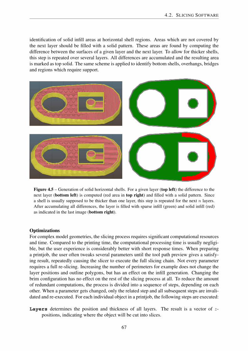
4.2. SLICING SOFTWARE
identification of solid infill areas at horizontal shell regions. Areas which are not covered bythe next layer should be filled with a solid pattern. These areas are found by computing thedifference between the surfaces of a given layer and the next layer. To allow for thicker shells,this step is repeated over several layers. All differences are accumulated and the resulting areais marked as top solid. The same scheme is applied to identify bottom shells, overhangs, bridgesand regions which require support.
Figure 4.5 – Generation of solid horizontal shells. For a given layer (top left) the difference to thenext layer (bottom left) is computed (red area in top right) and filled with a solid pattern. Sincea shell is usually supposed to be thicker than one layer, this step is repeated for the next n layers.After accumulating all differences, the layer is filled with sparse infill (green) and solid infill (red)as indicated in the last image (bottom right).
OptimizationsFor complex model geometries, the slicing process requires significant computational resourcesand time. Compared to the printing time, the computational processing time is usually negligi-ble, but the user experience is considerably better with short response times. When preparinga printjob, the user often tweaks several parameters until the tool path preview gives a satisfy-ing result, repeatedly causing the slicer to execute the full slicing chain. Not every parameterrequires a full re-slicing. Increasing the number of perimeters for example does not change thelayer positions and outline polygons, but has an effect on the infill generation. Changing thebrim configuration has no effect on the rest of the slicing process at all. To reduce the amountof redundant computations, the process is divided into a sequence of steps, depending on eachother. When a parameter gets changed, only the related step and all subsequent steps are invali-dated and re-executed. For each individual object in a printjob, the following steps are executed:
Layers determines the position and thickness of all layers. The result is a vector of z-positions, indicating where the object will be cut into slices.
67

CHAPTER 4. INTEGRATION OF ELECTRONICS AND MECHANICAL OBJECTS
Slice computes the intersections between the set of planes from the previous step and theobject model. Result is a vector of nested polygons (LayerParts).
Perimeters generates a set of extrusion loops by offsetting the LayerParts.DetectSurfaces split the remaining interior areas into regions with different filling strate-
gies for sparse internal and solid external infill.PrepareInfill detect bridges, combine infill regions over multiple layers etc.Infill generate the actual infill pattern extrusions.SupportMaterial compute the pairwise difference of adjacent layers to identify overhang-
ing regions and generate a supporting structure.
Additionally, most computationally intensive operations can be executed in parallel on suitablehardware. Parallelization is mostly done on a per layer- or per facet-basis (for the first slicingstep), since layers are mostly independent from each other.The slicing process can be either triggered manually or executed automatically upon invalida-tion of the current configuration when the user changes a parameter. The automatic executionis called background slicing. The idea is to reduce the response time. In an optimal case, theresult is immediately available and visualized. However, for complex objects the user interfacemay become unresponsive and the computation load is very high. For the integration of elec-tronic components, background slicing is heavily used to update the resulting placement andwire routes after each manipulation.
G-code ExportActual G-code instructions are only generated upon export of the final result. The tool pathpreview is rendered from internal extrusion representations only. Producing an executable G-code sequence from the geometric model of material extrusions requires the consideration ofa variety of additional aspects, including but not limited to: temperature control for nozzlesand printbed, travel moves, amount of material per extrusion segment (flow) and cooling. TheG-code file is created from bottom to top, layer by layer. If multiple objects are printed in asingle printjob, each object has its own set of layers. The layers of all objects are sorted bytheir print_z position and interleaved. Multiple copies of the same object are generated by"cloning" the G-code statements and only translating their x- and y-coordinates.
4.3 Import and Representation of eCAD-Data
The integration of electronics into a 3D-object requires a mechanical model of the object(mCAD) and a definition of the circuit (schematic diagram, eCAD). Importing a 3D-modelinto Slic3r from an .stl or similar format is a basic functionality, discussed in sec. 4.2.3. Sim-ilar to the 3D-model data, the import of schematics is split into an import function which canbe adapted to different file formats and a common internal representation. The import mech-anism was originally written by Daniel Ahlers [A2] and extended for this work. It currentlyonly supports EAGLE [B12] schematic (.sch) files. Such a schematic definition mainly con-tains a partlist, a netlist and package information for each component, encoded in anXML-format. A part describes the physical shape and pins of a specific component. A netbasically holds a list of connected pins with equal electric potential, representing an electric
68

4.3. IMPORT AND REPRESENTATION OF ECAD-DATA
connection. EAGLE stores spatial layout and routing information in a separate file which is notused at all for 3D-electronics.
As illustrated in fig. 4.7, the internal schematic representation is similar to the imported struc-ture, but contains additional semantic information. A single printjob can contain several phys-ical objects which are arranged on the printbed and printed in parallel. Each physical ob-ject representation is extended by an assigned Schematic class, which serves as a centralaccess point to all electronics related data and provides import and export functions. TheSchematic object holds a Netlist and a Partlist, similar to the imported data structure.The Partlist object provides geometric information about every component for the creationof cavities and visualization. It also holds the 3D-position of placed components which arestored relative to the mCAD coordinate system.The Netlist holds a list of 3D points, representing the geometry of wires, organized in agraph data structure for each individual net. The graph vertices are either pins, representingthe pins of a component, or user-generated waypoints. Edges represent direct, wired connec-tions between two pins. Upon initialization, the graph contains no edges and only pin verticesfrom the imported .sch-file.Figure 4.6 demonstrates how unwired connections are represented by rubberbands in theuser interface. To generate those rubberbands, all connected components of the graph are com-puted by a Depth First Search (DFS) based algorithm. The shortest spatial connection betweeneach pair of components is found subsequently and visualized by a rubberband (black). Newwaypoints and connections are created by double clicking an existing waypoint (red) or rubber-band and extending to an arbitrary point in 3D-space or an existing waypoint of the same net.Components, waypoints and wires are deleted by a double-right-click.Both Netlist and Partlist can be exported into a custom .3de-file to store the 3D arrange-ment and routing of a schematic in a printable object. The .3de-file only provides additionalpositioning and routing information and is linked to the original .sch-file, similar to a commonPCB layout file. This separation of circuit and layout information allows for later modifica-tions of the schematic. Additionally, the eCAD definitions are technically independent from themCAD model, also allowing for modifications of the physical shape of an object.
Figure 4.6 – Rubberband representation of a net. Left: unwired gnd-connection of 3 LEDs. Thegreen line indicates the resulting wired connection for the current ongoing interaction. Right: thesame net, partly wired. The left LED is only connected to the wired part of the net by the shortestrubberband possible.
69

CHAPTER 4. INTEGRATION OF ELECTRONICS AND MECHANICAL OBJECTS
Figure 4.7 – Architecture of the internal representation of electrical circuits and components. Eachmesh object on the plater holds an individual schematic object which imports the circuit informa-tion from an EAGLE netlist (green input files). The schematic object itself holds a partlist withcomponent geometries and positions and a netlist for electric connections. Each net is stored in agraph representation, containing the position of connected component-pins and user generated way-points. Position- and routing-information can be exported to an additional .3de-file which extendsthe original .sch-file (red).
The concept of a meta-format for 3D-electronics which aggregates and augments models fromdifferent domains without duplication of the respective model information is similar to theProstep ivip PSI ECAD/MCAD Collaboration format (.idx) [B6]. The .idx-format was es-tablished by a consortium of major CAD software companies to facilitate exchange betweendifferent specialized products, with a focus on spatial arrangement of conventional electroniccomponents. The Approach is described in a whitepaper [A18]. The standard is actively devel-oped by the "ECAD/MCAD-Collaboration" forum, new versions are released iteratively.
4.4 SMD-Component Integration
The first step of integrating a circuit into a 3D-object usually is to set the positions of com-ponents, followed by routing the wires. The geometric shape of the component’s body andpin positions is provided by the imported schematic definition, either as rectangle or polygon.For most standardized package formats (e.g. 0805, SOP, QFP) the component height is notexplicitly specified and must be provided by the user.
70

4.4. SMD-COMPONENT INTEGRATION
Figure 4.8 – Tool path visualization of a single object, augmented with the representation of elec-tronic circuits. The sidebar contains a list of all placed and unplaced components (1) and a dynamicgrid (2) with details of the selected component or waypoint (3, highlighted in green). Positioning ofa component or new waypoint is done with drag and drop on the currently selected top layer. Theslider on the right (4) allows to browse through the object layers. Exact positioning and rotating canbe done by modifying the values in the detail grid.
VisualizationSlic3r’s tool path visualization was extended to additionally display rubberbands, waypointsand SMD-components as illustrated in fig. 4.8. Unplaced components are positioned in an ob-ject by dragging them from list on the left to the surface of the currently displayed top layer.The exact position and rotation can be refined in the detail information grid on the lower left ofthe screen. The fader on the right indicates the current z-position and can be used to verticallybrowse through the generated layers. To visualize the components, individual meshes are com-posed from the footprint information by merging tessellated geometric primitives for all pinsand an extruded body outline into one object which can be displayed by the OpenGL-based ren-dering engine. The existing STL-library was used to store the generated meshes and to performrotations and translations.
Generation of pockets or cavities.Unless a component is placed on the surface of an object, a pocket or cavity is required toembed the component into the printed material. Cavities can either be part of the mCAD-model or generated dynamically during the slicing process. Explicit modeling of cavities offersmore design freedom, e.g. the battery slot in fig. 7.4 is shaped in a way that it also servesas a mechanical switch, but typically requires significantly more effort, especially when thecomponent position needs to be modified later. Cavities designed in the mCAD-model also donot respect any process parameters.Hence, for this work, the dynamic approach was chosen. The generation of cavities can bedone very early in the slicing process by modifying the original part model mesh prior to thelayer generation step (Layers), or by inserting holes into the LayerPart-polygons between the
71

CHAPTER 4. INTEGRATION OF ELECTRONICS AND MECHANICAL OBJECTS
Slice and Perimeters steps. Figure 4.9 illustrates the dynamic generation of cavities as itwas implemented into Slic3r. Once the LayerPart-polygons are generated, the algorithm iteratesover the list of all placed components and removes the convex hull polygon of the componentfrom each affected layer. The areas right below and above a cavity are marked as top- / bottom-surfaces during the DetectSurfaces step and therefore get automatically filled with a solidpattern, creating a smooth, reliable bed and cover for the component.
Figure 4.9 – To produce a cavity for a SMD-component, the part geometry from the imported .sch-file (1) is utilized. The convex hulls of the body (2) and pins (3) are combined (4), an additionaltolerance offset is applied and the resulting polygon is removed from all affected layer surfaces (5).
Generating a slot for an electronic component is considerably easy if the component is placedon its pins or flipped to its back (fig. 4.10, 1). A polygon, generated from the convex hull, canbe applied to every affected layer, leaving enough space to later fit the component into. Anadditional, user configurable offset is applied to achieve a sufficient tolerance. If the componentis rotated irregular, the ground of the slot must fit the components rotated geometry, but the topmust be flat and have at least the size of the projected convex hull polygon to allow the insertionof a component and to avoid collisions with the extruder after placing, as illustrated in fig. 4.10,3 and 4. For a given layer, this is achieved by generating a convex hull polygon from the rotatedcomponent geometry for this layer and computing the union of all component hull polygonsfrom the lower layers.
Figure 4.10 – Subtraction of SMD components from the printed object to create cavities. From leftto right: 1: outline subtraction, 2: part rotated but subtracted outline generated from flat footprint,3: naive polygon subtraction with rotation, 4: accumulating polygon subtraction with rotation.
Component placingOnce the position of components has been set and cavities are inserted to the G-code, placinginstructions are added to control the automatic pick and place process.During the G-code-generation, after each layer the list of SMD-components is checked forcomponents which are placed in the object, but not yet processed (printed) and whose upper
72

4.5. WIRE INTEGRATION
surface is below or at the current print_z value. The component is flagged as printed anda placing command is appended to the G-code, depending on the placing method selected bythe user:
Automatic Appends a "M361 P<partID>" command to trigger a fully automatic placingoperation as described in sec. 3.2.2.
Manual Appends a "M117 Insert component <partID>" command to notify the userthat a manual interaction is required. M117 simply displays a message at the screen. Ad-ditionally, a custom G-code snippet is appended to pause the printer, e.g:
G28 Z0 ; Home Z-axis for better accessibilityM0 ; Pause printjob, press button to continue
No placing Only appends a comment to notify the user that this component will not be placedat all. Omitting a component during the print process can be useful if it is located at asurface and supposed to be assembled in a subsequent processing step, e.g. for a verticalcomponent which can not be placed by the vacuum gripper.
Finally, a list with required information for all processed components is appended as describedin sec. 3.2.2 and the printed flags are reset.
Performance considerationsSince changing the position of a component requires a re-generation of the tool path to visualizethe result, performance is critical for the user experience. Often, only a small region of theobject is affected by such a change and a full re-slicing would introduce significant overhead.Modifying polygons on a per layer level allows for dynamic re-slicing of only a few layers,when a component is modified by the user. To achieve this, the original surface polygons mustbe stored to preserve the information that would be lost during the modification otherwise.After each user interaction, all layers which are affected by the modification are marked "dirty"and the slicing chain is triggered, starting with the Perimeters step, as the original Layer-Part polygons are already generated. All subsequent steps are layer-based and simply returnimmediately for clean layers. Finally, all dirty flags get removed.
Unfortunately, slicing only affected (dirty) layers causes several concerns. Combined infillaffects multiple layers and must either be disabled for partial re-slicing or adjacent layers mustbe also marked dirty, up to the maximum number of combined infill layers which is limited bya configuration parameter and the maximum printable layer height.If the modified component is already connected by wires, those have to be re-generated as well.While this is possible for static wire generation by following all connected wire to the firstfixed waypoint, it is not predictable which layers are affected by dynamically generated wiresas described in sec. 5.3.
4.5 Wire IntegrationThis section introduces the algorithmic core-concepts of the thesis, the generation of conductiveconnections within a printed object. Section 4.5.1 lays the groundwork by introducing the basicconcepts of waypoint based linear routing of wires over multiple layers. The generation ofactual physical channels and extrusion paths is then detailed in section 4.5.2, this also includes
73

CHAPTER 4. INTEGRATION OF ELECTRONICS AND MECHANICAL OBJECTS
strategies mitigation of defects and considerations to improve pin contacts. Once the basis isestablished, the next chapter 5 elaborates on dynamic routing approaches, incorporating thephysical topology of objects and wire self collisions, while preserving printability.
4.5.1 Static Wire RoutingAll wires connecting the individual components are stored in the Netlist object, representedby an acyclic undirected graph as introduced in sec. 4.3. The “rat’s nest” of placed but currentlyunwired components is visualized by a set of rubberbands. The routing of wires through the3-dimensional object is divided into two steps: the high-level generation of “waypoints” todefine the desired routing paths and the low-level routing of a single line between each tupleof waypoints. This concept allows for a certain level of decoupling between the classic routingtask of finding a collision free partitioning of the available space given a number of constraints,and the process related task of finding a set of suitable extrusion paths given a specific printer’sparameters.
Figure 4.11 – Generation of static wires. The unwired connection is represented by a rubberband(left), the route is defined by setting waypoints (a−d). Segment [a, b] crosses several planes, segment[b, c] affects only a single layer, [c, d] remains unwired.
The following algorithms focus on the second task, where a set of waypoints is manually de-fined by the user. Figure 4.11 illustrates how a single wire is represented by a sequence ofwaypoints w ∈ Z3 where usually the first and last waypoint are determined by the pin positionsof connected components. A wire segment s = [a, b] is the direct line between two subsequentwaypoints a and b. Note that waypoints are represented in scaled integer coordinates to avoidnumerical instabilities (cf. sec. 5.2.1).Figure 4.12 illustrates how the low level routing step computes a set of extrusion skeletons foreach layer from the 3-dimensional set of waypoints. This process is similar to the Slice stepwhich divides an object into a stack of 2.5-dimensional layers by computing the intersection ofa set of planes with the tesselated mesh representation. For a given layer L and each wire s,the intersection of the first point’s x-component ax with the lower and upper boundary Lb, Lt iscomputed by
a′x =
ax + (bx − ax) · Lb−az
bz−az if az < Lb
ax + (bx − ax) · Lt−azbz−az if az > Lt
and correspondingly for a′y and the second point b, resulting in a 2-dimensional set of lines. Thisstep is trivial for horizontal wire segments, where the intersection equals the planar projectionof the original wire. For inclined wires, the end points of the resulting line are then extended by
74

4.5. WIRE INTEGRATION
Figure 4.12 – Generation of extrusion paths from a wire routed in 3D-space. Left: three wiresegments (black) are defined by a set of waypoints (red), the slicing layer boundaries are indicatedas gray planes. Center: for inclined segments, the intersection with the upper and lower boundaryof each layer is computed to generate a horizontal section. Right: sections from inclined segmentsare extended to achieve reliable inter-layer contact points, resulting in a “staircase”.
a user defined offset to achieve a stable, overlapping, inter-layer connection to the adjacent wiresections as illustrated in fig. 4.12. The result of this routing step is an unordered set of extrusionlines per layer which requires further processing as described in the next section.
4.5.2 Channel Generation
The static wire routing step as described in the previous section produces a set of unordered,horizontal lines per layer. Actually printing a conductive trace with a direct write extruderrequires several additional steps to generate channels and a reasonable volumetric extrusion ofmaterial.
Extrusion trajectoriesIn a first step, the unordered lines are sorted to obtain continuous, printable polylines. This istrivial unless three or more pins are connected to the same net, inducing a junction as illustratedin fig. 4.13. Extrusion paths which can be printed as a continuous line are assembled by:
1. Finding an endpoint. Iterate the set until the first line with at least one endpoint whichdoesn’t coincides with any other endpoint. Remove this line from the set.
2. Traversing adjacent lines until finding a point which coincides with 0 (endpoint) or morethan 1 (intersection) other points and removing the lines.
3. Repeat steps 1-2 until the set is empty.
The trajectories are then printed in reverse order, such that the continuous line (the blue line infig. 4.13, 3) is printed first and all other traces terminate at the junction point to avoid crossingthe same point multiple times.The polylines can now be directly used as trajectory for the direct write extrusion. However, thestarting point of a an extrusion path tends to be not reliable after a retraction move. The plastic-and conductive ink extruder are in alternating use for every layer, therefore typically the firstconductive line at each layer is printed after a relatively long period of inactivity. Since wiresconsist of only one single trace, even a small air-gap is catastrophic. A few simple countermea-sures are implemented to mitigate extrusion defects:
75

CHAPTER 4. INTEGRATION OF ELECTRONICS AND MECHANICAL OBJECTS
Figure 4.13 – Generation of extrusion paths for a single layer. From left to right: 1: Wire segmentsfrom slicing. 2: Assembling a connected graph from unordered segments. 3: Re-fragmentation atjunctions, thin black arrows depict directions of overlapping extrusions. 4: Printed layer. Overlap-ping regions to ensure extrusion towards the SMD-pads are marked in red.
• After each toolchange the conductive ink extruder is primed by dumping a small amountof material and wiping the nozzle tip at a silicone blade.
• Each trajectory is split into two segments and the extrusion is executed from the center ofthe line towards the end to achieve reliable extrusion at the SMD-pad. The segments areextended at the starting point by a user defined offset, generating a small overlap at thecenter of the line. Possible over- or underextrusion only occurs at non-critical spots in theobject (see fig. 4.13, 4).
• The extrusion polylines are sorted by length, starting with the longest trajectory to maxi-mize the distance between overlap and endpoint. Trajectory splitting can be disabled bysetting the overlap parameter to 0.
• Priming the extruder is most important after a toolchange. Hence the amount of overlap-ping can additionally be increased only for the first segment of each layer to minimizedouble extrusions.
ChannelsThe resulting polylines are then used to generate channels for the wires by removing materialfrom the respective layers, similar to the cavity generation step described in sec. 4.4.Channels for the wires are generated by offsetting the polylines and subtracting the resultingpolygon from the current layer. The offset value amounts to e+ ∆
2, where e is the extrusion
width of the conductive material extruder and ∆ is an additional offset value provided by theuser for clearance. The result is illustrated in fig. 4.14, Layer 17.One fundamental issue when applying fine ink lines on a printed surface is the surface rough-ness, which is inevitable for the FDM-Process due to the working principle of plastic, extrudedby a single nozzle. If the wire is not aligned with the printed lines of a surface, ink tends tospread along the recesses resulting in electrical shorts as described by Espalin et al. [A19]. Forinks with a higher viscosity, the extrusion breaks off when crossing a surface peak or valley,resulting in disconnected electric connections. Typically, objects are fabricated with “sparse”infill to reduce printing time, weight and material consumption. Obviously, printing a wire onsufficiently sparse infill with a typical ratio of less than 50% plastic material makes the problemeven worse. Printing a wire on such a surface is generally impossible.Espalin et al. introduced an additional processing step by CNC machining pockets and channelsinto the half-finished FDM-printed object to achieve highly precise and smooth surfaces. Toavoid the expensive integration of a second process into the production chain with requirements
76

4.5. WIRE INTEGRATION
Figure 4.14 – Different layers of a tool path with integrated electronic components and wires, il-lustrating the steps for channel and cavity generation. Layer 12: Internal layer with sparse infill(density 20%). Layer 15: Several layers of solid infill to create a closed surface for wires and com-ponents. Layer 16: Layer directly below wires and components. The internal perimeters (yellow)serve as a smooth “substrate” for the wires, well aligned with the extrusion path of the conductivematerial. Layer 17: Channels and cavities are generated for the extrusion of wires and placing ofcomponents. Layer 18: Channels are covered by a region of solid infill. Layer 22: Placing ofcomponents. Layer 24: Components are also covered by a region of solid infill, providing reliablemechanical adherence.
77
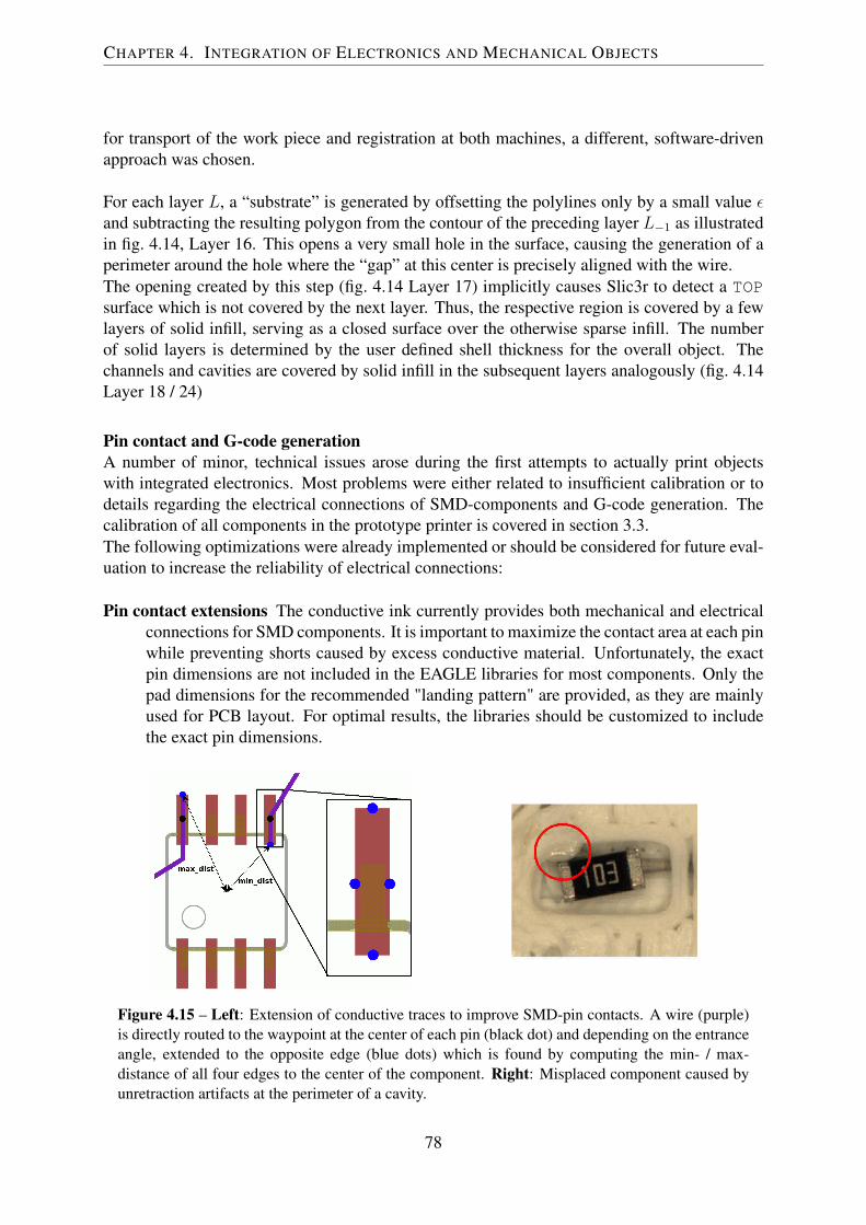
CHAPTER 4. INTEGRATION OF ELECTRONICS AND MECHANICAL OBJECTS
for transport of the work piece and registration at both machines, a different, software-drivenapproach was chosen.
For each layer L, a “substrate” is generated by offsetting the polylines only by a small value εand subtracting the resulting polygon from the contour of the preceding layer L−1 as illustratedin fig. 4.14, Layer 16. This opens a very small hole in the surface, causing the generation of aperimeter around the hole where the “gap” at this center is precisely aligned with the wire.The opening created by this step (fig. 4.14 Layer 17) implicitly causes Slic3r to detect a TOPsurface which is not covered by the next layer. Thus, the respective region is covered by a fewlayers of solid infill, serving as a closed surface over the otherwise sparse infill. The numberof solid layers is determined by the user defined shell thickness for the overall object. Thechannels and cavities are covered by solid infill in the subsequent layers analogously (fig. 4.14Layer 18 / 24)
Pin contact and G-code generationA number of minor, technical issues arose during the first attempts to actually print objectswith integrated electronics. Most problems were either related to insufficient calibration or todetails regarding the electrical connections of SMD-components and G-code generation. Thecalibration of all components in the prototype printer is covered in section 3.3.The following optimizations were already implemented or should be considered for future eval-uation to increase the reliability of electrical connections:
Pin contact extensions The conductive ink currently provides both mechanical and electricalconnections for SMD components. It is important to maximize the contact area at each pinwhile preventing shorts caused by excess conductive material. Unfortunately, the exactpin dimensions are not included in the EAGLE libraries for most components. Only thepad dimensions for the recommended "landing pattern" are provided, as they are mainlyused for PCB layout. For optimal results, the libraries should be customized to includethe exact pin dimensions.
Figure 4.15 – Left: Extension of conductive traces to improve SMD-pin contacts. A wire (purple)is directly routed to the waypoint at the center of each pin (black dot) and depending on the entranceangle, extended to the opposite edge (blue dots) which is found by computing the min- / max-distance of all four edges to the center of the component. Right: Misplaced component caused byunretraction artifacts at the perimeter of a cavity.
78

4.5. WIRE INTEGRATION
To improve pin contacts, conductive traces are extended to the opposite edge of the pin(or actually the opposite edge of the landing pad), depending on their entrance positionas illustrated in fig. 4.15.
Pin contact points A second problem, primarily related to component adhesion, is drying orcuring of ink before the component is placed. Details on the curing characteristics areprovided in section 3.1.3. Components are often placed several layers after the conductiveconnections were printed. To improve adhesion in those cases, small droplets of freshink can be dispensed right before the component is inserted. This is only possible ifthe ink dispensing nozzle is small enough (e. g. needle tip) to preclude collisions withhigher layers, as the nozzle tip must be positioned below the current print_z surface.Additionally, the ink extruder must have sufficient clearance to all other extruders, whichis granted in our case since the conductive ink extruder is mounted on an individual z-stage and lowered sufficiently for this operation.
Slic3r is designed for a layer-based, horizontal data structure and has no model for ver-tical extrusions. A new ExtrusionEntity model was implemented which providesvertical extrusion of a single line for a given height. The layer thickness of the first layeraffected by the cavity cutout is used as height of the vertical extrusion. Pin connectionoptions can be set per component to add droplets right after the connecting wires wereprinted, immediately before placing the component or disabled entirely.
Additionally, the component adhesion could be improved by also dispensing contactpoints for unconnected pins. This is not implemented yet.
Wire bed endpoints Wire beds ensure a smooth, solid and well aligned substrate for the de-position of conductive material. For SMD components with multiple pins this raises aproblem, as every endpoint generates its own extrusion loop inside of a the small areaunder the component. Figure 4.16 illustrates how this can lead to a high number of smallgaps and retraction movements if the extrusion width does not happen to by a multipleof the pin distance. Both gaps and particularly unretration movements result in a highlyirregular and unpredictable surface structure. To mitigate this effect, it is considered tointroduce a new surface type which generates a solid surface under components, wherethe infill pattern is aligned with the main direction of the pins. Such a surface could beprinted in a single run. A smooth but not perfectly aligned surface is still preferred overunpredictable gaps and blobs.
Figure 4.16 – Endpoints of wire beds causing a very irregular surface under multi-pin components(left). Gap filling leads to a high number of retraction and unretraction movements (right).
79

CHAPTER 4. INTEGRATION OF ELECTRONICS AND MECHANICAL OBJECTS
Unretraction strategy Channels and cavities by design are enclosed by perimeter extrusionloops. Entering such a loop requires an unretraction move which is prone to cause blobs,increasing the risk of interrupted conductive extrusions and component placement failuresas shown in fig. 4.15, right. The precision of unretractions decreases after long travelmoves and extruder changes. Minimizing travel moves and extruder changes prior toextrusion loops in the immediate vicinity of electronic components has the potential tomitigate the effect.
The actions described above are part of the tool path generation itself, the effect is alreadyvisible in the preview. At the stage of actual G-code-generation, some additional modificationswere required to reliably print conductive paste with a syringe extruder:
Extruder ordering For multi-extruder setups, extruders are usually used in alternating order,but with minimal extruder changes. Consider the example of two colors, white and black,both colors are used at each layer. At the end of layer Li, the black extruder is active. Thenext layer Li+1 is then started with the black extruder as well and finished with the whiteextruder to avoid the additional change. Layer Li+2 continues with white and so on.
For conductive paste, it is preferable to always have the extrusion at the end of a layerto minimize the time between extrusion and application of components and to reduce therisk of defects caused by a plastic extruder, crossing or touching a wire.
Extrusion width and speed Different aspects of an object (e.g. external perimeters or topsolid infills) require individual extrusion parameters, mainly extrusion-width and speed.A conductive_wire extrusion role was added to assign an extruder and configureextrusion-width and speed values. This role is assigned to all polylines, each representedby an ExtrusionPath object. The extrusion speed for needle dispensing of conductivepaste is very low, typically less than 2 mm/s. The extrusion-width must be set by theuser and describes the absolute width of the extrusion which is roughly shaped like a“squashed” cylinder.
Retraction and wiping Proper retraction for both the plastic, as well as the conductive ink ex-truder is important to avoid oozing and over- / underextrusion at the start of the first line.Oozing is a severe problem for the conductive ink extruder, as it potentially causes shorts.For the plastic extruder, blobs (too much) or gaps (not enough material) are the prevalentissue, but oozing can also cause problems if conductive traces are crossed and the un-cured ink is smeared by the trailing plastic strand. Further details and images are givenin sec. 7.1. Both extruder types have very different retraction and wiping requirements.The plastic extruder requires a high amount of fast retraction to remove the filament fromthe hot nozzle tip, whereas the conductive ink extruder is limited to very small retrac-tion values to avoid intake of air into the syringe. Slic3r natively supports per-extruderretraction settings. However, each extruder has a different wiping position. Also, the cur-rent amount of retraction must be known for correct unretraction prior to wiping. To solvethis, the tool change G-code insertion was extended by a set of new placeholder variables,which get replaced with the current values during each toolchange operation. Particularly[previous_retraction] and [next_retraction] are additionally exposed.
Different wiping positions were initially handled by a post-processing script, which filtersG-code lines based on logical conditions. This initial work was later implemented in
80

4.5. WIRE INTEGRATION
Slic3r as a conditional G-code parser by the community. A correct unretraction movementfor the plastic extruder (tool 0) can now be easily expressed as:if [next_extruder] == 0G1 E-[next_retraction] F1400
81

CHAPTER 4. INTEGRATION OF ELECTRONICS AND MECHANICAL OBJECTS
82
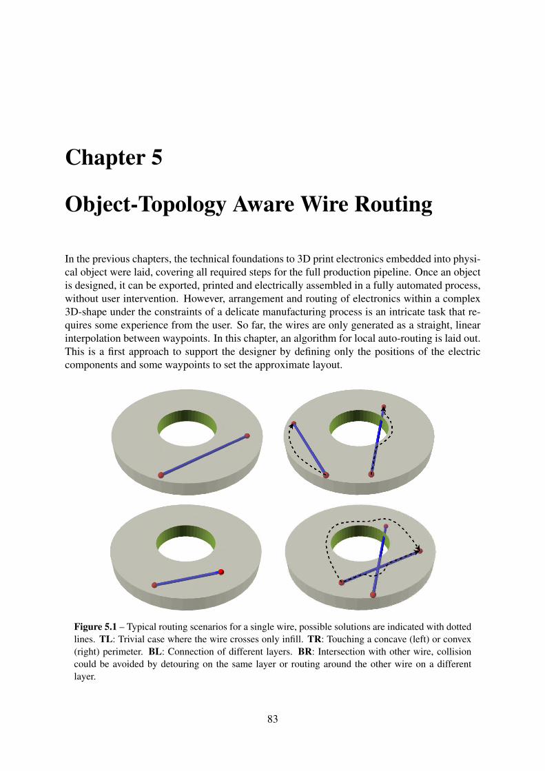
Chapter 5
Object-Topology Aware Wire Routing
In the previous chapters, the technical foundations to 3D print electronics embedded into physi-cal object were laid, covering all required steps for the full production pipeline. Once an objectis designed, it can be exported, printed and electrically assembled in a fully automated process,without user intervention. However, arrangement and routing of electronics within a complex3D-shape under the constraints of a delicate manufacturing process is an intricate task that re-quires some experience from the user. So far, the wires are only generated as a straight, linearinterpolation between waypoints. In this chapter, an algorithm for local auto-routing is laid out.This is a first approach to support the designer by defining only the positions of the electriccomponents and some waypoints to set the approximate layout.
Figure 5.1 – Typical routing scenarios for a single wire, possible solutions are indicated with dottedlines. TL: Trivial case where the wire crosses only infill. TR: Touching a concave (left) or convex(right) perimeter. BL: Connection of different layers. BR: Intersection with other wire, collisioncould be avoided by detouring on the same layer or routing around the other wire on a differentlayer.
83

CHAPTER 5. OBJECT-TOPOLOGY AWARE WIRE ROUTING
The term local in this context refers to finding a connection between two adjacent waypointswith fixed positions, where the wire segment must terminate at the exact waypoint positions.Global routing is defined as finding a connection between two endpoints of a net, e.g. twoSMD-pins. In a weaker definition, waypoints can be set to guide the routing algorithm by at-tracting the search with preferred exploration along the predefined path.
For the rest of this chapter, the routing problem is defined as finding the optimal, collision freepath, connecting two points A and B which is printable for a given object geometry and set ofprinter configurations. A and B are two adjacent waypoints, connected by a rubberband. Therouting step is executed iteratively on all wire segments, avoiding collisions with previouslyrouted wires.
The overall goal is to support users with their task of defining wire paths, by finding a smoothtrajectory in a complex shaped object, while not interrupting perimeters and reducing the amountof small gaps. Avoiding collisions between wires is a second important objective. 3D printingoffers a huge potential in this field, by introducing a full third dimension. On the downside,electrical connections between layers are prone to a high risk of defects. They also require sig-nificant physical space since direct vertical connections are not possible in most cases, and therouting complexity increases.
Figure 5.2 – Minimal example of a single wire toillustrate routing steps in the following sections.
The routing algorithm should also adapt tochanges in process parameters (layer height,number of perimeters, extrusion width etc.)to make the design process more indepen-dent from the manufacturing step. Fig-ure 5.1 illustrates different typical scenar-ios in the same order as in this chapter.Figure 5.2 shows an actual screenshot ofa trivial case of routing a single rubber-band in the simple demonstration object fromfig. 5.1. The waypoints are implicitly definedby the positions of the SMD-components,the wire is not yet generated. This objectis used throughout the next sections as aminimal example to illustrate the basic con-cepts.
The remainder of this chapter is organized as follows: first, an overview of search space rep-resentation and routing algorithms from related domains, particularly electronic circuits androbotic navigation, is given in section 5.1.In section 5.2, the reduced problem of routing a single wire on a single layer is analyzed. Thisincludes appropriate representation of the search space and utilization of common pathfindingalgorithms.Section 5.3 extends the search space to the full stack of layers which is required to describe awhole 3D-object. A focus is set on the problem of finding a set of suitable connections betweenadjacent layers which can then be used by the pathfinding algorithm to “jump” from layer to
84

5.1. RELATED APPROACHES
layer. Another important aspect is the coherent representation of positions (polygon points,vertices and waypoints) to identify matching points on different layers and to use indexing forefficient data access.Basic strategies for collision avoidance of multiple wires are discussed in section 5.4. Finally,section 5.5 wraps up the algorithmic results and gives a short summary of the entire routing andG-code generation process.
5.1 Related ApproachesRouting or pathfinding problems are a very common aspect in several domains and have re-ceived a tremendous amount of research over the last decades. The domain of PCB-routing,where many collision-free paths must be found in a constrained space, and the field of routeplanning in robot navigation and path planning, where only a single route must be found in acomplexly shaped terrain, are particularly related to the problem at hand and therefore consid-ered important.
5.1.1 VLSI and PCB routingVery Large Scale Integration (VLSI) in general and PCB design in particular are concernedwith the problem of arranging a number of components on a given surface (placement) andoptimizing collision-free connections between the components (routing). Figure 5.3 illustrateshow the problem is usually subdivided into multiple steps: global routing in which the wiresegments are tentatively assigned to coarse regions and detailed routing where wire segmentsare assigned to specific routing tracks [A39]. Additionally, optional timing driven steps canbe applied to refine the topology to perform optimizations, e.g., minimizing the total routinglength or circuit delay. The additional steps are particularly interesting as a potential solution tocompensate for the high resistivity of the silver ink used in our experiments.
Figure 5.3 – Example of coarse global routing (left), where the wires are assigned to regions andfine detailed routing (right) to determine the final positions of wires and vias. The three nets N1 -N3 are routed with rectilinear paths on two separate layers for vertical and horizontal connections[A39].
To model the available routing space, occupied regions are represented as polygons and the freespace is divided into regions of different types, e.g. channels, with wire running only from one
85

CHAPTER 5. OBJECT-TOPOLOGY AWARE WIRE ROUTING
edge to the opposite, and switchboxes, with connections into all four directions [A67, A39].The routing space is typically stored in a graph data structure for efficient reasoning as sketchedin fig. 5.4.
Figure 5.4 – Positions of switchboxes (numbered), channels (un-numbered) and the correspondingswitchbox connectivity graph representation [A39].
Classic routing approaches are Manhattan-grid-based [A53] and typically utilize RectilinearSteiner Minimal Tree (RSMT) algorithms to find an (optimal) spanning-tree between all pinlocations of a net. Constructing an RSMT in the general case is proven to be NP-hard, thereforeseveral heuristic solutions have been developed for practical applications [A31, A14]. Non-Manhattan Routing extends the grid to a 6- or 8-connected neighborhood, additionally allowingfor diagonal connections [A98]. Several modern routing algorithms are based on graph routing,Integer Linear Programming (ILP) and congestion avoidance methods. The focus lies on thedispatching of a high number of connections, which currently is not a realistic scenario forprinted electronics.An important concept to resolve conflicting routes with intersections is the Rip-Up and Reroute(RRR) strategy [A39]. In the naive, greedy procedure, wires are routed sequentially, forcinglater wires to accept large detours if the direct connection is already occupied. RRR allows totemporarily create conflicting routes. Once the overall structure is settled, those wires with thebest alternative paths available are ripped up and routed again.
5.1.2 Path Planning in Robotics
This paragraph mostly follows the textbooks by Siegwart et al. [A75] and Tzafestas [A86].Path planning in robotics refers to the fundamental problem of finding a collision-free path for agiven robot configuration in a partly occupied environment. Given a configuration q of the robotthat is composed of q1, . . . qk values. Each value represents a degree of freedom of the robot(e.g. a joint). The configuration space CS of the robot is the set of values that its configurationq may take. Then, the free configuration space CSfree is the subset of CS where the robot isnot in collision with an obstacle and therefore can move safely.Path planning in the sense of navigation in a planar environment for mobile robots can be seenas a simplified sub-problem, where the degree of the configuration space is typically limitedto two (x, y) or three dimensions (x, y, θ) for the position and rotation of the robot. For navi-gation purposes, CSfree is usually represented by a map. The type of map representation can
86

5.1. RELATED APPROACHES
Figure 5.5 – Left: continuous map representation using polygons to model areas and obstacles.Right: the same map in discrete occupancy grid representation, recorded with a laser scanner.
have an impact on the available options for position representation and navigation algorithms.Figure 5.5 shows frequent representations of maps, either continuous, with polygons as envi-ronmental obstacles, or discrete occupancy maps, where the space is decomposed into a grid.Besides the fixed grid decomposition, exact cell decomposition is widely recognized, to tes-sellate the free space between obstacles into distinct regions [A51]. Exact decomposition isonly feasible if the number of obstacles and the resolution of the polygon representation is lowenough.
For mobile robots, path planning involves two aspects that complement each other. Global pathplanning identifies a collision-free, efficient trajectory from start to goal, based purely on priorknowledge of the terrain (map). Local obstacle avoidance approximately follows the globalpath, but modulates the trajectory based on current sensor information to avoid collisions withpreviously unknown or dynamic obstacles. For this study, we focus on global path planningunder a closed world assumption without sensor input.
Deterministic search algorithms require an appropriate data structure to represent the map. Asa common first simplification step, the robot is represented as a point and all obstacles are in-flated by the radius of the robot convex hull. The map is then usually converted into a graphrepresentation. Grid-based occupancy maps can be seen as a special case of graph represen-tation where each cell is connected to the four or eight adjacent cells. Polygon base maps areoften converted into a graph representation by constructing the visibility graph. All polygonpoints which are visible to each other are directly connected by a straight line as illustrated infig. 5.6. Depending on the number of polygons and their resolution, the number of additionaledges might become very large. The shortest path in a visibility graph often exactly follows thecontours of some obstacles. While this effect is a serious problem in robotics, where a certainsafety distance is desired, it well matches the requirement in 3D printing where a conductivetrace is preferred to either match the contour or keep a certain distance to avoid small gaps. In atessellated map representation from a cell decomposition, the center of each cell, or the centerof each edge between two adjacent cells might be taken as a graph node, with edges connectingadjacent, non-occupied cells.
87

CHAPTER 5. OBJECT-TOPOLOGY AWARE WIRE ROUTING
Start
Goal
Start
Goal
Figure 5.6 – Navigation in a polygon-based map representation. Left: visibility graph, constructedby connecting all pairs of polygon points (red) with unobstructed line of sight and result from theA* search (orange). Right: tessellated representation of the same map. The graph is constructed bycreating nodes at the center of each edge (red) and connecting adjacent nodes.
5.2 Intra-Layer Connections
We start to solve the routing problem by considering the sub-problem of routing a single wiresegment within a single layer L. Later we will later generalize the solution to the three-dimensional case in sec. 5.3.
5.2.1 Data Representation
This section gives a short overview of the basic data structures which are used throughout therest of this chapter. The fundamental concepts of graph representation, notation and algorithmsare covered in more detail by virtually any textbook on algorithms, e.g. [A15, A75]. An ex-cellent, very detailed, informal overview of map representations and different aspects of the A*search algorithm is provided by [B23].
The search space in a given Layer Li is constrained by the physical outline of the layer contour,represented by a set of nested polygons. It is also constrained by the contour of one or moreprevious layers Li−1 . . . Li−n since the wire must be printed on a solid surface; bridges or over-hangs are not acceptable. The printed contour of Layer Li is generated by a set of np perimeterloops, forming the solid shell of each object. Within this shell which is filled with a sparse infillstructure, wires can be routed arbitrarily.
We use an undirected, weighted graph G = (V,E) with E ⊆ [V ]2 to represent the searchspace of each Layer Li. Vertices are mapped to a set of vertex properties: V → S, particularlycontaining the spatial position p of each vertex: p : V → Z3 and a number of properties forinternal use in algorithms i.e. color, distance, predecessor etc. A weight function w : E →R+
0 assigns a nonnegative weight w(u, v) to each edge. The weights are used to “prioritize”connections, e.g. to attract routes to be aligned with perimeters.All coordinates, weights and distances are scaled by a factor of 106 and represented by integervalues to avoid accuracy problems caused by floating point approximations.
88

5.2. INTRA-LAYER CONNECTIONS
After initialization, the empty Graph G is successively filled with information which is alreadyavailable prior to the routing step. This includes the existing perimeters of the given layer(sec. 5.2.2) and the direct connection between start- and endpoint of the current wire segment(sec. 5.2.3). During the routing process, the graph is successively extended as new connectionsare inserted in the currently explored region, aligned with a global grid (sec. 5.2.4).
The graph data structure is supported by external indices to allow for efficient access to individ-ual elements. The spatial position p of each vertex is a native property ofG (vertex-point-index).An inverse index Z3 → V is maintained as additional hash-map, to find the corresponding ver-tex for a given point (point-vertex-index). A list of all possible z-positions (layers) is providedto facilitate direct access to corresponding points on adjacent layers and to enable iterating overall layers of the 3D-model.
Finally, an R-tree [A30] based index is incorporated for efficient spatial relation queries (spatial-index). Since approximate spatial access is typically used in the current, or the direct lower andupper adjacent layers, the index is implemented as a map of two-dimensional R-trees, withz-positions as keys. The R-tree index is mainly used for two purposes. Due to the use of scaledinteger values, coordinates are unique within the graph. However, coordinates from the userinterface (waypoints) or slight deviations introduced during the slicing and polygon offsettingsteps frequently result in very similar, but not identical points. Two points with a distance belowa certain threshold ε are considered to be coincident. Without a spatial index, for simple lookupoperations (“is there a corresponding point on the next layer?”; see section 5.3.2) all vertices ofG must be checked for ε-coincidence individually by iterating the entire graph. A nearest-query is used to find the closest point which is then tested for ε-coincidence in a second step.The second application is introduced in sec. 5.2.4. The graph is dynamically extended by thesearch algorithm during the routing step. To connect a new grid-cell with existing vertices, allpoints within a bounding box must be identified (within- query).
No index R-tree (quadratic) R-tree (R*) No wires35.4 s 1.4 s 1.4 s 0.1 s
Table 5.1 – Execution time of the full slicing process for a test object with 604 facets to comparethe effect of different indexing strategies. Wires were spanning the maximum possible extent ofthe object to achieve a worst case scenario. Different R-tree implementation strategies showed nosignificant effect. The test object was also sliced without embedded wires for reference.
Using the R-tree index approximately reduces the complexity for spatial queries from O(n) toO(logn), which is significant, given that it is invoked in each exploration step of the searchalgorithm (Alg. 1, line 12). A brief performance evaluation is given in tab. 5.1.
5.2.2 Perimeters
The optimal route of a wire crossing or touching a perimeter would be such that it is perfectlyaligned with the most inward perimeter extrusion line. If this is not possible, due to a lack ofspace, the next best option would be the second, third, etc. perimeter. The number np and width
89

CHAPTER 5. OBJECT-TOPOLOGY AWARE WIRE ROUTING
Figure 5.7 – Parameters of a single conductive trace embedded in a printed channel. The distancebetween the vertical dashed lines indicates the required offset ∆1 to compute the deflated surfacefor a single perimeter loop (eq. 5.1).
δp of perimeter extrusions are defined by the user and potentially vary between each object,printer, or even different configurations on the same printer.Figure 5.7 illustrates the dimensions of a conductive trace, the required channel and the com-bined distance from the boundary of a plastic extrusion to the center of the conductive trace asit is used to compute a wire trajectory aligned to the object boundary.Optimal wire traces for all perimeters are found by taking the contour of Layer Li (fig. 5.8 Left)and computing a set of offset-polygons (deflated surfaces) for each perimeter. The offset values∆ are given by:
∆k = k · δp +δc + γ
2, k ∈ 0 . . np (5.1)
where δc is the extrusion width of the conductive material and γ is the amount of extra space toform a channel around the wire. The result of this operation is the center of the potential extru-sion line for conductive material, aligned to the respective perimeter. As discussed in sec. 4.2.3and illustrated in fig. 4.4, the extrusion width δp of the plastic extruder varies between internaland external perimeters and for different materials in one object and must therefore be com-puted for each individual layer and region.
In a final step, the resulting polygons are weighted, to prefer inner traces, and added to thegraph. The result is depicted in fig. 5.8 right. The edge weight w for the k-th contour computesas
wk = 1.0 + (np − k) · α (5.2)
where α can be configured in the user interface as conductive_wire_routing_perimeter_factor, with a default value of α = 0.1. For the example given in fig. 5.8, thisassigns a weight of 1.0 to the most inward (3), 1.1 to the second (2) and 1.2 to the outer (1)contour.
90

5.2. INTRA-LAYER CONNECTIONS
Figure 5.8 – Left: contour (slice) of layer Li. Right: graph edges as potential routes for wires,aligned to the object perimeter, found by offsetting the contour polygon. The resulting edges areweighted decreasingly from 1 to 3 to prefer traces with a higher distance to the surface and thenadded to G.
Aligning conductive wires with the perimeter extrusions has an undesirable effect when thenumber of perimeter extrusions np is odd. In fig. 5.9 the conductive trace is correctly alignedat a distance of three perimeters, but since perimeter extrusions surround both the wire and theobject, only an even number of loops is printable without a gap This effect can obviously beavoided by choosing an even number of perimeters.
Figure 5.9 – Effect of wire aligned to an even number (left) and an odd number of perimeter extru-sions, resulting in a gap (right).
5.2.3 Direct Connections
A second information which is immediately available is the direct connection l between A andB. Both points are always added as corresponding vertices s and t to G, as they are requiredas start- and endpoint of the search. In the trivial case where A and B both lie within the infillregion of a single layer and a straight conductive line would not touch or cross any perimetersor other wires, an edge e(s, t) is added as shortest possible connection.
91

CHAPTER 5. OBJECT-TOPOLOGY AWARE WIRE ROUTING
Figure 5.10 – Generation of shortcut edges if rubberbands are touching or crossing perimeter extru-sions. TL: Rubberband potentially crossing all three designated perimeter-aligned wire extrusionswith decreasing weight from 1 to 3. Intersection points with the first (TC), second (TR) and third(BL) extrusion path are computed individually and the resulting segments are appended to the graph.Weights are inherited from the perimeter polygons. A high weight (yellow) is assigned to edges out-side of the material. BC: In a final step, all combinations of start- and endpoints of the resultingedges are appended to G as well to enable connections between the different path options.BR: Orientation of contour polygons: outer perimeters (CCW) and inner perimeters (CW).
For the general case, intersections of the line l with all deflated surfaces generated in the lastsection are computed and fragments are added to the graph as skip links or shortcuts to acceler-ate the search and to provide direct connections between the perimeter traces of adjacent holes.
Consider the example given in Figure 5.10, where the direct connection l (blue) crosses the layerboundary twice. To find all shortcut connections, we iteratively compute the intersection of lwith all deflated surfaces. For each intersection found, a new point is inserted into the polygonand added to the graph, along with a set of matching edges.
The shortcuts are weighted either with the weighting factor of the current inflated slice if thesegment is inside of the material or with a (high) hole_routing_factor if not (yellow).The weight assignment is determined by computing the orientation of the current intersectionwith the deflated polygon as illustrated in fig. 5.10 BR. By definition, the outside of the object isalways on the right side of a contour. Hence, the orientation of an intersection indicates whetherthe following section lies in a hole or outside of the object as depicted by the blue arrow.
The result without any further steps would be similar to the Bug2 algorithm described in [A58](fig. 5.11 right).
92

5.2. INTRA-LAYER CONNECTIONS
Figure 5.11 – Visualization of the routing graph with perimeter and direct connection edges (left).The route at this stage is bound to the static graph connections (center), resulting in trajectoriessimilar to the Bug2 algorithm [A58] (right). (Image from [A58], fig. 4.)
5.2.4 Expanding Grid SearchOnce the graph representation of Layer Li is assembled, a variety of common search algorithmscan be applied to find the most optimal route for a printed wire. We use a priority queue basedimplementation [B2] of the A* algorithm [A32] to conduct the search as outlined in Alg. 1.The right-aligned comments serve two purposes: they informally describe the function of im-portant steps and indicate visitor event points of the boost implementation, where the algorithmcan be extended.In the pseudocode, d(v) is the distance of vertex v from the start vertex s. f(v) denotes theestimated cost of the best path from s over v to the goal vertex t, by combining the distanceto v and the estimated distance to the goal: f(v) = d(v) + h(v). Q is a queue, holding allopen vertices, ordered by their f -value. p(v) points to the predecessor of v and represents theresulting path after execution of the search algorithm.
Two core concepts are highlighted in red: the heuristic h in line 1 and the examine_vertex visi-tor event point in line 12. The basic realization of both concepts is explained in the following.More details for the final implementation, covering the full 3D-space, are provided later in theirrespective sections 5.3.2 and 5.3.3.
93

CHAPTER 5. OBJECT-TOPOLOGY AWARE WIRE ROUTING
1 A* (G, s, h)2 foreach vertex u in V do // initialize vertex u3 d[u] := f [u] :=∞;4 color[u] := WHITE;5 p[u] := u;6 end7 color[s] := GRAY ; // initialize start-vertex s8 d[s] := 0;9 f [s] :=h(s);
10 Insert(Q, s) ; // discover vertex s11 while Q 6= ∅ do12 u← Extract-Min(Q); // examine vertex u13 foreach vertex v in Adj[u] do // examine edge (u, v)14 if w(u, v) + d[u] < d[v] then15 d[v] := w(u, v) + d[u];16 f [v] := d[v]+ h(v);17 p[v] := u;18 if color[v] = WHITE then19 color[v] := GRAY;20 Insert(Q, v); // discover vertex v
21 end22 else if color[v] = BLACK then23 color[v] := GRAY;24 Insert (Q, v); // reopen vertex v
25 end26 end27 end28 color[u] := BLACK ; // finish vertex u
29 end30 end
Algorithm 1: The basic A* algorithm, used for searching an optimal wire route in G basedon the formulation from the Boost Graph Library documentation [B2] which was used forthe implementation.
94

5.2. INTRA-LAYER CONNECTIONS
Vertex u
Currentbest path
New gridvertices
Connection toexisting vertex
Rejected vertex outside of material
Figure 5.12 – Dynamic generation of new grid vertices. Upon examination of the current vertex(blue), new vertices (red) are generated in 45°steps with a distance of ν (grid_step_distance).Existing vertices within a radius of ν are connected in a second step (green).
So far, the search would be bound to the perimeters and straight connections, with trajectories“jumping” from obstacle to obstacle as illustrated in fig. 5.11. To also cover infill regions, anexploring grid is generated dynamically during the search. Upon examination of the currentvertex u (Alg. 1, line 12), new vertices vk are inserted in 45° steps around the current vertexduring the examination step as illustrated in fig. 5.12. The 8 neighbor points are generated on arectangular grid with configurable grid_step_distance ν, aligned to the object origin. Ina subsequent step, it is tested whether the new vertices lie within an infill area by testing if theyare contained by the deflated surface polygon of Li (fig. 5.12, purple vertex). Valid new verticesare added to G and connected to u by an edge e = u, vk. Additionally, existing verticesare connected by new edges if they lie within the grid step distance, to also establish contactsbetween perimeter traces and the grid (fig. 5.12, green vertex). Grid edges are weighted withthe same factor as the most outside perimeter edges (cf. equation 5.2). With a number of npperimeters and the perimeter factor α, the grid weight wg amounts to:
wg = 1.0 + np · α (5.3)
The R-tree index is utilized to efficiently select all existing vertices within a box of size ν(grid_step_distance).
Figure 5.13 demonstrates how the graph dynamically grows during the search. In the sim-ple cylindric demonstration object, the resulting route is actually the same as the route shownin fig. 5.11 without grid generation. The two components are located very close to the innerperimeter, therefore following this perimeter is actually optimal. However, the difference isclearly visible in the second, slightly more complex object in fig. 5.11.
The key feature and main difference between A* and Dijkstra’s algorithm is the use of a heuris-tic. Instead of only considering the minimum distance from the current node to the source, A*uses the sum of the distance from the source node s to the current node u and the estimated
95

CHAPTER 5. OBJECT-TOPOLOGY AWARE WIRE ROUTING
Figure 5.13 – Top: Development of the graph during a routing step. In infill areas, a grid is dynami-cally generated during the search process. Bottom: Demonstration of the same effect with an objectwhere the wire actually crosses an infill region.
distance to the goal t to significantly accelerate the search by providing additional informationabout the general direction to the goal (alg. 1, line 16).A heuristic is said to be admissible if it never overestimates the actual minimal cost between uand t. A* is optimal if the heuristic also is monotonic, meaning that for every pair of adjacentvertices x and y, h must satisfy the condition:
h(x) ≤ d(x, y) + h(y)
However, even with a monotonic, admissible heuristic, all equally suitable paths with the samedistance to the current fringe must be evaluated. The search can be accelerated by relaxingthe admissibility criterion and slightly overestimating the actual distance. By adding a factor ε(ε > 1) to the heuristic, the search is performed faster, producing a non-optimal result. How-ever, the result is still guaranteed to have a cost of at most ε times the optimal path [A63].
For the simplified 2D-routing problem, a Euclidean distance is used as heuristic to guide thesearch:
h(v) =√dx
2 + dy2 · ε (5.4)
where dx is the distance between the current vertex and the goal vertex along the x-axis:p(t).x − p(v).x, dy respectively. ε is a user-defined factor to adjust the processing speed versusrouting quality. Due to the nature of the 8-connected grid, the Euclidean distance is not optimalin regions where the wire crosses only infill, resulting in an underestimation of the actual cost
96

5.3. INTER-LAYER CONNECTIONS
and causing the algorithm to evaluate more nodes than necessary. An optimal heuristic for infillareas would be the octile distance:
h(v) = (dx + dy) + (√
2− 2) ·min(dx, dy)
However, the octile distance overestimates the remaining distance if it is possible to travel alongan inner perimeter and therefore would break admissibility.Further details on the heuristic used for the 3D-case, including inter-layer connections are pro-vided in section 5.3.3.
5.3 Inter-Layer Connections
Figure 5.14 – Overlapping inter-layer connection,aligned with the object perimeter.
Generally, a wire is not horizontally alignedwith a single layer, but crosses several lay-ers. In the previous section, only those partsof each wire were used which intersect thecurrent layer, as described in sec. 4.5.1 and[A92]. The start- and endpoint A and Bof the current segment were both located onthe same layer and the routing was also con-strained to this layer.For the A*-algorithm it makes no differencewhether it operates on a 2D or 3D-graphto find optimal routes. The graph that was
sketched in section 5.2 already contains the full 3D-representation of all layers. However, thechallenge is to ensure proper overlapping of extrusions when the wire jumps to the next layerto ensure conductivity by creating a “staircase” while maintaining the alignment to perimetersas demonstrated in fig. 5.14. The required length of overlap when jumping from one layer tothe next is given by a user-defined parameter interlayer_overlap. This problem can besolved by finding equal sequences of vertices pairwise in adjacent layers where the length ofthe sequence is higher than interlayer_overlap. Finding all possible combinations ofgraph segments for two adjacent layers is computationally expensive and therefore consideredto be not feasible.To reduce the complexity, we try to only search for combinations with a high probability ofbeing used by the final route trajectory. In a first step, direct connections between A and Balong the rubberband are added to the graph prior to the routing step to ensure the shortest pathis always available (sec. 5.3.1). Then, to find eligible positions for overlapping, yet optimalinter-layer connections, the exploring vertex examination step (alg. 1, line 12) is used again toonly consider candidates with a high probability of being used (sec. 5.3.2).
5.3.1 Direct Linear ConnectionsIn section 5.2.3, it is described how the shortest, direct connection is always inserted to the graphbefore the actual routing step is executed. Since computing all intersections with perimeterpolygons is not directly applicable for the 3D-case, the approach is extended with inter-layerconnections.
97

CHAPTER 5. OBJECT-TOPOLOGY AWARE WIRE ROUTING
Figure 5.15 – Generation of overlapping sections for linear inter-layer connections. The rubberband(red) intersects the layer boundary of L3 at p2. Coming from the right, the upper horizontal edge(green) would end at p2. It is extended to p1 to achieve an overlap with the lower layer, but the newinter-layer connection edge is inserted starting at the point at p3 (orange). The resulting route wouldtraverse green, orange, green. The blue lines are additionally stored in an overlap-segments mapand inserted later to achieve an overlapping electric connection. The resulting conductive traces areindicated in gray.
Each rubberband is split into a set of segments, one for each layer, as described in sec. 4.5.1 forstatic routing. Modeling overlapping sections in the graph is difficult. Simply connecting theendpoints of two segments on adjacent layers by a direct, vertical edge (at the p2 line in fig. 5.15)would not create a stable electric connection, as the overlap is too short. To solve this issue,overlapping sections are modeled explicitly. The matching endpoints of two extrusions at thelayer boundary are not extended as described for the static routing in sec. 4.5.1, but cropped byinterlayer_overlap/2 as depicted in fig. 5.15. Both new endpoints (blue dots) are theninserted to G as new vertices u and v and connected by a direct edge e = u, v (orange) whichcloses the gap and provides a connection between the layers. The new edge is horizontallyaligned with the rubberband, but jumps to the next layer before the end of the current segmentis reached, leaving a short “dead end” (fig. 5.15, blue line) in the routing graph. However, this isactually printed in the resulting G-code as overlapping connection. The weight of the new edgee is set to the weight of one original segment (fig. 5.15, blue), plus an additional static factorΓ . The effective cost of switching to the next layer is therefore equal to the actual horizontaldistance. The double extrusion is not included, but the layer change is penalized by the staticcost factor which typically is higher than the horizontal distance and implicitly controls howstrongly layer changes should be avoided.
Figure 5.16 illustrates how all overlapping sections are stored in an external key-value datastructure overlap-map. Each interlayer-edge is mapped by its vertex-ID to a sequence of 2D-points, representing the overlapping portion of two extrusions at the layer boundary, omitting thez-information. For the example in fig. 5.15, a direct line between the cropped endpoints is stored(edge e1). After the routing step, each edge with a.z 6= b.z is replaced by the correspondingsequence of points from the overlap-map. The sequence is inserted twice, with differentz-values for both affected layers, such that the end of an extrusion is repeated on the next layerto close the electric connection.
98

5.3. INTER-LAYER CONNECTIONS
Figure 5.16 – The overlap-segments map is a key-value store, mapping vertex-IDs from inter-layeredges in the graph to actual point sequences of the original path which are later inserted into theG-code to generate overlapping extrusions.
Figure 5.17 – Dynamic generation of inter-layer connections. The current optimal route (green) istraversed back during the vertex examination step. For all blue points on this path, a matching vertexwas found on the adjacent layer, the blue segment is therefore stored in the overlap-segments mapand a direct edge e (orange) is inserted to establish a connection between both layers.
5.3.2 Dynamically Exploring Connections
To efficiently find inter-layer connections in arbitrary regions, the exploring vertex examinationstep (alg. 1, line 12) is exploited again. During the A* search, the current front vertex u istested for its suitability as an inter-layer connection point. Figure 5.17 shows how the currentbest path to u is traversed back, until the distance is higher than interlayer_overlap +grid_step_distance. This threshold was chosen to ensure that at least one single gridstep is a valid candidate, even if the interlayer_overlap value ist very small. If everypoint on this path has a matching point on an adjacent layer, an inter-layer edge is added betweenthe first matching point on the path v and the point corresponding to u in the previous (up) ornext (un) layer respectively. The resulting edges ep, en (e2 in fig. 5.15 and fig. 5.17) are alignedwith the current best path and open routes with the same horizontal distance but terminatingon a different layer. Both edges are also appended to the overlap-map introduced in the
99

CHAPTER 5. OBJECT-TOPOLOGY AWARE WIRE ROUTING
previous section. The weight w(v, un) of en is set to the sum of the weights of all edges from uto v plus a constant factor Γ :
w(v, un) =v∑
k=u
w(k, p(k)) + Γ
where p(k) denotes the predecessor of k. Γ is exposed to the user interface as a parameter tocontrol how much layer changes should be avoided. The factor directly determines how farthe algorithm explores horizontally around an obstacle before it considers searching at the nextlayers. Inter-layer connections tend to be less reliable than extrusions on one layer and requireadditional toolchanges. Depending on the geometry of the individual object and the machinecharacteristics, layer changes can be either favored or avoided.While the basic idea is straightforward, a number of important details must be taken into consid-eration for practical applications. In most cases, u is a front vertex, and in infill regions the gridvertices at adjacent layers are not yet generated. A set of 9 new vertices is therefore created forboth adjacent layers as described in sec. 5.2.4, including the points up (previous) and un (next)at the same horizontal position as u. After the validation check, up and un are also connected totheir surrounding valid vertices.
Grid vertices are well aligned and a mapping between vertices at the same horizontal positionon adjacent layers can be done in constant time via the point-vertex-index by replacing the zcomponent of the point p(u) = (x, y, z), since they are generated in scaled coordinates andnumerically stable. The spatial-index is used to map vertices derived from perimeter polygonsor rubberband intersections which are subject to slights offsets and floating point deviations.
The newly generated edge e2(v, up) is not directly connected to front vertex u and will thereforenot be evaluated during the current examination step in alg. 1, line 13. Vertex v is already on theclosed list (marked as black) and will also not be evaluated again, leaving e2 as a dead branchin the original formulation of A*. To enforce a re-evaluation, v is inserted into the queue Qagain, by repeating the steps from line 16 and 18 to 25 without updating the predecessor mapp, re-inserting or pushing v to the correct queue position. In the next iteration, v is examinedagain with up and un being in the adjacency list, correctly appending them to the fringe if theirrelaxation is successful.
Figure 5.18 – Removing redundant collinear points. From left to right: 1: Typical object with manyrectangular surfaces, sectional plane indicated in gray. 2: Tesselated representation, all surfacesare composed of 2 or more triangles. 3: Resulting polygon in the slicing process on the indicatedlayer, containing a number of collinear points from the additional triangle edges (red marker in 2).4: Same polygon after collinear points were removed.
100

5.3. INTER-LAYER CONNECTIONS
The triangle-based representation of 3D-models introduces another type of ambiguity. Fig-ure 5.18 shows a typical example, where the rectangular surfaces of the cylindric cutout arerepresented by two triangles. The resulting contour polygon of a single layer contains a numberof redundant, collinear points, which are on a different, slightly shifted position for each layer,as the triangle edges are intersected at different heights (red marker). An otherwise matchingsegment for an inter-layer connection would be interrupted by a misaligned redundant point. Toavoid this, collinear points are removed immediately after the tessellated model is sliced intocontour polygons with the algorithm depicted in alg. 2. For each consecutive set of 3 pointsp1, p2, p3, the distance between the mid point p2 and the line [p1, p3] is computed. If the distanceis below a threshold ε, p2 is skipped and p1 is tested against the next pair of points.
input : A polygon P and tolerance εoutput: Simplified Polygon P
1 pp[1 ..Size(P)] := P.points;2 pp[Size(P)+ 2] := P.points.first; // Append first and last3 pp[0] := P.points.last; // point to cover boundaries4 Clear(P);
5 while i < ( Size(pp)− 2) do6 k := i+ 1;7 while k < ( Size(pp)− 1) do8 l :=Line(pp[i], pp[k + 1]);9 if Distance(l, pp[k])< ε then
10 k++;11 else12 if i > 0 then // implicitly removes13 Append(P, pp[i]); // duplicated first point14 end15 i := k;16 break;17 end18 end19 if k > (Size(pp)+ 2) then20 break; // Remaining points must be collinear21 end22 end23 Append(P, pp[i]);
Algorithm 2: Remove all collinear, redundant points from a polygon.
As a side effect, removing collinear points often significantly improves the general performanceof the entire slicing process as all subsequent operations must respect the redundant informa-tion. The implementation was therefore merged into the general version of Slic3r1.
Contrary to the problem of redundant collinear points, a low density of points on the perimeterpolygons also poses an issue. The distance between each two adjacent points pi and pi+1 must
1Issue and related code are documented at https://github.com/slic3r/Slic3r/issues/4726
101

CHAPTER 5. OBJECT-TOPOLOGY AWARE WIRE ROUTING
be smaller than interlayer_overlap, otherwise the search for an inter-layer connectionwould be aborted as the overlapping segment becomes too long. This is particularly relevant fortechnical objects with long, straight surfaces as demonstrated in fig. 5.19.Two strategies were considered to solve this issue:
• Insertion of additional (redundant) points into the contour polygons to achieve sufficientdensity, resulting in a graph where the length of each edge is guaranteed to be belowinterlayer_overlap length.
• Dynamic generation of new vertices during back traversal of the current best path.
Since the second option raises a number of subsequent problems with the implementation ofthe search algorithm (particularly the predecessor map would be invalidated), the first approachwas implemented.
Figure 5.19 – Alignment and upsampling of contour polygon points to guarantee maximum edgelength constraint for inter-layer connections. The contour of a single layer (center) is comparedpointwise against all points of the previous layer. Right: matching points with slight deviations arealigned (green), points matching the contour are inserted (blue). In a final step, additional pointsare inserted where the distance between two points is higher than interlayer_overlap (at therectangular cutout).
Additionally inserted polygon points should be aligned with corresponding points on adjacentlayers. The upsampling steps are depicted in fig. 5.19. For a given Layer Li all polygon pointsare compared to the points in Li−1. In a first step, coincident points are aligned and pointsoccurring in Li−1 but not in Li are projected upwards (green and blue points in fig. 5.19). In asecond step, all polygons are “upsampled” by inserting new points e.g. at the rectangular cutoutin fig. 5.19 which did not exist in the previous layer. Typically, adjacent contours are very sim-ilar and the point density is sufficient after the projection step, such that the upsampling occursonly a few times for each object at strong contour changes.
102

5.3. INTER-LAYER CONNECTIONS
The bowl-shaped cutout in fig. 5.19 is an example of an inclined surface where an overlappinginter-layer connection which follows the contour could still be printed with sufficient overlap.Given an extrusion width δc for a conductive trace, a layer height h and a surface inclinationangle θ, the offset τ of two such traces amounts to:
τ = tan(θ) · h (5.5)
Requiring a minimal overlap of 2/3 · δc, inter-layer connections are printable at surfaces with amaximum inclination of:
θ < tan−1(δc
3 · h) (5.6)
With typical values of δc = 0.5 mm and h = 0.2 mm inclinations up to ∼ 40° are printable(0° is vertical).
Figure 5.20 – A point pi−1 is projected onto the polygon as q. If |q − pi| < ε, pi is aligned to theprojection p. Otherwise, if |q − pi−1| < τ , q is inserted as projected point into the Polygon.
Alignment and projection of points at inclined surfaces is achieved by projecting a point pi−1
from Li−1 to the current polygon P as depicted in fig. 5.20. If the projection q is within adistance of ε to an existing point p of P , the points are aligned by setting P = q. Otherwise, ifthe distance between pi−1 and q is below τ , a new point is inserted into P at the position of q.The algorithm is provided as pseudocode in alg. 3.All the steps outlined in this section are executed per layer, bottom up, on each set of deflatedsurfaces, before the contours are converted into the graph representation.
Figure 5.21 shows a rendering of a tool path generated with the demonstration object fromfig. 5.19. The wire is automatically routed through the object, crossing several layers, withoutany additional waypoints. The trace is aligned to both the inclined surface at the sphericalcutout, where the overlapping segments slightly deviate from layer to layer to follow the chang-ing contour, and to the featureless vertical surface of the cubic cutout.
103
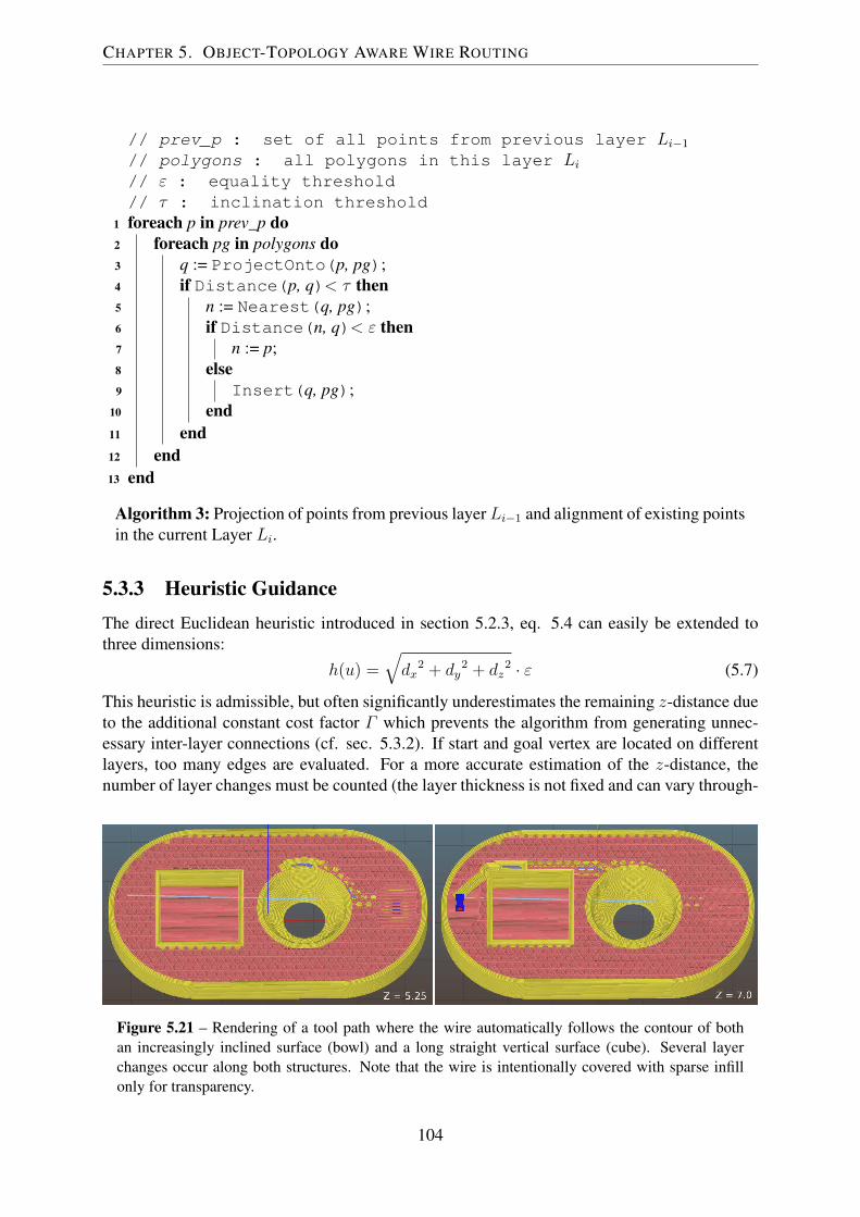
CHAPTER 5. OBJECT-TOPOLOGY AWARE WIRE ROUTING
// prev_p : set of all points from previous layer Li−1
// polygons : all polygons in this layer Li// ε : equality threshold// τ : inclination threshold
1 foreach p in prev_p do2 foreach pg in polygons do3 q := ProjectOnto(p, pg);4 if Distance(p, q)< τ then5 n := Nearest(q, pg);6 if Distance(n, q)< ε then7 n := p;8 else9 Insert(q, pg);
10 end11 end12 end13 end
Algorithm 3: Projection of points from previous layer Li−1 and alignment of existing pointsin the current Layer Li.
5.3.3 Heuristic GuidanceThe direct Euclidean heuristic introduced in section 5.2.3, eq. 5.4 can easily be extended tothree dimensions:
h(u) =√dx
2 + dy2 + dz
2 · ε (5.7)
This heuristic is admissible, but often significantly underestimates the remaining z-distance dueto the additional constant cost factor Γ which prevents the algorithm from generating unnec-essary inter-layer connections (cf. sec. 5.3.2). If start and goal vertex are located on differentlayers, too many edges are evaluated. For a more accurate estimation of the z-distance, thenumber of layer changes must be counted (the layer thickness is not fixed and can vary through-
Figure 5.21 – Rendering of a tool path where the wire automatically follows the contour of bothan increasingly inclined surface (bowl) and a long straight vertical surface (cube). Several layerchanges occur along both structures. Note that the wire is intentionally covered with sparse infillonly for transparency.
104

5.3. INTER-LAYER CONNECTIONS
out the object). With ||dz|| denoting the number of layer hops, the actual distance is estimatedas:
h(u) =(√
dx2 + dy
2 + dz2 + ||dz|| · Γ
)· ε (5.8)
It is generally preferable to equally distribute layer transitions along the trace and avoid local“stacks” of short extrusions. To support a uniform distribution, the heuristic is further extendedwith an adaptive factor:
zα =∣∣∣( dxyDxy
− dzDz
)· ν∣∣∣ (5.9)
Dxy is the horizontal Euclidean distance between start and goal vertex. dxyDxy
therefore describesthe remaining portion of the horizontal distance in the range [0..1], accordingly for the verticalratio. The difference of both ratios is exactly zero along the direct line between both vertices. Inother words: the difference becomes a positive value if the z-distance is too small or too large inrelation to the remaining xy-distance. The result is a dimensionless number and must be scaledto match the dimension of the grid. It is therefore multiplied with the grid_step_distanceν, so the additional estimated value does not exceed one grid step. The resulting heuristic isimplemented for the A* algorithm as:
h(u) =(√
dx2 + dy
2 + dz2 + ||dz|| · Γ + zα
)· ε (5.10)
Figure 5.22 – Effect of improved heuristics on the evaluation complexity, measured by the amountof vertices generated during the search. Left: number of required vertices for routing the wire inthe test object from fig. 5.21. Right: corresponding final graph at layer z = 6.5 mm with Euclidean,z-corrected and adaptive heuristic.
Figure 5.22 shows how a well-tuned heuristic reduces the processing complexity and run-time.Underestimating the remaining z-distance causes the search algorithm to increase the evalua-tion radius by ||dz|| ·Γ mm, often resulting in fully covered layers as pictured in the first graph.The adaptive factor only has a small effect on the complexity by “pruning” some paths withsimilar cost but different inter-layer connection positions.
In cases where the inclination between A and B is too high to form a straight, step-wise con-nection, the routing algorithm is forced into a meandering trajectory to elongate the trace until
105

CHAPTER 5. OBJECT-TOPOLOGY AWARE WIRE ROUTING
it is long enough for the required number of layer transitions, as illustrated in fig. 5.23. To avoidsharp edges or even vertical stacks of extrusions, the heuristic is further extended to not onlyconsider the current vertex u, but also the two predecessors p(u) and p(p(u)) if they exist. Theangle θ between these three points is computed as:
θ = arccos
(~AB · ~BC
|| ~AB|| · || ~BC||
)Acute angles are penalized by a higher estimated remaining distance. As the grid is arranged in45°steps, the heuristic h(u) is adjusted in 4 discrete steps:
h′(u) =
h(u) + 0 if θ ≤ 1/4π // ≤ 45°h(u) + ν · α1 if 1/4π < θ ≤ 1/2π // > 45°− < 90°h(u) + ν · α2 if 1/2π < θ ≤ 3/4π // ≥ 90°− < 135°h(u) + ν · α3 if θ ≥ 3/4π // ≥ 135°
The factor α can be used to progressively assign higher distances to sharper angles.It was stated above that the Euclidean distance fulfills the admissibility criterion and thereforeguarantees an optimal solution. This is also true for the corrected z-distance introduced with eq.5.8, which only gives a better estimation of the previously underestimated z-distance. However,both the adaptive z factor (eq. 5.9) and the penalization for sharp angles can break admissibilityin certain cases, namely if a very good, direct connection exists along a low-weighted perimeter.The adaptive z guidance can cause a maximum extension of one grid step length ν over theentire routed path, which is considered acceptable. Enforcing low angles might add a significantdistance, but in this case a longer trajectory is explicitly preferred to improve the mechanicalprintability.
5.4 Wire CollisionsAvoiding wire crossings while minimizing the length of each wire is the main goal of traditionalrouting algorithms for electric circuits. In the routing approach presented in this thesis, basiccollision avoidance is inherently achieved by processing one wire after the other. For eachindividual net, the routing graph is updated and only regions not yet occupied by previouslyrouted wires are considered. The required information is collected upon construction of the
Figure 5.23 – Routing of a wire with high vertical distance between the waypoints. The horizontaldistance is not sufficient for the required number of inter-layer overlaps, resulting in a non-directroute to increase the trace length.
106

5.4. WIRE COLLISIONS
SurfaceCavity
Routed wire
Bridge
Potential wire
Allowed
Not allowed
Not allowed
Not allowed
Allowed
Figure 5.24 – Classification of regions at object surfaces, bridges, component cavities and alreadyrouted wires.
static routing graph in two steps, covering the previous and following few layers. Given arequired shell thickness of k layers, the contour polygon of the current layer is modified by thefollowing steps:
Previous layers must be included anyway, to avoid generation of non-supported wires e.g.when printing on bridges. This is achieved by computing the intersection of k layercontours below the current layer, which already contain the channels from previouslyrouted wires.
Subsequent layers would also contain wire channels, but at this point it is not possible todistinguish a wire channel from a hole or a surface. Since printing on or close to surfacesis a frequent valid use case, channel polygons for routed wires on the next k layers aregenerated again by offsetting the trajectory (cf. sec. 4.5.2) and only those polygons areremoved from the current layer’s contour.
Figure 5.24 illustrates how the region above a routed wire can be classified equally to a regionon top of a bridge; both are not supported by plastic. In contrast, the region below a routed wiremust be removed from the graph to avoid electric shorts while routing at an internal or externalsurface is unproblematic. Cavities for electronic components are basically treated equally aswires, with only minor differences in the implementation.
Figure 5.25 – Wire collision resolved by detouring on the same layer (center) and by switching toa higher layer (right). Note that the position of the upper right component is different in both cases,resulting in the respective shortest path.
Figure 5.25 shows the resulting graph of a layer with colliding wires. Depending on the wiregeometry, the currently routed wire is detoured around an existing route or evades a collision by
107

CHAPTER 5. OBJECT-TOPOLOGY AWARE WIRE ROUTING
moving to a higher or lower layer. A main factor to control this behavior is the static inter-layerweight factor Γ . With a high value, long detours on the same layer are preferred.
While collisions are inherently avoided by routing wires sequentially, often the resulting lengthis not optimal. Figure 5.26 illustrates a case where the order of wire processing strongly in-fluences the quality. To mitigate this effect, a heuristic is used to optimize the order of therubberbands prior to the routing step.The general approach is simple and common in literature:
1. For each net, count the number of collisions with other nets, assuming that all connectionsare realized as straight lines. Sort nets ascending by number of collisions.
2. In a second step, order nets with an equal number of collisions by their length, startingwith the shortest.
The actual implementation of the net ordering heuristic raised practical challenges. First, thecollision of the wires represented by a one-dimensional line is insufficient, as the extrusion andchannel around the wire have a certain extent. This is solved by first inflating all other wiresto the channel diameter and computing intersections with the inflated polygons. Inflating thewires is also important if a wire ends inside the perimeter of a second wire, which then hasmore intersections and will therefore circumvent the first. Second, if the nets comprise multiplelayers, 3D-intersections must be computed to correctly identify collisions. This is solved byslicing the rubberbands according to the set of layers, inflating each individual segment andaccumulating the intersections from all layers.The aspect of collision avoidance for 3D-wires bears a huge potential for further optimization.Counting the intersection of unrouted wires obviously does not yield optimal results. It isexpected that typical methods from VLSI and PCB design are applicable at this point, e.g. Rip-Up and Reroute (RRR), to cover situations where the object geometry prevents straight traces.
5.5 Algorithms SummarizedAfter going through the algorithmic details of all routing steps individually, this section gives ashort summary of the contents of this chapter to provide a comprehensive overview. The han-dling of electronics is integrated into the overall slicing process mainly as two additional steps
Figure 5.26 – Effect of net order in wire routing. Processing the vertical connection first results inlong, detoured routes for the other wires (center). The accumulated length of all nets is optimalwhen processing the horizontal wires first (right).
108

5.5. ALGORITHMS SUMMARIZED
to modify the layer surface polygons:
• Re-slicing is triggered by changing a net or moving a component.
• The first two steps of the conventional slicing process are executed: the position of alllayers is determined and a vector of nested polygons (LayerParts) is computed, describingthe outline of each layer (sec. 4.2.3).
• Component cavities are inserted by removing their hull polygons from affected layers.
• Wires are generated. The resulting channels are also removed from the layer polygons.Extrusion paths for the conductive material are computed, stored per layer and integratedinto the G-code during export.
• The normal slicing process continues with perimeter and infill generation. The alignmentof wires, beds and the generation of solid surfaces to support electronics in sparse infillareas is implicitly done, only based on the modified polygons.
This chapter covered the step of generating wire trajectories between fixed, given waypoints(item 4 in the list above). The most simple option is to insert direct channels from waypoint towaypoint, resulting in very predictable routing. However, this is often not optimal or requiressetting a high number of waypoints. The technical details of implementing the required basicfunctions for this strategy were introduced in chapter 4. Building on this fundamental function-ality, a first approach to auto-routing was implemented to achieve good solutions in complexobject geometries with low manual effort.While the individual steps were presented in the order they were technically implemented, intro-ducing the basic concepts first and building up towards more general solutions (2D→ 3D), thefollowing pseudocode gives an informal overview over all steps in the order they are executed:
109

CHAPTER 5. OBJECT-TOPOLOGY AWARE WIRE ROUTING
1 Route (Layers, Schematic)// Pre-process polygon based layer representations
2 foreach Layer l in Layers do3 foreach Polygon p in l do // sec. 5.3.24 RemoveCollinearPoints(p);5 AlignToLayer(p, l−1);6 UpsamplePoints(p);7 end8 end9
// Prepare graph data structure, compute optimal routesalong the perimeters
10 G := new Graph;11 foreach Layer l in Layers do // sec. 5.2.212 Insert(G, DeflatePolygons(l.polygons));13 end14
// Change execution order to minimize collisions15 foreach Net n in Schematic do // sec. 5.4
// Number of intersections with other nets, if theywere routed as straight connections
16 CountIntersections(n, Schematic.nets);17 end18 Sort nets by number of collisions and length;19
// Execute actual routing step segment by segment20 foreach Net n in Schematic do21 foreach Segment s in n do22 Insert direct connection into G ; // sec. 5.2.323 A*(G, s) ; // secs. 5.2.4, 5.3.224 Remove resulting channels from contour polygons ; // sec 4.5.225 Reset G to intital state, update affected layers by re-generating them from
the modified contour polygons;26 end27 end28
// Generate extrusion commands29 foreach Layer l in Layers do // sec. 4.5.230 Sort routed wire fragments;31 Apply overlaps;32 end33 end
110

5.5. ALGORITHMS SUMMARIZED
From line 2, the contour representations of all layers are re-structured, such that the points arewell aligned over all layers and the distance between adjacent points is neither too low, whichwould generate unnecessary extra vertices, nor too high, which would prevent the algorithmfrom finding inter-layer connections. The pre-processed polygons are then converted into thegraph representation by multiple offsetting. The resulting graph contains edges which are posi-tions such that a wire trajectory would exactly follow the object contour along the perimeters.In the following step starting at line 15, the nets are pre-ordered to minimize wire collisions.
The actual routing step is executed for each wire segment individually. The segment is insertedinto the graph as a direct connection (line 22). Then the A* algorithm is executed, dynamicallygrowing a grid in infill regions of the object and gradually establishing inter-layer connectionsalong the search direction, where a sufficient overlap is possible. Once a trajectory is found,it is stored as polyline-segments per layer and the resulting channels are cut from the contourpolygons. The graph is reset to the contour representation from line 13, but all layers affectedby the route of the current segment are updated to respect the new channels.
In a final step (line 29) all wire fragments are accumulated per layer and converted into volu-metric extrusions for the G-code export.
Figure 5.27 shows an application of the algorithms introduced in this chapter. Three LED areintegrated into the boat as navigation lights, connected to a microcontroller. A few waypointswhere manually set at the bow of the boat to achieve a small distance to the components, andtwo waypoints at stern for the power connection. The routing algorithm then generated thetrajectories. It kept the wires within the material at the walls and avoided collisions with otherwires and components.
Figure 5.27 – Example 3D circuit generated with the autorouting algorithm. Model by Maxlarsenunder CC BY 3.0 license.
111

CHAPTER 5. OBJECT-TOPOLOGY AWARE WIRE ROUTING
112

Chapter 6
Process Documentation and Verification
Figure 6.1 – General workflow for the verificationapproach. Once a layer has been completed, a set ofimages is recorded and stitched together, classifiedinto categories (electronics, ink, plastics) and com-pared with the expected geometries from the G-codefile to detect possible defects.
Except for the camera-guided placing ofelectronics components described in sections3.1.4 and 3.2 and thermal control, the entirebuild process runs in an open loop control.This is common for most additive processes,but an increasing demand for quality assur-ance, documentation and verification of thebuild process is conveyed from the industry toenable integration into production processes.This is particularly important for the inte-gration of electronic circuits which are com-posed of complex but very small SMD com-ponents, requiring thorough monitoring andverification in the production process evenfor comparably reliable traditional 2D PCBs.The additive process introduces a number ofadditional uncertainties, primarily related tothe inhomogeneous results of material depo-sition of both structural and conductive material.
The final step of this work therefore aims to partially close the control-loop by automaticallyincorporating feedback during the print [A93]. To achieve this, the head camera, originally in-tended to guide the picking of components, is also used to take images of the workpiece duringthe print. The general idea is sketched in fig. 6.1. When a layer is completed, the camera is usedto take a set of images of the surface. The tiles are stitched into one large image which alreadyserves as a layer-wise documentation of the print process. The image is then compared with theG-code, ink and plastic regions are identified and the printjob is paused if a possible defect wasfound. A human operator is then asked to fix the issue and continue or abort the job.
The documentation and verification software is implemented as an OctoPrint plug-in [B37] andcan be configured for every OctoPrint-controlled printer with a suitable camera. It relies on theOctoPNP camera control interface for encapsulated hardware access. Technical documentationof the plug-in is provided in the repository.
113

CHAPTER 6. PROCESS DOCUMENTATION AND VERIFICATION
Figure 6.2 – Screenshot of the OctoCameraDocumentation software.
6.1 Image Recording during the Print-process
To obtain images with sufficient resolution and low distortion, only a small area can be coveredby a single image recorded with the camera. Except for very small objects, documenting anentire layer requires taking several images which are stitched together as a first processing step.To cover only regions where material was deposited in the current layer, the tool analyzes theG-code and generates a grid with optimal coverage for each individual layer as illustrated infig. 6.2.
A resulting set of tiles for one layer is given in fig. 6.3. Unfortunately, simple stitching of thetiles into one image proved to be inadequate for our belt-driven gantry systems. A resultingset of tiles for one layer is given in fig. 6.3. Unfortunately, simple stitching of the tiles intoone image proved to be inadequate for the belt-driven gantry system. In many cases, backlasheffects and insufficient positioning precision caused significant offsets. To reduce stitchinginaccuracies, tiles are recorded with a certain overlap and correlation-based image alignment isapplied on the overlapping regions [A21]. New tiles are appended iteratively from bottom totop, left to right. For each new tile, the offset and correlation coefficient with the bottom andleft tile are computed if they exist. The new position is the average of both offsets, weightedwith the correlation coefficient to prefer corrections with higher confidence.
Figure 6.3 – Stitching of tiles into a composed layer image. Left: individual images as recordedare naively assembled with positioning inaccuracies highlighted in red. Middle: positions of tilesrecorded with extended borders are corrected by pairwise correlation of overlapping regions Right:high-quality stitched layer image.
114

6.2. FEATURE SEGMENTATION
Figure 6.4 – Overlay of the raw image and G-code of a single layer. Left: all extrusions executedby the plastic extruder T0 and right: conductive ink lines extruded by T1.
6.2 Feature Segmentation
A reliable and accurate segmentation of regions covered with conductive ink is essential toautomatically detect wire defects. Since the desired geometry of both materials is encodedin the G-code, a mask can be created by parsing all positioning commands for a particularextruder which contain a positive amount of extrusion. The mask is converted to the knownimage coordinate system and applied as shown in fig. 6.4. This step also masks regions fromprevious layers, e.g. in sparse infill areas which are visible in the image.Figure 6.5 left illustrates how the predetermined positions of all plastic pixels (top) and conduc-tive ink pixels (bottom) are identified in the image by inverting the previously generated masks.Since each image typically contains several thousand pixels in each dimension, only a randomsubsample is extracted for each extruder to reduce the amount of data. Figure 6.6 clearly in-dicates that even a simple linear separation is sufficient to classify pixels based on their colorvalues. The resulting dataset contains an equal number of labeled data points from both classes.In a subsequent step, a Support Vector Machine (SVM) is trained with the labeled dataset andused to classify pixels in the image into the categories plastic or ink (fig. 6.5 right). For filamentcolors with a low distance to the ink color, a significant number of pixels is misclassified withthis method (fig. 6.5, top right result). This is mainly caused by incorrect labels in the trainingdata. The ink extrusion frequently shows slight over- or underextrusion and deviates from theintended path due to surface tension dragging the ink to the channel boundary. Most maskedareas, therefore, contain a certain amount of pixels from the opposite class. To mitigate this
Figure 6.5 – SVM-based classification into plastic / conductive material. Left: a random subsampleof plastic- and ink-pixels is extracted from the image after masking the respective tool paths. Right:an SVM is trained with the labeled dataset and used to classify all pixels in the image (top). Theclassification accuracy is significantly improved by self-filtering the training data. Entries which donot match the prediction of the SVM are removed and the classifier is re-trained with the reduceddataset (bottom).
115

CHAPTER 6. PROCESS DOCUMENTATION AND VERIFICATION
Figure 6.6 – Distribution of pixels in HSV (left) and BGR (right) color space. Black data pointsrepresent pixels from regions masked as plastic based on the G-code information, red data pointswere masked as conductive ink. Note that some pixels are misclassified due to over / unterextrusionof conductive material.
effect, the SVM is used to self-filter the training data. The classification is predicted for allelements of the training dataset, entries for which label and SVM prediction do not matchare removed. The SVM is then re-trained on the filtered dataset, yielding a clearly improvedclassification result (fig. 6.5, right bottom).To verify the classification step, a set of otherwise identical test objects with different plasticfilament colors was printed (fig. 6.7). All colors with sufficient distance to gray showed satisfy-ing results. For very similar colors (gray), reliable recognition becomes increasingly hard, evenfor humans.
6.3 Defect Detection
In a final analysis step, interruptions and strong deviations of the extrusion traces are automat-ically detected before printing the next layer. The test is implemented as a positive-coverage,sliding window detector as illustrated in fig. 6.8. A circular template matching the extrusiondiameter de is moved along the intended ink-extrusion lines extracted from the G-code. Thetemplate is shifted by de/2 for each iteration step. If the ratio of pixels classified as ink vs.
Figure 6.7 – Successful verification of the ink segmentation algorithm with different filament colors.
116

6.3. DEFECT DETECTION
plastic falls below a threshold ε, the region covered by this template is flagged as defect (redmarkers in fig. 6.8 and 6.9).
Figure 6.8 – A circular sliding window detector (blue), traversing the first ink extrusion line (top tobottom).
To evaluate the performance of the defect detection pipeline, and to test the integration intothe printing process and the effect on execution time, a series of test objects were printed.Five specimens with different filament colors and object shapes were manufactured with a totalnumber of 20 layers containing conductive traces. The syringe extruder was intentionally de-calibrated for these prints to increase the probability of defects to generate relevant test data.The recorded images were inspected and labeled manually, and then compared to the automaticdetection results. All disruptions and trace deviations in the evaluation dataset were successfullydetected, some relevant cases with highlighted defects are provided in fig. 6.9.To be suitable as a monitoring tool, running continuously in the background during the dailybusiness in a laboratory or production environment, the entire verification pipeline should beimplemented efficiently so as not to excessively extend the overall printing-time.Table 6.1 lists the amount of time required for the individual steps to print and verify a singlelayer on the test objects. The verification process (image stitching and analysis) requires approx-imately ∼1.0 % additional execution time per layer, which is considered reasonable. However,the image capturing step currently requires a significant amount of extra time (∼10.0 % or 4.1 sper image). This is due to the positioning of the camera, followed by image capturing, croppingand import of the image on the (slow) CPU of the 3D printer. Interleaving the printhead mo-tion and off-loading image processing to a (much faster) PC would reduce the reported time forimage capture dramatically.
117

CHAPTER 6. PROCESS DOCUMENTATION AND VERIFICATION
Cube CylinderTiles 8 (2x4) 9 (3x3)Printing 252.0 s 87.7 % 360.0 s 89.7 %Image capturing 33.1 s 11.5 % 37.2 s 9.3 %Stitching 0.8 s 0.3 % 2.7 s 0.7 %Analyzing 1.5 s 0.5 % 1.6 s 0.4 %Sum 287.4 s 401.5 s
Table 6.1 – Processing time of a single layer, broken down into the steps of the verification pipeline
The sliding-window-based, negative coverage test introduced in this section is a fairly simpleapproach. Yet it proves the feasibility of the idea and already finds most of the defects whichtypically occurred during the experiments. Future work should consider the implementation ofadditional and more sophisticated defect detection methods.This includes a negative coverage detector to identify overextrusions and short circuits by test-ing for absence of ink in a similar way. A check for sufficient ink extrusion, covering theconnector footprint outline for all SMD components before placing them could also be imple-mented with a combination of both test approaches.Another promising approach is a connected components detector which can be used to verifyboth an intact connection between two endpoints (one component) and an intact gap betweentwo wires (two components). The basic idea is to define a set of two or more points which lieinside of an ink-covered region and then apply a flood-fill or similar algorithm to the classifiedpixels to identify the connected components.
Figure 6.9 – Objects printed with intentionally de-calibrated syringe extruder to evaluate the detectorperformance. Defects automatically detected by the verification algorithm are highlighted in red. Forthis test dataset, the algorithm detected 100 % of all defects.
118

Chapter 7
Experimental Applications and Evaluation
This chapter summarizes several Experiences and results collected during the experiments withthe hardware, software and materials. Section 7.1 provides an overview of different plasticsused throughout the work on this thesis and assesses their suitability for this application. Severalprinted objects and case studies for potential applications of the technology developed in thiswork are presented in sec. 7.2. The chapter closes with a performance analysis of the slicingand routing algorithms.
7.1 PlasticsA broad range of different plastic base materials is a available for the FDM process. Whilethis work is focused on the algorithmic and integration aspects of 3D printed electronics, basicrequirements for material properties must be considered. Industrial applications often requirehigh performance materials with high strength, thermal- and UV-stability and low hygroscopy.Integration of printed electronics partly has contradictory requirements. Important propertiesare:
Temperature High temperatures of both the extruded plastic and ambient conditions (heatedchamber) result in faster curing of the conductive ink. This has a positive effect on wireswhich are partly sintered before the next layer is printed, but reduces adhesion of compo-nents placed into uncured ink.
Printbed Adhesion Good printbed adhesion is a general requirement. However, “overfilling”of the first layer to increase adhesion causes severe risks to printed electronics as theoverfilling perpetuates over the first few solid layers, causing extrusions to spill into thechannels.
Warping Low warping also is general requirement, but for printed electronics even small de-viations induce defects e.g. by shifting the contact pins for SMD components.
Stringing Stringing occurs when the extrusion is stopped and the extruder jumps to a differentposition. The molten plastic does not shear-off clean but often pulls strings with very lowdiameter. Such strings were a frequent cause of defects in our experiments. Figure 7.1illustrates the effect of conductive material extrusion crossing a plastic thread. This effectcan be partly mitigated in software by tuning the retraction parameters, wiping during
119

CHAPTER 7. EXPERIMENTAL APPLICATIONS AND EVALUATION
retraction moves and raising of the z-axis for travel moves, but material properties andextrusion temperature also have strong effects.
Bonding with Conductive Material Bonding of polymer based inks is excellent on all testedplastic materials but very low for eutectic metals.
Figure 7.1 – Partly or fully interrupted conductive traces due to stringing from the plastic extruder.The threads are barely visible with naked eye.
Some common plastic filaments were evaluated regarding their suitability as base material for3D printed electronics: PLA, ABS, PA (PA 6 / Nylon) and flexible filament (NinjaFlex). Carbonfiber reinforced filament was not tested, but is considered to be an interesting candidate.
PLA and ABS were both obtained in different colors and brands. Both materials show simi-lar printing characteristics and are generally suitable to be combined with conductive material.However, PLA exhibits slightly stronger stringing effects and limits the temperature for postcuring of conductive material due to its low glass transition temperature.
PA is printable on the machine but requires significant higher extrusion and ambient tempera-tures and is very sensitive to temperature fluctuations, e.g. when the build chamber is openedto manually insert a component. It is expected that PA materials can be used when the entireprocess is sufficiently stable and the hardware supports high temperatures e.g. by shielding theconductive material to avoid curing and clogging at the dispenser tip.
Flexible material is currently not suitable for printed electronics as the material flow cannot becontrolled with sufficient precision. However, it is an interesting candidate as second materialin multi extruder setups.
7.2 Demonstrators
Several demonstrator objects with different features and complexity have been fabricated overthe course of this thesis to collect experience with the printer and the slicing software and totest the feasibility of implemented features. While the primary purpose of the first printedobjects was testing of individual functionalities, calibration and integration, the user interface(sec. 7.2.2) and the instrumented object (sec. 7.2.3) are case studies where the methods devel-oped in this thesis were applied to solve actual manufacturing problems.
120

7.2. DEMONSTRATORS
7.2.1 Basic Functional TestsFigure 7.2 shows one of the very first test objects, printed on the modified CNC milling machine.The design is purely done in OpenSCAD. Object and circuit are two separate volumetric mod-els and printed as multi-material model where each material is assigned to one extruder. Sparseinfill, channels, cavities and routing are not supported and were manually designed where re-quired.The circuit is based on a 8 bit ATmega ATtiny45-20SU microcontroller with two resistors andLEDs. The interface is mechanically compatible to a USB type-A connector. The USB protocolis not supported, instead the interface can be used to program the ATtiny with a customized ISP.
Figure 7.2 – Early test object with a programmable blinking circuit, manufactured on the modifiedCNC milling machine. The design was done manually as multi-material object composed of twoindividual volumetric models without software support for channel generation or wire routing.
The flash drive-shaped object shown in fig. 7.3 was mainly used to conduct rapid tests forparameter tweaking and component placing. One end fits the dimensions of a USB type-Aconnector and can be plugged into any standard USB slot to apply 5V power to the circuit.
Figure 7.3 – Simple test object consisting of an LED and resistor, with all electronics on a singlelayer. Power is provided by any USB slot. This object is an example where automatic wire routingcan have a negative effect (right) as the contact pins are required to follow the mechanic USBinterface specifications.
121

CHAPTER 7. EXPERIMENTAL APPLICATIONS AND EVALUATION
The object in fig. 7.4 was designed to explore three specific aspects:
• The application of topology aware wire routing to a model where manual routing wouldrequire a high number of small linear approximations.
• Autonomous energy supply of printed objects with batteries.
• Manual insertion of components (battery) during the printing process which can not behandled by the printer’s pick and place system.
The circuit only consists of a single LED and a coin cell battery. The battery is connectedat the upper side by printing a conductive trace right onto the surface. A cantilever structurewith an embedded wire is printed at the lower side with a small gap to the battery, serving asmechanical switch. Wire routing is achieved by setting only 4 waypoints, two of which arerequired to contact the battery with a straight line. The routing algorithm successfully findsa collision free path through the object while preserving surface integrity and avoiding gaps.Overlapping inter-layer connections were observed to be stable.
Figure 7.4 – Demonstrator object for topology aware wire routing. Top: successful print and de-tailed view of the printed switch. Bottom: Final 3D routing over multiple layers along the curvedsurface. The circuit contains a coin cell battery and a blue LED with matching voltage requirements.The wires directly contact the battery, with the lower attached to a lever structure, serving as a man-ual switch. Two additional waypoints are set to ensure a straight line to contact the battery. Theimages show every second layer of the final tool path. The wires are automatically routed along thesurface over several layers, with overlapping sections to achieve stable inter-layer contact.
122

7.2. DEMONSTRATORS
7.2.2 Case Study: Integrated User InterfaceIn cooperation with a partner from the industry a pilot study was conducted to evaluate thepotential of 3D printed components with integrated electronics for industrial applications. Thestudy was intended as an early feasibility test with a real application. It is anticipated that theprocess currently does not fulfill all technical requirements to fabricate a fully equal replacementfor the current solution. Using specifications provided by an external party ensures that the taskis not specifically adapted for the existing solution, but it still allows to adjust the design orselection of components to suit for the additive process.
Figure 7.5 – User interface section cut out from a larger device for simplified testing. A mechanicalswitch and an RGB-LED are integrated into the closed free-form surface. Several additional com-ponents are required to connect the interface to the central controller. Top: 3D model and printedobject with integrated circuit. Bottom: documentation of the print process. Note that the imagesare partially assembled after the print as documentation covers only those parts of the current layerwhere material was deposited.
The aim of this study was to replace a simple user interface for a communication system, mainlyconsisting of an RGB-LED and a switch, with a part that can be additively manufactured in asingle process step. Figure 7.5 shows a cutout of the free-form surface where the interface isintegrated (left), the printed result, including the full circuit (right), and the manufacturing pro-cess (bottom). The LED, switch, and the pins for the connection to a controller are positionedat different heights. To a certain level, both the inside of the part and the circuit must be pro-tected against liquids from the outside, requiring the surface to be closed and not interrupted byelectronic components. Several additional electronic components are required to amplify thecurrent for the LED and to debounce the switch (detailed list below). One requirement, there-fore, was to integrate the entire circuit into the printed surface to eliminate an additional circuitboard.
123

CHAPTER 7. EXPERIMENTAL APPLICATIONS AND EVALUATION
The circuit contains a total of 19 components:
Qty Type Package1 SMD Pinhead 2.0 mm flat1 APEM DTSJW65NV mechanical switch Custom2 Resistor 220 Ω 12061 Resistor 470 Ω 12066 Resistor 1.0 kΩ 12062 Capacitor 10 nF 12062 Capacitor 100 nF 12061 Osram LRTB GVTG RGB-LED PLCC-63 SSM3K339R MOSFET SOT-23F
Several iterations of the part where printed. The complexity was gradually increased. Begin-ning with simple isolated component tests, more individual components were integrated intoone object in each manufacturing step.
A printed mechanical switch was already successfully tested with the “flashlight” object fromfig. 7.4. This approach was not directly applicable here, as it requires a gap around the elasticcantilever structure. We therefore attempted to use a common mechanical SMD-switch, cov-ered by a thin elastic layer of plastic. Figure 7.6 (1) shows the isolated test object. Actuatingthe switch required a high amount of force (∼50 N) due to the rigid elevated surface and nar-row cavity. Increasing the cavity offset improved the result, but the soft filament surroundedthe small button to an extent where it prevented the switch from triggering (2 and 3). As acountermeasure, a thin plate was attached to the switch to increase the filament support area(4). Additionally, a cutout was added to the model at the upper boundary of the switch (5). Thiscauses a large membrane-area and at the same time allows to use narrow cavity offsets, suchthat the space around the switch can be used for other components. The improved version stillrequires ∼20 N to trigger the switch, which is at the upper limit of subjective acceptance re-ported by several test persons. The cutout can currently not be modeled as part of the electroniccomponent package, as only extruded 2D-shapes are supported. Full 3D-component models areconsidered an important future improvement of the slicing software.
Printed circuits are typically small, with minor complexity but at exactly the position wherethey are required, e.g., in-situ sensors or small interfaces. The printed parts commonly needa connection to a power source or a central computing device, requiring means to connect acable. While small components are electrically connected and sufficiently affixed by the con-ductive paste and the enclosing cavity, larger connectors, e.g., pinheads or plug sockets wouldbe teared off by a connected wire. A second test was conducted to mount a pinhead during theprinting process. The pinhead was wetted with a two-component epoxy glue before insertion.Figure 7.6 shows the pinhead during the print process (6) and fully enclosed (7). Both mechan-ical and electrical connections were sufficiently stable to connect the required 7-core cable.
During the isolated component tests, a first version of the interface object with a reduced circuitwithout the LED-drivers was manufactured. Figure 7.7 (right) shows the result. At the design
124

7.2. DEMONSTRATORS
Figure 7.6 – Isolated testing of mechanical components. From top left to bottom right: 1: SMD-switch in a minimal, printed housing. 2, 3: Cross-section, clearly showing that the actuator isenclosed by sagging molten filament. 4: Thin plate to extend the surface of the switch for betterfilament support. 5: Extension of the cavity around the switch only for the topmost millimeter (indi-cated in red) to increase the flexible membrane area while maintaining an otherwise small cavity. 6:Insertion of a glue-wetted pinhead during the print process. 7: Resulting part with inset connector.
phase, it became evident that due to the limited space, some components had to be placed inclose proximity, resulting in touching or even merged cavities. While placing multiple com-ponents in a single cavity worked well, Slic3r’s bridging algorithm, which is used to cover thecavities with the first unsupported layer, turned out to be not well suited for this task. The effectis illustrated in fig. 7.7. The algorithm generally attempts to identify the primary orientationof a bridging area and aligns the extrusions with this direction to ensure a proper connectionto the solid object at both ends of each line. With the irregular shapes induced by componentswith slightly different heights and orientations, the algorithm detects two or more principal di-rections and splits up the area into multiple bridging surfaces. When the extrusion line ends ontop of a component, it a) does not stick to the plastic surface, resulting in a small clot of tangledfilament, which then b) often shifts the component out of place.
Figure 7.7 – Left: unsuitable result of the bridging algorithm when components are arranged inclose proximity. Right: successful print after rearranging the components to avoid the bridgingissues.
125

CHAPTER 7. EXPERIMENTAL APPLICATIONS AND EVALUATION
7.2.3 Case Study: Instrumented Object
Figure 7.8 – Can-shaped tracking object withtactile feedback.
The instrumented object approach was initiatedduring the European project HANDLE FP7-236410 and further developed within the Tran-sregio Project Crossmodal Learning, TRR 169[B31]. The general idea is to accomplish in-handmanipulation of objects with robotic multi-fingergrippers (e.g. Shadow Dexterous Hand [B28])by generalization from recorded demonstrationmovements, executed by human persons [A9]. Asetup of several precisely calibrated cameras andoptical markers was used to record the demon-strator movements with high spatial and tempo-ral resolution. However, external tracking suf-fers from two major drawbacks:
1. The object often is partly or fully covered by the hand during a manipulation, renderingexternal tracking very unreliable.
2. Contact forces between hand and object are crucial information which cannot directly beobtained from optical observation. The location, amount and direction of force applied tothe object at each contact point are of particular interest.
The proposed solution is an object with integrated active tracking and tactile sensing capabil-ities, mainly being a touch-sensitive surface to record forces, an Inertial Measurement Unit(IMU) for position tracking and a wireless connection to stream recorded data to an externalstorage system. The prototype illustrated in fig. 7.8 resembles a can, commonly used for bever-ages. The object consists of 40 individual tactile switches mounted on a massive metal frame.The switches are connected via 10 individual PCBs with a total of more than 300 electroniccomponents. The manufacturing of this prototype required significant resources and the designturned out too be to large and too heavy for many dexterous manipulation tasks.
lF
s
Proximity sensor
Deformable beam
Predicteddeflection
Optional base
Sensor marker
Figure 7.9 – Left: rendering of the basic one dimensional push-force sensor, with the deformablebeam on top and above the optical proximity sensor. To help the designer to dimension and align thesensor, the rendering optionally also includes the sensor marker (green), the fully deflected beam(gray), and a model of the proximity sensor (blue). Right: variations of the instrumented objectbased on the same basic design.
126

7.2. DEMONSTRATORS
Based on our previous research on printable force sensors [A94], a flexible design approachfor printable instrumented objects was developed. Additive manufacturing allows to quicklyproduce objects of different shapes and sizes, evolving with the progress of recording a largerdataset of manipulation movements, without the requirement for expensive force sensors.Figure 7.9 illustrates the (well known) basic principle of the printed force sensors based ona deformable cantilever. If the mechanical properties of the structure are known, the forceinducing the deformation can be computed. Low-cost optical proximity sensors are used tomeasure the deflection. The sensor consists of an IR-LED transmitter and a photo-transistor,changing its resistivity depending on the reflection of emitted IR-light. Figure 7.9 (right) alsoshows how such cantilever structures are used as flexible surface of the instrumented objects,each with a proximity sensor below it, mounted on the surface of the inner structure. The innerpart of the object contains all electronics and power supply. The force sensitive hull is printedas an individual component and can be quickly replaced to adjust the sensitivity by changingthe thickness of the cantilever structures.
Figure 7.10 – Left: EAGLE schematic of an instrumented object with 5 force sensitive surfaces.Right: G-code for three of the five side plates with integrated electronic components.
Figure 7.11 – Assembling of the instrumented object demonstrator. Left: three sides printed as afoldable object (top) and two single pieces (bottom). Center: base plate with microcontroller andfirst mounted side plate. Right: fully assembled object and deformable reflective hull.
Figure 7.10 shows the full schematic for a 5-sided instrumented object. The design contains atotal of 16 electronic components:
127

CHAPTER 7. EXPERIMENTAL APPLICATIONS AND EVALUATION
Qty Type Package1 Redbear BLE Nano / nRF52832 SoC Breakout board5 Resistor 100 Ω 12065 Resistor 10 kΩ 12065 Everlight ITR8307 proximity sensor Custom
Each proximity sensor is individually connected to one of the built-in AD-converters of theBLE Nano board. The board itself is mounted to the printed base via a socket to allow re-programming which requires removal from the instrumented object.Since placing of electronic components is currently only possible in one direction, on flat sur-faces, the design was split into a base-plate, containing the microcontroller and Bluetooth con-nector (fig. 7.11, center) and a number of side-plates which fit into a notch (fig. 7.11, left).Individual parts are connected by wires terminating at the edges, physical contact is establishedby plugging the part into the notch. The side-plates can be printed individually or as a set,connected by a thin layer of plastic to be bent at the corners after printing to form a hull. Eachplate contains the proximity sensor and two resistors, wired with a set of connections routed in3 dimensions to avoid collisions.
Figure 7.12 – Data recording with the printed instrumented object in a simplified tracking setup.The object position is optically tracked via visual marker. Force- and position-data are recorded,visualized and further processed with the Robot Operating System (ROS).
Figure 7.12 shows a first (simplified) data-collection experiment with the printed instrumentedobject. A camera provides absolute external reference for position tracking. Object positionand current forces are visualized during the experiment in a 3D scene representation (RViz)and recorded for subsequent evaluation. Force sensor data are streamed as raw ADC values tothe host computer and pre-processed to compensate different zero-points and to map from the
128

7.3. PERFORMANCE
non-linear proximity sensor characteristic to linear forces. The Bluetooth LE module currentlyallows a sampling frequency of approximately 140 Hz.
7.3 PerformanceThe amount of time to generate an executable G-code sequence from a model (seconds to min-utes) is small compared to the time it takes to physically print the object (hours to days). There-fore, good optimization at the slicing step is generally worth some extra time if it reduces therisk of failure during the print process. However, since the slicing steps are frequently executedto provide an accurate preview of the result when the position of electronic components or wiresis changed, the runtime of algorithms has a significant impact on the user experience.
To analyze the execution time, the designs of four of the objects introduced above where slicedwithout any electronics, with electronics but disabled routing and finally with contour followingrouting enabled. All objects where sliced with the same set of parameters on an Intel Core i5-8350U CPU. The relevant parameters used for the routing algorithm during this experimentwere:
Grid resolution ε (Heuristic) Γ (Inter-layer cost) α (perimeter weight)1.0 mm 1.0 1.5 0.1
The results are presented in fig. 7.13. The additional time required for the contour followingrouting algorithm is so dominant that the other two cases are only visible in the logarithmicrepresentation (right).A direct comparison is not always possible. Consider the batty light object. The slicing stepwas executed exactly with the waypoints shown in fig. 7.13. With this configuration, the staticrouting approach does not yield a printable result, but instead just creates straight wires, cross-ing both holes.
As expected, the runtime also heavily depends on the A* graph search parameters and objectshape. To estimate the effect, the battery light object was also processed with a combination ofdifferent parameters:
Grid resolution ε (Heuristic) Γ (Inter-layer cost) RuntimeBaseline 1.0 mm 1.0 1.5 28.7 s
Resolution1.5mm
1.0 1.517.6 s
2.0mm 20.1 s3.0mm 18.3 s
ε 1.0 mm1.1
1.525.4 s
1.3 24.4 s
Γ 1.0 mm 1.00.0 35.3 s3.0 24.7 s5.0 18.9 s
Combined 1.5mm 1.0 5.0 11.2 s
For each row, the altered parameter is highlighted in bold text. All other parameters are fixed,the baseline is identical with the parameters in the execution time analysis in fig. 7.13.
129

CHAPTER 7. EXPERIMENTAL APPLICATIONS AND EVALUATION
USB object Battery light User interface Instrumented object
Figure 7.13 – Execution time to generate the G-code of the four objects without electronics (grey),with static (black) and contour following wire routing (red). The left diagram shows the actualexecution time in seconds, the right diagram presents the same data at a logarithmic scale.
Reducing the grid resolution decreases the runtime as expected. For the object used in thisexperiment, the effect is limited as the infill area is small compared to the object’s surface.The sampling along the perimeter must be high enough to ensure overlapping inter-layer con-nections. The number of evaluated perimeter vertices is therefore significantly higher than thenumber of infill vertices.Increasing the heuristic factor ε yields slightly lower runtimes at the cost of less optimal trajec-tories.The layer-changing cost Γ also significantly affects the runtime. A low value prefers horizontalexploration, including several adjacent layers while a high value minimizes the number of layerchanges for the potential cost of longer in-layer detours. The special case of Γ = 0 eliminateslayer changing costs at all, often resulting in an “undulating” trajectory, jumping up and downbetween the layers.
In a second step the code execution time was profiled to identify critical sections with highpotential for optimization. All performance relevant parts of the code are written in C++, butexecuted through Perl’s XS-mechanism, complicating the insertion of instrumentation code.Therefore the perf profiling tool, included in the Linux kernel, was used for statistical profil-ing. The accuracy of this method is limited, as the process is only polled at certain intervals, butgood enough to identify hot-spots. The combined three side plates design for the instrumentedobject (fig. 7.11, left) was used for analysis to record a sufficient amount of statistical data.The result is provided in fig. 7.14. Only functions with a high share of the runtime are shown.The routing algorithm accounts for ∼95 % of the total runtime. Within the routing subroutine,79.6 % of the time is allotted to the Point::projection_onto function, which is used totest if a point is inside a polygon or on the polygon boundary and by the perimeter alignmentstep described in sec. 5.3.2 (cf. fig. 5.20).
130

7.3. PERFORMANCE
Further optimization steps should focus on the handling of polygon representations. Promis-ing approaches are caching of results or representation with an R-tree based data structure forefficient spatial indexing.
Figure 7.14 – Runtime profiling results for G-code generation with topology aware routing enabled,visualized as simplified flame graph. The share of execution time is given in percent. Only functionswith high contribution are shown for clearance. The routing subroutine accounts for ∼ 95% of thecomputing time.
131

CHAPTER 7. EXPERIMENTAL APPLICATIONS AND EVALUATION
132

Chapter 8
Conclusions and Outlook
In this thesis a full toolchain for additive manufacturing of objects with integrated electronicswas developed and successfully used to print several working demonstrators.In conclusion, the research questions from sec. 1.3 can be answered as follows:
Mechanical Engineering & Integration: Two iterations of 3D printers were developed to in-tegrate extrusion capabilities for plastic and conductive material and automatic compo-nent handling. A set of software tools was developed to calibrate and control the machinewith vision feedback. Several types of plastic and conductive substances were evaluatedand suitable materials were identified.
3D-Electronics Design: A combination of mCAD and eCAD data was achieved by combiningthem within the slicing software. Electronic components and wires are visualized in agraphical representation of the tool path which would be generated by this arrangement.This representation gives the user an immediate and realistic impression of the result.
2D & 3D Wire Routing Algorithms: A printable G-code is generated based on a graph-basedrouting algorithm and polygon manipulations utilizing the existing mechanisms for toolpath generation and surface detection. The algorithm minimizes layer changes and alignsthe trajectories with existing contours where possible, based on the process parameters ofeach individual print.
Process Verification: The quality and correctness of circuits immersed in plastic is docu-mented and verified by taking high-resolution images with the printer’s camera and com-paring them with the G-code by means of image processing to automatically detect de-fects.
The core contribution of this work is an approach to combine the volumetric 3D structure ofan object and an electronic circuit with the parameters of the FDM printing process into arepresentation which can be utilized for well-known routing algorithms. This is achieved bymodeling it as a combination of a graph data-structure and contour polygons, allowing to inferpossible connections within and between layers. Several successful approaches have been madetowards the physical integration of conductive materials into additive manufacturing processesin the last decade. The question of how to support and shape the design process to make efficientuse of those approaches was widely recognized, but significant research only started in recentyears, now coming up with the first useful results.
133

CHAPTER 8. CONCLUSIONS AND OUTLOOK
8.1 Limitations
Despite the successful and very promising results presented throughout the previous chapters,some issues currently prevent a broader commercial application of the technology discussed inthis thesis.
The mechanical positioning accuracy and reliability of the machines used for our experimentsis still insufficient, requiring frequent calibration and minor offset corrections and limiting theresolution achievable. The usage of syringe extruders for direct write application of conduc-tive ink is another limitation for both reliability and resolution. A promising alternative couldbe contactless dispensing via a piezo-driven jetting nozzle. A commercial product solving thisproblem, as it is already done in many other areas, was not available at the beginning of thiswork. Only recently are hardware manufacturers starting to develop integrated solutions. Withsufficient investments the technology should be available within few years.
The efficiency and overall usability of the user interface and routing algorithms still needs im-provement. Waiting up to several minutes for the updated preview after a design change for acircuit with only a few components is sufficient for an experimental prototype, but not accept-able in a production scenario.
True 3D circuits are possible and have been demonstrated with this thesis. However, the stair-case approach limits the angle, near vertical wires are currently not possible. The same problemoccurs for the positioning of components which is currently limited to z-rotations. Multi-axismanufacturing systems and non-planar slicing approaches both have the potential to solve thisissue, particularly for connections and components following curved surfaces.
Eventually, a very fundamental question is: will the FDM approach be suitable as the basetechnology in the long run? Miniaturization is technically limited with extrusion based pro-cesses. Many manufacturers also report that other additive processes are better suited to fulfilltheir requirements on stability, surface quality and scaling for mass production. However, nei-ther powder- nor resin-based approaches currently have the maturity and stability to be used inproductive manufacturing setups within the next few years.
8.2 Future Research
The usability and efficiency of the routing algorithm and the user interface can and shouldbe further improved. Several low-hanging fruit developments can be implemented with loweffort. The most important requirements, collected while fabricating the demonstrator objectsin sec. 7.2, are:
User Interface The user interface is currently rather simple. All important operations canbe executed, but more natural ways of interaction would certainly simplify the designprocess. This includes: placing of elements on grid to facilitate alignment, drag anddrop shifting of components, better labeling of component with relevant information, e.g.value of a resistor.
134

8.2. FUTURE RESEARCH
3D Component Models SMD components are currently represented based on their 2D shapefrom the EAGLE libraries, which is not sufficient e.g. for the mechanical switch or pin-head used for the user interface in sec. 7.2.2.
Wire Thickness currently, wires are modeled as a single line of extrusion. For high-currentapplications (e.g. motors) thicker wires would be required. This could be achieved withmultiple extrusion lines, but the graph representation currently does not support it.
Support Material Support material generation is not aware of electronic components. This isa problem if parts of a circuits are protruding the perimeter, e.g. connectors.
Coordinate System Registration Electronic components are positioned relative to the object’scenter of mass. If the 3D model is modified such that the CoM changes, repositioning ofall components is necessary.
Component Referencing Oftentimes, component models have to be slightly modified in theschematic, as they are originally intended for usage on PCBs. Saving a deviated modelwith a different name removes the component from the 3D design entirely.
The routing algorithm can be further improved in terms of efficiency. This could probablyachieved by utilizing index-based data-structures as indicated in sec. 7.3. A second optionwould be to make the routing algorithm itself more adaptive. Adapting the grid size to thetopology of the current object or starting with a coarse grid with iterative refinements only insections affected by the search are promising approaches.Another option would be backtracking and partial replanning of routes. This could also consid-erably contribute to improved collision avoidance. Similar techniques, e.g. Rip-Up and Reroute(RRR) have a long tradition in conventional wire routing.
Finally, overcoming the 3-axis limitation is an important research field to evolve from thestacking of two-dimensional layers to even more three-dimensional fabrication. Promising ap-proaches are 4- or 5-axis machines as they are commonly used for machining. While the hard-ware already exists, collision avoidance and G-code generation for additive processing still posemajor challenges. Other options is the combination of a common 3-axis gantry system to printthe plastic part with a robotic arm for ink deposition along free-form surfaces and componenthandling.
135

CHAPTER 8. CONCLUSIONS AND OUTLOOK
136
References
[A1] Max K. Agoston. Computer Graphics and Geometric Modelling. Springer, 2005. ISBN:9781852338183.
[A2] Daniel Ahlers. “Development of a Software for the Design of Electronic Circuits in3D-Printable Objects”. Bachelor Thesis. University of Hamburg, 2015. URL: https ://tams.informatik.uni-hamburg.de/publications/2015/BSc_Daniel_Ahlers.pdf.
[A3] Daniel Ahlers, Florens Wasserfall, Norman Hendrich, and Jianwei Zhang. “3D Print-ing of Nonplanar Layers for Smooth Surface Generation”. In: Proceedings of the 15thIEEE Conference on Automation Science and Engineering (CASE). Vancouver, 2019,pp. 1737–1743.
[A4] Kimball Andersen, Yue Dong, and Woo Soo Kim. “Highly Conductive Three-DimensionalPrinting With Low-Melting Metal Alloy Filament”. In: Advanced Engineering Materi-als 19.11 (2017), p. 1700301. DOI: 10.1002/adem.201700301.
[A5] Markus Ankenbrand, Yannic Eiche, and Jörg Franke. “Mechatronic Integrated De-vices”. In: 2019 International Conference on Electronics Packaging (ICEP) (2019),pp. 273–278.
[A6] Callum Bailey, Efrain Aguilera, David Espalin, Jose Motta, Alfonso Fernandez, MireyaA. Perez, Christopher Dibiasio, Dariusz Pryputniewicz, Eric MacDonald, and Ryan B.Wicker. “Augmenting computer-aided design software with multi-functional capabil-ities to automate multi-process additive manufacturing”. In: IEEE Access 6 (2017),pp. 1985–1994. DOI: 10.1109/ACCESS.2017.2781249.
[A7] Sandra Balzereit, Friedrich Proes, Volker Altstädt, and Claus Emmelmann. “Propertiesof copper modified polyamide 12-powders and their potential for the use as laser directstructurable electronic circuit carriers”. In: Additive Manufacturing Journal 23 (2018),pp. 347–354. DOI: 10.1016/j.addma.2018.08.016.
[A8] Jacob Bayless, Mo Chen, and Bing Dai. Wire Embedding 3D Printer. 2010.
[A9] A. Bernardino, M. Henriques, N. Hendrich, and J. Zhang. “Precision grasp synergiesfor dexterous robotic hands”. In: 2013 IEEE International Conference on Robotics andBiomimetics (ROBIO). Dec. 2013, pp. 62–67. DOI: 10.1109/ROBIO.2013.6739436.
137

REFERENCES
[A10] Marc Bestmann, Bente Reichardt, and Florens Wasserfall. “Hambot: An Open SourceRobot for RoboCup Soccer.” In: 19’th RoboCup international Symposium, Hefei. 2015.DOI: 10.1007/978-3-319-29339-4_28.
[A11] Marc Bestmann, Florens Wasserfall, Norman Hendrich, and Jianwei Zhang. “ReplacingCables on Robotic Arms by Using Serial via Bluetooth”. In: Proceedings of the IEEEConference on Robotics and Biomimetics (ROBIO). Macao, 2017, pp. 189–195. DOI:10.1109/ROBIO.2017.8324416.
[A12] Xiaorui Chen and Sara McMains. “Polygon offsetting by computing winding num-bers”. In: Proceedings of the ASME international design engineering technical confer-ences and computers and information in engineering conference 2 (2005), pp. 565–575.
[A13] Keun-Ho Choi, JongTae Yoo, Chang Kee Lee, and Sang-Young Lee. “All-inkjet-printed,solid-state flexible supercapacitors on paper”. In: Energy & Environmental Science(2016). DOI: 10.1039/C6EE00966B.
[A14] Chris Chu and Yiu-Chung Wong. “FLUTE: Fast Lookup Table Based Rectilinear SteinerMinimal Tree Algorithm for VLSI Design”. In: IEEE Transactions on Computer-AidedDesign of Integrated Circuits and Systems 27.1 (2008), pp. 70–83. DOI: 10 . 1109/TCAD.2007.907068.
[A15] Thomas H. Cormen, Charles E. Leiserson, Ronald L. Rivest, and Clifford Stein. Intro-duction to Algorithms. MIT Press, 2009. ISBN: 9780262032933.
[A16] Erick De Nava, Misael Navarrete, Amit Lopes, Mohammed Alawneh, Marlene Contr-eras, Dan Muse, Silvia Castillo, Eric Macdonald, and Ryan Wicker. “Three-DimensionalOff-Axis Component Placement and Routing for Electronics Integration using SolidFreeform Fabrication”. In: Proceedings of the 19th International Solid Freeform Fab-rication Symposium (2008), pp. 362–369.
[A17] Ugandhar Delli and Shing Chang. “Automated Process Monitoring in 3D Printing Us-ing Supervised Machine Learning”. In: Procedia Manufacturing 26 (2018), pp. 865–870. DOI: 10.1016/j.promfg.2018.07.111.
[A18] Christian Emmer, Arnulf Fröhlich, Volker Jäkel, and Josip Stjepandic. “StandardizedApproach to ECAD / MCAD Collaboration”. In: Proceedings of the 21st ISPE Inc.International Conference on Concurrent Engineering (2014). DOI: 10.3233/978-1-61499-440-4-587.
[A19] David Espalin, Danny W. Muse, Eric MacDonald, and Ryan B. Wicker. “3D Printingmultifunctionality: Structures with electronics”. In: International Journal of AdvancedManufacturing Technology 72 (2014), pp. 963–978. DOI: 10.1007/s00170-014-5717-7.
138

REFERENCES
[A20] Alejandro H. Espera, John Ryan C. Dizon, Qiyi Chen, and Rigoberto C. Advincula.“3D-printing and advanced manufacturing for electronics”. In: Progress in AdditiveManufacturing (2019). DOI: 10.1007/s40964-019-00077-7.
[A21] Georgios D. Evangelidis and Emmanouil Z. Psarakis. “Parametric image alignmentusing enhanced correlation coefficient maximization”. In: IEEE Transactions on Pat-tern Analysis and Machine Intelligence 30.10 (2008), pp. 1858–1865. DOI: 10.1109/TPAMI.2008.113.
[A22] Matthias Faes, Wim Abbeloos, Frederik Vogeler, Hans Valkenaers, Kurt Coppens, ToonGoedemé, and Eleonora Ferraris. “Process Monitoring of Extrusion Based 3D Printingvia Laser Scanning”. In: ArXiv abs/1612.02219 (2014). URL: http://arxiv.org/abs/1612.02219.
[A23] Jörg Franke, ed. Three-Dimensional Molded Interconnect Devices (3D-MID): Materi-als, Manufacturing, Assembly and Applications for Injection Molded Circuit Carriers.Hanser, 2014.
[A24] Harry Gao and Nicholas A. Meisel. “Exploring the Manufacturability and Resistivityof Conductive Filament Used in Material Extrusion Additive Manufacturing”. In: Pro-ceedings of the 28th Solid Freeform Fabrication Symposium (2017), pp. 1612–1626.
[A25] Ian Gibson, David Rosen, and Brent Stucker. Additive Manufacturing Technologies.2nd Edition. Springer, 2015. ISBN: 9781493921126.
[A26] Johannes Heinrich Glasschröder. “Additiv gefertigte Werkstücke mit integrierten elek-trischen Schaltungen unter Nutzung des 3D-Druckprozesses”. PhD thesis. TechnischeUniversität München, 2018.
[A27] Johannes Glasschroeder, Emanuel Prager, and Michael F. Zaeh. “Powder-bed based3D-Printing of function integrated parts”. In: Proceedings of the International SolidFreeform Fabrication Symposium. 2014, pp. 775–792.
[A28] Guo Liang Goh, Shweta Agarwala, Guo Dong Goh, Heang Kuan Joel Tan, LipingZhao, Tong Kuan Chuah, and Wai Yee Yeong. “Additively manufactured multi-materialfree-form structure with printed electronics”. In: International Journal of AdvancedManufacturing Technology 94.1-4 (2018), pp. 1309–1316. DOI: 10.1007/s00170-017-0972-z.
[A29] Cassie Gutierrez, Rudy Salas, Gustavo Hernandez, Dan Muse, Richard Olivas, EricMacDonald, Michale D. Irwin, Ryan Wicker, K. Churck, M. Newton, and Brian Zufelt.“CubeSat Fabrication through Additive Manufacturing and Micro-Dispensing”. In: Pro-ceedings from the IMAPS Symposium (2011). DOI: 10.4071/isom-2011-THA4-Paper3.
139

REFERENCES
[A30] Antonin Guttman. “R-Trees a dynamic index structure for spatial searching”. In: Pro-ceedings of the ACM SIGMOD international conference on Management of data. 1984,pp. 47–57. DOI: 10.1145/602259.602266.
[A31] M. Hanan. “On Steiner’s Problem with Rectilinear Distance”. In: SIAM Journal onApplied Mathematics 14.2 (1966), pp. 255–265. DOI: 10.1137/0114025.
[A32] P. E. Hart, N. J. Nilsson, and B. Raphael. “A Formal Basis for the Heuristic Deter-mination of Minimum Cost Paths”. In: IEEE Transactions on Systems Science andCybernetics 4.2 (1968), pp. 100–107. DOI: 10.1109/TSSC.1968.300136.
[A33] Martin Hedges and Aaron Borras Marin. “3D Aerosol Jet Printing - Adding ElectronicsFunctionality to RP/RM”. In: Direct Digital Manufacturing Conference (2012).
[A34] Johannes Hoerber, Johannes Glasschroeder, Michael Pfeffer, Johannes Schilp, MichaelZaeh, and Jörg Franke. “Approaches for additive manufacturing of 3D electronic appli-cations”. In: Procedia CIRP 17 (2014), pp. 806–811. DOI: 10.1016/j.procir.2014.01.090.
[A35] Mohammad Shojib Hossain, Jose A. Gonzalez, Ricardo Martinez Hernandez, Moham-mad Arif Ishtiaque Shuvo, Jorge Mireles, Ahsan Choudhuri, Yirong Lin, and RyanB. Wicker. “Fabrication of smart parts using powder bed fusion additive manufacturingtechnology”. In: Additive Manufacturing 10 (2016), pp. 58–66. DOI: 10.1016/j.addma.2016.01.001.
[A36] Vikram Iyer, Justin Chan, and Shyamnath Gollakota. “3D Printing Wireless ConnectedObjects”. In: ACM Trans. Graph. 36.242 (2017). DOI: 10.1145/3130800.3130822.
[A37] Ron Jamieson and Herbert Hacker. “Direct slicing of CAD models for rapid prototyp-ing”. In: Rapid Prototyping Journal 1.2 (1995), pp. 4–12. DOI: 10.1108/13552549510086826.
[A38] Rhys Jones, Patrick Haufe, Edward Sells, Pejman Iravani, Vik Olliver, Chris Palmer,and Adrian Bowyer. “RepRap – The replicating rapid prototyper”. In: Robotica 29.1spec. issue (2011), pp. 177–191. DOI: 10.1017/S026357471000069X.
[A39] Andrew B. Kahng, Jens Lienig, Igor L. Markov, and Jin Hu. VLSI Physical Design:From Graph Partitioning to Timing Closure. Springer, 2011. DOI: 10.1007/978-90-481-9591-6.
[A40] Yoshihiro Kawahara, Steve Hodges, Benjamin S. Cook, Cheng Zhang, and Gregory D.Abowd. “Instant inkjet circuits: Lab-based Inkjet Printing to Support Rapid Prototypingof UbiComp Devices”. In: Proceedings of the ACM International Joint Conference onPervasive and Ubiquitous Computing (2013), pp. 363–372. DOI: 10.1145/2493432.2493486.
140

REFERENCES
[A41] Mojtaba Khanzadeh, Prahalada Rao, Ruholla Jafari-Marandi, Brian K. Smith, MarkA. Tschopp, and Linkan Bian. “Quantifying Geometric Accuracy With UnsupervisedMachine Learning: Using Self-Organizing Map on Fused Filament Fabrication Addi-tive Manufacturing Parts”. In: Journal of Manufacturing Science and Engineering 140(2017), p. 031011. DOI: 10.1115/1.4038598.
[A42] Chiyen Kim, Alejandro Cuaron, Mireya A. Perez, David Espalin, Eric MacDonald,and Ryan B. Wicker. “Cooperative Fabrication Methodology for Embedding Wire onCurved Surfaces”. In: Proceedings of the International Solid Freeform FabricationSymposium (2014), pp. 185–196.
[A43] Chiyen Kim, David Espalin, Alejandro Cuaron, Mireya A. Perez, Eric MacDonald, andRyan B. Wicker. “Unobtrusive In Situ Diagnostics of Filament-Fed Material ExtrusionAdditive Manufacturing”. In: IEEE Transactions on Components, Packaging and Man-ufacturing Technology 8.8 (2018), pp. 1469–1476. DOI: 10.1109/TCPMT.2018.2847566.
[A44] Min-Saeng Kim, Won-Shik Chu, Yun-Mi Kim, Adrian Paulo Garcia Avila, and Sung-Hoon Ahn. “Direct metal printing of 3D electrical circuit using rapid prototyping”.In: International Journal of Precision Engineering and Manufacturing 10 (5 2010),pp. 147–150. DOI: 10.1007/s12541-009-0106-0.
[A45] Felix Kolwa. “A computer vision Based pick and place solution for 3D printers”. Bach-elor Thesis. University of Hamburg, 2019. URL: https://tams.informatik.uni-hamburg.de/publications/2019/BSc_Felix_Kolwa.pdf.
[A46] Yong Lin Kong, Ian A. Tamargo, Hyoungsoo Kim, Blake N. Johnson, Maneesh K.Gupta, Tae-wook Koh, Huai-an Chin, Daniel A. Steingart, Barry P. Rand, and MichaelC. McAlpine. “3D Printed Quantum Dot Light-Emitting Diodes”. In: Nano Letters14.12 (2014), pp. 7017–7023. DOI: 10.1021/nl5033292.
[A47] Thomas Krebs and Blaženk Šegmanovic. “Integrating the CAD Worlds of Mechanicsand Electronics with NEXTRA”. In: (2013). Ed. by Josip Stjepandic, Georg Rock, andCees Bil, pp. 777–788. DOI: 10.1007/978-1-4471-4426-7_66.
[A48] Dennis Krupke, Florens Wasserfall, Norman Hendrich, and Jianwei Zhang. “Printablemodular robot: an application of rapid prototyping for flexible robot design”. In: Inter-national conference on Climbing and Walking Robots (CLAWAR). 2014.
[A49] Dennis Krupke, Florens Wasserfall, Norman Hendrich, and Jianwei Zhang. “Printablemodular robot: an application of rapid prototyping for flexible robot design”. In: Indus-trial Robot: An International Journal 42.2 (2015), pp. 149–155. DOI: 10.1108/IR-12-2014-0442.
[A50] Sen Wai Kwok, Kok Hin Henry Goh, Zer Dong Tan, Siew Ting Melissa Tan, WengWeei Tjiu, Je Yeong Soh, Zheng Jie Glenn Ng, Yan Zhi Chan, Hui Kim Hui, and Kuan
141

REFERENCES
Eng Johnson Goh. “Electrically conductive filament for 3D-printed circuits and sen-sors”. In: Applied Materials Today 9 (2017), pp. 167–175. DOI: 10.1016/j.apmt.2017.07.001.
[A51] Jean-Claude Latombe. Robot motion planning. Boston: Kluwer, 1991.
[A52] J Ledesma-Fernandez, C Tuck, and R Hague. “High Viscosity Jetting of Conductiveand Dielectric Pastes for Printed Electronics”. In: Proceedings of the 26th InternationalSolid Freeform Fabrication Symposium (2015), pp. 40–55.
[A53] Yung-Cheng Lee. “An Algorithm for Path Connections and Its Applications”. In: IRETransactions on Electronic Computers EC-10.3 (1961), pp. 346–365. DOI: 10 . 1109/TEC.1961.5219222.
[A54] Simon J. Leigh, Robert J. Bradley, Christopher P. Purssell, Duncan R. Billson, andDavid A. Hutchins. “A Simple, Low-Cost Conductive Composite Material for 3D Print-ing of Electronic Sensors”. In: PLoS ONE 7.11 (Nov. 2012). DOI: 10.1371/journal .pone.0049365.
[A55] Ji Li, Yang Wang, Gengzhao Xiang, Handa Liu, and Jiangling He. “Hybrid AdditiveManufacturing Method for Selective Plating of Freeform Circuitry on 3D Printed Plas-tic Structure”. In: Advanced Materials Technologies 4.2 (2019), pp. 1–10. DOI: 10.1002/admt.201800529.
[A56] Amit Joe Lopes, Eric MacDonald, and Ryan B. Wicker. “Integrating stereolithographyand direct print technologies for 3D structural electronics fabrication”. In: Rapid Pro-totyping Journal 18 (2012), pp. 129–143. ISSN: 1355-2546. DOI: 10.1108/13552541211212113.
[A57] Lu Lu, Jian Zheng, and Sandipan Mishra. “A Layer-to-Layer Model and Feedback Con-trol of Ink-Jet 3D Printing”. In: IEEE/ASME Transactions on Mechatronics 20 (2015),pp. 1056–1068. DOI: 10.1109/TMECH.2014.2366123.
[A58] Vladimir J. Lumelsky and Alexander A. Stepanov. “Path-Planning Strategies for aPoint Mobile Automaton Moving Amidst Unknown Obstacles of Arbitrary Shape”.In: Algorithmica (1987), pp. 403–430.
[A59] Eric MacDonald, Rudy Salas, David Espalin, Mireya Perez, Efrain Aguilera, Dan Muse,and Ryan B. Wicker. “3D Printing for the Rapid Prototyping of Structural Electronics”.In: IEEE Access (Mar. 2014), pp. 234–242. DOI: 10.1109/ACCESS.2014.2311810.
[A60] Eric MacDonald and Ryan Wicker. “Multiprocess 3D printing for increasing compo-nent functionality”. In: Science 353 (2016), aaf2093–aaf2093. DOI: 10.1126/science.aaf2093.
142

REFERENCES
[A61] Richard Olivas, Rudy Salas, Dan Muse, Eric MacDonald, Ryan Wicker, Mike Newton,and Ken Church. “Structural Electronics through Additive Manufacturing and Micro-Dispensing”. In: International Symposium on Microelectronics 2010.1 (2010), pp. 940–946. DOI: 10.4071/isom-2010-tha5-paper6.
[A62] Neeraj Panhalkar, Ratnadeep Paul, and Sam Anand. “A Novel Additive ManufacturingFile Format for Printed Electronics”. In: ASME 2013 International Mechanical Engi-neering Congress and Exposition (2013), pp. 1–7. DOI: 10.1115/IMECE2013-64678.
[A63] Judea Pearl. Heuristics: Intelligent Search Strategies for Computer Problem Solving.Boston, MA, USA: Addison-Wesley Longman Publishing Co., Inc., 1984. ISBN: 0-201-05594-5.
[A64] Blake K. Perez and Christopher B. Williams. “Combining Additive Manufacturing andDirect Write for Integrated Electronics – A Review”. In: Proceedings of the Interna-tional Solid Freeform Fabrication Symposium (2013), pp. 962–979.
[A65] Raf Ramakers, Kashyap Todi, and Kris Luyten. “PaperPulse: An Integrated Approachfor Embedding Electronics in Paper Designs”. In: Proceedings of the 33rd Annual ACMConference on Human Factors in Computing Systems - CHI ’15 (2015), pp. 2457–2466.DOI: 10.1145/2702123.2702487.
[A66] Stephen J. Rock and Michael. J. Wozny. “Utilizing Topological Information to In-crease Scan Vector Generation Efficiency”. In: Proceedings of the International SolidFreeform Fabrication Symposium (1991).
[A67] H.-J. Rothermel and D. A. Mlynski. “Automatic Variable-Width Routing for VLSI”.In: IEEE Transactions on Computer-Aided Design of Integrated Circuits and Systems2.4 (1983), pp. 271–284. DOI: 10.1109/TCAD.1983.1270045.
[A68] Roozbeh (Ross) Salary, Jack P. Lombardi, Prahalad K. Rao, and Mark D. Poliks. “On-line Monitoring of Functional Electrical Properties in Aerosol Jet Printing AdditiveManufacturing Process Using Shape-From-Shading Image Analysis”. In: Journal ofManufacturing Science and Engineering 139.10 (2017), p. 101010. DOI: 10.1115/1.4036660.
[A69] Roozbeh (Ross) Salary, Jack P. Lombardi, M. Samie Tootooni, Ryan Donovan, Pra-halad K. Rao, Peter Borgesen, and Mark D. Poliks. “Computational fluid dynamicsmodeling and online monitoring of aerosol jet printing process”. In: Journal of Manu-facturing Science and Engineering 139.2 (2017), p. 021015. DOI: 10.1115/1.4034591.
[A70] John Sarik, Alex Butler, Nicolas Villar, James Scott, and Steve Hodges. “Combining3D printing and printable electronics”. In: TEI 2012 Works in Progress. ACM, 2012.
[A71] Valkyrie Savage, Ryan Schmidt, Tovi Grossman, George Fitzmaurice, and Björn Hart-mann. “A Series of Tubes : Adding Interactivity to 3D Prints Using Internal Pipes”.
143

REFERENCES
In: Proceedings of the 27th annual ACM symposium on User interface software andtechnology (2014). DOI: 10.1145/2642918.2647374.
[A72] Martin Schmitz, Mohammadreza Khalilbeigi, Matthias Balwierz, Roman Lissermann,Max Mühlhäuser, and Jürgen Steimle. “Capricate: A Fabrication Pipeline to Designand 3D Print Capacitive Touch Sensors for Interactive Objects”. In: Proceedings of the28th Annual ACM Symposium on User Interface Software & Technology - UIST ’15(2015), pp. 253–258. DOI: 10.1145/2807442.2807503.
[A73] Edward Sells and Adrian Bowyer. Rapid Prototyped Electronic Circuits. Tech. rep.University of Bath, Department of Mechanical Engineering, 2004.
[A74] Corey Shemelya, Luis Banuelos-chacon, Adrian Melendez, Craig Kief, David Espalin,and Ryan Wicker. “Multi-functional 3D Printed and Embedded Sensors for SatelliteQualification Structures”. In: 2015 IEEE SENSORS (2015), pp. 1–4. DOI: 10 . 1109/ICSENS.2015.7370541.
[A75] Roland Siegwart. Introduction to autonomous mobile robots. 2nd edition. Cambridge,Massachusetts: MIT Press, 2011.
[A76] Nandkumar Siraskar, Ratnadeep Paul, and Sam Anand. “Adaptive Slicing in AdditiveManufacturing Process Using a Modified Boundary Octree Data Structure”. In: Journalof Manufacturing Science and Engineering 137 (2015), p. 011007. DOI: 10.1115/1.4028579.
[A77] George O. Smith. Venus Equilateral. Ballantine Books, 1947.
[A78] P. J. Smith, D.-Y. Shin, J. E. Stringer, B. Derby, and N. Reis. “Direct ink-jet printingand low temperature conversion of conductive silver patterns”. In: Journal of MaterialsScience 41.13 (2006), pp. 4153–4158. DOI: 10.1007/s10853-006-6653-1.
[A79] Christian Staudigel, Matthias Hoffmann, Georg Schwalme, Ulrich Mohr-Matuschek,and Peter Heidemeyer. “Additive Manufacturing of Electric Circuits Based on GraphenePolymer Nanocomposites”. In: Proceedings of the 12th International Congress of MoldedInterconnect Devices (MID) (2016), pp. 2–6.
[A80] Neil Stephenson. The Diamond Age. Bantam Books, 1995.
[A81] Jeremy Straub. “Initial work on the characterization of additive manufacturing (3Dprinting) using software image analysis”. In: Machines 3.2 (2015), pp. 55–71.
[A82] Jonathan Stringer, Talal M. Althagathi, Christopher C.W. Tse, Van Duong Ta, JonathanD. Shephard, Emre Esenturk, Colm Connaughton, Thomas J. Wasley, Ji Li, Robert W.Kay, and Patrick J. Smith. “Integration of additive manufacturing and inkjet printedelectronics: a potential route to parts with embedded multifunctionality”. In: Manufac-turing Review 3 (2016). DOI: 10.1051/mfreview/2016011.
144

REFERENCES
[A83] John P. Swensen, Lael U. Odhner, Brandon Araki, and M. Aaron. “Injected 3D Elec-trical Traces in Additive Manufactured Parts with Low Melting Temperature Metals”.In: Proceedings of the International Conference on Robotics and Automation (ICRA).2015, pp. 988–995. DOI: 10.1109/ICRA.2015.7139297.
[A84] Tung D Ta, Fuminori Okuya, and Yoshihiro Kawahara. “LightTrace : Auto-router forDesigning LED Based Applications with Conductive Inkjet Printing”. In: Proceedingsof SCF (2017). DOI: 10.1145/3083157.3083160.
[A85] M. Samie Tootooni, Ashley Dsouza, Ryan Donovan, Prahalad K. Rao, Zhenyu Kong,and Peter Borgesen. “Classifying the Dimensional Variation in Additive ManufacturedParts From Laser Scanned Three-Dimensional Point Cloud Data Using Machine Learn-ing Approaches”. In: Journal of Manufacturing Science and Engineering 139 (2017),p. 091005. DOI: 10.1115/1.4036641.
[A86] Spyros G. Tzaphestas. Introduction to mobile robot control. 1st edition. Amsterdam:Elsevier, 2014.
[A87] Bala R. Vatti. “A Generic Solution to Polygon Clipping”. In: Communications of theACM 35.7 (1992), pp. 56–63. ISSN: 0001-0782. DOI: 10.1145/129902.129906.
[A88] T. Wasley, J. Li, D. Ta, J. Shephard, J. Stringer, P. Smith, E. Esenturk, C. Connaughton,and R. Kay. “Additive Manufacturing of High Resolution Embedded Electronic Sys-tems”. In: Proceedings of the 26th Annual International Solid Freeform FabricationSymposium (2016), pp. 1838–1855.
[A89] Florens Wasserfall. “Adaptive Slicing Algorithmen für Low-Cost 3D-Drucker mit mehrerenExtrudern”. Master Thesis. University of Hamburg, 2014. URL: https://tams.informatik.uni-hamburg.de/publications/2014/adaptive_slicing_wasserfall.pdf.
[A90] Florens Wasserfall. “Embedding of SMD populated circuits into FDM printed ob-jects”. In: Proceedings of the 26th International Solid Freeform Fabrication Sympo-sium. Austin, 2015, pp. 180–189.
[A91] Florens Wasserfall. “Topology-Aware Routing of Electric Wires in FDM-Printed Ob-jects”. In: Proceedings of the 29th International Solid Freeform Fabrication Sympo-sium. Austin, 2018, pp. 1649–1659.
[A92] Florens Wasserfall, Daniel Ahlers, Norman Hendrich, and Jianwei Zhang. “3D-PrintableElectronics - Integration of SMD Placement and Wiring into the Slicing Process forFDM Fabrication”. In: Proceedings of the 27th International Solid Freeform Fabrica-tion Symposium. Austin, 2016, pp. 1826–1837.
[A93] Florens Wasserfall, Norman Hendrich, and Daniel Ahlers. “Optical In-Situ Verificationof 3D-Printed Electronic Circuits”. In: Proceedings of the 15th IEEE Conference onAutomation Science and Engineering (CASE). Vancouver, 2019, pp. 1302–1307.
145

REFERENCES
[A94] Florens Wasserfall, Norman Hendrich, Fabian Fiedler, and Jianwei Zhang. “3D-PrintedLow-Cost Modular Force Sensors”. In: Proceedings of the 20th Intl. Conference onClimbing and Walking Robots (CLAWAR). Porto, 2017, pp. 485–492. ISBN: 978-981-3231-03-0.
[A95] Florens Wasserfall, Norman Hendrich, and Jianwei Zhang. “Adaptive Slicing for theFDM Process Revisited”. In: Proceedings of the 13th IEEE Conference on AutomationScience and Engineering (CASE). Xi’an, 2017, pp. 49–54. DOI: 10.1109/COASE.2017.8256074.
[A96] Ryan B. Wicker, Francisco Medina, Eric MacDonald, Danny W. Muse, and David Es-palin. “Methods and Systems For Connecting Inter-Layer Conductors and Componentsin 3D Structures, Structural Components, and Structural Electronic, Electromagneticand Electromechanical Components/Devices”. US20140268607A1. 2016.
[A97] Ryan B. Wicker, Francisco Medina, Eric MacDonald, Danny W. Muse, and David Es-palin. “Methods and Systems For Embedding Filaments in 3D Structures, StructuralComponents, and Structural Electronic, Electromagnetic and Electromechanical Com-ponents/Devices”. US20140268604A1. 2014.
[A98] Ran Zhang. “A Study of Routing Algorithms for PCB Design”. PhD thesis. WasedaUniversity, 2016.
[A99] Zicheng Zhu, Vimal G. Dhokia, Aydin Nassehi, and Stephen T. Newman. “A review ofhybrid manufacturing processes – state of the art and future perspectives”. In: Interna-tional Journal of Computer Integrated Manufacturing 26.7 (2013), pp. 596–615. DOI:10.1080/0951192X.2012.749530.
146

List of Web-Adresses
[B1] Autodesk Project Wire. Accessed: July 2018. URL: https://spark.autodesk.com/blog/autodesk-and-voxel8-make-3d-printed-electronics-reality/.
[B2] Boost Graph Library documentation. Accessed: January 2019. URL: https : / / www.boost.org/doc/libs/1_69_0/libs/graph/doc/.
[B3] Bread slicer Github repository. Accessed: October 2018. URL: https://github.com/nick-parker/Bread/.
[B4] Andres Campos and Victor Lamoine. ros_additive_manufacturing project documenta-tion. Accessed: October 2018. URL: http://wiki.ros.org/ros_additive_manufacturing/.
[B5] CuraEngine Github repository. Accessed: October 2018. URL: https : / / github. com /Ultimaker/CuraEngine/.
[B6] ECAD/MCAD Collaboration website. Accessed: February 2019. URL: http : / /http : / /ecad-mcad.org.
[B7] Enrique. Skeinforge toolchain documentation. Accessed: May 2019. URL: https : / /reprap.org/wiki/Skeinforge/.
[B8] Ing. Buero Friedrich. Target3001! product website. Accessed: February 2019. URL:https://www.ibfriedrich.com/en/.
[B9] MECADTRON GmbH. Nextra product website. Accessed: February 2019. URL: http://www.mecadtron.de.
[B10] Gina Häußge. Octoprint project website. Accessed: September 2018. URL: https : / /octoprint.org.
[B11] Hot-World GmbH & Co. KG. Repetier firmware Github repository. Accessed: Septem-ber 2018. URL: https://github.com/repetier/Repetier-Firmware/.
[B12] Autodesk Inc. EAGLE product website. Accessed: November 2018. URL: https://www.autodesk.com/products/eagle/overview/.
147

LIST OF WEB-ADRESSES
[B13] Voxel8 Inc. Voxel8 company website. Accessed: June 2019. URL: https://www.voxel8.com.
[B14] Angus Johnson. Clipper Polygon Bibliothek. Accessed: October 2018. URL: http : / /www.angusj.com/delphi/clipper.php.
[B15] Sylvain Lefebvre, Salim Perchy, and Cédric Zanni. IceSL slicer project website. Ac-cessed: May 2019. URL: https://icesl.loria.fr.
[B16] Marius Kintel. OpenScad CAD software project website. Accessed: July 2019. URL:http://http://www.openscad.org.
[B17] MatterSlice Github repository. Accessed: October 2018. URL: https : / / github. com /MatterHackers/MatterSlice/.
[B18] Multi3D LLC. Electrifi conductive filament product website. Accessed: June 2019.URL: https://www.multi3dllc.com/product/electrifi/.
[B19] Neotech AMT GmbH. Neotech AMT company website. Accessed: June 2019. URL:http://www.neotech-amt.com.
[B20] Jason von Nieda. Openpnp project website. Accessed: September 2019. URL: http ://openpnp.org.
[B21] Open Source Hardware Definition. Accessed: August 2018. URL: https://www.oshwa.org/definition/.
[B22] Optomec Inc. Optomec company website. Accessed: June 2019. URL: https : / /www.optomec.com/printed-electronics/aerosol-jet-technology/.
[B23] Amit Patel. Amit’s Thoughts on Pathfinding. Accessed: May 2019. URL: https://theory.stanford.edu/~amitp/GameProgramming/.
[B24] RepRap Project. RepRap original host and slicer repository. Accessed: May 2019.URL: https://github.com/reprap/host/.
[B25] Protoplant Inc. Proto-pasta conductive filament product website. Accessed: June 2019.URL: https : / / www. proto - pasta . com / collections / exotic - composite - pla / products /conductive-pla.
[B26] Alessandro Ranellucci. Slic3r project website. Accessed: August 2018. URL: http : / /slic3r.org.
[B27] RoboCup Federation. RoboCupSoccer Humanoid League. Accessed: June 2019. URL:https://www.robocup.org/leagues/3/.
148

LIST OF WEB-ADRESSES
[B28] Shadow Robot Company. Shadow Robot company website. Accessed: August 2019.URL: https://www.shadowrobot.com.
[B29] Slic3r Prusa Edition Github repository. Accessed: October 2018. 2018. URL: https ://github.com/prusa3d/Slic3r/.
[B30] The Spaghetti Detective. The Spaghetti Detecitve product website. Accessed: July 2019.URL: https://www.thespaghettidetective.com.
[B31] University of Hamburg. Crossmodal Learning (CML) project website. Accessed: Au-gust 2019. URL: https://www.crossmodal-learning.org.
[B32] Florens Wasserfall. Modified Repetier firmware for our Demonstrator platforms. Ac-cessed: September 2018. URL: https://github.com/platsch/RepRap-Industrial-Firmware/tree/reprap-industrial-PNP/.
[B33] Florens Wasserfall. OctoPNP Github repository. Accessed: September 2018. URL: https://github.com/platsch/OctoPNP/.
[B34] Florens Wasserfall. OctoPrint Autocalibration Github repository. Accessed: September2018. URL: https://github.com/platsch/OctoPrint-Autocalibration/.
[B35] Florens Wasserfall and Daniel Ahlers. Repository with hardware modifications andcomponents for the demonstrator platform printers. Accessed: September 2019. URL:https://github.com/platsch/RepRapPNP/.
[B36] Florens Wasserfall and Daniel Ahlers. Slic3r Electronics Github Repository. Accessed:June 2019. URL: https://github.com/platsch/Slic3r/.
[B37] Florens Wasserfall and Dennis Struhs. OctoCameraDocumentation Github repository.Accessed: April 2019. URL: https://github.com/platsch/OctoPNP/.
149

LIST OF WEB-ADRESSES
150

List of Figures
1.1 A rapid prototyper made by a rapid prototyper . . . . . . . . . . . . . . . . . . 141.2 Early experiments with electronic connections from conductive metal alloys . . 141.3 Printable Modular Robot . . . . . . . . . . . . . . . . . . . . . . . . . . . . . 15
2.1 Prototype of a printed, mobile robot . . . . . . . . . . . . . . . . . . . . . . . 242.2 Embedding and connection of wires . . . . . . . . . . . . . . . . . . . . . . . 262.3 FDM-printed CubeSat module and egg-timer . . . . . . . . . . . . . . . . . . 272.4 Iterative integration of SLA and direct write process for conductive circuits . . 282.5 Simple approach to design 3D printable electronics . . . . . . . . . . . . . . . 302.6 Development of a gaming die . . . . . . . . . . . . . . . . . . . . . . . . . . . 322.7 Screenshot of Autodesk’s project wire . . . . . . . . . . . . . . . . . . . . . . 332.8 Screenshot of Mecadtron’s Nextra®and IBFriedrich’s Target3001!®MID module. 34
3.1 Schematic of the main components for demonstrator printing platforms . . . . 383.2 First prototype of the demonstrator system . . . . . . . . . . . . . . . . . . . . 393.3 Motor driver, controller and Extruder . . . . . . . . . . . . . . . . . . . . . . . 393.4 Kühling & Kühling Industrial RepRap . . . . . . . . . . . . . . . . . . . . . . 403.5 Second prototype of the demonstrator system . . . . . . . . . . . . . . . . . . 423.6 CAD drawings of the modified X-axis . . . . . . . . . . . . . . . . . . . . . . 433.7 Iterations of a screw driven syringe extruder . . . . . . . . . . . . . . . . . . . 443.8 Dispensing experiments with In51Bi32Sn16 . . . . . . . . . . . . . . . . . . . 463.9 Insufficient adhesion of metal alloy on plastic . . . . . . . . . . . . . . . . . . 463.10 Curing characteristics of #6130F polymer ink . . . . . . . . . . . . . . . . . . 473.11 Oozing at the syringe extruder due to thermal expansion . . . . . . . . . . . . 473.12 Evaluation of the bonding quality between conductive ink and SMD components 483.13 G-code commands used to control the vacuum gripper . . . . . . . . . . . . . 493.14 Component tray for SMD-components . . . . . . . . . . . . . . . . . . . . . . 503.15 Cameras for pick & place application . . . . . . . . . . . . . . . . . . . . . . 513.16 XML G-code extension for in-line description of SMD components . . . . . . 523.17 Screenshot of the OctoPNP plug-in . . . . . . . . . . . . . . . . . . . . . . . . 533.18 Image processing steps to locate a single SMD-object in a given tray box . . . . 543.19 Image processing steps to locate a component . . . . . . . . . . . . . . . . . . 553.20 Illustration of the command buffer within the printers controller board . . . . . 563.21 Pin and pitch dimensions of SMD packages . . . . . . . . . . . . . . . . . . . 573.22 Calibration tool, integrated into the OctoPNP plug-in . . . . . . . . . . . . . . 593.23 Sensor based calibration of tool z-offsets . . . . . . . . . . . . . . . . . . . . . 60
151

LIST OF FIGURES
4.1 Tool path visualization in Slic3r and Cura . . . . . . . . . . . . . . . . . . . . 644.2 Example of a tessellated CAD object as CSG model . . . . . . . . . . . . . . . 644.3 Intersections of object for layer slicing . . . . . . . . . . . . . . . . . . . . . . 654.4 Generation of perimeter extrusion loops . . . . . . . . . . . . . . . . . . . . . 664.5 Generation of solid horizontal shells . . . . . . . . . . . . . . . . . . . . . . . 674.6 Rubberband representation of a net . . . . . . . . . . . . . . . . . . . . . . . . 694.7 Architecture of the internal representation of electrical circuits and components 704.8 Tool path visualization of a single object with electronic circuits . . . . . . . . 714.9 Generation of cavity from convex hull . . . . . . . . . . . . . . . . . . . . . . 724.10 Cavity generation strategies . . . . . . . . . . . . . . . . . . . . . . . . . . . . 724.11 Generation of static wires . . . . . . . . . . . . . . . . . . . . . . . . . . . . . 744.12 Generation of extrusion paths from a wire routed in 3D-space . . . . . . . . . . 754.13 Generation of extrusion paths for a single layer . . . . . . . . . . . . . . . . . 764.14 Different layers of a tool path with integrated electronic components and wires 774.15 Extension of conductive traces to improve SMD-pin contacts . . . . . . . . . . 784.16 Endpoints of wire beds under multi-pin components . . . . . . . . . . . . . . . 79
5.1 Typical routing scenarios for a single wire . . . . . . . . . . . . . . . . . . . . 835.2 Minimal example of a single wire . . . . . . . . . . . . . . . . . . . . . . . . 845.3 Global and local routing . . . . . . . . . . . . . . . . . . . . . . . . . . . . . 855.4 Switchbox connectivity graph representation . . . . . . . . . . . . . . . . . . . 865.5 Continuous and discrete map representations . . . . . . . . . . . . . . . . . . . 875.6 Navigation in a polygon-based map representation . . . . . . . . . . . . . . . . 885.7 Parameters of a single conductive trace . . . . . . . . . . . . . . . . . . . . . . 905.8 Contours from layer offsetting . . . . . . . . . . . . . . . . . . . . . . . . . . 915.9 Effect of wire aligned to an odd number of perimeter extrusions . . . . . . . . 915.10 Generation of shortcut edges . . . . . . . . . . . . . . . . . . . . . . . . . . . 925.11 caption . . . . . . . . . . . . . . . . . . . . . . . . . . . . . . . . . . . . . . . 935.12 Generation of grid vertices in 45°steps . . . . . . . . . . . . . . . . . . . . . . 955.13 Development of the graph during a routing step . . . . . . . . . . . . . . . . . 965.14 Overlapping inter-layer connection . . . . . . . . . . . . . . . . . . . . . . . . 975.15 Generation of overlapping sections for linear inter-layer connections . . . . . . 985.16 caption . . . . . . . . . . . . . . . . . . . . . . . . . . . . . . . . . . . . . . . 995.17 Dynamic generation of inter-layer connections . . . . . . . . . . . . . . . . . . 995.18 Removing redundant collinear points . . . . . . . . . . . . . . . . . . . . . . . 1005.19 Alignment and upsampling of contour polygon points . . . . . . . . . . . . . . 1025.20 Point projection for alignment . . . . . . . . . . . . . . . . . . . . . . . . . . 1035.21 Rendering of a tool path with contour following inter-layer connections . . . . 1045.22 Effect of improved heuristics on the evaluation complexity . . . . . . . . . . . 1055.23 Routing of a wire with high vertical distance between the waypoints . . . . . . 1065.24 Classification of regions at object surfaces, bridges, component cavities and
already routed wires. . . . . . . . . . . . . . . . . . . . . . . . . . . . . . . . 1075.25 Wire collision resolved by detouring . . . . . . . . . . . . . . . . . . . . . . . 1075.26 Effect of net order in wire routing . . . . . . . . . . . . . . . . . . . . . . . . 1085.27 Example 3D circuit generated with the autorouting algorithm . . . . . . . . . . 111
6.1 General workflow for the verification approach . . . . . . . . . . . . . . . . . 113
152

LIST OF FIGURES
6.2 Screenshot of the OctoCameraDocumentation software . . . . . . . . . . . . . 1146.3 Stitching of tiles into a composed layer image . . . . . . . . . . . . . . . . . . 1146.4 Overlay of the raw image and G-code of a single layer . . . . . . . . . . . . . 1156.5 SVM-based classification into plastic / conductive material . . . . . . . . . . . 1156.6 Distribution of pixels in HSV and BGR color space . . . . . . . . . . . . . . . 1166.7 Successful verification of the ink segmentation algorithm . . . . . . . . . . . . 1166.8 Circular sliding window detector . . . . . . . . . . . . . . . . . . . . . . . . . 1176.9 Objects printed with intentionally de-calibrated extruder . . . . . . . . . . . . 118
7.1 Interrupted conductive traces due to stringing from the plastic extruder . . . . . 1207.2 Early test object with a programmable blinking circuit . . . . . . . . . . . . . . 1217.3 Simple printed test object with USB power supply . . . . . . . . . . . . . . . . 1217.4 Demonstrator object for topology aware wire routing . . . . . . . . . . . . . . 1227.5 User interface section for case study . . . . . . . . . . . . . . . . . . . . . . . 1237.6 Isolated testing of mechanical components . . . . . . . . . . . . . . . . . . . . 1257.7 Unsuitable result of the bridging algorithm . . . . . . . . . . . . . . . . . . . . 1257.8 Can-shaped tracking object with tactile feedback. . . . . . . . . . . . . . . . . 1267.9 Printed 1D force sensor and variations of instrumented object design . . . . . . 1267.10 Schematic and G-code rendering of an instrumented object . . . . . . . . . . . 1277.11 Assembling the instrumented object . . . . . . . . . . . . . . . . . . . . . . . 1277.12 Instrumented object data recording . . . . . . . . . . . . . . . . . . . . . . . . 1287.13 Execution time to generate the G-code of the four objects . . . . . . . . . . . . 1307.14 Runtime profiling results for G-code generation with topology aware routing
enabled . . . . . . . . . . . . . . . . . . . . . . . . . . . . . . . . . . . . . . 131
153

LIST OF FIGURES
154

List of Tables
3.1 Properties of the conductive materials . . . . . . . . . . . . . . . . . . . . . . 45
5.1 Execution time comparison of different indexin strategies . . . . . . . . . . . . 89
6.1 Processing time of a single layer, broken down into the steps of the verificationpipeline . . . . . . . . . . . . . . . . . . . . . . . . . . . . . . . . . . . . . . 118
7.1 BoM user interface case study . . . . . . . . . . . . . . . . . . . . . . . . . . 1247.2 BoM instrumented object case study . . . . . . . . . . . . . . . . . . . . . . . 1287.3 Runtime analysis of the routing algorithm for different parameters . . . . . . . 129
155

LIST OF TABLES
156

Glossary
ABS Acrylonitrile Butadiene Styrene
CAD Computer Aided Design
CNC Computerized Numerical Control
CSG Constructive Solid Geometry
DXF Drawing Exchange Format
EBM Electron Beam Melting
eCAD electronic Computer Aided Design
mCAD mechanic Computer Aided Design
DFS Depth First Search
DLP Digital Light Processing
DOD Drop On Demand
FDM Fused Deposition Modelling
FFF Fused Filament Fabrication
ICA Isotropic Conductive Adhesive
ILP Integer Linear Programming
IMU Inertial Measurement Unit
MID Molded Interconnect Device
PA PolyAmide
PCB Printed Circuit Board
PCL PolyCaproLactone
PETG PolyEthylene Terephthalate Glycol
PID Proportional Integral Derivative
157

LIST OF TABLES
PLA Polylactic Acid
PP Polypropylene
ROS Robot Operating System
RSMT Rectilinear Steiner Minimal Tree
RRR Rip-Up and Reroute
SfS Shape from Shading
SLA Stereolithography
SLM Selective Laser Melting
SLS Selective Laser Sintering
SMD Surface Mounted Device
STL Surface Tesselation Language or Standard Triangulation Language
VLSI Very Large Scale Integration
158

Eidesstattliche Erklärung
Hiermit erkläre ich an Eides statt, dass ich die vorliegende Dissertationsschrift selbst verfasstund keine anderen als die angegebenen Quellen und Hilfsmittel benutzt habe.Ich versichere weiterhin, dass ich die Arbeit vorher nicht in einem anderen Prüfungsverfahreneingereicht habe und die eingereichte schriftliche Fassung der Fassung auf dem elektronischenSpeichermedium entspricht.
Hamburg, den 8. Oktober 2019
Unterschrift