Conductance of a quantum wire with a Gaussian impurity potential and variable cross-sectional shape
16
Conductance of a quantum wire with a Gaussian impurity potential and variable cross-sectional shape Vassilios Vargiamidis* and Hariton M. Polatoglou Department of Physics, Aristotle University, GR-54124 Thessaloniki, Greece sReceived 19 July 2004; revised manuscript received 12 November 2004; published 2 February 2005d We calculate the conductance through a Gaussian impurity potential in a quantum wire using the Lippmann- Schwinger equation. The impurity has a decay length d along the propagation direction while it is localized along the transverse direction. In the case of a repulsive Gaussian impurity it is shown that the conductance quantization is strongly affected by the decay length. In particular, increasing d causes gradual suppression of backscattering and smaller contribution of evanescent modes, leading to progressively sharper conductance steps. The dependence of the conductance on the impurity position is also examined. In the case of an attractive Gaussian impurity it is shown that multiple quasibound states are formed due to the finite size of the impurity. By varying the size of the impurity these quasibound states may evolve into highly localized states with greatly enhanced lifetime. It is also shown sfor a model impurity potential very similar to the Gaussiand that the transmission exhibits asymmetric Fano line shape. Under certain circumstances the Fano line shape may appear “inverted” or evolve into a Breit-Wigner dip. We consider also the effects of the cross-sectional shape of the wire on the quantum transmission. It is shown that varying the cross-sectional shape causes shifting of the positions of the conductance steps swhich is due to the rearrangement of the transverse energy levelsd and influences the character of conductance quantization. DOI: 10.1103/PhysRevB.71.075301 PACS numberssd: 72.10.Fk, 73.63.Nm I. INTRODUCTION Since the discovery of the quantized conductance, 1,2 of electron transport through narrow wires, much effort has been devoted to the description of electron scattering from impurities in such systems. 3–23 In most of these scattering calculations the impurity potential is taken to be the idealized model of the Dirac d function. The model of the d-function scatterer is used mainly for two reasons. First, it allows in most cases for an analytical solution of the scattering prob- lem with a relatively small amount of effort, and second, it captures the basic physics of the problem under consider- ation. Although sometimes useful, the use of a d function scat- terer in an infinite rectilinear quantum wire causes some problems. One such problem is the divergence of the quasi- bound states 20,24 as the number of transverse modes in- creases. Moreover, it has been proved 22,23 that a d-function impurity in a quantum wire scatters no electrons if the num- ber of evanescent modes is extended towards infinity. This leads to perfect transmission for all values of the Fermi en- ergy and not just at channel threshold swhich occurs when a finite number of modes is keptd. In addition the d-function potential is quite rough and irregular, whereas any realistic model of an impurity should have a smoother potential and finite range. Several works 8,12,18,24 have discussed the case of an im- purity that has a lateral extension but is a d function along the propagation direction of a rectilinear quantum wire. For this slightly more realistic and analytically solvable model of an impurity potential sfor which the problem of the diver- gence of the quasibound states is removedd the conductance shows no drastic change 24 compared to the conductance through a pure d-function impurity in the wire. The case where the impurity is represented by a rectangular barrier or attractive square well along the propagation direction has been examined in Refs. 6 and 19. However, a more realistic model for the potential of an impurity in a quantum wire should have a finite range with some decay length sthat is, an impurity with a smooth potential profiled along the propaga- tion direction. One important issue therefore is how an im- purity of this type affects the conductance of a rectilinear quantum wire. In this case an analytical solution to the scat- tering problem is not possible and a numerical approach is required. Another important issue related to electron transmission through an impurity in a three-dimensional s3Dd quantum wire is how the geometry of the wire sthat is, the shape of the transverse cross sectiond affects the conductance. This issue has been investigated in the case of 3D quantum constric- tions without impurities in the presence 25 and absence 16,26 of a magnetic field. In addition it has also been discussed in the case of a quantum wire with a d function impurity in the presence 23 and absence 27 of a magnetic field. One of the main results of these investigations is that the conductance of a quantum constriction 16,25,26 as well as the conductance of a quantum wire with a d function impurity 23,27 is determined not only by the cross-sectional area but also by the shape of the cross section. The purpose of this paper is twofold. The first objective is to present a brief description of our numerical method for solving the Lippmann-Schwinger equation 28 sLSEd for a general finite-size impurity in a rectilinear quantum wire. We then apply this method in the case of a Gaussian impurity potential with a decay length d along the propagation direc- tion. For the shake of clarity we make the simplifying as- sumption that the impurity is localized along the transverse direction. We find that as d increases the contribution of the PHYSICAL REVIEW B 71, 075301 s2005d 1098-0121/2005/71s7d/075301s16d/$23.00 ©2005 The American Physical Society 075301-1
Transcript of Conductance of a quantum wire with a Gaussian impurity potential and variable cross-sectional shape
Conductance of a quantum wire with a Gaussian impurity potential and variable cross-sectionalshape
Vassilios Vargiamidis* and Hariton M. PolatoglouDepartment of Physics, Aristotle University, GR-54124 Thessaloniki, Greece
sReceived 19 July 2004; revised manuscript received 12 November 2004; published 2 February 2005d
We calculate the conductance through a Gaussian impurity potential in a quantum wire using the Lippmann-Schwinger equation. The impurity has a decay lengthd along the propagation direction while it is localizedalong the transverse direction. In the case of a repulsive Gaussian impurity it is shown that the conductancequantization is strongly affected by the decay length. In particular, increasingd causes gradual suppression ofbackscattering and smaller contribution of evanescent modes, leading to progressively sharper conductancesteps. The dependence of the conductance on the impurity position is also examined. In the case of an attractiveGaussian impurity it is shown that multiple quasibound states are formed due to the finite size of the impurity.By varying the size of the impurity these quasibound states may evolve into highly localized states with greatlyenhanced lifetime. It is also shownsfor a model impurity potential very similar to the Gaussiand that thetransmission exhibits asymmetric Fano line shape. Under certain circumstances the Fano line shape may appear“inverted” or evolve into a Breit-Wigner dip. We consider also the effects of the cross-sectional shape of thewire on the quantum transmission. It is shown that varying the cross-sectional shape causes shifting of thepositions of the conductance stepsswhich is due to the rearrangement of the transverse energy levelsd andinfluences the character of conductance quantization.
DOI: 10.1103/PhysRevB.71.075301 PACS numberssd: 72.10.Fk, 73.63.Nm
I. INTRODUCTION
Since the discovery of the quantized conductance,1,2 ofelectron transport through narrow wires, much effort hasbeen devoted to the description of electron scattering fromimpurities in such systems.3–23 In most of these scatteringcalculations the impurity potential is taken to be the idealizedmodel of the Diracd function. The model of thed-functionscatterer is used mainly for two reasons. First, it allows inmost cases for an analytical solution of the scattering prob-lem with a relatively small amount of effort, and second, itcaptures the basic physics of the problem under consider-ation.
Although sometimes useful, the use of ad function scat-terer in an infinite rectilinear quantum wire causes someproblems. One such problem is the divergence of the quasi-bound states20,24 as the number of transverse modes in-creases. Moreover, it has been proved22,23 that ad-functionimpurity in a quantum wire scatters no electrons if the num-ber of evanescent modes is extended towards infinity. Thisleads to perfect transmission for all values of the Fermi en-ergy and not just at channel thresholdswhich occurs when afinite number of modes is keptd. In addition thed-functionpotential is quite rough and irregular, whereas any realisticmodel of an impurity should have a smoother potential andfinite range.
Several works8,12,18,24have discussed the case of an im-purity that has a lateral extension but is ad function alongthe propagation direction of a rectilinear quantum wire. Forthis slightly more realistic and analytically solvable model ofan impurity potentialsfor which the problem of the diver-gence of the quasibound states is removedd the conductanceshows no drastic change24 compared to the conductancethrough a pured-function impurity in the wire. The case
where the impurity is represented by a rectangular barrier orattractive square well along the propagation direction hasbeen examined in Refs. 6 and 19. However, a more realisticmodel for the potential of an impurity in a quantum wireshould have a finite range with some decay lengthsthat is, animpurity with a smooth potential profiled along the propaga-tion direction. One important issue therefore is how an im-purity of this type affects the conductance of a rectilinearquantum wire. In this case an analytical solution to the scat-tering problem is not possible and a numerical approach isrequired.
Another important issue related to electron transmissionthrough an impurity in a three-dimensionals3Dd quantumwire is how the geometry of the wiresthat is, the shape of thetransverse cross sectiond affects the conductance. This issuehas been investigated in the case of 3D quantum constric-tions without impurities in the presence25 and absence16,26ofa magnetic field. In addition it has also been discussed in thecase of a quantum wire with ad function impurity in thepresence23 and absence27 of a magnetic field. One of themain results of these investigations is that the conductance ofa quantum constriction16,25,26as well as the conductance of aquantum wire with ad function impurity23,27 is determinednot only by the cross-sectional area but also by the shape ofthe cross section.
The purpose of this paper is twofold. The first objective isto present a brief description of our numerical method forsolving the Lippmann-Schwinger equation28 sLSEd for ageneral finite-size impurity in a rectilinear quantum wire. Wethen apply this method in the case of a Gaussian impuritypotential with a decay lengthd along the propagation direc-tion. For the shake of clarity we make the simplifying as-sumption that the impurity is localized along the transversedirection. We find that asd increases the contribution of the
PHYSICAL REVIEW B 71, 075301s2005d
1098-0121/2005/71s7d/075301s16d/$23.00 ©2005 The American Physical Society075301-1
evanescentstunnelingd modes becomes negligible and thebackscattering is suppressed resulting to conductance withprogressively sharper quantum steps. We also show thatvarying the transverse position of the impurity leads to shift-ing of the energy subbandssin the scattering regiond and maystrongly affect the quantization of the conductance steps. Inthe case of an attractive Gaussian impurity we show thatthere exist multiple resonance dips in the conductance whichare due to the formation of discrete levels in the continuumand their interaction with the continuum states. We examinethe behavior of a resonance dip locationEres sat which theconductance drops to zerod and also the behavior of the reso-nance half widthG with increasing values of the decaylength of the impurity. We show thatEres as a function of thedecay length decreases and for some appropriate values ofdthe half widthG shrinks to infinitesimally small value whichcorresponds to a very stable state with greatly enhanced life-time. We also examine the transmission through a second-type attractive impurity potential which is very similar to theGaussian but having also a lateral extension. We find that anasymmetric Fano resonance appears in the transmission ver-sus Fermi energy whichsfor large enough values of the de-cay lengthd transforms into a Breit-Wigner dip. For certainvalues of the decay length and the intrasubband couplingmatrix element the resonance energy coincides with the en-ergy of the transmission zero, leading to a completely sym-metric dip. Also for certain ranges of the above parametersthe Fano resonance is “inverted.”
The second objective is to extend our previouscalculations23,27 and investigate shape effects of the crosssection of a 3D quantum wire on the conductance through aGaussian impurity. We find that increasing the cross-sectional shape anisotropyskeeping the cross-sectional areafixedd causes shifting of the positions of the conductancesteps, which is due to the rearrangement of the transverseenergy levels. Further, by varying the shape of the cross sec-tion, symmetry or accidental degeneracies may cause the dis-appearance of some steps, resulting in step heights of2s2e2/hd.
For an arbitrary shape of the impurity potential an analyti-cal solution of the LSE is not possible. The simple numericalmethod we developed in order to solve the LSE can be usedfor calculating the conductance of a quantum wire with anarbitrary impurity potential. It can also be used in the case ofmultiple scattering centers of arbitrary shape by treatingthem as a large composite scatterer.
The paper is organized as follows. In Sec. II we describethe theoretical method and the numerical solution of the LSEfor obtaining the transmission amplitudes and conductanceof the wire. In Sec. III we investigate the effects of the im-purity on the conductance. In Sec. IV we analyze the effectsof the shape of the cross section of the quantum wire onelectron transmission through the impurity and we present abrief summary of our results in Sec. V.
II. THEORETICAL FORMULATION
We consider an infinitely long two-dimensionals2Dd rec-tilinear quantum wire in which electrons are confined along
the y direction stransverse directiond but are free to movealong thex direction spropagation directiond. The cross sec-tion is uniform along the wire. The Hamiltonian can be writ-ten as
H = H0 + Vi , s1d
whereVi =Visx,yd is the scattering potential of any defects orimpurities in the wire. The unperturbed HamiltonianH0 isgiven as the sum of the kinetic energy plus the confiningpotentialVcsyd, i.e.,
H0 =p2
2m* + Vcsyd, s2d
wherem* is the effective mass of the electron.The energy eigenstates of the unperturbed wire—i.e., of
H0—are given as
cps0dsx,yd =
1Î2p"
eipxx/"fnsyd, s3d
where fnsyd are the normal confinement modessquantumchannelsd of the wire. The energy eigenvalues ofH0 are E=spx
2/2m*d+En, wherepx="kx has a continuous spectrum,nare subband indices, andEn are the subband energies.
In the presence of the scattering potentialVi we mustsolve the following Schrödinger equation:
sH0 + Viducl = Eucl. s4d
Equations4d has the solution
ucps+dl = ucp
s0dl +1
E − H0 + i«Viucp
s+dl, s5d
which is the LSE of scattering theory. This solution corre-sponds to the incident wave on the scatterer plus an outgoingwave traveling away from the scatterer. Assuming a finite-range and local scattering potential, Eq.s5d can be written inthe position basis as an integral equation for scattering,
cps+dsx,yd = cp
s0dsx,yd +2m
"2 E−`
`
dx8E−`
`
dy8Gs0dsx,y;x8,y8d
3Visx8,y8dcps+dsx8,y8d, s6d
where Gs0dsx,y;x8 ,y8d is the retarded Green’s functionswhich is energy dependentd of the unperturbed wire andtakes the form29
Gs0dsx,y;x8,y8d = on8=1
`
fn8sydfn8* sy8d
eikn8ux−x8u
2ikn8. s7d
The wave vectors for the propagating modes arekn8=f2m*sE−En8dg
1/2/". The wave vectors for the evanescentmodes are obtained by settingkn8= ikn8. The scattered modesn8 in the Green’s function of Eq.s7d are propagating or eva-nescent depending on whetherEn8 is less or greater than theFermi energyE.
The above procedure applies to a general finite-rangescattering potentialVi. For a particular form of the potentialVi, the solution to the integral equations6d for the unknown
V. VARGIAMIDIS AND H. M. POLATOGLOU PHYSICAL REVIEW B 71, 075301s2005d
075301-2
wave functioncps+dsx,yd will enable us to extract the current
transmission amplitudes. However, since the unknown wavefunction cp
s+dsx,yd appears also under the integral the solu-tion to Eq. s6d svalid throughout the whole wired requiresfirst finding the wave function in the scattering region, i.e., inthe region whereVisx,ydÞ0.
We consider now electron scattering from an impurity po-tential of the form
Visx,yd ="2g
2m* dsy − yidysxd, s8d
whereysxd is an arbitrary function of the coordinatex, yi isthe transversal position of the impurity, and the magnitude ofg sets the magnitude of the impurity potential, which may berepulsivesg.0d or attractivesg,0d. For the calculation ofthe wave function in the scattering region we will need toknow the transverse energy levelsEn,s swhich define the bot-toms of the subbandsd in this region. These levels are ob-tained from
sinsawd =g
asinsayidsinfasyi − wdg s9d
as derived from the Schrödinger equation in the transversedirection, wherea=s2mEd1/2/" and w is the width of thewire. For the impurity potential of Eq.s8d we can write theLSE Eq.s6d as
cps+dsx,yd = cp
s0dsx,yd
+ gE−`
`
dx8Gs0dsx,y;x8,yidysx8dcps+dsx8,yid.
s10d
We note that the scattered wave functioncps+dsx,yd of Eq.
s10d is expressed as the sum of the wave function for theincident wavecp
s0dsx,yd plus a term that represents the effectof scattering. In order to be able to solve Eq.s10d and findthe wave functioncp
s+dsx,yd throughout the entire wire wemust know the wave functioncp
s+dsx8 ,yid in the scatteringregion—i.e., in the region whereysx8dÞ0. Thus, our firstgoal is to find the wave functioncp
s+dsx8 ,yid in the regionwhere all the scattering takes place.
We assume that the scattering potential of Eq.s8d extendsfrom −x0 to x0, that isysx8dÞ0 for ux8uøx0 andysx8d=0 forux8u.x0. In the case whereysx8d has a Gaussian shape—i.e.,
ysx8d=e−x82/d2, where d is the decay length of the
scatterer—we can always chooseux0u far away such thatys±x0d becomes essentially zero. For the numerical calcula-tions of the next section we chooseux0u=5d. For this value ofux0u it is clear thatys±x0d is very nearly zero. We divide theinterval f−x0,x0g into s equal subintervals of widthb=2ux0u /s and the coordinatesx8 and x of Eq. s10d are dis-cretized according tox8=−x0+qb, x=−x0+rb, where q,r=0,1,2, . . . ,s. The numbers of subintervals can be chosensufficiently large such that the results converge. In the caseof a Gaussian impurity potential we found that convergenceis obtained when the inequalityb,0.1d is satisfied, which
means that the number of intervalss should satisfys.20ux0u /d. Replacing now the integral by a sum and settingy=yi in Eq. s10d we obtain
cps+ds− x0 + rb,yid = cp
s0ds− x0 + rb,yid + gboq=0
s
Gs0ds− x0
+ rb,yi ;− x0 + qb,yidys− x0 + qbdcps+d
3s− x0 + qb,yid. s11d
Equations11d represents a set ofs equationssone for eachvalue of rd for the s unknown values of the wave functioncp
s+d and can be writtensafter some manipulationsd in matrixnotation as
oq=0
s
Mrqcqs+d = −
1
gbcr
s0d, s12d
where
Mrq = Gs0ds− x0 + rb,yi ;− x0 + qb,yidys− x0 + qbd −1
gbdrq
s13d
are the entries of ans3s matrix, which depend also on theelectron energyfalthough this is not shown explicitly in Eq.s13dg. In Eq. s12d cq
s+d represents the unknown values of thewave functioncp
s+ds−x0+qb,yid in the scattering region and isa column vector. Similarly,cr
s0d is a column vector and rep-resents the known values of the wave functioncp
s0ds−x0
+rb ,yid of the incident wave in the region of the scatteringpotential. Inverting the matrixfM g whose elements are givenin Eq. s13d allows us to solve Eq.s12d for cq
s+d and find thewave function in the scattering regionswhich was our pri-mary goald. This solution is written formally as
fcqs+dg = −
1
gbfM g−1fcr
s0dg. s14d
Having found the values of the wave functioncps+dsx,yid
that we needed we can proceed and perform the integral inEq. s10d by discretizationsin line with the above discussiondand thus determine the wave function to the rightsor leftd ofthe scattering potentialsthat is, for uxu.x0d. The wave func-tion transmission amplitudes are then extracted from thatpart of the wave function valid forx.x0 and given formallyas
tnn8sEd = dnn8 +gb
2ikn8
Î2pfn8syidoq=0
s
e−ikn8s−x0+qbdys− x0
+ qbdcps+ds− x0 + qb,yid, s15d
wheren andn8 are the incident and scattered modes respec-tively, andcp
s+ds−x0+qb,yid are the values of the wave func-tion in the scattering region found from Eq.s14d. By settingkn8= ikn8 in Eq. s15d we obtain the wave function amplitudefor the case in which moden8 is an evanescent mode. Thecurrent transmission coefficientsTnn8 through the impurityare obtained as
CONDUCTANCE OF A QUANTUM WIRE WITH A… PHYSICAL REVIEW B 71, 075301s2005d
075301-3
Tnn8 =kn8
kntnn8tnn8
* . s16d
Equations16d gives the probability that an electron incidentfrom moden on the left will emerge in moden8 on the right.In order to calculate the conductance we use Landauer’sformula:30,31
G =2e2
hon,n8
Tnn8, s17d
wheren andn8 run only over the propagating modes of thewire.
III. CONDUCTANCE OF A QUANTUM WIRE WITH AGAUSSIAN IMPURITY
In this section we present results for the effects of aGaussian impurity potential on the conductance of a 2D rec-tilinear quantum wire. In particular for the impurity potentialwe will employ the model
Visx,yd ="2g
2m* dsy − yide−x2/d2, s18d
which is extremely localized along they direction but has adecay lengthd along the propagation direction. The laterallyconfining potential of the wire is that of an infinite squarewell. The cross sectionswidth wd is uniform along the wire.The electron mass is taken to be the effective mass for GaAswhich is 0.067 of the free-electron mass. In the followingnumerical calculations we include a total of eight modes.Including higher modes does not affect the results especiallyas the size of the impurity increases. In the clean part of thewire si.e., outside the scattering regiond the infinite squarewell confining potentialVcsyd gives rise to the transverseenergy levelsEn="2p2n2/2m*w2. We will express all dis-tances in units of the wire widthw and all energies will bemeasured in units ofE1.
A. Conductance through a repulsive Gaussian impurity
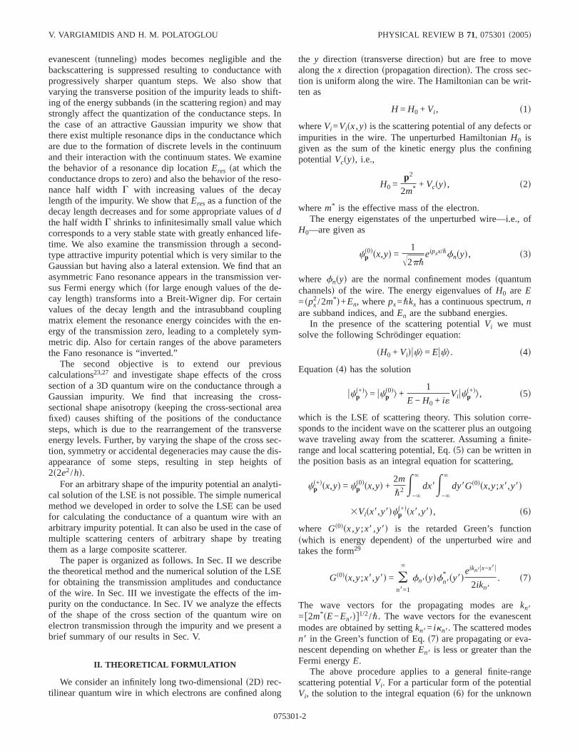
We analyze now the influence of the Gaussian impuritypotential on the conductance. The transverse location of theimpurity is at yi =s5/12dw. As mentioned in Sec. II thechoice ux0u=5d is sufficient to guarantee thatVis±x0,yd=0.The energy subbands in the scattering regionswhich we willdenote asEn,sd are shifted upwards due to the transversepotential of the impurity. The first subband in this regionopens at E1,s=1.85E1 while the second opens atE2,s=4.35E1.
Figure 1sad shows the behavior of the conductancethrough a Gaussian impurity in the 2D rectilinear quantumwire plotted versus the Fermi energy over the first subband,for several different values of the parameterd/w. For thesmallest value ofd chosen in the calculationsi.e., d=0.3wwhich corresponds to the solid lined we see thatG increasesalmost linearly in the beginning and finally approaches thequantum unit 2e2/h. However increasing the value ofd leadsto a progressively sharper rise of the conductance at the
opening of the subbandE1,s and a corresponding suppressionof the conductance belowE1,s. For E1,E,E1,s the firstchannel is not propagating and therefore transport occurs viatunneling for this particular channel. While the first channelof propagation opens up atE1,s, the subbands above theFermi level contribute to some extent by tunneling. Thus at aparticular value ofd the effect of the evanescent states abovethe Fermi level is to give rise to electron transmission priorto the opening of the subbandE1,s. The suppression of theconductancesfor E1,E,E1,sd with increasingd can be un-derstood simply in terms of the progressively smaller contri-bution of evanescent modes. We illustrate this gradual de-crease of tunneling in Fig. 1sbd for two values of the energyE=0.9E1,s and 0.88E1,s, i.e., well below the bottom of thefirst subbandE1,s. As it is clear from Fig. 1sbd the tunnelingprobability swhich is smaller for lower energiesd decreasesexponentially and for large enough values ofd it will vanish.Immediately after the opening of the subbandE1,s and withincreasing values ofd the conductance approaches progres-sively faster the quantum unit 2e2/h and equals 2e2/h over alarger part of the subband. This is due to the suppression ofbackscattering as the impurity potential becomes smoother.Thus the simultaneous suppression of tunneling and back-scattering effects with increasingd results in a sharper con-ductance step. In the extreme case in whichd becomes verylarge si.e., the impurity potential becomes almost flatd it isreasonable to expect that the impurity will cause very little or
FIG. 1. sad ConductanceG sin units of 2e2/hd as a function ofFermi energyE sover the first subbandd through a Gaussian impu-rity of strengthg=2.53106 cm−1 in a 2D rectilinear quantum wireof width w. E is given in units ofE1 swhereE1 is the bottom of thefirst subband in the clean wired. Results are shown for various sizesof the impuritysspecified by the parameterd/wd. Note that increas-ing d results to sharper rise of the conductance.sbd Tunneling prob-ability vs d/w, for two values of the Fermi energy. The solid linecorresponds toE=0.9E1,s while the dashed line toE=0.88E1,s,whereE1,s is the bottom of the first subband in the scattering region.
V. VARGIAMIDIS AND H. M. POLATOGLOU PHYSICAL REVIEW B 71, 075301s2005d
075301-4
no reflection since the quantum wavelength becomes smallcompared with the characteristic distance over which the po-tential varies appreciably. In this case quantum tunneling willalso be absent resulting to zero transmission prior to theopening ofE1,s. Accordingly we will obtain perfectly sharpstep structure andG=2e2/h over the entire subband. In theopposite limit of very smalld the conductance of a pointscatterer is recovered. It is worth mentioning here that in thecase of a point scatterer there is only one set of subbands inthe wire and the first two channels become propagating ex-actly atE=E1 andE=E2, respectively.
The above points can also be discussed in a perturbationpicture. In particular, the reflection coefficients due to thebackscattering can easily be calculated in the first-order Bornapproximation,22 obtaining
Rnn8sEd =Gnn8
2pd2
4knkn8e−skn + kn8d
2d2/2, s19d
wheren andn8 are the incident and reflected modes, respec-tively, while Gnn8=gfnsyidfn8
* syid are constants that are pro-portional to the coupling of the incident and reflected trans-verse modes at the impurity. It is clear from Eq.s19d thatbackscattering reduces very fast with increasingd, leading togradual enhancement of transmission and improving thequantized conductance step. In fact in the limit in whichdbecomes very largefwhile keeping all other parameters inEq. s19d fixedg, Rnn8 approaches zero, as can be verified fromthe above equation. For later analysis we also note that theabove reflection coefficients also depend on the coupling ofthe transverse modes at the impurity position through theconstantsGnn8.
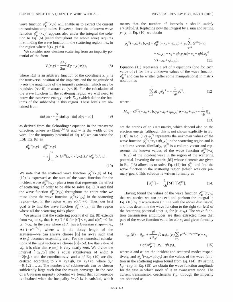
As mentioned above the subbands that lie above theFermi level can contribute to the conductance by tunneling.The most important contribution comes from the first sub-band that lies immediately above the Fermi levelssince thecontribution of the higher ones decreases with increasing en-ergyd. However, this contribution is different for differentconductance steps. This effect is illustrated in Fig. 2 wherewe plot the conductance versus the Fermi energy over thefirst two subbands, for several different values of the decaylength d. It is seen that the first conductance step risessmoother in the vicinity ofE1,s than the corresponding rise ofthe second step in the vicinity ofE2,s. This can be understoodif we examine the distance between the subbands in the scat-tering region and those in the clean wire. The distanceDEs1d
betweenE1 andE1,s is 0.85E1, which is much larger than thedistanceDEs2d betweenE2 and E2,s, which is 0.35E1. Eventhough the larger distanceDEs1d leads to smaller tunnelingprobability for E1,E,E1,s, the tunneling regionDEs1d ofthe first step is much greater than the tunneling regionDEs2d
of the second step by a factor of 2.42. Thus in the secondstep there is a larger amount of tunneling in a smaller tun-neling region and this leads to rapid enhancement of theconductance values in this region.
The smoother and sharper rise of the first and secondsteps, respectively, is also due to the different strength of theinteraction of the respective modes with the impurity. For theparticular position of the impurity that we considerfi.e., yi
=s5/12dwg the coupling of the first mode at the impurity isstronger than the corresponding coupling of the secondmode. Consequently scattering of the first mode is enhancedwhile scattering of the second mode is suppressed, givingrise to smoother and sharper steps, respectively. This canalso be understood from the perturbation result of Eq.s19d.We must note that when we consider transport in the secondsubband there is intrasubband reflection throughR12, R21 inaddition toR11. However, the dominant contribution comesfrom the backscattering within the second channel, i.e., fromR22, which has the smallest wave vector as can be seen fromEq. s19d. Now when we consider transport in the first sub-band the magnitude ofG11 is large resulting to enhancedreflection. When we consider transport in the second sub-band the coupling constantG22 scorresponding to the domi-nant reflection coefficientR22d is small leading to reducedreflection. Placing the impurity on the central axis of the wirewould result in a maximum scattering of the first mode whilethe second will suffer no scattering, leading to almost perfectquantization of the second step. These points will becomemore clear in the next section where we examine the influ-ence of the impurity position on the conductance.
B. Effects of the impurity position on the conductance
Several interesting effects are observed when we vary thetransverse position of the impurity. In Fig. 3sad we show theconductance through a Gaussian impurity withd=0.7w in a2D rectilinear quantum wire plotted versus the Fermi energy,for three different impurity positionsyi. It can be seen that asthe impurity is displaced away from the central axis of thewire the position of the first conductance step is systemati-cally shifted towards lower energy values while it rises pro-gressively sharper at the opening of the subbandE1,s. Note inparticular that when the impurity is placed atyi =s1/12dw theconductance grows rapidly with energy and very soon ap-proaches values very close to the quantum unit 2e2/h. How-ever, the shifting of the position of the second conductancestep can be either towards lower or higher energy values
FIG. 2. ConductanceG sin units of 2e2/hd vs Fermi energyEthrough a Gaussian impurity of strengthg=2.53106 cm−1 in a 2Drectilinear quantum wire of widthw, for three values of the param-eter d/w. Note the sharper rise of the second conductance stepscompared to the first stepd which is due to the smaller distancebetweenE2,s and E2, whereE2,s is the bottom of the second sub-band in the scattering region andE2 is the corresponding subband inthe clean part of the wire.
CONDUCTANCE OF A QUANTUM WIRE WITH A… PHYSICAL REVIEW B 71, 075301s2005d
075301-5
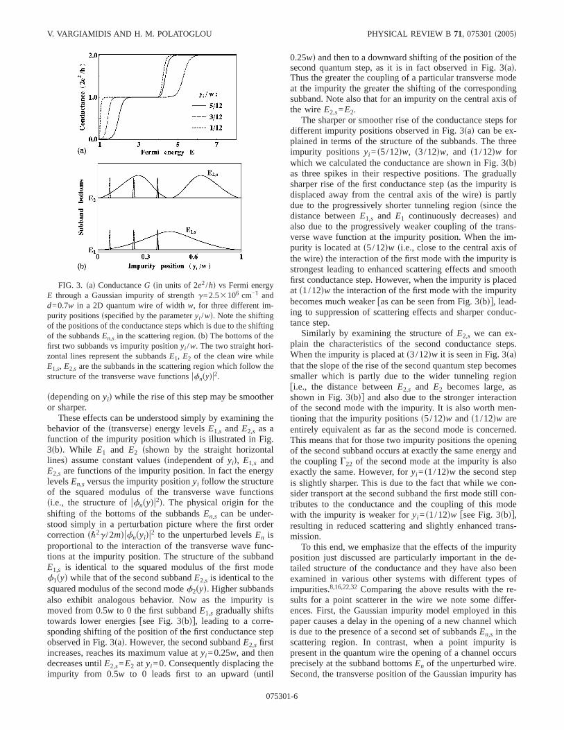
sdepending onyid while the rise of this step may be smootheror sharper.
These effects can be understood simply by examining thebehavior of thestransversed energy levelsE1,s andE2,s as afunction of the impurity position which is illustrated in Fig.3sbd. While E1 and E2 sshown by the straight horizontallinesd assume constant valuessindependent ofyid, E1,s andE2,s are functions of the impurity position. In fact the energylevelsEn,s versus the impurity positionyi follow the structureof the squared modulus of the transverse wave functionssi.e., the structure ofufnsydu2d. The physical origin for theshifting of the bottoms of the subbandsEn,s can be under-stood simply in a perturbation picture where the first ordercorrections"2g /2mdufnsyidu2 to the unperturbed levelsEn isproportional to the interaction of the transverse wave func-tions at the impurity position. The structure of the subbandE1,s is identical to the squared modulus of the first modef1syd while that of the second subbandE2,s is identical to thesquared modulus of the second modef2syd. Higher subbandsalso exhibit analogous behavior. Now as the impurity ismoved from 0.5w to 0 the first subbandE1,s gradually shiftstowards lower energiesfsee Fig. 3sbdg, leading to a corre-sponding shifting of the position of the first conductance stepobserved in Fig. 3sad. However, the second subbandE2,s firstincreases, reaches its maximum value atyi =0.25w, and thendecreases untilE2,s=E2 at yi =0. Consequently displacing theimpurity from 0.5w to 0 leads first to an upwardsuntil
0.25wd and then to a downward shifting of the position of thesecond quantum step, as it is in fact observed in Fig. 3sad.Thus the greater the coupling of a particular transverse modeat the impurity the greater the shifting of the correspondingsubband. Note also that for an impurity on the central axis ofthe wireE2,s=E2.
The sharper or smoother rise of the conductance steps fordifferent impurity positions observed in Fig. 3sad can be ex-plained in terms of the structure of the subbands. The threeimpurity positionsyi =s5/12dw, s3/12dw, and s1/12dw forwhich we calculated the conductance are shown in Fig. 3sbdas three spikes in their respective positions. The graduallysharper rise of the first conductance stepsas the impurity isdisplaced away from the central axis of the wired is partlydue to the progressively shorter tunneling regionssince thedistance betweenE1,s and E1 continuously decreasesd andalso due to the progressively weaker coupling of the trans-verse wave function at the impurity position. When the im-purity is located ats5/12dw si.e., close to the central axis ofthe wired the interaction of the first mode with the impurity isstrongest leading to enhanced scattering effects and smoothfirst conductance step. However, when the impurity is placedat s1/12dw the interaction of the first mode with the impuritybecomes much weakerfas can be seen from Fig. 3sbdg, lead-ing to suppression of scattering effects and sharper conduc-tance step.
Similarly by examining the structure ofE2,s we can ex-plain the characteristics of the second conductance steps.When the impurity is placed ats3/12dw it is seen in Fig. 3sadthat the slope of the rise of the second quantum step becomessmaller which is partly due to the wider tunneling regionfi.e., the distance betweenE2,s and E2 becomes large, asshown in Fig. 3sbdg and also due to the stronger interactionof the second mode with the impurity. It is also worth men-tioning that the impurity positionss5/12dw ands1/12dw areentirely equivalent as far as the second mode is concerned.This means that for those two impurity positions the openingof the second subband occurs at exactly the same energy andthe couplingG22 of the second mode at the impurity is alsoexactly the same. However, foryi =s1/12dw the second stepis slightly sharper. This is due to the fact that while we con-sider transport at the second subband the first mode still con-tributes to the conductance and the coupling of this modewith the impurity is weaker foryi =s1/12dw fsee Fig. 3sbdg,resulting in reduced scattering and slightly enhanced trans-mission.
To this end, we emphasize that the effects of the impurityposition just discussed are particularly important in the de-tailed structure of the conductance and they have also beenexamined in various other systems with different types ofimpurities.8,16,22,32Comparing the above results with the re-sults for a point scatterer in the wire we note some differ-ences. First, the Gaussian impurity model employed in thispaper causes a delay in the opening of a new channel whichis due to the presence of a second set of subbandsEn,s in thescattering region. In contrast, when a point impurity ispresent in the quantum wire the opening of a channel occursprecisely at the subband bottomsEn of the unperturbed wire.Second, the transverse position of the Gaussian impurity has
FIG. 3. sad ConductanceG sin units of 2e2/hd vs Fermi energyE through a Gaussian impurity of strengthg=2.53106 cm−1 andd=0.7w in a 2D quantum wire of widthw, for three different im-purity positionssspecified by the parameteryi /wd. Note the shiftingof the positions of the conductance steps which is due to the shiftingof the subbandsEn,s in the scattering region.sbd The bottoms of thefirst two subbands vs impurity positionyi /w. The two straight hori-zontal lines represent the subbandsE1, E2 of the clean wire whileE1,s, E2,s are the subbands in the scattering region which follow thestructure of the transverse wave functionsufnsydu2.
V. VARGIAMIDIS AND H. M. POLATOGLOU PHYSICAL REVIEW B 71, 075301s2005d
075301-6
a greater influence on the conductance of the wire because ofthe possible shifting of the subbandssin the scattering re-giond as the impurity is displaced. For some impurity posi-tions the subbands in the scattering region are far apart fromthose of the unperturbed wire while for other positions theycoincide resulting in significant changes in the appearance ofthe conductance. This effect is absent from the point impu-rity model where only one set of subbands exists. We nextturn to the case where the impurity is attractive.
C. Attractive Gaussian impurity
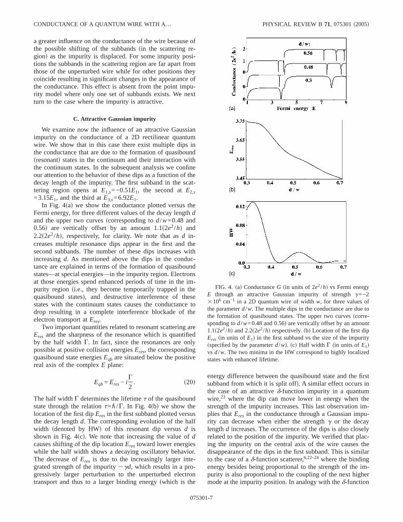
We examine now the influence of an attractive Gaussianimpurity on the conductance of a 2D rectilinear quantumwire. We show that in this case there exist multiple dips inthe conductance that are due to the formation of quasiboundsresonantd states in the continuum and their interaction withthe continuum states. In the subsequent analysis we confineour attention to the behavior of these dips as a function of thedecay length of the impurity. The first subband in the scat-tering region opens atE1,s=−0.51E1, the second atE2,s=3.15E1, and the third atE3,s=6.92E1.
In Fig. 4sad we show the conductance plotted versus theFermi energy, for three different values of the decay lengthdand the upper two curvesscorresponding tod/w=0.48 and0.56d are vertically offset by an amount 1.1s2e2/hd and2.2s2e2/hd, respectively, for clarity. We note that asd in-creases multiple resonance dips appear in the first and thesecond subbands. The number of these dips increases withincreasingd. As mentioned above the dips in the conduc-tance are explained in terms of the formation of quasiboundstates—at special energies—in the impurity region. Electronsat those energies spend enhanced periods of time in the im-purity region si.e., they become temporarily trapped in thequasibound statesd, and destructive interference of thesestates with the continuum states causes the conductance todrop resulting in a complete interference blockade of theelectron transport atEres.
Two important quantities related to resonant scattering areEres and the sharpness of the resonance which is quantifiedby the half widthG. In fact, since the resonances are onlypossible at positive collision energiesEres, the correspondingquasibound state energiesEqb are situated below the positivereal axis of the complexE plane:
Eqb = Eres− iG
2. s20d
The half widthG determines the lifetimet of the quasiboundstate through the relationt=" /G. In Fig. 4sbd we show thelocation of the first dipEres in the first subband plotted versusthe decay lengthd. The corresponding evolution of the halfwidth sdenoted by HWd of this resonant dip versusd isshown in Fig. 4scd. We note that increasing the value ofdcauses shifting of the dip locationEres toward lower energieswhile the half width shows a decaying oscillatory behavior.The decrease ofEres is due to the increasingly larger inte-grated strength of the impurity,gd, which results in a pro-gressively larger perturbation to the unperturbed electrontransport and thus to a larger binding energyswhich is the
energy difference between the quasibound state and the firstsubband from which it is split offd. A similar effect occurs inthe case of an attractived-function impurity in a quantumwire,23 where the dip can move lower in energy when thestrength of the impurity increases. This last observation im-plies thatEres in the conductance through a Gaussian impu-rity can decrease when either the strengthg or the decaylengthd increases. The occurrence of the dips is also closelyrelated to the position of the impurity. We verified that plac-ing the impurity on the central axis of the wire causes thedisappearance of the dips in the first subband. This is similarto the case of ad-function scatterer,6,22–24where the bindingenergy besides being proportional to the strength of the im-purity is also proportional to the coupling of the next highermode at the impurity position. In analogy with thed-function
FIG. 4. sad ConductanceG sin units of 2e2/hd vs Fermi energyE through an attractive Gaussian impurity of strengthg=−23106 cm−1 in a 2D quantum wire of widthw, for three values ofthe parameterd/w. The multiple dips in the conductance are due tothe formation of quasibound states. The upper two curvesscorre-sponding tod/w=0.48 and 0.56d are vertically offset by an amount1.1s2e2/hd and 2.2s2e2/hd respectively.sbd Location of the first dipEres sin units of E1d in the first subband vs the size of the impuritysspecified by the parameterd/wd. scd Half width G sin units of E1dvs d/w. The two minima in the HW correspond to highly localizedstates with enhanced lifetime.
CONDUCTANCE OF A QUANTUM WIRE WITH A… PHYSICAL REVIEW B 71, 075301s2005d
075301-7
scatterer we argue that the disappearance of the dipsswhenthe impurity is on the axisd is caused by the vanishing cou-pling of the second mode at the impurity.
In Fig. 4scd it is seen that the half width as a function ofdfirst increases, reaches a maximum atd=0.325w swhereGmax=0.1246E1d, and then decreases to a minimum atd=0.4352w swhere Gmin<2310−6E1d after which it growsagain. This situation can be repeated a few timessdependingon the properties of the impurity, such as its strength as wellas its transverse positiond. The extremely narrow half widthof the resonant dip atd=0.4352w corresponds to a verystable state—a state with greatly enhanced lifetime. Physi-cally this highly localized state is stable since at the particu-lar value ofd its interaction with the continuum is minimizedand therefore it decays extremely slowlysi.e., the decay rateof the localized state into a propagating state is lowestd. Thusat this special value ofd transformation of the quasiboundstate to a highly localized state occurs. The dips in the sec-ond subband also exhibit similar behavior.
The increase of the degree of localization of the quasi-bound states asG→0 can be explained in terms of the co-herent interaction of interfering channels in the impurity re-gion. This can be understood if we consider the energyintervalE2,s,E,E2 where there are two propagating modesn=1,2 in theimpurity region, while outside this region andfor the same energy interval only moden=1 is propagatingwhile moden=2 turns into an evanescent wave. Accordinglythe coherent resonant interaction of these channels leads toan increase of the charge density in the region of localizationand the electron escape rate is minimum.
Long-living electron states were also predicted for a rect-angular well model for the impurity potential in a straightquantum waveguide,19 and the subsequent collapse of theFano resonance was studied in detail. The coherent resonantphenomena in the impurity region is also the physical originof the effects studied in Ref. 19.
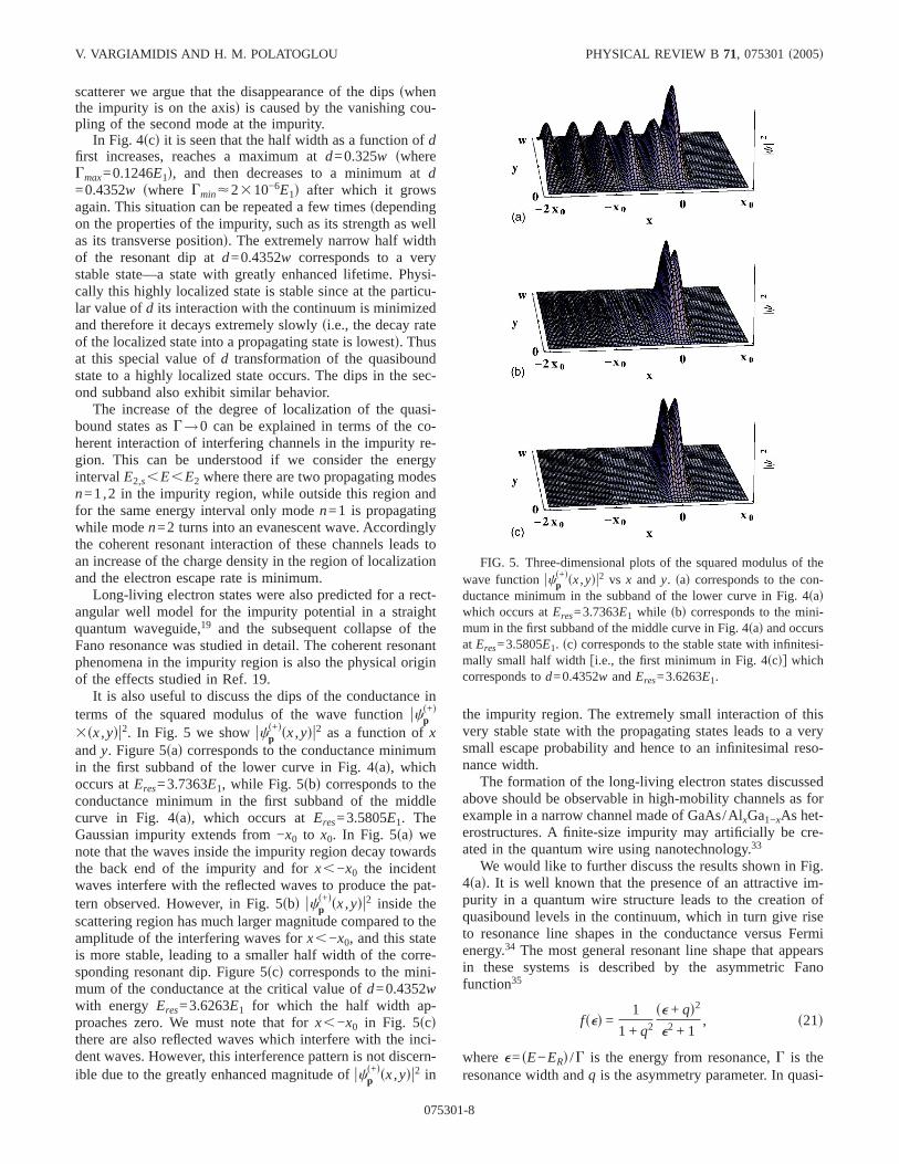
It is also useful to discuss the dips of the conductance interms of the squared modulus of the wave functionucp
s+d
3sx,ydu2. In Fig. 5 we showucps+dsx,ydu2 as a function ofx
andy. Figure 5sad corresponds to the conductance minimumin the first subband of the lower curve in Fig. 4sad, whichoccurs atEres=3.7363E1, while Fig. 5sbd corresponds to theconductance minimum in the first subband of the middlecurve in Fig. 4sad, which occurs atEres=3.5805E1. TheGaussian impurity extends from −x0 to x0. In Fig. 5sad wenote that the waves inside the impurity region decay towardsthe back end of the impurity and forx,−x0 the incidentwaves interfere with the reflected waves to produce the pat-tern observed. However, in Fig. 5sbd ucp
s+dsx,ydu2 inside thescattering region has much larger magnitude compared to theamplitude of the interfering waves forx,−x0, and this stateis more stable, leading to a smaller half width of the corre-sponding resonant dip. Figure 5scd corresponds to the mini-mum of the conductance at the critical value ofd=0.4352wwith energy Eres=3.6263E1 for which the half width ap-proaches zero. We must note that forx,−x0 in Fig. 5scdthere are also reflected waves which interfere with the inci-dent waves. However, this interference pattern is not discern-ible due to the greatly enhanced magnitude ofucp
s+dsx,ydu2 in
the impurity region. The extremely small interaction of thisvery stable state with the propagating states leads to a verysmall escape probability and hence to an infinitesimal reso-nance width.
The formation of the long-living electron states discussedabove should be observable in high-mobility channels as forexample in a narrow channel made of GaAs/AlxGa1−xAs het-erostructures. A finite-size impurity may artificially be cre-ated in the quantum wire using nanotechnology.33
We would like to further discuss the results shown in Fig.4sad. It is well known that the presence of an attractive im-purity in a quantum wire structure leads to the creation ofquasibound levels in the continuum, which in turn give riseto resonance line shapes in the conductance versus Fermienergy.34 The most general resonant line shape that appearsin these systems is described by the asymmetric Fanofunction35
fsed =1
1 + q2
se + qd2
e2 + 1, s21d
wheree=sE−ERd /G is the energy from resonance,G is theresonance width andq is the asymmetry parameter. In quasi-
FIG. 5. Three-dimensional plots of the squared modulus of thewave functionucp
s+dsx,ydu2 vs x and y. sad corresponds to the con-ductance minimum in the subband of the lower curve in Fig. 4sadwhich occurs atEres=3.7363E1 while sbd corresponds to the mini-mum in the first subband of the middle curve in Fig. 4sad and occursat Eres=3.5805E1. scd corresponds to the stable state with infinitesi-mally small half widthfi.e., the first minimum in Fig. 4scdg whichcorresponds tod=0.4352w andEres=3.6263E1.
V. VARGIAMIDIS AND H. M. POLATOGLOU PHYSICAL REVIEW B 71, 075301s2005d
075301-8
one-dimensional systems it has been shown36 that the trans-mission coefficient can be expressed in the Fano form asgiven in Eq.s21d, and in this case the asymmetry parameterq=sER−E0d /G, whereER is the resonance energy andE0 isthe energy of the transmission zero. As mentioned in thebeginning of this section the dips in the conductance curvesof Fig. 4sad are due to the formation of quasibound states inthe continuum and their subsequent coupling with the con-tinuum states. However, instead of the occurrence of asym-metric Fano resonances we observe symmetric dips. Thisbehavior of the conductance indicates that the asymmetryparameterq must be negligiblesi.e., q!1d, which meansthat the distance between the energy of the transmission zeroE0 and the resonance energyER is infinitesimal. Equivalentlywe may say that the symmetric dips in Fig. 4sad are due tothe large background36 si.e., nonresonantd transmission,which leads to infinitesimal values ofq. For the attractiveGaussian impurity that we considered in this section we veri-fied numerically that the background transmission rises pro-gressively faster as the decay lengthd increasessi.e., as theimpurity potential becomes smootherd and for sufficientlylarge d it becomes unity over the largest part of the energysubband, thereby leading to symmetric dips in the conduc-tance curves. We fully illustrate these considerations in thenext section where we employ the Feshbach37 approachswhich is particularly suitable for the description of reso-nance line shapesd in order to calculate the transmission co-efficient and the asymmetry parameter in the case of asecond-type impurity potential which is very similarsalmostidenticald to the Gaussian but having also a lateral extension.It will also be shown that in the regime of relatively smallvalues of the decay length an asymmetric Fano resonanceappears in the transmission.
D. Two-channel Feshbach approach
In this section we employ the Feshbach approach in orderto describe the transmission resonances in a rectilinear quan-tum wire with a smooth finite-size impurity to be definedbelow. Feshbach’s theory of coupled scattering channels wasin fact reformulated and employed in quasi-one-dimensionalsystems in order to describe symmetric34 line shapessBreit-Wigner-type resonancesd and also to describe more generalasymmetric36 line shapes for arbitrary coupling potentials,providing microscopic expressions for all line shape param-eters.
As in Sec. II we consider a uniform quantum wire wherethe electrons are confined along they direction but are free topropagate along thex direction. In the presence of an impu-rity we need to solve the Schrödinger equation
F−"2
2m* ¹2 + Vcsyd + Visx,ydGCsx,yd = ECsx,yd, s22d
whereVcsyd is the confining potential andVisx,yd is the at-tractive impurity potential, which we take to be of the form
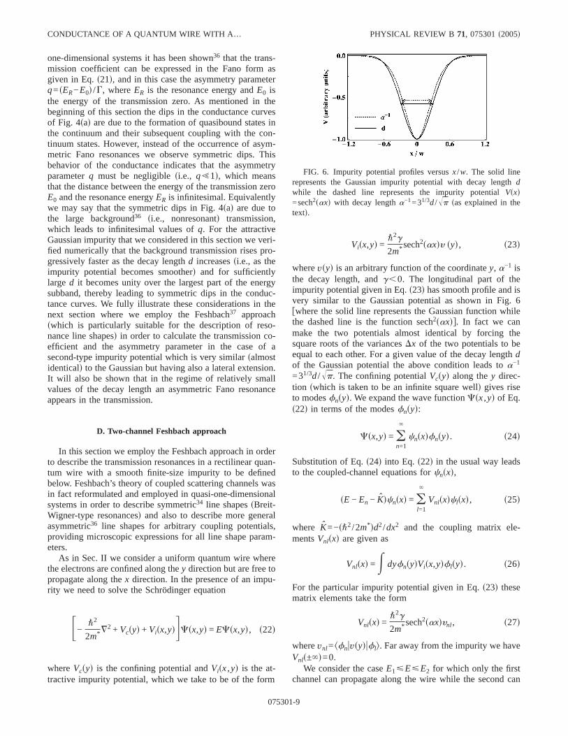
Visx,yd ="2g
2m* sech2saxdy syd, s23d
wherevsyd is an arbitrary function of the coordinatey, a−1 isthe decay length, andg,0. The longitudinal part of theimpurity potential given in Eq.s23d has smooth profile and isvery similar to the Gaussian potential as shown in Fig. 6fwhere the solid line represents the Gaussian function whilethe dashed line is the function sech2saxdg. In fact we canmake the two potentials almost identical by forcing thesquare roots of the variancesDx of the two potentials to beequal to each other. For a given value of the decay lengthdof the Gaussian potential the above condition leads toa−1
=31/3d/Îp. The confining potentialVcsyd along they direc-tion swhich is taken to be an infinite square welld gives riseto modesfnsyd. We expand the wave functionCsx,yd of Eq.s22d in terms of the modesfnsyd:
Csx,yd = on=1
`
cnsxdfnsyd. s24d
Substitution of Eq.s24d into Eq. s22d in the usual way leadsto the coupled-channel equations forcnsxd,
sE − En − K̂dcnsxd = ol=1
`
Vnlsxdclsxd, s25d
where K̂=−s"2/2m*dd2/dx2 and the coupling matrix ele-mentsVnlsxd are given as
Vnlsxd =E dyfnsydVisx,ydflsyd. s26d
For the particular impurity potential given in Eq.s23d thesematrix elements take the form
Vnlsxd ="2g
2m* sech2saxdynl, s27d
wherevnl=kfnuvsydufll. Far away from the impurity we haveVnls±`d=0.
We consider the caseE1øEøE2 for which only the firstchannel can propagate along the wire while the second can
FIG. 6. Impurity potential profiles versusx/w. The solid linerepresents the Gaussian impurity potential with decay lengthdwhile the dashed line represents the impurity potentialVsxd=sech2saxd with decay lengtha−1=31/3d/Îp sas explained in thetextd.
CONDUCTANCE OF A QUANTUM WIRE WITH A… PHYSICAL REVIEW B 71, 075301s2005d
075301-9
contribute via tunneling. Thus only the first channeln=1 canbe in some scattering state. These scattering states are givenas solutions of the equation
sK̂ + V11dxk±sxd = sE − E1dxk
±sxd, s28d
wherexk+ andxk
− correspond to scattering states for which theincident wave comes from −̀ and +̀ , respectively. Thesestates describe the backgroundsnonresonantd scattering,which is the scattering in a hypothetical system where thecoupling to the bound state is absent.12,36The solution to Eq.s28d proceeds in the same way as in a one-dimensional scat-tering problem38 with an attractive potential −U11 sech2saxd,whereU11=−s"2g /2m*dv11, and the asymptotic form of thewave function asx→−` is given in terms of Gamma func-tions
xk+sxd , e−ikxGsik/adGs1 − ik/ad
Gs− sdGs1 + sd
+ eikx Gs− ik/adGs1 − ik/adGs− ik/a − sdGs− ik/a + s+ 1d
, s29d
where k=f2m*sE−E1dg1/2/" and s=s1/2df−1+Î1+s8m*U11/a2"2dg. Then the scattering states can bewritten in the form
xk±sxd =Htbge±ikx sx → ± `d
e±ikx + r±bge7ikx sx → 7 `d
h , s30d
where the upper signs correspond to incident wave from −`.tbg and r±
bg correspond to the background transmission andreflection amplitudes in the wire. Specifically,r+
bg is the ratioof coefficients in the functionxk
+sxd of Eq. s29d. Due to sym-metry r−
bg=r+bg holds. We considerE close toE0, whereE0 is
the bound state energy of the stateF0 in the potentialV22sxdof the uncoupled channeln=2, i.e.,
sK̂ + V22dF0sxd = sE0 − E2dF0sxd. s31d
Employing the notatione=f−2m*sE0−E2dg1/2/"a, s=s1/2d3f−1+Î1+s8m*U22/a2"2dg, and U22=−s"2g /2m*dv22, Eq.s31d can be brought to a form38 that has solutions the asso-ciated Legendre polynomialsPs
esjd, wherej=tanhsaxd. Theenergy levels are then determined by the conditione=s−p,which gives
Ep = E2 −"2a2
8m* F− s1 + 2pd +Î1 +8m*U22
a2"2 G2
, s32d
wherep=0,1,2, . . .There is a finite number of levels deter-mined by the conditione.0, i.e.,p,s. In the following weassume thatU22 anda are such thatsø1, which implies thatthere is only one bound state with energyE0. The normalizedbound state wave function that corresponds to this energylevel is F0sxd=sa /2d1/2sechsaxd.
At this point it becomes clear that the reason we em-ployed the impurity potential of Eq.s23d in this section isthat it allows us to find analytical solutions to Eqs.s28d ands31d for the scattering and bound states whereas this wouldnot be possible for the Gaussian potentialsfor which no ana-
lytical solution exists in one dimensiond. This will allow usto study in detail the characteristics of the resonance lineshape in the two-channel approximation. On the other hand,the LSE could also have been used to solve numerically theproblem for a Gaussian impurity with an arbitrary but spe-cific shape of the impurity in the transverse direction. How-ever this would not permit us to vary the intra- and intersub-band coupling matrix elements independentlyfas we will beable to do for the impurity of Eq.s23d for which vsyd iscompletely arbitraryg, which are in fact buried inside thescattering wave function of Eq.s14d.
We now make the approximation of truncating the sum inEq. s25d at n=2. We then get the system of equations
sE − E1 − K̂ − V11dc1sxd = V12c2sxd, s33d
sE − E2 − K̂ − V22dc2sxd = V21c1sxd. s34d
The coupled-channel equationss33d and s34d are solved ingeneral in Refs. 34 and 36 with the ansatzc2sxd=AF0sxd andemploying the retarded Green’s operator for Eq.s33d. In theAppendix we calculate the wave functionc1sxd in the quan-tum wire for x→` with the impurity potential of Eq.s23dand extract the transmission coefficient
T = utbgu2sE − E0d2
sE − E0 − dd2 + G2 , s35d
where d and G are given in Eqs.sA12d and sA13d of theAppendix. Equations35d is of the Fano form in which thereal quantityd determines the asymmetry parameterq of theline shape by the relation
q =ER − E0
G=
d
G= −
cosfsp/2dÎ1 + s8m*U11/"2a2dg
sinhspk/ad.
s36d
An important feature of Eq.s36d is that q→0 as the decaylength a−1 increasesssince the denominator grows progres-sively faster while the numerator is restricted between thevalues of −1 and 1d. This effect is more pronounced whenthe wave vectork is largersi.e., when the asymmetric reso-nance line shape occurs closer to the second subband thresh-oldd. A second important feature of Eq.s36d is that for suit-able values ofU11/a2 the quantity d can be positive,negative or zerosi.e., the resonance energy may occur be-fore, after or be equal to the energy of the transmission zerod.It can be shown that forU11/a2=s"2/8m*dfs2n+1d2−1gwheren=1,2, . . ., wehaveER=E0 and in this case the trans-mission exhibits symmetric Breit-Wigner dips. For 0,U11/a2,"2/m* we have ER.E0 and the transmissionresonance is of the 0→1 typesi.e., the peak follows the dipd.For "2/m* ,U11/a2,3"2/m* we haveER,E0 and the reso-nance line shape is of the 1→0 typesi.e., the location of thepole is switched with the zero energyd. Thus after the valueU11/a2="2/m* swhere the transmission exhibits a symmetricdipd the Fano resonance is “inverted.” Similar inversion ofthe resonance level has also been observed in Ref. 19.
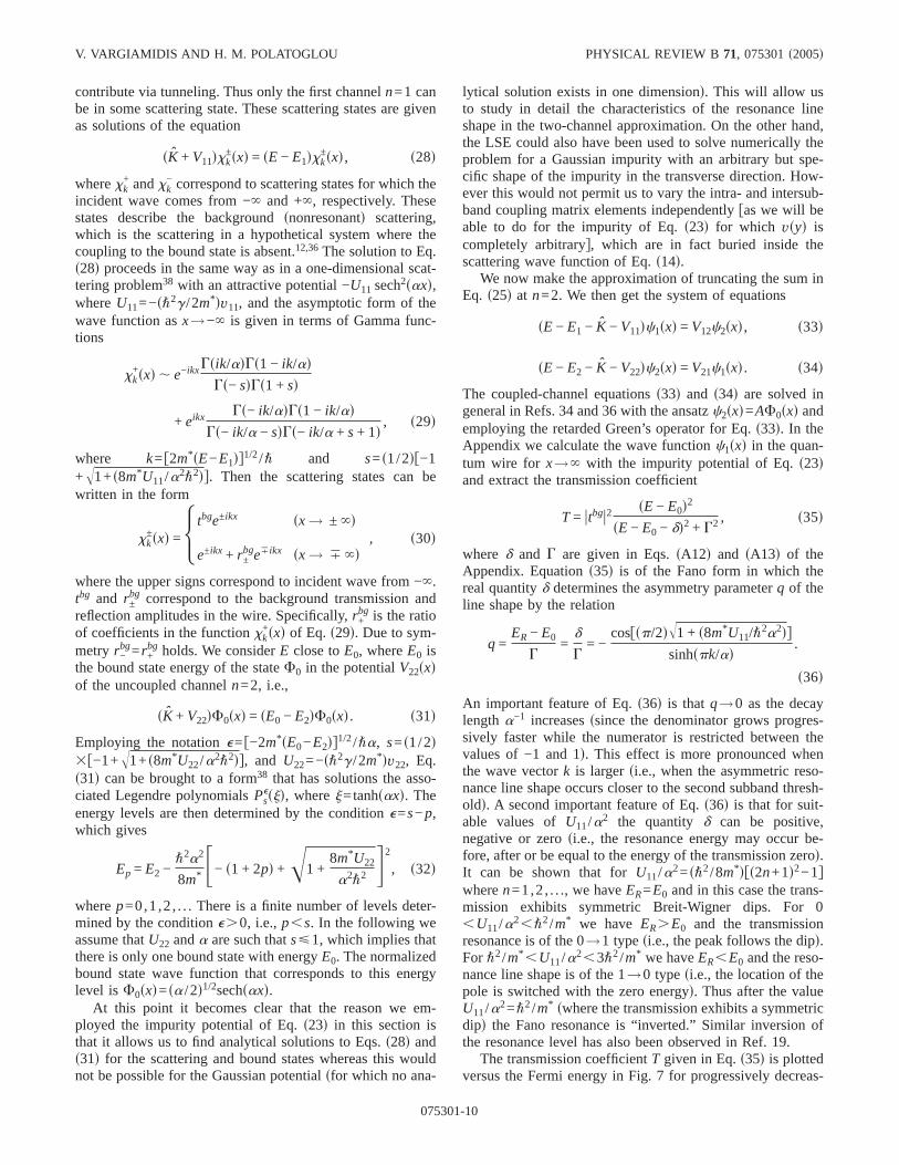
The transmission coefficientT given in Eq.s35d is plottedversus the Fermi energy in Fig. 7 for progressively decreas-
V. VARGIAMIDIS AND H. M. POLATOGLOU PHYSICAL REVIEW B 71, 075301s2005d
075301-10
ing values of the inverse decay lengtha.39 In Figs. 7sad–7scdthe intrasubband matrix elementv11 is kept fixed to the valuev11=−1.5, while a=1.7, 1.4, and 1, respectively. All threeresonance line shapes are of the 0→1 type sinceU11/a2
=0.52, 0.77, and 1.5, respectively, which lie in the range 0,U11/a2,2 sor equivalently 0,U11/a2,"2/m*d. In Fig.7sad we use the valuesv22=−1.2,v12=0.08. The dashed linerepresents the directsnonresonantd transmission which oc-curs in the decoupling limitv12=0 sfor which d=G=0d. Inthis limit there are two scattering mechanisms: a directsnon-resonantd scattering from the first subband and a resonantscattering from the quasibound state. When the coupling tothe quasibound level is nonzero the interference between di-rect and resonant transmissionsthrough the quasibound stated
produces the asymmetric Fano line shape, which has alsobeen noted previously.12,36,40
In Fig. 7sbd, where the value of the inverse decay length issmaller sa=1.4d, we note that the Fano resonance distortswhile the transmission below the bound state is enhanced. InFig. 7sbd we use the valuesv22=−0.8 andv12=0.08 in orderfor the transmission zero to occur closer to the bottom of thesecond subband so that we can make contact with the nu-merical results of Fig. 4sad. In Fig. 7scd the inverse decaylength has been further decreased to the valuea=1 whilev22=−0.5 andv12=0.13. We notice that the transmission isgreatly enhanced and exhibits an almost symmetric dip. Asmentioned above this behavior of the transmission is due tothe fact thatq decreases asa decreasesfwhich is what Eq.s36d suggestsg. This is a consequence of the fact that thedistance between the resonance energy and the zero energygradually decreases leading to the progressive disappearanceof the asymmetric resonance. Finally when the value ofabecomes low enough such thatU11/a2=2 thenER=E0 andthe transmission exhibits only a symmetric dipfas will bediscussed in the context of Fig. 8sadg. This is precisely whathappens in the lower curve of Fig. 4sad which is very similarto Fig. 7scd. However in the numerical calculationsfpre-sented in Fig. 4sadg the strength of the intra- and intersub-band coupling matrix elements could not be varied indepen-dently for the transversed-function potentialsin fact these
FIG. 7. Transmission coefficientT vs Fermi energyE throughan attractive impurity potentialVisx,yd=s"2g /2m*dsech2saxdysyd ina 2D quantum wire, for three values of the inverse decay lengthawhile y11 is kept fixed at the valuey11=−1.5. sad The solid line,which corresponds toa=1.7 with y22=−1.4 andy12=0.08, showsan asymmetric Fano line shape while the dashed line represents thedirect transmission.sbd Corresponds toa=1.4, y22=−0.8, y12
=0.08 and shows a distortion of the Fano resonance.scd Corre-sponds toa=1, y22=−0.5,y12=0.12 and the transmissionswhich isgenerally enhancedd exhibits only a dip.
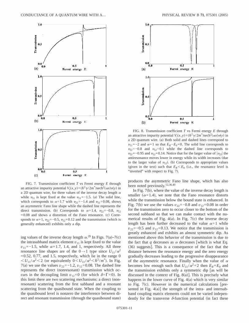
FIG. 8. Transmission coefficientT vs Fermi energyE throughan attractive impurity potentialVisx,yd=s"2g /2m*dsech2saxdysyd ina 2D quantum wire.sad Both solid and dashed lines correspond toy11=−2 anda=1 so thatER−E0=0. The solid line corresponds toy22=−0.8 and y12=0.1 while the dashed line corresponds toy22=−0.95 andy12=0.14. Notice that for the larger value ofuy22u theantiresonance moves lower in energy while its width increasessdueto the larger value ofy12d. sbd Corresponds to appropriate valuessgiven in the textd such thatER,E0 si.e., the resonance level is“inverted” with respect to Fig. 7d.
CONDUCTANCE OF A QUANTUM WIRE WITH A… PHYSICAL REVIEW B 71, 075301s2005d
075301-11
matrix elements were buried inside the scattering wave func-tion cp
s+dd and did not allow the full Fano structure to showup even for smaller values of the decay lengthd. Thus forlarge enough value of the decay length the conductance willonly exhibit dips regardless of the shape of the transverseimpurity potential or the values of the coupling matrix ele-ments. To this end, we point out that if we kept the value ofv22 fixed in Figs. 7sad–7scd the shape of the Fano resonancewould remain exactly the same except that the transmissionzero would occur at lower energies.
It was shown above that for certain values of the quantityU11/a2 the resonance energy coincides with the zero energyand in this case the transmission versus Fermi energy exhib-its symmetric Breit-Wigner dips. We illustrate this result inFig. 8sad where both solid and dashed lines correspond tov11=−2 anda=1 so thatU11/a2=2. Further for the trans-mission represented by the solid line we used the valuesv22=−0.8, v12=0.1 while the dashed line corresponds tov22=−0.95,v12=0.13. The only effect ofv22 on the transmis-sion is to displace the location of the transmission zero. Thusincreasinguv22u sdashed lined causes the displacement of thedip toward lower energy values. We also notice that thewidth of the antiresonance increases whenv12 increaseswhich is due to the larger coupling of the bound state withthe continuum.
In Fig. 8sbd we show the transmission as a function ofFermi energy for the valuesv11=−5.95, v22=−0.94, v12=0.068, anda=1.26. For these valuesU11/a2=3.75 andtherefore the resonance line shape is of the 1→0 type. Theinversion of the resonance level indicates that the roles ofdestructive and constructive interference between the directand resonant channels have been reversed. Thus when thespatial extensionsquantified by the decay lengtha−1d of theimpurity as well as the intrasubband matrix elementU11 haveappropriate values the Fano resonance appears inverted. Onecould argue that by keeping the value ofU11 fixed whilecontinuously decreasing the value ofa the quantityU11/a2
will reach the desirable values for which inversion of theFano resonance occurs. However, it is not enough thatU11/a2 be in the appropriate range. By makinga very smallssay a,0.5d the denominator of Eq.s36d becomes largeenough so thatq!1. Consequently the transmission will ex-hibit a dip while the peak will hardly be discerniblesdue tothe enhancement of the transmissiond.
IV. EFFECTS OF THE CROSS-SECTIONAL SHAPE ONTHE CONDUCTANCE
As mentioned in the Introduction, an important issue re-lated to electronic transport through quantum wires is howthe geometry of the wiressi.e., the shape of their transversecross sectiond influences the conductance. This issue hasbeen investigated in the case of transport in 3D quantumconstrictions16,25,26,41 and in 3D rectilinear quantum wireswith a d-function impurity23,27and several interesting effectshave been discussed. In the case of a 3D quantum wire witha d-function impurity, the solution of the scattering problemis known to be obtainable from the characteristic discontinu-ity of the derivative of the propagating wave function22,27
due to thed function, giving rise to a phase shift. The dis-continuity of the wave function depends critically on theshape of the cross section of the wire; increasing the aniso-tropy of the cross section leads to a progressively larger dis-continuity in the derivative of the wave function resulting ina larger phase shift and increased reflection. This and otherrelated effectssdiscussed in the references mentioned abovedimply that the shape of the cross section can strongly affectthe transport properties of a 3D quantum wire with an impu-rity.
Our objective in this section is to extend our previouscalculations23,27 and to investigate the influence of the cross-sectional shape of a 3D rectilinear quantum wire on the con-ductance through a repulsive Gaussian impurity potential ofthe form
Visx,y,zd ="2g
2m* dsy − yiddsz− zide−x2/d2, s37d
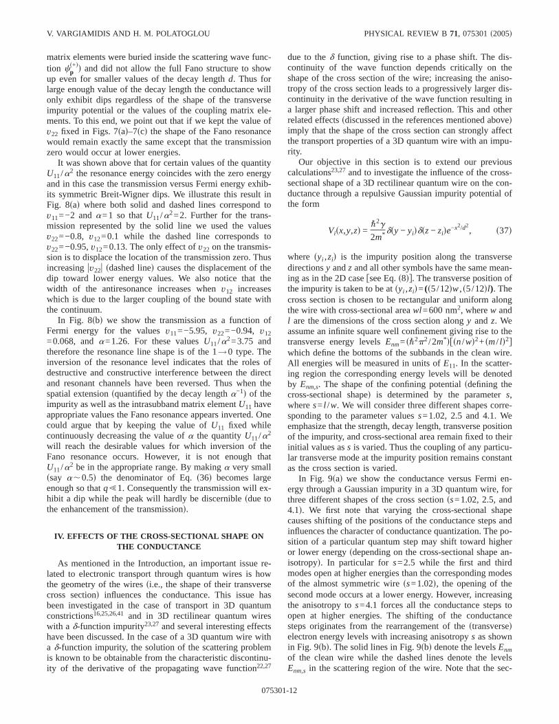
where syi ,zid is the impurity position along the transversedirectionsy andz and all other symbols have the same mean-ing as in the 2D casefsee Eq.s8dg. The transverse position ofthe impurity is taken to be atsyi ,zid=(s5/12dw,s5/12dl). Thecross section is chosen to be rectangular and uniform alongthe wire with cross-sectional areawl=600 nm2, wherew andl are the dimensions of the cross section alongy andz. Weassume an infinite square well confinement giving rise to thetransverse energy levelsEnm=s"2p2/2m*dfsn/wd2+sm/ ld2gwhich define the bottoms of the subbands in the clean wire.All energies will be measured in units ofE11. In the scatter-ing region the corresponding energy levels will be denotedby Enm,s. The shape of the confining potentialsdefining thecross-sectional shaped is determined by the parameters,wheres= l /w. We will consider three different shapes corre-sponding to the parameter valuess=1.02, 2.5 and 4.1. Weemphasize that the strength, decay length, transverse positionof the impurity, and cross-sectional area remain fixed to theirinitial values ass is varied. Thus the coupling of any particu-lar transverse mode at the impurity position remains constantas the cross section is varied.
In Fig. 9sad we show the conductance versus Fermi en-ergy through a Gaussian impurity in a 3D quantum wire, forthree different shapes of the cross sectionss=1.02, 2.5, and4.1d. We first note that varying the cross-sectional shapecauses shifting of the positions of the conductance steps andinfluences the character of conductance quantization. The po-sition of a particular quantum step may shift toward higheror lower energysdepending on the cross-sectional shape an-isotropyd. In particular for s=2.5 while the first and thirdmodes open at higher energies than the corresponding modesof the almost symmetric wiress=1.02d, the opening of thesecond mode occurs at a lower energy. However, increasingthe anisotropy tos=4.1 forces all the conductance steps toopen at higher energies. The shifting of the conductancesteps originates from the rearrangement of thestransversedelectron energy levels with increasing anisotropys as shownin Fig. 9sbd. The solid lines in Fig. 9sbd denote the levelsEnmof the clean wire while the dashed lines denote the levelsEnm,s in the scattering region of the wire. Note that the sec-
V. VARGIAMIDIS AND H. M. POLATOGLOU PHYSICAL REVIEW B 71, 075301s2005d
075301-12
ond degenerate levelE12s21d for s=1 splits to two levelsE12
and E21 for s.1. E12 shifts downward whileE21 shifts up-ward. Similarly the fourth degenerate levelE13s31d for s=1splits to E13 and E31 which shift down and upward respec-tively. We also note that the distance in energy between thefirst E11 and the secondE12 levels continuously decreaseswith increasings, leading to the progressively smaller size ofthe plateau between the first and second steps. Further whilethe first level E11 gradually shifts upward in energy withincreasings, the second levelE12 first shifts downward,reaches a minimum ats=2, and then shifts upward again.Thus ats=2.5 the second level is lower in energysthan thecorresponding level fors=1.02d giving rise to the opening ofthe second step at lower energyscompared to the second stepfor s=1.02d as is observed in Fig. 9sad.
We also note that due to the transverse potential in thescattering region the levelsEnm,s are slightly displaced up-wards with respect toEnm. However the relative distancebetweenEnm,s andEnm stays constant with increasings. Wealso observe that the upward displacement ofEnm,s with re-spect toEnm is different for different levels. For example thedifference E12,s−E12 is smaller than the differenceE11,s−E11. This is explained in terms of the weaker coupling ofthe second modes1, 2d at the impurity positionssince thatmode is close to have a node at the impurityd giving rise tosmaller upward shifting of the subbandE12,s. Similarly the
differenceE22,s−E22 is slightly smaller than the differenceE12,s−E12 since the coupling of modes2, 2d at the impurity iseven weaker. Placing the impurity at syi ,zid=(s1/2dw,s1/2dl) will result to zero coupling of modess1,2d, s2, 1d, ands2, 2d at the impurityssince these modes havenodes at the impurity positiond. This will cause the corre-sponding subbandsE12,s, E21,s, and E22,s in the scatteringregion to coincide with the subbandsE12, E21, andE22 of theclean wire, for any value ofs. We also note that the mini-mum energy of a particular modesn,md occurs ats=m/n.
When the cross section becomes almost symmetric thedistance between the second and third energy levels becomesextremely smallsi.e., these two levels become almost degen-erated giving rise to a plateau of a very small sizefsee thecurve fors=1.02 in Fig. 9sadg. The small size of the plateauinevitably forces the second step to rise sharply. In this casethe second and third modes lie very close in energy and thesecond step tends to disappear. In fact for the completelysymmetric wire withs=1, the degeneracy of the levelsE12and E21 will cause the disappearance of the second plateauand will give rise to a height of 2s2e2/hd for the secondconductance step. Whens=1 the first few conductance stepshave heights 1G0, 2G0, 1G0, 2G0, 2G0, . . ., where G0=2e2/h, reflecting the degeneracy of the electronic levels.Deviation from symmetry leads to splitting of the degeneratelevels and restoration of the single-stepsG0d behavior of theconductance. It’s also worth mentioning that under the influ-ence of a magnetic field an otherwise symmetric cross sec-tion will become effectively asymmetric.23,42,43 Upward ordownward shifting of thestransversed energy levels of aparabolically confined ballistic quantum wire under the in-fluence of a longitudinal magnetic field has been observedexperimentally.43 The degenerate levels observed in Ref. 43explain the disappearance of the corresponding plateau in theexperimentally measured conductance. For specific asym-metric cross-sectional shapes there might also be acciden-tally degenerate levels as can be seen in Fig. 9sbd. In particu-lar the levelsE13 andE22 are degenerate ats=1.29 for whichthe conductance will rise by 2G0 as are also the levelsE13and E21 at s=1.631. These degeneracies lead to occasionaldisappearance of steps in wires with asymmetric cross sec-tions. Variations in the shapes of the cross section of 3Dquantum point contacts have also been observedexperimentally44 in the past and such variations explain thedisappearance of some of the conductance steps. Effects ofthis type have no analogs in 2D quantum wires.
It’s also worth mentioning that examining the conduc-tance as a function ofs while keeping the Fermi energy fixedwould reveal an interesting feature of the quantum transport.Namely, increasing the anisotropy of the cross sectionsat afixed value of the Fermi energyd the subbands are shiftedtoward higher energies and therefore the contributing quan-tum channels decrease one by one. When the lowest subbandfinally crosses the fixed Fermi level, there is no open sub-band left and the conductance should vanish. Thus increasings leads to depopulation of subbandssi.e., decrease in thenumber of conducting channelsd, resulting to a decrease andeventually vanishing of the conductance. This last observa-tion suggests that cross-sectional shape anisotropy in 3D
FIG. 9. sad ConductanceG sin units of 2e2/hd vs Fermi energyE through a Gaussian impurity of strengthg=2.3 cm−2 and decaylengthd=20 nm in 3D rectilinear quantum wires with asymmetriccross sectionssspecified by the parameters, wheres= l /w andw, lare the transverse dimensions of the cross section alongy andzd. Eis given in units ofE11 swhereE11 is the bottom of the first subbandin the clean wired. The cross-sectional area is kept constant to thevalue wl=600 nm2 as the shape of the cross section is varied.sbdTransverse energy levels vs the cross-sectional shape anisotropys.Solid lines correspond to the levelsEnm of the unperturbed wirewhile the dashed lines correspond to the levelsEnm,s in the impurityregion.
CONDUCTANCE OF A QUANTUM WIRE WITH A… PHYSICAL REVIEW B 71, 075301s2005d
075301-13
quantum wires could be detected through conductance mea-surements at a fixed value of the Fermi energy.
V. SUMMARY
In this paper we have considered the transmission of elec-trons through a Gaussian impurityswith a decay lengthdalong the propagation directiond in 2D and 3D rectilinearquantum wires with symmetric or asymmetric cross sections.The confining potential is that of an infinite square well. Wehave solved the LSE numerically and investigated severalfeatures of the conductance.
The results for the 2D wire can be summarized as follows.Increasing the decay lengthd of a repulsive Gaussian impu-rity leads to a progressively sharper rise of the conductancesteps at the opening of the subbandsEn,s, as shown in Figs. 1and 2. The physical origin of this effect is the progressivelysmaller contribution of tunneling modes and the gradual sup-pression of backscattering as the impurity potential becomessmoother.
The conductance versus the Fermi energysfor various im-purity positionsd was also examined. Displacing the impurityaway from the central axis of the wire causes shifting of thepositions of the conductance steps which is due to the corre-sponding displacement of the bottoms of the subbandsEn,s inthe scattering region. A particular levelEn,s versus the impu-rity position follows the structure of the squared modulus ofthe corresponding transverse modeufnsydu2. Accordingly, de-pending on the particular impurity position, the coupling of atransverse mode at the impurity may be stronger or weakerleading to enhanced or suppressed scattering effects respec-tively si.e., to smeared or sharp quantum stepsd as shown inFig. 3.
In the case of an attractive Gaussian impurity we haveshown that there exist multiple resonance dips in the conduc-tance which are due to the formation of quasibound states.We examined the behavior of a dip locationEres and the halfwidth G as a function of the decay lengthd. We found thatincreasing the value ofd causes shifting ofEres toward lowerenergies while the half width decays in an oscillatory mannerssee Fig. 4d. In particular the half width of the resonant dipmay shrink to an extremely small value for some criticalvalues ofd resulting to an extremely stable statesa state withgreatly enhanced lifetimed.
The Feshbach approach was employed in order to analyzethe scattering from a second type impurity potentialsforwhich analytical solution to the coupled-channel equations ispossibled thereby allowing us to study extensively the char-acteristics of the resonance line shape. The transmission wasfound to exhibit asymmetric Fano line shape whichsfor largevalues of the decay lengthd evolves into a dip while for acertain range of values of the quantityU11/a2 the Fano reso-nance is inverted.
We also demonstrated that the shape of the transversecross section of a 3D wire may strongly affect the characterof conductance quantization. In wires with a symmetric crosssection the conductance steps have heights 2e2/h or2s2e2/hd, depending on the degeneracy of the transverse en-ergy levels. In wires with asymmetric cross sections the sym-
metry degeneracy is removed and the single-stepsheight2e2/hd behavior of the conductance is restored. However,accidental degeneracy may still occur for some asymmetriccross-sectional shapes. Further we demonstrated that varyingthe cross-sectional shape anisotropyskeeping the cross-sectional area fixedd causes shifting of the positions of theconductance stepsswhich is due to the rearrangement of thetransverse energy levelsd and changes the sizes of the pla-teaus between successive steps. To this end we emphasizethat shape effects are important in the detailed structure ofthe conductance of 3D wires and effects of this type do notshow up in 2D wires.
APPENDIX: CALCULATION OF THE TRANSMISSIONCOEFFICIENT
In this appendix we present the calculation of the trans-mission coefficient of the quantum wire with the impuritypotential of Eq.s23d by employing the formalism of Refs. 34and 36. Forx→` the solution of Eq.s33d for c1sxd takes theform
c1sxd = xk+sxd +
m*
i"2ktbgxk+sxd
ksxk−d* uV12uF0lkF0uV21uxk
+lE − E0 − kF0uV21G1V12uF0l
,
sA1d
whereG1 is the retarded Green’s function which can be writ-ten in terms of the scattering statesxk
±sxd as
G1sx,x8d =m*
i"2ktbg 3Hxk+sxdxk
−sx8d sx . x8d
xk+sx8dxk
−sxd sx , x8d.h sA2d
We will use this representation ofG1 in order to calculatethe matrix elements of Eq.sA1d. We then have
ksxk−d* uV12uF0l =
"2
2m* gy12Îa
2E dxse−ikx + r−
bgeikxdsech3saxd
="2
2m* gy12Îa
2sI1
* + r−bgI1d, sA3d
where
I1 =E−`
`
dxeikx sech3saxd, I1* =E
−`
`
dxe−ikx sech3saxd.
sA4d
It turns out thatI1= I1* =fsa2+k2dp sechskp /2adg /2a3. Also,
kF0uV21uxk+l =
"2
2m* gy21Îa
2tbgI1. sA5d
For the matrix element occurring in the denominator of Eq.sA1d we have
V. VARGIAMIDIS AND H. M. POLATOGLOU PHYSICAL REVIEW B 71, 075301s2005d
075301-14
kF0uV21G1V12uF0l =m*
i"2ktbgE−`
`
dxE−`
`
dx8F0sxdV12sxdF0sx8dV12sx8dxk−sxdxk
+sx8d
+m*
i"2ktbgE−`
`
dxE−`
x
dx8F0sxdV12sxdF0sx8dV12sx8dfxk+sxdxk
−sx8d − xk−sxdxk
+sx8dg
= Q1 + Q2 − Q3. sA6d
Inserting the explicit expressions for the bound stateF0, thepotentialV12 and the scattering statesxk
± into Eq. sA6d weobtain
Q1 =m*
i"2kS "2
2m* D2
g2y122 Sa
2DfI1
* I1 + r−bgsI1d2g sA7d
and
Q2 =m*
i"2kS "2
2m* D2
g2y122 Sa
2DfI2 + r−
bgI3g, sA8d
where
I2 =E−`
`
dxeikx sech3saxdE−`
x
dx8e−ikx8 sech3sax8d sA9d
and
I3 =E−`
`
dxeikxsech3saxdE−`
x
dx8eikx8 sech3sax8d
sA10d
The calculation ofQ3 yields exactly the same expression asQ2 so thatQ2−Q3=0. ThenkF0uV21G1V12uF0l=Q1. Finallyusing Eqs.sA7d and the results of the integralsI1 and I1
* thematrix element can be written as
kF0uV21G1V12uF0l = d − iG sA11d
with
d = −"2g2y12
2 sa2 + k2d2p2 sech2skp/2ad32m*ka5
3cosfsp/2dÎ1 + s8m*U11/"
2a2dgsinhspk/ad
sinh2spk/ad + cos2fsp/2dÎ1 + s8m*U11/"2a2dg
sA12d
and
G ="2g2y12
2 sa2 + k2d2p2 sech2skp/2ad32m*ka5
3sinh2spk/ad
sinh2spk/ad + cos2fsp/2dÎ1 + s8m*U11/"2a2dg
sA13d
giving the shift and width that the bound state acquires. Us-ing Eqs. sA3d and sA5d the numerator of Eq.sA1d can bewritten also as
m*
i"2ktbgksxk−d* uV12uF0lkF0uV21uxk
+l = d − iG. sA14d
We then get forx→`,
c1sxd = tbgeikx E − E0
E − E0 − d + iG, sA15d
which leads to the transmission coefficient
T = utbgu2sE − E0d2
sE − ERd2 + G2 , sA16d
whereER=E0+d and utbgu2 is given as
utbgu2 =sinh2spk/ad
sinh2spk/ad + cos2fsp/2dÎ1 + s8m*U11/"2a2dg
.
sA17d
*Electronic address: [email protected]. J. van Wees, H. van Houten, C. W. J. Beenakker, J. G. Will-
iamson, L. P. Kouwenhoven, D. van der Marel, and C. T. Foxon,Phys. Rev. Lett.60, 848 s1988d.
2D. A. Wharam, T. J. Thornton, R. Newbury, M. Pepper, H.Ahmed, J. E. F. Frost, D. G. Hasko, D. C. Peacock, D. A.Ritchie, and G. A. C. Jones, J. Phys. C21, L209 s1988d.
3A. Szafer and A. D. Stone, Phys. Rev. Lett.62, 300 s1989d.4D. van der Marel and E. G. Haanappel, Phys. Rev. B39, 7811
s1989d.5C. S. Chu and R. S. Sorbello, Phys. Rev. B40, 5941s1989d.6P. F. Bagwell, Phys. Rev. B41, 10 354s1990d.7P. F. Bagwell, J. Phys.: Condens. Matter2, 6179s1990d.8E. Tekman and S. Ciraci, Phys. Rev. B43, 7145s1991d.
CONDUCTANCE OF A QUANTUM WIRE WITH A… PHYSICAL REVIEW B 71, 075301s2005d
075301-15
9H. Tamura and T. Ando, Phys. Rev. B44, 1792s1991d.10A. Kumar and P. F. Bagwell, Phys. Rev. B43, 9012s1991d.11V. Marigliano Ramaglia, F. Ventriglia, and G. P. Zucchelli, Phys.
Rev. B 48, 2445s1993d.12E. Tekman and P. F. Bagwell, Phys. Rev. B48, 2553s1993d.13H. Xu, Phys. Rev. B48, 8878s1993d.14C. Kunze and P. F. Bagwell, Phys. Rev. B51, 13 410s1995d.15C. Kunze, L. F. Chang, and P. F. Bagwell, Phys. Rev. B53,
10 171s1996d.16M. Brandbyge, K. W. Jacobsen, and J. K. Norskov, Phys. Rev. B
55, 2637s1997d.17V. A. Geiler, V. A. Margulis, and L. I. Filina, Pis’ma Zh. Eksp.
Teor. Fiz. 113, 1376s1998d fJETP 86, 751 s1998d.g18E. Granot, Phys. Rev. B60, 10 664s1999d.19C. S. Kim, A. M. Satanin, Y. S. Joe, and R. M. Cosby, Phys. Rev.
B 60, 10 962s1999d.20D. Boese, M. Lischka, and L. E. Reichl, Phys. Rev. B61, 5632
s2000d.21N. G. Galkin, V. A. Geyler, and V. A. Margulis, Pis’ma Zh. Eksp.
Teor. Fiz. 118, 223 s2000d fJETP 91, 197 s2000dg.22V. Vargiamidis, O. Valassiades, and D. S. Kyriakos, Phys. Status
Solidi B 236, 597 s2002d.23V. Vargiamidis and H. M. Polatoglou, Phys. Rev. B67, 245303
s2002d.24D. Boese, M. Lischka, and L. E. Reichl, Phys. Rev. B62, 16 933
s2000d.25A. G. Scherbakov, E. N. Bogachek, and Uzi Landman, Phys. Rev.
B 53, 4054s1996d.26E. N. Bogachek, A. G. Scherbakov, and Uzi Landman, Phys. Rev.
B 56, 1065s1997d.27V. Vargiamidis and O. Valassiades, J. Appl. Phys.92, 302s2002d.
28J. J. Sakurai,Modern Quantum MechanicssAddison, New York,1994d, Chap. 7.
29P. M. Morse and H. Feshbach,Methods of Theoretical PhysicssMcGraw-Hill, New York, 1953d, Vol. 1.
30M. Buttiker, Y. Imry, R. Landauer, and S. Pinhas, Phys. Rev. B31, 6207s1985d.
31R. Landauer, J. Phys.: Condens. Matter1, 8099s1989d.32E. V. Sukhorukov, M. I. Lubin, C. Kunze, and Y. Levinson, Phys.
Rev. B 49, 17 191s1994d.33S. Yamada and M. Yamamoto, J. Appl. Phys.79, 8391s1996d.34S. A. Gurvitz and Y. B. Levinson, Phys. Rev. B47, 10 578
s1993d.35U. Fano, Phys. Rev.124, 1866s1961d.36J. U. Nöckel and A. D. Stone, Phys. Rev. B50, 17 415s1994d.37H. Feshbach, Ann. Phys.sN.Y.d 5, 357 s1958d; 19, 287 s1962d.38L. D. Landau and E. M. Lifshitz,Quantum MechanicssPerga-
mon, New York, 1965d.39The value of"2/2m* is 0.57 eV nm2 for GaAs. We take"2/2m*
equal to unity here. In the numerical calculations we can take theunit of the matrix elementsynm to be 0.1 eV nm. This yields anenergy unit of 17.7 meV and a length unit of 5.7 nm.
40J. U. Nöckel and A. D. Stone, Phys. Rev. B51, 17 219s1995d.41A. G. Scherbakov, E. N. Bogachek, and Uzi Landman, Phys. Rev.
B 57, 6654s1998d.42V. A. Geyler and V. A. Margulis, Phys. Rev. B61, 1716s2000d.43G. Salis, T. Heinzel, K. Ensslin, O. J. Homan, W. Bachtold, K.
Maranowski, and C. Gossard, Phys. Rev. B60, 7756s1999d.44J. I. Pascual, J. Mendez, J. Gomez-Herrero, A. M. Baro, N. Gar-
cia, U. Landman, W. D. Luedtke, E. N. Bogachek, and H.-P.Cheng, Science267, 1793s1995d.
V. VARGIAMIDIS AND H. M. POLATOGLOU PHYSICAL REVIEW B 71, 075301s2005d
075301-16