Compact Power Amplifiers Using Circuit Level and Spatial ...
133
Compact Power Amplifiers Using Circuit Level and Spatial Power Combining Techniques By Waleed Abdulaziz Alomar A dissertation submitted in partial fulfillment of the requirement for the degree of Doctor of Philosophy (Electrical Engineering) in The University of Michigan 2014 Doctoral Committee Professor Amir Mortazawi, Chair Associate Professor Jerome P. Lynch Professor Eric Michielssen Professor Kamal Sarabandi
-
Upload
khangminh22 -
Category
Documents
-
view
0 -
download
0
Transcript of Compact Power Amplifiers Using Circuit Level and Spatial ...

Compact Power Amplifiers Using Circuit Level and
Spatial Power Combining Techniques
By
Waleed Abdulaziz Alomar
A dissertation submitted in partial fulfillment of the requirement for the degree of
Doctor of Philosophy (Electrical Engineering)
in The University of Michigan 2014
Doctoral Committee
Professor Amir Mortazawi, Chair Associate Professor Jerome P. Lynch Professor Eric Michielssen Professor Kamal Sarabandi

i
© Waleed Abdulaziz Alomar 2014
All Rights Reserved

ii
To my Parents and my Wife

iii
ACKNOWLEDGEMENTS
I would like to thank God for his unlimited support and success that he provided
me during my entire life. Moreover, he guided to meet many people whom have a valuable
impact in my personal and academic life. Therefore, I would like to express my deepest
gratitude to those people. First of all, I would like to thank my research advisor Professor
Amir Mortazawi for his academic and technical supports that he gave me during my
graduate study. I also would like to thank my other committee members, Professor Kamal
Sarabandi, Professor Eric Michielssen, and Professor Jerome Lynch for their valuable time,
and effort in reading and advising my dissertation work.
Most importantly, I would like to thank my parents for their countless efforts and
supports that they provided me with since the first day of my life. They are my first and
most important teacher in my life. Furthermore, I would like to thank my wife for the
continuous love and support that she gives me.
I had a privilege of meeting nice and talented people in the Radiation Laboratory,
which facilitated my PhD study and made it more enjoyable. I would also like to thank Dr.
Adib Nashashibi for his valuable supports and discussions. Also, I would like to thanks all
of my colleagues in the Radiation Laboratory. I would like to thank Victor Lee, Seyit Sis,
Carl Pfeiffer, Meng-Hung Chen, Morteza Nick, Danial Ehyaie, Jia-Shiang Fu, Xinen Zhu,
Seungku Lee, Amr Alaa, Hatim Bukhari, Gurkan Gok, Luis Gomez, Mehrnoosh

iv
Vahidpour, Xueyang Duan, Fikadu Dagefu, Scott Rudolph, Amit Patel, Meysam Moallem,
Mohammadreza Imani, Erin Thomas, Michael Thiel, Yuriy Goykhman, Alireza
Tabatabaeenejad, Farhad Bayatpur, Adel Elsherbini, Mark Haynes, Abdulkadir Yucel,
Jungsuek Oh, Young Jun Song, Juseop Lee, Onur Bakir, Michael Benson, Mariko Burgin,
Noyan Akbar, and Elham Mohammadi.

v
TABLE OF CONTENTS
DEDICATION ........................................................................................................ ii
ACKNOWLEDGEMENTS ................................................................................... iii
LIST OF FIGURES ............................................................................................. viii
ABSTRACT ......................................................................................................... xiv
Chapter 1 Introduction ......................................................................................... 1
1.1 Motivation ................................................................................................. 1
1.2 Basic Classes of RF Power Amplifiers ..................................................... 2
1.2.1 Class-A Power Amplifiers .................................................................. 4
1.2.2 Class-B Power Amplifiers ................................................................... 5
1.2.3 Class-AB Power Amplifiers ................................................................ 7
1.2.4 Class-C Power Amplifiers ................................................................... 8
1.2.5 Class-D Power Amplifiers .................................................................. 9
1.2.6 Class-F Power Amplifiers ................................................................. 10
1.2.7 Class-E Power Amplifiers ................................................................. 13
1.3 Thesis Overview ...................................................................................... 22
Chapter 2 RF Power Combining ........................................................................ 25

vi
2.1 Introduction ............................................................................................. 25
2.2 Corporate Power Combining ................................................................... 27
2.3 Chain-Coupled Power Combining .......................................................... 29
2.4 Radial Power Combining ........................................................................ 30
2.5 Spatial Power Combining ........................................................................ 31
2.6 Extended Resonance Power Combining ................................................. 33
Chapter 3 Circuit Level Power Combining Using High Voltage High Power
(HiVP) Class-E Amplifiers ............................................................................................... 34
3.1 Introduction ............................................................................................. 34
3.2 HiVP Class-E Power Amplifier Design .................................................. 36
3.3 Prototype HiVP Class-E Power Amplifiers ............................................ 42
3.3.1 Design of a Two-Device HiVP Class-E Power Amplifier ................ 43
3.3.2 Design of a Four-Device HiVP Class-E Power Amplifier ................ 48
3.3.3 Design of a Four-Device HiVP Class-E Power Amplifier with Source-
To-Ground Parasitic Capacitance Compensation ..................................................... 53
3.4 Kilowatt-Level HiVP Class-E Power Amplifier Design ......................... 58
3.5 Conclusion ............................................................................................... 62
Chapter 4 Spatial Power Combining Using Squint Free Serially Fed
Antenna Arrays 64
4.1 Introduction ............................................................................................. 64

vii
4.2 Spatial Power Combining Using Serially Fed Active Antenna Arrays .. 66
4.3 Beam Squint Elimination Using a Center-Fed Series Antenna Array .... 72
4.4 Elimination of Beam Squint in Series Fed Active Antenna Arrays Using a
Lossy NGD Circuit ....................................................................................................... 73
4.5 Elimination of Beam Squint in Series Fed Active Antenna Arrays Using a
Shunt Lossless NGD Circuit ......................................................................................... 80
4.6 Elimination of Beam Squint in Series Fed Active Antenna Arrays Using a
Series Connected Lossless NGD Circuit ...................................................................... 96
4.7 A Solid State Millimeter Wave High Power Amplifier .......................... 99
4.8 Conclusion ............................................................................................. 101
Chapter 5 Conclusion ....................................................................................... 103
5.1 Summary ............................................................................................... 103
5.2 Future Work .......................................................................................... 105
APPENDIX ......................................................................................................... 108
BIBLOGRAPHY ................................................................................................ 111

viii
LIST OF FIGURES
Figure 1.1 Conduction angle definition [4]......................................................................... 3
Figure 1.2 Voltage and current waveforms of class-A power amplifier [4] ....................... 5
Figure 1.3 Voltage and current waveforms of class-B power amplifier [4] ....................... 6
Figure 1.4 Push-Pull class-B power amplifier schematic; (a) Basic circuit (B) Current
waveforms of class-B power amplifier [5]. ........................................................................ 7
Figure 1.5 Class-D power amplifier schematic; (a) Basic circuit (b) Ideal model (c) Voltage
and current waveforms of class-D power amplifier [5] .................................................... 10
Figure 1.6 Class-F power amplifier schematic [4] ............................................................ 11
Figure 1.7 Class-F power amplifier waveforms [4] .......................................................... 12
Figure 1.8 Optimum waveforms for Class-E design. (a) Voltage across the device. (b)
Current though the device [6]. .......................................................................................... 14
Figure 1.9 Basic circuit of Class-E power amplifier [4]. .................................................. 15
Figure 1.10 Equivalent circuit of Class-E power amplifier [4] ........................................ 15
Figure 1.11. Equivalent circuit of class-E power amplifier at fundamental frequency. ... 20
Figure 1.12 The frame work of the thesis. ........................................................................ 24
Figure 2.1 Output power as a function of frequency for various power amplifier
technologies [28]. .............................................................................................................. 26
Figure 2.2 Output power as a function of frequency for FET power amplifiers [29]. ...... 27
Figure 2.3 Corporate power combiner [26] ...................................................................... 28

ix
Figure 2.4 Theoretical combining efficiency of corporate structure. ............................... 28
Figure 2.5 Chain-coupled power combiner [26]. .............................................................. 29
Figure 2.6 Combining efficiency of the chain combining structure [26]. ........................ 30
Figure 2.7 Radial power combiner [30]. ........................................................................... 31
Figure 2.8 Spatial power combining [34] ......................................................................... 32
Figure 2.9 Ka-band quasi-optical amplifier array [33]. .................................................... 32
Figure 2.10 Extended resonance power combining circuit ............................................... 33
Figure 3.1 HiVP class-E power amplifier ......................................................................... 37
Figure 3.2 Multiple packaged cascode connection. .......................................................... 38
Figure 3.3 Circuit model of the nth transistor and parasitic due to alumina and copper foil.
........................................................................................................................................... 39
Figure 3.4 Two-device HiVP class-E power amplifier schematic .................................... 43
Figure 3.5 Drain voltage and current waveforms ............................................................. 44
Figure 3.6 Gats voltage waveforms .................................................................................. 45
Figure 3.7 Fabricated two device HiVP Class-E power amplifier .................................... 46
Figure 3.8 Measured and Simulated output power and PAE of two devices HiVP class-E
power amplifier ................................................................................................................. 47
Figure 3.9 circuit schematic of four devices HiVP class-E power amplifier using
potentiometer .................................................................................................................... 48
Figure 3.10 Fabricated four devices HiVP Class-E power amplifier using potentiometer.
........................................................................................................................................... 49
Figure 3.11 Simulated drains waveforms. ........................................................................ 50
Figure 3.12 Simulated gates waveforms. .......................................................................... 51

x
Figure 3.13 Simulated and measured drains voltage and drains current waveforms. ....... 51
Figure 3.14 Measured and simulated HiVP amplifier PAE, output power and power gain
verses frequency................................................................................................................ 52
Figure 3.15 Measured and simulated PAE, output power and power gain verses input
power................................................................................................................................. 53
Figure 3.16 circuit schematic of four devices HiVP class-E power amplifier using shunt
inductor. ............................................................................................................................ 54
Figure 3.17 Fabricated four devices HiVP Class-E power amplifier using shunt inductor.
........................................................................................................................................... 55
Figure 3.18 Simulated and measured drains’ voltages and currents waveforms for the four-
device HiVP. ..................................................................................................................... 56
Figure 3.19 Measured and simulated HiVP amplifier PAE, output power and power gain
verses frequency................................................................................................................ 57
Figure 3.20 Circuit schematic of 1.5 KW HiVP class-E power amplifier ........................ 59
Figure 3.21 simulated HiVP amplifier PAE, output power and power gain verses frequency
for a 1.5 KW power amplifier. .......................................................................................... 60
Figure 3.22 Equivalent model of the thermal resistances for a single device. .................. 61
Figure 4.1 Spatial power combining using serially fed active antenna array. .................. 66
Figure 4.2 One active antenna unit consists of a coupler, an amplifier and a patch antenna.
........................................................................................................................................... 67
Figure 4.3 (a) One active antenna unit using patch antenna with coupled port. ............... 68
Figure 4.4 S21 phase of the active antenna unit. ................................................................ 71

xi
Figure 4.5 Radiation pattern of the serially fed antenna array at 35.15 GHz and 34.85 GHz
frequencies. ....................................................................................................................... 72
Figure 4.6 Serially fed active antenna array from the center. ........................................... 72
Figure 4.7 Lossy series resonance based negative group delay circuit [63]. .................... 73
Figure 4.8 Phase of S21 for the lossy series resonance based negative group delay circuit.
........................................................................................................................................... 74
Figure 4.9 Negative group delay circuit designed by using a transmission line. .............. 74
Figure 4.10 Phase of S21 for the negative group delay circuit designed by using a
transmission line. .............................................................................................................. 74
Figure 4.11 Lossy parallel resonance based negative group delay circuit. ....................... 76
Figure 4.12 Phase of the active antenna unit S21 after adding a negative group delay circuit.
........................................................................................................................................... 78
Figure 4.13 Elimination of the beam squints in the serially fed arrays using lossy NGD
circuits. .............................................................................................................................. 79
Figure 4.14 One active antenna unit cell block diagram. ................................................. 81
Figure 4.15 Series fed active antenna array using antenna based NGD circuit. ............... 82
Figure 4.16 Phase response of the NGD circuit incorporating an antenna. ...................... 83
Figure 4.17 One active antenna unit cell using microstrip quasi-yagi antenna ................ 83
Figure 4.18 Phase response of one active antenna unit cell using microstrip quasi-yagi
antenna. ............................................................................................................................. 84
Figure 4.19 S21 of one active antenna unit cell using antenna based NGD circuit. .......... 84
Figure 4.20 S11 and S22 of one active antenna unit cell using antenna based NGD circuit.
........................................................................................................................................... 85

xii
Figure 4.21 Comparison between the array factors of serially fed antenna arrays using the
designed unit cell and using the conventional method (a) Array factor at 2.42 GHz (b)
Array factor at 2.36 GHz .................................................................................................. 86
Figure 4.22 Fabricated lossless NGD circuit using patch antenna. .................................. 87
Figure 4.23 Measured and simulated phase response of the lossless NGD circuit using
patch antenna. ................................................................................................................... 88
Figure 4.24 Measured and Simulated S21 and S11 Magnitudes of the lossless NGD circuit
using patch antenna. .......................................................................................................... 89
Figure 4.25 Microstrip quasi-yagi antenna fed by a microstrip to coplanar strip transition.
........................................................................................................................................... 89
Figure 4.26 Simulated and Measured S11 of a single microstrip-fed quasi-Yagi antenna. 90
Figure 4.27 Simulated and measured insertion phase of the lossless NGD using microstrip-
fed quasi-Yagi antenna circuit. ......................................................................................... 91
Figure 4.28 An active antenna unit cell consisting of a single microstrip-fed quasi-Yagi
antenna and an amplifier. .................................................................................................. 92
Figure 4.29 Simulated phase of S21 for active antenna unit cell using microstrip-fed quasi-
Yagi antenna based NGD circuit. ..................................................................................... 92
Figure 4.30 Simulated insertion and return losses for active antenna unit cell using
microstrip-fed quasi-Yagi antenna based NGD circuit. .................................................... 93
Figure 4.31 Series fed active antenna array using amplifier based NGD circuit. ............. 93
Figure 4.32 One active antenna unit cell using amplifier based NGD circuit. ................. 94
Figure 4.33 Simulated phase response of the NGD circuit incorporating amplifier ........ 95

xiii
Figure 4.34 Simulated phase variation between the adjacent antennas with and without the
NGD circuit. ...................................................................................................................... 96
Figure 4.35 An active antenna unit cell using lossless parallel resonator connected in series.
........................................................................................................................................... 97
Figure 4.36 Simulated phase of S21 for the lossless NGD circuit using parallel resonator
connected in series. ........................................................................................................... 97
Figure 4.37 Simulated return loss of the lossless NGD circuit using parallel resonator
connected in series. ........................................................................................................... 98
Figure 4.38 A series fed active antenna array using lossless parallel resonance NGD
circuits. .............................................................................................................................. 98
Figure 4.39 Active antenna unit connections. ................................................................. 100
Figure 4.40 Spatial power combining using serially fed active antenna array. .............. 100
Figure 5.1 One unit cell for phased array system. .......................................................... 106
Figure A.1 Microstrip quasi-yagi antenna fed by a microstrip to coplanar strip transition.
......................................................................................................................................... 109
Figure A.2 Microstrip quasi-yagi antenna fed by a microstrip to coplanar strip transition.
......................................................................................................................................... 110

xiv
ABSTRACT
Compact Power Amplifiers Using Circuit Level and Spatial Power Combining
Techniques
by
Waleed Alomar
Chair: Amir Mortazawi
High power, high efficiency, and compact size are important performance measures
of power amplifiers used in transmitters for civilian, as well military communications and
radars. It is difficult to achieve all the above performance measures at the same time.
Several new high power, high efficiency, and compact size power amplifier designs are
introduced in this dissertation.
A new circuit-level power combining technique, which is capable of achieving high
power levels while maintaining high efficiency and small size, is introduced. It consists of
cascoded class-E power amplifiers based on a high voltage / high power (HiVP) design
technique. Several power amplifiers are designed and implemented using microstrip
circuits and packaged laterally diffused metal oxide semiconductor (LDMOS) devices at
VHF. An output power of 71 W with 31.5 dB of gain and power added efficiency (PAE)

xv
of 69 % is achieved using this technique. Design equations for HiVP class-E power
amplifier are also derived. To the best of the author’s knowledge, this is the first
demonstration of a class-E HiVP power amplifier.
Subsequently, a compact millimeter wave spatial power combining technique using
serially fed antenna arrays is introduced in this dissertation. Several power amplifiers are
incorporated with antennas in a serially fed array in order to combine their output power in
free space. Design techniques for broadband serially fed antenna arrays employing new
lossless negative group delay (NGD) circuits are reported. Several lossless NGD circuits
are designed at Ka-band, X-band, and S-band frequencies. NGD is generated by employing
the resonance behavior of microstrip-fed quasi-Yagi antennas, microstrip patch antennas
and amplifiers with matching circuits.

1
Chapter 1
Introduction
1.1 Motivation
The rapid growth in wireless systems has increased the demand for high power RF
transmitters that are small in size, light weight, and efficient. The power amplifier is the
most power consuming component in the transmitter; therefore, it significantly impacts the
overall power consumption of the transmitter.
Power amplifiers with low efficiency dissipate a large amount of power as heat
requiring large heatsinks as well as large power supplies. Therefore, the transmitter’s size
is enlarged and battery lifetime in portable devices is reduced. Some systems such as
satellites and implantable medical devices have stringent requirements in regards to their
size and battery lifetime due to limited space and the power sources available to them.
Therefore, high efficiency power amplifiers must be used in these systems. Furthermore,
using a high efficiency design reduces the dissipated heat in the active devices, thereby
increasing their lifetime and accordingly makes the transmitters more reliable. In this
dissertation, a high-efficiency kilowatt level power amplifier is designed for synthetic
aperture radar (SAR) systems that are needed to be flown in an aircraft. Designing an
efficient power amplifier for this system reduces its power consumption by hundreds of
watts, thereby reducing the overall weight of the transmitter. Therefore, a smaller aircraft

2
can carry such system for a larger periods of time. As a result, the overall operation cost of
the SAR systems is reduced.
1.2 Basic Classes of RF Power Amplifiers
Power amplifier designs may be classified into linear mode and switch mode power
amplifiers [1, 2]. The design of each class of power amplifier has advantages in some
parameters and disadvantages in others. Typically RF and microwave power amplifiers are
causing the active device to achieve the maximum power given a particular active device
[3-5]. Thus, the active device in the power amplifier’s design is modeled as a nonlinear
current source controlled by the input signal. The major parameters controlling power
amplifier designs are output power, bandwidth, gain, efficiency, linearity, stability and DC
supply voltage.
One of the specifications of power amplifiers is the conduction angle which
represents the percentage of time the output current flows through the device. In order to
categorize power amplifiers, one may assume the input signal vin is:
cos( )in bias inv V V t , (1.1)
where Vin is the magnitude of the RF input voltage, and Vbias is the DC biasing voltage.
The relation between input voltage, output current, and conduction angle (2θ) is illustrated
in Figure 1.1.

3
Figure 1.1 Conduction angle definition [1]
When the vin equals to the pinch-off voltage Vp, therefore:
cos( )p bias inV V V . (1.2)
Therefore, the conduction angle is given by:
12 2cos ( )p bias
in
V V
V . (1.3)
Another specification of power amplifiers is drain or collector efficiency (η), which
is defined by [1, 3-5]:

4
o
dc
P
P (1.4)
where Po is the RF output power, and Pdc is the DC input power [1].
The efficiency and conduction angle for different classes of power amplifiers are
discussed in the following sections.
1.2.1 Class-A Power Amplifiers
In class-A power amplifiers, the transistor remains in the active region and acts as
a current source. It has a conduction angle of 360o hence the device output current flows
continually. In order to satisfy this condition, Vin must be less than Vbias-Vp. As a result,
drain voltage and drain current waveforms of class-A power amplifiers are sinusoidal [1,
3-5]. The voltage and current waveforms of class-A power amplifiers are shown in Figure
1.2.
Class-A power amplifier is the most linear power amplifier design, therefore it is
used where linear amplification is needed, as in the case of amplifying amplitude
modulated signals. Due to their linearity, class-A power amplifiers have lower harmonic
levels than other classes of power amplifiers, and therefore can operate near the maximum
frequency of the transistor. Furthermore, class-A power amplifiers have the highest gain
among all other power amplifiers types because they have a conduction angle of 360o.
However, they have low efficiencies because the DC voltage is dissipated in the transistor
whether there is an input signal or not. Their maximum efficiency is 50 %, which is lower
than the efficiency of all other power amplifier classes. Therefore, class-A power

5
amplifiers are suitable for applications requiring linearity, high gain, and broadband
operation.
Figure 1.2 Voltage and current waveforms of class-A power amplifier [1]
1.2.2 Class-B Power Amplifiers
In some applications that require high efficiency power amplifiers, class-B power
amplifiers are used. They have an ideal efficiency of 78.5 %, which is higher than class-A
power amplifiers. This improvement in the efficiency is caused by changing the gate/base
bias voltage, which is set at the threshold of device conduction therefore the transistor is

6
active half of the time resulting in a conduction angle of 180o. Therefore, the drain current
is a half-sinusoidal waveform that contains the second, third, and higher order components
of the fundamental frequency. These unwanted frequency components can be eliminated
by using a resonance circuit at the amplifier’s output [1, 3, 5]. The circuit diagram and the
waveforms for a class-B power amplifier are shown in Figure 1.3.
Figure 1.3 Voltage and current waveforms of class-B power amplifier [1]
Although class-B power amplifiers are more efficient than class-A amplifiers, they
are nonlinear. In order to improve the linearity of class-B power amplifier, push-pull power
amplifier design is used, as shown in Figure 1.4a. Push-pull class-B power amplifiers

7
consist of two identical transistors driven 180o out of phase. These transistors conduct
current alternately, where one transistor conducts current during the positive half cycle of
the input and the other one conducts current during the negative half cycle of the input.
Therefore, the entire input signal is reproduced and amplified at the output, as shown in
Figure 1.4b. As a result, push-pull power amplifiers have similar efficiencies to the single
ended power amplifiers, but with twice the output power.
Figure 1.4 Push-Pull class-B power amplifier schematic; (a) Basic circuit (B) Current waveforms of class-B power amplifier [2].
1.2.3 Class-AB Power Amplifiers
A class-AB power amplifier’s gate/base is biased in the middle between class-A
and class-B power amplifiers biasing conditions, therefore their conduction angle is
between 360o and 180o. Class-AB power amplifiers efficiency is between 50% and 78.5%.
Consequently, their efficiency is higher than class-A power amplifiers’ efficiency, and their
linearity is better than class-B power amplifiers’ linearity. In push-pull class-B power, the
finite transition time from the cutoff region to the active region of transistors causes both

8
transistors to be in the cutoff region simultaneously. Thus, the input signal cannot be
reproduced due to crossover distortion, and accordingly the amplifier’s linearity is
degraded. In order to eliminate the crossover distortion in class-B push-pull power
amplifiers, the amplifier is biased for a class-AB operation point. Furthermore, class-AB
biasing can be used with single ended amplifier. The drain voltage and current waveforms
of single ended class-AB power amplifiers are similar to the waveforms shown in Figure
1.3 but with conduction angles more than 180o.
1.2.4 Class-C Power Amplifiers
A Class-C power amplifier’s gate/base is biased below the threshold voltage such
that the transistor is active less than half a cycle, thereby the conduction angle is less than
180o. Therefore, it reduces the simultaneous existence of the voltage across the transistor
and the current through it. Accordingly it has a better efficiency than class-A, class-B and
class-AB power amplifiers. However, it has a worse linearity than these amplifiers,
therefore the harmonic content of the drain voltage and current are higher, which might
require adding a resonance circuit to filter out the high-order harmonics at the output. The
efficiency of class-C power amplifiers is inversely proportional to their output power.
Therefore, it is theoretically possible to achieve 100 % efficiency by reducing the output
power to zero, by setting the conduction angle equal to zero [3-5]. Moreover, reducing the
conduction angle reduces the power gain and increases the peak drain current. Therefore,
the choice of the conduction angle is a tradeoff between gain, linearity, efficiency and peak

9
drain current. The drain voltage and current waveforms of class-C power amplifiers are
similar to the waveforms shown in Figure 1.3 but with conduction angles less than 90o.
One of the major problems with designing class-C power amplifiers using solid
state devices is the large negative voltage swing at the input that coincides with the drain
voltage peak, resulting in voltage breakdown of the transistor. Therefore, class-C power
amplifier designs are not commonly used in solid state amplification at high frequency [3].
1.2.5 Class-D Power Amplifiers
Class-D power amplifiers are switch mode amplifiers that consist of two or more
transistors driven such that they alternatively switch ON and OFF as shown in Figure 1.5.
Such a design results in a square wave at the drain voltage and half sine wave drain current.
This eliminates the overlap between the drain voltage and the drain current and results in
zero power dissipated in the active device. The output circuit contains a low-pass or band-
pass filter to suppress all harmonics, resulting in a sinusoidal output signal [2, 3, 5].
The device in class-D power amplifiers is modeled as a switch, however it is
impossible to have an ideal switch in practice, especially at high frequencies. Finite
switching speed of the device, which causes the non-ideal behavior of the switch, affects
the performance of class-D power amplifiers. It causes the drain voltage and current to
overlap, which results in power dissipation across the active device. The drain-to-source
capacitance is charged and discharged every cycle resulting in power dissipation that is
directly proportional to the drain voltage and frequency of operation.

10
Figure 1.5 Class-D power amplifier schematic; (a) Basic circuit (b) Ideal model (c) Voltage and current waveforms of class-D power amplifier [2]
1.2.6 Class-F Power Amplifiers
Class-F power amplifiers are switch mode power amplifiers that use harmonic
resonators at the output to shape drain voltage and current waveforms. One or more
stopband filters at the odd harmonic frequencies are placed between the drain and the
output, as in Figure 1.6, to obtain square-wave voltage waveforms at the drain and half-
sine wave drain current waveforms.
L
L C
C Io
Io
I2
I1
Vo
V2
Vdc
Vo
Vo
Vo
I
Vo
t
I
I
I
Io
t
t
t
t2π
V2
V2
R
R

11
Vcc
i
VinRL
Io
3fo 5fo (2n+1)fo
fov+
-
Figure 1.6 Class-F power amplifier schematic [1]
Theoretically, an infinite number of odd-harmonic resonators is required to achieve the
ideal class-F waveforms shown in Figure 1.7. However, few resonators are sufficient to
prevent the overlap between the drain voltage and current waveforms that causes power
dissipation in the active device and degrades the efficiency. For example, the maximum
achievable efficiency for class-F power amplifiers with 1, 2, 3, 4, or 5 resonators are 50%,
70.7%, 81.65%, 90.45% or 100% respectively [5]. Typically, an impedance three to ten
times higher than the fundamental frequency impedance is considered an open circuit and
can be used as a stop band resonator. On the other hand, an impedance one third to one
tenth of the fundamental frequency impedance is considered a short circuit and can be used
as a short circuit resonator [1-3].

12
Figure 1.7 Class-F power amplifier waveforms [1]
The odd harmonic resonators for class-F power amplifiers can be designed using
either lumped elements or transmission line stubs. However, it is more practical to perform
the design using transmission line stubs especially at microwave frequencies because their
impedances will change as their electrical length changes with frequency. For example,
short circuits designed using quarter-wavelength open-circuit stubs become open circuits
at the second harmonic. When multiple stubs are used, the stub for the highest harmonic
resonator is placed nearest the drain whereas the stub used for the lowest harmonic
resonator is placed further away [5].

13
1.2.7 Class-E Power Amplifiers
The Class-E concept is a switch mode high efficiency power amplifier design
introduced by Sokals in 1975 [6], [7]. The active device operates as a switch to minimize
the dissipation at its output by controlling voltage and current waveforms to minimize the
simultaneous non zero voltage across the device and the current through it, thereby
improving the overall efficiency [1-3, 6-10]. The desired waveforms for drain voltage and
drain current are shown in Figure 1.8. These waveforms satisfy the following conditions
that are necessary for class-E mode [6, 10]:
1) Minimizing the voltage across the device when there is a current flowing
through it.
2) Minimizing the current through the device when there is a voltage across
it. This condition along with condition 1 are independent of the load
network however they require the active device to work as a switch with
the minimum “ON” state voltage and the minimum “OFF” state current.
3) Minimizing the switching time of the switch.
4) During switch transition from “ON” state to “OFF” state, the voltage across
the switch stays low until the current through the switch reduces to zero at
which point the voltage starts to increase.
5) During switch transition from “OFF” state to “ON” state, the voltage across
the switch returns to zero before the current flows through the switch.
Therefore, the output shunt capacitor does not discharge during “ON” state
thereby the dissipation of the stored energy 0.5CV2f is eliminated.

14
6) During switch transition from “OFF” state to “ON” state, the derivative of
the voltage with respect to time has to be zero when the voltage is zero.
This condition allows for mistuning of the amplifier. Conditions 4, 5 and 6
depend on the load network of the power amplifier.
Figure 1.8 Optimum waveforms for Class-E design. (a) Voltage across the device. (b) Current though the device [6].
The basic circuit for class-E power amplifier is shown in Figure 1.9. The load
network of a class-E power amplifier consists of a shunt capacitor, a series inductor and a
series filter tuned at the first harmonic to suppress high level harmonics.

15
Co Lo
Vcc
Id
Vin
L
RC
Io
Figure 1.9 Basic circuit of Class-E power amplifier [1].
Transistors used in class-E power amplifiers operate as switches, therefore the simplified
equivalent circuit for a class-E power amplifier can be represented as in Figure 1.10, where
the active device is considered as an ideal switch that is driven to provide device switching
between “ON” and “OFF” states.
Co Lo
Vcc
i
L
RC
Io
IRic
v
Figure 1.10 Equivalent circuit of Class-E power amplifier [1]

16
To simplify the analysis of class-E power amplifiers, the following assumptions are made:
1) The transistor has a zero “ON’ resistance, infinite “OFF” resistance, zero
“ON” voltage and the switching is instantaneous and lossless. However, a
more realistic analysis that violates these assumptions has been done in [10-
16].
2) The shunt capacitance is linear and independent of collector or drain
voltage. However, analysis that violates this assumption has been done in
[17].
3) The RF choke has a zero DC resistance and allows only DC current to flow.
However, analysis that violates this assumption has been done in [13, 18].
4) The loaded quality factor QL, which is given by QL=ωLo/R=1/(ωCoR), for
the series resonator LoCo is high enough to make the output current pure
sinusoidal at the switching frequency. However, analysis that violates this
assumption has been done in [10, 19].
5) The duty cycle is 50%. However, analysis that violates this assumption has
been done in [19-23].
6) The only source of loss is the load.
In order to achieve a lossless operation, the following conditions for the voltage across the
switch just before “ON” state, which is at the moment where ωt=2π, must be satisfied.
2( ) 0tv t (1.5)
2
( )0t
dv t
d t (1.6)

17
where v(ωt) is the voltage across the switch.
The series resonant circuit, shown in Figure 1.9, causes the load current to be sinusoidal
therefore it can be represented as
( ) sin( )R Ri t I t (1.7)
where φ is the phase shift of the load current.
During “ON” state, all the current flows through the switch and no current flows in the
shunt capacitor. Therefore, the current though the shunt capacitor when 0<ωt<π is
( )
( ) 0C
dv ti t C
d t
. (1.8)
The current flowing through the switch is
( ) sin( )o Ri t I I t (1.9)
where Io is the DC supply current.
Once the “ON” state started at ωt=0, i(0)=0 therefore
0 sin( )RI I . (1.10)
Furthermore, the switch current can be written as
( ) [sin( ) sin( )]Ri t I t . (1.11)
During “OFF” state, π <ωt<2π, there is no current flowing though the switch. However,
the current flowing through the shunt capacitor C is
( ) sin( )C o Ri t I I t . (1.12)

18
The voltage across the switch, which is caused by current flowing through C, can be
calculated by
1( ) ( ) [cos( ) cos( ) ( ) sin( )].
tR
C
Iv t i t d t t t
C C
(1.13)
By solving (1.5) and (1.13), the phase shift φ is calculated to be
1 2tan ( ) 32.482o
(1.14)
Therefore, the steady state voltage across the switch can be calculated by solving (1.14),
(1.13) and (1.10) to be
0 3( ) ( cos( ) sin( )).
2 2
Iv t t t t
C
(1.15)
The DC component of the waveform can be calculated using Fourier-series expansion to
be
2
0
0
1( ) .
2CC
IV v t d t
C
(1.16)
Therefore, the normalized switch voltage for a period of π<ωt<2π and the normalized
switch current for a period of 0<ωt<π are
( ) 3( cos( ) sin( ))
2 2CC
v tt t t
V
(1.17)
0
( )sin( ) cos( ) 1
2
i tt t
I
. (1.18)

19
In order to achieve 100 % collector or drain efficiency, the DC power and the fundamental
frequency output power Pout must be equal. Therefore
2
.2R
o CC
II V R (1.19)
Then, the DC value of the supply current Io and the output voltage VR are
2
80.577
4CC CC
o
V VI
R R
(1.20)
2
41.074 .
4CC
R CC
VV V
(1.21)
Therefore, the optimum load impedance for class-E operation is
2 2
2
80.5768
4CC CC
out out
V VR
P P
. (1.22)
The peak value of the collector or drain voltage and current can be calculated by finding
the maximum values of (1.17) and (1.18)
max 2 3.562CC CCV V V (1.23)
2
max
4I ( 1) 2.8621
2 o oI I
. (1.24)
At the fundamental frequency, the equivalent circuit of class-E power amplifier can be
represented as Figure 1.11.

20
i
L
RC
IRic
VR
+
-
VL+ -
V1
Figure 1.11. Equivalent circuit of class-E power amplifier at fundamental frequency.
Therefore, the voltage across the switch has two quadrature components that can be
obtained using Fourier analysis
2
0
1( ) sin( ) ( sin(2 ) 2 cos(2 ))
2R
R
IV v t t d t
C
(1.25)
22
0
1( ) cos( ) ( sin ( ) 2sin(2 ))
2R
L
IV v t t d t
C
. (1.26)
Therefore, the optimum load impedance for a class-E power amplifier is:
1 0.1836( sin(2 ) 2cos(2 ))2
R
R
VR
I C C
. (1.27)
As a result of (1.25), (1.26) and (1.27), the optimum value of the series inductor L can be
calculated as:
1.1525R
L
(1.28)
Furthermore, the DC supply current can be calculated as:

21
O CCI CV (1.29)
By solving (1.24) and (1.29), the maximum frequency for class-E power amplifier can be
determined:
max maxmax 2 2
1 1
56.54 2 CC CC
I If
CV CV
(1.30)
Therefore, the maximum frequency of operation is affected by the shunt capacitor C.
Further mathematical formulas for the circuit elements in the design, including the effect
of the finite load quality factor QL and the effect of finite ON resistance RON, are derived
using numerical methods [10]. The load circuit elements values are:
2
2 3
0.414395 0.577501 0.2059670.576801 (1.0000086 ) 2.365CC
ONL L L
VR R
P Q Q Q (1.31)
2
2
0.91424 1.031750.99866
0.6
34.2212 (2 )L LQ Q
CfR f L
(1.32)
2
1 1.01468(1.00121 )
0.104823 1.7879 0.2
2 (2 )L L
o
Q QC
fR f L
(1.33)
0 2LQ R
Lf
. (1.34)
Class-E power amplifiers have several features compared to other power
amplifiers. These features are [2]:
1) It operates with high efficiency, thereby the dissipated power is minimized.
Therefore, the lifetime of the active devices increases, which reduces the

22
failure time and improves the amplifier reliability. Furthermore, the size,
weight and cost of the amplifier are reduced because of the reduced
requirements for the heatsink. This feature is valid for all switch mode
power amplifiers.
2) Ease of design because some of the active device parasitic elements, which
have a negative effect in other classes of operation, can be used in the design
[24].
3) Low sensitivity to component tolerances, therefore high reproduction
quality can be obtained in mass production [2].
1.3 Thesis Overview
In this thesis, new approaches for designing compact and high power RF power
amplifiers using solid state devices are developed. Several new power combining
techniques have been introduced that address challenges in the high-power PA design.
In Chapter 3, a new approach for designing compact, high-power and high-
efficiency power amplifiers has been developed. In this design, a cascoded class-E power
amplifier based on a high voltage / high power (HiVP) technique has been designed using
microstrip circuits and packaged devices at VHF. Furthermore, mathematical derivations
and simulations have been performed in order to validate the design procedure. A prototype
amplifier is fabricated using flanged LDMOS transistors. Moreover, a new modification to
HiVP design, which eliminates the parasitic capacitance at the source, is introduced.

23
A new compact and efficient spatial power combining technique using serially fed
antenna arrays is introduced in chapter 4. Serially fed arrays have a narrow bandwidth due
to the non-zero group delay of the feed network causing variation of the phase shift between
the adjacent antennas with frequency. Therefore, the beam direction varies (beam squint)
as the frequency changes, thereby reducing the array boresight gain and causing array’s
performance degradation. In the proposed spatial power combining technique, a design for
a beam squint free serially fed antenna array employing the use of a negative group delay
(NGD) circuit is reported. Several lossless and lossy NGD circuits are designed using either
series resonance circuits connected in shunt or parallel resonance circuits connected in
series. These circuits are designed at S-band, X-band, and Ka-band frequencies. Several
implementations of lossless NGD circuits employing a microstrip quasi-yagi antenna, a
microstrip patch antenna, and an amplifier are reported. Moreover, a design that can lead
toward building a KW power level millimeter wave power amplifier is proposed.
Finally, chapter 5 concludes the thesis and summarizes its main parts. Then, it
suggests some future work that can continue the work done in this thesis. Figure 1.12 shows
the frame work of the thesis.

24
Figure 1.12 The frame work of the thesis.
Compact Power Amplifiers Using Circuit
Level and Spatial Power Combining
Methods of Eliminating Beam Squint in the Serially Fed Arrays to achieve wideband operation
Power Amplifier Design at Millimeter Wave Frequencies
Power Amplifier Design at VHF Frequencies
High Voltage High Power (HiVP) Class-E Power Amplifier
Class-E PA
NGD Circuit Design Center Fed Array
Spatial Power Combining Using Serially Fed Arrays
Lumped Elements Based NGD
Lossy Transmission Line Based NGD
Patch Antenna Based NGD Circuit
Amplifier Based NGD Circuit
Thermal Design
HiVP Implementation Using Flanged Devices
HiVP Performance Enhancement
Lossless NGD Circuit in Shunt
Lossless NGD Circuit in Series
Quasi-Yagi Antenna Based NGD Circuit

25
Chapter 2
RF Power Combining
2.1 Introduction
Several communication and radar systems require high power RF transmitters. Due
to the limitations in the output power of solid state devices, tube-based power amplifiers
such as traveling wave tube (TWT) or Klystron are used for systems that require higher
power levels than solid state device capability. Figure 2.1 shows a comparison between
output power as a function of frequency for different solid state and vacuum tube power
amplifiers. A more recent comparison between power capability of some solid state devices
is shown in Figure 2.2. According to Figure 2.1, the average output power of the vacuum
tubes is much greater than the solid state devices’ output power. However, it should be
mentioned that tube amplifiers are unreliable and bulky, and require high voltage to
operate. By combining power generated from many solid state devices, one can increase
the output power level of solid state amplifiers. Hence, often power combining techniques
are preferred to produce high power levels for radar and communication systems.
Several types of power-combining techniques have been developed in the last
decade in order to replace the tube power amplifiers with solid-state power amplifiers [25-
27]. Several performance measures have been studied in order to select the suitable

26
technique for various applications such as bandwidth, maximum number of devices,
efficiency, size, graceful degradation and the phase error. The most common types of
power-combining techniques are described in the following sections.
Figure 2.1 Output power as a function of frequency for various power amplifier technologies [28].

27
Figure 2.2 Output power as a function of frequency for FET power amplifiers [29].
2.2 Corporate Power Combining
The corporate power combiner shown in Figure 2.3 has a structure that is simple to
design. It consists of many identical 2-way adders such as Wilkinson power combiners that
are connected in a tree shape. Therefore, K devices can be combined in N stages using this
design. Where
2 NK (2.1)
The total output power (Pout ) is
2N NOUT oP P L (2.2)
where L is the loss of each stage and Po is the output power of a single device [28]. The
major drawback of this structure is that it allows only a limited number of devices to be

28
power combined due to cumulative losses as the number of stages increases [25-28]. The
combining efficiency (LN) is plotted in Figure 2.4.
. . .
. . .
. . .
Sources
Output2-Way Combiners
. . .
. . .
. . .. . .
. . .. . .
1st stage
2nd stage
Nth stage
2N
Devices2N-1
Adders
2N-2
Adders
2Adders
1Adder
Figure 2.3 Corporate power combiner [26]
Figure 2.4 Theoretical combining efficiency of corporate structure.
40
50
60
70
80
90
100
2 4 8 16 32 64 128
Combining Efficien
cy (%)
Number of combined devices (K)L=0.1 L=0.3 L=0.5

29
2.3 Chain-Coupled Power Combining
In the chain-coupled combiner, the output power from each device is coupled to the
main transmission line using directional couplers as shown in Figure 2.5. The coupling
coefficient for each coupler is determined by the total number of combined devices N, for
example the required coupling coefficient at the Nth coupler is 10 logN. Therefore, each
coupler has a different coupling factor, which increases the complexity of designing this
type of combiner as the number of devices increases or as the frequency of operation
increases. Other major drawbacks for this technique are the limited bandwidth and the low
combining efficiency when many devices are combined [25-27]. The combining efficiency
of the chain combining structure as a function of the number of devices that are power
combined is plotted in Figure 2.6.
Figure 2.5 Chain-coupled power combiner [26].

30
Figure 2.6 Combining efficiency of the chain combining structure [26].
2.4 Radial Power Combining
Unlike the corporate combiner, the radial power combiner combines the power
from many devices in a single stage thereby reducing the transmission line losses.
Therefore, this combining technique can achieve higher efficiencies and bandwidth as
compared to corporate power combining. Furthermore it can be used to combine high
power devices. On the downside, this combiner is bulky as shown in Figure 2.7. Moreover,
when using many power amplifiers in a small space, the thermal design of such combiner
becomes a critical issue [25-27].

31
Figure 2.7 Radial power combiner [30].
2.5 Spatial Power Combining
There is a broad category of the spatial power combining techniques that do not use
guided waves for power combining. In such approaches, the power is combined in free
space as shown in Figure 2.8. The major advantage of spatial power combining is that the
power combining efficiency is independent of the number of the combined devices, which
makes it a suitable candidate for combining a large number of devices [25, 27, 31-33]. In
[32], a spatial power combining is demonstrated using 256 monolithic microwave
integrated circuits (MMIC) at 45 GHz. It has an effective transmitted power of 5.9 W,
system gain of 35 dB, and dc-to-RF efficiency of 7.3 %. In this design, the input signal is
divided using many stages of power dividing, however the output is combined in space.
Another spatial power-combining approach that does not require an input power divider is
shown in Figure 2.9 [33]. In this configuration, the input signal is fed to a horn antenna

32
where it is divided spatially across an active antenna array. Each active antenna unit
consists of receiving and transmitting antennas and amplifiers. An estimated radiated
power of 25 W with 800 MHz bandwidth is obtained at Ka band using this design.
Figure 2.8 Spatial power combining [34]
Figure 2.9 Ka-band quasi-optical amplifier array [33].

33
2.6 Extended Resonance Power Combining
In the extended resonance circuit, the active devices’ admittances resonate with
each other to subsequently cancel their susceptance and combine their conductance. This
results in the output power from each device to be combined. The circuit schematic of the
extended resonance circuit is shown in Figure 2.10.
The transmission line connecting the active devices is used to transform the input
and output impedances of each device to its conjugate to cancel the imaginary part of the
adjacent device impedances. As a result of this design, the input signal is divided equally
among the devices, and the amplified signals from each device are power-combined. Like
the other combining techniques discussed so far, the gain of the multiple devices extended
resonance circuit is similar to the single device gain [35-38].
Figure 2.10 Extended resonance power combining circuit

34
Chapter 3
Circuit Level Power Combining Using High Voltage High
Power (HiVP) Class-E Amplifiers
3.1 Introduction
High power amplifiers at VHF are needed for many applications such as base
stations and synthetic aperture radars (SAR). In designing high power amplifiers, thermal
management is often a critical design issue. Hence, high efficiency power amplifiers are
used to reduce the amount of heat dissipation. Furthermore, high efficiency designs
improve power amplifiers’ reliability.
Switch mode power amplifiers such as class-D, class-E and class-F are often used
to design high efficiency power amplifiers [1, 5, 6, 10, 19, 24, 39]. Class-D power
amplifiers can provide the highest output power for a given drain voltage. However, their
efficiency begins to decrease as the operating frequency increases beyond the HF band.
Class-F power amplifiers require an output circuit that provides short or open circuit at
harmonic frequencies. Such circuits are difficult to implement at VHF or lower frequencies
[1, 5, 24]. On the other hand, class-E power amplifiers provide an attractive solution due
to their high efficiency and ease of implementation.

35
In power amplifiers’ design, the output impedance decreases as the power level
increases, resulting in increased matching loss and reduced bandwidth. Furthermore, the
gain and the output power of solid state power amplifiers are limited by the device
technology. In addition, power capability of the active devices decreases as the operation
frequency increases. For applications such as VHF-based SAR systems, high power FM
broadcasting stations, and plasma generation, where output power levels greater than 1 kW
are needed, multiple devices are power-combined to achieve required power levels.
Traditional power combining approaches often result in amplifiers’ increased size
and design complexity [40, 41]. The most popular power combining technique at VHF is
radial power combining, which is commonly used because of its low insertion loss and
wide bandwidth. However, this technique has several drawbacks such as large size and low
optimum output impedance. There are other power combining techniques that have smaller
sizes than radial power combiners. However, these combining techniques have higher
insertion losses or narrower bandwidth than radial power combining technique [25-27].
High Voltage / High Power (HiVP) design approach is an alternative method to
combine the power from several transistors. This approach has been demonstrated using
monolithic circuit techniques in order to address challenges associated with the design of
integrated power amplifiers such as the low operating voltage and low output impedance
of active devices [42-49]. In this chapter, discrete devices are used in designing a class-E
HiVP amplifier since they offer several advantages compared to traditional power
combining approaches. The main advantage of HiVP is that its optimum output impedance
increases as the number of transistors increases which facilitates impedance matching to a
50 ohms load. Such a design allows the power amplifier to have a wider bandwidth and

36
lower output matching loss. Furthermore, the size of this design is significantly smaller
than the size of other power combining techniques. Moreover, HiVP has a high gain
associated with it, which is 10 log (number of devices) more than a single device gain,
thereby reducing the need for a driver amplifier.
HiVP can be used to combine the output power from high power devices, which
are packaged and have a flange for heatsinking. However, designing hybrid HiVP power
amplifiers using such devices is challenging because the transistors’ sources have to be
connected to the drains of the adjacent transistors (cascode topology). In discrete high
power transistors, the source terminal is connected to the device flange to be mounted on
a heatsink. This complicates the implementation of HiVP configuration using packaged
devices. In this chapter, multiple BLF571 LDMOS devices have been power-combined
using the HiVP amplifier design. A new hybrid circuit level implementation of the HiVP
technique has been addressed. Furthermore, design formulas for HiVP class-E power
amplifiers have been derived.
3.2 HiVP Class-E Power Amplifier Design
An HiVP class-E power amplifier consisting of N transistors is designed as shown
in Figure 3.1. The input signal for this circuit is injected into the gate of Q1, and the
amplified output signal is taken at the drain of QN. The circuit elements in Figure 3.1 are
selected in order to have similar operating points for each transistor.
HiVP requires a direct connection between each transistor’s source and the adjacent
transistor’s drain. Since a packaged high power transistor’s source cannot be accessed

37
directly (the source is connected to a flange for heatsinking), the source of each transistor
is connected to the drain of the adjacent transistor using a section of copper foil as shown
in Figure 3.2. The copper foil connecting sources to drains is modeled as a microstrip
transmission line. Hence, there is a small phase shift between the drain voltages of the
adjacent devices, which should be taken into account when designing the amplifier.
Q1
RN
R1
10K
Co Lo
C2
CN
VDD
Output Matching
QN
VdN
Vd1
Id
Q2
Vd2
10K
Input Matching
……...
R2
Figure 3.1 HiVP class-E power amplifier
The entire structure is mounted on a heatsink. In order to insulate the transistors’
sources from each other, a 1.52 mm thick alumina is placed between the heatsink and the
transistor flanges of Qn ,where n =2, 3, ...,N. The aluminum oxide has been selected here as
an electrical insulator because of its low thermal resistance. Other replacements to the

38
Aluminum Oxide insulator with high thermal conductivity are Mica, Beryllium Oxide,
Aluminum Nitride and Diamond, but each has drawbacks that make them unattractive for
this circuit implementation. The parasitic capacitance (CInsulator), which is due to source-to-
ground proximity through the insulator, has been modeled using HFSS. The impact of
CInsulator on the design of inter-stage matching between the transistors has been taken into
account.
Figure 3.2 Multiple packaged cascode connection.
Assuming that Zopt is the optimum impedance at the drain of the first transistor (Q1)
that allows for Q1 to operate as a class-E power amplifier, the ideal optimum impedance at
the drain of the nth transistors is nZopt. Hence, the value of Cn has to be selected to provide
symmetrical voltage swings across each transistor. The derivation of the exact value of Cn

39
can be provided by using the class-E model for the nth transistor with the parasitic due to
the alumina and the copper foil as shown in Figure 3.3. Zin is the impedance seen by the
drain of transistor (n-1), and ZSn is the source impedance of the nth transistor.
Cn
Cgs
Cds
Cins
Iinsn
IgnIs
Isn
Vsn
Zsn
Zin
Vcc
Figure 3.3 Circuit model of the nth transistor and parasitic due to alumina and copper foil.
The class-E current can be represented as [1]
( ) ( ( ) sin( ))sin( )
ds CCS
C VI t Sin t
N
, (3.1)
where:
φ 2π
N= total number of transistors.
1
CC SnV VA
N n
, (3.2)

40
where:
The phasor format of Is is:
2
2 ( 1)ds sn
s
j C VI
A n
(3.3)
Furthermore,
gn insn sn ntI I jV C (3.4)
where:
n gsnt ins
n gs
C CC C
C C
(3.5)
sn s gn insnI I I I . (3.6)
The source impedance of the nth transistor can be determined to be
2
2 ( 1)
(2 ( 1) )sn
snsn nt ds
V A nZ
I j A n C C
(3.7)
Therefore, by equating |Z | to the magnitude of the optimum impedance
( 1 Z ) and solving for Cnt in (3.7), Cnt can be calculated as follows:
22
2 ( 1)
opt ds
nt
opt
A Z CC
A n Z
(3.8)

41
The effect of the copper foil connecting the adjacent transistors can be included by
calculating Zin. Where:
tan( )
tan( )sn o
in oo sn
Z jZ lZ Z
Z jZ l
(3.9)
2
2
2 ( 1) tan( )(2 ( 1) )
2 ( 1)(tan( ) )o ds
in oo nt ds o
A n Z l A n CZ jZ
A n l Z C C Z
(3.10)
where: Zo and βl are the characteristic impedance and the electrical length of the
transmission line connecting the nth transistor’s source with the adjacent transistor’s drain,
respectively. Therefore, the value of Cnt can be calculated by making |Z | 1 Z
and solving for Cnt.
22 ( 1)( tan( )) ( tan( ))
2 ( 1) ( tan( ))
o opt ds o opt o
nt
o opt o
A n Z Z l C Z Z Z lC
A n Z Z Z l
(3.11)
From (3.11), value of Cn can be determined to provide identical voltage swings
across the transistors. In standard cascoded amplifiers, the value of Cn is large in order to
provide an RF ground for the gates. However, Cn in HiVP amplifiers has a finite value in
order to control the voltage swing across each transistor. Another difference between the
standard cascode amplifier and HiVP amplifier configurations is the feedback resistor RN
that allows the gate voltages of each transistor to swing with the drain voltage, thereby
preventing Vgs from reaching its maximum limit [50-57]. In addition, RN is used together
with R1, R2… and RN-1 to divide the DC supply voltage among the devices to maintain
identical operating points for all transistors. Hence, the DC voltages at the drain of each
device are:

42
1Dn DV nV (3.12)
1( 1)Gn GS DV V n V (3.13)
In order for the gate and drain DC voltages to satisfy (12) and (13), R1, R2, …,
R(N-1) values have to be selected to satisfy the following relation:
1 2 ... DSN
DS GS
VR R R
V V
(3.14)
Furthermore, RN should be large enough to prevent RF leakage. In spite of setting
similar DC operating points for all devices, the RF voltages are not divided equally among
the transistors' drains because the gate and the drain voltages of Q1 are out of phase. In
order to address this issue, the values of R1, R2… and Rn are obtained using ADS
optimization to provide non identical operating points for various devices [45].
3.3 Prototype HiVP Class-E Power Amplifiers
Before designing the HiVP Class-E power amplifier, a single transistor Class-E
power amplifier, shown in Figure 1.9, is designed. The first step in this design is to
determine the value of the drain supply voltage (VDD) for a single transistor. VDD has to be
selected to ensure that the maximum value of the drain-to-source AC voltage (Vds max) is
less than the maximum allowed drain-to-source voltage for the transistor, which can be
calculated from (1.23). The transistor chosen for this work has a Vds max of 110 V. Hence,
VDD has been selected to be 25 V in this design. The second step is to select the loaded
quality factor for the series resonator LoCo based on the required bandwidth and the

43
maximum tolerable harmonic loss. All other element values can be calculated from (1.31)
, (1.32), (1.33), and (1.34). Once the design for a single transistor class-E power amplifier
has been completed, the results are used in (3.11) for designing the HiVP class-E power
amplifier.
3.3.1 Design of a Two-Device HiVP Class-E Power Amplifier
A two device HiVP class-E power amplifier is designed and fabricated in order to
verify the feasibility of cascoding packaged power amplifiers as shown in Figure 3.4.
Q1
R1C2
Vd1
Q2
Vd2
10K
Input Matching
R2
Co Lo
VDD
Output Matching
Id
Lout
Cout
Lin
Cin CDC
Input
Output
CInsulator
Figure 3.4 Two-device HiVP class-E power amplifier schematic
Advanced Design System (ADS) software is used to simulate the amplifier’s
circuit. Furthermore, performance improvement is obtained using load-pull and source-pull

44
optimization with harmonic balance analysis in ADS. In order to verify power amplifier’s
class-E operation, time domain voltage and current waveforms at the drains are simulated
as shown in Figure 3.5.
(a)
(b)
Figure 3.5 Drain voltage and current waveforms
‐0.5
0
0.5
1
1.5
2
2.5
3
3.5
4
‐10
0
10
20
30
40
50
60
70
0 5 10 15
Vd1(v) Id1(A)
Vd1 (v)
Id1 (A)
Time (ns)
‐1
‐0.5
0
0.5
1
1.5
2
2.5
3
‐20
0
20
40
60
80
100
120
140
160
0 2 4 6 8 10 12 14
Vd2(v) Id2(A)
Vd2 (v)
Id2 (A)
Time (ns)

45
According to Figure 3.5, the drains’ voltages reach their maximum value when
there is no current passing though the transistors, i.e. during the device OFF state. On the
other hand, the drain current reaches its maximum value when there is no voltage across
transistors’ drains, during the device ON state. Therefore, the simulated drain voltage
waveforms satisfy the switching conditions for a class-E power amplifier.
The simulated gates’ voltage waveforms are shown in Figure 3.6. It can be observed
that the gate voltage of Q1 is out of phase with the gate voltage of Q2 as expected for HiVP
amplifiers proper operation. Furthermore, the gate voltage of Q2 is in phase with drain
voltages of both transistors thereby preventing Vgs and Vgd of Q2 from reaching their
breakdown limits.
Figure 3.6 Gats voltage waveforms
The amplifier is fabricated on a 32 mil Roger RO4003C substrate with a dielectric
constant of 3.38. The two active devices used in this design are BLF571 LDMOS
‐10
0
10
20
30
40
50
60
0 2 4 6 8 10 12 14
Vg1 Vg2
Voltage (v)
Time (ns)

46
transistors. Each device is biased with a VGS of 1.25 V, which is the threshold voltage of
the transistor. VDD is set to 50 V in order to provide each transistor with a VDS of 25 V. The
values of R1, R2, C2, Lo, and Co are 12 kΩ, 11 KΩ, 5 pF, 82 nH, and 10 pF, respectively.
The output matching circuit consists of a 27 pF shunt capacitor and a 39 nH series inductor.
The input matching circuit consists of a 24 nH shunt inductor and a 15 pF series capacitor.
A photo of the fabricated power amplifier is shown in Figure 3.7. Q1 is placed
directly on a grounded heatsink whereas Q2 is isolated from the heat sink using an
aluminum oxide insulator to provide a good thermal contact with the heatsink while
providing DC isolation between the source of Q2 and ground.
Figure 3.7 Fabricated two device HiVP Class-E power amplifier

47
The simulated and measured power added efficiency (PAE), and output power of
the power amplifier versus frequency are plotted in Figure 3.8. The power amplifier is
designed to demonstrate HiVP class-E operation at 150 MHz. Its simulated output power
and power added efficiency at 150 MHz are 85 % and 36 W respectively. Due to fabrication
tolerances and large signal device model uncertainties, the measured center frequency is
shifted to 141 MHz. The power amplifier’s measured power-added efficiency, and output
power at 141 MHz are 76 %, and 26.8 W, respectively. The measured 1 dB bandwidth is
38 MHz, corresponding to a 30 % bandwidth.
Figure 3.8 Measured and Simulated output power and PAE of two devices HiVP class-E power amplifier
0
10
20
30
40
50
60
70
80
90
100
0
5
10
15
20
25
30
35
40
45
50
110 120 130 140 150 160 170
Simulated Pout (dBm) Measured Pout(dBm)
Simulated PAE (%) Measured PAE (%)
Output Power (dBm)
PAE (%
)
Frequency (MHz)

48
3.3.2 Design of a Four-Device HiVP Class-E Power Amplifier
The prototype design consists of four BLF571 transistors in HiVP configuration
designed to operate as a class-E power amplifier. A circuit schematic of this design is
shown in Figure 3.9. A potentiometer is used instead of a fixed resistor for R1, R2, R3 and
R4 in order to allow optimizing the circuit for the best performance.
Q1
R4
R3
R1
10K
10K
Co Lo
C2
C4
VDD
Q3
Q4
Vd4
Vd3
Vd1
Id
CInsulator
CInsulator
Q2
R2C3
Vd2
CInsulator
10K
Input Matching
Lin
Cin CDC
Input
Output Matching
Lin
Cout
Output
Figure 3.9 circuit schematic of four devices HiVP class-E power amplifier using potentiometer

49
The amplifier is fabricated on a 32 mil Roger RO4003C substrate with a dielectric
constant of 3.38. The active devices used in this design are BLF571 LDMOS transistors.
Each device is biased with a VGS of 1.25 V, the threshold voltage of the transistor. VDD is
set to be 100 V in order to bias each transistor with a VDS of 25 V. The values of R1, R2,
R3, R4, C2, C3, C4, Co and Lo, are 10 KΩ, 10 KΩ, 10 KΩ, 18 KΩ, 5.1 pF, 3.3 pF, 2.2 pF, 10
pF and 111 nH, respectively. The output matching circuit consists of a 39 nH shunt inductor
and a 27 pF series capacitor. The input matching circuit consists of a 10 pF series capacitor
and a 43 nH shunt inductor. A photo of the fabricated power amplifier is shown in Figure
3.10.
Figure 3.10 Fabricated four devices HiVP Class-E power amplifier using potentiometer.

50
ADS software is used to simulate the performance of the power amplifier. The drain
and gate voltage and current waveforms simulations for each transistor are shown in Figure
3.11 and Figure 3.12, respectively in order to verify the operation of the HiVP class-E
power amplifier. The drains’ voltage reaches its maximum value when there is no current
passing though the transistors, i.e. the device is OFF. On the other hand, the drain current
reaches its maximum value when there is no voltage across the transistors’ drain, which
occurs during the device ON state. The drains’ currents waveforms of Q2, Q3, and Q4 are
similar to the drain current waveform of Q1 but with small phase shift. Therefore, the
simulated drain voltage waveforms satisfy the class-E power amplifier requirements. The
simulated gates’ voltage waveforms show that the gate voltage of Q1 is out of phase with
the gate voltages of Q2, Q3, and Q4 as expected in HiVP amplifier’s waveforms.
Furthermore, the gate voltages of Q2, Q3, and Q4, are in phase with drain voltages of all
transistors, thereby preventing Vgs and Vgd of Q2, Q3, and Q4 from reaching their maximum
limits.
Figure 3.11 Simulated drains’ voltages and current waveforms.
‐0.5
0.0
0.5
1.0
1.5
2.0
2.5
3.0
‐50
0
50
100
150
200
250
300
0 2 4 6 8 10 12
Vol
tage
Time (ns)
Vd4
Vd3
Vd2
Vd1
Cur
ren
Id1

51
Figure 3.12 Simulated gates’ voltages waveforms.
The drain voltage and the drain current waveforms for the first transistor have been
simulated and measured as shown in Figure 3.13. The measurement is performed using a
microwave transition analyzer and an active voltage probe. Only the drain voltage of Q1 is
measured because the drain voltages of Q2, Q3, and Q4 are much higher than the probe’s
maximum voltage capability. According to Figure 3.13, the simulated and measured drain
voltage waveforms are in good agreement. The ringing in the drain voltage is due to the
eighth harmonic frequency component.
Figure 3.13 Simulated and measured drain’s voltage waveforms.
‐20
0
20
40
60
80
100
120
0 2 4 6 8 10 12
Time (ns)
Vol
tage
(v)
Vg4
Vg3
Vg2
Vg1
‐20
‐10
0
10
20
30
40
1 3 5 7 9 11 13
Measured Vd1 Simulated Vd1
Vd
1 (v
)
Time (ns)

52
The comparison between the simulated and measured gain, PAE, and output power
of the PA is shown in Figure 3.14. The power amplifier was designed at the center
frequency of 150 MHz. The power amplifier’s measured gain, power added efficiency, and
output power at 150 MHz are 30.3 dB, 72.5 %, and 54.9 W, respectively. A higher
efficiency has been measured at 153 MHz where the measured gain, power added
efficiency, and output power are 30.1 dB, 73.4%, and 52.1 W, respectively. Essentially, by
cascoding 4 devices, not only the amplifier provides four time the power of a single device
but also the overall PA’s gain is increased by four times as compared to a single device. It
should also be mentioned that the highest measured gain is 30.72 dB at 143 MHz with 60.1
W output power and 66.3% PAE. Plots of the simulated and measured output power verses
input power are provided in Figure 3.15. The highest measured output power level was
62.9 W as can be seen in Figure 3.15 with a PAE of 65.7%.
Figure 3.14 Measured and simulated HiVP amplifier PAE, output power and power gain verses frequency.
30
40
50
60
70
80
90
25
30
35
40
45
50
55
135 140 145 150 155 160 165
PA
E [
%]
Out
put P
ower
(dB
m),
Gai
n(dB
)
Frequency (MHz)
Simulated Pout(dBm) Measured Pout(dBm) Simulated Gain(dB)
Measured Gain(dB) Simulated PAE Measured PAE

53
As can be seen in Figure 3.14, the simulated results show an expected gain of 31.4
dB, PAE of 82 % and 69 W output power at 150 MHz. The discrepancy between the
measured and the simulated results can be due to several factors including inaccuracy of
the large signal device model, dissimilarity between the devices, and small delays between
the drain current of the adjacent devices that have not been fully accounted for.
Figure 3.15 Measured and simulated PAE, output power and power gain verses input power.
3.3.3 Design of a Four-Device HiVP Class-E Power Amplifier with Source-To-
Ground Parasitic Capacitance Compensation
The prototype class-E HiVP design consists of four BLF571 transistors has been
fabricated. A circuit schematic for this design is shown in Figure 3.16. A shunt inductor
(L) is connected to the sources of Q2, Q3 and Q4 in order to eliminate the effect of CInsulator
to reduce the delay between the adjacent devices. This can be achieved by adjusting the
30
35
40
45
50
55
60
65
70
75
25
30
35
40
45
50
55
12 14 16 18 20
PA
E [%
]
Out
put p
ower
(dB
m),
Gai
n(dB
)
Input power (dBm)
Simulated Pout(dBm) Measured Pout(dBm) Simulated Gain (dB)
Measured Gain(dB) Simulated PAE (%) Measured PAE (%)

54
value of L such that its susceptance resonate with the susceptance of CInsulator at the
frequency of operation. Furthermore, capacitors (CDC) in series with inductor L are used
for DC blocking. Phase delay between each adjacent transistor is reduced and the overall
output power is increased.
Q1
R4
R3
R1
10K
10K
Co Lo
C2
C4
VDD
Q3
Q4
Vd4
Vd3
Vd1
Id
L
L
CInsulator
CInsulator
Q2
R2C3
Vd2 L
CInsulator
10K
CDC
CDC
CDC
Input Matching
Lin
Cin CDC
Input
Lout
Output
Figure 3.16 circuit schematic of four devices HiVP class-E power amplifier using shunt inductor.
The amplifier is fabricated on a 32 mil Roger RO4003C substrate that has a
dielectric constant of 3.38. The active devices used in this design are BLF571 LDMOS

55
transistors. Each device is biased with a VGS of 1.25 V, which is the threshold voltage of
the transistor. VDD is set to be 100 V in order to bias each transistor with a VDS of 25 V.
The values of R1, R2, R3, R4, C2, C3, C4, Co, Lo, and L are 10 KΩ, 10 KΩ, 12 KΩ, 6.5 KΩ,
15 pF, 8.2 pF, 5.1 pF, 10 pF, 111 nH, and 120 nH, respectively. The output matching circuit
consists of a 82 nH shunt inductor. The input matching circuit consists of an 18 pF series
capacitor and a 43 nH shunt inductor. A photo of the fabricated power amplifier is shown
in Figure 3.17.
Figure 3.17 Fabricated four devices HiVP Class-E power amplifier using shunt inductor.

56
ADS software is used to simulate the performance of the power amplifier. In order
to verify class-E operation, the time domain waveforms of drains’ voltages and currents
are simulated and measured as shown in Figure 3.18.
Figure 3.18 Simulated and measured drains’ voltages and currents waveforms for the four-device HiVP.
‐2
‐1
0
1
2
3
4
‐100
0
100
200
300
‐2 3 8
Time (ns)
Vd4
(v)
Id4
(A)
‐1
0
1
2
3
4
‐50
0
50
100
150
200
‐2 3 8
Time (ns)
Vd3
(v)
Id3
(A)
‐1
0
1
2
3
4
‐50
0
50
100
150
‐2 3 8
Id2
(A)
Vd2
(v)
Time (ns)
‐2
0
2
4
‐50
0
50
100
‐2 3 8
Measured Drain VoltageSimulated Drain VoltageSimulated Drain Current
Vd1
(v)
Id1
(A)
Time (ns)

57
A capacitive voltage divider is implemented at the drain of each device in order to
allow measuring the drain voltage waveforms of each device using an oscilloscope active
probe. The measurement is done using Agilent MSO9404A oscilloscope and Agilent
85024A active voltage probe with a 100 dB of attenuation. A comparison between the
measured and simulated drains’ voltages are shown in Figure 3.18. A good agreement
between the measured and simulated results is obtained.
The power amplifier is designed at the center frequency of 150 MHz. The simulated
and measured gain, PAE, and output power of the HiVP amplifier versus frequency are
plotted in Figure 3.19.
Figure 3.19 Measured and simulated HiVP amplifier PAE, output power and power gain verses frequency.
0
10
20
30
40
50
60
70
80
90
100
20
25
30
35
40
45
50
122 132 142 152 162 172 182
Simulated_Pout (dBm) Measured Pout (dBm) Simulated Gain (dB)
Measured Gain (dB) Simulated PAE (%) Measured PAE (%)
Frequency (MHz)
Output Power (dBm) Gain (dB)
PAE (%
)

58
The power amplifier’s measured gain, power added efficiency, and output power
at 150 MHz are 31.7 dB, 67.75 %, and 74 W, respectively. According to Figure 3.19, the
measured gain, power added efficiency, and output power at 154 MHz are 31.4 dB, 69.3
%, and 69.7 W, respectively. The highest power at 145 MHz is 77 W with 31.9 dB of gain
and 63.8 % PAE. This power amplifier has a higher output power compared to the power
amplifier designed in the previous section because the phase delay between devices is
reduced, which is achieved by eliminating the effect of Cinsulator using a shunt inductor L.
3.4 Kilowatt-Level HiVP Class-E Power Amplifier Design
The design of a HiVP class-E power amplifier to generate 1.5 KW output power at
150 MHz by combining five BLF369 LDMOS devices as shown in Figure 3.20 is discussed
here. The amplifier is designed using a 31 mil Roger Rt/duroid 5880 substrate that has a
dielectric constant of 2.2. The active devices used in this design are BLF369 LDMOS
transistors. Each device is biased with VGS of 3.95 V, equal to the device threshold voltage.
VDD is set to be 160 V therefore each transistor’s VDS is 32 V. The values of R1, R2, R3, R4,
R5, C2, C3, C4, C5 , Co and Lo, are 60 KΩ, 60 KΩ, 60 KΩ, 60 KΩ, 52.5 KΩ, 280 pF, 91 pF,
66 pF, 52 pF, 12 pF and 94 nH, respectively. The output matching circuit consists of a 159
pF series capacitor and an 11.2 nH shunt inductor. The input matching circuit consists of a
134 pF series capacitor and an 8.6 nH shunt inductor.

59
Q1
CInsulator
R5
R4
R3
R1
10K
10K
10K
Co Lo
C2
C4
C5
VDD
Q3
Q4
Q5
Vd5
Vd4
Vd3
Vd1
Id
CInsulator
CInsulator
Q2
R2C3
Vd2
CInsulator
10K
Input Matching
Lin
Cin
Input
Output Matching
Lout
Cout
Output
Figure 3.20 Circuit schematic of 1.5 KW HiVP class-E power amplifier
Figure 3.21 shows Agilent ADS simulations of the output power, power added
efficiency and the power amplifier gain verses frequency. Based on the simulation results,
the power amplifier is expected to achieve an output power of 1.65 KW at 150 MHz with
79 % power added efficiency and 25.2 dB of gain. The 3 dB bandwidth of the power
amplifier is 26 MHz, which is a 17.3 % bandwidth.

60
Figure 3.21 simulated HiVP amplifier PAE, output power and power gain verses frequency for a 1.5 KW power amplifier.
At high power levels, the thermal management is a critical design issue. Therefore,
a thermal analysis of this amplifier is needed in order to prevent the amplifier from being
overheated. The average power dissipation of the amplifier over the entire bandwidth is
655 W. Since 5 cascoded transistors have been used, by assuming equal power dissipation
within each transistor, the average dissipated power for each transistor is 131 W.
Datasheet of BLF369 transistor provides the followings information:
Tj_max (maximum junction temperature) =200 C .
Rth(j-c) (thermal resistance from junction to case) =0.26 K/W.
Rth(j-h) (thermal resistance from junction to heatsink) =0.35 K/W.
Rth(h-a) (thermal resistance from heatsink to ambient) will be calculated.
20
30
40
50
60
70
80
14
19
24
29
34
39
44
49
54
59
64
135 140 145 150 155 160 165 170 175
Pout (dBm) Gain (dB) PAE (%)
Frequency (MHz)
Output Power (dBm), Gain (dB)
PAE (%
)

61
The thermal conductivity of the electrical insulator (Aluminum Oxide), which is placed
between the heatsink and the transistor’s flange, is 15.06 W/(m.K). Therefore, for 1.52 mm
thickness of Aluminum Oxide used here, the thermal resistance of the insulator is
R ∗
=.
. ∗ . ∗ .= 0.1529 K/W.
Assuming that the maximum ambient temperature Ta is 50 Co, the maximum operation
temperature for the SAR systems, the maximum total thermal resistance can be calculated
to be Rth(total_max).
th total_maxR = j_max aT T
dissipated power
=
200 50
131
= 1.14 K/W.
The total thermal resistance can be calculated by analyzing the thermal resistances as four
series resistances as shown in Figure 3.22.
Figure 3.22 Equivalent model of the thermal resistances for a single device.
From Figure 3.22, the total thermal resistance can be calculated as follows
th totalR th j cR th j hR + th h_aR + th insulatorR ≤ th total_maxR
th h_aR ≤ th total_maxR - th j cR - th j hR . - th insulatorR
Rth(j-c)
Rth(j-h)
R_insulator
Rth(h-a)

62
th h_aR ≤ 1.14 K / W - 0 .2 6 K / W - 0 .3 5 K / W -0.1529K/W
th h_aR ≤ 0.3771 K / W
Since the amplifier employs 5 transistors, then:
th h_aR ≤ 0.3771/5 K / W
th h_aR ≤ 0.075 K / W
Therefore, the heatsink that should be used must have a thermal resistance less than
0.075 K/W. A potential heatsink is 890SP-03000-A-100 from HS Marston Aerospace
Company, with 0.04 K/W thermal resistance. This heatsink, which contribute to most of
the power amplifier mass, weighs less than 2.6 Kg. Therefore, this design allows generating
high output power using small and lightweight power amplifiers.
3.5 Conclusion
This chapter reports on the first demonstration of an HiVP class-E power amplifier.
The main advantage of this design is its ability to provide high gain at high power levels
while achieving a high efficiency. For the first time, an approach based on connecting
flanged transistors in cascode configuration has been presented. Furthermore, design
formulas for HiVP class-E power amplifiers have been derived. Three HiVP class-E power
amplifiers have been designed and fabricated using BLF571 LDMOS devices. These
designs have been implemented to demonstrate power combining from packaged devices
using HiVP at VHF frequency range. The first power amplifier uses two devices and it
provide 26.8 W output power with a PAE of 76 %. The second power amplifier uses four

63
devices and provides 50 W output power level with a PAE of 73 % and gain of 30 dB. The
first and second power amplifiers are designed for best PAE, whereas the third power
amplifier is designed for the highest output power. The third power amplifier achieves
more than 31 dB of gain with 70 W output power and a PAE of 69 %. Furthermore, a
kilowatt power level power amplifier has been designed for high power synthetic aperture
radars. Based on ADS simulation results an output power of 1.65 KW at 150 MHz with 79
% power added efficiency, and 25.2 dB of gain is achieved. The 3 dB bandwidth of the
power amplifier is 26 MHz, corresponding to 17.3 % bandwidth. HiVP presents an
attractive approach for achieving high power using high efficiency and compact power
amplifiers.

64
Chapter 4
Spatial Power Combining Using Squint Free Serially Fed
Antenna Arrays
4.1 Introduction
Generating power levels of several watts or more at at millimeter frequencies using
solid state power amplifiers requires a large number of devices to be power combined.
Spatial power combining techniques offer an approach to combine many solid state devices
to achieve high power levels [25-28, 33, 58]. In this chapter, a spatial power combining
technique based on serially fed active antenna arrays is introduced.
Antenna arrays are widely used in communication and radar systems because of
their high directivity and ability to control beam direction. Some examples of these systems
are military radars, vehicle collision avoidance systems, cellular base stations, satellite
communication systems, broadcasting, naval communication, weather research, radio-
frequency identification (RFID) and synthetic aperture radars. Antenna arrays are classified
into either serial fed or corporate fed. Serially fed antenna arrays are more compact than
the corporate fed antenna arrays. Furthermore, the ohmic and feed line radiation losses are
smaller in serially fed arrays. Hence, serially fed arrays’ efficiency is higher than the
corporate fed array efficiency [59, 60]. On the other hand, there are disadvantages

65
associated with serially fed arrays. Serially fed arrays have a narrow bandwidth due to the
non-zero group delay of the feed network causing variation of the phase shift between the
adjacent antennas with frequency. Therefore, the beam direction varies (beam squint) as
the frequency changes, thereby reducing the array boresight gain and causing performance
degradation especially in narrow beamwidth systems [61].
A theoretical study provided by Brillouin and Summerfeld indicates that some
materials exhibit an anomalous dispersion and can exhibit a negative group delay (NGD)
[62]. The physical meaning of NGD is that in such materials the output pulse peak will
appear prior to the input pulse peak. Although this is an abnormal behavior, it does not
violate the causality because it can be described as pulse reshaping [63]. This phenomenon
has been demonstrated in microwave frequencies using negative group delay circuits
however there is a significant loss associated with such circuits, due to the way that they
have been realized [64-67]. Employing NGD circuits in serially fed antenna arrays can
theoretically eliminate the beam squinting problem. Various circuits that address the beam
squint in serially fed using NGD circuits have been reported [63, 67]. In these publications,
the group delay between the adjacent antennas has been adjusted to be zero by creating a
NGD that is equal to the positive group delay provided by the rest of the circuit. However,
all NGD circuits presented to date must be lossy in order to generate the required NGD,
thereby limiting their applications.
In this chapter, an approach method for providing high power levels at millimeter
wave frequencies based on spatial power combining using serially fed arrays has been
presented. Furthermore, new designs of a negative group delay circuit, which do not suffer
from either reflection or insertion losses that are common to conventional designs, have

66
been reported to eliminate the beam squint in the serially fed antenna arrays. By addressing
the beam squint issue in serially fed arrays, one can pave the way for the implementation
of low cost and compact phased arrays for both commercial and defense applications.
4.2 Spatial Power Combining Using Serially Fed Active Antenna Arrays
The proposed spatial power combining technique using a serially fed antenna array
is shown in Figure 4.1 where many amplifiers are integrated with antennas to form a series
fed spatial power combiner. This array consists of many cascaded unit cells, where each
unit cell consists of a power amplifier (PA), an antenna and a power divider, such as
Wilkinson, T-junction, or a coupled line coupler. Most of the input signal is radiated by the
antenna, whereas a small portion of it is fed to the input of the PA. The PA amplifies the
signal to provide the same power level as the input signal. The same process is repeated in
the remaining active antenna units.
Input
PA
Antenna
……...
PA PA
Antenna Antenna
Figure 4.1 Spatial power combining using serially fed active antenna array.

67
An example of a one active antenna unit cell, which uses a coupled line coupler as
a power divider, is shown in Figure 4.2. In this unit cell, the input signal is connected to a
coupled line coupler with coupling factor of C. The through port of the coupler is connected
to an antenna in order to radiate most of the input power. The coupled port of the coupler
is connected to an amplifier with a gain of G where the amplifier gain is equal to the
coupler’s coupling factor in order to make the overall gain of the unit cell zero dB. In this
way, all the antennas are excited uniformly. By cascading several unit cells, one can build
a spatial power combiner as shown in Figure 4.1.
Figure 4.2 One active antenna unit consists of a coupler, an amplifier and a patch antenna.
In order to eliminate the insertion loss caused by the coupler in active antenna unit
cells, another design approach where the input signal can be directly connected to a patch
antenna is proposed as shown in Figure 4.3a. The patch antenna is also performed as a
power divider, where part of the signal injected into the patch is used to feed the power
amplifier. The gain of the power amplifier is selected to make the overall gain of the unit
cell zero dB. The simulation results for the active antenna unit are shown in Figure 4.3b,
Input
PA
Coupler
Antenna

68
Figure 4.3c, and Figure 4.3d. The coupled signal level is -10.55 dB less than the input
signal as shown in Figure 4.3b. Therefore the PA’s gain must be 10.55 dB in order to
achieve zero dB gain for the entire unit cell.
Figure 4.3 (a) One active antenna unit using patch antenna with coupled port.
Fig. 4.3 (b) Patch antenna with coupled port S21.
Input
PA
PatchAntenna

69
To ensure that this design of a unit cell does not degrade the antenna performance,
S11 and the antenna gain of the unit cell, shown in Figure 4.3a, are simulated using ADS as
shown in Figure 4.3c and Figure 4.3d, respectively.
Fig. 4.3(c) Input return loss of the unit cell.
Fig. 4.3(d). Radiation pattern of the mm-wave patch antenna including the coupling port.

70
This unit cell will be used to develop a millimeter wave antenna array for a SAR system
operating at 35 GHz with a bandwidth of 300 MHz. According to Figure 4.3c and Figure
4.3d, S11 is less than -14 dB within the system bandwidth, and the antenna gain is 6.1 dB,
which indicates that there is no significant performance degradation. Many active antenna
units, like the circuit shown in Figure 4.3, can be cascaded in order to design serially fed
antenna arrays. However, it is difficult to use the active antenna unit shown in Figure 4.3
in a serially fed array that combines high-power millimeter wave MMICs output power.
This is due to the fact that millimeter wave power MMICs have a comparable size to
antennas. Furthermore, the distance between the adjacent antennas must be in the order of
the half wavelength to prevent grating lobes, thereby limiting the available space for
integrating power MMICs. This approach however can be useful in other designs that
require lower power levels or operate at lower frequencies. Therefore, the approach
described in Figure 4.2 should be used for combining high output power using serially fed
active antenna arrays.
As mentioned previously, a major drawback of the conventional series fed antenna
array is the beam squinting given by [68]:
1sin ( )f fobeam
oK d
(4.1)
Where: θbeam is the antenna array main beam angle, θfo and θf are the phase of S21 for the
circuit connecting two adjacent antennas at the center frequency and the squint frequency,
respectively, while d is the inter-element spacing. According to (4.1), the beam squint
occurs because the phase shift between the antennas varies with frequency. In order to

71
solve this problem, the phase shift between the antennas must be frequency independent.
In other words, the group delay (GD), which is calculated from (4.2), between adjacent
antennas must be eliminated.
1
2fd
GDdf
(4.2)
The phase response of S21 for the one active antenna unit, which consists of a
coupler, an amplifier and a patch antenna as shown in Figure 4.2, is plotted in Figure 4.4.
As mentioned previously, this active antenna unit will be used within the SAR system
operating at 35 GHz with a bandwidth of 300 MHz. Therefore, the active antenna unit cell
must operate in the frequency range between 34.85 GHz and 35.15 GHz. Due to the
nonzero group delay of the active antenna unit, the phase at 35.15 GHz is less than the
phase at 34.85 GHz by 28o, resulting in about 5o beam squinting, as shown in Figure 4.5.
This cannot be tolerated especially for narrow beamwidth arrays.
Figure 4.4 S21 phase of the active antenna unit.

72
Figure 4.5 Radiation pattern of the serially fed antenna array at 35.15 GHz and 34.85 GHz frequencies.
4.3 Beam Squint Elimination Using a Center-Fed Series Antenna Array
One method of addressing the beam squint issue in serially fed antenna arrays is to
split the array into two halves, feed each half from opposite directions and add 180o phase
shift for one half as shown in Figure 4.6.
Figure 4.6 Serially fed active antenna array from the center.
85 86 87 88 89 90 91 92 93 94 95-40
-35
-30
-25
-20
-15
-10
-5
0
180DegreesPhase Shifter
Input
. . .
. . .
. . .
. . .

73
In this configuration, the antenna beam is a combination of two beams from each
half of the array. The two halves of the array cancel each other’s beam squint therefore the
sum beam does not squint with frequencies. However, beyond a certain frequency limit,
each half of the beam will be tilted by half of the first-null beamwidth; therefore, the main
beam will split into two beams, and accordingly each beam will squint.
4.4 Elimination of Beam Squint in Series Fed Active Antenna Arrays Using a Lossy
NGD Circuit
NGD circuits have a positive derivative with respect to frequency; therefore, their
phase response increases with frequency. One method for designing NGD circuits is by
using a lossy series resonator connected in shunt as shown in Figure 4.7. The NGD circuit
shown in Figure 4.7 can be designed to cancel the phase delay of the active antenna unit
cell by providing an opposite phase response as shown in Figure 4.8[63]. It is sometime
difficult to find the exact required values of L and C at some frequencies therefore an
alternate NGD circuit consisting of a transmission line and resistor has been designed and
simulated as shown in Figure 4.9 and Figure 4.10.
Figure 4.7 Lossy series resonance based negative group delay circuit [63].
Input Output
L
C
R

74
Figure 4.8 Phase of S21 for the lossy series resonance based negative group delay circuit.
OutputInput
R
(2n+1)λ
Figure 4.9 Negative group delay circuit designed by using a transmission line.
Figure 4.10 Phase of S21 for the negative group delay circuit designed by using a transmission line.

75
The NGD circuits’ phase response shown in Figure 4.8 and Figure 4.10 have a
positive derivative with respect to frequency, which implies that the circuits shown in
Figure 4.7 and Figure 4.9 provide negative group delay. In order to derive a formula that
calculates NGD caused by a series resonator connected in shunt, a 2-port network, as
shown in Figure 4.7, is considered. S21 for this 2-port circuit can be calculated using its
ABCD matrix and by subsequently converting the ABCD matrix to an S-parameter matrix
using the following equation [69].
21
2
oo
SB
A CZ DZ
(4.3)
Where:
A = 1
B = 0
C = Y=
D = 1
Where X is the imaginary part of the lossy resonators’ input impedance. For
example, X in Figure 4.7 is
Therefore
22 /
22
22

76
∠22
∠ 2 4
2 2
where is the first derivative of X with respect to .
Near resonance, X≈0, therefore,
( 2 )
o
o
XZGD
R Z R
(4.4)
According to (4.4), must be positive in order for the group delay to have a negative value,
which implies that the resonant circuit must have a series resonance. Furthermore, the NGD
value is inversely proportional to the resistor value. Therefore, the NGD value is directly
proportional to the circuit loss.
Another method for designing NGD circuits is by using a lossy parallel resonator
connected in series. In order to derive the equations for calculating the NGD due to a series
connected shunt resonant circuit, the 2-port network representing this design, shown in
Figure 4.11, is considered.
R
C
L
OutputInput
Figure 4.11 Lossy parallel resonance based negative group delay circuit.

77
S21 for this 2-port circuit can be calculated using its ABCD matrix. The ABCD
matrix can then be converted into S-parameter matrix as shown in the following equation
[69].
2
Where:
A = 1
B = Z
C = 0
D = 1
Therefore
22 /
22
22
Where:
1
∠2

78
212 2
2( )(2Z R )
o ss
o s s
d S Z RGD X
d X
(4.5)
Where is the first derivative of Xs with respect to .
Therefore, in order to have a negative group delay value, must have a negative value,
which indicates that the resonant circuit must have a parallel resonance.
NGD circuits can be used to enhance serially fed antenna arrays performance. In
order to eliminate the beam squint in serially fed antenna arrays, the circuit connecting the
adjacent antennas must provide a zero group delay. Obtaining a zero group delay between
the adjacent antennas can be achieved by integrating a negative group delay circuit into the
feed line. The NGD magnitude must be equal to the magnitude of the positive group delay
of the interconnecting transmission lines in order to provide an overall zero group delay.
For example, by connecting the NGD circuit, shown in Figure 4.7, with the active antenna
unit cell shown in Figure 4.2, the phase response variation with frequency of the active
antenna unit cell is reduced, as shown Figure 4.12.
Figure 4.12 Phase of the active antenna unit S21 after adding a negative group delay circuit.

79
Therefore, a beam squint-free serially fed antenna array can be designed by adding
a NGD circuit between the adjacent antennas to have an overall zero group delay as in
Figure 4.13.
Amplifier Matching Circuit
Matching Circuit
Antenna
AmplifierMatching Circuit
Antenna
AmplifierMatching Circuit
Antenna
NGD Circuit
Matching Circuit
Matching Circuit
d d≈ 0.5 λ d
NGD Circuit
NGD Circuit
(a)
Amplifier Matching Circuit
Matching Circuit
NGD Circuit
Antenna
AmplifierMatching Circuit
Antenna
AmplifierMatching Circuit
Antenna
Matching Circuit
Matching Circuit
d d≈ 0.5 λ d
NGD Circuit
NGD Circuit
(b)
Figure 4.13 Elimination of the beam squints in the serially fed arrays using lossy NGD circuits.
The serially fed arrays shown in Figure 4.13 consist of several active antenna unit
cells each of which consists of a T-junction power divider, an amplifier with its input and
output matching circuits, a NGD circuit, and an antenna. Most of the input signal power is
fed to the antenna to be radiated, whereas a small portion of the input signal is fed to the

80
amplifier through the T-junction power divider. The amplifier and T-junction power
divider are designed to make the gain of one active antenna unit cell equal to zero dB,
causing the antennas to be equally excited. In order to have a broadside array, the phase
delay of the one unit cell must be a multiple of 2π. A NGD circuit is used in the unit cell
to eliminate the group delay, thereby making the phase response constant with frequency.
In order to do this, the magnitude of the group delay due to the NGD circuit must be equal
to the magnitude of the group delay caused by the rest of the circuit elements. The major
drawback of the conventional NGD circuits is their loss[63]. Furthermore, typically a delay
line is needed to obtain an electrical length of 2π in between the antennas
Conventional NGD circuits shown in Figure 4.13 contain a lossy resonator at the
design frequency, which causes a considerable amount of loss and limits their application
[63-67]. Novel designs of a lossless NGD circuit have been implemented in the following
section.
4.5 Elimination of Beam Squint in Series Fed Active Antenna Arrays Using a Shunt
Lossless NGD Circuit
The lossy resonator in the NGD circuit shown in Figure 4.7 can be replaced by any
lossless circuit such as an antenna or an amplifier as shown in Figure 4.14. Therefore,
instead of dissipating the signal within a lossy resonator, the signal is injected into a circuit
that resembles a lossy resonator. For example, an antenna can be designed to provide an
input impedance and quality factor equal to the input impedance and quality factor of the
NGD circuit in Figure 4.7. Hence, the antenna can function both as a NGD circuit and as a

81
radiating element simultaneously. Instead of dissipating the signal inside a lossy resonator,
it is radiated by the antenna. Therefore, the designed NGD circuit can be considered to be
lossless [70]. The bandwidth and the NGD value of this circuit depend mainly on the input
impedance and the quality factor of the antenna. The bandwidth is inversely proportional
to the quality factor of the antenna. On the other hand, the NGD value is inversely
proportional to the input impedance of the antenna and directly proportional to the quality
factor of the antenna. The magnitude of the NGD must equal to the positive group delay
caused by the other circuit elements in the active antenna unit cell.
Figure 4.14 One active antenna unit cell block diagram.
The active antenna unit consists of an amplifier, a T-junction, and an antenna as
shown in Figure 4.14. Most of the input power is delivered to the antenna, while a small
portion of it is delivered to the amplifier in order to boost the signal level to that of the
input signal. The amplified signal can then be input to the next stage as shown in Figure
4.15, where many unit cells are cascaded to form a beam squint free serially fed antenna
array.

82
Amplifier Matching Circuit
Matching Circuit
Antenna
AmplifierMatching Circuit
Antenna
AmplifierMatching Circuit
Antenna
Matching Circuit
Matching Circuit
d d≈ 0.5 λ d
Antenna
Figure 4.15 Series fed active antenna array using antenna based NGD circuit.
Designing a beam squint free series fed active antenna array using an antenna based
NGD circuit is an iterative procedure. First, the beam squint free serially fed antenna array
shown in Figure 4.13b has to be designed as described in section 4.4. Then, a single antenna
must be designed to provide an input impedance and quality factor similar to the lossy
NGD circuit used in Figure 4.13b. The magnitude of the NGD caused by the antenna, which
is calculated from (4.4), must be equal to the positive group delay of the rest of circuit
elements in order to achieve an overall zero group delay. Then, the procedure mentioned
in section 4.4 for designing a series fed array must be used in order to adjust the gain and
the phase of the active antenna unit cell as required. After that, the mutual coupling between
antenna elements must be considered by including the active impedance of the antennas in
the design. Finally, all the steps must be repeated to account for the antennas coupling
effect.
A lossless NGD circuit is designed using the resonance behavior of an antenna. The
phase response of the lossless NGD, shown in Figure 4.16, is increasing with frequency.
Moreover, a lossless active antenna unit cell is designed by replacing the lossy NGD circuit
with an antenna as shown in Figure 4.17. As a result, the circuit provide near flat phase
response with frequency. A comparison between the phase response of the circuits

83
connecting two adjacent antennas with and without the NGD circuit is shown in Figure
4.18.
Figure 4.16 Phase response of the NGD circuit incorporating an antenna.
According to Figure 4.18, the phase variation using the designed unit cell is 4 times less
than the phase variation caused by a one wavelength transmission line. Furthermore, a
phase delay is added to adjust the entire phase response to zero at the center frequency of
operation using transmission line TL4.
NGD Circuit + Antenna
NBB300 Amplifier
Input Output
Quarter wavelength transformer
Input Matching Circuit
Matching Circuit
Phase Delay
TL1
TL2
TL3 TL4C
L
Figure 4.17 One active antenna unit cell using microstrip quasi-yagi antenna
‐15
‐10
‐5
0
5
10
15
2.36 2.37 2.38 2.39 2.4 2.41 2.42
Frequency (GHz)
S2
1P
hase
(de
gree
)

84
Figure 4.18 Phase response of one active antenna unit cell using microstrip quasi-yagi antenna.
A quarter wavelength impedance transformer TL3, with a length of 800 mils and a width
of 3.7 mils, is placed between the amplifiers and the T-junction power divider in order to
achieve the required power dividing ratio that results in zero dB of loss between input and
output ports as shown in Figure 4.19. Furthermore, the unit cells have to be well matched
as shown in Figure 4.20 in order to be cascadable.
Figure 4.19 S21 of one active antenna unit cell using antenna based NGD circuit.
‐5.00
‐4.00
‐3.00
‐2.00
‐1.00
0.00
1.00
2.00
3.00
4.00
5.00
2.36 2.37 2.38 2.39 2.40 2.41 2.42
Phase response without using NGD circuit Phase response using NGD circuit
Frequency (GHz)
S2
1P
hase
(de
gree
)
‐0.2
‐0.15
‐0.1
‐0.05
0
0.05
0.1
0.15
0.2
2.36 2.37 2.38 2.39 2.4 2.41 2.42
Frequency (GHz)
S2
1(d
B)

85
Figure 4.20 S11 and S22 of one active antenna unit cell using antenna based NGD circuit.
The input matching circuit is designed using a single-stub tuning circuit consisting
of TL1 with a length of 397 mils and TL2 with a length of 163 mils. A 32 mil Roger
RO4003C substrate with a dielectric constant of 3.38 is used for this design. The output
matching circuit is designed using a L-type lumped element network consisting of a 1.2 pF
capacitor and a 1.7 nH inductor as shown in Figure 4.17. More details about the ADS
design of this circuit is in Appendix A. By cascading several unit cells, one can design a
beam squint free serially fed antenna array. A 30 element serially fed antenna array is
designed using the proposed active unit cell shown in Figure 4.17 in order to demonstrate
the idea of beam squint elimination. A comparison of the array factor for a beam squint
compensated and conventional array employing two different frequencies are shown in
Figure 4.21 a and b.
The center frequency of the antenna array is 2.39 GHz, and the main beam of both
antenna arrays at this frequency is at 900. In Figure 4.21a, the main beam at 2.42 GHz using
the proposed design is fixed at 900, whereas the main beam using the conventional method
‐40
‐35
‐30
‐25
‐20
‐15
‐10
‐5
0
2.36 2.37 2.38 2.39 2.4 2.41 2.42
S11 S22
Frequency (GHz)
S1
1an
d S
22
(dB
)
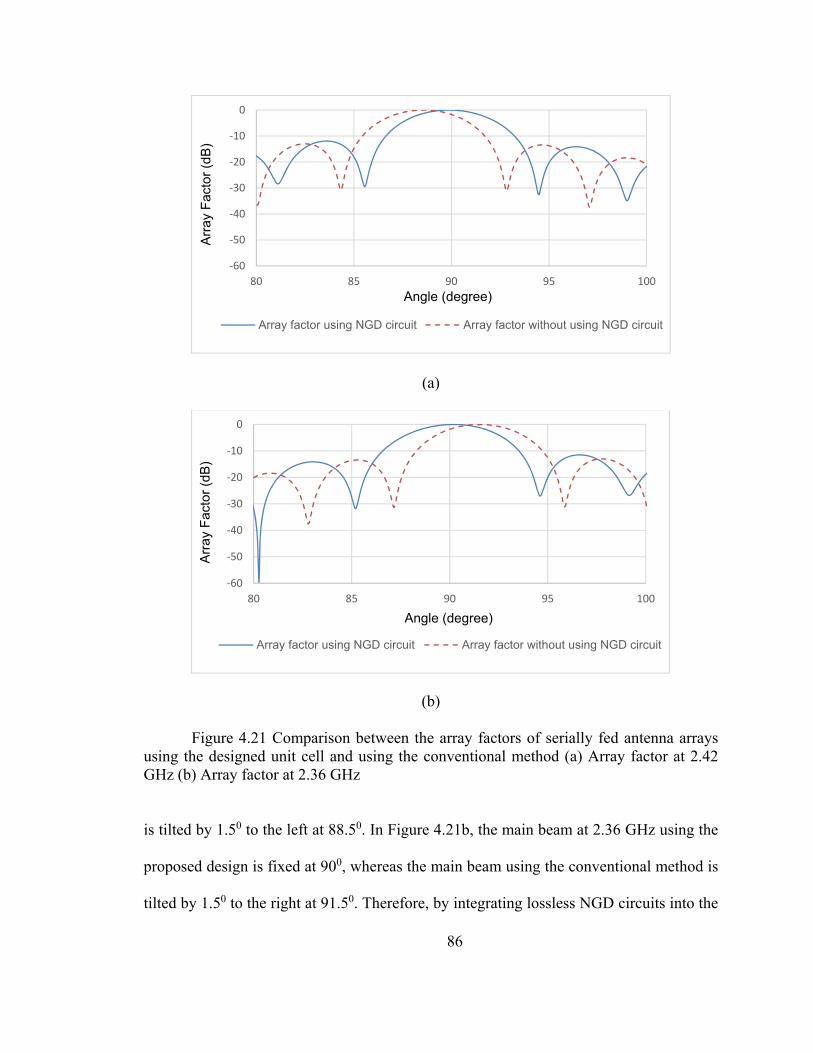
86
(a)
(b)
Figure 4.21 Comparison between the array factors of serially fed antenna arrays using the designed unit cell and using the conventional method (a) Array factor at 2.42 GHz (b) Array factor at 2.36 GHz
is tilted by 1.50 to the left at 88.50. In Figure 4.21b, the main beam at 2.36 GHz using the
proposed design is fixed at 900, whereas the main beam using the conventional method is
tilted by 1.50 to the right at 91.50. Therefore, by integrating lossless NGD circuits into the
‐60
‐50
‐40
‐30
‐20
‐10
0
80 85 90 95 100
Array factor using NGD circuit Array factor without using NGD circuit
Angle (degree)
Arr
ay F
acto
r (d
B)
‐60
‐50
‐40
‐30
‐20
‐10
0
80 85 90 95 100
Array factor using NGD circuit Array factor without using NGD circuit
Angle (degree)
Arr
ay F
acto
r (d
B)

87
serially fed antenna arrays, one can design a beam squint fee antenna array without using
lossy elements. Several prototype designs are implemented in order to validate the lossless
NGD circuit design method.
A NGD circuit consisting of a T-junction and a patch antenna has been fabricated
on a 15 mil Roger TMM3 substrate with a dielectric constant of 3.27 in order to
demonstrate the idea. A photo of the fabricated NGD circuit is shown in Figure 4.22. A
coupled line, which consists of two quarter-wavelength lines spaced by 10 mils, is added
to the T-junction power divider in order to achieve the required power dividing ratio.
Figure 4.22 Fabricated lossless NGD circuit using patch antenna.
In the fabricated NGD circuit, the S21 phase increases as the frequency increases as
shown in Figure 4.23. The NGD is provided in the frequency range from 10.03 GHz to
10.19 GHz, which is the same as the operating bandwidth of the patch antenna. The
measured magnitude of S21 is -15 dB, with an S11 of -40 dB, as shown in Figure 4.24
Patch Antenna
Coupler

88
indicating that most of the power is delivered to the antenna element. The simulation and
measurement results have a similar response; however, the measurement results are shifted
by 0.1 GHz due to circuit fabrication tolerances.
Figure 4.23 Measured and simulated phase response of the lossless NGD circuit using patch antenna.
Bandwidth of the demonstrated lossless NGD circuit is limited to the narrow
bandwidth of the patch antenna. Therefore, a broadband antenna can be designed in order
to improve the bandwidth of the NGD circuit. The antenna used in this design is a
microstrip-fed quasi-Yagi antenna that is fed using a broadband microstrip-to-coplanar
strip transition and uses a truncated ground plane [71, 72]. A single microstrip-fed quasi-
Yagi antenna is fabricated on a 30 mil Roger TMM10 substrate with a dielectric constant
of 9.2, as shown in Figure 4.25, and its simulation and measurement result are plotted in
Figure 4.26. In the fabricated antenna shown in Figure 4.25, L1, L2, L3, L4, L5, L6, L7,
30
32
34
36
38
40
42
44
46
48
50
9.9 9.95 10 10.05 10.1 10.15 10.2
Simulated Measured
Frequency (GHz)
S2
1P
hase
(de
gree
)

89
W1, and W2 are 112 mils, 113 mils, 55 mils, 130 mils, 58 mils, 165 mils, 311 mils, 86
mils, and 40 mils, respectively.
Figure 4.24 Measured and Simulated S21 and S11 Magnitudes of the lossless NGD circuit using patch antenna.
L1 L2 L3 L4 L5
W1
W2
L6 L7
Figure 4.25 Microstrip quasi-yagi antenna fed by a microstrip to coplanar strip transition.
‐60
‐50
‐40
‐30
‐20
‐10
0
9.9 9.95 10 10.05 10.1 10.15 10.2
Simulated S11 Measured S11
Simulated S21 Measured S21
Frequency (GHz)
S1
1an
d S
21
(dB
)

90
Figure 4.26 Simulated and Measured S11 of a single microstrip-fed quasi-Yagi antenna.
The simulated input return loss is better than 10 dB in the frequency range from 9.3
GHz to 10.4 GHz. The measured input return loss is better than 10 dB in frequency range
from 8.85 GHz to 11.77 GHz. The differences between the measured and simulated results
is due to fabrication inaccuracies.
The designed NGD circuit consisting of a microstrip quasi-yagi antenna and T-
junction shows an increasing S21 phase versus frequency as seen in Figure 4.27. The
simulated S21 phase of the NGD circuit has a positive slope in the frequency range from
9.3 GHz to 10.4 GHz, whereas the measured NGD circuit has a NGD in the frequency
range from 9.4 GHz to 10.25 GHz. The measured and simulated results have a similar
behavior, the deviation between the simulated and measured results are due to the
dimensional tolerances.
‐30
‐20
‐10
0
8.00 9.00 10.00 11.00 12.00
Measured Simulated
S1
1(d
B)
Frequency (GHz)

91
Figure 4.27 Simulated and measured insertion phase of the lossless NGD using microstrip-fed quasi-Yagi antenna circuit.
Furthermore, a unit cell consisting of an active antenna that has a flat S21 phase
variation with frequency has been designed as shown in Figure 4.28. The amplifier used in
this design is NBB300 from RFMD, which has a gain of 10 dB at 10 GHz. A series 0.1 pF
capacitor is connected to the T-junction power divider in order to achieve the required
power dividing ratio.
The simulation results for the phase of S21 for active antenna unit cell using
microstrip-fed quasi-Yagi antenna based NGD circuit is shown in Figure 4.29. The phase
of S21 has a flat response in the frequency range from 9.3 GHz to 10.3 GHz with a
bandwidth of 1 GHz. S11 and S21 of the active antenna unit cell are simulated in Figure
4.30, which shows that the unit cell is well match and it has a gain that is close to zero in
frequency of operation.
‐10
‐8
‐6
‐4
‐2
0
2
4
6
8
10
9.2 9.4 9.6 9.8 10 10.2 10.4
Simulated Measured
Frequency (GHz)
S2
1P
hase
(dg
ree)

92
Antenna
NBB300 Amplifier
Input Output
Balun
Ground plane (in the backside)
C
Figure 4.28 An active antenna unit cell consisting of a single microstrip-fed quasi-Yagi antenna and an amplifier.
Figure 4.29 Simulated phase of S21 for active antenna unit cell using microstrip-fed quasi-Yagi antenna based NGD circuit.
‐40
‐30
‐20
‐10
0
10
20
30
40
9 9.5 10 10.5 11
S2
1P
hase
(de
gree
)
Frequency (GHz)

93
Figure 4.30 Simulated insertion and return losses for active antenna unit cell using microstrip-fed quasi-Yagi antenna based NGD circuit.
The antenna based NGD circuits shown previously require using a resonance
antenna in order to generate NGD. A modified NGD circuit is presented in order to allow
using any type of antenna to generate NGD. The basic idea is shown in Figure 4.31.
d d
Amplifier
Antenna
Matching Circuit
Matching Circuit
d ≈ 0.5 λ
Figure 4.31 Series fed active antenna array using amplifier based NGD circuit.
Each active antenna unit consists of an amplifier, matching circuits, a T-junction,
and an antenna as shown in Figure 4.32. The amplifier and the matching circuits have been
‐30
‐25
‐20
‐15
‐10
‐5
0
5
10
9 9.5 10 10.5 11
S11 S21
Frequency (GHz)
S2
1an
d S
11
(dB
)

94
designed to provide input impedances and quality factors that are equal to the input
impedance and quality of the NGD circuit in Figure 4.7. Hence, the NGD circuit is lossless
[73].
Figure 4.32 One active antenna unit cell using amplifier based NGD circuit.
The first step in the design is to specify the required bandwidth and then to generate
the required NGD by adjusting the input impedance of the amplifier. Then, the power
dividing ratio, which is controlled by a T-junction power divider and the input impedance
of the amplifier, is adjusted in order to provide equal power excitation to the antennas.
Furthermore, a one wavelength meandered transmission line is connected to the NGD
circuit in order to provide a 2π phase shift between the adjacent antenna while 0.5 λ
physical distance between adjacent antennas is maintained. The length of the meandered
transmission line may deviate from one wavelength in order to compensate for the phase
shift caused by the NGD circuit.
The NGD magnitude must be equal to the magnitude of the positive group delay
due to the interconnecting transmission lines in order for the overall group delay to be zero.

95
The phase variation of the NGD circuit shown in Figure 4.32 is simulated using ADS
software as shown in Figure 4.33. The amplifier used in this design is VMMK1225 from
Avago Technologies.
Figure 4.33 Simulated phase response of the NGD circuit incorporating amplifier
Integrating the NGD circuit with a one wave length interconnection line reduces
the phase shift variation with frequency and minimizes the beam squint. The phase
variation of the designed active antenna unit cell circuit, shown in Figure 4.32, is compared
with a one-wavelength transmission line, as shown in Figure 4.34. A phase variation of
1.17o has been achieved in the feed line over 200 MHz compared to 7.2o phase variation
using the conventional series fed array. As can be calculated from (4.1), this phase variation
corresponds to less than 0.25o of beam squint which is comparable to the results from
previous publications using conventional NGD circuits [63, 66].
‐14
‐13
‐12
‐11
‐10
‐9
‐8
‐7
‐6
9.88 9.92 9.96 10 10.04 10.08
S2
1P
hase
(de
gree
)
Frequency (GHz)

96
Figure 4.34 Simulated phase variation between the adjacent antennas with and without the NGD circuit.
4.6 Elimination of Beam Squint in Series Fed Active Antenna Arrays Using a Series
Connected Lossless NGD Circuit
The lossy resonator in the NGD circuit shown in Figure 4.11 can be replaced by a
circuit that does not have loss but provides the same frequency response as discussed
previously. An example of a series connected lossless NGD circuit is shown in Figure 4.35.
A transformer is used to convert a differential signal into a single ended signal. The
amplifier’s input impedance resembles the lossy part in the NGD circuit shown in Figure
4.11. The phase of S21 for the lossless NGD circuit has a positive slope as shown in Figure
4.36, indicating that the circuit has NGD. In order to ensure that there is no significant
reflection loss, the magnitude of S11 is simulated, showing that the circuit is well matched
at input as illustrated in Figure 4.37. Several of the unit cells shown in Figure 4.35 can be
‐16.00
‐15.00
‐14.00
‐13.00
‐12.00
‐11.00
‐10.00
‐4.00
‐3.00
‐2.00
‐1.00
0.00
1.00
2.00
3.00
4.00
5.00
9.88 9.92 9.96 10.00 10.04 10.08
Phase response without using NGD Circuit
Phase response using NGD circuit
S11 using NGD circuit
Frequency (GHz)
S2
1P
hase
(dg
ree)
S1
1(d
B)

97
cascaded to design a beam squint free series fed active antenna array as shown in Figure
4.38. NGD circuits are connected with each other using a meandered transmission line in
order to provide a 2π phase shift and a 0.5 λ physical distance between adjacent antennas.
Figure 4.35 An active antenna unit cell using lossless parallel resonator connected in series.
Figure 4.36 Simulated phase of S21 for the lossless NGD circuit using parallel resonator connected in series.
Input
NGDCircuit
Output
Amplifier
Antenna

98
Figure 4.37 Simulated return loss of the lossless NGD circuit using parallel resonator connected in series.
d d
AmplifierAmplifierAmplifier
Input
d ≈ 0.5 λ
Figure 4.38 A series fed active antenna array using lossless parallel resonance NGD circuits.

99
4.7 A Solid State Millimeter Wave High Power Amplifier
The active array described in this section is intended for use in high-power SAR
system. This system is needed for mapping the height profile of the sand layers in deserts,
which could reduce the cost of oil and gas exploration. In order to do that, a high power Ka
band radar is required to characterize the scattering from the sand-air interface. The link
budget for the SAR system requires 1 KW transmitted power at 35 GHz with a 300 MHz
bandwidth. Designing such a high power amplifier at millimeter wave frequencies using
solid state devices has many challenges because of the limited power capability of the solid
state devices at millimeter-wave frequencies. For example, the maximum power from
commercially available MMICs at 35 GHz is approximately 3 watts. Therefore, more than
320 MMICs are required to generate the required power level. To overcome the combining
loss, output power from many transistors can be spatially combined by using a serially fed
active antenna array. To achieve the required power level, an antenna array consisting of
five rows with each row containing 80 active antenna elements is needed. Such an antenna
will provide a beamwidth of 0.7o in the azimuth direction and a beamwidth of 20o in the
elevation direction. Each active antenna unit consists of a MMIC PA mounted on a
pedestal, a T-junction power divider and a patch antenna, as shown in Figure 4.39. The
MMIC PA used in this design is TGA4517 from TriQuint, which has an output power of
3.16 W at 35 GHz. There is one PCB that has the dividers and the biasing circuit and one
PCB that has patch antennas only located above the other PCB. The antenna and the power
divider will provide negative group delay as well. In order to eliminate the beam squint
and thereby alleviate the bandwidth limitation that it may cause, the antenna array consists

100
of unit cells that have a zero group delay, and zero dB gain as described in section 4.5.
Moreover, every row in the array will to be fed from the middle as shown in Figure 4.40.
Figure 4.39 Active antenna unit connections.
180DegreesPhase Shifter
Input
. . .
. . .
. . .
. . .
. . .
. . .
. . .
. . .. . .
. . .
. . .
. . .
. . .
. . .
. . .
. . .
. . .
. . .
. . .
. . .
. . .
. . .
. . .
Antenna+
NGD Circuit
MMICPA
Figure 4.40 Spatial power combining using serially fed active antenna array.

101
The input signal of the antenna array is divided into three different paths as shown
in Figure 4.40. The first signal path is injected into 40 active antennas (to the left of Figure
4.40). The second part is injected into another 40 active antennas through a transmission
line providing 180o phase delay (on the right side of Figure 4.40). The third part is used to
excite the next row where it is amplified and divided into three parts, as described for the
first row. The same procedure is repeated for the rest of the rows.
4.8 Conclusion
The major drawback of conventional NGD circuits is the loss associated with them.
In this chapter, new approaches for designing lossless NGD circuits are introduced. Several
prototype circuits are designed and fabricated. Furthermore, the proposed NGD circuit is
used to design a beam squint free serially fed antenna array. By addressing the beam squint
issue in serially fed arrays, one can pave the way for the implementation of low cost and
compact phased arrays for defense and commercial applications.
A novel circuit that uses the resonance behavior and the input impedance of the
antenna in order to generate NGD without using lossy elements is introduced. The
performance of this circuit has been tested by fabricating NGD circuits that use a patch
antenna and a microstrip quasi-yagi antenna resonance behaviors to provide a negative
group delay. Furthermore, a circuit that uses an amplifier including its matching network’s
resonance behavior to generate NGD has been designed. Such circuits can be integrated
into a serially fed antenna array in order to reduce the beam squint without any additional
losses.

102
A new spatial power combining technique at millimeter wave frequency has been
proposed in this chapter. More than 1 KW output power can be spatially combined with a
beamwidth of 0.7o in one direction and 20o in the other direction.

103
Chapter 5
Conclusion
5.1 Summary
In this thesis, new methods for designing high-power, high-efficiency, and compact
power amplifiers using solid state devices are introduced to overcome the output power
limitations of solid state devices. Both circuit level and spatial power combining techniques
were developed to achieve this. These techniques can be used to design transmitters for
many applications such as radars, communication systems, RF heating, magnetic
resonance imaging, and plasmas, etc.
Several power combining techniques are summarized in chapter 2. Most of the
power combining designs in the literature don’t have a compact size when they are used to
generate kilowatt power levels. Chapter 3 and chapter 4 introduced new methods for
designing kilowatt-level compact power combining circuits.
For kilowatt power level transmitters, the power amplifier’s efficiency is one of the
critical factors predominant in determining the amplifier’s overall size, weight, and cost.
In chapter 3, a new high efficiency circuit-level power combiner design is introduced. This
design is based on a class-E power amplifier using a HiVP configuration in order to
combine the output power from several high-power flanged devices. HiVP amplifiers allow
the design of compact and high gain power amplifiers. Furthermore, it increases the

104
optimum output impedance, thereby reducing the matching loss and improving the
bandwidth. Moreover, using a class-E power amplifier design improves the efficiency of
the power amplifier thereby reducing thermal design requirements and accordingly
reducing the overall size and weight.
An approach based on connecting flanged transistors in a cascode configuration is
presented. Furthermore, design formulas for HiVP class-E power amplifiers are derived.
Three HiVP class-E power amplifiers are designed and fabricated using BLF571 LDMOS
devices in order to demonstrate power combining from packaged devices using HiVP at
the VHF frequency range. High-efficiency and high-gain are achieved using compact
power amplifier. Finally, a kilowatt power lever power amplifier, which will be used for
high-power SAR systems, is designed and simulated using ADS.
The overall efficiency of the amplifier designed using HiVP decreases as the
number of devices increases. Therefore, a new method for designing a spatial power
combiner using serially fed antenna arrays is introduced in chapter 4 in order to power
combine a large number of devices. However, the bandwidth of serially fed arrays is
limited due to beam squint, which is caused by variation of excitation phase of adjacent
antennas with frequency. Therefore, several new methods for eliminating beam squint in
the serially fed antenna arrays using lossless NGD circuits are introduced. These methods
can be used to design antenna arrays for many application including military radars, vehicle
collision avoidance systems, cellular base stations, satellite communication systems, etc.
Several lossless NGD circuits are designed and tested at S-band, X-band, and Ka-
band frequencies. These circuits are designed using the antenna’s resonance behavior to
generate NGD. A microstrip quasi-yagi antenna and a microstrip patch antenna are

105
fabricated to demonstrate lossless NGD circuits. Furthermore, these circuits are integrated
with an amplifier to obtain a zero group delay line. This delay line has been integrated with
a serially fed antenna array and was capable of reducing the beam squint without any
additional losses.
Another NGD circuit is designed using the amplifier with its matching network
resonance behavior to generate NGD. This design reduces the beam squint without any
additional losses. Furthermore, a new spatial power combining technique at millimeter
wave frequency has been designed and simulated in this chapter. More than 1 KW of output
power can be spatially combined with a beamwidth of 0.7o in one direction and 20o in the
other direction.
5.2 Future Work
A prototype HiVP class-E power amplifier has been demonstrated with a measured
output power of 70 W. A kilowatt power level power amplifier has also been designed for
a VHF SAR application. This amplifier can be fabricated using the provided design in
chapter 3 to be used in SAR applications.
Several high power radar systems require designing kilowatt power level power
amplifiers at Ka-band. These amplifiers can be designed using the design methodology for
spatial power combining proposed in chapter 4. In this design, the power amplifiers and
antennas are closely integrated, therefore the overall size of the radar system is minimized.
The lossless NGD circuits described in chapter 4 can be used to design efficient
and compact size passed array systems using serially fed antenna arrays. In order to do that,

106
a tunable phase shifter can be integrated within the one active antenna unit cell discussed
in chapter 4 as shown in Figure 5.1. By cascading many active antenna unit cells shown in
Figure 5.1 one can build a compact and low cost phase array systems.
Amplifier
Input Output
Matching Circuit
Input Matching Circuit
Output Matching Circuit
Variable Phase Shifter
Antenna+
NGD Circuit
3 Way Power Divider
Figure 5.1 One unit cell for phased array system.
In Chapter 4, a method of designing a NGD circuit using lossless parallel resonance
circuit connected in series is introduced. In this method, a transformer is used to convert a
differential signal into a single ended signal. Rather than using a transformer, a differential
amplifier can be connected directly to a lossless parallel resonance circuit in order to utilize
this design for millimeter wave applications.
The lossless NGD circuits described in this dissertation are not limited to the
antenna arrays applications. For example, they may also be utilized in broadband
transversal equalizers’ design. A transversal equalization is used to eliminate the effect of
multi-path propagation in wireless communication or the spectral distortion in wire-based
communication. Conventional transversal equalizers suffer from a frequency dependent

107
phase shifter. However, the NGD circuits discussed in this dissertation may allow for the
design of a frequency independent phase shifter which will improve the overall system
bandwidth.

108
APPENDIX

109
Appendix A
Beam Squint Free Antenna Array Design
The antenna used in the active antenna unit cell shown in Figure 4.14 is a
microstrip-fed quasi-Yagi antenna. The design and dimensions of this antenna is shown in
Figure A.1. In the designed antenna, L1, L2, L3, L4, L5, L6, L7, W1, and W2 are 548 mils,
658 mils, 1097 mils, 669 mils, 760 mils, 1842 mils, 1400 mils, 141 mils, and 40 mils,
respectively.
L1
L2
L3
L4
L5
W1
W2
L6
L7
Figure A.1 Microstrip quasi-yagi antenna fed by a microstrip to coplanar strip transition.

110
The ADS design file design unit cell shown in Figure 4.14 is shown in Figure A.2
Figure A.2 one active antenna unit cell ADS design.

111
BIBLOGRAPHY

112
BIBLOGRAPHY
[1] A. Grebennikov and N. O. Sokal, Switchmode RF Power Amplifiers: Elsevier
Science, 2007. [2] M. Albulet, RF Power Amplifiers: Institution of Engineering and Technology,
2001. [3] S. C. Cripps, Radio Frequency Power Amplifiers for Wireless Communications:
Artech House, Incorporated, 2006. [4] G. González, Microwave transistor amplifiers: analysis and design: Prentice Hall,
1997. [5] F. H. Raab, P. Asbeck, S. Cripps, P. B. Kenington, Z. B. Popovic, N. Pothecary, et
al., "Power amplifiers and transmitters for RF and microwave," Microwave Theory and Techniques, IEEE Transactions on, vol. 50, pp. 814-826, 2002.
[6] N. O. Sokal and A. D. Sokal, "Class E-A new class of high-efficiency tuned single-ended switching power amplifiers," Solid-State Circuits, IEEE Journal of, vol. 10, pp. 168-176, 1975.
[7] N. O. Sokal and A. D. Sokal, "High-efficiency tuned switching power amplifier," US Patent 3919656, 1975.
[8] M. Kazimierczuk, RF Power Amplifier: Wiley, 2008. [9] N. O. Sokal, "Class-E switching-mode high-efficiency tuned RF/microwave power
amplifier: improved design equations," in Microwave Symposium Digest. 2000 IEEE MTT-S International, 2000, pp. 779-782 vol.2.
[10] N. Sokal, "Class-E High-Efficiency RF/Microwave Power Amplifiers: Principles of Operation, Design Procedures, and Experimental Verification," in Analog Circuit Design, J. Huijsing, M. Steyaert, and A. Roermund, Eds., ed: Springer US, 2003, pp. 269-301.
[11] C. Wang, L. E. Larson, and P. M. Asbeck, "Improved design technique of a microwave class-E power amplifier with finite switching-on resistance," in Radio and Wireless Conference, 2002. RAWCON 2002. IEEE, 2002, pp. 241-244.
[12] P. Alinikula, "Optimum component values for a lossy Class E power amplifier," in Microwave Symposium Digest, 2003 IEEE MTT-S International, 2003, pp. 2145-2148 vol.3.
[13] M. Acar, A. J. Annema, and B. Nauta, "Analytical Design Equations for Class-E Power Amplifiers with Finite DC-Feed Inductance and Switch On-Resistance," in Circuits and Systems, 2007. ISCAS 2007. IEEE International Symposium on, 2007, pp. 2818-2821.

113
[14] P. M. Gaudo, C. Bernal, and A. Mediano, "Exact analysis of a simple class E circuit version for device characterization purposes," in Microwave Symposium Digest, 2003 IEEE MTT-S International, 2003, pp. 1737-1740 vol.3.
[15] C. K. Ho, H. Wong, and S. W. Ma, "Approximation of non-zero transistor ON resistance in class-E amplifiers," in Devices, Circuits and Systems, 2004. Proceedings of the Fifth IEEE International Caracas Conference on, 2004, pp. 90-93.
[16] T. Mury and V. F. Fusco, "Analysis and synthesis of pHEMT class-E amplifiers with shunt inductor including ON-state active-device resistance effects," Circuits and Systems I: Regular Papers, IEEE Transactions on, vol. 53, pp. 1556-1564, 2006.
[17] T. Suetsugu and M. K. Kazimierczuk, "Comparison of class-E amplifier with nonlinear and linear shunt capacitance," Circuits and Systems I: Fundamental Theory and Applications, IEEE Transactions on, vol. 50, pp. 1089-1097, 2003.
[18] M. Acar, A. J. Annema, and B. Nauta, "Generalized Design Equations for Class-E Power Amplifiers with Finite DC Feed Inductance," in Microwave Conference, 2006. 36th European, 2006, pp. 1308-1311.
[19] M. K. Kazimierczuk and K. Puczko, "Exact analysis of class E tuned power amplifier at any Q and switch duty cycle," Circuits and Systems, IEEE Transactions on, vol. 34, pp. 149-159, 1987.
[20] D. J. Kessler and M. K. Kazimierczuk, "Power losses and efficiency of class E RF power amplifiers at any duty cycle," in Circuits and Systems, 2001. ISCAS 2001. The 2001 IEEE International Symposium on, 2001, pp. 533-536 vol. 2.
[21] D. J. Kessler and M. K. Kazimierczuk, "Power losses and efficiency of class-E power amplifier at any duty ratio," Circuits and Systems I: Regular Papers, IEEE Transactions on, vol. 51, pp. 1675-1689, 2004.
[22] T. Suetsugu and M. K. Kazimierczuk, "Maximum Operating Frequency of Class-E Amplifier at Any Duty Ratio," Circuits and Systems II: Express Briefs, IEEE Transactions on, vol. 55, pp. 768-770, 2008.
[23] T. Suetsugu and M. K. Kazimierczuk, "Off-Nominal Operation of Class-E Amplifier at Any Duty Ratio," Circuits and Systems I: Regular Papers, IEEE Transactions on, vol. 54, pp. 1389-1397, 2007.
[24] F. H. Raab, "Broadband Class-E Power Amplifier for HF and VHF," in Microwave Symposium Digest, 2006. IEEE MTT-S International, 2006, pp. 902-905.
[25] C. Kai and S. Cheng, "Millimeter-Wave Power-Combining Techniques," Microwave Theory and Techniques, IEEE Transactions on, vol. 31, pp. 91-107, 1983.
[26] K. J. Russell, "Microwave Power Combining Techniques," Microwave Theory and Techniques, IEEE Transactions on, vol. 27, pp. 472-478, 1979.
[27] S. F. Marsh, "MMIC power splitting and combining techniques," in Design of RFIC's and MMIC's (Ref. No. 1997/391), IEE Tutorial Colloquium on, 1997, pp. 6/1-6/7.
[28] R. A. York and Z. B. Popović, Active and quasi-optical arrays for solid-state power combining: Wiley, 1997.

114
[29] R. T. N.D. du Toit, J.H. Smith, F.N. Schirk and J.A. Mogel, "Design of Solid-state, Wideband, High-power Microwave Amplifiers for Radiated Immunity Testing," Microwave Jounal, vol. 53, pp. 90-100, July 11 2010.
[30] M. Cicolani and A. Panariello, "Novel Design Technique for Radial Power Combiners," in Microwave Conference, 2000. 30th European, 2000, pp. 1-4.
[31] M. A. Gouker, "A circuit-fed, tile-approach configuration for millimeter-wave spatial power combining," in Microwave and Optoelectronics Conference, 1999. SBMO/IEEE MTT-S, APS and LEOS - IMOC '99. International, 1999, pp. 231-232 vol. 1.
[32] M. A. Gouker, J. T. Delisle, and S. M. Duffy, "A circuit-fed tile-approach configuration for millimeter-wave spatial power combining," Microwave Theory and Techniques, IEEE Transactions on, vol. 50, pp. 17-21, 2002.
[33] S. C. Ortiz, J. Hubert, L. Mirth, E. Schlecht, and A. Mortazawi, "A high-power Ka-band quasi-optical amplifier array," Microwave Theory and Techniques, IEEE Transactions on, vol. 50, pp. 487-494, 2002.
[34] J. Harvey, E. R. Brown, D. B. Rutledge, and R. A. York, "Spatial power combining for high-power transmitters," Microwave Magazine, IEEE, vol. 1, pp. 48-59, 2000.
[35] A. L. Martin and A. Mortazawi, "A class-E power amplifier based on an extended resonance technique," Microwave Theory and Techniques, IEEE Transactions on, vol. 48, pp. 93-97, 2000.
[36] A. L. Martin and A. Mortazawi, "A new lumped-elements power-combining amplifier based on an extended resonance technique," Microwave Theory and Techniques, IEEE Transactions on, vol. 48, pp. 1505-1515, 2000.
[37] A. L. Martin, A. Mortazawi, and B. C. Deloach, Jr., "An eight-device extended-resonance power-combining amplifier," Microwave Theory and Techniques, IEEE Transactions on, vol. 46, pp. 844-850, 1998.
[38] A. Martin, A. Mortazawi, and B. C. De Loach, Jr., "A power amplifier based on an extended resonance technique," Microwave and Guided Wave Letters, IEEE, vol. 5, pp. 329-331, 1995.
[39] F. H. Raab, "Idealized operation of the class E tuned power amplifier," Circuits and Systems, IEEE Transactions on, vol. 24, pp. 725-735, 1977.
[40] C. Piel, B. Aminov, A. Borisov, S. Kolesov, and H. Piel, "Development of A Solid State RF Amplifier in the KW Regime for Application with Low Beta Superconducting Rf Cavities," in Particle Accelerator Conference, 2005. PAC 2005. Proceedings of the, 2005, pp. 1-3.
[41] J. Sanggeun and D. B. Rutledge, "A 2.7-kW, 29-MHz class-E/F<sub>odd</sub> amplifier with a distributed active transformer," in Microwave Symposium Digest, 2005 IEEE MTT-S International, 2005, p. 4 pp.
[42] A. K. Ezzeddine and H. C. Huang, "The high voltage/high power FET (HiVP)," in Radio Frequency Integrated Circuits (RFIC) Symposium, 2003 IEEE, 2003, pp. 215-218.
[43] A. K. Ezzeddine and H. C. Huang, "High power high impedance microwave devices for power applications," US Patent 6137367, 2000.

115
[44] A. K. Ezzeddine and H. C. Huang, "Ultra-Broadband GaAs HIFET MMIC PA," in Microwave Symposium Digest, 2006. IEEE MTT-S International, 2006, pp. 1320-1323.
[45] A. Ezzeddine and H. Ho, "Broadband MMIC power amplifier for multiple wireless systems," in Wireless and Microwave Technology Conference (WAMICON), 2010 IEEE 11th Annual, 2010, pp. 1-3.
[46] L. Wu, R. Tao, U. Basaran, J. Luger, I. Dettmann, and M. Berroth, "The integrated 2W high voltage/high power 0. 12-/spl mu/m RF CMOS power amplifier," in Microwave Conference, 2004. 34th European, 2004, pp. 53-56.
[47] W. Lei, I. Dettmann, and M. Berroth, "A 900-MHz 29.5-dBm 0.13-μm CMOS HiVP Power Amplifier," Microwave Theory and Techniques, IEEE Transactions on, vol. 56, pp. 2040-2045, 2008.
[48] W. Alomar and A. Mortazawi, "A high voltage high power (HiVP) class-E power amplifier at VHF," in Microwave Symposium Digest (MTT), 2011 IEEE MTT-S International, 2011, pp. 1-4.
[49] T. J. Farmer, A. Darwish, and M. E. Zaghloul, "A 2.4 GHz SiGe HBT High Voltage/High Power Amplifier," Microwave and Wireless Components Letters, IEEE, vol. 20, pp. 286-288, 2010.
[50] S. Pornpromlikit, J. Jeong, C. D. Presti, A. Scuderi, and P. M. Asbeck, "A 33-dBm 1.9-GHz silicon-on-insulator CMOS stacked-FET power amplifier," in Microwave Symposium Digest, 2009. MTT '09. IEEE MTT-S International, 2009, pp. 533-536.
[51] J. Jeong, S. Pornpromlikit, P. M. Asbeck, and D. Kelly, "A 20 dBm Linear RF Power Amplifier Using Stacked Silicon-on-Sapphire MOSFETs," Microwave and Wireless Components Letters, IEEE, vol. 16, pp. 684-686, 2006.
[52] S. Pornpromlikit, J. Jeong, C. D. Presti, A. Scuderi, and P. M. Asbeck, "A Watt-Level Stacked-FET Linear Power Amplifier in Silicon-on-Insulator CMOS," Microwave Theory and Techniques, IEEE Transactions on, vol. 58, pp. 57-64, 2010.
[53] M. Apostolidou, M. P. van der Heijden, D. M. W. Leenaerts, J. Sonsky, A. Heringa, and I. Volokhine, "A 65 nm CMOS 30 dBm Class-E RF Power Amplifier With 60% PAE and 40% PAE at 16 dB Back-Off," Solid-State Circuits, IEEE Journal of, vol. 44, pp. 1372-1379, 2009.
[54] M. Apostolidou, M. P. van der Heijden, D. M. W. Leenaerts, J. Sonsky, A. Heringa, and I. Volokhine, "A 65nm CMOS 30dBm class-E RF power amplifier with 60% power added efficiency," in Radio Frequency Integrated Circuits Symposium, 2008. RFIC 2008. IEEE, 2008, pp. 141-144.
[55] A. Mazzanti, L. Larcher, R. Brama, and F. Svelto, "Analysis of reliability and power efficiency in cascode class-E PAs," Solid-State Circuits, IEEE Journal of, vol. 41, pp. 1222-1229, 2006.
[56] L. Ockgoo, H. Jeonghu, A. Kyu Hwan, L. Dong Ho, L. Kun-Seok, H. Songcheol, et al., "A Charging Acceleration Technique for Highly Efficient Cascode Class-E CMOS Power Amplifiers," Solid-State Circuits, IEEE Journal of, vol. 45, pp. 2184-2197, 2010.

116
[57] T. Sowlati and D. M. W. Leenaerts, "A 2.4-GHz 0.18-μm CMOS self-biased cascode power amplifier," Solid-State Circuits, IEEE Journal of, vol. 38, pp. 1318-1324, 2003.
[58] P. Khan, L. Epp, and A. Silva, "A KA-band wideband-gap solid-state power amplifier: architecture identification," 42-162, August 2005.
[59] T. Metzler, "Microstrip series arrays," Antennas and Propagation, IEEE Transactions on, vol. 29, pp. 174-178, 1981.
[60] K. L. Wu, M. Spenuk, J. Litva, and D. G. Fang, "Theoretical and experimental study of feed network effects on the radiation pattern of series-fed microstrip antenna arrays," Microwaves, Antennas and Propagation, IEE Proceedings H, vol. 138, pp. 238-242, 1991.
[61] D. M. Pozar and D. H. Schaubert, "Comparison of three series fed microstrip array geometries," in Antennas and Propagation Society International Symposium, 1993. AP-S. Digest, 1993, pp. 728-731 vol.2.
[62] L. Brillouin, Wave propagation and group velocity: Academic Press, 1960. [63] S. S. Oh and L. Shafai, "Compensated circuit with characteristics of lossless double
negative materials and its application to array antennas," Microwaves, Antennas & Propagation, IET, vol. 1, pp. 29-38, 2007.
[64] B. Ravelo, A. Perennec, and M. Le Roy, "Synthesis of Broadband Negative Group Delay Active Circuits," in Microwave Symposium, 2007. IEEE/MTT-S International, 2007, pp. 2177-2180.
[65] O. Siddiqui, M. Mojahedi, S. Erickson, and G. V. Eleftheriades, "Periodically loaded transmission line with effective negative refractive index and negative group velocity," in Antennas and Propagation Society International Symposium, 2003. IEEE, 2003, pp. 717-720 vol.1.
[66] O. F. Siddiqui, M. Mojahedi, and G. V. Eleftheriades, "Periodically loaded transmission line with effective negative refractive index and negative group velocity," Antennas and Propagation, IEEE Transactions on, vol. 51, pp. 2619-2625, 2003.
[67] S. Keser and M. Mojahedi, "Removal of beam squint in series fed array antennas using abnormal group delay phase shifters," in Antennas and Propagation Society International Symposium (APSURSI), 2010 IEEE, 2010, pp. 1-4.
[68] M. A. Antoniades and G. V. Eleftheriades, "A Metamaterial Series-Fed Linear Dipole Array with Reduced Beam Squinting," in Antennas and Propagation Society International Symposium 2006, IEEE, 2006, pp. 4125-4128.
[69] D. M. Pozar, Microwave Engineering: John Wiley & Sons Australia, Limited, 2005.
[70] W. Alomar and A. Mortazawi, "Elimination of beam squint in serially fed arrays with negative group delay circuits incorporating antenna elements," in Microwave Conference (EuMC), 2012 42nd European, 2012, pp. 625-627.
[71] Y. Qian, W. R. Deal, N. Kaneda, and T. Itoh, "Microstrip-fed quasi-Yagi antenna with broadband characteristics," Electronics Letters, vol. 34, pp. 2194-2196, 1998.
[72] Q. Yongxi and T. Itoh, "A broadband uniplanar microstrip-to-CPS transition," in Microwave Conference Proceedings, 1997. APMC '97, 1997 Asia-Pacific, 1997, pp. 609-612 vol.2.

117
[73] W. Alomar and A. Mortazawi, "Elimination of beam squint in uniformly excited serially fed antenna arrays using negative group delay circuits," in Antennas and Propagation Society International Symposium (APSURSI), 2012 IEEE, 2012, pp. 1-2.