Compact Ka-Band One-Port Vector Reflectometer Using a Wideband Electronically-Controlled...
10
IEEE TRANSACTIONS ON INSTRUMENTATION AND MEASUREMENT, VOL. 61, NO. 10, OCTOBER 2012 2807 Compact Ka-Band One-Port Vector Reflectometer Using a Wideband Electronically Controlled Phase Shifter Mojtaba Fallahpour, Student Member, IEEE, Mark A. Baumgartner, Arpit Kothari, Student Member, IEEE, Mohammad Tayeb Ghasr, Senior Member, IEEE, David Pommerenke, Senior Member, IEEE, and Reza Zoughi, Fellow, IEEE Abstract—In this paper, the design and implementation of a compact one-port Ka-band (26.5–40 GHz) vector reflectometer or network analyzer (VNA), operating in full Ka-band frequency range, are presented. The design follows that of a recently devel- oped VNA but with the goal of producing a wideband version. The most critical component of this design is a wideband electronically controlled phase shifter, designed using nonuniformly spaced p-i-n diode-loaded slots incorporated in the broad wall of a rectangu- lar waveguide. Nonuniform placement of the slots is shown to significantly reduce unwanted resonances within the operating bandwidth. Also, the new design provides the possibility of using a more accurate three-port S-parameter characterization instead of the previously used two-port approach. The design foundation and measurement results are presented. Index Terms—Microwave measurements, millimeter-wave imaging, millimeter-wave measurements, phase shifters, reflectometry. I. I NTRODUCTION O NE-PORT millimeter-wave vector reflectometers or vec- tor network analyzers (VNAs) have significant utility in many applications involving circuit component S-parameter analysis, near-field nondestructive testing (NDT) measure- ments, imaging, and material characterization, to name a few [1], [2]. Generally, VNAs can be categorized based on coherent and noncoherent detection design schemes [3]. In a coherent detection scheme, a VNA measures the in-phase and quadrature components of a complex signal (i.e., a phasor) referenced to a particular plane. Most commercial VNAs are designed based on coherent detection schemes. This detection scheme Manuscript received June 20, 2011; revised March 31, 2012; accepted April 2, 2012. Date of publication June 12, 2012; date of current version September 14, 2012. The Associate Editor coordinating the review process for this paper was Dr. Gerd Vandersteen. M. Fallahpour, M. A. Baumgartner, A. Kothari, M. T. Ghasr, and R. Zoughi are with Applied Microwave Nondestructive Testing Laboratory, Electrical and Computer Engineering Department, Missouri University of Science and Technology, Rolla, MO 65409 USA (e-mail: [email protected]; [email protected]; [email protected]; [email protected]; [email protected]; http://amntl.mst.edu/people/zoughi.html). D. Pommerenke is with Electromagnetic Compatibility Laboratory, Electri- cal and Computer Engineering Department, Missouri University of Science and Technology, Rolla, MO 65409 USA (e-mail: [email protected]). Color versions of one or more of the figures in this paper are available online at http://ieeexplore.ieee.org. Digital Object Identifier 10.1109/TIM.2012.2196389 provides for a large measurement dynamic range and a low noise floor, at the expense of higher cost, complexity, and larger physical size. On the other hand, VNAs designed based on noncoherent detection schemes estimate the magnitude and phase of the desired signal using power measurements resulting in a relatively simple and inexpensive system [4], [5]. In [6] and [7], novel designs of single-port, low-cost, and portable VNAs, operating in X-band (8.2–12.4 GHz) and at 35.5 GHz in the Ka-band (26.5–40 GHz), were discussed, respectively. The design approach is based on the idea that, by properly phase shifting a reflected signal measured at the aperture of a waveguide and measuring the corresponding standing-wave voltage(s) at a single location along the waveguide, one is able to recover the magnitude and phase of reflection coefficient referenced to the waveguide aperture. In [4], a similar approach is used but is based on measuring the standing-wave voltage at several different locations along a transmission line. The current approach eliminates the need for mechanical movement of the detector or the use of several detectors which, in turn, need to be characterized and calibrated to effectively produce similar detection characteristics. In contrast to perturbation two-port approach [8], the proposed technique in [6] and [7] requires neither a scalar network analyzer nor attenuation to the reflected signal. Also, compared to methods such as those reported in [9], this method eliminates the requirement for a multiport hybrid junction. These facts significantly reduce the complexity of the proposed VNA in comparison with previously reported nonco- herent detection-based VNAs. Although the design approach provides for several critically important practical features, it requires an electronically controlled and accurate phase shifter. Commercially available phase shifters operate at frequencies as high as 20 GHz. Consequently, designing such a wideband phase shifter at Ka-band (or generally in the millimeter-wave region) requires significant attention to be paid to the choice and details of its design. An accurate, single-frequency, and electronically controlled phase shifter was successfully designed at 35.5 GHz, using p-i-n diode-loaded nonresonant slots placed along the length of a section of a Ka-band rectangular waveguide [7]. This paper extends the design concept introduced in [7] and incor- porates novel design steps to realize an integrated, compact, accurate, and wideband one-port Ka-band vector reflectome- ter or VNA. The proposed VNA is electronically controlled, 0018-9456/$31.00 © 2012 IEEE
Transcript of Compact Ka-Band One-Port Vector Reflectometer Using a Wideband Electronically-Controlled...

IEEE TRANSACTIONS ON INSTRUMENTATION AND MEASUREMENT, VOL. 61, NO. 10, OCTOBER 2012 2807
Compact Ka-Band One-Port Vector ReflectometerUsing a Wideband Electronically
Controlled Phase ShifterMojtaba Fallahpour, Student Member, IEEE, Mark A. Baumgartner, Arpit Kothari, Student Member, IEEE,
Mohammad Tayeb Ghasr, Senior Member, IEEE, David Pommerenke, Senior Member, IEEE, andReza Zoughi, Fellow, IEEE
Abstract—In this paper, the design and implementation of acompact one-port Ka-band (26.5–40 GHz) vector reflectometeror network analyzer (VNA), operating in full Ka-band frequencyrange, are presented. The design follows that of a recently devel-oped VNA but with the goal of producing a wideband version. Themost critical component of this design is a wideband electronicallycontrolled phase shifter, designed using nonuniformly spaced p-i-ndiode-loaded slots incorporated in the broad wall of a rectangu-lar waveguide. Nonuniform placement of the slots is shown tosignificantly reduce unwanted resonances within the operatingbandwidth. Also, the new design provides the possibility of usinga more accurate three-port S-parameter characterization insteadof the previously used two-port approach. The design foundationand measurement results are presented.
Index Terms—Microwave measurements, millimeter-waveimaging, millimeter-wave measurements, phase shifters,reflectometry.
I. INTRODUCTION
ONE-PORT millimeter-wave vector reflectometers or vec-tor network analyzers (VNAs) have significant utility in
many applications involving circuit component S-parameteranalysis, near-field nondestructive testing (NDT) measure-ments, imaging, and material characterization, to name a few[1], [2]. Generally, VNAs can be categorized based on coherentand noncoherent detection design schemes [3]. In a coherentdetection scheme, a VNA measures the in-phase and quadraturecomponents of a complex signal (i.e., a phasor) referencedto a particular plane. Most commercial VNAs are designedbased on coherent detection schemes. This detection scheme
Manuscript received June 20, 2011; revised March 31, 2012; acceptedApril 2, 2012. Date of publication June 12, 2012; date of current versionSeptember 14, 2012. The Associate Editor coordinating the review process forthis paper was Dr. Gerd Vandersteen.
M. Fallahpour, M. A. Baumgartner, A. Kothari, M. T. Ghasr, andR. Zoughi are with Applied Microwave Nondestructive Testing Laboratory,Electrical and Computer Engineering Department, Missouri University ofScience and Technology, Rolla, MO 65409 USA (e-mail: [email protected];[email protected]; [email protected]; [email protected]; [email protected];http://amntl.mst.edu/people/zoughi.html).
D. Pommerenke is with Electromagnetic Compatibility Laboratory, Electri-cal and Computer Engineering Department, Missouri University of Science andTechnology, Rolla, MO 65409 USA (e-mail: [email protected]).
Color versions of one or more of the figures in this paper are available onlineat http://ieeexplore.ieee.org.
Digital Object Identifier 10.1109/TIM.2012.2196389
provides for a large measurement dynamic range and a lownoise floor, at the expense of higher cost, complexity, andlarger physical size. On the other hand, VNAs designed basedon noncoherent detection schemes estimate the magnitude andphase of the desired signal using power measurements resultingin a relatively simple and inexpensive system [4], [5]. In [6]and [7], novel designs of single-port, low-cost, and portableVNAs, operating in X-band (8.2–12.4 GHz) and at 35.5 GHzin the Ka-band (26.5–40 GHz), were discussed, respectively.The design approach is based on the idea that, by properlyphase shifting a reflected signal measured at the aperture ofa waveguide and measuring the corresponding standing-wavevoltage(s) at a single location along the waveguide, one is ableto recover the magnitude and phase of reflection coefficientreferenced to the waveguide aperture. In [4], a similar approachis used but is based on measuring the standing-wave voltage atseveral different locations along a transmission line. The currentapproach eliminates the need for mechanical movement of thedetector or the use of several detectors which, in turn, need tobe characterized and calibrated to effectively produce similardetection characteristics. In contrast to perturbation two-portapproach [8], the proposed technique in [6] and [7] requiresneither a scalar network analyzer nor attenuation to the reflectedsignal. Also, compared to methods such as those reported in [9],this method eliminates the requirement for a multiport hybridjunction. These facts significantly reduce the complexity of theproposed VNA in comparison with previously reported nonco-herent detection-based VNAs. Although the design approachprovides for several critically important practical features, itrequires an electronically controlled and accurate phase shifter.Commercially available phase shifters operate at frequenciesas high as 20 GHz. Consequently, designing such a widebandphase shifter at Ka-band (or generally in the millimeter-waveregion) requires significant attention to be paid to the choiceand details of its design.
An accurate, single-frequency, and electronically controlledphase shifter was successfully designed at 35.5 GHz, usingp-i-n diode-loaded nonresonant slots placed along the lengthof a section of a Ka-band rectangular waveguide [7]. Thispaper extends the design concept introduced in [7] and incor-porates novel design steps to realize an integrated, compact,accurate, and wideband one-port Ka-band vector reflectome-ter or VNA. The proposed VNA is electronically controlled,
0018-9456/$31.00 © 2012 IEEE

2808 IEEE TRANSACTIONS ON INSTRUMENTATION AND MEASUREMENT, VOL. 61, NO. 10, OCTOBER 2012
small, and relatively inexpensive where it may be particularlyused for a multitude of applications including NDT, materialcharacterization, wideband holographical (3-D) imaging, etc.The required phase shifts are obtained using a design thattakes advantage of nonuniformly spaced p-i-n diode-loadedwaveguide-fed slots to create a relatively short, wideband,and electronically controlled phase shifter. Compared to thedesign in [7], this design eliminates unwanted resonances andrelatively high signal attenuation due to the periodic structure ofthat phase shifter (i.e., equidistant slot placement) and other as-sociated components. The exact occurrence of such resonances,in the desired operating frequency range, cannot usually bepredicted while it also reduces the overall sensitivity of theVNA system. This is important particularly when measuringsmall reflected signals caused by weakly reflecting loads ortargets (in imaging). Furthermore, such undesired resonancesrender the designed VNA narrowband (or operable at a singlefrequency). More importantly, the newly designed phase shifterproduces much higher phase shift values than that in [7] whichis needed for a more robust and accurate estimation of thereflection coefficient. In addition, since the phase shifter isimplemented on a printed-circuit board (PCB) and used as thebroad wall of a standard rectangular waveguide (WR-28), it canbe easily attached to a coaxial probe assembled in a standardwaveguide section for probing the standing wave. The use ofa standard rectangular waveguide makes it possible to conven-tionally measure the overall S-parameters of the system (e.g., athree-port device) for system characterization purposes criticalto recovering the desired reflection coefficient. Compared to thetwo-port characterization process in [6] and [7], this approachmodels and describes the system more accurately and results inincreased measurement sensitivity and accuracy.
II. SYSTEM DESCRIPTION AND DESIGN
This system was initially designed and reported as a compactsingle-frequency VNA [10]. The components of the system,namely, the phase shifter and the coupler, were designed foroptimum characteristics (i.e., loss, phase shift, and coupling) at30 GHz. Overall, miniaturization of the system was also anothergoal in [10] for the VNA to be handheld and readily portable.
For the VNA to become wideband and cover the entire Ka-band frequency range, we had to fully investigate the frequencybehavior of each of its components and subsections (e.g., phaseshifter, coupler, and detector). Additionally, to achieve suffi-cient phase shift, unlike the one reported in [10], we built twophase shifters and cascaded them together in order to achievenot only more phase shift but also better frequency responsefor the overall phase shifter, as will be seen later. The PCB-integrated coupler in [10] did not provide for sufficient couplingat the lower end of Ka-band. Consequently, in this new design,it was replaced with a coaxial probe assembled in a standardwaveguide section which was readily attached and incorporatedinto the phase-shifter design. Also, the log detector used in[10] had an optimum operating range of 8–30 GHz, whichclearly does not cover the entire Ka-band frequency range of26.5–40 GHz. Therefore, it too was replaced with a Schottkydetector rated for operation extending to 40 GHz.
Fig. 1. Block diagram schematic of the coherent reflectometer/VNA.
The block diagram of the wideband VNA with its new designimprovements, indicating all of its major components, is shownin Fig. 1. An isolated millimeter-wave signal generator, operat-ing at the Ka-band (26.5–40 GHz), is used as the source. Theincident signal passes through the main arm of a rectangularwaveguide coupler and the phase shifter. After reaching thedevice under test (DUT), the signal reflects back into the phase-shifter waveguide section. The phase shifter is electronicallycontrolled by turning the p-i-n diodes on and off and loadingdifferent slots hence adding different yet known amounts ofphase shift to the reflected signal. This reflected phase-shiftedsignal then combines with the incident signal to form a standingwave where the rectangular waveguide coupler samples thestanding wave. Subsequently, a voltage proportional to the sam-pled power is measured by the detector, terminating the thirdarm of the coupler.
In the following sections, a brief theoretical background ofthe system will be provided followed by the design of variouscomponents of this coherent reflectometer/VNA.
A. Theoretical Background
In this section, the underlying principles of the proposedmethod in [6] and [7] are reviewed and extended to three-portcharacterization and modeling.
Assume a three-port network with source and load attachedto ports 1 and 2, respectively, as shown in Fig. 1. Port 3of the network is terminated with a detector. For simplicity,we assume that the source and detector are matched, and theload’s reflection coefficient is ΓL. Then, the input power to thedetector Pin-detector can be estimated using the S-parameters ofthe three-port network as
Pin-detector(f)
=Cpower(f)
∣∣∣∣S31(f)+S21(f)S32(f)ΓL(f)
1− S22(f)ΓL(f)
∣∣∣∣ (1)
where Cpower is a real-valued quantity proportional to thesource power level and f is the operating frequency. Thedetector output voltage is a function of the input power asfollows:
Vout-detector = F (Pin-detector) (2)

FALLAHPOUR et al.: COMPACT Ka-BAND ONE-PORT VECTOR REFLECTOMETER USING PHASE SHIFTER 2809
this function can be obtained from detector data sheet (ifcomprehensively available) or better yet through performing acharacterization procedure, as was done here. Now, having theoutput voltage measured as V M
out,detector, one can use inversefunction and find the input power to the detector PM
in-detector as
PMin-detector = F−1
(V Mout-detector
). (3)
Then, the obtained PMin-detector can be applied to (1) to find
ΓL. ΓL is an unknown complex quantity with a magnitude andphase. In [6], it was shown that at least three sets of independentmeasurements are required for an accurate estimation of ΓL.The phase shifter provides these independent measurements byshifting the standing wave at the detector location. Having thephase shifter included, (1) can be rewritten as
Pin-detector(f, φst) = Cpower(f)
∣∣∣∣S31(f, φst)
+S21(f, φst)S32(f, φst)ΓL(f)
1− S22(f, φst)ΓL(f)
∣∣∣∣ (4)
where φst shows the phase shift at state “st,” st = 0, 1, . . . , Ns.Moreover, Ns + 1 shows the total number of states. As it wasmentioned earlier, the number of states should be larger thantwo (e.g., Ns > 2). State refers to a different phase-shift valueproduced by the phase shifter.
Since (4) leads to a nonlinear set of equations, it cannotbe readily solved. An optimal iterative procedure, in termsof error function minimization, is a suitable candidate forsolving this type of problem, with attention paid to the choiceof cost-function definition since it can significantly affect theconvergence of the optimization procedure. Here, the utilizedcost function was defined as the distance between the measuredinput power and the input power calculated by (4) as
CΓ(f,ΓL)
=
Ns∑st=1
∣∣Pin-detector(st, f,ΓL)−PMin-detector(st, f,ΓL)
∣∣. (5)
A conjugate gradient-based algorithm was used to performa forward iterative process to check for the different ΓL’s andto find the optimum one that minimizes the cost function as afunction of frequency.
It should be noted that the maximum phase shift providedby the phase shifter should be enough to maximally spread themeasurement around the Smith chart and increase the accuracyof the overall system. If the phase shift is small, one runs therisk of getting incorrect estimation of ΓL since the solution to(5) may not be unique.
B. Phase-Shifter Design
Electronically controlled phase shifters can generally bedesigned based on the underlying principles of loaded/coupledlines, switched delay lines, etc. [11], [12]. The electronicallycontrolled phase shifter introduced in [7] uses a PCB with slotscut into it as one of the broad walls of a Ka-band rectangularwaveguide. The slots are loaded with flip-chip high-frequency
Fig. 2. General schematic of the proposed phase shifter with nonuniformlyspaced p-i-n diode-loaded waveguide-fed slots.
p-i-n diodes which can be turned on or off by applying anappropriate dc bias voltage (i.e., 1.45 V and 10 mA) [13]. Whenthe p-i-n diode is on, it acts as a resistive load (∼5 Ω) and closesthe slot, and when it is off, it acts as a capacitive load (in therange of 18–35 fF) and the slot becomes open. When the slot isopen, the electric current density path changes compared withwhen the slot is closed. This change in current path leads toa relative phase shift between the on and off cases. Moreover,the open slot radiates slightly which causes a perturbation tothe field inside the waveguide. This perturbation introduces asmall-signal loss which should be kept as small as possible(e.g., contributing to the insertion loss (IL) through the phaseshifter).
The narrowband phase shifter used in [7] was constructedwith uniformly spaced p-i-n diode-loaded slots cut into a PCBreplacing the broad wall of a Ka-band waveguide. At 35 GHz,the phase shifter provided a total phase shift of ∼19◦ witha maximum IL of 4 dB. A similar phase shifter to the oneused in [7] was initially built and tested for this investigation.Although this design was relatively good for a single-frequencyoperation, it is not effective for a wideband phase-shifter design.The reason was that the uniform spacing of the slots createsunwanted resonances (in frequency response) that substantiallydegrade the characteristics of the phase shifter. In addition, thetotal phase shift was found to be less than optimally desired, andthe loss through the phase shifter was also relatively large (par-ticularly if two were to be cascaded to produce twice the phase-shift values). An effective remedy for overcoming most of theselimitations (in particular, removing the unwanted resonances) isto eliminate the periodicity in the structure by using nonuniformspacing among the slots, as shown in Fig. 2. Clearly, there existsa countless number of iterations for such a design each withits own unique interspacing values. The two critical parametersassociated with such a phase-shifter design are the total phaseshift value as the slots are opened and closed and the IL throughthe phase shifter. A robust phase shifter must provide adequatephase-shift values among its states and present a relatively lowloss to the signal passing through it. In the case of this VNAdesign, the signal passes through the phase shifter twice beforethe standing-wave voltage is sampled. Therefore, keeping theIL as low as possible is an important issue since it affects thesmallest reflected signal that can be measured with the system(i.e., overall VNA system sensitivity). Consequently, usingsimilar slots as those reported in [7] and [10], an optimization

2810 IEEE TRANSACTIONS ON INSTRUMENTATION AND MEASUREMENT, VOL. 61, NO. 10, OCTOBER 2012
process utilizing a well-defined cost function that considersthese two parameters was employed.
For this optimization process, dimension and position of theslots are the two primary parameters that can be manipulatedfor minimizing the cost function. Although the cost functionmay not be unique, its selection can strongly influence theconvergence characteristics of the optimization algorithm. Thecost function used here is defined as a weighted sum of two costfunctions optimizing IL and phase shift given by
C(xn, yn, l, w) = V1CIL(xn, yn, l, w) + V2CP (xn, yn, l, w)(6)
where CIL and CP are IL and phase shift cost functions,respectively, and are given by (7) and (8) shown at the bottomof the page where Δφmn is relative phase shift between states“m” and “n” and is defined as
Δφm,n = ∠[S21(st = m)
S21(st = n)
], m, n = 0, 1, 2, . . . , Ns.
(9)In (7) and (8), (xn, yn) represents the nth slot’s center
position, V1 and V2 are weights dedicated to each component,and l and w are the length and width of the slots, respectively.All slots had the same dimensions in this design, although thisis not a restrictive requirement and even the slot shape maybe manipulated. Also, Pd is the desired maximum phase shift(in degrees), BWd is the desired operating frequency band,and “st,” as it was mentioned earlier, denotes the state of thephase shifter which is dictated by the p-i-n diodes’ individualstates (i.e., on or off). For example, consider a phase shifterwith nine slots (Ns = 9) and the p-i-n diode off states beingrepresented by “0” and the on states being represented by“1.” Then, 000000000 is the phase-shifter state 0, 1000000000is state 1, 110000000 is state 2, and so on. Different phase-shift values (relative to state 0) are then achieved for differentstates of the diodes. From the design perspective, the maximumachievable relative phase shift or total phase shift between twostates is a critical parameter in the design of this VNA. Thetotal phase shift usually occurs between two states: when all thep-i-n diodes are off (state 0) and when all the p-i-n diodes areon (state 9). It should be noted that there is a tradeoff betweenmaximum achievable phase shift and minimum attainable IL.Increasing the maximum phase shift may result in higher andunacceptable loss. Based on this tradeoff consideration, onecan add appropriate weight to the loss or the phase-shift costfunctions in (6) to obtain a desired (optimum) response. Theutilized p-i-n diode’s parameters can also affect the value ofmaximum achievable phase shift.
Considering this comprehensive approach, and after tryingmany different designs, a phase-shifter design was selected
TABLE ICALCULATED SLOT POSITIONS RESULTING FROM
OPTIMIZATION PROCEDURE
Fig. 3. Comparing obtained total phase shift of the single phase shifter frommeasurement, simulation with Cd = 18 fF, and simulation with Cd = 35 fF.
consisting of nine slots at Ka-band (i.e., BWd = 13.5 GHz), asshown in Fig. 2. The desired maximum phase shift was set to be45◦ over entire Ka-band. The commercially available numericalelectromagnetic simulation tool, CST Microwave Studio, wasused to simulate and optimize the phase shifter. The p-i-n diodeused was M/A-COM MA4GFCP910 [13] which was modeledas Rd = 5 Ω when p-i-n diode is on and Cd = 18 fF whenthe p-i-n diode is off. The Nelder–Mead simplex algorithmoption of CST Microwave Studio was chosen as the optimizerto minimize the cost function given in (6). The optimizationprocedure resulted in slot dimensions of l = 4 mm and w =1 mm, with their relative positions listed in Table I. Thesimulation results showing the total phase shift as a functionof frequency is shown in Fig. 3. As expected, the total phaseshift is not constant over the whole frequency band. However,it is quite good at the beginning of the band and acceptabletoward the end of the band. Subsequently, the phase shifterwas fabricated using a two-layer PCB with a 0.25-mm-thick
CIL(xn, yn, l, w) = max{|S21(f, st)|−1
f∈BWd
∣∣} (7)
CP (xn, yn, l, w) =
{max
{|max {|Δφmn|} − Pd|f∈BWd
∣∣2} max {|Δφmn|}∣∣f∈BWd
< Pd
0 max {|Δφmn|}∣∣f∈BWd
≤ Pd
(8)

FALLAHPOUR et al.: COMPACT Ka-BAND ONE-PORT VECTOR REFLECTOMETER USING PHASE SHIFTER 2811
Fig. 4. Total phase shift of the new phase-shifter set which is made of twocascaded phase shifters (measurement).
Rogers4350 substrate [14]. All slots were assumed to have thesame size cut as rectangular openings on both sides of the PCB.Vias were placed around the slots to limit any wave propagationwithin the PCB substrate [10].
The fabricated phase shifter was tested with an AgilentN5245A Performance Network Analyzer (PNA). Fig. 3 showsthe total measured phase shift as a function of frequencyalong with two simulation results using two different p-i-ndiode reverse-bias capacitance values. Clearly, there is adifference between simulation and measurement results forcapacitance of 18 fF (reported by the manufacturer). Thereare some possible reasons for this inconsistency. The PCBloss tangent and permittivity tolerances or even manufacturingissues can influence the overall frequency behavior. However,the difference between the measured and simulated results issubstantial and requires a more detailed look at what else maybe contributing to this difference. The one important parameterused in the simulation, which has something to do with thep-i-n diode characteristic, is the reverse-bias capacitance.Through extensive simulations, it was determined that thephase shift caused by changing the state of p-i-n diode can besignificantly affected by this parameter. Consequently, throughsimulations and reverse calculations, it was found that, forCd = 35 fF, the measurement and simulation results matchwell, as shown in Fig. 3. The value used in the initial simula-tions was Cd = 18 fF as reported by the p-i-n diode’s manu-facturer for 10 GHz. It is quite possible that the p-i-n diode’sactual Cd is larger than 18 fF in Ka-band. Moreover, solderingp-i-n diode to the PCB may have added to this value as well.
Considering the fact that the total phase shift is importantfor this VNA design, a similarly designed phase shifter witheight slots was built and cascaded with the first one. Theentire cascaded phase shifter was characterized using the samenetwork analyzer. The total measured phase shift as a functionof frequency is shown in Fig. 4. The results show a total phaseshift of ∼78◦ in the beginning of the band and ∼28◦ (the worstcase) at ∼38 GHz. The IL is also plotted for the two extremecases when all the p-i-n diodes are off (st = 0) and when all
Fig. 5. Measured IL of the two cascaded phase shifters for two extreme states(st = 0 and st = 17).
Fig. 6. Measured S-parameters of the waveguide coupler.
the p-i-n diodes are on (st = 17) in Fig. 5. Although in thebeginning of the band the IL is slightly greater than 10 dB,in most of the rest of the band, it is lower than 8 dB. Theseresults show that the newly designed cascaded phase shifter isnow suitable for incorporation into the rest of the VNA design.
C. Three-Port Characterization of Couplerand Phase-Shifter Set
As explained earlier, the VNA design requires a small portionof the standing-wave voltage to be coupled into the detector(i.e., be sampled by the detector). The coupler should haveminimal influence on the standing-wave properties that it issampling. Moreover, it is desired to have a coupler whichcan be readily integrated into a rectangular waveguide-fedphase-shifter assembly. Considering all of these features, acoaxial probe assembled in a standard waveguide section wasselected and used. The measured S-parameters of the couplerare shown in Fig. 6. The results show that the coupler provides

2812 IEEE TRANSACTIONS ON INSTRUMENTATION AND MEASUREMENT, VOL. 61, NO. 10, OCTOBER 2012
Fig. 7. Measured frequency response of integrated coupler/phase shifter, forstate 0 of phase shifter.
Fig. 8. Measured frequency response of integrated coupler/phase shifter, forstate 17 of phase shifter.
fairly constant coupling below 36 GHz and has a resonance at∼38 GHz which is not so deep and is still acceptable for thisVNA design. The coupler was attached to port 1 of the phaseshifter, and the entire system was characterized as three-portnetwork, with port 1 being the input port to the coupler, port 2being the second port of the phase shifter, and port 3 being thecoupler’s third port (see Fig. 1).
The magnitude of the measured S-parameters is shown inFigs. 7 and 8 for states 0 and 17, respectively. Moreover, thephase shift for a wave going through port 1 and reaching port 2is measured and plotted for four different states, namely, st = 3,9, 12, and 17 relative to st = 0 in Fig. 9. The results show thatthere is a distinct and reasonable phase shift between differentstates, and the total phase shift is about the same as that shownin Fig. 4.
Fig. 9. Measured phase shift for different states relative to st = 0.
Fig. 10. Measurement setup for detector characterization.
D. Detector Characterization
The Schottky detector used in this design (303BK Kry-tar detector) was rated to operate in the frequency range of0.1–40 GHz [15]. As it was mentioned earlier, the detectortransfer function F maps sampled input power into outputvoltage and should be known or determined through character-ization of the detector. The latter approach was used here usingthe measurement setup shown in Fig. 10. The detector wasattached to a source, through a precision rotary vane attenuator.Then, for different values of attenuations and 201 frequencysamples in the Ka-band range, the output voltage of the detectorwas recorded. The recorded data versus source power are shownin Fig. 11 for four frequencies (26.5, 30, 35, and 40 GHz). Asthe results show, the detector can detect signals with a power inthe range of ∼ −30 to +10 dBm. This dynamic range is quitegood for the proposed VNA application.
III. SYSTEM ASSEMBLY AND UNKNOWN
LOAD MEASUREMENT
The VNA was assembled by attaching the first and third portsof the coupler–phase-shifter set to the isolated source and thepower detector, respectively. The second port is used to measurethe unknown load. The whole system without the generator isshown in Fig. 12. Initially, three standard loads, namely, a short,a 3-mm shim (i.e., an extended short), and a matched load,were attached to the VNA, and corresponding voltages were

FALLAHPOUR et al.: COMPACT Ka-BAND ONE-PORT VECTOR REFLECTOMETER USING PHASE SHIFTER 2813
Fig. 11. Detector output voltage versus input power.
Fig. 12. Final VNA/reflectometer assembly.
Fig. 13. Measured Vout-detector for the short at two phase-shifter states:st = 1 and st = 17.
recorded as a function of frequency and for all 18 states of thephase shifter. For example, measured voltages for the short, as afunction of frequency for two phase-shifter states of st = 1 andst = 17, are shown in Fig. 13. Subsequently, using the detectorcharacterization mapping shown in Fig. 11, the detector output-voltage-to-input-power conversion was performed, as shownin Fig. 14. Finally, using (5) and the recalculation technique
Fig. 14. Calculated/mapped Pin-detector from measured detector voltage forthe short at two phase-shifter states: st = 1 and st = 17.
Fig. 15. Calculated uncalibrated reflection coefficient for the three loads:short, shim, and matched load.
explained in Section II, the uncalibrated reflection coefficientsfor the three loads were estimated, as shown in Fig. 15.
Subsequently, using a three-term {e00, e11,Δe} error-correction model calibration routine, the correct (calibrated)reflection coefficient may be obtained using [1]
Γcalibrated =ΓL − e00
ΓL · e11 −Δe. (10)
This calibration procedure was applied to the three measuredloads, and their respective calibrated reflection coefficients areshown in Fig. 16, showing good agreement with the expectedvalues for a short, matched load, and a shim.
The calibration procedure involved a two-step process, thefirst step of which involved characterization of the componentsof the system using a PNA. This procedure is only performedonce. Given the fact that the contribution of the reflectionsfrom the detector and the isolator is not accounted for in (4),a second calibration step became necessary to eliminate anycorresponding measurement inaccuracies (see Fig. 15). In the
2814 IEEE TRANSACTIONS ON INSTRUMENTATION AND MEASUREMENT, VOL. 61, NO. 10, OCTOBER 2012
Fig. 16. Reflection coefficient for standard loads: short, shim, and matchedload after calibration.
second step, three known standard loads are used according tothe three-term error-correction model calibration procedure tocorrect these errors (see Fig. 16). To eliminate the requirementfor measuring the S-parameters of the coupler and phase-shifterset, one may incorporate a procedure involving the use ofmultiple known loads such as that in [8] and [16]. However, athigh frequencies, multiple load measurements for this purposeproduce accumulative measurement errors which may degradethe system performance.
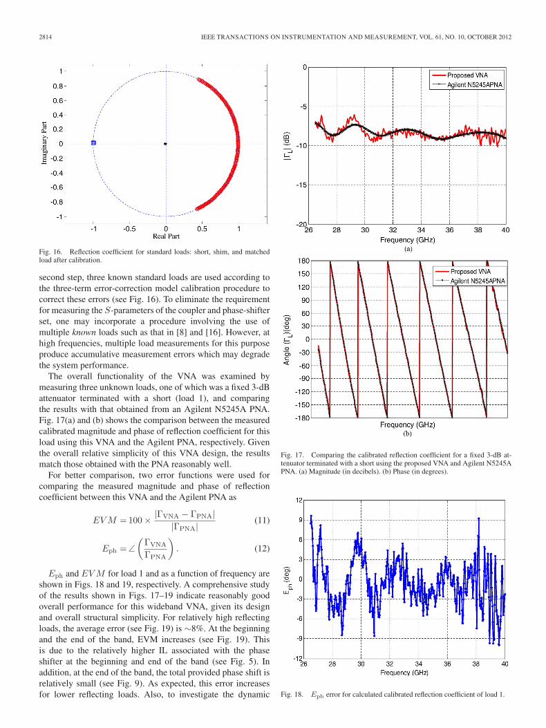
The overall functionality of the VNA was examined bymeasuring three unknown loads, one of which was a fixed 3-dBattenuator terminated with a short (load 1), and comparingthe results with that obtained from an Agilent N5245A PNA.Fig. 17(a) and (b) shows the comparison between the measuredcalibrated magnitude and phase of reflection coefficient for thisload using this VNA and the Agilent PNA, respectively. Giventhe overall relative simplicity of this VNA design, the resultsmatch those obtained with the PNA reasonably well.
For better comparison, two error functions were used forcomparing the measured magnitude and phase of reflectioncoefficient between this VNA and the Agilent PNA as
EVM =100× |ΓVNA − ΓPNA||ΓPNA|
(11)
Eph =∠(ΓVNA
ΓPNA
). (12)
Eph and EVM for load 1 and as a function of frequency areshown in Figs. 18 and 19, respectively. A comprehensive studyof the results shown in Figs. 17–19 indicate reasonably goodoverall performance for this wideband VNA, given its designand overall structural simplicity. For relatively high reflectingloads, the average error (see Fig. 19) is ∼8%. At the beginningand the end of the band, EVM increases (see Fig. 19). Thisis due to the relatively higher IL associated with the phaseshifter at the beginning and end of the band (see Fig. 5). Inaddition, at the end of the band, the total provided phase shift isrelatively small (see Fig. 9). As expected, this error increasesfor lower reflecting loads. Also, to investigate the dynamic
Fig. 17. Comparing the calibrated reflection coefficient for a fixed 3-dB at-tenuator terminated with a short using the proposed VNA and Agilent N5245APNA. (a) Magnitude (in decibels). (b) Phase (in degrees).
Fig. 18. Eph error for calculated calibrated reflection coefficient of load 1.

FALLAHPOUR et al.: COMPACT Ka-BAND ONE-PORT VECTOR REFLECTOMETER USING PHASE SHIFTER 2815
Fig. 19. EVM for calculated calibrated reflection coefficient of load 1.
Fig. 20. Reflection coefficient of three different loads (loads 2, 3, and 4)obtained from the proposed VNA compared to those from the Agilent PNA.
range of the proposed VNA, three other loads were used. Ashorted precision rotary vane attenuator was used to producethree loads, namely, 3 dB (load 2), 10 dB (load 3), and 20 dB(load 4).
Fig. 20 shows the calibrated magnitude of the reflectioncoefficient for these loads as a function of frequency comparedwith corresponding measurements using the Agilent PNA.Comparing the two sets of results shows that the proposed VNAperforms reasonably well and closely follows the Agilent PNAresults for loads 2 and 3. As the load reflection coefficient de-creases substantially for load 4, the variations in the measuredresults increase, as expected. Since the S11 of the attenuator(even though it is small) interacts with the reflected signal fromthe attenuated short and since for low reflecting loads (e.g., load4) the two signals have similar magnitudes, their interactioncauses the additional ripples (see Fig. 20). The limited dynamicrange of the VNA (compared to that of the Agilent PNA) doesnot allow it to exactly follow the PNA results for low reflectingloads. This limitation is attributed to the IL and the limitedphase-shift values of the phase shifter, as explained earlier.
Thus, using a phase shifter in this design requires it to be aslow loss as possible. Furthermore, the limited dynamic rangeof the detector (see Fig. 11) exasperates this problem for lowreflecting loads.
IV. CONCLUSION
In this paper, the design of a small, one-port, and wide-band reflectometer/VNA, based on a recently developed designapproach involving an electronically controlled phase shifter,as its critical component, has been presented. The proposeddesign uses a three-port characterization model to map thereflection coefficient of a DUT into several measured voltages.Comparing the results of measurements performed with thisreflectometer and an Agilent N5245A PNA for several testloads showed reasonably good overall agreement for magnitudeand phase, in particular for relatively high reflecting loads. Thecorresponding average error for such loads is around 8%. Giventhe operational bandwidth, size, cost, and capabilities of thiscoherent reflectometer, it is expected to find utility in many ap-plications including wideband millimeter-wave imaging, NDT,and time-domain reflectometery, to name a few. In such appli-cations, the size and cost of a PNA may prohibit its use.
ACKNOWLEDGMENT
The authors would like to thank S. Hatfield for assisting inperforming some of the measurements presented in this paper.
REFERENCES
[1] D. Rytting, “ARFTG 50 year network analyzer history,” in Proc. IEEEMTT-S Int. Microw. Symp. Dig., Jun. 15–20, 2008, pp. 11–18.
[2] S. Kharkovsky and R. Zoughi, “Microwave and millimeter wave nonde-structive testing and evaluation—Overview and recent advances,” IEEEInstrum. Meas. Mag., vol. 10, no. 2, pp. 26–38, Apr. 2007.
[3] Agilent Technologies, Inc., Agilent AN 1287-2, Exploring the Architec-tures of Network Analyzers, Application Note. [Online]. Available: http://cp.literature.agilent.com/litweb/pdf/5965-7708E.pdf
[4] R. Caldecott, “The generalized multi-probe reflectometer and its applica-tion to automated transmission line measurements,” IEEE Trans. Anten-nas Propag., vol. AP-21, no. 4, pp. 550–554, Jul. 1973.
[5] G. F. Engen, “A (historical) review of the six-port measurement tech-nique,” IEEE Trans. Microw. Theory Tech., vol. 45, no. 12, pp. 2414–2417, Dec. 1997.
[6] M. A. Abou-Khousa, M. A. Baumgartner, S. Kharkovsky, and R. Zoughi,“Novel and simple high-frequency single-port vector network analyzer,”IEEE Trans. Instrum. Meas., vol. 59, no. 3, pp. 534–542, Mar. 2010.
[7] M. A. Abou-Khousa, M. A. Baumgartner, S. Kharkovsky, and R. Zoughi,“Ka-band vector reflectometer based on simple phase-shifter design,”IEEE Trans. Instrum. Meas., vol. 60, no. 2, pp. 618–624, Feb. 2011.
[8] K. Hoffmann and Z. Skvor, “A novel vector network analyzer,” IEEETrans. Microw. Theory Tech., vol. 46, no. 12, pp. 2520–2523, Dec. 1998.
[9] G. F. Engen, “Calibrating the six-port reflectometer by means of slidingterminations,” IEEE Trans. Microw. Theory Tech., vol. MTT-26, no. 12,pp. 951–957, Dec. 1978.
[10] M. Fallahpour, M. Baumgartner, M. T. Ghasr, D. Pommerenke, andR. Zoughi, “Integrated design of a compact Ka-band one-port vectorreflectometer,” in Proc. IEEE I2MTC, Binjiang, China, May 10–12, 2011,pp. 154–158.
[11] R. V. Carver, “Broad-band diode phase-shifters,” IEEE Trans. Microw.Theory Tech., vol. MTT-20, no. 5, pp. 314–323, May 1972.
[12] B. M. Schiffman, “A New Class of Broad-Band Microwave 90-DegreePhase-Shifters,” IRE Trans. Microw. Theory Tech., vol. 6, no. 2, pp. 232–237, Apr. 1958.
[13] M/A-COM Technology Solutions, PIN Diode Data Sheet.[Online]. Available: http://www.macomtech.com/DataSheets/MA4AGP907_FCP910

2816 IEEE TRANSACTIONS ON INSTRUMENTATION AND MEASUREMENT, VOL. 61, NO. 10, OCTOBER 2012
[14] [Online]. Available: http://www.rogerscorp.com/acm/products/16/RO4000-Series-High-Frequency-Circuit-Materials-Woven-glass-reinforced-ceramic-filled-thermoset.aspx
[15] [Online]. Available: http://www.krytar.com/pdf/300zbs.pdf[16] V. Zavodny, K. Hoffmann, and Z. Skvor, “Seven state PTP for vec-
tor network analyzer,” Radioengineering, vol. 14, no. 4, pp. 87–90,Dec. 2005.
Mojtaba Fallahpour (S’09) received the B.Sc. andM.Sc. degrees in electrical engineering from theIran University of Science and Technology (IUST),Tehran, Iran, in 2005 and 2008, respectively. Heis currently working toward the Ph.D. degree atMissouri University of Science and Technology(Missouri S&T), Rolla.
He is a Graduate Research Assistant with the Ap-plied Microwave Nondestructive Testing Laboratory,Electrical and Computer Engineering Department,Missouri S&T. His research interests include nonde-
structive techniques for microwave and millimeter-wave inspection and test-ing of materials (nondestructive testing), microwave measurement instrumentdesign, array antenna pattern synthesis, and ultrawideband, miniaturized, andreconfigurable antenna design.
Mark A. Baumgartner was born in Atchison, KS,in 1988. He received the B.S. degrees in electricalengineering, computer engineering, and computerscience from Missouri University of Science andTechnology (Missouri S&T), Rolla, in 2010, wherehe is currently working toward the M.S. degree inelectrical engineering.
He is a Graduate Researcher with the Ap-plied Microwave Nondestructive Testing Laboratory,Electrical and Computer Engineering Department,Missouri S&T. His research interests include mea-
surement and instrumentation, RF design, and microwave imaging techniques.
Arpit Kothari (S’11) received the Bachelor of En-gineering degree in instrumentation technology fromVisvesvaraya Technological University, Belgaum,India, in 2007. He is currently working toward theM.S. degree in electrical engineering at MissouriUniversity of Science and Technology (MissouriS&T), Rolla.
After his graduation, from July 2007 to April2010, he was with Yokogawa India Limited,Bangalore, India, a firm specializing in measure-ment, control, and industrial automation, where he
worked on distributed control system. His area of focus was power plantinstrumentation and control. He is currently with Applied Microwave Non-destructive Testing Laboratory, Electrical and Computer Engineering Depart-ment, Missouri S&T, where he is working on millimeter-wave vector networkanalyzer calibration. His research interests are RF design, measurement andinstrumentation, and electromagnetism.
Mohammad Tayeb Ghasr (S’01–M’10–SM’12) re-ceived the B.S. degree (magna cum laude) in elec-trical engineering from the American University ofSharjah, Sharjah, UAE, in 2002, the M.S. degreein electrical engineering from the University ofMissouri, Rolla, in 2004, and the Ph.D. degree inelectrical engineering from Missouri University ofScience and Technology (Missouri S&T), Rolla,in 2009.
He is currently an Assistant Research Professorwith the Applied Microwave Nondestructive Testing
Laboratory, Electrical and Computer Engineering Department, Missouri S&T.His research interests include microwave and millimeter-wave instrumenta-tion and measurement, RF circuits, antennas, and numerical electromagneticanalysis.
David Pommerenke (M’98–SM’03) received thePh.D. degree from the Technical University Berlin,Berlin, Germany, in 1996.
He was with Hewlett Packard for five years, andthen, he joined the Electromagnetic Compatibility(EMC) Laboratory, Missouri University of Scienceand Technology, Rolla, in 2001, where he is currentlya Professor. He has published more than 100 papersand is the holder of 11 patents. He researches EMCwith emphasis on measurement and instrumentation,electronics, and immunity of electronic circuits, for
example, Electrostatic Discharge (ESD).
Reza Zoughi (S’85–M’86–SM’93–F’06) receivedthe B.S.E.E, M.S.E.E, and Ph.D. degrees in electricalengineering (radar remote sensing, radar systems,and microwaves) from The University of Kansas,Lawrence.
From 1981 to 1987, he was with the RadarSystems and Remote Sensing Laboratory. He iscurrently the Schlumberger Endowed Professor ofElectrical and Computer Engineering with MissouriUniversity of Science and Technology (MissouriS&T), formerly University of Missouri, Rolla. Prior
to joining Missouri S&T in January 2001 and in 1987, he was with theDepartment of Electrical and Computer Engineering, Colorado State University(CSU), Fort Collins, where he was a Professor and established the AppliedMicrowave Nondestructive Testing Laboratory (http://amntl.mst.edu/). From1995 to 1997, he held the position of Business Challenge Endowed Professorof Electrical and Computer Engineering while at CSU. He is the authorof a textbook entitled “Microwave Nondestructive Testing and EvaluationPrinciples” (KLUWER Academic Publishers, 2000) and a coauthor of a chapteron Microwave Techniques in the book entitled “Nondestructive Evaluation:Theory, Techniques, and Applications” edited by P.J. Shull (Marcel and Dekker,Inc., 2002). He is a coauthor of over 477 journal papers, conference proceedingsand presentations, and technical reports. He is the holder of ten patents to hiscredit all in the field of microwave nondestructive testing and evaluation.
Dr. Zoughi is the past Editor-in-Chief of the IEEE TRANSACTIONS ON
INSTRUMENTATION AND MEASUREMENT. He is serving his second term as anat-large Administrative Committee (AdCom) Member of the IEEE Instrumen-tation and Measurement (I&M) Society and currently serves as the society’sExecutive Vice President and an I&M Society Distinguished Lecturer. He hasbeen the recipient of numerous teaching awards both at CSU and MissouriS&T. He was the recipient of the 2007 IEEE I&M Society DistinguishedService Award, the 2009 American Society for Nondestructive Testing (ASNT)Research Award for Sustained Excellence, and the 2011 IEEE Joseph F.Keithley Award in Instrumentation and Measurement. He is also a Fellow ofthe ASNT.