Design of Functionally Stacked Channels of Oxide Thin-Film ...
Upload
khangminh22Category
view
5download
0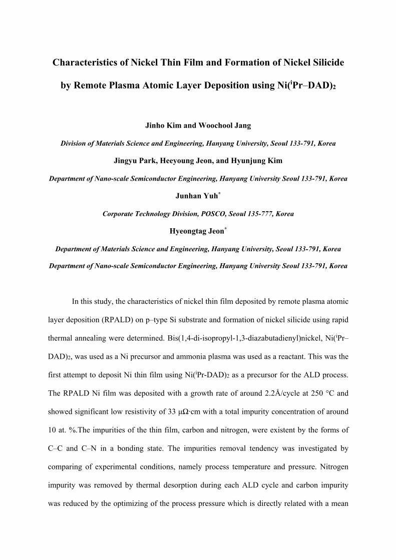
Characteristics of Nickel Thin Film and Formation of Nickel Silicide
by Remote Plasma Atomic Layer Deposition using Ni(iPr–DAD)2
Jinho Kim and Woochool Jang
Division of Materials Science and Engineering, Hanyang University, Seoul 133-791, Korea
Jingyu Park, Heeyoung Jeon, and Hyunjung Kim
Department of Nano-scale Semiconductor Engineering, Hanyang University Seoul 133-791, Korea
Junhan Yuh*
Corporate Technology Division, POSCO, Seoul 135-777, Korea
Hyeongtag Jeon*
Department of Materials Science and Engineering, Hanyang University, Seoul 133-791, Korea
Department of Nano-scale Semiconductor Engineering, Hanyang University Seoul 133-791, Korea
In this study, the characteristics of nickel thin film deposited by remote plasma atomic
layer deposition (RPALD) on p–type Si substrate and formation of nickel silicide using rapid
thermal annealing were determined. Bis(1,4-di-isopropyl-1,3-diazabutadienyl)nickel, Ni(iPr–
DAD)2, was used as a Ni precursor and ammonia plasma was used as a reactant. This was the
first attempt to deposit Ni thin film using Ni(iPr-DAD)2 as a precursor for the ALD process.
The RPALD Ni film was deposited with a growth rate of around 2.2Å/cycle at 250 °C and
showed significant low resistivity of 33 μΩ·cm with a total impurity concentration of around
10 at. %.The impurities of the thin film, carbon and nitrogen, were existent by the forms of
C–C and C–N in a bonding state. The impurities removal tendency was investigated by
comparing of experimental conditions, namely process temperature and pressure. Nitrogen
impurity was removed by thermal desorption during each ALD cycle and carbon impurity
was reduced by the optimizing of the process pressure which is directly related with a mean
free path of NH3 plasma. After Ni deposition, nickel silicide was formed by RTA in a
vacuum ambient for 1 minute. A nickel silicide layer from ALD Ni and PVD Ni was
compared at the annealing temperature from 500 to 900 °C. NiSi from ALD Ni showed better
thermal stability due to the contribution of small amounts of carbon and nitrogen in the as-
deposited Ni thin film. Degradation of the silicide layer was effectively suppressed with a use
of ALD Ni.
Keywords: atomic layer deposition, nickel, remote plasma, Ni(iPr-DAD)2, nickel silicide
*Corresponding author
E-mail: [email protected]
E-mail: [email protected]
I. INTRODUCTION
As memory device feature size has been scaling down for several decades, the
contribution of the contact resistance has been increasing much more in total device
resistance. These days, contact resistance has become a critical issue in current device
fabrication technology. Thus, to reduce the contact resistance in a ULSI (ultra large scale
integrated–circuit) device, the metal silicide technique is used for sub-micrometer devices [1-
3]. Titanium was first used to form a salicide (self–aligned silicide) due to the low resistivity
of TiSi2 (12–14 μΩ·cm) compared with other silicide materials. Then TiSi2 was replaced with
CoSi2 because the resistance of TiSi2 had rapidly increased below the 0.3 μm technology [4,5].
But CoSi2 has also had an abrupt increase in resistance caused by void formation in narrow
poly silicon gates under the 65 nm technology node. Furthermore, the CoSi2 phase requires a
high silicon consumption ratio (Co:Si = 1:3.6) which is a critical problem in forming an
ultra–shallow junction (USJ) [6]. Therefore, new silicide material is needed that satisfies the
low resistivity and low silicon consumption ratio. In this regard, NiSi are promising metal
silicide materials for next generation devices. NiSi has a relatively low silicon consumption
ratio (Ni : Si = 1 : 1.8), low silicide formation temperature, and less line width dependence
[7]. In the formation of NiSi, Ni atoms diffuse into the Si region. Thus, there is no bridging
failure that is caused by diffusion of Si atoms between gate and source/drain in MOSFET
structures [7,8]. Because of the numerous advantages, many researchers have studied the
deposition of thin and conformal nickel film.
In conventional metal deposition, the PVD (physical vapor deposition) method has
been widely used due to its high film quality without impurities. However, as the
semiconductor device has a complex structure that includes a three–dimensional structure,
and thus step coverage has become a great issue in film deposition. Therefore the CVD
(chemical vapor deposition) or ALD method, which has good step coverage, should be
investigated for metal deposition. The ALD method in particular, is very advantageous
because it can control the film thickness by monolayer. Thus the ALD metal film could be
expected to have excellent step coverage in terms of high aspect ratio [9]. Above all, the ALD
method has a lot of advantages including low impurity concentration, conformal film
formation, and a relatively low deposition temperature compared with the CVD method.
Based on the advantages of the ALD method, in this study Ni thin film was deposited
using a remote plasma atomic layer deposition (RPALD) and NiSi was formed by the RTA
process. There are several precursors for Ni deposition, but the result is a lot of carbon
impurities remaining after deposition according to previous reports [10-12]. Generally, the
impurity in thin film causes increases of sheet resistance, so the reduction of the impurities
was especially important for the contact materials. In this study, a relatively pure Ni thin film
was deposited by the ALD method using a newly introduced precursor, Ni(iPr-DAD)2.
Furthermore, impurities in their binding states in deposited Ni film have been described and
the changes of impurity concentration were investigated as a function of the ALD process
parameters. And the formation of NiSi was performed with the RTA process at various
annealing temperatures. The NiSi films from ALD Ni and PVD Ni were compared regarding
thermal stability and surface morphology by the several analyses.
II. EXPERIMENT
A Boron doped p–type Si (100) wafer with a resistivity of 1–10 Ω·cm was used for Ni
thin film deposition using RPALD method. Bis(1,4–di–isopropyl–1,3–diazabutadienyl)nickel,
Ni(iPr–DAD)2,was used as a precursor for the first time for the ALD process, and NH3
plasma was used as a reducing agent. The Si substrate was cleaned with a dilute HF solution
(HF : H2O = 1 : 50) for 2 minutes to remove native oxide. After the substrate cleaning, a Si
wafer was immediately loaded into the load–lock chamber to prevent native oxide formation
and transferred to the deposition chamber. The vapor pressure of the precursor was 0.25 Torr
at 93 °C and the canister for the Ni precursor was heated to 100 °C to supply the precursor
into a chamber. The gas delivery lines were maintained at 130 °C to prevent contamination.
The Ni thin film was deposited at a substrate temperature range from 150 to 300 °C and the
process pressure from 0.6 to 1.8 Torr, respectively. These efforts were conducted to
investigate the impurity concentration changing patterns as a function of the deposition
parameter. Next, 400W NH3 plasma was induced by inductively coupled plasma (ICP) type
13.56 MHz radio frequency (RF) power source with an ultra–high purity ammonia gas
(99.99999%). For the ALD process, an injected Ni precursor and reactant NH3 plasma were
separated by purge Ar gas. Consequently, one cycle of the ALD process had four steps
including 2 seconds of precursor injection with carrier Ar 50 SCCM (Standard Cubic
Centimeter per Minutes), 8 seconds of precursor purge (Ar 100 SCCM), 10 seconds of
reactant exposure (NH3 gas 50–400 SCCM), and 8 seconds of a remaining gas purge (Ar 100
SCCM).After the deposition, Ni films were annealed to form a silicide phase. To compare the
properties of NiSi, Ni films were prepared by the ALD method at a deposition temperature of
250 °C and the PVD method using e-beam evaporation of around 30nm thickness. An
annealing process was conducted by RTA for 1 minute in a vacuum ambient (1x10⁻³ Torr) at
the temperature range from 500 to 900 °C.
The electric resistance of the deposited Ni thin film and nickel silicide film were
measured using a four point probe (FPP). Field emission scanning electron microscopy (FE–
SEM) analysis was conducted to observe the deposited Ni film thickness and surface
morphology of NiSi. Atomic concentration and chemical binding states were analyzed by
auger electron spectroscopy (AES) and x–ray photoelectron spectroscopy (XPS). The crystal
structures of the Ni film and NiSi layer were examined by x–ray diffraction (XRD).
III. RESULTS AND DISCUSSION
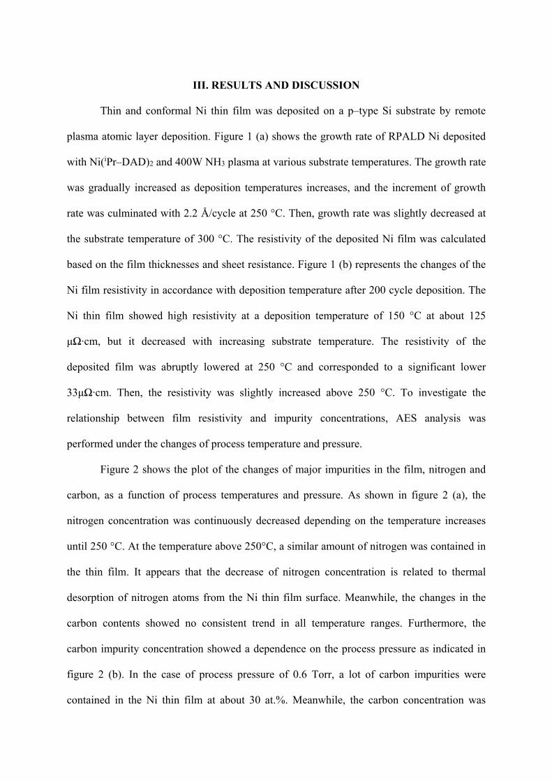
Thin and conformal Ni thin film was deposited on a p–type Si substrate by remote
plasma atomic layer deposition. Figure 1 (a) shows the growth rate of RPALD Ni deposited
with Ni(iPr–DAD)2 and 400W NH3 plasma at various substrate temperatures. The growth rate
was gradually increased as deposition temperatures increases, and the increment of growth
rate was culminated with 2.2 Å/cycle at 250 °C. Then, growth rate was slightly decreased at
the substrate temperature of 300 °C. The resistivity of the deposited Ni film was calculated
based on the film thicknesses and sheet resistance. Figure 1 (b) represents the changes of the
Ni film resistivity in accordance with deposition temperature after 200 cycle deposition. The
Ni thin film showed high resistivity at a deposition temperature of 150 °C at about 125
μΩ·cm, but it decreased with increasing substrate temperature. The resistivity of the
deposited film was abruptly lowered at 250 °C and corresponded to a significant lower
33μΩ·cm. Then, the resistivity was slightly increased above 250 °C. To investigate the
relationship between film resistivity and impurity concentrations, AES analysis was
performed under the changes of process temperature and pressure.
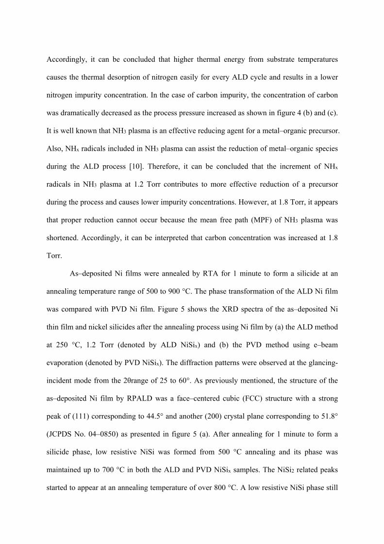
Figure 2 shows the plot of the changes of major impurities in the film, nitrogen and
carbon, as a function of process temperatures and pressure. As shown in figure 2 (a), the
nitrogen concentration was continuously decreased depending on the temperature increases
until 250 °C. At the temperature above 250°C, a similar amount of nitrogen was contained in
the thin film. It appears that the decrease of nitrogen concentration is related to thermal
desorption of nitrogen atoms from the Ni thin film surface. Meanwhile, the changes in the
carbon contents showed no consistent trend in all temperature ranges. Furthermore, the
carbon impurity concentration showed a dependence on the process pressure as indicated in
figure 2 (b). In the case of process pressure of 0.6 Torr, a lot of carbon impurities were
contained in the Ni thin film at about 30 at.%. Meanwhile, the carbon concentration was

rapidly decreased at 1.2 Torr and slightly increased over the pressure of 1.8 Torr. The
nitrogen concentration was not affected by the changes of the process pressure. These carbon
and nitrogen impurities binding states were analyzed by following an XPS study.
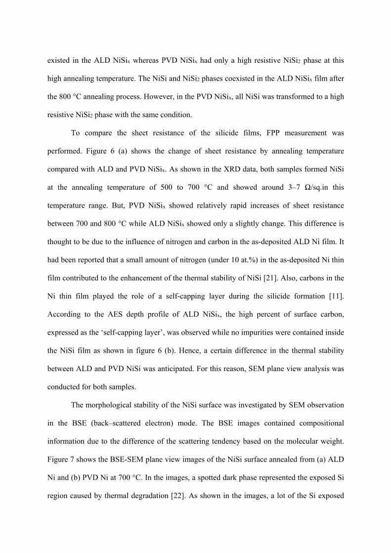
The elemental composition and chemical binding states of the deposited Ni thin film
were analyzed by XPS. Before the measurement, Ar sputtering on the surface was performed
to avoid the detection of surface oxide and contamination of the Ni surface. All collected
spectra were arranged by carbon impurity at 284.5 eV due to the charging effect. As shown in
Figure 3 (a), the C 1s spectra was deconvoluted into three subpeaks corresponding to C–C,
C–O [13,14] and C–N [15,16] bonds. These binding states constitute the C1s spectra by the
C–C bond of 71.4 %, the C–O bond of 9.3 %, and the C–N bond of 19.3 % according to the
area ratio of the spectra. Also, figure 3 (b) show that the N–C bond was observed at 397.5 eV
in the N 1s spectra [17,18]. Thus, it was confirmed that carbon and nitrogen impurities exist
not only in C–C bonding but also in C–N bonding state. This existence of the C-N bond could
describe the nitrogen removal process in the following investigation.
Based on the analyzed results and literature study, the changes of carbon and nitrogen
concentration were directly compared by an AES depth profile. Figure 4 represent the AES
depth profiles of the Ni films deposited with 400W NH3 plasma at (a) 200 °C 1.2 Torr, (b)
250 °C 0.6Torr, and (c) 250 °C 1.2 Torr, respectively. As the temperature increased, the
nitrogen concentration was found to significantly decrease compared with figure 4 (a) and (c).
According to the literature study, the C–N bond contained species were easily desorbed on
the Ni(111) surface by dehydrogenation, and nitrile (R–CN) formation caused by thermal
energy [19,20]. Therefore, the existence of the C–N bond on the Ni (111) surface closely
revealed the possibility of nitrogen desorption. As shown in the XPS results, carbon and
nitrogen forms in C–N bonding states. Moreover, the structure of the deposited Ni thin film
showed FCC Ni (111) and (200) observed by the XRD measurement (see figure 5(a)).
Accordingly, it can be concluded that higher thermal energy from substrate temperatures
causes the thermal desorption of nitrogen easily for every ALD cycle and results in a lower
nitrogen impurity concentration. In the case of carbon impurity, the concentration of carbon
was dramatically decreased as the process pressure increased as shown in figure 4 (b) and (c).
It is well known that NH3 plasma is an effective reducing agent for a metal–organic precursor.
Also, NHx radicals included in NH3 plasma can assist the reduction of metal–organic species
during the ALD process [10]. Therefore, it can be concluded that the increment of NHx
radicals in NH3 plasma at 1.2 Torr contributes to more effective reduction of a precursor
during the process and causes lower impurity concentrations. However, at 1.8 Torr, it appears
that proper reduction cannot occur because the mean free path (MPF) of NH3 plasma was
shortened. Accordingly, it can be interpreted that carbon concentration was increased at 1.8
Torr.
As–deposited Ni films were annealed by RTA for 1 minute to form a silicide at an
annealing temperature range of 500 to 900 °C. The phase transformation of the ALD Ni film
was compared with PVD Ni film. Figure 5 shows the XRD spectra of the as–deposited Ni
thin film and nickel silicides after the annealing process using Ni film by (a) the ALD method
at 250 °C, 1.2 Torr (denoted by ALD NiSix) and (b) the PVD method using e–beam
evaporation (denoted by PVD NiSix). The diffraction patterns were observed at the glancing-
incident mode from the 2θrange of 25 to 60°. As previously mentioned, the structure of the
as–deposited Ni film by RPALD was a face–centered cubic (FCC) structure with a strong
peak of (111) corresponding to 44.5° and another (200) crystal plane corresponding to 51.8°
(JCPDS No. 04–0850) as presented in figure 5 (a). After annealing for 1 minute to form a
silicide phase, low resistive NiSi was formed from 500 °C annealing and its phase was
maintained up to 700 °C in both the ALD and PVD NiSix samples. The NiSi2 related peaks
started to appear at an annealing temperature of over 800 °C. A low resistive NiSi phase still
existed in the ALD NiSix whereas PVD NiSix had only a high resistive NiSi2 phase at this
high annealing temperature. The NiSi and NiSi2 phases coexisted in the ALD NiSix film after
the 800 °C annealing process. However, in the PVD NiSix, all NiSi was transformed to a high
resistive NiSi2 phase with the same condition.
To compare the sheet resistance of the silicide films, FPP measurement was
performed. Figure 6 (a) shows the change of sheet resistance by annealing temperature
compared with ALD and PVD NiSix. As shown in the XRD data, both samples formed NiSi
at the annealing temperature of 500 to 700 °C and showed around 3–7 Ω/sq.in this
temperature range. But, PVD NiSix showed relatively rapid increases of sheet resistance
between 700 and 800 °C while ALD NiSix showed only a slightly change. This difference is
thought to be due to the influence of nitrogen and carbon in the as-deposited ALD Ni film. It
had been reported that a small amount of nitrogen (under 10 at.%) in the as-deposited Ni thin
film contributed to the enhancement of the thermal stability of NiSi [21]. Also, carbons in the
Ni thin film played the role of a self-capping layer during the silicide formation [11].
According to the AES depth profile of ALD NiSix, the high percent of surface carbon,
expressed as the ‘self-capping layer’, was observed while no impurities were contained inside
the NiSi film as shown in figure 6 (b). Hence, a certain difference in the thermal stability
between ALD and PVD NiSi was anticipated. For this reason, SEM plane view analysis was
conducted for both samples.
The morphological stability of the NiSi surface was investigated by SEM observation
in the BSE (back–scattered electron) mode. The BSE images contained compositional
information due to the difference of the scattering tendency based on the molecular weight.
Figure 7 shows the BSE-SEM plane view images of the NiSi surface annealed from (a) ALD
Ni and (b) PVD Ni at 700 °C. In the images, a spotted dark phase represented the exposed Si
region caused by thermal degradation [22]. As shown in the images, a lot of the Si exposed
region was observed in PVD NiSi. Meanwhile, a relatively less Si exposed region was
observed in ALD NiSi. These results demonstrate the enhancement of thermal stability of
NiSi film from the ALD method. Furthermore, less RS (sheet resistance) degradation was
observed in ALD NiSix after the annealing process. Therefore, it can be believed that
although the small amounts of carbon and nitrogen were included in the as-deposited ALD Ni
film, it contributed to the enhancement of thermal stability of the NiSi layer.
IV. CONCLUSION
In this study, low resistive Ni thin film was deposited by remote plasma atomic layer
deposition with a low impurity concentration. Ni(iPr-DAD)2 was introduced as a Ni precursor
and NH3 plasma was used as a precursor. Impurity contents were investigated based on the
process temperature and pressure. It was concluded that depending on the temperature
increases, nitrogen impurity could be thermally desorbed on the surface of the Ni thin film.
Moreover, carbon impurity was mainly affected by process pressure, related to the reaction
with NH3 plasma. Small amounts of carbon and nitrogen in as-deposited Ni were found to
have contributed to enhancing the thermal stability of NiSi during the RTA process. NiSi
from ALD Ni showed better thermal stability compared with those from PVD Ni. This study
is meaningful in that Ni film with low resistivity was found to be deposited by the ALD
method and formed in the NiSi phase with a higher thermal stability. Therefore it can be
believed that the possibility of introducing NiSi for practical industrial applications is more
feasible as a result of this study.
ACKNOWLEDGEMENT
This study was supported by the research program of Hanyang University and SK
Hynix Semiconductor (No. 2012–00000260001)
REREFENCES
[1] R. siu, D. S. Williams and W. T. Lynch, J. Appl. Phys. 63, 1990 (1988)
[2] H. C. Cheng, M. H. Juang, C. T. Lin and L. M. Huang, IEEE Electron Device Lett. 15,
342 (1994)
[3] K. Goto, A. Fushida, J. Watanabe, T. Sukegawa, Y. Tada, T. Nakamura, T. Yamazaki and
T. Sugii, IEEE trans. Electron Devices 46, 117 (1999)
[4] Q. F. Wang, C. M. Osburn, P. L. Smith, C. A. Canovai, G. E. McGuire, J. Electrochem.
Soc. 140, 200 (1993)
[5] J. B. Lasky, J. S. Nakos, O. J. Cain and P. J. Geiss, IEEE trans. Electron Devices 38, 262
(1991)
[6] J.P. Gambino and E.G. Colgan, Mater. Chem. Phys. 52, 99 (1998)
[7] H. Iwai, T. Ohguro, S.-I. Ohmi, Microelectron. Eng. 60, 157 (2002)
[8] T. Morimoto, T. Ohguro, H. S. Momose, T. Iinuma, I. Kunishima,K. Suguro, I. Katakabe,
H. Nakajima, M. Tsuchiaki, M. Ono,Y. Katsumata and H. Iwai, IEEE trans. Electron Devices
42, 915 (1995)
[9] O. Lühn, C. Van Hoof, W. Ruythooren, J.-P. Celis, Microelectron. Eng. 85, 1947 (2008)
[10] H. B. R. Lee, S. H. Bang, W. H. Kim, G. H. Gu, Y. K. Lee,T. M. Chung, C. G. Kim, C.
G. Park and H. J. Kim, Jpn. J. Appl. Phys. 49, 05FA11 (2010)
[11] C. M. Yang, S. W. Yun, J. B. Ha, K. I. Na, H. I. Cho, H. B. Lee,J. H. Jeong, S. H. Kong,
S. H. Hahm and J. H. Lee, Jpn. J. Appl. Phys. 46, 1981 (2007)
[12] K. W. Do, C. M. Yang, I. S. Kang, K. M. Kim, K. H. Back, H. I. Cho,H. B. Lee, S. H.
Kong, S. H. Hahm, D. H. Kwon, J. H. Lee and J. H. Lee, Jpn. J. Appl. Phys. 45, 2975 (2006)
[13] R. Dedryvere, S. Laruelle, S. Grugeon, P. Poizot, D. Gonbeau and J.-M. Tarascon, Chem.
Mater. 16, 1056 (2004)
[14] D. Banerjee, and H. W. Nesbitt, Geochim. Cosmochim. Acta 65, 1703 (2001)
[15] C. Pevida, M.G. Plaza, B. Arias, J. Fermoso, F. Rubiera, J.J. Pis, Appl. Surf. Sci. 254,
7165 (2008)
[16] Lan N. Bui and M. Thompson, Analyst 118, 463 (1993)
[17] F. Fujimoto and K. Ogata, Jpn. J. Appl. Phys. 32, 420 (1993)
[18] Z.-M. Ren, Y.-C. Du, Y. Qiu, J.-D. Wu, Z.-F. Ying, X.-X. Xiong and F.-M. Li, Phys.
Rev. B 51, 5274 (1995)
[19] D. E. Gardin and G. A. Somorjai, J. Phys. Chem. 96, 9424 (1992)
[20] J. C. Hemminger, E. L. Muetterties, and G. A. Somorjai, J. Am. Chem. Soc. 101, 62
(1979)
[21] S. I. Kim, S. R. Lee, K. M. Ahn, and B. T. Ahn, J. Electrochem. Soc. 157, H231 (2010)
[22] G. Utlu, N. Artunc, S. Selvi, Mater. Chem. Phys. 132, 421 (2012)
List of figures
Fig. 1. (a) The growth rate of RPALD Ni and (b) film resistivity for various substrate
temperatures
Fig. 2. The impurity concentrations of Ni thin film as a function of (a) substrate temperature
at 1.2 Torr and (b) process pressure at 250 °C
Fig. 3. The XPS spectra of impurities core level corresponding to (a) C1s and (b) N1s levels
Fig. 4. AES depth profiles of Ni films deposited for 200 cycles at (a) 200 °C1.2 Torr, (b)
250 °C0.6 Torr and (c) 250 °C 1.2 Torr with 400W NH3 plasma.
Fig. 5. The XRD patterns of as-deposited Ni film and nickel-silicide layer by (a) ALD
method and (b) PVD method after RTA for 1 min in vacuum ambient at various annealing
temperature.
Fig. 6. (a) Sheet resistance of the nickel-silicide films after annealing process for 1 min with
various annealing temperatures. (b) AES depth profiles of ALD NiSi at annealing
temperature 600 °C
Fig. 7. BES-SEM images of NiSi surface from (a) ALD Ni and (b) PVD Ni at the annealing
temperature of 700 °C
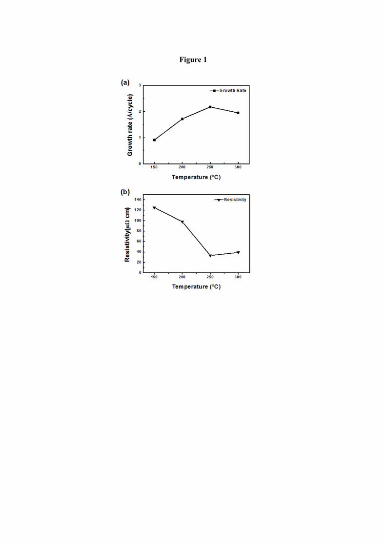
Figure 1
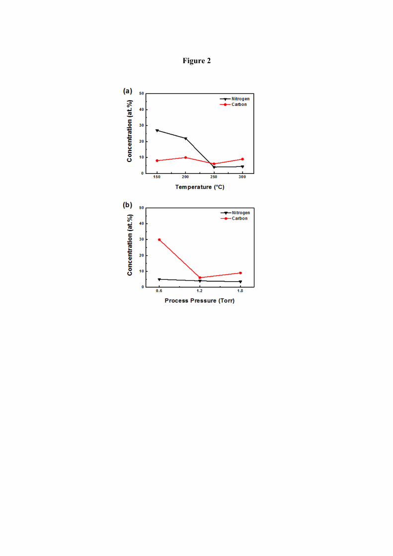
Figure 2
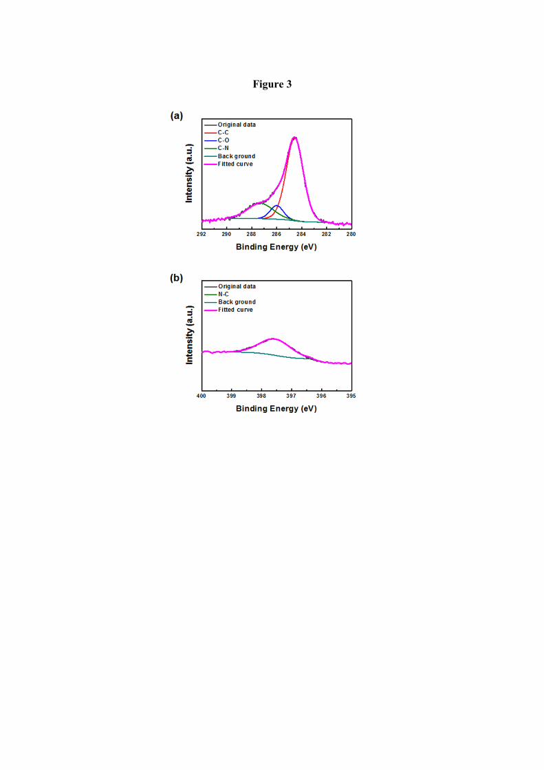
Figure 3
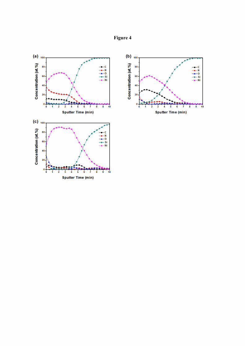
Figure 4
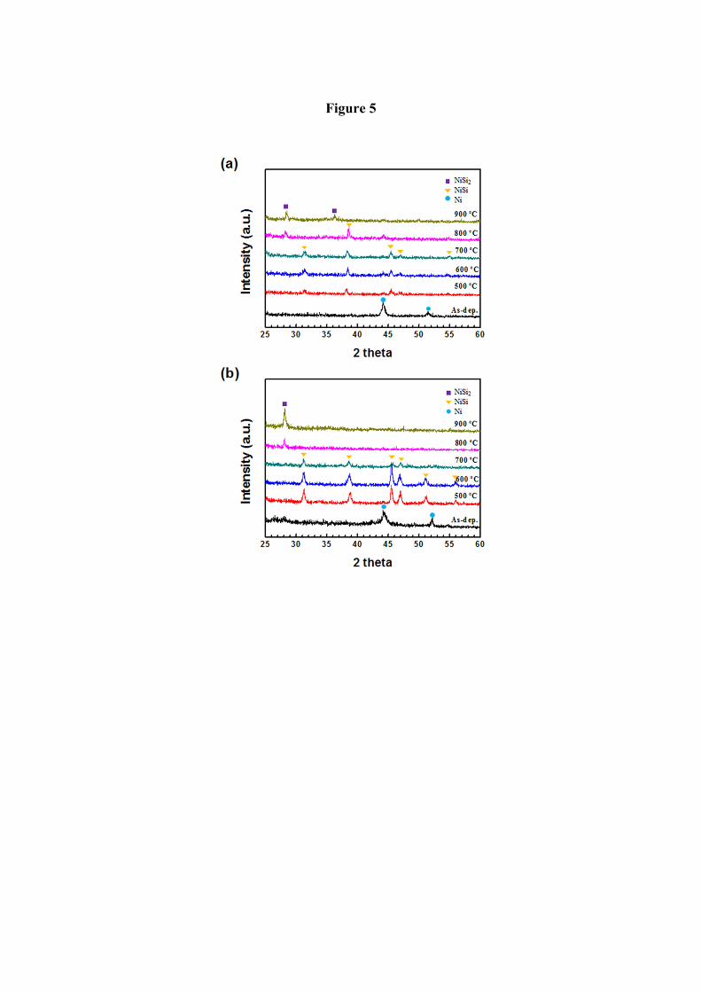
Figure 5
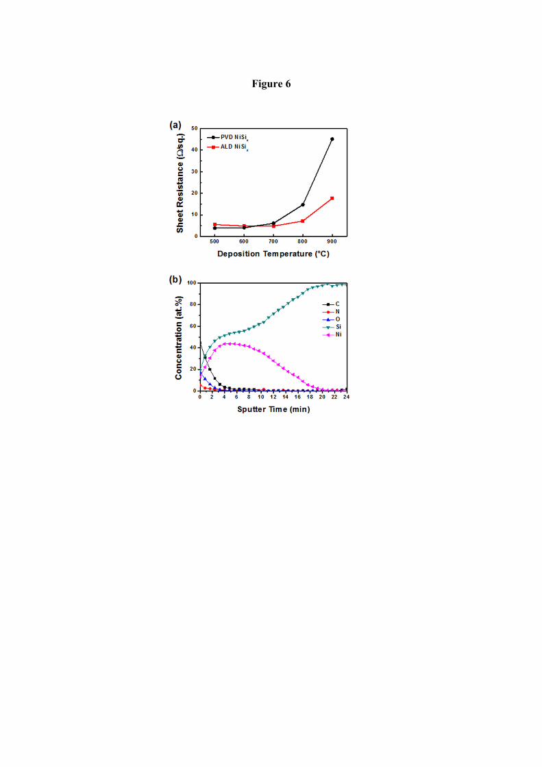
Figure 6
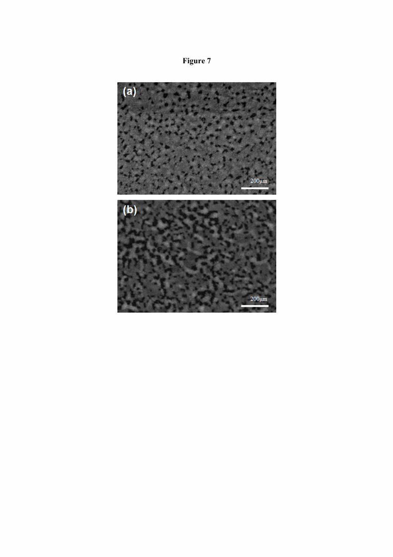
Figure 7
Copyright © 2022 FDOKUMEN