
Process compilation of thin film microdevices
20
IEEE TRANSACTIONS ON COMPUTER-AIDED DESIGN OF INTEGRATEDCIRCUITS AND SYSTEMS, VOL. IS, NO. I, JULY 1996 145 Process Compilation of Thin Film Microdevices Mohammed Hasanuzzaman and Carlos H. Mastrangelo, Member, ZEEE Abstruct- This paper describes a systematic method for the automatic generation of fabrication processes of thin film devices. The method uses a partially ordered set (poset) representation of device topology describing the order between its various components in the form of a directed acyclic graph. The sequence in which these components are fabricated is determined from the poset linear extensions, and the component sequence is expanded into a corresponding process flow. The graph-theoretic synthesis method is powerful enough to establish existence and multiplicity of flows thus creating a design space D suitable for optimization. The cardinality 11D11 for a device with S components is large with a worst case IlDIl 5 (S - l)! yielding in general a combinatorial explosion of solutions. The number of solutions is controlled through a priori estimates of 11D)11 and condensation of the device graph. The method has been implemented in the computer pro- gram MISTIC (Michigan Synthesis Tools for Integrated Circuits) which calculates specific process parameters using an internal database of process modules and materials. Currently, MISTIC includes process modules for deposition, lithography, etching, ion implantation, coupled simultaneous diffusions, and reactive growth. The compilation procedure was applied to several device structures. For a double metal twin-well BiCMOS structure, the compiler generated 168 complete process flows. I. INTRODUCTION INCE THE conception of planar monolithic transistors, S device designers have strived to produce improved fab- rication processes. Early device designers relied on hand calculations and experimental data to determine the correct set of steps and parameters required in the fabrication process. Since a process flow requires many weeks or even months to run and test, this trial and error procedure is slow and costly, typically requiring years of work for a single process. The emergence of simulation tools for semiconductor device processing in the 1970s created a “virtual factory” environment which allows designers to simulate their devices and test their ideas in a few hours. Ever since this design methodology was established, increasingly more sophisticated simulation tools have been developed. Current state-of-the-art simulation tools such as SUPREM [l], SIMPL [2], and MEMCAD [3] take a description of the fabrication process flow as input and generate accurate two- and three-dimensional (2- and 3-D) representation of thin-film devices. Manuscript received June 8, i995; revised November 22, 1995, January 16, 1996, and March 29, 1996. This work was supported by the National Science Foundation under Grant ECS-9309229. This paper was recommended by Associate Editor S. Duvall. The author& are with the Centcr for Integrated Sensors and Circuits, Department of Electrical Engineering and Computer Science, University of Michigan, Ann Arbor, MI 48109 USA. Publisher Item Identifier S 0278-0070(96)04900-7. While process simulators are excellent tools for verification, fine tuning, and parameter optimization [4], [5] of process flows, the task of developing the initial process remains on the designer. Thus if the simulation results are unsatisfactory, the designer must specify appropriate changes and run the simulation again. Typically, an acceptable process is arrived after many iterations and weeks of intensive simulation. The iterative nature of the simulation-based design method- ology represents an increasing burden as process complexity grows. For example, complex processes such as BiCMOS require 200-700 steps with a correspondingly large number of interactions which must be considered when making any changes. These changes in term depend on the process modules and laboratory resources available. Micromachining processes for integrated microelectromechanical systems (MEMS) are subject to the same complexity considerations [6], [7]. The success or failure of the fabrication process depend on how effectively the entire process is assembled with an imperfect set of available modules. There is a clear need for a process tool that directly assembles the process flow from a device description or in short a process compiler. In this paper, a systematic method for synthesis of process flows for thin film planar devices is presented. The paper begins with a discussion of the basic mathematical theory of process compilation which includes abstract process and device representation models (Sections 11-III), the basic synthesis method (Section IV), estimation and control of the number of solutions (Sections V-VII), and methods of process flow construction (Section VIII). This is followed by a description of process parameter selection and inverse calculations (Sections VIII-X), an introductory discussion of software implementation issues (Section XI), and finally test results for a few VLSI structures (Section XII). The synthesis procedure has been implemented into a soft- ware tool, MISTIC, which accepts a device cross section as input and generates feasible process flows as output. In its first version, this software accepts Manhattan representations of the device cross section; therefore, all calculations are one- dimensional (1-D) in nature over a collection of structurally different regions. A complete description of the software structure is beyond the scope of this paper and will be published elsewhere. The compiler performs three main tasks. It first divides the device into components, then sequences these into a serial process, and finally constructs a fabrication process flow using a database of materials, etchants, and other processes. The first two tasks examine the device topology effectively determining the order of steps that must be carried out. The last task selects appropriate available process modules 0278-0070/96$05.00 0 1996 IEEE
Transcript of Process compilation of thin film microdevices

IEEE TRANSACTIONS ON COMPUTER-AIDED DESIGN OF INTEGRATED CIRCUITS AND SYSTEMS, VOL. IS, NO. I , JULY 1996 145
Process Compilation of Thin Film Microdevices Mohammed Hasanuzzaman and Carlos H. Mastrangelo, Member, ZEEE
Abstruct- This paper describes a systematic method for the automatic generation of fabrication processes of thin film devices. The method uses a partially ordered set (poset) representation of device topology describing the order between its various components in the form of a directed acyclic graph. The sequence in which these components are fabricated is determined from the poset linear extensions, and the component sequence is expanded into a corresponding process flow. The graph-theoretic synthesis method is powerful enough to establish existence and multiplicity of flows thus creating a design space D suitable for optimization. The cardinality 11D11 for a device with S components is large with a worst case IlDIl 5 (S - l)! yielding in general a combinatorial explosion of solutions. The number of solutions is controlled through a priori estimates of 11D)11 and condensation of the device graph. The method has been implemented in the computer pro- gram MISTIC (Michigan Synthesis Tools for Integrated Circuits) which calculates specific process parameters using an internal database of process modules and materials. Currently, MISTIC includes process modules for deposition, lithography, etching, ion implantation, coupled simultaneous diffusions, and reactive growth. The compilation procedure was applied to several device structures. For a double metal twin-well BiCMOS structure, the compiler generated 168 complete process flows.
I. INTRODUCTION INCE THE conception of planar monolithic transistors, S device designers have strived to produce improved fab-
rication processes. Early device designers relied on hand calculations and experimental data to determine the correct set of steps and parameters required in the fabrication process. Since a process flow requires many weeks or even months to run and test, this trial and error procedure is slow and costly, typically requiring years of work for a single process.
The emergence of simulation tools for semiconductor device processing in the 1970s created a “virtual factory” environment which allows designers to simulate their devices and test their ideas in a few hours. Ever since this design methodology was established, increasingly more sophisticated simulation tools have been developed. Current state-of-the-art simulation tools such as SUPREM [l], SIMPL [2], and MEMCAD [ 3 ] take a description of the fabrication process flow as input and generate accurate two- and three-dimensional (2- and 3-D) representation of thin-film devices.
Manuscript received June 8, i995; revised November 22, 1995, January 16, 1996, and March 29, 1996. This work was supported by the National Science Foundation under Grant ECS-9309229. This paper was recommended by Associate Editor S. Duvall.
The author& are with the Centcr for Integrated Sensors and Circuits, Department of Electrical Engineering and Computer Science, University of Michigan, Ann Arbor, MI 48109 USA.
Publisher Item Identifier S 0278-0070(96)04900-7.
While process simulators are excellent tools for verification, fine tuning, and parameter optimization [4], [5] of process flows, the task of developing the initial process remains on the designer. Thus if the simulation results are unsatisfactory, the designer must specify appropriate changes and run the simulation again. Typically, an acceptable process is arrived after many iterations and weeks of intensive simulation.
The iterative nature of the simulation-based design method- ology represents an increasing burden as process complexity grows. For example, complex processes such as BiCMOS require 200-700 steps with a correspondingly large number of interactions which must be considered when making any changes. These changes in term depend on the process modules and laboratory resources available. Micromachining processes for integrated microelectromechanical systems (MEMS) are subject to the same complexity considerations [6], [7]. The success or failure of the fabrication process depend on how effectively the entire process is assembled with an imperfect set of available modules.
There is a clear need for a process tool that directly assembles the process flow from a device description or in short a process compiler. In this paper, a systematic method for synthesis of process flows for thin film planar devices is presented. The paper begins with a discussion of the basic mathematical theory of process compilation which includes abstract process and device representation models (Sections 11-III), the basic synthesis method (Section IV), estimation and control of the number of solutions (Sections V-VII), and methods of process flow construction (Section VIII). This is followed by a description of process parameter selection and inverse calculations (Sections VIII-X), an introductory discussion of software implementation issues (Section XI), and finally test results for a few VLSI structures (Section XII).
The synthesis procedure has been implemented into a soft- ware tool, MISTIC, which accepts a device cross section as input and generates feasible process flows as output. In its first version, this software accepts Manhattan representations of the device cross section; therefore, all calculations are one- dimensional (1-D) in nature over a collection of structurally different regions. A complete description of the software structure is beyond the scope of this paper and will be published elsewhere. The compiler performs three main tasks. It first divides the device into components, then sequences these into a serial process, and finally constructs a fabrication process flow using a database of materials, etchants, and other processes. The first two tasks examine the device topology effectively determining the order of steps that must be carried out. The last task selects appropriate available process modules
0278-0070/96$05.00 0 1996 IEEE

146 IEEE TRANSACTIONS ON COMPUTER-AIDED DESIGN OF INTEGRATED CIRCUITS AND SYSTEMS, VOL. 15, NO. I , JULY 1996
Fig. 1. Cross sections of device at different steps in the process
that build the device structure with good fabrication yields for a particular step order. The final process contains all the necessary parameters required to meet device specifications. For example, the compiler solves for diffusion and reactive growth schedules, as well as selects the most likely etchants.
11. STATE-SPACE REPRESENTATION
Our discussion begins with some useful definitions and a mathematical description of the VLSI fabrication process. In planar VLSI processing, the starting material is a blank substrate. This substrate can be modified by a finite set of m , operators 4, such as lithography, etching, deposition, implantation, diffusion, etc. The operators are applied to a sample in a specific sequence, and the last operator yields the desired device structure. In this sense, the fabrication process is represented by the discrete system
Xi+l = 4L(G) (1)
where 2, are discrete states representing the current state of the sample, 20 the initial substrate, and 2, the complete device. This state abstraction is commonly used in process modeling frameworks [8]. We shall soon demonstrate that n is related to device complexity and the number of layers. For example, the fabrication process shown in Fig. 1 consists of 12 operations performed in sequence with 11 intermediate states. Each intermediate cross section can be considered as a point in a state space as shown in Fig. 2, and each operator 4i represents a vector that connects subsequent states. In this state-space context, the synthesis problem consists of finding a finite path that connects the initial 20 and final 2, states. This path defines a sequence of operators with composition
n-1
5 , = ( b i ( 5 O ) -- F(50) (2) i=O
where 3 is the process Bow characteristic to device z,. Flow 3 consists of the sequence
operating on I C O . In this notation, brackets denote sequences and braces denote sets.
Fig. 2. State-space abstraction of VLSI process
Searches for the path 3 may be accomplished in different ways. The number of possible paths, however, is large. If the operator set consists of m distinct operators that can be applied to each of the states, there are mn possible paths of radius n originating from 20 that can be explored! For a typical device with n = 10 intermediate steps, and m = 5 operators there are mn = 5l0 zz l o 7 possible paths. Thus random type searches are inadequate.
The exponentially growing number of paths results in a combinatorial explosion which is a mixed blessing. The large path number leads in general to multiple solutions. The col- lection of feasible flows
is defined as the design space D(lcn) of cardinality /ID1/ = k . Since, in general, ~~2~~ > 1, the design space constitutes a basis for process flow optimization. However, a complete calculation of D may not be reached in finite time. In the next section, a systematic procedure that finds a path F efficiently is described. The path is determined extracting flow information from device topology, and imposing restrictions on F from approximate estimates of I 12) I 1 .
111. PLANAR DEVICE REPRESENTATION The process flow F is intimately connected with the specific
device topology; hence, information leading to F is found by analyzing the device structure. We begin our discussion with some definitions relevant to the device itself. A device d consists of a set of components C(d) organized in a specific order O(c)
( 5 )
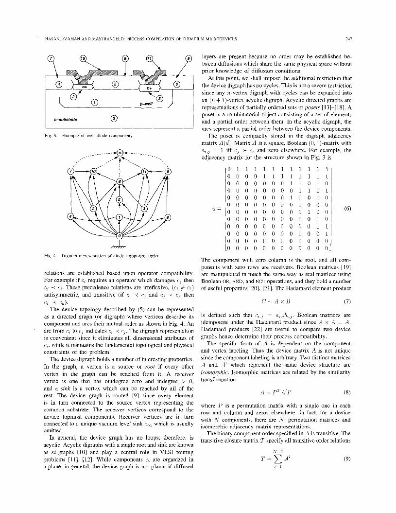
Each ci component represents a polygonal object in d of fixed attributes s, such as material type, dimensions, and doping type. For instance, the drain, source, and gate are components of a MOSFET. Fig. 3 shows the components of a well diode.
Some of these components may belong to the same physical layer. For the moment, we shall treat each of these as indi- vidual Components. The order U ( e ) specifies the organization of these components in the device through binary relations as follows. Component ci rests above cy whenever e; is in direct contact and covering or partially covering cJ. This relationship implicitly dictates that the fabrication of c j precedes that of c i , or in short notation cj 4 ci or ci F c j . Similarly, if component e; is diffused onto cj then cj 4 ci. Additional precedence
HASANUZLAMAN ANI) MASTRANGELO: PROCESS COMPILATION OF THIN FILM MICRODEVICES 141
n-substrate @
Fig. 3. Example of well diode components
& Fig. 4. Digraph representation of diode component order
relations are established based upon operator compatibility. For example if ci requires an operator which damages cj then cj 4 c i . These precedence relations are irreflexive, (e; + e ( ) antisymmetric, and transitive (if c; < cj and cj % c k then ci + C k ) .
The device topology described by (5) can be represented as a directed graph (or digraph) where vertices describe its component and arcs their mutual order as shown in Fig. 4. An arc from ci to cj indicates ci < e,. The digraph representation is convenient since it eliminates all dimensional attributes of e;, while it maintains the fundamental topological and physical constraints of the problem.
The device digraph holds a number of interesting properties. In the graph, a vertex is a source or root if every other vertex in the graph can be reached from it. A receiver vertex is one that has outdegree zero and indegree > 0, and a sink is a vertex which can be reached by all of the rest. The device graph is rooted [9] since every element is in turn connected to the source vertex representing the common substrate. The receiver vertices correspond to the device topmost components. Receiver vertices are in turn connected to a unique vacuum level sink c, which is usually omitted.
In general, the device graph has no loops; therefore, is acyclic. Acyclic digraphs with a single root and sink are known as st-graphs [IO] and play a central role in VLSI routing problems [I I], [12]. While components ci are organized in a plane, in general, the device graph is not planar if diffused
layers are present because no order may be established be- tween diffusions which share the same physical space without prior knowledge of diffusion conditions.
At this point, we shall impose the additional restriction that the device digraph has no cycles. This is not a severe restriction since any n-vertex digraph with cycles can be expanded into an (n + 1)-vertex acyclic digraph. Acyclic directed graphs are representations of partially ordered sets or posets [13]-[18]. A poset is a combinatorial object consisting of a set of elements and a partial order between them. In the acyclic digraph, the arcs represent a partial order between the device components.
The poset is compactly stored in the digraph adjacency matrix A(d) . Matrix A is a square, Boolean (0. 1)-matrix with
= 1 iff c3 t c, and zero elsewhere. For example, the adjacency matrix for the structure shown in Fig. 3 is
A =
-0 1 1 1 1 1 1 1 1 1 1 I 0 0 0 0 1 1 1 1 1 1 1 1 0 0 0 0 0 0 0 1 1 0 1 0 0 0 0 0 0 0 0 0 1 1 0 1 0 0 0 0 0 0 0 1 0 0 0 0 0 0 0 0 0 0 0 0 1 0 0 0 0 0 0 0 0 0 0 0 0 1 0 0 0 0 0 0 0 0 0 0 0 0 1 0 0 0 0 0 0 0 0 0 0 0 1 1 0 0 0 0 0 0 0 0 0 0 0 1 0 0 0 0 0 0 0 0 0 0 0 0
-0 0 0 0 0 0 0 0 0 0 0 0
The component with zero column is the root, and all com- ponents with zero rows are receivers. Boolean matrices [19] are manipulated in much the same way as real matrices using Boolean OR, AND, and NOT operations, and they hold a number of useful properties [20], [21]. The Hadamard element product
C = A x B (7)
is defined such that c,,~ = a, 3b , , J . Boolean matrices are idempotent under the Hadamard product since A x A = A. Hadamard products [22] are useful to compare two device graphs hence determine their process compatibility.
The specific form of A is dependent on the component and vertex labeling. Thus the device matrix A is not unique since the component labeling is arbitrary. Two distinct matrices A and A’ which represent the same device structure are isomorphic. Isomorphic matrices are related by the similarity transformation
where P is a permutation matrix with a single one in each row and column and zeros elsewhere. In fact, for a device with N components, there are N ! permutation matrices and isomorphic adjacency matrix representations.
The binary component order specified in A is transitive. The transitive closure matrix T specify all transitive order relations
N-1
(9)

748 IEEE TRANSACTIONS ON COMPUTER-AIDED DESIGN OF INTEGRATED CIRCUITS AND SYSTEMS, VOL. 15, NO. 7, JULY 1996
where the sum and power are Boolean AND and Boolean OR operations. Matrices A and T contain all order relations extracted from the device topology.
In principle, the digraph representation is suitable whenever the component order is well defined. Complex geometry components that do not meet this criteria can, however, be subdivided into several subcomponents which do. For example, odd-shaped sacrificial layers that may appear to be both above and below a device component can be decomposed onto two or more uniform-thickness subcomponents of well- defined order.
The graph-theoretic device representation provides a rigor- ous basis for the construction of a synthesis method as well as a means of comparison between different kinds of device topologies. We shall return to this topic when considering device integration problems.
IV. BASIC SYNTHESIS METHOD The flow path 3 joining 50 and rcT1 is constructed as
follows. The operators in the flow F must form all k device components. The flow operators 4 ’ s are thus intimately related to the device topology and the attributes of its components. Since each e, is distinct we shall assume that there exists a specific operator group
required to form component e,. The operator group @ ( e i ) is selective if it does not disturb the components existent on a state. Selective operator groups are the most useful since they decouple the operators required to form the device components. Using these definitions we can establish a flow construction procedure where each component is constructed one at a time yielding the more restrictive state equation
Equation (1 1) uniquely defines all intermediate states 5, and serves as a roadrnap for finding the path. Since selective @(c) are known then from (1)
and the flow .?’ is
From this discussion, it follows that [1311 2 k . The flow F is hence an expansion of the component sequence S
dictated by the order relationships O(c). The component sequence S (and flow 3) is found by
“stretching” the 2-D device graph into a linear chain or linear extension. Fig. 5 shows a few linear extensions for the graph of Fig. 4. This procedure is known as topological sorting [23]
3- @e @e ;e
a
Fig. S . h few linear extensions
and has many applications in computer science. The existence of 3 is thus assured by the existence of a linear extension in the device graph.
Theorern 1 (Fundamental): Let d be a device of e, compo- nents with order 6 represented by an acyclic directed graph. If there exists a selective operator group @(c) for each device component, there is at least one process flow for device d.
Proof: Under the conditions stated above, the existence of a process flow is essentially assured by that of the linear ex- tension of the digraph poset.\ The existence of linear extensions was established by a well-known theorem of Szpilrajn [24].
The fundamental theorem assures the existence of 3 in the topological sense. It does not assure the existence of selective @. We shall show later that good approximations for @ can be reached. Furthermore, the theorem can be slightly modified to accommodate operators which are not selective but distributed
0 Theorem 2 (Cardinality): A device d of N components
with T receivers and unique selective operator group @ has a design space D of cardinality r ! 5 11211 5 ( N - l)!
Pro08 Since the receiver components have no mutual order, there are T ! possible linear chain arrangements. Szpil- rajn’s theorem assures the existence of a linear chain for the rest A’ - T components. Thus there are at least T ! linear chains of length :V. The upper bound corresponds to a device with -V - 1 receivers and one root. 0
Theorem 2 states that devices with sparse transitive closure matrices are likely to have a very large number of flows F. The multiplicity in 3 is beneficial since it allows the selection of an optimal flow from a large pool. However, in very complex devices, the factorial growth of 11D11 becomes intractable.
This combinatorial explosion is avoided, however, by care- fully controlling the degrees of freedom in d through quick estimates of llD11 and graph reduction techniques. These topics, as well as specific methods for extracting the linear extensions, are discussed in the sections below.
(such as thermal diffusion cycles).
V. CARDINALITY OF DESIGN SPACE A computationally inexpensive a priori measure of the
design space cardinality /ID// is an essential tool for the detection of a combinatorial explosion. This quantity is used to introduce reduction techniques and additional constraints if llD11 is too large before the sequencing of the components is attempted. In practical terms, this is needed to assure that the calculation of D is performed in a finite time and without exceeding the machine storage space.

HASANUZZAMAN AND MASTRANGELO: PROCESS COMPILATION OF THIN FILM MICRODEVICES 749
A suitable measure of //DD// is the number of linear exten- sions. The enumeration and generation of linear extensions has been studied extensively [25]-[30]. For the general case, the generation all linear extensions is an NP-complete problem [31]. It is well known [25] that the the number of linear extensions for a graph with N vertices is
n = JJDJJ = N ! vol(B(T)) (15)
where B(T) is an N-dimensional convex polytope embedded within the unit hypercube, and vol() is the polytope volume. The polytope faces are hyperplanes defined by M constraints of T (i.e., the number of ones in T), and 2N constraints from the hypercube faces. It has been shown that computing this volume is an NP-complete [30], [31] process. Therefore, counting the linear extensions exactly [32] is computationally equivalent to finding V through topological sorting. The volume, however, can be determined approximately at much smaller expense by several methods. The most common is the Monte Carlo technique [33], [34]. In graphs with a large number of nodes, the volume of the polytope can be quite small; hence, Monte Carlo techniques are computationally ineffective due to the high accuracy requirement at the lower range in vel().
A computationally efficient lower bound for vol() is found approximating the polytope volume by that of the largest hypersphere that will fit inside it [35]. Each of the M + 2N bounding hyperplanes has the form
where v k is a unit vector pointing outward to hyperplane k , and bk is a measure of the unit distance from the origin. The distance from an interior point q* of the polytope to hyperplane k is
Therefore, the radius p of the maximum hypersphere is found from the hyperplane constraints
This is a standard linear programming problem solved in the worst case in O ( M 2 ) operations. The approximate IIDJJ is then [36]
This bound is suitable for small M . The maximum M occurs when T is a total order isomorphic to an upper triangular matrix of ones [9] with M = N 2 / 2 .
For large M , a less expensive upper estimate of IIDII is found by relaxing some of the order constraints as follows. From the transitive closure matrix T , a position restrictor matrix R can be defined. The rows in R represent the device components, and its columns the possible positions (or bins)
(b)
Fig. 6. graph.
Position restrictor example. (a) Device cross-section. (b) Device
in the sequence S . Since there are as many positions as components, R is a square matrix. The elements r,,, = 1 when c, can occupy position ,I and zero elsewhere. For example, in the structure shown in Fig. 6, component c1 has three elements above it and one below; thus only r1,2 and r1,3 are ones. Component c2 has two components above and one below thus r2,1. r2,2, and r2,3 are ones, and so on. The number of components below c, is the column count of T and the number of components above c, is its row count. The position restrictor matrix thus indicates the bins where a particular component may be placed as shown below
0 1 1 1 1 1 1 0 0 0 0 0 10 0 0 1 1 11 10 1 1 0 0 01 I .W) J+x=J 0 0 1 1 1 0
0 1 1 1 0 0 0 0 0 0 1 1 0 0 0 0 0 1 T = 1
1 L 0 0 0 0 0 0 1 1 0 0 0 0 0 1 0 0 0 1 1 0 0 0 0 0 0 1
An estimate for llD// is found by counting the number of configurations of the N components under some conditions. No two components occupy the same position in the sequence (column), and each component is placed at a single position. Therefore, in a valid configuration. each row and column has one component resembling the placement of N nonattacking rooks in a restricted N x N chessboard. A few of these arrangements are shown below. Dashes represent forbidden

750 IEEE TRANSACTIONS ON COMPUTER-AIDED DESlGN OF INTEGRATED CIRCUITS AND SYSTEMS, VOL. 15, NO. I , JULY 1096
(a)
Fig. 7. Condensation of components. (a) Worst case. (b) Best case.
bins, U components, and circles empty slots.
The enumeration of these configurations is a classical problem in combinatorics quantified by the Nth coefficient of the rook polynomial TN ( R ) [37 ] . Thus
Since components are more constrained in T than in R, then r‘N is an upper bound for ((DD((.
The position restrictor matrix has an additional combi- natorial interpretation. Components c, belong to the device set d . Each bin position in sequence S is a group. Each configuration in R is a set of distinct {ca . . . . c p } where each c, belongs to a particular group (column). Therefore, each N - rook configuration is a system of distinct representative (SDR) of matrix R [38]. The number of SDR’s and TN(R) in a Boolean matrix
(23)
is equal to thepermanent, per(R), of matrix R [391, [21], [40]. The permanent is a scalar quantity that often appears in many enumeration and combinatorial problems. For square matrices, the permanent is calculated as a ‘plus-only’ determinant [41]. The evaluation of per(R) requires in general N ! steps.
I/S.D.RII = T N ( R ) = per(R)
Fortunately there exists an upper bound for quantity
per(). The
N
11Dl1 5 T N ( T ) = per(R) 5 n(bi!)’”% (24)
is known as Bergman’s bound [42] for the permanent, and hi is the number of ones in row i of R. This bound is computationally inexpensive and can be calculated in N steps. Simpler estimates of per() are found as follows. First, the number of available bins in the first row, b l , of T is counted. Then the first column and row are deleted from matrix T , and the procedure is repeated recursively on the reduced matrix. The permanent is approximately
i=l
N
per(R) = n b, (25) i=l
and it is essentially a reduced factorial measure of the com- ponent combinations. This estimate reported in [42], [43] is known as the Lazyman’s permanent. In practice, the bound of (24) offers the most accuracy at the lowest computational cost.
VI. GRANULARITY CONTROL THROUGH CONDENSATION
In practice, if /(Dl1 > lo4, further simplifications are necessary to find D in a reasonable time. The cardinality 1(2)11 is a strongly increasing function of the number of vertices in the device graph. Therefore, substantial reductions are made by reducing the vertex count. This operation involves clustering of similar components under a single vertex now representing a layer. The resulting grouping operation in the graph is referred to as a condensation. Components belonging to the same physical layer can be condensed into a group. The condensation is repeated recursively until either llD\\ is below an acceptable threshold or until no further condensation is possible. The scheme outlined above results in a drastic reduction in 11D11.
Theorem 3 (Condensation): Let T and T* be the transi- tive closure of a graph before and after the condensation of two components, then \ \D(T)l l / (N - I) 5 llD(T*)ll 5
Proof These bounds correspond to the two extreme cases of Fig. 7. In Fig. 7(a), the two components c1 and c2
have identical lower and upper components. Therefore, each linear extension has a subsequence of type [. . . , c1, c:!, . . .]
IIW) I1 / a .

HASANUZZAMAN AND MASTRANGELO: PROCESS COMPILATION OF THIN FILM MICRODEVICES 75 1
(e)
Fig. 8. Condensation of components. (a) Uncondensed. (b) and (c) Acyclic condensations. (d) Cyclic condensation. (e) Device structure.
or [. . . , c2, c1, . . .]. After the condensation, these two subse- quence types reduce to one. In Fig. 7(b), one of the com- ponents has only order relations with the root. Therefore, this component is placed in the linear extension at any of the N - 1 positions above the root. After condensation, each of these N - 1 linear extensions reduces to just one.
Each of the vertices in the condensed graph T* represents a layer I , = {cl . . * . , c2}; hence the flow 3 is now specified in terms of a layer sequence
From the discussion, it is evident that all components in a layer are made at the same time. Therefore, only components which have identical attributes and hold no mutual order relationship can be condensed. This does not represent an obstacle since most devices have multiple components of the same material. For example in a MOSFET, both drain and source share the same attributes and, therefore, are part of the same diffused layer. While straightforward, the condensation procedure can yield cyclic graphs if improperly used. This is illustrated in Fig. 8. In Fig. 8(b) and (c), c1 and c3, or e2
and c 4 are condensed yielding graphs with four vertices. If the remaining components are condensed further, the resulting layer digraph in Fig. 8(d) contains a cycle. The cycle formation is eliminated, however, if the condensation is performed in a sequential manner and first between any two components that rest on a common component. After each two-component condensation the transitive closure is recalculated, and the procedure is repeated. This sequential condensation procedure is somewhat restrictive as the condensed graph may not be not unique if more than two components can be merged at a given step. In this case the condensed graph represents only one possible merging. This difficulty is avoided, however, if the entire collection of feasible condensed graphs are generated through permutations of the particular condensed components
(although many of these may reduce to the same graph after the procedure is completed). 0
VII. OTHER MISCELLANEOUS GRAPH-THEORETICAL RESULTS The intrinsic connection between device structures and
graph theory is very rich. Graph theory provides a wealth of theorems and corollaries directly applicable to planar process- ing and process design methodologies. In this section, a few of these results are discussed.
The graph theory framework allows the comparison of device structures in a relatively simple way. Two devices are compatible if they can be fabricated under a common flow 3.
Theorem 4 (Compatibility): Given two devices do and d l , l lC(dl) l l < IlC(do)ll with components C(d1) E C ( d o ) having identical labels and transitive closure matrices To and T I , let T,* be the submatrix of To relating C(dl). Device d l is compatible with do iff the Hadamard product 7': x TF = 0.
ProoJ In order for d l to be compatible with do, the components of d l must be a subset of those in do. The order of these components specified in both T," and TI must not be contradictory. This implies that if (aL3)" = 1 then ( a J z ) 1 # 1, or alternatively the product of T i with the transpose of TI is T,* x TF = 0. Theorem 4 is also valid for devices which share a subset of their respective components.
In many occasions, the process flow for a particular device is fixed, and one is interested to know if a different device can be fabricated under the same process. This situation is most frequently encountered in integration of new devices with conventional processes such as CMOS, etc. Two devices are strictly compatible if they can be fabricated using a fixed flow
Theorem 5 (Strict Compatibility): Given two devices do and d l , I lC(dl)l l < IlC(do)ll with components C ( d l ) E C ( d o ) having identical labels, let process flow 3 specify a linear order for do represented by transitive closure TF. Let T; be
3. n
152 IEEE TRANSACTIONS ON COMPUTER-AIDED DESIGN OF INTEGRATED CIRCUITS AND SYSTEMS, VOL. 15, NO. 7 , JULY 1906
the submatrix of TF relating c(d1) according to the linear order. Device d l is strictly compatible with do and 3 iff T$ + TI = T; (or alternatively iff T; x TT = 0).
Proo$ Since flow F specifies a total linear order, the component labels can be rearranged such that TF and T$ are full upper triangular. In order for d l to be strictly compatible with this total order, if (a ; j ) l = 1 then (ai?)? = 1. If this con- dition is violated, there exists additional order relations which are not included in T;, and d l cannot be fabricated using 3.
It is important to state the difference between the two theorems. Theorem 4 assures the existence of a common process which, in view of Theorem 1, is essentially a test for the presence of cycles in the merged do + d l graph. Theorem 5 imposes the same condition on the more dense (full upper triangular) TF uniquely determined by 3; hence, it includes Theorem 4 since To E TF. The equivalence between the product and sum terms in Theorem 5 is easily demonstrated by taking the Hadamard product
T
(27)
which is exactly the condition of Theorem 4 with the dense matrix T;. Theorem 5 is useful to determine if a particular device can be embedded onto another device process without changes.
A number of other interesting results stem from graph theory. Since devices are represented as graphs, the number of different types of devices is related to the number of nonisomorphic, idempotent Boolean matrices. In general, the number of devices (or topologies) that can be fabricated with n layers of ni different materials is approximately
T; x (TG + Tl) = TG x (T$)T T; x TT = 0
Equation (28) is a modification of the formula obtained in [20], [44]-[49] for unlabeled graphs. This number is very large but finite. Another interesting property of posets that may prove useful in VLSI technology is their ability to be stored as polynomials [50], [51]. This fact may prove useful as a compact means for describing complex device topology. U
VIII. PROCESS FLOW CONSTRUCTION
The first step in the construction of flow 3 consists of find- ing linear extensions of the condensed device graph. For finite graphs, the topological sort of its vertices can be performed in several ways. These sorting algorithms are based on a) se- quential generation of permutations [23], [52]-[56], b) finding directed paths in acyclic graphs [57]-[59], and c) triangulation of its adjacency matrix [60]. Efficient parallel computation algorithms [ 111, [61]-[63] have also been developed.
Since most device graphs contain a large number of vertices, it is necessary to use an algorithm which does not generate any redundant information. We have adopted a modification of a sequential algorithm due to Steiner [56]. This algorithm constructs the extensions using the ideals (feasible subsets) consistent with the poset order as shown in Fig. 9 for the graph of Fig. 6. An initial list of vertices U ( n ) and an empty
extension E(0) are first formed. Any vertex from U ( n ) -+ U ( n - 1) is first moved to E(0) + E(1) . In the next step, a second vertex from U ( n - 1) + U ( n - 2) is removed and added at all positions in the ideal consistent with the poset. This forms at most two distinct ideals El(2) and E2(2). The procedure is repeated until U = U ( 0 ) is empty yielding all linear extensions. Since all the ideals are distinct no repeated extensions are generated.
The layer sequences [ Z I ,Z2, . . . , 1 ~ ] are next expanded into flows using a selective operator set (a(12) as in (12). In the discussion below, we shall assume that these operators exist and defer the discussion on how to find these to a later section. The operator set @ consists of a group of operators $ in a specific sequence. The structure of (a(&) depends exclusively on the layer type. In the process construction, we identify three basic classifications of layers with correspondingly different (a. In our approach, deposited, diffused, and reactively grown layers are treated separately. The structure of Q, for two layers of the same category is the same; however, the parameters of
are specific to the layer materials. The specific expansion procedure for each is outlined below.
A. Deposited Layers ((ao) These layers are formed by the solidification of added
components on top of the wafer surface. Examples of de- posited layers are CVD, spin-casted, evaporated, and sputtered thin films. Components constructed from these layers can be formed as follows. a) In the subtractive approach, a blanket layer is deposited ( 4 ~ ) onto the substrate. This layer is next patterned by a subsequent lithography ( $ L ) and etch ( $ E ) . b) In the additive approach, the lithography ( $ L ) is performed first, the layer is next deposited (4~), and the resist is next removed along with the layer above it. The latter is known as a liftoff process ( $ F ) , and it is restricted to low-temperature deposition processes that do not damage the resist (such as metallizations).
B. Diffused Layers (Qp)
In most modern devices, diffused layers are formed by ion implantation. Under this process, a layer of resist is first patterned (4~), the dopants are next ion implanted ( $ I ) , and diffused by a drive-in anneal ($A). Doped layers can also be
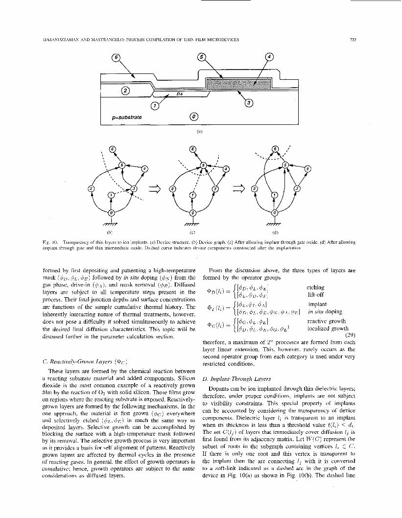
HASANUTLAMAN AND MASTRANGELO: PROCESS COMPILATION OF THIN FILM MICRODEVICES 153
I p-substrate
(b) (c) ( 4
Fig. IO. implant through gate and thin intermediate oxide. Dashed curve indicates device components constructed after the implantation.
Transparency of thin layers to ion implants. (a) Device structure. (b) Device graph. (c) After allowing implant through gate oxide. (d) After allowing
formed by first depositing and patterning a high-temperature mask (40. q 5 ~ . 4 ~ ) followed by in situ doping ( 4 ~ ) from the gas phase, drive-in (4~), and mask removal (4,). Diffused layers are subject to all temperature steps present in the process. Their final junction depths and surface concentrations are functions of the sample cumulative thermal history. The inherently interacting nature of thermal treatments, however, does not pose a difficulty if solved simultaneously to achieve the desired final diffusion characteristics. This topic will be discused further in the parameter calculation section.
C. Reactively-Grown Layers ( @ G )
These layers are formed by the chemical reaction between a reacting substrate material and added components. Silicon dioxide is the most common example of a reactively-grown film by the reaction of 0 2 with solid silicon. These films grow on regions where the reacting substrate is exposed. Reactively- grown layers are formed by the following mechanisms. In the one approach, the material is first grown (4~) everywhere and selectively etched (4~. 4 ~ ) in much the same way as deposited layers. Selective growth can be accomplished by blocking the surface with a high-temperature mask followed by its removal. The selective growth process is very important as it provides a basis for self alignment of patterns. Reactively grown layers are affected by thermal cycles in the presence of reacting gases. In general, the effect of growth operators is cumulative; hence, growth operators are subject to the same considerations as diffused layers.
From the discussion above, the three types of layers are formed by the operator groups
etching lift-off
[ 4 G , $ L * '$E] reactive growth [$D,$Li$E.4G,$E] localized growth
(29)
@G(lr) =
therefore, a maximum of 2" processes are formed from each layer linear extension. This, however, rarely occurs as the second operator group from each category is used under very restricted conditions.
D. Implant-Through Layers
Dopants can be ion implanted through thin dielectric layers; therefore, under proper conditions, implants are not subject to visibility constraints. This special property of implants can be accounted by considering the transparency of device components. Dielectric layer I , is transparent to an implant when its thickness is less than a threshold value t ( l L ) 5 dt. The set G(13) of layers that immediately cover diffusion 1, is first found from its adjacency matrix. Let W ( C ) represent the subset of roots in the subgraph containing vertices 1, E C. If there is only one root and this vertex is transparent to the implant then the arc connecting 1, with it is converted to a soft-link indicated as a dashed arc in the graph of the device in Fig. 10(a) as shown in Fig. 10(b). The dashed line

154 IEEE TRANSACTIONS ON COMPUTER-AIDED DESIGN OF INTEGRATED CIRCUITS AND SYSTEMS, VOL. 15, NO. 7, JULY 1996
defines the subgraph of elements above the diffusion. In order to allow the deposition of these transparent layers to occur prior to the diffusion, the device graph is modified as follows. First, all incoming arcs in the diffusion vertex are extended to all vertices immediately above it. The soft link is removed, and arcs are added from the diffusion vertex to those above the transparent layer blochng the diffusion as in Fig. lO(c). This procedure breaks the mutual order between thin layers and diffusions while maintaining the rest of the component order intact. The procedure is extended to stacked transparent layers by keeping track of a reduced threshold dt = dt - t(Zz) and repeating the procedure iteratively as in Fig. 10(d). If, however, there are several roots in W , the graph modifications are repeated for each root vertex in C. In the flow F, only processes with stacked transparent layers that fully cover the diffusion opening are generated to prevent the formation of a stepped implant.
E. Process Assembly
A process flow may now be assembled as a direct expansion of (12) using (29). This procedure is however overly restric- tive since it does not include the possible self-alignment of device components or the use of multiple masks for the same layer. These two important methods substantially increase the process yield and reduce the overall number of steps. We shall show that these two processing methods are accounted through the permutation, elimination, and expansion of 4 in F.
The process flow 3 is assembled in three phases. First, the operators that define layers ( 4 ~ $1, 4 ~ ; 4.4) are inserted in F. Thus
[ll? 12;. . . , In] * [ 4 D ( l l ) ; dD(12); " . 3 d ) I ( l j ) , ' $ A ( l j ) ; ' ' ' ; d'G(ln)]. (30)
Next, etching steps are inserted. The mutual order between the deposition operators and d ~ ( l i ) is determined by its characteristic mask set Mo(1i). The mask set consists of a collection of openings or gaps gi , j representing the areas where the layer is removed (for positive resists)
Mo(li) = {.9i,l3 gi;2; ' ; g i , k } . (31)
Self-aligned processes are obtained if gaps from different masks are permutated in F followed by reconstruction of M . The gaps and layers hold a specific order. Layers patterned by regular etching must be present before definition, therefore, gi,k % l i . Furthermore, the segment of layer 1, corresponding to gi,k must be visible. The layer visibility is determined by examining the blocking graph of the layer sequence [64], [65]. If this gap is covered by components from layer l;, then gi,k 4 l j . Precedence constraints between ~ ; , k from different mask sets are established when l j > li and g2,k(li) 6 g3,m(Zj) implying that g;,m + g; ,k . These order relations are compactly stored in the LG and GG matrices
Mo( l i ) Mo(Z2) M O ( & ) ll S l , l S l . 2 " ' g l , k S2,1S2,2"'S2,rn "".' S h , l
(32) . . . . . . . . . . . . .
. . . . . .
(33)
Gaps g i , k are next inserted into 3 consistent with this order. Therefore, different gaps for the same layer can be etched at different times. This is in fact required for a large number of device processes. Since the deposition operator order is fixed by the layer order, this procedure is equivalent to merging of two ordered sets [32].
The insertion of g;,k in F takes place according to the matrix order. The procedure uses the same topological sorting, but now with the additional constraint that each gi,k must operate on the corresponding layer. This is determined by the visibility constrains specified in the GG matrix. This condition is dynamically captured efficiently by a modification of the sequencing algorithm. The resulting F is a stream of d D . 4 I . $ k 4 , and si
[d'D(Zl); 91.1. g1.2; ' ' ' ; d'D(12), g2,1, ' ' ' g Z , k , ,9l,k, g1,Z ' ' ' , + gj.l:gj.S."';4I(lj);d'A(lj);'"]. (34)
In (35) , adjacent g;, j operating on the same layer are grouped into corresponding masks M k ( 1 ; ) E Mo(l;)
If layer Zi is patterned by etching using M(1i), the mask is replaced by a corresponding etching operator $E(M (1;))
[ 4 D (ll),d)E (M1 VI)) ,
+ M l ( l j ) , $ I ( Z j ) , 4 A ( l j ) , ' ' '1. (36)
This procedure generates multiple etching steps and corre- sponding lithographic steps for a single layer. If adjacent etching operators operate on different layers of the same material, these in term are condensed into a single etch.
In the last phase of the assembly, the lithography operators 4~ are added to F. At every state in 3, the device outline is determined. If all gaps si,; E Mk(l i ) conform to the exposed components, it may be possible to eliminate the lithography step completely yielding a self-alignment. The resulting F consists of a stream of operators specifying the various processes that the wafer must undergo to fabricate the device. Each of these processes contains a set of parameters which must be calculated.
Ix . DETERMINATION OF SELECTIVE OPERATORS
The idealization of a universally selective a(&) is rarely achievable in practice. Most processes used in VLSI technol- ogy will interact with other layers to certain extent. In general, there exist two types of interactions. Thermal interactions occur when exposes the sample to high temperatures. For deposited layers, these interactions are destructive or

HASANUZZAMAN AND MASTRANGELO: PROCESS COMPILATION OF THIN FILM MICRODEVICES I55
nondestructive. Destructive interactions are a priori detected and eliminated through appropriate changes in the device transitive closure matrix. Nondestructive thermal interactions, however, are easily accounted by considering the cumulative thermal effect of all operators in 3. Thermal interactions are inherently distributed phenomena of particular relevance to diffused layers. A detailed discussion of distributed thermal interactions is found in the flow parameter section.
Chemical interactions occur in general for all 4. For deposi- tion and reactive growth operators, these interactions are either negligible, well known, or unknown, Unknown interactions invalidate a flow. In feasible flows, layer materials are either undisturbed or reacting through a known set of rate equations. For example, the chemical interaction of reactive growth operators is well known while lithographic operators have nearly none. The most significant chemical interactions in a process occur during etching steps. Improper choice of etchants can lead to process failure; therefore, proper etchant selection is essential. Etching operators can be selective to some materials but highly interacting with others. For example, many plasma etchants used for silicon nitride etch do not attack oxide layers but attack polycrystalline silicon aggressively. On the other hand hot phosphoric acid does not attack oxide or silicon but strips resist. To compound these difficulties the response of many etchants on materials is often unknown. Therefore, the task of the compiler is to construct selective $ from an imperfect and incomplete data set.
The precarious knowledge of q5 poses severe restrictions. The first step toward finding selective a's is restricting the possible interactions. The operator set @ ( I z ) forms all com- ponents c, E 1, E x, without disturbing I , 4 l,, I , E xz-l. This causality on I , relaxes the selectivity restrictions since Q2 = @ ( l z , ~ ~ - 1 ) . Chemical interactions are further restricted to components which are exposed to the wafer su$ace. This component subset of 2, forms the outline set I'2 c zZ, hence Q Z = @ ( l t , I ' - l ) . The number of components in r2 is in general small because most device components are separated by uniform passivation dielectric layers. While a good choice of layer order minimizes interactions, these may not be negligible. In etching operators, the etch selectivity quantifier
where R(q5~,1~) is the etch rate of $E on layer I , , is an indication of the operator attack on the outline components. This parameter is related to device yield. In the process expansion, etching operators are selected such that the film is etched at a reasonable rate yet having a negligible attack on other exposed materials. A lower limit on S 2 S,,, is also imposed. If no etchant meets these conditions, the flow is discarded. Experimentally, a value of S,,, = 5 results in good yields. A second consideration in selection is its etching time. Etchants with etching times fitting inside a window
are accepted to assure a reasonable process time. In (38), tmin
is in the order of a few seconds and t,,, of a few hours. The
operator 4~ that best fits this criteria is selected. Similar time limits exist for both deposition and reactive growth operators.
The above procedure chooses a reasonable approximation to a selective operator set as a function of the state Z, and its outline r2. This fact implies that flow operators may change for different intermediate states x, resulting from distinct layer orders. It is the large variety of these orders that in general allows us to find a reasonable @ which matches the information known about operator interactions with x, . Many of the linear extensions are hence discarded, resulting in general in a small design space 2).
X. PROCESS FLOW PARAMETERS
Each of the flow operators q5(12) E 3 contains a set of parameters specific to the attributes of I,. These parameters depend on the type of operator. For example, for a polysilicon deposition process, the SiH4 flow, tube temperature, pressure, and deposition time are some of its parameters.
In view of the complexity of most operators, we have adopted a recipe-based approach. This simplification is nec- essary because many processes are laboratory and machine specific. Furthermore, the operator behavior under widely varying parameter ranges is in general unknown. Recipe pa- rameters however are finely tuned for satisfactory performance through many experiments yielding predictable results. Most recipes are specific with few parameters that can be adjusted. Operator recipes are stored in a database containing general [66] as well as lab specific data.
A. Lithography The lithography recipe consists of a dehydration cycle, resist
application, soft bake, exposure, and hardbake (for etching). The photoresist thickness is determined from the roughness of the surface topography. Good resist coverage is generally found when
1 treqiyt 2 -tstep(r) 3
where tstcp is the maximum step on the surface profile at a particular time. Increasing the resist thickness improves its coverage but degrades the sharpness of the patterns. Therefore, the minimum acceptable thickness is used unless the resist is severely attacked by an etchant. Appropriate spin-speeds, exposure and development times are calculated internally as a function of this thickness.
(39)
B. Deposition and Etch
Deposition and etch recipes characterize all operators in terms of linear deposition and etch rates. The actual times are proportional to the layer thickness and inversely proportional to their rates. The etchant selection is made according to the principles established above maximizing selectivity and fabrication yield.
C. Reactive Growth The thickness of reactively-grown layers is affected by
subsequent temperature steps. For example, in thermal oxide

156 IEEE TRANSACTIONS ON COMPUTER-AIDED DESIGN OF INTEGRATED CIRCUITS AND SYSTEMS, VOL. 15, NO. I, JULY 1996
growth, the field oxide thickness is changed when the gate oxide is regrown and invariably at any time that the oxide surfaces are exposed to a high temperature oxidizing environ- ment. For thermal oxidation, the thickness growth of the oxide layer from U , to its final state un+l by a temperature cycle at temperature T, and At, duration is
where B and BIA are the quadratic and linear rate constants [l]. For other type of reactions, (40) has the general form
(41) Un+l = f (%; Tn, At,).
Therefore, interacting reactive growth steps are solved si- multaneously to achieve all the desired thicknesses at the process end. Suppose the process contains k interacting re- active growth processes with k final thicknesses u; . f . At any given time, ui are easily calculated if (41) is rewritten in vector form as
(42) fin = i(fin+l, Tn, At,)
ii = (u1, U a , ' ' . , U k ) .
where
(43)
Equation (42) is solved by noting that the ith layer is only affected by subsequent j 2 i steps. Therefore, by causality, the last reactive growth step is
T
( U k ) k = f ( ( % ) k & l > T k & l > Atk-1) (44)
since ( u k ) k = u k , f and ( ~ k ) k - l = 0 are both known, then Atk-1 is solved from (40)
Ah-1 = h ( U k , f , 0, Tk-1) (45)
and the growth of layer IC no longer needs to be considered. Since Atk-1 is now known the thicknesses for all layers i < k at the k - 1 step are determined from (42)
Equations (45) and (46) form the basis for a backward re- cursion where each At, is found from At,-, to At,. This method of solution is very general and can be applied when only numerical forms of h ( ) exist.
The above solution procedure is first carried out on a fixed set of temperatures. If the At, are too short or long, the temperature for these steps are increased or decreased correspondingly to fit At, within an acceptable time window. If any At is negative, the process is invalidated.
D. Diffusion and Implantation
Doped layers are affected by all temperature cycles in the process; therefore, all diffusion and implantation parameters are calculated simultaneously. In the present implementation, diffused layers are accepted in terms of two parameters: junction depth xj and surface (top) concentration No. The junction depth specifies the diffused region thickness. The
parameters that must be calculated are the implant dose Q and energy El , diffusion temperature T , and diffusion time t .
As an initial estimate, diffusions are approximated as gaus- sians profiles, and implants are considered to be shallow. Therefore, junction depths are computed from intersection be- tween two gaussians or a gaussian and a constant background. The junction depth constraints thus form a set of equations
These relations yield the final straggle ( P T ) ~ for each profile with surface concentration Ni. The gaussian straggle is the cumulative Dt product of all successive steps
3 3
and Dz(T3) is the diffusion coefficient for the ith diffused layer [ l ]
(49)
where we have assumed a simple Ahrrenius form for D. The buildup of (,&), occurs in small increments distributed throughout the process as in (48).
In general, each diffusion is first formed by an implantation step followed by an intentional drive-in, and any other subse- quent high-temperature steps. The diffusion schedule solver of the compiler manipulates the temperature, time of the drive-in cycles, and implant dose to achieve desired junction depth and surface concentration specifications. Equation (48) is rewritten in terms of partial increments (p,), due to each dnve-in
3=,
where N is the number of drive-in annealing steps, Ci accounts for all fixed thermal cycles following diffusion i , and Q is a ratio of diffusion coefficients
The formulation of (50) is convenient since it removes the drive-in temperatures from the unknown. The above equation can be rewritten in the following matrix form
&[5?]4 + c = j T . (52)
Equation (52) requires an appropriate selection of T. Our implementation uses an initial choice of 1000 "C for all steps. Since the ith diffusion is only affected by subsequent steps j 2 i, then matrix 6 is upper triangular, and is solved easily by back substitution. If any /?, is negative, the process is discarded. If all p p 2 0, corresponding drive-in times and implant doses are calculated from
(53)

HASANUZZAMAN AND MASTRANGELO: PROCESS COMPILATION OF THIN FlLM MICRODEVICES 757
While this procedure yields, in general, a feasible diffusion schedule, the diffusion times may not be adequate. In order to assure reasonable drive-in times, these must fit within an acceptance time window. If the corresponding times are too long or too short, T, is increased or decreased and (52) is recalculated.
The gaussian approximation gives good values for Q and t in low concentration diffusions when the material remains essentially intrinsic at the diffusion temperature. However, in high concentration diffused layers, the diffusion coefficient is a function of concentration and dopant migration is affected by local electric fields. In this regime, the concentration of species Ct obeys [671, [681
where f i is the electric field enhancement factor
0.5N, fi =
[(0.5Cnet)2 + $1 o.5
and n
(54)
(55 )
i=l
In this regime, the gaussian approximation is a very crude guess to the actual profile. This difficulty, however, is elimi- nated if diffusion profiles are solved numerically. Numerical solution of (54)-(56) yields an expression
(57)
subject to similar causality constraints as those present in the treatment of reactive growth. Diffusion k is primarily affected by subsequent drive-in cycles j 2 k , and somewhat affected by electric fields induced by profiles of diffusions j < k . If a good guess of the profiles is available, most of the noncausal contribution to the motion of diffusion 3 will be accounted for. Therefore, errors contributed by this approximation are, in general, minor perturbations which can be treated as second-order corrections. The diffusion solver thus starts with a gaussian based guess for the profiles and iteratively refines this guess until convergence is achieved.
In this scheme, Q and t in (57) are solved using a recursive backward loop with noncausal corrections in a forward loop as shown in Fig. 11. The entire procedure is repeated until appropriate convergence is achieved. In the first backward recursion, the initial profiles are assumed to be gaussians. The dose and diffusion time ( Q k - 1 , t k - - l ) for the last kth diffusion are solved numerically to conform to z3,k. and Nk specifi- cations. Next, the k - 1 diffusion parameters ( Q k - 2 , t k - z )
are solved with the updated ( t k - 1 , Q k - 1 ) and corresponding numerical profile. The backward recursion is continued until (Qo, t o ) is found. An inherent error exists in these parameters due to the approximate nature of the initial guesses. In the forward loop, new numerical guesses are calculated using the updated (QJ, t J ) . These new guesses are used again in the backward loop to obtain second-order corrections. The backward-forward recursion loop is repeated until errors in
xJ and NJ in the forward loop are negligible. The main virtue of this scheme is that at any given time, parameters for a single diffusion layer are determined.
The calculation of (Q, , t J ) for each diffusion drive-in step is the most computationally intensive part of the procedure. Numerical solutions of (54) provide (NJ,x,) in terms of (Q,,tJ), but not vice versa. Therefore, correct (Q,. t J ) are arrived through iterative error minimization in tZ3 = (zJ - z,,f), and t~~ = ( N , - N f ) , where ( N f . zJ , f ) are its desired values. Several iteration schemes for (Q,, t,) have been imple- mented. These include a globally convergent Newton method, a contraction mapping, and a Bayesian global optimization [69]. The most robust scheme is a globally convergent Newton method described in [70]. The main disadvantage of Newton- type codes is in the numerical evaluation of gradients which may confuse the solver ending the iteration in a local minima rather than a root. The fastest convergence is accomplished by the gaussian-based iteration
Equation (58) is, in general, a contraction which converges very quickly. In general, approximately 5-10 iterations are required for convergence in each diffusion. Once the first diffusion of the process is reached, the forward loop is initiated again with these new values. Typically 5-25 backward-forward loops are necessary for full convergence within 3% of speci- fications. Since the existence of solutions is not warranted, if both algorithms fail, the Bayesian global optimizer finds the best possible fit. The Bayesian scheme constructs a probability density of the cost function from each evaluation. This scheme is particularly efficient for the computationally expensive cost functions considered here.
E. Yield and Figure of Merit
The process yield is affected by both deterministic and random factors. Systematic errors reduce the process yield through known deterministic nonuniformities in the process operators causing certain areas of the chip to fail. Yield is also reduced by the presence of random distribution of point defects on the wafer as well as random variations in the process operators. Random effects on yield have been studied by numerous authors [71]-[73] for fine tuning of well-known semiconductor processes. Since the compiler generates a large number of tentative processes with limited selectivities, we have adopted to estimate the deterministic yield instead.
The most important deterministic factor on yield is the loading effect. The loading effect results in nonuniformities in the radial distribution of deposition and etch rates caused by a balance between diffusion of fresh reactants and depletion of deposited or used species. The loading effect is primarily destructive during etching where it is manifested as a prop- agating front delineating areas of the wafer where the etch is not complete. The actual front propagation depends on the density of patterns on the wafer, but in most instances, the

758 IEEE TRANSACTIONS ON COMPUTER-AIDED DESIGN OF INTEGRATED CIRCUITS AND SYSTEMS, VOL. 15, NO. 7, JULY 1996
initial
I
; calculate ; gaussians ; I I _ _ _ _ _ _ _ _ _ _ _ _ _ _ _ _ I
forward correction
main loop backward loop
Fig. 1 1. Forward-backward iterative solution of simultaneous diffusions
front propagates from the outer edge toward its center forming a noticeable “bullseye” pattern.
If the reacting species diffuses from the wafer outer edges, and if the depletion is uniform in radial coordinates, the rate R is approximately determined by
2d2R dR r --+r--
dr2 dr (59)
with R(r,) E R, = Ro where rw is the wafer radius. In the above equation, L d is the characteristic depletion length
D is the species diffusivity, Ro the reaction velocity, and S the thickness of a boundary layer above it. The solution of (59) is
where lo() is the zero order modified Bessel function of the first kind.
If a uniform film of thickness t f is etched, the rate R(rTU) is larger than that at the center R(0); therefore, the film is clearing from the outside of the wafer toward its center. On the cleared areas, the films beneath are being attacked by the etchant with a selectivity S. We can now define a cutoff radius r, over which the fraction of overetched film is below a critical value a,. Areas where the overetch fraction exceeds a , are lost as shown in Fig. 12. Therefore, the nonuniformity in R(r) is
responsible for a systematic yield loss. In order to clear the film on the entire wafer, an annular area near the wafer outer edge will be overetched. The overetch time is a function of radius
therefore, the fraction of film beneath etched away is
where t b is the thickness of the film below. The cutoff radius corresponding to a, is
where a = (actb/ts) . The systematic yield for the etching step is then
for all layers exposed and beneath the etched layer. Equation (64) can be used for all etching steps in the process in a sequence providing an overall systematic yield for the entire process. Under normal conditions, a small overetch time is always used to assure that the top film is completely gone. Therefore

H A S A N U Z A M A N AND MASTRANGELO. PROCESS COMPILATION OF THIN FILM MICRODEVICES 759
etching is none. In this implementation, this is accounted as a gradual degradation of the FOM for every instance an alignment is required.
XI. SOFTWARE IMPLEMENTATION
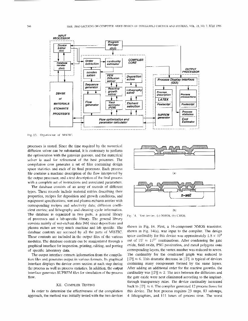
The structure of MISTIC is shown in Fig. 13. The compiler consists of four major software modules: a) an input device builder, b) a compilation core, c) an output processor, and d) a database of materials and laboratory processes. The four parts are supervised by a program manager which controls the flow of data among the various parts.
The input to the compiler core is generated by the device builder. This tool consists of a graphical user interface for drawing and editing device cross sections using the materials stored in the database. In addition to regular graphical editing
t
I I I I
(b)
Fig. 12. Loading effect decreases the yield. (a) Top view of wafer etch-front during etching. (b) Wafer cross section. Radius I‘, determines the region of the wafer with good devices.
where E is a deliberate overetch fraction of the total etching time, typically set between IO-25%. Since I ,J(z) M 1 + x2/4, then for each etching step
whichever of these is the lowest. While U, is not a true indication of the overall yield Yt, it is an upper bound hence a suitable figure of merit (FOM). For a process with k etching steps
The figure of merit indicates the precision over which patterns can be defined due to finite selectivities. The figure of merit has a maximum of one and can only decrease with low selectivity etching processes.
A second factor affecting the figure of merit is the number of alignments performed in the sample. Processes with self- aligned features are not subject to registration errors; therefore, their figure of merit is higher than that of processes where there
commands, the device builder has special drawing routines for quick calculation of conformal outlines and merging of common device macros (such as MOSFET’s). After comple- tion of editing, device structures are saved under a common format. The current implementation of the device builder accepts Manhattan geometry. Future work will include the incorporation of polygonal geometries.
The compilation core consists of several submodules. First, device cross-section files are read and the component order is determined thus generating adjacency and transitive closure matrices. These matrices are examined by a cardinality estima- tor. If 11211 is too high, the device components are recursively condensed until an acceptable limit is reached.
The condensed device is next sequenced using a low- memory budget modification of Steiner’s algorithm [56]. For each of the generated sequences, the flow generator generates the LG and GG matrices of (32)-(33) necessary for the flow expansion. The flow generator then inserts the gaps in the layer sequence consistent with these matrices. Typically, more than one flow is generated for a given sequence. Gaps are condensed into masks, and lithographies are inserted when self alignment is not possible. The output of the flow generator is a flow with all the instructions necessary to fabricate the sample. The parameters of the flow are next determined.
The parameter calculator interacts with six other submod- ules performing many of the functions outlined in [4]. First specific etchants are selected for all etching steps. The device outline and the list of materials which are exposed during and after each etch is calculated. The etchant selection module scans the database for etchants that attack the film under consideration within a specified time window yet having the highest selectivities possible respect to the rest of the exposed materials on the outline and beneath it. Deposition parameters, lithography parameters, and figure of merit are next calculated from lab-dependent recipes stored in the database. The param- eter calculator also interacts with the reactive growth solver that determines the reactive growth schedule. The diffusion doses, times, and temperature are determined by a 1-D finite element diffusion solver implementing the forward-backward iteration described above for each different device zone.
The finally assembled process is next graded by a process optimizer in terms of the figure of merit and process cost. A design space of a small, user-specified number of best
760 IEEE TRANSACTIONS ON COMPUTER-AIDED DESIGN OF INTEGRATED CIRCUITS AND SYSTEMS, VOL. 15, NO. 7 , JULY 1996
INPUT PROCESSOR
I DBASE
I MA T€R/A LS I ETCHANTS
PROCESSES * 4 ,
Flow optimization and I ,
parameter calculator
C. generator I ,
I I _ I ,
: _ _ _ _ _ _ _ _ _ _ _ _ _ _ _ _ _ _ _ _ _ _ _ _ _ _ _ _ _ _ _ _ _ _ _ _ _ I ‘ - - - - - - - - - - - - - - - - - - - - - - - - - - A
Fig. 13. Organization of MISTIC.
processes is stored. Since the time required by the numerical diffusion solver can be substantial, it is customary to perform the optimization with the gaussian guesses, and the numerical solver is used for refinement of the best processes. The compilation core generates a set of files containing design space statistics and each of its final processes. Each process file contains a machine description of the flow interpreted by the output processor, and a text description of the final process with a complete set of instructions and associated parameters.
The database consists of an array of records of different types. These records include material entries describing their properties, recipes for deposition and growth conditions, and equipment specifications; wet and plasma etchants entries with corresponding recipes and selectivity data; diffusion coeffi- cient entries; and lithography and cleaning cycle information. The database is organized in two parts, a general library of processes and a lab-specific library. The general library consists mainly of wet-etchant data [66] since depositions and plasma etches are very much machine and lab specific. The database contents are accessed by all the parts of MISTIC. These contents are included in the output files of the various modules. The database contents can be manipulated through a graphical interface for inspection, printing, editing, and porting of specific laboratory data.
The output interface extracts information from the compila- tion files and generates output in various formats. Its graphical interface displays the device cross section at each step during the process as well as process statistics. In addition, the output interface generates SUPREM files for simulation of the process flow.
XII. COMPILER TESTING
In order to determine the effectiveness of the compilation approach, the method was initially tested with the two devices
I I A I
[ n-we// J
(b)
Fig. 14. Test devlces. (a) NMOS. (b) CMOS
shown in Fig. 14. First, a 16-component NMOS transistor, shown in Fig. 14(a), was input to the compiler. The design space cardinality for this device was approximately 1.8 x lo9 out of 15! N 10l2 combinations. After condensing the gate oxide, field oxide, PSG passivation, and metal polygons onto corresponding layers, the vertex number was reduced to seven. The cardinality for the condensed graph was reduced to 112)11 w 6. This dramatic decrease in IlDIl is typical of devices containing many components formed by the same layers. After adding an additional order for the reactive growths, the cardinality was ll2)Il M 2. The arcs between the diffusions and the gate oxide were next eliminated according to the implant- through transparency rules. The device cardinality increased back to IlDIl 6. The compiler generated 12 process flows for this device. The best process requires 23 steps, 83 substeps, 4 lithographies, and 111 hours of process time. The worst

HASANUZLAMAN AND MASTRANGELO: PROCESS COMPILATION OF THIN FILM MICRODEVICES
I I I I I I I - MISTIC
SUPREM - - - --
-
- - - -
NMOS -
~
761
PSG
Poly
Dry Oxide
P+
Aluminum
Wet Oxide
N-well
&
Fig. 15. 8-vertex condensed CMOS digraph
process requires 34 steps, 7 lithographies, and 119 hours of process time. The best process included the localized oxidation of the field oxide, self alignment for the source and drain diffusions, and the same mask for the contact holes etching through the PSG passivation layer and gate oxide indicative of the mask reconstruction and elimination scheme implemented in the compiler.
The 29-component CMOS structure of Fig. 14(b) was next input to the compiler. The initial cardinality estimate was 11211 M 2 x After 22 condensations, the cardinality was reduced to IlDIl M 46. The 9-vertex condensed graph is shown in Fig. 15. Additional orders were introduced between the reactive growth and the well and source diffusions yielding 11Dl1 M 3. After modification of the graph for implant-through layers, the cardinality increased to 11211 M 29. The compiler generated 18 complete CMOS processes. The best process requires 36 steps, 85 substeps, 7 lithographies, and 278 hours of process time. The worst process requires 44 steps, 105 substeps, 9 lithographies, and 284 hours of process time. Due to the computational demands of the diffusion schedule solver, the initial processes for both devices are initially generated with the gaussian guesses. Accurate dopant doses and diffusion times are solved only on the best process. Fig. 16 shows comparison of doping profiles for the CMOS structure in both the NMOS and PMOS devices at the source calculated by the compiler FEM diffusion solver, and those from SUPREM-I11 using the MISTIC compiler specified doses, temperatures, and time. The diffusion solver was able to find the implant doses, drive-in temperatures and times to meet the specified junctions and surface concentrations for three simultaneous diffusions within 2% of specifications. There is a small difference in the diffusion profiles provided by MISTIC and SUPREM due to their slightly different diffusion coefficient models. These discrepancies are easily eliminated through matching of the internal models.
Fig. 16 shows simultaneous diffusion profiles for the source/drain regions of both MOSFET's in good agreement with SUPREM-I11 simulations. The diffusion drive-in cycles ranged from 1175 OC for the N-well for 4.5 h to 1000 OC for 2 h for the boron p+ source drain and 1000 "C for the phosphorus n+ diffusion.
- le+19 - le+18 - le+17 - le+16 - le+15 - le+14 - le+13 -
I I I I I I I I
0.00 1.00 2.00 3.00 4.00 5.00 6.00 (a)
le+19 y~ le+18 8 le+17 - le+16
le+15 c, le+14 h E le+13 Q)
le+12
3 le+ll le+10
h
.CI
c)
1 e+09 t I ' 1 1 0.00 1.00 2.00 3.00 4.00 5.00 6.00
Depth (W) (b)
Fig. 16. (a) PMOS well and source junctions. (b) NMOS source junction.
One of the most attractive virtues of the systematic com- pilation procedure is that its methods are independent of the number of components in the device; hence, the compiler is capable of handling very complex structures. The compiler was also tested with the double metal twin-well BiCMOS structure with its associated 64-vertex graph shown in Fig. 17. Despite its initial 135 order constraints, the cardinality for this structure is an immense number 11D11 M 5 x After 44 condensa- tions, the graph is reduced to the 20-vertex graph shown in Fig. 18. Despite its 47 order relations, the cardinality for this graph is approximately IlDll 2.6 x lo7. Due to the very large number of processes, additional constraints are added between its three reactive growths reducing 11D11 M 7 x 10' and its eight diffusions 11211 M 81. The cardinality increases to 11Dl1 M 860 after the graph modification for implant- through layers. It is found that for very large structures, the order between the diffusions must be included to complete the process assembly in a finite time. For example, if there is no a priori order set for its eight diffusions, the compiler must calculate each of its 8! = 40320 possible permutations. The a priori order is easily established by assuring that for any two given diffusions, the ,klp are positive. The vector C in (52) can only make ,!& decrease thus further restricting the diffusion orders. After proper selection of etch steps, the

162 IEEE TRANSACTIONS ON COMPUTER-AIDED DESIGN OF INTEGRATED CIRCUITS AND SYSTEMS, VOL. 15, NO. I, JULY 1996
I I
Fig. 17. BiCMOS test structure and its 64-vertex graph
PECVD oxide 1
Poly 2 POI
P-well Wet oxide 2
n+
Dry oxide 1 Wet oxide 1 p+ P+ con' "+ Emitter
p Base n+ collector N-well
Fig. 18. 20-vertex condensed BiCMOS graph
compiler generated 168 BiCMOS processes. The best process contains self-alignments for the NMOS and PMOS source and drains as well as the bipolar transistor base diffusion. This process requires 90 steps, 213 substeps, 18 lithographies, and 723 hours of process time. Most of this time is spend in the transit required by its eight out of lab implants. The worst process requires 106 steps, 253 substeps, 22 lithographies, and 747 hours of process time. The process compiler predicts the correct order of first well, base, collector contact, base contact, emitter, and source diffusions as well as the correct order of reactive growths with first the passivation wet oxide, next the bipolar intermediate oxide, and last the gate oxide growth.
The effectiveness of the diffusion schedule solver was tested for the BiCMOS device shown above. The backward- forward diffusion solver converged to the correct specifications within 3% after five loops. The resulting profiles of the source/drain regions of the NMOS and PMOS transistors with their corresponding wells are shown in Fig. 19. The
le+20 - le+19 - le+18 -
8 le+17 - - le+16 - E le+15 - 0 '3 le+14 - $ le+13 - 8 1e+12 -
- MISTIC 3 SUPREM
xj=3.0Pm /
0 U le+10 PMOS 1
le+09 tI ,-/ 0.00 1.00 2.00 3.00 4.00 5.00
1 e+20 - le+19 I E le+18 U le+17
le+16 5 le+15
le+14 2 le+13 8 1e+12
le+11 le+10
rn
W
.- c,
I I I I
le+09 1, -, I] 0.00 ' 1.00 2.00 3.00 4.00 5.00
Depth ( P m )
Fig. 19. BiCMOS PMOS and NMOS source and well areas
net concentration of the dopants in the bipolar transistor is shown in Fig. 20. Note the good agreement of MISTIC with SUPREM-I11 simulations. The least important diffusions for the base and collector contacts also agree within target specifications but are not shown here. Drive-in temperatures ranged from 1175 "C for the 3-pm boron well to 950 "C for the boron source of the PMOS transistor. The process statistics for the NMOS, CMOS, and BiCMOS structures are summarized in Table I. Since the gaussian guesses are used to determine an order between the various diffusions, in some instances, the diffusion solver times are not as short as they could be. A more precise fast approximation for the diffusions is required. For optimal performance, the order can be a priori established using the nonlinear diffusion solver at a moderate computational expense.
XIII. CONCLUDING REMARKS A method for the automatic generation of fabrication
process sequences of thin film devices has been developed. The method uses a 2-D device description as input, and topological sorting techniques to find feasible flows for the device. It is shown that the set of feasible flows is large; hence, an optimal flow is selected which maximizes the device yield. The method was implemented in a compiler program which

HASANUZZAMAN AND MASTRANGELO: PROCESS COMPILATION OF THIN FILM MICRODEVICES 763
le+19
le+l8
le+17
le+16
le+15
le+14 I I I I
0.00 1.00 2.00 3.00 4.00 5.00
Depth (Pm>
Fig. 20. BiCMOS npn bipolar transistor concentration profile.
TABLE 1 SUMMARY OF COMPILED PROCESSES
Device 1 Components 1 Proccsscs 1 S/A 1 Masks 1 Total steps
NMOS 16 12 4 83 CMOS BiCMOS
uses a graphical interface to input the device cross section and outputs the process flow data. The fabrication process flow is described by fundamental processing steps as deposition, lithography, etching, reactive growth, and diffusion. The method was successfully applied to the compilation of NMOS, CMOS, and double metal twin-well BiCMOS structures.
The rigorous theoretical basis of the compiler provides a sound framework for the addition of numerous improvements. The current version treats sacrificial layers rudimentarily as regular deposited layers in the device structure. These, how- ever, can be automatically formed in a variety of ways. It is not yet clear, however, which one of them is the most suitable for process design applications. The binary relation approach works for most structures, it is primarily a “memoryless” synthesis method since it only forms layers that are present in the original device cross section. Intermediate layer formation is currenly associated with specific operators inserted in process expansion logic. Additional order relations can also be added based upon the etchant selectivities and vis- ibility constraints which may speed up the sequence expansion significantly. This is of particular relevance to very complex structures. The current compiler version also lacks some of the features available in common simulation tools. In particular, the compiler has no provision for selecting an adequate implant energy. In this implementation, these energies are fixed, and the initial profiles are assumed as truncated gaussians. These and many other refinements will be included in future versions.
ACKNOWLEDGMENT
The authors wish to thank L. Mockus for providing the source code of the Bayesian optimizer. They also wish to thank S. B. Crary for numerous helpful discussions.
REFERENCES
S. M. Sze, VLSI Technology. K. Lee, “SIMPL-2 simulated profiles from the layout-Version 2,” Ph.D. thesis, Univ. California, Berkeley, 1985. S. D. Senturia, R. M. Harris el al., “A computer-aided design system for microelectromechanical systems (MEMCAD),” IEEE J. Microelec- tromechanical Syst., vol. 1, pp. 3-13, 1992. J. S. Wenstrand, H. Iwai, and R. W. Dutton, “A manufacturing oriented environment for synthesis of fabrication processes,” in IEEE Int. Con$ CAD, 1989, pp. 276-379. C.-Y. Fu, N. H. Chang, and K.-K. Lin, “Smart integrated circuit processing,” IEEE Trans. Semiconduct. Manufiict., vol. 2, pp. 15 1-158, 1989. R. T. Howe, “Polysilicon integrated microsystems: Technologies and ap- plications,” in Transducers’ 95: Proc. 8th Int. Conf Solid-State Sensors Act., Stockholm, Sweden, June 1995, pp. 43-46. C. Lu, M. Lemkin, and B. E. Baser, “A monolithic surface microma- chined accelerometer with digital output,” in Proc. IEEE Int. Solid-State Circuits Conf, San Francisco, CA, Feb. 1995, pp. 160-161. D. S. Boning, M. B. Mcllrath, P. Penfield, and E. M. Sachs, “A general semiconductor process modeling framework,” IEEE Trans. Semiconduct. Manufact., vol. 5 , pp. 266-280, 1992. F. Harary, R. Z. Norman, and D. Cartwright, Structural Models: An Introduction to the Theory c$ Directed Graphs. New York: Wiley, 1965. G. D. Battista and R. Tamassia, “Algorithms for plane representations of acyclic digraphs,” Theor. Comp. Sci., vol. 61, pp. 175-198, 1988. R. Tamassia and J. Vitter, “Parallel transitive closure and point location in planar structures,” Siam J. Comput., vol. 20, pp. 708-725, June 1991. P. Rosenstiehl and R. E. Tarjan, “Rectilinear planar layouts and bipolar orientations of planar graphs,” Discrete Comp. Geom., vol. I , pp. 343-353, 1986. B. Dushnik and E. W. Miller, “Partially ordered sets,” Am. J. Math., vol. 63, pp. 600-610, 1941. P. C. Fishburn, Interval Orders andInterva1 Graphs. New York Wiley, 1985. L. Budach, Algebraic and Topological Properties of Finite Particilly Ordered Sets. Leipzig: Teubner, 1988. I. Rival, Ordered Sets. ~, Algorithms and Order. Dordrecht: Kluwer, 1989. W. T. Trotter, Combinatorics and Partially Ordered Sets. Baltimore, MD: Johns Hopkins University Press, 1992. R. A. Brualdy and H. J. Ryser, Combinatorial Matrix Theory. New York: Cambridge Univ. Press, 1991. K. H. Kim, Boolean Matrix Theory and Applications. New York: M. Dekker, 1982. R. A. Brualdy and H. J. Ryser, A Survey of Finite Mathematics. New York: Cambridge Univ. Press, 1991. A. Kaufmann, Graphs, Dynamic Programming, and Finite Games. New York: Academic, 1967. D. E. Knuth and J. L. Szwarcfiter, “A structured program to generate all topological sorting arrangements,” Injo. Proc. Letters, vol. 2, pp. 153-157, 1974. E. Szpilrajn, “Sur I’extension de I’ordre partiel,” Fund. Math, vol. 60, pp. 175-186, 1930. N. Linial, “Hard enumeration problems in geometry and combinatorics,” SIAM. J. Alg. Disc. Meth., vol. 7, pp. 331-335, Apr. 1986. S. G. Mohanty, Lattice Paih Countings and Applications. New York: Academic, 1979. I. Rival, “Linear extensions of finite ordered sets,” Annals Discrete Math., vol. 23, pp. 355-370, 1984. G. R. Brightwell, “Linear extensions of infinite posets,” Discrete Maih- ematics, vol. 70, pp. 113-136, 1988. M. Pouzet and I. Rival, “Which ordered sets have a complete linear extension?’ Can. J . Math., vol. XXXIII, pp. 1245-1254, 1981. V. Bouchitte and M. Habib, “NP-completeness properties about linear extensions,” Order, vol. 4, pp. 143-154, 1987. G. R. Brightwell and P. Winkler, “Counting linear extensions is NP- complete,” in Proc. Twenty-Third Annual ACM Symp. Theory Comput., 1991, pp. 175-181. M. D. Atkinson and H. W. Chang, “Computing the number of mergings with constraints,” Info. Process. Letters, vol. 24, pp. 289-292, 1987. M. Dyer, A. Frieze, and R. Kannan, “A random polynomial time algorithm for approximating the volume of convex bodies,” in Proc. Twenty-First Annucil ACM Symp. Theory Comput., 1989, pp. 375-381. D. Applegate and R. Kannan, “Sampling and integration of near log- concave functions,” in Proc. TwenpThird Annual ACM Symp. Theory Cornput., 1991, pp. 156-163.
New York: McGraw-Hill, 1988.
Boston, MA: Kluwer, 1981.

764 IEEE TRANSACTIONS ON COMPUTER-AIDED DESIGN OF INTEGRATED CIRCUITS AND SYSTEMS, VOL. 15, NO. 7, JULY 1996
[35] S . W. Director and G. D.Hatchel, “The simplicial approximation ap- proach to design centering,” IEEE Trans. Circuits Sysr., vol. CAS-24, pp. 363-372, 1977.
[36] H. S. M. Coxeter, Regular Polytopes. [37] V. Bryant, Aspects of Combinatorics. New York: Cambridge Univ.
Press, 1993. 1381 M. Marcus, A Suwey of Finite Mathematics. New York: Dover, 1993. [39] M. Marcus and H. Minc, A Suwey of Matrix Theory and Matrix
Inequalities. New York: Dover, 1992. [40] W. Wan-di, “Permutations with restricted positions and k-permanent,”
Acta Math. Appl. Sinicu, vol. 6, pp. 177-182, 1983. 1411 H. Minc, Permanents. Reading, MA: Addison-Wesley, 1978. 1421 N. Alon, J. H. Suencer, and P. Erdos. The Probabilistic Method.
New York: Dover, 1973.
New - - York: Wiley, 1692.
r431 B. Goroi, R. Yuen, and C. H. Mastrangelo, “The automatic synthesis of - planar fabrication process flows for surface micromachined devices.” in Proc. MEMS, h t . Con$ Microelectromechanical Sq’st., 1994, pp. 153- 157.
[44] D. J. Kleitman and B. L. Rothschild, “Asymptotic enumeration of partial orders on a finite set,” Trans. Amer. Math. Soc., vol. 205. pp. 205-221. 1975.
[45] -~ “The number of finite topologies,” in Proc. Amer. Math. Soc.. vol. 25, 1970, pp. 276-282.
[46] R. L. Davis, “The number of structures of finite relations.” in Proc. Amer. Math. Soc., vol. 4, 1953, pp. 486495.
[47] K. K. Butler, “The number of partially ordered sets,” J. Comb. Theor., vol. 13, pp. 276-289, 1972.
[48] F. Harary, “The number of linear, directed, rooted and connected graphs,” Trans. Amer. Math. Soc., vol. 78, pp. 445463. 1955.
[49] M. H. El-Zahar, “Enumeration of ordered sets,” in Algorirhms and Order, 1. Rival, Ed.
[SO] J. Neggers, “Representations of finite partially ordered sets,” J. Combin..
1511 R. P. Stanley, “Ordered structures and partitions,” Memoirs Amer. Marh.
Dordrecht: Kluwer, pp. 327-352, 1989.
vol. 3, pp. 113-133, 1978. . -
sec., vol. l i s , pp. 1-102, 1972. ~
1521 A. D. Kalvin and Y. L. Varol. “On the generation of all touological I . . - - sortings,” J. Algorithms, vol. 4, pp. 150-162, 1983.
[53] A. B. Kahn, “Topological sortings of large networks.” Comm. ACM, vol. 5 , pp. 558-562, 1962.
1541 D. E. Knuth, The Arl ofcomputer Progrumming, vol. 1. Reading, MA: Addison-Wesley, 1968.
r551 Y. L. Varol and D. Rotem. “An algorithm to generate all to~ological - sorting arrangements,” Comput. J., vol. 24, pp. 83-84. 1981. G. Steiner, “An algorithm to generate the ideals of a partial order.“ Operations Res. Letters, vol. 5, pp. 317-320, 1986. A. V. Aho, M. R. Garey, and J. D. Ullman, “The transitive reduction of a directed graph,” SIAM J. Comput., vol. 1, pp. 131-137, 1972. E. M. Reingold, J. Nievergelt, and N. Deo, Combinatorial Algorithms: Theory and Practice. Englewood Cliffs, NJ: Prentice-Hall, 1977. R. Tarjan, “Finding dominators in directed graphs,” SIAM J . Comput., vol. 3, pp. 62-89, 1974. A. Nijenhuis and H. S. Wilf, Combinatorial Algorithms. New York: Academic, 1975. M. C. Er, “A parallel computation approach to topological sorting.” The Comput. J., vol. 26, pp. 293-295, 1983. P. Chaudhuri, “Fast parallel algorithms for a class of graph problems.” Jr. Comb. In$ Syst. Sci., vol. 12, no. 1, pp. 51-65, 1987. K. Culik and I. Fris, “Topological transformations as a tool in the design of systolic networks,” Theor. Comput. Sci., vol. 37, pp. 183-216, 1985. E. Welzl, “Constructing the visibility graph for 77-line segments in O ( n 2 ) time,” Inform. Process. Letters, vol. 20, pp. 167-171, 1990. S. Foldes, I. Rival, and J. Urrutia, “Light sources, obstructions and spherical orders,” Discrete Mathematics, vol. 102, pp. 13-23, 1992.
[66] J. L. Vossen, Thin Film Processes. [67] B. R. Penumalli, “A comprehensive two dimensional VLSI process
simulation program, BICEPS,” IEEE Trans. Electron Devices, vol. ED- 30, pp. 986-992, 1983.
[68] C. P. Ho, J. D. Plummer, S. E. Hansen, and R. W. Dutton, “VLSI process modeling-SUPREM 111,” IEEE Trans. Electron Devices, vol.
[69] J. Mockus, Bayesian Approach to Global Optimization: Theory and Applications. Boston, MA: Kluwer, 1989.
[70] W. H. Press, B. P. Flannery, S. A. Teulosky, and W. T. Vetterling, Numerical Recipes in C.
[71] A. J. Strowjas, Statistical Design of Integrated Circuits. New York: IEEE. 1987.
1721 S. W. Director and W. Malv. Statistical Aaaroach to VLSI. New York:
New York: Academic, 1978.
ED-30, pp. 1438-1453, 1983.
New York Cambridge Univ., 1993.
‘. - - North-Holland, 1994.
[73] D. Moore and H. Walker, Yield Simulation For Integrated Circuils. New York: Kluwer, 1987.
Mohammed Hasanuzzaman received the B.S.E degree in electrical and electronic engineenng from the Bangladesh University of Engineering and Tech- nology (BUET), Dhaka, Bangladesh, in 1991, and the M S E. degree in electrical engineering from the University of Michigan, Ann Arbor, in 1995 He is currently working toward the Ph D degree under the supervision of Professor Carlos H Mastrangelo.
He was a lecturer with the Department of Com- puter Science and Engineering, BUET from 1991 to 1993 Since July 1994, he has been working in the
de\ elopment of planar process compilation methods and their implementation in MISTIC (Michigan Synthesis Tools for Integrated Circuits) His research interests include application of numerical techniques to process and device design, TCAD, and automation of IC fabrication
b
Carlos H. Mastrangelo (S’84-M’90) was born in Buenos Aires, Argentina, in 1960. He received the B.S., M.S., and Ph.D. degrees in electrical engineering and computer science, all from the University of California, Berkeley, in 1985, 1988, and 1991, respectively.
He was with the Scientific Research Laboratory of Ford Motor Company, Dearborn, MI, from 1991 to 1992, developing microsensors for automotive applications. He is currently an Assistant Professor with the EECS Department, University of Michigan, -
Ann Arbor, and a private consultant. His research focuses OR microsensor and microelectromechanical system applications and technology, and integration, design. and modeling of complex fabrication processes.
Dr. iMastrangelo was awarded the AT&T Ph.D. Fellowship Award in 1987, the Sakrison Award for Best Dissertation in the department in 1991. In the same year, he received the 1991 Counsel of Graduate SchoolsKJniversity Microfilms Distinguished Dissertation Award for best technical dissertation in U.S. and Canada. He received a 1993 NSF Research Initiation Award and a 1994 NSF Young Investigator Award.