
Characterisation of 3.3kV IGCTs for Medium Power Applications
129
Nº ordre : 2272 Année 2005 Thèse préparée au Laboratoire d'Electrotechnique et d'Electronique Industrielle de l'ENSEEIHT Unité Mixte de Recherche N° 5828 au CNRS THESE Présentée pour obtenir le titre de DOCTEUR DE L’INSTITUT NATIONAL POLYTECHNIQUE DE TOULOUSE Spécialité : Génie Electrique Par Silverio ALVAREZ HIDALGO Ingénieur ENSEEIHT – DEA Génie électrique Characterisation of 3.3kV IGCTs for Medium Power Applications Soutenue le 3 novembre 2005 devant le jury composé de: MM. G. COQUERY Président J. R. TORREALDAY Rapporteur F. LABRIQUE Rapporteur E. CARROLL H. CARON P. LADOUX
-
Upload
khangminh22 -
Category
Documents
-
view
0 -
download
0
Transcript of Characterisation of 3.3kV IGCTs for Medium Power Applications
Nº ordre : 2272 Année 2005
Thèse préparée au Laboratoire d'Electrotechnique et d'Electronique Industrielle de l'ENSEEIHT
Unité Mixte de Recherche N° 5828 au CNRS
THESE Présentée
pour obtenir le titre de
DOCTEUR DE L’INSTITUT NATIONAL POLYTECHNIQUE DE TOULOUSE
Spécialité : Génie Electrique
Par
Silverio ALVAREZ HIDALGO Ingénieur ENSEEIHT – DEA Génie électrique
Characterisation of 3.3kV IGCTs for Medium Power Applications
Soutenue le 3 novembre 2005 devant le jury composé de: MM. G. COQUERY Président
J. R. TORREALDAY Rapporteur F. LABRIQUE Rapporteur E. CARROLL H. CARON P. LADOUX

1
Abstract The Low Voltage IGCT (3.3kV) is developed to provide a semiconductor able to work at high switching frequencies (>1kHz), preserving its “high current” capacity (4kA). The ultimate goal is to increase the dynamic performances of medium/high power converters, thus extending their application field. To characterise the experimental samples of 3.3kV IGCTs, an opposition method based test bench was developed. This method allows the components to be evaluated at different test conditions in real operation without the need of several megawatt power supplies. Once the samples were characterised, the applicability analysis of these components on specific applications related to the French railway network (SNCF) is performed. Finally, a reactive power compensation application for single-phase systems is studied in detail and a 100kVAR IGCT based set up is built.
Keywords • 3.3 kV IGCT • Medium Voltage • Medium Power • Opposition Method • STATCOM • AC Chopper
Résumé Le développement des IGCT Basse Tension (3,3kV) vise un composant capable de travailler à fréquence élevée (>1 kHz) tout en gardant sa capacité "fort courant" (4kA). L’objectif final est d’augmenter les performances dynamiques des convertisseurs moyenne/forte puissance et d’étendre ainsi leur champ d’application. Pour la caractérisation des échantillons expérimentaux des IGCT 3,3kV, un banc d’essais basé sur une méthode d’opposition a été développé. Cette méthode permet l’évaluation des composants sous différentes conditions d’essai en mode de fonctionnement réel sans nécessité de sources d’alimentation de plusieurs MW. Une fois les échantillons caractérisés, l’analyse de l’applicabilité de ces composants dans des applications spécifiques aux réseaux ferroviaires SNCF est abordée. Finalement, une application de compensation de puissance réactive pour des réseaux monophasés a été étudiée en détail et une maquette de 100kVAR à base de IGCTs a été réalisée.
Mots Clefs • IGCT 3.3kV • Moyenne Tension • Moyenne Puissance • Méthode d’opposition • Compensateur Statique • Gradateur MLI
2
Resumen Los IGCT de Baja Tensión (3.3kV) se desarrollan para proporcionar un componente capaz de trabajar a frecuencia elevada (>1kHz) manteniendo su capacidad de “alta corriente” (4kA). El objetivo final es aumentar las prestaciones dinámicas de los convertidores de media/alta potencia y ampliar así su campo de aplicación. Para caracterizar la muestras experimentales de IGCTs 3.3kV, se ha desarrollado un banco de ensayo basado en el método de oposición. Este método permite evaluar los componentes bajo diferentes condiciones de ensayo en modo de funcionamiento real sin necesidad de fuentes de alimentación de varios megavatios. Una vez que las muestras han sido caracterizadas, se aborda el análisis de la aplicabilidad de estos componentes en aplicaciones específicas relacionadas con la red ferroviaria Francesa (SNCF). Finalmente, se estudia en detalle una aplicación de compensación de potencia reactiva para redes monofásicas y se realiza una maqueta de 100kVAR con IGCTs.
Palabras Clave • IGCT 3.3 kV • Media Tensión • Media Potencia • Método de oposición • STATCOM • Chopper AC

3
Acknowledgements
The work presented in this dissertation was carried out in the Static Converters research group of the Laboratoire d’Electrotechnique et d’Electronique Industrielle, LEEI (INPT-ENSEEIHT-CNRS). This work takes place as part of a collaboration contract between the LEEI and ABB Switzerland Ltd. Semiconductors. After three and a half years of research work, I would like to first thank Mr. Y. Cheron, director of the LEEI, for accepting me to the laboratory. Next, I would like to express my gratitude to the advisory committee members of my PhD thesis:
• Mr. Gérard COQUERY, research manager of the New Technologies Laboratory (LTN) at the French National Institute for Transport and Safety Research (INRETS), for accepting to be part of my PhD advisory committee.
• Mr. José Ramón TORREALDAY, Professor and department head of the Industrial Electronics department of the Polytechnic High School at the University of Mondragon (EPS-MU), Spain. It is an honour to have you as reviewer of my dissertation and I would like to express my sincere appreciation to you not only as an exceptional schoolmaster, but also for your personable skills.
• Mr. Francis LABRIQUE, Professor and head of the Electrotechnical and Instrumentation Laboratory (LEI) of the Applied Science Faculty at the Catholic University of Louvain (FSA-UCL), Belgium, for the interest shown about my work and accepting to be a reviewer of my dissertation.
• Mr. Eric CARROLL, Marketing Manager of ABB Switzerland Ltd. Semiconductors, for his support as one of the main driving forces of this work, for his always much appreciated comments and for being part of my PhD advisory committee.
• Mr. Hervé CARON, Engineer of the Department of Fixed Installations for Electric Traction (IGTE) at the French National Railway Company (SNCF), for his collaboration to this study from the industrial point of view and his participation as a committee member.
• Mr. Philippe LADOUX, Professor at the Engineering National High School ENSEEIHT of the Polytechnic National Institute of Toulouse (INPT), head of “Static Converters” research group at the LEEI and supervisor of this PhD. I would like to express my sincere gratitude for his wise guidance and support, encouragement and trust in me. It has been an honour and pleasure to work and share many very good moments with you. Thank you very much for your friendship.
Throughout the development of my PhD, I have had the opportunity to take part of three different communities. For the first two and a half years, I shared my time between the LEEI in Toulouse, France and CIDAE (Power Engineering and Electrotechnologies Research Centre of the Mondragon University) in Mondragon, Spain, under the frame of a research collaboration established between both institutions. The last year, I had the opportunity to finish my PhD as an internship student in the ABB Corporate Research Centre in Baden-Dättwil, Switzerland. I would

Acknowledgements
4
like to thank all these institutions for the support to successfully finish my PhD. I would also like to express my gratitude to the very nice and friendly people that made my work and life more interesting and easier during these years. In some way, this PhD is also yours. In Mondragon, I would like to especially render thanks to Professor Mikel Sanzberro for his teaching and personable skills that stimulated my enthusiasm for power electronics. I will not forget all the highly valued colleagues (professors, lecturers, assistants, students, etc.) that first suffered my stay in the “Vehículo Eléctrico” office and then in “GARAIA”: Jose Maria Canales (our “Channels”), Jonan Barrena (“mi Jonan”), Xabi Agirre (I loved when we were flying together to Barcelona), Miguel Rodriguez (“del mundo mundial”), Gonzalo Abad, Gaizka Almandoz, Josu Galarza (“you are the next”), Estanis Oyarbide, Sergio Aurtenetxe, Iñigo Garin (“do not annoy too much the “abuelo””), Alex Munduate, Agurtzane Aguirre (“I still owe you a “lomo” from Extremadura, but at least you had some sweet Swiss chocolate”), Raul Reyero, Ion Etxeberria and his “ladies” Maider, Haizea, Amaia and Elsa, and many others. We had very good times together. I will always remember you all. In Toulouse, again, I would like to mention many people that I really appreciate. Amongst them, I firstly want to give thanks to Professor Henri Foch for his masterful lessons in Power Electronics, which made me love this topic. I also want to express my gratitude to the professors and researchers of the LEEI-ENSEEIHT for their excellent contribution to my formation, such as Maria Pietrzak-David, Michel Metz, Frederic Richardeau, Thierry Meynard, Henri Schneider, etc. Special thoughts also go to the mates of the LEEI 102 office during my first training period at the LEEI: Bruno Sareni (“the atypical French guy that does not like cheese, wine or bread, but loves cooking, (you know that I am always ready to try your experiments) and is an extremely good cards player”), Fernando Iturriz and Philippe Baudesson, all of them exemplary researchers and very friendly people. With all of them, a very special link to the LEEI was built on me. This link has been reinforced even more during my PhD thanks to many other people like Philippe Ladoux (the most famous jokester of the LEEI), Jean Marc Blaquiere (“we had a very good time playing with the 3MW toy we built, having long talks and doing some hiking in the Pyrenees”), Stephan Caux (“the LEEI most gourmand guy, who should ask Bruno for his dessert recipe book”), Didier Ginibriere and many other PhD students (Paul Etienne Vidal, Gianluca Postiglione, Herve Feral, Guillaume Fontes, Grace Gandanegara, Christoph Conilh, Wojciech Szlabowicz, Ali Ali Abdallah, Bayran Tounsi, Frederic Alvarez, etc.). I would like to also thank the administrative staff (Mesdames Bodden, Pionnie, Mebrek and Charron) for their valuable help. In the ABB Corporate Research at Baden, I would like to give thanks to the Automation Devices department head, Alex Fach, the Power Electronics R&D Program Manager, Amina Hamidi, and specially to the power electronics systems department group leaders, first Luc Meysenc (“still claims that the best wine is grown in France”) and then Peter Barbosa (“do not forget the squash tricks that we practised together, I will check them in la Rioja”), for allowing me to finish my PhD in their research group. I want to also express my gratitude to Christoph Haederli, my office mate in the department, for the very interesting discussions we had together, and also to Franz Wildner (“the books and newspaper eager reading man that knows a lot of everything, I loved the long discussions that you animate”) and Manfred Winkelnkemper for their valuable help during the development of the final set-ups. I also want to thank many colleagues that made my work and stay during the cold winter days in Switzerland easier: Philippe Karutz, (“the small 1.97cm tall German guy, alias Felipito, who was always eager for a Spanish tortilla”), Francisco Canales (“my first Spanish speaking connection there, a very nice Mexican guy with a very sarcastic sense of humour”), Satish Gunturi (“who expected me to lose because I came from Toulouse, we will see that squash match when your hand is recovered”), Anthony Karloff (“the Canadian that almost became my official English grammar editor”), Antonio Coccia (“il capo Antogniolli”), Antonio Balta (“my second Spanish connection, half German, half Spanish”), Nikola Celanovic, Didier Cottet,

Acknowledgements
5
Wolfgang Knapp, Sunita Kalkar, Mervi Jylhakallio, Jan-Henning Fabian, Samuel Hartmann, Toufan Chaudhuri, Koen Macken, Lindsey Westover, and all the rest. From a more intimate point of view, but no less important, I would like to express my gratitude and love to the members of my family that always supported, encouraged and cared for me. This achievement has been possible thanks to you. To my parents, Nicanor and Teresa, that worked a lot and overcame very hard times to raise their children. To my brothers and sisters, Juan, Candi, Sacra and Nica, who were always taking care of me, the little boy of the family! To the memory of my uncle Antonio, who left too early and taught me honesty and dignity. To the memory of my grand mother Candida. To my nephews Jairo (“I saw me on you some months ago, I am getting older”) and Mikel, to my little nieces Gloria (“already a well-bred young lady”), Marta, Leire, Nerea and Saioa (“it is so difficult for your uncle to say who is the most lovely among you! However, I know very well who is the most “toady”. Well, Ludi would have said “lovesome”), and to my closest relative-in-laws. A big part of you is and will always stay with me. Finally, I would like to dedicate this achievement and express all my love to Conchi. With your understanding, encouragement, patience and love, everything was possible. Mi Bollo, after more than nine years of relationship in the distance, finally we are going to be able to settle down, raise a family and grow old together. The “PhD” of our life together is going to last infinitively longer than this one. I love you.
a mi familia, a Conchi,
Con todo mi amor.
Contents
6
Contents
ACKNOWLEDGEMENTS ........................................................................................... 3
CONTENTS .................................................................................................................... 6
INTRODUCTION ........................................................................................................ 10
1 CHAPTER 1. IGCT, the Medium Voltage High Power Semiconductor ........ 12
1.1 INTRODUCTION ................................................................................................ 12 1.2 MEDIUM VOLTAGE HIGH POWER SEMICONDUCTORS OVERVIEW.................... 12
1.2.1 Thyristors................................................................................................ 14 1.2.2 Gate Turn Off Thyristors (GTO) ............................................................ 16 1.2.3 Integrated Gate Commutated Thyristors (IGCT) ................................... 18 1.2.4 Insulated Gate Bipolar Transistors (IGBT) ........................................... 20 1.2.5 Fast Recovery Diodes............................................................................. 24
1.3 IGCT IMPLEMENTATION ................................................................................. 26 1.3.1 Electrical Issues...................................................................................... 26
1.3.1.1 SOA (Safe Operating Area)................................................................ 26 1.3.1.2 Gate driver .......................................................................................... 27 1.3.1.3 dI/dt limitation, clamp circuit ............................................................. 29
1.3.2 Mechanic and Cooling Issues................................................................. 31 1.3.2.1 The mechanical assembly................................................................... 32 1.3.2.2 Heatsinks ............................................................................................ 33
1.4 IGCT FUTURE TRENDS.................................................................................... 33 1.4.1 10kV HV IGCTs...................................................................................... 34 1.4.2 Dual Gate Turn-off Thyristor ................................................................. 34 1.4.3 SOA Improvement................................................................................... 35 1.4.4 3.3kV LV IGCTs...................................................................................... 35
1.5 IGCT VS. IGBT............................................................................................... 36 1.5.1 Ratings and Mechanical Lay Out ........................................................... 36 1.5.2 Driver ..................................................................................................... 38 1.5.3 Cooling System ....................................................................................... 38 1.5.4 Reliability ............................................................................................... 39 1.5.5 Power Semiconductor Main Failure Sources......................................... 40
1.5.5.1 Thermal cycling.................................................................................. 40 1.5.5.2 Cosmic radiation................................................................................. 41 1.5.5.3 Partial discharges................................................................................ 42 1.5.5.4 Gate unit failure .................................................................................. 42
1.6 CONCLUSIONS ................................................................................................. 42
2 CHAPTER 2. 3.3 kV IGCTs Characterisation.................................................. 44
2.1 INTRODUCTION ................................................................................................ 44 2.2 HIGH POWER SEMICONDUCTORS CHARACTERISATION.................................... 45
2.2.1 Power Losses Characterisation Standard Tests..................................... 45
Contents
7
2.2.2 Opposition Method Principle ................................................................. 46 2.3 OPPOSITION METHOD BASED TEST BENCH FOR 3.3KV IGCTS........................ 47
2.3.1 Test Bench Power Stage ......................................................................... 48 2.3.2 Control Strategy ..................................................................................... 48
2.3.2.1 Output current closed loop control ..................................................... 49 2.3.2.2 FPGA functions .................................................................................. 52
2.3.3 Component Dimensioning ...................................................................... 54 2.3.3.1 Test bench power losses estimation ................................................... 55 2.3.3.2 Output inductor, LS............................................................................. 56 2.3.3.3 Input capacitor, CDC............................................................................ 57 2.3.3.4 dI/dt inductor and RCD clamp circuit components ............................ 58
2.3.4 Test Bench Lay-out ................................................................................. 59 2.3.4.1 Power stage components .................................................................... 60 2.3.4.2 Water cooling system ......................................................................... 62
2.4 3.3KV IGCTS CHARACTERISATION................................................................. 63 2.4.1 3.3kV IGCT Characterisation Results .................................................... 65
2.4.1.1 IGCT switching losses........................................................................ 66 2.4.1.2 IGCT on state losses ........................................................................... 68
2.4.2 FWD Characterisation Results............................................................... 70 2.4.2.1 FWD switching losses ........................................................................ 70 2.4.2.2 FWD on state losses ........................................................................... 72
2.4.3 Gate Unit Power Supply Requirements .................................................. 74 2.4.4 Clamp Circuit Power Losses .................................................................. 75
2.5 3.3KV IGCT – IGBT COMPARISON................................................................. 77 2.6 CONCLUSIONS ................................................................................................. 80
3 CHAPTER 3. Potential Applications for 3.3 kV IGCTs................................... 81
3.1 INTRODUCTION ................................................................................................ 81 3.2 UNIVERSAL POWER LOSSES ESTIMATOR ......................................................... 82
3.2.1 State of the Art for Semiconductor Power Losses Estimation................ 82 3.2.1.1 Analytic estimation............................................................................. 83 3.2.1.2 Estimation applying ideal switches simulation .................................. 83 3.2.1.3 Estimation applying real semiconductor models simulation.............. 83
3.2.2 Description of the Proposed Universal Power Losses Estimator .......... 84 3.2.2.1 Universal power losses estimator elements ........................................ 85 3.2.2.2 Universal power losses estimator validation ...................................... 88
3.3 POTENTIAL APPLICATIONS FOR 3.3KV IGCTS................................................. 89 3.3.1 Harmonic Currents Compensation for 1.5kV DC SNCF Substations .... 91
3.3.1.1 1.5kV DC SNCF Substations ............................................................. 91 3.3.1.2 24-pulse diode rectifier....................................................................... 95 3.3.1.3 Active filtering using 3.3kV IGCTs ................................................... 96 3.3.1.4 Active rectification using 3.3kV IGCTs........................................... 107 3.3.1.5 Harmonic currents compensation solution discussion...................... 112
3.3.2 Reactive Power Compensation for 25kV/50Hz Single-phase SNCF Substations............................................................................................................ 112
3.3.2.1 Voltage source inverter based topologies......................................... 114 3.3.2.2 PWM AC chopper ............................................................................ 123 3.3.2.3 Reactive power compensation solution discussion .......................... 126
3.4 CONCLUSIONS ............................................................................................... 127

Contents
8
4 CHAPTER 4. Single-phase STATCOM with 3.3kV IGCT based Step-Down PWM AC Choppers .................................................................................................. 128
4.1 INTRODUCTION .............................................................................................. 128 4.2 DIRECT AC/AC CONVERSION WITH PWM AC CHOPPERS ............................ 128
4.2.1 Overview of PWM AC Choppers Topologies ....................................... 129 4.2.2 Modulation of PWM AC Choppers....................................................... 132 4.2.3 Modelling and Control of PWM AC Choppers .................................... 134
4.3 3MVAR PWM AC CHOPPER BASED STATCOM FOR SNCF SINGLE-PHASE 25KV/50HZ SUBSTATIONS WITH 3.3KV IGCTS ........................................................ 136
4.3.1 Design of a 1MVAR Step-down PWM AC Chopper Module................ 138 4.3.1.1 Dimensioning of the power stage components................................. 138 4.3.1.2 Control system of the step-down PWM AC Chopper ...................... 146 4.3.1.3 AC Chopper PWM pattern generation ............................................. 153
4.3.2 Simulation of the PWM AC Chopper 3 MVAR STATCOM .................. 154 4.4 CONCLUSIONS ............................................................................................... 162
5 CHAPTER 5. Practical Evaluation of Single-phase STATCOM based on Step-Down PWM AC Choppers ....................................................................................... 163
5.1 INTRODUCTION .............................................................................................. 163 5.2 START-UP AND SHUTDOWN SEQUENCES OF THE PWM AC CHOPPER............ 163
5.2.1 Network Connection ............................................................................. 164 5.2.2 Switching Operation Start-up synchronisation .................................... 165 5.2.3 Shutdown sequence............................................................................... 166
5.3 PWM AC CHOPPER TEST BENCH CONTROL SYSTEM.................................... 167 5.3.1 Overview of the FPGA Program functions........................................... 169
5.3.1.1 AC Chopper PWM Modulator ......................................................... 169 5.3.1.2 Input voltage VNET level signals generation ..................................... 170 5.3.1.3 PWM AC Chopper state machine .................................................... 171 5.3.1.4 PWM AC Chopper switching logic.................................................. 172 5.3.1.5 Gate driver software ......................................................................... 172 5.3.1.6 Fault handler ..................................................................................... 173
5.3.2 Overview of the MATLAB/Simulink program functions....................... 173 5.4 PRACTICAL EVALUATION OF SINGLE-PHASE STEP-DOWN PWM AC CHOPPERS IN STATCOM OPERATION ........................................................................................ 175
5.4.1 Low Voltage/Power IGBT Based PWM AC Chopper .......................... 175 5.4.1.1 Validation tests of the IGBT Based PWM AC Chopper .................. 176
5.4.2 Medium Voltage IGCT Based PWM AC Chopper ............................... 177 5.4.2.1 Validation tests of the IGCT Based PWM AC Chopper .................. 180
5.5 CONCLUSIONS ............................................................................................... 182
CONCLUSION & FUTURE PROSPECTS............................................................. 184
REFERENCES ........................................................................................................... 186
6 APPENDIX 1. 2-Level VSI and Step-down AC-Chopper Current Ripple Estimation for Single Phase Reactive Power Compensation.................................. 192
6.1 INTRODUCTION .............................................................................................. 192 6.2 CURRENT RIPPLE EVALUATION OF A FULL BRIDGE 2-LEVEL VSI ................. 192
6.2.1 Current ripple evaluation in DC / DC operation ................................. 193 6.2.2 Current ripple evaluation in DC / AC operation (reactive power compensation)....................................................................................................... 195

Contents
9
6.3 CURRENT RIPPLE EVALUATION OF A STEP-DOWN PWM AC CHOPPER ......... 199 6.4 CONCLUSIONS ............................................................................................... 203
7 APPENDIX 2. α-β Instantaneous Complex Phasors Representation of Single-phase Systems Using Second Order Filters. Dynamic Characteristics.................. 204
8 APPENDIX 3. Hysteresis Controller for the Step-down PWM AC Chopper .................................................................................................................................. 207
8.1 INTRODUCTION .............................................................................................. 207 8.2 GENERIC HYSTERESIS CONTROLLER FOR THE STEP-DOWN PWM AC CHOPPER 207 8.3 MODIFICATION OF THE GENERIC HYSTERESIS CONTROLLER TO OBTAIN FIXED SWITCHING FREQUENCY OPERATION......................................................................... 211 8.4 CONCLUSION ................................................................................................. 213
9 APPENDIX 4. AC Chopper PWM pattern generation, freewheeling sequence at the input voltage zero crossing.............................................................................. 214
10
Introduction
At the end of the 90s, the evolution of the high power semiconductor properties, particularly the increase of the power semiconductors current and voltage ratings, stimulated the growth of the Medium Voltage/ Medium Power converters market ranging from several hundred kW to several MW in the kV voltage range. This evolution mainly influenced the field of industrial and traction applications but also had significant impact on electric energy generation, distribution and transmission applications. Nowadays, a wide range of applications apply medium and also high power electronic systems combining the latest developments on medium voltage semiconductors with advanced conversion topologies and control systems. For the applications where fully controlled semiconductors are required, mainly IGBTs and IGCTs are seriously considered. The IGBT, isolated gate bipolar transistor, is the favoured semiconductor for low and medium power applications, while the application field of IGCTs, turn-off thyristor type semiconductors, concerns mainly the medium and high power range (several tens MW). In contrast to the actual trend of increasing the semiconductor blocking voltage (>6.5kV) to enlarge the converter power capacity, this work deals with the use of the experimental 3.3kV IGCTs developed by ABB Semiconductors. Although the 3.3kV market is already well covered by the commercially available IGBTs, the aim of the 3.3kV IGCT development is to provide a semiconductor able to work at high switching frequencies (>1kHz), preserving its “high current” capacity (>1kA). The ultimate goal is to increase the dynamic performances of the medium and high power converters, which consequently allows extending their application field (active filtering, sag compensation, reactive power compensation, etc.). This is possible starting from the standard asymmetric IGCT (4.5kV) structure, where the wafer thickness is decreased as well as its blocking voltage rating, leading to the significant reduction of the semiconductor on-state voltage and switching losses. The main goals of the work presented in this dissertation concern the characterisation of the experimental 3.3kV IGCTs and the identification of the power electronic topologies and applications where the characteristics of these semiconductors can be efficiently exploited. The dissertation is organised in five chapters. The first chapter provides an overview of the main medium voltage / high power semiconductors. Special attention is given to the operation principles, the implementation requirements and the future trends of IGCTs. Also a general comparison between the characteristics of the IGCTs and IGBTs is presented to show the differences between both technologies. In the second chapter, the characterisation of the experimental samples of 3.3kV IGCTs and their associated freewheeling diodes is discussed. An opposition method based test bench is selected to evaluate the semiconductors in real operation under different test conditions, (DC bus (500V - 1.5kV), switched output DC current (0 - 2kA) and switching frequency (500Hz -2kHz) at constant duty cycle, α≈0.5), without the need of several megawatt power supplies and loads. The test bench is mainly used to identify the semiconductors on-state and switching losses, but also other interesting parameters are measured, especially the gate unit power requirements and the clamp circuit power losses. A brief comparison between the obtained characterisation results with
Introduction
11
the characteristics of the ABB commercially available 3.3kV IGBTs allows emphasising the properties offered by the experimental 3.3kV IGCTs. With the characterisation results presented in the second chapter, the use of the 3.3 kV IGCTs in different applications and topologies is analysed in the third chapter. The semiconductor power losses calculation is used as the comparison element between the different conversion structures considered for each application. To perform these comparisons, a universal power losses evaluation tool for the semiconductors of a switching cell is developed and applied. The analysis is mainly focused on two applications related to the French railway network (SNCF), the active filtering for 1.5kV DC substations and the reactive power compensation for 25kV/50Hz single-phase substations. The content of the fourth chapter is focused on a 3MVAR single-phase STATCOM based on step-down PWM AC Choppers equipped with 3.3kV IGCTs. First, the PWM AC Chopper topologies are briefly introduced. Then, a detailed design of the components, control strategy and switching pattern generation for a basic 1MVAR STATCOM module is treated. Finally, in the fifth chapter, the experimental evaluation of the concepts developed in the fourth chapter is presented. Two set-ups are employed to demonstrate the feasibility of the solutions proposed to obtain stable and safe operation of the system. The low voltage/low power IGBT based set-up is used to validate the adopted switching pattern and control strategies, while the medium voltage 100kVAR IGCT based set-up is built to validate the use of the developed concepts when IGCTs are employed.
12
1 Chapter 1
IGCT, the Medium Voltage High Power Semiconductor
1.1 Introduction From the very beginning, the development of power semiconductors has been looking for the ideal switch. Still these days, and thanks to the increasing demand of power electronics systems for different applications (industry and traction, generation, transmission and distribution, space, medicine, etc.), the search for the ideal switch goes on and will continue in the future. Different technologies and smart solutions in several disciplines (i.e. silicon technology, metallurgy and ceramics, electrical and mechanical engineering) have been applied to improve the characteristics of the semiconductors. The research and development efforts have been focused to minimise the on-state and switching losses, enlarge the semiconductors SOA (in both directions, current and voltage), operate at the highest possible switching frequency, use of simple and efficient driver circuits, increase the power dissipation capability, reliability and ruggedness of the components, etc. As silicon is reaching its physical limits, new materials as Silicon Carbide and diamond are being considered in order to realise the ideal switch. In this chapter, first a brief summary of the basics of the main high power semiconductors is presented. Then, special attention is paid to the main topics referred to IGCTs, from basics of operation to future trends, including set up considerations in power electronics systems.
1.2 Medium Voltage High Power Semiconductors Overview From the oldest semiconductor device, the p-n junction diode used since the 1940s, different power semiconductors have been used such as bipolar transistors, MOSFETs, Thyristors, GTOs, IGBTs, IGCTs, etc., most of them are silicon based devices, [KWO-95]. The first controllable high power semiconductor was the thyristor, which was first used in the 1960s for traction applications by means of line-commutated control [CAR-98] and for transmission applications with the first semiconductor based HVDC in 1970 [DAN-01]. Then, in the 1970s, fast thyristors and diodes allowed to expand the field of industrial and traction applications by means of self-commutated converters (choppers and inverters). During the 1980s the use of full-controlled semiconductors such as bipolar power transistors (Darlington), GTOs (Gate Turn-Off Thyristor and IGBTs (Insulated Gate Bipolar Transistor) enabled the rapid expansion of industrial motor drives. The transistor-based structures pushed the thyristor-based structures towards higher powers, and by the early 1990s GTOs had become very high power devices whereas the IGBTs and MOSFETs with their simple drive requirements (voltage control) were the main components of choice for low-voltage applications.
Chapter 1 IGCT, the Medium Voltage High Power Semiconductor
13
In the late 1990s, the emergence of the IGCT (Integrated Gate-Commutated Thyristor), [KLA-97], and the High Voltage-IGBT (HV-IGBT), [TAN-97], had given new impetus to the Medium Voltage - High Power semiconductor market. Nowadays, for high power applications, only these devices together with thyristors are under serious consideration for the present and the foreseeable future, since the GTO is destined to be replaced by the IGCT [CAR-98]. The IGBT seems to be the right component for low – medium power applications (from 100kW to 2-3 MW), whereas for medium – high power applications (1MW – 100MW) the IGCT seems to be the better option. However, the use of 6.5 kV IGBTs [GOT-99] and new developments using press pack IGBTs [DAN-01][BEG-03] and increasing the blocking voltage (8kV) [RAH-03], try to extend the IGBT power range. At the same time, new IGCT developments (10kV High Voltage [BER-03] and 3.3kV Low Voltage [ALV-04b]) try to expand their range of applications. Nowadays, 6.5kV/600A, 4.5kV/900A, 3.3kV/1.2kA are commercially available ratings for IGBTs, and 4.5kV/4kA and 6kV/3kA for IGCTs. Prosperity of high power electronics systems in many application fields has been possible thanks to the development of all these high power semiconductors, although many other device structures have been investigated and discussed, Table 1-1. These devices can be divided in two families; Transistors and Thyristors, depending on the way they react to the control signal. Transistors act as “amplifiers” than can control the collector current and the switching speed by means of the control terminal voltage or current. Thyristors, however, behave as “binary current valves” where the gate signal has little, if any, influence to the collector current and on / off switching speed (mainly defined by external circuits).
THYRISTOR based semiconductors TRANSISTOR based semiconductors
GTO (Gate Turn-Off Thyristor) Bipolar Transistor (Darlington)
MCT (MOS-Controlled Thyristor) MOSFET Transistor
FCTh (Field-Controlled Thyristor) FCT (Field Controlled Transistor)
SITh (Static Induction Thyristor) SIT (Static Induction Transistor)
MTO (MOS Turn-Off Thyristor) IEGT (Injection Enhanced Gate Transistor)
EST (Emitter-Switched Thyristor) IGBT (Insulated Gate Bipolar Transistor)
ETO (Emitter Turn-Off thyristor)
IGTT (Insulated Gate Turn-off Thyristor)
IGT (Insulated Gate Thyristor)
IGCT (Integrated Gate-Commutated Thyristor)
Table 1-1.- Fully controlled semiconductor devices classification
Thyristors, GTOs, IGCTs and HV-IGBTs have already demonstrated their entire applicability in high power real systems. Of course, the fast recovery Diode must not be forgotten since it plays an important role in the transient behaviour of the other controlled semiconductors. The well known Thyristor, also called SCR (Silicon Controlled Rectifier) or PCT (Phase Controlled Thyristors) to be distinguished from Fast Thyristors, can only be turn on controlled which limits its use mainly to line-commutated frequency conversion. For other kinds of conversions, high frequency PWM is mainly used, which requires full-controlled semiconductors (turn-on and turn-off), also known as self-commutated devices. GTOs, IGCTs and HV-IGBTs are the preferred full-controlled devices.
Chapter 1 IGCT, the Medium Voltage High Power Semiconductor
14
1.2.1 Thyristors A Thyristor is a 3 segment device (reversible voltage, unidirectional current) with a four-layer P+N−PN+ structure, where the outermost N+ and P+ layers are electrically accessible by the terminals called Cathode and Anode respectively. Contact to the P base layer, the control terminal, is called Gate, Figure 1-1, [TEC-a], [KWO-95], [ABB-a]. In the forward direction (anode voltage positive with respect to cathode VAK) two distinct states exist, a low current - high voltage off state and a high current - low voltage on state. A positive gate current can trigger the change from the forward blocking state to the forward conducting state. However, a negative gate current is not effective to turn off the thyristor. In the reverse direction, only the off state is available.
P+
N−
P N+
Cathode Gate
Anode
J1
J2
J3
VRM
VBO VON
ION
IH
VH
VAK
IA
Forward Blocking Reverse Blocking
IG>0 IG=0
IA
A: Anode
K: Cathode
G: Gate IG IK
VGK
VAK
Anode IA
P
N−
P P
N−
N+
Cathode IK
IG
Gate
Anode IA
PNP
Cathode IK
IG
Gate
IB2
IB1
IC1 IC2
NPN
Figure 1-1.- Thyristor structure, static characteristic, symbol and two-transistor representation
• Reverse blocking state: In the reverse blocking mode (VAK < 0), junctions J1 and J3 are reverse biased, but most of the voltage drop is supported by the N− region. The breakdown voltage VRM in this mode is mainly due to avalanche breakdown of J1.
• Forward blocking state: In the forward blocking mode (VAK > 0), only the junction J2 is reverse biased. There is a break-over voltage for VAK above which the thyristor is automatically switched to the on state. This break-over voltage VBO is a function of the gate current. With high gate current into the device VBO is very low and the forward characteristics resemble to a PN junction characteristic. The VBO level at zero gate current is usually very close to the reverse breakdown voltage VRM.
• Turn on: The turn on mechanism of the thyristor can be easily explained with its four-layer structure divided in to a PNP and a NPN bipolar transistor with each base connected to the other’s collector as depicted in Figure 1-1. Qualitatively, an initial small base current IB2 injected through the gate terminal produces a larger collector current IC2 which triggers the Thyristor. This IC2 is the base current for the PNP transistor, IB1, and it is further amplified to give a still larger collector current IC1. This IC1 adds to IG and becomes the original base current IB2. This effect represents a regenerative feedback that gives rise to switching on the thyristor (Eq. 1-1 to Eq. 1-4), it is said to be in the forward conducting state. Once the device has been latched on in this manner, external gate current is no longer required to maintain conduction, since the regeneration process is self-sustaining. The on state voltage VON is then the sum of one forward junction bias plus the VCE saturation voltage of a bipolar transistor. The required gate current level for switching on the thyristor is defined by the common base gain of the PNP and NPN transistors (αPNP and αNPN) and the leakage currents due to the reverse-biased collector-base junctions of two transistors (ICBO1 and ICBO2). The main function of IG for triggering is not to increase the numerator of Eq. 1-4 but to increase (αPNP + αNPN) to meet the ignition condition (αPNP + αNPN =1).
Chapter 1 IGCT, the Medium Voltage High Power Semiconductor
15
The ignition of the thyristor can be also triggered by means of other mechanisms than the injection of a gate current. In fact, every injection mechanism of hole current enough to bias the gate – cathode junction above its threshold voltage limit VGT is an ignition factor. For instance, the avalanche multiplication in the J2 junction due to high forward blocking voltage (voltage break-over), thermally derived J2 reverse current generation due to high junction temperature or even displacement current due to high VAK dV/dt are well known phenomena that can trigger the thyristor. To decrease the thyristors sensitivity to this non-desired ignition modes, small regions of N+ are left out in the cathode emitter layer and the corresponding P-type doping can reach the cathode metallised surface. These regions form an ohmic short-circuit across the P base-emitter junction (cathode shorts) and conduct a significant portion of the current at low current densities. This shunt resistance reduces the injection efficiency of the NPN transistor at low IG levels, decreases its common base gain (α NPN) and increases the value of the break-over voltage (VBO).
• Blocking: The transistor gain values in Thyristors make it impossible to turn off the device by extracting current through the gate. This is only possible with GTOs and IGCTs. The classical way to turn off a thyristor is by instantaneously decreasing the anode current. This inversion can be natural or externally generated by an auxiliary circuit. The polarity inversion has to be kept for a long enough time (tQ turn off time) to allow the recombination of the base junctions stocked charges and to guarantee the return to the blocking state before a forward voltage is re-applied. During the turn off sequence, it is very important that the voltage between anode and cathode remains inside the acceptable voltage limits. Normally, parallel RC snubbers have to be used to keep the blocking over-voltage under reasonable limits, Figure 3. This RC snubber also limits the dV/dt across the device.
Figure 1-2.- Typical thyristor blocking waveforms
Different thyristor packages are commercially available (modules – discrete dies and press-packs – monolithic wafer, Figure 1-3), however, for high power application the press-pack package is preferred for its high power density and thermal capability (both sides cooling). In the press-pack package the so-called free-floating technology is generally applied, where a specific compression
2CBOKNPN2C III +⋅α= Eq. 1-1
( ) 1CBOAPNP1B II1I −⋅α−= Eq. 1-2
GAK III += Eq. 1-3
( )( )PNPNPN
2CBO1CBONPNGA 1
IIIIα+α−++α⋅
≈ Eq. 1-4

Chapter 1 IGCT, the Medium Voltage High Power Semiconductor
16
force over the component is required to obtain good electrical contact between the external terminals (anode and cathode) and the silicon wafer.
Figure 1-3.-Thyristor packages, modules and press-pack
Recent developments in the field of high power thyristors have lead to new thyristor versions with specific functionalities adapted to specific applications (HVDC, SVC, etc) like the LTT (Light Triggered Thyristor, Eupec) or the BCT (Bi-directional Controlled Thyristor, ABB).
1.2.2 Gate Turn Off Thyristors (GTO) As a member of the thyristor family, the Gate Turn Off thyristor (GTO) has also a four layer three junction regenerative (P+N−PN+) structure, Figure 1-1, therefore the ignition operation principle is the same as for thyristors [KWO-95], [ABB-b], [GRU-96a]. GTOs differ from conventional thyristors, in that they are designed to turn-off when a negative voltage is applied to the gate electrode, thereby causing a negative gate current. To achieve this goal, a more efficient gate-controlled turn-off is required, thus IB2 and IC1 have to be minimised during the on state. This demands higher gain for the NPN transistor and lower gain for the PNP transistor (α NPN >> α PNP), which normally is obtained by means of anode shorts, Figure 1-4. As result, a relatively high gate current is needed to turn off the device with typical turn-off gains (ratio of the anode current to the peak negative gate current) being in the range of 3 to 5, which implies several hundred amps to be extracted through the gate.
P+
N−
P
N+
Cathode
Anode
P+ N+ P+
N+
Gate
Gate
Figure 1-4.- Classic anode shorted GTO cross section
Another big difference with respect to Thyristors is the necessity of a highly interdigitated gate-cathode junction to optimise the current turn-off capability. In fact, the GTO has a thyristor structure with a finely divided cathode such that it may be considered as a large number of small thyristors on a common silicon substrate, having common anodes and gates but individual cathodes. The most popular design features multiple segments arranged in concentric rings around the device centre, Figure 1-5. This interdigitation contributes to the homogeneous blocking of the gate – cathode junction, which finally avoids uneven current distribution over the silicon wafer and hence local heating. The same consideration acts for the turn on process where a high amplitude and rise time of the gate trigger current also helps obtaining homogeneous switching transition.
Chapter 1 IGCT, the Medium Voltage High Power Semiconductor
17
Figure 1-5.- Interdigitated cathode example of a GTO thyristor
All the actions taken to obtain a controlled turn off have an adverse effect on the device’s turn-on and conduction performance. Consequently, the resultant device is necessarily a compromise of turn-on, conduction and turn-off performance. This trade off requires the use of bulky RCD snubbers to limit the device dV/dt at turn off (typically 1000 V/μs). In fact, the maximum turn-off current of a GTO depends on the snubber capacitance chosen, and on the stray inductance in the snubber network. Also, dI/dt limitation at turn on is required to avoid excessive recovery current on the associated free wheeling fast recovery diode (around 500A/μs). Figure 1-6 shows the typical GTO waveforms at turn on and off and the classical Undeland snubber circuit for GTO phase legs.
DS1, DS2: Upper / Lower snubber diode CS: Snubber capacitor CCL Clamp capacitor RCL Clamp resistor
Figure 1-6.- GTO characteristic waveforms and classical Undeland snubber for a GTO phase leg
The switching frequency of GTOs is typically limited to a maximum value of about 300 Hz due to device and snubber losses. In general, the turn-on transient process of a GTO is almost identical with the one known from conventional thyristors; however, the main switching time constraints of GTOs appear especially at turn off. Large storage times, tS, are required (typically around 25μs) to make the anode current start to fall after the gate current become negative. Then, after the fall time tF, although the cathode current has ceased (NPN transistor blocked), anode to gate current continues to flow. This so-called “tail current” flows while the anode voltage is already high, which generates quite substantial power losses. The device regains its steady state blocking characteristics only when the tail current has completely disappeared. The device current distribution during the switching transients can be in-homogeneous, which could lead to hot spots on the semiconductor and consequently a thermal avalanche. To avoid this phenomenon and to allow uniform junction temperature, minimum on-time (tON_MIN) an off-time (tOFF_MIN) must be guaranteed (typically around 100μs). Regardless of its limitations and costs, the GTO technology has found interesting applications and several different varieties of GTO are currently manufactured, all of them only available in press-pack packages. Devices with reverse blocking capability equal to their forward voltage ratings are the so-called symmetric GTOs. However, most products on the market today feature
Chapter 1 IGCT, the Medium Voltage High Power Semiconductor
18
an anode junction incapable of blocking reverse voltage, which are called asymmetric GTOs. Reverse conducting types constitute the third family of GTOs, where a GTO is integrated together with an antiparallel freewheeling diode onto the same silicon wafer.
1.2.3 Integrated Gate Commutated Thyristors (IGCT) Many of the problems associated with the GTO turn off switching performances can be solved by using the Hard Driving principle, Figure 1-7, [ABB-b], [BER-96]. This principle relies on the application of a high gate current dIG/dt, enough to allow direct commutation of the total cathode current to the gate before a change in gate to anode voltage occurs. In this way, the NPN transistor of the four-layer thyristor structure is inactive, Figure 1-1, and the component turns off as a three-layer component (transistor mode turn off). Consequently, the device switching becomes homogeneous, eliminating the current filamentation problems inherent in conventional GTOs. The maximum turn off current will depend exclusively on the SOA capability of the device [STI-04] and not on external circuit elements (snubber capacitor value, stray inductances, etc.). Furthermore, the storage time tS and fall time tF are decreased remarkably, which leads to high reduction of the switching losses and simplification of the devices series connection.
Standard GTO
30nH
Coaxial Cable
200nH 100nH
Driver
GCT
2nH
PCB
1.5nH 1.5nH
Driver
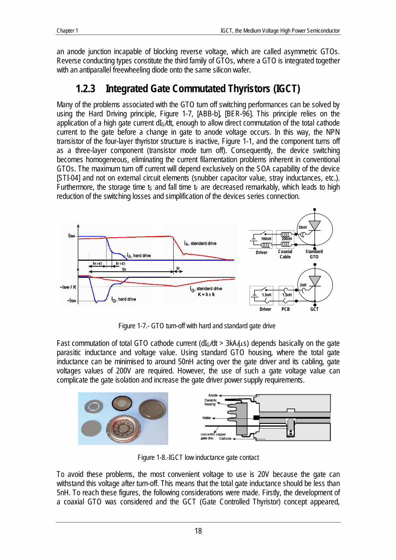
Figure 1-7.- GTO turn-off with hard and standard gate drive
Fast commutation of total GTO cathode current (dIG/dt > 3kA/μs) depends basically on the gate parasitic inductance and voltage value. Using standard GTO housing, where the total gate inductance can be minimised to around 50nH acting over the gate driver and its cabling, gate voltages values of 200V are required. However, the use of such a gate voltage value can complicate the gate isolation and increase the gate driver power supply requirements.
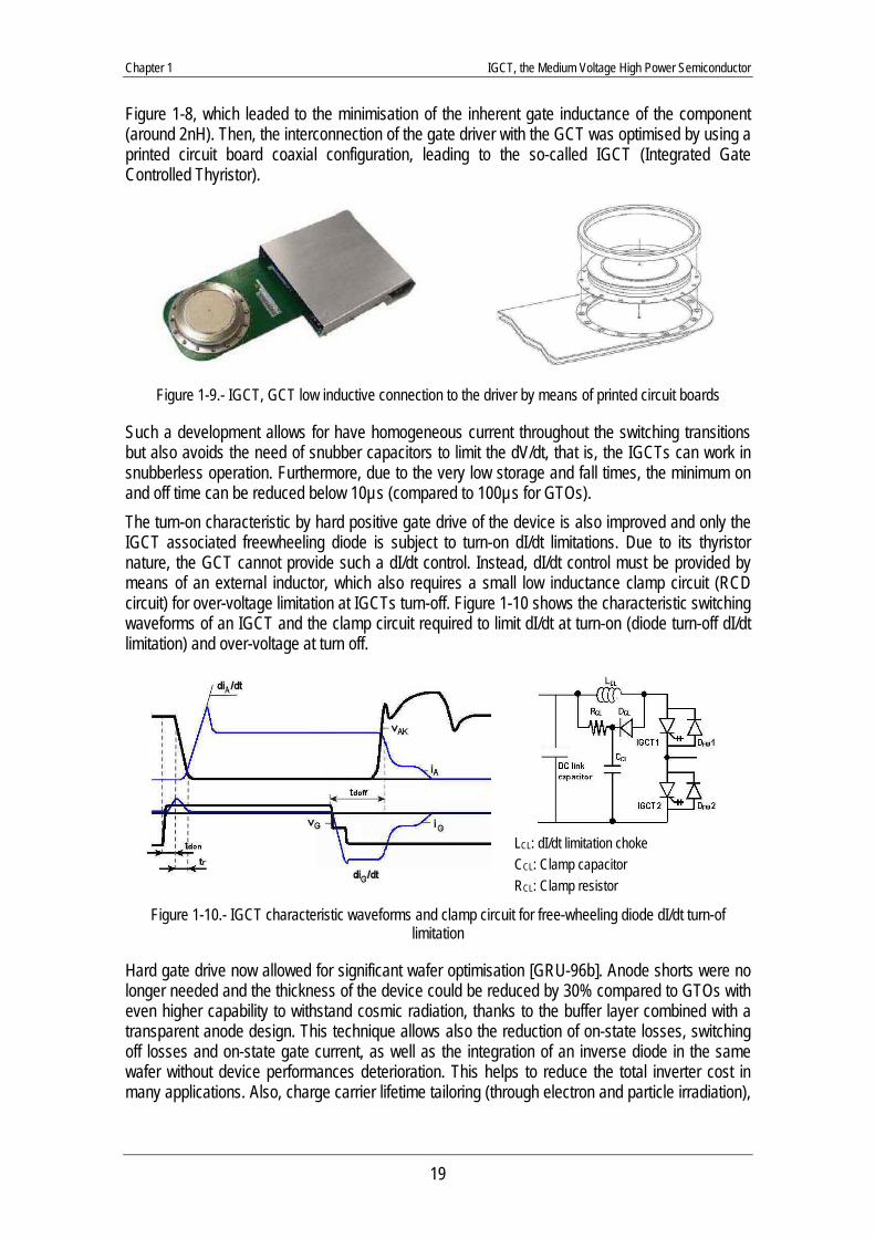
Figure 1-8.-IGCT low inductance gate contact
To avoid these problems, the most convenient voltage to use is 20V because the gate can withstand this voltage after turn-off. This means that the total gate inductance should be less than 5nH. To reach these figures, the following considerations were made. Firstly, the development of a coaxial GTO was considered and the GCT (Gate Controlled Thyristor) concept appeared,
Chapter 1 IGCT, the Medium Voltage High Power Semiconductor
19
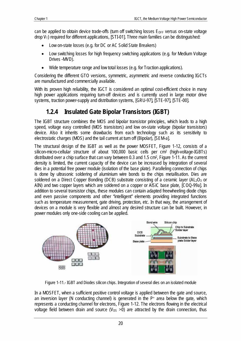
Figure 1-8, which leaded to the minimisation of the inherent gate inductance of the component (around 2nH). Then, the interconnection of the gate driver with the GCT was optimised by using a printed circuit board coaxial configuration, leading to the so-called IGCT (Integrated Gate Controlled Thyristor).
Figure 1-9.- IGCT, GCT low inductive connection to the driver by means of printed circuit boards
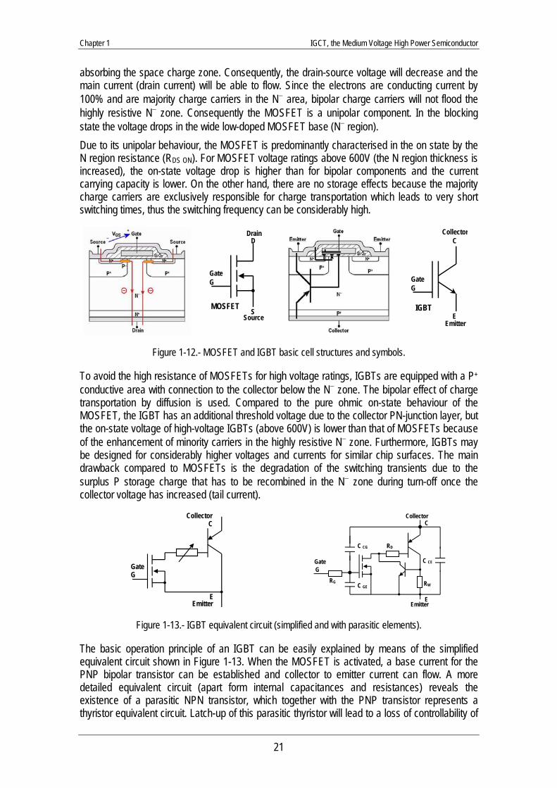
Such a development allows for have homogeneous current throughout the switching transitions but also avoids the need of snubber capacitors to limit the dV/dt, that is, the IGCTs can work in snubberless operation. Furthermore, due to the very low storage and fall times, the minimum on and off time can be reduced below 10µs (compared to 100µs for GTOs). The turn-on characteristic by hard positive gate drive of the device is also improved and only the IGCT associated freewheeling diode is subject to turn-on dI/dt limitations. Due to its thyristor nature, the GCT cannot provide such a dI/dt control. Instead, dI/dt control must be provided by means of an external inductor, which also requires a small low inductance clamp circuit (RCD circuit) for over-voltage limitation at IGCTs turn-off. Figure 1-10 shows the characteristic switching waveforms of an IGCT and the clamp circuit required to limit dI/dt at turn-on (diode turn-off dI/dt limitation) and over-voltage at turn off.
LCL: dI/dt limitation choke CCL: Clamp capacitor RCL: Clamp resistor
Figure 1-10.- IGCT characteristic waveforms and clamp circuit for free-wheeling diode dI/dt turn-of limitation
Hard gate drive now allowed for significant wafer optimisation [GRU-96b]. Anode shorts were no longer needed and the thickness of the device could be reduced by 30% compared to GTOs with even higher capability to withstand cosmic radiation, thanks to the buffer layer combined with a transparent anode design. This technique allows also the reduction of on-state losses, switching off losses and on-state gate current, as well as the integration of an inverse diode in the same wafer without device performances deterioration. This helps to reduce the total inverter cost in many applications. Also, charge carrier lifetime tailoring (through electron and particle irradiation),
Chapter 1 IGCT, the Medium Voltage High Power Semiconductor
20
can be applied to obtain device trade-offs (turn off switching losses EOFF versus on-state voltage drop VT) required for different applications, [STI-01]. Three main families can be distinguished:
• Low on-state losses (e.g. for DC or AC Solid State Breakers) • Low switching losses for high frequency switching applications (e.g. for Medium Voltage
Drives -MVD). • Wide temperature range and low total losses (e.g. for Traction applications).
Considering the different GTO versions, symmetric, asymmetric and reverse conducting IGCTs are manufactured and commercially available. With its proven high reliability, the IGCT is considered an optimal cost-efficient choice in many high power applications requiring turn-off devices and is currently used in large motor drive systems, traction power-supply and distribution systems, [GRU-97], [STE-97], [STE-00].
1.2.4 Insulated Gate Bipolar Transistors (IGBT) The IGBT structure combines the MOS and bipolar transistor principles, which leads to a high speed, voltage easy controlled (MOS transistors) and low on-state voltage (bipolar transistors) device. Also it inherits some drawbacks from each technology such as its sensitivity to electrostatic charges (MOS) and the tail current at turn off (Bipolar), [SEM-a]. The structural design of the IGBT as well as the power MOSFET, Figure 1-12, consists of a silicon-micro-cellular structure of about 100,000 basic cells per cm2 (high-voltage-IGBTs) distributed over a chip surface that can vary between 0.3 and 1.5 cm2, Figure 1-11. As the current density is limited, the current capacity of the device can be increased by integration of several dies in a potential free power module (isolation of the base plate). Paralleling connection of chips is done by ultrasonic soldering of aluminium wire bonds to the chips metallisation. Dies are soldered on a Direct Copper Bonding (DCB) substrate consisting of a ceramic layer (AL2O3 or AIN) and two copper layers which are soldered on a copper or AlSiC base plate, [COQ-99a]. In addition to several transistor chips, these modules can contain adapted freewheeling diode chips and even passive components and other “intelligent” elements providing integrated functions such as temperature measurement, gate driving, protection, etc. In that way, the arrangement of devices on a module is very flexible and almost any desired structure can be built. However, in power modules only one-side cooling can be applied.
Figure 1-11.- IGBT and Diodes silicon chips. Integration of several dies on an isolated module
In a MOSFET, when a sufficient positive control voltage is applied between the gate and source, an inversion layer (N conducting channel) is generated in the P+ area below the gate, which represents a conducting channel for electrons, Figure 1-12. The electrons flowing in the electrical voltage field between drain and source (VDS >0) are attracted by the drain connection, thus
Chapter 1 IGCT, the Medium Voltage High Power Semiconductor
21
absorbing the space charge zone. Consequently, the drain-source voltage will decrease and the main current (drain current) will be able to flow. Since the electrons are conducting current by 100% and are majority charge carriers in the N− area, bipolar charge carriers will not flood the highly resistive N− zone. Consequently the MOSFET is a unipolar component. In the blocking state the voltage drops in the wide low-doped MOSFET base (N− region). Due to its unipolar behaviour, the MOSFET is predominantly characterised in the on state by the N region resistance (RDS ON). For MOSFET voltage ratings above 600V (the N region thickness is increased), the on-state voltage drop is higher than for bipolar components and the current carrying capacity is lower. On the other hand, there are no storage effects because the majority charge carriers are exclusively responsible for charge transportation which leads to very short switching times, thus the switching frequency can be considerably high.
Drain
D
S
G
Source
Gate
MOSFET
Collector
C
E
G
Emitter
Gate
IGBT
Figure 1-12.- MOSFET and IGBT basic cell structures and symbols.
To avoid the high resistance of MOSFETs for high voltage ratings, IGBTs are equipped with a P+ conductive area with connection to the collector below the N− zone. The bipolar effect of charge transportation by diffusion is used. Compared to the pure ohmic on-state behaviour of the MOSFET, the IGBT has an additional threshold voltage due to the collector PN-junction layer, but the on-state voltage of high-voltage IGBTs (above 600V) is lower than that of MOSFETs because of the enhancement of minority carriers in the highly resistive N− zone. Furthermore, IGBTs may be designed for considerably higher voltages and currents for similar chip surfaces. The main drawback compared to MOSFETs is the degradation of the switching transients due to the surplus P storage charge that has to be recombined in the N− zone during turn-off once the collector voltage has increased (tail current).
Collector
C
E
Emitter
G Gate
Collector
C
E Emitter
G Gate
C CG
C GE
C CE
RG
RD
RW
Figure 1-13.- IGBT equivalent circuit (simplified and with parasitic elements).
The basic operation principle of an IGBT can be easily explained by means of the simplified equivalent circuit shown in Figure 1-13. When the MOSFET is activated, a base current for the PNP bipolar transistor can be established and collector to emitter current can flow. A more detailed equivalent circuit (apart form internal capacitances and resistances) reveals the existence of a parasitic NPN transistor, which together with the PNP transistor represents a thyristor equivalent circuit. Latch-up of this parasitic thyristor will lead to a loss of controllability of
Chapter 1 IGCT, the Medium Voltage High Power Semiconductor
22
the IGBT and, therefore, to its destruction. The parasitic thyristor latch-up may happen during on state (when a critical current density is exceeded, which decreases with rising chip temperature) but it can also appear during turn-off (dynamic latch-up due to the increased hole current compared to on-state operation). In modern IGBTs, depending on the IGBT structure, different design precautions are applied to reliably prevent latch-up. The static characteristic of an IGBT shows a 3 segment behaviour (current reversible and voltage unidirectional), however, the component forward operation characteristic optimisation results in a useless reverse characteristic, which means that the IGBT has to be considered as a 2 segment device, Figure 1-14. Therefore, if a third segment behaviour is required, combination with external diodes has to be applied. For instance, if reverse conducting capability is required, the extra diode must be connected in antiparallel with the IGBT. In turn, if reverse blocking capabilities are required the extra diode has to be series connected.
C
E
G
0
Gate Resistor RG
Gate Driver Voltage
VGE
Figure 1-14.- IGBT static characteristic. Control by resistance principle
• Forward off state: If the collector-emitter voltage VCE is positive and the gate-emitter voltage VGE is lower than the gate-emitter threshold voltage VGE (TH), a very small collector – emitter cut-off current is established. If VCE increases, this current raises slightly till a certain maximum breakdown voltage V(BR) CES where the avalanche breakdown phenomenon of the blocked junction appears. The multiplication current generated by the avalanche breakdown leads to the destruction of the IGBT.
• On-state: The forward on-state characteristic of an IGBT can be subdivided in two regions. In the active region, the gate-emitter voltage VGE slightly exceeds the threshold voltage VGE (TH) and controls the collector current depending on its forward transconductance characteristic, gFS, which defines the output characteristic of the component (dIC/dVGE). In the saturation region, also called on-state when the IGBT is used in switching operation, VGE is much larger than VGE (TH) and consequently the saturation collector-emitter voltage VCE SAT of the component is extremely small compared to the breakdown voltage V(BR) CES.
• Switching behaviour: The IGBT switching behaviour is determined by its internal capacitances (charges) and the internal and external gate resistances. Usually, IGBTs are driven by means of a controlled square voltage applied to the gate-emitter terminals through an external current limiting resistor, Figure 1-14. The value of the applied voltage and the gate resistors fix the extracting or injecting speed of the internal charges, which defines the speed and losses of the component’s switching transient. In that way, the dI/dt at turn on and the dV/dt at turn off can be limited by adjusting the VGE maximum and minimum values together with the gate resistor values (single gate resistor or two separate resistors for turn-on and turn-off).
Chapter 1 IGCT, the Medium Voltage High Power Semiconductor
23
Moreover, the commutation processes are affected by the parasitic connection inductances existing in the power layout and generated by connection of transistor chips in power modules; they induce transient over-voltages and may cause oscillations due to the circuit and transistor capacitances. The idealised hard switching waveforms can be observed in Figure 1-15. The IGBT bipolar effect at turn off (tail current) and the free-wheeling diode reverse recovery current IRR reflected over the collector current IC at turn on can be appreciated. Also, during both switching transients, the effect of the voltage drop (positive or negative) on the parasitic inductor of the switching loop is taken into account.
Figure 1-15.- IGBT idealised hard switching waveforms
• Reverse state: IGBT chips are designed mainly to comply with a high forward off-state voltage capability and optimised collector heat dissipation, which results in an ineffective reverse characteristic. So, the characteristics of the external diodes are exclusively responsible for the reverse on-state behaviour of IGBT modules.
Since the introduction of the IGBT, several structures have been considered, mainly planar structures. Promptly the “Non Punch Through” IGBT technology (homogeneous structure) dominated the original “Punch Through” concept based on Epitaxial technology, thanks to its easy paralleling ability provided by its on-state characteristic with positive temperature coefficient.
Figure 1-16.- Past and forecast 75A/1200V chip size and thickness evolution for NPT and Field-Stop IGBTs.
Nowadays, because of economic reasons, there is a strong demand for smaller chips with lower on-state and switching losses. A good indicator of the IGBTs evolution in terms of on-state and switching losses is the size and thickness evolution for a specific current / voltage die, as
Chapter 1 IGCT, the Medium Voltage High Power Semiconductor
24
depicted in Figure 1-16, [GUT-03]. As a consequence of smaller chip sizes, current densities are increased as well as the power dissipation density in combination with smaller silicon heat capacity. To combine these performances, new structures are being applied, even the consideration for vertical structures (Trench IGBTs). Among the structures now considered, the planar SPT (Soft-Punch-Through) and the vertical Trench-FS (Field Stop) technology offer the best performances, Figure 1-17. Both technologies show significant improvements over NPT-IGBTs, [LI-03].
Figure 1-17.- NPT, SPT and Trench – FS IGBT structures
The switching behaviour of the SPT-IGBT is optimised to obtain linear voltage rise at turn off, low voltage overshoot, low and short tail current, and a smooth transition between fall and tail phase. Even the saturation voltage is improved with respect to the standard NPT-IGBT, while the chip area and consequently the thermal resistance remain almost unchanged. The Trench-FS technology leads to an improvement of the saturation voltage by more than 30% compared to NPT-IGBT, while the chip size is reduced to about 70%, thus the current density is higher. However, it has a higher thermal resistance as a side effect. Thanks to all the different existing technologies, the component design can be adapted to the application requirements. IGBTs with switching losses, conduction losses or the total losses optimisation are commercially available.
1.2.5 Fast Recovery Diodes The excellent switching performances offered by the existing controlled switches (IGBTs, GTOs and IGCTs) also requires adapted fast recovery diodes with low static and dynamic losses, enhanced Safe Operating Areas (SOA) and controlled (soft) recovery at very high dI/dt and dV/dt levels. In most applications, the critical need to minimise stray inductance between the switch and the associated snubberless diode encourages fast diode commutation. Furthermore, these diodes can play different roles depending on their function on the circuit, (Snubber, Clamp, Free-Wheel Diode, inductive or resistive commutation), and often one single diode is not well adapted to be applied everywhere, [GAL-98]. For these reasons, semiconductor manufactures are developing new generations of diodes, trying to obtain lower reverse peak current IRR together with "soft recovery” performances, keeping the diode switching losses as low as possible. Two basic diode structures can be considered for fast power diodes, the Schottky and the PIN structure, [SEM-a]. The Schottky diode structure applies a metal-semiconductor junction as a blocking junction, which provides a very low on-state voltage and very low reverse recovery current. However, the Schottky structure application is only efficient for diodes with blocking voltage lower than 100V. Above 100V, PIN diodes, where the intrinsic zone (I) is obtained by means of N− material, are the preferred structure. For voltages reaching 600V PIN-epitaxial diodes are used, whereas for higher voltage levels PIN-diffused diodes are produced, Figure
Chapter 1 IGCT, the Medium Voltage High Power Semiconductor
25
1-18. For high power fast recovery diodes, the on-state and dynamic losses trade-off and the adapted recovery behaviour is obtained combining the PIN structure with additional manufacturing techniques, (Controlled Axial Lifetime CAL diodes, [WEB-97], Emitter controlled EmCon diodes, [BIE-03]).
N−
N+
Cathode
Anode
P
N+
Cathode
Anode
N−
P
N+
Cathode
Anode
N−
Figure 1-18.- Schottky structure, PIN-epitaxial structure and PIN-diffused structure
• Forward and blocking behaviour: For a PIN diode structure, the diode voltage drop in the forward direction is defined by the voltage drop of the PN-junction (0.6 ÷ 0.8V) and the resistance of the adjacent N− zone. At the same time, the blocking voltage capacity of the diode (breakdown voltage VBD) depends directly on the thickness of the N− zone. Consequently, for fast diodes with a blocking voltage of 600V and more the ohmic part prevails.
• Turn-on behaviour (forward recovery): When the diode is turned on with high dI/dt, the carrier gradient does not develop immediately, resulting in an overshoot voltage that decays with time to the normal forward voltage dc static level. The diode appears to be inductive; however, transit time and conductivity modulation, not only inductance, are responsible for this effect. This turn-on overshoot (dynamic) voltage appears generating turn–on losses. Usually the turn-on losses are neglected, however, for high power semiconductors and extremely high dI/dt, the diode turn-on dynamic voltage can be relatively high (several hundred volts) and can alter the transient waveforms of adjacent switches.
• Turn-off behaviour: The diode turn-off performance is mainly defined by its reverse-recovery characteristic. When diodes change from the on-state to the blocking state, as they are minority carrier devices, their internal storage charges have to be discharged. This results in a current flowing in reverse direction in the diode with a peak value called peak reverse recovery current IRRM, Figure 1-19.
IF
A: Anode
K: Cathode
VF
Figure 1-19.- Diode Static characteristic. Soft-recovery diode reverse recovery behaviour
This peak current changes with the diode on-state current value IF (storage charges), the current decreasing ratio (dIF/dt negative) imposed by the external circuit (active or passively limited), the temperature off the component and also the diode operating voltage. With the negative reverse recovery current already established in the diode,
Chapter 1 IGCT, the Medium Voltage High Power Semiconductor
26
the diode starts to block (diode reverse voltage starts increasing) when the PN-junction in the diode is free of charge carriers. After that, the maximum peak reverse recovery current IRRM is attained. Finally the current falls to the leakage current level depending solely on characteristic of the diode (diode recovery characteristic). If the current drops very steeply, this is called snappy recovery behaviour. If the current drops very softly, this is called soft recovery behaviour. The subdivision of the total reverse recovery time tRR into tF and tS is used to define the qualitative behaviour of the diode through the Recovery factor s (Eq. 1-5). The bigger the s factor is the softer the diode recovery behaviour is.
If the diode voltage is unclamped, for instance by means of the DC link capacitor in a voltage source inverter, a voltage overshoot is generated imposing the maximal reverse voltage VRM that the diode has to withstand. This voltage overshoot depends on the diode characteristics (recovery current, parasitic capacitance) but also on the external circuit parasitic inductance. Furthermore, this over-voltage (together with the reverse recovery current) is hardly responsible for the turn-off losses of the diode and must be limited carefully.
High power diodes in module and press-pack packages are available to complement the converters using snubberless controlled switches. However, in many cases the operation mode of the controlled switches is limited by the behaviour of the fast recovery diodes (in terms of power losses and SOA), which must be seriously considered when selecting the correct diode.
1.3 IGCT Implementation The safe utilisation of IGCTs requires the knowledge of several aspects that must be considered when designing IGCT based power converters. The following paragraphs point out and clarify these most critical aspects regarding electrical, mechanical and cooling issues.
1.3.1 Electrical Issues First of all, IGCTs must be selected according to the intended application. For instance, three different ABB asymmetric IGCT versions are commercially available, specially tailored for specific applications (low turn off losses, low on-state losses and wide temperature range). Each version defines different operation restrictions to the component regarding its SOA capability, driver power consumption requirements and so on. Then, for these different versions, there are common electrical restrictions that must be adhered to (maximum switching frequency, dI/dt limitation, etc.)
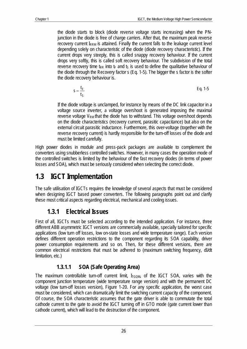
1.3.1.1 SOA (Safe Operating Area) The maximum controllable turn-off current limit, ITGQM, of the IGCT SOA, varies with the component junction temperature (wide temperature range version) and with the permanent DC voltage (low turn-off losses version), Figure 1-20. For any specific application, the worst case must be considered, which can dramatically limit the switching current capacity of the component. Of course, the SOA characteristic assumes that the gate driver is able to commutate the total cathode current to the gate to avoid the IGCT turning off in GTO mode (gate current lower than cathode current), which will lead to the destruction of the component.
S
Ftts = Eq. 1-5
Chapter 1 IGCT, the Medium Voltage High Power Semiconductor
27
Figure 1-20.- ABB 4.5kV asymmetric IGCTs SOA. a) 5SHY35L4511, b) 5SHY35L4512
In terms of voltage, the SOA is not limited by maximum repetitive peak off-state voltage VDRM that the component can withstand but by its cosmic radiation withstand rating. In the early 1990`s, it was found that cosmic particles can lead to random destruction of power semiconductors exposed to high blocking voltages for long periods. Thus, the SOA voltage limit is fixed by the maximum permanent DC voltage that guarantees a failure rate of 100 FIT (1FIT represents 1 failure in 109 hours) due to cosmic radiation at sea level.
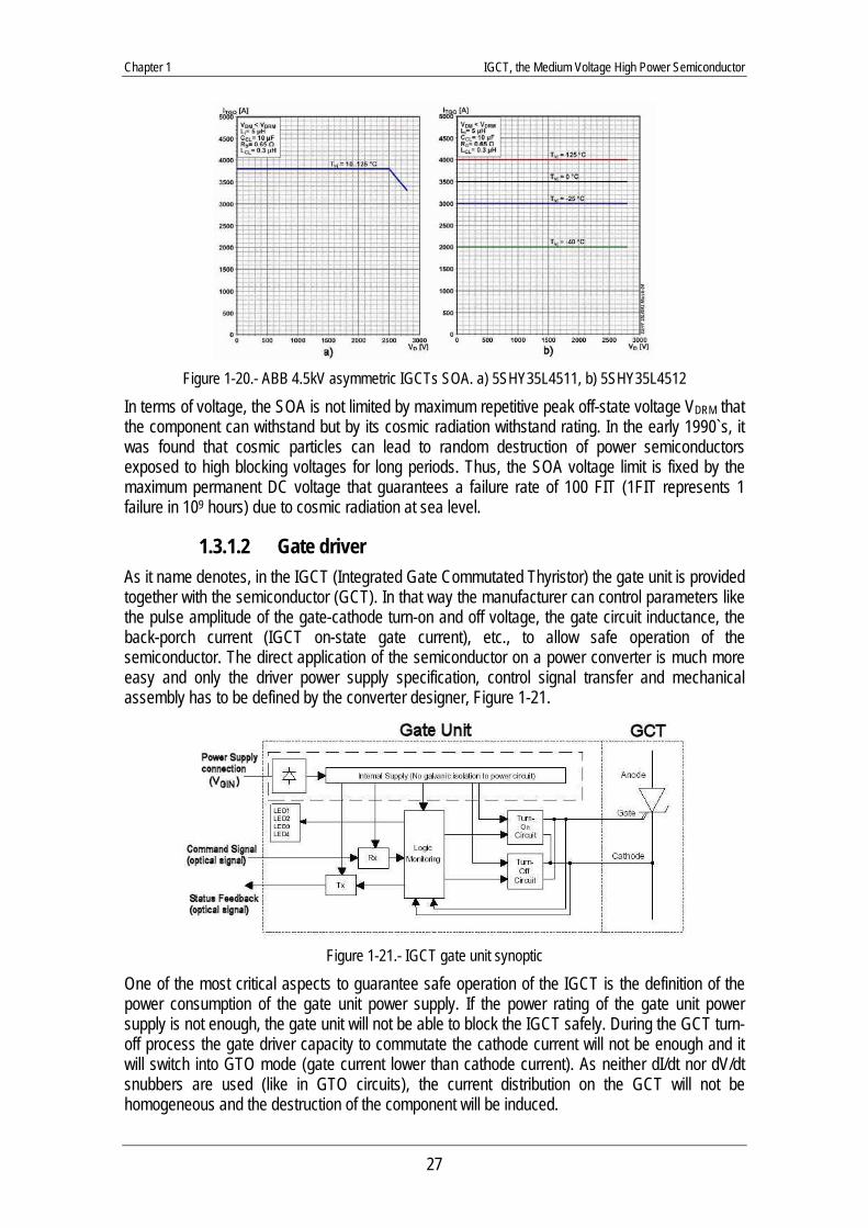
1.3.1.2 Gate driver As it name denotes, in the IGCT (Integrated Gate Commutated Thyristor) the gate unit is provided together with the semiconductor (GCT). In that way the manufacturer can control parameters like the pulse amplitude of the gate-cathode turn-on and off voltage, the gate circuit inductance, the back-porch current (IGCT on-state gate current), etc., to allow safe operation of the semiconductor. The direct application of the semiconductor on a power converter is much more easy and only the driver power supply specification, control signal transfer and mechanical assembly has to be defined by the converter designer, Figure 1-21.
Figure 1-21.- IGCT gate unit synoptic
One of the most critical aspects to guarantee safe operation of the IGCT is the definition of the power consumption of the gate unit power supply. If the power rating of the gate unit power supply is not enough, the gate unit will not be able to block the IGCT safely. During the GCT turn-off process the gate driver capacity to commutate the cathode current will not be enough and it will switch into GTO mode (gate current lower than cathode current). As neither dI/dt nor dV/dt snubbers are used (like in GTO circuits), the current distribution on the GCT will not be homogeneous and the destruction of the component will be induced.
Chapter 1 IGCT, the Medium Voltage High Power Semiconductor
28
The gate unit power consumption is directly influenced by the turn-off current, the switching frequency, the operating duty cycle, the chip temperature and the device technology (gate charge). That means that the definition of the gate unit power consumption is strongly application dependent. Information about the gate unit power consumption can be obtained from the component data sheet, Figure 1-22, however, not all the cases of operations are covered and approximate calculations have to be performed including a suitable safety margin. Of course, the power supply voltage and insulation has to be adapted to the selected IGCT and to the converter maximum operating voltage. Also gate unit internal component limitations must be considered (active and passive ratings, thermal limitations, etc.), which could limit the semiconductor work conditions to obtain the gate unit expected lifetime, Figure 1-23. From a signal control point of view (mainly fibber optics are used to provide high insulation and immunity performances), several aspects have to be considered. In normal operation, minimum IGCT ON and OFF times (tON MIN and tOFF MIN) as well as a minimum switching period (tON + tOFF) defined on the component datasheet must be respected to guarantee safe component operation. The gate unit provides an internal minimum pulse width limitation (ON and OFF), but these minimum values are usually smaller than the values defined on the datasheet to allow single event protection sequences. Also, special care must be taken on the power up and down sequence of the control and the power stages. As the gate unit takes some time to become active, if control signals are sent during this sequence and voltage is applied across the GCT, high frequency operation can be generated leading to the destruction of the IGCT.
Figure 1-22.- ABB 5SHY35L4511 asymmetric
IGCT (4.5kV) gate unit power consumption
Figure 1-23.- ABB 5SHY35L4511 asymmetric IGCT
(4.5kV) maximal turn-off current versus switching frequency for lifetime operation (20 years calculated lifetime of gate unit on-board electrolytic capacitors)
Special attention has to be paid in certain applications (voltage source inverters, soft switching converters) where load current sign changes quickly during the IGCT on-state. If this change induces the conduction change from the freewheeling diode to the GCT (negative to positive switch current), the thyristor regenerative effect has not been built in and the GCT is not yet ready for conduction. Inhomogeneous current distribution in the semiconductor can be established and device failure could be reached if this effect is reproduced in repetitive mode. If a critical rate of rise of the on-state current (dI/dtCR) defined on the datasheet is exceeded, this failure mode can be attained. To provide safe operation over this working operation mode, an external re-trigger pulse has to be generated by the controller, which will require a more complicated driver to define the re-triggering pulse generation timing (gate-cathode voltage measurement, timing accuracy, etc.), [LUS-04]. IGCT status feedback is provided by the gate unit by means of an optical status signal that can be used to detect fault operations on the GCT and / or the gate unit (gate unit supply voltage
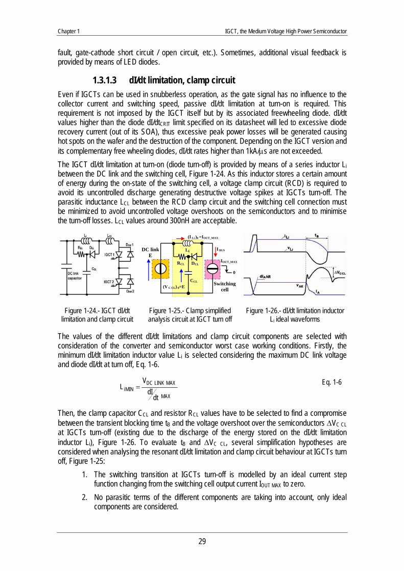
Chapter 1 IGCT, the Medium Voltage High Power Semiconductor
29
fault, gate-cathode short circuit / open circuit, etc.). Sometimes, additional visual feedback is provided by means of LED diodes.
1.3.1.3 dI/dt limitation, clamp circuit Even if IGCTs can be used in snubberless operation, as the gate signal has no influence to the collector current and switching speed, passive dI/dt limitation at turn-on is required. This requirement is not imposed by the IGCT itself but by its associated freewheeling diode. dI/dt values higher than the diode dI/dtCRIT limit specified on its datasheet will led to excessive diode recovery current (out of its SOA), thus excessive peak power losses will be generated causing hot spots on the wafer and the destruction of the component. Depending on the IGCT version and its complementary free wheeling diodes, dI/dt rates higher than 1kA/μs are not exceeded. The IGCT dI/dt limitation at turn-on (diode turn-off) is provided by means of a series inductor Li between the DC link and the switching cell, Figure 1-24. As this inductor stores a certain amount of energy during the on-state of the switching cell, a voltage clamp circuit (RCD) is required to avoid its uncontrolled discharge generating destructive voltage spikes at IGCTs turn-off. The parasitic inductance LCL between the RCD clamp circuit and the switching cell connection must be minimized to avoid uncontrolled voltage overshoots on the semiconductors and to minimise the turn-off losses. LCL values around 300nH are acceptable.
DC link E
IOUT_MAX
0
(I Li )0 =IOUT_MAX
I BUS
RCL
Li
DCL
CCL
(V C CL) 0=E Switching
cell
Figure 1-24.- IGCT dI/dt limitation and clamp circuit
Figure 1-25.- Clamp simplified analysis circuit at IGCT turn off
Figure 1-26.- dI/dt limitation inductor Li ideal waveforms
The values of the different dI/dt limitations and clamp circuit components are selected with consideration of the converter and semiconductor worst case working conditions. Firstly, the minimum dI/dt limitation inductor value Li is selected considering the maximum DC link voltage and diode dI/dt at turn off, Eq. 1-6.
Then, the clamp capacitor CCL and resistor RCL values have to be selected to find a compromise between the transient blocking time tB and the voltage overshoot over the semiconductors ΔVC CL at IGCTs turn-off (existing due to the discharge of the energy stored on the dI/dt limitation inductor Li), Figure 1-26. To evaluate tB and ΔVC CL, several simplification hypotheses are considered when analysing the resonant dI/dt limitation and clamp circuit behaviour at IGCTs turn off, Figure 1-25:
1. The switching transition at IGCTs turn-off is modelled by an ideal current step function changing from the switching cell output current IOUT MAX to zero.
2. No parasitic terms of the different components are taking into account, only ideal components are considered.
MAX
MAXLINKDCMINi
dtdI
VL = Eq. 1-6
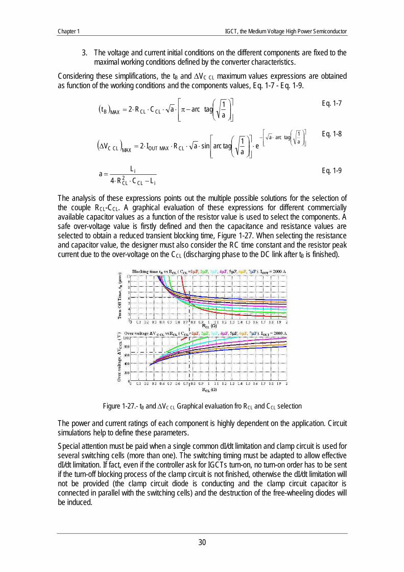
Chapter 1 IGCT, the Medium Voltage High Power Semiconductor
30
3. The voltage and current initial conditions on the different components are fixed to the maximal working conditions defined by the converter characteristics.
Considering these simplifications, the tB and ΔVC CL maximum values expressions are obtained as function of the working conditions and the components values, Eq. 1-7 - Eq. 1-9.
The analysis of these expressions points out the multiple possible solutions for the selection of the couple RCL-CCL. A graphical evaluation of these expressions for different commercially available capacitor values as a function of the resistor value is used to select the components. A safe over-voltage value is firstly defined and then the capacitance and resistance values are selected to obtain a reduced transient blocking time, Figure 1-27. When selecting the resistance and capacitor value, the designer must also consider the RC time constant and the resistor peak current due to the over-voltage on the CCL (discharging phase to the DC link after tB is finished).
Figure 1-27.- tB and ΔVC CL Graphical evaluation fro RCL and CCL selection
The power and current ratings of each component is highly dependent on the application. Circuit simulations help to define these parameters. Special attention must be paid when a single common dI/dt limitation and clamp circuit is used for several switching cells (more than one). The switching timing must be adapted to allow effective dI/dt limitation. If fact, even if the controller ask for IGCTs turn-on, no turn-on order has to be sent if the turn-off blocking process of the clamp circuit is not finished, otherwise the dI/dt limitation will not be provided (the clamp circuit diode is conducting and the clamp circuit capacitor is connected in parallel with the switching cells) and the destruction of the free-wheeling diodes will be induced.
( )⎥⎥⎦
⎤
⎢⎢⎣
⎡⎟⎟⎠
⎞⎜⎜⎝
⎛−π⋅⋅⋅⋅=
a1tagarcaCR2t CLCLMAXB
Eq. 1-7
( ) ⎥⎥⎦
⎤
⎢⎢⎣
⎡⎟⎟⎠
⎞⎜⎜⎝
⎛⋅−
⋅⎥⎥⎦
⎤
⎢⎢⎣
⎡⎟⎟⎠
⎞⎜⎜⎝
⎛⋅⋅⋅⋅=Δ
a1tagarca
CLMAXOUTMAXCLC ea1tagarcsinaRI2V
Eq. 1-8
iCL2CL
i
LCR4La
−⋅⋅= Eq. 1-9
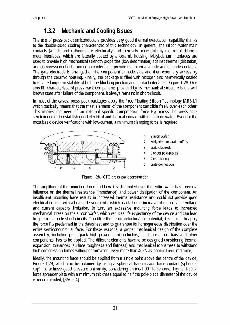
Chapter 1 IGCT, the Medium Voltage High Power Semiconductor
31
1.3.2 Mechanic and Cooling Issues The use of press-pack semiconductors provides very good thermal evacuation capability thanks to the double-sided cooling characteristic of this technology. In general, the silicon wafer main contacts (anode and cathode) are electrically and thermally accessible by means of different metal interfaces, which are laterally coated by a ceramic housing. Molybdenum interfaces are used to provide high mechanical strength properties (low deformation) against thermal (dilatation) and compression efforts, and copper interfaces provide the external anode and cathode contacts. The gate electrode is arranged on the component cathode side and then externally accessibly through the ceramic housing. Finally, the package is filled with nitrogen and hermetically sealed to ensure long-term stability of both the blocking junction and contact interfaces, Figure 1-28. One specific characteristic of press pack components provided by its mechanical structure is the well known state after failure of the component, it always remains in short-circuit. In most of the cases, press pack packages apply the Free Floating Silicon Technology [ABB-b], which basically means that the main elements of the component can slide freely over each other. This implies the need of an external specific compression force FM across the press-pack semiconductor to establish good electrical and thermal contact with the silicon wafer. Even for the most basic device verifications with low-current, a minimum clamping force is required.
1. Silicon wafer 2. Molybdenum strain buffers 3. Gate electrode 4. Copper pole-pieces 5. Ceramic ring 6. Gate connection
Figure 1-28.- GTO press-pack construction
The amplitude of the mounting force and how it is distributed over the entire wafer has foremost influence on the thermal resistance (impedance) and power dissipation of the component. An insufficient mounting force results in increased thermal resistance and could not provide good electrical contact with all cathode segments, which leads to the increase of the on-state voltage and current capacity limitation. In turn, an excessive mounting force leads to increased mechanical stress on the silicon wafer, which reduces life expectancy of the device and can lead to gate-to-cathode short circuits. To utilise the semiconductors’ full potential, it is crucial to apply the force FM predefined in the datasheet and to guarantee its homogeneous distribution over the entire semiconductor surface. For these reasons, a proper mechanical design of the complete assembly, including press-pack high power semiconductors, heat sinks, bus bars and other components, has to be applied. The different elements have to be designed considering thermal expansion, tolerances (surface roughness and flatness) and mechanical robustness to withstand high compression forces without deformation (even more than 40kN as nominal required force). Ideally, the mounting force should be applied from a single point above the centre of the device, Figure 1-29, which can be obtained by using a spherical transmission force contact (spherical cup). To achieve good pressure uniformity, considering an ideal 90° force cone, Figure 1-30, a force spreader plate with a minimum thickness equal to half the pole-piece diameter of the device is recommended, [BAC-04].
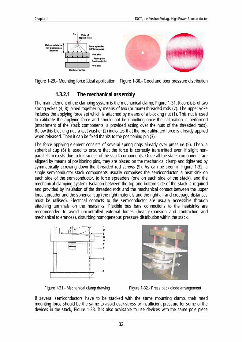
Chapter 1 IGCT, the Medium Voltage High Power Semiconductor
32
Figure 1-29.- Mounting force Ideal application Figure 1-30.- Good and poor pressure distribution
1.3.2.1 The mechanical assembly The main element of the clamping system is the mechanical clamp, Figure 1-31. It consists of two strong yokes (4, 8) joined together by means of two (or more) threaded rods (7). The upper yoke includes the applying force set which is attached by means of a blocking nut (1). This nut is used to calibrate the applying force and should not be unbolting once the calibration is performed (attachment of the stack components is provided acting over the nuts of the threaded rods). Below this blocking nut, a test washer (2) indicates that the pre-calibrated force is already applied when released. Then it can be fixed thanks to the positioning pin (3). The force applying element consists of several spring rings already over pressure (5). Then, a spherical cup (6) is used to ensure that the force is correctly transmitted even if slight non-parallelism exists due to tolerances of the stack components. Once all the stack components are aligned by means of positioning pins, they are placed on the mechanical clamp and tightened by symmetrically screwing down the threaded rod screws (9). As can be seen in Figure 1-32, a single semiconductor stack components usually comprises the semiconductor, a heat sink on each side of the semiconductor, to force spreaders (one on each side of the stack), and the mechanical clamping system. Isolation between the top and bottom side of the stack is required and provided by insulation of the threaded rods and the mechanical contact between the upper force spreader and the spherical cup (the right materials and the right air and creepage distances must be utilised). Electrical contacts to the semiconductor are usually accessible through attaching terminals on the heatsinks. Flexible bus bars connections to the heatsinks are recommended to avoid uncontrolled external forces (heat expansion and contraction and mechanical tolerances), disturbing homogeneous pressure distribution within the stack.
Figure 1-31.- Mechanical clamp drawing Figure 1-32.- Press pack diode arrangement
If several semiconductors have to be stacked with the same mounting clamp, their rated mounting force should be the same to avoid over-stress or insufficient pressure for some of the devices in the stack, Figure 1-33. It is also advisable to use devices with the same pole piece
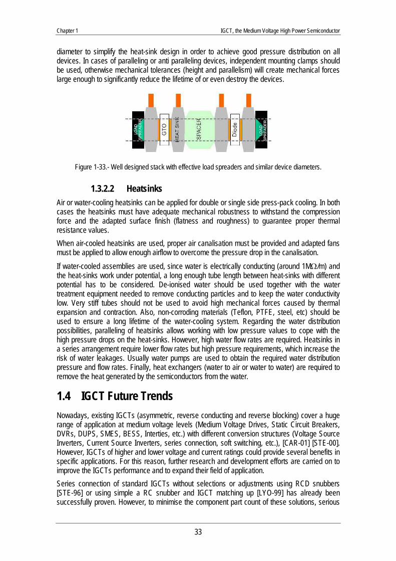
Chapter 1 IGCT, the Medium Voltage High Power Semiconductor
33
diameter to simplify the heat-sink design in order to achieve good pressure distribution on all devices. In cases of paralleling or anti paralleling devices, independent mounting clamps should be used, otherwise mechanical tolerances (height and parallelism) will create mechanical forces large enough to significantly reduce the lifetime of or even destroy the devices.
Figure 1-33.- Well designed stack with effective load spreaders and similar device diameters.
1.3.2.2 Heatsinks Air or water-cooling heatsinks can be applied for double or single side press-pack cooling. In both cases the heatsinks must have adequate mechanical robustness to withstand the compression force and the adapted surface finish (flatness and roughness) to guarantee proper thermal resistance values. When air-cooled heatsinks are used, proper air canalisation must be provided and adapted fans must be applied to allow enough airflow to overcome the pressure drop in the canalisation. If water-cooled assemblies are used, since water is electrically conducting (around 1MΩ/m) and the heat-sinks work under potential, a long enough tube length between heat-sinks with different potential has to be considered. De-ionised water should be used together with the water treatment equipment needed to remove conducting particles and to keep the water conductivity low. Very stiff tubes should not be used to avoid high mechanical forces caused by thermal expansion and contraction. Also, non-corroding materials (Teflon, PTFE, steel, etc) should be used to ensure a long lifetime of the water-cooling system. Regarding the water distribution possibilities, paralleling of heatsinks allows working with low pressure values to cope with the high pressure drops on the heat-sinks. However, high water flow rates are required. Heatsinks in a series arrangement require lower flow rates but high pressure requirements, which increase the risk of water leakages. Usually water pumps are used to obtain the required water distribution pressure and flow rates. Finally, heat exchangers (water to air or water to water) are required to remove the heat generated by the semiconductors from the water.
1.4 IGCT Future Trends Nowadays, existing IGCTs (asymmetric, reverse conducting and reverse blocking) cover a huge range of application at medium voltage levels (Medium Voltage Drives, Static Circuit Breakers, DVRs, DUPS, SMES, BESS, Interties, etc.) with different conversion structures (Voltage Source Inverters, Current Source Inverters, series connection, soft switching, etc.), [CAR-01] [STE-00]. However, IGCTs of higher and lower voltage and current ratings could provide several benefits in specific applications. For this reason, further research and development efforts are carried on to improve the IGCTs performance and to expand their field of application. Series connection of standard IGCTs without selections or adjustments using RCD snubbers [STE-96] or using simple a RC snubber and IGCT matching up [LYO-99] has already been successfully proven. However, to minimise the component part count of these solutions, serious
Chapter 1 IGCT, the Medium Voltage High Power Semiconductor
34
investigations about the 10kV IGCT are being held. Higher currents have already been realised up to 6 kA [OKA-03] and will become more common in the future for high power applications. For lower current and voltage ratings, purely commercial issues, market potentials and the “pros and cons” with respect to IGBTs will define their introduction on the market. A review of the most relevant IGCT trends and actual developments is presented in the next paragraphs.
1.4.1 10kV HV IGCTs One clear technical trend of medium voltage pulse width modulated (PWM) converters is the increase of the converter voltage and power. Nowadays, 2.3, 3.3 and 4.16 kVRMS standard line voltages are reached, applying 3-level Neutral Point Clamped voltages source converter with a single semiconductor for switch position. For higher line voltages, 6.6–7.2 kVRMS, series connection of several semiconductors [NAG-01] or converters with higher number of levels [EIC-01] must be used, increasing the complexity, cost and reliability of the total system. Therefore, the research on 10kV IGCTs is motivated by the simplification of power converters dealing with 6.6–7.2 kVRMS line voltages for Medium Voltage Drives and Power Quality applications, [EIC-00]. The part count reduction (RC snubbers, semiconductors and gate drivers, etc.) will lead to lower cost, increased reliability, and simpler design and maintenance, [BER-03]. However, if compared to the series connection solution, the power dissipation of a 10kV device will be 50% lower than 2 series connected devices, which limits the power handling capacity of both the semiconductor and the power converter. Also switching limitations due to 10kV fast recovery diode could lead to semiconductor switching capacity limitation.
Figure 1-34.- 68mm 10 kV IGCT sample
10kV IGCT samples, Figure 1-34, have been successfully tested in single pulse operation at 7kVDC and 1kA turn off current, [BER-03]. Further investigations will demonstrate the potential ability of this component to be applied in practical products.
1.4.2 Dual Gate Turn-off Thyristor The Dual Gate principle consists on the use of a second gate driver to control the IGCT gate-anode voltage (the base-emitter voltage of the PNP equivalent transistor in the thyristor type structure), Figure 1-35. This second gate driver will be able to eliminate the IGCT tail current at turn-off, considerably reducing the switching losses of the component, whereas using a symmetric structure can also provide a considerable reduction of the on-state losses [APE-01]. In addition, anode gate control may offer additional degrees of freedom for series connection and reduction of snubber requirements could be achieved, [APE-02]. The reduction of the switching losses provided by the dual gate principle, if applied to future 10kV IGCTs, could provide not only the required performances of the 6.6 – 7.2kVRMS medium voltage drives, but also reduce the cost per MW of the converter compared to a series connection solution. The main drawback comes from a control point of view, where the complexity and accuracy requirements are increased.
Chapter 1 IGCT, the Medium Voltage High Power Semiconductor
35
Figure 1-35.- Semiconductor structure of a “symmetrical” Dual Gate IGCT
1.4.3 SOA Improvement The standard IGCT (4.5kV - 6kV) based converters power is limited by the semiconductor SOA capacity. Improvement of the SOA for large area IGCTs could extend the power rating of such converters. Several approaches (optimised gate-circuit, local SOA improvement applying optimised profiles, irradiation and compensation of lateral effects by means of irradiation) have been investigated and combined to obtain more than 30% SOA improvement in large area devices [STI-04], obtaining exceptional results reaching 1MW/cm2 turn off capability for small devices (38mm), Figure 1-36. However practical application of all these combined technologies can increase the product cost drastically which will limit their use only accessible to very specific applications.
Figure 1-36.- 38mm IGCT sample with experimental gate unit for test purposes
1.4.4 3.3kV LV IGCTs The experimental 3.3kV LV IGCT and their associated free wheeling diodes have been designed on the technology platform of the standard IGCT product line, Figure 1-37. Reduction of the silicon thickness and carefully adapted carrier lifetime engineering provides the required trade-off between the on-state and switching losses to increase the attainable switching frequency (500 - 2000 Hz) of the component, keeping its “high current” capacity (2 – 1kA), [ALV-04b]. Such a component contends for increasing the IGCT field of applications in medium voltage / medium power applications providing higher dynamic performances of the converter. Experimental results show the ability of these components to guarantee continuous hard switching operation at 1 kHz with a turn off capacity of 1.4kA (1.5kVDC, α=0.5), is limited only by the driver capacity (power supply). If the IGCT power losses are kept constant (around 4.4kW) and the switching frequency is increased to 2 kHz, turn off currents of 1kA over 1.8kVDC (α=0.5) are accessible. For applications with clear design goals, a further optimisation is possible and further analysis could result in defining such optimised target specifications. However, to reach these working conditions, the power consumption of the gate unit is increased and even further development on the gate unit design is necessary to provide the required internal components (electrolytic capacitors and MOSFETs) lifetime expectancy, which can increase the cost of the component.
Chapter 1 IGCT, the Medium Voltage High Power Semiconductor
36
Figure 1-37.- Experimental 3.3kV IGCT (5SHY 45L3300) and diodes (5SDF 10H2500)
1.5 IGCT vs. IGBT Nowadays, despite the different technologies of IGCTs and IGBTs, their current and voltage ratings are similar, and for several applications and power converter ratings, both solutions can be applied. Therefore, the selection of the semiconductor has to be made according to relevant considerations like implementation issues, control simplicity, reliability, ruggedness, maintenance issues and of course market availability and cost. For each application where particular requirements are imposed, a case by case analysis should be required to define the best solution. However, different priority criterions of different designers could lead to different results. For this reason, and trying to provide an objective point of view, the comparison presented here will point out the main advantages and drawbacks of both solutions.
1.5.1 Ratings and Mechanical Lay Out Nowadays, the comparable IGCT and IGBT ratings available from different manufactures are shown in Table 1-2 and Table 1-3. For IGCTs, asymmetric and reverse conducting versions are taken into account. For the asymmetric IGCT, only the components optimised for medium frequency (1 kHz) and low turn-off losses are mentioned. It should be noted, for reverse conduction IGCTs, that the diode average current IFAV is usually much lower than the IGCT average current ITAV. The origin of this characteristic is the different section used in the wafer for the IGCT (outer region) and the diode (inner region) integration (separated by the gate contact ring). All IGBTs are of module type, no press pack IGBTs are available commercially for more than 3.3kV. Components under development or foreseen for new releases are not mentioned.
IGCT
Type VDRM (V) VDC LINK (V) ITGQM (A) Manufacturer
4500 2800 3800 ABB
4500 3000 4000 Mitsubishi
6000 3600 3000 ABB
Asym
metric
6000 3600 3500 Mitsubishi
Type VDRM (V) VDC LINK (V) ITGQM (A) ITAV / IFAV (A) Manufacturer
340 130 / 85 ABB 4500 2800
2200 1010 / 400 ABB
280 110 / 65 ABB Reve
rse
Cond
uctin
g
5500 3300 1800 840 / 340 ABB
Table 1-2.- IGCT available ratings (asymmetric and reverse conducting)
Chapter 1 IGCT, the Medium Voltage High Power Semiconductor
37
As a general rule, the IGCT switching capacity is higher for a given component adapted to a specific DC link voltage. Basically this is due to the lower on-state losses and higher power evacuation capability of IGCTs. However, the IGBT permanent switching frequency is, for the most part, only limited by its total thermal budget, while the IGCT maximum permanent switching frequency is limited to 1 kHz by the driver. The IGCT can operate at high switching frequency (16 kHz maximum) but only for a limited amount of time (burst mode).
IGBT
VCE (V) VDC LINK (V) IC (A) Manufacturer
1200 / 800 ABB
1200 / 800 / 400 Eupec
1200 / 800 / 400 Mitsubishi 3300 1800
1200 / 800 Dynex
4500 2800 900 / 600 / 400 Mitsubishi
600 ABB
600 / 400 / 200 Eupec
600 Mitsubishi 6500 3600
400 Dynex
Table 1-3.- IGBT available ratings
Regarding the mechanical lay out of both components, again the applied technologies are completely different. IGCTs require mechanical clamps to provide electrical and thermal contact to the component, Figure 1-38. As the connection interfaces to the press pack are under potential, insulation to ground has to be provided by means of external insulators. Creepage and clearance distances also have to be respected. This implies the adoption of complicated and expensive cooling systems, as is the case when de-ionised water-cooling systems are used. However, the inherent insulation of IGBT modules allows the direct fixation off several devices on the same heatsink, Figure 1-39, which simplifies the cooling system. Nevertheless, when high potential difference exists between these components (for example in multilevel converters) reinforced module insulation could be required.
Figure 1-38.- ABB IGCT based Power Electronics Building Block
Figure 1-39.- ABB IGBT based Power Electronics Building Block
In terms of stray inductances, IGBTs need complicated laminated multi-layer bus-bar arrangements to minimise the switching loop and to constrain the turn-off voltage overshoot. That

Chapter 1 IGCT, the Medium Voltage High Power Semiconductor
38
is not necessary for IGCTs because a dI/dt limiting inductor with an RCD clamp circuit is required as an intermediate stage between the DC link and the switching cell. However, it is recommended to minimise the existing stray inductance between the RCD circuit and the switching cell to limit the spike voltage over the IGCT and to minimise the turn-off losses (values around 300nH are acceptable). When series connection of various semiconductors is required, the press pack package is advantageous because the mechanical arrangement is extremely simple, (the components to be series connected are stacked up on the same mechanical clamp). Also, the well known explosion free short circuit behaviour of press pack components, in case of device failure, can guarantee continuous operation of the system if redundancy components are used. Series connection of IGBT modules becomes much more difficult due to laminated bus bar connections and the unknown device state after failure. However, with IGBTs, the problem of high insulation power supplies is simplified because the gate drivers’ power consumption is minimised.
1.5.2 Driver The semiconductor performances are partly stipulated by the gate unit characteristics. This is especially the case for IGCTs, where the specially designed low inductance gate unit is required to safely switch the component in snubberless operation. Similar comments can be mentioned for IGBT drivers, which exert influence on the switching losses of the device (dI/dt imposed by the control signal) and can also integrate protection functions (over current / short circuit protection and voltage active clamping). The gate unit power supply has to provide the required power to the gate unit, but also static and dynamic insulation according to the device voltage rating. The power consumption for IGBT gates units is low (several watts), which in some cases allows the integration of the power supply together with the gate unit circuit. This is inconvenient in the IGCT case where several tens of watts (50 ÷100W) are required. This fact, together with the complexity of the IGCT gate unit, leads to higher cost of the device driving system compared with the IGBT solution. This is an important argument in favour of IGBTs when selecting a semiconductor technology for devices series association.
Figure 1-40.- IGCT gate driver Figure 1-41.- IGBT gate driver
1.5.3 Cooling System When considering the differences between the cooling system for IGBTs and IGCTs, the first important element to take into account is the insulation requirements. As IGCT heatsinks are under potential, additional insulation is required. If air cooling is used, insulated air ducts can be used, however, when water cooling systems are applied, much more expensive and maintenance
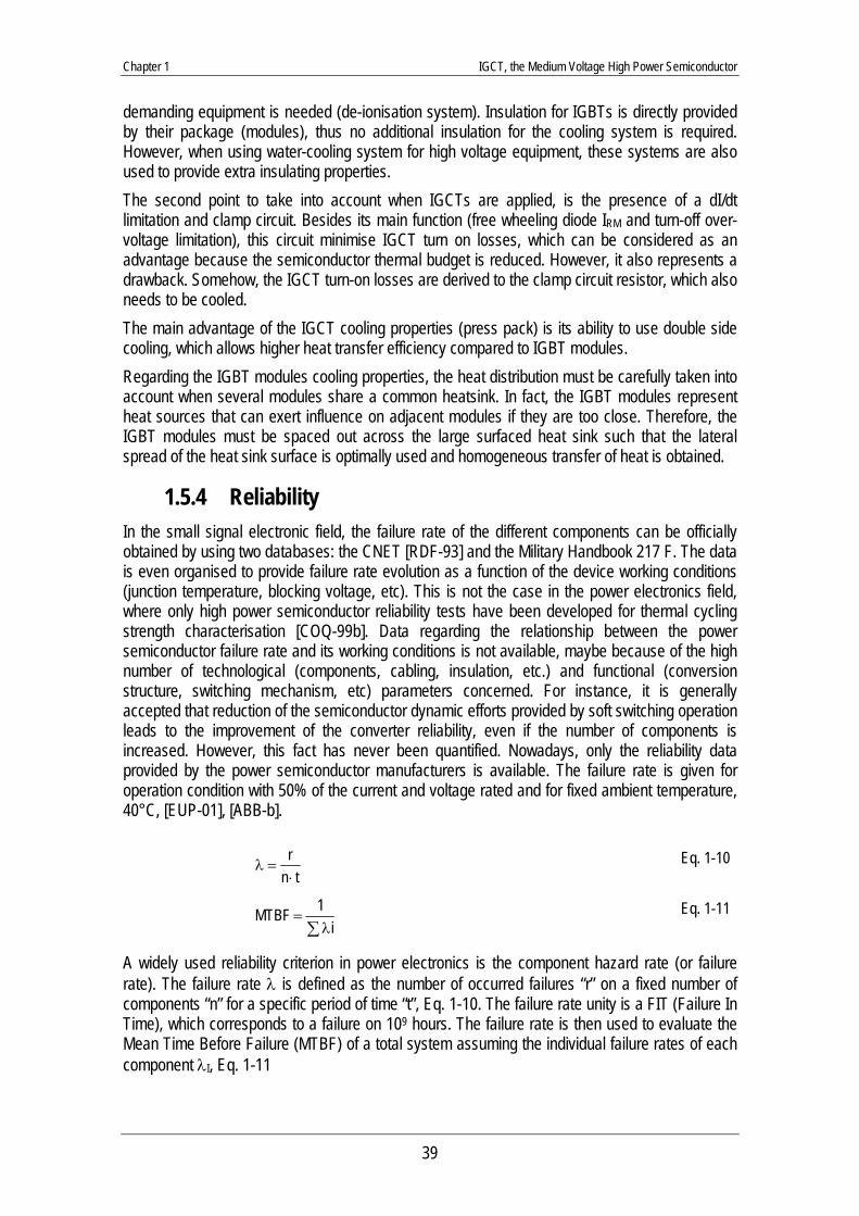
Chapter 1 IGCT, the Medium Voltage High Power Semiconductor
39
demanding equipment is needed (de-ionisation system). Insulation for IGBTs is directly provided by their package (modules), thus no additional insulation for the cooling system is required. However, when using water-cooling system for high voltage equipment, these systems are also used to provide extra insulating properties. The second point to take into account when IGCTs are applied, is the presence of a dI/dt limitation and clamp circuit. Besides its main function (free wheeling diode IRM and turn-off over-voltage limitation), this circuit minimise IGCT turn on losses, which can be considered as an advantage because the semiconductor thermal budget is reduced. However, it also represents a drawback. Somehow, the IGCT turn-on losses are derived to the clamp circuit resistor, which also needs to be cooled. The main advantage of the IGCT cooling properties (press pack) is its ability to use double side cooling, which allows higher heat transfer efficiency compared to IGBT modules. Regarding the IGBT modules cooling properties, the heat distribution must be carefully taken into account when several modules share a common heatsink. In fact, the IGBT modules represent heat sources that can exert influence on adjacent modules if they are too close. Therefore, the IGBT modules must be spaced out across the large surfaced heat sink such that the lateral spread of the heat sink surface is optimally used and homogeneous transfer of heat is obtained.
1.5.4 Reliability In the small signal electronic field, the failure rate of the different components can be officially obtained by using two databases: the CNET [RDF-93] and the Military Handbook 217 F. The data is even organised to provide failure rate evolution as a function of the device working conditions (junction temperature, blocking voltage, etc). This is not the case in the power electronics field, where only high power semiconductor reliability tests have been developed for thermal cycling strength characterisation [COQ-99b]. Data regarding the relationship between the power semiconductor failure rate and its working conditions is not available, maybe because of the high number of technological (components, cabling, insulation, etc.) and functional (conversion structure, switching mechanism, etc) parameters concerned. For instance, it is generally accepted that reduction of the semiconductor dynamic efforts provided by soft switching operation leads to the improvement of the converter reliability, even if the number of components is increased. However, this fact has never been quantified. Nowadays, only the reliability data provided by the power semiconductor manufacturers is available. The failure rate is given for operation condition with 50% of the current and voltage rated and for fixed ambient temperature, 40°C, [EUP-01], [ABB-b].
A widely used reliability criterion in power electronics is the component hazard rate (or failure rate). The failure rate λ is defined as the number of occurred failures “r” on a fixed number of components “n” for a specific period of time “t”, Eq. 1-10. The failure rate unity is a FIT (Failure In Time), which corresponds to a failure on 109 hours. The failure rate is then used to evaluate the Mean Time Before Failure (MTBF) of a total system assuming the individual failure rates of each component λI, Eq. 1-11
tnr⋅
=λ Eq. 1-10
∑λ=
i1MTBF Eq. 1-11
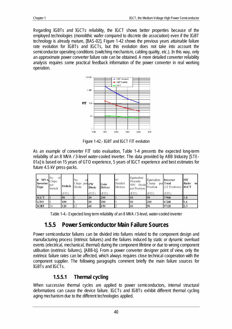
Chapter 1 IGCT, the Medium Voltage High Power Semiconductor
40
Regarding IGBTs and IGCTs reliability, the IGCT shows better properties because of the employed technologies (monolithic wafer compared to discrete die association) even if the IGBT technology is already mature, [BAS-02]. Figure 1-42 shows the previous years attainable failure rate evolution for IGBTs and IGCTs, but this evolution does not take into account the semiconductor operating conditions (switching mechanism, cabling quality, etc.). In this way, only an approximate power converter failure rate can be obtained. A more detailed converter reliability analysis requires some practical feedback information of the power converter in real working operation.
Figure 1-42.- IGBT and IGCT FIT evolution
As an example of converter FIT ratio evaluation, Table 1-4 presents the expected long-term reliability of an 8 MVA / 3-level water-cooled inverter. The data provided by ABB Industry [STE-01a] is based on 15 years of GTO experience, 5 years of IGCT experience and best estimates for future 4.5 kV press-packs.
Table 1-4.- Expected long term reliability of an 8 MVA / 3-level, water-cooled inverter
1.5.5 Power Semiconductor Main Failure Sources Power semiconductor failures can be divided into failures related to the component design and manufacturing process (intrinsic failures) and the failures induced by static or dynamic overload events (electrical, mechanical, thermal) during the component lifetime or due to wrong component utilisation (extrinsic failures), [ABB-b]. From a power converter designer point of view, only the extrinsic failure rates can be affected, which always requires close technical cooperation with the component supplier. The following paragraphs comment briefly the main failure sources for IGBTs and IGCTs.
1.5.5.1 Thermal cycling When successive thermal cycles are applied to power semiconductors, internal structural deformations can cause the device failure. IGCTs and IGBTs exhibit different thermal cycling aging mechanism due to the different technologies applied.
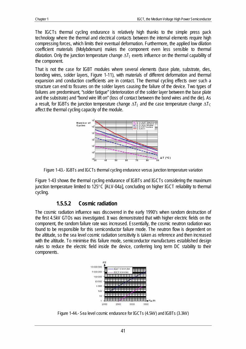
Chapter 1 IGCT, the Medium Voltage High Power Semiconductor
41
The IGCTs thermal cycling endurance is relatively high thanks to the simple press pack technology where the thermal and electrical contacts between the internal elements require high compressing forces, which limits their eventual deformation. Furthermore, the applied low dilation coefficient materials (Molybdenum) makes the component even less sensible to thermal dilatation. Only the junction temperature change ΔTJ exerts influence on the thermal capability of the component. That is not the case for IGBT modules where several elements (base plate, substrate, dies, bonding wires, solder layers, Figure 1-11), with materials of different deformation and thermal expansion and conduction coefficients are in contact. The thermal cycling effects over such a structure can end to fissures on the solder layers causing the failure of the device. Two types of failures are predominant, “solder fatigue” (deterioration of the solder layer between the base plate and the substrate) and “bond wire lift on” (loss of contact between the bond wires and the die). As a result, for IGBTs the junction temperature change ΔTJ and the case temperature change ΔTC affect the thermal cycling capacity of the module.
Figure 1-43.- IGBTs and IGCTs thermal cycling endurance versus junction temperature variation
Figure 1-43 shows the thermal cycling endurance of IGBTs and IGCTs considering the maximum junction temperature limited to 125°C [ALV-04a], concluding on higher IGCT reliability to thermal cycling.
1.5.5.2 Cosmic radiation The cosmic radiation influence was discovered in the early 1990’s when random destruction of the first 4.5kV GTOs was investigated. It was demonstrated that with higher electric fields on the component, the random failure rate was increased. Essentially, the cosmic neutron radiation was found to be responsible for this semiconductor failure mode. The neutron flow is dependent on the altitude, so the sea level cosmic radiation sensitivity is taken as reference and then increased with the altitude. To minimise this failure mode, semiconductor manufactures established design rules to reduce the electric field inside the device, conferring long term DC stability to their components.
Figure 1-44.- Sea level cosmic endurance for IGCTs (4.5kV) and IGBTs (3.3kV)
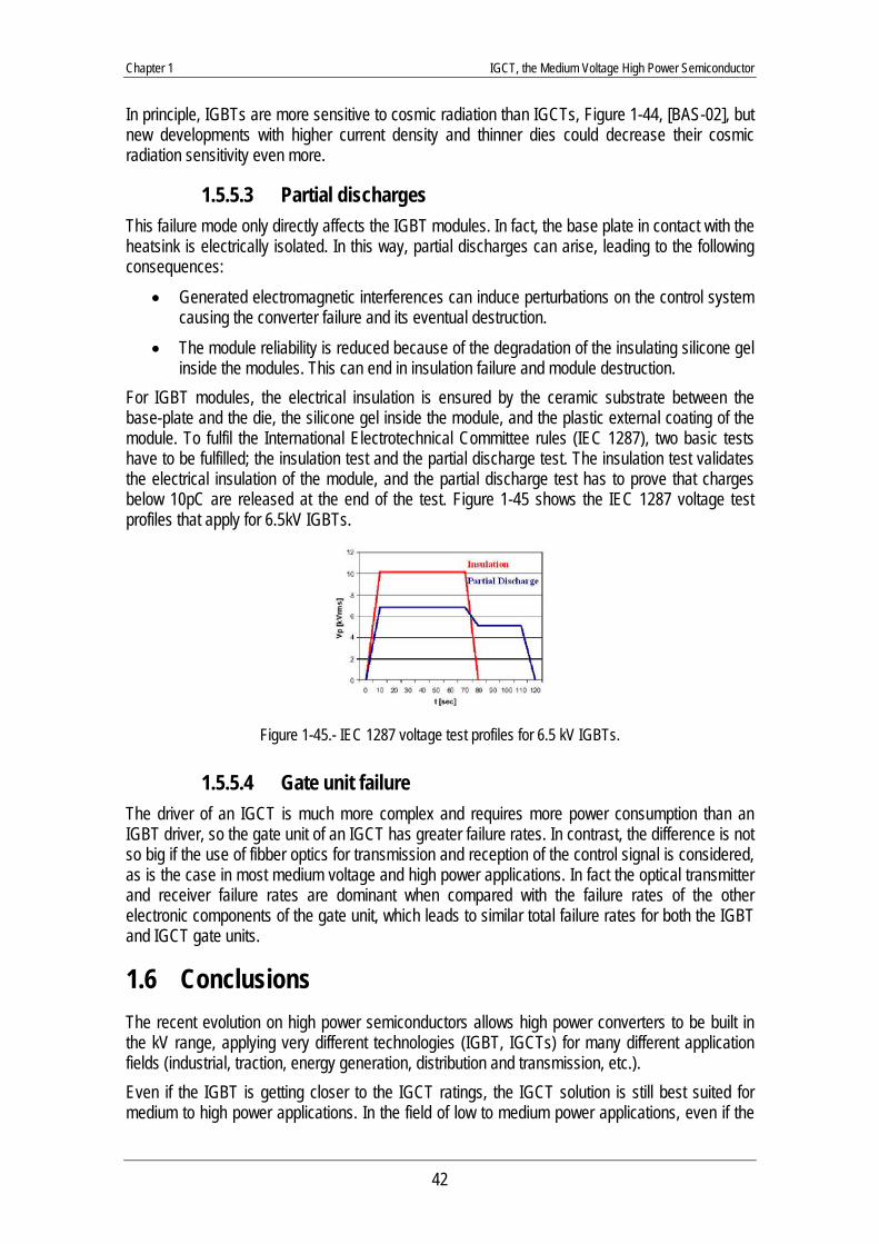
Chapter 1 IGCT, the Medium Voltage High Power Semiconductor
42
In principle, IGBTs are more sensitive to cosmic radiation than IGCTs, Figure 1-44, [BAS-02], but new developments with higher current density and thinner dies could decrease their cosmic radiation sensitivity even more.
1.5.5.3 Partial discharges This failure mode only directly affects the IGBT modules. In fact, the base plate in contact with the heatsink is electrically isolated. In this way, partial discharges can arise, leading to the following consequences:
• Generated electromagnetic interferences can induce perturbations on the control system causing the converter failure and its eventual destruction.
• The module reliability is reduced because of the degradation of the insulating silicone gel inside the modules. This can end in insulation failure and module destruction.
For IGBT modules, the electrical insulation is ensured by the ceramic substrate between the base-plate and the die, the silicone gel inside the module, and the plastic external coating of the module. To fulfil the International Electrotechnical Committee rules (IEC 1287), two basic tests have to be fulfilled; the insulation test and the partial discharge test. The insulation test validates the electrical insulation of the module, and the partial discharge test has to prove that charges below 10pC are released at the end of the test. Figure 1-45 shows the IEC 1287 voltage test profiles that apply for 6.5kV IGBTs.
Figure 1-45.- IEC 1287 voltage test profiles for 6.5 kV IGBTs.
1.5.5.4 Gate unit failure The driver of an IGCT is much more complex and requires more power consumption than an IGBT driver, so the gate unit of an IGCT has greater failure rates. In contrast, the difference is not so big if the use of fibber optics for transmission and reception of the control signal is considered, as is the case in most medium voltage and high power applications. In fact the optical transmitter and receiver failure rates are dominant when compared with the failure rates of the other electronic components of the gate unit, which leads to similar total failure rates for both the IGBT and IGCT gate units.
1.6 Conclusions The recent evolution on high power semiconductors allows high power converters to be built in the kV range, applying very different technologies (IGBT, IGCTs) for many different application fields (industrial, traction, energy generation, distribution and transmission, etc.). Even if the IGBT is getting closer to the IGCT ratings, the IGCT solution is still best suited for medium to high power applications. In the field of low to medium power applications, even if the

Chapter 1 IGCT, the Medium Voltage High Power Semiconductor
43
IGBT is the favoured component, a case to case analysis defining some priority design criterions (cost, reliability, maintenance, etc.) will be required to select the best solution. The examination in this chapter of the working principles, implementation requirements and future trends of IGCTs provides a clear glance at the advantages and drawbacks of this technology and the opportunities that such a component offers for Medium Voltage / Medium and High power applications.
44
2 Chapter 2
3.3 kV IGCTs Characterisation
2.1 Introduction When power semiconductors work in switching operation (hard or soft), the maximum switching frequency is practically limited by the total power losses and thermal properties of the device. However, the gate unit limits have also to be considered, (single pulse operation, burst mode, permanent switching operation). For a given heat transfer capacity of the semiconductor and its cooling system, the distribution between the semiconductor on-state and switching losses impose the maximum on-state current and switching frequency that can be handled. Depending on the application, the maximum attainable values can be modified, either giving preference to one of these two parameters (maximisation of the on-state current or switching frequency) or looking for a suitable trade-off. Currently, for standard 4.5kV asymmetric IGCTs (optimised for medium frequency and low turn-off losses) only switching frequencies below 1kHz are practically considered. If higher switching frequencies are needed, review of the IGCT ratings is required. In that way, based on the existing technology applied to the standard IGCT product line, ABB Semiconductors designed several experimental samples of 3.3kV LV IGCTs and their associated free wheeling diodes. The driver and package for 91mm wafers of the standard 4.5kV/4kA IGCT was used for the 3.3kV IGCT (5SHY 45L3300), whereas the 2.5kV (5SDF 10H2500) free wheeling diode was integrated into a 68mm wafer. Basically, the reduction of the silicon thickness and carefully adapted carrier lifetime engineering provided the required trade-off between the on-state and switching losses to increase the attainable switching frequency (500Hz – 2kHz) of the component retaining its “high current” capacity (2kA – 1kA). In order to characterise these components, a test bench applying the Opposition Method was developed at the LEEI. The application of this method allows driving the semiconductors under nominal working conditions in PWM operation avoiding the use of multi-megawatt loads and power supplies. The test bench is designed to characterise the semiconductors in DC chopper mode under DC link voltages and DC output currents reaching 1.5kVDC and 2kADC respectively. The switching frequency can also be selected (between 500Hz and 2kHz) maintaining the steady state duty cycle constant α≈0.5. In this chapter, a brief introduction of the standard semiconductor characterisation methods for the on-state and switching losses are given followed by the operation principle of the Opposition method test bench (power circuit and control strategy), its practical implementation and the 3.3kV IGCTs characterisation results.

Chapter 2 3.3 kV IGCTs Characterisation
45
2.2 High Power Semiconductors Characterisation Semiconductor manufacturers apply the existing standards [JED] [EIA-79], to specify their semiconductor characteristics. To determine the device properties (electrical, mechanical, thermal), several characterisation tests are performed (static and dynamic). Often, test characterisation conditions (junction temperature, off voltage, on current, dI/dt conditions, etc.) do not reflect the real operating conditions of semiconductors in power converters, so the power electronics designer must obtain an estimate of the semiconductor characteristics through extrapolation methods. That is the case with the device power losses (on-state and switching characteristic, mainly concerned in this analysis), which are very application dependent and essential for the definition of the semiconductor maximum current, voltage and switching frequency conditions as well as its cooling requisites [MAN-97]. For this reason, instead of using the standard characterisation methods (single / double pulse) to obtain the power losses characteristics of the 3.3kV IGCT and their free-wheeling diodes, the use of an Opposition Method [TUR-02] test bench that drives the semiconductors under real working conditions is proposed. Thanks to the Opposition Method operation principle, any semiconductor and converter operation mode could be reproduced, only the right conversion structure has to be applied, [BLO-99].
2.2.1 Power Losses Characterisation Standard Tests Semiconductor standards define the conditions that need to be applied to semiconductors in order to perform the characterisation tests. Generally, the semiconductor junction temperature is defined as one of the imposed test parameters and the test itself should not affect the predefined value. The preferred solution to comply with this condition is to control the device junction temperature by external heating and then perform a pulse test, which allows obtaining the required electric characteristics. Normally, high-speed digital systems are used for measuring and treating of the test voltage and current waveforms. A typical test circuit for pulse testing of IGCTs is shown in Figure 2-1, where Li, RCL, CCL and DCL form the dI/dt limitation and clamp circuit required for the safe switching operation of the IGCT and its freewheeling diode. First the component is pressed to the rated force and heated externally to the test temperature during a certain amount of time to reach a homogeneous temperature distribution of the junction temperature. Then, the input capacitor is charged with the VDC test voltage and the DUT (Device Under Test) is switched using a defined pattern until the test current ILOAD and the desired switching conditions (turn-on and turn-off) are reached. Depending on the LLOAD inductor value, the desired test voltage and current, the pulse test duration can last from several tens to several hundred μsec.
Figure 2-1.- IGCT test circuit. Pulse tester press clamping and heating system.
Chapter 2 3.3 kV IGCTs Characterisation
46
Depending on the desired characteristic (on state, turn-on or turn-off) and the component to be analysed (Free Wheeling Diode or IGCT), two basic pulse tests are considered, [LEM]. The single pulse test is mainly used to obtain the IGCT on-state and turn-off characteristics, Figure 2-2, whereas the double pulse test is used to obtain the IGCT turn-on and FWD turn-off characteristic, Figure 2-3.
Switching signal
ILOAD
IDUT
ON
OFF
ITEST
LOAD
DCLV
t
t
t
Switching signal
ILOAD
IDUT
ON
OFF
IDUT TEST
LOAD
DCLV
t
t
t
t
IFWD
IFWD TEST
Figure 2-2.- Single pulse test pattern Figure 2-3.- Double pulse test pattern
To determine the on-state characteristic, the on-state current and the resulting voltage across the test device are measured. They are next represented graphically by the semiconductor IT (on-state current) versus VT (on-state voltage) curve. The on-state voltage is temperature sensitive and so the device thermal equilibrium should be achieved before the measurement is made. The manner in which the test device is triggered into the on-state is unimportant as long as the test current is near the rated value. The junction test temperature must always be mentioned. Regarding the switching losses, diodes and controlled semiconductors should be characterised for the turn-on and turn-off switching transients. The parameters used for describing the switching losses (EOFF and EON) represent the energy dissipated in the device during the switching transients, they are given in joules per pulse. In the definition for the switching energy, Eq. 2-1, the instantaneous product v(t)·i(t) represents the instantaneous power of the device, and times t1 and t2 define the limits of integration. The main condition to obtain an accurate evaluation of the switching losses is the use of digital systems with sampling times fast enough compared to the switching times. Also, the use of current and voltage probes with known delays that can be compensated are advisable.
∫ ⋅⋅=2t
1t)J(dt)t(i)t(vE Eq. 2-1
When providing the switching losses defining parameters, elements and working conditions that influence their semiconductor performance need to be listed (switching voltage and current, circuit lay out, temperature, gate conditions, etc.).
2.2.2 Opposition Method Principle The opposition method principle is described in [TUR-02]. This method provides good accuracy in measuring power losses for high power converters. Furthermore, the converters can be tested at
Chapter 2 3.3 kV IGCTs Characterisation
47
full power without using power supplies and loads adapted to their maximal ratings (even several megawatts), only the power losses of the system need to be provided by the power supply. The principle of the opposition method consists of the use of two controllable voltage (current) sources that are linked by an inductor (capacitor). Both sources are controlled synchronously to impose the desired current (voltage) on the inductor (capacitor), Figure 2-4. Furthermore, the synchronisation control of both sources has to guarantee that the power generated by one source is going to be compensated by the other. In this way, the total power balance is reduced to the power losses on both sources and the inductor (capacitor).
In power electronics systems, each source can be implemented by any kind of converter (from the basic switching cell to the most complicated converter), both connected to the same auxiliary power supply (DC or AC single - multi-phase), Figure 2-5. Both converters are controlled to manage the reactive power exchange generating the desired testing conditions for the converters, their semiconductors and even the link passive components (inductors and capacitors) or other auxiliary systems (cooling system, drivers, etc.). The auxiliary power supply must supply only the active power that represents the total losses of the system. Obviously, the power supply voltage rating must match with the operating conditions of the converters to be tested.
Auxiliary Power Supply (DC / AC 1φ-3φ)
Source 1 (Power
Converter)
Source 2 (Power
Converter)
Link components
or
Total System Power Losses
Reactive Power Exchange
Figure 2-5.- Power converters in opposition method principle
2.3 Opposition Method Based Test Bench for 3.3kV IGCTs The proposed Opposition Method test bench allows the characterisation of 3.3kV IGCTs and their associated free wheeling diodes in chopper mode operation (DC/DC conversion), [LAD-04]. The system is designed to allow the semiconductor PWM operation for switching frequencies between
V1(t) V2(t) LLINK
IL(t)
Voltage Source
S1
Voltage Source
S2
dtL
)t(v)t(v)t(iLINK
21L ⋅
−= ∫ Eq. 2-2
I1(t) I2(t) VC(t)
Current Source
S1
Current Source
S2
CLINK
dtC
)t(i)t(i)t(vLINK
21C ⋅
−= ∫ Eq. 2-3
Figure 2-4.- Opposition Method operating principle
Chapter 2 3.3 kV IGCTs Characterisation
48
500Hz and 2kHz at a constant duty cycle (α=0.5) under DC link voltages and DC output current values ranging from 500V to 1.5kV and from 0 to 2kA respectively. The input power necessary to drive the semiconductors under these working conditions is only 40kW, while the maximum controlled power is 3MW (1.5kV × 2kA). The test bench is equipped with electrical and thermal measurements systems (voltage and current probes, oscilloscopes, power analyser, temperature and flow meters) to obtain the concerned characteristics. Mainly water cooled components are utilised to minimise the size of the test bench and to get smaller thermal time constants that require lower time to reach the steady thermal state where the measurement is to be taken.
2.3.1 Test Bench Power Stage The power stage of the test bench consists of two basic chopper switching cells (IGCT-Diode) arranged in the opposition configuration. The switching cells are controlled to manage the energy transfer between the input capacitor, CDC, and the output inductor, LS, Figure 2-6. A common dI/dt inductor and RCD clamp circuit are used for both switching cells to limit the dI/dt at turn-on and the over voltage at turn-off of the IGCTs. A fuse protects the test bench in the event of a switching cell short-circuit. In such a case, an input protection diode DP is used to avoid the polarity change on the input power supply. The maximum ratings of the test bench are summarised in Table 2-1.
Fuse
R CLAMP
L CLAMP
D CLAMP
Clamp Circuit
C CLAMP
0 ÷ 1500E
Power Supply
I DC
Input Filter
CDC
SwitchingCell 1
SwitchingCell 2
Output Inductor
T1
D1
IOUT
0 ÷2kA
LS, RS
IBUS
Control System
T2
D2
D P
Fuse Fuse
R CLAMP
L CLAMP
D CLAMPR CL
L CL
D CL
Clamp Circuit
C CL
0 ÷ 1500E
Power Supply
I DC
0 ÷ 1500V E
Power Supply
I DC
Input Filter
CDC Input Filter
CDC
SwitchingCell 1
SwitchingCell 2
Output Inductor
T1
D1
IOUT
0 ÷2kA
LS, RS
IBUS
Control System
T2
D2
D P
DC Bus Voltage 1.5 kV
Output DC Current 2 kA
Output Current Ripple 100 A
Switching Frequency 2 kHz
dI/dt at IGCT Turn On 1 kA/μs
Peak voltage at Turn Off 2.1 kV
Figure 2-6.- Power stage circuit of the 3.3kV IGCTs Test Bench Table 2-1.- Test Bench Maximum ratings
An adjustable electronic power supply is used to adjust the test DC input voltage between 0 and 1.5kV. Once the voltage is imposed, the control system is used to adjust the test output current between 0 and 2kA. The switching frequency can be also selected in the control system from 500Hz to 2kHz (500Hz, 750Hz, 1kHz, 1.25kHz, 1.5kHz, 2kHz). The dI/dt circuit is designed to keep the IGCT dI/dt at turn-on lower than 1kA/μs and the clamp-circuit to keep the maximum IGCT turn-off blocking voltage lower than 2.1kV.
2.3.2 Control Strategy Applying the Opposition method principle, each switching cell is controlled independently. The first switching cell works in PWM mode controlled by the DC output current IOUT control loop (α1 ≈ 0.5 in steady state), and the second switching cell works in open loop at constant duty cycle, (α2 = 0.5). The gate signals of both switching cells are phase-shifted to minimise the output current ripple and the inductor value (its weight and volume). The phase shift angle between both gate signals θ is carefully chosen to avoid the turn-on of an IGCT when the dI/dt limitation inductor is still magnetised during a turn-off transient, Figure 2-7, which could lead to diode failure due to
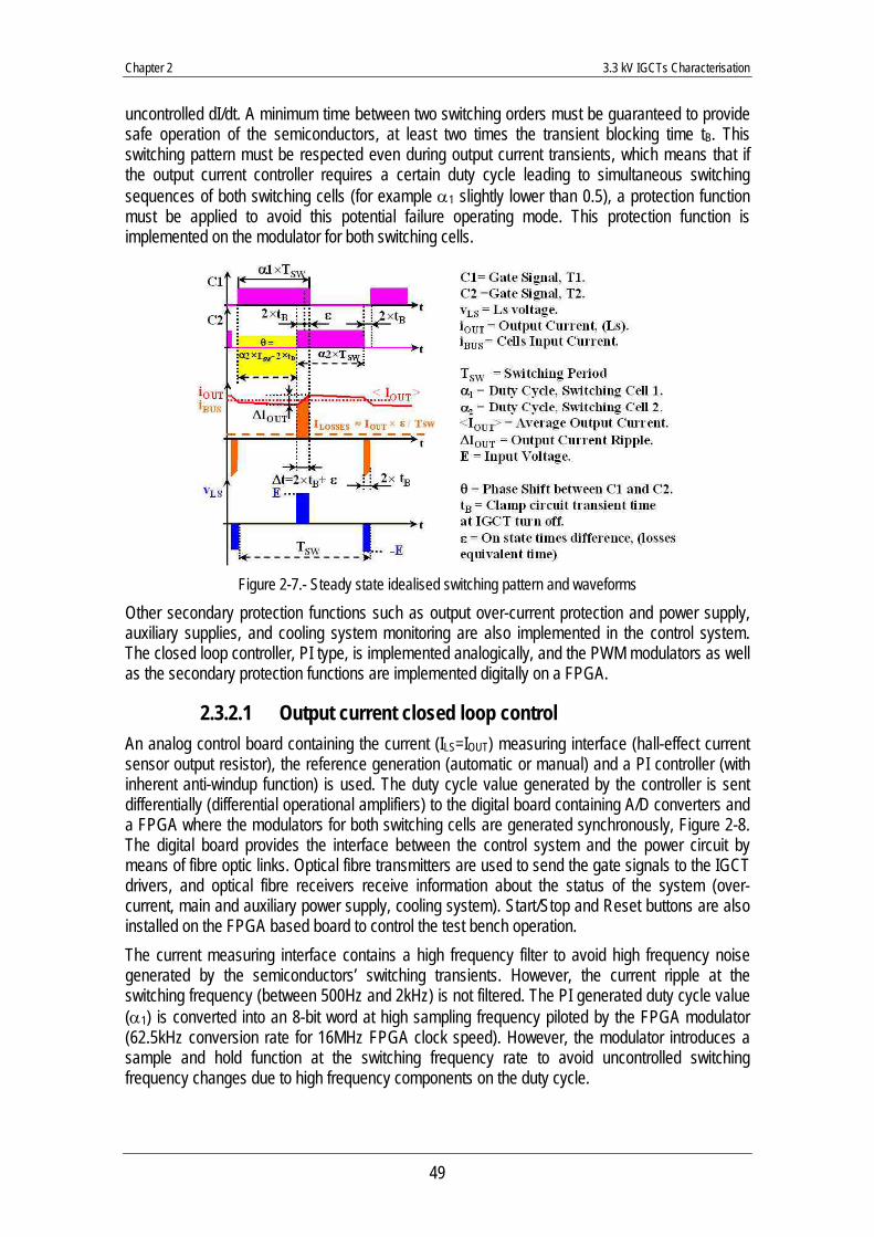
Chapter 2 3.3 kV IGCTs Characterisation
49
uncontrolled dI/dt. A minimum time between two switching orders must be guaranteed to provide safe operation of the semiconductors, at least two times the transient blocking time tB. This switching pattern must be respected even during output current transients, which means that if the output current controller requires a certain duty cycle leading to simultaneous switching sequences of both switching cells (for example α1 slightly lower than 0.5), a protection function must be applied to avoid this potential failure operating mode. This protection function is implemented on the modulator for both switching cells.
Figure 2-7.- Steady state idealised switching pattern and waveforms
Other secondary protection functions such as output over-current protection and power supply, auxiliary supplies, and cooling system monitoring are also implemented in the control system. The closed loop controller, PI type, is implemented analogically, and the PWM modulators as well as the secondary protection functions are implemented digitally on a FPGA.
2.3.2.1 Output current closed loop control An analog control board containing the current (ILS=IOUT) measuring interface (hall-effect current sensor output resistor), the reference generation (automatic or manual) and a PI controller (with inherent anti-windup function) is used. The duty cycle value generated by the controller is sent differentially (differential operational amplifiers) to the digital board containing A/D converters and a FPGA where the modulators for both switching cells are generated synchronously, Figure 2-8. The digital board provides the interface between the control system and the power circuit by means of fibre optic links. Optical fibre transmitters are used to send the gate signals to the IGCT drivers, and optical fibre receivers receive information about the status of the system (over-current, main and auxiliary power supply, cooling system). Start/Stop and Reset buttons are also installed on the FPGA based board to control the test bench operation. The current measuring interface contains a high frequency filter to avoid high frequency noise generated by the semiconductors’ switching transients. However, the current ripple at the switching frequency (between 500Hz and 2kHz) is not filtered. The PI generated duty cycle value (α1) is converted into an 8-bit word at high sampling frequency piloted by the FPGA modulator (62.5kHz conversion rate for 16MHz FPGA clock speed). However, the modulator introduces a sample and hold function at the switching frequency rate to avoid uncontrolled switching frequency changes due to high frequency components on the duty cycle.
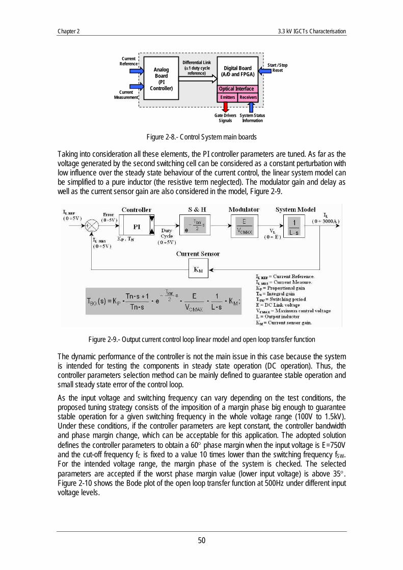
Chapter 2 3.3 kV IGCTs Characterisation
50
Analog Board
(PI Controller)
Digital Board (A/D and FPGA)
Differential Link (α1 duty cycle
reference)
Current Reference
Current Measurement
Optical Interface Emitters Receivers
Gate Drivers Signals
System Status Information
Start / Stop Reset
Figure 2-8.- Control System main boards
Taking into consideration all these elements, the PI controller parameters are tuned. As far as the voltage generated by the second switching cell can be considered as a constant perturbation with low influence over the steady state behaviour of the current control, the linear system model can be simplified to a pure inductor (the resistive term neglected). The modulator gain and delay as well as the current sensor gain are also considered in the model, Figure 2-9.
Figure 2-9.- Output current control loop linear model and open loop transfer function
The dynamic performance of the controller is not the main issue in this case because the system is intended for testing the components in steady state operation (DC operation). Thus, the controller parameters selection method can be mainly defined to guarantee stable operation and small steady state error of the control loop. As the input voltage and switching frequency can vary depending on the test conditions, the proposed tuning strategy consists of the imposition of a margin phase big enough to guarantee stable operation for a given switching frequency in the whole voltage range (100V to 1.5kV). Under these conditions, if the controller parameters are kept constant, the controller bandwidth and phase margin change, which can be acceptable for this application. The adopted solution defines the controller parameters to obtain a 60° phase margin when the input voltage is E=750V and the cut-off frequency fC is fixed to a value 10 times lower than the switching frequency fSW. For the intended voltage range, the margin phase of the system is checked. The selected parameters are accepted if the worst phase margin value (lower input voltage) is above 35°. Figure 2-10 shows the Bode plot of the open loop transfer function at 500Hz under different input voltage levels.
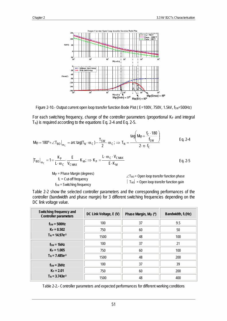
Chapter 2 3.3 kV IGCTs Characterisation
51
Figure 2-10.- Output current open loop transfer function Bode Plot ( E=100V, 750V, 1.5kV, fSW=500Hz)
For each switching frequency, change of the controller parameters (proportional KP and integral TN) is required according to the equations Eq. 2-4 and Eq. 2-5.
C
SW
C
NCSW
CNBO f2f
180fMtagT;
2T)T(tagarcTº180M
C ⋅π⋅
⎟⎟⎠
⎞⎜⎜⎝
⎛ ⋅+ϕ
=⇒ϖ⋅−ϖ⋅=∠+=ϕ ϖ Eq. 2-4
M
MAXCCPM
MAXCC
PBO KE
VLK;K
VE
LK1T
C ⋅
⋅ϖ⋅=⇒⋅⋅
ϖ⋅==ϖ Eq. 2-5
Mϕ = Phase Margin (degrees) fC = Cut-off frequency
fSW = Switching frequency
∠TBO = Open loop transfer function phase TBO= Open loop transfer function gain
Table 2-2 show the selected controller parameters and the corresponding performances of the controller (bandwidth and phase margin) for 3 different switching frequencies depending on the DC link voltage value.
Switching frequency and Controller parameters DC Link Voltage, E (V) Phase Margin, Mϕ (º) Bandwidth, fC(Hz)
100 37 9.5
750 60 50 fSW = 500Hz KP = 0.502
TN = 14.97e-3 1500 48 100
100 37 21
750 60 100 fSW = 1kHz KP = 1.005
TN = 7.485e-3 1500 48 200
100 37 39
750 60 200 fSW = 2kHz KP = 2.01
TN = 3.743e-3 1500 48 400
Table 2-2.- Controller parameters and expected performances for different working conditions
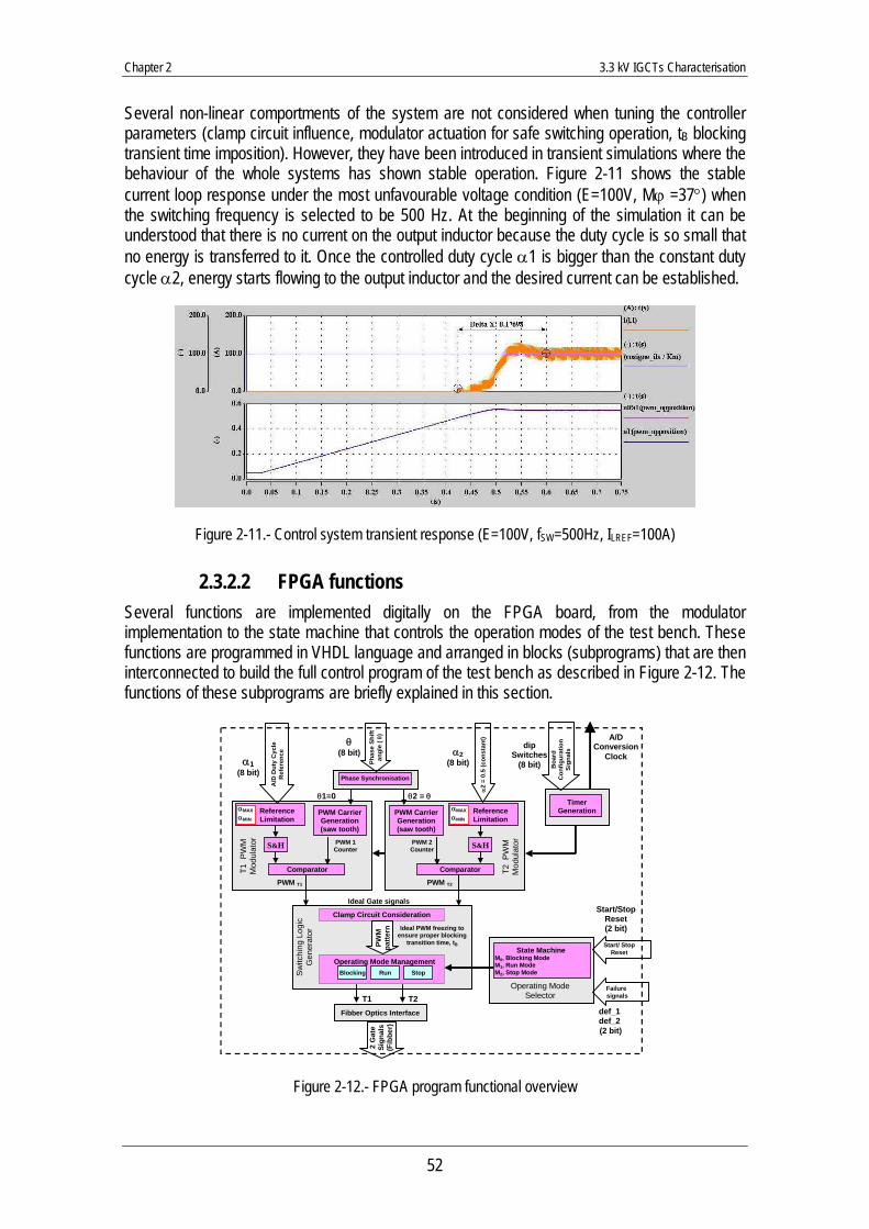
Chapter 2 3.3 kV IGCTs Characterisation
52
Several non-linear comportments of the system are not considered when tuning the controller parameters (clamp circuit influence, modulator actuation for safe switching operation, tB blocking transient time imposition). However, they have been introduced in transient simulations where the behaviour of the whole systems has shown stable operation. Figure 2-11 shows the stable current loop response under the most unfavourable voltage condition (E=100V, Mϕ =37°) when the switching frequency is selected to be 500 Hz. At the beginning of the simulation it can be understood that there is no current on the output inductor because the duty cycle is so small that no energy is transferred to it. Once the controlled duty cycle α1 is bigger than the constant duty cycle α2, energy starts flowing to the output inductor and the desired current can be established.
Figure 2-11.- Control system transient response (E=100V, fSW=500Hz, ILREF=100A)
2.3.2.2 FPGA functions Several functions are implemented digitally on the FPGA board, from the modulator implementation to the state machine that controls the operation modes of the test bench. These functions are programmed in VHDL language and arranged in blocks (subprograms) that are then interconnected to build the full control program of the test bench as described in Figure 2-12. The functions of these subprograms are briefly explained in this section.
State Machine M0, Blocking Mode M1, Run Mode M2, Stop Mode
Operating Mode Selector
Start/ Stop Reset
Start/Stop Reset (2 bit)
Failure signals
def_1 def_2 (2 bit)
Timer Generation
A/D Conversion
Clock
Boa
rd
Con
figur
atio
n Si
gnal
s dip
Switches(8 bit)
T1 T2
Fibber Optics Interface
2 G
ate
Sign
als
(Fib
ber)
T1 P
WM
M
odul
ator
PWM T1
PWM 1 Counter
PWM Carrier Generation (saw tooth)
Comparator
S&H
Reference Limitation
αMAX αMIN
α1 (8 bit)
A/D
Dut
y C
ycle
R
efer
ence
T2 P
WM
M
odul
ator
PWM T2
Comparator
S&H
Reference Limitation
αMAX αMIN
PWM 2 Counter
PWM Carrier Generation (saw tooth)
α2 (8 bit)
α2
= 0.
5 (c
onst
ant) θ
(8 bit)
Phas
e Sh
ift
angl
e ( θ
)
Phase Synchronisation
θ1=0 θ2 = θ
Ideal Gate signals
Clamp Circuit Consideration
Operating Mode Management Blocking Stop Run
PWM
pa
ttern
Ideal PWM freezing to ensure proper blocking
transition time, tB
Switc
hing
Log
ic
Gen
erat
or
Figure 2-12.- FPGA program functional overview
Chapter 2 3.3 kV IGCTs Characterisation
53
2.3.2.2.1 PWM modulator The PWM modulator is responsible of the ideal PWM pattern generation by comparing the duty cycle reference with the PWM carrier (saw tooth type). Also reference limitation and S&H functions in synchronism with the zero crossing of the PWM carrier are provided, which avoids measurement perturbation effects on the control loop due to commutation transitions. The switching frequency and other time dependent parameters (phase shift angle, blocking transient time generation, etc), can be selected by means of dip-switches. The most important quantities that can be directly affected with the selection of dip-switches are the switching frequency, the maximum and minimum on-state times, the phase shift angle between gate signals and the blocking transient time (ideal PWM pattern freezing time) that takes into account the existence of the clamp circuit.
2.3.2.2.2 Switching logic generator The switching logic generator defines the correct switching sequence depending on the operation mode of the test bench (Blocking, Run, Stop) and the ideal PWM pattern for both switching cells. The first function that this block implements is the freezing of the ideal PWM pattern generated previously when an IGCT blocking signal arrives. The first signal takes action but the other gate signal remains frozen for a defined period of time that guarantee the end of the blocking transition on the clamp circuit, thus providing safe switching operation of the semiconductors. The other main function of these elements is the management of the gate signals generation when the test bench changes from one operation mode to the other defined by the state machine that controls the operation of the test bench.
2.3.2.2.3 Operating mode selector (state machine) The semiconductors of the test bench can be driven into three different operation modes (M0, M1, M2). A state machine is utilised to manage how the test bench move from one to another, Figure 2-13.
• M0, Blocking Mode: In this operating mode, all semiconductors are in the blocking state. From this operation mode (state 0), the Run Mode can be reached if the Start/Stop switch generates a start order (leading edge). To avoid sending signals to the IGCTs gate drivers during the power up of the control system, the Start/Stop switch has to be kept for a defined minimum time (tON) on the Stop position, otherwise the state machine goes into a never ending loop (state 6) which requires the power down of the control system.
• M1, Run Mode: The IGCTs are controlled in PWM operation, with the first switching cell piloted from the analog control board, and the second switching cell working with constant duty cycle, α2=0.5. Also, a fixed phase shift angle between both gate signals is applied (close to half the switching period) which allows minimising the output current ripple.
• M2, Stop Mode: In this operating mode, a freewheeling sequence is generated to discharge safely the energy stored in the output inductor. Depending on the switching sequence previous to the Stop order, the free wheeling sequence is reached in a single commutation with either the upper or the lower switches, IGCT-Diode. Access to the Stop Mode can be accomplished by a normal operation stop order (lagging edge on the Start/Stop switch) or due to a fault signal generated because of output over current, power supply failure (main or auxiliary) or cooling system failure. All these faults are collected, coded and sent by a third control board (protection board)
Chapter 2 3.3 kV IGCTs Characterisation
54
to the FPGA control board by means of two fibber optic links, def_2 and def_1 (2 bit code). The test bench operation mode and error status are displayed by means of several LEDs as defined in Table 2-3.
def_2 def_1 Operating Mode Lighting LED
1 1 Run Mode GREEN
0 1 Output over current RED 1
1 0 Power Supply failure (main or auxiliary supply) RED 2
0 0 Cooling system failure RED 3
Table 2-3.- Protection Board signals meaning
Figure 2-13.- Test bench control system state machine
2.3.3 Component Dimensioning When applying the Opposition Method principle, the steady state working conditions and maximum current and voltage ratings of the components are mainly defined by the total power losses of the system. In the proposed 3.3kV IGCT characterisation test bench, as shown in Figure 2-7, the steady state duty cycle of the first switching cell, α1, is slightly higher than the constant duty cycle of the second switching cell (α2=0.5). The difference between the on-state times of both switching cells (ε=(α1-α2)×TSW) is only dependent on the active power that has to be supplied by the input power supply, that is the total power losses of the converter, Eq. 2-6. For this reason, the definition of the values and ratings of the components employed in the test bench (mainly passive components) need the previous estimation of the total power losses. For the components that have to be characterised (IGCTs and Diodes), the projected semiconductors data presented in [BAS-02] are used. For the other components, approximate data extrapolated from similar available components or empirical approximations are employed.
SW
OUTTIELossesPower ε⋅⋅
= Eq. 2-6
Once the operation conditions and values of the components are defined through the total power losses estimation, simulation assisted dimensioning for the main components is performed.
Chapter 2 3.3 kV IGCTs Characterisation
55
2.3.3.1 Test bench power losses estimation Before evaluating the total losses of the test bench, the proper semiconductor switching conditions need to be guaranteed. Considering the test bench working conditions and the switching condition limits of the 3.3kV IGCTs and their freewheeling diodes, the selection of the dI/dt inductor and RCD clamp circuit components values are selected, Table 2-4 (see 1.3.1.3 dI/dt limitation, clamp circuit) and checked by simulation, Figure 2-14.
EMAX, maximum DC Link Voltage 1.5kV
dI/dtMAX, maximum dI/dt at IGCTs turn on 1 kA/μs LCL MIN =1.5 μH
ΔVCL MAX, maximum semiconductors voltage overshoot 650V
tB MAX, maximum blocking transition time 6.1μs
CCL= 6μF RCL = 0.75 Ω
Table 2-4.- Components values of the dI/dt inductor and RCD clamp circuit
Figure 2-14.- dI/dt inductor and RCD clamp circuit maximum operating conditions
With these values already fixed, the evaluation of the test bench total losses is performed, Table 2-5. The power losses are evaluated at the maximum test bench output current and DC link voltage ratings (2kA, 1.5kV) for three switching frequencies (500Hz, 1kHz and 2kHz). Three main power losses sources are considered in the estimation process,
• Semiconductors, (switching cells IGCTs and Diodes): On state losses and switching losses are evaluated taking into account the expected output current ripple, ΔILS MAX =100A, and a maximum duty cycle difference between both switching cells (α1 - α2) lower than 0.025.
• Clamp resistor, RCL: the energy stored on the clamp inductor LCL is supposed to be evacuated completely over the clamp resistor. The frequency rate is twice the switching frequency (2 switching cells). The maximum output current (current ripple effect) is considered in the clamp resistor power losses evaluation.
• Output inductor parasitic resistor, RS: The Joule effect power losses on the output inductor are taken into account. The parasitic resistor value is estimated to be around RS=1.25 mΩ.
Chapter 2 3.3 kV IGCTs Characterisation
56
ILS = 2kA, E = 1.5kV, ΔILS = 100A
fSW 500Hz 1000Hz 2000Hz
On state 1712 W 1712 W 1712W IGCT 1 α1 = 0.525 Switching 1250 W 2500 W 5000 W
On state 1862 W 1862 W 1862 W Diode 1 1-α1 = 0.475 Switching 840 W 1680 W 3360 W
On state 1630 W 1630 W 1630 W IGCT 2 α2 = 0.5 Switching 1250 W 2500 W 5000 W
On state 1960 W 1960 W 1960 W Diode 2 1-α2 = 0.5 Switching 840 W 1680 W 3360 W
On state 7164W 7164W 7164W
Switching 4180 W 8360 W 16720 W
Semiconductor Total Losses
Total 11344W 15524W 23884W
CLAMP Losses (LCL·ILS MAX2·fSW )
3152W 6304W 12608 W
Output Inductor (Rs·ILS DC2)
5000 W 5000 W 5000 W
Total Losses 19496 W 26828 W 41492 W
Table 2-5.- Test bench power losses estimation
The estimation of power losses helps to define the power requirements of the input power supply, but also allows establishing the on state time difference between both switching cells ε, Eq. 2-6, which will be required for the definition of the test bench components. Table 2-6 shows the ε values for the three switching frequencies considered.
fSW = 500Hz fSW = 1000Hz fSW = 2000Hz
SWOUT
TIELossesPower
⋅=ε 13 μs 8.94 μs 6.92 μs
Table 2-6.- On state time difference between switching cell 1 and 2
2.3.3.2 Output inductor, LS The use of a phase shift angle θ between the gate signals of the switching cell 1 and 2 allows the minimisation of the output inductor value, LS, which implies the minimisation of its weight and volume. However, the value of θ is restricted by the existence of a single dI/dt inductor and RCD clamp circuit for both switching cells. In steady state operation θ is fixed to guarantee a minimum time between two consecutive switching transitions, at least twice the clamp imposed maximum blocking transition time, (2⋅tB MAX) Eq. 2-7. Furthermore, for the safe operation of semiconductors in transient conditions, the modulator is designed to freeze the adjacent gate signals at each switching transition order to guarantee this minimum time between two successive commutations. Under these operation restrictions, and imposing a maximum current ripple at the switching frequency lower than 5% of the maximum DC output current (ΔILS MAX ≤100A), the output inductor value is defined. The maximum input voltage pulse width ΔtMAX applied to the inductor when the input voltage is maximum and the current ripple limit impose the minimum value of LS. The
Chapter 2 3.3 kV IGCTs Characterisation
57
maximum pulse width is subordinated to ε, Eq. 2-8, and occurs when the switching frequency is 500 Hz. Such considerations lead to an inductor value bigger than 382.5 μH, Eq. 2-9.
MAXB2 t2 ⋅−α=θ Eq. 2-7
MAXBMAXMAX t2t ⋅+ε=Δ Eq. 2-8
H5.382I
tELMAXLS
MAXMAXMINS μ=
ΔΔ⋅
> Eq. 2-9
Transient simulations help to define the output inductor dimensioning voltage and current ratings, Table 2-7. Special attention has to be paid to the voltage across the inductor. In Figure 2-15 it can be seen how the maximum voltage over the inductor is higher than the DC link input voltage due to the effect RCD clamp circuit, which has to be taken into account when defining the insulation properties of the component. Finally an LS=400μH output inductor is specified and a water-cooled custom design solution is selected (LS=400μH / 2kA, 450kg, 650mm × 500mm × 900mm, Boige & Vignal S.A.).
FSW = 500 Hz ÷ 2000 Hz
Component IMAX IRMS IAV ΔI ΔV VMAX
LS = 400μH 2050 A 2000 A 2000A 100A 2200V ±2200V
Table 2-7.- Output inductor dimensioning parameters
Figure 2-15.- Output inductor voltage and current steady state waveforms (E=1.5kV, fSW=500Hz)
2.3.3.3 Input capacitor, CDC The value of the input capacitor is imposed by the maximum input voltage pulse width applied to the output inductor ΔtMAX, which also represents the maximum pulse width of the maximum output current circulating through the input capacitor. This consideration, together with the
Chapter 2 3.3 kV IGCTs Characterisation
58
maximum admissible switching frequency voltage ripple limited to less than 5% of the maximum input voltage (ΔVC DC <75V), imposes the minimum value of the input capacitor, Eq. 2-10.
F680V
tIC
MAXDCC
MAXMAXOUTMINDC μ=
Δ
Δ⋅> Eq. 2-10
Regarding the current ratings of the capacitor, not only the RMS and peak current values are required. Also, the current spectrum is used by the capacitors manufacturer to determine the total dissipation of the component and its ability to withstand the working conditions. Figure 2-16 shows the capacitor steady state current and voltage waveforms as well as the capacitor current spectrum for the maximum DC output current (2kA) at 2kHz. The maximum peak current that the capacitor has to withstand is greater than the output current due to the effects of the clamp circuit.
Figure 2-16.- Input capacitor steady state current and voltage waveforms (E=1.5kV, IOUT=2kHz, fSW=2kHz). Capacitor current spectrum
The capacitor dimensioning parameters are given in Table 2-8. A commercially available 3000μF /600ARMS /2150VDC capacitor (TRAFIM DKFTM266B3007, AVX) is finally utilised.
FSW = 500 Hz ÷ 2000 Hz
Component IMAX IRMS IAV ΔI ΔV VMAX
CDC = 1000μF 2700 A 540 A 0 A 2700A 50V 1600 V
Table 2-8.- Input capacitor dimensioning parameters
2.3.3.4 dI/dt inductor and RCD clamp circuit components The dI/dt inductor and RCD clamp circuit components values being already selected, the dimensioning ratings in terms of voltage and current are obtained using idealised simulations. Table 2-9 summarises the dimensioning parameters for these components.
Chapter 2 3.3 kV IGCTs Characterisation
59
FSW = 500 Hz ÷ 2000 Hz
Component IMAX IRMS IAV ΔI ΔV VMAX
LCL = 1.5μH 2050 A 510 A 60 A 2050 A 1600 V 1600 V
CCL = 6μF 2050 A 165 A 0 A 2050 A 650 V 2200 V
RCL = 0.75Ω 890 A 128 A 30 A 890 A 660V 660 V
DCL 2050 A 210 A 30 A 2050 A 1500 V 1500 V
Table 2-9.- dI/dt inductor and clamp circuit components dimensioning parameters
Figure 2-17 shows the simulated waveforms (ideal components) for the dI/dt inductor and RCD clamp circuit at maximum output current and input voltage for 2kHz operation.
Figure 2-17.- dI/dt inductor and RCD clamp circuit waveforms (E=1.5kV, IOUT=2kHz, fSW=2kHz)
Except for the clamp diode (5SDF 03D4502, ABB), the components specifications impose the use of custom designed components or association of existing components. For the clamp inductor, an air-cored solution is preferred to avoid the change on the inductance value. A custom design solution is selected (1.7μH, 600ARMS, 150mm × 150mm × 305mm, Boige and Vignal). Regarding the clamp capacitor, three low inductive capacitors (2μF) with axial connections in parallel are used, (FPG86X0205J, AVX). Due to the high power dissipation of the clamp resistor (12.6kW), an arrangement of 24 non-inductive resistors in parallel (UXP600-18Ω / 600W, EBG) distributed over 3 water-cooled heatsinks (AAVID Thermalloy custom design) is adopted. Bus bar connections are used to minimise the parasitic inductance of the parallel arrangement. The interconnection between all these elements is carefully defined to minimise the switching path unclamped parasitic inductor and thus the voltage spike over the switching cell semiconductors.
2.3.4 Test Bench Lay-out The disposition of the test bench components is selected to provide good access to the platform for the required measurements (electrical and thermal) and flexibility in the mounting and dismounting process of the component in case of necessity (failure, replacement of components). Also, special attention is paid to the semiconductor main switching loops, applying low inductive
Chapter 2 3.3 kV IGCTs Characterisation
60
bus bars where possible. Due to the high current values that are handled, some flexible current connections are provided to avoid mechanical stress over the semiconductors mechanical arrangements induced by thermal expansion. Also high surface contacts with several connecting points are utilised to provide good electric contact. Regarding protection issues, besides the active protection functions implemented by the control system, the required electrical and mechanical protection means are provided. Electrically, the chassis of all the components are connected to the protection earth when they are not under voltage (output inductor, input capacitor, power supply, etc). If they are under voltage, the required insulation according to the voltage level is provided (water tubes length, bus bar isolation, mechanical clamps supporting base, etc). Also, when the test bench is not operative, the input capacitor is short-circuited by means of a discharging circuit to avoid dangerous remaining voltages on the test bench. Mechanically, all the power stage components except the output inductor are installed on a chassis. This chassis is equipped with transparent polycarbonate plates for protecting people against any projected particles and allows visual supervision of the components. Also, isolated mechanical barriers are positioned between the control desk and the test bench to guarantee people safe insulation. The test bench is equipped with the electrical and thermal probes and equipments required to accomplish the characterisation of the components. Figure 2-18 shows the general overview of the developed test bench. Other relevant details concerning different aspects of the test bench layout are shown in the following paragraphs.
Figure 2-18.- 3.3kV IGCT characterisation test bench overview
2.3.4.1 Power stage components The main feature of the test bench layout is the arrangement of the power semiconductors. In contrast to the classical stacked assembly of press pack components, here each semiconductor is fitted into an independent mechanical clamp with the required heat-sinks (ABB) and hardened steel made force spreaders, Figure 2-19. This disposition provides high flexibility degree for mounting and dismounting the semiconductors in case of failure and avoids thermal interaction between components, which guarantees well defined thermal measurements. Furthermore, this kind of layout allows the use of low inductive bus-bars to minimise the parasitic inductance of the switching path between the power semiconductors and the clamp circuit components.
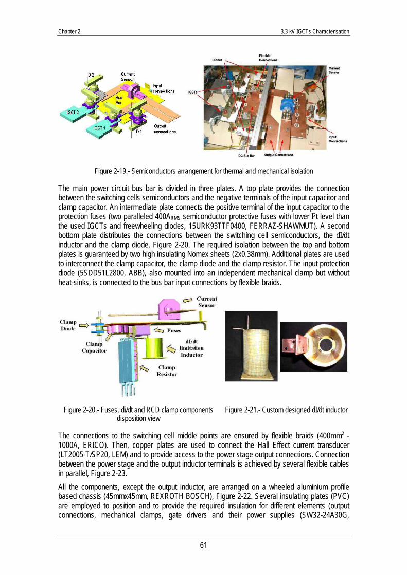
Chapter 2 3.3 kV IGCTs Characterisation
61
Figure 2-19.- Semiconductors arrangement for thermal and mechanical isolation
The main power circuit bus bar is divided in three plates. A top plate provides the connection between the switching cells semiconductors and the negative terminals of the input capacitor and clamp capacitor. An intermediate plate connects the positive terminal of the input capacitor to the protection fuses (two paralleled 400ARMS semiconductor protective fuses with lower I2t level than the used IGCTs and freewheeling diodes, 15URK93TTF0400, FERRAZ-SHAWMUT). A second bottom plate distributes the connections between the switching cell semiconductors, the dI/dt inductor and the clamp diode, Figure 2-20. The required isolation between the top and bottom plates is guaranteed by two high insulating Nomex sheets (2x0.38mm). Additional plates are used to interconnect the clamp capacitor, the clamp diode and the clamp resistor. The input protection diode (5SDD51L2800, ABB), also mounted into an independent mechanical clamp but without heat-sinks, is connected to the bus bar input connections by flexible braids.
Figure 2-20.- Fuses, di/dt and RCD clamp components disposition view
Figure 2-21.- Custom designed dI/dt inductor
The connections to the switching cell middle points are ensured by flexible braids (400mm² - 1000A, ERICO). Then, copper plates are used to connect the Hall Effect current transducer (LT2005-T/SP20, LEM) and to provide access to the power stage output connections. Connection between the power stage and the output inductor terminals is achieved by several flexible cables in parallel, Figure 2-23. All the components, except the output inductor, are arranged on a wheeled aluminium profile based chassis (45mmx45mm, REXROTH BOSCH), Figure 2-22. Several insulating plates (PVC) are employed to position and to provide the required insulation for different elements (output connections, mechanical clamps, gate drivers and their power supplies (SW32-24A30G,
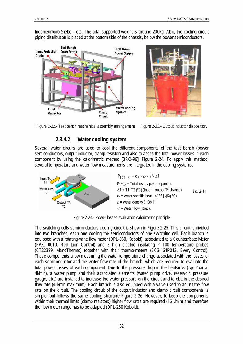
Chapter 2 3.3 kV IGCTs Characterisation
62
Ingenieurbüro Siebel), etc. The total supported weight is around 200kg. Also, the cooling circuit piping distribution is placed at the bottom side of the chassis, below the power semiconductors.
Figure 2-22.- Test bench mechanical assembly arrangement Figure 2-23.- Output inductor disposition.
2.3.4.2 Water cooling system Several water circuits are used to cool the different components of the test bench (power semiconductors, output inductor, clamp resistor) and also to asses the total power losses in each component by using the calorimetric method [BRO-96], Figure 2-24. To apply this method, several temperature and water flow measurements are integrated in the cooling systems.
T'cP PX_TOT Δ×ν×ρ×=
PTOT_X = Total losses per component. ΔT = T1–T2 (ºC) (input – output Tª change). cP = water specific heat - 4186 J/(Kg ºC). ρ = water density (1Kg/ l ). ν’ = Water flow (l/sec).
Eq. 2-11
Figure 2-24.- Power losses evaluation calorimetric principle
The switching cells semiconductors cooling circuit is shown in Figure 2-25. This circuit is divided into two branches, each one cooling the semiconductors of one switching cell. Each branch is equipped with a rotating-vane flow meter (DPL-060, Kobold), associated to a Counter/Rate Meter (PAXI 0010, Red Lion Control) and 3 high electric insulating PT100 temperature probes (CT22389, ManoThermo) together with their thermo-meters (EC3-161P012, Every Control). These components allow measuring the water temperature change associated with the losses of each semiconductor and the water flow rate of the branch, which are required to evaluate the total power losses of each component. Due to the pressure drop in the heatsinks (ΔP=2bar at 4l/min), a water pump and their associated elements (water pump drive, reservoir, pressure gauge, etc.) are installed to increase the water pressure on the circuit and to obtain the desired flow rate (4 l/min maximum). Each branch is also equipped with a valve used to adjust the flow rate on the circuit. The cooling circuit of the output inductor and clamp circuit components is simpler but follows the same cooling structure Figure 2-26. However, to keep the components within their thermal limits (clamp resistors) higher flow rates are required (16 l/min) and therefore the flow meter range has to be adapted (DPL-250 Kobold).
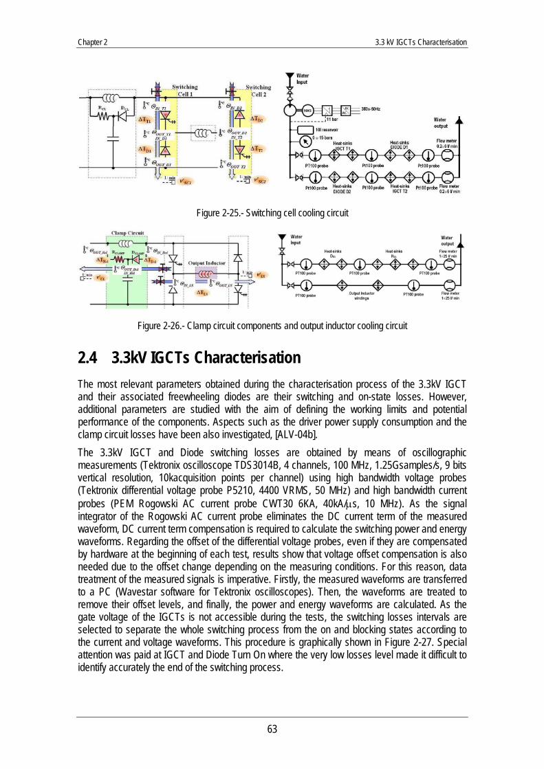
Chapter 2 3.3 kV IGCTs Characterisation
63
Figure 2-25.- Switching cell cooling circuit
Figure 2-26.- Clamp circuit components and output inductor cooling circuit
2.4 3.3kV IGCTs Characterisation The most relevant parameters obtained during the characterisation process of the 3.3kV IGCT and their associated freewheeling diodes are their switching and on-state losses. However, additional parameters are studied with the aim of defining the working limits and potential performance of the components. Aspects such as the driver power supply consumption and the clamp circuit losses have been also investigated, [ALV-04b]. The 3.3kV IGCT and Diode switching losses are obtained by means of oscillographic measurements (Tektronix oscilloscope TDS3014B, 4 channels, 100 MHz, 1.25Gsamples/s, 9 bits vertical resolution, 10kacquisition points per channel) using high bandwidth voltage probes (Tektronix differential voltage probe P5210, 4400 VRMS, 50 MHz) and high bandwidth current probes (PEM Rogowski AC current probe CWT30 6KA, 40kA/μs, 10 MHz). As the signal integrator of the Rogowski AC current probe eliminates the DC current term of the measured waveform, DC current term compensation is required to calculate the switching power and energy waveforms. Regarding the offset of the differential voltage probes, even if they are compensated by hardware at the beginning of each test, results show that voltage offset compensation is also needed due to the offset change depending on the measuring conditions. For this reason, data treatment of the measured signals is imperative. Firstly, the measured waveforms are transferred to a PC (Wavestar software for Tektronix oscilloscopes). Then, the waveforms are treated to remove their offset levels, and finally, the power and energy waveforms are calculated. As the gate voltage of the IGCTs is not accessible during the tests, the switching losses intervals are selected to separate the whole switching process from the on and blocking states according to the current and voltage waveforms. This procedure is graphically shown in Figure 2-27. Special attention was paid at IGCT and Diode Turn On where the very low losses level made it difficult to identify accurately the end of the switching process.
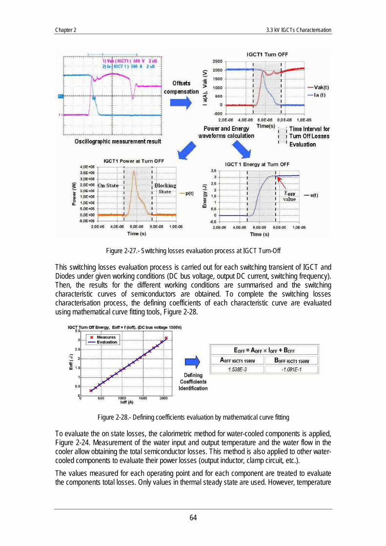
Chapter 2 3.3 kV IGCTs Characterisation
64
Figure 2-27.- Switching losses evaluation process at IGCT Turn-Off
This switching losses evaluation process is carried out for each switching transient of IGCT and Diodes under given working conditions (DC bus voltage, output DC current, switching frequency). Then, the results for the different working conditions are summarised and the switching characteristic curves of semiconductors are obtained. To complete the switching losses characterisation process, the defining coefficients of each characteristic curve are evaluated using mathematical curve fitting tools, Figure 2-28.
Figure 2-28.- Defining coefficients evaluation by mathematical curve fitting
To evaluate the on state losses, the calorimetric method for water-cooled components is applied, Figure 2-24. Measurement of the water input and output temperature and the water flow in the cooler allow obtaining the total semiconductor losses. This method is also applied to other water-cooled components to evaluate their power losses (output inductor, clamp circuit, etc.). The values measured for each operating point and for each component are treated to evaluate the components total losses. Only values in thermal steady state are used. However, temperature
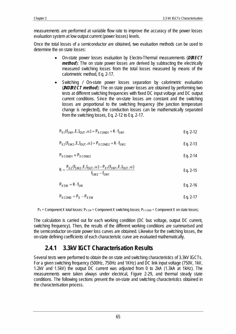
Chapter 2 3.3 kV IGCTs Characterisation
65
measurements are performed at variable flow rate to improve the accuracy of the power losses evaluation system at low output current (power losses) levels. Once the total losses of a semiconductor are obtained, two evaluation methods can be used to determine the on state losses:
• On-state power losses evaluation by Electro-Thermal measurements (DIRECT method): The on state power losses are derived by subtracting the electrically measured switching losses from the total losses measured by means of the calorimetric method, Eq. 2-17.
• Switching / On-state power losses separation by calorimetric evaluation (INDIRECT method): The on state power losses are obtained by performing two tests at different switching frequencies with fixed DC input voltage and DC output current conditions. Since the on-state losses are constant and the switching losses are proportional to the switching frequency (the junction temperature change is neglected), the conduction losses can be mathematically separated from the switching losses, Eq. 2-12 to Eq. 2-17.
1SW1CONDXOUT1SW1X fKP),I,E,f(P ⋅+=α Eq. 2-12
2SW2CONDXOUT2SW2X fKP),I,E,f(P ⋅+=α Eq. 2-13
2CONDX1CONDX PP ≈ Eq. 2-14
1SW2SW
OUT1SW1XOUT2SW2Xff
),I,E,f(P),I,E,f(PK−
α−α= Eq. 2-15
SWSWX fKP ⋅= Eq. 2-16
SWXXCONDX PPP −= Eq. 2-17
PX = Component X total losses: PX SW = Component X switching losses; PX COND = Component X on state losses;
The calculation is carried out for each working condition (DC bus voltage, output DC current, switching frequency). Then, the results of the different working conditions are summarised and the semiconductor on-state power loss curves are obtained. Likewise for the switching losses, the on-state defining coefficients of each characteristic curve are evaluated mathematically.
2.4.1 3.3kV IGCT Characterisation Results Several tests were performed to obtain the on state and switching characteristics of 3.3kV IGCTs. For a given switching frequency (500Hz, 750Hz and 1KHz) and DC link input voltage (750V, 1kV, 1.2kV and 1.5kV) the output DC current was adjusted from 0 to 2kA (1.3kA at 1kHz). The measurements were taken always under electrical, Figure 2-29, and thermal steady state conditions. The following sections present the on-state and switching characteristics obtained in the characterisation process.
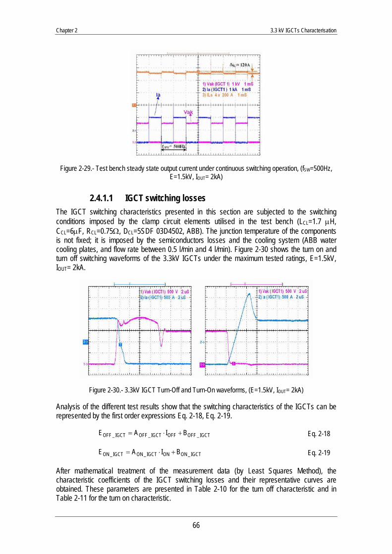
Chapter 2 3.3 kV IGCTs Characterisation
66
Figure 2-29.- Test bench steady state output current under continuous switching operation, (fSW=500Hz, E=1.5kV, IOUT= 2kA)
2.4.1.1 IGCT switching losses The IGCT switching characteristics presented in this section are subjected to the switching conditions imposed by the clamp circuit elements utilised in the test bench (LCL=1.7 μH, CCL=6μF, RCL=0.75Ω, DCL=5SDF 03D4502, ABB). The junction temperature of the components is not fixed; it is imposed by the semiconductors losses and the cooling system (ABB water cooling plates, and flow rate between 0.5 l/min and 4 l/min). Figure 2-30 shows the turn on and turn off switching waveforms of the 3.3kV IGCTs under the maximum tested ratings, E=1.5kV, IOUT= 2kA.
Figure 2-30.- 3.3kV IGCT Turn-Off and Turn-On waveforms, (E=1.5kV, IOUT= 2kA)
Analysis of the different test results show that the switching characteristics of the IGCTs can be represented by the first order expressions Eq. 2-18, Eq. 2-19.
IGCT_OFFOFFIGCT_OFFIGCT_OFF BIAE +⋅= Eq. 2-18
IGCT_ONONIGCT_ONIGCT_ON BIAE +⋅= Eq. 2-19
After mathematical treatment of the measurement data (by Least Squares Method), the characteristic coefficients of the IGCT switching losses and their representative curves are obtained. These parameters are presented in Table 2-10 for the turn off characteristic and in Table 2-11 for the turn on characteristic.
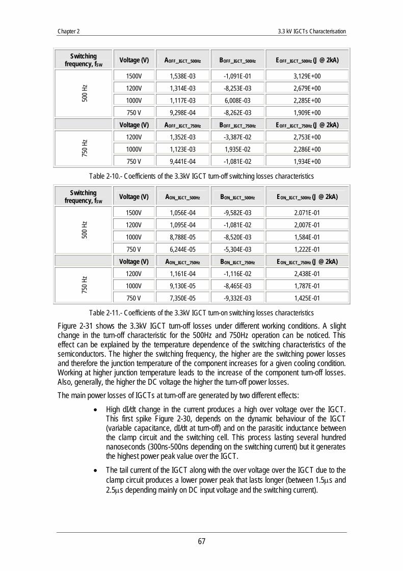
Chapter 2 3.3 kV IGCTs Characterisation
67
Switching frequency, fSW Voltage (V) AOFF_IGCT_500Hz BOFF_IGCT_500Hz EOFF_IGCT_500Hz (J @ 2kA)
1500V 1,538E-03 -1,091E-01 3,129E+00
1200V 1,314E-03 -8,253E-03 2,679E+00
1000V 1,117E-03 6,008E-03 2,285E+00 500 H
z
750 V 9,298E-04 -8,262E-03 1,909E+00
Voltage (V) AOFF_IGCT_750Hz BOFF_IGCT_750Hz EOFF_IGCT_750Hz (J @ 2kA)
1200V 1,352E-03 -3,387E-02 2,753E+00
1000V 1,123E-03 1,935E-02 2,286E+00
750 H
z
750 V 9,441E-04 -1,081E-02 1,934E+00
Table 2-10.- Coefficients of the 3.3kV IGCT turn-off switching losses characteristics
Switching frequency, fSW Voltage (V) AON_IGCT_500Hz BON_IGCT_500Hz EON_IGCT_500Hz (J @ 2kA)
1500V 1,056E-04 -9,582E-03 2.071E-01
1200V 1,095E-04 -1,081E-02 2,007E-01
1000V 8,788E-05 -8,520E-03 1,584E-01 500 H
z
750 V 6,244E-05 -5,304E-03 1,222E-01
Voltage (V) AON_IGCT_750Hz BON_IGCT_750Hz EON_IGCT_750Hz (J @ 2kA)
1200V 1,161E-04 -1,116E-02 2,438E-01
1000V 9,130E-05 -8,465E-03 1,787E-01
750 H
z
750 V 7,350E-05 -9,332E-03 1,425E-01
Table 2-11.- Coefficients of the 3.3kV IGCT turn-on switching losses characteristics
Figure 2-31 shows the 3.3kV IGCT turn-off losses under different working conditions. A slight change in the turn-off characteristic for the 500Hz and 750Hz operation can be noticed. This effect can be explained by the temperature dependence of the switching characteristics of the semiconductors. The higher the switching frequency, the higher are the switching power losses and therefore the junction temperature of the component increases for a given cooling condition. Working at higher junction temperature leads to the increase of the component turn-off losses. Also, generally, the higher the DC voltage the higher the turn-off power losses. The main power losses of IGCTs at turn-off are generated by two different effects:
• High dI/dt change in the current produces a high over voltage over the IGCT. This first spike Figure 2-30, depends on the dynamic behaviour of the IGCT (variable capacitance, dI/dt at turn-off) and on the parasitic inductance between the clamp circuit and the switching cell. This process lasting several hundred nanoseconds (300ns-500ns depending on the switching current) but it generates the highest power peak value over the IGCT.
• The tail current of the IGCT along with the over voltage over the IGCT due to the clamp circuit produces a lower power peak that lasts longer (between 1.5μs and 2.5μs depending mainly on DC input voltage and the switching current).
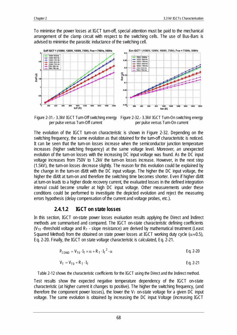
Chapter 2 3.3 kV IGCTs Characterisation
68
To minimise the power losses at IGCT turn-off, special attention must be paid to the mechanical arrangement of the clamp circuit with respect to the switching cells. The use of Bus-Bars is advised to minimise the parasitic inductance of the switching cell.
Figure 2-31.- 3.3kV IGCT Turn-Off switching energy per pulse versus Turn-Off current
Figure 2-32.- 3.3kV IGCT Turn-On switching energy per pulse versus Turn-On current
The evolution of the IGCT turn-on characteristic is shown in Figure 2-32. Depending on the switching frequency, the same evolution as that obtained for the turn-off characteristic is noticed. It can be seen that the turn-on losses increase when the semiconductor junction temperature increases (higher switching frequency) at the same voltage level. Moreover, an unexpected evolution of the turn-on losses with the increasing DC input voltage was found. As the DC input voltage increases from 750V to 1.2kV the turn-on losses increase. However, in the next step (1.5kV), the turn-on losses decrease slightly. The reason for this evolution could be explained by the change in the turn-on dI/dt with the DC input voltage. The higher the DC input voltage, the higher the dI/dt at turn-on and therefore the switching time becomes shorter. Even if higher dI/dt at turn-on leads to a higher diode recovery current, the evaluated losses in the defined integration interval could become smaller at high DC input voltage. Other measurements under these conditions could be performed to investigate the depicted evolution and reject the measuring errors hypothesis (delay compensation of the current and voltage probes, etc.).
2.4.1.2 IGCT on state losses In this section, IGCT on-state power losses evaluation results applying the Direct and Indirect methods are summarised and compared. The IGCT on-state characteristic defining coefficients (VT0 -threshold voltage and RT - slope resistance) are derived by mathematical treatment (Least Squared Method) from the obtained on state power losses at IGCT working duty cycle (α≈0.5), Eq. 2-20. Finally, the IGCT on state voltage characteristic is calculated, Eq. 2-21.
α⋅⋅+α×⋅= 2TTT0TCOND IRIVP Eq. 2-20
TT0TT IRVV ⋅+= Eq. 2-21
Table 2-12 shows the characteristic coefficients for the IGCT using the Direct and the Indirect method.
Test results show the expected negative temperature dependency of the IGCT on-state characteristic (at higher current it changes to positive). The higher the switching frequency, (and therefore the component power losses), the lower the VT on-state voltage for a given DC input voltage. The same evolution is obtained by increasing the DC input Voltage (increasing IGCT
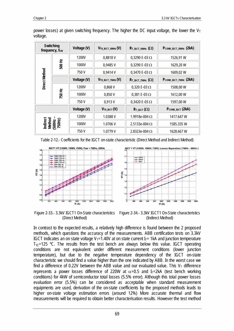
Chapter 2 3.3 kV IGCTs Characterisation
69
power losses) at given switching frequency. The higher the DC input voltage, the lower the VT voltage.
Switching frequency, fSW Voltage (V) VT0_IGCT_500Hz (V) RT_IGCT_500Hz (Ω) PCOND_IGCT_500Hz (2kA)
1200V 0,8818 V 0,3290 E-03 Ω 1526,91 W
1000V 0,9485 V 0,3290 E-03 Ω 1629,20 W 50
0 Hz
750 V 0,9414 V 0,3470 E-03 Ω 1609,02 W
Voltage (V) VT0_IGCT_750Hz (V) RT_IGCT_750Hz (Ω) PCOND_IGCT_750Hz (2kA)
1200V 0,868 V 0,320 E-03 Ω 1508,00 W
1000V 0,850 V 0,381 E-03 Ω 1612,00 W
Dire
ct M
etho
d
750 H
z
750 V 0,913 V 0,3420 E-03 Ω 1597,00 W
Voltage (V) VT0_IGCT (V) RT_IGCT (Ω) PCOND_IGCT (2kA)
1200V 1.0388 V 1.9918e-004 Ω 1417.647 W
1000V 1.0706 V 2.5133e-004 Ω 1585.335 W
Indi
rect
Me
thod
(5
00Hz
– 75
0Hz)
750 V 1.0779 V 2.8323e-004 Ω 1628.667 W
Table 2-12.- Coefficients for the IGCT on-state characteristic (Direct Method and Indirect Method)
Figure 2-33.- 3.3kV IGCT1 On-State characteristics (Direct Method)
Figure 2-34.- 3.3kV IGCT1 On-State characteristics (Indirect Method)
In contrast to the expected results, a relatively high difference is found between the 2 proposed methods, which questions the accuracy of the measurements. ABB certification tests on 3.3kV IGCT indicates an on state voltage VT=1.40V at on state current IT= 1kA and junction temperature TVJ=125 ºC. The results from the test bench are always below this value. IGCT operating conditions are not equivalent under different measurement conditions (lower junction temperature), but due to the negative temperature dependency of the IGCT on-state characteristic we should find a value higher than the one indicated by ABB. In the worst case we find a difference of 0.22V between the ABB value and our evaluated value. This VT difference represents a power losses difference of 220W at α=0.5 and IT=2kA (test bench working conditions) for 4kW of semiconductor total losses (5.5% error). Although this total power losses evaluation error (5.5%) can be considered as acceptable when standard measurement equipments are used, derivation of the on-state coefficients by the proposed methods leads to higher on-state voltage estimation errors (around 12%) More accurate thermal and flow measurements will be required to obtain better characterisation results. However the test method
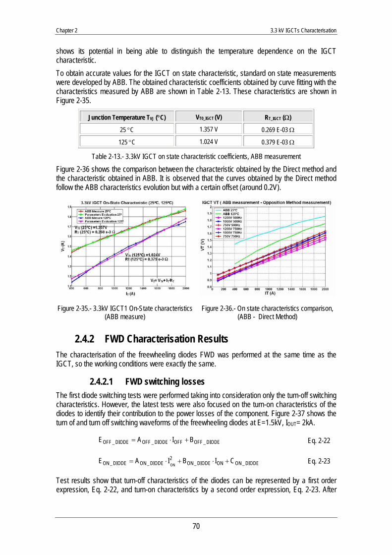
Chapter 2 3.3 kV IGCTs Characterisation
70
shows its potential in being able to distinguish the temperature dependence on the IGCT characteristic. To obtain accurate values for the IGCT on state characteristic, standard on state measurements were developed by ABB. The obtained characteristic coefficients obtained by curve fitting with the characteristics measured by ABB are shown in Table 2-13. These characteristics are shown in Figure 2-35.
Junction Temperature TVJ (°C) VT0_IGCT (V) RT_IGCT (Ω)
25 °C 1.357 V 0.269 E-03 Ω
125 °C 1.024 V 0.379 E-03 Ω
Table 2-13.- 3.3kV IGCT on state characteristic coefficients, ABB measurement
Figure 2-36 shows the comparison between the characteristic obtained by the Direct method and the characteristic obtained in ABB. It is observed that the curves obtained by the Direct method follow the ABB characteristics evolution but with a certain offset (around 0.2V).
Figure 2-35.- 3.3kV IGCT1 On-State characteristics (ABB measure)
Figure 2-36.- On state characteristics comparison, (ABB - Direct Method)
2.4.2 FWD Characterisation Results The characterisation of the freewheeling diodes FWD was performed at the same time as the IGCT, so the working conditions were exactly the same.
2.4.2.1 FWD switching losses The first diode switching tests were performed taking into consideration only the turn-off switching characteristics. However, the latest tests were also focused on the turn-on characteristics of the diodes to identify their contribution to the power losses of the component. Figure 2-37 shows the turn of and turn off switching waveforms of the freewheeling diodes at E=1.5kV, IOUT= 2kA.
DIODE_OFFOFFDIODE_OFFDIODE_OFF BIAE +⋅= Eq. 2-22
DIODE_ONONDIODE_ON2
DIODE_ONDIODE_ON CIBIAEON
+⋅+⋅= Eq. 2-23
Test results show that turn-off characteristics of the diodes can be represented by a first order expression, Eq. 2-22, and turn-on characteristics by a second order expression, Eq. 2-23. After
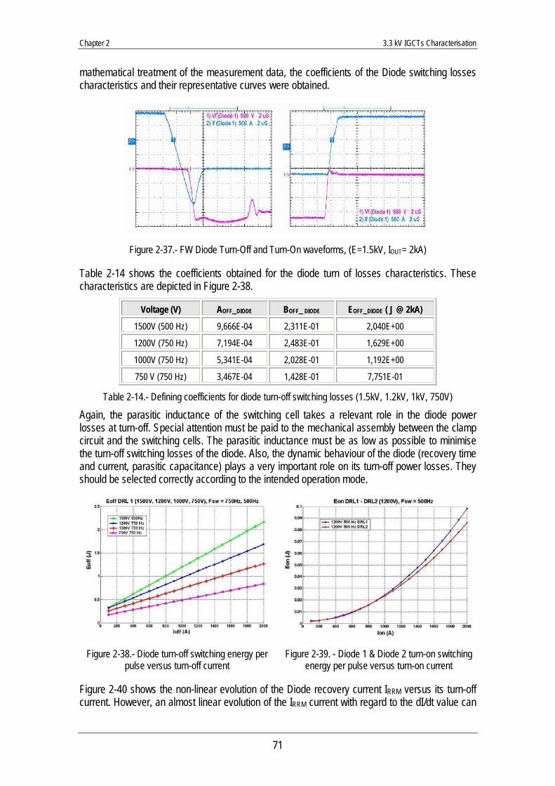
Chapter 2 3.3 kV IGCTs Characterisation
71
mathematical treatment of the measurement data, the coefficients of the Diode switching losses characteristics and their representative curves were obtained.
Figure 2-37.- FW Diode Turn-Off and Turn-On waveforms, (E=1.5kV, IOUT= 2kA)
Table 2-14 shows the coefficients obtained for the diode turn of losses characteristics. These characteristics are depicted in Figure 2-38.
Voltage (V) AOFF_DIODE BOFF_ DIODE EOFF_DIODE ( J @ 2kA)
1500V (500 Hz) 9,666E-04 2,311E-01 2,040E+00
1200V (750 Hz) 7,194E-04 2,483E-01 1,629E+00
1000V (750 Hz) 5,341E-04 2,028E-01 1,192E+00
750 V (750 Hz) 3,467E-04 1,428E-01 7,751E-01
Table 2-14.- Defining coefficients for diode turn-off switching losses (1.5kV, 1.2kV, 1kV, 750V)
Again, the parasitic inductance of the switching cell takes a relevant role in the diode power losses at turn-off. Special attention must be paid to the mechanical assembly between the clamp circuit and the switching cells. The parasitic inductance must be as low as possible to minimise the turn-off switching losses of the diode. Also, the dynamic behaviour of the diode (recovery time and current, parasitic capacitance) plays a very important role on its turn-off power losses. They should be selected correctly according to the intended operation mode.
Figure 2-38.- Diode turn-off switching energy per pulse versus turn-off current
Figure 2-39. - Diode 1 & Diode 2 turn-on switching energy per pulse versus turn-on current
Figure 2-40 shows the non-linear evolution of the Diode recovery current IRRM versus its turn-off current. However, an almost linear evolution of the IRRM current with regard to the dI/dt value can
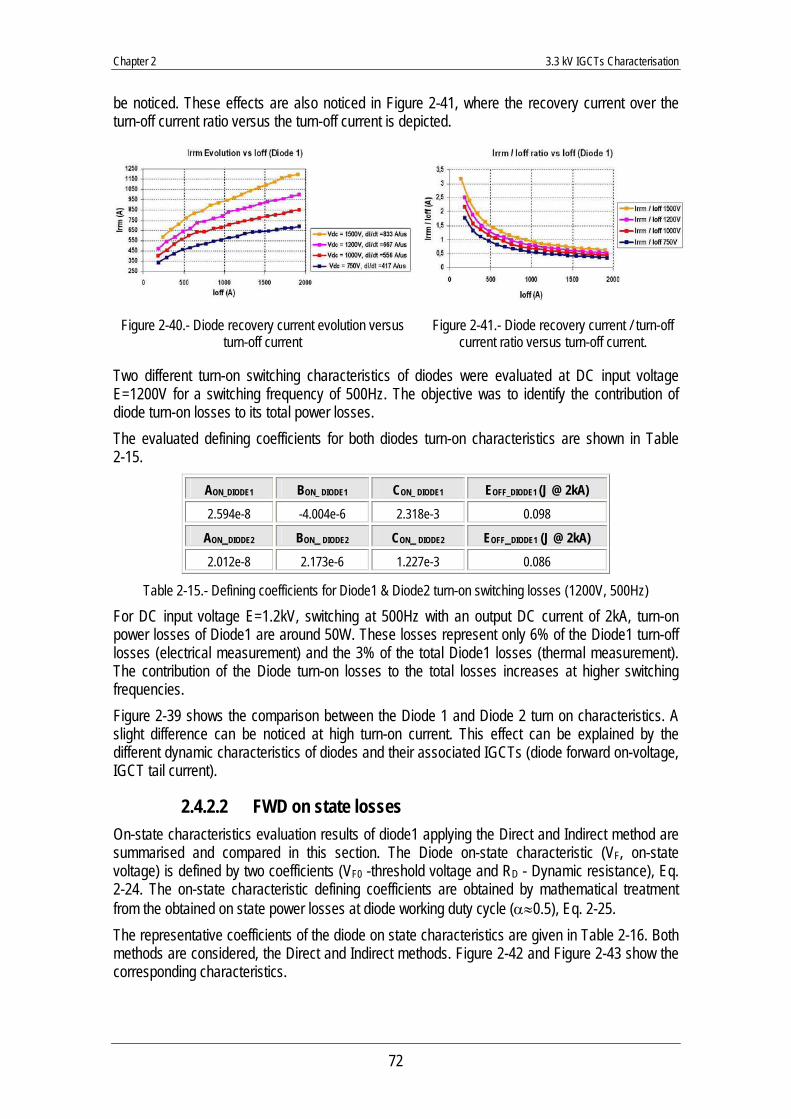
Chapter 2 3.3 kV IGCTs Characterisation
72
be noticed. These effects are also noticed in Figure 2-41, where the recovery current over the turn-off current ratio versus the turn-off current is depicted.
Figure 2-40.- Diode recovery current evolution versus turn-off current
Figure 2-41.- Diode recovery current / turn-off current ratio versus turn-off current.
Two different turn-on switching characteristics of diodes were evaluated at DC input voltage E=1200V for a switching frequency of 500Hz. The objective was to identify the contribution of diode turn-on losses to its total power losses. The evaluated defining coefficients for both diodes turn-on characteristics are shown in Table 2-15.
AON_DIODE1 BON_ DIODE1 CON_ DIODE1 EOFF_DIODE1 (J @ 2kA)
2.594e-8 -4.004e-6 2.318e-3 0.098
AON_DIODE2 BON_ DIODE2 CON_ DIODE2 EOFF_DIODE1 (J @ 2kA)
2.012e-8 2.173e-6 1.227e-3 0.086
Table 2-15.- Defining coefficients for Diode1 & Diode2 turn-on switching losses (1200V, 500Hz)
For DC input voltage E=1.2kV, switching at 500Hz with an output DC current of 2kA, turn-on power losses of Diode1 are around 50W. These losses represent only 6% of the Diode1 turn-off losses (electrical measurement) and the 3% of the total Diode1 losses (thermal measurement). The contribution of the Diode turn-on losses to the total losses increases at higher switching frequencies. Figure 2-39 shows the comparison between the Diode 1 and Diode 2 turn on characteristics. A slight difference can be noticed at high turn-on current. This effect can be explained by the different dynamic characteristics of diodes and their associated IGCTs (diode forward on-voltage, IGCT tail current).
2.4.2.2 FWD on state losses On-state characteristics evaluation results of diode1 applying the Direct and Indirect method are summarised and compared in this section. The Diode on-state characteristic (VF, on-state voltage) is defined by two coefficients (VF0 -threshold voltage and RD - Dynamic resistance), Eq. 2-24. The on-state characteristic defining coefficients are obtained by mathematical treatment from the obtained on state power losses at diode working duty cycle (α≈0.5), Eq. 2-25. The representative coefficients of the diode on state characteristics are given in Table 2-16. Both methods are considered, the Direct and Indirect methods. Figure 2-42 and Figure 2-43 show the corresponding characteristics.
Chapter 2 3.3 kV IGCTs Characterisation
73
α⋅⋅+α⋅⋅= 2FDF0FCOND IRIVP Eq. 2-24
FD0FF IRVV ⋅+= Eq. 2-25
Test results applying the direct method show the positive temperature dependency of the Diode on-state characteristic, which corresponds with the expected behaviour. The higher the DC input voltage, the higher the VF on-state voltage for a given switching frequency (junction temperature). However, the results obtained by the indirect method show a negative temperature dependency of this characteristic, which deviates from the expected results. Low calorimetric system accuracy can be the reason to this deviation.
Voltage (V) VF0_DIODE (V) RD_DIODE (Ω) PCOND_DIODE ( 2kA)
1200 V 8,862E-01 V 3,842E-04 Ω 1630,80 W
1000 V 9,336E-01 V 3,336E-04 Ω 1590,84 W Dire
ct
Meth
od
750 V 8,858E-01 V 3,050E-04 Ω 1473,18 W
Voltage (V) VF0_DIODE (V) RD_DIODE (Ω) PCOND_DIODE ( 2kA)
1200V 0.6435 V 2.9477e-004 Ω 1233.04 W
1000V 0.6775 V 3.2846e-004 Ω 1334.42 W
Indi
rect
Mo
de
750 V 0.6343 V 3.7871e-004 Ω 1391.75 W
Table 2-16.- Defining coefficients for diode on-state characteristics (Direct and Indirect Methods)
Figure 2-42.- Diode on-state characteristics (Direct Method)
Figure 2-43.- Diode on-state characteristics (Indirect Method)
ABB certification test of Diodes indicates VF (IF=1kA)=1.20V and VF (IF=2kA)=1.48V for a junction temperature TVJ=125ºC. With these values, an approximation of the diode on state characteristic defining parameters at 125°C are identified, Table 2-17.
Junction Temperature TVJ (°C) VF0_DIODE (V) RD_DIODE (Ω)
125 °C 0.83 V 0.34 E-03 Ω
Table 2-17.- Diode on state defining coefficients, TVJ=125°C
Chapter 2 3.3 kV IGCTs Characterisation
74
2.4.3 Gate Unit Power Supply Requirements The Siebel SW 32-24D20G power supply is used to supply the IGCT gate unit, Figure 2-44. The output current of the IGCT gate unit power supply is measured to identify its power requirements. Several measurements were performed at different DC link voltages, DC output currents and switching frequencies. The results show that only the IGCT turn off switching current and the switching frequency influence the power consumption of the driver power supply, no influence of the DC link voltage was perceived. Also the duty cycle should effect the gate unit power consumption due to the back-porch current during the IGCT on state, however these effects have not been analysed due to the fixed operation mode of the test bench (constant duty cycle α=0.5).
Figure 2-44.- Siebel SW 32-24D20G DC/DC power supply, (20VDC regulated, 80W)
Measurement results show that the driver output current evolution with the turn of switching current at fixed switching frequency can be represented by a first order expression Eq. 2-26, as shown in Figure 2-45.
FSW_DROFFFSW_DRFSW_DR BIAI +⋅= Eq. 2-26
SWIOFFIOFFIOFF_DR f2K1KI ⋅+= Eq. 2-27
The defining coefficients of the gate unit power supply consumption characteristic are identified for three different switching frequencies (500Hz, 750Hz and 1KHz), Table 2-18. The DC output test current was varied between 0 and 2kA when operating at 500Hz and 750Hz. However, it was limited to 1.3kA at 1kHz to avoid the destruction of the IGCT. In fact, operation between 1.5kA and 1.6kA was also tested but resulted in the destruction of the IGCT sample. The gate unit power supply consumption limit was reached and led to a non-homogeneous blocking process of the internal IGCT cells (GTO mode commutation), thus current focalisation and finally wafer perforation.
Switching frequency, fSW A DR_FSW B DRIFSW IDRIVER (2kA)
1000 Hz 1.764e-3 1.2703 4.80 A
750 Hz 1.2234e-3 1.2247 3.67 A
500 Hz 8.1739e-4 9.7479e-1 2.61 A
Table 2-18.- Coefficients of the gate unit power supply output current - turn off current characteristic, IDR=f(IOFF)
The gate unit power supply limit (80W and paralleling operation not possible) restricted the use of the IGCT at higher switching frequencies under relevant DC output currents. To estimate the power requirements of the driver power supply at higher switching frequencies (until 2kHz), it is firstly verified that the gate unit current evolves proportionally with the switching frequency for a given turn-off switching current Figure 2-46, for example following Eq. 2-27. The coefficients K1
Chapter 2 3.3 kV IGCTs Characterisation
75
and K2 are evaluated for each turn-off switching current from 100A to 2KA and then the driver current is extrapolated at different switching frequencies. The output power of the power supply is finally calculated considering the power supply DC output voltage to be constant and equal to 20V. The estimated power consumption for the 3.3kV IGCT driver power supply is shown in Figure 2-47.
Figure 2-45.- Driver power supply output current vs. Turn-Off current (fSW = 500Hz, 750Hz, 1KHz).
Figure 2-46.- Driver power supply current vs. switching frequency (IOFF =500A, 1kA, 1.5kA, 2kA)
The calculated results show how the limit of the utilised power supply (80W) is reached when operating the IGCT at 1kHz and 1.5kA (duty cycle α=0.5), which match with the failure mode that was obtained experimentally on the test bench. Obviously, these results do not take into account the thermal limitations of the semiconductors and consider exclusively the power consumption demands of the gate unit. Also, one has to consider that the utilised gate unit is designed to operate at maximum IGCT switching frequencies of 1kHz. The operation at higher switching frequencies should also require hardware modifications on the gate unit to allow safe operation of their components (electrolytic capacitor, MOSFETs, etc.), thus the right operation of the IGCT.
Figure 2-47.- Estimated power consumption for the 3.3KV IGCT gate unit power supply
2.4.4 Clamp Circuit Power Losses Hard Switching IGCT switching cells must contain an IGCT turn-on inductor (snubber) to limit the diode turn-off dI/dt. At IGCT turn-off, the energy stored in the inductor is discharged and clamped
Chapter 2 3.3 kV IGCTs Characterisation
76
by means of an RCD circuit, Figure 2-48. Not all of the magnetising energy is evacuated over the RCD circuit; certain amount of energy is dissipated on the semiconductors and restored to the input power supply.
Figure 2-48. - IGCT Switching cell dI/dt inductor and RCD clamp circuit
The clamp circuit power losses are evaluated to identify the amount of magnetising energy dissipated on the clamp circuit components. DCL and RCL power losses are evaluated by means of the calorimetric method. The clamp inductor and capacitor power losses are estimated from component data specifications (components parasitic resistors). The obtained results at 500Hz and 750Hz for several DC input voltages are compared with the theoretically calculated magnetising power generated by the dI/dt inductor, Eq. 2-28. The comparison results are shown in Figure 2-49.
SW2OUTCL fIL
21PowergMagnetisin ⋅⋅⋅= Eq. 2-28
Results show that the clamp circuit power losses increase with the DC input voltage for a given switching frequency. This fact can be explained by the IGCT turn-off behaviour change with the increasing DC input voltage. The higher the DC input voltage, the smaller the turn-off switching time and the higher the clamp circuit over voltage. Table 2-19 shows the measured turn-off times and clamp over voltage values at different DC input voltage levels. This fact means that with higher DC input voltage, the IGCT turn-off behaviour becomes more ideal and more energy is dissipated over the clamp circuit components.
Figure 2-49.- Clamp circuit losses evaluation, fsw = 500Hz, 750Hz
Figure 2-50 shows the magnetising power percentage dissipated over the clamp circuit components at different switching frequencies for several DC input voltages.
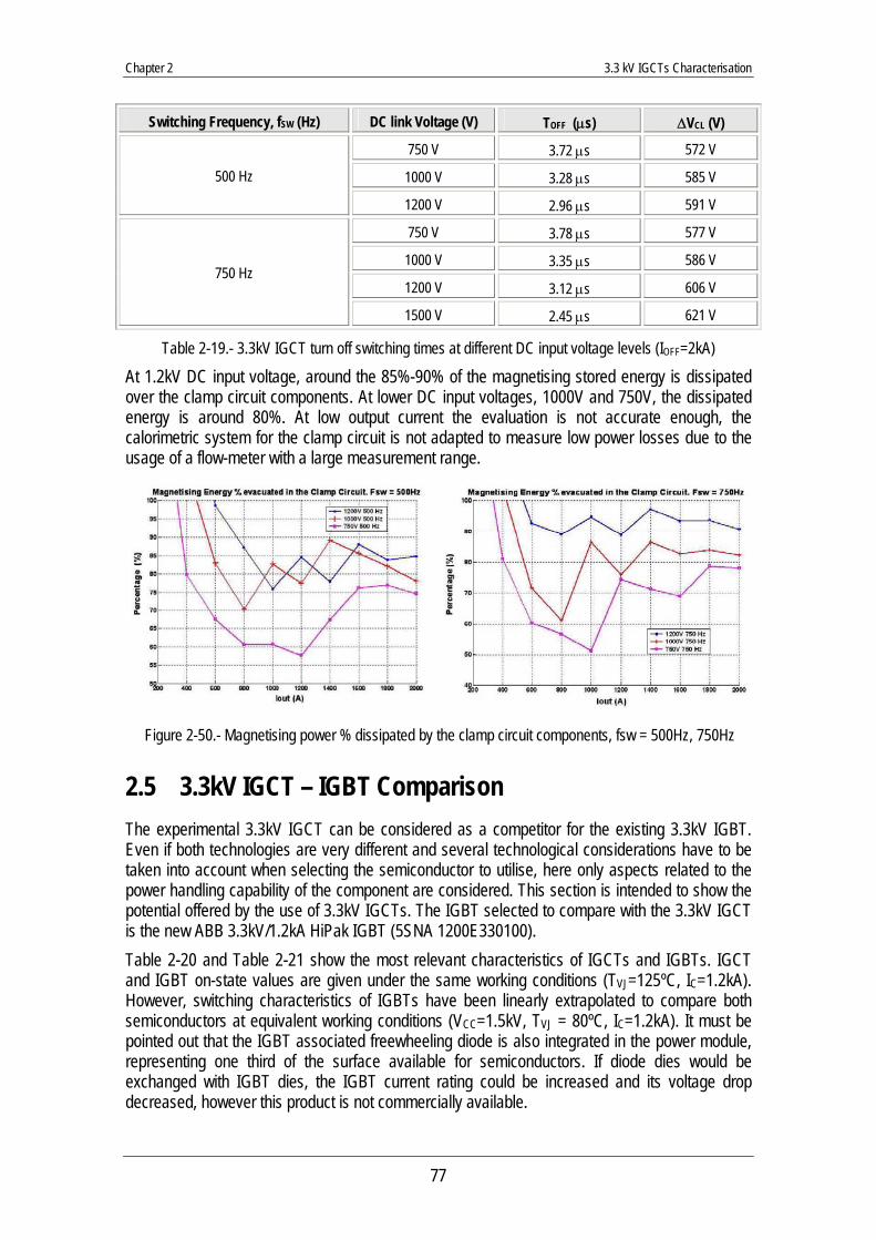
Chapter 2 3.3 kV IGCTs Characterisation
77
Switching Frequency, fSW (Hz) DC link Voltage (V) TOFF (μs) ΔVCL (V)
750 V 3.72 μs 572 V
1000 V 3.28 μs 585 V 500 Hz
1200 V 2.96 μs 591 V
750 V 3.78 μs 577 V
1000 V 3.35 μs 586 V
1200 V 3.12 μs 606 V 750 Hz
1500 V 2.45 μs 621 V
Table 2-19.- 3.3kV IGCT turn off switching times at different DC input voltage levels (IOFF=2kA)
At 1.2kV DC input voltage, around the 85%-90% of the magnetising stored energy is dissipated over the clamp circuit components. At lower DC input voltages, 1000V and 750V, the dissipated energy is around 80%. At low output current the evaluation is not accurate enough, the calorimetric system for the clamp circuit is not adapted to measure low power losses due to the usage of a flow-meter with a large measurement range.
Figure 2-50.- Magnetising power % dissipated by the clamp circuit components, fsw = 500Hz, 750Hz
2.5 3.3kV IGCT – IGBT Comparison The experimental 3.3kV IGCT can be considered as a competitor for the existing 3.3kV IGBT. Even if both technologies are very different and several technological considerations have to be taken into account when selecting the semiconductor to utilise, here only aspects related to the power handling capability of the component are considered. This section is intended to show the potential offered by the use of 3.3kV IGCTs. The IGBT selected to compare with the 3.3kV IGCT is the new ABB 3.3kV/1.2kA HiPak IGBT (5SNA 1200E330100). Table 2-20 and Table 2-21 show the most relevant characteristics of IGCTs and IGBTs. IGCT and IGBT on-state values are given under the same working conditions (TVJ=125ºC, IC=1.2kA). However, switching characteristics of IGBTs have been linearly extrapolated to compare both semiconductors at equivalent working conditions (VCC=1.5kV, TVJ = 80ºC, IC=1.2kA). It must be pointed out that the IGBT associated freewheeling diode is also integrated in the power module, representing one third of the surface available for semiconductors. If diode dies would be exchanged with IGBT dies, the IGBT current rating could be increased and its voltage drop decreased, however this product is not commercially available.
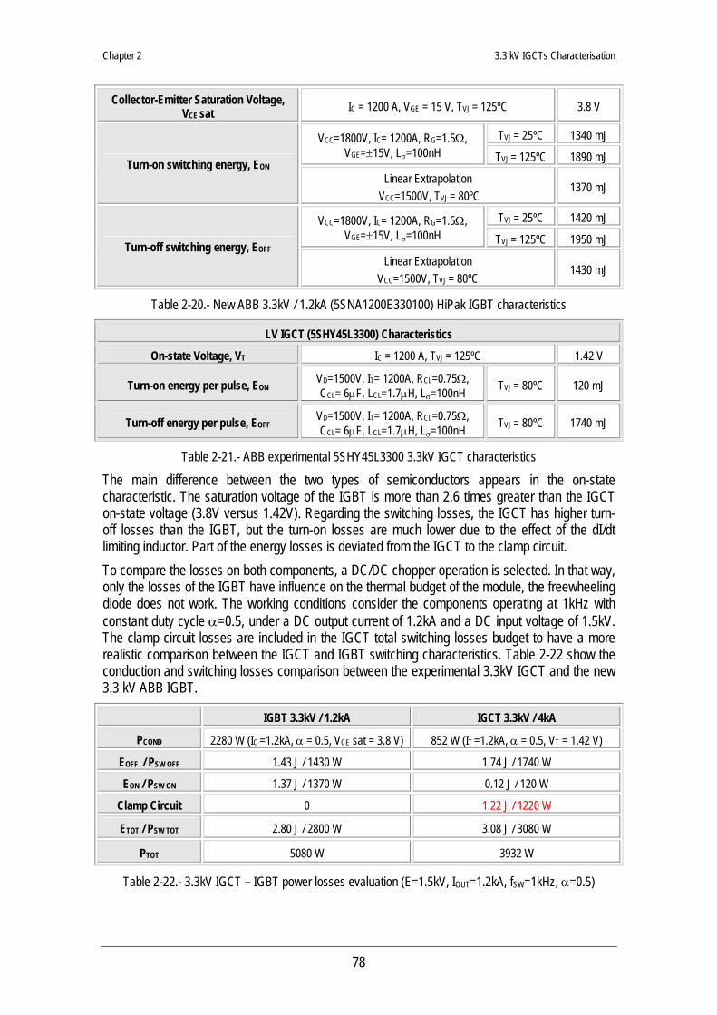
Chapter 2 3.3 kV IGCTs Characterisation
78
Collector-Emitter Saturation Voltage, VCE sat IC = 1200 A, VGE = 15 V, TVJ = 125ºC 3.8 V
TVJ = 25ºC 1340 mJ VCC=1800V, IC= 1200A, RG=1.5Ω, VGE=±15V, Lσ=100nH TVJ = 125ºC 1890 mJ Turn-on switching energy, EON
Linear Extrapolation VCC=1500V, TVJ = 80ºC
1370 mJ
TVJ = 25ºC 1420 mJ VCC=1800V, IC= 1200A, RG=1.5Ω, VGE=±15V, Lσ=100nH TVJ = 125ºC 1950 mJ Turn-off switching energy, EOFF
Linear Extrapolation VCC=1500V, TVJ = 80ºC
1430 mJ
Table 2-20.- New ABB 3.3kV / 1.2kA (5SNA1200E330100) HiPak IGBT characteristics
LV IGCT (5SHY45L3300) Characteristics
On-state Voltage, VT IC = 1200 A, TVJ = 125ºC 1.42 V
Turn-on energy per pulse, EON VD=1500V, IT= 1200A, RCL=0.75Ω, CCL= 6μF, LCL=1.7μH, Lσ=100nH TVJ = 80ºC 120 mJ
Turn-off energy per pulse, EOFF VD=1500V, IT= 1200A, RCL=0.75Ω, CCL= 6μF, LCL=1.7μH, Lσ=100nH TVJ = 80ºC 1740 mJ
Table 2-21.- ABB experimental 5SHY45L3300 3.3kV IGCT characteristics
The main difference between the two types of semiconductors appears in the on-state characteristic. The saturation voltage of the IGBT is more than 2.6 times greater than the IGCT on-state voltage (3.8V versus 1.42V). Regarding the switching losses, the IGCT has higher turn-off losses than the IGBT, but the turn-on losses are much lower due to the effect of the dI/dt limiting inductor. Part of the energy losses is deviated from the IGCT to the clamp circuit. To compare the losses on both components, a DC/DC chopper operation is selected. In that way, only the losses of the IGBT have influence on the thermal budget of the module, the freewheeling diode does not work. The working conditions consider the components operating at 1kHz with constant duty cycle α=0.5, under a DC output current of 1.2kA and a DC input voltage of 1.5kV. The clamp circuit losses are included in the IGCT total switching losses budget to have a more realistic comparison between the IGCT and IGBT switching characteristics. Table 2-22 show the conduction and switching losses comparison between the experimental 3.3kV IGCT and the new 3.3 kV ABB IGBT.
IGBT 3.3kV / 1.2kA IGCT 3.3kV / 4kA
PCOND 2280 W (IC =1.2kA, α = 0.5, VCE sat = 3.8 V) 852 W (IT =1.2kA, α = 0.5, VT = 1.42 V)
EOFF / PSW OFF 1.43 J / 1430 W 1.74 J / 1740 W
EON / PSW ON 1.37 J / 1370 W 0.12 J / 120 W
Clamp Circuit 0 1.22 J / 1220 W
ETOT / PSW TOT 2.80 J / 2800 W 3.08 J / 3080 W
PTOT 5080 W 3932 W
Table 2-22.- 3.3kV IGCT – IGBT power losses evaluation (E=1.5kV, IOUT=1.2kA, fSW=1kHz, α=0.5)
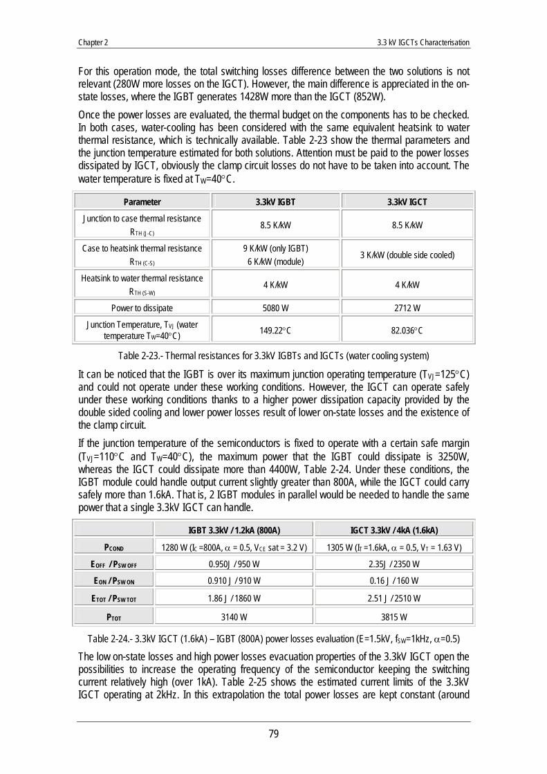
Chapter 2 3.3 kV IGCTs Characterisation
79
For this operation mode, the total switching losses difference between the two solutions is not relevant (280W more losses on the IGCT). However, the main difference is appreciated in the on-state losses, where the IGBT generates 1428W more than the IGCT (852W). Once the power losses are evaluated, the thermal budget on the components has to be checked. In both cases, water-cooling has been considered with the same equivalent heatsink to water thermal resistance, which is technically available. Table 2-23 show the thermal parameters and the junction temperature estimated for both solutions. Attention must be paid to the power losses dissipated by IGCT, obviously the clamp circuit losses do not have to be taken into account. The water temperature is fixed at TW=40°C.
Parameter 3.3kV IGBT 3.3kV IGCT
Junction to case thermal resistance RTH (J-C)
8.5 K/kW 8.5 K/kW
Case to heatsink thermal resistance RTH (C-S)
9 K/kW (only IGBT) 6 K/kW (module)
3 K/kW (double side cooled)
Heatsink to water thermal resistance RTH (S-W)
4 K/kW 4 K/kW
Power to dissipate 5080 W 2712 W
Junction Temperature, TVJ (water temperature TW=40°C) 149.22°C 82.036°C
Table 2-23.- Thermal resistances for 3.3kV IGBTs and IGCTs (water cooling system)
It can be noticed that the IGBT is over its maximum junction operating temperature (TVJ=125°C) and could not operate under these working conditions. However, the IGCT can operate safely under these working conditions thanks to a higher power dissipation capacity provided by the double sided cooling and lower power losses result of lower on-state losses and the existence of the clamp circuit. If the junction temperature of the semiconductors is fixed to operate with a certain safe margin (TVJ=110°C and TW=40°C), the maximum power that the IGBT could dissipate is 3250W, whereas the IGCT could dissipate more than 4400W, Table 2-24. Under these conditions, the IGBT module could handle output current slightly greater than 800A, while the IGCT could carry safely more than 1.6kA. That is, 2 IGBT modules in parallel would be needed to handle the same power that a single 3.3kV IGCT can handle.
IGBT 3.3kV / 1.2kA (800A) IGCT 3.3kV / 4kA (1.6kA)
PCOND 1280 W (IC =800A, α = 0.5, VCE sat = 3.2 V) 1305 W (IT =1.6kA, α = 0.5, VT = 1.63 V)
EOFF / PSW OFF 0.950J / 950 W 2.35J / 2350 W
EON / PSW ON 0.910 J / 910 W 0.16 J / 160 W
ETOT / PSW TOT 1.86 J / 1860 W 2.51 J / 2510 W
PTOT 3140 W 3815 W
Table 2-24.- 3.3kV IGCT (1.6kA) – IGBT (800A) power losses evaluation (E=1.5kV, fSW=1kHz, α=0.5)
The low on-state losses and high power losses evacuation properties of the 3.3kV IGCT open the possibilities to increase the operating frequency of the semiconductor keeping the switching current relatively high (over 1kA). Table 2-25 shows the estimated current limits of the 3.3kV IGCT operating at 2kHz. In this extrapolation the total power losses are kept constant (around
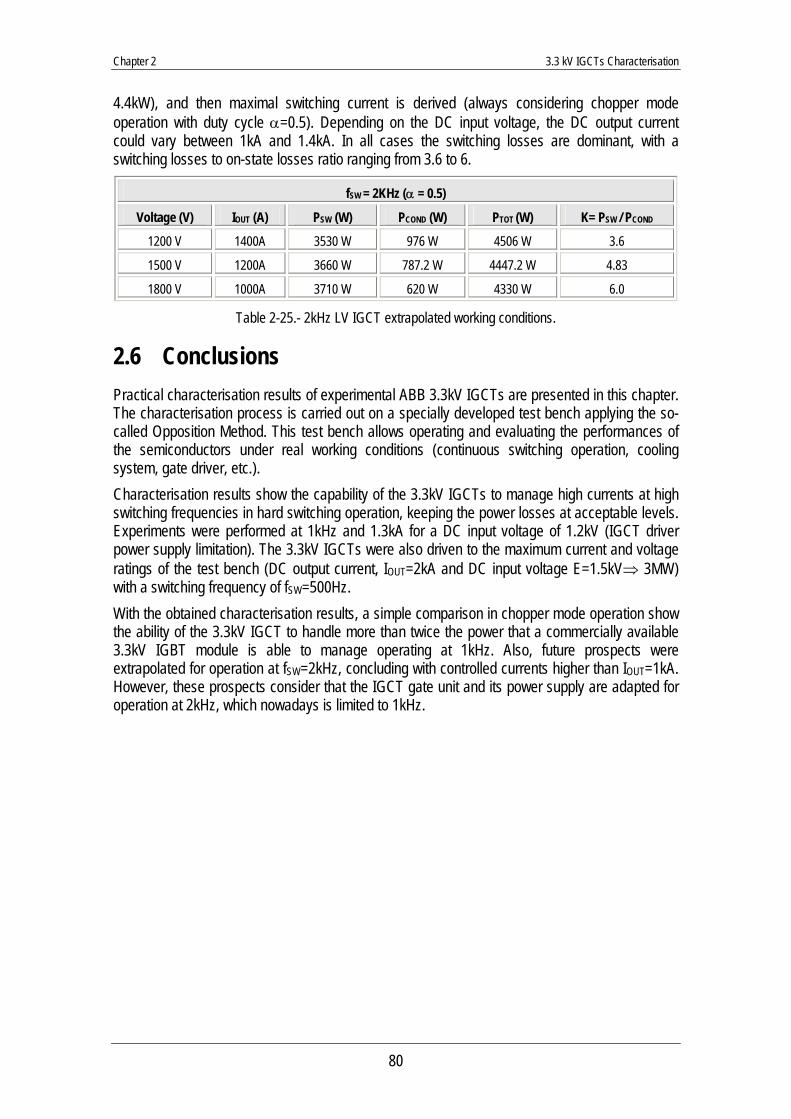
Chapter 2 3.3 kV IGCTs Characterisation
80
4.4kW), and then maximal switching current is derived (always considering chopper mode operation with duty cycle α=0.5). Depending on the DC input voltage, the DC output current could vary between 1kA and 1.4kA. In all cases the switching losses are dominant, with a switching losses to on-state losses ratio ranging from 3.6 to 6.
fSW = 2KHz (α = 0.5)
Voltage (V) IOUT (A) PSW (W) PCOND (W) PTOT (W) K= PSW / PCOND
1200 V 1400A 3530 W 976 W 4506 W 3.6
1500 V 1200A 3660 W 787.2 W 4447.2 W 4.83
1800 V 1000A 3710 W 620 W 4330 W 6.0
Table 2-25.- 2kHz LV IGCT extrapolated working conditions.
2.6 Conclusions Practical characterisation results of experimental ABB 3.3kV IGCTs are presented in this chapter. The characterisation process is carried out on a specially developed test bench applying the so-called Opposition Method. This test bench allows operating and evaluating the performances of the semiconductors under real working conditions (continuous switching operation, cooling system, gate driver, etc.). Characterisation results show the capability of the 3.3kV IGCTs to manage high currents at high switching frequencies in hard switching operation, keeping the power losses at acceptable levels. Experiments were performed at 1kHz and 1.3kA for a DC input voltage of 1.2kV (IGCT driver power supply limitation). The 3.3kV IGCTs were also driven to the maximum current and voltage ratings of the test bench (DC output current, IOUT=2kA and DC input voltage E=1.5kV⇒ 3MW) with a switching frequency of fSW=500Hz. With the obtained characterisation results, a simple comparison in chopper mode operation show the ability of the 3.3kV IGCT to handle more than twice the power that a commercially available 3.3kV IGBT module is able to manage operating at 1kHz. Also, future prospects were extrapolated for operation at fSW=2kHz, concluding with controlled currents higher than IOUT=1kA. However, these prospects consider that the IGCT gate unit and its power supply are adapted for operation at 2kHz, which nowadays is limited to 1kHz.
81
3 Chapter 3
Potential Applications for 3.3 kV IGCTs
3.1 Introduction The 3.3kV IGCT characterisation results demonstrate how the performance of this semiconductor can be used to complement and extend the existing Medium Power Converters application field, mainly providing a component that can handle higher currents (over 1kA) at high switching frequencies (over 1kHz). However, as the current market dealing with 3.3kV semiconductors is covered by the commercially available IGBTs and the IGCT technology is less popular for the greatest part of power converter manufacturers, the market introduction of the 3.3kV IGCTs depends only on commercial issues and market potentials. For these reasons, research efforts are dedicated to pointing out potential power converter topologies and applications where the use of 3.3kV IGCT utilisation could present interesting advantages. The 3.3kV IGCT characteristic that must be mainly exploited is the low on-state losses of the component. Consequently, the best-suited applications for the use of such components are those where high currents have to be handled. Since the power losses budget of the component is mainly driven by the switching losses, for applications where relatively high switching frequencies are needed, topologies where the on-state losses are dominant should be favoured. According to the previous considerations, the semiconductor’s power losses distribution can be used as the first element to clear up which applications and topologies are convenient for the use of 3.3kV IGCTs. As the number of applications and topologies to analyse can be very vast, a Universal Power Losses Estimator for 3.3kV IGCTs switching cells is developed. The proposed estimator is based on the ideal switches simulation approach and can be applied in every converter where a generic switching cell (voltage unidirectional and current reversible) can be identified, which lightens the power losses evaluation process. Furthermore, the estimator is designed to consider relevant factors that influence the losses distribution on high power converters such as output current ripple, DC link voltage fluctuations, over-modulation and closed loop operation. The applicability analysis of the 3.3kV IGCTs has been focused on specific medium power applications related to the French railway network (SNCF). Two particular applications have been considered, active filtering for the 1.5kV DC railway network substations, and reactive power compensation for the single-phase 25kV/50Hz railway network. For each application, different conversion structures and topologies have been analysed and briefly compared using the semiconductor power losses distribution as the main element of comparison. These analyses provide a detailed overview of the possibilities that the 3.3kV IGCTs can provide in distribution applications where high current and high switching frequency converters can be required.

Chapter 3 Potential Applications for 3.3 kV IGCTs
82
3.2 Universal Power Losses Estimator In most cases, any energy conversion function using static power converters (drives, power supplies, distributed power generation systems, active filtering, reactive power compensation, etc.) can be accomplished by means of several converter topologies using different semiconductor technologies. The selection of the conversion structure and semiconductors to be used is carried out mainly regarding the power of the system together with other features imposed by the application (static and dynamic performances, efficiency, ruggedness and reliability, volume and weight, cost, maintenance criteria, etc.). Last years developments in power semiconductors [CAR-98] (IGCT, HV IGBT, etc.) and topologies [MEY-98] (voltage or current source inverters, multilevel converters, AC/AC direct converters, soft switching converters, etc.) provide a wide spectrum of possibilities. The power losses in semiconductors have a direct influence on the performances of the converter. In fact, it is normally the junction temperature of the semiconductors who limits the switching frequency, the output power of the converter, the cooling system and the number of components to use (parallel and/or series association). At the same time, the switching frequency imposes the bandwidth of the converter, the weight and size of passive components. Therefore, especially in medium and high power applications, the amount of power losses in the semiconductors can be considered as the first important criterion that allows highlighting the advantages and disadvantages of each technology / topology. It can be used as an interesting parameter to compare the suitability of the available different solutions for the concerned applications, helping to define which semiconductor technology / converter topology is best suited for a specific application. Nevertheless, the final adopted solution usually requires additional criteria depending in the case to case conditions (cost, development efforts, market relevance, etc.). In our study, it is intended to find applications and topologies where the use of the experimental 3.3kV IGCT can improve the global performances of the system. Independently from the application, all power converters consist of several basic switching cells arranged to provide the desired energy conversion between two sources, [CHE-92]. As the number of concerned solutions can be immense, the evaluation of the semiconductor power losses on each conversion structure can be a hard task to complete. To simplify the task, a “universal” power losses evaluation tool for generic switching cells (unidirectional voltage and bi-directional current) is developed. This tool can be easily adapted to evaluate the semiconductor power losses when they are used in different topologies where a generic switching cell can be identified. Furthermore, the estimator takes into account the effect of output current ripple and the DC link voltage variations, which are relevant in high power converters. Also, closed loop operation and continuous conduction of the components for more than one switching period (hereafter called over-modulation operation) is taken into account.
3.2.1 State of the Art for Semiconductor Power Losses Estimation
The power semiconductor’s losses estimation is a very important stage in the developing phase of a power converter. This estimation allows defining the requirements of the cooling system, but can be also used to optimise the semiconductor or topology selection depending on the dimensioning criteria imposed by the application such as higher efficiency or higher switching frequency (volume reduction, higher bandwidth, etc.). Several estimation approaches can be used, each one applying certain assumptions that define the accuracy of the power losses
Chapter 3 Potential Applications for 3.3 kV IGCTs
83
estimation. A classification of the most commonly used techniques for power losses estimation is presented in the following paragraphs.
3.2.1.1 Analytic estimation The analytic estimation technique makes use of analytic formulations to describe the switching and on-state averaged losses as well as the thermal conditions of the semiconductor, mainly in PWM operation [BER-95], [SCH-04]. The results are obtained instantaneously, which is useful to quickly change the working conditions of the converter (switching frequency, DC link voltage, output current, output frequency, modulation index, semiconductor characteristics and so on). Some semiconductor manufacturers provide free access to analytic estimation tools for classic 3-phase / 2-level voltage source inverter [ABB-c], [EUP-a] using directly the database containing the characteristics of their components. However, this kind of tools generally does not take into account the closed loop operation of the converter, the output current ripple or the DC link voltage fluctuations. They are mainly intended to make a quick pre-selection of the components adapted to a very specific application.
3.2.1.2 Estimation applying ideal switches simulation The ideal switches simulation approach reproduces the power converter operation dealing with ideal models of semiconductors (binary resistor). Furthermore, the simulation integrates an estimation tool that uses the instantaneous currents and voltages generated by the simulated power converter to obtain the averaged power losses of the semiconductors. Sometimes, experimental evaluation test benches are developed to identify the on-state and switching losses parameters of semiconductors operating under specific working conditions (junction temperature, voltage, hard / soft switching, etc.), [MUN-00], [HIR-01]. These values are then used as input parameters for the estimation subsystem. Also, the thermal model of the component and its cooling system can be simulated to verify its functionality in case of complicated load profiles, overload conditions, etc. The main advantage of this estimation technique is the use of the real input and output current and voltage waveforms of the converter (current ripple, closed loop effect, input voltage change, etc.). Moreover, the computation time and the size of the output files are quite acceptable. Such a kind of estimator does not usually consider the thermo-electric iteration of the semiconductor parameters.
3.2.1.3 Estimation applying real semiconductor models simulation
Finally, real semiconductor models can be used to simulate the real behaviour of semiconductors in a power converter (physical model, behavioural models, electro-thermal iteration models, etc.), [WON-96], [HEF-91], [MA-93], [HEF-93]. Using these models, the real and complex behaviour of the semiconductors is simulated, providing the instantaneous switching and on-state waveforms. Mathematical treatment of these waveforms leads to the instantaneous power and energy losses evaluation. The main difficulty of these models is the identification of the required parameters to run the simulation. Sometimes, the identification can be performed using the datasheets of the semiconductor [EVA-a], [LAU-a], other times it is the semiconductor manufacturer who provides directly the semiconductor physical model, [SIG-97]. Also, the external circuit parameters where the semiconductor is to be used (parasitic inductors, capacitors, etc.) need to be evaluated. The simulation results are accurate, however, the computation time and the size of the simulation files become too big when simulations of several tens of milliseconds are compulsory. Also, simulation
Chapter 3 Potential Applications for 3.3 kV IGCTs
84
convergence problems can appear when the system complexity increase (number of real model components, non linear behaviour, etc.).
3.2.2 Description of the Proposed Universal Power Losses Estimator
The “universal” power losses estimator for 3.3kV IGCTs switching cells here proposed applies the ideal switches simulation approach. The estimator uses the experimental parameters obtained in the 3.3kV IGCT characterisation process presented in Chapter 2. However, the use of this estimator could be extended to any other controlled semiconductors (GTOs, IGBTs, MOSFETs, etc.) that can take part of a generic switching cell, only the defining coefficients of their on-state and switching losses characteristics are required. Figure 3-1 shows the synoptic of the “universal” power losses estimator. The elementary unit considered for the power losses estimator is not just a single semiconductor but the whole generic switching cell. In that way, instead of directly using the discontinuous semiconductor current and voltage waveforms, the switching cell continuous output current iSC(t) and input voltage eSC(t) waveforms can be used. This avoids the uncertainty of the signals amplitude and time detection during the ideally simulated switching transients, which are very simulation time step dependent. Consequently, the control signals uT1 and uT1C are required to obtain the switching transition times where the current and voltage values must be sampled to calculate the switching and on-state losses for each component (parameterised for each semiconductor IGCT – Diode). Finally, the average value of the semiconductor power losses is calculated at the end of each switching period in synchronisation with the PWM carrier by means of the signal TSW.
Figure 3-1.- Synoptic of the “Universal” power losses estimator.
Such a principle is applied in order to easily adapt the power losses estimator to any kind of topology where a generic switching cell (voltage unidirectional and current bi-directional) can be identified. Furthermore, this estimation structure allows considering the influence that the output current ripple, DC link voltage fluctuations, control loop and over-modulation operation can exert on the semiconductors power losses, which can be of relevance in medium and high power converters. The simulation tool that has been used for the implementation of the “universal” power losses estimation is SABER. The use of its own programming language MAST, and particularly the use
Chapter 3 Potential Applications for 3.3 kV IGCTs
85
of “state” type signals (continuous in amplitude but discrete in the time domain), allow to easily implant the proposed estimator.
3.2.2.1 Universal power losses estimator elements To provide the “universal” nature to this tool, the entire estimation system is divided in 3 main parts, Figure 3-2. Specific functions of these 3 elements are explained in the following sections.
Figure 3-2.- Elements of the “universal” power losses estimator
3.2.2.1.1 Modulator / estimation synchroniser The “modulator / estimation synchroniser”, receives the duty cycle reference from the closed loop control system and provides the switching orders, uC1 and uC1_C, to the ideal switches of the power converter. It also generates the synchronisation signals, clk_1 and clk_2, which are used to perform the power losses averaging at the end of each switching period. These synchronisation signals are specially required for topologies where the components of the switching cell can remain in continuous conduction state for more than one switching period (over-modulation operation). Otherwise, the evaluation of the semiconductor on state current based on the switching transitions detection could induce relevant errors as depicted in Figure 3-3. Also, these synchronisation signals are useful when non-linear modulators are used, for example hysteresis controllers, because the switching period can vary.
Figure 3-3.- Semiconductor on-state average current evaluation in over-modulation operation
Figure 3-4.- Power losses estimator synchronisation signal generation
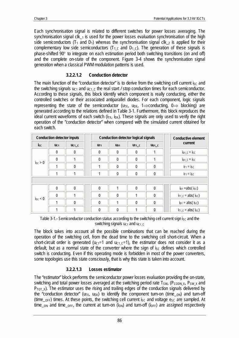
Chapter 3 Potential Applications for 3.3 kV IGCTs
86
Each synchronisation signal is related to different switches for power losses averaging. The synchronisation signal clk_1 is used for the power losses evaluation synchronisation of the high side semiconductors (T1 and D1) whereas the synchronisation signal clk_2 is applied for their complementary low side semiconductors (T1_C and D1_C). The generation of these signals is phase-shifted 90° to integrate on each estimation period both switching transitions (on and off) and the complete on-state of the component. Figure 3-4 shows the synchronisation signal generation when a classical PWM modulation patterns is used.
3.2.2.1.2 Conduction detector The main function of the “conduction detector” is to derive from the switching cell current iSC and the switching signals uC1 and uC1_C the real start / stop conduction times for each semiconductor. According to these signals, this block identify which component is really conducting, either the controlled switches or their associated antiparallel diodes. For each component, logic signals representing the state of the semiconductor (uTX, uDX, 1⇒conducting, 0⇒ blocking) are generated according to the relations defined in Table 3-1. Furthermore, this block reproduces the ideal current waveforms of each switch (iTX, iDX). These signals are only used to verify the right operation of the ”conduction detector” when compared with the simulated current obtained for each switch.
Conduction detector inputs Conduction detector logical signals
iSC uC1 uC1_C uT1 uD1 uT1_C uD1_C Conductive element
current
0 0 0 0 0 1 iD1_C = iSC
0 1 0 0 0 1 iD1_C = iSC
1 0 1 0 0 0 iT1 = iSC iSC > 0
1 1
1 0 0 0
iT1 = iSC
0 0 0 1 0 0 iD1 =abs( iSC)
0 1 0 0 1 0 iT1_C = abs( iSC)
1 0 0 1 0 0 iD1 = abs( iSC) iSC < 0
1 1
0 0 1 0
iT1_C = abs( iSC)
Table 3-1.- Semiconductor conduction status according to the switching cell current sign iSC and the switching signals uC1 and uC1_C
The block takes into account all the possible combinations that can be reached during the operation of the switching cell, from the dead time to the switching cell short-circuit. When a short-circuit order is generated (uC1=1 and uC1_C=1), the estimator does not consider it as a default, but as a normal state of the converter where the sign of iSC defines which controlled switch is conducting. Even if this operating mode is forbidden in most of the power converters, some topologies use this state consciously, that is why this state is taken into account.
3.2.2.1.3 Losses estimator The “estimator” block performs the semiconductor power losses evaluation providing the on-state, switching and total power losses averaged at the switching period rate TSW, (PCODN_X, PSW_X and PTOT_X). The estimator uses the rising and trailing edges of the conduction signals delivered by the “conduction detector” (uTX, uDX) to identify the component turn-on (time_ON) and turn-off (time_OFF) times. At these points, the switching cell current iSC and voltage eSC are sampled. At time_ON and time_OFF, the current at turn-on (iON) and turn-off (iOFF) are assigned respectively
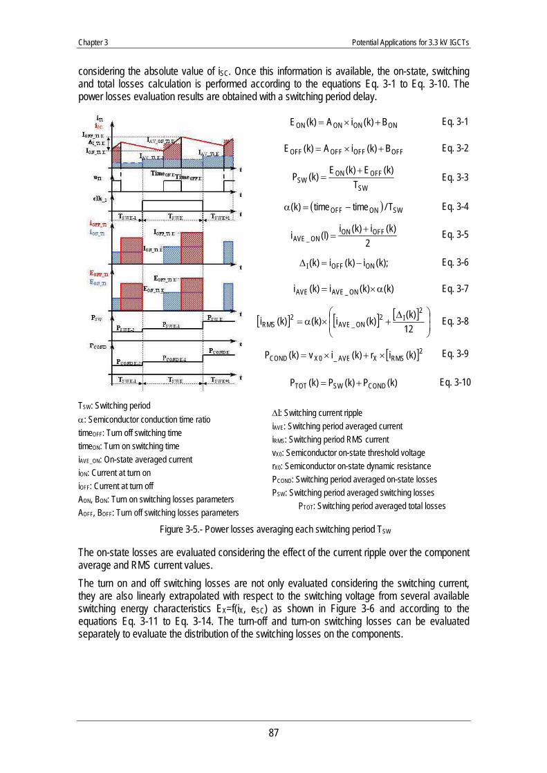
Chapter 3 Potential Applications for 3.3 kV IGCTs
87
considering the absolute value of iSC. Once this information is available, the on-state, switching and total losses calculation is performed according to the equations Eq. 3-1 to Eq. 3-10. The power losses evaluation results are obtained with a switching period delay.
ONONONON B)k(iA)k(E +×= Eq. 3-1
OFFOFFOFFOFF B)k(iA)k(E +×= Eq. 3-2
SW
OFFONSW T
)k(E)k(E)k(P += Eq. 3-3
( ) SWONOFF T/timetime)k( −=α Eq. 3-4
2)k(i)k(i)l(i OFFON
ON_AVE+
= Eq. 3-5
);k(i)k(i)k( ONOFFI −=Δ Eq. 3-6
)k()k(i)k(i ON_AVEAVE α×= Eq. 3-7
[ ] [ ] [ ]⎟⎟⎠
⎞⎜⎜⎝
⎛ Δ+×α=
12)k()k(i)k()k(i
2I2
ON_AVE2
RMS Eq. 3-8
[ ]2RMSXAVE_0XCOND )k(ir)k(iv)k(P ×+×= Eq. 3-9
)k(P)k(P)k(P CONDSWTOT += Eq. 3-10
TSW: Switching period α: Semiconductor conduction time ratio timeOFF: Turn off switching time timeON: Turn on switching time iAVE_ON: On-state averaged current iON: Current at turn on iOFF: Current at turn off AON, BON: Turn on switching losses parameters AOFF, BOFF: Turn off switching losses parameters
ΔI: Switching current ripple iAVE: Switching period averaged current iRMS: Switching period RMS current vX0: Semiconductor on-state threshold voltage rX0: Semiconductor on-state dynamic resistance PCOND: Switching period averaged on-state losses PSW: Switching period averaged switching losses
PTOT: Switching period averaged total losses
Figure 3-5.- Power losses averaging each switching period TSW
The on-state losses are evaluated considering the effect of the current ripple over the component average and RMS current values. The turn on and off switching losses are not only evaluated considering the switching current, they are also linearly extrapolated with respect to the switching voltage from several available switching energy characteristics EX=f(iX, eSC) as shown in Figure 3-6 and according to the equations Eq. 3-11 to Eq. 3-14. The turn-off and turn-on switching losses can be evaluated separately to evaluate the distribution of the switching losses on the components.
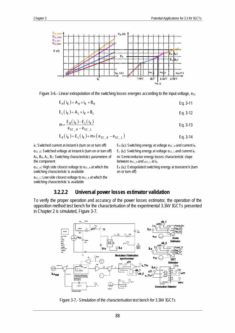
Chapter 3 Potential Applications for 3.3 kV IGCTs
88
Figure 3-6.- Linear extrapolation of the switching losses energies according to the input voltage, eSC
( ) HKHKH BiAiE +×= Eq. 3-11
( ) LKLKL BiAiE +×= Eq. 3-12
( ) ( )L_SCH_SC
KLKHee
iEiEm−−
= Eq. 3-13
( ) ( ) ( )L_SCK_SCKLKK eemiEiE −×+= Eq. 3-14
iK: Switched current at instant k (turn on or turn off) eSC_K: Switched voltage at instant k (turn on or turn off) AH, BH, AL, BL: Switching characteristics parameters of the component eSC_H: High side closest voltage to eSC_K at which the switching characteristic is available eSC_L: Low side closest voltage to eSC_K at which the switching characteristic is available
EH (iK): Switching energy at voltage eSC_H and current iK. EL (iK): Switching energy at voltage eSC_L and current iK. m: Semiconductor energy losses characteristic slope between eSC_H and eSC_L at iK. EK (iK): Extrapolated switching energy at transient k (turn on or turn off)
3.2.2.2 Universal power losses estimator validation To verify the proper operation and accuracy of the power losses estimator, the operation of the opposition method test bench for the characterisation of the experimental 3.3kV IGCTs presented in Chapter 2 is simulated, Figure 3-7.
Figure 3-7.- Simulation of the characterisation test bench for 3.3kV IGCTs
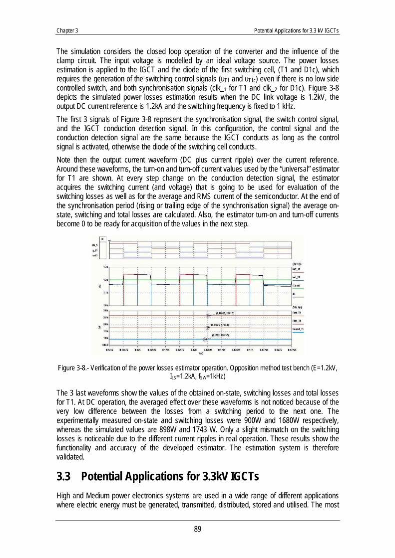
Chapter 3 Potential Applications for 3.3 kV IGCTs
89
The simulation considers the closed loop operation of the converter and the influence of the clamp circuit. The input voltage is modelled by an ideal voltage source. The power losses estimation is applied to the IGCT and the diode of the first switching cell, (T1 and D1c), which requires the generation of the switching control signals (uT1 and uT1c) even if there is no low side controlled switch, and both synchronisation signals (clk_1 for T1 and clk_2 for D1c). Figure 3-8 depicts the simulated power losses estimation results when the DC link voltage is 1.2kV, the output DC current reference is 1.2kA and the switching frequency is fixed to 1 kHz. The first 3 signals of Figure 3-8 represent the synchronisation signal, the switch control signal, and the IGCT conduction detection signal. In this configuration, the control signal and the conduction detection signal are the same because the IGCT conducts as long as the control signal is activated, otherwise the diode of the switching cell conducts. Note then the output current waveform (DC plus current ripple) over the current reference. Around these waveforms, the turn-on and turn-off current values used by the “universal” estimator for T1 are shown. At every step change on the conduction detection signal, the estimator acquires the switching current (and voltage) that is going to be used for evaluation of the switching losses as well as for the average and RMS current of the semiconductor. At the end of the synchronisation period (rising or trailing edge of the synchronisation signal) the average on-state, switching and total losses are calculated. Also, the estimator turn-on and turn-off currents become 0 to be ready for acquisition of the values in the next step.
Figure 3-8.- Verification of the power losses estimator operation. Opposition method test bench (E=1.2kV, ILS=1.2kA, fSW=1kHz)
The 3 last waveforms show the values of the obtained on-state, switching losses and total losses for T1. At DC operation, the averaged effect over these waveforms is not noticed because of the very low difference between the losses from a switching period to the next one. The experimentally measured on-state and switching losses were 900W and 1680W respectively, whereas the simulated values are 898W and 1743 W. Only a slight mismatch on the switching losses is noticeable due to the different current ripples in real operation. These results show the functionality and accuracy of the developed estimator. The estimation system is therefore validated.
3.3 Potential Applications for 3.3kV IGCTs High and Medium power electronics systems are used in a wide range of different applications where electric energy must be generated, transmitted, distributed, stored and utilised. The most
Chapter 3 Potential Applications for 3.3 kV IGCTs
90
important application fields where the power electronics systems are applied are Industry, Traction and Energy Management. In the High Power range, Industry and Utility applications are dominant. HVDC transmission systems in the range of several hundred MW to more than 1GW, Static VAR Compensators (SVC), large AC/AC cycloconverters for synchronous drives, arc furnaces and chlorine and aluminium electrolysis applications up to 100MW and more are some examples. All of these applications use line or load commutated converters based mainly on thyristors, which switch only once per network cycle. However, the development of power semiconductors has also enabled the use of Back to Back (BTB) configurations based on Voltage Source Inverters (VSI) for Interties and HVDC “Light” transmissions in the range of 100MW using IGCTs or IGBTs (usually in series / parallel connection) operating at switching frequencies up to 500Hz. Unified Power Flow controllers (UPFC), Active Filters for Power Conditioning and Storage system for several MW have been already installed punctually [AKA-01], [DAN-01], [CAR-98]. In the Medium Power Range, all application fields are concerned except Transmission. A big market in Medium Voltage Drives for industrial and traction applications is already established, with power ratings ranging form several hundred kW to several MW, [BER-00]. In the electric energy generation and distribution field, the interest on power electronics solutions has increased notably during the past few years thanks to the liberalisation of the Electric market and renovated environmental and power supply quality considerations. Terms such as “Distributed Generation” [ACK-01] and “Custom Power” [HIN-98] were introduced to classify the new emerging applications. In the generation market, the growth of wind turbines application is noticeable, with important quantities and power ratings reaching 3.5MW and planning to be increased. Other technologies such as solar plants, micro-turbines and fuel cells are also being considered, but its market introduction is still far from being massive for different reasons such as cost, reliability, etc. For the distribution market, multiple solutions such as Active Filters, Static VAR Compensators (STATCOMs), Dynamic Voltage Restorers (DVR), Solid State Breakers (SSB), Solid State Transfer Switches (SSTS), Dynamic Uninterruptible Power Supplies (DUPS), etc. have been applied successfully in field and keep improving their performances and reliability thanks to the research efforts being held. However, their use is limited to applications where other more basic solutions do not fulfil the specifications imposed by the actual standards or environmental issues (e.g. dynamic performances, volume, noise, etc.). The price and complexity of these systems are also big obstacles for their relevant market introduction, which in the near future can be overcome by the use of new technologies, equipments standardisation, etc. Also, the unstoppable increase on the electric energy consumption, the saturation of the actual electric system, the widespread introduction of distributed generation systems and future standards defined to modernise the electric system are the main arguments that will stimulate and support the use of these power electronics based systems. In the Distribution field, and more specifically regarding the French Railways electric network, two potential applications for Power Electronics systems in the Medium Power range are identified:
• Harmonic currents compensation for 1.5kV DC substations. • Reactive power compensation for 25kV / 50Hz single-phase substations
In these applications, the use of components handling high currents at high switching frequencies could provide competitive solutions to comply with the imposed requirements. Multiple solutions could be applied (i.e. semiconductors, topologies), but here the use of the most relevant solutions based on 3.3kV IGCTs are only considered to highlight the possibilities that this component offers in such applications.

Chapter 3 Potential Applications for 3.3 kV IGCTs
91
3.3.1 Harmonic Currents Compensation for 1.5kV DC SNCF Substations
With the railway market liberalisation, the managing task of the French railways network was divided into two public institutions, SNCF (Société Nationale des Chemins de Fer) and RFF (Réseau Ferré de France). The train operation is managed by the SNCF while RFF is the owner of the railway infrastructure and manages it. The French railway network totals around 33000km rail tracks, of which approximately 13500km are electrically energised. Of these 13500km, around 6000km use 1.5kV DC lines and the rest use 25kV/50Hz single-phase lines, Figure 3-9. Although the number of kilometres for both voltage lines is similar, the number of DC substations is considerably high compared to the number of 25kV substations. This is due to the need for higher line current values (reaching 6kA in overload mode) when trains operate under a DC line, which generates higher voltage drops on the line that require shorter distances between substations (8 to 25km compared to 35km to 90km for 25kV lines) to keep the line voltage inside the operating voltage range of the trains.
Figure 3-9.- Line voltages of the European railway networks
Not only is the voltage drop across the line a source of problems for the 1.5kV DC network, but the high harmonic current content generated on the rectifier based substations has to be limited to fulfil the standard imposed by the French public institutions for electric transmission (>63kV) RTE (Réseau de Transport d’Electricité) or electric distribution EDF (Electricité de France). In this section, the current harmonic problem on existing substations and several solutions are described and discussed.
3.3.1.1 1.5kV DC SNCF Substations The 1.5kV DC railway lines are supplied by substations usually connected to the 63kV or 90kV RTE transmission network. Internally, these substations consist basically of step-down transformers that adapt the voltage level and diode rectifiers to change the AC voltage into DC, which constitute the so-called “Traction Groups”, Figure 3-10. The substations output lines are parallel connected with distances ranging from 8 to 25km depending on the train traffic and track profile. Nowadays, the tendency for increasing the rail freight traffic (FRET) can require line current values up to 7kA, which can generate several hundred volt voltage drop between two substations and impede trains to work at their nominal rating. Under these circumstances, an intermediate substation can be installed. However, cost and environmental reasons complicate the access to
Chapter 3 Potential Applications for 3.3 kV IGCTs
92
the 63kV or 90kV network and only connection to the 20kV network is available. This implies that the amount of current harmonics that will be generated must be taken into serious consideration.
Figure 3-10.- SNCF 1.5kV DC substation synoptic
The current harmonic content must be limited to the specific values imposed by the electric transmission manager (RTE or EDF), otherwise penalties have to be suffered. For this application, the limits are well defined and better detailed in the low harmonic order range than in the IEEE 519 standard, “Recommended Practices and Requirements for Harmonic Control in Electric Power Systems”. Depending on the substation input voltage different regulations applies, [FAL-04]. Two voltage domains are concerned:
• HTA (1kV < UHV < 20kV): In this voltage domain, and for contracted powers PREF higher than 100kVAR, the “n” order harmonic currents IHV_N are limited according to the Table 3-2 and Eq. 3-15.
Even harmonics, n 2 4 >4 - -
KN 2 1 0.5 - -
Odd harmonics, n 3 5 & 7 9 11 & 13 >13
KN 4 5 2 3 2
Table 3-2.- Harmonic limits for the HTA voltage domain, PREF>100kVAR
HV
REFNN_HV U3
PKI⋅
⋅= Eq. 3-15
UHV: Contracted Voltage; PREF: Contracted Power; KN: n order harmonic limit coefficient;
• HTB (UHV > 20kV, usually 63kV and 90 kV): For the HTB domain the current harmonics limits are fixed by Table 3-3 and Eq. 3-16.
Even harmonics, n 2 4 >4 - -
KN 3 1.5 1 - -
Odd harmonics, n 3 5 & 7 9 11 & 13 >13
KN 6.5 8 3 5 3
Table 3-3.- Harmonic limits for the HTB voltage domain, PREF>100kVAR
HV
SNN_HV U3
SKI⋅
⋅= Eq. 3-16
UHV: Contracted Voltage; SS: Contracted Apparent Power; KN: n order harmonic limit coefficient;
As the KN harmonic current coefficients indicate, the tolerated harmonic currents are higher when the substation connection is made to the HTB domain. However, the cost of the connection to the HTB domain network is much more expensive than for the HTA (ratio close to 10), which makes
Chapter 3 Potential Applications for 3.3 kV IGCTs
93
more attractive the use of network connections in the HTA domain. Also, the HTB networks are not always accessible where a substation is to be installed. Considering the use of HTA network connections (20kV), a mean to allow higher harmonic current absolute values is increasing the contracted power. However, from an economic point of view, it is not acceptable to increase the contracted power in order to avoid penalties while the power consumption does not require such a contract. In that case, other solutions for harmonic current content reduction are required. Regarding the existing step-down transformer and rectifier configuration, different arrangements are employed. The type of substation is identified by a three-character code defining the nominal power of the installation, the arrangement of the rectifiers and the diode housing, Table 3-4.
Substation Identifier
1st Identifier
Nominal Power
2nd Identifier
Rectifier Configuration
3rd Identifier
Diode Housing
A 3000 kW 1 Single bridge v Modules
B 5000 kW 2 Double bridge p Press pack
C 6600 kW 3 Double bridge - series - -
- - 4 Double bridge - parallel - -
Table 3-4.- SNCF 1.5kV DC substations identification
The configuration mainly applied is the 12-pulse double bridge – series arrangement depicted in Figure 3-11. In that case the diodes of each 3-phase rectifier conduct the total load current IL and the railways line voltage UL is shared. To allow the safe series connection of both rectifiers, a six-phase system is generated by means of the star-triangle (⊥-Δ) transformer secondary windings arrangement. The primary is usually arranged in star configuration. To share equally the output voltage on each rectifier, the transformation ratio between the primary and each secondary must be adapted according to Eq. 3-17. For a given high voltage side phase to phase input voltage UHV, the average railways line voltage is defined by Eq. 3-18.
Figure 3-11.- Double bridge –series (12-pulse) rectifier configuration
;mm;m3m ⊥⊥Δ =⋅= Eq. 3-17
π⋅⋅⋅
= HVAVE_L
Um26U Eq. 3-18
;nnm;
nnm
1
3
1
2 == Δ⊥ UHV = High Voltage side phase to phase RMS voltage UL_AVE= Railways electric line average voltage
Considering the ideal behaviour of the rectifier, the high voltage side phase current waveform is shown in Figure 3-12. In that case, the harmonic current content worst case is considered as described by Eq. 3-19. Only harmonics of order (12⋅K±1) exist and their amplitude is inversely proportional to the order of the harmonic.
Chapter 3 Potential Applications for 3.3 kV IGCTs
94
( )∑∞
=⋅ϖ⋅⋅=
1NN_HVHV tNsinIi
( ) [ ]∞∈π⋅±⋅
⋅⋅⋅=±⋅ ,1K;
1K12I3m4I L
1K12HV Eq. 3-19
N: harmonic order IHV: harmonic maximal value
)3
21(Ima L +⋅⋅=
)3
11(Imb L +⋅⋅= 3
1Imc L ⋅⋅=
Figure 3-12.- High voltage side phase current waveform for 12-pulse rectifiers
For a contracted power of 8MVAR for a connection to the 20kV network, the evolution of the four first relevant harmonics (11th, 13th, 23rd, and 25th) with the load power consumption considering the rectifier ideal behaviour is shown in Figure 3-13. According to this figure, the imposed harmonic current limits are already exceeded for power consumption around 2.5MW.
Figure 3-13.- DC substation input current 11th, 13th, 23rd, 25th harmonic evolution, (Ideal 12 pulse rectifier)
Compared to the idealised current steps of Figure 3-12, the current evolution is limited by the real diode commutation process on the rectifier, thus the current harmonic content is reduced. Because of this effect, the input current RMS value is also reduced and the reactive power consumption is increased. Analytical and simulation analyses demonstrate that the harmonic content reduction mainly depends on the rectifier switching impedances (mainly the network and transformer leakage inductance) and also on the load current value. Circuit simulations results that consider the rectifier real behaviour are shown in Figure 3-14, [FAL-04]. The harmonic current content is considerably reduced mainly at high load power values. However, the harmonic current limits are still exceeded for low power values (3MW) compared with the contracted power (8MVAR). It is important to point out that only the 11th and 13th harmonics exceed the imposed limits. The 23rd and 25th harmonics are always below their maximum limit.
Figure 3-14.- DC substation input current 11th, 13th, 23rd, 25th harmonic evolution, (simulation results)
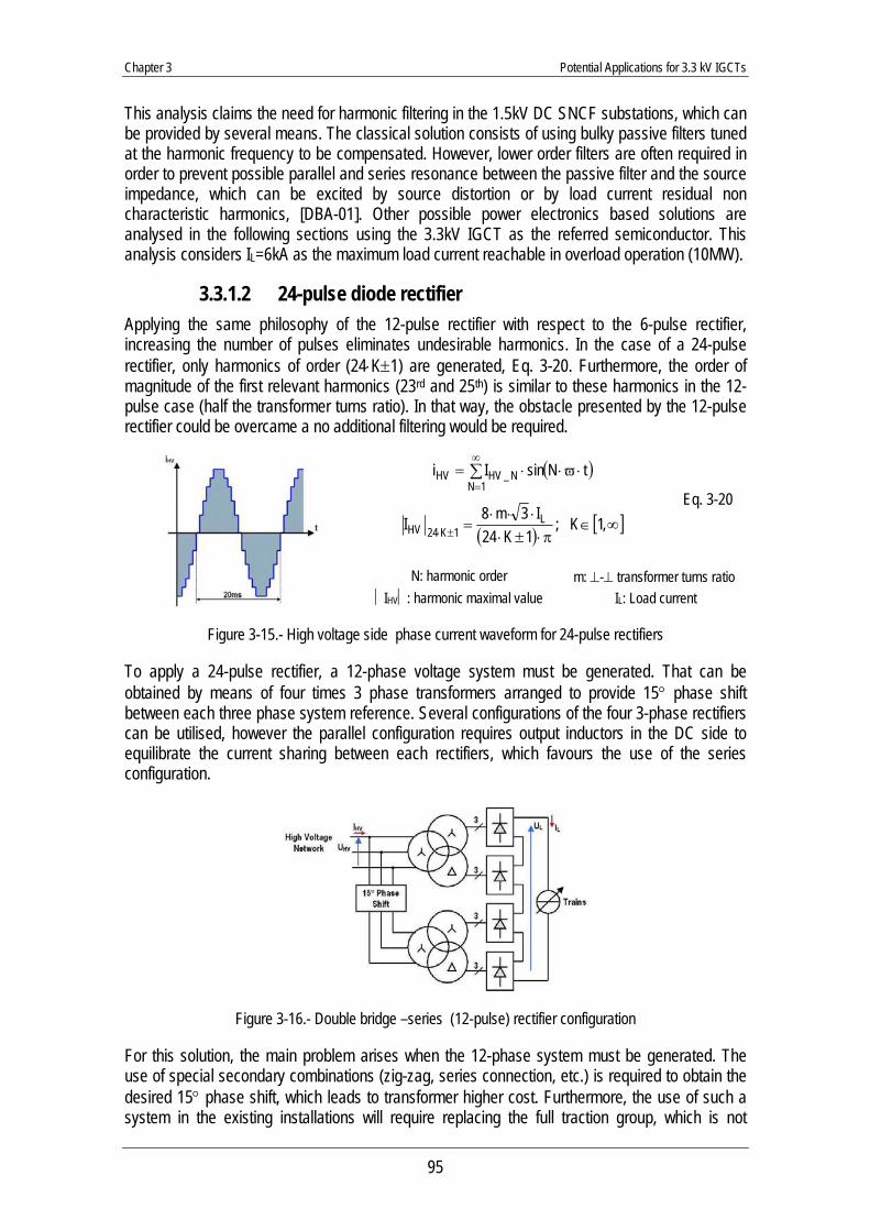
Chapter 3 Potential Applications for 3.3 kV IGCTs
95
This analysis claims the need for harmonic filtering in the 1.5kV DC SNCF substations, which can be provided by several means. The classical solution consists of using bulky passive filters tuned at the harmonic frequency to be compensated. However, lower order filters are often required in order to prevent possible parallel and series resonance between the passive filter and the source impedance, which can be excited by source distortion or by load current residual non characteristic harmonics, [DBA-01]. Other possible power electronics based solutions are analysed in the following sections using the 3.3kV IGCT as the referred semiconductor. This analysis considers IL=6kA as the maximum load current reachable in overload operation (10MW).
3.3.1.2 24-pulse diode rectifier Applying the same philosophy of the 12-pulse rectifier with respect to the 6-pulse rectifier, increasing the number of pulses eliminates undesirable harmonics. In the case of a 24-pulse rectifier, only harmonics of order (24⋅K±1) are generated, Eq. 3-20. Furthermore, the order of magnitude of the first relevant harmonics (23rd and 25th) is similar to these harmonics in the 12-pulse case (half the transformer turns ratio). In that way, the obstacle presented by the 12-pulse rectifier could be overcame a no additional filtering would be required.
( )∑∞
=⋅ϖ⋅⋅=
1NN_HVHV tNsinIi
( ) [ ]∞∈π⋅±⋅
⋅⋅⋅=±⋅ ,1K;
1K24I3m8I L
1K24HV Eq. 3-20
N: harmonic order
IHV: harmonic maximal value m: ⊥-⊥ transformer turns ratio
IL: Load current
Figure 3-15.- High voltage side phase current waveform for 24-pulse rectifiers
To apply a 24-pulse rectifier, a 12-phase voltage system must be generated. That can be obtained by means of four times 3 phase transformers arranged to provide 15° phase shift between each three phase system reference. Several configurations of the four 3-phase rectifiers can be utilised, however the parallel configuration requires output inductors in the DC side to equilibrate the current sharing between each rectifiers, which favours the use of the series configuration.
Figure 3-16.- Double bridge –series (12-pulse) rectifier configuration
For this solution, the main problem arises when the 12-phase system must be generated. The use of special secondary combinations (zig-zag, series connection, etc.) is required to obtain the desired 15° phase shift, which leads to transformer higher cost. Furthermore, the use of such a system in the existing installations will require replacing the full traction group, which is not
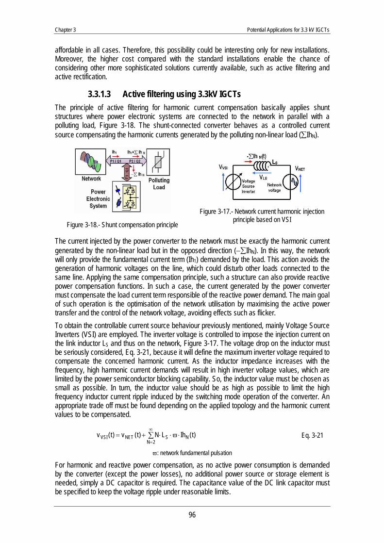
Chapter 3 Potential Applications for 3.3 kV IGCTs
96
affordable in all cases. Therefore, this possibility could be interesting only for new installations. Moreover, the higher cost compared with the standard installations enable the chance of considering other more sophisticated solutions currently available, such as active filtering and active rectification.
3.3.1.3 Active filtering using 3.3kV IGCTs The principle of active filtering for harmonic current compensation basically applies shunt structures where power electronic systems are connected to the network in parallel with a polluting load, Figure 3-18. The shunt-connected converter behaves as a controlled current source compensating the harmonic currents generated by the polluting non-linear load (∑IhN).
Figure 3-18.- Shunt compensation principle
Figure 3-17.- Network current harmonic injection
principle based on VSI
The current injected by the power converter to the network must be exactly the harmonic current generated by the non-linear load but in the opposed direction (−∑IhN). In this way, the network will only provide the fundamental current term (Ih1) demanded by the load. This action avoids the generation of harmonic voltages on the line, which could disturb other loads connected to the same line. Applying the same compensation principle, such a structure can also provide reactive power compensation functions. In such a case, the current generated by the power converter must compensate the load current term responsible of the reactive power demand. The main goal of such operation is the optimisation of the network utilisation by maximising the active power transfer and the control of the network voltage, avoiding effects such as flicker. To obtain the controllable current source behaviour previously mentioned, mainly Voltage Source Inverters (VSI) are employed. The inverter voltage is controlled to impose the injection current on the link inductor LS and thus on the network, Figure 3-17. The voltage drop on the inductor must be seriously considered, Eq. 3-21, because it will define the maximum inverter voltage required to compensate the concerned harmonic current. As the inductor impedance increases with the frequency, high harmonic current demands will result in high inverter voltage values, which are limited by the power semiconductor blocking capability. So, the inductor value must be chosen as small as possible. In turn, the inductor value should be as high as possible to limit the high frequency inductor current ripple induced by the switching mode operation of the converter. An appropriate trade off must be found depending on the applied topology and the harmonic current values to be compensated.
For harmonic and reactive power compensation, as no active power consumption is demanded by the converter (except the power losses), no additional power source or storage element is needed, simply a DC capacitor is required. The capacitance value of the DC link capacitor must be specified to keep the voltage ripple under reasonable limits.
∑∞
=⋅ϖ⋅⋅+=
2NNSNETVSI )t(IhLN)t(v)t(v Eq. 3-21
ϖ: network fundamental pulsation
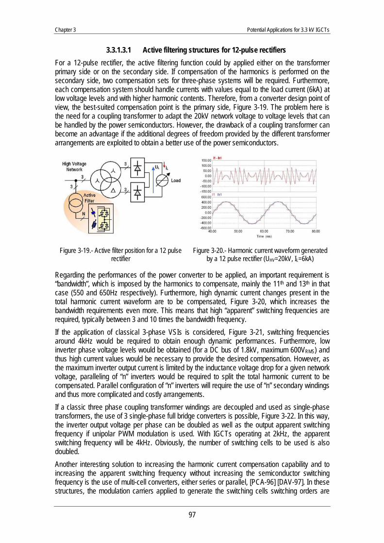
Chapter 3 Potential Applications for 3.3 kV IGCTs
97
3.3.1.3.1 Active filtering structures for 12-pulse rectifiers For a 12-pulse rectifier, the active filtering function could by applied either on the transformer primary side or on the secondary side. If compensation of the harmonics is performed on the secondary side, two compensation sets for three-phase systems will be required. Furthermore, each compensation system should handle currents with values equal to the load current (6kA) at low voltage levels and with higher harmonic contents. Therefore, from a converter design point of view, the best-suited compensation point is the primary side, Figure 3-19. The problem here is the need for a coupling transformer to adapt the 20kV network voltage to voltage levels that can be handled by the power semiconductors. However, the drawback of a coupling transformer can become an advantage if the additional degrees of freedom provided by the different transformer arrangements are exploited to obtain a better use of the power semiconductors.
Figure 3-19.- Active filter position for a 12 pulse rectifier
Figure 3-20.- Harmonic current waveform generated by a 12 pulse rectifier (UHV=20kV, IL=6kA)
Regarding the performances of the power converter to be applied, an important requirement is “bandwidth”, which is imposed by the harmonics to compensate, mainly the 11th and 13th in that case (550 and 650Hz respectively). Furthermore, high dynamic current changes present in the total harmonic current waveform are to be compensated, Figure 3-20, which increases the bandwidth requirements even more. This means that high “apparent” switching frequencies are required, typically between 3 and 10 times the bandwidth frequency. If the application of classical 3-phase VSIs is considered, Figure 3-21, switching frequencies around 4kHz would be required to obtain enough dynamic performances. Furthermore, low inverter phase voltage levels would be obtained (for a DC bus of 1.8kV, maximum 600VRMS) and thus high current values would be necessary to provide the desired compensation. However, as the maximum inverter output current is limited by the inductance voltage drop for a given network voltage, paralleling of “n” inverters would be required to split the total harmonic current to be compensated. Parallel configuration of “n” inverters will require the use of “n” secondary windings and thus more complicated and costly arrangements. If a classic three phase coupling transformer windings are decoupled and used as single-phase transformers, the use of 3 single-phase full bridge converters is possible, Figure 3-22. In this way, the inverter output voltage per phase can be doubled as well as the output apparent switching frequency if unipolar PWM modulation is used. With IGCTs operating at 2kHz, the apparent switching frequency will be 4kHz. Obviously, the number of switching cells to be used is also doubled. Another interesting solution to increasing the harmonic current compensation capability and to increasing the apparent switching frequency without increasing the semiconductor switching frequency is the use of multi-cell converters, either series or parallel, [PCA-96] [DAV-97]. In these structures, the modulation carriers applied to generate the switching cells switching orders are
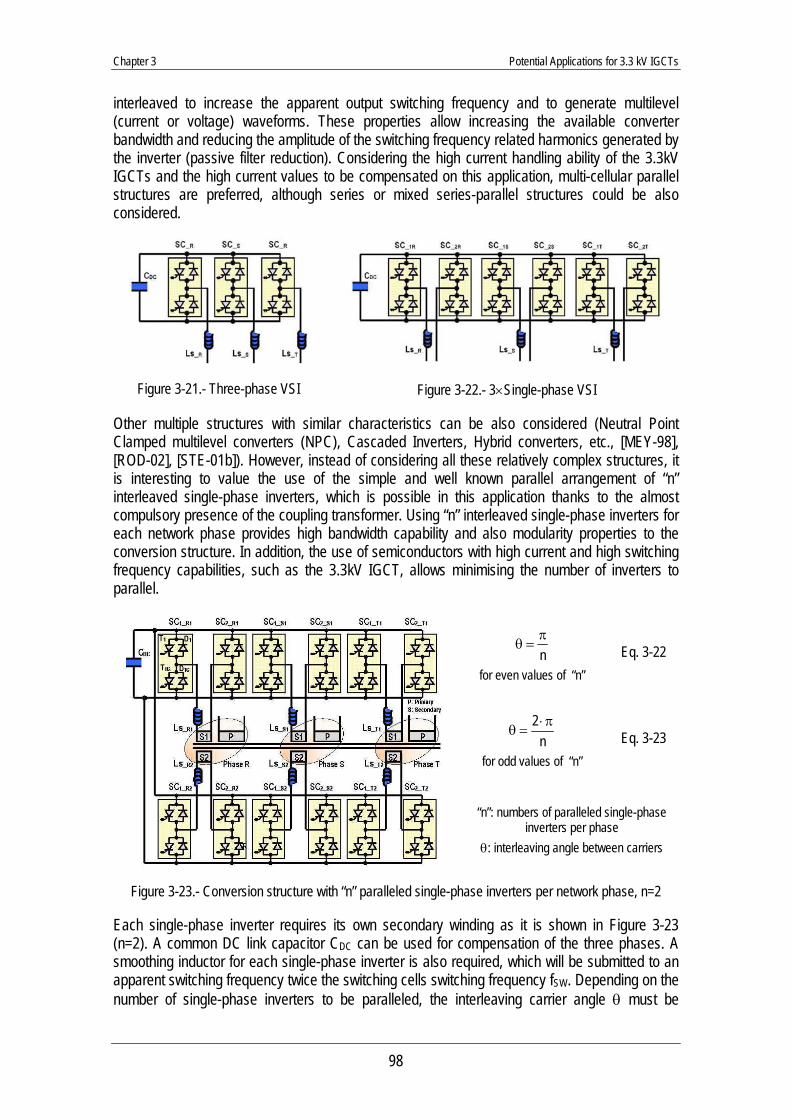
Chapter 3 Potential Applications for 3.3 kV IGCTs
98
interleaved to increase the apparent output switching frequency and to generate multilevel (current or voltage) waveforms. These properties allow increasing the available converter bandwidth and reducing the amplitude of the switching frequency related harmonics generated by the inverter (passive filter reduction). Considering the high current handling ability of the 3.3kV IGCTs and the high current values to be compensated on this application, multi-cellular parallel structures are preferred, although series or mixed series-parallel structures could be also considered.
Figure 3-21.- Three-phase VSI Figure 3-22.- 3×Single-phase VSI
Other multiple structures with similar characteristics can be also considered (Neutral Point Clamped multilevel converters (NPC), Cascaded Inverters, Hybrid converters, etc., [MEY-98], [ROD-02], [STE-01b]). However, instead of considering all these relatively complex structures, it is interesting to value the use of the simple and well known parallel arrangement of “n” interleaved single-phase inverters, which is possible in this application thanks to the almost compulsory presence of the coupling transformer. Using “n” interleaved single-phase inverters for each network phase provides high bandwidth capability and also modularity properties to the conversion structure. In addition, the use of semiconductors with high current and high switching frequency capabilities, such as the 3.3kV IGCT, allows minimising the number of inverters to parallel.
Each single-phase inverter requires its own secondary winding as it is shown in Figure 3-23 (n=2). A common DC link capacitor CDC can be used for compensation of the three phases. A smoothing inductor for each single-phase inverter is also required, which will be submitted to an apparent switching frequency twice the switching cells switching frequency fSW. Depending on the number of single-phase inverters to be paralleled, the interleaving carrier angle θ must be
nπ
=θ
for even values of “n” Eq. 3-22
n2 π⋅
=θ
for odd values of “n” Eq. 3-23
“n”: numbers of paralleled single-phase inverters per phase
θ: interleaving angle between carriers
Figure 3-23.- Conversion structure with “n” paralleled single-phase inverters per network phase, n=2
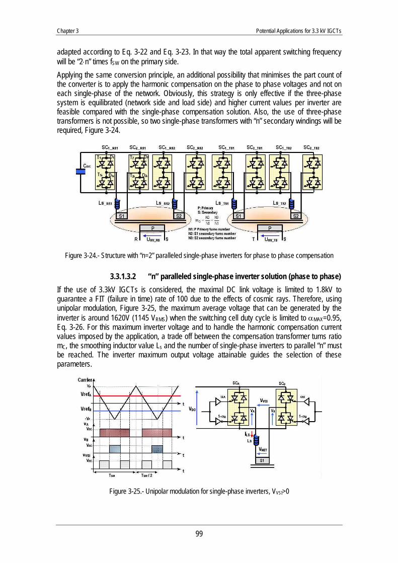
Chapter 3 Potential Applications for 3.3 kV IGCTs
99
adapted according to Eq. 3-22 and Eq. 3-23. In that way the total apparent switching frequency will be “2⋅n” times fSW on the primary side. Applying the same conversion principle, an additional possibility that minimises the part count of the converter is to apply the harmonic compensation on the phase to phase voltages and not on each single-phase of the network. Obviously, this strategy is only effective if the three-phase system is equilibrated (network side and load side) and higher current values per inverter are feasible compared with the single-phase compensation solution. Also, the use of three-phase transformers is not possible, so two single-phase transformers with “n” secondary windings will be required, Figure 3-24.
Figure 3-24.- Structure with “n=2” paralleled single-phase inverters for phase to phase compensation
3.3.1.3.2 “n” paralleled single-phase inverter solution (phase to phase) If the use of 3.3kV IGCTs is considered, the maximal DC link voltage is limited to 1.8kV to guarantee a FIT (failure in time) rate of 100 due to the effects of cosmic rays. Therefore, using unipolar modulation, Figure 3-25, the maximum average voltage that can be generated by the inverter is around 1620V (1145 VRMS) when the switching cell duty cycle is limited to αMAX=0.95, Eq. 3-26. For this maximum inverter voltage and to handle the harmonic compensation current values imposed by the application, a trade off between the compensation transformer turns ratio mC, the smoothing inductor value Ls and the number of single-phase inverters to parallel “n” must be reached. The inverter maximum output voltage attainable guides the selection of these parameters.
Figure 3-25.- Unipolar modulation for single-phase inverters, VVSI>0
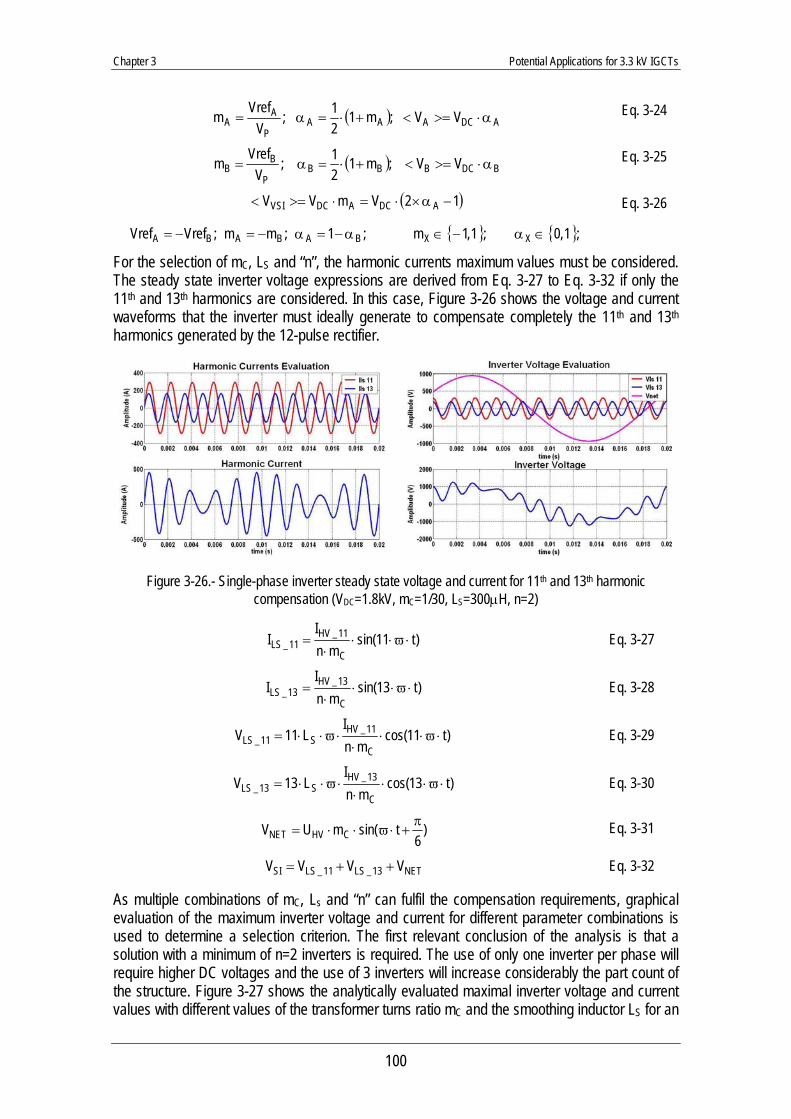
Chapter 3 Potential Applications for 3.3 kV IGCTs
100
( ) ADCAAAP
AA VV;m1
21;
VVrefm α⋅>=<+⋅=α= Eq. 3-24
( ) BDCBBBP
BB VV;m1
21;
VVrefm α⋅>=<+⋅=α=
Eq. 3-25
( )12VmVV ADCADCVSI −α×⋅=⋅>=< Eq. 3-26
;1;mm;VrefVref BABABA α−=α−=−= ;1,0;1,1m XX ∈α−∈
For the selection of mC, LS and “n”, the harmonic currents maximum values must be considered. The steady state inverter voltage expressions are derived from Eq. 3-27 to Eq. 3-32 if only the 11th and 13th harmonics are considered. In this case, Figure 3-26 shows the voltage and current waveforms that the inverter must ideally generate to compensate completely the 11th and 13th harmonics generated by the 12-pulse rectifier.
Figure 3-26.- Single-phase inverter steady state voltage and current for 11th and 13th harmonic compensation (VDC=1.8kV, mC=1/30, LS=300μH, n=2)
)t11sin(mn
II
C
11_HV11_LS ⋅ϖ⋅⋅
⋅= Eq. 3-27
)t13sin(mn
II
C
13_HV13_LS ⋅ϖ⋅⋅
⋅= Eq. 3-28
)t11cos(mn
IL11V
C
11_HVS11_LS ⋅ϖ⋅⋅
⋅⋅ϖ⋅⋅= Eq. 3-29
)t13cos(mn
IL13V
C
13_HVS13_LS ⋅ϖ⋅⋅
⋅⋅ϖ⋅⋅= Eq. 3-30
)6
tsin(mUV CHVNETπ
+⋅ϖ⋅⋅= Eq. 3-31
NET13_LS11_LSSI VVVV ++= Eq. 3-32
As multiple combinations of mC, Ls and “n” can fulfil the compensation requirements, graphical evaluation of the maximum inverter voltage and current for different parameter combinations is used to determine a selection criterion. The first relevant conclusion of the analysis is that a solution with a minimum of n=2 inverters is required. The use of only one inverter per phase will require higher DC voltages and the use of 3 inverters will increase considerably the part count of the structure. Figure 3-27 shows the analytically evaluated maximal inverter voltage and current values with different values of the transformer turns ratio mC and the smoothing inductor LS for an
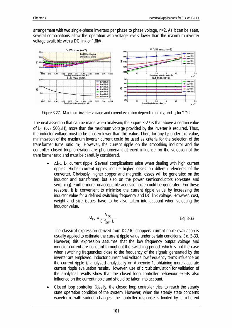
Chapter 3 Potential Applications for 3.3 kV IGCTs
101
arrangement with two single-phase inverters per phase to phase voltage, n=2. As it can be seen, several combinations allow the operation with voltage levels lower than the maximum inverter voltage available with a DC link of 1.8kV.
Figure 3-27.- Maximum inverter voltage and current evolution depending on mC and LS for “n”=2
The next assertion that can be made when analysing the Figure 3-27 is that above a certain value of LS (LS≈ 500μH), more than the maximum voltage provided by the inverter is required. Thus, the inductor voltage must to be chosen lower than this value. Then, for any LS under this value, minimisation of the maximum inverter current could be used as criteria for the selection of the transformer turns ratio mC. However, the current ripple on the smoothing inductor and the controller closed loop operation are phenomena that exert influence on the selection of the transformer ratio and must be carefully considered.
• ΔILS, LS current ripple: Several complications arise when dealing with high current ripples. Higher current ripples induce higher losses on different elements of the converter. Obviously, higher copper and magnetic losses will be generated on the inductor and transformer, but also on the power semiconductors (on-state and switching). Furthermore, unacceptable acoustic noise could be generated. For these reasons, it is convenient to minimise the current ripple value by increasing the inductor value for a defined switching frequency and DC link voltage. However, cost, weight and size issues have to be also taken into account when selecting the inductor value.
Lf8VISW
DCLS ⋅⋅
=Δ Eq. 3-33
The classical expression derived from DC/DC choppers current ripple evaluation is usually applied to estimate the current ripple value under certain conditions, Eq. 3-33. However, this expression assumes that the low frequency output voltage and inductor current are constant throughout the switching period, which is not the case when switching frequencies close to the frequency of the signals generated by the inverter are employed. Inductor current and voltage low frequency terms influence on the current ripple is analysed analytically on Appendix 1, obtaining more accurate current ripple evaluation results. However, use of circuit simulation for validation of the analytical results show that the closed loop controller behaviour exerts also influence on the current ripple and should be taken into account.
• Closed loop controller: Ideally, the closed loop controller tries to reach the steady state operation condition of the system. However, when the steady state concerns waveforms with sudden changes, the controller response is limited by its inherent
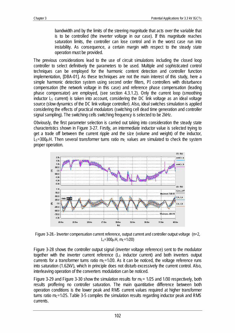
Chapter 3 Potential Applications for 3.3 kV IGCTs
102
bandwidth and by the limits of the steering magnitude that acts over the variable that is to be controlled (the inverter voltage in our case). If this magnitude reaches saturation limits, the controller can lose control and in the worst case run into instability. As consequence, a certain margin with respect to the steady state operation must be provided.
The previous considerations lead to the use of circuit simulations including the closed loop controller to select definitively the parameters to be used. Multiple and sophisticated control techniques can be employed for the harmonic content detection and controller function implementation, [DBA-01]. As these techniques are not the main interest of this study, here a simple harmonic detection system using second order filters, PI controllers with disturbance compensation (the network voltage in this case) and reference phase compensation (leading phase compensator) are employed, (see section 4.3.1.2). Only the current loop (smoothing inductor LS current) is taken into account, considering the DC link voltage as an ideal voltage source (slow dynamics of the DC link voltage controller). Also, ideal switches simulation is applied considering the effects of practical modulators (switching cell dead time generation and controller signal sampling). The switching cells switching frequency is selected to be 2kHz. Obviously, the first parameter selection is carried out taking into consideration the steady state characteristics shown in Figure 3-27. Firstly, an intermediate inductor value is selected trying to get a trade off between the current ripple and the size (volume and weight) of the inductor, LS=300μH. Then several transformer turns ratio mC values are simulated to check the system proper operation.
Figure 3-28.- Inverter compensation current reference, output current and controller output voltage (n=2, Ls=300μH, mC=1/20)
Figure 3-28 shows the controller output signal (inverter voltage reference) sent to the modulator together with the inverter current reference (LS inductor current) and both inverters output currents for a transformer turns ratio mC=1/20. As it can be noticed, the voltage reference runs into saturation (1.62kV), which in principle does not disturb excessively the current control. Also, interleaving operation of the converters modulation can be noticed. Figure 3-29 and Figure 3-30 show the simulation results for mC= 1/25 and 1/30 respectively, both results proffering no controller saturation. The main quantitative difference between both operation conditions is the lower peak and RMS current values required at higher transformer turns ratio mC=1/25. Table 3-5 compiles the simulation results regarding inductor peak and RMS currents.
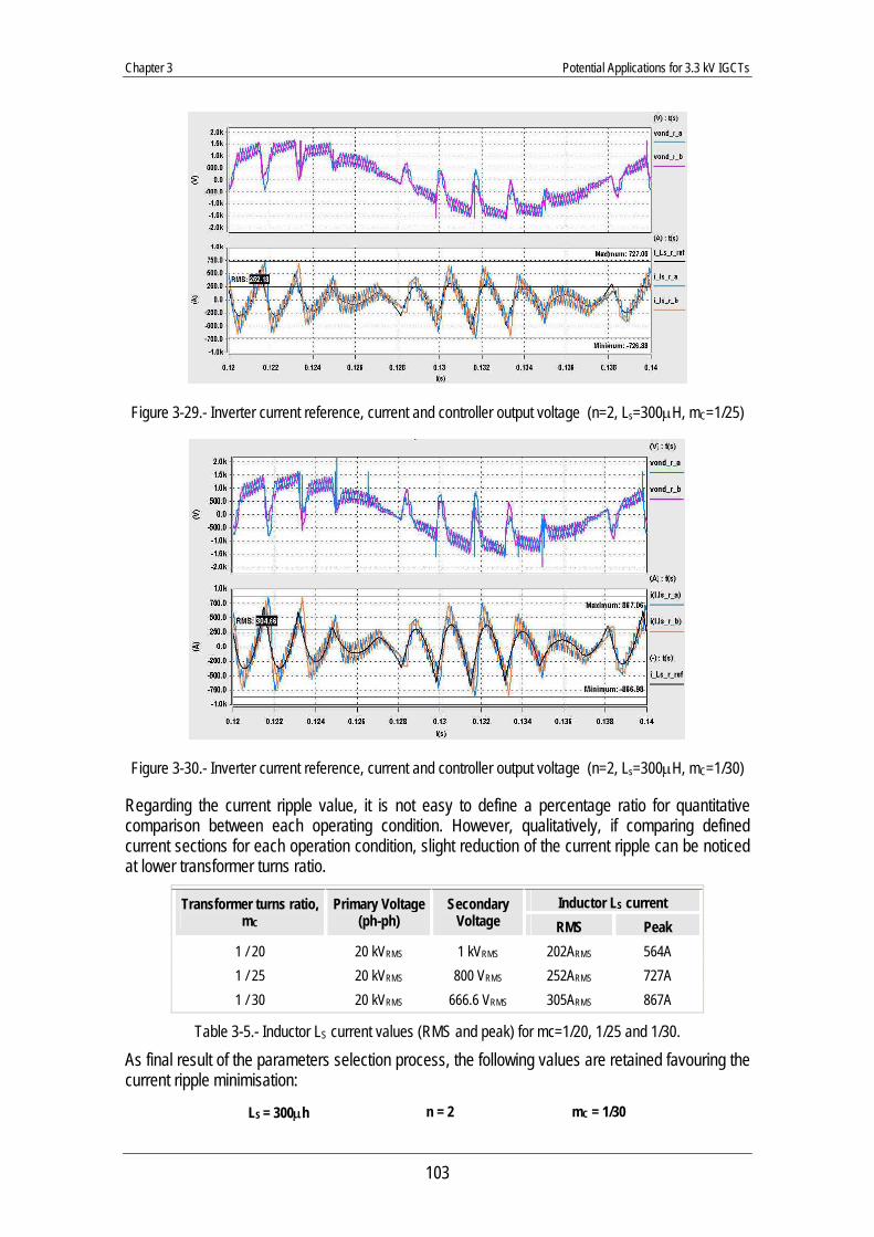
Chapter 3 Potential Applications for 3.3 kV IGCTs
103
Figure 3-29.- Inverter current reference, current and controller output voltage (n=2, Ls=300μH, mC=1/25)
Figure 3-30.- Inverter current reference, current and controller output voltage (n=2, Ls=300μH, mC=1/30)
Regarding the current ripple value, it is not easy to define a percentage ratio for quantitative comparison between each operating condition. However, qualitatively, if comparing defined current sections for each operation condition, slight reduction of the current ripple can be noticed at lower transformer turns ratio.
Inductor LS current Transformer turns ratio, mC
Primary Voltage (ph-ph)
Secondary Voltage RMS Peak
1 / 20 20 kVRMS 1 kVRMS 202ARMS 564A 1 / 25 20 kVRMS 800 VRMS 252ARMS 727A 1 / 30 20 kVRMS 666.6 VRMS 305ARMS 867A
Table 3-5.- Inductor LS current values (RMS and peak) for mc=1/20, 1/25 and 1/30.
As final result of the parameters selection process, the following values are retained favouring the current ripple minimisation:
LS = 300μh n = 2 mC = 1/30
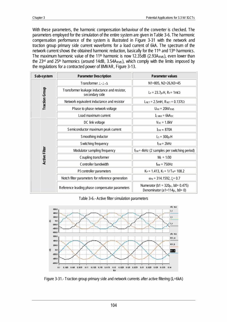
Chapter 3 Potential Applications for 3.3 kV IGCTs
104
With these parameters, the harmonic compensation behaviour of the converter is checked. The parameters employed for the simulation of the entire system are given in Table 3-6. The harmonic compensation performance of the system is illustrated in Figure 3-31 with the network and traction group primary side current waveforms for a load current of 6kA. The spectrum of the network current shows the obtained harmonic reduction, basically for the 11th and 13th harmonics. The maximum harmonic value of the 11th harmonic is now 12.35dB (2.93ARMS), even lower than the 23rd and 25th harmonics (around 14dB, 3.54ARMS), which comply with the limits imposed by the regulations for a contracted power of 8MVAR, Figure 3-13.
Sub-system Parameter Description Parameter values
Transformer ⊥-⊥-Δ N1=805, N2=26,N3=45
Transformer leakage inductance and resistor, secondary side LF = 23.7μH, RF= 1mΩ
Network equivalent inductance and resistor LNET = 2.5mH, RNET = 0.137Ω
Phase to phase network voltage UHV = 20kVRMS Trac
tion
Grou
p
Load maximum current IL MAX = 6kADC
DC link voltage VDC = 1.8kV
Semiconductor maximum peak current ISW ≈ 870A
Smoothing inductor LS = 300μH
Switching frequency fSW = 2kHz
Modulator sampling frequency fSM = 4kHz (2 samples per switching period)
Coupling transformer MC = 1/30
Controller bandwidth fBW = 750Hz
PI controller parameters KP = 1.413, KI = 1/ TN= 108.2
Notch filter parameters for reference generation ϖN = 314.1592, ξ= 0.7
Activ
e Filt
er
Reference leading phase compensator parameters Numerator (b1 = 320μ, b0= 0.475) Denominator (a1=114μ, b0= 0)
Table 3-6.- Active filter simulation parameters
Figure 3-31.- Traction group primary side and network currents after active filtering (IL=6kA)
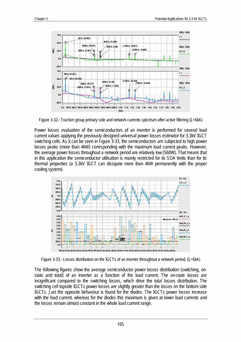
Chapter 3 Potential Applications for 3.3 kV IGCTs
105
Figure 3-32.- Traction group primary side and network currents spectrum after active filtering (IL=6kA)
Power losses evaluation of the semiconductors of an inverter is performed for several load current values applying the previously designed universal power losses estimator for 3.3kV IGCT switching cells. As it can be seen in Figure 3-33, the semiconductors are subjected to high power losses peaks (more than 4kW) corresponding with the maximum load current peaks. However, the average power losses throughout a network period are relatively low (560W). That means that in this application the semiconductor utilisation is mainly restricted for its SOA limits than for its thermal properties (a 3.3kV IGCT can dissipate more than 4kW permanently with the proper cooling system).
Figure 3-33.- Losses distribution on the IGCTs of an inverter throughout a network period, (IL=6kA)
The following figures show the average semiconductor power losses distribution (switching, on-state and total) of an inverter as a function of the load current. The on-state losses are insignificant compared to the switching losses, which drive the total losses distribution. The switching cell topside IGCTs power losses are slightly greater than the losses on the bottom side IGCTs. Just the opposite behaviour is found for the diodes. The IGCTs power losses increase with the load current, whereas for the diodes this maximum is given at lower load currents and the losses remain almost constant in the whole load current range.
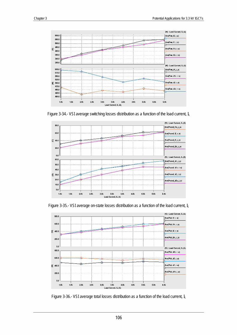
Chapter 3 Potential Applications for 3.3 kV IGCTs
106
Figure 3-34.- VSI average switching losses distribution as a function of the load current, IL
Figure 3-35.- VSI average on-state losses distribution as a function of the load current, IL
Figure 3-36.- VSI average total losses distribution as a function of the load current, IL

Chapter 3 Potential Applications for 3.3 kV IGCTs
107
3.3.1.3.3 Active filtering solution discussion Active filtering for SNCF 1.5kV DC substations can be accomplished by using multiple conversion structures. Here, the solution with n=2 interleaved 3.3kV IGCT based single-phase inverters is analysed in detail and shows the ability of the components to handle the harmonic compensation requirements. The use of 2 single-phase inverters per phase to phase voltage is not imposed by the thermal or SOA limits of the IGCT but by the maximum voltage that can provide the converter. In such conditions the 3.3kV IGCT can be considered to be underused, but other arguments such as the use of air-cooling systems instead of using water-cooling systems could justify the use of this component. Obviously, lower semiconductor ratings could be affordable and other semiconductor technologies (3.3kV IGBT) could be also applied at the expense of higher losses per component. If one wants better utilisation of the 3.3kV IGCT with the same dynamic performances, the use of a 3 level (multi-cell) single-phase inverter per phase to phase voltage could be used. In that way the maximum voltage level generated by the inverter is doubled and higher harmonic currents or higher transformer turns ratio mC (higher secondary voltage) could be allowed. Also, only one inductor and secondary transformers will be required. Evidently, the number of semiconductors is the same as for the n=2 proposed structure and other control (floating capacitor balance) and IGCT operation (clamp circuit) problems must be solved. No matter which structure is used, the active filter solution guarantees the operation of the substation under the harmonics limits imposed by the regulations. Furthermore, this solution can be applied either in existing or in new substations with relatively low power requirements (less than 1MVAR at the transformer level considering the RMS current for 10MW load power). However, other issues such as cost, volume, reliability and maintenance must be taken into account when compared to other alternative solutions.
3.3.1.4 Active rectification using 3.3kV IGCTs Another solution to comply with the regulations regarding the harmonic current content in the SNCF 1.5kV DC substation is to avoid the generation of harmonics. That can be accomplished by exchanging the existing 12-pulse diode rectifier, the source of harmonics, with an active rectifier with sinusoidal current consumption, Figure 3-37. The classical active rectifier solution consists of the connection of voltage source inverters between the network coupling transformer and the load to impose sinusoidal current consumption with power factor close to one. The presence of the network coupling transformer allows making similar considerations as in the previously analysed active filtering case (see 3.3.1.3.1).
Figure 3-37.- Active rectification structure.
The solution evaluated here consists of keeping the same transformer structure of the DC substation (2 secondary windings per phase) and the use of a full bridge single-phase inverter per transformer secondary, (six single-phase inverters in total). Only the transformer turns ratio is modified, N2=N3. The converter is equivalent to the structure presented in Figure 3-23, but in this
Chapter 3 Potential Applications for 3.3 kV IGCTs
108
case the load (trains) is connected to the DC link capacitor, CDC. This solution is adopted to reach the required power ratings of the application (10MW in overload conditions), and to obtain the required bandwidth for operation with sinusoidal current consumption. Using unipolar modulation for each inverter and the interleaving strategy between the inverters related to the same primary phase, (n=2 ⇒ θ=π/2), a switching cell switching frequency fSW=1kHz leads to a primary apparent switching frequency of 4kHz. This allows for a controller bandwidth fBW around ten times bigger than the network frequency, fNET=50Hz, which is enough to guarantee the expected sinusoidal current consumption. The minimum DC link to feed the load is fixed by the nominal voltage of the substation, 1.5kVDC. Considering the maximum available duty cycle (αMAX=0.95), the maximum inverter voltage reachable by each inverter is limited to 1.35kV. Obviously, this maximum voltage should not be reached, otherwise saturation of the control system will arise and consequently current control loss. Therefore, for the selection of the smoothing inductor LS, and the transformation ratio “m” this limit must be considered as shown in Figure 3-38.
Figure 3-38.- Maximum inverter voltage and current evolution depending on m and LS for active
rectification
Figure 3-39.- Single-phase inverter steady state voltage and current for active rectification
(VDC=1.5kV, m=1/14, LS=300μH)
For any LS below a certain value (LS≈700μH) the selection of “m” is fixed by the maximum inverter current. Considering the influence of the control loop behaviour and the current ripple evaluation, a certain inverter voltage margin is required. Circuit simulation is used to select the final values employed on the performance analysis of the converter. Figure 3-39 shows the inverter voltage and current steady state waveforms with the selected parameters when 10MW are supplied to the load, (VDC=1.5kV, m=1/14, LS=300μH). With these parameters, the behaviour of the converter is checked by simulation. Only the current loop is simulated considering the output voltage as an ideal voltage source. The inverter current reference phase synchronisation is obtained by means of notch filters and the measure of the secondary voltage waveform, whereas the amplitude reference is derived from the secondary voltage RMS value and the power consumption to be simulated. The controller implemented is the classical PI with disturbance compensation (the secondary voltage). Table 3-7 shows the entire system simulation parameters. Figure 3-40 shows the sinusoidal network currents obtained thanks to the active rectification for a DC link voltage of 1.6kV and a load power of 10MW. The line currents are in phase with their respective line voltages providing a power factor close to 1. A slight switching current ripple derived by the switching operation can be noticed. The line currents spectrum, Figure 3-41, shows that this high frequency current ripple is located around 4kHz as expected. Also small low
Chapter 3 Potential Applications for 3.3 kV IGCTs
109
frequency harmonics are generated (3rd, 5th, 7th, etc.) due to the inverter imperfections (dead time, switching current effect on the control loop, etc.), which could be compensated by control. In all cases, the system operation complies with the current defined harmonic regulations.
Sub-system Parameter Description Parameter values
Transformer ⊥-(decoupled secondary windings, 2 per phase) N1=840, N2=60,N3=60
Network equivalent inductance and resistor LNET = 2.5mH, RNET = 0.137Ω
Phase to phase network voltage UHV = 20kVRMS
Load maximum current IL MAX = 6kADC
DC link voltage VDC = 1.6kV
Semiconductor maximum peak current ISW ≈ 3.2kA
Smoothing inductor LS = 300μH
Switching frequency fSW = 1kHz
Modulator sampling frequency fSM = 2kHz (2 samples per switching period)
Controller bandwidth fBW = 600Hz
PI controller parameters KP = 1.084, KI = 1/ TN= 1116.7
Activ
e Rec
tifier
bas
ed T
ract
ion
Grou
p
Notch filter parameters for reference generation ϖN = 314.1592, ξ= 0.7
Table 3-7.- Active rectifier simulation parameters
Figure 3-40.- Primary side line currents and phase to neutral voltages (VDC=1.6kV, PL=10MW)
Figure 3-41.- Primary side line currents spectrum (VDC=1.6kV, PL=10MW)
Chapter 3 Potential Applications for 3.3 kV IGCTs
110
Figure 3-42 shows the inverters current waveforms when the maximum power is supplied (10MW). It can be seen that the interleaving operation of the two inverters is related to the same input voltage. A maximum peak current close to 3.2kA is attained, so the semiconductors have to admit such a peak current. Regarding the current ripple, maximum values around ΔILS≈800A are identified, which in percentage is translated to be around 15% of the 50Hz current term.
Figure 3-42.- Inverters current waveforms (VDC=1.6kV, PL=10MW)
In such working conditions, the semiconductor power losses are evaluated to demonstrate the ability of the 3.3kV IGCTs to handle such amount of power (1.6MW per single-phase inverter). The simulation results show how the semiconductors are submitted to high power losses peaks (close to 8kW and 6kW for the diodes and IGCTs respectively) but with average power losses that can be handled by the component (around 2kW), Figure 3-43. Considering this operation mode, if the power load is increased, the SOA limit of the component will limit the maximum attainable output power.
Figure 3-43.- Diodes and IGCTs power losses distribution (VDC=1.6kV, PL=10MW)
The following figures show the evolution of the average power losses of the inverter semiconductors as a function of the inverter 50Hz RMS current, thus the output power. In all the components the power losses increase with the output power and a certain balance between the on-state losses and switching losses is obtained (slightly higher on-state losses at maximum
Chapter 3 Potential Applications for 3.3 kV IGCTs
111
power). The total power losses are the same for both switching cells, with slight power losses differences between the top and bottom side semiconductors.
Figure 3-44.- Average switching losses distribution as a function of the inverter RMS current, ILS RMS
Figure 3-45.- Average on-state losses distribution as a function of the inverter RMS current, ILS RMS
Figure 3-46.- Average total losses distribution as a function of the inverter RMS current, ILS RMS
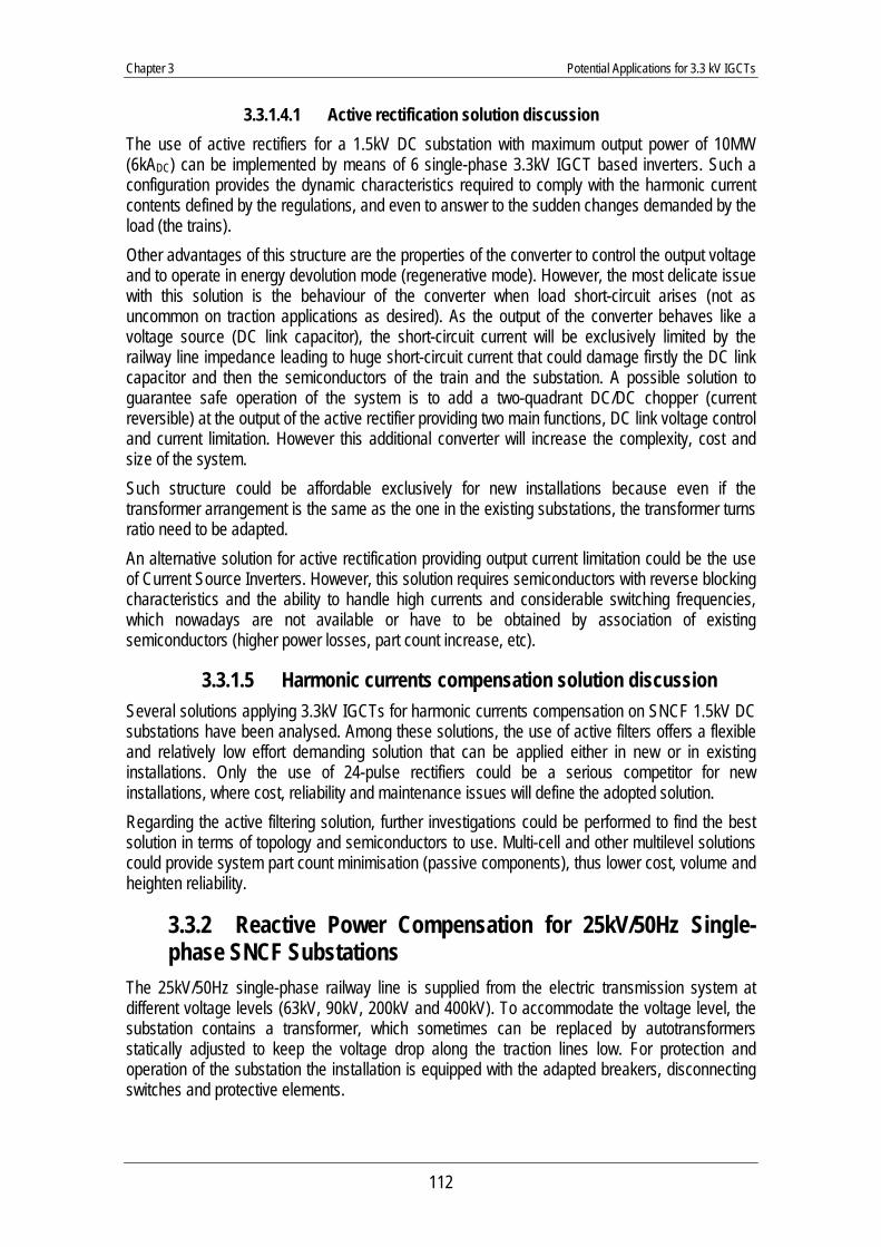
Chapter 3 Potential Applications for 3.3 kV IGCTs
112
3.3.1.4.1 Active rectification solution discussion The use of active rectifiers for a 1.5kV DC substation with maximum output power of 10MW (6kADC) can be implemented by means of 6 single-phase 3.3kV IGCT based inverters. Such a configuration provides the dynamic characteristics required to comply with the harmonic current contents defined by the regulations, and even to answer to the sudden changes demanded by the load (the trains). Other advantages of this structure are the properties of the converter to control the output voltage and to operate in energy devolution mode (regenerative mode). However, the most delicate issue with this solution is the behaviour of the converter when load short-circuit arises (not as uncommon on traction applications as desired). As the output of the converter behaves like a voltage source (DC link capacitor), the short-circuit current will be exclusively limited by the railway line impedance leading to huge short-circuit current that could damage firstly the DC link capacitor and then the semiconductors of the train and the substation. A possible solution to guarantee safe operation of the system is to add a two-quadrant DC/DC chopper (current reversible) at the output of the active rectifier providing two main functions, DC link voltage control and current limitation. However this additional converter will increase the complexity, cost and size of the system. Such structure could be affordable exclusively for new installations because even if the transformer arrangement is the same as the one in the existing substations, the transformer turns ratio need to be adapted. An alternative solution for active rectification providing output current limitation could be the use of Current Source Inverters. However, this solution requires semiconductors with reverse blocking characteristics and the ability to handle high currents and considerable switching frequencies, which nowadays are not available or have to be obtained by association of existing semiconductors (higher power losses, part count increase, etc).
3.3.1.5 Harmonic currents compensation solution discussion Several solutions applying 3.3kV IGCTs for harmonic currents compensation on SNCF 1.5kV DC substations have been analysed. Among these solutions, the use of active filters offers a flexible and relatively low effort demanding solution that can be applied either in new or in existing installations. Only the use of 24-pulse rectifiers could be a serious competitor for new installations, where cost, reliability and maintenance issues will define the adopted solution. Regarding the active filtering solution, further investigations could be performed to find the best solution in terms of topology and semiconductors to use. Multi-cell and other multilevel solutions could provide system part count minimisation (passive components), thus lower cost, volume and heighten reliability.
3.3.2 Reactive Power Compensation for 25kV/50Hz Single-phase SNCF Substations
The 25kV/50Hz single-phase railway line is supplied from the electric transmission system at different voltage levels (63kV, 90kV, 200kV and 400kV). To accommodate the voltage level, the substation contains a transformer, which sometimes can be replaced by autotransformers statically adjusted to keep the voltage drop along the traction lines low. For protection and operation of the substation the installation is equipped with the adapted breakers, disconnecting switches and protective elements.
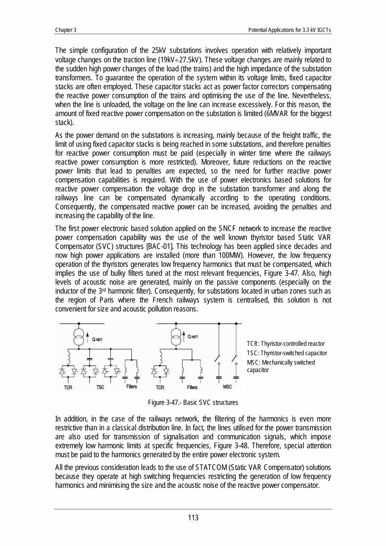
Chapter 3 Potential Applications for 3.3 kV IGCTs
113
The simple configuration of the 25kV substations involves operation with relatively important voltage changes on the traction line (19kV÷27.5kV). These voltage changes are mainly related to the sudden high power changes of the load (the trains) and the high impedance of the substation transformers. To guarantee the operation of the system within its voltage limits, fixed capacitor stacks are often employed. These capacitor stacks act as power factor correctors compensating the reactive power consumption of the trains and optimising the use of the line. Nevertheless, when the line is unloaded, the voltage on the line can increase excessively. For this reason, the amount of fixed reactive power compensation on the substation is limited (6MVAR for the biggest stack). As the power demand on the substations is increasing, mainly because of the freight traffic, the limit of using fixed capacitor stacks is being reached in some substations, and therefore penalties for reactive power consumption must be paid (especially in winter time where the railways reactive power consumption is more restricted). Moreover, future reductions on the reactive power limits that lead to penalties are expected, so the need for further reactive power compensation capabilities is required. With the use of power electronics based solutions for reactive power compensation the voltage drop in the substation transformer and along the railways line can be compensated dynamically according to the operating conditions. Consequently, the compensated reactive power can be increased, avoiding the penalties and increasing the capability of the line. The first power electronic based solution applied on the SNCF network to increase the reactive power compensation capability was the use of the well known thyristor based Static VAR Compensator (SVC) structures [BAC-01]. This technology has been applied since decades and now high power applications are installed (more than 100MW). However, the low frequency operation of the thyristors generates low frequency harmonics that must be compensated, which implies the use of bulky filters tuned at the most relevant frequencies, Figure 3-47. Also, high levels of acoustic noise are generated, mainly on the passive components (especially on the inductor of the 3rd harmonic filter). Consequently, for substations located in urban zones such as the region of Paris where the French railways system is centralised, this solution is not convenient for size and acoustic pollution reasons.
TCR: Thyristor-controlled reactor TSC: Thyristor-switched capacitor MSC: Mechanically switched capacitor
Figure 3-47.- Basic SVC structures
In addition, in the case of the railways network, the filtering of the harmonics is even more restrictive than in a classical distribution line. In fact, the lines utilised for the power transmission are also used for transmission of signalisation and communication signals, which impose extremely low harmonic limits at specific frequencies, Figure 3-48. Therefore, special attention must be paid to the harmonics generated by the entire power electronic system. All the previous consideration leads to the use of STATCOM (Static VAR Compensator) solutions because they operate at high switching frequencies restricting the generation of low frequency harmonics and minimising the size and the acoustic noise of the reactive power compensator.
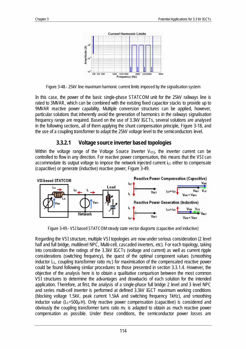
Chapter 3 Potential Applications for 3.3 kV IGCTs
114
Figure 3-48.- 25kV line maximum harmonic current limits imposed by the signalisation system
In this case, the power of the basic single-phase STATCOM unit for the 25kV railways line is rated to 3MVAR, which can be combined with the existing fixed capacitor stacks to provide up to 9MVAR reactive power capability. Multiple conversion structures can be applied, however, particular solutions that inherently avoid the generation of harmonics in the railways signalisation frequency range are required. Based on the use of 3.3kV IGCTs, several solutions are analysed in the following sections, all of them applying the shunt compensation principle, Figure 3-18, and the use of a coupling transformer to adapt the 25kV voltage level to the semiconductors level.
3.3.2.1 Voltage source inverter based topologies Within the voltage range of the Voltage Source Inverter VVSI, the inverter current can be controlled to flow in any direction. For reactive power compensation, this means that the VSI can accommodate its output voltage to impose the network injected current iLS either to compensate (capacitive) or generate (inductive) reactive power, Figure 3-49.
Figure 3-49.- VSI based STATCOM steady state vector diagrams (capacitive and inductive)
Regarding the VSI structure, multiple VSI topologies are now under serious consideration (2 level half and full bridge, multilevel NPC, Multi-cell, cascaded inverters, etc). For each topology, taking into consideration the ratings of the 3.3kV IGCTs (voltage and current) as well as current ripple considerations (switching frequency), the quest of the optimal component values (smoothing inductor LS, coupling transformer ratio mC) for maximisation of the compensated reactive power could be found following similar procedures to those presented in section 3.3.1.4. However, the objective of the analysis here is to obtain a qualitative comparison between the most common VSI structures to determine the advantages and drawbacks of each solution for the intended application. Therefore, at first, the analysis of a single-phase full bridge 2 level and 3 level NPC and series multi-cell inverter is performed at defined 3.3kV IGCT maximum working conditions (blocking voltage 1.5kV, peak current 1.5kA and switching frequency 1kHz), and smoothing inductor value (LS=500μH). Only reactive power compensation (capacitive) is considered and obviously the coupling transformer turns ratio mC is adapted to obtain as much reactive power compensation as possible. Under these conditions, the semiconductor power losses are
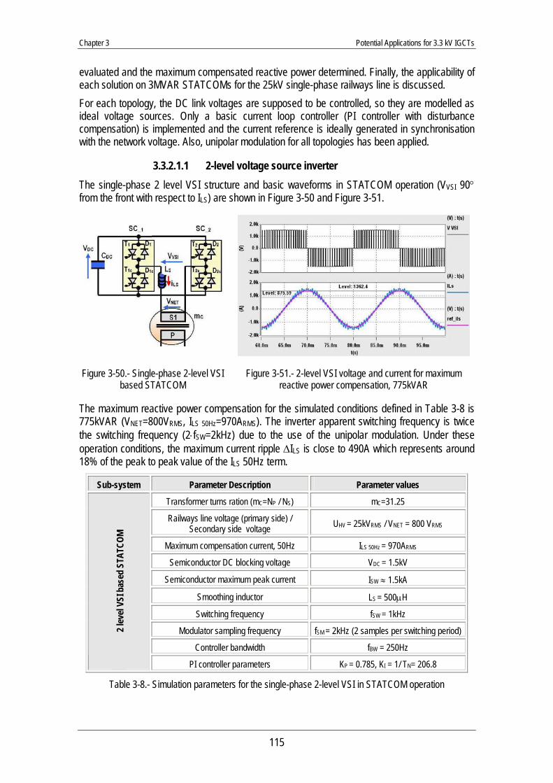
Chapter 3 Potential Applications for 3.3 kV IGCTs
115
evaluated and the maximum compensated reactive power determined. Finally, the applicability of each solution on 3MVAR STATCOMs for the 25kV single-phase railways line is discussed. For each topology, the DC link voltages are supposed to be controlled, so they are modelled as ideal voltage sources. Only a basic current loop controller (PI controller with disturbance compensation) is implemented and the current reference is ideally generated in synchronisation with the network voltage. Also, unipolar modulation for all topologies has been applied.
3.3.2.1.1 2-level voltage source inverter The single-phase 2 level VSI structure and basic waveforms in STATCOM operation (VVSI 90° from the front with respect to ILS) are shown in Figure 3-50 and Figure 3-51.
Figure 3-50.- Single-phase 2-level VSI based STATCOM
Figure 3-51.- 2-level VSI voltage and current for maximum reactive power compensation, 775kVAR
The maximum reactive power compensation for the simulated conditions defined in Table 3-8 is 775kVAR (VNET=800VRMS, ILS 50Hz=970ARMS). The inverter apparent switching frequency is twice the switching frequency (2⋅fSW=2kHz) due to the use of the unipolar modulation. Under these operation conditions, the maximum current ripple ΔILS is close to 490A which represents around 18% of the peak to peak value of the ILS 50Hz term.
Sub-system Parameter Description Parameter values
Transformer turns ration (mC=NP / NS) mC=31.25
Railways line voltage (primary side) / Secondary side voltage UHV = 25kVRMS / VNET = 800 VRMS
Maximum compensation current, 50Hz ILS 50Hz = 970ARMS
Semiconductor DC blocking voltage VDC = 1.5kV
Semiconductor maximum peak current ISW ≈ 1.5kA
Smoothing inductor LS = 500μH
Switching frequency fSW = 1kHz
Modulator sampling frequency fSM = 2kHz (2 samples per switching period)
Controller bandwidth fBW = 250Hz
2 lev
el VS
I bas
ed S
TATC
OM
PI controller parameters KP = 0.785, KI = 1/ TN= 206.8
Table 3-8.- Simulation parameters for the single-phase 2-level VSI in STATCOM operation
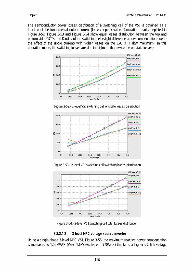
Chapter 3 Potential Applications for 3.3 kV IGCTs
116
The semiconductor power losses distribution of a switching cell of the VSI is obtained as a function of the fundamental output current (ILS 50 Hz) peak value. Simulation results depicted in Figure 3-52, Figure 3-53 and Figure 3-54 show equal losses distribution between the top and bottom side IGCTs and Diodes of the switching cell (slight difference at low compensation due to the effect of the ripple current) with higher losses on the IGCTs (1.1kW maximum). In this operation mode, the switching losses are dominant (more than twice the on-state losses).
Figure 3-52.- 2-level VSI switching cell on-state losses distribution
Figure 3-53.- 2-level VSI switching cell switching losses distribution
Figure 3-54.- 2-level VSI switching cell total losses distribution
3.3.2.1.2 3-level NPC voltage source inverter Using a single-phase 3-level NPC VSI, Figure 3-55, the maximum reactive power compensation is increased to 1.55MVAR (VNET=1.6kVRMS, ILS 50Hz=970ARMS) thanks to a higher DC link voltage
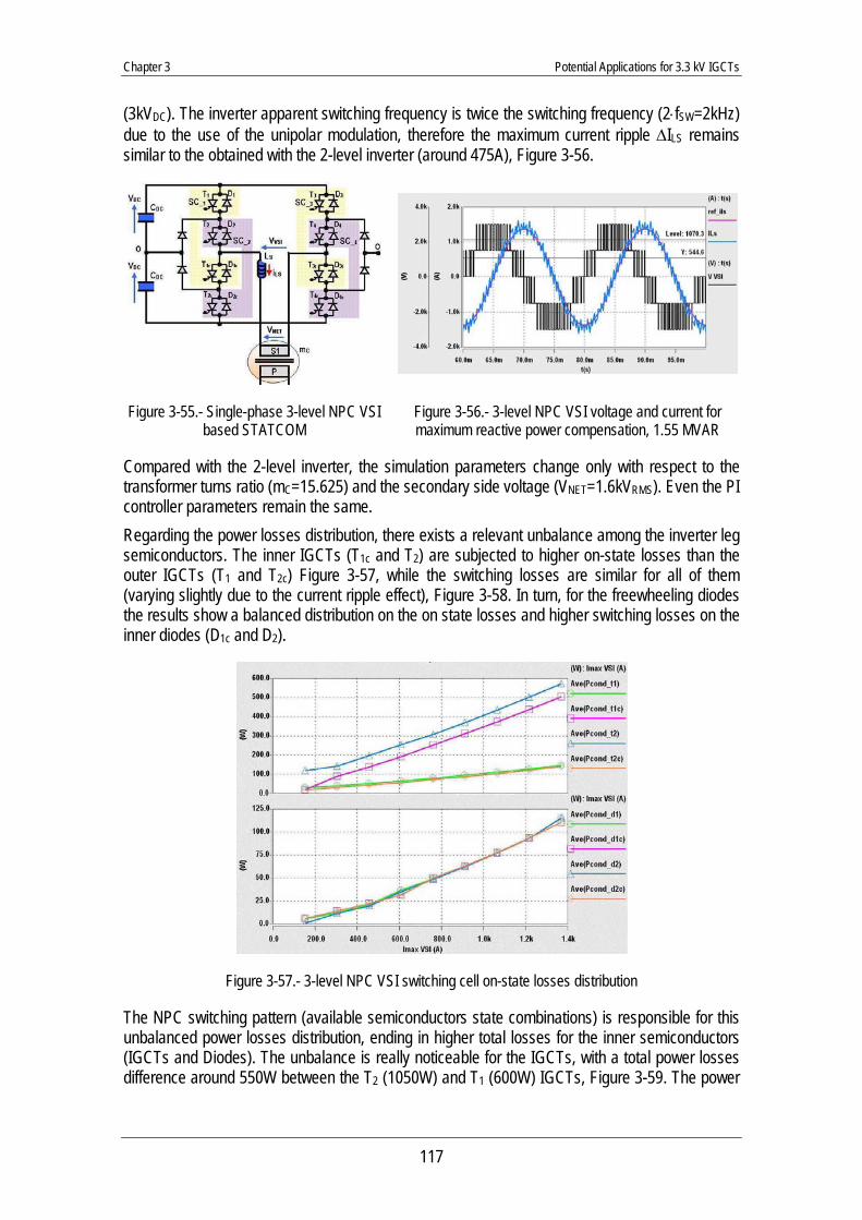
Chapter 3 Potential Applications for 3.3 kV IGCTs
117
(3kVDC). The inverter apparent switching frequency is twice the switching frequency (2⋅fSW=2kHz) due to the use of the unipolar modulation, therefore the maximum current ripple ΔILS remains similar to the obtained with the 2-level inverter (around 475A), Figure 3-56.
Figure 3-55.- Single-phase 3-level NPC VSI based STATCOM
Figure 3-56.- 3-level NPC VSI voltage and current for maximum reactive power compensation, 1.55 MVAR
Compared with the 2-level inverter, the simulation parameters change only with respect to the transformer turns ratio (mC=15.625) and the secondary side voltage (VNET=1.6kVRMS). Even the PI controller parameters remain the same. Regarding the power losses distribution, there exists a relevant unbalance among the inverter leg semiconductors. The inner IGCTs (T1c and T2) are subjected to higher on-state losses than the outer IGCTs (T1 and T2c) Figure 3-57, while the switching losses are similar for all of them (varying slightly due to the current ripple effect), Figure 3-58. In turn, for the freewheeling diodes the results show a balanced distribution on the on state losses and higher switching losses on the inner diodes (D1c and D2).
Figure 3-57.- 3-level NPC VSI switching cell on-state losses distribution
The NPC switching pattern (available semiconductors state combinations) is responsible for this unbalanced power losses distribution, ending in higher total losses for the inner semiconductors (IGCTs and Diodes). The unbalance is really noticeable for the IGCTs, with a total power losses difference around 550W between the T2 (1050W) and T1 (600W) IGCTs, Figure 3-59. The power
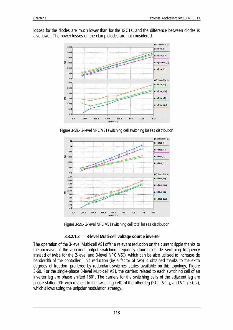
Chapter 3 Potential Applications for 3.3 kV IGCTs
118
losses for the diodes are much lower than for the IGCTs, and the difference between diodes is also lower. The power losses on the clamp diodes are not considered.
Figure 3-58.- 3-level NPC VSI switching cell switching losses distribution
Figure 3-59.- 3-level NPC VSI switching cell total losses distribution
3.3.2.1.3 3-level Multi-cell voltage source inverter The operation of the 3-level Multi-cell VSI offer a relevant reduction on the current ripple thanks to the increase of the apparent output switching frequency (four times de switching frequency instead of twice for the 2-level and 3-level NPC VSI), which can be also utilised to increase de bandwidth of the controller. This reduction (by a factor of two) is obtained thanks to the extra degrees of freedom proffered by redundant switches states available on this topology, Figure 3-60. For the single-phase 3-level Multi-cell VSI, the carriers related to each switching cell of an inverter leg are phase shifted 180°. The carriers for the switching cells of the adjacent leg are phase shifted 90° with respect to the switching cells of the other leg (SC_1-SC_3, and SC_2-SC_4), which allows using the unipolar modulation strategy.
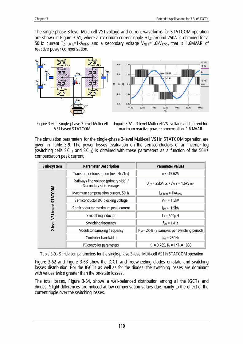
Chapter 3 Potential Applications for 3.3 kV IGCTs
119
The single-phase 3-level Multi-cell VSI voltage and current waveforms for STATCOM operation are shown in Figure 3-61, where a maximum current ripple ΔILS around 250A is obtained for a 50Hz current ILS 50Hz=1kARMS and a secondary voltage VNET=1.6kVRMS, that is 1.6MVAR of reactive power compensation.
Figure 3-60.- Single-phase 3-level Multi-cell VSI based STATCOM
Figure 3-61.- 3-level Multi-cell VSI voltage and current for maximum reactive power compensation, 1.6 MVAR
The simulation parameters for the single-phase 3-level Multi-cell VSI in STATCOM operation are given in Table 3-9. The power losses evaluation on the semiconductors of an inverter leg (switching cells SC_1 and SC_2) is obtained with these parameters as a function of the 50Hz compensation peak current.
Sub-system Parameter Description Parameter values
Transformer turns ration (mC=NP / NS) mC=15.625
Railways line voltage (primary side) / Secondary side voltage UHV = 25kVRMS / VNET = 1.6kVRMS
Maximum compensation current, 50Hz ILS 50Hz = 1kARMS
Semiconductor DC blocking voltage VDC = 1.5kV
Semiconductor maximum peak current ISW ≈ 1.5kA
Smoothing inductor LS = 500μH
Switching frequency fSW = 1kHz
Modulator sampling frequency fSM = 2kHz (2 samples per switching period)
Controller bandwidth fBW = 250Hz
2-lev
el VS
I bas
ed S
TATC
OM
PI controller parameters KP = 0.785, KI = 1/ TN= 1050
Table 3-9.- Simulation parameters for the single-phase 3-level Multi-cell VSI in STATCOM operation
Figure 3-62 and Figure 3-63 show the IGCT and freewheeling diodes on-state and switching losses distribution. For the IGCTs as well as for the diodes, the switching losses are dominant with values twice greater than the on-state losses. The total losses, Figure 3-64, shows a well-balanced distribution among all the IGCTs and diodes. Slight differences are noticed at low compensation values due mainly to the effect of the current ripple over the switching losses.
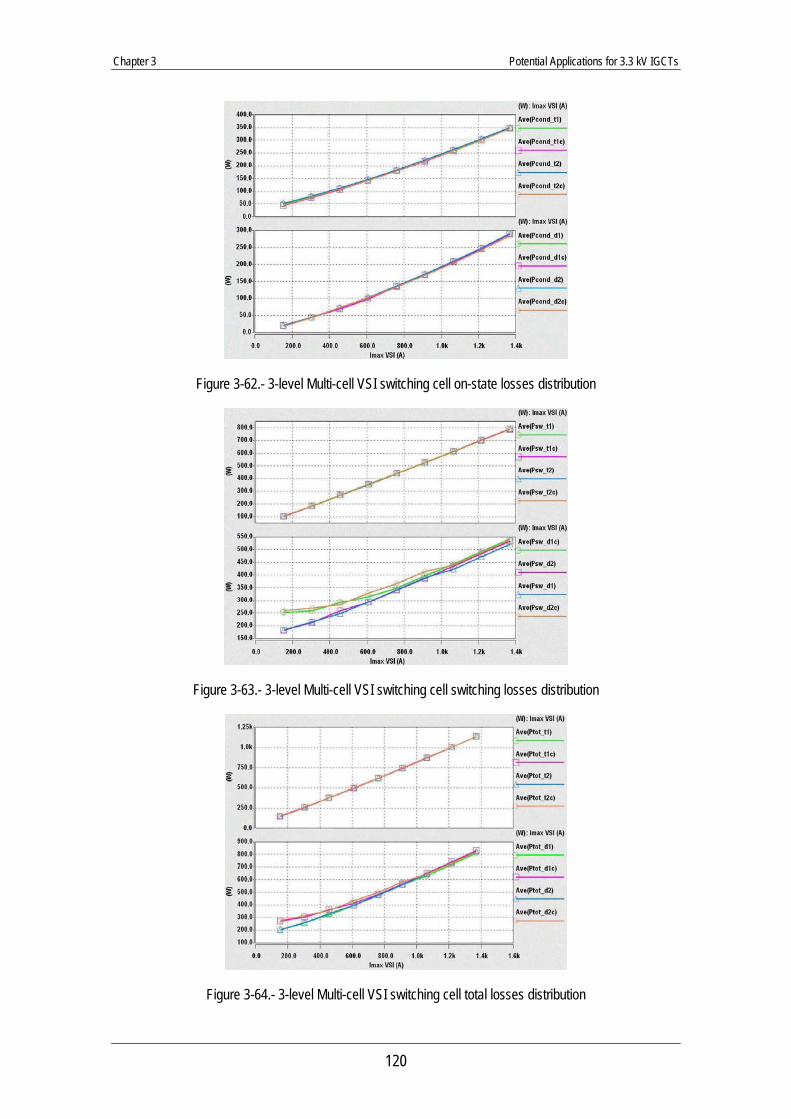
Chapter 3 Potential Applications for 3.3 kV IGCTs
120
Figure 3-62.- 3-level Multi-cell VSI switching cell on-state losses distribution
Figure 3-63.- 3-level Multi-cell VSI switching cell switching losses distribution
Figure 3-64.- 3-level Multi-cell VSI switching cell total losses distribution
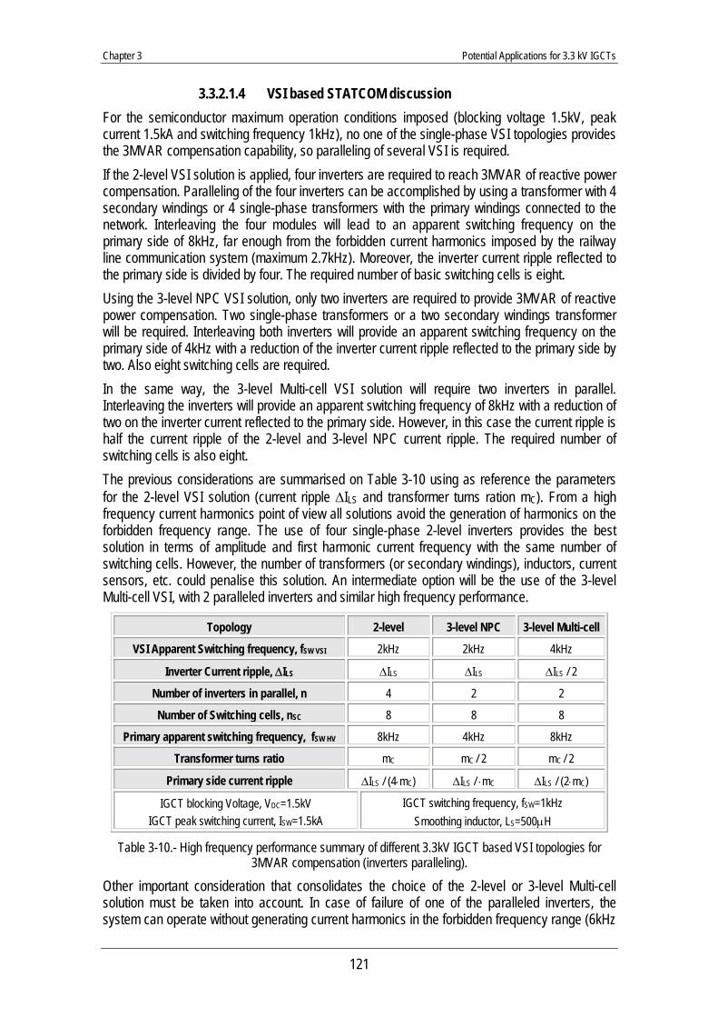
Chapter 3 Potential Applications for 3.3 kV IGCTs
121
3.3.2.1.4 VSI based STATCOM discussion For the semiconductor maximum operation conditions imposed (blocking voltage 1.5kV, peak current 1.5kA and switching frequency 1kHz), no one of the single-phase VSI topologies provides the 3MVAR compensation capability, so paralleling of several VSI is required. If the 2-level VSI solution is applied, four inverters are required to reach 3MVAR of reactive power compensation. Paralleling of the four inverters can be accomplished by using a transformer with 4 secondary windings or 4 single-phase transformers with the primary windings connected to the network. Interleaving the four modules will lead to an apparent switching frequency on the primary side of 8kHz, far enough from the forbidden current harmonics imposed by the railway line communication system (maximum 2.7kHz). Moreover, the inverter current ripple reflected to the primary side is divided by four. The required number of basic switching cells is eight. Using the 3-level NPC VSI solution, only two inverters are required to provide 3MVAR of reactive power compensation. Two single-phase transformers or a two secondary windings transformer will be required. Interleaving both inverters will provide an apparent switching frequency on the primary side of 4kHz with a reduction of the inverter current ripple reflected to the primary side by two. Also eight switching cells are required. In the same way, the 3-level Multi-cell VSI solution will require two inverters in parallel. Interleaving the inverters will provide an apparent switching frequency of 8kHz with a reduction of two on the inverter current reflected to the primary side. However, in this case the current ripple is half the current ripple of the 2-level and 3-level NPC current ripple. The required number of switching cells is also eight. The previous considerations are summarised on Table 3-10 using as reference the parameters for the 2-level VSI solution (current ripple ΔILS and transformer turns ration mC). From a high frequency current harmonics point of view all solutions avoid the generation of harmonics on the forbidden frequency range. The use of four single-phase 2-level inverters provides the best solution in terms of amplitude and first harmonic current frequency with the same number of switching cells. However, the number of transformers (or secondary windings), inductors, current sensors, etc. could penalise this solution. An intermediate option will be the use of the 3-level Multi-cell VSI, with 2 paralleled inverters and similar high frequency performance.
Topology 2-level 3-level NPC 3-level Multi-cell
VSI Apparent Switching frequency, fSW VSI 2kHz 2kHz 4kHz
Inverter Current ripple, ΔILS ΔILS ΔILS ΔILS / 2
Number of inverters in parallel, n 4 2 2
Number of Switching cells, nSC 8 8 8
Primary apparent switching frequency, fSW HV 8kHz 4kHz 8kHz
Transformer turns ratio mC mC / 2 mC / 2
Primary side current ripple ΔILS / (4⋅mC) ΔILS / ⋅mC ΔILS / (2⋅mC)
IGCT blocking Voltage, VDC=1.5kV IGCT peak switching current, ISW=1.5kA
IGCT switching frequency, fSW=1kHz Smoothing inductor, LS=500μH
Table 3-10.- High frequency performance summary of different 3.3kV IGCT based VSI topologies for 3MVAR compensation (inverters paralleling).
Other important consideration that consolidates the choice of the 2-level or 3-level Multi-cell solution must be taken into account. In case of failure of one of the paralleled inverters, the system can operate without generating current harmonics in the forbidden frequency range (6kHz
Chapter 3 Potential Applications for 3.3 kV IGCTs
122
for the 2-level and 4kHz for the 3-level Multi-cell). However the NPC solution will generate current harmonic exactly in the forbidden frequency range (2kHz). In this degraded operation mode, a possible solution to respect the harmonic current limits is modifying the switching frequency of the switching cell to 1.5kHz at the expense of switching losses augmentation and maybe power compensation limitation. Regarding the power losses distribution, the NPC solution presents the best power losses budget (without counting the clamping diode losses). However, some of the semiconductors (the inner IGCTs) have similar power losses than the semiconductors of the 2-level and 3-level Multi-cell topology, which lead to similar cooling efforts in all these topologies. In all cases, the semiconductors are not limited by their power losses or SOA limits, thus higher power compensation could be obtained increasing the inverter current and the switching frequency (decreasing the smoothing inductor value). However, practical limitations regarding the actual IGCT gate unit functionality or / and gate unit power supply could impede the operation under these conditions. Concerning the capacitor of the DC link for all VSI topologies, its capacitance value must be high enough to keep the low frequency voltage ripple as low as possible. Neglecting the high frequency harmonics of the VSI voltage and current, Eq. 3-34 and Eq. 3-35 represent the 50Hz terms that take part on the reactive power compensation (capacitive) as depicted in the vectors diagram of Figure 3-49. Considering that no power is lost or stored on the converter, the converter instantaneous input power is equal to the instantaneous output power, Eq. 3-36. From this hypothesis, the low frequency capacitor current and voltage can be easily derived Eq. 3-37, Eq. 3-38, and finally the peak to peak value of the capacitor voltage ripple can be obtained, Eq. 3-39. The CDC value must be selected to fix a maximum permissible voltage ripple (for example ΔVCDC=5% of the DC link voltage, Eq. 3-40) to avoid the perturbation of the inverter current control and to minimise the capacitor power losses. In the 2-level case, the required DC link capacitor value is CDC=22mF (ΔVCDC=5%, VDC0=1.5kV, QVSI=775kVAR)
)tsin(2Vv VSIVSI ⋅ϖ⋅⋅= Eq. 3-34
)2
tsin(2Ii LSLSπ
−⋅ϖ⋅⋅= Eq. 3-35
LSVSICDCCDC0DCCDCDC ivi)vV(iv ⋅=⋅Δ+=⋅ Eq. 3-36
0DC
LSVSI
0DC
LSVSICDC V
)t2sin(IVV
ivi ⋅ϖ⋅⋅⋅=
⋅≈ Eq. 3-37
)t2cos(C2V
IVdtiC
1vDC0DC
LSVSICDC
DCCDC ⋅ϖ⋅⋅
⋅ϖ⋅⋅⋅−
⋅=⋅=Δ ∫ Eq. 3-38
DC0DC
VSICDC
LSVSIVSI
CVQV
IVQ
⋅ϖ⋅=Δ
⋅= Eq. 3-39
ϖ⋅⋅= 2
0DC
VSIDC V05.0
QC Eq. 3-40
For the 3-level VSI solutions, the DC link voltage is the double of the 2 level VSI, therefore, if the same relative voltage ripple (%) is considered half the capacitance value is required for double the VSI reactive power, QVSI. However, the energy stored on the capacitor for 3-level VSI is twice the energy of the 2-level VSI capacitor (half the capacitance and double the voltage), which could
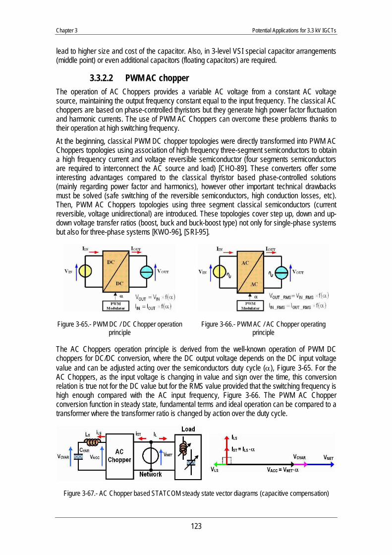
Chapter 3 Potential Applications for 3.3 kV IGCTs
123
lead to higher size and cost of the capacitor. Also, in 3-level VSI special capacitor arrangements (middle point) or even additional capacitors (floating capacitors) are required.
3.3.2.2 PWM AC chopper The operation of AC Choppers provides a variable AC voltage from a constant AC voltage source, maintaining the output frequency constant equal to the input frequency. The classical AC choppers are based on phase-controlled thyristors but they generate high power factor fluctuation and harmonic currents. The use of PWM AC Choppers can overcome these problems thanks to their operation at high switching frequency. At the beginning, classical PWM DC chopper topologies were directly transformed into PWM AC Choppers topologies using association of high frequency three-segment semiconductors to obtain a high frequency current and voltage reversible semiconductor (four segments semiconductors are required to interconnect the AC source and load) [CHO-89]. These converters offer some interesting advantages compared to the classical thyristor based phase-controlled solutions (mainly regarding power factor and harmonics), however other important technical drawbacks must be solved (safe switching of the reversible semiconductors, high conduction losses, etc). Then, PWM AC Choppers topologies using three segment classical semiconductors (current reversible, voltage unidirectional) are introduced. These topologies cover step up, down and up-down voltage transfer ratios (boost, buck and buck-boost type) not only for single-phase systems but also for three-phase systems [KWO-96], [SRI-95].
Figure 3-65.- PWM DC / DC Chopper operation principle
Figure 3-66.- PWM AC / AC Chopper operating principle
The AC Choppers operation principle is derived from the well-known operation of PWM DC choppers for DC/DC conversion, where the DC output voltage depends on the DC input voltage value and can be adjusted acting over the semiconductors duty cycle (α), Figure 3-65. For the AC Choppers, as the input voltage is changing in value and sign over the time, this conversion relation is true not for the DC value but for the RMS value provided that the switching frequency is high enough compared with the AC input frequency, Figure 3-66. The PWM AC Chopper conversion function in steady state, fundamental terms and ideal operation can be compared to a transformer where the transformer ratio is changed by action over the duty cycle.
Figure 3-67.- AC Chopper based STATCOM steady state vector diagrams (capacitive compensation)
Chapter 3 Potential Applications for 3.3 kV IGCTs
124
For reactive power compensation (capacitive) the AC chopper can be used to adapt the applied voltage over a fixed capacitor CVAR obtaining the required variable capacitor function. Figure 3-67 shows the steady state vector diagram for a step-down (BUCK) AC Chopper operating as reactive power compensator. The smoothing inductor LS is required to guarantee the current source behaviour of the load, however, at the line network frequency the load is capacitive. Figure 3-68 shows the semiconductor arrangement of the single-phase step-down AC Chopper. The conversion structure is composed of 2 current reversible and voltage unidirectional switching cells, which are controlled according to the sign of the input voltage VNET, (one switching cell is short-circuited alternatively on each input voltage semi-period while the other is PWM controlled). Also, an input capacitive filter CF is added to filter the high frequency current generated by the switching operation of the AC Chopper. The reactive power compensation characteristic of the step-down AC Chopper based STATCOM is duty cycle α dependent as defined by Eq. 3-41 and shown in Figure 3-69. Detailed explanations about the operation and control of the converter are given in Chapter 4.
Figure 3-68.- Single-phase AC Chopper based STATCOM
Figure 3-69.- Reactive power compensation characteristic for a Buck AC Chopper.
( )2
2VARS
VAR2NET
VAR
2VARS
NETNETLSACC
LSSVAR
LSLSCVARNETACC
CL1CV
CCL1
VVIVQ
;ILC
IVVVV
α⋅ϖ⋅⋅−
ϖ⋅⋅=
⎟⎟⎠
⎞⎜⎜⎝
⎛
ϖ⋅ϖ⋅⋅−
α⋅⋅α⋅=⋅=
⋅ϖ⋅−ϖ⋅
=+=α⋅=→→→→
Eq. 3-41
α = duty cycle ϖ = network pulsation (rad/s) VNET = Input filter voltage
For an 3.3kV IGCT based AC Chopper for STATCOM operation, the same maximum voltage, current and switching frequency values as for the VSI solution are fixed (blocking voltage 1.5kV, switching current 1.5kA, switching frequency 1kHz). The maximum blocking voltage of the IGCTs imposes the transformer turn ratio (mC=23.5, VNET=1.06kVRMS). Then, the load components (LS=1mH and CVAR=2.45mF) are selected to obtain the maximum reactive power compensation without exceeding the maximum switching current for a maximum duty cycle α MAX = 0.95. Under these operating conditions, the maximum reactive power compensation reaches 1MVAR. The AC Chopper output voltage VACC and current ILS waveforms operating at 1MVAR of reactive power compensation are shown in Figure 3-70. It can be seen how the sinusoidal input voltage is switched at 1kHz generating a current with a leading phase shift of 90° with respect to de voltage. Also the high frequency current ripple generated by the switching mode operation can be noticed.
Chapter 3 Potential Applications for 3.3 kV IGCTs
125
Figure 3-70.- AC Chopper voltage and current for maximum reactive power compensation, 1 MVAR
The use of the universal power losses estimator is applied to obtain the power losses distribution of the semiconductors on one switching cell of the AC Chopper. Obviously, the input voltage change, the short circuit operation of the switching cells according to the input voltage sign, the current ripple and the closed loop operation are taken into account. Simulation results for the on-state, switching and total power losses are depicted as a function of the maximum 50Hz component on the smoothing inductor LS current in Figure 3-71, Figure 3-72 and Figure 3-73 respectively. The most interesting property of the AC Chopper solution is that the on-state losses are dominant, which is well adapted for the use of IGCTs. The switching losses are low because the switching voltage and current change continuously and the maximum current /voltage is switched when the voltage/current is minimal.
Figure 3-71.- AC Chopper switching cell on-state losses distribution
The total losses on the switching cell are not balanced, and the topside IGCTs and diodes (T1 and D1) are much more loaded than the bottom side semiconductors (T1C and D1C). The power losses difference ratio between IGCTs and diodes of the same switching cell is greater than two. The power losses are balanced on an intermediate power compensation point. This point coincides with the operation at duty cycle α=0.5 where the top and bottom semiconductors are loaded equally. In general, in this topology the total power losses are lower (lower than 800W in the worst case) and higher reactive power compensation (1MVAR) is obtained compared with the VSI solutions for the same semiconductor working conditions.
Chapter 3 Potential Applications for 3.3 kV IGCTs
126
Figure 3-72.- AC Chopper switching cell switching losses distribution
Figure 3-73.- AC Chopper switching cell total losses distribution
To obtain 3 MVAR of total reactive power compensation three single-phase AC Choppers operating in parallel by means of a single-phase transformer is required. Interleaving the three modules will generate on the low and high voltage side an apparent switching frequency of 3kHz, therefore the high frequency current harmonics will be out of the forbidden frequency range imposed by the SNCF communication system. Obviously, if one of the AC Choppers fails, current harmonics on the forbidden range will be generated. To avoid this operation in degraded mode, the AC Choppers can change to operation at 1.5kHz without very much compensation capability reduction because only the switching losses will be increased and they are not dominant in this case.
3.3.2.3 Reactive power compensation solution discussion Several STATCOM solutions based on 3.3kV IGCTs for reactive power compensation of the single-phase 25kV/50Hz SNCF network have been analysed. Among the classical Voltage Source Inverter solutions the use of single-phase 2-level or 3-level Multi-cell inverters are the best choice from a high frequency current pollution point of view. Both solutions have very similar power losses, in both cases much higher than the losses of the 3-level NPC solution. For the required compensation, relatively high DC link capacitance values are required. Regarding the use of AC Choppers, the power losses results summarised on Table 3-11 show a relevant improvement compared to the VSI solution in terms of semiconductor use (lower number of switching cells to obtain 3MVAR) and power losses per module to be paralleled. However, from
Chapter 3 Potential Applications for 3.3 kV IGCTs
127
a high frequency current harmonic generation point of view the VSI solutions offer better performance.
Topology 2-level VSI 3-level NPC VSI
3-level Multi-cell VSI AC Chopper
Number of modules in parallel, n 4 2 2 3
Number of Switching cells, nSC 8 8 8 6
Primary apparent switching frequency, fSW HV 8kHz 4kHz 8kHz 3kHz
Maximum IGCT power losses 1.1kW 1.05kW 1.125kW 770W
Maximum Diode power losses 800W 380W 825kW 640
2.4kW 3.9kW Maximum switching cell power losses 3.8kW
2.3kW 3.9kW 1.95kW
Maximum leg power losses 3.8kW 4.7kW 7.8kW 1.95kW
Maximum module power losses 7.6kW 9.4kW 15.6kW 3.9kW
Maximum total power losses 30.4kW 18.8kW 31.2kW 11.7kW
Maximum reactive power 3.1MVAR 3.1MVAR 3.2MVAR 3MVAR
Table 3-11.- Results summary for 3MVAR STATCOM topologies based on 3.3kV IGCT
In all cases, the SOA and thermal limits of the semiconductors are not attained. However, the gate unit and its power supply consumption at higher current and switching frequencies could limit the practical operation of the semiconductors under these conditions.
3.4 Conclusions The universal power losses estimator developed for 3.3kV IGCT switching cells has demonstrated its flexibility to be used in different topologies for different applications under very different working conditions. Two main applications have been studied, the harmonic current compensation for SNCF 1.5kV DC substations and the reactive power compensation for SNCF 25kV/50Hz substations. For both applications their specific particularities have been introduced and several possible solutions have been proposed and analysed. In the case of the 1.5kV DC substations, active filters based on single-phase inverters offer an effective solution that can be applied either in existing or in new installations with a relatively low power equipment (around 1MVAR) for load power levels reaching 10MW. Under these conditions, the 3.3kV IGCT can be considered to be underused and lower current rated semiconductors could be applied. Lower current 3.3kV IGCTs (if developed) or existing 3.3kV could be best suited for this application. Regarding the single-phase 25kV substations, VSIs and AC Choppers have been analysed. If only reactive power compensation (capacitive) is required, the AC Chopper shows better performances in terms of power losses and utilisation of the semiconductors. However, concerning high frequency current harmonics generation, the VSI solutions offer better characteristics. Anyway, the AC chopper solution can fulfil the harmonic current requirements and must be considered as a serious candidate for this application using 3.3kV IGCTs. In contrast to the well know VSI, further research efforts on the AC Chopper must be carried out regarding the dimensioning of the components, IGCTs clamp circuits effect, control, modulation and operating modes of the topology, etc.