
Synthesis, Characterisation and Photocatalytic Activity ... - CORE
238
Synthesis, Characterisation and Photocatalytic Activity of Porous Silicon-based Materials Ting Li A thesis submitted in fulfilment of the requirements for the degree of Doctor of Philosophy of the University of East Anglia. School of Chemistry University of East Anglia Norwich, United Kingdom September 2017 © This copy of the thesis has been supplied on condition that anyone who consults it is understood to recognise that its copyright rests with the author and that use of any information derived there from must be in accordance with current UK Copyright Law. In addition, any quotation or extract must include full attribution.
-
Upload
khangminh22 -
Category
Documents
-
view
1 -
download
0
Transcript of Synthesis, Characterisation and Photocatalytic Activity ... - CORE

Synthesis, Characterisation and Photocatalytic
Activity of Porous Silicon-based Materials
Ting Li
A thesis submitted in fulfilment of the requirements for the
degree of Doctor of Philosophy of the University of East Anglia.
School of Chemistry
University of East Anglia
Norwich, United Kingdom
September 2017
© This copy of the thesis has been supplied on condition that anyone who consults it is
understood to recognise that its copyright rests with the author and that use of any
information derived there from must be in accordance with current UK Copyright Law.
In addition, any quotation or extract must include full attribution.

ii
Declaration
I declare that the research contained in the thesis, submitted for the degree
of Doctor of Philosophy, is original, except where due reference is made to
other authors, and has not previously been submitted by me for a degree
at this or any other universities.
Ting Li

iii
Abstract
As a free and abundant alternative energy source, the use of sunlight to store and
transfer energy is of great importance to a clean and sustainable future. Aiming for an
environmentally and economically friendly approach to utilizing solar energy, metal-
free, earth-abundant mesoporous silicon with hydrogen termination were developed
via inexpensive electrochemical etching. By means of a range of characterisation tools,
a detailed structural analysis was established, showing a large surface area, open porous
system and abundant quantum confined Si nanocrystallites of which the morphological
properties can be controllably tuned through adjusting etching parameters and wafer
resistivity. As a result, an excellent efficiency in degrading methyl orange under visible
light irradiation was achieved in the following photocatalytic study, which also revealed
the influence of different structural factors on the photocatalytic performance by
affecting mass transport, light absorption and photoexcited charge recombination. The
photocatalytic mechanism of mesoporous silicon in methyl orange degradation was also
investigated in this research, with insights gained into the electronic band properties,
photocatalytic oxidation facilitated by the generation of reactive oxygen species and the
roles of surface hydrides on the degradation pathways of methyl orange. By coupling
with graphitic carbon nitride (g-C3N4) nanosheets, the formed heterostructure showed
an enhanced degradation activity towards methyl orange under visible light
illumination. An exciton-related pathway was proposed to explain the promoted
reducing power of the surface hydrides upon irradiation with or without the
participation of g-C3N4. In general, this work highlighted the potentiality of H-terminated
mesoporous silicon in photocatalytic applications and deepened the understanding of
its photocatalytic mechanism and degradation behaviour for future exploration of
porous silicon-based photocatalysts.

iv
Table of Contents
Declaration ............................................................................................................... ii
Abstract .................................................................................................................. iii
Table of Contents .................................................................................................... iv
List of Schemes ........................................................................................................ xi
List of Tables .......................................................................................................... xii
List of Figures ........................................................................................................ xiv
List of Abbreviations .............................................................................................xxiii
Acknowledgements ...............................................................................................xxv
Chapter 1: Introduction
1.1 Porous solids .................................................................................................. 2
1.1.1 Microporous materials ................................................................................... 3
1.1.2 Mesoporous materials .................................................................................... 5
1.1.3 Macroporous materials .................................................................................. 6
1.1.4 Hierarchically structured porous materials .................................................... 7
1.2 Porous silicon ................................................................................................. 8
1.2.1 Background of porous silicon ......................................................................... 8
1.2.2 Outline history of porous silicon ..................................................................... 9
1.2.3 Fabrication of porous silicon ........................................................................ 11
1.2.3.1 Electrochemical etching ............................................................................ 11
1.2.3.2 Metal-assisted chemical etching ............................................................... 14
1.2.3.3 In-situ magnesiothermic reduction ........................................................... 16
1.2.4 Modification of porous silicon ...................................................................... 17
1.2.4.1 Morphological modification of porous silicon .......................................... 17
1.2.4.2 Shape modification of porous silicon ........................................................ 19

v
1.2.4.3 Surface modification of porous silicon ..................................................... 20
1.2.5 Applications of porous silicon ....................................................................... 21
1.2.5.1 Heterogeneous catalysis ........................................................................... 21
1.2.5.1.1 Porous silicon as catalyst support ...................................................... 21
1.2.5.1.2 Porous silicon as photocatalyst ......................................................... 22
1.2.5.2 Biomedical applications of porous silicon ................................................. 28
1.2.5.3 Energy storage applications of porous silicon .......................................... 28
1.3 Graphitic carbon nitride materials ................................................................ 29
1.3.1 General background of graphitic carbon nitride .......................................... 29
1.3.2 Photocatalytic applications of graphitic carbon nitride ............................... 31
1.4 Dye pollution and elimination ...................................................................... 32
1.5 Research objectives ...................................................................................... 33
1.6 Thesis outline ............................................................................................... 33
1.7 References ................................................................................................... 35
Chapter 2: Materials and Experimental Details
2.1 Materials ...................................................................................................... 58
2.1.1 Silicon wafers ................................................................................................ 58
2.1.2 Chemical reagents and materials ................................................................. 58
2.2 Experimental methods ................................................................................. 60
2.2.1 Mesoporous silicon (mpSi) ........................................................................... 60
2.2.1.1 Preparation of mpSi by electrochemical etching ...................................... 60
2.2.1.2 Preparation of mpSi disks and microflakes ............................................... 62
2.2.1.3 Surface oxidation ...................................................................................... 64

vi
2.2.1.4 Surface hydrosilylation .............................................................................. 64
2.2.2 Graphitic carbon nitride materials (g-C3N4) .................................................. 66
2.2.2.1 Synthesis of g-C3N4 bulk powders ............................................................. 66
2.2.2.2 Synthesis of g-C3N4 nanosheets ................................................................ 67
2.2.3 Porous silicon/carbon nitride composites (mpSi/g-C3N4 NSs) ...................... 68
2.3 Characterisation techniques ......................................................................... 68
2.3.1 Electron microscopy ..................................................................................... 69
2.3.1.1 Scanning electron microscopy (SEM) and field emission scanning electron
microscopy (FE-SEM) ............................................................................................... 70
2.3.1.2 High-resolution transmission electron microscope (HRTEM)................... 70
2.3.2 X-ray powder diffraction (XRD) ..................................................................... 71
2.3.3 Nitrogen adsorption-desorption isotherms ................................................. 72
2.3.4 Fourier transform infrared spectroscopy (FTIR) ........................................... 73
2.3.5 Raman scattering .......................................................................................... 74
2.3.6 X-ray photoelectron spectroscopy (XPS) ...................................................... 74
2.3.7 Thermogravimetric analysis .......................................................................... 75
2.3.8 Optical measurements .................................................................................. 76
2.3.8.1 Ultraviolet-visible absorption spectroscopy (UV-Vis) ............................... 76
2.3.8.2 Photoluminescence spectroscopy (PL) ..................................................... 77
2.3.8.3 Quantum yield (QY) ................................................................................... 78
2.4 Photocatalytic study ..................................................................................... 79
2.4.1 Photodegradation experiment ..................................................................... 80
2.4.2 Kinetic analysis .............................................................................................. 81
2.4.3 Total organic carbon analysis ....................................................................... 82
2.4.4 Active species analysis .................................................................................. 82
2.4.5 Lifetime study ............................................................................................... 83
2.5 Summary ...................................................................................................... 83
2.6 References ................................................................................................... 84

vii
Chapter 3: Controllable Generation of Mesoporous Silicon with Large
Surface Area by Electrochemical Etching
3.1 Overview...................................................................................................... 92
3.2 Experimental section .................................................................................... 93
3.2.1 Mesoporous silicon preparation (mpSi) ....................................................... 93
3.2.2 Free-standing mpSi preparation ................................................................... 94
3.2.3 Thiol-capped mpSi preparation .................................................................... 95
3.2.4 Material characterisation ............................................................................. 95
3.3 Results and discussion .................................................................................. 96
3.3.1 Microscopic morphology of PS-mpSi ............................................................ 96
3.3.1.1 FE-SEM images of PS-mpSi ........................................................................ 96
3.3.1.2 HRTEM images of PS-mpSi ........................................................................ 98
3.3.2 Structural effects of etching current density .............................................. 100
3.3.2.1 XRD patterns of PS-mpSi ......................................................................... 101
3.3.2.2 Raman scattering of PS-mpSi .................................................................. 103
3.3.2.3 ATR-IR spectra of PS-mpSi ....................................................................... 103
3.3.2.4 Nitrogen sorption analysis of PS-mpSi .................................................... 106
3.3.3 Structural effects of etching time ............................................................... 109
3.3.3.1 Layer thickness of PS-mpSi ...................................................................... 109
3.3.3.2 Surface and pore properties of PS-mpSi ................................................. 111
3.3.3.3 Crystallite size of PS-mpSi ....................................................................... 112
3.3.4 Characterisation results of HPS-mpSi ......................................................... 113
3.3.4.1 FE-SEM images of HPS-mpSi ................................................................... 113
3.3.4.2 Raman scattering of HPS-mpSi ................................................................ 115
3.3.4.3 ATR-IR spectrum of HPS-mpSi ................................................................. 115
3.3.4.4 Nitrogen sorption analysis of HPS-mpSi ................................................. 116
3.3.4.5 Layer thickness of HPS-mpSi ................................................................... 118
3.3.5 Free-standing mpSi disk and microflakes ................................................... 120
3.3.5.1 Characterisation results of mpSi disk ...................................................... 120

viii
3.3.5.2 Characterisation results of mpSi microflakes ......................................... 121
3.3.6 Characterisation results of thiol-capped mpSi ........................................... 123
3.3.6.1 Oil bath .................................................................................................... 124
3.3.6.2 Conventional oven .................................................................................. 125
3.3.6.3 Microwave irradiation ............................................................................. 126
3.4 Summary .................................................................................................... 128
3.5 References ................................................................................................. 129
Chapter 4: Hydrogen-Terminated Mesoporous Silicon as Visible-Light-
Active Photocatalyst in Dye Degradation
4.1 Overview.................................................................................................... 134
4.2 Experimental section .................................................................................. 136
4.2.1 Photocatalyst preparation .......................................................................... 136
4.2.2 Photocatalyst characterisation ................................................................... 136
4.2.3 Photocatalytic evaluation ........................................................................... 137
4.3 Results and discussion ................................................................................ 137
4.3.1 Characterisation of mesoporous silicon photocatalysts ............................ 137
4.3.1.1 Structural features of PS-mpSi ................................................................ 137
4.3.1.2 Structural features of HPS-mpSi ............................................................. 139
4.3.1.3 Optical analysis of PS-mpSi and HPS-mpSi .............................................. 141
4.3.1.3.1 Light absorption ............................................................................... 141
4.3.1.3.2 Light emission .................................................................................. 142
4.3.2 Photocatalytic activities of mesoporous silicon in dye degradation .......... 143
4.3.2.1 Control experiments ............................................................................... 143
4.3.2.2 The photocatalytic activity of PS-mpSi in dye degradation .................... 144
4.3.2.3 The photocatalytic activity of HPS-mpSi in dye degradation .................. 146

ix
4.3.3 Impact of various factors on photocatalyst performance .......................... 148
4.3.3.1 Porous morphology ................................................................................. 148
4.3.3.2 Silicon nanocrystallites ............................................................................ 149
4.3.3.3 Pore depth ............................................................................................... 150
4.3.3.4 Visible light responsiveness .................................................................... 151
4.3.3.5 Free-standing microflakes ....................................................................... 153
4.3.3.6 Surface chemistry .................................................................................... 154
4.3.4 Dye degradation behaviour under dark conditions.................................... 156
4.3.5 Dye degradation behaviour under visible light irradiation ........................ 160
4.3.5.1 Accelerating effect of visible light irradiation ......................................... 161
4.3.5.2 Total organic carbon analysis .................................................................. 162
4.3.5.3 Active species analysis ............................................................................ 164
4.3.5.4 Photocatalytic mechanism ...................................................................... 166
4.3.6 Lifetime study of mesoporous silicon in dye degradation ......................... 170
4.4 Summary .................................................................................................... 172
4.5 References ................................................................................................. 174
Chapter 5: Hydrogen-Terminated Mesoporous Silicon/Graphitic Carbon
Nitride (g-C3N4) Nanosheets Heterojunction Study
5.1 Overview.................................................................................................... 183
5.2 Experimental section .................................................................................. 184
5.2.1 Synthesis of graphitic carbon nitride bulk powders ................................... 184
5.2.2 Synthesis of graphitic carbon nitride nanosheets ...................................... 184
5.2.3 Synthesis of the composites (mpSi/g-C3N4 NSs) ......................................... 184
5.2.4 Sample characterisation ............................................................................. 185
5.2.5 Photocatalytic evaluation ........................................................................... 185
x
5.3 Results and discussion ................................................................................ 185
5.3.1 Characterisation and photocatalytic activity of g-C3N4 materials .............. 185
5.3.1.1 SEM images and elemental analysis of g-C3N4 materials........................ 186
5.3.1.2 ATR-IR spectra of g-C3N4 materials ......................................................... 187
5.3.1.3 Nitrogen sorption isotherms of g-C3N4 materials ................................... 188
5.3.1.4 Thermal gravimetric analysis of g-C3N4 materials ................................... 189
5.3.1.5 UV-Vis absorption spectra of g-C3N4 materials ....................................... 190
5.3.1.6 Photoluminescence spectra of g-C3N4 materials .................................... 191
5.3.1.7 Fluorescence quantum yield of g-C3N4 materials ................................... 192
5.3.1.8 Photocatalytic activities of g-C3N4 materials in dye degradation ........... 193
5.3.2 Photocatalytic activities of mpSi/g-C3N4 composites in dye degradation .. 195
5.4 Summary .................................................................................................... 199
5.5 References ................................................................................................. 200
Chapter 6: Conclusions and Future Work
6.1 Conclusions ................................................................................................ 205
6.2 Future work ............................................................................................... 208
6.3 References ................................................................................................. 210
Appendix: list of publications including potential publications

xi
List of Schemes
Scheme 2.1 Schematic diagram of the two-electrode electrochemical etching cell employed in the preparation of mesoporous silicon...................................................... 61
Scheme 2.2 Schematic diagram of as-etched mesoporous silicon formed on Si chip by electrochemical etching. ................................................................................................. 62
Scheme 2.3 Processing routes for mesoporous silicon disks and microflakes. .............. 63
Scheme 2.4 Surface oxidization reaction for porous silicon oxidized by H2O2. .............. 64
Scheme 2.5 Schematic diagram of grafting allyl mercaptan onto H-terminated mesoporous silicon via hydrosilylation reaction. ........................................................... 64
Scheme 2.6 Reaction mechanism for radical-based hydrosilylation. ............................. 65
Scheme 2.7 Molecular structure of quinine sulfate. ...................................................... 79
Scheme 4.1 Molecular structure of methyl orange. ..................................................... 143
Scheme 4.2 Structural formula of methyl orange degradation intermediate with m/z = 322....................................................................................................................... 146
Scheme 4.3 Proposed decomposition pathway of methyl orange by H-terminated mesoporous silicon. ...................................................................................................... 158
Scheme 4.4 Mineralization process of methyl orange by photo-generated species. .. 163

xii
List of Tables
Table 2.1 Specifications of the silicon wafers used in the preparation of mesoporous silicon. ............................................................................................................................. 58
Table 2.2 List of chemical reagents and materials used in this study. ........................... 59
Table 2.3 Etching parameters of mesoporous silicon samples mainly studied in this work. ......................................................................................................................................... 61
Table 3.1 Etching parameters for producing mesoporous silicon materials involved in Chapter 3. ........................................................................................................................ 94
Table 3.2 Preparation conditions for free standing mesoporous silicon materials investigated in Chapter 3. ............................................................................................... 94
Table 3.3 Experimental details of thiol-capping experiments of PS-60-05. ................... 95
Table 3.4 Textural properties of moderately doped mesoporous silicon derived from nitrogen sorption isotherms. ........................................................................................ 107
Table 3.5 Textural properties of heavily doped mesoporous silicon derived from nitrogen sorption isotherms. ....................................................................................................... 117
Table 3.6 Textural properties of mesoporous silicon microflakes and as-etched mesoporous silicon. ...................................................................................................... 123
Table 4.1 List of as-etched mesoporous silicon studied in Chapter 4 and the corresponding etching conditions applied in the electrochemical preparation. ......... 136
Table 4.2 The MO degradation rate constant and degradation efficiency of H-terminated mesoporous silicon samples with or without visible light irradiation. ......................... 156
Table 4.3 The bandgap and band edge potentials of mesoporous silicon materials versus Normal Hydrogen Electrode (NHE). .............................................................................. 167

xiii
Table 5.1 C/N atomic ratio of g-C3N4 bulk powders and g-C3N4 nanosheets measured by EDS analysis. .................................................................................................................. 187
Table 5.2 Textual properties of g-C3N4 bulk powders and g-C3N4 nanosheets ............ 189
Table 5.3 The fluorescence quantum yield data of quinine sulfate, g-C3N4 bulk powders and g-C3N4 nanosheets. ................................................................................................. 192
Table 5.4 IR absorption wavenumbers of C=N, C-N stretching vibrations and the breathing mode of tri-s-triazine ring of g-C3N4 bulk powders, g-C3N4 nanosheets and mpSi/g- C3N4 composite. ............................................................................................... 198

xiv
List of Figures
Figure 1.1 Overview of natural porous materials, placed alongside the length scale according to their critical dimensions. The SEM or OM images of original biological porous structures are shown from bottom to up: diatom, butterfly, wood, leaf, macaw feather, grass stem, kelp, coral, cotton, human bone, cuttlefish bone, and sponge. Reprinted with permission from ref. [1]. Copyright 2011, Wiley-VCH. ............................ 2
Figure 1.2 Unique shape selectivity imposed by zeolite structure. .................................. 4
Figure 1.3 Schematic diagram of the accessibility of micropore and mesopore. Reprinted with permission from ref. [11]. Copyright 2011, Royal Society of Chemistry. ................. 5
Figure 1.4 The interrelationship among synthesis/processing, structure/composition, properties, and performance. ........................................................................................... 7
Figure 1.5 The diamond cubic crystal structure of Si ....................................................... 8
Figure 1.6 Image of various pSi samples prepared at different etching conditions. Reprinted with permission from ref. [32]. Copyright, 2015. Hernández-Montelongo, Muñoz-Noval, García-Ruíz, Torres-Costa, Martín-Palma and Manso-Silván. ................. 10
Figure 1.7 Characteristic I–V curve for moderately-doped p-type silicon in 1% HF electrolyte. Reprinted with permission from ref. [76]. Copyright 2012, Wiley-VCH. ..... 12
Figure 1.8 Silicon dissolution scheme proposed by Lehmann and Gösele. Reprinted with permission from ref. [77]. Copyright 2000, Elsevier Science B.V. .................................. 13
Figure 1.9 An illustration of the metal-assisted chemical etch process: (1) the reduction of an oxidative agent (such as H2O2) catalyzed by a noble metal particle; (2) the injection of the holes generated during the reduction reaction, into the silicon substrate, with the highest hole concentration underneath the metal particle; (3) the migration of holes to silicon sidewalls and surfaces; and (4) the removal of oxidized silicon via HF. Reprinted from ref. [82]- Published by The Royal Society of Chemistry. ........................................ 15
Figure 1.10 Cross-section SEM images of porous silicon prepared via electrochemical etching of n-type (A) and p-type (B) Si wafer. Reprinted with permission from ref. [76]. Copyright 2012, Wiley-VCH. ............................................................................................ 18
xv
Figure 1.11 Schematic diagram of the silicon hydrides (SiH, SiH2 and SiH3) formed on the surface of as-etched porous silicon. ............................................................................... 20
Figure 1.12 Diagram of the band structure of semiconductor with electron excitation. ......................................................................................................................................... 22
Figure 1.13 AM1.5 solar spectrum, together with a graph that indicates the solar energy absorbed in a 2-μm-thick crystalline Si film (assuming single-pass absorption and no reflection). Reprinted with permission from ref. [129]. Copyright 2010, Nature Publishing Group. ............................................................................................................ 23
Figure 1.14 Schematic diagram depicting the radiative and non-radiative recombination pathways available to a Si nanocrystallite in porous silicon. Reprinted with permission from ref. [60]. Copyright 2009, Wiley-VCH. .................................................................... 24
Figure 1.15 Different diameter Si QDs for different reactions. Reprinted with permission from ref. [130]. Copyright 2007, American Chemical Society. ....................................... 25
Figure 1.16 The measured total hemispherical optical reflectance of polished and nanoporous Si in air, and the calculated reflectance of polished Si in water. Nanoporous Si shows broadband anti-reflection properties with optical reflectance < 2% over whole solar spectrum. The polished Si reflects about 25% of sunlight at the Si–water interface. Reprinted with permission from ref. [151]. Copyright 2011, Royal Society of Chemistry. ......................................................................................................................................... 26
Figure 1.17 Structures of (a) melamine, (b) melam, (c) melem, (d) melon and (e) g-C3N4
network with tri-s-triazine as tectons. ............................................................................ 30
Figure 2.1 Microwave power in the microwave-assisted surface modification of mesoporous silicon with allyl mercaptan. For each cycle, the system was heated for 10 s under microwave irradiation and then the microwave irradiation was stopped for 5 s. ......................................................................................................................................... 66
Figure 2.2 Photographs of as-synthesized graphitic carbon nitride after pyrolysis of melamine and grinding and its aqueous dispersion under 365 nm UV lamp at room temperature. ................................................................................................................... 67
Figure 2.3 Detectable signals from the interaction of incident electron beam with sample material under investigation in electron microscopy. .................................................... 69
Figure 2.4 Jablonski diagram representing various electronic and molecular processes that occur after photoexcitation. .................................................................................... 78

xvi
Figure 3.1 Top view FE-SEM image of PS-60-15. ............................................................ 96
Figure 3.2 Cross section SEM (A) and FE-SEM (B and C) images of PS-60-15. ................ 97
Figure 3.3 HRTEM images (A, B, C, E and F) and SAED pattern (D) of PS-60-15. Arrows in E and F represent the lattice fringes of Si nanocrystallites in the framework. .............. 99
Figure 3.4 Photographs of PS-10-15, PS-30-15 and PS-60-15. ..................................... 100
Figure 3.5 Cross sectional SEM images of PS-10-15 (A), PS-30-15 (B) and PS-60-15 (C) ....................................................................................................................................... 101
Figure 3.6 XRD patterns of PS-10-15 (a), PS-30-15 (b) and PS-60-15 (c). ..................... 102
Figure 3.7 XRD pattern of a moderately doped p-type silicon wafer (diffraction signals maximized at 61.7˚ and 65.9˚ are the Si (400) diffraction contributed by the residual Cu Kα and Ni Kα). .......................................................................................................... 102
Figure 3.8 Raman spectra of PS-10-15 (a), PS-30-15 (b) and PS-60-15 (c); laser wavelength 1064 nm, laser power 30 mW. .................................................................. 103
Figure 3.9 ATR-IR spectra of freshly made PS-10-15 (a), PS-30-15 (b) and PS-60-15 (c). ....................................................................................................................................... 104
Figure 3.10 ATR-IR spectra collected at three different surface sites (S1, S2 and S3) of two PS-30-15 samples (A and B) prepared under identical conditions by electrochemical etching. .......................................................................................................................... 105
Figure 3.11 Normalized IR absorption intensity of silicon tri-hydrides at 2140 cm-1, di-hydrides at 2110 cm-1 and mono-hydride at 2088 cm-1 derived from the IR spectra of PS-30-15 in Figure 3.10. ................................................................................................ 105
Figure 3.12 Nitrogen sorption isotherms of PS-10-15. ................................................. 106
Figure 3.13 Nitrogen sorption isotherms of PS-30-15. ................................................. 106
Figure 3.14 Nitrogen sorption isotherms of PS-60-15. ................................................. 107 Figure 3.15 SEM image (A) and nitrogen sorption isotherms (B) of Si powders obtained by high energy ball mill. ................................................................................................ 108

xvii
Figure 3.16 Nitrogen sorption isotherms of amorphous silica commercially purchased (A) and ordered mesoporous silica SBA-15 (B). ............................................................ 108
Figure 3.17 Pore size distribution curves of PS-10-15 (a), PS-30-15 (b) and PS-60-15 (c) acquired by BJH approach using adsorption branch. ................................................... 109
Figure 3.18 Cross sectional SEM micrographs of PS samples (A) PS-10-02, (B)PS-10-05, (C) PS-10-15, (D) PS-10-25, (E) PS-10-30, (F) PS-10-35, (G) PS-10-40, (H) PS-60-05, (I) PS-60-10, respectively. ............................................................................................. 110
Figure 3.19 Plots of layer thickness against etching time for mesoporous silicon prepared under 10 mA·cm-2 (square) or 60 mA·cm-2 (circle). ...................................................... 111
Figure 3.20 Nitrogen sorption isotherms (A) of PS-60-05 and pore size distribution curves (B) of PS-60-05 (a) and PS-60-15 (b). ................................................................. 111
Figure 3.21 XRD patterns of PS-60-05 (a) and PS-60-15 (b) ......................................... 112
Figure 3.22 FE-SEM images of HPS-150-10 (plane view: A, B and cross sectional: C, D); AFM images of the top surface of PS-60-15 (E) and HPS-150-10 (F), respectively. ...... 114
Figure 3.23 Raman spectrum of HPS-150-10. ............................................................... 115
Figure 3.24 ATR-IR spectrum of HPS-150-10. ............................................................... 116
Figure 3.25 Nitrogen sorption isotherms of HPS-150-05 (A), HPS-150-10 (B), HPS-150-15 (C) and HPS-60-15 (D). ............................................................................... 116
Figure 3.26 Pore size distribution curves of HPS samples (HPS-150-05, HPS-150-10, HPS-150-15 and HPS-60-15). ......................................................................................... 117
Figure 3.27 Cross sectional SEM images of HPS-150-05 (A), HPS-150-10 (B), HPS-60-05 (C) and HPS-60-15 (D). ................................................................................. 119
Figure 3.28 The layer thickness of heavily doped mesoporous silicon materials prepared under different etching current density (60 or 150 mA·cm-2) and etching time. ......... 119
Figure 3.29 Photograph (A) and FE-SEM image (B) of HPS-150-10-D. ......................... 120

xviii
Figure 3.30 Photographs of PS-60-15-F (A) and HPS-150-10-F (B); plane-view SEM images (C, D) of HPS-150-10-F. .................................................................................................. 121
Figure 3.31 ATR-IR spectra (D) of PS-60-15-F (a) and HPS-150-10-F (b). ...................... 121
Figure 3.32 Nitrogen sorption isotherms (A, C) and pore size distribution (B, D) of HPS-150-10-F (A and B) and PS-60-15-F (C and D). ....................................................... 122
Figure 3.33 ATR-IR spectra of as-etched PS-60-05 (a), thiol-capped PS-60-05-RF samples obtained under various reflux time in oil bath (b: 12 hours; c: 24 hours; d: 48 hours) and allyl mercaptan (e) as a reference. ............................................................................... 124
Figure 3.34 ATR-IR spectra of as-etched PS-60-05 (a), PS-60-05-AC prepared in an autoclave (b) and allyl mercaptan (c)............................................................................ 125
Figure 3.35 ATR-IR spectra of as-etched PS-60-05 (a), thiol-capped PS-60-05-MW obtained under microwave irradiation (b) and allyl mercaptan (c) as a reference...... 126
Figure 3.36 Deconvoluted XPS spectra of Si 2p, S 2p, C 1s and O 1s regions of PS-60-05-MW and Si 2p of freshly prepared PS-60-05. ................................................ 127
Figure 4.1 Plane view (A) and Cross section (B) FE-SEM images of PS-30-15; Inset A: histogram of pore size distribution derived from FESEM micrographs. ....................... 138
Figure 4.2 HRTEM images (A, B) and SAED pattern (C) of PS-30-15. ............................ 139
Figure 4.3 Plane view (A) and Cross section (B) FE-SEM images of HPS-150-05; Histogram of pore size distribution (C) of HPS-150-05 derived from FE-SEM micrographs. ......... 140
Figure 4.4 HRTEM images (A, B) and SAED pattern (C) of HPS-150-05. ....................... 140
Figure 4.5 UV-Vis absorption spectra of freshly made PS-30-15 (a) and HPS-150-05 (b). ....................................................................................................................................... 141
Figure 4.6 PL emission spectra of freshly made PS-30-15 (a), HPS-150-05 (b) and aged PS-30-15 (c). Excitation wavelength = 320 nm, 390 nm cut-off. .................................. 142

xix
Figure 4.7 UV-Vis absorption spectra of 50 µM MO solution at different time intervals, on its own under visible light irradiation (A), with heavily doped p-type Si chip under visible light irradiation (B), with moderately doped p-type Si chip (C: under visible light irradiation, D: in the dark). ............................................................................................ 144
Figure 4.8 UV-Vis absorption spectra of MO solution before and after adding PS-30-15 as a function of degradation time in the presence (A) / absence (B) of visible light illumination. .................................................................................................................. 145
Figure 4.9 The degradation rates (A) and first order kinetics (B) of MO degradation over PS-30-15 (light on: closed circle; light off: open circle). Photolysis of MO solution on its own was plotted as reference (square). ....................................................................... 145
Figure 4.10 UV-Vis absorption spectra of MO solution before and after adding HPS-150-05 as a function of degradation time in the presence (A) / absence (B) of visible light. ............................................................................................................................... 147
Figure 4.11 The degradation rates (A) and first order kinetics (B) of MO degradation over HPS-150-05 (light on: closed up triangle; light off: open up triangle). Photolysis of MO solution on its own was plotted as reference (square). ............................................... 147
Figure 4.12 The degradation rates (A) and first order kinetics (B) of MO degradation over PS-10-15 (light on: closed down triangle; light off: open down triangle) and PS-30-15 (light on: closed circle; light off: open circle). Photolysis of MO solution on its own was plotted as reference (square). ...................................................................................... 149
Figure 4.13 The degradation rates (A) and first order kinetics (B) of MO degradation over PS-30-05 (closed diamond) and PS-30-15 (closed circle) under visible light irradiation. Photolysis of MO solution was plotted as reference (square). .................................... 151
Figure 4.14 Nitrogen sorption isotherms (A) of HPS-200-05, inset pore size distribution curve acquired by BJH approach; UV-Vis absorption spectra (B) of HPS-150-05 (a) and HPS-200-05 (b). ............................................................................................................. 152
Figure 4.15 The degradation rates (A) and first order kinetics (B) of MO degradation over HPS-200-05 (light on: closed diamond; light off: open diamond), HPS-150-05 (light on: closed up triangle; light off: open up triangle) and HPS-400-05 (light on: closed down triangle). Photolysis of MO solution on its own was plotted as reference (square). ... 152
Figure 4.16 ATR-IR spectra (A) of PS-30-15-F (a) and HPS-200-05-F (b) ....................... 153

xx
Figure 4.17 The degradation rates (A) and first order kinetics (B) of MO degradation over PS-30-15 (circle), PS-30-15-F (diamond), HPS-200-05 (down triangle) and HPS-200-05-F (up triangle) under visible light irradiation. Photolysis of MO solution on its own was plotted as reference (square). ...................................................................................... 154
Figure 4.18 ATR-IR spectra of (a) HPS-150-05-[O] and (b) PS-30-15-[O]. ..................... 155
Figure 4.19 UV-Vis absorption of MO solution before and after adding HPS-150-05-[O] (A), PS-30-15-[O] (B) at different time intervals under visible light irradiation for 5 hours. ....................................................................................................................................... 155
Figure 4.20 The column chart of decomposition efficiency (η) of PS-30-15, HPS-150-05 and HPS-200-05 in MO degradation with or without external illumination for 60 min. ....................................................................................................................................... 157
Figure 4.21 UV-Vis absorption spectra of methyl orange (a), sulfanilic acid (b) and unreacted MO solution in the presence of PS-30-15 after 210 min without external illumination. .................................................................................................................. 159
Figure 4.22 ATR-IR spectra of PS-30-15 at different time intervals during MO degradation without light illumination, 0 min, 60 min, 120 min, 240 min and 360 min, respectively. ....................................................................................................................................... 160
Figure 4.23 The temporal course (A) and first-order kinetics (B) of MO degradation in the light off/on experiment of HPS-200-05 (lamp was turned on after 60 min in the dark). ....................................................................................................................................... 161
Figure 4.24 UV-Vis absorbance of absorption peaks at 464 nm and 246 nm of MO solution over HPS-200-05 at different time intervals in the dark (A), and under visible light irradiation (B). ....................................................................................................... 162
Figure 4.25 The evolution of MO concentration (-ΔC/C0) and total carbon content
(-ΔTOC/TOC0) of the 50 µM MO solution degraded by HPS-150-05 under visible light irradiation. ..................................................................................................................... 163
Figure 4.26 Decomposition efficiency of MO degradation by HPS-200-05 added with different quenchers (2-propanol, ethanol, triethanolamine) under visible light irradiation for 30 min. ................................................................................................... 165
Figure 4.27 Tauc plots of HPS-150-05 and HPS-200-05. ............................................... 167

xxi
Figure 4.28 Band edge positions of Si crystal and mesoporous silicon sample (HPS-150-05) relative to NHE (normal hydrogen electrode) and the vacuum level. For comparison, the reduction potentials (E0
red) of various ROS (e.g. ·O2-, ·OH, H2O2) are also
presented. ..................................................................................................................... 168
Figure 4.29 The proposed photocatalytic mechanism of the degradation of methyl orange by H-terminated mesoporous silicon under visible light irradiation and the fragmentation of methyl orange by surface hydrides of mesoporous silicon via hydrogen transfer. ......................................................................................................................... 169
Figure 4.30 The cycle runs of HPS-200-05 in visible light driven photo-degradation of methyl orange. HPS-200-05 was simply washed with 5 wt. % aqueous HF prior to the next cycle....................................................................................................................... 171
Figure 4.31 The cycle runs of HPS-200-05 in visible light driven photo-degradation of methyl orange without HF washing in between each cycle. ........................................ 171
Figure 4.32 The cycle runs of HPS-200-05 in degrading methyl orange in the absence of light. HPS-200-05 was simply washed with 5 wt. % aqueous HF prior to the next cycle. ....................................................................................................................................... 172
Figure 5.1 SEM images of g-C3N4 bulk powders (A, B) and g-C3N4 nanosheets (C, D). . 186
Figure 5.2 ATR-IR spectra of g-C3N4 bulk powders (a) and g-C3N4 nanosheets (b). ...... 187
Figure 5.3 Nitrogen sorption isotherms of g-C3N4 bulk powders (a) and g-C3N4 nanosheets (b). ............................................................................................................. 188
Figure 5.4 TGA-DSC curves of g-C3N4 bulk powders (A) and g-C3N4 nanosheets (B). ... 190
Figure 5.5 UV-Vis absorption spectra of g-C3N4 bulk powders (a) and g-C3N4 nanosheets (b). ................................................................................................................................. 191
Figure 5.6 Photoluminescence spectra of g-C3N4 bulk powders (a) and g-C3N4 nanosheets (b). Inset is the photograph of aqueously dispersed g-C3N4 nanosheets under the irradiation of 365 nm UV lamp, emitting blue luminescence at room temperature. .. 191
Figure 5.7 The gradients of integrated emission intensity versus the absorbance of UV-Vis absorption at 317 nm for (a) quinine sulfate standard (λEm = 449 nm), (b) g-C3N4
nanosheets (λEm = 437 nm) and (c) g-C3N4 bulk powders (λEm = 458 nm). ................... 192

xxii
Figure 5.8 UV-Vis absorption spectra of MO solution (15 mL, 30 µM) before and after adding 45 mg g-C3N4 powders (A) and 45 mg g-C3N4 nanosheets (B) as a function of degradation time under visible light irradiation. Before irradiation, the reaction system was stirred in the dark for 60 min. ................................................................................ 193
Figure 5.9 The degradation rates (A) and first order kinetics (B) of MO degradation over g-C3N4 powders (square) and g-C3N4 nanosheets (circle) under visible light irradiation. Before irradiation, the reaction system was stirred in the dark for 60 min. ................ 194
Figure 5.10 A: UV-Vis absorption spectra of MO solution before and after adding mpSi/g-C3N4-S2 as a function of degradation time under visible light illumination; B: MO degradation rates over HPS-200-05-F, g-C3N4 nanosheets, and mpSi/g-C3N4 NSs composites (S1, S2, S3) under visible light irradiation. ................................................. 195
Figure 5.11 Band diagram of mpSi/g-C3N4 heterojunction........................................... 196
Figure 5.12 A: ATR-IR spectra of HPS-200-05-F (a), g-C3N4 NSs (b), mpSi/g-C3N4-S2 before (c) and after (d) MO degradation; B: UV-Vis absorption and emission spectra of mpSi/g-C3N4-S2. ............................................................................................................ 197

xxiii
List of Abbreviations
1D One Dimensional
2D Two Dimensional
3D Three Dimensional
ATR Attenuated Total Reflectance
BEs Binding Energies
BET Brunauer–Emmett–Teller theory
BJH Barrett-Joyner-Halenda approach
C/N Carbon/nitrogen ratio
CB Conduction Band
CO2 Carbon dioxide
COFs Covalent Organic Frameworks
DCM Dichloromethane
DMPD Dimethyl-4-phenylenediamine
DOS Density of States
DSC Differential Scanning Calorimetry
e- Electron carriers
ECB Conduction band potential
EDX Energy Dispersive X-ray
Eg Bandgap energy
EM Electron Microscopy
Em Emission wavelength
eV Electron Volt
EVB Valence band potential
Ex Excitation wavelength
F- Fluoride ion
FE-SEM Field Emission Scanning Electron Microscopy
FTIR Fourier Transform Infrared Spectroscopy
g-C3N4 Graphitic carbon nitride
h+ Hole carriers
H2O2 Hydrogen peroxide
HF Hydrofluoric acid
HPS Boron-doped p-type Si (0.001-0.01 Ω·cm)
HRTEM High-Resolution Transmission Electron Microscope
H-terminated Hydrogen-terminated
IR Infrared Spectroscopy
IUPAC International Union of Pure and Applied Chemistry
I-V Current-Voltage
J Etching current density
Jps Electropolishing critical value
k Reaction rate constant

xxiv
KOH Potassium hydroxide
LN Liquid nitrogen
m/z Mass-to-charge ratio
MACE Metal-Assisted Chemical Etching
Mg Magnesium
MO Methyl orange (C14H14N3NaO3S)
MOFs Metal-Organic Frameworks
mpSi Mesoporous silicon
MW Molecular Weight
NSs Nanosheets
NHE Normal Hydrogen Electrode
NWs Nanowires
O2·- Superoxide radical anion
·OH Hydroxyl radical 1O2 Singlet oxygen
p/p0 Relative pressure
PL Photoluminescence Spectroscopy
PS Boron-doped p-type Si (1-10 Ω·cm)
pSi Porous silicon
PSZ Pore Size Distribution
PTFE Polytetrafluoroethylene
QCE Quantum Confinement Effect
QDs Quantum Dots
QY Quantum yield (φF)
ROSs Reactive Oxygen Species
SiO2 Silicon oxides
SAED Selected Area Diffraction
SEM Scanning Electron Microscopy
Si Silicon
SiH Silicon monohydride
SiH2 Silicon dihydride
SiH3 Silicon trihydride
SiHx (x = 1, 2, 3) Silicon hydrides
SSA Specific surface area
t Etching time
TEM Transmission Electron Microscopy
TEOA Triethanolamine
TGA Thermogravimetric Analysis
TOC Total Organic Carbon
UV-Vis Ultraviolet-Visible Absorption Spectroscopy
VB Valence Band
XPS X-ray Photoelectron Spectroscopy
XRD X-ray Diffraction
η Decomposition efficiency

xxv
Acknowledgements
I would like to express my very great appreciation to my supervisory team at UEA,
especially my principal supervisor, Dr Yimin Chao for giving me this great opportunity to
challenge and improve myself, for his valuable and constructive suggestions during the
planning and development of this research work, and for his rich personal experiences
and sincere life advices unreservedly shared with me that have enlightened me in
numerous ways. The willingness of him and his wife to give their time so generously has
been very much appreciated. My thanks also extends to my secondary supervisor, Prof
Andy Cammidge for his kindness to listen and to guide. His priceless advice has been a
great help in every aspect of this work and this thesis.
I also would like to offer my special thanks to Prof Gregory Wildgoose, Dr Andrew Mayes
in Chemistry department, Dr Sheng Qi from School of Pharmacy, Dr Congxiao Shang
from School of Environmental Sciences who so generously provided me with various
instruments in their labs for sample preparation and characterisation included in this
work.
I am immensely thankful to John Brindle and Bertrand Leze from School of
Environmental Sciences for their technical help and much appreciated contribution to
the data collection in this thesis.
I am also particularly grateful to Prof Hualong Xu from Fudan University who I have
always aspired to be since I was an undergraduate, for his patient guidance, enthusiastic
encouragement and useful critiques of this research work. And Jun Li, Qiang Zhang from
King Abdullah University of Science and Technology for their contribution to the data
collection as well.
To my lovely colleagues, Dr Qi Wang, Dr Shane Ashby, Dr Jayshree Ahire, Dr Mehrnaz
Behray, Ruoxi Liu, Tiezheng Bian, Ashley Marsh, Chenghao Yue, I would like to express
my sincere gratitude for their passionate spirit and open-mindedness, for their
helpfulness and considerate thoughts, and for sharing the big and small life moments
together.
To my dearest family and friends, especially my parents, Ying He and Anluo Li, for
everything, for their love and care, for their support and encouragement, for their belief
and trust, for their patience and sacrifice so that I can follow my own heart, for always
being there and all in all for being my mum and dad. I could not thank them enough and
I will never be.
Lastly, I would like to thank UEA deeply for the International Student Scholarship that
had supported me all through my PhD study.

Chapter 1
Chapter 1
Introduction
Abstract
Porous materials are first described in three fundamental categories: micro-, meso-
and macro-porous. Various aspects of porous silicon are overviewed including the
general knowledge, discovery history, fabrication strategies, modifiable properties and
various applications in catalysis, bio-related and energy storage fields. The history,
polymer structure, synthesis and photocatalytic applications of graphitic carbon nitride
(g-C3N4) are also reviewed. The condition of water pollution and currently available
solutions are discussed. Given this, the objectives of this research and thesis structure
are outlined.

Chapter 1 Introduction
2
1.1 Porous solids
Porous solids are materials consisting of an amorphous or crystalline framework with
void spaces, e.g. cavities, channels or interstices. Porous materials of varying structural
features and chemical characteristics are of fundamental importance in the areas of
science and technology. Many natural substances such as rocks and soil, biological
tissues (diatom, butterfly, leaf etc.) as shown in Figure 1.1 can be considered as porous
media that have shaped the world around us with their distinctive porous structures
and functionalities.
Figure 1.1 Overview of natural porous materials, placed alongside the length scale according to
their critical dimensions. The SEM or OM images of original biological porous structures are
shown from bottom to up: diatom, butterfly, wood, leaf, macaw feather, grass stem, kelp,
coral, cotton, human bone, cuttlefish bone, and sponge. Reprinted with permission from
ref. [1]. Copyright 2011, Wiley-VCH.1
Chapter 1 Introduction
3
Inspired by the delicate morphologies of natural substances and their various levels of
hierarchies, a broad class of artificial organic/inorganic porous materials with various
functionalities (acidic, basic, oxidative, reductive, inert, conducting,
semiconducting etc.) are discovered and applied in a variety of fields, ranging from
separation to catalysis and from energy to life sciences.2 By controlling the size of the
pore below 100 nm, the formed porous material also referred to as nanoporous
material has drawn extensive research interests from almost every aspect of the
scientific community, carrying the hope of leading to the next breakthrough of human
intelligence and technological revolution. Rationally designing the efficient structure of
nanomaterial relative to its application is challenging but also greatly rewarding. As
physics, computing science and engineering markedly advance, chemistry remains a
central part of this historical nanomaterial-era.
According to the length scale of pore dimensions, nanoporous materials are classif ied
into three categories: materials containing pores with diameter less than 2 nm are
called microporous material, materials with pores between 2-50 nm are typically
termed mesoporous material, and materials with pores greater than 50 nm are called
macroporous material.3 The characteristics of a porous material depend on not only its
chemical composition and crystal structure, but also are defined by the structural
morphology as illustrated in the discussion below.
1.1.1 Microporous materials
Microporous materials, such as zeolites, carbons, amorphous glasses, metal-organic
frameworks (MOFs), covalent organic frameworks (COFs) have caught widespread
attention owing to their practical and potential uses in catalysis, separation, gas
storage, sensing and biological applications. For example, zeolites have been widely
used in oil-refining industries as catalysts since the late 1950s.4-5 Zeolites are crystalline
aluminosilicates with three-dimensional microporous structures. One of the defining
features of zeolites is the inherent shape selectivity by its long diffusion channel
system in molecular dimension (typically 2-8 Å).6 The shape selectivity has this
remarkable “molecular sieving” effect, which only permits the molecules that fit inside

Chapter 1 Introduction
4
the pores to be exclusively processed by the active sites located on the internal
surface, as shown in Figure 1.2. One of the most famous examples is the
shape-selective xylene isomerization catalysed by HZSM-5 zeolite, which strongly
favours the production and outward diffusion of p-xylene, the isomer with the smallest
dimension.7
Figure 1.2 Unique shape selectivity imposed by zeolite structure.
However, the intrinsic micropore system of conventional zeolites could also serve as
the material’s weakness as well as the strength for allowing shape selectivity. It
imposes a severe diffusion barrier and hence extremely limits their applications and
efficacy in liquid phase reactions due to the restricted space inside the pores where
most active sites reside. Different strategies have been developed to increase the
surface availability while retaining its vital functionality. For example, by largely
+
CH3OH +

Chapter 1 Introduction
5
reducing the crystal size to nanometre scale, more active sites are relocated on the
external surface becoming accessible to bulky substrates that are unlikely to enter the
micropores due to their molecular size.8 By introducing additional porosity in the
mesopore size region (2–50 nm), a hierarchical structure can be constructed in the
zeolite matrix which is a promising route for effectively enhancing the mass transport
inside the porous network and largely improving their values in technological
applications.9-10
Figure 1.3 Schematic diagram of the accessibility of micropore and mesopore. Reprinted with
permission from ref. [11]. Copyright 2011, Royal Society of Chemistry.11
1.1.2 Mesoporous materials
As one of the most important branches of porous materials, mesoporous materials are
well acknowledged for the significantly improved molecular mobility in the porous
structure over conventional microporous materials. Outstanding progress has been
made in the development of mesoporous materials of which the chemical varieties
have been extensively enriched over the years.12 A wide class of substances including
silica, alumina, transitional metal compounds (e.g. oxides, sulfides, nitrides, and
phosphates), carbon, silicon, organic polymer etc. have been sufficiently explored.13-15
Their signature structural features such as high surface-to-volume ratio, wide range of
mesoscale pore dimension, high accessibility, released diffusion limitation, and high
storage capacity effectively promote their applications in various fields such as
catalysis, immobilization, adsorption, separation, sensors, energy and life sciences that
micropore mesopore

Chapter 1 Introduction
6
were once vastly dominated by the microporous counterparts. For example, the large
surface area of ordered mesoporous silica (OMS) that is often recognized as one of the
most exciting discoveries in material synthesis9, is largely exploited in supporting
functional nano-species such as metal nanoparticles used in heterogeneous catalysis
and bio-active molecules e.g. enzymes, drugs in biological applications.
1.1.3 Macroporous materials
Although above-mentioned mesoporous materials are very capable of providing easier
access with lower resistance for guest species, in viscous systems or in the presence of
very large molecules, very slow diffusion rate could still be resulted.
Thus, macroporous material with large pore size often in the range of 50 nm - 1.5 μm is
very useful in resolving the transport limitation. Besides, macroporous materials also
possess unique physicochemical properties. For example, their very large pore
diameter comparable to the visible light wavelength can effectively reinforce the light
harvesting efficiency through light scattering effect, making them ideal candidates for
photoelectrical applications, including dye-sensitized solar cells (DSSCs),
photoelectrochemical (PEC) cells, photocatalysis etc.16 Meanwhile, macroporous
materials are also well known for their mechanical robustness and good thermal,
chemical stabilities. However, a significant setback induced by the hollow structure
and large inner voids is the inherent low interface area owned by macroporous
materials, profoundly limiting their efficiency in various applications.17-20 Many efforts
have thus been made in increasing the specific surface area of macroporous structures
by growing secondary building blocks onto the macroporous framework, such as low
dimensional nanoparticles, nanowires, nanorods, etc.21-22
Chapter 1 Introduction
7
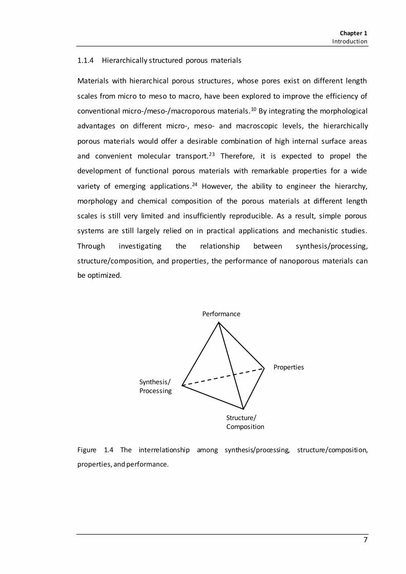
1.1.4 Hierarchically structured porous materials
Materials with hierarchical porous structures, whose pores exist on different length
scales from micro to meso to macro, have been explored to improve the efficiency of
conventional micro-/meso-/macroporous materials.10 By integrating the morphological
advantages on different micro-, meso- and macroscopic levels, the hierarchically
porous materials would offer a desirable combination of high internal surface areas
and convenient molecular transport.23 Therefore, it is expected to propel the
development of functional porous materials with remarkable properties for a wide
variety of emerging applications.24 However, the ability to engineer the hierarchy,
morphology and chemical composition of the porous materials at different length
scales is still very limited and insufficiently reproducible. As a result, simple porous
systems are still largely relied on in practical applications and mechanistic studies.
Through investigating the relationship between synthesis/processing,
structure/composition, and properties, the performance of nanoporous materials can
be optimized.
Figure 1.4 The interrelationship among synthesis/processing, structure/composition,
properties, and performance.
Performance
Properties
Structure/Composition
Synthesis/Processing

Chapter 1 Introduction
8
1.2 Porous silicon
1.2.1 Background of porous silicon
Silicon (Si) was discovered by Jöns Jacob Berzelius, a Swedish chemist, in 1824 by
heating chips of potassium in a silica container and then carefully washing away the
residual by-products. The origin of the name is from the Latin “silex” or “silicis” which
means flint. Silicon is the seventh most abundant element in the universe and the
second most abundant element in the Earth’s crust, constituting 27.7% of the Earth’s
crust by mass, which is only second to oxygen. The natural forms of Si are principally
found as silicon oxides (SiO2) or silicates in various minerals such as sand, rock, flint,
clay and in photosynthesising algae called diatoms. Alongside the daily uses of Si-
containing glass and silicon rubber etc., Si is also the material foundation of solid-state
electronic devices, marking crystalline Si as the most commonly used semiconductor
by far. Pure crystalline Si has a diamond cubic crystal structure of which the unit cell is
displayed in Figure 1.5. Every Si atom within the crystal lattice has four nearest
neighboring atoms. The length of Si-Si covalent bond is 2.35 Å and the strength is
226 kJ·mol-1.25 The lattice constant (a) is 5.431 Å.
Figure 1.5 The diamond cubic crystal structure of Si.
a(100)
[100]
[010]
[001]

Chapter 1 Introduction
9
Porous silicon (pSi) is a form of solid silicon that contains small channels connecting to
the surface and running within the matrix. It has become one of the most popular
porous materials available to date because of its outstanding and unique set of
physiochemical properties. According to IUPAC recommendations, it can be classified
as microporous silicon (< 2 nm), mesoporous silicon (2-50 nm) and classical
macroporous silicon (> 50 nm) based on the length scale of pore dimension.26 Although
in the pSi literature these terms have often been loosely applied to pSi as opposed to
the strict criteria used in describing porous carbon, silica mentioned in 1.1.
Together with one-dimensional Si nanowires (Si NWs) and zero-dimensional Si
nanoparticles or quantum dots (QDs), silicon nanostructures have become a research
hot point in recent years known as the most important semiconductor materials.
Fundamental properties, such as environmental benignity, earth abundancy, cost-
competitiveness, non-toxicity, and bio-degradability significantly promote the
development of porous silicon and other nanostructured Si materials in
optoelectronics, sensing, energy storage and bio-medical applications in which many
other characteristics also play an important part, such as size-dependent optical
properties, sensibility, compatibility with the existing microelectronic industry and
convenient surface chemistry.
1.2.2 Outline history of porous silicon
Porous silicon was accidentally discovered by the Uhlirs at Bell Labs, USA in the
mid-1950s when carrying out electropolishing experiments.27 Instead of a shiny
smooth surface as expected, they observed the generation of hydrogen gas in the
HF-based solution and the etched surface developed “a matte black, brown or red
deposit”, as shown in Figure 1.6. However, presuming this was silicon oxide, the
interesting finding was just reported as a technical note without further investigation
at that time. It was not until 1970s and 1980s, porous silicon became a material of
interest as the high surface area was used as a model in spectroscopic studies of
crystalline silicon surface and as a precursor to generate thick oxide layers on silicon.

Chapter 1 Introduction
10
Figure 1.6 Image of various pSi samples prepared at different etching conditions. Reprinted
with permission from ref. [32]. Copyright, 2015. Hernández-Montelongo, Muñoz-Noval,
García-Ruíz, Torres-Costa, Martín-Palma and Manso-Silván.28
The interest exploded after the landmark discovery made by Canham, Gösele and
Lehmann in the early 1990s when they observed the bright red-orange
photoluminescence at room temperature from silicon nanoparticles embedded within
the porous structure,29-30 leading to intensive focus on creating porous silicon-based
optoelectronics. However, the progress was not very impressive because of the low
electroluminescence efficiency.31-32
In 1999, laser adsorption/ionization on pSi was first observed, implying its possible
application in mass spectrometry.33 In 2001, the ability of photoexcited pSi to generate
singlet oxygen in solution was discovered, which makes it a good photosensitizer and
promising candidate for cancer theranostics.34 More recently, remarkable progress in
exploiting pSi as metal nanoparticles substrate used in surface enhanced Raman
spectroscopy (SERS),35-38 as photonic crystal sensor,39-41 as photoactive material in
converting solar energy,42-50 as anodic material for rechargeable
Lithium-ion battery,51-56 as bio-imaging agent and drug delivery vehicle57-61 have been
achieved by worldwide studies, which have significantly promoted the application of
porous silicon in many other areas and also inspired the work of ours.

Chapter 1 Introduction
11
1.2.3 Fabrication of porous silicon
A variety of preparation methods have been developed to fabricate porous silicon with
diverse morphologies and surface topographies, which can be divided into two main
categories, known as top-down and bottom-up approaches.
Top–down approaches include various etching-based methods with the use of a
homogeneous, macroscopic Si precursor, such as single-crystalline Si wafer that is
often employed in an electrochemical etching method, notably the most popular
method for Si porosification.62 Using a combination of lithography, deposition and
etching steps, a number of alternative top-down methods have also been developed
which include stain etching,63 metal-assisted chemical etching (MACE),64-66 reactive
ion etching (RIE),67 and laser ablation.68 Among them, the MACE method is widely
employed for its simplicity and controllability in preparing pSi and more often Si NWs.
Alternatively, porous silicon can also be generated through various bottom-up
approaches such as thermal annealing,69 magnesiothermic reduction,51, 70-71
magnetron sputtering,72 and ion implantation.73 In contrast to the top-down routes
that use sculpting or etching to carve structures from a large piece of Si material,
bottom-up methods are usually template-assisted and grow the porous structure from
Si atoms and Si-based molecules (e.g. silica, silane, silicon halides) in an additive
manner. For example, by varying the microscopic structure of silica template, pSi with
well-controlled 3D morphology can be readily synthesised through the
shape-preserving magnesiothermic reduction method.
1.2.3.1 Electrochemical etching
Among all the preparation methods, electrochemical etching is the most popular for
pSi preparation. It is simple, low-cost, versatile, therefore applied successfully across
physics, chemistry, engineering and material sciences.74 As a classic top-down method,
pSi with wide ranges of morphologies and porosities can be reproducibly attained by
anodic etching Si crystal in hydrofluoric acid (HF) containing electrolyte solution in
electrochemical cell under an external bias voltage.

Chapter 1 Introduction
12
Normally, silicon does not dissolve but if an external current flows through the system,
electrochemical etching will occur. This means that a specific chemical redox reaction
occurs at the Si/solution interface the nature of which is fundamental to the
electrochemical formation of pSi. Figure 1.7 shows the typical current-voltage (I–V)
curve for Si in aqueous HF. Although the exact I, V values vary upon the Si wafer
properties and electrolyte concentration, the main shape of the curve remains
consistent. At high anodic overpotentials, the Si surface is subject to electropolishing
and retains a smooth and planar morphology. In contrast, under low anodic
polarization, channels that penetrate deeply into the solid crystal dominate the surface
morphology.32, 75 From the initial exponential rise of the I-V curve to the first small
peak which is known as electropolishing current (Jps), lies the formation regime for pSi.
Figure 1.7 Characteristic I–V curve for moderately doped p-type silicon in 1% HF electrolyte.
Reprinted with permission from ref. [76]. Copyright 2012, Wiley-VCH.76
During pSi formation, two electrons per dissolved Si atom participate in the interfacial
charge transfer, while the remaining two of the total four available electrons undergo
a corrosive hydrogen generation. The occurring anodic semi-reaction during pSi
formation is shown below (Equation 1.1).

Chapter 1 Introduction
13
Equation 1.1
Figure 1.8 Silicon dissolution scheme proposed by Lehmann and Gösele. Reprinted with
permission from ref. [77]. Copyright 2000, Elsevier Science B.V.77
This two-electron electrochemical reaction and the resulting silicon surface change
were further explained in the dissolution mechanism proposed by Lehmann and
Gösele, which is so far the most accepted (Figure 1.8).30 The oxidizing equivalents that

Chapter 1 Introduction
14
start the electrochemical dissolution and pore formation are valence band holes (h+),
driven to the surface by the applied electric field and by charge diffusion. The
migration of charge carriers is preferentially directed towards the pore bottoms
because of the enhanced electric field at pore tips that have the smallest radius of
curvature. Once a hole makes it to a surface Si atom, the atom is susceptible to attack
by nucleophilic F- in the solution. As a result, pore walls which are sufficiently distant
from the tips are largely passivated, therefore pores are generated in the silicon crystal
and propagate through time.76
In summary, the supply of valence band holes at the surface, the presence of active
pore tips, and the external current density which should be lower than the
electropolishing critical value (Jps) are the basic requirements to be fulfilled for the
occurrence of electrochemical pore formation.78 By altering anodization conditions,
the structural features of pSi are adjustable with relative ease.74 Meanwhile, the
properties of initial Si wafer subjected to electrochemical etching also matter to the
resultant porous structure greatly.
1.2.3.2 Metal-assisted chemical etching
Metal-assisted chemical etching (MACE) is a recently developed anisotropic
wet-etching method.79 In the presence of HF and an oxidative agent, catalysed by
noble metals (Pt, Pd, Au, Ag), silicon can be etched to form required structures such as
1D Si NWs80 and 3D pSi81 with various morphologies. Compared to the anisotropic
nature of electrochemical etching along the [100] direction (Figure 1.5), the etching
direction in MACE can be controlled on the [100] and non-[100] directions.62
During deposition, a compound containing metal ions, such as AgNO3 or HAuCl4, is
added to a HF-H2O2 solution. Upon attachment to the silicon substrate, noble metal
ions acquire electrons (e-) from the silicon valence band (VB) and are reduced to form
seed nuclei, which develop into nanoparticles. Concurrently, these ions inject holes
underneath the silicon causing oxidation into SiO or SiO2, which are then removed by

Chapter 1 Introduction
15
HF etchant. By the continuous formation of silicon oxide underneath the metal
particles and the corresponding removal action by the HF, the metal particles sink into
the silicon and create porous structures (Figure 1.9). Once the desired surface
structures are created, the metal nanoparticles can be removed by HNO3, followed by
a cleaning process.82
MACE-fabricated pSi structure often has a black look, suggesting an improved
antireflection and light trapping property that can be exploited in enhancing the solar
cell efficiency in PV industry.83 It is also being intensively applied in the preparation of
Si-based anodic material used in Li-ion batteries.84 However, as the homogeneity of
the initial metal deposition in size and place distribution is usually quite poor, the level
of control is relatively limited.66
Figure 1.9 An illustration of the metal-assisted chemical etch process: (1) the reduction of an
oxidative agent (such as H2O2) catalysed by a noble metal particle; (2) the injection of the holes
generated during the reduction reaction, into the silicon substrate, with the highest hole
concentration underneath the metal particle; (3) the migration of holes to silicon sidewalls and
surfaces; and (4) the removal of oxidized silicon via HF. Reprinted from ref. [82] - Published by
The Royal Society of Chemistry.82

Chapter 1 Introduction
16
1.2.3.3 In-situ magnesiothermic reduction
Equation 1.2
As Equation 1.2 points out, when magnesium powder (Mg) and silica powder are well
mixed and heated above 650°C under inert atmosphere, the melting temperature
of Mg, silica can be converted into silicon replicas with identical porous network.70 In
contrast to the conventional carbothermal reduction of silica, which operates at
temperatures above 1500°C,85 the magnesiothermic reaction takes place at much
lower temperature region thus preserves the complex structure of silica in the final
pSi product. Another advantage of this method is that a vast range of artificial and
natural silica (diatom frustule,70 rice husk,86 etc.) can be transformed into pSi
nanostructures via this strategy. Owing to the simplicity and versatility,
magnesiothermic reduction has been used in diverse applications such as sensor,87
bio-medical therapy,88 Li-ion batteries51 and photocatalysis46.
However, magnesiothermic reduction has a critical limitation caused by unavoidable
incomplete reduction that results in low yield of pSi. In order to force silica reduction
to completion, a substantial excess of Mg powder is often required which leads to
degradation or even collapse of the structure by further reacting with the as-generated
silicon to form magnesium silicide (Mg2Si) at high temperatures (Equation 1.3).85, 89
Equation 1.3
2MgO (s) + Si (s)2Mg (g) + SiO2 (s)∆
650 °C
2Mg (g) + Si (s)∆
Mg2Si (s)

Chapter 1 Introduction
17
1.2.4 Modification of porous silicon
As mentioned above porous silicon can be produced via various synthetic approaches
of which each of the capability and speciality is also reflected on the resultant porous
structure, distinguishing in various aspects such as the structural morphology, shape,
surface chemistry and chemical composition. However, in many cases the as-formed
properties are not ideal, thus a range of physical and chemical post-treatments can be
applied in adjusting these crucial factors separately or collectively.
1.2.4.1 Morphological modification of porous silicon
Morphological control of porous material is vitally important in realizing its
functionality as known from the previous discussion about porous solids in 1.1. The
characteristics of a nanoporous material are deeply interlocked with its surface and
pore properties, depending on the size, geometry and connectivity of the pores. As
well as largely determined by the used preparation method and Si precursor, they can
also be tailored to meet the needs of the application via tuning the synthesis
parameters, which affect the formation process of porous silicon significantly.
For example, the morphological properties of electrochemically etched porous silicon
can be adjusted effectively by changing the etching conditions, or
electrolyte compositions.90 Meanwhile the crystal orientation and doping conditions of
Si wafer also have strong influence on the final structure.91 As these variables are
standardised and well-controlled, this endows electrochemical etching method
superior advantages over other methods which is also contributed by the fact that the
pore formation is largely defined by the pre-determined conditions.92 For p-type Si
wafer with doping density 1 × 1017 cm-3, the porosity of porous silicon can be adjusted
from 60% to 80% by increasing the etching current density from 3 to 300 mA·cm-2.93 As
found in another study of p-type Si wafer with a resistivity range of 9.0-13.0 Ω·cm, the
measured macropore diameter is proportional to the square root of etching
current density.94 The following example clearly highlights the effect of dopant on pore
texture in porous silicon films. Under the same conditions of current density

Chapter 1 Introduction
18
(50 mA·cm-2), etching time (300 s), and electrolyte composition (3:1
aqueous HF: ethanol), Figure 1.10A shows the cross-section SEM image of porous
silicon made from a (100)-orientated n-type Si wafer, featured by parallel macropores.
While for a (100)-orientated p-type Si wafer, porous silicon is densely packed with
small pores that are too small to be resolved properly in the image (Figure 1.10B).76
Figure 1.10 Cross-section SEM images of porous silicon prepared via electrochemical etching of
n-type (A) and p-type (B) Si wafer. Reprinted with permission from ref. [76]. Copyright 2012,
Wiley-VCH.76
It is often of interest to generate porous silicon with a high surface area in many
applications that potentially involve interfacial interactions, such as optoelectronics,
catalysis, drug delivery systems, and lithium-ion batteries. Since macroporous silicon
has an inherently low surface-to-volume ratio, efforts have mainly been focused on
developing micro-/mesoporous silicon structures. Ruike et al. reported a finely porous
meso-structure of Si prepared from a lightly boron-doped (dopant density 7×10¹⁴/cm3)
crystalline Si wafer by anodization (10 mA·cm-2) in mildly concentrated HF solution
exhibited a specific surface area of 590 m2·g-1 and mean pore size around 3.1 nm.95 A
similar value of surface area was also reported in a later study which achieved
570 m2·g-1 in amorphous mesoporous silicon from a sodiothermically reduced silica
template (NaY zeolite) with pore size distribution centred at 11.2 nm, further leading
to a high supercapacitive performance.96 Another bottom-up self-templating synthesis
A B

Chapter 1 Introduction
19
of mesoporous crystalline Si from a gaseous precursor (SiCl4) was also developed which
shows high surface area up to 580 m2·g-1 and enhanced photocatalytic efficiency in
hydrogen generation.48 By adding different additives (hydrochloric acid, sulphuric acid,
ammonium dodecyl sulfate) into the HF containing electrolyte, highly porous silicon
film with 1125 m2·g-1 (pore diameter 4.2 nm) and pSi particles with 864 m2·g-1 (pore
size in 2.8 - 3.2 nm region) were obtained on p-type Si wafer with resistivity 1 - 5 Ω·cm
through electrochemical etching and supercritical drying with CO2 solvent in order to
maintain the integrity of the etched micro-/mesoporosity during electrolyte
removal.97-98
1.2.4.2 Shape modification of porous silicon
The natural form of porous silicon produced by bottom-up approaches is usually
powder-like particles. In contrast, as crystalline Si wafers are often employed as
precursor in etching-based approaches in the preparation of porous silicon, as -etched
porous silicon is often supported by the unetched part of the Si wafer in the form of
porous thin film, a continuous bulky phase that can also be “lifted off” the substrate.
As an advantage, the chip-bound shape could open up the opportunities of porous
silicon prepared by top-down methods to be utilized in microelectromechanical
systems (MEMS) applications, especially the electrochemical etching method for its
excellent controllability.
For broader uses, porous silicon microparticles and nanoparticles are also
desirable.99-100 Common methods to prepare them involve physical grinding,
ball-milling101-103 or ultrasonication.104-106 Since the resulting particle size distribution is
relatively broad, extra sieving step is often required. With the emergence of various
new post-treatments, such as pulsed electrochemical etching,103, 107
high-pressure microfluidization,108 the yield of porous silicon nanoparticles can be
further improved with greater size control.

Chapter 1 Introduction
20
1.2.4.3 Surface modification of porous silicon
Figure 1.11 Schematic diagram of the silicon hydrides (SiH, SiH2 and SiH3) formed on the
surface of as-etched porous silicon.
Porous silicon outscores many other nanostructured Si for its unique porous structure
and large surface area, which means the surface properties are as important as the
bulk properties. In general, the surface of porous silicon fabricated by etching -based
approaches is often populated with Si-H bonds, as shown in Figure 1.11, resulting in a
hydride-passivated surface environment. These hydrides species are metastable and
thus can be transformed through various ways of oxidation, carbonization,
hydrosilylation, to enhance the stability,109-110 modify the surface
hydrophobicity/hydrophilicity,111-112 adjust the porous structure113-115 or
optical properties116-117 and to functionalize pSi with useful features via ligand grafting
which include alkene, alkyne, aldehyde etc.118-119 As a result, the surface chemistry of
porous silicon has been profoundly enriched which facilitates the development of
porous silicon-based multicomponent and multifunctional systems.

Chapter 1 Introduction
21
1.2.5 Applications of porous silicon
Due to the unique morphological structure and surface functionality, porous silicon is
widely applied in a broad range of fields of which a glimpse can be caught in the
discussion above in 1.2.2. Here, three potential applications that are attracting
increasing research attentions are described.
1.2.5.1 Heterogeneous catalysis
The large surface-to-volume ratio, open porous network, unique surface chemistry,
and semiconducting properties of pSi provide a solid structural basis for the material to
be utilized in catalytic/photocatalytic conversions as inert catalyst substrate or as
active photocatalyst.
1.2.5.1.1 Porous silicon as catalyst support
As we know in heterogeneous catalysis, the catalyst support has huge influences on
the catalytic performance and catalyst lifetime. A high specific surface area is greatly
appreciated, as that would improve the dispersity and stability of active catalysts,
increase the loading capacity, and exposes more reaction sites on the catalyst surfaces.
Much work have been dedicated to this area by making use of nanostructured Si, e.g.
Si NWs,120-122 pSi123-126 in anchoring active catalyst/photocatalyst species, most
commonly metal nanoparticles (e.g. Ag, Cu, Pt, Au), for the reduction of
nitroaromatics,125-126 CO oxidation,124 selective oxidation of hydrocarbons127-128 and
ethanol steaming reforming etc.123 Apart from the structural advantages, the
SiHx species on the surface of pSi also enable the in-situ reduction of metal ions into
metallic catalyst without the need for additional reducing agent.125-126, 128 As a
semiconductor, pSi may also influence the electronic state of metal clusters through
exciton-plasmon interaction and consequently affects the catalytic activity.125
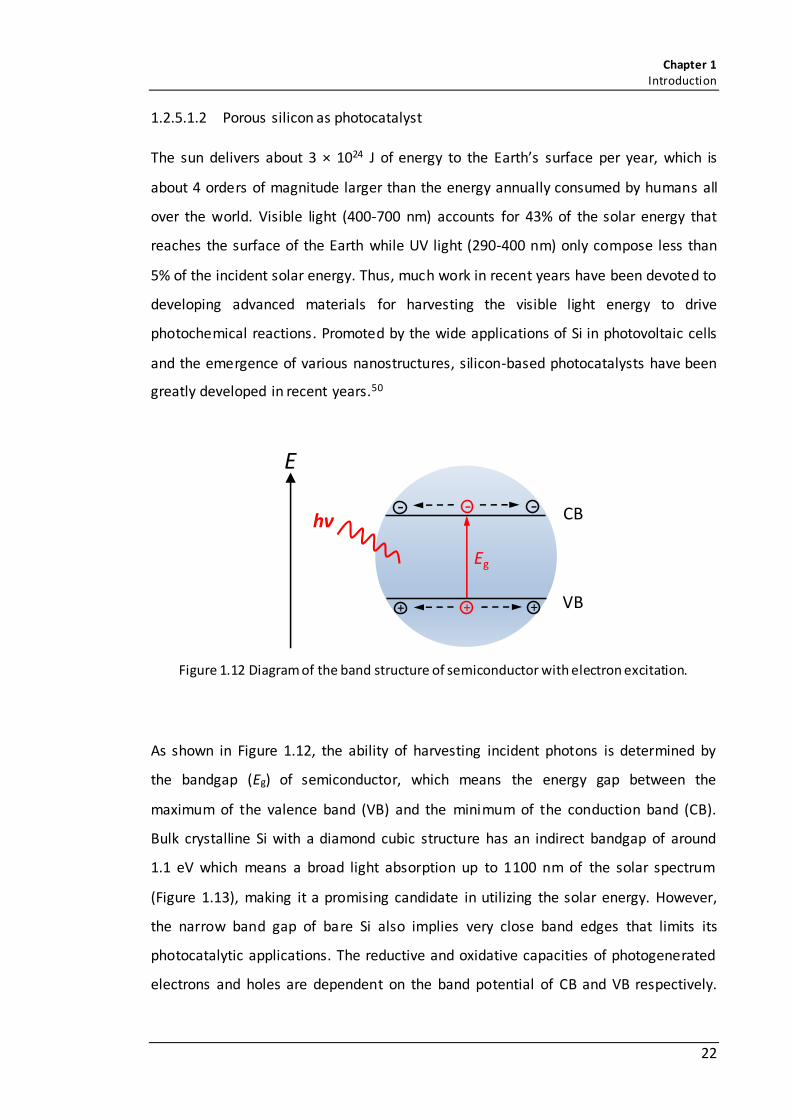
Chapter 1 Introduction
22
1.2.5.1.2 Porous silicon as photocatalyst
The sun delivers about 3 × 1024 J of energy to the Earth’s surface per year, which is
about 4 orders of magnitude larger than the energy annually consumed by humans all
over the world. Visible light (400-700 nm) accounts for 43% of the solar energy that
reaches the surface of the Earth while UV light (290-400 nm) only compose less than
5% of the incident solar energy. Thus, much work in recent years have been devoted to
developing advanced materials for harvesting the visible light energy to drive
photochemical reactions. Promoted by the wide applications of Si in photovoltaic cells
and the emergence of various nanostructures, silicon-based photocatalysts have been
greatly developed in recent years.50
Figure 1.12 Diagram of the band structure of semiconductor with electron excitation.
As shown in Figure 1.12, the ability of harvesting incident photons is determined by
the bandgap (Eg) of semiconductor, which means the energy gap between the
maximum of the valence band (VB) and the minimum of the conduction band (CB).
Bulk crystalline Si with a diamond cubic structure has an indirect bandgap of around
1.1 eV which means a broad light absorption up to 1100 nm of the solar spectrum
(Figure 1.13), making it a promising candidate in utilizing the solar energy. However,
the narrow band gap of bare Si also implies very close band edges that limits its
photocatalytic applications. The reductive and oxidative capacities of photogenerated
electrons and holes are dependent on the band potential of CB and VB respectively.
CB
VB
hν- --
+ ++
E
Eg

Chapter 1 Introduction
23
Through nanoscaling, the energy difference between CB and VB can be increased
effectively, leading to a better photoredox capability.
Figure 1.13 AM1.5 solar spectrum, together with a graph that indicates the solar energy
absorbed in a 2-μm-thick crystalline Si film (assuming single-pass absorption and no reflection).
Reprinted with permission from ref. [129]. Copyright 2010, Nature Publishing Group.129
Due to the quantum confinement caused by the Si nanocrystallites formed on the
porous framework, the bandgap energy of electrochemically etched pSi is effectively
enlarged to 1.8-2.2 eV.47 As a result, visible light photons with energies equal to and
higher than the bandgap level can be absorbed by porous silicon resulting in the
excitation of electrons from the valence band to the conduction band by overcoming
the transition barrier. After the charge separation, the photoexcited electrons (e-) and
holes (h+) then migrate to the surfaces of pSi from the inner bulk phase and are
donated to substrate molecules in liquid phase which results in interfacial charge
transfer and half reaction of reduction and/or oxidation. The reductive and oxidative
capacities of photogenerated electrons and holes are dependent on the band potential
of CB and VB respectively. As seen in Figure 1.14, the above mentioned charge transfer
pathway is among various other possibilities of photoinduced charge recombination
which can be generally divided as non-radiative recombination and radiative
recombination, the latter of which gives rise to the light emitting property of porous
silicon, as further illustrated in 1.2.5.2.

Chapter 1 Introduction
24
Figure 1.14 Schematic diagram depicting the radiative and non-radiative recombination
pathways available to a Si nanocrystallite in porous silicon. Reprinted with permission from
ref. [60]. Copyright 2009, Wiley-VCH.60
As earth-abundant, metal-free and visible-light responsive, Si-based photocatalysts
(pSi, Si NWs, Si nanoparticles etc.) have drawn widespread attention in fuel
production, organic synthesis, waste treatment and environmental
remediation.42-46, 48-49, 122, 130-147 Mao et al. reported the electrochemically etched Si
electrodes exhibit higher energy conversion efficiencies than Si electrodes due to the
formation of a pSi layer which suppressed charge recombination at the Si/electrolyte
interface and stabilizes the electrodes against photocorrosion.148 As good
photosensitizers, pSi and Si nanocrystals are also used in generating singlet oxygen.34
The photocatalytic ability of Si NWs and Si QDs in CO2 photoreduction,130, 140 water
splitting,47, 134, 137, 139 aqueous dye degradation (methyl red,130, 144, 146
rhodamine B,131, 145 indigo carmine,132 rose Bengal,136 methylene blue,134 methyl
orange43), selective oxidation of benzene,130, 146 benzoic alcohol,131 and reduction of
Cr (VI)135 under visible light irradiation have also been demonstrated in various studies.
One of the studies on Si QDs suggests a size-dependent photocatalytic activity for
different reactions as 1-2 nm Si QDs is capable in degrading methyl red and reducing
CO2 while 3-4 nm Si QDs shows little activity (Figure 1.15). This was explained by the
authors that the former QDs have more energy to induce those photochemical
reactions than the latter ones due to the wider band gap.130 Another study comparing

Chapter 1 Introduction
25
the photocatalytic performance of porous Si NWs and nonporous Si NWs prepared
with MACE method in methyl red photodegradation shows nanoporous Si NWs have
better photocatalytic activity as a result of the higher surface area, pore volume and
stronger light absorption.144 As implied, by controlling the surface and band gap of
nanostructured Si, more efficient Si NWs, QDs-based photocatalyst can be developed.
Figure 1.15 Different diameter Si QDs for different reactions. Reprinted with permission from
ref. [130]. Copyright 2007, American Chemical Society.130
While the physical structure is not much of a concern for the low dimensional Si QDs
and NWs which is also one of the reasons why their photocatalytic applications are
mostly investigated, porous silicon has much more complex micro- and nano-structural
features in terms of internal/external surfaces, pore size, pore interconnectivity, pore
volume and the size distribution of Si nanocrystallites on the pore walls.
Understandably, these factors not only affect the electronic band structure and optical
properties of pSi but also have huge influences on the photochemical reaction kinetics
by regulating the absorption and diffusion behaviours of reactant molecules.
Compared to the widely studied Si QDs and NWs, the photocatalytic performance of
pSi and pSi-based materials have been less intensively investigated despite the larger
surface area that it possesses. A very broad absorption across the entire UV, visible
light and near-IR range was widely recorded in a number of pSi research49, 149-150 which
is partly due to the existence of a wide spread of band gaps, as demonstrated by the
large and inhomogeneous lineshape of its visible emission band.77 Further studies
suggest the light absorption in water can be further enhanced by the nanoporous

Chapter 1 Introduction
26
structure by providing broadband anti-reflection which improves the photon
conversion efficiency (Figure 1.16).151 The visible-light-driven activities in solar
water splitting,47-48 photodegradation of methyl orange,44 phenol,49 nitroaromatics,
CO2 reduction152 have been broadly discussed in literature, exhibiting a promising
potentiality in H2 generation, pollution control and water purification under visible
light irradiation which can be further promoted by increasing the surface area or
adjusting the porous structure.
Figure 1.16 The measured total hemispherical optical reflectance of polished and nanoporous
Si in air, and the calculated reflectance of polished Si in water. Nanoporous Si shows
broadband anti-reflection properties with optical reflectance < 2% over whole solar spectrum.
The polished Si reflects about 25% of sunlight at the Si–water interface. Reprinted with
permission from ref. [151]. Copyright 2011, Royal Society of Chemistry.151
Although the actual photocatalytic mechanisms of Si QDs, Si NWs and pSi are still
largely unknown, some insights have already been shed on the importance of the
surface termination. In the study carried out by Shao et al., hydrogen-terminated
Si NWs exhibited even better photocatalytic activity than Pd-, Au-, Rh- or Ag-modified
ones in the degradation of rhodamine B which was ascribed to the effect of hydrogen
termination on accelerating photoexcited electrons and holes separation.131 Similar
effects were also proposed in other research in explaining the photocatalytic

Chapter 1 Introduction
27
behaviours of H-terminated Si QDs, Si NWs and pSi. As Megouda et al. reported, the
significance of surface hydrides was also shown in the control experiment of oxidized
Si NWs of which the photocatalytic activity in photodegradation of rhodamine B was
much lower than that of the hydrogenated sample.145 Since a hydrogen atom has a
large Pauling electron negative value of 2.2, this effect is attributed to the
electron-deficiency of H atoms in surface hydrides (SiHx), which may serve as an
electron sink to improve charge separation.145 Meanwhile, by washing with HF, it was
found that the HF-treated Si NWs are more efficient than the as-synthesized ones
because of the increased H surface coverage in addition to the original ones.144 A
closer look at the nature of surface species provided by Liu et al. confirms the strong
dependence of photocatalytic activity of Si NWs on the surface hydrides, which was
revealed as a dynamic interplay of charge distribution and surface reactions. As Si-H
can not only trap photoexcited electrons from the bulk but also undergoes bond
cleavage in forming H2 gas in the water splitting process. In the meantime, the Si-OH
formed on the surface enters into competition with Si-H on the electron extraction,
hindering the H2 generation.137
On the other hand, in the study performed by Kang et al., H-terminated Si QDs were
catalytically inactive in the first 2 hours of the photochemical reaction and gradually
recovered their photocatalytic capability in benzene hydroxylation after being oxidized
to Si/SiOx core-shell structure which was interpreted as the assistance of SiOx in the
process of the generation of active oxygen species. Another paper also demonstrated
that the hydrogen termination was not a prerequisite for the degradation activity of
Si NWs in the degradation of indigo carmine.153
As mentioned in 1.2.4.3, surface modification of pSi can be conducted through ligand
grafting by bridging with the surface hydrides. In fact, pSi is also employed as reducing
agent in converting CO2152, 154, nitrobenzene derivatives etc.155 The reactivity of Si-H is
also documented in several photocatalysis experiments as dye molecules (e.g.
methyl red, methyl orange, and methylene blue) were reduced in the absence of light
presumably through hydrogen transfer although how the photocatalytic pathway
would be affected by this event was not explored further.44-45, 144, 156 Another
important fact to be considered is that the hydrogen function is also known to be
Chapter 1 Introduction
28
affected by various external factors (UV laser,157 ultrasonic agitation,158 heat,159
energetic ion160) and varied by the surface topography of nanostructured Si as
well.118, 161
1.2.5.2 Biomedical applications of porous silicon
A clear advantage of Si materials applied in biological research is their natural
biocompatibility, biodegradability and bioresorbability.162-163 Promoted by the high
surface area, unique porous structure and adjustable surface functionalities , porous
silicon has embraced remarkable success acting as a drug delivery vector used in
cancer treatment, featuring a high drug loading, controlled and
sustained release.99, 164-165 As indicated in Figure 1.14, porous silicon can also emit
tuneable photoluminescence at room temperature through radiative recombination of
photoexcited electrons and holes which has prompted a vast number of studies on the
development of cell imaging agents61, 166 and photoluminescence-based
biosensors.60, 167 Also inspired by the photoactivity, the use of pSi in photothermo- and
photodynamic therapies has received increasing attention.100, 168-169
1.2.5.3 Energy storage applications of porous silicon
Taking advantage of the high theoretical specific capacity of silicon (4200 mAh·g-1) and
the anti-pulverization ability endowed by the void spaces in the porous structure,
porous silicon has been extensively explored as anode material for the next generation
of lithium-ion batteries, with improved capacity and cycling performance
as reported.53-55, 71, 170 Although this application is also structure-sensitive, the basic
requirement is mainly about the voids inside pSi to accommodate the drastic volume
expansion during Li+ insertion and extraction. Thus, the magnesiothermic reduction
approach is widely adopted for pSi preparation in battery research for its versatility
and cost effectiveness.171-175
Chapter 1 Introduction
29
1.3 Graphitic carbon nitride materials
Ever since the defining moment of the isolation of graphene from graphite in 2004,176
a wide spectrum of two-dimensional (2D) nanomaterials including graphene177-179 and
non-graphene layered materials such as transitional-metal dichalcogenides180-182 and
hexagonal boron nitride (h-BN)183 have attracted tremendous interests because of the
new functionalities and applications that emerge upon 2D confinement.184 A significant
amount of effort has in particular been devoted to the development of 2D graphitic
carbon nitride (g-C3N4) which has shown promising prospects in various fields of
energy applications, light-emitting and sensing etc.185-191
1.3.1 General background of graphitic carbon nitride
Carbon nitrides (C3N4), is a subclass of covalent organic frameworks (COFs) composed
of binary C, N-based polymeric materials.192 The first synthesis of a chain-like C3N4
derivative, melon, was reported by Berzelius and Liebig in 1834 (Figure 1.17(d)) and it
is regarded as one of the oldest synthetic polymers in human history.193 Carbon
nitrides can exist in several allotropes with diverse properties including α-C3N4, β-C3N4,
cubic-C3N4, pseudocubic-C3N4, and graphitic-C3N4.185, 194 Demonstrated by Liu et al., the
diamond-like β-C3N4 allotrope was discovered to be of comparative hardness and low
compressibility as that of diamond.195 While graphitic C3N4 (g-C3N4) was found to be
energetically favoured relative to other phases and is regarded as the most stable
allotrope of carbon nitrides under ambient conditions based on both theoretical and
experimental studies.196-197 Besides, it has many advantages such as reliable chemical
and thermal stability, high level of hardness, resistance to wear, bio-compatibility and
special electronic properties due to the unique tectonic structure motif.194 Thus, it has
attracted the focus of most carbon nitride oriented research.185, 188
Possessing a two-dimensional (2D) layered structure, g-C3N4 can be viewed as an
analogue of graphite, more precisely, as a high level of N-doped graphite-like
framework consisting of a π-conjugated system through sp2 hybridized C and N atoms
on the plane. As shown in Figure 1.17, its polymeric network (e) is formed by the

Chapter 1 Introduction
30
condensation of tri-s-triazine/heptazine (c) subunits, widely accepted as the basic
building units, connected through planar tertiary amino groups with periodic vacancies
in the lattice.198 As such, the electronic properties of g-C3N4 is distinctly different from
graphite as characterised as a wide-bandgap semiconductor while graphite has
excellent conductivity in the dimensions of the layers.
Figure 1.17 Structures of (a) melamine, (b) melam, (c) melem, (d) melon and (e) g-C3N4
network with tri-s-triazine as tectons.
One of the main advantages of g-C3N4 is its straightforward synthesis using a cheap
and easily available starting material. Many nitrogen-rich precursors can be thermally
polymerized into a g-C3N4 framework through a combination of polyaddition and
(a) (b)
(c) (d)
(e)

Chapter 1 Introduction
31
polycondensation, to name just a few, such as urea,199-200 thiourea,201 cyanamide,202
dicyandiamide,203-204 and melamine.205-206 Taken melamine as an example (Figure 1.17),
the reaction starts with condensation of melamine (a) that eliminates ammonia and
forms a dimer called melam (b). Melam is then converted into tri-s-triazine called
melem (c) which forms the 2D planar structure (e) via polymerization at approximately
520°C and stack into layered g-C3N4 through hydrogen bonds and van der Waals
interplanar forces.194
1.3.2 Photocatalytic applications of graphitic carbon nitride
The first photocatalytic result of g-C3N4 semiconductor was published in 2009 by
Wang et al. that revealed its photocatalytic activity in water splitting under visible
light irradiation.207 Since then, it has attracted worldwide research interests in
exploiting the ability in harnessing solar energy and rapidly became a “star” material of
significant importance in various fields, such as water splitting,208 CO2 fixation,209-210
pollutant elimination.185, 187, 211
As limited by the low surface area (2-10 m2·g−1), poor absorption at longer wavelengths
and poor charge mobility, much progress in recent years has been made in improving
the photon conversion efficiency and facilitating an easier mass transfer process from
four different directions of electronic structure modulation, crystal structure
engineering, nanostructure design, and heterostructure construction.194 In respect of
nanostructure design, different exfoliation strategies (e.g. thermal oxidation,212-214
mechanical exfoliation,215-218 chemical exfoliation219-221) for synthesising 2D g-C3N4
nanosheets have been developed and proved to be efficient in improving the
photocatalytic performance as a result of enlarged surface area and widened
bandgap.222 A variety of g-C3N4 based heterostructures have also emerged which can
be categorized as: metal-free heterojunction, g-C3N4/single metal oxide (sulfide),
g-C3N4/composite oxide, g-C3N4/halide, g-C3N4/noble metal, and g-C3N4-based complex
system.223 As suggested by these efforts, the potential of g-C3N4 in photocatalysis is
still not yet fulfilled and in need of new perspectives to pave the way for a greener
future.

Chapter 1 Introduction
32
1.4 Dye pollution and elimination
Over 10,000 different synthetic dyes are used widely in textile, pharmaceutical,
cosmetics, paper industries, constituting one of the largest groups of organic
compounds with serious environmental risks.224 Due to improper operation or
accidental leakage, about 15% of the total world production of dyes up to 200,000 tons
is lost and released into water bodies during production, storage, transportation
and usage.225 Due to the high stability, most of these escaped dyes tend to persist in
the natural environment, causing severe water pollution problems and ecological
damages.
The distinctive colour of the dye is caused by the chromophore-containing centre in its
molecular structure that are based on diverse functional groups, such as azo,
anthraquinone, methane, nitro, arilmethane, carbonyl etc.226 With respect to the
number and production volumes, azo dyes are the largest group of colorants,
dominating 60-70% of all organic dyes annually produced worldwide.227 Due to their
toxicity and mutagenic effect, they are banned throughout the world. However, their
uses continue today because of their low cost and other properties in food, paper,
leather and paints. Thus, removal and treatment of azo dyes from wastewater
presents a difficult task.
Since the azo dyes are almost non-destructive by the conventional biological
treatments and physical treatments are also ineffective considering the cost of
adsorbent agents, chemical methods especially heterogeneous photocatalysts are
significantly important as the solution to the existing and future water challenges for
various reasons. The photocatalysts are mostly made of substances that can be
accounted as available, inexpensive and non-toxic. The removal of organic
contaminants in aqueous systems can be done without involving other agents, and
carried out under ambient or mild conditions. More importantly, by utilizing sunlight,
the wastewater can be constantly cleaned by reusing the same photocatalyst. The
elimination efficiency is therefore largely dependent on the activity and recyclability of
photocatalyst. With the advent of more advanced nanotechnologies, more and more

Chapter 1 Introduction
33
efficient nanomaterials will be developed and contribute to the rebalance of the out-
of-balance relationship of the natural environment and human society.
1.5 Research objectives
From the discussion above, it is clear that solar energy utilization is of utmost
importance in resolving various aspects of global challenges the world is now facing, to
meet soaring energy demand, to tackle climate change, to solve the deteriorating
pollution crisis and most of all, to establish a sustainable society for us all. Thus, the
overall aim of this research is to search for an earth-abundant and eco-friendly system
that can utilize solar energy to eliminate environmental pollutants efficiently and
cost-effectively.
To approach the goal, we focused on exploiting porous silicon and porous silicon-based
heterojunctions with graphitic carbon nitride (g-C3N4). Inspired by the previous findings
on the surface area of catalysts, the first research objective is to prepare mesoporous
silicon with a large surface area and tuneable porous structure by an electrochemical
etching method and understand the morphological features and physiochemical
properties. Secondly, we are interested in the structural effects on the photocatalytic
performance of mesoporous silicon and the photocatalytic mechanism as well. Finally,
the combination of porous silicon and g-C3N4 nanosheets is to be investigated in the
hope of broadening the options for greener photocatalysis.
1.6 Thesis outline
According to these three objectives, this thesis is divided into 6 chapters in total.
Chapter 1 introduces the research background, concludes the state-of-the-art research
progress of porous silicon and graphitic carbon nitride materials , highlights the
importance of photocatalysis in dye degradation.

Chapter 1 Introduction
34
Chapter 2 overviews the experimental procedures for the preparation, modification,
characterisation and photocatalytic analysis of porous silicon and graphitic carbon
nitride materials, with a general discussion of the method principles correspondingly.
Chapter 3 showcases the high surface area and unique morphologies of mesoporous
silicon, implies the potential applications in heterogeneous catalysis, biomedicines and
energy storage.
Chapter 4 evaluates the photocatalytic activity of mesoporous silicon in dye
degradation under visible light irradiation, reveals the varied effects of structural
factors in reaction kinetics, and discusses the photocatalytic behaviours and
mechanisms of porous silicon as well.
Chapter 5 demonstrates the performance of mesoporous silicon/graphitic carbon
nitride nanosheets composited material in dye degradation under visible light
irradiation.
Chapter 6 summarizes the primary contributions of this research, and provides
suggestions for future work in this area.

Chapter 1 Introduction
35
1.7 References
1. Su, B.-L.; Sanchez, C.; Yang, X.-Y., Hierarchically Structured Porous Materials. Wiley-
VCH Verlag & Co. KGaA: Germany, Weinheim, 2011.
2. Yang, X.-Y.; Chen, L.-H.; Li, Y.; Rooke, J. C.; Sanchez, C.; Su, B.-L., Hierarchically
porous materials: synthesis strategies and structure design. Chem. Soc. Rev. 2017, 46
(2), 481-558.
3. Sing, K. S. W., Reporting physisorption data for gas/solid systems with special
reference to the determination of surface area and porosity (Recommendations 1984).
Pure Appl. Chem. 1985, 57 (4), 603-619.
4. Valtchev, V.; Majano, G.; Mintova, S.; Perez-Ramirez, J., Tailored crystalline
microporous materials by post-synthesis modification. Chem. Soc. Rev. 2013, 42 (1),
263-290.
5. Navrotsky, A.; Trofymluk, O.; Levchenko, A. A., Thermochemistry of microporous
and mesoporous materials. Chem. Rev. 2009, 109 (9), 3885-3902.
6. Csicsery, S. M., Shape-selective catalysis in zeolites. Zeolites 1984, 4 (3), 202-213.
7. Collins, D. J.; Medina, R. J.; Davis, B. H., Xylene isomerization by ZSM-5 zeolite
catalyst. Can. J. Chem. Eng. 1983, 61 (1), 29-35.
8. Yan, Y.; Guo, X.; Zhang, Y.; Tang, Y., Future of nano-/hierarchical zeolites in catalysis:
gaseous phase or liquid phase system. Catal. Sci. Technol. 2015, 5 (2), 772-785.
9. Corma, A., From microporous to mesoporous molecular sieve materials and their
use in catalysis. Chem. Rev. 1997, 97 (6), 2373-2420.
10. Perez-Ramirez, J.; Christensen, C. H.; Egeblad, K.; Christensen, C. H.; Groen, J. C.,
Hierarchical zeolites: enhanced utilisation of microporous crystals in catalysis by
advances in materials design. Chem. Soc. Rev. 2008, 37 (11), 2530-2542.
11. Xuereb, D. J.; Raja, R., Design strategies for engineering selectivity in bio-inspired
heterogeneous catalysts. Catal. Sci. Technol. 2011, 1 (4), 517-534.
12. Yang, Z.; Lu, Y.; Yang, Z., Mesoporous materials: tunable structure, morphology and
composition. Chem. Commun. 2009, (17), 2270-2277.

Chapter 1 Introduction
36
13. Moritz, M.; Geszke-Moritz, M., Mesoporous materials as multifunctional tools in
biosciences: principles and applications. Mater Sci Eng C Mater Biol Appl 2015, 49,
114-151.
14. Hoffmann, F.; Cornelius, M.; Morell, J.; Froba, M., Silica-based mesoporous organic-
inorganic hybrid materials. Angew. Chem. Int. Ed. 2006, 45 (20), 3216-3251.
15. Liang, C.; Li, Z.; Dai, S., Mesoporous carbon materials: synthesis and modification.
Angew. Chem. Int. Ed. 2008, 47 (20), 3696-3717.
16. Chen, H.-Y.; Xu, Y.-F.; Kuang, D.-B.; Su, C.-Y., Recent advances in hierarchical
macroporous composite structures for photoelectric conversion. Energy Environ. Sci.
2014, 7 (12), 3887-3901.
17. Wang, B.; Prinsen, P.; Wang, H.; Bai, Z.; Wang, H.; Luque, R.; Xuan, J., Macroporous
materials: microfluidic fabrication, functionalization and applications. Chem. Soc. Rev.
2017, 46 (3), 855-914.
18. Stein, A.; Schroden, R. C., Colloidal crystal templating of three-dimensionally
ordered macroporous solids: materials for photonics and beyond. Curr. Opin. Solid
State Mater. Sci. 2001, 5 (6), 553-564.
19. Nardecchia, S.; Carriazo, D.; Ferrer, M. L.; Gutierrez, M. C.; del Monte, F., Three
dimensional macroporous architectures and aerogels built of carbon nanotubes and/or
graphene: synthesis and applications. Chem. Soc. Rev. 2013, 42 (2), 794-830.
20. Carreon, M. A.; Guliants, V. V., Ordered meso- and macroporous binary and mixed
metal oxides. Eur. J. Inorg. Chem. 2005, 2005 (1), 27-43.
21. Ahn, S. H.; Kim, D. J.; Chi, W. S.; Kim, J. H., Hierarchical double-shell nanostructures
of TiO2 nanosheets on SnO2 hollow spheres for high-efficiency, solid-state, dye-
sensitized solar cells. Adv. Funct. Mater. 2014, 24 (32), 5037-5044.
22. Kim, H. N.; Moon, J. H., Enhanced photovoltaic properties of Nb2O5-coated TiO2 3D
ordered porous electrodes in dye-sensitized solar cells. ACS Appl Mater Interfaces
2012, 4 (11), 5821-5825.
23. Lee, J.; Kim, J.; Hyeon, T., Recent progress in the synthesis of porous carbon
materials. Adv. Mater. 2006, 18 (16), 2073-2094.

Chapter 1 Introduction
37
24. Sun, M. H.; Huang, S. Z.; Chen, L. H.; Li, Y.; Yang, X. Y.; Yuan, Z. Y.; Su, B. L.,
Applications of hierarchically structured porous materials from energy storage and
conversion, catalysis, photocatalysis, adsorption, separation, and sensing to
biomedicine. Chem. Soc. Rev. 2016, 45 (12), 3479-3563.
25. Neergaard Waltenburg, H.; Yates, J. T., Surface chemistry of silicon. Chem. Rev.
1995, 95 (5), 1589-1673.
26. Thommes, M.; Kaneko, K.; Neimark, A. V.; Olivier, J. P.; Rodriguez-Reinoso, F.;
Rouquerol, J.; Sing, K. S. W., Physisorption of gases, with special reference to the
evaluation of surface area and pore size distribution (IUPAC Technical Report). Pure
Appl. Chem. 2015, 87 (9-10), 1051-1069.
27. Uhlir, A., Electrolytic shaping of germanium and silicon. Bell Syst. Tech. J. 1956,
35 (2), 333-347.
28. Hernandez-Montelongo, J.; Munoz-Noval, A.; Garcia-Ruiz, J. P.; Torres-Costa, V.;
Martin-Palma, R. J.; Manso-Silvan, M., Nanostructured porous silicon: the winding road
from photonics to cell scaffolds - a review. Front Bioeng Biotechnol. 2015, 3: 60.
29. Canham, L. T., Silicon quantum wire array fabrication by electrochemical and
chemical dissolution of wafers. Appl. Phys. Lett. 1990, 57 (10), 1046-1048.
30. Lehmann, V.; Gosele, U., Porous silicon formation - a quantum wire effect.
Appl. Phys. Lett. 1991, 58 (8), 856-858.
31. Hirschman, K. D.; Tsybeskov, L.; Duttagupta, S. P.; Fauchet, P. M., Silicon-based
visible light-emitting devices integrated into microelectronic circuits. Nature 1996, 384
(6607), 338-341.
32. Cullis, A. G.; Canham, L. T.; Calcott, P. D. J., The structural and luminescence
properties of porous silicon. J. Appl. Phys. 1997, 82 (3), 909-965.
33. Wei, J.; Buriak, J. M.; Siuzdak, G., Desorption-ionization mass spectrometry on
porous silicon. Nature 1999, 399 (6733), 243-246.
34. Fujii, M.; Nishimura, N.; Fumon, H.; Hayashi, S.; Kovalev, D.; Goller, B.; Diener, J.,
Dynamics of photosensitized formation of singlet oxygen by porous silicon in aqueous
solution. J. Appl. Phys. 2006, 100 (12), 124302.

Chapter 1 Introduction
38
35. Novara, C.; Lamberti, A.; Chiadò, A.; Virga, A.; Rivolo, P.; Geobaldo, F.; Giorgis, F.,
Surface-enhanced Raman spectroscopy on porous silicon membranes decorated with
Ag nanoparticles integrated in elastomeric microfluidic chips. RSC. Adv. 2016, 6 (26),
21865-21870.
36. Virga, A.; Rivolo, P.; Frascella, F.; Angelini, A.; Descrovi, E.; Geobaldo, F.; Giorgis, F.,
Silver nanoparticles on porous silicon: approaching single molecule detection in
resonant SERS regime. J. Phys. Chem. C 2013, 117 (39), 20139-20145.
37. Chan, S.; Kwon, S.; Koo, T. W.; Lee, L. P.; Berlin, A. A., Surface-enhanced raman
scattering of small molecules from silver-coated silicon nanopores. Adv. Mater. 2003,
15 (19), 1595-1598.
38. Lin, H.; Mock, J.; Smith, D.; Gao, T.; Sailor, M. J., Surface-enhanced raman
scattering from silver-plated porous silicon. J. Phys. Chem. B 2004, 108 (31),
11654-11659.
39. Harraz, F. A., Porous silicon chemical sensors and biosensors: A review.
Sens Actuators B Chem. 2014, 202, 897-912.
40. Kilian, K. A.; Bocking, T.; Gooding, J. J., The importance of surface chemistry in
mesoporous materials: lessons from porous silicon biosensors. Chem. Commun. 2009,
(6), 630-640.
41. Priolo, F.; Gregorkiewicz, T.; Galli, M.; Krauss, T. F., Silicon nanostructures for
photonics and photovoltaics. Nat. Nanotechnol. 2014, 9 (1), 19-32.
42. Li, T.; Li, J.; Zhang, Q.; Blazeby, E.; Shang, C.; Xu, H.; Zhang, X.; Chao, Y.,
Hydrogen-terminated mesoporous silicon monoliths with huge surface area as
alternative Si-based visible light-active photocatalysts. RSC Adv. 2016, 6 (75), 71092-
71099.
43. Guan, B.; Sun, Y.; Li, X.; Wang, J.; Chen, S.; Schweizer, S.; Wang, Y.;
Wehrspohn, R. B., Conversion of bulk metallurgical silicon into photocatalytic
nanoparticles by copper-assisted chemical etching. ACS Sustain. Chem. Eng. 2016,
4 (12), 6590-6599.
44. Xu, H.; Xiao, H.; Pei, H.; Cui, J.; Hu, W., Photodegradation activity and stability of
porous silicon wafers with (100) and (111) oriented crystal planes. Microporous
Mesoporous Mater. 2015, 204, 251-256.

Chapter 1 Introduction
39
45. Xu, H.; Pei, H.; Xiao, H.; Hu, W., Degradation mechanism of hydrogen-terminated
porous silicon in the presence and in the absence of light. AIP Adv. 2015, 5 (6), 067125.
46. Wang, J.-F.; Chen, J.-S.; Zhou, Z.-F., Preparation of porous silicon by sodiothermic
reduction of zeolite and photoactivation for benzene oxidation. Eur. J. Inorg. Chem.
2015, 2015 (8), 1330-1333.
47. Chandrasekaran, S.; Nann, T.; Voelcker, N. H., Nanostructured silicon
photoelectrodes for solar water electrolysis. Nano Energy 2015, 17, 308-322.
48. Dai, F.; Zai, J.; Yi, R.; Gordin, M. L.; Sohn, H.; Chen, S.; Wang, D., Bottom-up
synthesis of high surface area mesoporous crystalline silicon and evaluation of its
hydrogen evolution performance. Nat. Commun. 2014, 5, 3605.
49. Su, J.; Yu, H.; Quan, X.; Chen, S.; Wang, H., Hierarchically porous silicon with
significantly improved photocatalytic oxidation capability for phenol degradation.
Appl. Catal. B 2013, 138-139, 427-433.
50. Liu, G.; Niu, P.; Cheng, H. M., Visible-light-active elemental photocatalysts.
ChemPhysChem 2013, 14 (5), 885-892.
51. Kim, H.; Han, B.; Choo, J.; Cho, J., Three-dimensional porous silicon particles for use
in high-performance lithium secondary batteries. Angew. Chem. Int. Ed. Engl. 2008,
47 (52), 10151-10154.
52. Li, X.; Gu, M.; Hu, S.; Kennard, R.; Yan, P.; Chen, X.; Wang, C.; Sailor, M. J.;
Zhang, J. G.; Liu, J., Mesoporous silicon sponge as an anti-pulverization structure for
high-performance lithium-ion battery anodes. Nat. Commun. 2014, 5, 4105.
53. Zhang, Z.; Wang, Y.; Ren, W.; Tan, Q.; Zhong, Z.; Su, F., Low-cost synthesis of porous
silicon via ferrite-assisted chemical etching and their application as Si-based anodes for
Li-ion batteries. Adv. Electronic Mater. 2015, 1 (4), 140059.
54. Lu, Z.; Liu, N.; Lee, H. W.; Zhao, J.; Li, W.; Li, Y.; Cui, Y., Nonfilling carbon coating of
porous silicon micrometer-sized particles for high-performance lithium battery anodes.
ACS Nano 2015, 9 (3), 2540-2547.
55. Wada, T.; Ichitsubo, T.; Yubuta, K.; Segawa, H.; Yoshida, H.; Kato, H., Bulk-
nanoporous-silicon negative electrode with extremely high cyclability for lithium-ion
batteries prepared using a top-down process. Nano Lett. 2014, 14 (8), 4505-4510.

Chapter 1 Introduction
40
56. Su, X.; Wu, Q. L.; Li, J. C.; Xiao, X. C.; Lott, A.; Lu, W. Q.; Sheldon, B. W.; Wu, J.,
Silicon-based nanomaterials for lithium-ion batteries: A Review. Adv. Energy Mater.
2014, 4 (1), 1300882.
57. Kotkovskiy, G. E.; Kuzishchin, Y. A.; Martynov, I. L.; Chistyakov, A. A.; Nabiev, I., The
photophysics of porous silicon: technological and biomedical implications.
Phys. Chem. Chem. Phys. 2012, 14 (40), 13890-13902.
58. Ahire, J. H.; Wang, Q.; Coxon, P. R.; Malhotra, G.; Brydson, R.; Chen, R.; Chao, Y.,
Highly luminescent and nontoxic amine-capped nanoparticles from porous silicon:
synthesis and their use in biomedical imaging. ACS Appl. Mater. Interfaces 2012, 4(6),
3285-3292.
59. Gu, L.; Park, J. H.; Duong, K. H.; Ruoslahti, E.; Sailor, M. J., Magnetic luminescent
porous silicon microparticles for localized delivery of molecular drug payloads. Small
2010, 6 (22), 2546-2552.
60. Sailor, M. J.; Wu, E. C., Photoluminescence-based sensing with porous silicon films,
microparticles, and nanoparticles. Adv. Funct. Mater. 2009, 19 (20), 3195-3208.
61. Gu, L.; Hall, D. J.; Qin, Z.; Anglin, E.; Joo, J.; Mooney, D. J.; Howell, S. B.; Sailor, M. J.,
In vivo time-gated fluorescence imaging with biodegradable luminescent porous silicon
nanoparticles. Nat. Commun. 2013, 4, 2326.
62. Santos, A.; Kumeria, T., Electrochemical etching methods for producing porous
silicon. 2015, 220, 1-36.
63. Vázsonyi, É.; Szilágyi, E.; Petrik, P.; Horváth, Z. E.; Lohner, T.; Fried, M.; Jalsovszky,
G., Porous silicon formation by stain etching. Thin Solid Films 2001, 388 (1-2), 295-302.
64. Huang, Z.; Geyer, N.; Werner, P.; de Boor, J.; Gosele, U., Metal-assisted chemical
etching of silicon: a review. Adv. Mater. 2011, 23 (2), 285-308.
65. Toor, F.; Miller, J. B.; Davidson, L. M.; Nichols, L.; Duan, W.; Jura, M. P.; Yim, J.;
Forziati, J.; Black, M. R., Nanostructured silicon via metal assisted catalyzed etch
(MACE): chemistry fundamentals and pattern engineering. Nanotechnology 2016,
27 (41), 412003.
66. Wang, Y.; Wang, T.; Da, P.; Xu, M.; Wu, H.; Zheng, G., Silicon nanowires for
biosensing, energy storage, and conversion. Adv. Mater. 2013, 25 (37), 5177-5195.

Chapter 1 Introduction
41
67. Lai, M.; Parish, G.; Liu, Y.; Keating, A. J., Reactive ion etching of porous silicon for
MEMS applications. IEEE 2010, 169-170.
68. Laiho, R.; Pavlov, A., Preparation of porous silicon films by laser ablation. Thin Solid
Films 1995, 255 (1-2), 9-11.
69. Lee, J. I.; Lee, K. T.; Cho, J.; Kim, J.; Choi, N. S.; Park, S., Chemical-assisted thermal
disproportionation of porous silicon monoxide into silicon-based multicomponent
systems. Angew. Chem. Int. Ed. Engl. 2012, 51 (11), 2767-2771.
70. Bao, Z.; Weatherspoon, M. R.; Shian, S.; Cai, Y.; Graham, P. D.; Allan, S. M.;
Ahmad, G.; Dickerson, M. B.; Church, B. C.; Kang, Z.; Abernathy, H. W., 3rd;
Summers, C. J.; Liu, M.; Sandhage, K. H., Chemical reduction of three-dimensional silica
micro-assemblies into microporous silicon replicas. Nature 2007, 446 (7132), 172-175.
71. Ge, M.; Fang, X.; Rong, J.; Zhou, C., Review of porous silicon preparation and its
application for lithium-ion battery anodes. Nanotechnology 2013, 24 (42), 422001.
72. Caballero-Hernandez, J.; Godinho, V.; Lacroix, B.; Jimenez de Haro, M. C.;
Jamon, D.; Fernandez, A., Fabrication of optical multilayer devices from porous silicon
coatings with closed porosity by magnetron sputtering. ACS Appl. Mater. Interfaces
2015, 7 (25), 13889-97.
73. Kozlovskii, V. V.; Kozlov, V. A.; Lomasov, V. N., Modification of semiconductors with
proton beams. A review. Semiconductors 2000, 34 (2), 123-140.
74. Canham, L., Handbook of porous silicon. Springer International Publishing: 2014.
75. Föll, H.; Christophersen, M.; Carstensen, J.; Hasse, G., Formation and application of
porous silicon. Mater. Sci. Eng. R 2002, 39 (4), 93-141.
76. Michael, S., Fundamentals of porous silicon preparation. 2012; pp 1-42.
77. Bisi, O.; Ossicini, S.; Pavesi, L., Porous silicon: a quantum sponge structure for
silicon based optoelectronics. Surf. Sci. Rep. 2000, 38 (1-3), 1-126.
78. Zhang, G. X., Porous silicon: morphology and formation mechanisms. In Modern
Aspects of Electrochemistry, Springer: New York, 2006; Vol. 39, pp 65-133.

Chapter 1 Introduction
42
79. Li, X.; Bohn, P. W., Metal-assisted chemical etching in HF/H2O2 produces porous
silicon. Appl. Phys. Lett. 2000, 77 (16), 2572-2574.
80. Peng, K.; Yan, Y.; Gao, S.; Zhu, J., Dendrite-assisted growth of silicon nanowires in
electroless metal deposition. Adv. Funct.l Mater. 2003, 13 (2), 127-132.
81. Liu, Y.; Chen, B.; Cao, F.; Chan, H. L. W.; Zhao, X.; Yuan, J., One-pot synthesis of
three-dimensional silver-embedded porous silicon micronparticles for lithium-ion
batteries. J. Mater. Chem. 2011, 21 (43), 17083-17086.
82. Liu, X.; Coxon, P. R.; Peters, M.; Hoex, B.; Cole, J. M.; Fray, D. J., Black silicon:
fabrication methods, properties and solar energy applications. Energy Environ. Sci.
2014, 7 (10), 3223-3263.
83. Li, X., Metal assisted chemical etching for high aspect ratio nanostructures: A
review of characteristics and applications in photovoltaics. Curr. Opin. Solid State
Mater. Sci. 2012, 16 (2), 71-81.
84. McSweeney, W.; Geaney, H.; O’Dwyer, C., Metal-assisted chemical etching of
silicon and the behavior of nanoscale silicon materials as Li-ion battery anodes. Nano
Research 2015, 8 (5), 1395-1442.
85. Ji, X.; He, G.; Andrei, C.; Nazar, L. F., Gentle reduction of SBA-15 silica to its silicon
replica with retention of morphology. RSC Adv. 2014, 4 (42), 22048-22052.
86. Liu, N.; Huo, K.; McDowell, M. T.; Zhao, J.; Cui, Y., Rice husks as a sustainable source
of nanostructured silicon for high performance Li-ion battery anodes. Sci. Rep. 2013, 3,
1919.
87. Zhu, J.; Liu, R.; Xu, J.; Meng, C., Preparation and characterization of mesoporous
silicon spheres directly from MCM-48 and their response to ammonia. J. Mater. Sci.
2011, 46 (22), 7223-7227.
88. Guo, M.; Zou, X.; Ren, H.; Muhammad, F.; Huang, C.; Qiu, S.; Zhu, G., Fabrication of
high surface area mesoporous silicon via magnesiothermic reduction for drug delivery.
Microporous Mesoporous Mater. 2011, 142 (1), 194-201.
89. Kim, K. H.; Lee, D. J.; Cho, K. M.; Kim, S. J.; Park, J. K.; Jung, H. T., Complete
magnesiothermic reduction reaction of vertically aligned mesoporous silica channels to
form pure silicon nanoparticles. Sci. Rep. 2015, 5, 9014.

Chapter 1 Introduction
43
90. Kumar, P.; Huber, P., Effect of etching parameter on pore size and porosity of
electrochemically formed nanoporous silicon. J. Nanomater. 2007, 2007, 1-4.
91. Kim, H.; Cho, N., Morphological and nanostructural features of porous silicon
prepared by electrochemical etching. Nanoscale Res. Lett. 2012, 7 (1), 408.
92. Xifré Pérez, E. Design, fabrication and characterization of porous silicon multilayer
optical devices. Universitat Rovira i Virgili., 2007.
93. Lehmann, V., Electrochemistry of Silicon: Instrumentation, Science, Materials and
Applications. Wiley-VCH Verlag GmbH: 2002.
94. Peckham, J.; Andrews, G. T., Effect of anodization current density on pore
geometry in macroporous silicon. Semicond. Sci. Technol. 2013, 28 (10), 105027.
95. Ruike, M.; Houzouji, M.; Motohashi, A.; Murase, N.; Kinoshita, A.; Kaneko, K., Pore
structure of porous silicon formed on a lightly doped crystal s ilicon. Langmuir 1996, 12
(20), 4828-4831.
96. Wang, J. F.; Wang, K. X.; Du, F. H.; Guo, X. X.; Jiang, Y. M.; Chen, J. S., Amorphous
silicon with high specific surface area prepared by a sodiothermic reduction method
for supercapacitors. Chem. Commun. 2013, 49 (44), 5007-5009.
97. Loni, A.; Canham, L. T.; Defforge, T.; Gautier, G., Supercritically-dried porous silicon
powders with surface areas exceeding 1000 m2/g. ECS J. Solid State Sci. Technol. 2015,
4 (8), 289-292.
98. Loni, A.; Defforge, T.; Caffull, E.; Gautier, G.; Canham, L. T., Porous silicon
fabrication by anodisation: Progress towards the realisation of layers and powders
with high surface area and micropore content. Microporous Mesoporous Mater. 2015,
213, 188-191.
99. Venuta, A.; Wolfram, J.; Shen, H.; Ferrari, M., Post-nano strategies for drug
delivery: multistage porous silicon microvectors. J. Mater. Chem. B 2017, 5 (2),
207-219.
100. Stojanovic, V.; Cunin, F.; Durand, J. O.; Garcia, M.; Gary-Bobo, M., Potential of
porous silicon nanoparticles as an emerging platform for cancer theranostics. J. Mater.
Chem. B 2016, 4 (44), 7050-7059.
Chapter 1 Introduction
44
101. Bimbo, L. M.; Sarparanta, M.; Santos, H. A.; Airaksinen, A. J.; Makila, E.;
Laaksonen, T.; Peltonen, L.; Lehto, V. P.; Hirvonen, J.; Salonen, J., Biocompatibility of
thermally hydrocarbonized porous silicon nanoparticles and their biodistribution in
rats. ACS Nano 2010, 4 (6), 3023-3032.
102. Salonen, J.; Laitinen, L.; Kaukonen, A. M.; Tuura, J.; Bjorkqvist, M.; Heikkila, T.;
Vaha-Heikkila, K.; Hirvonen, J.; Lehto, V. P., Mesoporous silicon microparticles for oral
drug delivery: loading and release of five model drugs. J. Control Release 2005,
108 (2-3), 362-374.
103. Nissinen, T.; Ikonen, T.; Lama, M.; Riikonen, J.; Lehto, V.-P., Improved production
efficiency of mesoporous silicon nanoparticles by pulsed electrochemical etching.
Powder Technol. 2016, 288, 360-365.
104. Pace, S.; Sciacca, B.; Geobaldo, F., Surface modification of porous silicon
microparticles by sonochemistry. RSC Adv. 2013, 3 (41), 18799-18802.
105. McInnes, S. J.; Michl, T. D.; Delalat, B.; Al-Bataineh, S. A.; Coad, B. R.; Vasilev, K.;
Griesser, H. J.; Voelcker, N. H., "Thunderstruck": plasma-polymer-coated porous silicon
microparticles as a controlled drug delivery system. ACS Appl. Mater. Interfaces 2016,
8 (7), 4467-4476.
106. Kim, T.; Braun, G. B.; She, Z.-g.; Hussain, S.; Ruoslahti, E.; Sailor, M. J., Composite
porous silicon–silver nanoparticles as theranostic antibacterial agents. ACS Appl.
Mater. Interfaces 2016, 8 (44), 30449-30457.
107. Qin, Z.; Joo, J.; Gu, L.; Sailor, M. J., Size control of porous silicon nanoparticles by
electrochemical perforation etching. Part. Part. Syst. Char. 2014, 31 (2), 252-256.
108. Roberts, D. S.; Estrada, D.; Yagi, N.; Anglin, E. J.; Chan, N. A.; Sailor, M. J.,
Preparation of photoluminescent porous silicon nanoparticles by high-pressure
microfluidization. Part. Part. Syst. Char. 2017, 34 (3), 1600326.
109. Boukherroub, R.; Wayner, D. D. M.; Sproule, G. I.; Lockwood, D. J.; Canham, L. T.,
Stability enhancement of partially-oxidized porous silicon nanostructures modified
with ethyl undecylenate. Nano Lett. 2001, 1 (12), 713-717.
110. Lees, I. N.; Lin, H.; Canaria, C. A.; Gurtner, C.; Sailor, M. J.; Miskelly, G. M.,
Chemical stability of porous silicon surfaces electrochemically modified with functional
alkyl species. Langmuir 2003, 19 (23), 9812-9817.

Chapter 1 Introduction
45
111. Wang, M.; Hartman, P. S.; Loni, A.; Canham, L. T.; Bodiford, N.; Coffer, J. L.,
Influence of surface chemistry on the release of an antibacterial drug from
nanostructured porous silicon. Langmuir 2015, 31 (22), 6179-85.
112. Velleman, L.; Shearer, C. J.; Ellis, A. V.; Losic, D.; Voelcker, N. H.; Shapter, J. G.,
Fabrication of self-supporting porous silicon membranes and tuning transport
properties by surface functionalization. Nanoscale 2010, 2 (9), 1756-1761.
113. Secret, E.; Wu, C. C.; Chaix, A.; Galarneau, A.; Gonzalez, P.; Cot, D.; Sailor, M. J.;
Jestin, J.; Zanotti, J. M.; Cunin, F.; Coasne, B., Control of the pore texture in
nanoporous silicon via chemical dissolution. Langmuir 2015, 31 (29), 8121-8128.
114. Secret, E.; Leonard, C.; Kelly, S. J.; Uhl, A.; Cozzan, C.; Andrew, J. S., Size control of
porous silicon-based nanoparticles via pore-wall thinning. Langmuir 2016, 32 (4),
1166-1170.
115. Fry, N. L.; Boss, G. R.; Sailor, M. J., Oxidation-induced trapping of drugs in porous
silicon microparticles. Chem. Mater. 2014, 26 (8), 2758-2764.
116. Joo, J.; Cruz, J. F.; Vijayakumar, S.; Grondek, J.; Sailor, M. J., Photoluminescent
porous Si/SiO2 core/shell nanoparticles prepared by borate oxidation. Adv. Funct.
Mater. 2014, 24 (36), 5688-5694.
117. Song, J. H.; Sailor, M. J., Dimethyl sulfoxide as a mild oxidizing agent for porous
silicon and its effect on photoluminescence. Inorg. Chem. 1998, 37 (13), 3355-3360.
118. Buriak, J. M., Organometallic chemistry on silicon and germanium Surfaces.
Chem. Rev. 2002, 102 (5), 1271-1308.
119. Jarvis, K. L.; Barnes, T. J.; Prestidge, C. A., Surface chemistry of porous silicon and
implications for drug encapsulation and delivery applications. Adv. Colloid. Interface
Sci. 2012, 175, 25-38.
120. Amdouni, S.; Coffinier, Y.; Szunerits, S.; Zaïbi, M. A.; Oueslati, M.; Boukherroub, R.,
Catalytic activity of silicon nanowires decorated with silver and copper nanoparticles.
Semicond. Sci. Technol. 2016, 31 (1), 014011.
121. Zhang, C.; Chen, P.; Liu, J.; Zhang, Y.; Shen, W.; Xu, H.; Tang, Y., Ag microparticles
embedded in Si nanowire arrays: a novel catalyst for gas-phase oxidation of high
alcohol to aldehyde. Chem. Commun. 2008, (28), 3290-3292.

Chapter 1 Introduction
46
122. Liao, F.; Wang, T.; Shao, M., Silicon nanowires: applications in catalysis with
distinctive surface property. J. Mater. Sci. Mater. Electron. 2015, 26 (7), 4722-4729.
123. Llorca, J.; Casanovas, A.; Trifonov, T.; Rodriguez, A.; Alcubilla, R., First use of
macroporous silicon loaded with catalyst film for a chemical reaction: A microreformer
for producing hydrogen from ethanol steam reforming. J. Catal. 2008, 255 (2),
228-233.
124. Polisski, S.; Goller, B.; Wilson, K.; Kovalev, D.; Zaikowskii, V.; Lapkin, A., In situ
synthesis and catalytic activity in CO oxidation of metal nanoparticles supported on
porous nanocrystalline silicon. J. Catal. 2010, 271 (1), 59-66.
125. Halim, M.; Tan, W.; Bakar, N.; Bakar, M., Surface characteristics and catalytic
activity of copper deposited porous silicon powder. Materials 2014, 7 (12), 7737-7751.
126. Liu, X.; Cheng, H.; Cui, P., Catalysis by silver nanoparticles/porous silicon for the
reduction of nitroaromatics in the presence of sodium borohydride. Appl. Surf. Sci.
2014, 292, 695-701.
127. Tsang, C. H.; Liu, Y.; Kang, Z.; Ma, D. D.; Wong, N. B.; Lee, S. T., Metal
(Cu, Au)-modified silicon nanowires for high-selectivity solvent-free hydrocarbon
oxidation in air. Chem. Commun. 2009, (39), 5829-5831.
128. Zhang, Y.; Han, X.; Liu, R.; Liu, Y.; Huang, H.; Zhang, J.; Yu, H.; Kang, Z., Tunable
metal/silicon hybrid dots catalysts for hydrocarbon selective oxidation. J. Phys.
Chem. C 2012, 116 (38), 20363-20367.
129. Atwater, H. A.; Polman, A., Plasmonics for improved photovoltaic devices.
Nat. Mater. 2010, 9 (3), 205-213.
130. Kang, Z.; Tsang, C. H.; Wong, N. B.; Zhang, Z.; Lee, S. T., Silicon quantum dots: a
general photocatalyst for reduction, decomposition, and selective oxidation reactions.
J. Am. Chem. Soc. 2007, 129 (40), 12090-12091.
131. Shao, M.; Cheng, L.; Zhang, X.; Ma, D. D.; Lee, S. T., Excellent photocatalysis of
HF-treated silicon nanowires. J. Am. Chem. Soc. 2009, 131 (49), 17738-17739.
132. Qu, Y.; Zhong, X.; Li, Y.; Liao, L.; Huang, Y.; Duan, X., Photocatalytic properties of
porous silicon nanowires. J. Mater. Chem. 2010, 20 (18), 3590-3594.

Chapter 1 Introduction
47
133. Oh, I.; Kye, J.; Hwang, S., Enhanced photoelectrochemical hydrogen production
from silicon nanowire array photocathode. Nano Lett. 2012, 12 (1), 298-302.
134. Ghosh, R.; Giri, P. K., Efficient visible light photocatalysis and tunable
photoluminescence from orientation controlled mesoporous Si nanowires. RSC Adv.
2016, 6 (42), 35365-35377.
135. Fellahi, O.; Barras, A.; Pan, G.-H.; Coffinier, Y.; Hadjersi, T.; Maamache, M.;
Szunerits, S.; Boukherroub, R., Reduction of Cr(VI) to Cr(III) using silicon nanowire
arrays under visible light irradiation. J. Hazard. Mater. 2016, 304, 441-447.
136. Ameen, S.; Park, D.-R.; Shin, H. S., Silicon nanowires arrays for visible light driven
photocatalytic degradation of rose bengal dye. J. Mater. Sci. Mater. Electron. 2016,
27 (10), 10460-10467.
137. Liu, D.; Li, L.; Gao, Y.; Wang, C.; Jiang, J.; Xiong, Y., The nature of photocatalytic
"water splitting" on silicon nanowires. Angew. Chem. Int. Ed. Engl. 2015, 54 (10),
2980-2985.
138. Chandrasekaran, S.; McInnes, S. J. P.; Macdonald, T. J.; Nann, T.; Voelcker, N. H.,
Porous silicon nanoparticles as a nanophotocathode for photoelectrochemical water
splitting. RSC Adv. 2015, 5 (104), 85978-85982.
139. Chandrasekaran, S.; Macdonald, T. J.; Gerson, A. R.; Nann, T.; Voelcker, N. H.,
Boron-doped silicon diatom frustules as a photocathode for water s plitting. ACS Appl.
Mater. Interfaces 2015, 7 (31), 17381-17387.
140. Peng, F.; Wang, J.; Ge, G. L.; He, T.; Cao, L. X.; He, Y. H.; Ma, H.; Sun, S. Q.,
Photochemical reduction of CO2 catalyzed by silicon nanocrystals produced by high
energy ball milling. Mater. Lett. 2013, 92, 65-67.
141. Meekins, B. H.; Lin, Y. C.; Manser, J. S.; Manukyan, K.; Mukasyan, A. S.; Kamat, P.
V.; McGinn, P. J., Photoactive porous silicon nanopowder. ACS Appl. Mater. Interfaces
2013, 5 (8), 2943-2951.
142. Liu, R.; Yuan, G. B.; Joe, C. L.; Lightburn, T. E.; Tan, K. L.; Wang, D. W., Silicon
nanowires as photoelectrodes for carbon dioxide fixation. Angew. Chem. Int. Ed. 2012,
51 (27), 6709-6712.

Chapter 1 Introduction
48
143. Lee, H. Y.; Ryu, J.; Kim, J. H.; Lee, S. H.; Park, C. B., Biocatalyzed artificial
photosynthesis by hydrogen-terminated silicon nanowires. ChemSusChem 2012, 5 (11),
2129-2132.
144. Wang, F. Y.; Yang, Q. D.; Xu, G.; Lei, N. Y.; Tsang, Y. K.; Wong, N. B.; Ho, J. C., Highly
active and enhanced photocatalytic silicon nanowire arrays. Nanoscale 2011, 3 (8),
3269-3276.
145. Megouda, N.; Cofininier, Y.; Szunerits, S.; Hadjersi, T.; Elkechai, O.; Boukherroub,
R., Photocatalytic activity of silicon nanowires under UV and visible light irradiation.
Chem. Commun. 2011, 47 (3), 991-993.
146. Lian, S. Y.; Tsang, C. H. A.; Kang, Z. H.; Liu, Y.; Wong, N.; Lee, S. T.,
Hydrogen-terminated silicon nanowire photocatalysis: Benzene oxidation and methyl
red decomposition. Mater. Res. Bull. 2011, 46 (12), 2441-2444.
147. Kang, Z.; Liu, Y.; Lee, S. T., Small-sized silicon nanoparticles: new nanolights and
nanocatalysts. Nanoscale 2011, 3 (3), 777-791.
148. Mao, D.; Kim, K. J.; Tsuo, Y. S.; Frank, A. J., Improved efficiency and stability of
silicon photocathodes by electrochemical etching. J. Phys. Chem. 1995, 99 (11),
3643-3647.
149. Xiao, W.; Jin, X.; Chen, G. Z., Up-scalable and controllable electrolytic production
of photo-responsive nanostructured silicon. J. Mater. Chem. A 2013, 1 (35),
10243-10250.
150. Betty, C. A.; Sasikala, R.; Jayakumar, O. D.; Sakuntala, T.; Tyagi, A. K.,
Photoelectrochemical properties of porous silicon based novel photoelectrodes. Prog.
Photovoltaics Res. Appl. 2011, 19 (3), 266-274.
151. Oh, J.; Deutsch, T. G.; Yuan, H.-C.; Branz, H. M., Nanoporous black silicon
photocathode for H2 production by photoelectrochemical water splitting. Energy
Environ. Sci. 2011, 4 (5), 1690-1694.
152. Sun, W.; Qian, C.; He, L.; Ghuman, K. K.; Wong, A. P. Y.; Jia, J.; Jelle, A. A.;
O’Brien, P. G.; Reyes, L. M.; Wood, T. E.; Helmy, A. S.; Mims, C. A.; Singh, C. V.;
Ozin, G. A., Heterogeneous reduction of carbon dioxide by hydride-terminated silicon
nanocrystals. Nat. Commun. 2016, 7, 12553.

Chapter 1 Introduction
49
153. Cao, Y.; Gu, X. Y.; Yu, H. K.; Zeng, W.; Liu, X.; Jiang, S. H.; Li, Y. S., Degradation of
organic dyes by Si/SiOx core-shell nanowires: Spontaneous generation of superoxides
without light irradiation. Chemosphere 2016, 144, 836-841.
154. Dasog, M.; Kraus, S.; Sinelnikov, R.; Veinot, J. G. C.; Rieger, B., CO2 to methanol
conversion using hydride terminated porous silicon nanoparticles. Chem. Commun.
2017, 53 (21), 3114-3117.
155. Xu, Y.; Wang, L.; Jiang, W.; Wang, H.; Yao, J.; Guo, Q.; Yuan, L.; Chen, H., Silicon
nanowire arrays - a new catalyst for the reduction of nitrobenzene derivatives.
ChemCatChem 2013, 5 (12), 3788-3793.
156. Ye, M.; Qian, C.; Sun, W.; He, L.; Jia, J.; Dong, Y.; Zhou, W., Dye colour switching by
hydride-terminated silicon particles and its application as an oxygen indicator. J.
Mater. Chem. C 2016, 4 (20), 4577-4583.
157. Miyauchi, Y.; Sano, H.; Mizutani, G., Numerical analysis of second harmonic
intensity images of a H–Si(111) surface after UV light pulse irradiation. Appl. Surf. Sci.
2008, 255 (5), 3442-3446.
158. Chen, Z. H.; Tang, Y. B.; Liu, Y.; Kang, Z. H.; Zhang, X. J.; Fan, X.; Lee, C. S.; Bello, I.;
Zhang, W. J.; Lee, S. T., Dye degradation induced by hydrogen-terminated silicon
nanowires under ultrasonic agitations. J. Appl. Phys. 2009, 105 (3), 034307.
159. Manilov, A. I.; Skryshevsky, V. A., Hydrogen in porous silicon — A review. Mater.
Sci. Eng.,B 2013, 178 (15), 942-955.
160. Vendamani, V. S.; Khan, S. A.; Dhanunjaya, M.; Pathak, A. P.; Rao, S. V. S. N.,
Energetic ion induced desorption of hydrogen from porous silicon studied by on-line
elastic recoil detection analysis. Microporous Mesoporous Mater. 2017, 246, 81-88.
161. Stewart, M. P.; Buriak, J. M., Exciton-mediated hydrosilylation on
photoluminescent nanocrystalline silicon. J. Am. Chem. Soc. 2001, 123 (32), 7821-7830.
162. Tzur-Balter, A.; Shatsberg, Z.; Beckerman, M.; Segal, E.; Artzi, N., Mechanism of
erosion of nanostructured porous silicon drug carriers in neoplastic tissues. Nat.
Commun. 2015, 6, 6208.
163. Low, S. P.; Voelcker, N. H.; Canham, L. T.; Williams, K. A., The biocompatibility of
porous silicon in tissues of the eye. Biomaterials 2009, 30 (15), 2873-2880.
Chapter 1 Introduction
50
164. Wu, C. C.; Hu, Y.; Miller, M.; Aroian, R. V.; Sailor, M. J., Protection and delivery of
anthelmintic protein Cry5B to nematodes using mesoporous silicon particles. ACS Nano
2015, 9 (6), 6158-6167.
165. Savage, D. J.; Liu, X.; Curley, S. A.; Ferrari, M.; Serda, R. E., Porous silicon advances
in drug delivery and immunotherapy. Curr. Opin. Pharmacol. 2013, 13 (5), 834-841.
166. Park, J. H.; Gu, L.; von Maltzahn, G.; Ruoslahti, E.; Bhatia, S. N.; Sailor, M. J.,
Biodegradable luminescent porous silicon nanoparticles for in vivo applications. Nat.
Mater. 2009, 8 (4), 331-336.
167. Gupta, B.; Zhu, Y.; Guan, B.; Reece, P. J.; Gooding, J. J., Functionalised porous
silicon as a biosensor: emphasis on monitoring cells in vivo and in vitro. Analyst 2013,
138 (13), 3593-3615.
168. Lee, C.; Kim, H.; Hong, C.; Kim, M.; Hong, S. S.; Lee, D. H.; Lee, W. I., Porous silicon
as an agent for cancer thermotherapy based on near-infrared light irradiation.
J. Mater. Chem. 2008, 18 (40), 4790-4795.
169. Hong, C.; Lee, J.; Zheng, H.; Hong, S. S.; Lee, C., Porous silicon nanoparticles for
cancer photothermotherapy. Nanoscale Res. Lett. 2011, 6 (1), 321.
170. Xiao, Q.; Gu, M.; Yang, H.; Li, B.; Zhang, C.; Liu, Y.; Liu, F.; Dai, F.; Yang, L.; Liu, Z.;
Xiao, X.; Liu, G.; Zhao, P.; Zhang, S.; Wang, C.; Lu, Y.; Cai, M., Inward lithium-ion
breathing of hierarchically porous silicon anodes. Nat. Commun. 2015, 6, 8844.
171. Zuo, X.; Xia, Y.; Ji, Q.; Gao, X.; Yin, S.; Wang, M.; Wang, X.; Qiu, B.; Wei, A.; Sun, Z.;
Liu, Z.; Zhu, J.; Cheng, Y. J., Self-templating construction of 3D hierarchical
macro-/mesoporous silicon from 0D silica nanoparticles. ACS Nano 2017, 11 (1),
889-899.
172. Liang, J.; Li, X.; Hou, Z.; Zhang, W.; Zhu, Y.; Qian, Y., A deep reduction and partial
oxidation strategy for fabrication of mesoporous Si anode for lithium ion batteries.
ACS Nano 2016, 10 (2), 2295-2304.
173. Choi, S.; Bok, T.; Ryu, J.; Lee, J.-I.; Cho, J.; Park, S., Revisit of metallothermic
reduction for macroporous Si: compromise between capacity and volume expans ion
for practical Li-ion battery. Nano Energy 2015, 12, 161-168.

Chapter 1 Introduction
51
174. Wu, P.; Wang, H.; Tang, Y.; Zhou, Y.; Lu, T., Three-dimensional interconnected
network of graphene-wrapped porous silicon spheres: in situ magnesiothermic
reduction synthesis and enhanced lithium-storage capabilities. ACS Appl. Mater.
Interfaces 2014, 6 (5), 3546-3552.
175. Xing, A.; Zhang, J.; Bao, Z.; Mei, Y.; Gordin, A. S.; Sandhage, K. H., A
magnesiothermic reaction process for the scalable production of mesoporous silicon
for rechargeable lithium batteries. Chem. Commun. 2013, 49 (60), 6743-6745.
176. Novoselov, K. S.; Geim, A. K.; Morozov, S. V.; Jiang, D.; Zhang, Y.; Dubonos, S. V.;
Grigorieva, I. V.; Firsov, A. A., Electric field effect in atomically thin carbon films.
Science 2004, 306 (5696), 666-669.
177. Geim, A. K.; Novoselov, K. S., The rise of graphene. Nat. Mater. 2007, 6 (3),
183-191.
178. Rao, C. N.; Sood, A. K.; Subrahmanyam, K. S.; Govindaraj, A., Graphene: the new
two-dimensional nanomaterial. Angew. Chem. Int. Ed. Engl. 2009, 48 (42), 7752-7777.
179. Zhang, N.; Zhang, Y.; Xu, Y. J., Recent progress on graphene-based photocatalysts:
current status and future perspectives. Nanoscale 2012, 4 (19), 5792-5813.
180. Hinnemann, B.; Moses, P. G.; Bonde, J.; Jorgensen, K. P.; Nielsen, J. H.; Horch, S.;
Chorkendorff, I.; Norskov, J. K., Biomimetic hydrogen evolution: MoS2 nanoparticles as
catalyst for hydrogen evolution. J. Am. Chem. Soc. 2005, 127 (15), 5308-5309.
181. Jaramillo, T. F.; Jorgensen, K. P.; Bonde, J.; Nielsen, J. H.; Horch, S.;
Chorkendorff, I., Identification of active edge sites for electrochemical H2 evolution
from MoS2 nanocatalysts. Science 2007, 317 (5834), 100-102.
182. Gao, M. R.; Xu, Y. F.; Jiang, J.; Yu, S. H., Nanostructured metal chalcogenides:
synthesis, modification, and applications in energy conversion and storage devices.
Chem. Soc. Rev. 2013, 42 (7), 2986-3017.
183. Golberg, D.; Bando, Y.; Huang, Y.; Terao, T.; Mitome, M.; Tang, C.; Zhi, C., Boron
nitride nanotubes and nanosheets. ACS Nano 2010, 4 (6), 2979-2993.

Chapter 1 Introduction
52
184. Bhimanapati, G. R.; Lin, Z.; Meunier, V.; Jung, Y.; Cha, J.; Das, S.; Xiao, D.; Son, Y.;
Strano, M. S.; Cooper, V. R.; Liang, L.; Louie, S. G.; Ringe, E.; Zhou, W.; Kim, S. S.;
Naik, R. R.; Sumpter, B. G.; Terrones, H.; Xia, F.; Wang, Y.; Zhu, J.; Akinwande, D.;
Alem, N.; Schuller, J. A.; Schaak, R. E.; Terrones, M.; Robinson, J. A., Recent advances in
two-dimensional materials beyond graphene. ACS Nano 2015, 9 (12), 11509-11539.
185. Ong, W.-J.; Tan, L.-L.; Ng, Y. H.; Yong, S.-T.; Chai, S.-P., Graphitic carbon nitride
(g-C3N4)-based photocatalysts for artificial photosynthesis and environmental
remediation: are we a step closer to achieving sustainability? Chem. Rev. 2016,
116 (12), 7159-7329.
186. Thomas, A.; Fischer, A.; Goettmann, F.; Antonietti, M.; Müller, J.-O.; Schlögl, R.;
Carlsson, J. M., Graphitic carbon nitride materials: variation of structure and
morphology and their use as metal-free catalysts. J. Mater. Chem. 2008, 18 (41),
4893-4908.
187. Lam, S. M.; Sin, J. C.; Mohamed, A. R., A review on photocatalytic application of
g-C3N4/semiconductor (CNS) nanocomposites towards the erasure of dyeing
wastewater. Mater. Sci. Semicond. Process. 2016, 47, 62-84.
188. Liu, J.; Wang, H.; Antonietti, M., Graphitic carbon nitride "reloaded": emerging
applications beyond (photo)catalysis. Chem. Soc. Rev. 2016, 45 (8), 2308-2326.
189. Mamba, G.; Mishra, A. K., Graphitic carbon nitride (g-C3N4) nanocomposites: A
new and exciting generation of visible light driven photocatalysts for environmental
pollution remediation. Appl. Catal., B. 2016, 198, 347-377.
190. Feng, L.; He, F.; Yang, G.; Gai, S.; Dai, Y.; Li, C.; Yang, P., NIR-driven graphitic-phase
carbon nitride nanosheets for efficient bioimaging and photodynamic therapy. J.
Mater. Chem. B 2016, 4 (48), 8000-8008.
191. Liu, J.-W.; Luo, Y.; Wang, Y.-M.; Duan, L.-Y.; Jiang, J.-H.; Yu, R.-Q., Graphitic carbon
nitride nanosheets-based ratiometric fluorescent probe for highly sensitive detection
of H2O2 and glucose. ACS Appl. Mater. Interfaces 2016, 8 (49), 33439-33445.
192. Sakaushi, K.; Antonietti, M., Carbon- and nitrogen-based organic frameworks. Acc.
Chem. Res. 2015, 48 (6), 1591-1600.
193. Liebig, J., Annalen 1834, 10 (10).

Chapter 1 Introduction
53
194. Zheng, Y.; Lin, L.; Wang, B.; Wang, X., Graphitic carbon nitride polymers toward
sustainable photoredox catalysis. Angew. Chem. Int. Ed. Engl. 2015, 54 (44),
12868-12884.
195. Liu, A. Y.; Cohen, M. L., Prediction of new low compressibility solids. Science 1989,
245 (4920), 841-842.
196. Kroke, E.; Schwarz, M.; Horath-Bordon, E.; Kroll, P.; Noll, B.; Norman, A. D.,
Tri-s-triazine derivatives. Part I. From trichloro-tri-s-triazine to graphitic C3N4
structures. New J. Chem. 2002, 26 (5), 508-512.
197. Sehnert, J.; Baerwinkel, K.; Senker, J., Ab initio calculation of solid-state NMR
spectra for different triazine and heptazine based structure proposals of g-C3N4.
J. Phys. Chem. B 2007, 111 (36), 10671-10680.
198. Gong, Y.; Li, M.; Wang, Y., Carbon nitride in energy conversion and storage: recent
advances and future prospects. ChemSusChem 2015, 8 (6), 931-946.
199. Yew, Y. T.; Lim, C. S.; Eng, A. Y. S.; Oh, J.; Park, S.; Pumera, M., Electrochemistry of
layered graphitic carbon nitride synthesised from various precursors: searching for
catalytic effects. ChemPhysChem 2016, 17 (4), 481-488.
200. Zheng, Y.; Zhang, Z.; Li, C., A comparison of graphitic carbon nitrides synthesized
from different precursors through pyrolysis. J. Photochem. Photobiol. A 2017, 332,
32-44.
201. Zhang, G.; Zhang, J.; Zhang, M.; Wang, X., Polycondensation of thiourea into
carbon nitride semiconductors as visible light photocatalysts. J. Mater. Chem. 2012,
22 (16), 8083-8091.
202. Zhu, Y.; Li, X.; Zhu, M., Mesoporous graphitic carbon nitride as photo-catalyst for
oxidative desulfurization with oxygen. Catal. Commun. 2016, 85, 5-8.
203. Fang, J.; Fan, H.; Zhu, Z.; Kong, L. B.; Ma, L., “Dyed” graphitic carbon nitride with
greatly extended visible-light-responsive range for hydrogen evolution. J. Catal. 2016,
339, 93-101.
204. Xu, J.; Wang, Y.; Shang, J.-K.; Jiang, Q.; Li, Y.-X., Synthesis of mesoporous carbon
nitride via a novel detemplation method and its superior performance in
base-catalyzed reactions. Catal. Sci. Technol. 2016, 6 (12), 4192-4200.
Chapter 1 Introduction
54
205. Yan, S. C.; Li, Z. S.; Zou, Z. G., Photodegradation performance of g-C3N4 fabricated
by directly heating melamine. Langmuir 2009, 25 (17), 10397-10401.
206. Zhang, Y.; Pan, Q.; Chai, G.; Liang, M.; Dong, G.; Zhang, Q.; Qiu, J., Synthesis and
luminescence mechanism of multicolor-emitting g-C3N4 nanopowders by low
temperature thermal condensation of melamine. Sci. Rep. 2013, 3, 1943.
207. Wang, X.; Maeda, K.; Thomas, A.; Takanabe, K.; Xin, G.; Carlsson, J. M.; Domen, K.;
Antonietti, M., A metal-free polymeric photocatalyst for hydrogen production from
water under visible light. Nat. Mater. 2009, 8 (1), 76-80.
208. Liang, Q.; Li, Z.; Huang, Z. H.; Kang, F.; Yang, Q. H., Holey graphitic carbon nitride
nanosheets with carbon vacancies for highly improved photocatalytic hydrogen
production. Adv. Funct. Mater. 2015, 25 (44), 6885-6892.
209. Xu, J.; Shang, J.-K.; Jiang, Q.; Wang, Y.; Li, Y.-X., Facile alkali-assisted synthesis of
g-C3N4 materials and their high-performance catalytic application in solvent-free
cycloaddition of CO2 to epoxides. RSC Adv. 2016, 6 (60), 55382-55392.
210. Tan, X.; Kou, L.; Tahini, H. A.; Smith, S. C., Conductive graphitic carbon nitride as
an ideal material for electrocatalytically switchable CO2 capture. Sci. Rep. 2015, 5,
17636.
211. Sun, L.; Yang, M.; Huang, J.; Yu, D.; Hong, W.; Chen, X., Freestanding graphitic
carbon nitride photonic crystals for enhanced photocatalysis. Adv. Funct. Mater. 2016,
26 (27), 4943-4950.
212. Niu, P.; Zhang, L.; Liu, G.; Cheng, H.-M., Graphene-like carbon nitride nanosheets
for improved photocatalytic activities. Adv. Funct. Mater. 2012, 22 (22), 4763-4770.
213. Qiu, P.; Chen, H.; Xu, C.; Zhou, N.; Jiang, F.; Wang, X.; Fu, Y., Fabrication of an
exfoliated graphitic carbon nitride as a highly active visible light photocatalyst.
J. Mater. Chem. A 2015, 3 (48), 24237-24244.
214. Han, Q.; Wang, B.; Gao, J.; Cheng, Z.; Zhao, Y.; Zhang, Z.; Qu, L., Atomically thin
mesoporous nanomesh of graphitic C3N4 for high-efficiency photocatalytic hydrogen
evolution. ACS Nano 2016, 10 (2), 2745-2751.
Chapter 1 Introduction
55
215. Zhang, X.; Xie, X.; Wang, H.; Zhang, J.; Pan, B.; Xie, Y., Enhanced photoresponsive
ultrathin graphitic-phase C3N4 nanosheets for bioimaging. J. Am. Chem. Soc. 2013,
135 (1), 18-21.
216. Han, Q.; Hu, C.; Zhao, F.; Zhang, Z.; Chen, N.; Qu, L., One-step preparation of
iodine-doped graphitic carbon nitride nanosheets as efficient photocatalysts for visible
light water splitting. J. Mater. Chem. A 2015, 3 (8), 4612-4619.
217. Han, Q.; Zhao, F.; Hu, C. G.; Lv, L. X.; Zhang, Z. P.; Chen, N.; Qu, L. T., Facile
production of ultrathin graphitic carbon nitride nanoplatelets for efficient visible-light
water splitting. Nano Res. 2015, 8 (5), 1718-1728.
218. Zhu, K. X.; Wang, W. J.; Meng, A.; Zhao, M.; Wang, J. H.; Zhao, M.; Zhang, D. L.; Jia,
Y. P.; Xu, C. H.; Li, Z. J., Mechanically exfoliated g-C3N4 thin nanosheets by ball milling as
high performance photocatalysts. RSC Adv. 2015, 5 (69), 56239-56243.
219. Chen, L.; Huang, D.; Ren, S.; Dong, T.; Chi, Y.; Chen, G., Preparation of graphite-like
carbon nitride nanoflake film with strong fluorescent and electrochemiluminescent
activity. Nanoscale 2013, 5 (1), 225-230.
220. Xu, J.; Zhang, L.; Shi, R.; Zhu, Y., Chemical exfoliation of graphitic carbon nitride for
efficient heterogeneous photocatalysis. J. Mater. Chem. A 2013, 1 (46), 14766-14772.
221. Shi, L.; Chang, K.; Zhang, H.; Hai, X.; Yang, L.; Wang, T.; Ye, J., Drastic enhancement
of photocatalytic activities over phosphoric acid protonated porous g-C3N4 nanosheets
under visible light. Small 2016, 12 (32), 4431-4439.
222. Zhang, J.; Chen, Y.; Wang, X., Two-dimensional covalent carbon nitride
nanosheets: synthesis, functionalization, and applications. Energy Environ. Sci. 2015,
8 (11), 3092-3108.
223. Zhao, Z.; Sun, Y.; Dong, F., Graphitic carbon nitride based nanocomposites: a
review. Nanoscale 2015, 7 (1), 15-37.
224. Zollinger, H., Color Chemistry: Synthesis, Properties of Organic Dyes and Pigments.
USA: VCH Publishers: New York, 1987.
225. Houas, A., Photocatalytic degradation pathway of methylene blue in water. Appl.
Catal. B 2001, 31 (2), 145-157.

Chapter 1 Introduction
56
226. Drumond Chequer, F. M.; de Oliveira, G. A. R.; Anastacio Ferraz, E. R.; Carvalho, J.;
Boldrin Zanoni, M. V.; de Oliveir, D. P., Textile dyes: dyeing process and environmental
impact. 2013.
227. Bafana, A.; Devi, S. S.; Chakrabarti, T., Azo dyes: past, present and the future.
Environ. Rev. 2011, 19, 350-371.
Chapter 2
Chapter 2
Materials and Experimental Details
Abstract
The fundamental part of our work is based on the synthesis and characterization of
semiconductor material of interest including mesoporous silicon, graphitic carbon
nitride (g-C3N4) and their hybrid composites. The preparation methods and related
experimental variables used for sample production and modification are depicted in
detail. A general discussion of the characterization techniques featured in this study is
provided. Lastly, photocatalytic experiments and analytic methods are included.

Chapter 2 Materials and Experimental Details
58
2.1 Materials
2.1.1 Silicon wafers
Boron-doped p-type monocrystalline Si wafers were used in the electrochemical
preparation of mesoporous silicon with various porous morphologies studied in this
research. The wafer specifications (crystal orientation, electrical resistivity, diameter,
thickness etc.) are summarized in Table 2.1, which includes both moderately doped and
heavily doped Si wafers, labelled as PS and HPS respectively.
Table 2.1 Specifications of the silicon wafers used in the preparation of mesoporous silicon.
PS HPS
Dopant Boron / p-type Boron / p-type
Orientation (100) ± 0.5 ˚ (100) ± 0.9 ˚
Resistivity / Ω·cm 1-10 0.001-0.01
Diameter / mm 100 ± 0.3 100 ± 0.3
Thickness / μm 525 ± 25 300 ± 25
Single side polished Yes Yes
Backside etched Yes Yes
Manufacturer Compart Technology
U.K.
Virginia Semiconductor
USA
2.1.2 Chemical reagents and materials
The chemical reagents and other materials used in this research are listed in Table 2.2.
All chemicals were used as received unless otherwise stated.

Chapter 2 Materials and Experimental Details
59
Table 2.2 List of chemical reagents and materials used in this study.
Substance Grade Source
Acetone ≥ 99.5% Sigma-Aldrich
Allyl mercaptan (C3H6S) 60% Sigma-Aldrich
Calcium chloride hexahydrate
(CaCl2·6H2O) 98% Sigma-Aldrich
Dichloromethane (DCM) ≥ 99.8% Sigma-Aldrich
Diethyl ether 2% ethyl alcohol Sigma-Aldrich
Distilled water Thermo Scientific NanoPure
purification system Produced on site
Ethanol (C2H5OH) ≥ 99.8% Sigma-Aldrich
Hexane ≥ 95% Sigma-Aldrich
Hydrofluoric acid (HF) 48-51 wt. % in water Acros Organics
Hydrogen peroxide (H2O2) 30% (w/w) in H2O Sigma-Aldrich
Isopropyl alcohol (C3H7OH) ≥ 99.7% Sigma-Aldrich
Melamine (C3H6N6) 99% Sigma-Aldrich
Methyl orange
(C14H14N3NaO3S) MW 327.33 Fluka Analytical
Potassium hydroxide (KOH) ≥ 85%, MW 56.11 Fisher Chemical
Silicon powder 99.95%, 60 nm io-li-tec nanomaterials
Silicon dioxide, nanopowder
(SiO2) 99.5%, 5-15 nm (BET) Sigma-Aldrich
Silicone oil For oil bath (-50˚C to 200˚C) Sigma-Aldrich
Sulfanilic acid 99% Sigma-Aldrich
Toluene 99.8% Sigma-Aldrich
Triethanolamine ≥ 99.0% Sigma-Aldrich

Chapter 2 Materials and Experimental Details
60
2.2 Experimental methods
This section summarizes the experimental procedures with corresponding chemicals
and apparatus related to the preparation and modification of mesoporous silicon (2.2.1)
and graphitic carbon nitride materials (2.2.2), followed by the synthesis of the
mesoporous silicon/graphitic carbon nitride composites as outlined in 2.2.3.
2.2.1 Mesoporous silicon (mpSi)
2.2.1.1 Preparation of mpSi by electrochemical etching
The crystalline wafer (PS and HPS) was first cut into small square-shaped Si chips of
dimensions 1.3 cm × 1.3 cm using a diamond scribe pen to match the configuration of
the etching cell. Prior to the porosification, Si chips were first ultrasonically degreased
in ethanol and then dipped into dilute HF/ethanol solution in a petri dish at room
temperature to remove the insulating surface oxides.
For each etching experiment, one so-obtained oxide-free Si chip was used. It was
mounted at the bottom of a custom-made Teflon cell using an O-ring, along with a
platinum plate acting as current collector. A schematic diagram of the electrochemical
cell was presented in Scheme 2.1. This allowed about 1 cm2 of the Si wafer surface
(polished side) to be exposed to the homogeneously mixed electrolyte solution
composed of equivalent volume of 48-51% HF aqueous solution and absolute ethanol.
The addition of ethanol can increase the wettability and assist the removal of H2 evolved
at the Pt cathode thus creating a uniform porous structure on the Si chip. A tungsten (W)
coil was placed under the Pt plate to connect with a Keithley Sourcemeter Model 2601,
which provided a constant external current to drive the continuous etching process.
After etching, the electrolyte solution was removed and disposed of in a waste bottle
containing calcium chloride (CaCl2). Then the etched Si chip was carefully transferred to
a Schlenk flask under nitrogen atmosphere and dried under vacuum for 4-6 hours at
room temperature until all the liquid residues were completely removed. After drying,

Chapter 2 Materials and Experimental Details
61
the mpSi sample was stored under a nitrogen atmosphere in the same Schlenk flask to
avoid degradation prior to use.
Scheme 2.1 Schematic diagram of the two-electrode electrochemical etching cell employed in
the preparation of mesoporous silicon.
Table 2.3 Etching parameters of mesoporous silicon samples mainly studied in this work.
Mesoporous
silicon
Etching current density (J)
/ mA·cm-2
Etching time (t)
/ min
PS-30-15 30 15
PS-60-05 60 05
PS-60-15 60 15
HPS-150-05 150 05
HPS-150-10 150 10
HPS-200-05 200 05
Etching conditions such as etching current density (J, mA·cm-2) and etching time (t, min)
can be adjusted conveniently on Keithley Sourcemeter and a variety of mpSi materials
were manufactured via the route above using varied J and t, named as “PS-J-t” or

Chapter 2 Materials and Experimental Details
62
“HPS-J-t”, representing the different Si wafer type (PS/HPS, Table 2.1) used in the
preparation. For reference, the major mpSi samples heavily involved in this work are
listed above in Table 2.3.
Scheme 2.2 shows the typical “CD disk” appearance and physical dimensions of the
as-etched mpSi layer. As mentioned above, the etched area on the Si chip was
pre-determined by the cell configuration, as a 1.1 cm diameter circle shape. Another
feature is the thickness (h) of the mpSi layer, which greatly depends on the exact etching
parameters (J and t). The total volume of mpSi disk can be calculated following
Equation 2.1.
Scheme 2.2 Schematic diagram of as-etched mesoporous silicon formed on Si chip by
electrochemical etching.
Equation 2.1
2.2.1.2 Preparation of mpSi disks and microflakes
As seen in Scheme 2.3, after electrochemical etching (Step 1), mpSi was formed and it
was processed directly by a procedure known as “lift-off” to generate a free-standing
mpSi disk (PS/HPS-J-t-D, Step 2).1 By enlarging the pores at the pore tip, neighbouring
pores will eventually overlap and completely undercut the mpSi layer from the wafer at
1.3 cm1.1 cm
2
=2
thickness
dV h
hthickness
d = 1.1 cmhthicknesshthickness
d

Chapter 2 Materials and Experimental Details
63
the bottom.2 The resulting disks were collected and sonicated into microparticles
(PS/HPS-J-t-F, Step 3). Detailed descriptions of the processing procedures are as follows.
Scheme 2.3 Processing routes for mesoporous silicon disks and microflakes.
The electrochemical etching cell with the chip bound mpSi was refilled with dilute HF
solution (3% by volume of 48% aqueous HF in ethanol) right after the removal of HF
electrolyte used in the preparation of mpSi. Then 4 mA·cm-2 external current (J’) was
supplied for 30-125 s. Once finished, the chip was lifted out of the etching cell and any
liquid residue on the wafer surface was gently absorbed by filter papers (WhatmanTM,
90 mm). Thereafter it was dipped into hexane to obtain the free standing mpSi disk by
reducing the adherence to Si chip, followed by drying under vacuum for 12 hours at
room temperature and stored under nitrogen atmosphere prior to use.
Dried mpSi disks were then collected in a glass vial containing 10-15 mL DCM, which was
constantly stirred using a magnetic stir bar to enhance the processing volume of the
microtip sonicator (Apollo Electronics, output level 4). During sonication, the glass vial
was continuously placed in ice bath to prevent heat build-up. Powdered mpSi were
recovered after 30 min sonication by evaporating the solvent under vacuum and dried
in a vacuum oven (Fistreem Ltd.) at 80˚C overnight.
PS/HPS chip
Etching (J, t)
PS/HPS-J-t
Ultra-sonication
PS/HPS-J-t-D
1
2 3
PS/HPS-J-t-F
J’

Chapter 2 Materials and Experimental Details
64
2.2.1.3 Surface oxidation
Scheme 2.4 Surface oxidization reaction for porous silicon oxidized by H2O2.
Silicon hydrides on the surface of mpSi pores have a dramatic influence on the
photocatalytic behaviour. In this study, H2O2 was used to quench these species, as its
use is simple and efficient (Scheme 2.4). In a plastic petri dish or a plastic centrifuge tube
for free standing samples, mpSi was soaked in dilute H2O2 aqueous solution (4 wt. %)
under static condition for 2-4 hours. The treated mpSi samples (PS/HPS-J-t-[O]) were
rinsed with ethanol and distilled water after being separated from H2O2, and dried in a
vacuum oven at 80 ˚C overnight.
2.2.1.4 Surface hydrosilylation
Scheme 2.5 Schematic diagram of grafting allyl mercaptan onto H-terminated mesoporous
silicon via thermal hydrosilylation reaction.

Chapter 2 Materials and Experimental Details
65
As proposed, allyl mercaptan (C3H5SH) was intended to be grafted onto the surface of
mesoporous silicon because of the potential applications of thiol-functionalized mpSi in
many areas as drug delivery vector or catalyst support.3-5 Through an addition reaction
between Si-H bonds on the mpSi surface and the alkene group of the ligand molecules,
Si-C bridges can be formed and hence covalently link the thiols to the silicon surface, as
seen in Scheme 2.5. In this study, thermal energy was introduced to overcome the
reaction barrier of which the reaction process can be interpreted as a radical
mechanism6 as outlined in Scheme 2.6. At higher temperature, the reaction occurs
through homolytic cleavage of a surface Si-H group to produce a silicon radical which
immediately reacts with an olefin molecule and forms a Si-C bond which links the
molecule onto the surface. The carbon-based radical then abstracts a hydrogen atom
from a neighbouring Si-H group on the surface.
Scheme 2.6 Reaction mechanism for radical-based hydrosilylation.
A silicone oil bath (max 200°C) was used for heating the Schlenk flask containing mpSi
(PS/HPS-J-t) and a mixture of toluene and allyl mercaptan. The flask was heated to reflux
under a nitrogen atmosphere and maintained for 12-48 hours as indicated in Chapter 3.
The mixture of toluene and allyl mercaptan with mpSi were sealed in a Teflon lined
stainless steel autoclave (50 mL) and heated in a conventional oven (GenLab Ltd.) at
temperatures up to 200˚C.

Chapter 2 Materials and Experimental Details
66
A domestic multi-mode microwave oven (Hinari, Max 800 Watt) was used to heat the
reaction mixture contained in a borosilicate glass vial. Three power modes
(Full/Medium/Low) are available and the Medium powder mode was used throughout
the experiment. As shown in Figure 2.1, microwave irradiation was applied at regular
intervals to enable the dissipation of thermal energy released under microwave field for
safety reasons. By using professional microwave reactors designed for research
purposes, it may not be necessary through real-time temperature control.7-9
After each experiment, the reactor was first cooled to room temperature. The excess of
unreacted and physisorbed reagent was removed by rinsing with diethyl ether. Samples
were dried under a stream of N2.
Figure 2.1 Microwave power in the microwave-assisted surface modification of mesoporous
silicon with allyl mercaptan. For each cycle, the system was heated for 10 s under microwave
irradiation and then the microwave irradiation was stopped for 5 s.
2.2.2 Graphitic carbon nitride materials (g-C3N4)
2.2.2.1 Synthesis of g-C3N4 bulk powders
In this work, graphitic carbon nitride was synthesised through thermal polycondensation
of melamine as reported previously.10-13 In a typical synthetic process, 2.5 g of melamine
0 5 10 15 20 25 30 35 40 45 50 55
Mic
row
ave p
ow
er
/ W
Heating time / s
0
800

Chapter 2 Materials and Experimental Details
67
was put into an alumina boat covered by Al foil and was subsequently annealed at
T = 550˚C for 2 hours (t) at a heating rate of 10 ˚C·min-1 (∆T) in a tube furnace (Carbolite
model CTF-121651550) in static air. After cooling to room temperature, the yellow
coloured products were then ground into powders as shown in Figure 2.2.
Figure 2.2 Photographs of as-synthesized graphitic carbon nitride after pyrolysis of melamine
and grinding and its aqueous dispersion under 365 nm UV lamp at room temperature.
2.2.2.2 Synthesis of g-C3N4 nanosheets
As inspired by the methods employed in the delamination of layered materials (graphite,
MoS2 etc.),14 free standing g-C3N4 nanosheets (g-C3N4 NSs) were prepared by one-pot
exfoliation of the bulk g-C3N4 solids as obtained above through simple sonication in a
polar solvent. Many studies devoted to this purpose often involve the pre-treatment of
protonation by using caustic chemicals such as H2SO4,15-16 HNO3,17-18 HCl,19 H3PO420 etc.
to assist the peeling process. Although this strategy could reduce the sonication time,
the overall preparation time required is actually extended. Thus we simplified the
procedure to use only a solvent, such as distilled water,21 methanol, acetone, DMSO,
THF etc.22 to minimize the environmental impact and promote the delamination of
g-C3N4. As revised from the previously reported approach,23 isopropanol was adopted
as the dispersion medium here as it was found to be more efficient than water and
acetone in our preliminary experiments.

Chapter 2 Materials and Experimental Details
68
Typically, 100 mg bulk g-C3N4 powders were added into 100 mL round bottom flask with
50 mL isopropanol and then sonicated for 10 hours at ambient conditions. Then the
suspension was centrifuged at 3000 rpm for 10 min to remove aggregated large particles,
giving rise to a homogeneously dispersed g-C3N4 nanosheets solution with a light-yellow
colour and can be stably stored for days. For the solid sample, the supernatant was next
centrifuged at 14000 rpm for 10 min and re-dispersed in 25 mL H2O, and taken to a
freeze-dryer at -80˚C under reduced pressure 10 Pa for 3 days.
2.2.3 Porous silicon/carbon nitride composites (mpSi/g-C3N4 NSs)
Free standing mesoporous silicon microflakes were fabricated following the procedures
mentioned above in 2.2.1 and used in the preparation of mpSi/g-C3N4 NSs composite via
liquid phase impregnation. 20 mg mpSi powders were added into 0.5 mL, 2.0 mL, 8.0 mL
of the condensed isopropanol dispersion of g-C3N4 NSs obtained above (10 mg·mL-1)
with subsequent addition of 9.5 mL, 8.0 mL, 2.0 mL acetone to keep a constant mixture
volume as 10 mL. Then it was stirred overnight at room temperature before evaporating
the organic solvent under vacuum and annealed in a conventional vacuum oven at 70˚C
overnight. The compositional ratio of mpSi/g-C3N4 NSs composite was varied with
m(Si):m(g-C3N4) as 4:1, 1:1 and 1:4 respectively.
2.3 Characterisation techniques
A range of imaging and spectroscopic techniques was employed to identify and
characterise the morphological features and physiochemical properties of obtained
materials studied in this research. The basic principles and instrumental parameters are
described as follows.

Chapter 2 Materials and Experimental Details
69
2.3.1 Electron microscopy
Electron microscopy is one of the most widely used techniques in material
characterisation for the ability to record the physical appearance of materials up to
atomic details. It also reveals information about the elemental composition of the
materials by detecting the X-rays produced by the interaction of the electrons with
sample matter. As indicated in Figure 2.3, a variety of signals can be detected and
analysed after the incident e-beam hits the sample depending on required structural
and compositional information.
Figure 2.3 Detectable signals from the interaction of incident electron beam with sample
material under investigation in electron microscopy.
Incident electron beam
Backscattered electrons
Secondary electrons
Auger electrons
X rays
Photons
Transmitted electron
Diffracted electrons
Loss electrons

Chapter 2 Materials and Experimental Details
70
2.3.1.1 Scanning electron microscopy (SEM) and field emission scanning electron
microscopy (FE-SEM)
By detecting the yield of secondary or backscattered electrons as a function of the
position of the focused e-beam, the surface region of sample material can be imaged
directly through a quick scanning.24 Due to shadowing of emitted electrons by rough
surfaces, secondary electron images (SEI) can provide an excellent view of surface
topography. While backscattered electron images can reveal valuable information on
the chemical composition because of the sensitivity of backscattering to the atomic
number of the target atoms. The elemental composition can be further measured by
elemental analysis using energy dispersive X-ray (EDX) technique of the SEM and FE-SEM
facilities.
In this thesis, all plane-view and cross section images were taken mainly under SEI mode
on a JEOL JSM 5900LV (SEM), and FEI Helios Nanolab 400S (FE-SEM). Samples were fixed
by a double-sided adhesive carbon tape on an aluminium specimen stub specified for
electron microscope use. The acceleration voltage was 20 kV for SEM and 5 kV for
FE-SEM. The magnification was varied up to 10k for SEM and 500k for FE-SEM. The high
magnification and spatial resolution of FE-SEM facilitated the observation of the very
fine structural features of the materials.
2.3.1.2 High-resolution transmission electron microscope (HRTEM)
Transmission electron microscopy (TEM) is used to provide some of the most detailed
information on the internal structure of the material. As shown in Figure 2.3, when a
sample of interest is irradiated by e-beam, a fraction of electrons passes through it
without suffering much energy loss. The amount of energy lost depends on the sample
thickness under scope. An image of the sample is thus impressed into the transmitted
electrons and is then magnified by subsequent electromagnetic lenses. Similar to SEM
and FE-SEM, TEM can also carry out elemental analysis such as EDX analysis, and
electron energy loss spectroscopy (EELS) on very small regions of a sample.24 It can also
record selected area diffraction pattern (SAED analysis) which allows important

Chapter 2 Materials and Experimental Details
71
evaluation of the crystallinity of the specimen and determination of the
crystallographic phases.25 While the more advanced HRTEM technique could further
extend the imaging capability of traditional TEM and improve the data quality
substantially by making use of the high-energy electron beams and superior atomic
resolution.
In this thesis, bright-field images and diffraction patterns were acquired with an
FEI Titan 80-300 microscope equipped with a high-brightness Schottky-field emission
electron source and working voltage of 300 kV. All mpSi samples for the TEM
observations were prepared by suspending them in ethanol and dip-casted onto
Cu-coated TEM grids. Particle size and interplanar spacing measurements were
performed by using Gatan Digital Micrograph version 3.6.4.
2.3.2 X-ray powder diffraction (XRD)
Wide-angle XRD is very useful in analysing the bulk crystallinity of nanomaterials. By
monitoring the elastic scattering of X-ray photons by atoms in a periodic lattice,
crystallographic phases and lattice parameters can be identified according to Bragg’s law
as expressed in the Bragg formula below.
Equation 2.2
In Equation 2.2, n is an integer representing the orders of the diffraction, λ is the
wavelength of the X-ray, θ is Bragg angle, the half of the deviation of the diffracted beam,
and d is the interplanar spacing for a lattice plane.26
For crystal size below 100 nm, the narrow diffraction lines from perfect crystals become
broadened due to incomplete destructive interference in scattering directions where
the X-ray is out of phase. Thus the mean size of nanocrystallites (τ) can be calculated
based on Scherrer’s formula (Equation 2.3).27 The width of diffraction peaks (𝛽) carries
nl =2dsinq

Chapter 2 Materials and Experimental Details
72
information on the dimensions of the reflecting planes related to crystal sizes. k is the
shape factor that depends on the specific shape and size distribution of the crystalline
cluster. In this work it was adopted as the typical value of 0.9 for spherical particles.28
Equation 2.3
In this thesis, XRD patterns were recorded on a Thermo ARL Xtra diffractometer with
Cu Kα radiation (λ = 1.540562 Å) at 45 kV and 40 mA. All scans were made in a 2θ range
of 30-80° with a step size of 0.01° and a step time of 1 s using aluminium sample holders.
Scherrer calculation was performed by using MDI Jade version 5.0.
2.3.3 Nitrogen adsorption-desorption isotherms
The properties of surface area, pore size and size distribution in porous materials is
crucial in understanding the physiochemical/optical/electrical behaviours of
semiconductors. Among various methods for pore determination, low temperature gas
adsorption is a popular tool in analysing the complete range of micro- and mesopores,
which has already been successfully applied in the characterisation of a variety of porous
solids with different morphologies and chemical compositions.29-30 It is based on
physisorption, which is a very common general phenomenon and occurs when gas
molecules (adsorbate) are brought into contact with the surface of a solid material
(adsorbent) through the van der Waals forces. This process can be generally divided into
stages that include micropore filling, monolayer-multilayer formation, pore
condensation for typical micro-mesoporous materials.30 At a given temperature and
adsorbate gas e.g. 77 K for N2, the gas adsorption and desorption behaviours at each of
these stages are primarily governed by the geometrical factors of the solid sample
investigated. Its surface and porous structure are therefore distinguishable by the shape
t =kl
b cosq

Chapter 2 Materials and Experimental Details
73
of physisorption isotherms and associated hysteresis loops, defined by the IUPAC
recommendations published in 2015.31
In this thesis, nitrogen sorption isotherms were performed at 77 K on a Quantachrome
Autosorb-1. Each chip of mpSi was cut into two pieces to be able to fit into the sample
cell (inner d. 10 mm), while free standing powder samples were used directly. Before
each measurement, samples were outgassed under vacuum at elevated temperature
overnight to eliminate any adsorbed moisture. The specific surface area was acquired
from the adsorption branch via the application of Brunauer-Emmett-Teller
theory (BET).32 The traditional linear range P/P0 = 0.05 to 0.3 was adopted to derive the
BET plot. The micropore analysis was conducted using the t-plot method. The data
points used for this method were in the normal t-plot range P/P0 = 0.2-0.7. The
Barrett-Joyner-Halenda (BJH) approach was used to predict the pore size distribution.33
The total pore volume was obtained from the amount of gas adsorbed at P/P0 = 0.96. All
the calculations were computed using Quantachrome AS1WIN version 2.11.
The mass of as-etched pSi was evaluated by subtracting the mass of unetched silicon (m1)
from the initial weight (m0) taken after electrochemical etching. Due to the more
strained nature of Si-Si bond in porous structure, m1 was derived by dissolving pSi in
dilute KOH aqueous solution (5% w/v). Both values were measured after degassing at
150˚C under vacuum overnight by using the outgassing station with which the
Quantachrome Autosorb-1 is equipped.
2.3.4 Fourier transform infrared spectroscopy (FTIR)
Infrared spectroscopy is a simple and sensitive spectroscopic method widely used in
both organic and inorganic chemistry, as well as in semiconductor research. By detecting
the position (wavenumber, cm-1) and intensity of characteristic vibrational absorption
bands, the chemical composition can be identified. The raw data recorded is then turned
into the actual transmittance or absorbance spectrum, by a data-processing technique
called Fourier transform. The IR spectrum of solid-state sample can be directly collected
as solid by using attenuated total reflectance technique (ATR). Sample is pressed against
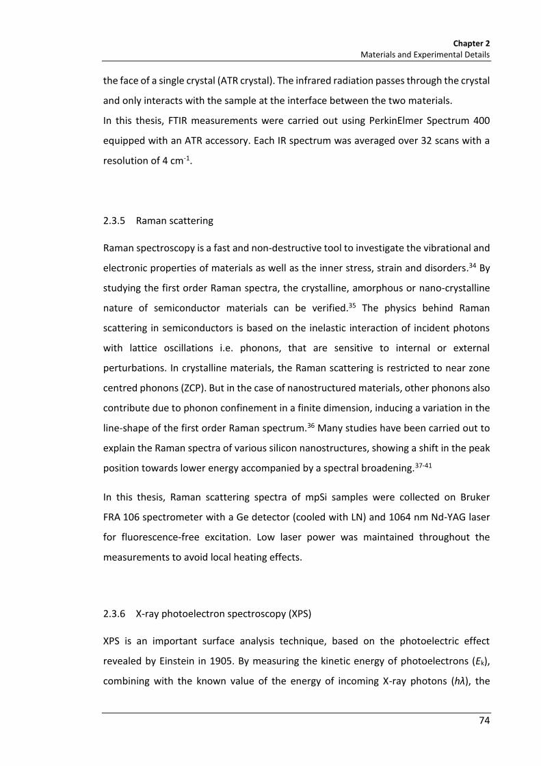
Chapter 2 Materials and Experimental Details
74
the face of a single crystal (ATR crystal). The infrared radiation passes through the crystal
and only interacts with the sample at the interface between the two materials.
In this thesis, FTIR measurements were carried out using PerkinElmer Spectrum 400
equipped with an ATR accessory. Each IR spectrum was averaged over 32 scans with a
resolution of 4 cm-1.
2.3.5 Raman scattering
Raman spectroscopy is a fast and non-destructive tool to investigate the vibrational and
electronic properties of materials as well as the inner stress, strain and disorders.34 By
studying the first order Raman spectra, the crystalline, amorphous or nano-crystalline
nature of semiconductor materials can be verified.35 The physics behind Raman
scattering in semiconductors is based on the inelastic interaction of incident photons
with lattice oscillations i.e. phonons, that are sensitive to internal or external
perturbations. In crystalline materials, the Raman scattering is restricted to near zone
centred phonons (ZCP). But in the case of nanostructured materials, other phonons also
contribute due to phonon confinement in a finite dimension, inducing a variation in the
line-shape of the first order Raman spectrum.36 Many studies have been carried out to
explain the Raman spectra of various silicon nanostructures, showing a shift in the peak
position towards lower energy accompanied by a spectral broadening.37-41
In this thesis, Raman scattering spectra of mpSi samples were collected on Bruker
FRA 106 spectrometer with a Ge detector (cooled with LN) and 1064 nm Nd-YAG laser
for fluorescence-free excitation. Low laser power was maintained throughout the
measurements to avoid local heating effects.
2.3.6 X-ray photoelectron spectroscopy (XPS)
XPS is an important surface analysis technique, based on the photoelectric effect
revealed by Einstein in 1905. By measuring the kinetic energy of photoelectrons (Ek),
combining with the known value of the energy of incoming X-ray photons (hλ), the

Chapter 2 Materials and Experimental Details
75
binding energy of each of the emitted electron (Eb) can be determined using
Equation 2.4,24 which is not only element specific but also contains chemical information.
The work function term 𝜙 is an adjustable instrumental correction factor dependent on
both the spectrometer and the material. Since the energy levels of core electrons
depend on the chemical state of the atom. Thus, XPS can not only provide the
composition of the surface region but also supply important information about the
chemical environments (i.e. binding states, oxidation states) of surface atoms (H and He
excluded).
Equation 2.4
XPS measurements were carried out on a K-Alpha XPS instrument (Thermo Scientific) at
NEXUS nanolab. Samples were drop cast onto a clean gold substrate (10 mm × 10 mm).
The film was introduced into a loadlock attached to an UHV chamber in which the typical
pressure was maintained below 5 × 10⁻⁹ mbar. All spectra were acquired at normal
emission with Al Kα radiation at 1486.6 eV and a spot size of 400 μm. A pass energy of
200 eV and step size of 0.4 eV was used for the survey spectra and a pass energy of 40 eV
and step size of 0.1 eV was used for high-resolution spectra. In all photoemission spectra,
binding energies (BEs) were referred to the Au 4f7/2 line measured on a gold foil in direct
contact with the sample, which was at 84 eV. Correction for charge shifts was done by
using the carbon contamination with a C 1s binding energy of 285.0 eV. XPS data analysis
and peak fitting was conducted using CasaXPS version 2.3.
2.3.7 Thermogravimetric analysis
Thermogravimetric analysis (TGA) is a conventional thermoanalytical method of
measuring the mass of a sample as it is submitted to a controlled temperature program
in a defined atmosphere. By simultaneously measuring the heat flow (Differential
Scanning Calorimetry) to the same sample in a single experiment, TGA-DSC curves are
produced which can be analysed to evaluate the thermal stability, to determine the
𝜙

Chapter 2 Materials and Experimental Details
76
composition, to explore the thermal behaviours such as phase transitions, desorption,
decomposition, oxidation etc. of the sample substance.42
In this thesis, the thermal properties of graphitic carbon nitride powders and nanosheets
were examined by TGA-DSC (Mettler Toledo, DSC 1). For each measurement, the sample
was heated in a 70 μL Pt crucible from 25°C to 1000°C with the heating rate as 10 °C·min-1
under a nitrogen atmosphere (20 mL·min-1).
2.3.8 Optical measurements
The optical properties of semiconductor materials are a great part of the unique set of
physical and chemical properties, and the drive of numerous studies in broad range of
fields of optoelectronics, cell imaging, sensors and solar energy conversion.
2.3.8.1 Ultraviolet-visible absorption spectroscopy (UV-Vis)
Ultraviolet-visible absorption spectroscopy (UV-Vis) monitors the absorption of photons
in ultraviolet-visible region by molecules or semiconductors as a result of electronic
transition from the ground state to an excited state. It is a heavily used tool in analytical
chemistry and shows its advantage in characterising the optical and electronic
properties of semiconductor materials. Electron-hole pairs in the crystalline matrix of
semiconductor can be separated by absorbing photons matched with its bandgap (Eg).
As a result, electrons are excited to the conduction band (CB) while the positive charged
holes remain in its lower valence band. The process is so-called photoexcitation and lays
the foundation for the capability of semiconductor in storing and converting solar
energy. As strongly affected by the quantum confinement effect induced by the very
small dimension of the crystallite size, the absorbed photon energy or wavelength can
be altered by varying the crystallite size which directly affects the size-dependent
bandgap level.43-45 In practice, this principle is often used to widen the bandgap of
narrow bandgap semiconductors e.g. Si by decreasing the nanocrystal size to enhance
the optical response across a broad range of spectrum.46-48

Chapter 2 Materials and Experimental Details
77
In this thesis, UV-Vis absorption spectra were collected on Shimadzu UV-1800
spectrometer under ambient conditions. A wavelength range of 200-800 nm was
scanned at 0.5 nm intervals. Samples were dispersed in H2O or DCM (230 nm cut-off) in
a 10 mm × 10 mm quartz cuvette. Sample spectra were obtained after subtracting the
spectrum of the solvent. Data analysis was done using UVProbe version 2.50.
2.3.8.2 Photoluminescence spectroscopy (PL)
Initiated by photoexcitation mentioned above, the absorbed photons of a particular
wavelength are rapidly re-emitted, through the radiative recombination of photoexcited
electrons on CB band (excited state) and holes on VB band (ground state). As indicated
in the Jablonski diagram shown in Figure 2.4, many electron transition processes may
occur before the emission event, such as internal conversion, vibrational relaxation, and
intersystem crossing, the latter of which results in the generation of phosphorescence
by altering the spin multiplicity (S1→T1 state). In the meantime, for crystalline
semiconducting systems, the exciton movement is also strongly influenced by extrinsic
effects, such as structural distortion, lattice disorder, and variation of the chemical
composition, acting as radiative recombination centres for the free photoinduced
charge carriers.49 Also affected by the size-dependent quantum confinement effect, PL
emission spectrum of Si is also strongly related to the nanocrystals.2, 40 Although the
origin of the photoluminescence of porous Si is still debatable, extensive research efforts
have been devoted to this topic.50-52 The general agreement is that both localized
defects at the interface and the quantum confinement of excitons account for the
light-emitting phenomenon.50

Chapter 2 Materials and Experimental Details
78
Figure 2.4 Jablonski diagram representing various electronic and molecular processes that occur
after photoexcitation.
In this thesis, PL spectra were recorded on a Perkin-Elmer LS55 spectrometer under
ambient conditions. Samples were dispersed in H2O or DCM in a 10 mm × 10 mm quartz
cuvette. The excitation wavelength was 320 nm and a 390 nm cut-off filter was applied.
For mpSi, the excitation slit width (Ex) was set to 10 nm and the emission slit width (Em)
was 15 nm. For g-C3N4, the Ex and Em values were set as 2.5 nm and 10 nm respectively.
For mpSi/ g-C3N4 composite, they were set as 10 nm and 5 nm respectively. Sample
spectra were corrected by subtracting the spectrum of the solvent. PL spectroscopic
data was processed using FL WinLab 4.00.03.
2.3.8.3 Quantum yield (QY)
As known from the discussion above, excited electrons can return to lower energy level
through different mechanisms including fluorescence. By comparing the number of
photons absorbed (UV-Vis absorbance) with the photons emitted through fluorescence
(PL emission intensity), the light emitting ability of semiconductor materials can be
assessed. The ratio is known as quantum yield (QY, 𝜙F). The most common method for
QY calculation involves the use of well-characterised standard sample with known QY
S2
S1
T1
Ene
rgy
S0
Excitation
Flu
ore
sce
nce
Phosphorescence
Internal conversion Vibrational relaxation
Intersystem crossing

Chapter 2 Materials and Experimental Details
79
value at similar excitation wavelength as the test sample which, if possible, emits in the
similar region as well. The QY value of fluorescent samples can be derived according to
the following equation.
Equation 2.5
In Equation 2.5, the subscripts ref and x denote reference sample and test sample,
respectively. Grad is the gradient from the plot of integrated fluorescence intensity
versus UV-Vis absorbance. η represents the refractive index of the solvent.
In our study, quinine sulfate in 0.1M H2SO4 was used as reference. For both the standard
sample and test sample, the plot of integrated fluorescence intensity versus absorbance
was composed of six data points from solutions of which the respective UV-Vis
absorbance was recorded as around 0, 0.02, 0.04, 0.06, 0.08 and 0.10.
Scheme 2.7 Molecular structure of quinine sulfate.
2.4 Photocatalytic study
This section includes a detailed description of the photodegradation experiment and the
engaged analysis methods in the measurements of reaction kinetics, organic carbon
content, active species and photocatalyst lifetime as discussed below.
2
2( )( )x x
F ref
ref ref
Grad
Grad
F refref ref
x x

Chapter 2 Materials and Experimental Details
80
2.4.1 Photodegradation experiment
The visible-light-active photocatalytic activities of various semiconductor materials
(mesoporous silicon, graphitic carbon nitride and their coupled composites) prepared
by above-mentioned methods were evaluated by photodegradation of organic dyes
under visible light irradiation. Among them, methyl orange (MO) was used in our
experiments as a model contaminant because of its minimized photosensitization by
visible light photons.53
A homemade photoreactor equipped with two 8 W fluorescent lamps (OSRAM) was
used throughout the analysis which also had a fan installed on top of the wood frame to
increase air circulation. The temperature variation inside the photoreactor under
fan-assisted air flow was found to be considerably smaller than the ambient
temperature during photocatalytic experiment, thus no other cooling system was
employed. Sample (m, mg) was added in a glass vial or beaker containing certain
volume (V, mL) of aqueous solution of methyl orange with initial concentration as
C0 (30-50 µmol·L-1). A magnetic bar and stirrer were used throughout the experiment to
constantly stir the solution phase. Then the vessel was positioned between the two
fluorescent lamps in the chamber at a distance of 10 cm. At certain intervals (30 min for
example), an aliquot of MO solution was taken for absorbance measurement in a UV-Vis
absorption spectrometer (Shimadzu, UV1800) under ambient conditions using the same
instrumental parameters mentioned in 2.3.8.1. For powder samples, prior to
illumination, the reaction system was sonicated for 15 min to suspend the photocatalyst
particles and the MO aliquot was also centrifuged to ensure a clear solution for UV-Vis
measurement. While for monolithic samples, since the solution was naturally free of any
solids, the centrifugation step was not necessary so the UV-Vis measurement was
directly carried out on the dye solution that had been sampled. Besides, the suspension
was also magnetically stirred for 1 hour in the dark to establish the adsorption-
desorption equilibrium with the organic substrate. For comparison, the behaviours of
our samples toward MO in the absence of external irradiation were also studied using
the same photoreactor with the lamps switched off and by following the same
experimental procedure mentioned above. Other experimental details including the

Chapter 2 Materials and Experimental Details
81
sample mass, initial dye concentration etc. will be elaborated in each experimental
section of the following chapters.
2.4.2 Kinetic analysis
In the field of heterogeneous photocatalysis, the reaction process is often interpreted
as kinetically controlled by the diffusion of initial substrate in the solution phase and
follows Langmuir-Hinshelwood type or pseudo first order reaction model of which the
mathematical expression is presented as follows.
Equation 2.6
Equation 2.7
As seen in the Equation 2.6 and Equation 2.7, k is the rate constant and can be realized
by plotting ln ([MO]t/[MO]0) vs. t to yield the gradient. According to Beer-Lambert law,
the concentration of an absorbing species is linearly proportional to the absorption
intensity recorded in the UV-Vis absorption spectrum. Therefore, by simply monitoring
the absorbance decay of MO molecules as a function of irradiation time, the first order
reaction rate (k) of MO degradation in the presence of photocatalyst can be determined.
Equation 2.8

Chapter 2 Materials and Experimental Details
82
2.4.3 Total organic carbon analysis
Total carbon analysis (TOC) is a very important chemical analytical method in detecting
contaminants in water, assessing the quality of drinking water and water for
pharmaceutical use as well. It is a sensitive and non-specific measurement of all organics
present in the sample. In photocatalysis, this technique is often used to determine the
photomineralization efficiency of organic substrates by detecting the carbon content
that remains in the photoredox system.
In this thesis, TOC was detected by using a Skalar Formacs CA16 TOC analyser. Typically,
a test sample was injected from an auto sampler into a high temperature combustion
furnace. In the reactor, at a temperature of 850°C, TOC was converted to CO2 by catalytic
oxidation of cobalt chromium and cerium oxide as catalyst to help the reaction to
completion. A flow of Zero Grade Air transported the CO2 product to a non-dispersive
infrared detector (NDIR) where the amount of CO2 was determined by IR detection at
4.2 µm.
2.4.4 Active species analysis
After band-to-band excitation, the photo-induced charge carriers are able to migrate to
the surface of semiconductor and participate in redox reactions by reacting with
O2/H2O/OH- existing in the system to generate a variety of active species, such as
superoxide radical anion (O2·-), hydroxyl radical (·OH), singlet oxygen (1O2), hydrogen
peroxide (H2O2), known as reactive oxygen species (ROSs)54 that are primarily
responsible for the photocatalytic oxidation of organic dyes in aqueous solution.55 The
behaviours of these active species are good indicators of the electronic band structure
and photocatalytic mechanism of semiconductor photocatalyst.56-59 Detection methods
include electron spin resonance (ESR) spectroscopy,60-61 chemiluminescence,62-63 mass
spectroscopy64-65 and scavengers.66-67
In this thesis, the involvement of ·O2-, ·OH, h+ in the visible light driven photodegradation
of MO were investigated by using ethanol, 2-propanol, and triethanolamine (TEOA) as
quenchers. In each experiment, 1 mmol of quencher, ethanol (58 µL), 2-propanol (76 µL),

Chapter 2 Materials and Experimental Details
83
TEOA (149 mg) was added into the photocatalytic system which was thereafter
irradiated and began the scavenging activities under visible light irradiation. The role of
dissolved oxygen in the formation of ROSs was also tested by bubbling high purity N2
through MO solution to ensure that the solution was N2 saturated and the reaction was
operated under anoxic conditions.
2.4.5 Lifetime study
As we know, the lifetime of photocatalyst is one of the most crucial factor determining
its efficiency and applicability, which is often interpreted as the ability to be
photocatalytically active in certain numbers of reaction cycles.
In this thesis, the lifetime of mesoporous silicon in MO photodegradation was assessed
during visible light irradiation. After a photocatalytic experiment, it was recovered by
immersing in 5 wt. % aqueous HF for 2 min and subsequently washed four times with
distilled water, followed by drying at 80°C for 12 h under vacuum to remove the residual
reactant prior to the next reaction cycle.
2.5 Summary
In general, inexpensive, eco-friendly and upscalable approaches were used in this
research for the synthesis and modification of semiconductor materials (silicon, carbon
nitride) that are widely recognized as low cost, metal-free and earth abundant. Given
this, electrochemical etching was employed in the preparation of mpSi with various
morphologies and properties. g-C3N4 was synthesized through one-step thermal
polycondensation of melamine followed by ultrasonication to gain exfoliated
nanosheets, which was to be composited with mpSi via simple impregnation. The
simplicity, availability and controllability of these preparation methods are highly valued
in this work as exhibited in the following chapters.

Chapter 2 Materials and Experimental Details
84
2.6 References
1. Sailor, M. J., Fundamentals of porous silicon preparation. In Porous Silicon in Practice:
Prepration, Chracterization and Applications. Wiley, 2012; pp 1-42.
2. Secret, E.; Leonard, C.; Kelly, S. J.; Uhl, A.; Cozzan, C.; Andrew, J. S., Size control of
porous silicon-based nanoparticles via pore-wall thinning. Langmuir 2016, 32 (4),
1166-1170.
3. Walcarius, A.; Etienne, M.; Bessière, J., Rate of access to the binding sites in organically
modified silicates. 1. Amorphous silica gels grafted with amine or thiol Groups.
Chem. Mater. 2002, 14 (6), 2757-2766.
4. Wang, C.; Flynn, N. T.; Langer, R., Controlled structure and properties of
thermoresponsive nanoparticle–hydrogel composites. Adv. Mater. 2004, 16 (13),
1074-1079.
5. Yang, H.; Wang, Y.; Huang, H.; Gell, L.; Lehtovaara, L.; Malola, S.; Hakkinen, H.;
Zheng, N., All-thiol-stabilized Ag44 and Au12Ag32 nanoparticles with single-crystal
structures. Nat. Commun. 2013, 4, 2422.
6. Buriak, J. M., Organometallic chemistry on silicon and germanium surfaces. Chem. Rev.
2002, 102 (5), 1271-1308.
7. Kappe, C. O., How to measure reaction temperature in microwave-heated
transformations. Chem. Soc. Rev. 2013, 42 (12), 4977-4990.
8. Obermayer, D.; Damm, M.; Kappe, C. O., Design and evaluation of improved magnetic
stir bars for single-mode microwave reactors. Org. Biomol. Chem. 2013, 11 (30),
4949-4956.
9. Obermayer, D.; Kappe, C. O., On the importance of simultaneous infrared/fiber-optic
temperature monitoring in the microwave-assisted synthesis of ionic liquids.
Org. Biomol. Chem. 2010, 8 (1), 114-121.
10. Yan, S. C.; Li, Z. S.; Zou, Z. G., Photodegradation performance of g-C3N4 fabricated by
directly heating melamine. Langmuir 2009, 25 (17), 10397-10401.

Chapter 2 Materials and Experimental Details
85
11. Mo, Z.; She, X.; Li, Y.; Liu, L.; Huang, L.; Chen, Z.; Zhang, Q.; Xu, H.; Li, H., Synthesis of
g-C3N4 at different temperatures for superior visible/UV photocatalytic performance
and photoelectrochemical sensing of MB solution. RSC Adv. 2015, 5 (123),
101552-101562.
12. Papailias, I.; Giannakopoulou, T.; Todorova, N.; Demotikali, D.; Vaimakis, T.;
Trapalis, C., Effect of processing temperature on structure and photocatalytic properties
of g-C3N4. Appl. Surf. Sci. 2015, 358, 278-286.
13. Zheng, Y.; Zhang, Z.; Li, C., A comparison of graphitic carbon nitrides synthesized
from different precursors through pyrolysis. J. Photochem. Photobiol. A 2017, 332, 32-44.
14. Coleman, J. N.; Lotya, M.; O'Neill, A.; Bergin, S. D.; King, P. J.; Khan, U.; Young, K.;
Gaucher, A.; De, S.; Smith, R. J.; Shvets, I. V.; Arora, S. K.; Stanton, G.; Kim, H. Y.; Lee, K.;
Kim, G. T.; Duesberg, G. S.; Hallam, T.; Boland, J. J.; Wang, J. J.; Donegan, J. F.;
Grunlan, J. C.; Moriarty, G.; Shmeliov, A.; Nicholls, R. J.; Perkins, J. M.; Grieveson, E. M.;
Theuwissen, K.; McComb, D. W.; Nellist, P. D.; Nicolosi, V., Two-dimensional nanosheets
produced by liquid exfoliation of layered materials. Science 2011, 331 (6017), 568-571.
15. Xu, J.; Zhang, L.; Shi, R.; Zhu, Y., Chemical exfoliation of graphitic carbon nitride for
efficient heterogeneous photocatalysis. J. Mater. Chem. A 2013, 1 (46), 14766-14772.
16. Guo, X.; Wang, Y.; Wu, F.; Ni, Y.; Kokot, S., Preparation of protonated,
two-dimensional graphitic carbon nitride nanosheets by exfoliation, and their
application as a fluorescent probe for trace analysis of copper(II). Microchimica Acta
2015, 183 (2), 773-780.
17. Chen, L.; Huang, D.; Ren, S.; Dong, T.; Chi, Y.; Chen, G., Preparation of graphite-like
carbon nitride nanoflake film with strong fluorescent and electrochemiluminescent
activity. Nanoscale 2013, 5 (1), 225-230.
18. Lin, L. S.; Cong, Z. X.; Li, J.; Ke, K. M.; Guo, S. S.; Yang, H. H.; Chen, G. N.,
Graphitic-phase C3N4 nanosheets as efficient photosensitizers and pH-responsive drug
nanocarriers for cancer imaging and therapy. J. Mate. Chem. B 2014, 2 (8), 1031-1037.
19. Ma, T. Y.; Tang, Y.; Dai, S.; Qiao, S. Z., Proton-functionalized two-dimensional
graphitic carbon nitride nanosheet: an excellent metal-/label-free biosensing platform.
Small 2014, 10 (12), 2382-2389.

Chapter 2 Materials and Experimental Details
86
20. Shi, L.; Chang, K.; Zhang, H.; Hai, X.; Yang, L.; Wang, T.; Ye, J., Drastic enhancement
of photocatalytic activities over phosphoric acid protonated porous g-C3N4 Nanosheets
under visible light. Small 2016, 12 (32), 4431-4439.
21. Zhang, X.; Xie, X.; Wang, H.; Zhang, J.; Pan, B.; Xie, Y., Enhanced photoresponsive
ultrathin graphitic-phase C3N4 nanosheets for bioimaging. J. Am. Chem. Soc. 2013,
135 (1), 18-21.
22. Zhang, J.; Chen, Y.; Wang, X., Two-dimensional covalent carbon nitride nanosheets:
synthesis, functionalization, and applications. Energy Environ. Sci. 2015, 8 (11),
3092-3108.
23. Yang, S.; Gong, Y.; Zhang, J.; Zhan, L.; Ma, L.; Fang, Z.; Vajtai, R.; Wang, X.; Ajayan, P.
M., Exfoliated graphitic carbon nitride nanosheets as efficient catalysts for hydrogen
evolution under visible light. Adv. Mater. 2013, 25 (17), 2452-2456.
24. Pavesi, L.; Turan, R., Silicon Nanocrystals: Fundamentals, Synthesis and Applications.
Wiley: 2010.
25. Bisi, O.; Ossicini, S.; Pavesi, L., Porous silicon: a quantum sponge structure for silicon
based optoelectronics. Surf. Sci. Rep. 2000, 38 (1-3), 1-126.
26. Bragg, W. H.; Bragg, W. L., The Reflection of X-rays by Crystals. Proceedings of the
Royal Society A: Mathematical, Physical and Engineering Sciences 1913, 88 (605),
428-438.
27. Patterson, A. L., The scherrer formula for X-Ray particle size determination. Phys.
Rev. 1939, 56 (10), 978-982.
28. Stokes, A. R.; Wilson, A. J. C., A method of calculating the integral breadths of
Debye-Scherrer lines: generalization to non-cubic crystals. Mathematical Proceedings of
the Cambridge Philosophical Society 1944, 40 (02), 197-198.
29. Thommes, M., Physical adsorption characterization of nanoporous materials. Chem.
Ing. Tech. 2010, 82 (7), 1059-1073.
30. Cychosz, K. A.; Guillet-Nicolas, R.; García-Martínez, J.; Thommes, M., Recent
advances in the textural characterization of hierarchically structured nanoporous
materials. Chem. Soc. Rev. 2017, 46 (2), 389-414.

Chapter 2 Materials and Experimental Details
87
31. Thommes, M.; Kaneko, K.; Neimark, A. V.; Olivier, J. P.; Rodriguez-Reinoso, F.;
Rouquerol, J.; Sing, K. S. W., Physisorption of gases, with special reference to the
evaluation of surface area and pore size distribution (IUPAC Technical Report). Pure Appl.
Chem. 2015, 87 (9-10), 1051-1069.
32. Brunauer, S.; Emmett, P. H.; Teller, E., Adsorption of gases in multimolecular layers.
J. Am. Chem. Soc. 1938, 60 (2), 309-319.
33. Groen, J. C.; Peffer, L. A. A.; Pérez-Ramırez, J., Pore size determination in modified
micro- and mesoporous materials. Pitfalls and limitations in gas adsorption data analysis.
Microporous Mesoporous Mater. 2003, 60 (1-3), 1-17.
34. Gouadec, G.; Colomban, P., Raman Spectroscopy of nanomaterials: How spectra
relate to disorder, particle size and mechanical properties. Prog. Cryst. Growth Charact.
Mater. 2007, 53 (1), 1-56.
35. Richter, H.; Wang, Z. P.; Ley, L., The one phonon Raman spectrum in microcrystalline
silicon. Solid State Commun. 1981, 39 (5), 625-629.
36. Zi, J.; Zhang, K.; Xie, X., Comparison of models for Raman spectra of Si nanocrystals.
Phys. Rev. B 1997, 55 (15), 9263-9266.
37. Yang, M.; Huang, D.; Hao, P.; Zhang, F.; Hou, X.; Wang, X., Study of the Raman peak
shift and the linewidth of light-emitting porous silicon. J. Appl. Phy. 1994, 75 (1), 651.
38. Zi, J.; Buscher, H.; Falter, C.; Ludwig, W.; Zhang, K. M.; Xie, X. D., Raman shifts in Si
nanocrystals. Appl. Phys. Lett. 1996, 69 (2), 200-202.
39. Zuk, J.; Kulik, M.; Andrews, G. T.; Kiefte, H.; Clouter, M. J.; Goulding, R.; Rich, N. H.;
NossarzewskaOrlowska, E., Characterization of porous silicon by Raman scattering and
photoluminescence. Thin Solid Films 1997, 297 (1-2), 106-109.
40. Kumar, P., Effect of silicon crystal size on photoluminescence appearance in porous
silicon. ISRN Nanotechnology 2011, 2011, 1-6.
41. Kosović, M.; Gamulin, O.; Balarin, M.; Ivanda, M.; Đerek, V.; Ristić, D.; Marciuš, M.;
Ristić, M., Phonon confinement effects in Raman spectra of porous silicon at
non-resonant excitation condition. J. Raman Spectrosc. 2014, 45 (6), 470-475.

Chapter 2 Materials and Experimental Details
88
42. Vyazovkin, S., Thermogravimetric analysis. In Characterization of Materials, 2012; pp
1-12.
43. Scholes, G. D.; Jones, M.; Kumar, S., Energetics of photoinduced electron-transfer
reactions decided by quantum confinement. J. Phys. Chem. C 2007, 111 (37),
13777-13785.
44. Canham, L. T., Silicon quantum wire array fabrication by electrochemical and
chemical dissolution of wafers. Appl. Phys. Lett. 1990, 57 (10), 1046-1048.
45. Lehmann, V.; Gosele, U., Porous silicon formation - a quantum wire effect. Appl. Phys.
Lett. 1991, 58 (8), 856-858.
46. Jana, A.; Lawrence, K. N.; Teunis, M. B.; Mandal, M.; Kumbhar, A.; Sardar, R.,
Investigating the control by quantum confinement and surface ligand coating of
photocatalytic efficiency in chalcopyrite copper indium diselenide nanocrystals. Chem.
Mater. 2016, 28 (4), 1107-1120.
47. Robel, I.; Kuno, M.; Kamat, P. V., Size-dependent electron injection from excited CdSe
quantum dots into TiO2 nanoparticles. J. Am. Chem. Soc. 2007, 129 (14), 4136-4137.
48. Kang, Z.; Tsang, C. H.; Wong, N. B.; Zhang, Z.; Lee, S. T., Silicon quantum dots: a
general photocatalyst for reduction, decomposition, and selective oxidation reactions.
J. Am. Chem. Soc. 2007, 129 (40), 12090-12091.
49. Romero, J. J.; Llansola-Portolés, M. J.; Dell’Arciprete, M. L.; Rodríguez, H. B.; Moore,
A. L.; Gonzalez, M. C., Photoluminescent 1–2 nm sized silicon nanoparticles: a surface-
dependent system. Chem. Mater. 2013, 25 (17), 3488-3498.
50. Sailor, M. J.; Wu, E. C., Photoluminescence-based sensing with porous silicon films,
microparticles, and nanoparticles. Adv. Funct. Mater. 2009, 19 (20), 3195-3208.
51. Kotkovskiy, G. E.; Kuzishchin, Y. A.; Martynov, I. L.; Chistyakov, A. A.; Nabiev, I., The
photophysics of porous silicon: technological and biomedical implications. Phys. Chem.
Chem. Phys. 2012, 14 (40), 13890-13902.
52. Mughal, A.; El Demellawi, J. K.; Chaieb, S., Band-gap engineering by molecular
mechanical strain-induced giant tuning of the luminescence in colloidal amorphous
porous silicon nanostructures. Phys. Chem. Chem. Phys. 2014, 16 (46), 25273-25279.

Chapter 2 Materials and Experimental Details
89
53. Rochkind, M.; Pasternak, S.; Paz, Y., Using dyes for evaluating photocatalytic
properties: a critical review. Molecules 2014, 20 (1), 88-110.
54. Krumova, K.; Cosa, G., Chapter 1. Overview of Reactive Oxygen Species. In Singlet
Oxygen: Applications in Biosciences and Nanosciences, 2016; Vol. 1, pp 1-21.
55. Chen, C.; Ma, W.; Zhao, J., Semiconductor-mediated photodegradation of pollutants
under visible-light irradiation. Chem. Soc. Rev. 2010, 39 (11), 4206-4219.
56. Prihod'ko, R. V.; Soboleva, N. M., Photocatalysis: oxidative processes in water
treatment. J. Chem. 2013, 2013, 1-8.
57. Spasiano, D.; Marotta, R.; Malato, S.; Fernandez-Ibanez, P.; Di Somma, I., Solar
photocatalysis: Materials, reactors, some commercial, and pre-industrialized
applications. A comprehensive approach. Appl. Catal. B 2015, 170, 90-123.
58. Dong, S.; Feng, J.; Fan, M.; Pi, Y.; Hu, L.; Han, X.; Liu, M.; Sun, J.; Sun, J., Recent
developments in heterogeneous photocatalytic water treatment using visible
light-responsive photocatalysts: a review. RSC Adv. 2015, 5 (19), 14610-14630.
59. Hoffmann, M. R.; Martin, S. T.; Choi, W. Y.; Bahnemann, D. W., Environmental
applications of semiconductor photocatalysis. Chem. Rev. 1995, 95 (1), 69-96.
60. Hirakawa, T.; Kominami, H.; Ohtani, B.; Nosaka, Y., Mechanism of photocatalytic
production of active oxygens on highly crystalline TiO2 particles by means of
chemiluminescent probing and ESR spectroscopy. J. Phys. Chem. B 2001, 105 (29),
6993-6999.
61. Nosaka, Y.; Kishimoto, M.; Nishino, J., Factors governing the initial process of TiO2
photocatalysis studied by means of in-situ Electron Spin Resonance measurements.
J. Phys. Chem. B 1998, 102 (50), 10279-10283.
62. Ishibashi, K.-i.; Fujishima, A.; Watanabe, T.; Hashimoto, K., Generation and
deactivation processes of superoxide formed on TiO2 film illuminated by very weak UV
light in air or water. J. Phys. Chem. B 2000, 104 (20), 4934-4938.
63. Nosaka, Y.; Yamashita, Y.; Fukuyama, H., Application of chemiluminescent probe to
monitoring superoxide radicals and hydrogen peroxide in TiO2 photocatalysis. J. Phys.
Chem. B 1997, 101 (30), 5822-5827.

Chapter 2 Materials and Experimental Details
90
64. Li, W.; Li, D.; Lin, Y.; Wang, P.; Chen, W.; Fu, X.; Shao, Y., Evidence for the active
species involved in the photodegradation process of methyl orange on TiO2. J. Phys.
Chem. C 2012, 116 (5), 3552-3560.
65. Baiocchi, C.; Brussino, M. C.; Pramauro, E.; Prevot, A. B.; Palmisano, L.; Marcı, G.,
Characterization of methyl orange and its photocatalytic degradation products by
HPLC/UV–VIS diode array and atmospheric pressure ionization quadrupole ion trap
mass spectrometry. Int. J. Mass Spectrom. 2002, 214 (2), 247-256.
66. Xu, Y.; Jing, L.; Chen, X.; Ji, H.; Xu, H.; Li, H.; Li, H.; Zhang, Q., Novel visible-light-driven
Fe2O3/Ag3VO4 composite with enhanced photocatalytic activity toward organic
pollutants degradation. RSC Adv. 2016, 6 (5), 3600-3607.
67. Jiang, Z.; Zhu, C.; Wan, W.; Qian, K.; Xie, J., Constructing graphite-like carbon nitride
modified hierarchical yolk–shell TiO2 spheres for water pollution treatment and
hydrogen production. J. Mater. Chem. A 2016, 4 (5), 1806-1818.

Chapter 3
Chapter 3
Controllable Generation of Mesoporous Silicon with Large
Surface Area by Electrochemical Etching
Abstract
As earth-abundant and low cost, elemental silicon has attracted numerous research
efforts in developing novel devices for various uses. Among different Si nanostructures,
nanoporous silicon has been extensively studied for its vast potential over a broad
spectrum of applications. In this study, mesoporous silicon with diverse surface and
pore properties have been fabricated via electrochemical etching. The hydrogen
termination, huge surface area and open mesoporous structure hold much promise for
a superior performance anticipated in a variety of areas.

Chapter 3 Controllable Generation of Mesoporous Sil icon
92
3.1 Overview
Owing to its semiconductor nature and outstanding structural characteristics,
nanoporous silicon (pSi) has been extensively investigated in applications ranging from
optoelectronics to various emerging fields. Due to the high theoretical capacity and
anti-pulverization ability, pSi is a promising candidate as anode materials for high
performance Li-ion rechargeable batteries.1-5 The biocompatibility, biodegradability
and light-emitting ability of pSi have also inspired growing interest in biomedical
research, as a novel bio-imaging agent,6-8 a drug delivery vector,9-11 etc. Recent
decades have also witnessed tremendous efforts in developing pSi-based sensors for
detection of toxic gases, heavy metal ions, bio-active molecules.12-14 Its unique optical
and electrical properties further led to a wider field of applications in heterogeneous
catalysis ranging from energy conversion to environmental remediation.15-18
At the heart of these applications, the morphological characteristics of pSi are of
utmost importance, determining the overall performance in various research fields.
The distribution of pore size is particularly crucial in the application of pSi as it strongly
influences the diffusion kinetics of substrate molecules especially in liquid phase and
thereby regulates the access to the internal surface.19-20 In previous studies of porous
solids, a meso-scale pore dimension is proved efficient in accommodating guest
species while also maintaining a relatively high surface-to-volume ratio. The surface
area, especially internal surface area of porous materials is also a significantly
important structural factor and a larger value could contribute dramatically to the
performance of the material with a greater loading capacity, a better sensibility and a
longer working lifetime.15, 21-22
In this chapter, we aim to fabricate mesoporous silicon (mpSi) with high surface area
and a tuneable porous system via an electrochemical etching method. As will be
demonstrated, the highest value of specific surface area reached up to 994.4 m2·g-1
with the pore size distributed primarily between 3-4 nm. Mesoporous silicon with
larger mesopores in the range of 7-10 nm were also generated in our study although
the surface area was accordingly reduced, but still up to 467 m2·g-1.

Chapter 3 Controllable Generation of Mesoporous Sil icon
93
By means of FE-SEM, HRTEM, XRD, ATR-IR, Raman and nitrogen adsorption analysis,
the morphological and physiochemical properties of mesoporous silicon materials
were thoroughly examined. The varied effects of etching conditions (etching current
density, etching time) and dopant concentration on crystallinity, surface and pore
features, as well as microscopic morphological figures of the resulting porous Si matrix
were investigated.
Furthermore, several post-treatments were explored to modify the shape and surface
environment of mpSi. Highly porous free-standing disks/microflakes were successfully
gained via pulse etching and sonication. The surface chemistry of mesoporous silicon
was altered by microwave-assisted thermal hydrosilylation, which yielded thiol-capped
mpSi for the first time using allyl mercaptan as precursor under microwave
electromagnetic field.
3.2 Experimental section
3.2.1 Mesoporous silicon preparation (mpSi)
Mesoporous silicon samples (PS/HPS-J-t) were fabricated by galvanostatic anodization
of silicon wafers in ethanoic HF acid under ambient conditions. Moderately doped and
heavily doped Si wafers (PS and HPS) were applied in the preparation of PS-J-t and
HPS-J-t samples, respectively, following a similar anodic etching process as described in
Chapter 2.

Chapter 3 Controllable Generation of Mesoporous Sil icon
94
Table 3.1 Etching parameters for producing mesoporous silicon materials involved in Chapter 3.
Mesoporous
silicon
Etching current density (J)
/ mA·cm-2
Etching time (t)
/ min
PS-10-15 10 15
PS-30-15 30 15
PS-60-05 60 05
PS-60-15 60 15
HPS-60-15 60 15
HPS-150-05 150 05
HPS-150-10 150 10
HPS-150-15 150 15
3.2.2 Free-standing mpSi preparation
HPS-150-10 and PS-60-15 were employed in the “lift-off” experiment and treated with
sonication to prepare free-standing mpSi disks (PS/HPS-J-t-D) and microflakes
(PS/HPS-J-t-F).
Table 3.2 Preparation conditions for free standing mesoporous silicon materials investigated in
Chapter 3.
HPS-150-10-D HPS-150-10-F PS-60-15-F
Disk sample
Current density / mA·cm-2
4 4 4
Etching time / s 125 125 125
Microflake sample
Output level* / 4 4
Sonication mode / Constant Constant
Sonication time / min / 30 30
* Microtip sonicator, purchased from Apollo Electronics, output level 1-10.

Chapter 3 Controllable Generation of Mesoporous Sil icon
95
3.2.3 Thiol-capped mpSi preparation
PS-60-05 was used in the capping experiments with allyl mercaptan (CH2=CHCH2SH) to
synthesize thiol-capped mpSi materials. Three different heating methods were
employed as mentioned below. Detailed descriptions of each experimental procedure
can be found in Chapter 2.
Table 3.3 Experimental details of thiol-capping experiments of PS-60-05.
PS-60-05-RF PS-60-05-AC PS-60-05-MW
Heating approach Oil bath Conventional
Oven
Microwave
oven
Allyl mercaptan / mL 2 2 2
Dry toluene / mL 10 10 5
Reaction temperature / °C ca. 110 200 N.A.
Reaction time 12 h-48 h 24 h 6 min
Atmosphere N2 Air N2
3.2.4 Material characterisation
The surface morphology, internal structure and layer thickness of mpSi were
determined by various imaging techniques (SEM, FE-SEM and HRTEM). XRD patterns
were recorded to reflect the crystalline nature of porous framework. The chemical
composition of as-etched mpSi and modified mpSi samples was distinguished by
ATR-IR, Raman and XPS spectroscopy. A quantitative evaluation of the surface and
pore features (SBET, Vpore and dpore) was performed on various mpSi samples using
low-temperature nitrogen sorption isotherms at 77 K. All measurement parameters
were the same as outlined in Chapter 2 unless otherwise stated.
Chapter 3 Controllable Generation of Mesoporous Sil icon
96
3.3 Results and discussion
3.3.1 Microscopic morphology of PS-mpSi
Electron microscopic images of as-etched moderately doped mpSi were first presented
in this section to show the main structural characteristics possessed by the highly
porous Si samples prepared via electrochemical etching, taking PS-60-15 as an example.
3.3.1.1 FE-SEM images of PS-mpSi
Figure 3.1 Top view FE-SEM image of PS-60-15.
The top surface of PS-60-15 was first examined by means of FE-SEM. As shown in
Figure 3.1, numerous nanoholes with varied sizes, mostly less than 10 nm, were
visualized with a homogeneous spatial distribution and very narrow interpore
distances. These nanopores were formed as neighbouring silicon atoms were rapidly
dissolved into soluble substances in HF solution under the external voltage bias during
electrochemical etching. Some large holes and cracks were also observed on the
surface that many factors could contribute to, such as unevenly distributed etching
200 nm

Chapter 3 Controllable Generation of Mesoporous Sil icon
97
current, surface tensions and unavoidable mechanical force during handling etc. On
the other hand, these features were more normally seen in PS-60-15 compared to
other PS samples etched under different conditions, which indicated a poorer
mechanical stability of PS-60-15 resulting from its highly porous structure.
Figure 3.2 Cross section SEM (A) and FE-SEM (B and C) images of PS-60-15.
Figure 3.2 demonstrates the cross section morphology of PS-60-15. A layer of porous
silicon was formed above the un-etched Si wafer, with two straight boundary lines

Chapter 3 Controllable Generation of Mesoporous Sil icon
98
lying between mpSi/Si and mpSi/outer environment. The thickness of the layer was
consistent and the value was estimated as 23.66 ± 0.20 μm. The internal structure was
further revealed in Figure 3.2C, showing abundant nanosized Si filaments and
particulates embedded on the internal structure, implying the very large surface area
possessed by PS-60-15. According to quantum confinement theory, these ultra-small Si
structural figures are known to have huge impact on the optical properties of pSi.23-27
3.3.1.2 HRTEM images of PS-mpSi
As displayed in Figure 3.3, a highly porous network with a matrix of isolated silicon
nanocrystallites was characterised in PS-60-15. Consequently, only amorphous rings
were detected in the SAED pattern (Figure 3.3D). Lattice fringes of silicon
nanocrystallites in irregular sizes and shapes were also discovered at various
framework locations as pointed out in Figure 3.3E and F. The sizes of the Si
nanocrystallites embedded on the internal surface were mostly less than 5 nm,
indicating the significance of quantum confinement effects on the electronic
properties.28

Chapter 3 Controllable Generation of Mesoporous Sil icon
99
Figure 3.3 HRTEM images (A, B, C, E, and F) and SAED pattern (D) of PS-60-15. Arrows in E and
F represent the lattice fringes of Si nanocrystallites in the framework.
200 nm 10 nm
5 nm
5 nm5 nm
A
C D
B
E F

Chapter 3 Controllable Generation of Mesoporous Sil icon
100
3.3.2 Structural effects of etching current density
To examine the effects of etching current density, in addition to PS-60-15, PS-10-15
and PS-30-15 were also prepared under current densities of 10 mA·cm-2 and
30 mA·cm-2, respectively. The etching time was constant at 15 min. As seen in
Figure 3.4, PS-10-15 appeared to have a golden brown colour while PS-30-15 became
more reddish and it was further darkened for PS-60-15. This is likely due to the varied
refractive index of porous Si in relation to the porosity and layer thickness.
Figure 3.4 Photographs of PS-10-15, PS-30-15 and PS-60-15.

Chapter 3 Controllable Generation of Mesoporous Sil icon
101
As shown in Figure 3.5, the mpSi layer became thicker with the increasing etching
current density, 5.8 μm for PS-10-15, 20.7 μm for PS-30-15 and 23.7 μm for PS-60-15.
The etching rate was accelerated under higher etching current density.
Figure 3.5 Cross sectional SEM images of PS-10-15 (A), PS-30-15 (B) and PS-60-15 (C).
3.3.2.1 XRD patterns of PS-mpSi
As shown in Figure 3.6, the main feature observed in the XRD patterns of PS-10-15,
PS-30-15 and PS-60-15 was a broad diffraction peak centred at 69.1˚, which is
attributable to the (400) crystal plane of silicon.29 This result is consistent with the
crystal orientation of the moderately doped silicon wafer used for mpSi preparation via
electrochemical etching (Figure 3.7). However, the (400) peak intensity of mpSi
samples was significantly weakened suggesting reduced crystallinity after
electrochemical etching. Various extents of (400) peak broadening were also identified,
corresponding to the physical dimension of Si nanocrystals constituting the framework.
By applying Scherrer’s Equation,30 it was determined to be 11.22 nm, 7.08 nm and
5.48 nm for PS-10-15, PS-30-15 and PS-60-15 respectively. Thus, as etching current

Chapter 3 Controllable Generation of Mesoporous Sil icon
102
density increases, the size of Si nanocrystals reduces, which could lead to a higher
surface area and enlarged bandgap of mpSi, and eventually affect the behaviour and
activity of mpSi. According to the prevalent pore-forming mechanisms, these Si
nanocrystallites are shaped by the occurrence of three processes during
electrochemical etching, i.e. electrochemical etching itself, chemical dissolution and
QCE.25, 31
Figure 3.6 XRD patterns of PS-10-15 (a), PS-30-15 (b) and PS-60-15 (c).
Figure 3.7 XRD pattern of a moderately doped p-type silicon wafer (diffraction signals
maximized at 61.7˚ and 65.9˚ are the Si (400) diffraction contributed by the residual Cu Kα and
Ni Kα).
30 40 50 60 70 80
Inte
ns
ity
/ C
PS
2 / degree
(a)
(b)
(c)
(400)
30 40 50 60 70 80
Inte
nsit
y /
CP
S
2 / degree
Si (400)

Chapter 3 Controllable Generation of Mesoporous Sil icon
103
3.3.2.2 Raman scattering of PS-mpSi
Figure 3.8 shows the Raman scattering spectra of mpSi materials. Each mpSi sample
shows an optical phonon band in the 450-600 cm-1 range. In the spectrum of PS-10-15,
the band (a) was symmetrically distributed at 519 cm-1 with a Lorentzian lineshape,
which slightly redshifted to lower energy side compared to a well-defined Si crystal
(521 cm-1) due to phonon confinement. And it further redshifted to 513 cm-1 and
became asymmetrically broadened as etching current density was increased, as shown
in the spectra of PS-30-15 (b) and PS-60-15 (c), which can be explained by the
existence of smaller Si nanocrystallites contained in their porous structures, in
agreement with the previous XRD results.
Figure 3.8 Raman spectra of PS-10-15 (a), PS-30-15 (b) and PS-60-15 (c); laser wavelength
1064 nm, laser power 30 mW.
3.3.2.3 ATR-IR spectra of PS-mpSi
Figure 3.9 presents the ATR-IR spectra of PS-10-15 (a), PS-30-15 (b) and PS-60-15 (c),
consisting of six characteristic Si-H peaks in each spectrum. The absorptions at
664 cm-1 and 910 cm-1 originate from Si-H wagging and scissoring modes. The IR signals
at 2087 cm-1, 2110 cm-1, and 2139 cm-1 were the stretching modes of SiH, SiH2 and SiH3,
460 480 500 520 540 560 580 600
In
ten
sit
y /
Arb
Raman shift / cm-1
(a)
(b)
(c)

Chapter 3 Controllable Generation of Mesoporous Sil icon
104
respectively.32 As implied, freshly prepared mpSi surface was successfully passivated
by chemically bound hydrogen atoms as a result of electrochemical etching. As etching
current density increased, the absorption intensity of SiHx signals at 2087, 2110, and
2139 cm-1 also increased, signifying an enhanced hydrogen coverage on the surface.
Notably, neither Si-O stretching peak in the range of 1000-1200 cm-1 nor any signals
around 2260 cm-1 from SiOySiHx (x + y = 4, x = 1, 2, 3) complexes were detected,
indicating the surface of mpSi was free of identifiable oxide phases.
Figure 3.9 ATR-IR spectra of freshly made PS-10-15 (a), PS-30-15 (b) and PS-60-15 (c).
To verify the reproducibility of the electrochemical etching method, the IR spectra of
two PS-30-15 samples were compared. For each sample, IR spectra were taken at
three spots (S1, S2 and S3) on the surface as displayed in Figure 3.10. Although it has
been documented that FTIR of porous silicon often vary in certain respects, even after
being made under identical conditions,26 in our experiments, each corresponding IR
peak in the IR spectra of PS-30-15a and PS-30-15b was located at similar position
regardless of the sites the IR signals were collected from. Although the peak intensity
was slightly different because of the variation in the force used for pressing sample
material against ATR crystal in an effort to ensure the best signal-to-noise ratio of the
spectra.
2500 2000 1500 1000 500
Tra
ns
mit
tan
ce
/ a
.u.
Wavenumber / cm-1
2200 2100 2000
Tra
ns
mit
tan
ce
/ a
.u.
Wavenumber / cm-1
(a)
(b)
(c)
(a)
(b)
(c)

Chapter 3 Controllable Generation of Mesoporous Sil icon
105
Figure 3.10 ATR-IR spectra collected at three different surface sites (S1, S2 and S3) of two
PS-30-15 samples (A and B) prepared under identical conditions by electrochemical etching.
Figure 3.11 Normalized IR absorption intensity of silicon tri-hydrides at 2140 cm-1, di-hydrides
at 2110 cm-1 and mono-hydride at 2088 cm-1 derived from the IR spectra of PS-30-15 in
Figure 3.10.
Figure 3.11 demonstrates the ratio of tri- (SiH3) at 2140 cm-1, bi- (SiH2) at 2110 cm-1 to
mono- (SiH) hydride at 2088 cm-1 derived from Figure 3.10, which is known to be
indicative of the roughness/shape of Si nanocrystallites contained in porous silicon
structures. As seen, the ratios were consistent among them, representing the high
level of reproducibility of electrochemical etching method.
3000 2500 2000 1500 1000 500
100
200
300
400
PS-30-15b-S1
PS-30-15b-S2
PS-30-15b-S3
Tra
ns
mit
tan
ce
/ a
.u.
Wavenumber / cm-1
3000 2500 2000 1500 1000 500
100
200
300
400
PS-30-15a-S1
PS-30-15a-S2
PS-30-15a-S3
Tra
ns
mit
tan
ce
/ a
.u.
Wavenumber / cm-1
A B
0
1
2
3
IR a
bso
rpti
on
SiH3
SiH2
SiH
A1 A2 A3 B1 B2 B3

Chapter 3 Controllable Generation of Mesoporous Sil icon
106
3.3.2.4 Nitrogen sorption analysis of PS-mpSi
The surface and pore properties of mpSi materials were further characterised by
means of low-temperature gas adsorption. Nitrogen sorption isotherms of PS-10-15,
PS-30-15 and PS-60-15 were presented respectively in Figure 3.12, Figure 3.13 and
Figure 3.14. According to IUPAC classification,33 a Type IV(a) isotherm was identified
with the capillary condensation step occurring at relative pressure P/P0 ~ 0.4, which is
typical for mesoporous materials.
Figure 3.12 Nitrogen sorption isotherms of PS-10-15.
Figure 3.13 Nitrogen sorption isotherms of PS-30-15.
0.0 0.2 0.4 0.6 0.8 1.0
0
200
400
600
800
Adsorption
Desorption
Ab
so
rbed
Vo
lum
e a
t S
TP
/ cm
3g
-1
Relative Pressure, P/P0 P/P0
0.0 0.2 0.4 0.6 0.8 1.0
0
200
400
600
800
Adsorption
Desorption
Ab
so
rbed
Vo
lum
e a
t S
TP
/ cm
3g
-1
Relative Pressure, P/P0 P/P0

Chapter 3 Controllable Generation of Mesoporous Sil icon
107
Figure 3.14 Nitrogen sorption isotherms of PS-60-15.
Table 3.4 Textural properties of moderately doped mesoporous silicon derived from nitrogen
sorption isotherms.
Samples SBET / m2·g-1
Vmeso / cm3·g-1
dpore
/ nm
PS-10-15 887.1 1.09 3.07
PS-30-15 907.0 1.04 3.43
PS-60-15 994.4 1.36 3.82
PS-60-05 819.2 1.08 3.84
Ball milled Si powder 14.67 0.03 7.80
Commercial silica powder 658.0 0.78 4.94
SBA-15 848.4 1.07 7.81
As shown in Table 3.4, as etching current density increased, the specific surface area,
pore volume and average pore size also increased representing an increasing porosity
of the resulting Si structure. All PS samples showed an exceptionally high specific
surface area. Especially for PS-60-15, it reached up to 994.4 m2·g-1, which is only
second to the highest reported value of porous silicon to date (1125 m2·g-1).34 For
comparison, crystalline silicon powders were also prepared by ball milling Si chips,
0.0 0.2 0.4 0.6 0.8 1.0
0
200
400
600
800
Adsorption
Desorption
Ab
so
rbed
Vo
lum
e a
t S
TP
/ cm
3g
-1
Relative Pressure, P/P0 P/P0

Chapter 3 Controllable Generation of Mesoporous Sil icon
108
which is widely used to achieve size reduction and surface area expansion of Si
materials. As shown in Figure 3.15, after ball milling, Si microparticles in a broad size
distribution were produced and its specific surface area measure by N2 adsorption was
merely 14.67 m2·g-1. Amorphous silica powder and order mesoporous silica e.g. SBA-15
are greatly valued for their abundant surface area. According to Figure 3.16, the
specific surface area of amorphous silica and SBA-15 was determined as 658.0 m2·g-1
and 848.4 m2·g-1 respectively which are lower than mesoporous silicon.
Figure 3.15 SEM image (A) and nitrogen sorption isotherms (B) of Si powders obtained by high
energy ball mill.
Figure 3.16 Nitrogen sorption isotherms of amorphous silica commercially purchased (A) and
ordered mesoporous silica SBA-15 (B).
A
0.0 0.2 0.4 0.6 0.8 1.0
0
10
20
30
40
50 Adsorption
Desorption
Ab
so
rbed
Vo
lum
e a
t S
TP
/ cm
3g
-1
Relative Pressure, P/P0
B
P/P0
0.0 0.2 0.4 0.6 0.8 1.0
0
100
200
300
400
500
600
700
800
Adsorption
Desorption
Ab
so
rbed
Vo
lum
e a
t S
TP
/ cm
3g
-1
Relative Pressure, P/P0
0.0 0.2 0.4 0.6 0.8 1.0
0
200
400
600
800
1000
1200
Adsorption
Desorption
Ab
so
rbed
Vo
lum
e a
t S
TP
/ cm
3g
-1
Relative Pressure, P/P0
A B
P/P0 P/P0

Chapter 3 Controllable Generation of Mesoporous Sil icon
109
Apart from surface area, pore size distribution is also an important factor to be
considered in the application of porous materials. As exhibited in Table 3.4, the
diameter of mesopores increased from 3.07 to 3.82 nm by increasing the etching
current density from 10 to 60 mA·cm-2. Due to the limitation of BJH analysis method,
the pore size distribution curve was measured above 3 nm as displayed in Figure 3.17.
As etching current density increased, the curve became gradually broader and also
exhibited a small portion of larger mesopores around 7-10 nm for PS-10-15 and
PS-30-15 samples.
Figure 3.17 Pore size distribution curves of PS-10-15 (a), PS-30-15 (b) and PS-60-15 (c) acquired
by BJH approach using adsorption branch.
3.3.3 Structural effects of etching time
As another important factor, etching time also has direct impact on the formation of
mesoporous silicon as discussed below.
3.3.3.1 Layer thickness of PS-mpSi
Figure 3.18 summarizes the cross sectional SEM images of various PS samples
fabricated under different etching time (A: PS-10-02, B: PS-10-05, C: PS-10-15, D:
PS-10-25, E: PS-10-30, F: PS-10-35, G: PS-10-40; H: PS-60-05, I: PS-60-10). The layer
3 6 9 12 15 18
c
b
dV
(d)
/ cm
3n
m-1
g-1
d / nm
a

Chapter 3 Controllable Generation of Mesoporous Sil icon
110
thickness was then plotted as a function of the etching duration as shown in
Figure 3.19. An etching time-dependent increase in the layer thickness was observed
as anodic etching process prolonged under constant 10 mA·cm-2 or 60 mA·cm-2. The
non-linearity is likely due to the depletion of HF electrolyte which affected the etch
rate during electrochemical etching.
Figure 3.18 Cross sectional SEM micrographs of PS samples (A) PS-10-02, (B)PS-10-05, (C)
PS-10-15, (D) PS-10-25, (E) PS-10-30, (F) PS-10-35, (G) PS-10-40, (H) PS-60-05, (I) PS-60-10,
respectively.

Chapter 3 Controllable Generation of Mesoporous Sil icon
111
Figure 3.19 Plots of layer thickness against etching time for mesoporous silicon prepared under
10 mA·cm-2 (square) or 60 mA·cm-2 (circle).
3.3.3.2 Surface and pore properties of PS-mpSi
Figure 3.20 Nitrogen sorption isotherms (A) of PS-60-05 and pore size distribution curves (B) of
PS-60-05 (a) and PS-60-15 (b).
To further reveal the effects of etching time, PS-60-05 was introduced into this study
and its structure was characterised by nitrogen adsorption and XRD as demonstrated
in Figure 3.20 and Figure 3.21. Type-IV curves with H2 hysteresis loop was featured in
the nitrogen sorption isotherms of PS-60-05 with the capillary condensation occurring
at relative pressure P/P0 ~ 0.4. According to Table 3.4, its SBET and Vmeso were derived
0 5 10 15 20 25 30 35 40 45
0
5
10
15
20
25
30
Po
rou
s S
i la
yer
thic
kn
ess /
m
Anodization time / min
10mAcm-2
60mAcm-2
0.0 0.2 0.4 0.6 0.8 1.0
0
200
400
600
800
Adsorption
Desorption
Ab
so
rbed
Vo
lum
e a
t S
TP
/ cm
3g
-1
Relative Pressure, P/P0
3 4 5 6 7 8 910 20 30 40 50
dV
(d)
/ c
m3g
-1n
m-1
Pore diameter / nm
A Ba
b
P/P0
dV
(d)

Chapter 3 Controllable Generation of Mesoporous Sil icon
112
as 819.2 m2·g-1 and 1.08 cm3·g-1. Compared to PS-60-15, it is clear to see that under
constant etching current density (60 mA·cm-2), longer etching time leads to larger
surface area and pore volume of the final mpSi structure. While the effect of etching
duration on the average pore dimension is very limited. As indicated in Figure 3.20B,
the PSZ curves of PS-60-05 and PS-60-15 were maximized at similar position, 3.84 nm
for PS-60-05, 3.82 nm for PS-60-15.
3.3.3.3 Crystallite size of PS-mpSi
Figure 3.21 XRD patterns of PS-60-05 (a) and PS-60-15 (b)
As stated previously, the average size of Si nanocrystals can be measured based on
Scherrer’s Equation and it was 6.57 nm and 5.48 nm for PS-60-05 and PS-60-15,
according to their XRD data above (Figure 3.21). As electrochemical etching extended,
the size of the Si nanocrystallites was reduced although the pore dimension was
unchanged, which confirms the influence of etching time on the microstructural
characteristics of the resulting mpSi. This result also explains the larger specific surface
area possessed by PS-60-15 as revealed above due to the smaller Si nanocrystallites
created on the pore walls than PS-60-05.
50 60 70 80
Inte
ns
ity
/ C
PS
2 / degree
a
b

Chapter 3 Controllable Generation of Mesoporous Sil icon
113
To understand the effects of etching time, the PS-60-05 sample can be considered in
the following discussion as an early stage of the formation process of PS-60-15 during
electrochemical etching. As known, after 60 mA·cm-2 was applied, mesopores were
gradually formed in the crystalline Si chip in the vertical direction along the [100]
direction. As it progressed, the produced porous structure of Si was also immersed in
the electrolyte solution and subject to the chemical corrosion of HF etchant during
electrochemical process, causing the dissolution of Si mass on the pore walls which led
to a gradual decrease of the size of the nanocrystallites embedded on the surface as
revealed in the XRD results above. By affecting the immersion time of mpSi in the
etchant solution, etching time is therefore able to modify the surface area, pore
volume while the pore size of the porous system is mainly determined by the etching
current applied in the electrochemical preparation of mpSi.
3.3.4 Characterisation results of HPS-mpSi
All the mpSi samples studied above were derived from moderately boron-doped
p-type silicon wafer (PS in Table 2.1) of which the intrinsic resistivity is 1-10 Ω·cm. In
this section, heavily boron-doped p-type silicon wafer (HPS in Table 2.1) with lower
resistivity as 0.001-0.01 Ω·cm was employed in the preparation of mpSi materials with
unique morphological characteristics as revealed below.
3.3.4.1 FE-SEM images of HPS-mpSi
Figure 3.22 exhibits the FE-SEM images of HPS-150-10 sample. As observed in the
plane view mode (A and B), numerous nanopores were formed and distributed
uniformly on the surface with thicker pore walls and larger pore openings compared to
the moderately doped mpSi samples as mentioned above. The average diameter of the
pores was measured as 12.4 nm based on the FE-SEM micrographs. The cross sectional
FE-SEM images (C and D) clearly recorded the remarkable straightness of the pore
arrays as they were shown to be orderly aligned along Si (100) plane and isolated by

Chapter 3 Controllable Generation of Mesoporous Sil icon
114
thin walls of crystalline Si. The undulate surface feature due to numerous open pores
was observable in the AFM image of HPS-150-10 while the surface of PS-60-15
appeared to be very smooth due to the very small pore openings as discovered
previously.
Figure 3.22 FE-SEM images of HPS-150-10 (plane view: A, B and cross sectional: C, D); AFM
images of the top surface of PS-60-15 (E) and HPS-150-10 (F), respectively.
300 nm
4 μm
A
C D
500 nm
1 μm
B
500 nm
F
500 nm
E

Chapter 3 Controllable Generation of Mesoporous Sil icon
115
3.3.4.2 Raman scattering of HPS-mpSi
Raman scattering spectrum of HPS-150-10 was presented in Figure 3.23. A symmetric
peak was centred at 519 cm-1 which was close to 521 cm-1 of well-defined Si crystal,
indicating the framework crystallinity of HPS-150-10 was preserved considerably well
after electrochemical etching in contrast to PS-60-15 studied in the earlier discussion.
The laser power was reduced to 10 mW to minimize lattice expansion and spectral
redshift caused by laser-induced heat generated on the crystalline framework.35
Figure 3.23 Raman spectrum of HPS-150-10.
3.3.4.3 ATR-IR spectrum of HPS-mpSi
The IR spectrum of HPS-150-10 presented in Figure 3.24 was similarly composed by six
of the main characteristic bands as featured in the IR spectra of PS samples which were
respectively maximized at 624, 663, 909, 2087, 2107, 2138 cm-1 from Si-Si and various
vibration modes of Si-H. Detailed explanation of their origins can be referred to the
discussion above of the PS samples.
460 480 500 520 540 560 580 600
Inte
ns
ity
/ A
rb
Raman shift / cm-1

Chapter 3 Controllable Generation of Mesoporous Sil icon
116
Figure 3.24 ATR-IR spectrum of HPS-150-10.
3.3.4.4 Nitrogen sorption analysis of HPS-mpSi
Figure 3.25 Nitrogen sorption isotherms of HPS-150-05 (A), HPS-150-10 (B), HPS-150-15 (C) and
HPS-60-15 (D).
2500 2000 1500 1000 500
Tra
ns
mit
tan
ce
/ a
.u.
Wavenumber / cm-1
624
663
909
20872107
2138
0.0 0.2 0.4 0.6 0.8 1.0
0
200
400
600
800
1000
1200
Adsorption
Desorption
Ab
so
rbed
Vo
lum
e a
t S
TP
/ cm
3g
-1
Relative Pressure, P/P0
0.0 0.2 0.4 0.6 0.8 1.0
0
200
400
600
800
1000
1200
Absorption
Desorption
Ab
so
rbed
Vo
lum
e a
t S
TP
/ cm
3g
-1
Relative Pressure, P/P0
0.0 0.2 0.4 0.6 0.8 1.0
0
200
400
600
800
1000
1200
Adsorption
Desorption
Ab
so
rbed
Vo
lum
e a
t S
TP
/ cm
3g
-1
Relative Pressure, P/P0
0.0 0.2 0.4 0.6 0.8 1.0
0
100
200
300
400
500
600
Absorption
Desorption
Ab
so
rbed
Vo
lum
e a
t S
TP
/ cm
3g
-1
Relative Pressure, P/P0
A
C
B
D
P/P0
P/P0
P/P0
P/P0

Chapter 3 Controllable Generation of Mesoporous Sil icon
117
The isothermal analysis was carried out for a more precise examination of the surface
and mesoporous structure of HPS samples. Including HPS-150-10, the nitrogen
sorption isotherms of four different HPS samples are summarized in Figure 3.25 and
characterised as IV-H1 pattern according to the IUPAC classification.33 Meanwhile, the
capillary condensation phenomenon occurred at relative pressure P/P0 around 0.7,
which was markedly higher than the turning point of PS samples that often took place
at 0.4 relative pressure, representing larger mesopores possessed by these HPS
structures. The average pore diameter of HPS-150-10 was 9.55 nm which has a
mesopore volume (Vmeso) as 1.72 cm3·g-1 and a specific surface area (SBET) as
455.3 m2·g-1. The data of other HPS samples were shown in Table 3.5.
Table 3.5 Textural properties of heavily doped mesoporous silicon derived from nitrogen
sorption isotherms.
Mesoporous silicon samples
SBET / m2·g-1
Vmeso / cm3·g-1
dpore
/ nm
HPS-150-05 458.5 1.76 9.55
HPS-150-10 455.3 1.72 9.55
HPS-150-15 467.0 1.71 9.55
HPS-60-15 369.7 0.90 7.82
Figure 3.26 Pore size distribution curves of HPS samples (HPS-150-05, HPS-150-10, HPS-150-15
and HPS-60-15).
3 4 5 6 7 8 910 20 30 40 50
HPS-150-05
HPS-150-10
HPS-150-15
HPS-60-15
dV
(d)
/ c
m3g
-1n
m-1
Pore diameter / nm

Chapter 3 Controllable Generation of Mesoporous Sil icon
118
By comparing HPS-60-15 and HPS-150-15, the influences of etching current density on
the surface and pore properties of HPS samples were revealed. As revealed in Table 3.5
and Figure 3.26, it is also very effective in shaping the porous structure of heavily
doped HPS materials and has similar effect as on the moderately doped PS samples
which is that under higher etching current density, the produced mpSi possesses larger
specific surface area, pore volume and pore diameter.
While etching time was observed to have little effect on the porous morphology of HPS
structures with respect to HPS-150-05, HPS-150-10 and HPS-150-15 of which the SBET,
Vmeso and dpore were almost identical as shown in Table 3.5 above. This is partly
consistent with the previous findings on PS samples, which also contained very similar
pore dimension but the SBET, Vmeso of PS samples were increased as electrochemical
process prolonged. This is likely associated with the different degrees of crystallinity of
mpSi materials. In contrast to the nanocrystalline or amorphous-like PS samples, the Si
matrix of HPS samples was much better crystallized which endowed a stronger
resistance to chemical dissolution in HF etchant during electrochemical etching
process.
3.3.4.5 Layer thickness of HPS-mpSi
Figure 3.27 and Figure 3.28 exhibited the cross sectional images and mpSi layer
thickness values of various HPS samples (HPS-150-05, HPS-150-10, HPS-60-05 and
HPS-60-15) prepared under different etching current density (60 or 150 mA·cm-2) and
etching time (5, 10, 15 min). Similarly, the layer thickness or the pore depth increases
as a function of the etching duration.

Chapter 3 Controllable Generation of Mesoporous Sil icon
119
Figure 3.27 Cross sectional SEM images of HPS-150-05 (A), HPS-150-10 (B), HPS-60-05 (C) and
HPS-60-15 (D).
Figure 3.28 The layer thickness of heavily doped mesoporous silicon materials prepared under
different etching current density (60 or 150 mA·cm-2) and etching time.
A
C
B
D
10 μm
10 μm
100 μm
50 μm
Bulk SipSi
Bulk Si
pSi
Bulk Si
pSi
Bulk SipSi
0 5 10 15
0
10
20
30
40
50
60
70
5 min, 34 m
10 min, 59 m
5 min, 16 m
PS
i la
yer
thic
kn
ess /
m
Etching time / min
60 mAcm-2
150 mAcm-2
15 min, 43 m

Chapter 3 Controllable Generation of Mesoporous Sil icon
120
3.3.5 Free-standing mpSi disk and microflakes
The feasibility of the proposed post-treatments in preparing free-standing mesoporous
silicon was investigated in this section by means of FE-SEM, IR and nitrogen sorption
techniques.
3.3.5.1 Characterisation results of mpSi disk
Free-standing HPS-150-10 was prepared by lifting the mpSi layer off the substrate via
4 mA·cm-2 pulse etching as described in Chapter 2. Its physical appearance is
observable in Figure 3.29, showing a dark coloured round disk shape. The FE-SEM
image confirmed the identical honeycomb-like mesoporous structure and similar pore
dimension as the original sample before the detachment.
While HPS disks were mostly stable and could be readily transferred by using a razor
blade or spatula, PS disks were less likely to remain intact during vacuum drying and
subsequent handling because of the layer thinness and highly porous texture. This
situation can be rectified to some extent by supercritical liquid drying as suggested by
previous studies.34, 36-37
Figure 3.29 Photograph (A) and FE-SEM image (B) of HPS-150-10-D.
1 cm 300 nm
A B
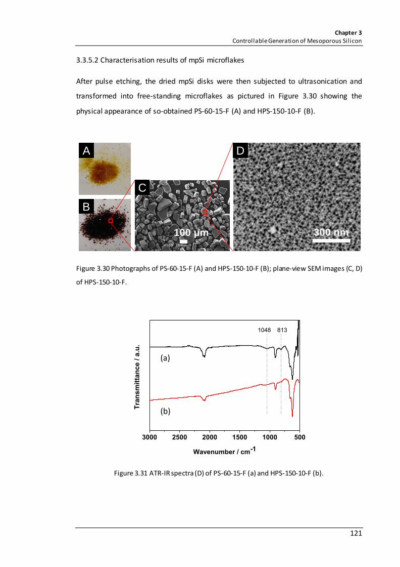
Chapter 3 Controllable Generation of Mesoporous Sil icon
121
3.3.5.2 Characterisation results of mpSi microflakes
After pulse etching, the dried mpSi disks were then subjected to ultrasonication and
transformed into free-standing microflakes as pictured in Figure 3.30 showing the
physical appearance of so-obtained PS-60-15-F (A) and HPS-150-10-F (B).
Figure 3.30 Photographs of PS-60-15-F (A) and HPS-150-10-F (B); plane-view SEM images (C, D)
of HPS-150-10-F.
Figure 3.31 ATR-IR spectra (D) of PS-60-15-F (a) and HPS-150-10-F (b).
A
B
C
100 μm 300 nm
D
3000 2500 2000 1500 1000 500
Tra
nsm
itta
nce /
a.u
.
Wavenumber / cm-1
1048 813
(a)
(b)

Chapter 3 Controllable Generation of Mesoporous Sil icon
122
The ATR-IR spectra (Figure 3.31) clearly show that the surface of both samples was still
hydrogen passivated with observable IR peaks from Si-H bonds at 664, 912, 2088, 2110,
2140 cm-1. Minor oxidation was also detected on the surface of PS-60-15-F sample,
indicated by the IR peaks at 813 cm-1 and 1048 cm-1, assuming to be related to its large
surface area and relatively poor structural crystallinity.
Figure 3.32 Nitrogen sorption isotherms (A, C) and pore size distribution (B, D) of HPS-150-10-F
(A and B) and PS-60-15-F (C and D).
The surface and pore properties of PS-60-15-F and HPS-150-10-F microflakes were
further examined by nitrogen sorption isotherms (Figure 3.32) and a summary of SBET,
Vmeso and dpore data was presented in Table 3.6 below. The average pore diameter of
HPS-150-10-F was measured as 9.50 nm, which is very similar to the untreated
HPS-150-10 sample. The similarity was also reflected in the total pore volume which
was marginally increased to 1.82 cm3·g-1 after being processed into free-standing
microflakes. Due to fragmentation, the specific surface area of HPS-150-10-F was
0.0 0.2 0.4 0.6 0.8 1.0
0
200
400
600
800
1000
1200
Adsorption
Desorption
Ab
so
rbed
Vo
lum
e a
t S
TP
/ cm
3g
-1
Relative Pressure, P/P0
3 4 5 6 7 8 910 20 30 40 50
HPS-150-10
HPS-150-10-M2-F
dV
(d)
/ c
m3g
-1n
m-1
Pore diameter / nm
0.0 0.2 0.4 0.6 0.8 1.0-100
0
100
200
300
400
500
600
700
800
Adsorption
Desorption
Ab
so
rbed
Vo
lum
e a
t S
TP
/ cm
3g
-1
Relative Pressure, P/P0
A B
C D
3 4 5 6 7 8 910 20 30 40 50
PS-60-15
PS-60-15-M2-F
dV
(d)
/ c
m3g
-1n
m-1
Pore diameter / nm
P/P0
P/P0

Chapter 3 Controllable Generation of Mesoporous Sil icon
123
increased to 527.0 m2·g-1. However, the surface area and total pore volume of
PS-60-15-F were both reduced compared to the as-etched PS-60-15 sample. This is
likely caused by the sonication-induced structural alteration which resulted in the
variation of pore dimension and pore size distribution as seen in Figure 3.32.
Table 3.6 Textural properties of mesoporous silicon microflakes and as-etched mesoporous
silicon.
Mesoporous silicon samples
SBET / m2·g-1
Vmeso / cm3·g-1
dpore
/ nm
HPS-150-10 455.3 1.72 9.55
HPS-150-10-F 527.0 1.82 9.50
PS-60-15 994.4 1.36 3.82
PS-60-15-F 699.9 1.16 4.91
3.3.6 Characterisation results of thiol-capped mpSi
As revealed above, the vast internal surface of both as-etched moderately doped PS
and heavily doped HPS samples are purely hydrogen-terminated. By covalently binding
with other organic molecules through silicon hydrosilylation that can be initiated by
heat, light, radicals or metal catalysts etc., the surface of porous silicon can be
modified with various functionalities. Here allyl mercaptan was intended to be grafted
onto the surface of H-terminated mpSi materials with large surface area and open
mesoporous structure. With –SH as functional end groups on the mpSi surface,
modified mpSi material can be conjugated with many biologically active species
through disulphide bond, which can be selectively cleaved inside the cells. On the
other hand, thiol-functionalized mpSi can also be used as catalyst support in anchoring
and stabilizing metal nanoparticles.38-40
A comparison of grafting efficiency among three different heating methods including
oil bath, conventional oven and domestic microwave oven was provided below which
shows the superior performance of microwave irradiation in thiol capping.
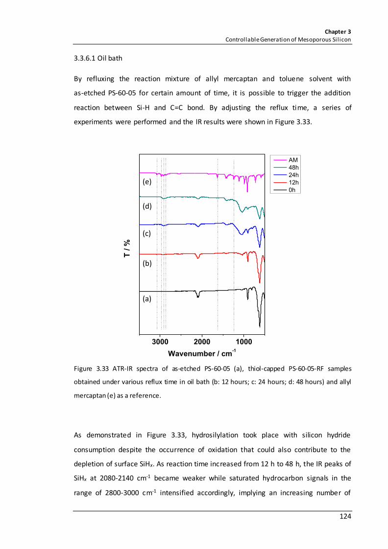
Chapter 3 Controllable Generation of Mesoporous Sil icon
124
3.3.6.1 Oil bath
By refluxing the reaction mixture of allyl mercaptan and toluene solvent with
as-etched PS-60-05 for certain amount of time, it is possible to trigger the addition
reaction between Si-H and C=C bond. By adjusting the reflux time, a series of
experiments were performed and the IR results were shown in Figure 3.33.
Figure 3.33 ATR-IR spectra of as-etched PS-60-05 (a), thiol-capped PS-60-05-RF samples
obtained under various reflux time in oil bath (b: 12 hours; c: 24 hours; d: 48 hours) and allyl
mercaptan (e) as a reference.
As demonstrated in Figure 3.33, hydrosilylation took place with silicon hydride
consumption despite the occurrence of oxidation that could also contribute to the
depletion of surface SiHx. As reaction time increased from 12 h to 48 h, the IR peaks of
SiHx at 2080-2140 cm-1 became weaker while saturated hydrocarbon signals in the
range of 2800-3000 cm-1 intensified accordingly, implying an increasing number of
3000 2000 1000
T / %
Wavenumber / cm-1
AM
48h
24h
12h
0h
(a)
(b)
(c)
(d)
(e)

Chapter 3 Controllable Generation of Mesoporous Sil icon
125
organic ligands successfully linked to the surface of mpSi material. The absence of sp2
C-H stretching mode at 3081 cm-1 and C=C stretching mode at 1634 cm-1 that featured
in the IR spectrum of allyl mercaptan further confirmed the binding result, suggesting
the alkene group of allyl mercaptan was successfully saturated by the surface hydrides
of mpSi which resulted in the covalent ligandization by forming the new Si-C bond of
which the IR absorption was also found at 1260 cm-1.
3.3.6.2 Conventional oven
The hydrosilylation reaction was also carried out in a PTFE lined autoclave reactor in
combination with a conventional oven so that the reaction temperature can be
elevated above the boiling point of toluene solvent in order to enhance the formation
of thiol linkages. As exhibited in Figure 3.34, the surface hydrides were completely
extinguished with no organic signals observable in the IR spectrum, suggesting the
inefficiency of this heating approach.
Figure 3.34 ATR-IR spectra of as-etched PS-60-05 (a), PS-60-05-AC prepared in an autoclave (b)
and allyl mercaptan (c).
3500 3000 2500 2000 1500 1000 500
T /
%
Wavenumber / cm-1
(a)
(b)
(c)

Chapter 3 Controllable Generation of Mesoporous Sil icon
126
3.3.6.3 Microwave irradiation
The above two conventional heating methods allow the heat to be transferred to
reaction system through thermal conduction and convection, which is often
recognized as indirect and of low-efficiency.41 Microwave-assisted thermal-driven
hydrosilylation was thus explored in this study. Benefitting from the direct, rapid,
volumetric and non-contact heating characteristics, microwave energy has shown its
superiority in accelerating reaction rate and improving product selectivity under mild
conditions in various studies.41-43
Doped silicon is known to absorb microwave energy efficiently.44 The heat transfer to
the near surface of the material will lead to a temperature gradient, which is expected
to influence the reaction rate during the chemical treatment of H-terminated
mesoporous silicon with organic reagents. The resistivity of the silicon wafer used to
prepare PS-60-05 is 1-10 Ω·cm, which is right in the range of the maximum absorption
of MW irradiation.45 While toluene employed in the reaction system as solvent is
non-polar and hence microwave transparent. These different interaction behaviours
with microwave irradiation is expected to impact on the course and rate of the
hydrosilylation reaction rate.
Figure 3.35 ATR-IR spectra of as-etched PS-60-05 (a), thiol-capped PS-60-05-MW obtained
under microwave irradiation (b) and allyl mercaptan (c) as a reference.
3500 3000 2500 2000 1500 1000 500
T /
%
Wavenumber / cm-1
(a)
(b)
(c)

Chapter 3 Controllable Generation of Mesoporous Sil icon
127
As shown in Figure 3.35, Si-C stretching peaks were detected at 1260 cm-1 and
1460 cm-1. Additional peaks characteristic of the alkyl chain also appeared at
2850-3000 cm-1 in the spectrum of PS-60-05-MW. The absence of signals from C=C
bond at 1634 cm-1 and sp2 C-H bond at 3081 cm-1 verified the fact that final product
was free of physically absorbed organic molecules. Meanwhile, a large decrease of the
νSiHx (2080-2140 cm-1), δSiH2 (910 cm-1), and ρSiHx (669 cm-1) peaks was also observed,
indicating the reaction was efficient within 6 min by consuming silicon hydrides. It is
worth noting that the vibration absorption band of thiol S-H at 2550-2620 cm-1,
however, was not identifiable in the spectrum of the capped sample. This is probably
because the absorption signal is commonly known as weak and broad as evidenced by
the IR spectrum of the neat allyl mercaptan in Figure 3.35c.
Figure 3.36 Deconvoluted XPS spectra of Si 2p, S 2p, C 1s and O 1s regions of PS-60-05-MW and
Si 2p of freshly prepared PS-60-05.
108 106 104 102 100 98
Inte
nsit
y / C
PS
Binding Energy / eV
292 288 284 280
Inte
nsit
y / C
PS
Binding Energy / eV
168 166 164 162 160
Inte
nsit
y / C
PS
Binding Energy / eV
540 536 532 528
Inte
nsit
y / C
PS
Binding Energy / eV
Si 2p S 2p
C 1s
O 1s
H-terminated
HS-Capped

Chapter 3 Controllable Generation of Mesoporous Sil icon
128
The chemical bonding of thiol-capped PS-60-06-MW sample was also revealed in the
XPS analysis (Figure 3.36). For comparison, the Si 2p XPS spectrum of freshly made
PS-60-05 was also recorded which saw the distinctive single peak at 99.8 eV from Si-Si
in accordance with its surface nature as described previously. While the Si 2p spectrum
of thiol-capped product was fitted by three components of which the respective B.E.
was centred at 103.4, 102.2, 99.4 eV, attributable to Si-O, Si-C and Si-Si. The
preservation of thiol functionality after ligand grafting was affirmed by the presence of
S 2p peak at 164.0 eV in the XPS spectrum, which comprised two sub-peaks in a 1:2
area ratio at 165.0 eV and 163.8 eV belonging to S 2p1/2 and S 2p3/2 from C-SH bond. By
calculating the peak area of Si-C and Si-O spectra, thiol coverage was estimated as 43.6%
of the total surface in this study.
3.4 Summary
This chapter is devoted to the preparation of mesoporous silicon via electrochemical
etching method. By anodically etching the mono-crystalline Si wafer, mesoporous
silicon was produced on the Si chip which shows intriguing morphological
characteristics of large surface area, mesoporous system and ample hydrogen
termination. The existence of abundant Si nanocrystallites on the framework is also an
important feature as they not only give rise to the high surface area but also are able
to influence the electronic band structure and optical properties of mesoporous silicon.
The high surface area and open mesoporous network could enhance the mass
transport in liquid phase applications although it is also largely dependent on the
actual pore dimension and interconnectivity, which can be altered by adjusting the
etching variables. An interconnected 3D porous network and a nicely ordered 1D
channel arrays were characterised in the moderately doped and heavily doped
mesoporous silicon, respectively. Free standing mpSi can be gained through pulse
etching and thiol capped mpSi can be prepared via microwave-assisted hydrosilylation
which was proved to be very efficient because of the selective heating of Si.

Chapter 3 Controllable Generation of Mesoporous Sil icon
129
3.5 References
1. Wang, B.; Li, X.; Qiu, T.; Luo, B.; Ning, J.; Li, J.; Zhang, X.; Liang, M.; Zhi, L., High
volumetric capacity silicon-based lithium battery anodes by nanoscale system
engineering. Nano Lett. 2013, 13 (11), 5578-5584.
2. Ge, M.; Fang, X.; Rong, J.; Zhou, C., Review of porous silicon preparation and its
application for lithium-ion battery anodes. Nanotechnology 2013, 24 (42), 422001.
3. Thakur, M.; Sinsabaugh, S. L.; Isaacson, M. J.; Wong, M. S.; Biswal, S. L., Inexpensive
method for producing macroporous silicon particulates (MPSPs) with pyrolyzed
polyacrylonitrile for lithium ion batteries. Sci. Rep. 2012, 2, 795.
4. Szczech, J. R.; Jin, S., Nanostructured silicon for high capacity lithium battery anodes.
Energy Environ. Sci. 2011, 4 (1), 56-72.
5. Li, X.; Gu, M.; Hu, S.; Kennard, R.; Yan, P.; Chen, X.; Wang, C.; Sailor, M. J.;
Zhang, J. G.; Liu, J., Mesoporous silicon sponge as an anti-pulverization structure for
high-performance lithium-ion battery anodes. Nat. Commun. 2014, 5, 4105.
6. Park, J. H.; Gu, L.; von Maltzahn, G.; Ruoslahti, E.; Bhatia, S. N.; Sailor, M. J.,
Biodegradable luminescent porous silicon nanoparticles for in vivo applications. Nat.
Mater. 2009, 8 (4), 331-336.
7. Gu, L.; Park, J. H.; Duong, K. H.; Ruoslahti, E.; Sailor, M. J., Magnetic luminescent
porous silicon microparticles for localized delivery of molecular drug payloads. Small
2010, 6 (22), 2546-2552.
8. Gu, L.; Hall, D. J.; Qin, Z.; Anglin, E.; Joo, J.; Mooney, D. J.; Howell, S. B.; Sailor, M. J.,
In vivo time-gated fluorescence imaging with biodegradable luminescent porous silicon
nanoparticles. Nat. Commun. 2013, 4, 2326.
9. Anglin, E. J.; Cheng, L. Y.; Freeman, W. R.; Sailor, M. J., Porous silicon in drug delivery
devices and materials. Adv. Drug Deliv. Rev. 2008, 60 (11), 1266-1277.
10. Salonen, J.; Kaukonen, A. M.; Hirvonen, J.; Lehto, V. P., Mesoporous silicon in drug
delivery applications. J. Pharm. Sci. 2008, 97 (2), 632-653.
11. McInnes, S. J. P.; Voelcker, N. H., Porous silicon-based nanostructured
microparticles as degradable supports for solid-phase synthesis and release of
oligonucleotides. Nanoscale Res. Lett. 2012, 7(1), 385.

Chapter 3 Controllable Generation of Mesoporous Sil icon
130
12. Sailor, M. J.; Wu, E. C., Photoluminescence-based sensing with porous silicon films,
microparticles, and nanoparticles. Adv. Funct.l Mater. 2009, 19 (20), 3195-3208.
13. Kotkovskiy, G. E.; Kuzishchin, Y. A.; Martynov, I. L.; Chistyakov, A. A.; Nabiev, I., The
photophysics of porous silicon: technological and biomedical implications. Phys. Chem.
Chem. Phys. 2012, 14 (40), 13890-13902.
14. Harraz, F. A., Porous silicon chemical sensors and biosensors: a review. Sens.
Actuators B Chem. 2014, 202, 897-912.
15. Dai, F.; Zai, J.; Yi, R.; Gordin, M. L.; Sohn, H.; Chen, S.; Wang, D., Bottom-up
synthesis of high surface area mesoporous crystalline silicon and evaluation of its
hydrogen evolution performance. Nat. Commun. 2014, 5, 3605.
16. Su, J.; Yu, H.; Quan, X.; Chen, S.; Wang, H., Hierarchically porous silicon with
significantly improved photocatalytic oxidation capability for phenol degradation. Appl.
Catal. B 2013, 138-139, 427-433.
17. Dasog, M.; Kraus, S.; Sinelnikov, R.; Veinot, J. G. C.; Rieger, B., CO2 to methanol
conversion using hydride terminated porous silicon nanoparticles. Chem. Commun.
2017, 53 (21), 3114-3117.
18. Ye, M.; Qian, C.; Sun, W.; He, L.; Jia, J.; Dong, Y.; Zhou, W., Dye colour switching by
hydride-terminated silicon particles and its application as an oxygen indicator. J. Mater.
Chem. C 2016, 4 (20), 4577-4583.
19. Yang, X.-Y.; Chen, L.-H.; Li, Y.; Rooke, J. C.; Sanchez, C.; Su, B.-L., Hierarchically
porous materials: synthesis strategies and structure design. Chem. Soc. Rev. 2017,
46 (2), 481-558.
20. Schneider, D.; Mehlhorn, D.; Zeigermann, P.; Kärger, J.; Valiullin, R., Transport
properties of hierarchical micro–mesoporous materials. Chem. Soc. Rev. 2016, 45 (12),
3439-3467.
21. Venuta, A.; Wolfram, J.; Shen, H.; Ferrari, M., Post-nano strategies for drug delivery:
multistage porous silicon microvectors. J. Mater. Chem. B 2017, 5 (2), 207-219.
22. Naderi, N.; Hashim, M. R.; Amran, T. S. T., Enhanced physical properties of porous
silicon for improved hydrogen gas sensing. Superlattices Microstruct. 2012, 51 (5),
626-634.

Chapter 3 Controllable Generation of Mesoporous Sil icon
131
23. Bisi, O.; Ossicini, S.; Pavesi, L., Porous silicon: a quantum sponge structure for
silicon based optoelectronics. Surf. Sci. Rep. 2000, 38 (1-3), 1-126.
24. Canham, L. T., Silicon quantum wire array fabrication by electrochemical and
chemical dissolution of wafers. Appl. Phys.Lett. 1990, 57 (10), 1046-1048.
25. Santos, A.; Kumeria, T., Electrochemical etching methods for producing porous
silicon. 2015, 220, 1-36.
26. Canham, L., Handbook of porous silicon. Springer International Publishing: 2014.
27. Lehmann, V.; Gosele, U., Porous silicon formation - a quantum wire effect. Appl.
Phys. Lett. 1991, 58 (8), 856-858.
28. Dasog, M.; Kehrle, J.; Rieger, B.; Veinot, J. G., Silicon nanocrystals and silicon-
polymer hybrids: synthesis, surface engineering, and applications. Angew. Chem. Int.
Ed. Engl. 2016, 55 (7), 2322-2339.
29. Deshmukh, A. B.; Devarapalli, R. R.; Shelke, M. V., Functional silicon nanostructures
derived from drying-mediated self-assembly of gold nanoparticles. Journal of
Nanoparticle Research 2014, 16 (5).
30. Patterson, A. L., The scherrer formula for X-Ray particle size determination. Phys.
Rev. 1939, 56 (10), 978-982.
31. Xifré Pérez, E. Design, fabrication and characterization of porous silicon multilayer
optical devices. Universitat Rovira i Virgili., 2007.
32. Lenshin, A. S.; Kashkarov, V. M.; Seredin, P. V.; Spivak, Y. M.; Moshnikov, V. A.,
XANES and IR spectroscopy study of the electronic structure and chemical composition
of porous silicon on n- and p-type substrates. Semiconductors 2011, 45 (9), 1183-1188.
33. Thommes, M.; Kaneko, K.; Neimark, A. V.; Olivier, J. P.; Rodriguez-Reinoso, F.;
Rouquerol, J.; Sing, K. S. W., Physisorption of gases, with special reference to the
evaluation of surface area and pore size distribution (IUPAC Technical Report). Pure
Appl. Chem. 2015, 87 (9-10), 1051-1069.
34. Loni, A.; Canham, L. T.; Defforge, T.; Gautier, G., Supercritically-dried porous silicon
powders with surface areas exceeding 1000 m2/g. ECS J. Solid State Sci. Technol. 2015,
4 (8), 289-292.

Chapter 3 Controllable Generation of Mesoporous Sil icon
132
35. Gouadec, G.; Colomban, P., Raman Spectroscopy of nanomaterials: How spectra
relate to disorder, particle size and mechanical properties. Prog. Cryst. Growth Charact.
Mater. 2007, 53 (1), 1-56.
36. Joo, J.; Defforge, T.; Loni, A.; Kim, D.; Li, Z. Y.; Sailor, M. J.; Gautier, G.; Canham, L. T.,
Enhanced quantum yield of photoluminescent porous silicon prepared by supercritical
drying. Appl. Phys. Lett. 2016, 108 (15), 153111.
37. Canham, L. T.; Cullis, A. G.; Pickering, C.; Dosser, O. D.; Cox, T. I.; Lynch, T. P.,
Luminescent anodized silicon aerocrystal networks prepared by supercritical drying.
Nature 1994, 368 (6467), 133-135.
38. Walcarius, A.; Etienne, M.; Bessière, J., Rate of access to the binding sites in
organically modified silicates. 1. Amorphous silica gels grafted with amine or thiol
groups. Chem. Mater. 2002, 14 (6), 2757-2766.
39. Wang, C.; Flynn, N. T.; Langer, R., Controlled structure and properties of
thermoresponsive nanoparticle–hydrogel composites. Adv. Mater. 2004, 16 (13),
1074-1079.
40. Yang, H.; Wang, Y.; Huang, H.; Gell, L.; Lehtovaara, L.; Malola, S.; Hakkinen, H.;
Zheng, N., All-thiol-stabilized Ag44 and Au12Ag32 nanoparticles with single-crystal
structures. Nat. Commun. 2013, 4, 2422.
41. Oliver Kappe, C., Microwave dielectric heating in synthetic organic chemistry. Chem.
Soc. Rev. 2008, 37 (6), 1127-1139.
42. Dallinger, D.; Kappe, C. O., Microwave-assisted synthesis in water as solvent. Chem.
Rev. 2007, 107 (6), 2563-2591.
43. Zhu, Y. J.; Chen, F., Microwave-assisted preparation of inorganic nanostructures in
liquid phase. Chem. Rev. 2014, 114 (12), 6462-6555.
44. Boukherroub, R.; Petit, A.; Loupy, A.; Chazalviel, J. N.; Ozanam, F., Microwave-
assisted chemical functionalization of hydrogen-terminated porous silicon surfaces. J.
Phys. Chem. B 2003, 107 (48), 13459-13462.
45. Moreno, T., Microwave Transmission Design Data. Dover Publications Inc.: New
York: 1948.

Chapter 4
Chapter 4
Hydrogen-Terminated Mesoporous Silicon as Visible-Light-
Active Photocatalyst in Dye Degradation
Abstract
On the basis of a detailed analysis of the morphological, optical and electronic band
properties, the use of mesoporous silicon with hydrogen termination in visible-light-
driven methyl orange photo-degradation as a model system have been investigated in-
depth in study with gained insights into the varied effects of structural factors, the roles
of surface species and a deepened mechanistic understanding of its intriguing
photocatalytic behaviours which is primarily expressed as an interrelated combination
of photo-generated charge-driven processes and an enhanced hydrogen transfer
process upon light irradiation.

Chapter 4 Mesoporous Sil icon in Dye Degradation
134
4.1 Overview
As it is free and abundant, the use of sunlight to store and transfer energy is of great
importance to environmental protection. Over the past few decades, various photo-
active nanomaterials (transition metal oxides, chalcogenides, plasmonic metal
nanoparticles etc.)1-2 were developed to harness the renewable solar energy, aiming to
meet the clean energy demand,3 to tackle climate change,4 and to control the
deteriorating pollution crisis.5 The large surface area, unique electron conduction
properties, size dependent effects, etc.6 largely contributed to the excellent
photocatalytic performance of nanomaterials in eliminating environmental pollutants,
purifying contaminated wastewater due to heavy metal ions and harmful organic
compounds such as dyeing agents as one of the main causes.7-8 Despite the remarkable
progress over the years, narrow light responsive range, fast charge recombination rate,
high cost of raw materials and associated environmental risks, as well as poor catalyst
separation efficiency, still substantially limit their engineering applications.9
As a promising metal-free semiconductor, silicon nanostructures have received great
attention owing to the environmental friendliness, natural abundance, low production
cost and tuneable visible light responsiveness.10-12 Significant efforts have been
dedicated to exploiting the photo-activity of silicon quantum dots (Si QDs),13-14 silicon
nanowires (Si NWs)15-21 and porous silicon (pSi),22-26 which often show a broad
absorption over entire spectral range as featured in various studies. As a result, nano-
engineered silicon structures were discovered to possess a comparable photocatalytic
capability as other inorganic materials in triggering diverse range of redox reactions,
such as CO2 fixation,13, 19, 27 water splitting,11, 24, 28 organic synthesis29-30 and pollutant
degradation (e.g. methyl orange, methylene blue, Rhodamine B, phenol and
nitroaromatics)13, 15-18, 22, 26, 31-34 under visible light irradiation. However, the
photocatalytic behaviour of silicon nanomaterials is still not so clear yet especially for
porous silicon which possesses much more complex micro- and nano-structural features
that will strongly influence the performance compared with the low dimensional Si QDs,
Si NWs etc.

Chapter 4 Mesoporous Sil icon in Dye Degradation
135
In the last chapter focusing on the synthesis and characterisation of mesoporous silicon
(mpSi) via electrochemical etching method, two distinctive porous morphologies have
been discovered, depending on the dopant concentration of the initial wafer material.
Moderately boron-doped mpSi samples (“PS-J-t”) presented a 3D mesoporous network
with large surface area while the heavily doped counterparts (“HPS-J-t”) can be descried
as ordered 1D channel arrays with relatively large pore width. By tuning the etching
variables (J, t), structural properties (surface area, pore size, pore length, Si
nanocrystallites) of mpSi material can be controllably altered of which the impacts on
the optical properties and photocatalytic activity of mpSi in degrading methyl orange
(MO) under visible light illumination will be revealed in this study.
This chapter summarized the kinetic results of MO degradation reaction by
H-terminated mesoporous silicon with various morphologies in the presence and
absence of external light irradiation. The essential roles of the existence of silicon
nanocrystallites and hydrogen passivation on the porous surface were affirmed in our
experiments with deciding effects on the material’s activity and degradation behaviours.
Large surface area, large mesopores, open mesoporous structure and abundant surface
hydrides facilitated the mass transport and promoted the photo-degradation process
while the activity of ordered 1D channel arrays of heavily doped samples was further
enhanced by the well-defined crystalline framework and better electrical conductivity.
By analysing the organic carbon content, active species and band potentials, the
photocatalytic mechanism of H-terminated mesoporous silicon materials was proposed,
which illustrated the different photochemical and chemical degradation pathways of
MO molecules simultaneously occurring on the Si interface. Last but not the least, as
shown later in this study, monolithic mpSi samples can also be efficiently separated from
the reaction system and an excellent reusability was exhibited with a remaining 88% of
the initial efficacy after 10 cycles of photo-degradation.

Chapter 4 Mesoporous Sil icon in Dye Degradation
136
4.2 Experimental section
4.2.1 Photocatalyst preparation
H-terminated mesoporous silicon were prepared by electrochemical etching of mono-
crystalline Si wafers (Table 2.1) following the same experimental procedure as described
in Chapter 2. All the monolithic mesoporous silicon samples engaged in this study and
their respective etching conditions (J and t) are summarized in Table 4.1.
Table 4.1 List of as-etched mesoporous silicon studied in Chapter 4 and the corresponding
etching conditions applied in the electrochemical preparation.
Mesoporous silicon samples
Etching current density
/ mA·cm-2
Etching time
/ min
PS-10-15 10 15
PS-30-05 30 05
PS-30-15 30 15
HPS-150-05 150 05
HPS-200-05 200 05
HPS-400-05 400 05
Besides, free-standing H-terminated mpSi microflakes (PS-30-15-F and HPS-200-05-F)
and oxidized mpSi materials (PS-30-15-[O] and HPS-150-05-[O]) were also obtained via
methods included in Chapter 2 and their activities in MO degradation under visible light
irradiation were also investigated.
4.2.2 Photocatalyst characterisation
The structural morphologies of mpSi samples were recorded using FE-SEM and HRTEM
techniques. The optical properties and electrical band gap were measured by UV-Vis and
fluorescence spectrometers with DCM used as dispersion medium. FTIR spectra of mpSi
materials were also collected to reflect the surface chemistry during reaction process.
All measurement parameters were the same as described in Chapter 2 unless otherwise

Chapter 4 Mesoporous Sil icon in Dye Degradation
137
stated. Notably, many samples listed in Table 4.1 including PS-10-15, PS-30-15 and
HPS-150-05 had already been characterised by a range of techniques in Chapter 3. Thus,
these results were also selectively mentioned in this chapter when necessary.
4.2.3 Photocatalytic evaluation
The photocatalytic behaviours and structural effects of H-terminated mesoporous
silicon were assessed by the photo-degradation of methyl orange (MO) under visible
light irradiation at room temperature. The unreacted dye concentration and organic
carbon content of MO solution were measured respectively by UV-Vis spectrometer and
TOC analyser at different time intervals of photocatalytic process. Apparent rate
constants were analysed which revealed the effects of various surface and pore factors
of mpSi on the photocatalytic efficiency. A series of trapping experiments using
2-propanol, ethanol, and triethanolamine (TEOA) were carried out to identify the main
active species involved in the organic decomposition process and the lifetime of mpSi
photocatalyst was evaluated through cycle test. All experimental procedures and
instrumental parameters were the same as outlined in Chapter 2 unless otherwise
specified.
4.3 Results and discussion
4.3.1 Characterisation of mesoporous silicon photocatalysts
Prior to the investigation of photocatalytic activity, the structural morphology and
optical properties of PS-30-15 and HPS-150-05 fabricated by electrochemical etching
method were first examined and discussed.
4.3.1.1 Structural features of PS-mpSi
The interconnected 3D porous network of PS-30-15 is evident in the FE-SEM images as
shown in Figure 4.1 and HRTEM images in Figure 4.2. The average pore size was
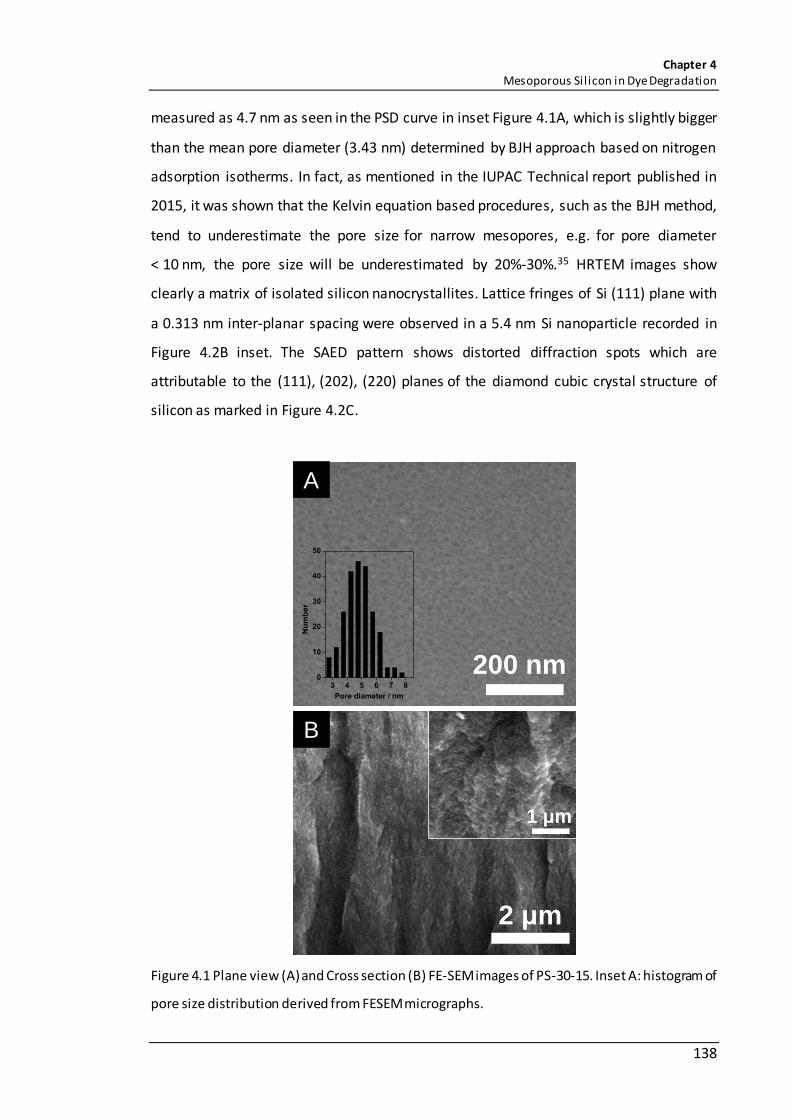
Chapter 4 Mesoporous Sil icon in Dye Degradation
138
measured as 4.7 nm as seen in the PSD curve in inset Figure 4.1A, which is slightly bigger
than the mean pore diameter (3.43 nm) determined by BJH approach based on nitrogen
adsorption isotherms. In fact, as mentioned in the IUPAC Technical report published in
2015, it was shown that the Kelvin equation based procedures, such as the BJH method,
tend to underestimate the pore size for narrow mesopores, e.g. for pore diameter
< 10 nm, the pore size will be underestimated by 20%-30%.35 HRTEM images show
clearly a matrix of isolated silicon nanocrystallites. Lattice fringes of Si (111) plane with
a 0.313 nm inter-planar spacing were observed in a 5.4 nm Si nanoparticle recorded in
Figure 4.2B inset. The SAED pattern shows distorted diffraction spots which are
attributable to the (111), (202), (220) planes of the diamond cubic crystal structure of
silicon as marked in Figure 4.2C.
Figure 4.1 Plane view (A) and Cross section (B) FE-SEM images of PS-30-15. Inset A: histogram of
pore size distribution derived from FESEM micrographs.
1 μm
2 μm200 nm
A B
3 4 5 6 7 80
10
20
30
40
50
Nu
mb
er
Pore diameter / nm
1 μm
2 μm200 nm
A B

Chapter 4 Mesoporous Sil icon in Dye Degradation
139
Figure 4.2 HRTEM images (A, B) and SAED pattern (C) of PS-30-15.
4.3.1.2 Structural features of HPS-mpSi
In agreement with the previous findings in chapter 3, a nicely ordered 1D channel array
was featured in HPS-150-05. The high degree of order was clearly reflected in the
FE-SEM (Figure 4.3) and HRTEM images (Figure 4.4), showing very straight and parallel
channels along the [100] direction. The 9.4 nm channel width revealed in the HRTEM
image is consistent with the BJH analysis result (9.55 nm, Table 3.5) and very close to
the value derived from the FESEM images (10.5 nm). The bright diffraction spots in the
SAED pattern and the Si (111) lattice fringes observed on the pore walls confirm the
well-defined crystalline structure of HPS-150-05 sample. The much thicker pore walls
ensured a good crystallinity and mechanical stability of the primary structure, and
maintained the isolation of the pores as well.
2 nm
0.313 nm
20 nm
50 nm
A B
C
50 nm
10 nm
(220)
(400)(220)
(111)
0.313 nm
5 nm
54.7˚
(111)
(220)
(202)
A B
C

Chapter 4 Mesoporous Sil icon in Dye Degradation
140
Figure 4.3 Plane view (A) and Cross section (B) FE-SEM images of HPS-150-05; Histogram of pore
size distribution (C) of HPS-150-05 derived from FE-SEM micrographs.
Figure 4.4 HRTEM images (A, B) and SAED pattern (C) of HPS-150-05.
300 nm 1 μm
500 nm
A B
4 8 12 16 200
20
40
60
80
100
120
140
Nu
mb
er
Pore diameter / nm
C
2 nm
0.313 nm
20 nm
50 nm
A B
C
50 nm
10 nm
(220)
(400)(220)
(111)
0.313 nm
5 nm
54.7˚
(111)
(220)
(202)
A B
C

Chapter 4 Mesoporous Sil icon in Dye Degradation
141
4.3.1.3 Optical analysis of PS-mpSi and HPS-mpSi
4.3.1.3.1 Light absorption
As presented in Figure 4.5, UV-Vis absorption spectra of PS-30-15 (a) and HPS-150-05 (b)
were collected, showing a broad absorption band maximized at 254 nm, 290 nm
respectively. The substantial blue shift of the peak position in comparison to the near-
IR absorption wavelength of Si bulk crystal (c. 1100 nm) indicates a significantly widened
bandgap between the conduction and valence bands due to the quantum confinement
effects of the constituted Si nanocrystals.36 Therefore, the absorption efficiency of
incident photons with energies between 1.8 eV and 3.1 eV corresponding to visible light
range 700-400 nm was effectively increased. As an indirect bandgap semiconductor, the
absorption coefficient of Si is often very low.37 However, the mesoporous structure of
mpSi samples partially made up for the deficiency by suppressing the broadband
reflection of light at the interface.10, 18 Therefore, more photons in a broad wavelength
range were absorbed by these structures and more visible light energy could hence be
harnessed to separate electron/hole (e-/h+) pairs by mpSi materials.
Figure 4.5 UV-Vis absorption spectra of freshly made PS-30-15 (a) and HPS-150-05 (b).
300 400 500 600 700 800
Ab
so
rban
ce / a
.u.
Wavelength / nm
a
b

Chapter 4 Mesoporous Sil icon in Dye Degradation
142
4.3.1.3.2 Light emission
Figure 4.6 PL emission spectra of freshly made PS-30-15 (a), HPS-150-05 (b) and aged PS-30-15
(c). Excitation wavelength = 320 nm, 390 nm cut-off.
Multiple PL bands were featured in the PL emission spectra shown in Figure 4.6, at
460 nm, 521 nm and 609 nm for PS-30-15, 474 nm and 520 nm for HPS-150-05. Although
the origin of the photoluminescence emitted by pSi is still under debate, many studies
suggest a number of combined factors could contribute to the light emitting process,
such as quantum confinement effect, structural defects, surface oxidation, framework
distortion etc.38-39 For example, the red emission at 609 nm seen in the spectrum of
freshly made PS-30-15 is often associated with an oxidation effect.40-41 As displayed in
the emission spectrum of the aged PS-30-15 which was left in the air for several days
under ambient conditions, the same 609 nm signal clearly was intensified. Surface
oxides and existing defects are known as radiative recombination sites for excitons
hence impairing the lifetime of photo-generated e-/h+ that are key to driving the
reductive photochemical reactions aimed for.42
Moreover, it is well acknowledged that the lower fluorescence intensity represents a
higher separation efficiency of e-/h+ pairs, which indicates a better photocatalytic
activity of the nanomaterials. Thus, HPS-150-05 is very likely to produce longer-lived
300 400 500 600 700 800
Inte
ns
ity
/ a
.u.
Wavelength / nm
609
a
b
c

Chapter 4 Mesoporous Sil icon in Dye Degradation
143
photo-induced free charges, indicated by the considerably lower emission intensity and
the absence of 609 nm signal despite the fact that it absorbed more incident photons
(λext = 320 nm) than PS-30-15. This enhancement in e-/h+ stability can be reasonably
explained by the improved charge mobility across the surface of HPS-150-05 because of
better electrical conductivity, lattice integrity, and higher resistance to oxidation than
PS-30-15.
4.3.2 Photocatalytic activities of mesoporous silicon in dye degradation
This section displays the photocatalytic activity of PS-30-15 and HPS-150-05 in methyl
orange photo-degradation under visible light irradiation taking advantage of the broad
light absorption capability and large surface area.
Scheme 4.1 Molecular structure of methyl orange.
4.3.2.1 Control experiments
Figure 4.7 presented several examples of the control experiments including the self-
decomposition of dye molecules, adding moderately-doped or heavily doped Si chip
with/without external visible light illumination. As shown, the peak absorbance of MO
molecule at 464 nm almost retained its intensity as the initial value at different time
intervals. The photolysis of MO on its own was negligible and MO molecules were also
very stable in the presence of any Si chip under visible light irradiation.
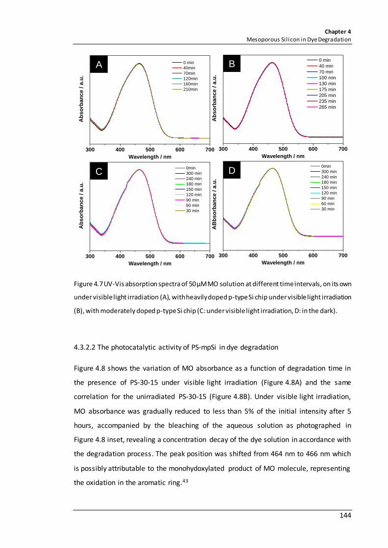
Chapter 4 Mesoporous Sil icon in Dye Degradation
144
Figure 4.7 UV-Vis absorption spectra of 50 µM MO solution at different time intervals, on its own
under visible light irradiation (A), with heavily doped p-type Si chip under visible light irradiation
(B), with moderately doped p-type Si chip (C: under visible light irradiation, D: in the dark).
4.3.2.2 The photocatalytic activity of PS-mpSi in dye degradation
Figure 4.8 shows the variation of MO absorbance as a function of degradation time in
the presence of PS-30-15 under visible light irradiation (Figure 4.8A) and the same
correlation for the unirradiated PS-30-15 (Figure 4.8B). Under visible light irradiation,
MO absorbance was gradually reduced to less than 5% of the initial intensity after 5
hours, accompanied by the bleaching of the aqueous solution as photographed in
Figure 4.8 inset, revealing a concentration decay of the dye solution in accordance with
the degradation process. The peak position was shifted from 464 nm to 466 nm which
is possibly attributable to the monohydoxylated product of MO molecule, representing
the oxidation in the aromatic ring.43
300 400 500 600 700
0min
300 min
240 min
180 min
150 min
120 min
90 min
60 min
30 min
AB
bs
orb
an
ce
/ a
.u.
Wavelength / nm
300 400 500 600 700
0 min
40 min
70 min
100 min
130 min
175 min
205 min
235 min
265 min
Ab
so
rba
nc
e /
a.u
.
Wavelength / nm
300 400 500 600 700
0min
300 min
240 min
180 min
150 min
120 min
90 min
60 min
30 min
Ab
so
rba
nc
e /
a.u
.
Wavelength / nm
300 400 500 600 700
0 min
40min
70min
120min
160min
210min
Ab
so
rba
nc
e /
a.u
.
Wavelength / nm
BA
DC

Chapter 4 Mesoporous Sil icon in Dye Degradation
145
Interestingly, without any illumination, the absorption intensity of the organic dye over
PS-30-15 was still observed to be dwindling although at a slower rate and with a constant
peak position at 464 nm. The disappearance of MO under dark condition is expected to
be related to physical adsorption and the surface hydrides of mpSi. The “dark” behaviour
of mpSi material will be discussed with more examples and experimental evidence in
the latter part of this chapter.
Figure 4.8 UV-Vis absorption spectra of MO solution before and after adding PS-30-15 as a
function of degradation time in the presence (A) / absence (B) of visible light illumination.
Figure 4.9 The degradation rates (A) and first order kinetics (B) of MO degradation over PS-30-15
(light on: closed circle; light off: open circle). Photolysis of MO solution on its own was plotted
as reference (square).
BA
0 min 300 min
300 400 500 600 700
0 min
30 min
90 min
150 min
210 min
270 min
355 min
Ab
so
rba
nc
e /
a.u
.
Wavelength / nm
464nm
300 400 500 600 700
0min
30 min
60 min
95 min
150 min
180 min
240 min
300 min
Ab
so
rba
nc
e /
a.u
.
Wavelength / nm
464 nm
kD = 0.22 h-1
kL = 0.39 h-1
0 60 120 180 240 300 360
0.0
0.2
0.4
0.6
0.8
1.0
Control
PS-30-15-L
PS-30-15-D
C/C
0
Reaction time / min
BA
0 60 120 180 240-0.5
0.0
0.5
1.0
1.5
2.0
-ln
(C
/C0)
Reaction time / min
PS-30-15-L
PS-30-15-D

Chapter 4 Mesoporous Sil icon in Dye Degradation
146
As presented in Figure 4.9A, the concentration ratios of unreacted MO molecules
derived from the UV-Vis absorption data were plotted against the decomposition time.
A first order reaction model was applied to determine the reaction rate constant
(Figure 4.9B).44 It was revealed as 0.39 h-1 under visible light irradiation and 0.22 h-1 in
the dark for PS-30-15. As observed the plot of dark condition in Figure 4.9A was in fact
based on a zero order reaction model of which the rate constant was calculated as
0.17 h-1. This is likely due to an insufficient active sites on the surface of PS-30-15 for
organic substrates to react with, implying different reaction pathways between
unirradiated sample and irradiated sample under visible light illumination.
4.3.2.3 The photocatalytic activity of HPS-mpSi in dye degradation
The photocatalytic activity of HPS-150-05 in degrading MO molecules was also
evaluated. As exhibited in Figure 4.10A, MO molecules were completely diminished
within 210 min under visible light irradiation. In contrast, under dark condition, the
decay was noticeably slower. The peak shift from 464 nm to 470 nm is attributed to the
formation of hydroxylated degradation products of MO, a part of the photocatalytic
oxidation process. According to the published HPLC/MS results in previous studies of
MO photo-degradation, the hydroxylated intermediate was possibly some derivative
form of the m/z = 322 compound shown below which has an absorption peak
wavelength at 470 nm.43
Scheme 4.2 Structural formula of methyl orange degradation intermediate with m/z = 322.

Chapter 4 Mesoporous Sil icon in Dye Degradation
147
Figure 4.10 UV-Vis absorption spectra of MO solution before and after adding HPS-150-05 as a
function of degradation time in the presence (A) / absence (B) of visible light.
Figure 4.11 The degradation rates (A) and first order kinetics (B) of MO degradation over
HPS-150-05 (light on: closed up triangle; light off: open up triangle). Photolysis of MO solution
on its own was plotted as reference (square).
Likewise, the degradation kinetics of HPS-150-05 were also analysed. As seen in
Figure 4.11, the apparent reaction rate constant (k) was calculated as 0.86 h-1 for the
irradiated HPS-150-05 and 0.48 h-1 for the same sample in the dark.
As shown in these examples of PS-30-15 and HPS-150-05, the commonly required
physisorption equilibrium between porous material and organic substrates in the
aqueous solution prior to external illumination was difficult to achieve in this study as
300 400 500 600
0 min
30 min
60 min
90 min
120 min
150 min
180 min
210 min
470
Ab
so
rba
nc
e /
a.u
.
Wavelength / nm
464
466
BA
300 350 400 450 500 550 600 650
0 min
30 min
60 min
90 min
120 min
150 min
180 min
210 min
Ab
so
rba
nc
e /
a.u
.
Wavelength / nm
0 60 120 180 240
0.0
0.5
1.0
1.5
2.0
2.5
3.0
3.5
HPS-150-05-L
HPS-150-05-D-l
n (
C/C
0)
Reaction time / min
0 60 120 180 240 300
0.0
0.2
0.4
0.6
0.8
1.0
Control
HPS-150-05-L
HPS-150-05-D
C/C
0
Reaction time / min
kD = 0.48 h-1
kL = 0.86 h-1
BA

Chapter 4 Mesoporous Sil icon in Dye Degradation
148
any physical contact between pSi and MO molecules leads to the destruction of the
organic structure rapidly due to the reactivity of hydrogen termination on the Si surface
which can be referred to further discussion in 4.3.4. Nonetheless, it’s clear that the
physical adsorption by pSi indeed contributed to the overall decrease in MO
concentration thus further evidence is necessary to estimate this impact by e.g. taking
UV-Vis absorption spectra of the substances washed off the catalyst surface. Some
insight was also reflected in the results of adsorbed MO by oxidized PS-30-15 and
HPS-150-05 as shown in 4.3.3.6 that the extent of pure physisorption was relatively small
which is likely related to the total amount of surface area available.
4.3.3 Impact of various factors on photocatalyst performance
In addition to PS-30-15 and HPS-150-05, other mpSi samples were also prepared via
electrochemical etching by adjusting the etching conditions or adding some post-etching
treatments. And their photocatalytic activity in MO degradation under visible light
irradiation was assessed. The varied effects of porous morphology, silicon
nanocrystallites, pore depth, light responsiveness, as well as free-standing mpSi
microflakes and surface oxidation will be investigated in this section.
4.3.3.1 Porous morphology
Firstly, the comparison was drawn between PS-30-15 and HPS-150-05 to understand the
influences of porous morphology in determining the photocatalytic performance of
H-terminated mpSi materials. It is widely acknowledged that a large surface area of
photocatalyst is appreciable as it can efficiently promote the surface-initiated
photochemical reactions for example of the MO photo-degradation in this study. As
disclosed in Chapter 3, PS-30-15 (SSA = 907.0 m2·g-1, Table 3.4) possesses a considerably
larger surface area than HPS-150-05 (SSA = 458.5 m2·g-1, Table 3.5). However, the kinetic
analysis displayed above of photocatalytic degradation over PS-30-15 and HPS-150-05
shows the benefits of the significantly larger surface area were greatly compromised by
some other factors so the actual degradation efficiency of PS-30-15 is lower than

Chapter 4 Mesoporous Sil icon in Dye Degradation
149
HPS-150-05 with or without irradiation. In fact, the unirradiated experimental results
further confirm the influences of porous morphology as the higher photocatalytic
activity exhibited by HPS-150-05 is also partly contributed by its better light
responsiveness and longer lifetime of the excited e-/h+ charge carriers.
Since the external surface area of these monolithic mpSi samples is very limited, most
mass/energy transfer took place inside the mesopores but the accessibility to the
abundant internal surface is predominantly governed by the pore features. In this study
although the porous morphology of both mpSi samples could be interpreted as vertically
aligned mesopores along the [100] direction but the pore width and pore
interconnectivity varied largely. The mean pore size was calculated as 3.43 nm for
PS-30-15 and 9.55 nm for HPS-150-05 as mentioned above. The layer thickness of
PS-30-15 and HPS-150-05 was 20.7 μm and 34.0 μm respectively. The larger pore size
and better ordered straight channel structure of HPS-150-05 could effectively ease the
diffusion resistance for MO molecules and therefore the degradation reaction was
accelerated. Whereas the interconnected porous network of PS-30-15 increased the
travel distance for substrate compound to reach the active surface site to be converted.
4.3.3.2 Silicon nanocrystallites
Figure 4.12 The degradation rates (A) and first order kinetics (B) of MO degradation over
PS-10-15 (light on: closed down triangle; light off: open down triangle) and PS-30-15 (light on:
closed circle; light off: open circle). Photolysis of MO solution on its own was plotted as reference
(square).
0 60 120 180-0.5
0.0
0.5
1.0
1.5
2.0
2.5
3.0
PS-10-15-L
PS-10-15-D
-ln
(C
/C0)
Reaction time / min
0 60 120 180 240 300 360
0.0
0.2
0.4
0.6
0.8
1.0
C/C
0
Reaction time / min
PS-10-15-L
PS-10-15-D
PS-30-15-L
PS-30-15-D
kD = 0.57 h-1
kL = 0.65 h-1
BA

Chapter 4 Mesoporous Sil icon in Dye Degradation
150
As known from previous results in Chapter 3, the size of Si nanocrystallites embedded
on the pore walls was estimated as 7.08 nm for PS-30-15 and 11.22 nm for PS-10-15
based on their XRD profiles, which might be slightly overestimated as the crystal size of
PS-30-15 appeared to be 5.4 nm from the HRTEM measurement (Figure 4.2).
Nonetheless, the photocatalytic performance of PS-10-15 was also investigated under
visible light irradiation, as shown in Figure 4.12. The apparent rate constant is 0.65 h-1,
or 0.011 min-1 which appears to be quicker than PS-30-15, likely due to the thinner layer
thickness and less interconnectivity of porous system. Interestingly, like PS-30-15
sample, MO disappearance was also observed without any illumination which also
followed a pseudo first order reaction model44 and the rate constant was calculated as
0.57 h-1, or 0.010 min-1 for unirradiated PS-10-15.
According to quantum confinement theory, the impact of spatial confinement is not the
same for different materials, as it depends on characteristic length scales of a given
property, the so-called Bohr exciton radius (a0), a physical dimension describing the
most probable distance between the electron and hole in an exciton by analogy to the
Hydrogen atom, which ranges from ~2 to ~50 nm depending on the semiconductor’s
chemical composition and structure.45 Spatial confinement begins to affect the exciton
wave function as the size of the nanocrystals approaches a0, giving rise to discrete
energy levels and widened CB/VB bandgap. The value of a0 for silicon is known as
4.3 nm,46 which is smaller than the size of Si nanocrystallites of PS-10-15 mentioned
above. Therefore the impact of quantum confinement was no longer observable which
eventually led to the poor photo-activity as revealed.
4.3.3.3 Pore depth
The effect of pore depth was revealed in the study of PS-30-05 as displayed in
Figure 4.13. Its apparent rate constant in MO photo-degradation under visible light
irradiation was determined as 0.85 h-1, which is significantly higher than the 0.39 h-1 of
PS-30-15 that was made under the same etching current density (30 mAcm-2). As
discussed above, the photocatalytic behaviour and degradation rate depend heavily on

Chapter 4 Mesoporous Sil icon in Dye Degradation
151
the porous morphology of photocatalyst and various pore properties such as
geometrical size and shape. According to the previous finding in Chapter 3, the impact
of etching time on the pore size of mpSi is insignificant, which indicates identical pore
dimensions for PS-30-05 and PS-30-15 (d = 3.43 nm, Table 3.4). However, the layer
thickness of PS-30-05 was only 5.5 μm due to the much shorter etching duration. The
thinner layer of mpSi means shorter pore length and diffusion path for dyes thus
promoted the photo-degradation process.
Figure 4.13 The degradation rates (A) and first order kinetics (B) of MO degradation over
PS-30-05 (closed diamond) and PS-30-15 (closed circle) under visible light irradiation. Photolysis
of MO solution was plotted as reference (square).
4.3.3.4 Visible light responsiveness
HPS-200-05 was fabricated by electrochemical etching and its porous structure was
examined by nitrogen adsorption technique. As shown in Figure 4.14A, the specific
surface area of HPS-200-05 was 408.6 m2·g-1 and its average pore diameter was
12.26 nm which is larger than the 9.55 nm of HPS-150-05 due to the higher etching
current density applied in the preparation of HPS-200-05. It also had stronger light
absorption ability in the visible light spectral range at wavelength greater than 400 nm,
as conveyed by the UV-Vis absorption spectrum in Figure 4.14B. This result implies that
more energy from the visible light photons can be utilized in charge separation by
HPS-200-05 to generate more energized e-/h+ for triggering MO degradation.
0 60 120 180 240
0.0
0.5
1.0
1.5
2.0
2.5
3.0
3.5
PS-30-05-L
-ln
(C
/C0)
Reaction time / min
0 60 120 180 240 300 360
0.0
0.2
0.4
0.6
0.8
1.0
C/C
0
Reaction time / min
PS-30-15-L
PS-30-05-L
BA
kL = 0.85 h-1

Chapter 4 Mesoporous Sil icon in Dye Degradation
152
Figure 4.14 Nitrogen sorption isotherms (A) of HPS-200-05, inset pore size distribution curve
acquired by BJH approach; UV-Vis absorption spectra (B) of HPS-150-05 (a) and HPS-200-05 (b).
Figure 4.15 The degradation rates (A) and first order kinetics (B) of MO degradation over
HPS-200-05 (light on: closed diamond; light off: open diamond), HPS-150-05 (light on: closed up
triangle; light off: open up triangle) and HPS-400-05 (light on: closed down triangle). Photolysis
of MO solution on its own was plotted as reference (square).
As shown in Figure 4.15, the actual rate constant was 1.98 h-1 for HPS-200-05, which is
remarkably quicker than the 0.86 h-1 of HPS-150-05. Meanwhile, its unirradiated
experiment also shows a faster reaction rate (k = 0.57 h-1) than the unirradiated
HPS-150-05 (k = 0.48 h-1) because of the enhanced mass transfer by the larger pores of
HPS-200-05 structure, although the improvement was not as significant as the irradiated
300 400 500 600 700 800
Ab
so
rba
nce
/ a
.u.
Wavelength / nm
HPS-150-05
HPS-200-05
0.0 0.2 0.4 0.6 0.8 1.0
0
200
400
600
800
1000
Adsorption
Desorption
Ab
so
rbed
Vo
lum
e a
t S
TP
/ cm
3g
-1
Relative Pressure, P/P0
4 6 8 10 20 40
0
1
2
3
4
5
dV
(d)
/ c
m3
g-1
nm
-1Pore diameter / nm
BA
a
b
P/P0
0 60 120 180 240 300
0.0
0.2
0.4
0.6
0.8
1.0
Control
HPS-150-05-L
HPS-150-05-D
HPS-200-05-L
HPS-200-05-D
HPS-400-05-L
C/C
0
Reaction time / min
0 60 120 180 240
0
1
2
3
4
5 HPS-200-05-L
HPS-200-05-D
HPS-400-05-L
-ln
(C
/C0)
Reaction time / min
kD = 0.57 h-1
kL = 1.98 h-1
kL = 1.49 h-1
BA

Chapter 4 Mesoporous Sil icon in Dye Degradation
153
condition. Further increasing to 400 mAcm-2, the photocatalytic activity of HPS-400-05
was evaluated as well with a reaction rate constant of 1.49 h-1.
It is clear to see that HPS-150-05, HPS-200-05 and HPS-400-05 outperformed PS-30-15
and PS-30-05 undoubtedly due to the ordered channel system, wider mesopores, and
well-defined crystallinity of the heavily doped mpSi samples. The morphological
qualities enabled them to be more efficient in mass transportation and charge
separation/transfer during MO photo-degradation under visible light irradiation.
4.3.3.5 Free-standing microflakes
As discussed previously in Chapter 3, as-etched mpSi layer can be lifted off the un-etched
substrate and further treated with sonication to make micrometre sized mpSi flakes.
Here free-standing PS-30-15-F and HPS-200-05-F microflakes were prepared. As shown
in the IR spectra (Figure 4.16), the hydrogen passivated surface was well preserved after
ultrasound-induced pulverization and only very few oxides were formed on the surface.
Figure 4.16 ATR-IR spectra (A) of PS-30-15-F (a) and HPS-200-05-F (b)
The photocatalytic performance of PS-30-15-F and HPS-200-05-F were demonstrated in
Figure 4.17 with the rate constant determined as 0.68 h-1 and 2.31 h-1, respectively. After
2500 2000 1500 1000 500
Tra
ns
mit
tan
ce
/ %
Wavenumber / cm-1
a
b

Chapter 4 Mesoporous Sil icon in Dye Degradation
154
mpSi layer was freed from its mother chip, both ends of the pores became wide open
so that substrate molecules gained the access to the internal surface more easily.
Therefore, the mass exchange between the dye solution and the porous system was
accelerated. Besides, varied degrees of the reaction rate enhancement were observed,
which is 73% for PS-30-15 and 17% for HPS-150-05. This result further emphasized the
influence of aforementioned porous morphology. As the diffusion barrier encountered
in the porous system of PS-30-15 was effectively reduced after the internal surface sites
became more available to the outside environment by making pore completely open.
Figure 4.17 The degradation rates (A) and first order kinetics (B) of MO degradation over
PS-30-15 (circle), PS-30-15-F (diamond), HPS-200-05 (down triangle) and HPS-200-05-F (up
triangle) under visible light irradiation. Photolysis of MO solution on its own was plotted as
reference (square).
4.3.3.6 Surface chemistry
Silicon hydrides are known to be reactive and essential to the performance of porous
silicon obtained by electrochemical etching.16, 47-49 The bond dissociation energy of Si-H
is 318 kJ·mol-1 which is even higher than the 222 kJ·mol-1 of Si-Si bond.50 Despite this,
the bond polarity enhances the reactivity of Si-H bond which may affect the charge
distribution on the surface of H-terminated porous silicon due to electron deficiency.50
By using oxidizers such as H2O2, surface hydrides can be effectively quenched, resulting
in increased hydrophilicity and stability of post-treated porous silicon in water solution,
0 60 120 180 240 300
0.0
0.2
0.4
0.6
0.8
1.0
Control
PS-30-15
PS-30-15-F-M2
HPS-200-05
HPS-200-05-F-M2
C/C
0
Reaction time / min
0 60 120 180 240
0
1
2
3
4
PS-30-15-F-M2
HPS-200-05-F-M2
-ln
(C
/C0)
Reaction time / min
BA
kL = 2.31 h-1
kL = 0.68 h-1
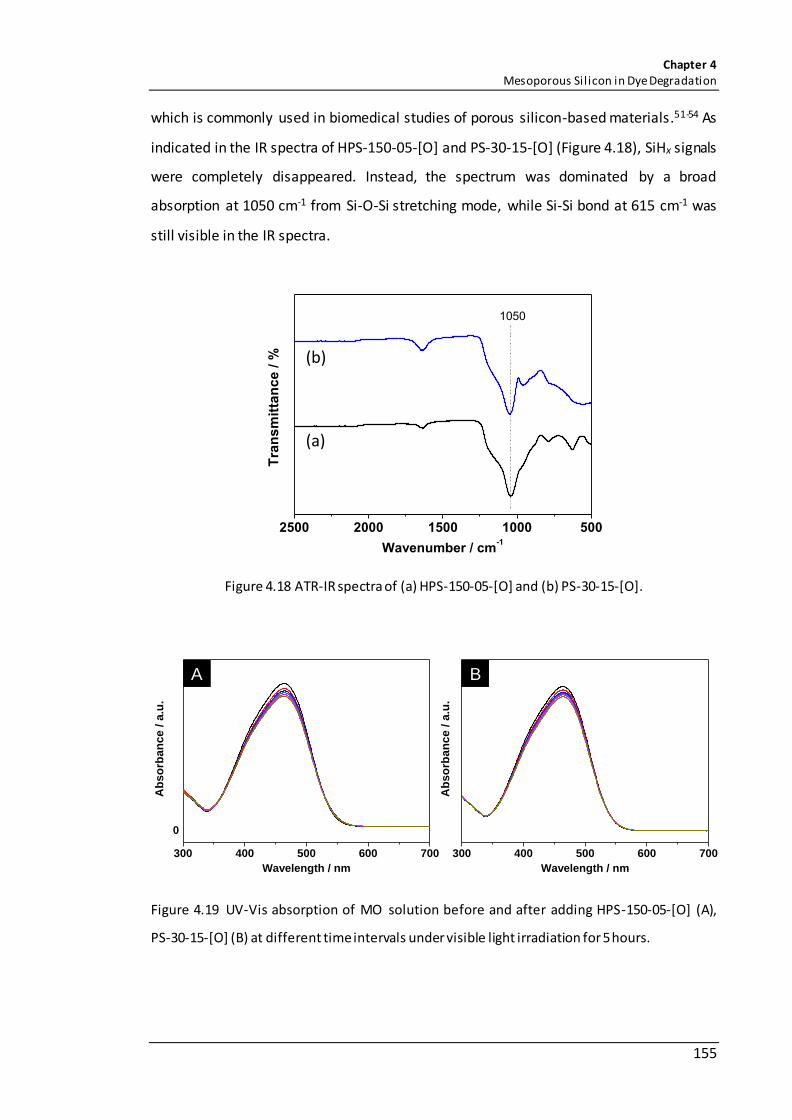
Chapter 4 Mesoporous Sil icon in Dye Degradation
155
which is commonly used in biomedical studies of porous silicon-based materials.51-54 As
indicated in the IR spectra of HPS-150-05-[O] and PS-30-15-[O] (Figure 4.18), SiHx signals
were completely disappeared. Instead, the spectrum was dominated by a broad
absorption at 1050 cm-1 from Si-O-Si stretching mode, while Si-Si bond at 615 cm-1 was
still visible in the IR spectra.
Figure 4.18 ATR-IR spectra of (a) HPS-150-05-[O] and (b) PS-30-15-[O].
Figure 4.19 UV-Vis absorption of MO solution before and after adding HPS-150-05-[O] (A),
PS-30-15-[O] (B) at different time intervals under visible light irradiation for 5 hours.
2500 2000 1500 1000 500
T
ran
sm
itta
nc
e /
%
Wavenumber / cm-1
1050
(a)
(b)
300 400 500 600 700
0
Ab
so
rba
nc
e /
a.u
.
Wavelength / nm
300 400 500 600 700
Ab
so
rba
nc
e /
a.u
.
Wavelength / nm
BA

Chapter 4 Mesoporous Sil icon in Dye Degradation
156
The evaluation of photocatalytic results (Figure 4.19) clearly show that the
photocatalytic activity of HPS-150-05-[O] and PS-30-15-[O] were completely inhibited
and only a slight reduction in MO concentration was detected which is mainly due to the
physical adsorption by the porous structure and implies that SiHx is largely responsible
for the observed activity of H-terminated mpSi towards MO molecules under dark
condition as well. This experimental result provided solid evidence that silicon hydrides
formed on the surface of mpSi is the determinant factor in the activity and behaviours
of H-terminated mpSi with or without any light irradiation.
4.3.4 Dye degradation behaviour under dark conditions
The surface state of mpSi is crucially important in the photocatalytic performance under
visible light irradiation. In fact, surface hydrides are also directly related to the “dark”
activity exhibited by H-terminated mpSi in MO degradation as shown in the previous
results summarized in Table 4.2 below.
Table 4.2 The MO degradation rate constant and degradation efficiency of H-terminated
mesoporous silicon samples with or without visible light irradiation.
Mesoporous silicon
Visible light illumination
Rate constant, k / h-1
Decomposition efficiency, η a / %
PS-10-15 ON 0.65 41.2
OFF 0.57 44.9
PS-30-15 ON 0.39 23.7
OFF 0.22 13.7
HPS-150-05 ON 0.86 53.9
OFF 0.48 40.0
HPS-200-05 ON 1.98 89.7
OFF 0.57 41.0
a Decomposition efficiency (η): the concentration ratio of decomposed MO molecules after 60 min with
or without external i l lumination.
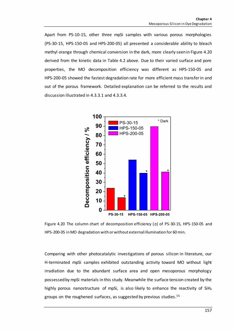
Chapter 4 Mesoporous Sil icon in Dye Degradation
157
Apart from PS-10-15, other three mpSi samples with various porous morphologies
(PS-30-15, HPS-150-05 and HPS-200-05) all presented a considerable ability to bleach
methyl orange through chemical conversion in the dark, more clearly seen in Figure 4.20
derived from the kinetic data in Table 4.2 above. Due to their varied surface and pore
properties, the MO decomposition efficiency was different as HPS-150-05 and
HPS-200-05 showed the fastest degradation rate for more efficient mass transfer in and
out of the porous framework. Detailed explanation can be referred to the results and
discussion illustrated in 4.3.3.1 and 4.3.3.4.
Figure 4.20 The column chart of decomposition efficiency (η) of PS-30-15, HPS-150-05 and
HPS-200-05 in MO degradation with or without external illumination for 60 min.
Comparing with other photocatalytic investigations of porous silicon in literature, our
H-terminated mpSi samples exhibited outstanding activity toward MO without light
irradiation due to the abundant surface area and open mesoporous morphology
possessed by mpSi materials in this study. Meanwhile the surface tension created by the
highly porous nanostructure of mpSi, is also likely to enhance the reactivity of SiHx
groups on the roughened surfaces, as suggested by previous studies.55
0
10
20
30
40
50
60
70
80
90
100
HPS-200-05
HPS-150-05
*
* *
Deco
mp
osit
ion
eff
icie
ncy /
%
PS-30-15
HPS-150-05
HPS-200-05
PS-30-15
* Dark

Chapter 4 Mesoporous Sil icon in Dye Degradation
158
As we know, the reduction activity of Si-H bond contained by nanostructured Si
materials is widely exploited in surface modification with alkene, alkyne,
aldehyde etc.,56-59 and in electroless deposition of metallic nanoparticles via in situ
reduction of metal ions such as Ag+, [PtCl4]2-, Cu2+, Ni2+ etc.60-62 The versatility of its
applications are also seen in the reduction of nitroarenes,48 CO2,49, 63 and the
dehydrogenation of secondary alcohol64 by Si NWs and NWs arrays of which the activity
was reported to be comparable to many functional inorganic materials used in
photochemical or electrochemical transformations including P-doped TiO2,
Pt nanoparticles.47 More importantly, the Si-H bond has also shown its reduction
capability for fabric azo dyes such as Remazol dyes,55 methylene blue65 in several studies
of Si NWs prepared by metal-assisted chemical etching approaches. Considering these
experimental results, the following degradation pathway was proposed in this study
(Scheme 4.3). By reducing the azo bond via hydrogen transfer from the surface hydrides
of H-terminated mesoporous silicon, MO molecules were converted into sulfanilic acid
and dimethyl-4-phenylenediamine.
Scheme 4.3 Proposed decomposition pathway of methyl orange by H-terminated mesoporous
silicon.
++ 4H
Methyl orange
Sulfanilic acid
Dimethyl-4-phenylenediamine

Chapter 4 Mesoporous Sil icon in Dye Degradation
159
Figure 4.21 UV-Vis absorption spectra of methyl orange (a), sulfanilic acid (b) and unreacted MO
solution in the presence of PS-30-15 after 210 min without external illumination.
As shown in Figure 4.21, the UV-Vis absorption spectrum of methyl orange solution is
mainly composed by two absorption bands at 464 nm and 271 nm originated from the
π-conjugated system. After adding mpSi, the intensity of these two peaks decayed as
the azo bonds of methyl orange molecules were destroyed over time. Meanwhile, the
appearance and gradual growth of a new peak at 246 nm was also observed at different
time intervals, which is likely contributed by the two end products, described above. As
Figure 4.21b clearly shows the characteristic absorption maximum for sulfanilic acid (SA)
is at 248 nm while it has been reported around 242 nm for dimethyl-4-
phenylenediamine (DMPD) as well.66
300 400 500 600 700 800
Ab
so
rba
nc
e /
a.u
.
Wavelength / nm
a
b
c

Chapter 4 Mesoporous Sil icon in Dye Degradation
160
Figure 4.22 ATR-IR spectra of PS-30-15 at different time intervals during MO degradation
without light illumination, 0 min, 60 min, 120 min, 240 min and 360 min, respectively.
Figure 4.22 shows the IR spectra of PS-30-15 at different time intervals of MO
degradation under dark condition. The vibrational signals of Si-H bond at 2080-2140 cm-1
and 910 cm-1 decreased accordingly with the Si-O-Si absorption peak at 1000-1100 cm-1
intensified, confirming the consumption of surface hydrides by organic dyes and the
formation of surface oxides on mpSi.
4.3.5 Dye degradation behaviour under visible light irradiation
The photocatalytic mechanism of MO degradation under visible light irradiation by
H-terminated mesoporous silicon was proposed based on the analysis of total carbon
content, active species, and electronic band structure of mesoporous silicon.
2500 2000 1500 1000 500
Tra
ns
mit
tan
ce
/ a
.u.
Wavenumber / cm-1
0 min
60 min
120 min
240 min
360 min

Chapter 4 Mesoporous Sil icon in Dye Degradation
161
4.3.5.1 Accelerating effect of visible light irradiation
After visible light irradiation was applied, the behaviours of mpSi toward MO was
immediately altered and the degradation rate was accelerated significantly. As displayed
in Figure 4.23, in the presence of HPS-200-05, MO concentration was first measured
twice every 30 min in the dark and then the lamp was switched on and the system was
irradiated by the visible light source for another 120 min. The 1st order reaction rate was
estimated as 1.72 h-1 under visible light irradiation, in accordance with the previous
result (k = 1.98 h-1).
Figure 4.23 The temporal course (A) and first-order kinetics (B) of MO degradation in the light
off/on experiment of HPS-200-05 (lamp was turned on after 60 min in the dark).
As mentioned previously, MO molecules were likely being converted into SA and DMPD
as shown in Scheme 4.3 by mpSi through hydrogen transfer, which accounts for the
major degradation activity in the dark. In fact, the presence of these products was also
observed under visible light irradiation at room temperature. As displayed in Figure 4.24,
the increasing rate of the peak intensity of 246-247 nm centred is far greater than that
of the dark condition, which signifies an elevated reactivity of Si-H bond under visible
-60 -30 0 30 60 90 120
0.0
0.2
0.4
0.6
0.8
1.0
1.2
C/C
0
Irradiation time / min
-60 -30 0 30 60 90 120
0
1
2
3
4
-ln
(C
/C0)
Irradiation time / min
k = 1.72 h-1
R2 = 0.994
BALight off Light on

Chapter 4 Mesoporous Sil icon in Dye Degradation
162
light illumination. As the visible light is not sufficiently energetic to cleave the surface
Si-H bond which requires a minimum wavelength of approximately 354 nm,67 and also
not capable of inducing total ejection of the electrons photogenerated in the conduction
band as suggested in previous studies of UV-promoted hydrosilylation.68 Therefore, the
activation barrier for hydrogen transfer was lowered. This is more likely to be a result of
its own solid-state electronics and surface environment by localizing photogenerated
charge carriers at specific surface sites, probably Si-H sites, in which way the reductive
activity was enhanced. To back this assumption up, similar proposal was also found in
literature which discovered so called exciton-based mechanism in the study of surface
hydrosilylation of H-terminated Si nanomaterials.69
Figure 4.24 UV-Vis absorbance of absorption peaks at 464 nm and 246 nm of MO solution over
HPS-200-05 at different time intervals in the dark (A), and under visible light irradiation (B).
4.3.5.2 Total organic carbon analysis
By measuring the organic carbon content of unreacted MO solution during
photocatalysis, the progress of photochemical degradation was monitored. As
presented in Figure 4.25 below, the total organic carbon (TOC) content declined by 10.1%
0 30 60 90 120 1500.0
0.4
0.8
1.2
1.6
UV
-Vis
ab
so
rban
ce /
a.u
.
Reaction time / min
246 nm
464 nm
0 30 60 90 120 1500.0
0.4
0.8
1.2
1.6 246 nm
464 nm
U
V-V
is a
bso
rban
ce /
a.u
.
Reaction time / min
A B

Chapter 4 Mesoporous Sil icon in Dye Degradation
163
after 60 min irradiation and 20.4% after 120 min irradiation time for HPS-150-05,
showing a mineralization process occurred to dye molecules in the reaction system by
mpSi under visible light irradiation.
Figure 4.25 The evolution of MO concentration (-ΔC/C0) and total carbon content (-ΔTOC/TOC0)
of the 50 µM MO solution degraded by HPS-150-05 under visible light irradiation.
According to photo-mineralization mechanism, organic matter is ultimately converted
into CO2, H2O and inorganic ions (e.g. NO3-, NH4
+, SO4-), through photocatalytic oxidation
which is initiated by photon-generated holes (h+), or by reactive oxygen-related species
(ROSs) produced on the CB/VB of irradiated semiconductor photocatalyst (Scheme 4.4).
Superoxide anion radical (·O2-), hydroxyl radical (·OH), hydrogen peroxide (H2O2) and
singlet oxygen (1O2) are amongst the most active ROSs that are capable of oxidizing
various organic substances because of their high oxidation potential.
Scheme 4.4 Mineralization process of methyl orange by photo-generated species.
0 60 120 180
0.0
0.1
0.2
0.3
0.4
0.5
0.6
0.7
0.8
0.9
1.0
C/C
0
TO
C/T
OC
0
Irradiation time / min
C/C0
TOC/TOC0
h+/ROSs + MO intermediates CO2 + H2O + SO42- + NO3
- + NH4+

Chapter 4 Mesoporous Sil icon in Dye Degradation
164
It is also known that the TOC removal rate is naturally slower than the reduction in the
concentration of organic substrate. Rather than simply destroying the chromophore
group of the azo dye, photo-mineralization involves various reaction intermediates
formed by bond cleavage, demethylation and hydroxylation, etc. during the
fragmentation of the substrate molecules, since the radical species are not so selective
in general.43, 70
Notably the carbon loss became stagnant after 120 min irradiation time while the
concentration of MO molecules constantly decayed. Due to the active participation of
silicon hydrides in MO reduction as described above, oxides were gradually formed on
the surface of mpSi as shown in Figure 4.22, and reduced the photo-oxidative activity of
mpSi. In fact, surface oxides are reported to be able to compete with Si-H on the electron
extraction and strongly influence the separation efficiency of photon-induced e-/h+
pairs.21 While Si-H functionalities can act as electron sinks, trapping photo-excited
electrons, therefore preventing the e-/h+ recombination, and consequently enhancing
the oxidizing ability of mpSi photocatalyst.15
4.3.5.3 Active species analysis
To further explore the photocatalytic mechanism, a series of trapping experiments were
performed to determine the primary active species involved in the photocatalytic
process of MO degradation over mpSi material under visible light irradiation. The results
of adding different radical scavengers into the system are displayed in Figure 4.26.

Chapter 4 Mesoporous Sil icon in Dye Degradation
165
Figure 4.26 Decomposition efficiency of MO degradation by HPS-200-05 added with different
quenchers (2-propanol, ethanol, triethanolamine) under visible light irradiation for 30 min.
When isopropyl alcohol (a quencher for hydroxyl radical, ·OH) was introduced into the
reaction system, the photocatalytic reaction rate was almost unaffected after 30 min.
Thus, hydroxyl radicals were unlikely among the active species in the photo-degradation
of MO by mpSi.
After saturating the MO solution with N2, the degradation efficiency declined by 20%
after 30 min irradiation time as shown in Figure 4.26. It is worth noting that despite the
depletion of oxygen in the aqueous solution, 56.8% MO molecules were still converted
which also signifies the influences of visible light irradiation on the action of surface
hydrides since the disappearance of only ~26% MO was observed in the dark
(Figure 4.15).
As known, by accepting the photo-induced electrons generated on the conduction band
of a semiconductor photocatalyst (Equation 4.1), superoxide radicals (·O2-), one of the
0
10
20
30
40
50
60
70
80
90
100
Deco
mp
osit
ion
eff
ecie
ncy /
%

Chapter 4 Mesoporous Sil icon in Dye Degradation
166
most important active species, can be formed (Equation 4.2) which lead to the rapid
oxidation of substrate molecules. Thus, without dissolved O2, superoxide radical species
could not be generated thereby the photocatalytic degradation progress of MO was
inhibited profoundly. Further proof was given by the quenching result of ethanol alcohol
(a quencher for electrons) which shows the decomposition was hindered after its
addition into the system. In fact, its electronic band structure as revealed below also
indicated very similar results.
Equation 4.1
Equation 4.2
Another quencher tested is triethanolamine (TEOA) for the detection of holes (h+). As
seen in Figure 4.26 , the photocatalytic reaction was inhibited dramatically with only
around 25% of initial MO were converted after 30 min irradiation. As we also observed
the release of gases from HPS-200-05, supposedly H2, due to the nucleophilic attack on
the electron deficient Si-H bond on the surface of mpSi (Equation 4.3). Thus, the
inactivity is likely due to the depletion of surface hydrides by TEOA quencher.
Equation 4.3
4.3.5.4 Photocatalytic mechanism
Based on the aforementioned results, a possible photocatalytic mechanism was
proposed. The bandgap energy (Eg) of mpSi was first estimated by the Tauc method
based on the UV-Vis absorption data of HPS-150-05 and HPS-200-05 (Figure 4.14). As
shown in Figure 4.27, it was 2.10 eV for HPS-150-05 and 2.05 eV for HPS-200-05, within
the reported range of 1.8-2.2 eV for porosified silicon materials.71-72
Si e-cb + h+
vb
hν
O2 + e- ·O2-
Si-H + H2O Si-OH + H2
δ+ δ-
(HOCH2CH2)3N:

Chapter 4 Mesoporous Sil icon in Dye Degradation
167
Figure 4.27 Tauc plots of HPS-150-05 and HPS-200-05.
The CB/VB band edge potential (ECB and EVB) of semiconductor can be calculated
according to the following formulas:
ECB = χ - EC - 0.5Eg Equation 4.4
EVB = ECB + Eg Equation 4.5
Eg is the bandgap energy of semiconductor. Ec is the energy of free electrons on the
hydrogen scale, 4.50 eV. χ is the absolute electronegativity of the component atoms,
4.77 eV for Si atom.73
Table 4.3 The bandgap and band edge potentials of mesoporous silicon materials versus Normal
Hydrogen Electrode (NHE).
Eg / eV ECB vs NHE/ V EVB vs NHE / V
HPS-150-05 2.10 -0.78 1.32
HPS-200-05 2.05 -0.75 1.30
Si74 1.10 -0.50 0.60
1.5 2.0 2.5 3.0 3.5 4.0 4.50.0
0.5
1.0
1.5
2.0
2.5
HPS-150-05
HPS-200-05
h
1/2(
eV
·cm
-1)1
/2
heV
Eg = 2.10 eV
Eg = 2.05 eV
hν
Eg
Eg

Chapter 4 Mesoporous Sil icon in Dye Degradation
168
As shown in Table 4.3, the bandgap of mpSi was significantly widened compared to Si
crystal due to the quantum confinement effects of the Si nanocrystallites embedded on
the pore walls of the mesoporous structure, rendering the material to be visible light
responsive and photo-catalytically active. The CB potential of mpSi shifted negatively by
0.2-0.3 V, which implies an improved reduction capability of CB electrons excited by
visible light photons. More significantly, its VB potential shifted downwards to
1.30-1.32 V from 0.60 V of the pristine Si. This positive shift is indicative of an enhanced
oxidation ability possessed by the valence band holes of mpSi. In fact, the photocatalytic
activity of Si-based nanostructures is often reported to be restricted by the shallow VB
band level which results in poor oxidation performance.10
Figure 4.28 Band edge positions of Si crystal and mesoporous silicon sample (HPS-150-05)
relative to NHE (normal hydrogen electrode) and the vacuum level. For comparison, the
reduction potentials (E0red) of various ROS (e.g. ·O2
-, ·OH, H2O2) are also presented.
As we know, the probability of charge transfer is determined by a relative position of
the valence and conductance zones of semiconductor photocatalyst and the value of the
oxidation-reduction potential (ORP) of the substrate.75 As seen in Figure 4.28, the CB/VB
energy levels of Si crystal and mesoporous silicon (HPS-150-05 for example) were
aligned with the reduction potential of multiple ROS couples that are most commonly
3.0
2.0
1.0
0.0
-1.0
-2.0
O2/·O2-
H2/H2O
O2/H2O
·OH/H2O
-2.5
-3.5
-4.5
-5.5
-6.5
-7.5
-0.5 V
SimpSi
Oxid
ation
of o
rganics
Water sp
litting
H2O2/·OH
HOO·/H2O2
0.6 V
-0.78 V
1.32 V

Chapter 4 Mesoporous Sil icon in Dye Degradation
169
discovered in heterogeneous photocatalysis. The widened bandgap of HPS-150-05
enabled it to absorb visible light energy and induce e-/h+ charge separation by exciting
electrons to conduction band. The energetic CB electrons of mpSi can reduce the
dissolved molecular oxygen into superoxide radical anions (·O2-), in agreement with the
previous quenching experiment. The insignificance of hydroxyl radicals (·OH) in the
photocatalytic process is also confirmed by the position of valence band edge of
HPS-150-05 shown in Figure 4.28 against E0red (·OH/H2O). Despite this, the increased VB
energy of mpSi is now greater than the H2O oxidation potential, suggesting water
splitting by mpSi without a sacrificial electron acceptor would be possible and will be
explored in the future. Figure 4.28 clearly affirmed the results of previous trapping
experiments, showing superoxide radical anions produced by one-electron reduction of
dissolved oxygen as the main reactive oxygen species in mpSi-catalysed MO photo-
degradation under visible light irradiation. Besides, the band structure also indicated the
possibility of the production of H2O2 and ·OH through the reduction of protonated ·O2-
during the photodegradation process. The existence of ·OH species was also evidenced
in the earlier analysis of the UV-Vis spectra of the unreacted solution (Figure 4.10) which
implied the generation of hydroxylated intermediates of methyl orange.
Figure 4.29 The proposed photocatalytic mechanism of the degradation of methyl orange by
H-terminated mesoporous silicon under visible light irradiation and the fragmentation of methyl
orange by surface hydrides of mesoporous silicon via hydrogen transfer.
hν
e-
h+
O2 aq ·O2-
MO CO2 + H2OEnergy Level
CB
VB
e-
h+ h+ h+ h+
e-e-
·OOH H2O2 ·OH
MO
MO CO2 + H2O HH H H H H H H
MO Fragments (SA, DMPD…)
Chemical pathway
+H+ +e- +e-
Hydroxylated intermediates
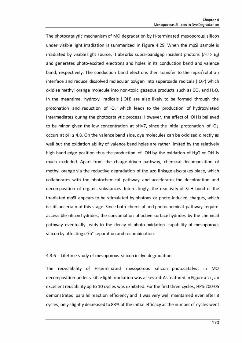
Chapter 4 Mesoporous Sil icon in Dye Degradation
170
The photocatalytic mechanism of MO degradation by H-terminated mesoporous silicon
under visible light irradiation is summarized in Figure 4.29. When the mpSi sample is
irradiated by visible light source, it absorbs supra-bandgap incident photons (h > Eg)
and generates photo-excited electrons and holes in its conduction band and valence
band, respectively. The conduction band electrons then transfer to the mpSi/solution
interface and reduce dissolved molecular oxygen into superoxide radicals (·O2-) which
oxidise methyl orange molecule into non-toxic gaseous products such as CO2 and H2O.
In the meantime, hydroxyl radicals (·OH) are also likely to be formed through the
protonation and reduction of ·O2- which leads to the production of hydroxylated
intermediates during the photocatalytic process. However, the effect of ·OH is believed
to be minor given the low concentration at pH≈7, since the initial protonation of ·O2-
occurs at pH ≤ 4.8. On the valence band side, dye molecules can be oxidized directly as
well but the oxidation ability of valence band holes are rather limited by the relatively
high band edge position thus the production of ·OH by the oxidation of H2O or OH- is
much excluded. Apart from the charge-driven pathway, chemical decomposition of
methyl orange via the reductive degradation of the azo linkage also takes place, which
collaborates with the photochemical pathway and accelerates the decoloration and
decomposition of organic substances. Interestingly, the reactivity of Si-H bond of the
irradiated mpSi appears to be stimulated by photons or photo-induced charges, which
is still uncertain at this stage. Since both chemical and photochemical pathway require
accessible silicon hydrides, the consumption of active surface hydrides by the chemical
pathway eventually leads to the decay of photo-oxidation capability of mesoporous
silicon by affecting e-/h+ separation and recombination.
4.3.6 Lifetime study of mesoporous silicon in dye degradation
The recyclability of H-terminated mesoporous silicon photocatalyst in MO
decomposition under visible light irradiation was assessed. As featured in Figure 4.30 , an
excellent reusability up to 10 cycles was exhibited. For the first three cycles, HPS-200-05
demonstrated parallel reaction efficiency and it was very well maintained even after 8
cycles, only slightly decreased to 88% of the initial efficacy as the number of cycles went

Chapter 4 Mesoporous Sil icon in Dye Degradation
171
up to 10. Thus, it is reasonable to assume that a comparable activity will be able to last
for even longer time. To our best knowledge, this is by far the best reuse performance
ever achieved on Si-based elemental photocatalysts.
Figure 4.30 The cycle runs of HPS-200-05 in visible light driven photo-degradation of methyl
orange. HPS-200-05 was simply washed with 5 wt. % aqueous HF prior to the next cycle.
Without HF cleaning procedure prior to each cycle, the activity of mesoporous silicon
upon visible light irradiation decayed rapidly (Figure 4.31). This is largely due to the
consumption of surface hydrides species and simultaneous formation of surface oxides
as explained above.
Figure 4.31 The cycle runs of HPS-200-05 in visible light driven photo-degradation of methyl
orange without HF washing in between each cycle.
0 60 120 180 240 300 360 420 480 540 6000.0
0.2
0.4
0.6
0.8
1.0
C/C
0
Time / min
1st 2nd 3rd 4th 5th 6th 7th 8th 9th 10th
0 60 120 1800.0
0.2
0.4
0.6
0.8
1.0
C/C
0
Time / min
1st 2nd 3rd

Chapter 4 Mesoporous Sil icon in Dye Degradation
172
Interestingly, we also tested the reusability of H-terminated mesoporous silicon in MO
degradation without any illumination using the same regeneration approach by HF
washing. As presented in Figure 4.32, its activity was maintained and only slightly
reduced after 5 runs. This result shows H-terminated mesoporous silicon is also a
promising candidate as a rechargeable hydride source, which can be exploited in many
applications such as H2 generation, CO2 reduction and organic synthesis for fine
chemicals.
Figure 4.32 The cycle runs of HPS-200-05 in degrading methyl orange in the absence of light.
HPS-200-05 was simply washed with 5 wt. % aqueous HF prior to the next cycle.
4.4 Summary
In this study, a highly reusable metal-free photocatalyst in visible-light-driven methyl
orange photo-degradation was developed via electrochemical etching of
monocrystalline Si. By absorbing visible light photons with energies equal to or higher
than the 2.05-2.10 eV bandgap ( 598 nm) of H-terminated mesoporous silicon
enlarged by quantum confinement of silicon nanocrystallites , electron-hole pairs were
generated and separated with electrons excited to the conduction band creating a
chemical potential (ECB = -0.78 V, EVB = 1.32 V vs NHE, e.g. HPS-150-05) that triggered the
generation of reactive oxygen species, mainly superoxide radicals (˙O2−) through single
electron transfer and other redox events involved in the dye degradation process under
0 60 120 180 240 3000.0
0.2
0.4
0.6
0.8
1.0
C/C
0
Time / min
1st 2nd 3rd 4th 5th

Chapter 4 Mesoporous Sil icon in Dye Degradation
173
visible light irradiation. The broad visible light responsive range, vast accessible surface
area and significantly released diffusion resistance by the open mesoporous system,
largely contributed to the excellent decomposition efficiency of mesoporous silicon with
organic molecules rapidly decolorized and mineralized.
The complex and important roles played by the surface hydrides of mesoporous silicon
were also reflected in the reductive degradation of the azo linkage of methyl orange
without light illumination and the determining influences on the course and rate of
photochemical activities exhibited by irradiated mesoporous silicon toward methyl
orange. The reactivity of the Si-H bond not only enabled unsaturated organics to be
chemically fragmented into smaller molecules, but also led to the competition against
charge-mediated photochemical degradation that is also strongly reliant on them as
silicon hydrides can improve the lifetime of separated e-/h+ pairs. Notably, we also
observed an acceleration in the chemical pathway after applying visible light irradiation
suggesting the reduction capability of surface Si-H bond was stimulated by most likely
the photo-induced charges considering the energy of incident photons are too weak to
break any chemical bonds. Further investigation will be necessary to confirm this result,
proposedly directed to understand the possible interaction and coupling between
surface species of mesoporous silicon and the incident photons and photo-induced
charges.
The effects of different structural factors on the photocatalytic performance were also
discussed in this chapter, which revealed the varied influences of pore order, pore size,
pore depth, sizes of Si nanocrystals on the photon absorption, and mass diffusion
processes during dye degradation. As found the ordered 1D channel array of heavily
doped mesoporous silicon is more efficient in degrading methyl orange molecules than
the interconnected porous network of moderately doped mesoporous silicon for the
improved mass transfer facilitated by the larger mesopores and straight pore alignment.
Last but not the least, the lifetime of H-terminated mesoporous silicon photocatalyst
was also examined which shows an excellent reusability and its activity can be
maintained very well even after 10 cycles of dye degradation.

Chapter 4 Mesoporous Sil icon in Dye Degradation
174
4.5 References
1. Linic, S.; Christopher, P.; Ingram, D. B., Plasmonic-metal nanostructures for efficient
conversion of solar to chemical energy. Nat. Mater. 2011, 10 (12), 911-921.
2. Martha, S.; Sahoo, P. C.; Parida, K. M., An overview on visible light responsive metal
oxide based photocatalysts for hydrogen energy production. RSC Adv. 2015, 5 (76),
61535-61553.
3. Kamat, P. V., Meeting the clean energy demand: nanostructure architectures for solar
energy conversion. J. Phys. Chem. C 2007, 111 (7), 2834-2860.
4. Habisreutinger, S. N.; Schmidt-Mende, L.; Stolarczyk, J. K., Photocatalytic reduction of
CO2 on TiO2 and other semiconductors. Angew. Chem. Int. Ed. Engl. 2013, 52 (29),
7372-7408.
5. Chen, C.; Ma, W.; Zhao, J., Semiconductor-mediated photodegradation of pollutants
under visible-light irradiation. Chem. Soc. Rev. 2010, 39 (11), 4206-4219.
6. Zhu, H.; Lian, T., Wavefunction engineering in quantum confined semiconductor
nanoheterostructures for efficient charge separation and solar energy conversion.
Energy Environ. Sci. 2012, 5 (11), 9406-9418.
7. Dong, S.; Feng, J.; Fan, M.; Pi, Y.; Hu, L.; Han, X.; Liu, M.; Sun, J.; Sun, J., Recent
developments in heterogeneous photocatalytic water treatment using visible light-
responsive photocatalysts: a review. RSC Adv. 2015, 5 (19), 14610-14630.
8. Cai, Z.; Sun, Y.; Liu, W.; Pan, F.; Sun, P.; Fu, J., An overview of nanomaterials applied
for removing dyes from wastewater. Environ. Sci. Pollut. Res. Int. 2017, 24 (19),
15882-15904.
9. Spasiano, D.; Marotta, R.; Malato, S.; Fernandez-Ibanez, P.; Di Somma, I., Solar
photocatalysis: Materials, reactors, some commercial, and pre-industrialized
applications. A comprehensive approach. Appl. Catal. B 2015, 170, 90-123.
10. Liu, G.; Niu, P.; Cheng, H. M., Visible-light-active elemental photocatalysts.
ChemPhysChem 2013, 14 (5), 885-892.
11. Chandrasekaran, S.; Nann, T.; Voelcker, N. H., Nanostructured silicon
photoelectrodes for solar water electrolysis. Nano Energy 2015, 17, 308-322.

Chapter 4 Mesoporous Sil icon in Dye Degradation
175
12. Liu, X.; Coxon, P. R.; Peters, M.; Hoex, B.; Cole, J. M.; Fray, D. J., Black silicon:
fabrication methods, properties and solar energy applications. Energy Environ. Sci. 2014,
7 (10), 3223-3263.
13. Kang, Z.; Tsang, C. H.; Wong, N. B.; Zhang, Z.; Lee, S. T., Silicon quantum dots: a
general photocatalyst for reduction, decomposition, and selective oxidation reactions.
J. Am. Chem. Soc. 2007, 129 (40), 12090-12091.
14. Kang, Z.; Liu, Y.; Lee, S. T., Small-sized silicon nanoparticles: new nanolights and
nanocatalysts. Nanoscale 2011, 3 (3), 777-791.
15. Shao, M.; Cheng, L.; Zhang, X.; Ma, D. D.; Lee, S. T., Excellent photocatalysis of
HF-treated silicon nanowires. J. Am. Chem. Soc. 2009, 131 (49), 17738-17739.
16. Qu, Y.; Zhong, X.; Li, Y.; Liao, L.; Huang, Y.; Duan, X., Photocatalytic properties of
porous silicon nanowires. J. Mater. Chem. 2010, 20 (18), 3590-3594.
17. Megouda, N.; Cofininier, Y.; Szunerits, S.; Hadjersi, T.; Elkechai, O.; Boukherroub, R.,
Photocatalytic activity of silicon nanowires under UV and visible light irradiation. Chem.
Commun. 2011, 47 (3), 991-993.
18. Wang, F. Y.; Yang, Q. D.; Xu, G.; Lei, N. Y.; Tsang, Y. K.; Wong, N. B.; Ho, J. C., Highly
active and enhanced photocatalytic silicon nanowire arrays. Nanoscale 2011, 3 (8),
3269-3276.
19. Liu, R.; Yuan, G. B.; Joe, C. L.; Lightburn, T. E.; Tan, K. L.; Wang, D. W., Silicon
nanowires as photoelectrodes for carbon dioxide fixation. Angew. Chem. Int. Ed. 2012,
51 (27), 6709-6712.
20. Liao, F.; Wang, T.; Shao, M., Silicon nanowires: applications in catalysis with
distinctive surface property. J. Mater. Sci. Mater. Electron. 2015, 26 (7), 4722-4729.
21. Liu, D.; Li, L.; Gao, Y.; Wang, C.; Jiang, J.; Xiong, Y., The nature of photocatalytic "water
splitting" on silicon nanowires. Angew. Chem. Int. Ed. Engl. 2015, 54 (10), 2980-2985.
22. Su, J.; Yu, H.; Quan, X.; Chen, S.; Wang, H., Hierarchically porous silicon with
significantly improved photocatalytic oxidation capability for phenol degradation. Appl.
Catal. B 2013, 138-139, 427-433.

Chapter 4 Mesoporous Sil icon in Dye Degradation
176
23. Meekins, B. H.; Lin, Y. C.; Manser, J. S.; Manukyan, K.; Mukasyan, A. S.; Kamat, P. V.;
McGinn, P. J., Photoactive porous silicon nanopowder. ACS Appl. Mater. Interfaces 2013,
5 (8), 2943-2951.
24. Dai, F.; Zai, J.; Yi, R.; Gordin, M. L.; Sohn, H.; Chen, S.; Wang, D., Bottom-up synthesis
of high surface area mesoporous crystalline silicon and evaluation of its hydrogen
evolution performance. Nat. Commun. 2014, 5, 3605.
25. Xu, H.; Xiao, H.; Pei, H.; Cui, J.; Hu, W., Photodegradation activity and stability of
porous silicon wafers with (100) and (111) oriented crystal planes. Microporous
Mesoporous Mater. 2015, 204, 251-256.
26. Li, T.; Li, J.; Zhang, Q.; Blazeby, E.; Shang, C.; Xu, H.; Zhang, X.; Chao, Y., Hydrogen-
terminated mesoporous silicon monoliths with huge surface area as alternative Si -based
visible light-active photocatalysts. RSC Adv. 2016, 6 (75), 71092-71099.
27. Peng, F.; Wang, J.; Ge, G. L.; He, T.; Cao, L. X.; He, Y. H.; Ma, H.; Sun, S. Q.,
Photochemical reduction of CO2 catalyzed by silicon nanocrystals produced by high
energy ball milling. Mater. Lett. 2013, 92, 65-67.
28. Oh, I.; Kye, J.; Hwang, S., Enhanced photoelectrochemical hydrogen production from
silicon nanowire array photocathode. Nano Lett. 2012, 12 (1), 298-302.
29. Lee, H. Y.; Ryu, J.; Kim, J. H.; Lee, S. H.; Park, C. B., Biocatalyzed artificial
photosynthesis by hydrogen-terminated silicon nanowires. ChemSusChem 2012, 5 (11),
2129-2132.
30. Lee, S. H.; Ryu, G. M.; Nam, D. H.; Kim, J. H.; Park, C. B., Silicon nanowire
photocathodes for light-driven electroenzymatic synthesis. ChemSusChem 2014, 7 (11),
3007-3011.
31. Lian, S. Y.; Tsang, C. H. A.; Kang, Z. H.; Liu, Y.; Wong, N.; Lee, S. T., Hydrogen-
terminated silicon nanowire photocatalysis: benzene oxidation and methyl red
decomposition. Mater. Res. Bull. 2011, 46 (12), 2441-2444.
32. Wang, J.-F.; Chen, J.-S.; Zhou, Z.-F., Preparation of porous silicon by sodiothermic
reduction of zeolite and photoactivation for benzene oxidation. Eur. J. Inorg. Chem. 2015,
2015 (8), 1330-1333.

Chapter 4 Mesoporous Sil icon in Dye Degradation
177
33. Ameen, S.; Park, D.-R.; Shin, H. S., Silicon nanowires arrays for visible light driven
photocatalytic degradation of rose bengal dye. J. Mater. Sci. Mater. Electron. 2016,
27 (10), 10460-10467.
34. Fellahi, O.; Barras, A.; Pan, G.-H.; Coffinier, Y.; Hadjersi, T.; Maamache, M.;
Szunerits, S.; Boukherroub, R., Reduction of Cr(VI) to Cr(III) using silicon nanowire arrays
under visible light irradiation. J. Hazard. Mater. 2016, 304, 441-447.
35. Thommes, M.; Kaneko, K.; Neimark, A. V.; Olivier, J. P.; Rodriguez-Reinoso, F.;
Rouquerol, J.; Sing, K. S. W., Physisorption of gases, with special reference to the
evaluation of surface area and pore size distribution (IUPAC Technical Report). Pure Appl.
Chem. 2015, 87 (9-10), 1051-1069.
36. Dohnalova, K.; Gregorkiewicz, T.; Kusova, K., Silicon quantum dots: surface matters.
J. Phys. Condens. Matter. 2014, 26 (17), 173201.
37. Rajkanan, K.; Singh, R.; Shewchun, J., Absorption coefficient of silicon for s olar cell
calculations. Solid-State Electron. 1979, 22 (9), 793-795.
38. Ioannis Leontis, A. O. a. A. G. N., Structure, morphology, and photoluminescence of
porous Si nanowires: effect of different chemical treatments. Nanoscale Res. Lett. 2013,
8, 383.
39. Kumar, P., Effect of silicon crystal size on photoluminescence appearance in porous
silicon. ISRN Nanotechnology 2011, 2011, 163168.
40. Wang, K.; Wang, Q.; Chao, Y., Simple fabrication of nanostructured silicon and
photoluminescence. Appl. Phys. A 2012, 109 (2), 437-440.
41. Coxon, P. R.; Wang, Q.; Chao, Y., An abrupt switch between the two
photoluminescence bands within alkylated silicon nanocrystals. J. Phys. D 2011, 44 (49),
495301.
42. Kotkovskiy, G. E.; Kuzishchin, Y. A.; Martynov, I. L.; Chistyakov, A. A.; Nabiev, I., The
photophysics of porous silicon: technological and biomedical implications. Phys. Chem.
Chem. Phys. 2012, 14 (40), 13890-13902.

Chapter 4 Mesoporous Sil icon in Dye Degradation
178
43. Baiocchi, C.; Brussino, M. C.; Pramauro, E.; Prevot, A. B.; Palmisano, L.; Marcı, G.,
Characterization of methyl orange and its photocatalytic degradation products by
HPLC/UV–VIS diode array and atmospheric pressure ionization quadrupole ion trap
mass spectrometry. Int. J. Mass Spectrom. 2002, 214 (2), 247-256.
44. Hoffmann, M. R.; Martin, S. T.; Choi, W. Y.; Bahnemann, D. W., Environmental
applications of semiconductor photocatalysis. Chem. Rev. 1995, 95 (1), 69-96.
45. Alivisatos, A. P., Perspectives on the physical chemistry of semiconductor
nanocrystals. J. Phys. Chem. 1996, 100 (31), 13226-13239.
46. Canham, L. T., Silicon quantum wire array fabrication by electrochemical and
chemical dissolution of wafers. Appl. Phys. Lett. 1990, 57 (10), 1046-1048.
47. Lee, H. Y.; Kim, J. H.; Son, E. J.; Park, C. B., Silicon nanowires as a rechargeable
template for hydride transfer in redox biocatalysis. Nanoscale 2012, 4 (24), 7636-7640.
48. Xu, Y.; Wang, L.; Jiang, W.; Wang, H.; Yao, J.; Guo, Q.; Yuan, L.; Chen, H., Silicon
nanowire arrays - a new catalyst for the reduction of nitrobenzene derivatives.
ChemCatChem 2013, 5 (12), 3788-3793.
49. Sun, W.; Qian, C.; He, L.; Ghuman, K. K.; Wong, A. P. Y.; Jia, J.; Jelle, A. A.;
O’Brien, P. G.; Reyes, L. M.; Wood, T. E.; Helmy, A. S.; Mims, C. A.; Singh, C. V.; Ozin, G. A.,
Heterogeneous reduction of carbon dioxide by hydride-terminated silicon nanocrystals.
Nat. Commun. 2016, 7, 12553.
50. Sailor, M. J., Fundamentals of porous silicon preparation. In Porous Silicon in Practice:
Prepration, Chracterization and Applications. Wiley, 2012; pp 1-42.
51. Secret, E.; Leonard, C.; Kelly, S. J.; Uhl, A.; Cozzan, C.; Andrew, J. S., Size control of
porous silicon-based nanoparticles via pore-wall thinning. Langmuir 2016, 32 (4),
1166-1170.
52. Wang, M.; Hartman, P. S.; Loni, A.; Canham, L. T.; Bodiford, N.; Coffer, J. L., Influence
of surface chemistry on the release of an antibacterial drug from nanostructured porous
silicon. Langmuir 2015, 31 (22), 6179-6185.
53. Joo, J.; Cruz, J. F.; Vijayakumar, S.; Grondek, J.; Sailor, M. J., Photoluminescent porous
Si/SiO2 core/shell nanoparticles prepared by borate oxidation. Adv. Funct. Mater. 2014,
24 (36), 5688-5694.

Chapter 4 Mesoporous Sil icon in Dye Degradation
179
54. Fry, N. L.; Boss, G. R.; Sailor, M. J., Oxidation-induced trapping of drugs in porous
silicon microparticles. Chem. Mater. 2014, 26 (8), 2758-2764.
55. Wang, H.; Jiang, W.; Yuan, L.; Wang, L.; Chen, H., Reductase-like activity of silicon
nanowire arrays. ACS Appl. Mater. Interfaces 2013, 5 (5), 1800-1805.
56. Buriak, J. M., Organometallic chemistry on silicon and germanium surfaces. Chem.
Rev. 2002, 102 (5), 1271-1308.
57. Behray, M.; Webster, C. A.; Pereira, S.; Ghosh, P.; Krishnamurthy, S.; Al-Jamal, W. T.;
Chao, Y., Synthesis of diagnostic silicon nanoparticles for targeted delivery of thiourea
to epidermal growth factor receptor-expressing cancer cells. ACS Appl. Mater. Interfaces
2016, 8 (14), 8908-8917.
58. Ahire, J. H.; Behray, M.; Webster, C. A.; Wang, Q.; Sherwood, V.; Saengkrit, N.;
Ruktanonchai, U.; Woramongkolchai, N.; Chao, Y., Synthesis of carbohydrate capped
silicon nanoparticles and their reduced cytotoxicity, in vivo toxicity, and cellular uptake.
Adv. Healthc. Mater. 2015, 4 (12), 1877-1886.
59. Wang, Q.; Bao, Y.; Zhang, X.; Coxon, P. R.; Jayasooriya, U. A.; Chao, Y., Uptake and
toxicity studies of poly-acrylic acid functionalized silicon nanoparticles in cultured
mammalian cells. Adv. Healthc. Mater. 2012, 1 (2), 189-198.
60. Amdouni, S.; Coffinier, Y.; Szunerits, S.; Zaïbi, M. A.; Oueslati, M.; Boukherroub, R.,
Catalytic activity of silicon nanowires decorated with silver and copper nanoparticles.
Semicond. Sci. Technol. 2016, 31 (1), 014011.
61. Polisski, S.; Goller, B.; Wilson, K.; Kovalev, D.; Zaikowskii, V.; Lapkin, A., In situ
synthesis and catalytic activity in CO oxidation of metal nanoparticles supported on
porous nanocrystalline silicon. J. Catal. 2010, 271 (1), 59-66.
62. Kim, T.; Fu, X.; Warther, D.; Sailor, M. J., Size-controlled Pd nanoparticle catalysts
prepared by galvanic displacement into a porous Si-iron oxide nanoparticle host. ACS
Nano 2017, 11 (3), 2773-2784.
63. Dasog, M.; Kraus, S.; Sinelnikov, R.; Veinot, J. G. C.; Rieger, B., CO2 to methanol
conversion using hydride terminated porous silicon nanoparticles. Chem. Commun.
2017, 53 (21), 3114-3117.

Chapter 4 Mesoporous Sil icon in Dye Degradation
180
64. El-Demellawi, J. K.; Holt, C. R.; Abou-Hamad, E.; Al-Talla, Z. A.; Saih, Y.; Chaieb, S.,
Room-temperature reactivity of silicon nanocrystals with solvents: the case of ketone
and hydrogen production from secondary alcohols: catalysis? ACS Appl. Mater.
Interfaces 2015, 7 (25), 13794-13800.
65. Ye, M.; Qian, C.; Sun, W.; He, L.; Jia, J.; Dong, Y.; Zhou, W., Dye colour switching by
hydride-terminated silicon particles and its application as an oxygen indicator. J. Mater.
Chem. C 2016, 4 (20), 4577-4583.
66. Jana, A.; Lawrence, K. N.; Teunis, M. B.; Mandal, M.; Kumbhar, A.; Sardar, R.,
Investigating the control by quantum confinement and surface ligand coating of
photocatalytic efficiency in chalcopyrite copper indium diselenide nanocrystals. Chem.
Mater. 2016, 28 (4), 1107-1120.
67. Kopping, B.; Chatgilialoglu, C.; Zehnder, M.; Giese, B., Tris(trimethylsilyl)silane: an
efficient hydrosilylating agent of alkenes and alkynes. J. Org. Chem. 1992, 57 (14),
3994-4000.
68. Buriak, J. M., Illuminating silicon surface hydrosilylation: an unexpected plurality of
mechanisms. Chem. Mater. 2014, 26 (1), 763-772.
69. Huck, L. A.; Buriak, J. M., Toward a mechanistic understanding of exciton-mediated
hydrosilylation on nanocrystalline silicon. J. Am. Chem. Soc. 2012, 134 (1), 489-497.
70. Lai, Y. K.; Huang, J. Y.; Zhang, H. F.; Subramaniam, V. P.; Tang, Y. X.; Gong, D. G.;
Sundar, L.; Sun, L.; Chen, Z.; Lin, C. J., Nitrogen-doped TiO2 nanotube array films with
enhanced photocatalytic activity under various light sources. J. Hazard. Mater. 2010,
184 (1-3), 855-863.
71. Chen, Z.; Lee, T. Y.; Bosman, G., Electrical band gap of porous silicon. Appl. Phys. Lett.
1994, 64 (25), 3446-3448.
72. Frederiksen, J. T.; Melcher, P. G.; Veje, E., The electrical band-gap energy of porous
silicon measured versus sample temperature. J. Porous Mater. 2000, 7 (1/3), 271-273.
73. Pearson, R. G., Absolute electronegativity and hardness: application to inorganic
chemistry. Inorganic Chemistry 1988, 27 (4), 734-740.
74. Bludau, W.; Onton, A.; Heinke, W., Temperature dependence of the band gap of
silicon. J. Appl. Phys. 1974, 45 (4), 1846-1848.

Chapter 4 Mesoporous Sil icon in Dye Degradation
181
75. Prihod'ko, R. V.; Soboleva, N. M., Photocatalysis: oxidative processes in water
treatment. J. Chem. 2013, 2013, 1-8.

Chapter 5
Chapter 5
Hydrogen-Terminated Mesoporous Silicon/Graphitic
Carbon Nitride (g-C3N4) Nanosheets Heterojunction Study
Abstract
In semiconductor-mediated photocatalysis, the construction of hybrids by coupling
different semiconductors is an effective strategy for achieving a better performance in
a given redox reaction. In contrast to the involvement of expensive metal-containing
components, two dimensional graphitic carbon nitride (g-C3N4) material appeals to be
an ideal candidate to generate earth abundant and metal-free heterojunction utilized in
solar energy conversion. Here g-C3N4 was for the first time composited with
H-terminated mesoporous silicon previously investigated via simple impregnation,
which exhibited an enhanced activity in methyl orange degradation under visible light
irradiation.

Chapter 5 Heterojunction Study
183
5.1 Overview
Two-dimensional (2D) nanomaterials, such as graphene,1-3 MoS2,4-6 and hexagonal
boron nitride (h-BN),7 have attracted worldwide attention owing to their exceptional
structural and electronic properties over the past decade.8 A significant amount of effort
has in particular been devoted to the development of 2D graphitic carbon nitride (g-C3N4)
which has shown promising activities in various fields of solar energy conversion, light-
emitting and sensing etc.9-15 Ever since the first report of using g-C3N4 in hydrogen
production in 2009 by Wang et al.,16 its potential as photocatalyst in water splitting,17
CO2 fixation,18 and pollutant regulation9, 11 has been exploited widely due to its notable
characters such as low-cost, earth abundant, non-toxic, thermal and chemical stability.10
Moreover, its layered structure can be easily delaminated into nanosheets via
thermal,19-21 chemical,22-24 or mechanical treatment25-28 which is widely recognized as a
novel class of nanostructured materials because of the high surface area, small vertical
thickness and quantum confined effects on photoactivity.29
In this chapter, H-terminated mesoporous silicon (mpSi) was combined with such
two-dimensional g-C3N4 nanosheets (g-C3N4 NSs), obtained through thermal
condensation polymerisation of melamine followed by ultrasonic exfoliation. Firstly, the
physiochemical properties of g-C3N4 bulk powders and g-C3N4 NSs were thoroughly
examined by means of characterisation techniques including SEM, IR, gas sorption,
thermal analysis and optical measurements, exhibiting clear differences in physical
morphology (plane size, vertical thickness), surface area and optical properties leading
to a more efficient photocatalytic performance of g-C3N4 NSs in degrading methyl
orange (MO) under visible light irradiation than the large aggregated parent powders.
After combined with mpSi via liquid-phase impregnation, the degradation activity of
mpSi/g-C3N4 NSs material of 1:1 weight ratio toward MO was remarkably promoted,
indicating a coupling interaction between these two semiconductor components.

Chapter 5 Heterojunction Study
184
5.2 Experimental section
5.2.1 Synthesis of graphitic carbon nitride bulk powders
The bulk g-C3N4 was fabricated by direct pyrolysis of melamine. The precursor was
heated in an alumina boat covered by Al foil at 550˚C and the heating rate was
10 ˚C·min-1, then kept for 2 hours at 550 ˚C under static air. After condensation, it was
ground into g-C3N4 powders.
5.2.2 Synthesis of graphitic carbon nitride nanosheets
Graphitic C3N4 nanosheets were prepared by sonication assisted liquid exfoliation.
Typically, 100 mg g-C3N4 powder as obtained above was first dispersed in 50 mL
2-propanol. Then the colloidal solution was exposed to ultrasound treatment for
10 hours at room temperature. Thereafter they were centrifuged at 3000 rpm and then
g-C3N4 NSs were obtained in the supernatant layer.
5.2.3 Synthesis of the composites (mpSi/g-C3N4 NSs)
H-terminated mesoporous silicon (mpSi) was obtained by electrochemical etching of
monocrystalline Si wafers in HF/ethanol electrolyte at room temperature. Among
various mpSi samples that had been studied in previous chapters, HPS-200-05-F samples
exhibited the most impressive photocatalytic activity in methyl orange degradation due
to the wide visible light responsiveness and its unique structural features according to
the findings in Chapter 4 (Figure 4.17). Thus, it was adopted here to be combined with
g-C3N4 nanosheets in varied weight ratio as 4:1, 1:1 and 1:4 respectively, through the
procedure described in 2.2.3 in Chapter 2.

Chapter 5 Heterojunction Study
185
5.2.4 Sample characterisation
The structural morphology and physiochemical properties of g-C3N4 bulk powders and
g-C3N4 nanosheets were examined by means of SEM, FTIR, nitrogen adsorption,
TGA-DSC, UV-Vis and fluorescence spectroscopic techniques with H2O used as
dispersion medium for the optical measurements. The IR, UV-Vis absorption,
photoluminescence emission spectra of mpSi/g-C3N4 NSs composites were also
recorded. All measurement parameters were the same as described in Chapter 2 unless
otherwise stated.
5.2.5 Photocatalytic evaluation
The photocatalytic activities of g-C3N4 materials and the heterojunction were measured
by the photo-degradation of methyl orange (MO) under visible light irradiation. The
unreacted dye concentration of MO solution was measured by UV-Vis spectrometer at
different time intervals of the photocatalytic process. Apparent rate constants were also
derived from the UV-Vis data of MO based on first order reaction model for the
clarification of reaction efficiency. All experimental procedures and instrumental
parameters were the same as outlined in Chapter 2 unless otherwise specified in the
text.
5.3 Results and discussion
5.3.1 Characterisation and photocatalytic activity of g-C3N4 materials
As described above, graphitic carbon nitride (g-C3N4) bulk particles were synthesized
through thermal-driven condensation polymerisation of melamine, which were then
used to prepare g-C3N4 nanosheets (g-C3N4 NSs) by sonication-assisted liquid exfoliation
in isopropanol. A range of characterisation tools (SEM, FTIR, gas sorption, thermal
analysis, UV-Vis absorption and fluorescence spectroscopies) were employed to confirm
this result. Then the photocatalytic performance of g-C3N4 powders and g-C3N4 NSs in
MO decomposition under visible light irradiation were also examined in this section.

Chapter 5 Heterojunction Study
186
5.3.1.1 SEM images and elemental analysis of g-C3N4 materials
Figure 5.1 SEM images of g-C3N4 bulk powders (A, B) and g-C3N4 nanosheets (C, D).
As shown in Figure 5.1, the particle size of g-C3N4 nanosheets (C and D) was significantly
reduced after exfoliation, in stark contrast to the bulky particles of parent g-C3N4
powders (A and B) as well as the thinness, while the typical graphite-like 2D layered
structure was distinctly featured in the bulk g-C3N4. The theoretical thickness of g-C3N4
monolayer is about 0.325 nm21 which would be greatly desirable to be used in the
following photocatalytic application because of the much enlarged interface area it
possesses for mass and charge transport. However, as known from graphene related
research, multilayer or buckled single layer have been demonstrated to be more stable
than the infinite flat plane.30 Therefore as analogy to graphite, g-C3N4 nanosheets were
composed of a variety of multilayers, which still enabled a thin vertical thickness and a
large surface area, as revealed in the nitrogen adsorption desorption data below.
A B
C D
1 µm 1 µm
1 µm 1 µm

Chapter 5 Heterojunction Study
187
The average C/N molar ratio was revealed as 1.09 and 1.00 for g-C3N4 powders and
g-C3N4 nanosheets respectively. The theoretical C/N ratio of the ideally crystallized
g-C3N4 is 0.75. However, due to the incomplete condensation, the C/N ratio of g-C3N4
product is often slightly lower than 0.75, indicating a partially polymerised structure.19-20
Nevertheless, the similar C/N ratios between g-C3N4 powders and g-C3N4 nanosheets
samples represent the elemental composition was not affected by exfoliation.
Table 5.1 C/N atomic ratio of g-C3N4 bulk powders and g-C3N4 nanosheets measured by EDS
analysis.
Samples C/N atomic ratio
g-C3N4 bulk powders 1.09
g-C3N4 nanosheets 1.00
5.3.1.2 ATR-IR spectra of g-C3N4 materials
Figure 5.2 ATR-IR spectra of g-C3N4 bulk powders (a) and g-C3N4 nanosheets (b).
4000 3500 3000 2500 2000 1500 1000 500
Tra
ns
mit
tan
ce
/ a
.u.
Wavenumber / cm-1
(a)
(b)

Chapter 5 Heterojunction Study
188
The IR spectra of g-C3N4 powder and g-C3N4 nanosheets are presented in Figure 5.2
displaying various signs of typical stretching modes of CN heterocycles.31 For example,
the IR absorption bands at 1628 cm-1 and 1539 cm-1 originate from the C=N bonding of
the melem structure. Other signals at 1395 cm-1, 1314 cm-1 and 1231 cm-1 are attributed
to C-N bonding of aromatic secondary and tertiary amines. The strong peak at 804 cm-1
represents the characteristic breathing mode of tri-s-triazine units, which confirms the
basic building block of the graphitic network of g-C3N4 materials. Meanwhile the broad
band at 3000-3500 cm-1 was also observed which is indicative of the uncondensed
terminal amino groups (-NH2 or =NH groups) on the conjugated framework due to
incomplete deamination. Overall, the FTIR results are in good accordance with precious
reports of g-C3N4 materials prepared by thermal polymerization method, and affirm the
identical chemical state of g-C3N4 powder and g-C3N4 nanosheets.
5.3.1.3 Nitrogen sorption isotherms of g-C3N4 materials
Figure 5.3 Nitrogen sorption isotherms of g-C3N4 bulk powders (a) and g-C3N4 nanosheets (b).
0.0 0.2 0.4 0.6 0.8 1.0
0
100
200
300
400
500
Adsorption
Desorption
Ab
so
rbed
Vo
lum
e a
t S
TP
/ cm
3g
-1
Relative Pressure, P/P0
(a)
(b)
P/P0

Chapter 5 Heterojunction Study
189
A Type IV shape with H3 hysteresis was found in the nitrogen sorption isotherms of both
samples. The specific surface area value (SBET) was derived by the application of the BET
approach on the adsorption branch which was determined as 25.66 m2·g-1 for the bulk
powders, in line with the reference value between 5-30 m2·g-1 depending on the exact
calcination temperature. After exfoliation, a dramatic rise in surface area was observed,
over 8 times to 209.2 m2·g-1 for g-C3N4 nanosheets as well as a larger pore volume from
the increased interparticle space due to smaller particle size. For nanostructural
semiconductor, the enlarged surface area is greatly advantageous for promoting surface
photo-redox reactions by providing more reactive sites and shortened migration
distance for photoexcited charge carriers.
Table 5.2 Textual properties of g-C3N4 bulk powders and g-C3N4 nanosheets
Samples SBET / m2·g-1 Vpore / cm3·g-1
g-C3N4 bulk powders 25.66 0.14
g-C3N4 nanosheets 209.2 0.68
5.3.1.4 Thermal gravimetric analysis of g-C3N4 materials
Through thermal gravimetric analysis, the exfoliated nature of g-C3N4 nanosheets was
further revealed. As shown in Figure 5.4A, g-C3N4 powders started to lose weight slowly
at 490˚C due to the condensation of terminal amino groups and distortion of the
graphitic network. These phase transformation and degradation processes developed
rapidly as the temperature was further elevated, resulting in a sharp drop of the TG
curve accompanied by an intense endothermic DSC peak maximized at 742˚C. In
contrast, the g-C3N4 nanosheets sample shows less thermal resistance than the parent
powders against the ramping temperature as seen in Figure 5.4B. Although the mass
loss occurred at the same temperature level as the powders, the degradation of carbon
nitride evidently progressed at a much faster rate due to its higher surface area and less
ordered structure, with the DSC curve peaked at 683˚C. The whole temperature range

Chapter 5 Heterojunction Study
190
was 490˚C-700˚C for g-C3N4 nanosheets, 65˚C short of the 490˚C-765˚C for the bulk
counterpart due to the finer physical dimensions and less defined stacking order of
nanosheets.
Figure 5.4 TGA-DSC curves of g-C3N4 bulk powders (A) and g-C3N4 nanosheets (B).
5.3.1.5 UV-Vis absorption spectra of g-C3N4 materials
As exhibited in the UV-Vis absorption spectra in Figure 5.5, both g-C3N4 samples show a
broad visible light absorption with a absorption maximum at 322 nm, 311 nm for g-C3N4
powders and g-C3N4 nanosheets, respectively. As a consequence of the quantum
confinement effect of semiconductor materials, the nanosheet sample with smaller in-
A
B
0 200 400 600 800 1000-7
-6
-5
-4
-3
-2
Heat
Flo
w /
Wg
-1
Heat Flow
Weight
Temperature / C
exo
0
20
40
60
80
100
Weig
ht
/ %
683700
0 200 400 600 800 1000
-4
-3
-2
-1
0
Heat
Flo
w /
Wg
-1
Temperature / C
7420
20
40
60
80
100
Heat Flow
Weight
Weig
ht
/ %
490
765
exo
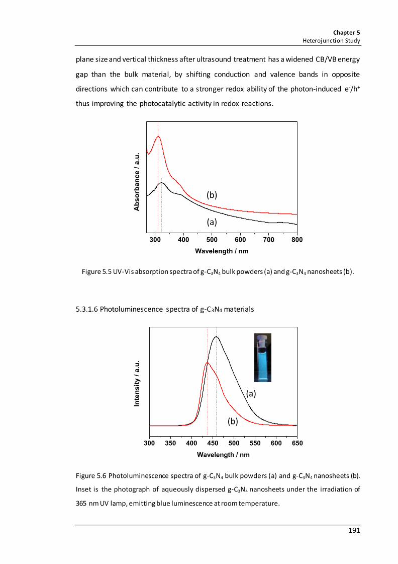
Chapter 5 Heterojunction Study
191
plane size and vertical thickness after ultrasound treatment has a widened CB/VB energy
gap than the bulk material, by shifting conduction and valence bands in opposite
directions which can contribute to a stronger redox ability of the photon-induced e-/h+
thus improving the photocatalytic activity in redox reactions.
Figure 5.5 UV-Vis absorption spectra of g-C3N4 bulk powders (a) and g-C3N4 nanosheets (b).
5.3.1.6 Photoluminescence spectra of g-C3N4 materials
Figure 5.6 Photoluminescence spectra of g-C3N4 bulk powders (a) and g-C3N4 nanosheets (b).
Inset is the photograph of aqueously dispersed g-C3N4 nanosheets under the irradiation of
365 nm UV lamp, emitting blue luminescence at room temperature.
300 400 500 600 700 800
Wavelength / nm
Ab
so
rba
nc
e /
a.u
.
(a)
(b)
300 350 400 450 500 550 600 650
Inte
ns
ity
/ a
.u.
Wavelength / nm
(a)
(b)

Chapter 5 Heterojunction Study
192
In agreement with the UV-Vis absorption data above, the emission peak position of
g-C3N4 nanosheets also shifted downwards to the lower wavelength side, from 458 nm
of bulk powders to 437 nm, as featured in Figure 5.6. Likewise, the blue shift
phenomenon is also the result of quantum confinement effect due to the reduction of
crystal size after exfoliation.
5.3.1.7 Fluorescence quantum yield of g-C3N4 materials
Figure 5.7 The gradients of integrated emission intensity versus the absorbance of UV-Vis
absorption at 317 nm for (a) quinine sulfate standard (λEm = 449 nm), (b) g-C3N4 nanosheets
(λEm = 437 nm) and (c) g-C3N4 bulk powders (λEm = 458 nm).
Table 5.3 The fluorescence quantum yield data of quinine sulfate, g-C3N4 bulk powders and
g-C3N4 nanosheets.
Slope Refractive index Quantum yield
Quinine sulfate 6.38 × 10⁵ 1.33 54.0%
g-C3N4 bulk powders
9.25 × 10⁴ 1.36 8.19%
g-C3N4 nanosheets 2.21 × 10⁵ 1.33 18.7%
0.00 0.02 0.04 0.06 0.08 0.10 0.12
0
10000
20000
30000
40000
50000
60000
70000
Slope = 92535
R2 = 0.984
Slope = 220768
R2 = 0.993
Inte
gra
ted
In
ten
sit
y
Absorbance at 317 nm / a.u.
Quinine Sulfate
g-C3N
4 nanosheets
g-C3N
4 bulk powders Slope = 637902
R2 = 0.995
(a)
(b)
(c)

Chapter 5 Heterojunction Study
193
The respective 𝜙F value for g-C3N4 nanosheets and g-C3N4 bulk powders were calculated
by measuring the integrated fluorescence intensity in aqueous dispersed g-C3N4
nanosheets and g-C3N4 powders in ethanol against quinine sulfate in 0.1M H2SO4 aq
solution. As shown in Figure 5.7, each series of the data points were linearly fitted and
the fitted slopes were listed in Table 5.3 as well as the quantum yield values calculated
by Equation 2.5. As displayed, the 𝜙F value of g-C3N4 nanosheets was profoundly
improved to 18.7%, in agreement with the DFT calculation results published by other
researchers in which the g-C3N4 nanosheets shows an clear increase of the density of
states (DOS) with respect to the bulk material on its conduction band which enables
improved photoresponsivity.25
5.3.1.8 Photocatalytic activities of g-C3N4 materials in dye degradation
Figure 5.8 UV-Vis absorption spectra of MO solution (15 mL, 30 µM) before and after adding
45 mg g-C3N4 powders (A) and 45 mg g-C3N4 nanosheets (B) as a function of degradation time
under visible light irradiation. Before irradiation, the reaction system was stirred in the dark for
60 min.
Figure 5.8 showed the variation of MO absorbance as a function of degradation time in
the presence of g-C3N4 powders (A) and g-C3N4 nanosheets (B) under visible light
irradiation. The peak intensity at 464 nm was gradually reduced and its position was
observably shifted to the lower wavelength range representing the continuous attack
upon the molecular structure of organic dyes and eventually degraded into CO2 and H2O
200 300 400 500 600 700
0 min
Dark 30 min
Dark 60 min
40 min
70 min
100 min
130 min
160 min
190 min
Ab
so
rba
nc
e /
a.u
.
Wavelength / nm
200 300 400 500 600 700 800
0 min
Dark 30 min
Dark 60 min
30 min
60 min
90 min
120 min
Ab
so
rba
nc
e /
a.u
.
Wavelength / nm
A B
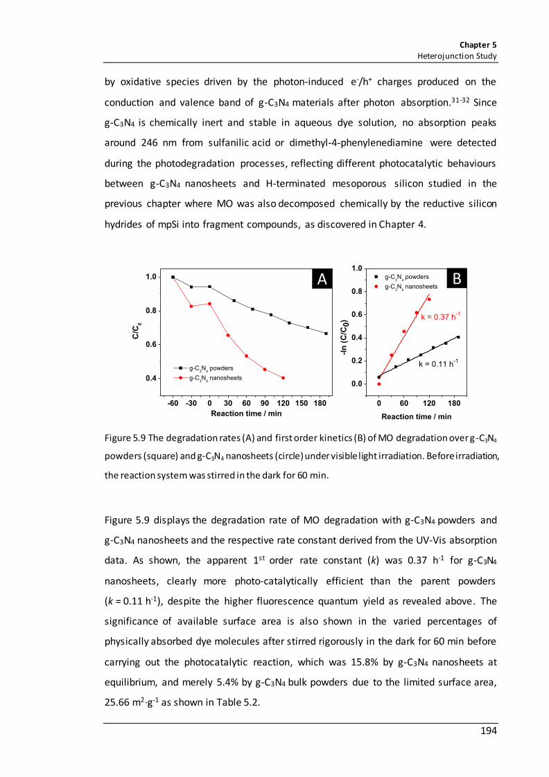
Chapter 5 Heterojunction Study
194
by oxidative species driven by the photon-induced e-/h+ charges produced on the
conduction and valence band of g-C3N4 materials after photon absorption.31-32 Since
g-C3N4 is chemically inert and stable in aqueous dye solution, no absorption peaks
around 246 nm from sulfanilic acid or dimethyl-4-phenylenediamine were detected
during the photodegradation processes, reflecting different photocatalytic behaviours
between g-C3N4 nanosheets and H-terminated mesoporous silicon studied in the
previous chapter where MO was also decomposed chemically by the reductive silicon
hydrides of mpSi into fragment compounds, as discovered in Chapter 4.
Figure 5.9 The degradation rates (A) and first order kinetics (B) of MO degradation over g-C3N4
powders (square) and g-C3N4 nanosheets (circle) under visible light irradiation. Before irradiation,
the reaction system was stirred in the dark for 60 min.
Figure 5.9 displays the degradation rate of MO degradation with g-C3N4 powders and
g-C3N4 nanosheets and the respective rate constant derived from the UV-Vis absorption
data. As shown, the apparent 1st order rate constant (k) was 0.37 h-1 for g-C3N4
nanosheets, clearly more photo-catalytically efficient than the parent powders
(k = 0.11 h-1), despite the higher fluorescence quantum yield as revealed above. The
significance of available surface area is also shown in the varied percentages of
physically absorbed dye molecules after stirred rigorously in the dark for 60 min before
carrying out the photocatalytic reaction, which was 15.8% by g-C3N4 nanosheets at
equilibrium, and merely 5.4% by g-C3N4 bulk powders due to the limited surface area,
25.66 m2·g-1 as shown in Table 5.2.
0 60 120 180
0.0
0.2
0.4
0.6
0.8
1.0 g-C
3N
4 powders
g-C3N
4 nanosheets
k = 0.37 h-1
k = 0.11 h-1
-ln
(C
/C0)
Reaction time / min
-60 -30 0 30 60 90 120 150 180
0.4
0.6
0.8
1.0
g-C3N
4 powders
g-C3N
4 nanosheets
C/C
0
Reaction time / min
A B

Chapter 5 Heterojunction Study
195
5.3.2 Photocatalytic activities of mpSi/g-C3N4 composites in dye degradation
Free standing H-terminated mesoporous silicon (mpSi), HPS-200-05-F sample was
hybridized with g-C3N4 nanosheets as characterised above via impregnation to form
mpSi/g-C3N4 NSs composites (mpSi/g-C3N4-S1, mpSi/g-C3N4-S2, mpSi/g-C3N4-S3) with
various weight ratios as m(mpSi): m(g-C3N4 NSs) = 4:1, 1:1 and 1:4 respectively. Since
the amount of photocatalyst used per unit of MO solution was decreased to about
6.67 g·mol-1, the photocatalytic rate constant of g-C3N4 NSs was thus reduced to 0.04 h-1
in this set of experiments.
Figure 5.10 A: UV-Vis absorption spectra of MO solution before and after adding mpSi/g-C3N4-S2
as a function of degradation time under visible light illumination; B: MO degradation rates over
HPS-200-05-F, g-C3N4 nanosheets, and mpSi/g-C3N4 NSs composites (S1, S2, S3) under visible
light irradiation.
200 300 400 500 600 700 800
0 min
30 min
60 min
90 min
120 min
150 min
180 min
Ab
so
rba
nc
e /
a.u
.
Wavelength / nm
246464
A
0 60 120 180
0.0
0.2
0.4
0.6
0.8
1.0
C/C
0
Reaction time / min
g-C3N
4 NSs
HPS-200-05-F
mpSi/g-C3N
4-S1
mpSi/g-C3N
4-S2
mpSi/g-C3N
4-S3
B

Chapter 5 Heterojunction Study
196
As shown in Figure 5.10A, the 464 nm peak intensity of MO decreased rapidly over
mpSi/g-C3N4-S2 sample and completely decayed after 90 min while ~40% of the initial
amount of organic molecules were still unreacted in the dye solution of mpSi under
similar conditions. As found from the previous chapter, the fast rate of MO
disappearance over irradiated mpSi material is a combined result of charge-driven
photocatalysis and surface hydride-involved reduction. Likewise, the appearance and
growth of the absorption band at 247 nm during MO degradation was also presented
here in the study of mpSi/g-C3N4-S2, indicating a similar behavioural pattern of the
composite in MO photodecomposition.
As further disclosed in Figure 5.10B, the activity of mpSi/g-C3N4 NSs composites in MO
decomposition was varied to a large extent corresponding to the weight ratio between
mpSi and g-C3N4 NSs components. By adding increasing amounts of mpSi into the
composite structure, the degradation rate of mpSi/g-C3N4-S1 with 4:1 weight ratio was
revealed to be similar to mpSi itself. Whereas the performance of mpSi/g-C3N4-S3 was
significantly inhibited by the very high compositional ratio of g-C3N4 NSs.
According to the reported band structure of g-C3N4, the CB and VB band positions of
g-C3N4 appear at -1.12 V and 1.58 V, respectively with a 2.7 eV energy gap.33-35 As well
as the band positions of mpSi (HPS-200-05) revealed in Chapter 4 as -0.75 V and 1.30 V,
the band alignment of mpSi/g-C3N4 NSs heterojunction is drawn in Figure 5.11.
Figure 5.11 Band diagram of mpSi/g-C3N4 heterojunction.
3.0
2.0
1.0
0.0
-1.0
-2.0
E vs NHE / V
mpSig-C3N4
e-
h+
e-
h+
hν hν
2.05 eV 2.7 eV
e-
h+

Chapter 5 Heterojunction Study
197
As shown the semiconductor composite is defined as a Type I straddling
heterostructure,36 in which the photogenerated electrons and holes would mainly
accumulate on the conduction and valence band of one component, mpSi in this case as
the charge acceptor which would gain the energy. As found in Chapter 4, the reductive
capability of Si-H bond of mpSi in converting MO appeared to be accelerated under
visible light irradiation through the proposed exciton-related mechanism as Si-H is
known as electron deficient and hence has the tendency to extract free electrons. Since
mpSi is a p-type semiconducting system with excess hole supply in the valence band, the
flow of photoexcited electrons may occur more frequently to the conduction band of
g-C3N4 to mpSi and is likely to be promoted by the above mentioned stimulation effect
on the hydrogen transfer process, eventually resulting in the fast disappearance of MO
molecules in the presence of mpSi/g-C3N4 NSs as shown here. According to the
electronic structure of g-C3N4 revealed in the DFT calculations, the valence and
conduction bands of g-C3N4 are mainly composed of the nitrogen pz orbitals and carbon
pZ orbitals, respectively.16 Thus to be more specific, the charge transfer in the
heterostructure is proposed to go through the C atom of g-C3N4 component to the
surface hydrides (SiHx) of mpSi material.
Figure 5.12 A: ATR-IR spectra of HPS-200-05-F (a), g-C3N4 NSs (b), mpSi/g-C3N4-S2 before (c) and
after (d) MO degradation; B: UV-Vis absorption and emission spectra of mpSi/g-C3N4-S2.
4000 3500 3000 2500 2000 1500 1000 500
(d)
(c)
(b)
Tra
ns
mit
tan
ce
/ a
.u.
Wavenumber / cm-1
HPS-200-05-F
g-C3N
4 NSs
mpSi/g-C3N
4-S2
mpSi/g-C3N
4-S2 after
(a)
300 400 500 600 700 800
Wavelength / nm
Ab
so
rba
nc
e /
a.u
.
Inte
ns
ity / a
.u.
A B

Chapter 5 Heterojunction Study
198
Table 5.4 IR absorption wavenumbers of C=N, C-N stretching vibrations and the breathing mode
of tri-s-triazine ring of g-C3N4 bulk powders, g-C3N4 nanosheets and mpSi/g- C3N4 composite.
g-C3N4 bulk powders g-C3N4 nanosheets mpSi/ g-C3N4-S2
C=N / cm-1 1628 1626 1639
1539 1539 1545
C-N / cm-1
1395 1394 1411
1314 1314 1321
1231 1230 1246
breathing / cm-1 804 804 811
As shown in Figure 5.12A, the FTIR spectra of mpSi/g-C3N4-S2 before and after
photocatalytic evaluation were recorded which exhibited characteristic IR signals from
both semiconductor components, confirming the existence of mesoporous silicon and
g-C3N4 in the composite which was also consistent through the degradation reaction and
catalyst recycling. Interestingly, the various IR peak positions of g-C3N4 NSs were all
blueshifted after being hybridized with mpSi, which is unlikely to be related to the
exfoliated nature of g-C3N4 NSs. As we can see, the IR bands of g-C3N4 NSs and bulk
powders were all situated in identical positions in Table 5.4.
In addition, a new UV-Vis band at 550 nm also emerged in the absorption spectrum of
mpSi/g-C3N4-S2 (Figure 5.12B). As featured, the 376 nm signal is commonly observed in
g-C3N4 synthesis and derived from the π-π* transition of the aromatic system. However,
the 550 nm peak induced by n-π* transition is rarely seen in the characterisation of
g-C3N4 as this electronic excitation is intrinsically forbidden by symmetry but can be
activated by structural distortion, especially in-plane distortion to the 2D
flat morphology.37-38 For example, the buckled configuration of g-C3N4 monolayer or
multilayer was reported to have increased spectral response in the visible region for
photon absorption and enhanced photocatalytic activity in H2 generation due to this
distinct optical feature.39

Chapter 5 Heterojunction Study
199
Thus, as suggested by the above results, some valuable insights into the coupling effects
of mpSi and g-C3N4 NSs semiconductors were provided of which some influences had
been shown on the bonding environment and structural morphology of g-C3N4
component, leading to the optical variations of g-C3N4 nanosheets. Although the nature
of the interfacial interaction between mpSi and g-C3N4 NSs in the composite is still not
yet clear in this stage. It can be better elucidated in the future with more detailed
characterisation results and in-depth investigation of the physical, chemical and
electronic effects on the photocatalytic behaviours of the coupled material.
5.4 Summary
In this chapter, photoactive hydrogen-terminated mesoporous silicon (mpSi) and
graphitic carbon nitride nanosheets (g-C3N4 NSs) were coupled into mpSi/g-C3N4 NSs
composite via impregnation, which presented an enhanced degradation capability
toward methyl orange under visible light irradiation. Since both components can be
facilely prepared from low cost, earth abundant raw materials, mpSi/g-C3N4 NSs
heterojunction is very promising as a metal-free, visible light responsive candidate in
utilizing the renewable solar energy on a large scale. On one hand, the large surface area
and accessible porous system of mesoporous silicon fabricated via electrochemical
etching facilitated the diffusion of reactants and products. Its widened optical bandgap
and well-defined crystal structure also enhanced the visible light absorption and lifetime
of photoinduced charge carriers. Meanwhile, the large surface area and small vertical
thickness possessed by g-C3N4 nanosheets also promoted the absorption of reactants
and reduced the charge migration distance. On the other hand, some synergistic effects
on the photocatalytic behaviour of the heterojunction are reasonably expected as
indicated in our preliminary results, which have shown stimulated activity of hydrogen
termination on mesoporous silicon surface and n-π* electronic transition mode of
g-C3N4 in the composite, although the nature of the electronic/physiochemical
interaction still remains largely unknown and will be the subject of future exploration.

Chapter 5 Heterojunction Study
200
5.5 References
1. Geim, A. K.; Novoselov, K. S., The rise of graphene. Nat. Mater. 2007, 6 (3), 183-191.
2. Rao, C. N.; Sood, A. K.; Subrahmanyam, K. S.; Govindaraj, A., Graphene: the new two-
dimensional nanomaterial. Angew. Chem. Int. Ed. Engl. 2009, 48 (42), 7752-7777.
3. Zhang, N.; Zhang, Y.; Xu, Y. J., Recent progress on graphene-based photocatalysts:
current status and future perspectives. Nanoscale 2012, 4 (19), 5792-5813.
4. Hinnemann, B.; Moses, P. G.; Bonde, J.; Jorgensen, K. P.; Nielsen, J. H.; Horch, S.;
Chorkendorff, I.; Norskov, J. K., Biomimetic hydrogen evolution: MoS2 nanoparticles as
catalyst for hydrogen evolution. J. Am. Chem. Soc. 2005, 127 (15), 5308-5309.
5. Jaramillo, T. F.; Jorgensen, K. P.; Bonde, J.; Nielsen, J. H.; Horch, S.; Chorkendorff, I.,
Identification of active edge sites for electrochemical H2 evolution from MoS2
nanocatalysts. Science 2007, 317 (5834), 100-102.
6. Gao, M. R.; Xu, Y. F.; Jiang, J.; Yu, S. H., Nanostructured metal chalcogenides: synthesis,
modification, and applications in energy conversion and storage devices. Chem. Soc. Rev.
2013, 42 (7), 2986-3017.
7. Golberg, D.; Bando, Y.; Huang, Y.; Terao, T.; Mitome, M.; Tang, C.; Zhi, C., Boron nitride
nanotubes and nanosheets. ACS Nano 2010, 4 (6), 2979-2993.
8. Bhimanapati, G. R.; Lin, Z.; Meunier, V.; Jung, Y.; Cha, J.; Das, S.; Xiao, D.; Son, Y.;
Strano, M. S.; Cooper, V. R.; Liang, L.; Louie, S. G.; Ringe, E.; Zhou, W.; Kim, S. S.;
Naik, R. R.; Sumpter, B. G.; Terrones, H.; Xia, F.; Wang, Y.; Zhu, J.; Akinwande, D.;
Alem, N.; Schuller, J. A.; Schaak, R. E.; Terrones, M.; Robinson, J. A., Recent advances in
two-dimensional materials beyond graphene. ACS Nano 2015, 9 (12), 11509-11539.
9. Ong, W.-J.; Tan, L.-L.; Ng, Y. H.; Yong, S.-T.; Chai, S.-P., Graphitic carbon nitride
(g-C3N4)-based photocatalysts for artificial photosynthesis and environmental
remediation: are we a step closer to achieving sustainability? Chem. Rev. 2016, 116 (12),
7159-7329.
10. Thomas, A.; Fischer, A.; Goettmann, F.; Antonietti, M.; Müller, J.-O.; Schlögl, R.;
Carlsson, J. M., Graphitic carbon nitride materials: variation of structure and morphology
and their use as metal-free catalysts. J. Mater. Chem. 2008, 18 (41), 4893-4908.

Chapter 5 Heterojunction Study
201
11. Lam, S. M.; Sin, J. C.; Mohamed, A. R., A review on photocatalytic application of
g-C3N4/semiconductor (CNS) nanocomposites towards the erasure of dyeing
wastewater. Mater. Sci. Semicond. Process. 2016, 47, 62-84.
12. Liu, J.; Wang, H.; Antonietti, M., Graphitic carbon nitride "reloaded": emerging
applications beyond (photo)catalysis. Chem. Soc. Rev. 2016, 45 (8), 2308-2326.
13. Mamba, G.; Mishra, A. K., Graphitic carbon nitride (g-C3N4) nanocomposites: a new
and exciting generation of visible light driven photocatalysts for environmental pollution
remediation. Appl. Catal. B 2016, 198, 347-377.
14. Feng, L.; He, F.; Yang, G.; Gai, S.; Dai, Y.; Li, C.; Yang, P., NIR-driven graphitic-phase
carbon nitride nanosheets for efficient bioimaging and photodynamic therapy. J. Mater.
Chem. B 2016, 4 (48), 8000-8008.
15. Liu, J.-W.; Luo, Y.; Wang, Y.-M.; Duan, L.-Y.; Jiang, J.-H.; Yu, R.-Q., Graphitic carbon
nitride nanosheets-based ratiometric fluorescent probe for highly sensitive detection of
H2O2 and glucose. ACS Appl. Mater. Interfaces 2016, 8 (49), 33439-33445.
16. Wang, X.; Maeda, K.; Thomas, A.; Takanabe, K.; Xin, G.; Carlsson, J. M.; Domen, K.;
Antonietti, M., A metal-free polymeric photocatalyst for hydrogen production from
water under visible light. Nat. Mater. 2009, 8 (1), 76-80.
17. Liang, Q.; Li, Z.; Huang, Z. H.; Kang, F.; Yang, Q. H., Holey graphitic carbon nitride
nanosheets with carbon vacancies for highly improved photocatalytic hydrogen
production. Adv. Funct. Mater. 2015, 25 (44), 6885-6892.
18. Xu, J.; Shang, J.-K.; Jiang, Q.; Wang, Y.; Li, Y.-X., Facile alkali-assisted synthesis of
g-C3N4 materials and their high-performance catalytic application in solvent-free
cycloaddition of CO2 to epoxides. RSC Adv. 2016, 6 (60), 55382-55392.
19. Niu, P.; Zhang, L.; Liu, G.; Cheng, H.-M., Graphene-like carbon nitride nanosheets for
improved photocatalytic activities. Adv. Funct. Mater. 2012, 22 (22), 4763-4770.
20. Qiu, P.; Chen, H.; Xu, C.; Zhou, N.; Jiang, F.; Wang, X.; Fu, Y., Fabrication of an
exfoliated graphitic carbon nitride as a highly active visible light photocatalyst. J. Mater.
Chem. A 2015, 3 (48), 24237-24244.

Chapter 5 Heterojunction Study
202
21. Han, Q.; Wang, B.; Gao, J.; Cheng, Z.; Zhao, Y.; Zhang, Z.; Qu, L., Atomically thin
mesoporous nanomesh of graphitic C3N4 for high-efficiency photocatalytic hydrogen
evolution. ACS Nano 2016, 10 (2), 2745-2751.
22. Chen, L.; Huang, D.; Ren, S.; Dong, T.; Chi, Y.; Chen, G., Preparation of graphite-like
carbon nitride nanoflake film with strong fluorescent and electrochemiluminescent
activity. Nanoscale 2013, 5 (1), 225-230.
23. Xu, J.; Zhang, L.; Shi, R.; Zhu, Y., Chemical exfoliation of graphitic carbon nitride for
efficient heterogeneous photocatalysis. J. Mater. Chem. A 2013, 1 (46), 14766-14772.
24. Shi, L.; Chang, K.; Zhang, H.; Hai, X.; Yang, L.; Wang, T.; Ye, J., Drastic enhancement
of photocatalytic activities over phosphoric acid protonated porous g-C3N4 nanosheets
under visible light. Small 2016, 12 (32), 4431-4439.
25. Zhang, X.; Xie, X.; Wang, H.; Zhang, J.; Pan, B.; Xie, Y., Enhanced photoresponsive
ultrathin graphitic-phase C3N4 nanosheets for bioimaging. J. Am. Chem. Soc. 2013,
135 (1), 18-21.
26. Han, Q.; Hu, C.; Zhao, F.; Zhang, Z.; Chen, N.; Qu, L., One-step preparation of iodine-
doped graphitic carbon nitride nanosheets as efficient photocatalysts for visible light
water splitting. J. Mater. Chem. A 2015, 3 (8), 4612-4619.
27. Han, Q.; Zhao, F.; Hu, C. G.; Lv, L. X.; Zhang, Z. P.; Chen, N.; Qu, L. T., Facile production
of ultrathin graphitic carbon nitride nanoplatelets for efficient visible-light water
splitting. Nano Res. 2015, 8 (5), 1718-1728.
28. Zhu, K. X.; Wang, W. J.; Meng, A.; Zhao, M.; Wang, J. H.; Zhao, M.; Zhang, D. L.;
Jia, Y. P.; Xu, C. H.; Li, Z. J., Mechanically exfoliated g-C3N4 thin nanosheets by ball milling
as high performance photocatalysts. RSC Adv. 2015, 5 (69), 56239-56243.
29. Zhang, J.; Chen, Y.; Wang, X., Two-dimensional covalent carbon nitride nanosheets:
synthesis, functionalization, and applications. Energy Environ. Sci. 2015, 8 (11),
3092-3108.
30. Carlsson, J. M., Graphene: buckle or break. Nat. Mater. 2007, 6 (11), 801-802.
31. Yan, S. C.; Li, Z. S.; Zou, Z. G., Photodegradation performance of g-C3N4 fabricated by
directly heating melamine. Langmuir 2009, 25 (17), 10397-10401.

Chapter 5 Heterojunction Study
203
32. Sun, L.; Yang, M.; Huang, J.; Yu, D.; Hong, W.; Chen, X., Freestanding graphitic carbon
nitride photonic crystals for enhanced photocatalysis. Adv. Funct. Mater. 2016, 26 (27),
4943-4950.
33. Peng, B.; Zhang, S.; Yang, S.; Wang, H.; Yu, H.; Zhang, S.; Peng, F., Synthesis and
characterization of g-C3N4/Cu2O composite catalyst with enhanced photocatalytic
activity under visible light irradiation. Mater. Res. Bull. 2014, 56, 19-24.
34. Xu, H.; Gan, Z.; Zhou, W.; Ding, Z.; Zhang, X., A metal-free 3C-SiC/g-C3N4 composite
with enhanced visible light photocatalytic activity. RSC Adv. 2017, 7 (63), 40028-40033.
35. Jiang, W.; Luo, W.; Wang, J.; Zhang, M.; Zhu, Y., Enhancement of catalytic activity
and oxidative ability for graphitic carbon nitride. J. Photochem. Photobiol. C: Photochem.
Rev. 2016, 28, 87-115.
36. Selinsky, R. S.; Ding, Q.; Faber, M. S.; Wright, J. C.; Jin, S., Quantum dot nanoscale
heterostructures for solar energy conversion. Chem. Soc. Rev. 2013, 42 (7), 2963-2985.
37. Li, Y.; Zhang, J.; Wang, Q.; Jin, Y.; Huang, D.; Cui, Q.; Zou, G., Nitrogen-rich carbon
nitride hollow vessels: synthesis, characterization, and their properties. J. Phys. Chem. B
2010, 114 (29), 9429-9434.
38. Jorge, A. B.; Martin, D. J.; Dhanoa, M. T. S.; Rahman, A. S.; Makwana, N.; Tang, J.;
Sella, A.; Corà, F.; Firth, S.; Darr, J. A.; McMillan, P. F., H2 and O2 evolution from water
half-splitting reactions by graphitic carbon nitride materials. J. Phys. Chem. C 2013,
117 (14), 7178-7185.
39. Chen, Y.; Wang, B.; Lin, S.; Zhang, Y.; Wang, X., Activation of n → π* transitions in
two-dimensional conjugated polymers for visible light photocatalysis. J. Phys. Chem. C
2014, 118 (51), 29981-29989.

Chapter 6
Chapter 6
Conclusions and Future Work
Abstract
In this chapter, the aim of the research described in the thesis is outlined. The main
conclusions are summarized and proposals for future work indicated by this research
are suggested.

Chapter 6 Conclusions and Future Work
205
6.1 Conclusions
Aiming for utilizing the abundant solar energy efficiently and cost-effectively, this thesis
was focused on the study of silicon and silicon-based semiconducting systems, which
are known as low-cost, earth-abundant, metal-free and eco-friendly, potentially useful
in resolving various global challenges we’re facing with such as water pollution.
Mesoporous silicon (mpSi) was facilely prepared by galvanostatic anodization which
created a Si-based open mesoporous system with a large accessible surface area to
promote mass diffusion and charge transfer in liquid phase photoreactions. In general,
two different structural morphologies were constructed within the Si crystalline matrix:
an interconnected porous network and an orderly aligned meso-channel array. Despite
the distinct differences in pore properties, several common similarities were also shared
including the hydrogen terminations and abundant Si nanocrystallites on the surface. By
taking advantage of the surface hydrides, thiol-capped mesoporous silicon with allyl
mercaptan was synthesised successfully under microwave field within a significantly
shortened reaction time.
By tuning the etching conditions, a variety of structural properties (layer thickness,
crystallinity, surface area, pore size distribution and Si nanocrystal sizes) of as-etched
mpSi material were correspondingly modified. As found, the resulting Si structure was
dominantly affected by the etching current density applied in the fabrication process.
As etching current density increased, it was rendered with higher specific surface area,
larger pore volume and pore size, and smaller nanocrystalline Si particles. The effect of
etching duration was comparatively moderate as the surface area slightly increased
after longer immersion time in the etchant due to the occurrence of chemical dissolution.
As a result of the high surface area, framework crystallinity and abundant surface
hydrides, hydrogen-terminated mesoporous Si channel array with ordered pore
alignment and large pore size showed an excellent activity in degrading methyl orange
(MO) under visible light irradiation. Its widened bandgap induced by the quantum
confinement effect of the constituted Si nanocrystallites endowed a broad absorption
of visible light range photons. While the less efficient performance of the interconnected

Chapter 6 Conclusions and Future Work
206
porous network in MO photodegradation was largely caused by its poor crystallinity,
lower electrical conductivity and higher oxidation tendency resulting in faster
recombination rate of photoexcited electrons (e-) and holes (h+), as well as by the
branched, narrower mesopores that were not as effective in enhancing the access to
the vast internal surface as the ordered channels. By further improving the visible light
responsiveness and surface availability of the meso-channel array, MO decomposition
over free-standing mpSi microparticles was further accelerated with 88% of the initial
efficacy remained after 10 cycles of photoreactions.
Hydrogen termination on the surface of mesoporous silicon was revealed to be a
prominent factor in destroying the molecular structure of MO by reducing its azo linkage
which was also the main responsible process occurred in the dark for MO decomposition
over mpSi. This degradation pathway was further promoted by enhancing the reduction
activity of the surface hydrides species under visible light irradiation of which the
underlying mechanism is assumed to be related to the localized excitons at Si-H sites. In
addition, photo-oxidation of MO was also initiated and proceeded simultaneously,
driven by the reactive oxygen species (ROSs), primarily superoxide radical anions (·O2-)
formed in the conduction band of mpSi. Upon irradiation, mpSi absorbed supra-bandgap
incident photons and generated photoexcited e- and h+ in its conduction band and
valence band. The conduction band electrons then transferred to the interface and
reduced dissolved O2 into ·O2-. In this process, surface Si-H bond is also critically
important as it prevented the undesired e-/h+ recombination by trapping the
photoinduced e-. As a result of the competing degradation pathway mentioned earlier,
the photo-oxidation capability of mpSi gradually declined.
An enhanced visible-light-driven photo-reduction of MO was achieved by combining
mesoporous silicon with graphitic carbon nitride nanosheets (g-C3N4 NSs). As indicated
by the Type-I heterojunction structure of the semiconductor composite, the reductive
capability of Si-H bonds in mpSi was likely promoted in the presence of g-C3N4 NSs,
because of an excess of photoinduced e- on the conduction band of mpSi donated from
the higher conduction band of g-C3N4 component, which eventually led to a faster
degradation rate against MO molecules according to the exciton-related mechanism.

Chapter 6 Conclusions and Future Work
207
In this thesis, the microscopic structural characteristics of mesoporous silicon prepared
by electrochemical etching have been examined thoroughly which can provide a useful
guide in the applications of porous Si-based materials. The potential of H-terminated
mesoporous silicon in photocatalytic degradation of methyl orange has been assessed
and the importance of mass diffusion within the porous structure has been highlighted
as largely regulated by the pore properties. The mechanistic study of the degradation
behaviour toward methyl orange has revealed the significant roles of the surface
hydrides with or without visible light irradiation. And the exploitable reduction power
of Si-H bond by the action of external light and other photoactive semiconductors also
suggests a potential research direction in tuning the activity to purposely guide a
photochemical/chemical transformation.

Chapter 6 Conclusions and Future Work
208
6.2 Future work
Considering the current progress of this work, some recommendations for future work
are:
To conduct a more detailed product analysis and intermediates generated through
the degradation process of methyl orange over H-terminated mesoporous silicon
with or without external visible light illumination by employing sophisticated
analytical tools, such as mass spectrometry.
To monitor the electron-transfer processes that occur under visible light irradiation
by using electrochemical methods for a direct observation of the charge separation,
migration and recombination on mesoporous silicon and mpSi/g-C3N4 NSs composite.
To understand the effect of photoinduced charge carriers on the reactivity of Si-H
bond on the surface of mesoporous silicon by in situ characterisation technique, such
as solid state NMR to be used on the irradiated sample.
To exploit H-terminated mesoporous silicon in photoreduction of carbon dioxide,1-2
organic compounds, metal ions etc. by making use of the abundant surface hydrides
and seeking for possible site selectivity.
To further explore the composite structure of mesoporous silicon and graphitic
carbon nitride nanosheets and investigate the interfacial interaction between these
two phases to guide the design of new structures.
More broadly, future exploration could be directed to:
Expanding the applications of mesoporous silicon to other potential areas.
o As anode material to be used in lithium-ion batteries making use of the
exceedingly high theoretical energy capacity of Si (ca. 4200 mA h g-1) and the
large surface area and porous structure to accommodate the volume
expansion during charging and discharging processes known to cause the
rapid decay problem.3-11
o As drug carrier or imaging agent to be used in biomedical applications making
use of the unique structural properties, light-emitting ability,
biocompatibility and biodegradability.12-21

Chapter 6 Conclusions and Future Work
209
Developing mesoporous silicon-based heterostructures with other photoactive
materials.22-24
Creating novel structured porous silicon by bottom-up magnesiothermic
reduction.4, 25

Chapter 6 Conclusions and Future Work
210
6.3 References
1. Sun, W.; Qian, C.; He, L.; Ghuman, K. K.; Wong, A. P. Y.; Jia, J.; Jelle, A. A.; O’Brien, P. G.;
Reyes, L. M.; Wood, T. E.; Helmy, A. S.; Mims, C. A.; Singh, C. V.; Ozin, G. A.,
Heterogeneous reduction of carbon dioxide by hydride-terminated silicon nanocrystals.
Nat. Commun. 2016, 7, 12553.
2. Dasog, M.; Kraus, S.; Sinelnikov, R.; Veinot, J. G. C.; Rieger, B., CO2 to methanol
conversion using hydride terminated porous silicon nanoparticles. Chem. Commun.
2017, 53 (21), 3114-3117.
3. Liu, L. H.; Lyu, J.; Li, T. H.; Zhao, T. K., Well-constructed silicon-based materials as high-
performance lithium-ion battery anodes. Nanoscale 2016, 8 (2), 701-722.
4. Liang, J.; Li, X.; Hou, Z.; Zhang, W.; Zhu, Y.; Qian, Y., A deep reduction and partial
oxidation strategy for fabrication of mesoporous Si anode for lithium ion batteries. ACS
Nano 2016, 10 (2), 2295-2304.
5. Du, F. H.; Wang, K. X.; Chen, J. S., Strategies to succeed in improving the lithium-ion
storage properties of silicon nanomaterials. J. Mater. Chem. A 2016, 4 (1), 32-50.
6. Yersak, T. A.; Shin, J.; Wang, Z.; Estrada, D.; Whiteley, J.; Lee, S. H.; Sailor, M. J.;
Meng, Y. S., Preparation of mesoporous Si@PAN electrodes for Li-ion batteries via the
in-situ polymerization of PAN. ECS Electrochem. Lett. 2015, 4 (3), A33-A36.
7. Westover, A. S.; Freudiger, D.; Gani, Z. S.; Share, K.; Oakes, L.; Carter, R. E.; Pint, C. L.,
On-chip high power porous silicon lithium ion batteries with stable capacity over 10,000
cycles. Nanoscale 2015, 7 (1), 98-103.
8. Han, X.; Chen, H.; Liu, J.; Liu, H.; Wang, P.; Huang, K.; Li, C.; Chen, S.; Yang, Y., A peanut
shell inspired scalable synthesis of three-dimensional carbon coated porous silicon
particles as an anode for lithium-ion batteries. Electrochim. Acta 2015, 156, 11-19.
9. Li, X.; Gu, M.; Hu, S.; Kennard, R.; Yan, P.; Chen, X.; Wang, C.; Sailor, M. J.; Zhang, J. G.;
Liu, J., Mesoporous silicon sponge as an anti-pulverization structure for high-
performance lithium-ion battery anodes. Nat. Commun. 2014, 5, 4105.
10. Ren, W.; Wang, Y.; Zhang, Z.; Tan, Q.; Zhong, Z.; Su, F., Carbon-coated porous silicon
composites as high performance Li-ion battery anode materials: can the production
process be cheaper and greener? J. Mater. Chem. A 2016, 4 (2), 552-560.

Chapter 6 Conclusions and Future Work
211
11. Su, X.; Wu, Q. L.; Li, J. C.; Xiao, X. C.; Lott, A.; Lu, W. Q.; Sheldon, B. W.; Wu, J., Silicon-
based nanomaterials for lithium-ion batteries: a review. Adv. Energy Mater. 2014, 4 (1),
1300882.
12. Venuta, A.; Wolfram, J.; Shen, H.; Ferrari, M., Post-nano strategies for drug delivery:
multistage porous silicon microvectors. J. Mater. Chem. B 2017, 5 (2), 207-219.
13. Stojanovic, V.; Cunin, F.; Durand, J. O.; Garcia, M.; Gary-Bobo, M., Potential of porous
silicon nanoparticles as an emerging platform for cancer theranostics. J. Mater. Chem. B
2016, 4 (44), 7050-7059.
14. McInnes, S. J.; Michl, T. D.; Delalat, B.; Al-Bataineh, S. A.; Coad, B. R.; Vasilev, K.;
Griesser, H. J.; Voelcker, N. H., "Thunderstruck": plasma-polymer-coated porous silicon
microparticles as a controlled drug delivery system. ACS Appl. Mater. Interfaces 2016,
8 (7), 4467-4476.
15. Wu, C. C.; Hu, Y.; Miller, M.; Aroian, R. V.; Sailor, M. J., Protection and delivery of
anthelmintic protein Cry5B to nematodes using mesoporous silicon particles. ACS Nano
2015, 9 (6), 6158-6167.
16. Wang, M.; Hartman, P. S.; Loni, A.; Canham, L. T.; Bodiford, N.; Coffer, J. L., Influence
of surface chemistry on the release of an antibacterial drug from nanostructured porous
silicon. Langmuir 2015, 31 (22), 6179-6185.
17. Tzur-Balter, A.; Shatsberg, Z.; Beckerman, M.; Segal, E.; Artzi, N., Mechanism of
erosion of nanostructured porous silicon drug carriers in neoplastic tissues.
Nat. Commun. 2015, 6, 6208.
18. Herranz-Blanco, B.; Arriaga, L. R.; Makila, E.; Correia, A.; Shrestha, N.; Mirza, S.;
Weitz, D. A.; Salonen, J.; Hirvonen, J.; Santos, H. A., Microfluidic assembly of multistage
porous silicon-lipid vesicles for controlled drug release. Lab Chip 2014, 14 (6), 1083-1086.
19. Savage, D. J.; Liu, X.; Curley, S. A.; Ferrari, M.; Serda, R. E., Porous silicon advances in
drug delivery and immunotherapy. Curr. Opin. Pharmacol. 2013, 13 (5), 834-841.
20. Gu, L.; Hall, D. J.; Qin, Z.; Anglin, E.; Joo, J.; Mooney, D. J.; Howell, S. B.; Sailor, M. J.,
In vivo time-gated fluorescence imaging with biodegradable luminescent porous silicon
nanoparticles. Nat. Commun. 2013, 4, 2326.

Chapter 6 Conclusions and Future Work
212
21. Gu, L.; Park, J. H.; Duong, K. H.; Ruoslahti, E.; Sailor, M. J., Magnetic luminescent
porous silicon microparticles for localized delivery of molecular drug payloads. Small
2010, 6 (22), 2546-2552.
22. Sampath, S.; Maydannik, P.; Ivanova, T.; Shestakova, M.; Homola, T.; Bryukvin, A.;
Sillanpää, M.; Nagumothu, R.; Alagan, V., Efficient solar photocatalytic activity of TiO2
coated nano-porous silicon by atomic layer deposition. Superlattices Microstruct. 2016,
97, 155-166.
23. Chandrasekaran, S.; Macdonald, T. J.; Mange, Y. J.; Voelcker, N. H.; Nann, T., A
quantum dot sensitized catalytic porous silicon photocathode. J. Mater. Chem. A 2014,
2 (25), 9478-9481.
24. Megouda, N.; Cofininier, Y.; Szunerits, S.; Hadjersi, T.; Elkechai, O.; Boukherroub, R.,
Photocatalytic activity of silicon nanowires under UV and visible light irradiation. Chem.
Commun. 2011, 47 (3), 991-993.
25. Zuo, X.; Xia, Y.; Ji, Q.; Gao, X.; Yin, S.; Wang, M.; Wang, X.; Qiu, B.; Wei, A.; Sun, Z.;
Liu, Z.; Zhu, J.; Cheng, Y. J., Self-templating construction of 3D hierarchical
macro-/mesoporous silicon from 0D silica nanoparticles. ACS Nano 2017, 11 (1), 889-899.
Appendix: list of publications including potential publications
[1] Li, T.; Li, J.; Zhang, Q.; Blazeby, E.; Shang, C.; Xu, H.; Zhang, X.; Chao, Y., Hydrogen-
terminated mesoporous silicon monoliths with huge surface area as alternative Si-based
visible light-active photocatalysts. RSC Adv. 2016, 6 (75), 71092-71099.
[2] Mechanistic elucidation of the degradation behaviour of hydrogen-terminated
mesoporous silicon in dye degradation. In preparation.