CATRENE Programme Review
42
Full year report January - December 2014 CATRENE Programme Review Report 9 C luster for A pplication and T echnology R esearch in E urope on N ano E lectronics
-
Upload
khangminh22 -
Category
Documents
-
view
2 -
download
0
Transcript of CATRENE Programme Review
Full year reportJanuary - December 2014
CATRENEProgramme Review
Report 9
C luster for Application
and Technology
Research in Europe
on NanoE lectronics

CATRENE Programme Review Year 2014
Distribution list
● CATRENE Board
● CATRENE Support Group
● CATRENE Steering Group Applications
● CATRENE Steering Group Technologies
● CATRENE Director’s Committee
● CAPA
● CATRENE Office
CATRENE Programme Review - Year 2014
4
CATRENE Programme Review - Year 2014
5
Table of Contents
Executive Summary...................................................................7
1. Overview of CATRENE..........................................................11
2. 2014 CATRENE Year in Review.............................................17
2.1. Achievements.............................................................................................18
2.1.1. Reflection on a new tool for beyond 2015................................................18
2.1.2. Call 7...................................................................................................18
2.1.3. Increased links and cooperation with other Clusters/Programmes..............19
2.2. Events......................................................................................................20
2.2.1. European Nanoelectronics Forum 2014 and CATRENE Innovation Award......20
2.2.2. Common AENEAS and CATRENE Brokerage Event 2014..............................21
2.2.3. CATRENE Scientific Committee Workshop: “Smart Systems for Healthcare and Wellness”..........................................21
2.2.4. CATRENE Design Technology Conference 2014.........................................22
2.3. Publications...............................................................................................23
2.3.1. Project Profiles and Result Sheets...........................................................23
2.3.2. Scientific Committee Report on Smart Systems for Health and Wellness...............................................................................................23
2.4. Press Coverage...........................................................................................24
3. Review of Call 7 and projects ended in 2014........................29
3.1. Call 7 & unsolicited projects (labelled in 2014)...............................................31
3.1.1. Overview Table......................................................................................31
3.1.2. Project CAT120 CISTERN.........................................................................31
3.1.3. Project CAT121 EAST.............................................................................32
3.1.4. Project CAT209 H2O..............................................................................33
3.1.5. Project CAT406 NEMADE........................................................................34
3.1.6. Project CAT601 SiPoB-3D........................................................................35
3.1.7. Project CAT801 TSV-HANDY.....................................................................36
3.1.8. Project CAT802 SAM3............................................................................38
3.2. Projects ended in 2014...............................................................................40
3.2.1. Overview Table.....................................................................................40
3.2.2. Project CA303 OPTIMISE........................................................................40
3.2.3. Project CA402 THOR.............................................................................42
3.2.4. Project CA308 ICAF...............................................................................44
3.2.5. Project CA403 RELY..............................................................................45
3.2.6. Project CT208 Reaching22......................................................................46
3.2.7. Project CT305 SOI450............................................................................47
3.2.8. Project CT306 NGC450..........................................................................48
3.2.9. Project CT402 9D-Sense..........................................................................50
3.2.10. Project CT210 Dynamic-ULP...................................................................51
4. Appendices
Appendix A. CATRENE Projects Focus Matrix........................................................55
Appendix B. Glossary of Terms............................................................................61


Executive Summary
CATRENE Programme Review - Year 2014
CATRENE Programme Review - Year 2014
8
CATRENE Programme Review - Year 2014
9
EXECUTIVE SUMMARY
CATRENE (Cluster for Application and Technology Research in Europe on Nano-Electronics) is a EUREKA cluster programme dedicated to cooperative research in micro and nanoelectronics.
The CATRENE cluster programme (∑! 4140) was approved by the EUREKA conference in Maribor on 25 October 2007, officially announced at the Ministerial Conference in Ljubljana on 06 June 2008, and started 01 January 2008 as a four year programme until year-end 2011. It has been extended until the end of 2015.
The following European Member States actively support CATRENE: Austria, Belgium, France, Finland, Germany, Ireland, Israel, Spain, Sweden, The Netherlands and Turkey.
The 2014 CATRENE Programme Review will cover the progress and actions undertaken throughout the year to meet the programme’s objective, which is to foster technological Leadership for a com-petitive European ICT.
Chapter 1 provides an overview of the CATRENE programme while chapter 2 and 3 focus more spe-cifically on 2014 projects and actions.
Overview of CATRENE
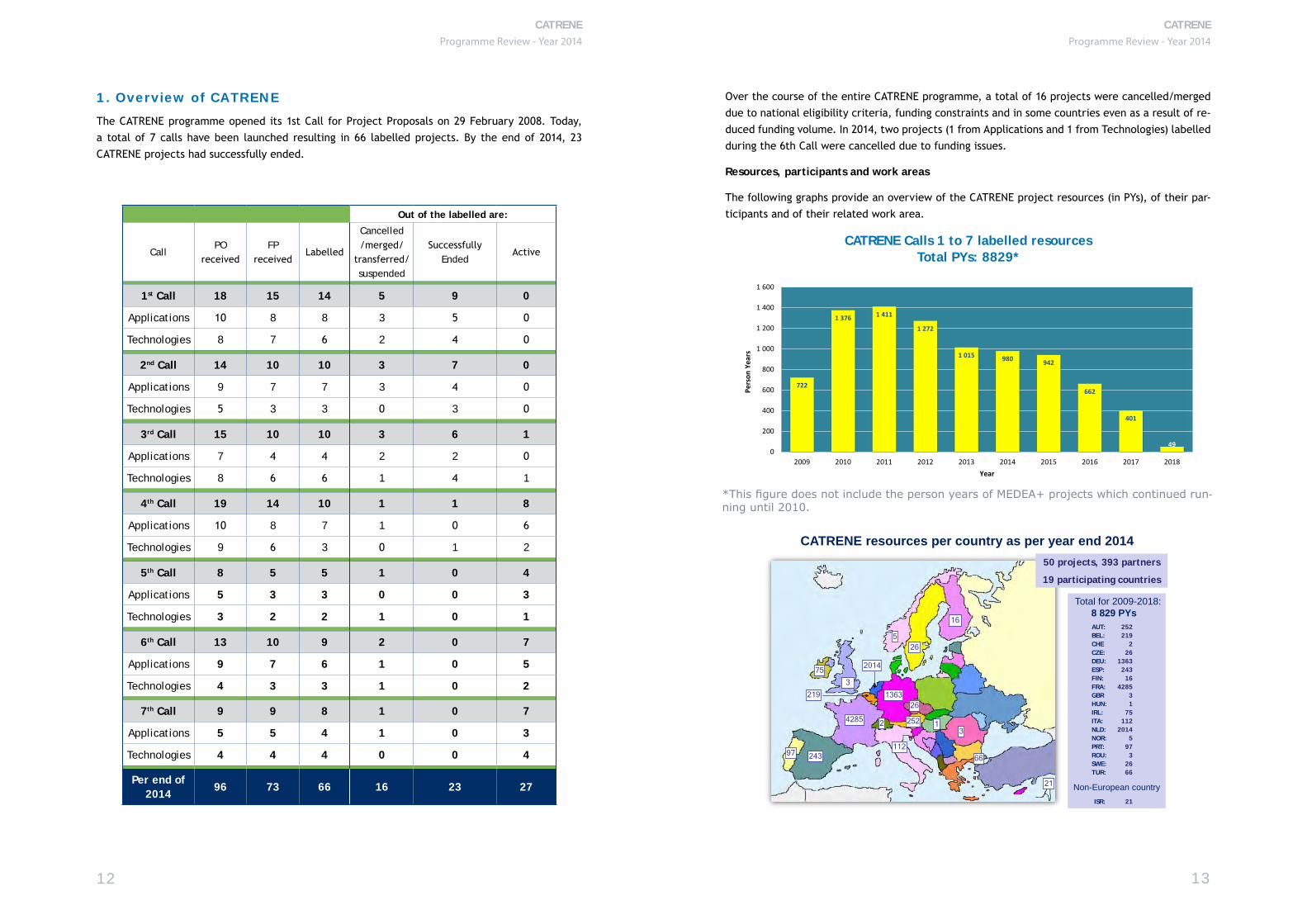
The CATRENE programme opened its 1st Call for Project Proposals on 29 February 2008. Today, a total of 7 calls have been launched resulting in 66 labelled projects and a total effort of 8 829 PYs.
At the end of 2014, 23 CATRENE projects had successfully ended.
Results of CATRENE Call 7 and launch of CATRENE Call 8
In 2014, CATRENE launched its 7th Call for Project Proposals. Altogether, 7 projects were la-belled amounting to 799 PYs.
It is of interest to note that SAM3 and SIPOB-3D have been co-labelled by CATRENE and EURIPIDES2.
European Nanoelectronics Forum 2014
The seventh edition of the European Nanoelectronics Forum took place in Cannes, France, on 26-27 November 2014 under the theme Enabling Smart Solutions.
Jointly organized by AENEAS, the EUREKA Cluster CATRENE, the ECSEL Joint Undertaking and the European Commission, the event had a good participation of 270 attendees from all over Europe.
During the forum, the project EM4EM received the CATRENE Innovation Award for its outstanding results which are pre-conditions for the next generation of electric vehicles, allowing European companies in the automotive industry to secure and expand while preserving or even increasing employment in Europe.
The feedback received in the questionnaire sent to participants at the end of the event showed a very high level of satisfaction, in particular with regards to the setup of the Project Village and
to the richness of the programme.
In addition to the day to day activities in 2014, reflection on a new tool for beyond 2015 was ad-dressed. Industry proposed to start a new EUREKA cluster for micro and nanoelectronics. A dedicat-ed Joint Working Group between National Authorities and Industry, which had the mandate to de-velop a concept for a new cluster, formulated new ideas for the scope and the organisation - based on the recommendations in the assessment report and the feedback received through interviews with the European Electronic Components and Systems community. A first draft was presented and discussed at the common meeting between National Authorities and Industry in April 2014.
At the same time, the new ECSEL Joint Undertaking was started by the European Commission and the Member States, focusing on the value chain from micro and nanoelectronics until System Integration. The requirement of the Public Authorities was to show that the planned new EUREKA Cluster and ECSEL are complementary tools – while having overlaps in content. During the year 2014, a lot of effort was put into the preparation of the concept for the New Tool. The concept was presented to the Public Authorities in November 2014. A detailed reaction with “cornerstones” for the New Tool is expected early 2015. The final decision on the establishment of a New EUREKA Cluster for micro and Nanoelectronics will most probably be taken in March 2015.

Overview of CATRENE
CATRENE Programme Review - Year 2014
1
CATRENE Programme Review - Year 2014
12
CATRENE Programme Review - Year 2014
13
1. Overview of CATRENE
The CATRENE programme opened its 1st Call for Project Proposals on 29 February 2008. Today, a total of 7 calls have been launched resulting in 66 labelled projects. By the end of 2014, 23 CATRENE projects had successfully ended.
Over the course of the entire CATRENE programme, a total of 16 projects were cancelled/merged due to national eligibility criteria, funding constraints and in some countries even as a result of re-duced funding volume. In 2014, two projects (1 from Applications and 1 from Technologies) labelled during the 6th Call were cancelled due to funding issues.
Resources, participants and work areas
The following graphs provide an overview of the CATRENE project resources (in PYs), of their par-ticipants and of their related work area.
CATRENE Calls 1 to 7 labelled resources Total PYs: 8829*
*This figure does not include the person years of MEDEA+ projects which continued run-ning until 2010.
Out of the labelled are:
CallPO
receivedFP
receivedLabelled
Cancelled /merged/
transferred/ suspended
Successfully Ended
Active
1st Call 18 15 14 5 9 0
Applications 10 8 8 3 5 0
Technologies 8 7 6 2 4 0
2nd Call 14 10 10 3 7 0
Applications 9 7 7 3 4 0
Technologies 5 3 3 0 3 0
3rd Call 15 10 10 3 6 1
Applications 7 4 4 2 2 0
Technologies 8 6 6 1 4 1
4th Call 19 14 10 1 1 8
Applications 10 8 7 1 0 6
Technologies 9 6 3 0 1 2
5th Call 8 5 5 1 0 4
Applications 5 3 3 0 0 3
Technologies 3 2 2 1 0 1
6th Call 13 10 9 2 0 7
Applications 9 7 6 1 0 5
Technologies 4 3 3 1 0 2
7th Call 9 9 8 1 0 7
Applications 5 5 4 1 0 3
Technologies 4 4 4 0 0 4
Per end of 2014
96 73 66 16 23 27
722
1 376 1 411
1 272
1 015 980 942
662
401
49 0
200
400
600
800
1 000
1 200
1 400
1 600
2009 2010 2011 2012 2013 2014 2015 2016 2017 2018
Pers
on Y
ears
Year
CATRENE resources per country as per year end 201450 projects, 393 partners
19 participating countries
219
243
4285
2014
1363
112
21
5
252 1
Total for 2009-2018: 8 829 PYsAUT:BEL:CHECZE:DEU:ESP:FIN:FRA:GBRHUN:IRL:ITA:NLD:NOR:PRT:ROU:SWE:TUR:
252219
226
136324316
428531
75112
20145
973
2666
97
16
26
75 3
3
66
26
Non-European country ISR: 21
2
CATRENE Programme Review - Year 2014
14
CATRENE Programme Review - Year 2014
15
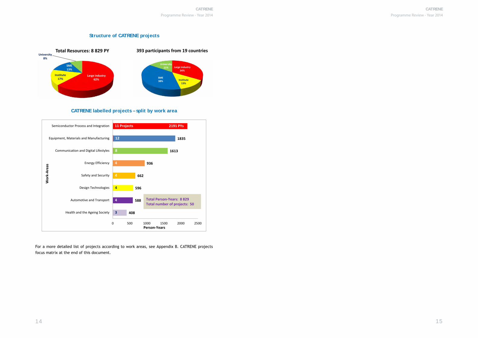
Structure of CATRENE projects
CATRENE labelled projects – split by work area
For a more detailed list of projects according to work areas, see Appendix B. CATRENE projects focus matrix at the end of this document.
Large industry 62%
Institute 17%
SME 13%
University 8%
Total Resources: 8 829 PY
Large industry 34%
Institute 13%
SME 38%
University 15%
393 participants from 19 countries
408
588
596
662
936
1613
1835
2191 PYs
3
4
4
4
4
8
12
11 Projects
0 500 1000 1500 2000 2500
Health and the Ageing Society
Automotive and Transport
Design Technologies
Safety and Security
Energy Efficiency
Communication and Digital Lifestyles
Equipment, Materials and Manufacturing
Semiconductor Process and Integration
Person-Years
Wor
k-Ar
eas
Total Person-Years: 8 829 Total number of projects: 50

CATRENE Year in Review
CATRENE Programme Review - Year 2014
2
CATRENE Programme Review - Year 2014
18
CATRENE Programme Review - Year 2014
19
2. 2014 CATRENE Year in Review
2.1. Achievements
2.1.1. Reflection on a new tool for beyond 2015
Industry proposed to start a new EUREKA cluster for micro- and nanoelectronics. A dedicated Joint Working Group between National Authorities and Industry, which had the mandate to develop a concept for a new cluster, formulated new ideas for the scope and the organisation - based on the recommendations in the assessment report and the feedback received through interviews with the European Electronic Components and Systems community. A first draft was presented and discussed at the common meeting between National Authorities and Industry in April 2014.
At the same time, the new ECSEL Joint Undertaking was started by the European Commission and the Member States, focusing on the value chain from micro- and nanoelectronics until System Integration. The requirement of the Public Authorities was to show that the planned new EUREKA Cluster and ECSEL are complementary tools – while having overlaps in content. During the year 2014, a lot of effort was put into the preparation of the concept for the New Tool. The concept was presented to the Public Authorities in November 2014. A detailed reaction with “cornerstones” for the New Tool is expected early 2015. The final decision on the establishment of a New EUREKA Cluster for micro and Nanoelectronics will most probably be taken in March 2015.
2.1.2. Call 7
In 2014, CATRENE launched its 7th Call for Project Proposals. The call opened with a Brokerage Event on 05-06 February in Brussels, attended by more than 200 people from across Europe. During the event, more than 40 project ideas for CATRENE and the ENIAC JU were identified and elabo-rated on.
Altogether, 7 projects were labelled by CATRENE as a result of CALL 7 amounting to 799 PYs.
It is of interest to note that SAM3 and SIPOB-3D have been co-labelled by CATRENE and EURIPIDES².
More details on the projects labelled in Call 7 are available in Chapter 3 of this publication.
2.1.3. Increased links and cooperation with other Clusters/Programmes
The mission of CATRENE is to promote and to strengthen the European nanoelectronics R&D&I com-munity. CATRENE and other EUREKA Clusters have been recognised as the only initiatives directly managed by R&D&I actors in regular contact with the EUREKA network and Public Authorities.
According to its mission, CATRENE is cooperating with other initiatives and organisations supporting the nanoelectronics domain:
y CATRENE and its predecessor programmes exists since 1987 and has continuously collaborated with the other EUREKA Clusters.
y CATRENE has co-labelled projects with other EUREKA Clusters and European funding programmes.
y An Inter-Cluster Committee has been created in 2010 to reinforce this cooperation.
y CATRENE has a strong link with the industry association “AENEAS” representing R&D&I actors in the ECSEL JU.
y CATRENE and AENEAS work together to define a common ‘Vision, Mission and Strategy’ (VMS) - the reference document for projects in CATRENE, ENIAC JU and the ECSEL JU.
y CATRENE and AENEAS host a Common Brokerage Event each year to prepare upcoming CATRENE and ECSEL calls.
y CATRENE organises the annual European Nanoelectronics Forum with the contribution of
CATRENE 7th Call 2014Call opens 04 FebruaryPO submission ends 05 AprilCommunication on selected POs 25 MayFP submission opens 01 JuneFP submission ends 04 September
Labelling sessions: 22 October25 November
Projects start 01 January 2015Participation in Project Outline (PO) phase is mandatory for participation in subsequent Full Proposal (FP).
Call # Project Number Acronym Work Area PYs
7 CAT120 CISTERN Communication & Digital Lifestyles 116
7 CAT121 EAST Communication & Digital Lifestyles 193
7 CAT209 H2O Safety and Security 206
7 CAT406 NEMADE Health and the Ageing Society 15
7 CAT601 SIPOB-3D Design Technology 102
7 CAT801 TSV-HANDYEquipment, Materials and
Manufacturing50
7 CAT802 SAM3Equipment, Materials and
Manufacturing117
CATRENE Programme Review - Year 2014
20
CATRENE Programme Review - Year 2014
21
the AENEAS, ECSEL JU and DGConnect (FP7) where projects and speakers from the three programmes are presented.
2.2. Events
A number of events underlined the CATRENE communication strategy in 2014, reaching from the very technically oriented and network focused Brokerage Event for experts to the yearly European Nanoelectronics Forum, which has achieved a high level of recognition in Europe today.
2.2.1. European Nanoelectronics Forum 2014 and CATRENE Innovation Award
The European Nanoelectronics Forum 2014 took place in Cannes, France on 27-28 November. 270 participants from all over Europe attended the event organised under the theme Enabling Smart Solutions. During the plenary session, the audience showed high appreciation for the speeches delivered, notably by Ben Verwaayen (Chairperson of the ELG), Philip Moynagh (Intel) and Berthold Hellenthal (Audi). The Project Village was organised in an area of 850 m² and presented 70 projects from CATRENE, the ENIAC JU and the European Commission’s FP7 programme. The new setup of the village, com-pared to previous years, was optimised to favour discussion and networking. A total of 4 Speakers’ Sessions were organised in the exhibition area during which hot topics were presented in an informal setting. The high number of participants in the sessions was unforeseen (15 participants per session in 2013 compared to +/-80 in 2014) and as a consequence the set up was not optimal. This will be corrected for 2015.
The feedback received in the questionnaire sent to participants at the end of the event showed a high level of satisfaction and that expectations were met at 95%.
The event was jointly organised by AENEAS, CATRENE, the ECSEL Joint Undertaking and the European Commission.
During the event, the project EM4EM (ElectroMagnetic reliability of electronic Systems for Electro Mobility) was chosen 2014 winner of the CATRENE Innovation Award. The results of the project are pre-conditions for the next generation of electric vehicles, allowing European companies in
the automotive industry to secure and expand while preserving or even increasing employment in Europe.
The objective of the EM4EM consortium is to cut out this interference as much as possible while extending its impact to the development of elec-tronics that are better able to withstand electromagnetic interference. With a strong interdisciplinary consortium led by Audi and including au-tomotive manufacturers, suppliers, semi-conductor manufacturers from three European countries, as well as universities, the EM4EM project has already produced impressive results. EM4EM deliverables (including tried and tested models, measurement methods and procedures as well
as simulation tools) will benefit a large number of European businesses by reducing time-to-mar-ket and costs of EMR-optimised components and systems for electric vehicles. The demonstrators along the value chain, for example, will help third parties integrate these results quickly into new products.
The CATRENE Innovation Award is bestowed each year to a project with a high level of innovation and far-reaching exploitation potential, market impact and overall benefits for Europe, as well as, creative objectives and effective management.
The next European Nanoelectronics Forum will be held on 01-02 December 2015.
2.2.2. Common AENEAS and CATRENE Brokerage Event 2014
The AENEAS/CATRENE Common Brokerage Event 2014 took place in Brussels, Belgium on 05-06 February and was held back-to-back with the ARTEMIS-IA Brokerage Event. Every year, the event brings together the European Nanoelectronics Community, to generate ideas for project proposal for the next CATRENE and ECSEL calls and to start consortia preparations.
The programme of the event is based on sessions covering the work areas common to both the CATRENE White Book and the ECSEL JU MASP:
y Communication and Digital Lifestyles
y Automotive and Transport
y Energy Efficiency
y Safety and Security
y Health and the Ageing Society
y Design Technologies
y Equipment, Materials and Manufacturing
y Semiconductor Process and Integration
During each session, a designated leader moderates the discussion around new project ideas along with consortia building.
During the 2014 edition, more than 230 participants worked together over the 2 days of the event coming up with more than 40 preliminary project ideas.
2.2.3. CATRENE Scientific Committee Workshop
"Smart Systems for Healthcare and Wellness"
See 2.3.2
EM4EM wins the 2014 CATRENE Innovation Award and provides solutions to meet new technical challenges for future vehicles with electric drives
Resolving electromagnetic compatibility and reliability issues required for future developments
in the automotive and semiconductor industries, the project EM4EM (ElectroMagnetic reliability
of electronic Systems for Electro Mobility) has received the 2014 CATRENE Innovation Award. This
award was presented on 26 November at the European Nanoelectronics Forum in Cannes.
As electric mobility becomes of increasing importance for today’s society, automotive manufacturers must address significant technical challenges when it comes to the reduction electromagnetic interference in electric vehicles.
The potential for interference to affect sensor systems, control systems and communication systems is up to one hundred times greater in electric vehicles than in vehicles with combustion engines. To date, expensive, complex screening and filtering measures, which increase the overall weight of electric vehicles, have been used in order to guarantee electromagnetic compatibility. The negative impact of this increase in weight results in the range of electric vehicles being reduced.
The objective of the EM4EM consortium is to cut out this interference as much as possible while extending its impact to the development of electronics that are better able to withstand electromagnetic interference.
With a strong interdisciplinary consortium led by Audi and including automotive manufacturers, suppliers, semi-conductor manufacturers from three European countries, as well as universities, the EM4EM project has already produced impressive results.
EM4EM deliverables (including tried and tested models, measurement methods and procedures as well as simulation tools) will benefit a large number of European businesses by reducing time-to-market and costs of EMR-optimised components and systems for electric vehicles. The demonstrators along the value chain, for example, will help third parties integrate these results quickly into new products.
By 2020, it is expected that there will be a market for 13 million electric vehicles. The semiconductor market for hybrid-electric and battery-electric vehicles, with annual growth rates of 25%, is expected to increase to $5.5 billion in 2020, reaching about 15% of the overall automotive semiconductor market.
The work completed in the CATRENE EM4EM project is a pre-condition for the next generation of electric vehicles, allowing European companies in the automotive industry to secure and expand while preserving or even increasing employment in Europe.
The CATRENE EM4EM project is scheduled to end in the first quarter of 2015. More information on the project is available at www.catrene.org.
INNOVATIONAWARD
MOST INNOVATIVE CATRENE PROJECTEM4EM
is presented to
CATRENE (∑! 4140), the EUREKA Cluster for Application and Technology Research in Europe on NanoElectronics, will bring about technological leadership for a competitive European information and communications technology industry.
CATRENE focuses on delivering nano-/microelectronic solutions that respond to the needs of society at large, improving the economic prosperity of Europe and reinforcing the ability of its industry to be at the forefront of the global competition.
CATRENE Office9 Avenue René Coty - F-75014 Paris - France
T. +33 1 40 64 45 60 - E. [email protected]
INNOVATIONAWARD
MOST INNOVATIVE CATRENE PROJECTEM4EM
is presented to
CATRENE Programme Review - Year 2014
22
CATRENE Programme Review - Year 2014
23
2.2.4. CATRENE Design Technology Conference 2014
The CATRENE Design Technology Conference was held in June 2014 in Grenoble. It was carried out in conjunction with the Leti Days Conference.
73 Delegates belonging to 30 different organisations and coming from 6 European countries (Austria, Finland, France, Germany, The Netherland, and Spain) attended the conference. The mix of repre-sentatives from industry and academic creates ideal opportunities for a professional exchange of ideas on a scientific basis.
The focus of the event was on application-oriented design methods for micro- and nanoelectronic products.
Based on this, DTC was organised into 5 Technical Sessions:
1. Reliability of SoCs in Safety Critical Applications
2. Power and thermal aware design
3. Energy efficient HPC
4. Power Electronics
5. Design enablement for advanced silicon technologies
and 2 Panels:
y What are the next growth areas in multimedia beyond TV, mobiles phones/tablets, STB,...?
y EDA beyond IC design
Held annually, the CATRENE DTC has become the meeting point for Europe’s scientists and experts in applications-oriented design. It is a unique opportunity to meet the CATRENE projects research-ers while enjoying the high quality program of the conference. However, attendees all agree that the best thing about DTC is the technical results which are presented by real experts from the field. The confluence of academic and industrial perspectives as well as electronic system design and manufacturing perspectives is unlike any other conference.
2.3. Publications
2.3.1. Project Profiles and Result Sheets
As of the end of 2014, 34 CATRENE Project Profiles and 16 CATRENE Result Sheets have been pro-duced and published on the web.
2.3.2. Scientific Committee Report on Smart Systems for Health and Wellness
The CATRENE Scientific Committee released the ‘Smart Systems for Health and Wellness’ report in February 2014 during a workshop in Brussels that gathered close to 80 participants.
The report and workshop focused on the key role that micro- and nanotechnology can play in find-ing solutions for this problem. Over the last 60 years, semiconductor technology has progressed tremendously. Following Moore’s law, huge computation power has become available into handheld devices, sensors have shrunk in size, and wireless communication has penetrated into the consumer market, to name only a few developments. The next step is the migration into wearable devices. Already many products are appearing on the market, but with limited functionality and unfit for long term continuous monitoring. More research is needed to obtain that goal. This report will fo-cus on the technology challenges that still lie ahead, and discuss possible solutions.
Various technologies are reviewed in the report with the following keywords in mind: prevention (including the promotion of healthy lifestyle through fitness and stress monitoring), diagnostic, therapy and therapy monitoring as well as decentralization from hospital to home maintenance. Three large applications are targeted: Devices for the healthy, devices to cure, and de-vices to aid the chronically ill (“stay fit”, “get well”, “a better live”). They have to operate unobtrusive, need full autonomy and are either wearable or implantable. Small devices (cm to mm size), with a typical power budget between several µW and a few mW are envisaged.
Semiconductor Technologies for
Smart Cities
CATRENE Scientific Committee
December 2014
T08:30 Key Peq MinTechnical Ch 09:00 Tu Hu09:45 DR
Ch10:05 En
LET 10:30 BrTechnical
Cha11:00 Th
incGe
11:20 Evoanin
11:40SOIchaindcir
12:05HigDCveh
12:30 Lu
Tuesday, 2
ynoteSiliconEurquignat,AEPI&Inalogic
lSession4:Eneair:FClermidy,I
utorial:HeterogenuNamNguyen,Bu
RAMarchitectureristianWeiss,UK
ergyEfficientSerTI
eak
lSession5:Powair:PaulMerkus
heroleofpowerecreasedenergyefraldDeboy,InfinolutionoftheSmddesigntechniquHVapplications,IsubstratestechnallengestodelivedustrialsubstratercuitperformanceghefficiencyHighC/DCConverterfohicle,PatrickDub
unch
24th June
rope,VeroniquesabelleGuillaum
ergyefficientHPCICTInfrastructur
neousHPCSystemull
forenergyefficieKL,(Tobeconfirm
rver,DenisDutoi
werElectronicssPhilips
electronicstoevefficiencyneonmartPowertechnouestowardhighdGiulioRicotti,STnologyandproceercostcompetitivesthatenableince,ManuelSellier,hVoltagetoLowVorelectricalorhybus,Valeo
me
Cre
ms
ency,med)
t,CEA‐
er
ologiesdensityTessvecreased,SoitecVoltageybrid
T
1
1
1
1
1
1
TechnicalSessioadvancedChair:Ah
14:00 Tutorial:FefficientS
14:45 AdvancedGlobalFo
15:05 “AdvancePatrickB
15:30 Break
16:00 Session6Chair:JMContributCadence,
17:30 Closing
on6:DesignenadsilicontechnolohmedJerrayaCEA
FDSOItechnologySoC,GergioCesandprocessenablemounderies(TobeedSystemDesignlouetST,AgnesF
6Panel:EDAbeyMChateau,STtors:Synopsys,AMagillem,Doceap
Sponsors
ablementforgies,ATech
yforenergyna,STment;GerdTeppeConfirmed)nEnablement,Fritsch,Thales
yondICdesign
Atrenta,Mentor,power
s
e Eu
H
M
Cha
h
Advance
uropean NaDesign T
Conf
Highlights fpro
June 23
MINATEC®, G
airs: Ahmed JerCo-Chairs: Ma
Patrick
For More Ihttp://www.let
For Vhttp://www
Programme
anoelectroTechnologyference
from CATREojects
– 24, 2014
Grenoble, Fra
rraya, CEATech,arcello Coppola,Blouet, ST
Information:tidays.com/20
Venue:w.minatec.org/
onicsy
ENE
4
nce
, France ST
:014/
CATRENE Programme Review - Year 2014
24
CATRENE Programme Review - Year 2014
25
The report received a high level of support from Industry and is available for download on the CATRENE website.
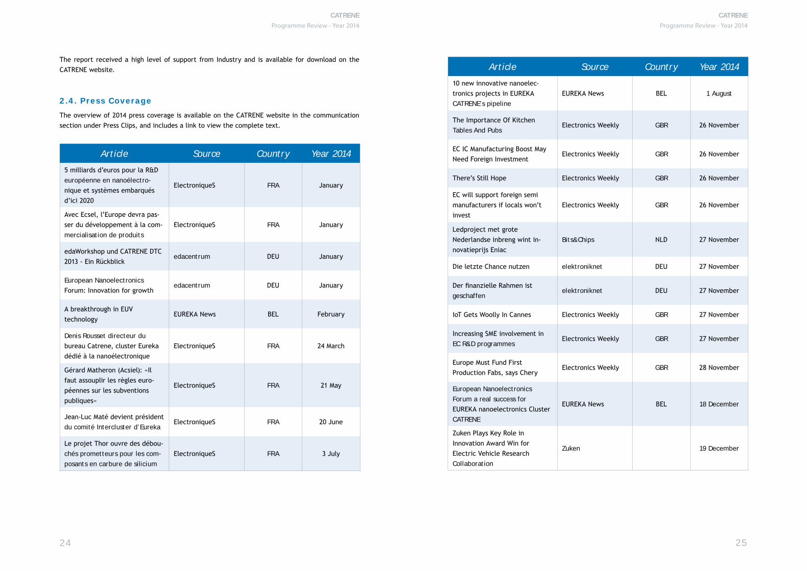
2.4. Press Coverage
The overview of 2014 press coverage is available on the CATRENE website in the communication section under Press Clips, and includes a link to view the complete text.
Article Source Country Year 2014
5 milliards d’euros pour la R&D européenne en nanoélectro-nique et systèmes embarqués d’ici 2020
ElectroniqueS FRA January
Avec Ecsel, l’Europe devra pas-ser du développement à la com-mercialisation de produits
ElectroniqueS FRA January
edaWorkshop und CATRENE DTC 2013 - Ein Rückblick
edacentrum DEU January
European Nanoelectronics Forum: Innovation for growth
edacentrum DEU January
A breakthrough in EUV technology
EUREKA News BEL February
Denis Rousset directeur du bureau Catrene, cluster Eureka dédié à la nanoélectronique
ElectroniqueS FRA 24 March
Gérard Matheron (Acsiel): «Il faut assouplir les règles euro-péennes sur les subventions publiques»
ElectroniqueS FRA 21 May
Jean-Luc Maté devient président du comité Intercluster d’Eureka
ElectroniqueS FRA 20 June
Le projet Thor ouvre des débou-chés prometteurs pour les com-posants en carbure de silicium
ElectroniqueS FRA 3 July
Article Source Country Year 2014
10 new innovative nanoelec-tronics projects in EUREKA CATRENE’s pipeline
EUREKA News BEL 1 August
The Importance Of Kitchen Tables And Pubs
Electronics Weekly GBR 26 November
EC IC Manufacturing Boost May Need Foreign Investment
Electronics Weekly GBR 26 November
There’s Still Hope Electronics Weekly GBR 26 November
EC will support foreign semi manufacturers if locals won’t invest
Electronics Weekly GBR 26 November
Ledproject met grote Nederlandse inbreng wint in-novatieprijs Eniac
Bits&Chips NLD 27 November
Die letzte Chance nutzen elektroniknet DEU 27 November
Der finanzielle Rahmen ist geschaffen
elektroniknet DEU 27 November
IoT Gets Woolly In Cannes Electronics Weekly GBR 27 November
Increasing SME involvement in EC R&D programmes
Electronics Weekly GBR 27 November
Europe Must Fund First Production Fabs, says Chery
Electronics Weekly GBR 28 November
European Nanoelectronics Forum a real success for EUREKA nanoelectronics Cluster CATRENE
EUREKA News BEL 18 December
Zuken Plays Key Role in Innovation Award Win for Electric Vehicle Research Collaboration
Zuken 19 December
CATRENE Programme Review - Year 2014
26
CATRENE Programme Review - Year 2014
27
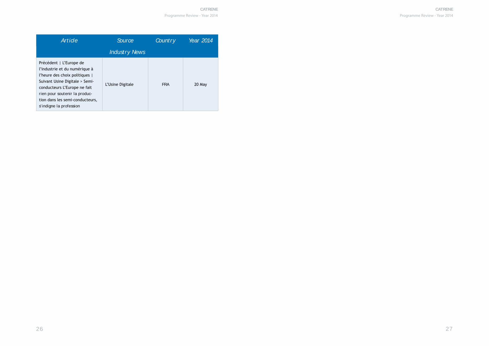
Article Source Country Year 2014
Industry News
Précédent | L’Europe de l’industrie et du numérique à l’heure des choix politiques | Suivant Usine Digitale > Semi-conducteurs L’Europe ne fait rien pour soutenir la produc-tion dans les semi-conducteurs, s’indigne la profession
L’Usine Digitale FRA 20 May
Review of Call 7
& Projects Ended in 2014
CATRENE Programme Review - Year 2014
3
CATRENE Programme Review - Year 2014
30
CATRENE Programme Review - Year 2014
31
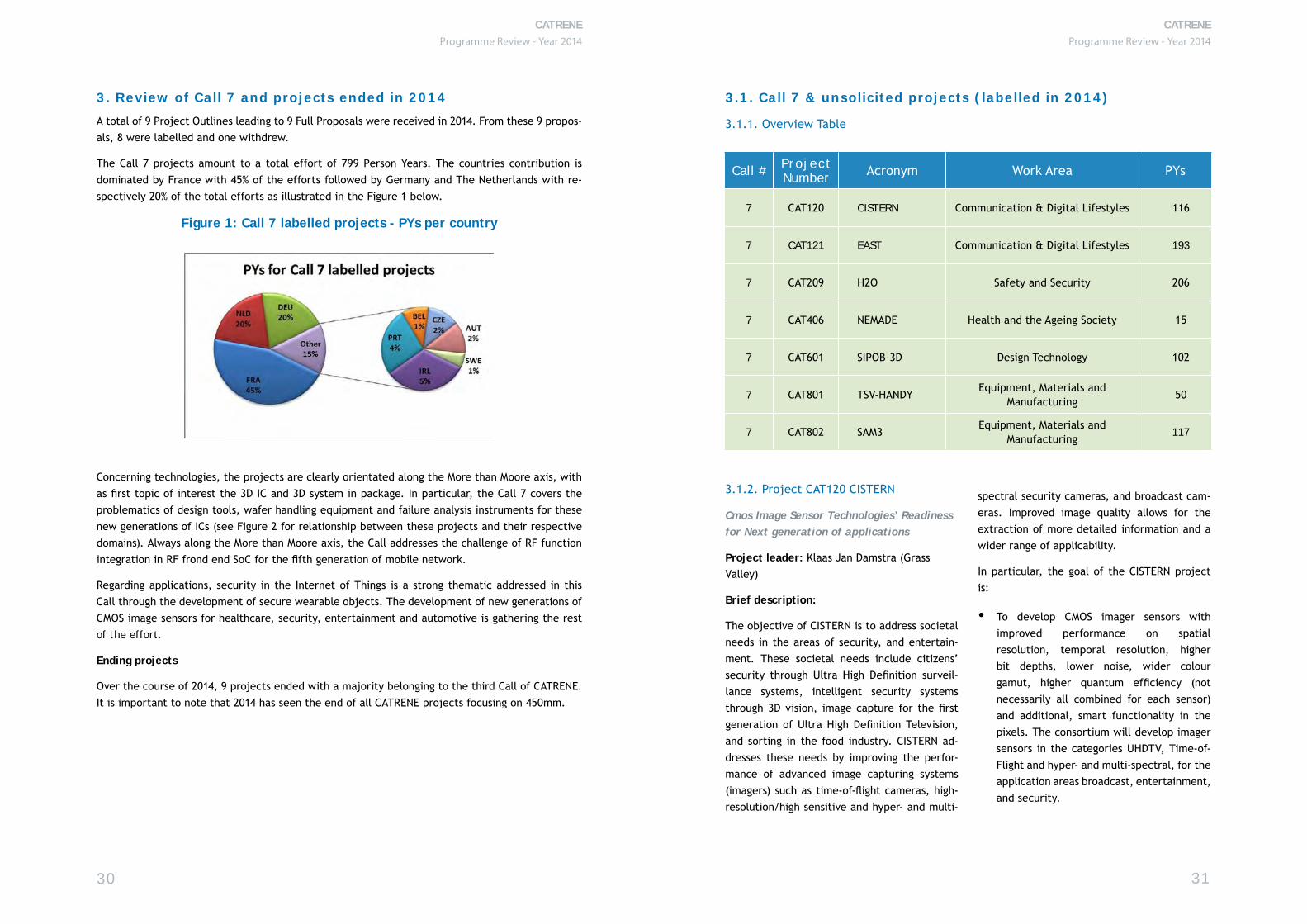
3. Review of Call 7 and projects ended in 2014
A total of 9 Project Outlines leading to 9 Full Proposals were received in 2014. From these 9 propos-als, 8 were labelled and one withdrew.
The Call 7 projects amount to a total effort of 799 Person Years. The countries contribution is dominated by France with 45% of the efforts followed by Germany and The Netherlands with re-spectively 20% of the total efforts as illustrated in the Figure 1 below.
Figure 1: Call 7 labelled projects - PYs per country
Concerning technologies, the projects are clearly orientated along the More than Moore axis, with as first topic of interest the 3D IC and 3D system in package. In particular, the Call 7 covers the problematics of design tools, wafer handling equipment and failure analysis instruments for these new generations of ICs (see Figure 2 for relationship between these projects and their respective domains). Always along the More than Moore axis, the Call addresses the challenge of RF function integration in RF frond end SoC for the fifth generation of mobile network.
Regarding applications, security in the Internet of Things is a strong thematic addressed in this Call through the development of secure wearable objects. The development of new generations of CMOS image sensors for healthcare, security, entertainment and automotive is gathering the rest of the effort.
Ending projects
Over the course of 2014, 9 projects ended with a majority belonging to the third Call of CATRENE. It is important to note that 2014 has seen the end of all CATRENE projects focusing on 450mm.
3.1. Call 7 & unsolicited projects (labelled in 2014)
3.1.1. Overview Table
3.1.2. Project CAT120 CISTERN
Cmos Image Sensor Technologies’ Readiness for Next generation of applications
Project leader: Klaas Jan Damstra (Grass Valley)
Brief description:
The objective of CISTERN is to address societal needs in the areas of security, and entertain-ment. These societal needs include citizens’ security through Ultra High Definition surveil-lance systems, intelligent security systems through 3D vision, image capture for the first generation of Ultra High Definition Television, and sorting in the food industry. CISTERN ad-dresses these needs by improving the perfor-mance of advanced image capturing systems (imagers) such as time-of-flight cameras, high-resolution/high sensitive and hyper- and multi-
spectral security cameras, and broadcast cam-eras. Improved image quality allows for the extraction of more detailed information and a wider range of applicability.
In particular, the goal of the CISTERN project is:
y To develop CMOS imager sensors with improved performance on spatial resolution, temporal resolution, higher bit depths, lower noise, wider colour gamut, higher quantum efficiency (not necessarily all combined for each sensor) and additional, smart functionality in the pixels. The consortium will develop imager sensors in the categories UHDTV, Time-of-Flight and hyper- and multi-spectral, for the application areas broadcast, entertainment, and security.
Call # Project Number Acronym Work Area PYs
7 CAT120 CISTERN Communication & Digital Lifestyles 116
7 CAT121 EAST Communication & Digital Lifestyles 193
7 CAT209 H2O Safety and Security 206
7 CAT406 NEMADE Health and the Ageing Society 15
7 CAT601 SIPOB-3D Design Technology 102
7 CAT801 TSV-HANDYEquipment, Materials and
Manufacturing50
7 CAT802 SAM3Equipment, Materials and
Manufacturing117
CATRENE Programme Review - Year 2014
32
CATRENE Programme Review - Year 2014
33
y To develop real time image processing techniques needed to improve the quality of the digital output signal of the sensor demonstrators.
y To develop and demonstrate the capability to produce multispectral imagers by hybridization of multispectral filter arrays on top of CMOS sensor. Both matrix filters and hybrid assembly process will be developed within the project.
y To demonstrate the improved performance of the CMOS imagers combined with related processing in a number of demonstrators.
y To develop Ultra High resolution, widely opened, sensor adapted zoom lenses (2/3’’ format, 4K resolution) for broadcast and security applications/markets.
y To optimize lens design in term of performance/cost/weight/camera integration for integral imaging chains.
y To develop and demonstrate an integrated Camera Lens Assembly for security applications that offers UHDTV performance with Size and Weight of an HDTV solution.
y To start in-house CMOS image sensor development in Grass Valley.
This project will build strong links with the ECSEL JU project EXIST.
Countries: Belgium, France, The Netherlands
Partners:
Belgium SoftKinetic Sensors
France
Le2i-University of Burgundy,SILIOS Technologies (sub-contractor of Le2i),Thales
The NetherlandsAdimec,Grass Valley,TU Delft
Expected start date: 01-04-2015 Expected end date: 31-03-2018
3.1.3. Project CAT121 EAST
Smart Everything everywhere Access to content through Small cells Technologies
Project leader: Philippe Meunier (NXP Semiconductors)
Brief description:
Today the wireless user is served by power-hungry 2G/3G/4G macro/micro-cell base sta-tions still having bounds on their data capac-ity, while the available spectrum has become a scarce resource. Fifth-generation (5G) mobile networks based on more and low power cells are expected to overcome these limitations and truly enable smart, high-speed, everything eve-rywhere access to their end users. In these low power networks, the technology for base sta-tion will have much more similarities to those of the handsets compared to the situation in 3G/4G applications.
However, to make the small cells network solu-tion successful technically and commercially for 5G, the following requirements on the RF front ends part of the Base station and handset have to be fulfilled:
1. Drastic cost & size reduction through integration;
2. Reduced energy consumption;
3. Improved re-configurability, adaptability and MIMO functionality.
EAST responds to these constraints for 5G net-works up to 6GHz, working on technologies, packaging, signal processing, architecture de-sign, and modelling for both base stations and mobiles. This clear focus on the “low” GHz range addresses the general expectation that this market segment will represent the highest economic value with the lowest environmental (energy consumption) impact. In particular, to fulfil the first requirement endowing cost re-
duction and miniaturization, EAST will research on:
y The high-density integration capabilities of CMOS/BiCMOS silicon technologies for the integration of antenna switch, low noise amplifiers and medium noise amplifiers;
y New packaging technics handling at the same time low insertion losses and good thermal dissipation.
Concerning energy saving, EAST will propose solution in the field of:
y Signal processing algorithms, to decrease computational power in the digital pre-distortion process;
y Technologies, exploiting the much better power-handling capabilities of LDMOS.
For the last field of requirement EAST will work on:
y Design, with fully digital Tx solution, enabling easy reconfiguration;
y Architecture for antenna array, enabling the MIMO capability.
Countries: France, Ireland, The Netherlands, Portugal
Partners:
France
3DiS Technologies,AMCAD Engineering,Cassidian,CEA–LETI,Ethertronics,III-V LAB,IMS Laboratory-University of Bordeaux,Institut Mines-Telecom/Telecom Paris-Tech,NXP Semiconductors,Sequans Communications,Thales Communications & Security,XLIM Xlim
Ireland Alcatel-Lucent
The Netherlands
Anteverta-mw,Besi,Bruco Integrated Circuits,Delft University of Technology,NXP Semiconductors,TNO,TUE - Technical University of Eindhoven
PortugalGSLDA,Instituto de Telecomunicacoes,NANIUM
Expected start date: 01-04-2015 Expected end date: 31-03-2018
3.1.4. Project CAT209 H2O
Human to Objects “Easy Interactions in the Smart City”
Project leader: Christian Dietrich (Gemalto)
Brief description:
The purpose of the H2O project, capitalizing on former results from the CATRENE eGo project, is to develop the requested architecture to put the human in control of the smart objects sur-rounding, put on or in him, so as to develop a human centric and privacy ensuring security architecture to support the rapidly emerging Wearable computing and IoT markets. The pro-ject will investigate the human to object in-teractions in different application areas of the smart city domain: communication, transporta-tion, e-health and e-retail. The purpose of this work will be to study and implement advanced architecture concepts and technology bricks felt as missing for the deployment of efficient wearable computing solutions, as resulting from the former successfully ended eGo project and also to develop new user experience for a com-plete adoption of this new digital lifestyle. The major assets delivered by the project will be:
y A high-performance, reliable, ultra-low-power BCC (Body Communication Coupling) technology with a standardized physical layer which should be usable as
CATRENE Programme Review - Year 2014
34
CATRENE Programme Review - Year 2014
35
communication enabler in any Body Area Network. The eGo project has demonstrated the need to improve the BCC interface for addressing harsh environments.
y A representative set of non-intrusive, secure, low-cost, always working, wearable devices, suitable for several application domains pertaining to the IoT or smart-city area (in particular, ehealth, communication, safety and security, and retail). The eGo project has prototyped some form factors acceptable by a large category of users, and the project intend to implement robust and easy-to-use form factors (e.g. bracelet, clips...) suitable for the target applications.
y A fully trusted and privacy preserving transaction environment, enabling the object(s) that the user wears or can touch to seamlessly initiate applications or communication with or between objects.
y An Open SDK and application certification tool-chains enabling third party developers to easily develop apps for wearable and guarantying that such app can be automatically verified before being remotely loaded in the wearable devices owned by the user.
y To complete reference and trusted security architecture enabling seamless secure synchronization of wearable devices. This synchronization includes the recovery of credentials into a blank wearable device.
y To pilot implementation of wearable computing scenarios in some IoT or Smart-City application domains, together with first QoS or QoE feedback reports.
Countries: Czech Republic, France, Ireland, Portugal
Partners:
Czech Republic IMA - Institute of Microelectronic Applica-tions
France
ASTUS,CEA–LETI,CEA LIST,Gemalto,IDATE,Insight SiP,Oberthur Technologies,SORIN CRM,STMicroelectronics,Trusted Labs,Worldline
Ireland
Electro Automation,InHandGuides,Institute of Technology Cork,Tyndall National Institute
Portugal GSLDA,Instituto de Telecomunicacoes
Expected start date: 01-12-2014 Expected end date: 30-11-2017
3.1.5. Project CAT406 NEMADE
New Mammography Detector
Project leader: Jan T. Bosiers (Teledyne DALSA)
Brief description:
This project aims at developing a new genera-tion, multi-modality (screening, biopsy and to-mosynthesis) mammography detector, bringing better imaging performance at lower X-ray dose and higher patient comfort, at a lower cost. The incumbent technology is at a point where it can no longer meet new application and regulatory requirements like higher speeds, multi-modali-ty and lower patient X-ray dose. The improved sensitivity and precision of the new genera-tion detectors will also enable improved treat-ment. As benchmark, the current detectors for mammography are considered. Access to clini-cal validation is secured via SigmaScreening through co-founder Prof. Dr. Den Heeten who works at the Department of Radiology of in the Academic Medical Center (AMC) in Amsterdam, or by clinical trials by a selected OEM.
The five main technical goals are:
1. More efficient X–ray energy conversion and improved image contrast by improved scintillator performance;
2. Detector using newest generation CMOS imagers allowing additional features like switchable saturation dose, dual-energy compatibility and real-time X-ray dose sensing and control; and improved imaging processing capabilities;
3. Improved assembly technology matching the stringent requirements for high-resolution mammography applications, combined with high reliability;
4. More personalized mammography and higher patient safety by adaptive breast compression, reduced X-ray dose and shorter imaging cycles, fewer re-takes, fewer incorrect screening diagnosis results;
5. Lower cost: lower cost for detector and ownership, more efficient diagnosis and treatment.
Countries: The Netherlands, Sweden
Partners:
The Netherlands Sigmascreening,Teledyne DALSA
Sweden Scint-X
Expected start date: 01-01 2015 Expected end date: 31-12-2017
CATRENE Call 7 technology focus: 3D-ICS Projects
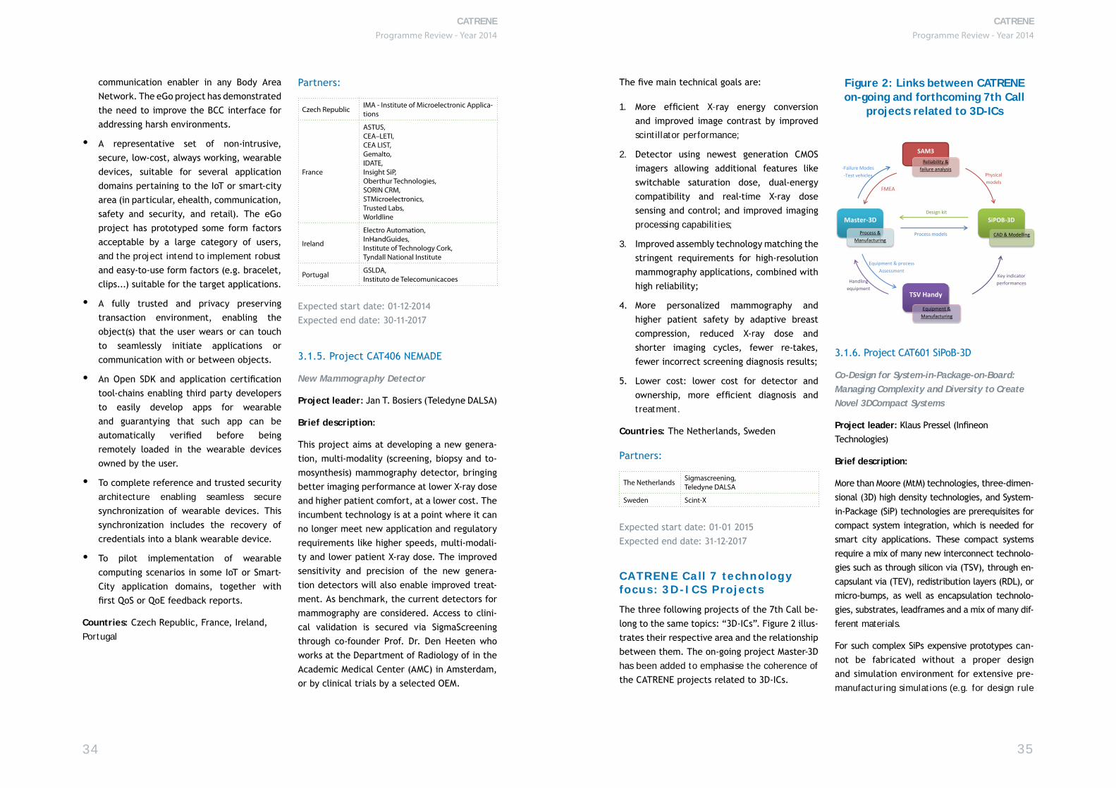
The three following projects of the 7th Call be-long to the same topics: “3D-ICs”. Figure 2 illus-trates their respective area and the relationship between them. The on-going project Master-3D has been added to emphasise the coherence of the CATRENE projects related to 3D-ICs.
Figure 2: Links between CATRENE on-going and forthcoming 7th Call
projects related to 3D-ICs
3.1.6. Project CAT601 SiPoB-3D
Co-Design for System-in-Package-on-Board: Managing Complexity and Diversity to Create Novel 3DCompact Systems
Project leader: Klaus Pressel (Infineon Technologies)
Brief description:
More than Moore (MtM) technologies, three-dimen-sional (3D) high density technologies, and System-in-Package (SiP) technologies are prerequisites for compact system integration, which is needed for smart city applications. These compact systems require a mix of many new interconnect technolo-gies such as through silicon via (TSV), through en-capsulant via (TEV), redistribution layers (RDL), or micro-bumps, as well as encapsulation technolo-gies, substrates, leadframes and a mix of many dif-ferent materials.
For such complex SiPs expensive prototypes can-not be fabricated without a proper design and simulation environment for extensive pre-manufacturing simulations (e.g. for design rule
Equipment & process Assessment
FMEA
Physical models
Design kit
Process models
SAM3
SiPOB-3D
TSV Handy
Master-3D
-Failure Modes -Test vehicles
CAD & Modelling
Reliability & failure analysis
Equipment & Manufacturing
Process & Manufacturing
Handling equipment
Key indicator performances
CATRENE Programme Review - Year 2014
36
CATRENE Programme Review - Year 2014
37
checks, thermal, electrical). The risk of failing is too high. Thus, a coherent chip-package-board co-design environment needs to be set-up that covers chips and passives, package and the board. SiPoB-3D aims at building up a next level of design methodology for 3D integrated systems, which includes not only the chip and package, but also the board domain.
The consortium will investigate a methodology for mapping the best technology available in companies to design the optimum SiPoB-3D de-vice faster, better and more economic. We must avoid expensive “try and error” loops (time consuming hardware iterations). For design of a compact system, the physics behind the tech-nologies and materials of a compact SiPoB-3D device must be understood. Therefore, empha-size will be put on hardware assessment based on advanced technologies. SiPoB-3D is a holis-tic approach, which includes investigation and simulation of models that enter into a design library, the design methodology considering multi-physics, and the capabilities setting-up an optimum system as a whole. Data transfer be-tween the different domains needs to be inves-tigated and optimized, especially between the board suppliers and packaged chip suppliers. A global optimum, on chip, package and also on board level needs to be achieved. SiPoB-3D intends to exploit the CoSiP backbone to en-able chip/package and board (PCB) co-design for footprints and connectivity. New SiP design rules and checks are a must and will be inte-grated in the design environment.
A world leading consortium has been set-up. The two European semiconductor suppliers, Infineon Technologies and STMicroelectronics, both with major production in Europe, will col-laborate with Continental and Symeo, which both will work on a subsystem on board de-velopment, the EDA vendors Atrenta, Docea Power, and CST, and the three small companies Hofmann LP, Schöller-Electronics, and Hitex,
the latter three represent the interface to the board (PCB). These partners are supported by four leading European research institutes. The results of SiPoB-3D will allow shorter time to market and support Europe for managing the complexity and diversity for setting up compact 3D systems as a whole including chip, package, and the board.
Countries: France, Germany
Partners:
France
Atrenta,CEA,Docea Power,STMicroelectronics Crolles,STMicroelectronics Grenoble,Université de Savoie
Germany
Continental Automotive,CST,FAU Erlangen-Nuremberg,Fraunhofer IIS/EAS,Hitex Development Tools,Infineon Technologies,Schoeller-Electronics,Symeo,Hofmann Leiterplatten
Expected start date: 01-04-2015 Expected end date: 31-03-2018
3.1.7. Project CAT801 TSV-HANDY
TSV HANDY Hvm AND Yield optimisation
Project leader: Guilhem Delpu (RECIF Technologies)
Brief description:
TSV (Through Silicon Via) is a “More-than-Moore” technology that enables new chip ar-chitectures. Some challenges reside along the several steps of process to make TSV products cost efficient. The project aims at supporting the HVM ramp-up and improving the yield for manufacturing TSV products.
The project addresses 4 main challenges:
1. The handling of heterogeneous 300mm wafers with edge trim inspection. In fact, on a 3D TSV line, wafers can present highly different mechanical behaviours and physical properties. RECIF targets the development of a 300mm wafer handling platform, which supports as many types of wafer as possible, without having to reconfigure the equipment or swap dedicated modules (like the end effector). This will help end users gaining in equipment flexibility and “up time”, because the current solutions on the market have proven not being stable enough. The resulting platform will allow a usage either as a wafer sorter by end users (like NANIUM), or as an EFEM for integration by OEM’s (like FOGALE).
2. The development of metrology and new logistical concepts for ultra-thin wafers after they are debonded on 380mm frames The manual handling of cassettes and wafer frames is an important contributor to wafer cracks, and open cassettes will become incompatible with the cleanliness requirement, driven by the shrinking of the pitch for micro-bumps (down to 20μm). There is a need to bring “Front End” methods and best practices, to “Middle End” (TSV lines). But 300mm modules and automation equipment are not compatible to handle 380mm film frames, because of their dimensions. For instance, a 300mm load port cannot handle 380mm substrates due to mechanical interferences. However, a solution is to consider re-using some of the 450mm modules that have been designed already (cf: CATRENE and ENIAC JU 450mm projects), and adapt it to the need of 380mm film frames. This way, industry will take benefit from existing standardized interfaces, with dimensions that are compliant with substrates wider
than 300mm, up to 450mm. ENTEGRIS and RECIF have designed 450mm modules which can be adapted to support the handling of film frames, within a cleaner and highly automated environment. ENTEGRIS 450mm carrier with 380mm insert for frames will be handled by RECIF 450mm handling platform. ENTEGRIS will develop new carriers to be compatible with higher level of automation, and the partners will demonstrate the industrial relevance of tracking the wafers debonded on frames thanks to RF tags integrated into the frame, at substrate level.
3. The investigations for the FO-WLP process, for round wafers larger than 300mm The project will investigate the manufacturing of surfaces larger than 300mm in Fan-Out Wafer Level Packaging for advanced packaging. In fact, since in this process, the size of the reconstituted mold wafer is independent of the original incoming silicon, GaAs or SiGe wafer, processing larger panels drives the cost per die down. Therefore, current 300mm wafer diameter for Fan-Out WLP needs to be enlarged (batch processing of large panel) and 330mm reconstituted wafer for Fan-Out WLP/eWLB and 450mm Si wafer for Fan-In WLP/WLCSP and Fan-Out WLP/eWLB, need to be studied and considered as next steps to be implemented in high volume manufacturing environment.
4. The improvement of temporary bonding and debonding processes, The work on temporary bonding consist in integrating the coating and bonding capability for “novel adhesives solutions” in order to increase the throughput and the performance of the temporary bonding process. On the debonding side, the project will evaluate the debonding process with wafers bonded with this new process and
CATRENE Programme Review - Year 2014
38
CATRENE Programme Review - Year 2014
39
implement the new standardization rule developed in the project (re-using 450mm automation modules like carriers and handling platform).
Synergies will be created with other CATRENE projects like NGC450, SOI450, MASTER_3D and-with the ENIAC JU EEM450PR project. The in-dustrial partners intend to release new prod-ucts to the market by early 2018.
Countries: Austria, Belgium, France, Germany, Portugal
Partners:
Austria EV Group E. Thallner
Belgium Imec
France
CEA-LETI,Fogale Nanotech,RECIF Technologies,STMicroelectronics Crolles
Germany ENTEGRIS
Portugal NANIUM
Expected start date: 01-04-2015 Expected end date: 31-03-2018
3.1.8. Project CAT802 SAM3
Smart Analysis Methods for 3D Integration in Advanced Microsystems and Corresponding Materials
Project leader: Klaus Pressel (Infineon Technologies)
Brief description:
More-than-Moore (MtM), System-in-Package (SiP), as well as 3D high-density integration technologies are a prerequisite for enabling the design of compact microelectronic devices and are enablers for European technology leader-ship. With increasing integration density the impact of right material choices is becoming of outstanding importance (e.g. electrical data, stress, adhesion, CTE matching). During the
last decade all package materials have been changed, which is a consequence of miniaturisa-tion as well as integration of more functionality into smaller volume. We expect that this trend in assembly and packaging will proceed (see discussions in ITRS roadmap, iNEMI roadmap, as well as international conferences). Increased functional density and small foot-print of inno-vative systems are achieved by innovative in-terconnects, such as Through Encapsulant Via (TEV), Through Silicon Vias (TSV) and redistri-bution layers applied to advanced assembly and packaging technologies. Examples of such ad-vanced packaging technologies are chip embed-ding in mold materials (eWLB), chip embedding in laminate materials as well as 3D stacking.
For these new and complex devices, failure analysis becomes a more and more expensive part of product development. An advanced fail-ure analysis strongly supports to meet the right timing for product introduction, a fact that provides an outstanding saving potential for companies. New materials and processes must be developed and qualified requiring effective analysis techniques to understand new failure modes and reliability limiting factors caused by thermo-mechanical mismatch, residual stresses and interaction of new materials and processes. Thus, for development of complex heterogene-ous SiP devices and for reaching required reli-ability, innovations in failure diagnostic and ma-terial analysis are required and must be aligned to the SiP technology developments in effective failure analysis workflows.
In particular, the existing failure analysis tech-niques are limited in localizing electrical de-fects in these compact SiP devices with multi-level wiring. Efficient and artefact free sample preparation to apply physical analysis tech-niques are limited. Techniques to determine local residual stresses and material parameter within the package are required for reliability modelling.
The four major European semiconductor and system suppliers Infineon, STMicroelectronics, Bosch and Thales will collaborate with eleven equipment and analytical method suppliers from Germany and France. The work is sup-ported by five academic institute partners. The SAM3 project will improve the capability of the semiconductor and system suppliers (Infineon, STMicroelectronics, Bosch, and Thales) to avoid defects and failures during product develop-ment based on better material understanding. Comprehensive, well adapted and effective failure analysis work flows provide essential support for technology development, process and product qualification, and quality/process control during fabrication. The project results will provide inputs for advanced simulation ap-proaches or reliability models that can be used to identify and consider reliability problems al-ready during the product development phase (“design for reliability”). Such concepts gain in-creasing importance since they allow to reduce time-to-market and development cost. In addi-tion proper analysis work flows allow reliability assessments to achieve short-time to market readiness, proven application potential, and fu-ture customer acceptance of innovative MtM, SiP and 3D integration solutions. Besides, the SAM3 project will allow the equipment suppli-ers to better understand the needs of the semi-conductor and system suppliers and tune their roadmaps according to the need of the industry with worldwide market perspectives.
Countries: France, Germany
Partners:
France
CNRS-AMU-LP3,DIGIT CONCEPT,GREMAN (UMR 7347),ORSAY-PHYSICS,STMicroelectronics Tours,STMicroelectronics Rousset,STMicroelectronics
Germany
3D-Micromac,Fraunhofer Institute for Mechanics of Materials,Infineon Technologies,Muegge,Nanoworld Services,point electronic,PVA TePla Analytical Systems,Reutlingen University,Robert Bosch,SmarAct,WITec
Expected start date: 01-03-2015 Expected end date: 28-02-2018
CATRENE Programme Review - Year 2014
40
CATRENE Programme Review - Year 2014
41
3.2. Projects ended in 2014
3.2.1. Overview Table
3.2.2. Project CA303 OPTIMISE
Optimisation of Mitigations for Soft, firm and hard Errors
Project leader: Florent Miller (EADS)
Brief description:
The reliability of electronic components is an essential element for automotive power elec-tronic, avionic and space applications. However, commercially available submicron technolo-gies are inherently sensitive to the incidence of energetic particles due to the low voltages at which they work (3,3, 2,5, 1.8 V….) and due to their very small node size. As example, the high sensitivity of the advanced technologies (below 90nm and down to 28nm) was assessed
experimentally in the project and the associat-ed risk for applications at ground and airplane levels was quantified with a potential increase in the error rate reaching almost +50% on 28nm technologies.
Starting from this statement, OPTIMISE project followed two main goals, applied to three dif-ferent applications automotive power electron-ic, avionic-FPGA and space ASICs:
y Acquire knowledge on new radiation threats that may impact future electronic equipment and work in close collaboration with standardization bodies to propose guidelines or standards to be able to perform relevant risk assessment;
Call # Project Number Acronym Work Area
1 CA303 OPTIMISE Automotive and Transport
2 CA402 THOR Health and the Ageing Society
3 CA308 ICAF Automotive and Transport
3 CA403 RELY Health and the Ageing Society
3 CT206 Reaching22 Semiconductor Process and Integration
3 CT305 SOI450 Equipment, Materials and Manufacturing
3 CT306 NGC450 Equipment, Materials and Manufacturing
3 CT402 9D-Sense Semiconductor Process and Integration
4 CT210 Dynamic-ULP Semiconductor Process and Integration
y Develop and validate mitigation techniques from layout to application architecture levels.
The first step towards the realisation of these two objectives was the development of tools for the radiation sensitivity assessment. In the following of the PARACHUTE project (MEDEA frame), the relevancy of using laser and emula-tion platforms to study the radiation sensitiv-ity has been pursued on a wide variety of de-vices (SRAM, test vehicles, SRAM based FPGA, …). In addition, the first experiments in the world demonstrating the possibility to simulate destructive failures using laser in Wide Band Gap power devices have been successfully per-formed by IMS and EADS allowing achieving one of the first detailed study of the radiation in-duced failures in SiC power devices.
Automotive application
Acquire knowledge
An important highlight is the standardized method proposed by Renault regarding reli-ability assessment due to radiation effects on power components.
Mitigations development & new products
y CNM designed an IGBT with an internal current sensing. it has been demonstrated the possibility to measure a SEL (Single Event Latchup through the sense electrode, without impact on main circuit, paving the way to possible early detection of destructive event, especially in the case of slow power electronics devices.
y STM Tours has been able to develop a new SiC diode technology and will propose a full range of SiC 1200V diodes in 2014 benefiting of improvements on radiation tolerance.
Avionic application
Acquire knowledge
Airbus proposed inputs for the update of the radiation test standards for avionics.
Mitigations development & new products
An Avionic I/O board implemented in a Stratix IV FPGA has then been tested using a fault in-jection platform:
y A state of the art DRAM fault-tolerant controller developed and patented by EADS was enhanced to support the more advanced DDR3 memory type used in the system.
y The CPU Checker IP was developed to detect errors enabling a continuous observation of the microprocessor execution without disturbing it.
y A selective mitigation approach developed by TIMA focuses on error detection in the FPGA Look-Up Table (LUT) configurations taking advantage of unused FPGAs resources.
SPACE ASIC
Acquire knowledge
On the standards side RIIF initiative has been launched.
Mitigations development & new products
y UC3M developed the AMUSE tool able to classify the cells of a circuit with respect to Single Event Effects (SEE).
y Arquimea synthesized a SEL free ASIC with a hardened 90nm CMOS library developed during the project by ATMEL. The measures of SETs width have shown an improved SET robustness of the hardened library compared to 90nm commercial cells (ratio around 100). The radiation assessment of
CATRENE Programme Review - Year 2014
42
CATRENE Programme Review - Year 2014
43
the 8T SRAM cells has been performed by UIB.
y In order to improve the design of robust circuits, iRoC and TIMA developed three innovative Radiation Hardening by Design (RHBD) solutions. These techniques have been used to design three hardened versions of the LEON2 processor synthesized using the ATMEL’s hardened library. These hardening techniques have been assessed by performing fault injection simulations and have been validated by iRoC and TIMA. Finally, these hardening techniques have been completed by the CPU checker proposed by UC3M in the avionic chain value and ported by UC3M and iRoC into the three hardened LEON2 design. These mitigation techniques were implemented in the test vehicle V53, which was manufactured at the end of May 2014 and tested under heavy ion in June 2014. The SEE results of the LEON2 circuits have shown a very good SET coverage protection with a benefit on the silicon area, and power overhead, without degrading the performances. On the exploitation side, this hardened library is used to develop a new ATMEL space-qualified SPARC processor that will address the space market.
Countries: France, Spain
Partners:
France
Airbus Defense and Space,ATMEL NANTES,CEA,Continental Automotive,EADS Innovation Works,IMS Lab,iRoC Technologies,RENAULT,STMicroelectronics,TIMA,Universite Provence IM2NP,Valeo Interior Controls
Spain
Alter Technology Group,Arquimea Ingenieria,CNM-Centro Nacional de Microelec-tronica IMB,D&T Microelectronica,Thales Alenia Space,UIB-University of Balearic Islands,Universidad Carlos III Madrid
Start date: 01-01-2015 End date: 31-12-2017
3.2.3. Project CA402 THOR
Striking technologies for Power
Project leader: Mark van Helvoort (Philips Healthcare)
Brief description:
The THOR Project, coordinated by Philips Healthcare, has delivered solutions for packag-ing, cooling and electromagnetic compatibil-ity. This helps industry to transform the Silicon Carbide (SiC) market from a device to a power modules business. This transformation will lead to a jump in growth of the SiC device market from 26% to 39% within the next year according to Yole Development.
In modern power converters, most of the volume is occupied by cooling components and electri-cal filters. SiC based power devices reduce both the requirements on cooling and filtering. THOR has exploited this aspect by developing high temperature packaging, compact cooling sys-tems and smaller filters. Compact power con-version systems with a very high power density have been demonstrated in three application areas: aeronautics, automotive and healthcare.
These compact and highly efficient converters are essential for addressing the environmental challenges in terms of CO2 emission and over reliance on fossil fuels. Power converters will significantly reduce the weight of cabling in a single aircraft thus diminishing fuel consump-
tion with an additional 30% being saved by storing transient energy during braking. In the medical area, more compact systems at a lower cost helps to address the health challenges in the ageing society.
Key to the success of the THOR project was its coverage of the full supply chain from semicon-ductor device level to power system integrator in combination with three application areas to leverage the economy of scale. The commercial advantage is a stronger competitive situation for the different industrial partners, because recent advancements in power electronics technology provided by the academic partners have been integrated into advanced applica-tions. This ranges from SiC and SoI technology to full compact power converters integrated in large systems.
Such broad coverage was made possible by the unique support of two large European support programmes: CATRENE and EURIPIDES2. The in-formation sharing and cross-fertilization within the THOR consortium was excellent; more than 70 reports with results have been internally ex-changed and new, long-lasting, collaborations have been established. Furthermore, the key players within THOR guaranteed efficient coop-eration with other related European projects.
THOR also shared its newly generated knowl-edge amongst the academic and industrial public. More than 30 papers have been writ-ten, 25 presentations were given and 12 patent applications have been submitted. A book on EMC of large systems and installations has also been published in Dutch and is currently being translated.
The first products based on THOR technol-ogy are already available on the market. In September 2012, STMicroelectronics released their SiC diodes for photovoltaic converters. They will extend their range this year to ad-
ditional applications and SiC Mosfets will follow soon. Soitec and NXP have a new silicon-on-in-sulator process in place facilitating the design of high temperature drivers and the integration of low-voltage and high-voltage integration at lower cost.
For electric vehicles, Valeo has demonstrated a compact air-cooled high-voltage DC/DC-converter with efficiency 93% and 95% over a very broad output power range. The vapour chamber and heat sink have been designed such that the cooling capabilities of the converter are independent of the mounting orientation, thus offering large flexibility to car designers.
Labinal Power Systems, Airbus Group Innovations, Thales Microelectronics and CIRTEM have demonstrated a compact power converter, which covers a very large tempera-ture range such that it can be located at both aeronautic engines and in brakes on airplanes (very high temperatures).
Philips Healthcare and the Dutch SME Prodrive demonstrated the capabilities of full digital control for power electronics. Among others, a compact high voltage power supply was shown with an ideal topology for introducing SiC com-ponents. Pilot tests in hospitals are already on-going. Further, a feedback system was devel-oped, which can correct up to 10 dB variations in amplifier gain.
Countries: Belgium, France, The Netherlands
Partners:
Belgium NXP Semiconductors
France
Airbus Group Innovations,Ampère Insa Lyon,Cirtem,Epsilon Ingénierie,Labinal Power Systems (Safran),Soitec,ST Microelectronics,Thales Microelectronics,University de Versailles-Saint-Quentin-en-Yvelines,Valeo Systèmes de Contrôles Moteur
CATRENE Programme Review - Year 2014
44
CATRENE Programme Review - Year 2014
45
The Netherlands
Bruco Integrated Circuits,NXP Semiconductors,Philips Healthcare,Prodrive,TUE-Technical University Eindhoven
Start date: 01-10-2010 End date: 31-03-2014
3.2.4. Project CA308 ICAF
Image Capture of the Future
Project leader: Jochem Herrmann (Adimec)
Brief description:
ICAF project developed and researched hard-ware and processing algorithms for single lens 3D camera systems, multi view camera systems, broadcast video over internet protocol systems and high speed vision cameras for 3D appli-cations. The project delivered 3D single lens microstereopsis camera, multi view systems, depth from luminance, depth image based ren-dering, super resolution of depth maps and de-noising and demosaicing for super slow motion HD cameras (including IP based transmission). In particular the project delivered the first 3D single lens stereopsis camera and the first HDTV slow motion camera beyond triple speed that can continuously output a slow motion stream together with a normal HDTV stream. In addi-tion the project provided high data rate trans-mission ICs to extend the worldwide CoaXPress standard with new protocols and higher bit rates up to 12.5 Gbps.
The products that incorporate results of the ICAF project are professional broadcast cam-eras, cameras for machine vision, the global security and medical markets, CoaXPress trans-mission ICs, CMOS image sensors and com-pression IP. These products are manufactured within Europe and shipped worldwide. The ex-ploitation results and expected market impact by partners are:
y Adimec has the first commercial camera with 2 Gpix/s continuous data rate streaming capability and the first rugged surveillance camera with CoaXPress;
y Axon has won 5 awards with his implementation and definition of the new Video over IP standards SMPTE2022 and AVB;
y EqcoLogic introduced its next-gen CoaXPress transceiver solutions. First engineering samples have been sent to selected customers for evaluation;
y Grass Valley has introduced a very successful 6x slow motion HDTV camera. They won 3 awards with this camera;
y Grass Valley has patented the principle used in the single lens microstereopsis camera;
y IntoPix has strengthened its position in video compression with first J2K Video over IP reference FPGA design;
y On-Semi has Strengthening its position in state of the art high speed and industrial imaging;
y TU Delft developed a novel method for automatic transformation of 2D images into 3D and has applied for patents in Europe, US, Japan, and Korea. It spawned a spin-off company to exploit the IP;
y University of Ghent has developed new denoising, demosaicing and super-resolution techniques for time-of-flight, microstereopsis and regular broadcast cameras;
y Hasselt University has developed novel high-quality and real-time camera interpolation.
A pro-active behaviour of all partners resulted in a smooth project management with mini-mal delays in deliverables and a high number of quality results compared to the size of the project.
Countries: Belgium, The Netherlands
Partners:
Belgium
EqcoLogic,Hasselt University,intoPIX -secure image technology,ON Semiconductor,University of Ghent
The Netherlands
Adimec,AXON,Grass Valley,TUD-Technical University Delft
Start date: 01-10-2011 End date: 30-09-2014
3.2.5. Project CA403 RELY
Design for RELIABILITY of SoCs for Applications like Transportation, Medical, and Industrial Automation
Project leader: Georg Georgakos (Infineon Technologies)
Brief description:
One of the main problems in ICs down-scaling is the high susceptibility to smallest interferences and deviations. Nevertheless, safety critical in-tegrated systems inside cars, planes, medical implants, etc. have to be reliable despite an increasing ageing and failure sensitivity. Today, this reliability is achieved by extremely expen-sive means like guard bending or redundancy. Starting from this statement, RELY targeted two main goals: ensure system reliability along the entire value chain, and enable new SoCs with a new level of functionality through increased re-liability at reasonable costs. These two general goals can be broken down into three technical areas:
1. Prediction of reliability at all phases of the system design.
2. Solutions to increase the system reliability.
3. Reduction of the area and cost overhead for the reliability measures through optimization.
Early and fast reliability prediction
At the transistor, gate, and RT level, ageing ef-fects are already modelled thanks to earlier projects such as HONEY or OPTIMISE. The main challenges for RELY were: increasing modelling speed, improving model accuracy, increasing the abstraction level, and including additional effects.
As regard to model accuracy, the RELY research has provided models for the Negative Bias Temperature Instability (NBTI), the Hot Carrier Degradation (HCD), the Time Dependent Dielectric Breakdown (TDDB), the soft break-down (SDB) and the electro-migration.
At levels of abstraction above RT level, CEA LIST integrated a reliability-aware system level simulation methodology into their SESAME tool which is 15 times faster compared to gate level. A simulation speed improvement of four orders of magnitude against SPICE has been observed using a phase space based approach developed by OFFIS as subcontractor from Infineon.
Finally, ITEM developed a new methodology enabling the selection of optimal design pa-rameters (in terms of functionality as well as reliability) for analogue circuits, demonstrat-ing two orders of magnitude speed-up against SPICE. Last but not least, Fraunhofer developed a methodology to generate degradation mod-els for all available tool interfaces directly from the characterization data enabling usage of the commercially available tools.
Solutions to increase the system reliability at optimized costs
Using these prediction methodologies, several run-time reliability management strategies were developed, such as sensor redundancy
CATRENE Programme Review - Year 2014
46
CATRENE Programme Review - Year 2014
47
schemes (AIRBUS), in-situ degradation sensing (TUM LTE), sensor output data aggregation and reliability management utilizing a dedicated re-liability layer (TUM LIS), or selective hardening (ITTP). X-FAB presented a highly reliable high-temperature technology with improved elec-tro-migration resistance. The partners Infineon, X-FAB and MunEDA developed techniques to prevent fatal field returns due to early detec-tion before tape-out. Finally, a new methodol-ogy based on product like circuitries for a hun-dred times faster detection of quality problems in the fab, was developed by Infineon.
The project consortium finally presented sev-eral demonstrators, successfully using these design techniques at several levels: One of the major demonstrators, to be developed in a 40nm Infineon technology was not ready at project end, but will nevertheless be presented later by Infineon and TUM at their own cost. This test chip will test the applicability of the RELY methodologies in an automotive context, analysing the effectiveness of critical path de-tection and adaptation, as developed by TUM. ITEM presented a test chip from the medical devices area; a mixed signal neural interface. The power overhead, stemming from the overd-esign of the reference circuit could be reduced by 20% in the analogue and 37% in the digital part under the same reliability target. AIRBUS and Fraunhofer jointly developed a redundant, thus highly reliable sensor array for avionic ap-plications in extremely harsh environments. This demonstrator presented how to build reli-able systems from unreliable components, es-pecially sensors.
Countries: France, Germany, The Netherlands, Romania
Partners:
France
ATMEL NANTES,CEA–List,EADS Innovation Works,ENST,STMicroelectronics
Germany
EADS Innovation Works,Fraunhofer-IISB,Infineon Technologies,MunEDA,TUM - Technical University Munich,UHB - University of Bremen,X-FAB Semiconductor Foundries
The Netherlands Intrinsic-ID
Romania Infineon Technologies
Start date: 01-05-2011 End date: 31-07-2014
3.2.6. Project CT208 Reaching22
REsearch on optimal ArCHitecture and INteGration of 22/20nm node core digi-tal CMOS technology- Electrical proof of concept
Project leader: Gilles Thomas (STMicroelectronics)
Brief description:
The project REACHING22 was labelled in 2010 and started on 01 April 2011. The works, done in the initial phase of REACHING22, related to 28nm FDSOI transistor architecture qualifica-tion for next generation of application proces-sor was a complete success and the activity completed according to plan. A complex SoC demonstrator of 69mm2 was designed by ST-Ericsson. With a 100% tool set compatibility with 28nm bulk the FDSOI 28nm offers a 40% frequency boost at nominal Vdd of 1V, 100mV reduced Vmin on SRAM and 40% less variability on NMOS. These encouraging results led to con-sider FDSOI transistor architecture as the ma-jor technology option for the 20nm node, dis-placing the 20nm bulk which was concurrently developed and could not show a comparable
power/performance compromise.
In a second phase, the project REACHING22 chose to develop the 20nm FDSOI transistor ar-chitecture (at module level in WP3) and towards a full integration in WP4 for the ST Crolles fab. Gate length more aggressively sized than 20nm were evaluated while the multilevel intercon-nect scheme could retain metal pitches defined for the 20nm bulk giving rise to an intermedi-ate technology node with mixed critical dimen-sion dubbed “14nmFDSOI”. The technology has been renamed “14FDSOI” because device per-formances compare to “16-14nm” node specs. In Q3 2013, ST-Ericsson left the consortium. An initial simple test chip (C20FIRST) was designed and the initial integration flow permitted the fabrication of a first lot. Although functional, this initial silicon was way off the predefined target. In the final 3 quarters of the project a big effort was made by CEA-LETI and ST to improve the process flow and boost the performance. A more complex mask set was designed to initi-ate the development of the 14FDSOI technology platform and to develop the complex Middle Of the Line (MoL) section of the process requiring multiple double patterning steps. At the end of the project process improvements made during the project are bringing DC parameters within 90-95% (for NMOS) and within 70% (for PMOS) of the target. AC parameters measured on ring os-cillators are reaching 78-80% of the predefined performance which is a good achievement at this early stage of the technology development. To improve, further investment is needed and planned. The change from node 20 perfor-mance specs to node 14 specs made it very dif-ficult to achieve speed goal at Ring Oscillator level; the project studied all options to boost performance including the gate last approach, as well as major process improvement in the critical MoL to reduce parasitic capacitances and resistances which will ensure 100% of AC and DC characteristics to be achieved.
Countries: Belgium, France
Partners:
Belgium UCL-Catholic University of Louvain
France
CEA–Leti,IMEP/INPG,LTM/CNRS,Soitec,ST-Ericsson,STMicroelectronics
Start date: 01-04-2011 End date: 31-03-2014
3.2.7. Project CT305 SOI450
Development of 450mm SOI substrates, related technologies and equipment
Project leader: Francois Brunier (Soitec)
Brief description:
The SOI450 project started in November 2011 and finished in June 2014, enabling to reach an unprecedented maturity level on SOI pro-cess and related technologies and equipment in 450mm. More over Resolving 450mm barriers with our consortium brought innovating solu-tions in 300mm “Fully depleted” SOI processes and allow for retrofitting in the 300mm frame-work. In particular the cleaning solutions de-veloped on EVG bonding tool using Megasonic and the introduction of the Adixen APA in the SOITEC 300mm FDSOI substrate line improve the yield and optimize the FOUP cleaning cost.
The main achievements in the project are the following:
y Soitec demonstrated the feasibility of the Smart CutTM process, evaluating each step of SOI substrate process flow in 450mm and measuring the existing gaps with targeted objectives. Most process steps reached a good maturity level, the main technical roadblock at his stage being the quality of
CATRENE Programme Review - Year 2014
48
CATRENE Programme Review - Year 2014
49
H implantation.
y Adixen, brought the study and assembly of the APA450 prototype, and its installation at G450C (Albany, USA), Adixen takes a forefront position in the area of molecular contamination, and especially toward international customers.
y EVG demonstrated successful fully automated wafer bonding on 450mm substrates for SOI manufacturing with fusion bonding process.
y Altatech developed a top table 450mm Altasight metrology system and interface with major players in material and process developments.
y INTEL; last but not least, thanks to the intermediate of INTEL a collaboration path with G450C was opened.
Thanks to the SOI450 program, the members of this consortium are ideally positioned when a recovery of 450mm activity and roadmap will occur.
Countries: Austria, Belgium, France, Germany, Ireland, The Netherlands
Partners:
Austria EV Group E. Thallner
Belgium Imec
France
Adixen Vacuum Products,Altatech,CEA-LETI,Soitec
Germany Mattson
Ireland Intel
The Netherlands ASM Europe
Start date: 01-11-2011 End date: 30-06-2014
3.2.8. Project CT306 NGC450
Project leader: Guilhem Delpu (RECIF Technologies)
Brief description:
NGC450 project aimed to enable in Europe the development of a wafer handling platform, dedicated to support the 450mm wafer size mi-gration. Considering the ever evolving 450mm global environment during the project time line, this concrete goal was a real challenge to achieve. The excellent collaboration and the ef-ficient management within the project helped to complete the targets within the planned tim-ing and to end with a successful project, suc-cessful in the innovation point of view but also in the industrial exploitation perspectives.
Technical progress, innovations
The projects brought innovation in the follow-ing sub-equipment:
y Atmospheric robotics: The challenge was to transfer heavier substrates through a longer distance within an equal period of time, despite increased vibrations phenomenon and more challenging mechanical properties of the substrate. The atmospheric robotics developed during the project is able to maintain the same throughput than a 300mm system, with an optimal wafer safety and extreme cleanliness.
y Vacuum robotics: Asys partner proved the possibility to produce an easily scalable vacuum chamber, maintaining the same throughput than a 300mm cluster system.
y Mini environment: Compliance with 16-22nm cleanliness and airborne molecular contamination has been proven 16-22 nm compatible (and beyond).
y Atmospheric and vacuum compliant End effectors: The challenge was to develop
Vibration free, stiff and very thin End effectors despite more challenging dimensions. Besides the End effector had to be compliant with low defectivity and contamination challenges (particle and metallic). The end effectors developed in the project have proven their efficiency with safe handling at Imec and low defectivity (cf CEA-LETI assessment).
y Software interface: AIS has proven the efficiency and stability of their software able to drive a multi-equipment cluster with a high performance interface.
y Advanced metal contamination characterization: The project has allowed specific VPD and LPD set-ups implementation on 450mm wafer and optimized metallic contaminants collection coupled to the advanced ICPMS characterizations. The set-ups efficiency and sensitivity has been proved by CEA-LETI.
Industrial exploitation and benefit per part-ner company
At this precise moment, the 450mm market outlook is unclear and it is thus very difficult to “predict” when the first 450mm order will come from industry. However, in this 450mm ramp-up perspective, the NGC450 project developed state-of-the art “off the shelf solutions“ for any process or metrology supplier. Besides, the NGC450 partners will be among the first to be activated thanks to their network and because they are at the beginning of the value chain and the consortium partners can very quickly and easily supply the developed solutions; because they led the development till the end.
The absence of immediate payback doesn’t make a commercial failure of this project. What are the benefits that can be used outside from a pure 450mm perspective?
y AIS will capitalize on their developments involving web services to enrich their current product offer for semiconductor business, but also railways technology, factory automation, photovoltaic, optical industry, pharmaceutical, general automation solutions. Now that AIS controller and RECIF 450mm EFEM are integrated, the path will be very easy to perform an integration on a RECIF 300mm system.
y Asys and HAP are into 300mm business thanks to the NGC450 project, to supply a big European OEM. This achievement led to further businesses in Asia, thanks to presentation to SEMATECH consortia. HAP gained experience and visibility for their end-effector business, which can be valued beyond 450mm arena.
y CEA-LETI has demonstrated their leading edge capabilities to develop advanced set-ups for chemical collection and assessment of metal contamination. They will participate to the “2015 International Conference on Frontiers of Characterization and Metrology for Nanoelectronics”.
y EVG has been presenting the developed SOI bonding system at several exhibitions (presentations at Semicon EU) and has been advertising this product to existing and potential customers through its global sales and customer support organization. The EVG systems are candidates to receive some of the atmospheric robotics modules developed within NGC450.
y HAP gained experience and visibility for their end-effector business, which can be valued beyond 450mm arena.
y RECIF gained a lot of visibility thanks to this project and has set-up strong links with G450C. Several OEM’s are expecting from RECIF to supply 300mm EFEM solutions, based on the successful demonstration of
CATRENE Programme Review - Year 2014
50
CATRENE Programme Review - Year 2014
51
NGC450 platform. RECIF has also improved its 300mm offer thanks to NGC450 learning, mainly on the cleanliness point of view. The company could achieve breakthrough results on its 300mm platform, when assessing the particle adders per wafer pass (PWP) on a KLA SP3, down to 26nm and 40nm particle size. RECIF sees a strong opportunity to disseminate and re-use some of the 450mm designs, for 300mm direct applications related to the handling of ultra-thin wafers (around 50µ thickness), after they are de-bonded on film frames (“More-than-Moore” applications). Manufacturing methods are mainly coming from the world of “back end” (BEOL). These methods will not be “clean enough” and will not offer sufficient automation levels to allow the manufacturing in high volume, with an acceptable yield.
The manual handling of cassettes and wafer frames is an important contributor to wafer cracks, and open cassettes will become in-compatible with the cleanliness requirement, driven by the shrinking of the pitch for micro-bumps (down to 20µm).
There is a need to bring “Front End” methods and best practices, to “Middle End“(TSV lines).
But 300mm modules and automation equip-ment are not compatible to handle 380mm film frames, because of their dimensions. For in-stance, a 300mm load port can’t handle 380mm substrates due to mechanical interferences.
However, a solution is to consider re-using some of the 450mm modules that have been designed already, and adapt it to the need of 380mm film frames. This way, industry will take ben-efit from existing standardized interfaces, with dimensions that are compliant with substrates wider than 300mm, up to 450mm.
Countries: Austria, Germany, France, Ireland
Partners:
Austria EV Group E. Thallner
France CEA-LETI,RECIF Technologies
Germany
AIS Automation Dresden,ASYS,Fraunhofer – IISB,HAP
Ireland Intel
Start date: 01-11-2011 End date: 31-12-2014
3.2.9. Project CT402 9D-Sense
Autonomous Nine Degrees of Freedom Sensor Module
Project leader: Ricardo Zamora (Robert Bosch)
Brief description:
The main goal of 9D-Sense was to provide tech-nologies and methods to enable a stand-alone 9D sensor chip integrating a 3-axis acceler-ometer, a 3-axis gyroscope and a 3-axis mag-netometer on silicon wafer based technology. The projects lead to several innovations sum-marised below:
1. Sensing module
One major goal for the Bosch MEMS department was to reduce the package size of multi degree of freedom sensor units. 9D-Sense delivered a 5x5x1 mm3 package compare to 10x8x3.8 state of the art solution where only one axis acceler-ometers and gyroscope were included in a sin-gle chip and the integration of three different sensors was only available at package level. This greatly helps to reduce size and cost of sensor production. Furthermore, this concept has the advantage of an inherent precise adjustment of all space axis of each sensor to each other which improves measurement accuracy. This global innovation was possible thanks to:
y An innovative MEMS-based Lorentz force magnetometers developed by FhG-ISIT.
y Redistribution Layer, Through Silicon Via and Fine Pitch Bumping allowing savings in die area of up to 25%.
y Innovation in Readout electronics with an innovative delta sigma ADC Gyroscope-ASIC and a Lorentz Force Magnetometer Excitation and Readout.
2. Thin film Battery
Realization of full 3D-batteries on structured substrates with CVD and/or ALD layers.
3. Energy Harvesters
y Kinetic Harvester (HSG-IMIT) using the heel-strike during walking has been realised. The achieved power output is sufficient to operate a fully energy autonomous mobile sensor system.
y Thermoelectric Generator (TEG) (Micropelt) a novel chemical etch process using Methane was developed.
4. Sensor Fusion
y Algorithms (Bosch Sensortec): improvement of pedestrian tracking algorithms using inertial and magnetic sensors only.
y Sensor fusion for indoor navigation (HSG-IMIT): elying on step detection [1] and Kalman filtering [2,3,4] had been investigated.
y Sensor fusion for gesture recognition (HSG-IMIT): Based on the concept of dynamic time warping an inertial sensor-based gesture recognition algorithm was developed.
5. Applications
y Smart Wristlet: The innovations in several ways: It is designed to be integrated into a wide Internet of Things ecosystem; The
integrated protocols are designed to be very battery friendly, Built-in security and Ergonomics.
y Orthesis (OttoBock HealthCare): E-Mag Active orthoses was modified and is now controlled by a 9D-Sense module allowing improvements in the learning mode of the orthoses.
Countries: Austria, Finland, France, Germany
Partners:
Austria Austria Microsystems
Finland University of Helsinki
France Gemalto
Germany
Fraunhofer,HSG-IMIT,Micropelt,Otto Bock Healthcare,Bosch Sensortec,Robert Bosch,Technische Universität Darmstadt
Start date: 01-11-2011 End date: 31-10-2014
3.2.10. Project CT210 Dynamic-ULP
High DYNAMIC range multiprocessor for Ultra Low Power mobile devices
Project leader: Philippe Garcin (STMicroelectronics)
Brief description:
The common goal of ST, ST-Ercisson, CEA and their partners has been to get an efficient de-sign platform for use by European designers pre-paring the next devices in the Mobile Wireless and Consumer Appliances where access to the multimedia contents will have no latency to the user.
For this purpose, DYNAMIC-ULP has developed advanced process modules and contribute to two successive generations of design platforms
CATRENE Programme Review - Year 2014
52
CATRENE Programme Review - Year 2014
53
(design kit, models, libraries) based on CMOS FDSOI technologies (Fully Depleted Silicon on Insulator) for European manufacturing facilities.
The success of DYNAMIC-ULP was achieved on 2 complete process nodes:
y A 28nm FDSOI design platform: the project allowed this platform to reach full maturity. Platform efficiency has been demonstrated on a high complexity System-on-Chip, till silicon level. The project was 80% design oriented, thus acting as a key link between developments on transistor architectures (inherited from REACHING22) and future manufacturing aspects performed by the Places2Be pilot line project. Actions towards new FDSOI-oriented methodologies included methods for SRAM development and design specific logic IP block. Feasibility studies to integrate forward and back biasing and DVFS techniques are being encompassed into a test chip connecting all relevant IP block into a front-end receiver design for 4G application. All the IPs were validated on ST-Crolles silicon run opening the volume production on the process node.
y A 14nm FDSOI design platform: the project has evolved towards this platform up to technology qualification. Process modules have been developed by an extensive usage of PROMO and QLIB test chips in order to assess the performance of the technology. A new tool for standard cell verification provided a speed improvement of a factor 8 compared to Monte Carlo method. The same hybrid solution has been ported to 14nm thus enabling the co-integration of bulk and SOI devices on the same die.
The FDSOI process is keeping the simplicity of the planar technology used for design since the Integrated Circuit has been manufactured. This legacy is guarantying a high reliability as
well as a low manufacturing cost. The second advantage clearly demonstrated is the time to market: most of previously circuit designed for bulk can be transferred into ta FDSOI database thanks to the methodology demonstrated by Dynamic-ULP deliverables.
The penetration of the FDSOI is just at the early stages where the ULP (Ultra Low Power) are a mandatory requirement for all mobile devices, all IoT (Internet of Thing) where the autonomy is the main differentiator on the market. ECSEL projects (Thing2Do) and (Way s2goFast) will be entrusted with the exploitation of these supe-rior process nodes into a large variety of con-sumer market segments.
Countries: France, Sweden, Turkey
Partners:
France
Atrenta,CEA,CEA-LETI,Dolphin Integration,Infiniscale,Soitec,ST-Ericsson,STMicroelectronics,STMicroelectronics Grenoble
SwedenAcreo,Lund Institute of Technology,ST-Ericsson
Turkey Ericsson Mikroelektronik
Start date: 01-01-2012 End date: 31-12-2014

Appendix A
CATRENE Projects Focus Matrix
CATRENE Programme Review - Year 2014
4
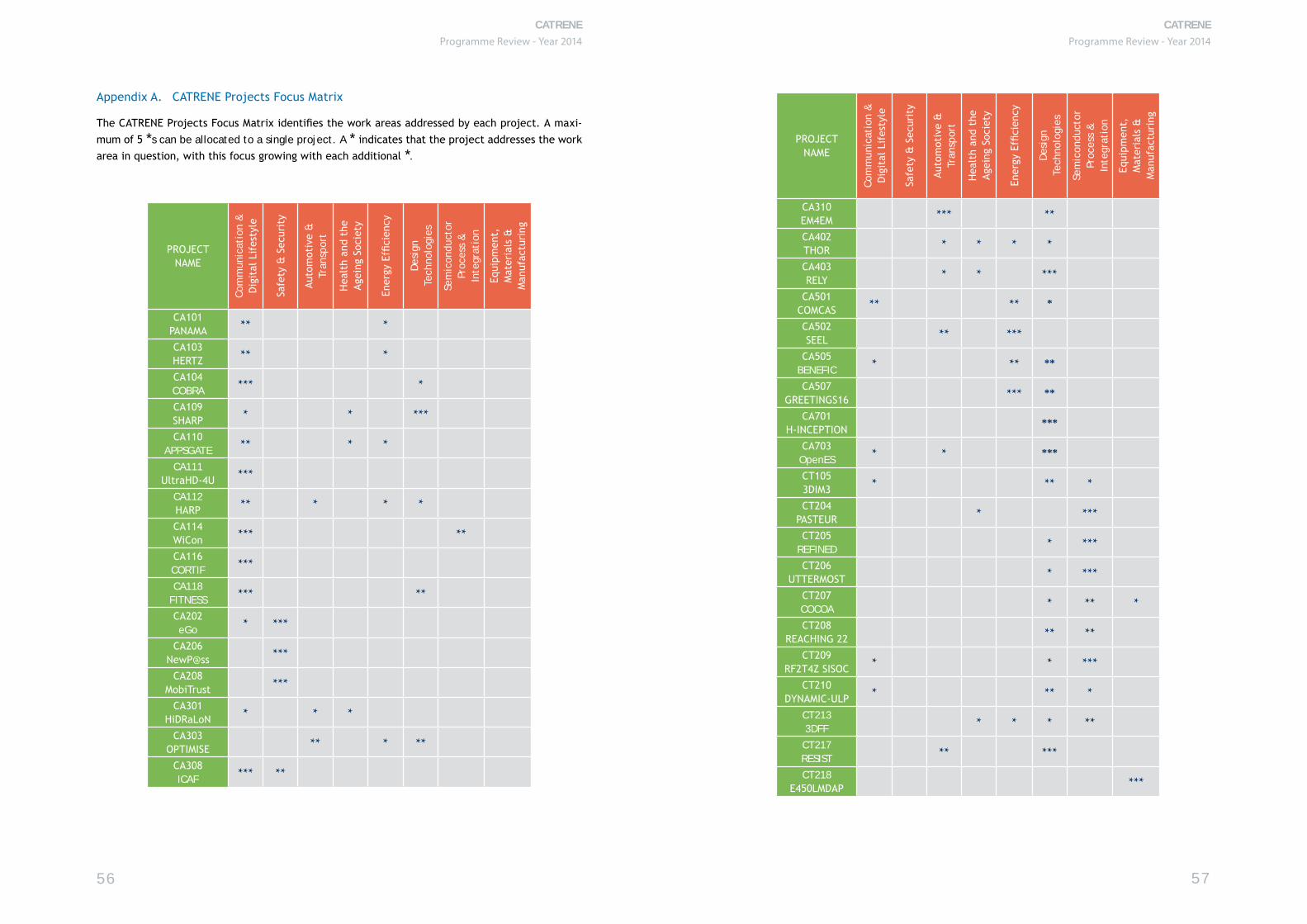
CATRENE Programme Review - Year 2014
56
CATRENE Programme Review - Year 2014
57
Appendix A. CATRENE Projects Focus Matrix
The CATRENE Projects Focus Matrix identifies the work areas addressed by each project. A maxi-mum of 5 *s can be allocated to a single project. A * indicates that the project addresses the work area in question, with this focus growing with each additional *.
PROJECT NAME
Com
mun
icat
ion
&
Dig
ital
Lif
esty
le
Safe
ty &
Sec
urit
y
Auto
mot
ive
&
Tran
spor
t
Hea
lth
and
the
Agei
ng S
ocie
ty
Ener
gy E
ffici
ency
Des
ign
Tech
nolo
gies
Sem
icon
duct
or
Proc
ess
&
Inte
grat
ion
Equi
pmen
t,
Mat
eria
ls &
M
anuf
actu
ring
CA101 PANAMA ** *
CA103HERTZ ** *
CA104COBRA *** *
CA109SHARP * * ***
CA110APPSGATE ** * *
CA111 UltraHD-4U ***
CA112 HARP ** * * *
CA114WiCon *** **
CA116CORTIF ***
CA118FITNESS *** **
CA202eGo * ***
CA206 NewP@ss ***
CA208MobiTrust ***
CA301 HiDRaLoN * * *
CA303OPTIMISE ** * **
CA308 ICAF *** **
PROJECT NAME
Com
mun
icat
ion
&
Dig
ital
Lif
esty
le
Safe
ty &
Sec
urit
y
Auto
mot
ive
&
Tran
spor
t
Hea
lth
and
the
Agei
ng S
ocie
ty
Ener
gy E
ffici
ency
Des
ign
Tech
nolo
gies
Sem
icon
duct
or
Proc
ess
&
Inte
grat
ion
Equi
pmen
t,
Mat
eria
ls &
M
anuf
actu
ring
CA310EM4EM *** **
CA402THOR * * * *
CA403 RELY * * ***
CA501 COMCAS ** ** *
CA502SEEL ** ***
CA505BENEFIC * ** **
CA507GREETINGS16 *** **
CA701H-INCEPTION
***
CA703OpenES * * ***
CT105 3DIM3 * ** *
CT204PASTEUR * ***
CT205REFINED * ***
CT206UTTERMOST * ***
CT207COCOA * ** *
CT208 REACHING 22 ** **
CT209 RF2T4Z SISOC * * ***
CT210 DYNAMIC-ULP * ** *
CT2133DFF * * * **
CT217RESIST ** ***
CT218E450LMDAP ***
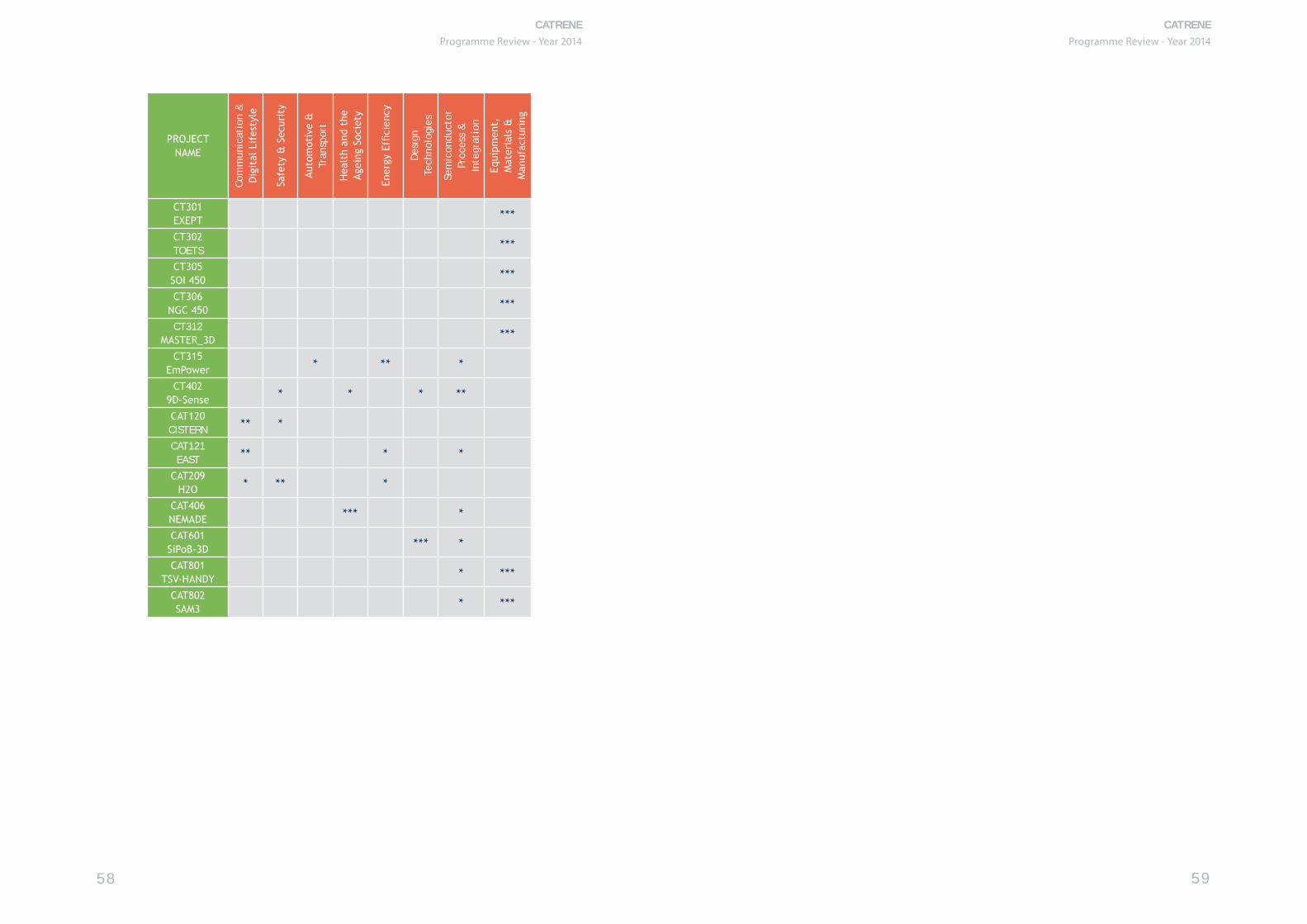
CATRENE Programme Review - Year 2014
58
CATRENE Programme Review - Year 2014
59
PROJECT NAME
Com
mun
icat
ion
&
Dig
ital
Lif
esty
le
Safe
ty &
Sec
urit
y
Auto
mot
ive
&
Tran
spor
t
Hea
lth
and
the
Agei
ng S
ocie
ty
Ener
gy E
ffici
ency
Des
ign
Tech
nolo
gies
Sem
icon
duct
or
Proc
ess
&
Inte
grat
ion
Equi
pmen
t,
Mat
eria
ls &
M
anuf
actu
ring
CT301 EXEPT ***
CT302 TOETS ***
CT305 SOI 450 ***
CT306 NGC 450 ***
CT312 MASTER_3D ***
CT315EmPower * ** *
CT402 9D-Sense * * * **
CAT120CISTERN ** *
CAT121EAST ** * *
CAT209H2O * ** *
CAT406NEMADE *** *
CAT601SiPoB-3D *** *
CAT801TSV-HANDY * ***
CAT802SAM3 * ***

Appendix B
Glossary of Terms
CATRENE Programme Review - Year 2014
4
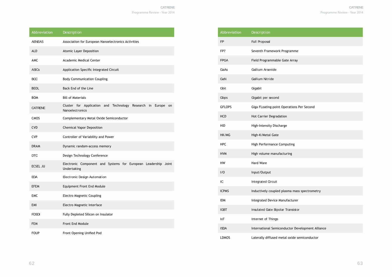
CATRENE Programme Review - Year 2014
62
CATRENE Programme Review - Year 2014
63
Abbreviation Description
FP Full Proposal
FP7 Seventh Framework Programme
FPGA Field Programmable Gate Array
GaAs Gallium Arsenide
GaN Gallium Nitride
Gbit Gigabit
Gbps Gigabit per second
GFLOPS Giga FLoating-point Operations Per Second
HCD Hot Carrier Degradation
HID High-Intensity Discharge
HK/MG High-K/Metal Gate
HPC High Performance Computing
HVM High volume manufacturing
HW Hard Ware
I/O Input/Output
IC Integrated Circuit
ICPMS Inductively coupled plasma mass spectrometry
IDM Integrated Device Manufacturer
IGBT Insulated Gate Bipolar Transistor
IoT Internet of Things
ISDA International Semiconductor Development Alliance
LDMOS Laterally diffused metal oxide semiconductor
Abbreviation Description
AENEAS Association for European Nanoelectronics Activities
ALD Atomic Layer Deposition
AMC Academic Medical Center
ASICs Application Specific Integrated Circuit
BCC Body Communication Coupling
BEOL Back End of the Line
BOM Bill of Materials
CATRENECluster for Application and Technology Research in Europe on Nanoelectronics
CMOS Complementary Metal Oxide Semiconductor
CVD Chemical Vapor Deposition
CVP Controller of Variability and Power
DRAM Dynamic random-access memory
DTC Design Technology Conference
ECSEL JUElectronic Component and Systems for European Leadership Joint Undertaking
EDA Electronic Design Automation
EFEM Equipment Front End Module
EMC Electro Magnetic Coupling
EMI Electro Magnetic Interface
FDSOI Fully Depleted Silicon on Insulator
FEM Front End Module
FOUP Front Opening Unified Pod
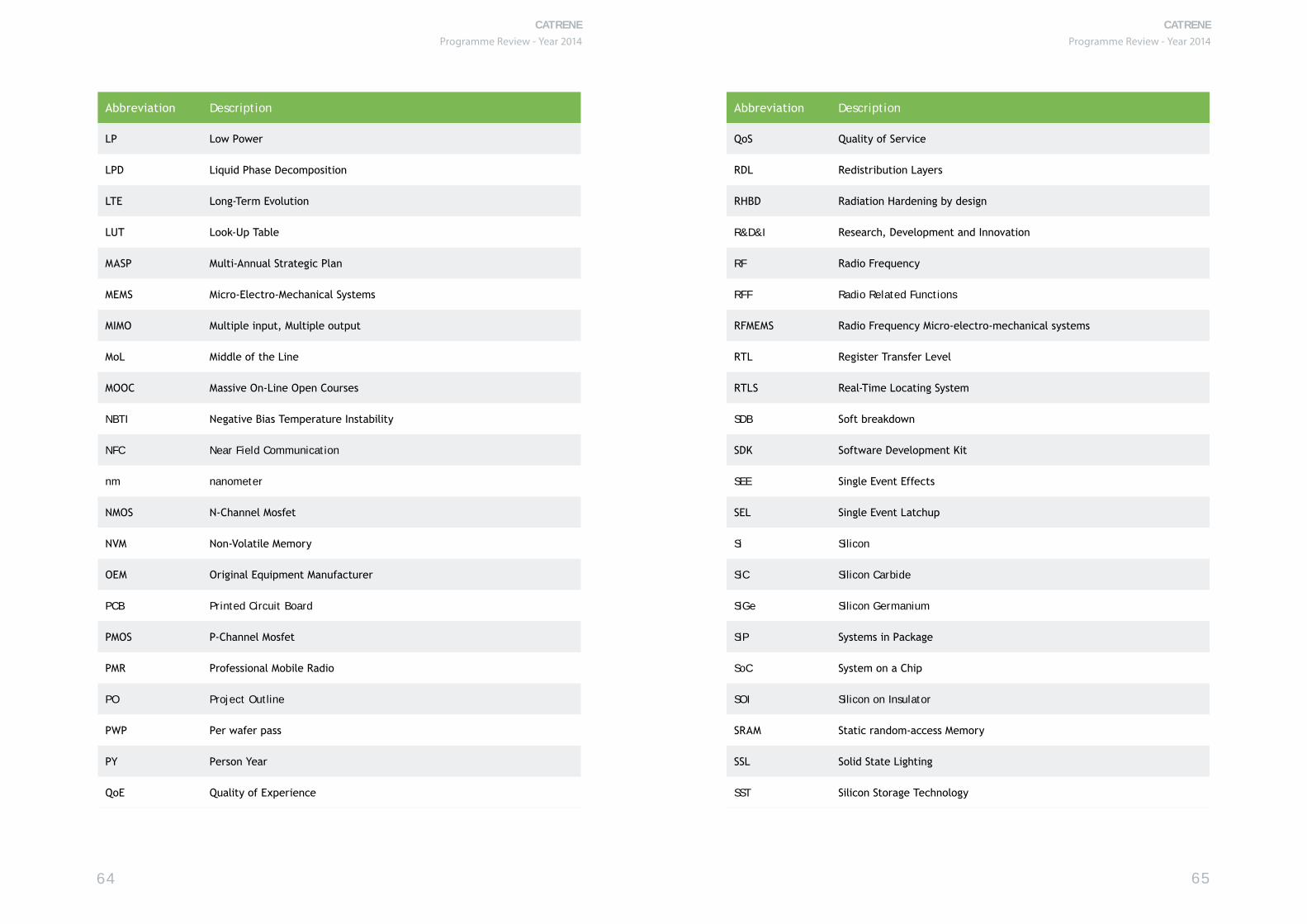
CATRENE Programme Review - Year 2014
64
CATRENE Programme Review - Year 2014
65
Abbreviation Description
QoS Quality of Service
RDL Redistribution Layers
RHBD Radiation Hardening by design
R&D&I Research, Development and Innovation
RF Radio Frequency
RFF Radio Related Functions
RFMEMS Radio Frequency Micro-electro-mechanical systems
RTL Register Transfer Level
RTLS Real-Time Locating System
SDB Soft breakdown
SDK Software Development Kit
SEE Single Event Effects
SEL Single Event Latchup
Si Silicon
SiC Silicon Carbide
SiGe Silicon Germanium
SiP Systems in Package
SoC System on a Chip
SOI Silicon on Insulator
SRAM Static random-access Memory
SSL Solid State Lighting
SST Silicon Storage Technology
Abbreviation Description
LP Low Power
LPD Liquid Phase Decomposition
LTE Long-Term Evolution
LUT Look-Up Table
MASP Multi-Annual Strategic Plan
MEMS Micro-Electro-Mechanical Systems
MIMO Multiple input, Multiple output
MoL Middle of the Line
MOOC Massive On-Line Open Courses
NBTI Negative Bias Temperature Instability
NFC Near Field Communication
nm nanometer
NMOS N-Channel Mosfet
NVM Non-Volatile Memory
OEM Original Equipment Manufacturer
PCB Printed Circuit Board
PMOS P-Channel Mosfet
PMR Professional Mobile Radio
PO Project Outline
PWP Per wafer pass
PY Person Year
QoE Quality of Experience
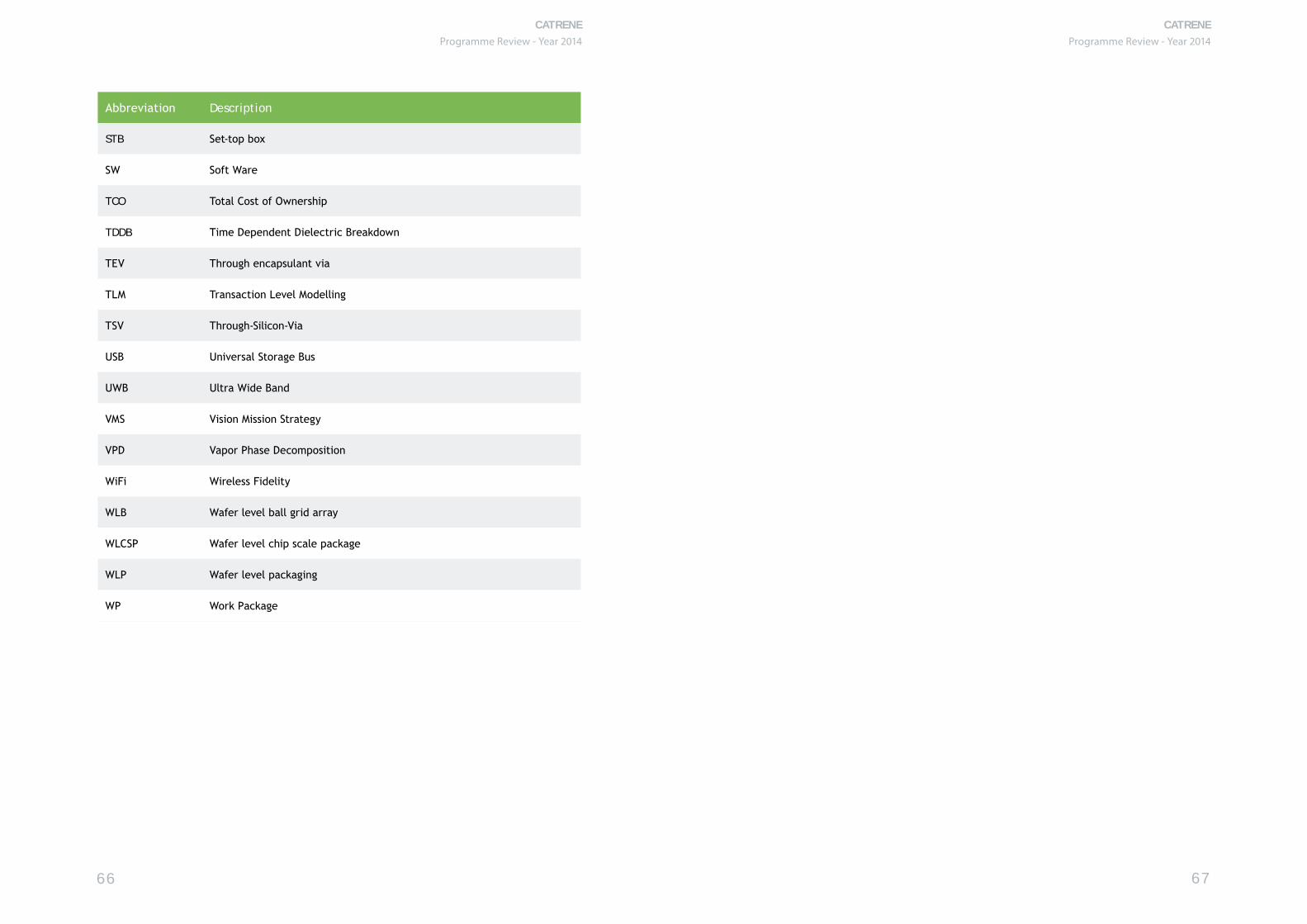
CATRENE Programme Review - Year 2014
66
CATRENE Programme Review - Year 2014
67
Abbreviation Description
STB Set-top box
SW Soft Ware
TCO Total Cost of Ownership
TDDB Time Dependent Dielectric Breakdown
TEV Through encapsulant via
TLM Transaction Level Modelling
TSV Through-Silicon-Via
USB Universal Storage Bus
UWB Ultra Wide Band
VMS Vision Mission Strategy
VPD Vapor Phase Decomposition
WiFi Wireless Fidelity
WLB Wafer level ball grid array
WLCSP Wafer level chip scale package
WLP Wafer level packaging
WP Work Package


www.catrene.org
CATRENE Office 9 Avenue René Coty 75014 Paris, France
T. +33 1 40 64 45 60 - F. +33 1 43 21 44 71 Email: [email protected]