CARLETON UNIVERSITY DEPARTMENT OF ELECTRONICS ...
121
CARLETON UNIVERSITY DEPARTMENT OF ELECTRONICS Modeling and Design of a Frequency-Controlled Class-E Transcutaneous Energy Transfer System by Ahmad Mizannojehdehi A T hesis S ubmitted in P artial F ulfillment of the R equirements for the D egree MASTER OF APPLIED SCIENCE Ottawa, Ontario January, 2007 Reproduced with permission of the copyright owner. Further reproduction prohibited without permission.
-
Upload
khangminh22 -
Category
Documents
-
view
0 -
download
0
Transcript of CARLETON UNIVERSITY DEPARTMENT OF ELECTRONICS ...

CARLETON UNIVERSITY DEPARTMENT OF ELECTRONICS
M odeling and Design of a Frequency-Controlled Class-E Transcutaneous Energy Transfer System
by
Ahmad M izannojehdehi
A T h e s i s S u b m i t t e d
i n P a r t i a l F u l f i l l m e n t o f t h e
R e q u i r e m e n t s f o r t h e D e g r e e
M ASTER OF APPLIED SCIENCE
Ottawa, Ontario
January, 2007
Reproduced with permission of the copyright owner. Further reproduction prohibited without permission.

Library and Archives Canada
Bibliotheque et Archives Canada
Published Heritage Branch
395 Wellington Street Ottawa ON K1A 0N4 Canada
Your file Votre reference ISBN: 978-0-494-23343-6 Our file Notre reference ISBN: 978-0-494-23343-6
Direction du Patrimoine de I'edition
395, rue Wellington Ottawa ON K1A 0N4 Canada
NOTICE:The author has granted a nonexclusive license allowing Library and Archives Canada to reproduce, publish, archive, preserve, conserve, communicate to the public by telecommunication or on the Internet, loan, distribute and sell theses worldwide, for commercial or noncommercial purposes, in microform, paper, electronic and/or any other formats.
AVIS:L'auteur a accorde une licence non exclusive permettant a la Bibliotheque et Archives Canada de reproduire, publier, archiver, sauvegarder, conserver, transmettre au public par telecommunication ou par I'lnternet, preter, distribuer et vendre des theses partout dans le monde, a des fins commerciales ou autres, sur support microforme, papier, electronique et/ou autres formats.
The author retains copyright ownership and moral rights in this thesis. Neither the thesis nor substantial extracts from it may be printed or otherwise reproduced without the author's permission.
L'auteur conserve la propriete du droit d'auteur et des droits moraux qui protege cette these.Ni la these ni des extraits substantiels de celle-ci ne doivent etre imprimes ou autrement reproduits sans son autorisation.
In compliance with the Canadian Privacy Act some supporting forms may have been removed from this thesis.
While these forms may be included in the document page count, their removal does not represent any loss of content from the thesis.
Conformement a la loi canadienne sur la protection de la vie privee, quelques formulaires secondaires ont ete enleves de cette these.
Bien que ces formulaires aient inclus dans la pagination, il n'y aura aucun contenu manquant.
i * i
CanadaReproduced with permission of the copyright owner. Further reproduction prohibited without permission.

ABSTRACT
A transcutaneous energy transfer system is used to transfer energy through a
human body’s skin by using a pair of coupled coils, one of which is implanted under the
skin and the other one placed over it at the exterior side of the body. Electromagnetic
flux, produced by current driven to the external coil, transfers power through the skin
to the secondary coil.
In this thesis a design methodology is proposed in which a Class-E amplifier is
used to provide the driving current of the external coil and the output voltage is
regulated by variation of the operation frequency of the system. The mathematical
models of this system are developed, by which, for a particular application the design
method is applied, the system is implemented and its simulation and experimental
results are reported.
The results of this work indicate that this system can compensate the power
transfer variation due to coupling, load and external battery voltage variation and,
as such, employing a frequency-controlled Class-E technique is an effective way of
controlling the transcutaneous stream of power for an implanted electronic device.
The developed system in this thesis demonstrates power transfer efficiency of 76%
for a separation distance of 15 mm between the two coils and can tolerate a ±5 mm
separation variation between the coils for a fixed output voltage. These specifications
could be even further improved through employment of better fabrication techniques
and utilization of highest quality electronic parts.
ii
Reproduced with permission of the copyright owner. Further reproduction prohibited without permission.

Acknowledgments
I wish to thank my thesis supervisors, Dr. Maitham Shams for his warm welcome,
support and advice; and Dr. Tofy Mussivand for opening my eyes to the world of
biomedical and providing the opportunity of contribution to this world.
I thank my wife, Dr. Nasrin Hojjat, for her invaluable help and sharing of hard
situation with me.
This thesis has been financially supported partly by NSERC and Medical Devices
Center of the University of Ottawa Heart Institute which is highly appreciated.
iii
Reproduced with permission of the copyright owner. Further reproduction prohibited without permission.

Contents
Abstract ii
Acknowledgments iii
List of Figures vii
1 Introduction 1
1.1 M otivation........................................................................................................ 5
1.2 Objective ........................................................................................................ 6
1.3 Thesis Organization........................................................................................ 6
2 Transcutaneous Energy transfer System Design: A R eview Study 8
2.1 Transcutaneous Transform er........................................................................ 8
2.1.1 Transcutaneous Transformer Equivalent C i r c u i t ......................... 9
2.2 Transcutaneous Transformer D esign ........................................................... 10
2.2.1 Transcutaneous Transformer Design and Coil Based Regulation 11
2.2.2 Geometrical A p p ro a c h ..................................................................... 12
2.2.3 Enhanced Geometrical A p p ro a c h ................................................. 13
2.2.4 Critical C o u p lin g .............................................................................. 14
2.2.5 Stagger T u n in g .................................................................................. 14
2.3 Coil-Driver Technologies.............................................................................. 15
2.3.1 Series Resonant C o il-D riv er........................................................... 16
2.3.2 Class-E Coil-Driver........................................................................... 22
2.4 Previous Work for Designing a Transcutaneous Energy Transfer System 27
Reproduced with permission of the copyright owner. Further reproduction prohibited without permission.

V
2.4.1 Series Resonant Coil-Driver Transcutaneous Energy Transfer
S y s te m s ............................................................................................. 27
2.4.2 Class-E Coil-Driver Transcutaneous Energy Transfer Systems 29
2.4.3 Frequency-Tracking Transcutaneous Energy Transfer System 29
3 Transcutaneous Transformer 32
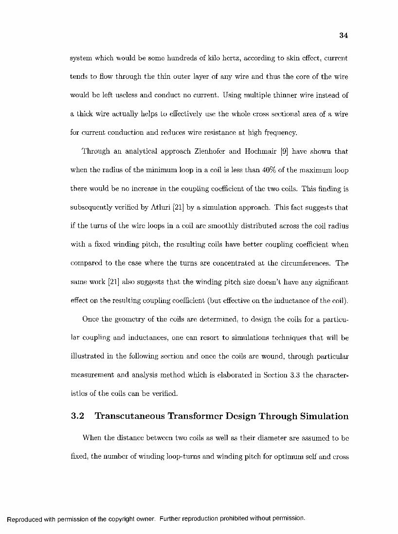
3.1 In troduction ..................................................................................................... 33
3.2 Transcutaneous Transformer Design Through S im u la tio n ..................... 34
3.2.1 Drawing a Spiral Coil in HFSS .................................................... 35
3.3 Transcutaneous Transformer Electrical Model D eterm ination ............... 38
4 Class-E Coil-Driver 41
4.1 Class-E A m plifier........................................................................................... 41
4.1.1 Class-E Amplifier D efin ition ........................................................... 42
4.1.2 Principle of O p e ra tio n .................................................................... 43
4.1.3 A n aly sis ............................................................................................. 44
4.1.4 Design P rocedure ............................................................................... 48
4.2 Load Variation E f fe c ts .................................................................................. 50
4.3 Class-E Rectifier ........................................................................................... 52
4.3.1 Principle of O p e ra tio n .................................................................... 53
4.3.2 A n aly sis ............................................................................................. 55
5 Class-E Transcutaneous Energy Transfer System 57
5.1 Proposed Transcutaneous Energy Transfer S ystem ................................. 58
Reproduced with permission of the copyright owner. Further reproduction prohibited without permission.

5.2 Circuit A nalysis............................................................................................. 58
5.3 Frequency Controlled Output V oltage...................................................... 60
5.3.1 Coils Coupling Variations Compensation by Frequency Variation 61
5.3.2 Load Variations Compensation by Frequency Variation . . . . 62
5.3.3 Frequency Variations A nalysis ....................................................... 62
5.3.4 Frequency Response of the Proposed Transcutaneous Energy
Transfer S ystem ................................................................................. 64
5.3.5 Closed-Loop Control and Stability Analysis ............................. 69
6 Spice Sim ulations and Experim ental R esults 74
6.1 S im u la tio n s ................................................................................................... 78
6.1.1 Power Transfer Simulations .......................................................... 78
6.1.2 Closed-Loop Stability S im u la tio n ................................................ 83
6.2 Experimental R esu lts ................................................................................... 87
6.2.1 The Prototype S y s te m .................................................................... 95
7 Conclusions, Contributions and Future Work 99
7.1 S u m m a ry ....................................................................................................... 100
7.2 R em ark s .......................................................................................................... 101
7.3 C on tribu tions................................................................................................ 103
7.4 Future W ork .................................................................................................... 104
References 106
Reproduced with permission of the copyright owner. Further reproduction prohibited without permission.

List of Figures
1.1 A transcutaneous energy transfer system block diagram [ 3 ] ............... 3
2.1 Coils of the transcutaneous transformer used in this t h e s i s ............... 9
2.2 A model for transcutaneous transformer ............................................... 9
2.3 A model for transcutaneous transformer ............................................... 11
2.4 Different mutual positions of two one turn coils A) Two concentric coils
with only separation distance B) Two coils with lateral misalignment
C) Two coils with angular misalignment D) Two coils with lateral and
angular misalignment ................................................................................. 12
2.5 Coils relative sizes in geometrical ap p roach ............................................ 13
2.6 A series resonant network ......................................................................... 16
2.7 A series resonant converter......................................................................... 17
2.8 The drain voltage and current of transistor M4 and the load voltage of
the series resonant converter of Figure 2.7 when it is operating at its
exact resonant frequency ............................................................................. 18
2.9 The drain voltage and current of transistor M4 and the load voltage of
the series resonant converter if Figure 2.7 when its operating frequency
is less than its resonant frequency ............................................................. 18
2.10 A series resonant network [1 9 ] ................................................................... 20
2.11 The multi-frequency netw ork...................................................................... 22
2.12 The frequency response of the multi-frequency n e tw o rk ...................... 23
Reproduced with permission of the copyright owner. Further reproduction prohibited without permission.

viii
2.13 A Class-E co il-d riv er.................................................................................... 23
2.14 The voltage oscillations across the transistor in a Class-E amplifier
when it is turned off for different load network quality factors . . . . 25
2.15 A self-tuning Class-E coil-diver ................................................................. 26
2.16 The frequency-tracking transcutaneous energy transfer system . . . . 30
3.1 Simulation of spiral coil in HFSS env ironm ent........................................ 35
3.2 Spiral path of a polygon produced by M A TLA B.................................... 36
3.3 Extruded spiral path produced by MATLAB in HFSS environment . 37
3.4 Impedance seen from primary when secondary is short circuited in a
transcutaneous energy transfer system electrical c i r c u i t ....................... 38
3.5 Impedance seen from primary when secondary is open circuited in a
transcutaneous energy transfer system electrical c i r c u i t ....................... 39
3.6 Impedance seen from secondary when primary is open circuited in a
transcutaneous energy transfer system electrical c i r c u i t ....................... 40
4.1 Ideal switch waveforms in a Class-E amplifier [1 6 ] ................................. 42
4.2 A Class-E am plifier........................................................................................ 43
4.3 The switch driving signal, output voltage, switch voltage and switch
current waveforms of a general Class-E amplifier [23] 45
4.4 Final fine tuning of a Class-E amplifier [16] 50
4.5 The Drain-Source and Gate voltage of the switching transistor of a
Class-E amplifier when load resistance equal to optimum load . . . . 51
Reproduced with permission of the copyright owner. Further reproduction prohibited without permission.

4.6 The Drain-Source and Gate voltage of the switching transistor of a
Class-E amplifier when load resistance is larger that optimum load . . 51
4.7 The Drain-Source and Gate voltage of the switching transistor of a
Class-E amplifier when load resistance is smaller that optimum load . 52
4.8 A Class-E rectifier [3 0 ] ................................................................................ 53
4.9 Idealized current and voltage waveforms of a Class-E rectifier [30] . . 54
5.1 The schematic diagram of power transfer section of the proposed tran
scutaneous energy transfer sy s tem ............................................................. 59
5.2 Figure 5.1 when its class-E rectifier is replaced by its equivalent circuit 59
5.3 Figure 5.1 when the secondary leakage inductance is eliminated by
re so n a n c e ....................................................................................................... 59
5.4 Figure 5.3 when secondary load is transfered to primary s id e .............. 60
5.5 Figure 5.4 when parallel L5 and Ri are replaced by their equivalent
series combination ....................................................................................... 60
5.6 A Class-E amplifier ................................................................................... 61
5.7 Frequency response of a Class-E amplifier................................................ 62
5.8 The Class-E transcutaneous energy transfer system with equivalent
secondary side c irc u it.................................................................................... 63
5.9 The Class-E transcutaneous energy transfer system with secondary
impedance is transferred to primary s i d e ................................................ 63
5.10 Figure 5.9 when series j X and R l are transformed to parallel combination 64
Reproduced with permission of the copyright owner. Further reproduction prohibited without permission.

X
5.11 Figure 5.10 when parallel combination of reactance and resistor are
transformed back to a series com bination................................................ 65
5.12 Frequency response of a Class-E amplifier................................................ 66
5.13 Frequency response of Class-E transcutaneous energy transfer system
when f res is very close to f c ....................................................................... 67
5.14 Frequency response of Class-E transcutaneous energy transfer system
when f res lags f c .......................................................................................... 68
5.15 Frequency response of Class-E transcutaneous energy transfer system
when f res leads f c .......................................................................................... 69
5.16 Block diagram of a closed-loop frequency controlled transcutaneous
energy transfer s y s te m ................................................................................. 70
5.17 Modeling of the transcutaneous energy transfer system in the SIMULINK 71
5.18 Gain and phase margins of the uncompensated transcutaneous energy
transfer s y s te m ............................................................................................. 71
5.19 Modeling of the transcutaneous energy transfer system in the SIMULINK 72
5.20 Gain and phase margins of the compensated transcutaneous energy
transfer s y s te m ............................................................................................. 73
6.1 Frequency response of the analyzed 15 W, 12 v output Class-E tran
scutaneous energy transfer system .......................................................... 76
Reproduced with permission of the copyright owner. Further reproduction prohibited without permission.

xi
6.2 Drain waveform obtained by MATLAB from top left to the bottom
right for the frequencies of fop = 360kHz, f op = 380kHz, / ^ = 385kHz,
fop = 389kHz, = 390kHz, = 410kHz, = 420kHz, fop
-■-10k 11/ respectively....................................................................................... 77
6.3 The power section of designed transcutaneous energy transfer system
circuit modeled in SPICE. The connection between the grounds of the
two sides of the transformer is necessary for simulation purpose. . . . 78
6.4 The portion of the transfer function between the two vertical lines is
the area the system is working o n ............................................................. 79
6.5 Simulated drain and output waveform at frequencies of fop = 350 kHz,
fop = 370 kHz and fop = 380 kHz from top respectively ....................... 80
6.6 Simulated drain and output waveform at frequencies of fop = 390 kHz,
fop = 400 kHz and fop — 410 kHz from top respectively ....................... 81
6.7 Simulated drain and output waveform at frequencies offop = 440 kHz,
fop = 460 kHz and fop = 480 kHz from top respectively ....................... 82
6.8 Proportional and integrator amplifiers in the closed control loop . . . 83
6.9 The behaviorial VCO in S P IC E ................................................................. 85
6.10 The output waveform of the proportional amplifier in the closed control
l o o p ................................................................................................................. 86
6.11 The output waveform of the integrator amplifier in the closed control
l o o p ................................................................................................................. 86
6.12 Experimental drain and output waveform at frequency of f op = 344 kHz 88
Reproduced with permission of the copyright owner. Further reproduction prohibited without permission.

xii
6.13 Experimental drain and output waveform at frequencies of = 347
kHz and = 365 kHz .............................................................................. 89
6.14 Experimental drain and output waveform at frequencies of f op = 372
kHz and = 375 kHz .............................................................................. 90
6.15 Experimental drain and output waveform at frequencies of f op = 385
kHz and = 392 kHz .............................................................................. 91
6.16 Experimental drain and output waveform at frequencies of f ap = 395
kHz and = 403 kHz .............................................................................. 92
6.17 Experimental drain and output waveform at frequencies of f op = 408
kHz and f ^ = 424 kHz ................................................................................ 93
6.18 Efficiency versus operating frequency for different coils distances . . . 94
6.19 The implanted board of the Class-E frequency-controlled transcuta
neous energy transfer system designed for this thesis (size = 4.5 x 6
c m 2 ) ................................................................................................................. 95
6.20 The External board of the Class-E frequency controlled transcutaneous
energy transfer system designed for this thesis ( size = 6.5x8 cm,2 ) . 96
6.21 The transcutaneous transformer of the Class-E frequency controlled
transcutaneous energy transfer system (diameter of each coil = 8 cm) 96
6.22 The schematic diagram of power transfer section of the proposed tran
scutaneous energy transfer sy stem ............................................................. 97
Reproduced with permission of the copyright owner. Further reproduction prohibited without permission.

Chapter 1
INTRODUCTION
Implanted electronic devices provide an improved quality of life for patients suf
fering from malfunctioning of an organ. Supplying of electric power for the electronic
implanted devices is one of the most difficult issues in which many fields of electri
cal engineering are involved. In the early stages of development of artificial organs,
percutaneous energy transfer method was used. In this method, electrical power is
transferred via wires connecting the implanted device to plugs passed through pierced
skin. This method inherently provides high risks of infections and medical complica
tions for a recipient of the system. Furthermore the subject of the implanted device
is limited to restricted living conditions and should be always under very rigorous
clinical care to prevent any infection. Transcutaneous energy transfer or transferring
power through the intact skin, which is addressed in this thesis, inherently doesn’t
have the infections problem therefore is a superior solution to the problem of powering
up an implanted electronic device [l]-[5]. A transcutaneous energy transfer system
uses a wireless link to transfer power through the intact skin. The recipient of this
1
Reproduced with permission of the copyright owner. Further reproduction prohibited without permission.

2
system is not subjected to infections from the exterior of the body and can enjoy a
less restricted and better quality of life with much less clinical care as compared to
the case where percutaneous energy transfer system is used. Nonetheless, designing a
transcutaneous energy transfer system is a challenging work. It should be highly effi
cient and reliable, not emit too much heat to overheat the surrounding tissues where
it is implanted, and should always have a stable working condition. Any progress
in development of the transcutaneous energy transfer system technology has a vital
influence in the development of implanted electronic devices and artificial organs and
any contribution to this technology has direct effect on better living and the quality
of life of the human beings.
A block diagram of a transcutaneous energy transfer system is shown in Figure
1.1. A transcutaneous energy transfer system consists of a transcutaneous trans
former, a coil-driver, a rectifier, a transcutaneous data transmission system and some
control circuitry. The basic operation of a transcutaneous energy transfer system is
as follows. The coil-diver produces an alternating current through the primary coil.
This alternating current, in turn, produces an alternating magnetic flux in the pri
mary coil. The portion of the alternating magnetic flux, captured by the secondary
coil, induces an alternating voltage across this coil according to Faraday’s law. An
alternating current will flow through the secondary coil as the result of this induced
voltage. Since most of the implanted medical devices need to be supplied by direct
current (DC), this alternating current is required to be changed to direct current by
the rectifier block. To regulate the output voltage, a voltage control loop is employed.
The transcutaneous data transceiver delivers the information of output voltage level
Reproduced with permission of the copyright owner. Further reproduction prohibited without permission.

3
to the exterior of body where it is used to determine the amount of current required
to be driven to the primary coil for keeping the output voltage fixed [3, 1].
RectifierCoil Driver
controlcircuit
controlcircuit
Figure 1.1 A transcutaneous energy transfer system block diagram [3]
Although the early efforts to design a transcutaneous energy transfer system is
referenced back to 1960 [6], the main contributions to this technology, as the pa
per review suggests, have been made after 1980 [l]-[7]. Among the contributions
made to enhance the design of a transcutaneous transformer, Soma [8] introduced
an algorithmic analytical method for designing a transcutaneous transformer. He
also introduced the Geometrical method for partially desensitizing a transcutaneous
transformer to lateral displacements of its coils. Zienhofer and Hochmair [9] intro
duced the Enhanced Geometrical method, a technique which increases the overall
efficiency of a transcutaneous transformer. Critical coupling is a method invented by
Hochmair [10]. By applying this method maximum voltage could be induced in the
secondary side of a transcutaneous transformer while a convenient coils separation
distance between the two coils can be maintained. Galbrith et. al. [11] introduced
the “Stagger tuning” method. With this method the desensitizing of voltage gain of
Reproduced with permission of the copyright owner. Further reproduction prohibited without permission.

4
two coupled coils to the variation of the coupling coefficient of the two coils is pos
sible. Eierhofer et. al. [12, 13] proposed a Class-E coil-driver circuit that can track
the varying separation-distance of the two coils of a transcutaneous transformer for
maximum power transfer efficiency.
To induce a voltage in the secondary coil of a transcutaneous transformer, a pro
portionate current must be driven to the primary coil. Several techniques have been
developed for driving the current to the primary coil of a transcutaneous transformer
most efficiently. The series resonant coil-driver is one of those methods. Ghahari
[2], Kim [14] and Joung [4] used the series resonant coil-driver for designing a tran
scutaneous energy transfer system. Instead of using a pancake shape coils for a
transcutaneous transformer, they used coils wound on ferrite pot-core, just for exper
imental purposes. Ghahari applied the theory of series resonance to the primary side
of the transcutaneous transformer to improve the voltage gain of a transcutaneous
transformer, however the voltage gain and efficiency he obtained were 0.165 and 50%
respectively. Kim employed resonance on both the primary and the secondary sides
of the transcutaneous transformer. He used the pulse-width modulation method to
control the output voltage. The voltage gain he obtained was improved to 1.1. Joung
also employed resonance at both the primary and the secondary coils but used the
frequency variation method to control the output voltage. The voltage gain and
efficiency he obtained were 0.4 and 70% respectively. Nishimura [15] used pancake-
shape coils for transcutaneous transformer for a series resonant transcutaneous energy
transfer system, however the best efficiency he obtained was 45%.
An alternate technique to design a coil-driver is using the Class-E amplifier that is
Reproduced with permission of the copyright owner. Further reproduction prohibited without permission.

5
invented by Sokal [16]. Troyk [17] analyzed the application of a Class-E amplifier as a
Coil-driver for a transcutaneous energy transfer system. Wang et. al. [1, 18] designed
a transcutaneous energy transfer system with a Class-E coil-driver whose output
voltage is controlled by variation of input voltage. This system has an efficiency of
65% for the coil separation-distance of 7 mm. Puers [3] also used the same method to
design an output voltage regulated transcutaneous energy transfer system. Miller et.
al. [5] introduced a frequency-tracking with Class-E coil driver system. This system
has an efficiency of 83% for the coil separation-distance of 5 mm.
Designing a reliable and efficient transcutaneous energy transfer system is the
main subject of this thesis. This thesis presents a study on feasibility and design of a
transcutaneous energy transfer system based on a Class-E power amplifier coil-driver
in which frequency variation is used as the main tool to control the output voltage.
1.1 M otivation
The main motivation behind the subject of this thesis is to try to make a contri
bution to the technology of transcutaneous energy transfer systems toward the goal
of improving quality of life for the instances that deteriorating health condition has
provided hard condition for human being.
The frequency-controlled Class-E transcutaneous energy transfer system, among
other methods, has specific features that have made it a promising method to design
a transcutaneous energy transfer system.
Reproduced with permission of the copyright owner. Further reproduction prohibited without permission.

6
1.2 Objective
The objective of this thesis is to investigate and design a frequency-controlled
Class-E transcutaneous energy transfer system. To achieve this objective the following
steps are carried out.
• A circuit for the frequency-controlled Class-E transcutaneous energy transfer
system is introduced
• The proposed circuit is analyzed
• The system is mathematically modeled using MATLAB
• The system is simulated using PSPICE
• A prototype is constructed and tested
• The simulation results are verified by the experimental results
• The challenges for designing a system with this method are identified
• The advantages and disadvantages of this approach over the previous work in
terms of design reliability and efficiency are identified
1.3 Thesis Organization
This thesis contains a survey of the relevant literature and challenges on transcu
taneous energy transfer system design in Chapter 2. Chapter 3 introduces the concept
of the transcutaneous transformer and its electrical equivalent circuit. In Chapter 4,
the Class-E amplifier as well as the Class-E rectifier are introduced and expressions
that govern their operation are outlined. These expressions are used for modeling the
coil-driver as well as the rectifier building blocks of the system. In fact Chapters 3
and 4 provide the necessary information needed for analysis of the proposed system.
In Chapter 5, our proposed transcutaneous energy transfer system is introduced, its
Reproduced with permission of the copyright owner. Further reproduction prohibited without permission.

7
circuit analysis is performed and the transfer function of the final system is derived
and interpreted. Chapter 6 uses the results of Chapter 5 to conduct the simulations
needed to find the regions of the transfer function which are safe for system operation.
This chapter concludes with the results of experiments conducted on a prototype sys
tem and the explanations for the discrepancies with the simulations results. Chapter
7 presents a summary of the thesis, some concluding remarks, contributions made,
and some guideline for future work.
Reproduced with permission of the copyright owner. Further reproduction prohibited without permission.

Chapter 2
TRANSCUTANEOUS ENERGY TRANSFER SYSTEM DESIGN: A REVIEW STUDY
In this chapter the transcutaneous energy transfer system is studied through a
literature review. At first the technologies for each of the most important blocks of a
typical transcutaneous energy transfer system such as the transcutaneous transformer,
the coil driver and the rectifier are reviewed and finally the various transcutaneous
energy transfer systems will be briefly introduced .
2.1 Transcutaneous Transformer
A transcutaneous transformer is composed of two pancake shape coils which are
placed opposite to each other. Figure 2.1 shows the two coils of a transcutaneous
transformer.
This transformer has a very poor coupling since there always exists a gap of around
0.5 to 2 cm between its two coils depending of the thickness of the skin tissues. This
gap limits the amount of flux captured by the secondary coil and reduces the coupling
coefficient of the transformer. The uncoupled portion of the flux can be represented
8
Reproduced with permission of the copyright owner. Further reproduction prohibited without permission.

9
Figure 2.1 Coils of the transcutaneous transformer used in this thesis
by a separate self inductance that is called the leakage inductance [2].
2.1.1 Transcutaneous Transformer Equivalent Circuit
Figure 2.2 represents the two coils of the transcutaneous transformer. In this
figure LI and L2 are the self inductances of the primary and the secondary coils and
the resistors R1 and R2 are the equivalent series resistance of the primary and the
secondary coils respectively.
R1
-VvV-
L1
*}
R2-AMv-
12
Figure 2.2 A model for transcutaneous transformer
The T equivalent circuit of the transcutaneous transformer, when the resistive
losses of the coils are neglected, is shown Figure 2.3. LL1 and LL2 are the leakage
inductances of the primary and the secondary sides respectively and LM represents
Reproduced with permission of the copyright owner. Further reproduction prohibited without permission.

10
the coupling inductance of the transcutaneous transformer. In fact to account for
the stranded flux which doesn’t close its path through the secondary coil, more than
the required flux to pass through the secondary coil is needed is to be produced by
the primary coil. The existence of this extra flux which requires extra current at
the primary side, which is called magnetizing current, is represented by the coupling
inductance LM in the equivalent circuit. The relationship among the self-inductances
of the two coils, LI and L2, the leakage inductances LL1 and LL2, the coupling
inductance LM and the coupling coefficient of the transcutaneous transformer, k , are
The leakage inductances prevent the circuit from having a large voltage gain since
part of input voltage drops on them. Large magnetizing current prevents the trans-
minimize the effects of the large leakage inductances.
2.2 Transcutaneous Transformer Design
This section presents the major techniques for designing a transcutaneous trans
former. Some of these techniques are general and some are particular methods to
alter a particular characteristic of a transcutaneous transformer.
[2 , 10]:
L M = k \? L l ■ 12 (2 .1)
(2.2)n
L L2 = L 2 - L M - n (2.3)
former from having a good efficiency. Specific coil driving techniques are required to
Reproduced with permission of the copyright owner. Further reproduction prohibited without permission.

11
LL1 ideal transformer LL2 ___
LM n
1 : n
Figure 2.3 A model for transcutaneous transformer
2.2.1 Transcutaneous Transformer D esign and Coil Based Regulation
Soma [8] introduced a simple and efficient mathematical approach to design a tran
scutaneous transformer which is generally described here without going into mathe
matical details. As the first step the coupling coefficient of two circular, single-turn
coils, in their different mutual positions are determined. The different mutual posi
tions of the two single-turn coils are illustrated in Figure 2.4. This task requires one
to determine the mutual inductance between these two coils. The equation of mutual
inductance between two single-turn coils is a classic electromagnetic equation that is
available in relevant text books. Soma developed an approximate equation, instead
of the exact equation, for the mutual inductance between the two single-turn coils
and extended the solution to cover the lateral, angular and eventually both of these
misalignment cases. This solution is claimed to be accurate within 10% of the value
obtained by the exact equation.
To extend the equation for a real coil which is composed of multiple single-turn
coils, the real coil is modeled as a single turn coil times an “average dimension”. For
example, for a pancake-shape coil, the average dimension would be the arithmetic
mean of the radii of all the single-turn circular coils available in the coil. After the
Reproduced with permission of the copyright owner. Further reproduction prohibited without permission.

12
approximate coupling coefficient of a real coil is determined, the following algorithm
is used to design a real coil:
• Determine coils parameters based on system consideration such as implant lo
cation etc.
• Determine nominal and worst-case angular and lateral displacement
• Assume a structure for the coil in the allowable parameters range
• Determine coupling coefficient with the method just described
• If coupling coefficient does not meet other design goals (bandwidth, gain ,..)
change the parameters and iterate until the desired coupling for the coil is
reached
Figure 2.4 Different mutual positions of two one turn coils A) Two concentric coils with only separation distance B) Two coils with lateral misalignment C) Two coils with angular misalignment D) Two coils with lateral and angular misalignment
2.2.2 G eom etrical Approach
The geometrical approach is used to desensitize an inductive link gain to coil
lateral misalignments. In this approach, as illustrated in Figure 2.5, the external coil
is larger than the implanted coil and as long as the smaller coil remains within the
perimeter of the larger coil, the flux line that is shared by both of the coils will be
roughly the same, and the coupling will remain fairly constant. Thus, the coils can
Reproduced with permission of the copyright owner. Further reproduction prohibited without permission.

13
move laterally and even tilt with only a minor effect on the gain. A transcutaneous
transformer designed by this approach is still sensitive to changes in distance between
the coils. In exchange for partially controlling the gain, the magnitude of the coupling
is sacrificed, since these coils share fewer flux lines than equally sized coils. A lower
coupling coefficient requires higher current in the primary coil to provide the same
output power at the secondary coil. The higher current at the primary coil also
causes more resistive loss in this coil. A poor bandwidth is another problem, since to
maintain a high gain, the link must have a high quality factor, Q, which results in a
smaller bandwidth [8].
External coil
Implanted coil
Figure 2.5 Coils relative sizes in geometrical approach
2.2.3 Enhanced G eom etrical Approach
The coupling between the two magnetically coupled coils can be enhanced by
distributing the turns of the coils across the radii instead of concentrating them at the
outer circumference. This method of winding a coil is called “advanced geometrical
approach” . In exchange for the coupling enhancement, there would be a moderate
decrease of the unloaded quality factors of the coils due to the increased wire length.
Reproduced with permission of the copyright owner. Further reproduction prohibited without permission.

14
But if unloaded quality factors are sufficiently high compared to the loaded quality
factors, the effect of the coupling enhancement predominates the effect of the unloaded
quality factor reduction on the overall efficiency and thus a net improvement of the
overall efficiency is obtained [9].
2.2.4 Critical Coupling
Hochmair [10] defined a special method of coupling two coils which is called “crit
ical coupling” . By critically coupling it would be possible to reduce the effect of
coils separation and lateral displacements. Critical coupling also makes it possible to
obtain maximum induced voltage with a convenient coil separation distance despite
steep decrease of the magnetic field with increase of the separation distance between
the coils. In exchange for this advantage, there would be a theoretical 50% reduction
in the energy transfer efficiency.
The critical coupling coefficient, K , as opposed to conventional coupling coeffi
cient, k, defined in 2.4.
K = k\ J Q 1Q 2 (2-4)
In this equation Q i and Q 2 are the primary and the secondary quality factors and
k is the conventional coupling coefficient of the two coils. It is said that the two coils
are critically coupled when critical coupling coefficient,^, is unity.
2.2.5 Stagger Tuning
The stagger tuning approach is used to desensitize the voltage gain of two cou
pled coils to the coupling coefficient of the coils. In this technique, in the transfer
Reproduced with permission of the copyright owner. Further reproduction prohibited without permission.

15
function of the link, one pole is placed above the operating frequency and one pole
below it. The poles move as the coupling coefficient changes. If the poles are placed
properly, their positions move in a way to compensate the gain drop due to the coils’
coupling changes. In this way the coils could be misaligned in a realistic manner with
little effect on the output transferred power. This approach provides both efficiency
and bandwidth, the two characteristics which were mutually exclusive in the earlier
mentioned approaches. Besides, in this approach the coils are equally sized, which
improves the average coupling and reduces the coils’ resistive losses. Another point is
that the stagger tuning can not be employed in a Class-E coil-driver, since a Class-E
loses efficiency if the load does not resonate at the operating frequency, instead a
Class-D amplifier can drive this load because it is independent of the frequency [11].
2.3 Coil-Driver Technologies
A coil-driver circuit is needed to supply enough current to the primary coil to
enrich the share of flux which pass through the secondary coil to the required value
providing a certain amount of voltage and power at the output. The voltage gain
of the system is very sensitive to the leakage inductances of the primary and the
secondary coils due to the drop of a part of the input voltage on these leakage induc
tances. By using proper coil-driver techniques these unwanted voltage drops across
the leakage inductances could be eliminated and accordingly the voltage gain of the
system could be increased. These techniques, among them the “series resonant” and
the “Class-E” coil-drivers, incorporate the leakage inductance of the transcutaneous
transformer into one resonant circuit to reduce its effect at the resonance frequency.
Reproduced with permission of the copyright owner. Further reproduction prohibited without permission.

16
2.3.1 Series Resonant Coil-Driver
By incorporating a leakage inductance into a series resonant network, the effect
of leakage inductance on the voltage gain of the system at the resonant frequency is
eliminated. Figure 2.6 shows a circuit in which the resistor R, which is the output
load, is supplied by an AC voltage source through a series resonant network. In fact
the capacitor C is placed in series with the inductor L to cancel its effect at the
resonant frequency. At this frequency the voltage gain, which is the ratio of the load
voltage to the input AC voltage, is maximum and the input impedance seen from the
AC source is minimum.
L C/V'"V*V"V____________JL
Figure 2.6 A series resonant network
By replacing the input AC voltage of the circuit of Figure 2.6 with a switching
network and also the resistive load of that circuit with a series combination of a
rectifier and a filter capacitor, the circuit of Figure 2.7 is realized. This circuit is a
series resonant converter [19]. The switching network of this circuit works as follows.
The transistors M l and M4 are on for 50% of a period while the transistor M2 and
M3 are off, applying the input DC voltage on the resonant network. On the next half
period, the transistors M2 and M3 are on while the transistors Ml and M4 are off,
applying the inverse of input voltage on the resonant network. In this way an AC
Reproduced with permission of the copyright owner. Further reproduction prohibited without permission.

17
square wave voltage is applied to the series resonant network where its main harmonic
is rectified, filtered and the resultant dc voltage is delivered to the load.
M2
M3 .C2
Figure 2.7 A series resonant converter
One of the main sources of power transfer deficiency and internal power losses
in this converter is the switching losses of the transistors. During the time that a
switching transistor is on or off, either of the transistor voltage or the current flowing
through it is zero, making the power loss of the transistor zero. But at the switching
time, for example at the turn-on state, the current of the transistor linearly raises
from zero to a maximum and the voltage across it changes from a maximum to zero,
therefore, the power loss which is the product of these current and voltage is not
zero. By applying special techniques in series resonant converters, either of the turn
on or turn-off switching losses is eliminated and accordingly the efficiency is increased.
Figure 2.8 shows the drain voltage and current of transistor M4 as well as the load
current, / l , of the circuit in Figure 2.7 when the circuit is operating at exact resonant
frequency of the series resonant network of LI and Cl.
As seen, the transistor current at switching instances is zero which will result
in zero switching losses of the transistor, however, when there is a slight frequency
Reproduced with permission of the copyright owner. Further reproduction prohibited without permission.

18
o'd
10
'«■ 1 0
Time (us)
Figure 2.8 The drain voltage and current of transistor M4 and the load voltage of the series resonant converter of Figure 2.7 when it is operating at its exact resonant frequency
deviation, this condition will not be maintained. If operating frequency is higher than
the resonant frequency of the series resonant network, the series resonant network acts
like an inductor and consequently the current flowing through resonant inductor lags
the voltage applied to the resonant network and therefore the waveforms of the Figure
2.9 result.
* 10
Time (us)
Figure 2.9 The drain voltage and current of transistor M4 and the load voltage of the series resonant converter if Figure 2.7 when its operating frequency is less than its resonant frequency
From this figure it is seen that no turn-on switching losses exist in the transistor
since the voltage across the transistor is zero before it conducts current. The nega
Reproduced with permission of the copyright owner. Further reproduction prohibited without permission.

19
tive iD current seen in this figure is caused by turning off of the opposite transistor
M2. That is when the transistor M2 turns off, the current of the resonant inductor
flowing through this transistor is transiently maintained by the inductive action of
the resonant inductor. This current is then forced to come up through the transistor
M4 in reverse direction or through its antiparallel parasitic diode [20].
Although this method eliminates the turn-on switching losses, the turn-off switch
ing losses is only reduced by placing a lossless capacitor, called snubber capacitor,
across each of the transistors. Actually, in this circuit, no snubber discharge resistor is
needed since these capacitors are discharged by the inverse current due to the inverse
action of the inductors when the corresponding opposite transistor in the bridge turns
off. This state happens as opposed to the case where these capacitors are discharged
through the snubber resistor when the corresponding transistor turns on. For exam
ple when the transistor M2 turns off, the resonant inductor current which is forced to
flow through the transistor M4 in reverse direction, will also discharge the snubber
capacitor across the M4 transistor.
Considerable switching losses are also attributed to the charging of the switching
transistors’ drain-source and drain-gate parasitic capacitors and discharging them
with the turn-on action of those transistors. In series resonant converters operating
above the resonant frequency of their resonant network, however, these parasitic
capacitors are not discharged by the transistors themselves, but by the transient
reverse current caused by turn-off of their corresponding opposite transistors in the
bridge network. This happens by the same argument as stated before, that is, the
parasitic capacitors charges are returned to dc source by virtue of the reverse current
Reproduced with permission of the copyright owner. Further reproduction prohibited without permission.

20
conduction of their corresponding opposite transistors due to the inductive action of
the resonant inductor.
The other option would be to choose the switching frequency lower than the
resonant frequency of the series resonant network. In this case the turn-off switching
losses of the transistors are eliminated, however, reducing the turn-on losses is not
as easy as placing a snubber capacitor across each switching transistor but require
placing small inductors in series with each transistor. The switching losses associated
with the parasitic capacitor’s energy storage are high since these devices’ capacitors
are discharged by their corresponding transistors turn-on action instead of by the
opposite transistors inverse current [20].
The theory of series resonant inverter could be employed to design a series res
onant transcutaneous energy transfer system. Figure 2.10 shows a series resonant
transcutaneous energy transfer system.
M1 m
C1 DI
MS;C2
Figure 2.10 A series resonant network [19]
In this figure the leakage inductor of the transcutaneous transformer has taken
the place of the resonant inductor at the primary side. By employing the series
resonance theory at the secondary side, the leakage inductance at this side could also
be eliminated. In Section 2.4 a literature review of the related work is performed. This
Reproduced with permission of the copyright owner. Further reproduction prohibited without permission.

21
review presents the results of applying the series resonance theory on the secondary
side [2], the primary side [15] and both sides of a transcutaneous transformer [4, 14].
The series resonant transcutaneous energy transfer system has high voltage gain
and therefore doesn’t require a high voltage battery at the primary side. However,
applying a small voltage to the input requires the driver to handle a large amount of
current to supply the load with the required amount of power at the output. Since the
equivalent series resistance of a series resonant transcutaneous energy transfer system
is extremely low at resonant frequency, the conduction loss of its switching transis
tors would be dominant and excessive. To reduce the conduction loss of the switching
transistor, it is necessary to use a transistor with extremely low on-state resistance
for the driver. However, low-resistance devices tend to have large die area and would
be characterized by large input capacitance and this raises the power handling re
quirement of pre-driver stage. Another option would be to employ a parallel resonant
transcutaneous energy transfer system [17]. The fact is that a parallel resonant net
work has a large equivalent resistance at the resonant frequency, thus although the
resistive losses across the transistors are not dominant, but a large input voltage is
required to supply the necessary current to the input for the required output power,
and in addition to that, a high voltage transistor also has the same power handling
problem as mentioned for high current transistor. A combination of parallel and se
ries resonant networks might produce a perfect solution for this problem. This leads
to the fundamentals of the theory of Class-E coil-driver which is discussed on the
following sub-section.
Reproduced with permission of the copyright owner. Further reproduction prohibited without permission.

22
2.3.2 Class-E Coil-Driver
A Class-E coil driver is basically a Class-E power amplifier used for driving current
through a coil. A Class-E amplifier circuit is principally a multi-frequency resonant
network whose circuit is shown in Figure 2.11. The multi-frequency circuit has two
resonant frequencies. These resonant frequencies are the series resonant frequency of
the series L2 and C2 elements and the parallel resonant frequency of the equivalent
inductance of the series L2-C2 and the Cl capacitor. The input impedance versus
frequency of this circuit is shown in Figure 2.12.
Figure 2.11 The multi-frequency network
The valley in impedance in this figure is caused by the resonance of L2 and C2. At
higher frequencies, positive inductance of combination of L2 and C2 forms a parallel
resonant network with Cl. At a particular frequency between the series and the
parallel peaks the multi-frequency network exhibit a favorable load condition for a
switching transistor driving this circuit. At this frequency the power losses in this
transistor are minimized and it operates at both moderate current and voltage. This
point is called the Class-E operating point [17].
Reproduced with permission of the copyright owner. Further reproduction prohibited without permission.

23
©:>
.110
lOIff
■1Iff
■aIff iiff 10
Figure 2.12 The frequency response of the multi-frequency network
Figure 2.13 shows the circuit of a Class-E coil driver. In this figure, the C2-L2
branch is a high quality “Q” series resonant network thus the current flowing through
it is nearly sinusoidal with a frequency equal to the switching frequency.
R v„
Figure 2.13 A Class-E coil-driver
While the switch is closed, L2 and C2 supply the current back to the switch. When
the switch is open, L2-C2 continue supplying current, however this time through C l,
resulting in a positive voltage across the switch. When this current reverses, the
charge on C l supplies the current, reducing the voltage across the switch. When the
voltage across the switch becomes zero, the switch is closed and the cycle is repeated.
Reproduced with permission of the copyright owner. Further reproduction prohibited without permission.

24
In this figure LI acts as a current source, supplying the energy being dissipated during
each cycle.
At the Class-E operating point, the switch voltage and L2 current are 90 degree
out of phase and the voltage across the switch is zero with zero slope at transis
tor closure time. This ensures there will be no large peak current at the switch in
the switching instances therefore the switching losses across the driver transistor are
minimized. The Class-E operation point is only maintained at a particular Q of
the multi-frequency network in which the output load resistance, R, is also included.
Figure 2.14 shows that for low values of this Q, ringing of the voltage across the tran
sistor, when it is turned off, is excessively damped, resulting in a negative peak above
zero. For high values of this Q, the ringing of the switch voltage does not sufficiently
damp and would cause the switch voltage to have a negative peak below zero. At a
particular Q, which is called the critical Q, the ringing of the switch voltage returns
to zero at zero slope. When the circuit is operating at the Class-E operating point,
it is possible for the switch transistor to switch at the instances when not only the
voltage across the switch but also the slope of this are zero.
The zero-voltage switching of driver transistor prevents a large current surge in
the switch and the zero-slope switching allows for slight timing error or slow switch
closure. In fact zero-voltage and zero-slop switching of the driver transistor are the
main features of a Class-E amplifier and should be kept during all working condition
of an amplifier. However, there are some factors that may throw the circuit out of
the Class-E operating point such as inductance and load variations. Troyk [17] has
introduced a Class-E amplifier circuit that controls either frequency or duty cycle of
Reproduced with permission of the copyright owner. Further reproduction prohibited without permission.

25
Q too high14
12
10
Drain 8 voltage (volts) 6
4
2
0
Critical Q
Q too low
0.7
Switch closure
Figure 2.14 The voltage oscillations across the transistor in a Class-E amplifier when it is turned off for different load network quality factors
the driver transistor to accommodate the circuit for the Class-E operating point when
the load or the series inductance of the Class-E amplifier are varied. This circuit is
using this fact that the current in the series inductor is the derivative of the switch
voltage (when the LC branch is starting to get capacitive), therefore by detecting
the zero current crossing of the the series inductor, which is sensed by a small pulse
transformer, switch closure instant is determined. By keeping the switch on-time
fixed, the controlling of the switch closure would control the operation frequency of
the circuit and thereby the Class-E operation mode is maintained.
One other feature of a Class-E amplifier is that its operating frequency is not lim
ited by the parasitic capacitors of the driver transistor. The drain parasitic capacitor
in a power amplifier is usually a limiting factor for increasing the switching frequency
since it takes time to be charged and discharged. In Class-E amplifiers this capacitor
can be incorporated into the capacitor C l in the design phase thereby its impact on
increasing the operation frequency is removed [17, 16].
As an application of Class-E amplifier in a coil-driver, Eierhofer et. al. [12, 13]
Reproduced with permission of the copyright owner. Further reproduction prohibited without permission.

26
introduced a Class-E coil-driver circuit which can track the separation-distance of the
two coils of a transcutaneous transformer for maximum power transfer efficiency. This
circuit is shown in Figure 2.15. While the two coils of the transcutaneous transformer,
L2 and L4, are coupled with coupling coefficient of k, they have a coupling with
transistor driving coil, L3, for self oscillation purpose. This coupling is represented
by coupling k l between L2 and L3 coils in this figure. The oscillation frequency of this
circuit is influenced by the mutual position of the coils. The coupling variations of
these coils produce a frequency offset which tracks the spectral location corresponding
to the absolute maximum power transfer efficiency. In this way an automatically
tuned power amplifier for maximum power transfer with varying separation-distance
between the two coils of a transcutaneous amplifier is realized.
C2
1 C4M1
C3
Figure 2 .1 5 A self-tuning Class-E coil-diver
Reproduced with permission of the copyright owner. Further reproduction prohibited without permission.

27
2.4 Previous Work for Designing a Transcutaneous Energy Transfer System
The previous work concerning designing a transcutaneous energy transfer system
so far presented in the literature could be classified based on either the type of the coil-
driver employed or the particular transcutaneous transformer used or even the rectifier
and output filter utilized. Here a classification based on the type of coil-driver is used
since changing the type of coil-driver of a transcutaneous energy transfer system
has more over-all impact on the design method and the performance of the designed
transcutaneous energy transfer system than any other part of a transcutaneous energy
transfer system. In this way the main classes identified are a transcutaneous energy
transfer system with a series resonant coil-driver, a transcutaneous energy transfer
system with a Class-E coil-driver and finally a transcutaneous energy transfer system
called frequency-tracking or auto-tuned transcutaneous energy transfer system.
2.4.1 Series Resonant Coil-Driver Transcutaneous Energy Transfer System s
Several methods have been introduced to design a transcutaneous energy transfer
system based on series resonant network. Ghahari [2] introduced a transcutaneous
energy transfer system in which series resonant technique is applied on the secondary
side of the transcutaneous transformer. He argues that since in a transcutaneous
transformer the coupling inductance is not large compared to the secondary leakage
inductance, a significant portion of the primary current flows back to the source
through this inductance and is wasted. Reducing the secondary leakage inductance
reduces the impedance seen in parallel with the coupling inductance and hence helps
Reproduced with permission of the copyright owner. Further reproduction prohibited without permission.

28
the input current to flow to the secondary side and load rather than short circuiting
at the primary side. The voltage gain that Ghahari obtained was 0.165 and his
efficiency was 50%. Following this work, Kim [14] employed resonance on both the
primary and the secondary sides of the transcutaneous transformer. He practically
found out that if the secondary resonant frequency is smaller than the operating
frequency, the current flow to the coupling inductor of the transcutaneous transformer
is minimized. In Kim’s work the variation of the duty-cycle of the pulses driving the
switching transistor was used to control the output voltage and in his circuit the
components’ values were determined through an intuitive simulation approach. The
voltage gain he obtained was improved to 1.1 while there is no indication of efficiency
value obtained in his work . Joung [4] did the most comprehensive work on the series
resonant approach by employing resonance at both the primary and the secondary
sides and using the frequency variation to control the output voltage against the
coupling and the load variations. The best voltage gain he achieved is 0.4 and his
system’s best efficiency was 70%. In all these aforementioned cases a ferrite pot core
was used as transcutaneous transformer which is not suitable for implantation as
a pancake shape coils is. Nishimura [15] designed a series resonant transcutaneous
energy transfer system with pancake-shape coils whose coupling was enhanced by
using an amorphous core which is a flexible material with properties close to ferrite
core. However the best efficiency he archived was 45%.
Reproduced with permission of the copyright owner. Further reproduction prohibited without permission.

29
2.4.2 Class-E Coil-Driver Transcutaneous Energy Transfer System s
Wang et. al. [1,18] designed a transcutaneous energy transfer system with a Class-
E coil-driver. In this system the varying input voltage is used to account for coupling
and load variations. A DC-DC converter provides the varying input voltage for this
system. The designed system transfers 250 mW of power to a cochlear implant. The
best power transfer efficiency achieved by this transcutaneous energy transfer system
is 65% for a coil distance of 7mm. The same approach is also used by Puers [3] for
output voltage regulation of a transcutaneous energy transfer system. Although this
method simplifies the design of a transcutaneous energy transfer system, it increases
the weight of the total system due to the need to have a DC-DC converter in the
front side and likewise degrades the overall efficiency due to the losses in the DC-DC
converter.
2.4.3 Frequency-Tracking Transcutaneous Energy Transfer System
Miller et. al. [5] introduced a transcutaneous energy transfer system with a
particular circuit structure which is called “Frequency-Tracking” or “Auto-tuned”
transcutaneous energy transfer system . Figure 2.16 represents the schematic circuit
of the main power transfer part of this system.
In this figure L2 and L4 represent the leakage inductances of the primary and
secondary side of the transcutaneous transformer. R1 represents the load and LI and
L3 represent the mutual inductances between the primary and secondary coils which
have a coupling coefficient of K. The capacitor Cl tunes the primary coil to a specific
frequency whose value depends on the primary leakage inductance. The transistor
Reproduced with permission of the copyright owner. Further reproduction prohibited without permission.

30
L2 L4 C2
skin barrierMi
Figure 2.16 The frequency-tracking transcutaneous energy transfer system
Ml is driven with a rectangular waveform with period t2 and off-time duty cycle of
t l . The primary coil oscillates at its resonant frequency (f p) which depends on the
coupling conditions of the transcutaneous transformer when the transistor M l is off.
To prevent clipping of the primary voltage waveform, the primary resonant period
(1 j fp ) is constrained to be larger than t l at its lowest value i.e. under maximum
coupling and smaller than twice t l at its highest value i.e. under minimum coupling.
The secondary coil is tuned by capacitor C2 to the frequency of f s = 1/12 or the
primary switching frequency. This state is called “in-tune” as opposed to the “off-
tune” state in which the resonant frequency of secondary side circuit is not equal to
switching frequency.
As the coils separation-distance varies, the secondary leakage inductance is varied
and accordingly the resonant frequency of the secondary coil changes. If the primary
circuit keeps driving at the fixed frequency of f s = 1/ 12, then the secondary circuit
gets off-tune, leading to the introduction of an inductor to the secondary circuit and
a voltage drop across it accordingly. As a result the voltage seen by the load is
reduced. This makes the power delivered to the load extremely sensitive to the coils
Reproduced with permission of the copyright owner. Further reproduction prohibited without permission.

31
separation-distance. To compensate for it the switching frequency of the primary side
circuit must be changed.
To sense the coils separation-distance variation, it is argued that the primary
current is composed of two component, one is attributed to the primary current of the
primary coil and the other is attributed to the reflected coil current from the secondary
coil. Since the change of resonant condition at the secondary side introduces the
proportional inductance at this side, this condition, when transferred to the primary
side, could be detected by phase difference changes between the primary current and
voltage at this side. The change of phase could be used to change the frequency of the
rectangular waveform driving the transistor at the primary side to keep the secondary
side always “in-tune”
Reproduced with permission of the copyright owner. Further reproduction prohibited without permission.

Chapter 3
TRANSCUTANEOUS TRANSFORM ER
A transcutaneous transformer is the component with which the power for an
implanted device is transferred through the skin. It is composed of two coils. Since
one of these coils is implanted under the skin, there is a separation distance as large
as the skin thickness between them. This separation distance significantly reduces
the coupling between the two coils and accordingly increases the leakage inductances
at the primary and secondary sides. A good transcutaneous transformer, other than
being implantable, should have the best coupling coefficient for a specified separation
distance and accordingly the smallest leakage inductances. Although the leakage
inductance will never be reduced to zero, however, their effect is totally eliminated
by employing some circuit techniques which will be discussed in Chapter 5.
In this chapter, first a method is introduced to identify the main characteristics of
an assumed transcutaneous transformer, such as the number of turns and the pitch
size, by simulation. After the coils are wound, a measuring method is introduced
to calculate the characteristics of the wound transcutaneous transformer which will
32
Reproduced with permission of the copyright owner. Further reproduction prohibited without permission.

33
lead to a determination of the elements of the electrical model of the transcutaneous
transformer. This also will be useful for verification of the simulation results.
3.1 Introduction
The flat pancake shape structure is the most popular transcutaneous transformer
used for a transcutaneous energy transfer system [24, 25, 26]. Its flatness makes it
convenient to be implanted under the skin with minimum separation distance between
the two coils and the roundness makes it easy to wind and prevents flux leakage at the
edges as opposed to other alternative shapes. Several studies have been conducted to
determine the number of turns, radii of minimum and maximum loops in a coil and
the structure of the wire with which to wind the coils [8, 9, 11, 21].
Increasing the coupling coefficient of two coils in a transcutaneous transformer
is the main concern of any design since it helps to reduce the primary current for
the same output power which accordingly reduces the primary power loss of P R and
increase the overall efficiency of a transcutaneous energy transfer system. Increasing
the outer diameter of both primary and secondary coils equivalently helps to increase
the coupling between the two coils [21] however the size constraint imposed by the
maximum allowable implantation area available for each application determines the
diameter of the secondary coil. Once the size of the secondary coil is determined
the size of the primary coil, required winding wire and winding method can be found
accordingly. On the other hand to reduce the coils resistances it is best to use a special
kind of wire known as Litz wire. A Litz wire is made from hundreds of strands of
very thin insulated wires. At operation frequency of a transcutaneous energy transfer
Reproduced with permission of the copyright owner. Further reproduction prohibited without permission.
34
system which would be some hundreds of kilo hertz, according to skin effect, current
tends to flow through the thin outer layer of any wire and thus the core of the wire
would be left useless and conduct no current. Using multiple thinner wire instead of
a thick wire actually helps to effectively use the whole cross sectional area of a wire
for current conduction and reduces wire resistance at high frequency.
Through an analytical approach Zienhofer and Hochmair [9] have shown that
when the radius of the minimum loop in a coil is less than 40% of the maximum loop
there would be no increase in the coupling coefficient of the two coils. This finding is
subsequently verified by Atluri [21] by a simulation approach. This fact suggests that
if the turns of the wire loops in a coil are smoothly distributed across the coil radius
with a fixed winding pitch, the resulting coils have better coupling coefficient when
compared to the case where the turns are concentrated at the circumferences. The
same work [21] also suggests that the winding pitch size doesn’t have any significant
effect on the resulting coupling coefficient (but effective on the inductance of the coil).
Once the geometry of the coils are determined, to design the coils for a particu
lar coupling and inductances, one can resort to simulations techniques that will be
illustrated in the following section and once the coils are wound, through particular
measurement and analysis method which is elaborated in Section 3.3 the character
istics of the coils can be verified.
3.2 Transcutaneous Transformer Design Through Simulation
When the distance between two coils as well as their diameter are assumed to be
fixed, the number of winding loop-turns and winding pitch for optimum self and cross
Reproduced with permission of the copyright owner. Further reproduction prohibited without permission.

35
inductances can be found by simulation. There are several tools for coil simulations
but what is used here is the full wave electromagnetic simulator HFSS from Ansoft
company. The software is quite strong for defining the geometry of the coils as well
as analyzing and computing the self and mutual inductances of the coils and their
coupling coefficient. Through the simulations not only can the techniques suggested
in the previous section be investigated, but also for a coil with particular diameter,
different winding pitch or turning loops can be tested to find the best self and mutual
inductances for a particular design.
3.2.1 Drawing a Spiral Coil in HFSS
HFSS has a special tool for drawing any desired spiral coil with a circular cross-
section wire. Figure 3.1 shows a spiral coil which is drawn in this way. There is one
& loSrt <# * »-u e t
■
Figure 3.1 Simulation of spiral coil in HFSS environment
problem with the spiral coil produced in this way which requires very long analysis
Reproduced with permission of the copyright owner. Further reproduction prohibited without permission.
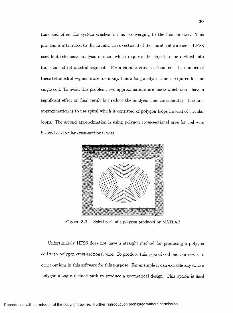
36
time and often the system crashes without converging to the final answer. This
problem is attributed to the circular cross sectional of the spiral coil wire since HFSS
uses finite-elements analysis method which requires the object to be divided into
thousands of tetrahedral segments. For a circular cross-sectional coil the number of
these tetrahedral segments are too many, thus a long analysis time is required for one
single coil. To avoid this problem, two approximations are made which don’t have a
significant effect on final result but reduce the analysis time considerably. The first
approximation is to use spiral which is consisted of polygon loops instead of circular
loops. The second approximation is using polygon cross-sectional area for coil wire
instead of circular cross-sectional wire.
» . - i s i xit h j * *fim feaart Tooii Qwfcfcup WtatowBefr _____________ _____|___________
b t f i a ’ 0 ®j> □ .
-jr.
-x ■x
Figure 3 .2 Spiral path of a polygon produced by MATLAB
Unfortunately HFSS does not have a straight method for producing a polygon
coil with polygon cross-sectional wire. To produce this type of coil one can resort to
other options in this software for this purpose. For example it can extrude any drawn
polygon along a defined path to produce a geometrical design. This option is used
Reproduced with permission of the copyright owner. Further reproduction prohibited without permission.

37
here to produce the desired approximated coil. HFSS can not produce a polygonal
spiral path, thus this path is produced here with a MATLAB program (Figure 3.2)
and again through MATLAB programming the produced coordinates are transformed
to a DXF format file which is the only way a path file can be imported by HFSS.
Here a hexagon is drawn as the cross section of the coil wire which is later on
extruded along the imported spiral path to produce the desired approximated coil
(Figure 3.3). The analysis time of this approximated coil is significantly reduced
which allows one to analyze different coil shapes (i.e. for different winding pitch) in
a very short time.
. -edt PnfKt ftav snakki:.ms- f t* Wndwr.m#-V m i* <>
•ja£T r ouea
; 9 < j» e B 8 6 Q « - ' »• >)f» ^ {*£***..
j&5ta *r:M — ?.■
F ig u r e 3 .3 Extruded spiral path produced by MATLAB in HFSS environment
Using this method a pancake shape transcutaneous transformer for the coils di
ameter of 8 cm is designed. Several coils with different turning loops and winding
pitches are assumed and accordingly their corresponding structures are created with
the method just described. Eventually it turned out that the coils with winding turns
Reproduced with permission of the copyright owner. Further reproduction prohibited without permission.
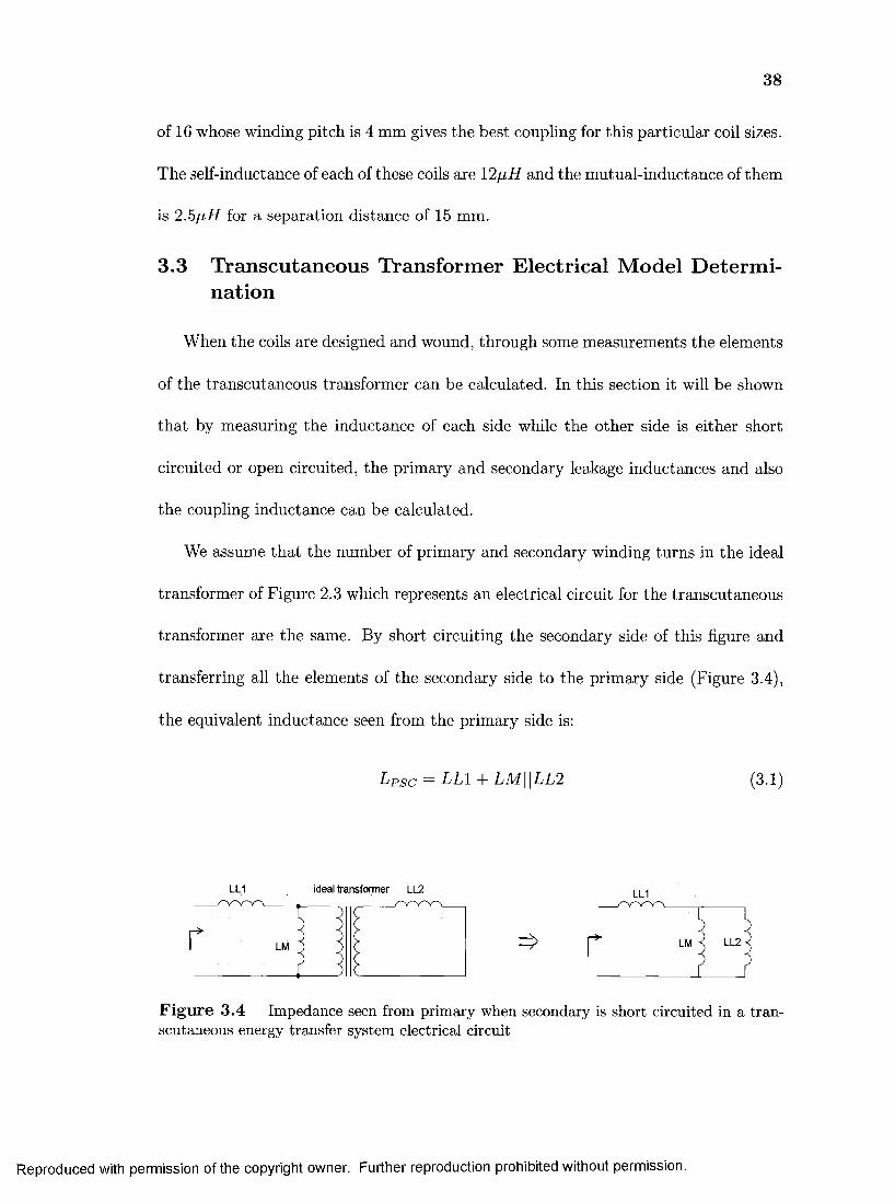
38
of 16 whose winding pitch is 4 mm gives the best coupling for this particular coil sizes.
The self-inductance of each of these coils are 12/iH and the mutual-inductance of them
is 2.5j iH for a separation distance of 15 mm.
3.3 Transcutaneous Transformer Electrical M odel Determ ination
When the coils are designed and wound, through some measurements the elements
of the transcutaneous transformer can be calculated. In this section it will be shown
that by measuring the inductance of each side while the other side is either short
circuited or open circuited, the primary and secondary leakage inductances and also
the coupling inductance can be calculated.
We assume that the number of primary and secondary winding turns in the ideal
transformer of Figure 2.3 which represents an electrical circuit for the transcutaneous
transformer are the same. By short circuiting the secondary side of this figure and
transferring all the elements of the secondary side to the primary side (Figure 3.4),
the equivalent inductance seen from the primary side is:
L p s c = LL1 + L M | \LL2 (3-1)
LL1 ideal transformer LL2 LL1
r LM LM < LL2 •
Figure 3.4 Impedance seen from primary when secondary is short circuited in a transcutaneous energy transfer system electrical circuit
Reproduced with permission of the copyright owner. Further reproduction prohibited without permission.
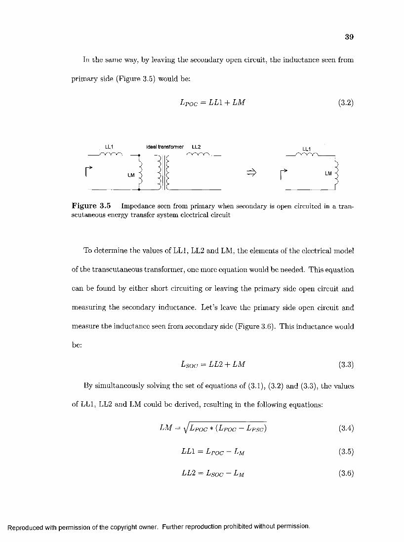
39
In the same way, by leaving the secondary open circuit, the inductance seen from
primary side (Figure 3.5) would be:
L Po c = L L \ -(- L M (3.2)
LL1 ideal transform er LL2
Figure 3.5 Impedance seen from primary when secondary is open circuited in a transcutaneous energy transfer system electrical circuit
To determine the values of LL1, LL2 and LM, the elements of the electrical model
of the transcutaneous transformer, one more equation would be needed. This equation
can be found by either short circuiting or leaving the primary side open circuit and
measuring the secondary inductance. Let’s leave the primary side open circuit and
measure the inductance seen from secondary side (Figure 3.6). This inductance would
be:
L s o c = LL2 + L M (3-3)
By simultaneously solving the set of equations of (3.1), (3.2) and (3.3), the values
of LL1, LL2 and LM could be derived, resulting in the following equations:
L M = \ J L p o c * (L p o c ~ L p s c ) (3.4)
LL1 = L p o c — L m (3-5)
LL2 = L s o c — L m (3.6)
Reproduced with permission of the copyright owner. Further reproduction prohibited without permission.

40
LL1 ideal tra n sfo rm e r LL2
LM
Figure 3.6 Impedance seen from secondary when primary ii scutaneous energy transfer system electrical circuit
LL2
open circuited in a tran-
Reproduced with permission of the copyright owner. Further reproduction prohibited without permission.

Chapter 4
CLASS-E COIL-DRIVER
In this work the Class-E amplifier is used to drive current into the primary coil
of a transcutaneous transformer. Before going into details of this particular design in
the following chapters, a brief introduction to operation theory, analysis and design
of the Class-E amplifier and rectifier is given here.
4.1 Class-E Amplifier
The Class-E amplifier was introduced by Sokal [16] in 1975. This amplifier, when
designed properly, has a theoretical efficiency of 100% which is mainly due to zero
switching losses of its switching transistor. This amplifier is also safe against load
short circuit, has very simple structure and capability of working at high frequency
[17].
The Class-E amplifier consists of a load network and a single transistor that is
operating at the carrier frequency of the output signal (Figure 4.2).
41
Reproduced with permission of the copyright owner. Further reproduction prohibited without permission.

42
4.1.1 Class-E Amplifier Definition
The definition of Class-E operation by Sokal [16] states three main objectives for
the voltage and current waveforms of a switching transistor(Figure 4.1):
1. The rise of the voltage across the transistor at turn-off should be delayed until
after the transistor is off.
2. The transistor voltage should return to zero before the transistor current begins
to rise.
3. The slope of the transistor voltage should be zero at the time of turn-on.
Switch "O ff' S ts te
Figure 4.1 Ideal switch waveforms in a Class-E amplifier [16]
The first condition assures that high voltage does not exist across transistor while
the current through it is nonzero, thereby avoiding the energy loss that would have
Reproduced with permission of the copyright owner. Further reproduction prohibited without permission.

43
otherwise existed. The second condition states that while the transistor is off, the
transient voltage across it first goes upward and then downward toward zero. This
voltage should reach zero before the start of an “on” state. The third condition states
that when the off state transient response reaches zero voltage across the switch,
i.e., just before the start of the “on” state, it does so with zero slope which allows
accidental slight mistuning of the amplifier without sever loss of efficiency.
4.1.2 Principle o f Operation
Every amplifier that meets the definitions of a Class-E amplifier, provided in the
previous section, is considered to be a Class-E amplifier. Figure 4.2 shows the most
popular circuit used for a Class-E amplifier.
r vb
PulseGenerator
Figure 4.2 A Class-E amplifier
In this circuit it is assumed that the inductance of inductor LI is so high that it can
be considered to perform like a current source supplying the energy lost during circuit
operation. It is also assumed that the tuned load network consisting of capacitor C2,
inductor L2 and the load have a very high Q so that the current flowing through this
network can be considered pure sinusoidal. This current flows through the switch
when it is on. When the switch turns off this current keeps flowing but this time
Reproduced with permission of the copyright owner. Further reproduction prohibited without permission.

44
through the capacitor Cl, raising the voltage across it as well as across the switch.
When the direction of the current is reversed, capacitor C l starts supplying this
current, reducing the voltage across it. The value for the Cl capacitor and the load
network series resonant network elements can be designed to make this voltage not
only reach zero but also have a zero slope at this instant. This instant is the best time
for the switch to turn on since it allows current flowing through it while the voltage
and also the slope of voltage across it is zero which makes the energy loss during
the switching period almost zero. The zero voltage is required for a zero switching
loss operation while the zero slope prevents a slight timing error to have a significant
effect on transistor switching losses.
4.1.3 Analysis
Although there are other methods for analyzing a Class-E amplifier such as the
analysis method presented by Puczko et. al. [22], in this thesis the method introduced
by Raab [23] is chosen for analyzing the Class-E coil-driver of the transcutaneous
energy transfer system. This method is accurate and simple, as compared to the other
methods, and is more referenced by other works [27]. In this method it is assumed
that the quality factor (Q) of the series resonant load network is high enough so that
the current flowing through it is sinusoidal. Figure 4.3 shows the waveforms of the
transistor driving voltage, the load voltage, the voltage across the transistor and the
current flowing through the transistor. The voltage and the current of the load are
as follows:
Reproduced with permission of the copyright owner. Further reproduction prohibited without permission.
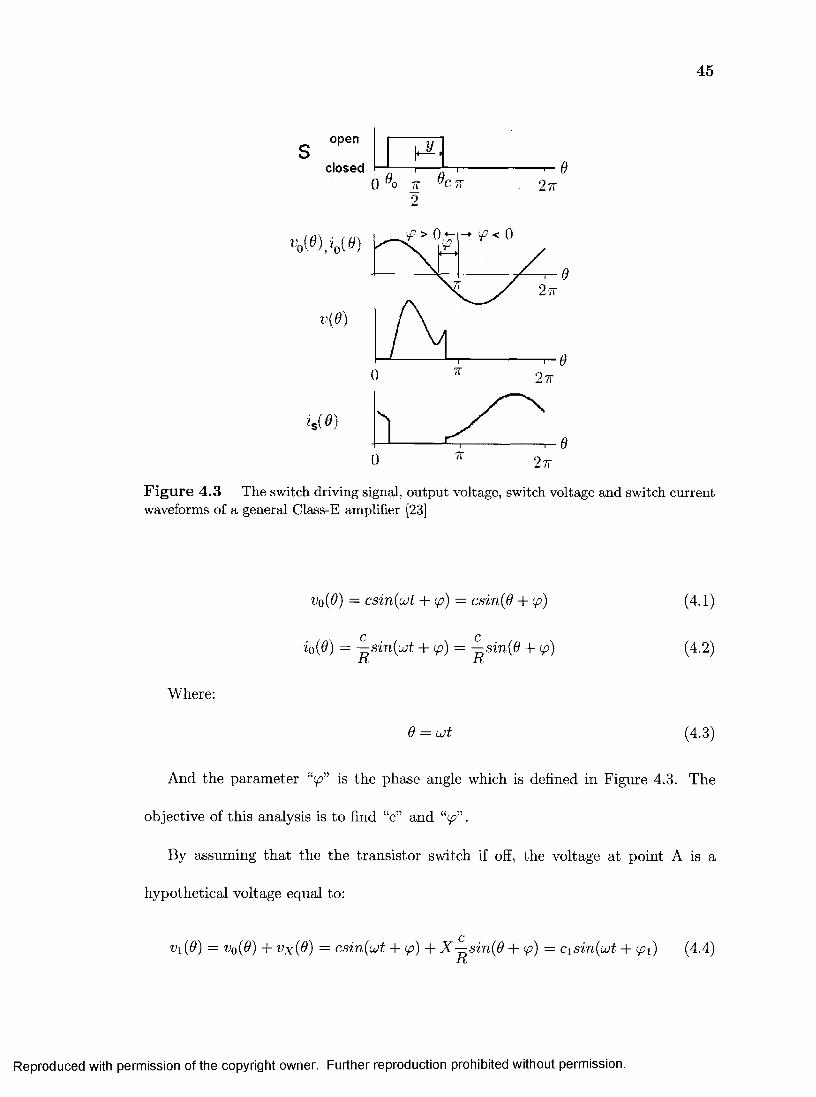
45
open
closedy
O^o it Bc 7r 2 7T9
27T
00 vi
Figure 4.3 The switch driving signal, output voltage, switch voltage and switch current waveforms of a general Class-E amplifier [23]
Where:
Vq (6) — csin(ujt + <p) = csin{6 + p)
c cio{0) = —sin (ait + p ) = —sin(9 + p )
i t K
9 = u>t
(4.1)
(4.2)
(4.3)
And the parameter ‘V ” is the phase angle which is defined in Figure 4.3. The
objective of this analysis is to find “c” and “9?”.
By assuming that the the transistor switch if off, the voltage at point A is a
hypothetical voltage equal to:
Vi (9) = Vo (9) + v x (9 ) = csin(u>t + tp) + X —sin (9 + p ) = cis in{uit + p \ ) (4.4)K
Reproduced with permission of the copyright owner. Further reproduction prohibited without permission.

46
Where X is the equivalent reactance of the series resonant network, L 2 C 2 , and:
/ X 2ci==cy 1 + j p = p ° (4-5)
andX
(pi = (f + i> = ip + tan_1(—) (4.6)K
and xjj is the phase difference which is made by the series resonant network, L 2 C 2 :
^ = ta n -1( | ) (4.7)
The current flowing through capacitor C l, when the switch is off, is provided by
the difference of the current of RF chock, LI, and the current of the series resonant
network. The switch voltage is the voltage across capacitor C l which is charged by
this difference current, hence,
1 rO 1 rS qv(9) = — / i c(u)du = — / [I — —s in (u + (p)\du (4.8)
COC JOq JD J n / 2 —y lb
where
B = ujc (4.9)
The fundamental frequency component of the switch voltage (Cl capacitance volt
age) should be equal to v\ (9) which is derived in (4.4). Thus c\ would be the sinusoidal
Fourier integral of (4.8). When the integrations are performed and the appropriate
substitutions are made, then by collecting terms it would be possible to solve for “c”
which is shown in (4.10)
Reproduced with permission of the copyright owner. Further reproduction prohibited without permission.

47
_ I R __________ 2y siny cos ipx + (2y c o s y - 2 siny) sin <pi_________7v B R p + | sin(2< ̂+ -0) sin 2y — y sin ip + 2 sin(y — y?) cos yq sin y
= I R h ( i p , i ) , y , B , R , p ) (4.11)
Still this equation is unable to determine the amplitude “c” since ip is unknown.
Since the fundamental frequency component of the switch voltage, v(0) , is by defini
tion a sinewave of phase ipi, as stated in (4.4), there can be no cosine or quadrature
component with respect to </?i, thus a second relationship among the parameters,
based on the fact that the cosine Fourier integral is zero, would be:
1 f 2*0 = — / v(9) cos(6 + ipi)d8 (4-12)
7r Jo
By solving this equation the following result will be obtained,
2y sin sin y — 2y cos ipi cos y + 2 cos tp\ sin yc = I R — ---- —---------------- ?----- = IRgl(p, w, y)
—2 sin(y? — y) sin y sin Pi — ̂sm 2y cos(2y? + yj) + y cos ip
(413)
The similarities of equations (4.10) and (4.13) require that,
g(<p,ij;,y) = h (<p , i l ) , y ,B ,R ,p) (4.14)
From this equation a value for p can be found and accordingly the amplitude will be
determined.
Reproduced with permission of the copyright owner. Further reproduction prohibited without permission.

48
4.1.4 D esign Procedure
To design a Class-E amplifier one should consider that there are two conditions
that a Class-E amplifier should meet. The voltage and the voltage slope across the
switch at turn on time must be zero. By applying these conditions, respectively, the
following equations will result,
v (e ) \ e=n/2+y = > g = V— (4.15)cos y s m y
dv(Q) „ , .wcosy — sinw,— L i = o ^ = tan ( - y- y~) 4.16dv y s m y
Load A ngle D eterm ination
For designing a Class-E amplifier, one can find the load phase angle from equation
(4.16). The resultant value, when plugged into (4.15), gives the value for “g”.
Load R esistance D eterm ination
The resistance that the amplifier shows to the power supply can be obtained by,
V 2Rac = - f (4.17)
■L fo
Where PQ is the output power and Vcc is the power supply voltage. The supply current
would become
I = L (4-18)dc
By considering that the output power is,
1 c2P“ “ 2 R <4'19>
Reproduced with permission of the copyright owner. Further reproduction prohibited without permission.

49
And by involvement of (4.13), (4.15) and (4.16), the load resistance can be obtained
I 2a2PR = (4.20)
z
Series R esonant Tank Elem ents
By recalling (4.13)
2y sin ipx sin y — 2y cos <px cos y + 2 cos p x sin y
^ —2sm((p — y ) s m y s m p 1 — ~ sm 2ycos (2 ip + xp) + ycosxp
The only unknown in this equation is the load phase angle which appears as
p x = xp + p. To determine xp it is necessary to expand the term containing p \ so that
sin xp and cos xp can be separated. This results in the following set of equations,
tan^ = ft siny + <f2 cosy,+ g3 cos2<p + gyq2 sin ip + q3 sin 2<p — qi cos ip
where
qi = - 2 g sin(< ̂- y) sin y - 2 y sin y (4.23)
q2 — 2y cos y — 2 sin y (4.24)
g3 = - |s in 2 ? / (4.25)
Once xp is determined, one can use the following equation to find the reactance
of the series resonant network from which the values of C2 and L2 can be easily
determined.
X = Rtoxvxp (4.26)
Reproduced with permission of the copyright owner. Further reproduction prohibited without permission.
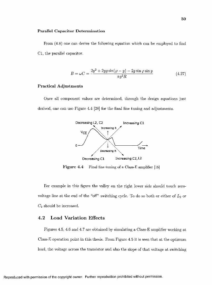
50
Parallel Capacitor Determination
Prom (4.8) one can derive the following equation which can be employed to find
Cl, the parallel capacitor.
B = o j C = V + 2V9 sin(y? - y ) - 2 g sin <p sin yn g 2R
Practical A djustm ents
Once all component values are determined, through the design equations just
derived, one can use Figure 4.4 [28] for the final fine tuning and adjustments.
Decreasing L2, C2 Increasing C l
Increasing R
CE
0Time
Decreasing R
Increasing C2, L2Decreasing C l
Figure 4.4 Final fine tuning of a Class-E amplifier [16]
For example in this figure the valley on the right lower side should touch zero-
voltage line at the end of the “off” switching cycle. To do so both or either of L 2 or
C 2 should be increased.
4.2 Load Variation Effects
Figures 4.5, 4.6 and 4.7 are obtained by simulating a Class-E amplifier working at
Class-E operation point in this thesis. From Figure 4.5 it is seen that at the optimum
load, the voltage across the transistor and also the slope of that voltage at switching
Reproduced with permission of the copyright owner. Further reproduction prohibited without permission.

51
instant are both zero, allowing for zero voltage switching and slight timing error in
transistor switching respectively.
VDS
20 v
10 v
0
VG
10v
A /A A
Tlme(us)
Figure 4.5 The Drain-Source and Gate voltage of the switching transistor of a Class-E amplifier when load resistance equal to optimum load
Figure 4.6 shows that as soon as the load resistance is increased from the optimum
value, the parallel capacitor can not be completely discharged any more and neither
zero voltage condition nor zero slope voltage condition across the switch will be main
tained and consequently switching losses start to increase dramatically. Figure 4.7
'DS
10v
V,G
10v
Time (us)
Figure 4.6 The Drain-Source and Gate voltage of the switching transistor of a Class-E amplifier when load resistance is larger that optimum load
shows the condition in which the load resistance is decreased from the optimum value.
At this state the parallel capacitor discharges earlier than the instant the switch tran
sistor turns on and hence the sine-wave current flowing through the series resonant
Reproduced with permission of the copyright owner. Further reproduction prohibited without permission.

52
network will be supplied by the switch MOSFET transistor conducting in reverse
direction. In case a bipolar transistor is used instead of a MOSFET transistor, an
anti-parallel diode across transistor can maintain the same situation. In either of
these cases the voltage across the switch transistor will remain zero (exactly as much
as the voltage drop across a forward conducting diode is) and this ensures that the
transistor will be turning on at zero voltage.
vDs20 v
10v
0
VG
10v
o
Figure 4.7 The Drain-Source and Gate voltage of the switching transistor of a Class-E amplifier when load resistance is smaller that optimum load
4.3 Class-E Rectifier
Class-E rectifiers offer a new means of high-frequency high-efficiency low-noise
rectification [30]. Figure 4.8 shows a Class-E rectifier. It consists of a diode, a shunt
capacitor and a second order low-pass output filter. The rectifier is driven by a sine-
wave current source “i” . The shunt capacitor shapes the voltage across the diode so
that the diode turns on and off at low d v / d t , reducing the current driven through the
diode at both transitions. The L f — C f output filter ensures the ripple in the output
voltage is below a specified level.
Time (us)
Reproduced with permission of the copyright owner. Further reproduction prohibited without permission.

53
b
I - t o t o
) VD "3
L
k J = c
t
=Ci i
I -
Figure 4.8 A Class-E rectifier [30]
4.3.1 Principle o f Operation
The idealized current and voltage waveforms of the rectifier for the case where the
diode on switch duty ratio is D = 0.5, i.e. when the conduction angle of the diode is
equal to 180° are shown in Figure 4.9.
The input current “i” of the circuit in Figure 4.9 is a sine-wave and the output
current IQ is DC current. The diode and the parallel capacitor C are driven by a
current source I0 — i. When the diode is off, the current I0 — i flows through the
capacitor C. When the diode is on, the current I0 — i flows through the diode. The
diode turns on when its voltage increases beyond the diode threshold voltage and
it turns off when its forward current decreases to zero. The current flown through
the capacitor C, when the diode is off, shapes the voltage across the diode. The
relationship between the current and the voltage of a capacitor is i c = C d v p / d t .
This equation indicate that when the current flowing through the capacitor C is zero
when the diode is turned off, the slope of the voltage across this capacitor, and hence
the diode D which is placed in parallel with this capacitor, would be zero. On can
follow through the waveforms of Figure 4.9 that the diode voltage at turn-off, v D,
Reproduced with permission of the copyright owner. Further reproduction prohibited without permission.

54
OFF ON
2ir(1-D)
■dm
Figure 4.9 Idealized current and voltage waveforms of a Class-E rectifier [30]
gradually decreases when the capacitor current, i c , is negative. This voltage reaches
its minimum value when capacitor current is back to zero and then slowly rises when
i c turns positive. Thus diode turns on and off at low d v /d t . reducing switching losses
as well as the switching noise. Moreover, the absolute value of diode current slope
at turn on, which is equal to capacitor C current slope at this instant, is quite small
since the diode voltage (Capacitor C voltage) at this instant is zero. This fact helps
to alleviate the effect of reverse recovery charge of the diode.
Reproduced with permission of the copyright owner. Further reproduction prohibited without permission.

55
4.3.2 Analysis
The basic equation for the rectifier of Figure 4.8 is:
I0 — i = iD + i c (4.28)
In this equation,
i = Im sm(ujt + ip) (4.29)
Where Im is the amplitude and ip is the phase angle indicated in Figure 4.9.
The relationship between the diode ON duty ratio D, and the phase angle ip is
given by [30],
1 — cos 27xDtan ip = -----—-— (4.30)
27t(1 — D ) + s m 2 7 r P
The diode on-duty cycle, D, depends on ujC R l as follows,
ujC R l = ^-{1 - 2tt2(1 - D )2 - cos2ttD + ' D ) + sm^ D ? y27T 1 — COS 27tD
For a particular operating frequency / and a diode turn-on duty cycle, D, the equiv
alent circuit for the Class-E rectifier is a series combination of resistor Ri and C\
capacitor. R.t is the input resistance of the rectifier and its value at the operating
frequency , / = Lu/2n, can be obtained by the following relation [30]:
Ri = 2R l sin2 (p (4.32)
Where R l is load resistance of the circuit. Likewise C i is input capacitance of the
rectifier whose value at the operating frequency, / , can be obtained by the following
relation [30]:
Reproduced with permission of the copyright owner. Further reproduction prohibited without permission.

56
Ci = C tt\k {1 — D ) + s m . 2 n D — \ sin An D cos 2i^ — \ sin 2^ sin2 2 n D — 2 n ( l — D ) siny?
sin(27rD - <p)]~l (4.33)
where C is the parallel capacitor of the Class-E rectifier.
Reproduced with permission of the copyright owner. Further reproduction prohibited without permission.

Chapter 5
CLASS-E TRANSCUTANEOUS ENERGY TRANSFER SYSTEM
Compensating the effects of leakage inductances in a transcutaneous transformer
helps to increase the voltage gain of a transcutaneous energy transfer system. These
effects can be totally eliminated by employing resonant coil drivers such as Class-E or
series resonant coils drivers, as were discussed in Chapter 2. Increasing the transcuta
neous transformer coupling coefficient, as was discussed in Chapter 3, helps to reduce
the leakage inductances and increase the efficiency of the system as well. However
there are some other issues that should be considered in designing a transcutaneous
energy transfer system. The fact is that, due to movement and breathing of the re
cipient of the implanted device, mutual position of two coils of the transcutaneous
transformer is ever changing. These variations result in variation of coupling coef
ficient and leakage inductances of the transcutaneous transformer. Therefore, after
the transcutaneous transformer is designed, not only its leakage inductances but also
their variations for a specified interval, determined by the required mutual position
57
Reproduced with permission of the copyright owner. Further reproduction prohibited without permission.

58
variation of the two coils, must be considered in the design. The other factors that
must be considered in a good design are the prediction of load and input voltage
variations. The control system employed for the design must also be capable to re
spond to these variations in a quick and effective way to ensure supplying of fixed
and regulated voltage for the implanted device.
In this chapter the design method for a transcutaneous energy transfer system that
is constructed for this thesis is outlined. The operation principles and the analysis
method are first illustrated and then the potential capability of this system for keeping
up with different coil positions and their effects on overall efficiency and operation
frequency of the system are investigated.
5.1 Proposed Transcutaneous Energy Transfer System
Figure 5.1 shows the schematic diagram of the power transfer section of the pro
posed transcutaneous energy transfer system. In this system a Class-E amplifier is
used as the coil-driver and a Class-E rectifier as the rectifier of the system. The
primary leakage inductance of the transcutaneous transformer is playing the role of
inductance in the tuned series network of the Class-E amplifier and effect of sec
ondary leakage inductance is eliminated through resonance with the capacitor C3 at
the operating frequency.
5.2 Circuit Analysis
To analyze the circuit of Figure 5.1 we start off by replacing the Class-E rectifier
by its equivalent circuit which is a resistor in series with a capacitor as was outlined
in Section 4.3.2. At this step the value for C% can be computed to make the two ca-
Reproduced with permission of the copyright owner. Further reproduction prohibited without permission.

59
transcutaneous transformer class E rectifier
7X1“i r
n=1
co /■ \
L4
£ Di: C4
: C6 ? RL
Figure 5.1 The schematic diagram of power transfer section of the proposed transcutaneous energy transfer system
n=1
Figure 5.2 Figure 5.1 when its class-E rectifier is replaced by its equivalent circuit
pacitors C \ and Cj and the secondary leakage inductance to resonate at the operating
frequency to cancel out the secondary leakage inductance (Figure 5.3).
n=1
Figure 5.3 Figure 5.1 when the secondary leakage inductance is eliminated by resonance
After transferring Ri to the primary side, the circuit will change into Figure 5.4.
By transforming a parallel combination of a resistor and an inductor to a series
Reproduced with permission of the copyright owner. Further reproduction prohibited without permission.

Figure 5.4 Figure 5.3 when secondary load is transfered to primary side
combination by appropriate equations [29] the circuit of Figure 5.5 will be the result.
Figure 5.5 Figure 5.4 when parallel and Ri are replaced by their equivalent series combination
And finally it will reduce to the conventional form of a Class-E amplifier whose
elements can be computed by the design method outlined in section 4.1.4.
5.3 Frequency Controlled Output Voltage
It would be very interesting to investigate the effect of operating frequency vari
ation on output voltage variation. One would note that in this circuit the effect of
the frequency variation is not limited to the series resonant network of the Class-E
coil-driver. The secondary side tuned circuit which is used to eliminate the effect of
Reproduced with permission of the copyright owner. Further reproduction prohibited without permission.

61
i L
u CC2
r- 11Leqq
M1 ,
H a
II
: C5 5 Req
Figure 5.6 A Class-E amplifier
secondary side leakage inductance of the transcutaneous coils perform like another
tuned filter in this circuit. Interaction of these two filters should be carefully studied
to find potential operating conditions under which a linear and effective control over
the output voltage would be possible .
5.3.1 Coils Coupling Variations Com pensation by Frequency Variation
Any variation in mutual positions of the coils will change the coupling coefficient
between them. This will lead to leakage and coupling inductances variations in the
electrical transcutaneous transformer model and these in turn will result in resonance
frequency variations of both of the filters. By increasing the distance between the
two coils, their coupling decreases, their leakage inductances will be increased and the
coupling inductance will be decreased. This will result in reduction of the resonant
frequency in both of the filters. Thus intuitively decreasing the operating frequency
can be accounted for compensating the coil distance increase. In the same way the
increase in operating frequency can account for compensation of coils distance reduc
tion. Hence frequency variation can reasonably be a means of compensating the coils
mutual movements.
Reproduced with permission of the copyright owner. Further reproduction prohibited without permission.

62
5.3.2 Load Variations Com pensation by Frequency Variation
By assuming a fixed coils distance, variation of operation frequency in an allowed
frequency band can also account for load variation in the allowed range the device is
designed for. This can be visualized by assuming that when the load is varied, the Q
of the Class-E amplifier will be varied. If it is assumed that the operating frequency
band of the Class-E coil-driver is larger than its resonant frequency, i.e. it is situated
at the right side of the center frequency in Figure 5.7, then by increase of the load,
the voltage gain will be increased, thus a reduction in operating frequency is needed
to compensate for this raise of load.
a
P5 as « t s s.
Operating frequency55
Figure 5.7 Frequency response of a Class-E amplifier
5.3.3 Frequency Variations Analysis
Studying the effects of frequency variation on the proposed circuit of Figure 5.1
is not a simple task since the role of the two tuned circuits should be considered at
the same time. One approach to perform this analysis will be explained here. The
circuit of Figure 5.3 when its series tuned circuit of the secondary side is replaced by
Reproduced with permission of the copyright owner. Further reproduction prohibited without permission.

63
j X is shown in Figure 5.8.
11 >C2 L2
Ml .
H e
II
: Cl 15 > «
n=1 jx-CZJ-
RL
Figure 5.8 The Class-E transcutaneous energy transfer system with equivalent secondary side circuit
When the operating frequency is lower than the resonant frequency of the tuned
filter, the X would change to a capacitance and when the frequency is higher than the
resonant frequency, it will change to an inductance. For further processing the circuit
on the secondary side will be transferred to the primary side as shown in Figure 5.9.
RL
Figure 5.9 The Class-E transcutaneous energy transfer system with secondary impedance is transferred to primary side
To simplify the analysis, the series combination of R L and j X will be transformed
to a parallel combination with the following equations as shown in Figure 5.10.
Rp — R l (1 + Q 2) ( 5 - 1 )
Reproduced with permission of the copyright owner. Further reproduction prohibited without permission.

64
1 + O2X r = X(-if-) (5.2)
q = T l (5'3)
M1
Figure 5.10 Figure 5.9 when series j X and R l are transformed to parallel combination
j X and ju>L5 will be paralleled and the combination of the resulting inductance
or capacitance and Rp will be transformed back to a series combination with the
following equations ( Figure 5.11)
Rs = ^ ( 1 + Q2) (5‘4)
x ' = x ^ T T q ^ <5-5>
Q = ~ (5-6)j \p
The resulting circuit would be the conventional Class-E circuit which could be
analyzed with the methods outlined in section 4.1.4
5.3.4 Frequency R esponse o f the Proposed Transcutaneous Energy Transfer System
By utilizing the equations derived in the previous section the frequency response
of the proposed transcutaneous energy transfer system can be computed. It will be
Reproduced with permission of the copyright owner. Further reproduction prohibited without permission.

65
C 3
Figure 5.11 Figure 5.10 when parallel combination of reactance and resistor are transformed back to a series combination
shown that the overall frequency response which is the result of the interaction of
the Class-E amplifier and the output tuned filter is more selective and narrow band
than a Class-E amplifier by itself. In obtaining this frequency response, one also has
some freedom to shape the frequency response of the overall system by choosing the
location of the center frequency of the output tuned filter.
Frequency R esponse of a Class-E Amplifier
Figure 5.12 shows the frequency response of the Class-E amplifier which is obtained
by mathematical modeling in MATLAB. This graph will be used as a reference to
compare with and illustrate the frequency response of the complete transcutaneous
energy transfer system.
Frequency R esponse of a Class-E Transcutaneous Energy Transfer System
Figure 5.13 shows the frequency response of the Class-E transcutaneous energy
transfer system obtained by mathematical modeling in MATLAB. This graph is ob
tained while the secondary tuned circuit is fine tuned to the operating frequency for
which the Class-E amplifier is designed. It can be seen that over part of the frequency
Reproduced with permission of the copyright owner. Further reproduction prohibited without permission.

66
1 1 5
ZVS a re a
200 300 fc 400 500Operating frequency (KHz)
600
Figure 5.12 Frequency response of a Class-E amplifier
band the transfer function is obtained the voltage is fixed while over some other parts
the output voltage is controllable by variation of the frequency. For controlling the
output voltage also either of the left positive slope or the right negative slope could
be used to control the output voltage. The control strategy and circuit limitations
are among the factors which determine the working frequency band.
Figure 5.14 which is obtained by mathematical modeling by MATLAB, shows the
frequency response of the Class-E transcutaneous energy transfer system when its
secondary tuned circuit’s resonant frequency is lower than the operating frequency
for which the Class-E amplifier is designed. Definitely the larger peak is the most
desired area for operation because of yielding better voltage gain for the system.
Around this peak, depending on the control strategy and better linearity, either of
the positive or negative slopes at the left or right side of the peak can be chosen.
When the secondary tuned circuit’s resonant frequency is chosen to be higher than
the operating frequency for which the amplifier is designed, the graph of Figure 5.15
Reproduced with permission of the copyright owner. Further reproduction prohibited without permission.

67
2.5 3.5 4 4.5 5
Operating frequency5.5 6.5
X 10S
Figure 5.13 Frequency response of Class-E transcutaneous energy transfer system when f res is very close to f c
is obtained fron the mathematical modeling by MATLAB. This graph offers a number
of options similar to those which already were discussed depending on which control
region is selected.
In either of the three types of transfer function obtained, the Zero voltage switching
(ZVS) condition has vital role in selection of the working frequency band since it
directly influences the efficiency of the system. In all the three cases the zero voltage
switching condition for Class-E amplifier switch are not investigated as it turned
out the analysis procedure used doesn’t have the potential for this investigation and
thus this is left for further analysis and simulations to investigate the case which is
performed in the next chapter.
Discussion
There is some discussion as what would be the potential benefits for a specific
location of the resonant frequency of the secondary tuned filter. It is obvious that the
Reproduced with permission of the copyright owner. Further reproduction prohibited without permission.

68
<D 10
2.5 3.5 4 4.5 5
Operating frequency5.5 6.5
Figure 5.14 Frequency response of Class-E transcutaneous energy transfer system when fres lags f c
effect of the secondary side resonant filter is just resistive when its resonant frequency
is equal to the operating frequency. If at this frequency the zero voltage switching
state for the coil-driver is maintained then the peak corresponding to this filter in
the transfer function of the transcutaneous energy transfer system is a safe region for
operation, either it is smaller or greater than the peak corresponding to the Class-
E coil-driver. But Figure 5.12 indicates that the safe operating area for a Class-E
amplifier is at the right side of its peak frequency, thus depending on where the
resonant frequency of the secondary filter is selected different situations may appear.
First, assume it is smaller than the peak Class-E coil-driver frequency. In this case
the area on the right skirt of Figure 5.14 is the useful operating area. The same
situation occurs when these two frequencies are very close to one another. When the
resonant frequency of the secondary resonant filter is larger than Class-E coil-driver
peak frequency, either part or all of the positive or negative slope of each of the
Reproduced with permission of the copyright owner. Further reproduction prohibited without permission.

69
18
16
14(0
3:= 8 Q .
i .4
2
0
2.5 32 3.5 4 4.5 5 5.5 6 6.5
Operating frequency xios
Figure 5.15 Frequency response of Class-E transcutaneous energy transfer system whenf r e s lo a d s f c
two peaks in the transfer function of Figure 5.15 might be a useful area for system
operation. This gives some guidelines as how to obtain the desired transfer function
by proper design. One can initiate the design by considering only the resistive effect
of the secondary side on the primary and design the Class-E coil-driver and obtain
its transfer function. By selecting the proper value for the secondary series capacitor,
location of the secondary resonant filter on the Class-E coil-driver can be obtained.
Once the transcutaneous energy transfer system is designed and the control strat
egy is identified, a closed-loop stability analysis should be performed to avoid any
oscillations due to instability which is the subject of the next section.
5.3.5 Closed-Loop Control and Stability Analysis
A closed-loop control technique is employed to keep the output voltage fixed and
regulated by changing the operating frequency. Figure 5.16 shows the block diagram
of this system.
Reproduced with permission of the copyright owner. Further reproduction prohibited without permission.
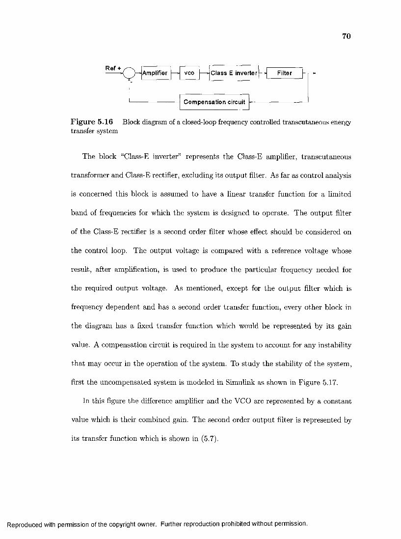
70
Ref +vcoAmplifier FilterClass E inverter
Com pensation circuit
Figure 5.16 Block diagram of a closed-loop frequency controlled transcutaneous energy transfer system
The block “Class-E inverter” represents the Class-E amplifier, transcutaneous
transformer and Class-E rectifier, excluding its output filter. As far as control analysis
is concerned this block is assumed to have a linear transfer function for a limited
band of frequencies for which the system is designed to operate. The output filter
of the Class-E rectifier is a second order filter whose effect should be considered on
the control loop. The output voltage is compared with a reference voltage whose
result, after amplification, is used to produce the particular frequency needed for
the required output voltage. As mentioned, except for the output filter which is
frequency dependent and has a second order transfer function, every other block in
the diagram has a fixed transfer function which would be represented by its gain
value. A compensation circuit is required in the system to account for any instability
that may occur in the operation of the system. To study the stability of the system,
first the uncompensated system is modeled in Simulink as shown in Figure 5.17.
In this figure the difference amplifier and the VCO are represented by a constant
value which is their combined gain. The second order output filter is represented by
its transfer function which is shown in (5.7).
Reproduced with permission of the copyright owner. Further reproduction prohibited without permission.
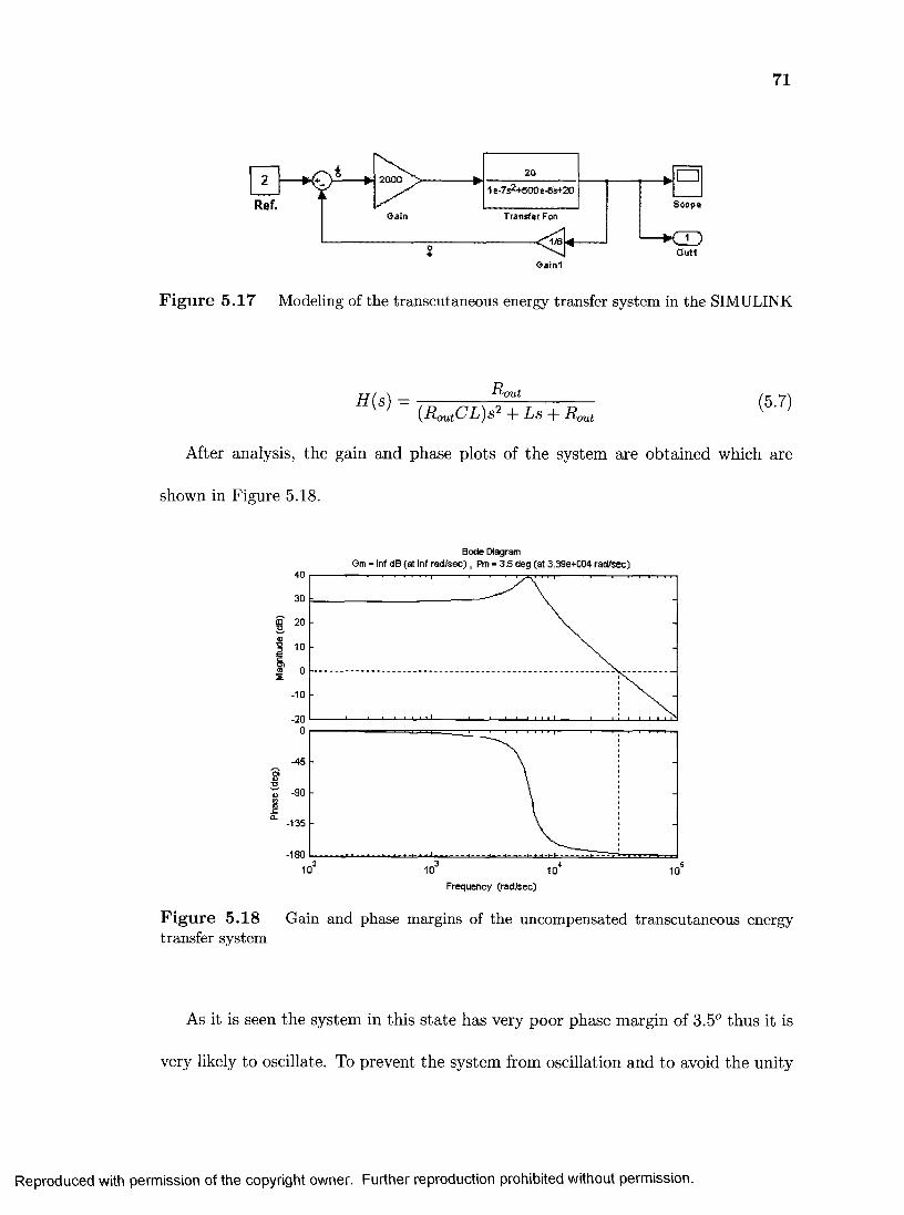
71
2000
Ref.Transfer Fen
K j D0ut1
1e-7s2+500e*8sf20
20
©ainl
Figure 5.17 Modeling of the transcutaneous energy transfer system in the SIMULINK
H (s ) =Rout (5.7)
(RoutCL)s2 + L s + Rout
After analysis, the gain and phase plots of the system are obtained which are
shown in Figure 5.18.
Bode DiagramGm = Inf dB (at Inf ra d /s e c ) , Pm = 3.5 deg (at 3.39e+004 rad/sec)
Frequency (radteec)
ftSc
-10
-20
-45Gl0)■o<u<Aas
a -135
-180,2 3 i S10' 10' 10 10'
Figure 5.18 Gain and phase margins of the uncompensated transcutaneous energy transfer system
As it is seen the system in this state has very poor phase margin of 3.5° thus it is
very likely to oscillate. To prevent the system from oscillation and to avoid the unity
Reproduced with permission of the copyright owner. Further reproduction prohibited without permission.

72
gain situation in the entire range of operating frequency band a compensation circuit
is required to improve the phase margin of the system. Among different choices for
the compensation circuit, a dominant pole circuit is used whose transfer function is
represented by equation (5.8). Figure 5.19 shows the block diagram of the system
after the compensation circuit is applied to it.
H(s ) =1
( R c o m p C c o m p ) ^ H - 1(5.8)
Transfer Fcn1
2000
Ref. Scope
♦CDOut1
1 e-7s2+500e-6s*20
20
Figure 5.19 Modeling of the transcutaneous energy transfer system in the SIMULINK
The gain and phase plots of the compensated system are shown in Figure 5.20.
These graphs indicate an improvement of up to 11.1 d B and 90.4° for gain and phase
margins of the system respectively.
Reproduced with permission of the copyright owner. Further reproduction prohibited without permission.

73
Figure 5.20system
Bode DiagramGm = 11.1 dB (at 6.33e+003 rad /sec ), Pm = 90.4 deg (at 559 rad/sec)
-50
-100
-90
if -180
-270□ 2 3 i S10 10 10' 10'
Frequency (rad/sec)
Gain and phase margins of the compensated transcutaneous energy transfer
Reproduced with permission of the copyright owner. Further reproduction prohibited without permission.

Chapter 6
SPICE SIMULATIONS AND EXPERIM ENTAL RESULTS
To apply the methods outlined in the previous chapter a transcutaneous energy
transfer system with the following specifications is designed:
• Input voltage 14 v
• Output voltage 12 v
• Maximum output power 15 W
It is assumed that the output voltage of this transcutaneous energy transfer system
should be kept constant at the coils separation distances between 1 to 4 cm.
For this design no limitation on the size of the implanting coils is assumed. Based
on the HFSS simulation, described in Section 3.2, each of the coils are wound with 16
turns of LITZ wire. According to the methods explained in Section 3.3 the elements
of the electrical models of the transcutaneous transformer are determined through
experimental measurements. This method could be used to obtain the curves of the
leakage and the coupling inductances variation versus the coils separation distance.
74
Reproduced with permission of the copyright owner. Further reproduction prohibited without permission.

75
The values of these inductances are limited to the coils extreme minimum and max
imum separation distances the system is intended designed for. To start the design
process, as the first step, the coupling and leakage inductances are obtained for the
average separation distances of the two required extreme positions. At this condi
tion, the difference between the values of the elements of the electrical models of the
transcutaneous transformer, when the coils move to the each of extreme required po
sition, is smaller than the case where initially these values are obtained for a different
position than average of the two required extreme separation distance. In this way
the chance of compensating the effects of variation of values of these elements by the
variation of the operating frequency, which is the goal of this study, is increased.
Determination of other circuit elements such as Class-E rectifier and Class-E am
plifier elements of Figure 5.1 are performed on the next step. This is performed
according to the methods explained in the Chapter 4 whose MATLAB programs are
already developed.
The circuit will then be simulated with PSPICE for a range of operating frequen
cies suggested by either of the graphs of Figures 5.13, 5.14 or 5.15. This is for finding
the band of frequencies for which the output voltage is linearly controlled while ZVS
is maintained. For example in this particular design, the transfer function depicted
in Figure 6.1 is used.
It would be desirable to determine the ZVS property of region of interest directly
by analysis than simulation since it would be much faster and more convenient. Un
fortunately the basis of the analysis method used [23] doesn’t seem to allow the
analytical exploration of this option. However an indirect analysis is possible and
Reproduced with permission of the copyright owner. Further reproduction prohibited without permission.

76
2.5 3.5Operating frequency
4.5 5.5
Figure 6.1 Frequency response of the analyzed 15 W, 12 v output Class-E transcutaneous energy transfer system
that is to check this region for ZVS property by observing the analyzed MOSFET
drain voltage waveforms in MATLAB. The graphs depicted in Figure 6.2 are the
waveforms obtained in this way for the range of operation frequencies form SQOkHz
to 440k H z .
Reproduced with permission of the copyright owner. Further reproduction prohibited without permission.

77
300380 kHz
250
200
150
100
I 500
•50
-100,0 0.2 0.4 0.6 0.8 1.4 1.6 1.81.2 2
360 kHz
389 kHz140
385 kHz120
100
80
> 60
40
20
0,0.2 0.4 0.6 0.8 1.2 1.4 .60 1 1.8 2
410 kHz
IF 25
390 kHz
120
440 kHz100
80
60
I40
20
00 0.2 0.4 0.6 0.6 1 1.2 1.4 1.6 1.8 2
60 420 kHz
50
* 30
>
20
10
0,0.2 0.4 0.6 0.00 1.2 1.4 16 1.8 2
Figure 6.2 Drain waveform obtained by MATLAB from top left to the bottom right for the frequencies of f o p = 360kHz, f o p = 380kHz, f o p = 385kHz, f o p = 389kHz, f o p = 390kHz, f o p = 410kHz, f o p = 420kHz, f o p = 440kHz respectively
Reproduced with permission of the copyright owner. Further reproduction prohibited without permission.

78
This figure indicates that at the frequency band between 389 kHz and 410 kHz,
ZVS is maintained and this band is most likely the most suitable range for controlling
the output voltage. To confirm this prediction, the designed transcutaneous energy
transfer system may be simulated in SPICE at the selected frequency range to validate
our initial prediction according to analytical waveforms obtained by MATLAB.
6.1 Simulations6.1.1 Power Transfer Simulations
Figure 6.3 shows the circuit simulated in PSPICE.
LI250u
IR FIS of-
V£lue = 14.5n 9u
2.1u15
Rl
■A/W- TX1i rL3
9u
5 D1M BR32
L4
SOOu± C4
26ndp ce
SOu
Figure 6.3 The power section of designed transcutaneous energy transfer system circuit modeled in SPICE. The connection between the grounds of the two sides of the transformer is necessary for simulation purpose.
Figures 6.5 to 6.7 demonstrate the MOSFET transistor voltage as well as the
output DC voltage waveforms resulted from the SPICE simulations for frequencies
from 350 kHz to 480 kHz. These waveforms confirm the results obtained by MATLAB
in the previous section and indicate that the frequency range between 390 kHz to 410
kHz could be the suitable operating frequency band for controlling the output voltage
in terms of maintaining the ZVS condition. These results also indicate that in the
selected frequency band, the output voltage can be controlled between 15.7 v to 10.5
v which is obtained on the negative slope of the frequency transfer function shown if
Reproduced with permission of the copyright owner. Further reproduction prohibited without permission.

79
Figure 6.4.
16
1= 10
2 2.5 3 3.5 4 4.5 5 5.5 6 6.5
Operating frequency (Hz) *io5
Figure 6.4 The portion of the transfer function between the two vertical lines is the area the system is working on
Reproduced with permission of the copyright owner. Further reproduction prohibited without permission.

80
f-!~
' i T i " i " H— r
' • !S E L »7.44U-
o U (R8:2)
9 8 3 .1 5 u s 984.8BUS 985.68US 986 .B 8us 987.00U 5 988.O0US 9 8 9 .8 8 u s 998.B8US 9 91 .B 6us 9 9 2 .1 4 u so U(M1:d)T ine
e U (R8:2)
25U
BU-
982US 988usa U(H 1:d)
...... !" "■.....
......i - H ........r ......
— -!......i ...... i.......
......
......
N: : . - ■ ! ......
.. ..................... .
- ■ t + H ......
- i ......i ........r ......h : h
......I ...... i ...... t ...... ......r - t .............
S E L »16.6BU-
o U(RB:2)
25U-
B.98483ms 0 .98600ns ,99686msa U(N 1:d)
Figure 6.5 Simulated drain and output waveform at frequencies of fop = 350 kHz, fo p = 370 kHz and f op — 380 kHz from top respectively
Reproduced with permission of the copyright owner. Further reproduction prohibited without permission.

81
15.75U
15.7BU-
580-
250-
S E L »-4 0 -0 .9 8 4 1 n s 0 .9 8 6 6 n s 0 .9 8 8 0 n s 0.9900ms 0 .9928ns 0.9940m s 0 .9 9 6 0 n s
o U(M1:d)T ine
1 3 .5 0 8 0
13 .4 7 5 0
1 3 .4 5 0 0□ U(R8:2)
250-
S E L »- 2 0 -9 72 .
1 1 .6 0 0
1 1 .5 8 0
1 1 .5 6 0
500
250
S E L »-3 0 -
F igure 6 .6 Simulated drain and output waveform at frequencies of f op = 390 kHz, fop = 400 kHz and f op = 410 kHz from top respectively
Reproduced with permission of the copyright owner. Further reproduction prohibited without permission.
16US 982.O0US 984.00US 985.95USd U(H1:d)

82
..... 1
- i ......
..... T...... \...... .........
E E E E
.......!"......\...... ........
E Q E j : : : : : : '3 3 E B.......r......t...... i...... ' ..... !...... 1.......
.......i...... j - - - i ........
.......:...... i...... 1........
......
....
: ..... :...... i........
.. i - . - i ..... \ ........
l - - / - —
O U (R 8:2)
38U
2BU
ieuS E L »
9 8 6 .Bus 9 9 2 .Busi V(lf1:d)
9.6U
S E L »9.2U -
o U (R8:2)
3BU
28U
1QU
9 8 8 .9us 9 8 2 .Bus 9 8 6 .Bus 9 8 8 .Bus 99B. BUS 9 9 1 . Bus□ U(M1:d)
38U
2BU
ou□ u(M1:d)
F igu re 6.7 Simulated drain and output waveform at frequencies o ifop = 440 kHz, fop = 460 kHz and fop = 480 kHz from top respectively
Reproduced with permission of the copyright owner. Further reproduction prohibited without permission.

83
6.1.2 Closed-Loop Stability Simulation
In Section 5.3.5 an analysis was performed to determine the values of the compo
nents for the compensation circuit. Here, based on that analysis, the whole circuit is
simulated to evaluate its performance with regard to stability.
Figure 6.8 shows the difference amplifier along with the compensation circuit
which is composed of a proportional amplifier and an integrator. The difference of
the sample of output voltage and a reference voltage, which is represented by a DC
voltage source in spice simulation, is proportionally amplified by the amplifier of the
first stage. The output of the first amplifier is integrated by the second stage amplifier
in this figure.
: SOQn
sample m208k500R8
OU]
2
Figure 6.8 Proportional and integrator amplifiers in the closed control loop
The output of the integration amplifier is fed to a VCO behaviorally realized by
the circuit of Figure 6.9. In this figure the capacitor C l is charged by the behaviorial
voltage-controlled current-source of G1 whose current is determined by the input
control voltage, Vcont, and the input difference voltage. The input difference voltage
is provided by the NAND Schmidt of U1A which oscillates between ”0” and ”5”
volts. The voltage-controlled current source of G2 discharges the capacitor Cl with
Reproduced with permission of the copyright owner. Further reproduction prohibited without permission.

84
the half amount of current G l charges C l when it is on. To describe the operation
of this circuit lets assume the capacitor C l is fully discharged first. At this state
the output of U1A is HI, the G l current source starts charging the capacitor Cl.
Once the voltage across this capacitor reaches the up threshold of U1A, G l stops
charging capacitor C l therefore the this capacitor is being discharged with current
source of G2, decreasing the voltage across this capacitor. When the voltage across
the capacitor C l reaches the lower threshold of U1A, the output of U1A turns on,
causing the Gl start charging back the capacitor C l. This charging and discharging of
capacitor C l creates the output square waveform of the circuit, however, the frequency
is determined by the amount of the current is provided by the current sources. Since
the amount of this current is determined by input control voltage thus the output
frequency of the circuit is determined by the value of input voltage. The output of
the VCO is used to drive the MOSFET switch transistor of the Class-E coil-driver.
Reproduced with permission of the copyright owner. Further reproduction prohibited without permission.

85
U1Av m N + . %IN-Wl A r r ’c trfV lfly 1e-3
IN+ O U T * — ---------' IN- OUT6 - |
GVAIUE
IC-O
VvVjVjftLUE
IM+ OUT, IN- OU1 tp C1
2.5/p+v(ctriyio),'i«-:•Wfo.t
F igu re 6.9 The behaviorial VCO in SPICE
Figure 6.10 shows the output of the proportional amplifier. The output of this
amplifier, after being integrated by the integration amplifier, is shown in Figure 6.11.
Reproduced with permission of the copyright owner. Further reproduction prohibited without permission.

86
■+-t" y
A.......i - ' - i - l .......... - - i -
0s
F igu re 6.10 The output waveform of the proportional amplifier in the closed control loop
U(CTRL)
T in e
F igure 6.11 The output waveform of the integrator amplifier in the closed control loop
As can be seen the output of the difference amplifiers/compensator is reduced to
50 mv after a transient time of 15 ms. Figure 6.10 also include the output voltage of
the system. As can be seen this voltage after a transient time of 10ms is stabilized
while the its overshoot is limited to 2 v at its start up.
Reproduced with permission of the copyright owner. Further reproduction prohibited without permission.

87
6.2 Experim ental Results
After realization of the circuit, the output and drain voltage waveforms obtained
from the experimental results are depicted in Figures 6.12 to 6.17. In this figures
the waveforms in channel 1 and channel 2 correspond to drain and output voltages
respectively. The Y axis represents the voltage whose resolution is mentioned un
derneath each figure for each corresponding channel and the X axis represents time
whose resolution is mentioned at the top of each figure. One can see that there is
a great resemblance between the simulation and the experimental results in terms
of the interpretation of the waveforms. For example both of the simulation and the
experimental waveforms’ amplitude follow the frequency transfer function of the Fig
ure 6.1 and the frequency band on which the safe operation could be maintained are
very close to each other. The differences between the simulation and experimental
waveforms, however, could be attributed to parasitics such as the equivalent series
resistances and capacitances of the coils as well as the drain capacitance of the switch
transistor. The experimental waveforms of Figures 6.12 to 6.17 indicate that in the
frequency band of 392 kHz to 408 kHz, where the ZVS can be maintained, the output
voltage can be controlled between 12.6 v to 9.8 v.
Reproduced with permission of the copyright owner. Further reproduction prohibited without permission.

88
Figure 6.12
Tele Run: 50.0M S/S Sample
M :
Experimental drain and output waveform at frequency of f (jp = 344 kHz
Reproduced with permission of the copyright owner. Further reproduction prohibited without permission.

89
Tek Run: SO.OMS/s Sample 347Khz
cm ‘ 20.0 v MiE io.o v1 m i O'ojis d H SI'1 ‘ s.dv T ek Run: 5 0 .0 M S /S Sam ple 365Khz
qpwy i w 1#"*"? Jtpfar*-***'
F ig u r e 6 .1 3 Experimental drain and output waveform at frequencies of f ()p = 347 kHz and f 0p = 365 kHz
Reproduced with permission of the copyright owner. Further reproduction prohibited without permission.

90
T ek Run: SO.OMS/s Sam ple* ........ — 1 372 .09kH ?
M̂ iobjis dhi \ ! LtivT ek Run: SO.OMS/s Sam ple
c h i' 20 0 v i 6.‘o v
F igure 6.14 Experimental drain and output waveform at frequencies of fop = 372 kHz and fop = 375 kHz
Reproduced with permission of the copyright owner. Further reproduction prohibited without permission.

91
TeK Run: SO.OMS/s Sample
w * 8 “ iif lg 1 ttiT ek Run: SO.OMS/s Sam ple
M i.oops Chi \ OV
F igure 6.15 Experimental drain and output waveform at frequencies of fop = 385 kHz and fop = 392 kHz
Reproduced with permission of the copyright owner. Further reproduction prohibited without permission.

92
TeK Run: SO.OMS/s Sample 395.65kH z
Ch120:tiV T ek Run: 50 .0M S /s Sam ple
i(j;oV -M i .00ps Chi V
10.0 V M 1 .oops till
F ig u re 6.16 Experimental drain and output waveform at frequencies of f op = 395 kHz and = 403 kHz
Reproduced with permission of the copyright owner. Further reproduction prohibited without permission.

93
Tek Run: SO.OMS/s Sample
m " io:t> 'Mi.Wps c mT ek Run: SO.OMS/s S am ple
th i 20.0 V
F igure 6.17 Experimental drain and output waveform at frequencies of fop = 408 kHz and fop = 424 kHz
Reproduced with permission of the copyright owner. Further reproduction prohibited without permission.

94
To have a better insight of the performance of the designed transcutaneous energy
transfer system, the efficiency graph of the system at different working conditions
would be helpful. The efficiency here is defined as the ration of the output delivered
power to the load to the input power delivered to the system. The efficiency versus
operating frequency for three different coil separation distances (air gap) found from
experimental results are shown in Figure 6.18.
£ 50
LLl 40d=24mmd=15mmd=10mm
0.4Frequency(MHz)
F igure 6.18 Efficiency versus operating frequency for different coils distances
The safe operating frequency band is defined here as the frequency band over
which the zero voltage switching condition is maintained. This band is considered to
be safe since beyond that not only the efficiency degrades bus also switching losses
raises which may lead to the destruction of switching transistor in short term. It can
be seen that the safe band for operating frequency of the system for the coils septation
distance of 24mm is between 360 to 410 kHz. This band for separation distances of
15mm and 10mm are 370 and 410 kHz and 380 and 420 kHz respectively. This
suggests that the frequency band of 380 and 410 kHz can be chosen for controlling
Reproduced with permission of the copyright owner. Further reproduction prohibited without permission.

95
the output voltage of the system in spite of coils separation variation from 10mm to
24mm.
Depending on the application of the system it might be necessary to have the
graphs pertaining to effects of lateral displacement of the coils on the output voltage
as well. This performance is not as important as compared with the effect of sep
aration displacement and doesn’t have significant value when, in general, the main
performance of the system is studied. In those application that the probability of
lateral displacement would be significant, to stabilize the effect the system against it,
the geometrical technique would be used as explained in Chapter 2. In this case the
study of lateral displacement must be performed to evaluate the effectiveness of the
method used.
6.2.1 The Prototype System
The pictures of the prototype system fabricated for experimental measurement
are shown in Figures 6.20, 6.19, and 6.21.
Figure 6.19 The implanted board of the Class-E frequency-controlled transcutaneous energy transfer system designed for this thesis (size = 4.5 x 6 cm? )
Reproduced with permission of the copyright owner. Further reproduction prohibited without permission.

96
F ig u re 6.20 The External board of the Class-E frequency controlled transcutaneous energy transfer system designed for this thesis ( size = 6.5x8 cm2 )
F ig u re 6.21 The transcutaneous transformer of the Class-E frequency controlled transcutaneous energy transfer system (diameter of each coil = 8 cm)
Reproduced with permission of the copyright owner. Further reproduction prohibited without permission.

97
These board are designed just for experimental measurements to evaluate the
modeling and design method of the target system. Many practical concerns were not
the the main objective to achieve at this step. The feedback of the system is imple
mented by hard wire therefore the effects of the wireless or infra-red transcutaneous
transceiver should be separately considered when those are implemented in the future
work.
Other than the coils of the transcutaneous transformer, the coils LI and L4 in
Figure 6.22, are chosen from ordinary coils which easily are found in a switching
power supply like a computer power supply. Using better quality and smaller coils
will be considered in the next version of this work. The capacitors Cl, C2 , C3 and
C4 must be very low ESR (equivalent series resistor) since all the transferred power
are passing or swing though them. In this work a large number of ordinary polyester
capacitors are paralleled to reduce the equivalent total resistance of them.
transcutaneous transformer class E rectifier
n=1
f
L4
I J: C4 LA o i t CS > RL
Figure 6.22 The schematic diagram of power transfer section of the proposed transcutaneous energy transfer system
The switching transistor here is IRF152 which can tolerate maximum voltage of
100 v and maximum current of 10 A. The on-state resistance of this transistor is 0.1.
The output diode, D l, is a schottcky diode whose on-state voltage-drop is 0.4 v and
can tolerate a reverse voltage of 40 v. Part of system losses are associated with the
Reproduced with permission of the copyright owner. Further reproduction prohibited without permission.

98
on-state voltage drop of the output diode and the on-state resistance of switching
transistor.
The rail voltages of the system are ±5 v which are created by a small switching
power supply, which produces the +5 v, and a switch-capacitor system which inverts
the +5 v to create a -5 v from it. These supplies are used to power up the op-amps,
which are used to create the difference amplifier and the compensator circuit, as well
as, supplying the VCO and the switching transistor driver of the circuit.
The operating frequency of this system is about 400 kHz. Although one might
speculate that increasing the operating frequency would reduce the size of the tran
scutaneous coils, but in biomedical application to which this work would be used it
is not true. Size of the transcutaneous coils are determined by so many factors such
as coils wire resistance, working temperature constraint, the implantation place and
required limit of efficacy for the system. Reducing the size of the coils by frequency
is only allowed when all these requirements are satisfied.
Reproduced with permission of the copyright owner. Further reproduction prohibited without permission.

Chapter 7
CONCLUSIONS, CONTRIBUTIONS AND FUTURE WORK
In this thesis a method for designing a transcutaneous energy transfer system is
presented and based on that a system is designed, simulated, constructed and tested.
This system uses a Class-E power amplifier for driving the primary coil of a tran
scutaneous transformer and also a Class-E rectifier at the secondary coil side, which
is implanted. In this system the operation frequency variation is used to control
the output voltage as well as to compensate the effects of the coils mutual position
variations and the load variations on the output voltage. The simulations and ex
perimental results indicate that this method for designing a transcutaneous energy
transfer system is not only feasible but also a very promising method for control
ling the output voltage and compensating the effects of coils mutual positions on
the system. The closed-loop control system used to control and adjust the operation
frequency provides a self-tuning capability for the system which does not require a
complex circuitry with excessive component count. This self-tuning capability along
9 9
Reproduced with permission of the copyright owner. Further reproduction prohibited without permission.

1 0 0
with the small component-count are the indication of small system size, more relia
bility and good efficiency of the proposed system.
7.1 Summary
In this thesis, after the introduction of a frequency-controlled Class-E transcuta
neous energy transfer system, its operation analysis, design method and simulation
and test results are reported. The analysis procedure for each block of the system
is either illustrated or referred to their relevant references for more details, neverthe
less the MATLAB programs for design and analysis of each subsection are written.
These programs are used to mathematically model the system operation for analysis
purposes and also are used like a CAD tool to design each section of the system
throughout this work. These models were also optimized and debugged in the course
of performing this thesis. The design of the power section was simulated by PSPICE
whose results are used for starting the experimental phase of this work. A closed-loop
analysis is performed using SIMULINK to determine the values of the components
required for the compensation circuit.
Designing the transcutaneous transformer is a challenging work in this thesis. By
finding the guidelines for winding the coils in the literature, first the initial design
was simulated by HFSS to find the self and mutual inductances of the coils. After
the optimization process at this step, the coils are wound and through practical
procedure the self and mutual inductances are measured and determined and the
results are compared to simulation results for verification and validation purpose.
Once the system is designed, its performance over the band of working frequencies,
Reproduced with permission of the copyright owner. Further reproduction prohibited without permission.

1 0 1
suggested by analysis, is evaluated and accordingly the suitable particular operating
band in which the safe and high performance operation are predicted is selected. A
control circuitry is devised to control the output voltage by variation of the operating
frequency. This control circuitry works on the principle that the result of the caparison
of output voltage and a reference voltage is amplified and fed to a VCO whose output
drives the switching MOSFET. The compensation circuitry whose design values are
determined with analysis by SIMULINK is used to either integrate or differentiate the
variation of the output voltage for the stability of the closed-loop and quick reaction
to any changes of voltage due to load, input voltage or the coils separation distance
changes.
7.2 Remarks
The simulations and experimental results indicate that the frequency-control method
is very promising for controlling the output voltage of a Class-E transcutaneous energy
transfer system. This control is necessary to compensate for the effects of coil mis
alignments, the effects of exposing a metal object to the coils and the load and input
voltage variations. The experimental results confirm that this method is highly effi
cient, provided that the operating frequency of the system is adjusted at zero-voltage
switching (ZVS)areas of the transfer function. The ZVS areas can be determined
analytically or through simulations as outlined in Chapter 6 .
The interaction of the secondary tuned filter with the Class-E coil driver provides
more flexibility in choosing the desired frequency band for the system operation as
well as choosing the desired control methodology according to the selected area of the
Reproduced with permission of the copyright owner. Further reproduction prohibited without permission.

1 0 2
transfer function. This step of the design has a significant effect on the overall system
performance. The optional selection of the relative positions of resonant frequencies of
the Class-E coil-driver and the output tuned filter versus operation frequency provides
flexibility in choosing the desired features for the transfer function for the system.
Among these optional features are the linearity of the transfer function, either negative
or positive slope of frequency versus output voltage control and the desired control
frequency band.
One should be cautious about the parasitics in the real circuit and include them in
circuit simulation to have the expected results in the practical tests. Parasitics that
should be taken into account are the drain-source capacitance and ohmic resistance
of the switch transistor as well as parasitic capacitance of the coils at the operating
frequency and the equivalent series resistance (ESR) of the capacitors. It is extremely
important to note that all the transferred power is passed through the series and par
allel capacitors of the Class-E coil-driver and the Class-E rectifier. If these capacitors
have large equivalent series resistances (ESR), the systems endures a great loss.
This method does not require a dc-dc converter at the front side as opposed
to voltage controlled Class-E method which uses this converter to control the input
voltage to adjust the current driven to the primary coil for the required output voltage.
This method does not either require a complex circuitry for compound frequency and
duty cycle control as opposed to frequency-tracking method and after all it employs
Class-E coil-driver controlled by frequency as opposed to series resonant coil-driver
controlled by frequency. The Class-E coil-driver is superior over series-resonant coil
driver in terms of eliminating both turn-on and turn-off of the switching transistor of
Reproduced with permission of the copyright owner. Further reproduction prohibited without permission.

103
the system.
Intrinsically, the frequency controlled Class-E coil-driver has a good consistency
with the system for compensating for coil displacements. The coil displacements
result in variation of leakage and coupling inductances which are incorporated into
the structure of Class-E coil-driver. That is, when the problem is seen from the
reverse side, when frequency varies, the series inductance of the Class-E coils driver
must be varied too and one of the way that this may happen is by displacements
of the coils. Of course there are some constraints as to what extent these variations
are tolerable which is one of the challenges for a good design. This means that for a
perfect design, according to this method, the limits of coils displacements should have
already been defined and made sure those could be covered in the safe and low-loss
operating points of the designed system. A design in which these aspects are already
considered can be truly called a self-tuned design. The self-tuning capability along
with the small component count of the introduced system are the indications that the
system designed with this approach has small size, is reliable, and has good efficiency.
7.3 Contributions
The contributions have been made by this work are listed below.
• Controlling frequency of a Class-E coil-driver to keep the output voltage of a
transcutaneous energy transfer system regulated
• Utilizing the combination of Class-E coil-driver and Class-E rectifier with a
transcutaneous transformer
• Studying the effects of secondary tuned filter to eliminate the secondary leakage
inductance and on overall system operation.
Reproduced with permission of the copyright owner. Further reproduction prohibited without permission.

104
• Modeling the operation of frequency-controlled Class-E in MATLAB
• Modeling the transcutaneous coil-driver in HFSS for any type of cross-section for
the winding wire and polygon turning loop instead of circular loop to maximize
simulation speed
• Fabrication of a prototype Class-E frequency controlled transcutaneous energy
transfer system which verifies the analysis and simulations
7.4 Future Work
There are a couple of things that will complete this work at the in-vitro level.
The first thing is adding a wire-less transcutaneous transceiver to the system and to
do all the stability analysis with the effects of the new parameters introduced to the
system.
Trying to raise the efficiency of the system while reducing the size of the implanted
circuit would be the other objective. There are so many practical issues that should
be solved in the preparation course of the system before starting the in-vivo tests.
Preventing the effects of the electromagnetic filed on the circuits, specially the im
planted one, and its physical situation with respect ot the implanted coil is one of
them. Using high quality coils for the Class-E rectifier system and the input of the
Class-E amplifier and replacing the current parts with surface-mount part and using
multi-layer PCB to reduce the effect of noise and electromagnetic filed on the system
should also be considered in this step.
This work has demonstrated great promises for employing the Class-E frequency
controlled transcutaneous energy transfer system, however, to have a clear view of the
merits of this system over the previous ones, designing the prototypes of the previous
Reproduced with permission of the copyright owner. Further reproduction prohibited without permission.

105
systems for the same application would be suggested.
Designing a CAD system specific for designing frequency-controlled transcuta
neous energy transfer system which can utilize all the MATLAB programs written
during this research would be another idea. Most of the design considerations, re
marks and iterations could be included in the prospect CAD which could ensure all
the details are considered into the design.
Applying the same approach for designing transcutaneous energy transfer system
for applications with different specifications and requirements would certainly help to
find problems were not seen at this work and make the method more comprehensive.
Reproduced with permission of the copyright owner. Further reproduction prohibited without permission.

106
References
1. G. Wang et. al., “A Closed Loop Transcutaneous Power Transfer System for Implantable Devices with Enhanced Stability,” Proceedings o f the 2004 In ternational Sym posium on Circuits and System s, ISCAS, Vol. 4, pp. 17-20, May 2004.
2. A. Ghahari and Bo. H. Cho, “Design of a Transcutaneous Energy Transmission System Using a Series Resonant Converter,” IEEE Transactions on pow er Electronics, Vol. 7, No. 2, pp. 261-267, Apr. 1992.
3. R. Puers and G. Vandevorde, “Recent Progress on Transcutaneous Energy Transfer for Total Artificial Heart Systems” , A rtificia l Organs, Vol. 25, No.5, pp. 400- 405, May. 2001.
4. G. B. Joung and Bo. H. Cho, “An Energy Transmission System for an Artificial Heart Using Leakage Inductance Compensation of Transcutaneous Transformer,” IE E E Transaction on P ow er Electronics, Vol. 13, No.6 , pp. 1013-1022, Nov. 1998
5. J. A. Miller, G. Belanger and T. Mussivand, “Development of an Autotuned Transcutaneous Energy Transfer System,” A SA IO , Vol. 39, pp. M706-M710.
6 . J. C. Schuder, “Powering an Artificial Heart: Birth of the Inductively coupled- Radio frequency system in 1960” , In ternational Society o f A rtificia l Organs, Blackwell Publishing Inc., Vol. 26, No. 11, pp. 909-915, 2002.
7. T. Mussivand, A. Hum and K. S. Holms, “ Remote Energy Transmission for Powering Artificial Hearts and Assist Devices,” Cardiovascular devices, U niversity o f O ttaw a H eart Institu te, Ontario, p344-347.
8 . M. Soma et. al., “Radio-Frequency Coils in Implantable Devices: Misalignment Analysis and Design Procedure,” IE E E Transactions on B iom edical Eng., Vol. BME-34, No. 4, pp. 276-282, Apr. 1987.
9. C.M. Zienhofer and E. S. Hochmair, “Geometric Approach for Coupling Enhancement of Magnetically Coupled Coils,” IE E E Transactions on B iom edical Eng., Vol. 43, No. 7, pp. 708-718, Jul. 1996.
10. E. S. Hochmair, “System Optimization for Improved Accuracy in Transcutaneous Signal and Power Transmission” , IE E E Transaction on B iom edical Eng., Vol 31, No. 2, pp. 177-86, Feb. 1984.
11. G. C. Galbrith and M. Soma, “A Wide-Band Efficient Inductive Transdermal Power and Data Link with Coupling Insensitive Gaib,” IEE E Transaction on Biom edicalEng., Vol. BME-34, NO. 4, pp. 265-275, Apr. 1987
12. C. M. Eierhofer and E. S. Hochmair, “ High-Efficiency coupling-insensitive Transcutaneous Power and Data Transmission via Inductive Link”, IE E E Transaction on B iom edical Eng., Vol. 37, No. 7, pp. 716-722, Jul. 1990.
Reproduced with permission of the copyright owner. Further reproduction prohibited without permission.

107
13. M.C Zierhofer and E.S. Hochmair, “Transcutaneous transmission of Digital Data and Energy in a Cochlear Prosthesis System” , The In ternational Journal o f A r- tifivial Organs, Vol. 15, No. 6 , pp. 378-382, 1992.
14. C. G. Kim and Bo. H. Cho, “Transcutaneous Energy Transmission with Double Tuned Duty Cycle Control,” IE C E C 96, Proceedings o f the 31st Intersociety, Vol. 1, pp. 587 - 591, Aug. 1996.
15. T. H. Nishimura et. al., “An Improvement of a Transcutaneous Transformer for a Non Invasive Recgargeable Cardiac Pacemaker Battery,” P E S O ’96 Record., 27th Annual IEEE, Vol. 1, pp. 316 - 321, Jun. 1996.
16. N. O. Sokal and A. D. Sokal, “Class E - a New Class of High-Hfficiency Tuned Single-Ended Switching Power Amplifiers,” IE E E Journal o f Solid-S tate circuits, Vol. 10, No. 3, pp. 168-176, Jun. 1975.
17. P. R. Troyk and M. A. K. Schwan “Closed-Loop Class-E Transcutaneous Power and Data Link for Micro-Implants,” IEE E transactin B iom edical Eng., Vol. 39, No. 6 , pp. 589-599, Jun. 1992
18. G. Wang et. al., “Design and Analysis of an Adaptive Transcutaneous Power Telemetry for Biomedical Implants,” IE E E Transaction on C ircuit and System , Vol. 52, No. 10, pp. 2109 - 2117, Oct. 2005.
19. P ow er Electronics course note, Colorado U niversity , http: ece-www.colorado.edu/ ecen5797/notes.html
20. R. Steigerwald, “A Comparison of Half-Bridge Resonant Converter Topologies,” IE E E Transaction on P ow er Electronics, Vol3, No.2 , pp. 174-182, Apr. 1988.
21. S. Atluri and M. Ghavanloo, “Design of a Wideband Power-Efficient Inductive Wireless Link for Implantable Biomedical Devices Using Multiple Carriers,” Proceedings o f second In ternational Conference o f IEE E E M B S on Neural Eng., Arlington, Virginia, pp. 533-537, March 16-19 2005.
22. M. K. Kazimerczuk and K. Puczko, “Exact Analysis of Class E Tuned Power Amplifier at Any Switch Duty Cycle,” IE E E Transactions on Circuits and System , Vol. 34, No. 2, pp. 149-159, Feb. 1987
23. F. H. Raab, “Idealized Operation of the Class E Tuned Power Amplifier,” IEE E Transactions on Circuits and System , Vol. 24, No. 12, pp.725-735, Dec. 1977.
24. H. Matsuki et. al., “Flexible Transcutaneous Transformer for Artificial Heart System,” IE E E Transactions on M agnetic, Vol. 26, No. 5, pp. 1548-1550, Sept. 1990.
25. T. H. Nishimura et. al., “An Advanced Transcutaneous Energy Transformer for a Rechargeable Cardiac Pacemaker Battery by Using a Resonant DC to DC converter,” Proceedings of the 1996 IEE E IE C O N 22nd In ternational Conference on D igita l Object Identifier, Vol. 1, pp. 524 - 529, Aug. 1996.
Reproduced with permission of the copyright owner. Further reproduction prohibited without permission.

108
26. L. Zhao et. al., “Tanscutaneous Transformer in Power supply system for an Artificial Heart,” P ow er Electronic D rives and Energy System s fo r Industrial Growth, In ternational Conference on D igital Object Identifier, Vol 1, pp. 348 - 352, Dec. 1998.
27. J. A. Blanchard and J. S. Yuan, “Effect of Collector Current Exponential Delay on Power Efficiency for Class E Tuned Power Amplifier,” IE E E Transactions on C ircuits and System , Vol. 41, No. 1, pp. 69-72, Jan. 1994
28. N. O. Sokal, “Class E high efficiency Power Amplifiers from HF to Microwave,” Proceedings o f the IE E E in ternational M icrowave Sym posium , Baltim ore, Vol. 2, pp. 1109-1112, Jun. 1998.
29. J. Rogers, C. Plett, Radio Frequency Integrated Circuit D esign Artech House Inc., 2003
30. M. K. Kazimerczuk, “Analysis of Class-E Zero-Voltage-Switching Rectifier,” IEE E Transactions on C ircuit and System s, Vol. 37, No. 6 , pp. 747-755, Jun. 1990
Reproduced with permission of the copyright owner. Further reproduction prohibited without permission.