Bridgeless SEPIC Rectifier With Unity Power Factor and Reduced Conduction Losses
11
IEEE TRANSACTIONS ON INDUSTRIAL ELECTRONICS, VOL. 56, NO. 4, APRIL 2009 1147 Bridgeless SEPIC Rectifier With Unity Power Factor and Reduced Conduction Losses Esam H. Ismail, Senior Member, IEEE Abstract—In this paper, a new bridgeless single-phase ac–dc converter with an automatic power factor correction (PFC) is proposed. The proposed rectifier is based on the single-ended primary inductance converter (SEPIC) topology and it utilizes a bidirectional switch and two fast diodes. The absence of an input diode bridge and the presence of only one diode in the flowing- current path during each switching cycle result in less conduction loss and improved thermal management compared to existing PFC rectifiers. Other advantages include simple control circuitry, re- duced switch voltage stress, and low electromagnetic-interference noise. Performance comparison between the proposed and the conventional SEPIC PFC rectifier is performed. Simulation and experimental results are presented to demonstrate the feasibility of the proposed technique. Index Terms—Bridgeless rectifier, discontinuous current mode (DCM), power factor correction (PFC), rectifier, single-ended pri- mary inductance converter (SEPIC), total harmonic distortion (THD). I. I NTRODUCTION I N RECENT years, the demand for improving power quality of the ac system has become a great concern due to the rapidly increased numbers of electronic equipment. To reduce harmonic contamination in power lines and improve the trans- mission efficiency, power factor correction (PFC) research be- came an active topic in power electronics, and significant efforts have been made on the developments of the PFC converters [1]–[4]. As a matter of fact, the PFC circuits are becoming mandatory on single-phase power supplies as more stringent power quality regulations and strict limits on the total harmonic distortion (THD) of input current are imposed [5]. The preferable type of PFC is active PFC since it makes the load behave like a pure resistor, leading to near-unity load power factor and generating negligible harmonics in the input line current [6]. Most active PFC circuits as well as switched- mode power supplies in the market today comprise a front-end bridge rectifier, followed by a high-frequency dc–dc converter such as a boost, a buck–boost, a Cuk, a single-ended primary inductance converter (SEPIC), and a flyback converter. This approach is suitable for a low-to-medium power range. As the power level increases, the high conduction loss caused by the high forward voltage drop of the diode bridge begins to degrade the overall system efficiency, and the heat generated within Manuscript received April 2, 2008; revised September 18, 2009. First published October 31, 2008; current version published April 1, 2009. The author is with the Department of Electrical Engineering, College of Technological Studies, Al-Shaab 36051, Kuwait (e-mail: [email protected]). Digital Object Identifier 10.1109/TIE.2008.2007552 Fig. 1. Conventional bridgeless boost rectifier [7]. the bridge rectifier may destroy the individual diodes. Hence, it becomes necessary to utilize a bridge rectifier with higher current-handling capability or heat-dissipating characteristics. This increases the size and cost of the power supply, which is unacceptable for an efficient design. Another reason for high conduction losses in conventional active PFC circuits is due to the fact that during each switching cycle, there are always three power semiconductors in the flowing-current path (two slow- recovery diodes plus an active switch or a fast-recovery diode). In an effort to improve the power supply efficiency, a num- ber of bridgeless PFC circuit topologies have been proposed [7]–[24]. All the presented bridgeless topologies so far im- plement a boost-type circuit configuration (also referred to as dual-boost PFC rectifiers) because of its low cost and its high performance in terms of efficiency, power factor, and simplic- ity. In [25], a systematic review of the bridgeless PFC boost rectifier implementations that have received the most attention is presented along with their performance comparison with the conventional PFC boost rectifier. A simplified schematic of the conventional bridgeless PFC boost rectifier is shown in Fig. 1. The switching conduction sequences for the rectifier of Fig. 1 are as follows: 1) during positive ac line cycle, Q 1 − D q2 , D 1 − D q2 , and 2) during negative ac line cycle, Q 2 − D q1 , D 2 − D q1 . Thus, during each switching cycle, the current path goes through only two semiconductor devices instead of three. As a result, the total conduction losses on the semiconductor de- vices will be considerably lower compared to the conventional PFC boost rectifier. These features have led power supply com- panies to start looking for bridgeless PFC circuit topologies. Although the bridgeless boost rectifier is very simple and popular, it has the same major practical drawbacks as the conventional boost converter. These drawbacks are that the dc output voltage is always higher than the peak input volt- age, input–output isolation cannot be easily implemented, high startup inrush current, as well as a lack of current limiting during overload conditions. Moreover, it is well known that 0278-0046/$25.00 © 2009 IEEE
-
Upload
independent -
Category
Documents
-
view
0 -
download
0
Transcript of Bridgeless SEPIC Rectifier With Unity Power Factor and Reduced Conduction Losses

IEEE TRANSACTIONS ON INDUSTRIAL ELECTRONICS, VOL. 56, NO. 4, APRIL 2009 1147
Bridgeless SEPIC Rectifier With Unity Power Factorand Reduced Conduction Losses
Esam H. Ismail, Senior Member, IEEE
Abstract—In this paper, a new bridgeless single-phase ac–dcconverter with an automatic power factor correction (PFC) isproposed. The proposed rectifier is based on the single-endedprimary inductance converter (SEPIC) topology and it utilizes abidirectional switch and two fast diodes. The absence of an inputdiode bridge and the presence of only one diode in the flowing-current path during each switching cycle result in less conductionloss and improved thermal management compared to existing PFCrectifiers. Other advantages include simple control circuitry, re-duced switch voltage stress, and low electromagnetic-interferencenoise. Performance comparison between the proposed and theconventional SEPIC PFC rectifier is performed. Simulation andexperimental results are presented to demonstrate the feasibilityof the proposed technique.
Index Terms—Bridgeless rectifier, discontinuous current mode(DCM), power factor correction (PFC), rectifier, single-ended pri-mary inductance converter (SEPIC), total harmonic distortion(THD).
I. INTRODUCTION
IN RECENT years, the demand for improving power qualityof the ac system has become a great concern due to the
rapidly increased numbers of electronic equipment. To reduceharmonic contamination in power lines and improve the trans-mission efficiency, power factor correction (PFC) research be-came an active topic in power electronics, and significant effortshave been made on the developments of the PFC converters[1]–[4]. As a matter of fact, the PFC circuits are becomingmandatory on single-phase power supplies as more stringentpower quality regulations and strict limits on the total harmonicdistortion (THD) of input current are imposed [5].
The preferable type of PFC is active PFC since it makesthe load behave like a pure resistor, leading to near-unity loadpower factor and generating negligible harmonics in the inputline current [6]. Most active PFC circuits as well as switched-mode power supplies in the market today comprise a front-endbridge rectifier, followed by a high-frequency dc–dc convertersuch as a boost, a buck–boost, a Cuk, a single-ended primaryinductance converter (SEPIC), and a flyback converter. Thisapproach is suitable for a low-to-medium power range. As thepower level increases, the high conduction loss caused by thehigh forward voltage drop of the diode bridge begins to degradethe overall system efficiency, and the heat generated within
Manuscript received April 2, 2008; revised September 18, 2009. Firstpublished October 31, 2008; current version published April 1, 2009.
The author is with the Department of Electrical Engineering, College ofTechnological Studies, Al-Shaab 36051, Kuwait (e-mail: [email protected]).
Digital Object Identifier 10.1109/TIE.2008.2007552
Fig. 1. Conventional bridgeless boost rectifier [7].
the bridge rectifier may destroy the individual diodes. Hence,it becomes necessary to utilize a bridge rectifier with highercurrent-handling capability or heat-dissipating characteristics.This increases the size and cost of the power supply, which isunacceptable for an efficient design. Another reason for highconduction losses in conventional active PFC circuits is due tothe fact that during each switching cycle, there are always threepower semiconductors in the flowing-current path (two slow-recovery diodes plus an active switch or a fast-recovery diode).
In an effort to improve the power supply efficiency, a num-ber of bridgeless PFC circuit topologies have been proposed[7]–[24]. All the presented bridgeless topologies so far im-plement a boost-type circuit configuration (also referred to asdual-boost PFC rectifiers) because of its low cost and its highperformance in terms of efficiency, power factor, and simplic-ity. In [25], a systematic review of the bridgeless PFC boostrectifier implementations that have received the most attentionis presented along with their performance comparison with theconventional PFC boost rectifier. A simplified schematic of theconventional bridgeless PFC boost rectifier is shown in Fig. 1.The switching conduction sequences for the rectifier of Fig. 1are as follows: 1) during positive ac line cycle, Q1 − Dq2,D1 − Dq2, and 2) during negative ac line cycle, Q2 − Dq1,D2 − Dq1. Thus, during each switching cycle, the current pathgoes through only two semiconductor devices instead of three.As a result, the total conduction losses on the semiconductor de-vices will be considerably lower compared to the conventionalPFC boost rectifier. These features have led power supply com-panies to start looking for bridgeless PFC circuit topologies.
Although the bridgeless boost rectifier is very simple andpopular, it has the same major practical drawbacks as theconventional boost converter. These drawbacks are that thedc output voltage is always higher than the peak input volt-age, input–output isolation cannot be easily implemented, highstartup inrush current, as well as a lack of current limitingduring overload conditions. Moreover, it is well known that
0278-0046/$25.00 © 2009 IEEE

1148 IEEE TRANSACTIONS ON INDUSTRIAL ELECTRONICS, VOL. 56, NO. 4, APRIL 2009
Fig. 2. (a) Proposed bridgeless SEPIC rectifier. (b) Circuit diagram forpositive half-line cycle. (c) Circuit diagram for negative half-line cycle.
the boost converter operating in discontinuous current mode(DCM) can offer a number of advantages, such as inherentPFC function, very simple control, soft turn-on of the mainswitch, and reduced diode reversed-recovery losses. However,the DCM operation requires a high-quality boost inductor sinceit must switch extremely high peak ripple currents and voltages.As a result, a more robust input filter must be employed tosuppress the high-frequency components of the pulsating inputcurrent, which increases the overall weight and cost of therectifier.
In order to overcome these problems, a new bridgeless PFCcircuit based on the SEPIC topology is introduced in this paper.Unlike the boost converter, the SEPIC and Cuk converters offerseveral advantages in PFC applications, such as easy implemen-tation of transformer isolation, inherent inrush current limita-tion during startup and overload conditions, lower input currentripple, and less electromagnetic interference (EMI) associatedwith the DCM topology [26]–[30]. The proposed bridgelessSEPIC rectifier is shown in Fig. 2(a). This circuit is formed byconnecting two SEPICs, one with a positive input source andthe other having an inverted input source. The proposed rectifierutilizes a bidirectional switch and two fast diodes. However,the two power switches, namely, Q1 and Q2, can be driven
with the same PWM signal, which significantly simplifies theimplementation of the control circuit. The operational circuitsduring a positive and a negative half-line cycle are shown inFig. 2(b) and (c), respectively. Note that during each switchingcycle, there is either one or two semiconductors in the flowing-current path; hence, the conduction losses as well as the thermalstresses on the semiconductor devices are further reduced,and the circuit efficiency is improved compared with thatof the bridgeless boost rectifier. Another advantage of the pro-posed rectifier is a reduction in the semiconductor voltage stressas compared with that of the conventional SEPIC PFC rectifier.The voltage stress is reduced to a level that is comparablewith that of the PFC boost rectifier. On the other hand, compo-nents’ current stresses are comparable with their counterpartsin the conventional SEPIC. The proposed rectifier structure uti-lizes three inductors, which are often described as a disadvan-tage. However, the three inductors can be coupled on the samemagnetic core [31], allowing considerable size and cost reduc-tion, and additionally, the “near-zero-ripple-current” conditionat the input port of the rectifier can be achieved without com-promising performance. This condition is very desirable, partic-ularly for the DCM operation, because the generated EMI noiseis minimized, reducing input filtering requirements dramati-cally. Moreover, both the conventional SEPIC PFC rectifier andthe proposed rectifier of Fig. 2(a) have the same count of totalcomponents when the coupled inductor technique is imple-mented. The major drawback of the proposed bridgeless SEPICPFC rectifier in Fig. 2(a) is that it requires an additional gate-drive transformer.
The remainder of this paper is organized as follows. Prin-ciple of operation and theoretical analysis are presented inSection II. Detailed analysis, modeling, and comparisons arepresented in Section III. A simplified design procedure exampleand simulation results are included in Section IV. Section Vprovides a detailed analysis of the proposed converter withcoupled inductors. Finally, results from a laboratory prototypeand conclusion are given in Sections VI and VII, respectively.
II. OPERATION OF THE PROPOSED BRIDGELESS PFCSEPIC RECTIFIER
The operation of the converter will be explained assumingthat the three inductors are working in DCM. Operating theSEPIC in DCM offers advantages over continuous-current-mode (CCM) operation, such as a near-unity power factorcan be achieved naturally and without sensing the input linecurrent [26]. Also, in DCM, both Q1 and Q2 are turned onat zero current, while diodes Do1 and Do2 are turned off atzero current. Thus, the loss due to the switching losses and thereverse recovery of the rectifier are considerably reduced.
The theoretical analysis of the proposed rectifier is performedduring one switching period in a positive half-period of theinput voltage [Fig. 2(b)]. Similar to the conventional SEPIC andCuk converters, the DCM for the proposed rectifier occurs whenthe current through diode Do1 drops to zero before the end ofthe switch-off time. Thus, the circuit operation in one switchingcycle, Ts, can be divided into three stages, as shown in Fig. 3. Tosimplify the analysis, it is assumed that the rectifier of Fig. 2(a)

ISMAIL: BRIDGELESS SEPIC RECTIFIER WITH UNITY POWER FACTOR AND REDUCED CONDUCTION LOSSES 1149
Fig. 3. Topological stages for the proposed rectifier during switching cycleTs. (a) Switch-on topology. (b) Switch-off topology. (c) DCM topology.
is operating in steady state, and the following assumptions aremade during one switching cycle:
1) The input voltage vac is considered to be an ideal rectifiedsine wave, i.e., vac = Vm sin(ωt), where Vm is the peakamplitude and ω is the line angular frequency.
2) All components are ideal; thus, the efficiency is 100%.3) The switching frequency (fs) is much higher than the
ac line frequency (fL), so that the input voltage can beconsidered constant during one switching period (Ts).
4) All the capacitors are big enough such that their switchingvoltage ripples are negligible during the switching periodTs. Moreover, the capacitor voltages vC1 and vC2 followthe input voltage vac, while the output voltage Vo isequally divided between Co1 and Co2, i.e., Vo1 = Vo2 =Vo/2. Note that the assumption of vC1 and vC2 followingvac can be justified by considering the two loops contain-ing (vac, L1, C1, L2) and (vac, L1, C2, L3) [Fig. 2(a)].These two loops are independent of the converter topol-ogy. Since the net change in the inductor current is zeroduring one switching cycle Ts, it follows that the steady-state average voltage across all inductors must be equalto zero during each switching period Ts (volt–secondbalance). Thus, during each Ts, the steady-state average
voltage across C1 (vc1-avg) and C2 (vc2-avg) must equalthe input voltage vac. In a practical SEPIC rectifier, C1
and C2 have a small capacitance (0.5–2 μF), so thatboth vc1-avg and vc2-avg track the ac line voltage, i.e.,vac = vc1 = vc2. A small high-frequency ripple voltagealso appears across C1 and C2.
With these assumptions, the main theoretical waveforms ofthe rectifier in DCM during one switching cycle are shown inFig. 4. The circuit operation during a switching period Ts in apositive half-line cycle will be briefly discussed next.
Stage 1 [t0, t1], Fig. 3(a): When the switch Q1 is turnedon, Q2 is conducting through its antiparallel body diode Dq2.Therefore, turning on or off Q2 has no effect on the circuitoperation. Thus, both of the switches Q1 and Q2 can be drivenby the same control signal, which helps in reducing the costand complexity of the system. In this stage, the three-inductorcurrents increase linearly at a rate that is proportional to theinput voltage vac. The rate of increase of the three inductorcurrents are given by
diLn
dt=
vac
Ln, n = 1, 2, 3. (1)
Referring to Fig. 3(a), the switch current is equal to the sumof the three inductors’ currents. Thus, the peak switch currentIQ1-pk is given by
IQ1,pk =Vm
LeD1Ts (2)
where
1Le
=1L1
+1L2
+1L3
(3)
and D1 is the switch duty cycle. This interval ends when Q1 isturned off, initiating the next subinterval.
Stage 2 [t1, t2], Fig. 3(b): At the instant tl, switch Q1 isturned off, diode Do1 is turned on, simultaneously providinga path for the three inductor currents. In this stage, the threeinductor currents decrease linearly at a rate that is proportionalto the output voltage Vo1. The three inductors’ currents aregiven by
diLn
dt=
−Vo1
Ln, n = 1, 2, 3. (4)
This interval ends when the diode current iDo1 reaches theground level. The normalized length of this interval is given by
D2 =2vacD1
Vo⇒ D2 =
2D1
Msin ωt (5)
where M = Vo/Vm is the voltage conversion ratio.Stage 3 [t2, Ts], Fig. 3(c): In this stage, all the semiconduc-
tors are in their OFF state, as shown in Fig. 3(c). The threeinductors behave as current sources, which keep the currentsconstant. The capacitors C1 and C2 are being charged ordischarged by the currents iL2 and iL3, respectively. In thisstage, the voltage across the three inductors is zero.

1150 IEEE TRANSACTIONS ON INDUSTRIAL ELECTRONICS, VOL. 56, NO. 4, APRIL 2009
Fig. 4. Theoretical waveforms in DCM of the proposed rectifier.
Fig. 4 shows the blocking voltage of diode Do2 during theswitching cycle. For Do2 to be off during the entire positive acline cycle, the following condition must be satisfied:
Vo
2− vac ≥ 0 ⇒ M ≥ 2. (6)
Equation (6) shows that the step-down property is lost (com-pared to the conventional SEPIC), which may be considered asa disadvantage in some applications. However, the constraint
in (6) can be removed by implementing input–output galvanicisolation. On the other hand, similar to the conventional SEPIC,galvanic isolation can be obtained easily by employing twowinding inductors for both L2 and L3 instead of two sepa-rate ones.
III. ANALYSIS, MODELING, AND COMPARISON
A. Voltage Conversion Ratio M
The voltage conversion ratio M = Vo/Vm in terms of circuitparameters can be found by evaluating the average diode Do1
current IDo1 during one line cycle of the ac input voltage, i.e.,
IDo1 =1
TL
TL∫0
iDo1 dt (7)
where TL is the period of the line voltage. The symbol “¯ ”denotes the average value during one switching cycle Ts. FromFig. 4, the average output diode current over one switchingperiod is given by
iDo1 =1Ts
Ts∫0
iDo1(t)dt ⇒ iDo1 =D2
1Tsv2ac
Levo. (8)
Substituting (8) into (7) and evaluating (7) give
IDo1 =V 2
m
2ReVo=
V 2ac,rms
ReVo(9)
where Re is the emulated input resistance of the converter andequals
Re =2Le
D21Ts
. (10)
On the other hand, the average output current during one linecycle is simply equal to
Io =Vo
RL. (11)
Since the integral of the steady-state capacitor Co1 currentover one line-cycle integration period is zero, the average valueof the diode Do1 current during one line cycle is equal to theaverage current through the load RL. Thus, by equating (9) and(11), the desired voltage conversion ratio M is
M =√
RL
2Re=
D1√2Ke
(12)
where the dimensionless parameter Ke is defined as
Ke =2Le
RLTs. (13)
The voltage conversion ratio M in (12) is the same expres-sion obtained for the conventional SEPIC PFC rectifier in DCM[28], except for the definition of Le.

ISMAIL: BRIDGELESS SEPIC RECTIFIER WITH UNITY POWER FACTOR AND REDUCED CONDUCTION LOSSES 1151
Fig. 5. Large-signal circuit model of the proposed rectifier.
B. Boundaries Between CCM and DCM
Referring to the diode Do1 current waveform in Fig. 4, theDCM operation mode requires that the sum of the duty cycleand the normalized switch-off time length be less than one, i.e.,
D2 < 1 − D1. (14)
Substituting (5) into (14) and using (12), the following condi-tion for DCM is obtained:
Ke < Ke-crit =1
2(M + 2)2. (15)
For values of Ke > Ke-crit, the converter operates in CCM;otherwise, the converter operates in DCM.
C. Input Line Current
Assuming that the efficiency is close to unity, the averagedinput current over one switching period can be obtained fromthe instantaneous power balancing between the input and outputports of the rectifier; thus,
vac · iL1 = vo1 · iDo1 =vo × iDo1
2(16)
where iL1 represents the input inductor current averaged duringone switching cycle. Substituting (8) into (16), we obtain
iL1 =vac
Re. (17)
Similar to the conventional SEPIC PFC rectifier, (17) showsthat the input port of the proposed rectifier obeys Ohm’s lawso that the input current is sinusoidal and in phase with theinput voltage. At this point, a large signal circuit model canbe developed by using (16) and (17), as shown in Fig. 5. Thismodel can greatly reduce the long computation time when it isimplemented in simulation software to predict the steady-stateand large-signal dynamic characteristics of the real circuit.
D. Semiconductor Stresses
The semiconductors’ voltage and current stresses for theproposed and the conventional SEPIC topology are listed inTable I. Referring to Table I, the ratio between the peak switch(or diode) voltages for the two topologies is given by
V(Q-pk)BL
V(Q-pk)Conv.
=M + 2
2(M + 1)(18)
TABLE ICOMPARISON BETWEEN THE CONVENTIONAL PFC SEPIC AND THE
PROPOSED BRIDGELESS SEPIC TOPOLOGY IN DCM
where the subscripts “BL” and “Conv.” refer to bridgeless andconventional, respectively. Moreover, Table I shows that thesemiconductors’ current stresses are expressed in terms of Mand Ke. However, the value of Ke-crit for the proposed topol-ogy is always less than the one obtained by the conventionalSEPIC [28], provided that both topologies are operating at thesame voltage conversion ratio M . The expression of Ke-crit forthe conventional SEPIC is given by
K(e-crit)Conv.=
12(M + 1)2
. (19)
Therefore, to ensure a fair comparison between the twotopologies, the semiconductors’ current stresses need to becompared for the same ratio value of Ke/Ke-crit. When bothconverters are operating at the same ratio of Ke/Ke-crit, thenthe ratio between the switch and diode rms currents for theproposed topology and the conventional SEPIC becomes
I(Q-rms)BL
I(Q-rms)Conv.
=I(Do-rms)BL
I(Do-rms)Conv.
=
√M + 2M + 1
. (20)
Similarly, the ratio between the peak switch (or diode) cur-rents for the two topologies becomes
I(Q-pk)BL
I(Q-pk)Conv.
=M + 2M + 1
. (21)
The graphical representation of (18), (20), and (21) is shownin Fig. 6, where the figure shows that the switch and diode in thebridgeless SEPIC topology are subjected to lower voltage stresscompared to the conventional SEPIC PFC rectifier. Whereas,the switch and diode current stresses in the proposed topologyare slightly higher than their counterparts in the conventionalSEPIC. This increase, however, is compensated by fewer semi-conductor components needed in the bridgeless topology. Also,

1152 IEEE TRANSACTIONS ON INDUSTRIAL ELECTRONICS, VOL. 56, NO. 4, APRIL 2009
Fig. 6. Switch-and-output-diode voltage and current stress ratio between theproposed bridgeless and conventional SEPIC rectifiers as a function of M .
the increase in the semiconductor current stress becomes lesspronounced as M increases.
E. Input Current and Output Voltage Ripples
The peak-to-peak input inductor current ripple in both theconventional SEPIC and proposed converters is proportional tothe operating duty cycle. When both converters are operating atthe same ratio of Ke/Ke-crit, then the ratio between the inputcurrent ripples is given by
ΔiL1,BL
ΔiL1,Conv.=
L1,Conv.
L1,BL× 1 + M
2 + M. (22)
From (22), it is clear that if both rectifiers are designed tohave the same input current ripple, then the amount of inputinductance required by the bridgeless SEPIC is always less thanthat of the conventional SEPIC. The low-frequency peak–peakoutput voltage ripple is given by
Δvo =1Co
3TL/8∫TL/8
[iDo1 − Io] dt
=TLVo
2Co
[1
ReM2
(1π
+12
)− 1
RL
](23)
where Co1 = Co2 = Co. The output voltage ripple in theproposed topology is twice that of the conventional SEPIC.However, connecting an additional capacitor across the loadterminals with a capacitance of (CL = Co/2) produces thesame output voltage ripple as that of the conventional SEPIC.
IV. DESIGN PROCEDURE AND SIMULATION
A simplified design procedure is presented in this sectionto determine the component values of the proposed rectifier.Suppose that we want to design the PFC rectifier with thefollowing power stage specifications:
1) input voltage vac = 120 Vrms at 50 Hz;2) output voltage Vo = 400 Vdc;3) output power Pout = 200 W;
4) switching frequency fs = 50 kHz;5) maximum input current ripple ΔiL1 = 20% of funda-
mental current;6) output voltage ripple Δvo = ±1% of Vo.
From the aforementioned data, and assuming that the efficiencyis 100%, the values of the circuit components are calculated asfollows.
1) The voltage conversion ratio M is
M =400√2 120
= 2.36. (24)
2) The value of Ke-crit can now be evaluated from (15) as
Ke-crit = 26.34 × 10⁻³. (25)
To ensure DCM operation, the following value of Ke isselected:
Ke = 0.85 × Ke-crit = 22.4 × 10⁻³. (26)
Thus, evaluating (13) gives an equivalent inductance Le
value of
Le =KeRL
2fs= 179.1 μH. (27)
3) From (12), the required switch duty ratio D1 is found as
D1 =√
2Ke × M = 0.5. (28)
4) From the given specifications, the required input currentripple is
ΔiL1 = 20% × Vm
Re= 0.47 A (29)
where Re is evaluated from (10) by
Re =2Le
D21Ts
= 72 Ω. (30)
To achieve this requirement, the input inductance valueL1 must be
L1 =VmD1
fsΔiL1= 3.6 mH. (31)
If we choose the value of L2 to be equal to the value ofL3, then
L2 = L3 =2L1Le
L1 − Le= 377 μH. (32)
5) The required output capacitance to maintain peak–peakoutput voltage ripple of 2% of Vo can be calculated from(23) as
Co1 = Co2 = 400 μF. (33)
6) The coupling capacitor C1 is an important element inthe SEPIC topology since its value greatly influences thequality of input line current. The capacitor C1 must bechosen such that its voltage follows the shape of the inputac line voltage waveform with the lowest voltage rippleas possible. Also, C1 should not cause low-frequency

ISMAIL: BRIDGELESS SEPIC RECTIFIER WITH UNITY POWER FACTOR AND REDUCED CONDUCTION LOSSES 1153
Fig. 7. Simulated waveforms for the converter of Fig. 2(a) in DCM.
oscillations with inductors L1, L2, and L3. Based onthese constraints, the value of C1 = C2 = 1 μF is chosenfor this particular design.
7) For design purposes, it is important to have the closed-form expressions for the inductor currents during theDCM stage (i.e., ix and iy). These expressions are impor-tant for evaluating the rms currents in the three inductorsand the coupling capacitors C1 and C2. Referring toFig. 4, the average currents in L1 and C1 during oneswitching cycle can be expressed as
iL1 =D2
1Tsvac
2L1
(1 +
2vac
Vo
)+ ix (34)
iC1 =D2
1Tsvac
2
[2vac
Vo
(1Le
− 1L2
)− 1
L2
]− iy (35)
respectively. The current ix can be simply found byequating (34) and (17) which gives
ix =vac
Re
[1 − Le
L1
(1 +
2vac
Vo
)]. (36)
On the other hand, since the average capacitor C1 voltageduring one switching cycle is equal to the input voltage, itfollows that the low-frequency component (average value overone switching period) of iC1 can be represented by
iC1 = C1ωVm cos(ωt). (37)
Hence, iy can found by equating (35) and (37).To verify the aforementioned design values, the proposed cir-
cuit of Fig. 2(a) is simulated by using PSpice circuit simulator.

1154 IEEE TRANSACTIONS ON INDUSTRIAL ELECTRONICS, VOL. 56, NO. 4, APRIL 2009
Fig. 8. Simulated line current for the converter of Fig. 2(a) in DCM underdistorted input voltage.
TABLE IIPERFORMANCE COMPARISON OF THE RECTIFIERS
Fig. 9. Bridgeless SEPIC rectifier with coupled inductors.
For the simulation, all switching devices and components areassumed ideal with no losses. Fig. 7(a) shows that the inputline current follows the input line voltage. The percentage ofthe THD in the input line current is 0.03%. The waveforms ofthe three inductors’ currents at peak input voltage are shownin Fig. 7(b) for several switching periods. Fig. 7(c) shows thatthe peak–peak output voltage ripple is 8 V with an averagedc value close to 400 V. Fig. 7(d) shows the intermediatecapacitor voltage VC1 and the inverted input line voltage vac fora complete ac cycle. It is clear from Fig. 7(d) that VC1 followsthe input voltage vac. Fig. 7(e) shows the switch Q1 as well asthe output diodes (Do1 and Do2) currents over a complete accycle. The simulated results confirm the operating principles ofthe proposed bridgeless PFC SEPIC rectifier.
The simulated results in Fig. 7 are obtained when the inputvoltage is a pure sinusoid. However, (17) predicts that theproposed rectifier operates as a voltage follower, meaning thatthe input current naturally follows the input voltage profile.
Fig. 10. Simulated waveforms for the converter of Fig. 9.
TABLE IIIEXPERIMENTAL CONVERTER PARAMETERS
To demonstrate this behavior, the circuit of Fig. 2(a) has beensimulated with a distorted input voltage. In this case, the inputvoltage contains third, fifth, and seventh harmonic components,with their magnitude being equal to 2.5% of the fundamentalcomponent, Vm. Thus, the THD in the input voltage is 4.33%.Fig. 8 shows the simulated input current waveform under a dis-torted input voltage condition. It is evident from Fig. 8 that volt-age distortions are reflected almost perfectly in the input linecurrent. In other words, the single harmonic distortion in theinput voltage is almost identical to the single harmonic distor-tion in the input line current. However, this does not mean anypractical restriction if the PFC circuit is targeted to meet the IEC61000-3-2 limits, since the compliance with harmonic limits isalways checked with an ideal sinusoidal line voltage waveform.
The performance of the proposed rectifier is compared withthe conventional SEPIC rectifier through PSpice simulation.
ISMAIL: BRIDGELESS SEPIC RECTIFIER WITH UNITY POWER FACTOR AND REDUCED CONDUCTION LOSSES 1155
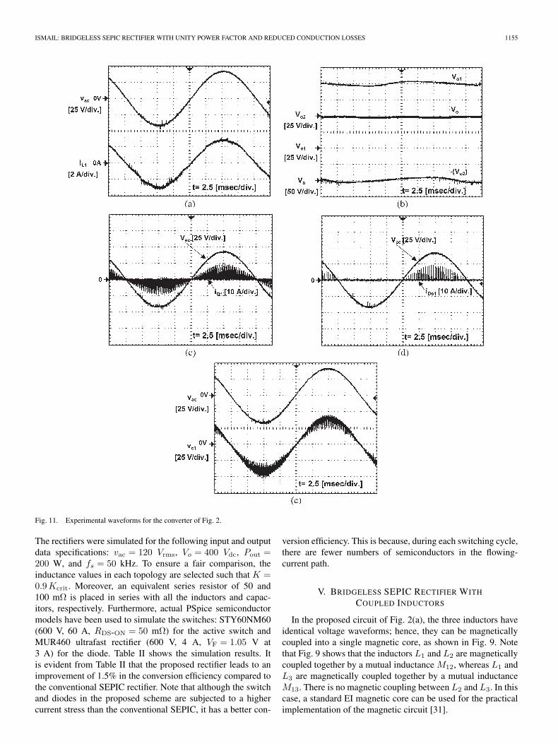
Fig. 11. Experimental waveforms for the converter of Fig. 2.
The rectifiers were simulated for the following input and outputdata specifications: vac = 120 Vrms, Vo = 400 Vdc, Pout =200 W, and fs = 50 kHz. To ensure a fair comparison, theinductance values in each topology are selected such that K =0.9Kcrit. Moreover, an equivalent series resistor of 50 and100 mΩ is placed in series with all the inductors and capac-itors, respectively. Furthermore, actual PSpice semiconductormodels have been used to simulate the switches: STY60NM60(600 V, 60 A, RDS-ON = 50 mΩ) for the active switch andMUR460 ultrafast rectifier (600 V, 4 A, VF = 1.05 V at3 A) for the diode. Table II shows the simulation results. Itis evident from Table II that the proposed rectifier leads to animprovement of 1.5% in the conversion efficiency compared tothe conventional SEPIC rectifier. Note that although the switchand diodes in the proposed scheme are subjected to a highercurrent stress than the conventional SEPIC, it has a better con-
version efficiency. This is because, during each switching cycle,there are fewer numbers of semiconductors in the flowing-current path.
V. BRIDGELESS SEPIC RECTIFIER WITH
COUPLED INDUCTORS
In the proposed circuit of Fig. 2(a), the three inductors haveidentical voltage waveforms; hence, they can be magneticallycoupled into a single magnetic core, as shown in Fig. 9. Notethat Fig. 9 shows that the inductors L1 and L2 are magneticallycoupled together by a mutual inductance M12, whereas L1 andL3 are magnetically coupled together by a mutual inductanceM13. There is no magnetic coupling between L2 and L3. In thiscase, a standard EI magnetic core can be used for the practicalimplementation of the magnetic circuit [31].

1156 IEEE TRANSACTIONS ON INDUSTRIAL ELECTRONICS, VOL. 56, NO. 4, APRIL 2009
The topological stages for the coupled inductor circuit ofFig. 9 are similar to the three topological stages for the uncou-pled case (Fig. 3). Referring to Fig. 9, k12 and k13 represent thecoupling coefficient between L1–L2 and L1–L3, respectively.By proper coupling between the three windings, it is possible toobtain an input current having very low high-frequency content(near-zero current ripples). This can be demonstrated by writingthe characteristic equations of the coupled inductors L1, L2,and L3 during switch-on time which is given by
d
dt
⎡⎣iL1
iL2
iL3
⎤⎦=
1Δ
⎡⎣ L2L3 −M12L3 −L2M13
−M12L3 L1L3−M213 M12M13
−L2M13 M12M13 L1L2−M212
⎤⎦⎡⎣vac
vC1
vC2
⎤⎦
(38)
where
Δ = L1L2L3 − L2M213 − L3M
212 > 0 (39)
M12 = k12
√L1L2, (0 < k12 < 1) (40)
M13 = k13
√L1L3, (0 < K13 < 1). (41)
Note that (39) must be positive since the total inductancematrix is symmetric positive definite, i.e., it has a positivedeterminant. At steady state, vC1 = vC2 = vac, and then from(38), the following condition must be satisfied for zero currentripples in the input current:
diL1
dt= 0 ⇒ L2L3 − L3M12 − L2M13 = 0. (42)
During switch-off time, one can show that the condition forzero current ripples in the input current is similar to (42).
It should be mentioned here that the steady-state analysispresented in Sections II and III for the uncoupled inductorsis also valid for the coupled-inductor extension, except for thedefinition of the effective inductance Le (3). This is becauseonly the inductors L2 and L3 determine the switching currentripple. Thus, for the coupled-inductor case, the definition of Le
becomes
Le =L2L3
L2 + L3. (43)
In the proposed topology, it is preferred that inductors L2 andL3 have equal values so that they carry the same ripple current.In this case, the condition in (39) and (42) reduces to
k212 + k2
13 < 1 (44)
M12 + M13 =L2 ⇒ k12 + k13 =√
L2
L1(45)
respectively. To demonstrate the effect of coupling the inductorson the input current, the circuit of Fig. 9 has been simulatedusing PSpice for the same power stage specifications and underthe same operating condition (i.e., for the same value of Ke)and with the same capacitor values mentioned in Section IV.The parameters of the coupled inductors used are L1 = 900 μH,L2 = L3 = 358.2 μH, and k12 = k13 = 0.315.
The simulated input voltage and input current waveforms areshown in Fig. 10(a), while the waveforms of the three induc-tor currents at a peak input voltage during several switching
Fig. 12. Experimental waveforms for the converter of Fig. 2 during a fewswitching periods.
periods are shown in Fig. 10(b). It is evident from Fig. 10that the high-frequency switching ripple current is significantlysuppressed due to the coupling of the three inductors. Thus, thegenerated EMI noise level is greatly minimized, as well as therequirement for input filtering.
VI. EXPERIMENTAL RESULTS
A laboratory prototype, whose parameters are listed inTable III, has been constructed to evaluate the performance ofthe proposed scheme of Fig. 2. In addition, a 68-μF capacitoris connected across the load to improve the ripple percentage.It should be mentioned here that the experimental circuit isnot optimized for maximum efficiency since the choice of theparameters is based on the availability of off-the-shelf compo-nents. The experimental waveforms of the converter at full loadare shown in Figs. 11 and 12. The input voltage and input linecurrent (iL1) waveforms are shown in Fig. 11(a). The input linecurrent waveform is obtained without utilizing an input filterand results in a measured THD of about 2.5%. Fig. 11(b) showsthe voltages across the output capacitors Co1 and Co2 and theload. It is evident that the output voltage is almost evenly splitbetween Co1 and Co2. The measured output voltage is 198.2 Vwith a 5.7-V peak–peak voltage ripple. The low-frequencycurrent envelope of the active switch iQ1 and the output diodeiDo1 are shown in Fig. 11(c) and (d), respectively. Note that thepeak switch and diode current fulfill the theoretical predictedresults shown in Table I. Fig. 11(e) shows the input voltage andthe voltage across the capacitor C1. It can be observed from

ISMAIL: BRIDGELESS SEPIC RECTIFIER WITH UNITY POWER FACTOR AND REDUCED CONDUCTION LOSSES 1157
Fig. 11(e) that the capacitor voltage vC1 closely tracks the inputvoltage vac. On the other hand, Fig. 12 shows the experimentalwaveforms over a few switching periods. The switch-gatingsignals (VGS) and the discontinuous inductor currents (iL1,iL2, and iL3) are shown in Fig. 12(a), whereas the blockingvoltages of the switch Q1 and diodes Do1 and Do2 are shownin Fig. 12(b). The experimental results are in good agreementwith the theoretical predictions. Finally, the measured full-loadefficiency is about 91.8%, which can be further improved byutilizing better components and improving the PCB layout.
VII. CONCLUSION
In this paper, a simple single-phase bridgeless SEPIC recti-fier with low input current distortion and low conduction losseshas been proposed and verified experimentally. Comparisonsare made between the proposed topology and the conventionalSEPIC. The main features of the proposed converters includehigh efficiency, low voltage stress on the semiconductor de-vices, and simplicity of design. These advantages are desirablefeatures for high-power and high-voltage applications. Theproposed bridgeless PFC configuration, as described in thispaper, has been implemented to verify the performance of thesystem. The measured THD was 2.5% with power conversionefficiency close to 92%. Finally, the proposed concept can beextended easily to other power conversion systems to satisfythe requirement of high-voltage demands.
REFERENCES
[1] C. Qiao and K. M. Smedley, “A topology survey of single-stage powerfactor corrector with a boost type input-current-shaper,” IEEE Trans.Power Electron., vol. 16, no. 3, pp. 360–368, May 2001.
[2] O. Gracia, J. A. Cobos, R. Prieto, and J. Uceda, “Single phase powerfactor correction: A survey,” IEEE Trans. Power Electron., vol. 18, no. 3,pp. 749–755, May 2003.
[3] M. M. Jovanovic and Y. Jang, “State-of-the-art, single-phase, ac-tive power-factor-correction techniques for high-power applications—Anoverview,” IEEE Trans. Ind. Electron., vol. 52, no. 3, pp. 701–708,Jun. 2005.
[4] J. A. Villarejo, J. Sebastian, F. Soto, and E. de Jódar, “Optimizing the de-sign of single-stage power-factor correctors,” IEEE Trans. Ind. Electron.,vol. 54, no. 3, pp. 1472–1482, Jun. 2007.
[5] Limits for Harmonic Current Emissions (Equipment Input Current ≤ 16A per Phase), EMC Part 3-2, 3rd edition. IEC 61000-3-2, Nov. 2005.
[6] R. W. Erickson and D. Maksimovic, Fundamentals of Power Electronics,2nd ed. Norwell, MA: Kluwer, 2001.
[7] D. M. Mitchell, “AC–DC converter having an improved power factor,”U.S. Patent 4 412 277, Oct. 25, 1983.
[8] J. C. Salmon, “Circuit topologies for single-phase voltage-doubler boostrectifiers,” in Proc. IEEE Appl. Power Electron. Conf., Mar. 1992,pp. 549–556.
[9] D. Tollik and A. Pietkiewicz, “Comparative analysis of 1-phase ac-tive power factor correction topologies,” in Proc. INTELEC, Oct. 1992,pp. 517–523.
[10] P. N. Enjeti and R. Martinez, “A high performance single phase AC to DCrectifier with input power factor correction,” in Proc. IEEE Appl. PowerElectron. Conf., May 1993, pp. 190–195.
[11] A. F. Souza and I. Barbi, “A new ZVS-PWM unity power factor rectifierwith reduced conduction losses,” IEEE Trans. Power Electron., vol. 10,no. 6, pp. 746–752, Nov. 1995.
[12] J. C. Salmon, “Circuit topologies for PWM boost rectifiers operated from1-phase and 3-phase ac supplies and using either single or split dc railvoltage outputs,” in Proc. IEEE Appl. Power Electron., Mar. 1995,pp. 473–479.
[13] A. F. Souza and I. Barbi, “A new ZVS semiresonant high power factorrectifier with reduced conduction losses,” IEEE Trans. Ind. Electron.,vol. 46, no. 1, pp. 82–90, Feb. 1999.
[14] A. F. Souza and I. Barbi, “High power factor rectifier with reduced con-duction and commutation losses,” in Proc. INTELEC, Jun. 1999, pp. 1–8.
[15] J. Liu, W. Chen, J. Zhang, D. Xu, and F. C. Lee, “Evaluation ofpower losses in different CCM mode single-phase boost PFC con-verters via simulation tool,” in Proc. IEEE Ind. Appl. Conf., Sep. 2001,pp. 2455–2459.
[16] U. Moriconi, “A bridgeless PFC configuration based on L4981 PFCcontroller,” Application Note AN 1606, pp. 1/18–18/18, Nov. 2002,ST-Microelectronics.
[17] C. M. Wang, “A novel zero-voltage switching PWM boost rectifierwith high power factor and low conduction losses,” in Proc. INTELEC,Oct. 2003, pp. 224–229.
[18] G. Moschopoulos and P. Jain, “A novel single-phase soft-switched recti-fier with unity power factor and minimal component count,” IEEE Trans.Ind. Electron., vol. 51, no. 3, pp. 566–576, Jun. 2004.
[19] T. Ernö and M. Frisch, “Second generation of PFC solutions,” PowerElectron. Europe, no. 7, pp. 33–35, 2004.
[20] H. Ye, Z. Yang, J. Dai, C. Yan, X. Xin, and J. Ying, “Common modenoise modeling and analysis of dual boost PFC circuit,” in Proc. Int.Telecommun. Energy Conf., Sep. 2004, pp. 575–582.
[21] B. Lu, R. Brown, and M. Soldano, “Bridgeless PFC implementation usingone cycle control technique,” in Proc. IEEE Appl. Power Electron. Conf.,Mar. 2005, pp. 812–817.
[22] P. Kong, S. Wang, and F. C. Lee, “Common mode EMI noise suppressionin bridgeless boost PFC converter,” in Proc. CPES Power Electron. Conf.,Apr. 2006, pp. 65–70.
[23] W.-Y. Choi, J.-M. Kwon, E.-H. Kim, J.-J. Lee, and B.-H. Kwon,“Bridgeless boost rectifier with low conduction losses and reduced diodereverse-recovery problems,” IEEE Trans. Ind. Electron., vol. 54, no. 2,pp. 769–780, Apr. 2007.
[24] C.-M. Wang, “A novel single-stage high-power-factor electronic ballastwith symmetrical half-bridge topology,” IEEE Trans. Ind. Electron.,vol. 55, no. 2, pp. 969–972, Feb. 2008.
[25] L. Huber, Y. Jang, and M. M. Jovanovic, “Performance evaluation ofbridgeless PFC boost rectifiers,” in Proc. IEEE Appl. Power Electron.Conf., Feb. 2007, pp. 165–171.
[26] J. Sebastian, J. Uceda, J. A. Cobos, J. Arau, and F. Aldana, “Improvingpower factor correction in distributed power supply systems using PWMand ZCS-QR SEPIC topologies,” in Proc. IEEE Power Electron. Spec.Conf., 1991, pp. 780–791.
[27] M. Brkovic and S. Cuk, “Input current shaper using Cuk converter,” inProc. Int. Telecommun. Energy Conf., 1992, pp. 532–539.
[28] D. S. L. Simonetti, J. Sebastian, and J. Uceda, “The discontinuousconduction mode Sepic and Cuk power factor preregulators: Analysisand design,” IEEE Trans. Ind. Electron., vol. 44, no. 5, pp. 630–637,Oct. 1997.
[29] G. Spiazzi and L. Rosseto, “High-quality rectifier based on coupled-inductor Sepic topology,” in Proc. IEEE Appl. Power Electron. Conf.,1994, pp. 336–341.
[30] F. S. Dos Reis, J. Sebastian, and J. Uceda, “Characterization of conductednoise generation for Sepic, Cuk and Boost converters working as powerfactor preregulators,” in Proc. IEEE IECON, pp. 965–970.
[31] S. Cuk, “A new zero-ripple switching DC-to-DC converter and inte-grated magnetics,” IEEE Trans. Magn., vol. MAG-19, no. 2, pp. 57–75,Mar. 1983.
Esam H. Ismail (M’93–SM’07) received the B.S.(magna cum laude) and M.S. degrees in electricalengineering from the University of Dayton, Dayton,OH, in 1983 and 1985, respectively, and the Ph.D.degree in electrical engineering from the Universityof Colorado, Boulder, in 1993.
From 1985–1988, he was a Lecturer with theCollege of Technological Studies, Al-Shaab, Kuwait,where he is currently an Associate Professor withthe Department of Electrical Engineering. Hisresearch interests include single- and three-phase
low-harmonic rectification, high-frequency power conversion, soft-switchingtechniques, and the development of new converter topologies.
Dr. Ismail was an Assistant Deputy Director General for Applied Educationand Research with the Public Authority for Applied Education and Trainingfrom 2000 to 2005. He is a member of Tau Beta Pi.