BOXER-6404 - IIS Windows Server
81
Last Updated: April 9, 2020 BOXER-6404 Embedded Box PC User’s Manual 5 th Ed
-
Upload
khangminh22 -
Category
Documents
-
view
0 -
download
0
Transcript of BOXER-6404 - IIS Windows Server

Last Updated: April 9, 2020
BOXER-6404
Embedded Box PC
User ’s Manual 5th Ed

Preface II
Em
bed
ded
Box P
C
BO
XER
-6404
Copyright Notice
This document is copyrighted, 2020. All rights are reserved. The original manufacturer
reserves the right to make improvements to the products described in this manual at
any time without notice.
No part of this manual may be reproduced, copied, translated, or transmitted in any
form or by any means without the prior written permission of the original
manufacturer. Information provided in this manual is intended to be accurate and
reliable. However, the original manufacturer assumes no responsibility for its use, or for
any infringements upon the rights of third parties that may result from its use.
The material in this document is for product information only and is subject to change
without notice. While reasonable efforts have been made in the preparation of this
document to assure its accuracy, AAEON assumes no liabilities resulting from errors or
omissions in this document, or from the use of the information contained herein.
AAEON reserves the right to make changes in the product design without notice to its
users.

Preface III
Em
bed
ded
Box P
C
BO
XER
-6404
Acknowledgements
All other products’ name or trademarks are properties of their respective owners.
⚫ Microsoft Windows® is a registered trademark of Microsoft Corp.
⚫ Intel® and Celeron® are registered trademarks of Intel Corporation
⚫ ITE is a trademark of Integrated Technology Express, Inc.
⚫ IBM, PC/AT, PS/2, and VGA are trademarks of International Business Machines
Corporation.
All other product names or trademarks are properties of their respective owners.

Preface IV
Em
bed
ded
Box P
C
BO
XER
-6404
Packing List
Before setting up your product, please make sure the following items have been
shipped:
Item Quantity
⚫ BOXER-6404 1
⚫ Power Adapter 1
If any of these items are missing or damaged, please contact your distributor or sales
representative immediately.

Preface V
Em
bed
ded
Box P
C
BO
XER
-6404
About this Document
This User’s Manual contains all the essential information, such as detailed descriptions
and explanations on the product’s hardware and software features (if any), its
specifications, dimensions, jumper/connector settings/definitions, and driver
installation instructions (if any), to facilitate users in setting up their product.
Users may refer to the product page at AAEON.com for the latest version of this
document.

Preface VI
Em
bed
ded
Box P
C
BO
XER
-6404
Safety Precautions
Please read the following safety instructions carefully. It is advised that you keep this
manual for future references
1. All cautions and warnings on the device should be noted.
2. Make sure the power source matches the power rating of the device.
3. Position the power cord so that people cannot step on it. Do not place anything
over the power cord.
4. Always completely disconnect the power before working on the system’s
hardware.
5. No connections should be made when the system is powered as a sudden rush
of power may damage sensitive electronic components.
6. If the device is not to be used for a long time, disconnect it from the power
supply to avoid damage by transient over-voltage.
7. Always disconnect this device from any AC supply before cleaning.
8. While cleaning, use a damp cloth instead of liquid or spray detergents.
9. Make sure the device is installed near a power outlet and is easily accessible.
10. Keep this device away from humidity.
11. Place the device on a solid surface during installation to prevent falls
12. Do not cover the openings on the device to ensure optimal heat dissipation.
13. Watch out for high temperatures when the system is running.
14. Do not touch the heat sink or heat spreader when the system is running
15. Never pour any liquid into the openings. This could cause fire or electric shock.
16. As most electronic components are sensitive to static electrical charge, be sure
to ground yourself to prevent static charge when installing the internal
components. Use a grounding wrist strap and contain all electronic components
in any static-shielded containers.

Preface VII
Em
bed
ded
Box P
C
BO
XER
-6404
17. If any of the following situations arises, please the contact our service personnel:
i. Damaged power cord or plug
ii. Liquid intrusion to the device
iii. Exposure to moisture
iv. Device is not working as expected or in a manner as described in
this manual
v. The device is dropped or damaged
vi. Any obvious signs of damage displayed on the device
18. DO NOT LEAVE THIS DEVICE IN AN UNCONTROLLED ENVIRONMENT WHERE
THE STORAGE TEMPERATURE IS BELOW -20° C (-4°F) OR ABOVE 60°C (140°F)
TO PREVENT DAMAGE.

Preface VIII
Em
bed
ded
Box P
C
BO
XER
-6404
FCC Statement
This device complies with Part 15 FCC Rules. Operation is
subject to the following two conditions: (1) this device may not
cause harmful interference, and (2) this device must accept
any interference received including interference that may
cause undesired operation.
Caution:
There is a danger of explosion if the battery is incorrectly replaced. Replace only with the
same or equivalent type recommended by the manufacturer. Dispose of used batteries
according to the manufacturer’s instructions and your local government’s recycling or
disposal directives.
Attention:
Il y a un risque d’explosion si la batterie est remplacée de façon incorrecte.
Ne la remplacer qu’avec le même modèle ou équivalent recommandé par le
constructeur. Recycler les batteries usées en accord avec les instructions du fabricant et
les directives gouvernementales de recyclage.

Preface IX
Em
bed
ded
Box P
C
BO
XER
-6404
China RoHS Requirements (CN)
产品中有毒有害物质或元素名称及含量
AAEON System QO4-381 Rev.A0
部件名称
有毒有害物质或元素
铅
(Pb)
汞
(Hg)
镉
(Cd)
六价铬
(Cr(VI))
多溴联苯
(PBB)
多溴二苯
醚(PBDE)
印刷电路板
及其电子组件 × ○ ○ ○ ○ ○
外部信号
连接器及线材 × ○ ○ ○ ○ ○
外壳 ○ ○ ○ ○ ○ ○
中央处理器
与内存 × ○ ○ ○ ○ ○
硬盘 × ○ ○ ○ ○ ○
液晶模块 × × ○ ○ ○ ○
光驱 × ○ ○ ○ ○ ○
触控模块 × ○ ○ ○ ○ ○
电源 × ○ ○ ○ ○ ○
电池 × ○ ○ ○ ○ ○
本表格依据 SJ/T 11364 的规定编制。
○:表示该有毒有害物质在该部件所有均质材料中的含量均在
GB/T 26572标准规定的限量要求以下。
×:表示该有害物质的某一均质材料超出了GB/T 26572的限量要求,然而该
部件
仍符合欧盟指令2011/65/EU 的规范。
备注:
一、此产品所标示之环保使用期限,系指在一般正常使用状况下。
二、上述部件物质中央处理器、内存、硬盘、光驱、电源为选购品。
三、上述部件物质液晶模块、触控模块仅一体机产品适用。

Preface X
Em
bed
ded
Box P
C
BO
XER
-6404
China RoHS Requirement (EN)
Hazardous and Toxic Materials List
AAEON System QO4-381 Rev.A0
Component
Name
Hazardous or Toxic Materials or Elements
Lead
(Pb
)
Mercu
ry
(Hg
)
Cad
miu
m
(Cd
)
Hexa
vale
nt
Chro
miu
m
(Cr(V
I))
Po
lybro
min
at
ed
bip
henyls
(PBBs)
Po
lybro
min
at
ed
dip
henyl
eth
ers
(PBD
Es)
PCB and
Components X O O O O O
Wires &
Connectors for
Ext.Connections
X O O O O O
Chassis O O O O O O
CPU & RAM X O O O O O
HDD Drive X O O O O O
LCD Module X X O O O O
Optical Drive X O O O O O
Touch Control
Module X O O O O O
PSU X O O O O O
Battery X O O O O O
This form is prepared in compliance with the provisions of SJ/T 11364.
O: The level of toxic or hazardous materials present in this component and its parts is below the
limit specified by GB/T 26572.
X: The level of toxic of hazardous materials present in the component exceed the limits specified
by GB/T 26572, but is still in compliance with EU Directive 2011/65/EU (RoHS 2).
Notes:
1. The Environment Friendly Use Period indicated by labelling on this product is applicable only
to use under normal conditions.
2. Individual components including the CPU, RAM/memory, HDD, optical drive, and PSU are
optional.
3. LCD Module and Touch Control Module only applies to certain products which feature these
components.

Preface XI
Em
bed
ded
Box P
C
BO
XER
-6404
Table of Contents
Chapter 1 - Product Specifications ........................................................................................ 1
1.1 Specifications ............................................................................................................ 2
Chapter 2 – Hardware Information ....................................................................................... 4
2.1 Dimensions ............................................................................................................... 5
2.2 List of Jumpers ......................................................................................................... 6
2.2.1 Clear CMOS Jumper (JP12, pin 1,3,5) ................................................... 6
2.2.2 Auto Power Button Enable/ Disable Selection (JP12, pin 2,4,6) ...... 6
2.2.3 Push Power Button with Orange LED (SW1) ........................................ 7
2.3 List of Connectors ................................................................................................... 8
2.3.1 COM Port RS-232 (CN1) ......................................................................... 9
2.3.2 +12 V Input (CN2) .................................................................................... 9
2.3.3 LAN (RJ-45) Port 1,2,3,4 (JP3,4,5,6) ..................................................... 10
2.3.4 +5 V Output for SATA HDD (CN7) ...................................................... 10
2.3.5 SATA Port (CN8) ........................................................................................ 11
2.3.6 DDR3L SO-DIMM Slot (CN9) ................................................................. 11
2.3.7 C-FAST Card Connector (CN11) ............................................................. 11
2.3.8 MiniCard Slot (CN13) (USB Port2 Only) .............................................. 12
2.3.9 Battery (CN14) .......................................................................................... 15
2.3.10 USB 3.0 Port 0 (CN17)............................................................................. 15
2.3.11 USB 2.0 Port 1, 3 (CN18,19) .................................................................... 16
2.3.12 HDMI Port 1, 2 (CN20,21) ....................................................................... 16
2.3.13 LPC Port (CN22) ...................................................................................... 17
2.3.14 SPI Programming Header (CN23) ....................................................... 18
2.4 Installing DRAM ...................................................................................................... 19
Chapter 3 - AMI BIOS Setup ................................................................................................ 21
3.1 System Test and Initialization .............................................................................. 22

Preface XII
Em
bed
ded
Box P
C
BO
XER
-6404
3.2 AMI BIOS Setup ..................................................................................................... 23
3.3 Setup Submenu: Main .......................................................................................... 24
3.4 Setup Submenu: Advanced ................................................................................ 25
3.4.1 Advanced: ACPI Settings ...................................................................... 26
3.4.2 Advanced: F81801 Super IO Configuration ....................................... 28
3.4.2.1 Super IO Configuration: Serial Port 1 Configuration ....... 29
3.4.3 Advanced: H/W Monitor ...................................................................... 30
3.4.4 Advanced: CPU Configuration ............................................................. 31
3.4.4.1 CPU Configuration: Socket 0 CPU Information ................ 32
3.4.5 Advanced: SATA Configuration ........................................................... 33
3.4.6 Advanced: USB Configuration ............................................................. 35
3.5 Setup Submenu: Chipset ..................................................................................... 37
3.5.1 Chipset: North Bridge ........................................................................... 38
3.5.2 Chipset: South Bridge ............................................................................ 39
3.5.2.1 South Bridge: USB Configuration (Default Setting) ......... 40
3.6 Setup Submenu: Security ..................................................................................... 41
3.7 Setup Submenu: Boot .......................................................................................... 42
3.8 Setup Submenu: Save & Exit .............................................................................. 43
Chapter 4 – Drivers Installation ...........................................................................................44
4.1 Drivers Download and Installation..................................................................... 45
Appendix A - Watchdog Timer Programming................................................................... 47
A.1 Watchdog Timer Initial Program ........................................................................ 48
A.2 Watchdog Sample Program ............................................................................... 49
Appendix B - I/O Information .............................................................................................. 52
B.1 I/O Address Map ................................................................................................... 53
B.2 Memory Address Map ......................................................................................... 55
B.3 IRQ Mapping Chart .............................................................................................. 56
Appendix C – Electrical Specifications for I/O Ports .......................................................... 67

Preface XIII
Em
bed
ded
Box P
C
BO
XER
-6404
C.1 Electrical Specifications for I/O Ports ................................................................ 68

Em
bed
ded
Box P
C
BO
XER
-6404
Chapter 1
Chapter 1 - Product Specifications

Chapter 1 – Product Specifications 2
Em
bed
ded
Box P
C
BO
XER
-6404
1.1 Specifications
System
CPU Intel® Celeron™ J1900, 2.0 GHz
Intel® Celeron™ N2807, 1.58 GHz
Chipset Intel® System on Chip
System Memory DDR3L 1333 SODIMM slot x 1, up to 8 GB
(J1900) or 4 GB (N2807)
Display Interface HDMI (max. 1920 x 1080)
Storage Device CFast™
Ethernet Intel® I211, 10/100/1000Base-TX x 4
I/O RS-232 x 1
USB 2.0 x 2
USB 3.0 x 1
HDMI x 2 LAN x 4
CFast slot x 1
Antenna holes x 1
Power button
Power input
Expansion Full-size Mini-Card (USB interface only) x 1
Indicator Power LED on power button
OS support Windows® 10, Windows® 8.1, Windows® 7,
Windows® Embedded 8, Windows®
Embedded 7, Linux Fedora

Chapter 1 – Product Specifications 3
Em
bed
ded
Box P
C
BO
XER
-6404
Power Supply
Power Requirement 12~24V with lockable DC jack
Mechanical
Mounting VESA (Mounting kit is optional)
DIN rail (Mounting kit is optional)
Dimensions (W x H x D) 6.53" x 4.20" x 1.18" (166 mm x 106.6 mm x 30
mm)
Gross Weight 2.9 lbs. (1.3 kg)
Net Weight 1.9 lbs. (0.86 kg)
Environmental
Operating Temperature -22°F ~ 149°F (-30°C ~ 65°C) with wide
temperature CFast™ card (according to
IEC68-2-14 with 0.5 m/s air flow; with industrial
devices)
Storage Temperature -22°F ~ 176°F (-30°C ~ 80°C)
Storage Humidity 95% @ 40°C, non-condensing
Anti-Vibration 5 Grms/ 5 ~ 500Hz/ operation –CFast™ card
Certification CE/FCC class A

Em
bed
ded
Box P
C
BO
XER
-6404
Chapter 2
Chapter 2 – Hardware Information

Chapter 2 – Hardware Information 5
Em
bed
ded
Box P
C
BO
XER
-6404
2.1 Dimensions

Chapter 2 – Hardware Information 6
Em
bed
ded
Box P
C
BO
XER
-6404
2.2 List of Jumpers
Please refer to the table below for all of the system’s jumpers that you can configure
for your application
Label Function
JP12 (1,3,5) Clear CMOS Jumper
JP12 (2,4,6) Auto Power Button Enable/ Disable Selection
SW1 Push Power Button with Orange LED
2.2.1 Clear CMOS Jumper (JP12, pin 1,3,5)
Normal (Default) Clear CMOS
2.2.2 Auto Power Button Enable/ Disable Selection (JP12, pin 2,4,6)
Enable Disable (Default)

Chapter 2 – Hardware Information 7
Em
bed
ded
Box P
C
BO
XER
-6404
2.2.3 Push Power Button with Orange LED (SW1)
Pin Pin Name Signal Type Signal Level
L1 +V5S IN +5V
L2 GND GND GND
1 NC
2 PWRBTN# OUT
3 GND GND GND
4 NC
5 NC
6 NC

Chapter 2 – Hardware Information 8
Em
bed
ded
Box P
C
BO
XER
-6404
2.3 List of Connectors
Please refer to the table below for all of the system’s connectors that you can configure
for your application
Label Function
CN1 COM port RS-232
CN2 +12 V Input
CN3 LAN (RJ-45) Port
CN4 LAN (RJ-45) Port
CN5 LAN (RJ-45) Port
CN6 LAN (RJ-45) Port
CN7 +5V Output for SATA HDD
CN8 SATA Port
CN9 DDR3L SO-DIMM Slot
CN11 C-FAST CARD Connector
CN13 MiniCard Slot (USB2.0 port 2 ONLY)
CN14 Battery
CN17 USB3.0 port 0
CN18 USB2.0 port 3
CN19 USB2.0 port 1
CN20 HDMI1 Port
CN21 HDMI 2 Port
CN22 LPC Expansion Connector
CN23 SPI Programming Header

Chapter 2 – Hardware Information 9
Em
bed
ded
Box P
C
BO
XER
-6404
2.3.1 COM Port RS-232 (CN1)
Pin Pin Name Signal Type Signal Level
1 DCD IN
2 RX IN
3 TX OUT ±9V
4 DTR OUT ±9V
5 GND GND
6 DSR IN
7 RTS OUT ±9V
8 CTS IN
9 RI IN
2.3.2 +12 V Input (CN2)
Pin Pin Name Signal Type Signal Level
1 +12 V PWR +12 V
2-3 GND GND

Chapter 2 – Hardware Information 10
Em
bed
ded
Box P
C
BO
XER
-6404
2.3.3 LAN (RJ-45) Port 1,2,3,4 (JP3,4,5,6)
Pin Pin Name Signal Type Signal Level
C1 MDI0+ DIFF
C2 MDI0- DIFF
C3 MDI1+ DIFF
C4 MDI2+ DIFF
C5 MDI2- DIFF
C6 MDI1- DIFF
C7 MDI3+ DIFF
C8 MDI3- DIFF
2.3.4 +5 V Output for SATA HDD (CN7)
Pin Pin Name Signal Type Signal Level
1 +V5S PWR +5V
2 GND GND
+5V
GND

Chapter 2 – Hardware Information 11
Em
bed
ded
Box P
C
BO
XER
-6404
2.3.5 SATA Port (CN8)
Pin Pin Name Signal Type Signal Level
1 GND GND
2 SATA_TXP1 DIFF
3 SATA_TXN1 DIFF
4 GND GND
5 SATA_RXN1 DIFF
6 SATA_RXP1 DIFF
7 GND GND
2.3.6 DDR3L SO-DIMM Slot (CN9)
Standard Specification
2.3.7 C-FAST Card Connector (CN11)
Pin Pin Name Signal Type Signal Level
S1 GND GND
S2 SATA_TXP0 DIFF
S3 SATA_TXN0 DIFF
S4 GND GND
S5 SATA_RXN0 DIFF
S6 SATA_RXP0 DIFF
S7 GND GND
Pin 1 Pin 7

Chapter 2 – Hardware Information 12
Em
bed
ded
Box P
C
BO
XER
-6404
Pin Pin Name Signal Type Signal Level
P1 NC
P2 GND GND
P3 NC
P4 NC
P5 NC
P6 NC
P7 GND GND
P8 CFD_LED# OUT +3.3 V
P9 NC
P10 NC
P11 NC
P12 NC
P13 +V3.3S PWR +3.3 V
P14 +V3.3S PWR +3.3 V
P15 GND GND
P16 GND GND
P17 NC
2.3.8 MiniCard Slot (CN13) (USB Port2 Only)
Pin Pin Name Signal Type Signal Level
1 WAKE_PCIE0#_3P3 IN
2 +V3.3A PWR +3.3 V
3 NC
4 GND GND
5 NC

Chapter 2 – Hardware Information 13
Em
bed
ded
Box P
C
BO
XER
-6404
Pin Pin Name Signal Type Signal Level
6 +V1.5S PWR +1.5 V
7 NC IN
8 NC PWR
9 GND GND
10 NC I/O
11 NC DIFF
12 NC IN
13 NC DIFF
14 NC IN
15 GND GND
16 NC PWR
17 NC
18 GND GND
19 NC
20 WL_DISABLED0# OUT +3.3 V
21 GND GND
22 BUF_PLT_RST# OUT +3.3 V
23 NC DIFF
24 +V3.3A PWR +3.3 V
25 NC DIFF
26 GND GND
27 GND GND
28 +V1.5S PWR +1.5 V
29 GND GND
30 SMB_CLK_3P3_FA I/O +3.3 V
31 NC DIFF

Chapter 2 – Hardware Information 14
Em
bed
ded
Box P
C
BO
XER
-6404
Pin Pin Name Signal Type Signal Level
32 SMB_DATA_3P3_FA I/O +3.3 V
33 NC DIFF
34 GND GND
35 GND GND
36 USB_DN2 DIFF
37 GND GND
38 USB_DP2 DIFF
39 +V3.3A PWR +3.3 V
40 GND GND
41 +V3.3A PWR +3.3 V
42 NC
43 NC
44 NC
45 NC
46 NC
47 NC
48 +V1.5S PWR +1.5 V
49 NC
50 GND GND
51 NC
52 +V3.3A PWR +3.3 V

Chapter 2 – Hardware Information 15
Em
bed
ded
Box P
C
BO
XER
-6404
2.3.9 Battery (CN14)
Pin Pin Name Signal Type Signal Level
1 +3.3 V PWR 3.3 V
2 GND GND
2.3.10 USB 3.0 Port 0 (CN17)
Pin Pin Name Signal Type Signal Level
1 +5VSB PWR +5 V
2 USB0_D- DIFF
3 USB0_D+ DIFF
4 GND GND
5 USB0_SSRX− DIFF
6 USB0_SSRX+ DIFF
7 GND GND
8 USB0_SSTX- DIFF
9 USB0_SSTX+ DIFF

Chapter 2 – Hardware Information 16
Em
bed
ded
Box P
C
BO
XER
-6404
2.3.11 USB 2.0 Port 1, 3 (CN18,19)
Standard USB Connector
Pin Pin Name Signal Type Signal Level
1 +5VSB PWR +5 V
2 USB1_D- DIFF
3 USB1_D+ DIFF
4 GND GND
2.3.12 HDMI Port 1, 2 (CN20,21)
Pin Pin Name Signal Type Signal Level
1 TMDS_DAT2+ DIFF
2 GND GND
3 TMDS_DAT2- DIFF
4 TMDS_DAT1+ DIFF
5 GND GND
6 TMDS_DAT1- DIFF
7 TMDS_DAT0+ DIFF
8 GND GND
9 TMDS_DAT0- DIFF
10 TMDS_CLK+ DIFF
11 GND GND
1
218
19

Chapter 2 – Hardware Information 17
Em
bed
ded
Box P
C
BO
XER
-6404
Pin Pin Name Signal Type Signal Level
12 TMDS_CLK- DIFF
13 NC
14 NC
15 DDC_CLK I/O +5 V
16 DDC_DATA I/O +5 V
17 GND GND
18 +5V I/O +5 V
19 HPLG_DETECT IN
2.3.13 LPC Port (CN22)
Pin Pin Name Signal Type Signal Level
1 LAD0 I/O +3.3 V
2 LAD1 I/O +3.3 V
3 LAD2 I/O +3.3 V
4 LAD3 I/O +3.3 V
5 +V3.3S PWR +3.3 V
6 LFRAME# IN
7 LRESET# OUT +3.3 V
8 GND GND
9 LCLK OUT

Chapter 2 – Hardware Information 18
Em
bed
ded
Box P
C
BO
XER
-6404
Pin Pin Name Signal Type Signal Level
10 LDRQ0 IN
11 LDRQ1 IN
12 SERIRQ I/O +3.3 V
2.3.14 SPI Programming Header (CN23)
Pin Pin Name Signal Type Signal Level
1 SPI_SO_F OUT
2 GND GND
3 SPI_CLK_F IN
4 +V3.3A_SPI PWR +3.3 V
5 SPI_SI_F IN
6 SPI_CS0#_F IN
7 NC

Chapter 2 – Hardware Information 19
Em
bed
ded
Box P
C
BO
XER
-6404
2.4 Installing DRAM
1. Remove the screws as shown below
2. Slot in the RAM diagonally into the slot, push down to secure.

Chapter 2 – Hardware Information 20
Em
bed
ded
Box P
C
BO
XER
-6404
3. Re-tighten the screws

Em
bed
ded
Box P
C
BO
XER
-6404
Chapter 3
Chapter 3 - AMI BIOS Setup

Chapter 3 – AMI BIOS Setup 22
Em
bed
ded
Box P
C
BO
XER
-6404
3.1 System Test and Initialization
The system uses certain routines to perform testing and initialization. If an error, fatal or
non-fatal, is encountered, a few short beeps or an error message will be outputted. The
board can usually continue the boot up sequence with non-fatal errors.
The system configuration verification routines check the current system configuration
against the values stored in the CMOS memory. If they do not match, an error message
will be outputted, in which case you will need to run the BIOS setup program to set the
configuration information in memory.
There are three situations in which you will need to change the CMOS settings:
- You are starting your system for the first time
- You have changed your system’s hardware
- The CMOS memory has lost power and the configuration information is erased
The system’s CMOS memory uses a backup battery for data retention, which is to be
replaced once emptied.
Chapter 3 – AMI BIOS Setup 23
Em
bed
ded
Box P
C
BO
XER
-6404
3.2 AMI BIOS Setup
The AMI BIOS ROM has a pre-installed Setup program that allows users to modify basic
system configurations, which is stored in the battery-backed CMOS RAM and BIOS
NVRAM so that the information is retained when the power is turned off.
To enter BIOS Setup, press <Del> or <F2> immediately while your computer is
powering up.
The function for each interface can be found below.
Main – Date and time can be set here. Press <Tab> to switch between date elements
Advanced – Enable/ Disable boot option for legacy network devices
Chipset – For hosting bridge parameters
Boot – Enable/ Disable quiet Boot Option
Security – The setup administrator password can be set here
Save & Exit –Save your changes and exit the program

Chapter 3 – AMI BIOS Setup 24
Em
bed
ded
Box P
C
BO
XER
-6404
3.3 Setup Submenu: Main

Chapter 3 – AMI BIOS Setup 25
Em
bed
ded
Box P
C
BO
XER
-6404
3.4 Setup Submenu: Advanced

Chapter 3 – AMI BIOS Setup 26
Em
bed
ded
Box P
C
BO
XER
-6404
3.4.1 Advanced: ACPI Settings
Options summary:
ACPI Sleep State Suspend Disabled
S3 (Suspend to RAM) Optimal Default, Failsafe Default
Select the highest ACPI sleep state the system will enter when the SUSPEND button is
pressed.
Restore AC Power
Loss
Power Off Optimal Default, Failsafe Default
Power On
Last State
Select AC power state when power is re-applied after a power failure
Power Mode ATX Type Optimal Default, Failsafe Default

Chapter 3 – AMI BIOS Setup 27
Em
bed
ded
Box P
C
BO
XER
-6404
AT Type
Select power supply mode
Wake on Ring Disabled Optimal Default, Failsafe Default
Enabled
En/Disabled wake from ring
Wake system with
Fixed Time
Disabled
Enabled
Enable or disable System wake on alarm event. Wake up time is setting by following
settings.
Wake up day 0-31
Select 0 for daily system wake up
Wake up hour 0-23
Wake up minute 0-59
Wake up second 0-59
Wake system with
Dynamic Time
Disabled
Enabled
Enable or disable System wake on alarm event. Wake up time is current time + Increase
minutes.
Wake up minute
increase
1-5

Chapter 3 – AMI BIOS Setup 28
Em
bed
ded
Box P
C
BO
XER
-6404
3.4.2 Advanced: F81801 Super IO Configuration
Options summary:
SATA Mode IDE Mode
AHCI Mode Optimal Default, Failsafe Default

Chapter 3 – AMI BIOS Setup 29
Em
bed
ded
Box P
C
BO
XER
-6404
3.4.2.1 Super IO Configuration: Serial Port 1 Configuration
Options summary:
Legacy USB Support Enabled Optimal Default, Failsafe Default
Disabled
Auto
Enables BIOS Support for Legacy USB Support. When enabled, USB can be functional
in legacy environment like DOS.
AUTO option disables legacy support if no USB devices are connected

Chapter 3 – AMI BIOS Setup 30
Em
bed
ded
Box P
C
BO
XER
-6404
3.4.3 Advanced: H/W Monitor

Chapter 3 – AMI BIOS Setup 31
Em
bed
ded
Box P
C
BO
XER
-6404
3.4.4 Advanced: CPU Configuration
Options summary:
Intel Virtualization
Technology
Disabled
Enabled Optimal Default, Failsafe Default
When enabled, a VMM can utilize the additional hardware capabilities provided by
Vander pool Technology
Chapter 3 – AMI BIOS Setup 32
Em
bed
ded
Box P
C
BO
XER
-6404
3.4.4.1 CPU Configuration: Socket 0 CPU Information
Options summary:
Power Mode ATX Type Optimal Default, Failsafe Default
AT Type
Select power supply mode.
AC Power Loss Last State Optimal Default, Failsafe Default
Power On
Power Off
Select power state when power is re-applied after a power failure.
RTC wake system
from S5
Disabled Optimal Default, Failsafe Default
Fixed Time
Dynamic Time
Enable or disable System wake on alarm event. When enabled, System will wake on the
hr::min::sec specified

Chapter 3 – AMI BIOS Setup 33
Em
bed
ded
Box P
C
BO
XER
-6404
3.4.5 Advanced: SATA Configuration
Options summary:
Serial-ATA (SATA) Enabled Default
Disabled
En/Disable SATA
SATA Speed Support Gen1
Gen2 Default
SATA Speed Support Gen1 or Gen2
SATA Mode IDE
AHCI Default

Chapter 3 – AMI BIOS Setup 34
Em
bed
ded
Box P
C
BO
XER
-6404
IDE: Configure SATA controllers as legacy IDE
AHCI: Configure SATA controllers to operate in AHCI mode
Serial-ATA Port 0 Enabled Default
Disabled
En/Disable SATA Port
SATA Port1 HotPlug Enabled
Disabled Default
En/Disable SATA Port Hotplug

Chapter 3 – AMI BIOS Setup 35
Em
bed
ded
Box P
C
BO
XER
-6404
3.4.6 Advanced: USB Configuration
Options summary:
Legacy USB Support Enabled Optimal Default, Failsafe Default
Disabled
Auto
Enables BIOS Support for Legacy USB Support. When enabled, USB can be functional
in legacy environment like DOS.
AUTO option disables legacy support if no USB devices are connected
Device Name (Emulation Auto Optimal Default, Failsafe Default

Chapter 3 – AMI BIOS Setup 36
Em
bed
ded
Box P
C
BO
XER
-6404
Type) Floppy
Forced FDD
Hard Disk
CDROM
If Auto. USB devices less than 530MB will be emulated as Floppy and remaining as
Floppy and remaining as hard drive. Forced FDD option can be used to force a HDD
formatted drive to boot as FDD(Ex. ZIP drive)

Chapter 3 – AMI BIOS Setup 37
Em
bed
ded
Box P
C
BO
XER
-6404
3.5 Setup Submenu: Chipset

Chapter 3 – AMI BIOS Setup 38
Em
bed
ded
Box P
C
BO
XER
-6404
3.5.1 Chipset: North Bridge
Options summary:
Primary IGFX Boot Display VBIOS Default Optimal Default, Failsafe Default
HDMI1
HDMI2
Select the Video device

Chapter 3 – AMI BIOS Setup 39
Em
bed
ded
Box P
C
BO
XER
-6404
3.5.2 Chipset: South Bridge
Chapter 3 – AMI BIOS Setup 40
Em
bed
ded
Box P
C
BO
XER
-6404
3.5.2.1 South Bridge: USB Configuration (Default Setting)

Chapter 3 – AMI BIOS Setup 41
Em
bed
ded
Box P
C
BO
XER
-6404
3.6 Setup Submenu: Security
Change User/Administrator Password
You can set an Administrator Password or User Password. An Administrator Password
must be set before you can set a User Password. The password will be required during
boot up, or when the user enters the Setup utility. A User Password does not provide
access to many of the features in the Setup utility.
Select the password you wish to set, and press Enter. In the dialog box, enter your
password (must be between 3 and 20 letters or numbers). Press Enter and retype your
password to confirm. Press Enter again to set the password.
Removing the Password
Select the password you want to remove and enter the current password. At the next
dialog box press Enter to disable password protection.
Chapter 3 – AMI BIOS Setup 42
Em
bed
ded
Box P
C
BO
XER
-6404
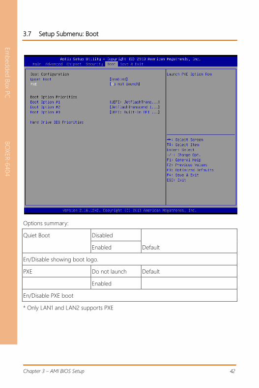
3.7 Setup Submenu: Boot
Options summary:
Quiet Boot Disabled
Enabled Default
En/Disable showing boot logo.
PXE Do not launch Default
Enabled
En/Disable PXE boot
* Only LAN1 and LAN2 supports PXE

Chapter 3 – AMI BIOS Setup 43
Em
bed
ded
Box P
C
BO
XER
-6404
3.8 Setup Submenu: Save & Exit

Em
bed
ded
Box P
C
BO
XER
-6404
Chapter 4
Chapter 4 – Drivers Installation

Chapter 4 – Driver Installation 45
Em
bed
ded
Box P
C
BO
XER
-6404
4.1 Drivers Download and Installation
Drivers for the BOXER-6404 can be downloaded from the product page on the AAEON
website by following this link:
https://www.aaeon.com/en/p/embedded-computers-boxer-6404
Download the driver(s) you need and follow the steps below to install them.
Step 1 – Install Chipset Drivers
1. Open the Step 1 - Chipset folder and select your OS
2. Open the SetupChipset.exe file in the folder
3. Follow the instructions
4. Drivers will be installed automatically
Step 2 – Install Graphics Driver
1. Open the Step 2 - VGA folder and select your OS
2. Open the Setup.exe file in the folder
3. Follow the instructions
4. Drivers will be installed automatically
Step 3 – Install Network Driver
1. Open the Step 3 - LAN folder and select your OS
2. Open the.exe file in the folder
3. Follow the instructions
4. Drivers will be installed automatically

Chapter 4 – Driver Installation 46
Em
bed
ded
Box P
C
BO
XER
-6404
Step 4 – Install TXE Driver (Windows 8.1/10 only)
1. Open the Step 4 - TXE folder and select your OS
2. Open the SetupTXE.exe file in the folder
3. Follow the instructions
4. Drivers will be installed automatically
Step 5 – Install USB 3.0 Drivers (Windows 7 only)
1. Open the Step 5 – USB 3.0 followed by the Setup.exe file
2. Follow the instructions
3. Drivers will be installed automatically
Step 6 – Install MBI Drivers
1. Open the Step 6 - MBI folder and select your OS
2. Open the Setup.exe file
3. Follow the instructions
4. Drivers will be installed automatically

Em
bed
ded
Box P
C
BO
XER
-6404
Appendix A
Appendix A - Watchdog Timer Programming

Appendix A – Watchdog Timer Programming 48
Em
bed
ded
Box P
C
BO
XER
-6404
A.1 Watchdog Timer Initial Program
Table 1 : Watch dog relative IO address
Default Value Note
I/O Base
Address 0xA00
I/O Base address for Watchdog operation.
This address is assigned by SIO LDN7, register
0x60-0x61.
Table 2 : Watchdog relative register table
Register Offset BitNum Value Note
Watchdog
WDTRST#
Enable
0x00 7 1
Enable/Disable
time out output via
WDTRST#
0: Disable
1: Enable
Pulse Width 0x05 0:1 01
Width of Pulse signal
00: 1ms (do not use)
01: 25ms
10: 125ms
11: 5s
Pulse width is must longer
then 16ms.
Signal Polarity 0x05 2 0
0: low active
1: high active
Must set this bit to 0
Counting Unit 0x05 3 0
Select time unit.
0: second
1: minute
Output Signal
Type 0x05 4 1
0: Level
1: Pulse
Must set this bit to 1
Watchdog
Timer Enable 0x05 5 1
0: Disable
1: Enable
Timeout Status 0x05 6 1 1: timeout occurred. Write a
1 to clear timeout status
Timer Counter 0x06 Time of watchdog timer
(0~255)

Appendix A – Watchdog Timer Programming 49
Em
bed
ded
Box P
C
BO
XER
-6404
A.2 Watchdog Sample Program
******************************************************************************
// WDT I/O operation relative definition (Please reference to Table 1)
#define WDTAddr 0xA00 // WDT I/O base address
Void WDTWriteByte(byte Register, byte Value);
byte WDTReadByte(byte Register);
Void WDTSetReg(byte Register, byte Bit, byte Val);
// Watch Dog relative definition (Please reference to Table 2)
#define DevReg 0x00 // Device configuration register
#define WDTRstBit 0x80 // Watchdog WDTRST# (Bit7)
#define WDTRstVal 0x80 // Enabled WDTRST#
#define TimerReg 0x05 // Timer register
#define PSWidthBit 0x00 // WDTRST# Pulse width (Bit0:1)
#define PSWidthVal 0x01 // 25ms for WDTRST# pulse
#define PolarityBit 0x02 // WDTRST# Signal polarity (Bit2)
#define PolarityVal 0x00 // Low active for WDTRST#
#define UnitBit 0x03 // Unit for timer (Bit3)
#define ModeBit 0x04 // WDTRST# mode (Bit4)
#define ModeVal 0x01 // 0:level 1: pulse
#define EnableBit 0x05 // WDT timer enable (Bit5)
#define EnableVal 0x01 // 1: enable
#define StatusBit 0x06 // WDT timer status (Bit6)
#define CounterReg 0x06 // Timer counter register
*******************************************************************************
*******************************************************************************
VOID Main(){
// Procedure : AaeonWDTConfig
// (byte)Timer : Counter of WDT timer.(0x00~0xFF)
// (boolean)Unit : Select time unit(0: second, 1: minute).
AaeonWDTConfig(Counter, Unit);
// Procedure : AaeonWDTEnable
// This procudure will enable the WDT counting.
AaeonWDTEnable();
}
*******************************************************************************
*******************************************************************************
// Procedure : AaeonWDTEnable
Appendix A – Watchdog Timer Programming 50
Em
bed
ded
Box P
C
BO
XER
-6404
VOID AaeonWDTEnable (){
WDTEnableDisable(1);
}
// Procedure : AaeonWDTConfig
VOID AaeonWDTConfig (byte Counter, BOOLEAN Unit){
// Disable WDT counting
WDTEnableDisable(0);
// Clear Watchdog Timeout Status
WDTClearTimeoutStatus();
// WDT relative parameter setting
WDTParameterSetting(Timer, Unit);
}
VOID WDTEnableDisable(byte Value){
If (Value == 1)
WDTSetBit(TimerReg, EnableBit, 1);
else
WDTSetBit(TimerReg, EnableBit, 0);
}
VOID WDTParameterSetting(byte Counter, BOOLEAN Unit){
// Watchdog Timer counter setting
WDTWriteByte(CounterReg, Counter);
// WDT counting unit setting
WDTSetBit(TimerReg, UnitBit, Unit);
// WDT output mode set to pulse
WDTSetBit(TimerReg, ModeBit, ModeVal);
// WDT output mode set to active low
WDTSetBit(TimerReg, PolarityBit, PolarityVal);
// WDT output pulse width is 25ms
WDTSetBit(TimerReg, PSWidthBit, PSWidthVal);
// Watchdog WDTRST# Enable
WDTSetBit(DevReg, WDTRstBit, WDTRstVal);
}
VOID WDTClearTimeoutStatus(){
WDTSetBit(TimerReg, StatusBit, 1);
}
*******************************************************************************
*******************************************************************************

Appendix A – Watchdog Timer Programming 51
Em
bed
ded
Box P
C
BO
XER
-6404
VOID WDTWriteByte(byte Register, byte Value){
IOWriteByte(WDTAddr+Register, Value);
}
byte WDTReadByte(byte Register){
return IOReadByte(WDTAddr+Register);
}
VOID WDTSetBit(byte Register, byte Bit, byte Val){
byte TmpValue;
TmpValue = WDTReadByte(Register);
TmpValue &= ~(1 << Bit);
TmpValue |= Val << Bit;
WDTWriteByte(Register, TmpValue);
}
*******************************************************************************

Em
bed
ded
Box P
C
BO
XER
-6404
Appendix B
Appendix B - I/O Information

Appendix B – I/O Information 53
Em
bed
ded
Box P
C
BO
XER
-6404
B.1 I/O Address Map

Appendix B – I/O Information 54
Em
bed
ded
Box P
C
BO
XER
-6404

Appendix B – I/O Information 55
Em
bed
ded
Box P
C
BO
XER
-6404
B.2 Memory Address Map
Appendix B – I/O Information 56
Em
bed
ded
Box P
C
BO
XER
-6404
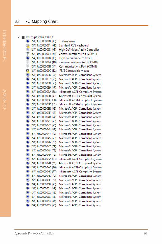
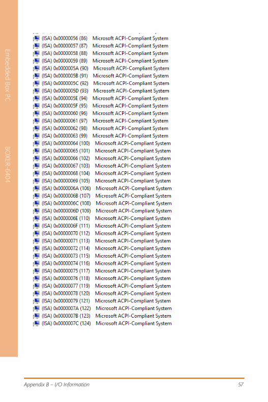
B.3 IRQ Mapping Chart
Appendix B – I/O Information 57
Em
bed
ded
Box P
C
BO
XER
-6404

Appendix B – I/O Information 58
Em
bed
ded
Box P
C
BO
XER
-6404

Appendix B – I/O Information 59
Em
bed
ded
Box P
C
BO
XER
-6404

Appendix B – I/O Information 60
Em
bed
ded
Box P
C
BO
XER
-6404

Appendix B – I/O Information 61
Em
bed
ded
Box P
C
BO
XER
-6404

Appendix B – I/O Information 62
Em
bed
ded
Box P
C
BO
XER
-6404

Appendix B – I/O Information 63
Em
bed
ded
Box P
C
BO
XER
-6404

Appendix B – I/O Information 64
Em
bed
ded
Box P
C
BO
XER
-6404

Appendix B – I/O Information 65
Em
bed
ded
Box P
C
BO
XER
-6404

Appendix B – I/O Information 66
Em
bed
ded
Box P
C
BO
XER
-6404

Em
bed
ded
Box P
C
BO
XER
-6404
Appendix C
Appendix C – Electrical Specifications for I/O Ports

Appendix C – Electrical Specifications for I/O Ports 68
Em
bed
ded
Box P
C
BO
XER
-6404
C.1 Electrical Specifications for I/O Ports
I/O Reference Signal Name Rate output
COM Port CN1 +5 V/ +12 V +5 V/ 1 A or
+12 V/ 1 A
+5 V Output for SATA HDD CN7 +5 V +5 V/ 1 A
CFast Slot CN11 +3.3 V +3.3 V/ 0.5 A
MiniCard Slot (USB 2.0 Port2
Only) CN13
+3.3 VSB
+1.5 V
+3.3 V/ 1.1 A
+1.5 V/ 0.375 A
USB 3.0 Port 0 CN17 +5 VSB +5V/ 1A
USB 2.0 Port 3 CN18 +5 VSB +5 V/ 0.5A
USB 2.0 Port 1 CN19 +5 VSB +5 V/ 0.5A
HDMI Port CN20, CN21 +5 V +5 V/ 1A