Basic Semiconductor Devices for Electrical Engineers
278
Volume 2 Basic Semiconductor Devices for Electrical Engineers Professor C.R. Viswanathan Distinguished Professor Emeritus Electrical Engineering Department University of California, Los Angeles 2018
-
Upload
khangminh22 -
Category
Documents
-
view
5 -
download
0
Transcript of Basic Semiconductor Devices for Electrical Engineers

Volume 2
Basic Semiconductor Devices for Electrical Engineers
Professor C.R. Viswanathan
Distinguished Professor Emeritus
Electrical Engineering Department
University of California, Los Angeles
2018
i
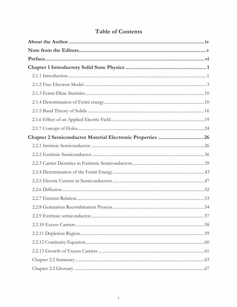
Table of Contents
About the Author ................................................................................................ iv
Note from the Editors .......................................................................................... v
Preface ................................................................................................................. vi
Chapter 1 Introductory Solid State Physics ......................................................... 1
2.1.1 Introduction ............................................................................................................................. 1
2.1.2 Free Electron Model ............................................................................................................... 3
2.1.3 Fermi-Dirac Statistics ............................................................................................................ 10
2.1.4 Determination of Fermi energy ........................................................................................... 10
2.1.5 Band Theory of Solids .......................................................................................................... 16
2.1.6 Effect of an Applied Electric Field ..................................................................................... 19
2.1.7 Concept of Holes ................................................................................................................... 24
Chapter 2 Semiconductor Material Electronic Properties ................................ 26
2.2.1 Intrinsic Semiconductor ....................................................................................................... 26
2.2.2 Extrinsic Semiconductor ...................................................................................................... 36
2.2.3 Carrier Densities in Extrinsic Semiconductors ................................................................. 39
2.2.4 Determination of the Fermi Energy ................................................................................... 43
2.2.5 Electric Current in Semiconductors ................................................................................... 47
2.2.6 Diffusion ................................................................................................................................. 52
2.2.7 Einstein Relation .................................................................................................................... 53
2.2.8 Generation Recombination Process ................................................................................... 54
2.2.9 Extrinsic semiconductor ....................................................................................................... 57
2.2.10 Excess Carriers ..................................................................................................................... 58
2.2.11 Depletion Region ................................................................................................................. 59
2.2.12 Continuity Equation ............................................................................................................ 60
2.2.13 Growth of Excess Carriers ................................................................................................ 61
Chapter 2.2 Summary ..................................................................................................................... 63
Chapter 2.2 Glossary ...................................................................................................................... 67

ii
Chapter 2.2 Problems ..................................................................................................................... 70
Chapter 3 P-N Junction ..................................................................................... 72
2.3.1 P-N junction Under Thermal Equilibrium ........................................................................ 75
2.3.2 Space Charge Region ............................................................................................................. 80
2.3.3 P-N Junction under Forward Bias ...................................................................................... 89
2.3.4 Quasi-Fermi Level ................................................................................................................. 94
2.3.5 Minority Carrier Diffusion ................................................................................................... 95
Chapter 2.3 Summary .................................................................................................................. 127
Chapter 2.3 Glossary ................................................................................................................... 130
Chapter 2.3 Problems .................................................................................................................. 135
Chapter 4 Bipolar Transistor ............................................................................ 139
2.4.1 D.C. Characteristics ............................................................................................................ 144
2.4.2 DC Current-Voltage Characteristics ................................................................................ 151
2.4.3 Low Frequency Small Signal Response and the Equivalent Circuit ........................... 156
2.4.4 Voltage Limitation .............................................................................................................. 161
2.4.5 Base Stored Charge ............................................................................................................ 166
2.4.6 Stored Charge Capacitance ............................................................................................... 168
2.4.7 Frequency Response .......................................................................................................... 170
2.4.8 Inclusion of Junction Capacitances ................................................................................. 177
2.4.9 Switching Transistors ......................................................................................................... 181
2.4.10 Ebers-Moll Model ............................................................................................................ 188
2.4.11 Output Impedance ........................................................................................................... 190
2.4.12 Non-ideal base current .................................................................................................... 193
2.4.13 Non-Uniform Doping in the Base ................................................................................ 195
Chapter 2.4 Summary .................................................................................................................. 197
Chapter 2.4 Glossary ................................................................................................................... 201
Chapter 2.4 Problems .................................................................................................................. 206
Chapter 5 MOS Devices ................................................................................... 209
2.5.1 MOS Capacitor ................................................................................................................... 209
iii
2.5.2 Non-Ideal MOS Device .................................................................................................... 229
2.5.3 Ideal MOS Capacitor ......................................................................................................... 236
2.5.4 MOS Transistor .................................................................................................................. 245
Chapter 2.5 Summary .................................................................................................................. 257
Chapter 2.5 Glossary ................................................................................................................... 261
Chapter 2.5 Problems .................................................................................................................. 265

iv
About the Author
After completing his PhD at the University of California, Los Angeles (UCLA) in the Physics department, Professor Chand R. Viswanathan (Vis) became a member of the faculty at UCLA in 1962 and later acted as Chairman and Assistant Dean of Graduate Studies at Henry Samueli School of Engineering and Applied Science. He served on the University of California Merced Task Force and was a member of the ASUCLA Board of Directors. In 2001, Professor Viswanathan served as Chair of the UC Academic Senate in the Statewide Legislative Assembly, becoming the highest-ranking faculty member in the University of California system. During his tenure, he dealt with issues ranging from rising student enrollment to the implementation of the dual-admissions policy.
Professor Vis’s research areas covered various topics in physics and solid state electronics which include and were not limited to low temperature electronics, semiconductor device processing, silicon-on-insulator devices, defect studies and VLSI technology. He published more than 150 technical papers and conference proceedings, delivered several invited papers at conferences, and received several awards including the 1984 IEEE Centennial Medal Award. He was elected Fellow of IEEE for his contributions towards metal oxide semiconductor devices and later advanced to Life Fellow in 1995. Throughout the years, Vis consulted for Hughes Aircraft, Rockwell International, Digital Equipment Corporation, Eastman Kodak Company, and IBM where he performed research work related to semiconductor devices in addition to giving short courses to their engineers.
Professor Vis received several awards including the Distinguished Teaching Award from the UCLA Academic Senate, Western Electric Fund by ASEE, Distinguished Faculty Award by the Engineering Alumni Association, Outstanding Educator of America, and the Undergraduate Teaching Award from the Institute of Electrical and Electronic Engineers (IEEE). Vis was a Fellow of IEEE and received the IEEE Undergraduate Teaching Award in 1997. He also received the UCLA Distinguished Teaching Award in 1976 and was honored with the Engineering Lifetime Contribution Award in 2014 from UCLA.

v
Note from the Editors
“A teacher affects eternity: he can never tell where his influence stops.” – Henry Adams
In 1957, Professor Chand R. Viswanathan (Vis) came to UCLA from India as a graduate student in the Physics department. He dedicated over 65 years of service to the UCLA community. In 1997, then Chancellor Albert Carnesale enjoyed a close working relationship with Vis. "I am continually inspired by the energy he brings to his work, passions… reflected in the extraordinary record of university service Vis has compiled," Carnesale said. While taking on teaching and administrative roles, he hoped to dispel the notion that an engineer cannot be a good administrator. "I hope people say of me, there is a successful engineer who was also chair of the Academic Senate from UCLA." He strived to maintain an academic environment that would be conducive to research, achieve excellence in education while balancing undergraduate and graduate programs.
Teaching was one of Vis’s main passions. He once said, "the greatest joy I get is being able to teach in front of a large class and see the faces brighten up.” Professor Vis taught classes in solid state electronics, electromagnetics, and circuits. He created the undergraduate and graduate courses in solid state electronics as well as the Solid State Electronics field of study at UCLA. As an astute teacher, Vis had an innate ability to simplify a complicated topic and make it easily comprehensible for his students. As a result, students felt comfortable talking and learning from him as Professor Vis had a genuine interest in his students’ wellbeing. Henry Samueli, one of Vis's pupils, has high praise for his former teacher. "Vis was one of the best instructors I ever had … [he] truly cares about his students and always made them feel comfortable to approach him at any time."
Professor Vis was a model for his students and had an integral role in making UCLA’s School of Engineering a top-ranked academic research institution. As his legacy continues to light fires in others, Vis will be remembered for dedicating his career to giving back to the community that gave him the opportunities to achieve his dreams. "When I came here as a foreign student, all the doors were opened for me. It is the beauty of this country and its Constitution, and a tribute to the UC system and all the people in it that I have accomplished what I have."
A well-documented example of his teaching prowess is demonstrated in the class notes for the solid state courses that he created and taught for the Electrical Engineering department. These notes have been adopted as teaching materials by solid state and material science professors and used by students. It was Professor Vis’s wish that his notes stay available for future students to learn from. Over the years, we had worked extensively with him to compile the notes into a two part book series: Introductory Atomic Physics and Quantum Mechanics (Volume 1) and Basic Semiconductor Devices for Electrical Engineers (Volume 2). These books give a fundamental understanding of solid state physics and we hope that the reader may find them useful and enjoyable for his or her studies.
Dr. Robert Loo, Editor-in-Chief Jodi Loo, Managing Editor

vi
Preface
While semiconductor electronics were solely taught in electrical engineering and electronics departments, the subject was of no direct interest to students in other areas such as in science and physiology departments. Now, with advances in materials and fabrication methods in nanotechnology, its physics and applications are expanding into new areas such as bioengineering, cell biology, molecular electronics, and neural sciences. Although we have many published books on semiconductors, this book gives in-depth explanations and step-by-step derivations of important principles to those who want to have a fundamental understanding of the physics of semiconductor devices.
Starting from the discovery of vacuum tubes followed by the invention of semiconductor devices, we are led into a new world of microelectronics by replacing discrete circuits with integrated circuits. However, the starting principle application is based on the amplifying properties of these devices, also known as transistors. Each transistor has an input and an output terminal. At the input, a small signal is amplified through the transistor. As a result, a larger signal at the output is fed into a load resistor, thereby delivering a larger signal power.
Figure A shows a vacuum tube transistor. It has three terminals: cathode, grid and anode. The input circuit to the transistor is the signal terminal, which is between the cathode and the grid. The output terminal is the load terminal, which is between the cathode and the anode. The cathode electrode is then common to both the input and output circuits. At the input, the electron current emitted by the cathode is controlled by the voltage on grid electrode, which is just a metallic plate with holes for electrons to pass through. This is achieved by biasing the grid voltage positive relative to the cathode. Electrons from the cathode are attracted and will pass through the holes in the grid to the anode electrode, which is also kept at a positive potential with respect to the cathode. Thus, the gate electrode is just the control electrode. It acts as a switch for transistor amplification. By making the distance between the grid and the cathode close to each other, a small voltage variation on the grid will have a large effect on the current flowing into the anode. A small time varying current at the input means small input power resulting in a larger current in the anode at the output circuit. Subsequently, the anode current flows to an external load resistor, delivering a larger output power. The vacuum tube transistor used in this manner is considered as a power amplifier.
Figure A. A vacuum tube amplifier
Once we had perfected the N- and P-type semiconductor materials, new types of transistors were invented. Figure B shows a silicon bipolar PNP transistor. Its operation is similar to a vacuum tube device in that it also has three terminals, emitter (cathode), base (grid) and collector (anode). The input signal is between the emitter, P, and the base, N, and the output is the load terminal,
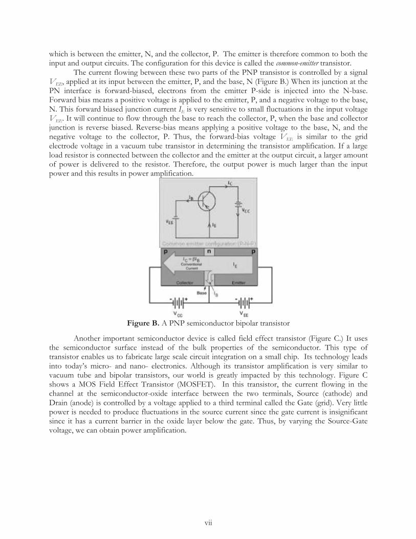
vii
which is between the emitter, N, and the collector, P. The emitter is therefore common to both the input and output circuits. The configuration for this device is called the common-emitter transistor.
The current flowing between these two parts of the PNP transistor is controlled by a signal VEE, applied at its input between the emitter, P, and the base, N (Figure B.) When its junction at the PN interface is forward-biased, electrons from the emitter P-side is injected into the N-base. Forward bias means a positive voltage is applied to the emitter, P, and a negative voltage to the base, N. This forward biased junction current IE is very sensitive to small fluctuations in the input voltage VEE. It will continue to flow through the base to reach the collector, P, when the base and collector junction is reverse biased. Reverse-bias means applying a positive voltage to the base, N, and the negative voltage to the collector, P. Thus, the forward-bias voltage VEE is similar to the grid electrode voltage in a vacuum tube transistor in determining the transistor amplification. If a large load resistor is connected between the collector and the emitter at the output circuit, a larger amount of power is delivered to the resistor. Therefore, the output power is much larger than the input power and this results in power amplification.
Figure B. A PNP semiconductor bipolar transistor
Another important semiconductor device is called field effect transistor (Figure C.) It uses the semiconductor surface instead of the bulk properties of the semiconductor. This type of transistor enables us to fabricate large scale circuit integration on a small chip. Its technology leads into today’s micro- and nano- electronics. Although its transistor amplification is very similar to vacuum tube and bipolar transistors, our world is greatly impacted by this technology. Figure C shows a MOS Field Effect Transistor (MOSFET). In this transistor, the current flowing in the channel at the semiconductor-oxide interface between the two terminals, Source (cathode) and Drain (anode) is controlled by a voltage applied to a third terminal called the Gate (grid). Very little power is needed to produce fluctuations in the source current since the gate current is insignificant since it has a current barrier in the oxide layer below the gate. Thus, by varying the Source-Gate voltage, we can obtain power amplification.

viii
Figure C. A MOS FET transistor
The study of semiconductor physics requires an understanding of quantum mechanics, which is built on the concept of several new and novel phenomena in solid state physics. Prior to the introduction of quantum mechanical and its description of matter, the understanding of electronic processes in solid states matter was incomplete. Semiconductor materials used were neither understood nor exploited in the modern applications as in the electronics that we are familiar with today.
Atomic particles such as electrons were considered as mechanical particles. The motion of the particles was described in terms of kinetic energy and potential energy, velocity and momentum. And when particles collided, energy was transferred. Also, energy was only understood to be in the form of waves and were described in terms of wavelength, frequency, propagation characteristics and other properties such as constructive and destructive interference. In short, energy and matter were considered as two separate aspects of nature in the world without any relation between them.
However, when advances in physics were made based on experimental observations on atoms, the physicists found it impossible to explain or interpret the results of the experiments based on the concepts of physics that were prevalent then. The whole world of physics came to realize that new concepts in the behavior of particles and waves have to be developed and evolved in order to understand the observed experimental results.
Starting from the time at the end of the nineteenth century, the concept of the duality of nature evolved and experimental observations brought conformation of the dual behavior of matter and energy. The famous photoelectric experimental results of Einstein confirmed that light energy, which had been thought of as a wave phenomenon, could also be composed of a collection of packets of energy called photons and that these photons could collide as particles with a transfer of energy (Figure D.)
Figure D. Einstein’s photoelectric effect
ix
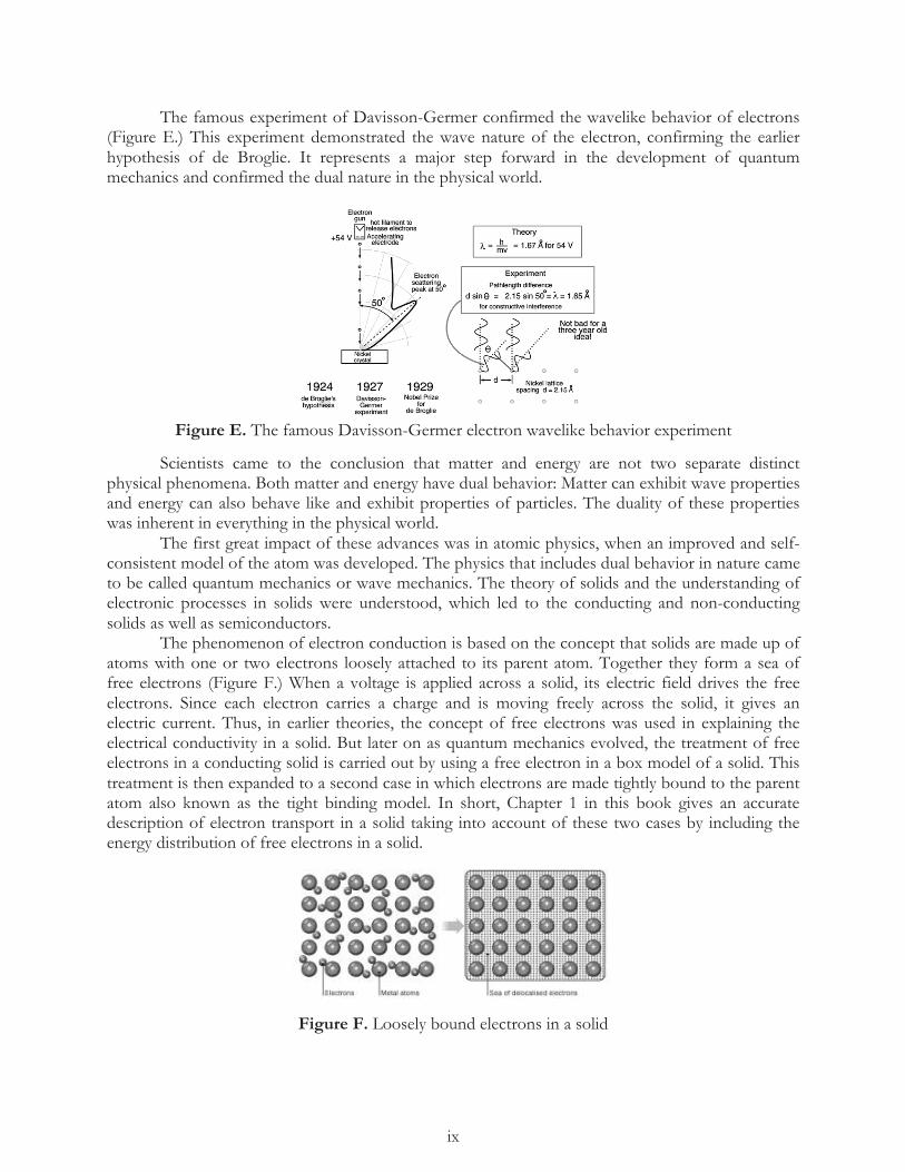
The famous experiment of Davisson-Germer confirmed the wavelike behavior of electrons (Figure E.) This experiment demonstrated the wave nature of the electron, confirming the earlier hypothesis of de Broglie. It represents a major step forward in the development of quantum mechanics and confirmed the dual nature in the physical world.
Figure E. The famous Davisson-Germer electron wavelike behavior experiment
Scientists came to the conclusion that matter and energy are not two separate distinct physical phenomena. Both matter and energy have dual behavior: Matter can exhibit wave properties and energy can also behave like and exhibit properties of particles. The duality of these properties was inherent in everything in the physical world.
The first great impact of these advances was in atomic physics, when an improved and self-consistent model of the atom was developed. The physics that includes dual behavior in nature came to be called quantum mechanics or wave mechanics. The theory of solids and the understanding of electronic processes in solids were understood, which led to the conducting and non-conducting solids as well as semiconductors.
The phenomenon of electron conduction is based on the concept that solids are made up of atoms with one or two electrons loosely attached to its parent atom. Together they form a sea of free electrons (Figure F.) When a voltage is applied across a solid, its electric field drives the free electrons. Since each electron carries a charge and is moving freely across the solid, it gives an electric current. Thus, in earlier theories, the concept of free electrons was used in explaining the electrical conductivity in a solid. But later on as quantum mechanics evolved, the treatment of free electrons in a conducting solid is carried out by using a free electron in a box model of a solid. This treatment is then expanded to a second case in which electrons are made tightly bound to the parent atom also known as the tight binding model. In short, Chapter 1 in this book gives an accurate description of electron transport in a solid taking into account of these two cases by including the energy distribution of free electrons in a solid.
Figure F. Loosely bound electrons in a solid

x
Before we study electron conduction in a semiconductor, we need to first consider the electronic conduction in metals. A metal is made up of atoms in which one or two electrons are loosely bound to the parent atom while the remaining electrons are strongly bound to the parent atom. When a solid is created with these atoms, the loosely bound electrons form a sea of electrons that are under the combined influence of all the atoms in the solid. Each electron carries a charge -q Coulombs and when they move, they give rise to a current and the electric current density is defined as the flow of charge per unit area in unit time (i.e. C cm-2 s-1 or more simply A cm-2.)
In the earlier models of electric conductivity in metallic solids, the conducting properties were considered by treating the presence of loosely bound electrons as free electrons in a box just like a collection of electrons in a box of the same dimensions as the solid. When no external field is applied, the only motion the electrons undergo is due to random collisions (scattering). Figure G shows electrons scattered randomly in a solid, and if the path of one electron is continuously observed, the electron seems to randomly and abruptly change directions after each collision, obeying the laws of Brownian motion.
Figure G. Electron movement in the absence of an electric field
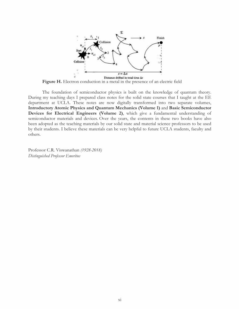
Because of random directions into which electrons are scattered, the electron does not move in any specific direction after a large number of collisions, and electron conduction remains stationary, (i.e. after a large number of collisions, the electron remains in nearly the same place in the solid.) But when an electric field is applied by applying a voltage across the solid, the electric field acts on the free electrons and propels them in the direction opposite to the direction the electric field because electron charge is negative. The electron gains kinetic energy as a function of time until it suffers a collision and its direction is suddenly turned. However, it will continue to move in a new direction. It can be noticed that the motion of electron in the presence of the electric field is superimposed on random motion. It is displaced creating a net displacement Δx. We can consider the electron to have moved a certain distance Δx in time Δt seconds. Figure H shows this process, which is called the drift of the electron due to the electric field. As time progresses, this distance becomes larger until it reaches the other end of the solid. In summary, we have an electric current flowing in the solid due to the applied electric field and therefore, the material is electrically conductive. The distance that the electron moves under the influence of the applied electric filed is proportional to the time that the electron has been gaining energy from the applied electric field measured from it last collision.
xi
Figure H. Electron conduction in a metal in the presence of an electric field The foundation of semiconductor physics is built on the knowledge of quantum theory.
During my teaching days I prepared class notes for the solid state courses that I taught at the EE department at UCLA. These notes are now digitally transformed into two separate volumes, Introductory Atomic Physics and Quantum Mechanics (Volume 1) and Basic Semiconductor Devices for Electrical Engineers (Volume 2), which give a fundamental understanding of semiconductor materials and devices. Over the years, the contents in these two books have also been adopted as the teaching materials by our solid state and material science professors to be used by their students. I believe these materials can be very helpful to future UCLA students, faculty and others.
Professor C.R. Viswanathan (1928-2018) Distinguished Professor Emeritus

1
Chapter 1 Introductory Solid State Physics
2.1.1 Introduction
An understanding of the concepts and devices in semiconductor physics requires an elementary familiarity with principles and applications of quantum mechanics. Up until the end of the nineteenth century, all physics investigations were conducted using Newton’s Laws of motion, which is encompassed in classical physics. Physicists at the time held the opinion that all physical phenomena can be explained using classical physics. However, as more sophisticated experimental techniques were developed and experiments on atomic size particles were studied, interesting and unexpected results that could not be interpreted using classical physics were observed. Physicists were looking for new physical theories to explain the observed experimental results. More specifically, classical physics was unable to explain the observations in the following:
(1) The model of the atom. (2) Why light emitted by atoms in an electric discharge tube contains sharp spectral lines
characteristic of each element. (3) Provide a theory for the observed properties in thermal radiation i.e., heat energy
radiated by a hot body. (4) Explain the experimental results obtained in photoelectric emission of electrons from
solids.
Early physicists Planck (thermal radiation), Einstein (photoelectric emission), Bohr (model of the atom) and others made some hypothetical and bold assumptions to make their models predict the experimental results. There was no theoretical basis on which all their assumptions could be justified and unified. In the 1920s, De Broglie made a revolutionary and amazing observation was made that particles also behave like waves. Einstein in 1905 had formulated that light energy behaves like particles called photons to explain the photoelectric results. De Broglie argued that energy and matter are two fundamental entities. The results of the photoelectric experiments demonstrated that light energy behaves also like particles and therefore matter also should exhibit wave properties. He predicted that a particle with a momentum of magnitude p will behave like a plane wave of wavelength, λ, equal to λ= h
p (2.1.1)
where h is Planck’s constant and numerically equal to h= 6.625 × 10⁻³⁴ J s
This led to the conclusion that both light particles and energy exhibited dual properties behaving as particles and waves. Since Planck’s constant, h, is extremely small, the De Broglie wavelength is correspondingly small for particles of large mass and momentum and therefore, the wave properties are not noticeable in daily life. However, subatomic particles such as electrons have such a small mass and a small momentum that makes the wavelength large enough to observe interference and diffraction effects in the laboratory.
A particle moving with a momentum, p, is represented by a plane wave of amplitude Ψ(r,t) given by
Ψ (r,t)=A ei k · r - ω t =A ei ( p · r
- ω t ) (2.1.2)
2
where k is the propagation vector of magnitude k= 2 πλ
, = h
2 π, ω=2πf and r, the radius
vector is equal to r=axx+ay y+az z
and ax, ay and az are the unit vectors along the three coordinate axes. The radius vector denotes the position where the amplitude is evaluated. The wavelength of the plane wave according to Equation 2.1.1, is given by λ= h
p= 2 π
k (2.1.3)
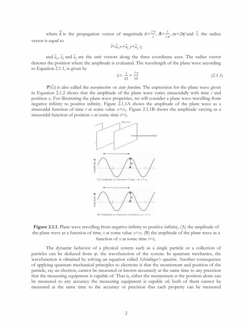
Ψ(r,t) is also called the wavefunction or state function. The expression for the plane wave given in Equation 2.1.2 shows that the amplitude of the plane wave varies sinusoidally with time t and position x. For illustrating the plane wave properties, we will consider a plane wave travelling from negative infinity to positive infinity. Figure 2.1.1A shows the amplitude of the plane wave as a sinusoidal function of time t at some value x=x1. Figure 2.1.1B shows the amplitude varying as a sinusoidal function of position x at some time t=t1.
Figure 2.1.1. Plane wave travelling from negative infinity to positive infinity, (A) the amplitude of the plane wave as a function of time, t at some value x=x1 (B) the amplitude of the plane wave as a
function of x at some time t=t1.
The dynamic behavior of a physical system such as a single particle or a collection of particles can be deduced from ψ, the wavefunction of the system. In quantum mechanics, the wavefunction is obtained by solving an equation called Schrödinger’s equation. Another consequence of applying quantum mechanical principles to electrons is that the momentum and position of the particle, say an electron, cannot be measured or known accurately at the same time to any precision that the measuring equipment is capable of. That is, either the momentum or the position alone can be measured to any accuracy the measuring equipment is capable of; both of them cannot be measured at the same time to the accuracy or precision that each property can be measured

3
separately. This is called the Heisenberg Uncertainly Principle. The more precisely position or momentum is measured, the other can be measured only less precisely. The physics underlying the uncertainty principle is that the act of measurement of one property disturbs the physical state of the system, making measurement of the other property less accurate. In quantum mechanics, there are other examples of pairs of physical properties that obey the Heisenberg Uncertainty Principle. For example, energy and time is another pair that obeys the Uncertainty Principle.
Mathematically, the uncertainty principle says that the product of the uncertainty in simultaneous measurement of position and momentum of a particle has to be higher than a minimum value of the order of Planck’s constant,, h, ΔPxΔx≥h. The uncertainty principle is not observable in the size and mass of particles in our daily life where the uncertainties of the properties are too small to observe because of the small value of Planck’s constant. When we deal with atomic particles, such as electrons, the uncertainty effects become significant.
When the wave-function is determined by solving Schrödinger’s equation for an electron that is confined to a narrow region of space along the x-axis, say between x=0 and x=Lx the result shows that the x-component of momentum can have only discrete values given by
Px= nx hLx
where nx is called a quantum number and is an integer (n = ±1, ±2, ±3, ...). Thus the x-component of momentum, p, can have only discrete values and are said to be discretized or quantized and hence nx is called a quantum number. If the electron is constrained to move in a restricted region in the x-y plane, then two quantum numbers, nx and ny, will be needed to quantize the x- and y- components of the momentum. In the case when the electron is confined to a small three dimensional region, the electron state will be specified by three quantum numbers nx, ny and nz, as discussed in the next section.
2.1.2 Free Electron Model
The electric current in a conducting solid such as a metal is explained in solid state physics using the Free Electron Model. According to this model, each atom of the solid contributes one (or two in some cases) electron(s) to form a sea of electrons in the solid and these electrons are free to roam around in the solid instead of being attached to the parent atom. If an electric field is applied in the solid, the electrons will move due to the force of the electric field and each electron will carry a charge –q (Coulomb) thus giving rise to the flow of an electric current. Thus free electrons in the solid are treated quantum mechanically as equivalent to electrons in a box of the same dimensions as the solid. We will now derive some properties of the free electrons in a conducting solid by using free electron model.
Let us now consider an electron of mass m that is confined to move within a three dimensional box. Let the box be rectangular with dimensions Lx, Ly, and Lz. As shown in Figure 2.1.2, we will choose the origin of our Cartesian coordinate system at one corner and the x-, y-, and z- axes to be along the three edges of the box.

4
Figure 2.1.2. Electron in a box.
We assume that the potential energy is constant and that it does not vary with position inside the box. Since force is equal to the gradient of the potential energy, there is no force acting on the electron because the gradient is zero. The electron is said to be in a force free region. Let the potential energy be taken as zero. A particle moving in force-free region has a constant momentum and is therefore represented by a plane wave. The wave function for the particle is given by Ψ r,t =A ei k ·r- ω t =A ei ( k ·r )e-iωt= ψ(r)e-iωt (2.1.4)
where ψ r =A ei ( k ·r )
ψ r can be written as, in rectangular coordinates, ψ r =ψ x,y,z =Ax eikxxAy e
ikyyAz eikzz
where A=AxAyAz. We can also write
ψ x,y,z =ψx x ψy y ψz z (2.1.5)
where
ψx x =Ax eikxx (2.1.6)
ψy y =Ay eikyy (2.1.7)
ψz z =Az eikzz (2.1.8)
The boundary condition on the wave function is that the wave function is the same in amplitude and phase when x is incremented by Lx, y is incremented by Ly and z is incremented by Lz i.e. ψ x,y,z =ψ x+Lx, y,z =ψ x, y+Ly,z =ψ x, y,z+Lz (2.1.9)
This boundary condition is called the Periodic Boundary Condition. The above boundary condition requires ψx x =ψx x+Lx (2.1.10)
ψy y =ψy y+Ly (2.1.11)

5
and ψz z =ψz z+Lz (2.1.12)
By applying the boundary condition given in Equation 2.1.6 to Equation 2.1.10, we obtain Ax eikxx=Ax eikx(x+Lx) (2.1.13)
This implies that kxLx=2π nx (2.1.14)
where nx is a positive or negative integer. Therefore, kx=
2 π
Lx nx (2.1.15)
and
ψx x =Ax ei
2 π nx Lx
x (2.1.16)
The x-component of the momentum, equal to kx, is therefore quantized with values px=0, ± h
Lx, ± 2h
Lx, ± 3h
Lx,± 4h
Lx ···etc (2.1.17)
Thus the x-component of the momentum is quantized with the same quantum number nx. Kinetic energy is related to the momentum. The kinetic energy due to the motion of the particle along the x-axis is also quantized. Let us denote the kinetic energy due to motion along the x-axis as E1.
E1=px2
2 m= ħ
2kx2
2m= ħ2nx2
2 m Lx2 (2.1.18)
Thus px, kx and E1 are all quantized with the same quantum number nx.
Example 2.1.1
Let us calculate kx, px and E1 for an electron in a state nx in a box of dimension 10 Å × 20 Å × 30 Å along the x, y, and z axes, respectively. Remember that 1 Å is 10-10m.
kx=2 πLx
nx=2 π × 1
10 × 10-10=2 π
10-9 = 6.28 × 10⁹ m-1
px= ħkx= 6.626 x 10⁻³⁴
2 π × 6.628 ×109=6.26×10⁻²⁵ K g m s
E1= px2
2 m=
px2
2 x 9.11 × 10-31=2.41 × 10⁻¹⁹ Joules=1.50 eV
kx, ky, and kz are related to x- , y-, and z- components of momentum through the De
Broglie relation. By using the boundary condition for ky, and kz, it can be shown ky=2 π nyLy
and
kz=2 π nz
Lz where ny and nz are quantum numbers similar to nx.

6
The kinetic energy due to motion along the y- and z- axes are denoted by E2 and E3
E2=ħ2ky2
2m=ħ2ny2
2mLy2 (2.1.19)
and E3=ħ2kz2
2m=ħ2nz2
2mLz2 (2.1.20)
In Figure 2.1.3, E1 is plotted as a function of kx. Since kx is quantized, E1 is also quantized. Because the adjacent values of kx and E1 lie so close to each other, the plot looks like a continuous curve. We say kx and E1 are quasi-continuous. The total wavefunction is obtained as a product function of ψx, ψy and ψz and is given by
ψ x,y,z =ψx x ψy y ψz z (2.1.21)
=Ax Ay Az ei(kxx+kyy+kzz) (2.1.22)
=Ax Ay Az eik ·r (2.1.23)
where k is called the propagation vector and is given by k =axkx+ayky+azkz (2.1.24)
=ax2 π nx
Lx +ay
2 π ny
Ly+az
2 π nz
Lz (2.1.25)
where r = radius vector, and ax, ay and az are the unit vectors along the x-, y-, and z- axes respectively E’, the total kinetic energy is equal to
E'= E1+E2+E3= ħ2k2
2m= ħ
2
2m nx2
Lx2 +
ny2
Ly2+
nz2
Lz2 (2.1.26)
where k is the magnitude of the propagation vector k. The numbers nx, ny, and nz are called quantum numbers, and once a particular set of three integers is assigned to these three quantum numbers, the momentum states for the particle is specified (i.e., the value of momentum the particle will have in that state.) We therefore denote the wavefunction by the subscripts nx, ny, and nz.
ψnxnynz=Ax Ay Azei 2 π (
nxxLx+nyy
Ly+nzz
Lz) (2.1.27)
Figure 2.1.3. Energy E1 vs. kx

7
The state nx=1, ny=2, and nz=-1, represents a state in which the particle is moving with a momentum p equal to
p=2πħ axLx+2ayLy
-az
Lz=h ax
Lx+2ayLy
-az
Lz (2.1.28)
Since nx, ny, and nz determine the momentum state, and can be only integers, we see that the px value changes by h
Lx from one state to the next and similarly the py and pz values change by h
Ly and
h
Lz respectively.
It should not be surprising that adjacent values of px differ by h
Lx. The maximum uncertainty
in the x-component of position is Δx=Lx since the particle can be anywhere in the box. Therefore the uncertainty in the x-component of momentum is required from the Uncertainty Principle to satisfy the condition
Δpx ≥ hLx
The adjacent values differing by hLx
are consistent with the Uncertainty Principle.
Consider a three dimensional space (imaginary of course) in which the three axes are px, py, and pz as shown in Figure 2.1.4. Each set of integers for nx, ny, and nz generates a point in this space (called the momentum space) and each point represents a particular momentum state. Such points in momentum space are called representative points or phase points.
Figure 2.1.4. Momentum space with px, py, and pz axes. The momentum space comprises an infinite number of phase points each separated from
its neighbor by hLx
along the px axis or hLy
along the py axis or hLz
along the pz axis. The origin of this
space is located at p=0 , and hence represents the state with no kinetic energy. The vector connecting the origin of the momentum space to a point with coordinate numbers nx, ny, and nz

8
represents the momentum vector of the state with x-component px= hLxnx, y-component py= h
Lyny,
and z-component pz= hLznz.
We obtained three quantum numbers because we restricted the motion of the particle to be within the small box of volume LxLyLz. If we constrain the particle to only a small region in one dimension, say along the x-axis, we get one quantum number nx and the momentum along the x-axis is quantized. Similarly, if we restrict the particle to a small area in the xy-plane, we will get two quantum numbers nx and ny and the momentum along the x- and y- axes will be quantized. If we restrict the particle to a three dimensional space, three quantum numbers nx, ny, and nz will be needed to specify the momentum state.
Let us consider a specific state characterized by a particular set of quantum numbers nx, ny, and nz This state is represented by point A in the momentum space with coordinates h
Lxnx,
h
Lyny and h
Lznz as shown in Figure 2.1.5. The rectangular volume contained in the momentum
space within coordinate numbers (nx, ny, nz), (nx+1, ny, nz), (nx, ny+1, nz), (nx, ny, nz+1), (nx+1, ny+1, nz), (nx, ny+1, nz+1), (nx+1, ny+1, nz+1) are the corner has eight adjacent states, one at each of its corners, and no states inside the rectangular volume. The rectangular volume has sides
Δpx=h
Lx, Δpy=
h
Ly, and Δpz==
h
Lz and has a volume equal to h3
LxLyLz. Since each corner is shared by
eight adjacent rectangular volumes, we can think that each rectangular volume equal to h3
LxLyLz
contains only one momentum state. The density of momentum states in the momentum space is the reciprocal of this volume (See Figure 2.1.5.)
According to quantum mechanics, the electron state is completely specified by four quantum numbers which are the three quantum numbers such as nx, ny, and nz obtained by constraining the particle to a small three dimensional volume and a fourth quantum number called the spin quantum number. The spin quantum number can either be 1
2 or - 1
2 for electrons. Thus for a
specific set of integers for nx, ny, and nz we have 2 quantum states: (1) nx, ny, and nz and 12 and (2) nx,
ny, and nz and - 12.
Figure 2.1.5. ABCDEFGH represents the elementary volume in the momentum space containing one momentum state.

9
In the momentum space, there are two electron states for a rectangular volume equal to h3
LxLyLz. Another way of saying this is that each electron state is contained within a volume
h3
2LxLyLz= h3
2V of the momentum space where the volume V of the box is LxLyLz. We can write that
the number of states in unit volume of the momentum space is equal to 2Vh3
and this is called the density of electron states in momentum space. If we take the potential energy to be zero (by suitably choosing the zero reference for the energy), then the total energy, E, is equal to the kinetic energy. If we describe a sphere of radius p in the momentum space with the origin at the center of the sphere, all states lying on the surface of the sphere will have the same energy. This leads us to conclude that the constant energy surface, i.e., a surface generated by connecting all states with the same energy, is a spherical in the momentum space.
Suppose we want to determine the number of electron states having momentum components between px and px+ dpx, py and py+ dyx, and pz and zx+ dpz. We consider an elementary rectangular volume of sides dpxdpydpz with its corner at the coordinates px, py, and pz in the momentum space as shown in Figure 2.1.6 and count the number of states within this volume. Instead of counting, we can simply multiply the volume of the elementary rectangular momentum space by the density of states 2V
h3 to obtain the number of states. The magnitude of the momentum
p, is given by
p= px2+py
2+pz2
Usually, we are more interested in finding the number of states having the magnitude of momentum between p and p+dp. In the momentum space if we describe two spheres around the origin, one with the radius equal to p and the other with radius equal to p+dp as shown in Figure 2.1.6, all the states in the interspace between the surfaces of these two spheres correspond to momentum magnitude between p and p+dp. The volume of the interspace between the two spheres
is equal to 4πp2dp. If we multiply this volume by the density of states 2V
h3in the momentum space,
we obtain Z(p)dp the number of states with the magnitude of momentum in the range between p and p+dp. The number of states having magnitude of momentum between p and p+dp as Z p dp= 2V
h34πp2dp
= 8 πVh3p2dp (2.1.29)
Figure 2.1.6. Constant momentum (magnitude) and constant energy surface.
10
2.1.3 Fermi-Dirac Statistics
When we have a single electron, this electron will occupy the state with the lowest energy. If we have a very large number of electrons in the box, all these electrons cannot occupy the same lowest energy state. According to a famous principle in physics called the Pauli exclusion principle, only one electron can occupy a given quantum state i.e., a state specified by the assignment of four quantum numbers. We start therefore filling the states, starting from the lowest energy state, until we have exhausted all the electrons. The last electron fills the state with the highest energy among all occupied states. This kind of distribution of electrons among the states is called the Fermi-Dirac statistics or distribution..
According to Fermi-Dirac statistics, the probability that an electron occupies a given state is given by the following function:
f E = 1
eE-EFkT +1
(2.1.30)
This function given by Equation 2.1.30) is called the Fermi function and the parameter Ef is called the Fermi energy. This function is plotted in Figure 2.1.7.
At absolute zero temperature, f(E) is 0 for E>Ef and is 1 for E<Ef. This means that at T=0 K states with energy less than Ef are occupied and states with higher energy are empty. Ef represents the maximum value of the energy of occupied states. The Fermi energy acts as a threshold energy separating the occupied states and the vacant states. The Fermi function exhibits a discontinuity at T=0 K in going from a value of 1 to 0 at E=Ef.
As the temperature is raised, the electrons in states close to the Fermi energy get excited by thermal energy to states with energy higher than the Fermi energy. This leads to a gradual variation with energy of the Fermi function from 1 to 0 around Ef. Since the thermal energy is on the order of kT which is very much smaller than Ef, the region of transition from 1 to 0 is very small compared with Ef as shown in Figure 2.1.7. Even at higher temperature, states with energy less than the Fermi energy by several kT, have a probability of 1 for occupation by an electron. Similarly, states with energy greater than the Fermi energy by several kT have a probability of nearly 0 for occupation by an electron. The probability of a state with energy equal to Ef, being occupied by an electron is 1
2.
2.1.4 Determination of Fermi energy
We denote the number of electrons having the magnitude of momentum between p and p+dp as dNp. dNp is obtained by multiplying Equation 2.1.29 and Equation 2.1.30.
dNp =Z p dp f E = 8 π V
h3 1
eE-EFkT +1
p2dp (2.1.31)
Let us now determine the distribution of electrons as a function of energy E. We want to find the number of electrons having energy between E and E+dE. Let us denote this number by dNE. In Figure 2.1.6 the surfaces of the two spheres with radius p and p+dp are constant energy

11
surfaces one with energy E and the other with E+dE. Therefore dNE is the same as dNp, but dNE needs to be expressed in terms of E instead of in terms of p. Since E, the total energy equal to the kinetic energy, when the potential energy is taken as zero,
E= p2
2m
Differentiating,
dE= 2p dp
2m= p dp
m (2.1.32)
p dp=m dE (2.1.33)
and
p= 2mE (2.1.34)
Substituting these in Equation 2.1.31, we obtain
dNE=dNp=8 π V
h3 1
eE-EFkT + 1
p2dp= 4 π V(2m)32
h3 E
12
eE-EFkT + 1
dE (2.1.35)
Figure 2.1.7. Fermi function (also called the Fermi-Dirac distribution function)
This can also be written in the form
dNE=f E Z E d (2.1.36)
where f(E) is the Fermi function and Z(E) is given by
Z E = 4 π V(2m)32
h3 E
12 (2.1.37)
12
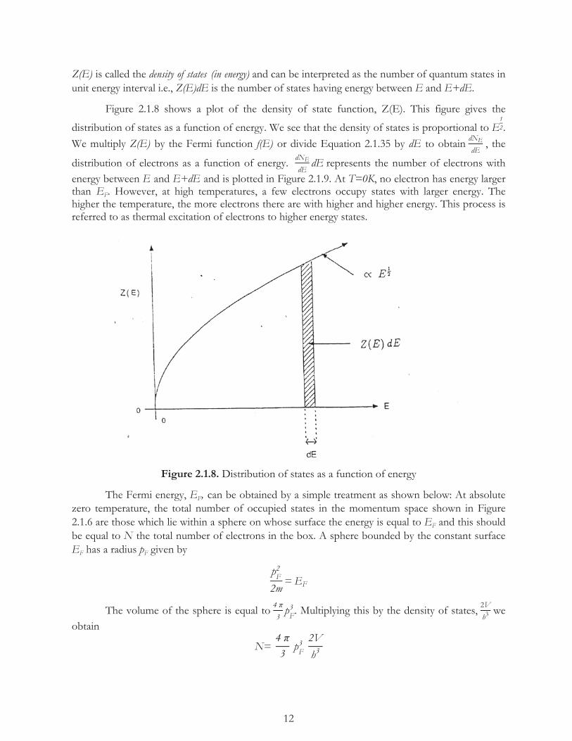
Z(E) is called the density of states (in energy) and can be interpreted as the number of quantum states in unit energy interval i.e., Z(E)dE is the number of states having energy between E and E+dE.
Figure 2.1.8 shows a plot of the density of state function, Z(E). This figure gives the
distribution of states as a function of energy. We see that the density of states is proportional to E12.
We multiply Z(E) by the Fermi function f(E) or divide Equation 2.1.35 by dE to obtain dNEdE
, the
distribution of electrons as a function of energy. dNEdEdE represents the number of electrons with
energy between E and E+dE and is plotted in Figure 2.1.9. At T=0K, no electron has energy larger than EF. However, at high temperatures, a few electrons occupy states with larger energy. The higher the temperature, the more electrons there are with higher and higher energy. This process is referred to as thermal excitation of electrons to higher energy states.
Figure 2.1.8. Distribution of states as a function of energy
The Fermi energy, EF, can be obtained by a simple treatment as shown below: At absolute zero temperature, the total number of occupied states in the momentum space shown in Figure 2.1.6 are those which lie within a sphere on whose surface the energy is equal to EF and this should be equal to N the total number of electrons in the box. A sphere bounded by the constant surface EF has a radius pF given by
pF2
2m= EF
The volume of the sphere is equal to 4 π3pF3 . Multiplying this by the density of states, 2V
h3 we
obtain
N= 4 π3
pF3 2V
h3

13
= 8 π V3 h3
pF3
= 8 π V
3 h3 (2m)
32 EF
32 (2.1.38)
We used the relation between pF and EF in the above equation. We can now rearrange this equation to express EF as
EF = 3 h3
8 π (2m)32
N
V
23
= 3 h3
8 π (2m)32n
23
(2.1.39)
Figure 2.1.9. Electron distribution as a function of energy
where n = NV
is the number of electrons per unit volume (i.e. density) in the box. The Fermi energy is dependent only on the density and not on the total number of electrons. As we will see later on, electrons in metallic solids that are free to roam around in the solid are modeled as electrons in a box of the same dimensions as the piece of solid. We can determine the Fermi energy of the solid, knowing n, the density of electrons. Whether a solid is large or small in size, the Fermi energy is the same independent of size because it depends only on the density of electrons.
14
_____________________________________________________________________________
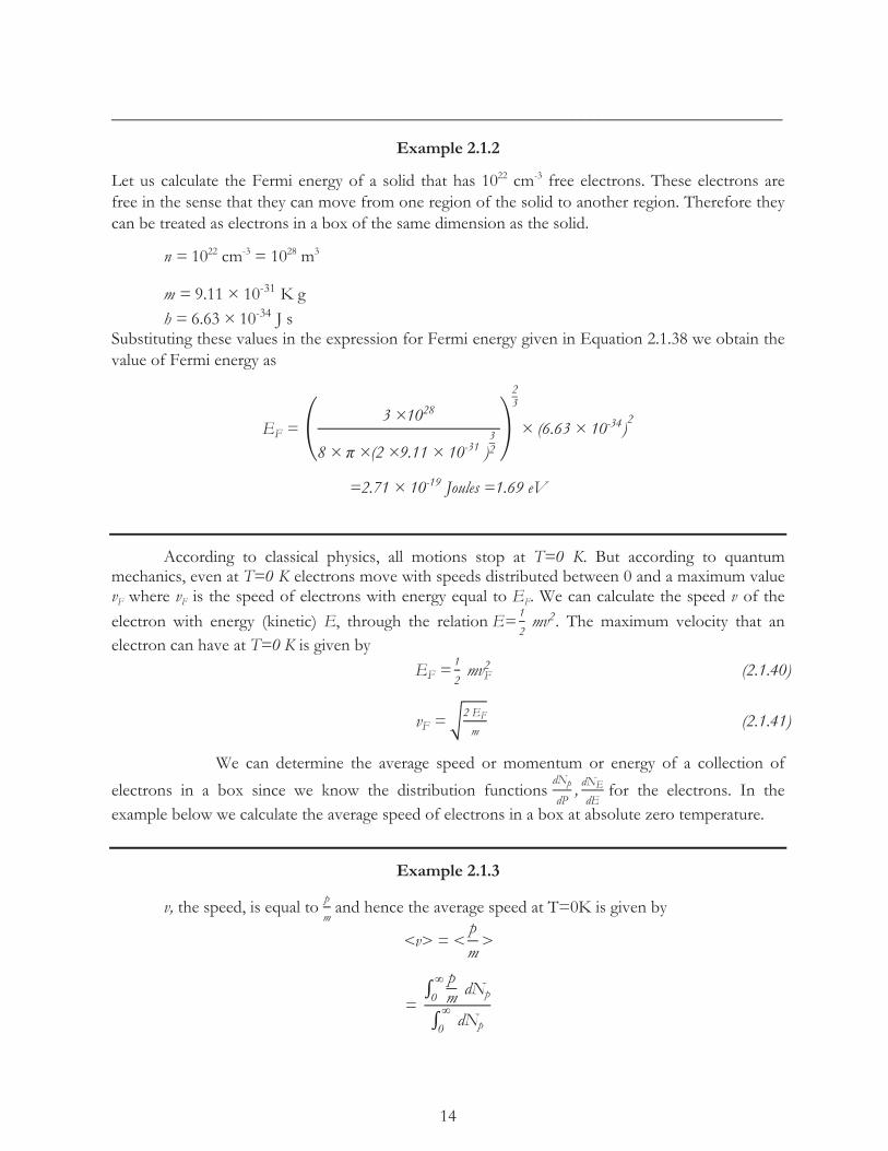
Example 2.1.2
Let us calculate the Fermi energy of a solid that has 1022 cm-3 free electrons. These electrons are free in the sense that they can move from one region of the solid to another region. Therefore they can be treated as electrons in a box of the same dimension as the solid.
n = 1022 cm-3 = 1028 m3
m = 9.11 × 10⁻³¹ K g h = 6.63 × 10⁻³⁴ J s
Substituting these values in the expression for Fermi energy given in Equation 2.1.38 we obtain the value of Fermi energy as
EF = 3 ×1028
8 × π ×(2 ×9.11 × 10-31 )32
23
× (6.63 × 10-34)2
=2.71 × 10⁻¹⁹ Joules =1.69 eV
According to classical physics, all motions stop at T=0 K. But according to quantum mechanics, even at T=0 K electrons move with speeds distributed between 0 and a maximum value vF where vF is the speed of electrons with energy equal to EF. We can calculate the speed v of the electron with energy (kinetic) E, through the relation E= 1
2 mv2. The maximum velocity that an
electron can have at T=0 K is given by EF = 1
2 mvF
2 (2.1.40)
vF = 2 EFm
(2.1.41)
We can determine the average speed or momentum or energy of a collection of
electrons in a box since we know the distribution functions dNp
dP, dNEdE
for the electrons. In the example below we calculate the average speed of electrons in a box at absolute zero temperature.
Example 2.1.3
v, the speed, is equal to pm and hence the average speed at T=0K is given by
<v> = <pm>
=
pm dNp
∞0
dNp∞0

15
=
pm Z p f E dp
∞0
Z p f(E)dp∞0
To evaluate this integral we take advantage of the property that f(E) is equal to 1 when p is between 0 and pF and is equal to 0 when p is greater than pF at absolute zero temperature.
<v>= pm p2dp
pF0
p2dpPF0
=pF4
4m ×
3pF3 =34
pFm
= 34
vF
Thus we see that the average speed of the electrons is 34 of the maximum speed vF.
If we want to localize the position of the electron in the box, by representing it as a wave packet, we superimpose a large number of plane waves of suitable amplitude and phase and of different k values with an average value of k0. The velocity of the electron is the group velocity of the wave packet and is equal to
dωdk
= 1ħ
dEdk
(2.1.42)
determined at k=k0. Referring to Figure 2.1.10, the velocity of the electron for the state k=k0 is related to the slope of the energy E vs k plot at k=k0. Since we have
E=ħ2k2
2m
the velocity of the electron in the state k=k0 is equal to
vel = vg=1
ħ dEdk k=k0
= ħ k0m
(2.1.43)
This is the usual result that velocity is momentum divided by m. We considered the potential energy to be constant inside the box. However, the potential energy inside the solid will be periodically varying. When we assume that the potential energy inside the box is varying periodically, an interestingly different E vs k diagram is obtained and the velocity is not equal to the momentum divided by the mass.
In the treatment of electrons in a box, the potential energy was assumed to be constant and hence there was no force on the electron. The electrons were said to be free. When we apply this model to treat the case of electrons in a metallic solid, we call it the free electron model of the solid. We found that the energy levels are discrete (quantized). However, since the dimensions of the solid are large in comparison with atomic distances, the discrete energy levels are very close to each other and for all practical purposes can be considered to be continuous. This is particularly true when we consider higher energy states where the quantum numbers are large and the separation in energy between adjacent states expressed as a fraction of the energy of the state becomes extremely
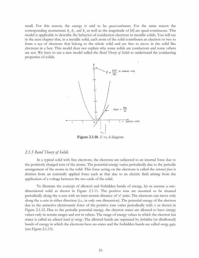
16
small. For this reason, the energy is said to be quasi-continuous. For the same reason the corresponding momentum kx, ky, and kz as well as the magnitude of k are quasi-continuous. This model is applicable to describe the behavior of conduction electrons in metallic solids. You will see in the next chapter that, in a metallic solid, each atom of the solid contributes an electron or two to form a sea of electrons that belong to the whole solid and are free to move in the solid like electrons in a box. This model does not explain why some solids are conductors and some others are not. We have to use a new model called the Band Theory of Solids to understand the conducting properties of solids.
Figure 2.1.10. E vs. k diagram
2.1.5 Band Theory of Solids
In a typical solid with free electrons, the electrons are subjected to an internal force due to the positively charged ions of the atoms. The potential energy varies periodically due to the periodic arrangement of the atoms in the solid. This force acting on the electrons is called the internal force is distinct from an externally applied force such as that due to an electric field arising from the application of a voltage between the two ends of the solid.
To illustrate the concept of allowed and forbidden bands of energy, let us assume a one-dimensional solid as shown in Figure 2.1.11. The positive ions are assumed to be situated periodically along the x-axis with an inter-atomic distance of ‘a’ units. The electrons can move only along the x-axis in either direction (i.e., in only one dimension). The potential energy of the electron due to the attractive electrostatic force of the positive ions varies periodically with x as shown in Figure 2.1.12. Due to the periodic potential energy, the electron states are allowed to have energy values only in certain ranges and not in others. The range of energy values in which the electron has states is called an allowed band of energy. The allowed bands are separated by forbidden (or disallowed) bands of energy in which the electrons have no states and the forbidden bands are called energy gaps, (see Figure 2.1.13).

17
Figure 2.1.11. Positive ions and free electrons in a one-dimensional solid.
Figure 2.1.12. Electrostatic potential energy variation with distance
In the free electron model, the electron energy varies quasi-continuously from 0 to +∞ as shown in Figure 2.1.14. In this figure, the kinetic energy, which is the same as the total energy since the potential energy is constant and can be taken as zero by a proper choice of the zero reference for energy, is plotted as a function of k. Motion is possible only along one dimension. K varies quasi-continuously from -∞ to +∞.
Figure 2.1.13. Bands of allowed and forbidden energy.
Let us assume that the potential energy varies periodically with the periodicity α and is given by
U x =U(x+a) (2.1.44)

18
When the existence of the periodic potential energy is treated quantum mechanically, it is shown in solid state physics books that the energy varies with k as shown in Figure 2.1.15. Notice that the energy of the states is split into bands. The solid line in the Figure 2.1.15 represents the energy according to the band theory. Let us now examine the essential features of the band theory.
Figure 2.1.14. E-k diagram for free electrons. Quasi-continuous distribution of energy as a function of the magnetitude of the momentum. Notice that the energy values extend from 0 to ∞.
Figure 2.1.15. A plot of energy as a function of k (E vs k) in the band theory in the one-dimensional approximation. Notice that the energy values are broken into bands of allowed and
forbidden values.
As the magnitude of k is increased from 0, the energy increases symmetrically with k for both positive and negative values of k until k becomes equal to ± π
a. At this value of k, the energy
has a discontinuity and if k is increased beyond πa then the energy increases again. The discontinuity
in energy at ± πa is called the energy gap or the bandgap. The continuous range of energy for values

19
of k between - πa and+ π
a is called the first energy band. Another energy gap occuring at-2 π
a and+2 π
a
is called the second band of energy. In general, the bandgap occurs at k =± nπa where n is an integer.
Thus, according to the band theory of solids, the energy values are split into allowed and forbidden bands of energy. The forbidden band of energy is also referred to as bandgap and the allowed band is referred to as energy band. At the bottom and at the top of the energy band, the energy plot has zero slope. In the middle of the band, the energy has a parabolic dependence on k, (i.e., is proportional to k2) as in the free electron model. Notice that, in the region of the band, the dotted line and the solid line overlap showing that the behavior of electrons in this region of the band is similar to the free electron behavior. It is shown in solid state physics textbooks that in a band, two states whose k value differs by 2nπ
a where n is a positive or negative integer are equivalent states if they also have the same
energy. Referring to the Figure 2.1.16, A and B are equivalent states because the k values differ by 2πa and they have the same energy. Similarly, C and D are equivalent states.
As the velocity of the electron is the group velocity of the wave-packet (Equation 2.1.42), the electron velocity varies in the bandgap due to the variation of the slope in the E vs k plot i.e., dE
dk
in the band. The electron has zero velocity in the bottom and in the top of the band since the slope is zero. It has maximum velocity in the middle of the band where the inflection point occurs.
Figure 2.1.16. One-dimensional energy band diagram illustrating equivalent states.
2.1.6 Effect of an Applied Electric Field
We will now examine the behavior of the electrons in a band under the application of an external field. Let us assume that the electric field, , is switched on at time t=0. There is a force on the electron equal to -q In a short interval of time δt the electron moves a distance v δt and gains an energy equal to
δE=-q vδt (2.1.45)
20
The energy of the electron is changed by δE, and it should be now in a new state k+δk
The differential in energy δE is given by
δE= dE
dkδk (2.1.46)
The velocity was seen earlier to be equal to the group velocity of the wave packet i.e.
v =vl =1 dE
dk (2.1.47)
Hence δE can be expressed in terms of the velocity of the electron as
δE= v δk (2.1.48)
Equating this expression for δE with that given in Equation 2.1.45, we obtain
-q = dkdt
(2.1.49)
Thus we see that dk
dt is equal to the external force on the electron due to the applied
electric field. We can infer, therefore, that the effect of an external force is to make the k value change with time at a rate given by dk
dt= external force (2.1.50)
What do we mean by a change in k value? The electron changes or makes a transition from a state of some k value to another of different k value. Under the application of the external field (force) the electron goes from one k state to the next higher k state and from that state to the next higher k state and thus keeps on making these transitions as long as the external force is applied. In other words, the electron changes its k state under the application of an external force.
Referring to Figure 2.1.16, an electron in the state P will jump to the next higher state Q due to the external field. Then it will jump to a next higher k state and keep on moving to higher k states until it reaches the state A. According to Equation 2.1.45, the velocity of the electron in any given state is proportional to the slope of the energy versus k plot known usually as E-k plot. In the upper left half of the bandgap, the E-k plot is concave downwards which means that the slope (velocity) decreases as k is increased. As the electron changes its state progressively from P to A, the electron velocity is decreasing (i.e., the electron is slowing down. Since the slope is zero at A, the electron velocity becomes zero. The k value cannot increase to a value higher than π
a since there is
an energy discontinuity. However, the state B is equivalent to A and therefore when the electron is in the state k= π
a, it is equivalent to being in the state =- π
a. Now, k can increase at the rate dk
dt from
the state B, where k=- πa . Since dE
dk is negative, the velocity is negative. The electron starts to move in
the opposite direction and the magnitude of the velocity in the negative direction increases from zero when it is in the state B to a maximum value when it reaches the state P’. Then it starts to slow down and reaches zero velocity in the state denoted by 0. As the force continues to act on the electron, the electron starts to move in the positive direction and its velocity increases until it reaches the state P. When the electron goes from state P to a higher k state, it starts to slow down and comes to rest when it reaches state A. This cycle keeps repeating as long as the force continues

21
to act on the electron. The electron changes states in the band in a cyclic fashion. When a band is completely full, all of the electrons are continually changing states in a cyclical fashion. At any given instant, there are as many electrons traveling in the positive direction as those in the negative direction. This is because electrons occupying states between k=0 (state 0) and k= π
a (state A)
correspond to electrons traveling in the positive direction while electrons occupying states between k=0 (state 0) and k=- π
a (state B) travel in the negative direction. The average velocity is therefore
zero and hence a completely filled band does not contribute to electrical conductivity. When the electron is in a state between state P and state A, the effect of the external field is to decelerate the electron (i.e., as time progresses its velocity decreases). Normally, when we consider free electrons, the electron will accelerate under the action of the external field. It is as though an electron in states between P and A has a negative mass. Similarly, the electron behavior in states between P’ and B is as though the electron has a negative mass. We define therefore, an effective mass, m*, which, when multiplied by the acceleration, gives the force on the electron. Since states in the upper half of the band correspond to deceleration of electrons, they have a negative effective mass while those in the bottom half of the band have a positive effective mass.
The acceleration of the electron is given by
a = dvdt
= ddt
1 dEdk= 1 d
2E
dtdk= 1 d
2E
dk2 dkdt
(2.1.51)
But the force -qε is equal to dk
dt, Hence
a= 12 d2E
dk2 dk
dt= 1
2 d2E
dk2 -q E = 1
2 d2E
dk2×Force (2.1.52)
The term 12 d2E
dk2 relates acceleration to the applied force just as mass relates total force and
acceleration. We thus define the effective mass, m*, as
m*= 2
d2E
dk2
(2.1.53)
The curvature d2E
dk2 of the E vs k plot is positive in the lower half of the band and hence m*
is positive. The curvature is negative in the upper half of the band, and hence the effective mass is negative. What is the philosophical interpretation of the effective mass? The effective mass relates the acceleration of the electron to the external force. If one were to include all the forces internal and external, then indeed the relation between the acceleration and the total force will be through the real mass of the electron. We are relating only the external force to the acceleration and hence we need to define an effective mass.
The effective mass is a useful concept since it enables one to determine the behavior of electrons by treating them as though they are free from any internal force (i.e., constant potential energy). Replacing the true mass by the effective mass m* in the expressions describes its dynamic behavior. In the three-dimensional solid, the effective mass m* is a second-order tensor which relates the external force along one direction to the acceleration along another direction. For example, in a general case, unless the external force is applied along one of the three principal axes of the crystal, the resulting acceleration will not be in the same direction as the force. However, for

22
the purposes of our discussion, we will assume that the effectiveness m* is a scalar quantity (i.e., the external force and the acceleration are in the same direction.)
Conductors, Insulators and Semiconductors
Let us now consider a material in which the upper most occupied band is partially filled while all the lower bands are completely filled. There is no contribution to the electrical conductivity from the lower bands since they are full as stated earlier. On the other hand, the electrons in the partially filled (highest) band move continuously to higher k states under the action of the eternal force. In a time interval t, the electrons would have changed to new states that differ in the k value by
Δk = external forceΔt (2.1.54)
One would expect that the electrons will be continually changing states in this fashion but this does not occur. The electrons collide with scattering centers such as impurities and other atoms of the crystal that have been displaced from their normal atomic sites. The scattering causes them to give up their excess energy and return to lower energy states. This process is called a relaxation process. The electrons are never able to go to very high energy states due to the relaxation process. According to solid state theory, it is possible to assume that, under steady state conditions, the distribution of electrons in the presence of the electric field E, is the same as what one would obtain if the field E acted on the electrons for a time period τc. τc is called the relaxation time. Referring to Figure 2.1.17, we find that under steady state conditions, all the electrons have shifted to new k states separated from the original states by an amount
Δk = 1 -q τc (2.1.55)
All the states below the dotted line in the energy axis have equal number of electrons going in the positive direction as in the negative direction. Only those electrons above the dotted line travel in the positive direction without an equal number traveling in the opposite direction. There is a net flow of electrons in the positive direction. These electrons contribute to electrical conductivity. We can conclude therefore that only partially filled bands contribute to electrical conductivity.
Figure 2.1.17. Electron distribution in the presence of an electric field

23
We can distinguish three classes of materials: conductors, insulators and semiconductors. An insulator is one in which the top-most occupied band is completely filled as shown in Figure 2.1.18. The top most filled band is called the valence band since the electrons in this band are the ones which give rise to the chemical bonding. The next higher band is called the conduction band, since any electron excited to this band will give rise to electrical conductivity due to the fact that the conduction band becomes partially filled. The difference in energy between the top of the valence and the bottom of the conduction band is the energy gap or band gap. Band gaps of insulators are very large and hence even at very high temperatures only a negligible number of electrons are excited into the conduction band and the material does not carry electrical current. On the other hand, if the bandgap is small, then even at moderately low temperatures, electrons will be excited from the valence band into the conduction band and we will get electrical conductivity from both the partially filled valence and conduction bands. Such materials are called semiconductors. At absolute zero temperature, the semiconductor is an insulator since there are no electrons in the conduction band. However, as the temperature is raised, electrons are thermally excited from the valence band to the conduction band and the material starts to conduct electricity. Conductors are materials in which the highest occupied band is only partially filled. The band structure for conductors is shown in Figure 2.1.19. The metallic solids have this feature, (i.e., the highest occupied band is partially filled) and are considered good conductors.
Figure 2.1.18. Band Structure of an insulator

24
Figure 2.1.19. Band structure of a conductor
2.1.7 Concept of Holes
We saw in the last section that a semiconductor has a small bandgap with its valence band completely filled while its conduction band is empty at very low temperatures. As the temperature is raised by heating the semiconductor, electrons are thermally excited from the valence band to the conduction band. This gives rise to a partially filled conduction band and the electrons in the conduction band can give rise to electrical conduction. Similarly, the remaining electrons in the valence band can give rise to electrical conduction since the valence band is now only partially filled. However, it is a very difficult task to determine the contribution of the large number of electrons in the valence band. A simple technique can be employed to calculate the contribution of the valence band electrons to electrical conduction.
For the sake of simplicity, let us assume that only one electron is excited from the valence band to the conduction band, leaving a vacant state in the valence band. The electron in the conduction band gives rise to electrical conduction as though it is a free electron with an effective mass, mc, appropriate to the state it occupies in the conduction band. The electron will occupy only a low energy state in the bottom of the band and therefore its effective mass is positive. On the other hand the vacant state in the valence band is in the top of the band and the effective mass is negative. An electron with an effective mass -mv can occupy the vacant state in the valence band, and make the valence band fully occupied. Assume that we introduce two fictitious particles one with a charge –q and a mass -mv and the other with a charge q and a mass mv. The particle with the negative charge and negative effective mass fills the vacant state making the valence band completely filled. However, the particle with the positive charge and positive effective mass will now be free to move around the crystal and contribute to the electrical conductivity. This fictitious particle with a positive charge and a positive effective mass is called a hole. It behaves like a free particle and carries a charge. It therefore contributes to electrical conductivity. For every electron excited from the valence band, there is hole in the valence band. We obtain electrical conductivity due to both electrons and holes.

25
The number of electrons in the conduction band is small in comparison to the total number of states in the conduction band. Hence, the electrons occupy a narrow range of states in the bottom of the conduction band. We can therefore assume that all these electrons have the same effective mass and calculate the electrical conductivity due to them by using the free electron model (electrons in a box) except that we will use the effective mass mc in the place of the true mass. Similarly, all the holes are nearly at the top of the valence band and occupy a narrow range of states in the valence band. They all have the same effective mass, mv, corresponding to the curvature of the top of the valence band. These holes can be treated as holes in a box. Thus, we can calculate the electrical conductivity of the semiconductor using the free electron and free hole models.

26
Chapter 2 Semiconductor Material Electronic Properties
2.2.1 Intrinsic Semiconductor
In this chapter we will briefly review the essential aspects of semiconductor physics that will be relevant to the discussion of device physics. A semiconductor is a material that has an electrical conductivity much less than a metallic conductor but is much more condcutive than an insulator. Furthermore, its electrical conductivity is zero at absolute zero and increases with and increase in temperature. The atoms in a semiconducting crystal are held together by covalent bonds. In order to understand what a covalent bond is, consider two hydrogen atoms that are initially infinitely apart. On bringing these two atoms closer, the electron in each atom is simultaneously subjected to the attractive forces of both nuclei lowering the potential energy of each electron. The lowering of the potential energy with the decrease in the distance between the two nuclei corresponds to an attractive force. The reason the two nuclei do not collapse onto each other is because of a repulsive force that arises between the two nuclei (Coulomb repulsion) at very close inter-nuclear distance. The two nuclei are in stable equilibrium at a distance where the attractive force is exactly balanced by the repulsive force. Since the two electrons have a very high probability of being found midway between the two nuclei, the electrons spend most of the time midway between the two nuclei. This does not violate Pauli’s exclusion principle because each atom has only one 1s electron. The electron in one atom can have an opposite spin to the electron in the other atom and therefore these two electrons can simultaneously exist in the same place. It is as though each atom has two electrons in the 1s orbit. However if we bring two helium atoms together, a covalent bond will not result because Pauli’s exclusion principle is violated since each atom already has a filled 1s state (or orbital). Therefore we can conclude that for covalent bonds to exist, each atom should have a partially filled orbital.
The same covalent bond gives rise to the bonding force in many of the solids like carbon, nitrogen, and oxygen. The covalent bond is directional and therefore these atoms crystallize in structures, which satisfy the directionality of the covalent bond. An atom with N electrons outside the close-shell structure requires (8-N) electrons to complete the s and p sub-shell. Since two neighboring atoms each contribute one electron to the bond between them, an atom with N valence electrons requires (8-N) nearest neighbors and the crystal structure that results has to provide (8-N) nearest neighbors which are symmetrical situated with respect to the first atom. For example, carbon (diamond), silicon, and germanium each have two s electrons and two p electrons. They require 4 nearest neighbors, which is obtained in the diamond structure. Figure 2.2.1 shows the crystal structure of diamond in which each atom is surrounded by four covalently bonded neighboring atoms. Silicon and Germanium also have similar crystalline structures.
It might be asked how Pauli’s exclusion principle is not violated when we have the s-orbitals filled in each of the carbon atoms. This is explained by assuming a rearrangement of the states of the four electrons. One of the 2s electrons goes into a 2p state and thereby, we have half-filled s-orbitals and half filled p-orbitals. Such a rearrangement is called hybridization. The four new

27
orbitals thus obtained are (sp3) hybrids. Figure 2.2.2 shows how the energy bands are formed by hybridization of s and p orbitals.
The covalent crystals exhibit great hardness and low electrical conductivity at low temperature and in the pure state. They usually have strong binding but some of the crystals (semiconductors) have weaker binding. These semiconductors exhibit electronic conductivity at high temperatures.
Figure 2.2.1. The diamond crystal structure.
Figure 2.2.2. Energy band formation in diamond by hybridization of s and p orbitals.
Band Structure of Semiconductors
Some of the common semiconductor materials are made up of atoms of group IV elements like germanium and silicon; these materials are referred to as elemental semiconductors. Semiconductor materials such as gallium arsenide or indium antimonide are made up of compounds of atoms of

28
group III and group V elements and therefore these materials are known as compound semiconductors. The energy band structures of some common semiconductors are given in Figure 2.2.3. In this figure, energy is plotted as a function of the wave vector (proportional to momentum) in two crystallographic directions (viz., [111] and [100].) In all semiconductors, the states in the lower bands are completely filled with electrons and the states in the higher bands are empty at very low temperatures. The electrons in the lower bands are the ones that participate in covalent bonding and as such, they are not free to move around in the crystal. Since the electrons in the lower bands are the ones in the covalent bond, the lower bands are called the valence band. The states in the higher band are empty; therefore, there are no electrons to move around in the crystal. At very low temperatures, there are no broken bond and the valence band is completely filled.
Figure 2.2.3. Energy band structure of some typical semiconductors
According to the principles of solid state physics, electrons in a completely filled band do not contribute to electrical conductivity and only electrons in a partially filled band contribute to electrical conductivity.
When a covalent bond is broken and an electron is free to move around in the solid, this electron is in one of the higher band states. The missing electron in the broken covalent bond is represented by a vacant state in the valence band. Electrons in the higher bands are called free electrons since they are free to move around in the solid.
As the temperature of the crystal is increased, some electrons break loose from the covalent band and become free to move around in the crystal. That is, some electrons are thermally excited to the states in the higher bands. The higher bands (which were empty at low temperatures) become partially occupied at higher temperatures and thus, these electrons give rise to electrical conductivity. For this reason, the higher bands are called the conduction band.
At higher temperatures, the valence band (which was fully occupied by electrons at low temperatures) become partially occupied and hence, gives rise to electrical conductivity. When there is a vacancy in an otherwise completely filled valence band, the collective behavior of the rest of the electrons in the valence band is equivalent to that of a fictitious particle called the hole, which has a positive effective mass and a positive charge. The holes are free to move around in the solid and

29
called free holes. An electron in the conduction band is free to move around in the crystal and a hole in the valence band is free to move around in the crystal as shown in Figure 2.2.4.
Figure 2.2.4. Generation of electron-hole pairs
In Figure 2.2.5, the lowest energy in the conduction band is denoted EC and the highest energy in the valence band is denoted EV. The minimum energy needed to excite an electron from the valence band to the conduction band is EC-EV and is called the energy gap, Eg. A photon does not have momentum and can excite an electron in the valence band to a state with the same momentum in the conduction band. This is referred to as vertical transition. We note that there is a difference between elemental semiconductors and compound semiconductors. In gallium arsenide and other materials, in which the bottom of the conduction band, EC, also occurs at zero momentum values, it is possible to excite an electron optically from the top of the valence band to the bottom of the conduction band directly (or vertically) without the need of a phonon. These materials are called direct semiconductors. In silicon and germanium, the minimum energy in the conduction band, EC, occurs at a momentum value different from that at which the maximum energy in the conduction band, EV, occurs. In order to excite an electron from the top of the valence band to the bottom of the conduction band, not only does energy need to be given, but also some momentum needs to be imparted. Hence, in these materials, a phonon is involved to supply the needed change in the momentum between the initial and final states. For this reason, these materials are called indirect semiconductors. The direct and indirect transitions are illustrated in Figure 2.2.5.
We will now simplify our discussion by denoting the conduction and the valence band by two horizontal lines—one for EC and another for EV with the understanding that the conduction band states are above the EC line and the valence band states are below the EV line as illustrated in Figure 2.2.5. In this figure, EC is the bottom of the conduction band, and EV is the top of the valence band. The difference EC-EV is the energy gap where there are no electron states.
In a crystal, on which no external radiation is incident or no externally applied electric fields are present, the excitation energy for the electron to jump from the valence band to the conduction band comes from the thermal energy. For this reason, this process is called the thermal excitation process and the electron is said to be thermally excited from the valence band to the conduction band. In a pure crystal, which contains no impurities, thermal excitation from the valence band (the
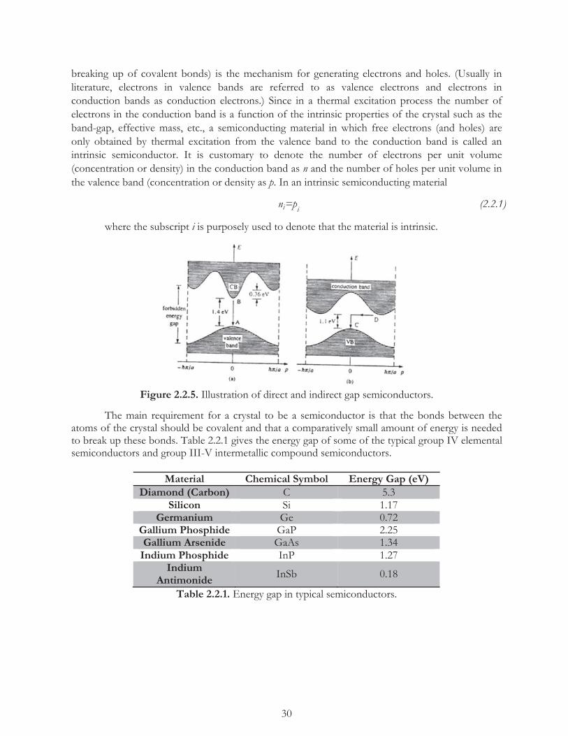
30
breaking up of covalent bonds) is the mechanism for generating electrons and holes. (Usually in literature, electrons in valence bands are referred to as valence electrons and electrons in conduction bands as conduction electrons.) Since in a thermal excitation process the number of electrons in the conduction band is a function of the intrinsic properties of the crystal such as the band-gap, effective mass, etc., a semiconducting material in which free electrons (and holes) are only obtained by thermal excitation from the valence band to the conduction band is called an intrinsic semiconductor. It is customary to denote the number of electrons per unit volume (concentration or density) in the conduction band as n and the number of holes per unit volume in the valence band (concentration or density as p. In an intrinsic semiconducting material
ni=pi (2.2.1)
where the subscript i is purposely used to denote that the material is intrinsic.
Figure 2.2.5. Illustration of direct and indirect gap semiconductors.
The main requirement for a crystal to be a semiconductor is that the bonds between the atoms of the crystal should be covalent and that a comparatively small amount of energy is needed to break up these bonds. Table 2.2.1 gives the energy gap of some of the typical group IV elemental semiconductors and group III-V intermetallic compound semiconductors.
Material Chemical Symbol Energy Gap (eV)
Diamond (Carbon) C 5.3 Silicon Si 1.17
Germanium Ge 0.72 Gallium Phosphide GaP 2.25 Gallium Arsenide GaAs 1.34
Indium Phosphide InP 1.27 Indium
Antimonide InSb 0.18
Table 2.2.1. Energy gap in typical semiconductors.

31
Figure 2.2.6. An electron in a state with energy E in the conduction band has a kinetic energy equal to E-EC. The kinetic energy is small compared with the band gap energy EC-EV. (The figure is
not drawn to scale.)
Let us now calculate the density (or concentration) of electrons in the conduction band.
When an electron is in a state that is at the bottom of the conduction band (i.e., a state with energy EC), it has no velocity and therefore no kinetic energy. Hence, we can say that the electron in this state has only potential energy. Therefore the potential energy of the electron is taken as equal to EC. The kinetic energy of the electron in a state in the conduction band with energy E is therefore equal to E-EC as shown in Figure 2.2.6. We have already seen that the conduction electrons can be considered as nearly free, and we can apply the techniques of free electron theory (i.e., treat them as electrons in a box.( The density of states in the conduction band close to the bottom of the band (i.e., close to EC), can be approximated by the density of states of free electrons or electrons in a box with one assumption. The mass of the electron is to be replaced by the effective mass determined by the curvature of the conduction band near EC. Since only states that are nearly at the bottom of the conduction band are occupied, treating these electrons as free electrons is subject to the assumption of the same effective mass for all electrons is valid. The momentum p of the conduction electrons can be readily written from the box model as
p= 2mc (E-Ec) (2.2.2)
The density of states for electrons in the conduction band is then given by
Zc E = 4 π V (2mc)32
h3(E-Ec)
12 (2.2.3)
where V is the volume of the semiconductor solid and the subscript c in Zc(E) has been used to denote the density of states in the conduction band. The density of states for electrons is shown in Figure 2.2.7. The number of electrons dnE, with energy between E and E+dE per unit volume of the crystal, is then given by
dnE= Zc E f E dEV
= 4πh3(2mc)
32(E-Ec)
12dE
(eE-EFkT + 1)
(2.2.4)
where f(E) is the Fermi function. The concentration (density) of free electrons can now be obtained by integrating Equation 2.2.4 between the limits EC and Etop where Etop is the top of the conduction band i.e., the maximum energy of the conduction band.

32
n= dnEEtop
Ec
Typically, the concentration of free electrons is very low; the states in the lower portion of the conduction band will be occupied. Two further assumptions can then be made: (1) Etop can be assumed to be infinite (i.e., the upper limit of the integral can be assumed to be ∞ instead of Etop without any appreciable error), and (2) the effective mass mc is assumed to be the same for all the electrons since the curvature of the band is the same for all the states in the bottom of the conduction band. Hence mc can be considered constant and taken outside the integral. Under these conditions, the density of electrons is given by
n= 4πh3
(2mc)32 (E-Ec)
12dE
(eE-EFkT + 1)
∞Ec
(2.2.5)
This integral has to be evaluated numerically as it stands. However, some simplifications can be made. Let us assume that EC-EF>>kT (i.e., the Fermi energy lies in the band gap at least a few kT below the conduction band minimum EC.) Since the lower value that E can have is EC, E>>EC, and hence E-EF>>kT. The equation for the electron density n can now be simplified by neglecting the unity term in the denominator to yield
n= 4πh3
(2mc)32 (E-Ec)
12∞
EceEF-EkT dE (2.2.6)
Let us define a new variable η= E-EckT
. The above integral equation can be transformed as
E-Ec12∞
EceEF-EkT dE= kT
32e
EF-EckT
E-ECkT
12eEc-EkT
d E
kT
= kT32e
EF-EckT η
12e-η dη (2.2.7)
Hence n= 4πh3
(2mc)32 e
EF-EckT kT
32 η
12
∞0
e-ηdη (2.2.8)
The integral in the right hand side of the above equation is just equal to π2
The equation for n can then be simplified to
n=2 2 πmckT
h2
32 e
-Ec-EFkT (2.2.9)
The above equation is usually written as
n=Nce-Ec-EFkT (2.2.10)
where Nc=22 πmckT
h2
32 (2.2.11)
This quantity NC is called the effective density of states in the conduction band. The reason
why NC is called so is as follows: The factor e-Ec-EFkT in the expression for n, gives the probability
that a state located at level EC will be occupied, since it can be shown that when EC-EF>>kT,

33
f Ec =1
eEc-EFkT + 1
≈e-Ec-EFkT (2.2.12)
If there are NC states located at E=EC, then we will have for n the same expression as derived above.
We can similarly calculate the number of holes in the valence band per unit volume of the crystal. While we can calculate the density of states in the valence band by methods similar to what we did for the conduction band, we must use 1-f(E) as the probability that a hole will exist in a state of energy E, which is the probability that an electron will not exist in that state.
We will consider the holes as free particles in a box. A hole at the top of the valence band has no velocity and therefore has no kinetic energy. As we go to lower energy states in the valence band, the velocity of the hole increases and therefore the kinetic energy increases. It is therefore possible to write the kinetic energy of the hole as EV-E, where EV is the energy of the top of the valence band. The density of states expression is the same as for electrons except for kinetic energy we write EV-E and is given by
Zv E = 4π V(2mv)32
h3 Ev -E
12 (2.2.13)
The density of states in the valence band is plotted in Figure 2.2.8. We can calculate as we did for the electrons, the number of holes per unit volume of the crystal. We again assume that the Fermi Energy is at least a few kT above EV, the valence band maximum. Then proceeding similarly to the case of electrons, we can show
p=2 2 πmvkTh2
32 e
-EF-EvkT =Nve
-EF-EvkT (2.2.14)
where NV is the effective density of states in the valence band and is defined as
Nv=2 2 πmvkT
h2
32 (2.2.15)
When the Fermi energy EF is a few kT below EC and also a few kT above EV, the material is called a non-degenerate semiconductor. When this condition is not satisfied, the material is called a degenerate semiconductor.
We denote the Fermi energy in an intrinsic material Ei. Since ni=pi according to Equation 2.2.1, we can write
Nce-Ec-EikT =Nve
-Ei-EvkT (2.2.16)
and also
ni2= ni×pi=Nc Nve
-Ec-EikT e
-Ei-EvkT =Nc Nve
-Ec-EvkT =Nc Nve
-EgkT
(2.2.17)
This is an important result. This shows that the electron density (as well as the hole density) in an intrinsic material depends on the width of the energy gap (band gap). This result helps us to determine the location of Ei, the Fermi energy in an intrinsic material. If we multiply both sides of Equation 2.2.16 by Ei
kT and rearrange terms we get
e2EikT= Nv
NceEc+EvkT (2.2.18)

34
Taking logarithms of both sides and multiplying by kT2
, we get
Ei=kT
2ln Nv
Nc+ Ec+Ev
2 (2.2.19)
We notice first that Ec+Ev2
represents an energy level exactly in the middle of the band gap. Secondly, if the effective mass of the electrons and that of the holes are nearly equal, the first term in the right hand side of the above equation is very nearly equal to 0. Hence we conclude that Ei, the Fermi energy in the intrinsic material, is nearly at the middle of the band gap.
Example 2.2.1
Let us now calculate the effective density of states in a semiconductor at room temperature (T=300 K). Let us assume that the effective mass mc of the electron is the same as m0, the mass of an electron in vacuum.
mc≈m0=9.11 × 10⁻³¹ kg m
k=1.38 × 10⁻²³JouleK
h=6.63 × 10⁻³⁴JouleK
Substituting these values in the expression for NC we get
Nc=22 × π × 9.11 x 10-31 × 1.38 x 10-23× 300
6.63 × 10-342
32
=2.51 × 1025 m-3=2.51 × 1019 cm-3
If we assume similarly that the effective mass of the hole, mv, is the same as that of the electron in vacuum, we will get the same value for NV.
We can now determine ni, the density of electrons or holes, in the intrinsic semiconductor.
By taking the square root of both sides of Equation 2.2.17 we can write
ni= NcNve- Eg2kT (2.2.20)
In order to express the carrier density at any temperature in terms of the number for the density of states that were calculated for T=300 K we rearrange the terms to yield
ni=2.51×10¹⁹ mcmv
m02
34 T
300
32 e-
Eg2kT cm-3 (2.2.21)
Where m0 is the mass of an electron in vacuum. This expression can more readily be used to calculate ni, the intrinsic carrier density at any temperature.

35
Example 2.2.2
Let us now calculate ni, the intrinsic electron concentration in silicon at room temperature. Substituting the following values
mc=0.29 m0
mv=0.57 m0
Eg T=300 K = 1.12 eV
We get for ni
ni= 4x2π×300×1.38×10-23×9.1x10-31
6.63×10-342
3
× 0.29×0.5732 ×e
-1.12×1.6×10-19
2×300×1.38×10-23 =2.54 ×109cm-3
We must point out that the above calculation is in error since it does not take into account the fact that there are six conduction bands in silicon and hence the effective density of states NC that we calculated must be multiplied by a factor 6. Hence the value for ni has to be multiplied by a factor 6. For our purpose, we approximate ni as ni=1.00 × 1010 cm-3. We will use this value for ni for silicon at room temperature throughout this book.
Figure 2.2.7. Density of states for electrons in the conduction band.
Figure 2.2.8. Density of states for holes in the valence band.
36
2.2.2 Extrinsic Semiconductor
The properties of an intrinsic (i.e., pure) semiconductor can be altered by adding a small amount of impurity atoms to occupy the lattice sites originally occupied by the atoms of the intrinsic material. The impurities are said to be substitutionally added since they substitute the original atom in the lattice site. This modified semiconductor is said to be extrinsic, since its properties depend on the externally added impurities. Consider, for example, an element belonging to group III in the periodic table, which is trivalent (boron, aluminum, gallium or indium). Such an atom has three valence electrons and when it substitutes a tetravalent atom of a semiconductor, the site into which it goes has only three of the four bonds completed so the fourth bond is incomplete. The boron atom is in the neutral state. This is illustrated in Figure 2.2.9A, with boron as the impurity atom. An electron from one of the covalent bonds of a nearby silicon atom can break free from its bond and jump into the incomplete bond of the boron atom. When that happens, all four bonds surrounding the boron atom are completed and an electron (a negative charge) is bound to the boron atom as shown in Figure 2.2.9A. The boron atom is now negatively ionized as shown in Figure 2.2.9B. In this process, we have a bound electron (at the site of the boron atom) and a broken bond in a nearby semiconductor atom. The broken bond represents a free hole. Since the boron atom (and all other group III elements) accepts an electron, releasing a hole in the valence band, boron and other group III elements are called acceptor impurities. When the acceptor atom accepts an electron, it becomes ionized and each ionized acceptor atom gives rise to a free hole.
If instead we substitute an atom from a group V element, which is penta-valent (such as phosphorous) we then have one more electron than the number needed to complete the four covalent bonds (tetra-valent bond) as shown in Figure 2.2.10A. This fifth electron requires very little energy to get freed from the parent phosphorous atom. When it is freed, we have a free electron in the crystal and an ionized phosphorous atom as shown in Figure 2.2.10B. We can think of the removal of the fifth electron as a positive charge bound to the site of the phosphorous atom. The bound positive charge in the phosphorous atom donates a free electron. This is called a donor impurity. A donor atom donates an electron when it is ionized and each ionized donor atom gives rise to a free electron. In Table 2.2.2, we give the ionization energy (energy required to free (A) an electron from the donor atom or (B) a hole from the acceptor atom) for some of the common impurity atoms in germanium and silicon.
Impurity Si Ge P 0.044 0.012 4 As 0.049 0.013 Sb 0.039 0.096 Bi 0.067
Table 2.2.2A. Ionization Energy in eV of Donor Atoms.
Impurity Si Ge B 0.045 0.01 4 Al 0.057 0.01 Ga 0.067 0.11 In 0.11
Table 2.2.2B. Ionization Energy in eV of Acceptor Atoms.

37
Figure 2.2.9. Substitution of trivalent boron for one of the tetravalent silicon: (A) The boron atom is neutral and an electron is missing from the covalent bond. (B) An electron breaks loose from the covalent bond of a neighboring silicon atom and jumps into the covalent bond of the boron atom in which an electron was missing. The boron atom is now negatively charged. The broken covalent
bond in the neighboring silicon atom can be thought of as a free hole.
From Table 2.2.2, the ionization energy is approximately of the same order for all the different impurities in a given semiconductor. In the case of a neutral donor atom, a single (fifth) electron is orbiting around a positive charge in a space characterized by the dielectric constant of the semiconductor. It is like a hydrogen atom, which can be described by the Bohr model. We can therefore substitute the value of permittivity of the semiconductor for the permittivity of free space in the expression for the ionization energy of the hydrogen atom to obtain the ionization energy of the donor atom. We can treat the acceptor atom similarly, where we assume a positive charge to be revolving around a fixed negative charge. It is therefore usual to assume that the energy level of the acceptor atoms is typically about 0.05 eV above the top of the valence band, and that the energy level of the donor atoms is typically about 0.05 eV below the bottom of the conduction band in silicon. This is illustrated in Figure 2.2.11. In a neutral material, the charge neutrality condition should hold. The magnitude of negative charge per unit volume should be equal to the amount of positive charge per unit volume. If in a material there are ND donor atoms in unit volume of the crystal, the amount of positive charge per unit volume is equal to
q p+ND+
and the magnitude of negative charge per unit volume is equal to qn
Equating the two we get n=p+ND
+ (2.2.23)

38
Where ND+ is the number of positively ionized donor impurities per unit volume. We have
free electrons due to two reasons: (1) thermal excitation of the valence electrons and (2) donor ionization. In the above equation, the first term on the right hand side represents the density of electrons due to thermal excitation from the valence band and the second term represents the density of electrons due to ionization of donor atoms. Since both electrons and holes carry a charge, they are called charge carriers or, more simply, carriers. According to the above equation, for a material that has donor type impurities with more electrons than holes per unit volume, it can be inferred that n is larger than p. For this reason, the electrons are called majority carriers, and the holes are called minority carriers. For the same reason, this material is called an n-type semiconductor. If we have a material with only acceptor type of impurities of density NA, then charge neutrality requires
p=n+NA- (2.2.24)
where NA- is the number of negatively ionized acceptor atoms per unit volume. Free holes are
created due to two reasons: (1) thermal excitation of valence electrons and (2) acceptor ionization. As before, the first term on the right hand side of the above equation represents the density of holes due to thermal excitation and the second term represents the density of holes due to the ionization of acceptor atoms. In this material, holes are majority carriers and electrons are minority carriers. This type of material is called p-type material. To denote the carrier density and other parameters in extrinsic materials, we use a subscript p for p-type materials, and a subscript n for n-type materials.
In practice, the purest semiconductors prepared in the laboratory have an impurity ratio of 1 in 1010 or 1011. This corresponds to approximately 1011 or 1012 impurity atoms per cubic centimeter. Therefore, the acceptor and donor impurities that are added should be greater than 1012 per cubic centimeter (cm3) to sensibly alter the properties of this material.
Figure 2.2.10. Substitution of a pentavalent phosphorus atom for one of the tetravalent silicon: (A) A phosphorus atom is neutral and there is an extra electron orbiting around the phosphorous atom
similar to the electron in the hydrogen atom. (B) The orbiting electron breaks loose due to the imparting of a small amount of energy. The phosphorous atom is positively ionized. The electron is
now free to move around in the crystal and is called the free electron.

39
Figure 2.2.11. Impurity energy levels in silicon and generation of free carriers.
2.2.3 Carrier Densities in Extrinsic Semiconductors
The expression for the thermal equilibrium density of free electrons n and free holes p in an extrinsic semiconductor is the same as what we derived earlier for an intrinsic semiconductor, since in these derivations we did not use any intrinsic property of the material. Denoting the thermal equilibrium carrier densities with a subscript 0,
n0=Nce-Ec-EikT and p0=Nve
-Ei-EvkT (2.2.25)
as long as the Fermi energy, EF, is at least a few kT below EC and a few kT above EV (i.e., the material is non-degenerate.) When the impurity concentration, ND, is approximately equal to or larger than NC in an n-type material, or when the impurity concentration, NA, is equal to or greater than NV in a p-type material, EF is closer to EC or EV by less than a few kT, and the material is said to be degenerate. In these cases, the majority carrier density is given by Equation 2.2.5 for electrons or a similar one for holes and not by the simplified expressions in Equation 2.2.25.
The expression for the center densities in Equation 2.2.25 is the same for both the intrinsic and the non-degenerate extrinsic material. The difference between the values of the carrier concentrations in intrinsic and extrinsic semiconductors arises due to the difference in the positions of the Fermi level in the two cases. Also we note, as before, that in the non-degenerate semiconductor,
n0 p0=NcNve-EgkT =ni
2 (2.2.26)
This relationship is called the law of mass action, which is valid even in the extrinsic material as long as it is non-degenerate. While ND and NA are the impurity concentrations in n and p type materials respectively, ND
+
and NA- are respectively the ionized impurity densities. The probability that an acceptor atom will
be ionized is the probability that an electron will occupy a state with energy equal to EA and this is given by the Fermi Dirac statistics. Therefore,

40
NA- = NA
1+eEA-EFkT
(2.2.27)
Similarly the probability that a donor atom will be ionized is equal to the probability that an electron will not occupy a state with energy equal to the donor energy. Hence,
ND+=ND 1- 1
eED-EFkT +1
(2.2.28)
It is possible to have both types of impurities simultaneously present in the same region of the material. Then the material becomes n or p depending on the type of impurity that is higher in density. For example, if the donor density is larger than the acceptor density, the material will be n-type. If the opposite is true, the material will be p-type. If the densities of acceptor and donor atoms are equal, then the electron and hole densities will be equal and the material is like an intrinsic material. This type of material is called a compensated material. In the fabrication of semiconductor devices, regions of n and p type are formed in the same wafer by first starting with a particular type of semiconductor with the lightest doping. Then the wafer is covered with an oxide layer by oxidizing the wafer in a furnace at high temperature. Next, windows are cut in the oxide layer and impurities of the opposite type of the starting wafer are diffused. If the wafer initially had an impurity concentration of acceptors, then donor type of impurities will be diffused through the windows in the oxide such that in a region close to the window there are more donor atoms than acceptor atoms (i.e., ND>NA.) This region will therefore have a net donor type of impurities of density ND-NA, and hence will be n-type. The majority carrier density will be equal to the net donor density. We use the net donor density in the calculation of the carrier densities instead of the total donor density. On the other hand, if NA is greater than ND, the material will be p-type and we will use the net acceptor density NA-ND in the calculation of the carrier density instead of the total acceptor density.
n-type material
Let us consider a non-degenerate n-type semiconductor. Using the subscript n for the n-type material and the subscript 0 for the thermal equilibrium, we have
nn0=ND++pn0
Hence Nce-Ec-EikT =ND 1- 1
eED-EFkT +1
+Nve-EF-EvkT (2.2.29)
The above expression is difficult to solve and has to be solved numerically. At absolute zero temperature, no donor atom is ionized and no free carriers exist. Therefore, nn0=0. The Fermi energy lies halfway between EC and ED, since a slight increase in the temperature will give rise to an equal number of electrons in the conduction band and ionized donor atoms. As the temperature is gradually raised, more and more donor atoms are ionized so the Fermi level moves downward. When the Fermi level is between EC and ED, the material is said to be in the freeze-out region. In this range of temperatures, only some of the donor atoms are ionized. This is referred to as partial ionization of the donor atoms. When the Fermi energy is close to ED, such that the electrons in the conduction band are essentially due to ionization of donor atoms, the material is said to be in the extrinsic region. When the Fermi level goes way below ED as the temperature is increased further, the material is said to be in the exhaustion region, since in this case the donor energy lies above the

41
Fermi energy and all the donor atoms are ionized. No increase in electron density can arise due to further ionization of donor atoms, since all the donor atoms are already ionized. Any further increase of electron density can arise only due to thermal excitation of the valence electrons and this happens when the temperature is increased to a much higher value. The Fermi level decreases with temperature and asymptotically approaches the intrinsic Fermi level Ei at high temperature (nn0 becomes equal to pn0). At high temperatures the material becomes intrinsic. It can be seen, then that if we want to take advantage of the properties brought about by external impurities in the semiconductor, we must limit the operating temperature so that the material is used in the extrinsic, or exhaustion range. The variation of Fermi level with temperature is shown in the upper half of Figure 2.2.12 for an n-type material with varying concentrations of impurity atoms. The effect of increasing the concentration of impurities extends the extrinsic and exhaustion range of temperatures to higher values. The minority carrier densities in a semiconductor can be obtained from the law of mass action (Equation 2.2.26). In an n-type material, the thermal equilibrium minority carrier density is therefore obtained as
pn0=ni2
nn0 (2.2.30)
Figure 2.2.12. Variation of Fermi Level with Temperature for n- and p- type semiconductor
From Equation 2.2.23 (charge neutrality expression in an n-type material), we get
nn0=ND++pn0=nn0=ND
++ ni2
nn0 (2.2.31)
Rearranging terms we obtain the following quadratic equation nn0
2 -nn0ND+ -ni
2=0 (2.2.32)
The solution to this equation is
nn0=ND++ ND
+ 2+4 ni
2
2 (2.2.33)

42
This solution to the quadratic equation corresponding to the negative sign before the radical is neglected since it will not give physically meaningful solution. It can be seen that this expression for nn0 approaches ni and ND
+ in the two limits of small and large ND+ respectively. When
ND+>> ni, as in n-type semiconductors at moderate and low temperatures,
nn0≈ND+ (2.2.34)
and pn0=ni2
nn0= ni
2
ND+ (2.2.35)
When ni>>ND+ as at very high temperatures,
nn0≈ ni
pn0= ni2
nn0=ni (2.2.36)
Example 2.2.3
Let us calculate the carrier densities in an n-type material in which the donor density is 1014 cm-3. Assume all the donor atoms are ionized at room temperature.
nn0=ND++ ND
+ 2+4 ni2
2=1014+ 1028+4 ×10²⁰
2≈ 1014cm-3
and pn0=ni2
nn0= 10
20
1014=106cm-3
p-type material
Let us now consider a p-type material. Using the subscripts p for the p-type material and 0 for thermal equilibrium in the charge neutrality Equation 2.2.24 we get
pp0=NA- +np0 (2.2.37)
where NA- is the density of ionized acceptors. But
NA- =NA
1
eEA-EFkT + 1
(2.2.38)
Therefore pp0=Nve-EF-EvkT = NA
eEA-EFkT + 1
+ Nce-Ec-EFkT (2.2.39)
This equation has to be solved numerically as before and the variation of the Fermi level with temperature is plotted in the lower half of Figure 2.2.12. For convenience we are plotting the Fermi energy variation with temperature for both n- and p- type materials in the same figure. In the pure p-type material, the Fermi level lies between EA and EV at low temperatures, and approaches the intrinsic Fermi level as the temperature is increased. The p-type material is also characterized by freeze-out, extrinsic, exhaustion and intrinsic ranges of temperatures.
Using the law of mass action, transforming Equation 2.2.37 into a quadratic equation and solving, we get

43
pp0=NA
-+ NA
-2+4 ni
2
2 (2.2.40)
As before, if NA- >> ni as in a p-type semiconductor at moderate and low temperatures,
pp0≈NA- (2.2.41)
and np0=ni2
pp0≈ ni
2
NA- (2.2.42)
When ni NA- as at very high temperatures,
(2.2.43)
and np0= ni2
pp0=ni (2.2.44)
2.2.4 Determination of the Fermi Energy
We will now derive an expression for the Fermi energy location in the band gap for an extrinsic semiconductor. As stated before the material is assumed to be a non-degenerated semiconductor.
n-type material.
In the non-degenerate n-type semiconductor, the majority carrier density can also be expressed from Equation 2.2.25 as
nn0=Nce-Ec-EFkT
Dividing both sides by NC and taking logarithms of each side and rearranging terms, we get
EF=kT ln nn0Nc+Ec (2.2.45)
Since nn0≈ ND+
EF=kT ln ND+
Nc+Ec (2.2.46)
Since ND+ is less than NC in the non-degenerate semiconductor, the term ln ND
+
Nc is negative. Hence
EF is below EC by an amount equal to kT ln ND+
Nc. This is illustrated in Figure 2.2.13A. At room
temperature, all the donor atoms can be assumed to be ionized and hence ND+= ND. Therefore,
EF=kT ln NDNc
+EC (2.2.47)
p-type material
The majority carrier density in the non-degenerate p-type semiconductor can be expressed using Equation 2.2.25 as

44
pp0=Nve
Ev-EFkT
Proceeding as we did in the case of the n-type material, we get
EF=kT ln NVpp0
+Ev (2.2.48)
But pp0=NA
- . Hence,
EF=kT ln Nv
NA- +Ev (2.2.49)
The Fermi Energy is above the valence band in a p-type semiconductor by an amount equal
to kT ln NV
NA- as illustrated in Figure 2.2.13B. At room temperature all the acceptor atoms are
assumed to be ionized. Hence,
NA- =NA
Therefore EF=kT ln NvNA
+Ev (2.2.50)
Figure 2.2.13. Location of the Fermi energy in an extrinsic semiconductor: (A) n-type material (B) p-type material.

45
Example 2.2.4
Let us now determine the location of the Fermi energy in an n-type material with a net impurity concentration of ND=5×10
15cm-3 at room temperature. Let us assume that the effective mass of the electron is the same as that of an electron in vacuum. We had calculated in an earlier example that NC under these assumptions is equal to 2.51×1019cm-3. All the donor atoms can be assumed to be ionized at room temperature. kT= 1.38 x 10-23 x 300 Joules=0.02589 eV
EF=kT lnNDNc
+EC
=0.0258 ln5×1015
2.51×10¹⁹+EC
= -0.22 eV+EC
The Fermi energy is located in the band gap 0.22 eV below the conduction band.
Carrier Densities in terms of Ei
Starting from the expression for the thermal equilibrium carrier densities n and p in terms of the Fermi energy as given in Equation 2.2.25, it is easy to show (left as a homework exercise) that
nx0=nieEF-EikT (2.2.51)
and px0=nie-EF-EikT (2.2.52)
where Ei stands for the intrinsic Fermi energy and the subscript x stands for n in a n-type material and for p in a p-type material. Therefore
EF=kT ln nx0ni+Ei (2.2.53)
and
EF=kT ln nipx0
+Ei (2.2.54)
In an n-type material,
nx0= nn0= ND+ (2.2.55)
Hence EF=kT ln nn0ni+Ei= kT ln ND
+
ni+Ei (2.2.56)
It is trivial to show that starting from Equation 2.2.54 and putting x=ni, we will get the same result. Similarly in a p-type material,

46
EF=kT ln nipp0
+Ei= kT ln ni
NA- +Ei=Ei-kT ln
NA-
ni (2.2.57)
The location of the Fermi energy with respect to Ei is illustrated in Figure 2.2.14A for n-type material and in Figure 2.2.14B for p-type material.
Example 2.2.5
Let us determine the location of the Fermi energy with respect to Ei in a p-type semiconductor with NA=1015 cm-3 at room temperature. At room temperature it is reasonable to assume that all the
acceptor atoms are ionized, (i.e., NA- ≈NA.)
EF=kT lnniNA
+Ei
=0.0259 ln1010
1015+Ei
=-0.297 eV+Ei
The Fermi energy is 0.2976 eV below Ei in the bandgap. This is illustrated in Figure 2.2.14.
Figure 2.2.14. Fermi energy in terms of the intrinsic Fermi energy: (A) n-type material (B) p-type material.

47
2.2.5 Electric Current in Semiconductors
We will now study the flow of electric current in semiconductors. According to thermodynamic treatments, the Fermi energy is equal to the sum of chemical potential (energy) and the internal electrostatic potential energy. The electrochemical potential Ϛ for electrons is given by
Ϛ = μ-qψ
where μ is the chemical potential and ψ is the electrostatic potential. Thus we see that the Fermi energy is the electrochemical potential in a solid in which equilibrium conditions exist (i.e., no externally applied electric field or no radiation is present.) When we apply a voltage across a piece of semiconductor, the thermal equilibrium conditions are disturbed. Even then, as long as there are no excess carriers, the Fermi energy is equal to the electrochemical potential. The electrochemical potential is different at the two ends of the semiconductor across which the voltage is applied. The difference is equal to the amount of the applied voltage multiplied by the electron charge. Hence, the Fermi level at one end of the semiconductor is shifted in energy with respect to the Fermi level at the other end by q times the applied voltage as shown in Figure 2.2.15. Since the material is uniform (i.e., the carrier density is the same everywhere), the conduction band and the valence band vary in direct accordance with the variation in the Fermi energy. In other words, the conduction band and the valence band are shifted from one end of the crystal to the other by the amount -qV where V is the applied voltage. The electric field is the negative gradient of the electrostatic potential ψ.
= -∇ψ (2.2.58)
In one dimension
= - dψdx
(2.2.59)
The electrostatic potential ψ is the potential energy divided by charge. We saw earlier that EC, the bottom of the conduction band, is the potential energy of the electron. The electrostatic potential is obtained by dividing by -q, and is therefore equal to
ψ= - Ecq
= - Eiq
-Eg2q
(2.2.60)
and = - dψdx
= 1q
dEcdx
= 1q
dEidx
(2.2.61)
The energy band diagram in the presence of an electric field is represented in Figure 2.2.15. The electric field is shown as being in the -x direction in this figure. Hence the gradient, according to Equation 2.2.61 is also negative and hence the bands are tilted downward to the right. The slope is constant since the electric field is constant.
We saw earlier that in the presence of an electric field, the k values and the momentum p values change by an amount proportional to the external force under steady state. Δk= F τc=
q τc (2.2.62)
Where τc is the scattering relaxation time and F is the externally applied force due to the electric field. The change in momentum correspondingly is Δp= Δk=-q τc (2.2.63)

48
Figure 2.2.15. Energy band diagram in the presence of an electric field.
Before the application of the electric field, the average momentum was zero since for every electron having a particular value of momentum, there was another electron with the opposite momentum. In the presence of the electric field, all the electrons have the same net change in momentum given by Equation 2.2.63. Since all the electrons have the same net change in momentum, the average momentum of the electrons is equal to the net change, and is given by Pav=-q τc (2.2.64)
Since the momentum is given by p=m*v where m* is the effective mass of the electron and v is its velocity, the average velocity, which is also called the drift velocity vd is given by vd=
pavm*
= - q τcm*
(2.2.65)
Equation 2.2.65 shows that the drift (average) velocity is proportional to the electric field . This is usually expressed as vd= -μ (2.2.66)
The proportionality constant is r and μ is called the mobility of the electron and is given in units of velocity per unit electric field. Typically we express mobility in units of cm2 V-1 s-1 Since we will be discussing the drift velocity of electrons as well as that of holes, we denote the parameters with a subscript n for electrons and p for holes. Therefore, for electrons vdn=-μn (2.2.67)
and μn= q τcnmn
(2.2.68)
For holes we must bear in mind that the charge is positive and therefore the externally applied force is q . Hence,
vdp= q
mpτcn =μn (2.2.69)
and μp= qτcnmp
(2.2.70)

49
Figure 2.2.16. Motion of an Electron with and without an Electric Field.
In the above equations, mn and mp are the effective masses for electrons and holes. The relaxation time due to scattering τc is also different for electrons and holes; hence different subscripts are also used to denote the relaxation time. Figure 2.2.16 shows the random motion of the electron in the absence of an electric field and the average velocity is zero (left). On the right, the motion of the electrons has a drift velocity vdn superimposed on the random motion in the presence of the electric field. If the charge carriers (viz., electrons and holes), have a non-zero drift velocity, then an electric current flows. The particle flux density can be determined as follows: since all the particles are moving with the same velocity, vdn, the particles passing through a unit cross sectional area in the next second will be only those that are within a distance numerically equal to vdn and they are equal to Particle flux density= n v
dn (2.2.71)
The electric current density is obtained by multiplying the particle flux density by the charge -q and hence the electric current density due to electron flow is Jn=-qnvdn=qn μn (2.2.72)
The current flow due to the electric field is called drift current. Similarly, the electric current density due to hole flow is given by Jp=-qnvd =qn μp (2.2.73)
The total drift current density is J=Jn+Jp. Hence J= q n μn +q n μp
The total electric current density is proportional to the applied electric field. This is called Ohm’s Law. The electrical conductivity is the electric current density per unit electric field and is given by
σ=J
Therefore σ=q (n μn+p μp) (2.2.74)
The resistivity ρ is the reciprocal of σ.
ρ= 1σ=
1q (n μn+p μp)

50
It must be pointed out that the drift current is essentially determined by the majority carriers and the contribution of the minority carriers is negligible since the majority carrier density is orders of magnitude larger than the minority carrier density. Interpretation of τcn and τcp
The mobility defines the ease with which carriers move in the semiconductor under the application of an external field and depends primarily on the effective mass of the carrier. The relaxation time τc, τcn can be interpreted as the average or mean time between scattering or collisions of the electron with a similar interpretation for τ
cp Since the random motion of the electron is due to thermal velocity, the average or mean distance traveled by the electron between collisions, denoted ln, is given by ln=vthτcn (2.2.75)
where vth is the average of the magnitude of thermal velocity. The parameter ln is called the mean free path. 1
τcn can be interpreted as the probability per unit time that an electron will be scattered.
Collisions or scattering of the electrons can be due to several mechanisms such as lattice (phonon) scattering and impurity scattering. Therefore when several scattering mechanisms are simultaneously present, the probabilities of scattering due to each of the mechanisms are added. 1
τcn= 1
τn ph+ 1
τn imp (2.2.76)
where 1τn ph
is the probability per unit time of scattering due to lattice vibrations or phonons and 1
τn imp
is the probability per unit time of scattering due to impurities. Therefore, 1
μn= 1
μn ph+ 1
μn imp (2.2.77)
Here μn ph and μn imp are the mobilities that the electron would have had if only scattering due to lattice vibrations was present or if only scattering due to impurities was present, respectively. The two scattering mechanisms have different temperature dependence.
μn ph α T-32
and μn imp α T32
1
Nimp
Similar arguments apply for hole mobility.
Figure 2.2.17 gives the variation of electron mobility with temperature for different donor concentrations. The mobility at low temperatures is limited by impurity scattering. The impurity scattering probability decreases with an increase in temperature and the mobility increases with temperature. At higher temperatures the lattice or phonon scattering probability becomes significant and the mobility starts to fall off with temperature since the scattering probability due to lattice vibrations increases with temperature. The mobility exhibits a peak at some temperature where the influence of the two scattering mechanisms is comparable. The peak shifts to the right and falls off along with height as the impurity concentrations increase since the probability of scattering due to impurity scattering increases with donor concentration.

51
Figure 2.2.17. Electron mobility versus temperature in silicon. (From Sze)
Figure 2.2.18 gives the variation of mobility with impurity concentration. The mobility is
high and fairly constant with impurity density until about 1016 cm-3 after which it falls to a lower value. The figure gives both the electron and the hole mobility variation with the total impurity concentration. In compensated materials, the mobility should be determined from this figure using the total density of impurities (the sum of donor and acceptor impurity densities). The resistivity at room temperature for silicon for different donor or acceptor concentrations is given in Figure 2.2.19. Once we know the resistivity, we know the impurity concentration. Similarly when we know the impurity concentration, we know the resistivity.
Figure 2.2.18. Electron and Hole mobility variation with impurity concentration in silicon at T= 300 K. (From Mueller and Kamins)

52
Figure 2.2.19. Resistivity variation with dopant concentration in silicon. (From Sze)
2.2.6 Diffusion
An electric current can also flow in a semiconductor due to a variation of the density of electrons and holes. The process by which the concentration variation produces carrier flow is called diffusion. In diffusion, particles flow from regions of high concentration to regions of low concentration. In Figure 2.2.20, we have assumed that electron concentration increases with x; hence electrons tend to flow from right to left. The particle flux density is proportional to the concentration gradient. The direction of flow is opposite to the gradient.
Particle flux density= - Dn∇n (2.2.78)
where Dn is the proportionality constant. This is called the electron diffusion constant. The negative sign in the equation for the particle flux density indicates that the flux of particles is in the opposite direction to the concentration gradient (∇n). Since the dimension of the left hand side of the above equation is cm-2 s-1 and the dimension of the concentration gradient is cm-4, we infer that the dimension of the diffusion constant, Dn, is cm-2 s-1. Since each electron carries a charge equal to -q, the electric current density due to diffusion is given by
Jn=qDn∇n (2.2.79)
In one dimension this becomes equal to
Jn= q Dn
dn
dx (2.2.80)
When one calculates the current flow due to hole diffusion noting that each carries a charge +q, we get for the hole current density

53
Jn= q Dp
dp
dx (2.2.81)
The electric current due to the density gradient is called the diffusion current. We saw that the electric current due to the presence of the electric field is called the drift current. The electric current density caused by electron flow is due to both diffusion and drift and is given by
Jn=q n μn + q Dndn
dx (2.2.82)
and similarly the hole electric current density is given by
Jp= q p μp- q Dp
dp
dx (2.2.83)
The total electric current density is the sum of electron and hole electric current densities and is given by
J=Jn+Jp (2.2.84)
In our discussions, we will be concerned with the diffusion current due to the minority carriers only. The diffusion current due to majority carrier density gradient will be balanced by a drift current arising from a self-induced electric field.
2.2.7 Einstein Relation
The mobility and diffusion constants are related as follows:
μn= qkTDn (2.2.85)
and μp= qkTDn (2.2.86)
This relationship is called Einstein relationship. Although this relationship can be derived, it is sufficient for our purposes to assume the relationship. It is easy to remember this relationship if
one bears in mind the dimensions of mobility has the dimension cm2 V-1 s-1 Since kTq
has the
dimension of a Volt it is easy to remember that the mobility times kTq
is the diffusion constant.
Figure 2.2.20. Variation of electron concentration with distance.

54
2.2.8 Generation Recombination Process
We saw that free electrons and holes were created by the thermal excitation of electrons from the valence band into the conduction band. The process of creating electrons and holes is called generation. Generation can be either due to thermal excitation (i.e., by imparting the electron in the valence band an amount of thermal energy sufficient to have it be excited to the conduction band) or by other means such as optically exciting the valence band or by bombardment with high energy particles. Electrons in the valence band are those that are localized in the covalent bonds. As shown in Figure 2.2.21, when a covalent bond is broken, the free electron is the electron in the conduction band and the vacancy represented in the broken bond is the hole in the valence band.
Figure 2.2.21. Illustration of connection between free electrons and free holes in the semiconductor and electrons in the conduction band and hole in the valence band.
A free electron moving in the crystal can recombine with a free hole resulting in the loss of both the electron and hole. This process is called the recombination of an electron and a hole.
There are two mechanisms by which generation-recombination process takes place: (1) band to band generation or recombination and (2) generation or recombination through an impurity or a defect. In the first process, electrons and holes recombine directly by an electron in the conduction band jumping back to a vacant state in the valence band. Physically, the recombination process is one in which the free electron wanders to the site of a broken bond and the covalent bond gets completed when the electron jumps into the broken bond. This results in the loss of a free electron and a free hole.
In the second process, electrons and holes recombine through the intermediary of an impurity or trap, which has an energy level in the band gap. Such impurities or traps are called generation-recombination centers or g-r centers. Recombination takes place by a recombination center capturing an electron or a hole and then subsequently capturing a carrier of the opposite charge. This gives rise to the annihilation or recombination of an electron and a hole.

55
Recombination centers also generate electrons and holes. Generation takes place by the center emitting an electron or a hole first and subsequently emitting a carrier of the opposite charge. Generation requires imparting energy to the solid and recombination results in the release of energy. In band-to-band recombination, energy is released in the form of light or photons. In recombination through g-r centers, energy is released as thermal (phonon) energy.
The processes of generation and recombination always require the involvement of both an electron and a hole each time the process takes place and it is customary to say that the recombination of an electron-hole pair or the generation of an electron-hole pair occurs. In silicon, the generation-recombination process occurs mostly through g-r centers and the band-to-band process is highly improbable.
Independent of the actual process, direct or indirect, the rate of recombination R, (equal to the number of electron-hole pairs lost due to recombination per unit volume in unit time), is proportional to the density of electrons and the density of holes. During the proportionality constant as r, we have
R=r n p (2.2.87)
In thermal equilibrium, the generation rate, G, which is equal to the number of electron-hole pairs generated per unit volume in unit time, should be equal to the recombination rate R. What do we mean by thermal equilibrium? When there is no externally applied electric, magnetic or electromagnetic field, the solid is in thermal equilibrium with its surroundings. Under that condition, the temperature is constant everywhere within the solid and the only way electrons are excited into the conduction band is by thermal excitation, a process called thermal generation. In thermal equilibrium, no electric current flows. We denote the carrier densities n and p with subscript 0 such as n0 and p0 to denote thermal equilibrium carrier densities. Denoting the recombination rate in thermal equilibrium as Rth, and denoting the thermal generation rate as Gth, we have
Gth=Rth=r n0 p0=r ni2 (2.2.88)
If we increase the density of one type of carriers, the probability of recombination for the other type of carriers increases. Hence the density of the second type of carriers decreases. This is the basis of law of mass action.
The thermal generation rate Gth is the rate at which electron-hole pairs are generated thermally at a given temperature, and therefore has the same value whether thermal equilibrium conditions hold no or not.
The recombination-generation process involving a g-r center has been modeled by a theoretical treatment developed by Schockley, Read and Hall. This model is called the Schockley-Read Hall model or S-R-H model. According to the S-R-H model, the constant r is given as,
r= 1n+n1Ntσpvp
+P+p1Ntσnvn
(2.2.89)
where

56
Nt = density of traps or g-r centers,
σn, σp= capture cross-sections for electrons and holes respectively
vn, vp =thermal velocity of electrons and holes respectively and is equal to 3 k T
m*, where m* is the
effective mass of the carrier
n1= Nc e-Ec-EtkT (2.2.90)
p1= Nv e-Et-EvkT (2.2.91)
Et = the trap energy level.
The capture cross-section, σ, relates to the ability (probability) of the g-r centers to capture the charge carriers. n1 and p1 are short-hand notations for the expression given in the above equations. However, one can assign a physical meaning to them. n1 is equal to the number of free electrons per unit volume in the semiconductor when the Fermi energy is at the same level as the trap energy level. Similarly, p1 is the number of holes per unit volume when the Fermi energy is at the same level as the trap level.
Let us define the terms involving electron and hole capture as follows
τn0= 1
Ntσnvn (2.2.92)
and τp0= 1
Ntσpvp (2.2.93)
Then r= 1
n+ n1 τp0+ p+ p1 τn0 (2.2.94)
The recombination rate R and Gth can then be written as
R=n p
n+ n1 τp0+ p+ p1 τn0
Gth=ni2
n+ n1 τp0+ p+ p1 τn0 (2.2.95)
The net recombination rate is the difference between R and Gth. In regions where there is thermal equilibrium, the np product is equal to ni
2 and hence the net recombination rate is zero. In regions where there is no thermal equilibrium, if the np product is more than ni
2, a net recombination will occur. If the np product is less than ni
2, then a net generation of electron-hole pairs will occur. Let us now illustrate these points by considering an extrinsic semiconductor.

57
2.2.9 Extrinsic semiconductor
We will consider an n-type semiconductor although the discussion is similar for a p-type semiconductor. Let us consider the thermal equilibrium recombination rate first.
Rth=nn0 pn0
nn0+ n1 τp0+ pn0
+ p1
τn0
= ni2
nn0τp0+n1τp0+ p1τn0 (2.2.96)
We neglected the term involving pn0 in the denominator of the above equation since pn0 nn0. Expressing n1 and p1 in terms of n1,
Rth=ni2
nn0τp0+niτp0eEt-E1kT +niτn0e
-Et-EikT
= pn0
τp0+ninn0τp0e
Et-E1kT +τn0e
-Et-EikT
(2.2.97)
Equation 2.2.97 can be rewritten as
R =pn0τp
(2.2.98)
where 1τp= 1
τp0+n1nn0τp0+
p1nn0τn0
(2.2.99)
We can infer from Equation 2.2.98 that 1τp
can be interpreted as the probability per unit time that a
hole, (i.e., a minority carrier) will combine. Using this interpretation one can show that τp is the average time that a minority carrier spends before it is lost due to recombination. Hence it is called the minority carrier lifetime. Equation 2.2.99 tells us that the minority carrier lifetime depends on the energy of the g-r center that is near the middle of the band gap.
When the trap levels are close to the middle of the gap, then the minority carrier lifetime τp becomes
τp= τpo (2.2.100)
The thermal generation rate, Gth, is equal to Rth and hence,
Gth=ni2
nn0 τp0+ n1τp0+p1 τn0=
pn0τp
(2.2.101)
We can rewrite the above equation as
pn0= Gth τp (2.2.102)

58
Which gives the interpretation that the thermal equilibrium minority carrier density is the thermal generation rate times the lifetime. Until now we only considered a g-r center with a discrete energy level. However, generally the g-r centers are distributed over a range of energies. Then the minority carrier lifetime is obtained by adding the contributions of all the g-r centers.
2.2.10 Excess Carriers
Suppose that excess carriers over and above the thermal equilibrium densities are created by illuminating the semiconductor with light or by electrical injection as we will see later on in our study of p-n junctions. This corresponds to a non-thermal equilibrium situation. The carrier densities n and p can be written as
n= nn0+ Δn (2.2.103)
p= pn0+ Δp (2.2.104)
Where nn0 and pn0 are thermal equilibrium carrier densities and Δn and Δp are called excess carrier densities. When excess carrier densities are created optically, equal number of excess holes and electrons are created and hence Δn=Δp. When excess minority carriers are injected as in a p-n junction, excess majority carriers will flow into this region to preserve charge neutrality and hence again Δn=Δp. The recombination rate in the presence of excess carriers is therefore given by
R= n p
n+ n1 τp0+ p+ p1 τn0
R=nn0+Δp pn0+Δp p
nn0+Δp+ n1 τp0+ pn0+Δp+ p1 τn0 (2.2.105)
The net recombination rate, U, is the difference between the recombination rate and the generation rate. The latter is the thermal generation rate
U=R-Gth
= nn0+Δp pn0+Δp p
nn0+Δp+ n1 τp0+ pn0+Δp+ p1
τn0-
ni2
nn0 τp0+ n1τp0+p1 τn0
=nn0pn0+ nn0+pn0 Δp+Δp
2
nn0+Δp+ n1 τp0+ pn0+Δp+ p1 τn0- ni
2
nn0 τp0+ n1τp0+p1 τn0 (2.2.106)
We will now distinguish two limiting cases, one called low injection and the other called high injection. The low injection conditions are obtained when Δp ≤ nn0.
Under low injection conditions, Δp2 is negligible and pn0 and Δp are also negligible in comparison with nn0. Hence,
U=nn0+pn0 Δp+ nn0pn0
nn0+Δp+ n1 τp0+ pn0+Δp+ p1τn0-
ni2
nn0+n1 τp0+p1 τn0

59
=nn0Δp +ni
2
nn0+n1 τp0+p1 τn0-
ni2
nn0+n1 τp0+p1 τn0
Δp
τp0+n1nn0+p1nn0τn0-
ni2
nn0+n1 τp0+p1 τn0
= Δp
τp0+n1nn0τp0+
p1nn0τn0= Δpτp
(2.2.107)
The net recombination is due to excess carriers. Therefore U is the rate of excess carrier
recombination and is proportional to Δp. In other words, 1τp
is the probability per unit time that an
excess carrier will be lost due to recombination. Therefore the excess carrier lifetime is also τp which is the minority carrier lifetime.
Under high injection Δp>nn0 so the term (nn0+n1) Δp is negligible in comparison with Δp2. Therefore
n=nn0+Δp ≈ Δp (2.2.108)
Also Gth is negligible in comparison with R. Under this condition
U=Δp2
nn0+Δp+ n1 τp0+ pn0+Δp+ p1 τn0
=Δp2
Δp τp0+τn0
= Δp
τp0+τn0 = Δp
τhi (2.2.109)
Where τhi is the lifetime of the excess carrier at high injection. Under high injection conditions, the excess carrier lifetime becomes the sum of τp0 and τn0. At intermediate injection, the lifetime is between the high injection value and the low injection value.
2.2.11 Depletion Region
We will see in our study of p-n junctions with an applied voltage that it is possible to have regions within the semiconductor under non-thermal equilibrium conditions, in which the carrier densities n and p are much less than the thermal equilibrium carrier densities. Under this condition (n≈p≈0) the recombination rate R is negligible for
R= n p Ntv0σ0n+n1+p+p1
≈0 (2.2.110)
The thermal generation rate Gth is equal to

60
Gth=ni2
n+ n1 τp0+ p+ p1
τn0
≈ ni2
n1τp0+p1τn0=
ni
τp0eEt-EikT +τn0e
- Et-EikT
= ni2τg
(2.2.111)
Where τg is defined as the generation lifetime and equal to
τg= 12τp0e
Et-EikT +τn0e
- Et-EikT (2.2.112)
The generation rate is a maximum only when the trap level Et is in the middle of the band gap (i.e., when n1=p1=ni.) Another way of stating this is that only those traps which are within a few kT above or below Ei will be effective as generation centers. When Et=Ei, τg is a minimum and equal to
τg=τp0+τn02
(2.2.113)
Thus we conclude that the thermal generation rate is ni2τg
in the non-thermal equilibrium depletion
region, while in the neutral region it is equal to pn0τp
.
2.2.12 Continuity Equation
Let us consider an elementary volume ΔV in an n-type semiconductor. In this elementary volume minority carriers are being thermally generated at a rate Gth and we assume that minority carriers are also generated at a rate Gopt due to external light sources. Minority carriers are also lost due to recombination at rate R. In addition, if there is an outward flow of current out of this elementary volume, then the minority carriers will be lost if the minority carriers are holes, and minority carries will increase in number if the minority carriers are electrons. Since we are considering an n-type semiconductor, the minority carriers are holes in our example.
The total outward flow of current out of a volume surrounded by a surface is equal to
Jp· dSsurface= ∇ ·Jp· dVvol
(2.2.114)
In an elementary volume ΔV, the outward flow of current reduces to ∇·Jp ΔV. The outward flow
represents the charge flow, and hence the number of holes lost in unit time is equal to 1q∇·JpΔV.
We can write the rate of increase of the number of holes in the elementary volume as
δpδtΔV=ΔV(-R+Gth+Gopt-
1
q∇·Jp) (2.2.115)

61
Dividing the above equation by ΔV we get
δpδt
= -R+Gth+Gopt-1
q∇·Jp (2.2.116)
This equation is called the continuity equation. From our earlier discussion, we know that
R-Gth= Δpτp
(2.2.117)
Hence the continuity equation reduces to
δpδt= δ Δp
δt=- Δp
τp+Gopt-
1
q∇·Jp (2.2.118)
But Jp=qμppE-qDp∇p (2.2.119)
In one dimension, the continuity equation reduces to
δ Δpδt=- Δp
τp+Gopt-
1
q
dJp
dx (2.2.120)
The expression for the hole current density is given by
Jp=qμppE-qDpδpδx
(2.2.121)
Let us assume that the electric field is zero.
Jp= -qDpδpδx
Then δ Δpδt= - Δp
τp+Gopt+Dp
δ2Δpδx2
(2.2.122)
2.2.13 Growth of Excess Carriers
Let the light be switched on a time t = 0. Since the excess carriers are uniformly generated everywhere in the semiconductor, there is no concentration gradient, and hence the term due to the current flow can be dropped in the continuity equation. The continuity equation governing the growth of the excess carriers is then given by
dΔp
dt=- Δp
τp+Gopt (2.2.123)
The solution to this equation can be readily seen to be
Δp(t)=Goptτp 1-e-tτp =Δp0 1-e
-tτp (2.2.124)

62
Where Δp0=Goptτp is the excess carrier density at t=∞ (i.e., when steady state conditions have been reached.) Equation 2.2.124 describes that the excess carrier density grows exponentially with time from zero to its steady state value.
Decay of excess carriers
Let us assume that the light has been on for a long time, and that steady state conditions have been reached. Now, let the light be turned off at time t=∞. The decay of excess carrier density will be governed by putting Gopt=0 in the continuity equation, which will then be
dΔp
dt=- Δp
τp (2.2.125)
The solution to this equation is
Δp t =Δp0e-tτp (2.2.126)
Where Δp0 is the excess carrier density just when the light was turned off, (i.e., at t=0.) From the above treatment, we can conclude that the time taken to reach steady state during the growth and the decay of excess carriers is determined by the minority carrier lifetime.

63
Chapter 2.2 Summary
A semiconductor behaves like an insulator at very low temperatures, but it exhibits increasing electrical conductivity as the temperature is increased. The electrical conductivity of a semiconductor at room temperature is much lower than that of a conductor but much higher than that of an insulator. As the temperature is raised in a semiconductor, some of the electrons get enough thermal energy to break loose from the covalent bond and become free electrons. Similarly, the broken bonds represent free holes. In terms of band picture, at very low temperatures the valence band is completely full and the conduction band is empty. Additionally, the band gap (the separation in energy between the conduction and valence bands) is small. As the temperature is increased, the electrons get excited from the valence band to the conduction band. The electrons in the conduction band are the free electrons while the vacant states in the valence band are free holes. Since an electron has a charge of –q coulombs and a hole has a charge of q coulombs, the charge moves with them when they move. Hence electrons and holes are called charge carriers, or simply carriers.
An intrinsic semiconductor is one in which electrons and holes are only generated by thermal excitation from the valence band to the conduction band. The free electron density is equal to the free hole density (ni=pi). The electron has no velocity when it occupies a state at the bottom of the conduction band, and hence has no kinetic energy. EC, the bottom of the conduction band, is the potential energy of the electron. An electron that occupies a state with energy E has a kinetic energy is E-EC. Similarly, the potential energy of the hole is EV and its kinetic energy is EV-E. In other words, the kinetic energy of the hole increases as we go deeper into the valence band.
Free holes and free electrons can be treated as particles in a box by assuming the appropriate effective masses for the electrons and holes. The probability of occupation of a state by an electron is given by the Fermi function, f(E). The probability of occupation of a state by a hole is the probability that an electron will not occupy that state, 1-f(E).
In deriving the expression for the density of electrons and holes, a numerical integration is necessary. This procedure can be simplified by assuming that the Fermi energy is at least a few kT below the conduction band and at least a few kT above the valence band. When the assumption is not valid in a material, the semiconductor is said to be degenerate. The Fermi function approximates the Boltzmann distribution function. Hence this approximation is also called the Boltzmann approximation.
The electron (and hole) density in an intrinsic semiconductor is determined by the band gap energy Eg and the effective masses. It is also a strong function of temperature. The Fermi energy is approximately at the middle of the band gap in an intrinsic material. If the effective masses of the holes and the electrons are assumed to be equal to the mass of the

64
electron in vacuum, then the Fermi energy lies exactly at the middle of the band gap. The Fermi energy in an intrinsic material is denoted by Ei, and hence it is customary to denote the middle of the bandgap as Ei.
An extrinsic semiconductor is one in which controlled amount of trace impurities are substitutionally added to increase either electron or hole carriers. When elements of group V are added as impurities in silicon, the electron density is increased without a corresponding increase in the free hole density. These impurities are called donors, and the material is called an n-type semiconductor. In an n-type semiconductor, electrons are called majority carriers and holes are called minority carriers since the electron density is much larger than the hole density. On the other hand, when impurity atoms belonging to an element in group III of the periodic table are added, the hole density is larger than the electron density. This type of material is called a p-type semiconductor. In this type of material, holes are called majority carriers and electrons are called minority carriers.
In an n-type semiconductor, free electrons arise due to two reasons: thermal excitation from the valence band, and thermal excitation from the donor atoms (ionization of the donor atoms). The holes in an n-type material arise only due to thermal excitation of electrons from the valence band. The positive charge in an n-type semiconductor arises due to free holes and positively ionized donor atoms while the negative charge arises due to free electrons.
In a p-type semiconductor, free holes arise due to two reasons: thermal excitation of electrons from the valence band, and ionization of acceptor atoms. The electrons arise only due to thermal excitation from the valence band. The positive charge in a p-type material arises due to free holes, while the negative charge in an n-type material arises due to electrons and negatively ionized acceptor atoms. In a neutral semiconductor, (n-type or p-type) the net charge density is zero. When both acceptors and donors are present in the same region, the net impurity density (the donor density minus the acceptor density) determines the type of semiconductor. Such a material is called a compensated material.
The expression for the carrier density in an extrinsic semiconductor can be derived similarly to the expression for an intrinsic material. For a high density of impurities, the carrier density can only be obtained by numerical integration. However, when the impurity density is not that high, the material can be considered to be non-degenerate and the expression for the carrier density is the same form as what is obtained in the intrinsic case under the non-degenerate assumption. In a non-degenerate semiconductor, np=ni
2. This is called the law of mass action. When the electron density is increased by adding donor impurities, the hole density decreases. Similarly, when the hole density is increased by adding acceptor impurities, the electron density decreases. The number of ionized impurities increases with

65
temperature. At moderate and low temperatures, the majority carrier density is equal to the ionized net impurity atoms.
In an n-type material the Fermi energy lies in the upper half of the band gap. As the donor density is increased, the Fermi energy moves closer to the conduction band. In a p-type material the Fermi energy lies in the lower half of the band gap. As the acceptor density is increased, the Fermi energy moves closer to the valence band.
At high temperatures, all the impurity atoms are ionized and an increase in carrier density arises only by thermal excitation from the valence band. At still higher temperatures, the electron and hole densities become equal and the material becomes intrinsic.
An electric current in a semiconductor can arise from either a drift or a diffusion process. In the drift process, an externally applied electric field drives the charge carriers. The resulting current is called the drift current. The drift current can be expressed in terms of a parameter called the mobility. The drift current is generally due to majority carriers. In the diffusion process, carriers diffuse from regions of high concentration to regions of low concentration resulting in a current called the diffusion current. The diffusion current is expressed in terms of a constant called the diffusion constant. The diffusion current is due to minority carriers only.
The diffusion constant is related to the mobility by a factor kTq
. This relationship is called
the Einstein relation. Mobility is limited by scattering from impurity atoms or scattering from phonons. The two processes have different temperature dependence.
In a semiconductor, electrons and holes are constantly being created (generated) and lost due to recombination. Recombination is the process in which an electron in the conduction band jumps back to a vacant state in the valence band. In this manner, both an electron and a hole have been annihilated. In steady state, the generation rate is equal to the recombination rate.
There are two mechanisms for generation-recombination to occur. One is what is called the band-to-band generation-recombination. The second is called generation-recombination through a trap or a generation-recombination (g-r) center. In silicon, the latter is the dominant mechanism. The average time that a minority carrier spends in its band before it is lost due to recombination is called the minority carrier lifetime. The thermal equilibrium minority carrier density is given by the product of the thermal generation rate and the minority carrier lifetime. The minority carrier lifetime is inversely proportional to the density of g-r centers. When excess carriers are generated, the process is called injection of carriers. The average time an excess carrier spends in its band before it is lost due to
66
recombination is called excess carrier lifetime. The steady state excess carrier density is given by the product of the excess carrier generation rate and the excess carrier lifetime.
When the excess carrier density is much less than the thermal equilibrium majority carrier density, it is called a low injection process. When the excess carrier density is comparable to or higher than the thermal equilibrium majority carrier density, it is called a high injection process. Under low injection, the excess carrier lifetime is the same as the minority carrier lifetime. The growth and decay of excess carriers is governed by the excess carrier lifetime when the generation process is switched on or off respectively. The flow and growth (or decay) of excess carriers is determined by solving the continuity equation.

67
Chapter 2.2 Glossary
dNE number of electrons with energy between E and E+dE per unit volume of the crystal
dV elementary volume
Dn electron diffusion constant
Dp hole diffusion constant
E energy
EA acceptor energy level
EC bottom of the conduction band, also the potential energy of an electron in the bottom of the conduction band
ED donor energy level
EF Fermi energy
Eg bandgap equal to EC-EV
Ei Fermi energy in an intrinsic material, usually referred to as the intrinsic Fermi energy
Et trap level or energy level of the g-r center
Etop top of the conduction band or the maximum energy of the conduction band
electric field
f(E) Fermi function; the probability of occupation by an electro
G generation rate
Gopt rate at which minority carriers are generated by an external light source
Gth thermal generation rate
h Planck’s constant
J total current density
Jn electric current density due to electron flow
Jp electric current density due to hole flow
k Boltzmann constant
ln average distance travelled by the electron between collisions
m0- the mass of an electron in vacuum
mc effective mass of an electron in the conduction band
mn, mp effective masses for electrons and holes respectively
mv effective mass of hole in the valence band
68
m* effective mass of the carrier
n0, p0 thermal equilibrium carrier densities
n1 number of free electrons per unit volume in the semiconductor when the Fermi energy is at the same level as the trap energy level
n electron density
ni density of electrons or holes in the intrinsic semiconductor
n0 thermal equilibrium electron density in the n-region
nx0 thermal equilibrium electron density in the x-type of semiconductor where x is n or p
NC effective density of states in the conduction band
Nt density of traps or g-r centers
NV effective density of states in the valence band
NA density of acceptor atoms
NA- density of ionized acceptors, number of negatively ionized atoms per unit volume
ND density of donor atoms
ND+ density of ionized donors, number of positively ionized atoms per unit volume
p density of free holes
P momentum of carriers
p1 number of holes per unit volume if the Fermi energy is at the same level as the trap level
pn0 thermal equilibrium hole (minority carrier) density in an n-type semiconductor
pp0 thermal equilibrium hole (majority carrier) density in a p-type semiconductor
px0 thermal equilibrium hole density in x-type material where x is n or p
q charge
r proportionality constant for recombination rate
R recombination rate
Rth recombination rate at thermal equilibrium
t time
T temperature in degrees Kelvin (K)
U net recombination rate, the recombination rate minus the generation rate
v velocity
vd average velocity, also called the drift velocity

69
vdn, vdp drift velocity of electrons and holes, respectively
vn, vp thermal velocity of electrons and holes, respectively
V volume of a semiconductor solid
Zc(E) density of states for electrons in the conduction band
Δn excess electron density
Δp excess hole density
Δp change in momentum
Δp0 excess carrier density at t=∞
ΔV elementary volume
ideality factor
μ mobility of the carriers
μn electron mobility
μn imp mobility that an electron would have if scattering were due only to impurities
μn ph mobility that an electron would have if scattering were due only to lattice vibration
μp hole mobility
ρ resistivity, the reciprocal of σ
σ electrical conductivity
σ capture cross-section
σn, σp capture cross-sections for electrons and holes respectively
τC scattering relaxation time or average time between collisions
τCN average time between scattering or collisions suffered by the electron
τCP average time between scattering or collisions suffered by the hole
τP hole lifetime, i.e. average time that a minority carrier spends before it is lost due to recombination
ϕ electrostatic potential
ψ electrostatic potential
70
Chapter 2.2 Problems
1. Derive an expression for the density of holes in a non-degenerate semiconductor using a method similar to that used in the text for the derivation of an expression for the density of electrons.
2. Given that ni= 1010 cm-3 at T=300 K, calculate ni at T=200 K and at T= 150 K assuming Eg=1.12eV at all temperatures (i.e., neglecting variation of Eg with temperature).
3. A piece of silicon is doped with 2×10¹⁵ phosphorus atoms per cm3. What are the majority and minority carrier concentrations at room temperature?
4. Suppose that the hole concentration in a piece of silicon at room temperature is 105 cm-3, find the (a) electron concentration (b) location of the Fermi energy
5. A sample of silicon is first doped with 1015 cm-3 boron atoms, and then doped with 4x10¹⁵
cm-3 arsenic atoms. (a) What is the type of the semiconductor? (b) Find the location of the Fermi energy.
6. For an n-type semiconductor, at higher temperatures electrons come from ionization of the
donor atoms as well as from excitation of electrons from the valence band to the conduction band. If ND
+ is the donor density, show that the intrinsic carrier density, at the
temperature at which the electron density is twice that of the hole density, is 2ND+ .
7. Find the resistivity of the same in Problem 4. Take the mobility values from the figure in
the text. 8. Using the mobility curves in the text, find the resistivity of the sample in the Problem 5. 9. A piece of n-type silicon has a resistivity of 5 Ω-cm at room temperature (27 °C). Find the
thermal equilibrium concentration at 17 °C. 10. Two scattering mechanisms are present in a semiconductor. The mobility, if the first
mechanism alone is present, is 500 cm2 V-1 s-1. The mobility, if the second mechanism alone is present, is 900 cm2 V-1 s-1. What is the mobility of the carrier in the sample?
11. If an intrinsic piece of silicon is illuminated such that carriers are generated at the rate of
1018 cm-3 s-1 uniformly everywhere in the sample and if the lifetime of the carriers is 10-6 s, determine the change in the electrical conductivity.

71
12. Write the expression for the total electron current in a semiconductor. From this write the
relation between the concentration gradient dndx
and n(x) under conditions of no current flow.
13. Show that the probability that a hole will survive without recombining for t seconds is given
by e-tτp assuming that it was created at time t=0 and that 1
τp is the probability that a hole will
recombine in unit time. 14. Show that the average time that a hole lasts without recombining is τp seconds. Assume that
the hole was created at time t=0. (This is why τp is called the hole lifetime.) 15. Consider an n-type silicon sample with Nd = 1016 cm-3. Calculate the location of the Fermi
level at (a) 300 K (b) 200 K
72
Chapter 3 P-N Junction
A p-n junction is a device structure in which a single crystal of a semiconductor, such as silicon, has one region doped with donor impurities to make it n-type while the rest of the semiconductor is doped with acceptor impurities to make it p-type. For example, Figure 2.3.1 shows the impurity variation from one end of the crystal to the other. This figure is called the impurity profile. The y-coordinate is the net impurity concentration ND-NA, which is positive in the n-type region and negative in the p-type region. The abscissa is x, position.
Let us now consider an isolated p-type semiconductor. The net impurity concentration ND-NA is negative. The density of states in the two bands is plotted in Figure 2.3.2A. The Fermi distribution function is plotted for a p-type material in Figure 2.3.2B. The Fermi energy is close to the valence band as shown in Figure 2.3.2B. The probability of occupation by electrons (i.e., the Fermi function) is nearly zero in value for states in the conduction band whereas the probability of occupation by holes (i.e., 1 minus the Fermi function), is much larger for states in the valence band. The distribution of electrons in the conduction band and the holes in the valence band is obtained by multiplying the density of states and the probability of occupation, and is given in Figure 2.3.2C. The area under these distribution curves gives the number of carriers in the conduction and the valence band. As is to be expected in a p-type semiconductor, a small density of electrons and a large density of holes are obtained.
Let us now similarly consider an isolated n-type semiconductor. The net impurity concentration ND-NA is positive. Again the density of states in the two bands is plotted in Figure 2.3.3A. The probability functions for the occupation of states by electrons and holes are plotted in Figure 2.3.3B. The distribution of carriers in the two bands is given in Figure 2.3.3C. We see now in the n-type material a small density of holes and a large density of electrons are obtained.
Before going further we will now show that the gradient in Fermi energy is zero when no electric current flows. Let us consider the electric current due to electron flow. The electric current is given by
Jn=q n μn E+q Dndn
dx (2.3.1)
But we know that under thermal equilibrium,
n0=nieEF-EikT (2.3.2)
Where we have used the subscript 0 to denote thermal equilibrium densities, and
=- dψdx= 1q dEidx
(2.3.3)

73
Figure 2.3.1. Impurity profile in a p-n junction. This junction is called an abrupt junction since the net impurities change from one type to the other abruptly.
Figure 2.3.2. Carrier distribution in an isolated p-type semiconductor. (A) Plot of the distribution of density of states in the valence and in the conduction band. (B) Plot of f(E) (Fermi function) and
1-f(E). (C) Distribution of electrons and holes in the respective bands.

74
Figure 2.3.3. Carrier distribution in an isolated n-type semiconductor. (A) Plot of the distribution of density of states in the valence and in the conduction band. (B) Plot of f(E) (Fermi function) and
1-f(E). (C) Distribution of electrons and holes in the respective bands.
differentiating the equation for n we get
dn0dx= n0kT
dEFdx
- dEidx
(2.3.4)
Substituting the above values of dndx
and in Equation 2.3.1 we get
Jn=q n μn1
q dEidx
+q Dnn0kT
dEFdx
- dEidx
(2.3.5)
Recalling Einstein’s relation which is
μn=Dnq
kT (2.3.6)
we can write Jn as
Jn=n0 μn dEidx+n0 μn
dEFdx
-n0 μn dEidx=n0 μn
dEFdx
(2.3.7)
Similarly Jp=p0 μp dEFdx
(2.3.8)
When dEFdx
is equal to zero, Jn is zero, which means that under conditions of no current flow,
EF is constant and does not vary with distance. Under that condition Jp is also zero. Another way of stating this is that under thermal equilibrium conditions, no current flows and that the Fermi energy does not vary with x.
75
2.3.1 P-N junction Under Thermal Equilibrium
The p-n junction is in thermal equilibrium when no external voltage is applied. Hence no electric current flows through the junction and the Fermi energy is constant and does not vary with distance. Let us define the metallurgical junction as the plane at which the semiconductor changes from p-type to n-type and assume that it is located at x=0. EF is closer to EV on the p-side and closer to EC on the n-side. (Recall the discussion on the location of the Fermi energy in the band gap of extrinsic semiconductor in Chapter 2.) This means that in order for EF to be constant with x, EC has to decrease with x as we pass through the metallurgical junction from the p-side to the n-side. On the p-side far away from the junction, there is no electric field and hence EC is constant (i.e., does not vary with distance) and is separated from EF by an amount determined by the net ionized acceptor concentration NA
-. EF is below the intrinsic Fermi energy level Ei, by an amount given by
Ei-EF=kT ln NAni
(2.3.9)
Similarly on the n-side far away from the junction, EC is constant and is separated from EF by an amount determined by the net ionized donor concentration ND
+. EF is above the intrinsic Fermi energy level Ei by an amount given by
EF-Ei=kT ln ND+
ni (2.3.10)
However, close to the junction, EC (potential energy) and therefore Ei and EV vary gradually from their respective values on the p-side to their values on the n-side. This region where the potential energy varies is called the transition region. In this region, there is an electric field since EC and the electrostatic potential varies. Outside the transition region the electric field is zero. Since the electric field lines emanate (flow out) from the positive charges and terminate on negative charges, the transition region comprises of positive charges on one side and negative charges on the other side. The charge density in the transition region is non-zero whereas the charge density is zero outside the transition region. For this reason the transition region is called the space charge region since it has a net charge density. The region outside the transition region is called the neutral region since it has no net charge density. How does space charge arise? In the transition region on the n-side, the electron density is much less than the thermal equilibrium majority carrier density so a charge density equal to the magnitude of the electrical charge multiplied by the ionized donor atom density arises in this region. Similarly hole density is less than the thermal equilibrium majority carrier density value in the transition region on the p-side. Thus there is a region on the p-side close to the metallurgical junction with a net negative charge density equal to the electron charge times the ionized acceptor atom density. Electric lines of force emanate from the positive charge on the n-side and terminate on the negative charge on the p-side.
Another way of looking at the origin of the transition region is as follows: Let us assume that the p-n junction is formed by fusing a p-type semiconductor and an n-type semiconductor together. As soon as the two pieces of semiconductor have been joined together, electrons, which are large in number in the n-region diffuse to the p-region where there are only a few of them. Thus there is diffusion current. The diffusion of electron charges the p-region negative with respect to

76
the n-region and therefore the potential energy of the electrons on the p-side rises relative to the n-side (i.e., a potential energy barrier arises between the n and p regions.) This gives rise to an electric field in the transition region due to the gradient of the potential energy since the potential energy changes with x from the p-side to n-side. This electric field causes a drift flow of electron current in the direction from the p-side to the n-side (i.e., in the opposite direction to the diffusion current.) The potential energy barrier in the transition region reduces the diffusion current and hence fewer electrons diffuse and resulting in a reduction in the rise of potential energy. Ultimately a steady state condition is met where the potential energy barrier is of a magnitude where the drift current is exactly equal and opposite to the diffusion current. As a result, no net current flows through the junction. In the transition region on the n-side there is a net positive charge density due to the ionized donor atoms since electrons leave this region to initially go to the p-side. Similarly, in the transition region on the p-side, there is a net negative charge density due to the majority carriers (viz., holes having been neutralized by the electrons that came from the n-side.) We discussed this model as though electrons initially went from the n-side to the p-side. We would have arrived at the same conclusion if we had assumed that holes initially diffused form the p-side to the n-side.
Let us define the electrostatic potential ϕ as
=- ECq
+ constant= - Eiq
-Eg2q+constant (2.3.11)
The purpose of the constant is to reference the electrostatic potential to a particular reference or
zero value. Since EF is constant with distance, choose the constant as Eg2q+ EF
q. Then ϕ becomes
= - Eiq+ EF
q=
EF-Eiq
(2.3.12)
ϕ, the electrostatic potential, varies with the distance x in the transition region. Since n0, the thermal equilibrium density of electrons, is given by
n0=ni eEF-EikT (2.3.13)
We can express n0 as
n0= nie qkT (2.3.14)
Similarly, since p0, the thermal equilibrium density of holes, is given by
p0=ni eEi-EFkT (2.3.15)
we can express p0 as
p0= nieqkT (2.3.16)
Thus, both the electron and the hole densities vary with distance x in the transition region. By taking the logarithm of both sides of Equations 2.3.14 and 2.3.16, we can express the electrostatic potential in terms of the thermal equilibrium carrier densities.

77
= kTqln n0
ni (2.3.17)
and also =- kTqln
p0ni
(2.3.18)
These two equations relate the potential variation with thermal equilibrium carrier density variation.
ϕ, the electrostatic potential, defined as above, can also be used in the neutral semiconductor. In a neutral n-type semiconductor, n0, the thermal equilibrium electron density, is equal to nn0, the thermal equilibrium majority carrier density which is equal to ND
+, the ionized donor density, Substituting ND
+ for n0 in Equation 2.3.14 we find that ϕ, the electrostatic potential in the neutral semiconductor, is given by
n= kTqln ND
+
ni (2.3.19)
where we have used a subscript n in ϕ to denote the electrostatic potential in a neutral n-type semiconductor. Similarly we can define an electrostatic potential for a p-type material as
p= - kTqln
NA-
ni (2.3.20)
where we have used a subscript p in ϕ to denote the electrostatic potential in a neutral p-type semiconductor.
Example 2.3.1
Let us now calculate the electrostatic potential ϕ for a p-type silicon that has a concentration of 1016 cm-3 acceptor atoms at room temperature. We assume that at room temperature all the impurity atoms are ionized, i.e., NA
-=NA. Let us take ni as equal to 1×1010cm-3.
p= -kTqlnNA-
ni
= -.02585 × ln10 16
1×1010
=-0.02585 × 13.81= -0.357 V
Let us now go back to the space charge region. Differentiating n0- given in Equation 2.3.14 we obtain
dn0dx=n0
q
kT
d
dx (2.3.21)
This yields
dn0=n0q
kTd (2.3.22)

78
which can be written as
d = kTq
dn0n0
(2.3.23)
We can integrate Equation 2.3.23 to obtain the potential difference between two points say A and B in a semiconductor. The potential difference ϕA-B is equal to
A-B= d = kTq
dn0n0
AB
AB
= kTqln nA
nB (2.3.24)
We can use this result to obtain an expression for the potential barrier that exists between the n-side and the p-side in a p-n junction. This potential barrier is called the built-in voltage since it is already in existence in a p-n junction under thermal equilibrium. This built-in voltage which is denoted by Vbi is the potential difference between the neutral n-side and the neutral p-side and according to the above equation, is equal to
Vbi=kT
qln nn0
np0= kT
qln
nn0pp0
ni2 = kT
qln
NA-ND+
ni2 (2.3.25)
Equation 2.3.25 can be rewritten as
Vbi=kT
qln ND
+
ni+ln
NA-
ni (2.3.26)
We could have arrived at the same result by a different route also. We know ϕp and ϕn, the electrostatic potentials of the neutral p and the n region, respectively. The built-in voltage Vbi is the electrostatic potential difference between the neutral n and the p regions.
Hence
Vbi= n- p (2.3.27)
Since ϕp is negative from Equation 2.3.20 we can write
Vbi= n+ p = kTqln ND
+
ni+ln
NA-
ni (2.3.28)
which is the same result that we obtained before.
Example 2.3.2
Let us now determine the built-in potential for a p-n junction in which the n-region is uniformly doped with a net donor concentration of 2×1016 cm-3 and the p region is uniformly doped with a net acceptor concentration of 1×1015 cm-3. Assume room temperature and that all the impurity atoms are ionized. From Equation 2.3.25 we find

79
Vbi=0.02585 × ln2x1016x1x1015
1×10102
=0.02585 × 26.02
=0.673 V
An abrupt p-n junction is one in which the net acceptor density is uniform in the p-region and the net donor density is uniform in the n-region. The impurities change from acceptor to donor type abruptly as we go across the metallurgical junction. In Figure 2.3.4A the abrupt junction is shown with the metallurgical junction at x=0. The p and the n regions are connected externally by a copper wire. The junction is therefore in thermal equilibrium. In Figure 2.3.4B is shown the band bending (i.e., the bending of EC, Ei and EV), that occurs in the transition region as we go from the p-side to the n-side. The built-in voltage is the difference between the potential energy on the p-side and that on the n-side divided by q. In other words, it is equal to the amount of band bending divided by q. In Figure 2.3.4C the space charge distribution is shown in the transition region. The charge density in the transition region is due to the ionized impurity atoms that are not compensated by equal number of majority carriers. Hence the charge density in the space charge region is ρ=-qNA on the p-side and ρ=+qNA on the n-side. Since the p-n junction is in thermal equilibrium, EF is constant and does not vary with x. On the other hand Ei varies with x in the depletion region. The electron density and the hole density in the specie-charge region are given by
n=ni eEF-EikT
and p=ni e-EF-EikT
Hence n and p vary with position, x, in the depletion region. The electron density decreases from nn0, the thermal equilibrium majority carrier concentration on the n-side, to np0, the thermal equilibrium minority carrier concentration on the p-side. The electron density in the portion of the transition (space charge) region lying on the n-side is less than nn0 the thermal equilibrium majority carrier density in the neutral n-region. Hence this region has a net charge density equal to a ND
+ and is depleted of electrons. By a similar argument, the portion of the transition region on the p-side is depleted of holes and the charge density in this region is –qNA
+. The carrier densities are smaller than the thermal equilibrium majority carrier densities in respective portions of the entire space charge region. Hence the space charge region is depleted of charge carriers and the space charge region is usually referred to as the depletion region. The product of the electron and the hole densities anywhere in the transition region is equal to the square of the intrinsic carrier concentration since the junction is in thermal equilibrium, (i.e., the law of mass action is obeyed.) At the two edges of the space charge region, the charge density gradually approaches zero as shown in Figure 2.3.4C since the carrier densities change gradually. However for ease of calculation and analysis, we approximate the space charge density distribution as a rectangular distribution in which the charge density becomes zero abruptly at the two edges as shown in Figure 2.3.4D. We assume here that the negative charge density due to ionized acceptors exists between x=-xp and x=0 and the positive charge density due to ionized donors exists between x=0 and x=xn. The electric field variation in the space region is shown in Figure 2.3.4E. Outside the space charge region, the electric

80
field is zero. Inside the space charge region, the electric field varies linearly and the magnitude reaches a maximum value at the metallurgical junction. The electric field is the negative gradient of the electrostatic potential. Therefore the line integral of the electric field yields the electrostatic potential difference between two points. The area under the plot of the electric field in Figure 2.3.4E is equal to the built-in voltage Vbi. The linear variation of the electric field in the space charge region is based on the assumption that the impurity density is constant in each region and that it changes from one type to the other abruptly at the metallurgical junction.
Figure 2.3.4. (A) An abrupt p-n junction with the metallurgical junction at x=0. (B) Bending of the band at the junction. The built-in voltage is the difference in the potential energy between the two sides divided by the electron charge q. (C) The actual space charge region with the charge density
gradually approaching zero at the two edges. (D) Approximation by a rectangular charge density in which the density abruptly goes to zero at the edges. (E) Electric field variation in the space charge
region.
2.3.2 Space Charge Region
We will now calculate the potential distribution and the width of the space charge region in the abrupt junction. There are two ways by which one can determine the space charge region characteristics: (1) using the Poisson equation and (2) using Gauss’s theorem. Both the approaches are the same from the physics point of view. In certain cases one method may be more direct while in some other cases the other method may be more direct. Hence we will consider both the methods.

81
Poisson Equation
The Poisson equation is given by
d2
dx2= - ρ
ϵs (2.3.29)
Let us assume that the metallurgical junction is at x=0 and the space charge region is approximated by the rectangular density shown in Figure 2.3.4D bounded by x=-xp on the p-side and x=xn on the n-side. The charge density in the various regions can then be written as
For x<-xp ρ=0
For –xp<x<0 ρ=-qNA
For 0<x<xn ρ=-qND+
For x>xn ρ=0
In the space charge region, under steady state conditions, all the impurity atoms are ionized even at low temperatures (i.e., ND
+=ND and NA- =NA.) This is in contrast to the neutral region where the
impurity atoms are partially ionized at low temperatures. Let us consider the space charge region (the depletion region) on the p-side.
ρ=- qNA=- qNA
The Poisson equation is given by
d2
dx2= qNA
ϵs (2.3.30)
Integrating the above equation we get
d
dx= qNAx
ϵs+C1 (2.3.31)
where C1 is an integration constant.
Since the electric field in the neutral region is 0, ddx
must be equal to 0 at x=-xp. Applying
this boundary condition we obtain
C1=qNAxp
ϵs (2.3.32)
And substituting this value of C1 in the equation for ddx
we get
d
dx= qNA
ϵsx+xp (2.3.33)
Again integrating
= qNA2ϵs
x2+ qNAϵsxpx+C2 (2.3.34)
82
Where C2 is an integration constant. Starting with the charge density in the n-side, which is equal to
ρ=q ND+=q ND
We get
d2
dx2= - qND
ϵs (2.3.35)
Integrating,
d
dx=- qNDx
ϵs+C1
' (2.3.36)
Where C1’ is an integration constant. Using the boundary condition that the electric field (- d
dx) is
zero in the neutral n region and hence ddx
is zero at x=xn, we find
C1' =qNDxnϵs
Hence d
dx=- qNDx
ϵs+ qNDxn
ϵs=qND xn-x
ϵs (2.3.37)
Integrating, =- qND2ϵs
x2+ qNDϵsxnx+C3 (2.3.38)
where C3 is an integration constant. Realizing that ϕ given by Equations 2.3.34 and 2.3.38, should have the same value at x=0, we put C2=C3. Therefore, the potential ϕ at –x=-xp, is given, from Equation 2.3.34, by
x=-xp = qNAxp2
2ϵs-qNAxp2
ϵs+C2=-
qNAxp2
2ϵs+C2 (2.3.39)
Similarly, the potential ϕ at x=xn is obtained from Equation 2.3.38 as
x=xn = - qNDxn2
2ϵs- qNDxn
2
ϵs+C2=
qNDxn2
2ϵs+C2 (2.3.40)
The total potential difference between the neutral n-side and the neutral p-side is given by
Vbi= x=xn - x=-xp
=qNDxn2
2ϵs+C2- -
qNAxp2
2ϵs+C2
= qNDxn2
2ϵs+qNAxp2
2ϵs (2.3.41)
The amount of positive charge in the n-side of the space charge region, per unit area of the junction, is equal to qNDxn. Similarly, the amount of negative charge in the p-side of the space charge region, per unit area of the junction, is equal to -qNAxp. Since the positive charge in the n-
83
side of the depletion region should be equal to the magnitude of the negative charge in the p-side, we get
NAxp=NDxn (2.3.42)
Using this equality we can express Vbi as
Vbi=qND2ϵs
xn2+qNA2ϵs
xpxp=qND2ϵs
xn2+qNDxnxp2ϵs
= qNDxn2ϵs
xn+xp = qNDxn2ϵs
xn+NDxnNA
=qNDxn2
2ϵs1+NDNA
= qNDxn2
2ϵs NA+NDNA
Therefore xn=2ϵsVbiq
NAND NA+ND
(2.3.43)
Similarly it can be shown that
xp=2ϵsVbiq
NDNA NA+ND
(2.3.44)
The total depletion region width xd is equal to
xd= xn+xp
= 2ϵsVbi
q NA+ND
NAND
+NDNA
=2ϵsVbi
q NA+ND NA+NDNDNA
= 2ϵsVbi NA+NDq NDNA
(2.3.45)
It must be pointed out that the temperature dependence of xd arises due to the temperature dependence of Vbi as expressed in Equation 2.3.28. In that equation we expressed the built-in voltage as sum of two components ϕn and ϕp. We have to remember that these two components are not the potential drop across the depletion region on the n-side and the potential drop across the depletion region on the p-side. In Equation 2.3.41, we again expressed Vbi as sum of two components. However in this equation, the first component expresses the potential drop across the depletion region in the n-side while the second component is the potential drop across the depletion region in the p-side.

84
Let us now express the potential as a function of distance in the depletion region. The electrostatic potential ϕ given in Equation 2.3.34 is measured with respect to some arbitrary zero reference by an appropriate choice of C2. Let us measure the potential with respect to the neutral p-side (i.e., choose the electrostatic potential on the neutral p-side as zero, and denote this potential by ψ.) ψ can be obtained from ϕ proper choice of C2. Using Equation 2.3.34 we obtain ψ for the region –xp<x<0 as
ψ= qNA2ϵsx2+ qNA
ϵsxpx+C2
' (2.3.46)
where C2’ is the new constant which should make equal to zero at x=-xp. By putting this condition in the above equation we obtain
C2' =
qNAxp2
2ϵs (2.3.47)
By substituting this in the above equation for ψ we get
ψ= qNA2ϵsx2+ qNA
ϵsxpx+
qNAxp2
2ϵs= qNA
2ϵsxp+x
2 (2.3.48)
ψ at x=0 is obtained as
ψ x=0 = qNAxp2
2ϵs (2.3.49)
Equation 2.3.48 describes the potential variation in the depletion region on the p side, the potential being measured with respect to the neutral p region. Since we are measuring the potential, ψ, with respect to the neutral p region, the value of ψ at x=-xp given by Equation 2.3.49 is equal to the potential drop across the segment of the transition region lying on the p-side.
Using Equation 2.3.38 we can express the potential variation in the depletion region on the n-side with respect to the same zero reference also by using the same constant C2’, and show that the potential ψ(x) in the depletion region on the n side i.e., for 0<x<xn as
ψ x =- qND2ϵsx2+ qND
ϵsxnx+
qNAxp2
2ϵs (2.3.50)
This is equivalent to putting the constant C3 in Equation 2.3.38 as equal to
qNAxp2
2ϵs
We could have started also with the zero reference for the potential as that on the neutral n region and derived a similar set of expressions for the potential in the depletion regions on the two sides of the metallurgical junction.

85
Table 3.1.1 summarizes the step-by-step solution of Poisson equation in the space charge region of an abrupt p-n junction. The solutions to the Poisson equation with two different zero references are also given in this table.
Region Region
-xp<x<0 0<x<xn
d2
dx2
ddx
Boundary condition
Integration constant
ddx
Boundary condition at zero: x=0
qNAϵs
qNAxϵs
+C1
ddx
=0 at x=xp
C1=qNAxpϵs
qNAϵs
x+xp
qNA2ϵs
x2+qNAϵsxpx+C2
C2
-qNDϵs
-qNDxϵs
+ C1'
ddx
=0 at x=xn
C1' =qNDxnϵs
qND xn-x
ϵs
- qND2ϵs
x2+qNDϵsxnx+C3
C3=C2
Zero reference
Integration Constant
x=-xp =0
C2=qNAxp2
2ϵs
qNA xp+x2
2ϵs=qNAxp2
2ϵs1+
xxp
2
qNAxp2
2ϵs
- qND2ϵs
x2+qNDϵsxnx+
qNAxp2
2ϵs
Table 3.1.1 A step-by-step summary solution of Poisson equation in the space charge region of an abrupt p-n junction.

86
Gauss’s Theorem Approach
The origin of the electric field in the depletion region is more intuitively understood if the depletion region is examined using Gauss’s Theorem. We will now derive the same result using Gauss’s theorem. As before let us assume that the depletion region charge is rectangular as shown in Figure 2.3.5A.
If we imagine a cylindrical section of the depletion region, with unit area of cross-section, as shown in Figure 2.3.5B, then the total negative charge contained between -xp and x=0 in the cylindrical section is equal in magnitude to the total positive charge in the cylinder between x=0 and xn. This equality of charge magnitude is required according to Gauss theorem due to the fact that the electric field is zero outside the depletion region (i.e., in the neutral n and p regions.) The electric field at any point x in the depletion region can be obtained by partitioning the cylinder with a plane at x and considering the charge contained in either part of the cylinder. For example, in Figure 2.3.5C, the left part of the cylinder contained between x=xp and x is shown. The electric field at x is the charge contained in the left part of the cylinder divided by ϵs, the permittivity of the semiconductor.
x =-qNA x- -xp
ϵs =-
qNA x+xp
ϵs (2.3.51)
In the above discussion we assume that x is located between –xp and 0 (i.e., in the p-side of the depletion region.) The field lines come from the right to the left and hence the field is negative. x in Equation 2.3.51 is also negative.
The electric field, (x), at x is also equal to the charge contained in the right part of the cylinder between x and xn as shown in Figure 2.3.5D, divided by ϵs, the permititivity. Hence,
x =-qNA x-0
ϵs+qND xn-0
ϵs=- qNAx
ϵs+ qNDx
ϵs (2.3.52)
Since NDxn=NAxp this expression for , the electric field, is the same as the one in Equation 2.3.51. It is always convenient to consider the charge contained in that part of the cylindrical section in which the impurity atoms are of the same type. Equation 2.3.51 is the preferred choice to express (x) for –xp<x<0 If x was chosen to be between 0 and xn (i.e., in the n-side of the depletion region), then we can write x as the charge contained in the right part of the cylinder divided by ϵs.
x =-qND xn - x
ϵs (2.3.53)
We can obtain the potential variation as a function of x by taking the line integral of (x). If we take the zero reference for the potential as that at the neutral p-region, then
ψ x = - x dxx
-xp

87
= q NA x + xp
ϵs
x
-xp
dx
=q NAϵs
x2
2 +xpx
-xp
x
=q NAϵs
x2
2+xpx-
xp2
2-xp2
=q NAϵs
x2
2+xpx+
xp2
2
=q NA2ϵs
x2+2xpx+xp2
= q NA2ϵs
x+ xp 2 (2.3.54)
This is the same result that we obtained in Equation 2.3.48 by solving the Poisson equation.
Figure 2.3.5. The charge distribution in the depletion region of an abrupt p-n junction: (A) Rectangular profile of the charge distribution. (B) Cylindrical section of unit cross-sectional area of the entire depletion region. (C) The left part of the cylindrical section obtained by partitioning the cylindrical section with a plane at x. We have chosen x to be in the p-side of the depletion region.
(D) The right part of the cylindrical section.
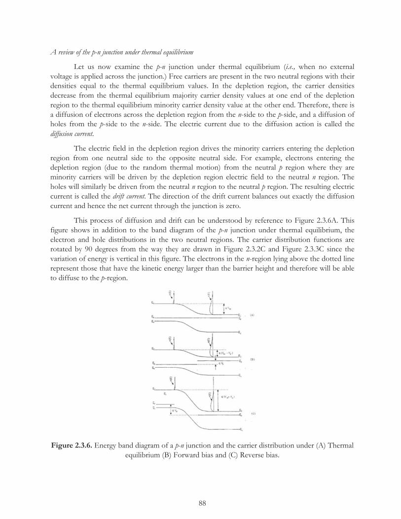
88
A review of the p-n junction under thermal equilibrium
Let us now examine the p-n junction under thermal equilibrium (i.e., when no external voltage is applied across the junction.) Free carriers are present in the two neutral regions with their densities equal to the thermal equilibrium values. In the depletion region, the carrier densities decrease from the thermal equilibrium majority carrier density values at one end of the depletion region to the thermal equilibrium minority carrier density value at the other end. Therefore, there is a diffusion of electrons across the depletion region from the n-side to the p-side, and a diffusion of holes from the p-side to the n-side. The electric current due to the diffusion action is called the diffusion current.
The electric field in the depletion region drives the minority carriers entering the depletion region from one neutral side to the opposite neutral side. For example, electrons entering the depletion region (due to the random thermal motion) from the neutral p region where they are minority carriers will be driven by the depletion region electric field to the neutral n region. The holes will similarly be driven from the neutral n region to the neutral p region. The resulting electric current is called the drift current. The direction of the drift current balances out exactly the diffusion current and hence the net current through the junction is zero.
This process of diffusion and drift can be understood by reference to Figure 2.3.6A. This figure shows in addition to the band diagram of the p-n junction under thermal equilibrium, the electron and hole distributions in the two neutral regions. The carrier distribution functions are rotated by 90 degrees from the way they are drawn in Figure 2.3.2C and Figure 2.3.3C since the variation of energy is vertical in this figure. The electrons in the n-region lying above the dotted line represent those that have the kinetic energy larger than the barrier height and therefore will be able to diffuse to the p-region.
Figure 2.3.6. Energy band diagram of a p-n junction and the carrier distribution under (A) Thermal equilibrium (B) Forward bias and (C) Reverse bias.

89
2.3.3 P-N Junction under Forward Bias
When an external voltage source such as a battery is connected across the p-n junction such that the positive terminal of the battery is connected to the p-side and the negative terminal is connected to the n-side as shown in Figure 2.3.7, the p-n junction is said to be forward biased. The potential energy of the electrons on the n-side is increased relative to the potential energy of the electrons on the p-side by an amount equal to qVF where VF is the externally applied voltage. The junction is said to be forward biased under this condition. The band diagram under forward bias is illustrated in Figure 2.3.6B. The amount of band-bending is equal to the difference between EC (the potential energy of the electrons) in the neutral p region and that in the neutral n region: The potential energy barrier height, is now q(Vbi-VF). The barrier height is hence reduced by an amount qVF under forward bias. In the neutral regions far away from the depletion region, the carrier densities are at their thermal equilibrium values and the Fermi energy is located in the band gap at a level determined by the net impurity (acceptor and donor) concentrations. The Fermi energy in the neutral n region (far away from the depletion region) is shifted upward by qVF from the Fermi energy in the neutral p region (far away from the metallurgical junction).
The expression for the depletion region width under forward bias can be derived exactly the same way as we did for the thermal equilibrium case either by solving the Poisson equation or by using Gauss’s theorem. The expression for the depletion region width will have essentially the same form excerpt the potential barrier height Vbi will be replaced by (Vbi-VF). Using the same notation for the depletion region width as in the thermal equilibrium case, we have
xp=2ϵsND
qNA NA+NDVbi-VF
12 (2.3.55)
xn=2ϵsNA
qND NA+NDVbi-VF
12 (2.3.56)
and xd=xn+xp
= 2ϵs NA+NDqNDNA
Vbi-VF
12 (2.3.57)
We denote that the depletion region width is smaller under forward bias conditions than under thermal equilibrium. The potential barrier is less under forward bias conditions so less charge is needed to sustain in a smaller potential barrier. The depletion region has a smaller width.
Figure 2.3.7. A p-n junction under forward bias. VF is the voltage applied across the p-n junction.

90
Example 2.3.3
Calculate the depletion region width in an abrupt p-n junction with a net impurity density of NA= 1016 cm-3 on the n-side at room temperature (a) in thermal equilibrium and (b) at a forward applied voltage bias of 0.4 V. Take ni as equal to 1010 cm-3. Using Equation 2.3.25 we get
Vbi=0.0259 × ln1016×1015
1020=0.656 V
(a) Thermal equilibrium:
Xp=2x11.9×8.854×10-14×1015
1.6x10-19×1016× 1016+1015
12
=3.627×103× 1015
1016x1.1x1016× 0.656
=0.0886 × 10⁻⁴ cm
Similarly xn=3.627×103× 1016
1015×1.1×1016× 0.656
=0.886×10⁻⁴cm
xd= 0.886+0.0886 ×10⁻⁴ cm
=0.975 × 10⁻⁴ cm
(b) Forward Bias: The barrier height is now Vbi-VF equal to 0.656 0.4= 0.256 V
xp=3.627×103×
1015
1016×1.1×1016× 0.256
=0.553×10⁻⁴ cm
Similarly xn=3.627×103× 1016
1015×1.1×1016× 0.256
=0.553 ×10⁻⁴ cm
xd= 0.553+0.553 x10⁻⁴ cm

91
Referring to Figure 2.3.6B, the electrons that are distributed above the dotted line have adequate energy to clear the barrier, and diffuse to the other side. This results in diffusion current. This diffusion current is larger than in thermal equilibrium since there are more electrons with kinetic energy adequate to go over the smaller barrier height. On the other hand, the drift current of electrons will be the same since it does not depend on the barrier height. Similarly, more holes will be able to diffuse than in the thermal equilibrium case causing a larger hole diffusion current while the hole drift current will be the same as in thermal equilibrium.
Due to the diffusion of electrons from the n-side to the p-side, the (electron) minority carrier density in the p-side increases from its thermal equilibrium value; hence, this process is called minority carrier injection. Similarly, holes are also injected into the neutral n region from the p region under this process.
We saw earlier that under conditions of no current flow, the electron densities at two different locations xA and xB are related by the following expression:
n(xA)=n(xB) e
qψABkT (2.3.58)
and
p(xA)=p(xB) e
- qψABkT (2.3.59)
Where ψAB is the electrostatic potential difference between xA and xB. This is called the Boltzmann relation.
In the case of a p-n junction under thermal equilibrium, the condition of zero net current is realized, due to two large, equal and opposite currents. One of these currents is due to diffusion, and the other due to drift. However, when a forward bias is applied, a current flows across the junction due to the minority carrier injection process. We will assume that the current through the device under forward bias is very small in comparison with the drift and drift components of current flowing under thermal equilibrium. This is tantamount to assuming that the drift and diffusion components are nearly equal under forward bias. We can therefore assume that the carrier densities are still given by the Boltzmann relation (Equation 2.3.58) even under forward bias.
As before, we will choose the origin x=0 at the metallurgical junction with the boundary of the depletion region on the p-side at x=-xp, and that of the n-side at x=xn, as shown in Figure 2.3.8. The width of the neutral n region is the distance Wn between the boundary of the depletion region (x=xn) and the ohmic contact to the neutral n region. The ohmic contact is used to apply a voltage to the device and send a current. In our example, we have taken the location of the ohmic contact to the neutral n region as x=xn+Wn. Similarly, the ohmic contact to the neutral p region is located at x=-xp-Wp, where Wp is the width of the neutral p region. The electron densities at x=xn and x=-xp are related by the Boltzmann distribution, and therefore,
np x=-xp = nn x=xn e- q(Vbi-VF)
kT
Similarly, the hole density at x=xn is given by

92
pn x=xn = pp(x=-xp) e- q(Vbi-VF)
kT
The minority carrier density under thermal equilibrium is np0 on the p side, and pn0 on the n side. The extra (or excess) minority carrier densities at x=xn and at x=-xp under forward bias are given by
Δp x=xn =pn x=xn -pno
and Δn x=-xp =np x=-xp -npo
Due to the fact that we have excess minority carriers in the neutral regions, equal amounts of excess majority carriers flow into the neutral regions from their respective ohmic contacts to maintain charge neutrality. Therefore, the majority carrier densities are also increased from their thermal equilibrium values, i.e.,
pp x=-xp =ppo+Δp x=-xp =ppo+Δn x=-xp (2.3.60)
and nn0 x=xn =nno+Δn x=xn =nno+Δp x=xn (2.3.61)
We distinguish two cases: one called high injection, and the other called low injection.
When Δn x=-xp is>ppo
or when Δp x=xn is>nno
we call it high injection condition.
When Δn x=-xp <ppo, i.e. pp x=-xp ≈ ppo (See Equation 3.3.60)
and when Δp x=xn <nno, i.e. nn x=xn ≈ nno (See Equation 3.3.61)
we have a low and moderate injection condition. We will restrict our discussion to low and moderate injection cases only. Therefore,
nn x=xn ≈ nno and pp(x=-xp)≈ ppo (2.3.62)
The expression for np(x=-xp) can be simplified as
np x=-xp =nn x=xn e-qVbikT e
qVFkT
= nno e-qVbikT e
qVFkT
=npo eqVFkT (2.3.63)
In the above equation, we made use of the Boltzmann relation for the thermal equilibrium carrier densities, i.e.,
npo=nno e-qVbikT

93
Similarly, the expression for pn(x=xn) can be obtained as
pn x=xn = pnoeqVFkT (2.3.64)
The excess minority carrier densities at x=xn and x=-xp are obtained as
Δp x=xn =pnoeqVFkT -pno=pno e
qVFkT -1 (2.3.65)
and Δn x=-xp=npoe
qVFkT -npo=npo e
qVFkT -1 (2.3.66)
These excess minority carrier charges will now diffuse into the two respective neutral regions. Before we study the diffusion process, we will discuss another concept called the Quasi-Fermi Level.
Figure 2.3.8. The depletion and neutral regions in a forward biased p-n junction
Example 2.3.4
Let us calculate the excess carrier density in the neutral p and n regions of a p-n junction, at the boundary of the depletion region. Assume NA=10
16cm-3 on the -side, and ND=5 ×1016cm-3on the n-side. Assume a forward bias voltage of 0.4 V.
ppo≈1016cm-3 and npo=
ni2
pp0
×1020
1016=104cm-3
nn0=5×1015cm-3 and pn0=
ni2
pp0
=1020
5×1015=2×104cm-3
Δp x=xn =npo eqVFkT -1
94
kTq
=0.0259 V
Δp x=xn =104 e
0.40.0259-1 104× 5.1×106-1 ≈5.1×1010cm-3
Δn x=-xp =2x10⁴× e
0.40.0259-1 ×104x5.1×106=1.02×1011cm-3
2.3.4 Quasi-Fermi Level
In thermal equilibrium, we expressed the minority carrier density in terms of Fermi energy. However, under forward bias it will not be possible to do so. We therefore define a parameter called the Quasi-Fermi energy, to enable us to write the expression for the minority carrier density in the same form as in the thermal equilibrium case.
We define a quasi-Fermi energy level, EFn , for electrons such that the electron density can be written as
np= nie(EFn
-Ei)
kT
Similarly, the hole density can be written as
pn= nie(EFp
-Ei)
kT
where EFp is the quasi-Fermi energy level for holes. The quasi-Fermi levels for electrons and holes
are plotted in Figure 2.3.9. Since we are considering low and moderate injection conditions, the majority carrier densities are nearly the same as the thermal equilibrium values, and the majority carrier quasi-Fermi levels are nearly the same as Fermi energy under thermal equilibrium conditions. We make a further assumption that the quasi-Fermi levels in the depletion region of the forward biased p-n junction is at the same level as the majority carrier quasi-Fermi level. This is illustrated in Figure 2.3.9. At distances far from the junction, the excess carrier densities would become zero, as discussed in the next section. Hence, the quasi-Fermi level for the minority carriers would be at the same level at the thermal equilibrium Fermi energy. For example, at x=-xp, EFn is at a higher level than the Fermi energy under thermal equilibrium, and gets lower until it approaches the thermal equilibrium value as it proceeds further into the neutral p region.
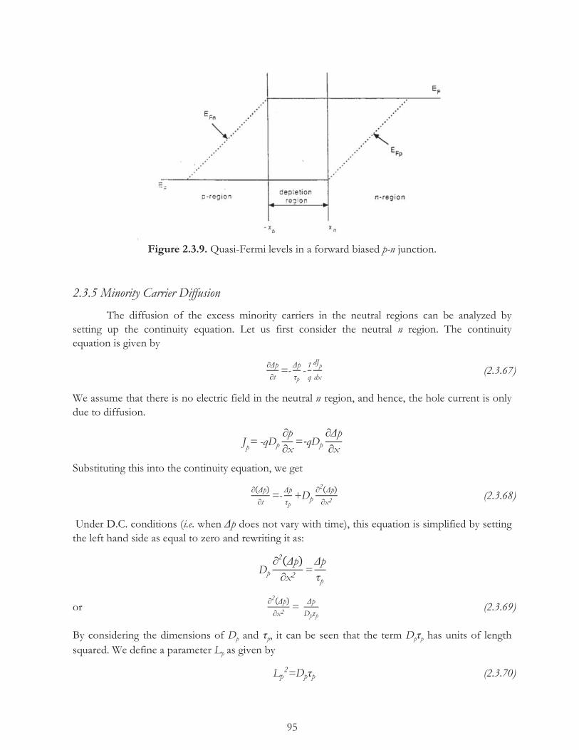
95
Figure 2.3.9. Quasi-Fermi levels in a forward biased p-n junction.
2.3.5 Minority Carrier Diffusion
The diffusion of the excess minority carriers in the neutral regions can be analyzed by setting up the continuity equation. Let us first consider the neutral n region. The continuity equation is given by
∂Δp∂t=- Δp
τp- 1q
dJp
dx (2.3.67)
We assume that there is no electric field in the neutral n region, and hence, the hole current is only due to diffusion.
Jp= -qDp∂p∂x= qDp
∂Δp∂x
Substituting this into the continuity equation, we get
∂ Δp∂t=- Δp
τp+Dp
∂2 Δp∂x2
(2.3.68)
Under D.C. conditions (i.e. when Δp does not vary with time), this equation is simplified by setting the left hand side as equal to zero and rewriting it as:
Dp∂2 Δp∂x2
=Δpτp
or ∂2 Δp∂x2
= ΔpDpτp
(2.3.69)
By considering the dimensions of Dp and τp, it can be seen that the term Dpτp has units of length squared. We define a parameter Lp as given by
Lp2=Dpτp (2.3.70)

96
The equation of continuity is now written as
∂2 Δp∂x2
=ΔpLp2
Let us define a new variable x’=x-xn, (i.e. we choose the origin of the horizontal axis at x=xn) The continuity equation, written in terms of x’, is given by
∂2 Δp∂x 2
= ΔpLp2 (2.3.71)
The general solution to this equation is
Δp x' = Aex'Lp+Be
x'Lp (2.3.72)
A and B are integration constants that will be determined by the boundary conditions at x’=0 and x’=Wn. The boundary condition at x’=0 is given by
Δp x'=0 = pno(eqVFkT -1)
according to Equation 2.3.65. The excess carrier density at an ohmic contact is by definition zero. Hence, the boundary condition at x’=Wn is
Δp x'=Wn =0
Applying these boundary conditions to determine A and B, we can arrive at the solution to the continuity equation, as done in the next chapter, and obtain
Δp x' = Δp osinh(
Wn-x'
Lp)
sinh(WnLp) (2.3.73)
Where Δp(0) is defined as Δp(x’=0). However, for the present we limit our discussion to two limiting approximations
Wn Lp and Wn Lp
Wide Base Case (Wn>>Lp)
When Wn>>Lp, it is considered a wide base case. Consider Equation 2.3.72, which gives the solution to the continuity equation. If we evaluate Δp(x) at (x’=Wn), we get
Δp Wn = Ae-WnLp +Be
WnLp
Where Δp(Wn) is Δp evaluated at x’=Wn. Since Wn>>Lp, the first term on the right hand side is negligible and hence
97
Δp Wn = BeWnLp
But our boundary condition at the ohmic contact requires Δp(Wn) to be zero and eWnLp is a
large quantity. In order to satisfy the boundary condition, we set B=0. The solution to the continuity equation then becomes
Δp x' = Ae-x'Lp
If we apply the boundary condition at x’=0, we can evaluate A and obtain
Δp x' = Δp o e-x'Lp (2.3.74)
where Δp(0) is Δp(x’=0)=pno(eqVFkT -1), as stated earlier.
The plot of Δp(0) as a function of distance as given by Equation 2.3.74, is given in Figure 2.3.10A. We find that the excess minority carrier density decays exponentially with distance. What is the physical interpretation? A hole that is injected from the left at x’=0 diffuses to the right, and as it travels in the neutral n region, it recombines with an electron. Hence, the excess minority carrier density decreases with x’. We can now explain why it decays exponentially.
Let P(x’)dx’ be the probability that an excess hole injected at x’=0, will recombine in an elementary distance dx’ between x’ and x’+dx’. Then P(x’) is the probability per unit distance that an excess minority carrier (hole) will recombine and be lost. The number of excess holes that recombine (and therefore lost) in the interval dx’ is equal to the product Δp(x), (i.e., the number of excess hole density at x’), multiplied by P(x’)dx’. The difference in excess hole density at x’ and at x’+dx’ is what is lost due to the recombination in the interval dx’. Hence
d Δp x' = Δp x'+dx' -Δp x' = -Δp x' P x' dx'
Assuming P(x’) does not vary with distance and is equal to P0, this equation can be rewritten as
d(Δp x' )Δp x' = -Podx'
and directly integrated to obtain
Δp x' =A'e-Pox'
The constant A’ is obtained as ΔP(0) by applying the boundary condition at x’=0:
Δp x' =Δp o e-Pox’
By comparing the above to Equation 2.3.74, we see that
Po=1Lp

98
This means that 1Lp
is the probability per unit distance that a hole will recombine. That is, dx'Lp
is the
probability that an excess hole will recombine in an interval dx’ Using this argument, it can be shown that Lp is the average distance an excess hole (minority carrier) will travel before it recombines. (This is left as a problem.) For this reason, Lp is called the minority carrier diffusion length. Figure 2.3.10A gives the profile of the excess minority carrier density. As mentioned before in order to maintain charge neutrality, excess majority carrier density equal to the excess minority carrier density will be present in the neutral n region, with a profile exactly equal to that of the minority carrier density. This is illustrated in Figure 2.3.10B. Due to the concentration variation of the excess minority carrier density, diffusion current will flow. The resulting electric current density is given by
Jp x' =-qDp
d(Δp)dx'
=qDpΔp oLpe
-x'
Lp (2.3.75)
The diffusion current also decays exponentially with distance.
While there is a diffusion current due to the exponential decay of the minority carrier density, there will be no similar majority carrier diffusion current arising from the exponential variation of the excess majority carrier density. The reason for this is that the excess majority carrier density is maintained by the presence of a small electric field, whose value is proportional to the ratio of Δn(x’) and (x’). n(x’) is equal to ND+ Δn(x’) where ND is the donor density in the n region. The drift current of electrons due to this electric field, given by Jdrift=qn(x
')μn (x'), is exactly
balanced by the excess electron diffusion current, given by Jdiff=qDndΔndx'
. In the case of minority
carriers, there is a drift current due to this electric field, but it is negligibly small compared to the diffusion current. This is the reason why we take into account the minority carrier diffusion current, and not the majority carrier diffusion current.
Figure 2.3.10. Plot of the excess carrier density in the neutral n region for a wide base case: (A) Plot of the excess minority carrier (hole) density, and (B) Plot of the excess majority carrier
(electrons) density.
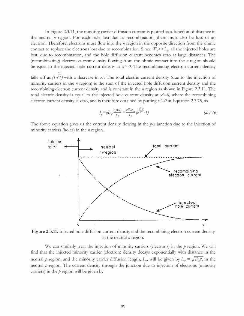
99
In Figure 2.3.11, the minority carrier diffusion current is plotted as a function of distance in the neutral n region. For each hole lost due to recombination, there must also be loss of an electron. Therefore, electrons must flow into the n region in the opposite direction from the ohmic contact to replace the electrons lost due to recombination. Since Wn>>Lp, all the injected holes are lost, due to recombination, and the hole diffusion current becomes zero at large distances. The (recombinating) electron current density flowing from the ohmic contact into the n region should be equal to the injected hole current density at x’=0. The recombinating electron current density
falls off as (1-e-x'
Lp) with a decrease in x’. The total electric current density (due to the injection of minority carriers in the n region) is the sum of the injected hole diffusion current density and the recombining electron current density and is constant in the n region as shown in Figure 2.3.11. The total electric density is equal to the injected hole current density at x’=0, where the recombining electron current density is zero, and is therefore obtained by putting x’=0 in Equation 2.3.75, as
Jp=qDpΔp 0Lp=qDppnoLp(eqVFkT -1) (2.3.76)
The above equation gives us the current density flowing in the p-n junction due to the injection of minority carriers (holes) in the n region.
Figure 2.3.11. Injected hole diffusion current density and the recombining electron current density in the neutral n region.
We can similarly treat the injection of minority carriers (electrons) in the p region. We will find that the injected minority carrier (electron) density decays exponentially with distance in the neutral p region, and the minority carrier diffusion length, Ln, will be given by Ln = Dnτn in the neutral p region. The current density through the junction due to injection of electrons (minority carriers) in the p region will be given by
100
Jn=qDnnpoLp
(eqVFkT -1)
The total electric current density through the junction will be the sum of Js in the equation above and Jp in Equation 2.3.76 and is given by
J= Jn+Jp=[qDnnpo
Ln+qDppnoLp](eqVFkT -1) (2.3.77)
This is usually written as
J=Js (eqVFkT -1)
where Js = qDnnpo
Ln+qDppnoLp
(2.3.78)
Js is called the saturation current density.
Figure 2.3.12 shows the various components of current that flow in the forward biased p-n junction. Jp2 is the injected hole diffusion current density. Jp3 is the hole current density that is flowing in the neutral p region to inject holes in the n region. Jn1 is the electron current density in the neutral n region replacing the electrons lost due to recombination with holes in the neutral n region. Similarly, Jn2 is the injected electron diffusion current density in the neutral p region. Jn3 is the electron current density flowing in the neutral n region to inject electrons in the p region. Jp1 is the recombining hole current density in the neutral p region. The total electric current density, Jt, is the sum of all these various components.
The current flowing through a forward biased junction is obtained by multiplying the current density by the area A of the junction
I=Is (eqVFkT -1) (2.3.79)
where Is= AJs=A[qDnnpo
Ln+qDppnoLp] (2.3.80)
Is is called the saturation current. The current in the forward biased junction is plotted in Figure 2.3.13. At values of VF larger than a few kT, it can be seen from Equation 2.3.79 that the term -1 is negligible in comparison with the exponential term, and hence, I is given by
I≈Is (eqVFkT ) (2.3.81)
The current increases exponentially with the forward bias voltage VF.

101
Figure 2.3.12. Various components of electric current density in the forward biased p-n junction. The arrows indicate the direction in which the electrons or hole flow.
Figure 2.3.13. Forward Bias current through the junction.

102
Narrow Base Case
When Wn<<Lp, we call it a narrow base junction.
Starting from Equation 2.3.72, we can expand the exponential terms and retain only the first two terms:
Δp x' =A 1- x'
Lp+B 1+ x'
Ln (2.3.82)
By applying the boundary conditions at x’=0 and at x’=Wn, we obtain
A=Δp 02
1+LpWn
and B= Δp 02
1-Lp
Wn
Substituting these values in Equation 2.3.82, we obtain
Δp x' = Δp 0 1- x'
Wn (2.3.83)
The excess minority carrier (hole) density in the neutral n region is plotted in Figure 2.3.14 A. As stated before, a neutralizing excess majority carrier density Δn(x’)(=Δp(x’)) also exists and is plotted in Figure 2.3.14B. The injected hole diffusion current density is obtained from Equation 2.3.83 as
Jp x' =-qDp
d Δpdx'
= qDpΔp 0Wn
=qDppn0Wn
(eqVFkT -1)
Figure 2.3.14. Excess carrier density in the neutral n region of a forward biased p-n junction for a narrow base approximation. (A) Excess minority carrier (hole) density (B) Excess majority carrier
(electron) density.

103
First, we notice that the injected hole diffusion current density is constant and independent of x’. This means that any hole current injected at x’=0 from the p region reaches the ohmic contact. There is no recombination of minority carriers in the n region. Since Wn is very small in comparison with the diffusion length Lp, the probability of an injected hole recombining in the n region is negligible. Hence the injected hole current density reaches the ohmic contact without any attenuation.
Secondly, we notice that the expression for the injected hole diffusion current density is similar to that for the wide base case, except that Lp is replaced by Wn If we now assume that the neutral p region can also be approximated to be narrow base, (i.e., Wp<<Ln), we get, for the injected electron diffusion current density,
Jn=qDnnp0Wp
eqVFkT -1
The total current through the junction is given by
I=AqDnnp0Wp
+qDppn0Wn
eqVFkT -1
= IS eqVFkT -1
where IS is the saturation current. Thus, we see that the form of the expression for the current under forward bias of a narrow base p-n junction is similar to that for a wide base junction. It should be noted that it is possible that in a p-n junction, one side can be approximated as narrow base, and the other as wide base. In such a case, the current through the junction will be expressed as an appropriate combination of narrow base and wide base expressions.
P-N Junction under Reverse Bias
When an external voltage is connected such that the positive terminal is connected to the n-side and the negative terminal to the p-side of the junction, then the junction is said to be reverse-biased. The potential energy of the electrons on the p-side is increased relative to that of the electrons on the n-side by an amount equal to qVR where VR is the externally applied reverse bias voltage. The band diagram in a p-n junction under reverse bias is illustrated in Figure 2.3.6C. The height of the potential energy barrier as before is the difference between EC on the neutral p-side and EC on the n side and therefore equal to q(Vbi+VR). The band-bending, (i.e., the barrier height is thus increased from the thermal equilibrium value of qVbi to q(Vbi+VR).)
In the neutral regions far away from the junction, the carrier densities are at their thermal equilibrium values and the Fermi energy is located in the band gap at a level determined by the net impurity (acceptor and donor) concentrations. Therefore, the Fermi energy in the neutral region (far away from the junction) is shifted downward by qVR from the Fermi energy in the neutral p region (far away from the junction).
104
The expression for the depletion region width under reverse bias can be derived exactly the same way as we did earlier either by solving the Poisson equation or by using Gauss theorem. The expression for the depletion region width will have essentially the same form except the potential barrier height Vbi will be replaced by (Vbi+VR). Using the same notation for the depletion region width as earlier, we have
xp=2ϵsND
qNA NA+NDVbi+VR
12 (2.3.84)
xn=2ϵsNA
qND NA+NDVbi+VR
12 (2.3.85)
and xd=xn+xp
= 2ϵs NA+NDqNDNA
Vbi+VR
12 (2.3.86)
Thus we see that the depletion region width under reverse bias increases with the reverse voltage. The increase is physically understandable because a larger space charge (and hence a wider space charge region) is needed for a larger potential energy barrier.
Example 2.3.5
Calculate the depletion region width in an abrupt p-n junction with a net impurity density of NA= 1016 cm-3 on the p-side and ND=1015 cm-3 on the n-side. Assume room temperature and a reverse bias voltage of 6 V. We determined the depletion region width for this diode under thermal equilibrium case and under a forward bias of 0.4 V in the example worked earlier in the section on forward bias. We can therefore use the value, 0.656 V for Vbi from the previous example.
Vbi+VR=0.656+6=6.656 V
xp=3.627×103×
1015
1016×1.1×1016× 6.656
=0.282 × 10⁻⁴ cm
Similarly xn=3.627×103× 1016
1015×1.1×1016× 6.656
=2.81×10⁻⁴ cm
xd= 2.821+0.282 ×10⁻⁴ cm
=3.103 × 10⁻⁴ cm
105
Due to the increase in the barrier height, the hole (minority carrier) density in the neutral n region at the boundary of the depletion region, (i.e., x=xn), is reduced from its thermal equilibrium value since every hole that enters the depletion region will be pulled towards the p side by the electric field in the depletion region. Another way of stating this is that while there was a balance between the drift and the diffusion currents in thermal equilibrium, under reverse bias condition the diffusion current is reduced due to the increase in the barrier height. Thus only the drift current remains. Yet another way of looking at this is by considering the carrier density at the edges of the depletion region using the Boltzmann relation in the following manner:
p x=xn =p x=-xp e-q Vbi+VR
kT =pp0e-q(Vbi-VF)
kT = pn0e-qVRkT (2.3.87)
We see that when qVR is much larger than kT, p at x=xn is nearly zero. Using the above relation we see that the excess hole density at x=xn is negative and is given by
Δp x=xn =pn0e-qVRkT -pn0=pn0 e
-qVRkT -1 (2.3.88)
We can now set up the continuity equation which will be the same as Equation 2.3.68. Again setting up a new variable x’, as we did in the forward bias case we obtain the same equation as Equation 2.3.71 which is given below
d2 Δpdx'2
=Δp
Lp2
Solving this equation under the boundary condition that the excess carrier density is equal
to 0 at x’=Wn and is equal to pn0 e-qVRkT -1 at x’=0, we get for the wide base diode,
Δp x' =pn0 e-qVRkT -1 e
-x'Lp (2.3.89)
and for the narrow base diode,
Δp x' =pn0 e-qVRkT -1 e
-x'Lp 1- x'
Wn (2.3.90)
When we consider the electron density in the neutral p region, we get similar results. The excess minority carrier densities in the neutral n and p regions are negative and are plotted in Figure 2.3.15.
We will find that the diffusion current is of the same form as we got for the forward-biased junction except that VF will be replaced by -VR. The current through the diode will be similar in form as the forward bias current but opposite in direction. The current is called the reverse current, Irev.
Irev=Is e-qVRkT -1 (2.3.91)
In the case of wide base diode,

106
Is=AJs=AqDnnp0
Ln+qDppn0Lp
(2.3.92)
IS is the same as what we obtained under forward bias for a wide base diode. In the case of the narrow base diode
Is=AJs=AqDnnp0
Wp+qDppn0Wn
(2.3.93)
IS is again the same as what we obtained under forward bias for a narrow base diode.
The current in the reverse biased junction is plotted in Figure 2.3.16. At values of VR larger than a few kT, it can be seen from Equation 2.3.91 that the exponential term is negligible in comparison with the term -1 and hence, I approaches or saturates to a value
I=-Is (2.3.94)
and is independent of the reverse voltage. This is the reason why IS is called the saturation current.
Figure 2.3.15. The Plot of the excess (depleted) carrier density in the reverse biased junction.
Figure 2.3.16. Reverse current in the p-n junction.

107
Example 2.3.6
Let us now calculate the current through a wide-base diode at a forward bias of 0.5 V and at a reverse bias of 0.5 V. The diode is assumed to be an abrupt p-n junction with NA=1016 cm-3 on the p-side and with ND=1015 cm-3 on the n-side. Assume room temperature. The minority carrier diffusion constant is assumed to be 10 and 25 cm2 s-1 in the neutral n and p regions respectively and
let the minority carrier diffusion length be 5 × 10⁻³ and 10-2 cm respectively in the neutral n and p regions. Let the area of the junction A, be 10-3 cm2.
Is=AJs=AqDnnp0Ln
+qDppn0Lp
Dn=25 cm2s-1
Ln=10-2 cm
np0=1020
1016=104cm-3
Dp=10 cm2s-1
Lp=5x10⁻³ cm
pn0=1020
1015=105cm-3
Substituting these values in the equation for IS we get
Is=3.60 ×10⁻¹⁴ A
IF=3.60 x10⁻¹⁴× e0.5
0.02589-1 =9.41 × 10⁻⁶A
IR=3.60 x10⁻¹⁴× e-5
0.02589-1 =-3.60 × 10⁻¹⁴A
Interpretation of Reverse Current
We saw in the last section that the current through the diode is given by
I=qADppn0Lp+Dnnp0
LneqVFkT -1 (2.3.95)
for a wide base diode where VF is the externally applied voltage. We can give a physical interpretation for this reverse current. When a reverse voltage VR is applied, the term VF in the above equation should be replaced by -VR. When VR is large than a few kT, the exponential term
108
becomes negligible. The resulting current, I, denoted by IR, is the leakage or saturation current IS and is given by
IR=-IS= -qADppn0Lp+Dnnp0
Ln=-Isp-Isn (2.3.96)
where Isp and Isn are the saturation current components due to the flow holes and electrons respectively. Recall from Chapter 2 that the minority carrier thermal generation rate in the neutral n region of the semiconductor is given by
gth=pn0τp
(2.3.97)
Also Lp= Dpτp (2.3.98)
We can therefore write
Dppn0Lp=DpLppn0Lp2 =
Lppn0τp=Lp× gth (2.3.99)
The reverse current can therefore be expressed as
IR=-IS=-Isp-Isn=-q A gpLp-gnLn (2.3.100)
where gn and gp are the thermal generation rates of electrons and holes in the neutral p and n regions respectively.
What is the physical interpretation of this equation? A minority carrier that enters the depletion region will be swept away to the other side due to the electric field in the depletion region. This gives rise to the reverse current. For example, an electron that enters the depletion region from the p side where it is a minority carrier will be pushed to the n side by the electric field in the depletion region. Similarly a hole will be pushed from the n side to the p side. Since a minority carrier will travel on an average a distance equal to the diffusion length before it recombines, carriers generated in the neutral region farther than a diffusion length away from the edge of the depletion region will not reach the depletion region. It is only those minority carriers that are generated within a diffusion length that will produce the reverse current. The first term in the above equation represents the current flowing through the junction due to minority carriers (holes) generated in the neutral n region within a diffusion length Lp from the depletion region and similarly the second term represents the current due to the minority carriers (electrons) generated in the neutral p region within a diffusion length Ln from the depletion region. Such a physical interpretation is not readily possible for the reverse current in the narrow base diode.
Non-Ideal Current Characteristics
The current characteristics that we discussed so far are called the ideal current characteristics. We will now discuss additional components of current that flow in a p-n junction and these additional components of current are called non-ideal currents. In our treatment we

109
neglected the component of current due to generation of electron-hole pairs in the depletion region in the reverse current and the component of current due to recombination of electron-hole pairs in the depletion region in the forward current.
Reverse Bias
In the depletion region of the reverse-bias junction, the np product is less than ni2. Recall
from our discussion in Chapter 2 that under this condition, there is a net generation in the depletion region equal to
gth=ni2τg
(2.3.101)
Each electron-hole pair that is generated in the depletion region will be acted upon by the electric field in the depletion region such that the electron will be propelled to the neutral n region and the hole will be propelled to the neutral p region. This results in an electric current through the junction equal to the flow of the charge of an electron for each electron-hole pair that is generated. Since each electron is carrying a charge of q coulombs, and the electron-hole pairs are generated throughout the depletion region of volume equal to Axd where A is the area of the junction and xd is the width of the depletion region, the reverse current is given by
IR=q A Dppn0Lp+Dnnp0
Lne
-qVRkT -1 - qA xd
ni2τg=Is e
-qVRkT -1 -qA xd
ni2τg
(2.3.102)
Since xd, the depletion region width, is dependent on the applied reverse voltage, the term due to generation in the depletion region has a voltage dependence as shown in Figure 2.3.17.
Figure 2.3.17. Non-ideal current characteristics under a reverse bias.

110
When the junction is forward biased the n-p product in the depletion region is larger than ni
2. Hence there is a net recombination in the depletion region. This gives rise to an additional component in the forward current. The term due to recombination in the depletion region is of the form
Irec=Is rec eqVF2kT (2.3.103)
This expression for the current can be derived as shown below. The rate of recombination is given by the Schockley Read Hall Model discussed in chapter 2 and is repeated below
R=r n p (2.3.104)
Where n and p are the electron and hole densities respectively and r is given by
r = 1
n+n1 τp0+ p+p1 τn0 (2.3.105)
where τp0=1
Ntσpvp
τn0=1
Ntσnvn
Nt = density of traps or g-r centers.
σn,σp = capture cross-sections for electrons and holes respectively
vn, vp =thermal velocity of electrons and holes respectively and is equal to 3 kT
m*, and m* is the
effective mass of the carrier,
n1=NC exp -EC-EtkT
= niexpEt-EikT
(2.3.106)
p1=NV exp -Et-EVkT
= niexp - Et-EikT
(2.3.107)
where Et = the trap energy level
The value of n at the edge of the depletion region near the neutral n-side is equal to the majority
carrier density nn0 and p has a value equal to pn0eqVFkT . Hence the product of n and p at the edge of the
depeletion region near the neutral n region is given by
n p=nn0pn0eqVFkT =ni
2eqVFkT (2.3.108)

111
Similarly by considering the hole and electron densities at the edge of the depletion region near the neutral p region, it can be shown that the n-p product is the same as at the edge of the depletion region near the neutral n-side. We now assume that the n-p product has the same value throughout the interior of the depletion region and is given by Equation 2.3.108. This is pictorially shown in Figure 2.3.18. Hence the expression for the net recombination rate can be written as
U=R-Gth= np-ni2
n+n1 τp0+ p+p1 τn0=
ni2 e
qVFkT -1
n+n1 τp0+ p+p1 τn0 (2.3.109)
The net recombination rate is a maximum when the denominator is a minimum. Near the edge of the depletion region close to the neutral n region, n is large and in the region close to the neutral p region, p is larger. n and p are both small only in the middle of the depletion region when n and p are nearly equal as shown in Figure 2.3.18. Therefore only a small region in the middle of the depletion region is effective in producing recombination. Using Equation 2.3.108 and using the fact that n and p are nearly equal in this region, we can write
n=p= np=nieqVF2kT (2.3.110)
U=ni2 e
qVFkT -1
nieqVF2kT+n1 τp0+ nie
qVF2kT+p1 τn0
(2.3.111)
Substituting the expression for n1 and p1 in terms of (Et-Ei), we obtain
U=ni2 e
qVFkT -1
nieqVF2kT τp0+τn0 +nie
(Et-Ei)kT τp0+nie
- (Et-Ei)kT τn0
=ni e
qVFkT -1
eqVF2kT τp0+τn0 + τp0e
(Et-Ei)kT + τn0e-
(Et-Ei)kT
(2.3.112)
When Et-Ei > kT, the denominator is large and hence U is nearly zero. Only when the trap is in the middle of the gap (i.e., Et≈Ei, U) becomes not negligible.
U ≈ni e
qVFkT -1
τp0+τn0 eqVF2kT+1
(2.3.113)
The Term 1 in both the numerator and the denominator is negligible in comparison with the exponential terms and can therefore be omitted.
U ≈ nieqVFkT
eqVF2kT τp0+τn0
= nieqVF2kT
τp0+τn0 (2.3.114)
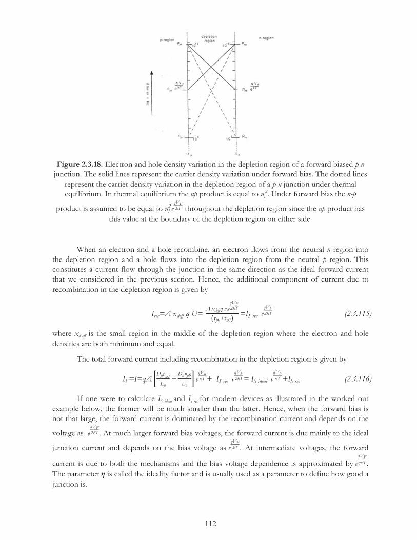
112
Figure 2.3.18. Electron and hole density variation in the depletion region of a forward biased p-n junction. The solid lines represent the carrier density variation under forward bias. The dotted lines
represent the carrier density variation in the depletion region of a p-n junction under thermal equilibrium. In thermal equilibrium the np product is equal to ni
2. Under forward bias the n-p
product is assumed to be equal to ni2eqVFkT throughout the depletion region since the np product has
this value at the boundary of the depletion region on either side.
When an electron and a hole recombine, an electron flows from the neutral n region into the depletion region and a hole flows into the depletion region from the neutral p region. This constitutes a current flow through the junction in the same direction as the ideal forward current that we considered in the previous section. Hence, the additional component of current due to recombination in the depletion region is given by
Irec=A xdeff q U=A xdeffq nie
qVF2kT
τp0+τn0=IS rec e
qVF2kT (2.3.115)
where xd eff is the small region in the middle of the depletion region where the electron and hole densities are both minimum and equal.
The total forward current including recombination in the depletion region is given by
IF=I=qADppn0Lp+Dnnp0
LneqVakT + IS rec e
qVF2kT= IS ideal e
qVFkT +IS rec (2.3.116)
If one were to calculate IS ideal and Is rec for modern devices as illustrated in the worked out example below, the former will be much smaller than the latter. Hence, when the forward bias is not that large, the forward current is dominated by the recombination current and depends on the
voltage as eqVF2kT . At much larger forward bias voltages, the forward current is due mainly to the ideal
junction current and depends on the bias voltage as eqVFkT . At intermediate voltages, the forward
current is due to both the mechanisms and the bias voltage dependence is approximated by eqVFηkT .
The parameter η is called the ideality factor and is usually used as a parameter to define how good a junction is.

113
Example 2.3.7
Consider a p-n junction with the following characteristics where NA and ND are the net impurity concentration on the n and p sides respectively. A is the area of the junction.
A=10-4cm2, ND=1016cm-3,NA=10
15cm-3, Dn=30 cm2s-1, Dp=4 cm2s-1, τn=10-4s, τp=10-5s
The ideal current prefactor IS ideal and the recombination current prefactor IS rec can now be calculated using the values for the universal constants q and k and assuming room temperature i.e., T=300K. Taking the intrinsic carrier density ni as equal to 1010 cm-3, the thermal equilibrium minority densities can be calculated as
pn0=ni2
ND= 10
20
1016=104 cm
-3 (2.3.117)
and np0=ni2
NA= 10
20
1015=105 cm
-3 (2.3.118)
The minority carrier diffusion lengths are calculated as
Lp= τpDp= 10-5x4 =6.32 x 10⁻³cm (2.3.119)
Ln= τnDn= 10-4x30 =5.48 ×10⁻²cm (2.3.120)
Substituting these values in the equation for IS ideal we get
IS ideal =1.6x10-19× 10-4×
4×104
6.32 × 10⁻³+
30× 105
5.48 ×10-2
= 1.6x10-23× 5.7×106+5.47×107
= 9.66 ×10⁻¹⁶ Amperes
For calculating IS recwe use the following typical parameters. Let the density of the traps, Nt be 1015
cm-3 and σn= σn=10-16cm . Assume vn= vp=vth where
vth=3kT
m= 3×1.38×10-23×300
9.11x10-31 =1.17 × 10⁵ (2.3.121)
We have assumed the effective mass of the carriers to be the same as for electrons in vacuum. Since we will be using mostly cm as the unit of length we take vth as 1.17×107cm s-1. Let us assume tht the
width of the region wwhere the recombination is effective, xdiff, is 3×10⁻⁵ cm. τn0 is equal to τp0 due
to our assumption of equality of σn and σp as well as vn andvp. Therefore
τn0+τp0= 1.6x10-19x 10-4x 3 x 10-5x 1010
1,71 x 10⁻⁶

114
=2.81 x 10⁻¹² Amperes
Thus we see that IS rec is larger than IS ideal and therefore dominates at low bias voltages. At higher bias voltages, the ideal current dominates because of the absence of the factor of 2 in the denominator of the exponent of the voltage dependent term.
In the discussion so far, we considered recombination generation in the bulk of the semiconductor. Normally the depletion region intersects a surface and the g-r centers (called surface states or interface states) on the surface of the depletion region can also provide a recombination current under forward bias and a generation current under reverse bias in addition to the previously discussed components of current. The net recombination rate per unit area of the surface, US is given by
Us=np-ni
2
n+n1Nstσpvp
+p+p1Nstσnvn
(2.3.122)
Where Nst is the number of g-r centers per unit area of the surface (surface density), and all other parameters have the same meaning as before for the bulk recombination. Under forward bias the n-p product in the surface region is much larger than ni
2 and hence a surface recombination current flows in addition to the bulk recombination current. The surface recombination current also has the
same voltage dependence as the bulk recombination current i.e., the current is proportional to eqVF2kT .
When the junction is under reverse bias, the np product is negligible in comparison with ni2 and
hence the net generation rate under the assumption that only the surface states whose energy is in the middle of the gap contribute to the generation, is given by
U= ni2
n1Nstσpvp
+p1
Nstσnvn
=- ni1
Nstσpvp+
1Nstσnvn
=- nis2
(2.3.123)
where s is equal to
=2
1Nstσpvp
+1
Nstσnvn
and is called the surface recombination velocity. Recall that we defined a minority carrier lifetime in the bulk to describe the generation rate. We now define a surface recombination velocity for the surface to describe the generation at the surface. The electron-hole pairs created at the surface depletion region give rise to another component of reverse current, which we call the surface generation current. This component of surface generation current adds to the bulk generation current under reverse bias.
A typical current voltage plot is given in Figure 2.3.19 in which the current is plotted on a logarithmic scale while the voltage is plotted on a linear scale. The slope at small values of forward bias voltage is half that at larger values of bias voltage. The recombination component IS rec is larger than the ideal IS ideal and hence at small voltages, the recombination current dominates and the slope

115
is q
2kT . At higher voltage, the ideal component dominates and the slope is q
kT. It is customary to
express the current as
IF=IS eqVFηkT (2.3.124)
Where η is called the ideality factor. The more ideal a diode is, closer is η to unity.
Figure 2.3.19. Plot of the forward current in a typical p-n junction as a function of the bias voltage. The current is on a logarithmic scale. Notice how the slope increases by a factor of 2 between the
lower and higher voltages.
Capacitive Effects
The p-n junction behaves like a capacitor for small signal (applied) voltages. There are two mechanisms that give rise to capacitive effects. One arises due to the dependence of the space charge in the depletion region (and hence the depletion region width) on the applied voltage. The capacitance is called Junction Capacitance or Depletion Capacitance. The other is due to the minority carrier charge stored in the neutral regions. This capacitance is called Storage Capacitance or Diffusion Capacitance. We will examine both of these now.
dQ+=qNDdxn
and dQ-=-qNAdxp
and they flow from the external voltage source into the diode. The two elementary charges are equal in magnitude but opposite in sign. When the step voltage is removed, the elementary charges

116
flow back to the external voltage source. Hence the diode behaves like a capacitor of capacitance per unit area equal to
C=dQ+
dVa
We will now derive an expression for the depletion capacitance. At any point x in the depletion region, the increase in the electric field, d due to the small step voltage, is obtained from Gauss’s theorem as
dE=dQ+
ϵs
It is independent of x. The incremental change in the applied voltage across the diode dVa can be obtained from the line integral of d across the depletion region. Since d is constant with x, the line integral is
dVa= xd× d
Substituting the expression for d in terms of dQ+ we get
dVa= xd× dQ+
ϵs
Dividing both sides of the equation by dQ+, we obtain for the depletion capacitance per unit area of the junction,
Cd=dQ+
dVa= ϵs
xd (2.3.125)
We find that this is exactly the same expression that we would have had if we have a parallel plate capacitor with the semiconductor as the dielectric between the parallel plates of unit area and a spacing of W between the plates. Thus we see that the junction behaves like a parallel plate capacitor. What we calculated was the expression for the capacitance for unit area of the junction. The capacitance of a junction of area A is
CJ=A Cd=A ϵsxd
(2.3.126)
What we derived for the junction capacitance is valid for a junction even if it did not have uniform impurity concentrations (i.e., if the diode was not an abrupt junction.) We can arrive at the expression for the capacitance of an abrupt junction by an alternate method also. The total positive charge in the depletion region, Q+ per unit area of the junction is given by
Q+=q NDxd=qNDNAND+NA
xd
Where we have used the relation
NDxn=NAxp
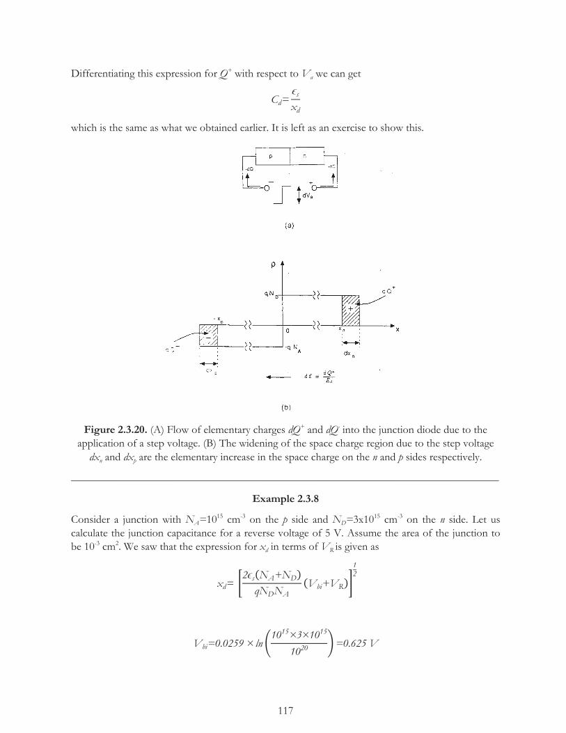
117
Differentiating this expression for Q+ with respect to Va we can get
Cd=ϵsxd
which is the same as what we obtained earlier. It is left as an exercise to show this.
Figure 2.3.20. (A) Flow of elementary charges dQ+ and dQ- into the junction diode due to the application of a step voltage. (B) The widening of the space charge region due to the step voltage
dxn and dxp are the elementary increase in the space charge on the n and p sides respectively.
_____________________________________________________________________________
Example 2.3.8
Consider a junction with NA=1015 cm-3 on the p side and ND=3x1015 cm-3 on the n side. Let us calculate the junction capacitance for a reverse voltage of 5 V. Assume the area of the junction to be 10-3 cm2. We saw that the expression for xd in terms of VR is given as
xd=2ϵs NA+NDqNDNA
Vbi+VR
12
Vbi=0.0259 × ln1015×3×1015
1020=0.625 V

118
Substituting the values for Vbi and other parameters, we get
xd=211.9×8.84×10-14 3+1 ×10¹⁵
1.6x10-19×3×1015×10155+0.625
12
=3.13 × 10⁻⁴ cm
Cd=11.9×8.84×10-14
3.13 x 10-4=3.36×10⁻⁹ F cm-2cm-2
and CJ=10-3×3.36 × 10-9=3.36 × 10⁻¹²F=3.36 pF
Diffusion or Storage Capacitance
We saw earlier that under a forward bias minority carriers are injected into the neutral region on either side of the depletion region. The excess minority carrier density decayed with distance in the neutral regions either exponentially as in the case of the wide base diode or linearly as in the case of the narrow base diode. Although the excess carriers were diffusing and, they constantly moved until they recombined (wide base) or reached the ohmic contact (narrow base), at any given time they had a density distribution given by Figure 2.3.10 and 2.3.14. It is as though the minority carriers equal to the area under the curve in these two figures are stored in the neutral regions. The minority carrier charge stored in the neural regions can be obtained by integrating the excess minority carrier density in the neutral region and by multiplying this by the electron charge q and the area, A, of the junction. The charge due to excess holes stored in the neutral n region is therefore given by
Qps=q A Δp x' dx'Wn
0
where we have used the subscript s to denote that we are considering stored charge.
Wide Base Diode
Let us consider the wide base diode. Substituting the expression for the excess hole density in the wide base case which is
Δp x' = Δp o e-x'Lp
into the expression for Qps and integrating we get,
Qps=q A Δp o e-x'Lp
Wn0
dx'=AqΔp 0 Lp (2.3.127)
We can relate this to the current through the diode. The current due to hole injection is
119
Ip=-q A DpdΔp x'
dx' x'=0
=q A DpΔp 0
Lp
Dividing the expression for Qps, by Ip and rearranging, we get
Qps=IpLp2
Dp= Ip τp (2.3.128)
Thus we see that the stored charge in the neutral region is the injected minority carrier current times the lifetime. The stored charge is dependent on the applied forward bias, VF, since
Δp 0 = pn0 eqVFkT -1
Let us assume that a step voltage dVF is applied in series with VF as shown in Figure 2.3.21A. Due to this step voltage, the stored charge will increase by an amount dQps as shown in Figure 2.3.21B. This extra charge dQps, flowed into the neutral n region from the external source dVa through the neutral p region. In order to maintain charge neutrality, the electron density in the neutral n region also has to increase and the increase in the negative charge, dQns, will be exactly equal and oppoissite to dQp and has to flow from the external source through the neutral n region as shown in Figure 2.3.21C. Therefore the diode appears to the external source as a capacitor of capacitance equal to
Cdiff p=dQps
dVF (2.3.129)
Hence we can obtain the diffusion capacitance as
Cdiff p=d Ip τpdVF
=τpdIp
dVF (2.3.130)
But Ip=Isp eqVFkT -1
which becomes equal to
Ip≈IspeqVFkT
Under the approximation dVF kT Differentiating this with respect to VF we get
dIp
dVa=
dIp
dVF=qIp
kT (2.3.131)
Therefore the diffusion capacitance becomes equal to
Cdiff p=τpqIp
kT (2.3.132)
The DC current through the diode also increases by a small increment dIp due to the small step voltage and therefore the diode appears to the step voltage as a resistor of resistance equal to
rfp=dVadIp

120
or a conductor of conductance equal to
gfp=dIp
dVa (2.3.133)
Using Equation 2.3.132, we can write the diffusion capacitance as
Cdiff p=τpgfp (2.3.134)
So far we considered only the small signal circuit elements due to the hole injection in the neutral n region. We have similar diffusion capacitance due to electron injection in the neutral p region so that we can write for the total diffusion capacitance as
Cdiff p=τpqIp
kT+ τn
qInkT= τpgfp+τngfn (2.3.135)
where In is the component of forward bias current due to electron injection in the neutral p region and gfp and gfn are the forward conductances due to hole and electron injection, respectively. Similarly the forward conductance will be equal to
gf= qkT
Ip+In =qIFkT
= gfp+gfn
Figure 2.3.21. The effect of the application of a step voltage on a forward biased junction diode. (A) The step voltage, dVa is applied in series with the forward bias. (B) The increase in the injected minority carrier distribution in the neutral n-region is shown by the shaded area. (C) The increase in the majority carrier distribution in the neutral n-region to maintain the charge neutrality is shown by
the shaded area.
121
Narrow Base Diode
Similar to the wide base diode case, the minority carrier distribution increases with the application of a step voltage in the case of the narrow base diode. Hence we get stored charge effects and the diode gives rise to diffusion capacitance. It is left as an exercise to show that the stored charge due to the injection of minority carriers in the neutral n region is given by
Qps=q A Δp o Wn
2
Similarly, the diffusion capacitance can be shown to be
Cdiff p=Wn
2
2Dp
qIpkT
In the next chapter, it will be shown that Wn2
2Dp is the transit time for the holes in the neutral n-region
(i.e., the time taken for the hole to traverse the n-region.) A diffusion capacitance arises also due to the injection of electrons in the neutral p-region. The total diffusion capacitance is the sum of both the diffusion capacitances and is given by
Cdiff =qIp
kT
Wn2
2Dp+ qInkT
Wp2
2Dn (2.3.136)
If one side, say the p-side, is approximated as a wide base and the other side (n-side) is approximated as a narrow base, the diffusion capacitance is given by
Cdiff=qIp
kT
Wn2
2Dp+ τnqIn
kT (2.3.137)
The expression for the small signal conductance and resistance is the same as what we obtained earlier for the wide base case.
Small Signal Equivalent Circuit
The diode behaves like a capacitor due to the junction capacitance under reverse and forward bias voltages and due to the diffusion capacitance under forward bias.
Reverse-biased Diode
Under reverse bias, the current in an ideal diode depends on the reverse voltage for small values of voltage but is independent of the voltage for larger values of reverse voltage. We can conclude that the conductance under reverse bias is zero or the resistance is infinite. But when the non-ideal components are considered, the reverse current depends on the reverse voltage. Hence there is a non-zero conductance, but the conductance is very small. So the diode behaves like a large resistor. The junction also behaves as a capacitor due to the junction capacitance whose value depends on the reverse voltage. The equivalent circuit for the reverse biased diode is a large resistor in parallel with the junction capacitance as shown in Figure 2.3.22A. In circuit representation, the

122
diode is denoted by the symbol of an arrow and a vertical line as depicted in this figure. The direction of the arrow is the direction of the forward current flow. The side containing the arrow is the p-side and the side containing the vertical line is the n-side.
Figure 2.3.22. Equivalent circuit of a diode under (A) reverse bias and (B) forward bias
Forward-biased Diode
We saw earlier that under forward bias, the current through the diode current increases with the forward voltage and diode behaves like a small signal resistor of resistance equal to
rf=kTqIF
Since kTq
is approximately equal to 0.0258 V at room temperature, a current of 1 mA under forward
bias will give rise to a small resistance of 0.025810-3 =25.8 Ω. We see that a forward biased diode offers
very low resistance to a small signal voltage. In addition, the diode gives rise to capacitive effects through the junction capacitance and the diffusion capacitance. The response of the diode to a small signal voltage can be represented by the equivalent circuit shown in Figure 2.3.22B. The capacitors and the resistor are all in parallel because the incremental charge or the incremental

123
current all flow independent of each other and only depend on the small signal voltage. The resistance has a small value.
Junction Breakdown
The reverse current in an ideal diode remains constant with increasing reverse voltage until at a certain reverse voltage called the breakdown voltage the current suddenly increases to an extremely large value as shown in Figure 2.3.23. If current limiting resistors were not included in the circuit the current will become so large as to destroy the junction. Under this condition, the junction is said to go through a breakdown and the reverse voltage at which the breakdown occurs is called the junction breakdown voltage. There are three mechanisms that cause the junction to break down and they are: (1) Thermal mechanism, (2) Avalanche breakdown and (3) Tunneling breakdown.
Although the reverse current, or diode leakage current, is extremely small at room temperature, it is very sensitive to and increases very rapidly with temperature. The power dissipated in the junction, is the product of the leakage current and the reverse voltage. At large enough reverse voltages, the power dissipation can become excessive and cause a heating of the junction. This increases the junction temperature and the leakage current increases, which also increases the junction power dissipation. This cycle of increased power dissipation and increase in temperature keeps on recurring until the current becomes very large and the diode is destroyed. This is called the thermal breakdown. Thermal breakdown used to be a big problem in the days when germanium instead of silicon was used as the semiconducting material for fabricating junction devices. However with modern silicon devices, in which adequate heat sinks are used as part of the device design, thermal breakdown is not usually a problem.
In modern devices, the breakdown due to the other two mechanisms limits the maximum reverse voltage that can be applied across the junction. The avalanche mechanism can be explained by reference to Figure 2.3.24. In this figure, the band diagram of a junction across which a larger reverse voltage has been applied is shown. The depletion region is wide and also has a large electric field. An electron entering the depletion region is accelerated by the large electric field, and within a short distance its kinetic energy increases to a sufficiently large value such that it is able to create an electron-hole pair by impact ionization. The electron loses most of its kinetic energy in the impact ionization process. It starts to accelerate again and, within a short distance, causes the generation of another electron-hole pair. By the time the electron reaches the other end of the depletion region, it has generated many more electrons. This process is called avalanche multiplication. The ratio of the number of electrons coming out of the depletion region to the electrons entering the depletion region is called the multiplication factor. The holes can also cause avalanche multiplication. At sufficiently large reverse voltage, the multiplication factor becomes infinite and the current increases infinitely to cause a junction breakdown.
The tunneling mechanism can be explained with reference to Figure 2.3.25A. In this figure, a junction in which the impurity concentrations on the two sides are very high is shown. The depletion region width is very narrow because of this. In order to go to the conduction band the electrons in the valence band need not be thermally excited, but can tunnel through a triangle barrier to the conduction band as shown in Figure 2.3.25B.
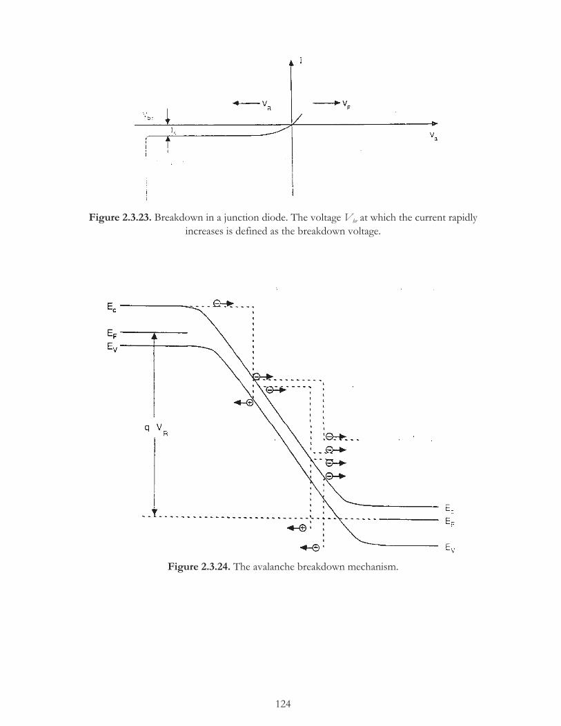
124
Figure 2.3.23. Breakdown in a junction diode. The voltage Vbr at which the current rapidly increases is defined as the breakdown voltage.
Figure 2.3.24. The avalanche breakdown mechanism.

125
Figure 2.3.25. The tunneling breakdown mechanism: (A) The band diagram under tunneling conditions and (B) The triangular barrier through which the electron tunnels through
A detailed theoretical model is available to treat the avalanche process and derive an expression for the avalanche breakdown voltage. Similarly, a detailed theoretical model is used to derive an expression for the tunneling breakdown voltage. For our purposes, we will assume that there is a certain critical electric field which when exceeded causes the junction to breakdown independent of the mechanism. We can derive an expression for the breakdown voltage in terms of the critical electric field. For an abrupt junction the maximum electric field is equal to
max=qND
sxn=
qNAsxp
But the total voltage across the junction is equal to
VR+Vbi= maxxn+xp2
Substituting for xn and xp from the previous equation we get
VR+Vbi= maxxn+xp2
= max
2max s
qND+ max s
qNA
= max2s
2q
1
ND+ 1
NA (2.3.138)
The breakdown voltage Vbr is the value of VR at which max becomes equal to crit, the critical electric field. Thus we obtain the expression for the breakdown voltage as

126
Vbr=crit2s
2q
1
ND+ 1
NA-Vbi (2.3.139)
There are two points that must be mentioned with respect to the junction breakdown. One is that the avalanche mechanism is the dominant mechanism in diodes in which the breakdown
voltage is larger than 6Egq
and the tunneling mechanism is the dominant one in diodes in which the
breakdown voltage is less than 4Egq
. For silicon diodes avalanche process is dominant in diodes in
which the breakdown voltage is above 6.6 V and tunneling is the dominate process for diodes with a breakdown voltage less than 4.4 V. Secondly, the avalanche breakdown process has a positive temperature coefficient (i.e., the breakdown voltage increases with temperature whereas the tunneling breakdown process has a negative temperature coefficient with the breakdown voltage decreasing with increasing temperature.) Silicon diodes that have a breakdown voltage between 4.4 and 6.6 V have both mechanisms present and so they have very little temperature dependence of the breakdown voltage. Usually diodes which are in the breakdown mode are used as a voltage reference at a voltage of Vbr and are called Zener diodes.
The expression we derived for the breakdown voltage is for planar diodes (i.e., ones in which the junction is planar.) However in practical diodes, the sides and corners of the junction are curved and hence the actual breakdown voltage is lower than what we derived due to the fact that the electric field is higher in curved junctions than in planar junctions for a given applied voltage.
Example 2.3.9
Given that the critical electric field is 3x10⁵ V cm-1 for a diode with NA equal to 1015cm-3 on the p
side and ND equal to 1016cm-3 on the n side, calculate the breakdown voltage.
Vbi=kTqlnNANDni2 =0.0258 ln
1031
1020=0.654 V
Hence
Vbi=3x10⁵
2×11.9×8.84x10-14
2×1.6×10-19× 10-15+10-16 -0.654=325-0.654≈324 V

127
Chapter 2.3 Summary
In thermal equilibrium, a potential barrier exists across the p-n junction such that the diffusion current is balanced by a drift current in the opposite direction. The height of the potential barrier is denoted byVbi.
A depletion region is formed on either side of the metallurgical junction, and the charge density in the depletion region is due to ionized acceptor atoms on the p-side, and to donor atoms on the n-side.
xd= xn+xp Where xn = width of the depletion region on the n-side, and xp = width of the depletion region on the p-side and xp is the total width of the depletion region.
The positive charge in the depletion region on the n-side is equal in magnitude to the negative charge in the depletion charge on the n-side (NAxp = NDxn)
The depletion region occurs more on the lightly doped side. The electric field exists only in the depletion region. The neutral n and p regions do not have any electrical field.
Forward Bias
Under forward bias, the height of the potential barrier across the junction is reduced to Vbi- VF, where VF= bias voltage.
The expression for the depletion region widths is the same as the one for thermal equilibrium, with Vbi replaced by Vbi -VF. The depletion region width decreases under forward bias.
Under forward bias, excess minority carriers are injected into the two neutral regions. The value of the excess minority density at the boundary of the deletion region and the neutral region is
Δp o =pno(eqVFkT -1) n-side
Δn o =npo(eqVFkT -1) p-side
A net current flows across the junction due to the diffusion of the injected excess minority carrier’s density.
Under ideal conditions.
IF=IS(eqVFkT -1)
where
IS=qADppn0Lp+Dnnp0
Ln When Wn Lp and Wp Ln

128
and IS=qADppn0Wn+Dnnp0
Wp when Wn Lp and Wp Ln
The first term in the expression for IF represents the diffusion current, and the second one represents the drift current.
Reverse Bias
Under reverse bias, the height of the potential barrier increases to Vbi +VR where VR is the reverse voltage.
The expression for the depletion region under reverse bias is the same as the one for thermal equilibrium with Vbi replaced by Vbi+VR. The depletion region width increase under forward bias.
The net current under reverse bias has the same form as the forward current with VF replaced by -VR
IR=IS e-qVRkT -1
Again, as in the forward bias case, the first term represents the diffusion current, and the second term the drift current. When qVR>>kT, the reverse current is only due to the drift current.
Is is called the saturation current.
IR is called the leakage (or reverse) current.
It can be shown that IS is due to the generation of minority carriers within a diffusion length from the boundary of the depletion region in the two neutral regions.
Non-ideal Current
Current due to recombination of electron-hole pairs also contributes to the current in the p-n junction under forward bias. This component of current has a voltage dependence given
by eqVFkT , and is dependent on the number of traps (g-r centers) per unit volume.
Similarly, an additional component due to the generation of electron-hole pairs in the depletion region flows in the junction under reverse bias.
Capacitance
The depletion region behaves like a parallel plate capacitor with spacing equal to the depletion region width with respect to applied small signal voltage. The capacitance is called the junction capacitance.
Injected minority carriers give rise to a stored charge in the two neutral regions. In the one-sided abrupt p+-n junction

129
Qs=Iτp
where
Qs= stored charge
τp= minority carrier lifetime
I current through the diode
A capacitance effect arises due to the stored charge, which is called the diffusion capacitance.
When the diode is switched from ‘on’ to ‘off’, there is a delay in the reverse current attaining the steady-state value. This delay time is related to the minority carrier lifetime.
Breakdown Voltage
As the reverse voltage is increased at sufficiently large voltages and when the maximum electric field in the depletion region becomes equal to the critical electrical field, the reverse current increases enormously. This voltage is called the Breakdown Voltage.
There are three mechanisms: (1) Thermal instability (2) Tunneling process (3) Avalanche process
The breakdown voltage due to tunneling has a negative temperature coefficient. The cylindrical and spherical junctions have lower breakdown voltage than planar junctions.

130
Chapter 2.3 Glossary
A area of the junction
A’ an integration constant
A, B two points in a semiconductor
A, B integration constants that will be determined by the boundary conditions at x=0 and x'=Wn
C capacitance
C1 an integration constant
C’1 an integration constant
C2 an integration constant
C3 an integration constant
Cd depletion capacitance per unit area
Cdiff diffusion or storage capacitance
Cdiff p diffusion capacitance due to stored holes
Cj junction capacitance
dVa step voltage
Dn electron diffusion constant
Dp hole diffusion constant
Ec energy at the bottom of the conduction band, also the potential energy of electrons
EF Fermi energy
EFn quasi-Fermi energy level for electrons
EFp quasi-Fermi energy level for holes
Eg energy gap or bandgap energy
Ei intrinsic Fermi energy level
Et trap energy level
EV energy at the top of the valence band
electric field
crit critical electric field
max maximum electric field in the space charge region
(x) the electric field at x
f(x) Fermi function
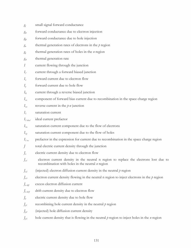
131
gf small signal forward conductance
gfn forward conductance due to electron injection
gfp forward conductance due to hole injection
gn thermal generation rates of electrons in the p region
gp thermal generation rates of holes in the n region
gth thermal generation rate
I current flowing through the junction
IF current through a forward biased junction
In forward current due to electron flow
Ip forward current due to hole flow
IR current through a reverse biased junction
Irec component of forward bias current due to recombination in the space charge region
Irev reverse current in the p-n junction
IS saturation current
IS ideal ideal current prefactor
ISn saturation current component due to the flow of electrons
ISp saturation current component due to the flow of holes
IS rec prefactor in the expression for current due to recombination in the space charge region
J total electric current density through the junction
Jn electric current density due to electron flow
Jn1 electron current density in the neutral n region to replace the electrons lost due to recombination with holes in the neutral n region
Jn2 (injected) electron diffusion current density in the neutral p region
Jn3 electron current density flowing in the neutral n region to inject electrons in the p region
Jn diff excess electron diffusion current
Jn drift drift current density due to electron flow
Jp electric current density due to hole flow
Jp1 recombining hole current density in the neutral p region
Jp2 (injected) hole diffusion current density
Jp3 hole current density that is flowing in the neutral p region to inject holes in the n region

132
Js saturation current density
Jt the total electric current density
k Boltzmann constant
Lp minority carrier diffusion length (of holes) in the n region
Ln minority carrier diffusion length (of electrons) in the p region
m* effective mass of the carrier
n electron density
n1 electron density in the semiconductor if the Fermi energy at trap level
n0 thermal equilibrium density of electrons
nn0 thermal equilibrium majority carrier (electron) density
nn electron density in the n region
ni electron density in an intrinsic semiconductor
np electron density in the neutral p region
np0 thermal equilibrium minority carrier (electron) density
NA acceptor density
NA- ionized acceptor density
ND donor density
ND+ ionized donor density
ND-NA net impurity concentration
Nt density of traps or g-r centers
p hole density
p1 hole density in the semiconductor if the Fermi energy is at trap level
p0 thermal equilibrium density of holes
pn hole density in the neutral n region
pn0 thermal equilibrium minority carrier (hole) density
pp hole density in the p region
pp0 thermal equilibrium majority carrier (hole) density
P(x’)dx’ probability that an excess hole, injected at x’=0 will recombine in an elementary distance dx’ between x’ and x’+dx’

133
P(x’) probability per unit distance that an excess minority carrier (hole) will recombine and be lost
P0 probability that an excess minority carrier will recombine and that does not vary with x
q total electric charge, expressed in coulombs
Q charge
Qns stored charge due to excess electrons
Qps stored charge due to excess holes
Qs stored charge
r proportionality constant in the recombination rate
rf small signal forward resistance
R recombination rate
s surface recombination velocity
t time
T Temperature
US net recombination rate per unit area of the surface
vn, vp thermal velocity of electrons and holes respectively and is equal to 3kT
m*
vth thermal velocity
Va applied voltage
Vbi built-in voltage, potential difference between the neutral n-side and the neutral p-side
Vbr breakdown voltage
VF externally applied forward bias voltage
VR externally applied reverse bias voltage
Wn width of the neutral n region
Wp width of the neutral p region
x distance measured with the origin at the metallurgical junction
x’ distance measured with the origin at x=xn
xd total depletion region width = xn+xp
xd eff part of the depletion region where the electron and hole are both minimum and equal
xn boundary of the depletion region on the n-side, or the width of the depletion region on the n-side

134
xp width of the depletion region on the p-side
-xp boundary of the depletion region on the p-side
Δxn excess electron density
Δn(x= -xp) excess minority carrier densities at x=-xp under forward bias
Δp excess hole density
Δp(0) excess carrier (hole) density at x’=0, i.e., at x=xn
Δp(Wn) Δp evaluated at x’=Wn
Δp(x=xn) excess minority carrier density at x=xn under forward bias, same as Δp(0)
εs permittivity of a semiconductor
ideality factor
μn electron mobility
μp hole mobility
ρ charge density
σn, σp capture cross-sections for electrons and holes respectively
τg generation lifetime
τn minority carrier (or excess carrier) lifetime in the p-region
τn0 1
Ntσnvn
τP minority carrier (or excess carrier) lifetime in the n-region
τp0 1
Ntσpvp
ϕ electrostatic potential
ϕA-B potential difference between two points A and B
ϕn electrostatic potential in an n-type material
ϕp electrostatic potential in a p-type material
ψ electrostatic potential difference
ψ(x) electrostatic potential difference at some point x
ψAB electrostatic potential difference between xA and xB

135
Chapter 2.3 Problems
1. Calculate the electrostatic potential ϕn or ϕp as the case may be, at room temperature for each of the following impurity concentrations: (a) 1015 cm-3 boron atoms (b) 1016 cm-3 gallium atoms (c) 1017 cm-3 phosphorous atoms
2. Redo problem above at T=100 K. (Assume that all the impurity atoms are ionized at this
temperature.)
3. Consider a n-type silicon sample with ND= 1016 cm-3. Calculate ϕn at (a) 300 K (b) 200 K
4. An abrupt p-n junction has an impurity concentration of 1015 cm-3 boron atoms on the p-side and 1017 cm-3 antimony atoms on the n-side. Calculate the built-in potential of the junction at room temperature.
5. Calculate the depletion region width on the n-side and that on the p-side as well as the total depletion region width for the case described in the previous problem. Do you expect your answer to depend on the temperature? (The impurity atoms are completely ionized in the depletion region even though in the neutral region the impurity atoms will only be partially ionized at low temperatures.) If so, why?
6. Consider an abrupt p-n junction with the net impurity concentration of 4×1015cm-3 on the
n-side and 6×1016cm-3 on the p-side. Determine the built-in potential.
7. For the sample in the previous problem, calculate the depletion region width under thermal equilibrium at T=300 K
8. For the sample in the previous problem (a) What is the maximum electric field εmax, in the depletion region?
(b) At what values of x in the depletion region will the electric field be of εmax?
9. Consider a one sided abrupt p+-n junction in which the acceptor density on the p-side is 1018
cm-3 and the donor density on the n-side is 1015 cm-3. Calculate the depletion region width in thermal equilibrium.
10. An abrupt p-n junction has 1015 cm-3 donor atoms on the n-side and 1016 cm-3 acceptor atoms on the p-side. Determine Vbi, xp, xn, and xd.

136
11. Consider an abrupt junction with ND=1016 cm-3 on the n-side and ND=1015 cm-3 on the p-side. Assume that the edge of the depletion region occurs at –xp and xn. Assume ni to be 1010 cm-3 at room temperature.
(a) What is the electron density at x=-xp
2 in thermal equilibrium?
(b) What is the hole density at the same point under the same condition?
12. The equations in the text give the potential variation in the p-side and in the n-side respectively for an abrupt junction, taking the zero reference for the potential as that at the neutral p region. Write down similar equations for the potential taking the zero reference for the potential as that at the neutral n region.
13. Consider a linear junction where the impurity concentration varies as N= -αx and α is a constant. Derive an expression for the electric field and the potential variation in the
depletion region assuming the boundary of the depletion region to be at x= -W2 and x=W
2.
14. A diffused p-n junction has a uniform doping of 2×1014cm-3 on the n-side. The impurity concentration varies linearly from the n-side to the p-side with a=1019 cm-3. At zero bias the depletion region on the p-side is 0.8 μm. Find the depletion region width, built-in potential and maximum electric field in the depletion region.
15. Show that for a narrow base diode, the excess carrier density variation in the neutral n region is given by
Δp x' =Δp(0) 1- x'
Wn
16. Write down the expression for the ideal diode current when the region is approximated as
a narrow base and the p region is approximated as a wide base.
17. Consider an abrupt p-n junction in which the acceptor density on the p-side is 1016 cm-3 and the donor density on the n-side is 6x1015 cm-3. Calculate the depletion region widths on the p- and on the n- side for a forward bias voltage of 0.6 V.
18. Assume that the area of the junction for the device in the last problem is 10-4 cm-2. Calculate the current through the device under a forward bias voltage of 0.5 V assuming that the diode is a wide base diode. Take the minority carrier lifetime in the p and in the n regions to be 10-6 and 10-5 seconds respectively. Use the mobility curve in Chapter 2 in the text.
19. Consider as abrupt junction with ND=1016 cm-3 on the n side and NA=2x1015 cm-3 on the p-side. Let the area of the junction be 10-3 cm-2. Given the diffusion constant to be 20 and 10

137
cm2s-1 and the lifetime to be 80 and 10 μs in the n and p regions respectively, determine the ideal reverse current for a reverse voltage of (a) 0.06 V (b) 6 V
20. Given that Nt=1015 cm-3, σn=σp= 1016 cm-2 and vth=107 cm s-1 for both the electrons and the holes in the diode in the previous problem, calculate the forward current due to recombination in the depletion region for a forward bias of 0.4 V. Assume that the effective depletion region width in which the recombination is effective is xdeff=
xd3 where xd is the
depletion region width.
21. Given that non-ideal reverse current is only due to generation in the depletion region occurring in the bulk of the device (i.e., neglecting surface generation) calculate the reverse current at a reverse bias of 6V.
22. Consider an abrupt p-n junction with the metallurgical junction located at x=0 and the boundaries of the depletion region located at x= -xn on the n-side and at x= -xp on the p-side. (a) What is the ratio of the electric field at x= -r1xn and that at x= -r2xp where r1 and r2 are
constants of value less than 1. (b) What is the built-in voltage at room temperature if NA=1016 cm-3 in the p-side and
ND=1015 cm-3 on the n-side? Assume ni = 1x1010 cm-3.
23. An abrupt p-n junction is fabricated with ND=2x1016 cm-3 on the n-side and NA=5x1015 cm-3 on the p-side. Let A the area of the junction be 10-4 cm2 What fraction of the forward current is due to the minority carrier injection in the neutral p-side? Assume that Dn and Ln on the p-side to be 40 cm2s-1 and 0.02 cm respectively and that Dp and Lp on the n-side to be 10 cm2s-1 and 0.005 cm respectively.
24. An abrupt p-n junction has 1015 cm-3 donor atoms on the n-side and 1016 cm-3 acceptor atoms on the p-side. If the area of the junction is 10-4 cm2 and the minority carrier lifetime is 0.4 and 1 μs on the n- and p- side, respectively, find the diode current at (a) 0.6 V (b) -1 V bias applied across the device
25. An abrupt p-n junction has 1015 cm-3 donor atoms on the n-side and 1019 cm-3 acceptor atoms on the p-side. Find the current through the diode for a forward bias of 0.5 V given that the diffusion lengths in the n and p regions are 10-2 and 3x104 cm respectively. Assume the area of the junction to be 2x10⁻⁴ cm2. Take the diffusion constants from the curve in Chapter 2 of the text.
138
26. An abrupt p-n junction has 1015 cm-3 donor atoms on the n-side and 1019 cm-3 acceptor atoms on the p-side. Calculate the junction capacitance at a (a) Forward bias of 0.4 V (b) Reverse bias of 10 V
27. In an abrupt p-n junction ND= 5x1016 cm-3, NA= 1017 cm-3, and the area of the junction is 10-3 cm2. Given that the minority carrier diffusion constant and lifetime are 20 cm2 s-1 and 2x10⁻⁵ s on the p-side and 8 cm2 s-1 and 2x10⁻⁶ s on the n-side, calculate the current through the diode at room temperature under a forward bias voltage of 0.5 V

139
Chapter 4 Bipolar Transistor
In this chapter, we will be discussing a device called bipolar junction transistor (BJT) or a bipolar transistor. The principle of bipolar transistor action is based on (1) minority carrier injection into a neutral region using a forward-biased p-n junction and (2) the collection of the injected minority carriers by placing a second (revers-biased) p-n junction very close to the forward-biased p-n junction. In order to illustrate this principle, let us first consider an ideal p-n junction. Under forward bias, the current through the junction comprises of two components: (1) electron injection into the p side and (2) hole injection into the n side. The forward biased p-n junction represents a low-impedance junction: for a small voltage applied across the junction, a large amount of current flows through it. On the other hand, if a p-n junction is under reverse bias, the current through the junction is from minority carriers that enter the depletion region, and does not depend on the reverse voltage (barrier height). The same current will essentially flow independent of the reverse voltage. In this sense, it is a constant current source or a high impedance current source; even for a large change in the reverse bias, the increase in the current is negligibly small.
Two types of transistor structures are possible in the bipolar transistors, and are shown in Figure 2.4.1. They are called n-p-n and p-n-p transistors. Let us first consider the n-p-n transistor. Assume that the first n-p junction is forward-biased, and the second p-n junction is reverse-biased as shown in Figure 2.4.1A. The first n region is called the emitter, the p region the base, and the second n region the collector. The emitter-base junction is forward biased so minority carriers (electrons) are injected into the base region and diffuse in the base region towards the collector-base junction. If the collector-base junction is close to the emitter-base, then a substantial fraction of the injected minority carriers will reach the collector-base depletion region without being lost in recombination. The carriers reaching the collector-base depletion region are driven by the electric field in the collector-base depletion region to the neutral collector region. Thus, the injected minority carriers in the base region give rise to a current through the collector lead, and this current is called the collector current. The collector current acts like a current from a constant current source since it is due to minority carriers that enter a reverse-biased junction. If a large load resistance is connected between the collector and the base, then a large amount of output power will be delivered to the load resistance. Let us look at the band diagram of the device as given in Figure 2.4.2. The energy barrier for minority carrier flow in the emitter-base junction is reduced because it is forward-biased, giving rise to electron injection from the emitter into the base. The energy barrier in the collector-base junction is increased because it is reverse-biased. Most of the electrons injected into the base will reach the collector-base junction if the base region is narrow. Let us consider the circuit shown in Figure 2.4.3. A small signal voltage, vs is connected between the emitter and the base in series with the forward-bias voltage source VBE. A load resistor (RL) is connected between the collector and the base, in series with the collector voltage supply (VCC). Let an alternating current (ie) flow in the emitter lead due to the small signal voltatge. Let ic and ib be the corresponding collector and base currents. The collector current (ic) flows through the load resistance. The power that the small-signal source, has to deliver to the transistor is given by
Power Input=ic2 rE (2.4.1)
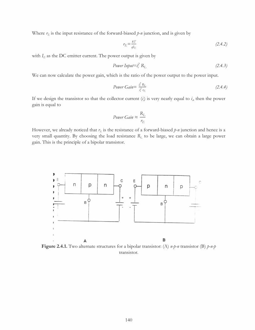
140
Where rE is the input resistance of the forward-biased p-n junction, and is given by
rE=kT
qIE (2.4.2)
with IE as the DC emitter current. The power output is given by
Power Input=ic2 RL (2.4.3)
We can now calculate the power gain, which is the ratio of the power output to the power input.
Power Gain= ic2 RLie2 rE
(2.4.4)
If we design the transistor so that the collector current (ic) is very nearly equal to ie, then the power gain is equal to
Power Gain ≈ RLrE
However, we already noticed that rE is the resistance of a forward-biased p-n junction and hence is a very small quantity. By choosing the load resistance RL to be large, we can obtain a large power gain. This is the principle of a bipolar transistor.
Figure 2.4.1. Two alternate structures for a bipolar transistor: (A) n-p-n transistor (B) p-n-p transistor.
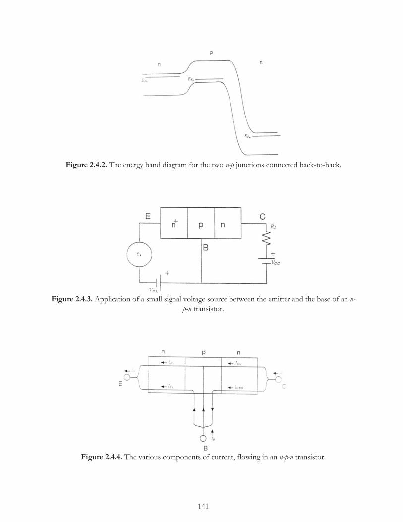
141
Figure 2.4.2. The energy band diagram for the two n-p junctions connected back-to-back.
Figure 2.4.3. Application of a small signal voltage source between the emitter and the base of an n-p-n transistor.
Figure 2.4.4. The various components of current, flowing in an n-p-n transistor.

142
Let us now consider the various components of current flowing through the device. The DC current flowing through the emitter (which is denoted IE) comprises of two components: (1) electron injection from the emitter into the base, IEn, and (2) hole injection from the base into the emitter, IEp. The electrons injected into the base diffuse toward the collector region and result in a collector current. However, not all the electrons injected into the base are able to reach the collector-base depletion region, since some of the injected electrons recombine in the neutral-base region. Hence the electron current, ICn, that reaches the collector-depletion region and flows through the collector lead is smaller than IEn, the electron current injected from the emitter into the base.
In the collector, in addition to ICn, we also have a leakage current that normally arises in a reverse-biased p-n junction. Let us denote the leakage current ICBO. The collector current, IC, is therefore equal to the sum of ICBO (the leakage current) and ICn (the current due to the injection of electrons from the emitter into the base).
Holes have to flow into the base region to participate in the recombination process. The hole current flows through the base lead. Similarly, holes injected into the emitter from the base also flow through the base lead. Additionally, the collector leakage current, ICBO, also has to flow through the base lead. The flow of the various components of current in an n-p-n transistor is shown in Figure 2.4.4. In this figure, the arrows indicate the direction of the conventional electric current, and not the direction of the particle flow. The electron (particle) flow is opposite to the conventional electric current flow for IEn and ICn. We can now write the emitter, base and collector currents as equal to
IE=IEn+IEp (2.4.6)
IC=ICn+ICBO (2.4.7)
IB=IE-IC= IEn-ICn+IEp-ICBO (2.4.8)
We define the current gain of the device as equal to the collector current due to electron injection from the emitter into the base, divided by total emitter current. The current gain is denoted α0, and given by
α0=ICnIE
(2.4.9)
The subscript 0 in α0 implies that the gain is evaluated for very low (or zero) frequency input signals. It must be noted that we are considering an n-p-n transistor, and hence the collector current due to minority carrier (electron) injection in the base from the emitter is denoted with a subscript n. On the other hand, if we were to consider a p-n-p transistor, the collector current arising from minority carrier injection from the emitter into the base will be due to holes and will be denoted with a subscript p in place of n.
The current gain, α0, can be related to two other parameters, which are γ (the emitter injection efficiency) and αT (the base transport factor). The emitter injection efficiency γ is defined as the ratio of the emitter current due to minority injection from the emitter into the base and the total emitter current. Hence it is equal to

143
γ= IEnIE= IEnIEn+IEp
(2.4.10)
The base transport factor, αT, is defined as the ratio of the collector current and the minority carrier current injected from the emitter into the base, i.e., the fraction of the injected minority carrier current that reaches the collector. This relationship is expressed by
αT=ICnIEn
(2.4.11)
It is readily seen that α0 is the product of γ and αT, that is
α0=ICnIE= IEnIE
ICnIEn=γ αT (2.4.12)
We can now write the collector current as equal to
IC=ICn+ICBO=αTIEn+ ICBO
= αTγ IE+ICBO= α0IE+ICBO (2.4.13)
and similarly, the base current can be expressed in terms of the emitter current as
IB=IE-IC=(1- α0)IE-ICBO (2.4.14)
In principle, the emitter injection efficiency is made very close to unity by making the emitter impurity concentration very large in comparison to the base impurity concentration. Similarly, the base transport factor can be made very close to unity by making the width of the neutral base region (i.e., the distance the minority carriers that are injected from the emitter into the base have to travel to reach the collector-base depletion region) very small compared with the diffusion length of the minority carriers in the base. Under these conditions, the current gain will be very close to unity.
Example 2.4.1
Let us now calculate the power gain of an n-p-n transistor based on our discussions so far. Let us assume that the transistor is carrying a DC emitter current IE, equal to 1 mA. Let the load resistance RL be equal to 259 KΩ. Let the current gain α0 be taken as 0.99. Assume a small signal voltage vs is applied between the emitter and the base giving rise to an emitter current and ie and a collector current ic.
Power Output= ic2 RL
=(0.99 ie)2 RL
= (0.99ie)2× 259 x103 W
Power Input= ie2 re

144
But re=kT
qIE
= 0.0259
10-3 Ω
=25.9 Ω
Power Input= ie2 x 25.9
Power Gain= (0.99ie)
2x 259 x103
ie2 x 25.9
= 0.992 x 104
=0.98 x 104=9800
From the above example, we see that a large power gain is obtained by choosing a large value of RL. From this rudimentary discussion it appears that infinite power gain can be obtained by choosing RL to be infinitely large. This is not so. Later on, we will see that our initial assumption that the collector-base junction acts as a current source with infinite impedance is in error, and that the output impedance of the collector-base junction (the ratio of the incremental change in the collector voltage to the incremental change in the collector current) is large but not infinite. Hence the maximum power that can be drawn from the device is what is obtained with RL equal to the output impedance of the collector-base junction.
The bipolar device is denoted by the symbol shown in Figure 2.4.5A for n-p-n transistors, and that in Figure 2.4.5B for p-n-p transistors. The lead with an arrow is the emitter and the direction of the arrow indicates (as in a p-n junction) the direction of the forward-bias current.
2.4.1 D.C. Characteristics
Let us now investigate the characteristics of the bipolar transistor in a quantitative manner. We make the following assumptions:
(1) The impurity concentration in the emitter, base and collector, regions are uniform. This means that there is no spatial variation of the impurity concentration within any one of the three regions.
(2) The injection of minority carriers in the base corresponds to a low-level injection. (3) There is no recombination or generation in the depletion region of the emitter-base
junction, or in the collector-base junction. In other words, we treat the two junctions as ideal junctions.
(4) There is no series resistance in the bulk regions of the device.

145
Ideal Transistor Characteristics
The characteristics of a device under the assumption of ideal junctions are called ideal transistor characteristics. Let us examine the base region. Referring to Figure 2.4.6, the metallurgical junctions at the emitter-base and on the collector-base are located at x=0 and x=WBJ, respectively. However, the active neutral region of the base is obtained by subtracting xPE (the width of the depletion-region occurring in the base region due to the emitter-base junction), and xPC (the width of the depletion-region occurs in the base region due to collector-base junction) from the width WBJ. We choose a new coordinate system, x’, where the origin is chosen at the edge of the neutral base region on the emitter side. The edge of the depletion region on the collector side occurs at x’=W’. W’ is then equal to
W'=WBJ-xPE-xPC (2.4.15)
From now on, we will use W’ to denote the width of the neutral base region. The minority carriers injected from the emitter at x’=0 diffuse in the neutral base region and travel toward the collector-based junction. This gives rise to diffusion current. In order to derive an expression for the diffusion current due to injection of minority carriers in the base, we first set up the continuity equation in the base region. Since we are considering an n-p-n transistor, electrons are the minority carriers in the base. The continuity equation for electrons in the base region is given by
∂Δn∂t= 1q∇·Jn-
Δnτn
(2.4.16)
Δn stands for the excess minority carrier in the base region due to minority carrier injection from the emitter, Jn is the minority carrier current density and τn is the minority carrier lifetime. If we assume a one-dimensional case, this continuity equation reduces to
∂Δn∂t= 1q
∂
∂x'(Jn)- Δnτn
(2.4.17)
where Jn=nqμnE+ qDn∂Δn∂x'
(2.4.18)
Let us assume that there is no electric field in the neutral base region. Then the expression for the current density has only the diffusion term and the gradient of Jn becomes equal to
∂Jn∂x'=qDn
∂2Δn∂x'2
(2.4.19)
Substituting this expression for the gradient of Jn in the continuity equation, we get
∂Δn∂t=Dn
∂2Δn∂x'2
- Δnτn
(2.4.20)
We can solve the continuity equation first under DC conditions. We assume that sufficient time has been allowed to elapse after the application of the DC bias so that steady-state conditions can be assumed.

146
Figure 2.4.5. The circuit symbol for the bipolar transistor. (A) n-p-n transistor and (B) p-n-p transistor.
Figure 2.4.6. The neutral base region. The region between the metallurgical junction on the emitter side and that on the collector side represents the total base region. However, the neutral
base region width is obtained by subtracting appropriate segments of the depletion region widths on the two sides.
Steady State (DC Conditions)
Under steady-state conditions, the partial of Δn with respect to time is equal to zero. Hence, the continuity equation can be rearranged to obtain
∂2Δn∂x'2= ΔnDnτn= ΔnLn2 (2.4.21)

147
where Ln= Dnτn is the diffusion length, which we came across in our study of the p-n junction. The solution to the continuity equation is seen to be
Δn=A e-x'Ln+ Be
x'Ln (2.4.22)
The boundary conditions for the excess carrier density in the base region are
At x’=0 Δn x'=0 =Δn0=np0 eq VBEkT -1 (2.4.23)
And at x’=W’, the boundary condition can be approximated as
Δn=0 (2.4.24)
By applying the boundary condition at x’=0 in Equation 2.4.22, we get
Δn0 = A + B=npB0 eq VBEkT -1 (2.4.25)
Similarly, by applying the boundary condition at x’=W’, we get
0=A e-W'
Ln+ BeW'
Ln (2.4.26)
Solving for the constants A and B, (left as a homework problem) we obtain
B= Δn0e-W'
Ln
e-W'
Ln - eW'
Ln
(2.4.27)
A= Δn0eW'
Ln
eW'
Ln - e-W'
Ln
(2.4.28)
Substituting these expressions for A and B, we obtain
Δn x' = Δn0e(W'-x')Ln
eW'
Ln - e- W'
Ln
+ Δn0e- (W'-x')Ln
e- W'
Ln - e+
W'
Ln
=Δn0sinh (
(W'-x')Ln
)
sinh(W'
Ln)
(2.4.29)
This expression for Δn is the most general expression for excess carrier density in the base region. It may be recalled from our discussion of the p-n junction that the excess carrier density in the neutral region decreased linearly with distance when the width of the neutral region was small compared to the minority carrier diffusion length (narrow base diode) and decayed exponentially with distance when the width of the neutral region was large compared to the diffusion length (wide base diode). It is easy to show that Equation 2.4.29 reduces to an exponential or linear relation under appropriate assumptions. As we will see later on, in order to make (the base transport factor) as close to unity as possible, W’ (the neutral base width) has to be kept very small

148
in comparison with Ln (minority carrier diffusion length). When W’<<Ln, the expression for Δn(x) can be simplified as
Δn x' ≈ Δn0
(W'-x')Ln
W'
Ln
= Δn0(1-x'
W') (2.4.30)
n(x’) given by Equation 2.4.29 is plotted in Figure 2.4.7 as a function of x’ for various values of W'
Ln.
It is noticed that when W’<<Ln, a linear plot is obtained and when W’>>Ln, an exponential plot is obtained. We can now calculate the diffusion current in the base due to the injected minority carriers by substituting the expression for Δn(x’) given by Equation 2.4.29 in the expression for electron diffusion current. The electron diffusion current density is given
Jn x' = qDn
dΔn∂x'
= -q DnΔn0Ln
cosh (
(W'-x')Ln
)
sinh(W'
Ln)
(2.4.31)
Base Transport Factor
The electron current density at x’=0 is obtained by putting x’=0 in the above equation.
Jn x'=0 = -q Dn
Δn0Ln
cosh (
W'
Ln)
sinh(W'
Ln)=-q Dn
Δn0 coth (W'
Ln)
Ln (2.4.32)
The emitter current due to electrons injected from the emitter into the base (IEn) is equal to
IEn=A Jn x'=0 = -q A Dn
Δn0coth (W'
Ln)
Ln (2.4.33)
The electron current density at x’=W’ is obtained by putting x’=W’ in Equation 2.4.31
Jn x'=W' = -q Dn
Δn0Ln
1
sinh(W'
Ln) (2.4.34)
This is the collector current density arising due to minority carrier injection in the base. The collector current, ICn, is equal to
ICn=A Jn x'=W' = -q A Dn
Δn0Ln
1
sinh(W'
Ln) (2.4.5)
The difference between IEn and ICn represents the decrease in current due to recombination in the neutral base region. The base transport factor is the ratio of ICn to IEn, and is given by
αT=ICnIEn=Jn x
'= W'
Jn x'=0
= 1
cosh(W'
Ln) (2.4.36)
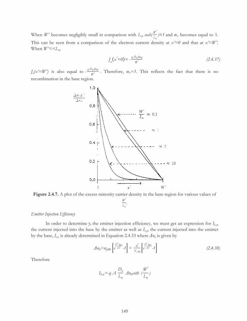
149
When W’ becomes negligibly small in comparison with Ln, cosh(W'
Ln)≈1 and αT becomes equal to 1.
This can be seen from a comparison of the electron current density at x’=0 and that at x’=W’. When W’<<Ln,
Jn x'=0 = - q DnΔn0
W' (2.4.37)
Jn(x’=W’) is also equal to - q DnΔn0W'
. Therefore, αT=1. This reflects the fact that there is no
recombination in the base region.
Figure 2.4.7. A plot of the excess minority carrier density in the base region for various values of W'
Ln.
Emitter Injection Efficiency
In order to determine γ the emitter injection efficiency, we must get an expression for IEn, the current injected into the base by the emitter as well as IEp, the current injected into the emitter by the base, IEn is already determined in Equation 2.4.33 where Δn0 is given by
Δn0=npB0 eqVBEkT -1 = ni
2
NABeqVBEkT -1 (2.4.38)
Therefore
IEn=-q A DnLn
Δn0coth (W'
Ln)

150
= -q A DnLn
ni2
NAB coth (W
'
Ln) e
qVBEkT -1 (2.4.39)
The component IEn of the emitter current due to hole injection from the base into the emitter can similarly be obtained by solving the continuity equation for holes in the neutral emitter region. Let us assume that the width of the neutral emitter region, WE, is large compared with the minority carrier (hole) diffusion length (LPE) in the emitter. Then we can use the wide base approximation in the emitter region. We will get an expression for the injected hole current density, which decays exponentially (because of our assumption that WnE is much large than LpE). We determine the expression for the hole current in the emitter just at the boundary of the emitter-base depletion region, and take that as the current injected into the emitter by the base. Hence IEp is given by
IEp= -q A DpELpE
pnE0 eqVBEkT -1
=-q A DPELpE
ni2
NDE e
qVBEkT -1 (2.4.40)
The emitter injection efficiency, γ, can be obtained as
γ==IEnIE=
IEnIEn+IEp
=
DnLn
1NAB
coth (W'
Ln)
DpELpE
1NDE
+ DnLn
1NAB
coth (W'
Ln)
= 1
1 + DpEDn
Ln
LpE NAB NDE
tanh(W'
Ln) (2.4.41)
It is seen that when NDE is very large in comparison with NAB, γ approaches 1. When W’<<Ln,
coth (W'
Ln)≈ Ln
W'Therefore
γ= 1
1 + DpEDn
W'
LpE
NAB NDE
(2.4.42)
Example 2.4.2
Let us calculate the base transport factor given
W'=1 μm=10-4cm
Ln=10 μm=10-3cm

151
By substituting these values in the expression for α0, we obtain
αT=1
cosh(W'
Ln)= 1
1.005=0.995 (2.4.43)
Example 2.4.3
Let us now calculate the emitter injection efficiency given
NDE≈1019cm-3
NAB=1017cm-3
W'=1.0 μm
LpE=10 μm
DpE=1 cm2 sec
Dn=10 cm2 sec
By substituting these values in the expression for γ, we obtain
γ= 1
1 + 110
1 10
1 100
= 1
1 + 1
104 ≈0.9999
2.4.2 DC Current-Voltage Characteristics
The DC current-voltage characteristics of the bipolar transistor can be measured in either of two modes: the common base mode and the common emitter mode.
Common Base Mode
In the common base mode, the collector current is measured as a function of the collector-base voltage for a specified value of the emitter current using the experimental configuration shown in Figure 2.4.8). The emitter-base voltage, VBE, is adjusted to a suitable value, such that a specified emitter current is obtained. The collector current is measured for different values of the collector-base voltage, VCB, while adjusting VBE to keep IE constant at the specified value. A family of curves can be obtained where each curve corresponding to a specific value of emitter current, as shown in Figure 2.4.9. The x-axis in this figure is the collector-base voltage, VCB and the y–axis is the collector current, IC. When VCB is positive, the collector-base junction is reversed-biased. Since α0 is very close to unity, the collector current is very nearly equal to the emitter current. When VCB is negative, the collector-base junction is forward-biased, and the collector also injects minority carriers into the base just as the emitter does. Hence as the forward bias on the collector is increased, the collector current decreases and ultimately becomes zero. When the collector-base
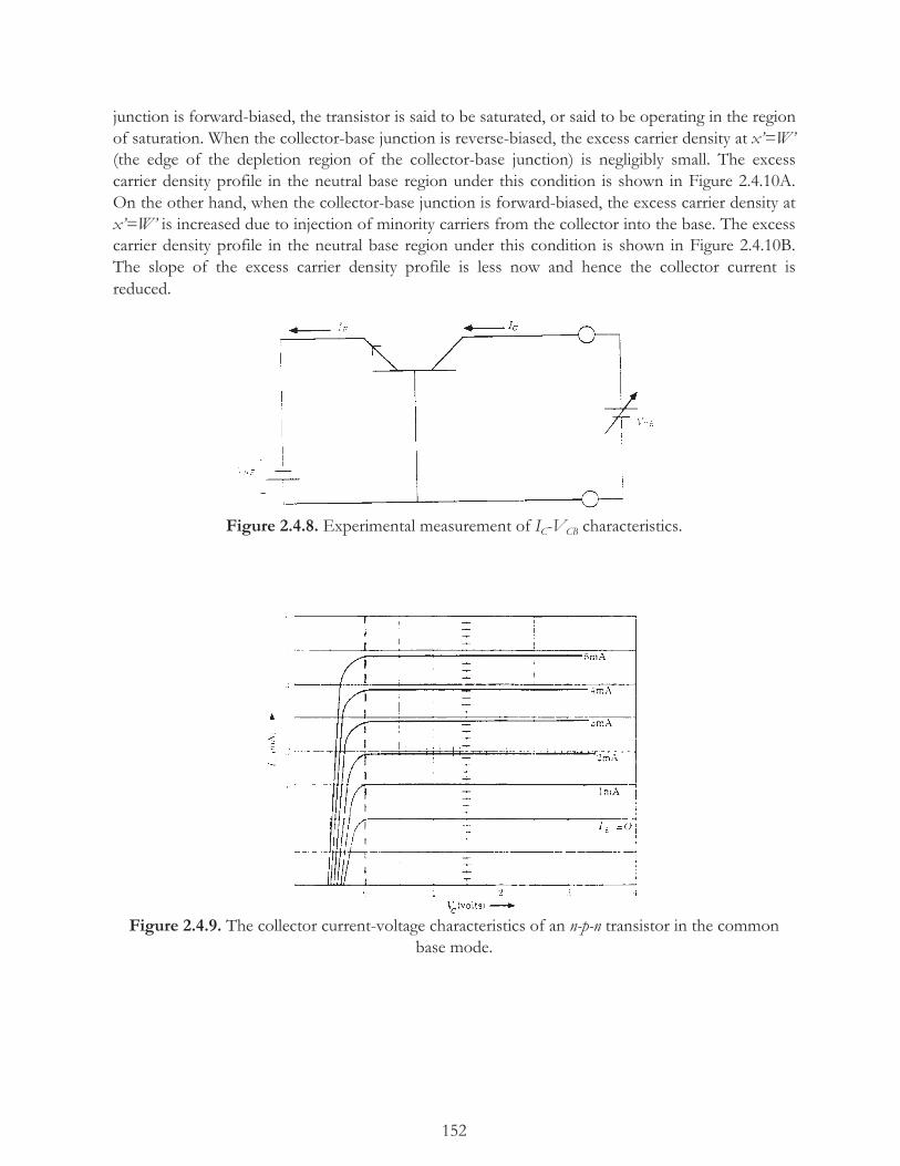
152
junction is forward-biased, the transistor is said to be saturated, or said to be operating in the region of saturation. When the collector-base junction is reverse-biased, the excess carrier density at x’=W’ (the edge of the depletion region of the collector-base junction) is negligibly small. The excess carrier density profile in the neutral base region under this condition is shown in Figure 2.4.10A. On the other hand, when the collector-base junction is forward-biased, the excess carrier density at x’=W’ is increased due to injection of minority carriers from the collector into the base. The excess carrier density profile in the neutral base region under this condition is shown in Figure 2.4.10B. The slope of the excess carrier density profile is less now and hence the collector current is reduced.
Figure 2.4.8. Experimental measurement of IC-VCB characteristics.
Figure 2.4.9. The collector current-voltage characteristics of an n-p-n transistor in the common base mode.
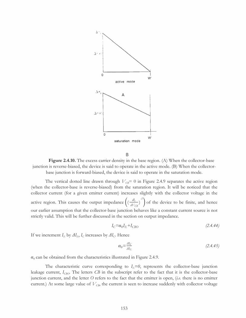
153
Figure 2.4.10. The excess carrier density in the base region. (A) When the collector-base junction is reverse-biased, the device is said to operate in the active mode. (B) When the collector-
base junction is forward-biased, the device is said to operate in the saturation mode.
The vertical dotted line drawn through VCB= 0 in Figure 2.4.9 separates the active region (when the collector-base is reverse-biased) from the saturation region. It will be noticed that the collector current (for a given emitter current) increases slightly with the collector voltage in the
active region. This causes the output impedance ( dIc dVCB
)-1
of the device to be finite, and hence
our earlier assumption that the collector-base junction behaves like a constant current source is not strictly valid. This will be further discussed in the section on output impedance.
IC=α0IE+ICBO (2.4.44)
If we increment IE by ΔIE, IC increases by ΔIC. Hence
α0=ΔICΔIE
(2.4.45)
α0 can be obtained from the characteristics illustrated in Figure 2.4.9.
The characteristic curve corresponding to IE=0, represents the collector-base junction leakage current, ICBO. The letters CB in the subscript refer to the fact that it is the collector-base junction current, and the letter O refers to the fact that the emitter is open, (i.e. there is no emitter current.) At some large value of VCB, the current is seen to increase suddenly with collector voltage

154
in all the curves. This is due to the breakdown of the collector-base junction. The breakdown phenomenon will be discussed in the section on voltage limitations. The collector leakage current, ICBO, is given by the expression for the leakage current for a reverse-biased p-n junction and is equal to
ICBO=-qADnnp0
Ln+DpCpnC0LpC
e-qVCBkT -1 (2.4.46)
Common Emitter Mode
In the common emitter mode, the collector current-voltage characteristics are measured as a function of the collector-emitter voltage, keeping the base current constant. The experimental set-up to obtain these characteristics is illustrated in Figure 2.4.11. As in the previous method, the collector current is measured at different values of the collector-emitter voltage while adjusting the base-emitter voltage to keep the base current constant at a specified value. As before, a family of IC-VCE curves is obtained, each curve corresponding to a particular value of the base current, IB, as shown in Figure 2.4.12. The voltage VCE represents the sum of the voltage drop across the collector-base junction and that across the base-emitter junction.
VCE=VCB+ VBE
Hence, when VCE becomes less than VBE, VCB becomes negative, and the collector-base junction becomes forward-biased. The device becomes saturated under this condition. In Figure 2.4.12, the portion of the curve lying to the left of the dotted line marked VCB=0 corresponds to the saturation region of operation, while the portion to the right corresponds to the active region of operation. As expressed before, the collector current IC is equal to
IC= α0IE+ ICBO
But IB=(1-α0) IE-ICBO
Referring terms in this equation to obtain IE, we get
IE=IB(1-α0)
+ ICBO(1-α0)
(2.4.47)
Substituting this expression for IE in the equation for IC, we get
IC=α0IB1-α0
+ICBO1-α0
+ ICBO
= α01-α0
IB+α01-α0
ICBO+ICBO (2.4.48)
If we give an increment ΔIB in the base current, the collector current increases by ΔIC. We now define a current gain, β0 in the common emitter mode as equal to
β0≡ ΔICΔIB
(2.4.49)

155
From the last equation for IC
ΔIC= α01-α0
Δ B (2.4.50)
since ICBO does not change due to a change in IB. Hence
β0= α01-α0
(2.4.51)
Hence, IC can be written in terms of IB as
IC= β0IB++ β0ICBO+ICBO= β0IB+ (β0+1) ICBO (2.4.52)
The collector current with the base open (i.e., with IB=0) is denoted ICEO and from this equation we can see that
ICEO=(β0+1) ICBO (2.4.53)
Again, the letters CE refer to the fact that the current is flowing between the collector and the emitter, and the letter o signifies the fact that the base is open, (i.e., no base current is flowing.) The leakage current in the common emitter mode, ICEO, is larger than the leakage current in the common base mode, ICBO, by a factor (β0+1)
Figure 2.4.11. Experimental measurement of IC-VCE characteristics.
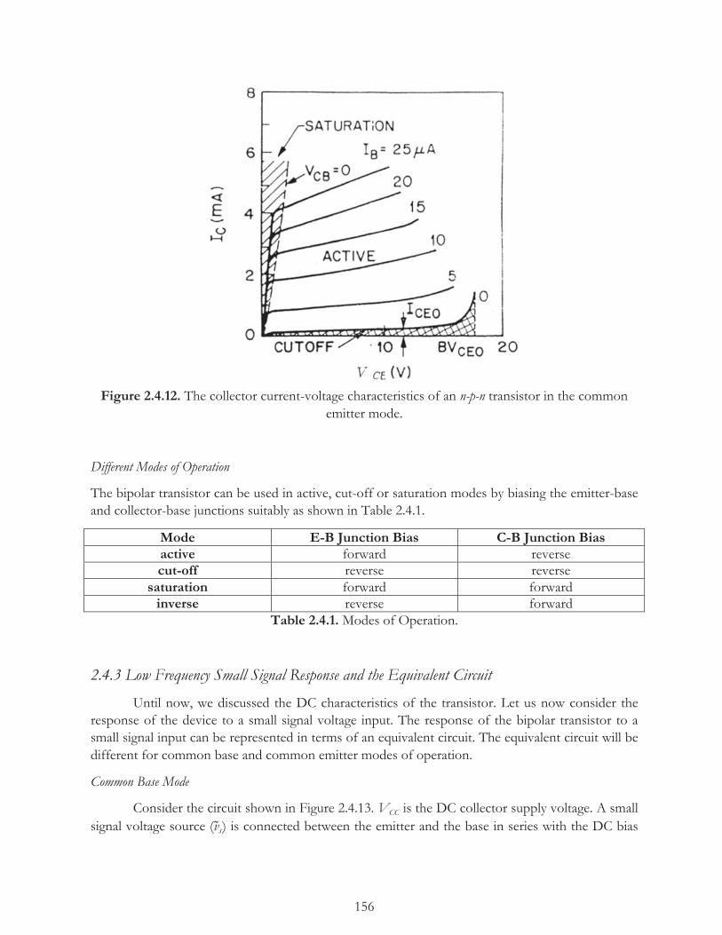
156
Figure 2.4.12. The collector current-voltage characteristics of an n-p-n transistor in the common emitter mode.
Different Modes of Operation
The bipolar transistor can be used in active, cut-off or saturation modes by biasing the emitter-base and collector-base junctions suitably as shown in Table 2.4.1.
Mode E-B Junction Bias C-B Junction Bias active forward reverse cut-off reverse reverse
saturation forward forward inverse reverse forward
Table 2.4.1. Modes of Operation.
2.4.3 Low Frequency Small Signal Response and the Equivalent Circuit
Until now, we discussed the DC characteristics of the transistor. Let us now consider the response of the device to a small signal voltage input. The response of the bipolar transistor to a small signal input can be represented in terms of an equivalent circuit. The equivalent circuit will be different for common base and common emitter modes of operation.
Common Base Mode
Consider the circuit shown in Figure 2.4.13. VCC is the DC collector supply voltage. A small signal voltage source (vs) is connected between the emitter and the base in series with the DC bias

157
voltage, VBE. We assume that the frequency of the small signal voltage source is very low and that the injected minority carrier density everywhere in the base is varying in step with voltage variation. Since vs is varying sinusoidally with time, the injected carrier density in the base varies sinusoidally as shown in Figure 2.4.14. The top line in this figure shows the minority carrier density in the base when the sinusoidal function (vs) is at the most positive excursion. Assuming vs= vs sinωt, the base emitter voltage at its most positive excursion is VBE+vs. The middle line in this figure represents the carrier distribution when the same function is zero. The bottom line represents the carrier density when vs is at its most negative excursion, with the instantaneous base-emitter voltage equal to VBE-Vs. The excess carrier density Δn at x’=0 is given by
Δn0= Δn x'=0 = npBO eq(VBE + vs)
kT -1 (2.4.54)
Denoting the total emitter current as IEt, we obtain
IEt= IES eq(VBE + vs)
kT -1 ≈ IES eq(VBE + vs)
kT = IES eqVBEkT e
qvskT (2.4.55)
Expanding eqvskT as an exponential series and retaining only the leading terms, we obtain
IEt≈ IES eqVBEkT (1+ qvs
kT) (2.4.56)
IEt therefore comprises of a DC term and a sinusoidally varying term, and can expressed as
IEt= IE+ie (2.4.57)
where IE is the DC current and ie is the sinusoidally varying component of current. By comparing Equations 2.4.56 and 2.4.57, we obtain
IE= IES eqVBEkT (2.4.58)
which is the DC emitter current when no sinusoidally varying voltage is applied.
ie= IE eqvskT (2.4.59)
Figure 2.4.13. Common base mode amplifier connection. vs is the small signal sinusoidal input. voltage. RL is the load resistor in the collector circuit.

158
Figure 2.4.14. Modulation of the injected minority carrier density in the base in step with a small sinusoidal signal voltage.
Figure 2.4.15. Equivalent circuit of the input circuit in common base mode.
The ratio of the sinusoidal input voltage, vs to the sinusoidal emitter current (input current)
ie defines an equivalent resistor which has a conductance equal to q
kTIE . The input circuit is
equivalent to a resistance (or conductance) and is shown in Figure 2.4.15. The ratio ievs is the small
signal input conductance, gin, and 1gin
= rin=rE is called the input resistance. Since Δn(x) varies
sinusoidally in step with vs, a small signal collector current flows in step with vs, the total collector current ICt is given by
ICt=α0IEt+ICBO=α0IE+ α0ie+ICBO (2.4.60)
The DC current in the collector is
IC=α0IE+ICBO
and the small signal sinusoidal collector current is
ic=α0ie (2.4.61)
The small signal current gain is equal to

159
ioutiin
= icie=α0 (2.4.62)
The output voltage is
vout= icRL=α0ieRL=α0q
kTIE vs RL=gmvs RL (2.4.63)
where gm= α0q
kTIE = α0
rE (2.4.64)
is called the transconductance. In our treatment, vs= vbe where vbe is the sinusoidally varying small signal emitter-base voltage. Transconductance relates the output (collector) current to the input (emitter-base) voltage. Since ic flows through a reverse-biased p-n junction, ic is (nearly) independent of the value of RL, the load resistor. This is equivalent to a constant current source, ic . The output circuit behaves as though a current source gmvs(gmvbe) exists between the collector and the emitter. The equivalent circuit for the output circuit is shown in Figure 2.4.16. Combining the equivalent circuits for the input and the output sides, the equivalent circuit for the transistor is shown in Figure 2.4.17. The rectangular box enclosed by the dotted line outlines the transistor. The voltage gain equals
vout
vin =
gmvs RL
vs=gm RL (2.4.65)
The power gain equals
ioutvoutiinvin
=α0 gm RL= α02 gin RL= α02RLrE
(2.4.66)
Figure 2.4.16. Equivalent circuit of the output circuit in common base mode.
Figure 2.4.17. Equivalent circuit for the bipolar transistor in common base mode.

160
Figure 2.4.18. Circuit connection for common emitter mode amplifier. vs is the small signal sinusoidal input voltage, and RL is the load resistor.
Common Emitter Mode
Consider the circuit shown in Figure 2.4.18. In the common emitter mode, the small signal sinusoidal input voltage is connected in series with the DC bias base-emitter voltage across the base and the emitter. VCC is the collector supply voltage. The load resistor RL is connected between the collector and the emitter in series with the collector supply voltage. Thus the emitter is common to both the input and the output circuit. The input current is the base current. The total base current, IBt, is given by
IBt=(1-α0) IEt-ICBO=(1-α0) IE+(1-α0) ie-ICBO=IB+ib (2.4.67)
The base current thus contains a DC current, IB, equal to (1-α0)IE-ICBO, and a small signal current, ib, equal to (1-α
0)ie. The input current is equal to
iin=ib=(1-α0) ie (2.4.68)
But ie= vsrE
Hence ib= (1-α0) qIE
kTvs=vs
1-α0rE
(2.4.69)
The ratio iinvs
is called the input conductance, gin. Therefore
gin= iinvs=(1-α
0) qIE
kT=1-α0rE
(2.4.70)
Recalling that we defined rE as equal to kTqIE
, we can write the input resistance as
rin= 1gin
= kT
qIE (1-α0) = rE
(1-α0) (2.4.71)
The input circuit therefore behaves as though there were a resistance, rin, between the base and emitter terminals. The output current is equal to
iout=ic=α0ie=α0qIEkTvs=α0
vsrE
=gmvs (2.4.72)

161
As before, the output circuit behaves as though a current source, gmvs, exists between the collector and the emitter. The equivalent circuit is shown in Figure 2.4.19. In this instance, the current gain is equal to
ioutiin= icib=gmvs
iin=
α0qIE kTvs
(1-α0)qIE kTvs= α01-α0=β0 (2.4.73)
Thus the current gain in the common emitter mode is β0. The subscript 0 in the α0 and β0 refers to the fact we are considering a very low frequency input signal, (i.e., at nearly zero frequency.) We are neglecting capacitive effects. The voltage gain equals
voutvin
= gmvsRL
vs=gmRL (2.4.74)
and the power gain equals
ioutiin
voutvin=β0gmRL=
α0β0rERL (2.4.75)
Figure 2.4.19. Equivalent circuit of the transistor in the common emitter mode.
2.4.4 Voltage Limitation
The maximum collector voltage that can be applied is limited by one of the following physical mechanisms: thermal, punch-through, the breakdown of the collector-base junction in the common base mode, or the collector breakdown in the common emitter mode. In a practical device, the limit on the magnitude of the collector voltage that can be applied is due to that mechanism which yields the lowest breakdown voltage. In some devices the punch-through voltage may be the limiting mechanism while in some other devices the collector breakdown maybe the limiting mechanism. We will now examine the three voltage limiting mechanisms.

162
Punch-Through Voltage, Vpt
When the reverse collector-base junction voltage, VCB, is increased, the depletion region widens, and hence the width of the neutral base region decreases. This is illustrated in Figure 2.4.20. WBJ is the width of the base region between the metallurgical junctions on the emitter side, and that on the collector side. The width of the segment of the emitter-base depletion region occurring on the base side is denoted xpE. Similarly, the width of the segment of the collector-base depletion region occurring on the base side is denoted xpC. The width of the neutral base region is denoted W’, and is equal to
W'=WBJ-xpE-xpC (2.4.76)
However, we know from our study of the p-n junctions that
xpE= 2 ϵs(VbiE-VBE)NDEq NAB(NDE+NAB)
≈ 2 ϵs(VbiE-VBE)
q NAB (2.4.77)
Since NDE>>NAB and
xpC=2 ϵs(VbiC+VBC)NDCq NAB(NDC+NAB)
(2.4.78)
Hence W'= WBJ-2 ϵs(VbiE-VBE)
q NAB- 2 ϵs(VbiC+VBC)NDC
q NAB(NDC+NAB) (2.4.79)
where VbiE and VbiC are the built-in voltages of the emitter-base and collector-base junctions. NDE, NAB and NDC are the impurity concentrations in the emitter, base and collector regions, respectively.
As the collector-base applied voltage VCB is increased, xpC (which is the third term on the right-hand side of Equation 2.4.79 representing the portion of the collector-base depletion region lying on the base side) increases. Thus, W’ decreases as VCB is increased. At some value of voltage VCB≡Vpt (punch-through voltage) W’ becomes zero. Vpt can be determined by putting W’=0 in the above equation and solving for Vpt. Hence,
Vpt=q NAB(NAB+NDC)
2 ϵsNDCWBJ-
2 ϵs(VbiE-VBE)
q NAB
2
-VbiC (2.4.80)
Under the punch-through conditions, the depletion region extends all the way from the collector to the emitter, and the base current (or voltage) has no control on the collector current. The collector current that flows under this condition is a space charge limited current, and is called the punch-through current. The punch-through phenomenon is important only in transistors in which the metallurgical base region, which is small.

163
Figure 2.4.20. The neutral base region.
Example 2.4.4
Given that the impurity concentration in the emitter, base and collector regions are NDE= 1019 cm-3, NAB= 1016 cm-3 and NDC= 1015 cm-3, and the width of the base region is WBJ=2μm determine the punch-through voltage, given that the emitter-base junction forward voltage is 0.5 V. The built-in voltage, VbiE, of the emitter base junction is
VbiE= kTqlnNDENABni2 =0.0258
1035
1020=0.893 V
xpE ≈ 2 ϵs(VbiE-0.5)
q NAB=
2 ×11.9 × 8.84 × 10-14×0.393
1.6x10-19×1016=0.227μm
The built-in voltage of the collector-base junction is
VbiC= kTqlnNABNDCni2 =0.0258
1031
1020=0.655 V ≈0.66 V
Substituting these values into Equation 2.4.80, we obtain
Vpt= 1.6×10-19×1016× (1.1 x 1016)
2 ×11.9 × 8.84 × 10-14×1015 (2 × 10⁻⁴- 0.227 × 10⁻⁴)
2-0.66
=2.63.33-0.66 ≈262.7 V
Collector- Base Breakdown Voltage, BVCBO
In the common-base mode, the maximum voltage that can be applied on the collector is limited by the breakdown characteristics of the collector-base junction. Recall our discussion on avalanche breakdown. The breakdown voltage of the collector-base junction is calculated the same way as the p-n junction breakdown voltage. That is, the collector-base junction voltage is

164
determined by the applied voltage needed to attain critical electrical field in the depletion region and is therefore a function of the dopant impurity concentrations in the base and collector regions.
BVCBO represents the maximum collector voltage that can be applied in the common-base configuration unless punch-through occurs earlier, i.e., at a lower collector voltage. BVCB0 can be calculated by using the expression for the breakdown voltage for the p-n junction in terms of the critical electric field, crit discussed in Chapter 3.
BVCBO= Ecrit 2 ϵs
2q
1
NDC+ 1
NAB -VbiC (2.4.81)
In the avalanche process, the carriers entering the depletion region get multiplied due to impact ionization in the depletion region. The multiplication factor M is given by
M= 1
1- VVbr
η (2.4.82)
where V is the voltage applied across the junction, Vbr is the breakdown voltage of the junction, and η is an empirical parameter. By putting V=Vbr, we can see that the multiplication factor M increases to infinity at breakdown. The symbol that is used to denote the common-base collector breakdown voltage is BVCBO. The 0 is in the subscript implies that the emitter is open. Equation 2.4.82 can be rewritten in terms of BVCBO as
M= 1
1- VCBBVCBO
η (2.4.83)
where VCB is the voltage across the collector-base junction.
Example 2.4.5
For the transistor discussed in the previous example, let us calculate BVCBO given that crit =200,000 V/cm. Substituting the values for the various quantities, we have
BVCBO= 2× 10⁵
2× 11.9 × 8.84 × 10-14
2× 1.6×10-19
1
1015+1
1016- 0.66
=144.6-0.66 ≈143.9 V
Collector-Emitter Breakdown Voltage, BVCEO
In the common-emitter mode of operation, recall that the base current is given by
IB=(1-α0) IE-ICBO (2.4.84)
When the base is open, IB is 0 so
IE= ICBO(1-α0)
(2.4.85)

165
This is the leakage current that flows between the collector and the emitter when the base lead is open. However, at larger collector voltages, the collector multiplication factor arises, and hence the current through the collector-base junction increases by a factor M (i.e., it gets multiplied by M.)
IC=M(α0IE+ ICBO) (2.4.86)
When the base is open, IC=IE. Hence
IE= M ICBO1-α0M
(2.4.87)
As the collector-emitter voltage is increased, M becomes larger than 1 (as seen from Equation 2.4.82), and hence IE increases. Ultimately when α0M=1, IE becomes infinite, and breakdown occurs. The collector voltage at which IE becomes infinite is denoted BVCEO. The notation in the subscript is similar to what we had for BVCBO; 0 indicates that the base is open. The condition for this breakdown to occur is given by
α0M=1= α0
1- VCbrBVCBO
η = α0
1- BVCEOBVCBO
η (2.4.88)
By writing the above equation, we have assumed that at breakdown the collector to emitter voltage BVCEO, is the same as the collector to base voltage VCbr. Rearranging terms, we obtain
BVCEO= BVCBO 1-α01η (2.4.89)
Since β0≈ 1
1-α0we obtain
BVCEO≈ BVCBOβ01η= BVCBO
β0η (2.4.90)
For silicon, it is reported that η has a value between 2 and 6.
Example 2.4.6
Let us calculate BVCEO by assuming that η=3 and β0=125 for the transistor used in the previous example.
BVCEO = BVCBBOβ0
η
From our last example, BVCBO is calculated to be 143.8 V
β0η
= 1253 =5
Hence BVCEO = BVCBO5
= 143.95
=28.8 V

166
Thus we see that BVCEO is much smaller than BVCBO. In the common-emitter mode BVCEO imposes the limit on the collector voltage unless punch-through occurs earlier.
2.4.5 Base Stored Charge
The minority carriers injected in the base are diffusing towards the collector base junction. At any instant of time, the minority carrier density distribution in the base region looks like what is shown in Figure 2.4.21A. This distribution is stationary and does not change with time, although individual electrons (minority carriers) are constantly moving. It is as though many minority carriers are stored in the base region. The area under the plot in Figure 2.4.21A multiplied by qA (where A is the area of cross-section of the base region) is called the stored minority carrier charge. The minority carrier charge stores in the base is given by
QB= -qA Δn x' dx'W'
0 (2.4.91)
To maintain charge neutrality, an excess majority carrier density (Δp(x’)) equal to Δn(x’) also arises. The distribution of excess majority carriers is identical to that of excess minority carrier distribution, and is shown in Figure 2.4.21B. The stored majority carrier charge is equal in magnitude but opposite in sign to QB. (Recall the discussion in Chapter 3.)
In a well-designed transistor, most of the minority carriers emitted from the emitter reach the collector. Very few minority carriers are lost due to recombination in the base. Hence the distribution is almost linear. We can therefore define a term τB as the Base-Transit time. The base-transit time denotes the average time taken by the injected minority carrier to traverse the neutral base region, and reach the collector. The current in the base region due to the injected electrons is given by
ICn x' = -q A v x' Δn x' (2.4.92)
Where v(x’) is the velocity of electrons as a function of x’. The velocity of the minority carrier at some point x’ in the neutral base region is
v x' = - ICn x
'
q A Δn x' (2.4.93)
The time taken to traverse a distance dx’ between x’ and x’+dx’ is
dt= dx'
v x'= -
q A Δn x'
ICn x'dx' (2.4.94)
The transit time is obtained by integrating dt, and is equal to
τB= dt= - q A Δn x'
ICn x'dx'
W'
0 (2.4.95)
Since we assume that there is negligible recombination in the base region, the current is constant in the base, and equal to ICn Hence, we can take ICn(x’) outside the integral, and obtain

167
τB= 1ICn
- q A Δn x' dx'W'
0=
QBICn
(2.4.96)
QB= τB ICn= τB α0 IE (2.4.97)
Since we assumed that there was negligible recombination in the base, the excess carrier density can be approximated to vary linearly with x’, and is given by
Δn x' = Δn0 1- x'
W' (2.4.98)
QB= - q A Δn x' dx'W'
0= -q A Δn0W
'
2 (2.4.99)
But ICn=q A Dn δΔn δx'
= -q A DnΔn0W'
(2.4.100)
τB= QBICn
= W'2
2Dn (2.4.101)
Example 2.4.7
Consider the base region in which the minority carrier diffusion constant is equal to 20 cm2/s Assume W’=2. Then the base transit time, τB is equal to
τB= 2x10⁻⁴
2
2 x 20= 10-9 sec
Figure 2.4.21. Excess carrier distribution in the base region: (A) minority carriers (B) majority carriers.

168
Although we assumed no recombination in the base region for the purpose of determining the base transit time, in reality there is some recombination and the base transport factor αT, is less than unity. Recall that
αT= 1
coshW'
Ln
(2.4.102)
If we now expand the denominator under the assumption W’<<Ln, we obtain
αT ≈ 1
1+W'2
2Ln2
≈1- W
'2
2Ln2 =1- W'2
2Dnτn (2.4.103)
where τn is the minority carrier lifetime in the base.
αT ≈1- W'2
2Dnτn ≈1- τB
τn (2.4.104)
The above equation can be used to give a physical interpretation to the base transport factor. We
know that dtτn
is the probability that the minority carrier in the base will recombine in the base in a
time interval dt. Hence if the base transit time τB is small compared with τn, then τBτn
is the probability
that a minority carrier will recombine in the base region in its transit to the collector. Hence 1- τBτn
is
the probability that an injected minority carrier will reach the collector without being lost by recombining. By decreasing the base-transit time , in comparison with the lifetime τnαT can be made closer to unity. When τB is very much smaller than τn, αT≈1.
2.4.6 Stored Charge Capacitance
The minority carriers stored in the base region give rise to capacitive effects. The capacitor associated with minority carrier storage is called the diffusion capacitance, or storage capacitance. Consider the carrier density distributions in the base region shown in Figure 2.4.23A for excess minority carriers and Figure 2.4.23B for excess majority carriers when the emitter base junction is forward biased at some DC bias voltage, VBe. Let us now apply a small incremental step voltage, dV, in series with VBE so that the net forward bias voltage is VBE+dV as shown in Figure 2.4.22. Due to dV, the excess minority carrier density is increased in the base corresponding to the new emitter-base voltage. The stored negative charge in the base is increased by an amount, dQB=-dQ, where
dQB=-dQ= -qA ∂ ΔnW'
0dx' (2.4.105)
where ∂ Δn is the incremental change in the excess minority carrier density. The shaded region in Figure 2.4.23A represents the increment in the negative charge, -dQ. This incremental negative charge entered the base region through the emitter from the step voltage source as shown in Figure 2.4.22. In order to preserve charge neutrality, the excess majority carrier in the base also increases by the same amount as the excess minority carriers. The incremental change in the positive charge

169
due to majority carriers is equal to dQ, and is shown in Figure 2.4.22B by shaded lines. The incremental positive (majority carrier) charge (dQ) flows into the base region through the base ohmic contact from the step voltage source as shown in Figure 2.4.22. Thus we see that due to the application of the step voltage (dV), a charge +dQ flows into the base through the base contact, and a charge -dQ flows into the base through the emitter, both from the step voltage source. When the step voltage is reduced to zero, the incremental charges flow back to the step voltage source from the base, the same way they entered the base region. Thus the transistor behaves as though there were a capacitor between the emitter and the base lead. This capacitor which is called the diffusion capacitor (or storage capacitor) has a capacitance, Cdiff equal to
Cdiff= dQdV
= d QBdVBE
(2.4.106)
We can evaluate this capacitance by writing QB explicitly. Recall that in a previous section, we expressed QB as
QB= ICn τB = α0 IE τB
Cdiff= d QBdVBE
=α0 τB d IEdVBE
= α0 τB q IEkT
= α0 τBrE
(2.4.107)
Example 2.4.8
Let us calculate the diffusion capacitance of a bipolar transistor carrying an emitter current of 1 mA with a transit time equal to 10-8 sec, and α0 equal to 0.99. Let T=300 K.
rE= kTq IE
= 0.0259 V
1 mA=25.9 Ω
Cdiff= α0 τBrE
= 0.99 × 10⁻⁸ 25.9
=3.82 × 10⁻¹⁰ F
Figure 2.4.22. Application of a step voltage, dV, in series with VBE so as to increase the injected minority carriers in the base.

170
Figure 2.4.23. Incremental change in excess carrier densities (A) minority carriers. The increase in stored minority carrier charge comes about due to +dQB flowing from the emitter into the base. (B)
majority carries. The increase in stored majority carrier charge comes about due to -dQB flowing into the base region from the base ohmic contact.
2.4.7 Frequency Response
We considered earlier the response of a bipolar transistor to a sinusoidally varying small signal input voltage. We had assumed that the small signal voltage varied sinusoidally at a very low frequency, so that the injected carrier density varied in step with the small signal input emitter base voltage. This is illustrated in Figure 2.4.14. When the sinusoidal input voltage is at its maximum value, the excess carrier density is increased everywhere in the base, as indicated by the top line in Figure 2.4.14. When vs is at its most negative value, the excess carrier density is decreased everywhere, as indicated by the bottom line in Figure 2.4.14. The middle line represents the excess carrier density due to the DC emitter-base voltage. On the other hand, when the input signal varies at a very high frequency such that the period of the sinusoidal signal is small compared to the base-
transit time, τB (i.e. 1ω
< τB) the excess carrier density in the base has a spatial variation. The excess
carrier density varies in phase in different regions, as illustrated in Figure 2.4.24. This variation arises because the excess carrier density injected at x’=0 at some instant of time has not had enough time to travel to the collector before the excess carrier density at x’=0 changes to a new value. Thus there is a phase difference and attenuation between the (sinusoidal) current injected by the emitter

171
and the (sinusoidal) current reaching the collector. The current gain decreases with frequency and also has a phase dependence.
We can now represent the high frequency response of the transistor in terms of an equivalent circuit. Let us initially consider the frequency response of the device, neglecting all parasitic capacitances and resistances. We consider the junction (depletion) capacitance as a parasitic element, and similarly the bulk resistances of the collector, base, and contact resistances1 are considered parasitic elements. On the other hand, the diffusion capacitance, Cdiff, is not neglected and is included as part of the transistor. The diffusion capacitance arises due to the injection of minority carriers in the base, which is vital to the transistor action. A transistor in which the parasitic elements are neglected, is called an intrinsic transistor. In the equivalent circuit for an intrinsic transistor, we only included elements that are necessary for the transistor action.
Common Base Mode
Let us now consider the common-base mode. The equivalent circuit for the intrinsic transistor in the common-base mode is shown in Figure 2.4.25. In this circuit, the diffusion capacitance is shown to be connected parallel to rE (the emitter resistance). The reason for placing the diffusion capacitance in parallel with the input emitter resistance rE is that the input voltage supplies both the incremental stored charge and the injected current. The collector current is given as before by the current source (gmvBE) and is in phase with vBE; the collector current is in phase with the current that flows through rE. The emitter current flows partially through Cdiff and partially through rE. There is therefore a phase difference between the emitter current and the current through rE. Hence the emitter current and the collector current are not in phase. As the frequency of the input signal is increased, more and more of the emitter current flows through Cdiff and the collector current decreases. The current gain decreases.
Let us assume that a sinusoidal input current of ie= ie sinωt is applied at the input terminals. Then the base-emitter voltage vBE is given by
vBE= ie rE×
1jωCdiff
rE+1
jωCdiff
= ie rE1+ jωCdiffrE
(2.4.108)
The collector current is given by
ic = gmvBE= gmrE
1+ jω Cdiff rE ie (2.4.109)
Hence the current gain α, which is a function of frequency, is given by
α ω = ic ie =
gmrE
1+ jω Cdiff rE (2.4.110)
1 The emitter bulk resistance is negligible because of the heavy doping

172
At a very low frequency (ω→0), α ω approaches α0, the low frequency gain. By putting ω=0 in the equation for α(ω), we obtain
α ω=0 = α0=gmrE (2.4.111)
Hence α ω = α01+ jω Cdiff rE
(2.4.112)
Figure 2.4.24. Spatial variation in the base of the excess minority carrier charge density due to a high frequency input signal.
Figure 2.4.25. High Frequency equivalent circuit of the intrinsic transistor in the common base mode
Let us now define a parameter, ω*cα as
ωcα* ≡ 1
Cdiff rE (2.4.113)
Then α ω = α01+ j
ωωcα*
(2.4.114)
We have used a superscript to indicate that this and other parameters that follow with a superscript refer to an intrinsic transistor. The same parameters without the superscript will refer to a real transistor in which the effect of the parasitic elements are also included. As ω increases, α(ω) decreases, and a phase difference arises between the output and input currents. The

173
frequency at which α(ω) falls to 12
of its low frequency value is called the alpha-cutoff frequency. This
happens when ω= ωcα* . Therefore, the alpha-cutoff frequency is given by
fcα* = ωcα
*
2π= 1
2π Cdiff rE (2.4.115)
Recalling Cdiff= α0τBrE
We can write fcα* = 1
2π α0τB (2.4.116)
Thus we see that the maximum frequency is limited by the base-transit time, τB. The phase of α(ω) at f=f cα is 450. The variation of the magnitude of α(ω) with ω is shown in Figure 2.4.26. In this figure, α(ω) is plotted as a function of log(ω) It is seen that α(ω is equal to α0 at low frequencies and falls off as ω approaches ω*cα. At high frequencies,
α ω ≈ α0 jωωcα*
= α0ωcα*
jω (2.4.117)
The gain falls off by a factor of 2 when the frequency (or ω) is doubled. In this region the gain is said to fall off at the rate of 6 db/octave.
Figure 2.4.26. Plot of the magnitude of the current gain, α(ω), as a function of ω ωcα is the value of ω at which α(ω) is equal to 0.707 of α0.
Example 2.4.9
Let us now determine the alpha cut-off frequency of an intrinsic n-p-n bipolar transistor, given
W'=2 μm
Dn=15 cm2/sec
α0=0.995
τB= W'2
2Dn=
1× 10-42
2 × 15=1.33×10⁻⁹ s

174
fcα* =
12π α0τB
Therefore,
fcα* =
1
2π×0.995 ×1.33 × 10-9=
1
8.34× 10-9=1.2 × 10⁸ Hz
Common Emitter Mode
Let us now treat the frequency response of the device in the common emitter mode. The equivalent circuit of the intrinsic transistor is the same as what we derived earlier for the low frequency case, except that the input resistance, rin, which is in parallel with the diffusion capacitor (Cdiff), is equal to rE
1- α0. The equivalent circuit for the intrinsic transistor in the common emitter mode
is shown in Figure 2.4.27. The input current (which is now the base current ib divides itself between two paths: (1) through rin, and (2) through Cdiff. The collector current, ic, is determined by the current that flows through rin, and therefore there is a phase difference between ic and ib. The base-emitter voltage, vBE, is given by
vBE= ib
rE1- α0
1
jωCdiffrE1- α0
+ 1
jωCdiff
=rE1- α0
1+ jω Cdiff rE1- α0
ib (2.4.118)
The collector current is obtained as
ic= gmvBE= gm
rE1- α0
1+ jω Cdiff rE1- α0
ib (2.4.119)
The current gain is now a function of frequency, and is given by
β ω = icib=
gm rE1- α0
1+ jω Cdiff rE1- α0
(2.4.120)
At very low frequency, (i.e. ω→0), β ω is obtained by putting ω=0, and is equal to β0.
β ω |ω=0= β0= gm rE1- α0
(2.4.121)
Therefore β(ω) can be expressed in terms of β0 as
β ω = β01+ jωCdiff
rE1- α0
(2.4.112)
Let us define a parameter given by
ωCβ* ≡ 1
Cdiff rE1- α0
(2.4.123)

175
Since
CdiffrE = α0τB (2.4.124)
ωCβ* = 1 α0τB1- α0
= 1
β0τB (2.4.125)
Then
β ω = β01+ j
ωωCβ*
(2.4.126)
The magnitude of the current gain ( β(ω) ) is plotted in Figure 2.4.28 as a function of log(ω). We
define the beta cutoff frequency as that at which the magnitude of the gain, falls off to 12
of its low
frequency value. This happens when ω=ωCβ* . Hence beta cut-off frequency (f*Cβ) is given by
fCβ* =
ωCβ*
2π= 1
2π Cdiff rE1- α0
= 1
2π β0τB (2.4.127)
The phase of the collector current differs from that of the base current by 450 when f=f*Cβ. At very high frequencies,
β ω ≈ β0 jωωCβ*
=j β0ωCβ
*
ω (2.4.128)
In the range of frequencies over which the above equation is valid, the magnitude of β(ω) multiplied by ω is a constant, given by
ω β(ω) = β0ωCβ* =
β0 β0τB
= 1τB
(2.4.129)
As the frequency is increased, the gain falls by an amount such that the product of gain and frequency is a constant. This constant is called the gain-bandwidth product. The decrease in the gain with frequency at high frequencies, again demonstrates a 6db/octave characteristic, (i.e. β decreases by a factor of 2 when the frequency is doubled.) The value of ω at which β(ω) becomes unity is denoted ωT*, and is found in Equation 2.4.129 to be
ωT*=1
τB (2.4.130)
According to Equation 2.4.129, the frequency at which β(ω) becomes unity is equal to
fT*= ωT
*
2 π = 1
2 π τB (2.4.131)
Using Equation 2.4.130 we can express ωCβ* as
ωCβ* = 1
β0τB= ωT
*
β0 (2.4.132)

176
To summarize, the alpha cut-off frequency is
fcα* = 1
2π 1
α0 1τB
(2.4.133)
The beta cut-off frequency is
fCβ* = 1
2π 1β0
1τB
(2.4.134)
The gain bandwidth product is
fT*= 1
2π 1τB
(2.4.135)
If any two of these three frequencies are known, the third is readily obtained. Or alternately, if τB and either α0 or β0 are known, the three frequencies are readily obtained. Thus, of the five quantities, f
cα* , f
Cβ* , f
T* , τB and either α0 or β0, we can determine the other three if any two are known.
Example 2.4.10
Let us now determine the limiting frequencies f*Cβ and f*T for the transistor discussed in the early
example. We saw that τB=1.33 × 10⁻⁹ s We were given α0 as equal to 0.995. Hence
fT*=
12π
1
1.33 × 10-9= 1.194 × 10⁸ Hz
β0= α0
1-α0= 0.9950.005
=199
fcβ* =
12π ×
1β0
× 1τB
=5.998 × 10⁵ Hz
Figure 2.4.27. The equivalent circuit of the intrinsic transistor in the common emitter mode.
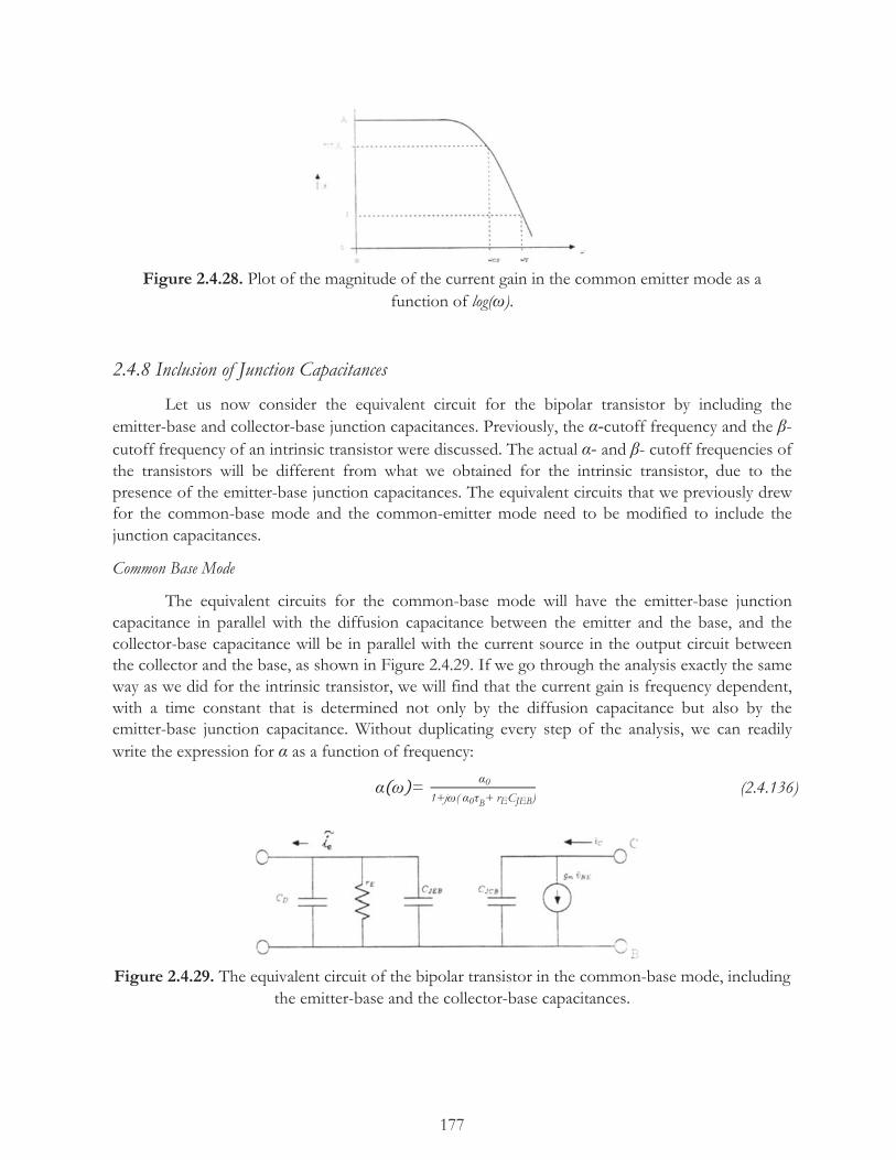
177
Figure 2.4.28. Plot of the magnitude of the current gain in the common emitter mode as a function of log(ω).
2.4.8 Inclusion of Junction Capacitances
Let us now consider the equivalent circuit for the bipolar transistor by including the emitter-base and collector-base junction capacitances. Previously, the α-cutoff frequency and the β- cutoff frequency of an intrinsic transistor were discussed. The actual α- and β- cutoff frequencies of the transistors will be different from what we obtained for the intrinsic transistor, due to the presence of the emitter-base junction capacitances. The equivalent circuits that we previously drew for the common-base mode and the common-emitter mode need to be modified to include the junction capacitances.
Common Base Mode
The equivalent circuits for the common-base mode will have the emitter-base junction capacitance in parallel with the diffusion capacitance between the emitter and the base, and the collector-base capacitance will be in parallel with the current source in the output circuit between the collector and the base, as shown in Figure 2.4.29. If we go through the analysis exactly the same way as we did for the intrinsic transistor, we will find that the current gain is frequency dependent, with a time constant that is determined not only by the diffusion capacitance but also by the emitter-base junction capacitance. Without duplicating every step of the analysis, we can readily write the expression for α as a function of frequency:
α ω = α01+jω( α0τB+ rECJEB)
(2.4.136)
Figure 2.4.29. The equivalent circuit of the bipolar transistor in the common-base mode, including the emitter-base and the collector-base capacitances.

178
The expression differs from that for the intrinsic transistor due to the fact that the time constant of the input circuit is increased from α0τB to α0τB+rECjEB. In terms of Cdiff, α(ω) can be written as
α ω = α01+jωrE(Cdiff+CJEB)
(2.4.137)
The expression for the alpha-cutoff frequency can similarly be written as
fCα =
12π(Cdiff+CJEB)rE
= 1
2π ( α0τB+CJEBrE) (2.4.138)
where CJEB is the emitter-base junction capacitance. We already know from previous discussion that
the emitter resistance, rE equals kTqIE
, and therefore decreases with the emitter current, IE. At very
high emitter-currents, rE becomes small, making CJEB × rE negligible in comparison with α0 × τB.
At low currents, fCα is less than f*Cα, where f*Cα is the intrinsic α-cutoff frequency, and at high currents, fCα approaches f*Cα. If we measure the α cutoff frequency at different values of the emitter
current, IE, and then plot the reciprocal of fCα versus 1IE
, we will obtain a straight-line plot as show
in Figure 2.4.30. If we extrapolate the linear plot, the intercept on the vertical axis at 1IE=0 will be
equal to 1fCα* . Thus we can obtain the intrinsic α-cutoff frequency by measuring the α-cutoff
frequency of a real transistor at different emitter-current.
Common Emitter Mode
The equivalent circuit for the bipolar transistor in the common emitter mode including the junction capacitances is shown in Figure 2.4.31. The input capacitance is increased by having CJEB, the emitter-base junction capacitance in parallel with the diffusion capacitance, Cdiff. In the common-emitter mode, the collector-base junction capacitance appears as a feedback capacitance between the output and the input terminals. The feedback capacitance is usually referred to as a Miller Feedback Capacitance.
As we discussed in the common base mode, the time constant of the input circuit now is increased from its intrinsic value to a larger value given by
Input time constant =rE1-α0
Cdiff+ CJEB
The expression for β(ω) can be derived as before. We can write
β ω = β0
1+jω β0τB+ rE1-α0
CJEB

179
=β0
1+jω1-α0
α0τB+ rECJEB
=β0
1+jω1-α0
rECdiff+ rECJEB
=β0
1+jω rE 1-α0
Cdiff+ CJEB (2.4.139)
Thus we see that the effect of including the emitter-base junction capacitance is as though the input circuit time constant is increased by rE
1-α0 CJEB. We can readily write the expression for the β-
cutoff frequencies without any further analysis as
fCβ =
12π
1-α0rE(Cdiff+CJEB)
=1-α0
2π(α0τB+rECJEB)
= 1
2πβ0(τB+1α0rECJEB)
(2.4.140)
The β-cutoff frequency is thus seen to be less than the intrinsic β-cutoff frequency. Again noticing that the emitter resistance, rE, is inversely proportional to the emitter-current. We can now determine the intrinsic β-cutoff frequency by measuring the actual β-cutoff frequency at several different emitter-current values. This procedure is to measure the β-cutoff frequency at different
values of the emitter-current and plot the reciprocal of the measured β-cutoff frequency, 1fCβ
, as a
reciprocal function of the emitter current, 1IE
as illustrated in Figure 2.4.32. A linear plot will be
obtained which when extrapolated to intercept the vertical axis at 1IE=0 yields the reciprocal of the
intrinsic β-cutoff frequency, 1fCβ
Example 2.4.11
Let us calculate the α-cutoff frequency and the β cutoff frequency of a transistor including junction capacitances. Let us consider the transistor which we used to calculate f*Cα and f*Cβ in the previous examples. Assume IE=1 mA, CJEB= 340 pF.
rE is calculated to be
rE= kTqIE=
25.9 mV1 mA
=25.9 Ω

180
Using the value for β0, f*Cα, and f*Cβ in the previous examples, we calculate the following.
α0=β0β0+1
=0.995
τB=1.33 x 10⁻⁹ sec
fCα* =
12π × ( α0τB+ rECJEB)
=1
2π × (0.995 × 1.33 ×10-9+ 25.9 × 340 × 10-12)
=1.57 × 10⁷ Hz
fCβ* =
1
2π × ( β0τB+rE1- α0
CJEB)
=1
2π × (199 ×1.33 ×10-9+ 25.90.005 × 340 × 10-12)
=78.56 KHz
Thus we see that both α-cutoff and β-cutoff frequencies are reduced. The junction capacitances decrease the frequency response of the transistor.
Figure 2.4.30. Plot of the reciprocal α-cutoff frequency, 1fCα
, as a function of the reciprocal emitter
current, 1IE

181
Figure 2.4.31. Equivalent circuit in the common emitter mode, including junction capacitance.
Figure 2.4.32. Plot of 1fCβ
as a function of 1IE
. The intercept on the vertical axis at 1IE=0 corresponds
to 1fCβ*
2.4.9 Switching Transistors
A bipolar transistor can also be used as an inverter or as a switch. In digital applications, a bipolar transistor is used in either of these two functions. A bipolar transistor is typically used as what is called a saturated inverter, or a switch. The transistor is either off or on: when it is on, the transistor is in the saturation mode. When it is off, it is in the cutoff mode. Let us consider the circuit shown in Figure 2.4.33A. The transistor has a load resistance (RL) in series with the collector-supply voltage (VCC) connected between the collector and the emitter. The base current is applied to the base terminal as shown in this figure. Denoting the collector-emitter voltage as the output voltage V0,
Vo= VCC- RLIC
As IC increases, V0 decreases. Finally when
IC= VCCRL
V0 is zero. When the device is off, IC is nearly zero and V0=VCC Thus when the input current goes up from 0 to IB, the output voltage (which is the collector-emitter voltage) goes down from VCC to

182
0. Hence the output voltage swing is opposite in phase to the input, and this circuit is called an inverter circuit. We assume that the transistor is initially off (i.e., the emitter-base voltage is reverse-biased). At time t=0, a base current, IB, is applied. The base current is chosen to be large enough so that the device under steady-state condition will be driven into saturation.
Due to the base current, minority carriers are injected into the base from the emitter and
the stored charge, QB, in the base increases. The collector current which is equal to QBτB
, increases. As
the current increases in the collector circuit, the collector to the base voltage, which was initially at a voltage nearly equal to the collector supply voltage starts to decrease. Ultimately, when sufficiently large collector current flows, the collector voltage falls below the base emitter voltage. The collector base junction becomes forward-biased, driving the transistor into saturation. When the collector to emitter voltage becomes 0, no further increase in collector current can occur. Thus the collector
current reaches a maximum value equal to VCCRL
. However, the base current is still flowing, and the
stored charge in the base continues to increase. The stored charge in the base increases even though the collector current has reached its maximum value and stopped increasing.
Since we are discussing an n-p-n transistor, the injected (and stored) minority carriers are electrons. The base current provides the majority carriers (holes) needed to neutralize the stored minority carrier charge, and to provide the hole current for: (a) injecting holes into the emitter, (b) providing majority carriers to recombine with the minority carriers in the base, and (c) the flow of the collector-base junction leakage current, ICBO. We will first assume that the hole injection current into the emitter, IEp, is negligible. This assumption is tantamount to letting the emitter injection efficiency, γ, to be very nearly unity. Let us further assume that ICBO is negligibly small in comparison with the base current bias IB. The base current under these assumptions is given by
IB=d QBdt+
QBτn
(2.4.141)
This equation is called the charge-control equation. The first term on the right hand side denotes the base current needed for the buildup of majority carrier charge to neutralize the growing QB and the second term on the right hand side denotes the hole current needed for the recombination.
The boundary condition for solving the charge-control equation, when IB is turned on at time t=0, is
QB=0 for t<t0 (2.4.142)
The solution is then easily seen to be
QB = IBτn 1- e- tτn (2.4.143)
A plot of the growth of QB as a function of time is shown in Figure 2.4.34. The stored charge is seen to grow exponentially with time. When t>τn.
QB =IB τn (2.4.144)
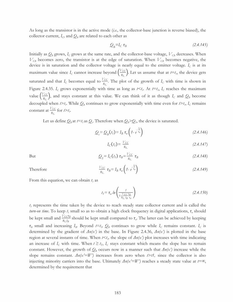
183
As long as the transistor is in the active mode (i.e., the collector-base junction is reverse biased), the collector current, IC, and QB are related to each other as
QB=IC τB (2.4.145)
Initially as QB grows, IC grows at the same rate, and the collector-base voltage, VCB decreases. When VCB becomes zero, the transistor is at the edge of saturation. When VCB becomes negative, the device is in saturation and the collector voltage is nearly equal to the emitter voltage. IC is at its
maximum value since IC cannot increase beyond VCCRL
Let us assume that at t=t1, the device gets
saturated and that IC becomes equal to VCCRL
. The plot of the growth of IC with time is shown in
Figure 2.4.35. IC grows exponentially with time as long as t<t1. At t=t1, IC reaches the maximum
value VCCRL
, and stays constant at this value. We can think of it as though IC and QB become
decoupled when t>t1. While QB continues to grow exponentially with time even for t>t1, IC remains
constant at VCCRL
for t>t1.
Let us define QB at t=t1 as Qs. Therefore when QB>QS, the device is saturated.
Qs= QB t1 = IB τn 1- e- t1τn (2.4.146)
IC t1 = VCCRL
(2.4.147)
But QS= IC t1 τB=VCCRL
τB (2.4.148)
Therefore VCCRL
τB= IB τn 1- e- t1τn (2.4.149)
From this equation, we can obtain t1 as
t1= τn ln1
1-VCC τBRL IB τn
(2.4.150)
t1 represents the time taken by the device to reach steady state collector current and is called the turn-on time. To keep t1 small so as to obtain a high clock frequency in digital applications, τn should
be kept small and VCCτBRLIB
should be kept small compared to τn. The latter can be achieved by keeping
τB small and increasing IB. Beyond t=t1, QB continues to grow while IC remains constant. IC is determined by the gradient of Δn(x’) in the base. In Figure 2.4.36, Δn(x’) is plotted in the base region at several instants of time. When t<t1, the slope of Δn(x’) plot increases with time indicating an increase of IC with time. When t ≥ t1, IC stays constant which means the slope has to remain constant. However, the growth of QB occurs now in a manner such that Δn(x’) increase while the slope remains constant. Δn(x’=W’) increases from zero when t>t1, since the collector is also injecting minority carriers into the base. Ultimately Δn(x’=W’) reaches a steady state value at t=∞, determined by the requirement that

184
QB ∞ = IB τn
The area under the plot of Δn(x’) is described by a right-angled triangle for t<t1 and by a trapezoid for t>t1, QS is equal to q times the area of the triangle at t=t1. If Δn(W’) is the excess carrier density at x’=W’ for t>t1, then the area of the trapezoid Atrap is equal to
QB ∞
qA=Atrap = Δn W' W'+
QSqA
What we have discussed so far is called the turn-on behavior. Let us now discuss the device behavior, when the transistor, which has been on in the saturation mode for a long time with a large base current drive, is switched off by turning off IB to zero at time t=0. The transistor current will decrease to zero only after some time delay, and this behavior is called the turn-off transient.
Let us make the assumption that a base current IB has been flowing for a long time and that IB is sufficiently large to drive the transistor into saturation. The base current as a function of time is shown in Figure 2.4.37. The charge control equation under this assumption becomes t=0.
d QBdt
= - QBτn
(2.4.151)
The boundary condition is that at t=0,
QB(t=0) = IB τn (2.4.152)
The solution can be readily seen to be
QB = IBτne
-tτn (2.4.153)
The stored charge decays exponentially with time, as illustrated in Figure 2.4.38. The collector current continues to remain constant at the value it had before the base current was turned off. This situation continues until the device gets out of saturation. The device gets out of saturation when QB becomes equal to or less than QS. We define the time that it takes for the device to get out of saturation as the storage time and denote it by the symbol ts Therefore by our definition, at t=ts, the stored charge is equal to QS. At t=ts
QB ts = QS= IBτne-tsτn (2.4.154)
Therefore, ts is obtained as
ts= τn ln IBτn QS
=τn ln IBτnVCC τBRL
(2.4.155)
When t>ts, the device is in the active mode and IC is proportional to QB. Hence IC decays with time in step with QB This is illustrated in Figure 2.4.39. The decay of IC is given by
IC= QSτB
e-t-tsτn (2.4.156)

185
To decay to 1e of the initial value of the collector current, t-ts, should be equal to τn The total time
taken for the collector current to decay to 1e of its initial value from the instant of time when IB is
reduced to zero is
t= ts+ τn (2.4.157)
To speed up this process, ts should be decreased. This is equivalent to saying that the device should not be operated in deep saturation.
Example 2.4.12
Let us calculate the switching characteristics of an n-p-n transistor used as a saturated inverter, given RL = kΩ, Vcc= 10 V, IB= 150 μA, β0= 100 and τB= 10-9 s. Let us further assume that the emitter injection efficiency is nearly unity, so that we can assume β0= τn
τB.
Turn-on
Icmax=VCCRL
= 10
2 × 103=5 mA
QS= IcmaxτB=5 × 10-3 × 10-9= 5 × 10-12C
τn= β0τB=100 × 10-9= 10-7sec
QB ∞ =IBτn=150 ×10-6 ×10-7=1.5 × 10⁻¹¹C
t1= -τn ln 1- VCCτBRLIBτn
= -10-7 × ln 1- 5 × 10-12
1.5 × 10-11= 10-7× 0.405
=4.05 × 10⁻⁸ sec
Turn-off
ts= - τn lnVCCτBRLIBτn
= -10-7× ln5 x 10-12
1.5 x 10-11
=1.1 × 10⁻⁷ sec
Total time taken for IC to fall off to 1eof its initial value is equal to
ts+ τn=10-7+ 1.1 x 10-7=2.1 × 10⁻⁷sec

186
Figure 2.4.33. (A) A circuit configuration for using a bipolar transistor as a saturated inverter. (B) The base current as a function of time.
Figure 2.4.34. The growth of the stored charge as a function of time due to a constant base. current drive, IB.
Figure 2.4.35. The increase in collector current as a function of time due to the base current drive IB. IB is assumed to be large enough to drive the device into saturation. The device gets saturated at
t=t1, for t<t1, IC= QB(t)
τB

187
Figure 2.4.36. The growth of excess minority carrier density in the base in a saturated inverter.
Figure 2.4.37. The base current during the turn-off phase.

188
Figure 2.4.38. The decay of stored charge in the base in a saturated inverter, when the base current drive, IB, is turned off at t=0.
Figure 2.4.39. The decay of collector current in a saturated inverter. The current starts to decay only after a time delay equal to the storage time.
2.4.10 Ebers-Moll Model
The Ebers-Moll model is a basic model for the bipolar transistor, which relates DC currents to the junction voltages and is useful for analyzing the behavior of the devices under large signal input. We saw earlier that in the active region of operation of the bipolar transistor, the current in the emitter, IE is given as
IEs eqVBEkT -1
and the current in the collector is given as
IC= α0IEs eqVBEkT -1 + ICs e
qVBCkT -1
The current in the collector comprises of a collector base junction diode current and a current due to minority carrier injection in the base from the emitter. If we want to describe the

189
behavior of the device under saturation as well as in the inverse mode of operation, we must also take into account the emitter current due to the injection of minority carriers in the base from the collector. This is what is done in the Ebers-Moll Model and is illustrated in Figure 2.4.40.
The emitter current, the base current and the collector current are all shown as going into the device. The emitter current comprises two components, one due to the junction diode current and the other due to minority carrier injection from the collector into the base.
IE= - IEs eqVBEkT -1 + αr ICs e
qVBCkT -1 (2.4.158)
where αr is the alpha of the device in the inverse or reverse mode (i.e., when the collector is used as the emitter and the emitter is used as the collector.) The collector current is now written as
IC= αfIEs eqVBEkT -1 - ICs e
qVBCkT -1 (2.4.159)
where αf is the alpha of the device in the normal mode. The base current is equal to
IB= -(IE+ IC)= - (1-αf) IEs e
qVBEkT -1 - (1-α
r) ICs e
qVBCkT -1 (2.4.160)
The transistor is shown as two diodes connected back to back with a current source connected in parallel to each diode. The current is shown in the emitter and also in the collector as consisting of two components, one due to the diode current and the other from a current source due to minority carrier injection from the opposite region. The currents are controlled by the internal junction voltages. It is customary to write the equations as
IE= a11 eqVBEkT -1 + a12 e
qVBCkT -1 (2.4.161)
and IC= a21 eqVBEkT -1 + a22 e
qVBCkT -1 (2.4.162)
where
a11= - IEs
a12= αrICs
a22=- ICs
and a21=αfIEs
Using the reciprocity relationship of the two-port device, we can write α12= α21. Hence,
αrICs=αfIEs
Therefore only three out of the four parameters (viz., αf, αr, IEs, and ICs) are needed to model the device.

190
Figure 2.4.40 Equivalent circuit diagram for the bipolar transistor according to Ebers-Moll Model.
2.4.11 Output Impedance
When we examined the DC characteristics of the transistor, we observed that the collector current increased slightly with collector voltage in the common-base mode, whereas in the common-emitter mode the collector current increased much more with collector voltage. The rate of increase of collector current with collector voltage is called the collector output impedance. The output impedance, r0, is defined as
ro≡ ∂VC∂IC
(2.4.163)
Theoretically, we would have expected the collector output impedance to be infinite, since the reverse-biased collector-base junction acts as a constant current source. But the collector current depends on the width of the neutral region of the base. The width of the neutral region decreases with the collector voltage due to the widening of the collector-base junction depletion region. The effect is called Early effect, and is illustrated in Figure 2.4.41. If we increase the collector-base voltage, the base width decreases and the slope of Δn(x’) increases as shown in Figure 2.4.41. The collector current which is proportional to the slope of Δn(x’) at x’=W’ increases causing the output impedance to be finite.
If the emitter-base voltage is kept constant, the excess carrier density at x’=0 is constant since it depends only on the impurity density in the base and the emitter-base voltage, i.e.
n x'=0 =nPBO eqVBEkT -1
The output impedance under this condition is given by
ro≡ ∂VCB∂ICn
|VBE=constant=∂VCB∂W'
∂ICn∂W'
|VBE=constant (2.4.164)
∂W'
∂VCB can be obtained by differentiating Equation 2.4.79 with respect to VCB.
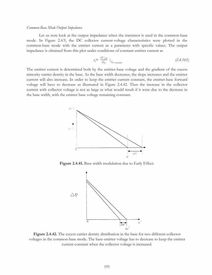
191
Common-Base Mode Output Impedance
Let us now look at the output impedance when the transistor is used in the common-base mode. In Figure 2.4.9, the DC collector current-voltage characteristics were plotted in the common-base mode with the emitter current as a parameter with specific values. The output impedance is obtained from this plot under conditions of constant emitter current as
ro≡ ∂VCB∂IC
|IE=constant (2.4.165)
The emitter current is determined both by the emitter-base voltage and the gradient of the excess minority carrier density in the base. As the base width decreases, the slope increases and the emitter current will also increase. In order to keep the emitter current constant, the emitter-base forward voltage will have to decrease as illustrated in Figure 2.4.42. Thus the increase in the collector current with collector voltage is not as large as what would result if it were due to the decrease in the base width, with the emitter base voltage remaining constant.
Figure 2.4.41. Base width modulation due to Early Effect.
Figure 2.4.42. The excess carrier density distribution in the base for two different collector voltages in the common-base mode. The base-emitter voltage has to decrease to keep the emitter
current constant when the collector voltage is increased.

192
Common-Emitter Mode Output Impedance
Let us now consider the output impedance in the common-emitter mode. The DC characteristics were plotted in Figure 2.4.12 for the common emitter mode, and a family of curves was plotted for different values of base current. The output impedance under conditions of constant base output current is obtained from this plot and is equal to
ro= ∂VCE∂IC
|IB=constant (2.4.166)
When the collector to emitter voltage is increased by a small amount, this increment is partially applied across the collector-base junction and partially across the base-emitter junction. This division between the two junctions occurs in a manner such that the base current remains constant.
The base current supplies (a) the current for injection of minority carriers from the base into the emitter and (b) the majority carriers needed for recombination with minority carriers in the base. If the injection efficiency is assumed to be nearly unity, then the former is negligible, and the latter is the dominant component of the base current. The base current is then equal to
IB≈ QBτn
(2.4.167)
where QB is the stored minority carrier charge, and is proportional to the area under the plot of the excess minority carrier density in the base, as shown in Figure 2.4.43. IB is therefore constant when QB is constant. When VCE is increased, the base width decreases due to the increase in the collector-base voltage. In order to keep the stored charge QB constant, the excess carrier density at x’=0 (height of the triangle) has to increase so that the area of the triangle is constant, as illustrated in Figure 2.4.43. The collector current increase is therefore not only due to the increase in slope because of a decrease in base width, but also due to an increase in the injected minority carriers at x’=0. Thus the output impedance is much smaller than what is obtained in the common base mode.
Figure 2.4.43. The excess carrier density in the base for two different values of the collector-emitter voltage in the common emitter mode under conditions of constant base current. The area
under the plot has to remain constant if the base current is kept constant.
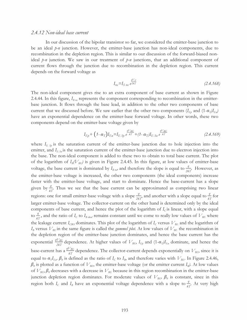
193
2.4.12 Non-ideal base current
In our discussion of the bipolar transistor so far, we considered the emitter-base junction to be an ideal p-n junction. However, the emitter-base junction has non-ideal components, due to recombination in the depletion region. This is similar to our discussion of the forward-biased non-ideal p-n junction. We saw in our treatment of p-n junctions, that an additional component of current flows through the junction due to recombination in the depletion region. This current depends on the forward voltage as
Irec=IS rec eqVF2kT (2.4.168)
The non-ideal component gives rise to an extra component of base current as shown in Figure 2.4.44. In this figure, IB rec represents the component corresponding to recombination in the emitter-base junction. It flows through the base lead, in addition to the other two components of base current that we discussed before. We saw earlier that the other two components (IEp and (1-αT)IEn) have an exponential dependence on the emitter-base forward voltage. In other words, these two components depend on the emitter-base voltage given by
IEp+ 1- αT IEn=IE Sp eqVBEkT +(1- αT)IE Sn e
qVBEkT (2.4.169)
where IE Sp is the saturation current of the emitter-base junction due to hole injection into the emitter, and IE Sn is the saturation current of the emitter-base junction due to electron injection into the base. The non-ideal component is added to these two to obtain to total base current. The plot of the logarithm of IB(VBE) is given in Figure 2.4.45. In this figure, at low values of emitter-base voltage, the base current is dominated by IB rec, and therefore the slope is equal to q
2kT However, as
the emitter-base voltage is increased, the other two components (the ideal components) increase faster with the emitter-base voltage, and start to dominate. Hence the base-current has a slope given by q
kT Thus we see that the base current can be approximated as comprising two linear
regions: one for small emitter-base voltage with a slope q2kT
, and another with a slope equal to qkT
for
larger emitter-base voltage. The collector-current on the other hand is determined only by the ideal components of base current, and hence the plot of the logarithm of IC is linear, with a slope equal to q
kT and the ratio of IC to IB ideal remains constant until we come to really low values of VBE where
the leakage current ICBO dominates. This plot of the logarithm of IC versus VBE and the logarithm of IB versus VBE in the same figure is called the gummel plot. At low values of VBE the recombination in the depletion region of the emitter-base junction dominates, and hence the base current has the
exponential qVBE2kT
dependence. At higher values of VBE, IEp and (1-αT)IEn dominate, and hence the
base-current has a qVBEkT
dependence. The collector-current depends exponentially on VBE, since it is
equal to αTIEn. β0 is defined as the ratio of IC to IB, and therefore varies with VBE. In Figure 2.4.46, β0 is plotted as a function of VBE, the emitter-base voltage (or the emitter current IB). At low values of VBE, β0 decreases with a decrease in VBE because in this region recombination in the emitter-base junction depletion region dominates. For moderate values of VBE, β0 is constant, since in this region both IC and IB have an exponential voltage dependence with a slope to q
kT. At very high
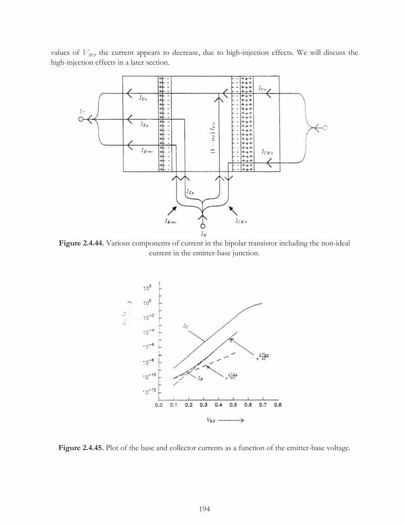
194
values of VBE, the current appears to decrease, due to high-injection effects. We will discuss the high-injection effects in a later section.
Figure 2.4.44. Various components of current in the bipolar transistor including the non-ideal current in the emitter-base junction.
Figure 2.4.45. Plot of the base and collector currents as a function of the emitter-base voltage.

195
Figure 2.4.46. Plot of β0 as a function of VBE or IE.
2.4.13 Non-Uniform Doping in the Base
We also have assumed earlier in our discussion of the transistor characteristics that the base had a uniform doping (i.e., NA was constant.) We further assumed that the minority-carrier flow in the base region was only due to diffusion, by assuming that the electric field was zero. We are going to see now that in a real device, both of these assumptions are invalid. Due to the method of fabrication of the bipolar transistor using an impurity diffusion process, the impurity profile in the base region typically has an exponential slope as shown in Figure 2.4.47. In this figure, the metallurgical junction is between where the logarithm of net NAB goes to -∞ (i.e., net NAB is zero) on the emitter side and where it goes to ∞ on the collector side. However, the actual neutral-base width is less than this, and equal to W’ as indicated in the figure. In this neutral-base region therefore, it is possible to approximate the impurity profile as
NAB x' = NABE e- ηx'
W' (2.4.170)
where NABE is the impurity concentration at x’=0, and η is a parameter which depends on the variation of the impurity concentration with distance. Therefore, we find the hole density to be higher at x’=0 than at x’=W’. In order to prevent the diffusion of holes (majority carriers) in the direction of the collector, an electric field arises in the base region in a negative direction. A drift current due to the electric filed is exactly balanced by the diffusion current. Thus there is no net hole current in spite of the concentration gradient of the acceptor impurity in the base. We can write the expression for the hole current density as
Jp= q pp0μpE-q Dp0dp0dx'
=q NAB x' μpE-qDpdNAB x'
dx' (2.4.171)
where pp0 is the majority-carrier density in thermal equilibrium, and therefore equal to NAB, the acceptor density in the base-region. In order for the two currents to balance, Jp has to equal 0. By setting the equation for Jp to 0, the electric field is expressed as
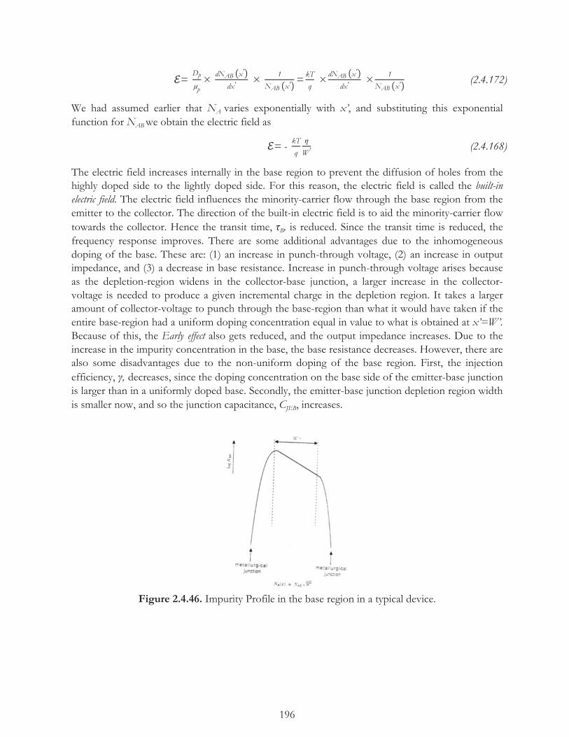
196
= Dp
μp×
dNAB x'
dx' × 1
NAB x'= kT
q ×
dNAB x'
dx' × 1
NAB x' (2.4.172)
We had assumed earlier that NA varies exponentially with x’, and substituting this exponential function for NAB we obtain the electric field as
= - kTq
ηW'
(2.4.168)
The electric field increases internally in the base region to prevent the diffusion of holes from the highly doped side to the lightly doped side. For this reason, the electric field is called the built-in electric field. The electric field influences the minority-carrier flow through the base region from the emitter to the collector. The direction of the built-in electric field is to aid the minority-carrier flow towards the collector. Hence the transit time, τB, is reduced. Since the transit time is reduced, the frequency response improves. There are some additional advantages due to the inhomogeneous doping of the base. These are: (1) an increase in punch-through voltage, (2) an increase in output impedance, and (3) a decrease in base resistance. Increase in punch-through voltage arises because as the depletion-region widens in the collector-base junction, a larger increase in the collector-voltage is needed to produce a given incremental charge in the depletion region. It takes a larger amount of collector-voltage to punch through the base-region than what it would have taken if the entire base-region had a uniform doping concentration equal in value to what is obtained at x’=W’. Because of this, the Early effect also gets reduced, and the output impedance increases. Due to the increase in the impurity concentration in the base, the base resistance decreases. However, there are also some disadvantages due to the non-uniform doping of the base region. First, the injection efficiency, γ, decreases, since the doping concentration on the base side of the emitter-base junction is larger than in a uniformly doped base. Secondly, the emitter-base junction depletion region width is smaller now, and so the junction capacitance, CJEB, increases.
Figure 2.4.46. Impurity Profile in the base region in a typical device.
197
Chapter 2.4 Summary
The bipolar transistor works based on the principle of minority carrier injection into the lightly doped side of a one-sided abrupt p-n junction and the flow (or collection) of these minority carriers into a reverse-biased p-n junction which is placed nearby.
The typical structure of a bipolar transistor comprises a heavily doped n+ region and a lightly doped n-region separated by a narrow p-region. The n+ region is the emitter, the p-region the base and the n-region the collector. Such a transistor is called an n-p-n transistor. A p-n-p transistor is one in which the emitter is a p+ region, and the collector a p+ region with the intervening base layer an n-region. In normal operation, the emitter-base junction is forward-biased and the collector-base junction reverse biased.
The total emitter current is the sum of minority carrier current injected from the emitter into the base and the minority carrier current injected from the base into the emitter. The emitter injection efficiency, γ, is defined as the ratio of minority carrier current injected into the base from the emitter to the total emitter current. In a well-designed transistor, γ is made as close to 1 as possible.
The minority carriers injected from the emitter diffuse through the base region to the collector-base junction. Before they reach the collector-base junction, some of the minority carrier current reaches the collector-base junction is less than the emitter injected minority carrier current. The ratio of the two is called the base transport factor, αT. In a well-designed transistor, αT (which is less than 1) is made as close to unity as possible.
The minority carriers reaching the collector-base junction from the base are swiftly swept into the collector region by the electric field in the collector-base depletion region. This results in a collector current. In addition, a reverse leakage current due to the collector-base junction also flows and adds to the collector current.
The current through the base is the difference between the current due to majority carriers recombining with minority carriers in the base and the reverse leakage current in the collector-base junction.
The transistor can be normally operated in either of two modes viz., common base or common emitter. In the common base mode the input signal is applied between the emitter and the base and the output signal is obtained between the collector and the base. In the common emitter mode the input signal is applied between the base and the emitter and the output signal is obtained between the collector and the emitter.

198
The short circuit current gain of the transistor is defined as the ratio of the incremental change in the output current and an incremental change in the input current with the output AC short circuited. In the common-base mode, the current gain is called alpha of the device and is denoted by α0 where the subscript 0 refers to the fact that the frequency is very low
α0= γ αT
In the common emitter mode, the short circuit current gain at low frequency is called beta of the device and is denoted by β0.
β0= α01- α0
In a well-designed transistor, α0 is made as close to unity as possible. This is done by making the emitter heavily doped in comparison with base doping to get γ as close to unity as possible and making the base region as narrow as possible in comparison with the minority carrier diffusion length in the base to get α0 as close to unity as possible.
The transistor is said to be saturated or operating in the saturation regime when the collector-base junction also is forward biased. In saturation, the excess minority density in the base at the edge of the collector base space charge region is increased due to injection from the collector. The transistor is said to be in the active regime of operation when the emitter-base junction is forward-biased and the collector-base junction is reverse biased.
In the common-base mode of operation, the input resistance to a small signal input voltage is the small signal resistance of a forward biased p-n junction. The resistance is called the
emitter resistance and is equal to rE=kT
qIE, where IE is the DC emitter current. The output
circuit can be represented by having a dependent current source with a current value gmvBE
where vBE is the sinusoidal signal emitter-base voltage.
In the common emitter mode, the small signal input resistance is equal to rE1- α0
and therefore
( 1
1- α0) times larger than the input resistance in the common base mode. The output circuit
can be represented by the same equivalent circuit as for the common base mode.
Due to injection of excess minority carriers in the base, at any given instant of time, there is an extra amount of charge in the base. This charge is called stored base charge. In order to maintain charge neutrality majority carriers flow into the base from the base contact to keep an excess majority carrier density everywhere in the base exactly equal to the excess minority carrier density. A small increment in the emitter base voltage causes an increase in the stored charge by an incremental charge flowing into the base from the emitter while an

199
incremental charge of same magnitude but of opposite polarity flows into the base from the base contact to maintain charge neutrality. Thus a capacitive effect arises due to the stored charge. This is called the diffusion capacitance.
The time taken for the minority carriers to traverse the neutral base region from the emitter-base depletion region to the collector-base depletion junction when the device is in the active mode is called the base transit time, τB. The collector current, IC times the base transit time, gives the stored base charge, QB
QB= IC τB The diffusion capacitance is related to τB as
Cdiff= α0rEτB
Due to the diffusion capacitance the excess minority carrier density does not change
instantaneously with a change in the emitter base voltage. Hence the gain of the transistor falls off. The equivalent circuit for the transistor has the diffusion capacitor in parallel with the input resistance. The input circuit has a time constant due to Cdiff and rin. When we ignore the effect of junction capacitances but include only the effect of the diffusion capacitance we call the device an intrinsic transistor. In an intrinsic transistor, the alpha falls
off at high frequencies and the frequency at which α falls to 12 of its low frequency is
called the alpha-cut-off frequency, f*Cα. The gain α falls of at a rate of 6 db/octave (i.e., decreases by a factor of 2 for an increase in frequency by a factor of 2.) In this range of frequencies the product of f and α is a constant. The asterisk denotes that an intrinsic transistor is being considered. The beta also decreases with frequency and the frequency at
which β falls to 12 of its low frequency is called the beta cut-off frequency, f*Cβ. Also,
β decreases by a factor of 2 when the frequency is increased by a factor of 2 at frequencies larger than f*c β. The frequency at which β becomes equal to 1, is called the gain bandwidth product and is denoted by f*T. The product of f and β at frequencies larger than f*Cβ is a constant and equal to f*T.
When the junction capacitances are included, the time constant of the input circuit is increased. In the output circuit capacitive shunting effects arise. Due to this, the frequency response is poorer than in an intrinsic device. The alpha cut-off frequency, the beta cut-off frequency and the gain bandwidth product in an actual transistor are all reduced from the intrinsic transistor values.

200
When the transistor is used as a saturated inverter, there is delay in the turn-on time. The delay in the turn-off time is longer than the turn-on time by the amount of storage time. The storage time is defined as the time needed to get off saturation regime and reach active regime.
The punch-through voltage, Vpt, is the collector voltage at which the collector-base depletion region widens all the way until it touches the emitter-base junction depletion region, Vpt poses a limit on the maximum voltage that can be applied on the collector
In the common base mode, the collector-base junction breakdown voltage represents the maximum voltage that can be applied on the collector unless punch-through occurs earlier. This voltage is denoted BVCBO.
In the common-emitter mode, the maximum collector voltage that can be applied is less than BVCBO due to the collector multiplication factor. This voltage is denoted BVCEO
The output impedance of the transistor, ∂IC∂VCB
-1, in the common base mode is not infinite
due to the Early effect. The Early effect is the reduction of the neutral base width with increasing collector voltage.
The output impedance in the common emitter mode is smaller than in the common base mode due to the fact that the injection of minority carriers from the base has to increase in order to keep the base current constant when the collector voltage is increased.
In an actual transistor, non-ideal components due to recombination in the emitter, base junction depletion region and surface recombination arise. This has the effect of lowering the gain at low emitter current whereas at higher emitter currents the gain remains at a high value.
In a real device, the impurity profile is non-uniform in the base with the density decreasing from the emitter side to the collector side. Such a non-uniform impurity profile arises as a result of the diffusion process in the fabrication of the device. Due to this an internal electric field arises which helps the minority carriers reach the collector in a shorter time interval. The base transit time is reduced, so the frequency response is improved.
201
Chapter 2.4 Glossary
A area of cross-section of the base region
A,B integration constants
BVCBO collector-base junction breakdown voltage
BVCBO collector breakdown voltage in the common emitter mode
Cdiff diffusion capacitance of the transistor
CjEB emitter-base junction capacitance
Dn electron diffusion constant
Dp hole diffusion constant
DpC hole diffusion constant in the collector
dQ incremental positive (majority carrier) charge
dt incremental time or time interval
dV small incremental step voltage
electric field
crit critical electric field
fc α α- cut off frequency
f*c α intrinsic α-cut off frequency
fc β β- cut off frequency
f*c β intrinsic β- cut off frequency
fT gain bandwidth product
f*T intrinsic gain bandwidth product
F Farad. Unit of capacitance
g conductance
gm small signal input conductance
ib small signal sinusoidal base current
ic small signal sinusoidal collector current
ie small signal sinusoidal emitter current
iin small signal sinusoidal input current
iout small signal sinusoidal output current
IB base current
202
IB rec component of base current due to recombination in the emitter-base junction depletion
region
IBt total base current
IC collector current
ICBO collector-base junction leakage current
ICEO collector current with the base open
ICn collector current due to the injection of electrons from the emitter into the base
ICn(x) current in the base region due to injected electrons
ICt total collector current
IDC DC current
IE DC emitter current
IEn electron current injected from the emitter into the base
IEp DC emitter current due to hole injection from base into the emitter
IES total saturation current of the emitter-base junction
IESn saturation current of the emitter-base junction due to electron injection into the base
IESp saturation current of the emitter-base junction due to hole injection into the emitter
IS rec saturation current due to recombination in the emitter-base depletion region
IEt total emitter current
J -1
Jn minority carrier (electron) current density
Jn(x’) electron current density in the base
Jp hole current density
k Boltzmann constant
Ln minority carrier (electron) diffusion length in the base
LpC minority carrier (hole) diffusion length in the collector
Lp Eminority carrier (hole) diffusion length in the emitter
M avalanche multiplication factor
n electron density
ni intrinsic carrier density
npBO thermal equilibrium minority carrier (electron) density in the base
NA acceptor density

203
NAB acceptor impurity concentration in the base
NABE acceptor impurity concentration at x’=0
NDC donor impurity concentration in the collector
NDE donor impurity concentration in the emitter
p0 majority carrier density in thermal equilibrium
pnC0 thermal equilibrium minority carrier (hole) density in the collector
pnE0 thermal equilibrium minority carrier (hole) density in the emitter
q electron charge
QB minority carrier charge stored in the base
Qs stored charge, QB at t=t1
rE emitter resistance
r0 output impedance
RL load resistance
t time
t1 turn-on transient
ts storage time, the time it takes for the device to get out of saturation
T absolute temperature
vBE base-emitter voltage
vin mall signal sinusoidal input voltage
vout small signal sinusoidal output voltage
v0 small signal sinusoidal voltage
v(x’) velocity of electrons as a function of x’
V voltage applied across the junction
VBC voltage across the collector-base junction
VbiC built-in voltage of the collector-base junction
VbiE built-in voltage of the emitter-base junction
VBE base-emitter voltage
Vbr breakdown voltage of the junction
VCB collector-base voltage
VCC DC collector supply voltage
VCE collector-emitter voltage
Vpt punch-through voltage

204
W’ width of the neutral base region
WBJ width of the base region between the metallurgical junction on the emitter side, and that on
the collector side
WE width of the neutral emitter region
x coordinate
xpC width of the depletion-region occurring in the base region due to the collector-base
junction
xpE width of the depletion-region occurring in the base region due to the emitter-base junction
x’ coordinate system in the neutral base region where the origin is chosen at the edge of the
neutral base region on the emitter side
α current gain
α0 low frequency current gain in the common-base mode
αT base transport factor
α(ω) alpha as a function of ω=2π times frequency
β current gain in the common emitter mode
β(ω) beta as a function of ω=2π times frequency
β0 low frequency current gain in the common emitter mode
∂ differential
∂ Δn incremental change in the excess minority carrier density
∂t short time interval
∂x' elementary distance
Δ increment
ΔIB incremental change in base current IB
ΔIC incremental change in collector current IC
Δn excess minority carrier in the base region due to minority carrier injection from the emitter
ΔIE incremental change in emitter current IE
Δn x' excess carrier (electron) density as a function of x’
ϵs permittivity of semiconductors
γ emitter injection efficiency
η an empirical parameter in avalanche multiplication expression
η an empirical parameter defining the impurity density variation in the base

205
μn electron mobility
μp hole mobility
τB base transit time
τn minority carrier (electron) lifetime
ω 2π times frequency
ωcα * 2π times alpha cut-off frequency
ωcβ * 2π times beta cut-off frequency
ωT * value of ω at which β(ω) becomes unity
∇ divergence

206
Chapter 2.4 Problems
Assume room temperature in all problems except when it is specifically states otherwise. Also assume silicon as the semiconductor material. Take ni as 1 × 1010 cm-3.
1. The expression for the excess minority carrier density in the neutral base region was derived in the text in terms of hyperbolic functions. Show under appropriate conditions that a) it becomes a linear function and b) it becomes an exponentially decaying function.
2. A n-p-n transistor has impurity concentrations of 5 × 1019 cm-3 in the emitter, 5 × 1016 cm-3 in the base and 2 × 1015 cm-3 in the collector. Assume the distance between the metallurgical junction on the emitter side and that on the collector side called the metallurgical base width is equal to 2μm Assume the diffusion constant and the lifetime of the minority carriers in the base region to be 30 cm2/s and 3 × 10⁻⁶ sec respectively. Assume that the emitter-base voltage is -0.5 V and the collector-base voltage is 5 V. Plot on a graph sheet the excess carrier density in the base region.
3. We derived in the class the expression for the base-transport factor, the emitter injection efficiency and the current gain for a n-p-n transistor. Do the same for a p-n-p transistor.
4. For the device in Problem 2, the area of the emitter-base junction and that of the collector-base junction are the same and equal to 10-4 cm2 Assume the minority carrier mobility and lifetime in the emitter to be 500 cm2/V s and 0.25 x 10⁻⁶ sec respectively. What is the injection efficiency at the voltage biases given in Problem 2.
5. For the device in Problem 2, determine the base transport factor at the specified voltage.
6. A p-n-p transistor has impurity concentrations of 5 × 1019 cm-3, 2 × 1016 cm-3 and 5 × 1015 cm-3 in the emitter, base and collector regions respectively. Assume that the distance between the two metallurgical junctions, WBJ is 2.5 × 10⁻⁴ cm. Assume the emitter-base junction is forward biased by 0.5 V and that the collector-base junction is reverse biased by 10 V. The minority carrier parameters are given below in each of the three regions.
Emitter Base Collector
Lifetime (s) 10-6 10-4 2×10⁻⁴
Diffusion Constant (cm2/s)
10 15 16
Calculate γ, αT, α0 and β0
7. For the device in Problem 6, calculate ICBO and ICEO. Take the area of both the collecetor and the emitter junctions to be 10-3 cm2.
8. For the device in Problem 6, draw the equivalent circuit for (a) common base mode and (b) common emitter base mode.

207
9. For the device in Problem 6, calculate the punch-through voltage, BVCBO and BVCEO. Assume that the critical electric filed for breakdown in the collector-base junction is 200,000 V/cm. Take η=3.
10. An n-p-n transistor has impurity concentrations of 1019 cm-3, 1016 cm-3, and 1015 cm-3 in the emitter, base and collector regions respectively. Assume that the distance between the two
metallurgical junctions, WBJ is 2.5 × 10⁻⁴ cm. Assume that the emitter-base junction is forward biased to 0.5 V. Find the punch-through voltage.
11. Assume that for the device in Problem 10, τB=5 x10⁻⁸ sec and the minority carrier lifetime in the base is 10-5 sec. Assume the transistor to be intrinsic. What is BVCEO, assuming that ϒ is nearly unity. Take the value of the parameter η as 3 and BVCBO to be 250V.
12. For the device in Problem 11, determine fCα, fCβ, and f
T. Assume the device is intrinsic (i.e.,
you can neglect the parasitic elements and the junction capacitances.)
13. Assume an area of 10-3 cm2 for the emitter-base junction for the device in Problem 10. Assume τB is not the value given in Problem 11. Assume the width of the neutral base
region W’ to be 2 × 10⁻⁴ cm. Let the minority carrier diffusion constant in the base be 16 cm2 s-1. Calculate f
Cα and fCβ at an emitter-base bias voltage of 0.6 V and a collector-base
reverse bias of 5 V. (Note: You are still assuming that γ is nearly unity.)
14. For the operating voltage given in the last problem determine the equivalent circuit. Assuming the area of the collector-base junction to be the same as that for the emitter-base junction.
15. Assume that VCC is 10 V for the device in the last problem. Calculate the storage time when the device is used as an inverter with a load resistor of resistance equal to 10 kΩ. Assume that the base current drive is 2mA and that the current has been on for a long time for the purpose of calculating the storage time.
16. A switching transistor has the following characteristics f Cβ=106 Hz and f T=108 Hz. The device is used as a saturated inverter and assume (a) γ, the emitter injection efficiency is nearly unity, b) the load resistor is 5 kΩ and (c) the collector supply voltage is 10 V. A base drive current of 50 μA is applied at t=0. Calculate the time required to turn the device on.
17. For the device in Problem 16, assume that the base current of 50 μA is flowing for sufficiently long time to establish steady state condition. Assume that at t=0 the base current is switched off. Calculate the turn-off time, which is defined as the time required for

208
the collector current to decay to a predetermined fraction such as 1e or 10% of the initial
value.
18. For the condition given in Problem 17, determine the emitter-base voltage at time t=0, assuming that the device is a p-n-p transistor and the base doping is 1016 cm3.
19. The impurity concentration in the base of a n-p-n transistor is given approximately by the function
NB x' =NBE exp (-ηx'
W' )
Where NBE is the impurity concentration at x’=0 and η is a parameter. Take W’ as equal to 2 μm. (a) What is the value of η if NBC= NB(x’=W’)= 10-3NBE. Do not confuse this η with the one
that we used to calculate BVCEO. (b) What is the value of the electric field in the base?
20. Design an n-p-n transistor with the following specifications. It should have a minimum β0 of
40 and it should be capable of withstanding a collector voltage of 100 V. It should have an intrinsic beta cut-off frequency of 150 kHz or larger. Assume you can alter the minority carrier lifetime to any specific design value by adding g-r centers with a capture cross-section of 10-16 cm2. Assume that the starting material has a lifetime of 100 μs. (Note: There is no unique design.)

209
Chapter 5 MOS Devices
MOS devices refer to a class of devices in which a thin insulating layer such as silicon-dioxide (usually a thermally grown oxide) is sandwiched between a metallic plate and a semiconductor. The term MOS stands for Metal-Oxide-Semiconductor. These types of devices are called field-effect devices since a voltage applied between the metallic plate and the semiconductor gives rise to an electric field perpendicular to the interface between the semiconductor and the insulating layer. The electric field alters the electrical properties of the semiconductor in a region close to the interface by inducing a space charge. The term MIS is used to describe in which, instead of an oxide, any insulting layer is used.
2.5.1 MOS Capacitor
We will first consider a simple structure called a MOS capacitor, which is also sometimes called an MOS diode. The device is just a parallel-plate capacitor with a metallic layer as one plate, and the semiconductor as the other parallel plate with an insulating layer as the dielectric region between the parallel plates. The device is illustrated in Figure 2.5.1. This type of structure is fabricated by oxidizing the surface of silicon in a furnace which is heated to a very high temperature, such that a thin oxide layer of thickness typically less than 1000 Å is grown on the surface. Silicon has a great affinity for oxygen, and therefore the thermal oxidation of silicon is easy to accomplish. The interface between silicon and the oxide has a low interfacial charge. A metallic film is then deposited on top of the oxide layer to form the MOS sandwich.
The metal is called the gate and in modern devices, the gate is made of polysilicon instead of a metallic layer. The semiconductor is called the substrate. A voltage applied on the gate with respect to the substrate give rise to a perpendicular electric field in the oxide layer. The electric field induces charge in the semiconductor. The induced charge generally exists over a certain spatial region of the semiconductor and it is called the space charge. The space charge is induced in a region very close to the semiconductor-oxide interface. This field-effect is illustrated in Figure 2.5.2.
ox is the electric field in the oxide layer. The electric field lines terminate on the charges in the space charge region. Choosing the interface between the oxide and the substrate as the origin of the x-axis in Figure 2.5.2, the space charge region extends up to a depth of xd and the neutral region is below the space charge region.
In the neutral region of the semiconductor, the net charge density is zero, and in the space charge region of the semiconductor, the charge density is not zero. The total charge of the free carriers in a neutral semiconductor, which is mostly due to majority carriers, is equal and opposite to that of the ionized impurities. Hence, in the neutral region the charge density ρ is zero, as shown in the following equation.
ρ=q p0-n0+ND+ -NA
- =0 (2.5.1)
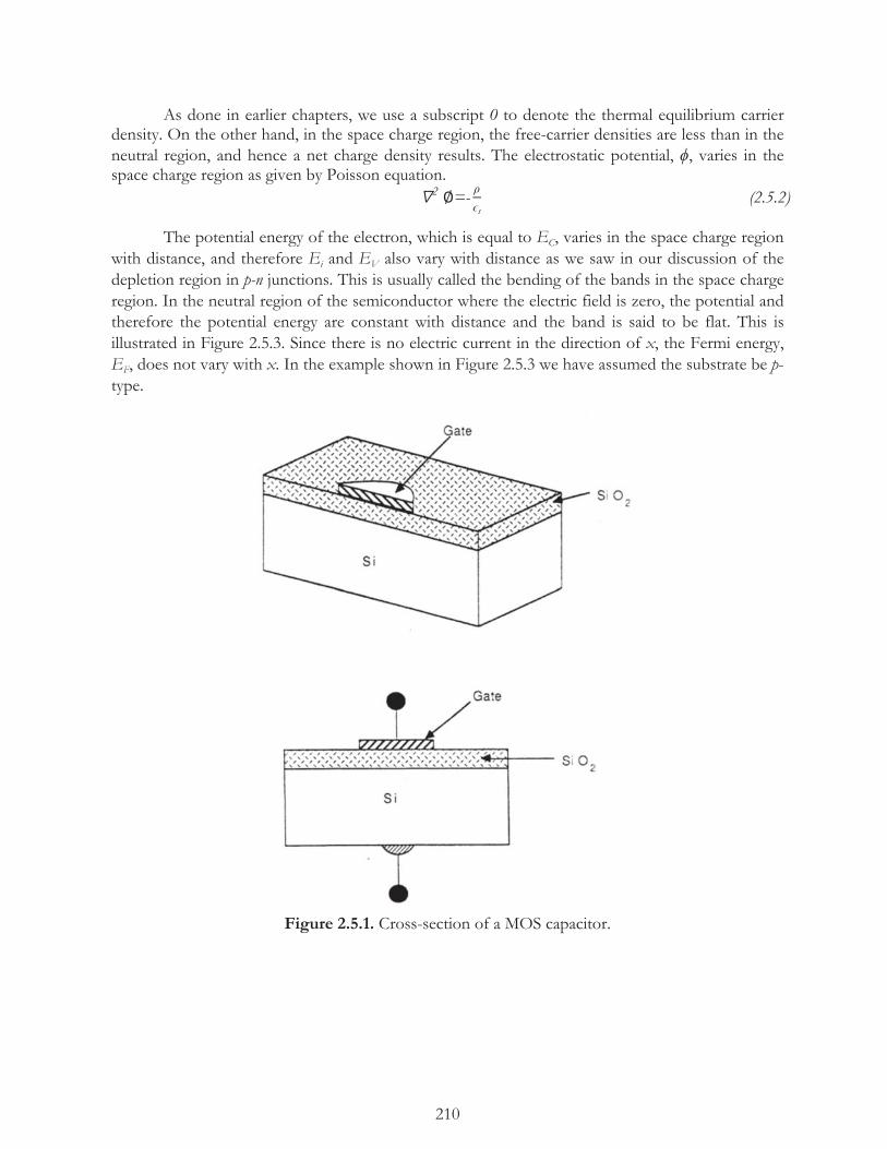
210
As done in earlier chapters, we use a subscript 0 to denote the thermal equilibrium carrier density. On the other hand, in the space charge region, the free-carrier densities are less than in the neutral region, and hence a net charge density results. The electrostatic potential, ϕ, varies in the space charge region as given by Poisson equation. ∇2 =- ρ
ϵs (2.5.2)
The potential energy of the electron, which is equal to EC, varies in the space charge region with distance, and therefore Ei and EV also vary with distance as we saw in our discussion of the depletion region in p-n junctions. This is usually called the bending of the bands in the space charge region. In the neutral region of the semiconductor where the electric field is zero, the potential and therefore the potential energy are constant with distance and the band is said to be flat. This is illustrated in Figure 2.5.3. Since there is no electric current in the direction of x, the Fermi energy, EF, does not vary with x. In the example shown in Figure 2.5.3 we have assumed the substrate be p-type.
Figure 2.5.1. Cross-section of a MOS capacitor.

211
Figure 2.5.2. Illustration of the field-effect in the MOS structure. A sheet charge is induced in the gate and a space charge is induced in the semiconductor.
Figure 2.5.3. The space charge region in the substrate of an MOS capacitor. (A) Four distinct regions of the MOS capacitor (B) The band-bending in the space charge region of the
semiconductor.
The electrostatic potential, which is equal to - Ecq plus an additive constant, can be written as
= EF-Eiq
(2.5.3)

212
Recalling our previous discussions on carrier density, we can write
n= nieEF-EikT =nie
qkT (2.5.4)
and p= nie- EF-EikT =nie
- qkT (2.5.5)
The neutral region beneath the space charge region is referred to as the bulk, where the carrier densities are at their thermal equilibrium values. The carrier densities in the bulk are denoted nb and pb, and are given by
nb=nie q bkT (2.5.6)
and pb=nie- q bkT (2.5.7)
Here we have defined a bulk electrostatic potential as equal to
b= EF-Eibq
(2.5.8)
where Eib is the intrinsic Fermi energy level, and EF-Eib represents the separation between the Fermi energy and the intrinsic Fermi energy in the bulk. We can now write the expression for the electrostatic potential ϕb in the bulk in terms of the thermal equilibrium carrier densities.
b=kT
qln nb
ni=- kT
qln
pbni
(2.5.9)
In an n-type substrate, nb is larger than ni, and hence ϕb is positive, while in a p-type substrate pb is larger than ni, and therefore it is negative. Again, we can express this in terms of the impurity concentrations in the bulk by assuming that the majority carrier density is equal to the donor density in the n-type substrate, and equal to the acceptor density in the p-type substrate. For example, in an n-type substrate, nb is equal to nn0 which is equal to ND
+. Hence
b=kT
qln ND
+
ni≈ kT
qln ND
ni (2.5.10)
Similarly, in a p-type substrate, pb is equal to pp0, which is equal to NA-. Hence
b=- kTqln
NA-
ni≈- kT
qln NA
ni (2.5.11)
The reader should easily recall that ϕb is the same electrostatic potential ϕn or ϕn we defined in Chapter 2. In the above two equations we have made the assumption that at room temperature all the impurity atoms are ionized, i.e., ND
+=ND and NA-=NA In the space charge region, the
electrostatic potential varies due to band bending, and hence the carrier densities vary.
n x =ni eq xkT (2.5.12)
and p x =ni e-
q xkT (2.5.13)
Multiplying both sides of the equation by eq bkT × e -
q bkT , which is equal to 1, we get
n x =nieq bkT e
q( x - b)kT
213
=nb eq( x - b)
kT (2.5.14)
and similarly p x =pbe- q( x - b)
kT (2.5.15)
We will now define as electrostatic potential difference, ψ(x) between x and xd, as
ψ x = x - b (2.5.16)
We can think of ψ(x) as representing the electrostatic potential at some point x, measured with respect to the bulk. The carrier densities at x in the space charge region can be now expressed in terms of this electrostatic potential difference ψ as
n x = nb e q ψ xkT (2.5.17)
and p x = pb e-
q ψ xkT (2.5.18)
We notice that
n x p x =nb pb=ni2
The law of mass action is valid in the space charge region, since the space charge region is in thermal equilibrium. The value of ψ at x=0 is denoted ψs, and is defined as the surface potential (or more correctly, the interface potential.)
ψs= ψ (x=0) (2.5.19)
The electron and hole concentrations at the interface are obtained by substituting ψs in Equations 2.5.17 and 2.5.18
ns=n x=0 = nbeqψskT (2.5.20)
ps=p x=0 = pbe- qψskT (2.5.21)
-qψ(x) denotes the value by which the potential energy (and therefore EC ) is different at some value x, from the value in the bulk. In other words, qψ(x) denotes the amount of band bending. If ψ(x) is positive, the potential energy at x is less than in the bulk, and the bands bend downward. The electron concentration increases, and the hole concentration decreases from their respective bulk values (i.e., the values in the neutral region) as the interface is approached. If ψ(x) is negative, the band bends upward as the surface is approached. The hole concentration increases and the electron concentration decreases. The amount of space charge induced in the semiconductor under a unit area of cross-section at the interface is defined as the space charge density Qsc. If xsc is the width of the space charge region, then Qsc is equal to
Qsc= ρ x dxxsc0
(2.5.22)

214
Qsc can be visualized as the amount of charge in the space charge region contained in a cylinder of unit area of cross-section and length equal to the width of the space charge region, as shown in Figure 2.5.4.
We will now consider the behavior of the space charge region under different bias conditions. For the purposes of discussion of the principles involved, let us consider a p-type substrate, although we could have (equally well) chosen an n-type semiconductor.
Figure 2.5.4. The space charge density Qsc is defined as the amount of charge in the space charge region under a unit area of cross-section at the interface. Therefore Qsc is equal to the charge
contained in a cylinder in the space charge region of length equal to the width of the space charge region and unit area of cross-section.
Accumulation
Let us first assume a negative charge voltage on the gate. The voltage is divided between the oxide layer and the space charge region. The potential across space charge region is the surface potential ψs, and ψs is therefore negative. Another way of looking at this is that the electric field at the interface is directed away from the semiconductor towards the gate. Potential increases from the surface as the bulk is approached and hence ψs is negative. The induced space charge is therefore positive. The hole concentration increases from its bulk value, so as to give rise to a net positive charge in the space charge region. The hole concentration at the surface is given by
ps= pb e- qψskT (2.5.23)
For a small increase in ψs , ps increases enormously because of the exponential dependence on ψs, and also because pb (which is the thermal equilibrium majority carrier density) is large. The space charge region occurs in a very thin region near the surface, so that the space charge can be considered as a sheet charge. Since the majority carrier charge is increased at the interface by accumulating majority carriers, the space charge region is called the accumulation region. Under this condition, the semiconductor is said to be accumulated. The band-bending under conditions of accumulation is illustrated in Figure 2.5.5. The space charge region extends to a width xsc=xacc. Since the space charge due to accumulation extends over a small region of very narrow width, the accumulation charge can be considered to be a sheet charge for all practical purposes.

215
Figure 2.5.5. Band-bending under conditions of accumulation at the surface of a p-type substrate in an MOS capacitor. In this figure, the conduction band and the valence band in the oxide are also
shown.
Example 2.5.1
Let us calculate the carrier densities at the surface, given the surface is accumulated with ψs= -0.1 V
and the bulk impurity concentration NA=5 × 1015cm-3. Let us consider room temperature and therefore we can assume that all the acceptor atoms are ionized at room temperature.
pb=5×1015cm-3
ps= pb e- qψskT
=5×10¹⁵e 0.10.0259 cm-3
=2.4 ×1017cm-3
nb=ni2
pb
=20,000 cm-3
ns= nbe qψskT
=20000×e - 0.10.0259 cm-3
=421 cm-3

216
The hole concentration at the surface is much larger than the hole (majority carrier) density in the bulk and hence the surface is accumulated. Alternately, we can calculate ns, by using the law of mass action.
ns=ni2
ps
= 1020
2.4×1017=421 cm-3
Depletion
When the gate voltage is positive, ψs is positive and the induced space charge is negative. The hole concentration in the space charge region is decreased from its thermal equilibrium value, and hence the net charge is negative in the space charge region. The space charge is assumed to be only due to the ionized impurity atoms, and not due to free carriers. It is similar to the depletion region that we considered earlier in the p-n junction. To calculate the potential variation in the space charge region, we make the approximation that throughout the space charge region the free carrier density is small compared with the impurity density. Hence we will refer to the space charge region under these conditions as the depletion region. The free carrier density varies in the depletion region due to the potential variation as given by Equations 2.5.17 and 2.5.18. The hole density decreases and the electron density increases as they move towards the surface. The assumption that the free carrier density in the space charge region is negligibly small in comparison to the impurity concentration is valid everywhere in the depletion region except near the edge of the depletion region. However, we will assume that even at the edge of the depletion region the free carrier density is negligible by taking the majority carrier density to change abruptly from its thermal equilibrium value in the bulk to zero in the depletion region.
We can express ns in terms of pb, the thermal equilibrium majority carrier density in the neutral region as
ns= nb eqψskT = ni
2
pb e
qψskT (2.5.24)
But pb is given by Equation 2.5.7. Rearranging Equation 2.5.7 as
ni=pbe q bkT
(2.5.25)
and substituting, we obtain
ni2
pb= pbe
2 q bkT = pbe
- q 2 bkT (2.5.26)
Therefore
ns= pb eqkT
ψs-2 b (2.5.27)
From this we see that as long as ψs< 2 b , the electron density at the surface is less than pb, and therefore less than NA. If the electron density at the surface is less than pb (=NA), it is definitely also less than NA throughout the space charge region since n(x) is less than ns when ψs is positive. For the entire range of ψs values between 0 and 2 b , the assumption that the space charge region is just a depletion region is valid, and the semiconductor surface is said to be depleted.

217
When ψs= b , ns=ni as can be readily seen. Therefore, when ψs> b , ns>ni and ps<ni, In other words, at the surface, the electron concentration is larger than the hole concentration, and hence the surface region is more like an n-type material as far as the carrier densities are concerned, and hence the surface is said to be weakly inverted. We say that the surface is weakly inverted because at the surface, the electron concentration, ns, is still less than the bulk majority carrier density, pb. It is therefore possible to subdivide the range of ψs values of 0 to 2 b as depletion when ψs lies between 0 and b and weak inversion when ψs lies between b and 2 b .
The band bending and the charge density in the space charge region are shown in Figure 2.5.6, when the surface is depleted. The band-bending under the condition ψ that satisfies 0<ψs< b , is shown in Figure 2.5.6A, while the band-bending under the condition that ψs satisfies
b < s<2 b , corresponding to weak inversion is shown in Figure 2.5.6B. In both cases, the charge density in the space charge region is still equal to -qNA. For our purposes, the entire range of ψs values between 0 and 2 b is said to correspond to depletion condition, for in this range the charge density in the space charge region is equal to –qNA. When the gate voltage, VG, is of such a magnitude and polarity as to make ψs lie between 0 and 2 b , the MOS device is said in the depletion region of operation.
Figure 2.5.6. Band-bending under conditions of depletion at the surface: (A) Depletion (B) Weak inversion
Strong Inversion
When ψs becomes larger than 2 b , according to Equation 2.5.27 the surface electron density becomes larger than pb, and also NA. The surface is said to be strongly inverted under this

218
condition. The band-bending and the charge density under strong inversion conditions are shown in Figure 2.5.7.
The space charge region under these conditions can be viewed as comprising two regions: (1) The electron density is >NA, and (2) The electron density is <NA. The former, which lies close to the surface is called the inversion region and the latter, which lies between the inversion region and the bulk neutral region, is called the depletion region. The charge density in the inversion region is determined by the electron density (since n(x)>NA) while that in the depletion region is just equal to qNA since n(x)<NA.
Referring to Figure 2.5.7, the region lying between the surface (x=0) and xI, where ψ(x
I)=2 b represents the inversion region. The region to the right of xI is the depletion region.
Thus when ψs=2 b , xI occurs at x=0 and the inversion region has zero width. Hence, the condition ψs=2 b is called the on-set of inversion. As ψs increases beyond 2 b , the inversion region grows and the surface is said to be strongly inverted. We denote the boundary between the space charge region and the neutral bulk region xd max. The depletion region occurs between xI and xd max.
In reality, the inversion layer is a thin layer, and the charge in this region can be approximated as a sheet charge, and xI can be assumed to be negligibly small.
Figure 2.5.7. Band-bending under inversion conditions.
Relation Between VG and ψs
In this section, let us determine the relation between the gate voltage and the surface potential or the space charge density. Referring to Figure 2.5.8, when a voltage VG is applied between the gate and the substrate, the electric field, ( ox), in the oxide induces a space charge of

219
density Qsc in the semiconductor. If ox is positive, (i.e., directed into the semiconductor,) Qsc is negative. Using Gauss’ law, Qsc is given by
QSC= - ϵox ox (2.5.28)
where ϵox is the permittivity of the oxide, which is equal to
ϵox=Koxϵo (2.5.29)
where Kox is the dielectric constant of the oxide, and ϵo is the permittivity of free space. For silicon dioxide, Kox≈3.9. The voltage across the oxide layer is denoted Vox, and equal to
Vox= oxtox (2.5.30)
where tox is the thickness of the oxide layer. Using Equation 2.5.28, we can write
Vox=-QSCϵoxtox (2.5.31)
A parallel plate capacitor using the oxide layer as the dielectric and with tox as the thickness of the dielectric layer will have a capacitance per unit area (denoted Cox) equal to Cox= ϵox
tox (2.5.32)
We call Cox the oxide layer capacitance. Equation 2.5.31 can be rewritten as
Vox=-QSCCox
(2.5.33)
Since the gate voltage is applied across the oxide layer and the space charge region, VG is divided into two components: (1) Vox across the oxide layer and (2) ψs across the space charge region.
VG= Vox+ψs (2.5.34)
Since Qsc depends on the surface ψs, we will denote Qsc as Qsc(ψs). Combining the equation for Vox with the above equation, we can write VG as
VG=-QSC( ψs)Cox
+ ψs (2.5.35)
We can now determine the relation between ψs and VG for accumulation, depletion and inversion conditions.
Figure 2.5.8. The MOS diode under the application of a DC bias.

220
Figure 2.5.9. Sheet charge of majority carriers under accumulation condition.
Accumulation
As stated before, we will assume that the space charge is a sheet charge under accumulation conditions and we take ψs≈0. By putting ψs=0 in Equation 2.5.35, we get
VG=- QSCCox
Denoting the space charge density in accumulation as Qacc, we get
Qacc= - Cox VG (2.5.36)
In p-type substrates, the accumulation charge is due to holes and it is customary to write
Qacc= Qp
Hence Qp= Qacc= - Cox VG (2.5.37)
Since VG is negative in the accumulation condition for a p-type substrate, we see that
Qp= Cox VG (2.5.38)
The accumulation sheet charge is illustrated in Figure 2.5.9. The origin of the x-axis is chosen at the oxide silicon interface, and the gate electrode is located at x=-tox in this figure. We see that the charge on the gate is a sheet charge and the space charge is also a sheet charge at the surface of the semiconductor.
Example 2.5.2
Consider an MOS capacitor with a p-type substrate. Let the oxide thickness be 500 Å. Calculate the accumulation charge density at a gate voltage of –5V.

221
Cox= ϵoxtox
= Koxϵoxtox
= 3.9 × 8.85 × 10-14
500 × 10-8=6.9 × 10⁻⁸ F/cm2
(A useful number to remember for Cox is 3.45 × 10⁻⁸F/cm2 for 1000 Å of oxide thickness.)
Qacc= Qp=- Cox VG= -6.9 × 10⁻⁸× -5 = 3.45 × 10⁻⁷ C/cm2
Depletion
We now apply a positive gate voltage of such a magnitude as to keep ψs less than 2 b . ψs is positive. As stated before, the space charge is due to ionized impurities, and hence the space charge region is a depletion region. As discussed in Chapter 3, all the impurity atoms (acceptors for a p-type substrate) are ionized in the depletion even at low temperatures, in contrast to the neutral region where the impurity atoms are only ionized partially at low temperatures.
The charge density in the depletion region is
ρ= -q NA (2.5.39)
and the potential difference across the depletion region is ψS. Although the depletion region can be treated as similar to that arising in a one-sided abrupt junction and the expression for the space charge density can be written straight away, we derive the expression for ψs(x) using the Gauss theorem approach. Consider the band-bending under depletion condition shown in Figure 2.5.10 A), and the corresponding space charge region shown in Figure 2.5.10 B. The electric field (x) at some point x in the depletion region is due to negatively ionized acceptor atoms lying between x and xd in the depletion region and the direction of the electric field is positive since the charge is negative.
(x) = qNA (xd - x)
ϵs (2.5.40)
Integrating, we obtain
ψs x = - dx +C
= - q NA xd x -
x2
2
ϵs+C (2.5.41)

222
Figure 2.5.10. (A) Band-bending under depletion conditions. (B) The space charge is due to depletion charge.
where C is an integration constant. At x=xd, ψs(xd)=0. Hence
C= q NA xd2
2ϵs (2.5.42)
Substituting this expression for C,
ψs x =- q NA(xdx-
x22 -xd2
2 )
ϵs
=q NA2ϵs
(xd-x)2 (2.5.43)
at x=0, ψ=ψs. Hence
ψs= q NA xd2
2ϵs (2.5.44)
The expression for ψ(x) can be expressed as
ψ x = q NA2ϵs
xd-x 2
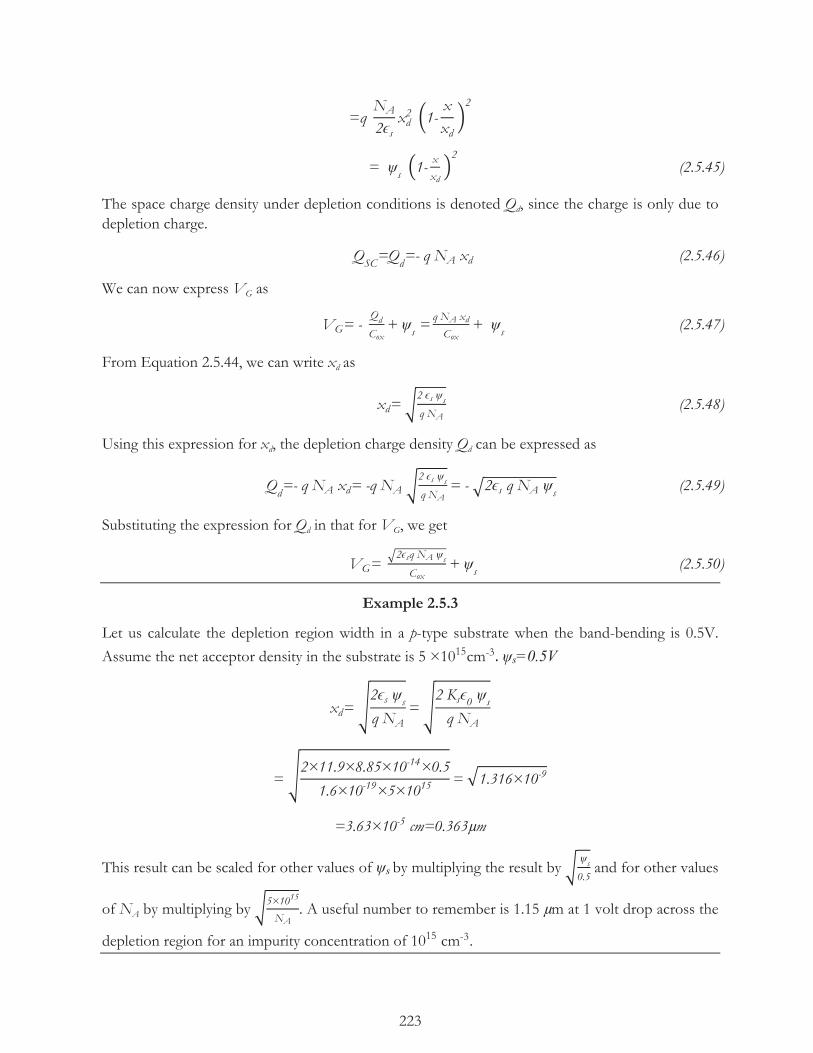
223
=q NA2ϵsxd2 1-
xxd
2
= ψs 1-x
xd
2 (2.5.45)
The space charge density under depletion conditions is denoted Qd, since the charge is only due to depletion charge.
QSC=Qd=- q NA xd (2.5.46)
We can now express VG as
VG= - QdCox+ ψs =
q NA xdCox
+ ψs (2.5.47)
From Equation 2.5.44, we can write xd as
xd= 2 ϵs ψsq NA
(2.5.48)
Using this expression for xd, the depletion charge density Qd can be expressed as
Qd=- q NA xd= -q NA 2 ϵs ψsq NA
= - 2ϵs q NA ψs (2.5.49)
Substituting the expression for Qd in that for VG, we get
VG= 2ϵsq NA ψsCox
+ ψs (2.5.50)
Example 2.5.3
Let us calculate the depletion region width in a p-type substrate when the band-bending is 0.5V.
Assume the net acceptor density in the substrate is 5 ×1015cm-3 ψs=0.5V
xd= 2ϵs ψsq NA
= 2 Ksϵ0 ψs
q NA
= 2×11.9×8.85×10-14×0.5
1.6×10-19×5×1015= 1.316×10-9
=3.63×10⁻⁵ cm=0.363μm
This result can be scaled for other values of ψs by multiplying the result by ψs0.5
and for other values
of NA by multiplying by 5×10¹⁵
NA. A useful number to remember is 1.15 μm at 1 volt drop across the
depletion region for an impurity concentration of 1015 cm-3.
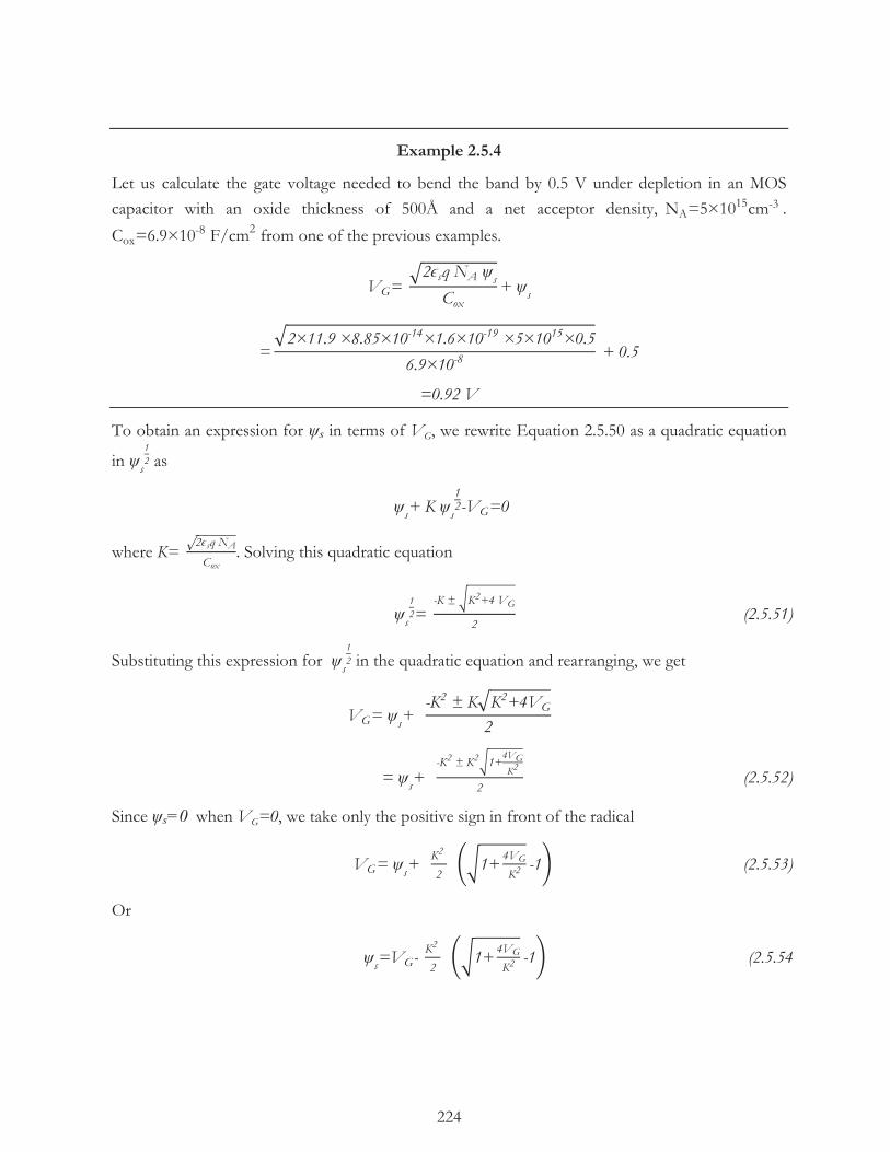
224
Example 2.5.4
Let us calculate the gate voltage needed to bend the band by 0.5 V under depletion in an MOS capacitor with an oxide thickness of 500Å and a net acceptor density, NA=5×10
15cm-3 .
Cox=6.9×10⁻⁸ F/cm2 from one of the previous examples.
VG= 2ϵsq NA ψsCox
+ ψs
=2×11.9 ×8.85×10-14×1.6×10-19 ×5×1015×0.5
6.9×10⁻⁸ + 0.5
=0.92 V
To obtain an expression for ψs in terms of VG, we rewrite Equation 2.5.50 as a quadratic equation
in ψs12 as
ψs+ K ψs12-VG=0
where K= 2ϵsq NACox
. Solving this quadratic equation
ψs12=
-K ± K2+4 VG
2 (2.5.51)
Substituting this expression for ψs12 in the quadratic equation and rearranging, we get
VG= ψs+ -K2 ± K K2+4VG
2
= ψs+ -K2 ± K2 1+
4VGK2
2 (2.5.52)
Since ψs=0 when VG=0, we take only the positive sign in front of the radical
VG= ψs+ K2
2 1+ 4VG
K2-1 (2.5.53)
Or
ψs=VG- K2
2 1+ 4VG
K2-1 (2.5.54

225
Example 2.5.5
Let us calculate the surface potential of the MOS capacitor discussed in the previous example for a gate voltage of 0.7 V.
ψs=VG- K2 2
1+4VGK2
-1
K= 2ϵsq NACox
= 2×11.9 ×8.85×10-14×1.6×10-19 ×5×1015
6.9×10-8
=0.59 Volt
ψs=0.7 -0.592
21+
2.8
0.592-1
=0.35 V
Onset of Strong Inversion
We can now derive an expression for the gate voltage which corresponds to the onset of strong inversion. Onset of inversion occurs when ψs=2 b . We denote this value ψs inv. When the gate voltage exceeds the value corresponding to the onset of inversion, strong inversion occurs. For this reason, the gate voltage is called the turn-on voltage, since the gate voltage has to exceed this voltage to turn the device on. Denoting the threshold voltage as VVT, we find
VT= 2ϵsq NA ψs inv
Cox+ ψs inv
= 2ϵsq NA2 b
Cox+2 b (2.5.55)
We are assuming that at the onset of inversion there is no contribution to the space charge from electrons and that the space charge is essentially depletion charge.
Example 2.5.6
Let us determine the threshold voltage, VT, for the MOS capacitor discussed in the previous examples.
NA= 5×1015cm-3
Hence

226
b= - KTqlnNA-
ni≈ -
KTqlnNAni
=-0.34 V
ψs inv= 2 b =0.68 V
VT= = 2ϵsq NA ψs inv
Cox+ ψs inv
=2×11.9 ×8.85×10-14×1.6×10-19 ×5×1015×0.68
6.9×10⁻⁸+ 0.68
=1.17 V
Strong Inversion
The space charge under strong inversion comes from both the inversion charge (minority carrier charge at the surface) and the depletion charge. Denoting the inversion charge per unit area of the surface as Qinv
QSC=Qinv+ Qd (2.5.56)
For a small increase, Δψs, in the surface potential beyond ψs inv (equal to 2 b ), the inversion charge density, Qinv, increase enormously since the minority carrier density, ns, increase exponentially with surface potential. On the other hand, the depletion charge density, Qd, only increases slightly
since it is proportional to ψs12. The exact calculation of Qsc(ψs) in strong inversion is treated in
advanced text books, and is beyond the scope of this book. Hence we will calculate Qsc(ψs) using an approximation called Depletion Approximation. According to this approximation, in strong inversion the depletion region width, (and therefore depletion charge density) do not increase once inversion sets in (i.e., they remain constant at a value they had at the on-set of inversion and correspond to ψs = ψs inv=2 b .) This means that beyond the on-set of inversion, the space charge density, Qsc, increases only due to an increase in the inversion charge density. Since the depletion region width does not increase once inversion sets in, the depletion region width is presumed to have attained a maximum value at the on-set of strong inversion and is denoted xd max where
xd max= 2ϵs ψs inv
q NA= 2ϵs2 b
q NA (2.5.57)
The depletion layer charge density, which also does not increase once inversion sets in, is denoted Qd max where
Qd max= -qNAxd max= - 2ϵsq NA2 b (2.5.58)
Therefore QSC= Qinv+ Qd max= Qinv- 2ϵsq NA2 b (2.5.59)
Under strong inversion, ψs can be written as
ψs = ψs inv+ Δ ψs= 2 b + Δ ψs (2.5.60)
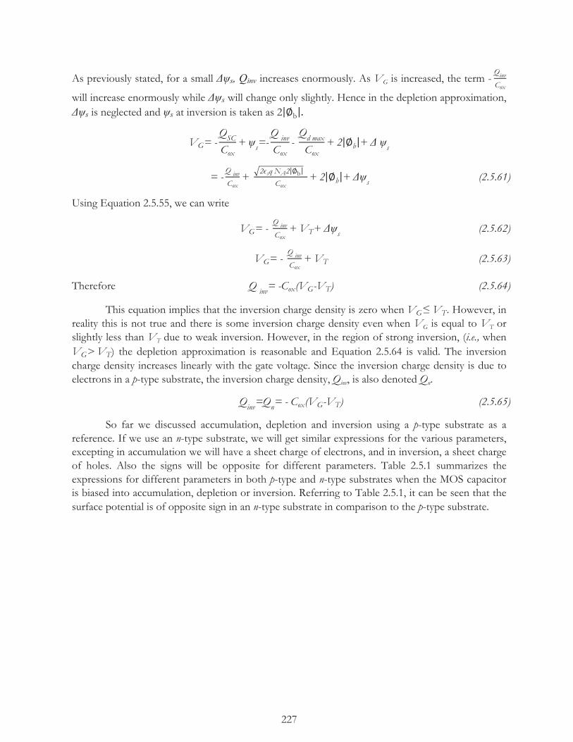
227
As previously stated, for a small Δψs, Qinv increases enormously. As VG is increased, the term -QinvCox
will increase enormously while Δψs will change only slightly. Hence in the depletion approximation, Δψs is neglected and ψs at inversion is taken as 2 b
VG= -QSCCox
+ ψs=-Q invCox
- Qd max
Cox+ 2 b + Δ ψs
= -Q invCox
+ 2ϵsq NA2 b
Cox+ 2 b + Δψs (2.5.61)
Using Equation 2.5.55, we can write
VG= - Q invCox
+ VT+ Δψs (2.5.62)
VG= - Q invCox
+ VT (2.5.63)
Therefore Q inv= -Cox(VG-VT) (2.5.64)
This equation implies that the inversion charge density is zero when VG≤ VT. However, in reality this is not true and there is some inversion charge density even when VG is equal to VT or slightly less than VT due to weak inversion. However, in the region of strong inversion, (i.e., when VG>VT) the depletion approximation is reasonable and Equation 2.5.64 is valid. The inversion charge density increases linearly with the gate voltage. Since the inversion charge density is due to electrons in a p-type substrate, the inversion charge density, Qinv, is also denoted Qn.
Qinv=Qn= - Cox(VG-VT) (2.5.65)
So far we discussed accumulation, depletion and inversion using a p-type substrate as a reference. If we use an n-type substrate, we will get similar expressions for the various parameters, excepting in accumulation we will have a sheet charge of electrons, and in inversion, a sheet charge of holes. Also the signs will be opposite for different parameters. Table 2.5.1 summarizes the expressions for different parameters in both p-type and n-type substrates when the MOS capacitor is biased into accumulation, depletion or inversion. Referring to Table 2.5.1, it can be seen that the surface potential is of opposite sign in an n-type substrate in comparison to the p-type substrate.
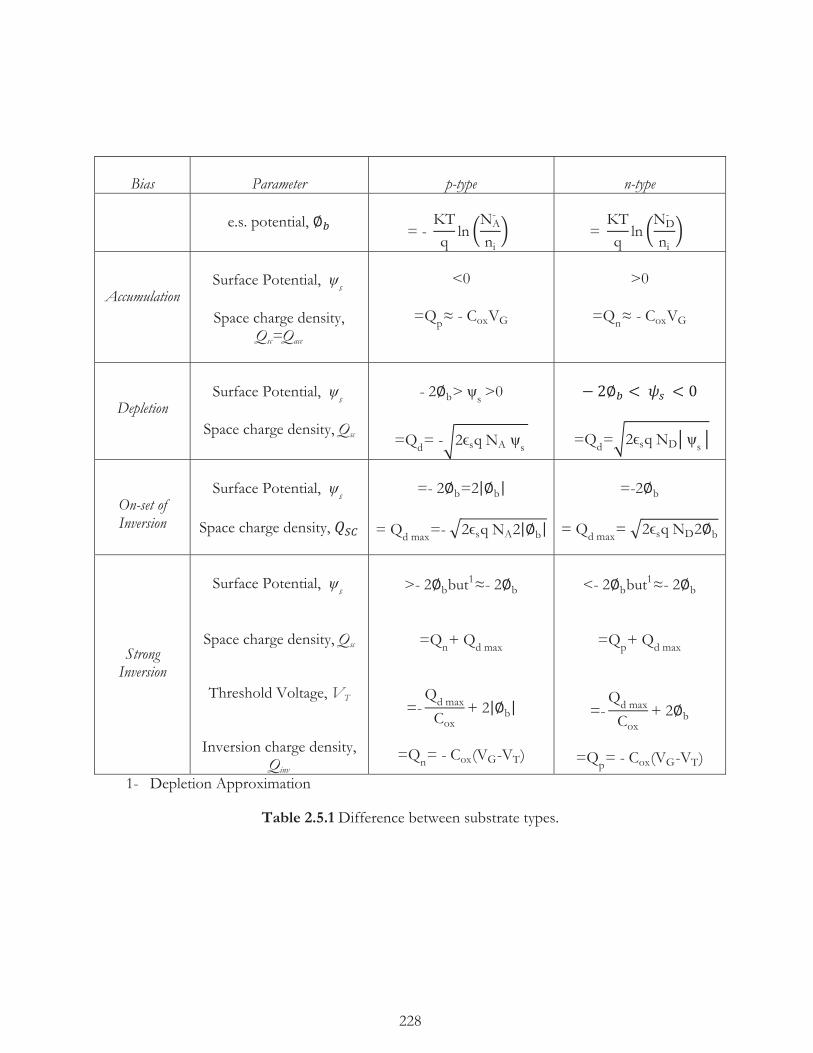
228
Bias
Parameter
p-type
n-type
e.s. potential,
= - KTqlnNA-
ni
= KTqlnND-
ni
Accumulation
Surface Potential, ψs
Space charge density,
Qsc=Qacc
<0
=Qp≈ - CoxVG
>0
=Qn≈ - CoxVG
Depletion
Surface Potential, ψs
Space charge density, Qsc
- 2 b> ψs >0
=Qd= - 2ϵsq NA ψs
=Qd= 2ϵsq ND ψs
On-set of Inversion
Surface Potential, ψs
Space charge density,
=- 2 b=2 b
= Qd max=- 2ϵsq NA2 b
=-2 b
= Qd max= 2ϵsq ND2 b
Strong Inversion
Surface Potential, ψs
Space charge density, Qsc
Threshold Voltage, VT
Inversion charge density, Qinv
>- 2 bbut
1≈- 2 b
=Qn+ Qd max
=-Qd max
Cox+ 2 b
=Qn= - Cox(VG-VT)
<- 2 bbut
1≈- 2 b
=Qp+ Qd max
=-Qd max
Cox+ 2 b
=Qp= - Cox(VG-VT)
1- Depletion Approximation
Table 2.5.1 Difference between substrate types.

229
2.5.2 Non-Ideal MOS Device
Until now we discussed as ideal MOS Device. What do we mean by an ideal MOS device? An ideal MOS device is one in which there is no induced space charge in the semiconductor in the absence of the gate voltage. A non-ideal MOS device, on the other hand, is one in which there is a space charge in the semiconductor even in the absence of a gate voltage. Real MOS devices have a space charge in the semiconductor even when the gate voltage VG is equal to zero. There are three causes for this non-ideal behavior, and they are:
(1) Charges in the oxide (2) Difference in work function between the gate and the substrate (3) Surface state charges
We can apply a voltage on the gate that will reduce the induced space charge to zero, and we define that voltage as the flat-band voltage, VFB. The reason for using the concept of the flat-band voltage is to describe the behavior of a non-ideal MOS device as though it were an ideal device with a bias voltage applied on the gate equal to the flat-band voltage VFB. For example the threshold voltage of a non-ideal MOS device can be written as
VT non-ideal=VT ideal+VFB (2.5.66)
Actually, this relationship is not exactly valid due to the presence of surface states, but for all practical purposes this can be taken as valid. Let us now determine the flat-band voltage arising from the three different sources of non-ideal behavior.
Charges in the Oxide
Due to the manner in which the silicon atoms are bonded to the oxygen atoms in the growth of the oxide layer in a thermal oxidation process, the oxide layer contains some positive charge. The positive charges in the oxide induce a negative space charge in the semiconductor, and the magnitude of the induced charge will depend on the relative location of the charge in the oxide between the metal and the substrate. Let the positive charge in the oxide have a density ρ(x) and let it vary in some arbitrary fashion as shown in the Figure 2.5.11. In this figure, we have chosen the origin, x=0, at the oxide-silicon interface, and the oxide-gate interface at x=-tox where tox is the thickness of the oxide layer. Consider the charge in the oxide in an elementary region between x and x+dx. This charge can be thought of as a sheet charge of density ρ(x)dx. According to the theory of images, the sheet charge ρ(x)dx, located at a distance x on the x-axis from the oxide-silicon interface, will induce charges both on the gate and in the semiconductor. The charge induced in the semiconductor is proportional to the distance between the sheet charge and the gate and similarly the charge induced in the gate is proportional to the distance between the sheet charge and the semiconductor. Hence, it is possible to write the space charge induced in the semiconductor per unit area of the interface as
dQSC=- ρ x dx x-(-tox)
tox= - ρ x tox+x dx
tox (2.5.67)
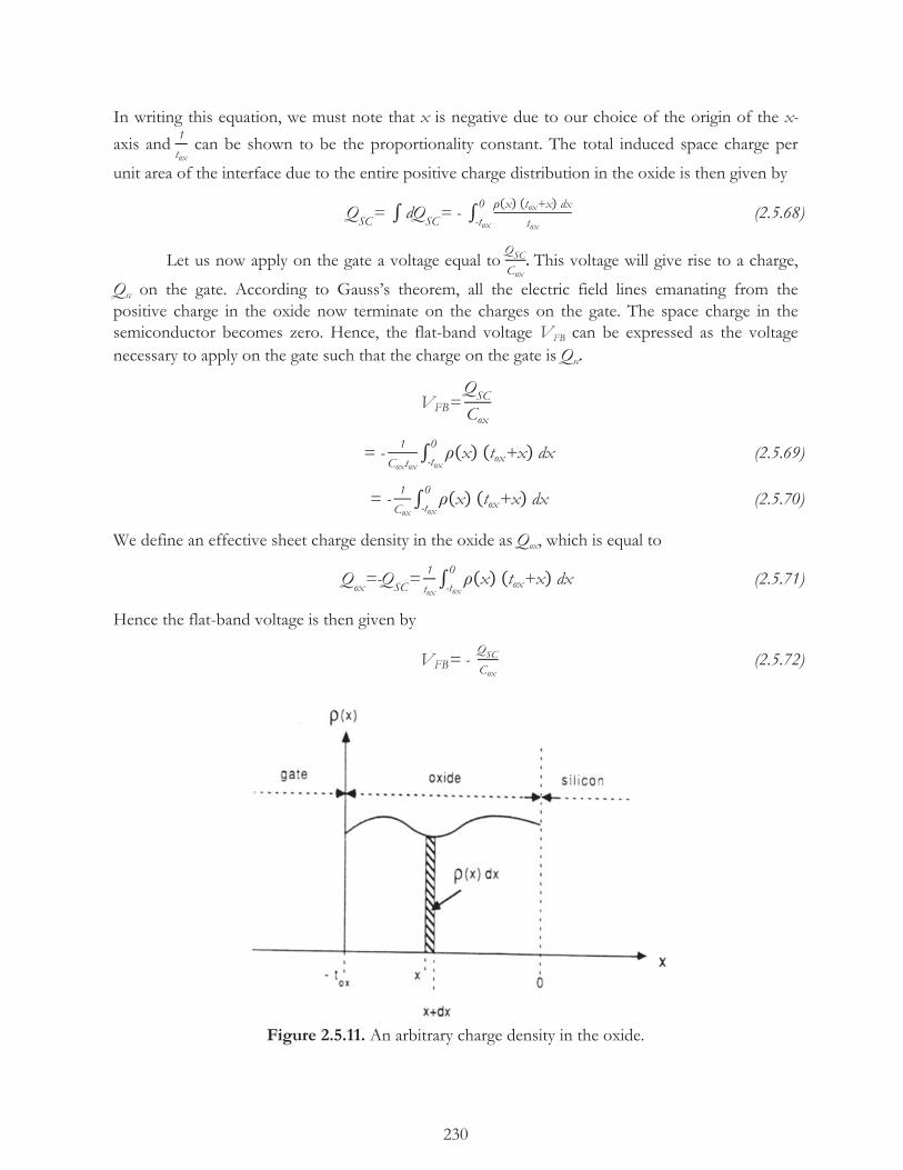
230
In writing this equation, we must note that x is negative due to our choice of the origin of the x-
axis and 1tox
can be shown to be the proportionality constant. The total induced space charge per
unit area of the interface due to the entire positive charge distribution in the oxide is then given by
QSC= dQSC= - ρ x tox+x dx
tox
0-tox
(2.5.68)
Let us now apply on the gate a voltage equal to QSCCox
This voltage will give rise to a charge,
Qsc on the gate. According to Gauss’s theorem, all the electric field lines emanating from the positive charge in the oxide now terminate on the charges on the gate. The space charge in the semiconductor becomes zero. Hence, the flat-band voltage VFB can be expressed as the voltage necessary to apply on the gate such that the charge on the gate is Qsc
VFB=QSCCox
= - 1
Coxtoxρ x tox+x dx
0-tox
(2.5.69)
= - 1
Coxρ x tox+x dx
0-tox
(2.5.70)
We define an effective sheet charge density in the oxide as Qox, which is equal to
Qox=-QSC=1
toxρ x tox+x dx
0-tox
(2.5.71)
Hence the flat-band voltage is then given by
VFB= - QSCCox
(2.5.72)
Figure 2.5.11. An arbitrary charge density in the oxide.

231
Example 2.5.7
Let us now consider an example in which we assume that the oxide layer has a thickness of 1000 Å, and has a uniform charge density of 1015 ions/cm3. Since ρ(x) is a constant, say equal to ρ0, Qsc (or Qox) can be evaluated taking ρ outside the integral.
QSC=- Qox= - ρ x tox+x
tox
0
-tox
dx
=- ρ0tox
tox+x0
-tox
dx
=-ρ0tox
toxx+ x2
2-tox
0
=- ρ0tox2
In this example, Qsc becomes equal to
QSC= - 1015×1.6×10-19×1000×10-8
2= -0.8 ×10⁻⁹ c/cm2 (2.5.73)
Cox=ϵoxCox
= Koxϵotox
= 3.9 ×8.84×10-14
1000 × 10-8 ≈3.45 ×10⁻⁸F/cm2 (2.5.74)
Hence VFB= -0.8 ×10⁻⁹
3.4 ×10-8 =-0.023 V (2.5.75)
Note that the flat-band voltage due to the positive charge in the oxide is the same for n- and p- type substrates. It is negative since the charge in the oxide is positive.
Work Function Difference
Every material has a characteristic work function. Work function is defined as the difference between the Fermi energy and the surface barrier energy, where the surface barrier energy is the energy that an electron inside the solid must have in order to leave the solid and escape into vacuum. The surface barrier energy, therefore, is also called the vacuum level, Evac. This is illustrated in Figure 2.5.12. We denote the work function of the solid as qΦ and given by
qΦ= Evac-EF (2.5.76)
One should note that although Φ has units of a Volt, is not the electrostatic potential.
Let us now consider two solids A and B with work functions qΦA and qΦB respectively. Let ΦB be less than ΦA. Let the two solids be not connected to each other as shown in Figure 2.5.13A. Since the two solids are not connected to each other, the vacuum levels for the two solids are at the same level since an electron that is excited with enough energy to overcome the surface barrier energy will have zero kinetic energy in vacuum in both solids. The Fermi energy is at a higher level in B than in A since it has a smaller work function. If the materials A and B are connected to form

232
a junction as shown in Figure 2.5.13B, electrons will move from material B into material A so that the Fermi levels are lined up. Hence B will be positive with respect to A. A potential difference, ΦAB= ΦA-ΦB will arise between B and A. This potential difference is called the contact potential.
Figure 2.5.12. Work function of a solid.
Figure 2.5.13. Two solids with different work function: (A) The solids are not connected to each other and (B) The solids are connected to each other.
When we consider the work function of a semiconductor, a similar definition follows. The vacuum level and the conduction and valence bands are shown in Figure 2.5.14. We notice that the location of the Fermi energy in the bandgap is dependent on the type and density of dopant (impurity) atoms. The workfunction is not a constant for a given semiconductor material and depends on whether it is n or p type material and also on the resistivity of the material. On the other hand, the difference in energy between the conduction band minimum, EC, and the vacuum level, Evac, is a constant for a given semiconductor material. This difference is called electron affinity, and denoting affinity as χ we have
χ = Evac-Ecq
(2.5.77)
In a p-n junction, n- and p-type semiconductor materials form a junction. This is equivalent to connecting a p-type and an n-type semiconductor. We saw that a potential difference, called the

233
built-in voltage, Vbi exists between the n-region and the p-region in a p-n junction. The built-in voltage is just the contact potential as shown below:
Let us denote the work function of the p-type semiconductor Φ1, and that of the n-type semiconductor as Φ2.
qΦ1=Evac-EF1= qχ+ Ec-EF1 (2.5.78)
where EF1 is the Fermi level in the p-type semiconductor. But
Ec-EF1= Eg2
+ Ei-EF1=Eg2+q p (2.5.79)
where ϕp is the bulk electrostatic potential of the p-type semiconductor. Therefore
q 1=qχ+Eg2+q p (2.5.80)
Similarly, it can be shown that
q 2=qχ+Eg2
-q n (2.5.81)
where ϕn is the bulk electrostatic potential of the n-region. Hence the work function difference, Φ12=Φ1-Φ2 is equal to
Φ12=Φ1-Φ2= p + n= Vbi (2.5.82)
In an MOS device when there is a difference between the gate and the semiconductor work function, a potential difference arises. Let ΦM be the work function of the gate and ΦS the work function of the substrate semiconductor. Therefore the substrate is positive with respect to the gate by an amount equal to the contact potential ΦMS where ΦMS=ΦM-ΦS. This will therefore give rise to a space charge in the semiconductor. If we now apply a voltage ΦMS it will exactly balance out the contact potential difference, and hence no space charge will be induced in the substrate. We can therefore conclude that the flat-band voltage VFB required to account for the work function difference is given by
VFB=ΦMS=ΦM-ΦS (2.5.83)
Figure 2.5.14. Electron affinity and work function in a semiconductor.

234
Surface States (Interface States)
At the interface between the oxide and the substrate, there are a large number of states due to unfilled covalent bonds, which are called dangling bonds. These states can be charged or neutraland are called interface states or surface states. Usually these states are distributed continuously in energy in the band gap. Let us define Dit as the number of states per unit area per unit energy interval at some energy level E. Then in an energy level dE between E and E+dE, the number of states per unit area is DitdE. A surface state will be more positively charged if the Fermi energy is below it. On the other hand, it will be less positively charged if the Fermi energy is above it. Thus, the location of the Fermi energy in the band gap at the surface determines the amount of charge in the surface states. Although the Fermi energy remains constant with distance, its location in the band gap at the surface changes as the band bending changes (i.e., as ψs changes). Hence the amount of charge in the surface states changes. The charge in the surface states is located at the interface, and therefore is a sheet charge. If Qst is the sheet charge density at the surface, then Qst is a function of ψs. The sheet charge at the interface between the semiconductor and the oxide induces a space charge of density -Qst in the semiconductor. Hence, if we apply a charge on the gate equal to –Qst, then the space charge will be completely removed from the semiconductor. This is again based on the principle of Gauss’s theorem that the electric lines of force emanating from the surface state sheet charge now will terminate on the sheet charge –Qst on the gate. Hence we can write the flat band voltage VFB as equal to
VFB= -Qst(ψs=0)
Cox (2.5.84)
The total flat band voltage due to all the three sources is
VFB=- QoxCox+ ΦMS -
Qst(ψs= 0)
Cox (2.5.85)
On the other hand, the threshold voltage VT of a non-ideal MOS structure is
VT non-ideal=VT ideal- QoxCox+ ΦMS -
Qst(ψs = 2 b )
Cox
= VT ideal+ VFB - ΔQstCox
(2.5.86)
where ΔQst= Qst( ψs =2 b )- Qst(ψs=0) (2.5.87)
In most modern devices, ΔQst is very small, and hence it is reasonable to express the threshold voltage as
VT = VT ideal+ VFB (2.5.88)
and neglect the -ΔQstCox
term.
235
Example 2.5.8
Let us assume that the surface state density, Dit, is a constant with energy (i.e., it has the same value
throughout the band gap) with a value equal to 5× 10¹⁰ eV-1cm-2
. Let the oxide thickness be 1000
Å. Let us assume a p-type substrate with NA=5×10¹⁵/cm3 Let us calculate the value for -
ΔQstCox
.
The change in ψs between flat-band and on-set of inversion is equal to Δψs=2 b .
b= -kTqlnNAni
=-0.0259 ln5×1015
5×1010= -0.298
Δψs=2×0.298=0.596 V
ΔQst is negative, since the bands bend downward at inversion (Fermi energy rises in the band gap at the surface).
ΔQst= -q Nit dψ= -q Nit Δ ψs
ψs=2 b
ψs=0
=-1.6 × 10-19×5×1010×0.596
= -4.77× 10⁻⁹ c cm-2
Therefore - ΔQstCox
= 4.77× 10⁻⁹
3.45× 10-8 =0.14 V
In modern semiconductor devices, the interface state density is lower by a factor of 10 and the
oxide thickness is on the order of 200 Å. Hence -ΔQstCox
is a couple of millivolts and negligible.
Capacitance Effect
In a parallel plate capacitor, which is formed by having a dielectric medium between two parallel metal plates, equal sheet charges of opposite sign are induced on the two plates when a voltage is applied across this capacitor. The charge on the metal plate, which is connected to the positive terminal of the voltage source, has a positive sheet charge and that which is connected to the negative terminal has a negative sheet charge. The capacitance is determined only by the geometrical structure of the parallel plate capacitor. The capacitance is inversely proportional to the thickness of the dielectric material between the plates and proportional to the area of the plate. On the other hand, when an MOS capacitor is fabricated with silicon (the substrate) as one of the two parallel plates, the induced charge in the semiconductor is not a sheet charge but a space charge which under certain specific conditions can be approximated as a sheet charge as discussed earlier. The magnitude of the space charge is not directly proportional to the potential drop across the space charge region, (the surface potential). Hence, the capacitance in an MOS capacitor is voltage

236
dependent. In this section we will examine the voltage dependence of the capacitance of an MOS capacitor. Let us first consider an ideal MOS capacitor.
2.5.3 Ideal MOS Capacitor
Let us now assume that a DC voltage VG is applied on the gate of an MOS capacitor so as to bias the device in one of the three regimes of operation, (i.e., accumulation, depletion or inversion.) The applied voltage is divided into a voltage, Vox, across the oxide layer and a potential drop, ψs, across the space charge region. Let us also assume that a step voltage of a very small amplitude dVG, is applied in series with the DC voltage VG, as shown in Figure 2.5.15. The applied voltage dVG is also distributed partially across the oxide and partially across the space charge region, giving us the relationship
dVG= dVox+ dψs (2.5.89)
where dVox and dψs, are the incremental changes in Vox and ψs, respectively. dVG gives rise to a small sheet charge dQ on the gate electrode in addition to the already existing sheet charge due to the bias voltage VG. Similarly, the space charge density in the semiconductor increases by dQsc
where
dQsc=-dQ (2.5.90)
We divide the above equation for dVG by dQsc to obtain
dVGdQ
= dVoxdQSC
+dψsdQSC
(2.5.91)
The differential of the gate (sheet) charge Q, with respect to VG, given by dQ dVG
, denotes the ratio of
the incremental change dQ in the gate charge Q to the incremental change dVG in the gate voltage, and is defined as the small signal capacitance C of the MOS capacitor of gate area equal to unity.
dVGdQ= 1
dQ dVG
= 1C (2.5.92)
Figure 2.5.15. A small step voltage in series with a DC bias voltage VG applied across an MOS capacitor.
237
Similarly, the differential of Q with respect to Vox is equal to the capacitance of a parallel plate capacitor with the oxide layer between two metallic plates. Denoting this as the oxide capacitance per unit area, Cox we obtain
dVoxdQSC
= dVoxdQ= 1
Cox (2.5.93)
where Cox= ϵoxtox
(2.5.94)
The differential of dQSC with respect to ψs is defined as the space charge capacitance Csc and is given by
dψsdQSC
= 1
CSC (2.5.95)
Therefore 1
C= 1
Cox+ 1
CSC (2.5.96)
The small signal equivalent capacitance of an MOS capacitor of unit area can therefore be described as a series combination of two capacitors, one Cox, and the other Csc, which is illustrated in Figure 2.5.16. Instead of an incremental voltage dVG, let us now apply a small sinusoidal voltage v in series with the DC voltage across the MOS capacitor, as shown in Figure 2.5.17. Due to the small signal voltage v , a small signal current i flows. By measuring the ratio of v and i , the capacitance C can be determined from the relation
C= 1
jω v (2.5.97)
where ω is 2π multiplied by the frequency of the small signal voltage v If Q is the component of space charge that varies sinusoidally in step with v then
C= Q
v (2.5.98)
The measured capacitance C is
C= Cox CSCCox+ CSC
(2.5.99)
where the area of the gate is assumed to be unity, Cox is the oxide capacitance per unit area, and Csc is equal to space charge capacitance per unit area. If we were to consider a MOS capacitor of area A, then the measured capacitance, Cm is equal to A×C where C is the capacitance per unit area.
Q= Qacc (2.5.100)

238
Figure 2.5.16. Equivalent circuit of an MOS capacitor.
Figure 2.5.17. A sinusoidal voltage in series with a DC bias voltage applied across an MOS capacitor.
Let us now evaluate the small signal capacitance for different regimes.
Accumulation
The charge distribution in the MOS device under accumulation conditions can be visualized as shown in Figure 2.5.18. Let us assume that x=0 represents the interface between the oxide and silicon. Let the interface between the gate and the oxide be located at x= -tox.
The accumulation charge is located at x=0 as shown in Figure 2.5.18. Qacc is a small component of the total sheet charge which varies in step with the applied small signal voltage v
CSC=dQSCdψs
=dQaccdψs
(2.5.101)
Since Qacc changes enormously for a small change in ψs, Csc is very large. Hence
1
C = 1
Cox+ 1
CSC ≈ 1
C= 1
Cox= toxϵox
(2.5.102)

239
The above equation shows that the measured capacitance of the MOS capacitor in the accumulation regime of operation is essentially equal to the oxide capacitance. The equivalent circuit is just a simple capacitor Cox as shown in Figure 2.5.19.
Figure 2.5.18. Charge distribution in the MOS capacitor under accumulation conditions.
Figure 2.5.19. Equivalent circuit of an MOS capacitor when the surface is accumulated. The MOS capacitor has a capacitance equal to Cox in accumulation.
Depletion
The space charge under depletion conditions is the charge in the depletion region in the semiconductor. The applied elementary sinusoidal voltage induces a sinusoidally varying depletion charge in the semiconductor. The sinusoidal depletion charge variation occurs at the edge of the depletion region, as shown in Figure 2.5.20. The space charge capacitance is the depletion region capacitance, which is equal to
CSC= Cd=ϵsxd
(2.5.103)
where xd is the depletion region width. The equivalent circuit is shown in Figure 2.5.21. Since the depletion region capacitance is comparable to or less than the oxide capacitance, the net capacitance of the series combination of Csc and Cox is less than Cox. As the gate voltage is increased so as to induce a larger space charge region, the width of the depletion region xd increases, and therefore the space charge capacitance Csc (=Cd) decreases. Hence the capacitance of the MOS capacitor decreases as the gate voltage is increased.

240
Figure 2.5.20. Charge distribution in the MOS capacitor under depletion conditions.
Figure 2.5.21. Equivalent circuit of an MOS capacitor when the surface is depleted.
Inversion
When the gate voltage is increased to a value larger than the threshold voltage, we saw earlier that the space charge is due to both the inversion charge and the depletion charge. Due to the applied voltage dVG, an increase in the inversion charge occurs if minority carriers can be generated fast enough in the depletion region. Then the inversion charge has a component that varies sinusoidally in step with the small signal voltage v. For the inversion charge to change in step with applied voltage, the sinusoidal voltage should change slowly with time. The period of oscillation of the sinusoidal voltage v has to be much larger than the minority carrier generation
lifetime τg (i.e., ω< 1
τg). The sinusoidal change in the space charge density therefore is equal to
QSC= Qinv
and occurs at the silicon surface as shown in Figure 2.5.22. The range of frequencies for which
ω< 1
τg is called the low frequency region.
CSC=dQSCdψs
=dQinvdψs

241
Figure 2.5.22. Low frequency charger distribution in the MOS capacitor under inversion conditions.
It is large since the inversion charge increases enormously for a small change in ψs. At low frequencies the MOS device behaves like a parallel plate capacitor with an oxide dielectric between the two parallel plates since the sinusoidal change occur on the gate and in the semiconductor at the oxide interface. The capacitance of the MOS capacitor under these conditions is the same as the oxide capacitance. The equivalent circuit under inversion conditions is shown in Figure 2.5.23.
Figure 2.5.23. Low frequency equivalent circuit of an MOS capacitor under inversion conditions.
If sufficient time is not allowed for minority carriers to be generated, the inversion charge is not able to change in step with applied voltage and hence the incremental change in the space charge density occurs at the edge of the depletion region adjacent to the neutral region of the semiconductor as shown in Figure 2.5.24. In other words, if the period of the sinusoidal voltage, v, is much less than the minority carrier generation lifetime, τg, then the elementary sinusoidal change in the space charge dQ occurs at the edge of the depletion region. The range of frequencies for
which ω> 1
τg is called the high frequency region. The measured capacitance at high frequencies
therefore will be the oxide capacitance in series with the depletion capacitance corresponding to a depletion region with a maximum width, xd max. Figure 2.5.25 shows the equivalent circuit of the MOS capacitor under high frequency conditions. Due to the different responses of the space charge density at low and high frequencies, the space charge capacitance will have different values at low and high frequencies.
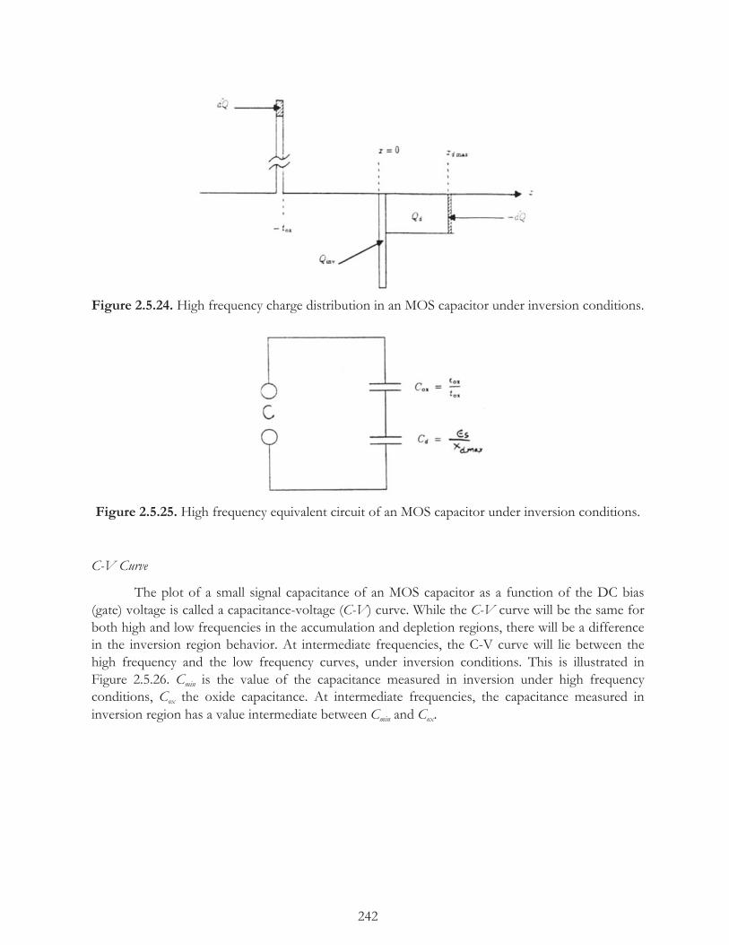
242
Figure 2.5.24. High frequency charge distribution in an MOS capacitor under inversion conditions.
Figure 2.5.25. High frequency equivalent circuit of an MOS capacitor under inversion conditions.
C-V Curve
The plot of a small signal capacitance of an MOS capacitor as a function of the DC bias (gate) voltage is called a capacitance-voltage (C-V) curve. While the C-V curve will be the same for both high and low frequencies in the accumulation and depletion regions, there will be a difference in the inversion region behavior. At intermediate frequencies, the C-V curve will lie between the high frequency and the low frequency curves, under inversion conditions. This is illustrated in Figure 2.5.26. Cmin is the value of the capacitance measured in inversion under high frequency conditions, Cox the oxide capacitance. At intermediate frequencies, the capacitance measured in inversion region has a value intermediate between Cmin and Cox.

243
Figure 2.5.26. The capacitance-voltage (C-V) characteristics of an MOS capacitor at low, intermediate and high measurement frequencies.
Deep Depletion
Let us now assume that a step voltage of amplitude VG (>dVT) is applied on the gate at time t=0. Let us also apply a small sinusoidal voltage v in series with the step voltage, VG, as shown in Figure 2.5.27. The purpose of v is to measure the small signal capacitance, and it is therefore called the probing signal. Immediately after the application of the step voltage (that is at t=0+) the induced space charge will essentially be caused by the depletion charge. This is because there is no time for the inversion charge to be generated by thermal generation of minority carriers. The depletion charge is increased beyond the maximum depletion charge obtained under steady state conditions. The space charge region under this condition represents the non-equilibrium condition. At t=0+ the depletion region widens to a large value xd0+ which is much larger than xd max. Hence, the condition is called deep depletion. The generation and recombination rates in the space charge are not what will be obtained in thermal equilibrium, and do not balance each other out as required by the law of mass action. Minority carriers are generated in the space charge region in excess of what are lost due to recombination. These minority carriers will be driven towards the interface, where they will form the inversion charge, while the majority carriers proceed in the opposite direction. Part of the majority carriers generated will neutralize the ionized impurities at the edge of the depletion region, thereby reducing the depletion region width while the rest of the majority carriers will be flown out of the ohmic contact. It must be pointed out that the increase in the inversion charge is more than the reduction in the depletion charge. As time progresses, the inversion charge increases and the depletion charge decreases correspondingly. Ultimately at t=∞, a depletion width of xd max is obtained, and the inversion charge and the depletion charge attain steady state values. The space charge region now is in thermal equilibrium. The space charge region thus exhibits a transient behavior before steady state conditions are reached. Therefore the capacitance also exhibits a transient behavior. The transient response of the capacitance is shown in Figure 2.5.28.

244
In deep depletion, (i.e., at t=0+), there is no inversion charge and there is only depletion charge. Hence, the surface potential ψs(0
+) is related to the step voltage, VG, by the relationship
VG= -Qd(0
+)
Cox+ψs 0
+ =2ϵsqNAψs 0
+
Cox+ψs 0
+ (2.5.104)
This can be solved to yield, as was done earlier,
ψs 0+ = VG- K
2
2
4VGK2+1-1 (2.5.105)
where K is defined as equal to
K= 2ϵsqNACox
(2.5.106)
The band-bending at t=0+ is shown in Figure 2.5.29. The surface potential ψs represents a potential well at x=0 for an electron (remember we are assuming a p-type substrate), of depth equal to ψs(0
+). This potential well can be used to store electrons. This storage can be done only momentarily due to the transient nature of deep depletion. By placing a large number of MOS capacitors at close spacing and by pulsing these in a suitable sequence, the charge stored in the potential well under these capacitors can be successfully transferred from one to the next all the way to the end of the string of capacitors. The string of closely spaced MOS capacitors is called the charge couple device (CCD). The charge coupled device has many applications in digital, analog and imaging circuits.
The capacitance at t=0+ is very small since the depletion region width is large and hence Cd at t=0+ is small. Hence C is also small. As time increases from t=0+, ψs decreases and the depletion region width decreases and Cd increases. Therefore the capacitance of the MOS capacitor also increases and finally reaches a steady state value corresponding to xd =xd max after a long time. This is called the transient behavior of the MOS capacitor.
Figure 2.5.27. Application of a large step voltage on the gate of an MOS capacitor to produce deep depletion.

245
Figure 2.5.28. Transient behavior of the capacitance of an MOS capacitor.
Figure 2.5.29. Band bending in deep depletion.
2.5.4 MOS Transistor
The MOS transistor is a device based on the principle that a conducting channel is induced in the surface of a semiconductor by an electric field of suitable polarity and magnitude. In our study of MOS capacitors, we saw that when we apply a gate voltage larger than the threshold voltage, the surface gets inverted. The inversion layer at the surface can provide a conducting path, and therefore can carry electric current between two regions that are doped opposite to the substrate. As an example, consider a MOS structure on a p-type substrate as shown in Figure 2.5.30. Two n+ regions, one called the source and the other called the drain, are formed by diffusing (or implanting) donor atoms. A thin oxide layer called the gate oxide is grown on the surface of the substrate between the source and the drain. A gate electrode extending from the edge of the source region to the edge of the drain region is deposited on top of the gate oxide layer. When the voltage applied on the gate is less than the threshold voltage, VT, no conducting channel exists between the source and the drain. The path between the source and the drain comprises of two n+-p junctions connected back-to-back. When the gate voltage VG is made larger than VT, an inversion layer of electrons provides a conducting channel between the source and the drain. The conductance is dependent on the inversion charge density, and hence on the gate voltage, VG. Thus we are able to

246
control the conductance (and therefore resistance) between the source and the drain through the application of a voltage on the gate. The device is therefore called a transistor.
The particular structure that we discussed is called an n-channel device since the charge carriers in the conducting channel are electrons. If we had started with an n-type substrate and p+ diffusions for the source and the drain, the resulting device would have been called a p-channel device. The drain current, ID, versus the gate voltage, VG, characteristic is called the transfer characteristic, and it is shown in Figure 2.5.31 for n- and p- channel devices. For the n-channel device, when the gate voltage, VG, is less than VT no current flows and when VG is larger than VT the current increases with VG. We will later on see that this increase is linear for small drain voltages. In the case of the p-channel device, the threshold voltage is negative, and hence when the magnitude of the negative gate voltage is larger than the magnitude of the threshold voltage, conduction results in the p-channel device. The symbols for the two types of devices are also shown in Figure 2.5.31. The direction of the arrow in the substrate lead is to indicate whether it is a p-channel or an n-channel device, and the convention is the same as in a p-n junction. The direction of the arrow is from the p- to the n- region. In the case of the n-channel device, the substrate is p and the channel is n. Therefore the arrow is inward. In the case of the p-channel, the substrate is n-type and the channel is p-type, and therefore the arrow is outward.
Let us now calculate the drain current. Assume that the length of the channel between the source and the drain lies along the y-axis with the source at y=0, and the drain at y=L. Let W be the width of the channel. Then the current, J, in the channel is given by
J= μnndEFdy
(2.5.107)
where μn is the mobility of the electrons, n is the electron density, and EF is the Fermi energy. The current density J is in units of amperes per square centimeter (A cm2.) Let us assume that a voltage VD is between the source and the drain. At any point, the voltage drop along the channel measured
with respect to the source will be denoted V(y). The gradient of the voltage along the channel is dVdy
.
The gradient of Fermi energy is related to the gradient of the voltage drop along the channel through the relationship
dEFdy=-q dV
dy (2.5.108)
We can therefore write the current density as equal to
J= -qμnn dVdy
(2.5.109)
Let xI be the thickness of the inversion layer of electrons. Furthermore, let us assume that the electron density, n, is constant in the inversion layer perpendicular to the channel. Then the drain current ID is equal to the current density, J, multiplied by WxI, and is given by
ID= - qμn n WxIdV
dy (2.5.110)

247
Consider a small section of the inversion layer a shown in Figure 2.5.32. Let us now describe a rectangular strip of length dy, contained between y and y+dy. The charge contained in this rectangular strip is equal to QnWdy since Qn is the electron (inversion) charge per unit area of the surface. But this is also equal to
QnW dy=- q n WxI dy (2.5.111)
Hence Qn =- q n xI (2.5.112)
Using this expression for Qn we can express the drain current as
ID= μn Qn WdV
dy (2.5.113)
Figure 2.5.30. A schematic representation of the n-channel MOS transistor.
Figure 2.5.31. The transfer characteristics and the symbol for (A) n-channel device and (B) p-channel device.

248
Figure 2.5.32. A section of the inversion layer between y and y+dy.
We will now distinguish three cases:
Case 1. SSmall VD
Let the source and the substrate be connected together to the ground. We will assume that the drain voltage, VD, is small. Therefore it is reasonable to assume that the inversion charge density is the same everywhere in the channel (i.e., does not vary with y.) The inversion charge density Qinv is given by
Qinv= Qn=-Cox(VG-VT) (2.5.114)
where Cox is the oxide capacitance per unit area. The inversion layer now looks like a rectangular sheet of electron charge of dimensions W, L and xI as shown in Figure 2.5.33. Therefore the drain current is given by
ID= - μnWCox(VG-VT)dV
dy (2.5.115)
We can now approximate the gradient dVdy
as equal to VDL
since the drain voltage VD is very small.
Hence
ID= - μn W
L Cox(VG-VT) VD (2.5.116)
We see therefore that the drain current varies linearly with the drain voltage and the gate voltage.
Figure 2.5.33. Approximation of the inversion layer as a sheet charge.

249
Case 2. Large VD (Simpli f i ed Treatment)
We will now consider the case when the drain voltage, VD, is large. We present a simplified
treatment. Since VD is large, it is no longer possible to assume that the gradient dVdy
is constant
everywhere between the source and the drain. Due to V(y), the inversion charge density will be different for different values of y. In the early days, it was assumed that a threshold voltage VT(y) at some value of y was related to VT at y=0 at the source by the relation
VT y = VT y=0 +V(y) (2.5.117)
At the drain therefore, the threshold voltage will be given by
VT y=L = VT y=0 +VD (2.5.118)
Hence the inversion charge density, Qn, according to Equation 2.5.114 has a maximum value at the source, decreases along the channel, and has a minimum value at the drain. Another way of looking at this is that the electric field between the gate and the substrate is large at the source and decreases as one proceeds towards the drain. Hence the induced inversion charge gets smaller as you approach the drain. The inversion charge density, Qn(y), at some point y in the channel is therefore given by
Qn y = -Cox[VG-VT y ]= -Cox[VG-VT y=0 -V y ] (2.5.119)
Substituting this value of Qn in the expression for drain current given before, we get
ID= - μnWCox[VG-VT y=0 -V y ] dVdy
(2.5.120)
Multiplying both sides of the above equation by dy and integrating, we obtain
IDL= - VD
0μnWCox VG-VT y=0 -V y dV
= - μnWCox VG-VT y=0 -VD2VD (2.5.121)
Dividing both sides of the equation by L, the drain current is obtained as
ID= - μn WCox
LVG-VT y=0 -VD
2VD (2.5.122)
Writing the threshold voltage at the source y=0 as VT, we obtain ID as equal to
ID= -μn WCox
LVG-VT-VD
2VD (2.5.123)
At the drain, y is equal to L, and therefore Qn at y=L is equal to
Qn y=L =- CoxVG-VT-VD (2.5.124)

250
The inversion charge density at the drain decreases as VD is increased, and at some value of VD denoted VD sat, the inversion charge density Qn(y=L), becomes zero. Qn at the drain becomes zero when
VD=VD sat=VG-VT (2.5.125)
At this value of the drain voltage, the channel is said to be pinched off at the drain, and hence VD sat is also denoted Vp. We denote the drain current at VD equal to VD sat, as ID sat. Substituting VD sat for VD in Equation 2.5.122, we get
ID sat=- μn WCox
LVG-VT-VD sat
2VD sat= -
μn WCox2 L
VG-VT2 (2.5.126)
When the channel is pinched off at the drain, the drain current is proportional to the square of the gate voltage as shown in Equation 2.5.126. If VD is increased beyond VD sat , the channel is pinched off at some other value of y<L. In other words, the pinch off point moves towards the source. The voltage at the pinch-off point y is now equal to VD sat. Another way of looking at this is that at the pinch off point, the gate voltage is equal to the local threshold voltage. Hence, the inversion charge density is zero.
When VD > VD sat, let L’ be the distance of the pinch-off point from the source as shown in Figure 2.5.34. The region between y=L’ and y=L, has a voltage drop VD-VD sat. This region is a depletion region. Although the channel is pinched off at y=L’, the current through the device is what would flow in a device with VD=VD sat and of length L’, since the integration carried out in Equation 2.5.12 to obtain ID is now carried out between the source and the pinch off point. In other words, the current is given by
ID VD> VD sat = - μn WCox
2 L' VG-VT
2 (2.5.127)
Older devices were fabricated with a very large L, and hence L-L’ was negligible in comparison with L. ID at voltages greater than VD sat was essentially the same as what was obtained at VD=VD sat. It is as though the drain current saturates to a constant value ID sat.
ID VD> VD sat =ID sat= - μn WCox
2 L' VG-VT
2 (2.5.128)
However, in modern short channel devices the distance between the pinch off point and the drain (L-L’) is not negligible in comparison with L. Hence the drain current does not remain constant with the drain voltage, and increases with the drain voltage in saturation. The drain voltage drain current characteristic is shown in Figure 2.5.35. The drain conductance gD is defined as
gD= ∂ID∂VD
VG =constant (2.5.129)
and the transconductance gm is defined as
gm= ∂ID∂VG
VD =constant (2.5.130)
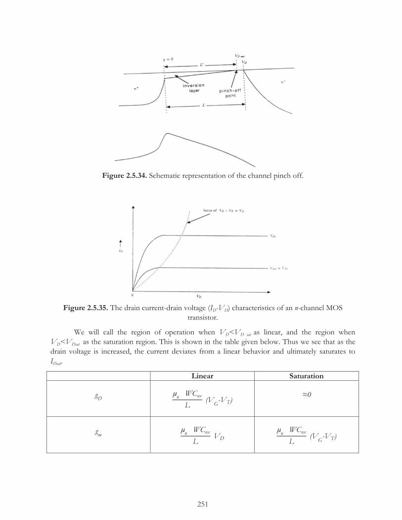
251
Figure 2.5.34. Schematic representation of the channel pinch off.
Figure 2.5.35. The drain current-drain voltage (ID-VD) characteristics of an n-channel MOS transistor.
We will call the region of operation when VD<VD sat as linear, and the region when VD<VDsat as the saturation region. This is shown in the table given below. Thus we see that as the drain voltage is increased, the current deviates from a linear behavior and ultimately saturates to IDsat.
Linear Saturation
gD
μn WCox
L (V
G-VT)
≈0
gm
μn WCox
L VD
μn WCox
L (V
G-VT)

252
Case 3. Large VD (A More Exact Treatment)
The assumption made in Case 2 that the threshold voltage at any point y in the channel increases from its value at the source by the amount V(y) presupposes that the depletion region width does not change with the voltage drop V(y). In other words, it is implicit in this assumption that the depletion region width is the same from the source to the drain independent of V(y) This is not correct. If we refer to Figure 2.5.36 we will notice that due to the voltage drop V(y) the Fermi level at point y is decreased from the Fermi level in the bulk by an amount equal to qV(y) and therefore the band has to be bent by q (V y + 2 b ) to produce the onset of inversion. Hence, the condition for the inversion to set in at y is dictated by V(y). The band bending for the onset of inversion at y is given by
ψs inv y = V y + 2 b (2.5.131)
Under this condition, the depletion region width at y is given by
xd y = 2 ϵsq NA
V y + 2 b (2.5.132)
And the depletion charge density at y is given by
Qd y = -q NA xdy =- q NA2 ϵ
sV y + 2 b (2.5.133)
If we were to write the expression for gate voltage in terms of the space charge density and ψs we get
VG=Vox+ ψs y = - Qsc y
Cox +ψs y (2.5.134)
Figure 2.5.36. Band bending at y when the voltage drop is V(y).
We will now use the depletion approximation, according to which the band bending in strong inversion is the same as the band bending at the onset of inversion. That is, the surface potential continues to remain at
ψs y =V y + 2 b (2.5.135)

253
even in strong inversion. Using the above two equations, we find that the total space charge density is given by
Qsc y = - Cox VG- ψs y =- Cox VG- V y - 2 b (2.5.136)
The inversion charge density is the difference between the total space charge density and the depletion charge density. Hence, the inversion charge density is given by
Qn y = Qsc y -Qd y
=- Cox VG- V y - 2 b - q NA2 ϵ
s
Cox V y + 2 b
12
If we substitute this in the expression for the drain current which is
ID= μn W Qn(y) dVdy
and then integrate after multiplying both sides by dyL, we obtain
ID=- μn Cox W
L VG- VD
2- 2 b VD- 2
3
q NA2 ϵs
Cox VD + 2 b
32- 2 b
32 (2.5.137)
We could have arrived at the same result by determining the local threshold voltage VT(y) as
VT y =q NA2 ϵ
s V y + 2 b
Cox +V y + 2 b (2.5.138)
and obtaining the inversion charge density as
Qn y =- Cox VG-VT y (2.5.139)
This expression for the drain current is valid as long as the channel is not pinched off due to a high drain voltage. The channel is pinched off at y=L if the gate voltage is equal to the threshold voltage at y=L. VD sat therefore can be obtain from Equation 2.5.138 by putting VT (y=L) as VG and V(y=L) as VD sat. Hence solving for VD sat (left as an exercise), we get
VD sat= VD - K2
2
4VGK2+1-1 -2 b (2.5.140)
where K = 2ϵsqNACox
(2.5.141)
K is called the body factor, and is also sometimes denoted γ.
The expression for the drain current, ID, given in Equation 2.5.137 is valid in strong inversion regions (VG>VT). This expression is modified in the presence of a substrate bias voltage.

254
If a reverse bias voltage VSB is applied between the source and the body, then the amount of band bending needed at the source (y=0) for the onset of inversion is
ψs y=0 =VSB + 2 b (2.5.142)
The band bending required at the onset of inversion at some point y in the channel is therefore equal to
ψs y =VSB +V y + 2 b (2.5.143)
The expression for the drain current in the presence of a substrate bias is modified such that 2 b is replaced by VSB +2 b and is therefore given by
ID=-μn Cox W
L VG- VDS
2-VSB- 2 b VDS - 2
3 γ VDS +VSB + 2 b
32- VSB + 2 b
32 (2.5.144)
where VDS is the drain to source voltage, VG is measured with respect to the substrate, and γ is equal to K given in Equation 2.5.141.
Measurement of VT
The threshold voltage, can be obtained by measuring the drain current as a function of gate voltage for a small value of drain voltage. When the drain current is plotted as a function of VG, the characteristics shown in Figure 2.5.37 are obtained. If we now extrapolate the linear portion to intercept the voltage axis, the intercept on the voltage axis is the threshold voltage.
We note that ID does not go to zero when the gate voltage, VG is equal to VT. This is because the inversion charge density does not actually go to zero at this voltage. In fact, a small drain current flows through the device even when the gate voltage is less than the threshold voltage under weak inversion conditions. This region of operation is called the subthreshold region. The calculation of the drain current in the subthreshold region is beyond the scope of this book. Hence we will assume that the drain current is zero at VG=VT.
Equivalent Circuit
We can draw the equivalent circuit for the MOS transistor. This is illustrated in Figure 2.5.38. The input voltage is applied between the gate and the source, and the output current is taken between the drain and the source. Cin and Gin are the capacitance and the conductance that the input voltage source looks into. In our case, Cin is given by
Cin= d QGd VG
≈W L Cox (2.5.145)
The value of Cin is obtained in strong inversion. The input conductance, Gin, is essentially due to leakage current in the oxide. The feedback capacitance between the drain and the gate, Cfb, is the sum of the gate overlap capacitance and the fringing field capacitance. The overlap capacitance

255
arises because the gate electrode extends beyond the length of the channel over the source and the drain region. This fringing field capacitance arises due to edge effects. The output conductance gD is given by
gD = δ IDδ VD
(2.5.146)
The transconductance, gm, is given by
gm = δ IDδ VG
The output capacitance is the capacitance between the drain and the source region, which is essentially equal to the capacitances of the source-to-substrate p-n junction and the drain substrate p-n junction.
We can now calculate the maximum frequency up to which the MOS transistor can be used. The constant current source in the output circuit is equal to gm vg This constant current source therefore, is directly related to the voltage across the conductance, Gin, that is in other words, the current through the conductance Gin Therefore as the frequency is increased, the input current flows more and more through the input capacitance Cin, and less through the conductance Gin We can now calculate the gain of the device at any given frequency, just as we did for the bipolar transistor in the last chapter. The maximum frequency is defined as when the current through the input capacitance, Cin is equal to gm VG . The current through Cin is given by vgjω Cin.
Equating this to gm vg we get
ωmax= gm Cin
(2.5.147)
This now leads to the maximum frequency as equal to
fmax
= gm
2 π Cin (2.5.148)
The ratio gm Cin
is called the figure of merit. In the linear region, we saw that the transconductance, gm,
is given by
gm = μn Cox W
L VD
and Cin =W L Cox
Substituting these two values to calculate the figure of merit, we find the maximum frequency fmax to be
fmax
= 12 π
μnVDL2
(2.5.149)

256
Assuming VD is very small because we are considering the linear region, VD
L is approximately the
electric field, and multiplying it by μn gives us the velocity, and therefore, the maximum frequency fmax is rewritten as
fmax
= v
2 π L= 1
2 π τtr (2.5.150)
where v is the velocity of the carriers in the channel, and vL
is the reciprocal of the transit time τtr. We find that the maximum frequency at which the device can be operated is related to the time of transit of carriers from the source to the drain. The intrinsic limit on the maximum frequency of operation is imposed by the transit time of the carriers. This is true not only in MOS transistors and bipolar transistors but also in all other devices.
Figure 2.5.37. Plot of the drain current as a function of the gate voltage to obtain the threshold voltage.
Figure 2.5.38. Equivalent circuit for the MOS transistor.

257
Chapter 2.5 Summary
An MOS device uses the electric field applied perpendicular to the surface of a semiconductor to induce space charge in the semiconductor. The MOS structure consists of a semiconductor substrate on the surface of which a thin oxide layer is grown. A conducting layer (metal), deposited on top of the oxide, is called the gate and a voltage applied on the gate generates the electric field perpendicular to the semiconductor surface (also called the interface.)
The space charge induced by the voltage on the gate bends the bands in the semiconductor up or down towards the interface according to whether the gate voltage is negative or positive, respectively.
When the induced charge is of the same polarity as that of the majority carriers in the substrate (bulk), excess majority carriers accumulate at the interface. The surface is said to be accumulated and the device is in the accumulation region of operation. The space charge is due to the excess majority carriers.
When the induced charge is of a polarity opposite to that of the majority carriers in the semiconductor, the induced space charge is initially due to ionized impurity atoms in the substrate and the surface is said to be depleted. The device is said to be in the depletion region of operation. For larger values of gate voltage, the minority carrier density at the interface becomes comparable to or larger than the majority carrier density in the bulk. Under these conditions, the surface is said to be inverted. The charge due to the excess minority carriers is called the inversion charge and the layer of excess minority carriers is called the inversion layer. The inversion layer is very thin so the inversion charge can be considered as a sheet charge. The space charge is due to both depletion charge and inversion charge.
The space charge density, which is defined as the charge contained in the space charge under unit area of the interface, determines the electric field in the oxide and hence the potential difference across the oxide.
The potential difference across the space charge region is the amount of band bending in the space charge region and is called the surface potential. The surface potential determines whether the substrate is accumulated, depleted or inverted.
The charge in the accumulation layer or in the inversion layer is approximated as a sheet charge and hence the potential difference across these layers is taken as negligible. On the other hand, the depletion region is of non-zero width. The width of the space charge region is therefore approximated as the width of the depletion region.

258
Inversion sets in when the bending of the band is such that the difference between the
Fermi energy and the intrinsic Fermi energy at the interface is the same in magnitude as the difference between these two energies in the bulk but of opposite polarity. This condition is called “on-set of inversion”. The gate voltage at which the surface starts to be inverted (on-set of inversion) is called the threshold voltage.
According to the depletion approximation, the depletion region width remains constant in strong inversion at a value it had at the on-set of inversion. The width of the depletion region remains at a maximum value xd max under inversion condition.
An ideal MOS device is one in which there is no space charge in the semiconductor when the gate voltage is zero. A voltage is required to be applied on the gate to induce a space charge.
A non-ideal MOS device is one in which there is a space charge even when there is no applied voltage on the gate, Charge in the gate oxide, interface states and work function difference between the gate and the substrate give rise to non-ideal behavior.
The flat band voltage is the voltage needed to be applied on the gate to reduce the space charge to zero so that the device with a voltage on the gate equal to the flat –band voltage looks like an ideal device with zero gate voltage.
The space charge induced by the oxide charge and the work function difference is independent of band-bending while that due to the interface states depends on band bending.
Interface states can be acceptor type or donor type. It is conventional to assume that the interface states in the upper half of the band gap are acceptor type while those in the lower half are donor type.
The space charge region gives rise to small signal capacitance effect. This capacitance is called space charge capacitance and is equal to the rate of increase of space charge with surface potential.
Since the inversion and accumulation charge increases exponentially with surface potential, the space charge capacitance of accumulation and inversion charges is much larger than the capacitance due to the oxide layer. The capacitance due to the oxide layer called the oxide capacitance is the same as a parallel plate capacitor with the gate oxide as the dielectric. The

259
MOS capacitor behaves as a series combination of the oxide capacitance and the space charge capacitance.
Due to the dependence of the space charge capacitance on the surface potential which in turn depends on the gate voltage, the capacitance of a MOS capacitor varies with the gate voltage. The capacitance-voltage characteristic is called the C-V curve.
In accumulation, the MOS capacitance is equal to the oxide capacitance itself since the space charge capacitance is very much larger.
As the device is biased into depletion, the space charge capacitance (equal to the depletion
region capacitance ≈ ϵsxd
decreases (due to the increase in depletion region width) and hence
the capacitance of the MOS device decreases.
At strong inversion, the capacitance behavior is different at high and low frequencies of the measuring small signal. At high frequencies, the inversion charge does not vary in step with the small measuring signal and hence the space charge capacitance remains at a minimum
value ≈ ϵsxd max
and the MOS capacitance remains constant at a minimum value.
At low frequencies, the inversion charge has time to be generated thermally so that it can
vary in step with the measuring signal. The space charge capacitance is determined by the variation with time of the inversion charge and is therefore very large. The MOS capacitance in strong inversion becomes equal to the oxide capacitance as in the accumulation case.
In the MOS transistor, the conductance between two heavily doped regions in the substrate (called the source and the drain) is controlled by the surface inversion of the region between the source and the drain.
In the simplest model, the drain voltage is assumed to be small and the inversion charge density is assumed to be constant between the source and the drain.
If the inversion charge is due to electrons providing a conductance between the n+ source and drain, the device is called an n-channel MOS transistor.
If the source and drain are heavily doped p regions and the inversion charge is due to holes, the device is called a p-channel MOS transistor.

260
When the drain voltage is high, the inversion charge density decreases towards the drain due to the voltage drop along the channel. This is equivalent to the local threshold voltage increasing from its lowest value near the source to its highest value near the drain.
In one approximate model, the local threshold voltage at some point y in the channel is taken as sum of the voltage drop at y measured with respect to the source and the threshold voltage at the source.
In a more exact model, the band bending required to attain inversion at some point y in the channel is taken as the sum of voltage drop at y and the band bending needed at the source to produce inversion.
As the drain voltage is increased, the inversion charge density at the drain decreases and becomes ultimately zero. The channel is said to be pinched off at the drain. When the drain voltage is increased further, the pinch off point moves toward the source and the drain current increases very slowly with the drain voltage as though the current has saturated. Hence the transistor is said to be operating in the saturation region.

261
Chapter 2.5 Glossary
Å Angstroms
C an integration constant
C capacitance per unit area of the MOS capacitor
Cd depletion layer capacitance
Cfb feedback capacitance between the drain and the gate
Cin input capacitance
Cm measured capacitance
Cmin minimum capacitance in the high frequency C-V curve
Cox oxide layer capacitance per unit area
Csc space charge capacitance per unit area
e.s. electrostatic potential
Ec energy at the bottom of the conduction band (also potential energy of electrons)
EF Fermi energy
EF1 Fermi level in a p-type semiconductor
Eg energy gap
Ei intrinsic Fermi energy
Eib intrinsic Fermi energy level in the bulk
Evac vacuum level
EV energy at the top of the valence band (also potential energy of holes)
ε electric field
εox electric field in the oxide
ε(x) electric field at
fmax maximum frequency
gD drain conductance or output conductance
gm transconductance
Gin input conductance
i small signal current
ID drain current
IDSAT drain current at saturation
J current density

262
K Boltzmann constant
K body factor, also ϒ
Kox dielectric constant of the oxide
L length of the channel
L’ distance of the pinch-off point from the source
n electron density
n0 thermal equilibrium electron density
nb electron density in the bulk
ni intrinsic carrier density
nn0 thermal equilibrium electron density in n-type material
ns electron concentration at the interface or surface
n(x) electron density at x
NA acceptor impurity density
NA- ionized acceptor impurity density
ND donor impurity density
ND+ ionized donor impurity density
Nit number of interface states per unit area per unit energy interval at some energy level E
p hole density
p0 thermal equilibrium hole density
pb hole density in the bulk
ps hole concentration at the interface or surface
p(x) hole density at x
q electron charge (magnitude)
qϕ work function of the solid
qϕA work function of solid A
qϕB work function of solid A
Q sinusoidally varying small signal charge
Qacc space charge density in accumulation
Qd depletion charge density
Qd max maximum depletion charge density
Qg charge on the gate

263
Qinv inversion charge density
Qn electron density at the surface or interface
Qox effective sheet charge density
Qp hole density in the surface or interface
Qsc space charge density
Qst sheet charge density at the interface or surface
t time
tox thickness of the oxide layer
v velocity of the carriers in the channel
v small signal sinusoidal voltage
vg small signal sinusoidal gate voltage
Vbi built-in voltage, contact potential
VD drain voltage
VDSAT saturation drain voltage
VDS drain to source voltage
VFB flat-band voltage
p0 thermal equilibrium density of holes
Vg gate voltage
Vox voltage across the oxide layer
Vp pinch-off voltage
VSB reverse substrate bias voltage
VT threshold voltage
VT ideal threshold voltage of an ideal MOS device
VT non-idealthreshold voltage of a non-ideal MOS device
V(y) voltage at y
W width of the channel
x position value
xd width of the space charge or depletion region
xd max depletion region width at the on-set of strong inversion
xI thickness of the inversion layer of electrons
y position value
Δψs change in surface potential
264
ϵ0 permittivity of free space
ϵox permittivity of the oxide
ϵs permittivity of the semiconductor
ϒ body factor, same as K
ϕ electrostatic potential
ϕb bulk potential
ϕn bulk electrostatic potential of the n-region
ϕp bulk electrostatic potential of a p-type semiconductor
ϕ(x) electrostatic potential at x
ϕ work function
ϕ1 work function of a p-type semiconductor
ϕ2 work function of an n-type semiconductor
ΦAB contact potential
ΦM work function of the gate
ΦMS work function difference between the gate and the substrate
ΦS work function of the substrate semiconductor
ρ charge density
τg minority carrier generation lifetime
τtr transit time
ψ electrostatic potential difference
ψs surface potential or interface potential
ψinv band bending at the onset of inversion or surface potential at onset of inversion
ψ(x) electrostatic potential difference at x (i.e., ϕ(x)-ϕb)
χ electron affinity
ω 2π times the frequency of the small signal voltage v
ωmax 2π times the maximum frequency
265
Chapter 2.5 Problems
1. Show that ns=ni when ψs=- b for a MOS device with a p-type substrate.
2. For an ideal MOS diode (capacitor) with tox=500 Å and NA=1015 cm-3, find the value of the surface potential ψs and the voltage across the oxide layer required to produce (a) Intrinsic condition at the interface (b) On-set of strong inversion at the interface
3. In a MOS capacitor with a p-type substrate determine the space charge density for a gate voltage of 0.75V assuming the oxide layer thickness to be 1000 Å and the substrate impurity concentration to be 5×1015cm-3.
4. Consider a MOS capacitor with a substrate doping of 2×1015cm-3 of donor atoms and an oxide thickness of 600 Å, determine the gate voltage at which the surface becomes intrinsic.
5. For the device in the previous problem, find the value of the space charge density at a gate voltage equal to (a) The threshold voltage (b) Twice the threshold voltage
6. For the device in the previous problem, find the inversion charge density and the depletion region charge density when the gate voltage is three times the threshold voltage.
7. For the device in the previous problem, find the high and low frequency capacitance at a gate voltage of -4V. Assume an area of 10-4 cm2 for the capacitor.
8. Show that the potential ψ(x) in the depletion region of a MOS capacitor varies as
ψ(x)=ψs1- xxd
2.
9. Show that in deep depletion, the relation between the gate voltage and the surface potential ψs is given by
VG=K2
24VGK2
+1-1 +ψs
Where K is defined as
K= 2ϵsqNACox
10. Consider a MOS device in which the oxide layer contains positive ions with a density of 1016 cm-3. If the oxide thickness is 400Å calculate the flat-band voltage VFB.
266
11. Assume the gate is p-type poly-silicon with an impurity concentration of 1017 cm-3 and the substrate to be n-type with a resistivity equal to 5 Ω-cm. Assuming the electron affinity of silicon to be 4.1V, determine the flat-band voltage.
12. Consider a MOS capacitor with a p-type substrate and an oxide thickness of 500 Å. Let the substrate impurity density be 5 ×1015cm-3. Assume the device is ideal.
13. Calculate the high frequency and low frequency capacitances in strong inversion.
14. Assuming that a step voltage of 5V is applied on the gate at t=0. Calculate the small signal capacitance at t=0+.
15. Consider a MOS transistor with a p-type substrate containing 1015 cm-3 acceptor impurities and an oxide thickness of 500 Å. The flat-band voltage is 0.5V. Determine the drain conductance for a gate voltage of 5V in the linear region. Take the mobility μn as 900 cm2V-
1s-1, W as 20 μm and L as 10μm.
16. For the device in the previous problem, determine the transconductance in the saturation region.
17. Consider an n-channel MOS transistor with tox=150Å. The substrate impurity concentration is 1016 cm-3. Let the channel length, L, be 2μm, the channel width, W to be 20 μm and the mobility of the channel carriers be 750 cm2V-1s-1.
18. What is the value of the transconductance for a drain voltage of 20mV?
19. Assume that the oxide has positive ions of density equal to 1017 cm-3 . Assume that the gate is p-type poly-silicon with an impurity density of 1017 cm-3. Neglect the contribution of surface states to the flat-band voltage. Using the simplified treatment given in Case 2, determine the saturation drain voltage, VDSAT, for a gate voltage 5V.