
AWG and EDFA based optical packet switch using feedback shared loop buffer memory
13
Opt Quant Electron (2007) 39:1153–1165 DOI 10.1007/s11082-007-9147-8 AWG and EDFA based optical packet switch using feedback shared loop buffer memory Rajat Kumar Singh · Rajiv Srivastava · Yatindra Nath Singh Received: 26 March 2007 / Accepted: 13 November 2007 / Published online: 13 December 2007 © Springer Science+Business Media, LLC. 2007 Abstract Optical packet switching provides high speed, data rate/format transparency, efficient use of bandwidth and flexibility. The major problem in the implementation of “all- optical” switching is contention which occurs when two or more packets arrive at the same time for the same destination. To resolve the contention, we have proposed an optical packet switch architecture based on WDM loop buffer memory in the feedback configuration. In that architecture, the contending packets are stored in a loop buffer module, and routed in the free time slots. The buffering duration in the recirculating loop is limited by a circulation limit. The analysis was been done to obtain the maximum number of allowed circulations. This paper proposes improved version of that optical packet switch architecture, to increase the number of maximum allowed circulations. The modification is done either by adding an extra erbium doped fiber amplifier (EDFA) in the original switch or by replacing the core space switch with arrayed waveguide grating (AWG). The performance analysis has been done by the simulations. Keywords Optical buffering · Loop buffer memory · Optical packet switch 1 Introduction All-optical switching is an important and valuable technique for the success of next generation optical networks. Several all-optical switching architectures have been proposed, to utilize the large capacity of optical fiber (Tucker and Zhong 1999; Dittmann et al. 2003; Singh and Singh 2006). Currently all-optical packet switching is hybrid in nature where the header is processed electronically at the node, while the payload remains in optical form R. K. Singh (B ) Indian Institute of Information Technology Allahabad, Deoghat-Jhalwa, Allahabad, 211012 UP, India e-mail: [email protected]; [email protected] R. Srivastava · Y. N. Singh Department of Electrical Engineering, Indian Institute of Technology, Kanpur 208016, India 123
Transcript of AWG and EDFA based optical packet switch using feedback shared loop buffer memory
Opt Quant Electron (2007) 39:1153–1165DOI 10.1007/s11082-007-9147-8
AWG and EDFA based optical packet switchusing feedback shared loop buffer memory
Rajat Kumar Singh · Rajiv Srivastava ·Yatindra Nath Singh
Received: 26 March 2007 / Accepted: 13 November 2007 / Published online: 13 December 2007© Springer Science+Business Media, LLC. 2007
Abstract Optical packet switching provides high speed, data rate/format transparency,efficient use of bandwidth and flexibility. The major problem in the implementation of “all-optical” switching is contention which occurs when two or more packets arrive at the sametime for the same destination. To resolve the contention, we have proposed an optical packetswitch architecture based on WDM loop buffer memory in the feedback configuration. Inthat architecture, the contending packets are stored in a loop buffer module, and routed inthe free time slots. The buffering duration in the recirculating loop is limited by a circulationlimit. The analysis was been done to obtain the maximum number of allowed circulations.This paper proposes improved version of that optical packet switch architecture, to increasethe number of maximum allowed circulations. The modification is done either by adding anextra erbium doped fiber amplifier (EDFA) in the original switch or by replacing the corespace switch with arrayed waveguide grating (AWG). The performance analysis has beendone by the simulations.
Keywords Optical buffering · Loop buffer memory · Optical packet switch
1 Introduction
All-optical switching is an important and valuable technique for the success of nextgeneration optical networks. Several all-optical switching architectures have been proposed,to utilize the large capacity of optical fiber (Tucker and Zhong 1999; Dittmann et al. 2003;Singh and Singh 2006). Currently all-optical packet switching is hybrid in nature where theheader is processed electronically at the node, while the payload remains in optical form
R. K. Singh (B)Indian Institute of Information Technology Allahabad, Deoghat-Jhalwa, Allahabad, 211012 UP, Indiae-mail: [email protected]; [email protected]
R. Srivastava · Y. N. SinghDepartment of Electrical Engineering, Indian Institute of Technology, Kanpur 208016, India
123
1154 R. K. Singh et al.
throughout the switch. The header information is used to route the packet. Wavelength divi-sion multiplexing (WDM) technology can be incorporated (Danielsen et al. 1997) to improvethe performance.
Contention resolution is one of the critical issues for optical packet switching, and needto be resolved for successful routing of the packet. The contention occurs when two or morepackets arrive in the same time slot for same destination, and to resolve it, one packet isdirected to the destination and the other packets have to be stored. Till now, all-optical mem-ory suitable for photonic packet switching has not yet been developed. Also, it is not possibleto store the light similar to electronics where the data is stored/retrieved in/from memorychips. The other available options for the contention resolution are wavelength conversion(Danielsen et al. 1997), deflection routing (Chlamtac and Fumagalli 1993) and optical fiberdelay lines (Hunter et al. 1998), where the packets are delayed till the destination is not free.The optical fiber delay lines are more popular and suitable, and are used in the traveling(Haas 1993; Singh and Singh 2005) and recirculating (Verma et al. 2002; Shukla et al. 2004)configurations. The recirculating buffers require optical components such as optical gateswitches, optical couplers, optical amplifiers, and wavelength converters to realize photonicbuffering (Verma et al. 2002; Shukla et al. 2004). The optical buffers are better than theelectronic memories because, the data path is: (i) all-optical i.e., O/E and E/O conversion notrequired, (ii) having larger bandwidth, (iii) data rate transparent and (iv) WDM applicable.In the literatures, several architectures are proposed on the basis of the optical bufferingtechnique and buffering capacity (Singh et al. 2006; Srivastava et al. 2006; Yao et al. 2000;Chia et al. 2001; Fow-Sen Choa et al. 2005; Papadimitriou et al. 2003), and the research iscontinued to provide an optimal solution for optical buffering.
In this paper, we are proposing a modification in the optical packet switch architecture(Singh et al. 2007), which uses multiple loop buffer modules in the feedback sharing config-uration. In Singh et al. (2007), WDM based fiber delay lines are used to store the contendingpackets and a space switch is used to direct them appropriately. The main disadvantage of thearchitecture is that the loss in signal power is very high, and it reduces the number of maxi-mum allowed circulations by the data in loop buffer modules. Thus, to reduce this power loss,we are proposing two modifications: (i) either an extra optical amplifier (EDFA) is placedat the output of the loop in the buffer module, or (ii) the core space switch is replaced byan AWG. The main objective of these modifications is to increase the number of maximumallowed circulations. This will provide a relaxation in the circulation limit, which in turnresults in the better packet loss probability and the average delay by effectively utilizing theavailable buffer capacity. Hence, this paper can be assumed as an extended and improvedversion of Singh et al. (2007).
The remaining paper is organized as follows. Brief discussion about the original switcharchitecture is given in Sect. 2 and the proposed modification is discussed in Sect. 3. Thepower budget analysis for loss, power and noise is presented in Sect. 4. The schedulingalgorithm is explained in Sect. 5 and the simulation analysis and results are given in Sect. 6.Finally, Sect. 7 concludes the work.
2 Feedback optical packet switch architectures: an overview
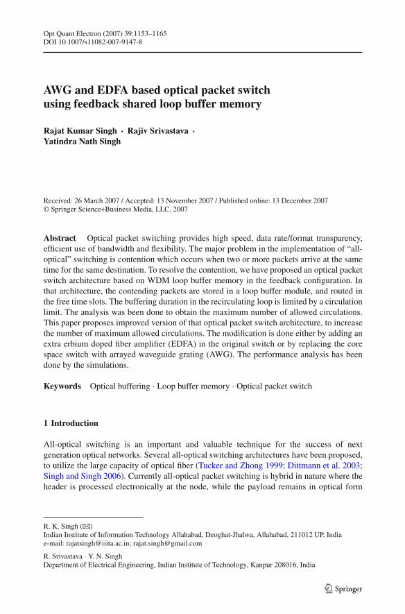
The architecture proposed in Singh et al. (2007) for optical packet switching, is shown inFig. 1. The core of this architecture is a nonblocking space switch of dimension 2N × 2N .The lower N ports (indexed 1 to N ) are used as switch inputs/outputs and the upper Nports (indexed N + 1 to 2N ) are used for retrieving/storing the packets from/into the optical
123
AWG and EDFA based optical packet switch using feedback shared loop buffer memory 1155
Fig. 1 Optical packet switch architecture: modules (1 to m) represent loop buffer modules
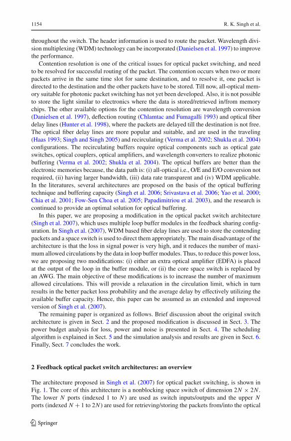
Fig. 2 Loop buffer module
loop buffer modules (Fig. 2). Under this condition, the maximum numbers of allowed buffermodules are m = �N/D�, where D is the number of input/output at each loop buffer mod-ule. If the switch is optimized for M modules (M ≤ m), then the rest of upper half ports(i.e., N − MD) will be left free and the space switch fabric of size (N + MD) × (N + MD)
will be used. The length of delay line as well as the slot duration has been assumed of onepacket length. Newly arriving packets and already stored packets may also contend for thesame output. In such case, one of the contending packets is directed to the output port andremaining packets are kept in buffer according to the scheduling algorithm given in Sect. 5.When the contending packets can neither be directed to the assigned output port nor storedin buffer, it is dropped and assumed to be lost.
The loop buffer module (Fig. 2) consists of D tunable wavelength converters (TWC)-oneat each input, a recirculating loop, and D fixed filters (FF)-one at each output (Verma et al.2002; Shukla et al. 2004). The path across the recirculating loop consists of 3 dB coupler,DEMUX, TWC, combiner, erbium-doped fiber amplifier (EDFA), isolator and again thesame 3 dB coupler. EDFA is placed inside the loop to compensate the power loss through it,during circulations. WDM technology is used to share the capacity of loop buffer. Each buffer
123
1156 R. K. Singh et al.
module uses (B + D) wavelengths where B is the number of buffer wavelengths used to storethe packets in buffer modules, and D is the number of wavelengths used for reading out thepackets from the buffer modules. The number of TWCs and the size of DEMUX/Combinerinside the loop, depend upon the desired buffer capacity, and are considered equal to B.Thus, the total number of TWCs and FF used in the buffer module will be (B + D) and Drespectively.
The number of buffer wavelengths (B) inside the memory module, depends on the switchdesign, desired traffic throughput, packet loss probability and size of the switch (Shun et al.2003). The wavelength allocation of the packets for the loop buffer depends on the routingand priority algorithm for the switch. The packets to be buffered are converted to the wave-lengths available in the buffer; if buffer is full then packets are dropped. When a packet isforwarded for buffering, the respective TWC at the input of the available buffer module istuned to any one of the B loop buffer wavelengths, which is free to accept the packet. Aslong as a packet remains in the buffer, the TWC inside that module, corresponding to thewavelength assigned to this packet, will remain transparent till it is desired to read out thepacket or to have dynamic wavelength re-allocation. For reading out a packet when outputcontention is resolved, the corresponding TWC is tuned to the wavelength of appropriateoutput port fixed filters (FF). The packet is then broadcasted towards FFs and received by theintended one. Then, these packets will be directed to the destined output ports through thespace switch fabric. The buffer wavelengths are automatically cleared (become free), oncethe buffered packets are delivered to the intended output port.
We have assumed that the controlling is done electronically, which tunes various com-ponents of the loop buffer as well as controls the whole switch (Fow-Sen Choa et al. 2005;Singh et al. 2007). The tuning speed of TWCs and the switching speed of space switch donot put any constraint on the switching operation.
3 Modified optical packet switch architectures
We will use the word ‘original’ in this paper, to refer to the switch proposed by us in Singhet al. (2007). The number of maximum allowed circulations (C) in that switch is limitedby the loss in signal power, due to the presence of various optical components (Fig. 2).The proposed modifications are intended towards the increment of C . The modified switcharchitectures are discussed below.
3.1 Placement of an optical amplifier (EDFA)
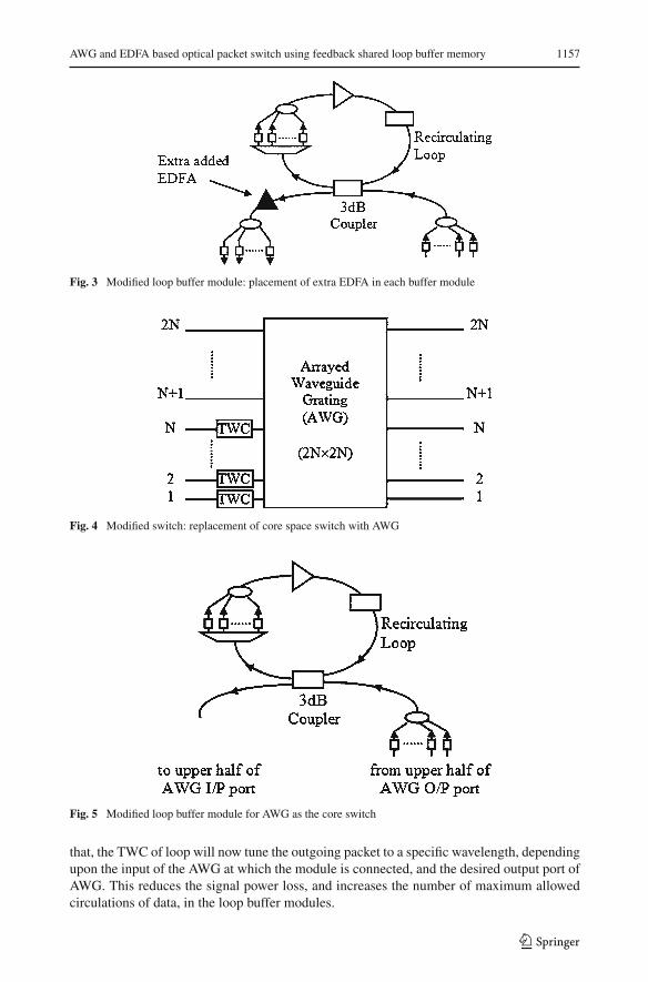
We are placing an extra amplifier (EDFA) at the output of recirculating loop, just after the3 dB coupler, in each buffer modules (Fig. 3). This EDFA is followed by the splitter, FF andspace switch. The gain of this EDFA is chosen such that it will compensate the loss throughthese three components. Effectively, it will allow the packets to circulate for some moreduration as compared to the original switch. The control complexity will remain same whilethe packet loss probability will decrease. We will refer to this modification as Mod-EDFA,in rest of this paper.
3.2 Replacement of space switch with AWG as the core switch
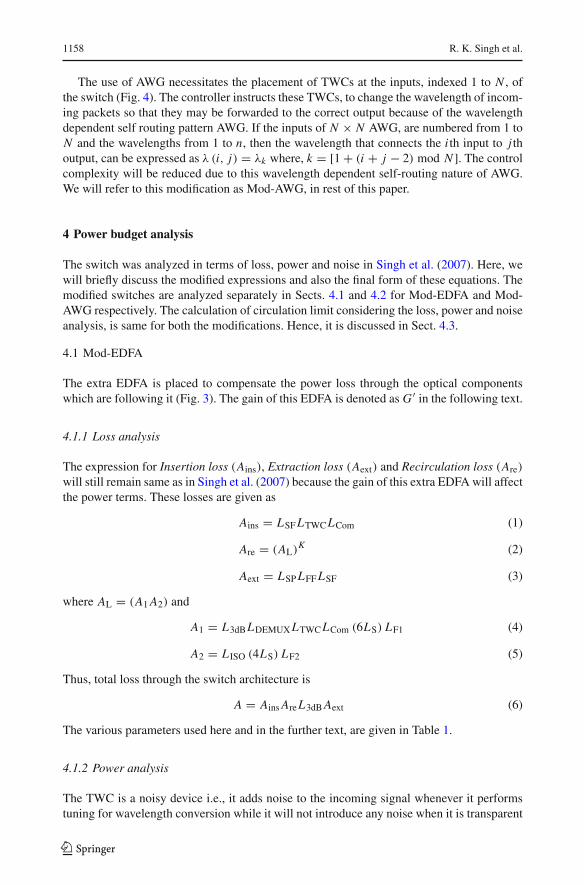
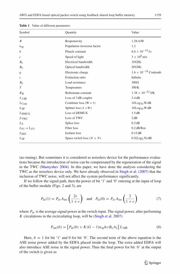
The core of space switch is replaced by an arrayed waveguide grating (AWG) (Fig. 4). Themain advantage of AWG is that it will avoid the need of Splitter and the Fixed Filter at theoutput of loop buffer module (Fig. 5). The only change in the working of the switch will be
123
AWG and EDFA based optical packet switch using feedback shared loop buffer memory 1157
Fig. 3 Modified loop buffer module: placement of extra EDFA in each buffer module
Fig. 4 Modified switch: replacement of core space switch with AWG
Fig. 5 Modified loop buffer module for AWG as the core switch
that, the TWC of loop will now tune the outgoing packet to a specific wavelength, dependingupon the input of the AWG at which the module is connected, and the desired output port ofAWG. This reduces the signal power loss, and increases the number of maximum allowedcirculations of data, in the loop buffer modules.
123
1158 R. K. Singh et al.
The use of AWG necessitates the placement of TWCs at the inputs, indexed 1 to N , ofthe switch (Fig. 4). The controller instructs these TWCs, to change the wavelength of incom-ing packets so that they may be forwarded to the correct output because of the wavelengthdependent self routing pattern AWG. If the inputs of N × N AWG, are numbered from 1 toN and the wavelengths from 1 to n, then the wavelength that connects the i th input to j thoutput, can be expressed as λ (i, j) = λk where, k = [1 + (i + j − 2) mod N ]. The controlcomplexity will be reduced due to this wavelength dependent self-routing nature of AWG.We will refer to this modification as Mod-AWG, in rest of this paper.
4 Power budget analysis
The switch was analyzed in terms of loss, power and noise in Singh et al. (2007). Here, wewill briefly discuss the modified expressions and also the final form of these equations. Themodified switches are analyzed separately in Sects. 4.1 and 4.2 for Mod-EDFA and Mod-AWG respectively. The calculation of circulation limit considering the loss, power and noiseanalysis, is same for both the modifications. Hence, it is discussed in Sect. 4.3.
4.1 Mod-EDFA
The extra EDFA is placed to compensate the power loss through the optical componentswhich are following it (Fig. 3). The gain of this EDFA is denoted as G ′ in the following text.
4.1.1 Loss analysis
The expression for Insertion loss (Ains), Extraction loss (Aext) and Recirculation loss (Are)
will still remain same as in Singh et al. (2007) because the gain of this extra EDFA will affectthe power terms. These losses are given as
Ains = LSF LTWCLCom (1)
Are = (AL)K (2)
Aext = LSP LFF LSF (3)
where AL = (A1 A2) and
A1 = L3dBLDEMUX LTWCLCom (6LS) LF1 (4)
A2 = L ISO (4LS) LF2 (5)
Thus, total loss through the switch architecture is
A = Ains Are L3dB Aext (6)
The various parameters used here and in the further text, are given in Table 1.
4.1.2 Power analysis
The TWC is a noisy device i.e., it adds noise to the incoming signal whenever it performstuning for wavelength conversion while it will not introduce any noise when it is transparent
123
AWG and EDFA based optical packet switch using feedback shared loop buffer memory 1159
Table 1 Value of different parameters
Symbol Quantity Value
R Responsivity 1.28 A/W
nsp Population inversion factor 1.2
h Planck constant 6.6 × 10⁻³⁴ J s
c Speed of light 3 × 10⁸ m/s
Be Electrical bandwidth 10 GHz
Bo Optical bandwidth 20 GHz
q Electronic charge 1.6 × 10⁻¹⁹ Coulomb
ε Extinction ratio Infinite
RL Load resistance 300�
T Temperature 300 K
KB Boltzmann constant 1.38 × 10⁻²³ J/K
L3 dB Loss of 3 dB coupler 3.4 dB
LCom Combiner loss (W×1) 10 Log10 W dB
LSP Splitter loss (1×W ) 10 Log10 W dB
LDMUX Loss of DEMUX 1.5 dB
LTWC Loss of TWC 2 dB
LS Splice loss 0.2 dB
LF1 = LF2 Fiber loss 0.2 dB/Km
LISO Isolator loss 0.15 dB
LSF Space switch loss (N × N ) 0.5(Log2 N) dB
(no tuning). But sometimes it is considered as noiseless device for the performance evalua-tions because the introduction of noise can be compensated by the regeneration of the signalin the TWC (Mamyshev 2004). In this paper, we have done the analysis considering theTWC as the noiseless device only. We have already observed in Singh et al. (2007) that theinclusion of TWC noise, will not affect the system performance significantly.
If we follow the signal path, then the power of bit ‘1’ and ‘0’ entering at the input of loopof the buffer module (Figs. 2 and 3), are
Pin(1) = Pav Ains
(2ε
1 + ε
)and Pin(0) = Pav Ains
(2
1 + ε
)(7)
where Pav is the average signal power at the switch input. The signal power, after performingK circulations in the recirculating loop, will be (Singh et al. 2007)
Pout(b) = [Pin(b) + K (G − 1)nsphυBo A2
]L3dB (8)
Here, b = 1 for bit ‘1’ and 0 for bit ‘0’. The second term of the above equation is theASE noise power added by the EDFA placed inside the loop. The extra added EDFA willalso introduce ASE noise in the signal power. Thus the final power for bit ‘b’ at the outputof the switch is given as
123
1160 R. K. Singh et al.
P(b) = Pout(b)AextG′ + (
G ′ − 1)
nsphνBo (9)
Since the gain (G ′) is considered equal to 1/Aext, in order to cancel the effect of opticalcomponents following it i.e., G ′ = 1/Aext, so the power term will become
P(b) = Pout(b) + (G ′ − 1
)nsphνBo (10)
The second term of Eq. 10 represents the ASE noise added by the extra EDFA.
4.1.3 Noise analysis
Due to square law detection by the photodetector in the receiver, various noise componentsare generated. The variance of these noise component for bit ‘b’, are given as
σ 2s = 2q R P(b)Be (11)
σ 2sp−sp = 2R2 P2
sp(K )(2Bo − Be)Be
B2o
(12)
σ 2sig−sp = 4R2 P(b)
Psp(K )Be
Bo(13)
σ 2s−sp = 2q R Psp(K )Be (14)
σ 2th = 4kT Be
RL(15)
where
Psp (K ) = [K (G − 1) nsphυBo A2 L3dBG ′ + (
G ′ − 1)
nsphυBo]
Aext (16)
Here σ 2s , σ 2
sp−sp, σ 2sig−sp, σ 2
s−sp and σ 2th are variances of shot noise, ASE–ASE beat noise,
sig-ASE beat noise, ASE-shot beat noise and thermal noise respectively. The term Psp(K ) isthe spontaneous noise power.
4.2 Mod-AWG
Since, the replacement of space switch with AWG, requires use of TWCs (Fig. 4), the lossthrough these TWCs, need to be considered in the loss analysis.
4.2.1 Loss analysis
The placement of AWG, will be modify the expression of Insertion loss (Ains) and Extractionloss (Aext), while the Recirculation loss (Are) will remain same. The modified expressionsare given as
Ains = LTWCLAWG LTWCLCom (17)
Aext = LAWG (18)
The other terms will remain same as given in Sect. 4.1.1.
123
AWG and EDFA based optical packet switch using feedback shared loop buffer memory 1161
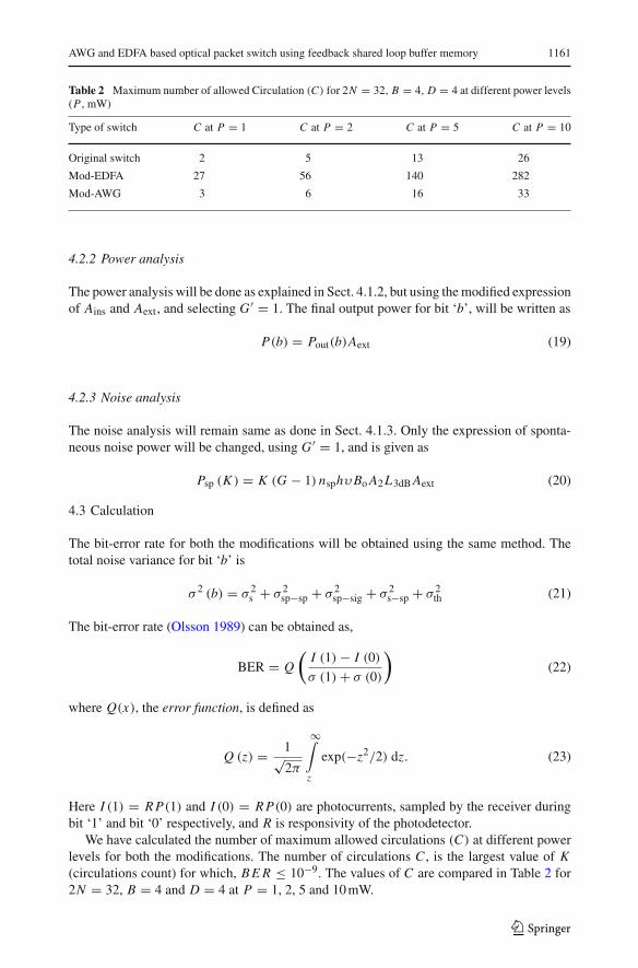
Table 2 Maximum number of allowed Circulation (C) for 2N = 32, B = 4, D = 4 at different power levels(P , mW)
Type of switch C at P = 1 C at P = 2 C at P = 5 C at P = 10
Original switch 2 5 13 26
Mod-EDFA 27 56 140 282
Mod-AWG 3 6 16 33
4.2.2 Power analysis
The power analysis will be done as explained in Sect. 4.1.2, but using the modified expressionof Ains and Aext, and selecting G ′ = 1. The final output power for bit ‘b’, will be written as
P(b) = Pout(b)Aext (19)
4.2.3 Noise analysis
The noise analysis will remain same as done in Sect. 4.1.3. Only the expression of sponta-neous noise power will be changed, using G ′ = 1, and is given as
Psp (K ) = K (G − 1) nsphυBo A2 L3dB Aext (20)
4.3 Calculation
The bit-error rate for both the modifications will be obtained using the same method. Thetotal noise variance for bit ‘b’ is
σ 2 (b) = σ 2s + σ 2
sp−sp + σ 2sp−sig + σ 2
s−sp + σ 2th (21)
The bit-error rate (Olsson 1989) can be obtained as,
BER = Q
(I (1) − I (0)
σ (1) + σ (0)
)(22)
where Q(x), the error function, is defined as
Q (z) = 1√2π
∞∫z
exp(−z2/2) dz. (23)
Here I (1) = R P(1) and I (0) = R P(0) are photocurrents, sampled by the receiver duringbit ‘1’ and bit ‘0’ respectively, and R is responsivity of the photodetector.
We have calculated the number of maximum allowed circulations (C) at different powerlevels for both the modifications. The number of circulations C , is the largest value of K(circulations count) for which, B E R ≤ 10−9. The values of C are compared in Table 2 for2N = 32, B = 4 and D = 4 at P = 1, 2, 5 and 10 mW.
123
1162 R. K. Singh et al.
5 Scheduling algorithm
The buffering in the modules is done using the following scheduling algorithm:
1. The tunable wavelength converters (TWCs) placed at the inputs of the loop buffer(Fig. 2), can be tuned to any of the B wavelengths and the TWCs inside the loop can betuned to any of the (B + D) wavelengths. Further it is assumed that TWCs can be tunedalmost instantaneously.
2. If there are total i packets buffered in all the modules for the output j , then one of themwill be send to the output via switch fabric. If in that slot, there are one or more packetsalso present at the inputs of switch destined for the output j , then these packets will bestored in the loop buffer to the extent allowed by the rules 4–5.
3. Considering the case when there is no packet in the buffer for the output j , but n of Ninput lines have packets for that output. Then, one of these n packets is directly sent tooutput j by configuring the switch fabric. The remaining (n − 1) packets will be storedin the buffer module to the extent allowed by the rules 4–5.
4. Number of packets x j for the output j , stored in all the buffer modules, should never begreater than min(MB,C) i.e.,
x j ≤ min(M B, C), 1 ≤ j ≤ N
5. Total amount of buffered packets for all the outputs, cannot be larger than the maximumbuffering capacity MB i.e., ∑
x j ≤ M B, 1 ≤ j ≤ N
6. The buffers in the loop are such that simultaneous read and write is allowed in the sameslot for the same wavelength.
7. The contending packets will try to occupy the lowest numbered (1 to m) available module(Fig. 1).
8. During any time slot, priority will be given to the packets stored in the loop buffer mod-ules than the packets at the switch input. Essentially for switch output, FIFO disciplinewill be maintained.
9. If there are total q packets in all modules for any output r , then the oldest of q contendingpackets, will leave first for the switch output.
10. Packet for different output can leave the switch at the same time.11. If any of the incoming packets will not be able to pass through the switch due to the
maximum buffer capacity limitation, then it will be dropped.
6 Simulation analysis and results
Using the above algorithm, the simulated results for ‘packet loss probability’ and ‘averagepacket delay’ are obtained for both the modifications, and are compared with the results oforiginal switch. Figs. 6–9 show results for the switch of size 2N = 32 with B = D = 4.As defined earlier, 16 of 32 ports are the actual inputs and other 16 ports are used to connectdifferent number of buffer modules.
The number of maximum allowed circulations is more for Mod-EDFA as compared toMod-AWG (Table 2). In case of Mod-EDFA, there will not be any circulation limit at allpower levels, because the maximum capacity is still lesser than the number of maximumallowed circulations. For the example of 2N = 32, the maximum capacity is 16(= M × B),
123
AWG and EDFA based optical packet switch using feedback shared loop buffer memory 1163
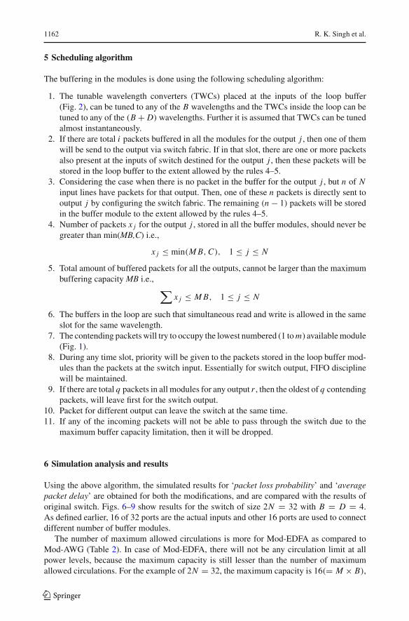
Fig. 6 Loss probability for 2N = 32, D = 4, B = 4, M = N/D and P = 1 mW
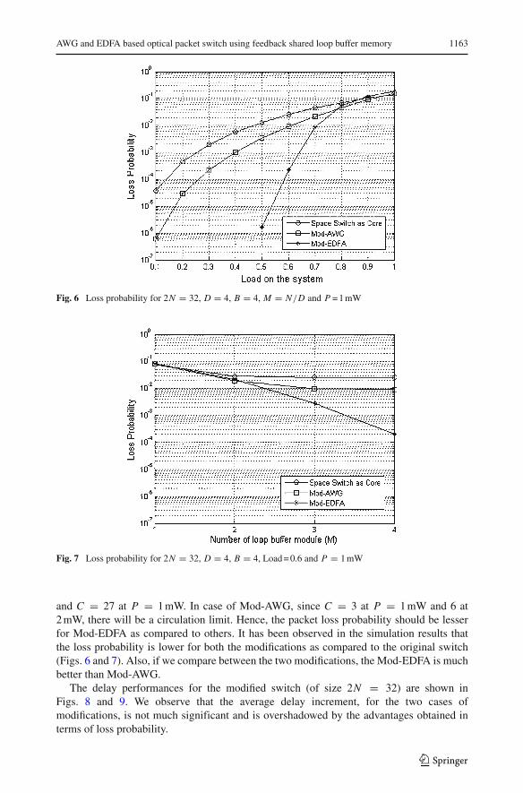
Fig. 7 Loss probability for 2N = 32, D = 4, B = 4, Load = 0.6 and P = 1 mW
and C = 27 at P = 1 mW. In case of Mod-AWG, since C = 3 at P = 1 mW and 6 at2 mW, there will be a circulation limit. Hence, the packet loss probability should be lesserfor Mod-EDFA as compared to others. It has been observed in the simulation results thatthe loss probability is lower for both the modifications as compared to the original switch(Figs. 6 and 7). Also, if we compare between the two modifications, the Mod-EDFA is muchbetter than Mod-AWG.
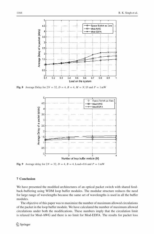
The delay performances for the modified switch (of size 2N = 32) are shown inFigs. 8 and 9. We observe that the average delay increment, for the two cases ofmodifications, is not much significant and is overshadowed by the advantages obtained interms of loss probability.
123
1164 R. K. Singh et al.
Fig. 8 Average Delay for 2N = 32, D = 4, B = 4, M = N/D and P = 1 mW
Fig. 9 Average delay for 2N = 32, D = 4, B = 4, Load = 0.6 and P = 1 mW
7 Conclusion
We have presented the modified architectures of an optical packet switch with shared feed-back-buffering using WDM loop buffer modules. The modular structure reduces the needfor large range of wavelengths because the same set of wavelengths is used in all the buffermodules.
The objective of this paper was to maximize the number of maximum allowed circulationsof the packet in the loop buffer module. We have calculated the number of maximum allowedcirculations under both the modifications. These numbers imply that the circulation limitis relaxed for Mod-AWG and there is no limit for Mod-EDFA. The results for packet loss
123
AWG and EDFA based optical packet switch using feedback shared loop buffer memory 1165
probability and average delay are compared and they indicate that the proposed modificationsgive enhanced performance.
In order to focus on performance of the switch, the analysis is done under the assumptionof single node network, instead of the network consisting of several such switches. We canalso apply the switch in the networks; the related issues need further investigations.
References
Chlamtac, I., Fumagalli, A.: An optical switch architecture for manhattan network. IEEE J. Sel. AreasCommun. 6, 550–559 (1993)
Chia, M.C., et al.: Packet loss and delay performance of feedback and feed-forward arrayed-waveguide grat-ings-based optical packet switches with WDM inputs-outputs. J. Lightw. Technol. 19, 1241–1254 (2001)
Danielsen, S.L., Mikkelsen, B., Jorgensen, C., Durhuus, T., Stubkjaer, K.E.: WDM packet switch architectureand analysis of the influence of tunable wavelength converters on the performance. J. Lightw. Tech-nol. 15, 219–226 (1997)
Dittmann, L., et al.: The European IST project DAVID: a viable approach toward optical packet switching. IEEEJ. Sel. Areas Commun. 21, 1026–1040 (2003)
Fow-Sen Choa, J., et al.: An optical packet switch based on WDM technologies. J. Lightw. Technol. 23,994–1014 (2005)
Haas, Z.: The staggering switch: an electronically controlled optical packet switch. J. Lightw. Technol. 11,925–936 (1993)
Hunter, D.K., Chia, M.C., Andonovic, I.: Buffering in optical packet switches. J. Lightw. Technol. 16,2081–2094 (1998)
Mamyshev, P.V.: All-optical data regeneration based on self phase modulation effect. In: Proc. ECOC Conf.,pp. 475–476 (2004)
Olsson, N.A.: Lightwave systems with optical amplifiers. J. Lightw. Technol. 7, 1071–1082 (1989)Papadimitriou, G.I., Papazoglou, C., Pomportsis, A.S.: Optical switching: switch fabrics, techniques, and
architectures. J. Lightw. Technol. 21, 384–405 (2003)Shun, Y., Mukherjee, B., Yoo, S.J.B., Dixit, S.: A unified study of contention resolution schemes in optical
packet switched networks. J. Lightw. Technol. 21, 672–683 (2003)Shukla, S., Srivastava, R., Singh, Y. N.: Modeling of fiber loop buffer switch. In: Proc. Photonics Conf.,
p. 248 (2004). Available at http://home.iitk.ac.in/~ynsingh/papers/rajiv.pdfSingh, R.K., Singh, Y.N.: A modified architecture for the staggering switch. In: Proc. NCC Conf., pp. 186–187
(2005). Available at http://home.iitk.ac.in/~ynsingh/papers/ncc05_rajat.pdfSingh, R.K., Singh, Y.N.: An overview of photonic packet switching architectures. IETE Tech. Rev. 23,
15–34 (2006)Singh, R.K., Srivastava, R., Mangal, V., Singh, Y.N.: Wavelength routed shared buffer based feed-forward
architectures for optical packet switching. In: Proc. IEEE INDICON Conf. (2006)Singh, R.K., Srivastava, R., Singh, Y.N.: Opt. Quant. Electron. (2007) DOI 10.1007/s11082-007-9061-0Srivastava, R., Mangal, V., Singh, R.K., Singh, Y.N.: A modified photonic switch architecture based on fiber
loop memory. In: Proc. IEEE INDICON Conf. (2006)Tucker, R.S., Zhong, W.D.: Photonic packet switching: an overview. IEICE Trans. Commun. E82(B), 254–
264 (1999)Verma, N., Srivastava, R., Singh, Y.N.: Novel design modification proposal for all optical fiber loop buffer
switch. In: Proc. Photonics Conf., p. 181 (2002). Available at http://home.iitk.ac.in/~ynsingh/papers/netp08.pdf
Yao, S., Mukherjee, B., Dixit, S.: Advances in photonic packet switching: an overview. IEEE Commun.Mag. 38, 84–94 (2000)
123