
average current-mode control - OhioLINK ETD Center
84
AVERAGE CURRENT-MODE CONTROL A thesis submitted in partial fulfillment of the requirements for the degree of Master of Science in Electrical Engineering By Ankit Chadha B. S., Koneru Lakshmaiah University, Guntur, Andhra Pradesh, India, 2013 2015 Wright State University
-
Upload
khangminh22 -
Category
Documents
-
view
1 -
download
0
Transcript of average current-mode control - OhioLINK ETD Center

AVERAGE CURRENT-MODE CONTROL
A thesis submitted in partial fulfillment
of the requirements for the degree of
Master of Science in Electrical Engineering
By
Ankit Chadha
B. S., Koneru Lakshmaiah University, Guntur, Andhra Pradesh, India, 2013
2015
Wright State University

WRIGHT STATE UNIVERSITY
GRADUATE SCHOOL
January 5, 2016
I HEREBY RECOMMEND THAT THE THESIS PREPARED UNDER MY SU-PERVISION BY Ankit Chadha ENTITLED Average Current-Mode Control BE AC-CEPTED IN PARTIAL FULFILLMENT OF THE REQUIREMENTS FOR THEDEGREE OF Master of Science in Electrical Engineering.
Marian K. Kazimierczuk, Ph.D.Thesis Director
Brian Rigling, Ph.D.
ChairDepartment of Electrical Engineering
College of Engineering andComputer Science
Committee onFinal Examination
Marian K. Kazimierczuk, Ph.D.
Yan Zhuang, Ph.D.
Lavern Alan Starman, Ph.D.
Robert E. W. Fyffe, Ph.D.Vice President for Research andDean of the Graduate School

ABSTRACT
Chadha, Ankit. M.S.E.E, Department of Electrical Engineering, Wright State Uni-
versity, 2016. Average current-mode controller.
In this thesis, an average current-mode controller is analyzed for controlling power
electronic converters. This controller consists of two loops. An inner loop, which
senses and controls the inductor current and an outer loop, which is used to control the
output voltage and provide reference voltage for the inner current loop. An average
current-mode controller averages out high frequency harmonics it senses from the
inductor current to provide a smooth DC component. This can be used as a control
voltage for a pulse width modulator and produce switching pulses for the power
electronic converters. An average current-mode controller can also be designed for a
good bandwidth, which helps in accurate tracking of the sensed inductor current.
For a better understanding of the operation of an average current-mode controller
analytical equations are derived. Many transfer functions, which help analyze the
properties of an open loop system, the controller transfer functions and a block di-
agram representing the converter along with current and voltage-control loops are
presented. The block diagram and the transfer functions were used to derive the
required controller parameters on MATLAB. The designed converter along with the
controller is implemented on SABER circuit simulator. Waveforms representing the
analytical equations along with the dynamic properties of the converter with the
controller were plotted.
The plotted SABER simulations were in agreement with the analytical equations.
The designed controller was able to produce a controlled output voltage for step
change in input voltage and load resistance, when simulated on SABER. Ripples
could be observed in the control voltage of the controller, when designed for a good
bandwidth. This was also represented by the derived analytical equations.
iii

Contents
1 Introduction 1
1.1 Thesis Objectives . . . . . . . . . . . . . . . . . . . . . . . . . . . . . . 3
1.2 Thesis Outline . . . . . . . . . . . . . . . . . . . . . . . . . . . . . . . . 4
2 Overview of Buck DC-DC converter 5
2.1 Circuit operation of Buck DC-DC converter . . . . . . . . . . . . . . . 5
2.2 Small-Signal Model of a Buck DC-DC Converter . . . . . . . . . . . . . 6
2.3 Open-Loop Control-to-Output Voltage Transfer Function . . . . . . . . 7
2.4 Open-Loop Control-to-Inductor Current Transfer Function . . . . . . . 10
2.5 Open-Loop Input-to-Output Voltage Transfer Function . . . . . . . . . 15
2.6 Open-Loop Input Impedance Transfer Function . . . . . . . . . . . . . 17
2.7 Open-Loop Output Impedance Transfer Function . . . . . . . . . . . . 19
3 Controllers 22
3.1 Introduction . . . . . . . . . . . . . . . . . . . . . . . . . . . . . . . . . 22
3.2 Voltage-Mode Control . . . . . . . . . . . . . . . . . . . . . . . . . . . 22
3.2.1 Proportional Controller . . . . . . . . . . . . . . . . . . . . . . . 23
3.2.2 Differentiator . . . . . . . . . . . . . . . . . . . . . . . . . . . . . 24
3.2.3 Integrator . . . . . . . . . . . . . . . . . . . . . . . . . . . . . . . 25
3.3 Current-Mode Control . . . . . . . . . . . . . . . . . . . . . . . . . . . 26
3.3.1 Peak Current-Mode Control . . . . . . . . . . . . . . . . . . . . . 27
3.3.2 Average Current-Mode Control . . . . . . . . . . . . . . . . . . . 28
4 Design 36
4.1 Introduction . . . . . . . . . . . . . . . . . . . . . . . . . . . . . . . . . 36
iv

4.2 Design of an Open-Loop Buck DC-DC Converter in Continuous
Conduction Mode . . . . . . . . . . . . . . . . . . . . . . . . . . . . . . 36
4.3 Closed-Loop Buck DC-DC Converter . . . . . . . . . . . . . . . . . . . 41
4.3.1 Design of Inner Current Control-Mode-Controller . . . . . . . . . 44
4.3.2 Design of Outer Voltage-Mode-Controller . . . . . . . . . . . . . . 54
5 Saber Simulations and Results 62
5.1 Introduction . . . . . . . . . . . . . . . . . . . . . . . . . . . . . . . . . 62
5.2 Dynamic Response of Inner Current Control Loop . . . . . . . . . . . . 62
5.2.1 Controller Response . . . . . . . . . . . . . . . . . . . . . . . . . 64
5.2.2 Dynamic Response of the Buck DC-DC Converter with Inner
Current Control Loop for the Step Change in Load Resistance . . 67
5.2.3 Dynamic Response of the Buck DC-DC Converter with Inner
Current Control for the Step Change in Input Voltage . . . . . . 67
5.3 Dynamic Response of Outer Voltage Control Loop . . . . . . . . . . . . 68
5.3.1 Dynamic Response of the Buck DC-DC Converter with Inner
Current and Outer Voltage Control Loop for the Step Change in
Load Resistance . . . . . . . . . . . . . . . . . . . . . . . . . . . . 70
5.3.2 Dynamic Response of the Buck DC-DC Converter with Inner
Current and Outer Voltage Control Loop for the Step Change in
Input Voltage . . . . . . . . . . . . . . . . . . . . . . . . . . . . . 70
6 Conclusion 72
6.1 Summary . . . . . . . . . . . . . . . . . . . . . . . . . . . . . . . . . . 72
6.2 Future Work . . . . . . . . . . . . . . . . . . . . . . . . . . . . . . . . . 72
7 Bibliography 73
v

List of Figures
2.1 Circuit diagram of a buck DC-DC converter[5] 5
2.2 Small-signal model of a buck DC-DC converter. 6
2.3 Small-signal model of a buck DC-DC converter to derive
control-to-output voltage transfer function 7
2.4 Corner frequency as a function of load resistance 12
2.5 Damping factor as a function of load resistance 13
2.6 Idealized Bode plots of the open-loop control-to-inductor current
transfer function Ti for the buck converter 14
2.7 Small-signal model of a buck DC-DC converter to derive
input-to-output voltage transfer function 15
2.8 Small-signal model of a buck DC-DC converter to derive output
impedance 19
3.1 Block diagram of an op-amp as a controller 23
3.2 Circuit diagram of a proportional controller 24
3.3 Circuit diagram of a differentiator 24
3.4 Circuit diagram of an integrator 25
3.5 Block Diagram representing a general current control scheme 26
3.6 Circuit diagram of a peak current-mode controller[5] 27
vi

3.7 Circuit diagram of an average current-mode control 28
3.8 (a) Waveform of inductor current of a buck DC-DC converter. (b)
Waveform of control voltage of a pulse-width modulator which is an
amplified version of the sensed inductor current. 31
3.9 (a) Waveform of inductor current of a buck DC-DC converter. (b)
Waveform of control voltage of a pulse-width modulator when cross
over frequency of the controller is less than the switching frequency of
the buck DC-DC converter. 31
3.10 (a) Waveform of inductor current of a buck DC-DC converter. (b)
Waveform of control voltage of a pulse-width modulator when cross
over frequency of the controller is higher than the switching frequency
of the buck DC-DC converter. 32
3.11 Magnitude and phase plot of a first order type one average
current-mode controller 33
3.12 Waveforms in the pulse-width modulator representing the sawtooth
voltage vt, the control voltage vC1 and gate-to-source voltage vGS for
controller crossover frequency less than the switching frequency.[5] 34
3.13 Waveforms in the pulse-width modulator representing the sawtooth
voltage vt, the control voltage vC1 and gate-to-source voltage vGS for
controller crossover frequency more than the switching frequency. 35
4.1 Circuit diagram of the buck DC-DC converter after implementing the
design specification. 38
vii

4.2 Magnitude and phase plots of control-to-inductor current transfer
function of buck DC-DC converter. 40
4.3 Step response of inductor current of buck DC-DC converter for a step
change in duty cycle. 41
4.4 Block diagram of the DC-DC buck converter with inner current
control loop and output voltage control loop. 42
4.5 Circuit diagram of DC-DC buck converter with inner current control
loop and output voltage control loop 43
4.6 Block diagram of inner loop representing closed loop inductor current
to control relationship 44
4.7 Magnitude and phase plots of internal loop gain without controller
compensation. 45
4.8 Circuit diagram of a first order type zero current mode controller 47
4.9 Magnitude and phase plots of average current mode controller 50
4.10 Magnitude and phase plots of inner loop gain with controller 51
4.11 Block diagram of inner closed loop buck DC-DC converter. 52
4.12 Magnitude and phase plots of closed loop control-to-inductor current
transfer function of buck DC-DC converter. 53
4.13 Step response of inductor current of a closed-loop buck DC-DC
converter for a step change in duty cycle 54
4.14 Circuit diagram representing PI controller for outer voltage loop control. 55
viii

4.15 Block diagram representing outer loop gain 57
4.16 Magnitude and phase plots of outer loop gain with controller. 58
4.17 Block diagram for closed loop gain of outer voltage loop control. 59
4.18 Magnitude and phase plots of outer closed loop gain with controller. 60
4.19 Step response of outer closed loop with controller. 61
5.1 Saber circuit for average current mode control of inductor current. 63
5.2 Waveforms representing control and sawtooth reference voltages for a
good phase margin. 65
5.3 Waveforms representing control and sawtooth reference voltage with
high capacitance in the feedback of the controller. 66
5.4 Waveforms representing inductor current and output voltage of the
buck DC-DC converter for a step change in load resistance. 67
5.5 Waveforms representing inductor current and output voltage of the
buck DC-DC converter for a step change in input voltage. 68
5.6 Saber circuit of a buck DC-DC converter with both inner current
control and outer voltage control. 69
5.7 Waveforms of inductor current and output voltage of the buck
DC-DC converter for a step change in load resistance. 70
5.8 Waveforms of inductor current and output voltage of the buck
DC-DC converter for a step change in input voltage. 71
ix

Acknowledgement
To start of, I would like to express my immense gratitude to my advisor Dr. Marian
K. Kazimierczuk, whose support, motivation and wisdom has helped me through out
my research. I would also like to thank my thesis committee members Dr. Yan
Zhuang and Lavern Alan Starman for their insightful comments and suggestions. I
am grateful to the Department of Electrical Engineering and the Department Chair,
for giving me this opportunity to obtain my MS degree at Wright State University. A
sincere thanks also goes to my fellow colleague Agasthya Ayachit, whose support and
experience built the confidence in me. Last but not the least I would like to thank
my family, who stood by me on every decision I made and who have always showed
me the right path.
x

1 Introduction
Obtaining a sustainable energy production at lowered costs has always been a global
priority. This has lead to many improvements in technologies. Power electronic con-
verters with their many available topologies, which help interface different energy
sources is an example of one such technology. Power electronic converters use MOS-
FETs, driven by pulse width modulated (PWM) pulses, as switches to produce output
voltage. Hence, they are named switch-mode DC-DC converters. The turn-on time
and the turn-off time of these switches play an important role deciding the character-
istics of the converter as they provide conversion ratio for these converters. A similar
stepping up or stepping down of the output voltage can be obtained by using a trans-
former with proper turns ratio. But, a transformer is usually responsible for high
switching surges, which can damage the switching components in the circuit. Due to
these features a great number of uses for DC-DC converters like, an integrated circuit
utilizing a switching converter for a 3.3 V or 1.5 V or a power supply for automobile
industries for electronic load, have emerged [13].
Since power electronic converters provide good conversion ratio, a proper regula-
tion of the duty cycle can help in controlling the output voltage. A controller can be
employed for such application. The main task of a controller is to sense a change in a
required quantity and provide proper compensation, when the situations asks for it.
Power electronic converters like, a DC-DC buck or a DC-DC boost converter employ
such controllers to keep the output voltage in desired range. Since a controller senses
and controls a required parameter, multiple control circuits can be employed to sat-
isfy the multiple application requirement. A current mode controller is an example of
one such controller, where the controller senses the current instead of a voltage and
provides the required compensation. Both, the current mode and the voltage mode
controller can be applied to power electronic converters and if required multiple loops
1

containing both the types of control can also be integrated onto a circuit.
Adopting a current mode control usually has many advantages over voltage mode
control. A current mode control has a faster transient response, provides over-current
protection to a circuit and are also easier to design. Due to these advantages a current-
mode control is a preferable option in power supply industries. There are many types
of current-mode-control available like average, peak, valley current-mode control in
which, the sensed current is converted into voltage to compare it to a reference voltage
and let the controller decide the required compensation.
A peak current mode control is a simple yet robust way to control a DC-DC power
electronic converter. This control scheme uses an op-amp and a latch to decide the
duty cycle of a converter. This is done by using a threshold voltage given to the sensed
inductor current. Whenever the sensed inductor current reaches the given threshold
voltage MOSFET is made to turn off and later the time period of the converter is
completed by switching back the MOSFET on by using clock and a latch. Problem
with this type of a current control is that, since it uses the peak value of the inductor
current any harmonics in the system can cause false triggering by the controller. This
is usually the case in power factor correction circuits.
An average current mode controller senses and averages out any surge in the
sensed current and making it a better option, when trying to control a circuit with
power factor correction. Since current spikes are common for such circuits. In average
current mode control the sensed signal is first averaged out. Therefore, filtering any
harmonics that could have been present in the inductor current. Also, average current
mode control offers a higher low frequency gain thus, helps in tracking the current
profile with high accuracy. An average current mode controllers gain compensation
can be decided and designed depending on the controller requirements. In [8] and [2]
two different types of average current mode control circuits have been used.
2

In [8] a buck converter is analyzed with a type one average current mode controller
to control the inductor current with the control signal, which in this case is duty cycle.
Doing so causes DC phase of the system to be −90o. In this study, a first order type
zero average current control circuit is used to control a buck converter for which the
transfer function for the control-to-inductor current is derived. Using this transfer
function required magnitude and phase plots are plotted, which helps to decide the
required controller compensation and the controller parameters. The obtained control
scheme with the buck converter is analyzed using MATLAB and Saber to note the
dynamic properties of this controller.
1.1 Thesis Objectives
• Understand the difference between peak current mode control and average cur-
rent mode control as it helps in better understanding of a current mode con-
troller and how each of these controllers are implemented
• Derive different transfer functions namely, input voltage-output voltage transfer
function (Mv), control-to-output voltage transfer function (Tp), output impedance
(Zo), input impedance (Zi) and control-to-inductor current transfer function
(Ti). This helps one to understand the open loop characteristics of the buck
converter.
• Knowing the open loop characteristics of a buck converter gives knowledge
about the compensation requirement of the converter by plotting for its loop
gain without any controller compensation
• After obtaining the required controller design, buck along with the controller
is connected and simulated on saber to observe the dynamic property of the
converter and the control circuit.
3

1.2 Thesis Outline
This thesis is written in following order:
• Chapter 2: Working of a buck DC-DC converter is discussed. Followed by
derivation of different transfer functions using it small-signal model obtained
from circuit averaging method.
• Chapter 3: To be able to control the discussed converter in chapter 2 different
types of controllers are summarized in here. This chapter mainly shed light
on the working of the first order average current mode controller, which is the
concentration of this thesis.
• Chapter 4: This chapter helps in obtaining all the required parameters for
the converter to run and later control it. For this, the considered buck DC-
DC converter is designed for the required specifications. Since, this control
scheme has two controllers, a design procedure for our first order average current
mode controller and finally, a design procedure for a voltage mode controller is
mentioned.
• Chapter 5: In this chapter a powerful simulation tool namely, Saber is used to
simulate the buck DC-DC converter with average current mode controller to
observe its dynamic properties
4

2 Overview of Buck DC-DC converter
2.1 Circuit operation of Buck DC-DC converter
A buck converter as the name suggests helps in chopping or in other words steps down
the applied input voltage. It uses the switching property of a MOSFET, diode and
power storing property of an inductor in the form of current, to obtain such a drop
in voltage. The circuit diagram representing a buck converter can be seen in Figure
2.1.
Figure 2.1: Circuit diagram of a buck DC-DC converter[5]
The converter starts working, when high gate-to-source voltage (VGS) is applied to
the MOSFET, which causes the MOSFET to switch on. At this point the MOSFET
is short circuited. This builds up a reverse bias voltage across the diode forming
an open circuit across the diode and the input voltage is being supplied to the load
through the inductor. The capacitor connected as shown in Figure 2.1 filters out any
AC component from the output voltage. This continues from time t = 0 till t = DT ,
where T is the total time period and D is the Duty cycle of the applied pulse to
the MOSFET. After time t = DT , the VGS applied to the MOSFET drops and is
not enough to drive the MOSFET causing the MOSFET to switch off. This creates
an open circuit by the MOSFET. At this point, the diode is forward biased by the
output voltage. Now, the load is no longer supported by the input supply and the
5

energy stored in inductor in the form of current circulates within the system through
the diode. Here the diode acts like a free wheeling diode. The point to be noted is
that power falls due to this action and the output voltage is lower than the input.
Thus, providing us with a lowered output voltage.
2.2 Small-Signal Model of a Buck DC-DC Converter
l
l
Figure 2.2: Small-signal model of a buck DC-DC converter.
The main interest for the design of a controller for a power electronic converters
are its frequency response, transient response and stability for which one needs linear
circuit theory. But, power converters are highly non-linear circuit. Therefore, such
an analysis is not possible. For this, the circuit can be linearized by using circuit
averaging method. In these circuits the switches used in the system can be replaced
for a voltage or a current dependent sources. Also the DC voltage and current sources
can be replaced by time varying AC components so that perturbations in the system
can be represented. The on-state resistances are also taken into consideration. The
circuit hence is called a large signal model. Since, the magnitude of small-signal
model is low enough, the large signal model can be further simplified by neglecting
the products of AC components to form a low frequency small-signal model. A small-
signal model of a buck converter can be seen in Figure 2.2. The following assumptions
are to be made to obtain such a circuit:
6

• Neglect switching losses, that is neglect the output capacitance of a transistor
and diode capacitance.
• Transistor and diode in off-state does not allow any current to flow, that is the
off-state resistance is infinite.
• Transistor in its on-state acts as a linear time invariant resistor, while the diode
in its on-state can be represented as a voltage source VF in series with a linear
time invariant resistor.
2.3 Open-Loop Control-to-Output Voltage Transfer Function
l
l
Figure 2.3: Small-signal model of a buck DC-DC converter to derive control-to-outputvoltage transfer function
A buck converter is designed for a constant output voltage but due to uncertain
disturbances in the system like change in load or a surge in supply, the output voltage
of the system might rise or fall, which needs to be checked by using a controller. A
transfer function helps in relating a signal which is to be controlled and a control
signal. Doing so aids in understanding how the system behaves in certain conditions.
A control-to-output voltage transfer function is an example of one such transfer func-
tion. A control-to-output voltage transfer function as the name suggests provides a
7

transfer function or in layman’s term provides a relation between control and output
voltage, where the control signal is the duty cycle. Now, knowing such a relation
will help us describe characteristics for the required controller and hence, design one.
From Figure 2.2, let us assume that the perturbations in the system due to input
voltage vi and output current io are zero which is depicted in Figure 2.3.
From Figure 2.3, Let the current flowing in the right most loop be i1 that is i1
flows through the capacitor and the load resistor. Let the current flowing through
the middle loop be i2. Also r represents the total resistance in the inductor branch
and is given by
r = DrDS + (1 − D)RF + rL[5], (2.1)
where rDS is the drain to source resistance, RF is averaged diode resistance and rL is
DC parasitic in inductor.
using Kirchhoff’s voltage law, we have
(rC + XC)(i2 − i1) = vo. (2.2)
and
− VId + (r + XL)i1 + vo = 0, (2.3)
Also, the output voltage across the load resistance is given by
vo = ı2RL. (2.4)
From equation (2.3), (2.2) and (2.4),
vo
RL
−VId − vo
r + XL
=vo
rC + XC
. (2.5)
Manipulating equation (2.5), we have
VId
r + XL
= vo
(
1
r + XL
+1
RL
+1
rC + XL
)
. (2.6)
8

Taking the ratiovo
don the left hand side of the equation and remaining onto the right
hand side, we get
vo
d=
VI
r + XL
11
r + XL
+1
RL
+1
rC + XC
. (2.7)
In equation (2.7), the XL is a complex inductance and is given by sL and XC repre-
sents complex capacitance and is given by1
sCwhere s = jω. Therefore the transfer
function in S domain can be written as
vo
d=
VI
r + sL
11
r + sL+
1
RL
+1
1
sC+ rC
. (2.8)
Rearranging the equation (2.8) gives us
vo
d=
(
VIRLrC
LrC + RLL
) s +1
rCC
s2 + s[C(RLrC + RLr + rrC) + L]
LC(RL + rC)+
r + RL
LC(RL + rC)
. (2.9)
A general representation of the control-to-output transfer function is
Tp = Tpx
s − ωzn
s2 + 2ξωos + ω2o
, (2.10)
where
ωzn =1
rCC, (2.11)
is the angular frequency of left hand plane zero. The angular corner frequency or the
angular undamped natural frequency is given by
ωo =
√
r + RL
LC(RL + rC). (2.12)
The damping ratio is given by,
ξ =C[RL(rC + r) + rrC ] + L
2√
LC(RL + rC)(r + RL). (2.13)
The conjugate complex pole is given by
p1, p2 = −ξωo ± ωo
√
ξ2 − 1 = −ξωo ± jωo
√
1 − ξ2. (2.14)
9

2.4 Open-Loop Control-to-Inductor Current Transfer Func-
tion
An open-loop control-to-inductor current transfer function provides a relation that
defines any changes in inductor current due to changes in the duty cycle. The small-
signal model of the buck converter is shown in Figure 2.3, which can be used to derive
this transfer function and relate the inductor current to the control voltage.
Using Kirchhoff’s voltage law, gives us
VId = ril + sLil + Z1il (2.15)
and
VI =il
d[r + sL + Z1], (2.16)
where from Figure 2.3,
Z1 =1
1
RL
+1
1
sC+ rC
. (2.17)
Substituting equation (2.17) into equation (2.16), we have
il
d=
VI
r + sL +1
1
RL
+1
1
sC+ rC
, (2.18)
il
d=
VI
r + sL +1
1
RL
+sC
srCC + 1
, (2.19)
il
d=
VI
r + sL +1
(srCC + 1)RL
srCC + sRLC + 1
, (2.20)
il
d=
VI [srCC + sRLC + 1]
srrCC + sRLCr + r + s2rCLC + s2RLLC + sL + sRLrCC + RL
, (2.21)
10

il
d=
VI [s(rCC + RLC) + 1]
s2(rCLC + RLLC) + s(rrCC + RLCr + L + RLrCC) + RL + r, (2.22)
il
d=
VIC(rC + RL)
CL(rC + RL)
s +1
C(rC + RL)
s2 +(rrCC + RLCr + L + RLrCC)
LC(rC + RL)s +
RL + r
LC(rC + RL)
, (2.23)
Ti(s) =il
d=
VI
L
s +1
C(rC + RL)
s2 +C[rrC + RLr + RLrC ] + L
LC(rC + RL)s +
RL + r
LC(rC + RL)
(2.24)
is the control-to-inductor current transfer function. A general representation is given
by
Ti(s) =il
d= Tix
s + ωzi
s2 + 2ξωo + ω2o
, (2.25)
Tix =VI
L. (2.26)
The DC gain of the transfer function is given by
Tio = Ti(0) =VI
L
ωzi
ω2o
. (2.27)
The left hand plane zero is given by
ωzi =1
C(rC + RL). (2.28)
The angular corner frequency or the angular undamped natural frequency is given by
ωo =
√
r + RL
LC(RL + rC). (2.29)
The damping ratio is given by
ξ =C(RL(rC + r) + rrC) + L
2√
LC(RL + rC)(r + RL). (2.30)
11

RL (Ω)
0 2 4 6 8 10 12
fo (
Hz)
1126
1128
1130
1132
1134
1136
1138
1140
1142
1144
Figure 2.4: Corner frequency as a function of load resistance
The variation of corner frequency fo and damping coefficient ξ with respect to change
in load resistance can be seen in figure 2.4 and 2.5 respectively. the quality factor Q
is given by
Q =1
2ξ, (2.31)
the conjugate complex poles are given by
p1, p2 = −ξωo ± ωo
√
ξ2 − 1 = −ξωo ± jωo
√
1 − ξ2. (2.32)
Substituting s = jω into (2.25) yields
Ti(jω) = Tio
(
1 +jω
ωzi
)
1 +(
ω
ωo
)2
+ 2jξ
(
ω
ωo
)= |Ti|e
jφTi , (2.33)
12

RL (Ω)
0 2 4 6 8 10 12
ξ
0.4
0.5
0.6
0.7
0.8
0.9
1
1.1
1.2
1.3
Figure 2.5: Damping factor as a function of load resistance
where
|Ti| = Tio
√
√
√
√
√
√
√
√
√
1 +(
ω
ωzi
)2
[
1 −(
ω
ωo
)2]2
+ 4ξ2
(
ω
ωo
)
(2.34)
and
φTi= arctan
(
ω
ωzi
)
− arctan
2ξ
(
ω
ωo
)
1 −(
ω
ωo
)2
, forω
ωo
≤ 1. (2.35)
13

Figure 2.6: Idealized Bode plots of the open-loop control-to-inductor current transferfunction Ti for the buck converter
The asymptotic bode plot can be seen in Figure 2.6. It is to be noted that the
figure represents an ideal version of the magnitude and frequency response. But due
to the presence of conjugate complex poles there will be a peak in the magnitude
plot. For high values of damping coefficient ξ the peak is lower and vice versa. This
14

peak can be denoted by the quality factor as given in equation 2.31
2.5 Open-Loop Input-to-Output Voltage Transfer Function
The input-to-output voltage transfer function, also known as the audio susceptibility
of the system can be obtained by setting d = 0 and io = 0 in Figure 2.2 to obtain a
small-signal model as shown in Figure 2.7.
l
l
Figure 2.7: Small-signal model of a buck DC-DC converter to derive input-to-outputvoltage transfer function
Using Kirchhoff’s voltage law in second loop gives us,
il(r + XL) + (XC + rC)(il − io) − Dvi = 0. (2.36)
Applying Kirchhoff’s voltage law in the right most loop gives us,
vo + (io − il)(XC + rC) = 0, (2.37)
−vo
XC + rC
= io − il, (2.38)
15

il = io +vo
XC + rC
. (2.39)
The small signal output current is given as
io =vo
RL
. (2.40)
From equation (2.36) and (2.39)
(io +vo
XC + rC
)(r + XL) + (XC + rC)(io +vo
XC + rC
− io) − Dvi = 0. (2.41)
From equation (2.40) and (2.41)
io(r + XL) +vo
XC + rC
(r + XL) + vo − Dvi = 0, (2.42)
vo
(
r + XL
RL
+r + XL
XC + rC
+ 1)
= Dvi, (2.43)
vo
vi
=D
r + XL
RL
+r + XL
XC + rC
+ 1, (2.44)
vo
vi
=D(RLXC + RLrC)
rXC + rCr + RLr + XCXL + rCXL + RLXC + RLrC
, (2.45)
vo
vi
=DRL
(
1
sC+ rC
)
r
sC+ rCr + RLr +
L
C+ rCLs + RLLs +
RL
sC+ RLrC
, (2.46)
vo
vi
=
DRLrC
s
(
1
CrC
+ s
)
s(rCL + RLL) + rCr + RLr +L
C+ RLrC +
r + RL
sC
, (2.47)
vo
vi
=DRLrC
(
s +1
CrC
)
s2C[rCL + RLL] + [C(rCr + RLr + RLrC) + L]s + r + RL
, (2.48)
16

Mv =DRLrC
L(rC + RL)
s +1
CrC
s2 +C[rCr + RL(r + rC)] + L
CL(rC + RL)s +
r + RL
LC(rC + RL)
. (2.49)
is the input-to-output voltage transfer function of a buck DC-DC converter the general
representation of this transfer function is given by
Mv = Mvx
s − ωzl
s2 + 2ξωo + ω2o
, (2.50)
where
Mvx =DRLrC
l(rC + RL). (2.51)
The angular frequency of the left-half plane zero is given by
ωzl =1
CrC
. (2.52)
The angular corner frequency or the angular undamped natural frequency is given by
ωo =
√
r + RL
LC(RL + rC). (2.53)
The damping ratio is given by,
ξ =C[RL(rC + r) + rrC ] + L
2√
LC(RL + rC)(r + RL), (2.54)
the conjugate complex pole is given by
p1, p2 = −ξωo ± ωo
√
ξ2 − 1 = −ξωo ± jωo
√
1 − ξ2. (2.55)
2.6 Open-Loop Input Impedance Transfer Function
The open equivalent circuit used in Figure 2.7 can also be used to obtain the input
impedance transfer function.
Using Kirchhoff’s voltage law,
(r + XL)il + vo − Dvi = 0, (2.56)
17

(r + XL)il + ilZ1 − Dvi = 0, (2.57)
where input current is given by ii = ilD
ii(r + XL + Z1) − D2vi = 0, (2.58)
vi
ii
=r + XL + Z1
D2, (2.59)
vi
ii
=1
D2
r + sL +
RL
sC
RL +1
sC+ rC
, (2.60)
vi
ii
=1
D2
rRL +r
sCrrC + sLRL +
L
C+ sLrC +
RL
sC+ RLrC
RL + rC +1
sC
, (2.61)
vi
ii
=1
D2C(RL + rC)
r + RL + sC(rRL + rrC +L
C) + s2LC(RL + rC)
s +1
C(RL + rC)
, (2.62)
vi
ii
=L
D2
s2 + sC(rrC + RL(r + rC)) + L
LC(RL + rC)+
r + RL
LC(RL + rC)
s +1
C(RL + rC)
. (2.63)
The general representation of the this transfer function is given as
Zi = Zix
s2 + 2ξωos + ω2
o
s − ωrc
, (2.64)
where
Zix =L
D2. (2.65)
The angular frequency of left-half plane pole is given by
ωrc =1
C(RL + rC). (2.66)
18

2.7 Open-Loop Output Impedance Transfer Function
The small-signal model of a buck converter can be reduced by setting d, vi, and io
to zero and applying an independent voltage source vt, which will force current il
into the system. Now the ratio of vt by it will give us the output impedance of the
converter. The small-signal model required for the output impedance can be seen in
Figure 2.8. From the Figure the voltage vt is being applied to the total impedance
and therefore can be calculated as
!
!
"
#
$
%
Figure 2.8: Small-signal model of a buck DC-DC converter to derive outputimpedance
vt = it
[
Z1(XL + r)
Z1 + XL + r
]
, (2.67)
19

vt
it
=
RL(XC + rC)(XL + r)
RL + XC + rC
RL(XC + rC)
RL + XC + rC
+ XL + r
, (2.68)
vt
it
=RL(XC + rC)(XL + r)
RL(XC + rC) + (XL + r)(RL + XC + rC), (2.69)
vt
it
=RL
(
1
sC+ rC
)
(sL + r)
RL
sC+ rCRL + sRLL +
L
C+ srCL + rRL +
r
sC+ rrC
, (2.70)
vt
it
= RLCrCL
(
s +1
CrC
) (
s +r
L
)
s2C(rCL + RLL) + (RLrC +L
C+ rRL + rrC)sC + r + RL
, (2.71)
Zo =RLrC
rC + RL
(
s +1
CrC
) (
s +r
L
)
s2 +C[rCr + RL(r + rC)] + L
CL(rC + RL)s +
r + RL
LC(rC + RL)
(2.72)
is the output impedance of the buck converter. The general representation of this
transfer function is given by
Zo = Zox
(s − ωzl)(s − ωzm)
s2 + 2ξωos + ω2o
, (2.73)
where
Zox =RLrC
rC + RL
. (2.74)
The angular frequency of left-half plane zeros are given by
ωzl =1
CrC
(2.75)
and
ωzm =r
L. (2.76)
The angular corner frequency or the angular undamped natural frequency is given by
ωo =
√
r + RL
LC(RL + rC). (2.77)
20

The damping ratio is given by,
ξ =C[RL(rC + r) + rrC ] + L
2√
LC(RL + rC)(r + RL). (2.78)
The conjugate complex poles is given by
p1, p2 = −ξωo ± ωo
√
ξ2 − 1 = −ξωo ± jωo
√
1 − ξ2. (2.79)
Knowing these transfer functions helps analyze the open-loop system response of a
system. These responses can be altered by using controllers. In this thesis, controllers
will be designed to sense and control the inductor current and the output voltage.
Types of controllers and their functions will be briefed in the next chapter.
21

3 Controllers
3.1 Introduction
There are many specific objectives that any general system tries to accomplish. For
instance, an air conditioner tries to regulate constant room temperature, speed of an
automobile is to be maintained depending upon the amount of acceleration provided
by the driver. To accomplish such objectives requires a use of certain control systems.
A control system senses for the signal, which is to be controlled and provides required
compensation such that the system always successfully fulfills its task [6]. Depending
on the type of signal the controller senses, there are different types of controllers
available for example, a voltage-mode controller or a current-mode controller. Since
the objective of this thesis is to control a buck DC-DC converter, the signals sensed
in this system are voltage and current. Thus, voltage and a current-mode control will
be utilized.
3.2 Voltage-Mode Control
A voltage-mode controller senses voltage and compares it to a reference voltage to
obtain an error voltage. Depending on error voltage the controller decides the com-
pensation it should provide to regulate the sensed voltage. There are many types
of conventional voltage-mode controllers like a proportional controller, in which the
sensed voltage is multiplied by a constant, An integral controller, which adds an ex-
tra pole to the transfer function or a derivative controller, which added a zero to the
transfer function. These controllers along with their combination can be used to help
shape the sensed voltage. This includes reducing settling time, rise time, overshoots
and undershoots.
A general representation of a voltage-mode controller can be seen in Figure 3.1. The
transfer function of such a controller is given by the equation (3.1). Now depending
22

&'
(
'
))
**
Figure 3.1: Block diagram of an op-amp as a controller
on the selection of passive components for Z1 and Zf the controller shown in Fig-
ure 3.1 can behave as a proportion or integral or differencial controller or even the
combination of the three. Each of these controllers are described in brief as follow
vc
vf
= −Zf
Z1
(3.1)
3.2.1 Proportional Controller
Using a pure resistive Z1 and Zf , the input-to-output transfer function of the con-
troller is independent of the frequency and thus output of such a controller is ampli-
fied. The transfer function of such an amplifier is given in equation (3.2). Figure 3.2
represents a proportional amplifier.
vc
vf
= −Rf
R1
(3.2)
23
+
,
--
..
/
+
Figure 3.2: Circuit diagram of a proportional controller
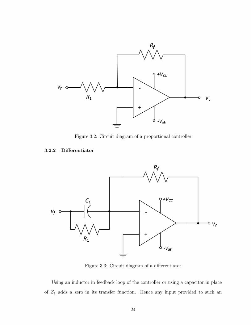
3.2.2 Differentiator
0
1
22
33
4
0
4
Figure 3.3: Circuit diagram of a differentiator
Using an inductor in feedback loop of the controller or using a capacitor in place
of Z1 adds a zero in its transfer function. Hence any input provided to such an
24

op-amp gets differentiated and is obtained in the output. Such a controller is very
sensitive because of the inductive nature and therefore are usually susceptible to
noises. The voltage input to output transfer function of such a differenciator is as
shown in equation (3.3). Figure 3.3 represents a differentiator.
vc
vf
= −RfC1
(
s +1
C1R1
)
(3.3)
3.2.3 Integrator
5
6
77
88
99
99
9
Figure 3.4: Circuit diagram of an integrator
An op-amp can be used as an integrator by using a capacitor in its feedback loop,
which creates a pole in its transfer function, doing so for the high frequencies averages
out the input to the op-amp. An example to an op-amp acting as an integrator can
be seen in Figure 3.4. Here adding a resistance in parallel to the capacitance makes
sure that the feedback of the op-amp does not turn into an open circuit, when the
capacitor discharges and hence helps in maintaining a stable feedback system. The
input to output transfer function of such an op-amp is given by the equation (3.4).
Also using such a controller adds a pole to the loop gain of the system, which helps in
reducing the steady state error to zero and also reduce the settling time but sometimes
25

is also responsible for overshoots.
vc
vf
= −1
R11C11
1
s +1
C11R1
(3.4)
3.3 Current-Mode Control
:;<=>
?@=AB>;CDA
E;CF=>B=>
EG>>=CB
E;CB>;@@=> H;@BIJ=
E;CB>;@@=>
KL K
M
KN
KNO
Figure 3.5: Block Diagram representing a general current control scheme
A current-mode controller first senses a current signal and converts it into voltage
by using a sense resistance. Now, this sensed current is compared to a reference volt-
age provided to the controller to obtain an error signal. Depending on the magnitude
of the error signal the current-mode controller provides the required compensation
to control the sensed current. A current-mode controller provides a higher order of
control, when compared to a voltage-mode control. In many cases a current-mode
controller is usually integrated along with a voltage-mode controller. A general rep-
resentation of one such control scheme is as shown in Figure 3.5, which represents an
inner current loop and an outer voltage loop. The inner loop helps control the current
signal depending on the reference voltage that has been provided by the control signal
26

of the outer voltage loop. The outer voltage control loop controls the voltage signal
depending on the reference voltage that has been provided to the voltage controller.
Depending on the property of the current signal that the controller tries to manipu-
late, there are different types of current-mode controllers like, a peak current-mode
controller, valley current-mode controller or an average current-mode controller. A
peak current-mode controller is the most common controller used for controlling a
current signal for a power electronic converter but has a few drawbacks like, false
triggering due to harmonics in the system and no control over controller gain. A first
order, type one average current-mode controller is introduced as its replacement.
3.3.1 Peak Current-Mode Control
PP
R
S
T
Figure 3.6: Circuit diagram of a peak current-mode controller[5]
A peak current-mode controller without slope compensation is connected as shown
in Figure 3.6. Since the on time of a buck converter decides the peak value of the
inductor current a variable duty cycle can be used as a control signal. In this type
of current-mode control, the non-inverting terminal of the op-amp is connected to a
reference voltage and the current, which is to be controlled is sensed and converted to
voltage by using a sense resistance and is connected to the inverting terminal. Here
the op-amp acts as a comparator. Whenever, the sensed voltage reaches the reference
voltage, the op-amp saturates to VEE. Thus, giving low signal to the reset of the
27

latch. These signals along with the clock produces duty cycle for MOSFET. This
duty cycle drives the DC-DC power electronic buck converter. Any rise in the peak
value of the inductor current will be prevented by this controller by switching the
MOSFET off.
3.3.2 Average Current-Mode Control
UU
VV
WW
WW
XW
YWYWZW
[
W
\W\W[W[W
]W]W^W^W
_
``aa
Figure 3.7: Circuit diagram of an average current-mode control
An average current-mode controller is connected as shown in Figure 3.7. It com-
pares an average value of the sensed voltage to a reference voltage vR1 to generate
error voltage vE1. Depending on this error voltage required, compensation is needed.
This controller can be implemented onto a buck converter to control its inductor cur-
rent. Here, the inductor current is the sensed current. Since, an op-amp can compare
only voltages, the inductor current is converted into a voltage by using a sense resistor
Rs. The voltage across this resistor can now be called sense voltage vF 1, which is then
compared to VR1.
28

The inductor current has three main components namely, average DC current
IL, the AC ripples due to switching ∆il and small signal perturbation il. All three
components are sensed to get their respective voltage equivalents VF 1, ∆vf1 and vf1
respectively as shown in Figure 3.7. The current profile without the perturbations
can be seen in Figure 3.8. The inductor current can be represented as
iL = IL + ∆il + il. (3.5)
This inductor current is sensed and is converted into voltage by using a sense resis-
tance
vF 1 = RsiL. (3.6)
This sensed feedback voltage will also have the components of the inductor current.
vF 1 = VF 1 + ∆vf1 + vf1. (3.7)
The reference voltage of this controller has a DC component VR1 but if this voltage is
sensed from the outer voltage feedback loop it may contain small signal perturbations
given by vr1 given by
vR1 = VR1 + vr1. (3.8)
The error voltage is the difference between the feedback voltage and the reference
voltage
vE1 = vR1 − vF 1, (3.9)
from equation (3.7), (3.8) and (3.9)
vE1 = VR1 − VF 1 + vr1 − vf1 − ∆vf1. (3.10)
The control voltage of the controller is given by
vC1 = vR1 +Zf
Zi
vE1, (3.11)
29

from equation 3.8 and 3.11
vC1 = VR1 + vr1 +Zf
Zi
(VR1 − VF 1 + vr1 − vf1 − ∆vf1). (3.12)
Therefore, the control voltage also has three components namely a DC control voltage
VC1 given by
VC1 = VR1
Zf (0)
Zi(0)(VR1 − VF 1). (3.13)
The control voltage due to small signal perturbations
vc1 = vr1 +Zf (s)
Zi(s)(vr1 − vf1), (3.14)
and the third components in the control voltage is due to the ripples present in the
inductor current given by
∆vc1 = −Zf (s)
Zi(s)(∆vf1). (3.15)
It should be noted that if a constant voltage source VR1 is used as a reference voltage,
a small signal disturbance vr1 can be set to zero simplifying 3.14 to
vc1 = −Zf (s)
Zi(s)(vf1). (3.16)
It is to be noted from equation (3.13) that if a controller with a constant non-time
varying gain is used the control voltage will resemble the waveform as shown in Figure
3.8(b), which is an amplified or an attenuated version of the sensed inductor current
depending on the controller gain. Also, it is to be noted that since an inverting op-
amp is used, the control voltage has a phase difference of 1800 with respect to sensed
inductor current. From equation (3.15), since the gain is no longer constant and varies
with frequency, the control voltage vc1 has ripples as a function ofZf (s)
Zi(s), which is
a function of frequency. The controller with a magnitude plot as shown in Figure
3.11 will have a high gain at low frequencies and after the crossover frequency of the
controller, it will attenuate the sensed signal. A controller with such a magnitude plot
can be obtained by using a capacitor in Zf . Now, for a first order type one controller
30

bc
de
f
gbc
hi i j
(a)
klm n
opq
rpq s otq
m
(b)
Figure 3.8: (a) Waveform of inductor current of a buck DC-DC converter. (b) Wave-form of control voltage of a pulse-width modulator which is an amplified version ofthe sensed inductor current.
uv
wx
y
zuv
| |
(a)
~
(b)
Figure 3.9: (a) Waveform of inductor current of a buck DC-DC converter. (b) Wave-form of control voltage of a pulse-width modulator when cross over frequency of thecontroller is less than the switching frequency of the buck DC-DC converter.
31

(a)
(b)
Figure 3.10: (a) Waveform of inductor current of a buck DC-DC converter. (b)Waveform of control voltage of a pulse-width modulator when cross over frequency ofthe controller is higher than the switching frequency of the buck DC-DC converter.
as shown in Figure 3.7, the cross over frequency is given by fC =1
2πR21C11
. Since
the ripples in inductor current due to switching oscillate at switching frequency of
the buck converter, a controller designed with a cross over frequency less than the
switching frequency of the converter will attenuate these ripples and produce a pure
DC control voltage given by equation (3.13) and as shown in Figure 3.9(b). Now, this
control signal is sent to an analog-to-digital converter, which compares this control
voltage to a triangular reference voltage to generate pluses as shown in Figure 3.12
If the controller’s cross over frequency is more than the switching frequency of
the buck converter then the control voltage will have small components of the ripple
voltage present in it as a function of frequency represented by equation (3.15). The
obtained waveform can be seen in Figure 3.10(b) and due to the capacitive nature
the control voltage will lag behind the sensed voltage. Therefore the control voltage
will have certain phase difference with sensed voltage. But the controller still can be
used to control the buck DC-DC converter. The waveform of the control voltage with
the triangular reference voltage can be seen in Figure 3.13
32

¡¢
Figure 3.11: Magnitude and phase plot of a first order type one average current-modecontroller
33

£¤
£¤
¥¤
¦
§¦
¦
§¨
©
¦
£¤©
ª«
¦
Figure 3.12: Waveforms in the pulse-width modulator representing the sawtooth volt-age vt, the control voltage vC1 and gate-to-source voltage vGS for controller crossoverfrequency less than the switching frequency.[5]
34

¬
¬
®
¯
°¯
¯
°±
²
¯
¬²
³´
µ
Figure 3.13: Waveforms in the pulse-width modulator representing the sawtooth volt-age vt, the control voltage vC1 and gate-to-source voltage vGS for controller crossoverfrequency more than the switching frequency.
35

4 Design
4.1 Introduction
This chapter provides all the design procedures one needs to follow to obtain a con-
trolled buck DC-DC converter using a first order average current-mode controller.
All the required plots to support the design are plotted for analysis. The design
procedure is going to start off by designing a buck DC-DC converter. Based on the
compensation it requires a current-mode controller to control the inductor current
and a voltage-mode controller to control the output voltage will be designed and
implemented.
4.2 Design of an Open-Loop Buck DC-DC Converter in Con-
tinuous Conduction Mode
A buck converter is designed[5] for the following specifications:
VI = 28 ± 4 V, VO = 12 V, IOmin = 1 A, IOmax = 10 A fs = 100 kHz. This same
design will be used for the rest of this thesis and will be the basis for designing the
controllers.
From the given specifications minimum and maximum power offered by the converter
are
POmin = VOIOmin = 12 × 1 = 12 W (4.1)
and
POmax = VOIOmax = 12 × 10 = 120 W. (4.2)
The minimum, maximum and nominal values of load resistance are given by
RLmin =VO
IOmax
=12
10= 1.2 Ω, (4.3)
RLmax =VO
IOmin
=12
10= 12 Ω (4.4)
36

and
RLnom =RLmin + RLmax
2= 6.6 Ω. (4.5)
select R=6.8 Ω. The maximum, nominal and minimum value of DC voltage transfer
function are
MV DCmin =VO
VImax
=12
32= 0.38, (4.6)
MV DCnom =VO
VInom
=12
28= 0.43 (4.7)
and
MV DCmax =VO
VImin
=12
24= 0.50. (4.8)
Assuming converter efficiency η = 85 % The minimum, nominal and maximum value
of duty cycle are
Dmin =MV DCmin
η=
0.375
0.85= 0.441, (4.9)
Dnom =MV DCnom
η=
0.43
0.85= 0.506 (4.10)
and
Dmax =MV DCmax
η=
0.5
0.85= 0.588. (4.11)
The minimum inductance required for the converter to operate in continuous conduc-
tion mode is given by
Lmin =RLmax(1 − Dmin)
2fs
=12(1 − 0.411)
(2 × 10⁵)= 33.54 µH. (4.12)
Let L = 100 µH. The maximum ripple in inductor current is
∆iLmax =VO(1 − Dmin)
fsL=
12(1 − 0.441)
(105 × 100 × 10−6)= 0.67 A. (4.13)
The ripple voltage
Vr =VO
100=
12
100= 120 mV. (4.14)
The maximum DC resistance offered by the filter capacitance is
rCmax =Vr
∆iLmax
=120 × 10−3
0.67= 0.18 mΩ. (4.15)
37

Let rC = 50 mΩ. The minimum value of filter capacitor is given by
Cmin = max
Dmax
2fsrC
,1 − Dmin
2fsrC
=Dmax
2fsrC
=0.588
2 × 105 × 50 × 10−3= 58.8 µF. (4.16)
Pick C = 220 µF/25 V/50 mΩ,
Voltage and current stresses are given by
VSMmax = VDMmax = VImax = 32 V (4.17)
and
ISMmax = IDMmax = IOmax +∆iLmax
2= 10 + 1.6772 = 10.839 A. (4.18)
Knowing the values of inductor L, capacitor C, load resistor R and input voltage
VI , the circuit can be connected as shown in Figure 4.1. The MOSFET and diode
can be selected based on their respective voltage and current stresses as shown in
equations (4.17) and (4.18). An mtp12n10e as a MOSFET and an mur1540 as a
diode is selected.
¶· ¸ ¹º ¶
» ¼ ½ ¾¿¿ ÀÁ
Âà ½ ¹¿¿ ÀÄ ÅÆ ½ ÇÈÇ É
Ê
Ë
Figure 4.1: Circuit diagram of the buck DC-DC converter after implementing thedesign specification.
Now, to control this designed buck converter, it needs to be analyzed for its
time and frequency responses to decide the required compensation. This can not be
achieved by using linear circuit equations, for which a small-signal model is derived as
discussed in Chapter 2. Using the transfer function Ti as given in equation (2.24) the
magnitude and frequency response of the system can be plotted as shown in Figure
38

4.2, which for the selected specifications and equation (2.75) to (2.31) has a zero at
fzi = 1.12 kHz, conjugate poles at fo = 1.12 kHz, damping factor of ξ = 0.1514 and
quality factor of Q = 3.316 as shown in Figure 4.2. Taking an inverse laplace of this
transfer function gives us the relation between the inductor current and the change in
duty cycle, in time domain. Thus, step response can be plotted. Figure 4.3 represents
the step response of average value of inductor current, when there is a step change in
duty cycle from 0.5 to 0.7. One can note that the step response has high overshoots
of 233%, a settling time and rise time of 3.9 ms and 0.0125 ms respectively. This can
be improved upon my using a controller in a closed loop, which is dealt upon in the
following section.
39

| Ti| (
dB)
-20
-10
0
10
20
30
40
50
60
100 101 102 103 104 105
φT
i (°)
-90
-45
0
45
90
Gm = Inf , Pm = 90.3 deg (at 4.46e+04 Hz)
f (Hz)
Figure 4.2: Magnitude and phase plots of control-to-inductor current transfer functionof buck DC-DC converter.
40

×10-3
0 1 2 3 4 5 6-2
0
2
4
6
8
10Step Response
t (seconds)
iL (
A)
8.84
3.9
Figure 4.3: Step response of inductor current of buck DC-DC converter for a stepchange in duty cycle.
4.3 Closed-Loop Buck DC-DC Converter
To enable the converter to maintain a constant inductor current a closed loop can be
implemented. Later the responses of the system can further be improved upon by
adding controllers. To better comprehend the converter along with controller, a block
diagram is represented in Figure 4.4. The inner most loop is the current control loop
and the outer loop is the voltage control loop. Since the controller is now a part of
the total closed loop system the properties of the controller can be designed in such a
way that it improves any drawbacks closed loop buck DC-DC converter had without
any controller compensation.
41

Ì Í
Î
Ï Ð Ñ
Ò
Ó
ÔÕ ÖÎ
ÓÎ
ÕÎ ÐÎ ×
Figure 4.4: Block diagram of the DC-DC buck converter with inner current controlloop and output voltage control loop.
In the block diagram
• Ti: Control-to-Inductor Current Transfer Function,
• Tm: Analog-to-Digital Conversion Gain,
• Tc: Inductor Current Controller Transfer Function,
• Tt: Output Voltage-to-Inductor Current Transfer Function,
• Tv: Output Voltage Control Transfer Function,
• β1: Gain due to Sense Resistance,
• β: Voltage Feedback Gain.
The control-to-inductor current transfer function Ti and output voltage-to-inductor
current transfer function have been derived in Chapter 2. β1 is the gain due to sense
resistance of the inner current loop, which senses the inductor current and converts
it into a voltage so that it can be compared to another voltage reference vr1 using
an op-amp. β is yet another sensor, which acts as a feedback loop for the outer
42

voltage loop. Tm is an analog to digital converter, which adds gain to the control
loop. This converter contains an op-amp, which adds gain to the system. This gain is
dependent of the amplitude on the reference voltage used and is given by Tm =1
VT m
,
where VT m is the amplitude of the reference voltage applied to the op-amp, which for
this thesis is VT m=5 V. Tc and Tv are current and voltage controllers respectively. A
circuit diagram representing the total control scheme with the converter can be seen
in Figure 4.5. The design of the current-mode and voltage-mode controllers will be
discussed in the further sections.
Ø
Ù
Ú
Û
Ü
ÝÝ
ÞÞ
Û
ß
à
ÛÛ
ÝÝ
ÞÞ
ÛÛ
áÛ
â
Û
á
ã
ÞÞ
ÝÝ
ä
åæ
åæ
ç
Ø
èéê
Figure 4.5: Circuit diagram of DC-DC buck converter with inner current control loopand output voltage control loop
43
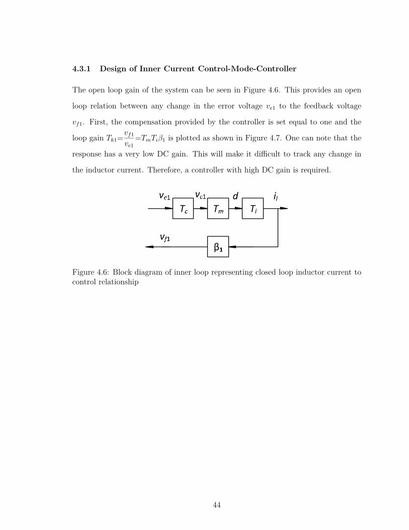
4.3.1 Design of Inner Current Control-Mode-Controller
The open loop gain of the system can be seen in Figure 4.6. This provides an open
loop relation between any change in the error voltage ve1 to the feedback voltage
vf1. First, the compensation provided by the controller is set equal to one and the
loop gain Tk1=vf1
ve1
=TmTiβ1 is plotted as shown in Figure 4.7. One can note that the
response has a very low DC gain. This will make it difficult to track any change in
the inductor current. Therefore, a controller with high DC gain is required.
ë
ì
í î
ïì
ðì íì ñ
Figure 4.6: Block diagram of inner loop representing closed loop inductor current tocontrol relationship
44

| β
1T
ITm
| (dB
)
-30
-25
-20
-15
-10
-5
0
5
10
100 101 102 103 104
φβ
1T
ITm
(°)
-90
-45
0
45
90
Gm = Inf , Pm = 108 deg (at 1.61e+03 Hz)
f (Hz)
Figure 4.7: Magnitude and phase plots of internal loop gain without controller com-pensation.
45

It should also be kept in mind that the ripple in the inductor current needs to
be attenuated to be able to use its average value as the control voltage. Therefore,
a controller with a bandwidth enough to attenuate the inductor current ripples is
required. Since, the ripples have a frequency equal to the switching frequency of
the buck DC-DC converter, a controller with a crossover frequency less than the
switching frequency of the converter can be used. Both the above mentioned criteria
of the controller can be accomplished by using a first order type zero integral controller
as shown in Figure 4.8. The values of R11, R12 and C11 is derived on the basis of
the controller requirement. The transfer function representing this controller can be
derived as follow: From equation (3.1)
vc1
vf1
= −Zf
Z1
, (4.19)
From Figure 4.8, the equation (3.1) can be written as
vc1
vf1
= −R21
R11
[
C11s(R21 +1
C11s)] , (4.20)
vc1
vf1
= −R21
R11
1
R21C11s + 1, (4.21)
Tc = −vc1
ve1
=Zf
Zi
=R21
R11
1
R21C11s + 1, (4.22)
Tc =1
R11C11
1
s +1
R21C11
, (4.23)
is the inner current mode controller transfer function. The DC gain is given by
Tc(0) =R21
R11
. (4.24)
Since the comparison between the average value of inductor current and reference
voltage is required, the slope of the inductor current, when the switch turns off, given
byVO
Lmust be less than the slope of the triangular control voltage to be able to
46

òó
ôó
õõ
öö
óó
óó
÷ó
Figure 4.8: Circuit diagram of a first order type zero current mode controller
compare their average values [2].
Therefore,
VT mfs = β1
VO
L
R21
R11
, (4.25)
where VT mfs is the slope of the PWM control voltage,Vo
Lgives the downward slope
of the inductor current, β1 is the gain due to sense resistance andR21
R11
is the DC gain
of the controller. For this control scheme, the inductor current is sensed using a sense
resistance Rs as shown in Figure 4.5. The sensed resistance for this thesis is selected
to be equal to 0.1 Ω. This sensed current is used to provide control voltage for a
PWM generator. This PWM generator provides a pulse at the required duty cycle
to drive the MOSFET.From equation (4.25),
R21
R11
=LVT mfs
β1VO
, (4.26)
R21
R11
=200 × 10−6(5)(100 × 103)
0.1(12), (4.27)
47

R21
R11
=500
12, (4.28)
whereR21
R11
is the DC gain of this controller. Hence, shows that the controller has
a high DC gain. This will help compensate for the low DC gain for the open loop
gain as seen in Figure 4.7. Now assuming R11 = 1.2 kΩ and from equation (4.28),
we get R12 = 50 kΩ. Now knowing the values of R11 and R21, magnitude and phase
plots of TCL = TmTiTcβ1 can be plotted for different values of C11 to obtain phase
margin of 600. From Figure 4.10 the magnitude and phase plots has a good phase
margin of 59.40, which was obtained at C11 = 60 pF. Figure 4.9, represents the
magnitude and phase plots of the controller. It can be noted from Figure 4.9 that
the controller cut off frequency lies beyond the switching frequency of the buck DC-
DC converter. Therefore, from equation (3.15) the ripples in the inductor current
with frequency equal to the switching frequency of the buck converter do not get
attenuated completely. Instead a small second order time varying control voltage is
produced by the controller. The obtained values are plugged into saber to verify this
current controller. This can be referred in the next chapter.
It can be seen from Figure 4.10 the loop gain with controller transfer function has
a good DC gain thus helps in proper tracking of the change in the inductor current,
while maintaining a good phase margin of 59.40 at 30 kHz.
Now, the reference voltage VR1, which will be required to initiate and maintain
the controller can be calculated by considering the DC gain of the current controller
R12
R11
. Since VC1 = VT mD .
VC1 = 5 × 0.5 = 2.5 V, (4.29)
From equation (4.24)
Tc(0) =R21
R11
=500
12, (4.30)
the output of an op-amp with a non zero voltage at its non-inverting terminal as
48

shown in Figure 4.8 is given by,
VC1 =R11
R21
(VR1 − VF 1) + VR1, (4.31)
the feedback voltage VF 1 comes from the sensed inductor current and is given by
VF 1 = β1IL giving us
VC1 =R11
R21
(VR1 − β1IL) + VR1, (4.32)
VR1 =VC1 + β1IL
R11
R21
1 +R11
R21
(4.33)
Therefore, for the given specification
VR1 =0.241 × 500
512= 0.2353 V . (4.34)
It is to be noted that the controller is designed for a crossover frequency more than
the switching frequency of the converter. therefore, small oscillations in the control
voltage is observed. But these oscillations are not significant and could still reliably
be used as a control voltage.
49

| T
c| (
dB)
-10
-5
0
5
10
15
20
25
30
35
40
103 104 105 106 107
φT
c
(°)
-90
-45
0
Gm = Inf , Pm = 91.4 deg (at 2.21e+06 Hz)
f (Hz)
Figure 4.9: Magnitude and phase plots of average current mode controller
50

| TC
L|(
dB)
-60
-40
-20
0
20
40
60
100 101 102 103 104 105 106
φT
CL
(°)
-180
-135
-90
-45
0
45
90
Gm = Inf dB (at Inf Hz) , Pm = 59.4 deg (at 3.19e+04 Hz)
f (Hz)
Figure 4.10: Magnitude and phase plots of inner loop gain with controller
51

The block diagram as shown in Figure 4.11 could also be used to find out the
closed loop response of the system. The closed loop transfer function of the buck
DC-DC converter with controller is given by
ø
ù
ú û
üù
ýù úù þÿù
Figure 4.11: Block diagram of inner closed loop buck DC-DC converter.
Ticl =il
vr1
=TcTmTi
1 + TcTmTiβ1
. (4.35)
Taking the inverse laplace transform of (4.35), the step response can be plotted using
MATLAB as shown in Figure 4.13. Here, the step change in reference voltage is from
0.23 V to 0.33 V.
52

| Tic
l| (dB
)
-40
-30
-20
-10
0
10
20
30
40
101 102 103 104 105 106
φT
icl (
°)
-180
-90
0
90
Gm = Inf dB (at Inf Hz) , Pm = 22.6 deg (at 1.42e+05 Hz)
f (Hz)
Figure 4.12: Magnitude and phase plots of closed loop control-to-inductor currenttransfer function of buck DC-DC converter.
53

×10-3
0 0.5 1 1.5 2 2.5 3 3.5 42.4
2.5
2.6
2.7
2.8
2.9
3
t (seconds)
iL (
A)
2.75
Figure 4.13: Step response of inductor current of a closed-loop buck DC-DC converterfor a step change in duty cycle
It can be seen from Figure 4.13 that the overshoot is equal to 12% and the rise
time and settling times are 4.9 µs and 2.75 ms, which when compared to an open
loop system as shown in Figure 4.3 has a significant fall in overshoots and rise time.
Thus making the system faster and also reducing surges duty to step change in duty
cycle. the closed loop magnitude and phase plots can be seen in Figure 4.12
4.3.2 Design of Outer Voltage-Mode-Controller
A simple proportional controller could be used to control output voltage but using a
PI controller makes the outer loop slower than the inner current loop. The controller
can be seen in Figure 4.14. The transfer function of this controller can be calculated
54

as shown below.
Figure 4.14: Circuit diagram representing PI controller for outer voltage loop control.
vc = −Zf
Zi
vf , (4.36)
vc = −
11
R4
+1
R5 +1
C1s
R3
vf , (4.37)
vc = −
11
R4
+C1s
C1R5s + 1R3
vf , (4.38)
vc = −
R4(C1R5s + 1)
C1R5s + R4C1s + 1R3
vf , (4.39)
vc = −R4C1R5
R3C1(R5 + R4)
s +1
C1R5
s +1
C1(R5 + R4)
vf , (4.40)
55

vc = −R4R5
R3(R5 + R4)
s +1
C1R5
s +1
C1(R5 + R4)
vf , (4.41)
vc
vf
= −R4R5
R3(R5 + R4)
s +1
C1R5
s +1
C1(R5 + R4)
, (4.42)
which gives the voltage controller transfer function
Tv = −vc
vf
=R4R5
R3(R5 + R4)
s +1
C1R5
s +1
C1(R5 + R4)
. (4.43)
The DC gain is given by
Tv(0) =R4
R3
. (4.44)
For a good bandwidth, a gain of 15 is chosen. From equation (4.44),
R4
R3
= 15, (4.45)
select R3=1000 Ω, that give R4= 15000 Ω. The outer loop gain block diagram can
be seen in Figure 4.15. Now for different values of C1, the loop gain with controller
compensation, given by TV L = Tv
TcTiTm
1 + β1TcTiTm
Ttβ is plotted for a phase margin of
600. At C1 = 1 nF, a good phase margin of 63.70 is obtained. This capacitance is
selected and simulated on saber, which can be observed in next the chapter.
56

Figure 4.15: Block diagram representing outer loop gain
To initiate the controller and maintain the system output voltage a DC reference
voltage VR is required and needs to be calculated. For an op-amp with a non-inverting
pin connected to VR. The output of the controller is given by
VC = VR + Tv(0)(VR − VF ), (4.46)
form equation (4.44), for a low frequency
VC = VR +R4
R3
(VR − VF ), (4.47)
whereR4
R3
is the DC gain of the voltage controller. Since, for the inner current loop
we need VR1 = 0.24 V, from equation (4.33). VC = VR1 = 0.24 V. Therefore,
VC =R4
R3
(VR − VF ) + VR, (4.48)
VR =VC + VF
R4
R3
R4
R3
+ 1, (4.49)
VR =0.24 + (1.2)(15)
16= 1.14 V, (4.50)
The block diagram as shown in Figure 4.17 could used to find out the closed loop
frequency response. The closed loop transfer function of the buck DC-DC converter
57

| TV
L| (
dB)
-200
-150
-100
-50
0
50
100 102 104 106 108
φT
VL
(°)
-270
-225
-180
-135
-90
-45
0
Bode DiagramGm = 15.5 dB (at 4.23e+04 Hz) , Pm = 63.7 deg (at 1.02e+04 Hz)
f (Hz)
Figure 4.16: Magnitude and phase plots of outer loop gain with controller.
58

! " # $%$&$'
( ) *+$%$&$',- ,.
Figure 4.17: Block diagram for closed loop gain of outer voltage loop control.
with controller is given by
Tivl =vo
vr
=TvTicl
1 + TvTiclβ. (4.51)
The inverse laplace of (4.51) provides us with the time domain response of output
voltage. The step response of the output voltage for a step change in refrence voltage
can be plotted using MATLAB as shown in Figure 4.19. The closed loop frequency
response can be seen in Figure 4.18.
59

| Tiv
l| (dB
)
-200
-150
-100
-50
0
50
102 103 104 105 106 107 108
φT
ivl (
°)
-270
-180
-90
0
Gm = -6.08 dB (at 4.23e+04 Hz) , Pm = -25.3 deg (at 5.52e+04 Hz)
f (Hz)
Figure 4.18: Magnitude and phase plots of outer closed loop gain with controller.
60

×10-4
0 0.1 0.2 0.3 0.4 0.5 0.6 0.7 0.8 0.9 112
12.2
12.4
12.6
12.8
13
13.2
t (seconds)
vo (
V)
Figure 4.19: Step response of outer closed loop with controller.
It can be seen from Figure 4.19 that the system has a low overshoot of 0.4 %,
rise and settling time of 18 µs and 68.5 µs giving us a response system with less
overshoot.
61

5 Saber Simulations and Results
5.1 Introduction
Synopsys saber is a proven platform for modeling and simulating many physical sys-
tems. It is a user friendly platform, which provides full-system prototyping. Many
virtual power electronic circuits can be connected and dynamic responses can be
obtained in this interface. The designed controllers along with the buck DC-DC con-
verter can be connected in saber and simulated for its dynamic responses. In this
chapter the controller is tested for the change in load resistance, input voltage and
the controller reference voltage.
5.2 Dynamic Response of Inner Current Control Loop
Circuit diagram of the buck DC-DC converter with inner current control loops con-
nected on saber and can be seen in Figure 5.1. This circuit is simulated by added
forced perturbations in the inductor current by varying load resistance, input voltage
and reference voltage after time t = 15 ms. For each of these changes the steady
state and transient responses of the inductor current is noted to know the controller
properties.
62

Vee
100u
DC/DC
n1:1n2:1
pp
pm
sp
sm
12
S
sd
vee
vcc
PWM Generator
v_dc10
D
k:.1
B1
cncp
rnom:500
100u
initial:0pulse:5
Vtri
vee
vcc
Average Current Controller
v_dc4.9v_dc4.9
v_dc.23
Vee
Vcc
6e−9
6.6RL
v_pulse
initial:0pulse:10
10
r1
irf720_1
s
d
v_pulse
initial:0pulse:10
Figu
re5.1:
Sab
ercircu
itfor
averagecu
rrent
mode
control
ofin
ductor
curren
t.
63

5.2.1 Controller Response
As mentioned earlier the average current mode controller designed eliminates the
ripples from the sensed inductor current to provide the average value at the controller
output. Any error in the average value of the sensed inductor current will be amplified
and will be used for controlling the buck DC-DC converter. Figure 5.2 represents the
control voltage VC1 and the triangular reference voltage of PWM Vtri. It can be seen
that the control voltage is not a pure DC but contains ripples, which are at a phase
difference, with the sensed inductor current. This can be eliminated by using high
capacitance in the feedback of the controller as shown in Figure 5.3. But doing so will
cause the bandwidth of the closed loop control-to-inductor current Ticl to fall. It can
also be noted that in both cases, the control voltage provides almost the same duty
cycle, this is because the phase difference of the control voltage is almost equal to
900 hence the point of intersection of the control voltage with reference voltages are
equal in both cases. But a low capacitance is selected in the feedback as it provides
high Ticl bandwidth.
64

Figure 5.2: Waveforms representing control and sawtooth reference voltages for agood phase margin.
65

Figure 5.3: Waveforms representing control and sawtooth reference voltage with highcapacitance in the feedback of the controller.
66

5.2.2 Dynamic Response of the Buck DC-DC Converter with Inner Cur-
rent Control Loop for the Step Change in Load Resistance
From Figure 5.1, the controller senses for any change in the inductor current, when
the load has changed and provides required compensation to nullify the change in the
inductor current and maintain constant inductor current. But because of the change
in load, the output voltage falls, which can also be seen in Figure 5.4.
Figure 5.4: Waveforms representing inductor current and output voltage of the buckDC-DC converter for a step change in load resistance.
5.2.3 Dynamic Response of the Buck DC-DC Converter with Inner Cur-
rent Control for the Step Change in Input Voltage
For a perturbation in the input voltage the inner current loop provides the required
compensation even before this disturbance can reach the load at the output. Hence,
also controlling the output voltage in the process. The waveforms of the inductor
current and the output voltage for the step change in the input voltage can be seen
67

in Figure 5.5
IL (A
)
0.0
2.0
4.0
6.0
V
O (V
)
−10.0
0.0
10.0
20.0
t(s)
10.0m 12.0m 14.0m 16.0m 18.0m 20.0m
IL (A) : t(s)
Open Loop
Closed Loop
VO (V) : t(s)
Open Loop
Closed Loop
Figure 5.5: Waveforms representing inductor current and output voltage of the buckDC-DC converter for a step change in input voltage.
5.3 Dynamic Response of Outer Voltage Control Loop
Using the values obtained on MATALB, saber circuit is connected and as shown
in Figure 5.6. One can note the output voltage for the designed buck converter in
Figure 5.7. Here, the output voltage is 12V , which satisfies our designed requirement.
This designed buck DC-DC converter is made to pass through dynamic change in load
resistance, input voltage and reference voltage, for which the responses of the inductor
current and output voltage is noted.
68

Vee
Vcc
VR
VR
Vee
100u
DC/DC
n1:1n2:1
pp
pm
sp
sm
28
Vin
12
S
sd
vee
vcc
PWM Generator
D
k:.1
B1
cncp
rnom:500
100u
initial:0pulse:5
Vtri
vee
vcc
Average Current Controller
v_dc4.9v_dc4.9
v_dc1.139
Vee
Vcc
6e−9
6.6RL
k:.1B
vm
vp
vee
vcc
Voltage Controller
rnom:15000
1e−9
rnom:100
rnom:1000
1
r8
irf720_2
s
d
v_pulse
initial:0pulse:10
v_dc10
Figu
re5.6:
Sab
ercircu
itof
abuck
DC
-DC
converter
with
both
inner
curren
tcon
trolan
dou
tervoltage
control.
69

5.3.1 Dynamic Response of the Buck DC-DC Converter with Inner Cur-
rent and Outer Voltage Control Loop for the Step Change in Load
Resistance
It can be seen from Figure 5.7, when the load resistance falls down the output voltage
still remains constant . Since the main aim of this controller is to obtain a constant
output voltage the aim is fulfilled. Using an inner current loop provides a high degree
of control and therefore the steady state error is very low.
IL (A
)
−5.0
0.0
5.0
10.0
V
O (V
)
−10.0
0.0
10.0
20.0
t(s)
0.0 5.0m 10.0m 15.0m 20.0m 25.0m 30.0m
IL (A) : t(s)
Closed Loop
Open Loop
VO (V) : t(s)
Closed Loop
Open Loop
Figure 5.7: Waveforms of inductor current and output voltage of the buck DC-DCconverter for a step change in load resistance.
5.3.2 Dynamic Response of the Buck DC-DC Converter with Inner Cur-
rent and Outer Voltage Control Loop for the Step Change in Input
Voltage
It can be noted from Figure 5.5 that, when the input voltage was stepped up by
10 V, the current control loop provided maximum compensation and prevented the
disturbance to reach the output voltage. This has been improved upon by adding
70

an outer voltage loop, which has decreased the steady state error even further and
this can be noted in Figure 5.8, where the steady state error of the output voltage
has completely been nullified. Also, using a current control loop made sure that
the average inductor current has also been maintained to a required value providing
multiple signal control in the circuit.
Figure 5.8: Waveforms of inductor current and output voltage of the buck DC-DCconverter for a step change in input voltage.
71

6 Conclusion
6.1 Summary
• A current mode controller provides a higher order of control when compared to
voltage mode controller.
• Using circuit averaging technique a small signal model of a non-linear system
can be obtained
• A small signal model can be used to obtain linear transfer functions between
you required quantities.
• Peak, valley, average are few example of different types of controllers available.
They are named based on the characteristic of the sensed signal the controller
manipulates for its control action.
• Since, average current mode controller averages out any high frequency distur-
bances it is preferable for power factor correction circuits.
6.2 Future Work
A first order buck DC-DC converter was designed in this thesis as the buck converter
did not required a higher order controller transfer function. But, many different higher
order average current mode controllers can still be designed depending on the system
to which the controller is to be implemented. Further more this average current mode
controller was implemented to average out the sensed inductor current. But, if the
transfer function which related the switch current of the buck DC-DC converter to
the control voltage is derived then the switch could directly be controlled. Here even
though the switch has discontinuous current the controller will average it out and
provide with a good control signal.
72

7 Bibliography
References
[1] Jorge Alberto Morales-Saldana, Jesus Leyva-Ramos, Enrique Eduardo Carbajal-
Gutierrez, and Ma. Guadalupe Ortiz-Lopez “Average Current-Mode Control
Scheme for a Quadratic Buck Converter With a Single,” IEEE Transactions
on Power Electronics, Vol. 23, No. 1, pp. 485-490, January 2008.
[2] Lloyd Dixon, “Average Current Mode Control of Switching Power Supplies,”
Unitrode Power Supply Design Seminar, pp. 356-369, 1990.
[3] Jian-Min Wang, Sen-Tung Wu, Yanfeng Jiang, Huang-Jen Chiu “A Dual-Mode
Controller for the Boost PFC Converter,” IEEE Transactions on Industrial Elec-
tronics, Vol. 58, No. 1, pp. 369-372, January 2011.
[4] Kashif Habib, Aftab Alam, Shahbaz Khan,“Average Current Control Mode Boost
Converter for the Tuning of Total Harmonic Distortion Power Factor Correc-
tion using PSIM,” Global Journal of Researches in Engineering: Electrical and
Electronics Engineering, Vol. 14, Issue 5, Version 1.0, Year 2014.
[5] M. K. Kazimierczuk, Pulse-Width Modulated DC-DC Power Converters, John
Wiley and Sons: UK, 2nd Edition, 2016.
[6] Farid Golnaraghi, Benjamin C.Kuo, Automatic Control Systems, Ninth Ed., John
Wiley and Sons: USA, 2009.
[7] Kiam Heong Ang, Gregory Chong, Yun Li, “PID Control System Analysis, De-
sign, and Technology, ”IEEE Transactions on Control Systems and Technology,
Vol. 13, No. 4, pp. 559-576, July 2005.
73

[8] W. Tang, F. C. Lee, R. B. Ridley, “Small-Signal Modeling of Average Current-
Mode Control,” publication No. 0-7803-0485-3/92, IEEE Trans. on Power Elec-
tronics, vol. 8, no.2, pp. 112-119 April 1993.
[9] J. Leyva-Ramos, M.G. Ortiz-Lopez, L.H. Diaz-Saldierna, M. Martinez-Cruz,
“Average current controlled switching regulators with cascade boost converters,”
IET Power Electronics., 2011, Vol. 4, Iss. 1, pp. 1-10.
[10] Shamim Choudhury, “Average Current Mode Controlled Power Factor Correc-
tion Converter using TMS320LF2407A,” Digital Power, C2000 DSP and System
Power Management, pp. 1-14, July 2005.
[11] Robert Sheehan, “Understanding and Applying Current-Mode Control Theroy,”
Power Electronics Technology Exhibition and Conference, November 2007.
[12] Yingyi Yan, Fred C. Lee, Paolo Mattavelli, Pei-Hsin Liu, “I2 Average Current
Mode Control for Switching Converters,” IEEE Transactions on Power Electron-
ics, Vol. 29, No. 4, April 2014.
[13] J. G. Kassakian, J. M. Miller, and N. Traub, “Automotive electronics power up,”
IEEE Spectrum, vol. 37, pp. 34-39, 2000.
[14] Ali Aminian, Marian Kazimierczuk Electronic Devices: A Design Approach,
Pearson Prentice Hall, c2004
74