Auger generation as an intrinsic limit to tunneling field-effect ...
16
J. Appl. Phys. 120, 084507 (2016); https://doi.org/10.1063/1.4960571 120, 084507 © 2016 Author(s). Auger generation as an intrinsic limit to tunneling field-effect transistor performance Cite as: J. Appl. Phys. 120, 084507 (2016); https://doi.org/10.1063/1.4960571 Submitted: 07 June 2016 . Accepted: 26 July 2016 . Published Online: 29 August 2016 James T. Teherani , Sapan Agarwal , Winston Chern, Paul M. Solomon, Eli Yablonovitch , and Dimitri A. Antoniadis ARTICLES YOU MAY BE INTERESTED IN 2D-2D tunneling field-effect transistors using WSe 2 /SnSe 2 heterostructures Applied Physics Letters 108, 083111 (2016); https://doi.org/10.1063/1.4942647 Subthreshold-swing physics of tunnel field-effect transistors AIP Advances 4, 067141 (2014); https://doi.org/10.1063/1.4881979 Electrostatics of lateral p-n junctions in atomically thin materials Journal of Applied Physics 122, 194501 (2017); https://doi.org/10.1063/1.4994047
-
Upload
khangminh22 -
Category
Documents
-
view
3 -
download
0
Transcript of Auger generation as an intrinsic limit to tunneling field-effect ...

J. Appl. Phys. 120, 084507 (2016); https://doi.org/10.1063/1.4960571 120, 084507
© 2016 Author(s).
Auger generation as an intrinsic limit totunneling field-effect transistor performanceCite as: J. Appl. Phys. 120, 084507 (2016); https://doi.org/10.1063/1.4960571Submitted: 07 June 2016 . Accepted: 26 July 2016 . Published Online: 29 August 2016
James T. Teherani , Sapan Agarwal , Winston Chern, Paul M. Solomon, Eli Yablonovitch , andDimitri A. Antoniadis
ARTICLES YOU MAY BE INTERESTED IN
2D-2D tunneling field-effect transistors using WSe2/SnSe2 heterostructures
Applied Physics Letters 108, 083111 (2016); https://doi.org/10.1063/1.4942647
Subthreshold-swing physics of tunnel field-effect transistorsAIP Advances 4, 067141 (2014); https://doi.org/10.1063/1.4881979
Electrostatics of lateral p-n junctions in atomically thin materialsJournal of Applied Physics 122, 194501 (2017); https://doi.org/10.1063/1.4994047

Auger generation as an intrinsic limit to tunneling field-effect transistorperformance
James T. Teherani,1,a) Sapan Agarwal,2 Winston Chern,3 Paul M. Solomon,4
Eli Yablonovitch,5 and Dimitri A. Antoniadis3
1Department of Electrical Engineering, Columbia University, New York, New York 10027, USA2Sandia National Laboratories, Albuquerque, New Mexico 87123, USA3Department of Electrical Engineering and Computer Science, Massachusetts Institute of Technology,Cambridge, Massachusetts 02139, USA4IBM T.J. Watson Research Center, Yorktown Heights, New York 10598, USA5Department of Electrical Engineering and Computer Sciences, University of California, Berkeley,California 94720, USA
(Received 7 June 2016; accepted 26 July 2016; published online 29 August 2016)
Many in the microelectronics field view tunneling field-effect transistors (TFETs) as society’s best
hope for achieving a >10� power reduction for electronic devices; however, despite a decade of
considerable worldwide research, experimental TFET results have significantly underperformed
simulations and conventional MOSFETs. To explain the discrepancy between TFET experiments
and simulations, we investigate the parasitic leakage current due to Auger generation, an intrinsic
mechanism that cannot be mitigated with improved material quality or better device processing.
We expose the intrinsic link between the Auger and band-to-band tunneling rates, highlighting the
difficulty of increasing one without the other. From this link, we show that Auger generation
imposes a fundamental limit on ultimate TFET performance. Published by AIP Publishing.[http://dx.doi.org/10.1063/1.4960571]
I. INTRODUCTION
Deceleration of Moore’s law scaling of complementary
metal-oxide-semiconductor (CMOS) field-effect transistors
has prompted an urgent search for next-generation logic
devices.1 Of all exploratory devices under consideration,
tunneling field-effect transistors (TFETs) offer the most
promise due to their potential speed, energy efficiency, and
compatibility with existing CMOS infrastructure.2,3
The key advantage of TFETs over existing technologies
is the possibility for significant energy reduction achieved
through energy-efficient switching of band-to-band tunneling
(BTBT) current. The switching characteristics of transistors
are assessed by the subthreshold swing, dVG=d log10ðIDÞ,which gives the change in gate voltage to produce a 10�increase in drain current. The quantum-mechanical nature of
BTBT allows significantly sharper switching for TFETs
compared to conventional transistors. [The subthreshold
swing of conventional transistors is governed by the Fermi-
Dirac distribution of carriers above a potential barrier whose
height is modulated by the gate voltage. The thermionic cur-
rent resulting from carriers above this barrier produces the
often-cited 60-mV/decade subthreshold swing at 300 K.
TFETs, on the other hand, can overcome the 60-mV/decade
thermal limit because they switch by modulating tunneling
through a barrier, instead of over it.] Sharper switching of
TFETs, corresponding to smaller subthreshold swings, ena-
bles lower voltage operation yielding substantial energy sav-
ings over conventional devices.
However, despite many years of considerable world-
wide effort, TFETs with switching characteristics superior
to MOSFETs (i.e., TFETs with subthreshold swings
<60 mV/decade at 300 K) for currents greater than 10 nA/
lm have not been demonstrated. (See Lu and Seabaugh’s
review4 for a compilation of the most recent TFET results.)
Previous work focused on trap-related phenomena, such as
Shockley–Read–Hall generation, degraded gate efficiency,
and trap-assisted tunneling, to explain non-ideal device
characteristics.5–8 More recently, Teherani et al.9 suggest
that intrinsic phenomena, such as Auger, phonon-assisted,
and radiative generation, may also limit TFET performance
and explain the 60-mV/decade room-temperature swings
observed in several experimental papers.10–12 This work
expands on this idea and describes an intrinsic mecha-
nism—Auger generation—that may limit the minimum
subthreshold swing, off-current, and on/off ratio of experi-
mental TFETs. Auger generation must be understood to
improve TFET switching characteristics so that sizeable
energy reduction can be attained.
II. BACKGROUND ON AUGER GENERATION
Auger generation, also called impact ionization, occurs
when a high-energy carrier collides with an electron in the
valence band, resulting in the high-energy carrier losing much
of its momentum and exciting the valence-band electron to
the conduction band, creating an electron–hole pair. Auger
generation is the reverse of Auger recombination, where the
recombination of an electron–hole pair excites a third carrier
to a high-kinetic-energy state. For both generation and recom-
bination, the high-energy carrier can be either an electron or a
hole (Figure 1).
a)Author to whom correspondence should be addressed. Electronic mail:
0021-8979/2016/120(8)/084507/15/$30.00 Published by AIP Publishing.120, 084507-1
JOURNAL OF APPLIED PHYSICS 120, 084507 (2016)
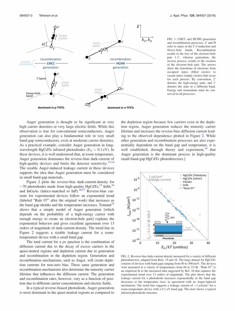
Auger generation is thought to be significant at very
high carrier densities or very large electric fields. While this
observation is true for conventional semiconductors, Auger
generation can also play a fundamental role in very small
band-gap semiconductors, even at moderate carrier densities.
As a practical example, consider Auger generation in long-
wavelength HgCdTe infrared photodiodes (EG � 0.1 eV). In
these devices, it is well understood that, at room temperature,
Auger generation dominates the reverse-bias dark-current of
high-quality devices and limits the detector sensitivity.13,14
The sizable Auger-induced leakage current in these devices
supports the idea that Auger generation must be considered
in small band-gap materials.
Figure 2 plots the reverse-bias dark-current-density for
�70 photodiodes made from high-quality HgCdTe,15 InSb,16
and InGaAs (lattice-matched to InP).16,17 Reverse-bias cur-
rents for experimental devices follow an exponential trend
(labeled “Rule 07” after the original work) that increases as
the band gap shrinks and the temperature increases. Tennant15
shows that a simple model of Auger generation [which
depends on the probability of a high-energy carrier with
enough energy to create an electron-hole pair] explains the
exponential behavior and gives excellent agreement over 13
orders of magnitude of dark-current-density. The trend line in
Figure 2 suggests a sizable leakage current for a room-
temperature device with a small band gap.
The total current for a pn junction is the combination of
diffusion current due to the decay of excess carriers in the
quasi-neutral regions and depletion current due to generation
and recombination in the depletion region. Generation and
recombination mechanisms, such as Auger, will create deple-
tion currents for non-zero bias. These same generation and
recombination mechanisms also determine the minority carrier
lifetime that influences the diffusion current. The generation
and recombination rates, however, vary as a function of posi-
tion due to different carrier concentrations and electric fields.
In a typical reverse-biased photodiode, Auger generation
is most dominant in the quasi-neutral regions as compared to
the depletion region because few carriers exist in the deple-
tion region. Auger generation reduces the minority carrier
lifetime and increases the reverse-bias diffusion current lead-
ing to the observed dependence plotted in Figure 2. While
other generation and recombination processes are also expo-
nentially dependent on the band gap and temperature, it is
well established, through theory and experiment,14 that
Auger generation is the dominant process in high-quality
small-band-gap HgCdTe photodetectors.]
FIG. 1. CHCC and HCHH generation
and recombination processes. C and H
refer to states in the C-Conduction and
Heavy-hole bands. Recombination
results in the loss of the electron–hole
pair 1-10, whereas generation, the
inverse process, results in the creation
of the electron–hole pair. The arrows
show the transitions of electrons from
occupied states (filled circles) to
vacant states (empty circles) that occur
for each process. By convention, 20
denotes the high-energy state, and 10
denotes the state in a different band.
Energy and momentum must be con-
served in all processes.
FIG. 2. Reverse-bias dark-current-density measured for a variety of different
photodetectors, adapted from Refs. 15 and 16. The large dataset for HgCdTe
consists of devices with band gaps ranging from 80 to 500 meV. The devices
were measured at a variety of temperatures from 60 to 313 K. “Rule 07” is
an empirical fit to the measured data suggested by Ref. 16 that captures the
experimental trend over 13 orders of magnitude. The plot shows that the
leakage current for a photodiode increases exponentially as the band gap
decreases or the temperature rises, in agreement with an Auger-induced
mechanism. The trend line suggests a leakage current of �1 lA/lm2 for a
room-temperature device with a 0.1-eV band gap. The inset shows a typical
infrared photodiode structure.
084507-2 Teherani et al. J. Appl. Phys. 120, 084507 (2016)

Though many TFETs are fabricated from conventional
semiconductors with relatively large band gaps, the energy
separation between the electron and hole eigenstates of the
tunneling region becomes exceedingly small as the device is
turned on. For example, the perpendicular n-TFET (Figure 3)
is switched on by biasing the structure so that the hole eigen-
state of the source aligns in energy with the electron eigenstate
of the channel. Ideally, the device remains off and no current
flows until the electron and hole eigenstates align in energy
(Figure 4(c)). But right before the bands align, a small energy
separation exists between the electron and hole eigenstates in
the tunneling region. The eigenstate energy separation of thetunneling region resembles a small-band-gap semiconductorwhose band gap changes with applied gate voltage.
Consequently, as will be shown, Auger generation, in
addition to other generation and recombination processes,
will occur at significantly higher rates than traditionally
expected due to the small eigenstate energy separation of the
tunneling region as compared to the large band gap of the
bulk material.
To further underscore the importance of intrinsic genera-
tion and recombination in TFETs, consider a device just
before ideal band-to-band tunneling occurs where the electron
and hole states of the tunneling junction are separated by the
thermal energy, kT (e.g., Figure 4(b)). Tunneling occurs only
when the states align in energy if there is some spatial overlap
of the electron and hole states at the tunneling junction.
[A zero spatial overlap signifies that the electrons and holes
are completely disconnected from each other. Even with
abrupt band-edges, the amplitudes of the electron and hole
wavefunctions have an approximately exponential decay in
the band gap of the material. Under the WKB framework, this
decay is viewed as the exponentially decreasing tunneling
probability with barrier thickness.] Given the spatial overlap
of electrons and holes and the very small energy separation
between the eigenstates, non-defect-mediated generation and
recombination processes, often negligible in conventional
devices, can couple the electron and hole states with signifi-
cant transition rates. In this work, we address this problem by
first establishing a framework for analyzing Auger generation,
and then calculating the Auger rate as a function of the energy
separation between the electron and hole eigenstates. The rate
is then related to a minimum current, and its impact on sub-
threshold swing is shown to set intrinsic limits to TFET
device performance.
III. DEVICE STRUCTURE AND OPERATION
We analyze the Auger transition rate for the perpendicu-
lar TFET structures depicted in Figure 3. The ideal turn-on
of the device occurs when a sufficient gate bias is applied
such that the electron eigenstate of the n-layer aligns in
energy with the hole eigenstate of the p-layer (Figure 4(c)).
Two doping versions of the structure exist, the n-TFET
and p-TFET (Figure 3). They are named in analogy with n-and p-MOSFETs since they follow the same biasing
conventions.
Generally, the potential bias of the pþ source of the
n-TFET sets the quasi-Fermi level for holes while the nþdrain sets the quasi-Fermi level for electrons. For an n-TFET,
FIG. 3. Device structure of perpendicular p-, n-, and bilayer TFETs. The terminal voltages indicate a typical biasing scheme, and the purple oval indicates the
region over which band-to-band tunneling (BTBT) nominally takes place. The p and n layers can be made from the same material or different materials to
form a homostructure or heterostructure device. The bilayer TFET29 has no intentional channel doping, and uses top and bottom gates to electrostatically
induce electrons and holes. The bilayer n-TFET is often biased with a constant negative back gate voltage (�VB) to create a hole-rich layer along the bottom
of the channel, while the top gate voltage (þVG) is varied to modify the energy alignment of the electron and hole eigenstates.
FIG. 4. Energy-band diagram across the tunneling region of an n-TFET. The gate voltage is increased from a to c. The dashed lines represent the ground-state
subband energy for the electron and hole eigenstates. The gray area represents the electron and hole density as a function of position. (a) DE is the energy sepa-
ration between the first electron and hole eigenstates, which varies with gate voltage. (b) As the gate voltage is increased, band bending occurs mostly in the
n-region reducing DE. Generation and Recombination transition rates increase exponentially as the energy separation becomes smaller than the bulk band gap.
(c) At a sufficient gate voltage, the eigenstates align in energy ðDE ¼ 0Þ, and ideal band-to-band tunneling (BTBT) can occur.
084507-3 Teherani et al. J. Appl. Phys. 120, 084507 (2016)

the drain’s communication with electrons in the channel is
unimpeded, whereas communication with the source is
restricted by the tunneling barrier. The drain bias is typically
much larger than the thermal voltage (VD � kT=q), and elec-
trons in the channel are depleted by the drain as fast as they
are supplied (assuming ballistic transport). If the tunneling
probability from the source is low, the electron occupancy of
the channel will also be low. The strength of Auger genera-
tion in an n-TFET does not depend on the precise electron
occupancy, only that the electron concentration is low enough
to prevent efficient recombination of the generated carriers. A
related situation occurs for p-TFETs, where the hole concen-
tration in the channel is decreased by the negative drain bias.
To achieve reasonable tunneling current and gate con-
trol, the thickness of the lightly doped layer must be quite
thin (�10 nm), resulting in carrier-energy quantization. This
quantization may or may not occur in the heavily doped
layer, depending on its thickness. Previous work18 suggested
beneficial device performance for 2D-to-2D tunneling as
compared to 2D-to-3D tunneling. In our work, both electron
and hole energies are considered to be quantized in their
respective layers, a treatment that can be extended to devices
with thick layers by considering carriers to be quantized but
with a very small energy separation between eigenstates.
This approach allows our methodology to be applied to a
wider variety of device structures.
IV. THEORY OF AUGER GENERATION ANDRECOMBINATION
Auger transitions can occur among many different bands.
The type of transition is denoted by a four-letter initialism that
identifies the bands for the initial and final states of the two
particles involved in the process. C, H, S, and L correspond to
the C-Conduction, Heavy-hole, Split-off hole, and Light-hole
bands. We focus on Auger generation for two cases: (1) the
CHCC process, when a high-energy electron in the conduction
band collides with an electron in the heavy-hole band, knock-
ing it into the conduction band; and (2) the HCHH process,
when an energetic hole collides with a valence electron, excit-
ing it into the conduction band. These processes are schemati-
cally illustrated in Figure 1. In both processes, energy and
momentum must be conserved. While we address CHCC and
HCHH processes, other transitions, such as HCHS and
HCHL, also occur. HCHS and HCHL processes occur at
much higher rates than HCHH in most p-type bulk materials
with HCHS dominating in materials with band gaps greater
than or equal to the split-off energy (EG � D).19,20 We investi-
gate HCHH in this work due to its similarity with CHCC and
as a means to establish the theoretical framework. Additional
work is needed to compare HCHH, HCHL, and HCHS rates
as a function of eigenstate energy separation.
The relative rates of the different transitions depend on
specific parameters, such as the split-off energy, effective-
mass, and quantization energy of the different bands. Our
work is restricted to transitions between the first heavy-hole
subband and the first C subband to demonstrate the key depen-
dencies of the Auger transition rate. Transitions not considered
in this work increase the transition rate but do not significantly
alter our overall conclusion—that Auger transitions play a key
role in determining the subthreshold behavior of TFETs.
The dominance of CHCC or HCHH in a specific device
depends on the relative electron and hole concentrations in
the channel. CHCC generation requires a reasonable electron
concentration because multiple electrons are involved in the
transition; HCHH generation requires a reasonable hole con-
centration. Low electron concentration in the n-TFET channel
(due to the drain bias, explained in Section III) causes HCHH
to dominate, whereas low hole concentration in p-TFETs
causes CHCC to dominate. We derive rates for the CHCC and
HCHH processes, but typically only one is dominant in a spe-
cific TFET structure due to the doping profile and the applied
bias.
The expression for the net Auger recombination rate per
unit area (U) is derived using Fermi’s Golden Rule to give21
U ¼ R� G
¼ 1
A
2p�h
X1; 10; 2; 20
P 1; 10; 2; 20ð Þ jMj2 d E1 � E10 þ E2 � E20ð Þ;
(1)
where R� G is the difference between recombination and
generation, and the sum is over all initial and final states
including spin. Here, A is the in-plane area of the quantum
well, �h is the reduced Planck constant, P is the occupation
probability function, M is the matrix element that couples
the initial and final states, and dðE1 þ E2 � E10 � E20 Þensures energy conservation. Components of the Auger rate
are described in Sections IV A–IV C.
A. Occupation probability function
The driving force for net recombination is the occupation
probability function (P) that gives the difference between the
occupation of states required for the forward (recombination)
and reverse (generation) processes. Following the diagram of
Figure 1, P is expressed by
PCHCCð1; 10; 2; 20Þ ¼ fcðE1ÞfcðE2Þf 0vðE10 Þf 0cðE20 Þ� f 0cðE1Þf 0cðE2ÞfvðE10 ÞfcðE20 Þ� fcðE1ÞfcðE2Þf 0vðE10 Þ � fcðE20 Þ; (2a)
PHCHHð1; 10; 2; 20Þ ¼ f 0vðE1Þf 0vðE2ÞfcðE10 ÞfvðE20 Þ� fvðE1ÞfvðE2Þf 0cðE10 Þf 0vðE20 Þ� f 0vðE1Þf 0vðE2ÞfcðE10 Þ � f 0vðE20 Þ; (2b)
where
fc;v Eð Þ ¼ 1
1þ expE� EFn;p
kT
and f 0c;v Eð Þ ¼ 1� fc;v Eð Þ;
(3)
fc and fv are the Fermi-Dirac distributions for a state to be
occupied in the conduction and valence bands with quasi-
Fermi levels EFn and EFp, respectively, and kT is the thermal
energy. Similarly, f 0 is the probability for a state to be vacant.
084507-4 Teherani et al. J. Appl. Phys. 120, 084507 (2016)

The approximation to P in Eq. (2) assumes f 0c � 1 and fv � 1,
appropriate for non-degenerate carrier concentrations (dis-
cussed further below Eq. (6)). Equations (2a) and (2b) can be
manipulated into their typical forms
PCHCC 1; 10; 2; 20ð Þ � n
Nc
np
nopo� 1
� �exp �E20 � Ec
kT
� �; (4a)
PHCHH 1; 10; 2; 20ð Þ � p
Nv
np
nopo� 1
� �exp
E20 � Ev
kT
� �; (4b)
by employing Maxwell–Boltzmann statistics.22 Here, n and
p are the 2D densities of electrons and holes, and no and po
are their values in quasi-equilibrium. [Quasi-equilibrium
means VDS ¼ 0, but VGS can vary.] Nc and Nv are the 2D den-
sities of states of the conduction band and valence band, and
Ec and Ev are the subband ground-state energies for the con-
duction and valence bands. [Equations (4) and (5) are also
valid for 3D densities with the appropriate redefinition of
variables from 2D to 3D.] The bracketed factor represents
the difference between recombination and generation. In
equilibrium n ¼ no, p ¼ po, and the net rate is zero. An np-
product greater than equilibrium results in net recombina-
tion, whereas an np-product less than equilibrium results in
net generation. When considering the impact of drain and
source potentials, it is useful to note that
np
nopo¼ exp
EFn � EFp
kT
� �: (5)
For reverse bias, np� nopo, and Eq. (4) can be written as
PCHCC 1; 10; 2; 20ð Þ � � n
Ncexp �E20 � Ec
kT
� �; (6a)
PHCHH 1; 10; 2; 20ð Þ � � p
Nvexp
E20 � Ev
kT
� �: (6b)
The use of Eq. (6) makes the implicit assumptions that
(i) the carrier probability at the high-energy state j20i is
accurately modeled by non-degenerate statistics,
(ii) the reverse bias is sufficient to make recombination
negligible, and
(iii) the joint probability of an electron in the valence band
along with a vacant state in the conduction band is
sufficiently high such that it does not limit the crea-
tion of an electron–hole pair.
Assumption (i) is reasonable in most cases because
the high-energy state is typically far from the band-edge,
making the use of Maxwell–Boltzmann statistics at E20
appropriate.
Assumption (ii) is valid given the conditions explained
in Section III.
Assumption (iii) is justified by revisiting the non-
degenerate approximation in Eq. (2): the generation term of
PCHCC is given by f 0cðE1Þf 0cðE2ÞfvðE10 ÞfcðE20 Þ � fcðE20 Þ. In the
non-degenerate limit, f 0c � 1 and fv � 1, and the approximation
results in little error. As the electron concentration increases
towards the degenerate limit, fcðE20 Þ grows exponentially
while f 0cðE1Þ and f 0cðE2Þ decrease slightly. Even at the extreme
when the Fermi level is located at E1 and E2 [which assumes
that E1 ¼ E2, shown to be the condition for the most probable
transition in Appendix C:], f 0cðE1Þ ¼ f 0cðE2Þ ¼ 12, leading to
only a 4� error; however, at the same time, fcðE20 Þ has grown
exponentially by many orders of magnitude, dominating the
characteristics for P. It is therefore reasonable to neglect f 0c and
fv factors for most cases.
B. Matrix element and wavefunctions
The square of the total matrix element for the Auger
process is given by23
(7)
where
Mij ¼ð ð
W10 rið ÞW20 rjð Þq2
4p�jr1 � r2jW1 r1ð ÞW2 r2ð Þ d3r1d3r2:
(8)
[The physics community often uses CGS units such that the
denominator of Eq. (8) is missing the 4p-factor. Because our
work uses SI units (with energy in eV), we include the 4p-fac-
tor.] WnðrÞ is the wavefunction for state jni, q is the elementary
charge, and � is the permittivity of the semiconductor. (For the
low-energy transitions analyzed in this work, the corresponding
frequency is relatively low and use of the static permittivity is
reasonable. See Refs. 24 and 25 for a more detailed discussion
regarding the use of the static versus optical permittivity.) The
bold notation indicates a vector quantity. The middle factor in
Eq. (8) emphasizes the electron–electron Coulombic interaction
between particles 1 and 2 that causes the Auger transition.
The total matrix element includes coupling due to col-
liding electrons with the same spins and opposite spins. M12
represents the transition from j1; 2i ! j10; 20i, whereas M21
indicates j1; 2i ! j20; 10i. When the particles have opposite
spins, they are distinguishable, and no interference occurs.
The contribution of opposite spin collisions to Eq. (7) is
jM12j2 þ jM21j2. When the electrons’ spins are the same, the
M12 and M21 processes interfere due to the exchange interac-
tion resulting in the jM12 �M21j2 term in Eq. (7). (See Refs.
23 and 26 for further explanation.)
The wavefunctions for the conduction and valence
bands are given by Bloch functions with confinement along
the z-direction (perpendicular to the quantum well)26
Wc;k rð Þ ¼ 1ffiffiffiAp uc;k rð Þei kxxþkyyð Þwc zð Þ
¼ 1ffiffiffiAp
XG
ak;Gei kxþGxð Þxþ kyþGyð ÞyþGzzð Þwc zð Þ; (9a)
Wv;k rð Þ ¼ 1ffiffiffiAp uv;k rð Þei kxxþkyyð Þwv zð Þ
¼ 1ffiffiffiAp
XG
bk;Gei kxþGxð Þxþ kyþGyð ÞyþGzzð Þwv zð Þ; (9b)
084507-5 Teherani et al. J. Appl. Phys. 120, 084507 (2016)

where k is the wavevector, uðrÞ is the cell-periodic function
with periodicity of the crystal, eiðkxxþkyyÞ and wðzÞ are the
envelope wavefunctions along the in-plane and confined
dimensions, and the summation is a Fourier series expansion
of u in terms of G, the set of all reciprocal lattice vectors.
Following the procedure detailed in Appendix A, the
Auger matrix element for a quantum well is found to be
MQW12 ¼
q2
2�A
dk?1�k?10 þk?2�k?20
jk?1 � k?10 jV; (10)
where
V ¼ hu10 ju1ihu20 ju2ihw10 jw1ihw20 jw2i: (11)
Here,
hujjuii ð
Xcell
uj;kjðrÞui;ki
ðrÞd3r; (12)
hwjjwii ð
wj ðzÞwiðzÞdz; (13)
and Xcell is the volume of a unit cell. As shown in Appendix
C, the most probable transition occurs when k1 ¼ k2, which
gives M12 � M21. Because M12 and M21 are nearly equal, the
squared matrix element of Eq. (7) can be approximated by
jMj2 � 2jM12j2: (14)
Physically, Eq. (14) suggests that only collisions between
carriers of opposite spins contribute significantly to Auger
transitions.
C. Wavefunction overlap
The Auger matrix element depends on the overlap inte-
grals of the cell-periodic function u and the envelope func-
tion w. The overlap integrals within the same band are taken
to be unity,21 so that Eq. (11) can be simplified to
V � hu10 ju1ihw10 jw1i; (15)
whereby the numbering convention of Figure 1 is followed,
and states j1i and j10i are defined to be in different bands.
The overlap of the periodic part of the Bloch functions
hu10 ju1i is not straightforward to calculate. Burt et al.25 show
that the use of the effective-mass sum-rule method, often
used to calculate hu10 ju1i, is flawed, and instead compute the
cell-periodic Bloch function overlap between the C and
heavy-hole bands using the 15-band k � p and non-local pseu-
dopotential methods. In a subsequent work,27 the same
authors calculate hu10 ju1i for additional III–V and II–VI
direct-gap semiconductors. Both studies show strong agree-
ment between the k � p and pseudopotential methods.
Pseudopotential calculations27 give similar results for III–V
(InSb, GaSb, GaAs) and II–VI (CdTe, ZnSe) semiconduc-
tors, with the overlap for II–VIs approximately half that of
III–Vs. For both sets of materials, the cell-periodic Bloch
function overlap has a nearly linear dependence on the
wavevector difference between the C and heavy-hole band
(K ¼ jk1 � k10 j) and is given by
jhu10 ju1ij � cuK; (16)
where cu equalsffiffiffiffiffiffiffiffiffiffiffiffiffiffiffiffiffiffiffiffi2� 10�17p
cm for III–V andffiffiffiffiffiffiffiffiffiffiffiffiffiffiffiffiffiffiffiffi6� 10�18p
cm for II–VI semiconductors. Note that Eq. (16) agrees with
the work of Verhulst et al.,28 which highlights the zero-
coupling between the C and heavy-hole band at zone-center
(i.e., when K ¼ 0).
The calculation of hw10 jw1i depends on the details of the
structure. Specifically, the envelope wavefunction overlap is
affected by
(i) the effective mass of electrons and holes in the quanti-zation direction: As the effective mass decreases, the
particle is less confined to its well and a large fraction
of its wavefunction leaks into the band gap.
(ii) the width of the quantum well: As the quantum well
widens, a larger separation distance between electron
and hole wavefunctions occurs when a perpendicular
electric field is applied to the quantum well. The
wavefunctions separate in real space and hw10 jw1idecreases considerably. For the same reason, BTBT
also decreases considerably as the distance between
holes and electrons (i.e., the tunneling distance)
increases.
(iii) the doping profile in the tunneling region: Doping modi-
fies the energy-band diagram and thus the wavefunc-
tions. Arbitrary doping profiles require a self-consistent
calculation of the coupled Poisson–Schr€odinger equa-
tions to determine the wavefunctions and the overlap
integral.
For a structure with low doping concentration, such as
the bilayer TFET29 shown in Figure 3, the energy-band dia-
gram is well-modeled by a uniform electric field across the
tunneling junction. The exact wavefunctions for a quantum
well with a uniform electric field have been solved analyti-
cally and shown by Ref. 30 to be a linear combination of Airy
functions. In Figure 5, we calculate the wavefunction overlap
hw10 jw1i for an InAs quantum well with a uniform electric
field. hw10 jw1i at eigenstate energy alignment (DE ¼ 0) varies
from approximately 0.01 to 0.1 as the quantum-well width
decreases from 20 to 10 nm.
D. Auger rate equation
To arrive at a simplified form of the Auger rate equation,
the terms derived in Secs. IV A–IV C are substituted into Eq.
(1) to give
UCHCC �1
A
2p�h
X1; 10; 2; 20
� n
Ncexp �E20 � Ec
kT
� �
� 2q2
2�A
dk?1�k?10 þk?2�k?20
jk?1 � k?10 j
!2
� cuKð Þ2 jhw10 jw1ij2 d E1 � E10 þ E2 � E20ð Þ;
(17a)
084507-6 Teherani et al. J. Appl. Phys. 120, 084507 (2016)

UHCHH �1
A
2p�h
X1; 10; 2; 20
� p
Nvexp
E20 � Ev
kT
� �
� 2q2
2�A
dk?1�k?10þk?2�k?20
jk?1 � k?10 j
!2
� cuKð Þ2 jhw10 jw1ij2 d E1 � E10 þ E2 � E20ð Þ:
(17b)
Following the procedure in Appendix B, the summation over
all states is converted to an integral that evaluates to
GCHCC �q4mc
3 kTð Þ2cu2
4p2�h7�2
lþ 1ð Þ2lþ 1ð Þ2
jhw10 jw1ij2
� n
Ncexp � 2lþ 1ð Þ
lþ 1ð ÞDE
kT
� �; (18a)
GHCHH �q4mv
3 kTð Þ2cu2
4p2�h7�2
l�1 þ 1� �2l�1 þ 1ð Þ2
jhw10 jw1ij2
� p
Nvexp � 2l�1 þ 1
� �l�1 þ 1ð Þ
DE
kT
!; (18b)
where G is the areal generation rate; DE is the energy separa-
tion between the first electron and hole subbands; l ¼ mc=mv,
and mc and mv are the density-of-states masses for the C and
heavy-hole bands. [When using energy units of ½eV�, the q4-
factor in Eq. (18) is equal to ð1:602…� 10�19Þ2 ½e2 C2�,where C is Coulombs and e is the elementary unit of charge.
Using this prescription, the q2=�-factor of the Coulombic
potential is expressed in units of ½ e CF=cm� ¼ eV cm½ �.]
The exponential factor in the generation rate results
from the Maxwell–Boltzmann probability of a carrier in the
high-energy state j20i. For example, in the case of CHCC
generation, there is a high probability for an empty state in
the conduction band at j1i and j2i and an electron in the
valence band at j10i, but a low probability of an electron at
j20i that ultimately limits the generation rate (see Figure 1).
The minimum energy for j20i that satisfies energy and
momentum conservation is
CHCC: E20min¼ 2lþ 1
lþ 1DE; (19a)
HCHH: E20min¼ 2l�1 þ 1
l�1 þ 1DE: (19b)
Equation (19) is derived in Appendix C. By substituting
Eq. (19) into (6), the origin of the exponential dependence of
the generation rate can be readily understood.
E. Auger generation current
Because Auger generation occurs in the high-field
region of a reverse-biased pn junction, nearly all the gener-
ated carriers are swept out to the contacts where they
contribute to device current. With this assumption, the
current-density due to generation can be expressed as
Jgen ¼ qG; (20)
where the sign of Jgen is defined to correspond with the sign
of the drain current ID.
If the material properties and structural details are
known, the Auger generation current can be calculated using
Eqs. (18) and (20). We define a generic material to provide
an Auger generation current that is relevant to a wide variety
of material and doping configurations. The generation cur-
rent for a specific structure can be determined by multiplying
the current for the generic material by relevant scaling
factors.
Figure 6 shows a plot of the generation current-density as
a function of DE for different ratios of the electron and hole
mass for CHCC and HCHH processes. The exponential factor
of Eq. (18) dominates the current characteristics, giving rise
to room-temperature subthreshold swings (dDE=d log10ðJgenÞ)between 30 and 60 meV/decade, depending on the mass ratio.
The change in the envelope wavefunction overlap with DE(Figure 5) is significantly weaker than the exponential depen-
dence of the Auger rate assuming unity overlap (Figure 6).
Therefore, inclusion of a DE-dependent wavefunction overlap
to Figure 6 will lower the calculated rate, but not significantly
change the trends with DE.
To convert from DE to gate voltage, VG, the gate effi-
ciency of the device must be known. As described in Ref.
29, the incremental gate-voltage efficiency ðdDE=dðqVGÞÞ is
poor for materials with a small effective mass. Increasing VG
to decrease DE (Figure 4(c)) increases the field across the
junction leading to increased quantization that increases DE.
For example, the expected gate efficiency for a TFET with a
15-nm InAs body and 1-nm effective oxide thickness is
FIG. 5. Overlap integral of the electron and hole envelope wavefunctions as
a function of DE (the energy separation between the first electron and hole
eigenstates) for an InAs quantum well with a uniform electric field. An elec-
tric field is applied across the quantum well to decrease DE, which increases
the distance between electron and hole distributions and hence decreases the
envelope wavefunction overlap. Increasing the body thickness also leads to
decreased overlap since the carriers are farther apart. The insets show a
double-gated bilayer TFET structure with a uniform electric field across the
channel. The corresponding energy-band diagram is shown to the left of the
structure.
084507-7 Teherani et al. J. Appl. Phys. 120, 084507 (2016)

�40% (Ref. 29). Such a low gate efficiency will further
degrade the subthreshold swing in these devices.
V. COMPARISON OF AUGER AND BTBT PROCESSES
Even though BTBT is a single-particle process while
Auger requires two particles, BTBT and Auger transitions
are not remarkably different phenomena. Both can be viewed
as generation and recombination events, and Fermi’s Golden
Rule can be used to calculate the transition rate. Changing a
device design to increase BTBT likely increases Auger tran-
sition rates. We believe that the relationship between Auger
and BTBT is instructive for designing devices that minimize
Auger and maximize BTBT.
Applying Fermi’s Golden Rule to calculate the BTBT
rate gives18
UBTBT ¼ R� G ¼ 1
A
2p�h
X1; 10
P 1; 10ð Þ jMj2 d E1 � E10ð Þ: (21)
The occupation probability function for BTBT (P) is the dif-
ference between recombination (where an electron in the
conduction band tunnels to the valence band) and generation
(where an electron in the valence band tunnels to the conduc-
tion band). P is given by
PBTBT 1; 10ð Þ ¼ fc E1ð Þf 0v E10ð Þ � f 0c E1ð Þfv E10ð Þ
� np
nopo� 1; for EFn < E1 ¼ E10 < EFp; (22)
where the approximation assumes Maxwell–Boltzmann sta-
tistics. For BTBT in a sufficiently reverse-biased pn junction,
np� nopo and PBTBT � �1. [PBTBT is defined for net recom-
bination so a negative value indicates net generation.]
The equations for the occupation probability function
for BTBT (22) and Auger (4) are quite similar. The same
driving force is seen in both functions, with the Auger func-
tion scaled by the probability of a carrier in the high-energy
state j20i. This probability factor is crucial to the different
dependencies of Auger and BTBT rates.
The matrix element for BTBT tunneling is given by
MBTBT ¼ð
W10 ðrÞ q/ðzÞW1ðrÞ d3r; (23)
where q/ðzÞ is the potential energy in the depletion region of
the pn junction, and W1 and W10 are wavefunctions in the
valence and conduction band. Following the derivation in
Appendix D, the matrix element can be rewritten as
MBTBT ¼ ðqFÞzcvdk?1�k?10 hw10 jw1i; (24)
where
jzcvj2 ¼�h2
4mrEGand mr ¼
mcmv
mc þ mv: (25)
Here, a constant electric field (F) across the tunneling junc-
tion is assumed, dk?1�k?10 ensures perpendicular momentum
conservation, EG is the band gap including quantization
energy, mr is the reduced mass, and zcv ¼ u10 jid=dkzju1. The
expression for zcv in Eq. (25) results from Kane’s two-band
k � p calculations.31
The similarity between the matrix element for BTBT
(24) and Auger (10) should be noted. Both require perpen-
dicular momentum conservation and are proportional to the
overlap of the envelope wavefunctions of the valence and
conduction bands, hw10 jw1i.The BTBT rate is derived in Appendix E, and the areal
generation rate is found to be
GBTBT ¼qFð Þ2
2�hEGjhw10 jw1ij
2; for DE 0: (26)
Equation (26) looks quite different from typical expressions
for BTBT because most of the details of the tunneling
process are hidden in the hw10 jw1i factor. Using this equa-
tion, the intrinsic on/off ratio between the BTBT and Auger
rates at the point of ideal TFET turn-on (DE ¼ 0) is found
to be
GBTBT
GCHCC¼ qFð Þ2
EG
2p2�h6�2
q4mc3 kTð Þ2cu
2
2lþ 1ð Þ2
lþ 1ð ÞNc
n; (27a)
GBTBT
GHCHH¼ qFð Þ2
EG
2p2�h6�2
q4mv3 kTð Þ2cu
2
2l�1 þ 1� �2
l�1 þ 1ð ÞNv
p: (27b)
[Nc, Nv, n, and p are given by their 2D values.] This ratio is
plotted as a function of the electric field in Figure 7. The
ratio depends only on fundamental constants, material
parameters, and the electric field and doping of the structure.
It is technology-independent, without the effects of band
tails, selection rules, defect states, and other non-idealities.
While the turn-on of BTBT is often envisioned as a sharp
FIG. 6. Auger generation current-density as a function of DE (the energy
separation between the first electron and hole eigenstates) for a generic
material with parameters given in the plot. The curves are valid for both the
CHCC and HCHH processes given the interpretation and conditions
described in the figure. l is the ratio of the C-band mass to the heavy-hole
mass. The dashed lines show swings of 30, 40, and 60 meV/decade. Note
that to estimate the conventional gate-voltage-controlled current turn-on
swing, the gate efficiency ðdDE=dðqVGÞÞ should be included.
084507-8 Teherani et al. J. Appl. Phys. 120, 084507 (2016)

jump from near zero current to its on-state value,18 Eq. (27)
quantifies this jump in current and sets limitations to device
performance.
For an ideal TFET, an infinitesimal change in gate volt-
age creates a huge change in drain current, which translates
to a huge on/off ratio. Auger generation, however, increases
the off-current, thereby reducing the on/off ratio. Equation
(27) provides the maximum possible on/off ratio for an infin-
itesimal change in a TFET’s gate voltage. Because we look
only at Auger transitions between the first eigenstates of the
heavy-hole and C band, the actual on/off ratio will be even
smaller than the value calculated from Eq. (27). Overall,
Auger generation prevents ideal TFET operation because it
decreases the on/off ratio, complicating circuit design and
increasing off-state power consumption, which reduce the
energy-efficiency and limit the potential applications for
TFETs.
VI. DISCUSSION
The Arrhenius dependence of Auger-generation current
on the eigenstate energy separation is a challenge for
researchers seeking a steep switching transistor. The turn-on
of BTBT is intrinsically linked to the turn-on of Auger gen-
eration, which (unfortunately) is thermally dependent.
Efforts to improve the steepness of BTBT may be unproduc-
tive if Auger generation dominates the subthreshold charac-
teristics of the device. Therefore, Auger generation (along
with other non-ideal effects) must be modeled in the sub-
threshold region of TFET characteristics to capture its nega-
tive impact on device performance and resolve the
discrepancy between simulation and experimental results.
Auger generation is difficult to mitigate given that it is
an intrinsic phenomenon. Decreasing the wavefunction
overlap to decrease Auger generation will also, undesirably,
decrease the BTBT current. The best approach to decrease
Auger generation is to decrease the carrier concentration of
the heavily doped source; however, a reduction in the source
doping will decrease the field across the junction, decreasing
the tunneling rate. These difficulties require careful device
design to minimize the impact of Auger generation.
One straightforward method to reduce Auger generation
is to use a p-TFET device design with CHCC as the domi-
nant Auger process. As shown in Figure 7, p-TFETs yield
higher on/off ratios and lower Auger currents compared to
n-TFETs because CHCC generation depends on the C-band
mass to the third power (mc3), which is quite small for many
materials.
Our work focuses on perpendicular TFETs (i.e., tunnel-
ing perpendicular to the gate), but point TFETs (with tunnel-
ing parallel to the gate) are also affected by Auger
generation. The area over which Auger generation is preva-
lent is approximately equal to the tunneling area of the
device. For a perpendicular TFET, the tunneling area is equal
to the gate area. For a point TFET, the tunneling area is less
easily defined but can be considered approximately equal to
the width of the device multiplied by the thickness over
which tunneling occurs. Our approach provides a rough esti-
mate of the Auger current in point TFETs, but a more
detailed analysis is needed to address the dependence of
Auger generation on device dimensionality.
Auger generation presents a novel method of achieving
sub-thermal subthreshold swings—the minimum room-
temperature subthreshold swing for an Auger process is
30 mV/decade (assuming perfect gate efficiency), when the
mass of one carrier is many times heavier than the other (i.e.,
either l or l�1 !1). For many materials, the hole mass is
much heavier than the electron mass which leads to a large
l�1. We propose a new device concept—the Auger FET—
that uses the steep slope of Auger generation as a switching
mechanism. Such a device may look similar to a perpendicular
TFET; however, the structure would be optimized to increase
Auger rather than BTBT, such as by increasing the doping
concentration of the source. More analysis is needed to char-
acterize the Auger FET’s potential for achieving high
currents.
ACKNOWLEDGMENTS
This work was supported in part by the Center for Energy
Efficient Electronics Science (NSF Award No. 0939514). The
authors thank Mathieu Luisier, Roger Lake, and Rebecca
Murray for their technical comments regarding the manuscript.
APPENDIX A: DERIVATION OF THE AUGER MATRIXELEMENT
The final form of the Auger matrix element for a quan-
tum well given in Eq. (10) can be derived from Eq. (8),
which gives the standard expression for a matrix element
resulting from a Coulombic potential between two particles.
Before deriving the matrix element for a quantum well, it is
helpful to first analyze the matrix element for a bulk crystal.
FIG. 7. Intrinsic on/off ratio of the BTBT and Auger rates at eigenstate
alignment (DE¼ 0) as a function of the electric field, calculated from Eq.
(27). The BTBT rate decreases dramatically as the field decreases, and there-
fore, the ratio drops. The permittivity (�) and heavy-hole mass (mv) do not
vary significantly among materials; hence, constant values indicated on the
plot are used. A 1-eV band gap is also assumed. The ratio depends linearly
on 1=EG so decreasing the band gap by half will double the on/off ratio. The
CHCC process (dominant in p-TFETs with high n-doping) gives a much bet-
ter on/off ratio because the Auger generation rate is much lower for the
CHCC process due to the light electron mass. The inset shows the energy-
band diagram for two structures with different body thicknesses at DE¼ 0.
The thinner structure requires a higher electric field to align the bands,
which results in an improved on/off ratio due to increased BTBT at high
fields. The electric field at DE¼ 0 will also be dependent on the doping pro-
file and electrostatics of the device, in addition to body thickness.
084507-9 Teherani et al. J. Appl. Phys. 120, 084507 (2016)

1. Auger matrix element for a bulk crystal
The conduction and valence band wavefunctions for a
bulk three-dimensional crystal can be written as Bloch
functions26
Wc;k rð Þ ¼ 1ffiffiffiffiXp uc;k rð Þeik�r ¼ 1ffiffiffiffi
Xp
XG
ak;Gei Gþkð Þ�r; (A1a)
Wv;k rð Þ ¼ 1ffiffiffiffiXp uv;k rð Þeik�r ¼ 1ffiffiffiffi
Xp
XG
bk;Gei Gþkð Þ�r: (A1b)
Here, X is the volume of crystal, k is a three-dimensional
wavevector, and other parameters have the same definitions
as in Eq. (9). Substituting the wavefunctions for a bulk crys-
tal into Eq. (8) gives
Mbulk12 ¼
1
X2
ð ð XG1;G10 ;G2;G20
ak1;G1bk10 ;G10
ak2;G2ak20 ;G20
� ei k1�k10þG1�G10ð Þ�r1 ei k2�k20 þG2�G20ð Þ�r2
� q2
4p�jr1 � r2jd3r1d3r2: (A2)
Making use of the substitution r1 ¼ r12 þ r2, the integral can
be rewritten as
Mbulk12 ¼
q2
4p�X2
ð ð…ei k1�k10þG1�G10ð Þ�r12
� ei k1�k10þk2�k20 þG1�G10þG2�G20ð Þ�r2
� 1
jr12jd3r12d3r2: (A3)
Integrating over r2 and making use of the identity that
limX!1
1
X
ðX
eik�rd3r ¼ dk; (A4)
(where dk is the Kronecker delta) yields
Mbulk12 ¼
q2
4p�X
ð…dk1�k10 þk2�k20þG1�G10 þG2�G20
� ei k1�k10þG1�G10ð Þ�r121
jr12jd3r12: (A5)
To evaluate the integral over r12, the integral is transformed
into spherical coordinates defined such that the vector
k1 � k10 þ G1 � G10 lies along h ¼ 0. This transformation
allows the integral to be expressed as
ðei k1�k10 þG1�G10ð Þ�r12
1
jr12jd3r12
¼ð ð ð
eijk1�k10 þG1�G10 jq12 cos h 1
q12
q212 sin hd/dhdq12
¼ 4p
jk1 � k10 þ G1 � G10 j2; (A6)
where q12 ¼ jr12j. Putting this all together gives
Mbulk12 ¼
q2
�X
XG1;G10 ;G2;G20
ak1;G1bk10 ;G10
ak2;G2ak20 ;G20
�dk1�k10þk2�k20 þG1�G10þG2�G20
jk1 � k10 þ G1 � G10 j2: (A7)
Given the unlikelihood of Umklapp processes and the
requirement of momentum conversation,26 terms in which
G1 6¼ G10 and G2 6¼ G20 are neglected. This allows the matrix
element to be written as
Mbulk12 ¼
q2
�X
XG1
ak1;G1bk10 ;G1
XG2
ak2;G2ak20 ;G2
dk1�k10þk2�k20
jk1 � k10 j2;
(A8)
which can be simplified to
Mbulk12 ¼
q2
�Xhu10 ju1 ihu20 ju2i
dk1�k10 þk2�k20
jk1 � k10 j2; (A9)
where
hu10 ju1i huv;k10 juc;k1i ¼
ðXcell
uv;k10ðrÞuc;k1
ðrÞd3r
¼X
G
ak1;Gbk10 ;G; (A10a)
hu20 ju2i huc;k20 juc;k2i ¼
ðXcell
uc;k20ðrÞuc;k2
ðrÞd3r
¼X
G
ak2;Gak20 ;G: (A10b)
2. Auger matrix element for a quantum well
The Auger matrix element for a quantum well can be
derived following a similar procedure as used for the bulk
crystal. Substituting the quantum-well wavefunctions from
Eq. (9) into (8) gives
MQW12 ¼
1
A2
ð ð XG1;G10 ;G2;G20
ak1;G1bk10 ;G10
ak2;G2ak20 ;G20
� ei k?1�k?10 þG?1�G?10ð Þ�r?1
� ei k?2�k?20þG?2�G?20ð Þ�r?2 ei Gz1�Gz10ð Þ�z1 ei Gz2�Gz20ð Þ�z2
� w1 z1ð Þw10 z1ð Þw2 z2ð Þw20 z2ð Þq2
4p�jr1 � r2jd3r1d3r2;
(A11)
where k? refers to the two-dimensional in-plane wavevector
(perpendicular to the tunneling direction), ri ¼ xi þ yi þ zi,
r?i ¼ xi þ yi, and other parameters are defined below Eq.
(9). Making use of the substitution r?1 ¼ r?12 þ r?2, the
integral can be rewritten as
084507-10 Teherani et al. J. Appl. Phys. 120, 084507 (2016)

MQW12 ¼
q2
4p�A2
ð ð XG1;G10 ;G2;G20
ak1;G1bk10 ;G10
ak2;G2ak20 ;G20
� ei k?1�k?10 þG?1�G?10ð Þ�r?12
� ei k?1�k?10 þk?2�k?20þG?1�G?10þG?2�G?20ð Þ�r?2
� ei Gz1�Gz10ð Þ�z1 ei Gz2�Gz20ð Þ�z2
� w1 z1ð Þw10 z1ð Þw2 z2ð Þw20 z2ð Þ
� 1ffiffiffiffiffiffiffiffiffiffiffiffiffiffiffiffiffiffiffiffir2?12 þ z2
12
p d2r?12d2r?2dz1dz2; (A12)
where z12 ¼ z1 � z2. Integrating over r?2 and making use of
the identity that
limA!1
1
A
ðA
eik?�r?d2r? ¼ dk? ; (A13)
yields
MQW12 ¼
q2
4p�A
ð…dk?1�k?10 þk?2�k?20þG?1�G?10þG?2�G?20
� ei k?1�k?10 þG?1�G?10ð Þ�r?12 ei Gz1�Gz10ð Þ�z1 ei Gz2�Gz20ð Þ�z2
� w1 z1ð Þw10 z1ð Þw2 z2ð Þw20 z2ð Þ
� 1ffiffiffiffiffiffiffiffiffiffiffiffiffiffiffiffiffiffiffiffir2?12 þ z2
12
p d2r?12dz1dz2: (A14)
To evaluate the integral over r?12, the integral is transformed
into circular coordinates defined such that the vector k?1
�k?10 þ G?1 � G?10 lies along h ¼ 0. Most of the contribu-
tion to the integral over r?12 in Eq. (A14) occurs when z12 is
small. Therefore, the square root factor is approximated as
jr?12j. The integral over r?12 can now be evaluated as follows:ðei k?1�k?10 þG?1�G?10ð Þ�r?12
1
jr?12jd2r?12
¼ð ð
eijk?1�k?10þG?1�G?10jq12 cos h 1
q12
q12dhdq12
¼ 2pjk?1 � k?10 þ G?1 � G?10 j
; (A15)
where q12 ¼ jr?12j. Combining Eqs. (A14) and (A15) and
neglecting Umklapp processes gives
MQW12 ¼
q2
2�A
XG1
ak1;G1bk1;G1
XG2
ak2;G2ak2;G2
hw10 jw1i hw20 jw2i
�dk?1�k?10þk?2�k?20
jk?1 � k?10 j: (A16)
This expression can then be simplified to Eq. (10) by using
the definition of hujjuii provided in Eq. (A10).
APPENDIX B: DERIVATION OF THE AUGERTRANSITION RATE FOR A QUANTUM WELL
To derive the overall Auger transition rate, we begin with
the summation in Eq. (1) and the foresight that the matrix
element will include a Kronecker delta factor enforcing
conservation of momentum. The sum over all states can be
transformed into an integral by making use of property that
there is one k-state for a reciprocal-space area of ð2pÞ2=A
X1; 10; 2; 20
dk?1�k?10þk?2�k?20 � 2A
2pð Þ2
!3 ðd2k?1d2k?2d2k?10 :
(B1)
The initial factor of 2 accounts for the spin-up and spin-down
configurations of the initial states. (The matrix element
already accounts for the cases in which the initial states have
the same or opposite spins as explained in Section IV B.) The
Kronecker delta is used to reduce the sum over four states to
an integral over three states since k?20 ¼ k?1 � k?10 þ k?2.
Rewriting Eq. (1) as an integral produces
U ¼ 2
A
2p�h
A
2pð Þ2
!3 ðP 1; 10; 2; 20ð Þ2jMQW
12 k?1 � k?10ð Þj2
� d Eð Þd2k?1d2k?2d2k?10 : (B2)
Equation (14) has been used to replace the square of the
matrix element with 2jM12j2. The notation MQW12 ðk?1 � k?10 Þ
signifies that MQW12 is a function of the wavevector difference
between j1i and j10i. MQW12 ðk?1 � k?10 Þ is given by Eq. (10),
but the Kronecker delta factor has already been used in the
transformation performed in Eq. (B1). For brevity, dðE1
�E10 þ E2 � E20 Þ has been replaced with dðEÞ. Substituting
Eq. (6a) for Pð1; 10; 2; 20Þ in the above equation gives
U � � 1
A
8p�h
A
2pð Þ2
!3n
NcQ; (B3)
where
Q ¼ð
exp �E20 � Ec
kT
� �jMQW
12 Kð Þj2d Eð Þd2Kd2k?2d2k?10 ;
(B4)
and K ¼ k?1 � k?10 . The above expression is valid for the
CHCC process under the assumptions detailed in Section IV A.
Much of subsequent procedure follows the work of Ref.
22. It is reproduced here for completeness. To evaluate the
integrals of Eq. (B4), K is expressed in terms of polar coordi-
nates (K; h), and k?10 and k?2 are expressed in Cartesian
coordinates [denoted (x10 ; y10 ) and (x2; y2)] such that y10 and
y2 lie along K. The energy for state j20i can be written as
E20 ¼ Ec þ ak202 (B5a)
¼ Ec þ aðk1 � k10 þ k2Þ2 (B5b)
¼ Ec þ aðK þ k2Þ2 (B5c)
¼ Ec þ aðx2 þ ðK þ y2ÞÞ2; (B5d)
where a ¼ �h2=2mc.To provide clarity, these expressions use
the abuse of notation that the square of a vector implies the
dot product with itself, i.e., k2 k � k. The statement of
energy conservation can be re-expressed as
084507-11 Teherani et al. J. Appl. Phys. 120, 084507 (2016)

E ¼ E1 � E10 þ E2 � E20 (B6a)
¼ DEþ aðk12 þ lk10
2 þ k22 � k20
2Þ (B6b)
¼ DEþ aððlþ 1Þk102 þ 2ðk1 � k10 Þðk10 � k2ÞÞ (B6c)
¼ DEþ aððlþ 1Þk102 þ 2Kðk10 � k2ÞÞ (B6d)
¼ DEþ aððlþ 1Þðx102 þ y10
2Þ þ 2Kðy10 � y2ÞÞ: (B6e)
By going from (B6b) to (B6c), momentum conservation was
used to make the substitution k20 ¼ k1 � k10 þ k2. These
statements allow Q to be rewritten as
Q ¼ð
exp � a x2 þ K þ y2ð Þð Þ2
kT
� �jMQW
12 Kð Þj2
� d Eð ÞKdhdKdx10dy10dx2dy2; (B7)
where E is given by (B6e). In this work, M is assumed to be
independent of h, which makes the integration over h trivial.
In reality, M has a h-dependence that should be accounted
for in future work. The integral over x2 is straightforward
ð1�1
exp � ax22
kT
� �dx2 ¼ 2
ð10
exp � ax22
kT
� �dx2 ¼
ffiffiffiffiffiffiffiffipkT
a
r:
(B8)
This gives
Q ¼ 2p
ffiffiffiffiffiffiffiffipkT
a
r ðexp � a K þ y2ð Þ2
kT
� �jMQW
12 Kð Þj2
� d Eð ÞKdKdx10dy10dy2: (B9)
The integral over x10 is evaluated using the property that
d g xð Þð Þ ¼X
i
d x� xið Þjg0 xið Þj
; xi j g xið Þ ¼ 0
; (B10)
to giveð1�1
d a lþ 1ð Þx102 � D
� �dx10 ¼
1ffiffiffiffiffiffiffiffiffiffiffiffiffiffiffiffiffiffiffiffiffiDa lþ 1ð Þ
p ; (B11)
where
�D ¼ aðlþ 1Þy102 þ 2aKðy10 � y2Þ þ DE: (B12)
For the integral over x10 to be non-zero, D > 0 since x10 is
real. Q is now given by
Q ¼ 2p
ffiffiffiffiffiffiffiffipkT
a
r1ffiffiffiffiffiffiffiffiffiffiffiffiffiffiffiffiffi
a lþ 1ð Þp ð
1ffiffiffiffiDp
� exp � a K þ y2ð Þ2
kT
� �jMQW
12 Kð Þj2KdKdy10dy2: (B13)
Next, the integral over y10 is evaluated under the condition
that D > 0. This requires y10 to be within the range of
y10maxmin ¼
�2aK6ffiffiffiffiffiffiffiffiffiffiffiffiffiffiffiffiffiffiffiffiffiffiffiffiffiffiffiffiffiffiffiffiffiffiffiffiffiffiffiffiffiffiffiffiffiffiffiffiffiffiffiffiffiffiffiffiffiffiffiffiffiffiffiffiffiffi4a2K2 � 4a lþ 1ð Þ DE� 2aKy2ð Þ
p2a lþ 1ð Þ :
(B14)
Using these limits, the integral can now be evaluated
ðy10max
y10min
1
iffiffiffiffiffiffiffiffi�Dp dy10 ¼
ln �1ð Þiffiffiffiffiffiffiffiffiffiffiffiffiffiffiffiffiffia lþ 1ð Þ
p ¼ pffiffiffiffiffiffiffiffiffiffiffiffiffiffiffiffiffia lþ 1ð Þ
p : (B15)
Q can now be written as
Q ¼ 2p2
ffiffiffiffiffiffiffiffipkT
a
r1
a lþ 1ð Þ
�ð
exp � a K þ y2ð Þ2
kT
� �jMQW
12 Kð Þj2KdKdy2: (B16)
Since y10 must be real, y2 must satisfy
y2 � y2min ¼DE
2aK� K
2 lþ 1ð Þ ; (B17)
which is found from evaluating the square root term in Eq.
(B14). The variable substitution
u ¼ffiffiffiffiffiffia
kT
rK þ y2ð Þ; (B18)
is used to compute the integral over y2
ð1umin¼
ffiffiffia
kT
pKþy2minð Þ
exp �u2ð ÞffiffiffiffiffiffikT
a
rdu
¼ffiffiffiffiffiffikT
a
r ffiffiffipp
2erfc
ffiffiffiffiffiffia
kT
rK þ y2minð Þ
!; (B19)
where erfc is the complimentary error function. Q can now
be given as
Q¼ p3kT
a2 lþ 1ð Þ
�ð1
0
erfc
ffiffiffiffiffiffia
kT
rDE
2aKþ 2lþ 1ð Þ
2 lþ 1ð ÞK� � !
jMQW12 Kð Þj2KdK:
(B20)
The complimentary error function is peaked at the K-value
where its argument is a minimum, which occurs when
K ¼ Ko ffiffiffiffiffiffiffiffiffiffiffiffiffiffiffiffiffiffiffiffiffiffiffiffilþ 1ð Þ2lþ 1ð Þ
DE
a
s: (B21)
For DE� kT, the complimentary error function varies much
more quickly than jMQW12 ðKoÞj2, allowing the matrix element
factor to be moved outside the integral to produce
084507-12 Teherani et al. J. Appl. Phys. 120, 084507 (2016)

Q � p3kT
a2 lþ 1ð Þ jMQW12 Koð Þj2
�ð1
0
erfc
ffiffiffiffiffiffia
kT
rDE
2aKþ 2lþ 1ð Þ
2 lþ 1ð ÞK� � !
KdK: (B22)
The integration over K can be performed using Eq. (4.3.34)
from Ref. 32 to find
Q � p3 kTð Þ2
a3
lþ 1ð Þ2lþ 1ð Þ2
jMQW12 Koð Þj2 exp � 2lþ 1ð Þ
lþ 1ð ÞDE
kT
� �:
(B23)
While the above equation is only strictly true for DE� kTdue to the approximation made in Eq. (B22), numerical cal-
culations suggest that Eq. (B23) overestimates the exact inte-
gral of Eq. (B20) by less than a factor of 2, even when
DE ¼ kT. Plugging Q back into Eq. (B3) gives
U � �A2 mc3 kTð Þ2
p2�h7
lþ 1ð Þ2lþ 1ð Þ2
jMQW12 Koð Þj2
n
Nc
� exp � 2lþ 1ð Þlþ 1ð Þ
DE
kT
� �: (B24)
Substituting the expression for MQW12 ðKoÞ and using the linear
relationship between hu10 ju1i and K given by Eq. (16)
produces
U � �mc3 kTð Þ2
p2�h7
lþ 1ð Þ2lþ 1ð Þ2
q2
2�
� �2
cu2jhw10 jw1ij
2 n
Nc
� exp � 2lþ 1ð Þlþ 1ð Þ
DE
kT
� �: (B25)
In this expression, the 1=K-dependence of the matrix element
cancels with the K-dependence of the cell-periodic Bloch func-
tion overlap. This expression can then be simplified to the form
given by Eq. (18a) in the paper. A similar procedure can be
used to derive the net recombination rate for the HCHH process.
APPENDIX C: DERIVATION OF THE MINIMUM ENERGYFOR STATE j20i
As discussed in Section IV, the probability of a carrier
in the high-energy state j20i limits the overall Auger genera-
tion rate. The probability is highest when j20i is at its mini-
mum energy (E20min). The following derivation is performed
in one dimension for simplicity but can be expanded to mul-
tiple dimensions arriving at the same results. To find E20min,
it is useful to begin with the equations for energy and
momentum conservation
E1 � E10 þ E2 � E20 ¼ 0 (C1)
k1 � k10 þ k2 � k20 ¼ 0: (C2)
The subscripts refer to the states shown in Figure 1, and by
convention, j20i is defined to be the high-energy state of the
Auger process. For the CHCC process, Eq. (C1) can be
rewritten as
E20 ¼ E1 � E10 þ E2
¼ DEþ �h2
2mck1
2 þ lk102 þ k2
2� �
; (C3)
where l ¼ mc=mv. Rearranging Eq. (C2) as k2 ¼ �k1
þk10 þ k20 and substituting into Eq. (C3) gives
E20 ¼ DEþ �h2
2mc½2k1
2 þ lþ 1ð Þk102 þ k20
2
� 2k1k10 � 2k1k20 þ 2k10k20 �: (C4)
In the above expression, k1 and k10 are the only independent
variables because k20 can be rewritten in terms of E20 . The
minimum energy can be found when the gradient of Eq. (C4)
is zero
rE20 ¼ 0 ¼ @E20
@k1
bk1 þ@E20
@k10ck10 ; (C5a)
)
@E20
@k1
¼ 0 ¼ 4k1 � 2k10 � 2k20
@E20
@k10¼ 0 ¼ �2k1 þ 2 lþ 1ð Þk10 þ 2k20 :
8>>><>>>: (C5b)
Solving this linear system of equations gives
k1 ¼l
2lþ 1k20 ; k10 ¼
�1
2lþ 1k20 ; (C6)
when state j20i is at its minimum energy. Combining the
above with Eq. (C2) gives
k2 ¼ k1; (C7)
which shows that the wavevectors for j1i and j2i must be
equal for the minimum energy condition. Substituting Eq.
(C6) into (C4) and simplifying the expression gives
E20min¼ 2lþ 1
lþ 1DE; (C8)
valid for the CHCC process, and a similar procedure can
be used to find the minimum energy for the HCHH
process.
APPENDIX D: DERIVATION OF THE BTBT MATRIXELEMENT
To derive the BTBT matrix element in Eq. (24), we
begin with the standard expression in Eq. (23). Assuming a
constant electric field (F) across the tunneling junction, the
potential /ðzÞ can be given as /ðzÞ ¼ /o þ Fz. The constant
/o term results in zero coupling since hW10 j/ojW1i ¼/ohW10 jW1i and the eigenstates of the system are orthogonal
to one another. This allows the BTBT matrix element of Eq.
(23) to be written as
MBTBT ¼qF
A
ðWQW
10; k10rð Þ
�z WQW
1; k1rð Þ
�d3r (D1a)
084507-13 Teherani et al. J. Appl. Phys. 120, 084507 (2016)

¼ qF
A
ðeik?10 �r?w10 zð Þuv;k10 rð Þ �
z eik?1�r?w1 zð Þuc;k1rð Þ
� �d3r;
(D1b)
with the same definitions as in Eq. (9). Here, bz is the tunnel-
ing direction, ? indicates directions perpendicular to tunnel-
ing, and the integral is over the entire volume of the device.
The confined envelope wavefunction, wðzÞ, can be
expressed as a Fourier series of plane waves,
wnðzÞ ¼X
kz
fnðkzÞeikzz; (D2)
where fnðkzÞ are the Fourier coefficients for state n. This
allows Eq. (D1a) to be expressed as
MBTBT ¼qF
A
Xkz1;kz10
f 10 kz10ð Þf1 kz1ð Þð
eik10 �ruv;k10 rð Þ �
� z eik1�ruc;k1rð Þ
� �d3r (D3a)
¼ qF
A
Xkz1;kz10
f 10 kz10ð Þf1 kz1ð Þð
Wbulk10; k10
rð Þ �
� z Wbulk1;k1
rð Þ �
d3r; (D3b)
where Wbulkn;k is the Bloch wavefunction for state n and wave-
vector k in a bulk crystal. Blount33 shows that the integral in
Eq. (D3b) is given byðWbulk
10;k10rð Þ
�z Wbulk
1; k1rð Þ
�d3r
¼ �i@
@kz1
ðWbulk
10;k10rð Þ
�Wbulk
1;k1rð Þ
�d3r
þð
ei k1�k10ð Þ�ruv;k10rð Þ i@uc;k1
rð Þ@kz1
d3r; (D4)
which can be proven by expanding the partial derivative of
the first term using the chain rule and cancelling opposing
terms. The first term of Eq. (D4) evaluates to zero because
the wavefunctions of different bands are orthogonal. This
leaves only the second term. The cell-periodic part of the
Bloch function varies much quicker than the envelope wave-
functions, allowing the expression to be written asðei k1�k10ð Þ�ruv;k10
rð Þ i@uc;k1rð Þ
@kz1
d3r
¼XRm
ei k1�k10ð Þ�Rm
ðXcell
uv;k10rð Þ i@uc;k1
rð Þ@kz1
d3r; (D5)
where Rm is the set of all lattice positions and Xcell is the vol-
ume a unit cell. Using two-band k � p theory, Kane31 shows
that
zcv 1
Xcell
ðXcell
uv;k10rð Þ i@uc;k1
rð Þ@kz1
d3r ¼ i�h
2ffiffiffiffiffiffiffiffiffiffiffimrEG
p ; (D6)
where EG is the band gap including the quantization energy
and mr is the reduced mass equal to
mr ¼mcmv
mc þ mv: (D7)
Combining Eqs. (D4) through (D6) givesððWbulk
10;k10ðrÞÞzðWbulk
1;k1ðrÞÞd3r¼zcvXcell
XRm
eiðk1�k10 Þ�Rm (D8a)
¼ zcv
ðeiðk1�k10 Þ�rd3r: (D8b)
Substituting Eq. (D8b) into (D3b) yields
MBTBT ¼qFð Þzcv
A
Xkz1; kz10
f 10 kz10ð Þf1 kz1ð Þð
ei k1�k10ð Þ�rd3r (D9a)
¼ qFð Þzcv
A
ðei k?1�k?10ð Þ�rd2r?
ð Xkz1; kz10
f10 kz10ð Þeikz10 z� �
� f1 kz1ð Þeikz1z� �
dz (D9b)
¼ ðqFÞzcvdk?1�k?10
ðw10 ðzÞw1ðzÞdz (D9c)
¼ ðqFÞzcvdk?1�k?10 hw10 jw1i: (D9d)
Equations (A13) and (D2) are used to go from (D9b) to
(D9c). The final form of the BTBT matrix element in Eq.
(D9d) is quite simple as it hides most of the tunneling phys-
ics in the hw10 jw1i factor. This simplified form is especially
convenient for comparison to Auger processes, as shown in
Section V.
APPENDIX E: DERIVATION OF THE BTBT RATEFOR A QUANTUM WELL
To calculate the BTBT transition rate, we begin by con-
verting the sum over all states of Eq. (21) to an integral using
the property that
X1; 10
dk?1�k?10 ! 2A
2pð Þ2
!ðd2k?1: (E1)
The initial factor of two accounts for the spin degeneracy.
Rewriting Eq. (21) using (E1) produces
UBTBT ¼1
A
2p�h
2A
2pð Þ2
!ðP 1; 10ð Þ jMj2 d E1 � E10ð Þd2k?1:
(E2)
Using the values for P and M given in Section V, the areal
generation rate is found to be
GBTBT ¼1
A
2p�h
2A
2pð Þ2
!qFð Þ2jzcvj2jhw10 jw1ij
2
�ð
d E1 � E10ð Þd2k?1: (E3)
Assuming spherical bands, the integral can be rewritten as
084507-14 Teherani et al. J. Appl. Phys. 120, 084507 (2016)

ðd2k?1 !
ð2pk?1dk?1; (E4)
to give
GBTBT ¼2
�hqFð Þ2jzcvj2jhw10 jw1ij
2
ðd E1 � E10ð Þk?1dk?1:
(E5)
The energy difference in the Dirac delta function can be
expressed as
E1 � E10 ¼ ðEz1 þ E?1Þ � ðEz10 � E?10 Þ (E6a)
¼ DEþ �h2k2?1
2mcþ
�h2k2?10
2mv(E6b)
¼ DEþ �h2k2?1
2mr DEþ E?: (E6c)
Using the variable substitution that
dE? ¼�h2
mrk?1dk?1; (E7)
the integral of Eq. (E5) can be expressed asðmr
�h2d DEþ E?ð ÞdE? ¼
mr
�h2; for DE 0: (E8)
Putting this all together, we get
GBTBT ¼2mr
�h3qFð Þ2jzcvj2jhw10 jw1ij
2; for DE 0: (E9)
Equation (26) can be then found by substituting the expres-
sion from (D4) for zcv.
1K. Bernstein, R. K. Cavin, W. Porod, A. Seabaugh, and J. Welser, Proc.
IEEE 98, 2169 (2010).2D. E. Nikonov and I. A. Young, Proc. IEEE 101, 2498 (2013).3D. E. Nikonov and I. A. Young, IEEE J. Explor. Solid-State Comput.
Devices Circuits 1, 3 (2015).4H. Lu and A. Seabaugh, IEEE J. Electron Devices Soc. 2, 44 (2014).5S. Mookerjea, D. Mohata, T. Mayer, V. Narayanan, and S. Datta, IEEE
Electron Device Lett. 31, 564 (2010).6T. Yu, U. Radhakrishna, J. L. Hoyt, and D. A. Antoniadis, IEEE Int.
Electron Devices Meet. 2015, 22.4.1–22.4.4.
7A. M. Walke, A. Vandooren, R. Rooyackers, D. Leonelli, A. Hikavyy, R.
Loo, A. S. Verhulst, K.-H. Kao, C. Huyghebaert, G. Groeseneken, V. R.
Rao, K. K. Bhuwalka, M. M. Heyns, N. Collaert, and A. V.-Y. Thean,
IEEE Trans. Electron Devices 61, 707 (2014).8U. E. Avci, B. Chu-Kung, A. Agrawal, G. Dewey, V. Le, R. Rios, D. H.
Morris, S. Hasan, R. Kotlyar, J. Kavalieros, and I. A. Young, IEEE Int.
Electron Devices Meet. 2015, 34.5.1–34.5.4.9J. T. Teherani, W. Chern, S. Agarwal, J. L. Hoyt, and D. A. Antoniadis, in
2015 Fourth Berkeley Symposium on Energy Efficient Electronic SystemsE3S (2015), pp. 1–3.
10X. Zhao, A. Vardi, and J. A. del Alamo, IEEE Int. Electron Devices Meet.
2014, 25.5.1–25.5.4.11G. Dewey, B. Chu-Kung, J. Boardman, J. M. Fastenau, J. Kavalieros, R.
Kotlyar, W. K. Liu, D. Lubyshev, M. Metz, N. Mukherjee, P. Oakey, R.
Pillarisetty, M. Radosavljevic, H. W. Then, and R. Chau, IEEE Int.
Electron Devices Meet. 2011, 33.6.1–33.6.4.12M. Kim, Y. Wakabayashi, R. Nakane, M. Yokoyama, M. Takenaka, and
S. Takagi, IEEE Int. Electron Devices Meet. 2014, 13.2.1–13.2.4.13M. A. Kinch, Fundamentals of Infrared Detector Materials (SPIE Tutorial
Text Vol. TT76) (SPIE Publications, 2007).14M. A. Kinch, M. J. Brau, and A. Simmons, J. Appl. Phys. 44, 1649
(1973).15W. E. Tennant, J. Electron. Mater. 39, 1030 (2010).16W. E. Tennant, D. Lee, M. Zandian, E. Piquette, and M. Carmody,
J. Electron. Mater. 37, 1406 (2008).17H. Yuan, M. Meixell, J. Zhang, P. Bey, J. Kimchi, and L. C. Kilmer, Proc.
SPIE 8353, 835309 (2012).18S. Agarwal and E. Yablonovitch, e-print arXiv:1109.0096.19M. Takeshima, J. Appl. Phys. 43, 4114 (1972).20N. K. Dutta and R. J. Nelson, J. Appl. Phys. 53, 74 (1982).21C. Smith, R. A. Abram, and M. G. Burt, J. Phys. C: Solid State Phys. 16,
L171 (1983).22C. Smith, R. A. Abram, and M. G. Burt, Superlattices Microstruct. 1, 119
(1985).23B. K. Ridley, Quantum Processes in Semiconductors, 4th ed. (Oxford
University Press, New York, 2000).24A. Haug, J. Phys. Chem. Solids 49, 599 (1988).25M. G. Burt, S. Brand, C. Smith, and R. A. Abram, J. Phys. C: Solid State
Phys. 17, 6385 (1984).26A. R. Beattie and P. T. Landsberg, Proc. R. Soc. London, Ser. A 249, 16
(1959).27S. Brand, M. G. Burt, C. Smith, and R. A. Abram, in Proceedings of the
17th International Conference Phys. Semiconductors, edited by J. D.
Chadi and W. A. Harrison (Springer, New York, 1985), pp. 1013–1016.28A. S. Verhulst, D. Verreck, M. A. Pourghaderi, M. V. de Put, B. Sor�ee, G.
Groeseneken, N. Collaert, and A. V.-Y. Thean, Appl. Phys. Lett. 105,
43103 (2014).29J. T. Teherani, S. Agarwal, E. Yablonovitch, J. L. Hoyt, and D. A.
Antoniadis, IEEE Electron Device Lett. 34, 298 (2013).30C. T. Giner and J. L�opez Gondar, Phys. BC 138, 287 (1986).31E. Kane, J. Phys. Chem. Solids 12, 181 (1960).32E. W. Ng and M. Geller, J. Res. Natl. Bur. Stand. 73B, 1 (1968).33E. I. Blount, in Solid State Physics, edited by F. S. Turnbull and D.
Turnbull (Academic Press, 1962), pp. 305–373.
084507-15 Teherani et al. J. Appl. Phys. 120, 084507 (2016)