Atomic-Scale Movement Induced in Nano-Ridges by ... - arXiv
20
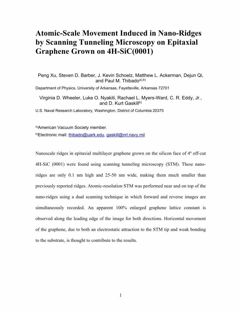
1 Atomic-Scale Movement Induced in Nano-Ridges by Scanning Tunneling Microscopy on Epitaxial Graphene Grown on 4H-SiC(0001) Peng Xu, Steven D. Barber, J. Kevin Schoelz, Matthew L. Ackerman, Dejun Qi, and Paul M. Thibado a),b) Department of Physics, University of Arkansas, Fayetteville, Arkansas 72701 Virginia D. Wheeler, Luke O. Nyakiti, Rachael L. Myers-Ward, C. R. Eddy, Jr., and D. Kurt Gaskill b) U.S. Naval Research Laboratory, Washington, District of Columbia 20375 a) American Vacuum Society member. b) Electronic mail: [email protected], [email protected] Nanoscale ridges in epitaxial multilayer graphene grown on the silicon face of 4º off-cut 4H-SiC (0001) were found using scanning tunneling microscopy (STM). These nano- ridges are only 0.1 nm high and 25-50 nm wide, making them much smaller than previously reported ridges. Atomic-resolution STM was performed near and on top of the nano-ridges using a dual scanning technique in which forward and reverse images are simultaneously recorded. An apparent 100% enlarged graphene lattice constant is observed along the leading edge of the image for both directions. Horizontal movement of the graphene, due to both an electrostatic attraction to the STM tip and weak bonding to the substrate, is thought to contribute to the results.
-
Upload
khangminh22 -
Category
Documents
-
view
2 -
download
0
Transcript of Atomic-Scale Movement Induced in Nano-Ridges by ... - arXiv
1
Atomic-Scale Movement Induced in Nano-Ridges by Scanning Tunneling Microscopy on Epitaxial Graphene Grown on 4H-SiC(0001)
Peng Xu, Steven D. Barber, J. Kevin Schoelz, Matthew L. Ackerman, Dejun Qi, and Paul M. Thibadoa),b)
Department of Physics, University of Arkansas, Fayetteville, Arkansas 72701
Virginia D. Wheeler, Luke O. Nyakiti, Rachael L. Myers-Ward, C. R. Eddy, Jr., and D. Kurt Gaskillb)
U.S. Naval Research Laboratory, Washington, District of Columbia 20375
a)American Vacuum Society member. b)Electronic mail: [email protected], [email protected]
Nanoscale ridges in epitaxial multilayer graphene grown on the silicon face of 4º off-cut
4H-SiC (0001) were found using scanning tunneling microscopy (STM). These nano-
ridges are only 0.1 nm high and 25-50 nm wide, making them much smaller than
previously reported ridges. Atomic-resolution STM was performed near and on top of the
nano-ridges using a dual scanning technique in which forward and reverse images are
simultaneously recorded. An apparent 100% enlarged graphene lattice constant is
observed along the leading edge of the image for both directions. Horizontal movement
of the graphene, due to both an electrostatic attraction to the STM tip and weak bonding
to the substrate, is thought to contribute to the results.

2
I. INTRODUCTION The novel electronic properties of graphene have been inspiring intense research
efforts since this two-dimensional material was first successfully isolated in 2004.1 Its
intriguing features, such as ballistic transport,2 the quantum Hall effect,3 and ultra-high
mobility,4 mark graphene as a potentially pivotal material in the field of carbon-based
electronics. In particular, epitaxial graphene grown on SiC has been identified as one of
the most likely avenues to graphene-based electronics.5, 6 Semi-insulating SiC has a large
band gap which makes it ideally suited for the production of top-gated, electrically
isolated devices, and furthermore, it is already available in the form of large-diameter
wafers compatible with current industrial technology.7, 8 To form graphene on SiC,9 the
sample must be annealed at temperatures >1200°C, causing Si to sublimate and leaving
behind large regions of pristine epitaxial graphene once the sample has cooled.10-12
Interestingly, atomic force microscopy (AFM) images on the graphene surface have
revealed distinctive, large ridges (~1.5 nm high) running along step edges and across
terraces, with atomically flat regions in between.13-16 The appearance of these ridges has
been attributed to strain-induced bending and buckling of the graphene caused by the sign
difference in the thermal expansion coefficients of graphene and SiC as the sample
cools.17-19 Scanning tunneling microscopy (STM) studies have confirmed this
interpretation and have shown that the large ridges can be manipulated and even
generated through interactions with the STM tip during imaging.20
Scanning probe microscopy techniques have also been helpful toward gaining
insight into the crucial electronic interaction between the graphene surface layer and the
SiC substrate.21 For instance, an STM study by Rutter et al. was responsible for
determining that the dominant source of electron scattering in epitaxially grown graphene
3
was due to defects in the SiC substrate.22 And to help reduce such detrimental doping
effects, a later STM study found that the carbon buffer layer23 at the graphene/SiC
interface could be decoupled from the SiC substrate by means of fluorine intercalation.24
In a separate study, Yakes et al. used a four-probe STM system to perform local transport
measurements and discovered a local conductance anisotropy in the epitaxial graphene.25
The direction of increased scattering was attributed to interference from Si atoms trapped
underneath the graphene along the step edges of the SiC crystal where Si desorption
occurs more rapidly.26-28 These small-scale electronic studies and others have proven
invaluable to uncovering the fundamental interactions governing transport in epitaxial
graphene, and the same could be said for investigations into large-scale topographic
features like the aforementioned ridges and terrace steps. What remains largely
unexamined, however, is the very small-scale topography in epitaxial graphene on SiC
and its response to local imaging.
In this work, we report nano-ridges (~0.1 nm high) found by an STM study of the
multilayer graphene on 4º off-cut 4H-SiC(0001) (the Si face). These ridges are much
smaller than those found in earlier studies, but they likely form by the same mechanism
(i.e., thermal coefficient of expansion mismatch). Surprisingly, images acquired near the
nano-ridges show an enlarged graphene lattice constant on the left or right edge
depending on the scanning direction. Moreover, increasing the tunneling current setpoint
increased the size of the altered region in the STM image. We propose that an
electrostatic attractive force between the STM tip and graphene sample produces these
results by dynamically displacing the surface layer.

4
II. EXPERIMENTAL
The epitaxial graphene sample used in this study was grown on 20 m of
intentionally n-doped (1×10¹⁴/cm3) epitaxial 4H-SiC layer on the Si face of a 4º off-cut
4H-SiC substrate measuring 16 mm × 16 mm and cut from a 76.2 mm diameter parent
wafer (Cree, Inc). Growth was carried out in a commercially available hot-wall Aixtron
VP508 chemical vapor deposition reactor. Prior to graphene growth, the substrate was
etched in situ in a H2 ambient environment for 5 minutes at 1520 °C. This etching
produces a controlled starting surface that is dominated by SiC surface steps roughly 0.5
nm high. After the H2 etching step, the ambient environment was switched to Ar with a
transition period of 2 minutes during which pressures varied by ±50% around 100 mbar.
The subsequent 120 minute graphene growth process was conducted under a flowing Ar
environment of 20 standard liters per minute at 100 mbar, with a substrate growth
temperature of 1620 °C.29 After growth, the sample was cooled to room temperature, cut
to 7 mm × 14 mm, and diamond scribed labels were added to the carbon face. Next,
Raman data was collected for the sample using a Thermo DXR system. A 532 nm, 8 mW
laser was used as the pump probe with a spot size 0.6 m. After characterization with
Raman, the sample was secured, sealed, and sent to the STM facility.
Experimental STM images were obtained using an Omicron ultrahigh-vacuum
(base pressure is 10-10 mbar) STM (low-temperature model) operated at room
temperature. The sample was mounted with silver paint onto a flat tantalum sample plate
and transferred through a load-lock into the STM chamber where it was electrically
grounded. No cleaning or heating was done to the sample. STM tips were
electrochemically etched from 0.25 mm diameter tungsten wire via a custom double

5
lamella setup with an automatic gravity-switch cutoff.30 After etching, they were gently
rinsed with distilled water, briefly dipped in a concentrated hydrofluoric acid solution to
remove surface oxides,31 and then loaded into the STM chamber through the same load-
lock. All STM images were acquired using a positive tip bias of 0.1 V.
III. RESULTS AND DISCUSSION
A. Raman Spectra and STM Images of Nano-ridges
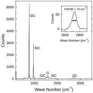
A full-range Raman scan of the epitaxial graphene on the SiC sample is shown in
Fig. 1. The largest peaks are identified with the SiC substrate; in addition both the G and
2D peaks of graphene are present. A magnified view of the 2D peak is shown in the inset
and has a full width at half maximum of 70 cm-1, which indicates that there are over 2
layers of graphene on the surface of our sample.32
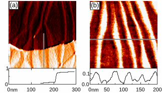
Two large-scale, filled-state STM images of the epitaxial graphene on the SiC
sample obtained with a tunneling current setpoint of 0.05 nA are shown in Fig. 2. The
first image, displayed in Fig. 2(a), is 300 nm × 300 nm and exhibits two prominent
features. First, the sharp contrast between the dark upper half and light lower half
indicates the presence of a step in the SiC substrate. A height data line profile extracted
from the image is plotted below it (the location is indicated by the black line drawn on
the image) and reveals that the step is about 0.55 nm high (note, the c lattice constant for
4H-SiC is 1.0053 nm, which is 4 SiC bilayers). Second, nano-ridges are seen running
from top to bottom which are uninterrupted by the presence of the step. Some appear to
have distinct kinks and some bunch together, yet without combining to form wider
ridges. A slightly closer view of the nano-ridges is provided in the 200 nm × 200 nm
image of Fig. 2(b). A height profile was again extracted, this time horizontally, and is
6
displayed below the image. It shows that, on average, the nano-ridges are around 0.1 nm
high and between 25-50 nm wide. They exhibit an oscillatory nature, and though not
readily apparent in the image, smaller peaks sometimes occur between the more
prominent ones.
Previously observed large ridges mentioned earlier are much higher than the
nano-ridges shown here in Fig. 2. Scanning probe experiments report that the larger
ridges are 1 to 2 nm high (10 to 20 times larger).14 In addition to the nano-ridges in Fig. 2
being much smaller, they also have a very different geometry. They tend to meander,
have kinks, and bunch together, while the large ridges tend to be isolated and straighter.
The kinks are especially interesting because they may represent nucleation or pinning
sites for the formation of the nano-ridges. Nevertheless, it seems likely that both types of
ridges are formed by the same physical process, namely, compressive strain33 induced
during cooling of the SiC wafer.17, 19, 34 As the system is cooled from the growth
temperature, the graphene expands as the substrate contracts,35 and the resulting strain is
most easily relieved by having portions of the graphene flex away from the substrate and
buckle. The nano-ridges discussed here are likely the source for the extra graphene
material required to form the larger ridges found in other studies with AFM. Other
studies may have missed the nano-ridges due to their small, atomic-scale heights or
possibly due to the stronger interaction of AFM.13
B. Atomic Scale Movement Induces by STM in Nano-ridges
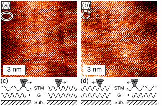
Atomic-scale STM was performed in the region of the nano-ridges and two
typical 12 nm × 12 nm filled-state images are shown in Fig. 3(a,b). These images were
acquired simultaneously at the same location using a dual scanning technique, a tunneling
7
current of 0.5 nA, and the fast-scan direction horizontal with the tip moving at a speed of
72 nm/s. The image recorded while the STM tip moved from left to right on each line of
data (with 400 lines of data) is displayed in Fig. 3(a). The hexagonal symmetry structure
of graphene is resolved in various smaller regions throughout and indicating the presence
of graphene on the top of the sample. However, the lattice constant of the graphene
appears to change as the image is viewed from left to right. In fact, within approximately
0.5 nm of the entire leftmost edge, the lattice constant is enlarged by 150% horizontally
and 100% vertically when compared with the right side. On the right-hand side, the
lattice constant is measured to be 0.25 nm, consistent with theory and previous
experiments.36
STM data was also simultaneously recorded as the tip returned moving right to
left for each line of data and this is shown in Fig. 3(b). Note that this data acquisition
process does not result in mirror images. Rather, the position marked by the ovals
represents the same location on the sample surface in both instances. This second image
is nearly identical to the previous one; however, there is one important difference. The
enlarged lattice constant is now on the right edge while the normal lattice constant is on
the left side. Because the enlarged lattice constant is seen on the left in Fig. 3(a) and on
the right in Fig. 3(b), the possibility of it being a real permanent feature in the graphene
lattice is automatically ruled out. It is also not a result of in-plane stretching of the
carbon-carbon bonds, due to their stiffness as well as the relatively low strain of the
epitaxial graphene (~1%).37

8
C. Discussion
The stretched out atomic features in these images are more reminiscent of data
containing piezoelectric creep.38 When an STM image is acquired during the creep time,
the beginning part of the image will appear warped or sheered compared to the ending
part. Creep results are not real, but simply an artifact of the tip moving more than the
assigned value. However, creep quickly goes away with typical scan speeds, yet the
effect shown in Fig. 3(a,b) never goes away. Even though the lack of time dependence in
our data successfully rules out the piezoelectric creep model, we do believe that
independent movement between the tip and sample is occurring outside the assigned data
acquisition values. Piezoelectric hysteresis is another mechanism that can lead to
distorted STM images; however, this effect does not change in time. For this case, the
voltage applied to the piezoelectric scanner leads to a non-linear response in its
displacement.39-41 For our studies, the piezoelectric scanner is being operated within its
linear range. Also, this type of distortion does not occur for our control samples (not
shown) like graphite and graphene on copper.
Previous studies have established that graphite derivatives, including graphene,
are especially susceptible to movement induced by the electrostatic interaction between
the STM tip and the sample.42-45 In the simplest situation, constant-current scanning
tunneling spectroscopy measurements used on freestanding graphene clearly
demonstrated that the graphene flexes more than 30 nm toward the STM as the tip bias
increases from 0.1 V to 3.0 V.43 Using a similar technique on graphite, large scale
movement of 20 nm wide ribbons was also demonstrated.44 Another important example,
9
on an insulating substrate, was done by Mashoff et.al, who demonstrated oscillatory
motion induced in graphene on SiO2 using STM.46
With the idea of independent sample movement in mind, we introduce a “sample
creep” model to best explain our results. In this model, as the STM tip moves across the
graphene surface, the top graphene layer will be attracted to the tip and slide horizontally
with the tip, which causes the observed features. This is especially plausible given the
weak coupling between graphene and the substrate below, as well as the excess graphene
available on the surface in the form of nano-ridges. A series of four STM schematics is
provided at the bottom of Fig. 3 to illustrate how sample creep would replicate the
unusual details in the findings. Each diagram portrays, from top to bottom, a moving
triangular STM tip and the path it traces (labeled STM), the semi-mobile graphene
surface of constant local density of states (labeled G), and the stationary substrate
(labeled Sub.). As the tip first begins to move left to right, corresponding to the left side
of Fig. 3(c), it drags the graphene along with it (motion direction indicated by the arrow),
though at a slower speed than the tip is moving. The relative motion between the two
causes the tip to trace a path with a larger lattice constant than if the sample were
stationary. Soon, however, the available slack in the graphene has been removed, or
alternatively, a compressive strain has accumulated ahead of the tip. At this point, the
graphene ceases to slide, and it is imaged with its normal lattice constant, as depicted in
the STM trace shown on the right side of Fig. 3(c). When the tip reaches the end of a
given line, and changes direction, this allows the graphene surface to relax back to
equilibrium and, in addition, allows the tip to now pull the graphene in the opposite
direction. Similar to before, the motion of the graphene (indicated by the arrow) is in the

10
same direction as the STM tip and falsely constructs an enlarged lattice constant, as
illustrated in the right side of Fig. 3(d). At some point the motion of the graphene is
constrained, and the rest of the line is imaged normally. This corresponds with the left
side of Fig. 3(d). As the process just described repeats for every line, it results in the
time-independent edge distortions observed line-by-line going up the images. Thus
instead of unrecorded movement of the piezoelectric causing these deformations, we are
seeing movement of the sample surface caused by both its electrostatic attraction to the
STM tip and weak bonding to the underlying layer(s).
We can further test our model by examining the width of the distorted area as a
function of the setpoint current, since piezoelectric creep is independent of the tunneling
current. To do this, we acquired a large set of STM images all from the same location
(but at a different one than in Fig. 3). The constant-current STM images were collected
at various setpoints between 0.02 nA and 2 nA, and all with a common scan speed of 72
nm/s. The current setpoint does have a clear effect on the edge width, as seen in the semi-
log plot shown in Fig. 4(a). As the tunneling current was increased, the edge width
approximately doubled from 0.5 nm to more than 1 nm. This increase in width can be
explained by the sample creep model, since increasing the current setpoint effectively
shortens the distance between the tip and sample and therefore increases the electrostatic
attraction between them. As a result, the tip pulls on the sample with a greater force,
resulting in greater displacements of the graphene and larger edge widths.
The edge width was also studied as a function of the STM tip scan speed for a
fixed setpoint current of 2 nA as shown in Fig. 4(b) and overlaid with a linear regression
of the data. The scan speed was varied between 50 and 150 nm/s, and over this range the

11
edge width generally increased with scan speed, from 0.75 nm to 1.5 nm. This trend is
also consistent with the sample creep model, but also lends some insight into the
mechanism. At the end of each scan line where the STM tip reverses direction, the
accumulated strain in the graphene is released as the tip begins to pull it in the opposite
direction. If the tip is moving very slowly, then the graphene will relax prior to the STM
tip imaging the surface. This would result in measuring the smaller edge width observed
experimentally.
The horizontal shifting of the graphene sample surface agrees favorably with
interpreting the nano-ridges as buckled graphene which has separated from the
underlying layers. Since the nano-ridges are physically separated from the surface, the
interaction with the substrate is significantly reduced. One would then expect the nano-
ridges to act as superior conductance channels. This is because it was found that as
graphene becomes partially decoupled from a SiC substrate, electron scattering will be
reduced.22, 24 A similar outcome was reported by Pirkle et al. when studying the electrical
properties of chemical vapor deposited graphene transferred onto SiO2.47 In particular,
they found via AFM measurements across graphene strips that the closer the graphene
was to the substrate the lower the electron mobility.48 Raised nano-ridges could,
therefore, also lead to conductance anisotropy, just as step edges do on a larger scale.25
Since the ridges occur in essentially parallel rows, local transport would favor the
direction following the ridges rather than crossing them.
IV. CONCLUSIONS
In conclusion, we have performed an atomic scale STM study on an atomically
flat region of multilayer epitaxial graphene grown on 4º off-cut 4H-SiC(0001). For the

12
first time, atomic-scale parallel nano-ridges were observed on the graphene layer.
Atomic-resolution STM images were obtained near and on top of these ridges and
significantly enlarged lattice constants were investigated. We showed that the graphene
top layer, during scanning, moves with the STM tip due to an electrostatic attraction
between the tip and sample, which is consistent with the idea that the ridges are regions
of the graphene sheet that have buckled due to strain and have become partially
decoupled from the underlying layer.
ACKNOWLEDGMENTS
P. X. and P. T. gratefully acknowledge the financial support of the Office of Naval
Research under grant number N00014-10-1-0181 and the National Science Foundation
under grant number DMR-0855358. Work at the U.S. Naval Research Laboratory is
supported by the Office of Naval Research. LON gratefully acknowledges postdoctoral
fellowship support through the ASEE.
13
References
1 K. S. Novoselov, A. K. Geim, S. V. Morozov, D. Jiang, Y. Zhang, S. V. Dubonos, I. V. Grigorieva, and A. A. Firsov, Science 306, 666 (2004).
2 X. Du, I. Skachko, A. Barker, and E. Y. Andrei, Nat. Nanotechnol. 3, 491 (2008).
3 Y. Zhang, Y. W. Tan, H. L. Stormer, and P. Kim, Nature 438, 201 (2005).
4 K. I. Bolotin, K. J. Sikes, Z. Jiang, M. Klima, G. Fudenberg, J. Hone, P. Kim, and H. L. Stormer, Solid State Commun. 146, 351 (2008).
5 C. Berger, Z. Song, T. Li, X. Li, A. Y. Ogbazghi, R. Feng, Z. Dai, A. N. Marchenkov, E. H. Conrad, P. N. First, and W. A. de Heer, J. Phys. Chem. B 108, 19912 (2004).
6 C. Berger, Z. Song, X. Li, X. Wu, N. Brown, C. Naud, D. Mayou, T. Li, J. Hass, A. N. Marchenkov, E. H. Conrad, P. N. First, and W.A. de Heer, Science 312, 1191 (2006).
7 T. Ohta, A. Bostwick, T. Seyller, K. Horn, and E. Rotenberg, Science 313, 951 (2006).
8 C. Riedl, U. Starke, J. Bernhardt, M. Franke, and K. Heinz, Phys. Rev. B 76, 245406 (2007).
9 C. Riedl, C. Coletti, and U. Starke, J. Phys. D: Appl. Phys. 43, 374009 (2010).
10 P. N. First, W. A. de Heer, T. Seyller, C. Berger, J. A. Stroscio, and J. S. Moon, MRS Bull. 35, 296 (2010).
11 W. A. de Heer, C. Berger, M. Ruan, M. Sprinkle, X. Li, Y. Hu, B. Zhang, J. Hankinson, and E. Conrad, Proc. Natl. Acad. Sci. USA 108, 16900 (2011).
12 P. Sutter, Nat. Mater. 8, 171 (2009).
13 G. G. Jernigan, B. L. VanMil, J. L. Tedesco, J. G. Tischler, E. R. Glaser, A. Davidson, III, P. M. Campbell, and D. K. Gaskill, Nano Lett. 9, 2605 (2009).
14 Luxmi, P. J. Fisher, N. Srivastava, R. M. Feenstra, Y. Sun, J. Kedzierski, P. Healey, and G. Gu, Appl. Phys. Lett. 95, 073101 (2009).
15 Luxmi, S. Nie, P. J. Fisher, R. M. Feenstra, G. Gu, and Y. Sun, J. Electron. Mater. 38, 718 (2009).
16 G. Prakash, M. L. Bolen, R. Colby, E. A. Stach, M. A. Capano, and R. Reifenberger, New J. Phys. 12, 14 (2010).
17 N. Ferralis, J. Kawasaki, R. Maboudian, and C. Carraro, Appl. Phys. Lett. 93, 191916 (2008).
18 N. Ferralis, R. Maboudian, and C. Carraro, Phys. Rev. Lett. 101, 156801 (2008).
14
19 J. Röhrl, M. Hundhausen, K. V. Emtsev, T. Seyller, R. Graupner, and L. Ley, Appl. Phys. Lett. 92, 201918 (2008).
20 G. F. Sun, J. F. Jia, Q. K. Xue, and L. Li, Nanotechnology 20, 355701 (2009).
21 V. W. Brar, Y. Zhang, Y. Yayon, T. Ohta, J. L. McChesney, A. Bostwick, E. Rotenberg, K. Horn, and M. F. Crommie, Appl. Phys. Lett. 91, 122102 (2007).
22 G. M. Rutter, J. N. Crain, N. P. Guisinger, T. Li, P. N. First, and J. A. Stroscio, Science 317, 219 (2007).
23 G. M. Rutter, N. P. Guisinger, J. N. Crain, E. A. A. Jarvis, M. D. Stiles, T. Li, P. N. First, and J. A. Stroscio, Phys. Rev. B 76, 235416 (2007).
24 S. L. Wong, H. Huang, Y. Wang, L. Cao, D. Qi, I. Santoso, W. Chen, and A. T. S. Wee, ACS Nano 5, 7662 (2011).
25 M. K. Yakes, D. Gunlycke, J. L. Tedesco, P. M. Campbell, R. L. Myers-Ward, C. R. Eddy, Jr., D. K. Gaskill, P. E. Sheehan, and A. R. Laracuente, Nano Lett. 10, 1559 (2010).
26 J. Choi, H. Lee, and S. Kim, J. Phys. Chem. C 114, 13344 (2010).
27 Y. M. Lin, C. Dimitrakopoulos, K. A. Jenkins, D. B. Farmer, H. Y. Chiu, A. Grill, and P. Avouris, Science 327, 662 (2010).
28 S. H. Ji, J. B. Hannon, R. M. Tromp, V. Perebeinos, J. Tersoff, and F. M. Ross, Nat. Mater. 11, 114 (2012).
29 G. G. Jernigan, T. J. Anderson, J. T. Robinson, J. D. Caldwell, J. C. Culbertson, R. Myers-Ward, A. L. Davidson, and M. G. Ancona, J. Vac. Sci. Technol. B 30, 5 (2012).
30 J. K. Schoelz, P. Xu, S. D. Barber, D. Qi, M. L. Ackerman, G. Basnet, C. T. Cook, and P. M. Thibado, J. Vac. Sci. Technol. B 30, 033201 (2012).
31 L. A. Hockett and S. E. Creager, Rev. Sci. Instrum. 64, 263 (1993).
32 L. M. Malard, M. A. Pimenta, G. Dresselhaus, and M. S. Dresselhaus, Phys. Rep. 473, 51 (2009).
33 L. B. Biedermann, M. L. Bolen, M. A. Capano, D. Zemlyanov, and R. G. Reifenberger, Phys. Rev. B 79, 125411 (2009).
34 Z. H. Ni, W. Chen, X. F. Fan, J. L. Kuo, T. Yu, A. T. S. Wee, and Z. X. Shen, Phys. Rev. B 77, 115416 (2008).
35 W. Bao, F. Miao, Z. Chen, H. Zhang, W. Jang, C. Dames, and C. N. Lau, Nat. Nanotechnol. 4, 562 (2009).

15
36 P. Xu, Y. Yang, S. D. Barber, M. L. Ackerman, J. K. Schoelz, I. A. Kornev, S. Barraza-Lopez, L. Bellaiche, and P. M. Thibado, Phys. Rev. B 84, 161409(R) (2011).
37 J. A. Robinson, M. Wetherington, J. L. Tedesco, P. M. Campbell, X. Weng, J. Stitt, M. A. Fanton, E. Frantz, D. Snyder, B. L. VanMil, G. G. Jernigan, R. L. Myers-Ward, C. R. Eddy,Jr. and D. K. Gaskill, Nano Lett. 9, 2873 (2009).
38 R. V. Lapshin, Nanotechnology 15, 1135 (2004).
39P. Ge and M. Jouaneh, IEEE T. Contr. Syst. T. 4, 209 (1996).
40D. Croft, G. Shed, and S. Devasia, J. Dyn. Syst. T. ASME. 123, 35 (2001).
41R. Wiesendanger, Scanning Probe Microscopy and Spectroscopy: Methods and Applications. (Cambridge University Press, Cambridge, UK, 1998), pp. 96.
42 P. Xu, Y. Yang, D. Qi, S. D. Barber, M. L. Ackerman, J. K. Schoelz, T. B. Bothwell, S. Barraza-Lopez, L. Bellaiche, and P. M. Thibado, Appl. Phys. Lett. 100, 201601 (2012).
43 P. Xu, Y. Yang, S. D. Barber, M. L. Ackerman, J. K. Schoelz, D. Qi, I. A. Kornev, L. Dong, L. Bellaiche, S. Barraza-Lopez, and P. M. Thibado, Phys. Rev. B 85, 121406(R) (2012).
44 P. Xu, Y. Yang, S. D. Barber, J. K. Schoelz, D. Qi, M. L. Ackerman, L. Bellaiche, and P. M. Thibado, Carbon 50, 4633 (2012).
45 S. R. Snyder, W. W. Gerberich, and H. S. White, Phys. Rev. B 47, 10823 (1993).
46 T. Mashoff, M. Pratzer, V. Geringer, T. J. Echtermeyer, M. C. Lemme, M. Liebmann, and M. Morgenstern, Nano Lett. 10, 461 (2010).
47 A. Pirkle, J. Chan, A. Venugopal, D. Hinojos, C. W. Magnuson, S. McDonnell, L. Colombo, E. M. Vogel, R. S. Ruoff, and R. M. Wallace, Appl. Phys. Lett. 99, 122108 (2011).
48 Z. Cheng, Q. Zhou, C. Wang, Q. Li, C. Wang, and Y. Fang, Nano Lett. 11, 767 (2011).

16
Figure Captions
FIG. 1. Raman spectra of graphene on SiC(0001) obtained using 532 nm laser line. Inset:
detailed feature of 2D band for graphene.
FIG. 2. (Color online) Filled-state STM images of graphene on SiC(0001) taken with a
current setpoint of 0.05 nA and tip bias of 0.1 V. (a) 300 nm × 300 nm image showing
parallel nano-ridges prominently aligned vertically across a 0.55 nm horizontal step. A
height line profile extracted from the image showing the step height is displayed below
the image. (b) 200 nm × 200 nm image shows a zoomed in view of the nano-ridges. A
height line profile extracted from the image is displayed below.
FIG. 3. (Color online) Filled-state 12 nm × 12 nm STM images of graphene grown on
SiC(0001) taken in an area with nano-ridges using a current setpoint of 0.5 nA and a tip
bias of 0.1 V. Both images were acquired simultaneously from the same location using a
dual scanning technique which recorded height data when the STM tip was moving both
(a) left to right and (b) right to left. Illustrations of the semi-mobile sample and the
contour recorded by the STM tip as it scans from (c) left to right and (d) right to left.
FIG. 4. The width of the area containing an enlarged lattice constant measured from
atomic-resolution STM images of graphene on SiC as functions of (a) current setpoint,
but with a common scan speed of 72 nm/s and (b) scan speed, but with a common current
setpoint of 2 nA.
0
1000
2000
3000
4000
5000
6000C
ount
s
1000 2000 3000
Wave Number (cm-1)
0
50
Cou
nts
2600 2800
Wave Number (cm-1)
FWHM = 70 cm-1
SiC
SiC
SiCSiCG
2D
(a)
0
1
0 100 200 300nm
(b)
0.0
0.1
0 50 100 150 200nm
3 nm
(a)
3 nm
(b)
(c) (d)
Sub.
G
STM
Sub.
G
STM

0.5
1.0
1.5E
dge
Wid
th(n
m)
0.01 0.1 1
Current Setpoint (nA)
(a)
0.5
1.0
1.5
Edg
eW
idth
(nm
)
50 100 150
Scan Speed (nm/s)
(b)