Artificial optoelectronic spiking neuron based on a resonant ...
12
Matěj Hejda, Ekaterina Malysheva, Dafydd Owen-Newns, Qusay Raghib Ali Al-Taai, Weikang Zhang, Ignacio Ortega-Piwonka, Julien Javaloyes, Edward Wasige, Victor Dolores-Calzadilla, José M. L. Figueiredo, Bruno Romeira, and Antonio Hurtado Artificial optoelectronic spiking neuron based on a resonant tunnelling diode coupled to a vertical cavity surface emitting laser Abstract: Excitable optoelectronic devices represent one of the key building blocks for implementation of artificial spiking neurons in neuromorphic (brain-inspired) photonic systems. This work introduces and experimentally investigates an opto-electro-optical (O/E/O) artificial neuron built with a resonant tunnelling diode (RTD) coupled to a photodetector as a receiver and a vertical cavity surface emitting laser as a the transmitter. We demonstrate a well defined excitability threshold, above which this neuron produces ∼100 ns optical spiking responses with characteristic neural-like refractory period. We utilise its fan-in capability to perform in-device coincidence detection (logical AND) and exclusive logical OR (XOR) tasks. These results provide first experimental validation of deterministic triggering and tasks in an RTD-based spiking optoelectronic neuron with both input and output optical (I/O) terminals. Furthermore, we also investigate in theory the prospects of the proposed system for its nanophotonic implementation with a monolithic design combining a nanoscale RTD element and a nanolaser; therefore demonstrating the potential of integrated RTD-based excitable nodes for low footprint, high-speed optoelectronic spiking neurons in future neuromorphic photonic hardware. Keywords: photonic neuron, neuromorphic photonics, VCSEL, RTD, spiking, optical computing 1 Introduction Artificial Intelligence (AI) and Machine Learning (ML) algorithms nowadays power a wide range of advanced computational tasks, ranging from natural language processing and realistic image synthesis [1] to solutions solving major challenges such as protein folding [2]. As a general principle, it can be stated that higher computational capability of AI models goes hand in hand with their scale. Hence, further growth in the size of these models is expected as new, more complex tasks are being explored. This can be observed in current models such as GPT-3, which operates with 175 billion parameters [3], over a magnitude increase in the number of parameters when compared to its previous iteration. With the growth of scale and increase in Matěj Hejda, Dafydd Owen-Newns, Weikang Zhang, Antonio Hurtado, Institute of Photonics, SUPA Dept of Physics, University of Strathclyde, Glasgow, United Kingdom, e-mail: [email protected], [email protected], [email protected], [email protected] Ekaterina Malysheva, Victor Dolores-Calzadilla, Eindhoven Hendrik Casimir Institute, Eindhoven University of Technology, Eindhoven, The Netherlands, e-mail: [email protected], [email protected] Qusay Raghib Ali Al-Taai, Edward Wasige, High Frequency Electronics Group, University of Glasgow, Glasgow, United Kingdom, e-mail: [email protected], [email protected] Ignacio Ortega-Piwonka, Julien Javaloyes, Dept de Física and IAC-3, Universitat de les Illes Balears, Palma de Mallorca, Spain, e-mail: [email protected], [email protected] José M. L. Figueiredo, Centra-Ciências and Departamento de Física, Faculdade de Ciências, Universidade de Lisboa, Lisboa, Portugal, e-mail: jmfi[email protected] Bruno Romeira, INL – International Iberian Nanotechnology Laboratory, Ultrafast Bio- and Nanophotonics Group, Braga, Portugal, e-mail: [email protected] arXiv:2206.11044v1 [cs.ET] 22 Jun 2022
-
Upload
khangminh22 -
Category
Documents
-
view
0 -
download
0
Transcript of Artificial optoelectronic spiking neuron based on a resonant ...

Matěj Hejda, Ekaterina Malysheva, Dafydd Owen-Newns, Qusay Raghib Ali Al-Taai,Weikang Zhang, Ignacio Ortega-Piwonka, Julien Javaloyes, Edward Wasige, VictorDolores-Calzadilla, José M. L. Figueiredo, Bruno Romeira, and Antonio Hurtado
Artificial optoelectronic spiking neuronbased on a resonant tunnelling diodecoupled to a vertical cavity surfaceemitting laser
Abstract: Excitable optoelectronic devices represent one of the key building blocks for implementationof artificial spiking neurons in neuromorphic (brain-inspired) photonic systems. This work introducesand experimentally investigates an opto-electro-optical (O/E/O) artificial neuron built with a resonanttunnelling diode (RTD) coupled to a photodetector as a receiver and a vertical cavity surface emittinglaser as a the transmitter. We demonstrate a well defined excitability threshold, above which this neuronproduces ∼100 ns optical spiking responses with characteristic neural-like refractory period. We utiliseits fan-in capability to perform in-device coincidence detection (logical AND) and exclusive logical OR(XOR) tasks. These results provide first experimental validation of deterministic triggering and tasks in anRTD-based spiking optoelectronic neuron with both input and output optical (I/O) terminals. Furthermore,we also investigate in theory the prospects of the proposed system for its nanophotonic implementationwith a monolithic design combining a nanoscale RTD element and a nanolaser; therefore demonstratingthe potential of integrated RTD-based excitable nodes for low footprint, high-speed optoelectronic spikingneurons in future neuromorphic photonic hardware.
Keywords: photonic neuron, neuromorphic photonics, VCSEL, RTD, spiking, optical computing
1 IntroductionArtificial Intelligence (AI) and Machine Learning (ML) algorithms nowadays power a wide range of advancedcomputational tasks, ranging from natural language processing and realistic image synthesis [1] to solutionssolving major challenges such as protein folding [2]. As a general principle, it can be stated that highercomputational capability of AI models goes hand in hand with their scale. Hence, further growth in the sizeof these models is expected as new, more complex tasks are being explored. This can be observed in currentmodels such as GPT-3, which operates with 175 billion parameters [3], over a magnitude increase in thenumber of parameters when compared to its previous iteration. With the growth of scale and increase in
Matěj Hejda, Dafydd Owen-Newns, Weikang Zhang, Antonio Hurtado, Institute of Photonics, SUPA Dept of Physics,University of Strathclyde, Glasgow, United Kingdom, e-mail: [email protected], [email protected],[email protected], [email protected] Malysheva, Victor Dolores-Calzadilla, Eindhoven Hendrik Casimir Institute, Eindhoven University of Technology,Eindhoven, The Netherlands, e-mail: [email protected], [email protected] Raghib Ali Al-Taai, Edward Wasige, High Frequency Electronics Group, University of Glasgow, Glasgow, UnitedKingdom, e-mail: [email protected], [email protected] Ortega-Piwonka, Julien Javaloyes, Dept de Física and IAC-3, Universitat de les Illes Balears, Palma de Mallorca,Spain, e-mail: [email protected], [email protected]é M. L. Figueiredo, Centra-Ciências and Departamento de Física, Faculdade de Ciências, Universidade de Lisboa,Lisboa, Portugal, e-mail: [email protected] Romeira, INL – International Iberian Nanotechnology Laboratory, Ultrafast Bio- and Nanophotonics Group, Braga,Portugal, e-mail: [email protected]
arX
iv:2
206.
1104
4v1
[cs
.ET
] 2
2 Ju
n 20
22

2 M. Hejda et al., Artificial optoelectronic spiking neuron based on a resonant tunnelling diode coupled to a vertical cavity surface emitting laser
resource and requirements of these AI models, the chips on which those algorithms run come more intothe spotlight, fuelling the search for alternative, AI-optimised hardware. In particular, approaches beyondthe conventional Von-Neumann architecture of digital processors (with distinct memory and logic units)are receiving increasing interest. These alternative computing schemes offer the promise of relieving thestalling chip performance improvements due to CMOS downscaling bottlenecks and architecture limitations.Neuromorphic (brain-inspired) engineering is a prime example of such unconventional computing approach.
Neuromorphic computing systems attempt to harness the vast computational capabilities and powerefficiency of the brain by mimicking and abstracting their architecture. These systems rely on very highdegree of parallelism and concepts such as event-based asynchronous computation and in-memory computing.Driven both by their utility in the fields of AI and computational neuroscience, neuromorphic computersare being developed by both academic [4, 5] and industrial parties [6, 7] in a variety of technology platforms.In particular, neuromorphic realisations based on photonics offer some highly desirable benefits. The useof light allows for high bandwidth and low-loss, wavelength-division multiplexed (WDM) communicationschemes without unwanted inductive crosstalk and resistive heating in wires, while advances in the field ofphotonic integrated circuits (PICs) allow for high-density chip integration. The field is currently ongoingrapid expansion, with many different classes of photonic devices being investigated for brain-inspiredcomputing and AI acceleration. These include quantum-dot lasers [8, 9], superconducting nanowires [10,11], integrated photonic components including modulators [12, 13, 14], semiconductor optical amplifiers,[15, 16], micro-rings [17, 18], phase change material-based PICs [19, 20] as well as vertical cavity surfaceemitting lasers (VCSELs) subject to injection locking [21, 22] or with saturable absorber sections [23,24]. Furthermore, VCSELs have been previously demonstrated as a viable technology for spike-basedoptical computing by utilising their high speed spiking dynamics for tasks such as all-optical convolution[25], pattern classification [26] or rate-coded encoding of image data [27]. Simultaneously, a recent studyhas demonstrated VCSELs suitability for integration into arrays [28], which is crucial for realisation oflarger-scale on-chip integrated circuits.
In this work, we introduce a modular, excitable, optoelectronic spiking neuron based on a resonanttunnelling diode (RTD) electrically coupled to a PD (Thorlabs PDA8GS) serving as a receiver and toa telecom-wavelength, pigtailed VCSEL serving as a transmitter, together realising an O/E/O system.RTDs are a class of semiconductor devices that typically employ a double barrier quantum well (DBQW)semiconductor heterostructure, allowing for ultrafast quantum tunnelling through the resonant statesof the well. This sets RTD-based oscillators among the fastest semiconductor devices operating at roomtemperature, with currently highest achieved frequency reaching 2 THz [29]. RTDs exhibit a highly nonlinear,N -shaped I-V with a negative differential conductance (NDC) region, which introduces gain and nonlineardynamical responses. Previously, RTDs have been successfully employed for photodetection with very highsensitivity [30, 31], as reciever systems [32], for small-scale THz imaging [33] and in circuits for high-speeddata transmission [34, 35]. RTD-based oscillator circuits can also exhibit excitability, yielding these devicesas highly-promising elements for use in novel brain-inspired computing paradigms [36] and in so-calledcellular neural networks [37, 38]. Previous works have demonstrated spike-shaped oscillations [39] andneuron-like, excitable stochastic (noise-driven) spiking in systems of RTDs connected to either a laserdiode (RTD-LD) [36] or a photodetector (RTD-PD) and using electrical noise or modulated optical input[40]. A signal-regenerating spiking memory cell with an optoelectronic RTD circuit has also been reported[41] as well as optically induced stochastic resonance effects [42]. Recently, nanoscale RTD-based LEDs[43] have been proposed as a viable solution for low-power, high-speed and low footprint optical spikingnodes. Numerically, the dynamics and spiking signal propagation characteristics were recently studied ina master-receiver (RTD-LD to PD-RTD) system [44] and feed-forward spiking neural network based onRTD-LD/PD master-receiver nodes, with spatiotemporal spike pattern detection and information processingfunctionality [45].
In Section 2, we introduce the layout of the studied RTD-based optoelectronic node and the experi-mental setup. While previous studies focused on stochastic, noise-induced spiking [40], our layout enablesdeterministic, user controlled spike triggering of the RTD-based photonic neuron, which is key for practicalinformation processing. Furthermore, our photonic neuron combines for the first time an RTD coupled to a

M. Hejda et al., Artificial optoelectronic spiking neuron based on a resonant tunnelling diode coupled to a vertical cavity surface emitting laser 3
Fig. 1: (a) Component layout of the PRL node, including the RTD element with independently tuneable bias 𝑈𝑠 coupledto a fiber-coupled VCSEL biased at 𝐼𝑠. PD - photodetector; DCB - DC blocking element; PS - resistive power splitter;TEE - a bias tee; RTD - resonant tunnelling diode. (b) I-V characteristics of the RTD, with region of negative differentialconductance (NDC) highlighted in orange. RTD is operated in region around 860 mV. (c) L-I curve of the output (trans-mitter) VCSEL. (d) The dual-channel (fan-in) experimental setup with optical timetrace readout on the RT OSC. TL -tuneable laser; ISO - optical isolator; VOA - variable optical attenuator; PC - polarisation controller; MZM - Mach-Zehndermodulator; AWG - arbitrary waveform generator. (e) Example of an spike triggering perturbation (waveform for AWG). (f)Trace of optical power on input branch, RF-modulated via MZM and recorded on amplified photodetector (DC componentis filtered). (g) An electrical spike, activated in a PD-RTD system. (h) An optical spike at the output VCSEL.
telecom-wavelength operating VCSEL, both systems with proven track record and recognised potentialfor use in optical neuromorphic systems. In Section 3, we evaluate the excitable responses of the system,including its well-defined spiking threshold and refractory (lethargy) period. In Section 4, we demonstratein-device coincidence detection (logical AND) and exclusive logical OR (XOR) tasks, two of the keyfunctionalities for practical operation in networked arrangements. Finally, in Section 5, we provide futureoutlook of a nanoscale RTD artificial photonic neuron based on a monolithic design and demonstrate thecoincidence detection task in such low footprint, high speed system.
2 PD-RTD-VCSEL spiking node layoutThe RTD artificial spiking neuron circuit combines an O/E receiver (PD), an excitable RTD and anE/O transmitter laser (a VCSEL). Throughout this work, we will refer to this layout as a PRL node(Photodetector-RTD-Laser), with the node circuit layout depicted in Fig. 1(a) and experimental layoutused to characterise the node shown in Fig. 1(d). The RTD device (with a 3 µm radius circular mesa) wasfabricated on a layerstack grown by molecular beam epitaxy on a semi-insulating InP substrate, containing a1.7 nm AlAs/5.7 nm InGaAs/1.7 nm AlAs DBQW structure surrounded by highly doped n-InGaAs contactlayers. As previously discussed, the RTD exhibits a highly nonlinear I-V characteristic (shown in Fig. 1(b))with a pronounced NDC region starting around 900 mV and extending beyond 1.25 V as highlighted withorange shading in Fig. 1(b). Lumped circuit scheme for the RTD optoelectronic circuit can be found in

4 M. Hejda et al., Artificial optoelectronic spiking neuron based on a resonant tunnelling diode coupled to a vertical cavity surface emitting laser
[44, 45]. For operation as an excitable driving element, the RTD is biased via a 12 GHz bias-tee (Inmet8800SMF1-12) with a DC voltage 𝑈𝑆 very close to the peak voltage value (typical operation point highlightedwith green dashed line in Fig. 1(b)). When biased near the NDC region, any perturbation of sufficientstrength can push the system over the boundary of the NDC, causing the RTD to fire an excitable spikealongside a limit cycle. The I -V curve of the RTD exhibits a very high peak-to-valley current ratio (PVCR≈ 8.5, Fig. 1(b)), which is favourable as it provides spikes with high signal-to-noise amplitude ratio.
The optical input of the PRL node is realised with a 9 GHz amplified InGaAs photodetector (PD,Thorlabs PDA8GS), which directly converts input light perturbations into RF signals that enter the RTD.Unlike in previous works [41], our setup does not require an EDFA to increase input optical power enteringthe node. The PD is coupled through a DC blocking element (DCB in Fig. 1a) since any offset voltagecoming from the PD could shift the RTD operational point from 𝑈𝑆 . The output of the PRL node isrealized with an off-the-shelf VCSEL (Raycan) operating at 1550 nm, driven with an RF-enabled lasermount (Thorlabs LDM56) with thermal control via thermistor (𝑅 = 12.5 kΩ) and with an 50 Ω RF inputthat is AC-coupled directly to the VCSEL through a bias-tee. The lasing threshold of the VCSEL isapprox. 1.9 mA (Fig. 1(c)) at room temperature. The VCSEL output passes through an optical isolator (toavoid unwanted reflections and increase the S/N ratio) and is read out on a 16 GHz real-time oscilloscope(Rohde&Schwarz RTP) using a second amplified photodetector. The input (PD) and output (RF-IN on thebias-tee driving the VCSEL) terminals ot the PRL node are all connected together via a 2-way-0° resistive50 Ω power splitter (ZFRSC-183-S+, PS in Fig. 1a). These three main functional blocks constitute thefull PRL (O/E/O) photonic spiking neuron. Fig. 1(e-h) shows how a small optical perturbation (Fig. 1(f))activates a spiking response in the RTD (Fig. 1(g)) and subsequently in the VCSEL output (Fig. 1(h)). Inall the Figs., "(opt.p.)" denotes optical power, represented by voltage trace (as produced by the amplifiedphotodetector).
To demonstrate the fan-in functionality and input integration capability for multiple optical upstreamsignals, we provide two optical inputs (branches) into the PRL node. This showcases that the node cansimultaneously process signals at various wavelengths (defined by the sensitivity range of the PD) similarlyto other O/E neurons [46]. Each branch includes an optical isolator (ISO) to limit unwanted reflections, avariable optical attenuator (VOA) for power adjustment and a Mach-Zehnder modulator (MZM) controlledby an arbitrary waveform generator (AWG, Keysight M8190 12 GSa·𝑠−1) via a 10dB RF amplifier whichprovide spike trigger signals. The operational point (bias voltage) of each MZM is set between the quadratureand the maximum of the output power transfer curve to achieve near-linear relation between input amplitudesand output light intensity modulations. The two independent branches are then combined via a 50:50fibre-optic coupler and fed into the input (PD) of the PRL node. We denote the input branches as: A andB. Branch A utilizes a tunable laser (Santec TSL-210) operating at 1310 nm. The MZM (Thorlabs) inbranch A is biased at 7 V. Branch B utilizes another tunable laser (Santec WSL-110) operating at 1546 nmand the MZM (JDS Uniphase) is biased at 2.1 V. The average CW power provided from each branch wasapprox. 350 µW.
We want to emphasise that this off-the-shelf realisation of the PRL neuron is a first proof-of-conceptdemonstration of an RTD-based O/E/O spiking neuron with deterministic spike triggering. In the future,an optically-sensitive RTD (with an embedded optical input window) would enable for co-integrationof the PD-RTD elements into single (sub)-micron sized structure. In parallel, a fully monolithic layoutincorporating all the active components into a single structure is under investigation [47]. These monolithicdesigns [45, 44] are of significant interest, as they would significantly reduce the footprint of the PRL nodesdown to sub-micrometric dimensions and allow for their chip-scale integration. Furthermore, we also wantto highlight that the spiking rates of the proposed O/E/O PRL node are mostly governed by the RTD’scircuit parameters, and not limited by the RTD structure itself since the resonant tunnelling effects inthe RTDs persist beyond GHz rates. Therefore, future optimisation of circuit parameters, in addition totransition towards monolithically-integrated designs, will enable optoelectronic spiking systems yieldingultrafast spiking (multiple GHz) rates. The performance of such future monolithic integrated PRL node isinvestigated numerically at the end of this work in Section 5.

M. Hejda et al., Artificial optoelectronic spiking neuron based on a resonant tunnelling diode coupled to a vertical cavity surface emitting laser 5
3 PD-RTD-VCSEL spiking node characterisationFor a system to operate as a spiking artificial neuron, multiple functional requirements need to be fulfilled.These include the ability to receive inputs (ideally from multiple upstream nodes), perform input signalsummation and thresholding, and finally respond with all-or-nothing responses that are generally independenton the shape of the activating perturbation. The excitable spiking neuron should also act as a filter forperturbations arriving too soon after the firing of a spike event (thus exhibiting refractoriness), andshould also integrate (summate) multiple sub-threshold pulses arriving at the same time. We demonstrateexperimentally that the PRL node fulfills all these requirements.
First, a spiking artificial neuron should exhibit a clear excitability threshold, upon which an all-or-nothing response (spike) is fired. A single sub-threshold input perturbation (stimulus) should not resultin any significant response from the system. Conversely, a super-threshold perturbation should cause thefiring of a spiking event, where the shape of the spike is fully governed by the dynamical limit cycle (i.e. thecircuit, not by input perturbation’s shape).
0.0
0.2
0.4
0.6
AWG
outp
ut[V
]
860 mV
870 mV
880 mV
(a)
AWG outthresholds
0
50
PRL
out
(opt
.p.)
[mV] (b) U= 860 mV
0
50
PRL
out
(opt
.p.)
[mV] (c) U= 870 mV
0 1 2 3 4 5 6 7Time [µs]
0
50
PRL
out
(opt
.p.)
[mV] (d)
U= 880 mV
0 2 4 6 80.0
0.2AW
G [V
] 80 n
s90
ns
100
ns
(e)
0 2 4 6 8
0
4
8
12
16
20
Cycle
(f)
0 2 4 6 8Time [µs]
0
50
PRL
out
(opt
.p.)
[mV]
(g)
Fig. 2: Threshold and refractoriness characterization in the PRL. (a) Source waveform of stimuli (3 ns square pulses) withvarying amplitude. This serves as PRL input via MZM on the input branch to the PRL. Dashed lines show approximatethreshold levels for different RTD bias voltages. (b)-(d) Timetraces of VCSEL output as recorded on an amplified pho-todetector. For the lowest bias voltage value (b) 𝑈 = 860 mV, the threshold is further from the steady state and onlythe strongest perturbation triggers a response (a spike). Response for same signal with RTD bias 𝑈 = 870 mV (c) andresponse with RTD biased closest to the threshold, for 𝑈 = 870 mV (d); Refractory period demonstration with tempo-ral map (𝑛 = 20 cycles).; Refractory period study: (e) The source modulation, consisting of pulse pairs with graduallyincreasing temporal separation (10 ns increments). (f) The temporal map shows the traces of 20 subsequently recordedmeasurement cycles of 10 µs length. (g) Example of one response trace of the PRL node.
Fig. 2(a-d) demonstrates the clear thresholding behaviour in the PRL node, showing how variations ofthe RTD bias voltage 𝑈 shift the distance of the threshold from the quiescent state. In this experiment,a sequence of three (𝑡𝑠𝑒𝑝 = 500 ns) square-shaped unipolar 3 ns pulses of varying amplitudes is used tomodulate the optical signal from one of the input branches. The system responds in an all-or-nothingmanner, with sub-threshold pulses not causing any observable response at the PRL output trace. It canalso be seen that increasing the 𝑈 value from 860 mV to 880 mV moves the excitable threshold closer to thesteady-state, resulting in spike-activation for input pulses with lower amplitudes.
Another hallmark characteristic of excitable systems is the presence of a refractory (lethargic) time.After a spiking response is elicited within the system, it exhibits a time period in which it is unable torespond with another full response. In certain classes of artificial neuron models, a distinction can be made

6 M. Hejda et al., Artificial optoelectronic spiking neuron based on a resonant tunnelling diode coupled to a vertical cavity surface emitting laser
between an absolute refractory time (period during which the system can not respond at all) and a relativerefractory period (where the probability of spike activation is reduced or amplitude of the spiking responseis diminished). Fig. 2(f,g) demonstrates that the PRL node exhibits a clearly defined refractory period.To test this, we injected input perturbations into the PRL in the form of a sequence of super-threshold3 ns pulse doublets with gradually increasing temporal separation between the individual pulses in eachpair. Temporal separation values between Δ𝑡 = 0 ns and Δ𝑡 = 150 ns have been used with 10 ns increments.To better evaluate the refractory period of the system, 20 subsequent oscilloscope readouts (cycles) havebeen acquired and processed into a temporal map shown in Fig. 2(f). The orange highlight shows thepulse doublet separation for which a second excitable event starts occurring, directly demonstrating therefractory period of the system 𝑇𝑟𝑒𝑓 ≈ 90 ns. Due to the presence of noise and temporal jitter, the observedspike activation probability per separation is not a strict step-like function, but exhibits an interval (hereΔ𝑡 = 90 ns) where the likelihood of a follow-up spike is reduced. Since the upper limit of excitable system’sspiking rate is governed by the refractory time, we can define the maximum spiking frequency for thePRL as 1
𝑇𝑟𝑒𝑓≈ 10 MHz. As the temporal map in Fig. 2(f) also demonstrates, the spike excitation process
via super-threshold pulses offers very high degree of reliability, with no missing spikes observed in the 20recorded cycles.
4 PD-RTD-VCSEL spiking node functional tasksArtificial neurons in neural networks rarely process information from a singular upstream source. Therefore,having the many-to-one fan-in functionality (processing multiple simultaneous inputs) is key for realisationof larger-scale neural networks. It is generally assumed that signal coincidences and synchrony play amajor role in the brain [48] and in sensory pathways, including the auditory [49] cortex. Among otherfunctionalities, coincidence detection enables for mirror symmetry density detection [50], which is vital forperception procedures based on visual stimuli in image processing algorithms. Furthermore, for propagationof information in larger neural networks, it is also important to have the capability of information subtraction.An example of this is the exclusive OR (XOR) logic task, where each individual input coming from one ofthe two branches results in a TRUE state, while both pulses coming together result in a FALSE state inthe system. In this section, we experimentally demonstrate these two fundamental tasks, performed with apair optical inputs entering into a single PRL node: a coincidence detection (logical AND) and an exclusiveor (logical XOR) task.
Fig. 3 shows the results for both of the tasks. First, we demonstrate pulse coincidence detectionperformed on two independent optical inputs entering the PRL node (Fig. 3(a-d)). Both input branches weremodulated with 2 ns square pulses with gradually increasing mutual temporal separations, with increments(measured between rising edges of pulses) of Δ𝑖𝑛𝑐𝑟 = 1 ns. As can be seen in Fig. 3(a,b), only perfectlyoverlapping pulses Δ𝑖𝑛𝑐𝑟 = 0 ns and partially overlapping pulses Δ𝑖𝑛𝑐𝑟 = 1 ns result on total sum of opticalinput power exceeding the excitability threshold, leading to the triggering of a single excitable spike inthe RTD. For separations Δ ≥ 2 ns, no responses are triggered. This functionality can be considered as atemporal version of the AND logical gate. Next, we demonstrate the XOR task (Fig. 3(e-l)), with XORtruth table added for reference. In this case, the two input branches use equivalent, bipolar, spike-likemodulation signals (red trace, Fig. 3(e,g)). These perturbations are converted to optical signals using MZMs(Fig. 3(f,h)). Here, each MZM is set in opposing points of the transfer function between quadrature andmaximum, resulting in polarity inversion for the pulses in branch B (Fig. 3(h)). These bipolar optical pulsesare then propagated to the PD element in the PRL node. Each pulse on its own is capable of elicitingan individual spike, since the positive part of the perturbation exceeds the spike activation threshold ofthe RTD (Fig. 3(i),(j)). However, when both of these pulses arrive on the PD element of the PRL nodesimultaneously, they cancel each other out (Fig. 3(k)) as they are mutually in anti-phase. As a result, nospike is elicited in the PRL node for active A and B (Fig. 3(l)). Therefore, the full set of required states for

M. Hejda et al., Artificial optoelectronic spiking neuron based on a resonant tunnelling diode coupled to a vertical cavity surface emitting laser 7
0
200
AWG
[mV] (a) ∆=0 ns (b) ∆=1 ns (c) ∆=2 ns (d) ∆=3 ns
2.10 2.11Time [µs]
0
200
AWG
[mV]
2.60 2.61Time [µs]
3.10 3.11Time [µs]
3.60 3.61Time [µs]
2.00 2.25Time [µs]
010203040506070
PRL
out (
opt.p
.) [m
V]
2.50 2.75Time [µs]
3.00 3.25Time [µs]
3.50 3.75Time [µs]
200
0
200
AWG
[mV] (e)
20
0
20 (f)
PD in(opt.p.) [mV]
0
25
50
PRL
out
(opt
.p.)
[mV]
(i)
A only
0 50Time [ns]
200
0
200
AWG
[mV] (g)
0 50Time [ns]
20
0
20 (h)
0
25
50
PRL
out
(opt
.p.)
[mV]
(j)
B only
-40
0
40
PD in
(opt
.p.)
[mV]
(k)
A XOR B (PD)
0.0 0.5 1.0 1.5 2.0Time [µs]
0
20
40
60
PRL
out
(opt
.p.)
[mV]
(l)
A XOR BA 0 1 0 1B 0 0 1 1
A B 0 1 1 0
XOR gate truth table
Fig. 3: Two-input information processing tasks in the PRL. (a-d) Coincidence detection (logical AND), where the first tworows show the 2 ns square pulses (stimuli) gradually shifting apart in time. For (a) perfect and for (b) partial overlap, thetotal energy at a given moment surpasses the firing threshold, eliciting a spike. However, as the pulses drift further apart(c,d), the input perturbation energy to the system at any given time is not sufficient for spiking.; (e-l) Demonstration of anexclusive OR (XOR) in the PRL: (e,g) Bipolar RF-modulation trigger pulses, (f,h) MZM-output for each branch, togetherproviding input to the PRL. The input pulses can individually elicit spiking responses from the PRL node (i,j), but whenarriving simultaneously, they (k) cancel out and no spike is fired in such instance (l). This demonstrates the XOR taskperformance. The truth table for the task is included for reference.
the XOR task is achieved by the combination of optical signal summation, thresholding and optical spikefiring in the PRL system.
5 Perspective: towards nanoscale RTD-based optoelectronicspiking nodes
Following the experimental results on the system’s refractoriness (Fig. 2), the lower bound on the time-interval between two consecutively fired spiking events is approx. 100 ns. This already allows for spiking ratesat up to 10 MHz with this proof-of-concept experimental system demonstration. With further optimizations,we believe higher speeds are attainable since RTD oscillator circuits can operate at much faster frequencies,typically governed by the circuit’s layout and parameters, e.g. (parasitic) inductance of the circuit 𝐿 andcapacitance 𝐶, among other factors. Simultaneously, it is of vital importance to explore the prospects ofcomponent integration and spatial footprint reduction.
To highlight the feasibility of RTD optoelectronic circuits for high-speed spiking functionalities withhighly-reduced footprints, we investigate numerically the operation of a nanoscale monolithic PRL nodecomprising in its structure an RTD capable of operating at beyond GHz spiking rates. Similarly to theexperimental results on the PRL system built with the off-the-shelf components, the numerical modelinvestigating the operation of a nanoscale-PRL node combines three main functional elements: a voltage-coupled photodetector term; a two-dimensional system of ordinary differential equations describing theevolution of 𝐼 and 𝑉 in a nanoscale RTD-based circuit; and a two-dimensional nanolaser model withan included stochastic term. The dynamics of the nanoscale PRL are modelled using a set of ordinarydifferential equations:

8 M. Hejda et al., Artificial optoelectronic spiking neuron based on a resonant tunnelling diode coupled to a vertical cavity surface emitting laser
𝐶𝑑𝑉
𝑑𝑡= 𝐼 − 𝑓(𝑉 ) (1)
𝐿𝑑𝐼
𝑑𝑡= 𝑉0 + 𝑅𝜅𝑆0(𝑡) − 𝑉 − 𝑅𝐼 (2)
𝑑𝑆
𝑑𝑡=
(︂𝛾𝑚(𝑁 − 𝑁0) − 1
𝜏𝑝
)︂𝑆 + 𝛾𝑚𝑁 +
√︀𝛾𝑚𝑁𝑆𝜉(𝑡) (3)
𝑑𝑁
𝑑𝑡= 𝜂𝑉
𝑞𝑒𝑅0− (𝛾𝑙 + 𝛾𝑚 + 𝛾𝑛𝑟)𝑁 − 𝛾𝑚(𝑁 − 𝑁0)|𝐸|2 (4)
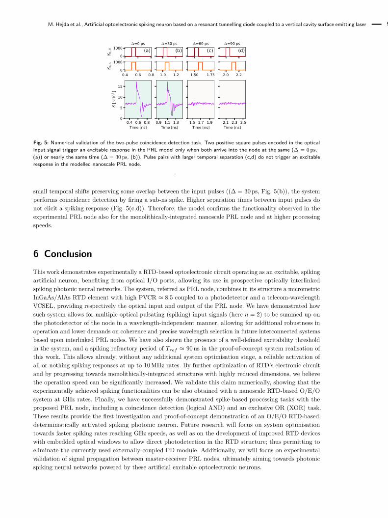
where 𝑉 is the voltage along the RTD, 𝐼(𝑡) is the total current in the circuit, 𝑆(𝑡) is the photon numberand 𝑁(𝑡) is the carrier number. In difference to previous works [36], the RTD (first two Eqns.) and laser(last two Eqns.) models are coupled through the voltage term to represent same behaviour as observedexperimentally, where RF signals are AC-coupled directly to the laser through a bias-tee network (here, 𝑅0= 50 Ω and coupling efficiency 𝜂 = 0.2). The PD element is coupled as a voltage modulation via the 𝑅𝜅𝑆0(𝑡)term, where 𝜅 represents the opto-electrical conversion factor of the PD (sensitivity, in units of current perphoton count), hence defining 𝑅𝜅 as the detector conversion gain. The 𝐼-𝑉 characteristic (Fig. 4(a)) ofthe RTD is based on a physical model by Schulman [51]. The curve parameters, based on experimentalmeasurement of nano-scale RTD devices, as well as the laser and circuit parameters are available from[45]. Using these 𝐼-𝑉 parameters yields a highly nonlinear 𝐼-𝑉 curve with an NDC region between 609 mVand 720 mV. As shown in Fig. 4, an incoming optical perturbation in the form of a 20 ps long pulse (Fig.4(b)) is sufficient to trigger an ultrafast (sub-ns) spiking response with amplitude of over 1 V peak-peak(Fig. 4(c)). Direct comparison with the traces displayed in Fig. 1(e) confirms very good agreement betweenthe dynamics observed experimentally with the macroscopic PRL node (PD-RTD-VCSEL design) andnumerically for the modelled nanoscale PRL system. This signal is then fed into the nanolaser within thenano-PRL node’s structure, resulting in high speed optical spikes (Fig. 4(d)). In addition to the consistencybetween the numerical and experimental dynamics, we must note that the nanoscale PRL system allows forsignificantly improved spiking rates, currently projected as approximately three magnitudes faster thanthose obtained in our experiments with the PD-RTD-VCSEL based PRL system. To obtain the estimateof upper limit on the spiking rate of this nanoscale PRL model, we performed a spiking refractorinessevaluation by using pairs of pulses with gradually increasing temporal separation (the same test that wascarried out experimentally in Fig. 2). The achieved lowest temporal separation between two input pulses thatreliably elicited a pair of spiking responses from the nanoscale PRL node was 300 ps (Fig. 4), resulting in amaximum theoretical spiking rate of 3.3 GHz. Furthermore, we validate in theory that the same coincidencedetection functionality (as demonstrated experimentally in Fig. 3) can be achieved with the nanoscale PRLnode, yet again at significantly faster rates. In Fig. 5, a pair of 60 ps optical pulses of amplitude 𝑆0 = 1000is incident on the PD element of the nano-PRL node. For either no temporal shift (Δ = 0 ps, Fig. 5(a)) or
0 500 1000Voltage [mV]
0.0
0.1
0.2
0.3
0.4
Curre
nt [m
A]
(a)I-V curvebias pointlimit cycleNDR
0.5 1.0 1.5Time [ns]
0
5
10
15
S0 [×
103]
(b)V0 = 0.58V
1.0 1.5Time [ns]
0.2
0.4
0.6
0.8
1.0
1.2
Volta
ge [V
]
(c)
1.0 1.5Time [ns]
0
5
10
15
S [×
103]
(d)
2 3Time [ns]
0
5
10
15
S [×
103]
∆=300 ps(e)
Fig. 4: Numerical simulation of a PD-RTD-LD system. (a) I-V characteristic of a nano-scale RTD, with highlighted NDCregion, voltage bias (fine dashed line) and evolution of the system states during the spiking event, showing the dynamicallimit cycle. (b) Example of an electrical trigger signal. (c) Electrical response of the nano-RTD. (d) Optical response of avoltage-coupled nanoscale RTD-LD system. e) Demonstration of firing of a pair of consecutive optical spikes, elicited inthe system when subject to the arrival of a pair of input perturbations with temporal separation of 300 ps.
M. Hejda et al., Artificial optoelectronic spiking neuron based on a resonant tunnelling diode coupled to a vertical cavity surface emitting laser 9
0
1000
S0,B (a)
∆=0 ps(b)
∆=30 ps(c)
∆=60 ps(d)
∆=90 ps
0.4 0.6 0.80
1000
S0,A
1.0 1.2 1.50 1.75 2.0 2.2
0.4 0.6 0.8Time [ns]
0
5
10
15
S [×
103]
0.9 1.1 1.3Time [ns]
1.5 1.7 1.9Time [ns]
2.1 2.3 2.5Time [ns]
Fig. 5: Numerical validation of the two-pulse coincidence detection task. Two positive square pulses encoded in the opticalinput signal trigger an excitable response in the PRL model only when both arrive into the node at the same (Δ = 0 ps,(a)) or nearly the same time (Δ = 30 ps, (b)). Pulse pairs with larger temporal separation (c,d) do not trigger an excitableresponse in the modelled nanoscale PRL node.
.
small temporal shifts preserving some overlap between the input pulses ((Δ = 30 ps, Fig. 5(b)), the systemperforms coincidence detection by firing a sub-ns spike. Higher separation times between input pulses donot elicit a spiking response (Fig. 5(c,d)). Therefore, the model confirms the functionality observed in theexperimental PRL node also for the monolithically-integrated nanoscale PRL node and at higher processingspeeds.
6 ConclusionThis work demonstrates experimentally a RTD-based optoelectronic circuit operating as an excitable, spikingartificial neuron, benefiting from optical I/O ports, allowing its use in prospective optically interlinkedspiking photonic neural networks. The system, referred as PRL node, combines in its structure a micrometricInGaAs/AlAs RTD element with high PVCR ≈ 8.5 coupled to a photodetector and a telecom-wavelengthVCSEL, providing respectively the optical input and output of the PRL node. We have demonstrated howsuch system allows for multiple optical pulsating (spiking) input signals (here 𝑛 = 2) to be summed up onthe photodetector of the node in a wavelength-independent manner, allowing for additional robustness inoperation and lower demands on coherence and precise wavelength selection in future interconnected systemsbased upon interlinked PRL nodes. We have also shown the presence of a well-defined excitability thresholdin the system, and a spiking refractory period of 𝑇𝑟𝑒𝑓 ≈ 90 ns in the proof-of-concept system realisation ofthis work. This allows already, without any additional system optimisation stage, a reliable activation ofall-or-nothing spiking responses at up to 10 MHz rates. By further optimization of RTD’s electronic circuitand by progressing towards monolithically-integrated structures with highly reduced dimensions, we believethe operation speed can be significantly increased. We validate this claim numerically, showing that theexperimentally achieved spiking functionalities can be also obtained with a nanoscale RTD-based O/E/Osystem at GHz rates. Finally, we have successfully demonstrated spike-based processing tasks with theproposed PRL node, including a coincidence detection (logical AND) and an exclusive OR (XOR) task.These results provide the first investigation and proof-of-concept demonstration of an O/E/O RTD-based,deterministically activated spiking photonic neuron. Future research will focus on system optimisationtowards faster spiking rates reaching GHz speeds, as well as on the development of improved RTD deviceswith embedded optical windows to allow direct photodetection in the RTD structure; thus permitting toeliminate the currently used externally-coupled PD module. Additionally, we will focus on experimentalvalidation of signal propagation between master-receiver PRL nodes, ultimately aiming towards photonicspiking neural networks powered by these artificial excitable optoelectronic neurons.

10 REFERENCES
Acknowledgment: The authors would also like to acknowledge J. Iwan Davies from IQE for providing theepitaxial growth for RTD fabrication.
Funding: The authors acknowledge support by the European Commission (Grant 828841-ChipAI-H2020-FETOPEN-2018-2020) and by the UK Research and Innovation (UKRI) Turing AI Acceleration FellowshipsProgramme (EP/V025198/1).
References[1] Aditya Ramesh et al. “Zero-Shot Text-to-Image Generation”. In: arXiv:2102.12092 [cs] (Feb. 2021).[2] John Jumper et al. “Highly Accurate Protein Structure Prediction with AlphaFold”. In: Nature 596.7873 (Aug.
2021), pp. 583–589. issn: 0028-0836, 1476-4687. doi: 10.1038/s41586-021-03819-2.[3] Tom B. Brown et al. Language Models Are Few-Shot Learners. May 2020.[4] Alexander Neckar et al. “Braindrop: A Mixed-Signal Neuromorphic Architecture With a Dynamical Systems-Based
Programming Model”. In: Proceedings of the IEEE 107.1 (Jan. 2019), pp. 144–164. issn: 0018-9219. doi: 10.1109/JPROC.2018.2881432.
[5] Sebastian Höppner et al. The SpiNNaker 2 Processing Element Architecture for Hybrid Digital Neuromorphic Com-puting. Mar. 2021.
[6] Michael V. DeBole et al. “TrueNorth: Accelerating From Zero to 64 Million Neurons in 10 Years”. In: Computer52.5 (May 2019), pp. 20–29. issn: 0018-9162. doi: 10.1109/MC.2019.2903009.
[7] Garrick Orchard et al. “Efficient Neuromorphic Signal Processing with Loihi 2”. In: 2021 IEEE Workshop on SignalProcessing Systems (SiPS). Coimbra, Portugal: IEEE, Oct. 2021, pp. 254–259. isbn: 978-1-66540-144-9. doi:10.1109/SiPS52927.2021.00053.
[8] Joshua Robertson et al. “Externally-Triggered Activation and Inhibition of Optical Pulsating Regimes in Quantum-Dot Mode-locked Lasers”. In: Scientific Reports 8.1 (Dec. 2018), p. 12515. issn: 2045-2322. doi: 10.1038/s41598-018-30758-2.
[9] George Sarantoglou, Menelaos Skontranis, and Charis Mesaritakis. “All Optical Integrate and Fire NeuromorphicNode Based on Single Section Quantum Dot Laser”. In: IEEE Journal of Selected Topics in Quantum Electronics26.5 (Sept. 2020), pp. 1–10. issn: 1077-260X. doi: 10.1109/JSTQE.2019.2945549.
[10] Michael L. Schneider et al. “Ultralow Power Artificial Synapses Using Nanotextured Magnetic Josephson Junctions”.In: Science Advances 4.1 (Jan. 2018), e1701329. issn: 2375-2548. doi: 10.1126/sciadv.1701329.
[11] Emily Toomey, Ken Segall, and Karl K. Berggren. “Design of a Power Efficient Artificial Neuron Using Supercon-ducting Nanowires”. In: Frontiers in Neuroscience 13 (Sept. 2019). issn: 1662-453X. doi: 10.3389/fnins.2019.00933.
[12] Jonathan K. George et al. “Neuromorphic Photonics with Electro-Absorption Modulators”. In: Optics Express 27.4(Feb. 2019), p. 5181. issn: 1094-4087. doi: 10.1364/OE.27.005181.
[13] Alexander N. Tait et al. “Silicon Photonic Modulator Neuron”. In: Physical Review Applied 11.6 (June 2019),p. 064043. doi: 10.1103/PhysRevApplied.11.064043.
[14] George Mourgias-Alexandris et al. “Neuromorphic Photonics With Coherent Linear Neurons Using Dual-IQ Modula-tion Cells”. In: Journal of Lightwave Technology 38.4 (Feb. 2020), pp. 811–819. issn: 0733-8724, 1558-2213. doi:10.1109/JLT.2019.2949133.
[15] George Mourgias-Alexandris et al. “An All-Optical Neuron with Sigmoid Activation Function”. In: Optics Express27.7 (Apr. 2019), p. 9620. issn: 1094-4087. doi: 10.1364/OE.27.009620.
[16] Bin Shi, Nicola Calabretta, and Ripalta Stabile. “InP Photonic Integrated Multi-Layer Neural Networks: Architectureand Performance Analysis”. In: APL Photonics (Dec. 2021), p. 5.0066350. issn: 2378-0967. doi: 10 . 1063 / 5 .0066350.
[17] Werner Coomans et al. “Solitary and Coupled Semiconductor Ring Lasers as Optical Spiking Neurons”. In: PhysicalReview E 84.3 (Sept. 2011), p. 036209. doi: 10.1103/PhysRevE.84.036209.
[18] Jinlong Xiang et al. “All-Optical Spiking Neuron Based on Passive Microresonator”. In: Journal of Lightwave Tech-nology 38.15 (Aug. 2020), pp. 4019–4029. issn: 0733-8724, 1558-2213. doi: 10.1109/JLT.2020.2986233.
[19] Johannes Feldmann et al. “All-Optical Spiking Neurosynaptic Networks with Self-Learning Capabilities”. In: Nature569.7755 (2019), pp. 208–214. issn: 0028-0836. doi: 10.1038/s41586-019-1157-8.
[20] Santiago G. C. Carrillo et al. “Behavioral Modeling of Integrated Phase-Change Photonic Devices for NeuromorphicComputing Applications”. In: APL Materials 7.9 (Sept. 2019), p. 091113. issn: 2166-532X. doi: 10 . 1063 / 1 .5111840.

REFERENCES 11
[21] Matěj Hejda et al. “Spike-Based Information Encoding in Vertical Cavity Surface Emitting Lasers for NeuromorphicPhotonic Systems”. In: Journal of Physics: Photonics 2.4 (Aug. 2020), p. 044001. issn: 2515-7647. doi: 10.1088/2515-7647/aba670.
[22] Joshua Robertson et al. “Toward Neuromorphic Photonic Networks of Ultrafast Spiking Laser Neurons”. In: IEEEJournal of Selected Topics in Quantum Electronics 26.1 (Jan. 2020), pp. 1–15. issn: 1077-260X. doi: 10.1109/JSTQE.2019.2931215.
[23] Shuiying Xiang et al. “Computing Primitive of Fully VCSEL-Based All-Optical Spiking Neural Network for Super-vised Learning and Pattern Classification”. In: IEEE Transactions on Neural Networks and Learning Systems (2020),pp. 1–12. issn: 2162-237X. doi: 10.1109/TNNLS.2020.3006263.
[24] Zhenxue Zhang et al. “Controllable Spiking Dynamics in Cascaded VCSEL-SA Photonic Neurons”. In: NonlinearDynamics (Nov. 2019). issn: 0924-090X. doi: 10.1007/s11071-019-05339-1.
[25] Yahui Zhang et al. “All-Optical Neuromorphic Binary Convolution with a Spiking VCSEL Neuron for Image GradientMagnitudes”. In: Photonics Research 9.5 (May 2021), B201. issn: 2327-9125. doi: 10.1364/PRJ.412141.
[26] Joshua Robertson et al. “Ultrafast Optical Integration and Pattern Classification for Neuromorphic Photonics Basedon Spiking VCSEL Neurons”. In: Scientific Reports 10.1 (Dec. 2020), p. 6098. issn: 2045-2322. doi: 10 .1038/s41598-020-62945-5.
[27] Matěj Hejda et al. “Neuromorphic Encoding of Image Pixel Data into Rate-Coded Optical Spike Trains with aPhotonic VCSEL-neuron”. In: APL Photonics 6.6 (June 2021), p. 060802. issn: 2378-0967. doi: 10 . 1063 / 5 .0048674.
[28] Tobias Heuser et al. “Developing a Photonic Hardware Platform for Brain-Inspired Computing Based on 5 × 5VCSEL Arrays”. In: Journal of Physics: Photonics 2.4 (Sept. 2020), p. 044002. issn: 2515-7647. doi: 10.1088/2515-7647/aba671.
[29] Ryunosuke Izumi, Safumi Suzuki, and Masahiro Asada. “1.98 THz Resonant-Tunneling-Diode Oscillator with Re-duced Conduction Loss by Thick Antenna Electrode”. In: 2017 42nd International Conference on Infrared, Millime-ter, and Terahertz Waves (IRMMW-THz). IEEE, Aug. 2017, pp. 1–2. isbn: 978-1-5090-6050-4. doi: 10 .1109/IRMMW-THz.2017.8066877.
[30] Qianchun Weng et al. “Quantum Dot Single-Photon Switches of Resonant Tunneling Current for Discriminating-Photon-Number Detection”. In: Scientific Reports 5.1 (Aug. 2015), p. 9389. issn: 2045-2322. doi: 10 . 1038 /srep09389.
[31] Andreas Pfenning et al. “Sensitivity of Resonant Tunneling Diode Photodetectors”. In: Nanotechnology 27.35 (Sept.2016), p. 355202. issn: 0957-4484. doi: 10.1088/0957-4484/27/35/355202.
[32] Yousuke Nishida et al. “Terahertz Coherent Receiver Using a Single Resonant Tunnelling Diode”. In: ScientificReports 9.1 (Dec. 2019), p. 18125. issn: 2045-2322. doi: 10.1038/s41598-019-54627-8.
[33] Tomoyuki Miyamoto, Atsushi Yamaguchi, and Toshikazu Mukai. “Terahertz Imaging System with Resonant Tunnel-ing Diodes”. In: Japanese Journal of Applied Physics 55.3 (Mar. 2016), p. 032201. issn: 0021-4922, 1347-4065. doi:10.7567/JJAP.55.032201.
[34] Jue Wang et al. “15-Gb/s 50-Cm Wireless Link Using a High-Power Compact III-V 84-GHz Transmitter”. In: IEEETransactions on Microwave Theory and Techniques (2018), pp. 1–8. issn: 0018-9480, 1557-9670. doi: 10.1109/TMTT.2018.2859983.
[35] Weikang Zhang et al. “Optical Direct Intensity Modulation of a 79GHz Resonant Tunneling Diode-PhotodetectorOscillator”. In: Optics Express 27.12 (June 2019), p. 16791. issn: 1094-4087. doi: 10.1364/OE.27.016791.
[36] Bruno Romeira et al. “Excitability and Optical Pulse Generation in Semiconductor Lasers Driven by ResonantTunneling Diode Photo-Detectors”. In: Optics Express 21.18 (Sept. 2013), p. 20931. issn: 1094-4087. doi: 10.1364/OE.21.020931.
[37] Martin Hänggi and Leon O. Chua. “Cellular Neural Networks Based on Resonant Tunnelling Diodes”. In: Interna-tional Journal of Circuit Theory and Applications 29.5 (Sept. 2001), pp. 487–504. issn: 00989886. doi: 10.1002/cta.172.
[38] Pinaki Mazumder, Sing-Rong Li, and Idongesit E. Ebong. “Tunneling-Based Cellular Nonlinear Network Architec-tures for Image Processing”. In: IEEE Transactions on Very Large Scale Integration (VLSI) Systems 17.4 (Apr.2009), pp. 487–495. issn: 1063-8210. doi: 10.1109/TVLSI.2009.2014771.
[39] Qusay Al-Taai et al. “Towards an Excitable Microwave Spike Generator for Future Neuromorphic Computing”. In:2021 16th European Microwave Integrated Circuits Conference (EuMIC). IEEE, 2022, pp. 386–389. doi: 10.23919/EuMIC50153.2022.9783686.
[40] Weikang Zhang et al. “Analysis of Excitability in Resonant Tunneling Diode-Photodetectors”. In: Nanomaterials11.6 (June 2021), p. 1590. issn: 2079-4991. doi: 10.3390/nano11061590.
[41] Bruno Romeira et al. “Regenerative Memory in Time-Delayed Neuromorphic Photonic Resonators”. In: ScientificReports 6.1 (May 2016), p. 19510. issn: 2045-2322. doi: 10.1038/srep19510.
[42] Fabian Hartmann et al. “Light-Induced Stochastic Resonance in a Nanoscale Resonant-Tunneling Diode”. In: Ap-plied Physics Letters 98.24 (2011), pp. 96–99. issn: 00036951. doi: 10.1063/1.3600329.

12 REFERENCES
[43] Bruno Romeira, José M. L. Figueiredo, and Julien Javaloyes. “NanoLEDs for Energy-Efficient and Gigahertz-SpeedSpike-Based Sub-𝜆 Neuromorphic Nanophotonic Computing”. In: Nanophotonics (June 2020). issn: 2192-8614. doi:10.1515/nanoph-2020-0177.
[44] Ignacio Ortega-Piwonka et al. “Spike Propagation in a Nanolaser-Based Optoelectronic Neuron”. In: Optical Materi-als Express (Mar. 2022). issn: 2159-3930. doi: 10.1364/OME.451706.
[45] Matěj Hejda et al. “Resonant Tunneling Diode Nano-Optoelectronic Excitable Nodes for Neuromorphic Spike-Based Information Processing”. In: Physical Review Applied 17.2 (Feb. 2022), p. 024072. issn: 2331-7019. doi:10.1103/PhysRevApplied.17.024072.
[46] Alexander N. Tait et al. “Neuromorphic Photonic Networks Using Silicon Photonic Weight Banks”. In: ScientificReports 7.1 (Dec. 2017), p. 7430. issn: 2045-2322. doi: 10.1038/s41598-017-07754-z.
[47] Bruno Romeira et al. “Subwavelength Neuromorphic Nanophotonic Integrated Circuits for Spike-Based Computing:Challenges and Prospects”. In: Emerging Topics in Artificial Intelligence (ETAI) 2021. Ed. by Giovanni Volpe et al.San Diego, United States: SPIE, Sept. 2021, p. 11. isbn: 978-1-5106-4446-5 978-1-5106-4447-2. doi: 10.1117/12.2591852.
[48] Hagai Agmon-Snir, Catherine E. Carr, and John Rinzel. “The Role of Dendrites in Auditory Coincidence Detection”.In: Nature 393.6682 (May 1998), pp. 268–272. issn: 0028-0836, 1476-4687. doi: 10.1038/30505.
[49] Charles F. Stevens and Anthony M. Zador. “Input Synchrony and the Irregular Firing of Cortical Neurons”. In:Nature Neuroscience 1.3 (July 1998), pp. 210–217. issn: 1097-6256, 1546-1726. doi: 10.1038/659.
[50] Jonathan K. George et al. “Symmetry Perception with Spiking Neural Networks”. In: Scientific Reports 11.1 (Dec.2021), p. 5776. issn: 2045-2322. doi: 10.1038/s41598-021-85232-3.
[51] Joel N. Schulman, Hector J. De Los Santos, and David H. Choi. “Physics-Based RTD Current-Voltage Equation”.In: IEEE Electron Device Letters 17.5 (May 1996), pp. 220–222. issn: 0741-3106, 1558-0563. doi: 10.1109/55.491835.