
Optoelectronic Properties of Nanostructured Ensembles Controlled by Biomolecular Logic Systems
Upload
khangminh22Category
view
0download
0
Organic Photodiodes and Their
Optoelectronic Applications
by
Hyunsoo Kim
A dissertation submitted in partial fulfillment of the requirements for the degree of
Doctor of Philosophy (Electrical and Computer Engineering)
in The University of Michigan 2017
Doctoral Committee:
Professor Jerzy Kanicki, Chair Professor L. Jay Guo Professor Jinsang Kim Professor Jamie D. Philips

© Hyunsoo Kim 2017 All Rights Reserved

ii
To my beautiful wife, and family

iii
ACKNOWLEDGEMENTS
First and foremost, I sincerely thank my research advisor, Prof. Jerzy
Kanicki, for his support throughout my Ph.D study in the University of Michigan.
Without his guidance, the six year journey was impossible for me and might be
tumbled down at the middle of the period. He taught me in such a unique way to
think more critically and deeply, broaden the knowledge, and learn how to write.
I also appreciated his endless patience, respect to students, and encouragement
which helped me to overcome many difficulties and frustrations during the period.
I also gratefully thank my doctoral committee, Prof. L Jay Guo, Prof.
Jinsang Kim, and Prof. Jamie D. Phillips for their time and guidance through my
doctoral work. My previous advisor, Prof. Guo has expressed constant
encouragement and support even after I moved my research group. My fabrication
skills and broad experience on nano science were mostly taught by him. Without
him, I was not able to reach this stage of life. Prof. Kim has been a role model
among Korean graduate student society and I really appreciated his
thoughtfulness and consideration to students. Prof. Phillips was not only a good
researcher but also the best lecturer to me as I remember I really enjoyed his solar
cell class a lot. I also specially express my gratitude to Prof. Ganago who was my
GSI instructor throughout the period. He always cared about my research and

iv
health during the semester when I was busy doing both teaching and research
work. He was very good friend and supporter during my doctoral journey.
I would like to thank Kanicki group members and friends in the University
of Michigan for their help and friendship. First of all, I was lucky to work with
talented former and current Kanicki group members : Chumin Zhao, Aunnasha
Sengupta, Eric Yu, Mao-Hsun Cheng, Che-lin Huang, Soo Chang Kim, and Prof.
Agnieszka Pawlicka. I also need to express my thankfulness to former Guo group
members : Jaeyong Lee, Kyu-Tae Lee, Taehee Jang, Sangeon Lee, Taehwa Lee
for their friendship and support. I am especially feeling grateful to OCM group
members : Kyusang Lee, Jaesang Lee, Byeongseop Song, Jongchan Kim, Joosung
Moon, Byungjun Lee, Changyeong Jeong and Prof. Stephen Forrest for their
friendship and support on my research.
Most importantly, I have indebted to my parents, my sisters, and my wife
for their endless support and unconditional love. I would never have completed
my Ph.D without their sacrifice and patience for such a long period. Especially, I
would like to express my sincere thankfulness and love to my wife, Jungwon Choi,
for her support and endurance in the time of long distance relationship and when
I was remotely writing the dissertation at Palo Alto. She continuously encouraged
me that I can do this when I was discouraged, and she was always with me
whenever I was working on the thesis including weekends and holidays. Finally,
I thank to my God who allowed me to finish it.

v
TABLE OF CONTENTS
DEDICATION . . . . . . . . . . . . . . . . . . . . . . . . . . . . . . . . . . . . . . . . . . . . . . . . . . ii
ACKNOWLEDGEMENTS . . . . . . . . . . . . . . . . . . . . . . . . . . . . . . . . . . . . . . . iii
LIST OF FIGURES . . . . . . . . . . . . . . . . . . . . . . . . . . . . . . . . . . . . . . . . . . . . viii
LIST OF TABLES . . . . . . . . . . . . . . . . . . . . . . . . . . . . . . . . . . . . . . . . . . . . . xiii
LIST OF APPENDICES . . . . . . . . . . . . . . . . . . . . . . . . . . . . . . . . . . . . . . . . xiv
ABSTRACT . . . . . . . . . . . . . . . . . . . . . . . . . . . . . . . . . . . .. . . . . . . . . . . . . . . xv
CHAPTER 1. Introduction . . . . . . . . . . . . . . . . . . . . . . . . . . . . . . . . . . . . . . . . . . . . . . . . . . 1
1.1. Motivation . . . . . . . . . . . . . . . . . . . . . . . . . . . . . . . . . . . . . . . . . . . . . . . . . . . . . . . . . . . 1
1.2. Physics of Organic Semiconductors . . . . . . . . . . . . . . . . . . . . . . . . . . . . . . . . . . . . . . . 3
1.3. Deposition Methods of Organic Semiconductors . . . . . . . . . . . . . . . . . . . . . . . . . . . 10
1.3.1. Spin Coating . . . . . . . . . . . . . . . . . . . . . . . . . . . . . . . . . . . . . . . . . . . . . . . . . . . 12
1.3.2. Blade Coating . . . . . . . . . . . . . . . . . . . . . . . . . . . . . . . . . . . . . . . . . . . . . . . . . . 14
1.3.3. Inkjet Printing . . . . . . . . . . . . . . . . . . . . . . . . . . . . . . . . . . . . . . . . . . . . . . . . . . 15
1.4. Organic Photodiodes . . . . . . . . . . . . . . . . . . . . . . . . . . . . . . . . . . . . . . . . . . . . . . . . . . 16
1.4.1. Organic Solar Cells . . . . . . . . . . . . . . . . . . . . . . . . . . . . . . . . . . . . . . . . . . . . . . 16
1.4.2. Organic Photodetectors . . . . . . . . . . . . . . . . . . . . . . . . . . . . . . . . . . . . . . . . . . . 17
1.5. Thesis Organization . . . . . . . . . . . . . . . . . . . . . . . . . . . . . . . . . . . . . . . . . . . . . . . . . . . 19
2. Inverted Organic Photodetector with DMD Top Illumination Transparent
Anode . . . . . . . . . . . . . . . . . . . . . . . . . . . . . . . . . . . . . . . . . . . . . . . . . . . . . . . . . . . . . . . . 20 2.1. Introduction . . . . . . . . . . . . . . . . . . . . . . . . . . . . . . . . . . . . . . . . . . . . . . . . . . . . . . . . . 20
2.2. Experimental . . . . . . . . . . . . . . . . . . . . . . . . . . . . . . . . . . . . . . . . . . . . . . . . . . . . . . . . 21
2.2.1. Device Fabrication . . . . . . . . . . . . . . . . . . . . . . . . . . . . . . . . . . . . . . . . . . . . . . 21
2.2.2. Device Measurement . . . . . . . . . . . . . . . . . . . . . . . . . . . . . . . . . . . . . . . . . . . . 22
2.2.3. DMD Electrode Optical Simulations . . . . . . . . . . . . . . . . . . . . . . . . . . . . . . . . 23
2.3. Results and Discussion . . . . . . . . . . . . . . . . . . . . . . . . . . . . . . . . . . . . . . . . . . . . . . . . 24

vi
2.3.1. DMD Electrode Simulation, Characterization, and Optimization . . . . . . . . . . 24
2.3.2. Device Physics of the Inverted DMD OPDs . . . . . . . . . . . . . . . . . . . . . . . . . . 31
2.3.3. Electrical Characteristics of the Inverted DMD OPDs . . . . . . . . . . . . . . . . . . 34
2.4. Conclusion . . . . . . . . . . . . . . . . . . . . . . . . . . . . . . . . . . . . . . . . . . . . . . . . . . . . . . . . . 42
3. Bilayer Interdiffused Heterojunction Organic Photodiode by Double
Transfer Stamping Method . . . . . . . . . . . . . . . . . . . . . . . . . . . . . . . . . . . . . . . . . . . 43 3.1. Introduction . . . . . . . . . . . . . . . . . . . . . . . . . . . . . . . . . . . . . . . . . . . . . . . . . . . . . . . . 43
3.2. Experimental . . . . . . . . . . . . . . . . . . . . . . . . . . . . . . . . . . . . . . . . . . . . . . . . . . . . . . . 45
3.2.1. PDMS Stamp and Solutions Preparation . . . . . . . . . . . . . . . . . . . . . . . . . . . . . 45
3.2.2. Device Fabrication . . . . . . . . . . . . . . . . . . . . . . . . . . . . . . . . . . . . . . . . . . . . . . 46
3.2.3. Measurements and Simulations . . . . . . . . . . . . . . . . . . . . . . . . . . . . . . . . . . . . 50
3.3. Results and Discussion . . . . . . . . . . . . . . . . . . . . . . . . . . . . . . . . . . . . . . . . . . . . . . . 53
3.3.1. Device Band Diagram . . . . . . . . . . . . . . . . . . . . . . . . . . . . . . . . . . . . . . . . . . . 53
3.3.2. Dark Current Density vs. Voltage Characteristics . . . . . . . . . . . . . . . . . . . . . . 56
3.3.3. Capacitance – Voltage Characteristics under Dark . . . . . . . . . . . . . . . . . . . . . 58
3.3.4. Figures of Merit of the BiHJ OPDs . . . . . . . . . . . . . . . . . . . . . . . . . . . . . . . . . 62
3.3.5. BiHJ Solar Cells Properties . . . . . . . . . . . . . . . . . . . . . . . . . . . . . . . . . . . . . . . 67
3.3.6. EQE measurement . . . . . . . . . . . . . . . . . . . . . . . . . . . . . . . . . . . . . . . . . . . . . . 70
3.4. Conclusion . . . . . . . . . . . . . . . . . . . . . . . . . . . . . . . . . . . . . . . . . . . . . . . . . . . . . . . . . 80
4. High Performance Low-bandgap Polymer Organic Photodiode with
Broadband Absorption with Charge Blocking Layer by Double Transfer
Stamping Method . . . . . . . . . . . . . . . . . . . . . . . . . . . . . . . . . . . . . . . . . . . . . . . . . . . . 81 4.1. Introduction . . . . . . . . . . . . . . . . . . . . . . . . . . . . . . . . . . . . . . . . . . . . . . . . . . . . . . . . 81
4.2. Experimental . . . . . . . . . . . . . . . . . . . . . . . . . . . . . . . . . . . . . . . . . . . . . . . . . . . . . . . 82
4.2.1. Device Fabrication . . . . . . . . . . . . . . . . . . . . . . . . . . . . . . . . . . . . . . . . . . . . . . 82
4.2.2. Device Measurement . . . . . . . . . . . . . . . . . . . . . . . . . . . . . . . . . . . . . . . . . . . . 84
4.3. Absorption Spectra of Films . . . . . . . . . . . . . . . . . . . . . . . . . . . . . . . . . . . . . . . . . . . . 87
4.4. Results and Discussion . . . . . . . . . . . . . . . . . . . . . . . . . . . . . . . . . . . . . . . . . . . . . . . . 90
4.5. Conclusion . . . . . . . . . . . . . . . . . . . . . . . . . . . . . . . . . . . . . . . . . . . . . . . . . . . . . . . . 102
5. Hemispherical Organic Photodiodes Arrays enabled by Three
Dimensional Printed Masks . . . . . . . . . . . . . . . . . . . . . . . . . . . . . . . . . . . . . . . . . . 103 5.1. Introduction . . . . . . . . . . . . . . . . . . . . . . . . . . . . . . . . . . . . . . . . . . . . . . . . . . . . . . . 103

vii
5.2. Curved Focal Plane Arrays for Imaging Systems . . . . . . . . . . . . . . . . . . . . . . . . . . . 104
5.2.1. Human Eyes and Conventional Camera System . . . . . . . . . . . . . . . . . . . . . . 104
5.2.2. Comparison between Different Camera Systems . . . . . . . . . . . . . . . . . . . . . . 105
5.2.3. Challenges to Fabricate the Curved Focal Plane Array . . . . . . . . . . . . . . . . . 107
5.3. Preparation for the Curved Focal Plane Array Fabrication . . . . . . . . . . . . . . . . . . . . 108
5.3.1. Stereolithography for 3D Mask Fabrication . . . . . . . . . . . . . . . . . . . . . . . . . . 108
5.3.2. Preparation of Elastomeric 3D PDMS Stamp . . . . . . . . . . . . . . . . . . . . . . . . . 110
5.4. Fabrication of Hemispherical Focal Plane Arrays . . . . . . . . . . . . . . . . . . . . . . . . . . 111
5.5. Result and Discussion . . . . . . . . . . . . . . . . . . . . . . . . . . . . . . . . . . . . . . . . . . . . . . . . 114
5.6. Conclusion . . . . . . . . . . . . . . . . . . . . . . . . . . . . . . . . . . . . . . . . . . . . . . . . . . . . . . . . . 115
6. Simulation of Organic Photodiode - Metal Oxide Active Pixel Sensor
Circuit with Transimpedance Amplifier . . . . . . . . . . . . . . . . . . . . . . . . . . . . . . 116 6.1. Introduction . . . . . . . . . . . . . . . . . . . . . . . . . . . . . . . . . . . . . . . . . . . . . . . . . . . . . . . . 116
6.2. Device Fabrication . . . . . . . . . . . . . . . . . . . . . . . . . . . . . . . . . . . . . . . . . . . . . . . . . . 118
6.2.1. Amorphous Indium-Tin-Zinc Oxide TFTs . . . . . . . . . . . . . . . . . . . . . . . . . . 118
6.2.2. Organic Photodiodes . . . . . . . . . . . . . . . . . . . . . . . . . . . . . . . . . . . . . . . . . . . . 118
6.3. Device Characteristics and SPICE Models . . . . . . . . . . . . . . . . . . . . . . . . . . . . . . . 120
6.3.1. Amorphous Indium-Tin-Zinc-Oxide TFTs . . . . . . . . . . . . . . . . . . . . . . . . . . . 120
6.3.2. SPICE Model for a-ITZO TFT . . . . . . . . . . . . . . . . . . . . . . . . . . . . . . . . . . . . 122
6.3.3. SPICE Model for Organic Photodiodes . . . . . . . . . . . . . . . . . . . . . . . . . . . . . 124
6.4. OPD-APS and Transimpedance Amplifier . . . . . . . . . . . . . . . . . . . . . . . . . . . . . . . . 125
6.4.1. Operation Principle . . . . . . . . . . . . . . . . . . . . . . . . . . . . . . . . . . . . . . . . . . . . . 127
6.4.2. Simulation Results and Discussion . . . . . . . . . . . . . . . . . . . . . . . . . . . . . . . . . 129
6.5. Conclusion . . . . . . . . . . . . . . . . . . . . . . . . . . . . . . . . . . . . . . . . . . . . . . . . . . . . . . . . . 140
7. Final Remarks and Future Work . . . . . . . . . . . . . . . . . . . . . . . . . . . . . . . . . . . . 141 7.1. Conclusion of the Thesis . . . . . . . . . . . . . . . . . . . . . . . . . . . . . . . . . . . . . . . . . . . . . 141
7.2. Recommendations for Future Work . . . . . . . . . . . . . . . . . . . . . . . . . . . . . . . . . . . . . 144
Appendices . . . . . . . . . . . . . . . . . . . . . . . . . . . . . . . . . . . . . . . . . . . . . . . . . . . . . . . . . . . . . 146
Bibliography . . . . . . . . . . . . . . . . . . . . . . . . . . . . . . . . . . . . . . . . . . . . . . . . . . . . . . . . . . . 163

viii
LIST OF FIGURES
Figure 1.1 Examples of various electronic devices based on organic semiconductors . . . . . . 1 Figure 1.2 Schematic view of the organic molecule structures . . . . . . . . . . . . . . . . . . . . . . . . 4 Figure 1.3 Schematic diagram of the various types of excitons in semiconductors and
insulator . . . . . . . . . . . . . . . . . . . . . . . . . . . . . . . . . . . . . . . . . . . . . . . . . . . . . . . . . . . . . 6 Figure 1.4 Schematic representation of two types of energy transfer between a donor (D) and
an acceptor (A) molecule . . . . . . . . . . . . . . . . . . . . . . . . . . . . . . . . . . . . . . . . . . . . . . . . 7 Figure 1.5 Schematic of steps in the photocurrent generation process . . . . . . . . . . . . . . . . . . 9
Figure 1.6 Schematic of the vacuum thermal evaporation (VTE) system . . . . . . . . . . . . . . . . 11 Figure 1.7 Schematic of steps of the spin coating process . . . . . . . . . . . . . . . . . . . . . . . . . . . 13 Figure 1.8 Schematic of the blade coating process . . . . . . . . . . . . . . . . . . . . . . . . . . . . . . . . 14 Figure 1.9 Schematic of ink-jet printing method . . . . . . . . . . . . . . . . . . . . . . . . . . . . . . . . . .15 Figure 2.1 Device structure of the inverted OPD with top illumination . . . . . . . . . . . . . . . . 24 Figure 2.2 Measured refractive indices of Ag and MoO3 plotted from 400 nm to 800 nm
wavelength . . . . . . . . . . . . . . . . . . . . . . . . . . . . . . . . . . . . . . . . . . . . . . . . . . . . . . . . . 25 Figure 2.3 (a) Sheet resistance of the MoO3 5 nm / Ag varied / MoO3 35 nm structure fabricated
on glass as a function of the thickness of the Ag interlayer (b) Simulated 2D absorption spectrum with different bottom and top MoO3 thickness in DMD structure with fixed Ag layer thickness of 10 nm. . . . . . . . . . . . . . . . . . . . . . . . . . . . . . . . . . . . . . . . . . . . . 27
Figure 2.4 Admittance diagrams of (a) MoO3 (5 nm, #1)/ Ag (10 nm, #2) DM and (b) MoO3
(5 nm, #1)/ Ag (10 nm, #2)/ MoO3 (35 nm, #3) DMD multilayers on glass substrates. The arrows indicate the increasing thickness of each layer from the glass substrates . . . . . . . . . . . . . . . . . . . . . . . . . . . . . . . . . . . . . . . . . . . . . . . . . . . . . . . . . . . 28
Figure 2.5 Experimental and simulated optical transmittance and reflectance spectra of the optimal DMD (MoO3 5 nm/ Ag 10 nm/ MoO3 35 nm) and DM (MoO3 5 nm/ Ag 10 nm) multilayer . . . . . . . . . . . . . . . . . . . . . . . . . . . . . . . . . . . . . . . . . . . . . . . . . . . . . . . . . . . 30
Figure 2.6 (a) Flat band energy diagram of the inverted type P3HT:PCBM OPD under open circuit condition. D indicates the P3HT electron donor while A is PCBM electron acceptor. (b) Schematic band diagram of the inverted type OPD in equilibrium under dark condition. (c) Band diagram of the OPD with reverse bias under dark condition. The arrows show the carrier injection mechanism at each electrode and the direction of dark current . . . . . . . . . . . . . . . . . . . . . . . . . . . . . . . . . . . . . . . . . . . . . . . . . . . . . . . . . . 32

ix
Figure 2.7 (a) The absorption coefficient plot of P3HT:PCBM active layer from wavelength 400 nm to 800 nm. (solid line) Emission spectra of CsI(Tl) scintillator is included for comparison. (dashed line) (b) Experimental and fitted current density (J) versus voltage (V) characteristics under dark condition and irradiance of 950 µW/cm2 light illumination with 546 nm wavelength of the OPDs with different thickness of the photoactive layer. Open symbols represent measured dark currents when solid symbols are photo responses. The solid lines are fitted dark current densities from non-ideal diode equation. The dashed line represents ideal J-V curve when the shunt resistance Rsh is infinite. (c) Dark current density (Jdark) measurement plot as function of the internal electric field for the OPDs with different active layer thickness. (d) External Quantum Efficiency (EQE) of the OPD with 320 nm thickness active layer at reverse bias of 1.5V . . . . . . . . . . . . . . . . . . . . . . . . . . . . . . . . . . . . . . . . . . . . . . . . . . . . . . . . . . . . . . . . 36
Figure 2.8 (a) J-V curve of the OPD with 320 nm active layer under various light intensity at 546nm light wavelength. (b) Linear dynamic range (LDR) plot of the OPD with 320nm active layer thickness measured at reverse bias of 1.5V . . . . . . . . . . . . . . . . . . . . . . . . . . . . . . . . . . . . . . . . . . . . . . . . . . . . . . . . . . . . . . . . 41
Figure 3.1. Schematic illustration of proposed Double Transfer Stamping (DTS) process for fabricating bilayer heterojunction organic photodiode . . . . . . . . . . . . . . . . . . . . . . . . . 47
Figure 3.2 Advancing contact angle measurement on PDMS stamps with different mixing ratio of PDMS to Sylgard and curing agent combined . . . . . . . . . . . . . . . . . . . . . . . . . . . . . 48
Figure 3.3 Device structure of (a) As-cast bilayer OPD before thermal annealing (b) Bilayer interdiffused heterojunction (BiHJ) OPD after thermal annealing process. Bottom illumination was used for the OPDs . . . . . . . . . . . . . . . . . . . . . . . . . . . . . . . . . . . . . . . 50
Figure 3.4 Schematic of the J-V measurement setup . . . . . . . . . . . . . . . . . . . . . . . . . . . . . . . . 50 Figure 3.5. Schematic of the EQE measurement setup . . . . . . . . . . . . . . . . . . . . . . . . . . . . . . 51
Figure 3.6 Suggested band diagrams of the (a) conventional bulkheterojunction (BHJ) OPD (b) bilayer OPD and (c) bilayer interdiffused heterojunction (BiHJ) OPD with reverse bias under dark condition . . . . . . . . . . . . . . . . . . . . . . . . . . . . . . . . . . . . . . . . . . . . . . . 55
Figure 3.7 Experimental dark and under illumination current density (J) versus voltage (V)
characteristics for OPDs with different annealing conditions . . . . . . . . . . . . . . . . . . . 57 Figure 3.8 (a) C–V characteristics along with dissipation factor plot (b) Mott-Schottky [ (C/A)-
2 – V ] characteristics of the BiHJ OPDs for as-cast and 110 oC annealing conditions. 59 Figure 3.9 Linear dynamic range (LDR) of the BiHJ OPD with 110oC annealing condition
under various light intensity at 546nm light wavelength with 1.5V reverse bias . . . . 64 Figure 3.10 J-V curve of the BiHJ OPD with 110 oC annealing condition under various light
intensity at 546nm wavelength . . . . . . . . . . . . . . . . . . . . . . . . . . . . . . . . . . . . . . . . . . . 65
Figure 3.11 Transient responses of the BiHJ OPD with 110oC annealing condition with different reverse biases for light intensity of 5 µW/cm2. . . . . . . . . . . . . . . . . . . . . . . . 66
Figure 3.12 Frequency response of the BiHJ OPD with 110 oC annealing condition with 1.5 V reverse bias condition . . . . . . . . . . . . . . . . . . . . . . . . . . . . . . . . . . . . . . . . . . . . . . . . . . 67
Figure 3. 13 J-V characteristics of the BiHJ OPDs with various annealing temperatures under illumination at 100 mW/cm2 (AM 1.5G) . . . . . . . . . . . . . . . . . . . . . . . . . . . . . . . . . . . 69

x
Figure 3.14 (a) EQE spectral response of the BiHJ OPDs under various reverse biases with as-cast and 110 oC annealing conditions. (b) Absorbed optical power distribution of the BiHJ OPD active layers with as-cast (left) and 110 oC (right) annealing conditions . . 71
Figure 3.15 Measured extinction coefficient versus wavelength plot of P3HT, PCBM and BiHJ film annealed at 110 oC . . . . . . . . . . . . . . . . . . . . . . . . . . . . . . . . . . . . . . . . . . . . . . . . . 72
Figure 3.16 Absorbance spectra of as-cast and 110 oC BiHJ OPD. The thickness of the
measured films was 200 nm . . . . . . . . . . . . . . . . . . . . . . . . . . . . . . . . . . . . . . . . . . . . . 74 Figure 3.17 Absorption coefficient plot versus photon energy for as-cast, 110 oC, PCBM and
P3HT films . . . . . . . . . . . . . . . . . . . . . . . . . . . . . . . . . . . . . . . . . . . . . . . . . . . . . . . . . . 75 Figure 3.18 Tauc plot versus photon energy for as-cast, 110 oC, PCBM and P3HT films . . . 75 Figure 3.19. Comparison of experimental (open circles and triangles) and simulated
photocurrent Jph (solid lines) under 1 sun illumination (Po = 100 mW/cm2) . . . . . . . . 77 Figure 3.20 The charge collection efficiency versus applied reverse voltage of the as-cast and
110 oC BiHJ OPD . . . . . . . . . . . . . . . . . . . . . . . . . . . . . . . . . . . . . . . . . . . . . . . . . . . . . 78 Figure 3.21. Simulated distribution profiles for the E-field intensities in the as-cast (top) and
BiHJ 110 oC (bottom) OPDs. The excitation wavelength was fixed to 546 nm . . . . . 79
Figure 4.1. Schematic of the transient measurement setup . . . . . . . . . . . . . . . . . . . . . . . . . . . 85 Figure 4.2. Schematic of the noise measurement setup . . . . . . . . . . . . . . . . . . . . . . . . . . . . . . 86
Figure 4.3 Johnson noise measurement with different value of metal-film resistors . . . . . . . 87 Figure 4.4. (a) Chemical structure of PTB7-Th and PC70BM. (b) Energy diagram of the
materials used in the OPDs . . . . . . . . . . . . . . . . . . . . . . . . . . . . . . . . . . . . . . . . . . . . . 88
Figure 4.5 Absorption coefficient plot versus wavelength for PC70BM , PTB7-Th (transferred), PTB7-Th:PC70BM BHJ film . . . . . . . . . . . . . . . . . . . . . . . . . . . . . . . . . . . . . . . . . . . . . 89
Figure 4.6 Tauc plot versus photon energy for PTB7-Th:PC70BM BHJ film . . . . . . . . . . . . 89
Figure 4.7 Device structures of the selected low bandgap polymer . . . . . . . . . . . . . . . . . . . . 91
Figure 4.8 Jd-V curves in the dark for BHJ reference cell (D1), Bilayer device (D2), BHJ device with both HBL and EBL (D3) and BHJ device with only EBL (D3*) . . . . . . . 92
Figure 4.9 EQEs of the BHJ control device (D1), bilayer device (D2) and BHJ device with both EBL and HBL blocking layers (D3) at reverse bias of 0.5 V . . . . . . . . . . . . . . . . . . . . 92
Figure 4.10 Optical distribution profiles of the E-field intensity in D1 (top) and D3 (bottom) devices. The excitation wavelength used were 546 nm (green) and 720 nm (near IR) . . . . . . . . . . . . . . . . . . . . . . . . . . . . . . . . . . . . . . . . . . . . . . . . . . . . . . . . . . . . . . . . . 95
Figure 4.11 Shot noise current comparison with measured dark current of D3 . . . . . . . . . . . 97
Figure 4.12 The measured specific detectivity as a function of wavelength at – 0.5 V bias condition of D1, D2 and D3 device . . . . . . . . . . . . . . . . . . . . . . . . . . . . . . . . . . . . . . . 97
Figure 4.13 Current density versus voltage curve of D3 under various light intensity with 546nm wavelength . . . . . . . . . . . . . . . . . . . . . . . . . . . . . . . . . . . . . . . . . . . . . . . . . . . . 99

xi
Figure 4.14 Variation of the photocurrent and Responsivity with irradiance of the D3 device under monochromatic light of 546 nm and reverse bias of 0.5V in linear scale . . . . . 99
Figure 4.15 3dB bandwidth plot with 650nm laser diode . . . . . . . . . . . . . . . . . . . . . . . . . . . 100
Figure 4.16 J-V characteristics of the OPDs under illumination at 100 mW/cm2 (AM 1.5G). D4 device is also compared with the other devices already evaluated for OPD performance . . . . . . . . . . . . . . . . . . . . . . . . . . . . . . . . . . . . . . . . . . . . . . . . . . . . . . . . . 101
Figure 5.1 Cross sectional view of (a) human eye (b) modern digital camera system . . . . . . 105
Figure 5.2 Three different optical systems (a) Cooke triplet (b) flat FPA with single lens (c) hemipherical FPA ( r = 1 cm) with single lens . . . . . . . . . . . . . . . . . . . . . . . . . . . . . . 106
Figure 5.3 (a) Schematic of a hemispherical BK-7 substrate (b) Projet 3500 HDMax 3D printer used for the fabrication of the 3D shadow mask . . . . . . . . . . . . . . . . . . . . . . . . . . . . .109
Figure 5.4 (a) Solidworks 3D modeling of the shadow mask (b) 3D printed plastic shadow
mask (c) Bottom Au electrode (100 nm) patterned with the 3D shadow mask on the hemispherical substrate . . . . . . . . . . . . . . . . . . . . . . . . . . . . . . . . . . . . . . . . . . . . . . . . 109
Figure 5.5 (a) Fabricated 3D PDMS stamp for the active layer formation (b) P3HT:PC70BM active layer printed on the hemispherical substrate . . . . . . . . . . . . . . . . . . . . . . . . . . . 111
Figure 5.6 Fabrication procedure of the hemispherical organic photodiode . . . . . . . . . . . . . 113
Figure 5.7 Fabricated hemispherical organic photodiode OPD on curved substrate . . . . . . . 113
Figure 5.9 Experimental dark and under illumination current density (J) versus voltage (V) characteristics for the hemispherical OPDs . . . . . . . . . . . . . . . . . . . . . . . . . . . . . . . . . 115
Figure 6.1 Cross-sectional view of (a) a-ITZO TFT (b) DMD OPDs descirbed in the chapter (c) Schematic cross-sectional view of vertically integrated OPD-APS pixel. . . . . . . 119
Figure 6.2 Current - voltage (I-V) characteristics of the a-ITZO TFT used in the model . . . 122
Figure 6.3 (a) Current - voltage (I-V) characteristics of the BiHJ OPD used in the model (b) Equivalend OPD model . . . . . . . . . . . . . . . . . . . . . . . . . . . . . . . . . . . . . . . . . . . . . . . . 125
Figure 6.4 (a) Proposed top anode APS circuit schematic with transimpedance amplifier readout circuit. The APS pixel consists of three transistors (TRESET, TREAD and TAMP) with an OPD with a capacitance of CPD. (b) An example of the driving/ reading scheme. tFRAME, treset, tint and tRD are the frame time of operation, reset time, integration time and readout time, respectively. Note that the Vout signal is synced with tRD . . . . . . . . . . . 127
Figure 6.5 (a) Output voltage waveform with differenent feedback capacitance value with fixed RF = 500 kΩ. (b) VOUT - RF plot with fixed CF = 5 pF and Iph = 0 µA. . . . . . . . . . . . . 132
Figure 6.6 Voltage waveforms of the a-ITZO TFT APS with TIA under various photo current (Iph) values ranging from 0 pA to 14 pA (a) Vin during tINT (b) VOUT during tRD. . . . 134
Figure 6.7 (a) Input voltage – output voltage (VIN vs VOUT) linearity plot (Av) (b) charge-to-voltage conversion gain (G) and charge-to-current gain (K) plot of the a-ITZO APS with TIA . . . . . . . . . . . . . . . . . . . . . . . . . . . . . . . . . . . . . . . . . . . . . . . . . . . . . . . . . . . . . . . . 136
Figure 6.8 Effect of channel length scaling and the feedback resistor on charge-to-voltage gain . . . . . . . . . . . . . . . . . . . . . . . . . . . . . . . . . . . . . . . . . . . . . . . . . . . . . . . . . . . . . . . 137
Figure 6.9 Output current IOUT for different storage capacitances CST. Total CPIX is calculated as CPIX = CPD (0.21 pF) + CST. . . . . . . . . . . . . . . . . . . . . . . . . . . . . . . . . . . . . . . . . . . . 139

xii
Figure A.1 Description of series resistance components inside conventional OPV cells . . . 147
Figure A.2 (a) The effect of Rs variation on projected J-V characteristics for the P3HT:PCBM test cell. (b) The effect of anode conductivity and cell area on cell power conversion efficiency for the P3HT:PCBM test cell . . . . . . . . . . . . . . . . . . . . . . . . . . . . . . . . . . . . . . . . . . . . . . . . . 148 Figure A.3 Calculated power conversion efficiency of a P3HT:PCBM-based single rectangular organic solar cell as a function of the width of the electrode. Two cases are shown, an ITO sheet resistance of 15Ohm/sq.(solid line) and 60 ohm/sq.(dashed line) . . . . . . . . . . . . . . . . . . . . . . 150 Figure A.4 (a) The fabricated transparent metal electrode on glass (b) The optical microscope image of the fabricated transparent silver electrode. The line width of silver is 5um and the distance between lines is 150um . . . . . . . . . . . . . . . . . . . . . . . . . . . . . . . . . . . . . . . . . . . . . . . 151 Figure. A.5 UV-Vis transmittance spectra of bare glass, ITO glass, and the transparent Ag, Al mesh electrodes . . . . . . . . . . . . . . . . . . . . . . . . . . . . . . . . . . . . . . . . . . . . . . . . . . . . . . . . . . . 152 Figure A.6 The device structure of the inverted TME solar cell for (a) P3HT:PCBM bulk heterojunction (b) PIDT-phanQ:PC71BM bulk heterojunction . . . . . . . . . . . . . . . . . . . . . . . 152 Figure A.7 J-V characteristics of organic solar cells fabricated using different transparent metal electrodes (top) P3HT:PCBM BHJ inverted cells with Al TME/PH500, Al TME/PH1000, and Ag TME/PH500 (bottom) PIDT-phanQ:PC71BM BHJ inverted cells with ITO glass/PH500, Al TME/PH500 and Ag TME/PH500 . . . . . . . . . . . . . . . . . . . . . . . . . . . . . . . . . . . . . . . . . . . 153 Figure B.1 (a) Schematic of the possible localized shunt leakage in OPV cells, (b) Schematic of the OPV cells with intentional shunt holes formation, (c) Optical microscope picture of ZnO layers on ITO substrate with various hole areas of 1%, 5% and 20% . . . . . . . . . . . . . 157 Figure B.2. Current density (J) versus voltage (V) characteristics under 1 sun condition for various shunt hole densities on ZnO electron transfer layers . . . . . . . . . . . . . . . . . . . . . . . . . 158 Figure B.3. Dark saturation current density (Jdark) versus voltage (V) characteristics of the solar cells with various shunt hole densities on ZnO electron transfer layers . . . . . . . . . . . . . . . . . 159 Figure B.4. Comparison of J-V characteristics under 1 sun illumination for simulated and experimental data with shunt hole densities of 5% and 20% . . . . . . . . . . . . . . . . . . . . . . . . 161

xiii
LIST OF TABLES
Table 1.1 Comparison of organics and inorganics optoelectronic properties . . . . . . . . . . . . . 10 Table 2.1 A summary of the complex refractive indices of P3HT:PCBM, ZnO, MoO3, Al, and
Ag at 546nm wavelength measured by the ellipsometer . . . . . . . . . . . . . . . . . . . . . . . 25
Table 2.2. Comparison of photodiode figures of merit with different thickness of P3HT:PCBM active layer of 200nm, 320nm and 450nm . . . . . . . . . . . . . . . . . . . . . . . . . . . . . . . . . . 40
Table 3.1 The extacted parameters for the BiHJ OPDs with different annealing conditions. . 57
Table 3.2 Comparison of figures of merit of OPDs with different annealing conditions at irradiance of 50µW/cm2 light illumination with 546 nm wavelength . . . . . . . . . . . . . 63
Table 3.3 Summary of photovoltaic figures of merit under AM 1.5G condition . . . . . . . . . . 69
Table 3.4 Parameters used in fitting the Jph-V characteristics under 1 sun illumination (100 mW/cm2) for the BiHJ OPDs . . . . . . . . . . . . . . . . . . . . . . . . . . . . . . . . . . . . . . . . . . . . 77
Table 4.1. Jdark, EQE and Responsivity comparison of the devices at wavelength of 546 nm
(green light) and 720 nm (near IR) at -0.5 V bias condition . . . . . . . . . . . . . . . . . . . . 94
Table 4.2 Summary of photovoltaic figures of merit under AM 1.5G condition for D1 ~ D4 devices . . . . . . . . . . . . . . . . . . . . . . . . . . . . . . . . . . . . . . . . . . . . . . . . . . . . . . . . . . . . 102
Table 6.1 Comparison of the electrical properties of a-ITZO TFTs . . . . . . . . . . . . . . . . . . . . 121
Table 6.2 SPICE parameters for the a-ITZO TFT . . . . . . . . . . . . . . . . . . . . . . . . . . . . . . . . . 123
Table 6.3 SPICE parameters for the OPDs . . . . . . . . . . . . . . . . . . . . . . . . . . . . . . . . . . . . . . . 125
Table 6.4 SPICE parameters for the a-ITZO TFT APS with Transimpedance Amplifier . . . 129
Table 6.5 A summary table of performance comparison with previous works . . . . . . . . . . 138 Table A.1 Device characteristics of solar cells fabricated by transparent metal mesh of (a) P3HT:PCBM BHJ inverted cell . . . . . . . . . . . . . . . . . . . . . . . . . . . . . . . . . . . . . . . . . . . . . . 154 Table A.2 Device characteristics of solar cells fabricated by transparent metal mesh of PIDT-phanQ :PC71BM BHJ inverted cell . . . . . . . . . . . . . . . . . . . . . . . . . . . . . . . . . .. . . . . 154 Table B.1. Summary of device performance of P3HT:PCBM based inverted solar cells with various shunt hole densities on ZnO electron transfer layer . . . . . . . . . . . . . . . . . . . . . . . . . 158 Table B.2. Comparison of calculated and measured dark saturation current Jo of the solar cell devices with various shunt hole densities on ZnO electron transfer layer . . . . . . . . . . . . . . . 160
Table B.3. Comparison of open circuit voltage and shunt resistance of simulated data and experimental data for 3um shunt holes with 5% and 20% areas on ZnO layers of solar cell devices . . . . . . . . . . . . . . . . . . . . . . . . . . . . . . . . . . . . . . . . . . . . . . . . . . . . . . . . . . . . . . . . . . . 161

xiv
LIST OF APPENDICES
A. Influence of Series Resistance in Large Area Solar Cells . . . . . . . . . . . . . . . . . . . . . . . . . 146
B. Origin of Shunt Leakage in Organic Photodiode with Inverted Structure . . . . . . . . . . . . 155

xv
ABSTRACT
Recently, organic photodiodes (OPDs) have been acknowledged as a next-generation
device for photovoltaic and image sensor applications due to their advantages of large area
process, light weight, mechanical flexibility, and excellent photoresponse. This dissertation
targets for the development and understanding of high performance organic photodiodes for
their medical and industrial applications for the next-generation.
As the first research focus, A dielectric / metal / dielectric (DMD) transparent electrode
is proposed for the top-illumination OPDs. The fabricated DMD transparent electrode showed
the maximum optical transmittance of 85.7% with sheet resistance of 6.2 Ω/sq. In the second
part of the thesis, a development of novel transfer process which enables the dark current
suppression for the inverted OPD devices will be discussed. Through the effort, we
demonstrated OPD with high D* of 4.82 x 1012 cm·Hz1/2W-1 at reverse bias of 1.5 V with dark
current density (Jdark) of 7.7 nA/cm2 and external quantum efficiency (EQE) of 60 %.
Additionally in the third part, we investigate a high performance low-bandgap polymer OPD
with broadband spectrum. By utilizing the novel transfer process to introduce charge blocking
layers, significant suppression of the dark current is achieved while high EQE of the device is
preserved. A low Jdark of 5 nA/cm2 at reverse bias of 0.5 V was achieved resulting in the highest
D* of 1.5 x 1013 cm·Hz1/2W-1. To investigate the benefit for the various OPD applications, we
developed a novel 3D printing technique to fabricate OPD on hemispherical concave substrate.
The techniques allowed the direct patterning of the OPD devices on hemispherical substrates
without excessive strain or deformation. Lastly, a simulation of the OPD stacked a-ITZO TFT
active pixel sensor (APS) pixel with external transimpedance amplifier (TIA) readout circuit
was performed.

1
Chapter 1.
Introduction
1.1 Motivation
Over the last two decades, organic semiconductors have been extensively studied
because of their easy deposition method, large-area process, and fine material tunability [1,2].
Due to the unique properties of the organic semiconductors, the opportunities to develop next-
generation electronic devices using organic materials have emerged. Organic semiconductors
virtually can be utilized to replace all the kinds of the electronic devices including transistors
[3,4], light emitting diodes [5–7], photovoltaics [1,8,9], photodiodes [2,10], antennas [11], and
etc as shown in Figure 1.1.
Figure 1.1 Examples of various electronic devices based on organic semiconductors (a) LG paper-like OLED TV [12] (b) ITO-free organic photovoltaic devices [13] (c) organic transistor array on plastic substrate [14] (d) organic photodetector array on flexible substrates [15].

2
The most successful adaptation of the organic semiconductors to industry so far was
organic light emitting diodes (OLEDs) for display and lighting applications. Samsung and LG
demonstrated the active matrix OLEDs (AMOLEDs) display technology can be a great
successor of the conventional liquid crystal display (LCD) for mobile phone and TV
applications, respectively [16,17]. The great expansion of the OLED market these days
encouraged further development of the other organic devices for various applications.
In contrast to OLEDs, organic photodiodes (OPDs) utilize the organic semiconductor
to absorb incident light and convert it to electric current. Since the inorganic photodiodes such
as silicon photodetector technology suffer from its inherent bottleneck for cost reduction or
easy fabrication process, organic semiconductor provides a huge potential for mass production
of inexpensive photovoltaic cells or large area imager. Furthermore, the ability to fabricate the
device on flexible substrates with low temperature provides a freedom to develop new kinds of
photodetector using organic semiconductor materials.
The technological advantages on flexibility and large-area processability of the OPD
could be particularly desirable when it is utilized in X-ray digital imager application. Since X-
ray imager requires the size to be equal or larger than the target object, a facile spin-coating /
blade-coating deposition of the organic active layer on the active matrix array can be beneficial
in such an application. Moreover, the imager integrated with OPD can be made in flexible or
curved form so it can significantly enhance the comfortableness of the patients being examined.
In this context, the main focus of the thesis will be the investigation of various OPD
structures for the applications of the X-ray digital imager and next generation imaging devices.
The strategies to enhance key features for the high performance OPDs such as low dark current,
high quantum efficiency will be mainly emphasized throughout the thesis. In addition, the
structural modification to enable the integration of OPD to conformal / arbitrary backplane will
be discussed. Before proceed to the next chapter, we begin with a brief review of organic
semiconductors and optoelectronic devices for better conceptual understanding for readers.

3
1.2 Physics of Organic Semiconductors
Organic materials are basically molecular solids bonded by van der Waals interaction
between discrete molecules mainly consisted of carbon and hydrogen atoms. They can be
largely classified into two categories : small-molecules and polymers. The classification of the
organic materials are based on the molecular weights. (e.g. small molecules < ~500, polymers
> ~2000). The optical and electronic properties of the organic materials can be easily tailored
by chemical synthesis, providing ultimate variations in terms of material properties and
combinations.
To transform the generic organic materials into organic semiconductors, the conjugated
system of the carbon atoms needs to be employed. The conjugated system is a chain of carbon
atoms with alternating single and double or single and triple bonds. The optoelectronic
properties of organic semiconductors are mainly attributed to the π-conjugated system along
the carbon atoms. In the conjugated systems, the carbon atoms form sp2 hybridization, where
the sp2 orbitals are arranged in a planar trigonal structure with 120o angles and the pz orbital is
perpendicular to the sp2 plane as shown in Figure 1.2(a). A 𝜎 bond is formed by the orbital
overlap of two sp2 orbitals from two carbon atoms. The remaining electrons in the pz orbitals
overlap and form the π-bond, creating a delocalized electron density. The energy difference
between the bonding and anti-bonding π-orbitals is much smaller compared to 𝜎-bond which
contributes to semiconducting properties. The energy diagram of the interaction of two sp2
hybridized carbon atoms is visualized in Figure 1.2(b). The electrons in the π-orbital are
delocalized and spread over the entire backbone of the organic semiconductor molecule. The
interaction of the pz orbital of the two carbon atoms in a repeating molecular chain results in
splitting the resultant and formation of two energy levels: The Highest Occupied Molecular
Orbital (HOMO) and Lowest Unoccupied Molecular Orbital (LUMO). The electronic

4
properties of the organic material are determined mainly by the π-electrons in HOMO, as they
are the most-easily excited into the lowest unfilled π* orbitals, LUMO. A schematic of the
delocalization of the orbitals and bonds is shown in Figure 1.2(c).
Figure 1.2 Schematic view of the organic molecule structures (a) sp2 hybridization architecture with the angle between hybrid orbitals of 120° (b) Energy diagram of two sp2 hybridized carbon atoms with sp2 and pz orbital forming a non-bonding orbital, σ and π molecular orbital. The interaction of two carbon atoms (C = C) results in splitting of the pz orbital into π and π* molecular orbitals. (reproduced from [18]) (c) Schematic view of the delocalization of the π -molecular orbitals through the carbon backbone.
While the organic semiconductor atoms are strongly bounded by covalent bonds, the
organic molecules are rather bounded by van der Waals forces as dipole-dipole or dipole-induce
dipole interactions. This weak intermolecular interaction results in short-range molecular
arrangement and amorphous phase of the organic semiconductors. This intermolecular
interaction of the organic molecules can be described by the empirical Lennard-Jones
expression in Equation 1-1 [19],
𝑈 𝑟 = 𝑈%&&(𝑟) + 𝑈*+,(𝑟) = − .*/+ 0
*12 (1-1)

5
where U(r) is Lennard-Jones potential, Uatt(r) is attractive force at long ranges, Urep(r) is
repulsive force at shorter ranges due to orbital overlapping, r is the intermolecular distance
while A and B are constants. As shown in Equation 1-1, the intermolecular bonds via van der
Waals forces between organic molecules are much weaker compared to covalent bonds of
inorganic materials case such as silicon. Since the intermolecular interaction in organic
molecules is weak, the organic molecules are more independent and isolated compared to
covalently bonded inorganic counterparts. Therefore, when an organic molecules are excited
by thermal agitation or absorbed photons, it will create a so called exciton rather than a free
electron and hole pair [20]. The looser intermolecular interaction between organic molecules
leads to hopping process dominated charge transport along the organic solids, resulting in
significantly lower charge carrier mobility in the order of 10-2 to 10-6 cm2/Vs [21].
An exciton is an electrically neutral quasiparticle which forms a bound state of an
electron and a hole attracted by the Coulombic force. Based on its size relative to the
intermolecular distance, there are three types of excitons: Frenkel excitons, Wannier- Mott
excitons and charge transfer (CT) excitons [21]. Frenkel excitons are tightly bounded electron-
hole pair separated by a distance R, smaller than or close to the lattice constant a, that is R ≤ a.
As shown in Figure 1.3, the Frenkel exciton is localized at a single site so it has strong
Coulombic interaction due to the absence of strong dipoles (Figure 1.3(a)). Because of the weak
Coulombic screening, the relative dielectric constant is usually small (e.g. 3~6 ) [22]. The CT
excitons, with an increased delocalization, usually have a radius of two or more lattice constants
(Figure 1.3(b)). The Frenkel excitons and CT excitons are seen commonly in organic
semiconductors with a typical binding energy of 0.1 eV to 2 eV when the exciton binding energy
can be expressed as
𝐸0 𝑟 = 42
567879* (1-2)

6
where EB is the binding energy, q is the electric charge, 𝜀ois the vacuum permittivity, 𝜀r is the
relative dielectric constant and r is the electron-hole separation. As the radius of exciton
becomes larger than lattice spacing, R>>a, there is a third type of highly delocalized exciton,
named Wannier-Mott exciton, with a much smaller binding energy of a few meV. It is usually
observed in inorganic semiconductors (Figure 1.3(c)).
Figure 1.3 Schematic diagram of the various types of excitons in semiconductors and insulators. (a) Frenkel excitons, localized on a single molecule with distance R ≤ a. (b) charge transfer (CT) excitons, slightly delocalized over two or more molecules. (c) Wannier-Mott excitons, highly delocalized with distance R>> (reproduced from [21]).
Exciton energy transfer (movement) can include energy migration between either same
or different molecular species. Exciton migration in an organic solid is essentially a thermally
activated hopping process and it can be further divided into one of three mechanisms: Cascade
energy transfer, Förster energy transfer and Dexter energy transfer. During the Cascade energy
transfer process, the exciton in the donor recombines and emits a photon, which is identical
with a photon reabsorption process. Förster energy transfer, so called resonant energy transfer,
requires the overlap between emission spectrum of donor and absorption spectrum of acceptor.
As seen in Figure 1.4, the donor molecule is initially at an excited state and the acceptor
molecule stays at a ground state. Energy transfer occurs from a donor to an acceptor by dipole-

7
dipole coupling during the transition of the donor to the ground state and the acceptor to the
excited state. The Förster transfer rate can be described by [23]
𝐾?→.Aö*C&+* ∝ − EFGH/
IJ
KJLMJ𝐹?(𝜔)𝜎(𝜔)𝑑𝜔 (1-3)
where τD is the donor lifetime, n0 is the solvent index of refraction, FD(ω) is the fluorescence
spectrum of the donor, and σ(ω) is the normalized acceptor absorption cross section of the
acceptor. The Förster radius depends on the spectral overlap between the donor emission and
acceptor absorption. Förster transfer can occur at a distance at < ~ 100 Ǻ, which is shorter than
the range of the photon reabsorption process, which can exceed 100 Ǻ.
Figure 1.4 Schematic representation of two types of energy transfer between a donor (D) and an acceptor (A) molecule: Förster energy transfer (left) and Dexter energy transfer (right). The symbol * represents the excited state.
A third type of energy transfer, Dexter transfer is the diffusion of the exciton or direct
exchange of the charges from donor to acceptor. It requires wavefunction overlap between the
donor and the acceptor, therefore it only occurs over a very short distance typically in ~ 20 Ǻ.
The Dexter transfer rate is given by:

8
𝐾?→.?+Q&+* ∝ exp − UHV
𝐹?(𝜔)𝜎(𝜔)𝑑𝜔 (1-4)
where L is the effective Bohr radius. Dexter energy transfer involves the direct transfer of an
electron from the LUMO of the donor molecule to the LUMO of the acceptor molecule with
the transfer of a hole from the HOMO of the acceptor to the HOMO of the donor. This
interaction relies on the overlap of donor and acceptor electron wavefunctions as well as the
overlap of emission and absorption spectra.
Because the Frenkel excitons generated in organic semiconductor are tightly bounded
and hard to be dissociated, the working principle of the charge generation process in the OPD
is significantly different from inorganic counterparts. In general, an effective exciton
dissociation can occur at the interfaces between materials which have distinct electron affinities
and ionization potentials. The materials with lower electron affinity is so called electron donor
while the material with higher electron affinity is called electron acceptor. The physical origin
of these charge transfers is attributed to the reduction of the electrochemical energy of the
system to result in thermodynamically more favorable states. With an assist of external
electrical field or adaptation of heterojunction interface, the exciton can be effectively
dissociated into a free electron and a hole. In a heterojunction configuration, there are total four
steps for photocurrent generation as shown in Figure 1.5 [24]. In a heterojunction, the energy
difference between the HOMO of the donor and LUMO of the acceptor is typically smaller than
the EB of the exciton, providing enough energy for the charge dissociation. Under light
absorption, (i) excitons are generated by photon absorption (absorption efficiency, ηA), (ii)
excitons diffuse to the electron acceptor-donor interface (diffusion efficiency, ηDiff), (iii) the
diffused excitons dissociate into electron-hole pairs (charge transfer efficiency, ηCT). (iv)
Finally, the electrons and holes are collected by cathode and anode (charge collection efficiency,
ηCC), respectively, generating photocurrent in the OPD. The resulting total external quantum
efficiency can be expressed as EQE = ηAηDiffηCTηCC [24].

9
Figure 1.5 Schematic of steps in the photocurrent generation process. The horizontal lines to the left and right indicate the Fermi energies (EF) of the anode and cathode contacts, respectively. The boxes correspond to the donor and the acceptor energy gaps. Red dots are electrons and red circles are holes. The dashed lines between them represent excitons. The dip in the energy levels in the vicinity of the exciton represents its binding energy (~ 0.5 – 1 eV) (reproduced from [24]).
Last but not least, it is worthwhile to briefly discuss about the photophysics of the
organic semiconductors. Not surprisingly, the absorption and emission properties of organic
semiconductors are governed by the behavior of excitons. The optical transitions in organic
solids are basically dominated by electronic transitions, with additional broadening of the
absorption and emission spectra by the vibrational and rotational transitions of the molecules
[20]. The weak van der Waals force in the intermolecular structure acts as the high oscillator
strength when molecules interact with light. This behavior enables the absorption coefficient of
the organic solids in the visible wavelength range reaches above ~ 105 cm-1 which makes a
typical absorption length below ~ 100 nm. This provides the opportunity to make ultrathin

10
organic photodetectors device with high performance. The summary of key properties
comparison between organic and inorganic semiconductors is shown in Table 1.1.
Table 1.1 Comparison of organics and inorganics optoelectronic properties [25]
Properties Organics Inorganics
Charge Transport Polaron Hopping Band Transport
Bonding van der Waals Ionic / Covalent
Excitons Frenkel Wannier-Mott
Exciton Radius ~ 10 Å ~ 100 Å
Binding Energy 500 ~ 800 meV 10 ~ 100 meV
Mobility < 0.1 cm2/Vs ~ 1000 cm2/Vs
Absorption coefficient 105 ~ 106 cm-1 104 ~ 105 cm-1
1.3 Deposition Methods of Organic Semiconductors
The organic semiconductor is usually processed in relatively low temperature ( < 300
oC) due to its complex molecular structure and fragile nature caused by the weaker van der
Waals bonding network as we mentioned in the previous section. The deposition process of the
organic semiconductor materials can be mainly divided into two categories, (i) vacuum thermal
evaporation (VTE) and (ii) solution process.
The VTE process is suitable for the deposition of small molecule organic semiconductor
materials due to its difficulty to be dissolved in a solvent [26]. The process relies on a thermal
sublimation process when the material is heated so it should be executed under high vacuum
environment around 1x10⁻⁶ torr or higher. The high vacuum condition can eliminate possible
contamination issue during the deposition process caused by the presence of oxygen, moisture,
or other possible contaminants which can react with the organic semiconductor materials during

11
the deposition process. The pre-purified small molecule organic materials are first placed in a
baffled boat (typically based on highly resistive metal e.g. Tungsten or Tantalum) connected to
electrodes inside the chamber. The materials are then evaporated by increasing the temperature
of the boat with Joule heating by flowing electric current through the boat. The evaporation rate
should be kept low (< 3 Å/s) to have a uniform film and prevent the material decomposition
due to high temperature above glass transition temperature of the organic material [27]. One of
the advantage of VTE process is the precise control of the film thickness and composition ratio.
The thickness of the organic materials is monitored by quartz crystal balances in real time
during deposition process and can be interrupted in rapid manner by closing shutters, which
allows sub-nm control of the film thickness. The schematic of the VTE system is shown in
Figure 1.6.
Figure 1.6 Schematic of the vacuum thermal evaporation (VTE) system. In a high vacuum chamber enabled by vacuum pumps, the material is evaporated upwards the substrate located in a rotatable substrate holder. The mechanical shutter precisely control the thickness of the films while oscillating quartz is used for the deposition rate monitoring [28].

12
On the other hand, the polymer organic materials, different from the small molecule
organic materials, a rapid molecular weight reduction of the polymer will take place with
increasing temperature leading to material property degradation due to breaking of backbone
bonds, breakage of side groups or molecules, etc [29]. In other words, when the temperature of
the material increases, polymers usually pass through a glass transition temperature, Tg, before
it reaches the sublimation temperature to start the evaporation, severely altering the properties
of the original polymer semiconductor materials. Therefore, in contrast to the aforementioned
VTE process which is suitable for small molecule organic semiconductor device fabrication,
the solution process has its advantage on the deposition of polymer organic materials due to
inherent thermodynamic instability of the polymer materials. The following subsections will
introduce a few representative solution process techniques of the polymer materials that have
been adopted for the organic semiconductor device fabrications.
1.3.1 Spin Coating
Spin coating process is the most universal process with long history which allows to
deposit uniform thin films on flat substrate. It is well known process for the photoresist
deposition for conventional photolithography process. The spin coating process can be divided
into four stages: (i) deposition, (ii) spread, (iii) spin-off and (iv) evaporation (Figure 1.7). A
droplet of solution is dispensed on the substrate during the deposition stage. During the spread
stage, the solution flows radially outward driven by centrifugal force. In the spin-off stage,
excess liquid flows to the perimeter and leaves as droplets. As the film become thinner, the rate
of removal of excess solution by spin-off process slows down. This is because the film becomes
thinner, the flow resistance got bigger, increasing viscosity since the concentration of the non-
volatile components become dense. In the final stage, evaporation takes over as the primary
mechanism of film formation.

13
Figure 1.7 Schematic of steps of the spin coating process.
The final film thickness and morphology depend on several parameters such as viscosity,
density, surface tension of the solution and etc. The spin-coating condition such as acceleration,
rotational speed, time and atmospheric pressure will also affect the properties of the film.
Analytically, the thickness of the final film can be anticipated by the following relationship [30],
ℎX ∝ 𝑥Z[K
12 (1-5)
where hf is the final film thickness, x is the rate of the solids contacting on the substrate, 𝜇 is
the viscosity of solution, 𝜌 is the concentration, and 𝜔 is the angular speed.
Organic devices based on polymer semiconductor materials will confront a major
disadvantage when the stacks of the device become more complex. This is because the organic
solution for each layer can dissolve the other layers if solvent with similar properties are chosen
for such a sequential coating process. The limitation can be overcome by cross-linking each
layer [31,32] or using orthogonal solvents [33,34] for each layer. In addition, during the spin-
coating process, most of the solution is wasted and the material utilization ratio is less than 5 %
generally. Therefore, the spin coating process is considered to be suitable for academic research
purpose but not for the industry level fabrication process.
14
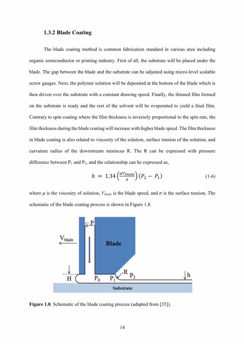
1.3.2 Blade Coating
The blade coating method is common fabrication standard in various area including
organic semiconductor or printing industry. First of all, the substrate will be placed under the
blade. The gap between the blade and the substrate can be adjusted using micro-level scalable
screw gauges. Next, the polymer solution will be deposited at the bottom of the blade which is
then driven over the substrate with a constant drawing speed. Finally, the thinned film formed
on the substrate is ready and the rest of the solvent will be evaporated to yield a final film.
Contrary to spin coating where the film thickness is inversely proportional to the spin rate, the
film thickness during the blade coating will increase with higher blade speed. The film thickness
in blade coating is also related to viscosity of the solution, surface tension of the solution, and
curvature radius of the downstream meniscus R. The R can be expressed with pressure
difference between P1 and P2, and the relationship can be expressed as,
ℎ = 1.34 Zbcdefgh
𝑃U −𝑃E (1-6)
where 𝜇 is the viscosity of solution, Vblade is the blade speed, and 𝜎 is the surface tension. The
schematic of the blade coating process is shown in Figure 1.8.
Figure 1.8 Schematic of the blade coating process (adapted from [35]).

15
Because the blade coating is fast process with controllable solution supply ratio, a large
amount of solution will be preserved after the coating which is suitable for the industrial
application. One of the disadvantages of the blade coating process is that difficulty on patterning
the deposited layer. This drawback is similarly applicable to the aforementioned spin coating
process. Moreover, the homogeneity over large areas larger than 1 cm2 is relatively poor
compared to spin-coating process due to different drying speed over the large area.
1.3.3 Inkjet Printing
Compared to the spin coating and blade coating method mentioned above, the ink-jet
printing process is an attractive technology for organic electronics due to the controlled solution
deposition of patterns and delivery of small quantities of the target materials [36–40]. To
facilitate this technology, there are two general types of inkjet printing method ; the first one is
continuous and the other one is drop-on-demand (DOD). The biggest difference between those
technologies is the frequency of droplets generation.
Figure 1.9 Schematic of ink-jet printing method (a) continuous (b) drop-on-demand.
(a) (b)

16
In continuous ink jet printing system, droplets are continuously generated with constant
amount of electric charges induced [41]. As shown in Figure 1.9 (a), the charged droplets are
ink-jetted from a nozzle continuously toward the substrate. By applying external electric field
perpendicularly to the direction of the ink-jetting route, the charged droplets are either landed
to the substrate for printing, or they are redirected to a recirculation system. Thus, while the
droplets are generated in continuous manner, they can be directed to the substrate only when
the patterning is required.
In DOD ink jet printing system, droplets are ejected only when they are needed to be
printed. One of the method in this category is thermal inkjet printing, namely, bubble jet printer,
which employs thermal energy to generate the ink droplets. Ink drops are ejected from a nozzle
by the high pressure due to thermal expansion induced by heat [42]. Alternatively, the droplets
can be ejected mechanically through the application of an acoustic pulse or electrically
stimulating a piezoelectric force to elicit a deformation of the chamber, which will generate a
liquid droplet as shown in Figure 1.9 (b) [38]. One of the advantage of inkjet printing lies on
its modularity. Individual printing nozzles can be combined into a single printing head. Multiple
printing heads can be combined within a single printer system. This modular nature allows
flexibility on printing methods ; printing more than one kind of ink at the same time or printing
in large area by laterally combining multiple print heads.
1.4 Organic Photodiodes
1.4.1 Organic Solar Cells
One of the most vigorously studied area for the application of the organic semiconductor
is for photovoltaics. The most appealing reason for that is because the organic semiconductor
materials can be possibly deposited in low temperature, ambient environment with large area

17
and cheap price. Since Tang et al, developed the first heterojunction organic solar cell (OSC)
device with 1% power conversion efficiency [9], the efficiency increased dramatically up to
~13.2 % with state-of-art tandem cell structures [43]. The most famous material (workhorse)
for the OSC research was Poly(3-hexylthiophene-2,5-diyl) : Phenyl-C61-butyric acid methyl
ester (P3HT:PCBM) system materials [44]. These days many state-of-art low bandgap polymer
OSCs are developed to comprise wider spectrum of illuminated solar radiation [45]. Even
though there are more technical barrier for commercialization such as stability, life time issues,
OSCs have high potential to be next-generation photovoltaic alternative.
1.4.2 Organic Photodetectors
In contrast to solar cells which is basically aiming to convert solar energy to electrical
energy as much as possible, photodetectors need to target for precise detection of lower level
of photons. Recently, organic photodetectors (OPDs) have been acknowledged as a next-
generation device for image sensor applications due to wide spectrum response [32,46,47], low
dark current density [48,49], excellent photoresponse [50,51] and fast response time [10].
Moreover, the low-temperature processability on the large area / arbitrary shaped substrates
enables the OPDs to make innovative / next-generation sensors which is impossible using
inorganic counterparts.
Most importantly, one of the interesting applications of OPDs is for digital imaging. The
flexibility and light-weight capability of the OPDs provides a unique advantage to next-
generation applications such as flexible digital x-ray detectors [52], near IR OPD imager [53]
or artificial eyes utilizing hemispherical photodetector arrays [54]. For example, Xu et al
demonstrated a passive matrix of OPDs on hemispherical focal plane detector array [55]. A
plastic substrate is adopted in order to mimic the function of the human eye, where the spherical
shape allows focus through a single lens. The integration in a hypothetical imaging system with

18
11 × 13 array of (500 µm)2 detectors are successfully fabricated on a 1 cm radius plastic
substrate. Bilayer OPDs based on a copper phthalocyanine (CuPc) electron donor and C60
fullerene electron acceptor were deposited between patterned Au anode and thin Ag cathode
stripes. To enable the non-conventional shaped OPD structure, they adapted a transfer technique
based on elastomeric stamps with cold-welding technique. The fabricated OPDs showed a
spectral responsivity of 65 mA/W with specific detectivity of 5 × 10¹⁰ cmHz1/2/W. Meanwhile,
Ng et al. demonstrated an OPD can be successfully implemented on active-matrix array based
on the passive pixel architecture [56]. An organic layer of the poly[2-methoxy-5-(2-
ethylhexyloxy)-1,4-phenylene-vinylene] (MEH-PPV) and PC61BM photoactive mixed blend
was deposited on top of a flexible amorphous silicon TFT backplane with 180 × 180 pixels,
with a 75 ppi. The transparent top-electrode was formed by spin-coating ITO nano-particles
dispersion on top of the photoactive layer. The dark currents lower than 1 nA/cm2 at reverse
bias of 4 V, comparable to standard silicon p-i-n photodiodes, were achieved by a very thick 4
µm blend layer. The external quantum efficiency (EQE) of the integrated detector was 35 %,
with Noise Equivalent Power (NEP) of 30 pW/cm2 with 100 ms integration time.
By tuning the properties of the organic active layer materials, even near infrared (NIR)
image using the OPD was successfully demonstrated by Rauch et al. [53]. The ternary blended,
nanocrystalline PbS quantum-dot sensitized P3HT:PCBM OPDs integrated with an amorphous
silicon TFT backplane showed EQE up to 50% at a reverse bias 8 V. The photoactive film was
solution processed with the 256 × 256 pixels with a 154 µm pitch active matrix backplane and
a fill factor of 83.3%. A specific detectivity of 2.3 ×10⁹ cmHz1/2/W with a 3 dB cutoff frequency
of 2.5 kHz.
Besides all the aforementioned excellent works to utilize the OPD to imager
applications, our main object in this thesis is to investigate the possibilities to enhance the
performance of OPDs further by various approaches such as modification of the device
structure or development of the new process.

19
1.5 Thesis Organization
In Chapter 2, we begin with the discussion on top-illumination OPDs with inverted
structure. The development of the high efficient structure of top-illumination OPD is crucial for
the vertically stacked OPD image sensor application. A dielectric / metal / dielectric (DMD)
structure to replace conventional transparent electrodes such as ITO was discussed by both
optical simulation and experimental measurement. Chapter 3 discusses a development of novel
transfer process which enables the dark current suppression for the inverted OPD structure with
high performance. Accurate analyses of the bilayer and interdiffused heterojunction organic
devices are successfully fabricated and discussed by various optoelectrical measurement and
modeling methods. In Chapter 4, we report a high performance low-bandgap polymer OPD
with broadband spectrum. By utilizing the novel transfer process developed in our lab,
significant suppression of the dark current is achieved while high quantum efficiency of the
device is preserved by employing charge blocking layers to typical BHJ devices. In Chapter 5,
for the first time, we report the fabrication of hemispherical organic photodiode arrays on
curved concave glass substrate using three dimensional (3D) printed shadow mask. A novel 3D
mask enabled by additive manufacture technologies and a 3D elastomeric stamp are utilized to
successfully fabricate the OPD on curved surface. Chapter 6 reported the simulation result of
the OPD integrated with active pixel sensor (APS) pixel circuit using metal oxide TFTs and
external transimpedance amplifier (TIA) readout circuit. The performances of the proposed
system such as current gain or voltage gain are evaluated and compared with exiting previous
works. Lastly, the thesis concludes with Chapter 7, which summarized the major contributions
and findings of this work. Several recommendations for future research are suggested at the end
of the thesis.

20
Chapter 2. Inverted Organic Photodetectors with DMD Top
Illumination Transparent Anode
2.1. Introduction
Among various organic materials for an indirect type X-ray imager application,
P3HT:PCBM bulkheterojunction (BHJ) blend system proved itself as the best candidate [57–
61] and few groups successfully demonstrated X-ray imager with the active matrix backplane
organic photodiode combination. Ng et al. used 4 µm thick MEHPPV : PCBM BHJ blend layer
as photoactive layer in combination with a flexible a-Si TFT backplane to realize an imager
array with 35% external quantum efficiency [56]. They used solution processed ITO
nanoparticles as top transparent electrodes which had a very high sheet resistance of 1MΩ/sq,
resulting in significant current loss during signal readout. Alternatively, Tedde et al.
demonstrated a concept of active pixel sensor (APS) imager with three a-Si:H TFTs integrated
with the OPD. The utilization of the APS provided on-pixel amplification up to 10 compared
to passive pixel sensor (PPS) [57]. They adapted conventional structure of OPDs with top
Ca/Al transparent cathode. In case of use of the low-workfunction metals as transparent top
electrode, even though the encapsulation post-process can prevent the degradation of the
electrode and active layer, the long-term stability of the devices cannot be guaranteed if delicate
encapsulation process is not used. In this context, the inverted organic solar cell or photodiode
architectures are investigated to enhance the device stability in air by adapting the high
workfunction metal such as Au, Ag, or poly(3,4-ethylenedioxythiophene) polystyrene
sulfonate (PEDOT:PSS) as top transparent electrodes [62–68]. Although a large number of

21
works have been reported for inverted type organic solar cells [62–66] or inverted type organic
photodetector with bottom illumination [67], still few inverted type organic photodetectors with
top illumination geometry have been reported so far. For example, Baierl et al demonstrated
the inverted type P3HT:PCBM OPD with PEDOT:PSS as a top electrode [69,70]. However,
the PEDOT:PSS suffers from a high acidity, hygroscopic behavior, resulting in inferior stability
[71]. Alternatively, ultra-thin metallic films can also be used as a transparent electrode in OPV
and OPD application [57,58,72,73]. In such configuration, the reflection from the metal surface
is too high and a large portion of incident light can be wasted. To suppress such high reflections,
an optically transparent dielectric material can be employed as an anti-reflection layer, leading
to the Dielectric / Metal / Dielectric (DMD) multilayer electrode configuration. Although a
number of papers on the application of the DMD transparent electrode on organic solar cell
have been published [74–78], to our best knowledge, no research on the top anode, top-
illumination OPD with the DMD configuration has been reported so far. In this chapter, we
demonstrate a top-anode, top-illumination OPD with engineered MoO3 / Ag / MoO3 DMD
semi-transparent electrode that could be used for large-area imager application. Especially,
optical simulation and experimental measurement are conducted to investigate the effect of the
DMD semi-transparent electrode on the OPD. Additionally, electrical characteristics including
current-voltage properties, quantum efficiency, noise equivalent power, and detectivity of the
fabricated OPDs are evaluated.
2.2. Experimental
2.2.1. Device Fabrication
Low-cost soda lime glass substrates (Asahi glass) were cleaned by acetone, isopropyl
alcohol, and deionized water by sonication for 5 minutes for each process, and treated by
oxygen plasma for 5 minutes subsequently. 100 nm of aluminum layer was thermally

22
evaporated with shadow mask for patterning bottom cathode. ZnO sol-gel solution was
prepared by dissolving 0.5 M of zinc acetate dihydrate (Zn(CH3COO)2·2H2O, Sigma Aldrich)
as a precursor in 2-methoxyethanol (2ME, Sigma Aldrich) solvent. 0.5 M of mono-
ethanolamine was added as a stabilizer and the mixture was vigorously stirred at a temperature
of 60 oC for 4 hours. The solution was then cooled down and aged for more than 24 hours. The
synthesized ZnO solution was spin-coated on top of the patterned cathode layer with spin-
coating speed of 2000 rpm for 30 seconds and annealed at 150 oC for 20 minutes, yielding 40
nm thickness of ZnO layer. The substrates were transferred into a glove box with nitrogen
atmosphere for deposition of photoactive layer. 25mg of P3HT (Rieke Metals) and 25mg of
PCBM (American Dye Source, Purity: >99.5%) were mixed into 1mL of dichlorobenzene
(DCB) and stirred by magnetic bar overnight for the BHJ solution. The solution was filtered
by 0.45 µm syringe filter and then spin-coated onto the ZnO layer with different spin-coating
speed to give an active layer thickness of 200 nm, 320 nm and 450 nm to fabricate OPDs with
different active layer thickness. To prevent complete drying of P3HT:PCBM film, the spin-
coating timing was adjusted for each process. The active layers were then solvent-assisted
annealed [79] for 30 minutes to 1 hour to ensure fully dried films in N2 atmosphere. The
substrates were transferred into thermal evaporator with top-anode shadow mask on it to deposit
5 nm MoO3, 10 nm silver and 35 nm MoO3 subsequently to finish the fabrication. All the
devices were encapsulated with a thin slide glass sealed by UV curable epoxy resin. The device
size was 0.04 cm2 with square shape.
2.2.2. Device Measurement
Optical transmittance and absorbance spectra of the semitransparent DMD, DM
multilayer, and P3HT:PCBM BHJ film were measured using Agilent CARY-5E UV-vis
spectrometer. Optical reflectance of the DMD, DM electrode were measured by Filmmetrics

23
F20 thin-film measurement system. Sheet resistances of the electrodes are measured by 4-point
probe method. A solar simulator (Oriel) equipped with Xenon lamp and band pass filter with
peak wavelength 546nm (FWHM = 2nm), was used for the current density-voltage (J-V)
characteristic measurement under illumination. The irradiance of the illuminated light was
measured by Newport power meter. The J-V characteristics of all the organic photodiode under
illumination and dark conditions were measured by HP2416A semiconductor measurement
system with a probe station in a dark Faraday cage. External Quantum Efficiency (EQE) was
measured with a setting of lock-in amplifier (Stanford Research Systems SRS 830),
monochromator with a 100W halogen tungsten lamp, light chopper, and UV-enhanced silicon
photodetector (Newport UV808) for calibration.
2.2.3. DMD Electrode Optical Simulations
We carried out the optical simulations by using the transfer matrix method to find an
optimized DMD electrode structure and calculate an optical absorption in the photoactive
region [22,80]. The transfer matrix method is based on boundary conditions for the electric
field across isotropic, homogeneous interfaces from one layer to the following medium. Given
the field of the initial layer medium, the field at the next medium can be obtained from a matrix
calculation. Thus an optical property, such as transmittance, reflectance, and absorption, of an
entire OPD structure (i.e., multiple stacks) can be calculated by a matrix multiplication
procedure. A spectroscopic ellipsometer (M-2000, J. A. Woollam) was employed to measure
dielectric constants of all the layers, all of which were used in the optical simulation. To further
explain that high transmittance is due to minimized reflectance of the DMD structure, the
admittance loci diagram technique is used, which is widely used to study the thin film coating
performance [81]. The admittance diagram is a visual representation of the evolution of surface
admittance from the substrate interface to the incident medium interface, which contains all the

24
information necessary for the calculation of reflectance. The characteristic admittance Y of a
material is defined as Y=H/E where H is the magnetic field and E is the electric field. Because
there is no direct magnetic effects at optical frequencies, we can get a simple relationship
between the characteristic admittance and complex refractive index as y = (n - ik) in free space
with unit of 1/377 Siemens [S]. Note that the admittance and the complex refractive index of
a material are not physically identical when they become numerically equal in this case.
2.3. Results and Discussion
2.3.1. DMD Electrode Simulation, Characterization and Optimization
The DMD electrode has a great advantage over other transparent top electrode, such as
(i) the DMD electrode has anti-reflection MoO3 dielectric layer on top, which maximizes the
transmission of the light of interest, and (ii) the passivation of the top electrode with the
additional MoO3 layer allows direct deposition (e.g. thermal evaporation [82]) of CsI(Tl)
scintillator materials, which is beneficial in achieving higher scintillator gain [61].
Figure 2.1 Device structure of the inverted OPD with top illumination. The thickness for each layer indicates the optimized values for the fabricated OPD.

25
Figure 2.2 Measured refractive indices of Ag and MoO3 plotted from 400 nm to 800 nm wavelength. Extinction coefficient of MoO3 is omitted in the graph due to negligible value.
Table 2.1 A summary of the complex refractive indices of P3HT:PCBM, ZnO, MoO3, Al, and Ag at 546nm wavelength measured by the ellipsometer
Materials n k
P3HT:PCBM 2.0918 0.4128
ZnO 1.5361 0
MoO3 2.0941 0.0067
Al 0.9445 6.6304
Ag 0.0672 3.5076
Figure 2.1 shows the schematic of the fabricated inverted-type OPD with top
illumination. To find optimum layer thicknesses ensuring that a maximum amount of incident
light can pass through the top DMD multilayer transparent electrode, an optical simulation is
carried out based on refractive indices of all the layers in the OPD design measured by a
spectroscopic ellipsometer. The measured refractive indices of MoO3 and Ag layers over

26
wavelength from 400 nm to 800 nm are shown in Figure 2.2. The index values of all the layers
in the OPD at the wavelength of 546 nm are summarized in Table 2.1.
Prior to determining the optimum thickness of each layer of the DMD electrode, we
need to fix the Ag interlayer which ensures both a low sheet resistance and a high optical
transmittance. Figure 2.3(a) shows the variation of the sheet resistance of the DMD structure
with MoO3 5 nm / Ag varied / MoO3 35 nm on glass as a function of the thickness of the Ag
interlayer. As shown in the figure, silver thickness higher than 9 nm gives sheet resistance
under 10 Ω/sq which is suitable for a large area imager. High sheet resistance of 24 Ω/sq of the
DMD layer with 8 nm Ag thickness shown in the figure can be attributed to the discontinuous
film morphology with aggregated Ag islands formation [83].
Meanwhile, the significant decrease of the Rsh for Ag thickness above 9 nm assures the
formation of the continuous metal film. We fixed Ag thickness to 10 nm for the DMD
multilayer; the sheet resistance of the DMD film was 6.2 Ω/sq, which is much lower than 10
Ω/sq of standard ITO. Next, to find the optimum thickness of the bottom and top MoO3
dielectric layer for light transmission, the transfer matrix method approach was applied to the
whole OPD structure with varying top and bottom MoO3 thickness. Figure 2.3(b) shows a
simulated contour plot of the light absorption in the P3HT:PCBM active layer of the OPD
structure as functions of top and bottom MoO3 thickness. Fixed thickness of Al = 100 nm, ZnO
= 40 nm, P3HT:PCBM = 320 nm, and Ag = 10 nm are used. In this simulation, a
monochromatic light at the wavelength 546nm is chosen since it corresponds to an emission
peak of the CsI(Tl) scintillator [61]. As can be seen from the figure, the highest absorption in
the active layer can be achieved when the top MoO3 layer thickness is around 35 nm, indicating
light absorbance over 90 % by P3HT:PCBM film. Since the bottom MoO3 layer not only
transmits the incident light but also transports the photogenerated charges [75,83], it is required
to optimize this thickness for both light transmission and carrier transport. From the simulation

27
data we can conclude that the maximum absorption is attained with a combination of bottom
MoO3 = 70 nm and top MoO3 = 35 nm. However, we need to limit the thickness of the bottom
MoO3 layer to 5 nm to ensure the efficient charge transport in the interlayer.
Figure 2.3 (a) Sheet resistance of the MoO3 5 nm / Ag varied / MoO3 35 nm structure fabricated on glass as a function of the thickness of the Ag interlayer (b) Simulated 2D absorption spectrum with different bottom and top MoO3 thickness in DMD structure with fixed Ag layer thickness of 10 nm. The color bar represents the absorption in P3HT:PCBM at 546 nm.

28
Finally, for optimum OPD performance, we decided that the bottom MoO3 layer should
be fixed to 5 nm with 10 nm of Ag interlayer and 35 nm of top MoO3 layer. The star in Figure
2.3(b) indicates the suggested optimum light absorption point of the OPD structure. This choice
is expected to guarantee a high charge transport efficiency and a high absorption of the incident
light above 90 % in the active layer at the same time [75,83].
Figure 2.4 Admittance diagrams of (a) MoO3 (5 nm, #1)/ Ag (10 nm, #2) DM and (b) MoO3 (5 nm, #1)/ Ag (10 nm, #2)/ MoO3 (35 nm, #3) DMD multilayers on glass substrates. The arrows indicate the increasing thickness of each layer from the glass substrates.

29
Additionally, we investigated the influence of the dielectric layer in the DMD electrode
on the light reflection properties by studying an optical admittance of the multilayer system
[84,85]. The admittance diagram helps to understand more clearly how the variation of each
multilayer results in the minimum reflectance of the DMD structure. Figure 2.4 presents the
admittance diagrams of the multilayer transparent electrodes of Ag 10 nm / MoO3 5 nm / glass
and MoO3 35 nm / Ag 10 nm / MoO3 5 nm / glass substrate at 546nm wavelength, respectively.
The loci for perfect electric conductors and optically transparent dielectric materials are
represented by a series of circular arcs while the semiconductors result in a spiral locus. As the
thickness of each medium increases, the optical admittance of the layer is computed that leads
to a rotation of the admittance on either circles or spirals and the corresponding locus is plotted
on the complex plane. The starting point of the admittance diagram is (1.45, 0) that corresponds
to a glass substrate and the subsequent admittance is determined by both the refractive index
and thickness of the material. For example, in Figure 2.4(a), 5 nm of MoO3 (#1) leads to the
admittance rotating from (1.45, 0) toward (1.463, 0.131). After that, 10 nm of Ag (#2) results
in the rotation of admittance to (1.245, -1.511). When the termination point of the whole
multilayer system ends at (1, 0) that corresponds to air, a perfect impedance matching occurs,
thus giving rise to zero reflection. This implies that reducing the difference between the final
admittance point and the air enables the transmission efficiency of the DMD electrode to be
enhanced by suppressing the light reflections. For the structure without the top MoO3 film, the
termination point is (1.245, -1.511) that is not close to the air, resulting in 32.1 % reflections
(R), which can be calculated by the following expression.
𝑅 = kMlk1kMmk1
kMlk1kMmk1
∗ (2-1)
where Yo and Y1 are the optical admittance of the incident medium (i.e. air) and the termination
point, respectively [85].

30
In contrast, in Figure 2.4(b), the admittance attained from the multilayer structure with
the top MoO3 layer (#3) ends at (0.766, 0.183), which is much close to the point of the air,
thereby leading to highly suppressed reflections of 2.8%. Such highly reduced reflections can
also be explained by a small index contrast between air and MoO3 as compared to the contrast
between air and metallic layer.
0
20
40
60
80
100
Wavelength (nm)
Ref
lect
ance
(%)
Tran
smitt
ance
(%)
DMD_T DM_T DMD_T_simul DM_T_simul ITO
400 500 600 700 8000
20
40
60
80
DM_R DMD_R DMD_R_simul DM_R_simul
Figure 2.5 Experimental and simulated optical transmittance and reflectance spectra of the optimal DMD (MoO3 5 nm/ Ag 10 nm/ MoO3 35 nm) and DM (MoO3 5 nm/ Ag 10 nm) multilayer. Transmission spectra (top) shows excellent match with experimental spectra (DMD : closed circle, DM : open circle) with simulation plot (DMD : solid line, DM : dashed line). Transmission spectrum of ITO film (open square) is included for comparison. Reflectance spectra (bottom) is shown with experimental spectra (DMD : closed triangle, DM : open triangle) with simulation plot (DMD : solid line, DM : dashed line) in good agreement.

31
Figure 2.5 shows excellent agreement between simulated data obtained by the transfer
matrix method and the experimental optical transmission and reflectance spectra of the both
MoO3 5 nm / Ag 10 nm / MoO3 35 nm DMD and MoO3 5nm / Ag 10nm DM electrodes on
glass substrates at normal incidence. It is noticed that the maximum light transmittance of
85.7 % is achieved at 468 nm wavelength for the DMD electrode on glass. We also note that
the light transmittance of the optimized DMD electrode is comparable with that of a standard
ITO glass (Delta technologies, Rsheet ~ 11 Ω/sq), as included in Figure 2.5. The transmittance
of the DMD electrode at 546 nm wavelength was 76.8 %, which is much higher than that of
DM electrode of 56 % at same wavelength. On the other hands, the measured reflectance of
the DMD multilayer at 546 nm wavelength was 5.4 % while the DM structure showed 37.6 %
of the reflectance value. These measured reflectance values are in excellent agreement with the
calculated reflectance values from both the simulated reflectance spectrum in Figure 2.5 and
the admittance diagram in Figure 2.4.
2.3.2. Device Physics of the Inverted DMD OPD
The inverted OPD incorporates several functional layers including cathode (Al),
electron transfer layer (ETL, ZnO), bulkheterojunction (BHJ, P3HT:PCBM) photoactive layer,
hole transfer layer (HTL, bottom MoO3), anode (Ag), and anti-reflection layer (top MoO3).
Figure 2.6(a) shows flat band diagram of the OPD with corresponding energy levels for each
layer. The superpositioned layers in BHJ region with solid line and dashed line represent energy
band of P3HT electron donor and PCBM electron acceptor, respectively. Note that the good
alignment of the conduction band of the ZnO layer (4.4eV [86]) with the lowest unoccupied
molecular orbital (LUMO) level of PCBM (4.3eV [87]) and the conduction band of the MoO3
layer (5.5eV [88]) with the highest occupied molecular orbital (HOMO) level of P3HT (5.0eV
[87]) forms favorable energy level match between buffer layers and BHJ active layer.

32
Figure 2.6 (a) Flat band energy diagram of the inverted type P3HT:PCBM OPD under open circuit condition. D indicates the P3HT electron donor while A is PCBM electron acceptor. (b) Schematic band diagram of the inverted type OPD in equilibrium under dark condition. (c) Band diagram of the OPD with reverse bias under dark condition. The arrows show the carrier injection mechanism at each electrode and the direction of dark current.

33
Under equilibrium condition, we assume that ZnO and MoO3 layer forms ohmic contact
with Al cathode and Ag anode, respectively. The device band bending under equilibrium
condition is depicted in Figure 2.6(b). Although both ZnO and MoO3 buffer layers employed
in the OPD structure are n-type semiconductor [68,88], the high work function difference
between ZnO (ФZnO = 4.7eV [86]) and MoO3 (ФMoO3 = 5.7eV [88]) makes electrons on ZnO
cathode side migrate to MoO3 anode side, establishing the internal electric field inside the BHJ
active layer as shown in the figure. Under light illumination condition, the internal E-field
allows photo-generated electrons and holes in the active layer drift to the ZnO cathode and
MoO3 anode, respectively, which is the generation principle of the short circuit current when
the OPD works in photovoltaic regime with zero bias.
When the OPD is reverse biased, (positive bias to Al/ZnO cathode and negative bias to
MoO3/Ag) in dark condition, as shown in Figure 2.6(c), the reverse dark saturation current is
mainly generated by undesired charge injection through electrodes, which can be minimized by
formation of energetic barriers on each electrode by ZnO and MoO3 layer [89]. To decrease
the dark current at cathode side, the ZnO layer is employed as a hole blocking layer (HBL) to
increase the injection barrier for holes to BHJ active layer as ΔEcathode = valence band of ZnO
(7.7eV [68]) – ФAl (4.2eV) = 3.5 eV. On the other hand, the energetic barrier for carrier
injection on anode side is ΔEanode = ФMoO3 (5.7eV) - LUMOPCBM (4.3eV) = 1.4 eV, which has
lower barrier than cathode side. Due to its lower energetic barrier formed on active layer /
MoO3 interface, the dominant carrier injection will occur at the anode side.
Under light illumination, (i) excitons are generated by photon absorption in P3HT
electron donor, and (ii) excitons diffuse to the electron acceptor-donor interface. (iii) The
diffused excitons dissociate into electron-hole pairs due to internal electric field. (iv) Finally,
the electrons and holes transport by hopping between localized states and collected by cathode
and anode, respectively, generating photocurrent in the OPD [90].

34
2.3.3. Electrical Characteristics of the Inverted DMD OPDs
To validate the suitability of the P3HT:PCBM BHJ layer for the indirect type imager
with CsI(Tl) scintillator, absorption coefficient of the fabricated P3HT:PCBM film is compared
with the emission spectra of CsI(Tl) scintillator in Figure 2.7(a). The absorption coefficient α
was derived from the measured absorption spectrum of the P3HT:PCBM layer with thickness
of 200 nm deposited on glass and optical density. The emission spectrum of CsI(Tl) scintillator
shown in Figure 2.7(a) is adapted from reference [91]. As shown in the figure, the absorption
coefficient of the P3HT:PCBM film overlaps well with the emission spectrum of the CsI(Tl)
scintillator.

35

36
Figure 2.7 (a) The absorption coefficient plot of P3HT:PCBM active layer from wavelength 400 nm to 800 nm. (solid line) Emission spectra of CsI(Tl) scintillator is included for comparison. (dashed line) (b) Experimental and fitted current density (J) versus voltage (V) characteristics under dark condition and irradiance of 950 µW/cm2 light illumination with 546 nm wavelength of the OPDs with different thickness of the photoactive layer. Open symbols represent measured dark currents when solid symbols are photo responses. The solid lines are fitted dark current densities from non-ideal diode equation. The dashed line represents ideal J-V curve when the shunt resistance Rsh is infinite. (c) Dark current density (Jdark) measurement plot as function of the internal electric field for the OPDs with different active layer thickness. (d) External Quantum Efficiency (EQE) of the OPD with 320 nm thickness active layer at reverse bias of 1.5V. The right axis indicates specific detectivity of the OPD according to wavelength from 400 nm to 800 nm.
To optimize device performance, the inverted OPDs with different thickness of the
active layers of 200 nm, 320 nm and 450 nm were fabricated and investigated. Figure 2.7(b)
shows the current density (J) versus voltage (V) characteristics of the inverted OPDs with
different active layer thicknesses. The figure confirms that the dark current value of the OPDs
increases with decreased active layer thickness and increased reverse bias voltage. The trends
indicate that the carrier injection occurs from device contact to photoactive layer and the
injection mechanism is attributed to electric-field assisted electron injection from the MoO3/Ag
contact to the LUMO level of PCBM where the lowest energetic barrier exists [49,89]. To
validate the E-field driven injection mechanism, the dark current densities are plotted as a

37
function of the internal E-field in Figure 2.7(c) with a relationship E = V/d, where E is the
internal E-field, V is applied reverse bias and d is thickness of each active layer. In the figure,
note that the Jdark = 2.22x10⁻⁷A/cm2 of 320 nm active layer device is almost identical with Jdark
= 2.49x10⁻⁷A/cm2 of 450 nm device at E = 3x10⁶ V/m with negligible error. It is worthwhile to
emphasize that the Jdark of 320 nm device is even smaller than Jdark of 450nm device at E=3x10⁶
V/m compared to the trend of higher Jdark of 320nm device than Jdark of 450 nm device in Figure
2.7(b). The bigger variation of Jdark of 200 nm device in the figure can be possibly originated
from imperfect and unfavorable BHJ morphology with pin-holes developed due to thin active
layer [89,92]. However, the data is still acceptable since the Jdark of 200 nm device is 5.8x10-
7A/cm2 at E=3x10⁶ V/m, which is only about two times bigger than Jdark value of 320 nm and
450 nm devices at same E-field, when the Jdark value of 200 nm device at 1.5 V reverse bias is
>10 times bigger than Jdark of 320 nm and 450 nm device at the same bias.
To probe existence of traps inside active layers in each device, the dark J-V
characteristics of the OPDs are fitted using the non-ideal diode equation given by [93],
𝐽p 𝑉 = 𝐽r exp 4 blsf b HtLuv
− 1 + blsf b HtHwx
(2-2)
where Jd is total dark current density, Jo is reverse dark saturation current density, n is ideality
factor, k is Boltzmann constant, T is temperature, RS is series resistance, and Rsh is shunt
resistance. The fitted curves are included in Figure 2.7(b) showing a very good agreement to
experimental data. The fitting of Equation 2-2 to the dark J-V characteristics yielded n = 1.95,
Rsh = 1 MΩ for 200 nm device, n = 1.6, Rsh = 4 MΩ for 320 nm device, n = 1.5, Rsh = 5.5MΩ
for 450 nm device, respectively. The ideality factor deviating from unity is the evidence of
deeply trapped carrier or trap-assisted recombination mechanism [94,95]. The larger ideality
factor values for thinner active layer devices rationalize that more pin-holes and defects in
thinner active films induced more trap-assisted recombination sites inside films. The increasing
shunt resistance values from 1 MΩ to 5.5 MΩ with thicker active layer also support the fact

38
that the current leakage inside the active layer decreases with thicker film. From the fitted
parameters and Equation 2-2, we can estimate the theoretical limit of the total dark current
density Jd,min of fabricated OPD by setting the shunt resistance Rsh value to infinite, meaning
there is no shunt leakage through the device. The dashed line in Figure 2.7(b) represents the
ideal J-V curve of the OPD and the corresponding Jd,min value converges to 9x10⁻¹⁰ A/cm2,
which is identical to the value of reverse dark saturation current density Jo.
For the OPD, the figures of merit which need to be evaluated include external quantum
efficiency (EQE), responsivity (ℛ), noise equivalent power (NEP), specific detectivity (D*),
and linear dynamic range (LDR). One of the most fundamental properties of the photodetector
is the responsivity, which is defined as the photocurrent per unit incident optical power, which
gives the equation [96],
ℛ = zx|8
= ~4I
= ~[L]EU.[L/.]
[A/W] (2-3)
where iph is the output photocurrent of the detector, Popt is the incident optical power on the
detector, η is quantum efficiency, q is electron charge, λ is wavelength of interest, h is plank
constant, and c is the light velocity. Note that responsivityℛ is directly related to external
quantum efficiency η by a factor of qλ/hc, and it can be used to determine the photogenerated
current in response to the light wavelength of interest. Noise equivalent power (NEP, in
W/Hz1/2) is defined as the incident power at a particular wavelength required to produce a
photodetector current equal to the root-mean-squate (rms) noise current in a photodetector. In
other words, it is the amount of incident light required to make a signal-to-noise ratio (SNR) to
unity, and given by [97],
𝑁𝐸𝑃 =2 /0
ℛ (2-4)
where IN is the noise current, B is the bandwidth and ℛ is the responsivity. The noise current
is generated from various mechanisms. The representative noise sources are classified as

39
thermal (Johnson) noise, shot noise, and 1/f (flicker) noise [98]. When we assume that the shot
noise current associated to the dark current is dominant over the thermal noise under reverse
bias [97], NEP can be expressed as,
𝑁𝐸𝑃 =2
H= U4G
H [W/Hz1/2] (2-5)
where ID is the dark current of the photodetector and 2qID is the shot noise power spectral
density. Because the mean square noise of the photodectector is proportional to the detector
bandwidth, the NEP of a detector is proportional to the square root of the detector bandwidth,
NEP ∝ 𝐵, and the NEP is generally specified in terms of the NEP for a bandwidth of 1 Hz as
NEP/ 𝐵 which corresponds to Equation 1-8 with unit of W/Hz1/2. From the equation, it is
obvious that the lower dark current yields smaller NEP value, while higher responsivity is
desirable for lower NEP.
In general, it is more convenient to define the inverse of the NEP as another figure of
merit, called detectivity, defined as D = 1/NEP. However, since the detectivity is still dependent
on the size of the photodetector, it is beneficial to normalize the detectivity to unit area to
accurately compare the performance with other detectors, and it is called specific detectivity
D*, written as
𝐷∗ = .0|
(2-6)
expressed in Jones or cm 𝐻𝑧/W, where A is the area of the photodetector. Another important
figure of merit of photodiode is linearity of sensitivity of linear dynamic range (LDR). LDR
can be defined as [46]
𝐿𝐷𝑅 = 20log(sx∗
sf) [dB] (2-7)
where J*ph is the photocurrent density measured at light intensity of 1mW/cm2 and Jd indicates
dark current density.

40
Table 2.2 summarized the OPDs’ figures of merit including Jdark, Responsivity (ℛ),
External Quantum Efficiency (EQE), Noise Equivalent Power (NEP), and Specific Detectivity
(D*). ℛ and EQE are calculated by Equation 2-3 and NEP and D* are derived from Equation
2-5 and 2-6, respectively. In the table, even though the dark current of OPD with 450 nm active
layer thickness showed lowest value of 2.95 x 10⁻⁷ A/cm2 compared to 3.81 x 10⁻⁷ A/cm2 of
OPD with 320 nm active layer and 4.25 x 10⁻⁶ A/cm2 of OPD with 200 nm active layer at reverse
bias of 1.5V, higher responsivity of 320 nm OPD (0.18 A/W) than 450 nm OPD (0.14 A/W)
yielded the highest specific detectivity of 5.25 x 10¹¹ Jones among all the devices. This value
is comparable to the value (D* = 8.8 x 10¹¹ Jones) reported by Tedde et al. in their bottom-
illuminated spray coated OPDs [99] and even higher than the detectivity value of 3.15 x 10¹¹
Jones reported by Arredondo et al. in their ITO-free inverted P3HT:PCBM photodetectors [100].
Figure 2.7(d) shows the measured EQE of the OPD with 320 nm active layer along with specific
detectivity D* plotted according to the wavelength in logarithmic scale. The EQE and D* were
measured under reverse bias 1.5V. The peak EQE value of 42.6% at 546 nm wavelength in the
figure shows good agreement with the calculated value in Table 2.2.
Table 2.2. Comparison of photodiode figures of merit with different thickness of P3HT:PCBM active layer of 200nm, 320nm and 450nm
P3HT:PCBM thickness
Jdark @ -1.5V
Responsivity @ -1.5V
EQE @ -1.5V
NEP (W/Hz1/2)
D* (Jones)
200nm 4.25x10⁻⁶ A/cm2 0.17 A/W 38 % 1.37x10⁻¹² 1.46 X 10¹¹
320nm 3.81x10⁻⁷ A/cm2 0.18 A/W 42 % 3.81x10⁻¹³ 5.25 X 10¹¹
450nm 2.95x10⁻⁷ A/cm2 0.14 A/W 31 % 4.46x10⁻¹³ 4.49 X 10¹¹

41
Figure 2.8 (a) J-V curve of the OPD with 320 nm active layer under various light intensity at 546nm light wavelength. (b) Linear dynamic range (LDR) plot of the OPD with 320nm active layer thickness measured at reverse bias of 1.5V. The photocurrent density J is the summation of dark current and photo-generated current, J = Jdark + Jph, when the irradiance is 546nm wavelength monochromatic illumination. The inset is the LDR plot in logarithmic scale.
Figue 2.8(a) shows the J-V characteristics of OPD with 320 nm active layer for various
light intensities of the 546 nm wavelength illumination. The graph clearly shows that the OPD
can response to light irradiance from 950 µW/cm2 down to 780 nW/cm2. While the

42
photocurrent at the negative bias increases with higher light intensity, the photocurrent at
positive bias 1 V has no variation, indicating the series resistance RS of the OPD is not affected
by the irradiance. Figure 2.8(b) shows fitted linear dynamic range (LDR) of the photocurrent
according to input irradiance in Figure 2.8(a) at reverse bias of 1.5 V. The lower limit of the
range was defined by the dark current value of the OPD, which is 3.8x10⁻⁷ A/cm2 for the OPD
with 320nm active layer. The photocurrent is found to be increased linearly with irradiance of
546nm wavelength up to 1mW/cm2. The LDR graph can be expressed as a linear equation, J
[A/cm2] = αPin [µW/cm2] + β with coefficients α = 0.108 [A/W] and β = -1.51x10⁻⁶ [A/cm2],
where J is the photocurrent and Pin is input irradiance. Note that the minimum J value in the
equation is limited by the dark current value of the OPD. The calculated LDR of the OPD from
Equation 1-5 was 60 dB, comparable to the LDR of InGaAs photodetectors [46], which is
sufficient for the high contrast imaging.
2.4. Conclusion
In conclusion, we suggested the inverted OPD with MoO3/Ag/MoO3 semi-transparent
electrode with top illumination. The DMD top transparent electrode for the OPD is simulated
and optimized to acquire the best light absorption condition for CsI(Tl) scintillator light
emission spectrum of 545 nm wavelength. The fabricated DMD transparent electrode showed
the maximum optical transmittance of 85.7% with Rsheet = 6.2 Ω/sq, which is suitable for large
area imager application. Moreover, P3HT:PCBM active layer was optimized for the inverted
OPD structure to yield the high detectivity of 5.25x10¹¹ Jones. The OPD with inverted structure
will enhance the stability of the OPD significantly when the top incoupling MoO3 layer allows
direct deposition of scintillator material over OPD. The OPDs with such structure are ready-
to-be integrated on various applications especially to cost-effective large area X-ray imager.

43
Chapter 3
Bilayer Interdiffused Heterojunction Organic Photodiode by Double Transfer Stamping Method
3.1. Introduction
BHJ system has been the preferred choice for the active layer in the OPD structure since
it can be introduced as one-step deposition of a polymer : fullerene blend from solution [2,8].
Performance of the BHJ type OPDs typically depends on various process parameter, such as
the blending ratio of donor and acceptor materials, the solvents used, thermal annealing
conditions, etc [101]. It is known that the choice of the solvent system largely affect the vertical
segregation of the donor and acceptor materials, greatly influencing the opto-electronic
performance of the BHJ devices [102]. The co-existence (e.g. two materials present at the same
time) of the electron donor and acceptor materials on both cathode / anode interface had made
difficult on effective suppression of the dark injection current due to ill-defined metal / organic
materials interface [2]. The vertical material composition can be controlled somehow by both
careful solvent selection [102] and surface energy treatment of the substrate [103,104]. But
these approaches cannot completely remove the co-existence problem of the electron donor and
acceptor materials at electrodes when BHJ is used. Substantial dark current suppression can be
achieved, in principle, by controlling donor / acceptor (D/A) vertical segregation using the
double-layered active layer structure [49,105]. However, realization of the polymer / fullerence
multilayered structures using solution process needs special techniques due to the difficulty of
finding “orthogonal” solvents for each material. Typical polymer and fullerene derivative
materials can be easily dissolved in halogenated solvents such as chlorobenzene (CB),

44
dichlorobenzene (DCB) or dichloromethane (DCM). So far, the most popular method to realize
the bilayer heterojunction was successive spin-coating deposition of the electron acceptor
material dissolved in DCM on polymer film since the solvent typically has lower solubility with
polymer materials [106–109]. However, this method can easily allow partial penetration of the
D/A materials to counter-electrodes forming macroscopically undesirable films. Moreover, low
solubility of the fullerene derivatives in DCM solvent circumvents the preparation of highly
concentrated solution, limiting the range of spin-coatable active layer thickness [107].
Alternatively, float-casting method was introduced but surface of the polymer materials can be
easily contaminated and degraded by water molcules and cannot guarantee conformal contact
between films [110,111]. The bilayer can also be realized utilizing middle-stage substrate
treated with releasing agent, but this method incorporates surface contamination which possibly
introduce unfavorable interface traps [112,113]. To minimize the contamination, the lamination
process using a polydimethylsiloxane (PDMS) stamp treated by O2 plasma was introduced by
Chen et al which enabled the polymer films casting directly on the PDMS [114]. However, this
method not only causes serious damage to the surface structure due to the plasma treatment but
also makes difficult to detach the polymer film from the PDMS stamp for transfer process due
to increased adhesion energy between the stamp and polymer film. Spray-coating [99] or hot-
cast method [60] are also developed as unconventional coating methods. However, these
methods are difficult in defining exact layers of each active material, therefore they can not
guarantee a well-defined bilayer of the heterojunction.
The key concept used in this chapter is taking advantage of the interdiffusion of the
electron acceptor molcules into the electron donor polymer induced by thermal annealing
process, verified by Treat et al [115] . They described the evolution of the blend morphology
of the P3HT / PCBM BHJ films starting from a bilayer film fabricated by the float-casting
technique. They found that PCBM molecular species interdiffuse into the amorphous regions
of P3HT during thermal annealing, resulting in a homogeneous BHJ system when the

45
temperature increased up to 150 °C with an estimated interdiffusion coefficient of 3 x 10⁻¹⁰
cm2/s. Even though they succeeded to elucidate a miscibility and detailed interdiffusion
behavior in the polymer: fullerene bilayer system, no fabrication of an actual photodiode was
followed using this approach. This was due to serious contamination and degradation of the
films during the float-casting method. However their work clearly indicated that if the annealing
temperature and time are deliberately controlled, we could achieve an optimized vertically
segregated heterojunction active layer.
To address these problems, we introduce double transfer stamping (DTS) to promote
interdiffusion between donor and acceptor layers to form well-defined interdiffused bilayer
heterojunction (BiHJ) OPDs sandwiched between doner and acceptor layers that are in direct
contact with their respective metal electrodes. The thermal annealing step is used to enable
interdiffusion between the donor and acceptor layers, forming the active layer. Using this
approach, we demonstrate an inverted interdiffused P3HT/PCBM bilayer photodiode whose
dark current density is 7.7 ± 0.3 nA/cm2 with an external quantum efficiency of 60 ± 1 % and
a peak specific detectivity of (4.8 ± 0.2) x 1012 cm·Hz1/2W-1.
3.2. Experimental
3.2.1 PDMS Stamp and Solutions Preparation
The PDMS stamps were prepared by mixing the Sylgard 184 silicone elastomer (Dow
Corning) and a curing agent in clean roon (43 % relative humidity, 20 oC temperature)
environment [116]. Various ratios of Sylgard : curing agent by mass were prepared to yield a
different surface energy of the stamps. The two components were mixed homogenerously for
10 minutes and degassed in vacuum chamber at the pressure of ~ 0.4 psi for six hours before
being poured onto plastic weighing boats and cured at room temperature for three days. The
PDMS stamps were gently peeled off from the boats and then cut into pieces (~ 1.5 x 1.5 cm2 ).

46
The thickness of the PDMS stamps were typically ~5 mm. The PDMS stamps were attached to
backing glass wafers for a conformal transfer process. The polyethylenimine ethoxylated
(PEIE) layer was used to form a low workfunction cathode [117]. The PEIE solution was
prepared by dissolving 5 wt% of PEIE (Sigma Aldrich) in 2-methoxyethanol (2ME, Sigma
Aldrich) solvent in ambient atmosphere. Two kinds of active layer solution were prepared in
glove box (O2, H2O level < 0.5 ppm) : (1) P3HT solution : 14 mg of P3HT (Rieke Metals,
~91 % regioregularity) was dissolved in 1.5 mL of CB; and (2) PCBM solution : 25 mg of
PCBM (American Dye Source, Purity: > 99.5%) was dissolved in 1 mL of CB. All the solution
were filtered by 0.45 µm syringe filter and then stirred by magnetic bar overnight at 70 oC for
homogeneous solutions.
3.2.3 Device Fabrication
Figure 3.1 summarizes schematic illustration of the proposed DTS fabrication process
of the BiHJ OPD device. Before starting the device fabrication, we need to prepare a receiving
glass substrate. The ITO-coated glass substrates (Delta Technologies, LTD) were cleaned by
acetone, isoropyl alcohol, and deionized water by sonication for 5 minutes respectively, and
subsequently by oxygen plasma for 5 minutes.
Next a low-work function cathode was prepared by spin-coating of PEIE on top of the
ITO coated glass [117]. The spin-coating speed of 2000 rpm for 60 seconds and thermal
annealing at 100 oC for 10 minutes in air yielded < 10 nm thick PEIE layer. Then the substrates
were transferred into the glove box for deposition of photoactive layers. The PCBM in CB
solution was spin-coated for 60 seconds to form ~ 90 nm thick electron acceptor layer on the
top of PEIE/ITO substrate. The spin-cast process allowed enough time for CB solvent to
vaporize and no further thermal annealing process was added. Next, two PDMS stamps with

47
different surface energies were prepared by mixing different ratio of Sylgard elastomer and
curing agent.
Figure 3.1. Schematic illustration of proposed Double Transfer Stamping (DTS) process for fabricating bilayer heterojunction organic photodiode : (a) Prepare PDMS stamps with different surface energy. (b) Drop-cast P3HT solution droplet on a PDMS stamp with lower surface energy. (c) Squeeze down the solution with higher surface energy PDMS stamp to form a uniform film. (d) Detach PDMS stamp (in this stage, whole film is transferred to 15:1 stamp due to higher surface energy). (e) Transfer the P3HT film from stamp onto prepared substrate. (f) Substrate heating to allow interdiffusion of PCBM into P3HT (g) Completion of the deivce fabrication by depositing MoO3 / Ag anode. All the processes are done inside glove box to prevent any degradation induced by oxygen and water molecules.

48
To fabricate the PDMS stamp having suitable surface energy, advancing contact angles
were measured by dropping P3HT in CB solution on various PDMS surfaces for the elastomer
to curing agent mixing ratios varying from 5:1 to 20:1. The advancing contact angles measured
using a goniometer in air are shown in Figure 3.2.
Figure 3.2 Advancing contact angle measurement on PDMS stamps with different mixing ratio of PDMS to Sylgard and curing agent combined. The P3HT dissolved in CB was used for these measurements.
It is clear that the contact angle is decreasing from 33o to 18o when the composition of
the elastomer in PDMS stamps increases from 5:1 to 20:1. The decrease of P3HT contact angle
indicates formation of a less hydrophobic surface for higher PDMS ratio. The PDMS stamps
having less curing agent (cross-linker) have a lower contact angles; e.g. higher PDMS surface
energy. However, if the content of the cross-linker is too low, the PDMS modulus of elasticity
becomes too small making difficult the fabrication of stamp with required stiffness. Therefore,
for the DTS process, we chose PDMS stamps with 15:1 and 5:1 ratios. Next the P3HT solution
was drop-casted in the glove box on 5:1 PDMS stamp followed by quick squeeze with 15:1
PDMS stamp to form a uniform polymer film between two stamps having different surface

49
energies (e.g. adhesion). After few seconds, needed for solvent evaporation into the gas
permeable stamp, the 15:1 PDMS stamp was detached. During this process step the whole
polymer film is transferred from 5:1 to 15:1 stamp having a higher adhesion energy. The
thickness of printed (formed) polymer film measured by surface profilometer was 90 ± 5 nm.
Next the polymer film formed on the 15:1 stamp was stamped (printed) onto PCBM/PEIE/ITO
substrate to form a P3HT / PCBM bilayer structure. A perfect P3HT film transfer from the 15:1
stamp onto the PCBM surface was accomplished due to much higher adhesion energy between
P3HT solution and PCBM surface, verified by the contact angle measurement of P3HT in CB
droplet on PCBM surface which showed a complete wetting behavior. Once this transfer is
completed the bi-layer is subjected to thermal annealing with temperature ranging from 70 oC
to 150 oC allowing PCBM molecules to diffuse into the P3HT film [115]. The thermal annealing
time for all the devices was adjusted to 5 minutes to realize well defined diffusion region
between PCBM and P3HT. The thickness of the P3HT / PCBM bilayer was kept to ~ 190 nm.
Finally, the interdiffused devices were transferred into thermal evaporator built in glove box to
complete the device fabrication by depositing MoO3 / Ag anode; Circular shadow mask with 1
mm diameter was used to deposit 15 nm MoO3 and 100 nm silver electrode subsequently.
Figure 3.3 shows schematic of device structures of (a) as-cast bilayer OPD before
thermal annealing process and (b) BiHJ OPD after thermal annealing process. The
interdiffusion of the PCBM into P3HT layer allows formation of well defined layer between
PCBM and P3HT layers. By varying annealing temperature and time an optimized
interdiffusion layer with well defined morphology can be formed. As shown in the figure, the
inverted device structure incorporates several functional layers including low-work function
cathode (PEIE/ITO), hole blocking layer (PCBM), BiHJ (interdiffused) active layer, electron
blocking layer (P3HT), hole transport layer (HTL, MoO3), and anode (Ag).

50
Figure 3.3 Device structure of (a) As-cast bilayer OPD before thermal annealing (b) Bilayer interdiffused heterojunction (BiHJ) OPD after thermal annealing process. Bottom illumination was used for the OPDs.
3.2.4 Measurements and Simulations
A contact angle measurement was done by a contact angle goniometer (Ramé-Hart) in
clean room (43 % relative humidity, 20 oC temperature) . A static sessile drop method was used
to measure the advancing angle of the P3HT in CB solution droplet on the PDMS stamps. The
calculation of contact angles from the captured data was performed by a built-in software.
Optical absorbance spectra of the BiHJ films were measured by Agilent CARY-5E UV-vis
spectrometer.
Figure 3.4 Schematic of the J-V measurement setup.

51
The dark current density – voltage (J-V) characteristics of the OPDs were measured by
HP2416A semiconductor measurement system with a probe station in a dark Faraday cage at
room temperature in air. For the J-V measurement of the OPDs under illumination, a
combination of a solar simulator (Oriel) equipped with Xenon lamp, a band pass filter with peak
wavelength at 546nm (FWHM = 10 nm) and 4156C semiconductor parameter analyzer located
outside the glove box was used. The experimental scheme is shown in Figure 3.4. The measured
devices were located inside the glove box and illumination was done through ITO side. A liquid
light guide (Newport, 5mm diameter) and a broadband mirror were used for the device (circular
1mm diameter) bottom illumination. The optical intensity of the illuminated monochromatic
light was measured by a radiant power meter (70260, Newport) using the same configuration.
For the solar cell J-V characterization, simulated AM 1.5G illumination at 1 sun intensity (100
mW/cm2) was used.
The schematic of EQE measurement set-up is shown in Figure 3.5. First of all, incident
light from a halogen tungsten lamp passing through a monochromator is chopped by a light
chopper at 200 Hz outside the glove box and illuminated on the device inside the glove box
through the fiber optic cable.
Figure 3.5. Schematic of the EQE measurement setup.

52
The generated AC photocurrent from the device is converted and amplified to an AC
voltage by a current amplifier (KEITHLEY 428) and then detected by a lock-in amplifier (SRS
830, Stanford Research), synced with the light chopper. The current amplifier is able to provide
reverse bias directly on the device while the lock-in amplifier exclude a DC signal component
(e.g. dark current with bias).
The extracted EQE data can be calculated based on the definition of EQE,
𝐸𝑄𝐸 = ++I&*LC&/C+I,&LCzL/C+I
= I**+L&/I%*+XL+++I&*L&&%,+*X,&LC/+L+*XL+,&L
(3-1)
Firstly, the photocurrent values [C/s] of the Si photodetector with each wavelength are collected.
The responsivity [(C/s)/(J/s)] table provided with the commercial Si photodetector is used to
calculate the incident power [J/s] for each wavelength. Meanwhile, the energy of one photon
can be derived using the Planck’s equation, E [J/photon] = hc / λ, where h is the planck’s
constant (6.626 x 10⁻³⁴ J·s) and c is the speed of light in vacuum ( 3 x 10⁸ m/s). Finally we can
calculate the number of photons per second [photons/sec] by dividing incident power by E.
Next we measure the current value [C/s] of the testing device and divide it by the element charge
value, q = 1.6 x 10⁻¹⁹ C, yielding the total number of electrons per second [electrons/sec]. Now
we can calculate the EQE = [electrons/sec] / [photons/sec].
A UV-enhanced silicon photodetector (UV808, Newport) was used for the light
intensity calibration for both photovoltaic J-V and EQE measurement. The temporal response
and bandwidth optical measurements were conducted with in-house probe station set-up in
ambient atmosphere at room temperature. The green light emitting diode (LED) was used and
pulsed by a function generator (HP 8110A). A low-noise current pre-amplifier with bias voltage
capability (SR 570, Stanford Research) and an oscilloscope (Agilent MSO7104B) were used
for the temporal response and bandwidth measurement. Capacitance – voltage (C-V)
measurements were performed in air using HP4284A LCR meter at room temperature in the

53
dark. The amplitude of the small-signal voltage for the C-V measurement was 25 mV with
frequency of 1 kHz.
Transient measurement of the photocurrent is performed in order to characterize the
dynamic response of the OPD to pulsed light source. To measure the temporal response, we
used a green light-emitting diode (LED) as a light source connected to a function generator
(8110A, HP) to generate square light pulses. The output signal was measured by a digital
oscilloscope (MSO7104B, Agilent) with 1MΩ input impedance.
The optical simulation of the fabricated OPDs was performed by transfer matrix method
to calculate the interference of reflected and trasnmitted light waves at each layer of the device
[22,80]. The complex refractive index (ṉ = n + ik) of each material is acquired by a
spectroscopic ellipsometer (M-2000, J. A. Woollam) with a B-spline fitting function and used
in the simulation. The electric field distribution and absorbed optical power distribution is
calculated by following the model of Petterson [80] with normal incidence condition.
3.3 Results and Discussion
3.3.1. Device Band Diagram
Figure 3.6 shows schematic band diagram to illustrate how the bilayer interdiffusion can
effectively suppress the dark current injection under reverse bias condition. Detailed energy
level values for different layers can be found in Chapter 2.3.2. Although other approaches were
proposed to suppress the dark current injection such as addition of the hole blocking layer
(HBL) (e.g. ZnO) [118,119] or electron blocking layer (EBL) (e.g. Poly[ N , N ′-bis(4-
butylphenyl)- N , N ′-bis(phenyl)-benzidine] (poly-TPD)) [32], they are highly fabrication
process dependent since the additional layers can introduce interface states and deteriorate the
device performance [120–122].

54
ITO/ PEIE Ag
MoO
3
Vbias<0
=6.9eV
=3.6eV
ФMoO3
ФITO/PEIE
ΔEelectron
ΔEhole
(a)
=1.4eV
=2.6eV
ITO/ PEIE Ag
MoO
3
Vbias<0
=6.9eV
=3.6eV
ФMoO3
ФITO/PEIE
ΔEelectron
ΔEhole
(b)
=2.5eV
=3.9eV

55
Figure 3.6 Suggested band diagrams of the (a) conventional bulkheterojunction (BHJ) OPD (b) bilayer OPD and (c) bilayer interdiffused heterojunction (BiHJ) OPD with reverse bias under dark condition. The arrows show the carrier injection mechanism at each electrode. LUMO,D and HOMO,D indicate LUMO and HOMO level of electron donor (P3HT) while LUMO,A and HOMO,D corresponds to electron acceptor (PCBM).
These trap states can become the recombination centers at the interface and provide
additional dark current components which will increase the shunt leakage current. Theoretically,
to suppress the dark current, it is desirable to have only acceptor material at cathode side while
only donor material presents at anode side to prevent undesirable carrier injection [2,49]. In the
case of the generic BHJ system, both the electron donor and acceptor species are present at the
cathode / anode interface, lowering the average charge injection barrier. In the inverted structure,
used in this study as shown in Figure 3.6(a), the hole injection barrier at the cathode/ BHJ active
layer is about ΔEhole = 1.4 eV (ΔEhole = the highest occupied molecular orbital (HOMO) level
of P3HT (5.0 eV)[87] - ФITO/PEIE (3.6 eV)[117] ) and the electron injection barrier at the anode/
BHJ active layer is determined as ΔEelectron = 2.6 eV (ΔEelectron = ФMoO3 (6.9 eV)[88] - the lowest
ITO/ PEIE Ag
MoO
3 Vbias<0
=6.9eV
=3.6eV
ФMoO3
ФITO/PEIE
(c)
ΔEhole =2.5eV
ΔEelectron =3.9eV

56
unoccupied molecular orbital (LUMO) level of PCBM (4.3 eV)[87] ). A significant increase on
the injection barrier can be realized by precisely controlling the vertical segregation of the
donor/ acceptor materials by the bilayer structure, Figure 3.6(b). The bilayer of the electron
acceptor and donor allows higher injection barriers at the interface with the increased hole
injection barrier at the cathode/ PCBM layer as ΔEhole = 2.5 eV (ΔEhole = the highest occupied
molecular orbital (HOMO) level of PCBM (6.1 eV)[87] - ФITO/PEIE (3.6 eV) ) and the increased
electron injection barrier at the anode/ P3HT layer as ΔEelectron = 3.9 eV (ΔEelectron = ФMoO3 (6.9
eV)[88] - the lowest unoccupied molecular orbital (LUMO) level of P3HT (3.0 eV)[87] ). The
increased ΔEhole and ΔEelectron in the bilayer OPD structure are expected to suppress the device
leakage current effectively. Even though the increased injection barriers are achieved through
the bilayer concept, the small interface between electron acceptor and donor at the middle of
the cell can significantly limit the photo-generated carrier generation due to small diffusion
length of excitons on the order of 10 nm. As we described earlier in the introduction chapter,
the thermal interdiffusion concept is adapted and depicted in Figure 3.6(c) in order to maximize
the area of the electron donor / acceptor mixed layer while preserving the electron donor and
acceptor only layers at each electrode. The precise control of the thermal annealing condition
for the interdiffusion process is required to yield optimum performance which guarantees both
high quantum efficiency and low dark current.
3.3.2. Dark Current Density vs. Voltage Characteristics
The dark current density (Jd) versus applied voltage (V) characteristics for BiHJ OPDs
with various thermal annealing conditions are shown in Figure 3.7. The Jd-V curves are fitted
with the recursive non-ideal diode equation 2-2 and fits are shown as solid lines.

57
-1.5 -1.0 -0.5 0.0 0.5 1.0 1.510-10
10-9
10-8
10-7
10-6
10-5
10-4
10-3
10-2
10-1
100
Jd (as-cast) Jd (70oC) Jd (110oC) Jd (150oC)
Jd (as-cast)_fitted Jd (70oC)_fitted Jd (110oC)_fitted
Jp (as-cast) Jp (70oC) Jp (110oC) Jp (150oC)
dark current
50µW/cm2 @ 546nm
photo current
Cur
rent
den
sity
(A/c
m2 )
Voltage (V)
Figure 3.7 Experimental dark and under illumination current density (J) versus voltage (V) characteristics for OPDs with different annealing conditions. The voltage was applied to anode contact and irradiance of 50µW/cm2 light illumination with 546nm was used. Solid symbols represent measured dark currents when open symbols are photo responses and the solid lines indicate fitted J-V curves.
Table 3.1 The extacted parameters for the BiHJ OPDs with different annealing conditions
Annealing conditions
Jd (A/cm2) @ -1.5V
RshA (Ωcm2)
RsA (Ωcm2)
n Jo
(A/cm2)
As-cast 9.38 x 10⁻⁸
1.5 x 10⁷ 55 1.3 3.0 x 10
-9
70 °C 3.32 x 10⁻⁸
4.0 x 10⁷ 50 1.45 1.5 x 10
-9
110 °C 7.72 x 10⁻⁹
1.8 x 10⁸ 12 1.5 3.0 x 10
-10
All the parameters are extracted from the fitted dark current plots for T = 299 K and
summarized in Table 3.1. We can observe that the Jd at - 1.5 V decreases more than one order
of magnitude when the annealing temperature is increased up to 110 oC. It is believed that a
higher dark current observed for as-cast device is due to residual solvent molecules that could

58
introduce undesirable doping or traps resulting in increased recombination – generation (R-G)
current under reverse bias [96,123]. As the annealing temperature increases, the residual solvent
molecules can be effectively removed decreasing solvent effect. When the annealing
temperature increases up to 150 oC, we clearly observe the sharp increase of the Jd. As verified
by Treat et al [115], the elevated temperature accelerates the PCBM interdiffusion into P3HT
polymer chains and eventually the PCBM molecules penetrate completely the P3HT polymer
layer reaching the counter-electrode (anode). Resulting poorly defined contact between electron
acceptor molecules and anode can siginificantly reduce the effective carrier injection barrier
leading to sharp increase of the dark current at higher reverse bias, as experimentally observed.
3.3.3 Capacitance – Voltage Characteristics under Dark
The capacitiance – voltage (C-V) characteristics of the as-cast and 110 oC annealed BiHJ
OPDs are shown in Figure 3.8(a); the measured dissipation factor (D = 1/ωRC, ω = 2πf and R
is device resistance) is also shown. At high reverse bias, the capacitance values for both as-cast
and 110 oC BiHJ devices tend to saturate. This behavior can be explained if we assume that the
active layer is fully depleted of majority carriers for large reverse bias [124,125]. In such case
the device capacitance becomes equivalent to geometric capacitance, Cgeo = εε0A/t (where the
ε is the dielectric constant of active layer, εo is vacuum permittivity, and t is thickness of the
active layer between electrodes). The inset in Figure 3.8(a) shows measured capacitance values
for both devices at higher reverse bias ranging from -2 V to -4 V. It is interesting to note that
the saturated capacitance values of as-cast and 110 oC devices are slightly different. The
measured capacitances for as-cast and 110 oC devices at -2 V bias are Cas-cast = 153 pF and
C110o
C = 123 pF, respectively.

59
Figure 3.8 (a) C–V characteristics along with dissipation factor plot (b) Mott-Schottky [ (C/A)-
2 – V ] characteristics of the BiHJ OPDs for as-cast and 110 oC annealing conditions.
It can be noticed, when the solvent is removed the thickness of the active layer becomes
thinner. The average thickness reduction of the devices after annealing was about 5 % (e.g. 190

60
nm to 180 nm) measured by profilometer over 20 devices. This should lead to C110o
C > Cas-cast
due to thickness reduction, which is opposite to experimental observation. Therefore to explain
experimental data we must assume that change of heterojunction morphology with the
annealing introduce a change of the effective value of the dielectric constant. Assuming that
Cas-cast is composed of two serially connected capacitors of P3HT and PCBM films with same
thickness, we can obtain
𝐶%ClI%C& =£¤¥¦§£¤¨©ª£¤¥¦§m£¤¨©ª
= 𝜀«.&/U
7¤¥¦§7¤¨©ª7¤¥¦§m7¤¨©ª
(3-3)
where t is thickness of the total active layer, εP3HT and εPCBM are the dielectric constants of P3HT
and PCBM films, respectively. When we use εP3HT = 4.4 [126] and εPCBM = 3.9 [127], the
calculated Cas-cast becomes 151 pF, which matches quite well with the experimental value. On
the other hands, 110 oC device can be regarded as three capacitors connected in series composed
of CP3HT, CBiHJ and CPCBM, due to intermixed middle layer by thermal annealing process. If we
assume that the interdiffused heterojunction is expanded to most of the volume inside the active
layer, the whole capacitance value can be approximated to C110o
C = CBiHJ since smaller
capacitance dominates in series connection. Now the capacitance can be simplified as Equation
3-4,
𝐶EE«8£ ≈ 𝐶0zs = 𝜀0zs𝜀«.& (3-4)
where εBiHJ is the dielectric constant of P3HT:PCBM BiHJ film.
When we use the measured C110o
C = 123 pF value and t = 180 nm which is reduced
after annealing, the calculated εBiHJ yields 3.2, which is comparable with εBiHJ = 3.3 from [124].
We believe that the smaller εBiHJ of the mixed layer compared to εP3HT and εPCBM is partially
affected by solvent removal effect (dielectric constant of CB = 5.62) by thermal annealing.
This simple analysis is consistent with the idea of fully depleted region at higher reverse bias
and formation of the BiHJ layer after thermal annealing.

61
When the applied voltage increases to forward bias region, the capacitance values of
both devices increases and show different peaks with Cpeak = 2.7 nF at 0. 56 V for 110 oC device
and Cpeak = 0.9 nF at 0.64 V for as-cast device. The capacitance increase can be attributed to
the compensation of the depleted carriers formed by built-in electric field inside the device. As
the depleted region diminishes, the space charge capacitance disappears and the bulk
capacitance (e.g. device series resistance) becomes dominant factor, which can be responsible
for the decrease of the capacitance after the peak region [128]. For the high precision C-V
measurement system, the upper limit of the dissipation factor D should be kept in the range of
< 10, giving the approximate instrumentation error around < 1 % [129]. In case of 110 oC device
at higher forward bias, the OPD becomes very conductive yielding the high D value which
prevents accurate evaluation of capacitance. In contrast, D value for the as-cast device remained
within the acceptable error range even at higher forward bias range. We attribute the difference
of the capacitance peak for the both devices to distinct structures of the heterojunction in active
layers having different RsA values, Table 3.1.
By using the standard C-V analysis, the Mott-Schottky relationship was plotted in
Figure 3.8(b) according to Equation 3-5 [96].
.2
£2= U
477Mg®®(𝑉 z − 𝑉) (3-5)
where Neff is the effective charge density, Vbi is the built-in voltage, and V is the applied voltage.
Using A and ε values previously obtained, the 110 oC device yielded Vbi = 0.41 V and Neff =
1.44 x 1016 cm-3; the Vbi and Neff values for as-cast device have not been explicitly extracted
because of the unpredictable C-2-V curve.
If the investigated OPD is to be used for X-ray imager application it is important to
evaluate the full-well capacity Qwell given by [130].
𝑄+ = 𝐶|?(𝑉)b°e±b9gwg
𝑑𝑉 (3-6)

62
where CPD is OPD capacitance, Vmax and Vreset are the maximum and reset bias voltage,
respectively. If we assume that the CPD is fully depleted in reverse bias mode, it can be
approximately regarded as constant value. When we assume Vreset is zero and Vmax equals Vbias,
the simplified Qwell equation becomes
𝑄+ = 𝐶|?𝑉 z%C =77M.&¤G
𝑉 z%C = 𝜀𝜀«𝐴𝐸%,,z+p (3-7)
where Vbias is applied reverse bias, tPD is the thickness of the OPD, and Eapplied is the applied
electric field. A dynamic range (DR) of an imager is limited by the charge handling capacity so
higher Qwell can enhance the imager performance, where DR is defined by
𝐷𝑅 = 20 log(°e±°³´
) = 20 log(µ¶gdd°e±lfv³´
h92m4f·v³´) (3-8)
where Id is dark current, Tint is integration time and 𝜎r2 is variance of the temporal noise. As
shown in Equation 3-7, to increase the Qwell, (i) the Eapplied needs to be enhanced either by
increasing Vbias or by decreasing tPD; (ii) ε or (iii) A needs to be increased. Our BiHJ OPD
device (110 oC) was able to sustain Qwell value of 1.9 pC at Eapplied = 1.5 V / 180 nm = 8.3 V/µm
with low dark current value of 7.72 nA/cm2. Increase of ε will require new material. Increase
of Vbias or decrease of tPD could increase Id. Increase of A will reduce imager resolution. (e.g.
pixel size will be larger). All these requirements cannot be satisfied at the same time. Hence
there must exist a pixel size and these OPD materials / structure that compromise the criteria.
3.3.4 Figure of Merits of the BiHJ OPDs
In addition to the Jd-V and C-V characterization in the dark, we evaluated the OPD
performance under illumination condition with 546 nm wavelength having light intensity of 50
µW/cm2. The 546 nm wavelength was chosen since it lies in the absorption peak of the

63
P3HT:PCBM BiHJ film and also corresponds to a typical emission peak of a scintillator on
indirect-type X-ray imager [61].
Table 3.2 Comparison of figures of merit of OPDs with different annealing conditions at irradiance of 50µW/cm2 light illumination with 546 nm wavelength
Annealing conditions
ℛ (mA/W) @ -1.5V
EQE (%) @ -1.5V
NEP (W/Hz1/2) @ -1.5V
D* (cm·Hz1/2W-1) @ -1.5V
As-cast 28 8 5.51 x 10⁻¹³
1.61 x 10¹¹
70 °C 75 14 1.38 x10⁻¹³
6.44 x 10¹¹
110 °C 240 60 1.84 x 10⁻¹⁴
4.82 x 10¹²
150 °C 243 61 2.59 x 10⁻¹³
3.42 x 10¹¹
The J-V semi-log plot under the illumination condition can be found in Figure 3.7. Based
on the J-V characteristics, figure of merits (FOMs) of the OPDs (Jd, EQE, Responsivity (ℛ),
Noise Equivalent Power (NEP) and Specific Detectivity (D*)) are evaluated using Equations
2-3, 2-5 and 2-6 and summarized in Table 3.2 for different annealing temperatures. The detailed
derivation methods of the FOMs can be found elsewhere [118]. As we discussed in previous
section, while the lowest Jd was achieved with 110 oC device and the highest Jd value was
observed with 150 oC device at 1.5 V reverse bias, the responsivity values of both devices were
similar as ℛ = 240 mA/W for 110 oC device and ℛ = 243 mA/W for 150 oC device. The
comparable ℛ obtained for the two devices confirms that the annealing temperature of 110 oC
is sufficient to produce interdiffusion layer yielding the maximum photo response, while the
higher temperature will extend the interdiffusion layer throughout the device and will reach
both contacts leading to high Jd. The 110 oC device showed highest D* = 4.82 x 1012 cm·Hz1/2W-
1 due to the lowest dark current value Jd = 7.72 x 10⁻⁹ A/cm2 at 1.5 V reverse bias. Beside the
photoconductive mode of the photodetector which requires applied reverse bias for charge
storage purpose, the unbiased photovoltaic mode has its advantage of low-noise continuous-
wave measurement (e.g. Optical Power Meter) which requires minimum level of dark current
[96,97]. In the photovoltaic mode, the 110 oC BiHJ OPD showed Jd (0V) = 3.58 x 10⁻¹⁰ A/cm2

64
and ℛ(0V) = 243 mA/W, yielding a high detectivity value of D* = 1.57 x 1013 cm·Hz1/2W-1 at
546 nm wavelength, which is one of the best detectivity using P3HT/PCBM or other high
performance low bandgap polymer BHJ system published so far [2].
Figure 3.9 shows the measured LDR of the BiHJ OPD with 110 oC annealing condition
all the way down to noise equivalent power (NEP) at reverse bias of 1.5 V with 546 nm
wavelength illumination. The BiHJ OPD device has a linear response with fitting equation, J
[A/cm2] = αPin [µW/cm2] + β with slope coefficient α = 0.585 [A/W] and β = 1.81x10⁻⁷ [A/cm2],
where J is photocurrent and Pin is input irradiance.
0 50 100 150 200 250 300 3500.0
0.5
1.0
1.5
2.0
0.01 0.1 1 10 10010-8
10-7
10-6
10-5
10-4
J (A
/cm
2 )
Irradiance (µW/cm2)
J (1
0-4 A
/cm
2 )
Irradiance (µW/cm2)
Figure 3.9 Linear dynamic range (LDR) of the BiHJ OPD with 110oC annealing condition under various light intensity at 546nm light wavelength with 1.5V reverse bias. The inset shows the LDR plot in logarithmic scale.

65
-4 -3 -2 -1 0 1 21E-10
1E-9
1E-8
1E-7
1E-6
1E-5
1E-4
1E-3
0.01
0.1
1da
rk (A
/cm
2)
V (V)
dark 11.8nW/cm2 75.6nW/cm2 541nW/cm2 653nW/cm2 1.86µW/cm2 2.93µW/cm2 4.10µW/cm2 5.05µW/cm2 41.4µW/cm2 126µW/cm2 197µW/cm2 329µW/cm2
Figure 3.10 J-V curve of the BiHJ OPD with 110 oC annealing condition under various light intensity at 546nm wavelength.
The full J-V characteristic of the OPD with various 546 nm light intensities can be found
in Figure 3.10. The OPD device did not show the photocurrent saturation up to 0.1 W/cm2 of
the light intensity which yields corresponding LDR over 120 dB. This high LDR is significantly
higher than InGaAs photodetectors (66dB) and is comparable with a Si photodetector (120dB)
[46]. Moreover, for further evaluation of the OPDs, we measured transient response and 3 dB
bandwidth characteristics of the 110 oC BiHJ OPD, as shown in Figure 3.11 and 3.12,
respectively. The amplitude of the temporal response increases with higher reverse bias, varied
from 0 V to -4 V. The measured rise time tr and fall time tf with 4 V reverse bias were 2 ms and
3.9 ms, respectively, which are taken from the transient data as the time it takes to rise (or fall
for tf) from 10 % to 90 % of its final value. The bandwidth (B) is defined as the frequency of
the light signal modulation at which the output photo response is -3 dB (half power) lower than

66
continuous wave response, calculated by the equation, 20log(Vout / Vin). The light intensity of
the modulated input signal was kept as 5 µW/cm2. The measurend 3 dB bandwidth frequency
(f3dB) was about 200 Hz, which agrees with the relationship between tr and f3dB given by the
equation tr = 0.35 / f3dB [97]. The calculated tr value of 1.75 ms from the equation is close to tr
value of 2 ms measured in Figure 3.11. The measured bandwidth (BW) was ~ 200 Hz at 4 V
reverse bias condition with a light intensity of 5 µW/cm2 at 546 nm wavelength, which is
sufficient for typical video applications with a minimum bandwidth of 30 Hz.
Figure 3.11 Transient responses of the BiHJ OPD with 110oC annealing condition with different reverse biases for light intensity of 5 µW/cm2.

67
Figure 3.12 Frequency response of the BiHJ OPD with 110 oC annealing condition with 1.5 V reverse bias condition.
3.3.5. BiHJ Solar Cell Properties To demonstrate the possibility of the BiHJ OPD for solar cell application, we
additionally measured the solar cell performances of the OPDs under 1 sun illumination
condition. To evaluate the performance of the solar cell, the power conversion efficiency (PCE)
under standard illumination condition (AM 1.5 spectral illumination) should be evaluated. The
PCE of an OSC can be determined by three parameters, open circuit voltage (Voc), short circuit
current (Jsc) and fill factor (FF). Under 1 sun illumination condition, the J-V curve of the OSC
will generate the maximum power (Pmax) at a particular point, which is the product of the
maximum current density value Jm and maximum voltage Vm. Now the PCE can be defined as
𝑃𝐶𝐸 = |°e±|³´
= s°b°|³´
= sw·b8·AA|³´
(3-7)
where Pin is the power of the incident light on the device, and the FF is defined by

68
𝐹𝐹 = |°e±sw·b8·
= s°b°sw·b8·
(3-8)
Here, we re-write the full non-ideal diode equation for typical solar cell model,
𝐽 𝑉 = 𝐽r exp 4 bls b Ht.Luv
− 1 + bls b Ht.Hwx
− 𝐽, (3-9)
Equations for Voc and Jsc can be easily deduced by setting the net current of the diode equation
3-9 to zero and the voltage to zero, respectively
𝑉r£ =Luv4ln sx
s81 − b¹¨
sxHwx.+ 1 (3-10)
𝐽º£ =E
Em »t»wx
𝐽𝑒𝑥𝑝 − 4st¨Ht.Luv
− 1 − 𝐽, (3-11)
where Jph is the photocurrent generated by the incident light.
The measured J-V curves and FOMs for solar cells are shown in Figure 3.13 and Table
3.3, respectively. All the FOMs including Jsc, Voc, FF and PCE are extracted and calculated
by Equation mentioned above. As shown in the figure, the as-cast device exhibited a power
conversion efficiency (PCE) of 0.48 % with a short circuit current (Jsc) of 1.29 mA/cm2, open
circuit voltage (Voc) of 0.58 V, and a fill factor (FF) of 63.7 %. The BiHJ device with 70 oC
annealing condition gave the similar PCE of 0.49 % with slightly increased Jsc and decereased
FF. The 110 oC annealed BiHJ device showed the best PCE value of 3.59 % mainly due to
substantially increased Jsc value of 9.89 mA/cm2.

69
-0.4 -0.2 0.0 0.2 0.4 0.6 0.8
-10
-8
-6
-4
-2
0C
urre
nt d
ensi
ty (m
A/c
m2 )
Voltage (V)
as-cast 70 oC 110 oC 150 oC
Figure 3. 13 J-V characteristics of the BiHJ OPDs with various annealing temperatures under illumination at 100 mW/cm2 (AM 1.5G).
Table 3.3 Summary of photovoltaic figures of merit under AM 1.5G condition
Annealing conditions
Jsc (mA/cm2) Voc (V) FF(%) PCE(%)
As-cast 1.29 0.58 63.7 0.48 70 °C 1.39 0.58 61.1 0.49 110 °C 9.89 0.62 58.2 3.59 150 °C 9.41 0.64 57.2 3.45
The increase of the Voc from 0.58 V for as-cast device to 0.62 V for 110 oC device was
0.04 V, and this increase can be attributed to the decrease of Jo (Table 3.1) and increase of
photocurrent Jph as the annealing temperature increases, since 𝑉r£ ∝ ln(sxs8+ 1). The full Voc
equation is shown in Equation 1-9. The 150 oC annealed BiHJ device showed slightly lower
PCE value of 3.45 % but most of the FOMs were comparable with optimized 110 oC device. It

70
is noteworthy to emphasize that the PCE value of 3.59 % obtained in this work is one of the
best PCE obtained for the modular construction of the bilayer P3HT / PCBM active layers using
various approaches [106,109,111,131–136]. Hence the proposed DTS process can also be
beneficial for the fabrication of highly efficient organic solar cells based on suggested or any
other organic materials.
3.3.6 EQE measurement
Figure 3.14 compares the EQE spectal responses of the as-cast and 110 oC annealed
BiHJ OPDs for various reverse bias conditions of 0 V, 1.5 V, 3 V and 4.5 V. The EQE is defined
as the ratio of the number of electrons collected by the external circuit per the number of
incident photons for a given wavelength (Equation 3-1). As shown in the figure, the overall
EQE of the both OPDs increased with higher reverse bias. The EQE values of the as-cast device
were much lower compared to 110 oC annealed device over all the range of spectrum. The
measured result was consistent with the calculated responsivity and EQE values at 546 nm
wavelength at -1.5 V (Table 3.2) derived from J-V characteristics in Figure 3.7. The as-cast
device showed the peak EQE value for all the bias condition (e.g. EQE = 12 % with -1.5 V) at
435 nm wavelength while the 110 oC BiHJ OPD showed the highest EQE values (e.g. EQE =
62 % with -4.5 V) at 555 nm wavelength. To clarify the difference in peak EQE locations before
/after thermal annealing, photon absorption profile modeling within the BiHJ devices was
performed using the transfer matrix method. The photon absorption profile versus position and
wavelength was calculated by [80]
𝑄¾(𝑥, 𝜆) =U6I7MuÁLÁ
𝑬𝒋 𝑥
U (3-12)
where c is the speed of light, and Ej is the electric field when the multilayer is composed of j (j
= 1, 2, ..., m) individual layers.

71
Figure 3.14 (a) EQE spectral response of the BiHJ OPDs under various reverse biases with as-cast and 110 oC annealing conditions. (b) Absorbed optical power distribution of the BiHJ OPD active layers with as-cast (left) and 110 oC (right) annealing conditions.
Full structure of the BiHJ OPDs was simulated and Figure 3.14(b) shows the photon
absorption distribution inside only the active layers. The complex refractive indices of all the
layers (ITO, PEIE, active layers [P3HT, PCBM, BiHJ 110 oC], MoO3, Ag) were measured by
(a)
(b)
400 500 600 7000
10
20
30
40
50
60
70
110oC
as-castEQE
(%)
Wavelength (nm)
-4.5V -3V -1.5V 0V
as-cast
as-cast 110oC

72
ellipsometer and representative extinction coefficients (k) for active layers were plotted in
Figure 3.15.
300 400 500 600 700 800
0.0
0.1
0.2
0.3
0.4
0.5
0.6
0.7
Ex
tinct
ion
coef
ficie
nt (k
)
wavelength (nm)
P3HT PCBM BiHJ_110oC
Figure 3.15 Measured extinction coefficient versus wavelength plot of P3HT, PCBM and BiHJ film annealed at 110 oC.
For the as-cast device simulation, we assumed partially interdiffused BiHJ network
during the DTS process, hence included 10 nm of BiHJ layer between 90 nm thickness of P3HT
and PCBM layers (total 190 nm thick). The BiHJ 110 oC device is assumed to have residual 10
nm thick film for each P3HT / PCBM layers after interdiffusion process with 160 nm of BiHJ
layer at middle. For the as-cast device, we observe a peak photon absorption of the incident
light occurs around 400 ~ 450 nm range at the middle layer of the device and gradually decrease
as the wavelength increases. These results are consistent with the experimental EQE results
obtained for as-cast device. This similarity indicates that the optical absorption around middle
D/A junction generates major portion of the photo-generated charges for the as-cast device. The
high absorption profile around 400 nm inside PCBM layer (front side of device) and around
600 nm inside P3HT layer (rear side of device) generates Frenkel excitons which are

73
immediately undergoing recombination process due to lack of D/A junction; hence do not
contribute to photocurrent since the exciton diffusion lengths Lex = (Dexτex)1/2 (Dex : exciton
diffusion coefficient, τex : exciton lifetime) for P3HT and PCBM are typically limited to 5 ~ 20
nm range [137,138] . Meanwhile, BiHJ 110 oC device showed broad and intense overlapping
region of the photon absorption around 500 ~ 600 nm wavelength at both front and rear regions
of the BiHJ layer, where the absorbed photons will directly contibute to charge carriers due to
expanded D/A junction through the device volume.
To break down the origin of the enhanced EQE after thermal annealing process, the
EQE can be factored into four detailed optical-to-electrical conversion processes [22],
EQE(λ, V) = ηA(λ)ηIQE(λ, V) = ηA(λ)ηDiffηCT(V)ηCC(V) (3-13)
where ηIQE is the internal quantum efficiency, ηA is the optical absorption efficiency of the
incident photons in the active layer resulting in the excitons formation, ηDiff is the exciton
diffusion efficiency equal to the fraction of excitons reaching the D/A junction, ηCT is the charge
transfer efficiency for excitons to dissociate into electrons in the PCBM acceptor and holes in
the P3HT donor, and ηCC is the charge collection efficiency, defined as the fraction of charges
collected at the electrodes. The λ is the wavelength of the incident light and V is the applied
voltage. ηCT can be treated as unity since the offset between the D/A electronic energy levels is
large enough for typical organic D/A system and the charge transfer (CT) process occurs in a
few hundred femto-seconds which is much shorter than any other competing process [22].
Therefore, the Equation 3-13 now becomes
EQE(λ, V) ≈ ηA(λ)ηDiffηCC(V) (3-14)
To evaluate ηA, the absorption spectra of the devices were measured for both as-cast
and 110 oC BiHJ films with 200 nm thickness as shown in Figure 3.16.

74
300 400 500 600 700 8000
20
40
60
80
100
Abs
orba
nce
(%)
wavelength (nm)
as-cast 110 oC
Figure 3.16 Absorbance spectra of as-cast and 110 oC BiHJ OPD. The thickness of the measured films was 200 nm.
The spectra showed similar absorption behavior over all wavelength region with slight
blue-shift around 550 - 650 nm. In the absorption spectra, we clearly see the absorption peak
for P3HT in the range of 450 to 550 nm which corresponds to the π-π* transition of the P3HT
backbone [139] and peak for PCBM around 345 nm [140]. Based on the measured optical
absorption spectra of the films, the absorption coefficients (α) of the as-cast BiHJ, 110 oC BiHJ
including P3HT and PCBM films are plotted in Figure 3.17 versus photon energy. The optical
energy gap (EG) of each film was estimated by the Tauc plot of the absorption spectra in Figure
3.18 [141]. Even though the Tauc analysis cannot be strictly used for organic semiconductors
where Bloch’s theorem does not hold, it can provide a better estimate of the optical energy gap
than the simple absorption spectra. By assuming the active layers are in amorphous 3-D
structure which have a parabolic density of state at the band edge, the relationship between the
absorptivity and EG can be described as
(ℏ𝜔𝛼)E/U ∝ (ℏ𝜔 − 𝐸Æ) (3-15)

75
where ℏ𝜔 is the photon energy. The Tauc gap (EG) of the as-cast BiHJ thin film extracted from
the figure was determined to be 1.79 ± 0.01 eV when the EG of 110 oC BiHJ film was 1.83 ±
0.01 eV and EG for P3HT film was 1.85 ± 0.01 eV.
1.5 2.0 2.5 3.0 3.5 4.0
1
10
α (x
104 cm
-1)
photon energy (eV)
as-cast 110 oC PCBM P3HT
Figure 3.17 Absorption coefficient plot versus photon energy for as-cast, 110 oC, PCBM and P3HT films.
1.5 1.8 2.1 2.4 2.7 3.00
2
4
6
PCBM P3HT as-cast BiHJ 110oC
(αΕ)1/2x1
02 (cm
-1eV
)1/2
photon energy (eV)
Figure 3.18 Tauc plot versus photon energy for as-cast, 110 oC, PCBM and P3HT films.

76
Since we observed comparable ηA for both devices, it is obvious that ηA is not dominant
factor for the EQE enhancement, but the ηDiffηCC. ηCC can be defined by following equation
[142],
𝜂££ =Vf&[1 − 𝑒𝑥𝑝(− &
Vf)] (3-16)
where Ld is the charge drift length and t is the thickness of the active layer. In Equation 3-13, it
is obvious that ηCC ≈ 1 when t << Ld by Taylor expansion, and ηCC ≈ Ld/t for t >> Ld, which
tells us that the thinner active layer than the Ld will yield high charge collection efficiency. The
Ld, which is a function of the applied voltage can be expressed as,
𝐿p = (𝜇,𝜏, + 𝜇L𝜏L)(𝑉 z − 𝑉)/𝑡 ≈ 𝐿p«(𝑉 z − 𝑉)/𝑉 z (3-17)
where 𝜇,(𝜇L) is the hole (electron) mobility, 𝜏,(𝜏L) is the hole (electron) lifetime, Vbi is the
built-in potential, and 𝐿p« = 𝐿p 𝑉 = 0 = (𝜇,𝜏, + 𝜇L𝜏L)𝑉 z/𝑡 is the charge drift length under
short-circuit condition. From Equation 3-16 and 3-17, we see that the ηCC can be significantly
enhanced by either having thinner active layer or increasing the applied reverse voltage.
Meanwhile, the total current density under illumination can be described as J(V) = Jd(V) +
Jph(V) when Jph(V) is defined as [143]
𝐽,(𝑉) = 𝑞 𝐸𝑄𝐸 𝜆, 𝑉 𝑆 𝜆 I𝑑𝜆 (3-18)
where S(λ) is power spectrum of the incident light. Equation 3-18 can be rewritten by
substituting Equation 3-14,
𝐽,(𝑉) = 𝑃𝑅𝜂II(𝑉) (3-19)
where 𝑃 = 𝑆 𝜆 𝑑𝜆is the incident optical power density and 𝑅 =4I𝜂. 𝜆 𝜂?zXX𝑑𝜆is the
responsivity in case 𝜂II equals unity. Now Equation 3-16 can be fitted with J-V characteristics
in Figure 3.13 to estimate the ηCC . The experimental Jph derived from Figure 3.13 and fitted Jph
curves for as-cast and 110 oC devices are plotted in Figure 3.19. The fitting parameters are listed
in Table 3.4 and the ηCC versus applied reverse voltage up to – 4.5 V is plotted in Figure 3.20.

77
The calculated ηCC under short-circuit (zero bias) was ~ 0.6 for as-cast and ~ 0.9 for 110 oC
device. As we increase the applied voltage to -4.5 V, the ηCC can approach up to ηCC as-cast(-
4.5V) ≈ 0.94 and ηCC 110oC (-4.5V) ≈ 0.99.
-2.0 -1.5 -1.0 -0.5 0.00
2
4
6
8
10
12
J ph (m
A/c
m2 )
Voltage (V)
110 oC (exp) 110 oC (fit) as-cast (exp) as-cast (fit)
Figure 3.19. Comparison of experimental (open circles and triangles) and simulated photocurrent Jph (solid lines) under 1 sun illumination (Po = 100 mW/cm2).
Table 3.4 Parameters used in fitting the Jph-V characteristics under 1 sun illumination (100 mW/cm2) for the BiHJ OPDs
Fitting Parameters t (nm) Po (mW/cm2) Ro (mA/W) Lco (nm) Vbi (V)
As-cast 190 100 20 180 0.70
110 oC 180 100 110 800 0.70

78
-4 -3 -2 -1 00.5
0.6
0.7
0.8
0.9
1.0
ηcc
Voltage (V)
110 oC as-cast
Figure 3.20 The charge collection efficiency versus applied reverse voltage of the as-cast and 110 oC BiHJ OPD.
To estimate the ηDiff value for each device, we fix the wavelength to 546 nm for a simple
analysis. At λ = 546 nm, the EQEas-cast(-4.5V) ≈ 0.12 and the EQE110 oC(-4.5V) ≈ 0.62. By
plugging in ηAas-cast (546nm) ≈ 0.82 and ηA
110oC(546nm) ≈ 0.76 to Equation 3-11, we get
ηDiffηCCas-cast(-4.5V) ≈ 0.146 and ηDiffηCC
110oC(-4.5V) ≈ 0.816. The spatial deviation of the
absorption efficiency for each device can be neglected since the optical field distribution at 546
nm wavelength in each device is proven to be similar as shown in Figure 3.21. Now when we
consider the calculated charge collection efficiency ηCC as-cast(-4.5V) ≈ 0.94 and ηCC
110oC(-4.5V)
≈ 0.99, we finally conclude the estimated ηDiffas-cast(546nm) ≈ 0.156 and ηDiff
110oC(546nm) ≈
0.824. Since the ηDiff is proportional to the fraction of excitons reaching the D/A junction, the
volume of the interdiffused layer can be estimated by the evaluated ηDiffas-cast and ηDiff
110oC. If
we assume that the effective active layer thickness of the as-cast device which contributes to

79
photo-generated charges as ~ 30 nm including Lex, we can estimate the volume of the
interdiffused region after 110 oC thermal annealing becomes approximately ηDiff110oC(546nm)/
ηDiffas-cast(546nm) ≈ 5.28 times increased, as ~ 160 nm. The result is consistent with the
estimated thickness of the interdiffused volume used in the photon absorption profile modeling
in Figure 3.14(b).
Figure 3.21. Simulated distribution profiles for the E-field intensities in the as-cast (top) and BiHJ 110 oC (bottom) OPDs. The excitation wavelength was fixed to 546 nm.

80
3.4. Conclusion
In conclusion, we developed a novel transfer printing method called DTS process to
fabricate precisely controlled donor/acceptor bilayer organic photodiode which effectively
prevents co-existence of the D/A material at the anode and cathode. Post-interdiffusion process
was adapted to maximize the D/A interface at the middle of the active layer that is clearly
seperated by donor and acceptor materials from respective electrodes. Moreover, the DTS
method was able to exclude any contamination of the films during the process which can
adversely introduce impurities inside the active layer. The proposed DTS method can be
virtually applied to any fullerene / polymer hetrojunction system and it allows more freedom
on selecting the solvent system for numerous materials which practically require tedious
optimization processes to achieve favorable active layer morphology. Through the effort in this
research, we demonstrated OPD with high specific detectivity of 4.82 x 1012 cm·Hz1/2W-1 at
reverse bias of 1.5 V (Eapplied = 8.3 V/µm) with Jdark of 7.7 nA/cm2 and EQE of 60 %
(photoconductive mode) while the D* of 1.57 x 1013 cm·Hz1/2W-1 could be achieved at zero
bias (photovoltaic mode). Additionally, the solar cell performance under simulated 1 sun
condition was evaluated, achieving 3.59 % of PCE. In summary, we firmly believe that the
proposed DTS process can be beneficial to simplify the complex BHJ morphology optimization
process and enhance the reliability and yield of the OPD or OPV fabrication process. Moreover,
the realization of the precisely defined bilayer heterojunction device can open a new
opportunity to further reveal the physics and properties of the polymer organic heterojunction
system.

81
Chapter 4. High Performance Low-bandgap Polymer Organic
Photodiode with Broadband Absorption with Charge Blocking Layer by Double Transfer Stamping Method
4.1 Introduction
Recently, there has been considerable efforts to use OPDs for image sensor applications
associated with complementary metal-oxide-semiconductor [144] or metal-oxide thin film
transistor active pixel sensor arrays [61]. Even though the spectrum selectivity of the OPDs can
be beneficial to certain application [145], broadband photo-response in visible range of the
organic materials is desirable to replace the Si PDs in conventional CMOS based imager. So
far, the P3HT:PCBM system has been the most popular choice for the hybrid imagers
applications [57,58,61,144]. However, the absorption spectra of P3HT:PCBM suffers from low
absorption coefficient and weak photo-response below 620 nm of wavelength [118]. This
narrow optical absorption bandwidth compared with their Si based inorganic counterparts
hampers their replacement with OPDs for full color imager applications. Therfore, it is highly
desirable to adapt a low-bandgap polymer material to extend the absorption spectrum to cover
all visible range, including near-IR region.
Among various narrow-bandgap polymers reported so far, a blend of [[2,6′-4,8-di(5-
ethylhexylthienyl)benzo[1,2-b;3,3-b] dithiophene] [3-fluoro-2[(2-
ethylhexyl)carbonyl]thieno[3,4-b]thiophenediyl] (PTB7-Th) and [6,6]-phenyl-C71-butyric acid
methyl ester (PC70BM) has been extensively studied for solar cell applications due to its
broadband absorption, high EQE and PCEs around 8 ~ 10 % [146]. Even though there were a

82
great number of efforts to enhance the performance of organic solar cells using the PTB7-Th
polymer [146–149], none of the previous works focused on improvement of the photodetector
performance by suppressing dark leakage current and maintaining high quantum efficiency at
the same time. Unlike the organic solar cell case which does not focus on the dark current
suppression, a photodetector usually requires additional buffer layers such as electron blocking
layers (EBL) or hole blocking layers (HBL) to suppress the carrier injections responsible for
leakage dark current under reverse bias [49,105,150–152]. The development of the solution for
EBL or HBL for the solution-processed organic photodetector can be challenging task, because
each solution has to be modified to prevent dissolution or damage of the underlying organic
layers.
In previous chapter, we introduced a novel transfer printing method called DTS process
to promote thermally induced interdiffusion between donor and acceptor layers to form well-
defined BiHJ OPDs having a low dark leakage current and high performance. In this chapter
we exploit the applicability of the DTS process for the OPD based on low-band gap polymer
material with the goal to achieve a low dark current and a high responsivity at the same time.
In this approach, we applied electron acceptor (PC70BM) or electron donor (PTB7-Th) materials
as HBL or EBL, respectively, which are used for the BHJ mixed active layer in this work. The
resulting device is an inverted PTB7-Th:PC70BM BHJ OPD sandwiched between PC70BM
HBL and PTB7-Th EBL having dark current density of 5.1 ± 0.2 nA/cm2, an external quantum
efficiency of 48 ± 1 % and a peak specific detectivity of (1.48 ± 0.1) x 1013 cm·Hz1/2W-1 at
reverse bias 0.5 V under 700 nm illumination.
4.2. Experimental
4.2.1 Device Fabrication

83
The ITO-coated glass substrates (Rsheet ≈ 10 Ω/sq) were cleaned by acetone, isopropyl
alcohol, and deionized water by sonication for 10 minutes, and subsequently ashed by oxygen
plasma for 5 minutes. ZnO sol-gel solution was prepared by dissolving 1 M of zinc acetate
dihydrate (Zn(CH3COO)2·2H2O, Sigma Aldrich) as a precursor in 2-methoxyethanol (2ME,
Sigma Aldrich) solvent. The 0.5 M of mono-ethanolamine was added as a stabilizer and the
mixture was vigorously stirred at a temperature of 70 oC for 2 hours. The solution was then
cooled down and aged for more than 12 hours. The synthesized ZnO solution was spin-coated
on top of the cleaned ITO glass substrates with spin-coating speed of 500 rpm for 5 seconds for
spreading and 3500 rpm for 50 seconds for film formation. The thermal annealing is done at
150 oC for 20 minutes, yielding 70 nm ZnO layer. The substrates were transferred into a glove
box with nitrogen atmosphere for deposition of photoactive layer. Total three kinds of active
layer solution were prepared in glove box: (1) PTB7-Th solution : 10 mg of PTB7-Th
(Solarmer) was dissolved in 1.1 mL of CB; (2) PC70BM solution : 25 mg of PC70BM (Nano-C,
purity: > 99.9%) was dissolved in 1 mL of CB; and (3) BHJ solution : 10 mg of PTB7-Th and
17 mg of PC70BM was dissolved in 1 mL of CB. All the solutions were stirred by magnetic bar
for ~12 hours at 70 oC to yield homogeneous solutions. PC70BM solution was spin-coated with
2000 rpm or 1000 rpm for 1 min to form 50 nm or 90 nm thick film on the top of prepared ZnO
/ ITO substrate. The spin-cast process allowed enough time for CB solvent to vaporize and no
further thermal annealing process was needed. For BHJ layer film deposition, 3 vol% 1,8-
diiodooctane (DIO, Sigma-Aldrich) was added to the BHJ solution right before spin-coating
process. The mixed solution was spin-coated with 600 or 900 rpm for 2 min to yield 150 nm or
100 nm thick of BHJ film. In case of spin-coating of the BHJ solution on PC70PM film, the
solution was drop-casted while spinning the substrate to minimize the dissolution of the
PC70BM film. The transfer of PTB7-Th polymer solution onto BHJ film or PC70BM film was
performed by the DTS process to prevent the dissolution of the underlying active layer. The
detailed description of DTS process is explained in Chapter 3.2.3. Subsequently, the devices

84
were transferred into thermal evaporator built-in glove box to complete the device fabrication
by depositing MoO3 / Ag anode; Circular shadow mask with 1 mm diameter was used to deposit
25 nm MoO3 and 100 nm silver electrode.
4.2.2 Device Measurement
The current density – voltage (J-V) measurement of the OPDs under dark and
illumination were measured using a solar simulator (Oriel) equipped with Xenon lamp, band
pass filters with peak wavelength at 546nm and 720 nm (FWHM = 10 nm) and 4156C
semiconductor parameter analyzer located outside the glove box. The measured devices were
located inside the glove box and illumination was done through bottom side (glass substrate).
The optical intensity of the illuminated monochromatic light was measured by a power meter
(70260, Newport). For the solar cell J-V characterization, simulated AM 1.5G illumination at
1 sun intensity (100 mW/cm2) was used. EQE was measured with a setting of lock-in amplifier
(Stanford Research Systems SRS 830), monochromator equipped with a 100W halogen
tungsten lamp, light chopper, and UV-enhanced silicon photodetector (Newport UV808) used
for calibration. Detailed description of the EQE measurement can be found in Chapter 3.2.4.
To measure the temporal response, a 5 V red dot laser diode (Farhop, 5 mW, 650 nm)
was used as a light source connected to a function generator (8110A, HP) to generate square
light pulses. The OPD photocurrents were amplified and converted to voltage value by a current
pre-amplifier (SR 570, Stanford Research). The voltage bias to the OPDs was applied by the
pre-amplifier with High Bandwidth gain mode. The transient output signal was measured by a
digital oscilloscope (MSO7104B, Agilent) with 1MΩ input impedance. The schematic of the
transient measurement is shown in Figure 4.1.

85
Figure 4.1. Schematic of the transient measurement setup.
To fully characterize the performance of the OPD, the evaluation of noise current is
crucial since the lower limit of the photo detection ability is determined by the noise
characteristic of the device. The major sources of noise in OPDs can be classified as Johnson
(thermal) noise, shot noise (current fluctuations due to the discrete nature of the Poissonian
distributed electrons) and low-frequency (flicker) noise [98]. These noise components have no
correlation with each other so the total noise current of the OPD can be expressed as
𝑖LzC+ = 𝑖sU + 𝑖CU + 𝑖XU (4-1)
where iJ is the Johnson noise , ish is the shot noise and if is the flicker noise current [97].
Figure 4.2 shows the measurement setup used for the noise analysis. The device under
test (DUT) is placed on the stage inside a noise-isolated Faraday cage to shield ambient
electromagnetic noise. For further shielding of external ambient noise, the DUT is covered by
a aluminum foil case. The noise current from the device is first amplified by a current pre-
amplifier (SR 570, Stanford Research) which also provides a voltage bias to the device. The
first amplified signal was passed through a high-pass filter (HPF) with 0.03 Hz cut-off
frequency at +6 dB / octave to remove DC current components of the DUT with low drift gain
mode. The pre-amplifier was powered by the ± 12 V batteries to prevent any AC coupled noise
inteference from the power source. The final output signal was digitized by a FFT spectrum
analyzer (SR760, Stanford Research).

86
Figure 4.2. Schematic of the noise measurement setup.
To verify the accuracy of the noise measurement set-up, the Johnson current noise of
metal-film resistors was measured. Johnson noise, first measured by John B. Johnson [153], is
the thermal agitation of the electrons by the random thermal motion of electrons within resistive
materials similar to Brownian movement. The thermal noise of a resistor R is directly
proportional to the absolute temperature T and can be described as
𝑖¾ =5uvÍXH
(4-2)
where k is the Boltzmann’s constant and Δf is the noise bandwidth. Because Equation 4-2 is
independent of frequency, the Johnson noise is considered as a white noise source. The Johnson
noise may become a dominant noise source when the dark current level of the photodetector is
extremely low. (e.g. photovoltaic mode of the photodetector without any external bias to the
photodetector).

87
0.000 0.002 0.004 0.006 0.008 0.0100.0
2.0x10⁻¹³
4.0x10⁻¹³
6.0x10⁻¹³
8.0x10⁻¹³
1.0x10⁻¹²
1.2x10⁻¹²
1.4x10⁻¹²
Noi
se C
urre
nt (A
/Hz0.
5 )
1/R0.5
y = - 0.67 + 1.34x10⁻¹⁰x
Figure 4.3 Johnson noise measurement with different value of metal-film resistors. The fitted line shows a good agreement with theoretical equation.
When the measured atmosphere temperature inside the Faraday cage was T = 296 K,
Equation 4-2 now becomes iJ = 1.278 x 10⁻¹⁰ / 𝑅 [A/Hz0.5] when R represents the measured
resistor values of metal-film resistors. The measured R values were typically 10 kΩ, 100 kΩ
and 1.2 MΩ. The measured noise current value for each resistor is plotted with error bar in
Figure 4.3. The fitted line can be described by a linear equation, y = -0.67 + (1.34x10⁻¹⁰)x when
x axis represents 1/ 𝑅 and y axis is converted Johnson noise current in A/Hz0.5. The fitted slope
of 1.34 x 10⁻¹⁰ matched well with the theoretical expected slope value of 1.278 x 10⁻¹⁰, which
indicates that the noise measurement set-up is reliable. The lowest noise current value (noise
floor) which the measurement set-up could detect was ~ 5 x 10-16 A/Hz0.5.
4.3. Absorption Spectra of Films

88
The chemical structures of PTB7-Th polymer and PC70BM are shown in Figure 4.4(a)
and Figure 4.4(b) shows energy diagram of the different materials used in our OPDs structure.
The diagram shows a good alignment of the conduction band of the ZnO layer (4.4eV [86])
with the lowest unoccupied molecular orbital (LUMO) level of PC70BM (4.3eV [154]) and the
conduction band of the MoO3 layer (5.5eV [88]) with the highest occupied molecular orbital
(HOMO) level of PTB7-Th (5.4eV [155]).
Figure 4.4. (a) Chemical structure of PTB7-Th and PC70BM. (b) Energy diagram of the materials used in the OPDs.
As shown in Figure 4.5, the PTB7-Th polymer film absorbs from λ = 300 nm to λ = 800
nm, with a peak of 1.9 x 104 cm-1 at λ = 700 nm, showing low absorption profile at lower
wavelength region. The PC70BM shows absorption between λ = 300 nm to λ = 720 nm but
decrease gradually from λ = 550 nm. This complementary absorption spectra of PTB7-Th and
PC70BM result in broad absorption spectrum for PTB7-Th:PC70BM BHJ film over all visible
range.
The optical energy gap (EG) of the PTB7-Th:PC70BM BHJ film was estimated by the
Tauc plot of the absorption spectra in Figure 4.6 [141]. By assuming the active layers are in
amorphous 3-D structure, the relationship between the absorptivity and EG can be described by
(ℏ𝜔𝛼)E/U ∝ (ℏ𝜔 − 𝐸Æ) where ℏ𝜔 is the photon energy. The Tauc gap (EG) of the PTB7-

89
Th:PC70BM BHJ film extracted from the figure was 1.50 ± 0.01 eV, which is ~ 0.3 eV lower
than P3HT:PCBM BHJ as described in Chapter 3.3.6.
300 400 500 600 700 800
5
10
15
20
α
(x10
4 cm-1)
wavelength (nm)
PC70BM PTB7-Th BHJ
Figure 4.5 Absorption coefficient plot versus wavelength for PC70BM , PTB7-Th (transferred), PTB7-Th:PC70BM BHJ film.
1.5 2.0 2.5 3.0 3.5 4.00
2
4
6
8
(αΕ)1/2x1
02 (cm
-1eV
)1/2
photon energy (eV)
PTB7-Th:PC70BM BHJ
Figure 4.6 Tauc plot versus photon energy for PTB7-Th:PC70BM BHJ film.

90
4.4. Results and Discussion
To evaluate the opto-electronic properties of the OPD, we fabricated and investigated
following structures of OPDs :
(i) D1 : ITO/ ZnO/ PTB7-Th:PC70BM 150 nm/ MoO3/ Ag (reference cell)
(ii) D2 : ITO/ ZnO/ PC70BM 90nm/ PTB7-Th 100nm/ MoO3/ Ag
(iii) D3 : ITO/ ZnO/ PC70BM 50nm/ PTB7-Th:PC70BM 100nm/ PTB7-Th 50nm/ MoO3/ Ag
(iv) D3* : ITO/ ZnO/ PTB7-Th:PC70BM 100nm/ PTB7-Th 50nm/ MoO3/ Ag
(v) D4 : ITO/ ZnO/ PC70BM 50nm/ PTB7-Th:PC70BM 150nm/ MoO3/ Ag
D1 was the reference cell with typical BHJ active layer and inverted structure. In the
device, MoO3 HTL and ZnO ETL are directly in contact with the active layer and no additional
buffer layer is employed.
D2 device is the bilayer structure fabricated by DTS process. The thickness of the
acceptor layer was precisely controlled to be 90 nm through spin-casting process optimization
while polymer layer thickness was adjusted by controlling the concentration of the solution and
the stamping pressure during DTS process.
D3 and D3* devices exhibit additional PTB7-Th EBL on top of the active layer,
transferred by the DTS process. The difference between D3 compared to D3* was the existence
of the additional PC70BM HBL on bottom of the active layer. The total thickness (150 nm) of
BHJ layer plus EBL in D3* was kept same as BHJ thickness of D1 device to exclude influence
of the series resistance associated with the film thickness variation of active region. D4 device
is composed of only PC70BM HBL layer without EBL layer. For the discussion of the OPD
characteristics, D4 device was omitted intentionally since it showed almost identical OPD
performance with D1 reference cell. D4 device will be discussed in more detail later as it
showed superior photovoltaic performance than other devices. Through investigation of these

91
various device structure, we were able to determine the D3 OPD has the best yielding the
highest detectivity. Figure 4.7 visualized the device structures of the studied OPDs ; D1, D2
and D3.
Figure 4.7 Device structures of the selected low bandgap polymer OPDs (i) D1, reference cell with typical BHJ active layer (ii) D2, bilayer cell with DTS method (iii) D3, BHJ active layer cell with hole and electron blocking layers.
The dark current density (Jd) versus applied voltage (V) characteristics of D1, D2, D3
and D3* devices are plotted in Figure 4.8. As shown in the figure, the D1 reference device
without any EBL or HBL showed a large dark current of about 0.43 µA/cm2 at reverse bias of
0.5 V, which is one or two orders of magnitude larger than the other devices. In general, high
level of the dark current is not usually suitable for the high performance OPD application [2].
As the first attempt to suppress the dark current, we tried to fabricate a bilayer interdiffused
device D2 using DTS process as we described in Chapter 3. Different annealing conditions after
bilayer formation have been conducted to facilitate the interdiffusion process of the PC70BM
fullerene molecules into the polymer material. The post-annealing process with temperatures
of as-cast, 100 oC, 120 oC and 140 oC were done following Experimental procedure described
in Chapter 3. Even though we succeeded to supress the dark current level about 20 times
compared to D1 down to Jdark = 25.3 nA/cm2 at - 0.5 V, the various annealing conditions could
not enhance EQE value (~10 %) of D2 devices as shown in Figure 4.9, indicating the
interdiffusion process was not efficient compared to interdiffusion process of P3HT / PCBM

92
discussed in Chapter 3. This observation implies that the interdiffusion process efficiency
between a polymer and fullerene molecules is influenced by the chemical structure or materials
properties (e.g. hardness, tensile strength, etc) of the polymer material.
-1.5 -1.0 -0.5 0.0 0.5 1.0 1.5
10-9
10-7
10-5
10-3
10-1
D1 D2 D3 D3*
Cur
rent
den
sity
(A/c
m2 )
Voltage (V)
Figure 4.8 Jd-V curves in the dark for BHJ reference cell (D1), Bilayer device (D2), BHJ device with both HBL and EBL (D3) and BHJ device with only EBL (D3*).
400 500 600 700 800
0
10
20
30
40
50
60
70
D1 D2 D3EQ
E (%
)
Wavelength (nm)
@ -0.5 V
Figure 4.9 EQEs of the BHJ control device (D1), bilayer device (D2) and BHJ device with both EBL and HBL blocking layers (D3) at reverse bias of 0.5 V.

93
To alleviate the low EQE problem, D3 and D3* devices were fabricated by modifying
the D1 structure by adding PTB7-Th EBL using DTS process on top of the BHJ film. As
discussed earlier, the D3 device has additional PC70BM HBL compared to D3* device. For D3
and D3* device fabrication, the DTS process is crucial because the PTB7-Th EBL solution can
re-dissolve and damage the BHJ layer previously deposited, resulting in unreliable OPD
performance. As shown in Figure 4.8, D3 device showed the dark current of about 5.1 nA/cm2
at reverse bias of 0.5 V when D3* device showed slightly larger Jd = 8 nA/cm2, demonstrating
the effectiveness of electron blocking of the transferred PTB7-Th layer at the anode side. It
should be noted that the D3 device with additional PC70BM layer under BHJ layer showed
lower dark current level compared to D3* device with BHJ film directly deposited on ZnO
buffer layer. The suppression of the dark current of D3 device is associated with the presence
of PC70BM layer providing additional hole blocking function to ZnO ETL. Besides the
decreased dark current level of D3 compared to D1 device, the forward bias dark current of D3
also decreased, resulting from increased series resistance due to additional PTB7-Th EBL and
PC70BM HBL. The measured EQE value of D3 device was consistently around 50 % from 400
nm to 720 nm range which is ~ 15 % smaller than EQE of D1 control device. This is possibly
due to the thinner active layer thickness and additional incident light absorption by the PTB7-
Th EBL in D3 device which does not contribute to photocurrent generation. The deficiency of
the electron acceptor material in the PTB7-Th EBL layer leads to inefficient photo-generated
exciton dissociation process and subsequent overall EQE drop. Table 4.1 summarizes the dark
current density, EQE and responsivity of the D1, D2, and D3 devices at wavelength 526 nm
and 720 nm at reverse bias of 0.5 V. The responsivityℛ is directly related to EQE by a factor
of qλ/hc. Since the responsivity is defined as the photocurrent per unit incident optical power,
it can be used to determine the photogenerated current in response to the light wavelength of
interest.

94
Table 4.1. Jdark, EQE and Responsivity comparison of the devices at wavelength of 546 nm (green light) and 720 nm (near IR) at -0.5 V bias condition
Device Jdark
at - 0.5 V
Responsivity
at 546nm
EQE
at 546 nm
Responsivity
at 720nm
EQE
at 720 nm
D1 430 nA/cm2 253 mA/W 57.7 % 375 mA/W 64.6 %
D2 25.3 nA/cm2 33 mA/W 7.6 % 54 mA/W 9.2 %
D3 5.1 nA/cm2 200 mA/W 45.6 % 280 mA/W 48.3 %
To justify that the smaller EQE of D3 device compared to reference cell is due to
reduced light absorption inside the BHJ layer, the simulation of optical field distributions for
the D1 and D3 devices was done for 546 and 720 nm wavelength by Transfer Matrix method
[80]. Figure 4.10 shows spatial distributions of the normalized squared optical electric field
strength (|E|2) inside D1 and D3 device structures. The chosen 546 and 720 nm wavelengths are
typical spectra for indirect X-ray imager or IR detector applications, respectively [156,157].
The E-field profiles are consequence of the optical interference between the incident light from
the ITO side and back-reflected light by the metallic Ag electrode. As shown in the figure, the
E-field intensity |E|2 for 546 nm and 720 nm wavelength inside D1 device was relatively higher
than |E|2 in D3 device. For 𝜆 = 546 nm, the addition of the PTB7-Th EBL spacer between active
layer and MoO3 layer resulted in right-shift of the interference maxima to reside in the EBL
layer with overall |E|2 decrease about 30 % compared to D1 device. The optical distribution of
the 720 nm wavelength inside the active layer in D3 was greatly attenuated due to strong
absorption in the PTB7-Th EBL film around 𝜆 = 600 ~ 750 nm region as shown in the
absorption coefficient (𝛼) plot of Figure 4.5. These results show consistent trend with EQE
graph of Figure 4.9 ; the EQE values at 546 nm and 720 nm of D1 are higher than D3 by about
20 %.

95
Figure 4.10 Optical distribution profiles of the E-field intensity in D1 (top) and D3 (bottom) devices. The excitation wavelength used were 546 nm (green) and 720 nm (near IR).

96
After establishing that the BHJ device sandwiched between PC70BM HBL and PTB7-
Th EBL can have reduced dark current and reasonably high EQE over a broad spectral range,
it will be worthwhile to investigate the other OPDs key parameters. The most useful figure of
merit to evaluate the OPD performance is specific detectivity D*, which is the function of
external quantum efficiency η, dark current Id and other noise sources as following
𝐷∗ = µ4 ÎI
𝑖LzC+ lE [cm Hz/W] (4-3)
where A is the area of the OPD and inoise is the noise current such as shot noise, Johnson noise
or flicker noise. As shown in Equation 4-3, the high D* requires a low noise current and high
quantum efficiency. For the accurate evaluation of the specific detectivity, it is necessary to
determine inoise appropriately.
The noise characteristic of the D3 device is measured using a noise measurement set-up
described in Chapter 4.2.2. Figure 4.11 shows comparison of the measured noise current versus
dark-current of the D3 device. The noise current is commonly expressed as a summation of the
shot noise ish and thermal noise ij. It should be noted that the ish from the dark current is
commonly assumed to be the dominant factor on noise, which is not always true and can
underestimate the noise level due to additional flicker noise [46]. The shot noise current limit
in the plot is calculated by 𝑖C = 2𝑞𝐼p𝛥𝑓 where Id is the dark current and 𝛥𝑓 is the modulated
bandwidth. The Johnson noise floor is also included in the plot. The measured dark current
value was slightly higher but very close to the shot noise limit, which tells us that the noise of
the OPD is dominated by the shot noise. The measured noise current iN = 5.31 x 10⁻¹⁵ A/Hz0.5
at - 0.5 V was used to calculate the Noise Equivalent Power,𝑁𝐸𝑃 = ( 𝑖U /𝛥𝑓) /ℛ of D3
device at 546 nm wavelength. Applying the responsivity value of 0.2 A/W at 546 nm
wavelength with - 0.5 V bias, the corresponding NEP was 2.65 x 10⁻¹⁴ W/Hz1/2 at reverse bias
of 0.5 V at 546 nm.

97
10-12 10-11 10-10 10-9 10-810-16
10-15
10-14
10-13
10-12
(Johnson noise limit)
bias -1.5V
bias -0.5V
bias 0V
Noi
se c
urre
nt (A
/Hz0.
5 )
Dark current (A)
(Shot noise limit)
Figure 4.11 Shot noise current comparison with measured dark current of D3.
400 500 600 700 8001010
1011
1012
1013
1014
D1 D2 D3Sp
ecifi
c D
etec
tivity
(Jon
es)
Wavelength (nm)
Figure 4.12 The measured specific detectivity as a function of wavelength at – 0.5 V bias condition of D1, D2 and D3 device.
Using the measured noise current at a corresponding reverse bias, the specific detectivity
D* for D1, D2 and D3 device was calculated and plotted in Figure 4.12. As shown in Table 4.1,

98
even though the EQE value of D1 was ~ 10 % higher than D3, about two orders of magnitude
lower dark current level of D3 device yielded the highest D* of reaching ~1013 cm·Hz1/2W-1 at
0.5 V reverse bias covering all the visible spectral region of 400 nm to 750 nm with highest D*
= 1.48 x 1013 cm·Hz1/2W-1 at 700 nm. This specific detectivity obtained is one of the highest
detectivity among organic semiconductor based photodetector published so far
[2,48,152,158,159]. The peak specific detectivity of the D2 bilayer device was D*peak(D2) =
3.56 x 1012 cm·Hz1/2W-1 at 700 nm, which is about one order higher than D*peak(D1) = 5.93 x
1011 cm·Hz1/2W-1 of the reference cell. Considering the lower EQE value of D2 (less than 10 %)
compared to EQE ⋍60 % of the D1 device (Table 4.1), it is clear that devices having a low
dark current (noise current) level can achieve higher detectivity.
Figure 4.13 shows the J-V characteristics of D3 device with various light intensities of
the 546 nm wavelength illumination. The figure indicates that the OPD responses to light
irradiance down to 960 nW/cm2, having more capability to detect weaker light intensity at low
negative bias region ( 0 V ~ - 1 V) while the photoresponse is being limited by the dark current
at higher bias region over - 2 V. Meanwhile, the photocurrent at positive bias above open circuit
voltage has no variation, which indicates the series resistance RS of the OPD is not affected by
the irradiance level. According to the various input irradiance level, The linear dynamic range
(LDR) of the D3 device is plotted, which is defined as LDR = 20log(J*ph/Jd) [dB] where J*
ph is
the photocurrent density of the OPD [97]. LDR of the D3 device at reverse bias of 0.5 V for
546 nm wavelength was plotted in Figure 4.14, which shows the value over > 90 dB . The
measured responsivity with input irradiance variation for 546 nm wavelength is also plotted
together. Due to the linear photocurrent generation with light intensity variation, the
responsivity of the OPD was also constant at different irradiance levels, which tells us that the
OPD performance is quite stable.

99
-1.5 -1.0 -0.5 0.0 0.5 1.0 1.510-11
10-9
10-7
10-5
10-3
10-1
µW/cm2
568.6 336.7 212.9 71.2 7.1 0.96 dark
Cur
rent
den
sity
(A/c
m2 )
Voltage (V)
Figure 4.13 Current density versus voltage curve of D3 under various light intensity with 546nm wavelength.
100 101 102 10310-3
10-2
10-1
100
J ph (1
0-4 A
/cm
2 )
Irradiance (µW/cm2)
0.12
0.16
0.20
0.24
0.28
546 nm
Responsivity (A
/W)
Figure 4.14 Variation of the photocurrent and Responsivity with irradiance of the D3 device under monochromatic light of 546 nm and reverse bias of 0.5V in linear scale.
Transient response and 3 dB bandwidth characteristics of the D3 device were measured
as shown in Figure 4.15. The 3 dB bandwidth is defined as the frequency of the light signal

100
modulation at which the output photo response is -3 dB half power lower than continuous wave
response. The light intensity of the modulated input signal was kept at 5 µW/cm2. The measured
3 dB bandwidth frequency (f3dB) with reverse bias of 0.5 V was about 700 kHz with the
modulated light intensity of 13.2 mW/cm2.
100 1k 10k 100k 1M
-18
-15
-12
-9
-6
-3
0
f3dB = 700 kHz
I = 13.2 mW/cm2
Nor
mal
ized
Res
pons
e (d
B)
Frequency (Hz)
Figure 4.15 3dB bandwidth plot with 650nm laser diode.
Even though we focused on the evaluation and discussion of the OPD characteristics
throughout the chapter, it is worthwhile to discuss the solar cell performance of the fabricated
devices because one of the OPD structures showed desirably high photovoltaic performance
under 1 sun illumination condition (AM 1.5G). The measured photo current density - voltage
curves and key photovoltaic parameters of the fabricated devices are shown in Figure 4.16 and
Table 4.2, respectively. For the photovoltaic performance comparison, the D4 device, the cell
with only PC70BM HBL, is included which showed the highest performance with the best PCE
of 8.45 %. D1 reference device, without any additional buffer layer exhibited PCE of 6.51 %
with the short-circuit current density (Jsc) of 15.63 mA/cm2, open circuit voltage (Voc) of 0.8
V, and fill factor (FF) of 52.1 %. The bilayer D2 devices exhibited PCE of 0.96 % mainly due

101
to low Jsc of 2.34 mA/cm2 with similar Voc = 0.78 V and 53.14 % of FF. The low Jsc of D2
device is originated from low EQE value over the spectrum range as already shown in Figure
4.9. D3 device, which showed the best OPD performance with the highest detectivity, gave
PCE = 5.56 % which is slightly lower than reference cell. The smaller PCE was mainly caused
by reduced Jsc = 12.51 mA/cm2. The smaller Jsc is due to the undesirable light absorption in
the PTB7-Th EBL layer, which is validated by the optical field distribution comparison in
Figure 4.10. Device D4, the BHJ cell with PC70BM HBL underneath the active layer, exhibited
the best PCE of 8.45 % mainly due to enhanced FF of 67.79 % with similar Voc of 0.8 V and
Jsc of 15.58 mA/cm2. The additional PC70BM buffer layer possibly enhanced the balance of
charge transport and decreased the contact resistance, resulting in improved FF compared to
reference cell [160,161].
-0.4 0.0 0.4 0.8-20
-15
-10
-5
0
5
J (m
A/c
m2 )
Voltage (V)
D1 D2 D3 D4
Figure 4.16 J-V characteristics of the OPDs under illumination at 100 mW/cm2 (AM 1.5G). D4 device is also compared with the other devices already evaluated for OPD performance.

102
Annealing conditions
Jsc (mA/cm2) Voc (V) FF(%) PCE(%)
D1 15.63 0.80 52.10 6.51
D2 2.34 0.78 53.14 0.96
D3 12.51 0.80 55.55 5.56
D4 15.58 0.80 67.79 8.45
Table 4.2 Summary of photovoltaic figures of merit under AM 1.5G condition for D1 ~ D4 devices.
4.5. Conclusion
In this chapter, a high performance low-bandgap polymer OPD was fabricated using a
PTB7-Th:PC70BM BHJ sandwiched between PC70BM HBL and PTB7-Th EBL enabled by a
novel double transfer stamping (DTS) method. A low dark current of ~ 5 nA/cm2 at reverse bias
0.5 V was achieved resulting in high specific detectivity of 1.48 x 10¹³ Jones at 700 nm. We
elucidate that the reduced dark current by transferring PTB7-Th film is due to efficient charge
blocking function of the film under reverse bias by increase of the interfacial barrier at anode
side. Further analysis of the device properties revealed that the device with the electron blocking
layer has fast frequency response with f-3dB = 700 kHz. A reliable noise measurement for the
OPD is performed and the OPD showed NEP of 2.65 x 10⁻¹⁴ W/Hz1/2 with 0.5 V reverse bias at
546 nm. Finally, the optimum structure for the PTB7-Th:PC70BM BHJ photovoltaic cell was
investigated. We demonstrated that the BHJ device with PC70BM HBL showed the best solar
cell performance with PCE of 8.45 %. We believe that the performance of the PTB7-
Th:PC70BM OPD / OPV can be further enhanced by deliberate design of the each active / buffer
layer and utilization of the DTS process which enables a reliable film transfer process of the
charge blocking layers without damaging preceding layer.

103
Chapter 5. Hemispherical Organic Photodiodes Arrays Enabled by
Three Dimensional Printed Masks
5.1 Introduction
Most of the current image sensors and cameras are based on flat focal plane array (FPA)
technology, which is developed either on flat silicon substrate (CCD, CMOS) or glass substrate
(TFT). The planar FPA requires complex multi-element lenses to correct the image surface ;
i.e., the Petzval surface. The deviations of the optical system performance lead to a distorted
and blurred image due to off-axis aberrations. To correct these problems, additional optical
elements and high precision lens system are required, which result in more complex and
expensive optical system. Compared to the camera system with the flat FPA, a curved image
surface mimicking a spherical human retina provides numerous advantages. The image system
with the curved image surface can provide a wide field of view (FOV), a low optical aberration,
low 1/f number and less optical lens components which lead to compact, cheaper and lighter
camera system. [162–164].
However, the fabrication of image sensors on curved surface has long been a challenging
task among researchers due to the difficulty of the development of the fabrication method. To
name a few efforts, Yoo et al reported a fabrication of a-Si:H TFT passive pixel sensor (PPS)
array on hemispherical surface by maskless laser-write lithography (LWL) method [165]. The
successful fabrication of the PPS array on hemispherical surface showed a potential for the fully
functional image sensor when it can be possibly integrated with organic photodiode on the top
of the array. On the other hand, Xu et al. demonstrated an organic photodetector array on a

104
hemispherical substrate by cold welding method [55].
In Chapter 3 and 4, we proposed a novel transfer printing method called DTS process
which provides a degree of freedom on fabrication of polymer based organic photodiode
devices. The PDMS stamps for the DTS process can be not only prepared on flat substrate but
also on hemispherical surface if an appropriate substrate is ready. We utilize a customized
concave glass substrate already used for the a-Si TFT PPS array fabrication in our lab to
fabricate the organic photodetector array on a hemispherical surface [165,166]. To realize the
OPD array on a hemispherical surface, we suggest a novel process by combination of the
modified transfer stamping process and a stereolithography technique to fabricate a three
dimensional (3D) mask for metal electrode deposition.
5.2. Curved Focal Plane Arrays for Imaging Systems
5.2.1 Human eyes and conventional camera system
A vision system of primates such as human eyes is regarded as one of the ideal imaging
systems due to its wide field of view (FOV), low aberration, and low f-number. Its simple one-
lens imaging system is enabled by the curved retina, located at the back of the eyeball, as shown
in Figure 5.1 (a). Compared to the natural imaging system, the artificial imaging system such
as CMOS / CCD cameras relies on flat, brittle, silicon-based planar FPAs. Even though both
human eyes and artificial cameras resemble in structures which comprise an aperture, optical
elements (lenses) and a FPA, the different shapes of the focal plane distinguish the complexity
of overall system, especially in number of lens elements. As shown in Figure 5.1(b), in modern
digital cameras, due to flat shape of the FPA, multiple lens elements with high precision are
required to allow the image surface (Petzval surface) to be flattened so the major optical
aberrations such as coma, field curvature, and distortion can be suppressed. This complex lens
system became major barrier to develop light-weighted, wide FOV with free of image distortion

105
imager for next-generation camera systems. Therefore, it is inevitable to investigate a curved
imager sensor which can potentially leads to better image quality with less aberration, more
compact and simpler optics.
Figure 5.1 Cross sectional view of (a) human eye (image adapted from [167]) (b) modern digital camera system (image supplied by Canon inc. [168]).
5.2.2 Comparison between different camera systems
As we mentioned above, a curved image sensor such as retina has an obvious advantage
that can make the lens system much simpler since the edges of the focal plane are about the
same distance from the lens as the center. In contrary, the edge of the flat FPA is farther from
the lens, while the center is closer, which eventually results in corner blurriness. To emphasize
the advantage of the curved FPA system, more analytical comparison between different FPAs
and lens systems using optical modeling are illustrated in Figure 5.2.
Total three optical systems considered (Figure 5.2. (a)-(c)) and compared. The optical
traces of the three systems are produced using the ray tracing software (Zemax OpticStudio
16®) and the result is shown as image (I)-(III) which are generated from system (a)-(c),
respectively [169]. The images are simulated by employing the Image Simulation feature of the
software which visualizes geometric aberrations of the modeled optical system which considers

106
lens properties, object radiance, geometric distortion and spatially-variant PSFs (point spread
functions) at various wavelengths. System (a) is Cooke triplet lens system, which is a typical
three-lens system for low-end cameras [170]. System (b) consists of a convex lens (r = 18 mm)
and a planar FPA with a 10 mm diameter. System (c) has same convex lens with System (a) but
with a hemispherical FPA with radius-of-curvature of r = 10 mm. Our glass substrate is used as
lens material (refractive index n= 1.5168) for the systems. The excited wavelength for all the
systems was λ = 546 nm.
Figure 5.2 Three different optical systems (a) Cooke triplet (b) flat FPA with single lens (c) hemispherical FPA ( r = 1 cm) with single lens. (I-III) images generated by corresponding optical systems (a-c), respectively.
As shown in the figure, System (b) with single lens and flat FPA produces an image
(II) with blurred boundaries and barrel distortion. However, System (a) and (c) resolved the
problem of system (b) and generate images with good quality and suppressed geometric

107
aberration. Moreover, a curved focal plane of system (c) represents a significant improvement
for better imaging capability than system (a) in terms of simplicity of the lens system. Based
on the analysis, it is obvious that employing a curved focal plane instead of flat focal plane can
significantly reduce the number of lens components required to minimize the optical aberrations,
and increase the overall performance of the imaging system.
5.2.3 Challenges to fabricate the curved focal plane array
Despite of many advantages of the hemispherical detector geometry, the realization of
this type of curved detector has been suffered from extremely challenging fabrication process
compared to well-established process for planar silicon-based FPAs, which comprises
conventional patterning, deposition, etching, growth techniques.
The fabrication routes for the curved FPA can be largely categorized into two methods.
The first one is patterning the circuit on flat substrate, followed by deforming the substrate into
desired curved shape [163,171–173]. This method can be beneficial since it can use the mature
semiconductor patterning techniques for silicon wafer before the deformation. However, due to
the brittle nature of the conventional substrates such as silicon or glass, the strain that can be
induced during the deformation is greatly limited, which otherwise can cause permanent
damage to the devices.
Alternatively, the detector circuit can be directly patterned on the prepared curved
substrate [55,174–177]. This method introduces no deformation-induced strain, and allows
more freedom on the surface geometry. However, it requires special, unconventional patterning
techniques to fabricate reliable devices on the curved substrates, which can be potentially quite
complicated and unreliable for mass production of such devices. Even though various
techniques to fabricate patterned detector arrays on curved surfaces have been reported
[164,178–182], very few works have been done to fabricate fully functional detector arrays on

108
the curved substrates [55,176]. Hence, it is worthwhile to develop a new pathway to fabricate
reliable photodetector array on hemispherical surface.
5.3. Preparation for the Curved Focal Plane Array Fabrication
To realize the FPA array on curved substrate, it is crucial to develop a reliable method
to pattern metal electrodes and active layers on the non-flat surface. In this work, we propose
two novel patterning methods to enable the direct fabrication of metal electrodes and organic
active layers on hemispherical substrates. For the electrode deposition, a stereolithography
technique to fabricate the 3D mask is employed [183–185]. The fabricated 3D shadow mask
can be conformally attached to the curved surface for the metal electrode patterning process.
The organic active layer on the hemispherical surface also requires non-conventional deposition
technique other than typical spin-coating process. Here, we adapt modified transfer stamping
process using 3D shaped PDMS stamp.
5.3.1. Stereolithography for 3D Mask Fabrication
The 3D shadow mask model was designed based on the dimension information of the
hemispherical substrate shown in Figure 5.3 (a). The glass substrate is fully customized by a
manufacturer to have FOV = 120o [165,166]. The prototype 3D shadow mask were modelled
by SolidWorks 2016® (Dassault System, USA) CAD software to have total five uniformly
distributed arrays ( aperture = 1 mm, pitch = 1 mm) to fabricate 5 x 5 array. The solidworks file
(.SLDPRT) was converted to .STL format to be compatible with 3D printer's software package.
The modeled 3D shadow mask is shown in Figure 5.4 (a).

109
Figure 5.3 (a) Schematic of a hemispherical BK-7 substrate (b) Projet 3500 HDMax 3D printer used for the fabrication of the 3D shadow mask.
Figure 5.4 (a) Solidworks 3D modeling of the shadow mask (b) 3D printed plastic shadow mask (c) Bottom Au electrode (100 nm) patterned with the 3D shadow mask on the hemispherical substrate.
Projet 3500 HDMax (3D Systems, USA) high definition 3D printer (Figure 5.3 (b)) was
used for the 3D shadow mask fabrication with 25 µm x-y and 16 µm layer thickness deposition
resolution. The imported 3D CAD model of the 3D shadow mask was embedded into the ProJet
built-in software with "Ultra High Definition" mode to yield the highest resolution.
The Projet 3D printer is based on multijet printing method (MJP method) [186]. The
MJP process technology employs UV bulbs and photo-polymer materials with piezo-printhead
technology to deposit the photocurable plastic resin. The print heads have several piezoelectric

110
nozzle rows arranged in a line. Each layer is exposed to UV for curing for immediate
solidification, and the surface is milled to hold tolerance. This process is repeated until
fabrication completion. Therefore, they are essentially stereolithography systems [183,187].
For the 3D mask fabrication, VisiJet M3-X (ABS like) resin (3D Systems) with VisiJet
S300 Support Wax was used as per manufacturer standard operating protocol (SOP) [188]. The
printed substance required several post-processing steps to remove the Support Wax to
complete the process : (i) oven treatment at 70 °C for 30 min; (ii) ultrasonic cleaning in a canola
oil at 50 °C for 5 minutes; (iii) ultrasonic cleaning in a canola oil at 50 °C combined with
flushing devices with a warm canola oil (55°C) for up to 5 minutes; (iv) washing with Decon90
detergent for 5 minutes to flush out oil and remaining wax.
Figure 5.4(b) shows a prototype shadow mask fabricated by a 3D printer. The thickness
of the 3D mask was 1mm to sustain the shape of the printed model. The thinner 3D printed
shadow mask suffered from deformation due to soft material properties. The printed 3D shadow
mask will be utilized for both top /bottom electrode deposition for the curved OPD with 90o
vertical overlap to yield total 5x5 arrays. Finer and more precise pattern can be designed and
fabricated for smaller pixel array fabrication. The prototype bottom electrode (Au 100 nm) on
the hemispherical substrate deposited using the fabricated 3D shadow mask is shown in Figure
5.4(c).
5.3.2. Preparation of elastomeric 3D PDMS stamp
The elastomeric 3D PDMS stamps were prepared by mixing the Sylgard 184 silicone
elastomer (Dow Corning) and a curing agent in clean room (53 % relative humidity, 22 oC
temperature) environment [116]. The two components were mixed homogenously for 20
minutes and degassed in vacuum chamber at the pressure of ~ 0.4 psi overnight before being
poured onto targeted hemispherical substrate. The concave glass substrate itself is utilized as

111
the mold for the 3D PDMS stamp. The curved glass substrate was placed at the center of a
plastic weighing boat and the mixed PDMS solution was poured on the substrate to fully
immerse the curved substrate. The PDMS solution was cured at room temperature for three
days. The cured 3D PDMS stamps were gently peeled off from the substrate then cut into
appropriate form for the stamping (Figure 5.5 (a)). The thickness of the PDMS stamps boundary
were typically ~5 mm. The 3D PDMS stamps were attached to backing glass wafers for a
conformal transfer process. For the active layer deposition, the modified transfer stamping
process was performed by squeezing the active layer solution between a 3D PDMS stamped
the hemispherical substrate. By adapting the modified transfer stamping process, we
successfully demonstrated a uniform deposition of P3HT:PCBM BHJ film on hemispherical
surface and this technique was used for the hemispherical OPD fabrication. Figure 5.5 (b) shows
the uniformly printed P3HT:PCBM solution using the fabricated 3D PDMS stamp.
Figure 5.5 (a) Fabricated 3D PDMS stamp for the active layer formation (b) P3HT:PC70BM active layer printed on the hemispherical substrate
5.4. Fabrication of Hemispherical Focal Plane Arrays
For the fabrication of the hemispherical FPA, we adapt the 3D shadow mask and 3D
PDMS stamp described in previous section. We demonstrate 5 x 5 passive pixel array with 1
mm2 feature size, which the active layer is perpendicularly sandwiched between bottom Al
cathode and top DMD anode stripes. The hemispherical glass substrates were cleaned by

112
acetone, isopropyl alcohol, and deionized water, and treated by O2 plasma (80 sccm, 160 mT,
300 W) for one minute subsequently. The prepared 3D shadow mask was attached on the curved
substrate and placed inside a thermal evaporator for bottom electrode deposition. 80 nm of
aluminum layer was thermally evaporated with the shadow mask with 1 Å/s deposition rate
(Figure 5.6(a)). The PEIE solution was prepared by dissolving 5 wt% of PEIE (Sigma Aldrich)
in 2-methoxyethanol (2ME, Sigma Aldrich) solvent in ambient atmosphere. The PEIE solution
was spray-coated on top of the Al patterned curved substrate to uniformly deposit < 10 nm of
PEIE dipole layer and annealed at 100 oC for 10 minutes in air. The substrates were transferred
into a glove box with nitrogen atmosphere for deposition of photoactive layer. 20 mg of P3HT
(Rieke Metals) and 20 mg of PCBM (American Dye Source, Purity: >99.5%) were mixed into
1mL of chlorobenzene (CB) and stirred by magnetic bar overnight for the BHJ solution, and
filtered by 0.45 µm syringe filter subsequently. Next the BHJ solution was drop-casted on the
curved substrate followed by quick squeeze with 3D shaped PDMS stamp to form a uniform
BHJ film on the curved substrate. Once the BHJ film formation is completed the BHJ active
layer is thermally annealed with temperature of 150 oC (Figure 5.6(b)). The final thickness of
the BHJ active layer was measured by Dektek profilometer yielding 250 ± 20 nm. The BHJ
layer formed substrates were transferred into thermal evaporator with the 3D shadow mask on
it to deposit 5 nm MoO3, 15 nm Ag and 35 nm MoO3 subsequently for the transparent top anode
formation. The transparent Ag metal layer needed to be thicker than the optimized DMD
electrode in Chapter 2 to prevent the disconnection of the metal strips at the outside edge of the
hemispherical dome. The devices were encapsulated with a thin slide glass sealed by UV
curable epoxy resin to finish the device fabrication (Figure 5.6(c)). An individual device size
was (0.1 x 0.1) cm2 with square shape with total 5 x 5 array. The picture of completed
hemispherical OPD device is shown in Figure 5.7.

113
Figure 5.6 Fabrication procedure of the hemispherical organic photodiode (a) bottom cathode deposition (b) electron transporting dipole layer (PEIE) and BHJ active layer formation (c) top DMD anode formation.
Figure 5.7 Fabricated hemispherical organic photodiode OPD on curved substrate.

114
5.5. Result and Discussion
The current density - voltage (J-V) characteristics of a fabricated hemispherical OPD
device are shown in Figure. 5.9. The irradiance of the illuminated light from the top was 1.63
mW/cm2 at 546 nm wavelength. The J-V characteristics of the hemispherical OPD under
illumination and dark conditions were measured by HP2416A semiconductor measurement
system with a probe station in a dark Faraday cage. The probe contacts were made on the flat
periphery region of the electrodes outside the hemispherical dome. The dark current density at
1.5 V reverse bias of the OPD was Jd = 994 ± 0.6 nA/cm2. This value was only ~2 times higher
than the DMD top anode OPD device with similar active layer thickness (200 nm) demonstrated
in Chapter 2. The measured external quantum efficiency (EQE) of the hemispherical OPD was
17.91 % for λ = 546 nm at -1.5 V, which was half of the EQE acquired with the 200 nm DMD
OPD in Chapter 2. This lower EQE can be attributed to thicker Ag electrode (15 nm) in the top
DMD anode which can significantly decrease the optical transmittance of the top transparent
anode. However, the thicker electrode was needed to guarantee the connectivity of top thin
metal electrode strips on a curved surface. The photodetector performance was evaluated by the
specific detectivity D* = (A∆f)1/2/NEP, where A is the detector area, ∆f is the bandwidth, and
NEP is the noise equivalent power previously described in Chapter 2.3.3. The NEP can be fairly
approximated to NEP = (2qID)1/2/R, when we assume the shot noise current associated to the
dark current is dominant over the thermal noise under reverse bias [97]. In this case, we obtain
D* = 1.4 x 10¹¹ Jones in a 1 Hz bandwidth at 546 nm wavelength with -1.5 V bias. The D*
value obtained here is comparable with the D* of the 200 nm DMD OPD device in Chapter 2
which was slightly higher (1.46 x 10¹¹ Jones). Finally, we evaluate a yield of the hemispherical
OPD array as low as ~ 10 % for sample number N > 50. The low yield of the device is possibly
due to non-uniform nature of the DMD transparent top anode during thermal evaporation
process especially on steep region of periphery side. A modification of the vacuum evaporator

115
might be needed for more uniform thin metal evaporation process.
Figure 5.9 Experimental dark and under illumination current density (J) versus voltage (V) characteristics for the hemispherical OPDs. The irradiance of 1.63 mW/cm2 light illumination with 546 nm was used. Solid symbols represent measured dark currents when open symbols are photo responses.
5.5. Conclusion
In this chapter, for the first time, we have demonstrated a method to fabricate organic
photodiode passive arrays on a hemispherical substrate with FOV = 120o. To realize the
hemispherical OPD fabrication, two unconventional fabrication process was introduced ; 3D
shadow mask fabrication by stereolithography, and 3D PDMS stamp for transfer printing on
curved substrate. This technique allows us to directly pattern the device electrodes without
excessive strain caused by substrate deformation process. We believe that the developed 3D
mask and 3D organic layer transfer printing process can be extended to more complicated
applications which can mimic the advanced imaging system such as human eyes.

116
Chapter 6. Simulation of Organic Photodiode - Metal Oxide Active
Pixel Sensor Circuit with Transimpedance Amplifier
6.1 Introduction
Today the large area digital imaging such as X-ray imaging are based on the active
matrix flat panel digital detector technology [189–191]. The most common choice for the
commercial flat panel imagers is amorphous silicon thin-film transistors (a-Si TFTs) passive
pixel sensor (PPS) technology [192–196]. To increase the sensitivity of the sensor circuit
especially for the low dose applications, it is essential that the dynamic range (DR) of the sensor
circuit is larger than 30 dB [197]. The a-Si TFT PPS circuitry generally suffers from a high
noise (e.g. > 1000 e-) since it transmits detected photo-induced signals to a readout circuit
without any signal amplification [198]. Moreover, a-Si PPS technology has critical limiting
factor : low field-effect mobility (µeff). The µeff is less than 1 cm2/Vs that limits the readout
speed or frame per second (FPS) of the pixel array [61,199]. To mitigate the a-Si PPS circuit
low signal-to-noise (SNR) ratio, a current-mode active pixel sensor (C-APS) circuit based on
a-Si TFT was proposed [193,57]. However, the low mobility of the a-Si TFT limited the
effectiveness of the APS circuitry yielding a charge gain of less than 3.2 [57]. To mitigate this
issue, the amorphous indium-gallium-zinc oxide (a-IGZO) TFT PPS with a higher µeff = 10 ~
20 cm2/Vs has been proposed for image sensor application by a few groups [200,201].
Furthermore, Zhao et al. proposed a-IGZO TFT APS X-ray imager for digital breast
tomosynthesis (DBT) to increase the charge gain and suppress the noise [61]. The proposed a-
IGZO TFT based APS imager system exhibited a large charge gain of 31–122 with total noise

117
of 912 e- for 50 µm pixel pitch. In addition, Roose et al. reported an APS X-ray backplane with
the a-IGZO TFT technology [202].
To further enhance the performance of the APS imager system, it will be beneficial to
adapt a new kind of metal oxide TFTs with the higher mobility. Recently, amorphous indium-
tin-zinc oxide (a-ITZO) TFTs with even higher µeff > 30 cm2/Vs and lower off current Ioff < 10-
14 A have been reported by our group and the others [203–205]. These high µeff and low Ioff
properties are highly desirable to be used for the high-performance X-ray imagers and the next
generation image sensor application.
Previously, we have investigated various strategies to enhance the performance of the
OPD for the image sensor applications. In the Chapter 2, we proposed that the DMD transparent
electrode can be used as top anode for the vertically stacked imager application. In the chapter
3 and 4, a novel DTS method is proposed to effectively suppress the dark current noise and
increase the responsivity of the OPD at the same time. By combining both DMD top electrode
and DTS method, high performance organic photodiode can be integrated successfully on the
active matrix backplane for flat panel imager application.
In this chapter, we propose the study of the vertically integrated OPD and a-ITZO TFT
APS with a transimpedance amplifier (TIA) readout circuit. Adaptation of the TIA readout
circuit to the OPD with a-ITZO TFT APS array allows cost-effective solution with comparably
fast readout with suppressed noise performance for the low-dose, video-rated X-ray imaging
system [202]. This simple “current-to-voltage converter" allows considerably faster and
resonably higher gain with simpler and cheaper circuit schematic. Various conditions of the a-
ITZO APS and the TIA are simulated to evaluate the circuit performance. Voltage gain (Av),
linearity, charge-to-current conversion gain (K), and electron-to-voltage conversion gain (G)
are calculated and discussed.

118
6.2 Device Fabrication
6.2.1 Amorphous Indium-Tin-Zinc Oxide TFTs
The detailed fabrication process of the a-ITZO TFT used in this modeling can be found
elsewhere [203]. To briefly describe the process, a gate electrode (Mo) and a 470-nm-thick
amorphous silicon dioxide (SiO2) as a gate insulator are deposited using plasma-enhanced
chemical vapor deposition (PECVD). Next, a 30-nm-thick a-ITZO film is deposited by DC
sputtering with an O2 flow ratio of 5%, subsequently patterned by a wet etching process, and
then annealed at 300 °C. Afterward, the S/D electrodes (Mo) are deposited by sputtering and
patterned by phosphoric acid, acetic acid, and nitric acid (PAN) etchant. Finally, an organic or
inorganic film as a passivation layer is deposited over the a-ITZO TFT to finish the fabrication
process. Figure 6.1(a) shows a cross-sectional view of the fabricated a-ITZO TFT.
6.2.2 Organic Photodiodes
The BiHJ OPD fabrication process on the APS backplane is briefly explained here. 100
nm ITO layer is deposited on top of the Mo Source / Drain electrode to be used as bottom
cathode electrode. A synthesized ZnO solution was spin-coated on top of the patterned cathode
layer with spin-coating speed of 2000 rpm for 30 seconds and annealed at 150 oC for 20 minutes,
yielding 40nm thickness of ZnO layer. Next, a 90nm thick PCBM electron acceptor layer is
deposited by spin coating process. Subsequently, a 90-nm-thick P3HT electron donor film is
transferred by DTS process on PCBM/ZnO/ITO/Mo substrate. The P3HT/PCBM/ZnO/ITO/Mo
substrate is subsequently annealed at 110 °C to facilitate a interdiffusion process between P3HT
and PCBM (P3HT/interdiffusion hetero- junction/PCBM/PEIE/ITO/Mo). Finally, a 15 nm
MoO3, a 10 nm Ag, and a 35 nm MoO3 are sequentially deposited on the top of the active layer
to form a transparent anode electrode. The OPD is illuminated through the top transparent anode.

119
Figure 6.1(b) shows the cross-sectional view of the BiHJ OPD with DMD top transparent anode.
A cross-sectional view of the vertically stacked OPD-APS is shown in Figure 6.1(c).
Figure 6.1 Cross-sectional view of (a) a-ITZO TFT (b) DMD OPDs descirbed in the chapter (c) Schematic cross-sectional view of vertically integrated OPD-APS pixel.

120
6.3. Device Characteristics and SPICE Models
6.3.1 Amorphous Indium-Tin-Zinc Oxide TFTs
The data points of Figure 6.2 (a) and (b) show the measured a-ITZO TFT with 35 µm/
15 µm (W/L) transfer (drain current vs. gate-to-source voltage; ID vs. VGS) and output (drain
current vs. drain-to-source voltage; ID vs. VDS) characteristics, respectively. The TFT transfer
characteristic is obtained by sweeping VGS from -20 V to 20 V as VDS is set to 0.1 V and 20 V
referring to linear and saturation regions, respectively. The TFT output characteristic is acquired
by sweeping VDS from 0 V to 20 V while VGS is from 0 V to 20 V. The field-effect mobility as
a function of VGS in linear (µEFF_lin) region and in saturation region (µEFF_sat) can be calculated
by the equations
µAAd³´ =V
£8±bGt
ÕGd³´ÕbÖt
(6-1)
µAAwe =UV
£8±
Õ Gwe12
ÕbÖt
U
(6-2)
where ID_lin is drain currents in linear region, ID_sat is drain currents in saturation region, L is
the channel length, W is the channel width, and COX is the gate capacitance per unit area. COX
can be computed by COX = εrε0/TOX where εr is the relative permittivity of SiO2, ε0 is the vacuum
permittivity, and TOX is the thickness of SiO2, so COX is 7.34 nF/cm2.
Extracted values of µEFF_lin and µEFF_sat are 27.59 and 31.19 cm2/Vs, respectively, at VGS = 10
V. The device mobility is gate voltage dependent. Substhreshold swing (SS) can be estimated
by SS = [∂(logID)/∂VGS]-1. Minimum SS is 153 mV/dec. IOFF is lower than 10-14 A. With the
linear fitting method based on 10 % to 90 % of maximum ID of transfer characteristics in linear
scale, the extracted initial Vth is -0.93 V. The extracted field effect mobility, SS and IOFF were
comparable or even higher than previously published works [204–208]. Table 6.1 summarizes
the comparison of the electrical properties of this work with literatures.

121
Table 6.1 Comparison of the electrical properties of a-ITZO TFTs
Fukumoto et al.
[205] Ryu et al.
[206] Tseng et al.
[208] Junho et al.
[204] This work
µEFF (cm2/Vs) 30.9 24.6 33.2 22.4 31.19
SS (mV/dec) 210 230 220 440 153
Vth (V) 0.97 0.20 0.27 0.75 - 0.93
IOFF (A) 1 x 10-14 1 x 10-13 2 x 10-14 1 x 10-13 < 10-14
-20 -15 -10 -5 0 5 10 15 2010-17
10-15
10-13
10-11
10-9
10-7
10-5
10-3
Experimental Simulation
(a)a-ITZO TFTW/L = 35 /15 µm
Vds = 0.1V
Ids
(A)
Vgs (V)
Vds = 20V

122
Figure 6.2 Current - voltage (I-V) characteristics of the a-ITZO TFT used in the model (a) Transfer curve (b) Output curve (the data adapted from [209]).
6.3.2 SPICE Model for a-ITZO TFTs
An a-ITZO TFT model for SILVACO SmartSpice© is established using Rensselaer
Polytechnic Institute (RPI) a-Si TFT model (LEVEL = 35), which is based on a number of
equations developed for above-threshold, subthreshold, and leakage regions of a TFT. The
detailed procedure is described in [210]. The above-threshold region is related to zero bias
threshold voltage (VTO), power law mobility parameter (GAMMA), characteristic voltage for
field-effect mobility (VAA), saturation modulation parameter (ALPHASAT), channel
modulation parameter (LAMBDA), knee shape parameter (M), electron band mobility
(MUBAND), transition width parameter (DELTA), and convergency parameter (VMIN). The
subthreshold region is influenced by flat-band voltage (VFB), characteristic voltage of deep
0 5 10 15 20
0
20
40
60
80
100
120 (b) a-ITZO TFTW/L = 35 /15 µm
Vgs = 0V
Vgs = 5V
Vgs = 10V
Vgs = 15V
Vgs = 20V
Ids
(µΑ)
Vds (V)

123
states (V0), midgap density of states (GMIN), dark Fermi level position (DEF0), and effective
conduction band density of states (NC). The leakage region is associated with zero bias leakage
current (IOL), hole leakage current drain voltage parameter (VDSL), hole leakage current gate
voltage parameter (VGSL), and minimum leakage current (SIGMA0). Relative permittivities
of gate insulator (EPSI) and substrate (EPS) are material-related parameters. Gate insulator
thickness (TOX) is device-geometry-related parameter. Extraction of these parameters is
discussed in [209] and obtained. The parameters are given in Table 6.2. The solid lines of figure
6.1 show a good fit between the experimental TFT data and the simulated curves based on the
extracted parameters, ensuring the accuracy of the circuit simulations.
Table 6.2 SPICE parameters for the a-ITZO TFT
Above-Threshold region
Parameter Value Parameter Value VTO 1 (V) GAMMA 0.1509
VAA 1627.2 (V) ALPHASAT 0.526
LAMBDA 0.0069 (V) M 1.59
MUBAND 0.005 (m2/Vs) DELTA 5
VMIN 0.05
Subthreshold region Parameter Value Parameter Value
VFB -2 (V) V0 0.3992 (V)
GMIN 4.96 x 10²⁰ (m-3eV-1) DEF0 1.5 (eV)
NC 5 x 1024 (m-3)
Leakage region
Parameter Value Parameter Value
IOL 1 x 10-12 (A) VDSL 1000 (V)
VGSL 100 (V) SIGMA0 1 x 10-18 (A/V)
Others
Parameter Value Parameter Value
EPSI 3.9 EPS 10
TOX 4.7 x 10-7 (m)

124
6.3.3 SPICE Model for Organic Photodiodes
The SPICE model for the 110 oC annealed BiHJ OPD in Chapter 3 is modeled using an
equivalent circuit model described in Figure 6.3 (b) [209]. In the figure, D is a basic diode, RS
is a series resistor, RSH is a shunt resistor, CPD is a photodiode capacitance, and IPH is a current
source emulating photocurrents. The model equation used to calculate and extract the device
physical parameters has been described in Chapter 3.
The reverse-biased current is affected by RSH, the transition between the forward-biased
region and the reverse-biased region is determined by the diode (ideality factor, n, and
saturation current density, JS), and the forward-biased current is associated with RS. Matlab and
SmartSpice are both used to evaluate and extract physical parameters for the OPD. Table 6.3
lists the PDs parameters that have been extracted from Chapter 3.3. The OPD area is modeled
to be 50 µm x 50 µm pixel pitch. The fitted curve shown in Figure 6.3 (a) agrees well with the
experimental I-V.
-2 -1 0 1 210-15
10-13
10-11
10-9
10-7
10-5
(a)
OPD area = 50 µm x 50 µm
Cur
rent
(A)
Voltage (V)

125
Figure 6.3 (a) Current - voltage (I-V) characteristics of the BiHJ OPD used in the model (b) Equivalent OPD model (figure adapted from [209]).
Table 6.3 SPICE parameters for the OPDs
Parameter Value Parameter Value Diode version LEVEL = 1 RSH 1.8 x 10⁸ (Ω/cm2)
Js 0.3 x 10⁻⁹ (A/cm2) CPD 0.21 (pF) @ -5V
n 1.52 IPH 0 ~ 100 (pA)
RS 12 (Ω/cm2)
6.4. OPD-APS and Transimpedance Amplifier
One possible choice for the a-ITZO APS readout circuit is the charge integrator that has
a fast readout ability [193,57,211]. However, the discrete design of the switched charge
integrator could be impractical for a low noise and precision applications because of the
switching noise of the reset switch, which is caused by the injection of charge across the
parasitic gate-to-source, gate-to-drain, and source-to-drain capacitances of the FET switches
[212–214]. A special design such as differential readout [215,216] or correlated double
sampling (CDS) [217–219] is needed for the noise cancellation for a high performance charge
integrator. Alternative readout circuit is a transimpdedance amplifier [202,212,220–225]. One
possible advantage of the TIA is that there is no need for a large integration feedback capacitor

126
(typically larger than ~ 5 nF), which can reduce the readout circuit cost and area [202]. Another
advantage of the TIA is removal of the feedback reset switch, which simplifies the readout
circuits further and reduce the reset switching noise [212,226,227].
Figure 6.4 shows the pixel sensor schematics and corresponding timing diagrams for the
a-ITZO APS and the TIA readout circuit. APS consists of one PD, and three a-ITZO TFTs
(TRST, TAMP, and TREAD). The PD detects photo-induced signals (electrons) generated by
photons absorbed by the OPD layer. The CPIX (CPD + CST) stores detected photo-induced signals.
TRST is used to remove photo-induced signals stored in CPIX (i.e. to reset the gate voltage of
TAMP, VIN, to its initial value). TAMP is used to amplify detected photo-induced signals. TREAD
controls the transfer of amplified photo-induced signals from the pixel sensor to the external
readout circuit. The output current IOUT of the individual pixel flows through the column bus
data line which include typically line capacitance, CDATA. Finally, the output current IOUT is
converted to voltage VOUT by the TIA readout circuit for signal post-processing.

127
Figure 6.4 (a) Proposed top anode APS circuit schematic with transimpedance amplifier readout circuit. The APS pixel consists of three transistors (TRESET, TREAD and TAMP) with an OPD with a capacitance of CPD. (b) An example of the driving/ reading scheme. tFRAME, treset, tint and tRD are the frame time of operation, reset time, integration time and readout time, respectively. Note that the Vout signal is synced with tRD.
6.4.1 Operation Principle
Reset period: The reset switch TRST is turned on by setting VRST to high (10 V) and
VREAD is kept low (-5 V) to switch off TREAD to isolate APS from the TIA readout circuit. The
turned-on TRST resets the gate node (VIN) of TAMP to VDD. A reverse-biased condition for OPD
(Vcathode = VDD = 10V, Vanode = VBIAS = 5 V) is kept to ensure the OPD works in photoconductive
mode. The VOUT is maintained at the ground level by the shunting feedback RF network to
virtual ground of the OP Amp.

128
Integration period: VREAD are kept low to isolate the APS from the TIA readout circuit
and TRST is switched off by setting VRST low (-5 V) during integration period tint. During tint, the
input light signal (e.g. green light emitted from scintillator excited by X-rays) are absorbed by
OPD and generate excitons [228]. These excitons are dissociated into polarons at the donor /
acceptor junction which are separated into electrons and holes by the electrical field inside OPD
formed by reverse bias . The generated holes and electrons move toward anode and cathode,
respectively, to discharge CPIX and decrease the VIN during integration period.
Readout period: After integration period, TREAD is turned on by setting VREAD high (10
V) during a readout time tRD, which connects the APS to the TIA circuit for further signal
amplification. The VIN modulated by the end of integration period determines the amount of
the current IOUT produced by TAMP, which flows into the TIA external circuit through TRD. Since
VDD = 10 V is higher than VIN - VTH_AMP (threshold voltage of TAMP) at the end of Integration
stage, the channel of TAMP is to be pinched off and operated in saturation region [229]. Therefore,
IOUT can be expressed as:
𝐼r×v = µ+XX𝐶QUV
𝑉 − 𝑉º −𝑉v_.Ù|U (6-3)
where µeff is the field-effect mobility, VS is source voltage of TAMP, and W and L are the channel
width and length of TAMP, respectively.
The readout TIA circuit consists of an op-amp, a shunt feedback resistor RF, and a
stabilizing feedback capacitor CF as shown in Figure 6.4(a). The transfer function of output
voltage Vout can be simply expressed as
𝑉r×v = −𝐼r×vHÚ
Em¾U6XHÚ£Ú (6-4)
where f is the operation frequency of the current. The transfer function simply converts the
current IOUT to output voltage VOUT based on Ohm's Law at low frequency (e.g. below cutoff
frequency fcut-off = 1/2πRFCF),

129
𝑉r×v = −𝐼r×v𝑅A (6-5)
However, the integration of the TIA with the pixel circuit having the feedback loop should be
carefully designed to stabilize the whole circuit. The capacitance CF between the OP Amps
inverting input and VOUT stabilizes the circuit against potential oscillation problem or gain
peaking due to impedance mismatch when operating frequency varies [212,227]. The effect of
CF and RF variation on the TIA circuit performance will be discussed in the following section
in more detail.
6.4.2 Simulation Results and Discussion
SmartSpice is used to evaluate the APS TIA circuit performances. Table 6.4 lists circuit
parameters used for the OPD-APS TIA evaluation. In the simulation, integration time tINT is set
to 100 ms (10 FPS) which is suitable for typical X-ray imager read-out operation [230]. The
tRESET was set to 100 µs and the TREAD is on for tRD = 20 µs, which is typical timings of a rolling
shutter readout method [231].
Table 6.4 SPICE parameters for the a-ITZO TFT APS with the Transimpedance Amplifier
Parameter Value Parameter Value VDD 10 (V) IPH 0 ~ 14 (pA)
VBIAS 5 (V) tRESET 100 (µs)
VRS -5 / 10 (V) tINT 100 (ms)
VRD -5 / 10 (V) tRD 20 (µs)
TRST (W/L) 10 / 3,4,5 (µm) tFRAME 100.2 (ms)
TAMP (W/L) 36 / 3,4,5 (µm) RF 500, 250 (kΩ)
TREAD (W/L) 36 / 3,4,5 (µm) CF 5 (pF)
CST 0 ~ 0.4 (pF) CDATA 50 (pF)
The SPICE model for the transimpedance amplifier was modified from the switched

130
integrator (Burr-Brown ACF2101) model provided by the supplier [213]. To optimize the
performance of the TIA for the OPD-APS circuit, it is essential to choose appropriate value of
the feedback components RF and CF for the TIA design while considering operation frequency
(in this simulation, 10 FPS). If the feedback loop is inappropriately designed by choosing wrong
RF and CF value, the TIA is prone to oscillation due to phase shifts [226]. Therefore, detailed
analysis for the system is required for the optimum performance. This is out of scope of this
initial studies. Figure 6.5 (a) shows the VOUT of the TIA with various CF value of 0, 5 and 10
pF. The RF was set to 500 kΩ and no Iph was induced for the simulation. The justification for
the choice of RF value with Iph = 0 is explained in below paragraph. As it is shown in the figure,
overshooting oscillation swing from -17 V to 12 V was observed with no phase compensation
capacitor CF = 0 pF). This oscillation behavior can induce huge error during the readout period
which makes the TIA circuit unusable. The oscillation behavior also presents with Iph ≠ 0 case
so the Iph value is not directly related to the oscillation phenomena. When CF = 5 pF is used, the
oscillation is suppressed and stable VOUT was achieved during the readout time period. If CF
increases to 10 pF, the time constant 𝜏= RFCF becomes 5 µs, which is not fast enough to achieve
desirable VOUT during the readout time. Therefore, it is very important to choose the correct CF
value to prevent the possible oscillation problem when designing TIA circuit. The adjustment
of CF value needs to be carefully done by considering the RF value together.
Meanwhile, it is important to choose the correct RF value which will maximize the
output voltage and charge gain. The small difference in IOUT associated with small Iph to be
produced at low X-ray dose can have increased dynamic range by choosing high RF value to
amplify the current. However, the maximum voltage range of the TIA circuit is limited by the
supply voltage of the amplifier. In our simulation, the supply voltage to the OP Amp was VCC+
= 18 V and VCC- = -18 V so the maximum achievable VOUT saturated at - 17 V which is limited
by VCC- when RF = 600 kΩ with CF = 5 pF, as can be seen in Figure 6.5 (b). The VOUT increased
linearly with increasing RF value, starting from VOUT = -3 V with RF = 100 kΩ, reaching VOUT

131
= -14 V with RF = 500 kΩ. Based on the analysis of the dependence of RF and CF value on TIA
circuit, we choose CF = 5 pF and RF = 500 kΩ as optimum feedback components throughout
the analysis in the following sections. The different Iph values will not alter the optimum RF
value because the VOUT decreases with higher Iph in the APS, which is not affecting VOUT
saturation. The analysis with RF = 250 kΩ will be also included to discuss the feedback resistor
effect on output performance.
200.30 200.31 200.32 200.33 200.34
-18-15-12-9-6-30369
12
Iph = 0 µA
oscillation
RF = 500 kΩ
(a)
Vout
(V)
time (µs)
CF = 0 pF CF = 5 pF CF = 10 pF

132
0 100k 200k 300k 400k 500k 600k 700k 800k-18
-15
-12
-9
-6
-3
Iph = 0 µA
(b)
CF = 5 pF
Vout
(V)
RF (Ohm)
Figure 6.5 (a) Output voltage waveform with different feedback capacitance value with fixed RF = 500 kΩ. (b) VOUT - RF plot with fixed CF = 5 pF and Iph = 0 µA.
Figure 6.6 (a) shows the VIN waveforms of the APS TIA during the integration period
tINT. Iph was varied from 0 pA (dark state when only OPD dark current (IDARK) exists) to 14 pA
for which VIN saturates before tINT reaches 100 ms. The VIN is essentially the gate voltage of
TAMP and it determines the transconductance (gm = ∆Ids/∆Vgs) of TAMP. At the beginning of the
TINT period, VIN is reset to 9 V, due to 1 V voltage drop in the on-state TRST during reset stage.
The discharging behavior of VIN signal during tINT period is a function of CPIX, and it can be
described as,
∆𝑉 =∆µ¤£¤ÜÝ
(6-5)
where ∆QP = (IDARK + Iph) tINT is the change in the input signal charge on CPIX = CPD + CST due
to induced light and corresponding Iph. The CPIX value with zero CST in the simulation was 0.21
pF which is the measured value of the BiHJ OPD. The maximum ∆VIN in this configuration at

133
the end of tINT was 4.5 V and it can be potentially increased if CPIX is decreased as indicated in
Equation 6-5.
Figure 6.6 (b) shows VOUT waveforms of the APS TIA circuit during tRD period with RF
= 500 kΩ and CF = 5 pF. As shown in the figure, the transimpedance amplifier read-out scheme
of the Iout signal enables very fast (< 10 µs) signal amplification to given VOUT level. The VOUT
signal is inversely proportional to the amount of Iph and the saturation occurs at 12 pA, which
is limited by VIN saturation behavior. While the VOUT is inversely proportional to Iph value, the
rise time tRISE and fall time tFALL are related to the time constant 𝜏 = RFCF. With RF = 500 kΩ
and CF = 5 pF, the calculated 𝜏 is 2.5 µs resulting in tRISE ≈ tFALL ≈ 4.8 µs, independent with
induced IPH value.
120 140 160 180 200
4
6
8
10
tINT = 100 µs
(a)
Vin
(V)
time (ms)
0 pA 2 pA 4 pA 6 pA 8 pA 10 pA 12 pA 14 pA
Iph

134
200.30 200.31 200.32 200.33 200.34 200.35
-16
-14
-12
-10
-8
-6
-4
-2
0
Iph
Iph
CF = 5 pFRF = 500 kΩ
(b)
Vout
(V)
time (µs)
14 pA 12 pA 10 pA 8 pA 6 pA 4 pA 2 pA 0 pA
tRD = 20 µs
Figure 6.6 Voltage waveforms of the a-ITZO TFT APS with TIA under various photo current (Iph) values ranging from 0 pA to 14 pA (a) Vin during tINT (b) VOUT during tRD.
Figure 6.7(a) shows the linearity relation between VIN vs VOUT of the APS TIA. In this
case, 250 kΩ feedback resistor along with 500 kΩ RF were considered to evaluate the RF
dependence on voltage gain and linearity. Owing to a consistent saturation region operation of
TAMP (constant transconductance, gm) which is a typical characteristic of source follower, the
APS TIA produces a highly linear relation between VIN and VOUT. The non-linearity is
calculated by fitting the curve according to the adjusted R-squared model [232]. The residual
non-linearity was 0.17 % for both RF = 500 kΩ and 250 kΩ cases. This results indicate that the
source-follower type APS with TIA is attractive pixel circuit for the X-ray imagers. The same
residual non-linearity for both RF values also confirms that the linearity is not related to the
external readout components.
The voltage gain, Av defined by Av = ∆Vout / ∆Vin was 3.03 for RF = 500 kΩ and 1.52

135
for RF = 250 kΩ for the APS TIA circuit. The Av reduction is expected since VOUT is linearly
proportional to RF value. As mentioned earlier, the RF value should be carefully adjusted not to
exceed the supply voltage limit of the OP Amp which will eventually result in voltage clipping.
Figure 6.7(b) shows the variation of VOUT and IOUT with the amount of electrons (Qpd)
between the a-ITZO APS TIA with and OPD when RF = 500 kΩ. For VOUT extraction for both
Figure 6.7(a) and 6.7(b), the value at steady-state (e.g. t = 200.325 µs) was chosen. Charge-to-
voltage conversion gain, G, in the unit of V/pC defined as voltage variation caused by 1 pC
photo-induced charge can be calculated by
𝐺 = Íb¹ß§Íµf
(6-5)
where ∆QPD is the charge variation induced by OPD currents, Iph and ∆ePD = ∆QPD/q, where q
is electron charge. Alternatively, Charge-to-current conversion gain, K, in the unit of µA/pC
can be defined as ∆IOUT caused by 1 pC photo-induced charge.
𝐾 = ͹ߧ͵f
(6-6)
4 5 6 7 8
-14
-12
-10
-8
-6
-4
-2 CF = 5 pF(a)
residual non-linearity : 0.17%
Vout
(V)
Vin (V)
RF = 250kΩ RF = 500kΩ linear fits

136
0.0 0.2 0.4 0.6 0.8 1.0 1.2 1.4 1.6
-14
-12
-10
-8
-6
-4
-2
0.0 1.3 2.5 3.8 5.0 6.3 7.5 8.8 10.0
28
24
20
16
12
8
4
ΔePD (106)
RF = 500 kΩIout (µA
)Vout = -RFIout
Saturatedregion
(b)
Vout
(V)
Qpd (pC)
L = 5 µm L = 4 µm L = 3 µm linear fits
Figure 6.7 (a) Input voltage – output voltage (VIN vs VOUT) linearity plot (Av) (b) charge-to-voltage conversion gain (G) and charge-to-current gain (K) plot of the a-ITZO APS with TIA
The G and K are essentially the slope of the VOUT or IOUT vs Qpd plot of non-saturated
region in Figure 6.7(b) and the relationship between IOUT and VOUT can be simply defined by
Equation 6-4. TFTs used in this work have channel length (critical dimension, CD) of 3 µm,
higher CD can lead to higher production yield and uniformity [202]. The TFT channel length
can have impact on the APS TIA properties. Figure 6.7 (b) shows charge-to-voltage conversion
gain, G, for CD = 3, 4 and 5 µm. The RF value was fixed to 500 kΩ in this analysis. The different
CD values yielded decreasing G from 9.1 V/pC, 6.6 V/pC and 5.3 V/pC, respectively.
Interestingly, increasing CD also adversely affected the input charge (Qpd) - VOUT linearity
behavior. The non-linearity of the Qpd-VOUT was calculated excluding the saturated region due
to the CPIX limit. The maximum remaining non-linearity for CD = 5 µm case was 0.65 %, which
is enhanced to 0.43 % when CD is decreased to 3 µm. The linearity decrease with higher CD is

137
possibly due to weaker channel inversion with the longer channel length. The calculated K for
each CD value was 18.2, 13.3 and 10.5 µA/pC for CD = 3, 4 and 5 µm, respectively. The G and
K comparison with different CDs and RF value were plotted in Figure 6.8.
3 4 5
2
4
6
8
10
4
8
12
16
20
CF = 5 pF
Charge-to-C
urrent Gain (µA
/pC)
RF = 250kΩ
Cha
rge-
to-V
olta
ge G
ain
(V/p
C)
CD (µm)
RF = 500kΩ
Figure 6.8 Effect of channel length scaling and the feedback resistor on charge-to-voltage gain.
For the readers' information, a summary table of performance comparison with previous
works on APS imager is given in Table 6.5. When we compare the proposed readout system
with the previous works, it showed superior charge-to-current gain of 18 µA/pC and remaining
non-linearity of 0.48 % except the work by Roose et al [202], which showed higher charge-to-
current gain (K) of 59 µA/pC. However, it is worthwhile to emphasize that the gain (K or G) in
our simulation can be further enhanced by increasing supplying voltage range (VDD) or
modulating TFT Ids-Vds output curve. For example, if the VDD value in our system is increased

138
from 10 V to 20 V, the forced current by the VDD through the TAMP will be amplified further
resulting in charge-to-current gain increase from 18 µA/pC to 25 µA/pC. Alternatively, the W/L
ratio of the TFT can be increased or Vth can be adjusted to increase output current (gm) of TAMP.
The range of the CPIX for both work was comparable ( Roose et al. : 0.22 pF ~ 0.44 pF, this
work : 0.21 pF ~ 0.61 pF) so the K difference affected by CPIX value can be neglected.
Table 6.5 A summary table of performance comparison with previous works
Karim et al.
[193] Tedde et al.
[57] Zhang et al.
[233] Roose et al.
[202] Proposed System
Detector a-Si:H pin OPD Current source Current source OPD
TFT Technology a-Si:H a-Si:H a-IGZO a-IGZO a-ITZO
Pixel pitch 250 µm (102 ppi)
150 µm (169 ppi)
135 µm (195 ppi)
100 µm (254 ppi)
50 µm (508 ppi)
Critical Dimension 25 µm 4 µm 4 µm 3 µm 3 µm
Operating principle Source output
Source output
Source output
Drain output
Source output
Readout circuit Charge
Integrator (CFB=10pF)
Charge Integrator
(CFB=100pF)
Charge Integrator
(CFB=100pF)
Transimpedance Amplifier
(RF = 20kΩ)
Transimpedance Amplifier
(RF = 300kΩ)
Charge-to-current Gain
0.43 µA/pC 0.35 µA/pC 0.011 µA/pC 59 µA/pC 18 µA/pC
Remaining non-linearity
1.77 % 2.08 % 0.95 % 0.33 % 0.48 %

139
0.0 0.4 0.8 1.2 1.6 2.0 2.4 2.8 3.25
10
15
20
25
30
35
Qpd (pC)
I out (µA
) Cst = 0 pF Cst = 0.2 pF Cst = 0.4 pF
lower K, higher Qmax
Figure 6.9 Output current IOUT for different storage capacitances CST. Total CPIX is calculated as CPIX = CPD (0.21 pF) + CST.
The another design rule to increase the charge-to-current gain is by decreasing CPIX
[193]. Figure 6.9 shows that higher CPIX = CPD + CST will result in lower K based on Equation
6-5, ∆VIN = ∆QP / CPIX. For the different CST value of 0 pF, 0.2 pF, and 0.4 pF, the K value is
calculated as 18.21 µA/pC, 11.48 µA/pC, and 8.36 µA/pC, respectively. Even though higher
CPIx can decrease K and G due to slower VIN change, it can increase the capacity QMAX of the
a-ITZO APS. Therefore, CPIX must be carefully determined to achieve an acceptable K and
QMAX for a certain imaging application.
Finally, the dynamic range, DR = 20log(Qmax / Qmin) was evaluated. Qmax can be
calculated by QMAX = ISATtINT where ISAT is the maximum IPH that the APS TIA can detect. Qmax
for the OPD is 7.5 × 10⁶ e-, from Figure 6.7 (b). Similarly, Qmin can be determined by Qmin =
IDARKtINT/q. Qmin for the OPD is 2.43 × 10⁵ e-. From the evaluated Qmax and Qmax, the calculated
DR was about 30 dB.

140
6.5. Conclusion
In this chapter, we proposed a vertically OPD stacked a-ITZO TFT APS with a
transimpedance amplifier. We evaluated the applicability of the organic photodiode in
combination with the a-ITZO thin film transistor active pixel sensor circuit and transimpedance
amplifier circuit to imager. It is demonstrated that the a-ITZO TFT APS with TIA readout
circuit can yield max G = 9.1 V/pC, K = 18.2 µA/pC with DR = 30 dB. A remaining non-
linearity for CD = 3 µm and RF = 300 kΩ was 0.43%. Additionally, we demonstrate a
transimpedance approach for the readout IC to reduce the integration cost by eliminating the
integrating capacitor. Overall, we demonstrated the a-ITZO TFT APS with TIA is another
possible approach for the next generation x-ray imager applications.

141
Chapter 7. Final Remarks and Future Works
7.1 Summary of Results and Conclusions
The attempts to use organic based optoelectronic devices in many applications are
tremendously increasing as the Internet of Things (IoT) and wearable device technology
emerges as next industry trends. Especially, the huge focus on organic photodetectors and
image sensors is being made due to the importance to be able to see and communicate with each
devices for autonomous industry. In this context, the aim of this thesis was to investigate the
strategies for high performance organic photodiodes which is applicable to the large-area /
conformal image sensor for medical or next-generation imager applications. To achieve this
goal, several key requirements were tackled and presented in each chapter. To be brief, we have
investigated and presented followings :
† The development and optical analysis of DMD top transparent anode for inverted
organic photodiode and imager application
† The direct modification of the bilayer heterojunction active layer by novel double
transfer stamping (DTS) method for high performance OPD
† The employment of the DTS process to low-bandgap polymer donor material with
electron blocking layer
† OPD fabrication on hemispherical concave substrate by 3D printed mask and 3D
PDMS stamp
† Simulation and modeling of OPD performance integrated on metal oxide active pixel
sensor circuit with transimpedance amplifier external circuit.

142
First of all, in order to enable the vertical integration of the OPD on active matrix array,
we demonstrated a top-anode, top-illumination organic photodetector with engineered MoO3/
Ag/ MoO3 Dielectric/ Metal/ Dielectric (DMD) semi-transparent electrode that could be used
for large area imager or optoelectronic communication. It is confirmed that the optimized DMD
transparent electrode with 5 nm MoO3/ 10 nm Ag/ 35 nm MoO3 DMD structure showed
maximum optical transmittance of 85.7% with Rsheet = 6.2 Ω/sq, which outperforms
conventional ITO values used in such applications. More detailed optical simulation and
experimental measurement are done to investigate the effect of the DMD semi-transparent
electrode on OPD. Another merit of the inverted OPDs is enhanced air stability of the OPD due
to stable top metal electrode. The proposed DMD anode demonstrated in the chapter can be a
new standard for low-cost, high performance OPD for next generation.
To suppress the dark current without sacrificing the high external quantum efficiency,
a novel double transfer stamping (DTS) method is developed for the inverted OPD structure.
The DTS method allowed efficient interdiffusion of the electron acceptor molecules into the
electron donor polymer induced by thermal annealing process, which eventually produce
optimum morphology for the heterojunction active layer, with well-defined electron donor /
acceptor layers to prevent the presence of each material on cathode and anode. Precise analysis
of the bilayer interdiffused organic photodiode is performed by capacitance - voltage, current -
voltage, EQE measurement and optical modeling methodology. Performance parameters of the
OPD were critically calculated and discussed which gave us very high specific detectivity of
4.8 x 10¹² Jones at a reverse bias of 1.5 V at a wavelength of 546 nm. The organic photodiodes
also showed a very high linear dynamic range of > 120 dB.
We also demonstrated a high performance low-bandgap polymer OPD with broadband
spectrum using DTS method. Because one of the biggest advantage of the OPD is the variety
of organic materials, it is legit to investigate higher performance low-bandgap polymer
materials which potentially yield better OPD characteristics. Besides the popular P3HT:PCBM

143
BHJ or BiHJ system, we investigated the OPD performance of PTB7-Th:PC70BM BHJ active
layer with inverted structure. For the higher performance OPD to produce lower dark current
and higher responsivity, various approaches of the device structure employing hole blocking
layer (HBL) or / and electron blocking layer (EBL) were investigated. A very low dark current
of ~ 5 nA/cm2 at reverse bias 0.5 V was achieved with BHJ active layer sandwiched between
both HBL and EBL resulting in high specific detectivity of 1.48 x 10¹³ Jones at 700 nm, which
is significantly high value comparable with commercially available inorganic photodiode
counterparts. In addition, critical noise current measurement of the OPD was done to evaluate
more accurate Noise Equivalent Power (NEP) value. It turned out that the shot noise is dominant
over the thermal noise in the OPD verified by the in-depth noise analysis. Further analysis
frequency response of the OPD was conducted and the acquired 3 dB cut-off frequency was f-
3dB = 700 kHz. Moreover, the alternative optimum structure for the PTB7-Th:PC70BM BHJ
photovoltaic cell was also investigated which gave us the best PCE of 8.45 % with PC70BM
HBL employed. More deliberate design of the device structure can deliver higher performance
OPD / OPV cell with developed DTS method.
The other attractive character of the organic polymer semiconductor is its
processability on arbitrary surface. To investigate this benefit for the various OPD applications,
we successfully fabricated hemispherical organic photodiode arrays on curved concave glass
substrate. To achieve the goal, we developed a novel 3D shadow mask by additive
manufacturing process (stereolithography) for the electrode deposition and 3D shaped PDMS
stamp for organic active layer formation. The techniques allowed the direct patterning of the
OPD devices on hemispherical substrates without excessive strain or deformation. It is believed
that the developed 3D mask and 3D organic layer transfer printing process can be further
utilized to various optoelectronic device applications which require free form factor on arbitrary
substrates.

144
Lastly, based on the aforementioned accomplishments for the high performance OPD
development, a thorough simulation of the OPD stacked a-ITZO TFT active pixel sensor (APS)
pixel with external transimpedance amplifier (TIA) readout circuit was performed. We
especially investigated the applicability of the organic photodiode we developed for the imager
application with a-ITZO thin film transistor active pixel sensor circuit and transimpedance
amplifier circuit. Various parameters such as feedback capacitance and resistance was
considered and optimized to produce high output voltage with affordable dynamic range.
Charge-to-current gain (K) and charge-to-voltage gain (K) was critically calculated in various
scenarios of the system and maximum K and G value obtained was 18.2 µA/pC and 9.1 V/pC,
respectively. The transimpedance amplifier approach for the readout IC can potentially decrease
the integration cost of the readout circuits by eliminating the large-value integrating capacitor
and complex reset switch configuration. To sum up, we demonstrated that the OPD stacked a-
ITZO TFT APS with TIA can be a promising technology for the next generation high
performance imager application.
7.2 Recommendations for Future Work
There are still more works to be done to prove that the organic photodiode is promising
alternative for the next generation imager application. We propose following topics as
suggested future works for the potential future researchers.
· Organic photodiode integration on CMOS imager
Although it is shown that organic photodiodes have many possibilities to be used for the
imager applications, actual demonstration of the large area imager integrated with organic
photodetector was not accomplished in this work. We suggest to develop a hybrid CMOS image
sensor vertically integrated with solution-processable organic photodetectors. The suggested
CMOS image sensor technology is mature, and already in market. Therefore, the fabrication of

145
the hybrid organic-CMOS image sensor can be easier and more accessible than other
undeveloped next - generation imagers such as OPD stacked IGZO TFT APS image sensor.
· Spectral imager with structured color filter
We previously demonstrated that DMD structure can be a great alternative of the top
transparent electrode for the OPD imager applications. By modifying the DMD structure to
metal/DMD (MDMD) structure, we can further extend the functionality of the DMD
transparent top electrode to color filtered electrodes at the same time by employing structured
Fabry-Perot cavity. By finely tuning the optical cavity induced by the MDMD structure, it is
possible to create the structured RGB color filter array which can be potentially used for next-
generation colored image sensor. To accomplish this goal, we suggest to do the following : An
optical simulation and optimization of the DMDM color filter ; fabrication of the DMDM color
filter on glass substrate by various deposition method including thermal evaporation and
solution processing ; Integration of the DMDM color filter with organic photodetector and
active matrix backplane.
· Fabrication of active matrix array on a spherical substrate by 3D mask approach
A passive matrix array using cross-bar approach was successfully demonstrated in the
thesis. However, for fully functional OPD imager, it is necessary to integrate active matrix array
such as passive pixel sensor (PPS) or active pixel sensor (APS) on the hemispherical substrate.
For this purpose, it is suggested to investigate the possibility to use 3D mask concept for
patterning finer density circuits by conventional / unconventional patterning technology such
as photolithography, spin-coating, spray-coating, or etc. Moreover, further investigation and
optimization for the deposition condition of organic active layer and top transparent electrode
need to be followed. Finally, proper optical lens design and testing methodology should be
explored to evaluate the performance of the fabricated device.

146
APPENDIX A
Influence of Series Resistance in Large Area Solar Cells
Practical large area solar cell devices suffer from resistive losses, which should be
minimized to maintain the performance of the devices. We will quantify the effect of series
resistance, Rs by computing the resistive power loss. In small area devices, organic
semiconducting active layers contribute more to the resistive power loss than other factors.
However, as the size of the devices increases, the Rs of the transparent electrodes becomes the
main factor of the resistive loss. The total resistive power loss per unit area is given by
Pá =Hw s°e±. 2
.= 𝑅º𝐴𝐽%QU , (A-1)
where PR is the total resistive power loss per unit area, RS is the series resistance in the device,
Jmax the current density, and A the area of the devices. Rs in organic solar cell contains the the
resistances of the anode, active layer, contacts, and cathode:
Rã = 𝑅%Lp+ + Räåæçèé + 𝑅IL&%I&C + 𝑅I%&p+, (A-2)
where Ractive and Rcontacts are the series resistances of active layer and contacts of each layer,
respectively. When we assume the conventional structure of organic solar cell, cathode side is
the reflective metal and the anode side is the transparent electrode. Ractive and Rcontacts does not
increase with area scaling since they are vertical components in the cell which have the same
carrier travel distance regardless of cell area. Furthermore, the metal cathode has negligible
series resistance as compared to transparent anode electrode such as ITO, with typical
conductivity ratio of ~100:1. Therefore, the main factor that determines the resistive loss with
increasing device size is the resistance of transparent electrode. Figure A.1 shows each
component inside the cell graphically.

147
Figure A.1 Description of series resistance components inside conventional OPV cells.
The effect of the series resistance can be studied in more detail with the non-ideal
equivalent circuit model, which is widely acceptable for both inorganic solar cells and organic
solar cells [234]. With the parasitic resistances included, the diode equation becomes,
J V = Jë 𝑒ì íîï í »wð
´ñ§ − 1 + bls b Hw.Hwx.
− 𝐽, (A-3)
where Jo is the reverse saturation current, V is the applied voltage, J is the current density of
the cell, n is the diode ideality factor, k is Boltzmann’s constant, T is temperature, Rs is series
resistance, Rsh is shunt resistance and Jph is the photocurrent generated by the cell. The
parameters Jo, n, Rs, Rsh and Jph can be obtained by fitting the diode model to the experimental
J-V data from actual OPV devices under illuminated and dark conditions. Servaites et al. [235]
showed the impact of Rs on the performance of large area P3HT:PCBM BHJ OPVs using ITO
anode. Figure A.2 shows the effect of Rs variation on the J-V curves for the P3HT:PCBM test
cell. In the graph, Rs is the only parameter that changes and all the other parameters in Equation
A-3 are kept constant. The results show that the resistive losses due to Rs remain negligible
with cell areas under ~0.1 cm2. However, as cell area increases over 0.2 cm2, the efficiency

148
starts to drop significantly due to steep increase of anode series resistance. Figure A.2(b) show
the relationship between anode conductivity and cell area on power conversion efficiency of
the P3HT:PCBM device, illustrating the importance of the anode conductivity as the cell size
increases.
a.
b.
Figure A.2 (a) The effect of Rs variation on projected J-V characteristics for the P3HT:PCBM test cell. (b) The effect of anode conductivity and cell area on cell power conversion efficiency for the P3HT:PCBM test cell.

149
A.1 Design Strategy of Transparent Electrode for Low Series Resistance
To reduce the series resistance of the transparent electrode of the large area OPVs, metal
grid patterns can be added to the anode side to reduce the resistive loss. Deliberate design of
electrode geometry is imperative. Several strategies have been employed to reduce the negative
effect of the series resistance on OPVs including bus bar design [236] , ring type design [237],
stripe type design [238], and deep trench type metal grating design with conductive polymer
[239]. Stripe design of the large area OPVs is the most popular type due to its simplicity and
adaptability to roll-to-roll process. The resistive losses from relatively high resistance of the
transparent electrode can be minimized by reducing the travel distance of the photo-generated
charges at the transparent electrode. The simplest way to achieve this is by putting at least one
side of metal lines as close as possible to the regions of photocurrent generation. In other words,
the width of the PV cell stripe should be kept narrow with the contacts put on the long sides
while the length of the stripe does not matter as long as each layer of the solar cell device has
no defects or discontinuities. The effects of the width of the stripe in organic solar cells were
investigated by Lungenschmied et al. [240]. They calculated theoretical power conversion
efficiencies of a P3HT:PCBM BHJ cells with two cases of ITO sheet resistance, 15 ohm/sq.
and 60 ohm/sq.. As shown in Fig A.3, the rapid decrease of the power conversion efficiency
with increasing width of the rectangular solar cell can be observed while the length of the device
kept same, indicating that the performance of stripe typed large area OPV devices are mainly
affected by the width of the stripes as a result of the series resistance of the the transparent
electrode.

150
Figure A.3 Calculated power conversion efficiency of a P3HT:PCBM-based single rectangular organic solar cell as a function of the width of the electrode. Two cases are shown, an ITO sheet resistance of 15Ohm/sq.(solid line) and 60 ohm/sq.(dashed line).
Another effective way to reduce the Rs of transparent electrode is the combination of
metal mesh and PEDOT:PSS to serve as transparent electrode [241]. By increasing the metal
width and reducing the mesh period, the sheet resistance can be made smaller than the
conventional ITO electrode. A trade-off between the optical transmittance and electrical
conductivity still exists, though much smaller than that of ITO. This trade-off can be further
compensated by embedding high aspect-ratio metal mesh into conductive polymer, which
eliminates the low optical transmittance problem without sacrificing the conductivity. Kuang
et al. [239] fabricated a nanoscale metallic grating with optical transparency over 80% and low
electrical resistance under 2.4 ohm/sq.. To make the structure, a polyurethane (PU) grating
structure was prepared for oblique metal deposition and argon ion milling process to get the
metal layers on the PU sidewalls. The typical sheet resistance of the patterned structures with
gold and silver were 9.6 ohm/sq.and 3.2 ohm/sq., respectively, which are lower than the sheet
resistance of ITO for typical applications of OPVs and OLEDs.

151
A.2 Fine Metal Mesh Design for the Transparent Electrode
Previously we have demonstrated normal type OPVs by using fine transparent metal
mesh electrodes (TME) made by nanoimprinting [241] and transfer-printing techniques [242].
Recently we fabricated TME by conventional photolithography technique and successfully
fabricated inverted type OPVs with the TMEs using aluminum and silver with 150 um cell size
and 5 um line width (Figure A.4). The thickness of the patterned TMEs for both metals was
50nm. Figure A.5 shows the UV-vis transmittance spectra from 200nm to 1100nm wavelength
range of the TME. The transmittance of Ag TME substrate was 85%, which is comparable with
ITO glass. The transmittance of Al TME was 80%, which is slightly low than ITO glass and
Ag TME substrate.Inverted solar cells were fabricated with structure shown in Figure A.6. On
the TME substrates, PEDOT:PSS was spun-coated to planarize the TME patterns.
Polyethylenimine ethoxylated (PEIE) solution was coated subsequently to reduce the work-
function of the PEDOT:PSS for it to function as a cathode for extracting electrons. Both
P3HT:PC61BM and a low bandgap polymer PIDT-phanQ:PC71BM [243] bulk heterojunction
system were used to fabricate the solar cells. MoO3 and silver were deposited sequentially for
the anode formation.
a. b.
Figure A.4 (a) The fabricated transparent metal electrode on glass (b) The optical microscope image of the fabricated transparent silver electrode. The line width of silver is 5um and the distance between lines is 150um.

152
Figure. A.5 UV-Vis transmittance spectra of bare glass, ITO glass, and the transparent Ag, Al mesh electrodes. a. b.
Figure A.6 The device structure of the inverted TME solar cell for (a) P3HT:PCBM bulk heterojunction (b) PIDT-phanQ:PC71BM bulk heterojunction.
To compare the performance of the TME substrates for organic solar cell application
two PEDOT:PSS materials with different conductivity, pristine PH500 (σ = 0.2 S/cm) and
PH1000 (σ = 0.4 S/cm) purchased from HC Starck , were used to compare the performance of
Al and Ag TME electrodes. The current density versus voltage characteristics are shown in
Figure A.7. The figures of merits are summarized in Table A.1. When we compare the
P3HT:PC61BM BHJ device with Al TME and Ag TME, the OPV with Ag TME showed
superior performance than Al TME due to the higher conductivity of Ag. In Table A.2, the Ag

153
TME based OPV devices were compared with ITO based OPV devices for the PIDT-
phanQ:PC71BM BHJ system. The OPV with Ag TME showed the best performance with higher
current density and fill factor compared to the OPV with Al TME and ITO electrode. One of
the reasons is that Ag TME with PH500 show the lowest Rs. Once again these results show the
importance of Rs in determining the OPV overall efficiency.
Figure A.7 J-V characteristics of organic solar cells fabricated using different transparent metal electrodes (top) P3HT:PCBM BHJ inverted cells with Al TME/PH500, Al TME/PH1000, and Ag TME/PH500 (bottom) PIDT-phanQ:PC71BM BHJ inverted cells with ITO glass/PH500, Al TME/PH500 and Ag TME/PH500.

154
Table A.1 Device characteristics of solar cells fabricated by transparent metal mesh of (a) P3HT:PCBM BHJ inverted cell
P3HT:PCBM Jsc
(mA/cm2) Voc (V)
FF (%)
PCE (%)
Rs (Ωcm2)
Rsh (Ωcm2)
Al TME/PH500 7.90 0.63 52.46 2.62 19.52 3588.17
Al TME/PH1000 8.20 0.63 56.22 2.89 11.85 767.65
Ag TME/PH500 9.01 0.64 61.57 3.53 6.29 1932.42
Table A.2 Device characteristics of solar cells fabricated by transparent metal mesh of PIDT-phanQ :PC71BM BHJ inverted cell
P3HT:PCBM Jsc
(mA/cm2) Voc (V)
FF (%)
PCE (%)
Rs (Ωcm2)
Rsh (Ωcm2)
ITO/PH500 8.53 0.87 59.62 4.41 5.95 1320.41
Al TME/PH500 9.66 0.88 46.90 3.99 32.10 591.74
Ag TME/PH500 10.54 0.88 61.49 5.68 4.14 1927.38
A.3 Conclusions
This chapter described the influence of the series resistance in large area solar cell /
photodetector. Metal mesh structures in combination with conductive polymers was also
introduced as the ITO-free transparent electrode. Finally, successful fabrication of the organic
solar cells using transparent metal mesh electrodes was demonstrated.

155
APPENDIX B
Origin of Shunt Leakage in Organic Solar Cells with
Inverted Structure
B.1. Introduction
Large area organic solar cell module has become huge interest in the organic
photovoltaics field because the organic solar cell proved itself that it can be a great alternative
for low-cost, high-throughput solar cells with efficiency higher than ~10% [1]. Recently, there
were numerous efforts among researchers to fabricate large area organic solar cell modules with
decent efficiency. When the thin film organic solar cell gets larger, not only series resistance
but also the shunt leakage current through the buffer layers become dominant factor which
hinders the solar cell module maintains the optimum performance. There were many efforts to
analyze the series resistance issue in organic solar cells so far and several groups achieved
significant results for the series resistance analysis on large area solar cell module [239,244–
248]. However, not that many researchers focused on the shunt resistance issues so far and the
research on the shunt leakage on the organic thin film solar cell remains still insufficient. There
were several papers mentioning about shunt leakage for solar cells but they mainly focused on
inorganic solar cells or theoretical works [121,249–251].
In this chapter, we systematically analyze the effect of shunt defect on electron transfer
layer by intentional shunt holes formation on ZnO electron transfer layer of inverted organic
solar cells. We found that the defect on the buffer layer reduces open circuit voltage and power
conversion efficiency significantly due to increased dark saturation leakage current through the
shunting defect site.

156
B.2. Experimental
Device Fabrication : ITO substrates (Delta Technologies, LTD) were cleaned by
acetone, IPA, and DI water by sonication for 5 minutes for each process, and treated by O2
plasma for 3 minutes subsequently. The ZnO sol-gel solution was prepared by dissolving 0.5
M of zinc acetate dihydrate (Zn(CH3COO)2·2H2O) as a precursor in 2-methoxyethanol (2ME)
solvent. 0.5 M of mono-ethanolamine was added as a stabilizer and the mixture was vigorously
stirred at a temperature of 60 oC for 4 hours. The solution was then cooled down and aged for
more than 24 hours. The synthesized ZnO solution was spin-coated on top of the ITO layer with
spin-coating speed of 3000 rpm for 30 seconds and annealed at 150 oC for 20 minutes, yielding
40nm thickness of ZnO layer. To pattern the shunting holes on ZnO layer, we used conventional
lithography process using photomasks with various densities of holes. After forming the various
areas of holes on ZnO layers, the substrates were transferred to a glove box with nitrogen
atmosphere for deposition of photoactive layer. 20 mg of regioregular P3HT and 16mg of
PCBM (American Dye Source, Purity: > 99.5%) were mixed into Chlorobenzene and stirred
by magnetic bar overnight. The solution was filtered by 0.45 um syringe filter and then spin-
coated onto the ZnO layer to give an active layer thickness of 100nm. After annealing at 160
oC for 8 minutes, the substrates were transferred into thermal evaporator with shadow mask on
it to deposit 7 nm MoO3 and 100 nm of silver to finish the fabrication. The device size was
0.785 mm2 with circular shape of 1 mm diameter.
Device Measurement : A solar simulator(Oriel) equipped with Xenon lamp and AM
1.5G filter at intensity of 100mW/cm2, was used for the current density-voltage (J-V)
characteristic measurement. The system was calibrated with a NREL certified reference silicon
photodiode. The current versus voltage (I-V) characteristics of all the PV cells were measured
by Keithley 2400 system.

157
B.3. Results and Discussion
Figure B.1(a) shows schematic of the inverted organic solar cell with possible shunt
paths on buffer layers. In this study, as shown in Figure B.1(b), we intentionally patterned the
shunt holes on ZnO electron transfer layer with densities of 1%, 5% and 20% with periodical
holes pattern with 3 um diameter (Figure B.1(c)). The current density versus voltage (J-V)
measurement of the inverted solar cells with various shunt hole sizes under 1 sun illumination
are presented in Figure B.2.
(a) (b)
(c) 1% 5% 20%
Figure B.1 (a) Schematic of the possible localized shunt leakage in OPV cells, (b) Schematic of the OPV cells with intentional shunt holes formation, (c) Optical microscope picture of ZnO layers on ITO substrate with various hole areas of 1%, 5% and 20%.
The device parameters including short circuit current (Jsc), open circuit voltage (Voc),
fill factor (FF), power conversion efficiency (PCE), series resistance (Rs) and sheet resistance
(Rsh) are summarized in Table B.1. The control device with no intentional shunt holes on ZnO
layer gave us the Voc value of 0.62V, which is the typical value of the P3HT:PCBM inverted
solar cells. As the shunt holes area increases, the VOC starts to decrease significantly from 0.57

158
V of 1 % shunt holes device to 0.50 V for 5 % shunt hole device and 0.40V for 20 % shunt hole
device, respectively.
-0.4 -0.2 0.0 0.2 0.4 0.6-12
-10
-8
-6
-4
-2
0
J (m
A/cm
2 )
control 3um hole 1% 3um hole 5% 3um hole 20% no ZnO
Voltage (V)
Figure B.2. Current density (J) versus voltage (V) characteristics under 1 sun condition for various shunt hole densities on ZnO electron transfer layers.
Table B.1. Summary of device performance of P3HT:PCBM based inverted solar cells with various shunt hole densities on ZnO electron transfer layer
Jsc
(mA/cm2) Voc (V)
FF (%)
PCE (%)
Rs (Ωcm2)
Rsh (Ωcm2)
control 9.17 0.62 52.84 3.00 9.88 737.84 3um hole 1% 8.00 0.57 45.73 2.09 26.66 510.93 3um hole 5% 7.36 0.50 46.73 1.72 23.43 381.55 3um hole 20% 7.25 0.40 41.59 1.21 13.66 146.04
This reduction of the Voc was essentially due to the shunt resistance decrease which is
reduced about four times from Rsh = 737.84 Ωcm2 of control device to Rsh = 146.04 Ωcm2 for
20% shunt hole device. To clarify the origin of the Voc and Rsh reduction, the dark current

159
density was measured according to voltage. The graph for dark current density versus voltage
(Jdark-V) measurement is shown in Figure B.3. From the graph, we can clearly see the dark
current density at reverse bias significantly increases when the area of shunt holes increases.
Control device with no shunt holes shows dark current density of 2x10⁻³ mA/cm2 at - 0.5 V.
However, the device with only 1% area of shunt holes shows the dark current density of 1X10-
2 mA/cm2 which is one order of the magnitude larger than control device. The devices with 5%
and 20% area of shunt holes showed dark currents of 8x10⁻² mA/cm2 and 2x10⁻¹ mA/cm2 at -
0.5 V, respectively, which is significantly higher than the dark current of the control device
which has no shunt defect. This result proves that the increased dark saturation current is closely
related to open circuit voltage and shunt resistance reduction.
-0.4 -0.2 0.0 0.2 0.4 0.6 0.8 1.0
10-5
10-4
10-3
10-2
10-1
100
101
102
control 3um hole 1% 3um hole 5% 3um hole 20% no ZnO
J (m
A/c
m2 )
Voltage (V)
Figure B.3. Dark saturation current density (Jdark) versus voltage (V) characteristics of the solar cells with various shunt hole densities on ZnO electron transfer layers.
To elucidate the relationship between open circuit voltage and dark saturation current
reduction with increasing shunt hole areas, we utilize the non-ideal diode equation B-1 which
has been generously accepted in organic solar cell research.

160
Table B.2. Comparison of calculated and measured dark saturation current Jo of the solar cell devices with various shunt hole densities on ZnO electron transfer layer
Voc (V)
Rsh (Ωcm2)
Calculated Jo (mA/cm2)
Measured Jo (mA/cm2)
control 0.62 737.84 3.2 X 10⁻⁵ 4.5 X 10⁻⁵
3um hole 1% 0.57 510.93 6.9 X 10⁻⁵ 7.8 X 10⁻⁵
3um hole 5% 0.50 381.55 2.31 X 10⁻⁴ 1.4 X 10⁻⁴
3um hole 20% 0.40 146.04 2.4 X 10⁻³ 2.0 X 10⁻³
𝐽 𝑉 = 𝐽 exp 4 bls b HtLuv
− 1 + bls b HtHwx
− 𝐽, 𝑉 (B-1)
where J is total current, Jo is reverse dark saturation current, n is ideality factor, k is Boltzmann
constant, T is temperature, RS is series resistance, Rsh is shunt resistance and Jph is photocurrent.
Equation B-1 can be used to fit the experimental data by adapting appropriate fitting parameters
such as Jo, RS, Rsh and n. When we put the total current value to zero, the equation B-1 can be
modified in terms of the open circuit voltage, yielding,
𝑉r£ =Luv4ln[sx b¹¨
s8+ 1 − b¹¨
Hwxs8] (B-2)
Table B.2 shows the comparison of calculated and measured values of Jo of the solar
cell devices with 0%, 1%, 5% and 20% shunt hole areas. We observed that the calculated dark
saturation current values match with the measured values with minor errors. This analysis
proves that the VOC reduction is directly related to the dark saturation current increase due to
the increased leakage recombination current through the shunt holes in ZnO buffer layers.
We also investigated the behavior of VOC reduction with illuminated condition by
comparing the experimental data with simulated photovoltaic J-V curves. The simulated J-V
curves with 1 sun illumination were calculated by linear superposition of the data extracted
from control device with ZnO buffer layer and the device without ZnO layer. For example, the

161
simulated J-V characteristic for the device with 5% shunt hole area was obtained by linearly
summing up the J-V data of the control device with ZnO buffer layer scaled by 95% and the
data of the device without ZnO layer scaled by 5%. The simulated result for the devices with
5% and 20% shunt areas was compared with the experimental result of the corresponding
devices with 3 um shunt holes.
-0.4 -0.2 0.0 0.2 0.4 0.6-12
-10
-8
-6
-4
-2
0
J (m
A/cm
2 )
5% _simul 20%_simul 5%_exp 20%_exp
Voltage (V)
Figure B.4. Comparison of J-V characteristics under 1 sun illumination for simulated and experimental data with shunt hole densities of 5% and 20%
Table B.3. Comparison of open circuit voltage and shunt resistance of simulated data and experimental data for 3um shunt holes with 5% and 20% areas on ZnO layers of solar cell devices
3% holes Simulation Experimental Voc
Deviation Rsh
Deviation Voc (V)
Rsh (Ωcm2)
Voc (V)
Rsh (Ωcm2)
5% shunt 0.60 465.74 0.50 381.55 0.10 V 84.19 Ωcm2 20% shunt 0.55 229.11 0.40 146.04 0.15 V 83.07 Ωcm2

162
As shown in Figure B.4, the experimental J-V characteristics showed apparent divergence with
the simulated result. When the simulated data yields VOC reduction of 0.02 V and 0.07 V for
5% and 20% shunt hole devices, respectively, compared to control device, the actual devices
showed huge deviation of VOC value with 0.12 V and 0.22 V for each device. The shunt
resistance difference between simulated and experimental device was also apparently large.
Table B.3 summarizes the comparison of the simulated and experimental results and their
deviation. To explain this large deviation between simulated and experimental results, we
suspect the shunt holes have funneling effect which makes the effective shunt holes much
bigger to attract more photogenerated charges near the holes, due to the lower contact resistance
of no ZnO area compared to the resistance of area with ZnO buffer layer.
B.4. Conclusion
In this chapter, we systematically analyzed the effect of shunting holes on buffer layer
of organic thin film solar cells with inverted structure. To find out the origin of the VOC
reduction with increasing shunting areas, the dark saturation current versus voltage
characteristics was exploited to establish the direct relationship between open circuit voltage
reduction and dark current increase. We also compared the experimental result with simulated
data of the solar cell devices with various shunt hole areas and huge discrepancy between the
data was observed. This study tells us that even the small percentage of shunting leakage areas
such as pinholes or particle defects deteriorates the overall performance of the solar cell due to
the crowding effect of recombination current on the shunt defects making the effective site of
the shunting leakage area bigger. To realize the scale up of the organic solar cell devices from
laboratory level to industrial size, it would be crucial to establish the robust design of the buffer
layers for organic solar cell structure.

163
BIBLIOGRAPHY
[1] L. Dou, J. You, Z. Hong, Z. Xu, G. Li, R.A. Street, Y. Yang, 25th anniversary article : a decade of organic/polymeric photovoltaic research, Adv. Mater. 25 (2013) 6642–71.
[2] K.-J. Baeg, M. Binda, D. Natali, M. Caironi, Y.-Y. Noh, Organic light detectors : photodiodes and phototransistors, Adv. Mater. 25 (2013) 4267–95.
[3] Z. Bao, Materials and fabrication needs for low-cost organic transistor circuits, Adv. Mater. 12 (2000) 227–230.
[4] M.C. Hamilton, J. Kanicki, Organic polymer thin-film transistor photosensors, IEEE J. Sel. Top. Quantum Electron. 10 (2004) 840–848.
[5] T. Tsujimura, OLED displays fundamentals and applications, John Wiley & Sons, 2012.
[6] J. Wang, F. Zhang, J. Zhang, W. Tang, A. Tang, H. Peng, Z. Xu, F. Teng, Y. Wang, Key issues and recent progress of high efficient organic light-emitting diodes, J. Photochem. Photobiol. C Photochem. Rev. 17 (2013) 69–104.
[7] Y. Hong, J.-Y. Nahm, J. Kanicki, Optoelectrical properties of four amorphous silicon thin-film transistors 200 dpi active-matrix organic polymer light-emitting display, Appl. Phys. Lett. 83 (2003) 3233.
[8] G. Yu, J. Gao, J.C.J. Hummelen, F. Wudl, A.J. Heeger, Polymer photovoltaic cells: enhanced efficiencies via a network of internal donor-acceptor heterojunctions, Science (80-. ). 270 (1995) 1789–1791.
[9] C.W. Tang, Two-layer organic photovoltaic cell, Appl. Phys. Lett. 48 (1986) 183.
[10] P. Peumans, V. Bulovic, S.R. Forrest, Efficient, high-bandwidth organic multilayer photodetectors, Appl. Phys. Lett. 76 (2000) 3855–3857.
[11] P. Rebello, L. Costa, V. Ferro, Development of all-organic antenna printed for passive UHF RFID application, in: 2014 IEEE Bras. RFID, IEEE, 2014: pp. 57–60.
[12] H.-J. Shin, K.-M. Park, S. Takasugi, S.-H. Choi, Y.-S. Jeong, H.-D. Choi, I.-J. Kim, H.-S. Kim, H.-W. Lee, C.-H. Oh, 45-2: Advanced OLED Display Technologies for Large-Size Semi-Flexible TVs, SID Symp. Dig. Tech. Pap. 47 (2016) 609–612.
[13] Y. Galagan, R. Andriesse, Third generation photovoltaics, InTech, 2012.
[14] http://www.japanbullet.com/technology/new-organic-transistor-can-be-sterilized-at-150-degrees-c, (n.d.).
[15] http://www.osadirect.com/news/article/980/isorg-and-plastic-logic-co-develop-the-worlds-first-organic-image-sensor-on-plastic/, (n.d.).
[16] J. hyuk Lee, H.D. Kim, C.H. Lee, H.-J. Chung, S.C. Kim, S.S. Kim, The technological trends of future AMOLED, in: Proc. SPIE, International Society for Optics and Photonics, 2009: p. 74150O–1.
[17] Y.-H. Tak, C.-W. Han, H.-S. Kim, B.-C. Kim, J.-W. Kim, T.-S. Kim, B.-S. Kim, C.-H. Oh, S.-Y. Cha, B.-C. Ahn, Novel technologies for commercialized 55-inch WRGB OLED TV, Proc. SPIE - Int. Soc. Opt. Eng. 8829 (2013) 88290R.

164
[18] P. Stallinga, Electrical characterization of organic electronic materials and devices, John Wiley & Sons, 2009.
[19] J.E. Lennard-Jones, Cohesion, Proc. Phys. Soc. 43 (1931) 461–482.
[20] A. Köhler, H. Bässler, Electronic Processes in Organic Semiconductors: An Introduction., John Wiley & Sons, 2015.
[21] M. Pope, C.E. Swenberg, Electronic processes in organic crystals and polymers, 2nd ed., Oxford University Press, New York, 1999.
[22] P. Peumans, A. Yakimov, S.R. Forrest, Small molecular weight organic thin-film photodetectors and solar cells, J. Appl. Phys. 93 (2003) 3693.
[23] T. Förster, Delocalized excitation and excitation transfer., Florida State University, Talahassee Flor., 1965.
[24] S.R. Forrest, The limits to organic photovoltaic cell efficiency, MRS Bull. 30 (2005) 28–32.
[25] S. Forrest, EECS 598 Organic electronics : fundamentals to applications, Lecture Notes, (2016).
[26] S. Forrest, Ultrathin organic films grown by organic molecular beam deposition and related techniques, Chem. Rev. 97 (1997) 1793–1896.
[27] H. Klauk, ed., Organic electronics: materials, manufacturing, and applications, John Wiley & Sons, 2006.
[28] https://stuff.mit.edu/afs/athena.mit.edu/course/3/3.082/www/team2_f02/, (n.d.).
[29] K.P. Gritsenko, A.M. Krasovsky, Thin-film deposition of polymers by vacuum degradation, Chem. Rev. 103 (2003) 3607–3649.
[30] D.B. Hall, P. Underhill, J.M. Torkelson, Spin coating of thin and ultrathin polymer films, Polym. Eng. Sci. 38 (1998) 2039–2045.
[31] F. Guo, Z. Xiao, J. Huang, Fullerene photodetectors with a linear dynamic range of 90 dB enabled by a cross-linkable buffer layer, Adv. Opt. Mater. 1 (2013) 289–294.
[32] X. Zhou, D. Yang, D. Ma, Extremely low dark current, high responsivity, all-polymer photodetectors with spectral response from 300 nm to 1000 nm, Adv. Opt. Mater. 3 (2015) 1570–1576.
[33] M.S. Kim, D.H. Lee, Y.H. Cha, K.B. Kim, S.H. Jung, J.K. Lee, O. Beom-Hoan, S.G. Lee, S.G. Park, Preparation of fluoropolymer structures for orthogonal processing of diverse material by Micro-Contact Printing, Microelectron. Eng. 123 (2014) 33–37.
[34] J.C. Aguirre, S.A. Hawks, A.S. Ferreira, P. Yee, S. Subramaniyan, S.A. Jenekhe, S.H. Tolbert, B.J. Schwartz, Sequential processing for organic photovoltaics: Design rules for morphology control by tailored semi-orthogonal solvent blends, Adv. Energy Mater. 5 (2015) 1–11.
[35] H. Youn, H. Kim, L.J. Guo, Low-cost fabrication of organic photovoltaics and polymer LEDs, Low-cost nanomaterials, green energy and technology, Springer, 2014.
[36] A. Teichler, J. Perelaer, U.S. Schubert, Inkjet printing of organic electronics – comparison of deposition techniques and state-of-the-art developments, J. Mater. Chem. C. 1 (2013) 1910.
[37] S.-H. Jung, J.-J. Kim, H.-J. Kim, High performance inkjet printed phosphorescent

165
organic light emitting diodes based on small molecules commonly used in vacuum processes, Thin Solid Films. 520 (2012) 6954–6958.
[38] M. Singh, H.M. Haverinen, P. Dhagat, G.E. Jabbour, Inkjet printing-process and its applications, Adv. Mater. 22 (2010) 673–685.
[39] M. Bale, J.C. Carter, C.J. Creighton, H.J. Gregory, P.H. Lyon, P. Ng, L. Webb, A. Wehrum, Ink-jet printing: The route to production of full-color P-OLED displays, J. Soc. Inf. Disp. 14 (2006) 453.
[40] T. Shimoda, K. Morii, S. Seki, H. Kiguchi, Inkjet printing of light-emitting polymer displays, MRS Bull. 28 (2003) 821–827.
[41] P.. Blazdell, J.R.. Evans, Application of a continuous ink jet printer to solid freeforming of ceramics, J. Mater. Process. Technol. 99 (2000) 94–102.
[42] A. Asai, Three-dimensional calculation of bubble growth and drop ejection in a bubble jet printer, J. Fluids Eng. 114 (1992) 638.
[43] Heliatek sets new Organic Photovoltaic world record efficiency of 13.2%. (2016, Feb 02). Retrieved from http://www.heliatek.com/en/press/press-releases/details/heliatek-sets-new-organic-photovoltaic-world-record-efficiency-of-13-2, (n.d.).
[44] M.T. Dang, L. Hirsch, G. Wantz, P3HT:PCBM, best seller in polymer photovoltaic research, Adv. Mater. 23 (2011) 3597–3602.
[45] L. Dou, Y. Liu, Z. Hong, G. Li, Y. Yang, Low-bandgap near-IR conjugated polymers / molecules for organic electronics, Chem. Rev. 115 (2015) 12633–12665.
[46] X. Gong, M. Tong, Y. Xia, W. Cai, J.S. Moon, Y. Cao, G. Yu, C.-L. Shieh, B. Nilsson, A.J. Heeger, High-detectivity polymer photodetectors with spectral response from 300 nm to 1450 nm., Science. 325 (2009) 1665–7.
[47] C.H. Cheung, D.Y. Kim, J. Subbiah, C.M. Amb, J.R. Reynolds, F. So, Solution processed polymer near-infrared photodiode with electron and hole blockers, IEEE Trans. Electron Devices. 61 (2014) 3852–3857.
[48] A. Pierre, I. Deckman, P.B. Lechêne, A.C. Arias, High detectivity all-printed organic photodiodes, Adv. Mater. 27 (2015) 6411–6417.
[49] P.E. Keivanidis, S.-H.H. Khong, P.K.H. Ho, N.C. Greenham, R.H. Friend, All-solution based device engineering of multilayer polymeric photodiodes: Minimizing dark current, Appl. Phys. Lett. 94 (2009) 173303.
[50] F. Guo, B. Yang, Y. Yuan, Z. Xiao, Q. Dong, Y. Bi, J. Huang, A nanocomposite ultraviolet photodetector based on interfacial trap-controlled charge injection, Nat. Nanotechnol. 7 (2012) 798–802.
[51] X. Hu, K. Wang, C. Liu, T. Meng, Y. Dong, S. Liu, F. Huang, X. Gong, Y. Cao, High-detectivity inverted near-infrared polymer photodetectors using cross-linkable conjugated polyfluorene as an electron extraction layer, J. Mater. Chem. C. 2 (2014) 9592–9598.
[52] A. Kumar, D. Moet, J.-L. van der Steen, A. Tripathi, F.G. Rodriguez, J. Maas, M. Simon, W. Reutten, A. Douglas, R. Raaijmakers, P.E. Malinowski, K. Myny, U. Shafique, R. Andriessen, P. Heremans, G. Gelinck, J. Van Der Steen, X-ray imaging sensor arrays on foil using solution processed organic photodiodes and organic transistors, 9137 (2014) 91370Q.

166
[53] T. Rauch, M. Boberl, U. Lemmer, W. Heiss, O. Hayden, M. Bo, W.H. and O.H. berl , Sandro F. Tedde, Jens Fu rst, Maksym V. Kovalenko, Gu nter Hesser, Uli Lemmer, Near-infrared imaging with quantum-dot- sensitized organic photodiodes, Nat. Photonics. 3 (2009) 332–336.
[54] N. Martino, D. Ghezzi, F. Benfenati, G. Lanzani, M.R. Antognazza, J.M. Chem, N. Martino, D. Ghezzi, F. Benfenati, G. Lanzani, M.R. Antognazza, Organic semiconductors for artificial vision, J. Mater. Chem. B. 1 (2013) 3768–3780.
[55] X. Xu, M. Davanco, X. Qi, S.R. Forrest, Direct transfer patterning on three dimensionally deformed surfaces at micrometer resolutions and its application to hemispherical focal plane detector arrays, Org. Electron. 9 (2008) 1122–1127.
[56] T.N. Ng, W.S. Wong, M.L. Chabinyc, S. Sambandan, R.A. Street, Flexible image sensor array with bulk heterojunction organic photodiode, Appl. Phys. Lett. 92 (2008) 213303.
[57] S. Tedde, E.S. Zaus, J. Fürst, D. Henseler, P. Lugli, Active pixel concept combined with organic photodiode for imaging devices, IEEE Electron Device Lett. 28 (2007) 893–895.
[58] G.H. Gelinck, A. Kumar, D. Moet, J. Van Der Steen, U. Shafique, P.E. Malinowski, K. Myny, B.P. Rand, M. Simon, W. Rütten, A. Douglas, J. Jorritsma, P. Heremans, R. Andriessen, X-ray imager using solution processed organic transistor arrays and bulk heterojunction photodiodes on thin, flexible plastic substrate, Org. Electron. 14 (2013) 2602–2609.
[59] F. Arca, E. Kohlstädt, S.F. Tedde, P. Lugli, O. Hayden, Large active area organic photodiodes for short-pulse X-ray detection, IEEE Trans. Electron Devices. 60 (2013) 1663–1667.
[60] T. Agostinelli, M. Campoy-Quiles, J.C. Blakesley, R. Speller, D.D.C. Bradley, J. Nelson, A polymer/fullerene based photodetector with extremely low dark current for X-ray medical imaging applications, Appl. Phys. Lett. 93 (2008) 203305.
[61] C. Zhao, J. Kanicki, Amorphous In–Ga–Zn–O thin-film transistor active pixel sensor x-ray imager for digital breast tomosynthesis, Med. Phys. 41 (2014) 91902.
[62] B. Zimmermann, U. Würfel, M. Niggemann, Longterm stability of efficient inverted P3HT:PCBM solar cells, Sol. Energy Mater. Sol. Cells. 93 (2009) 491–496.
[63] Z. He, C. Zhong, S. Su, M. Xu, H. Wu, Y. Cao, Enhanced power-conversion efficiency in polymer solar cells using an inverted device structure, Nat. Photonics. 6 (2012) 593–597.
[64] S.K. Hau, H.-L. Yip, N.S. Baek, J. Zou, K. O’Malley, A.K.-Y. Jen, Air-stable inverted flexible polymer solar cells using zinc oxide nanoparticles as an electron selective layer, Appl. Phys. Lett. 92 (2008) 253301.
[65] A.K.K. Kyaw, X.W. Sun, C.Y. Jiang, G.Q. Lo, D.W. Zhao, D.L. Kwong, An inverted organic solar cell employing a sol-gel derived ZnO electron selective layer and thermal evaporated MoO3 hole selective layer, Appl. Phys. Lett. 93 (2008) 221107.
[66] G. Li, C.-W. Chu, V. Shrotriya, J. Huang, Y. Yang, Efficient inverted polymer solar cells, Appl. Phys. Lett. 88 (2006) 253503.
[67] X. Liu, H. Wang, T. Yang, W. Zhang, I.-F. Hsieh, S.Z.D.D. Cheng, X. Gong, Solution-processed near-infrared polymer photodetectors with an inverted device structure, Org.

167
Electron. 13 (2012) 2929–2934.
[68] J. Jeong, S. Nam, H. Kim, Y. Kim, Inverted organic photodetectors with ZnO electron-collecting buffer layers and polymer bulk heterojunction active layers, IEEE J. Sel. Top. Quantum Electron. PP (2014) 1–1.
[69] D. Baierl, B. Fabel, P. Gabos, L. Pancheri, P. Lugli, G. Scarpa, Solution-processable inverted organic photodetectors using oxygen plasma treatment, Org. Electron. 11 (2010) 1199–1206.
[70] D. Baierl, B. Fabel, P. Lugli, G. Scarpa, Efficient indium-tin-oxide (ITO) free top-absorbing organic photodetector with highly transparent polymer top electrode, Org. Electron. 12 (2011) 1669–1673.
[71] M. Jørgensen, K. Norrman, F.C. Krebs, Stability/degradation of polymer solar cells, Sol. Energy Mater. Sol. Cells. 92 (2008) 686–714.
[72] C. Zhang, D. Zhao, D. Gu, H. Kim, T. Ling, Y.K.R. Wu, L.J. Guo, An ultrathin, smooth, and low-loss Al-doped Ag film and its application as a transparent electrode in organic photovoltaics, Adv. Mater. 26 (2014) 5696–5701.
[73] C.-C. Chueh, S.-C. Chien, H.-L. Yip, J.F. Salinas, C.-Z. Li, K.-S. Chen, F.-C. Chen, W.-C. Chen, A.K.-Y. Jen, Toward high-performance semi-transparent polymer solar cells : optimization of ultra-thin light absorbing layer and transparent cathode architecture, Adv. Energy Mater. 3 (2013) 417–423.
[74] K. Hong, K. Kim, S. Kim, I. Lee, H. Cho, S. Yoo, H.W. Choi, N. Lee, Y. Tak, J. Lee, Optical properties of WO3 / Ag / WO3 multilayer as transparent cathode in top-emitting organic light emitting diodes, J. Phys. Chem. C. 115 (2011) 3453–3459.
[75] B. Tian, G. Williams, D. Ban, H. Aziz, Transparent organic light-emitting devices using a MoO3/Ag/ MoO3 cathode, J. Appl. Phys. 110 (2011) 104507.
[76] T. Winkler, H. Schmidt, H. Flügge, F. Nikolayzik, I. Baumann, S. Schmale, T. Weimann, P. Hinze, H.-H. Johannes, T. Rabe, S. Hamwi, T. Riedl, W. Kowalsky, Efficient large area semitransparent organic solar cells based on highly transparent and conductive ZTO/Ag/ZTO multilayer top electrodes, Org. Electron. 12 (2011) 1612–1618.
[77] J.Y. Lee, K.-T. Lee, S. Seo, L.J. Guo, Decorative power generating panels creating angle insensitive transmissive colors., Sci. Rep. 4 (2014) 4192.
[78] K. Lee, J.Y. Lee, S. Seo, L.J. Guo, Colored ultrathin hybrid photovoltaics with high quantum efficiency, Light Sci. Appl. 3 (2014) e215.
[79] G. Li, V. Shrotriya, J. Huang, Y. Yao, T. Moriarty, K. Emery, Y. Yang, High-efficiency solution processable polymer photovoltaic cells by self-organization of polymer blends, Nat. Mater. 4 (2005) 864–868.
[80] L.A.A. Pettersson, L.S. Roman, O. Inganäs, Modeling photocurrent action spectra of photovoltaic devices based on organic thin films, J. Appl. Phys. 86 (1999) 487.
[81] A. Macleod, The admittance diagram, Soc. Vac. Coaters Bull. Spring (2008) 22–26.
[82] D. Yao, M. Gu, X. Liu, S. Huang, B. Liu, C. Ni, Fabrication and Performance of Columnar CsI ( Tl ) Scintillation Films With Single Preferred Orientation, 60 (2013) 1632–1636.
[83] D. Nguyen, S. Vedraine, L. Cattin, P. Torchio, M. Morsli, F. Flory, J.C. Bernède,

168
Effect of the thickness of the MoO 3 layers on optical properties of MoO 3 / Ag / MoO 3 multilayer structures, J. Appl. Phys. 112 (2012) 63505.
[84] C.C. Lee, S.H. Chen, C.C. Jaing, Optical monitoring of silver-based transparent heat mirrors., Appl. Opt. 35 (1996) 5698–703.
[85] K.-T. Lee, S. Seo, J.Y. Lee, L.J. Guo, Ultrathin metal-semiconductor-metal resonator for angle invariant visible band transmission filters, Appl. Phys. Lett. 104 (2014) 231112.
[86] A. Janotti, C.G. Van de Walle, Fundamentals of zinc oxide as a semiconductor, Reports Prog. Phys. 72 (2009) 126501.
[87] I. Hwang, D. Moses, A.J. Heeger, Photoinduced carrier generation in P3HT / PCBM bulk heterojunction materials, J. Phys. Chem. C. 112 (2008) 4350–4354.
[88] A. Kahn, J. Meyer, A. Kahn, Electronic structure of molybdenum-oxide films and associated charge injection mechanisms in organic devices, J. Photonics Energy. 1 (2011) 11109.
[89] P.E. Keivanidis, P.K.H. Ho, R.H. Friend, N.C. Greenham, The dependence of device dark current on the active-layer morphology of solution-processed organic photodetectors, Adv. Funct. Mater. 20 (2010) 3895–3903.
[90] C. Deibel, V. Dyakonov, Polymer–fullerene bulk heterojunction solar cells, Reports Prog. Phys. 73 (2010) 96401.
[91] B.C. Grabmaier, Crystal scintillators, IEEE Trans. Nucl. Sci. NS-31 (1984) 372–376.
[92] V.D. Mihailetchi, P.W.M. Blom, J.C. Hummelen, M.T. Rispens, Cathode dependence of the open-circuit voltage of polymer : fullerene bulk heterojunction solar cells, J. Appl. Phys. 94 (2003) 6849–6854.
[93] C. Waldauf, M.C. Scharber, P. Schilinsky, J.A. Hauch, C.J. Brabec, Physics of organic bulk heterojunction devices for photovoltaic applications, J. Appl. Phys. 99 (2006) 104503.
[94] G. a. H. Wetzelaer, M. Kuik, M. Lenes, P.W.M. Blom, Origin of the dark-current ideality factor in polymer:fullerene bulk heterojunction solar cells, Appl. Phys. Lett. 99 (2011) 153506.
[95] R.A. Street, M. Schoendorf, A. Roy, J.H. Lee, Interface state recombination in organic solar cells, Phys. Rev. B. 81 (2010) 205307.
[96] S. M. Sze, Physics of semiconductor devices, Wiley-Interscience, 2007.
[97] J.-M. Liu, Photonic devices, Cambridge University Press, 2005.
[98] P. Bhattacharya, Semiconductor optoelectronic devices, Upper Saddle River, NJ: Prentice-Hall, 1997.
[99] S.F. Tedde, J. Kern, T. Sterzl, J. Fu, P. Lugli, O. Hayden, Fully spray coated organic photodiodes, Nano Lett. 9 (2009) 980–983.
[100] B. Arredondo, C. De Dios, R. Vergaz, a. R.R. Criado, B. Romero, B. Zimmermann, U. Würfel, C. de Dios, Performance of ITO-free inverted organic bulk heterojunction photodetectors: Comparison with standard device architecture, Org. Electron. 14 (2013) 2484–2490.
[101] Y. Huang, E.J. Kramer, A.J. Heeger, G.C. Bazan, Bulk heterojunction solar cells:

169
morphology and performance relationships., Chem. Rev. 114 (2014) 7006–7043.
[102] M.A. Ruderer, S. Guo, R. Meier, H.Y. Chiang, V. Körstgens, J. Wiedersich, J. Perlich, S. V. Roth, P. Müller-Buschbaum, Solvent-induced morphology in polymer-based systems for organic photovoltaics, Adv. Funct. Mater. 21 (2011) 3382–3391.
[103] J.J. Jasieniak, N.D. Treat, C.R. McNeill, B.J.T. de Villers, E. Della Gaspera, M.L. Chabinyc, Interfacial characteristics of efficient bulk heterojunction solar cells fabricated on MoOx anode interlayers, Adv. Mater. (2015) n/a-n/a.
[104] H.J. Park, M.G. Kang, S.H. Ahn, L.J. Guo, A facile route to polymer solar cells with optimum morphology readily applicable to a roll-to-roll process without sacrificing high device performance, Adv. Mater. 22 (2010) 247–253.
[105] M. Binda, A. Iacchetti, D. Natali, L. Beverina, M. Sassi, M. Sampietro, High detectivity squaraine-based near infrared photodetector with nA/cm2 dark current, Appl. Phys. Lett. 98 (2011) 73303.
[106] L. Xie, S. Yoon, Y.J. Cho, K. Kim, Effective protection of sequential solution-processed polymer/fullerene bilayer solar cell against charge recombination and degradation, Org. Electron. 25 (2015) 212–218.
[107] V.S. Gevaerts, L.J.A. Koster, M.M. Wienk, R. a J. Janssen, Discriminating between bilayer and bulk heterojunction polymer:fullerene solar cells using the external quantum efficiency., ACS Appl. Mater. Interfaces. 3 (2011) 3252–5.
[108] H. Kong, J. Sinha, D. Hoeft, S.B. Kirschner, D.H. Reich, H.E. Katz, Solution processable organic p-n junction bilayer vertical photodiodes, Org. Electron. Physics, Mater. Appl. 14 (2013) 703–710.
[109] X. Lin, J. Seok, S. Yoon, T. Kim, B. Kim, K. Kim, Morphological investigation of P3HT/PCBM heterojunction and its effects on the performance of bilayer organic solar cells, Synth. Met. 196 (2014) 145–150.
[110] A. Tada, Y. Geng, Q. Wei, K. Hashimoto, K. Tajima, Tailoring organic heterojunction interfaces in bilayer polymer photovoltaic devices., Nat. Mater. 10 (2011) 450–5.
[111] D. Chen, F. Liu, C. Wang, A. Nakahara, T.P. Russell, Bulk heterojunction photovoltaic active layers via bilayer interdiffusion, Nano Lett. 11 (2011) 2071–2078.
[112] H.W. Ro, B. Akgun, B.T. O’Connor, M. Hammond, R.J. Kline, C.R. Snyder, S.K. Satija, A.L. Ayzner, M.F. Toney, C.L. Soles, D.M. DeLongchamp, Poly(3-hexylthiophene) and [6,6]-phenyl-C61-butyric acid methyl ester mixing in organic solar cells, Macromolecules. 45 (2012) 6587–6599.
[113] D. Leman, M.A. Kelly, S. Ness, S. Engmann, A. Herzing, C. Snyder, H.W. Ro, R.J. Kline, D.M. DeLongchamp, L.J. Richter, In situ characterization of polymer–fullerene bilayer stability, Macromolecules. 48 (2015) 383–392.
[114] B.L. Chen, P. Degenaar, D.D.C. Bradley, Polymer transfer printing : Application to layer coating , pattern definition , and diode dark current blocking, Adv. Mater. 20 (2008) 1679–1683.
[115] N.D. Treat, M.A. Brady, G. Smith, M.F. Toney, E.J. Kramer, C.J. Hawker, M.L. Chabinyc, Interdiffusion of PCBM and P3HT reveals miscibility in a photovoltaically active blend, Adv. Energy Mater. 1 (2011) 82–89.
[116] Y. Xia, G.M. Whitesides, Soft lithography, Annu. Rev. Mater. Sci. 28 (1998) 153–184.

170
[117] Y. Zhou, C. Fuentes-Hernandez, J. Shim, J. Meyer, A.J. Giordano, H. Li, P. Winget, T. Papadopoulos, H. Cheun, J. Kim, M. Fenoll, A. Dindar, W. Haske, E. Najafabadi, T.M. Khan, H. Sojoudi, S. Barlow, S. Graham, J.-L. Brédas, S.R. Marder, A. Kahn, B. Kippelen, A universal method to produce low-work function electrodes for organic electronics., Science. 336 (2012) 327–32.
[118] H. Kim, K.-T. Lee, C. Zhao, L.J. Guo, J. Kanicki, Top illuminated organic photodetectors with dielectric/metal/dielectric transparent anode, Org. Electron. 20 (2015) 103–111.
[119] H.-L. Yip, A.K.-Y. Jen, Recent advances in solution-processed interfacial materials for efficient and stable polymer solar cells, Energy Environ. Sci. 5 (2012) 5994.
[120] F. Arca, S.F. Tedde, M. Sramek, J. Rauh, P. Lugli, O. Hayden, Interface trap states in organic photodiodes., Sci. Rep. 3 (2013) 1324.
[121] S. Dongaonkar, J.D. Servaites, G.M. Ford, S. Loser, J. Moore, R.M. Gelfand, H. Mohseni, H.W. Hillhouse, R. Agrawal, M.A. Ratner, T.J. Marks, M.S. Lundstrom, M.A. Alam, Universality of non-ohmic shunt leakage in thin-film solar cells, J. Appl. Phys. 108 (2010) 124509.
[122] B.V. Popescu, D.H. Popescu, P. Lugli, S. Locci, F. Arca, S.F. Tedde, M. Sramek, O. Hayden, Modeling and simulation of organic photodetectors for low light intensity applications, IEEE Trans. Electron Devices. 60 (2013) 1975–1981.
[123] Robert F. Pierret, Semicondutor device fundamentals, Addison-Wesley, 1996.
[124] M. Mingebach, C. Deibel, V. Dyakonov, Built-in potential and validity of the Mott-Schottky analysis in organic bulk heterojunction solar cells, Phys. Rev. B - Condens. Matter Mater. Phys. 84 (2011) 1–4.
[125] P.P. Boix, M.M. Wienk, R.A.J. Janssen, G. Garcia-Belmonte, Open-circuit voltage limitation in low-bandgap diketopyrrolopyrrole-based polymer solar cells processed from different solvents, J. Phys. Chem. C. 115 (2011) 15075–15080.
[126] Y.-S.S. Cho, R.R. Franklin, Conducting polymer material characterization using high frequency planar transmission line measurement, Trans. Electr. Electron. Mater. 13 (2012) 237–240.
[127] F. Jahani, S. Torabi, R.C. Chiechi, L. Jan, A. Koster, J.C. Hummelen, Fullerene derivatives with increased dielectric constants., Chem. Commun. 50 (2014) 10645–7.
[128] J. Kanicki, ed., Amorphous and microcrystalline semiconductor devices: materials and device physics vol. 2., Artech House, 1992.
[129] D.K. Schroder, Semiconductor material and device characterization, John Wiley & Sons, 2006.
[130] J. Nakamura, Image sensors and signal processing for digital still cameras, Taylor & Francis, CRC Press, Inc., 2005.
[131] T.A.M. Ferenczi, J. Nelson, C. Belton, A.M. Ballantyne, M. Campoy-Quiles, F.M. Braun, D.D.C. Bradley, Planar heterojunction organic photovoltaic diodes via a novel stamp transfer process, J. Phys. Condens. Matter. 20 (2008) 475203.
[132] J.-H. Huang, Z.-Y. Ho, T.-H. Kuo, D. Kekuda, C.-W. Chu, K.-C. Ho, Fabrication of multilayer organic solar cells through a stamping technique, J. Mater. Chem. 19 (2009) 4077.

171
[133] B. Jung, K. Kim, J. Kim, S. Kim, E. Kim, W. Kim, Inter-diffused ordered bulk heterojunction organic photovoltaics: Optimized morphology for efficient exciton dissociation and charge transport, Sol. Energy Mater. Sol. Cells. 120 (2014) 675–684.
[134] J.Y. Oh, W.S. Jang, T. Il Lee, J.M. Myoung, H.K. Baik, Driving vertical phase separation in a bulk-heterojunction by inserting a poly(3-hexylthiophene) layer for highly efficient organic solar cells, Appl. Phys. Lett. 98 (2011) 1–4.
[135] M. Casalegno, D. Kotowski, A. Bernardi, S. Luzzati, R. Po, G. Raos, The effect of donor content on the efficiency of P3HT:PCBM bilayers: optical and photocurrent spectral data analyses, Phys. Chem. Chem. Phys. 17 (2015) 2447–2456.
[136] M.K. Wong, K.Y. Wong, Investigation of the factors affecting the power conversion efficiency of all-solution-processed “bilayer” P3HT:PCBM solar cells, Synth. Met. 170 (2013) 1–6.
[137] P.E. Shaw, A. Ruseckas, I.D.W. Samuel, Exciton diffusion measurements in poly(3-hexylthiophene), Adv. Mater. 20 (2008) 3516–3520.
[138] G.F. Burkhard, E.T. Hoke, S.R. Scully, M.D. McGehee, Incomplete exciton harvesting from fullerenes in bulk heterojunction solar cells, Nano Lett. 9 (2009) 4037–4041.
[139] H. Sirringhaus, P.J. Brown, R.H. Friend, M.M. Nielsen, Two-dimensional charge transport in self-organized, high-mobility conjugated polymers, (1999) 685–688.
[140] V. Shrotriya, J. Ouyang, R.J. Tseng, G. Li, Y. Yang, Absorption spectra modification in poly(3-hexylthiophene):methanofullerene blend thin films, Chem. Phys. Lett. 411 (2005) 138–143.
[141] J. Tauc, Amorphous and liquid semiconductors, Plenum Press, 1974.
[142] J. Xue, B.P. Rand, S. Uchida, S.R. Forrest, A hybrid planar-mixed molecular heterojunction photovoltaic cell, Adv. Mater. 17 (2005) 66–71.
[143] B.P. Rand, D.P. Burk, S.R. Forrest, Offset energies at organic semiconductor heterojunctions and their influence on the open-circuit voltage of thin-film solar cells, Phys. Rev. B - Condens. Matter Mater. Phys. 75 (2007) 1–11.
[144] D. Baierl, L. Pancheri, M. Schmidt, D. Stoppa, G.-F. Dalla Betta, G. Scarpa, P. Lugli, A hybrid CMOS-imager with a solution-processable polymer as photoactive layer, Nat. Commun. 3 (2012) 1175.
[145] D.S. Leem, K.H. Lee, K.B. Park, S.J. Lim, K.S. Kim, Y.W. Jin, S. Lee, Low dark current small molecule organic photodetectors with selective response to green light, Appl. Phys. Lett. 103 (2013).
[146] J. Kong, I.-W. Hwang, K. Lee, Top-down approach for nanophase reconstruction in bulk heterojunction solar cells, Adv. Mater. 26 (2014) 6275–6283.
[147] S.H. Liao, H.J. Jhuo, Y.S. Cheng, S.A. Chen, Fullerene derivative-doped zinc oxide nanofilm as the cathode of inverted polymer solar cells with low-bandgap polymer (PTB7-Th) for high performance, Adv. Mater. 25 (2013) 4766–4771.
[148] B.A.E. Courtright, S.A. Jenekhe, Polyethylenimine interfacial layers in inverted organic photovoltaic devices: effects of ethoxylation and molecular weight on efficiency and temporal stability, ACS Appl. Mater. Interfaces. 7 (2015) 26167–26175.
[149] J. Jeong, J. Seo, S. Nam, H. Han, H. Kim, T.D. Anthopoulos, D.D.C. Bradley, Y. Kim, Significant stability enhancement in high-efficiency polymer:fullerene bulk

172
heterojunction solar cells by blocking ultraviolet photons from solar light, Adv. Sci. (2015) 1500269.
[150] J.R. Manders, T.-H. Lai, Y. An, W. Xu, J. Lee, D.Y. Kim, G. Bosman, F. So, Low-noise multispectral photodetectors made from all solution-processed inorganic semiconductors, Adv. Funct. Mater. 24 (2014) 7205–7210.
[151] S. Valouch, C. Hönes, S.W. Kettlitz, N. Christ, H. Do, M.F.G. Klein, H. Kalt, A. Colsmann, U. Lemmer, Solution processed small molecule organic interfacial layers for low dark current polymer photodiodes, Org. Electron. 13 (2012) 2727–2732.
[152] E. Saracco, B. Bouthinon, J. Verilhac, C. Celle, N. Chevalier, D. Mariolle, O. Dhez, J. Simonato, Work function tuning for high-performance solution- processed organic photodetectors with inverted structure, (2013) 6534–6538.
[153] J.B. Johnson, Thermal agitation of electricity in conductors, Nature. 119 (1927) 50–51.
[154] P. Fuchs, A. Paracchino, H. Hagendorfer, L. Kranz, T. Geiger, Y.E. Romanyuk, A.N. Tiwari, F. Nüesch, Indium-free PTB7/PC71BM polymer solar cells with solution-processed Al:ZnO electrodes on PET substrates, Int. J. Photoenergy. 2016 (2016) 1–6.
[155] Quality control datasheet, catalog number : ZP-007, Solarmer Energy, Inc, (n.d.).
[156] M. Hoheisel, Review of X-ray detectors for medical imaging, (n.d.).
[157] A. Rogalski, Infrared detectors: status and trends, Prog. Quantum Electron. 27 (2003) 59–210.
[158] I.K. Kim, B.N. Pal, M. Ullah, P.L. Burn, S.-C. Lo, P. Meredith, E.B. Namdas, High-performance, solution-processed non-polymeric organic photodiodes, Adv. Opt. Mater. 3 (2014) n/a-n/a.
[159] Y. Fang, F. Guo, Z. Xiao, J. Huang, Large gain, low noise nanocomposite ultraviolet photodetectors with a linear dynamic range of 120 dB, Adv. Opt. Mater. 2 (2014) 348–353.
[160] H.J. Park, H. Kim, J.Y. Lee, T. Lee, L.J. Guo, Optimization of polymer photovoltaic cells with bulk heterojunction layers hundreds of nanometers thick: modifying the morphology and cathode interface, Energy Environ. Sci. 6 (2013) 2203.
[161] B. Qi, J. Wang, Fill factor in organic solar cells., Phys. Chem. Chem. Phys. 15 (2013) 8972–82.
[162] L.P. Lee, L.P. Lee, R. Szema, Inspirations from biological optics for advanced photonic systems, Science (80-. ). 1148 (2010) 1148–1151.
[163] S.-B. Rim, P.B. Catrysse, R. Dinyari, K. Huang, P. Peumans, The optical advantages of curved focal plane arrays, Opt. Express. 16 (2008) 4965.
[164] H.-C. Jin, J.R. Abelson, M.K. Erhardt, R.G. Nuzzo, Soft lithographic fabrication of an image sensor array on a curved substrate, J. Vac. Sci. Technol. B Microelectron. Nanom. Struct. 22 (2004) 2548.
[165] G. Yoo, T. Fung, D. Radtke, M. Stumpf, U. Zeitner, J. Kanicki, Hemispherical thin-film transistor passive pixel sensors, Sensors Actuators A Phys. 158 (2010) 280–283.
[166] G. Yoo, H. Lee, D. Radtke, M. Stumpf, U. Zeitner, J. Kanicki, A maskless laser-write lithography processing of thin-film transistors on a hemispherical surface, Microelectron. Eng. 87 (2010) 83–87.

173
[167] E. Allen, S. Triantaphillidou, The manual of photography (tenth edition), Tenth Edit, Elsevier, 2011.
[168] www.pcworld.idg.com.au/review/canon/eos_m_interchangeable_lens_camera_preview /431375, (n.d.).
[169] J.M. Geary, Introduction to lens design : with practical ZEMAX examples, Willmann-Bell, Willmann-Bell Richmond, 2002.
[170] M.J. Kidger, Fundamental optical design, SPIE, 2001.
[171] K. Itonaga, T. Arimura, K. Matsumoto, G. Kondo, K. Terahata, S. Makimoto, M. Baba, Y. Honda, S. Bori, T. Kai, K. Kasahara, M. Nagano, M. Kimura, Y. Kinoshita, E. Kishida, T. Baba, S. Baba, Y. Nomura, N. Tanabe, N. Kimizuka, Y. Matoba, T. Takachi, E. Takagi, T. Haruta, N. Ikebe, K. Matsuda, T. Niimi, T. Ezaki, T. Hirayama, A novel curved CMOS image sensor integrated with imaging system, in: 2014 Symp. VLSI Technol. Dig. Tech. Pap., IEEE, 2014: pp. 1–2.
[172] R. Dinyari, J.D. Loudin, P. Huie, D. Palanker, P. Peumans, A curvable silicon retinal implant, Tech. Dig. - Int. Electron Devices Meet. IEDM. (2009) 595–598.
[173] D. Dumas, M. Fendler, N. Baier, J. Primot, E. le Coarer, Curved focal plane detector array for wide field cameras, Appl. Opt. 51 (2012) 5419.
[174] S.R. Forrest, X. Xu, C.K. Renshaw, M. Hack, J. Brown, A 10×10 all-organic passive pixel sensor array, 2010 IEEE Photinic Soc. 23rd Annu. Meet. (2010) 369–370.
[175] X. Xu, M. Mihnev, A. Taylor, S.R. Forrest, Organic photodetector arrays with indium tin oxide electrodes patterned using directly transferred metal masks, Appl. Phys. Lett. 94 (2009) 9–12.
[176] H.C. Ko, M.P. Stoykovich, J. Song, V. Malyarchuk, W.M. Choi, C.-J. Yu, J.B. Geddes III, J. Xiao, S. Wang, Y. Huang, J.A. Rogers, A hemispherical electronic eye camera based on compressible silicon optoelectronics., Nature. 454 (2008) 748–53.
[177] T.F. O’Connor, A. V. Zaretski, B. a. Shiravi, S. Savagatrup, A.D. Printz, M.I. Diaz, D.J. Lipomi, Stretching and conformal bonding of organic solar cells to hemispherical surfaces, Energy Environ. Sci. 7 (2014) 370.
[178] K.E. Paul, M. Prentiss, G.M. Whitesides, Patterning spherical surfaces at the two-hundred-nanometer scale using soft lithography, Adv. Funct. Mater. 13 (2003) 259–263.
[179] J. Huang, P.F. Miller, J.S. Wilson, A.J. de Mello, J.C. de Mello, D.D.C. Bradley, Investigation of the effects of doping and post-deposition treatments on the conductivity, morphology, and work function of poly(3,4-ethylenedioxythiophene)/poly(styrene sulfonate) films, Adv. Funct. Mater. 15 (2005) 290–296.
[180] K. Takechi, M. Nakata, T. Eguchi, H. Yamaguchi, S. Kaneko, Temperature-dependent transfer characteristics of amorphous InGaZnO4 thin-film transistors, Jpn. J. Appl. Phys. 48 (2009).
[181] W.M. Choi, O.O. Park, A soft-imprint technique for direct fabrication of submicron scale patterns using a surface-modified PDMS mold, Microelectron. Eng. 70 (2003) 131–136.
[182] P. Ruchhoeft, M. Colburn, B. Choi, H. Nounu, S. Johnson, T. Bailey, S. Damle, M. Stewart, J. Ekerdt, S. V. Sreenivasan, J.C. Wolfe, C.G. Willson, Patterning curved

174
surfaces: Template generation by ion beam proximity lithography and relief transfer by step and flash imprint lithography, J. Vac. Sci. Technol. B Microelectron. Nanom. Struct. Process. Meas. Phenom. (1999).
[183] M. Vaezi, H. Seitz, S. Yang, A review on 3D micro-additive manufacturing technologies, Int. J. Adv. Manuf. Technol. 67 (2013) 1721–1754.
[184] D.I. Wimpenny, P.M. Pandey, L.J. Kumar, Advances in 3D printing & additive manufacturing technologies, 2017.
[185] T.J. Snyder, M. Andrews, M. Weislogel, P. Moeck, J. Stone-Sundberg, D. Birkes, M.P. Hoffert, A. Lindeman, J. Morrill, O. Fercak, S. Friedman, J. Gunderson, A. Ha, J. McCollister, Y.K. Chen, J. Geile, A. Wollman, B. Attari, N. Botnen, V. Vuppuluri, J. Shim, W. Kaminsky, D. Adams, J. Graft, 3D systems’ technology overview and new applications in manufacturing, engineering, science, and education, 3d Print. Addit. Manuf. 1 (2014) 169–176.
[186] C. Duty, Additive manufacturing, Siemens. (2013).
[187] K. Ikuta, S. Maruo, S. Kojima, New micro stereo lithography for freely movable 3D micro structure-super IH process with submicron resolution, MEMS 98. Proceedings., Elev. Annu. Int. Work. (1998) 290–295.
[188] 3D Systems, ProJet® 3500 SD & HD professional 3D printers, 2014.
[189] M.J. Yaffe, J.A. Rowlands, X-ray detectors for digital radiography, Phys. Med. Biol. 42 (1997) 1–39.
[190] A.C. Konstantinidis, M.B. Szafraniec, R.D. Speller, A. Olivo, The Dexela 2923 CMOS X-ray detector: A flat panel detector based on CMOS active pixel sensors for medical imaging applications, Nucl. Instruments Methods Phys. Res. Sect. A Accel. Spectrometers, Detect. Assoc. Equip. 689 (2012) 12–21.
[191] J.-P. Moy, Large area X-ray detectors based on amorphous silicon technology, Thin Solid Films. 337 (1999) 213–221.
[192] J.T. Rahnl, F. Lemmi, J.P. Lu, P. Meil, R.B. Apte, R.A. Street, R. Lujan, R.L. Weisfield, J.A. Heanue, High resolution x-ray imaging using amorphous silicon flat-panel arrays, IEEE Trans. Nucl. Sci. 46 (1999) 457–461.
[193] K.S. Karim, A. Nathan, S. Member, J.A. Rowlands, Amorphous silicon active pixel sensor readout circuit for digital imaging, IEEE Trans. Electron Devices. 50 (2003) 200–208.
[194] A. Nathan, B. Park, A. Sazonov, S. Tao, I. Chan, P. Servati, K. Karim, T. Charania, D. Striakhilev, Q. Ma, R.V.. Murthy, Amorphous silicon detector and thin film transistor technology for large-area imaging of X-rays, Microelectronics J. 31 (2000) 883–891.
[195] R.. Street, R.. Apte, T. Granberg, P. Mei, S.. Ready, K.. Shah, R.. Weisfield, High performance amorphous silicon image sensor arrays, J. Non. Cryst. Solids. 227–230 (1998) 1306–1310.
[196] R.L. Weisfield, W. Yao, T. Speaker, K. Zhou, R.E. Colbeth, C. Proano, Performance analysis of a 127-micron pixel large-area TFT/photodiode array with boosted fill factor, in: International Society for Optics and Photonics, 2004: p. 338.
[197] W. Zhao, W.G. Ji, A. Debrie, J. a. Rowlands, Imaging performance of amorphous selenium based flat-panel detectors for digital mammography: Characterization of a small area prototype detector, Med. Phys. 30 (2003) 254.

175
[198] R.L. Weisfield, N.R. Bennett, Electronic noise analysis of a 127-micron pixel TFT/photodiode array, Phys. Med. Imaging, Proc. SPIE. 4320 (2001) 209–218.
[199] A. Nathan, S. Lee, S. Jeon, J. Robertson, Amorphous oxide semiconductor TFTs for displays and imaging, J. Disp. Technol. 10 (2014) 917–927.
[200] T. Sakai, H. Seo, S. Aihara, M. Kubota, N. Egami, D. Wang, M. Furuta, A 128x96 pixel, 50 µm pixel pitch transparent readout circuit using amorphous In–Ga–Zn–O thin-film transistor array with indium–tin oxide electrodes for an organic image sensor, Jpn. J. Appl. Phys. 51 (2012) 10202.
[201] S. Jeon, S. Park, I. Song, J.-H. Hur, J. Park, H. Kim, S. Kim, S. Kim, H. Yin, U. Chung, E. Lee, C. Kim, Nanometer-scale oxide thin film transistor with potential for high-density image sensor applications, ACS Appl. Mater. Interfaces. 3 (2011) 1–6.
[202] F. De Roose, K. Myny, S. Steudel, M. Willigems, S. Smout, T. Piessens, J. Genoe, W. Dehaene, A flexible thin-film pixel array with a charge-to-current gain of 59µA/pC and 0.33% nonlinearity and a cost effective readout circuit for large-area X-ray imaging, in: Dig. Tech. Pap. - IEEE Int. Solid-State Circuits Conf., IEEE, 2016: pp. 296–297.
[203] M. Nakata, C. Zhao, J. Kanicki, DC sputtered amorphous In–Sn–Zn–O thin-film transistors: Electrical properties and stability, Solid. State. Electron. 116 (2016) 22–29.
[204] J.L. Junho Song, Jun Hyung Lim, Byung Du Ahn, High mobility oxide TFTs for future LCD applications, SID 2013 Dig. 10.3 (2013) 93–96.
[205] E. Fukumoto, T. Arai, N. Morosawa, K. Tokunaga, Y. Terai, T. Fujimori, T. Sasaoka, High-mobility oxide TFT for circuit integration of AMOLEDs, J. Soc. Inf. Disp. 19 (2011) 867.
[206] M.K. Ryu, S. Yang, S.-H.K. Park, C.-S. Hwang, J.K. Jeong, Impact of Sn/Zn ratio on the gate bias and temperature-induced instability of Zn-In-Sn-O thin film transistors, Appl. Phys. Lett. 95 (2009) 173508.
[207] M.K. Ryu, S. Yang, S.-H.K. Park, C.-S. Hwang, J.K. Jeong, High performance thin film transistor with cosputtered amorphous Zn–In–Sn–O channel: Combinatorial approach, Appl. Phys. Lett. 95 (2009) 72104.
[208] W.-H. Tseng, S.-W. Fang, C.-Y. Lu, H.-Y. Chuang, F.-W. Chang, G.-Y. Lin, T.-W. Chen, K.-H. Ma, H.-S. Chen, T.-K. Chen, Y.-H. Chen, J.-Y. Lee, T.-H. Shih, H.-C. Ting, C.-Y. Chen, Y.-H. Lin, H.-J. Hong, The effect of nitrous oxide plasma treatment on the bias temperature stress of metal oxide thin film transistors with high mobility, Solid. State. Electron. 103 (2015) 173–177.
[209] M.-H. Cheng, C. Zhao, C.-L. Huang, H. Kim, M. Nakata, J. Kanicki, Amorphous InSnZnO thin-film transistor voltage-mode active pixel sensor circuits for indirect X-ray imagers, IEEE Trans. Electron Devices. 63 (2016) 1–9;
[210] H.C. Slade, Device and material characterization and analytic modeling of amorphous silicon thin film transistors, Univ. Virginia, Charlottesville, VA, 1997.
[211] F. De Roose, S. Steudel, P.E. Malinowski, K. Myny, A. Xhakoni, G. Gielen, J. Genoe, W. Dehaene, Active pixel concepts for high-resolution large area imagers, in: Int. Image Sens. Soc., International Image Sensor Society, 2015: pp. 139–141.
[212] C. Henn, Application Bulletin : Comparison of noise performance between a FET transimpedance amplifier and a switched integrator, Burr-Brown Corp. GmbH. 3197 (1994) 1–4.

176
[213] ACF2010 datasheet : low noise , dual switched integrator, in: Burr-Brown Corp. GmbH, 1990.
[214] https://www.hamamatsu.com/resources/pdf/ssd/charge_amp_kacc9001e.pdf, (n.d.).
[215] M. Massarotto, A. Carlosena, A.J. Lopez-Martin, Two-stage differential charge and transresistance amplifiers, IEEE Trans. Instrum. Meas. 57 (2008) 309–320.
[216] H. Rödjegård, A. Lööf, A differential charge-transfer readout circuit for multiple output capacitive sensors, Sensors Actuators A Phys. 119 (2005) 309–315.
[217] O. Oliaei, Noise analysis of correlated double sampling sc integrators with a hold capacitor, IEEE Trans. Circuits Syst. I Fundam. Theory Appl. 50 (2003) 1198–1202.
[218] H.M. Wey, W. Guggenbuhl, An improved correlated double sampling circuit for low noise charge coupled devices, IEEE Trans. Circuits Syst. 37 (1990) 1559–1565.
[219] C.C. Enz, G.C. Temes, Circuit techniques for reducing the effects of op-amp imperfections: autozeroing, correlated double sampling, and chopper stabilization, Proc. IEEE. 84 (1996) 1584–1614.
[220] L.B. Oliveira, C.M. Leitao, M.M. Silva, Noise performance of a regulated cascode transimpedance amplifier for radiation detectors, IEEE Trans. Circuits Syst. I Regul. Pap. 59 (2012) 1841–1848.
[221] K. Iniewski, Electronics for radiation detection, CRC Press, 2011.
[222] L.J. Kozlowski, Low-noise capacitive transimpedance amplifier performance versus alternative IR detector interface schemes in submicron CMOS, in: E.R. Fossum (Ed.), International Society for Optics and Photonics, 1996: pp. 2–11.
[223] G. Gurun, P. Hasler, F.L. Degertekin, Front-end receiver electronics for high-frequency monolithic CMUT-on-CMOS imaging arrays, IEEE Trans. Ultrason. Ferroelectr. Freq. Control. 58 (2011) 1658–1668.
[224] A. Basu, R.W. Robucci, P.E. Hasler, A low-power, compact, adaptive logarithmic transimpedance amplifier operating over seven decades of current, IEEE Trans. Circuits Syst. I Regul. Pap. 54 (2007) 2167–2177.
[225] K. Ogawa, E.L. Chinnock, GaAs f.e.t. transimpedance front-end design for a wideband optical receiver, Electron. Lett. 15 (1979) 650.
[226] A. Bhat, Application note : stabilize your transimpedance amplifier, in: Maxim Integr., 2012.
[227] E. Sackinger, The transimpedance limit, IEEE Trans. Circuits Syst. I Regul. Pap. 57 (2010) 1848–1856.
[228] S. Takada, M. Ihama, M. Inuiya, T. Komatsu, T. Saito, CMOS color image sensor with overlaid organic photoconductive layers having narrow absorption band, Proc. SPIE. 6502 (2007) 1–11.
[229] A.S. Sedra, K.C. Smith, Microelectronic circuits, Oxford University Press, 1998.
[230] M. Bissonnette, M. Hansroul, E. Masson, S. Savard, S. Cadieux, P. Warmoes, D. Gravel, J. Agopyan, B. Polischuk, W. Haerer, T. Mertelmeier, J.Y. Lo, Y. Chen, J.T. Dobbins III, J.L. Jesneck, S. Singh, Digital breast tomosynthesis using an amorphous selenium flat panel detector, in: M.J. Flynn (Ed.), Med. Imaging. Int. Soc. Opt. Photonics, International Society for Optics and Photonics, 2005: p. 529.

177
[231] C. Zhao, A.C. Konstantinidis, Y. Zheng, T. Anaxagoras, R.D. Speller, J. Kanicki, 50 µm pixel pitch wafer-scale CMOS active pixel sensor x-ray detector for digital breast tomosynthesis, Phys. Med. Biol. 60 (2015) 8977–9001.
[232] P. Dalgaard, Introductory statistics with R., Springer Science & Business Media, 2008.
[233] R. Zhang, L. Bie, T.-C. Fung, E.K.-H. Yu, C. Zhao, J. Kanicki, High performance amorphous metal-oxide semiconductors thin-film passive and active pixel sensors, 2013 IEEE Int. Electron Devices Meet. 4 (2013) 27.3.1-27.3.4.
[234] A. Cheknane, H.S. Hilal, F. Djeffal, B. Benyoucef, J.-P. Charles, An equivalent circuit approach to organic solar cell modelling, Microelectronics J. 39 (2008) 1173–1180.
[235] J.D. Servaites, S. Yeganeh, T.J. Marks, M.A. Ratner, Efficiency enhancement in organic photovoltaic cells: consequences of optimizing series resistance, Adv. Funct. Mater. 20 (2010) 97–104.
[236] S. Choi, W.J. Potscavage, B. Kippelen, Area-scaling of organic solar cells, J. Appl. Phys. 106 (2009) 54507.
[237] F.C. Krebs, M. Jørgensen, K. Norrman, O. Hagemann, J. Alstrup, T.D. Nielsen, J. Fyenbo, K. Larsen, J. Kristensen, A complete process for production of flexible large area polymer solar cells entirely using screen printing—First public demonstration, Sol. Energy Mater. Sol. Cells. 93 (2009) 422–441.
[238] D. Angmo, M. Hösel, F.C. Krebs, All solution processing of ITO-free organic solar cell modules directly on barrier foil, Sol. Energy Mater. Sol. Cells. 107 (2012) 329–336.
[239] P. Kuang, J.-M. Park, W. Leung, R.C. Mahadevapuram, K.S. Nalwa, T.-G. Kim, S. Chaudhary, K.-M. Ho, K. Constant, A new architecture for transparent electrodes: relieving the trade-off between electrical conductivity and optical transmittance., Adv. Mater. 23 (2011) 2469–73.
[240] C. Lungenschmied, G. Dennler, H. Neugebauer, S.N. Sariciftci, M. Glatthaar, T. Meyer, A. Meyer, Flexible, long-lived, large-area, organic solar cells, Sol. Energy Mater. Sol. Cells. 91 (2007) 379–384.
[241] M.-G. Kang, M.-S. Kim, J. Kim, L.J. Guo, Organic solar cells using nanoimprinted transparent metal electrodes, Adv. Mater. 20 (2008) 4408–4413.
[242] M.-G. Kang, H. Joon Park, S. Hyun Ahn, L. Jay Guo, Transparent Cu nanowire mesh electrode on flexible substrates fabricated by transfer printing and its application in organic solar cells, 2010.
[243] K.M. O’Malley, C.-Z. Li, H. Yip, A.K.-Y. Jen, Enhanced open-circuit voltage in high performance polymer/fullerene bulk-heterojunction solar cells by cathode modification with a C60 surfactant, Adv. Energy Mater. 2 (2012) 82–86.
[244] J.D. Servaites, M. a. Ratner, T.J. Marks, Organic solar cells: A new look at traditional models, Energy Environ. Sci. 4 (2011) 4410.
[245] W.-I. Jeong, J. Lee, S.-Y. Park, J.-W. Kang, J.-J. Kim, Reduction of collection efficiency of charge carriers with increasing cell size in polymer bulk heterojunction solar cells, Adv. Funct. Mater. 21 (2011) 343–347.
[246] A.K. Pandey, J.M. Nunzi, B. Ratier, A. Moliton, Size effect on organic optoelectronics devices: Example of photovoltaic cell efficiency, Phys. Lett. A. 372 (2008) 1333–1336.
[247] H. Jin, A. Pivrikas, K.H. Lee, M. Aljada, M. Hambsch, P.L. Burn, P. Meredith, Factors

178
influencing the efficiency of current collection in large area, monolithic organic solar cells, Adv. Energy Mater. 2 (2012) 1338–1342.
[248] A. Manor, E. a. Katz, T. Tromholt, B. Hirsch, F.C. Krebs, Origin of size effect on efficiency of organic photovoltaics, J. Appl. Phys. 109 (2011) 74508.
[249] S. Dongaonkar, Y. Karthik, D. Wang, M. Frei, S. Mahapatra, S. Member, M.A. Alam, On the nature of shunt leakage in amorphous silicon p-i-n solar cells, 31 (2010) 1266–1268.
[250] Y.-K. Liao, S.-Y. Kuo, M.-Y. Hsieh, F.-I. Lai, M.-H. Kao, S.-J. Cheng, D.-W. Chiou, T.-P. Hsieh, H.-C. Kuo, A look into the origin of shunt leakage current of Cu(In,Ga)Se2 solar cells via experimental and simulation methods, Sol. Energy Mater. Sol. Cells. 117 (2013) 145–151.
[251] V. Karpov, A. Compaan, D. Shvydka, Random diode arrays and mesoscale physics of large-area semiconductor devices, Phys. Rev. B. 69 (2004) 45325.
Copyright © 2022 FDOKUMEN