ARPA/NBS Workshop IV. Surface analysis for silicon devices
260
z v> J N BS SPECIAL PUBLICATION 400-23 U.S. DEPARTMENT OF COMMERCE / National Bureau of Standards eas tm ARPA/NBS Workshop IV. Surface Analysis for Silicon Devices
-
Upload
khangminh22 -
Category
Documents
-
view
0 -
download
0
Transcript of ARPA/NBS Workshop IV. Surface analysis for silicon devices
z v>
JNBS SPECIAL PUBLICATION 400-23
U.S. DEPARTMENT OF COMMERCE / National Bureau of Standards
eas tm
ARPA/NBS Workshop IV.
Surface Analysis for
Silicon Devices
NATIONAL BUREAU OF STANDARDS
The National Bureau of Standards 1 was established by an act of Congress March 3, 1901.
The Bureau's overall goal is to strengthen and advance the Nation's science and technology
and facilitate their effective application for public benefit. To this end, the Bureau conducts
research and provides: (1) a basis for the Nation's physical measurement system, (2) scientific
and technological services for industry and government, (3) a technical basis for equity in trade,
and (4) technical services to promote public safety. The Bureau consists of the Institute for
Basic Standards, the Institute for Materials Research, the Institute for Applied Technology,
the Institute for Computer Sciences and Technology, and the Office for Information Programs.
THE INSTITUTE FOR BASIC STANDARDS provides the central basis within the United
States of a complete and consistent system of physical measurement; coordinates that system
with measurement systems of other nations; and furnishes essential services leading to accurate
and uniform physical measurements throughout the Nation's scientific community, industry,
and commerce. The Institute consists of the Office of Measurement Services, the Office of
Radiation Measurement and the following Center and divisions:
Applied Mathematics — Electricity — Mechanics — Heat — Optical Physics — Center
for Radiation Research: Nuclear Sciences; Applied Radiation — Laboratory Astrophysics 2
— Cryogenics" — Electromagnetics - — Time and Frequency".
THE INSTITUTE FOR MATERIALS RESEARCH conducts materials research leading to
improved methods of measurement, standards, and data on the properties of well-characterized
materials needed by industry, commerce, educational institutions, and Government; provides
advisory and research services to other Government agencies; and develops, produces, and
distributes standard reference materials. The Institute consists of the Office of Standard
Reference Materials, the Office of Air and Water Measurement, and the following divisions:
Analytical Chemistry — Polymers — Metallurgy — Inorganic Materials — Reactor
Radiation — Physical Chemistry.
THE INSTITUTE FOR APPLIED TECHNOLOGY provides technical services to promote
the use of available technology and to facilitate technological innovation in industry and
Government; cooperates with public and private organizations leading to the development of
technological standards (including mandatory safety standards), codes and methods of test;
and provides technical advice and services to Government agencies upon request. The Insti-
tute consists of the following divisions and Centers:
Standards Application and Analysis — Electronic Technology — Center for Consumer
Product Technology: Product Systems Analysis; Product Engineering — Center for Building
Technology: Structures, Materials, and Life Safety; Building Environment; Technical Evalua-
tion and Application — Center for Fire Research: Fire Science; Fire Safety Engineering.
THE INSTITUTE FOR COMPUTER SCIENCES AND TECHNOLOGY conducts research
and provides technical services designed to aid Government agencies in improving cost effec-
tiveness in the conduct of their programs through the selection, acquisition, and effective
utilization of automatic data processing equipment; and serves as the principal focus within
the executive branch for the development of Federal standards for automatic data processing
equipment, techniques, and computer languages. The Institute consists of the following
divisions:
Computer Services — Systems and Software — Computer Systems Engineering — Informa-
tion Technology.
THE OFFICE FOR INFORMATION PROGRAMS promotes optimum dissemination and
accessibility of scientific information generated within NBS and other agencies of the Federal
Government; promotes the development of the National Standard Reference Data System and
a system of information analysis centers dealing with the broader aspects of the National
Measurement System; provides appropriate services to ensure that the NBS staff has optimum
accessibility to the scientific information of the world. The Office consists of the following
organizational units:
Office of Standard Reference Data — Office of Information Activities — Office of Technical
Publications — Library — Office of International Relations — Office of International
Standards.
1 Headquarters and Laboratories at Gaithersburg. Maryland, unless otherwise noted; mailing address
Washington. D C. 20234.
- Located at Boulder, Colorado 80302.
Semiconductor Measurement Technology:
ARPA/NBS Workshop IV.
Surface Analysis for Silicon Devices
A. George Lieberman
Electronic Technology Division
Institute for Applied Technology
National Bureau of Standards
Washington, D.C. 20234
This activity was supported by
The Defen.-e Advanced Research Projects Agency
under ARPA Order 2397, Program Code 5D10
and
The National Bureau of Standards
Washington, D.C. 20231
U.S. DEPARTMENT OF COMMERCE, Elliot L. Richardson, Secretary
James A. Baker, III, Under Secretary
Dr. Betsy Ancker-Johnson, Assistant Secretary for Science and Technology
NATIONAL BUREAU OF STANDARDS, Ernest Ambler, Acting Director
Issued March 1976
Library of Congress Cataloging in Publication Data
Main entry under title:
ARPA/NBS workshop IV.
(Semiconductor measurement technology) (NBS Special
publication ; 400-23)
"Contains the proceedings of the ARPA/NBS workshop IV,
Surface analysis for silicon devices, held at the National Bureau of
Standards on April 23-24, 1975.''
Supt. of Docs. no.. 0 13.10:400-23.
1. Semiconductors—Testing—Congresses. -. Silicon
—
Testing—Congresses 3. Surfaces (Technology)—Congresses.
4. Spectrum analysis—Congresses. I. Lieberman, Alfred George,
1937- II. United States. National Bureau of Standards. III. Series.
IV. Series: United States. National Bureau of Standards.Special
publication ; 400-23.
QC100.U57 no. 400-23 [TK7871.85] 602 .1s [621.3815'2]
76-608043
National Bureau of Standards Special Publication 100-2
Nat. Bur. Stand. (U.S.), Spec. Publ. 400,23, 238 pages (Mar. 1476)
CODEN: XN-BSAV
PREFACE
The ARPA/NBS Workshop IV, Surface Analysis for Silicon Devices } was held at theNational Bureau of Standards on April 23-24, 1975 under the cosponsorship of the NationalBureau of Standards and the Defense Advanced Research Projects Agency. It was the firstmeeting, on a national level, to address the applicability of modern surface measurementtechniques to the analysis of semiconductor devices. Representatives from industrial,governmental and academic organizations concerned with device manufacture, analysis and
instrument design participated in this workshop. Speakers were selected from among the
finest and most active researchers in the field. The outcome was a large and enthusiasticworkshop attendance. It is hoped that this report will convey the spirit of the workshopto those who could not attend.
A. George LiebermanEditor
iii

ABSTRACT
This report contains the proceedings of the ARPA/NBS Workshop IV, Surface Analysis forSilicon Devices, held at the National Bureau of Standards on April 23-24, 1975.
The Workshop, as part of an NBS program to develop measurement technology for the
field of semiconductor devices, was held to discuss the present capabilities and futureprospects of modern analytical beam techniques as applied to silicon, and associatedinsulator films and device structures. Of particular interest were the determination of
impurity profiles, surface contamination, and interface characteristics. Techniquesutilizing impinging electron, ion, neutral or photon beams were considered. The Workshopwas directed at the analysts, the semiconductor manufacturers who use the analysts' re-
sults, and the instrument people who design and manufacture the analytical equipment.Transcripts of the discussions following each paper are also included within these pro-ceedings .
Key words: Auger spectroscopy; depth profiles; electron beam induced imaging; ESCA;
insulator films; interface characteristics; internal photoemission ; ion scattering spec-
troscopy; nuclear resonance profiling; photodepopulation ; photovoltaic imaging; Rutherford
backscattering; SCANIIR; secondary ion mass spectroscopy; semiconductor devices; silicon;
surface analysis; X-ray photoelectron spectroscopy.
TABLE OF CONTENTS
PAGE
WELCOMING REMARKS 1
Judson C. French, Chief, Electronic Technology DivisionNational Bureau of Standards, Washington, DC 20234
INTRODUCTORY CONCEPTS FOR SILICON SURFACE ANALYSIS 3
A. George Lieberman, Electronic Technology Division,National Bureau of Standards, Washington, DC 20234
IDENTIFICATION OF INTEGRATED CIRCUIT PROCESS AREAS AMENABLE TO DIAGNOSIS AND CONTROLBY ANALYTICAL BEAM TECHNIQUES 7
Bruce E. Deal, Integrated Circuits R&DFairchild Camera and Instrument Corporation, Palo Alto, CA 94304
ION AND NEUTRAL BEAMS - TECHNIQUES AND APPLICATIONS
LOW ENERGY ION SCATTERING SPECTROMETRY STUDIES OF Si, Si0 2 AND RELATED MATERIALS . . 21
William L. Harrington, David Sarnoff Research CenterRCA Laboratories, Princeton, NJ 08540
SURFACE ANALYSIS BY SECONDARY ION MASS SPECTROSCOPY TECHNIQUES 31
Robert D. Dobrott, Materials Characterization LaboratoryTexas Instruments Incorporated, Dallas, TX 75222
SOME EFFECTS LIMITING SIMS DEPTH PROFILE ANALYSIS AND METHODS FOR IMPROVEMENT .... 45
Robert K. Lewis, Applications LaboratoryCameca Instruments, Incorporated, Elmsford, NY 10523
QUALITATIVE ASSESSMENT OF ION EROSION DAMAGE BY MEANS OF ELECTRON CHANNELINGPATTERNS 61
Dale E. Newbury, Analytical Chemistry DivisionNational Bureau of Standards, Washington, DC 20234
THE EFFECT OF SPECIMEN COOLING ON THE MIGRATION OF SODIUM IN THIN FILM Si0 2 65
Bradway F. Phillips, Naval Weapons Support Center, Crane, IN 47522
Alfred E. Austin, Battelle Columbus Laboratories, Columbus, OH 43201
Harold L. Hughes, Naval Research Laboratory, Washington, DC 20375
SILICON-ON-SAPPHIRE IMPURITY ANALYSIS 73
D. Howard Phillips, Electronics Research DivisionRockwell International Corporation, Anaheim, CA 92803
SURFACE COMPOSITION BY ANALYSIS OF IMPACT RADIATION 81
Clark W. White,Bell Laboratories, Murray Hill, NJ 07974
NUCLEAR RESONANCE AND BACKSCATTERING SURFACE ANALYSIS OF SILICON AND RELATEDINSULATORS 95
Kenneth L. Dunning, Radiation Technology DivisionNaval Research Laboratory, Washington, DC 20375
TABLE OF CONTENTS
PAGE
ELECTRON AND PHOTON BEAMS - TECHNIQUES AND APPLICATIONS
APPLICATIONS OF SCANNING AUGER SPECTROSCOPY (SAM) TO THE SILICON INTEGRATED CIRCUIT(SIC) TECHNOLOGY . 105
Joseph M. Morabito,Bell Laboratories, Allentown, PA 18103
USE OF AUGER ELECTRON SPECTROSCOPY TO DETERMINE THE STRUCTURE OF SILICON OXIDEFILMS 119
Jan S. Johannessen and William E. SpicerStanford Electronics Laboratories, Stanford University, Stanford, CA 94305Yale E. Strausser, Varian Associates, Palo Alto, CA 94305
AN AUGER ELECTRON SPECTROSCOPY STUDY OF SILICON SPECTRA FROM SILICON MONOXIDE,SILICON DIOXIDE AND SILICON NITRIDE 125
Yale E. Strausser, Varian Associates, Palo Alto, CA 94305Jan S. Johannessen, Stanford Electronics Labs., Stanford Univ., Stanford, CA 94305
SURFACE COMPOSITIONAL CHANGES WITH ELECTRON BOMBARDMENT OBSERVED BY AES 139
Simon Thomas , Semiconductor Analytical LaboratoryMotorola Semiconductor Products Division, Phoenix, AZ 85008
COMBINED SCANNING ELECTRON MICROSCOPY - AUGER SPECTROSCOPY FOR MICRO-SPOT SURFACEAND IN-DEPTH ANALYSIS OF SILICON AND TRANSISTOR METALLIZATIONS 143
A. Christou, W. Weisenberger and H. M. DayNaval Research Laboratory, Washington, DC 20375
APPLICATIONS OF X-RAY PH0T0ELECTR0N SPECTROSCOPY (ESCA) TO MIS DEVICES 151
Frank J. Grunthaner, Jet Propulsion LaboratoryCalifornia Institute of Technology, Pasadena, CA 91103
CHOOSING BETWEEN ESCA AND AUGER FOR SURFACE ANALYSIS .... 175
Gary E. McGuire , Materials Characterization LaboratoryTexas Instruments, Incorporated, Dallas, TX 75222
SILICON DEVICE APPLICATIONS USING A COMBINED ESCA/AES ANALYSIS SYSTEM 183
L. E. Davis and G. E. RiachPhysical Electronics Industries, Incorporated, Eden Prairie, MN 55343
PHOTODEPOPULATION TECHNIQUE FOR THE STUDY OF ELECTRONIC TRAPS IN INSULATORS .... 189
T. H. DiStefano, IBM Watson Research Center, Yorktown Heights, NY 10598J. M. Franz, IBM System Products Division, Essex Junction, VT 05452
PHOTOEMISSION AND PHOTOVOLTAIC IMAGING OF SEMICONDUCTOR SURFACES 197
Thomas H. DiStefanoIBM Watson Research Center, Yorktown Heights, NY 10598
ELECTRON BEAM INDUCED IMAGING OF SILICON SURFACES .... 211
William R. Bottoms , Department of Electrical EngineeringPrinceton University, Princeton, NJ 08540
TABLE OF CONTENTS
PAGE
CONCLUSION
A COMPARISON OF THE TECHNIQUES FOR SILICON SURFACE ANALYSIS 219
Charles A. Evans, Jr., Materials Research LaboratoryUniversity of Illinois, Urbana, IL 61801
APPENDIX
List of Workshop Participants 233
Author Index 239
Certain commercial materials and equipment are identified in these proceedings in order to
adequately specify the experimental procedure. In no case does such identification implyrecommendation or endorsement by the National Bureau of Standards, nor does it imply thatthe material or equipment identified is necessarily the best available for the purpose.
vii


WELCOMING REMARKS
Judson C. French, Chief
Electronic Technology DivisionNational Bureau of Standards
Washington, D. C. 20234
Good morning. It is my pleasure this morn-ing to welcome you on behalf of the NationalBureau of Standards and our cosponsor, theDefense Advanced Research Projects Agency,to the Workshop on Surface Analysis forSilicon Devices.
This Workshop is the fourth in a seriesdedicated to the furtherance of the measure-ment technology needed by the semiconductordevice industry in its attempt to provide to
its customers products that are based on the
most advanced technology yet have high re-liability and the affordable costs which re-sult from high yields.
These products are essential components in
modern electronics, and they consequentlyplay a vital role in the social and economicwelfare of our Nation and in its defense.They are, therefore, a matter of consider-able interest both to the Department of
Commerce and to the Department of Defense,the parent organizations of the sponsors of
these Workshops.
To those of you who are not in the semicon-ductor business, and in this Workshop in
particular there are many such people, it
may come as a surprise that there is anyneed for NBS and ARPA to carry on work in a
field which is so technologically sophisti-cated and so innovative. The reason is thatthe sophistication and innovative abilitiesof the semiconductor industry have led to
the development of new processes' and newdevices much faster than the measurementtechniques for their control and character-ization have been developed.
In the fifteen years that our NBS staff hasworked with the semiconductor industry and
its customers we have seen increasing needfor improvements in practical methods of
measurement for analysis, control, andspecifications in this field. And we havelearned that the Bureau can be especiallyhelpful in this field because of its neu-trality in evaluating measurement methodsand associated technology, and because its
charter encourages it to work in the area of
generic measurement for industry-wide useand market-place application. This is anarea where individual companies understand-
ably find less incentive for extensive re-search than in areas leading to new and pro-prietary processes and designs.
As a result, the NBS Semiconductor TechnologyProgram has been established, having as itsgoal the development and standardization ofimproved methods of measurement for use inspecifying materials and devices and in
control of device fabrication processes:methods that have been well documented andtested for technical adequacy, are of demon-strated precision of an industrially accept-able level, and are acceptable to both usersand suppliers.
When such methods are used by the electronicsindustry, they are expected to provide a moreconsistent set of measured results and inter-pretations and, hence, lead to improvedquality control and yield in the manufacturer'splant, and to improved reliability and economyin the customer's applications.
In recent years, ARPA has joined with us as
a major sponsor of the program in order to
provide a new approach to the solution of DoDproblems in component reliability and avail-ability, system costs, and system maintain-ability.
Our program now encompasses work on selectedmeasurements ranging from those needed to
characterize process materials; through thosefor photolithography, process control usingtest structures, bonding and die attachment,and hermeticity; on to thermal and electricalproperties of finished devices.
Modern devices are dependent for their oper-ation on the properties of extremely thin
layers of silicon and oxides, and theirinterfaces. Performance demands, includingthose of reliability and radiation hardness,
call for knowledge and manufacturing control
of the chemical and physical makeup of thesestructures that pose requirements for sensi-
tivity and spatial resolution far exceedingthose provided by traditional analyticalmethods
.
Thus, an exciting new area of interest in
our Program is the subject of this Workshop:
the determination of the present qualitative
1
and quantitative capabilities, and thefuture prospects, of modern analytical beamtechniques as applied to the analysis ofsilicon and associated insulator films anddevice structures.
Of particular interest are the determinationof impurity profiles, surface contamination,and interface characteristics, using elec-tron, ion, neutral particle, or photonbeams
.
Our initial work in this area has disclosedboth great promise, and numerous problems in
interpretation and quantification of theresults of beam analysis methods. It hasalso disclosed that too little communicationexists between many in the semiconductorindustry who have need for the new tech-niques, the many expert analysts, and manu-facturers of the analytical instruments.
It is the purpose of this Workshop to bringsome of these people together to fosterdiscussions between these three groups forthe mutual benefit of all three.
I share the pleasure of your Chairman,George Lieberman, at seeing the largeattendance of representatives of thesegroups. I hope that the report of theWorkshop, when it is published, will carryyour discussions to the many others who wereunable to attend. The titles of the papers,and the stature of our speakers, promisemost interesting and valuable presentations,and I encourage you to take advantage of theexpertise of our speakers and of your col-leagues in the audience in the discussions.
I would like to acknowledge the efforts of
our Workshop Committee in making thearrangements for today's meeting:Dr. Lieberman, its chairman; Kathy Leedy andHarry Schafft, for coordination and public-ity; and Sara Torrence, for the local ar-rangements .
I want to thank all of you, and especiallyour speakers, for attending and helping us
to make this a useful Workshop. And now I
will return the microphone and the conductof the day's program to Dr. Lieberman.Again, thank you all.
2
NBS Special Publication 400-23, ARPA/NBS Workshop IV, Surface Analysis for Silicon Devices,
held at NBS, Gaithersburg, Maryland, April 23-24, 1975 (Issued March 1976)
INTRODUCTORY CONCEPTS FOR SILICON SURFACE ANALYSIS
A. George Lieberman
Electronic Technology DivisionNational Bureau of Standards
Washington, D. C. 20234
The planar silicon technology for semicon-ductor device manufacturing was first des-
cribed in 1960. Since then, planar silicontechnology has become the principal methodfor fabricating semiconductor devices and
integrated circuits (ICs) . The technique
has now been developed to the extent that
3,000 to 10,000 MOS components can be manu-factured on chip areas which only fifteenyears before could hold no more than a dozenbipolar components. To meet today's compo-nent density requirements, on chips barelymillimeters on a side, design rules havebeen met that call for micrometer linewidthsand gate oxides less than 0.1 pm thick. In
addition, most of the device physics is
found to occur within nanometers from the
silicon surface. The continuing trend to-
ward larger scales of integration and micro-miniaturization has consequently increasedthe need for quantitative. measurements in
extremely shallow multilayer device struc-tures and accounts for the growing interestin surface analysis for silicon devices.
Over the years, manufacturing techniques for
control of the IC process have not substan-tially changed. Yet, it has been estimatedthat only three percent of the siliconentering the manufacturing process now endsin acceptable devices. New techniques areclearly called for to improve productionyield and assure the quality of completeddevices. Modern surface analysis can pro-vide the IC manufacturer with the potentialto identify, count, and locate, with mono-layer precision, trace impurity atoms. Forthe device scientist, these analyticalmethods also allow determinations of chem-ical bonding, carrier trapping levels, anddensities of states information. Several of
the surface analysis techniques are alreadyin successful use for IC failure analysis.
From among the myriad of surface spectros-copies which have been spawned over the pastdecade, a half dozen of the most promisingtechniques for the analysis of silicon de-vice structures and associated materialswere selected for workshop discussion. Thedetermination of impurity profiles, surfacecontamination, and interface characteristicsfor IC process control were held foremost in
mind. The instrumentation had also to be
commercially available or capable of readilybeing constructed.
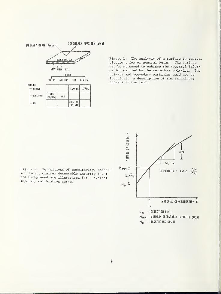
Referring to figure 1 we see that each spec-troscopy employs a beam of primary particlesto probe and interact with the impurity atomson the device structure. A flux of secondaryparticles is detected which may, or may not,
be the same as the primary particles. Thedifficulty in detecting neutrals has beenreason to exclude this species as a viablesecondary particle spectroscopy. The ion
and neutral excitation spectroscopies on
the right half of the diagram form a groupdistinct from the electron detection spec-troscopies on the left. Of course, thereare other spectroscopies, but they do notappear to meet the objectives of the work-shop .
The ion and neutral excitation spectros-copies may be ranked in energy. At the lowend, between 0.5 and 2 keV, is Ion ScatteringSpectroscopy (ISS) , while at the high end,
from 0.5 to 3 MeV is Rutherford Backscat-tering Spectroscopy (RBS) . Both spectros-copies measure the energy loss of the pri-
mary ion after it experiences an elasticbinary collision with an impurity atom. The
energy loss serves to identify the impurityatom through its mass. Because of its low
energy, ISS is extremely surface sensitive.
A most important aspect of RBS is that it is
the only quantitative and essentially non-destructive spectroscopy for depth profilingavailable today.
RBS faces problems detecting light elements
in heavier substrates, but here the comple-mentary accelerator technique known as
Nuclear Resonance Profiling (NRP) is of
aid. The chief disadvantage of all these
accelerator techniques is the cost and size
of the equipment. However the increasingusage of ion accelerators for impurity im-
plantation in device structures may even-tually offset this.
At intermediate beam energies, from 1 to
20 keV, the impact of inert or reactive ions
is effective in removing and ionizing sur-
face material in a controllable manner. The
method of Secondary Ion Mass Spectroscopy(SIMS) consists of determining the mass to
3

charge ratio of these sputtered ions. SIMS
is the most sensitive of all the depth pro-filing methods, but it suffers from ordersof magnitude variation in sensitivity fromone element to the next.
SCANIIR, an acronym for Surface Compositionby Analysis of Neutral and Ion Impact Radia-t ion , is the optical analogue of SIMS.
SCANIIR utilizes the characteristic radia-tive relaxations of sputtered metastableions to identify and quantify the amount of
an element present on an investigated sur-face. The major advantage of this techniqueis its ability to use neutral beams to
analyze insulating films under field-freeconditions
.
Auger Electron Spectroscopy , AES, is themost popular of the surface analysis methods.In conjunction with simultaneous sputter-etching it can be used to determine compo-sitional depth profiles. Impurity elementsare identified by the characteristic ener-gies of their detected Auger electrons.Sensitivities vary by less than a factor of
ten for the various elements, except forhydrogen and helium which cannot be detected.In addition to having superb depth resolu-tion, AES is also capable of excellentlateral resolution in the plane of thespecimen, e.g., when the focussed beam of
a scanning electron microscope is used as
the primary excitation.
The UV and X-ray Photoelectron Spectros-copies (UPS and XPS*) are becoming in-creasingly important for electronic mater-ials analysis. UPS has been applied to
study the effects of contaminants on sur-face potentials, and to study the trappinglevels in the energy bandgap of insulators.Since UV photoelectrons originate fromvalence band states, or thereabouts, theyare not element specific. On the otherhand, the core level binding energiesmeasured by XPS not only uniquely identifythe parent atoms, but also contain infor-mation concerning its chemical environment.The chemical information contained in theXPS spectra is what makes this techniqueso useful.
Statements comparing sensitivities, detec-tion limits, resolutions, sampling depths,etc., of the various spectroscopies must betied to a particular material, instrument,measurement procedure, and the skill of the
*Also known as Electron Spectroscopy forChemical Analysis (ESCA)
.
experimentalist. There is also a certaintransmutability of the instrument parametersthemselves, e.g., the ability to trade sen-sitivity for spectral resolution. It may bewell to consider the definitions of sensitiv-
ity and detection limit used in evaluating a
spectroscopy. These definitions are illus-trated in figure 2 for a typical impuritycalibration curve.
The sensitivity of an analytical techniquerefers to the slope of a calibration curve,i.e., the change in the output signal to theincrement in material concentration. It is,
so to speak, the gain of the instrument. Bythe output signal is meant the amplitude of
the spectral peak less the background level.The background consists of all unwanted in-formation which is correlated with thedesired signal, and it is different fromnoise which is not correlated and, in prin-ciple, can be reduced to any desired levelby averaging the signal over an ensemble of
identical specimens or over a sufficentlylong period of time. The data acquisitiontime is, of course, limited in practice bythe rate at which the surface deterioratesunder the action of the probe or by contam-ination. Even under ultrahigh vacuumconditions, at pressures of 10~ 8 pascals(vlO
-^ Torr) , a surface can become com-pletely covered by deposited contaminationin less than two hours
.
The detection limit is a concept which is
related to the sensitivity. The detectionlimit is defined as the minimum concentra-tion of an impurity required to produce anobservable signal with 95% confidence. Thecriterion in common use for whether a tracedetection has occurred is that the signalcount N must exceed the background countby three times the square root of the back-ground count (N > N + 3v/R~) .
D D
The detection limit of a surface analyticaltechnique for a specified element is usuallystated as being a fraction of a monolayer .
A surface measurement should ideally sampleonly the very outermost layer of surfaceatoms, a depth of less than one nanometer.Silicon has a bulk atomic density of
5 x 10 22 cm-3 and therefore a monolayer of
coverage would contain about 10^ atoms persquare centimeter of surface. Most surfacemeasurements today sample depths of severalnanometers with the result that impurityatoms residing below the surface, but withinthe sampling volume, are interpreted as
belonging to the surface. Consequently, the
detection limit for a surface analysis mayappear to be either better or worse than it
4
actually is, depending upon the technique,the sampling depth, and the particular im-
purity distribution. When a surface analyt-ical technique is applied, together withsome form of surface removal, for the pur-pose of measuring an impurity concentration -
depth profile, it becomes appropriate to
introduce bulk detection limits and to speakof volumetric concentrations. It follows
that those surface analytical techniquesemploying the smallest sampling depths are
capable of yielding concentration profiles
displaying the greatest depth resolution and
possibly the poorest bulk detection limits.
These concepts are not, of course, the only
factors to be considered in evaluating a
spectroscopy. One has only to examine a
spectrometer manufacturer's specification
sheet to realize how complex the choice of a
technique or an instrument can be.
In summary, the evolution of high componentdensity, planar silicon technology hasforced us to look for new techniques to
assist or replace the traditional processcontrol methods. Microprobes of extremesensitivity are being called for which canidentify, quantify and locate impurity atomsat surfaces, interfaces and within thinfilms. Only a few commercially availablesurface analysis techniques have demonstratedtheir usefulness for studying silicon devicestructures and related material properties.These techniques will be examined at thisworkshop in light of their performance for
analyzing silicon, silicon dioxide, and re-lated materials.
1
PRIMARY BEAM (ProbeSECONDARY FLUX [Emission]
DEVICE SURFACE
V.' '.'/// '/ '-'.v.'//. IWWHEAT, FIELDS, ETC.
PROBE
EMISSION
i- PHOTON
• ELECTRON
ION
1
PHOTON1
ELECTRON1
ION
1
NEUTRAL
SCANIIR SCANIIR
UPS
XPS|ESCA| AES
SIMS, ISS,
RBS, NRP
Figure 1. The analysis of a surface by photon,electron, ion or neutral beams. The surfacemay be stressed to enhance the spectral infor-mation carried by the secondary emission. Theprimary and secondary particles need not beidentical. A description of the techniquesappears in the text.
Figure 2. Definitions of sensitivity, detect-ion limit, minimum detectable impurity leveland background are illustrated for a typicalimpurity calibration curve.
MATERIAL CONCENTRATION ,C
Ld
L 0 = DETECTION LIMIT
Nmin = MINIMUM DETECTABLE IMPURITY COUNT
N R = BACKGROUND COUNT
6
NBS Special Publication 400-23, ARPA/N3S Workshop IV, Surface Analysis for Silicon Devices,held at NBS, Gaithersburg
, Maryland, April 23-24, 1975 (Issued March 1976)
IDENTIFICATION OF INTEGRATED CIRCUIT PROCESS AREASAMENABLE TO DIAGNOSIS AND CONTROL BY ANALYTICAL
BEAM TECHNIQUES
Bruce E. Deal
Fairchild Camera and Instrument CorporationPalo Alto, California 94304
ABSTRACT
The general process steps required to fabricate silicon integratedcircuits are reviewed, and examples in each area are indicated whereanalytical beam techniques can be used for compositional analysis and
process control. In some cases satisfactory methods of analysis havebeen established and are in current use, while in others new techniquesneed to be developed. Those characterizations related to device reli-ability and yield improvement are considered to be the most important;these include metallization, chip protection, and oxide charge controlfor reliability effects, and photomasking and cleaning in regards to
yield considerations.
INTRODUCTION
Analytical beam techniques have been employedfor a number of years to evaluate and controlprocesses used to fabricate semiconductor de-
vices and integrated circuits. As the struc-tures of these devices and circuits havebecome more and more complex with increasingcomponent densities, the requirements for
more refined analytical techniques have in-
creased accordingly. The purpose of this pa-
per is to review areas of integrated circuitfabrication where such analytical beamtechniques of analysis are important.
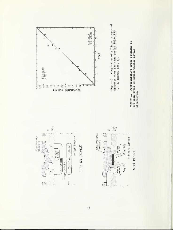
There are two general types of integratedcircuits—MOS and bipolar. Examples of their
structures are shown in Fig. 1. While spe-cific process steps used to fabricate these
circuits vary widely from product line to
product line, some general process areas are
common to all MOS or bipolar structures.These are as follows
:
Silicon Substrate PreparationThermal OxidationPhotomasking and CleaningDiffusionDielectric DepositionMetallizationChip Protection
In this paper we will discuss each of these
general areas, and will indicate where prob-
lems in composition or structure may arise
which can affect device properties or perfor-
mance. We will give examples which show howsome of these problems are being solved by
the proper use of analytical beam techniques,
and where, in other cases, additional workneeds to be done. Due to space limitations,
only one or two examples will be given for
each process area.
Before discussing these possible problemareas, we should emphasize that many of to-
day's bipolar integrated circuit structures
are every bit as complicated as MOS-type cir-
cuits, and we can no longer say that MOS pro-
cess control problems are more severe than
those of bipolar circuits. Also, the formi-
dable requirements for tools used in the
analysis of integrated circuit structures
produced today are demonstrated by the yearly
increase of circuit complexity as shown in
Fig. 2. These data were produced by Gordon
Moore [1] and show that in 1975 the semicon-
ductor industry can produce circuits contain-
ing more than 10,000 individual components on
chips with areas not too much larger than
those of discrete devices produced only fif-
teen years ago. Thus, the challenge to those
involved with developing and carrying out
materials analysis techniques is readily
apparent
.
DISCUSSION OF INTEGRATED CIRCUIT PROCESSING
AREAS
(A) Silicon Substrate Preparation
Characterization and analysis of semiconductor
substrates is an established procedure and in-
cludes several areas. The first is the orig-
inal crystal as produced by various crystal
growing techniques. Such properties as struc-
ture, impurities, dopant distribution and
defects such as dislocations must be
7
characterized and kept under suitablecontrol. Next, the silicon surface afterwafer slicing must be maintained free of con-tamination and particles. In addition, the
surface should have the proper crystal ori-entation and be relatively free of stress.
Finally, subsequent substrate processingsteps such as buried collector preparationand epitaxial film deposition must be con-
trolled. In the latter case, all considera-tions applicable to the original crystal bulkand surface apply, but in addition, analysisand control of the dopant profile becomeincreasingly important.
As indicated above, methods of analysis used
to characterize the properties of the siliconsubstrate are well known. Of course, as
larger slices are used and more complex cir-cuit structures are developed, the analyticaltechniques may have to be refined. Sincethis area of integrated circuit fabricationis probably under better control than the
others, no specific examples will be present-ed here. However, the reader is referred to
a general reference on the subject of surfacecharacterization [2].
(B) Thermal Oxidation
Thermal silicon dioxide (Si02) is the basisfor today's semiconductor devices and inte-grated circuits. It provides passivation foractive device regions that is not equaled byother types of dielectric layers generallyprepared by deposition techniques. The ther-
mal oxidation kinetics and properties havebeen characterized in a satisfactory mannerso that devices with predictable propertiesmay be produced. Included in this charac-terization are the electrical properties as
determined by the four types of oxide
charges . These charges are Qss , the fixedoxide charge; Nst , fast interface states;
Q0 , mobile ionic charge; and Not , radiation-induced charge. While the empirical depen-dence of these charges on processingvariables is well known, a number of ques-tions remain as to their exact origin and
physical nature [3]. Indications of howthese charges may be investigated usinganalytical beam techniques are as follows.
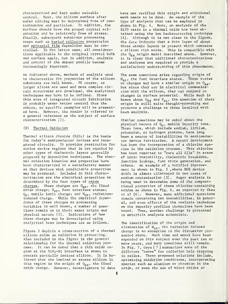
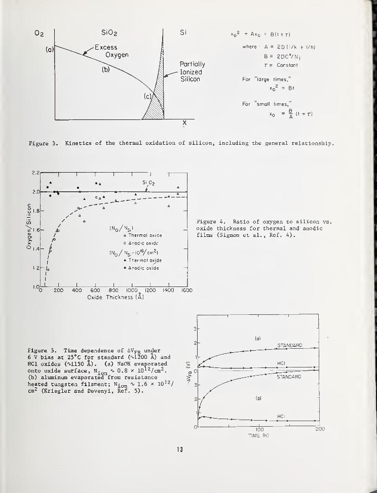
Figure 3 depicts a cross-section of a thermalsilicon oxide as oxidation is proceeding.Also included in the figure is the generalrelationship for the thermal oxidation pro-cess. It can be noted that a thin oxide re-gion at the Si02~Si interface is shown to
contain partially ionized silicon. It is be-lieved that the ionized or excess silicon inthis region is the origin of Qss , the fixedoxide charge. However, investigators to date
have not verified this origin and additionalwork needs to be done. An example of the
type of analysis that can be employed is
shown in Fig. 4. Here, an analysis of the
Si/0 ratio in a thermal oxide has been ob-tained using the ion backscattering technique
[4]. Although it is not clear in the figure,
the data indicate that a thin layer of about
three atomic layers is present which contains
a silicon rich oxide. This is compatible withthe Qss origin model described above. However,
it is clear that additional characterizationsand analyses are required to provide a
satisfactory understanding of this phenomenon.
The same questions arise regarding origin of
Nst , the fast interface states. These states
or charges may have a similar origin to Qss ,
but since they are in electrical communica-tion with the silicon, they can respond to
changes in surface potential. While much is
known about Qss and Nst , the question of their
origin is still quite thought-provoking and
presents a challenge to those involved withbeam analysis
.
Similar questions may be asked about the
physical nature of QQ , mobile impurity ions.
These ions, which include sodium, lithium,
potassium, or hydrogen protons, have long
been a source of instabilities in semiconduc-
tor device fabrication. A recent development
has been the incorporation of a chlorine spe-
cies in the oxidation process. This chlorine
has been reported to "cure all ills" in areas
of ionic instability, dielectric breakdown,junction leakage, fast state generation, and
others. An example of a verified improve-
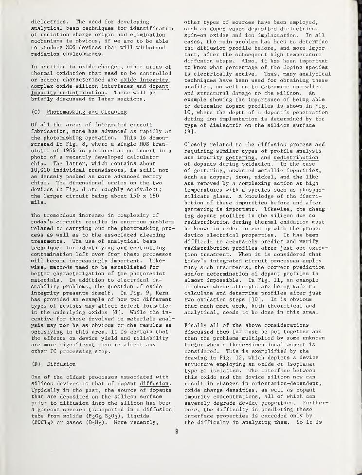
ment is shown in Fig. 5 , where MOS device
drift is almost eliminated in two cases of
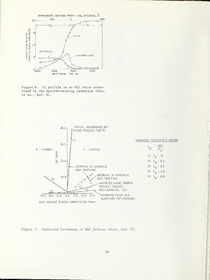
sodium contamination [5]. Auger analysis is
being used to determine some of the composi-
tional properties of these chlorine-containing
oxides as shown in Fig. 6, as reported by Chou
et al [6] . However, many additional questions
remain concerning ion instabilities, in gener-
al, and even effects of the analysis technique
on the impurity profiles themselves have beennoted. Thus, another challenge is presented
to materials analysis scientists.
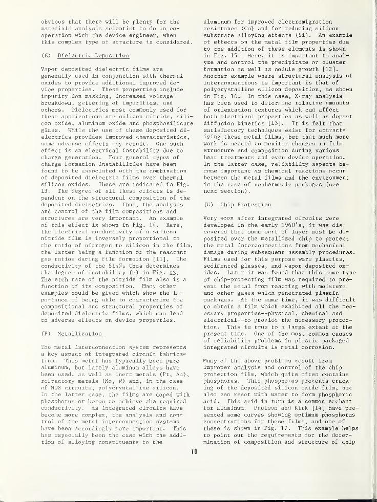
The identification of the origin and
elimination of Not , the radiation induced
charge is no exception to the discussion pre-sented above. Much time and money have beenexpended on this subject over the past ten or
more years, and many questions still remain.
In Fig. 7, Gwyn [ 7 ] summarizes some of the
different "cures" for radiation hole trapping
in oxides. These proposed solutions include,
optimizing oxidation conditions, incorporatingspecies such as aluminum or chromium in the
oxide, or even the use of mixed oxides or
dielectrics. The need for developinganalytical beam techniques for identificationof radiation charge origin and eliminationmechanisms is obvious, if we are to be ableto produce MOS devices that will withstandradiation environments.
In addition to oxide charges, other areas of
thermal oxidation that need to be controlledor better characterized are oxide integrity ,
complex oxide-silicon interfaces and dopantimpurity redistribution . These will bebriefly discussed in later sections.
(C) Photomasking and Cleaning
Of all the areas of integrated circuitfabrication, none has advanced as rapidly as
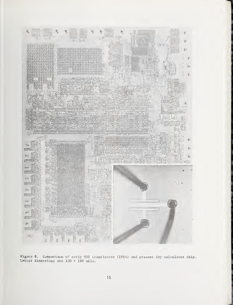
the photomasking operation. This is demon-strated in Fig. 8, where a single MOS tran-sistor of 1964 is pictured as an insert in a
photo of a recently developed calculatorchip. The latter, which contains about10,000 individual transistors, is still notas densely packed as more advanced memorychips. The dimensional scales on the two
devices in Fig. 8 are roughly equivalent;the larger circuit being about 150 x 180mils
.
The tremendous increase in complexity of
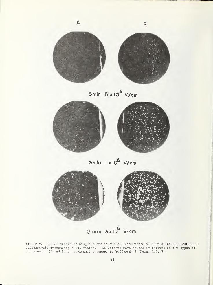
today's circuits results in enormous problemsrelated to carrying out the photomasking pro-cess as well as to the associated cleaningtreatments. The use of analytical beamtechniques for identifying and controllingcontamination left over from these processeswill become increasingly important. Like-wise, methods need to be established forbetter characterization of the photoresistmaterials. In addition to electrical in-stability problems, the question of oxideintegrity presents itself. In Fig. 9, Kernhas provided an example of how two differenttypes of resists may affect defect formationin the underlying oxides [8]. While the in-centive for those involved in materials anal-ysis may not be as obvious or the results as
satisfying in this area, it is certain thatthe effects on device yield and reliabilityare more significant than in almost anyother IC processing step.
(D) Diffusion
One of the oldest processes associated withsilicon devices is that of dopant diffusion .
Typically in the past, the source of dopantsthat are deposited on the silicon surfaceprior to diffusion into the silicon has beena gaseous species transported in a diffusiontube from solids (P2O5, B2O3), liquids(POCI3) or gases (BoHg). More recently,
9
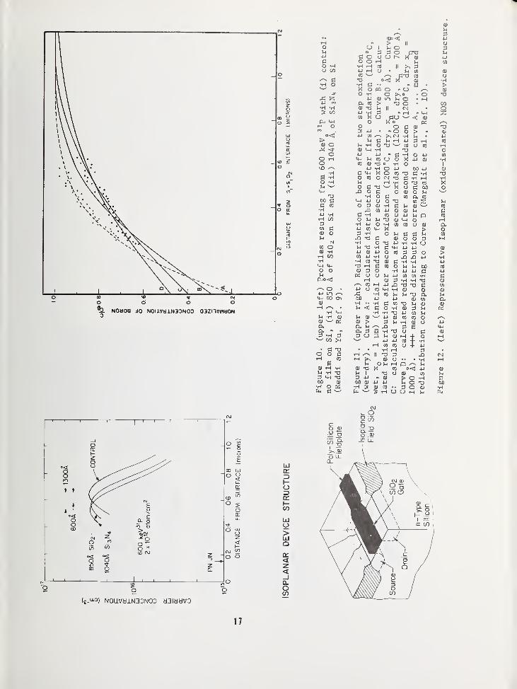
other types of sources have been employed,such as doped vapor deposited dielectrics,spin-on oxides and ion implantation. In allcases, the main problem has been to determinethe diffusion profile before, and more impor-tant, after the subsequent high temperaturediffusion steps. Also, it has been importantto know what percentage of the doping speciesis electrically active. Thus, many analyticaltechniques have been used for obtaining theseprofiles, as well as to determine anomaliesand structural damage to the silicon. Anexample showing the importance of being ableto determine dopant profiles is shown in Fig.
10, where the depth of a dopant's penetrationduring ion implantation is determined by the
type of dielectric on the silicon surface[9].
Closely related to the diffusion process andrequiring similar types of profile analysisare impurity gettering , and redistributionof dopants during oxidation. In the caseof gettering, unwanted metallic impurities,such as copper, iron, nickel, and the like
are removed by a complexing action at hightemperatures with a species such as phospho-silicate glass. A knowledge of the distri-bution of these impurities before and aftergettering is important. Likewise, the chang-ing dopant profiles in the silicon due to
redistribution during thermal oxidation mustbe known in order to end up with the properdevice electrical properties. It has beendifficult to accurately predict and verifyredistribution profiles after just one oxida-tion treatment. When it is considered that
today's integrated circuit processes employmany such treatments, the correct predictionand/or determination of dopant profiles is
almost impossible. In Fig. 11, an exampleis shown where attempts are being made to
calculate and determine profiles after just
two oxidation steps [10]. It is obviousthat much more work, both theoretical andanalytical, needs to be done in this area.
Finally all of the above considerationsdiscussed thus far must be put together and
then the problems multiplied by some unknown
factor when a three-dimensional aspect is
considered. This is exemplified by the
drawing in Fig. 12, which depicts a device
structure employing an oxide or Isoplanartype of isolation. The interface between
this oxide and the device silicon now can
result in changes in orientation-dependent,
oxide charge densities, as well as dopant
impurity concentrations, all of which can
severely degrade device properties. Further-
more, the difficulty in predicting these
interface properties is exceeded only by
the difficulty in analyzing them. So it is
obvious that there will be plenty for thematerials analysis scientist to do in co-operation with the device engineer, whenthis complex type of structure is considered.
(E) Dielectric Deposition
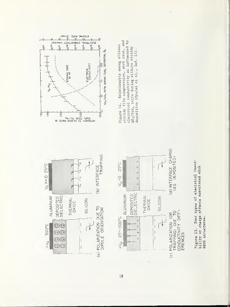
Vapor deposited dielectric films aregenerally used in conjunction with thermaloxides to provide additional improved de-vice properties. These properties includeimpurity ion masking, increased voltagebreakdown, gettering of impurities, andothers. Dielectrics most commonly used for
these applications are silicon nitride, sili-con oxide, aluminum oxide and phosphosilicateglass. While the use of these deposited di-electrics provides improved characteristics,some adverse effects may result. One sucheffect is an electrical instability due to
charge generation. Four general types of
charge formation instabilities have beenfound to be associated with the combinationof deposited dielectric films over thermalsilicon oxides. These are indicated in Fig.
13. The degree of all these effects is de-pendent on the structural composition of thedeposited dielectrics. Thus, the analysisand control of the film compositions andstructures are very important. An exampleof this effect is shown in Fig. 14. Here,the electrical conductivity of a siliconnitride film is inversely proportional to
the ratio of nitrogen to silicon in the film,
the latter being a function of the reactantgas ratios during film formation [11]. Theconductivity of the SiaNij thus determinesthe degree of instability (c) in Fig. 13,
The etch rate of the nitride film also is a
function of its composition. Many otherexamples could be given which show the im-
portance of being able to characterize thecompositional and structural properties of
deposited dielectric films, which can leadto adverse effects on device properties.
(F) Metallization
The metal interconnection system representsa key aspect of integrated circuit fabrica-tion. This metal has typically been purealuminum, but lately aluminum alloys havebeen used, as well as inert metals (Pt, Au)
,
refractory metals (Mo, W) and, in the caseof MOS circuits, polycrystalline silicon.In the latter case, the films are doped withphosphorus or boron to achieve the requiredconductivity. As integrated circuits havebecome more complex, the analysis and con-trol of the metal interconnection systemshave been accordingly more important. Thishas especially been the case with the addi-tion of alloying constituents to the
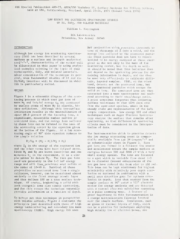
aluminum for improved electromigrationresistance (Cu) and for reducing siliconsubstrate alloying effects (Si). An exampleof effects on the metal film properties dueto the addition of these elements is shownin Fig. 15. Here, it is important to anal-yze and control the precipitate or clusterformation as well as nodule growth [12]
.
Another example where structural analysis of
interconnections is important is that of
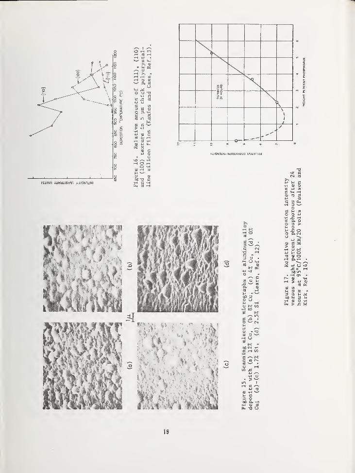
polycrystalline silicon deposition, as shownin Fig. 16. In this case, X-ray analysishas been used to determine relative amountsof orientation textures which can affectboth electrical properties as well as dopantdiffusion kinetics [13]. It is felt thatsatisfactory techniques exist for charact-izing these metal films, but that much morework is needed to monitor changes in filmstructure and composition during variousheat treatments and even device operation.In the latter case, reliability aspects be-come important as chemical reactions occurbetween the metal films and the environmentin the case of nonhermetic packages (see
next Section)
.
(G) Chip Protection
Very soon after integrated circuits weredeveloped in the early 1960's, it was dis-covered that some sort of layer must be de-posited over the metallized chip to protectthe metal interconnections from mechanicaldamage during subsequent assembly procedures.Films used for this purpose were plastics,sedimented glasses, and vapor deposited ox-ides. Later it was found that this same type
of chip-protecting film was required to pre-vent the metal from reacting with moistureand other gases which penetrated plasticpackages. At the same time, it was difficultto obtain a film which exhibited all the nec-essary properties—physical, chemical andelectrical— to provide the necessary protec-tion. This is true to a large extent at thepresent time. One of the most common causesof reliability problems in plastic packagedintegrated circuits is metal corrosion.
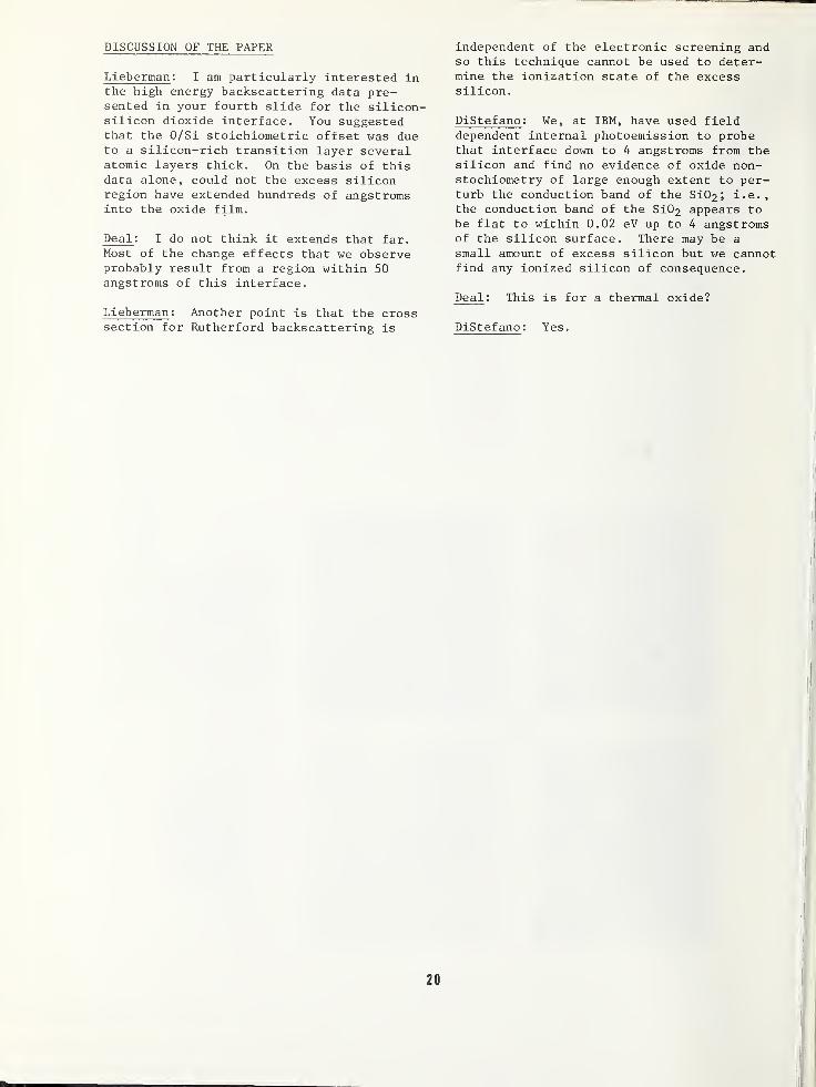
Many of the above problems result fromimproper analysis and control of the chipprotection film, which quite often containsphosphorus. This phosphorus prevents crack-ing of the deposited silicon oxide film, butalso can react with water to form phosphoricacid. This acid in turn is a common etchantfor aluminum. Paulson and Kirk [14] have pre-sented some curves showing optimum phosphorusconcentrations for these films, and one of
these is shown in Fig. 17. This example helpsto point out the requirements for the deter-mination of composition and structure of chip
protection films. An additional difficultyis that of obtaining a proper depth profileof the constituents.
One last type of characterization that is
very important in this area involves failure
analysis. When integrated circuits are sub-
jected to life tests or fail in actual use,
the understanding of the failure mode is
very important and may be accomplished by a
carefully executed analysis. Such an anal-ysis includes identification of reactionproducts, and analytical beam techniques can
be used very effectively for this purpose.
CONCLUSIONS
In summary, we have reviewed the variousprocessing steps of integrated circuit fabri-cation. In doing so, we have noted the manyareas where analytical beam techniques can
be used to provide a better control of these
processes and the resulting device proper-ties. Many such analyses are being success-fully used today, while in some areas, newor improved methods must be developed. If
priorities are to be stated, those areas of
analysis related to device reliabilityshould be listed first. These include chip
protection, metallization and control of
device electrical properties. Next in im-
portance would be wafer sort yield. In this
case, control and characterization of the
photomasking and cleaning processes wouldundoubtedly be the most important factors,
since this process area dominates yields of
semiconductor integrated circuits today.
Finally, it is important that the scientistswho are responsible for developing and carry-
ing out the analyses keep in close communi-cation with the IC processing engineers, so
that the problems that need to be solved are
solved, and that our always limited
resources are used most efficiently.
ACKNOWLEDGMENTS
The author wishes to thank A. J. Learn and
R. C. McDonald for helpful discussionsconcerning various aspects of this paper.
REFERENCES
1. Moore, G. E. , Private Communication.
2. Characterization of Solid Surfaces,P. F. Kane and G. B. Larrabee, Eds.,(Plenum Press, New York 1974).
3. Deal, B. E. , J. Electrochem. Soc. 121 ,
1986 (1974).
4. Sigmon, T. W. , Chu, W. K. , Lugujjo, E.
and Mayer, J. W. ,Appl. Phys. Lett. 24
,
105 (1974).
5. Kriegler, R. J. and Devenyi, T. F.,
Proa. 11th Annual Reliability PhysicsConf., Las Vegas, Nevada, April 3-5, 1973.
6. Chou, N. J., Osburn, C. M. , van derMeulen, Y. J., and Hammer, R.
, Appl.
Phys. Lett. 22, 380 (1973).
7. Gwyn, C. W. , Sandia Laboratories ReportNo. SLA-73-0017, Jan. 1973.
8. Kern, W. , RCA Review 34, 655 (1973).
9. Reddi, V. G. K. and Yu, A. Y. C. , SolidState Tech. , 35, (Oct. 1972).
10. Margalit, S. , Neugroschel, A. andBar-lev, IEEE Trans. Elec. Dev. ED-19 ,
861 (1972).
11. Gyulai, J., Meyer, 0., Mayer, J. W. andRodriguez, V., J. Appl. Phys. 42_, 451
(1971).
12. Learn, A. J., Thin Solid Films 20, 261
(1974)
.
13. Kamins, T. I. and Cass, T. R. , ThinSolid Films 16, 147 (1973).
14. Paulson, W. M. and Kirk, R. W. , Proc.
12th Annual Reliability Phys. Conf.Las Vegas, Nevada, April 2-4, 1974.
dIHD i!3d SlN3N0dW03
T3(U
4-1
tfl
u moo r~-
CD o>-u' rHfi 1
»H OAmGO —
I
oH T3i—
1
O•H •HCO
4-4
per
O0)
1.—
s
4-1 —
1
•H 4-1
a> (UH « cu
a. 4-1
eo M
0) 0)
> !-i
oOO
ts
0) •H)-l 3 wD o00 !-l
•H •H 6CJ
o
CO
o CD
•H cj
4J •Ho ><u CU
(J) XI1
CO >_l
cn oo 4J}-) Cj
CJ 3T3C
> O•H o4-J Hn)
84J
£CO
CO
<u oS-i
Ow CO
0) cu
Pi
4-1
rH C•H
01 Ctj
1-1 e000 o•H S
4-1
12
o 2
(a)
C i
x02 + Ax 0 = B(t + t)
where A = 2 D ( l/k + l/h)
Oxygen | B = 2DC*/N,
(bT^\ 1Partially r = Constant
Ionized
Silicon For "large times,"
x02 = Bt
For "small times,"
x 0B | (t + T)
Figure 3. Kinetics of the thermal oxidation of silicon, including the general relationship,
2.2
2.0
01
O1 .4
1.2-
1 1
A
• •
1 1 1 1 1
• » Si 02— ——
A a
""a
/ifc
/
/°
<N 0/ NS,>
a Thermal oxide
0 Anodic oxide
-//
/
-/o1
1
11 1
(N0/N
Sl-IO l6/cm2
)
* Thermal oxide
• Anodic oxide —
1 1 1 1 1
Figure 4. Ratio of oxygen to silicon vs,
oxide thickness for thermal and anodicfilms (Sigmon et al. , Ref. 4).
0 200 400 600 800 1000 1200 1400 1600_ o
Oxide Thickness (A)
Figure 5. Time dependence of AV-pB under6 V bias at 25°C for standard (vL200 A) andHC1 oxides (VL150 A) . (a) NaOH evaporatedonto oxide surface, Nion % 0.8 x 10 12 /cm2
.
(b) aluminum evaporated from resistanceheated tungsten filament; N-^on a, 1.6 * 10 12
/
cm2 (Kriegler and Devenyi, Ref. 5).
200
13
APPROXIMATE DISTANCE FROM Si-Si02 INTERFACE, A
SPUTTERING TIME, sec
Figure 6. CI profile in an HC1 oxide deter-mined by the sputter-etching technique (Chouet al. , Ref . 6)
.
40.0
CHANNEL
TYPICAL UNHARDENED DRY
OXIDE PROCESS (1100°C)
CHANNEL
RADIATION SENSITIVITY FACTOR
DECREASE IN INTRINSIC
HOLE TRAPPING
/ /DECREASE IN EXTRINSIC
/ \y HOLE TRAPPING
HARDENED OXIDE GROWTHPROCESS (HUGHES,
WESTINGHOUSE, NRL)
-15.0 -10.0 -5.0 0.0 5.0 10.0 15.0
GATE VOLTAGE DURING IRRADIATION (Volts)
HARDENED OXIDE ANDALUMINUM IMPLANTATION
(1)
(2)
(3)
(4)
(5)
R= 15
= 0.4
= 0.2
- 1.0
= 0.0
Figure 7. Radiation hardening of MOS devices (Gwyn, Ref. 7).
1 I
IS
5min 5 x 10 V/cm
2 min 3x10 V/cm
Figure 9. Copper-decorated S1O2 defects in two silicon wafers as seen after application of
successively increasing oxide fields. The defects were caused by failure of two types ofphotoresist (A and B) on prolonged exposure to buffered HF (Kern, Ref. 8).
16
N0U08 JO N0I1VH1N3DN0D Q3ZnvWMON
OU•UcO vHO CO
^ 3•H O
S co
Ph 4h- o
oo
>0)
^!
Oo
B -h0 *H
4-1
XI00 C3 cd
•H4-1 -H
05 OrH 00•H4-1 4-1
O OM0_|O<
^-v O •
u in ^4h 00 a\0)
^ .
CD'
ft3
4-1
CO p-i
3 t3O C
B*
rH *H•H XI4-1 XJ
0)
oc ^
II
c oo o•H rH4J rHCd ^XJ•H 3X oO -i-l
4J
ft nj
a) XIM -Hco X
O
Ob <ti
>I M O3 3 o sxjo o r-. x aiH M« II 3CJ • rJ CO
exi njo<; X ai
» b •
« u ^^» • o1-1 O • rHT3 O •
M OOo) in>
CM
OIS 4-1
4-1 CO
MrJ -H0) 4-1
4J4-4 tj
n) 014-J
C >4-l
O CO
o 3X o•H
<-4—
I
o 3
C! -H0 M•H 4-)
4J CO
3 --H
X)•HP XI4-1 0) 4-1 O
X
o
o c• «o o
^-s CN iHC l-l rH 4-1
O X) ^ CO
•H X)4J « 3 -H(J U O KXI o -HO•H O 4J
X O CO XIO cm XI C
rH -H Oxi ^ X a3 O a)
O C co
O O X)•H 30)
CO 4Jcd
l-l X)O -H4-1 X
oc
uCD
U 4J0) 4-1
co cd
- 4h<; ai
ai
> »
M •
3 rHo cn
00 4-1
3 -H•rH rHXI Cd
3 OBO l-i
ft cd
CD 20) wl-l
l-i QOO 0J
>3 uO 3
CO 4-1
•h cd
XI rH0) 3« o
rH/-n Cd4-> CJ
X00•H ••
rJ <!
l-l 0)
0) >ft Mft 3
rJ 301 O -
O X) 4J -H -H U'
3. 4-1 4-1 4-1
cd 3 3X X
C -H -HO V4
0)
cu
—I 4-1
cd 4-1
h cd
•H 4-J 4-1
CO
3 -Hxi xi•H 0)
u u
m
•H 3 co x) ^C O -iH 0) 3•H -H XI 4J CO
4-> cu cd cd
3-r? ^ _ 3B -H X) o3- l-l 0) rH
4J 4J Cdi—I co cd cj
•iH rHII XJ 3
0) CJ ••
O U rH QX
oo oi
ai cd
S rH
3Xi•Hl-l
cd o<; 4_>
u gi co
> o -Hu o XI
•• 3 o cuU U rH l-l
CU
cj
>01
XI
XIOi
ucd
3cdrHftoCO
cu
>•H
30)
CO
01
uft0)
0)
M300•H
17
(5»VY) 31V« 9NIHD13
(uio/oqiu) AllAUDTKjNCO "IVOIdlOrD
1 5. 1 " 1 *g g S g g g
ISN/ N N 'Wild *N£!SNl OllVa N03I1IS 01 N390a±IN
s -°cfl
- 0)
o> o4-1 CCO 0)
H 3
ti o aos
•H O co cd
•H 4-i
>H
HTO
Oo- oe 3O "-0
0) CJ CO
6 o
cr)
pi
. -H
r-l
0)
0) 13S-l -H3 M60 4-J
•rH -HPn 3
c•HS-< -H3 cfl
T3 r-l
3O•H O4-1 ^CO
U 3o
EC 4J
•H -r-l
C/l CO
Oco
cd o)
S3 T3
CO55>n n y o_i< 2 uj
o.coj>iCL I- O 1^
CO4-1
CO ^3a 4J
H •HS
iHCO T)CJ 0)
•H 4-1
cO4J •r-l
O CJ
0) oH CO
<D CO
CO>4-<
O CO
4Jco OCD CU
O.>> '4-1
4-> 0)
CU
3 60 CO
0 U 0)
Pn CO S-i
,£3 3CJ 4J
Ocl 1-1 3rH O M
4J
cu f>> co
4J
3 •H Cfl
00 rH O•H 1—
1
s
HUHrH 4J •
CO H-l
>% 0)
- H Pi
H ^ •H H inH O to^ a. nj
c_>
<4-l ,Mo o
•H Cco 42 to
C co
3 S 3O 3. vHa acfl LTl cfl
a) C ^co
<u
M3 -HmumOJ
(S1IND AaVdllBMV) A1ISN31NI
3Oo•H
rH O iHO -H
d) H B)
3 CU
60 T) C•H (2 -Hfa Cfl rH
SiOH
«01/96
\\
1
t
o—
-
1
A1ISN3INI NOISOSaOO 3All«13b
orH 6-5
H OCfl
e •5'
3 ^C3 On)
•H rHe -
3 3 •
rH O IHtfl 01
6-5 piCH <*O
>-> Cco a u42 ^ «a. cu
Cfl ju -^60 3o oM -Ho ^ w•H 00E ^^ in3- rO •
O ^ CMu•U /-vO * t>Q) 3rH C_>
CU
60 CN iHC rH W•H
(2 cfl r--
cfl ^ •
O rHCO 42
44 /-v•H CJ
• SIin
10
cfl
(1) H ^(-1 CO
3 O60 P,•HOfl
-o o
-cr
•U (J
•H CU
CO 4J
3 HHCU Cfl
•H 42 rH
U 42 <
O D. (
CU c> CU
•H O4J Htfl CU
rH P.CU
4260
• 'Hr-~ CU
rH IS
CU CO
l-i 33 Cfl
60 U•H CU
>
19
DISCUSSION OF THE PAPER
Lieberman : I am particularly interested inthe high energy backscattering data pre-sented in your fourth slide for the silicon-silicon dioxide interface. You suggestedthat the O/Si stoichiometric offset was dueto a silicon-rich transition layer severalatomic layers thick. On the basis of thisdata alone, could not the excess siliconregion have extended hundreds of angstromsinto the oxide film.
Deal : I do not think it extends that far.Most of the change effects that we observeprobably result from a region within 50angstroms of this interface.
independent of the electronic screening andso this technique cannot be used to deter-mine the ionization state of the excesssilicon.
DiStefano : We, at IBM, have used fielddependent internal photoemission to probethat interface down to 4 angstroms from thesilicon and find no evidence of oxide non-stochiometry of large enough extent to per-turb the conduction band of the Si025 i.e.,the conduction band of the Si02 appears tobe flat to within 0.02 eV up to 4 angstromsof the silicon surface. There may be a
small amount of excess silicon but we cannotfind any ionized silicon of consequence.
Deal : This is for a thermal oxide?Lieberman: Another point is that the crosssection for Rutherford backscattering is DiStefano : Yes.
20
NBS Special Publication 400-23, ARPA/NBS Workshop IV, Surface Analysis for Silicon Devices,held at NBS, Gaithersburg, Maryland, April 23-24, 1975 (Issued March 1976)
LOW ENERGY ION SCATTERING SPECTROMETRY STUDIESOF Si, Si02, AND RELATED MATERIALS
William L. Harrington
RCA LaboratoriesPrinceton, New Jersey 08540
INTRODUCTION
Although low energy ion scattering spectrom-etry (ISS) has been described by severalauthors as a surface and in-depth analyticaltool 1
'2
'3
, characteristics of the method willbe illustrated in this paper by using analyt-ical examples relating to the topic of thisworkshop— Si, Si02, and related materials.After consideration of the technique in gen-eral, some fundamental studies of Si and theSi/Si02 interface will be discussed in whichISS is particularly suited.
METHOD
Figure 1 is a schematic diagram of the scat-tering process in which rare gas ions of
mass M^ and initial energy Eq are scatteredby surface atoms of mass M2 in elastic, bi-nary collisions. Although this ion-surfaceinteraction results in the neutralization of
about 99.9 percent of the incoming ions, a
significant, measurable number survive as
scattered ions, and the energy loss sufferedby these ions can be related to the mass of
the scattering center by the equation givenat the bottom of the figure. At a lab scat-tering angle of 90° this equation reduces to
the simple relation
Ei/E0 = (M 2 - M!)/M 2 + MX )
where E]_ is the energy of the scattered ionand the other terms have been defined above.
Since Mj and Eo are known quantities and onemeasures E^ in the experiment, it is a sim-ple matter to deduce M2 . The rare gas ions
used are generally in the 1-3 keV energyrange and will thus penetrate most solids on
othe order of 10-60 A. Survival of theseprojectiles as scattered ions from a singlecollision, however, can be restricted almostentirely to the first average atomic layerand thus defines ISS as a true surface tech-nique. Of course, bombarding a solid withsuch energetic ions also causes sputtering,and for this reason the technique naturallyprovides information as a function of depth.
To better put this technique in perspectivewith related methods, Figure 2 contrasts theprinciples just described with those of highenergy backscattering and secondary ion massspectroscopy (SIMS) . High energy ISS uses
MeV projectiles whichopenetrate thousands to
tens of thousands of A into a solid, and theenergy loss suffered by the scattered parti-cle (this particle does not have to remainionized to be energy analyzed at these ener-gies) is due not only to the mass of thescattering center, but its depth as well.It should be noted that this technique doesnot depend on the sputtering process for ob-taining information in depth, and can thusbe used very effectively to calibrate diffi-cult, layered samples. SIMS, on the otherhand, detects not the scattered ions, butthose sputtered particles which escape thesolid as ions. The sputtered ions are thenextracted into a mass spectrometer and anal-yzed according to their mass/charge ratio.A point sometimes forgotten when comparingsurface techniques is that SIMS data comefrom the sputtered species, which in thesteady state are representative of the bulksample composition. Low energy ISS and othertechniques such as Auger Electron Spectros-copy analyze the surface that remains aftersputtering, so that differential sputteringeffects must be considered in the interpre-tation of data.
The instrumentation which in practice detectsthe low energy scattering event is commer-cially available from the 3M Company
1*' 5 andis schematically shown in Figure 3. Raregas ions are formed in a filament ion sourceand accelerated toward the sample surface at
energies between 500 and 3000 eV with a verysmall energy spread. The ions are focussedto a spot which is variable from about 1-3
mm in diameter (recent enhancements of the
ion gun have reduced the beam size to 100 pm)
This beam can be kept stationary for highestsensitivity with relatively poor depth reso-lution or rastered in combination with a
small area detection gate for optimum reso-lution in depth. Ions that scatter from the
sample surface at 90° enter a 127° electricsector for energy analysis and are detectedwith a channel electron multiplier operatingin a pulse counting mode. A feature of
great importance in this instrumentation is
a charge neutralization filament locatednear the sample surface. Insulators, suchas glass or thermal layers of Si02, whichcan be a problem for techniques employinghigh density ion or electron beams, are
21
flooded with thermal electrons during ion
bombardment with feedback regulation to keepthe sample surface at a fixed potential nearground. The importance of sputtering with an
uncharged surface will be demonstrated in
some of the examples to follow, but the cru-cial point is to eliminate large electricfield gradients across a sample to preventmigration of mobile ions.
The output from this technique is best de-
scribed with the help of a pertinent exampleas shown in Figure 4. These are typical ISS
spectra where the scattered response in
counts/second is plotted vs. E^/Eq, the
ratio of scattered to initial ion energy as
defined previously in Figure 1. The samplein this example is an alkali strontium sili-cate glass which is certainly a good insula-tor. With charge neutralization by the floodfilament, however, no charging effects are
noted. That is, the peaks fall at the sameenergy ratio as those obtained from a goodconductor, and there is no evidence that mo-bile ions are affected by the sputteringbeam. The top spectrum in this figure is
that for a normal, untreated glass, and onecan discern peaks for 0, Na, Si, K, and Sr.
The bottom spectrum is from the same glassafter the application of a heat and voltagetreatment with non-blocking contacts to movemobile ions into the glasses 7—only 0 and Si
remain at the surface. A series of suchspectra while continuing to sputter yields a
concentration profile in depth as shown in
Figure 5. Note the depletion and subsequentpile-up of Sr, the largest and least mobileof the ions, whereas Na, the most mobilespecies, is barely detected even at largedistances from the surface. Potassium, hav-
ing an intermediate mobility, shows an inter-mediate trend.
The magnitude of the scattered signal from an
element in a given matrix is basically a
function of three variables— (1) the geomet-ric arrangement of atoms on a surface, i.e.,
does one atom shield another from the incom-
ing beam?, (2) the extent of neutralizationof the incident ions, and (3) the scatteringcross section (the probability that scatter-ing will occur) as a function of atomic num-ber. Geometry, for most analytical problemsconcerning amorphous, non-oriented layers,
is not critical; but for situations wherethe position of atoms is important, the onelayer resolution of ISS can be used to an
advantage. Although neutralization may varyfrom one surface to another, differentialneutralization between elements in a givenmatrix would be expected to be a rathersmall factor. Relative scattering crosssections have been studied extensively, and
certainly as a first approximation, one can
correct elemental scattering data for this
variable. Figure 6 is a plot of Bingham'sdifferential cross sections 8 as a functionof atomic number for 1500 eV 4 He +ions . Of
course, there is a family of such curves foreach initial energy and for each differentprobe ion. The magnitude of the correctionimplied by these data over the range of a
light element such as 0 to a heavy elementsuch as Pb is only about a factor of 6 as
compared to several orders of magnitude. cor-rection for ion yields in the SIMS technique.
To illustrate this correction, Figure 7 showsa spectrum of glass used to form a liquidcrystal cell. When a voltage is applied to
specific areas of such a cell, the liquidcrystal material sandwiched between the glasssurfaces will align to produce visible con-trast for displays. For this applicationthe glass surface composition has been foundto be important, and in some cases leads to
liquid crystal misalignment. The spectrumshown in this figure was taken in an area of
the cell which operated normally. The Na,
Ca, 0, and Si concentrations were calculatedby subtracting a background for each peakand dividing the net peak height by the rel-ative scattering cross section. A simplesumming of all corrected signals and divi-sions to determine individual percentagesproduced very good agreement with the bulkcomposition as given by the manufacturer.Figure 8 is a similar spectrum taken in anarea of the glass cell just a few mm awayfrom that in Figure 7. In this case liquidcrystal misalignment was a problem, and thesurface composition of the glass, as deter-mined from the same calculation proceduredescribed previously, is completely differentwith very high concentrations of Na and Ca.
CRYSTALLOGRAPHIC ORIENTATIONS OF SINGLECRYSTAL Si
Having established the characteristics of
the method, it is instructive to describethe results of two ISS studies which focuson Si and the Si/Si02 interface.
The (111) and (100) surfaces of single crys-tal Si wafers are used extensively in Si de-vices and offer an excellent system for
studying surface sensitivity and informationdepth of an analytical technique. In addi-tion, for those techniques using sputteringto provide information as a function of
depth, single crystal Si provides a sensitivemeans of evaluating damage to these surfacesfrom ion bombardment.
The detailed preparation of these surfaces
22
has been described previously , but Figure 9
shows spectra of a typical surface as re-
ceived— there is the expected small amountof residual oxide, some carbon, and F from
the final HF etch. In order to obtain accu-
rate ISS response on the pure Si surface, it
was necessary to carefully sputter throughthis thin contamination layer to reach a
clean Si surface, as shown in the right halfof this figure.
If one considers the geometrical packing of
Si atoms on the (111) and (100) surfaces,
the surface atom density of (111) Si is 1.15
times greater than that of (100) Si. ISS
responses for these two orientations areshown in Figure 10 as a function of severalenergies for both He"*" and Ne+ . The columns
under the figures show the signal level for
each orientation, and the last column is the
calculated (111)/(100) ratio. For He+ the
observed ratio does not fall within the
range of the true ratio until an energy of
1500-2500 eV is reached. Because the trueratio is observed at these higher energies,one can deduce that no detectable damage hasbeen done to the crystal lattice by He bom-bardment. At low energies the ratio ap-
proaches unity because the low current den-
sity and very low sputter yield at these en-ergies result in a situation where the sur-face is not kept clean during the scatteringmeasurement. With such a contamination layer
on the surfaces, the true Si response cannotbe obtained. If the surface were firstcleaned by sputtering with 1500 eV He+ , theratios obtained with Ne+ at 500 and 1500 eV
are correct within the measurement precision.The slightly lower value at 500 eV couldagain be due to contamination since thehigher Ne sputter yield was somewhat offsetby a low current density of about 3 pA/ cm2 .
The low ratio at 2500 eV indicates that dam-age has been done to the crystal lattice.This damage is shown more clearly in Figure11, where Ne+ at 500, 1500, and 2500 eV wasused to sputter the two surfaces until the
oxide was removed. Each location sputteredwas then examined with 1500 eV He"*" ions
.
The ratio at 500 eV is the same as that ob-tained with no Ne+ sputtering, so that againthere was no detectable damage. The ratiosat 1500 and 2500 eV, however, become progres-sively smaller; and if one examines the in-
dividual Si responses, it is the (111) sur-face that remains stable and the (100) sur-face that becomes damaged and pushed into a
configuration of higher surface density.
Even at these low energies lattice damagecan result—especially in Si lattices of
less than maximum density. Those techniqueswhich obtain depth profile data by sputtering
with heavy ions (0, Ne, Ar) at much higherenergies are definitely causing damage to
the surface being examined, and the possibleeffect of this damage on true concentrationprofiles must be kept in mind.
STOICHIOMETRY OF SiO? AND THE Si02/SiINTERFACE
The Si - Si02 system is a vital part of
present semiconductor device technology as
evidenced by the fact that this workshop hasbeen organized on this topic. The thin re-gion making up the Si/Si02 interface domi-nates many aspects of MOS behavior—surfacestates, surface charge, radiation damage,dielectric breakdown, etc.—and for thisreason has received a great deal of attentionby analytical techniques. High energy back-scattering, in particular the work of Sigmon,Chu, Lugujjo, and Mayer 10
, has reported a
rapidly decreasing 0/Si ratio as one meas-ures thinner and thinner oxide films. Thiswork is interpreted as showing excess Si
near the interface which has been pulled out
of the substrate lattice into the oxide dur-ing the initial stages of oxide growth. How-ever, the limit of depth resolution by this
technique is on the order of 200 A, so that
only integrated values over these thicknessescan be obtained, and thus the data can onlyinfer the Si-rich interface.
The low energy scattering technique has sucha well-defined, small information depth as
illustrated previously in this presentationthat the question of Si02 stoichiometry andthe character of the Si02/Si interface cannow be examined in much greater detail.
Assuming that excess Si does exist at the
interface, it is inconceivable that thesesubstrate atoms could move large distancesinto an oxide. For this reason an oxidethickness of about 1000 A was chosen as an
ISS standard for Si02- Certainly, in the
outer few hundred A of such a film, as shown
in Figure 12, the 0/Si ratio should be 2:1.
In this and all the following figures the
scattered response for 0 was multiplied by
1.72 as an empirical, relative scatteringcross section correction, which for the 904o .
A oxide in Figure 12 produces an 0/Si ratio
of 2. Figure 13 shows a complete profile of
this same film after controllably etching
down to a thickness of 498 A (all these
oxide thicknesses were measured by ellip-
sometry before ISS profiling) . At this
thickness the 0/Si ratio is still 2 withinthe measurement precision, and it might be
noted that at such oxide thicknesses, highenergy ISS already reports a deviation fromthe 2:1 ratio. This etching procedure was
23
continued for several steps, and down to 44 A,
as shown in Figure 14, the ratio at the sur-face is still 2. It is at this point that
there is a slight indication in the Si re-sponse that might be direct evidence of ex-
cess Si at the interface.
Because it is difficult to controllably etchfilms much thinner than in Figure 14, theproblem was then approached from the otherdirection—clean to bare Si and grow to
known, measured thicknesses of 600°C oxide.
At 7 A, in Figure 15, the 0 signal had to bemultiplied by 5 to show up effectively on thesame scale as the other plots. At the maxi-mum 0 level the O/Si ratio is only 0.3-0.4,in good agreement with some of the thinneroxides measured by high energy ISS. At thesethicknesses the integration effect of thehigh energy technique is of little conse-quence. Figure 16 shows a large change whengrowth proceeds from 7 to 17 A*, but in this
experiment the ratio is still between 0.2 and
0.5 in the region of constant oxygen response.Again at 40 A, as shown in Figure 17, the0/Si ratio is 2 near the surface and this
profile agrees quite well with the 44 A layerobtained by thick film growth and etching(Figure 14)
.
The results shown in Figure 18 were obtainedafter the installation of a beam raster/gateddetector system. Such a modification givesthe much needed improvement in depth resolu-tion that was lacking with a stationary,Gaussian beam, and almost equally importantallows a fine control over the sputter ratefor obtaining detailed data on these verythin films. Over much of the film in thisfigure the 0/Si ratio is again 2, but at the
interface it is clear that the Si signalrises to a plateau before the 0 signal falls.
It is this region of 10-20 A that is estab-lished experimentally as Si-rich. Using the
Si atom density of 7.9 x 10 11+ at/cm 2 in the
thermal Si02 region as a point of calibration,one can calculate rather directly that theSi-rich plateau corresponds to a Si densityof 9.4 x 10 ll+ at/cm2
. Therefore, there is anexcess Si density of 1.5 x 10^ 4 at/cm2 permonolayer which extends out from the inter-face 10-15 A or about 3-4 molecular layers.
REFERENCES
1. Smith, D. P., Scattering of keV Ionsfrom Solid Surfaces, Proc. 15th Ann.Conf. on Mass Spectrometry and AlliedTopics, Denver, 1967.
2. Smith, D. P., Scattering of Low EnergyNoble Gas Ions from Metal Surfaces, J.
Appl. Phys. 38, 340-347 (1967).
3. Honig, R. E. and Harrington, W. L., IonScattering Spectrometry Below 10 keV,Thin Solid Films 19, 43-56 (1973)
.
4. Goff, R. F. , Ion Scattering Spectrom-etry — A New Technique for SurfaceComposition Analysis, Proc. 6th Natl.Conf. on Electron Probe Analysis,Pittsburgh, 1971.
5. Goff, R. F. , Ion Scattering Spectrom-etry, J. Vac. Sci. Technol. W, 355-358(1973).
6. Carlson, D. E. , Ion Depletion of Glassat a Blocking Anode: I, Theory and Ex-perimental Results for Alkali SilicateGlasses, J. Am Ceramic. Soc. 57 (7)
,
291-294 (1974).
7. Carlson, D. E. , Hang, K. W. andStockdale, G. F. , Ion Depletion ofGlass at a Blocking Anode: II, Prop-erties of Ion Depleted Glasses, J. Am.Ceramic Soc. 57(7), 295-300 (1974).
8. Bingham, F. W. , Tabulation of AtomicScattering Parameters Calculated Clas-sically from a Screened Coulomb Poten-tial, Sandia Research Rept. SC-RR-66-506, TID-4500-Physics, 1966.
9. Harrington, W. L. and Honig, R. E. , LowEnergy Ion Scattering Spectrometry of(111) and (100) Silicon, Proc. 22ndAnn. Conf. on Mass Spectrometry and Al-lied Topics, Philadelphia, 1974.
10. Sigmon, T. W. , Chu, W. K. , Lugujjo, E.
and Mayer, J. W. , Stoichiometry of ThinSilicon Oxide Layers of Silicon, Appl.Phys. Lett. 2A_, 105-107 (1974).
* Recent data on similar films obtained withthe raster/gate system for better depthresolution indicate an 0/Si ratio of 2 at
the surface of films only 15 A thick. Thisobservation also establishes the extent of
othe Si-rich region as 10-15 A.
24
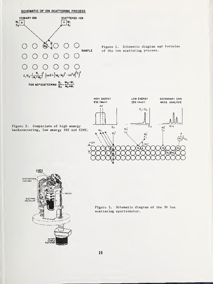
SCHEMATIC OF ION SCATTERING PROCESS
PRIMARY ION SCATTERED ION
Mi
o o ©40 o o000000 SAMPLE
Figure 1. Schematic diagram and formulae
of the ion scattering process.
OOOOO9E.'£.-(.-,"y'(-"t,"'"''
,! -'i,!,]
V!
f
E| M 2 -M,FOR 90* SCATTERING
E 0 M 2 +M,
Figure 2. Comparison of high energybackseat tering, low energy ISS and SIMS1
HIGH ENERGYISS (MeV)
AE
LOW ENERGYISS (KeV)
SECONDARY IONMASS ANALYSIS
SAMPLETURRET
Figure 3. Schematic diagram of the 3M ion
scattering spectrometer.
25
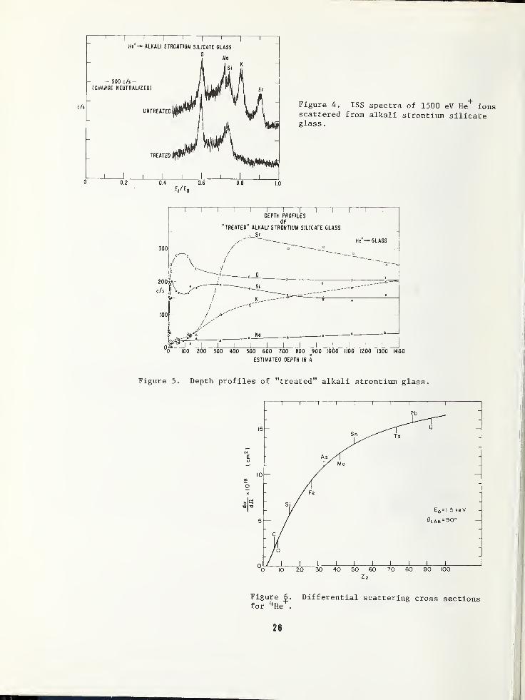
Figure 6. Differential scattering cross sectionsfor 4 He .
21
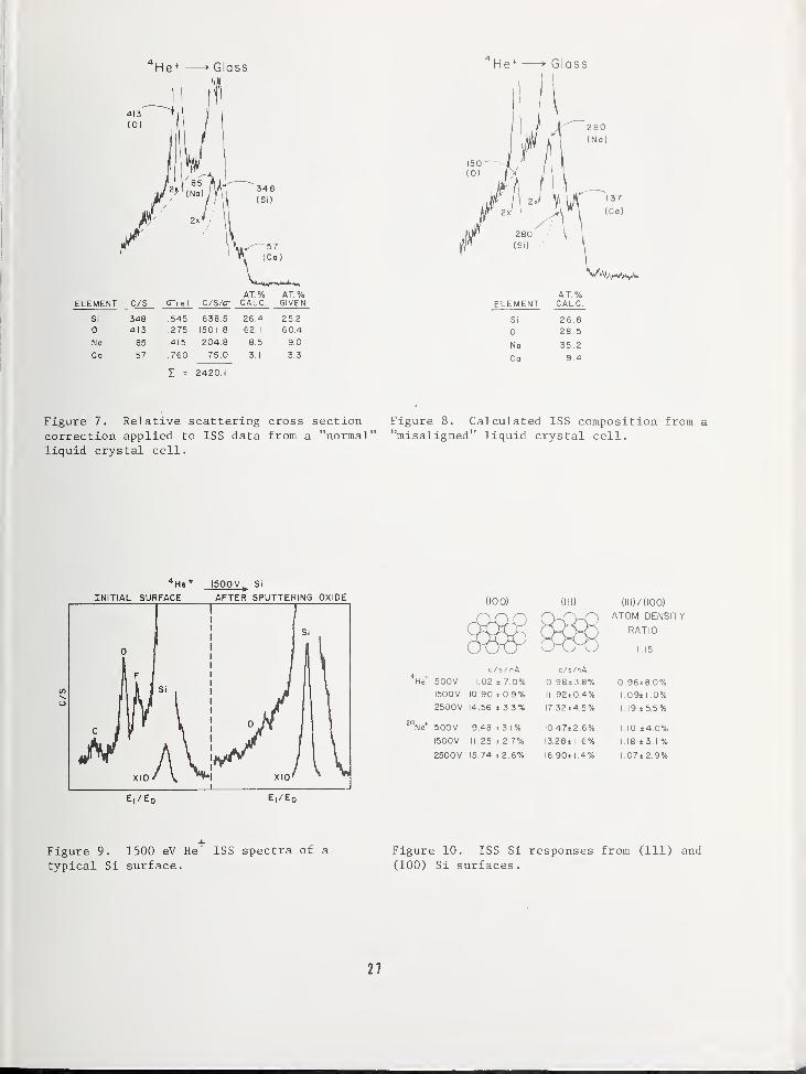
Figure 7. Relative scattering cross section Figure 8. Calculated ISS composition from a
correction applied to ISS data from a "normal" "misaligned" liquid crystal cell,
liquid crystal cell.
4 He + ISOOV^ Si
INITIAL SURFACE AFTER SPUTTERING OXIDE(100)
c/s/nA
500V 1.02 t 7 0%1500V 10.90 t 0 9%2500V 14.56 ± 3.3%
500V 9 48 i 3 I %
1500V 11.25 ± 2 7%
2500V 15.74 ± 2.6%
c/s/nA
0 98±3 8%II 92±0.4%
17 32±4.5%
I0.47±2.6%
I3.28t 1,6%
I6.90i 1.4%
(lll)/(IOO)
ATOM DENSITY
RATIO
1.15
0.96±8.0%
09tl.0%
19 t 5.5 %
10 i 4 0%18 ±3.1 %07±2 9%
E,/Er E|/E 0
Figure 9. 1500 eV He ISS spectra of a
typical Si surface.
Figure 10. ISS Si responses from (111) and
(100) Si surfaces.
27
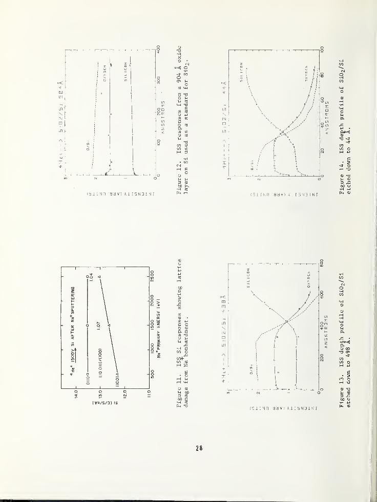
(si
r
nd 'a y v> ai r sni 1 n r
QJ
•HXQ
CMo<; Q
*H
oo
cd
£ *do }_)
cd
'Oa
0)
0) jjCO CO
£o cd
D-i
CO CO
CD cd
J_l
""OXJ~) cu
CO
H•HC/3
Csl
T—
1
CO
CU
D CU
00•H cd
H (5itNn-ayv)Aii5N3iNr
COCO oH 4-1
~* 0rH
QJ "0M cu
3 -c60 o•H 4-)
Fn QJ
00a•H
OJ!w
Ul
cu
(VU/S/D) !S
CO 4-J
c co cu
CX ECO T3CU Uu cd
,£>
•H eco ooU0+co cu
\-t
eo
rH uH 4H
CU cu
S-i bO3 a00 6•H cfl
fn
ICON
z
\
>
a
/
\/ /
//;
Ul
a
(SlINn 8MV) A1I5N31NI
•HCO
Csl
O•Hco
MHo
CU
rH•HMHOUa.
cxcu COT)
COCO o1-1 4-1
(3
3CO orH T3
cu -aM 0)
3 fi00 CJ
•H 4J
Fk CU
28
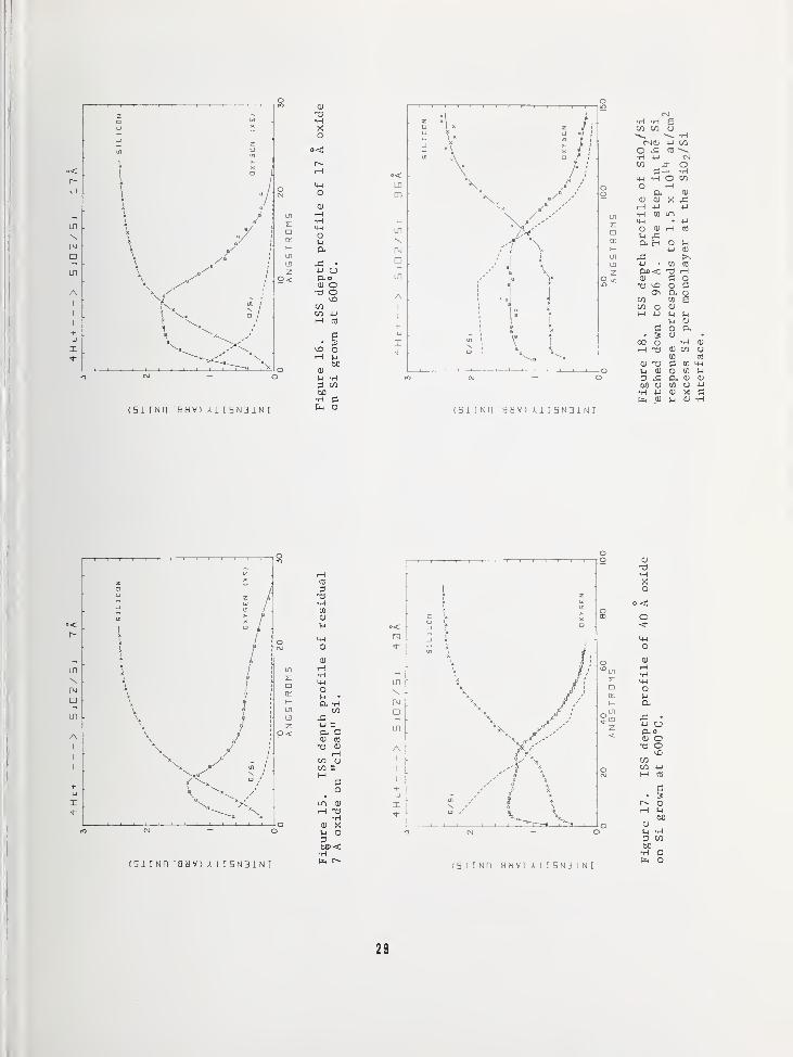
< 5 1 I N n '8MV> A 1 r 5N3 1 N
I
<u
XI•HXo
o
cu
tH•HU-J
Ouax: •
w ud,o0) o-a otoC/3 4Jl-l CO
vD Or—i UMCD
U -i-l
3 C/3
t)0
•H CO
*H *H
•HCNCU C/3
•H -i-f OJ
hJ1
1 | Q C/3
cu
O <U rj
* lO
1
i r-f-1 pi—
H
rrt
oU ^ o c
oCO CO £en o 0)M -U J-i u
M CU
a O• s O
00 o CU
CU CO aCO CD
CO T3 C CO "4-1
i-i OJ O CO ucu cu
oo o CO CJ 4Jcu X c
cu u a)
(sirNn 'aavi ai r 5N3i n r
CO
x>
(5 1 I Nfl '8cJV> A 1 I SN3 1 N f
•H10
0)
(J
y-i
o<u
iH•Hiwouo. •H
C*>
x:4J
(X "sCU CO
T) CU
HC/3 _CJ
rtCO
m CU
.H xt•H
CU
!-i o3o8><;•H
( 5 1 [ N n '8 U V> A 1 [ SN3 1 N f
28
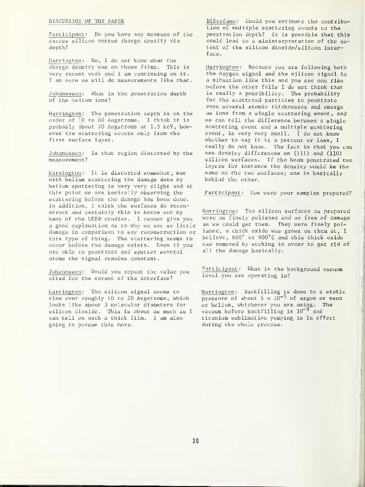
DISCUSSION OF THE PAPER
Participant : Do you have any measure of theexcess silicon versus charge density viadepth?
Harrington : No, I do not know what thecharge density was on these films. This is
very recent work and I am continuing on it.
I am sure we will do measurements like that.
Johanessen : What is the penetration depthof the helium ions?
Harrington : The penetration depth is on the
order of 10 to 60 Angstroms. I think it is
probably about 20 Angstroms at 1.5 keV, how-ever the scattering occurs only from thefirst surface layer.
Johanessen : Is that region distorted by themeasurement ?
Harrington : It is distorted somewhat , butwith helium scattering the damage done byhelium sputtering is very very slight and at
this point we are basically observing the
scattering before the damage has been done.
In addition, I think the surfaces do recon-struct and certainly this is borne out bymany of the LEED studies. I cannot give youa good explanation as to why we see so littledamage in comparison to say reconstruction orthis type of thing. The scattering seems to
occur before the damage exists. Even if youare able to penetrate and sputter severalatoms the signal remains constant.
Johanessen : Would you repeat the value youcited for the extent of the interface?
Harrington : The silicon signal seems to
rise over roughly 10 to 20 Angstroms, whichlooks like about 3 molecular diameters for
silicon dioxide. This is about as much as I
can tell on such a thick film. I am alsogoing to pursue this more.
DiStefano : Could you estimate the contribu-tion of multiple scattering events to thepenetration depth? It is possible that thiscould lead to a misinterpretation of the ex-tent of the silicon dioxide/silicon inter-face .
Harrington : Because you are following boththe oxygen signal and the silicon signal ina situation like this and you see one risebefore the other falls I do not think thatis really a possibility. The probabilityfor the scattered particles to penetrateeven several stomic thicknesses and emergeas ions from a single scattering event, andwe can tell the difference between a singlescattering event and a multiple scatteringevent, is very very small. I do not knowwhether to say it is a percent or less, I
really do not know. The fact is that you cansee density differences on (111) and (110)silicon surfaces. If the beam penetrated twolayers for instance the density would be thesame on the two surfaces; one is basicallybehind the other.
Participant : How were your samples prepared?
Harrington : The silicon surfaces as preparedwere as finely polished and as free of damageas we could get them. They were finely pol-ished, a thick oxide was grown on them at, I
believe, 600° or 900°C and this thick oxidewas removed by etching in order to get rid ofall the damage basically.
Participant : What is the background vacuumlevel you are operating in?
Harrington : Backfilling is done to a staticpressure of about 5 x 10~5 of argon or neonor helium, whichever you are using. Thevacuum before backfilling is 10 andtitanium sublimation pumping is in effectduring the whole process.
30
NBS Special Publication 400-23, ARPA/NBS Workshop IV, Surface Analysis for Silicon Devices,held at NBS, Gaithersburg
, Maryland, April 23-24, 1975 (Issued March 1976)
SURFACE ANALYSIS BY SECONDARY ION MASS SPECTROSCOPY TECHNIQUES
Robert D. Dobrott
Materials Characterization LaboratoryTexas Instruments Incorporated
Dallas, Texas 75222
The secondary ion mass spectrographic tech-nique implies a source of primary ions, a
source of secondary ions and a spectroscopicmethod of analyzing the latter. Figure 1 is
an artist's conception illustrating the pri-mary and secondary ions referred to in thispresentation. The primary ions in the col-limated column are normally generated from a
gaseous ambient either by dc or rf fields orin separate sophisticated ion guns such as
duoplasmatrons . These primary ions thencollide with the solid surface which resultsin the sputter process which in turn givesrise to a plasma containing positive andnegative ions, neutral atoms and moleculeshaving the composition of the solid surface.These sputtered ions are the secondary ionswhich are analyzed by mass spectroscopy.Figure 1 also illustrates the 20 angstrompossible escape depth of a secondary ionwhich defines the minimum surface depth.
The remainder of this presentation will be
restricted to the three types of commerciallyavailable instruments. Figure 2 is a sche-matic of the ARL QMAS system. Primary ionsare generated in the duoplasmatron , acceler-ated to 10 kV in the gap between the anodeand pickup electrode, and focused onto thesample by the primary lens. The sputteredsecondary ions are accelerated by the samplevoltage back through the extraction lensinto a spherical electric sector where theyare energy separated. The ions are thenmass analyzed by a quadrupole mass spectrom-eter and detected by ion to electron con-
version-scintillator-photomultiplier tech-nique. The quadrupole mass analysis schemeis illustrated in figure 3. A dc field ap-
plied to opposite poles is superimposed witha radio frequency field. This oscillatingfield will then start the ions oscillatingbetween the poles. At any specified fre-
quency only ions of a given mass will undergostable oscillation which is necessary for
them to pass through the length of the field
without being collected by the electrodes.The mass is selected by choice of both the
dc field and the radio frequency field.Mass spectra are recorded by continuouslyvarying both fields keeping their ratiosconstant. Figure 4 shows a portion of a 1
ppm boron doped silicon spectrum taken withthis instrument. 2 The boron 10 peak shows
that the sensitivity is well into the sub-ppmregion. This spectrum also shows the massresolution is sufficient for most inorganicanalysis
.
Figure 5 is a schematic of the Cameca ionmicroanalyzer . This instrument is unique inthat it uses a magnetic prism for mass analy-sis which acts as an ion emission microscopeas well as a microanalyzer. The primary ionsare generated in the duoplasmatron and focusedonto the sample. The secondary ions are ac-
celerated and picked up by an electrostaticimmersion lens. These ions are then mass ormomentum analyzed in the first leg of themagnetic prism which has both radial andtranverse focusing properties. The ions aredirected towards the electrostatic mirrorwhere only ions with an energy below a pre-selected threshold are reflected back throughthe aperture into the second leg of the mag-netic prism. This leg of the magnetic prismreproduces the single mass ion image of thespecimen surface on the ion to electron imageconverter where the electrons can be used forfluorescing a screen, exposing a film or
activating a scintillator for photomultiplierdetection. A given mass can be preselectedby using the appropriate magnetic field, or a
complete mass spectra can be recorded bysweeping the magnetic field. Figure 6 is a
photograph of this instrument. The ion-gunand sample are to the left of the magneticprism, and the ion to electron converter,fluorescent screen and photomultiplier to the
right
.
Figure 7 shows the scheme of the third typeof instrument. This is the block diagram of
the ARL ion microprobe mass analyzer instru-ment. The primary ions are generated in the
duoplasmatron and accelerated to the primarymagnet where they are mass separated. Theselected ions are then focused onto the sam-
ple with a condenser-objective electrostaticlens combination. The secondary ions are
accelerated to the pickup electrode, focused
by a retrofocal lens, energy analyzed with a
spherical electric sector, and mass separatedby the secondary magnet system. The mass of
interest is allowed to pass through the slit
where the ions are detected with the ion-
electron conversion-scintillator-photomulti-plier combination. Mass spectra are obtained
31
by sweeping the magnetic field. Ion imagesof a preselected mass are obtained by ras-tering the primary beam on the sample andusing the photomultiplier current output to
modulate the brightness of a CRT by synchro-nizing the raster with the primary beam.
Figure 8 is a photograph of the ARL-IMMAinstrument. This particular one is the in-
strument in our laboratory at Texas Instru-ments. The duoplasmation and primary magnetare to the right in the main console and thesecondary ion analyzer system is to the left.
The data collection system is interfaced to
a Texas Instruments 960A computer (installedin the top rack on the left console) . The960A can drive a digital plotter which hasbeen used to generate most of the data fig-
ures in this presentation.
This introduction to the instruments, whichis by no means complete, is only intended to
cover the general principles; let us go on
to their application to surface analysis.No review of secondary ion mass spectroscopywould be complete without showing Anderson'sfamous figure 9 depicting the ion yieldcomparison between the kinetic and chemicalionization processes.
+The curve on the left
is the ion yield of Al as a function of
sputter time (or depth) . Note that the ionyield falls off dramatically as the surfaceoxide is sputtered away. The curve on theright is a repeat of the same experimentusing 02
+ as the sputter beam. Here thesurface yield is high; then the yield takesa small dip, and then returns to the highsurface point after about 40 seconds of
sputtering. The conclusion is that in bothcases the surface yield is primarily the re-sult of chemical ionization (oxides) and in
the Ar"*" case the mechanism quickly convertsto kinetic ionization. For the O2 beamthe dip is related to a combination of
kinetic and chemical ionization which be-comes completely chemical when the sputtereddepth reaches the original primary ion im-
plant depth. This experiment has lead to
the widespread use of oxygen as the primaryion sputter beam while maintaining a rela-
tive high partial pressure of oxygen nearthe sample surface.
Figure 10, also from Anderson's 1 work, showsthe relative intensities of secondary ions
obtained from pure metals using an 0~ sputterbeam. From this table Al appears to be themost intense, and noble metals representedby Au the least intense. This chart, eventhough taken from the pure metals, does cor-relate moderately well with the sensitivitiesdetermined for these elements in the siliconor silicon oxide matrix. However, for bulktype analysis in silicon, the ordinate is
from 1 ppb to 10 ppm going from top to bottom.This illustrates that secondary ion massspectroscopy is a very sensitive techniqueeven when material quantities are small, as
is the case in surface analysis.
Figure 11 is a series of spectra taken from a
silicon surface with identical primary 02+
beam density, with the analyzed surface depthcontrolled by either rastering the primarybeam or moving the sample. The calculatedsputter rate for these spectra was about50 A/sec. As can be seen in these spectra,by far the most sensitive method in surfaceanalysis is to move the sample and therebyconstantly expose a fresh area to the primarybeam. In this spectrum the carbon, hydrocar-bon fragments, sodium, potassium and calciumpeaks are quite pronounced. The 400 micronraster spectrum does show the same peaks butnot nearly so intense. Also, note that theoverall intensity is reduced, which tells us
that the whole spectrum was recorded in theregion between the surface and primary ionimplant depth. The 50 micron and stationaryspectra both suggest the surface is quiteclean with only traces of Na and K appearing.I have not labeled the peaks on these spectrasince the point I wish to make is the numberof peaks and their relative intensity. How-ever, if you care to do some quick mentalexercises, I will remind you Si ha.s 3 isotopesat mass 28, 29, and 30, and Si related peakswill always appear as groups of three to fivepeaks. Also, you may note that the Si02group at mass 60 (spectra shifted to theright) are prominent in the 50 micron andstatic beam spectra. This, along with thehigher intensity, tells us that the spectrawere recorded after reaching the implantdepth. This molecular spectra is character-istic of structural chemical bonding and hasbeen investigated by several of my Europeancolleagues for surface fingerprint spectra.Other techniques such as decreased beam in-
tensity or faster recording could have beenused to insure the surface wasn't sputteredaway before the entire spectra was recorded,but it must be remembered that sensitivity is
directly related to ions/sec delivered to thedetector, and that a little integration goesa long way at the low end.
Figure 12 is the analysis of various fractionsof a monolayer of Ag deposited on a Si sur-face. The monolayers were deposited byelectroless deposition from an aqueous sol-ution which contained *
1*Ag tracer ions.
^
The coverage was then determined by gammacounting the tracer on the Si slice afterdeposition. The analysis was done with a 20
kV, 15 nanoamp, 10 micron, 02+ beam rastered
to a 200 x 160 micron area. By electroniccounter gating synchronized with the primary
beam raster, the count acceptance area wasrestricted to the central 1/4 of the craterbottom. The depth assignments were made bymeasuring the total crater depth with opti-cal interferometry and assuming a uniformsputter rate. This family of curves allshow the same trend, a very intense surfacepeak rapidly falling off before the 50 ang-stroms depth, then increasing slightly as
the primary ion implant depth is approached,and then taking a second sharp decrease to aconstant level well above background. Theseshapes show that much of the surface Ag is
knocked into the silicon by the primary ionbeam, hence, the second rapid decline. Thisis bad if we were interested in a concentra-tion depth profile, but actually beneficialin a surface analysis since it does contrib-ute to detectability time for quantitativeanalysis. However, if we are struggling forquantitative analysis, which is every massspectroscopist 's impossible goal, we wouldlike to minimize this knock-on effect eventhough it is only 1 part per hundred. Fig-ure 13 is an attempt to reduce the knock on,
or at least the depth, by lowering the pri-mary ion energy. The general trend doesshow that the second sharp drop is indeeddecreased as the energy is reduced. Onlythe 12 kV curve violates this trend and is
probably in error. The actual depths forthese curves were extremely difficult to
measure and could easily be as much as 100%in error. One final point to note on thesecurves is that only the 20 kV curve shows a
positive slope after the first surface drop.
This results from the decreased sputterrate, with the lower energy beams allowingthe ambient oxygen to keep a constant sur-face oxide throughout the analysis. Figure14 is a closer look at the surface region as
a function of primary ion energy. The setillustrates that even in the worst case at20 kV, we will have collected about 90% of
the integrated intensity before 50 angstromshave been sputtered away. Consequently,this illustrates that for quantitative sur-face analysis by secondary ion mass spec-trometry, it will probably be for only onemass per area sputtered. If the area is
limited such as on a small signal diode,this can be a severe limitation. However,on pilot slices, which encompasses most of
my work, the problem is not limiting as it
can be overcome by continual movement of thesample. Figure 15 is one last look at thecurves as a function of primary ion energy.These are the same curves as Figure 13, butnow the abscissa is plotted as a function of
time. This set shows that for qualitativeanalysis, as much as 10 minutes was avail-able to detect the Ag which was present atabout 5% of a monolayer.
Figure 16 shows how quantitative the resultsshown back in Figure 12 were. The line is aleast squares fit to the five points indica-ted. Each point represents the total inte-grated count under the respective curve, withthe base line taken where the curve leveledoff after the second sharp drop. This empir-ical calibration curve is very encouragingeven though two of the low points are off byas much as 100%. No correction was made forion pick-up efficiency by means of a matrix-ion and this is known to vary by as much as
50% from sample to sample. This study doesshow that given a set of standards, and I be-lieve that bulk standards can be used,secondary ion mass spectroscopy surface anal-ysis can be empirically quantitated, providedthe surface impurity concentrations are nothigh enough to drastically alter the effectivematrix which controls the ion yield efficiency.
Figure 17 turns the topic over to the analysisof Si02 surfaces, whereas up to now I haveconcentrated on silicon surfaces. This is a
series of spectra taken under various condi-tions on a 10,000 angstrom thick oxide film.The oxide was not coated with a conductivefilm, as would be the normal practice forbulk or in depth analysis, since this wouldmask the surface of interest. As can be seenfrom this set of spectra the use of a positivebeam on a naked sample gave only a few peaks,none of which are normal patterns expectedfrom a Si02 matrix. The absence of a spectrais the result of a high positive chargebuildup at the point of impact by both the
positive ion beam and loss of secondary elec-trons. Also, without a conductive surfacecoating there is insufficient bias on thesample surface to accelerate and direct thesecondary ions to the pickup electrode. Thenegative beam on the naked sample does showthe silicon peaks but they are very weak.This does show that the secondary electronloss is compensated by the negative primaryion which allows the point of impact to come
to an equilibrium state. The absence of theremainder of the spectrum here is entirelydue to the absence of the accelerating samplebias. The two spectra on the right weretaken through the open areas on a 300 meshelectron microscope copper grid which waselectrically connected to the 1500 volt sam-
ple bias. The primary beam was rasteredrapidly over both the copper bars and the
openings. The theory is that the primarybeam bombarding the copper emitted sufficientlow energy secondary electrons, which neu-tralized the positive charge on the Si02surface and provided the necessary secondaryion accelerating potential as well. Thesespectra do show that the mechanism works;both positive and negative beams give
33
satisfactory spectra. However, these electro-plate formed copper grids are not noted for
their purity, so a much more pure grid mustbe employed to render meaningful results.Grids formed by e-beam evaporation of highpurity Al or Au should be excellent. Thisdiscussion only applies to oxide films
greater than 1500 angstroms thick. Thinneroxides behave the same as bare silicon.Therefore, when searching for the source of
contaminants, such as furnace tubes, theoxide thickness should be kept below about1200°C which just happens to be the gateoxide thickness of most MOS devices.
No presentation concerning oxide analysiswould be complete without illustrating the
mobile ion problem shown by Ron Baxter 4 in
Figure 18. These profiles were taken on the
same sample using both a positive and nega-tive beam. The conclusion is that using a
positive beam, the Na all moves to the inter-face and with a negative beam, it is alldrawn to the surface. The grid techniquemay help this problem as well, but to datethe grid itself has been the dominant sourceof sodium.
To summarize this presentation, a look at
secondary ion mass spectroscopy with respectto five criteria for surface analysis is in
order.
1. Accuracy of Chemical Analysis
The qualitative analysis was shown to bevery good and the Ag experiment showedquantitative potential is fair.
2. Surface Sensitivity
The sensitivity has been shown to be as
good as a few ppm.
3. Non-Destructive Analysis
The method is totally surface destructive.
4. Selected Area Chemical Analysis
Can be very good depending upon instru-ment .
5. Experimental Complexity
Secondary ion mass spectroscopy is oneof the most complex analytical techni-ques in use.
Therefore, for surface analysis, secondaryion mass spectroscopy has not yet reachedthe ideal, but it has demonstrated itself tobe one of the more powerful techniques.
REFERENCES
1. Anderson, C. A., International Journalof Mass Spectrometry and Ion Physics2, 61 (1969).
2. Fralick, R. D., and Roden, H. J., ASMSCommittee VII Workshop, 22nd Annual ASMSConference, Philadelphia, (May 1974).
3. Larrabee, G. B. , unpublished work, TexasInstruments Incorporated, Dallas, Texas.
4. Hughes, H. L., Baxter, R. D. , and
Phillips, B., IEEE Trans. Nucl. Sci.NS-19 , 256 (1972).
34
ION MICROPROBE
ION BEAM
9
0 •
oO fP
oo°G o
O oo oo°>°o°°o ° o Oo °OoQ
°ooonooo0°
TO MASSSPECTROMETERo
i
O
^3 »O
I20A
Figure 1. Artist's conception of thesecondary ion production process.
35
37
ALUMINUM
50 100
TIME (SEC )
38 n +
J L
50 100
Figure 9. Sputter yield comparison for
kinetic and chemical ionization mechanism.
Accel, potential 11 KVSample current 4 * 10~ 9 AProbe size 20 ym2
Figure 10 (below). Relative yield of some positive ion intensities from pure metals.
0.0)40 50
Z ATOMIC NUMBER
90
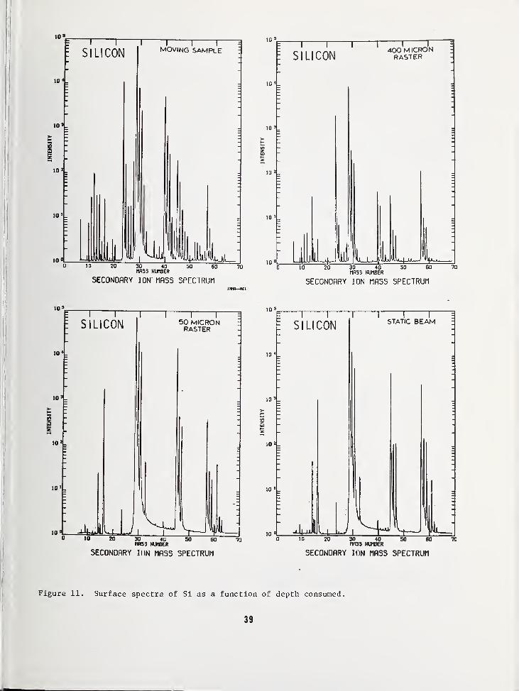
10 »
SECONDARY ION MASS SPECTRUM
10'
10 *
5 .
10 2
10 0
~~i
1 r
SILICON400 MICRONRASTER
0 10 20 30 40nflSS NUMBER
SECONDARY ION MASS SPECTRUM
10 s
10*.
10
i i r
SILICON
8 :
i .
10»_
10
10 1_0 10 20
50 MICRONRASTER
SECONDARY II IN MASS SPECTRUM
10'.
io 2 _
10 0
~~i
r~SILICON
Jul
—i rSTATIC BEAM
10 20 30 40 SO 60HR33 NUMBER
SECONDARY ION MASS SPECTRUM
Figure 11. Surface spectra of Si as a function of depth consumed.
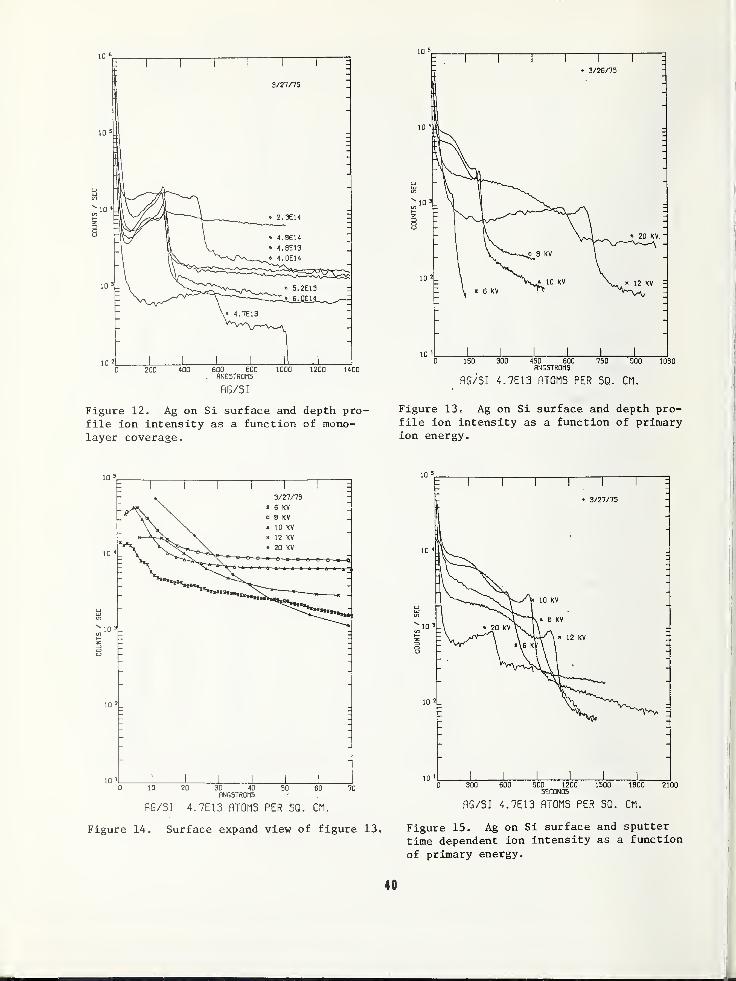
10 5
'10 *
10'
102
i1
1 r
3/27/75
J ] U J_200 400 600 800 1000 1200 1400
, ANGSTROMS
RG/S]
Figure 12. Ag on Si surface and depth pro-
file ion intensity as a function of mono-layer coverage.
450 600ANGSTROMS
900 1050
AG/SI 4.7E13 ATOMS PER SQ. CM.
Figure 13. Ag on Si surface and depth pro-file ion intensity as a function of primaryion energy.
1 1 1 1 1
3/27/75
i 6 KV
\ o 8 KV
» 10 KV
\ « 12 KV:
^jb--0\ • 20 KV
3
?
1
1
30 40ANGSTROMS
0 10 20
AG/SI 4.7E13 ATOMS PER SQ. CM.
Figure 14. Surface expand view of figure 13.
0 300 600 900 1200 1500 1800SEGON0S
AG/SI 4.7E13 ATOMS PER SQ. CM.
2100
Figure 15. Ag on Si surface and sputter
time dependent ion intensity as a function
of primary energy.
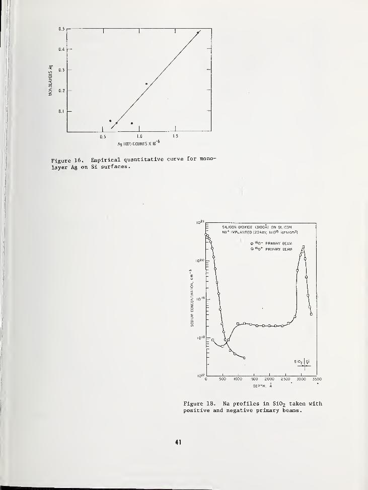
0.5 1.0 15
Ag (107) COUNTS X I0"6
Figure 16. Empirical quantitative curve for mono-
layer Ag on Si surfaces.
Figure 18. Na profiles in SiC>2 taken withpositive and negative primary beams.
41
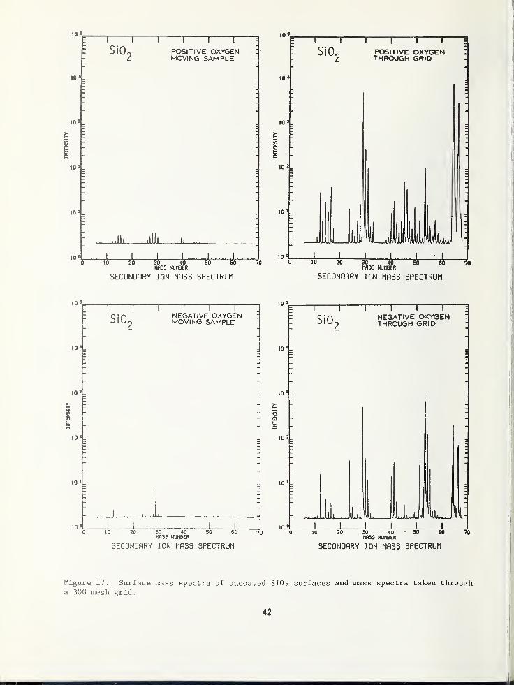
10 *_
10 »_
i r
Si0oNEGATIVE OXYGENMOVING SAMPLE
_j iJbu
10 20 30 40MASS NUMBER
SO 60
SECONDARY ION MASS SPECTRUM
10
10 4
10'
10
SiO,
i 1 1 r~NEGATIVE OXYGENTHROUGH GRID
30 40rtflSS NUMBER
SECONDARY ION MASS SPECTRUM
Figure 17. Surface mass spectra of uncoated Si0 2 surfaces and mass spectra taken througha 300 mesh grid.
42

DISCUSSION OF THE PAPER be accompanied by a corresponding dip in the
silver signal?
Participant : I did not understand what yousaid concerning the appearance of the Si02peaks in the silicon.
Dobrott : The Si02 peak appeared in thesilicon analysis after the initial oxide sur-face was removed simply because I was ana-lyzing the silicon dioxide formed at the im-plant depth of the primary oxygen beam.
Participant : Could you have avoided that
problem by using 180 instead of 1^0 as theprimary ion?
Dobrott : There was no mass interferenceproblem. I made that observation to point
out the sample depth at which that particularspectrum was gathered.
Morabito : Should not that dip in the Si02
profile, due to the primary oxygen implant,
Dobrott : The silver profiles determined at
lower primary ion energies did not really dip,
they went down and never regained; probablybecause of the proximity of the initial im-
plant depth and the surface. The higherenergy profiles dipped and recovered probablydue to the implantation process.
Participant : In the silver case did youassume the silver was uniform, or could it
have formed islands, or what?
Dobrott : We assumed that there was a uniformdeposition of silver. The analysis was doneto see if we could correlate the known amountof low temperature electroless deposited sil-ver on the surface with what we get when wesputter it all away, and to see how quicklythis could be done. Yes, the silver couldhave formed islands, we do not know that it
did not.

NBS Special Publication 400-23, ARPA/NBS Workshop IV, Surface Analysis for Silicon Devices,held at NBS, Gaithersburg, Maryland, April 23-24, 197.5 (Issued March 1976)
SOME EFFECTS LIMITING SIMS DEPTH PROFILE ANALYSISAND METHODS FOR IMPROVEMENT
Robert K. Lewis
Cameca Instruments, Inc.Elmsford, New York 10523
INTRODUCTION
Secondary ion mass spectrometry (SIMS) hasproven to be a very attractive method for
obtaining surface and bulk concentrations of
materials used in semiconductor device tech-nology. The popularity of SIMS has resultedprimarily from the fact that the method hasthe sensitivity necessary to detect dopinglevel concentrations, namely 10+ -'-^ to I0+17
atoms/cm-^, and the ability to produce depthprofiles at these concentration levels. 1>2
The disadvantage of being a destructivemethod is readily offset by the inherentdepth analysis capability which results fromthe sputtering action of the primary beam.It is this depth profiling capability, in
fact, that has provided the principal inter-est in SIMS for analyzing semiconductor ma-terial and the technique is now widely usedfor characterizing these materials. However,there are problems with SIMS depth profilingwhich must be taken into consideration.This paper discusses some of the effectswhich have been encountered and tend to
limit the usefulness of the technique anddescribes methods to minimize them. Theseeffects have been summarized in Table I.
DEPTH RESOLUTION
To achieve good depth resolution it is ob-vious that the surface of the crater bottommust be maintained as flat as possible.With normal or non-normal incidence of theprimary beam a high degree of flatness canbe easily maintained by rastering the beam.Schematic diagrams of craters produced bynon-rastered and rastered beams are shown in
Figure 1 and Figure 2. Figure 1 shows that
with a non-rastered beam, 250ym in diameter,incident at 45° (this is approximately thebombarding angle in the Cameca IMS 300 in-
strument used for this study), and a gaussiandistribution, the flatness variation over a
typical selected area (50ym) is approxima-tely 200 A. This is adequate for many depthprofiles. However, if the beam is rasteredas shown in Figure 2, the flatness over thearea selected for analysis can be greatlyimproved. We have established that thevariation in flatness can be less than 40 Aover an area of lOOym to depths of about1,000 A by bombarding amorphous Ta205 and
using the technique of observing the variationin color of fringes produced in white light.
1
This would give a value of less than 5% forthe variation in depth divided by the totaldepth sputtered. This value is consistentwith the R value found by Werner 3.
It is clear that ions sputtered from thecrater wall must be rejected to have gooddepth resolution. This is easily accomplishedin the Cameca ion microscope by mechanicallyaperturing in an image plane or in an ionprobe by electronic gating (turning off thesecondary detector when the primary beam is
on the crater wall) . Mechanical aperturingis shown schematically in Figures 1, 2, and16. With electronic gating the primary beammust be kept smaller than that required withmechanical aperturing. This tends to limitthe maximum average beam density obtainableand consequently the maximum sputtering rateavailable with ion probes.
If the sample surface does not sputter awayevenly because of a lateral variation in
sputtering rate, the depth resolution willsuffer accordingly. Lateral variation in
sputtering rate results from different lat-tice orientations encountered by the primarybeam from grain to grain in polycrystallinematerial or from different lattice structureswhen different phases are encountered. Forthis reason the depth resolution attainablein such material is usually only ten to
twenty percent of the total depth sputtered.Continuously rotating the sample while sput-tering could reduce the lattice orientationeffect; however, no commercial instrumentspresently provide this capability. Whenlateral differences in orientation or in
phase are encountered the use of an oxygenleak can sometimes minimize the variation in
sputtering rate.
Channeling (lattice effects) in SIMS havebeen described by Slodzian and Bernheim^.This is a variation in ion yield that occurswhen the incident beam traverses transparentand opaque directions in the lattice. A plotof secondary ion intensity versus the angleof rotation is shown in Figure 3. Fortunate-ly, this effect is only a second order effectso it is generally not a problem in depthprofiling. However, it is important to be
45
aware of the fact that it can cause errorsespecially when comparing samples. A methodof minimizing the effect is to bombard thesurface with a stream of oxygen (oxygen leak)
.
This produces a less severe variation in ionintensity with orientation as shown by the
dotted line in Figure 3. Slodzian haspointed out that the effectiveness of theoxygen leak is determined by whether the sur-face oxide formed is crystalline or amorphous.
"Knock on" is the redistribution that occursfrom the physical driving in and sub atomicmixing of the atoms being analyzed. The ef-fect has been shown by McHugh^ analyzingTa2C>5 which had an approximately 50 A thickphosphorous layer located 230 A below thesurface. His results are shown in Figure 4.
The effect is significant only at high pri-mary bombardment voltages (above about fivekilovolts) . The effect would be less, of
course, at a higher angle of incidence. Theangle of incidence can be changed for non-normal incident primary beams by changing thepolarity of the primary beam. The combina-tions positive primary-positive secondary andnegative primary-negative secondary give thehighest angles of incidence.
DETECTION SENSITIVITY
One of the most serious problems encounteredin SIMS is the mass interference from the
complex polyatomic species produced by thesecondary ion process. These species areformed from the clusters of the matrix atomsformed by the sputtering action of the beam(e.g., M, M2, M3,...) and combinations withthe primary ion when a reactive gas such as
oxygen is used (e.g., MO, M02....M20, M2O2,. . .etc.)
.
Typical spectra produced when bombardingsilicon with a reactive gas (oxygen) is
shown in Figure 5 due to Evans^. It can be
seen that the problem of mass interferenceis more severe at the higher masses. This is
just the opposite of the ion productionprocess in spark source mass spectrometry(SSMS) where the interferences are more con-
centrated in the lower mass region of themass spectrum. This is because in the sparksource the energy available is much higherwhich breaks up the clusters and creates manymultiply charged ion species.
The simplest method for minimizing massinterference from the polyatomic species is
to take advantage of the large differences in
energy distribution between the polyatomicand monatomic species. These distributionsare shown in Figure 6 which is fromSatiewicz^. It can be seen that the complex
polyatomic species can be rejected perfer-entially over the monatomic species by re-jecting the low energy ions.
The low energy ions may be rejected in theCameca instrument by using the low energydiscriminator (L.E.D.) shown in Figure 7 orby appropriate adjustment of the electro-static analyzer when the double focusing ar-rangement shown in Figure 8 is used. Re-jection of the low energy ions with the ESAis possible because the double focusinggeometry used has a first order directionfocus position such that slits can be usedto precisely define the energy limits ac-cepted. The SIMS instruments designed by
Herzog et. al. (GCA) 8 and Tamura et. al.
(Hitachi) ^ have this feature while the ion
probe SIMS instruments described by Liebl(ARL) 10 and Banner et. al. (AEL) 11 do not.
The attenuation of the silicon polyatomics in
the spectra shown in Figure 5 with increasingattenuation of the parent monatomic peakusing the L.E.D. on the Cameca instrument is
shown in Figure 9. A typical application of
the L.E.D. is shown in Figure 10. Here thedetection of arsenic using the AsO
-species
has been improved by one order of magnitude.An equally important use of the L.E.D. is
the removal of tails on the low energy sideof a mass peak. The presence of these tailscan cause a serious loss in abundance sensi-tivity (and therefore detection sensitivity)on the low mass side of intense peaks. Thisis shown for the detection of copper and zincin gallium arsenide in Figure 11. Thesetails result from the post ionization of theneutral species leaving the sample. This"kinetic" emission process has been describedby Blaise and Slodzian-^. it is not necessaryto attenuate the intensity of the peak to
eliminate the low energy tails with the L.E.D.
A second and more elegant method for elimina-ting interference from polyatomic ion speciesis the use of high mass resolution. Themethod of obtaining high mass resolution on
the Cameca instrument is shown in Figure 8.
Here the normal imaging mode path, that is
prism - mirror - prism, is interrupted and
the beam is allowed to pass through a hole inthe mirror (the mirror being displaced) into
a sperical electrostatic analyzer (ESA)
.
This combination of an ESA with the firstmagnetic deflection is an inverted Nier-Johnson double focusing configuration. Withthis .analyzer mass resolutions over 5000 havebeen achieved. It is possible with high massresolution to completely separate the inter-fering polyatomic mass peak ^' AI2 from the
->^Fe peak as shown in Figure 12 because of
the mass differences that occur. Some
46
typical elements, the possibly polyatomicinterferences, and the mass resolution re-
quired to resolve the doublet are listed in
Table II. The separation of the75As/ 29 Si 30SiO doublet at the peak and lowerlimit of the distribution, for arsenic ionimplanted into silicon, is shown in Figure 13.
A second effect limiting detection sensitivityis the contamination of the surface from theambient gas molecules in the vacuum system.At pressures around 10" 7 to 10"^ torr, whichis the typical vacuum level in commercialSIMS instruments, it can be readily demon-strated that the low current densities pres-ent in the beam periphery produce an arti-ficially high background signal. This is
because the influx of ambient gas moleculesnow competes with the primary beam and reactwith the surface where they are sputteredaway producing various interfering ionspecies. Low beam densities will always bepresent at the periphery of an ion probe.In addition there is a significant flux of
neutral atoms (neutralized ions) over a largearea outside the bombarded region that alsosputter the target surface and produce ions
from the ambient gas as shown by McHugh-'- 3 in
Figure 14. A cold plate near the samplesurface will minimize the hydrocarbon con-
tamination, but it will not eliminate it andit will have little or no effect on oxygen,nitrogen and CC^. The effect is showndramatically using the Cameca instrument bybombarding aluminum with a beam of non-reactive ions (Ar"*") . By keeping the beamdiameter less than the field of view (225um)
it is possible to see the effects of lowprimary beam density at the periphery of thebeam on the fluorescent screen as shown in
Figure 15. At the periphery there is a
marked increase in the secondary ion inten-sity due to an ion yield enhancement (chem-ical effect) from the reactive ambient gas.
By mechanically aperturing as shown in
Figure 16 and selecting areas approximately50ym in diameter at the center (Area A) and
the periphery (Area B) the spectra shown in
Figure 17 were produced. It is obviouslyimpossible to achieve a low background sig-nal without rejecting this ambient contribu-tion. The only methods that have been dem-onstrated to be effective in eliminating the
ambient contamination are lowering thevacuum below 10~ 9 Torr as Benninghoven-L^ hasshown which unfortunately is impractical incommercial SIMS instruments or the ions pro-duced outside the area of high beam densitycan be eliminated by the mechanical apertur-ing technique. However, there is no way to
avoid this effect with the electronic gatingtechnique used with ion probes.
A third effect which can limit detectionsensitivity is the phenomena of resputtering.This effect is observed when material in highconcentration near the surface at the edge ofthe crater is sputtered and the neutral par-ticles are scattered in some manner into theanalyzed area at the crater bottom. This isessentially a second order effect. It can bekept below the detection limits by usingcrater diameters much larger than the areaanalyzed. Evaporating non mass interferingmetal (e.g. gold) on the surface prior to
depth profiling can also be helpful.
ACCURACY
The most serious effects limiting the accuracyof a depth profile are those limiting theuniformity of the ion yield of the elementbeing measured or a reference element (e.g.
a matrix element) used for normalization.Any marked change in concentration of a
reactive element such as boron, carbon oroxygen can change the ion yield of elementsassociated with it. This effect is shown in
Figure 18 where phosphorous enhances theyield of the tantalum ion. It is importantto determine if such species are present byin-depth mass spectral analysis wheneverpossible, and, if present, to measure the
depth profile of the reactive species simul-taneously with the element of interest. Thisalso applies to any element being measuredfor normalization purposes. Sometimes it is
useful to check for the presence of a reac-tive element by using an inert gas as theprimary beam (e.g. argon) which does not en-hance the matrix greatly increasing thecontrast
.
Whenever a reactive primary beam is usedthere can be a marked change in the ion yieldover the first few hundred angstroms of sput-tered material (15kV bombardment) due to theimplantation effect of the primary beam as
described by Lewis et. al.-'--'. The effect is
shown in Figure 19 where pure silicon wasbombarded with 0~ primary ions and positivesecondary ions of oxygen and silicon measuredtogether. This ion yield variation resultsfrom the fact that the implanted primaryoxygen ion is first concentrated at a depthbelow the surface as shown schematically in
Figure 20. Until the sputtering front
reaches this depth there will be a variationin ion yield of all elements which are en-hanced by the primary ion. The effect is
minimized by keeping the bombardment voltagelow (below 5kV) and can be essentially elim-inated by the use of an oxygen leak as shownin Figure 21.
47
Variations in sputtering rate with depth cancause errors in depth measurements if thevariations are not taken into considerationin the sputtering rate calibrations used to
establish the depth scale. Often measurementof a matrix species and normalization againstthis signal will take care of small sputter-ing rate variations due to beam densitychanges. However, variations due to phasechanges in the sample must be determined bydepth measurements outside the instrument.If sufficient thicknesses of the material in
the individual phases are available (a fewhundred angstroms) it is possible to maketheir depth calibrations with a Talystep. If
larger thicknesses (a few thousand angstroms)are available it is more convenient to makethe measurements with a light microscopeequipped with a Michelson interferometer.
It is not unusual to encounter a situationwhere what appears to be a variation in depth(shown for aluminum in the thin film depthprofiles shown in Figure 22) is actually a
variation in lateral distribution as shown in
the ion image of Figure 23. This variationmay be real or a result of variations in thelateral sputtering rate. The lateral distri-bution effect is observed most often at
metal - metal oxide interfaces or thin filmmetallizations. It is difficult to minimizethis effect. However, its presence canusually be taken into account by observing a
series of ion images with depth.
One of the major concerns in all depthprofiling work is whether the element of in-
terest is being redistributed by the bombard-ment process. This is the case of the "knockon" phenomena described above, which wasdescribed as a second order process. Theonly first order redistribution effect ob-served to date has been for the analysis of
sodium in silicon dioxide layers. This re-
distribution occurs whenever a potential is
applied to the surface. The sodium migrates(within milliseconds) to the Si02/Si inter-face or to the sample surface depending on
whether the potential applied at the samplesurface is positive or negative as shown in
Figure 24. It is questionable whether an
accurate profile of sodium in Si02 can be ob-
tained at all since even neutral atom bom-bardment will release secondary electrons andcharge the surface. The surface to substratepotential must not exceed a few tenths of a
volt while the profile is being measured.
Fortunately this ion mobilization phenomenaappears to be a problem only for the case of
sodium in silicon dioxide. No other docu-
mented instances are known to this author.
References
1. Morabito, J. M.,and Lewis, R. K. , Anal.Chem. 45_, 869 (1973).
2. Kofkner, W. K., Werner, H. W. , Oosthoek,
D. E.,and de Grefte, H. A. M. , Rad.Effects 17, 88 (1973).
3. Werner, H. W. , Acta Electronica 18, 51(1975).
4. Slodzian, G. , and Bernheim, G. , Int. J.
Mass Spectrom. Ion Physios (1975).
5. McHugh, J. A., Rad. Effects (1973).
6. Blattner, R. J., Baker, J. E., andEvans, Jr., C. A., Anal. Chem. 46, 2171(1974).
7. Satkiewicz, R. G. , Air Force TechnicalReport, AFAL TR-69-322 (1970).
8. Herzog, R. F. K. , Poshchenrieder , W. P.,Ruedenauer, F. G. and Satkiewicz, F. G.
,
Proc. Fifteenth Annual Conf. Mass Spec-trometry and Allied Topics, Denver,Colorado, May 1967, p. 301.
9. Tamura, H. , Kondo, T. and Doi, H.
,
Advances in Mass Spectrometry, Quayle,Ed., (Inst, of Petroleum, London,1971), Vol. V., p. 441.
10. Liebl, H., J. Appl. Phys. 38, 5277(1967).
11. Banner, A. E. , and Stimpson, B. P.,Vacuum 24, 511 (1975)
.
12. Blaise, G., and Slodzian, G. , J. Phys.31, 93 (1970).
13. McHugh, J. A., to be published.
14. Benninghoven, A., Surf. Sci.
_2J5, 541(1971).
15. Lewis, R. K. , Morabito, J. M. , andTsai, J. C. C. , Appl. Phys. Lett. 23,260 (1973).
48
CDu CNI
360 rH•HPn
s0)
xiH
4) O00 C
00 a) •Hs c 4Jto •H rH
oo CU U M o X.c O 3 > 4-1
•H 4->
N 00 M 3 01
T-r C (U o in
s cfl •H (0. •H to
•H s 4-J CO CD
c •H CO a) >s UH N 00 rH rH M CJ
a a CO Pi ^£ j*i CO CO O E co CO B •H
>4H 60 •H tH CO 01 <u •Ho c C C CO iH H r< ^4
•H O CO OX) M cu 3 3o 0) jj a 4-i cu 01 M XIJS 4-1 CO 00 oo cu C4J co qj s u 3 TO
QJ k rH o X oPi w PS o o rJ
CO
X) 4JrH 30 ,a <u
t-l 00 4-> a rH1-1 e p. cu CO
a o • o CU u uo 4-1 oo rl 3 4J>H <4—
1
MH CO 34J 01 O c CO CU
cd 00 1 t-l •H cu Ca c C o CO 3 a•rl o •H rH 0) cm O CO CU
B •H l-i CJ •rl 4-1 .3 00•H 4-1 3 a CO CO 4-> 3 4-1 MM 3 4-J 3 CM rH 0) p. CO
U rH 1-1 3 M r-H X) .Q B 01 ,3CO O cu o 3 rt (U •rt CU x> CJ
•i-l CO p. « CO 3 N H rHX> cu co > >^ 4-1 01 cu CU
u cu H rH ^! CO 4-1 00 ors rH C H CU CO CO •rl 0) CO c CO
OO CO CO •rl a. 4-4 c 01 t3 > •H •H mM CO o S nj cO rH •H X> 00 uCD CO •rl 0) CO H H 4-J 01 CO 3C 0 c 4.) CO CJ cO c 0 CJ
aa CO
a) CO CO 01 CU 4J CO •HJ3 J3 H 4-1 tx H 00 •H 01 01 p00 CJ CD CO cu CO >> 3 4-1 C cu
•H 0) P O CD X O c O CU
a O CJI o a H rH
rH rH rH CN rH rH CN rH rH rH *
CD 3o O•H •H
00 B 4-1
rH 3 o CU 3rH •H 4-1 J3 CD X>cfl M CO 4-1 4-1 •H
3 CU
aCfl M
a 4-J rH rl 4-1
o (H 4-1 o o co
4-1 cu 3 "n p u 00 •H4-J 4-1 P. o MH 13 3 XIO CO (0 a rH •H-Q u M o 3 <U rl rH
CJ 3 CJ rl O •H CU Cfl
t-l •rl o <4H •H 4-1 UCU e c 4J .U 0)
4-1 o 3 cu cO 3 3 4-J
CO S-J O o 3 O d. Cfl
u MH •H 3 •rl rl cfl rHCJ 4-1 XI CU
13
CO CO
ato 3 3 3 O
MH n rl CU 4J Cfl OO •rl •H •H •Ho o M MH 3 00 3 4H
H CO oo S-i O •H Cfl CO Cfl 3CO 4J > 3 0) CJ 4-1 rl 3 3 3CO 3 •H 4-1 3 0) O o O •Hcu J3 rH rH 3 CU CU 4J H rH •H rl
c •H CO CU CU •H CJ •rl 4J 4-J 4-1 4-1 4-1
cu >-l r< 4J c CO 3 cfl Cfl Cfl Cfl
> 4-1 0) CO 3 Cfl 14H P •H •H •H •HCU 3 4-1 rl CO Cfl (-1 cfl CO )H M H X)3 0 CO J3 cO 3 CU CO cfl Cfl CD
3> c_> rJ a a tn > > >
30•H4-1
3rH0 4-1
M CO 3 rlcu CU O >4J Oh •H •H
4-J 4-1
a J3 CJ •HCfl 4J CD
aU P 4-1
CO (U 01 CU
Oh Q p
oCO
rl
3oCJ
49
TABLE II
MASS RESOLUTION REQUIRED TO SEPARATE DOUBLETSOF TYPICAL INTERFERING POLYATOMIC ION SPECIES IN SIMS
NominalMass Species M/ AM
14U
N/ 2?Si++ 1,000
27n
B16
0/27Al 1,200
4824Mg/ 8
Ti 2,200
5427.. ,54^Al / Fe
z2,300
5624Mg0
2/56
Fe 1,400
5628 ,56Z°Si
2r D
Fe 3,000
5927 A1 16n ,59„Al 0^1 Co 1,500
6028
Q .16n ,60...Si 0^1 Ni 1,700
6448^.16^ ,64„
Ti 0/ Zn 4,700
7529c .30c . n/ 75.Si SiO/ As 3,200
To Mass Spectrometer
Aperture -
SecondaryBeam
—1 1
(|(— 50/tm
I \^.// // /
45°
'<*— Primary
Beam
Sample0.017 fj.m—
'
350/im
To Moss Spectrometer
Aperture
SecondaryBeam
l/xm
RastennqPlates
— 50/im
350/xm
50/i.m
45"
PrimaryBeam
Sample
Figure 1. Crater produced by unrasteredprimary ion beam.
Figure 2. Crater produced by rasteredprimary ion beam.
0' 90' 180' 270' 360'
Figure 3. Variation in ion yield withdifferent orientations of primary beam.
Figure 4. "Knock on" redistribution from
ion bombardment
.
~\ r 1
—
1.75 keV ,60
,78 A
n 1 r-
7.75 keV l60
~i 1 r -i 1 r
18.5 keV ,60
3I P-RICH-LAYER
230 A
I60IONBEAM
//)y//A
}To2°5
200 200 400 200
DEPTH (A)
400 600
51
00001
1 1 1———
r
High Purity Silicon
Oxygen Bombardment
I- 1 i *t* I" 1
1 —i
1— " *-i" — ————1
0 10 20 30 40 50 60 70 80 90 100 110 120 130 140 ISO
Mass/Charge
Figure 5. Mass spectra of silicon polyatomics
,
0 200 400 600 800 1000 1200
INITIAL ENERGY eV—
-
Ion beam
Electro - magnet
GRID FILTER
Figure 7. Low energy discriminator grid
filter on the Cameca IMS.
Figure 6. Energy distribution of poly-
atomics .
%1
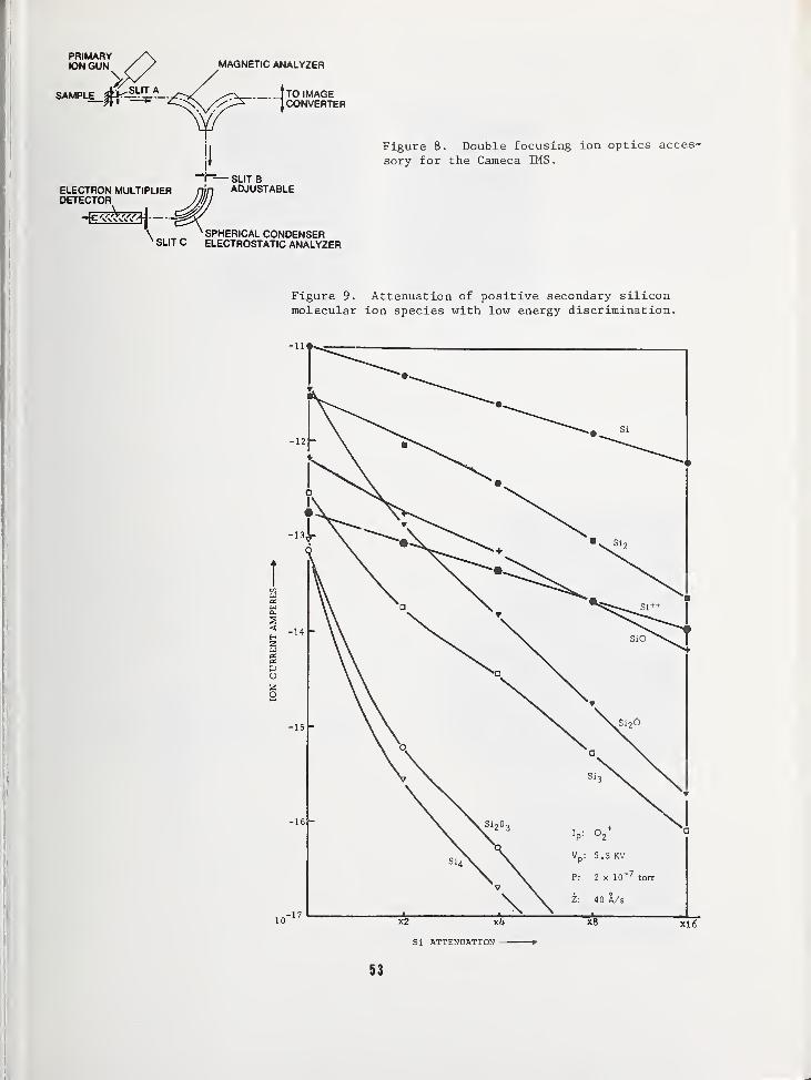
PRIMARYION GUN
VSAMPLE^b^'IA-
ELECTRON MULTIPLIERDETECTOR
ION MULTIPLIER nin"OR JJl
MAGNETIC ANALYZER
_tTO IMAGEJ CONVERTER
IT*— SLIT BADJUSTABLE
'SLITCSPHERICAL CONDENSERELECTROSTATIC ANALYZER
Figure 8. Double focusing ion optics acces-
sory for the Cameca IMS.
Figure 9. Attenuation of positive secondary siliconmolecular ion species with low energy discrimination.
Si ATTENUATION r
53
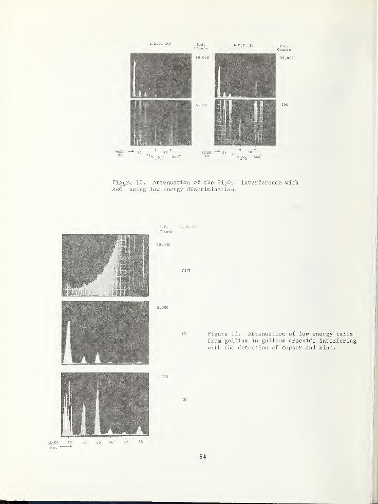
111.
mri, L In,MASS —> 85
Figure 10. Attenuation of the Si20 2 interference withAsO using low energy discrimination.
F.S. L. E. D.Counts
1,000
Figure 11. Attenuation of low energy tailsfrom gallium in gallium arsenide interferingwith the detection of copper and zinc.
^4
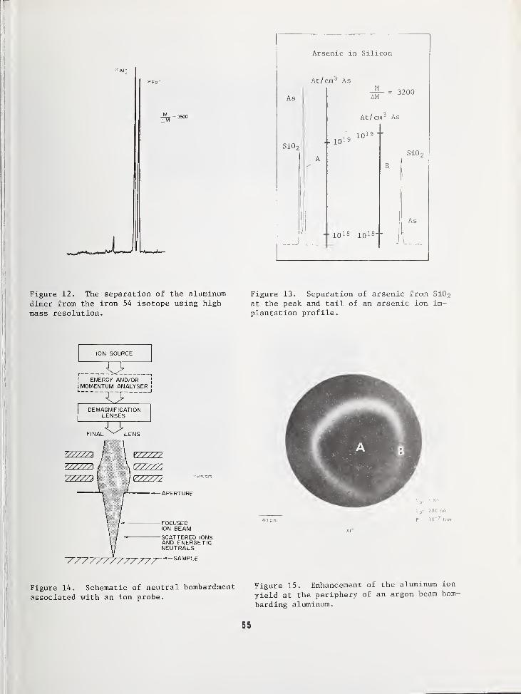
Arsenic in Silicon
At/cm 3 As
As
SiO;-- 10
M
i 9
AM
At/cm 3 As
10 19 "
= 3200
--10 18 10 18"
SiO;
As
t Jl_
Figure 12. The separation of the aluminum
dimer from the iron 54 isotope using high
mass resolution.
Figure 13. Separation of arsenic from SiC>2
at the peak and tail of an arsenic ion im-plantation profile.
Figure 14. Schematic of neutral bombardment
associated with an ion probe.
Figure 15. Enhancement of the aluminum ion
yield at the periphery of an argon beam bom-
barding aluminum.
II
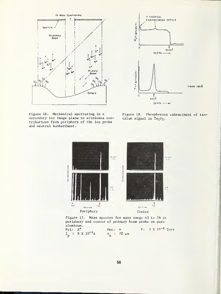
Figure 16. Mechanical aperturing in a Figure 18. Phosphorous enhancement of tan-secondary ion image plane to eliminate con- talum signal in Ta20 5 .
tributions from periphery of the ion probeand neutral bombardment.
si
Depth
Figure 19. Depth profiles of silicon andoxygen in pure silicon bombarded with oxygen.
I : 0", V : 15 kV, P: 10_17
TorrP P
Figure 20. Primary oxygen beam implantation Figure 21. Primary oxygen beam implantationdepth profile. depth profile with oxygen leak.
1?
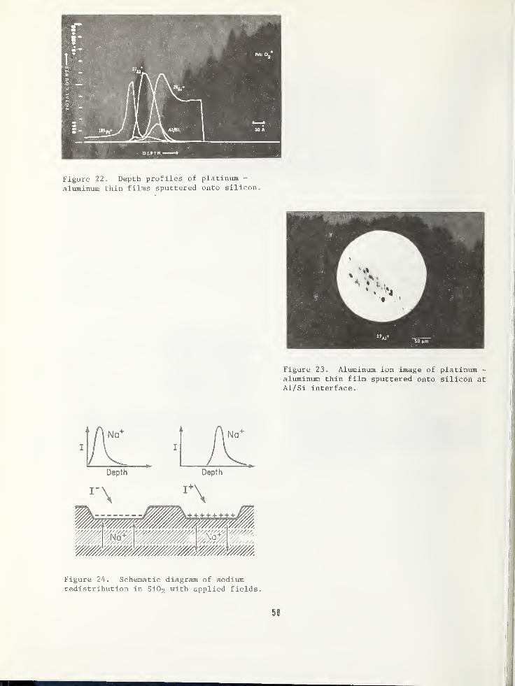
Figure 22. Depth profiles of platinum -
aluminum thin films sputtered onto silicon.
Figure 23. Aluminum ion image of platinum -
aluminum thin film sputtered onto silicon atAl/Si interface.
Depth Depth
Figure 24. Schematic diagram of sodiumredistribution in SiC>2 with applied fields.
5!:'

DISCUSSION OF THE PAPER
Hurd : How does the SIMS profiling techniquecompare to other profiling techniques, such
as NAA, spreading resistance, or the four
point probe techniques?
Lewis : Actually I should probably refer youto one of the people who has used SIMS and
those other techniques, Joe Tsai could tell
you more.
Tsai : Our results show very good correlationas a matter of fact.
Morabito : Another point is that the SIMS
technique can measure the electrically in-
active as well as active species.
Lewis : The electrical techniques only
measure the concentration of electricallyactive impurities whereas SIMS measures the
actual chemical concentration. I should also
say something about the speed of analysis.
A typical SIMS profile can be obtained in a
matter of minutes, but your spreading resis-tance measurement takes how long?
Participant : About a day or so.
Lewis : Right. So I think it is importantto point this out. You can, in a day, do
easily 40 or 50 SIMS depth profiles. While
the high performance SIMS instruments are
quite expensive, the speed of analysis also
has to be taken in consideration. This is
one thing I like to point out when SIMS
analysis is compared to electron probeanalysis. At the same concentration level
SIMS can typically do analysis five to ten
times faster. This can readily offset the
difference in cost of these machines. The
real interest to semiconductor people, how-
ever, is that SIMS has the sensitivity to de-
tect the dopant concentration levels and I
do not know of any other technique that does
as well.
Harrington : You can also tell what the
dopant species is, whether it is boron, or
aluminum, or phosphorous. With the electricaltechniques you are only guessing.
Lewis : Right, we are identifying the speciesand, as a matter of fact, we are correlatingthis information with other possible electri-cally or nonelectrically active species, so
the information that you gather this way is
considerably more useful.
DiStefano : What sort of total spatialresolution do you obtain with your SIMS
technique?
Lewis : The depth resolution can be a fewtens of angstroms if you are dealing withsingle crystal silicon. But there are manylimiting effects. Usually we do not like to
quote a depth resolution capability betterthan 10% of the depth sputtered because of
sputtering artifacts. However, in siliconyou are usually working with a very idealsituation and much better resolutions can beobtained.
DiStefano : If you sample a large area youcould obtain a resolution of 10 A, but for a
smaller area you obviously would have to
sample a greater depth. What combinationsof sampled area and sampled depth are
attainable?
Lewis: You must always take into consid-eration the amount of material sputtered andthe ionization efficiency of the particularspecies you are looking at. As the area is
made smaller and smaller you must sputter togreater depths to get enough ions to achievean adequate precision. I am talking about abulk analysis now. In a concentration grad-ient this does not really apply. The answeris that the lateral spatial resolution is
about a half a micron in bulk analyses.However, this is not a practical area to usefor a depth profile. A practical limit to
depth resolution for a depth profile is a
few tens of angstroms for an area 100 pm or
so in diameter.
5S

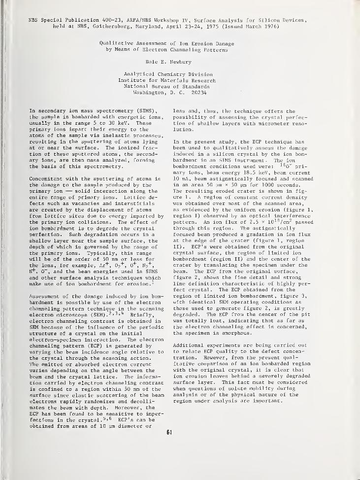
NBS Special Publication 400-23, ARPA/NBS Workshop IV, Surface Analysis for Silicon Devices,held at NBS, Gaithersburg, Maryland, April 23-24, 1975 (Issued March 1976)
Qualitative Assessment of Ion Erosion Damageby Means of Electron Channeling Patterns
Dale E. Newbury
Analytical Chemistry DivisionInstitute for Materials ResearchNational Bureau of Standards
Washington, D. C. 20234
In secondary ion mass spectrometry (SIMS),
the sample is bombarded with energetic ions,usually in the range 5 to 30 keV. Theseprimary ions impart their energy to theatoms of the sample via inelastic processes,resulting in the sputtering of atoms lyingat or near the surface. The ionized frac-tion of these sputtered atoms, the second-ary ions, are then mass analyzed, formingthe basis of this spectrometry.
Concomitant with the sputtering of atoms is
the damage to the sample produced by theprimary ion — solid interaction along theentire range of primary ions. Lattice de-fects such as vacancies and interstitialsare created by the displacement of atomsfrom lattice sites due to energy imparted bythe primary ion collisions. The effect of
ion bombardment is to degrade the crystalperfection. Such degradation occurs in a
shallow layer near the sample surface, thedepth of which is governed by the range ofthe primary ions. Typically, this rangewill be of the order of 50 nm or less forthe ions, for example, Ar+ , 02
+, 0+ , N2+ ,
N*, 0~, and the beam energies used in SIMSand other surface analysis techniques whichmake use of ion bombardment for erosion. 1
Assessment of the damage induced by ion bom-bardment is possible by use of the electronchanneling pattern technique in the scanningelectron microscope (SEM). 2 ' 3 '
1* Briefly,
electron channeling contrast is obtained in
SEM because of the influence of the periodicstructure of a crystal on the initialelectron-specimen interaction. The electronchanneling pattern (ECP) is generated byvarying the beam incidence angle relative to
the crystal through the scanning action.The emitted or absorbed electron currentvaries depending on the angle between the
beam and the crystal lattice. The informa-tion carried by electron channeling contrastis confined to a region within 50 nm of thesurface since elastic scattering of the beamelectrons rapidly randomizes and decolli-mates the beam with depth. Moreover, theECP has been found to be sensitive to imper-fections in the crystal. 5 ' 6 ECP's can beobtained from areas of 10 urn diameter or
less and, thus, the technique offers thepossibility of assessing the crystal perfec-tion of shallow layers with micrometer reso-lution.
In the present study, the ECP technique hasbeen used to qualitatively assess the damageinduced in a silicon crystal by the ion bom-bardment in an SIMS instrument. The ionbombardment conditions used were: 160~ pri-mary ions, beam energy 18.5 keV, beam current10 nA, beam astigmatically focused and scannein an area 50 urn x 50 pm for 1000 seconds.The resulting eroded crater is shown in fig-ure 1. A region of constant current densitywas obtained over most of the scanned area,as evidenced by the uniform erosion (figure 1
region I) observed by an optical interferencepattern. An ion flux of 2.5 x 10 18 /cm2 passei
through this region. The astigmaticallyfocused beam produced a gradation in ion fluxat the edge of the crater (figure 1, regionII). ECP's were obtained from the originalcrystal surface, the region of limited ion
bombardment (region II) and the center of thecrater by translating the specimen under thebeam. The ECP from the original surface,figure 2, shows the fine detail and strongline definition characteristic of highly per-fect crystal. The ECP obtained from theregion of limited ion bombardment, figure 3,
with identical SEM operating conditions as
those used to generate figure 2, is greatlydegraded. The ECP from the center of the pit
was totally lost, indicating that as far as
the electron channeling effect is concerned,the specimen is amorphous.
Additional experiments are being carried out
to relate ECP quality to the defect concen-tration. However, from the present qual-itative comparison of an ion bombarded region
with the original crystal, it is clear that
ion erosion leaves behind a severely degradedsurface layer. This fact must be consideredwhen questions of solute mobility duringanalysis or of the physical nature of the
region under analysis are important.

References
Carter, G. , and Colligon, J. S., Ion
Bombardment of Solids, pp. 151-156
(Elsevier, New York, 1968).
Booker, G. R. , Modern Diffraction andImaging Techniques in Material Science,
Amelinckx, S. , et al., ed., pp. 613-653
(North Holland Publishing Company,
Amsterdam, The Netherlands, 1970).
Newbury, D. E. in SEM/1974, Proceedings
of the 7th Annual SEM Symposium,
Johari, 0., ed. , IITRI, Chicago,
Illinois, 1974, pp. 1047-1054.
4. Goldstein, J. I. , Yakowitz, H.
,
Newbury, D. E. , Lifshin, E., Colby, J.,
and Coleman, J. , Practical ScanningElectron Microscopy, pp. 150-179 (PlenumPress, New York, 1975).
5. Schulson, E. M. , van Essen, C. G. , andJoy, D. C. in SEM/1969, Proceedings ofthe 2nd Annual SEM Symposium, Johari, 0.
,
ed., IITRI, Chicago, Illinois, 1969,
pp. 47-55.
6. Wolf, E. D. , and Hunsperger, R. G. in
SEM/1970, Proceedings of the 3rd AnnualSEM Symposium, Johari, 0., ed., IITRI,Chicago, Illinois, 1970, pp. 457-463.
82
1 I
I
50pm
Figure 1. Optical micrograph of ion eroded
crater. Region I is uniformly bombarded;
Region II is lightly bombarded.
<?k>
Figure 2. Electron channeling pattern ob-tained from original crystal surface prior
to ion bombardment
.
Figure 3. Electron channeling pattern fromedge of crater region (Region II in figure 1)
.
13

NBS Special Publication 400-23, ARPA/NBS Workshop IV, Surface Analysis for Silicon Devices,
held at NBS, Gaithersburg, Maryland, April 23-24, 1975 (Issued March 1976)
THE EFFECT OF SPECIMEN COOLING ON THE MIGRATIONOF SODIUM IN THIN FILM Si0 2
Bradway F. PhillipsNaval Weapons Support CenterElectron Optics Laboratory
Crane, Indiana 47522
Alfred E. Austin Harold L. Hughes
Battelle Columbus Labs Naval Research Laboratory
Columbus, Ohio 43201 Washington, D.C. 20375
INTRODUCTION
Being able to profile element concentrationchanges as a function of depth in thin film
oxide structures, particularly Si02 , is of
vital concern to the understanding of MOS
device characteristics. Early in the de-
velopment of techniques to measure these
element profiles directly using the ion
probe, it was shown that both Na and K were
mobilized by the primary ion beam while Al
and P were essentially undisturbed by the
charge built up in the thin Si02 film [1],
[2], [3]. This discovery helped to explain
how a number of widely varying results could
be obtained on specimens which were sup-
posedly identical in preparation since K and
Na were moving through the Si02 films quite
readily. This effect was causing Na and K
surface contamination to show up at differ-
ent points remote from the surface, partic-
ularly at the Si0 2 - Si interface.
EXPERIMENTAL CONCEPT
As a step toward providing better data on
Na distributions in Si02 a number of pos-
sible experiments were proposed, including:
A. Use a primary ion beam with a low ioni-
zation potential compared to the 0~, 02+ or
Ar+ beam used regularly.
B. Increase or decrease the primary ion
energy greatly compared to the nominal
5.5 keV 0 2+ or Ar+ ions or 14.5 keV 0" ions
used in the Cameca IMS 300.
C. Cool the specimen as near to liquid ni-
trogen temperatures as possible to slow down
the "drift" of Na under the surface charge
built up with ion bombardment
.
It was felt that all of these experiments
were important but that choice C was bestsuited to the study we wished to make.Therefore, a liquid nitrogen dewar andspecimen holder were constructed to fit the
specimen cooler port of the Cameca IMS 300.
The specimen holder was designed to holdspecimens 0.010 to 0.020 inch thick, 3/8inch wide, and up to 1.5 inches long, andincluded a translation mechanism to go to
any spot in a vertical line across these
specimens. This allowed us to load three3/8 inch square silicon slices, in additionto the copper grid pressed into aluminum foraligning the instrument and making sure thesecondary ion optics were properly focussed.Specimen cooling rates and ultimate tempera-tures were measured several times, and the
averaged temperature value obtained at thespot being analyzed was -180°C.
EXPERIMENTAL RESULTS AND ANALYSIS
As a reference to the work which lead to
this study we see the results of profilingthe Na distribution in Si02 at room tempera-ture in figure 1, which was mentioned pre-viously today in Bob Dobrott's talk andwhich is typical of analyses we were seeing
in 1970, 1971, and early 1972. According to
the predictions of the LSS theory we wouldexpect the sodium to peak at 350 A from thesurface and obviously it is not doing that.
Therefore, for our first room temperatureand low temperature experiments we chose a
series of specimens, which ranged from as-grown oxides to samples containing severallevels of aluminum implantation and residualsodium. Results of these analyses are pre-sented in table 1. First, we have an as-
grown oxide analyzed at -180°C, in which 27%
of the sodium concentrated at the Si02~Siinterface; then at room temperature, where70% of the sodium concentrated at the inter-face. The remainder of the specimens are
aluminum implantations performed at 20 and
25 keV ranging in three steps from 4 x 10 15
to 6.8 x 10 12 atoms per square centimetertotal dose. As we can see with the lower
implant dose, NRR 371, we have at -180°C the
smallest amount of sodium (32%) moving to
the Si0 2-Si interface of this group of
specimens. However, as we go to the higherdose specimen, NRR 372, 45% of the sodiummoves and at the much higher dose, NRR 437,
46% of the sodium moves, where at roomtemperature these values are 75, 88, and 90%
respectively. So we can see that there is a
definite effect produced by using the low
temperature specimen holder. As an exampleof the profiles obtained, figure 2 shows the
results of analyzing an as-grown oxide at
room temperature. The silicon secondary ionyield changes by several orders of magnitudeas the interface is penetrated. At allpoints in the specimen except at the SiC>2-Si
interface the sodium profile shows a countrate which is essentially at the backgroundnoise level of the instrument.
In figure 3 we see the results of coolingthe same specimen to -180°C and this analy-sis demonstrates that the drift of sodium is
retarded. The instrumental conditions werekept exactly the same in both cases. Herewe see that when the specimen is cooled thesodium does not move rapidly to the SiC^-Siinterface during analysis, but is retarded;in fact, the sodium concentration is two or-ders of magnitude higher throughout the
oxide in the spot analyzed on the cooledspecimen than it is in the spot analyzed at
room temperature. Although this techniquedoes not yet give the true sodium profile,it does give some encouragement to continueon this path of analysis, and table 2 de-scribes the next set of specimens which wereprepared. The first specimen, JR1C, the as-grown oxide control sample, was cut up andused as a base material for all of the so-dium ion implants which ranged from3.2 x 10 11+ to 1.4 x 10 15 atoms per squarecentimeter total dose; some of which wereannealed at 200 or 900°C. The results ob-tained on these samples are tabulated intable 3. In specimen JR1C analyzed at 25°Cwith the 0~ beam, 100% of the sodiumappears at the surface of the oxide; at
-180°C with the 0" beam, 97.5% of thesodium appears at the surface. Therefore,we see that in the control specimen essen-tially all of the sodium is present at thesurface of the oxide as contamination. Thenext experiment on JR1C using the 02+ beamdemonstrates that we still have a fairamount of the sodium mobilized both at 25°Cand at -180°C. At 25°C, 10% of the sodiumis at the surface and 89% is at the Si02~Siinterface. Going to -180°C on the same sam-ple, we see that 54% is on the surface of
the oxide, 26% at the interface, and 20% is
included within the bulk oxide. So we haveretarded the movement of the sodium althoughwe do not feel that we have a perfect pro-file yet. Working with specimen JR1A1,which was implanted to 3.2 x 10 lt+ atoms percentimeter and annealed at 200 °C, we seethat there is a very small amount of the so-dium at the surface in both the -180°C andthe 25°C specimens. Most of the sodium hasgone to the interface. We interpret this asbeing caused primarily by the ion inducedchannels from the implantation process andby the fact that the 200°C treatment doesnot anneal out these channels. We still
have an inducement for the sodium to move,even though we have cooled the sample.JR1A2 has been annealed at 900°C for 30 min-utes, and in this case we see at -180°C that29% of the sodium is on the surface. 65% is
at the interface. Essentially the same ap-pearance was seen at 25°C, showing thatthere must have been some prior movement ofthe sodium at room temperature and then at
900 or 200°C before we did the analyses.
In order to show the differences a littlebit more clearly we have made up differen-tial plots between the work done at roomtemperature and the work done at low temper-ature. Figure 4 shows the results obtainedwith a differential plot of JR1C, our con-trol specimen. This plot demonstrates thatcooling holds some Na at the surface of theSi02, retards its diffusion through theSi02 , and greatly reduces the pileup at theSi02-Si interface. In figure 5 we are look-ing at the JR1A1, which is an implanted andlow temperature-annealed sample. We seethat there is a sizeable portion of the so-dium present which is retained at the sur-face by cooling the specimen during analysis
In the sodium profile through the samplethere is a large decrease in the peak rightbefore going into the silicon substrate andsome reproducible small peaks as you sput-ter into the silicon itself that must becaused by interface states and the differ-ences in sodium activity between 25°C and-180°C. In figure 6 we are looking at thedifferential plot of JR1A2, which was an-nealed at 900°C for 30 minutes. Here we seesomewhat the same results as with JR1A1 ex-cept that there is a wide peak of the so-dium at the surface compared to the specimenanalyzed at room temperature and a very deepvalley when we get close to the interface.The integrated sodium intensities of thetwo JR1A2 specimens were 26,000 and 29,800counts, compared to 54,000 and 44,000 for
the JR1A1 specimens. This difference may bedue to the loss of sodium from the surfaceduring the high temperature annealing pro-cess. Such loss caused by diffusion of so-dium to the surface and partial escape intothe furnace atmosphere would also accountfor the increased surface concentrations of
sodium in the JR1A2 specimens, 22 to 29%compared to 6 to 7% of the JR1A1 specimens.That the sodium concentration at the sur-faces of the JR1A1 specimens is lower thanwould be expected for the shallow 200 Arange suggests that the sodium ions may bedriven into the Si02~Si interface by surfacecharging during the ion implantation.
A run on the JR1A1 specimen with O-
primarybeam at -180°C showed a high but continuous-ly decreasing sodium concentration throughthe oxide, and no sodium at the Si02~Si in-
terface. As with the control, the high-energy 0~ beam apparently makes the sodiummore mobile in the oxide. We see in our
third example, JR1A2, a fairly uniform dis-tribution of the sodium throughout the Si0 2 ,
with the peak reduced at the interface and a
peak showing at the surface. Therefore, wecan conclude that when a specimen which haslittle implantation damage is analyzed at
-180°C, we can get a much better profile of
the sodium which we would say does exist onthe surface of the SiC>2 as contaminationfrom the growth technique, and throughoutthe oxide from the implantation, than we canat room temperature.
SUMMARY
In summary the following points have beenestablished
.
1. A liquid nitrogen-cooled specimen holderwas fabricated for a Cameca IMS 300.
2. Cooling thin-film Si02 specimens does
retard the diffusion of Na during ion probeanalyses
.
Although it does not give a perfect profile,
such cooling is a step in the direction of
attaining sodium profiles that are repro-
ducible and real.
3. The interactions of primary beam energyand species, ion implantation dose andenergy, annealing temperature, and a varietyof other factors not yet known, combine toaffect the Na profiles obtained and to im-prove or degrade the benefits of cooling thespecimens
.
ACKNOWLEDGEMENTS
We would like to acknowledge the contribu-tions of Mr. Ronald Baxter of Leeds andNorthrop Company, North Wales, Pennsylvaniain the design and initiation of these ex-
periments, and the sponsorship of the DefenseNuclear Agency under subtask Z99QAXTD033,work unit 51, work unit title, "RadiationResistant MOS Technology," technical moni-tor, Mr. H. L. Hughes, of the U. S. NavalResearch Laboratory.
REFERENCES
1. H. L. Hughes, R. D. Baxter, and B. F.
Phillips, IEEE Trans. Nue. Soi. NS-19 ,
256 (1972).
2. D. V. McCaughan, and V. T. Murphy, IEEETrans. Bug. Sci. NS-19 , 249 (1972).
3. R. D. Baxter, Investigation of Thermally
Grown Si02 by Ion Microanalysis,Battelle Memorial Institute (1971).
II
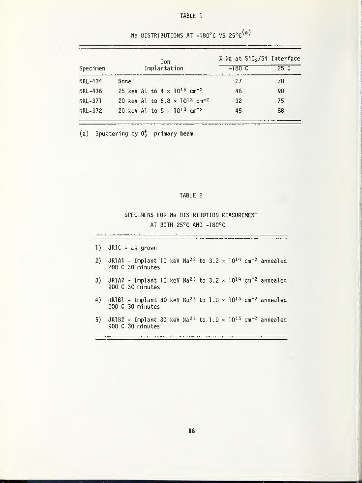
TABLE 1
Na DISTRIBUTIONS AT -180°C VS 25°C(a)
SpecimenIon
Implantation
% Na at Si02/Si Interface
-180 C 25 C
NRL-434 None 27 70
NRL-436 25 keV Al to 4 X 10 15 cm" 2 46 90
NRL-371 20 keV Al to 6 8 x 10 12 cm-2 32 75
NRL-372 20 keV Al to 5 X 10 13 cm" 2 45 88
(a) Sputtering by 0* primary beam
TABLE 2
SPECIMENS FOR Na DISTRIBUTION MEASUREMENT
AT BOTH 25°C AND -180°C
1) JRIC - as grown
2) JR1A1 - Implant 10 keV Na 23 to 3.2 x 10 14 cm" 2 annealed200 C 30 minutes
3) JR1A2 - Implant 10 keV Na23 to 3.2 x 10 14 cm' 2 annealed900 C 30 minutes
4) JR1B1 - Implant 30 keV Na23 to 1.0 x 10 15 cm" 2 annealed200 C 30 minutes
5) JR1B2 - Implant 30 keV Na 23 to 1.0 x 10 15 cm" 2 annealed900 C 30 minutes
TABLE 3
Na DISTRIBUTIONS AT -180 C VS 25 C
Percent of Na in
Temp. Primary Surface Bulk Si0 2/Si
Specimen C Beam of Oxide Oxide (interface) Si
JR1C 25 0" 100
JR1C -180 0" 97.5
JR1C 254-
0+2 10.7 0.23 89
JR1C -180 0+2 54 20 26
JR1A1 25 0+2 7.2 2.3 90.5
JR1A1 -180J.
0+2 6 24 70
JR1A2 25 0+2 22 1 77
JR1A2 -180 0+2 29 6 65
JR1B1 25 o+2 5 6 74 15
JR1B1 -180 o+2 3 64 26 7
JR1B2 25 0+2 21 4 74 1
JR1B2 -180 0+2 25 40 34 1
SILICON DIOXIDE (3100 I) ON SILICON
Na* IMPLANTED <20k»V, IxlO15 ionl/cm*)
• '*0~ PRIMARY BEAM
"O* PRIMARY BEAM
{
\
SIOj Si
.1 I LO 500 1000 I5C0 2000 2500 JOOO S500
DEPTH, I
LU 10CO —II- <z od tn
8 oQ ,„2
Figure 1. Sodium profiles of a sodium - implantedsilicon dioxide film for both 16 0+ and 16 0~.
104
zoZ><0Oo
» 30 Si
• 23 Na
Wax*'*!
••
••
• • •'•• «•**•• ' * •<
• •
• •
•
••
RELATIVE DEPTH
Figure 2. Sodium profile at 25°C of an as-grownoxide.
X 30Si• 23 Na
xxxxxxxxXXXXXXXXXX,xxxxxxxxx^ xxxxxxxxxxxxxxxxxxxx xxxxxxxxxx "*xX
X
.'. X
. y
*•••
K
• »x»»xx«,xXXXXXXXxXX (XXXxXX»»J
• • •
0 20 40 60 80 100 120 140 160 180 200
RELATIVE DEPTH
Figure 3. Sodium profile at -180°C of the samespecimen as in figure 2.
eoOp
700 I
600
500
400
0LO 300 -
CN
200 -
Na 100
u -100 -0
O00 -200 -
H1
-300
nj
S3 --•GO -
-500 -
-600 -
-700 -
-800 1—
~i i r
J 1 L
Figure 4. Plot of Na (-18.0°C) - Na (25°C)distribution in JR1C.
30 40 50 60 70 60
Chonnol
Figure 5. Plot of Na (-180°C)
distribution in JR1A1.Na (25°C)
IB00
1600
1400
1200
1000
u coooLOCM 600
400
200
1
0
O0 -200
O00t-H
1
-400
-600
-800
-IOC0
-1200
-K00
-1600
lo 26001"1
1 1 1 r
go so ico no
Figure 6. Plot of Na (-180°C) - Na (25°C)
distribution in JR1A2
.
71
DISCUSSION OF THE PAPER
Participant : What was your primary beamcurrent density?
Phillips : The primary ion beam intensitywas approximately 250 nanoamps rastered outto cover an 800 micron square.
Cock : For one of your samples you postu-lated that the sodium motion was enhanced bydislocations. Would you could elaborate on
that model.
Phillips : I would say that at the 200°Canneal, you have not removed the channelsthat are caused by the ion implantationprocess itself. At the 900°C anneal youhave removed some of the channels but youhave also mobilized the sodium. Data, whichwe did not present today, using the picturemode in the Cameca IMS 300 to study thelocation of the sodium after a 200°C annealand after a 900°C anneal shows the difference.At 900°C you have mobilized the sodium andyou actually have it diffusing back throughthe channels to the surface and escapinginto the furnace atmosphere, making yourtotal sodium content in the entire oxidehalf as large as it is with the 200°C anneal.
Cock : I see, so this is a dislocation in
the oxide structure.
Phillips : Yes. If you implant sodium to a
high enough intensity in the oxide structure,somewhere around 1 x 10-L5 atoms per squarecentimeter, you can provide a state in theSi02 which is of such a high energy thatthe silicon and sodium, - in fact, all ions- coming off the specimen from a sectionextending from the surface to close to the
depth at which the maximum of the implanta-tion peak should occur, are of such a highenergy compared to the secondary ion bandpass of the instrument that you do not seeany secondary ions. So you know that you
are producing an extremely strained state inthe Si02 film that does shift even yoursecondary-ion energy distribution.
Participant : The temperature of 180°C thatyou quote is, I gather, a bulk sampletemperature
.
Phillips : That is correct. The microtem-perature at the sputtering spot has not beendetermined. The temperature at which thesputtering actually takes place, or theplasma in which the ions are produced, wouldbe significant for the theory devised by Dr.C. A. Andersen. The bulk temperature hasbeen determined to be 180°C.
Participant : Although the temperature at
the sputtering location has not been deter-mined do you have any idea of approximatelyhow large of a difference you might expect?
Phillips : Well, in the plasma itself, or at
the place at which the sputtering is occur-ring, the temperature is several thousandsof degree Kelvin.
Evans : You are talking of the plasma or
electronic temperature, not the thermal tem-
perature. The thermal rise at the surfacedue to ion bombardment is only of the orderof 5 to 50°C above the bulk sample tempera-ture. The plasma "temperatures" are thermalspikes: they last the order of 10 sec-onds; they are not a temperature in the truesense, they are an electronic temperature.
Phillips : The temperature rise is extremelysmall because we are dealing with a fairlyheat-conductive medium, silicon, and a fairlythin film of Si02 with a massive heat sinkcompared to the size of the sample. So I
would say that even going through the Si02
there would be an extremely small temperaturerise in the local area surrounding the
sputtering; of the order of a few degrees at
the most.
12
NBS Special Publication 400-23, ARPA/NBS Workshop IV, Surface Analysis for Silicon Devices,held at NBS, Gaithersburg , Maryland, April 23-24, 1975 (Issued March 1976)
SILICON-ON-SAPPHIRE IMPURITY ANALYSIS 5'
1
D. Howard Phillips
Electronics Research DivisionRockwell International Corporation
Anaheim, California 92803
INTRODUCTION
The presence of undesirable impurities haddetrimental effects on both the electricaland radiation performance of silicon-on-sap-phire (SOS) integrated circuits. Conversely,device electrical and radiation characteris-tics can be improved by minimizing the num-ber and types of impurities in SOS films.
Ion microprobe mass analysis (IMMA) tech-
niques are being utilized for impurity analy-
ses in a program associated with the develop-ment of a radiation-hardened CMOS/SOS (com-
plementary MOS on sapphire) technology. Froman applications point of view, four goalshave been established for this program. Thefirst is to improve lot-to-lot repeatability;the second is to improve wafer-to-wafer re-
peatability; the third is to improve the
electrical stability of the devices (i.e.,
the bias-temperature stability of thresholdvoltage) ; and the fourth is to improve the
radiation stability of the devices.
IMPURITY SOURCES
One source of contaminants is the sapphiresubstrate. Impurities are sometimes added
during the growth process to minimize crystal
defects such as twinning.
A second source of impurities is the epitax-ial film itself. During the epitaxial film
growth process, impurities come from silane,
hydrogen carrier gas, and dopant gases.
A potential major source of impurities is
the processing steps that are used duringthe wafer fabrication process.
MASS-ANALYSIS SILICON IMPURITY DATA
Figure 1 shows recent data comparing silicon-on-sapphire films with an epitaxial siliconlayer on bulk silicon. The shaded areas in-
dicate the impurity concentration measuredin silicon films on a sapphire substrategrown using the Czochralski process. The
* Partially sponsored by USAF/AFCRL (Contract
F19628-75-C-0108) and by Rockwell Inter-
national Corporation (IR&D)
.
unshaded lines on the bar graph indicate the
impurity concentrations that were measuredon epitaxial films grown on bulk silicon.The data are plotted as a function of ele-mental impurities versus the relative con-centration, where each increment on the hori-zontal axis indicates an order-of-magnitudechange in impurity concentration.
These data show that aluminum concentrationsin silicon-on-sapphire are orders of magni-tude greater than aluminum concentrations in
bulk silicon. In the case of sapphire(AI2O3) , there is more aluminum present in
the system to act as a potential contaminant,either from top-side diffusion or from back-side diffusion out of the sapphire substrate.
Another very important observation from thesedata is a consideration of sodium content.Sodium and potassium are known sources of
electrical instability in MOS transistors.Compared to bulk silicon, typical silicon on
sapphire contains much higher sodium concen-trations. The data in Figure 1 show very
little difference between silicon-on-sapphireepitaxial films and bulk silicon epitaxialfilms, in terms of potassium impurity con-centration .
DIFFUSION PROFILES IN SILICON ON SAPPHIRE
IMMA analysis techniques are being used in
the analysis of intentional dopants. Figure
2 shows phosphorous concentration as a func-
tion of diffusion drive-in time. The drive-
in time at 1,000 degrees centlgrate was var-
ied from 0 to 15, 30, 60 and 80 minutes.
Initially (at T = 0) , phosphorous was con-
centrated close to the surface. Followinghigh-temperature processing, the profiles
changed as shown in Figure 2. We typically
use silicon-on-sapphire material with a sil-
icon epitaxial thickness in the range from0.8 to 1.0 micron. For typical wafer-pro-cessing thermal cycles, phosphorous diffuses
completely through the silicon-on-sapphirefilm. The diffusion coefficient in sapphire
is very low and phosphorous does not diffusethrough the silicon-sapphire interface. The
sapphire interface acts as a diffusion stop
causing phosphorous to remain in the silicon
film.
MASS ANALYSIS DATA ACQUISITION
Figure 3 illustrates the instrument used to
obtain impurity data presented in Figures 1
and 2. The ion microprobe mass analyzergenerates an ionized beam that is swept elec-
trostatically both in the Y direction and
the X direction in much the same manner that
a TV raster is generated. The ion source is
allowed to impinge on the sample of interest.
Beam diameters can be adjusted from 2 micronsto 500 microns. The rate at which the sur-
face is eroded depends on several experimen-tal factors, i.e., the ion source, the in-
tensity of the ion beam, the energy of the
ion beam and the nature of the sample that
is being analyzed. Erosion rates vary over
a range from less than one angstrom per sec-
ond up to 1000 angstroms per second. The
secondary ions are analyzed electrostatically(momentum) and magnetically (mass-to-chargeratio) . The ions impinge on a target where
an electron beam is produced. The electronbeam generates light in the scintillator,and this light is coupled to a photomulti-plier tube. The signals from the photomulti-plier tube can be recorded and displayed in
several ways. One way is to record them on
a CRT which utilizes the signal from the
photomultiplier tube for Z axis modulation.CRT Y and X signals are derived from the
waveforms used to deflect the primary ion
beam. Data can also be recorded on a strip-chart recorder by using the signal from the
photomultiplier tube to modulate the Y axis
of the recorder. Data can be recorded by
using a scaler to count pulses from the
photomultiplier tube. Data can be recordedin the MHz range without significant dataloss due to scaler dead time.
SPECTROCHEMICAL-ANALYSIS SAPPHIRE IMPURITYDATA
Table I lists data showing impurity levelsin the sapphire substrate, rather than the
silicon film. These data were obtained usingspectrochemical analysis techniques ratherthan the ion microprobe mass analysis tech-nique just described. These data were ob-
tained by using Crystal Systems sapphirewhich was grown using the gradient furnacetechnique. The gradient furnace techniqueis one of three techniques that is used com-
mercially to grow sapphire crystals that can
be used to fabricate silicon-on-sapphireintegrated circuits. Table I compares pre-1971 sapphire impurity data with data for
the improved process that is being used at
this time by Crystal Systems in the growthof gradient furnace sapphire. The number of
impurities present to a significant extentare greater for the improved process, but
the impurity concentrations, in general, are
much less than for the sapphire-growth pro-
cess used by Crystal Systems prior to 1971.
MATERIAL COMPARISON AND DATA CORRELATION
Considering the different analysis techniquesthat have been used to analyze both sapphireand silicon films, data correlation is needed.
Figure 4 indicates some of the work that is
being done to correlate the data that havebeen accumulated. Data are being obtainedfor three types of sapphire substrates
—
Czochralski-grown sapphire substrates fabri-
cated by Union Carbide, ribbon sapphire sub-strates fabricated by Tyco, and gradient-furnace sapphire substrates fabricated byCrystal Systems. These sapphire substrategrowth techniques are quite different, and
preliminary indications are that the impurityconcentrations are quite different for thesethree techniques.
Figure 4 describes a correlation study that
is being performed as a cooperative effortwith NBS and Rockwell participating in thedata acquisition activities. This study in-
cludes the analysis of silicon-on-sapphirewafers from three sources. Each wafer willbe divided into halves. One-half of thesapphire wafer will be analyzed using the
flame emission spectrometry techniques in
use at the National Bureau of Standards.The other half of the wafer will be analyzedby Rockwell using the ARL-IMMA analysistechnique. An attempt will be made to cor-relate the results of these two measurementmethods with the objective of learning moreabout the sapphire substrates and the sili-con epitaxial films, and using that informa-tion in our attempts to improve the materialcharacteristics and the device electricaland radiation characteristics. Wafers fromthe same lot will be used in integrated cir-cuit fabrication. These integrated circuitswill be characterized to determine the elec-trical characteristics and the radiationperformance of SOS integrated-circuit de-vices. The data from the integrated circuitfabrication and test activities will also becorrelated with the analysis of the SOS
starting material using the flame emissionspectrometry and IMMA analysis techniques.At the same time, we have other silicon-on-sapphire integrated-circuit fabrication andcharacterization programs that are contin-ually providing additional data that can be
used for correlation.
SUMMARY AND CONCLUSIONS
Unintentional impurities in silicon-on-sap-phire films and substrates are relatively
74

high, based on mass analysis data. Concen-
trations of the unintentional impurities are
equal to, or greater than, the dopant concen-tration of the most lightly doped region of
the semiconductor.
There is a significant difference between the
impurity concentrations in typical SOS de-
vices or SOS wafers as compared to bulk sili-con wafers.
Preliminary data indicate that there is a
good deal of impurity-concentration varia-bility depending upon the sapphire sourceand the sapphire growth technique. In addi-tion, considerable lot-to-lot and wafer-to-wafer variability has been observed in sili-con films and has been attributed to growthconditions and device fabrication methods,as well as impurity concentration variations.
75
TABLE 1
SPECTROCHEMICAL ANALYSISCRYSTAL SYSTEMS SAPPHIRE DATA
GRADIENT-FURNACE SAPPHIRE
IMPROVED PROCESS (1971 1975) EARLY PROCESS (PRE-1971)
Element Concentration Element Concentration ELEMENT CONCENTRATION (ppm)
(ppm) (ppm)
Cr 0.4 N 3 Cr 1
Cu 2 F 0.3 Cu 10
Fe 8 Na 3 Fe 1
Mg 0.3 P 0.05 Mg 1
Mo 1 K 3 Mo 10-100
Ti 0.3 Ca 0.7 Pb 1
Y 0.5 V 0.04 Si 10-100
Sc 4 Mn 0.7 Ti 10100
Ce 6 Ni 0.2 Elements sought and not detected (< 0.05 ppma):B 0.02 Zn 0.6 Ag, As, Au, B, Ba, Be, Bi, Ca, Cd, Co. Ga, Ge, Hf, Hg, In, Ir.K, Li,
Mn. Na Nb Ni Os P Pd Pt Rb Re. Rh Ru. Sb Sn. Sr Ta. Te. Ti.Nominal detection limit = U.Ub ppma.
V, W, Zn, Zr.
RELATIVE ELEMENTAL SCANS OF EPITAXIAL S I LICON ON BULKSILICON AND SAPPHIRE SUBSTRATES
B
C
Na
Mg
Al
K
Ca
Cr
Fe
Mn
Cu
Tzzzzzm
mZTZZL
7ZZL Z ;y,' 7 ////ay/,;;;; aaaI
'
1
IMMA DATA
0 Si ON SAPPHIRE (CZ)
Si ON BULK
ZZZZZZZZZZZZZZZ 7Z2 22 ' 2 .'-V/V; >>w?w//??
x
io* 10x+2 10X+3
RELATIVE CONCENTRATION10*+4 10x+5
Figure 1. Relative elemental scans of epitaxial silicon on bulksilicon and sapphire substrates.
OTHER SOS APPLICATIONS OF IMMA
PHOSPHOROUS CONCENTRATION VSPROCESSINGTEMPERATURE: 1000°C
4 6
DEPTH X 103 A
Figure 2. Phosphorous diffusion profiles in silicon on sapphire.
77
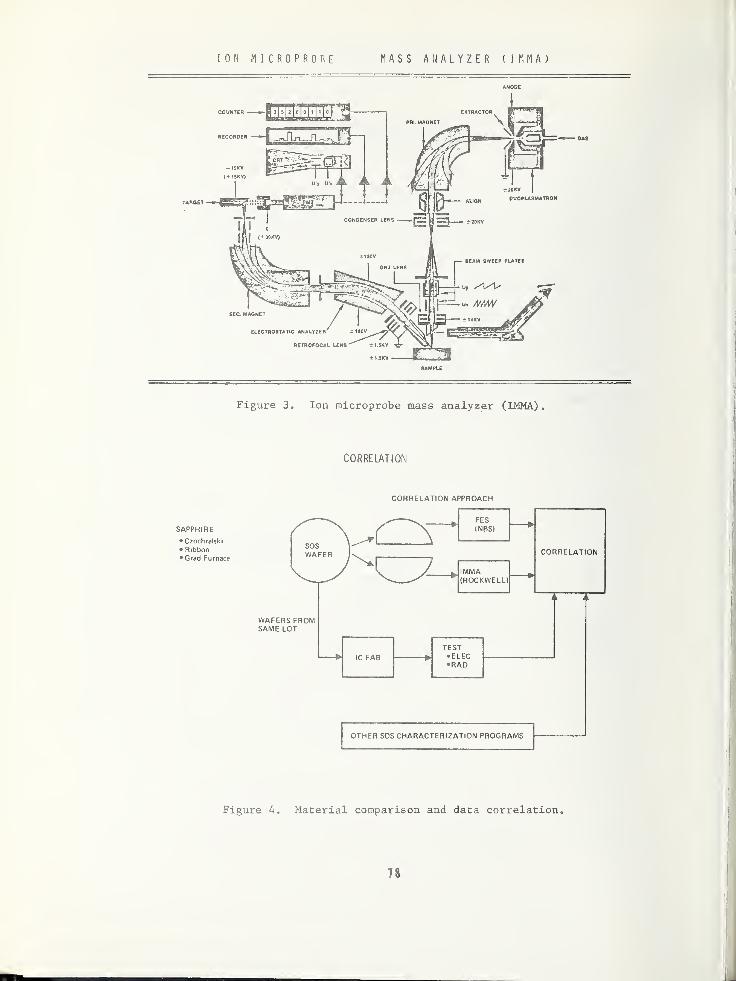
ION MI CROPRORE MASS ANALYZER (IMMA)
Figure 3. Ion microprobe mass analyzer (IMMA)
.
CORRELATION
CORRELATION APPROACH
• Czochralski
• Ribbon•Grad-Furnace
FES(NBS)
WAFERS FROMSAME LOT
IMMA(ROCKWELL
CORRELATION
TEST• ELEC•RAD
OTHER SOS CHARACTERIZATION PROGRAMS
Figure 4. Material comparison and data correlation.
18
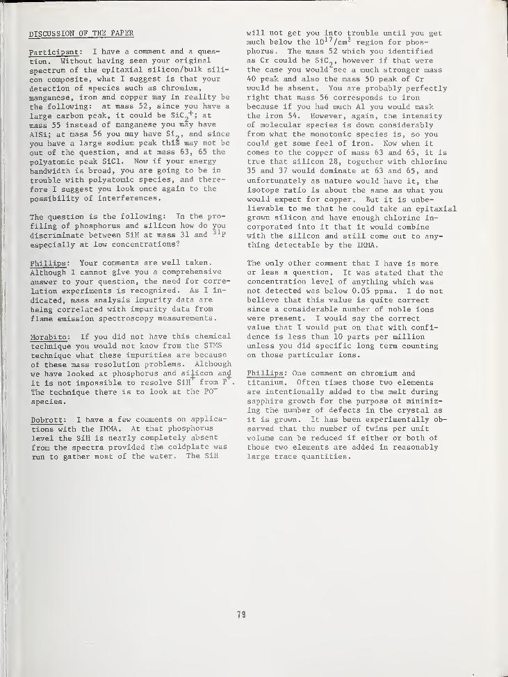
DISCUSSION OF THE PAPER
Participant : I have a comment and a ques-
tion. Without having seen your original
spectrum of the epitaxial silicon/bulk sili-
con composite, what I suggest is that your
detection of species such as chromium,
manganese, iron and copper may in reality be
the following: at mass 52, since you have a
large carbon peak, it could be SiC2+ 5 at
mass 55 instead of manganese you may have
AISi; at mass 56 you may have Si2» and since
you have a large sodium peak this may not be
out of the question, and at mass 63, 65 the
polyatomic peak SiCl. Now if your energy
bandwidth is broad, you are going to be in
trouble with polyatomic species, and there-
fore I suggest you look once again to the
possibility of interferences.
The question is the following: In the pro-
filing of phosphorus and silicon how do you
discriminate between SiH at mass 31 and 31 P
especially at low concentrations?
Phillips : Your comments are well taken.
Although I cannot give you a comprehensive
answer to your question, the need for corre-
lation experiments is recognized. As I in-
dicated, mass analysis impurity data are
being correlated with impurity data from
flame emission spectroscopy measurements.
Morabito : If you did not have this chemical
technique you would not know from the SIMS
technique what these impurities are because
of these mass resolution problems. Although
we have looked at phosphorus and silicon and_
it is not impossible to resolve SiH from P .
The technique there is to look at the P0~
species
.
Dobrott : I have a few comments on applica-
tions with the IMMA. At that phosphorus
level the SiH is nearly completely absent
from the spectra provided the coldplate was
run to gather most of the water. The SiH
will not get you into trouble until you getmuch below the 10 17 /cm 3 region for phos-phorus. The mass 52 which you identifiedas Cr could be SiC2> however if that werethe case you would see a much stronger mass40 peak and also the mass 50 peak of Crwould be absent. You are probably perfectlyright that mass 56 corresponds to ironbecause if you had much Al you would maskthe iron 54. However, again, the intensityof molecular species is down considerablyfrom what the monotonic species is, so youcould get some feel of iron. Now when it
comes to the copper of mass 63 and 65, it is
true that silicon 28, together with chlorine35 and 37 would dominate at 63 and 65, and
unfortunately as nature would have it, theisotope ratio is about the same as what youwould expect for copper. But it is unbe-lievable to me that he could take an epitaxialgrown silicon and have enough chlorine in-corporated into it that it would combinewith the silicon and still come out to any-thing detectable by the IMMA.
The only other comment that I have is moreor less a question. It was stated that theconcentration level of anything which wasnot detected was below 0.05 ppma. I do notbelieve that this value is quite correctsince a considerable number of noble ionswere present. I would say the correctvalue that I would put on that with confi-dence is less than 10 parts per millionunless you did specific long term countingon those particular ions.
Phillips : One comment on chromium andtitanium. Often times those two elementsare intentionally added to the melt duringsapphire growth for the purpose of minimiz-ing the number of defects in the crystal as
it is grown. It has been experimentally ob-
served that the number of twins per unitvolume can be reduced if either or both of
those two elements are added in reasonablylarge trace quantities.
n

II
NBS Special Publication 400-23, ARPA/NBS Workshop IV, Surface Analysis for Silicon Devices,held at NBS, Gaithersburg, Maryland, April 23-24, 1975 (Issued March 1976)
SURFACE COMPOSITION BY ANALYSIS OF IMPACT RADIATION
Clark W. WhiteBell Laboratories
Murray Hill, New Jersey 07974
Several speakers at this conference will dis-
cuss analysis techniques that are based on
phenomena that occur when the low energy ions
impact on solids. These include the tech-
niques of low energy ion backscattering and
secondary ion mass analysis, both of whichutilize beams of low energy ions to bombardthe surface of interest. In addition to the
backscattering of the ion projectile and the
secondary emission of positive and negativeions, one also observes the production of
intense optical radiation in the low energyparticle-solid collision process. In col-laboration with Norman Tolk and DouglasSimms, we have been studying the radiationthat is produced in collisions of low energyions and neutral atoms with solids. Thesestudies give fundamental information on the
low energy particle-solid collision phenom-ena and at the same time provides us withthe basis for a sensitive technique to iden-
tify the constituents of the surface and
near surface regions. The radiation that
will be discussed is produced as a result of
the sputtering process and, therefore, if
sputtering is being used for any purposethese optical signals and the optical infor-mation can then be used to serve as a monitorfor the sputtering process.
Figure 1 schematically illustrates the type
of experimental apparatus which has been used
in this work. This apparatus produces beams
of ions or neutral atoms of well-defined en-
ergy in the energy range from about 50 eV to
about 8 keV. The neutral beam is used to im-
pact on insulating surfaces to avoid any
problems that are associated with charge ac-
cumulation on the nonconducting target. In
the target chamber, the target to be bom-barded is oriented with the surface normalmaking an angle of from 45 to 60 degreeswith respect to the beam direction, and pho-tons that are produced in the collision pro-
cess pass through a quartz window and are
focused by a quartz lens into a small, fast
monochrometer . The monochrometer and the
photomultiplier are used to record the spec-tral distribution of radiation that is pro-
duced in the collision process and singlephoton counting techniques are used for sen-
sitive radiation detection.
Table 1 lists at least three possible
sources or mechanisms for producing opticalradiation in the low-energy collision region.
First of all, there is radiation from ex-cited states of atoms and molecules thathave been sputtered off the surface. Basi-cally, interaction of the beam with a solidresults in sputtering of atoms and moleculesoff the surface. A significant portion of
the sputtered fragments leave the solid in
excited electronic states which then decayand give rise to lines and bands that arecharacteristic of surface constituents in-
cluding surface contaminants. Secondly,there is radiation from excited states of
backscattered beam particles. This obviouslygives information on the quantum mechanicalstates of the backscattered projectiles.Then, finally, there is radiation which re-
sults from the excitation of the electronsin the solid. These, in general, are ob-
served to be very broad continuum of radia-tion which are produced most efficiently byhigh velocity projectiles impinging on in-
sulating targets. The radiative continuumthat are observed here are localized to the
solid and result from the transfer of pro-jectile energy to the electrons in the solid.
This gives rise to the creation of electron^hole pairs which then produce the radiativecontinuum upon recombination. The first
mechanism provides the basis for a techniqueto identify surface constituents. This is
the technique which we call the SCANIIR tech-
nique which stands for Surface Composition
by Analysis of Neutral and Ion Impact Radia-tion. As an analysis technique this method
is very sensitive to the first few monolayersof the solid. The spectrum of radiation that
one obtains is relatively simple and uncom-
plicated, but there are effects due to non-
radiative de-excitation processes that one
has to be aware of.
Figure 2 shows examples of the spectrum of
radiation that are produced when argon ions
at an energy of 4 keV impinge on surfaces of
copper and nickel. The prominent lines that
are shown in these two spectra arise from
low lying excited states of neutral copper
and neutral nickel. Therefore, we are de-
tecting the sputtering of neutral atoms from
the surface by detecting the radiation that
they emit when they leave the surface. In
addition to radiation from copper and nickel,
we also see radiation from common surface
contaminants such as sodium, from the sodium
D lines, as well as organic contaminants
from a molecular band that arises from an
8!

excited state of the CH molecule. There is
also radiation from hydrogen, which presum-
ably results from either the fragmentationof the organic contaminants or possibly watervapor. The molecular band from the CH mole-cule is the most intense radiative featurethat is seen from any of the common organiccontaminants, and it serves as a unique fin-gerprint to identify specifically the fact
that one has organic contamination on a sur-
face. We have used this on numerous occa-
sions to look for such things as photoresistresidues on elemental surfaces.
Figure 3 shows results that were obtainedusing the neutral beam on three insulatingtargets: sapphire, lithium fluoride, and
fused quartz. The optical lines that areshown here arise from low lying excitedstates of aluminum, lithium and silicon, re-
spectively. The widths of all of these
lines, at least the prominent ones, havebeen measured to be less than or
oequal to
the instrumental resolution (^1 A) and this
reinforces the conclusion that these lines
originate from atoms which are radiating af-
ter they leave the surface. Experimentallywe find that the photon production efficiencyis substantially greater for these insulatingtargets than in the case of metal targets.In the case of metals, a typical prominentline will be produced with an efficiency of
approximately 10-^ to 10~5 photons produced
per incident projectile. In the case of in-
sulators, these same optical lines are pro-duced with an efficiency that is measured to
be some two to three orders of magnitudehigher.
A plausible explanation for the large differ-ence in the excitation efficiency on metaland insulating targets can be found by con-
sidering the effects of nonradiative de-excitation. When an atom is in the vicinityof a solid, there are nonradiative electronicprocesses which result from the interactionof the excited atom with the solid which canvery efficiently compete with radiative de-cay of the excited atomic states. In gen-eral, there are two basic types of nonradia-tive processes, and they are illustratedschematically in Fig. 4. This shows a poten-tial well diagram that is appropriate to a
metal with an excited atom located a distanceS away from the surface. If the excitedatomic state lies above the Fermi level, thenthe excited atomic electron can tunnelthrough the potential barrier into one of theunoccupied levels. This is a one electronresonance tunneling process and is known as
resonance ionization. However, if the ex-cited atomic state lies below the Fermi level(Case B) , then tunneling is prohibited since
the levels are filled. Even in that casethe excitation energy can still be transfer-red nonradiatively to one of the availableelectrons in the solid and the electron fromthe solid may or may not appear as a second-ary electron; it depends on the excitationenergy of the atomic state and the depth in
the well from which the upper electron wasdrawn. This is a two electron nonradiativeprocess and is known as Auger de-excitation.
For both of these processes the nonradiativede-excitation rate is a very strong functionof the distance of the excited atom from the
surface, and it can be shown that these pro-cesses will preferentially de-excite thoseexcited atoms which leave the surface withlow velocities. This leaves only the smallfraction ejected at higher velocities to ef-
ficiently contribute to the radiation. How-ever, the band structure of a typical insu-
lator is such that in many cases these non-radiative processes are not energeticallyallowed. Under these conditions, then, weexpect to see radiation from all excitedsputtered atoms even those that leave thesurface with low velocities. We believe thenthat this accounts, at least in part, for thevery large difference in the optical excita-tion that one commonly observes on insulatingtargets as compared to metal targets.
A good example of the effects of these non-radiative processes is illustrated in Fig. 5
where we have profiled a composite structureconsisting of a 1200 angstrom thick film of
Si02 on an infinite thickness of silicon.We have done this by measuring the intensityof a prominent silicon optical line as a
function of the bombardment time. Thesemeasurements have been normalized to unityand then plotted on a logarithmic scale.
The location of the Si02 silicon interfaceregion is determined by that time at whichthe very rapid decrease in the intensity of
the silicon optical line occurs. We see a
factor of 50 reduction in the intensity of
this optical line as we sputter from the
S102 film into the silicon substrate. Theexplanation for the results of Fig. 5 followsfrom the consideration of Fig. 6. Figure 6
shows the same type of potential well dia-
gram, this time appropriate to an excitedsilicon atom in the vicinity of a silicontarget and an SiC>2 target. As illustratedhere, only in the case of the silicon sub-strate are the nonradiative de-excitationprocesses energetically allowed. Thereforein the silicon case, we expect to see radia-tion contributed efficiently only by thoseatoms which are leaving the silicon targetwith high velocities; only those atoms that
lie in the high velocity tail. In the case
B2
of Si02» because of the very large 8 or 9 eVbandgap it is energetically impossible for
these nonradiative processes to take place.Under those conditions we expect to see radi-ation from all excited sputtered atoms, eventhose that leave the surface with low veloc-ities. And we believe that this accountsfor the large difference in the optical in-
tensity from SiC>2 as compared to silicon.
This model basically says there should be asubstantial difference in the velocity dis-tribution of the radiating atoms, and youmight expect to see this reflected in the
width of the optical emission line due simplyto the Doppler effect, i.e., the Dopplerbroadening of the emission lines. Experimen-tal results are shown in Fig. 7 where wehave measured the emission line profiles for
the same optical line in the case of the
SiC>2 target and in the case of the silicontarget. These measurements were done at
higher bombarding energies, a bombardingenergy of 80 keV, and they were done in sec-ond order to enhance any possible differencesin the emission line profiles. In the caseof the Si02 target we measure an emissionline that has a full width at half maximum
oof about 1 A, which is the instrumental res-olution that we are using for these measure-ments. Under the exact same experimentalconditions from the silicon substrate, wemeasure a full width at half maximum of
o
about 5 A. Since the instrumental resolutionis the same 1 A then most of the width of
the optical line from the silicon target is
real and this definitely indicates thatthere is a substantial difference in thevelocity distribution of the radiatingatoms. Experimentally, we find that the ef-fects of these nonradiative processes can beminimized by either using oxygen as a bom-barding projectile or by purposely backfill-ing the target chamber with oxygen gas.
These, of course, are techniques that his-torically have been used in secondary ionmass analysis for essentially the same pur-poses and they drastically reduce the effectsof the nonradiative processes in the opticalemission.
To use this optical technique to identifythe constitutents in the near-surface regionof unknown solids, the procedure that we useis to simply impact the surface with theprojectile beam, record the spectral distri-bution of the radiation, and identify theprominent lines and bands. A typical resultis shown in Fig. 8. This shows the spectrumof radiation that was produced when nitrogenmolecules impinged on two silica targetscontaining various oxide impurities. Thesetwo spectra were produced using an equivalent
neutral current of about 1x10"^ amps/cm^ andit took about 20 minutes to accumulate thisdata. We are using a scanning monochromatorand therefore the full wavelength range mustbe scanned. By identifying the prominentlines that are shown in Fig. 8, one can showthat there are common oxide impurities suchas sodium, aluminum, and calcium in both ofthese. However, in one sample we have sub-stantial optical lines from elements such asmagnesium and iron, and those are not seenwith any intensity in the other sample.
An indication of the sensitivity of theoptical technique was obtained by using Si02samples containing oxide impurities whichwere distributed homogeneously at known con-centrations in the Si02 matrix. These sam-ples were impacted with a beam of neutralatoms and the signal to noise ratio of themost prominent optical line from each im-purity was measured. The detection limitfor each impurity was estimated from theknown impurity concentration and the meas-ured signal to noise ratio. Table 2 sum-marizes results for some 10 or 12 oxide im-purities in Si02- The left hand column ofTable 2 lists the oxide impurities whichwere present in several different Si02 sam-ples, and the right hand column gives thedetection limit for the corresponding im-purity. The numbers in the right hand columnof Table 2 refer to the weight fraction ofthe oxide impurity which is necessary to beseen with a signal/noise ratio of one to one.
An integration time of 10 sees was used andthe particle flux was approximately lxl0~6amps/cm2. These results were obtained usinga monochromator to isolate the prominentoptical line characteristic of each impurity.However, if one is willing to use a narrowband interference filter to isolate the
prominent optical lines, then 2 orders of
magnitude improvement can be expected simplybecause this increases the photon collectionefficiency by 2 orders of magnitude.
One other way that we have used to estimatedetection limits is to use substrates whichcontain impurities distributed on the sur-
face at known concentrations. Figure 9
shows results that were obtained using sili-con samples which had chromium purposely de-posited on the surface. For these measure-ments chromium was deposited on the surfaceof three silicon wafers at different con-centrations and each of these samples wasmeasured by 2 MeV Rutherford backscatteringto give the chromium concentration. Theserange from approximately 2x10-'-^ to 2x10-'-^
chromium atoms per square centimeter. Thesamples were then put into the apparatus and
the intensity of the prominent chromium
optical line was measured as a function of
bombardment time. The sample with 2xlO XD
chromium atoms /cm^ was almost infinitely
thick during the time scale of these meas-urements. For the sample that had 2x10-^
atoms /cm^, the chromium optical line was ob-served with a peak signal to noise ratio of
approximately 200 to 1. The noise level wasapproximately 20 counts per second. Since
the chromium coverage is about one-tenth of
a monolayer on the silicon surface then one
might expect to see 5 parts in 10^ of a mon-olayer of chromium on silicon, and thatcould be improved also by using a narrowband interference filter.
One can also use this technique to providedepth profile information. Figure 10 showsthe profile of a composite structure con-sisting of a layer of Si02, on AI2O3, on
Si02, on an infinite thickness of silicon.These results were obtained by measuring the
intensity of a silicon and an aluminum opti-cal line as a function of bombardment time.
In Fig. 10 you can easily distinguish the
three different interface regions, but this
is not a particularly good example becausewe obviously have problems related to the
cratering phenomena. Presumably that is the
reason that the aluminum optical intensitydoes not decrease to the noise level. Nev-ertheless, I think this example illustratesthe potential for the optical technique andit certainly shows, for example, that if
ion etching is being used for any purposeand you are interested in milling away a
given layer to an interface region, then de-tection of the optical radiation produced in
the collision process provides an in situmethod to know when to turn off the beam.
One other possible application for this
optical technique is to measure the range of
implanted ions in silicon dioxide. Figure11 shows some very preliminary results for
an aluminum implant into silicon dioxide.The implantation dose was 10 J aluminum ions
per square centimeter at an energy of 25
keV. This sample was then profiled bymeasuring the intensity of the aluminum op-tical line and the silicon optical line as
a function of bombardment time. The time
at which the rapid decrease in the siliconoptical line occurs is a measure of the
Si02/silicon interface region. If the ini-tial film thickness is known, then the filmthickness and time can be used to measurethe sputtering rate for the conditions un-der which the experiment was performed.Knowing the sputtering rate, you can thendetermine the depth of the peak in the
distribution of the implanted aluminum,which in this case is about 350 A. From
the full width at half maximum you can
estimate the projected standard deviationwhich in this case is about 160 A. The gaus-sian profile that one would expect is not in-dicated in Fig. 11. It has been fit andthere is very little deviation until you getinto the wings of the distribution and thenit does start to deviate somewhat from the
gaussian profile presumably due to effectsassociated with recoil implantation.
1 would like to conclude by indicating theresults of an experiment that was done to
determine how impurity profiles of a mobilespecies such as sodium, which we have al-ready heard about this morning, can be modi-fied as a result of several different typesof heavy particle bombardment. These exper-iments were done in collaboration withRichard Kushner and D. V. McCaughan. Previ-ous work by these two had shown that if one
took Si02 films on silicon, purposely coatedon the outside surface with sodium, and bom-barded the contaminated film with positiveions, then a large fraction of the sodiumwhich was initially on the surface of the
Si02 film was transferred as a result of thebombardment to the Si02~silicon interfaceregion. They observed that up to 10 to 20%
of all the sodium could be driven throughthe oxide film to the interface, simply as a
result of the low energy ion bombardment.They attributed this transport to effectsassociated with the neutralization of the
incoming ion at the Si02 surface. This, of
course, gives rise to a positive charge on
the outside surface which then provides a
source of driving electric field to move the
sodium to the interface. The experiment wedid was to compare sodium transport in Si02films subjected to ion and neutral particlebombardment. The results are shown in Fig.
12. The films that were used in this workwere 5,000 angstrom Si02 films on silicon,purposely contaminated on the outside sur-face with approximately 10^ sodium atoms/cm , the sodium contained 22Na as a radiotracer. The slices were then bombarded withnitrogen ions at 2 keV, nitrogen neutrals at
2 keV, and a third case was to use nitrogenions at 2 keV but to flood the surface of the
S102 film with thermal electrons from a
heated filament during bombardment . This
was done in an effort to keep the surfaceneutral during bombardment. Each film wasimpacted with a particle dose of vLO^heavy particles /cm^ . Following bombardment,the sodium profile in the film was deter-mined using planar etch and radio tracer
counting techniques, i.e., counting the
etching solutions for the ^^Na removed in a
given etching step. The profile resultsare given in Fig. 12. In the case of ion
84
bombardment we observed that sodium is left
distributed throughout the oxide and is
piled up very near to the interface region,
certainly within the last 500 A of the
interface region. In the ion bombardment
case, approximately 10% of all the sodium
that was initially on the surface was moved
through the oxide film to the interface.
Under the conditions of neutral particle
bombardment, we cannot detect any sodium in
the Si02~silicon interface region. After
removing a few hundred angstroms of the Si02
film, there is very little or no sodium ob-
served above the detection limit for the
radio tracer technique which is approximate-
ly 7x10¹⁴ Na atoms /cm^. Therefore in neu-
tral bombardment there is no detectable
sodium at the interface, and this is sub-
stantially less, by at least 3 orders of
magnitude, than in the case of the ion bom-
bardment. The case of using nitrogen ions
with the surface flooded with thermal elec-
trons is an intermediate case. The sodium
at the interface is down by almost two order
of magnitude compared to the case of posi-
tive ion bombardment, but this is substan-
tially above that which was observed in the
case of the neutral particle bombardment.
This work was done using 2 keV ions orneutral molecules of nitrogen and the tar-gets were at room temperature. Other work,using argon as a bombarding projectile, gaveessentially the same results. This worktherefore suggests that using neutral parti-cles for bombardment may substantially re-duce problems associated with ion inducedmobile impurity transport in Si02 films.However, a word of caution is in order. Inour work a particle dose of ^lO^-Vcm^ wasused. However, much greater doses,1017-10 1^/cm2
, are required to profile a
film of a few thousand angstroms, and it is
dangerous to extrapolate our results to
that dose range.
In conclusion, I want to emphasize that thestudy of optical radiation produced in par-ticle-solid collisions provides fundamentalinformation on particle-solid interactionsand serves as the basis for a technique to
identify constituents and contaminants onsurfaces. This radiation is produced inthe sputtering process and the optical in-formation is available for a variety ofdiagnostic purposes in any type of
sputtering experiment.
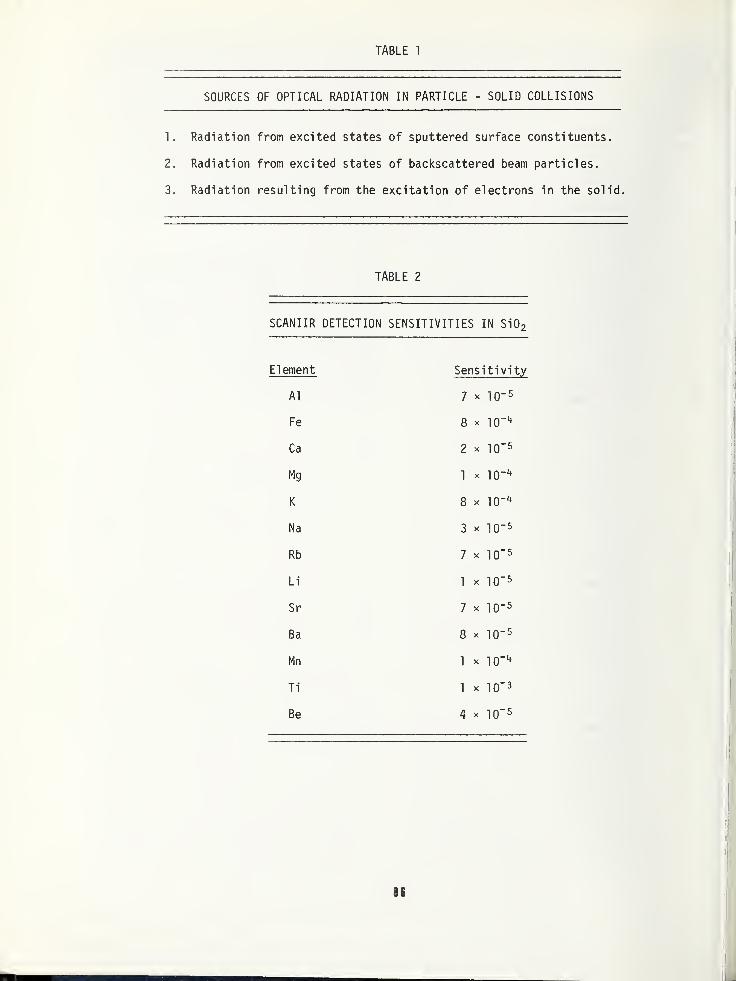
TABLE 1
SOURCES OF OPTICAL RADIATION IN PARTICLE - SOLID COLLISIONS
1. Radiation from excited states of sputtered surface constituents.
2. Radiation from excited states of backscattered beam particles.
3. Radiation resulting from the excitation of electrons in the solid.
TABLE 2
SCANIIR DETECTION SENSITIVITIES IN Si0 2
Element Sensitivity
Al 7 X 10" 5
Fe 8 X 10" 4
Ca 2 X 10" 5
Mg 1 X TO" 4
K 8 X 10" 4
Na 3 X 10" 5
Rb 7 X 10" 5
Li 1 X 10" 5
Sr 7 X 10⁻⁵
Ba 8 X 10" 5
Mn 1 X lO-4
Ti 1 X 10" 3
Be 4 X 10" 5
II
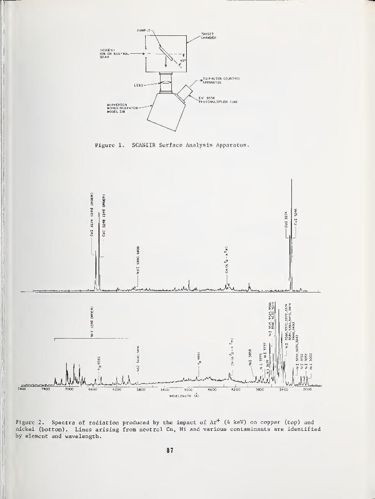
INCIC
IONBEAI
Figure 1. SCANIIR Surface Analysis Apparatus.
fcjgsa— r~ i- t r-~~i -i ; i , , , i i i i i i i i t*" v
'i^-1
7800 7400 7000 6600 6200 5800 5400 5000 4600 42 00 3800 34 00 3000
WAVELENGTH (A)
Figure 2. Spectra of radiation produced by the impact of Ar+ (4 keV) on copper (top) andnickel (bottom). Lines arising from neutral Cu, Ni and various contaminants are identifiedby element and wavelength.
87
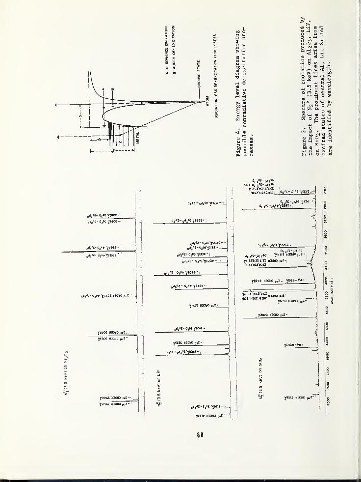
I
60 Oc u
t*
o cJ3 OCO *H
4J
B cd
Cfl 4-1
M -rl
60 OCd X•H CD
•O I
cu
rH XIcu
> cu
(U >
>s cd
60 -rl
>-l XJ<u cd
C Hw coc
<r cu
I-l •
CU CO
U Tt CU
3 co cn
60 CO CO
•rl O CU
tn Cu U
XI "H(U iJo3 »XI co
O Ol-i e-J
Cu i—
I
<cO C•rl O4-1
cd
•rl >xi cu
cd ^t-i m
<4-l •
o CO
cd
i-l o4-1 OJ
o aCU
Cu <4-l
CO o
B x)o dVi cd
H-4
•Hcu COCO•rl -
H tHcd i-4
CO " •
CU i-l £c <d 4J
•H 60i-H t-l C
cd CU
l-l r-l
4-1 CU
3cu cd
• om cd
a.cu Bn -H360 CU
•rl J3fK 4J
acu
c•rl
BO IH >.M O ,£>
P.CO X)
cu cu cu
4-i -hH cd U-l
4-1 lHCO 4J
cCM XI CU
O CU XI•rl 4J "H
rl
OXCU cd
od z<l£-a
2Pt'«80£ 1
od z<l£-a
zP£'«60£-
„d,<l£- S-St '\Tfcfr6£-
0d,d£- Se«»'YSI96«
0dj<l£- Q
zPb 'VSZSZ HBOBO puZ " i
VZ80£ M30d0 PuZ-
V£60£ M3CW0 puZ
yfrt>6£ M3QM0 puZ -
ygi96£ aaaao puz-
„djdZ- 0jPryS6i£-
0d Ji'2-0jP9'VSI6£-_
0djdZ- Sj'S'yEZZfr -_
z<iZ - 0;P»'Y£09fr-
0d,<i2 - s^fyzzs*-,
0djdZ- a 2
P£'»»OI9 -
T££ZE H30d0 puZ
-
Sj»z -0d;dz 'vacua -
] 3
odj^Z-SjtE 'V9ZI8-.
«£lfr H30M0 puZ•
0, z^-oV*0N» dt z
d£" ode""V6Z5ZVZSZ'6ISZ
1
•9isz'wsz-iosz toe^fif! g«g
S,2d£ -
0d,P£ 'VK9Z -j
a, jH£ -Qditfr'yzesz-|
Si ;d£- od|»fr'y906£ -i
a, z«£-0 Ji p £
dtjiE-A £»£'; 'yfziz «ado pu z-|
y6iz?eizz iizz tiaoao puz^'ZIZZ'IIZZ'BOZZ I
v*t t>z asaao puZ - yi98fr-
yzogzWMM3atJ0
J
'6ISZ >ZSZ '6Z9Z —VI£9Z «30d0 DUZ-
VZB8Z M30M0 puZ -
V906E d30M0 pu Z-
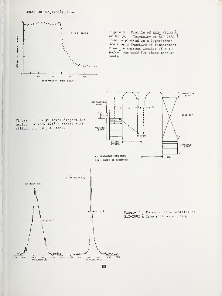
ARGON ON Si02(I200A ) / Si (~)
SII - 2882 JS
80 120
BOMBARDMENT TIME (MINS)
Figure 5. Profile of Si02 (1200 A)on Si (<=°) . Intensity of SiI-2882 Aline is plotted on a logarithmicscale as a function of bombardmenttime. A current density of ^ 10pA/ cm2 was used for these measure-ments .
Figure 6. Energy level diagram for
excited Si atom (4s 1 P° state) near
silicon and Si0 2 surface.
A - RESONANCE IONIZATION
B,B' — AUGER DE-EXCITATION
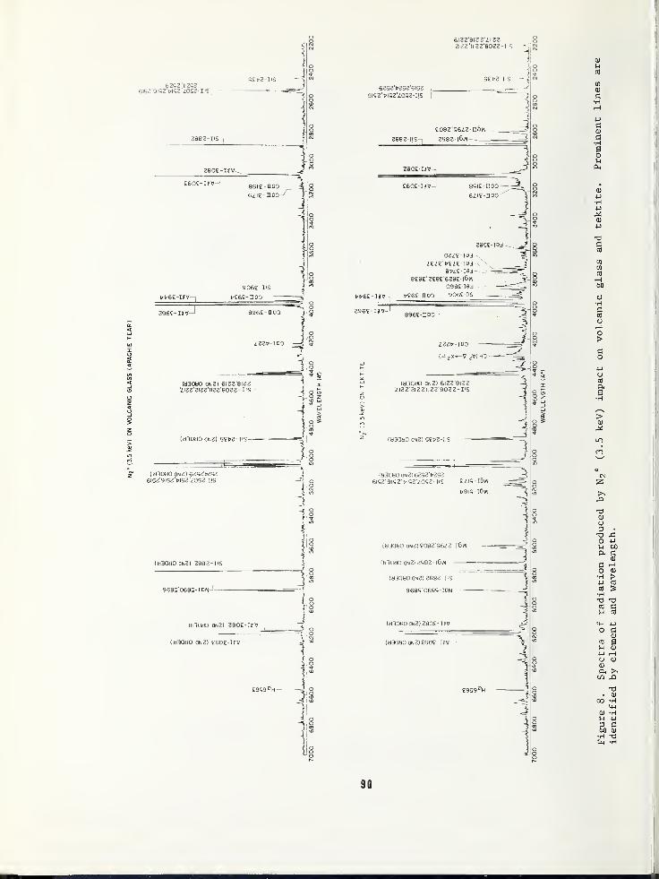
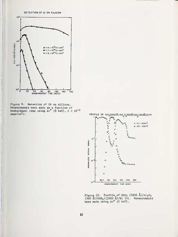
DETECTION OF Cr ON SILICON
10 5 I
BOMBARDMENT TIME (SECS)
Figure 9. Detection of Cr on silicon.Measurements were made as a function ofbombardment time using Ar+ (8 keV) , 4 x 10~ 6
amps/cm2 )
.
PROFILE OF SiO ?(2000A)/At 0 (500A)/SiO (IOOOA)/Si(-)
0A * rf^o
o - Sil - 2882 A
a - All - 396I
A
80 ^I
320_J
400I
BOMBARDMENT TIME IMINS)
Figure 10. Profile of Si02 (2000 A)/A120 3
(500 A)/Si02 /(1000 A) /Si (°°) . Measurementswere made using Ar+ (5 keV)
.
11
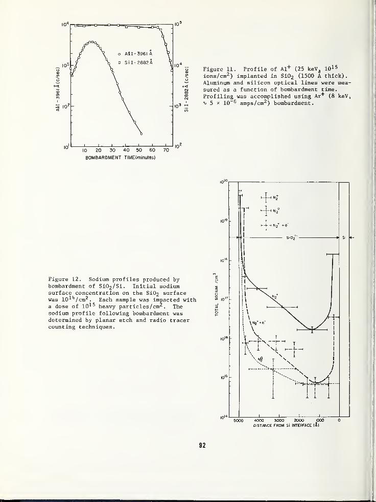
10'
10 20 30 40 50 60
BOMBARDMENT TIME(minutes)
7010'
Figure 11. Profile of Al+ (25 keVa
10 15
ions/cm2 ) implanted in SiC>2 (1500 A thick).
Aluminum and silicon optical lines were mea-sured as a function of bombardment time.
Profiling was accomplished using Ar+ (8 keV,^ 5 x 10
-6 amps/cm2 ) bombardment.
Figure 12. Sodium profiles produced bybombardment of Si02 /Si. Initial sodiumsurface concentration on the Si02 surfacewas 10 11+ /cm2 . Each sample was impacted witha dose of 10 15 heavy particles/cm2
. Thesodium profile following bombardment wasdetermined by planar etch and radio tracercounting techniques.
4000 3000 2000 \000
DISTANCE FROM Si INTERFACE (A)
11
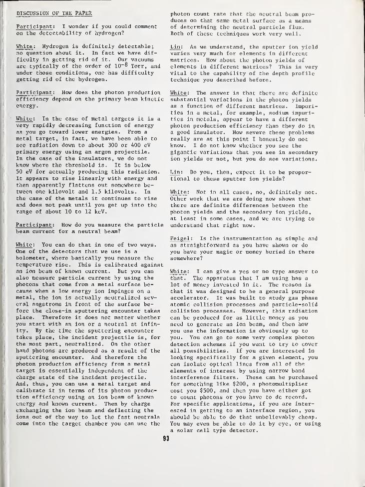
DISCUSSION OF THE PAPER
Participant : I wonder if you could commenton the detectability of hydrogen?
White: Hydrogen is definitely detectable;no question about it. In fact we have dif-ficulty in getting rid of it. Our vacuumsare typically of the order of 10~° Torr, andunder those conditions, one has difficultygetting rid of the hydrogen.
Participant : How does the photon productionefficiency depend on the primary beam kineticenergy.
White: In the case of metal targets it is a
very rapidly decreasing function of energyas you go toward lower energies. From a
metal target, in fact, we have been able to
see radiation down to about 300 or 400 eVprimary energy using an argon projectile.In the case of the insulators, we do notknow where the threshold is. It is below50 eV for actually producing this radiation.It appears to rise linearly with energy andthen apparently flattens out somewhere be-tween one kilovolt and 1.5 kilovolts. In
the case of the metals it continues to riseand does not peak until you get up into therange of about 10 to 12 keV.
Participant : How do you measure the particlebeam current for a neutral beam?
White : You can do that in one of two ways.One of the detectors that we use is a
bolometer, where basically you measure thetemperature rise. This is calibrated againstan ion beam of known current. But you canalso measure particle current by using thephotons that come from a metal surface be-cause when a low energy ion impinges on ametal, the ion is actually neutralized sev-eral angstroms in front of the surface be-fore the close-in sputtering encounter takesplace. Therefore it does not matter whetheryou start with an ion or a neutral at infin-ity. By the time the sputtering encountertakes place, the incident projectile is, forthe most part, neutralized. On the otherhand photons are produced as a result of thesputtering encounter. And therefore thephoton production efficiency from a metaltarget is essentially independent of thecharge state of the incident projectile.And, thus, you can use a metal target andcalibrate it in terms of its photon produc-tion efficiency using an ion beam of knownenergy and known current. Then by chargeexchanging the ion beam and deflecting theions out of the way to let the fast neutralscome into the target chamber you can use the
photon count rate that the neutral beam pro-duces on that same metal surface as a meansof determining the neutral particle flux.Both of these techniques work very well.
Lin : As we understand, the sputter ion yieldvaries very much for elements in differentmatrices. How about the photon yields ofelements in different matrices? This is veryvital to the capability of the depth profiletechnique you described before.
White : The answer is that there are definitesubstantial variations in the photon yieldsas a function of different matrices. Impuri-ties in a metal, for example, sodium impuri-ties in metals, appear to have a differentphoton production efficiency than they do ina good insulator. How severe these problemsreally are at this point I honestly do notknow. I do not know whether you see thegigantic variations that you see in secondaryion yields or not, but you do see variations.
Lin : Do you, then, expect it to be propor-tional to these sputter ion yields?
White : Not in all cases, no, definitely not.Other work that we are doing now shows thatthere are definite differences between thephoton yields and the secondary ion yields,at least in some cases, and we are trying tounderstand that right now.
Feigel : Is the instrumentation as simple andas straightforward as you have shown or do
you have your magic or money buried in theresomewhere?
White : I can give a yes or no type answer to
that. The apparatus that I am using has a
lot of money invested in it. The reason is
that it was designed to be a general purposeaccelerator. It was built to study gas phaseatomic collision processes and particle-solidcollision processes. However, this radiationcan be produced for as little money as youneed to generate an ion beam, and then howyou use the information is obviously up to
you. You can go to some very complex photondetection schemes if you want to try to coverall possibilities. If you are interested in
looking specifically for a given element, youcan isolate optical lines from all of the
elements of interest by using narrow bandinterference filters. These can be purchasedfor something like $200, a photomultipliercost you $500, and then you have either gotto count photons or you have to dc record.
For specific applications, if you are inter-ested in getting to an interface region, youshould be able to do that unbelievably cheap.
You may even be able to do it by eye, or usinga solar cell type detector.
Harrington : Both ion and neutral beams will
give secondary electrons and charged sur-
faces. Evidently from your experience, this
is a second order effect in charging sur-
faces. Would you care to comment on that?
White : You can, under the conditions of
neutral bombardment drive a lot of the
sodium through an SiC>2 film to an interfaceif you put a collector in front of the tar-
get and collect the negative charge that
comes off the bombarded surface. By biasingthe collector to a certain voltage, you can
control, or at least roughly control, what
the surface potential will be on the bom-
barded surface. Now, our experience has
been that if the collector is biased to
approximately 100 V, you can then begin to
see significant effects associated withdriving sodium through the oxide. However,
if you are not purposely collecting the
secondary electrons that are emitted from
the surface, then I do not expect that the
bombarded surface is going to increase to a
potential which is any greater than the
average energy of the secondary electrons.
This, I think is of the order of just a few
volts, approximately 4 or 5 volts. There-
fore, I think that this would be the only
driving field that you would have, at least
under the conditions that we have seen.
This does not appear to be enough to give us
sodium transport.
Participant : Do you have any techniquesfor reducing the cratering effect of neutralbeams?
White : No. The only technique that we haveis to narrow down the field of view of theoptical detection system to the point wherewe are looking at a very small region. Andthen we hope that we are in the middle ofthe bombarded region. However, you can playgames. We produce neutral beams by accel-erating positive ions up to the desiredenergy and then partially neutralizing theions by resonant charge transfer in theirown gas. Resonant charge transfer is anatomic process in which there is very littlemomentum transfer so the resulting neutralhas essentially the same energy and directionas the initial fast ion. If the aperturesin the charge exchange region are opened up,then a certain amount of rastering of theion beam before it goes through the chargeexchange region is possible. By this tech-nique a certain amount of rastering of theneutral beam is possible. But we have notdone that yet and we have no plans to do it.
Participant : Have you looked for, or haveyou seen, any effects of damage while pro-filing implanted impurities?
White : No, as a matter of fact we have not.
We have just gotten into the implantationbusiness and we definitely have not looked
for topography changes in the bombarded region
yet. That is obviously something we should be
doing, and in the future we will be. But in
terms of the ion implantation profiles, we
have done so few of them at this point that
it is really meaningless to talk about them.
NBS Special Publication 400-23, ARPA/NBS Workshop IV, Surface Analysis for Silicon Devices,held at NBS, Caithersburg , Maryland, April 23-24, 1975 (Issued March 1976)
NUCLEAR RESONANCE AND BACKSCATTERING SURFACE ANALYSIS OFSILICON AND RELATED INSULATORS*
Kenneth L. Dunning
Naval Research LaboratoryWashington, D.C. 20375
INTRODUCTION
Methods for surface analysis which are basedon nuclear reactions and scattering general-ly require more complex and expensive appa-ratus than do other methods considered at
this workshop and, in addition, are morelimited with respect to the number of host-impurity combinations that can be profitablyexamined. On the other hand, these methodshave some distinctive features which makethem very useful in investigations pertain-ing to the technology of silicon and relatedinsulators. For example, distributions of
sodium in thin layers of silicon dioxide onsilicon substrates can be accurately and re-
peatedly profiled; such measurements cannotbe made by means of methods which sputteraway the specimen in the depth-profilingprocess
.
Two of the most useful nuclear methods for
quantitative surface analysis are: nuclearresonance profiling and Rutherford backscat-tering. This paper is concerned with the
principles and applications of these methods,with emphasis on the first since it is lessfamiliar, and with the discussion of thesecond confined mainly to a recently-intro-duced improvement in the depth resolutionvery near the surface. These methods can beused to measure impurity depth-concentrationprofiles with depth resolution of the orderof tens of angstroms (very near the surface)
.
In interior regions, depuh resolution is
poorer, changing roughly as the square rootof the depth. The depth scale is based uponthe average rate of energy loss of the bom-barding particles as they penetrate thespecimen. This basis for the establishmentof depth scales is better understood andprovides greater reproducibility than do
methods based upon sputtering rates. Al-though charged particles with energies in
the neighborhood of one million electronvolts do alter the crystalline structure of
solids which they penetrate, their effect
* This research was partially supported bythe Defense Nuclear Agency under subtaskZ99QAXTA007, work unit 52, work unit title"Electronic Transport and Trapping in
Thin-Film Oxides."
upon the distribution of elements is generallynegligible and can be investigated by repeat-edly measuring a particular depth-concentra-tion profile.
References [1] through [3] are concerned withmaterials analysis by means of nuclear reac-tions in general; references [4] through [8]
are specialized to nuclear resonance reac-tions; reference [9] is a recent review of
backscattering and nuclear-reaction analysismethods
.
INTERACTION OF ONE-MeV PROTONS WITH SILICON
The sketch of Figure 1 is intended as an aidto a brief review of the way charged particleswith energies in the neighborhood of 1 MeVinteract with silicon. For def initeness
,
protons are taken to be the incident parti-cles; remarks on the interaction of alphaparticles (which are commonly used for Ruther-ford backscattering analyses) will be insertedas the discussion proceeds. The sketch rep-resents a layer of silicon 1,000 A thick. Asthe protons penetrate the layer, they loseenergy in a large number of small-angle in-
elastic scatterings depicted at the top of
the figure. The average loss of 1-MeV pro-tons traversing 1,000 A of silicon will be 4
keV; the energy loss is linear with the depthof penetration and, hence, the depth can beconveniently measured in terms of this energyloss. Energy loss serves as a basis for a
depth scale in both nuclear resonance pro-filing and Rutherford backscattering. As the
protons pass through the silicon layer, theyexcite and ionize the atoms of silicon,losing a few electron volts in each inter-action, and emerge in essentially the samedirection in which they entered. At thesevelocities , a proton may occasionally pick up
an electron but more than 99% of the time it
is simply a stripped hydrogen nucleus. If
the protons were to enter as hydrogen atoms,
they would be stripped almost immediately andproceed as stripped nuclei. Alpha particlespenetrating matter behave in a very similarway; however, the rate of energy loss withdepth for 1-MeV a particles is about 7 timesas great as for 1-MeV protons. This is anadvantage in measuring depth by means of
energy loss.
35
Although the average loss for 1-MeV protonstraversing the layer is 4 keV, the losses of
individual particles will be distributedabout this average in a predictable way.
For penetration depths of the order of tensof keV, these loss distributions are Gaussianshaped; for small penetrations, the lossdistributions are asymmetric about the meanbut can still be predicted with great accu-racy by means, for example, of the theory ofP. V. Vavilov [11]. The full width at halfmaximum of the energy loss distribution of
the protons emerging from the layer of sili-con depicted is about 2.8 keV. It is thisphenomenon of energy-loss fluctuations whichis the chief source of depth resolutiondegradation in nuclear resonance profilingand Rutherford backscattering. The processrepresented at the middle of the sketch of
Figure 1 is that of large-angle scattering.If this large-angle scattering occurs be-cause of the Coulomb field interactions andnot because of nuclear interactions, we callit Rutherford scattering. The probabilityfor the occurrence of this process in a
layer of the type illustrated is much less
than the first process described but suffi-cient so that detectors can be located to
measure the number and the energies of thescattered particles and this informationused to establish quantitative depth-concen-tration profiles.
A third process of interest is illustratedat the bottom of the sketch; a proton is
captured into the nucleus of one of the tar-get atoms to form a compound nucleus of a
new atomic species. Many different modes of
decay of the compound nucleus are possible;two are illustrated. The decay mode in
which a gamma ray is emitted is very usefulfor nuclear resonance profiling but that in
which a nucleon is emitted can also be used.
The probability for nuclear capture is oftenan extremely sharp function of the energy of
the incident protons and the process is some-times described as resonance capture.
PRINCIPLES AND APPLICATIONS OF NUCLEARRESONANCE PROFILING
It is convenient to present the principlesof nuclear resonance profiling with an ex-ample which makes use of a sharp resonancein the 27Al(p, y)
28 Si reaction at a protonenergy of 991.9 keV. The sketch of figure 2
shows a proton beam incident upon a silicontarget which has a layer of aluminum atomsat the surface and another at a depth of
500 A. A depth scale in angstroms is shownat the top of the target and at the bottomof the target is a depth scale in keV of theenergy loss for the proton beam as it
penetrates the target. The resonance in thisreaction is very sharp having a full width athalf maximum of 0.10 keV. If the proton en-ergy is advanced in small steps from 1/2 keVbelow resonance energy to about 6 keV aboveresonance energy and a fraction of the gammarays from the target is counted by means of asodium iodide detector (with an energy window9 to 12 MeV) for a fixed number of protons ontarget at each energy step, a gamma-ray yieldcurve of the kind illustrated in the lowerhalf of the sketch will be obtained.
To understand the role of the resonance, con-sider the interior target layer containingaluminum atoms. When the bombarding energyis 2 keV above resonance, the most probableenergy loss for the protons that have arrivedin this layer is 2 keV; thus, the protons inthis layer are very near resonance energy.Most of the protons to the left of this layerare above resonance energy and those to theright are below resonance energy. The firstpeak in the gamma-ray yield curve is associ-ated with the first layer in the target con-taining aluminum atoms. The first peak is
higher and narrower than the second peak be-cause there are more aluminum atoms in thefirst layer than in the interior layer andthere is less energy-loss straggling. Thearea under the gamma-ray yield curve is pro-portional to the number of aluminum atoms inthe layer. The abscissa scale on the gamma-ray yield curve is a measure of the incidentproton energy in keV above resonance energy.The figure has been drawn so that the abscissascales of keV energy loss and incident protonenergy above resonance are numerically equal.The yield curve, when plotted as a functionof bombarding energy above resonance, pro-vides an approximate depth-concentration pro-file. It is not a perfect depth-concentra-tion profile because the incident proton beamhas a small but finite width to its energydistribution and the resonance also has a
small but finite energy width. The mostserious impediment to precision is the sta-tistical fluctuation in the energy loss of
the protons as they penetrate the solid, thatis, energy-loss straggling. This stragglingbecomes more pronounced with depth, increas-ing approximately as the square root of thedepth of penetration.
Although the approximate profile provided bythe yield curve is often accurate enough forsome purposes, a much more exact profile canbe obtained with the help of the followingequation which describes the yield Y(Eb) as
a function of the bombarding proton energy,Eb [10].
r(Eb
) = Const^jI
o(E) gCE^E^ w(E1~E,A) C(A) dE dE
idA
where o(E) is the cross section for the27Al(p,y) 28Si reaction in the vicinity of
the resonance (Breit-Wigner formula)
,
gCE-L.Ejj) is the beam-energy distribution,w(E-l-E,~A~) is the energy-loss distributionwhich gives the probability that for a depthin the target for which the average energyloss is ~K, the exact energy loss is E^-E,and CCA) is the concentration function.That is, the protons which are in an energybin of width dE^ at E-^ before entering thetarget have the probability, w, of being de-graded into energy bin of width dE at E in
the neighborhood of resonance energy on _their way to the target layer of width dA at
depth ~E. The beam-energy distribution de-pends upon the characteristics of the beam-energy analyzer and, for the case at hand,the energy-loss distributions can be calcu-lated by the theory of P. V. Vavilov [11,12].
One point of view that may be helpful is to
think of performing the integration withrespect to E^ first. This would give a newfunction of E and ~E. This proton energydistribution in the target broadens withdepth, making the uncertainty for the calcu-lated yield greater in interior regions thanat the surface. Note that an additional in-
tegration with respect to E^ will give thearea under the yield curve, this area is
proportional to the total number of aluminumatoms represented by the profile. The fore-going equation may be used to calculate, to
within a constant, ordinates on the gamma-ray yield curve if the concentration func-tion, C(K) is known. The constant can bedetermined from a measurement of the yieldfrom a homogeneous target of known thickness.If a yield curve is measured for a targetwith an unknown concentration profile, wecan equate the experimental yield to theright-hand side of the equation but are thenfaced with the task of extracting the con-
centration function. Since the measuredgamma-ray yield curve is an approximation of
C(A) , we may construct a trial function,calculate the yield function, and compare it
with the experimental yield curve. If the
comparison is not satisfactory, the compari-son may be used as a guide to construct a
new trial concentration function and theprocess iterated until satisfactory agree-ment between the calculated yield and exper-imental yield is obtained. With the aid of
a digital computer to make the calculationsand plot the experimental yield curve, thecalculated yield curve, and the concentrationfunction, a very satisfactory representation
of the concentration function can be obtainedwith a few iterations.
Figure 3 illustrates results obtained withthe procedure described for a target whichwas made by depositing 600 A of aluminumoxide on a silicon substrate. A gamma-rayyield curve was then measured by counting thegamma rays as the bombarding energy was ad-vanced in small steps from below resonance to10 keV above resonance; these data are repre-sented by the circles. The concentrationfunction of the aluminum in the oxide is rep-resented by the solid line. The calculatedgamma-ray yield curve is represented by thetriangles. The fact that the yield rises be-fore the profile (near resonance) is due tothe finite widths of the resonance and theincident beam-energy distribution. The"spike" at resonance is due to the asymmetryof the energy-loss distributions. The di-vergence of the calculated and experimentalyield curves from the profile near the backface is due to the energy-loss straggling.
The area under the experimental curve is pro-portional to the number of aluminum atomsrepresented by the profile. The constant of
proportionality can be easily obtained andexperience has shown that the number of atomsrepresented by the profile can be determinedwith an accuracy of about 5%. This determi-nation does not depend upon the shape of thebeam, the shape of the resonance, or the ef-fects of energy-loss straggling.
Figure 4 shows a profile for an unknown sampledetermined by this method. The sample wasmade by implanting 60-keV aluminum into sili-con carbide and then annealing at a tempera-ture of 1400°C. The sample was profiled be-fore annealing and it was found the profilehad a Gaussian shape with a peak at about700 A. The annealing drastically altered theprofile, bringing aluminum to the surfaceregion. A comparison of areas showed that
there is much less aluminum in the region of
the profile than there was before the anneal-ing. The width of the spike in the profileat the face of the target is about 20 A at
half height. This gives some idea of whatthe depth resolution can be at the very faceof the target. In interior regions, it is
poorer than this due to energy-loss strag-
gling. If such a spike concentration werelocated in the interior of the target then the
yield curve representing it would be smearedout; the accuracy to which the profile couldbe constructed depends upon the depth at
91
which the spike occurs and upon the statis-tical uncertainty of the experimental data.
It is feasible to profile sodium in thinsilicon dioxide layers by means of this
method. Reproducible profiles have been ob-
tained for sodium in thin layers of silicondioxide on silicon, both for test structureswhich have thin gold layers on the silicondioxide surface and for test structureswhich have no metallic layer. There is,
however, a limit to the fluence of protonswhich can be passed through the silicon di-oxide layer without disturbing the sodiumdistribution. Figure 5 shows the results of
measurements on a test structure consistingof 3,000 A of silicon dioxide on a silicon
' o
substrate with a 175-A layer of gold evapo-rated onto the surface of the silicon diox-ide. Prior to the deposition of the goldsurface layer, the structure was implantedwith 60-keV sodium to a fluence of 10 15
atoms/cm2. The profile represented by the
solid line was obtained for the as-preparedstructure. It was re-measured to insurethat the measurement process did not alterthe profile. The specimen was then irradi-ated with 13-keV electrons (with the gold at
+30 V relative to the silicon) to a fluenceof 10 13 /cm2
, the profile measured, and thenre-measured to insure reproducibility. Theelectron irradiation has caused a migrationof the sodium from the region profiled. It
appears that some sodium has moved deeperinto the specimen and that sodium has mi-grated through the gold film on the surfaceof the silicon dioxide. However, there is
the possibility, of sodium contamination to
the gold surface during the electron irradi-ation. These data are presented simply to
demonstrate the profiling technique.
PRINCIPLES AND APPLICATIONS OF RUTHERFORDBACKSCATTERING SURFACE ANALYSIS
Much has been written concerning the appli-cation of Rutherford backscattering to theanalysis of surfaces [2 , 9 ] .Nuclear resonancesare not used in this method to improve the
depth resolution as was done in the previ-ously discussed method. Instead, the depthscale is established on the basis of theenergy loss of the incident charged particle(usually an a particle) in its trip to thescattering atom in the solid being analyzedand, after scattering, to the detector. In
some situations, scattering can be enhancedby nuclear resonances but this is generallyavoided so that the cross section for scat-tering can be computed from the Rutherfordformula. The method is best suited to theprofiling of heavy impurity atoms in lighthosts
.
The principles upon which the method is basedcan be quickly reviewed by referring to fig-ure 6. Mono-energetic a particles (typicallyin the range 1 to 3 MeV) are shown incidentfrom the right upon a target consisting of analuminum oxide substrate covered by a thinnickel film which is, in turn, covered with a
thin gold film. Scattered particles are usu-ally detected by a semiconductor detectorshown at the upper right. The voltage pulsesfrom such a detector are proportional to theenergy of the scattered particle. If thesepulses are sorted by a pulse-height analyzerand displayed on an oscilloscope, a pulse-height (energy) spectrum such as that dis-played in the lower part of the diagram is
obtained. The energy, EQ , of the incidentparticles is an upper limit to the energy of
the scattered particles. The high-energyside of the peak in the scattered spectrummarked Au is due to the scattering from thesurface of the gold since the gold atoms arethe heaviest atoms in the target and the in-cident particles have lost very little or no
energy in the target before being scattered(billiard-ball kinematics) . Alpha particlesthat are scattered from the interior of thegold film lose energy on the way to the scat-tering center and again on the way to thedetector by small-angle inelastic scatteringsuch as that discussed in connection withfigure 1. Thus, if there are no atoms in thetarget which have nearly the same mass as thegold atoms, a peak will be formed in thescattered spectrum whose height is propor-tional to the number of gold atoms/cm2 andwhose width is proportional to the thicknessof the gold layer. A similar peak appears inthe scattering spectrum due to the presenceof the nickel. The a particles scatteredfrom nickel all have lower energies than anyparticle scattered from gold because thenickel atoms are not as heavy as the goldatoms and, in addition, the incident particlemust lose energy in the gold layer before anyscattering from the nickel can take place.Since the aluminum oxide substrate is con-sidered to be very thick relative to thenickel and gold layers, the a particles scat-tered from aluminum atoms form a continuumwhich extends essentially to zero energy and,
similarly, the contribution to the backscat-tered spectrum from the oxygen appears on top
of this continuum. The signal-to-backgroundratio is much better for the heavy elementsthan for the oxygen. Since the cross sectionfor scattering can be calculated from theRutherford formula, and the rate of energyloss of the a particles in various materialshas been measured and cataloged [13] , the dat
in the scattered spectrum may be used to con-
struct a quantitative depth-concentrationprofile
.
The depth resolution for the method justdescribed is determined by the finite energywidth of the incident a-particle energy dis-tribution, the energy-loss straggling in thetarget, and the energy-loss straggling in-
troduced by the detector. The energy loss
in such detectors is usually in the range 10
to 15 keV with the width of the energy-lossdistribution being in the neighborhood of 10keV; this can cause an uncertainty in thedepth scale at the face of the target, typ-ically, in the neighborhood of 100 A.
There are a few laboratories where the semi-conductor detector in a scattering apparatushas been replaced by a magnetic spectrometerwhich determines the energy of the scatteredparticle without introducing energy loss.
Figure 7 shows such an arrangement which hasbeen developed and tested by Dr. J. K.
Hirvonen and his colleagues at the Naval Re-search Laboratory. The spectrometer can berotated about a verticle axis and positionedto accept a certain fraction of the particlesscattered from a target. Of the particlesscattered, those within a small range of
momentum (determined by the strength of themagnetic field which is perpendicular to thepaper) will pass through the spectrometerand be detected in a position-sensitive de-tector in the image plane of the spectrome-ter. The voltage pulses from this detectorare routed to a pulse-height analysis sys-tem. The energy coordinate of the contribu-tion of a particle to the scattered-particlespectrum is determined by the position at
which the particle strikes the detectorwhich is located in the image plane of thespectrometer. With this arrangement, one ob-
tains only a small part of the semiconductorenergy spectrum but the degradation of depthresolution introduced is an order-of-magni-tude smaller than that introduced by a semi-conductor detector.
In order to measure the effect of the scat-tered-particle detector on the depth resolu-tion, it is useful to have a very thin tar-
get of heavy atoms. The data of figure 8
were obtained with a target made by deposit-ing gold onto silicon dioxide to an averagethickness of one monolayer. However, golddeposited in such thin layers tends to form"islands" which means that some of the in-cident 2-MeV a particles were scattered by
several monolayers of gold. At any rate, wehave a target which is quite thin.
The upper part of figure 8 shows a spectrumobtained with a semiconductor detector. Theleft half of the spectrum is due to the sil-icon and oxygen and is not of interest. At
the high-energy end of the spectrum is the
contribution from the gold, a peak with a fullwidth at half maximum of 16 keV. This widthis due almost entirely to the energy-lossstraggling in the semiconductor detector.The spectrum at the lower right of the figurewas obtained with the magnetic spectrometer.The full width at half maximum of the peak is
now 5 keV and less than half of this is dueto the uncertainty in the scattered energydue to the spectrometer arrangement which is
about 2 keV and corresponds to an uncertaintyin the depth scale of a depth-concentrationprofile of about 25 A. Thus, the depth reso-lution that may now be achieved with Ruther-ford backscattering at the surface of a
specimen is comparable to that illustrated in
figure 4 with nuclear resonance profiling.
The magnetic spectrometer arrangement hasanother advantage; it passes scattered parti-cles whose energies fall only within a narrowband, whereas the semiconductor detector seesa much larger number of particles per unit oftime. This results in a higher background in
the semiconductor detector scattered spectrumdue to pulse "pileup" and degrades the detec-tion level. The "spectrum" at the lower leftof figure 8 was obtained by bombarding a sil-icon dioxide target with no gold layer. Al-though five times as many incident a partic-les were used in this case as were used to
obtain the spectrum at the lower right, not a
single event was recorded in the 40-keV re-gion spanned by the abscissa. If one counthad been recorded, the detection limit forthe gold would be 10 10 atoms /cm 2
. The de-tection limit with the semiconductor detectoris about 10 12 gold atoms/cm 2
. Thus we seethat we can expect a depth resolution verynear the surface of about 25 A with a detec-tion limit of less than 10 10 atoms/cm2 withthis spectrometer arrangement for a target
that is free from contaminating atoms withatomic weights near that of gold.
CONCLUSION
Some of the more important features of the
two discussed methods of obtaining depth-con-centration profiles can be summarized and
compared as follows.
(1) Both methods discussed are nondestructivein the sense that the atoms struck are not
moved very far (at least almost never) . How-
ever, the probing ions do move the struck
atoms from their lattice sites far enough to
degrade the crystalline structure.
(2) Repeated measurements can be made on the
same test specimen and these measurements can
be interspersed with various other processessuch as annealing and irradiation.
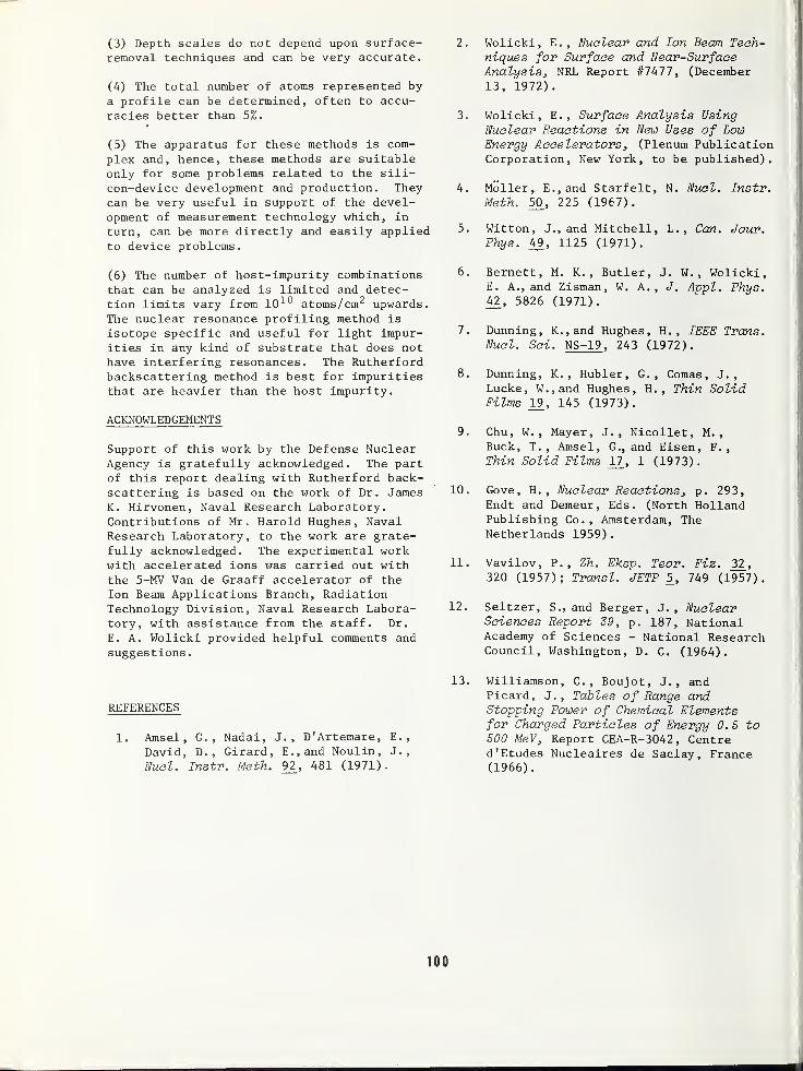
(3) Depth scales do not depend upon surface-removal techniques and can be very accurate.
(4) The total number of atoms represented by
a profile can be determined, often to accu-racies better than 5%.
(5) The apparatus for these methods is com-
plex and, hence, these methods are suitableonly for some problems related to the sili-
con-device development and production. Theycan be very useful in support of the devel-opment of measurement technology which, in
turn, can be more directly and easily appliedto device problems.
(6) The number of host-impurity combinationsthat can be analyzed is limited and detec-tion limits vary from 10 10 atoms/cm 2 upwards.
The nuclear resonance profiling method is
isotope specific and useful for light impur-ities in any kind of substrate that does nothave interfering resonances. The Rutherfordbackscattering method is best for impuritiesthat are heavier than the host impurity.
ACKNOWLEDGEMENTS
Support of this work by the Defense NuclearAgency is gratefully acknowledged. The partof this report dealing with Rutherford back-scattering is based on the work of Dr. JamesK. Hirvonen, Naval Research Laboratory.Contributions of Mr. Harold Hughes, NavalResearch Laboratory, to the work are grate-fully acknowledged. The experimental workwith accelerated ions was carried out withthe 5-MV Van de Graaff accelerator of theIon Beam Applications Branch, RadiationTechnology Division, Naval Research Labora-tory, with assistance from the staff. Dr.
E. A. Wolicki provided helpful comments andsuggestions
.
REFERENCES
1. Amsel, G. , Nadai, J., D'Artemare, E.
,
David, D. , Girard, E.,and Noulin, J.,
Nucl. Instr. Meth. 9^2, 481 (1971).
2. Wolicki, E., Nuclear and Ion Beam Tech-niques for Surface and Near-SurfaceAnalysis, NRL Report #7477, (December
13, 1972).
3. Wolicki, E., Surface Analysis UsingNuclear Reactions in New Uses of LowEnergy Accelerators, (Plenum PublicationCorporation, New York, to be published).
4. Moller, E.,and Starfelt, N. Nucl. Instr.Meth. 50, 225 (1967).
5. Witton, J., and Mitchell, L. , Can. Jour.Phys. 49, 1125 (1971).
6. Bernett, M. K. , Butler, J. W. , Wolicki,E. A., and Zisman, W. A. , J. Appl. Phys.42, 5826 (1971).
7. Dunning, K.,and Hughes, H. , IEEE Trans.Nucl. Sci. NS-19 , 243 (1972).
8. Dunning, K. , Hubler, G., Comas, J.,
Lucke, W.,and Hughes, H. , Thin SolidFilms 19, 145 (1973).
9. Chu, W. , Mayer, J., Nicollet, M.
,
Buck, T.,Amsel, G., and Eisen, F. ,
Thin Solid Films 17_, 1 (1973).
10. Gove, H. , Nuclear Reactions, p. 293,Endt and Demeur, Eds. (North HollandPublishing Co., Amsterdam, TheNetherlands 1959)
.
11. Vavilov, P., Zh. Eksp. Teor. Fiz. 32,320 (1957); Transl. JETP 5, 749 (1957).
12. Seltzer, S., and Berger, J., NuclearSciences Report 39, p. 187, NationalAcademy of Sciences - National ResearchCouncil, Washington, D. C. (1964).
13. Williamson, C. , Boujot, J., andPicard, J., Tables of Range andStopping Power of Chemical Elementsfor Charged Particles of Energy 0.5 to500 MeV, Report CEA-R-3042 , Centred' Etudes Nucleaires de Saclay, France(1966).
100
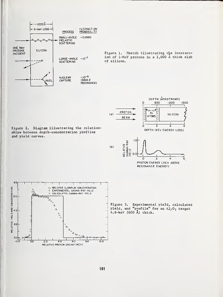
INTERACTIONPROCESS PROBABILITY
ONE MeVPROTONSINCIDENT
SILICON
"°^NUCL
SMALL-ANGLEINELASTICSCATTERING
NUCLEARCAPTURE
-0.9999
LARGE-ANGLE ~I0"SCATTERING
HOT*(SINGLERESONANCE)
Figure 1. Sketch illustrating tlje interact-ion of 1-MeV protons in a 1,000 A thick slabof silicon.
(a)
Figure 2. Diagram illustrating the relation-
ships between depth-concentration profiles
and yield curves.
(b)
DEPTH (ANGSTROMS)500 1000 1500
I
11
PROTON
BEAM
ALATOMS
SILICON
DEPTH (KEV ENERGY LOSS)
0 2 4
PROTON ENERGY (KEV ABOVERESONANCE ENERGY)
Figure 3. Experimental yield, calculatedyield, and "profile" for an A120 3 target4.6-keV (600 A) thick.
2.0 4.0 6,0 8.0
RELATIVE PROTON ENERGY (KEV)
101
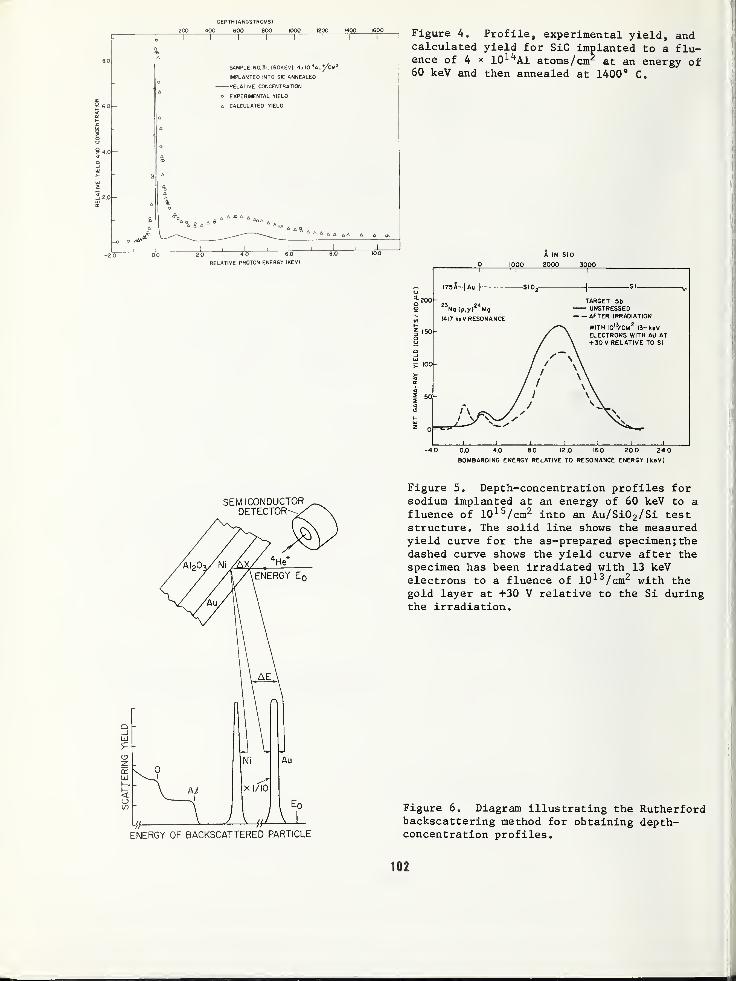
DEPTH (ANGSTROMS)
400 600 900
SAMPLE NO 31. (60KEV) 4i lO^AL^/CM 2
IMPLANTEO INTO SIC ANNEALEO
-RELATIVE CONCENTRATION
EXPERIMENTAL YIELO
CALCULATED YIELD
RELATIVE PROTON ENERGY 1KEVI
Figure 4. Profile, experimental yield, andcalculated yield for SiC implanted to a flu-ence of 4 * 10 14A1 atoms/cm2 at an energy of60 keV and then annealed at 1400° C.
A IN SiO
2000 3000
I75A-
Nolp.x) Mg
1417 keV RESONANCE
TARGET 5bUNSTRESSEDAFTER IRRADIATION
WITH I0l3/CM 2
13- keVELECTRONS WITH AU AT+ 30V RELATIVE TO SI
0.0 4.0 8.0 12.0 16.0 20.0 24.0
BOMBARDING ENERGY RELATIVE TO RESONANCE ENERGY (keV)
SEMICONDUCTORDETECTOR-
Figure 5. Depth-concentration profiles forsodium implanted at an energy of 60 keV to afluence of 10 15 /cm2 into an Au/Si02 /Si teststructure. The solid line shows the measuredyield curve for the as-prepared specimen; thedashed curve shows the yield curve after thespecimen has been irradiated with 13 keVelectrons to a fluence of 10 13 /cm2 with thegold layer at +30 V relative to the Si duringthe irradiation.
ENERGY OF BACKSCATTERED PARTICLE
Figure 6. Diagram illustrating the Rutherfordbackscattering method for obtaining depth-concentration profiles.
102
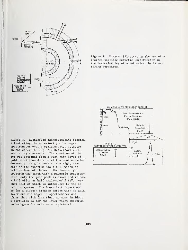
Figure 7. Diagram illustrating the use of a
charged-particle magnetic spectrometer in
the detection leg of a Rutherford backscat-tering apparatus
.
AU MONOLAYER ON SILICON DIOXIDE
Figure 8. Rutherford backscattering spectraillustrating the superiority of a magneticspectrometer over a semiconductor detectorin the detection leg of a Rutherford back-scattering apparatus. The spectrum at thetop was obtained from a very thin layer ofgold on silicon dioxide with a semiconductordetector; the gold peak at the right handside of the spectrum has a full width at
half maximum of 16-keV. The lower-rightspectrum was taken with a magnetic spectrom-eter; only the gold peak is shown and it hasa full width at half maximum of 5 keV, less
than half of which is introduced by the de-tection system. The lower left "spectrum"is for a silicon dioxide target with no goldlayer and the magnetic spectrometer andshows that with five times as many incidenta particles as for the lower-right spectrum,no background counts were registered.
-I 1 l 1
Solid State Detector
-2000 VEnergy Spectrum
10 fj.C charge
-1000 I Detector
^""'•*'""*<*i Resolution —\ 16 KeV
_j iA 1 1
—
i
AE
MAGNETICSCATTERING YIELD (COUNTS)
11
BACKGROUND A J
Si Wafer
-2 50^C,
icvc I
i n
-150 J
system /
resolution _Jj— 5 KeV
103
it

DISCUSSION OF THE PAPER at MeV energies as being almost completelystripped.
Harrington : The magnetic spectrometer thatyou use depends, of course, on ions comingfrom the surface. From what depths can thesereflected particles originate and still beions? Are not most of the particles from,
say, the silicon substrate coming back as
neutrals?
Dunning : At this energy many particles comeoff as charged particles and so I would sayone can analyze at least to micron depths.
Harrington : I was under the impression thatmost of the particles were coming out as
neutrals from those depths. Are they stillionized?
Dunning : My impression is that , at MeVenergies, as soon as an ion enters a solid it
is almost entirely stripped. It will pick upa little charge and loose a little charge as
it goes through but we always think of ions
Dobrott : You showed us a profile of a sodiumion implanted oxide. You told us that thesodium flux was lO^-Vcm^ but do you happen toremember at what energy the implant was made?
Dunning : The energy for the sodium implant I
think was 60 keV.
Dobrott : Then the actual peak that you didsee was probably a little bit deep for thetheoretical projected range of the sodium inthe Si02-
Dunning : It is not exactly according totheory but I think it is not far off.
Dob rott : The peak was shown to fall betweentwo thousand and twenty-five hundred Angstromsinto the sample, and that is pretty deep.
Dunning : No, I would say that that wasfairly near the theoretical peak.
104
NBS Special Publication 400-23, ARPA/NBS Workshop IV, Surface Analysis for Silicon Devices,held at NBS, Gaithersburg, Maryland, April 23-24, 1975 (Issued March 1976)
APPLICATIONS OF SCANNING AUGER SPECTROSCOPY (SAM)TO THE SILICON INTEGRATED CIRCUIT (SIC) TECHNOLOGY
Joseph M. Morabito
Bell LaboratoriesAllentown, Pennsylvania 18103
I. INTRODUCTION
Auger electron spectroscopy is a techniquebased on the emission and energy analysis of
secondary electrons produced by a high energy(3-10 keV) electron beam. The energy of a
small fraction of the secondary electrons canbe related to the core levels of a targetatom; these electrons, the Auger electrons,have an escape depth in the range of approxi-mately 5 to 20 A, making Auger electron spec-troscopy a truly surface sensitive techniquewhich can detect all elements with exceptionof H and He down to approximately 10 12 atomsper centimeter squared or .1 atom percent.The technique, in principle, is nondestruc-tive; but electron beam damage and electronbeam desorption effects can occur. In com-bination with insitu ion sputtering, in-depth profile analysis can be obtained andby the use of multiplexing, several elementscan be monitored while sputtering through thefilm. By the use of finely focussed electronbeams, or optical methods, selected area sur-face analysis can also be obtained, which is
very important when analyzing actual inte-grated circuits. Quantitative analysis is
also possible along with Auger imaging, whichprovides a surface distribution map of the
impurities on the surface.
II. INSTRUMENTATION
Figure 1 shows some of the basic componentsand associated electronics of the commercial-ly available PHI scanning Auger micro-probe. C
1) This consists of an electron gun
used to excite the Auger electrons and a
spectrometer for energy analysis. Electronsof a well-defined energy are focussed on the
exit aperture of the spectrometer and enteran electron multiplier where they are de-
tected by phase sensitive detection using a
lock- in amplifier. The electron gun consistsof 4 basic components; a tungsten triodesource, condenser and objective lenses, and
deflection plates. Its operation is somewhatsimilar to a scanning electron microscope.The condenser lens and the objective lens are
used to demagnify the crossover formed by the
triode source. The deflection plates are
used to raster the beam over the sample.
Electron beam spot sizes down to approximate-ly 5 microns can be obtained and the beam
currents possible are in the range of 10
nanoamps to 10 microamps. To locate areas of
interest on the sample, absorbed current micro-graphs or secondary electron micrographs areused. Useful magnification is about 1,000 X.
Line scans and Auger imaging provide informa-tion on the variations of surface impurities.The Auger imaging is obtained by rasteringthe primary electron beam and intensity modu-lating the z axis of a CRT. Table I shows theminimum time constant required for the analysisof 10 and 1 atom percent, corresponding to sig-nal-to-noise ratios of 10 to 1 and 100 to 1, as
a function of varying beam size (in urn2) for
current densities of 10 7 amps per micronsquared and 10 & amps per micron squared. Apractical limit on the lock-in amplifier is
approximately 10 seconds . This is due to am-plifier drift. This limit is reached at 1
atom percent for a beam area of approximately10_microns squared for a current density of
10 7 A/um2. If_the current density is in-
creased from 10 7 to 10 6 A/um2, this limit
of 1 atom percent is reached at a beam areaof approximately 1 micron squared. Beam areasin the range of 20 to approximately 1 um2
are very useful in the analysis of actual inte-grated circuits. As the beam size is de-creased, the time that it takes to do the anal-ysis increases, and this time is inverselyproportional to the_beam current. Currentdensities in the 10 7 A/um2 range can be ob-tained, as shown by the work of Brandis^ 2 ),
with the tungsten triode source down to ap-
proximately 1 micron squared. Current densi-
ties in the range to 10 6 can only be obtainedwith a lanthium hexaboride source, which is a
brighter source. However, at these beam cur-
rent densities there is a possibility of beamdesorption and beam damage effects,
particularly in the case of insulators.
III. MODES OF OPERATION
The Auger technique, like SIMS, has basicallythree modes of operation: a) Auger spectra,
b) Auger images and c) in-depth profile anal-
ysis. These three modes of operation (illus-
trated in Figure 2) provide a truly three-
dimensional microchemical analysis. Augerspectra are used to detect and identify surfaceimpurities and impurities in the bulk of the
sample. Spectral interferences are less of a
05
problem in Auger Spectroscopy than in SIMS,
but they can occur since the inherent energyspread of Auger electrons is such that it is
difficult to resolve peaks that are within 1
or 2 eV of each other. When this becomes a
problem, the best solution is to add an X-raysource and to obtain photoelectron or ESCAspectra. Some of the unique features of theESCA technique have been described in the
literature.
(
3) One of its unique features
is that it can provide information on chemi-cal environment, but it is also possible to
occasionally obtain information on chemicalenvironment using the Auger spectra. >
5»6 )
This information is contained in peak energyshifts, changes in peak shape, and in finestructure on the low energy side of the peak.Figure 3 shows Auger spectra which were ob-tained on a silicon nitride layer of a sili-con diode array. The spectrum at top is thespectrum obtained prior to sputtering. Priorto sputtering the silicon is partially pre-sent in oxide form( 5
) and the low energy sil-icon transistion is occurring at approximately78 eV. After sputtering we have removed theoxide, the silicon is now no longer presentas oxide and its energy has shifted from 78
eV to approximately 90 eV which is a shift of12 eV. In the case of pure silicon the lowenergy peak occurs at 92 eV. Although suchchanges in the Auger spectra are often ratherdifficult to interpret, they do provide a
fingerprint like the SIMS spectra of the
chemical environment
.
A lateral resolution of approximately 0.5
microns has been demonstrated
(
2) in Auger
imaging. Auger imaging does not require sam-ple consumption, but is limited to
approximately 1 atom percent concentration.
Auger profiling is particularly useful whenmonitoring concentration from the surfaceinto the bulk of a thin film, or when the ex-tent and amount of interdiffusion in multi-layer film is of interest. Figure 4 shows anAuger profile of a titanium-copper-nickel-gold (TCNA) thin film system'' 7
'' after 4 hoursof 350°C. The copper and nickel have com-pletely diffused through the gold layer andare present on the surface as oxides. Themetal oxides can interfere, for example, withTC bonding to this system. Copper is pre-sent throughout the nickel diffusion barrierlayer and has also diffused into the titaniumglue layer. The depth resolution possiblewith Auger profiling is primarily limited byartifacts inherent in the sputtering process.In polycrystalline films the depth resolutionis in the range of 10 to 30 percent of thethickness removed by sputtering. (8) Some or
the problems inherent in sputtering are:First, the possibility of differential
11
sputtering; this is particularly true in the
case of alloys.
(
9 ) It is not always possible
to eliminate, but it can be minimized by the
use, when possible, of higher energy (larger
escape depth Auger electrons) because these
transitions are less sensitive to the change
in surface composition
(
9 ) which results from
differential sputtering. Next, the recoil or
"knock on" phenomenon^ 0 ); this is an effect
whereby lattice atoms are pushed deeper into
the solid during the sputtering process. It
is a cumulative affect, i.e., a function of
film thickness. This can sometimes be mini-
mized by the use of low energy primary ions
in the range of around 500 eV to about 2 KeV.
There is also a possibility of the redeposition
of sputtered atoms. This can be avoided by
careful instrument alignment. Topographical
changes can also occur during the sputtering
operation. The best way to avoid these is to
use smooth substrates when possible. And,
finally, probably one of the worst problems,
a varying sputtering rate throughout the film
due to changes in composition or changes in the
alloying that occurred during the interdiffu-
sion process. This greatly complicates the
assignment of an accurate depth scale. Accu-
rate depth scales are important when extracting
diffusion coefficients from Auger profiles .^ 8 > *jf
:
?
However, the work of Dahlgren and McClanahan' 12 '
has shown, in the case of alloys where the so-
lute is about 10 atom percent or greater, that
the lower sputtering yield element actually
controls the sputtering rate. By using this
fact, it is often possible to assign a rather
accurate depth scale from measurements of
sputtering rate (z) and time.( 8 )
IV. STATUS OF QUANTITATIVE ANALYSIS
There are essentially three methods of
performing quantitative Auger analysis. Meth-
od A is a method based on the use of standards
prepared by techniques such as ion implanta-
tion, ( 13 ) reactive sputtering, and con-
trolled doping.
(
15 ) Method B is the use of
pure elemental samples and sensitivity factors
with an equation of the following form:
I./A-
C. =l
rel
mI I . /A
(1)
j=lrel
where C^ is the concentration of element i,
Ij is the measured Auger peak height, ^ Te ± is
the relative Auger yield of element i refer-
enced or normalized to some matrix element,
and j is a running index summed over all the
elements present in the sample. Method C is
a technique which is independent of any
standards - called the first order approximation
method. Generalized models, e.g., modelssuch as those used for quantitative analysisusing the electron microprobe (17) or SIMS( 18
)
technique, do not at the present time existfor Auger electron spectroscopy. The majorreason for this is that we do not have an ac-curate data base on the ionization crosssections, the escape depths, or on the back-scattering correction. Other reasons in-clude: the sputtering artifacts mentionedand the fact that it is difficult to performbackground correction procedures in Augerspectroscopy. Figure 5 shows a calibrationcurve
(
15 ) obtained on samples which wereprepared by bulk doping. With these cali-bration curves it is possible to measurethe concentration of phosphorus and boronin silicon. This data also establishesthe detectability limits for these dopants in
silicon. In this case, the detectabilitylimits for boron and for phosphorus in sili-con is approximately 8 x 10 18 atoms per cubiccentimeter. Method B has been successfullyapplied to numerous multicomponent sys-tems. ( 8 »
19 ) The first order approximationmethod does not depend on standards, but is
based primarily on the fact that the Augeryield is determined primarily by the ioniza-tion cross section ($) , the transmission of
the spectrometer (n) , and the Auger escapedepth (d) . Work to date has shown that theionization cross section ($) is proportionalto one over the square of the Auger energy,at least for K and L transitions. For theCMA analyzer, the transmission (n) is linearwith energy. Escape depths (d) in a rangeof 100-1,000 eV appear to be proportionalto the square root of the energy. The prod-uct, $nd, is therefore proportional to oneover the square root of the energy. We canuse this fact to estimate the Auger yield orsensitivity factors. Table II shows some of
the results using this method for magnesiumoxide, copper oxide, cadmium sulfide, galliumphosphide, and potassium chloride. The re-sults are quite good, particularly since no
corrections
(
9) for sputtering artifacts have
been made.
Table III shows a comparison between the
bulk detectability limits of Auger and SIMSfor the common dopants in silicon and forthe light element in tantalum. In general,the detectability limits for Auger are in
the range of 10 19 and 10 20 - which is muchless sensitive with regard to bulk detecta-bility limits than SIMS, which can detectboron down to lO 14 atoms/cm 3
. It is veryimportant to be able to detect concentrationsin the range of 10 17 -10 14 in the case of
transistor fabrication. This is just notpossible at the present time with Augerelectron spectroscopy. Possible ways to
1
increase the sensitivity of Auger electronspectroscopy are: 1) increase the transmis-sion (n) of the spectrometer; 2) improve thedetection scheme, e.g., the use of multichan-nel analyzer, data smoothing techniques,deconvolution, background correction, integra-tion techniques, etc.; 3) signal processing -
analog averaging or digital averaging;* 4) usea different source to excite the Auger elec-tron. Some possibilities include high energyproton sources and ions. With these sourcesthe background could be lower.
V. APPLICATIONS OF SCANNING AUGER MICROPROBEIN SILICON INTEGRATED CIRCUIT (SIC)
FABRICATION
a) Analyses Of Contaminated Gold Beam Leads
Gold beam leads are used to attach SIC's to
gold metallized ceramic. Any contaminationof these leads or of the gold on the ceramiccan prevent intimate gold-to-gold contact,which results in unreliable bonding. Figure6 shows an Auger spectrum and absorbed currentmicrograph of a contaminated beam lead. Thebeam lead is ^ 4 mils in width. The brightlower line on the micrograph indicates that
most of the beam current is absorbed by theconducting beam lead which appears dark. Themajor surface contaminants are carbon andoxygen with trace amounts of copper, sodium,and silicon. Although the high energy goldtransition is detectable, the low energy goldtransition at 69 eV is not. This low energygold transition has an escape depth of ^ 5 Aand is completely attenuated by the carbonlayer. The carbon layer does not, however,completely attenuate the high energy goldtransition at 2,017 eV, which has an escape
O
depth of ^ 20 A. This suggests thaf the
carbon layer is no greater than 20 A in
thickness. The carbon Auger image obtainedshowed the carbon to be homogeneous across
the surface, but the copper and silicon Augerimages suggest a heterogeneous distributionfor these elements. Figure 7 shows the in-
depth profile of carbon. As the carbon film
is- removed by sputtering, the intensity of
the low energy gold transition increases.
The thickness of the carbon layer can be
calculated by the following expression^ 20 )
Au Au L \ Au/ \ c Au I
J
* This is not a very practical approach sincea factor 10 increase in sensitivity wouldrequire a factor 100 increase in analysistime
.
where I c /IAu ^s t 'ie measured carbon peak
height normalized to the high energy (2,017
eV) gold peak, and I£/Ia.u is tne ratio or tne
272 eV carbon Auger peak height to the 2,017
eV peak height for carbon and gold in the
pure state. xc is the thickness of the car-
bon layer, d c is the escape depth of the
carbon 272 eV Auger electrons and dAu is the
escape depth of the 2,017 eV gold Auger
electrons. Equation 2 can be simplified to
x = d. Inc Au
(3)
which has been plotted for dAu equal to 4, 6,
and 10 A in Figure 8. These curves can then
be used to estimate the thickness of the car-
bon layer from the data shown in Figure 6.
The thickness of the carbon layer for
I c/I^u = 35.2 is in the range of 8 A (for
dAu = 4 A) to 20 A (for dAu = 10 A) . It is
doubtful that this amount of carbon couldseriously interfere with bonding. Therefore,
the carbon layer is most probably polymerizedby the high energy electron beam, leavingbehind a carbon layer of reduced thickness.There is, in addition, the possibility of
beam desorption of some of the carbon presenton the surface during analysis. Therefore,the actual thickness of the contaminationlayer prior to electron beam excitation is
perhaps a factor 5 higher, i.e., in the rangeof 40 to 100 A, which would definitely in-
hibit bonding.
b) Analysis of Contaminated Gold PlatedCeramic
Figure 9 shows the Auger results obtained on
a gold plated ceramic after pre-bond clean-ing. Pre-bond cleaning which includes a heattreatment of 120°C for 1 hour has increasedthe Cu (920 eV),Au (239 eV) and Ag (354 eV)/Au -
(239 eV) ratios from an average of .36 to
1.24 for the "as-received" sample to .49 and1.70 respectively. This increase is due to
diffusion from the bulk via grain boundaries.There is also a large increase in the oxygenpeak. The large increase in oxygen suggeststhat these impurities are present as oxides.There is, however, no characteristic changein the Auger spectra of Figure 9 (e.g., peakenergy shifts, additional plasma loss peaks)which can be used to verify that oxidationhas actually occurred, but Schon^ 21
) hasrecently used X-ray induced Auger emissionand photoelectron spectroscopy to identifythe presence of Cu, Cu20 and CuO. Unfor-tunately, the energy resolution required^ 21 )
is beyond the capability of most spectrometersused in Auger electron spectroscopy.
The surface concentration of Ag and Cu variedin the range of 1 to 4 at. %. This magnitude
is consistent with the fact that 50 ppm (at. %)
in the bulk, if completely concentrated withinthe first 10 A of the surface, would corre-spond to 4.95 at. % and to 9.9 at. %. The
above calculations were made for a gold bonding
pad with an area of 2.25 x 10⁻² cm2 and a gold
thickness of 10-1+ cm or 1 ym. Figure 10 shows
the calculated surface concentration, Cg ca ^,
which would result if all of the bulk impuri-
ties should concentrate within the first 10 Aof the surface. The bulk concentration wasvaried from 5 to 300 ppm (at. %) . Although it
is highly improbable that all or even most of
the bulk impurities will concentrate on the
surface after processing prior to bonding, a
fraction (a) of the impurities will, and this
fraction can be measured by quantitative Augeranalysis
.
The presence of Sn (Figure 9) is apparentlydue to inadvertent contamination introducedduring pre-bond cleaning, but the Cu and Agare codeposited during plating. A regres-sion analysis (shown in Figure 11) of thebonding and Auger data showed the correlationbetween the presence of Ag, Cu, 0, and Sn on
the surface and poor bonding to be 0.74. Theimpurities present in the bulk are thereforesegregating to the surface during thermal pro-cessing, oxidize, and act as barriers to
intimate gold-to-gold contact.
c) SAM Analysis of Laser Debris On Ti-Pd-AuResonator Electrodes
The frequencies of Ti-Pd-Au resonator electrodescan be raised by vaporizing portions of massfrom the resonator electrode.
(
22) Using the fo-
cussed beam from a Q-switched Nd:YaG laser (A =
1.06 ym) , a series of 25 ym diameter holes on
approximately 125 ym centers are vaporized as
shown in Figure 12. When nominal frequency has
been reached, laser trimming is terminated. The
use of an on-line computer and optical beamsteering techniques permit raster scanning bywhich each resonator is adjusted in three suc-cessive passes. In this manner the effects of
thermal shock can be minimized and the adjust-ment control is as precise as the vacuum opera-tion (± 12 Hz). All initial filter electricalrequirements can be met; i.e., adequate controlover resonator frequencies can be exercised.However, since the laser machining involves the
melting and evaporation of material from the
108
acoustically active region of the resonator,the enhancement of long-term aging mightresult from this operation.
A pair of thin film electrodes which form theresonator region are composed of Ti-Pd-Autri-metal thin films. As the focussed laserpulse strikes the top electrode, a small holeis produced, and material from this region ismelted and evaporated. Most material is
evaporated; however, some material melts,pulls away and forms a lip surrounding the
hole. Other material is ejected and rede-posited in the immediate vicinity of the
hole. An additional problem is encounteredsince the quartz substrate is only 200 ymthick. When the laser beam strikes the top
electrode, it vaporizes in a matter of a fewnanoseconds.
(
23) The pulse width of the Q-
switched TaG laser is approximately 300 nano-seconds. After the top electrode is
vaporized there is still sufficient beamenergy to vaporize a hole in the bottom elec-trode (Figure 12 - 'laser exit') even thoughthe beam is defocussed and scattered by two'rough' quartz surfaces. The vaporizationof the bottom electrode is markedly dif-ferent from that of the top electrode, as
the Ti layer next to the quartz is vaporizedfirst while the outer Pd-Au layers are stillmomentarily intact. The diameter of the
laser exit hole is (15 ym) considerablysmaller than that produced on the top elec-trode (25 ym) . SEM micrographs (Figure 12)
were taken of both laser entrance and exitholes. The entrance hole has a minimal lipformation and shows no obvious damage to thesubstrate. The laser exit hole has a some-what larger lip formation, but again noobvious damage to the substrate can be seen.
Figure 13 (insert) shows an adsorbed currentimage of entrance laser machined craters.The bright line across the micrograph indi-cates the dynamic position of the primaryelectron beam which is within a beam diameter(^ 5 ym) of the laser hole. The point analy-ses obtained in the vicinity of the craterdefined by the bright line is also shown inFigure 13. The selected area analysis showedthat Ti, Pd, and Si (in the form of Si0 2 ) arepresent in the vicinity of the crater, butare not present about ^ 50 ym away from thecraters as shown in Figure 14. Carbon, anubiquitous contaminant present in cleaningsolvents and laboratory air, is present overthe entire surface. S and CI, which are com-mon impurities in Pd' 24 '' and Ti( 25 ), are alsodetected (see Figure 13). The impuritiesCI and S are also common impurities in thesolvents used in cleaning (such as trichloro-ethylene, acetone and ethyl alcohol) . Theintensity of the Ti, Si and Pd peaks varied
10
in the vicinity of each crater. This is
attributed to pulse-to-pulse variation in
laser intensity and in point-to-point varia-tions in beam attenuation in focussing lens.
The laser is operated at power levels whichare near threshold values to initiate vapori-zation; thus, small differences in power lev-
els could easily account for the observedhole-to-hole variations. Auger images of Ti
and Pd could be taken in the vicinity of thecraters, but surface charging due to exposedquartz (Si02) at the bottom of the crater pre-vented the taking of well-defined images at
that region. The images obtained in the
vicinity of the crater prior to charging in-dicated that the Ti-Pd debris layer is uniformand extends approximately 25 ym beyond thecrater. This fact and the fact that the highenergy gold transitions (approximately 20 Aescape depth) were also detected indicatesthat the debris surrounding the crater is onthe order of 20 A in thickness. It is alsopossible to determine from Auger data thatthe titanium debris is completely oxidized,
since the oxidation of titanium has a definiteeffect on the titanium LMM Auger triplet
(387, 418, 460 eV) . The 418 eV transitionis the most sensitive to oxidation and willdecrease in amplitude relative to the 387 eV
peak, which is smaller in amplitude forunoxidized titanium.
(
25»25
) Selected areain-depth profile analysis showed that the
entire titanium debris layer was oxidized;
i.e., the amplitude of the 387 eV Ti transitionwas larger than the 418 eV Ti transition and
the oxygen peak (510 eV) was also high. Re-
moval by insitu on sputtering of the debris
layer (^ 20 A) showed complete absence of the
387 and 415 eV Ti peaks, which also was ac-companied by almost complete attenuation of
the oxygen peak.
The analysis in the vicinity of the exit lasermachined holes was very similar to that pre-
viously discussed for the entrance holes. TheTi-Pd debris again extended approximately 25
ym around the exit crater. Thus, from the
debris distribution analysis, the laser exit
hole did not exhibit different characteristics.
VI. SUMMARY
Auger electron spectroscopy is capable of
three-dimensional selected area analysis. Of
the techniques described in this monograph,with the possible exception of SIMS, it is
the only analytical technique which can per-
form a selected area analysis on dimensionswhich are of interest in integrated circuitprocessing. Quantitative analysis is possibleby means of calibration standards, pure stan-
dards, and a first order approximation method.
Detectability limits are in the range of 0.1
atom percent. .
9
Future possibilities include the developmentof techniques to increase the sensitivity ofAuger electron spectroscopy, the commercialavailability of instrumentation which combineAuger with SIMS and ESCA, and the developmentand routine use of ^0.5 pm electron beamsizes with sufficient current for practicalanalysis times.
REFERENCES
1. Physical Electronics, Inc., EdenPrairie, Minnesota.
2. Brandis, E. K. , Proc. of Ninth AnnualConf. Microbeam Analysis Soc. , Ottawa,Canada, 45A, July 22-26, 1974.
3. Electron Spectroscopy, D. A. Shirley,Ed. , (North Holland Publishing Company,Amsterdam, The Netherlands, 1972).
4. Bassett, P. J., and Gallon, T. E., J.
Electron Spectroscopy and RelatedPhenomena^, 101 (1973).
5. Amelio, G. F., Surf. Sci. 22, 301
(1970)
.
6. Grant, J. T., and Haas, T. W. , Surf. Sci.
24, 332 (1971).
7. Morabito, J. M., Thomas, J. H. , and
Lesh, N. G. , to be published in specialissue of IEEE Parts, Hybrids, andPackaging
.
8. Hall, P. M.,Morabito, J. M. , and
Poate, J. M. , to be published in ThinSolid Films.
9. Shimizu, H. , Ono , M., and Nakayama, K.
,
Surf. Sci. 36, 817 (1973).
10. Schulz, F., Wittmaack, K., and Maul, J.,
Rad. Effects 18, 211 (1973)
.
11. Hall, P. M., and Morabito, J. M. , to bepublished in Surf. Sci.
12. Dahlgren, S. D.,and McClanahan, E. D,
J. Appl. Phys. 43, No. 4, 1514 (1972).
13. Morabito, J. M., and Tsai, J. C. C.
,
Surf. Sci. 33., 422 (1972).
14. Morabito, J. M. , Anal. Chem. 46, 189(1974) .
15. Thomas, J. M., and Morabito, J. M., Surf.
Sci. 41, 629 (1974).
16. Morabito, J. M. , Surf. Sci. 49, 318(1975) .
17. Castaing, R. , These de Doctorat,Universite de Paris (1951) , PublicationOnera (1955).
18. Anderson, C. A., and Hinthorne , J. R.,
Anal. Chem. 45, 1421 (1973).
19. Palmberg, P. W. , paper presented atSymposium on Surface and Near SurfaceChemical Characterization, Am. Inst.Metal. Engrs., Toronto, May 18-22,(1975).
20. Holloway, P. H. , to be published.
21. Schon, G., Surf. Sci. 35, 96 (1973).
22. Hokanson, J. L.,and Unger, B. A., J.Appl. Phys. 40, 3157 (1969).
23. Masumura, R. A., and Achter, M. R.
,
Appl. Phys. Lett. 16, 395 (1970).
24. Tracy, J. C, and Palmberg, P. W. , J.Chem. Phys. 5, 852 (1969).
25. Bishop, H. E., Riviere, J. C, and
Coad, J. P., Surf. Sci. 24, 1 (1971).
26. Morabito, J. M. , Thin Solid Films 19,21 (1971).
110
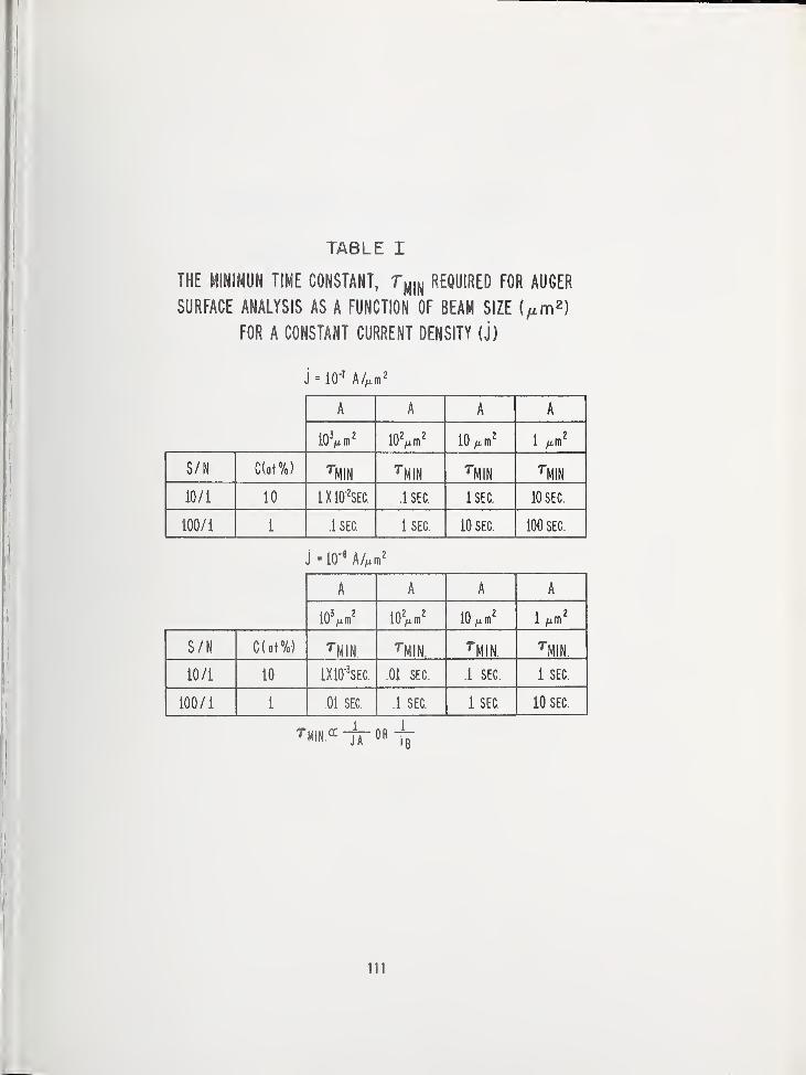
TABLE I
THE MINIMUN TIME CONSTANT, Tm REQUIRED FOR AUGER
SURFACE ANALYSIS AS A FUNCTION OF BEAM SIZE (^m 2)
FOR A CONSTANT CURRENT DENSITY (j)
j 10-7 A/^m 2
A A A A
10W lOVm2
10 ^m 21 /xm
2
S/N C(at%) rMIN
TMIN
TMIN
TMIN
10/1 10 1X10*SEC. .1 SEC. ISEC. 10 SEC.
100/1 1 .1 SEC. 1 SEC. 10 SEC. 100 SEC.
j -lO'6A/^m
2
A A A A
10V 10V 10^m2
Urn2
S/N C(at%) TMIN.
TMIN.
TMIN.
TMIN.
10/1 10 1X10⁻³SEC. .01 SEC. .1 SEC. 1 SEC.
100/
i
1 01 SEC. .1 SEC. 1 SEC. 10 SEC.
T MIN.0C OR
-Jjj-
111
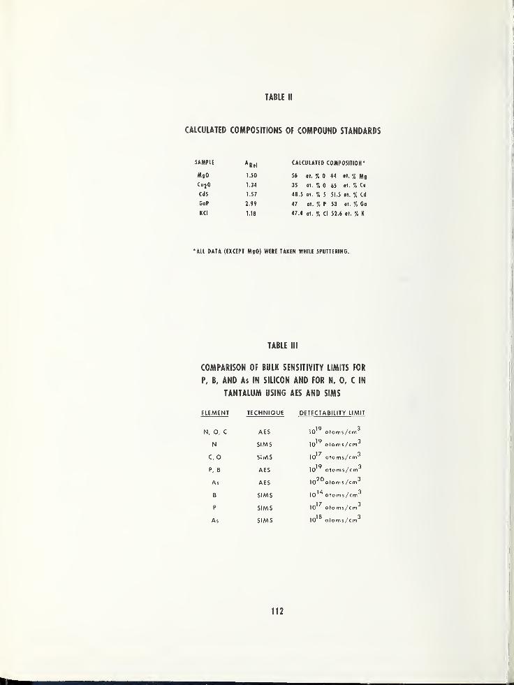
TABLE ii
CALCULATED COMPOSITIONS OF COMPOUND STANDARDS
SAMPLE ARej
CALCULATED COMPOSITION*
MgO 1.50 56 at. % 0 44 at. % Mg
Cu 2 0 1.34 35 at. % 0 65 at. 7. Cu
CdS 1.57 48.5 ol. 7. S 51.5 at. 7. Cd
GaP 2.99 47 at. % P 53 at. 7. Ga
KCI 1.18 47.4 at. 7. CI 52.6 at. 7. K
*AIL DATA (EXCEPT MgO) WERE TAKEN WHILE SPUTTERING.
TABLE III
COMPARISON OF BULK SENSITIVITY LIMITS FOR
P, B, AND As IN SILICON AND FOR N, 0, C IN
TANTALUM USING AES AND SIMS
ELEMENT TECHNIQUE DETECTABILITY LIMIT
N, O, C AES 1019 atoms/cm 3
N SIMS 1019 atoms/cm 3
C, O SIMS 1017 atoms/cm3
P, B AES
As AES 10 atoms/cni
B SIMS ,14
P SIMS lO17 atoms/cm 3
1 Q QAs SIMS 10 atoms/cm
112
Figure 1. Schematic of SAM instrumentation.
Figure 2. Modes of operation for AES.
113
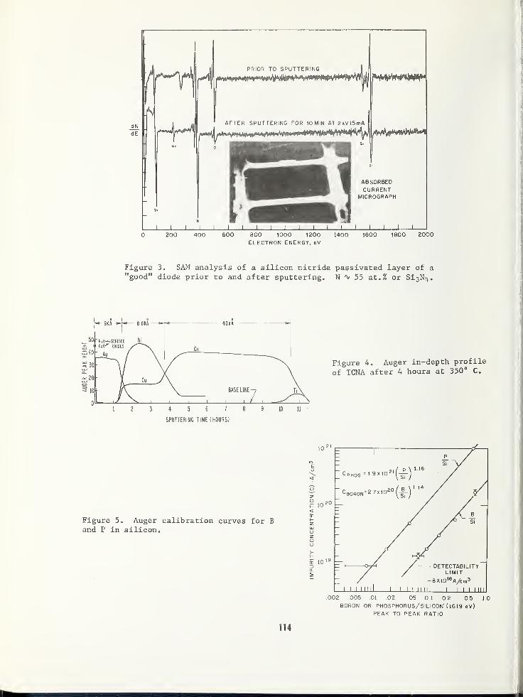
__l I I I I I I I I I I I I I I I I I I—
I
0 200 400 600 800 1000 1200 1400 1600 1800 2000ELECTRON ENERGY, eV
Figure 3„ SAM analysis of a silicon nitride passivated layer of a"good" diode prior to and after sputtering. N ^ 55 at.% or Si 3Nit .
Figure 4. Auger in-depth profile
of TCNA after 4 hours at 350° C.
123456789 10 11
SPUTTERING TIME (HOURS)
114
AuAu Au
ABSORBED CURRENT IMAGE 350
X
ELECTRON BEAMPOSITION
BEAM LEAD
J I I I I I L. I l I l
0 200 400 600 800 1000 1200 1400 1600 1800 2000
ELECTRON ENERGY eV
Figure 6. Auger spectrum and absorbed current image of contaminated
beam lead priT to in-situ ion sputtering.
Figure 7. In-depth profile of a carbon con-
taminated beam lead.
VmulT = 1560
Vmult = 1500
2 4 6
SPUTTERING TIME (MINUTES)
15 20 25 30
CARBON/GOLD AUGER PEAK RATIO
Figure 8. Carbon layer thicknessvs. the normalized Auger peakheights (C/Au) for carbon escapedepths (dj of 4 A, 6 A and 10 A.
115
Figure 9. Auger analysis after pre-bond
cleaning of gold plated ceramic.
0 500 1000
ELECTRON ENERGY (eV)
24
BULK (ppm at.) LEAD FAILURES PERCENT
Figure 11. Regression analysis of Auger
data vs. lead failures (percent).Figure 10. Calculated surface concentration
(C ) assuming complete segration to the
surface as a function of bulk concentration(ppm at. )
.
116
LASER FINE TUNE
Figure 12. Schematic of laser fine tuneprocess. SEM of laser entrance hole showsminimal lip formation and absence of substratedamage. SEM of laser exit hole shows smallerhole with somewhat larger lip formation, butno damage to substrate.
LASER EXIT 2000X
-BEAM POSITION
ADSORBED CURRENT MICROGR
0 200 400 600 800 1000 1200 1400 1600 1800 2000
ELECTRON ENERGY. oV
BEAM POSITION
ADSORBED CURRENT MICROGRAPH
0 200 400 600 800 1000 1200 1400 1600 1800 2000ELECTRON ENERGY, ev
Figure 13. Absorbed current image (insert)and SAM spectrum in vicinity of laser ma-chined holes
.
Figure 14. Absorbed current image (insert)
and SAM spectrum away from laser machined
region.
117
DISCUSSION OF THE PAPER
Participant : I wonder if you could clarifyexactly which of the impurities was causingthe beam lead bond failures? Was it the car-bon, the silver, the tin, or the copper -
and how did they manage to get all those im-purities in that gold?
Morabito : At different times, different im-purities were causing the bond failures.For the example I showed, it was primarilythe carbonaceous material. Now variouscleaning techniques can be used to removethe carbonaceous material. When this is
done there is a possibility that other im-purities can start to have an effect. Asfar as the metallic impurities are concerned,other people have been able to identify thatduring the plating operation impurities suchas copper, iron and silver are codeposited.Silver is actually a part of the gold cyanidesolution. These impurities will rapidlydiffuse to the surface. In fact, for a cer-tain dimension of beam lead (for example5,000 A in thickness and so many angstromsin width) you could actually calculate that100 ppm of copper in the bulk relocated onthe surface would represent a 10 atom per-cent concentration. This could have a
drastic effect on TC bonding and it does.
Dobrott : Would you care to comment on thefact that all the Auger spectra showed goldbut were conspicuously absent of sodium orpotassium. Could you comment on the sensi-tivity of Auger spectroscopy these elements?
Morabito : I can show you many spectra wherewe do see sodium. The one unique thingabout sodium is that it is very rapidly beamdesorbed. Anyone doing Auger spectroscopyhas seen sodium; not routinely, but veryoften. Carbon is perhaps the more routine.I do not really expect sodium to have anyaffect on bonding. The sensitivities ofAuger, as indicated, are not as high as
those of SIMS. I am really talking seriouslywhen I say 0.1 atom percent is about thevery best Auger can do.
Participant : Where does your contaminationcome from?
Thomas : Very often you find carbon on topof the gold surface. The explanation whichis often given is that carbon diffused to
the gold surface very readily, even thoughthere is only a small amount of carbon pres-ent in the bulk. Even at moderately lowtemperatures it can come to the surface.Even if there is no hydrocarbon contamina-tion you will see some carbon on top of thegold.
I would also like to agree with you about the
bonding problem. The most frequently recur-ring problem is really due to the oxides of
copper, nickel or iron, rather than the car-bon. All of our experiments show that carbonis not really a bonding problem as such, if
it is less than 20-25 A thick, as you said.
The real problems are nickel oxide, copperoxide, or iron oxide. Some of the leadshave gold plate on copper; the copper canthen diffuse through the gold. The coppercan also be codeposited in the gold plate,
as in your case. There are many possibili-ties, however carbon is not a problem as far
as I can see.
Morabito : In my particular case, the carbondid not come from the plating film.
Whitf ord : Many semiconductor manufacturersuse, as part of their processing, the tech-nique called low temperature ashing, theyalso do etching work with it. It has beenused by the connector industry when theywant a good bond and a hermetic seal to
glass, rubber or polymer. Just a quickspritz for about 5 minutes in a nitrogenatmosphere at room temperature in a RF plasmainsures the bond and takes off any carbonfilms or any materials that have diffused to
the surface. I know the technique has beenused in some electron microscopy work insteadof ion sputtering to clean surfaces, and it
is a lot cheaper too.
Morabito: We are very familiar with that
technique.
118
NBS Special Publication 400-23, ARPA/NBS Workshop IV, Surface Analysis for Silicon Devices,held at NBS, Gaithersburg
, Maryland, April 23-24, 1975 (Issued March 1976)
USE OF AUGER ELECTRON SPECTROSCOPY TO DETERMINETHE STRUCTURE OF SILICON OXIDE FILMS
J. S. Johannessent and W. E. Spicer
Stanford Electronics LaboratoriesStanford University
Stanford, California 94305
and
Y. E. Strausser
Varian AssociatesPalo Alto, California 94305
In the present paper we present experimentalresults on phase separation in unsaturatedsilicon oxides 1 and the chemical structureof the Si0 2-Si interface. 2
The chemical structure of Si0x is a contro-versial subject which has received consid-erable attention in the past. From inter-pretation of experimental observations, twochemical structure models have emerged.These models are commonly referred to as the
microscopic mixture model 3 and the randombonding model. ^
The microscopic mixture model (MMM) statesthat unsaturated silicon oxides SiO^, where0 < x < 2 is a stoichiometry factor, arephase separated mixtures of amorphous Si andamorphous Si02. Interpretation of radialdistribution functions of films of SiOx givesupport to this model. 3 ' 5
Optical reflectance data from unsaturatedsilicon oxides are interpreted in terms ofthe random bonding model (RBM) 14
, whichstates that the local atomic arrangement in
SiOx is statistically distributed among fivecoordinations of Si atoms.
Figure 1 shows how these two models predictthe relative amount in each coordination C
zas a function of sample stoichiometry, givenby x. 3 The MMM is represented by the brokenline. The RBM, represented by full drawncurves, is based on a statistical distri-bution of tetrahedra of the type Si -
(Siz-! 0 5 _ z ), where z = 1, 2, 3, 4, 5. Therelative amount in each coordination C z is
determined by the overall stoichiometry, as
shown in figure 1. Both models are identicalfor x = 0 and x = 2.
On leave from Electronics Research Lab-oratory (ELAB)
, University of Trondheim,Norwegian Institute of Technology, Norway.
In the present paper we present experimentalevidence of phase separation of Si02 and Si
in unsaturated silicon oxides of stoichiom-etry SiO
x , where x < 2. We make use of highenergy resolution Auger electron spectroscopy(AES) in a study of evaporated films of SiOxand thermally grown Si0 2 . Significant chem-ical structure effects are observed in boththe LVV and KLL series of Auger transitions.However, we limit the discussion to the Si^-^spectra because these spectra reflect directlythe effect of the changes in the local atomicarrangement around each silicon atom as a
result of changes in the overall stoichiometry.
Chemical structure effects or chemical shiftsare well known from XPS and ESCA analysis of
oxidized silicon 6 and evaporated films of
silicon oxide 7, and appear as a 3-4 eV shift
in the binding energy of the Si(2p) energylevel. We see similar chemical shifts in the
silicon KL 2 3^2,3 Auger transition as indi-cated in figure 2. In figure 2 we show twoexperimental transition energies 1618 eVcorresponding to elemental silicon x = 0, and1611 eV corresponding to silicon in Si02,
x = 2. The straight line between these two
values gives an indication of the expectedchemical shift in the silicon ^2^312^ tran-sition energy as the local coordination aroundeach silicon atom changes. We use the extra-polated Auger transition energies in figure 2
and the coordination factors in figure 1 to
calculate the energy dependence of the
silicon KL 2 3L2 3 Auger transition of the two
structural models. The result for two stoi-chiometrics is shown in figure 3 where we,
for convenience, have chosen a Lorentzianshape of each of the Auger transitions. Thehalf width in this case is slightly less than
the experimental half width. The brokencurves are the contribution from each of the
separate silicon coordinations. There is a
pronounced difference between the two models.The MMM shows two distinct Auger transitions,where the peak-to-peak heights depend on
overall stoichiometry. The RBM, shows one
119
broadened peak, whose peak-to-peak heightand energy position depends on the stoichi-ometry factor x.
In figure 4 we show a series of experimental
Sj-KLL spectra obtained from a thermallygrown oxide x = 2, and from evaporated oxidefilms 1.2 < x < 1.9. The Si (100) substrateis used as reference x = 0. Notice that thespectra for x = 0 and x = 2 are similar, butdisplaced in energy by AE ^ 7 eV. This is
the chemical shift due to change in localcoordination of the silicon atom. Similarshifts are reported for oxidized silicon. 8
The Auger spectra for intermediate values of
x are significantly different. This is
particularly pronounced for the lowest valueof x, which show two distinct transitions of
1611 eV and 1618 eV. We were not able to
obtain SiO, probably due to a finite 0 2
background during deposition at 10-7
Torr.The experimental conditions are describedelsewhere.^ The stoichiometry factor x is
estimated using the peak-to-peak heightnormalized to the thermally grown oxide.
The experimental results presently in figure4 strongly support the MMM, as can be seenwhen compared with figure 3. Based on theabove discussion and our experimental datawe are led to the conclusion that unsatu-rated silicon oxides SiOx , where 0 < x < 2,
are phase separated and best described bythe microscopic mixture model.
We have also performed chemical depth pro-filing of thermally grown Si0 2 on Si (100)
.
In figure 5 is shown a typical depth profileof an oxide grown to a thickness of 1000 1at 1200 A in dry 0 2 . After oxidation thesample was annealed in dry N 2 and slowlypulled from the furnace. Figure 5 is ob-tained by automatic multiplexing of thepeak-to-peak heights of the Ojy^ (502 eV)
,
SiKLL (!611-1618 eV) , and SiLW (78-92 eV)
Auger transitions. 10 The data points to theleft of the origin are steady state valuesbefore the onset of the 1 keV Argon ionbeam. The small step in the Ojq^ and Si^yytransitions is most probably due to removalof surface contaminants such as water vaporand carbon. The depth profile of figure 5
shows a uniform Si0 2 film, except in theinterface region when there is a dip in thesilicon KL2j 3L 2 3 peak-to-peak height. Thereason for this dip is clearly shown in theactual real time Auger spectra plotted abovethe depth profile. The numerals indicatethe position of the spectra in the interfacelegion of the Si0 2 -Si depth profile.
There are two characteristic features of thedepth profile near the interface. Firstly,
the Sijy^ transition "sees" the interfacebefore the and Si^yy transitions, andsecondly it "sees" a broader interface thanthe two other transitions. These featuresare related to the escape depth of the Augerelectrons and to the nature of the KLL andLW Auger transitions. 2
When the electron escape depth 5 ' 11 is ac-counted for, we find that the width of theSi0 2 -Si interface is on the order of 35-50 Awide. Interface broadening by the ion beamis estimated to be on the order of 10 to 15 A..
2f
Hence, we are left with a "real" interfacewidth on the order of 20-30 A.. In the inter-face region, the average stoichiometry is
SiOx , x < 2, and the material appears to bephase separated in a similar manner as un-saturated silicon oxides.
In conclusion, we mention that we have madethe first observation of chemical shifts inthe silicon KL 2 3L 2 3 Auger transition inunsaturated silicon'oxide films. We inter-pret our results in terms of a microscopicmixture of Si02 and Si. Chemical depth pro-files through thermally grown Si0 2 on Si (100)show a phase separated Si0 2 -Si interface offinite width on the order of 20—30 A. Webelieve that the positive oxide charge ob-served in MOS-devices 12
, are confined to theconnective regions between the two phases at
the interface, Si0 2 and Si, respectively.
ACKNOWLEDGEMENTS
Work in part supported by Army Research Office,Contract No. DAHC 0474 G 0215. One of us
(J.S.J.) has been partly supported by ELABand the Royal Norwegian Council for Scientificand Industrial Research.
REFERENCES
1. Johannessen, J. S., Spicer, W. E. , andStrausser, Y. E. , to be published.
2. Johannessen, J. S., Spicer, W. E. , and
Strausser, Y. E. , to be published.
3. Temkin, R. J., J. Non-Cryst. Solids 17,
215 (1975).
4. Phillips, H. R. , J. Non-Cryst. Solids,8-10, 627 (1972).
5. Coleman, M. V., and Thomas, A. J. D.,
Phys. Stat. Sol. 22, 593 (1967).
6. Flitsch, R.,and Raider, S. I., J. Vac.
Sci. Technol. 12, 305 (1975).
120

Hollinger, G. ,Tousset, J., and Tran
Ming Due, Tetrahedrally Bonded Amor-phous Semiconductors, M. H. Brodsky,S. Kirkpatrick, S. and D. Weatre, Eds.,
p. 102 (Am. Inst. Phys., New York,
1974)
.
Wagner, C. D. , Anal. Chem. 4_7, 1201
(1975)
.
Strausser, Y. E., and Johannessen, J. S.
,
An Auger Electron Spectroscopy Study ofSilicon Spectra From Silicon Monoxide,Silicon Dioxide and Silicon Nitride,
ARPA/NBS Workshop IV, Surface Analysisfor Silicon Devices, A. G. Lieberman,Ed., NBS Spec. Publ. 400-23 (March 1976).
10. The notation Si^yv ^s use d to show thatthe LW spectrum of silicon oxides is
composed of molecular orbitals orig-inating both from Si-Si bonds and Si-0bonds
.
11. Lindau, I., and Spicer, W. E. , J. Elec.
Spectr. 3, 409 (1974).
12. Deal, B. E. , J. Electrochem. Soc. 121,
198C (1974).
121
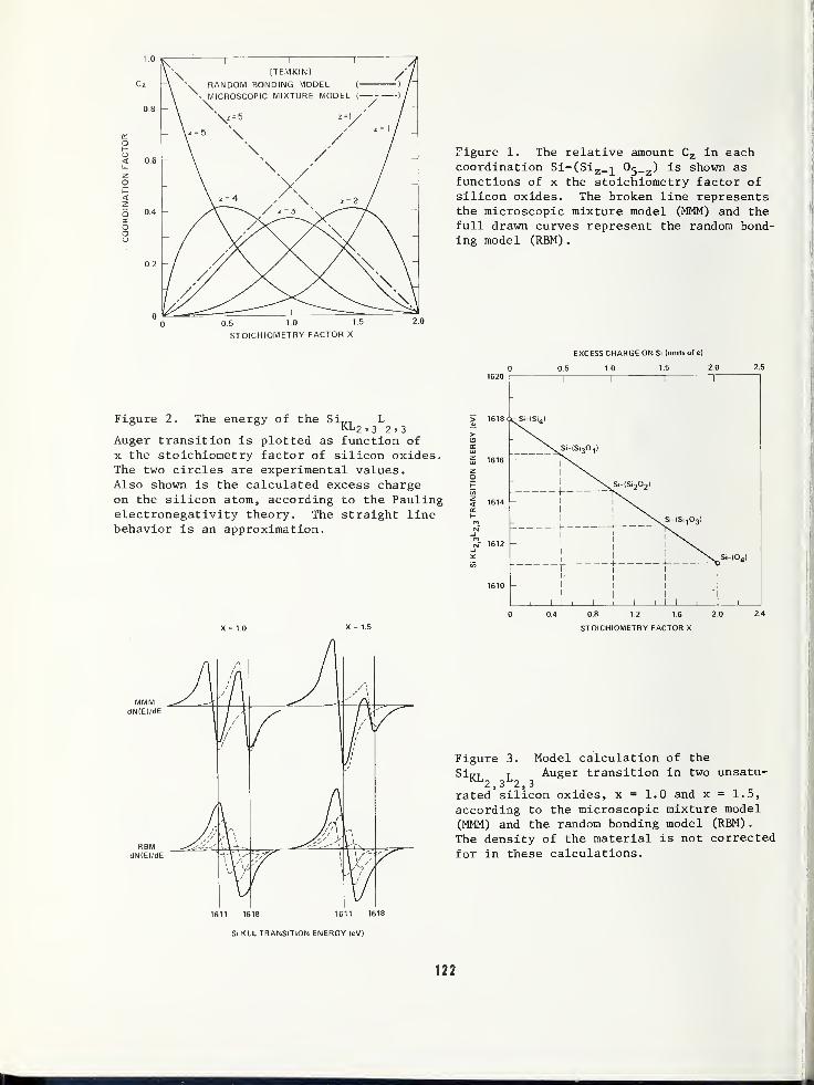
0.5 10 1.5
STOICHIOMETRY FACTOR X
Figure 2. The energy of the Si.,, LKL2>3 2.3
Auger transition is plotted as function of
x the stoichiometry factor of silicon oxides.The two circles are experimental values.Also shown is the calculated excess chargeon the silicon atom, according to the Paulinjelectronegativity theory. The straight linebehavior is an approximation.
Figure 1.
coordination Si-(Si z_^ 0^_ z ) is shown asfunctions of x the stoichiometry factor ofsilicon oxides. The broken line representsthe microscopic mixture model (MMM) and thefull drawn curves represent the random bond-ing model (RBM)
.
EXCESS CHARGE ON Si (units of e)
0.5 1.0 1.5 2.0
1 1 1 1
1618 < >r SH(Si4 )
1616
S:Si-tSi30
1)
\ Si-(Si20 2 l
1614 1 \.1
\s Si-(Si103 )
16121
1
1
1
v Si-(04 )
1610
1 1 , 1
1
1
1
1 1 1 1
1
1
"1
0.4 0.8 1.2 1.6 2.0 2.4
STOICHIOMETRY FACTOR X
1611 1618 1611 1618
Si KLL TRANSITION ENERGY (eV)
Figure 3. Model calculation of the
SivT t Auger transition in two unsatu-^2,3^2,3
rated silicon oxides, x = 1.0 and x = 1.5,
according to the microscopic mixture model
(MMM) and the random bonding model (RBM)
.
The density of the material is not corrected
for in these calculations.
122
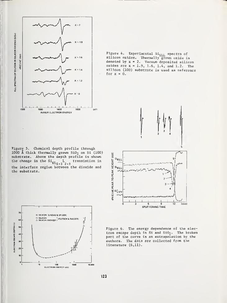
O S
Figure 4. Experimental SiKLL spectra ofsilicon oxides. Thermally grown oxide isdenoted by x = 2. Vacuum deposited siliconoxides are x = 1.9, 1.6, 1.4, and 1.2. Thesilicon (100) substrate is used as referencefor x = 0.
' ' i i i i i i i i i i i i i i_
1500 1550 1600 1650 (eV!
AUGER ELECTRON ENERGY
It
11
Figure 5. Chemical depth profile through1000 A thick thermally grown Si0 2 on Si (100)substrate. Above the depth profile is shownthe change in the Si L transistion in
KL2»3 2>3the interface region between the dioxide andthe substrate.
sirLVVtoo0 '
0003° OOODoQgO^Ot ,000°aoooot^ooo!*5 oO°d3oo rf^rf1^)0!
I I I I I
V-r/
0 SILICON (LINDAU 8. SPICERI
A SILICON DIOXIDE I
IFLITSCH & RAIDER]
3 6 9 12 (min)
SPUTTERING TIME
Figure 6. The energy dependence of the elec-tron escape depth in Si and Si02- The brokenpart of the curve is an extrapolation by the
authors. The data are collected from the
literature (6,11).
100
ELECTRON ENERGY (eVI
123

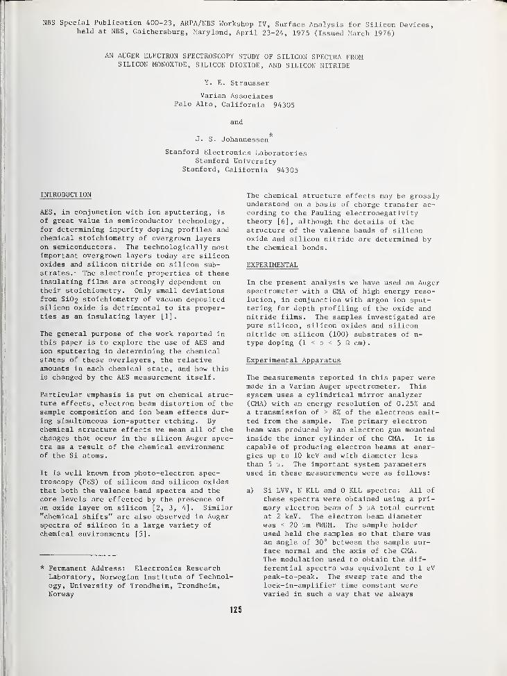
NBS Special Publication 400-23, ARPA/NBS Workshop IV, Surface Analysis for Silicon Devices,held at NBS, Gaithersburg, Maryland, April 23-24, 1975 (Issued March 1976)
AN AUGER ELECTRON SPECTROSCOPY STUDY OF SILICON SPECTRA FROMSILICON MONOXIDE, SILICON DIOXIDE, AND SILICON NITRIDE
Y. E. Strausser
Varian AssociatesPalo Alto, California 94305
and
J. S. Johannessen
Stanford Electronics LaboratoriesStanford University
Stanford, California 94305
INTRODUCTION
AES, in conjunction with ion sputtering, is
of great value in semiconductor technology,for determining impurity doping profiles andchemical stoichiometry of overgrown layerson semiconductors. The technologically mostimportant overgrown layers today are siliconoxides and silicon nitride on silicon sub-strates.- The electronic properties of theseinsulating films are strongly dependent ontheir stoichiometry. Only small deviationsfrom Si02 stoichiometry of vacuum depositedsilicon oxide is detrimental to its proper-ties as an insulating layer [1].
The general purpose of the work reported inthis paper is to explore the use of AES andion sputtering in determining the chemicalstates of these overlayers, the relativeamounts in each chemical state, and how thisis changed by the AES measurement itself.
Particular emphasis is put on chemical struc-ture effects, electron beam distortion of thesample composition and ion beam effects dur-ing simultaneous ion-sputter etching. Bychemical structure effects we mean all of thechanges that occur in the silicon Auger spec-tra as a result of the chemical environmentof the Si atoms.
It is well known from photo-electron spec-troscopy (PES) of silicon and silicon oxidesthat both the valence band spectra and thecore levels are effected by the presence of
an oxide layer on silicon [2, 3, 4]. Similar"chemical shifts" are also observed in Augerspectra of silicon in a large variety of
chemical environments [5].
* Permanent Address: Electronics ResearchLaboratory, Norwegian Institute of Technol-ogy, University of Trondheim, Trondheim,Norway
The chemical structure effects may be grosslyunderstood on a basis of charge transfer ac-cording to the Pauling electronegativitytheory [6], although the details of thestructure of the valence bands of siliconoxide and silicon nitride are determined bythe chemical bonds.
EXPERIMENTAL
In the present analysis we have used an Augerspectrometer with a CMA of high energy reso-lution, in conjunction with argon ion sput-tering for depth profiling of the oxide andnitride films. The samples investigated arepure silicon, silicon oxides and siliconnitride on silicon (100) substrates of n-type doping (1 < p < 5 Q cm)
.
Experimental Apparatus
The measurements reported in this paper weremade in a Varian Auger spectrometer. Thissystem uses a cylindrical mirror analyzer(CMA) with an energy resolution of 0.25% anda transmission of > 8% of the electrons emit-ted from the sample. The primary electronbeam was produced by an electron gun mountedinside the inner cylinder of the CMA. It is
capable of producing electron beams at ener-gies up to 10 keV and with diameter less
than 5 p. The important system parametersused in these measurements were as follows:
a) Si LVV, N KLL and 0 KLL spectra: All of
these spectra were obtained using a pri-mary electron beam of 5 yA total currentat 2 keV. The electron beam diameterwas < 20 um FWHM. The sample holderused held the samples so that there wasan angle of 30° between the sample sur-face normal and the axis of the CMA.
The modulation used to obtain the dif-ferential spectra was equivalent to 1 eVpeak-to-peak. The sweep rate and thelock-in-amplif ier time constant werevaried in such a way that we always
125
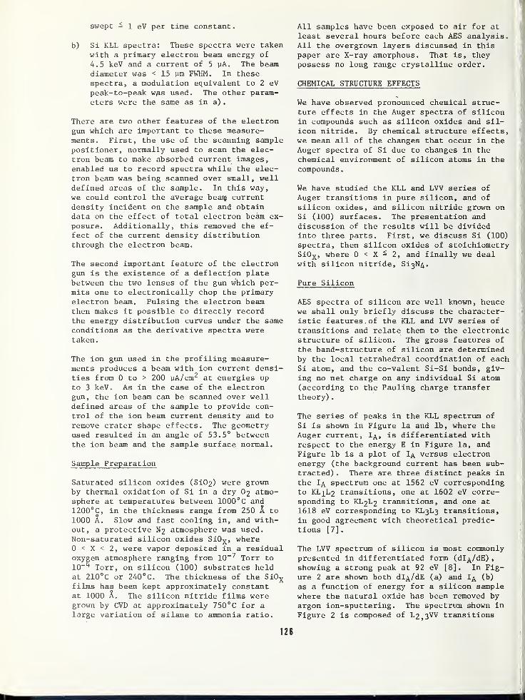
swept - 1 eV per time constant.
b) Si KLL spectra: These spectra were taken
with a primary electron beam energy of
4.5 keV and a current of 5 yA. The beamdiameter was < 15 ym FWHM. In thesespectra, a modulation equivalent to 2 eV
peak-to-peak was used. The other param-eters were the same as in a)
.
There are two other features of the electrongun which are important to these measure-ments. First, the use of the scanning samplepositioner, normally used to scan the elec-tron beam to make absorbed current images,
enabled us to record spectra while the elec-tron beam was being scanned over small, welldefined areas of the sample. In this way,we could control the average beam currentdensity incident on the sample and obtaindata on the effect of total electron beam ex-posure. Additionally, this removed the ef-fect of the current density distributionthrough the electron beam.
The second important feature of the electrongun is the existence of a deflection platebetween the two lenses of the gun which per-mits one to electronically chop the primaryelectron beam. Pulsing the electron beamthen makes it possible to directly recordthe energy distribution curves under the sameconditions as the derivative spectra weretaken.
The ion gun used in the profiling measure-ments produces a beam with ion current densi-ties from 0 to > 200 uA/cm2 at energies up
to 3 keV. As in the case of the electrongun, the ion beam can be scanned over welldefined areas of the sample to provide con-trol of the ion beam current density and to
remove crater shape effects. The geometryused resulted in an angle of 53.5° betweenthe ion beam and the sample surface normal.
Sample Preparation
Saturated silicon oxides (Si02) were grownby thermal oxidation of Si in a dry O2 atmo-sphere at temperatures between 1000°C and1200°C, in the thickness range from 250 & to
1000 A. Slow and fast cooling in, and with-out, a protective N2 atmosphere was used.Non-saturated silicon oxides SiO^, where0 < X < 2, were vapor deposited in a residualoxygen atmosphere ranging from 10-7 Torr to10~ L>
Torr, on silicon (100) substrates heldat 210°C or 240°C. The thickness of the SiOxfilms has been kept approximately constantat 1000 A. The silicon nitride films weregrown by CVD at approximately 750°C for alarge variation of silane to ammonia ratio.
All samples have been exposed to air for at
least several hours before each AES analysis.All the overgrown layers discussed in thispaper are X-ray amorphous. That is, theypossess no long range crystalline order.
CHEMICAL STRUCTURE EFFECTS
We have observed pronounced chemical struc-ture effects in the Auger spectra of siliconin compounds such as silicon oxides and sil-icon nitride. By chemical structure effects,we mean all of the changes that occur in theAuger spectra of Si due to changes in thechemical environment of silicon atoms in thecompounds
.
We have studied the KLL and LVV series of
Auger transitions in pure silicon, and of
silicon oxides, and silicon nitride grown onSi (100) surfaces. The presentation and
discussion of the results will be dividedinto three parts. First, we discuss Si (100)
spectra, then silicon oxides of stoichiometrySiOx , where 0 < X - 2, and finally we dealwith silicon nitride, Si3N4-
Pure Silicon
AES spectra of silicon are well known, hencewe shall only briefly discuss the character-istic features. of the KLL and LVV series of
transitions and relate them to the electronicstructure of silicon. The gross features of
the band-structure of silicon are determinedby the local tetrahedral coordination of eachSi atom, and the co-valent Si-Si bonds, giv-ing no net charge on any individual Si atom(according to the Pauling charge transfertheory)
.
The series of peaks in the KLL spectrum of
Si is shown in Figure la and lb, where theAuger current, 1^, is differentiated withrespect to the energy E in Figure la, andFigure lb is a plot of 1^. versus electronenergy (the background current has been sub-tracted) . There are three distinct peaks in
the 1^ spectrum one at 1562 eV correspondingto KLjL2 transitions, one at 1602 eV corre-sponding to KL2L2 transitions, and one at1618 eV corresponding to KL3L3 transitions,in good agreement with theoretical predic-tions [7]
.
The LVV spectrum of silicon is most commonlypresented in differentiated form (dl^/dE)
,
showing a strong peak at 92 eV [8]. In Fig-ure 2 are shown both dl^/dE (a) and 1^ (b)
as a function of energy for a silicon samplewhere the natural oxide has been removed byargon ion-sputtering. The spectrum shown in
Figure 2 is composed of L2,3W transitions
126
at higher energies and LjI^^V transitions atthe low energy side of the spectrum. Detail-ed analysis and identification of the differ-ent transitions is difficult due to the com-plexity of the silicon valence band. How-ever, some of the characteristic features ofthe valence band are reflected in the LVVseries of Auger transitions. Using Kane'sdensity of state calculations [9], by assign-ing the binding energies V]_ = 3 eV, V2 = 4 eV,
V3 = 7 eV, and V4 = 10 eV to the four majorpeaks in the density of states, and using thebinding energies EL ^
= 148.7 eV and El2.3 =
99.2 eV, we are able to give a crude identi-fication of the features of LVV Auger spec-trum of Si. This is the same approach asthat of Maguire [10]. The major peak inFigure 2b, at 88 eV, is due to L2 3V
^
transitions, while the minor peak is due toL2 3V4V4 transitions at 72 eV. The shoulderbetween these peaks is largely L2 3V3V3transitions at 79 eV. The two small piecesof structure on the low energy side areLjL2 3V2 2 transitions at y 41 eV andL1L 2,3V3,4 transitions at y 35 eV. The de-tails of the LVV spectrum are amplified bydifferentiation w.r.t. energy as shown inFigure 2a.
Silicon Oxides
Silicon oxides and oxidized silicon havebeen subject to extensive studies in thepast, both by AES and photoelectron spectro-scopy (PES) [2, 3, 11]. However, most of
the work has been focused on either silicondioxide or oxygen chemisorbed on clean sili-con. In this paper, we report on results of
studies of thermally grown silicon oxide of
stoichiometry Si02, and evaporated films ofstoichiometry SiO^, 1 % X a, 2.
In Figure 3, we show a series of Si LVVspectra of silicon oxides (a) , and oxygenKLL spectra (b) for the corresponding com-pounds. The stoichiometry of the sampleswas determined using the amount of oxygenpresent in the films, as indicated by thepeak-to-peak heights of Figure 3 (b) . Theoxygen spectra of Figure 3 (b) indicate thatoxygen is present in only one chemical state,namely as a bridge between two silicon atoms[12]. Furthermore, the coordination of oxy-gen determines the major features of the LVVspectrum through the density of states in
the valence band of silicon oxides. The twomajor peaks in the LVV spectra of silicon at
64 eV and 78 eV are associated with transi-tions from bonding and non-bonding molecularorbitals of the Si-O-Si (Si20) quasi-mole-cule. The transition probabilities are ap-parently determined by the oxygen 2p predom-inance of these orbitals. The peak appearing
at 92 eV is due to the presence of "free"silicon, i.e., silicon coordinated by fournearest silicon neighbors. A small amountof "free" silicon in silicon oxides is inthis case produced by ion sputter cleaning.In fact, 500 A of material had been removedbefore the AES spectra were taken.
It is important to understand that the ratioof the peak-to-peak heights of the 78 eV and92 eV peaks in the ^ spectra does not give,directly, the ratio of the concentrations ofSi bound to 0 to the concentration of Sibound to Si ("free" Si) . Observation of theN (E) spectrum shows that the peaks at 64 eVand 78 eV are very broad whereas the 92 eVpeak is narrow, with a very sharp high energyedge. This, of course, results in a largenegative excursion on the 92 eV gS peak with-out the corresponding large number of elec-trons in the peak. In fact, N (E) spectracorresponding to a condition like that shownin the spectra of Figure 3 will show the92 eV peak to be only a small, althoughsharp, step on the high energy side of thelarge, broad 78 eV peak. This does not,however, prohibit the calibration of the LWspectrum to determine the relative concentra-tions of these two states of Si. On theother hand, the KLL spectra give much moreobvious and direct information about therelative concentrations of the differentchemical states of Si.
The local atomic arrangement around the sil-icon atoms is shown by the Si KLL spectra inFigure 4, for silicon oxides of varyingstoichiometry. For X = 2 (Si02) there ap-pears a well defined KL2 3L2 3 peak at 1611eV, associated with Si-(d4) coordination.For X ^ 1.8 there appears a small shoulderabove 1611 eV, and for X ^ 1.3 a broad peakoccurs at 1616 eV. This peak may be asso-ciated with silicon tetrahedra of the typeSi - (Siy 04_y) , where y 4- 0, 4. However,upon electron exposure a single peak emergesat 1618 eV corresponding to Si - (Si^) tetra-hedra (or "free" silicon)
.
Silicon Nitride
In Figure 5a and b, we show silicon nitrideAuger spectra in the energy range between25 eV and 525 eV. Figure 5a is the spectrumfrom a sample exposed to atmosphere. Notethe presence of carbon and oxygen KLL tran-sitions, the large silicon nitride LVV peakat 85 eV, and the small silicon oxide peakat 64 eV. Removal of carbon and oxygen byion-sputter etching results in the cleansilicon nitride spectrum shown in Figure 5b.
It is interesting to note that oxygen is
associated with silicon oxide in the
127
contaminated surface, and that removal of
silicon oxide results in a "free" siliconpeak at 92 eV, while there is no observablechange in the 382 eV N KLL peak. This indi-
cates that nitrogen exists only in one chem-
ical state associated with a silicon nitridequasi-molecule (Si-jN) , where the Si-N bondshave less ionic character than the Si-0 bond.
This observation is confirmed by the Si KLLspectrum of the nitride which has a well de-fined peak at 1618 eV, apparently identicalto the "free" silicon Si-(Si^) coordination,indicating a negligible charge transfer fromSi to N in silicon nitride. We are notaware of X-ray photoemission spectra of
Si3N^ or valence band structure calculationsso an analysis beyond this mere descriptiveone is not pursued here.
We have shown above that the Si3N4 LW spec-trum is strongly influenced by oxygen ad-sorbed on the surface. Oxygen adsorptioncompletely removed the 92 eV "free" siliconpeak. This phenomena suggests that amorphoussilicon nitride is a microscopic mixture of
Si and Si3N4.
ELECTRON STIMULATED DESORPTION EFFECTS
We have already mentioned in the previoussection that the stoichiometry of siliconoxides may be changed by electron exposure.
The effect is to reduce the oxygen content in
the sample. This phenomenon is commonlyknown as electron stimulated desorption (ESD)
,
and is thoroughly reviewed in the literature
[13]. We have investigated electron beamexposure effects on Auger spectra of SiO„(1.2 < X S 2) and Si 3N4 films on Si (100)single crystals. Si3N4 appears to be stableto electron exposure at energies less than2 keV. Apart from desorption of surface con-
taminants (carbon and oxygen) the LVV andKLL spectra appear unchanged upon prolongedexposure. Silicon oxides on the other handare more volatile, and we will restrict ourdiscussion to these compounds.
Si02 is known to decompose under electronirradiation. It has been shown that oxygendesorption from Si02 is accompanied by the
formation of "free" silicon [14]. Our find-ings are similar for SiO. However, wherethe stoichiometry of silicon oxide films is
SiOx with 0 < X < 2, this effect is muchmore pronounced. In Figure 6a and b, weshow the growth of the 92 eV Si LVV peak as
a function of exposure time for SiOi.4 (a)
and Si02 (b) , the parameter is the electronflux density, and the primary electron ener-
gy is 2 keV. There appears to be a linearincrease at small exposure times followed bya saturation region. The linear slope and
the saturation level both increase with in-creasing flux density. The former being re-lated to decomposition of SiOx followed bydesorption of oxygen. The saturation levelis most probably determined by oxygen deple-tion in the surface layer and out diffusionof oxygen from deeper lying layers. Notethat the saturation level in SiO^^ is morethan three times that of Si02.
Decomposition and desorption of oxygen is
shown in Figure 7, where the 0 KLL peak-to-peak height is plotted against exposure timefor the same samples discussed in Figure 6.
We find that in order to minimize electronirradiation distortion of silicon oxides,the dose should be kept at 10 19 electrons/cmor below, at 2 keV primary energy. Thiscorresponds to 2.5 min. exposure at 10-2
A/ cm2 .
CHEMICAL DEPTH PROFILES AND ION BEAM EFFECTS
Chemical depth profiles are obtained by re-
cording AES spectra as a function of timeduring simultaneous ion sputtering. Thetechnique is well known, and we shall re-
strict the discussion to some of the factorsthat limit the depth resolution.
In Figure 8, we show a typical depth profilethrough a 1080 A thick layer of SiOx (X -
1.4) vacuum deposited on Si(100) . Only theinitial and the final part of this particu-lar profile are shown. The initial part of
the curve shows how adsorbed carbon is re-
moved, and how a balance between bound oxy-gen and "free" silicon is reached by oxygenremoval. The saturation level gives a meas-ure of the stoichiometry of the sample. Thefinal part of the profile shows the inter-face between film and substrate, and the
finite transition region between the two.
In this case, the width is 29 A (defined as
distance between 80% and 20% of the oxygenpeak-to-peak height) . The question is nowwhat factors control and determine the ob-served width or depth resolution. A recentpaper by Ishitani et.al. [15] deals withthese problems in model calculations of
knock-on atomic mixing. They find a depthresolution decreasing with increasing ion
energy, and increasing with incidence angleof the ion beam between 0° and 60°. An ex-
perimental investigation of Ta205 on Ta [16]
has shown a minimum transition width of
^ 60-70 A for ion energies between 6 and
7 deV. We have employed A+ ions at 3 keV of
varying current density. In Figure 9, weshow the transition with AY as a function of
ion power density for silicon oxides and
silicon nitride on Si (100). The generaltrend is that AY decreases with increasing
128
power density for both compounds, towards a
broad minimum or saturation level of the or-o
der of 30 to 40 A. This value is roughly
50% of that reported for Ta205 on Ta [16].
Figure 9 also shows that the nitride inter-
face is sharper than the oxide interface at
low power densities. We find that the sput-
tering yield for silicon nitride is 0.5 mole-
cule/ion, and for silicon oxide ^ 1.5 mole-cule/ion, and an ion energy of 3 keV. Wefind our experimental results in qualitativeagreement with the knock-on mixing model
[15], when we take into account the lower
ion energy and the angle of incidence wehave used. The lower limit of 30 - 40 A in-
terface width may be reduced even further by
reducing the ion energy. However, other
factors such as surface roughness, prefer-ential sputtering, and inhomogeneities may
set an upper limit to the depth resolution.
The ultimate limit is set by the escape depth
of the Auger electrons, which will be discus-
sed in the next paper.
CONCLUSION
The results presented in the preceeding sec-
tions may be summarized in the followingconclusions. The electronic structure of
silicon compounds is largely determined by
the molecular bonds and the local atomic ar-
rangement. Thus, in silicon oxides it is
the Si-0 bond and in silicon nitride it is
the Si-N bond that gives the major contribu-
tion to the electronic structure. The Si-0
bond energy is larger than Si-Si bond*. The
charge transfer associated with the Si-0
bond gives rise to a chemical shift in the
binding energy of the Si L2}3 level of 3.9
eV [18]. This gives rise to a shift in the
Si KLL transition energy of 7 eV from
Si-(Si4) coordination to Si-(04> coordination
[18]. We have observed varying amounts of
these two states in electron irradiated SiOxfilms, X < 2. Similar chemical shifts have
not been observed in silicon nitride. We
believe that this is due to a much smaller
charge transfer associated with the Si-N
bond.
Electron distortion of silicon oxides by
dissociation and desorption of oxygen can be
reduced to a negligible level by keeping the
total electron dose below a limit of 10 19
el/cm2 at 2 keV electron energy. Silicon
nitride is stable to electron irradiation
within the experimental conditions of this
investigation. Why this is so is not fully
understood. It may be associated with the
higher ionization potential of nitrogen com-
pared with oxygen.
profiling of silicon oxides and silicon ni-tride. The mixing effect results in reduceddepth resolution. By varying the ion flux
we were able to reduce the width of the in-
terface between silicon oxide or silicon ni-o
tride and silicon, to 30 to 40 A at an argonion energy of 3 keV. This result is en-
couraging in that it indicates the possibilityof studying the interface region of M0S and
MNOS devices where charge is accumulated.
ACKNOWLEDGEMENT
We would like to thank Forrest Futtere for
preparing the SiOx samples, and KrishnaSaraswat for supplying us with thermallygrown Si02 and reactor grown Si3N4 samples.
REFERENCES
1. Hirose, H.,and Wada, Y. , Japan. J. Appl.Phys. 3, 179 (1964).
2. DiStefano, T. H., and Eastman, D. E.
,
Phys. Rev. Lett. 27_, 1560 (1971).
3. Hollinger, G. , Tousset, J., and TranMinh Due, Tetrahedrally Bonded Ampor-phous Semiconductors, M. H. Brodsky,S. Kirkpatrick and D. Weaire, Eds.
,
p. 102 (Am. Inst. Phys., New York,
1974)
.
4. Danyluk, S., and McGuire, G. E., J. Appl.Phys. 45, 5141 (1974).
5. Stupian, G. W. , J. Appl. Phys. 45_, 5278(1974)
.
6. Pauling, L. , The Nature of the ChemicalBond, 3rd ed. , (Cornell Univ. Press,Ithaca, New York, 1960).
7. Siegbahn, K. , Nordling, C. ,Fahlman, A.,
et. al. , Electron Spectroscopy forChemical Analysis , Technical ReportAFML-TR-68-189 , Inst. Phys., Uppsala,Sweden (1968).
8. Grant, J. T.,and Haas, T. W. , Surf. Sci.
23, 347 (1970).
9. Kane, E. 0., Phys. Rev. 146, 558 (1966).
10. Maguire, H. G., and Augustus, P. A., J.
Phys. C. 4_, L174 (1971).
11. Ibach, H., and Rowe, J. E. , Phys. Rev.
B10 , 710 (1974).
We have observed knock-on mixing of elements
caused by energetic ions during depth129

12. Johannessen, J. S., Spicer, W. E. , and
Strausser, Y. E. , Use of Auger Electron
Spectroscopy To Determine The Structure
of Silicon Oxide Films, ARPA/NBS Work-
shop IV, Surface Analysis for Silicon
Devices, A. G. Lieberman, Ed., NBS
Spec. Publ. 400-23 (March 1976).
13. Madey, T. E.,and Yates, Jr., J. T. , J.
Vac. Sci. Technol. 8_, 525 (1971).
14. Thomas, S. , J. Appl. Phys. 45^,
161 (1974).
15. Ishitani, T.,and Shimizu, R. , Appl.Phys. 6, 241 (1975).
16. Ishitani, T. , Shimizu, R.,and Tamura,H., Appl. Phys. 6, 271 (1975).
17. Roberts, J. D. , Stewart, R. , andCaseuio, M. G. , Organic Chemistry(W. A. Benjamin, Inc. , Menlo Park,
California 1971).
18. Wagner, C. D. , to be published.
130
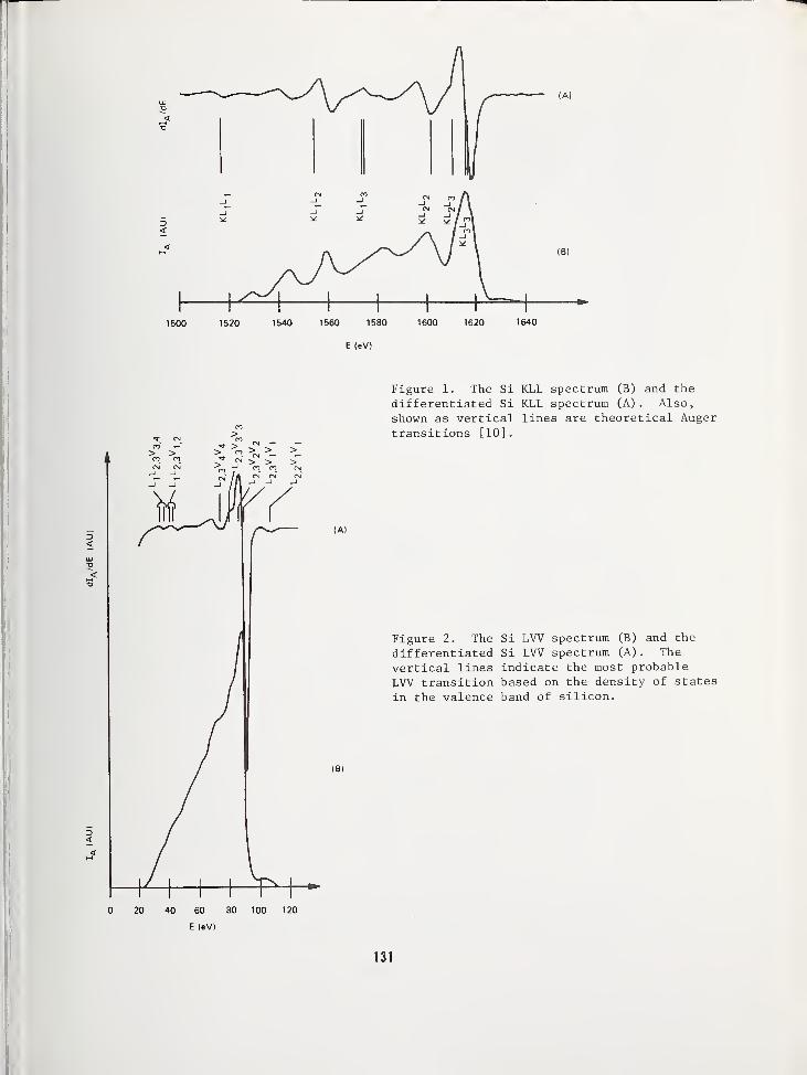
1500 1520 1540 1560 1580 1600 1620 1640
E (eV)
Figure 1. The Si KLL spectrum (B) and the
differentiated Si KLL spectrum (A). Also,
shown as vertical lines are theoretical Augertransitions [10].
Figure 2. The Si LVV spectrum (B) and the
differentiated Si LW spectrum (A) . The
vertical lines indicate the most probable
LVV transition based on the density of states
in the valence band of silicon.
(Bl
0 20 40 60 80 100 120
E (eVI
131
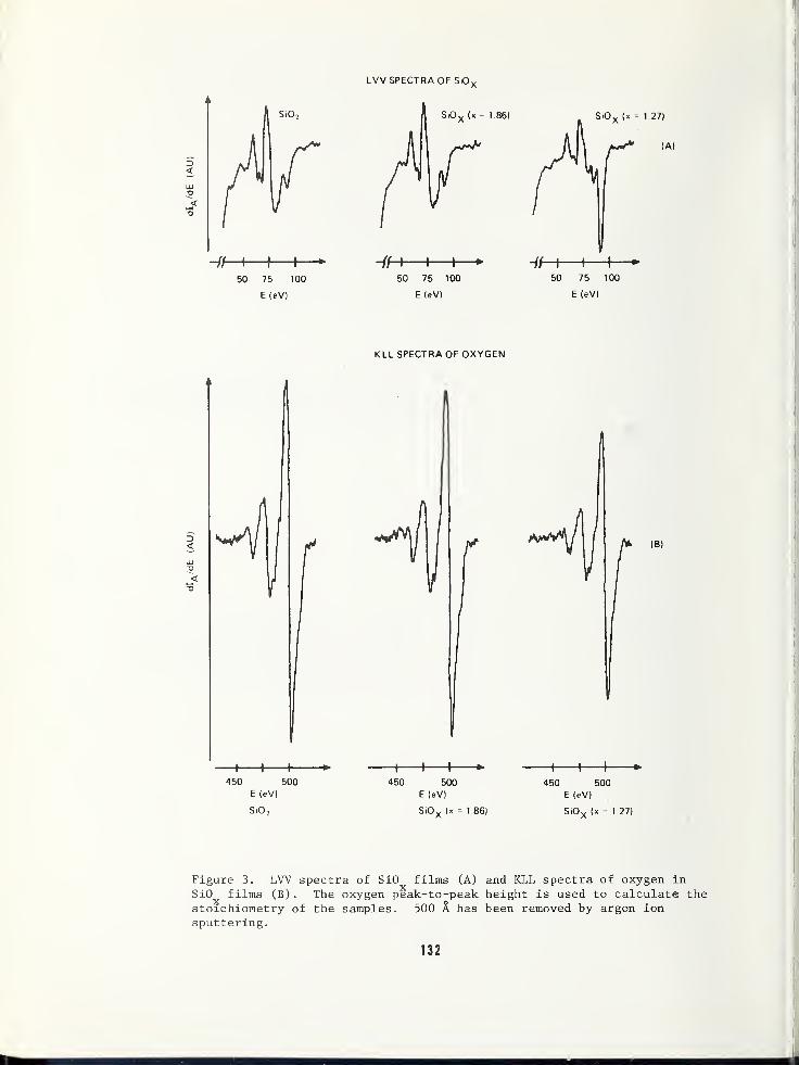
Figure 3. LVV spectra of SiO films (A) and KLL spectra of oxygen in
SiO films (B). The oxygen peak-to-peak height is used to calculate thestoichioraetry of the samples. 500 A has been removed by argon ionsputtering.
132
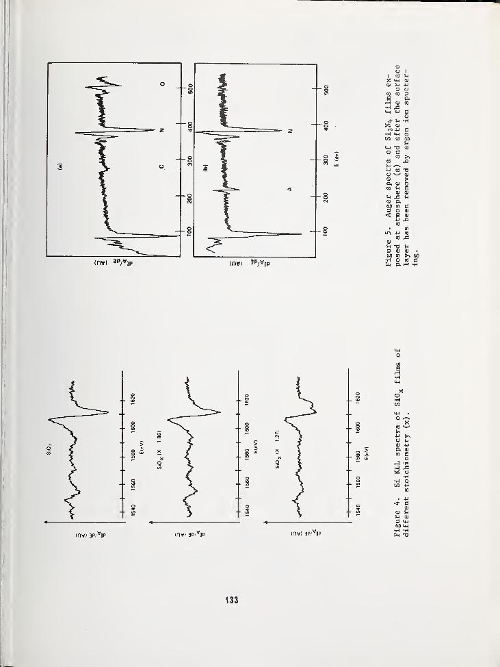
O
-- X
-- s
invi 3P, ip mvi 3p/vip inv) 3p/
vip
133
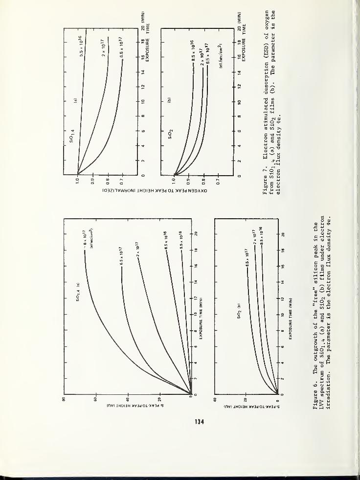
--o I
inw) 1H0I3H *V3d Ol XV3d >s IflV) 1H0I3H XV3d Oi *V3d 'S
O 01
o> u4J
4-1 U >^0) u
c r-l •rl
•rl 0)ns
Ha) (U T34) T3& C
3 3C i-l
o <4-l
o e•H i—
i
cH •H o•H M-l S-l
CO 4J/—
N
u0)
"<u —
'
H0) 0)
)-i CM<4-l O 0)
•H 4=CO 4J
0)
T3 CO4J
4-1
an•H
o 0)
ca AJ0)
4-1
2= j-
Ot-i
00 o o.4-1 •HP C/3 cu
o4-1
Th
01 o
Hco
4-1 •rl
vO o 4J01 C8
<U D. •Hu CO T33 Bj
t>0 > u•rl >(x< r5 •H
134
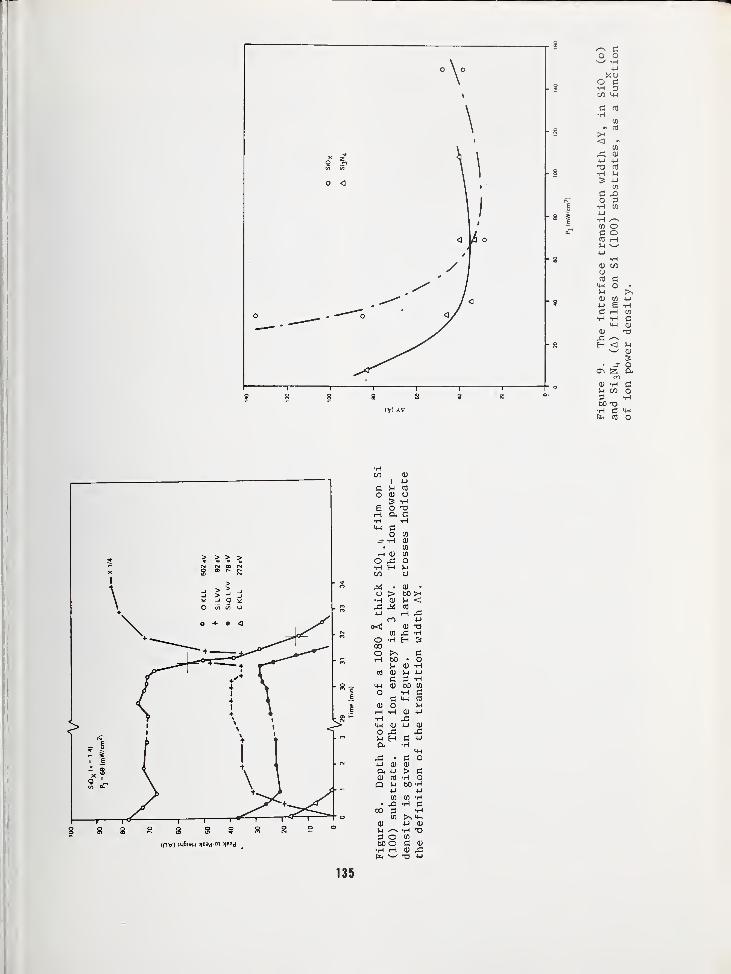
(0CO
><<
CO
CU
u 4JX) CD•H Ms St
c X.o 3•rf CO4J
•H —
V
CO oC ocO rHt-i
4J•H
CU COofa on
01 CO 4J4J E •HC i-l CO
•H fi en
0) XIx; < u
we
oCTi
CO4) •H Ci-i CO o3 •H00 XI•H c M-l
Pk cfl o
inv) 146i3H ^BSd-oi-iica,)
•HCO CU
4-1
(3 u ca
o cu oS •H
E o XIiH a c•H •HM-l 13
O CO
J" -H CU
0)
0) CO
O o•H H uCO u
^1 cu
o > 00•H 01 n <•C CO4-1 iHm 4-1
cxrj CU XI(0 J3 •H
O •H HCOo aH 00 o
M CU Hca CU •M
c 3 •H14-1 CU 00 CO
o •H cc m CO
01 o MiH •H cu 4-1
•H j=M-l CU 4-1 CU
Ou H e 4-1
•H<4-4
C O4-1 cu CU
a 4-1 > cCU a) H op t-i 00 •H
4-1 4-1
ca CO HXI •H c
00 3 •HCO !>. 4-4
CU 4-1 0)
u •H XI3 o CO
00 o c CU
•H r-l cu
P*4 ^3 4-1
135

DISCUSSION OF THE PAPERS BY STRAUSSER AND
JOHANNES SEN
Thomas : Without resurrecting the argumentabout the assignment of the Auger peaks of
elemental silicon, I have to say that two of
the peaks on the low energy side of yourmajor KLL peak are not really Auger peaksbut rather plasma loss peaks; the same is
true of the 107 eV silicon peak you havelabeled as an Auger peak, but there is some
controversy over that too. That is thepoint that I had to make, but could you also
tell me how you determined the stoichiometricfactor x in your SiOx ?
Strausser : As to your comment first of all,
I certainly agree that those are plasma loss
peaks in the silicon KLL spectrum. We sim-ply didn't label them. For the 107 eV peak,
we are inclined to accept the interpretation
by Grant and Haas, namely, that it is a
doubly ionized silicon Auger transition.
Now as to your question, we have done somequantitative work using normalization fac-
tors, which is basically like Joe Morabito'ssecond technique. He normalizes all the
peaks, applying an empirical correction fac-
tor to the major peaks, normalizing them all
to one particular peak and dividing each of
them with a total signal, thus calculatingpercentages. Instead of experimentally de-
riving the normalization factors, we havecalculated them. We use calculated ioniza-tion cross sections, a linear correction for
the energy dependence of the CMA transmis-sion, measured and extrapolated fluorescentyields and escape depths. We combine all of
these into a normalization factor. We can
then calculate the stoichiometry , and wehave verified the stoichiometry of thermallygrown silicon dioxide, for instance, that it
'is Si02- However, on that particular figurewe simply used the oxygen peak heights to
determine the stoichiometry of the subdioxidefilms using a known Si02 film as a referencefor the suboxides.
Thomas : During the past two or three years,I have been looking, day in and day out, at
"Si02" whatever that may be. We have pre-pared Si02 by various techniques. If I wereto measure just the ratio of the oxygen peakto a silicon peak, you would notice that the
ratio would change, depending upon whichtechnique were used to prepare the oxide.In other words, you would have a differentvalue for quartz, dry oxides, or oxidesgrown in steam, or spin-on oxides, or what-ever it is; the peak ratio can change sig-nificantly. So I do not know whether youtake the value two because you always say,Si02, and particularly how do you get that
value, x = 1.2. Do you measure the value of,for example, the oxygen peak of Si02 and thenmeasure the ratio of oxygen to some suboxide?I did not quite follow that.
Strausser : We convinced ourselves that aparticular dioxide film really was Si02.
Then we measured the oxygen peak height inthat film and we measured the oxygen peakheights in the suboxide films and used thosepeak heights to determine exactly what thestoichiometry of those films were. For thecalculations of stoichiometry of Si02 films,I have used the KLL peak rather than the LWpeak, we find that it is more reliable.
Thomas : Just one more comment. I have neverseen anything like a 7 eV chemical shift inthe KLL Auger peak. For one thing, the ESCA2p shift for silicon is only about 4 eV,
maybe 5 eV, depending on the author you read.
Can you explain why you see 7 eV?
Johannessen : Well, we do see a 7 eV shift in
the main Si]<LL peak, between elemental sili-con and silicon dioxide, and we see bothpeaks as a doublet in the suboxide. I canrefer you to a recent paper by C. D. Wagner.A simple explanation is that the Auger shiftis approximately twice that of the shift in
the L2}3 level, which is around 2.5 eV.
Thomas : No, why should it be? All thelevels are changing equally. You are talkingabout KL2
J3L2
)3, why should it be double?
Johannessen : Our value of a 7 eV Auger shiftin an unsaturated silicon oxide agrees wellwith similar results obtained by Wagner inoxidized silicon. In response to your ques-tion, I implied that a part of the shift wasdue to different chemical shifts of the K and
L levels, although the problem is more complexthan that.
Thomas : I have to disagree with you becauseI have never seen anything like that doubletstructure. Also, it is an unfair method of
looking at the stoichiometry because whenyou sputter and come to the interface you may
not be removing material uniformly at all.
What you may be seeing is really an Si02
chunk sitting here on the silicon so you may
be getting a silicon signal and a surfacecharged Si02 chunk more than anything else.
I have never seen a doublet like that of
equal intensity. You can get the 7 eV shifts
if you have a very large surface charge.
Johannessen : You will see a similar thing if
you look at the natural oxide on silicon.
136
Strausser : I think the important thing isthat this analyzer has enough resolution toresolve that peak and you have to considerwhat instrument you are using.
Erickson : In doing ESCA spectroscopy wequite frequently find that Auger shifts areapproximately double the correspondingshifts one finds in the ESCA spectrum. In
fact, for the case of copper oxide, there isno energy difference between metallic copperand a copper in cuprous oxide, but there aretremendous differences, 3 or 4 eV, in theAuger binding energies for the two states ofcopper. So it is not unexpected to findlarger shifts in the Auger spectra than in
the ESCA spectra. The reason is partly thatin the ESCA spectra you start out with, saya neutral atom and the final state is a uni-positive ion, whereas in the Auger case, youstart out with a unipositive ion and you endup with a doubly positive ion. You have to
consider the energy difference between theinitial state and the final state. There is
a concept known as extra-atomic or atomicrelaxation which can account for these dif-ferences in binding energy, or kinetic energyin the case or Auger electron.
Thomas ; The Auger shifts do not have to bedouble the ESCA shifts.
Erickson : It does not have to be double.In fact, in the cuprous oxide case there is
no shift at all in the ESCA binding energybut there is a 3 or 4 eV shift in the Augerenergy. So there are some mysterious thingswhich are not completely understood theoret-ically, but they are certainly experimentallyreal. I would agree that the observed shiftsin the KLL peaks for silicon and silicondioxide are entirely reasonable. I have seenshifts with that order of magnitude myself.
A question addressed to either one of thespeakers: In ESCA spectroscopy, one normallydetermines a direct N(E) curve and I am al-
ways a little suspicious of derivative typecurves for the following reason. If you lookat the ESCA spectrum of silicon 2p for a
thermally annealed clean silicon surface andcompare that with an argon bombarded siliconsurface, one finds out that the areas of twopeaks are approximately the same. However,the silicon 2p line for the argon implantedspecimen is broadened by a factor of about 2
or 3. On the other hand, the silicon 2p linefor the dioxide is, to start with, consider-ably broader than it is for pure silicon so
the effect of the 'residual argon in the lat-tice after bombardment does not have as
great an effect on the peak height or on itswidth. I am wondering whether or not you
see effects in the Auger spectrum due to
residual argon in the lattice, and if youfind any differences in the peak heights de-pending on whether or not you annealed thesample after argon bombardment.
Johannessen : We have not done any annealingof our samples after ion sputtering, and wehave not seen any significant effects oneither the oxygen or silicon spectra due to
argon ion implantation. The only observablechange due to ion sputtering is the removalof surface contaminants, such as water vaporand carbon. These contaminants tend to af-fect the appearance of, for instance, theLW spectra of silicon nitride. We do notsee any effect on the Si^LL spectra. Thismay be due to the larger escape depth, andhence, the larger sample volume being probed.I have here a viewgraph (Fig. 6) showingsome recent data on the escape depths ofelectrons from silicon and silicon oxide.The low energy data are taken from a paperby Lindau and Spicer, and the data on thehigh energy side are taken from a recentpaper by Flitsch and Raider. If you look atthe 1 KeV region, you will see that the es-cape depth for the Si^ix electrons is on theorder of 30 A. The oxygen KLL electrons at
roughly 500 eV escape from a depth on theorder of 10 to 15 A. There is a factor ofat least 2 in the escape depth between theoxygen and silicon KLL transitions.
In the depth profile of the Si02~Si interfacewe "saw" the effect of the interface on the
Si-KLL transition roughly 30 A before anychanges appeared in the oxygen peak. There-fore, the effect of different escape depthsis born out in our experimental data, andthis also shows that the ion beam does notdisturb the sample deeper than some 10 - 15 A.
Morabito : I would also like to comment that
7 eV is not an unreasonable Auger shift.Secondly, if the shift is due to a surfacecharge, then you should also see a shift in
the oxygen peak and this was not seen.
Strausser : If the shift was due to a surfacecharge, all the peaks should shift the sameamount and we really did not see that at all,
and we did not see a double peak at the
oxygen position. We always see the oxygenpeak at the same energy in the oxide film.
Harrington : For an escape depth, let us say,
of 20 to 30 A, is not this just the widthover which you are talking about seeing this
transition, and would that not equally wellexplain the transition rather than non-stoichiometry?
137

Strausser : That is the escape depth of thesilicon KLL peak. We are talking about thefall off of the oxygen KLL peak, and the Oj^ll
escape depth is much smaller. Johannessenwas showing the change in the shape of the
^i-KLL transitions through the interfaceregion, which indicates not only a change in
stoichiometry but also a change in chemicalstate of the Si atoms.
Johannessen : We define the metallurgicalinterface as the fall off in the oxygen KLLsignal. What we have seen is that the oxygenatoms apparently always exist in only onestate in silicon oxide; they are alwaysbonded to two silicon atoms as an Si20 quasi-molecule
.
Harrington : But the changes in the siliconpeak were what you are showing for the sili-con KLL and that is just the region you aretalking about here in thickness, and so youare interpreting the effect of the penetra-tion or escape depth as stoichiometry changes.
Johannessen : It is true that we averageover a depth of the order of the electronescape depth. In the case of the Si^LLAuger transition, it sees a much wider inter-face than that defined by the fall off of
the oxygen peak. It is difficult to exactlydetermine the stoichiometry in the interfaceregion because we deal with a differentialspectrum.
Harrington : Take the situation, where,ideally, there is just an abrupt interface,and because you have a penetration depth(escape depth) you are going to see the sil-icon and oxygen peaks of the oxide graduallyshift, even though you have an abruptinterface
.
Johannessen: That is correct and it would— — o
be on the order of 10 A, referred to theoxygen KLL peak.
Harrington : That would be on the order of
20 to 30 A according to your figures.
Johannessen : Yes, using the silicon KLLpeak, but we are referring to the oxygen KLLelectrons which have an escape depth around10 A. As a matter of fact, we have seennarrower interface regions in vacuum de-posited SiOx , where one would expect an
abrupt interface due to the condensationprocess on the cold substrate. So we areable to see differences for different dep-osition processes.
Morabito : Consider the particular exampleof a thin anodic tantalum oxide film on top
of tantalum, and I have done this. If younow monitor all the tantalum transitions, thehigher energy tantalum transition comefirst, you see it coming into the interfacebefore the lower energy transition. Inaddition to that, if you have a change in theAuger yield you are going to have a corre-sponding change in intensity and that couldbe in either direction, up or down.
Johannessen : I agree we see a broader inter-face in the silicon KLL than in the oxygenKLL.
DiStefano : After unfolding the effects of
the escape depth, allowing you to see thesilicon before you get there because someelectrons are escaping through the thin layerof Si02, and after unfolding the spatialvariations in the sputter rate, how' much of
that 35 A estimated interface width is left?How much of that graded junction is real?
Strausser : I think that the last effect is
very, very small. We have looked at thesecraters under SEM's and have seen very, verysmooth craters. Secondly, our electron probebeam is only 5 microns wide, and so it is notsampling a big enough area to have largevariations in sputter yield across it.
DiStefano : Let me paraphrase, after sputter-ing 1000 A of Si02, how much variation in
thickness would you have? If you have 1%
sputtering variation across that area, youwould have 10 A difference in the interfaceposition. So it looks like you are verysensitive to variation in the sputter yieldacross the area.
Johannessen : We have been worried aboutthings like that, and we have seen surfaceroughening effects due to the ion beam at
very low sputtering rates, less than 10 A/min.The present data are obtained at approximately80 A/min using a rastered low energy ion beam.
No surface irregularities were visible evenif we used the TEM and replica technique. Webelieve that the provisions I just mentionedare essential for this type of work.
Now taking all of these effects, escapedepths, ion beam distortion, etc., into ac-
count, our estimate of the interface width is
on the order of 20-30 A.
138
NBS Special Publication 400-23, ARPA/NBS Workshop IV, Surface Analysis for Silicon Devices,held at NBS, Gaithersburg, Maryland, April 23-24, 1975 (Issued March 1976)
SURFACE COMPOSITIONAL CHANGES WITH ELECTRONBOMBARDMENT OBSERVED BY AES
Simon Thomas
Semiconductor Analytical LaboratoryMotorola Semiconductor Products Division
Phoenix, Arizona 85008
ABSTRACT
Auger Electron Spectroscopy (AES) is generally considered to be a'non-destructive' surface analytical technique. However, there are manyinstances where the incident electron beam can alter the surface compo-sition of the solid being analyzed. The commonly observed effects ofthe electron bombardment are the surface decomposition, desorption, out-diffusion, surface migration and co-adsorption. Some typical examplesof these effects, often encountered in the AES analyses of semiconductordevices are given.
Auger Electron Spectroscopy (AES) has emergedas a very powerful and popular surface ana-lytical technique for semiconductor devicefabrication and failure analyses. The ele-mental specificity, sensitivity, depth of
analysis and the spatial resolution have con-tributed to its popularity as an analyticaltechnique for the characterization of a
'practical surface'. In addition to the ele-mental specificity, the chemical effects of-ten observed in the Auger spectra providefurther insight into the surface composition.Noble gas ion sputtering is generally coupledwith AES as a means of removing the adsorbedspecies from a typical processed surface or
for obtaining the depth composition profiles.Generally, AES is considered to be a non-destructive surface technique. It is assumedthat no significant surface compositionalchanges are induced by the incident electronbeam which is typically of energy 1-5 keV andbeam currents of 1-50 uA. However, there aremany exceptions to the non-destructive natureof this technique. The intent of this briefreport is to draw the attention of the numer-ous Auger spectroscopists , particularly in
the semiconductor industry, to the typicalsurface compositional changes which may occuras a result of prolonged electron bombardment.The beam effects do not necessarily underminethe immense capabilities of AES as a surfaceanalytical technique. Nevertheless one has
to be aware of these effects and try to min-imize them, if present. If any deleteriouseffects are present they should be reckonedwith in any quantitative analysis. The mostcommonly observed effects of the electronbeam bombardment on the surface composition,are the surface decomposition, desorption,outdiffusion , surface migration and co-adsorption. Some examples of these are givenbelow.
SURFACE DECOMPOSITION
In the surface analysis of silicon devices,the most commonly observed adverse effect is
the decomposition of silicon dioxide. Withthe prolonged electron bombardment of Si02,one observes the appearance of the Si-L2 3VV
Auger peak at ^92 eV which is characteristicof elemental silicon. Simultaneously, thereis a reduction in the 75 eV Auger peak char-acteristic of silicon in Si02 and also a re-duction in the oxygen Auger peak height.The various parameters affecting the decom-position of Si02 have been reported in theliterature and will not be discussed here.
There are many other examples of the decom-position of oxides by electron bombardment.An example is given in Figure la wherephosphorus pentoxide present on an aluminumsubstrate is reduced to mostly elementalphosphorus in a matter of minutes (Ep = 3 keV;
Ip = 12 pA) . It is interesting to note the
large chemical effects present in the Augerfeatures of P in P2O5. A large chemicalshift of M.2 eV and a pronounced change in
the peak shape are observed from P in P2O5.These features resemble the chemical effectsfrom Si and Si02. The decomposition of P2O5with electron bombardment appears to be ma-trix dependent as evident from Figure l.b.
In this case P2O5 is present as an impurity
on an oxidized GaAs substrate. No changesin the Auger features of P2O5 are observedwith prolonged bombardment. Oxides in whichdecompositional effects have been observedin our laboratory include B2O3, Ge02, hydrousoxides of Al, Ti02 and some cases of bulkAI2O3. This list is by no means exhaustive.
DESORPTION
Another consequence of the electron bombardment
139
is the desorption of selected surface species.
Electron stimulated desorption (ESD) has beenstudied extensively by many authors and com-prehensively reviewed by Madey and Yates (2).
Typical cross sections for the desorption of
adsorbed species are in the range 10~16 -
10~22 cm^. The most conspicuous desorptioneffect is observed in the Auger analysis of
adsorbed halogens with desorption cross sec-tions of VLO- -^ cm^. In Figure 2 is shownthe variation of the Auger signal from fluo-rine adsorbed on an aluminum substrate, as a
function of electron bombardment time (Ep
=
3 keV, Ip = 5 uA). The beam current of 5 yAused in this study is usually considered amoderately low value for typical AES analysis.However, one can observe the rapid decreasein the Auger signal, which makes the absolutepeak height measurement somewhat difficult.Assuming the surface concentration to be uni-form one may translate the area of analysisand obtain a fairly accurate estimate of thepeak height. In addition to the halogens,the alkali metals show similar desorption ef-fects with a strong dependence on the matrix.The total desorption cross sections for thealkali metals appear to be much smaller thanthose for the halogens.
OUTDIFFUSION
Semiconductor devices are commonly passivatedwith silicon dioxide doped with phosphorus.In the surface compositional analysis of suchphosphosilicate glass (PSG) using AES, one of
the commonly observed phenomenon is the in-crease in the phosphorus Auger signal withelectron bombardment time. This is due to
the outdiffusion of phosphorus from the bulkto the surface. In all the PSG surfaces typ-ically used in the device fabrication, theoutdiffusion of P has been observed. Therate of P outdiffusion appears to be dependenton the PSG deposition temperature and thestoichiometry , besides the incident electronbeam parameters. Although the mechanism of P
outdiffusion is not well understood it is
thought that the electric field establishedat the surface of the PSG with electron bom-bardment is the driving force. The phenom-enon of the P outdiffusion has to be borne inmind while attempting to obtain Auger cali-bration curves for P in PSG. In addition to
the P outdiffusion, the surface decompositionalso is observed in the Auger analysis of P
in PSG. Phosphorus appears to be present at
the surface of the PSG as ?2®5> although this
could not be conclusively proved for the bulkusing the Auger peak features. P2°5 presentat the surface of the PSG is converted to
elemental phosphorus with electron bombard-ment .
Chou et.al. have observed similar outdif-fusion of chlorine from SiC>2 grown in chlo-rine or HC1 and the subsequent desorptionfrom the surface.
SURFACE MIGRATION
Mobile ions, particularly alkali ions, canmigrate along the surface under the influenceof the electron beam. However, this is not aserious impediment in most typical Augeranalyses. Desorption of the alkali ions is a
more serious problem than the surfacemigration.
CO-ADSORPTION
It is generally observed that the electronbeam assists in the adsorption of oxygen andcarbon from the residual vacuum in the cham-ber. Although its presence is duly recog-nized, co-adsorption is the least problem-atic effect as far as the Auger analysis of
'practical surfaces' encountered in silicondevice technology is concerned. Under typi-cal vacuum of <10- ^ Pa, routinely obtainedin an AES chamber, no significant co-adsorp-tion occurs in the time required to plot anAuger spectrum. The problem, of course, canbe aggravated by the high residual pressuresof reactive gases such as H2O, CO, CO2 or CH4present in the chamber.
In many cases one may observe one or more of
the above beam effects. If such effects arepresent
,proper care must be taken in mini-
mizing them and in interpreting the Augerdata. The need for caution is acute in the
simultaneous ion sputtering and Auger analy-sis when the ion beam and the electron beamare bombarding the surface continuously.Notwithstanding the likely surface composi-tional changes which may occur in selectedcases, AES is one of the most valuable sur-face analysis techniques for semiconductorprocessing and device failure analyses.
REFERENCES
1. S. Thomas, J. Appl. Phys. , 45, 161 (1974).
2. T. E. Madey, and J. T. Yates, J. Vac. Sci
and Technol. 8, 525 (1971).
3. N. J. Chou, C. M. Osburn, Y. T. van der
Meulen, and R. Hammer, Appl. Phys. Lett.
22, 380 (1973).
140
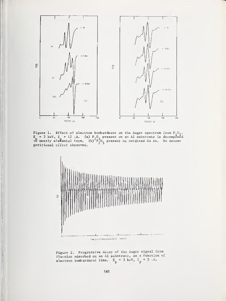
0 50 100 150 200 0 50 100 150 200
ENERGY ev ENERGY eV
Figure 1. Effect of electron bombardment on the Auger spectrum from P^O^
.
E = 3 keV, I = 12 yA. (a) ^2^5 Present on an Al substrate is decomposedtB mostly elemental form. (b) ^2^5 Present on oxidized Ga As. No decom-positional effect observed.
TIME OF ELECTRON BOMBAROMENT MINUTES
Figure 2. Progressive decay of the Auger signal from
fluorine adsorbed on an Al substrate, as a function of
electron bombardment time. E = 3 keV, I = 5 yA.
141

NBS Special Publication 400-23, ARPA/NBS Workshop IV, Surface Analysis for Silicon Devices,held at NBS, Gaithersburg
, Maryland, April 23-24, 1975 (Issued March 1976)
COMBINED SCANNING ELECTRON MICROSCOPY-AUGERSPECTROSCOPY FOR MICRO-SPOT SURFACE AND IN-DEPTHANALYSIS OF SILICON AND TRANSISTOR METALLIZATIONS
A. Christou, W. Weisenberger and H. M. DayNaval Research LaboratoryWashington, D. C. 20375
ABSTRACT
Auger Spectroscopy with a focused electron beam in the scanning electronmicroscope (SEM) has provided an extremely powerful diagnostic techniquefor silicon surfaces and transistor metallization systems. The focusedelectron beam in a SEM allows one to determine the surface topography ofthe specimen which can be correlated with the Auger spectra of selectedareas. In addition, a scanning Auger image may be obtained by using theamplitudes of a selected Auger peak for intensity modulation of the CRT.The normal modes for micro-spot AES investigation in the SEM includespot analysis, line scan and Auger electron imaging. Secondary electronimage resolutions of less than 2000 A have been correlated with Augerspectra of submicron regions. Surface features associated with gold andaluminum metallizations of microwave power transistors have been anal-yzed in detail using the AES-SEM technique. In addition the submicronAuger spatial resolution capability has been applied to the identifica-tion of contaminants on silicon surfaces.
INTRODUCTION
The analysis of failed regions on fine geom-etry devices has previously been extremelydifficult. Energy dispersive x-ray analysisincludes a reaction area about one micron(at 15 kV) below the surface. Auger anal-ysis only examines about a 10 A depth, how-ever most systems use an analysis area whichhas a 50 urn diameter. Even the scanningAuger microprobe (SAM) uses a 5 ym beam andhas no corresponding high spatial resolutionSEM topography information. Microwave powertransistors are characterized by cells on
the order of 50 to 100 pm with line spacingon the order of 1 urn.
The utilization of electrostatic lens and
the geometric configuration 1'2 of present
day Auger detectors has made the attainmentof submicron size electron beam a formidableproblem. In the present investigation, thefocused electron beam in the scanning elec-tron microscope (SEM) is used as the primarybeam for Auger spectroscopy 3 » 4 > 5 thereby
improving the AES spatial resolution to
.2 urn. The microspot technique thereforeallows the determination of Auger spectra of
selected areas in addition to the surfacetopography (SEM mode) of a failed region.
Scanning Auger images may also be obtainedby using the amplitude of the Auger peaksfor intensity modulation of the cathode ray
tube. The spatial resolution of . 2 pm to
1
2 um for Auger spectroscopy obtained by thistechnique is ideally suited for the analysisof (1) localized interdif fusion regions in
metallizations, (2) adhesion problems and
(3) process associated contamination. Theinstrument requirements for high resolutionAuger spectroscopy of solid state devices ina commercial scanning electron microscopewill be reviewed in order to understand the
usefulness and limitations of the micro-spotSEM-AES technique.
General Requirements for AES-SEM Instruments
The requirements for AES in a scanning elec-tron microscope are the vacuum chamber, the
energy analyzer and the electron opticalcolumn. The vacuum system used to achievea clean ultra-high vacuum in our SEM is an
electro-ion pump with a mechanical carbonvane pump and cryo-sorption pumping for an
oil free 2 stage roughing system 5. The
electro-ion pump is a four-cell triode type
electrostatic getter-ion pump with a speedof 1600 1/sec for dry nitrogen. The pump is
closely connected to the specimen chamber of
the SEM by a 6 inch ultra high vacuum gate
valve. Figure 1 shows a schematic of the
entire system. The SEM is an ETEC autoscanspecially made for this application 6
. Theentire system is of stainless steel construc-tion. The only non-stainless steel part ex-
posed to vacuum is the viton seal at the gatevalve. The ports contain the Auger detector,

ion etching capability, secondary electrondetector, leak valve and one sight port withan optical microscope. Pressures of 3 x
10-9 torr in the specimen chamber have beenobtained after a mild bakeout atl35°C.Under normal operational conditions, the
system is operated at pressures between5 x 10~ 9 torr and 1 x 10
-8torr. A residual
gas analysis of the system was attempted in
order to determine the presence of contami-nants. A quadrupole mass spectrometer wasinstalled in the approximate vicinity of thespecimen stage. The constituents due to
water had partial pressures of the order of
1 x 10⁻⁸ torr, while nitrogen partial pres-
sure was below 3 x 10⁻⁹
torr.
The Electron Optics and Auger Detector
The electron optical column is the ETECmulti-lens system housed in a modular pre-aligned column. The energy source was a
triode electron gun with a high emissiontungsten filament. The spherical aberrationcoefficient of the final lens was 3 cm for a
working distance of 8 mm. Figure 2 showsthe relationship between probe current andprobe diameter for a fixed working distanceof 19 mm. The curved lines are for the 400and 500 um aperture. The straight line is
for the optimum aperture obtained by varyingaperture diameter. Since most of the AESinvestigations were accomplished with a
probe current of 10-7 A to 10
-8 A the opti-mum sgatial resolution possible is between2000 A and 1 um at 20 kV. However, one mustalso take into account such parameters as
escape depth, atomic number, surface areaand beam energy when determining spatialresolution. A second factor other than beamcurrent which must be considered in obtain-ing the required resolution is recordingtime. The signal to noise (S/N) ratio canbe increased by utilizing longer recordingtimes. The recording time of an Auger spec-trum can be increased to reduce the beamcurrent while maintaining the same S/Nratio.
The Auger detector used is the cylindricalmirror type 5 designed to minimize the work--ing distance of the scanning electron micro-scope to 19 mm. The analyzer energy reso-lution was measured to be .5% at 3 kV beamvoltage with 10% transmission. Using a
sputter ion gun and a multiplexing unit formonitoring peak to peak amplitudes, up to
six Auger peaks can be monitored while thespecimen surface is etched.
AES-SEM Modes and Analyses
a. Spot Analysis . The normal analyticalmodes include spot analysis, line scan and
1
scanning Auger imaging. Each of these anal-yses can be combined with sputter etching inorder to obtain an in-depth analysis. TheAuger image can be recorded for a specifiedarray of points or for a specified number of
line scans. The amplitudes of the Augerpeaks are then recorded or displayed as in-tensity or amplitude modulation of the record-ing cathode ray tube.
The spot analysis will now be applied to thefailure analysis of a microwave power tran-sistor in order to illustrate the uniqueapplication of this instrument as a diagnos-tic tool. Figure 4 illustrates a regiontypical of a failed microwave power transis-tor from pulsed RF accelerated life tests,showing the presence of a film material be-tween the metallizations. Micro-spot AES-SEManalysis was applied to the reacted regionsbetween the metallizations in order to iden-tify the reaction products (oxide overcoatand aluminum reaction)
.
Application of the energy dispersive x-rayanalysis technique (EDXA) on the area of
interest was attempted before the initialAES analysis. A large 1740 eV Si peak wasobserved (figure 3) along with the 1490 eValuminum line. The silicon detected couldhave been present in the reaction region or
it may be from the substrate silicon. In
addition, the EDXA technique cannot differ-entiate between aluminum in A120 3
and freealuminum or between free silicon and siliconin Si0 2 . The AES spectrum with the SEM elec-tron beam situated on the reacted region is
shown in figure 4. The position of the
aluminum KLL Auger transition is indicatedat 1407 eV. Also shown is an aluminum oxidepeak at 57 eV. Therefore, the surface of
the reacted zone consists essentially of
A1 20 3 , oxygen and carbon (from handling and
testing). Free silicon, up to the sensitiv-ity limitations of the instrument which is
1.0 percent per monolayer was not detected.The lack of detection of silicon is shownby the absence of the 92 eV LMM and 1619 eV
transitions. Auger analysis of the unreactedemitter metallization shows the position of
the Al (KLL) transition at 1396 eV as expectedfor pure aluminum''. In addition, the posi-
tion of the Al LMM transition was located at
69 eV instead of the 57 eV peak found for the
aluminum reacted zone. The peak shift and
change in shape of the KLL peak for aluminumclearly indicated that the film region of
figure 4 was the result of the formation of
A1 20 3.
b. Auger Imaging. A problem related to
semiconductor device reliability is the
thermal dissolution of silicon into aluminumenhanced by microcracks or flaws in the
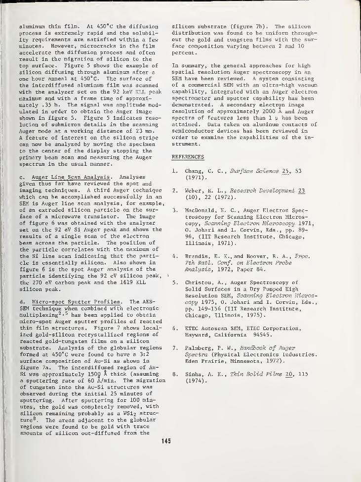
aluminum thin film. At 450°C the diffusionprocess is extremely rapid and the solubil-ity requirements are satisfied within a fewminutes. However, microcracks in the filmaccelerate the diffusion process and oftenresult in the migration of silicon to the
top surface. Figure 5 shows the example of
silicon diffusing through aluminum after a
one hour anneal at 450°C. The surface of
the interdiffused aluminum film was scannedwith the analyzer set on the 92 keV KLL peakmaximum and with a frame time of approxi-mately .35 h. The signal was amplitude mod-ulated in order to obtain the Auger imageshown in figure 5. Figure 5 indicates reso-lution of submicron details in the scanningAuger mode at a working distance of 23 mm.
A feature of interest on the silicon stripecan now be analyzed by moving the specimento the center of the display stopping theprimary beam scan and measuring the Augerspectrum in the usual manner.
c. Auger Line Scan Analysis . Analysesgiven thus far have reviewed the spot andimaging techniques . A third Auger techniquewhich can be accomplished successfully in anSEM is Auger line scan analysis, for example,of an extruded silicon particle oh the sur-
face of a microwave transistor. The imageof figure 6 was obtained with the analyzer
set on the 92 eV Si Auger peak and shows the
results of a single scan of the electronbeam across the particle. The position of
the particle correlates with the maximum of
the Si line scan indicating that the parti-
cle is essentially silicon. Also shown in
figure 6 is the spot Auger analysis of the
particle identifying the 92 eV silicon peak, >
the 270 eV carbon peak and the 1619 KLLsilicon peak.
d. Micro-spot Sputter Profiles . The AES-SEM technique when combined with electronicmultiplexing 2 ' 5 has been applied to obtainmicro-spot Auger sputter profiles of reactedthin film structures. Figure 7 shows local-ized gold-silicon recrystallized regions of
reacted gold-tungsten films on a siliconsubstrate. Analysis of the globular regionsformed at 450°C were found to have a 3:2
surface composition of Au-Si as shown in
figure 7a. The interdif fused region of Au-Si was approximately 1500 A thick (assuminga sputtering rate of 60 A/min. The migrationof tungsten into the Au-Si structures wasobserved during the initial 25 minutes of
sputtering. After sputtering for 100 min-utes, the gold was completely removed, with
silicon remaining probably as a WSi2 struc-
ture 8. The areas adjacent to the globular
regions were found to be gold with trace
amounts of silicon out-diffused from the
145
silicon substrate (figure 7b). The silicondistribution was found to be uniform through-out the gold and tungsten films with the sur-face composition varying between 2 and 10
percent
.
In summary, the general approaches for highspatial resolution Auger spectroscopy in anSEM have been reviewed. A system consistingof a commercial SEM with an ultra-high vacuumcapability, integrated with an Auger electronspectrometer and sputter capability has beendemonstrated. A secondary electron imageresolution of approximately 2000 A and Augerspectra of features less than 1 u has beenattained. Data taken on aluminum contacts ofsemiconductor devices has been reviewed in
order to examine the capabilities of the in-strument .
REFERENCES
1. Chang, C. C. , Surface Science 25 , 53
(1971).
2. Weber, R. L., Research Devetopment 2^3
(10), 22 (1972).
3. MacDonald, N. C. , Auger Electron Spec-troscopy for Scanning Electron Micros-copy, Scanning Electron Microscopy 1971,0. Johari and I. Corvin, Eds., pp. 89-
96, (IIT Research Institute, Chicago,Illinois, 1971).
4. Brandis, E. K., and Hoover, R. A., Proc.
7th Natl. Conf. on Electron ProbeAnalysis, 1972, Paper 84.
5. Christou, A., Auger Spectroscopy of
Solid Surfaces in a Dry Pumped HighResolution SEM, Scanning Electron Micros-copy 1975, 0. Johari and I. Corvin, Eds.,
pp. 149-156 (IIT Research Institute,Chicago, Illinois, 1975).
6. ETEC Autoscan SEM, ETEC Corporation,Hayward, California 94545.
7. Palmberg, P. W. , Handbook of AugerSpectra (Physical Electronics Industries.Eden Prairie, Minnesota, 1972).
8. Sinha, A. K. , Thin Solid Films 2_0, 115
(1974).
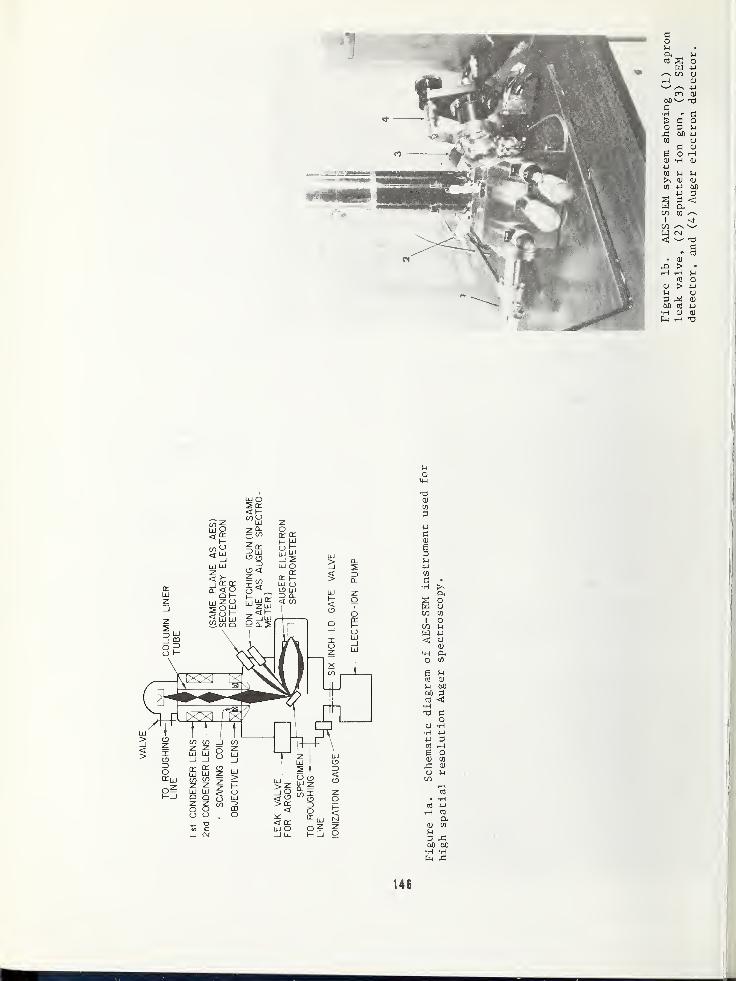
T3a)
a•H
P.
sOo
c/1 cn
o
W 4-1
<! o<u
<4-l P,O CO
0cu
n 00bO 3a) <•HT3 e
OO •H•H 4-1
4J 3H
e O0) CO
CD
o U
i—\
n)
•Hni 4-1
t-i
p-CU CO
,Ct>0
•H H
146
PROBE DIAMETER
Figure 2. The relationship between probe current andprobe diameter for AES-SEM system.
Figure 3. EDXA analysis of a failed micro-wave power transistor showing the detectionof both a large 1740 eV Si peak along withthe 1490 eV aluminum peak. Also shown is aschematic comparing the X-ray and Augerelectron analysis regions.
147
"
—
—r~- 1
3= 10K KEUEX-RAY HS= 20EU/CH
00 02
o
148
Q. 2 —
h fl; h 5a u. < i/>a u- <to o a
NOIllSOdrTOD iN33d3dNOIllSOdWOO ±N3Dd3d
O>-i •
o. co
mJ3U -H4-1 14-1
4-1
3 CD. »Hco x
4-1
cu c00 01
3 4J
< co
604-> C0 a(X 4JCO I
1 -aO rHM OO £>0
H2 c
•iH
• cr-. o
•H0) CO
M 33 M-i
60 >4-i
•H -H(Jh XI
D2 i'
2LJ 0.> CTj Ld
Mm
o
a)
rHO•H4-1
Maj
D. •
Uo
O Ua co
•H -HH CO
•H q!
co ct)
MCd 4-J
M-l Uo cu
CO o•H a.CO
a)
rH >cd aj
o BCO
ct)
cu
a m-i
•H OrJ
CU
O• ct)
uCU 3M co
360 CU
•H4-1
149
DISCUSSION OF THE PAPER
Harrington ; Although you gain in spatialresolution what you do feel you loose in
sensitivity with the Auger technique at the
small beam diameters?
Christou : I do not have a quantitativeanswer for that, but you certainly degrade
the signal to noise ratio significantly.The best way would be to computer interface
your system so that you could observe peaks
hidden in the noise.
Madey : I would, just like to issue a word of
caution about beam induced damage and prob-
lems of the sort that you have describedhere. I think it is particularly acute whenyou have such a small beam and a high cur-
rent. For the situation you described with10~9 amps and a 0.1 micron beam diameter you
have a current density that is of the orderof 10 amps per square centimeter. Now forelectron stimulated desorption and decompo-sition, typical cross sections are of theorder of 10~20 to 10~22 square centimetersfor decomposition of surface oxides, de-sorption of oxygen and other species fromsurfaces. Under these conditions the aver-age lifetime of the oxygen on the surfacecould be of the order of 1 to 100 secondswhich is of the same order of magnitude as
you need to get a workable signal to noiseratio. So it is quite possible then you canget appreciable beam decomposition and dam-age, particularly in compounds, insulatorsand semiconductors.
Christou : Yes, I agree and it is for that
reason that we have been mainly applyingthis technique to interdiffusion phenomenaand thin films.
150
NBS Special Publication 400-23, ARPA/NBS Workshop IV, Surface Analysis for Silicon Devices,held at NBS, Gaithersburg
, Maryland, April 23-24, 1975 (Issued March 1976)
APPLICATIONS OF X-RAY PHOTOELECTRON SPECTROSCOPY(ESCA) TO MIS DEVICES*
Frank J. Grunthaner
Jet Propulsion LaboratoryCalifornia Institute of Technology
Pasadena, California 91103
Summary
X-ray photoelectron spectroscopy (XPS, orESCA) is described as both an analytical andexperimental tool for the characterizationof metal-insulator-semiconductor (MISdevices. A brief description is given ofgeneral problems which lend themselves to
the application of this technique. Key ex-perimental methods in XPS are discussed.Several illustrative applications are con-sidered including characterization of theSi/Si02 interface, surface corrosion inhermetically sealed packages, mobile ion in-stabilities, organic surface contamination,etchant residues and heavy-metal impurities.New developments in XPS are discussed andsome limitations of the technique are as-sessed .
Introduction
resistance. In each of these modes, severalfailure mechanisms can be detailed which aredependent on the chemistry of the oxide, thatof the defects in the oxide, and that ofresidual species determined by the process.The study and characterization of the processrequires chemical and physical informationresulting from the probing of well-definedregions of the device. The study of the sur-faces of devices can yield such information.
X-Ray Photoelectron Spectroscopy
XPS has seen considerable development sincethe first monograph on the phenomenon appearedin 1967. 1 Work in this field has also beencatalogued under the more general descriptionof electron spectroscopy for chemical analy-sis (ESCA) . A number of recent reviews haveappeared2-5 and can be consulted for experi-mental detail.
In the last three to four years, major ad-vances have been made in the technologies of
surface spectroscopy. These spectroscopiesperturb the surface of a sample withphotons, ions or electrons, and monitor therelaxation processes which results. Thisyields a variety of data concerning thephysical parameters of the surface. Severalof these methods give estimates of the ele-mental composition of samples. One of thesetechniques, XPS, also gives significantchemical information about the surface.
The production of an MIS device is basicallyan exercise in chemical processing technol-ogy. The fabrication of high reliabilitydevices is dependent on achieving an under-standing of the interaction of processingchemistry with device physics. In CMOStechnology, for example, several dominantfailure modes can be identified including:oxide breakdown, threshold voltage shifts,resistive and open connections, excessleakage and shorts, and changes in channel
Figure 1 describes the physical process. Asoft x-ray source is used to irradiate thesurface of a sample with photons of a char-acteristic energy (e.g., AS, Koij 2 )- Tneabsorption of the photon can lead to two
excitation cases: 1) x-ray absorption wherean electron is excited from a core-level to
the Fermi level, and 2) electron emission inwhich the electron is excited from the boundcore state into the vacuum continuum. Eitherof these processes result in the excitationof the absorbing atom. The system can under-go relaxation through electron or photonemission or through more complicated radia-tionless processes. The photon emission pro-cess gives rise to an x-ray quantum (x-rayfluorescence) . The electron emission eventis termed auto-ionization and gives rise to
an Auger electron. Auger electron spectros-copy (AES) typically uses high-energy elec-trons to create the core-level holes requiredto stimulate this electron emission.
In the case of photon absorption followed bydirect electron emission, the energy of theejected electron is given by:
hv = E + EF
(k) + qV + W (1)kin s spec
This paper presents the results of onephase of research performed at the Jet Pro-pulsion Laboratory, sponsored by the Na-tional Aeronautics and Space Administrationunder Contract NAS 7-100.
where hv is the photon energy, E the
151
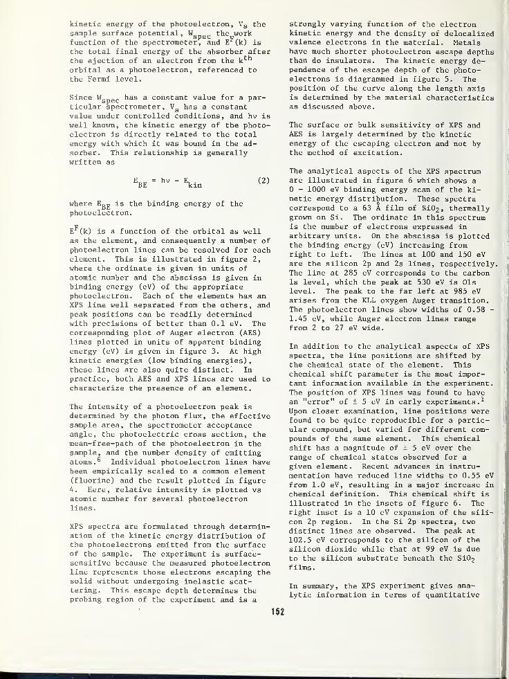
kinetic energy of the photoelectron, V9 thesample surface potential, W
gpecthe work
function of the spectrometer, and E^(k) is
the total final energy of the absorber afterthe ejection of an electron from the k^orbital as a photoelectron, referenced to
the Fermi level.
Since Wgpec
has a constant value for a par-ticular spectrometer, V
ghas a constant
value under controlled conditions, and hv iswell known, the kinetic energy of the photo-electron is directly related to the totalenergy with which it was bound in the ad-sorber. This relationship is generallywritten as
EDC = hv - E (2)BE kin
where Egg is the binding energy of thephotoelectron.
E (k) is a function of the orbital as wellas the element, and consequently a number ofphotoelectron lines can be resolved for eachelement. This is illustrated in figure 2,
where the ordinate is given in units of
atomic number and the abscissa is given inbinding energy (eV) of the appropriatephotoelectron. Each of the elements has anXPS line well separated from the others, andpeak positions can be readily determinedwith precisions of better than 0.1 eV. Thecorresponding plot of Auger electron (AES)
lines plotted in units of apparent bindingenergy (eV) is given in figure 3. At highkinetic energies (low binding energies)
,
these lines are also quite distinct. In
practice, both AES and XPS lines are used to
characterize the presence of an element.
The intensity of a photoelectron peak is
determined by the photon flux, the effectivesample area, the spectrometer acceptanceangle, the photoelectric cross section, themean-free-path of the photoelectron in thesample, and the number density of emittingatoms. 6 Individual photoelectron lines havebeen empirically scaled to a common element(fluorine) and the result plotted in figure4. Here, relative intensity is plotted vsatomic number for several photoelectronlines.
XPS spectra are formulated through determin-ation of the kinetic energy distribution ofthe photoelectrons emitted from the surfaceof the sample. The experiment is surface-sensitive because the measured photoelectronline represents those electrons escaping thesolid without undergoing inelastic scat-tering. This escape depth determines theprobing region of the experiment and is a
strongly varying function of the electronkinetic energy and the density of delocalizedvalence electrons in the material. Metalshave much shorter photoelectron escape depthsthan do insulators. The kinetic energy de-pendence of the escape depth of the photo-electrons is diagrammed in figure 5. Theposition of the curve along the length axisis determined by the material characteristicsas discussed above.
The surface or bulk sensitivity of XPS andAES is largely determined by the kineticenergy of the escaping electron and not bythe method of excitation.
The analytical aspects of the XPS spectrumare illustrated in figure 6 which shows a0 - 1000 eV binding energy scan of the ki-netic energy distribution. These spectracorrespond to a 63 A film of Si02 ,
thermallygrown on Si. The ordinate in this spectrumis the number of electrons expressed inarbitrary units. On the abscissa is plottedthe binding energy (eV) increasing fromright to left. The lines at 100 and 150 eVare the silicon 2p and 2s lines, respectively.The line at 285 eV corresponds to the carbonIs level, which the peak at 530 eV is 01slevel. The peak to the far left at 985 eVarises from the KLL oxygen Auger transition.The photoelectron lines show widths of 0.58 -
1.45 eV, while Auger electron lines rangefrom 2 to 27 eV wide.
In addition to the analytical aspects of XPSspectra, the line positions are shifted bythe chemical state of the element. Thischemical shift parameter is the most impor-tant information available in the experiment.The position of XPS lines was found to havean "error" of i 5 eV in early experiments. 1
Upon closer examination, line positions werefound to be quite reproducible for a partic-ular compound, but varied for different com-pounds of the same element. This chemicalshift has a magnitude of ± 5 eV over therange of chemical states observed for a
given element. Recent advances in instru-mentation have reduced line widths to 0.55 eV
from 1.0 eV, resulting in a major increase in
chemical definition. This chemical shift is
illustrated in the insets of figure 6. Theright inset is a 10 eV expansion of the sili-con 2p region. In the Si 2p spectra, two
distinct lines are observed. The peak at
102.5 eV corresponds to the silicon of the
silicon dioxide while that at 99 eV is dueto the silicon substrate beneath the Si02
films
.
In summary, the XPS experiment gives ana-lytic information in terms of quantitative
and qualitative analysis. Quantitative in-formation requires calibration, and pre-cisions in the ± 1% range are easilyachieved. In qualitative terms, sensitivi-ties of about 1 ppm have recently been de-monstrated. 7 The chemical shift is the mostimportant aspect of the experiment and per-mits assignment of the chemical state of
various surface species. The observationdepth is typical of surface spectroscopiesand ranges from 3 - 4 A to about 125 A.
Experimental Considerations
The execution of the XPS experiment is dia-grammed in figure 7. An x-ray source is
required to irradiate (excite) the samplesurface. The kinetic energy distribution of"
the emitted electrons is determined by meansof an electron monochromator . This sequencerequires that source, sample and analyzer becontained in a high vacuum system.
In practice, however, this basic experimentimposes several serious constraints on the
equipment. The most important of these arelisted in table I. An ultra-high-vacuumsystem is mandated by the surface nature of
the experiment. Unless sample limited pres-sures of 10
-9 torr and less are achieved,the surface can become recoated during anal-ysis. The residual gases present in the
spectrometer must be as non-reactive as
possible, e.g., He, A, N2, etc., with lowsticking coefficients.
Since photoelectron spectra consist of sharplines rising out of a significant scatteredelectron background, the highest possiblesignal-to-background ratio must be achieved.The background level is determined by theS/B ratio of the x-ray source, the surfacefeatures of the sample, the presence of
secondary electrons in the sample chamber,and the electron background of the analyzer/detector. High S/B ratios in the x-raysource require the use of soft x-ray mono-chromators. The use of monochromatedsources gives rise to collimated x-raybeams', which reduce the secondary electronflux in the sample chamber.
The analyzer, x-ray source and detector mustbe treated as a system and optimized for themaximum throughput; that is, for each photonimpinging on the sample surface, the largestpossible fraction of electrons must reachthe detector.
A sample-mounting system is required whichwill permit variation in the electron accep-tance angle of the analyzer in relation to
the sample surface. This variation permits
depth analysis in the range 2 - 120 A with-out destruction of the sample. 9 Control of
secondary electrons in the sample chamberenables a series of electrical experimentswhich will be described later. Variabletemperature capability permits capture of
reaction intermediates as well as study of"in situ" reactions, thermal degradation,etc
.
The actual XPS experimental setup is illus-trated for the JPL electron spectrometer in
figures 8-10. Figure 8 gives a simplifieddiagram of the basic ESCA spectrometer. Thesoft x-ray source consists of an aluminumtarget bombarded with 15 keV electrons.These photons are focused by the sphericallybent quartz-crystal monochromator on thesample surface in a separate chamber. Thex-ray beam is collimated to a spot size of1x5 mm. Electrons enter the energy ana-
lyzer through the 4-element electron lens,which retards and focuses the electrons.The analyzer is a spherical capacitor oper-ated at a fixed energy transmission. Theelectrons are then directed against themultielement detector and the data then readinto the multichannel analyzer.
A physical representation of the samplechamber of the spectrometer is given in
figure 9. The x-ray source and analyzer
are indicated in perspective. The sampleis mounted on a sample rod which permitsvariation of the electron take-off angleseen by the analyzer. This permits the
emphasis of either surface or bulk featuresin the ESCA spectrum. A low-energy electron-irradiating device (flood gun) is mounted in
order to control charging effects and thusthe surface potential. It provides a diffusebeam of electrons whose average energy can bevaried from 0 - 10 eV above the vacuum levelof the gun. Emission current can be variedover three orders of magnitude. An electronprobe is being installed for direct measure-ment of the surface potential. The probe is
provided with high-resolution optics at lowkinetic energies and with capability for x-yscanning along the surface. The sample sup-port is insulated from ground and thereforecan be connected through a sensitive ammeterto the ground in order to detect currentsfrom the electron probe.
The general surface analytical installationis diagrammed in figure 10. The key compo-nent is the high-resolution electron spec-trometer (HP-5950A) . The electron probediscussed above is also planned to operateas a scanning electron gun to stimulateAuger electron spectra. A sample reactionarea is provided which is separate from the
analyzer chamber and which contains equip-ment for secondary ion mass spectroscopy,electron-stimulated desorption, ion milling,metal deposition, and gas-solid reactions.A sample-preparation area is attached to theinlet chamber of the spectrometer consistingof a dry box with introduction lock. Thedry box is under 5 psi pressure of nitrogen,which is dried over LN2 . A high-temperaturefurnace is provided for controlled growth ofoxides on silicon. The furnace has an in-troduction lock permitting direct transferof samples to spectrometer without aqueousor carbonaceous contamination. A plasma-cleaning facility is interlocked to the drybox to permit removal of trace organic con-tamination.
Sample Preparation
For reproducible results in XPS, consider-able attention must be given to sample-mounting procedures. In this specific case,where the Si02 /Si interface is the object ofstudy, reproducible electrical contacts mustbe fabricated to the silicon substrate. Theproblems of ohmic contact and that of physi-cal mounting were solved by using low-melting-point solders, such as InSn andGeAu. The sample and the mounting config-uration are indicated in figure 11. A gold(Au) platen is prepared by washing with TCE,acetone, then several rinses with high re-sistivity (20 megohm) water. The platen is
bonded to the rough underside of the oxi-dized silicon wafer by heating on a hotstage in the nitrogen atmosphere of the drybox. A gold window is placed over the topsurface of the sample. The area illuminatedby x-rays is indicated in the center of thewindow zone and is somewhat less than 1 x
5 mm (0.3 x 4 mm). Since the detector of
the HP-5950A spectrometer is positionallysensitive, the long dimension can be reducedto approximately 1 mm, giving 0.3 mm 2 as theminimum analytical area.
During the experiments described in thefollowing sections, the spectrometer wasoperated at a pressure of 6 x lO
-^ torr.
The ambient gas consisted primarily of H2 ,
He with lower levels of N2 and N. H20 andA were minor components, but some CO waspresent
.
Applications
Silicon-Silicon Dioxide Interface
In CMOS technology, the fundamental devicecharacteristics are determined by the oxide-semiconductor interface. Our initial exper-iments indicated that the escape depth of
photoelectrons in Si02 was consistent withX e = 40 A. This suggested that one couldstudy the elemental silicon surface when
ocovered by thin layers of Si0 2 up to 100 Athick. Other experiments 9 have indicatedthat reproducible pinhole-free thermal oxidescan be grown on silicon with thicknesses inthe range of 15 - 200 X.. These oxides,grown in our laboratory, show extremely uni-form thicknesses, and give excellent devicecharacteristics
.
Figure 12 reproduces the silicon 2p photo-electron spectrum of a freshly etched p-typesilicon crystal. The spectrum comprises10 eV, and the 2p spin-orbit doublet ofsilicon is clearly resolved. The spin-orbitsplitting of silicon has a magnitude of about0.6 eV. An instrumental system resolution of0.55 eV is indicated by this spectrum.
In order to demonstrate the chemical shiftbetween silicon in the elemental state andsilicon in the +4 oxidation state (Si02 ),
the spectra of figure 13 show both cases.The upper spectrum arises from the 2p doubletof elemental silicon. This sample is iden-tical to that of the lower spectrum exceptthat, in this case, the Si02 has been strippedwith H20/HF and a monolayer of fluoride is
present on the sample surface. The lowerspectrum is due to a wet 40 A oxide grown onsilicon 100. In this spectrum, the Si 2pline due to the substrate occurs at nearlythe same energy as in the elemental case.The peak at higher binding energy (104.3 eV)
is due to the oxidized silicon of Si02 . Thisshift of about 4.0 eV is characteristic ofthe 2p binding energy differences between Si0
and Si4+ .
There is reason to believe that the linewidth, line shape, and spin-orbit splittingof Si
1*"1" is similar if not identical to that
of Si°. The broader structure of the oxidepeak is indicative of a distribution of
chemically inequivalent states. Althoughthis distribution can be mathematicallydetermined from the data,*" it cannot bedirectly observed through higher instrumen-tal resolution. It is possible, however, to
experimentally modify this distribution of
states by applying electrical stress to theoxide film.
In the XPS experiment, the metal-oxide inter-face of an MIS device can be modelled by the
vacuum/oxide boundary. Electrical contactto the oxide can be accomplished by means of
the vacuum level. The XPS experiment tendsto produce a positive surface charge in the
case of an insulator. An x-ray photon inter-acts with the surface of the sample creating
154
an electron hole pair. If the electron is
emitted into the vacuum, a hole is left be-hind. Therefore, a positive charge canbuild up in the thin surface layer interro-gated in the XPS experiment 100 A) . Thesteady-state surface charge reflects thebalance of the depletion current (photo-emission) against the replenishment currents(vacuum secondaries, tunneling currents,etc.). Since the vacuum secondaries areminimized through x-ray collimation, andlow x-ray flux densities, a significantpositive surface charge can be developed in
Si02. In very thin oxides this potentialis ultimately limited by electrons tunnelingfrom the Si interface. 11
A corresponding negative potential can beinduced by increasing the current densityof low-energy electrons to the sample sur-face from the flood gun. Therefore, a biasof either polarity can be applied dynam-ically in the course of the XPS experiment.
Figure 14 illustrates the effect of bias on
Si 2p spectra of a 44 A Si02 layer on sili-con (100) . The positive bias spectrum is
given as the lower curve. The negative biasspectrum (upper curve of figure 15) was re-corded while bombarding the sample surfacewith electrons of an average energy of8.6 eV above the vacuum level. A change in
line shape of the elemental line is observed,as is a change in the relative position of
the oxide peak.
Previous work of just two to three years ago
identified the escape depth of photoelec-trons in Si0 2 at 10 - 15 X (A £ ).
2 Figures15-a and 15-b give the Si 2p spectra of a
113 & film of Si0 2 over Si. In figure 15a,
the large difference in relative intensitiesof the oxide and substrate peak are evident,while figure 15b shows the line shape of
the substrate silicon line at higher gain
(20 X). Its binding energy of 99.06 eV is
in good agreement with that of the Si° peaks
of figures 12 and 13.
The Si1* state (Si02 ) is clearly resolved
from that of Si°. The determination of
silicon to oxygen ratio can be directly cal-culated by comparing the oxidized siliconpeak intensity with the intensity of the
oxygen Is peak. The magnitude of excesssilicon, and reduced silicon oxides can nowbe directly measured, within the sensitivi-ty of the experiment. For these thinoxides, no ion milling is required to see
the interface and hence no ion-stimulatedredistributions need be considered in inter-preting the data.
Migratory-Gold-Resistive-Short
The technology of metallization in integrated-circuit devices is based on either aluminumor gold. The presence of moisture within thedevice package has long been known to leak to
electrolyte corrosion of aluminum. Thiscorrosion results in a well-documented fail-ure mode. The chemistry of gold suggestedthat metallization schemes using this noblemetal would be free from susceptibility to
such electrochemical attack.
Recently, electrolytic corrosion has beenobserved and described phenomenologically asthe migratory-gold-resistive-short (MGRS)
mode. 12 The failure is seen as the abruptdecrease of resistance between two or moreadjacent metal stripes. The shorting cur-rent are on the order of milliamperes . SEMmicrographs of failed parts reveal that fern-like or dendritic gold deposits have formeda bridge between metal stripes.
The dendritic deposits appear to progressfrom the negatively-biased stripe (cathode)toward the positive one. The general formor morphology of the growth is quite specificand similar to that of deposits found in
electrochemical silver migration. 13 Thiswell-known phenomenon results from the sur-face transport of silver which is driven bylarge electric fields. This surface trans-port is strongly dependent on the presenceof moisture and on the nature of the sub-strate surface.
The MGRS failure is observed on the surfaceof integrated circuits using Ti/W/Au metal-lization which has been covered with a layerof e-beam-evaporated quartz. Failure anal-ysis of affected parts showed significantlevels of water in the purportedly hermeti-cally sealed package.
The presence of water made possible a corro-sion cell. This implied that the rate of
attrition of parts is determined by the
amount of time adequate potential is appliedacross adjacent metal stripes. The majordifficulty, however, was that dendriticgrowth requires as few as 10 10 atoms of gold
to bridge a stripe.
Since gold cannot be simply dissolved in
aqueous solutions, we studied the surface of
failed and reference parts to determine the
nature of the impurities residing atop the
passivating glass layer. The presence of
significant levels of halogens was observedby means of XPS.
155
This is an example of surface corrosionchemistry, and three points are relevant to
this discussion: 1) positionally sensitivedetection, 2) limiting sensitivity, and
3) decomposition of sample system. Thefirst of these points is illustrated in
figures 16 and 17. Figures 16 shows a 0 -
1000 eV binding energy scan of the top ofthe chip, together with the bonding pads,wire leads, and some parts of the packagebase. This is determined by the relativeintensities of the gold 4f photoelectronline at about 85 eV and of the oxygen Is
line at 530 eV. The gold line is approx-imately 25% more intense than the oxygen Is
line. In figure 17, the detector is ad-justed to scan the top of the chip, and theoxygen/gold intensity ratio has changed by a
factor of 22.
The analysis of the surface of the glassi-vated substrate by XPS indicates that sig-nificant quantities of the halogens (CI ,
Br~, I") are present together with hydro-and fluorocarbons and several trace metals,such as Na+ , K+ and Hg. Of the halogens,Br was most abundant while CI and I hadrelatively equal concentrations. Thebromine 3d region of the photoelectron spec-trum is given in figure 18. The structurearises from at least 2 different chemicalstates of the element . The iodine 3d regionof the spectrum is plotted in figure 19. Thespin orbit doublet is clearly defined in thisspectrum.
Over the range of failed and unfailed partswhich have been examined by XPS, the concen-tration of I has varied over four orders ofmagnitude. Levels of iodine as low as 1 ppmcan be readily detected. This represents a
sensitivity limit about three orders of
magnitude lower than was previously ob-served. 2 This is related to the relativelyhigh photoelectric cross-section of theiodine 3d electrons for 1.5 keV x rays, andto the magnitude of the spin-orbit splitting.This separation of two lines with an appro-priate intensity relationship facilitatesthe use of sophisticated noise-removal tech-niques for data manipulation.*
1*
Interestingly, many of these impurity atomswere not observed in electron-stimulatedAuger and x-ray spectra. This suggests thatfor many problems, electron-stimulated de-sorption is a serious experimental diffi-culty. Monochromatized x-ray excitationoffers a minimal source of secondary elec-trons for such desorptions.
Mobile Ion Instability
The role of mobile ions in causing instabil-ities in MOS devices is well known and sev-eral reviews have appeared. 15-19 The pre-vious work has demonstrated that sodium isthe most common source of such instabilities.Sodium contamination in thermally grown Si02is often introduced by the sodium in theoxidizing or annealing ambient. 20 Most ofthe sodium present in the ambient can beintroduced through the walls of the furnacetube since this tube is usually fabricatedof silica, which permits extremely highdiffusion rates of sodium at the requiredoperating temperatures. Additional furnacetube liners are often used to reduce thissource of contamination. The processingsteps following high-temperature oxidationare also potential sources of sodium con-tamination, since most solvents—organic andaqueous—show significant sodium levels ifnot controlled. The effective concentrationof sodium in the bulk arising from surfacecontamination of the oxide is directlydetermined by the maximum temperature towhich the structure is exposed. Finally,sodium contamination can be introducedduring metallization unless extreme precau-tions are taken.
It has been established that the rate ofremoval of sodium from the Si02 /Si interfaceis much faster than that from the Si0 2 /metalor Si02 /vacuum interface. The mobility ofNa ions in the "bulk" of the Si02 is quitehigh (at least 4 * 10~ 13 cm2 /V sec at roomtemperature) . The rate-limiting step duringforward drift appears to be the "emission"of ions from "traps" at the Si02 /metal inter-face. The trapping at the Si02 /Si interfaceis much weaker and is strongly dependent onthe conditions of oxidation and annealing.
The existence of two forms of traps for Na+
at the Si02 /Si interface has been suggestedwhere one of these becomes saturated at highionic contamination levels. This patch modelhas been developed to explain variations atthe metal/oxide interface as well. 21
Recently, methods have been developed to
getter sodium ions in Si0 2 or to neutralizeNa+ at the Si/Si0 2 interface. Phospho-silicate glass (PSG) is widely used to trapor getter Na+ moving from the metal/Si02boundary to the Si0 2 interface. Recentexperiments 22 have indicated that the
addition of HC1 in the high-temperatureoxdiation step modifies the silicon inter-face and permits charge neutralization of
156
Na as it approaches the Si boundary. Thesemethods basically involve a modification ofthe chemistry of trapping defect sites with-in the oxide.
Unfortunately, these traps created throughprocess variation are highly susceptible tohigh-energy gamma- and electron-radiation.In radiation fields, the sodium is again re-leased, leading to device failure. We choseto initiate a study of mobile ions in thinSiC>2 by means of XPS in order to understandthe chemistry of the defect-site mobile-ioninteraction.
Conversations with device physicists indi-cated that there existed two fundamentallydifferent forms of sodium in silicon oxides.One of these is termed positive, has a +1charge, and moves when subjected to appro-priate fields. The second form is termedneutral sodium because it is positionallytrapped and cannot translate in response todc fields.
These observations, together with the "patch"model of specific traps suggested a coordin-ation chemistry of sodium which might leadto well-resolved states in the XPS spectrum.
In a previous section, it was observed thata positive or negative bias could be appliedto the surface of an insulating sample inthe course of the XPS experiment. The com-bination of applied bias and elevated tem-peratures was employed to pull the Na+ in
the oxide out to the oxide/vacuum interface,or alternately push the Na"*" into the oxidesilicon interface. The effects on the sili-con, oxygen and sodium spectra have beencatalogued and interpreted. 23 Figure 20
gives the Na Is spectrum of an as-processeddevice. Electronic measurements of thissample indicated a mobile-ion concentrationof about 10^ atoms/cm2
. This spectrum is
the result of 51 hours of accumulation time.In figure 21, the Na Is spectrum of a dif-ferent area of the silicon wafer is given.In this case, however, the Si02 film hasbeen etched in H20/HF. The accumulationtime for this spectrum is identical to thatof figure 20. A composite of the peak posi-tions observed in this experiment is repro-duced as figure 22.
Five species of sodium are discernible andthe corresponding peaks are numbered in thefigure. With positive bias at 525°K, peaks3 and 4 diminish in intensity, while peaks1 and 2 increase. Application of negativebias results in an increase in the intensityof 3 and 4 with a decrease in 1 and 2 . Nochange is seen in peak 5 as a function of
bias. In a particular sample its intensityappears to scale as the flood gun current;however, this effect has not been firmly es-tablished. Alternating positive and negativebias fails to transfer more than 30% of theintensity of peaks 3 and 4 to peaks 1 and 2.
Finally, as a function of increased intensityof peaks 3 and 4 at negative bias, a split-ting is observed in the apparent vacuumlevel of the Si02 under the x-ray beam. Thesplitting is of the order of 0.7 to 1.0 Vand is quite reproducible.
A number of additional states were observedin some samples but were not adequately re-producible to warrant including them in thiscomposite. The possibility exists, however,that future work may resolve as many as 4
additional states of Na in Si0 2 •
Significant changes in the spectra of theoxygen Is and silicon 2p regions were alsoobserved and correlated with ion movement. 23
Organic Surface Contamination
The fabrication of an MIS device can be re-duced to a sequence of chemical processeswhich are implemented under clean conditionsat atmospheric pressure or at high vacuum.Throughout these process steps, the wafer is
exposed to a number of organic compoundspresent in the gas phase. As a consequence,all wafers have a surface coating of carbo-naceous material which is generally severalatomic layers thick.
Rinsing with organic solvents leaves thisoverlayer unaffected. Oxidizing and re-ducing cleaning treatments modify the chem-istry of the layer but do not remove it.
There is mounting evidence 24 that this over-layer persists after oxidation at 1000°C in
dry 0 2 •
The presence of these overlayers can lead to
bond failure and anomalous contact resis-tance in metallization systems. Tentativeoverlayers of appropriate chemical charac-teristics can modify etchant performance.Residual carbon doping at the Si/Si0 2 inter-face during gate-oxide growth may effectdevice performance.
Unfortunately, thin overlayers of carbon aredifficult to analyze. Electron- and ion-stimulated surface analyses cause rapiddesorption of the layer in vacuum, and caninduce chemical changes in its structure.Since XPS involves the lowest magnitude of
electron flux to the sample surface, we have
157
begun a study of organic contamination in
MIS device processing.
Figure 23 illustrates the presence of such
films. This 0 - 1000 eV binding energy scan
is that of a kovar package interior. Gold,
copper, chromium, iron, cobalt, oxygen,
chlorine, fluorine and a number of other
elements are readily observed. The carbonline at about 285 eV represents a majorcomponent of this surface.
Simple element detection is not an adequateuse of XPS. The importance of this experi-
ment is the ability to identify chemical
parameters. This is illustrated in figures
24 and 25. These represent scans of the
surface of a GaAs sample on which a thin
oxide has been grown. Experiments in a
solar-cell research program at JPL have in-
dicated that oxides grown in different con-ditions of carbon contamination had markedlysuperior operating parameters. The samplegiving rise to figure 24 was significantlysuperior to that of figure 25. In bothspectra, a number of aliphatic carbon states
can be assigned. Similarly, carbonyl or
carbon-oxygen chemistry is found in bothsamples. In the superior device an amidecarbon signal is observed. The presence of
amines in an epoxy used to attach the waferto a metal substrate had resulted in the in-
corporation of some of these compounds onthe surface of the GaAs. This observationpermits the design of a process to injectthis species at the surface. If this had
not been observed directly, the processwould have to be developed through randomoptimization of conditions.
Figure 25 gives a final illustration of thetenaciousness of surface adsorbed carbon.This silicon sample had been etched in hotH2 0, HF under dry N2 and directly introducedto the spectrometer. This 0 - 1000 eV spec-trum is now dominated by the silicon 2s and
2p lines. The fluorine Is line is clearlyobserved as is the fluorine KLL Auger struc-ture. Note, however, the intensity of the C
Is is still quite significant. In these ex-periments, silicones, freons, and simplehalocarbons can be readily detected. Pro-teins and lipids resulting from human han-dling can also be observed. In our work,only cleaning in an 02 plasma resulted inremoval of the carbon overlayer.
Etchant Residues
Yet another of the fundamental chemical stepsin device processing involves the etching ofmetals and oxides in conjunction with photo-resist masking. Although the chemistry of
metal and oxide dissolution is well under-stood for bulk materials, little work hasbeen done to characterize the effect ofthese solution techniques on the device sur-face.
One of the basic difficulties with liquid/solid reactions concerns the possibility ofetchant residues deposited on the wafer sur-face. Often the presence of the surfacealters the solubility of the end products ofthe etch and consequently such films areexceedingly difficult to remove. Proper re-moval requires the ability to directly moni-tor their presence. In figure 26, severalpeaks are observed at high binding energywhich can be attributed to the presence of
two or more forms of cerium oxide.
This sample was prepared from a wafer whichhad a chromium/gold metallization over thegate oxide. The metal contact was etchedwith KI3 solution to remove the gold, fol-lowed by eerie ammonium sulfate solution to
dissolve the chromium. This sample was thentreated with hot H20/HF to remove the Si02film. After these processing steps, littletri-iodide is observed on the surface, butthe cerium remains.
Such residues, if undetected, can then bedriven into the device by subsequent pro-cessing.
Figure 27 shows a narrow energy scan of the
cerium region showing the splitting of
states in the individual components of the
cerium 3d doublet. Exposure of the waferto chemical solutions of appropriate pH can
virtually eliminate this oxide residue.
Heavy Metal Impurities
In the region of 920 and 950 eV in the spec-trum of figure 28, components of the copper
2p doublet can be detected. Most of thesamples studied in our laboratory are fab-ricated on single-crystal silicon substrateswhich have been polished by the copper-ionpolishing method. This polishing system in-volves exposure of the wafer to cupric ionsolutions. After polishing, these wafersare pre-oxidized to a depth of several thou-sand Angstroms. This oxide is then strippedto remove any heavy metal contamination as
well as crystallographic damage introducedby the polishing mechanism.
Our studies indicate that copper persists at
the Si/Si02 interface in spite of these pre-cautions. Figure 28 illustrates this situ-
ation with the copper 2p region of a freshly
etched wafer. The copper 2p doublet is
158
clearly resolved. A scanoof this sample
before removal of the 50 A Si02 film indi-cated that the copper was barely detectiblethrough the oxide. The intensity ratios ofthe Cu 2p line before and after oxide removalindicate that the copper is located at theSi/Si02 interface, and is probably imbeddedin the elemental silicon. Repeated pre-oxidations slowly reduce the amount ofcopper present.
Three types of copper can be discerned overthe range of wafers studied, and there areindications that the different species haveunique effects on the electrical character-istics of the device.
New Developments
threshold condition exists. Let the valueof Vfg for threshold be V
Q ;then, by scanning
Vfg from some bias setting such that Vfgscans from Vfg < V0 to Vf > VQ , the currentthrough the sample must abruptly rise at
Vfg = VQ to a saturation value. This scan-ning is accomplished in a time shorter thanthe relaxation time of the surface chargegenerated during the fixed bias. The firstderivative of the current with respect to
Vfg gives a maximum determining VQ . In fig-ure 29, the cathode work function W
c , theelectron affinity of the oxide Xox» t 'ie
Si02 /Si barrier energy, ()>g, and the siliconbulk potential Vg are all constant. There-fore, changes in V
Qequal changes in V
gand
provide a hard energy reference for XPS of
insulators
.
One of the basic problems facing the appli-cation of electron-emission spectroscopiesto the study of semiconductor and insulatorsamples is that of referencing the observeddata. As was developed previously, the
binding energy observable is a function of
the work function and surface potential. In
insulator samples the work function and sur-face potential are not fixed, but, rather,
are a function of the x-ray flux density,
the emission currents, and the secondaryelectron currents.
A new method has been devised which enablesmeasurement of hard reproducible values for
the work function and surface potential of
the sample during the XPS experiment . In
order to illustrate this approach, figure 29
shows the relation of the energy levels of
the flood gun/vacuum/Si02 /Si system. AllXPS measurements are referenced to the Fermilevel E-p of the spectrometer which is fixedto Ej, of the silicon substrate (a known biasmay be applied to the substrate) . The sur-
face potential Vg
of the sample determinesthe fields in the sample hear the surface,
affecting the energy shifts in the XPS lines.
The magnitude of Vg
is given by the sum
V = F w + Vs ox ss
where FQX is the oxide field , w is the oxidethickness, and Vss is the surface potentialat the silicon interface.
In this experiment, the flood gun cathode is
biased to ground by a known voltage Vfg.When the vacuum levels are such that
Efg > Eox , some of the electrons emittedfrom the flood gun reach the sample surface,
charging the surface more negatively and
causing a current through the sample. When
Efg < Eox , these electrons are totally re-
flected from the surface. When Efg = EQx , a
1
The current from the flood gun through thesample is monitored with the experimentalarrangement shown in figure 30. The sampleis connected to ground through an ammeterwith a lock-in amplifier. A referenceoscillation is applied to the cathode of theflood gun and phase-sensitively detected at
the lock-in amplifier. The first harmonicof the ac signal gives the first derivativeof the current.
Since the flood gun gives a broad divergingsource of electrons, maxima appear in the
scan corresponding to both the x-ray irradi-ated and unirradiated region of the oxide as
well as the gold mask region at the peripheryof the sample window. The maximum due to
the gold mask is constant and equal to the
difference in work functions of the gold and
flood gun cathode. The irradiated region of
the oxide is shifted to more positive poten-tials by the positive charging effect of the
x-rays
.
Figure 31 gives a representative indication
of the variation in surface potential (of
the Si02 under the x-ray beam) as a function
of different flood-gun parameters. A range
of approximately 4 eV was observed in the
case of a 30 A dry oxide thermally grown in
Si. An analogous shift was observed in the
relative positions of the Si 2p peaks for
Si02 and for Si, as a function of different
flood-gun parameters. Additional experimen-
tal detail concerning these experiments and
those planned with the electron probe havebeen reported elsewhere.
Since this experiment can be accomplished in
a time scale of 10-8
to 10-9 seconds, the
ability to determine hard reference energies
permits energy lock-in and should lead to
much narrower line widths. Also, the routine
intercomparison of data between laboratories 2.
would be greatly facilitated.
Recent advances in sample preparation make 3.
possible the fabrication of clean activesurface adsorbers. Placing these adsorbers
in contact with solutions and gaseous atmos-pheres should facilitate the sampling of 4.
impurities at sub-part per billion levels.
Conclusions
XPS is a powerful tool for the study of the 5.
surface and interface chemistry of MIS de-
vice processing. It offers reasonable sen-
sitivity together with minimum interferences 6.
for analytical capabilities. The chemical
shift observed in this spectroscopy is its
most important feature. The physics of the
experiment can be manipulated to give con- 7.
siderable electronic/chemical informationabout the insulator/semiconductor interface.
Since the observational depth of the method
is sharply defined, this chemical informa-
tion is often lost in the application of con-ventional techniques. Consequently, this
data is often of critical utility in the 8.
solution of processing problems.
Although technical advances on the part of 9.
instrument manufacturers have made possiblepromising new applications of XPS, severaldifficulties remain. The most fundamental
difficulties are those of sample area and 10.
time. Current state-of-the-art limitations
on sample size are about 0.1 x 0.3 mm. This
restriction is imposed by the physical dif- 11.
ficulty of making high fluence x-ray sourcesand focussing soft x ray. Electron-stimulated methods, though more destructive 12.
than XPS, offer a considerably narrower field
of view. This limitation is directly re-lated to the second fundamental difficulty:time. Low sodium levels reported here re- 13.
quired observation times on the order of
50 hours. The corresponding SIMS experimentwould require less than one hour's accumu- 14.
lation time.
15.
References
1. Siegbahn, K. ,Nordling, C. , Fahlman, A.,
Nordberg, R. , Hamrin, K. , Hedman, J., 16.
Johansson, G. ,Bergmark, T. ,
Karlsson,S. , Lindgren, I. , Lindberg, B. , Elec-tron Spectroscopy for ChemicalAnalysis - Atomic, Molecular, and 17.
Solid-State Studies by Means of Elec-tron Spectroscopy (Almqvist & WiksellsBoktryekeri AB, Stockholm, Sweden,1967)
.
Brundle, C. R. , J. Vac. Sci. Technol.11, 212 (1974).
Bremser, W. , X-Ray Photoelectron Spec-troscopy, Topics in Current Chemistry,p. 36, (Springer-Verlag, Berlin, 1973).
Fadley, C. S., Theoretical Aspects ofElectron Spectroscopy, NATO Conf. onElectron Emission, Ghent, Belgium,1973.
Hollander, J. M., and Shirley, D. A.,Ann. Rev. Nucl. Sci. 20, 435 (1970).
Henke, B. L. , X-Ray Optics and X-RayMicroanalysis, pp. 157-172, (AcademicPress, New York, 1963).
Grunthaner, F. J., Griswold, T. W. , andClendening, P. J., Migratory Gold Re-sistive Shorts: Chemical Aspects of aFailure Mechanism, Proc. 13th AnnualReliability Physics Conf., Las Vegas,Nevada, April 1-3, 1975, pp. 99-106.
Fadley, C. S., J. of Electron Spectros-copy 5, 725 (1974).
Kriegler, R. J., Cheng, Y. C. , andColton, D. R. , J. Electrochem. Soc.
119, 388-392 (1972).
Grunthaner, F. J. , Klein, J. , Barton, J(to be published)
.
Williams, R.,and Woods, M. H. , J. Appl.Phys. 44, 1026 (1973).
Shumka, A. and Piety, Proc. 13th AnnualReliability Physics Conf., Las Vegas,Nevada, April 1-3, 1975.
Butts, A., and Coxe, C. D., Silver,
Chapt. 34, (Van Nostrand Company, 1967)
Grunthaner, F. J., (to be published).
Kriegler, R. J. , Proc. 12th AnnualReliability Physics Conf., Las Vegas,Nevada, April 2-4, 1974, pp. 250-258.
Kerr, D. R. , Proc. 9th Annual Reliabil-ity Physics Conf., Las Vegas, Nevada,1971, pp. 1-8.
Szedon, J. R., and Handy, R. M. , J. Vac.
Sci. Tech. 6, 1-12 (1969).
160
18. Snow, E. H., and Deal, B. E. , Trans.Metal. Soc. AIME 242, 512-523 (1968).
19. Hofstein, S. R. , Solid-State Electron.10, 657-570 (1967).
20. Kriegler, R. J., Proa. 2nd Internation-al Symposium on Silicon, Materials andTechnology, Electrochem. Soc. Meeting,Chicago, Illinois, 1973, pp. 363-375.
21. DiStefano, T. H. , J. Appl. Phys. 4<4_,
527 (1973).
22. Kriegler, R. J., Cheng, Y. C. , andColton, D. R. , J. Electrochem. Soc.
119 , 388-392 (1972); or see Grunthaner,F. J. and Maserjian, J., Proc. 13thAnnual Reliability Physics Conf.,Las Vegas, Nevada, 1975, p. 15-26.
23. Grunthaner, F. J., Lewis, B. F.
,
Griswold, T. W., and Maserjain, J.,
Differential Charging in X-Ray Photo-electron Spectroscopy, ACS Meeting,Honolulu, Hawaii, June 12, 1975.
24. Clendening, P. J., Maserjain, J., and
Grunthaner, F. J., Chemical Structuresof Carbon Contamination at Si/Si02Interfaces, submitted to J. Electrochem.Soc.
161
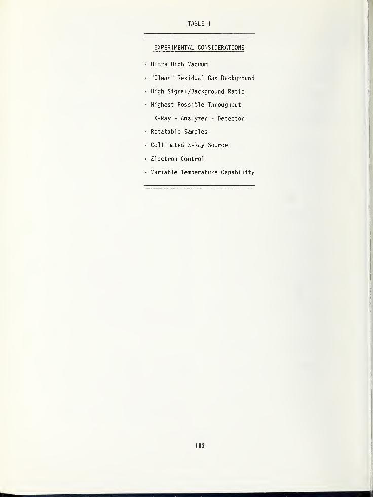
TABLE I
EXPERIMENTAL CONSIDERATIONS
• Ultra High Vacuum
• "Clean" Residual Gas Background
• High Signal/Background Ratio
• Highest Possible Throughput
X-Ray • Analyzer • Detector
• Rotatable Samples
• Collimated X-Ray Source
• Electron Control
• Variable Temperature Capability
162
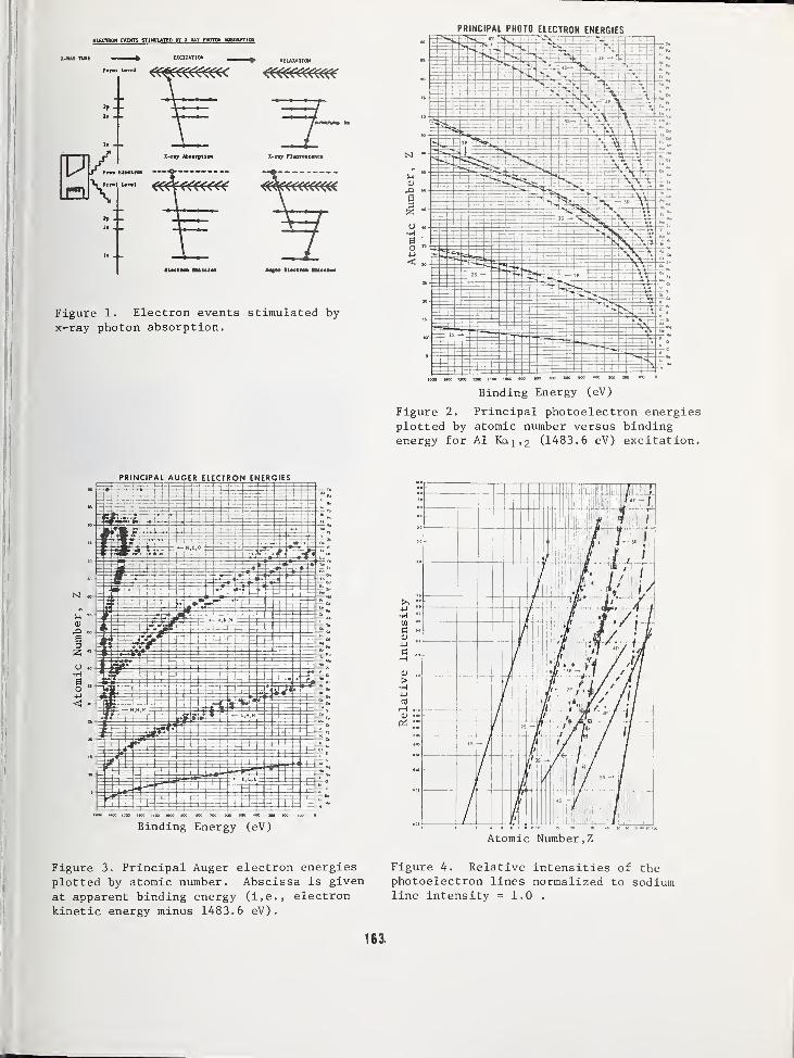
ELECTBOW EVENTS STIMULATED BY j RAY PHPTW ADSOHPTIOH
IIMlm Bmliiio* tmm llcctna klnlN
Figure 1. Electron events stimulated by
x-ray photon absorption.
PRINCIPAL AUGER ELECTRON ENERGIES
Binding Energy (eV)
Figure 3. Principal Auger electron energies
plotted by atomic number. Abscissa is given
at apparent binding energy (i,e., electron
kinetic energy minus 1483.6 eV).
PRINCIPAL PHOTO ELECTRON ENERGIESU^r»fcJ--r jp *>J. "
I _ Lt_ l~r~ Tj1—i i
Binding Energy (eV)
Figure 2. Principal photoelectron energiesplotted by atomic number versus bindingenergy for Al Ka^, 2 (1483.6 eV) excitation.
Atomic Number,
Z
Figure 4. Relative intensities of thephotoelectron lines normalized to sodiumline intensity =1.0 .
163.
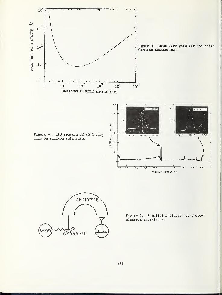
Figure 7. Simplified diagram of photo-electron experiment.
164
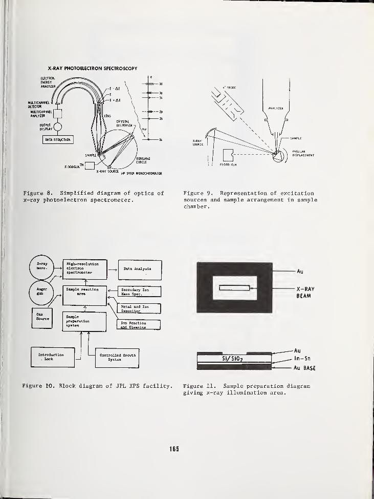
X-RAY PHOTOELECTRON SPECTROSCOPY
Figure 8. Simplified diagram of optics ofx-ray photoelectron spectrometer.
Figure 9. Representation of excitationsources and sample arrangement in samplechart ber
.
Introduction. Lock J Controlled Growth
System Si/SlO ?
Figure 10. Block diagram of JPL XPS facility. Figure 11. Sample preparation diagramgiving x-ray illumination area.
165
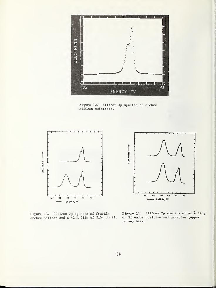
Figure 12. Silicon 2p spectra of etchedsilicon substrate.
t
107 105 103 101 99 97
— ENERGY, EV
T 1 1 1 1 1 1 1 1-
* lii...|
107 10} 10} 101 » 97
ENEKCV, EV
Figure 13. Silicon 2p snectra of freshly
etched silicon and a 42 A film of Si02 on Si.
Figure 14. Silicon 2p spectra of 44 A Si02
on Si under positive and negative (upper
curve) bias.
166
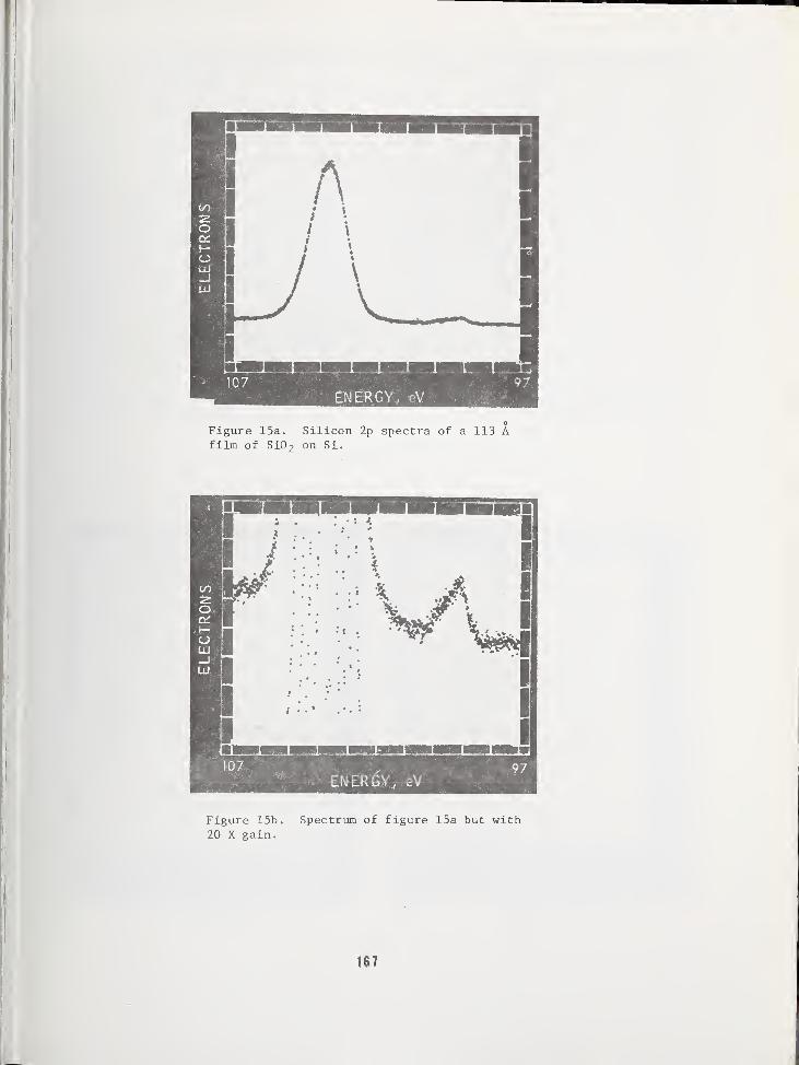
Figure 15a. Silicon 2p spectra of a 113 Afilm of Si0 2 on Si.
107:
-- , \ 97
^ EN ERGY, eV
Figure 15b. Spectrum of figure 15a but with20 X gain.
167
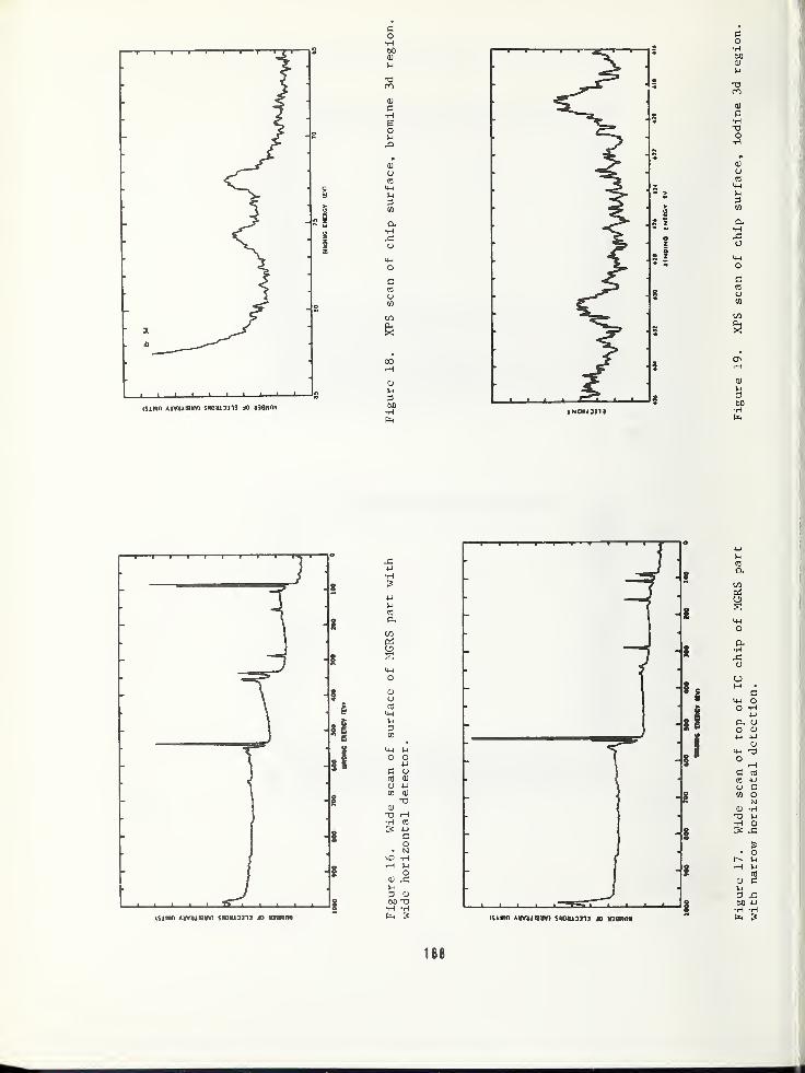
168
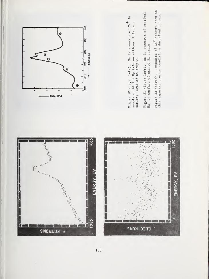
SN0U13313
•HCO u
c 3 rt
H XI CD cu•H CU 4JCO
aj cCO )_i cO •pi
•HM-l M-l +j *oo CO o QJ
*H cu
Jc3 p, »HCO
J_l ^4J •u CO
o O cO QJ
<u o cu 01 >2 "JCu o CX i—
1
CO •H CO M-4 CO,—
i
t. oCO *Hr-| CO rH CO cu •r-1
4_l 4_)
Cfl c CO •H •H *HQ CU S3 to CO *"U
t-H Q r;
B a T3 p QiH B QJ (J
•H CO J2 Qm CO u O fa
+ M-l 4-1
0) CO <u 0)
iH O 53 rH•H 14-1 ^
U C/l CH u O CU
0) O CU
01 oft o CJ n CU
S3 <• cu rH cfl CO d> 4-1 *H
uO M-l rH i—
1
D cni CUCN O CN CO CN p,HCU a) CO aj c CU 0)
M i—
i
M M o u3 Pu 3 3 0 CO
C>0 e 4-1 oa- 00 •H•H cO CO •rl CO •H 43
CO (3 Z Pm 4-»
S NO Mi031 3'
169
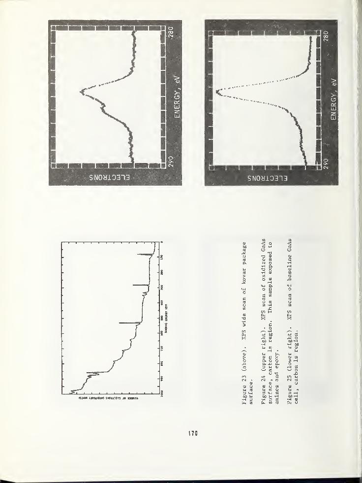
170
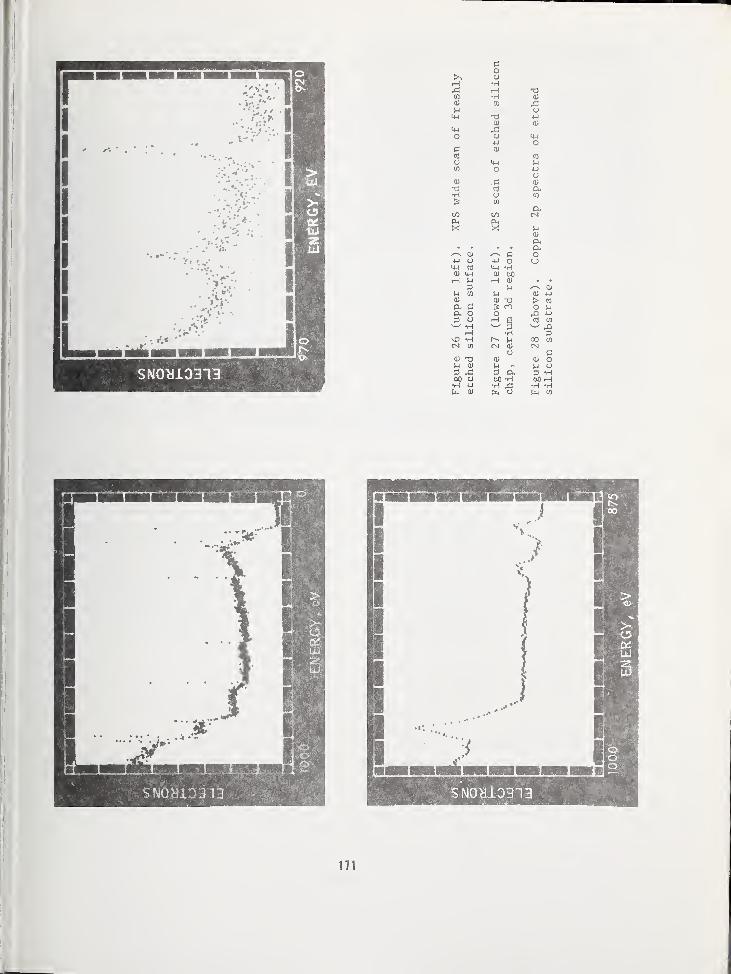
171
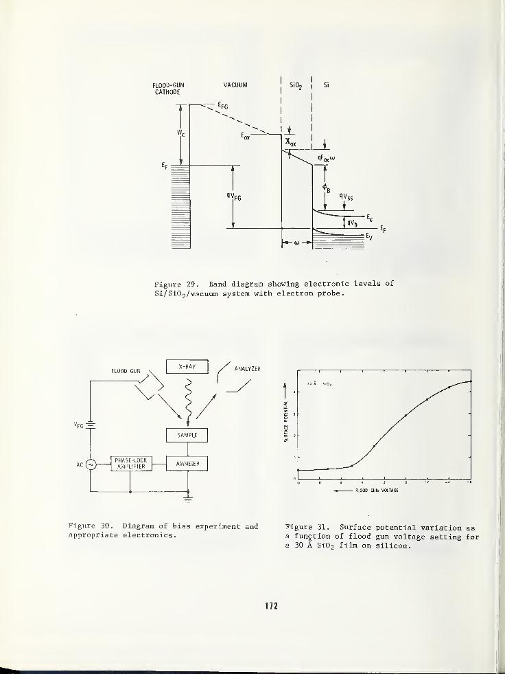
Figure 29. Band diagram showing electronic levels of
Si/Si0 2/vacuum system with electron probe.
0 1 I I I 1 I i—
10 8 a 4 2 0 -2
-«! FLOOD GUN VOLTAGE
Figure 30. Diagram of bias experiment and Figure 31. Surface potential variation asappropriate electronics. a function of flood gun voltage setting for
a 30 A Si02 film on silicon.
172
DISCUSSION OF THE PAPER
Morabito : You skipped over the gold migra-tion problem somewhat. Could you go intomore detail?
Grunthaner : The gold migration problem canbe treated from two points of view. Thephysical cause is the failure of the part'shermeticity. This resulted in the injectionof water into the package during a thermalshock test. The chemical cause of the prob-lem is the simultaneous presence of the
halide ion for gold ion complexation and a
thin film of water on the surface of thepart. The existence of water and appliedpotential would have resulted in slow corro-sion of the metal stripes. This would havebeen of little long-term concern. The pres-ence of the halogens permitted gold trans-
port. The glassivated coating has a multi-tude of open cracks and incomplete coveragesin the region of the gold. The combinationof strong complexation of the gold ion and
high current densities resulted in dendriticgrowth. The morphology of the dendrite is
related to the strength of the gold complex,
since this, together with the actual concen-
tration of gold ions, determines the effec-tive concentration of gold at the depositingelectrode
.
Initially, we had felt that an extremelyclean electrode surface was required for
dendritic growth. Subsequent experimentsindicated that high-current density and low
source ion concentrations were the limitingrequirements. The presence of iodine was
due to residual etchant which was stronglyadsorbed to the surface of the remaining
gold. Bromine and chlorine were also found,
although the sources of these ions have not
been clearly established. The chlorine may
have been present from human handling or may
have had a significant concentration in the
water entering the package.
Morabito : Was chlorine more of a problemthan iodine?
Grunthaner : The gold-chloro-complex is muchmore stable than the iodo-complex. In largegold ion concentrations, the chloro-complexwould be most effective in generation ofdendritic growth. In these lesser concen-trations the iodo-complex provides transport,and reasonable concentrations. The polar-ized iodine on the gold surface also assistedin the dissolution of the gold stripe. Thechlorine will be active but the iodine is
probably the more important immediate prob-lem. Bromine and bromate were also observed.The bromine case would be intermediate be-tween chloride and iodide.
The primary question to our program was the
possibility that there existed a long-term
failure mechanism, i.e., parts failing after
one or more years of operation. This fail-
ure mechanism was observed over periods of
hundreds of hours with multilayer coverage
of H2O over the surface. Was failure at ex-
tended times possible at one- or two-layer
coverage? The situation is resolved into
ionic and hydrogenic currents and current
study is addressing this problem.
The data available at this point are adequateto suggest several possible corrective ac-
tions to minimize MGRS failures: 1) Reducethe water content of the package to severalhundred ppm (by volume) or less. 2) Reducethe impurity levels at the electrode and
substrate surfaces, so as to eliminatetransport. 3) Getter reactive impurities bychemical reaction, thereby modifying theirchemistry, or by use of clathrates to im-
mobilize them. 4) Treat the surface of the
device to produce a hydrophobic surface,such as by use of methyl silane or othersilicone derivatives.
173

NBS Special Publication 400-23, ARPA/NBS Workshop IV, Surface Analysis for Silicon Devices,held at NBS, Gaithersburg
, Maryland, April 23-24, 1975 (Issued March 1976)
CHOOSING BETWEEN ESCA AND AUGER FORSURFACE ANALYSIS
Gary E. McGuire
Materials Characterization LaboratoryTexas Instruments Incorporated
Dallas, Texas 75222
ABSTRACT
Although photoelectron and Auger spectroscopy were developed over similartime frames and required similar hardware development, until recently thetwo techniques have remained as separate tools for surface analysis.Auger spectroscopy was readily accepted by the semiconductor industry formaterials characterization. Interest in photoelectron spectroscopy didnot develop as quickly nor did it become as widespread as Augerspectroscopy
.
The two techniques being quite complementary can be used very wellwithin the same laboratory if not within the same vacuum system. A num-ber of examples will be discussed for which one would choose by prefer-ence ESCA over Auger. Although the choice may not be apparent before-hand, ESCA can be the more valuable characterization technique in certainaspects of polymer surfaces, electroplating and thin film metallizationsystems for semiconductor devices.
INTRODUCTION
If one takes into consideration all the com-mercial and non-commercial designs of elec-tron spectrometers there are two basic dif-ferences that continue to distinguish theAuger electron (AES) spectrometer from theX-ray photoelectron (ESCA) spectrometer,resolution and excitation source. Augerspectrometers emphasize high transmissionand use an electron beam for excitation whileESCA spectrometers emphasize high resolutionand use soft X-rays for excitation. The softX-ray source irradiates a much larger samplearea with less intensity than an electronbeam. Soft X-rays cause less damage to thesample, allowing longer times for data ac-quisition without altering the surface. Thehigh resolution capabilities of the typicalESCA spectrometer and simplicity of thephotoelectron spectra permits the identifica-tion of chemical shifts.
The two factors, resolution and excitation,ultimately govern the choice of which tech-nique to use for a particular problem. Thenext few examples will be used to demonstrateoccasions where these factors favor the useof ESCA. Because of the speed of data ac-quisition and excellent spatial resolutionof Auger spectroscopy, it has been readilyadapted for analysis of semiconductor sur-faces. The examples presented here are notintended to downgrade the capabilities of
Auger spectroscopy but are an effort to show
how one would choose between the two tech-niques intelligently. These examples areslanted toward ESCA because we feel it hasnot been exploited as much in problem solvingfor semiconductor materials.
Chemical Identification
A feature that has always been one of themajor strengths of ESCA has been the abilityto observe chemical shifts in the spectracorresponding to the chemical states of thesystem being studied. For example in Figure1 the separation between the peak positionsfor Si and Si02 is approximately 4.5 eV.
The line widths are sufficiently small thatthe peaks are well resolved and easily dis-tinguishable. The corresponding Auger chem-ical shift for Si and Si02 is much larger at
13 eV. The two chemical states may be easilyidentified in the Auger derivative spectrumbut the transitions cannot be completelyseparated. Frequently it is possible to en-hance certain features using integrationtechniques; however the integrated Si-Si02Auger transitions overlap extensively(Figure 2)
.
In general photoelectron line widths, ex-pressed as full width at half maximum (FWHM)
,
are usually narrower and less complicatedthan the corresponding Auger line widths.Most Auger series consist of a family of
curves with one or two dominant features.Even in examples where the AES shift is much
175
larger, the chemical shift in the ESCA spec-trum continues to be more easily distin-guished. This may be enhanced by the higherresolution capability of the typical ESCAspectrometer (0.02%) over that of the typi-cal AES spectrometer (0.5%).
With the numerous cited examples of chemicalshifts in the literature, one may get theimpression that every chemical combinationproduces a unique combination of photoelec-tron binding energies that are readily dis-tinguishable. Although the combinations maybe unique, the magnitude of the shifts may
be so similar the peaks overlap extensively.These then may not be reduced to meaningfuldata except by comparing elemental ratioswhich could also be accomplished from the
corresponding AES spectra.
Frequently the simplest method of studying a
process that malfunctions is to compare"good" and "bad" samples in order to identifythe presence of anything that may be detri-mental or unusual. Numerous useful examplesof this type may be found throughout theliterature. Typical AES spectra of gold-plated surfaces which displayed "good" and"bad" plating characteristics are presentedin Figure 3. The AES spectra reveal thepresence of large deposits of K, C, N and Snassociated with "poor" plating character-istics. The same information concerning theelemental composition can just as easily beobtained by ESCA. In addition, ESCA givessome insight into the failure mechanism.From the AES data, it is not apparent whetherthe presence of K, C and N on the gold platedsurface is due to adsorption of the gold saltKAu(CN)2 on the surface or due to coprecipi-tation of the end product, K+ and CN~. Bycomparing the binding energies of gold 4f
lines (Figure 4) from evaporated Au, KAu(CN)2,a commercial gold salt, and the gold platedsurface, we get an indication of the failuremechanism. The binding energies of the goldplated surface agree with those of evaporatedgold while those of the commercial gold saltand KAu(CN)2 agree. From this figure onecould make the observation that the goldplated surface displayed the same chemicalbehavior as evaporated gold. The potassium,carbon and nitrogen present on the surfaceare end products of the plating process thatare trapped in the gold. The similarity inthe binding energies of the commercial goldsalt and KAu(CN)2 suggests a common chemicalform for the two. Correlations such as thismay be used to obtain substitute chemicalsfor expensive commercial formulations.
Excitation Source Influences
It is generally accepted that the influenceof an X-ray source is less severe than thatof an electron beam. Electron induced de-sorption and decomposition can alter thesample sufficiently to make data from somesamples meaningless. (Bremsstrahlung fromthe X-ray source may produce the same re-sults but to a smaller extent.) It is verydifficult to obtain AES data from rough in-sulating surfaces such as printed circuitboard because of charging induced by theprimary beam. Examination of the same typesof materials by ESCA are straightforward andsimple. In Figure 5 is a representativeESCA spectrum of printed circuit board whichwe were unable to analyze by Auger. Theanalysis picked up the presence of Pb and Naon the surface even in areas away from the
Pb-Sn plate.
If electron induced desorption or migrationoccurs then the Auger spectrum may not dis-tinguish differences in samples with widelyvarying surface properties. In the follow-ing example, we were unable to detect any
differences in surface composition by AES
while the ESCA data displayed some signifi-cant variations (Figure 6) . The samplesexamined were clean tin oxide, tin oxidetreated in a N2 atmosphere and tin oxidetreated in an 62 atmosphere. The untreatedsurface exhibits a clean tin oxide spectrumas observed by the Sn3d3/2~3d5/2 doublet.
Treatment in a nitrogen atmosphere results
in a small amount of Na appearing on the
surface. The tin oxide surface is masked by
a thin layer of Na when an O2 atmosphere is
used. The presence or absence of Na was
verified by the Na KLL Auger transition that
occurs in the same energy region of the ESCAspectrum as the Sn3d doublet. The important
point we are trying to make is that examina-
tion of the same samples by AES does not
reveal the presence of Na at all while ESCA
indicates significant differences that cor-
relate with the known physical properties of
these films. We also observe a reversal in
the physical properties of these films to
the original state upon examination by AES
(electron beam exposure) which has been cor-
related with the absence of Na.
Metal Contact Systems
ESCA may prove to be one of the most useful
techniques available for examination of
metallurgical contacts and thin film metal-
lization systems, particularly heavy metals.
176
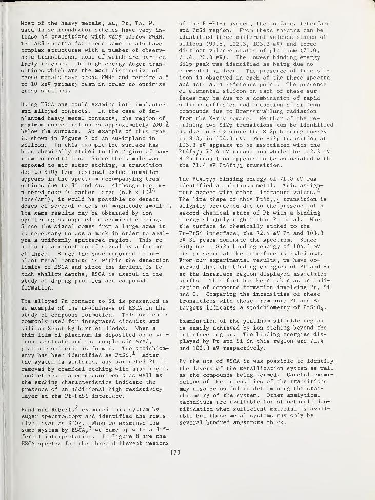
Most of the heavy metals, Au, Pt, Ta, W,
used in semiconductor schemes have very in-tense 4f transitions with very narrow FWHM.
The AES spectra for these same metals havecomplex structures with a number of observ-able transitions, none of which are particu-larly intense. The high energy Auger tran-sitions which are the most distinctive ofthese metals have broad FWHM and require a 5
to 10 keV primary beam in order to optimizecross sections.
Using ESCA one could examine both implantedand alloyed contacts. In the case of im-
planted heavy metal contacts, the region ofo
maximum concentration is approximately 200 Abelow the surface. An example of this typeis shown in Figure 7 of an Au-implant in
silicon. In this example the surface hasbeen chemically etched to the region of max-imum concentration. Since the sample wasexposed to air after etching, a transitiondue to Si02 from residual oxide formationappears in the spectrum accompanying tran-sitions due to Si and Au. Although the im-
planted dose is rather large (6.8 x 10-^
ions/cm^), it would be possible to detectdoses of several orders of magnitude smaller.
The same results may be obtained by ionsputtering as opposed to chemical etching.
Since the signal comes from a large area it
is necessary to use a mask in order to anal-yze a uniformly sputtered region. This re-
sults in a reduction of signal by a factorof three. Since the dose required to im-
plant metal contacts is within the detectionlimits of ESCA and since the implant is to
such shallow depths, ESCA is useful in the
study of doping profiles and compoundformation.
The alloyed Pt contact to Si is presented as
an example of the usefulness of ESCA in the
study of compound formation. This system is
commonly used for integrated circuits and
silicon Schottky barrier diodes. When a
thin film of platinum is deposited on a sil-
icon substrate and the couple sintered,platinum silicide is formed. The stoichiom-etry has been identified as PtSi.^" Afterthe system is sintered, any unreacted Pt is
removed by chemical etching with aqua regia.
Contact resistance measurements as well as
the etching characteristics indicate the
presence of an additional high resistivitylayer at the Pt-PtSi interface.
Rand and Roberts examined this system by
Auger spectroscopy and identified the resis-
tive layer as SiC>2. When we examined thesame system by ESCA,-^ we came up with a dif-
ferent interpretation. In Figure 8 are the
ESCA spectra for the three different regions
of the Pt-PtSi system, the surface, interfaceand PtSi region. From these spectra can beidentified three different valence states of
silicon (99.8, 102.3, 103.3 eV) and threedistinct valence states of platinum (71.0,
71.4, 72.4 eV) . The lowest binding energySi2p peak was identified as being due to
elemental silicon. The presence of free sil-icon is observed in each of the three spectraand acts as a reference point. The presenceof elemental silicon on each of these sur-faces may be due to a combination of rapidsilicon diffusion and reduction of siliconcompounds due to Bremsstrahlung radiationfrom the X-ray source. Neither of the re-maining two Si2p transitions can be identifiedas due to Si02 since the Si2p binding energyin Si02 is 104.3 eV. The Si2p transition at
103.3 eV appears to be associated with thePt4f 7 / 2 72.4 eV transition while the 102.3 eVSi2p transition appears to be associated withthe 71.4 eV Pt4f7/2 transition.
The Pt4f7/2 binding energy of 71.0 eV wasidentified as platinum metal. This assign-ment agrees with other literature values.^The line shape of this Pt4f -j /2 transition is
slightly broadened due to the presence of a
second chemical state of Pt with a bindingenergy slightly higher than Pt metal. Whenthe surface is chemically etched to the
Pt-PtSi interface, the 72.4 eV Pt and 103.3eV Si peaks dominate the spectrum. SinceSi02 has a Si2p binding energy of 104.3 eV
its presence at the interface is ruled out.
From our experimental results, we have ob-served that the binding energies of Pt and Si
at the interface region displayed associatedshifts. This fact has been taken as an indi-cation of compound formation involving Pt, Si
and 0. Comparing the intensities of these
transitions with those from pure Pt and Si
targets indicates a stoichiometry of PtSi04.
Examination of the platinum silicide regionis easily achieved by ion etching beyond the
interface region. The binding energies dis-played by Pt and Si in this region are 71.4
and 102.3 eV respectively.
By the use of ESCA it was possible to identify
the layers of the metallization system as wellas the compounds being formed. Careful exami-
nation of the intensities of the transitions
may also be useful in determining the stoi-
chiometry of the system. Other analyticaltechniques are available for structural iden-
tification when sufficient material is avail-
able but these metal systems may only be
several hundred angstroms thick.
77
SUMMARYREFERENCES
ESCA has proven useful for many appliedsemiconductor research problems. Except forspatial resolution and speed, it offers the
same advantages as AES as a surface charac-terization technique. In addition it may beused when sample charging, decomposition andelectron induced migration are potentialproblems. It also offers the advantage of
high resolution with resultant chemicalshift information. The simplicity of thephotoelectron transitions are easily reducedto quantitative information.
In the future one can expect to see ESCAused to obtain "chemical in-depth profiles"^as opposed to the more common elemental pro-files. ESCA will also prove to be useful inthe study of diffusion mechanisms^ with theadded dimension of elucidating compoundformation.
1. Muta, H. and Shinoda, D. , J. Appl. Phys.43, 2913 (1972); Poate, J. M. andTisone, T. C. , Appl. Phys. Lett. 24, 391(1974).
2. Rand, M. J. and Roberts, J. F., Appl.
Phys. Lett. 24, 49 (1974).
3. Danyluk, S. and McGuire, G. E. , J. Appl.Phys. 45, 5141 (1974).
4. Bearden, J. A. and Burr, A. F. , Rev. Mod.Phys. 39, 125 (1967).
5. McGuire, G. E. , unpublished results.
6. Danyluk, S. , McGuire, G. E., Koliwad,
K. M. and Yang, M. G. , Thin Solid Films25, 483 (1975).
178
SILICON SLICE WITH RESIDUAL OX I DE
800
co 400
110
Si 2p
Si0 2 ,l043eV Si.99.8eV
Figure 1. X-ray photoelectron spectrum of a
silicon slice with a residual oxide coating.
The Si(2p) transitions of Si and Si02 display
a chemical shift of 4.5 eV.
106 102 98
BINDING ENERGY (eV)
Figure 2. The characteristic minima at 78and 91 eV for Si0 2 and Si respectively canbe observed in the derivative Auger spectrum.The integrated curve is superimposed over thederivative curve.
Gold Plated Samples
Au "~
/Au C source #2, good plating
characteristics
Y AuIj N Sn q
| source #1, substrate #2
[AilK Iq poor plating characteristic!
t^. " Cu Cu
/Au,fNSn o
source #1, substrate #1
Au poor plating characteristics
K
i 1
C
I 1 I 1 I 1 l
200 400 600 800
Electron Energy (ev)
65 10 15 W 85 90 95
ELECTRON ENERGY (eV)
Figure 3. Auger spectra of gold-platedsurfaces. The presence of potassium, carbonand nitrogen was identified with Au-platedsurfaces with poor bonding characteristics.
179
Tin Oxide
Sn3d3/2
and Na Auqer
Sn3d 5/2
500 495 490 485
Binding Energy (eV)
300 200
BINDING ENERGY (eV)
Figure 5. X-ray photoelectron spectrum of printedcircuit board. Lead and sodium were found on thesurface and associated with leakage currents caus-ing the printed circuit to fail.
Figure 6. X-ray photoelectron spectrum of tinoxide surfaces. Treatment of the tin oxide sur-face in an O2 or N2 atmosphere leaves a thincoating of Na. The sodium is induced to migrateaway from areas exposed to an electron beam as inAuger analysis.
180
Au Implant in Silicon
U5 105 95~
85~
Electron Binding Energy. eV
Figure 7. X-ray photoelectron spectrum of Au im-plant in silicon. The surface has been chemicallyetched to the region of maximum concentration.
Figure 8. X-ray photoelectron spectrum ofPt contact to silicon. Three spectra areshown: (a) platinum surface, (b) samplethat has been chemical etched of excessplatinum, and (c) sample that has been chem-
ically etched then ion etched to the PtSiregion.
EVAPORATED PLATINUM UN Si (111)
SINTERED 630°C
MO 90 80
BINDING ENERGY (eV)
181
DISCUSSION OF THE PAPER
Grunthaner : I would like to comment aboutyour statement concerning the line widths of
the gold as opposed to silicon. The siliconlines in the spectra are probably the nar-rowest lines that one observes at all, al-
though the presence of the silicon 2p dou-blet, when broadened by the instrument and
that sort of thing does give rise to a some-what broader line. The silicon lines that
we have seen in the spectrometer are of theorder of about 520 millivolts wide. The
narrowest gold lines we have observed are of
the order of about 680 millivolts wider.
McGuire : Most people get the impressionlooking at the commercial brochures that thegold and the silver give the narrowest lines,but sometimes these elements are merely themost convenient, they are good conductorsand the separation between the doublet is
quite large.
Morabito : Because of the difference in theescape depth between the ESCA photoelectronas compared to the Auger electron, it is
possible that, for the last example youshowed, the layer within 5 or 10 A of sur-face could be Si02. You are sampling a muchdeeper region with ESCA, so below you mayhave platinum silicide but above that it is
possible you have Si02-
McGuire : I would like to make a commentconcerning the escape depth. I have seenboth Auger and ESCA papers that have come upwith different escape depths but I have a
hard time believing that an electron, whetherit is due to an Auger process or a photo-electron process, will behave differently asfar as its coming out of a given material.I do not think they should differ.
Morabito: That depends on the kineticenergy of the electron.
McGuire : Yes, so I would say electrons fromeither process with the same kinetic energyshould have identical escape depths.
Participant : I would like to point out thatin stripping off the platinum and lookingagain whether you have not really done any-thing to the surface, which presumably wouldhave the oxide or silicate on it, you couldbe changing the Fermi level of the samplewith respect to the vacuum, which may giveyou a shift in the lines.
McGuire: Well, in the spectrum I showed wewere using the elemental silicon as a refer-ence point. That is the reason we used the
data we got from the McPherson instrument,i.e. , it was very convenient. We had a lot
more difficulty with the Hewlett-Packardinstrument because we did not always see thepresence of the elemental silicon.
182
NBS Special Publication 400-23, ARPA/NBS Workshop IV, Surface Analysis for Silicon Devices,held at NBS, Gaithersburg, Maryland, April 23-24, 1975 (Issued March 1976)
SILICON DEVICE APPLICATIONS USING ACOMBINED ESCA/AUGER ANALYSIS SYSTEM
L. E. Davis and G. E. Riach
Physical Electronics Industries, Inc.Eden Prairie, Minnesota 55343
ABSTRACT
Silicon device applications are described which emphasize the advantagesof measuring both X-ray induced photoelectrons and electron beam stimu-lated Auger electrons as a function of depth in the same analysis systemThe measurements include depth-composition profiles and chemical bindinginformation for nichrome thin films and boron predeposits on silicon.
INTRODUCTION
ESCA and Auger electron spectroscopy havemuch to offer in the study of semiconductordevices. 1 In conventional Auger systems,electron beam excitation allows localizedsurface analysis and rapid signal readout.ESCA, on the other hand, offers a means of
characterizing chemical bonds at the surface.When used in conjunction with sputter-etch-ing, both techniques can be used to obtaindata as a function of depth. The applica-tions to follow illustrate how a combinedESCA/Auger electron spectrometer can be usedto give a more complete characterization of
thin films than either technique alone.
EXPERIMENTAL APPARATUS AND METHOD
The schematic diagram of a commercialelectron energy analyzer optimized in designfor high transmission and energy resolutionis shown in Figure 1. In the ESCA analysismode (via pulse counting) the essential ad-vantages of the analyzer are: 1) selectivearea analysis within an area 2mm in diameterand 2) adjustable energy resolution. In theconventional Auger analysis mode (via thelock-in amplifier) the high transmission(approximately 7%) of the analyzer allowsreal-time measurement of the Auger electronpeak-to-peak heights as a function of sput-ter-etching time. A complete description of
the electron spectrometer functions andspecifications have been reported byPalmberg
.
2
The analysis was performed in an ultrahighvacuum system capable of reaching pressuresless than lO
--^ Torr. The electron spec-trometer, X-ray source and sputter ion gunare pre-aligned so that when the specimen is
positioned for optimum (photoelectron or
Auger electron) signal, the ESCA/Auger analy-sis area and ion beam coincide. In this
manner, X-ray photoelectron and electronbeam excited Auger electron measurementscould be made after ion beam sputteringwithout moving the specimen. The typicalanalysis procedure was to record the Augerelectron peak-to-peak [dN(E)/dE] amplitudessimultaneously with argon ion beam sputter-ing and, thus, obtain a depth-compositionprofile. 3 High energy resolution ESCA anal-ysis was performed at selected depths byturning off the ion gun at the desired depth,making the ESCA measurement, and then re-suming the Auger depth profile measurement.The two types of data are then easilycorrelated
.
APPLICATIONS
Oxidation of a Nichrome Film
As indicated in the Auger electron depth-composition profile of Figure 2, the nichromefilm after heating in air for 30 seconds at
450°C is composed of a metallic oxide layerat the surface. A chromium rich layer domi-nates near the surface while nickel hasformed a distinct layer at the metal/siliconinterface. To gain a better understandingof the effect this heating process had onthe chemical bonding, high energy resolutionESCA measurements of chromium and nickelwere made at the surface and at depths A, B,
C and D indicated on the depth profile.This data is shown in Figure 3.
The chromium and nickel 2p3/2 photoelectronlines are shifted to higher binding energies(approximately 2.5eV for chromium and 3.0eVfor nickel) at the surface. These shiftsare consistent with ^203^ and NiO 5 oxidationstates. Slightly below the surface, at depthA, the Ni 2pj/2 line nas shifted to a bindingenergy consistent with elemental nickel. Thechromium, however, remains in oxide formuntil depth B where both oxide and metallic
183
states are apparent. At depths C and D,
both chromium and nickel are predominantlymetallic
.
In conclusion, it can be seen that heatingthis nichrome film in air produced a surfaceoxide layer about 100A thick consistingmainly of (^203. Within ISA of the surfacea small amount of NiO was formed. Deeperthan this within the structure, however, thenickel remained entirely in the metallicstate.
Boron Predeposit on Silicon
In the doping of silicon with boron, thefirst processing step is the deposition of a
shallow layer of boron on a silicon wafer.The predeposit is produced by allowing a
boron gas (e.g., a borane) to react with the
silicon surface at elevated temperatures.As Figure 4 indicates, a glass surface layeris formed during the predeposit process.The next step in doping is to chemically re-move the boron glass, leaving only a boronrich silicon surface. The remaining boronthen is diffused at high temperatures into
the bulk silicon to the desired depth andconcentration level. In some cases the pre-deposition is carried out at a high enoughtemperature that the diffusion occurs simul-taneously with the predeposit.
In order to achieve reproducible dopantlevels, it is of considerable aid to theprocess engineer to know the properties of
the predeposit before glass removal. Themain properties of interest are (1) thethickness of the glass layer, (2) the boronconcentration as a function of depth and (3)
the chemical state of boron and other ele-ments as a function of depth.
The depth-composition profile of Figure 4
illustrates that by monitoring the Augersignals of Si, B and oxygen during sputter-etching, the predeposit glass layer and borondensity can be rapidly characterized as a
function of depth. In the example, the boronis entirely within the glass overlayer. Theglass removal and diffusion steps have notbeen carried out on this specimen at this
point. At the depths A, B, C and D indicatedon the plot, the profile was interrupted so
that high energy resolution ESCA measurementscould be made to determine the chemical stateof the important components of the predepositlayer
.
ESCA spectra of the Si 2p and B Is photoelec-tron lines at the depths indicated in Figure4 are shown in Figure 5. The Si 2p bindingenergies (103eV) at depths A and B are
consistent with Si02. At depths C and D theelemental silicon lines (at 97.8eV) are alsopresent. The boron photoelectrons at 193eVdo not change in binding energy as a functionof depth. B Is electrons at this bindingenergy belong to the oxide state of boron.
The depth-composition profile in Figure 6
shows the results of a combined boron pre-deposit and diffusion carried out at 1050°Con polycrystalline silicon. Note that herethe boron is concentrated at the glass/sili-con interface. The ESCA spectrum in Figure7 obtained at depth A shows that two B Isphotoelectron lines exist at the glass/sili-con interface. The photoelectrons at 193eVcorrespond to the boron oxide state, thesame binding energy as the B Is electronsshown in Figure 5. The lower binding energyelectrons at 186. 2eV belong to elementalboron.
These examples point out the usefulness of
joint ESCA and Auger analysis for completecharacterization of thin films on siliconsurfaces. Both composition and chemicalbinding information as a function of depthare obtainable without changing specimenorientation. In addition, the examples showthat the information obtained is in a formthat can be applied directly for definitiveprocess control and evaluation of silicondevices
.
Acknowledgements
The authors gratefully acknowledge Drs. N. C.
MacDonald and P. W. Palmberg for suggestingthe application topics and supplying back-ground information about specimen processing.
REFERENCES
1. McGuire, G. E. ,Choosing between ESCA
and Auger for Surface Analysis, ARPA/NBSWorkshop IV, Surface Analysis for SiliconDevices, A. G. Lieberman, Ed., NBS Spec.
Publ. 400-23 (January 1976).
2. Palmberg, P. W. , Vac. Sci. Technol. 12,
379 (1975).
3. Weber, R. F. ,Research/Development 23 ,
22 (1972).
4. Kim, K. S., Purdue University, privatecommunicat ion
.
5. Fiermans, L, Hoogewijs, R. , and Vennik,
J., Surf. Sci. 47, 1 (1975).
184
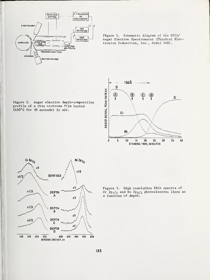
£^ PRECISION ANALYZER
SPECIMEN
\ \ SPUTTER ION GUN
Figure 1. Schematic diagram of the ESCA/Auger Electron Spectrometer (Physical Elec-
tronics Industries, Inc., Model 548).
Figure 2. Auger electron depth-compositionprofile of a thin nichrome film heated(450°C for 30 seconds) in air.
150A
.' («) (|) © (6)
Cr
Si
Ni
10 15 20 25 30
ETCHING TIME, MINUTES35 40
Figure 3. High resolution ESCA spectra of
Cr 2p3/ 2 and Ni 2p 3 / 2photoelectron lines as
a function of depth.
578 576 574 572 858 856 854 852 850
BINDING ENERGY, eV
185
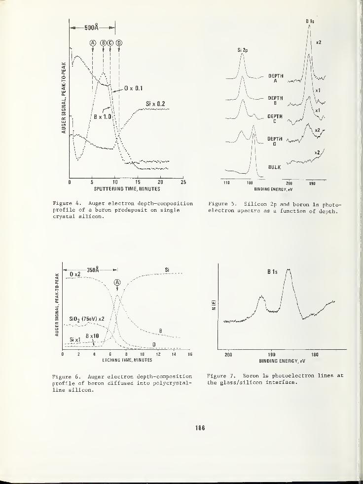
Figure 4. Auger electron depth-composition Figure 5. Silicon 2p and boron Is photo-profile of a boron predeposit on single electron spectra as a function of depth,crystal silicon.
Figure 6. Auger electron depth-composition Figure 7. Boron Is photoelectron lines at
profile of boron diffused into polycrystal- the glass/silicon interface,
line silicon.
186

DISCUSSION OF THE PAPER
Thomas ; Did you say that the boron had beenoxidized by the glass structure?
Davis : No, I did not mean to imply that. Myinterpretation is that the boron in the first
predeposit example exists as boron oxide,probably as a borosilicate. The Auger elec-tron peak, shape of boron in the glass layer(not shown) was quite different from the ele-mental boron peak shape. This, of course, isadditional evidence that the boron in Figure5 is in oxide form.
187

NBS Special Publication 400-23, ARPA/NBS Workshop IV, Surface Analysis for Silicon Devices,held at NBS, Gaithersburg, Maryland, April 23-24, 1975 (Issued March 1976)
PHOTODEPOPULATION TECHNIQUE FOR THE STUDY OFELECTRONIC TRAPS IN INSULATORS*
T. H. DiStefano
IBM Watson Research CenterYorktown Heights, New York 10598
and
J. M. Franz
IBM System Products DivisionEssex Junction, Vermont 05452
ABSTRACT
A new type of photodepopulation spectroscopy has been used to obtainthe energy distribution of electrons trapped in an insulator. Thechange in the trapped charge produced by monochromatic light is de-tected by a silicon surface effect device, which serves as one of theelectrodes. The result is the spectral photoyield for trap ionization,free of any complication of extraneous currents. This photodepopula-tion technique was applied to the Si02-Si
3N4 system to determine thetrap distribution responsible for charge storage in the MNOS transistor.The results, although somewhat complicated by photoinj ection from theelectrodes, show an ionization energy of 3.0 eV. Generally, the tech-nique is applicable to the very sensitive spectroscopic measurement of
deep traps in wide bandgap insulators.
INTRODUCTION
A new photodepopulation technique-'- has beendeveloped and used to examine spectroscopi-cally the impurities and trapped electronsin insulating thin films. Essentially, thetechnique involves a measurement of the re-
laxation of the charge stored in an insula-tor that is exposed to monochromatic light.
From the discharge of the traps produced byillumination from a scanned monochromatorsource, the spectral yield for photoemissionfrom the traps is obtained directly. Thecharge in the insulator is detected by meansof one of the electrodes, which is a fieldeffect device that serves as an electrometerEither of two modes of detection, small sig-nal capacitance or surface conductance, is
satisfactory for measuring the field at the
electrode from which the net charge is de-
termined. The photodepopulation techniquehas an advantage in that it samples only the
density of occupied trap levels, and it is
unaffected by extraneous sources of current.
It also has an advantage over a photocapaci-tance technique^ used by Harari and Royce to
study traps at the SiO2~Al203 interface; our
* Work supported in part by the Defense Ad-vanced Research Projects Agency and moni-
tored by AFCRL under contract numberF19628-74-C-0077.
photodepopulation technique is not influencedby a redistribution of the electrons amongthe various trap levels in the system causedby light-* or by thermal excitation. However,as with any photoionization technique for
thin film insulators, our technique is limi-ted to a window equal to the electrode bar-rier energy; for photon energies greater thanthis barrier, the photodepopulation resultsare complicated by injection from the elec-trodes .
We have used the photocapacitance techniqueto determine the distribution of the specifictraps, near the Si02~Si3N4 interface, whichare filled and emptied by electron tunnelingduring the normal operation of an MNOS deviceElectron traps in the Si3N4 itself have beenwell characterized by several techniques in-
cluding thermally stimulated currents^ »^ and
I-V measurements k' ^ . Both techniques are
able to determine the binding energy of traps
which are characteristic of the bulk of Si^N4Binding energies are found to lie in a rangefrom about 0.5 eV to 0.9 eV, as measured by
thermally stimulated currents and from about0.5 eV to 1.5 eV determined from the I-V de-
pendence. However, neither of these tech-niques is capable of being used to character-ize the deep trapping levels associated withcharge storage near the Si02~Si3N4 interface,since they are obscured by the shallow traps
in the conductivity measurements. It is the
189
deep traps which are of specific interest
since these states near the interface of SiC>2
and Si3N4 are responsible for the charge
storage in MNOS memory transistors. Modelsfor switching8 and charge retention^ in
the MNOS transistor would benefit by a de-
termination of the deep trapping states. The
spectral photoyield was obtained for traps
filled to various charge levels by tunneling.
From the photoemission spectra and thresh-
olds, information is derived about the energy
distribution of the deep traps in the Si02~
Si3N^ structure.
EXPERIMENT
The capacitive mode of charge detection was
used for the photodepopulation study of trap-
ped electrons near the Si02~Si3NA interface.
To some extent this particular technique is
a variation of photocapacitance spectroscopy,which has been used to study traps in the de-
pletion region of a semiconductor junction.
During the measurements, a bias voltage is
applied to the MNOS sandwich to maintain a
null electric field at the silicon surface,
as is shown in Fig. 1. The zero surfacefield condition was sensed by a capacitancemeasurement at 100 kHz and maintained by a
feedback loop in which the capacitance meas-urement is used to control the sample bias.
The capacitance is measured by a phase sen-sitive detector in order to reject leakagecurrents and the photocurrent . In this
"flat-band" condition, the bias voltage is
directly related to the net charge densitystored near the Si02~Si3N4 interface,
P =e e V0 1 fb
(1)
where p is the net charge density, e± is thedc dielectric constant of the Si3N4, Vf^ is
the bias voltage necessary to maintain the"flat-band" condition, and d is the thicknessof the Si3N^ layer. It was assumed that thestored charge lies near the Si02-Si3N^ inter-face; the assumption is reasonable in this
case, where the charge was introduced eitherby tunneling from the silicon or by photo-emission from the silicon.
The photoresponse of the system was obtainedby shining monochromatic light through thesemitransparent aluminum electrode and ontothe traps near the interface. The lightsource was a Bausch and Lomb 0.5 meter mono-chromator with a Hg-Xe high pressure arcsource. The emergent light was de-focusedto cover uniformly the area of the sampleelectrode. The light intensity was measuredwith an RCA 1P42 photodiode covered by a
layer of sodium salycilate phosphor; thephotodiode was calibrated against an Eppley
thermopile. Measurements were obtained forphoton energies from 2 eV to 6 eV, which is
the upper practical limit of the lightsource. A filter was used at energies below3.5 eV to eliminate second order light in a
range over which the sample was extremelysensitive. All of the spectra were obtainedat room temperature. The measurements wereperformed on samples which are characteristicof an MNOS transistor. The sandwich struc-
oture comprised a silicon substrate, 25 A of
Si02Qformed on the silicon by oxidation,
535 A of Si3N4 formed by chemical vapor de-position at 875°C, and finally 125 A ofaluminum to form a semitransparent electrode.Samples were formed on (100) 2Q-cm siliconsubstrates of both n and p type. The semi-transparent electrodes, 0.060" in diameter,were deposited by evaporation in a vacuum of
about 2 x 10~6 torr. The samples exhibitedtypical hysteresis effects, with a maximumtotal stored charge of about 8 x 10-^ elec-trons/cm^
.
Light of sufficient energy Kw excited elec-trons from the deep traps into the conductionband of the Si3N4. For the condition shownin Fig. 1, excited electrons are collectedby the aluminum electrode; re-trapping of
the electrons in the Si3N4 was not found to
be a significant factor at room temperatureand at fields above 10^ V/cm. Because thephotoexcitation of electrons from traps re-
sults in a discharge of the insulator, theflat-band voltage shifts with exposure to
light. The photoyield Y(Kuj) is then obtainedas
Y(Ku>)Vl AV
fb
del (Kid) At(2)
hw
where I(Koj) is the photon flux at energy Koj
and e is the electronic charge. The measure-ments were made in steps of finite intervalAt, between 10 and 60 seconds. The intervalAt was chosen to be sufficiently brief so
that the total spectrum was not appreciallydistorted by a depletion of the trappedcharge near the end of the measurements se-
quence. The discharge measurements were per-formed in order, from low to high photonenergy
.
Photodepopulation spectra were obtained from
the decay of Vf j-,, shown in Fig. 2, produced
by a sequence of exposures to light of in-
creasing photon energy. In this case, the
sample was exposed for 15 sec. at each photonenergy, and the charge measurement was madebetween the intervals of exposure. Measure-ments were taken in the dark because any in-
cident light would cause a shift in Vf^ due
190
to a small induced surface photovoltage.Some portion of the initial trapped chargeis depleted during the course of the meas-urement, leading to a distortion of thespectra from this data. 3 Throughout the setof measurements reported in Fig. 2, the elec-tric field in the Si3N^ was always greaterthan 10^ V/cm, which is sufficient to ionizeshallow traps in the bulk of the Si3N^ andto assure the collection of electrons in-
jected into the conduction band of the Si3N4.
RESULTS
Photoyield spectra obtained from Vfj, dis-charge curves are shown in Fig. 3 for aninitial charge density of 7.8 x lO-^ 2 e /cm2 .
Similar spectra were obtained for initialconditions of 6.6 and 5.1 x lO-*-
2 e /cm 2.
The spectra display a parabolic rise above a
threshold of about 3.0 eV. The yield reachesa saturation level at a photon energy of
about 4.0 eV and then falls off. For photonenergies within the 4.25 eV window, thespectra are relatively simple, characteristicof emission from a single trap level with an
ionization energy of about 3 eV. At photonenergies above the 4.25 eV window, the yielddrops rapidly to a negative value because of
a filling of the traps by photoinj ectionfrom the silicon substrate. Because of this
photoinj ection , the photoyield spectrum is
valid only for photon energies in the windowbelow 4.25 eV. The curves above 4.25 eV
are shown as a dashed line in the figure.
Below 4.25 eV, the yield spectrum shows no
structure other than the parabolic edge nearthreshold for all values of net negativecharge; the shape of the yield curve is notsignificantly influenced by the total chargedensity. At photon energies near threshold,a plot of the half power of yield vs photonenergy fits the data quite well, as in Fig.
4, to determine a threshold for ionizationof about 3.0 eV. It is interesting that the
threshold increases from 3.00 eV to only3.05 eV when the net negative charge is
changed from 5.1 x 10¹² e~/cm 2 to 7.8 x 10 12
e /cm2. This suggests that the distributionof traps is not filled in sequence from low
to high energy, but rather the traps are
filled uniformly at all energies of the dis-tribution.
Some information on the photodepopulationprocess can be obtained from the decay of
Vfb or stored charge in response to light of
different photon energies. Fig. 5 showstime dependent discharge curves for 3.5 eV,
4.0 eV, and 4.5 eV. Both the 3.5 eV and 4.0
eV discharge curves decay to the same satu-ration value, corresponding to a drop in net
stored charge from 7.8 x 10¹² e /cm2 to about
3.0 x 10-*-^ e /cm2 . Presumably, saturationcorresponds to the point at which all elec-trons accessible to ionization by a photon ofenergy no) have been removed. Since the satu-ration level is the same for 3.5 and 4.0 eV
photon energy, one might conclude either thatno significant trap levels lie between 3.5and 4.0 eV or that any traps lying between3.5 and 4.0 eV are ionized by a multiple ex-citation. The evidence from the photodepopu-lation spectra indicates that the former pos-sibility is reasonable; the photoyield satu-rates at an energy of about 3.8 eV, indicatingthat few traps appear between 3.8 eV and the4.25 eV window. The discharge curve is quitedifferent for light of 4.5 eV, which liesabove window of photon energy. Here, the Vf]-,
decays rapidly to a saturation level which is
higher than that at 3.5 eV or 4.0 eV. Thislarger net charge at saturation results fromthe operation of two competing processes, thefilling of traps by photoinj ection and theemptying of them by photoionization.
There is some question about the effect of
charge carrier injection at the Al-Si3N4 in-
terface upon the "window" available for pho-todepopulation spectroscopy. The photoin-jection of holes into the Si3N4 would competewith photodepopulation in the discharge of
trapped electrons. However, the process of
photoinj ection of holes or electrons from a
metal electrode into Si3N4 is very ineffi-cient, and is not thought to be a significantfactor in the spectra presented for Si02~Si3N4- To test this hypothesis, we measuredthe accumulated positive charge photoinj ectedinto the insulator from the Al electrode, af-
ter all of the accessible electron traps had
been emptied. During the interval of exposureto light, the gate electrode was maintainedat +10 V, and the silicon surface field wasnot nulled. No evidence was found for anysignificant photoinj ection of holes from thealuminum, so that the Al-Si3N4 contact does
not seem to limit the available "window".Injection from the aluminum may, however,
contribute an insignificant component to the
photodepopulation spectra.
The information derived from the photoioniza-tion study adds to our knowledge of the Si02~Si3N4 interface, which is shown schematicallyin Fig. 6. The electronic levels are shown
for the specific MNOS structure comprisingSi-Si02-Si3N4~Al. As found in the photoion-ization study, the electron traps lie in a
band beginning 3.0 eV below the Si3N4 con-
duction band. The total width of this trap
band is probably less than 0.5 eV. However,other trap bands may exist below the 4.25 eV
limit of the photoionization technique.Another technique would be necessary to probe
191
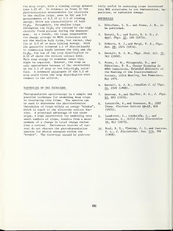
the deep traps, with a binding energy greater
than 4.25 eV. No evidence is found in the
photoionization measurements for electrons
in the shallow traps, seen in TSC and I-V
measurements of 0.5 eV to 1.5 eV binding
energy, which are characteristic of bulk
Si3N4. Presumably, the shallow traps
throughout the Si3N4 are ionized by the high
electric field present during the measure-
ment. As a result, the traps responsible
for charge storage in MNOS structures are
not the shallow bulk traps, but rather, they
lie at 3.0 eV or more binding energy. With
the generally accepted 1.1 eV discontinuity
in conduction bands between the Si02 and the
Si3N^, the top of the trap distribution is
0.15 eV above the silicon valence band.
This trap energy is somewhat lower than
might be expected. However, the trap is
only approximate because of the uncertainty
in the 1.1 eV step at the Si02~Si3N4 inter-
face. A downward adjustment of the 1.1 eV
step would raise the trap distribution with
respect to the silicon.
DISCUSSION OF THE TECHNIQUE
Photopopulation spectroscopy is a simple andpowerful technique for examining deep trapsin insulating thin films. The spectra canbe used to determine the photoionizationthresholds of traps within an energy "window",which is equal to the electrode contact bar-rier. A principal advantage of the tech-nique, a high sensitivity for examining verysmall numbers of traps, results from a meas-urement of a change in total charge ratherthan a current. Extraneous sources of cur-rent do not obscure the photodepopulationspectra for photon energies within the"window". The technique should be particu-
larly useful in examining traps introducedinto MOS structures by ion implantation, im-purities, or radiation damage.
REFERENCES
1. DiStefano, T. H. , and Franz, J. M. , tobe published.
2. Harari, E. , and Royce, B. S. H. , J.
Appl. Phys. T2, 106 (1973).
3. DiMaria, D. J., and Feigl, F. J., Phys.Rev. B9, 1874 (1974).
4. Kendall, E. J. M. , Phys. Stat. Sol. 32.,
763 (1969).
5. Franz, J. M. ,Fitzgerald, D. , and
DiStefano, T. H. , Charge Trapping inNMOS Capacitors, Extended Abstracts of
the Meeting of the Electrochemical
Society, 145th Meeting, San Francisco,
May 1974.
6. Kendall, E. J. M. , Canadian J. of Phys.
46, 2509 (1968).
7. Swaroop, B., and Shaffer, P. S., J. Phys.
D3, 803 (1970).
8. Lundstrom, K., and Svensson, M.,, IEEETrans. Electron devices ED-19 , 826
(1972).
9„ Lundkvist, L. , Lundstrom, I., and
Svensson, C. , Solid State Electronics16, 811 (1973).
10. Deal, B. E. , Fleming, J. J., and Castron,
P. L. , J. Electrochem. Soc. 115 , 300
(1968).
192
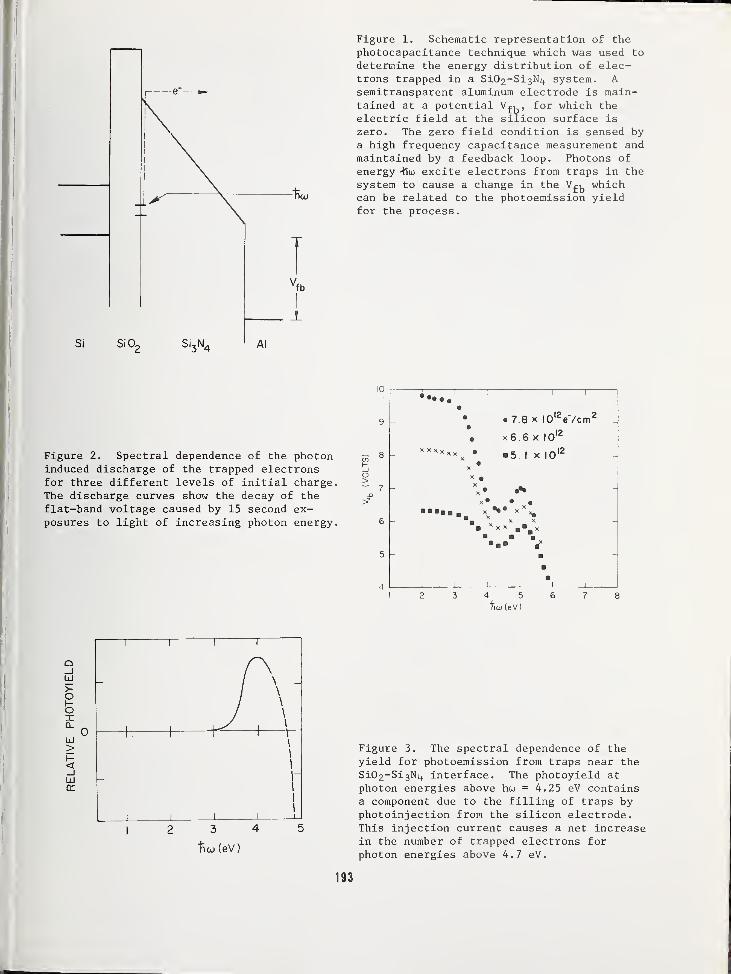
Figure 1. Schematic representation of thephotocapacitance technique which was used to
determine the energy distribution of elec-trons trapped in a Si02~Si3Ni
tsystem. A
semitransparent aluminum electrode is main-tained at a potential V^, for which theelectric field at the silicon surface is
zero. The zero field condition is sensed bya high frequency capacitance measurement andmaintained by a feedback loop. Photons of
energy -ttw excite electrons from traps in the
system to cause a change in the whichcan be related to the photoemission yieldfor the process.
Figure 2. Spectral dependence of the photoninduced discharge of the trapped electronsfor three different levels of initial charge.The discharge curves show the decay of the
flat-band voltage caused by 15 second ex-posures to light of increasing photon energy.
5 -
• 7.8 x IOl2e"/cm
2
x6.6 x 10
5. I x I01
12
4 5
1 1 i i
J\ \h h-
i i
\
i i i
3
Figure 3. Theyield for photoSi0 2-Si 3Ni+
intephoton energiesa component duephotoinjectionThis injectionin the number o
photon energies
spectral dependence of theemission from traps near therface. The photoyield atabove hw = 4.25 eV containsto the filling of traps by
from the silicon electrode,current causes a net increasef trapped electrons forabove 4.7 eV.
193
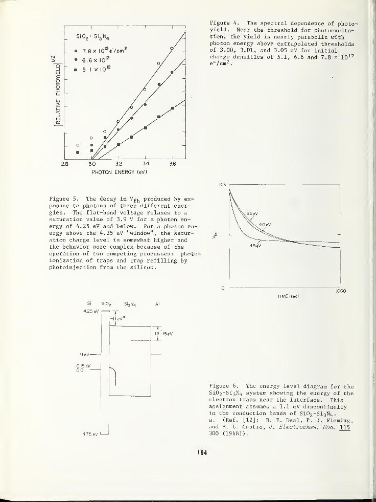
2.8 30 3.2 3.4 3.6
PHOTON ENERGY (eV)
Figure 4. The spectral dependence of photo-yield. Near the threshold for photoexcita-tion, the yield is nearly parabolic withphoton energy above extrapolated thresholdsof 3.00, 3.01, and 3.05 eV for initialcharge densities of 5.1, 6.6 and 7.8 x 10 12
e~ I cm2 .
10V
Figure 5. The decay in Vj^ produced by ex-posure to photons of three different ener-gies. The flat-band voltage relaxes to a
saturation value of 3.9 V for a photon en-ergy of 4.25 eV and below. For a photon en-ergy above the 4.25 eV "window", the satur-ation charge level is somewhat higher andthe behavior more complex because of theoperation of two competing processes: photo-ionization of traps and trap refilling byphotoinjection from the silicon.
1000
Si SiO-
4.25 eV
Si,N,3IV4
TIME (sec)
-475 eV
Figure 6. The energy level diagram for theSi02~Si3Ni+ system showing the energy of theelectron traps near the interface. Thisassignment assumes a 1.1 eV discontinuityin the conduction bands of Si02-Si3Ni+
.
a. (Ref. [12]: B. E. Deal, P. J. Fleming,and P. L. Castro, J. Eleotrochem. Soo. 115300 (1968)).
194
DISCUSSION OF THE PAPER is to measure the charge and then differen-tiate that.
Participant : How will you determine the trap
density?
DiStefano: The density of occupied traps is
determined by working back to get the photo-
yield as a function of photon energy. From
an assumed ionization cross section you can
get an approximate value for the trap density.
The point is that you can determine the photo-
emission yield from a measurement of the
photodepopulation without actually measuring
that current directly. I might also point
out that often you cannot measure the photo-
current from the traps directly because the
currents involved are small and obscured by
other currents in the system. The only way
you can detect the trap depopulation current
Participant : This is specifically for a
nitride film?
DiStefano : No, this is for the MNOS systems
we have examined. You can, I guess, measure
the current directly in the case of a largeamount of charge trapped in the insulator.
You can look at photocurrent and get a photo-
conductivity by a beaching of those traps.
But, for the case of a very small number of
traps in insulators like Si02, the discharge
time is so long and the total charge density
is so small it is very hard to detect the
photocurrent directly. Also, with the photo-
capacitance technique, we measure only the
current from the deep traps of interest,
without the complication of extraneouscurrents
.
195

NBS Special Publication 400-23, ARPA/NBS Workshop IV, Surface Analysis for Silicon Devices,
held at NBS, Gaithersburg , Maryland, April 23-24, 1975 (Issued March 1976)
PH0T0EMISSI0N AND PHOTOVOLTAIC IMAGING OF SEMICONDUCTOR SURFACES*
T. H. Di Stefano
IBM Watson Research CenterYorktown Heights, New York 10598
ABSTRACT
The new electro-optical techniques of scanned internal photoemission andscanned surface photovoltage can be used to obtain images of non-unifor-mities and defects at semiconductor surfaces or interfaces. The spatialresolution of either method is primarily determined by the wavelength ofthe laser used as a collimated light source. The images obtained by thephotoemission technique are replicas of the local contact barrier at theinterface between two materials. Typically, photoemission images showdetails due to variations of stoichiometry or local concentration of im-purities. The photovoltage technique, on the other hand, displays re-combination centers such as precipitates, dislocation, stacking faults,cracks, and gross damage near a semiconductor surface. Each of theseelectro-optical imaging techniques provides information about interfacesthat was previously inaccessible to observation.
INTRODUCTION
Focused beams of various types of ionizingradiation have been used in the past [1-20]
to probe semiconductor surfaces and devices,generally in the region near a p-n junction.The signal induced in a junction by a scannedoptical beam has been found to provide in-
formation [3-10] on resistivity fluctuationsin the material, on gross defects in the de-
vice, and on surface irregularities or in-
version layers near the junction. Generally,in this type of measurement, a beam of elec-trons or photons is scanned across an areaof a semiconductor to produce hole-electronpairs in the material. An irregularity in
the material will produce a fluctuation in a
sample current of some sort measured whenthe beam scans across the defect. In the
standard configuration, a p-n junction col-
lects current produced within a diffusionlength of the junction. Any change in eitherthe generation or recombination rate near the
junction is detected as a fluctuation of the
collected current. The beam induced current
is displayed on a rastered CRT to produce an
image of the defects and inhomogeneities
.
Imaging techniques of the electron beam in-
duced current [11-20] (EBIC) or photon in-
duced current type [4-10] are useful in
identifying defects in individual semicon-
ductor devices, but they cannot easily be
* Work supported in part by the Defense
Advanced Research Projects Agency and mon-
itored by AFCRL under contract numberF 19628-74-C-0077.
applied to the study of semiconductor surfacesor interfaces on which no p-n junction exists.The necessity of a p-n junction to collectthe beam induced current makes non-destructiveevaluation of material surfaces at variousstages of processing virtually impossible.
Recently, several scanned beam techniques,including scanned internal photoemission[21-24] (SIP), scanned surface photovoltage
[25, 26] (SSP) , and the corresponding elec-tron beam analogs [27, 28] have been developedto probe free semiconductor surfaces. Thesenew techniques provide images of defects nearsurfaces or interfaces without the necessityof a p-n junction to detect the signal cur-rent. As a result, they can be used to exam-ine non-destructively the defects which occuron semiconductors at various stages of mate-rial processing. Each of the techniques hascharacteristic advantages and capabilities.The e-beam techniques provide the best reso-
lution, better than about 1000 A, [27] but
they are complicated by beam induced chargingof any insulating film on the surface. [28]
On the other hand, the optical techniqueshave a resolution capability of on the orderof one micron, but they do not charge the
surface insulating or passivating film.
Hence, the optical techniques can also beused to examine charge non-uniformity in the
insulating film on the surface without dis-turbing the system. Additionally, the opticalscanning apparatus can be made to be cleanerthan existing e-beam systems because it does
not require a complex vacuum system.
197

Of the optical techniques, SIP determinessmall inhomogeneities in the contact barrier$ between two materials, one of which is
typically an insulator such as Si02. TheSIP technique is useful in imaging changes
in 3> which are due to contamination, inter-
face chemical reaction, impurity segregationat the interface, or surface crystallographicdefects. In contrast, the SSP technique is
sensitive to local recombination centersthat are within about one micron of the sur-
face and to charge inhomogeneities in the
insulating overlayer. Typical recombinationcenters seen in SSP images include crystal-lographic defects, precipitates, and gross
surface damage; these defects are usuallyintroduced during growth, cutting, polishing,and high temperature processing of the semi-conductor material. The SSP technique has a
unique advantage in that no direct contactto the sample is required if the photovolt-age measurement is made by capacitive coup-
ling. Since physical contact is unnecessary,the SSP technique is clean and completelynon-destructive.
OPTICAL SCANNING SYSTEM
The instrumentation for the two scannedoptical techniques is quite similar in that
a small spot is rastered on the sample sur-
face while a signal, either photoemission or
photovoltage , is detected and displayed on a
CRT. A cw laser was used for the lightsource in order to obtain a measurable sig-
nal from a small, nearly diffraction limitedlight spot. Reasonable signals were obtainedwith 1.0 mW of light incident on the sample,without any noticeable thermal damage to the
sample at the 105 W/ cm2 power density at the
focused spot. The spot was swept by thesawtooth motion of a galvanometer drivenmirror, which was scanned at a 20 Hz rate.
In the other direction, the beam was sweptslowly in order to complete a 600 linesingle frame in 30 sec. The frame rate,
which is limited by the rate of the fast
scan mirror, could easily be increased an
order of magnitude by increasing the fast
scan rate to 200 Hz. A further increase, at
the expense of a reduced spacial resolution,could be obtained with an accoustic deflec-tion system for the fast scan direction.The total resolution capability of the opti-cal scanning technique is limited by threeequally important factors: the divergenceof the light output from the laser, the dif-fraction limit of the objective lens, andthe bandwidth of the detector. At best, thespacial resolution (of the SIP measurement)is estimated to be about 0.43 microns, withthe dominant factors being lens diffraction
o
at A = 3250 A and laser divergence.
The simple optical system shown in figure 1
was used to scan a light spot over a squarearea of the sample surface. Radiation froma laser source was focused onto a 50 micronpinhole in order to eliminate the light thatdiverged by more than 0.5 mrad. The lasersource was chosen to be either an RCA He-Cdlaser operating with 3mW at 3250 A or a
Spectra Physics He-Ne laser with 5 mW at
6328 A. Light emergent from the pinhole wasprojected a distance of one meter onto a
series of two front surface mirrors, whichrotate through angles 0 and <j>. Light fromthe two scanned mirrors completely filled theaperture of the objective lens for the fullrange of the scanned angles. Then, thefocused spot of light from the objective lensscanned an area of the sample as the twoorthogonal mirrors were rotated. The size of
the scanned area, and to some extent, theresolution of the system, were determined bythe objective lens. The focal length of thelenses used in the measurements range from0.54 cm to 20 cm. Reflecting objectivelenses were used for the high resolutionmeasurements so that correction of the opticsfor the wavelength of each laser wasunnecessary
.
The fast scan mirror was driven at about 20Hz by a rotary galvanometer, G— 306, availablefrom General Scanning, Inc. Care was takento balance the mirror and rotor in order to
minimize parasitic oscillation of the mirrorassembly. This parasitic oscillation orvibration causes deflection of the lightperpendicular to the direction being scannedby that particular mirror. Although fastergalvanometer scanners are available, therelatively conservative rate of 20 Hz waschosen to minimize the problems caused byvibration and to optimize resolution.
The problem of positioning and focusing thesample, something which is particularly dif-ficult in the case of UV light, was solved bydetecting light reflected back into the sys-tem from the sample. Initially, light fromthe pinhole goes through the scan systemwhich focuses it onto the sample. When the
system is in focus, the light reflected fromthe sample is focused by the system back onto
the pinhole, independent of the mirror posi-tions 9 and <|>. However, if the system is out
of focus , the reflected light falls outsidethe pinhole where it strikes a fluorescentscreen. The system is brought into focus by
adjusting the sample position along the opti-cal axis until all of the reflected light is
refocused back onto the pinhole.
In order to locate the sample in the beam and
to examine the surface conditions during the
198
measurements, a reflectivity image of thesample can be obtained and displayed in thecoordinate frame of the CRT. A portion ofthe light reflected from the sample is di-rected onto a photocell by a beamsplitter.The light falling on the photocell comes tofocus at a point which is independent of thescan angles 6 and <j>. Current from the photo-cell, when displayed as Z-axis modulation ofa rastered CRT, forms an image of the sampleat the wavelength of the laser source and inthe same coordinate frame as the SSP or theSIP image of the same area.
Both the photoemission and the photovoltaicsignals are detected and displayed on a CRTscreen by the circuitry shown schematicallyin Fig. 2. The signal current is detectedby a Kiethley 18000 picoammeter which hasbeen modified for a fast response; the modi-fication involves a reduction of the feed-back capacitance in each of the two amplifiersections, while maintaining the stability ofthe overall system. The signal in the SIPmeasurement is the photocurrent , while thesignal in the SSP measurement is the capaci-tive current induced in the probe electrodeby the surface photovoltage. The amplitudeand dc level of the signal are adjusted andapplied to the Z-axis of the CRT, along witha retrace blanking pulse derived from thefast scanner. The X and Y axes of the CRTare driven by voltages proportional to thosedirectly across the drive motor armatures.Images of the Z-axis modulated display ofthe SSP or the SIP signal are recordedphotographically
.
The measurement apparatus, shown in figure3, includes the scan mirrors, the galvanome-ter motors, the reflecting microscope objec-tive, the sample positioning stage, and thepicoammeter. Light, incident on the mirrorsfrom the right , is deflected onto the two
orthogonally mounted scanning mirrors by a
stationary positioning mirror. From the
fast scanned mirror, the beam enters the re-
flecting objective lens (Beck 36/. 5) whichfocuses the light onto the sample. Becauseof the curvature of the focal plane of this
objective, the overall resolution is notice-ably degraded for beam deflections greaterthan ±0.5°. In order to extend the useablefield of view, it is necessary to use a re-
fractive piano-objective which is correctedfor flatness of field at the laser wavelength.
The sample is held in position and focusedby an X-Y-Z adjustable hot stage. Signals
from the sample are detected by the picoam-meter located behind the hot stage in figure
3. The entire assembly is secured to a two
meter optical bench.
SCANNED INTERNAL PHOTOEMISSION
Scanned internal photoemission (SIP) is a
relatively recent technique [21-24] for prob-ing interfaces with a beam of light to produceelectronically an image or replica of theinterface contact barrier. Typical imagesdisplay a modulation of the internal photo-current induced by the scanned beam which is
due to a lateral inhomogeniety of the contactbarrier. The technique is somewhat analogousto scanning electron microscopy (SEM)
, exceptthat in this case a light beam is used to ex-cite electron emission into a dielectric in-stead of into vacuum. As in the SEM tech-nique, the emitted current is displayed onthe Z-axis of a CRT.
The mechanism of SIP is internal photoemissionon a local scale, as shown in figure 4. Ascanned light beam of energy 'hw penetrates a
transparent [29] or semi-transparent [30]
electrode and is absorbed in the oppositeelectrode where it excites electrons into theconduction band. Some of the electrons havesufficient momentum normal to the interfaceso that they are able to surmount the barrier$ and reach the opposite electrode. Nearthreshold, the quantum yield for photoemis-sion is
Y (-nu
where y is a constant and a is an empiricallydetermined power, typically in the range 2 to
3. A small percentage reduction in 0 leadsto a relatively larger increase in yield,
d[ln ¥] =(fito - $)
d[ln $]
The sensitivity of the SIP technique dependsupon the rapid increase of photocurrent pro-duced by a small decrease of $ below the pho-ton energy <hw. For a reasonable image con-trast, the laser and any Schottky barrier re-
duction are chosen so that /fiw is severaltenths of an eV above $.
The Si-Si02 interface is an interestingcandidate for examination by SIP imaging, as
can be seen in figure 5 and 6. Here, the
Si-Si02 interfaces have been uniformly coatedwith about 4 x 10^ Na/cm2 by electrodeposi-tion in order to reduce the interface bar-rier^l from 4.25 eV down to a level that is
accessible to the He-Cd laser operating at
3.81 eV. Actually, the sodium acts as a
"staining agent," increasing the local photo-current in those places where ions accumulateon the interface. Since the sodium coverageis influenced by defects, it was found to en-
hance the SIP contrast around defects. Fig.
5 shows an interesting pattern of dark spots
199
seen in the emission from an Si-SiC>2 interfacegrown on vLO20 P/cm3 doped (100) Si. Thesespots, which are about 10 microns in diame-ter, have been identified as phosphorousthat has segregated onto the Si-Si02 inter-face during high temperature growth [32, 33]
of the 1000 A thick Si02- Apparently,sodium that does reach the Si-Si02 interfaceis rendered ineffective by chemical combina-tion with the phosphorous lying within a few
atomic layers of the interface [33]. Thesephosphorus islands, observed for the first
time by the SIP imaging technique, werefound to be correlated with the phosphorousdoping density in the silicon substrate.Another type of defect on the Si-Si02 inter-
face is seen in figure 6 as a line, about 30
microns long, with bright spots at eitherend. The defect, which lies along the <110>
crystallographic direction, is thought to be
a stacking fault that has been decorated bysodium ions. The contrast of the stackingfault is enhanced by the sodium decoration.
The SIP technique was also used to studymetal-insulator interfaces such as Nb205~Bi,which is of interest because of the fast
switching found in this structure. The SIPimage in figure 7 represents photocurrentemitted from a 200 A Bi electrode intoNb205 • The light source was a He-Ne laserat 1.96 eV, which is close to thresholdwhere the technique is most sensitive. In
this system, the contrast mechanism is notsimple because of the large number of traps
in the ^205. '
S'
SCANNED SURFACE PHOTOVOLTAGE
Photovoltage images show defects that causeminority carrier recombination on a semicon-ductor surface. The SSP images have alsobeen found to show any non-uniform charge in
the passivating layer on a semiconductor.An SSP image is formed by displaying the
first or second derivative of the photovolt-age induced by a scanned beam of light on a
semiconducting surface. The travellinglight spot produces a comet shaped cloud of
minority carriers which are captured on the
slightly depleted surface, as represented infigure 8. Carriers from the moving cloudcover the surface to produce a photovoltage.When the beam passes over a defect, some of
the charge cloud is lost to recombination,leading to a dip in the photovoltage. Thisdip is detected by a capacitively coupledelectrode near the surface, and displayed ona CRT. Since the charge cloud is quitelarge, on the order of the diffusion length,the resolution of images produced directlyfrom the photovoltage is rather poor. Thehigh resolution [25] of the SSP technique is
due to the usederivative of
image. The disignal in thewhere the charrithmic singulderivative is
the capacitivetions of the s
of the first or secondthe photovoltage to form thef ferentiation accentuates theregion around the light spot,ge cloud density has a loga-arity. In practice, the firstobtained directly by measuringcurrent induced by fluctua-
urface photovoltage.
By using conduction of minority carriersalong the slightly depleted surface, it is
possible to obtain SSP images at some dis-tance from the electrode. The local photo-voltage is coupled to the entire surface bythe slightly conducting surface. In somecases , it is necessary to enhance the surfaceconductivity by generating extra minoritycarriers by a dc blanket illumination. Theresolution of remotely detected images wasfound to be reduced if the surface conductiv-ity is too low. Also, in order to develop a
photovoltage signal, the surface must be de-
pleted, either by a blanket electrode (theelectrode can be an aquous solution, as wasshown by Lile and Davis [26]) , or by a sur-face treatment such as that produced by dryoxidation of p-type silicon.
The signal S' is proportional to a convolutionof the excess local recombination rate R withan experimental sampling function, which is
approximately equal to the x-derivative of
'
the charge cloud density n. Mathematically,
dn(x-x ,y-y )
- R(x,y)(x •V dx
where G is the total generation rate, S is tneeffective depletion width, Ea is the permit-tivity of the semiconductor, E^ is that of
the dielectric, and t 0 is the surface minoritycarrier lifetime. Ideally, dn/dx would be a
singly differentiated Dirac delta functionand the signal S' would then be proportionalto dR/dx. Because of the finite size of the
light spot, however, the resolution is re-
duced. In a coordinate system centered on
the moving spot, a modified diffusion equation
[25] is solved to obtain the charge density n
in the region around the scanned spot. The
charge density
n = A exp (Kr)
where
of
V To\l/2
4? )
'
and where KQ is a modified Bessel functionthe second kind, and D is the surface dif-
fusion coefficient. The sampling functiondn/dx is plotted in figure 9 for several scanvelocities, with the reasonable parameters
200
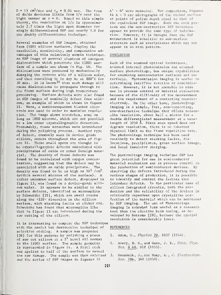
D = 15 cm2 /sec and x 0 = 0.01 sec. The formof dn/dx deviates little from 1/r near thelight center at r = 0 . Based on this simpletheory, the resolution at 1/e is approxima-tely 2.7 times the light spot diameter forsingly differentiated SSP and nearly 1.0 forthe doubly differentiated technique.
Several examples of SSP images, obtainedfrom (100) silicon surfaces, display the
resolution, sensitivity, and comparative ad-vantages of this relatively simple technique.An SSP image of several clusters of emergentdislocations which penetrate the (100) sur-face of a sample are shown in Fig. 10. Thedislocations were produced by mechanicallydamaging the reverse side of a silicon wafer,and then annealing it in dry He at 800 °C for30 min. It is known^^ that such damage willcause dislocations to propagate through to
the front surface during high temperatureprocessing. Surface defects were also foundin SSP images of nominally defect free sili-con, an example of which is shown in figure11. Here, a semitransparent blanket elec-trode was used in order to maximize resolu-tion. The image shows scratches, some as
long as 1000 microns, which are not parallelto a low order crystallographic direction.Presumably, these scratches were introducedduring the polishing process. Another typeof defect, commonly seen in device gradesilicon, occurs throughout the area of fig-
ure 12. These small spots are thought to
be crystallographic defects associated withprecipitates of oxide or other foreign mate-rial. The density of these defects wasfound to be correlated with oxygen concen-tration, suggesting that the defect may be
associated with an oxide precipitate. Thedensity was found to be as high as 10^ / cm2
(within several microns of the surface) . A
rather uncommon surface defect, displayed in
figure 13, was found on a device-grade sili-con wafer. It appears to be similar to the
surface defects, identified as microsplitsby Schwuttke [35], which are small cracksalong the <110> direction in the siliconsurface, with stacking faults at either end.
Schwuttke has found that microsplits likethat in figure 13 are introduced during the
saw cutting of the silicon.
It is interesting to compare the SSP techniqu-
with the useful but destructive technique of
selective etching. A sample was prepared
[36] for this purpose by polishing a pieceof saw cut silicon at a 2° bevel off normalto the (100) surface. The sample geometryis represented in figure 14. A Sirtl etch
was applied to half of the surface to reveal
the saw damage. The sample was then oxidized
and the series of SSP images in figures 14
A 1 - D' were measured. For comparison, figures14 A - D are micrographs of the etched surfaceat points of polish depth equal to that of
the equivalent SSP image. Both the etch pat-tern and the non-destructive SSP techniqueappear to provide the same type of informa-tion. However, it is thought that the SSPmeasurement is sensitive to sub-surfacestructure such as precipitates which may notappear in an etch pattern.
CONCLUSION
Each of the scanned optical techniques,scanned internal photoemission and scannedsurface photovoltage , has unique capabilitiesfor examining semiconductor surfaces and in-
terfaces. Photoemission imaging is useful in
determining interface reaction or contamina-tion. However, it is not amenable to wideuse in process control or material evaluationbecause of the difficulty of the measurementand the requirement of a contacting counter-electrode. On the other hand, photovoltageimaging is a simple, fast, non-contacting,non-destructive technique that offers reason-albe resolution, about half a micron for a
double differentiated measurement at a wave-length of 3250 A. Since scan speed does notdegrade resolution, there is no inherentphysical limit on the frame repetition rate.
The photovoltage technique has been usedroutinely to detect stacking faults, dis-locations, precipitates, gross surface damage,and local insulator charging.
The photovoltage imaging technique SSP has
great potential for use in semiconductormaterial evaluation and in process control in
the production of semiconductor devices. By
observing the defects introduced during the
various stages of production, it is possibleto identify and control the factors that
introduce defects. In the particular case of
silicon integrated circuits, both the pro-
duction and the reliability of the devices is
critically dependent upon crystalline per-
fection of the material which can be monitoredby SSP imaging. The use of Photovoltageimaging is somewhat less useful as a research
tool than the electron beam analog, as de-
veloped by Bottoms [28] , because the specialresolution is considerably lower.
REFERENCES
1. Adam, G. , Physica 20, 1037 (1954).
2. Avery, D. G., and Gunn, J. B., Proa. Phys.
Soo. B 68 , 918 (1955)
.
3. Oroshnik, J., and Many, A., J. Electrochem.
Soa. 106, 360 (1959).
201
4. Tihanyi, J., and Pasztor, G. , Solid State 20.
Electronics 10, 235 (1967).
5. Potter, C. N., and Sawyer, D. W. ,Optical
Scanning techniques for semiconductor 21.
device screening and identification of
surface and junction phenomena, Physics
of Failure in Electronics ,Shilliday, 22.
T. S. and Vaccaro, J., Eds., Rome AirDevelopment Center Series in Reliability,
1967, vol. 5, p. 37. 23.
6. Summers, R. A., Solid State Technology,
p. 12, (March, 1967). 24.
7. Haberer, J. R. ,Photoresponse Mapping
of Semiconductors, in Physics of Failure 25.
in Electronics, Shilliday, T. S. andVaccaro, J., Eds., Rome Air DevelopmentCenter Series in Reliability, 1967,vol. 5, p. 51.
8. Phelan, Jr., R. J., and DeMeo, Jr., N. L . , 26.
Appl. Optics 10, 858 (1971).
9. Kozhevin, V. E. , Sov. Phys. -Solid State 27.
8, 1979 (1967)
.
10. Kasprzak, L. A., Rev. Sci. Inst. 46, 17 28.
(1975)
.
11. Lander, J. J., Schreiber, H„ and Buch, 29.
T. M. , Appl. Phys. Lett. 3, 206 (1963).
12. Everhart, T. E., Wells, 0. C, and Matta, 30.
R. K. , J. Electrochem. Soc. Ill, 929
(1964)
.
13. MacDonald, N. C.,and Everhart, T. S.,
Appl. Phys. Lett. ]_, 267 (1965). 31.
14. Czaja, W., and Patel, J. R. , J. Appl.
Phys. 36, 1476 (1975) . 32.
15. Everhart, T. E., Pvoc. IEEE 54_, 1480
(1966)
.
33.
16. Foss, N. A., J. Appl. Phys. 41, 823
(1970)
.
34.
17. Ravi, K. V., Varker, C. J., and Volk,
C. S., J. Electrochem. Soc. 120, 533
(1973). 35.
18. Varker, C. J., and Ravi, K. V., J. Appl.
Phys. 45s 272 (1974) . 36.
19. Gonzales, J. A., Scanning ElectronMicroscopy 1974, Johari , 0., Ed. p. 94
(ITT Research Institute, Chicago,Illinois, 1974).
Kato, T. , Matsukawa, T., Koyama, H. , andFujikawa, K. , J. Appl. Phys. 46, 2288
(1975)
.
DiStefano, T. H. , Appl. Phys. Lett. 19,280 (1971)
.
DiStefano, T. H. , J. Appl. Phys. 44, 527
(1973)
.
Williams, R., and Woods, M. H. , J. Appl.
Phys. 4_3, 4142 (1972) .
DiStefano, T. H., and Viggiano, J. M.
,
IBM J. Res. Dev. 18, 94 (1974).
Philbrick, J. W.,and DiStefano, T. H.
,
Scanning Surface Photovoltage Study of
Defects in Silicon, Proc. 13th AnnualReliability Physics Conf. Las Vegas,Nevada, April 1, 1975 p. 159.
Lile , D. L., and Davis, N. M. , to bepublished in Solid State Electronics.
Bottoms, W. R.,and Guterman, D. , J. Vac.
Sci. Technol. 11, 965 (1974).
Bottoms, W. R.,Guterman, D. and Roitman,
P., J. Vac. Sci. Tech. 12, 134 (1975).
Goodman, A. M. , Phys. Rev. 152, 780
(1966)
.
Williams, R.,Injection by Internal
Photoemission, Semiconductors and Semi-metals, Vol. 6, Willardson, R. K. , Ed.,
(Academic Press, Inc., New York, 1970).
DiStefano, T. H., and Lewis, J. E. , J.
Vac. Sci. Technol. 11, 1020 (1974).
Chou, N. J., van der Meulen, Y. J.,
Hammer, R., and Cahill, J. G. , Appl. Phys.
Lett. 24, 200 (1974)
.
van der Meulen, Y. J., J. Vac. Sci.
Technol. 11, 985 (1974)
.
Dumin, D. J., and Henry, W. N.
,
Metallurgical Trans. _2, 677 (1971).
Schwuttke, G. H. , Tech. Rep't. 1 ,2,
ARPA Contract No. DAHC 15-72-C-0274.
The bevel polished sample was prepared
by J. W. Philbrick, IBM Hopewell Junction,New York.
202
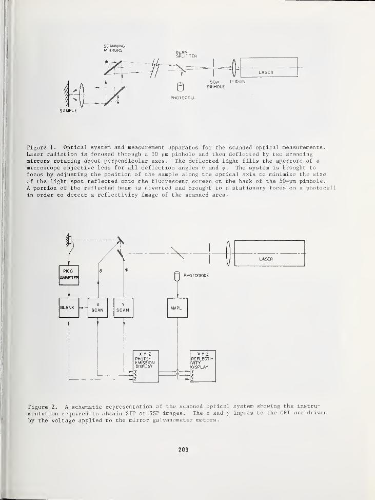
SCANNINGMIRRORS BEAM
SPLITTER
LASER
Figure 1. Optical system and measurement apparatus for the scanned optical measurements.Laser radiation is focused through a 50 urn pinhole and then deflected by two scanningmirrors rotating about perpendicular axes. The deflected light fills the aperture of a
microscope objective lens for all deflection angles 6 and<f>
. The system is brought to
focus by adjusting the position of the sample along the optical axis to minimize the size
of the light spot reflected onto the fluorescent screen on the back of the 50-um pinhole.
A portion of the reflected beam is diverted and brought to a stationary focus on a photocellin order to detect a reflectivity image of the scanned area.
LASER
X-Y-ZPHOTO
"
EMISSIONDISPLAYYXZ
X-Y-Z
REFLECTI-VITYDISPLAYYXZ
Figure 2. A schematic representation of the scanned optical system showing the instru-
mentation required to obtain SIP or SSP images. The x and y inputs to the CRT are driven
by the voltage applied to the mirror galvanometer motors.
203
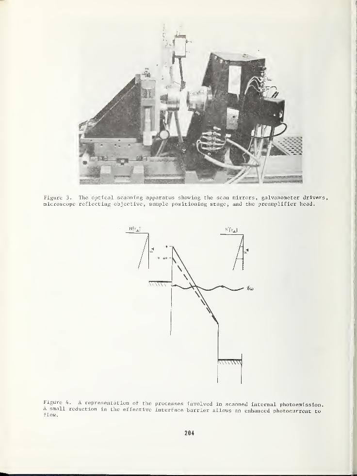
Figure 3. The optical scanning apparatus showing the scan mirrors, galvanometer drivers,microscope reflecting objective, sample positioning stage, and the preamplifier head.
\W\VA\
Figure 4. A representation of the processes involved in scanned internal photoemission
.
A small reduction in the effective interface barrier allows an enhanced photocurrent toflow.
204
Figure 5. Scanning internal photoemissionimages of three samples of Si-SiC^ inter-faces covered with 4 * 10 12 sodium atoms persquare centimeter, and measured at a photonenergy of 3250 A. The light areas indicatea high photoyield produced by the presenceof sodium on the interface. The dark areasare thought to be due to regions of phos-phorus rich layers near the Si-Si02 inter-face. Phosphorus segregates at that inter-face during the formation of the Si02 layers,produced by the oxidation of 10 20 P/cm^doped silicon.
. 6
.
Figure 6. Scanned internal photoemissionmeasurements of an Si-Si02 interface whichhas been uniformly coated with 4 x 10 12
Na/cm2. The Na is found to decorate a
30 pm, long defect which lies in the <100>
direction on the silicon surface.
Figure 7. Scanned internal photoemissionimage of a Bi-Nb20 interface, measured atA = 6328 K. The vertical striae are due toa dc level shift of leakage currents.
205
S'(t)
Figure 8. The rudiments of the scanned surface photovoltage measurement. A spot of lightis swept across a semiconductor surface, generating a comet shaped cloud of minoritycarriers in a surface depletion region. The surface potential, capacitively detected by a
remote electrode, fluctuates when the spot traverses a surface recombination center.
Figure 9. The spacial derivative of the surface minority carrier density, along a line in
the direction of travel of a 1 pra spot of light. The derivative is relatively insensitiveto the scan velocity v for the values shown in the figure. The quantity [dn/dx| is the
sampling function in the singly differentiated scanned surface photovoltage measurement.
206
Figure 10. Scanned surface photovoltage
image of several clusters of emergent dis-
locations through the (100) surface of a
silicon wafer. The dislocations were gener-
ated by sandblasting a spot on the reverse
side. During subsequent annealing and oxi-
dation steps, the dislocation loops gener-
ated at the damage sites grow through the
wafer, eventually penetrating the front
surface.
Figure 12. Scanned surface photovoltageimage of a (100) silicon surface showingsmall, randomly distributed defects.
Figure 11. Scanned surface photovoltageimage of surface damage produced during thcutting and polishing of a silicon wafer.The damage lines do not follow the <110>
direction on the (100) surface.
i
Figure 13. Scanned surface photovoltageimage of a defect, apparently a microsplitwhich was introduced during saw cutting ofthe (100) surface. The microsplit is
thought to be flanked by stacking faultarrays in the <110> direction on thesurface
.
207
A A'
Figure 14. Scanned surface photovoltage images (A', B', C', D') of saw damage in a siliconwafer which has been polished at a 2° angle. For comparison, micrographs (A, B, C, D,) of
an adjacent area of the surface were made after etching. Both sets of images, taken on a
highly polished area of the beveled surface, show the transition from the damaged region to
the undamaged region occuring at about the same depth, as is observed on an etched portionof the bevel.
208
DISCUSSION OF THE PAPER
Feigel : Photovoltaic imaging is a non-contacting technique, right?
DiStefano : That is correct. The onlycontact that is made to the sample is thecapacitive contact. The sample is simply a
sandwich between capacitive electrodes.
Feigel : Then is it relatively easy to
engineer?
DiStefano : Nothing is hidden, everythingwas shown on the figure.
Feigel : I meant there are no super criticaldimensions or dimensional stability prob-lems you have to worry about?
DiStef ano : Focussing is a problem but, as I
mentioned, we use the back reflected light
to focus the sample. Focussing is a problemin the ultraviolet because you cannot see
the spot. Other than that, there is nothingintrinsically difficult about the technique.
Thomas : Can you actually identify the
collecting species? You said it is actuallycopper.
DiStefano : In some of the cases weintentionally put copper into the system.
It is an inference that the precipitate is
copper, since there is copper in this sample.
Thomas : We also have found copper, but
there are other metals that can actually
decorate the defects. Would you say there
is some similarity between this techniqueand the EBIC technique?
DiStefano : There are some similarities.With the electron beam induced current tech-nique you need a junction, and you look at
junction current. There is no problem withresolution, but it is necessary to have a
surface junction on the sample. One of the
beauties of the photovoltage technique is
that it is nondestructive, so you can lookat an area, process that area, and then go
back and examine what defects were caused by
the processing. We are studying variousthings such as nitride passivation and thedefects introduced by the mechanical stress.We are looking at deep etching and oxideisolation in silicon. So this technique is
ideal for following a piece of siliconthrough a stage of processing steps.
Participant : Can you use the amplitude of
the surface photovoltage to obtain a three-dimensional representation of your datasimilar to the Y amplitude images?
DiStef ano : We can do that, but we do not,
because that tends to make it harder to iden-tify the position of the defect. We do use a
series of photographs in different colors to
look at the depth of the trap. There is onething that I have not mentioned, namely you
can also bend the bands of the silicon sur-face and submerge a trap or a surface defect
below the energy level so you no longer see
it. You can take a series of images as a
function of the Fermi level at the surface as
defect disappears to obtain an X, Y, and
energy representation of the defect.
209

NBS Special Publication 400-23, ARPA/NBS Workshop IV, Surface Analysis for Silicon Devices,
held at NBS, Gaithersburg, Maryland, April 23-24, 1975 (Issued March 1976)
ELECTRON BEAM INDUCED IMAGING OF SILICON SURFACES*
W. R. Bottoms
Department of Electrical EngineeringPrinceton University
Princeton, New Jersey 08540
Modern electron optics can provide a focusedbeam of less than 100 angstrom units in di-ameter which may be swept across a samplein order to address any portion within the"field of view." This allows one to inputenergy to a well defined region and, by col-lecting the signals associated with the var-ious energy relaxation processes which occur,an analysis of the structure of the samplewith high spatial resolution can be under-taken. Figure 1 illustrates the primarysignal channels which are activated by theelectron beam with the principle type ofanalysis associated with each beam. The en-ergy dissipated within the sample in termsof electron-hole pair production can be de-tected in an external circuit and images,associated with any process which alters thecurrent measured in the external circuit,can be formed. The contrast mechanismswhich are responsible for the images formedare listed in Table l 1
. It is often diffi-cult to determine which mechanism or whichcombination of mechanisms are responsiblefor the formation of a given image and, in
an effort to deconvolute the various contri-butions to contrast, data is gathered fromas many different sources as possible. BothC-V and G-V measurements are conducted to
determine as fully as possible the effect of
the incident beam and the various sampleprocessing steps on the distribution of in-ternal charge.
Electron beam induced imaging is carried out
as a function of the incident beam voltagewhich can be related to the depth within thesample by the calculated range of the inci-dent electron beam2
,Figure 2. Potential
barriers of known depth within the samplealso provide depth resolution since they
contribute to the signal current by separa-ting excess carriers generated by the inci-dent beam. In addition, images are formedas a function of bias across the sample and
processing history (principally the biasthermal stressing used to determine the num-ber of mobile ions present and move themfrom one region of the sample to another)
.
Work supported by ARPA Contract No. F19678-
72-C-0298.
21
The electron beam induced images of "bare"silicon surfaces and internal interfaces inMOS samples are analogous to the correspondingimages which can be obtained using electro-magnetic radiation as the exciting probe withtwo very important differences. The opticalprobe can be chosen so that the incoming beamdoes not see portions of the sample which areof little interest in a particular image 3
(i.e., the silicon-silicon dioxide interfacecan be probed with an optical beam of energysuch that a signal is stimulated by internalphotoemission at the interface but the oxideis transparent to the probing beam) . In thecase of electron beam excitation, it is pos-sible to obtain images of interface structureassociated with the excitation of secondaryelectrons across the potential barrier betweenthe silicon and the oxide, as in internalphotoemission, but this signal includes cur-rents associated with all other interactionsof the beam with the sample
1
*. The variouscurrent components are convoluted and indeed,under most conditions, another imaging mech-anism will dominate resulting in the reverseof the contrast obtained from the internalphotoemission mechanism 5
. The result of thispropensity of the electron to undergo energyexchange interactions which appear continuousrather than discrete (insofar as the scale of
energy interactions of the experiment is con-cerned) limits the technique. Although theelectron beam interacts much more stronglywith the system under investigation andtherefore is able to "see" events whichcould not be seen with optical or X-rayprobes, this very density of informationmakes it difficult to deconvolute the contri-butions from various processes. The secondimportant difference between the optical probeand the electron beam probe is that it is
possible to generate an incident electronbeam with a diameter more than an order of
magnitude smaller than that of the opticalprobe and therefore, under many imaging con-ditions, provide a much higher spatial reso-lution with a similar improvement in the
depth of field.
An example of the first of the contrast mech-anisms listed in Table 1 is shown in Figure3. This is the normal image which is derivedfrom the scanning electron microscope (SEM)
and it is a map of the topography of the
1
sample as well as the variations in theplane of the secondary emission and reflec-tion coefficients. An appropriate adjust-ment of incident beam parameters can givethe situation where electrons of low energyare excited across the barrier between the
gate metallization and the insulator in a
MOS sample thus providing an image of thevariations in the barrier height between themetal and the insulator. An example of suchan image is shown in Figure 4. The struc-ture has been attributed to local variationsin barrier height due to mobile ion aggre-gation at the gate which was generated bybias thermal stressing of the sample. Fig-ure 5 is an example of an image of the Si-Si02 interface. Variations in barrierheight due to aggregation of Na ions at theinterface are responsible for the structuresin this image.
Figure 6 gives an example of image structuredue to lateral nonuniformities in the chargestored in the insulator. In this casecharge was stored selectively in some partsof the sample by the electron beam and theregions of bright and dark intensity withrespect to the background showed that bothpositive and negative charge can be storedin the sample with the incident beam. Thisstored charge is an ever present artifact of
the electron beam imaging technique and mustbe kept in mind when interpreting imagesformed in this manner.
CONCLUSIONS
The use of electrom beam induced images hasbeen shown to be a powerful tool for theobservation of subsurface and surface varia-tions of electronic structure in silicon.Spatial resolution of the order of 1000 Ahas been obtained for structure at an inter-face located several thousand angstroms belowthe surface. Structure located closer to theentrance can be imaged with even higher res-olution since there is less spread of the in-cident beam. The electron beam can producethe analog of scanning internal photoemissionand surface photovoltage images with betterspatial resolution than is obtained for simi-lar images induced by electromagnetic radia-tion. The major disadvantages of electronbeam techniques are of cost and of the dif-ficulty in deconvoluting the information ob-tained. We are, in most cases, only able to
present models for the structural imageswhich are consistent with our experiments.We are not able, at present, to make a uniquedetermination of the mechanism responsiblefor a given image and therefore we cannotuniquely identify the structure. The abilityto obtain images of defects on "bare" siliconhas been demonstrated. This has importantimplications for developing technologieswhich place more rigid specifications on thestarting semiconductor material such as highvoltage power devices and large area CCDdevices
.
When defect structures in a silicon samplecause local variations in recombinationrates we can detect a signal due only to thechange in the capacitance of the sample in-duced by the spatial variation of thecharge. 1 This gives rise to the electroninduced analog of the surface photovoltagemechanism 5
. Figure 7 shows stacking faultdefects in a Si (111) crystal where theimage formation has been attributed to thisanalog of the surface photovoltage technique.This image is of the Si-Si02 interface in anMOS capacitor. Figure 8 is an image of a
"bare" silicon wafer which was mounted inthe microscope with spring tension holdingit between two flat metal plates. The nat-ural oxide covering the silicon and themetal plates is of sufficient thickness to
prevent large dc current flow across thesample and the ac signal is coupled outthrough the capacitor between the siliconand the top metal electrode. In this con-figuration the image is again attributed tothe analog of the surface photovoltage mech-anism.
References
1. Bottoms, W. R., and Roitman, P., CriticalReviews in Solid State Sciences (in
press)
.
2. Everhart, T. E.,and Hoff, P. H. , J. Appl.Phys. 42, 5837 (1971).
3. DiStefano, T. H. , Appl. Phys. Lett. 19_,
280 (1971).
4. Bottoms, W. R., and Guterman, D., J. Vac.
Sci. Tech. 11, 965 (1974).
5. Bottoms, W. R. , Guterman, D. , andRoitman, P., J. Vac. Sci. Tech. 12_, 134
(1975).
6. DiStefano, T. H. , Photoemission andPhotovoltaic Imaging of SemiconductorSurfaces, ARPA/NBS Workshop IV, SurfaceAnalysis for Silicon Devices,A. G. Lieberman, Ed., NBS Spec. Publ.400-23 (March 1976)
.
212
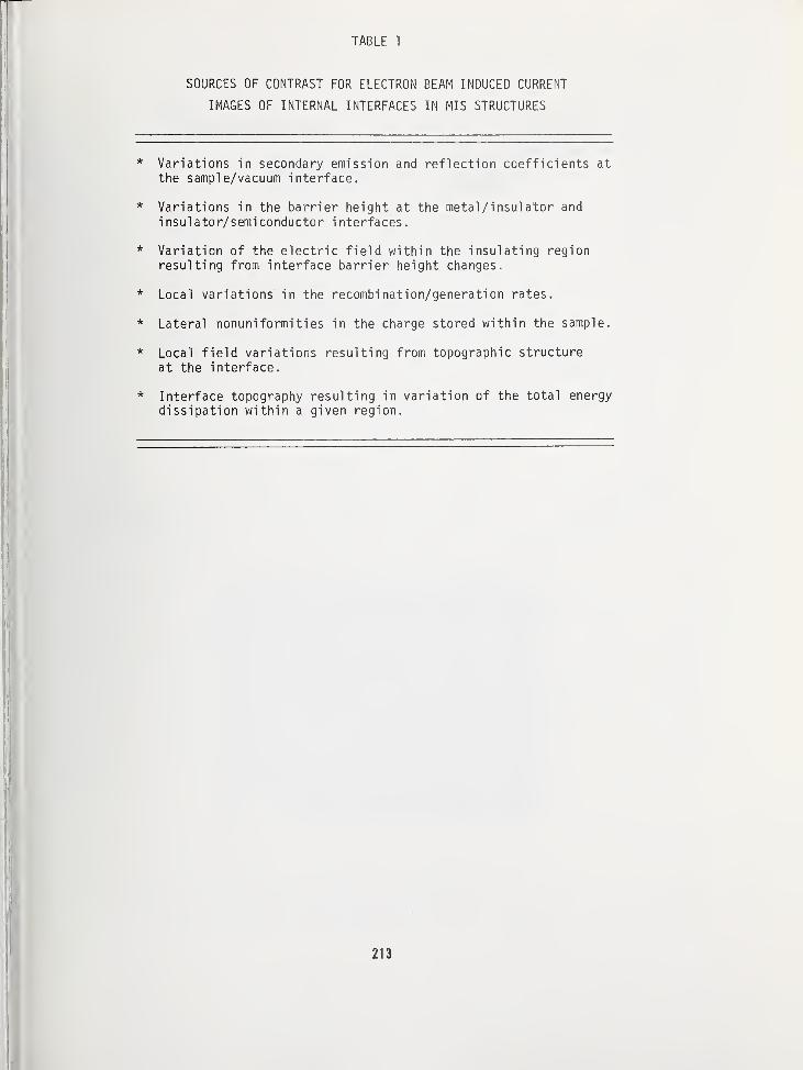
TABLE 1
SOURCES OF CONTRAST FOR ELECTRON BEAM INDUCED CURRENT
IMAGES OF INTERNAL INTERFACES IN MIS STRUCTURES
* Variations in secondary emission and reflection coefficients at
the sample/vacuum interface.
* Variations in the barrier height at the metal/insulator and
insulator/semiconductor interfaces.
* Variation of the electric field within the insulating region
resulting from interface barrier height changes.
* Local variations in the recombination/generation rates.
* Lateral nonuniformities in the charge stored within the sample.
* Local field variations resulting from topographic structureat the interface.
* Interface topography resulting in variation of the total energy
dissipation within a given region.
213
SCANNING ELECTRON MICROSCOPE
MODES OF OPERATION
INTERNAL MICROSTRUCTURE
Figure 1, A schematic diagram illustrating the primary signal channels activated by anelectron beam. The principle information contained in each signal is noted.
214
2 3 4 5 6 7 8
RANGE (1000 A)
Figure 2. The rate of energy loss for electron beam penetration of Al-SiO -Si systemscalculated using the Everhart-Hof f function.
Figure 3. A conventional secondary electronimage of a region on a MOS capacitor where a
"self-healing" dielectric breakdown has oc-
curred. The bright areas correspond to gate
metallization not evaporated during breakdown.
215
Figure 4. Interface image of the metal/
insulator interface taken with a 2 Kev pri-
mary beam after BTS processing to drive
mobile ions to the gate.
Figure 5. Interface image of the insulator/semiconductor interface taken on the samecapacitor as in Figure 4 after additionalBTS processing to drive the mobile ions to
the insulator/semiconductor interface. Thisimage was formed with a primary beam energyof 6 Kev.
itor with the same imaging conditions as in
Figure 4 after it had been subjected to non-uniform electron beam irradiation. Imagedetail due to the resulting nonuniformityin stored charge is indicated.
216
Figure 7. An image of the insulator/semi-conductor interface of an MOS capacitortaken with a 30 Kev primary beam. Thedefects visible with definite crystallo-graphic orientation are attributed tostacking faults.
Figure 8. Electron beam induced images of a "bare" (111) oriented, 150 fi-cm, p-typesilicon wafer which has been mechanically polished. a) analog of the surface photovoltageimage showing residual polishing damage on the wafer. b) conventional secondary electronimage of the same area of the sample showing the topography of the surface.
217

DISCUSSION OF THE PAPER
Participant : Do you see exactly the samesort of phenomena in Si02 that Tom DiStefanohad mentioned earlier regarding the use ofphotoemission and photovoltaic imaging?
Bottoms : Yes, we do see exactly the samethings. For instance, there seems to be a
correlation between those stacking fault de-
fects that occur after processing and oxygencontent as well as some metal content in thematerial. There is no disagreement in ourdata. Tom has more data that is tied to a
production line than I do . I do not have a
production line.
Participant : Do you share his inferences?
Bottoms : I am not sure of that. They areconsistent with everything we know. We havesamples not from IBM processes, but wherethe chemical processes were altered and thealteration in the images related to the chem-ical process alterations in the way consis-tent with everything Tom was talking about.We only have consistency but not specificity.
218
NBS Special Publication 400-23, ARPA/NBS Workshop IV, Surface Analysis for Silicon Devices,held at NBS, Gaithersburg, Maryland, April 23-24, 1975 (Issued March 1976)
A COMPARISON OF THE TECHNIQUES FOR SILICON SURFACE ANALYSIS*
Charles A. Evans, Jr.
Materials Research LaboratoryUniversity of IllinoisUrbana, Illinois 61801
This paper will summarize the five chemicalanalytical techniques that are most widelyused to characterize surfaces and thin filmsin the silicon technology area. These areAuger Electron Spectroscopy (AES), ElectronSpectroscopy for Chemical Analysis (ESCA)
,
Ion Scattering Spectrometry (ISS), MeV onBackscattering Spectrometry (BS), and Sec-ondary Ion Mass Spectrometry (SIMS) commonlyreferred to as the ion probe.
Because of space limitations, concepts ratherthan specifics will be discussed. As such,there will be exceptions to these generali-zations. Sensitivities may be worse or maybe better by a factor of two or three in cer-tain circumstances. The most important con-clusion to make is that every technique hasits advantages and its limitations in a spe-cific analytical feature. More importantly,the solution to a particular analytical prob-lem may require the application of more thanone of these techniques. So it is importantto see how these techniques interdepend, in-
terrelate, and compliment each other.
The first question that is generally askedabout a technique is "What is its elementalsensitivity?" In Table 1 the five tech-niques are characterized in four features of
elemental sensitivity:
1. Coverage - All of the techniques can
detect from lithium to uranium (i.e.,
almost full periodic coverage). In ad-
dition the SIMS technique can detect hy-
drogen. This is a definite advantage.In terms of silicon technology, it could
be very important to determine the role
of hydrogen which may be coming from CVD
processes, what is happening to it and
how does it enhance or reduce diffusion,
reactions, etc., in a thin film.
2. Specificity - This is the ability of the
technique to resolve different elements,
either as it is limited by the intrinsic
nature of the technique or in terms of
spectral interferences which can be en-
countered and reduce the ability to see
a given element. Auger electron spec-
trometry has a reasonable specificity;
intrinsically it can detect every elementbut hydrogen and helium. However, specif
i
interference situations are encountered.Backscattering spectrometry specificity is
definitely dependent upon the mass of theelement. At low mass this technique pro-vides good resolution, however, resolutiondecreases as one goes to higher mass. It
becomes difficult to tell tungsten fromgold in certain circumstances. ESCA has
good specificity much as the AES techniqueIon scattering spectrometry exhibits muchthe same situation as MeV backscattering.As long as the probing particle mass is of
the order of the target particle, good res
olution is obtained. However, as the tar-get atom mass greatly exceeds that of the
probing ion, spectral resolution decreasesThe SIMS technique has very good specific-ity. In particular, it gives isotopic de-tection capability which might be usefulin self-diffusion studies.
3. Sensitivity - Sensitivity variations arevery important in considering a techniquesince this affects the ability to relatethe analytical signal to the concentrationof that element. The two electron tech-niques, AES and ESCA, have only a factorof 10 variation from the least sensitiveto the most sensitive element with perhapsa little bit more variation in ESCA. In
BS there is a pronounced, but predictable,variation in sensitivity with atomic num-ber. From bismuth to oxygen, a factor of
about a hundred in sensitivity is lost.
Over this same range, ISS suffers a sen-
sitivity variation of about a factor of
five. The SIMS technique has the largestvariation in elemental sensitivity. Four
to five orders of magnitude in variationof sensitivity is encountered between the
least sensitive and the most sensitiveelement
.
4. Detection limits - Auger electronspectrometry sensitivity is about 10
3
atomic fraction. Large variations in
detection limits are encountered in
backscattering spectrometry betweenlithium and uranium. The ESCA techniquehas average detection limits between 10~ i
^Supported in part by National Science Foundation Grants OTS-74-05745 and DMR-72-03026
.
219
and 10 atomic fraction. Ion scatteringspectrometry has an average detectionlimit of 10~.Jvary from 10
SIMS_detection limitsto 10
8 atomic fraction.
Figure 1 summarizes the detection limits in
an interference free situation for the dif-
ferent techniques. This figure shows that
there is a periodic dependence of detection
limit on atomic number in the SIMS technique.
It should be noted that these detection lim-
its are for positive secondary ion spectrom-
etry. Negative ion spectrometry with Cs+
ion bombardment provides a reversal of these
curves such that many of the less sensitive
elements become the most sensitive. Back-
scattering spectrometry has a smooth curve
which provides detection limits approximately10
kin the case of bismuth. Auger electron
spectrometry is essentially atomic number
independent. Thus AES detection limits are
best related as a broad band across the peri-
odic table with about 103
to 102 atomic
fraction for detection limits. ESCA exhibits
a periodicity whereas ion scattering has a
smooth curve much the same shape as high en-
ergy backscattering but with somewhat poorerdetection limits.
There are two important features to these
data. Doping levels in semiconductors are at
the 10 3 atom fraction (r»10
19 atoms/cm 3) and
go to lower concentrations. Therefore, if
the analyst is to look at doping levels there
is really only one technique that is able to
provide elemental identification and chemical
concentration - the SIMS technique. Second-
ly, it is commonly assumed SIMS is quite sub-
ject to spectral interferences. However, the
technique has tremendous sensitivity for many
of the elements, and interferences do not be-
come a problem above the 103 level. So the
possibility for spectral interferences in
SIMS does not generally occur until the con-
centration is below the detection limits of
the other techniques. More recently, high
mass resolution SIMS instruments have become
available, and even in interference situa-
tions very good detection limits can be re-
alized. As one goes to high mass resolution,
these doping level detection limits can still
be realized.
Another important aspect of any analyticaltechnique is the matrix effects that are en-
countered, and these are summarized in Table2. As has been discussed during the wholeconference, AES is subject to matrix or
chemical shifts. These generally occur onlyfor a few elements, and they have becomequite useful in characterizing certain typesof compounds. Backscattering is a nuclearprocess and exhibits no matrix effects. In
ESCA chemical shifts are the justificationfor the technique. So chemical effects andmatrix effects are very important in ESCA andare the key to the technique. ISS does exhibitsome matrix effects. This dependence on thematrix results from the matrix influence onion neutralization. Differences in intensitiesare encountered for the same concentration whengoing from one matrix to another because of
probing ion neutralization. In SIMS, matrixeffects are quite often found. Researchers aretrying to use them to understand compound pres-ence or absence in materials, but at the pres-ent time they are generally considered a
nuisance
.
Since the amount of sample for analysis maybe limited, the alteration or consumption of
material during analysis can be important. Asseen in Table 3, the only truly nondestructivetechnique for depth profiling is high energybackscattering. It is nonconsumptive in allmodes. However, radiation damage of organicmaterial can result. If channeling experimentsare done to determine radiation damage duringan implantation, interstitial versus latticelocations in silicon, etc., there can be alter-ation of the sample with respect to these as-pects upon extended exposure of the sample to
the probing beam. The remainder of the tech-niques break down into two areas. The firstarea includes those techniques which are non-destructive during the analytical process,i.e., the AES and ESCA techniques, but must
use ion etching in order to perform depth pro-files. Again, there must be concern aboutradiation damage; electron impact desorptioncan be quite important with AES. ESCA is lesssubject to radiation damage in the analyticalmode when sensitive materials are examined.In the second area, ISS and SIMS consume sam-ple material in all modes. Even though heliumions may be used for low sputtering rates dur-ing the analytical step, there will still besome material sputtered, and one must be awareof this at all times
.
Now, combining all of the above factors, howdoes one make these techniques quantitative?As seen in Table 4, none of the techniques ex-
cept backscattering are quantitative on anabsolute basis. Only for the backscatteringtechnique can a sample be analyzed using no
standards. From the data, quantitation in
both concentration and in the depth scale canbe provided. There is no dependence on the
sputtering rates. The use of standards in BS
can improve quantitation from about 5% to
about the 2% level. Standards are required by
all the other techniques: AES, ESCA, ISS, and
SIMS. Obviously, one would hope to remove the
requirement for standards and start using some
sort of mechanistic or fundamental approach in
220
order to quantitate the other four techniques.Quantitation procedures are just beginning inAuger. The author is not familiar with anyquantitation or mechanistic approach to quan-titation in ESCA. In the ISS technique,known scattering cross sections for two dif-ferent elements can be used to determine rela-tive concentration by the application ofthese known scattering cross sections. InSIMS, some work is being done in terms ofmechanistic approaches. The most successfulprocess gives ± 200% (that is, a factor of 2)in almost every case and in many cases givesquantitation in the + 20% range.
As was implied above, another important pointof quantitation is the ability to quantita-tively locate a particular subsurface featurewithin the sample. Only the backscatteringtechnique can provide this on an absolutebasis. As an example, Fig. 2 shows the energyloss observed versus the thickness as cali-brated by a variety of other techniques for a
tantalum oxide matrix [1]. The points shownare actual data points, but the curves arenot best fits. These are theoretical curves -
two with a depth correction and one assumingjust a straight linear approximation. Twodifferent densities were used since the den-sity is required. As is seen, the theoreti-cal calculation fits very well with the datapoints for a variety of tantalum oxide filmsas thick as 5,000 angstroms. This is a very,very important aspect of the backscatteringtechnique. It does provide absolute cali-bration of the thickness of the layers in a
multilayer film. The as-deposited thicknessof a film may be known, but the annealedstructure can only be characterized by oneof these analytical techniques. Only back-scattering spectrometry can provide thisinformation without need for sputtering ratecalibration.
It is very important in actual devicecharacterization and in debugging a productline to be able to perform chemical analyseswith high lateral resolution (< 10 urn) . Thosetechniques that provide microanalysis are the
AES technique with a microfocussed primaryelectron beam, the SIMS technique with a mi-crof ocussed ion beam, i.e., the ion micro-probe, or SIMS with a stigmatic massspectrometer, i.e., the ion microscope."Milli-analysis" is now available with ISS
using 0.1 mm diameter probing ion beams.Macroscopic area analysis is provided by thebackscattering technique since a one milli-meter probing beam is generally used. Thereis one instrument available with a one to
ten micrometer beam for backscattering [2].
It is a highly specialized instrument andvery time consuming in its operation. ESCA
usually illuminates rather large areas.People do work with masks to reduce X-rayillumination areas in order to obtain localanalysis, but it still remains a macroscopictechnique. Table 5 summarizes the lateralanalytical features of these five surfaceanalytical techniques.
Examination of the two microanaly tical tech-niques reveals that there is a very intimateinterrelationship between the detection limitthat can be realized and the probe, or analy-tical, area being used as illustrated in Fig.
3. The detection limits for Auger electronspectrometry decrease as a smaller probe is
used. This results from a smaller excitingcurrent available at the smaller diameters.In this instance, the fall-off begins at
about 10 pm diameter. Unfortunately going to
larger probes and hence larger currents doesnot provide detection limits better than about0.1% atomic. Such an effect is observed sincethe sensitivity is detector limited in the
AES technique. However, with the ion probetechnique, since material is consumed and thetechnique is not detector limited, the volumeconsumed determines the number of ions thatare available for analysis. Thus there is aninterrelationship between the realizable de-tection limit and the probe area. Given theassumptions shown in the box of Fig. 3, thelarger the analyzed area, the better are thedetection limits for SIMS. The attainablelimits will vary depending on the ion yieldof the different elements. For the sensitiveelements such as aluminum and iron, the ionprobe technique (for all probe sizes) is
much more sensitive than Auger. However, as
elements with lower yields are analyzed, the
ion probe may be more or less sensitive than
Auger depending on the available analyticalarea. Before one can choose Auger or SIMS
for a microanalysis, the relative sensitivityof the sought-for element and the analyticalarea must be considered.
As has been discussed, all of these techniquesprovide an in-depth analytical capability.
Backscattering spectrometry samples all depths
simultaneously and, therefore, gives an in-
stant readout of all depths as well as chemi-cal identification. The other techniques -
AES, ESCA, ISS and SIMS require ion sput-
tering with the analytical excitation in order
to realize a depth profile. When using the
sputtering techniques one must be concernedabout a variety of artifacts which can dis-
tort the analytical information. One mustbe concerned about how the sputtering processdistorts the chemical information provided by
ESCA. Is the ion beam going to damage the
sample so that it is no longer in the same
chemical state it was before? Under
221

reasonable conditions, the sputtering process
can provide remarkable results. We have been
able to detect with both AES and SIMS a 5
angstrom layer of antimony under 8,000 ang-
stroms of amorphous silicon. Even after dif-
fusion we were able to detect the antimony.
Sputtering in either amorphous or in singlecrystal situations is not a particular prob-lem. It is only when polycrystalline , com-pound or multi-phase systems are sputteredthat one can run into problems. Depth reso-lution in the backscattering technique is
controlled by detector resolution and energystraggling in the sample. Whereas in allthe techniques employing sputtering, the
controlling parameters are the flatness of
the crater, differential sputtering, "knock-on" of atoms into deeper layers, and the
need to calibrate the sputtering rate. Thislatter point is quite important because some-how time must be converted into distance.Table 6 summarizes the concepts and concernsto be considered in depth profiling.
If the analyst is required to depth profilea large volume of thin films, he must beconcerned about analytical time and systemturnabout. Table 7 compares the fivetechniques in the time required to depth pro-file a 5000A film. Backscattering is veryfast. All accessible depths are sampledsimultaneously, and the vacuum requirementsare minimal. It is not a monolayer surfaceanalytical technique but really a techniquefor chemical and compositional analysis of
multilayer thin films. The time for a 5,000angstrom film is 10 or 15 minutes. Sincethe analytical time is independent of thick-ness, the "same time would be required for a
1,000 or 10,000 angstrom film. Backscatter-ing spectrometry is the fastest techniquefor depth profiling thick films (or thinfilms depending on your definition) . TheSIMS technique is also generally quite fast.The use of sample carousel systems or vacuum •
interlocks provides fast sample turnaroundtimes. Approximately 10 to 15 minutes wouldbe required for this 5,000 angstrom film sincesputtering rates of 300 to 500 angstroms perminute are attainable. However, to realizethis type of efficiency, a computer or multi-channel analyzer data system must be employed.AES is generally slow in its turnaround timesince vacuum compatibility with the analyti-cal process is required and the spectrometermust be calibrated for every sample. Thesputtering rates employed in AES can approachthose of SIMS. However the analyst must besomewhat careful if he wishes to monitorsubtle changes in concentration because ittakes a finite amount of time to measureAuger peak height or SIMS ion intensity.Thus depth resolution can be reduced if
sputtering rates are too large. The ESCAand ISS techniques are very slow in theirturnaround time because of the low signalto noise encountered, which implies a veryslow sputtering rate. They are not amenableto the depth profiling of very thick films.They are, of all of these techniques, thetrue surface analytical techniques. Theyare not intended for, or amenable to, thickfilm depth profiling.
Several general conclusions (Table 8) can bemade about these techniques. Auger is a goodtechnique with its sensitivity to low Z ele-ments, minimum matrix effects, and microan-alytical capability. Backscattering, mostimportantly, is fast as well as being quanti-tative in concentration and depth. This is
extremely important in the characterizationof thin films. Unfortunately, it has verypoor sensitivity for low Z elements and haspoor lateral resolution. The most outstandingfeature of ESCA is its chemical information.The outer monolayer analysis capability of
ISS is its distinguishing feature. SIMS hasppm detection limits for almost all the ele-ments, provides isotopic resolution, is fastand is a microanalytical technique. As far
as disadvantages are concerned, ESCA has poor
detection limits, poor lateral resolution and
very slow profiling time. ISS has low sensi-tivity, poor lateral resolution and slow pro-filing. The limitations of SIMS are thetroubles with quantitation and the matrixeffects encountered.
The most important conclusion from the abovediscussion is that complete characterizationof a system may well require more than one of
the above techniques . Joint research on re-actions and transport in thin films with M-A.Nicolet and J. W. Mayer of Caltech has evolveda multi-technique approach to the characteri-zation of thin film systems as illustrated in
Fig. 4.
Every sample is subjected to a backscatteringanalysis. A large number of samples per unit
time can be characterized in this manner. If
we wish to do additional in-depth profiling,
we then go to AES because of its low Z element
capability. This is to supplement the BS
analysis to provide the major and minor ele-
ment overview and depth scale calibration.
If we must go to low concentrations for im-
purities and dopants, we then go to SIMS. If
they were available to either laboratory, we
would use ISS for outer monolayer analysis
and ESCA for chemical information. We do not
have these two techniques but they are in the
figure for prospective. If we require lateral
analysis after the backscattering analysis,scanning Auger microscopy or the ion
222
microprobe is used. We find more and moreit has become necessary to begin to look atstructural information because of transport,precipitation, etc., when we are studyingreactions. So structural information is pro-vided by using optical microscopy formorphology or an SEM (with X-ray detectionfor elemental characterization) . If we wishto do microstructure phase identification orcrystal quality, we go to transmission elec-tron microscopy and use X-ray diffractionfor macrophase identification.
For other perspectives of the relativefeatures of these techniques and the instru-mentation required the reader is referred to
references [3-7].
LITERATURE CITED
1. Chu, W. K. , Nicolet, M-A. , Mayer, J. W.
,
and Evans, Jr., C. A., AnalyticalChemistry 46, 2136 (1974).
2. Cookson, J. A., and Pilling, F. D. , ThinSolid Films 19, 381 (1973).
3. Coburn, J. W., and Kay, E. , CRC CriticalReviews in Solid State Sciences 4_, 561(1974)
.
4. Honig, R. E. , Surface, and Thin-FilmAnalysis of Semiconductor Materials,Thin Solid Films, 1975 (to be published).
5. Evans, Jr., C. A., J. Vac. Sci. Technol.12, 144 (1975).
6. Evans, Jr., C. A., Surface and Thin FilmCompositional Analysis - A Descriptionand Comparison of Techniques, Anal.Chem. Feature article (August, 1975).
7. Evans, Jr., C. A., Instrumentation forSurface and Thin Film Analysis, Anal.Chem., Instrumentation article, (August,1975).
223
o•r— -3- CO CO-t-> 1 1 1
c o o o Oo is) 03 1
+j S- no 1
+-> Lu 1 o 1
o E O 1
—
CD CJ+-> 1 1 1 .?
QJ E o o oo o4->
r-j r-j
O -rr -—
-
o -C>> 03 r— >,+-> O 03 i
—
>,-!->— cc +-> T- O +->!- LO o oo C 4— •t- 3 -— C 4- i- 3> H3 O > 03 O > ee CO 4->+-> r- CO sz f- co "O 03
+J <a t-> S_ +-> QJ +-> s_ +-> QJ O c NO •I- CO O o QJ
CI si (/) -l-> 1/1 \ CO +J CO 03 1—1 Q_ CC co o c cu i-i CO o C QJ CO QJ oQJ QJ 03 QJ S_ 0Q QJ 03 QJ S- •—
'
QCO _l 4- co o _1 4- CO O
oQJo_CO
T3OOCD
-o S-O OO Ocd o.
I I
O -r-
—i
T3ooCD
ooCD
i— QJi— CT>03 S-
E 03
CO _1
co
CO •!-
QJ 4->
TD O•i- QJ> +JO QJS- T3
oO -r-CO Q_.— Oo3 +->
-—' OCO
QJOi03S-QJ>O(_>
+QJ
•r- QJ—i 2:
>> COQ.-1-O co
QJ CJ >>+-> CO i
—
+-> O 03 S-03 !_ C +J
c: O +-> =£ CD QJo CO O C t= E
CD S- >! QJ i— >> O O-!-> i- CJ i- CL 03 S- s- i—i S-
cr O +-> 03 +-> CO U QJ +-> 4->
QJ QJ CO QJ +J QJ >> Oc i— E E c E +J E i- QJ_c LlJ O c o O CD 03 O 03 Clo S- o s- S- -C^ O i- "O COcu S_ +-> ^ 1—1 +-> +J CJ <=E CO +-> •—
~
C COh- QJ O CO (_) ^ O O O CO O WZ
CT) QJ LU >• QJ CO QJ i- CO c QJ CO O CO l—l
3 a.<c QJ CLCO — O LlJ o Q-i—
i
QJ 03 CO<: co -—
-
S CO— LU 4— CO CO 2:
CM CO LO
224
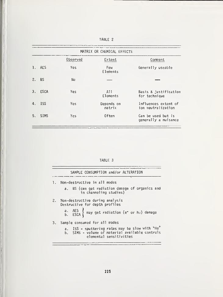
TABLE 2
MATRIX OR CHEMICAL EFFECTS
Observed Extent Comment
1. AES Yes FewEl ements
Generally useable
2. BS No
3. ESCA Yes All
ElementsBasis & justificationfor technique
4. ISS Yes Depends on
matrixInfluences extent of
ion neutralization
5. SIMS Yes Often Can be used but is
generally a nuisance
TABLE 3
SAMPLE CONSUMPTION and/or ALTERATION
1. Non-destructive in all modes
a. BS (can get radiation damage of organics and
in channeling studies)
2. Non-destructive during analysisDestructive for depth profiles
may get radiation (e~ or hv) damage
3. Sample consumed for all modes
a. ISS - sputtering rates may be slow with kHe+
b. SIMS - volume of material available controls
elemental sensitivities
225
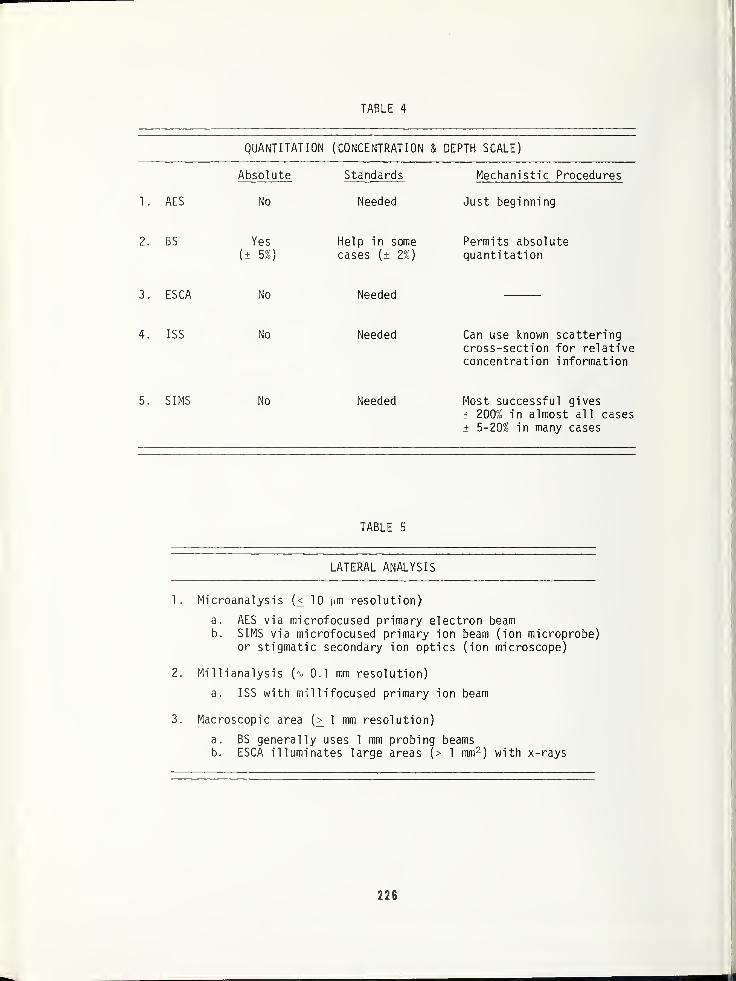
TABLE 4
QUANTITATION (CONCENTRATION J« DEPTH SCALE)
Absolute Standards Mechanistic Procedures
1
.
AES No Needed Just beginning
2. BS Yes
(± 5%)
Help in somecases (± 2%)
Permits absolutequantitation
3. ESCA No Needed
4. ISS No Needed Can use known scatteringcross-section for relativeconcentration information
5. SIMS No Needed Most successful gives± 200% in almost all cases± 5-20% in many cases
TABLE 5
LATERAL ANALYSIS
1. Microanalysis [<_ 10 pm resolution)
a. AES via microfocused primary electron beamb. SIMS via microfocused primary ion beam (ion microprobe)
or stigmatic secondary ion optics (ion microscope)
2. Millianalysis (^ 0.1 mm resolution)
a. ISS with millifocused primary ion beam
3. Macroscopic area (> 1 mm resolution)
a. BS generally uses 1 mm probing beamsb. ESCA illuminates large areas (> 1 mm 2
) with x-rays
226
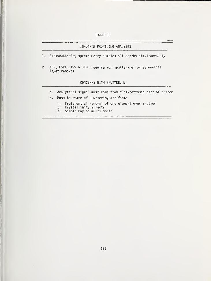
TABLE 6
IN-DEPTH PROFILING ANALYSES
1. Backscattering spectrometry samples all depths simultaneously
2. AES, ESCA, ISS & SIMS require ion sputtering for sequentiallayer removal
CONCERNS WITH SPUTTERING
a. Analytical signal must come from flat-bottomed part of crater
b. Must be aware of sputtering artifacts
1. Preferential removal of one element over another2. Crystal 1 inity effects3. Sample may be multi-phase
227
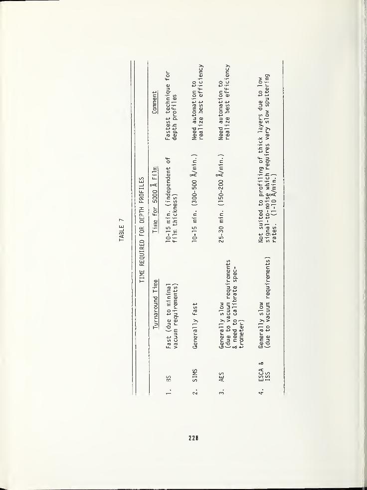
S- £=
o CL)
4-O O
cu •4->
3 4—<LT c 4-
c •i- oo o 0)CD C CU
E -C i— +-> +J£ O •!- ro i/i
o CU <+- E CDo l-> oS-
to-Q
+J CL 3 aiCO ro NCU -C+•> +-> o00 cx CU roro CU CU CDU- "0 s-
'
—
4-O C
r-E 4-> E
)
—
•i— aico U_LjJ c O
1 o< 0) oCL LO
U_ O cu 1O o o oo c to oQ_ LO to CO
a>rc s_r— oCL. 4- c o cUJQ QJ E E
E +->
CC lo LOo r— Eu_ o OQ 4-UJcc
ZDo-UJ
ME
i— CUE
ro 001— E +->
s=T3 c: ai
EE a) +->
o S- tos_ O <oro -t-> 3 4-C crS- cu (1) >>3 3 S-
I— aE ro3 S_
+-> 3 QJto o Cro ro CULl_ > CD
OOs:
00 i—
i
CO CO
C\J
228
cu C7>
3 Co o O *l"+-> •!—
i— S-4- cu
C 4— o +->
O CU +-> +->
3+J +-> CU Clro to 3 00
E CUO -Q+j oo O3 cu i_ i
—
ro N CU OO>,
"O i
—
ro >>CU ro i— S-
CU CU CUz: s_ -XZ >
•i— oo-c ai+-> S-
^4- 3O O"
CU
E cn s_
o<: •i- sz .—
-
1— <_> •o •r- -r- Co 4- -CCM O 5 E
1 S_ \o O. CUoeCLO co
O -i- o_ ^ +-> O i
—
C 1
"O 1 i
—
cu o-(-> +J
E 'r— 1
3 i— *
o to ro toro C CU
I +-> CD +->
LO O t- roCM Z 00 1.
_
—
00 on+-> +->
1 c:cu u CDE cu Ecu a. CUS- 00 t.
3 cu 3O"
cu (O cuS- S- s_
-Q3 EO =3 O 3
i— 3 ro i— 3to O O O0 CJ
ro ro
>> > o^ >> >+-> S-
r— O cu i— Oro +-> "O -!-> ro +->
t- CU CU S_
cu cu CU E CU cuC 3 c o C 3ai -o i- CU "OCJ3 oS +-> o '
oa
=too O COLU 00 oo<c UJ I—
I
oo
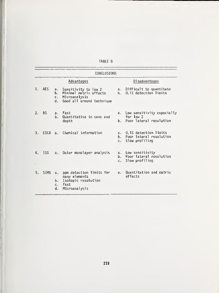
TABLE 8
CONCLUSIONS
Havaniages u\ saQVanuayes
1 AFS G > oensiLivity to low Laa . U 1 1 1 1 t_ U l L L.U l)Ua II C 1 La Lc
b. Minimal matrix effects b. 0.1% detection limitsr-C .
M "i c y*c\7\ nal wci cll l L i Ud j la l jo 1 o
u
.
(Zr\r\r\ oil av^nuhn torhni niifluUUU d 1 1 cuUUMU LcLiiniLjUc
2. BS a. Fast a. Low sensitivity especiallyb. Ouant i ta ti vp in cone and for low Z
depth b. Poor lateral resolution
3. ESCA a. Chemical information a
.
0.1% detection limitsb. Poor lateral resolutionc. Slow profiling
4. ISS a. Outer monolayer analysis a. Low sensitivityb. Poor lateral resolutionc. Slow profiling
5. SIMS a. ppm detection limits for a
.
Quantitation and matrix
many elements effects
b. Isotopic resolutionc. Fastd. Microanalysis
229
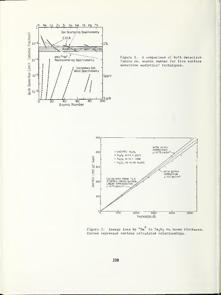
,H Ne Co Zn Zr Sn Nd Yb Hg Th1
11 1 1 1 1 1 1 1 r~
Ion Scattering Spectrometry
2 10-^-
10"
10"
3 io-
Auger*Bectron Spectroscopy;. -^s. - '
I
1
i
i
I
i
s
I
I
I
I
I
I
I
I
I
I
MeV 4 He+ / _Backscattering Spectrometry
/ / Secondary Ion
/ / Mass Spectrometry
/ i
20
1%
Figure 1. A comparison of bulk detectionlimits vs. atomic number for five surfacesensitive analytical techniques.
lppm
40 60Atomic Number
80 100lppb
THICKNESS (A)
Figure 2. Energy loss by 4He in Ta 20 5 vs. known thickness.Curves represent various calculated relationships.
230
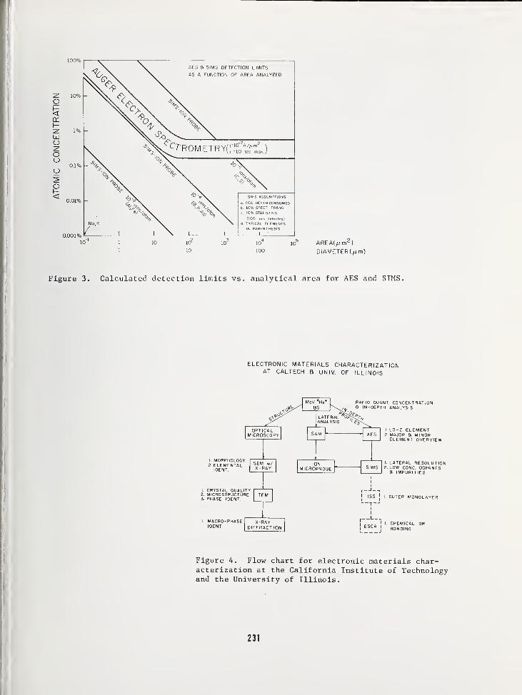
Figure 3. Calculated detection limits vs. analytical area for AES and SIMS.
ELECTRONIC MATERIALS CHARACTERIZATIONAT CALTECH a UNIV. OF ILLINOIS
Mev 4He
BS
OPTICALMICROSCOPY
1. MORPHOLOGY2. ELEMENTAL
I DE NT
SEM »/X-RAY
1. CRYSTAL QUALITY2. MICROSTRUCTURE3. PHASE I DENT
MACRO- PHASE X-RAY'DENT. DIFFRACTION
LATERALANALYSIS
RAPID QUANT CONCENTRATIONS IN-DEPTH ANALYSIS
IONMICROPROBE
I ISS
I.LO-Z ELEMENT2 MAJOR a MINORELEMENT OVERVIEW
I LATERAL RESOLUTION2. LOW CONC. DOPANTS
8 IMPURITIES
OUTER MONOLAYER
ESCAj
CHEMICAL ORBONDING
Figure 4. Flow chart for electronic materials char-acterization at the California Institute of Technologyand the University of Illinois.
231
DISCUSSION OF THE PAPER
Participant : In one of the slides youshow sensitivity vs beam diameter for Auger
and SIMS, where does the hydrogen sit on that
diagram?
Evans : If you remember in the beginning we
excluded hydrogen as being unobservable by
the Auger. As far as SIMS is concerned, we
are not really sure. I am only familiar with
the work in our own laboratory on hydrogenand we have not really been looking at low
levels. We have been looking at the forma-
tion of niobium hydride in hydrogen chargedniobium. I would guess the ionization yield
for H probably sits between 10"^ and 10~6
ions/atom and as such H appears in the middleof the diagram.
Newbury : Is it worth mentioning that with
the selection of the primary ion beam youmight, in fact, get enhanced sensitivity from
say, gold, carbon, or sulphur by possiblyusing a cesium beam? It is possible by
selection of your beam to improve the
situation
.
Evans : Hughes and other laboratories are
developing cesium ion sources for ion micro-probes. If you do use cesium ion bombardment
and negative ion spectroscopy instead of
oxygen ion bombardment and positive ion
spectroscopy, those elements such as gold,
carbon, etc., which used to be very insensi-tive are now very sensitive. In fact, in
positive ion spectroscopy sodium is the most
sensitive element, in negative ion spectros-
copy using cesium ion bombardment gold isprobably the most sensitive element. So as
instrument developments come along we mayfind improvements in the Auger curve butthere will definitely be a dramatic improve-ment in the SIMS curves as soon as a goodcesium ion source is developed.
Lucke : You mentioned one of the disadvantagesof SIMS was quantitation. I wonder what youcould say about the possibilities of eventu-ally obtaining absolute concentration numbers.
Evans : There are laboratories working on thefundamentals of the secondary ionizationprocess. The most successful of the resultanttechniques are those used by Anderson, andAnderson and Hinthorn. Basically, they tryto calculate what the conditions are in theionization region. They assume that it is a
plasma in local thermal equilibrium. Thenthe actual concentrations are calculated fromthe assumed ionization conditions and themeasured secondary ion intensities.
Lieberman : The alternative approach towardquantitation is to develop working curvesbased on measurements of reference materialshaving elemental concentrations similar to
those of the unknown sample. The ElectronicTechnology Division of NBS is endeavoring to
develop and document techniques for the ap-plication of SIMS to silicon material anddevice analysis. This work includes thedevelopment of methods of sample preparationand data analysis for reliable quantitativeSIMS analysis of impurities on silicon andsilicon dioxide surfaces.
232
WORKSHOP PARTICIPANTS
John AlbersNational Bureau of StandardsWashington, DC 20234
Gordon AndersonNaval Research LaboratoryWashington, DC 20375
James AnthonyNational Security AgencyFort Meade, MD 20755
Donna BakaleVarian VacuumSpringfield, NJ 07081
W. D. BakerNaval Research LaboratoryWashington, DC 20375
William R. BandyNational Security AgencyFort Meade, MD 20755
Robert BarrTechnics Inc.
Alexandria, VA 22310
Lt. Richard BernardRome Air Development CenterGriffiss Air Force BaseRome, NY 13440
J. B. BindellBell Telephone Laboratories, Inc.
Allentown, PA 18103
W. R. BottomsElectrical Engineering DepartmentPrinceton UniversityPrinceton, NJ 08540
M. G. Buehler
National Bureau of StandardsWashington, DC 20234
James W. ButlerNaval Research LaboratoryWashington, DC 20020
Sidney R. ButlerLehigh UniversityDepartment of Metallurgy and Materials
ScienceBethlehem, PA 18015
Robert C. CargillPhysical Electronics Industries, Inc.
Eden Prairie, MN 55343
Forrest L. CarterNaval Research LaboratoryWashington, DC 20034
Thomas R. CassHewlett-Packard LaboratoriesPalo Alto, CA 94304
Jar-Mo ChenMartin Marietta LaboratoryBaltimore, MD 21227
A. ChristouNaval Research LaboratoryWashington, DC 20375
Thomas E. CodyApplied Research LaboratoriesAllentown, PA 18101
Donald K. ConleyWestern Electric CompanyAllentown, PA 18103
Dwight CookBell Telephone LaboratoriesMurray Hill, NJ 07974
Lawrence P. CookNational Bureau of StandardsWashington, DC 20234
Becky P. CorbinCommonwealth Scientific CorporationAlexandria, VA 22314
Howard S . DanaceauThe Kearns GroupRockville, MD 20850
David DarboNASA Goddard Space Flight CenterGreenbelt, MD 20771
John E . DaveyNaval Research LaboratoryWashington, DC 20375
L. E. DavisPhysical Electronics Industries, Inc.
Eden Prairie, MN 55343
Howard M. DayNaval Research LaboratoryWashington, DC 20390
Bruce E. DealFairchild SemiconductorPalo Alto, CA 94304
233
T. H. DiStefanoIBM ResearchYorktown Heights , NY 10598
Robert D. DobrottTexas Instruments, Inc.
Dallas, TX 75222
L. G. DowellUnion Carbide CorporationTarrytown, NY 10591
Kenneth L. DunningNaval Research LaboratoryWashington, DC 20375
John W. DzimianskiWestinghouse Electric Corp., S.D.DBaltimore, MD 21203
James EhrsteinNational Bureau of StandardsWashington, DC 20234
Nils E. EricksonNational Bureau of StandardsWashington, DC 20234
Charles A. Evans, Jr.
Materials Research LaboratoryUrbana, IL 61801
R. J. FarrarHarry Diamond LaboratoriesWashington, DC 20438
Frank J. FeiglDepartment of PhysicsLehigh UniversityBethlehem, PA 18015
Charles FeldmanThe Johns Hopkins UniversitySilver Spring, MD 20910
David FileCameca, Inc.
Elmsford, NY 10523
Judson C. FrenchNational Bureau of StandardsWashington, DC 20234
Bill GadzukNational Bureau of StandardsWashington, DC 20234
Kenneth GallowayNational Bureau of StandardsWashington, DC 20234
Anthony J. Garratt-ReedMassachusetts Institute of TechnologyCambridge, MA 02139
Richard GerberAerospace CorporationLos Angeles, CA 90009
Louis F. Giles, III.
National Security AgencyFort Meade, MD 20755
Michael N. GiulianoWestinghouse/Advanced Technology LaboratoryBaltimore, MD 21203
Ralph Gorden , Jr.
National Bureau of StandardsWashington, DC 20234
Leonard P. GradyDeltaray CorporationBurlington, MA 01803
Edward T. GraneyPhysical Electronics Industries, Inc.
Springfield, NJ 07090
Henry F. GrayNaval Research LaboratoryWashington, DC 20375
Frank GrunthanerJet Propulsion LaboratoryPasadena, CA 91103
George A. HaarNaval Research LaboratoryWashington, DC 20375
Hiroshi HaradaUniversity of West LafayetteWest Lafayette, Indiana 47907
W. L. HarringtonRCA LaboratoriesDavid Sarnoff Research Center
Princeton, NJ 08540
James K. HirvonenNaval Research LaboratoryWashington, DC 2037 5
H. Ward HuangIBM CorporationEssex Junction, VT 05452
H. HughesNaval Research LaboratoryWashington, DC 20375
234
James M. HurdTektronix Inc.
Beaverton, Oregon 97077
Harry M. HymanRCA CorporationSomerville, NJ 08876
N. L. JarvisNaval Research LaboratoryWashington, DC 20375
Marilyn A. Jasper, FIRNight Vision LaboratoryFt. Belvoir, VA 22060
Murzban JhabvalaNASA Goddard Space Flight CenterGreenbelt, MD 20771
Francis KubWestinghouse ATLBaltimore, MD 21203
Chris KuyattNational Bureau of StandardsWashington, DC 20234
Alan J. KushnirSemi-FilmsWest Hurley, NY 12491
Max G. LagallyUniversity of WisconsinMadison, WI 53706
G. M. LambNASA Goddard Space Flight CenterGreenbelt, MD 20771
Jan S. JohannessenStanford Electronics LaboratoryStanford UniversityStanford, CA 94305
Phil F. KaneTexas Instruments Inc.
Dallas, TX 75222
W. J. KeeryNational Bureau of StandardsWashington, DC 20234
G. J. KingArmy Night Vision LaboratoryAlexandria, VA 22307
T. D. KirkendallComsat LaboratoriesClarksburg, MD 20734
W. J. Kitchen, Jr.
Department of DefenseFt. Meade, MD 20755
Bruce E. KnoxPenn State UniversityUniversity Park, PA 16802
Robert J. KoppFairchild Camera and Instrument CorporatiMountain View, CA 94040
Ram KossowskyWestinghouse ResearchPittsburgh, PA 15235
R. KoyamaNational Bureau of StandardsWashington, DC 20234
Donald E. LanderAEI Scientific Apparatus, Inc.
Falls Church, VA 22043
Graydon B. LarrabeeTexas Instruments Inc.
Dallas, TX 75222
K. 0. LeedyNational Bureau of StandardsWashington, DC 20234
T. F. LeedyNational Bureau of StandardsWashington, DC 20234
Douglas H. LeongHughes Aircraft CompanyNewport Beach, CA 92663
Leonard L. LevensonUniversity of Missouri-RollaRolla, MO 65401
Miguel E. LevyHughes Aircraft CompanyCulver City, CA 90230
Robert K. LewisCameca Instruments, Inc.
Elmsford, NY 10523
A. G. LiebermanNational Bureau of StandardsWashington, DC 20234
Wen N. LinRockwell International CorporationAnaheim, CA
235
Y. LiuNational Bureau of StandardsWashington, DC 20234
W. H. LuckeNaval Research LaboratoryWashington, DC 20735
Fred LuehrsTousimis Research CorporationRockville, MD 20852
Ingemar LundstromIBM CorporationYorktown Heights, NY 10589
Gary McGuireTexas Instruments, Inc.
Dallas, TX 75222
R. M. McLouskiWestinghouseBaltimore, MD 21203
Joseph F. MartinoNight Vision LaboratoryFt. Belvoir, VA 22060
Santos MayoNational Bureau of StandardsWashington, DC 20234
David M. MetzPenn State UniversityUniversity Park, PA 16802
Reid A. MickelsenBoeingBellevue, WA 98006
T. A. MidfordHughes Research CenterTorrance, CA 90509
Gaines W. MonkCommonwealth Scientific CorporationAlexandria, VA 22314
J. M. MorabitoBell Telephone LaboratoriesAllentown, PA 18103
Bernard MrstikNaval Research LaboratoryWashington, DC 20375
J. MunarinNaval Ammunition DepotCrane, IN 47522
J. S. MurdayNaval Research LaboratoryWashington, DC 20375
Brian A. MurphySemi-Films TechnologyWest Hurley, NY 12491
Madan NandaIBM/SDDManassas, VA 22110
Dale E. NewburyNational Bureau of StandardsWashington, DC 20234
Paul NortonBell Telephone Laboratories, Inc.Allentown, PA 18103
Mylous S. O'DellNight Vision LaboratoryFort Belvoir, VA 22060
F. F. OettingerNational Bureau of StandardsWashington, DC 20234
Victor J. OhmRome Air Development CenterGriffiss Air Force Base, NY 13441
Masatoshi OnoNational Bureau of StandardsWashington, DC 20234
Philip F. OrdungUniversity of CaliforniaSanta Barbara, CA 93106
J. OroshnikU. S. NavyRockville, MD 20853
John M. PankratzTexas Instruments, Inc.Dallas, TX 75222
Donald L. ParkerTexas A & M UniversityCollege Station, TX 77843
Martin C. PeckerarNaval Research LaboratoryWashington, DC 20375
Brad PhillipsNaval Ammunition DepotCrane, IN 47522
236
Howard PhillipsRockwell International CorporationAnaheim, CA 92806
Dan PierceNational Bureau of StandardsWashington, DC 20234
Larry E. PlewNaval Ammunition DepotCrane, IN 47522
Juergen L. W. PohlmannArmy Night Vision LaboratoryFort Belvoir, VA 22060
Cedric PowellNational Bureau of StandardsWashington, DC 20234
R. A. ReynoldsAdvanced Research Projects AgencyArlington, VA 22209
A. G. ReveszComsat LaboratoriesClarksburg, MD 20734
Giorgio RigaFairchild CameraMountain View, CA 94042
Frank G. SatkiewiczJohns Hopkins UniversityApplied Physics LaboratorySilver Spring, MD 20910
D. E. SawyerNational Bureau of StandardsWashington, DC 20234
Harry SchafftNational Bureau of StandardsWashington, DC 20234
George H. Sigel
Naval Research LaboratoryWashington, DC 20375
Ronald L. SmithNational Security AgencyFort Meade, MD 20755
Sherman D . SmithBurroughs CorporationDowningtown, PA 19335
Richard SteinNational Bureau of StandardsWashington, DC 20234
Yale StrausserVarian Vacuum DivisionPalo Alto, CA 94303
Barbara E. SumnerArmy Night Vision LaboratoryFort Belvoir, VA 22060
Yen T. TanKodak Research LaboratoriesRochester, NY 14650
Simon ThomasMotorola SPDPhoenix, AZ 85008
A. J. TousimisTousimis Research Corporation, Inc.
Rockville, MD 20852
0. D. TrappTechnology AssociatesPortola Valley, CA 94025
Richard E. TresslerPennsylvania State UniversityUniversity Park, PA 16802
J. C. C. TsaiBell Telephone Laboratories, Inc.
Reading, PA 19603
Charles VathIntel
Santa Clara, CA 95051
Theodore VorburgerNational Bureau of StandardsWashington, DC 20234
Bernie WaclawskiNational Bureau of StandardsWashington, DC 20234
M. S. WangMonsanto CompanySt. Louis, MO 63166
John C. WebberIBM CorporationHopewell Junction, NY 12533
Clark W. WhiteBell Telephone Laboratories, Inc.
Murray Hill, NJ 07974
W. R. WhitfordORTEC, Inc.
Pearl River, NY 10965
237
Robert G. WilsonHughes Research LaboratoriesMalibu, CA 90265
W. A. WolstenholmeAEI Scientific ApparatusElmsford, NY 10523
K. H. YangIBM CorporationHopewell Junction, NY 12590
Carl ZanoniZygo CorporationMiddlefield, CT 06455
238
AUTHOR INDEX
AUTHOR
Austin, A. E. . .
Bottoms, W. R.
Christou, A. . .
Davis, L. E. . .
Day, H. M. . . .
Deal, B. E. . . .
DiStefano, T. H.
Dobrott, R. D.
Dunning, K. L.
Evans , Jr . , C. A.
Franz, J. M. . .
French, J. C. . .
Grunthaner, F. J.
Harrington, W. L.
Hughes, H. L. . .
Johannessen, J. S
Lewis, R. K. . .
Lieberman, A. G.
McGuire, G. E.
Morabito, J. M. .
Phillips, B. F. .
Phillips, D. H. .
Riach, G. E.
Spicer, W. E. . .
Strausser, Y. E.
Thomas , S . ...
Weisenberger , W.
White, C. W.
PAGE
65
211
143
183
143
7
189, 197
31
95
219
189
1
151
21
65
119, 125
45
3
175
105
65
73
183
119
119, 125
139
143
181
239

NBS-1 14A (REV. 7-73)
U .S. DEPT. OF COMM.
. BIBLIOGRAPHIC DATASHEET
1. PUBLICATION OR REPORT NO.
NBS SP 400-2?
2. Gov't AccessionNo.
3. Recipient's Accession No.
4. TITLE AND SUBTITLE
Semiconductor Measurement Technology: ARPA/NBS Workshop IV,
Surface Analysis for Silicon Devices
5. Publication Date
March 1976
6. Performing Organization Code
7. AUTHOR(S)A. George Lieberman
8. Performing Organ. Report No.
9. PERFORMING ORGANIZATION NAME AND ADDRESS
NATIONAL BUREAU OF STANDARDSDEPARTMENT OF COMMERCEWASHINGTON, D.C. 20234
10. Project/Task/Work Unit No.
11. Con t rac c /(jr<in t No.
ARPA Order No. 2397Program Code 5D10
12. Sponsoring Organization Name and Complete Address (Street, City, State, ZIP)
Defense Advanced Research Projects Agency - 1400 Wilson Blvd.Arlington, Virginia 22209
National Bureau of Standards, Washington, D. C. 20234
13. Type of Report & PeriodCovered Final
April 23-24, 197514. Sponsoring Agency Code
15. SUPPLEMENTARY NOTES
Library of Congress Catalog Card Number: 76-608043
16. ABSTRACT (A 200-word or less factual summary of most significant information. If document includes a significant
bibliography or literature survey, mention it here.)
This report contains the proceedings of the ARPA/NBS Workshop IV, SurfaceAnalysis for Silicon Devices, held at the National Bureau of Standards onApril 23-24, 1975.
The Workshop, as part of an NBS program to develop measurement technology for
the field of semiconductor devices, was held to discuss the present capabilities andfuture prospects of modern analytical beam techniques as applied to silicon, and
associated insulator films and device structures. Of particular interest were the
determination of impurity profiles, surface contamination, and interface charac-teristics. Techniques utilizing impinging electron, ion, neutral or photon beamswere considered. The Workshop was directed at the analysts, the semiconductormanufacturers who use the analysts' results, and the instrument people who designand manufacture the analytical equipment. Transcripts of the discussions followingeach paper are also included within these proceedings.
17. KEY WORDS (six to twelve entries; alphabetical order; capitalize only the first letter of the first key word unless a proper
name; separated by semicolons) Auger spectroscopy; depth profiles; electron beam induced
imaging; ESCA; insulator films; interface characteristics; internal photoemission ; ion
scattering spectroscopy; nuclear resonance profiling; photodepopulation; photovoltaic
imaging: Rutherford backscattering : SCANIIR; secondary ion mass spectroscopy; semi-
conductor devices; silicon; surface analysis; X-ray photoelectron spectroscopy.
18. AVAILABILITY |~X] Unlimited 19. SECURITY CLASS(THIS REPORT)
21. NO. OF PAGES
1 For Official Distribution. Do Not Release to NTISUNCL ASSIFIED
238
~2 Order From Sup. of Doc, U.S. GovernmentWashington, D.C. 20-102,
PrintinE Office 20. SECURITY CLASS(THIS PAGE)
22. Price
~l Order From National Technical Information
Springfield, Virginia 22151
Service (NTIS)UNCLASSIFIED
<HJ.S. GOVERNMENT PRINTING OFFICE: 1976 210-801/190 1-3

Announcement of New Publications on
Semiconductor Measurement Technology
Superintendent of Documents,
Government Printing Office,
Washington, D.C. 20402
Dear Sir:
Please add my name to the announcement list of new publications to
be issued in the series: National Bureau of Standards Special Publi-
cation 400-.
Name
Company
Address
City State Zip Code
(Notification Key N-413)


NBS TECHNICAL PUBLICATIONS
PERIODICALS
JOURNAL OF RESEARCH reports National Bureauof Standards research and development in physics,
mathematics, and chemistry. It is published in two sec-
tions, available separately:
• Physics and Chemistry (Section A)
Papers of interest primarily to scientists working in
these fields. This section covers a broad range of physi-
cal and chemical research, with major emphasis onstandards of physical measurement, fundamental con-
stants, and properties of matter. Issued six times a
year. Annual subscription: Domestic, $17.00; Foreign,
$21.25.
• Mathematical Sciences (Section B)
Studies and compilations designed mainly for the math-ematician and theoretical physicist. Topics in mathe-matical statistics, theory of experiment design, numeri-
cal analysis, theoretical physics and chemistry, logical
design and programming of computers and computersystems. Short numerical tables. Issued quarterly. An-nual subscription: Domestic, $9.00; Foreign, $11.25.
DIMENSIONS/NBS (formerly Technical News Bul-
letin)—This monthly magazine is published to informscientists, engineers, businessmen, industry, teachers,
students, and consumers of the latest advances in
science and technology, with primary emphasis on the
work at NBS. The magazine highlights and reviews such
issues as energy research, fire protection, building tech-
nology, metric conversion, pollution abatement, health
and safety, and consumer product performance. In addi-
tion, it reports the results of Bureau programs in
measurement standards and techniques, properties of
matter and materials, engineering standards and serv-
ices, instrumentation, and automatic data processing.
Annual subscription: Domestic, $9.45; Foreign, $11.85.
NONPERIODICALS
Monographs—Major contributions to the technical liter-
ature on various subjects related to the Bureau's scien-
tific and technical activities.
Handbooks—Recommended codes of engineering and
industrial practice (including safety codes) developed
in cooperation with interested industries, professional
organizations, and regulatory bodies.
Special Publications—Include proceedings of confer-
ences sponsored by NBS, NBS annual reports, and other
special publications appropriate to this grouping such
as wall charts, pocket cards, and bibliographies.
Applied Mathematics Series—Mathematical tables,
manuals, and studies of special interest to physicists,
engineers, chemists, biologists, mathematicians, com-puter programmers, and others engaged in scientific
and technical work.
National Standard Reference Data Series—Provides
quantitative data on the physical and chemical proper-
ties of materials, compiled from the world's literature
and critically evaluated. Developed under a world-wide
program coordinated by NBS. Program under authorityof National Standard Data Act (Public Law 90-396).
NOTE: At present the principal publication outlet forthese data is the Journal of Physical and ChemicalReference Data (JPCRD) published quarterly for NBSby the American Chemical Society (ACS) and the Amer-ican Institute of Physics (AIP). Subscriptions, reprints,
and supplements available from ACS, 1155 SixteenthSt. N. W., Wash. D. C. 20056.
Building Science Series—Disseminates technical infor-
mation developed at the Bureau on building materials,components, systems, and whole structures. The seriespresents research results, test methods, and perform-ance criteria related to the structural and environmen-tal functions and the durability and safety character-istics of building elements and systems.
Technical Notes—Studies or reports which are completein themselves but restrictive in their treatment of asubject. Analogous to monographs but not so compre-hensive in scope or definitive in treatment of the sub-ject area. Often serve as a vehicle for final reports of
work performed at NBS under the sponsorship of othergovernment agencies.
Voluntary Product Standards—Developed under pro-cedures published by the Department of Commerce in
Part 10, Title 15, of the Code of Federal Regulations.The purpose of the standards is to establish nationallyrecognized requirements for products, and to provideall concerned interests with a basis for common under-standing of the characteristics of the products. NBSadministers this program as a supplement to the activi-
ties of the private sector standardizing organizations.
Federal Information Processing Standards Publications(FIPS PUBS)—Publications in this series collectively
constitute the Federal Information Processing Stand-ards Register. Register serves as the official source of
information in the Federal Government regarding stand-ards issued by NBS pursuant to the Federal Propertyand Administrative Services Act of 1949 as amended,Public Law 89-306 (79 Stat. 1127), and as implementedby Executive Order 11717 (38 FR 12315, dated May 11,
1973) and Part 6 of Title 15 CFR (Code of FederalRegulations)
.
Consumer Information Series—Practical information,based on NBS research and experience, covering areasof interest to the consumer. Easily understandablelanguage and illustrations provide useful backgroundknowledge for shopping in today's technological
marketplace.
NBS Interagency Reports (NBSIR)—A special series of
interim or final reports on work performed by NBS for
outside sponsors (both government and non-govern-ment). In general, initial distribution is handled by the
sponsor; public distribution is by the National Technical
Information Service (Springfield, Va. 22161) in papercopy or microfiche form.
Order NBS publications (except NBSIR's and Biblio-
graphic Subscription Services) from: Superintendent of
Documents, Government Printing Office, Washington,D.C. 20402.
BIBLIOGRAPHIC SUBSCRIPTION SERVICES
The following current-»wareness and liter»ture-survey
bibliographies are issued periodically by the Bureau:Cryogenic Data Center Current Awareness Service
A literature survey issued biweekly. Annual sub-
scription: Domestic, $20.00; foreign, $25.00.
Liquefied Natural Gas. A literature survey issued quar-
terly. Annual subscription: $20.00.
Superconducting Devices and Materials. A literature
survey issued quarterly. Annual subscription : $'20.00.
Send subscription orders and remittances for thepreceding bibliographic services to National Bu-reau of Standards, Cryogenic Data Center (275.02)Boulder, Colorado 80302.
Electromagnetic Metrology Current Awareness Service
Issued monthly. Annual subscription: $24.00. Sendsubscription order and remittance to Electromagnetics
Division, National Bureau of Standards, Boulder,
Colo. 80302.

U.S. DEPARTMENT OF COMMERCENational Bureau of StandardsWashington. D C 20234
OFFICIAL BUSINESS
Penalty for Private Use. $300
POSTAGE AND FEES PAIDU.S. DEPARTMENT OF COMMERCE
COM-21 5
SPECIAL FOURTH-CLASS RATEBOOK
TO YEARSNBS1901 - 1976