Archives Des Sciences
10
Archives Des Sciences Vol 65, No. 10;Oct 2012 124 ISSN 1661-464X Electrical and morphological study of screen printed silicon solar cells contacts Razika TALA-IGHIL (Corresponding author) Institute of Electronics & Electrical Engineering, University Boumerdes, 35000 Algeria LMMC, Laboratoire des minéraux et matériaux composites, Boumerdes University, 35000 Algeria E-mail : [email protected] Farid CHELLI LMMC, Laboratoire des minéraux et matériaux composites, Boumerdes University, 35000 Algeria Samira SALI Division des cellules et modules photovoltaïques, UDTS, Algiers 16200, Algeria Slimane OUSSALAH Division de Microélectronique et nanotechnologie, CDTA, Baba Hassen, Algiers, 16300 Algeria Messaoud BOUMAOUR, Faiza TAYOUR, Yasmine SI-AHMED Division des cellules et modules photovoltaïques, UDTS, Algiers 16200, Algeria Abstract The screen printed contact quality influences directly the mono-crystalline silicon solar cells efficiency. This is the aim of this study. A batch of mono-crystalline silicon wafers have undergone all the technological processes such as chemical cleaning, phosphorus diffusion and finally screen printing metallization. According to the used silver paste technical data, the firing temperature should not be greater than 750°C. This is why for this last step, a temperature swept from 650°C to 750°C has been carried out. The principal purpose of this work is to evaluate the Ag/N + front contact quality by identifying the specific contact resistance, the resistivity and the morphology of each temperature profile. Transmission line method (TLM) is used as the technique for photovoltaic electrical characterization. It has been found that the best annealing temperature profile is750°C which corresponds to the lowest specific contact resistivity value of 1.65 mcm 2 . Morphological study shows low contact porosity at 750°C which reflects its good quality. Keywords: solar cell, TLM resistance, mono-crystalline silicon, screen printing, metallization, FERRO 3349
Transcript of Archives Des Sciences
Archives Des Sciences Vol 65, No. 10;Oct 2012
124 ISSN 1661-464X
Electrical and morphological study of screen printed silicon solar cells contacts
Razika TALA-IGHIL (Corresponding author)
Institute of Electronics & Electrical Engineering, University Boumerdes, 35000 Algeria
LMMC, Laboratoire des minéraux et matériaux composites, Boumerdes University, 35000 Algeria
E-mail : [email protected]
Farid CHELLI
LMMC, Laboratoire des minéraux et matériaux composites, Boumerdes University, 35000 Algeria
Samira SALI
Division des cellules et modules photovoltaïques, UDTS, Algiers 16200, Algeria
Slimane OUSSALAH
Division de Microélectronique et nanotechnologie, CDTA, Baba Hassen, Algiers, 16300 Algeria
Messaoud BOUMAOUR, Faiza TAYOUR, Yasmine SI-AHMED Division des cellules et modules photovoltaïques, UDTS, Algiers 16200, Algeria
Abstract
The screen printed contact quality influences directly the mono-crystalline silicon solar cells efficiency.
This is the aim of this study. A batch of mono-crystalline silicon wafers have undergone all the
technological processes such as chemical cleaning, phosphorus diffusion and finally screen printing
metallization. According to the used silver paste technical data, the firing temperature should not be
greater than 750°C. This is why for this last step, a temperature swept from 650°C to 750°C has been
carried out. The principal purpose of this work is to evaluate the Ag/N+ front contact quality by identifying
the specific contact resistance, the resistivity and the morphology of each temperature profile.
Transmission line method (TLM) is used as the technique for photovoltaic electrical characterization. It
has been found that the best annealing temperature profile is750°C which corresponds to the lowest specific
contact resistivity value of 1.65 mcm2. Morphological study shows low contact porosity at 750°C which
reflects its good quality.
Keywords: solar cell, TLM resistance, mono-crystalline silicon, screen printing, metallization, FERRO 3349
Archives Des Sciences Vol 65, No. 10;Oct 2012
125 ISSN 1661-464X
1. Introduction
Photovoltaic energy gained great attention these last years due to its high potential to be an alternative source of energy [1-5, 6].
Screen printing metallization is the most important step in large area mono-crystalline silicon based solar cells [7-9]. The best parameter which can reflect the contact quality is the specific contact resistance which can be deduced from Transmission Line Method TLM [10]. Each improvement for one step or process in solar cells fabrication is welcomes to make the photovoltaic solar energy competitive comparing to the other types of renewable energies [11].
Electrical characterization [12], is an important side after photovoltaic solar cells realization. It is the way by what can be detected the solar cell quality.
In our present work, we focus on Transmission line Method. It is based on the determination of the total resistance between two ohmic contacts as function of the distance which separate them [13]. This total resistance depends on the semiconductor resistance and on the specific resistance of the screen printed contacts [14]. A correlation with the morphological study has been made.
2. Experimental Details
A batch of mono-crystalline p-type silicon wafers with a resistivity of 1 Ωcm undergoes chemical cleaning process (degreasing+ RCA decontamination).
After that, a phosphorus diffusion by using solid sources PH-950 have been performed in order to create a N+/P junction with 0.7 μm in depth.
Then, a silver paste (Ag) type Ferro 3349 is screen printed onto the N+ Silicon front side according to the TLM pattern.
Finally, the contacts are annealed at temperatures between 650°C and 750°C.
The paste composition influences directly the annealing temperature profile. For example, L.A. Dobrzański et al. [18] ,worked at temperature interval 860°C-945°C while in our case and following the technical data of FERRO 3349 silver paste [19], the annealing profile should be between 680°C and 750°C. TLM measurements have been carried out by using equipment comprising a prober type Karl Suss AP4 and an analyzer type Agilent 4156 C.
Before starting TLM measures, TLM pattern contacts are isolated electrically by a mesa [15] in order to avoid vertical current circulation flow and consequently current leakage. The mesa consists of 4 grooves which form a rectangle, realized by diamond scriber with a depth greater than silicon junction depth.
3. Results & Discussion:
TLM pattern have been realized by lithography to measure the specific contact resistance.
As shown in figure 1, the TLM pattern consists of rectangular contacts with variable dimensions screen printed onto mono-crystalline silicon solar cells.
It has the following characteristics:
The length L which equals the finger contact width L= 270µm with 10 µm thickness Ag silver paste. A conventional distance between two fingers s=3 mm. TLM distances between contacts ( i.e between TLM lines 1 to 5) are given by
D1= d12 =0.3s =0.9 mm D2=d23 =0.5s =1.5 mm
D3=d34 =0.9s =2.7 mm D4=d45 =1.3s =3.9 mm
Samples 1, 2, 3 and 4 were prepared by annealing the TLM grid at temperatures 650°C, 680°C, 700°C and 750°C respectively.
Archives Des Sciences Vol 65, No. 10;Oct 2012
126 ISSN 1661-464X
Current –Voltage characteristics I(V) for each TLM distance at annealing Temperatures varying from 650°C to 750°C are represented in Figure 2.
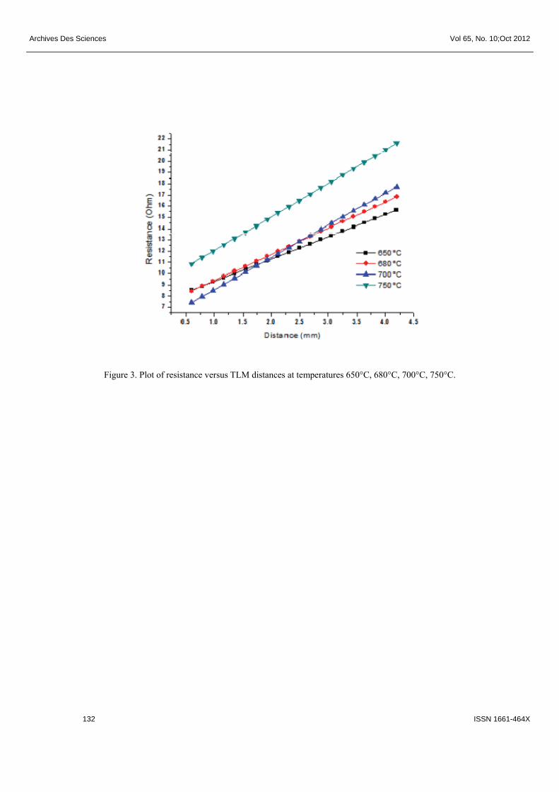
From these curves are deduced resistances which are the inverse of I(V) slope for each distance D.
And finally, from Figure 3 which shows resistance variation with TLM distance D, is deduced TLM resistance for each temperature profile.
Following reference [16], TLM resistance is half the intersection of the curve R(D) with y-axis (figure 3).
Total resistance (RT) between two neighbouring contacts is expressed by [20] :
V/I=RT=2Rc+R D/Z (1)
Where RT is the total resistance between two contacts, Rc is the contact resistance, R is the sheet resistance, D is the contact spacing.
The width of contacts ( Z=6mm ) is defined by the width of the mesa; their length ( W ) is equal to the width of the finger.
According to reference [20]:
If LT2L: c= Rc LT Z (cm2)
If LT2L: c= Rc L Z (cm2)
TLM Results are gathered and summarized in the table 1.
It represents TLM resistance with annealing profile. One can remark that contact resistivity starts with a value of 8.16 mcm2 at 650°C, reaches a maximum of 8.26 mcm2 at 680°C and then decreases to 3.34 mcm2 at 700°C and arrives to 1.65 mcm2 at 750°C.
So, the lowest contact resistance occurs at 750°C annealing profile. This means that a metallization at 750°C is required for mono-crystalline silicon solar cells in order to get higher conversion efficiency. This value is comforted by what is given in literature around 2 mcm2 [21-23].
Figure 4 illustrates SEM micrographs for the Ag/N+ contact at temperatures sweeping 650°C to 750°C.
One can observe the high porosity of the contact at 650°C, which increases at 680°C and start decreasing at 700°C until being compact at 750°C. This result is comforted by the previous contact resistance study and converges to the conclusion that the metallization annealing profile at 750°C is the best to obtain high conversion efficiency [17].
4. Conclusion
Screen printed contacts for photovoltaic silicon solar cells have been studied.
From I(V) measurements made on metallic contacts of Ag on the front Silicon junction N+/P with metallization temperature annealing varying from 650°C to 750°C.
The values for specific contact resistance were deduced by the transmission line method (TLM). The obtained results show that the Ag contact reaches its smallest value at 750°C.
The above results can be explained as due to the high contact quality at 750°C as illustrated in SEM figures.
The contact shows high compactness and consequently low porosity at this temperature profile. This means that the eutectic between the silver paste and silicon is well formed during metallization annealing at 750°C.
As a conclusion, screen printing metallization in silicon solar cells is in perpetual optimization. It depends essentially in the sheet resistance of the front junction, the annealing type: classical or RTP (rapid thermal annealing), the employed paste and the annealing profile.

Archives Des Sciences Vol 65, No. 10;Oct 2012
127 ISSN 1661-464X
References
[1] P M Anbarasan, P Senthil Kumar, K Vasudevan, R Govindan and V Aroulmoji Indian J. Phys.Vol. 85 1477 (2011)
[2] S Tekerek, A Kudret and Ü Alver Indian J. Phys.85 1469 ( 2011)
[3] S Siebentritt, T K ampschulte, A Bbauknecht, U Bliske, W Harmeit, U Fiedeler, M Lux-steiner, Solar Energy Materials & Solar cells 70 447 (2002)
[4] U Malm, J Malmström, C Platzer-Björrkman, L Stolt Thin solid films 480-481 208 (2005)
[5] G Mandal and T Ganguly Indian J. Phys. 85 1229 (2011)
[6] G Mandal and T Ganguly, Indian J. Phys. Vol. 85 1229 (2011)
[7] S B Rane, P K Khanna, T Seth, G J Phatak, D P Amalnerkar and B K Das Materials Chemistry and Physics 82 237 (2003)
[8] F Recart, I Freire, L Perez, R Lago-Aurrekoetxea, J C Jimeno, G Bueno; Solar Energy Materials & Solar Cells 91 897 (2007)
[9] K Firor And S Hogan Solar Cells 5 87 (1981 - 1982)
[10]S J Poctor, L W Linholm IEEE Electron Device letters 3 294 (1982)
[11] A Goetzberger, C hebling, H W Schock Materials Science & Engineering R 40 1 (2003)
[12] H Amrollahi Bioki and M Borhani zarandi, Indian J. Phys. Article in press
[13] A Sayah, G A Racine, Travaux pratiques en salle blanche, Ecole Polytechnique Fédérale de Lausanne (2002)
[14] H B Harrison, proc. IREE41, 95(1980) Australia
[16] G K Reeves, H B Harrisson, IEEE Electron Device letters 3 111 (1982)
[15]J H Zhao, K Tone, S R Weiner, M A Caleca, IEEE Electron Device Letters 18 375 (1997)
[17] S Saha and N B Manik, Indian J. Phys. Article in press
[18] L A Dobrzański, M Musztyfaga, A Drygała, W Kwaśny, P Panek Journal of Achievements in Materials and Manufacturing Engineering 45/2 141 (2011)
[19] www.ferro.com, Photovoltaic materials, Silver conductor 3349.
[20] L A Dobrzański, M Musztyfaga, A Drygała, W Kwaśny, P Panek Journal of Achievements in
Materials and Manufacturing Engineering 41/1-2 57 (2010)
[21] A Mette, G Emanuel, D Erath, R Preu, G Willeke 21st European Photovoltaic Solar Energy
Conference, September 4 – 8, 2006, Dresden,germany
[22] A Rohatgi, M Hillali, D L Meier, A Ebong, C Honsberg, A F Canol and P.Hacke 17th European
Photovoltaic Solar Energy Conference and Exhibition; Munich, Germany; October 22-26, 2001.
[23] Ansgar Mette, New concepts for front side metallization of industrial silicon solar cells, Verlag Dr. Hut,
2007, ISBN:9783899636505

Archives Des Sciences Vol 65, No. 10;Oct 2012
128 ISSN 1661-464X
Table 1. Specific contact resistance results deduced by TLM method
Annealing Temperature (°C) 650 680 700 750
Contact resistance (Ω) 3.67 4.53 2.83 1.79
Transfer Length LT (mm) 3.71 3.04 1.97 1.54
Specific contact resistance
If LT2L: c= Rc LT Z
If LT2L: c= Rc L Z
8.16
mcm2
8.26
mcm2
3.34
mcm2
1.65
mcm2

Archives Des Sciences Vol 65, No. 10;Oct 2012
129 ISSN 1661-464X
Figure 1: Metal grid for characterization TLM
TLM pattern

Archives Des Sciences Vol 65, No. 10;Oct 2012
130 ISSN 1661-464X
(a)
(b)

Archives Des Sciences Vol 65, No. 10;Oct 2012
131 ISSN 1661-464X
(c )
(d)
Figure 2. Current-voltage I (V) characteristics for each TLM distances for screen printed samples annealed
at : (a) 650°C, (b) 680°C, (c) 700°C and (d) 750°C.
Archives Des Sciences Vol 65, No. 10;Oct 2012
132 ISSN 1661-464X
Figure 3. Plot of resistance versus TLM distances at temperatures 650°C, 680°C, 700°C, 750°C.

Archives Des Sciences Vol 65, No. 10;Oct 2012
133 ISSN 1661-464X
(a) (b)
(b) (d)
Figure 4. SEM micrographs of Ag/Si(N+) contacts for different temperatures :
(a) 650°C, (b) 680°C, (c) 700°C and (d) 750°C