Application of Fuzzy PID Control Based on DSP in DC-DC ...
6
Application of Fuzzy PID Control Based on DSP in DC-DC Boost Circuit Henghui Zhou * and Bin Jiao School of Electrical Engineering, Shanghai Dianji University, Shanghai, China * Corresponding author Abstract—In order to improve the quality of power that the phase-shifted full-bridge DC/DC boost circuit supply to the microgrid and the safety and reliability of its operation, fuzzy PID control method is used to achieve phase-shift control of the main circuit in the paper. The output DC voltage is controlled by adjusting the phase-shifting angle between the leading-leg and the lagging-leg. According to the response of the system, fuzzy inference is used to change the PID parameters in real time so that the control effect of the system can be optimized. Firstly, the modeling and simulation are performed by MATLAB/Simulink to verify the superiority of fuzzy PID over traditional PID control methods. Then the TMS320F28335 DSP chip is used to program for the hardware implementation of the control strategy, and the feasibility of which is verified by the experimental waveform. Finally, the experiment shows that this control technology achieves the effective control of the DC/DC boost circuit, which has good dynamic and steady state performance and the operation quality of the equipment is improved greatly. It has a certain promotion value. Keywords—DC/DC boost; phase-shift control; fuzzy PID; TMS320F28335 I. INTRODUCTION Photovoltaic power generation systems include DC/DC booster link and DC/AC inverter link. Among both, the 48V DC generated by photovoltaic power generation is used as the input voltage of the DC/DC power converter and is inverted through the inverter (DC/AC) to a square wave. This process is the key to improving the stability and dynamic performance of the system. Then the high-frequency pulse transformer is used to carry out isolation and boosting of the AC square wave, and then which is rectified (AC/DC), but it will generate certain harmonics. Therefore, it is necessary to filter the harmonics with a filter and eventually 400V DC voltage is output. The quality of the output voltage will affect the operating efficiency of the post- stage DC/AC inverter or DC load operation to some extent. Therefore, the DC/DC boost circuit not only has the function of the distributed power supply and supplies power to the microgrid, but also manages and improves the power quality of the microgrid and improves the security and reliability of micro-grid operation. However, at present most of the products on the market only have the function of inverter power. In addition, because the system itself has a strong non-linear characteristic, it is difficult to establish an accurate mathematical model. Therefore, the traditional PID control accuracy of the system will be low and the desired control effect can’t be achieved. In view of the above problems, this paper proposes that the fuzzy PID parameter self-tuning optimization control strategy is applied to the phase-shifted control of the booster circuit, and MATLAB/Simulink modeling simulation of which is performed. The TMS320F28335 DSP chip is used for programming and the control strategy is verified on the hardware. And satisfactory experimental results are obtained. II. PHASE-SHIFT CONTROL STRATEGY BASED ON FUZZY PID ALGORITHM OPTIMIZATION In this paper, in order to make the DC/DC booster circuit output a stable DC bus voltage, the phase-shifted full-bridge control method is adopted by adjusting the phase difference of time when switching devices are turned on that means phase shift angle θ between the leading-leg Q1, Q3 and the lagging-leg Q2, Q4 in the main circuit to control the magnitude of the output voltage [1]-[2]. As shown in Figure I is the main circuit phase shift control block diagram. In this design, the main circuit adopts the ZVZCS PWM DC/DC converter. In terms of control, the DC output voltage on the load side is sampled and fed back and closed-loop control is implemented. DC Load Q1 Q3 Q4 Q2 VD1 VD2 VD3 VD4 A/D Driving waveform Q1 Q2 Q3 Q4 Voltage feedback Feedback control FIGURE I. THE MAIN CIRCUIT PHASE SHIFT CONTROL BLOCK DIAGRAM The closed-loop control method of this design is to detect the output DC voltage. If its value is greater than set value of the voltage, the phase shift angle θ will be increased to reduce the time for turning on diagonal switch devices at the same time, then the load voltage will be decreased accordingly. On the contrary, when its value is smaller than the given value, the phase shift angle θ will be decreased to increase the time that the 3rd International Conference on Electrical, Automation and Mechanical Engineering (EAME 2018) Copyright © 2018, the Authors. Published by Atlantis Press. This is an open access article under the CC BY-NC license (http://creativecommons.org/licenses/by-nc/4.0/). Advances in Engineering Research, volume 127 21
-
Upload
khangminh22 -
Category
Documents
-
view
3 -
download
0
Transcript of Application of Fuzzy PID Control Based on DSP in DC-DC ...
Application of Fuzzy PID Control Based on DSP in DC-DC Boost Circuit
Henghui Zhou* and Bin Jiao School of Electrical Engineering, Shanghai Dianji University, Shanghai, China
*Corresponding author
Abstract—In order to improve the quality of power that the phase-shifted full-bridge DC/DC boost circuit supply to the microgrid and the safety and reliability of its operation, fuzzy PID control method is used to achieve phase-shift control of the main circuit in the paper. The output DC voltage is controlled by adjusting the phase-shifting angle between the leading-leg and the lagging-leg. According to the response of the system, fuzzy inference is used to change the PID parameters in real time so that the control effect of the system can be optimized. Firstly, the modeling and simulation are performed by MATLAB/Simulink to verify the superiority of fuzzy PID over traditional PID control methods. Then the TMS320F28335 DSP chip is used to program for the hardware implementation of the control strategy, and the feasibility of which is verified by the experimental waveform. Finally, the experiment shows that this control technology achieves the effective control of the DC/DC boost circuit, which has good dynamic and steady state performance and the operation quality of the equipment is improved greatly. It has a certain promotion value.
Keywords—DC/DC boost; phase-shift control; fuzzy PID; TMS320F28335
I. INTRODUCTION
Photovoltaic power generation systems include DC/DC booster link and DC/AC inverter link. Among both, the 48V DC generated by photovoltaic power generation is used as the input voltage of the DC/DC power converter and is inverted through the inverter (DC/AC) to a square wave. This process is the key to improving the stability and dynamic performance of the system. Then the high-frequency pulse transformer is used to carry out isolation and boosting of the AC square wave, and then which is rectified (AC/DC), but it will generate certain harmonics. Therefore, it is necessary to filter the harmonics with a filter and eventually 400V DC voltage is output. The quality of the output voltage will affect the operating efficiency of the post-stage DC/AC inverter or DC load operation to some extent. Therefore, the DC/DC boost circuit not only has the function of the distributed power supply and supplies power to the microgrid, but also manages and improves the power quality of the microgrid and improves the security and reliability of micro-grid operation. However, at present most of the products on the market only have the function of inverter power. In addition, because the system itself has a strong non-linear characteristic, it is difficult to establish an accurate mathematical model. Therefore, the traditional PID control accuracy of the system will be low and the desired control effect can’t be achieved.
In view of the above problems, this paper proposes that the
fuzzy PID parameter self-tuning optimization control strategy is applied to the phase-shifted control of the booster circuit, and MATLAB/Simulink modeling simulation of which is performed. The TMS320F28335 DSP chip is used for programming and the control strategy is verified on the hardware. And satisfactory experimental results are obtained.
II. PHASE-SHIFT CONTROL STRATEGY BASED ON FUZZY
PID ALGORITHM OPTIMIZATION
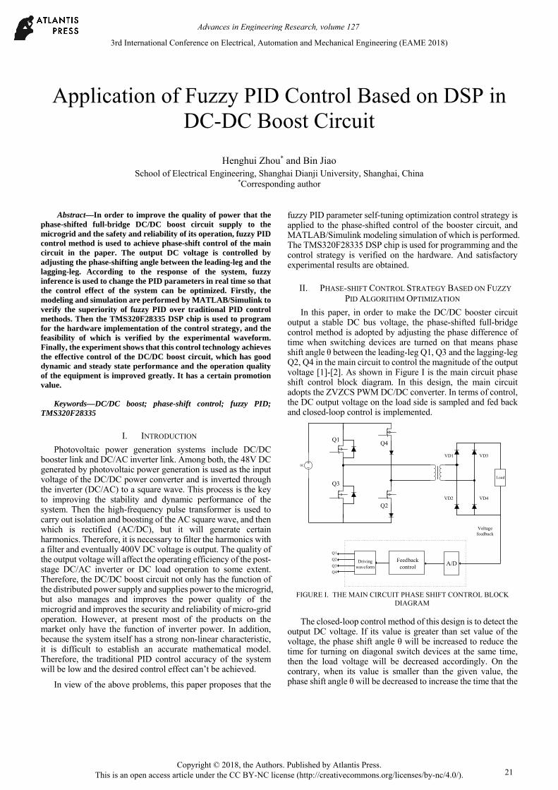
In this paper, in order to make the DC/DC booster circuit output a stable DC bus voltage, the phase-shifted full-bridge control method is adopted by adjusting the phase difference of time when switching devices are turned on that means phase shift angle θ between the leading-leg Q1, Q3 and the lagging-leg Q2, Q4 in the main circuit to control the magnitude of the output voltage [1]-[2]. As shown in Figure I is the main circuit phase shift control block diagram. In this design, the main circuit adopts the ZVZCS PWM DC/DC converter. In terms of control, the DC output voltage on the load side is sampled and fed back and closed-loop control is implemented.
DC
Load
Q1
Q3
Q4
Q2
VD1
VD2
VD3
VD4
A/DDriving waveform
Q1
Q2
Q3
Q4
Voltage feedback
Feedback control
FIGURE I. THE MAIN CIRCUIT PHASE SHIFT CONTROL BLOCK
DIAGRAM
The closed-loop control method of this design is to detect the output DC voltage. If its value is greater than set value of the voltage, the phase shift angle θ will be increased to reduce the time for turning on diagonal switch devices at the same time, then the load voltage will be decreased accordingly. On the contrary, when its value is smaller than the given value, the phase shift angle θ will be decreased to increase the time that the
3rd International Conference on Electrical, Automation and Mechanical Engineering (EAME 2018)
Copyright © 2018, the Authors. Published by Atlantis Press. This is an open access article under the CC BY-NC license (http://creativecommons.org/licenses/by-nc/4.0/).
Advances in Engineering Research, volume 127
21
diagonal switches are turned on at the same time, so that the load voltage increases accordingly. Because of the complementary formation between the upper and lower arms, it is necessary to set the dead time Td in order to prevent the occurrence of the shoot-through problem. So strictly speaking, the phase shift angle θ varies [0, π-Td/2].
A. Traditional PID Control Principle
As shown in Figure II, the traditional PID is a linear control method. In the above process, the actual output DC voltage can be defined as Ud and set value of the voltage is defined as Vref, so that the control error can be obtained as e=Vref-Ud. Then the control error e is proportionally, integrally, and differentially calculated and the results of the above three operations are added to obtain the output u of the PID controller. The transfer function between the phase shift angle θ (the controlled variable) and it is:
* / arccosp i du k e k edt k de dt L (1)
Differential action
Proportional action
Integral action
Controlled object
Vref Ude u
+ -
++
+
FIGURE II. TRADITIONAL PID CONTROL BLOCK DIAGRAM
In the formula: kp, ki, kd, L—proportional coefficient, integral coefficient, differential coefficient and linear adjustment coefficient.
The relationship between the phase shift angle θ and the phase shift time t is:
t = θ*T / 2π (2)
In the formula: T—switching cycle.
When the traditional PID is used for phase-shifted closed-loop control, the actual voltage is continuously approached to the given value by adjusting the phase-shifting time between the leading-leg and lagging-leg.
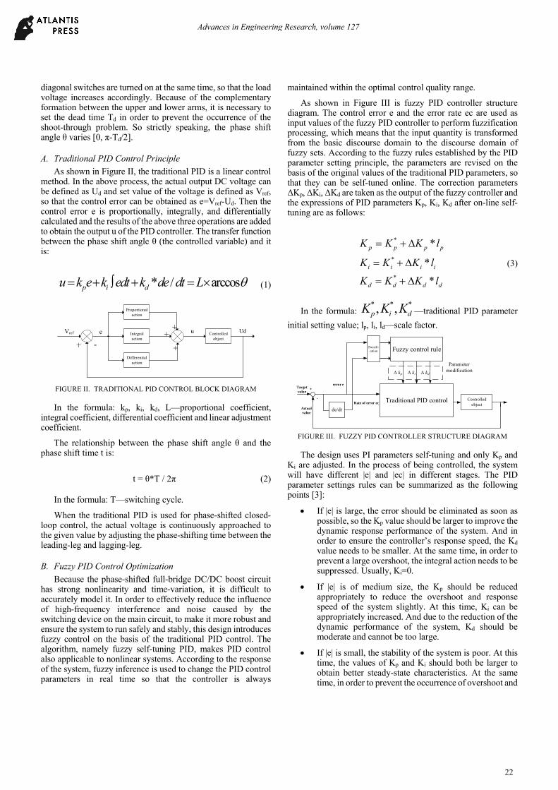
B. Fuzzy PID Control Optimization
Because the phase-shifted full-bridge DC/DC boost circuit has strong nonlinearity and time-variation, it is difficult to accurately model it. In order to effectively reduce the influence of high-frequency interference and noise caused by the switching device on the main circuit, to make it more robust and ensure the system to run safely and stably, this design introduces fuzzy control on the basis of the traditional PID control. The algorithm, namely fuzzy self-tuning PID, makes PID control also applicable to nonlinear systems. According to the response of the system, fuzzy inference is used to change the PID control parameters in real time so that the controller is always
maintained within the optimal control quality range.
As shown in Figure III is fuzzy PID controller structure diagram. The control error e and the error rate ec are used as input values of the fuzzy PID controller to perform fuzzification processing, which means that the input quantity is transformed from the basic discourse domain to the discourse domain of fuzzy sets. According to the fuzzy rules established by the PID parameter setting principle, the parameters are revised on the basis of the original values of the traditional PID parameters, so that they can be self-tuned online. The correction parameters ΔKp, ΔKi, ΔKd are taken as the output of the fuzzy controller and the expressions of PID parameters Kp, Ki, Kd after on-line self-tuning are as follows:
*
*
*
*
*
*
p p p p
i i i i
d d d d
K K K l
K K K l
K K K l
(3)
In the formula: * * *, ,p i dK K K —traditional PID parameter
initial setting value; lp, li, ld—scale factor.
Traditional PID control
Fuzzy control rule
Controlled object
de/dt
Target value
Actual value
‐
+error e
Rate of error ec
∆ kp ∆ ki ∆ kd
Parameter modification
Fuzzifi-cation
FIGURE III. FUZZY PID CONTROLLER STRUCTURE DIAGRAM
The design uses PI parameters self-tuning and only Kp and Ki are adjusted. In the process of being controlled, the system will have different |e| and |ec| in different stages. The PID parameter settings rules can be summarized as the following points [3]:
If |e| is large, the error should be eliminated as soon as possible, so the Kp value should be larger to improve the dynamic response performance of the system. And in order to ensure the controller’s response speed, the Kd value needs to be smaller. At the same time, in order to prevent a large overshoot, the integral action needs to be suppressed. Usually, Ki=0.
If |e| is of medium size, the Kp should be reduced appropriately to reduce the overshoot and response speed of the system slightly. At this time, Ki can be appropriately increased. And due to the reduction of the dynamic performance of the system, Kd should be moderate and cannot be too large.
If |e| is small, the stability of the system is poor. At this time, the values of Kp and Ki should both be larger to obtain better steady-state characteristics. At the same time, in order to prevent the occurrence of overshoot and
Advances in Engineering Research, volume 127
22

oscillation, the Kd value can be determined based on |ec|. If |ec| is larger, then Kd should be smaller and be appropriately valued.
It is defined that the fuzzy set of the error e, the error rate ec and the correction parameters ΔKp, ΔKi are all NB, NM, NS, ZE, PS, PM, PB representing negative big, negative middle, negative small, zero, positive small, positive middle, positive big. In order to facilitate the implementation on the DSP, the membership functions chosen here are trigonometric functions with strong sensitivity, as shown in Figure IV. The domain of all variables defined is [-3,3], the basic domain of e is [-3,3], the basic domain of ec is [-6,6], the basic domain of ΔKp is [-0.6,0.6], the basic domain of ΔKi is [-0.06,0.06].
FIGURE IV. MEMBERSHIP FUNCTION DIAGRAM
According to the above parameter setting principle and the experience of manually adjusting, the fuzzy rule tables of ΔKp and ΔKi can be obtained, as shown in Table I and Table II.
TABLE I. FUZZY RULE TABLE OF ΔKP
e ec
NB NM NS ZE PS PM PB
NB PB PB PM PM PS ZE ZE
NM PB PB PM PS PS ZE NS
NS PM PM PM PS ZE NS NS
ZE PM PM PS ZE NS NM NM
PS PS PS ZE NS NS NM NM
PM ZE ZE NS NM NM NM NB
PB ZE ZE NM NM NM NB NB
TABLE II. FUZZY RULE TABLE OF ΔKI
e ec
NB NM NS ZE PS PM PB
NB NB NB NM NM NS ZE ZE
NM NB NB NM NS NS ZE ZE
NS NM NM NS NS ZE PS PS
ZE NM NM NS ZE PS PM PM
PS NS NS ZE PS PS PM PB
PM ZE ZE PS PS PM PB PB
PB ZE ZE PS PM PM PB PB
III. HARDWARE COMPOSING OF DC/DC BOOST CIRCUIT
The basic composition diagram of the DC/DC boost circuit designed in this paper is shown in Figure V. It is mainly composed with the power main circuit and the DSP control loop.
The input filter
Full bridge
inverter
High frequency
booster
Output rectification filter circuit
48V(DC) 400V(DC)
DSP controller
Drive circuit
Sampling circuit
Protective circuit
DSP control loop
FIGURE V. THE BASIC COMPOSITION DIAGRAM OF THE DC/DC
BOOST CIRCUIT
A. Main Circuit Topology
At present, the soft-switching mode of the phase-shifted full-bridge soft-switching circuit can be divided into two categories: ZVS and ZVZCS [4]-[5]. Generally, for the typical phase-shifted ZVS full-bridge converter, the switches on its lagging-leg are not easy to implement ZVS and it is difficult to implement soft switching especially at light loads. The ZVZCS PWM converter has the same operation principle as the phase-shifted ZVS full-bridge converter on the leading-leg and can realize zero voltage switching. And its lagging-leg realizes zero current switching, so that the above defect of the phase-shifted full-bridge ZVS can be solved. The loss of the circulating energy inside the circuit is greatly reduced, thereby which effectively improves the efficiency of the converter and significantly reduces the loss of duty ratio on the secondary side. At this point, the range of soft switching will not be affected by the input voltage and load. Therefore, this design uses this topology as the main power circuit, as shown in Figure VI.
DC
Q1
Q3
Q4
Q2
VD1
VD2
VD3
VD4
The input filter
Full bridge inverterHigh
frequency booster
rectifier The output filter
FIGURE VI. THE BLOCK DIAGRAM OF THE MAIN POWER CIRCUIT
The main power circuit of this DC/DC boost circuit adopts the topology structure of DC-AC-DC conversion and is mainly composed of inputting filter, full-bridge inverter, high-frequency booster, rectifier and outputting filter. Among them, the rectifying part adopts the bridge rectifier topology with uncontrollable diode, which contributes to achieving the booster function of the DC/DC circuit.
Advances in Engineering Research, volume 127
23
B. Control Circuit
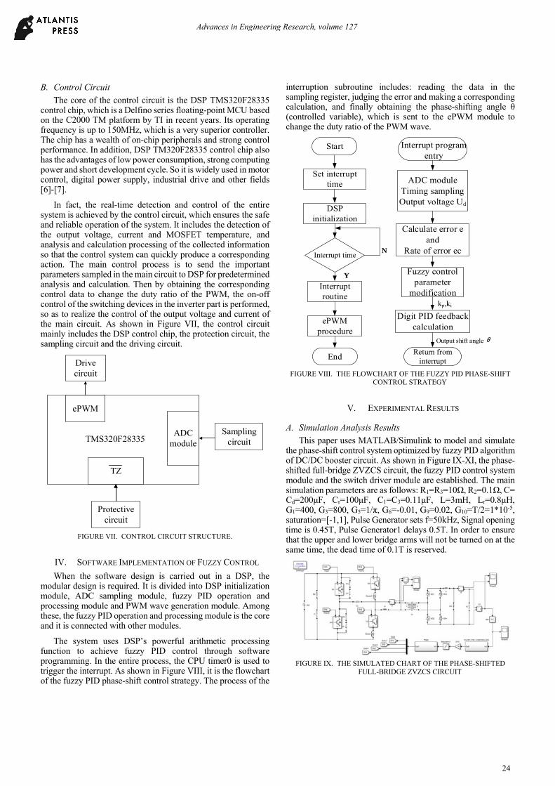
The core of the control circuit is the DSP TMS320F28335 control chip, which is a Delfino series floating-point MCU based on the C2000 TM platform by TI in recent years. Its operating frequency is up to 150MHz, which is a very superior controller. The chip has a wealth of on-chip peripherals and strong control performance. In addition, DSP TM320F28335 control chip also has the advantages of low power consumption, strong computing power and short development cycle. So it is widely used in motor control, digital power supply, industrial drive and other fields [6]-[7].
In fact, the real-time detection and control of the entire system is achieved by the control circuit, which ensures the safe and reliable operation of the system. It includes the detection of the output voltage, current and MOSFET temperature, and analysis and calculation processing of the collected information so that the control system can quickly produce a corresponding action. The main control process is to send the important parameters sampled in the main circuit to DSP for predetermined analysis and calculation. Then by obtaining the corresponding control data to change the duty ratio of the PWM, the on-off control of the switching devices in the inverter part is performed, so as to realize the control of the output voltage and current of the main circuit. As shown in Figure VII, the control circuit mainly includes the DSP control chip, the protection circuit, the sampling circuit and the driving circuit.
ADC module
TZ
ePWM
TMS320F28335Sampling
circuit
Protective circuit
Drive circuit
FIGURE VII. CONTROL CIRCUIT STRUCTURE.
IV. SOFTWARE IMPLEMENTATION OF FUZZY CONTROL
When the software design is carried out in a DSP, the modular design is required. It is divided into DSP initialization module, ADC sampling module, fuzzy PID operation and processing module and PWM wave generation module. Among these, the fuzzy PID operation and processing module is the core and it is connected with other modules.
The system uses DSP’s powerful arithmetic processing function to achieve fuzzy PID control through software programming. In the entire process, the CPU timer0 is used to trigger the interrupt. As shown in Figure VIII, it is the flowchart of the fuzzy PID phase-shift control strategy. The process of the
interruption subroutine includes: reading the data in the sampling register, judging the error and making a corresponding calculation, and finally obtaining the phase-shifting angle θ (controlled variable), which is sent to the ePWM module to change the duty ratio of the PWM wave.
Start
Set interrupt time
DSP initialization
Interrupt time
Interrupt routine
ePWM procedure
End
Y
N
ADC moduleTiming samplingOutput voltage Ud
Calculate error e and
Rate of error ec
Fuzzy control parameter
modification
Digit PID feedback calculation
Return from interrupt
kp,ki
Output shift angleθ
Interrupt program entry
FIGURE VIII. THE FLOWCHART OF THE FUZZY PID PHASE-SHIFT
CONTROL STRATEGY
V. EXPERIMENTAL RESULTS
A. Simulation Analysis Results
This paper uses MATLAB/Simulink to model and simulate the phase-shift control system optimized by fuzzy PID algorithm of DC/DC booster circuit. As shown in Figure IX-XI, the phase-shifted full-bridge ZVZCS circuit, the fuzzy PID control system module and the switch driver module are established. The main simulation parameters are as follows: R1=R3=10Ω, R2=0.1Ω, C= Cd=200μF, Cr=100μF, C1=C3=0.11μF, L=3mH, Lr=0.8μH, G1=400, G3=800, G5=1/π, G6=-0.01, G9=0.02, G10=T/2=1*10-5, saturation=[-1,1], Pulse Generator sets f=50kHz, Signal opening time is 0.45T, Pulse Generator1 delays 0.5T. In order to ensure that the upper and lower bridge arms will not be turned on at the same time, the dead time of 0.1T is reserved.
FIGURE IX. THE SIMULATED CHART OF THE PHASE-SHIFTED
FULL-BRIDGE ZVZCS CIRCUIT
Advances in Engineering Research, volume 127
24
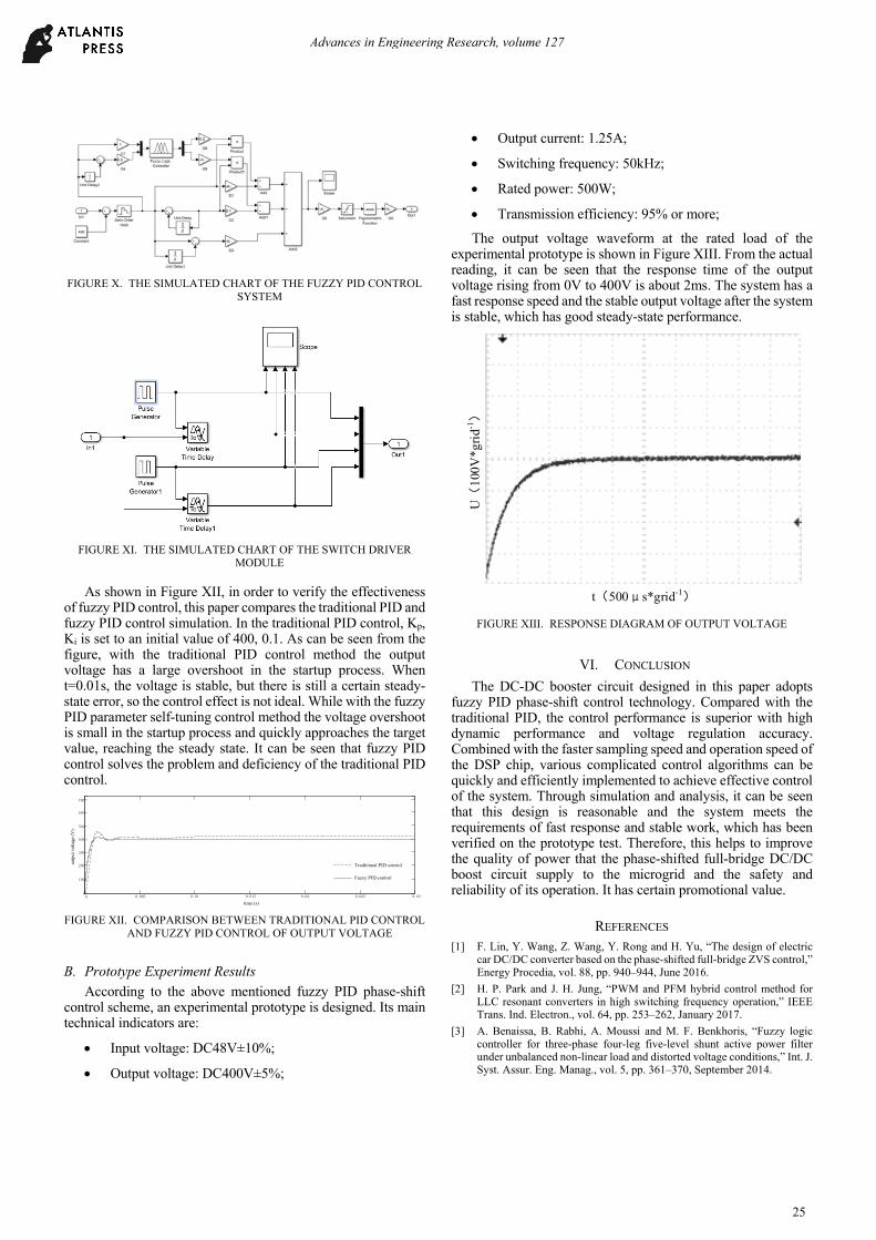
FIGURE X. THE SIMULATED CHART OF THE FUZZY PID CONTROL SYSTEM
FIGURE XI. THE SIMULATED CHART OF THE SWITCH DRIVER MODULE
As shown in Figure XII, in order to verify the effectiveness of fuzzy PID control, this paper compares the traditional PID and fuzzy PID control simulation. In the traditional PID control, Kp, Ki is set to an initial value of 400, 0.1. As can be seen from the figure, with the traditional PID control method the output voltage has a large overshoot in the startup process. When t=0.01s, the voltage is stable, but there is still a certain steady-state error, so the control effect is not ideal. While with the fuzzy PID parameter self-tuning control method the voltage overshoot is small in the startup process and quickly approaches the target value, reaching the steady state. It can be seen that fuzzy PID control solves the problem and deficiency of the traditional PID control.
0 0.005 0.01 0.015 0.02 0.025 0.030
100
200
300
400
500
600
700
time (s)
outp
ut v
olta
ge (
V)
Traditional PID control
Fuzzy PID control
FIGURE XII. COMPARISON BETWEEN TRADITIONAL PID CONTROL
AND FUZZY PID CONTROL OF OUTPUT VOLTAGE
B. Prototype Experiment Results
According to the above mentioned fuzzy PID phase-shift control scheme, an experimental prototype is designed. Its main technical indicators are:
Input voltage: DC48V±10%;
Output voltage: DC400V±5%;
Output current: 1.25A;
Switching frequency: 50kHz;
Rated power: 500W;
Transmission efficiency: 95% or more;
The output voltage waveform at the rated load of the experimental prototype is shown in Figure XIII. From the actual reading, it can be seen that the response time of the output voltage rising from 0V to 400V is about 2ms. The system has a fast response speed and the stable output voltage after the system is stable, which has good steady-state performance.
t(500μs*grid-1)
U(
100V
*gri
d-1)
FIGURE XIII. RESPONSE DIAGRAM OF OUTPUT VOLTAGE
VI. CONCLUSION
The DC-DC booster circuit designed in this paper adopts fuzzy PID phase-shift control technology. Compared with the traditional PID, the control performance is superior with high dynamic performance and voltage regulation accuracy. Combined with the faster sampling speed and operation speed of the DSP chip, various complicated control algorithms can be quickly and efficiently implemented to achieve effective control of the system. Through simulation and analysis, it can be seen that this design is reasonable and the system meets the requirements of fast response and stable work, which has been verified on the prototype test. Therefore, this helps to improve the quality of power that the phase-shifted full-bridge DC/DC boost circuit supply to the microgrid and the safety and reliability of its operation. It has certain promotional value.
REFERENCES [1] F. Lin, Y. Wang, Z. Wang, Y. Rong and H. Yu, “The design of electric
car DC/DC converter based on the phase-shifted full-bridge ZVS control,” Energy Procedia, vol. 88, pp. 940–944, June 2016.
[2] H. P. Park and J. H. Jung, “PWM and PFM hybrid control method for LLC resonant converters in high switching frequency operation,” IEEE Trans. Ind. Electron., vol. 64, pp. 253–262, January 2017.
[3] A. Benaissa, B. Rabhi, A. Moussi and M. F. Benkhoris, “Fuzzy logic controller for three-phase four-leg five-level shunt active power filter under unbalanced non-linear load and distorted voltage conditions,” Int. J. Syst. Assur. Eng. Manag., vol. 5, pp. 361–370, September 2014.
Advances in Engineering Research, volume 127
25

[4] H. S. Choi, J. W. Kim and B. H. Cho, “Novel zero-voltage and zero-current-switching (ZVZCS) full-bridge PWM converter using coupled output inductor,” IEEE Trans. Power Electron., vol. 17, pp. 641–648, September 2002.
[5] S. Hamada and M. Nakaoka, “A novel zero-voltage and zero-current switching PWM DC-DC converter with reduced conduction losses,” IEEE Trans. Power Electron., vol. 17, pp. 413–419, May 2002.
[6] M. Caruso, A. O. D. Tommaso, F. Genduso, R. Miceli and G. R. Galluzzo, “A DSP-based resolver-to-digital converter for high-performance electrical drive applications,” IEEE Trans. Ind. Electron., vol. 63, pp. 4042–4051, July 2016.
[7] H. Hu, W. Shi, Y. Lu and Y. Xing, “Design considerations for DSP-controlled 400Hz shunt active power filter in an aircraft power system,” IEEE Trans. Ind. Electron., vol. 59, pp. 3624–3634, September 2012.
Advances in Engineering Research, volume 127
26