application-note-studying-solar-cells-with-the-modulab-xm ...
17
D APPLICATION NOTE Studying Solar Cells with the ModuLab XM PhotoEchem Optical and Electrical Measurment System Application Note SA 105 Laurie Peter Department of Chemistry University of Bath Bath BA2 7AY United Kingdom 1 st June 2016 www.solartronanalytical.com
-
Upload
khangminh22 -
Category
Documents
-
view
1 -
download
0
Transcript of application-note-studying-solar-cells-with-the-modulab-xm ...

D APPLICATION NOTE
Studying Solar Cells with the ModuLab XM PhotoEchem
Optical and Electrical Measurment System Application Note SA 105
Laurie Peter
Department of Chemistry
University of Bath
Bath BA2 7AY
United Kingdom
1st June 2016
www.solartronanalytical.com

Application Note SA 105
2
Princeton Applied Research | Solartron Analytical | Signal Recovery
1.Overview
The ModuLab XM PhotoEchem System was developed originally for the study of dye-
sensitized solar cells, but because the system is so versatile it can be applied to other
types of solar cells, notably to the new generation of hybrid organic-inorganic lead halide-
based perovskite photovoltaics, which have achieved remarkable solar power conversion
efficiencies of around 20%. The highly flexible Modulab system allows experimenters to
perform a range of different measurements on solar cells or photoelectrochemical cells.
This technical note looks at the following methods:
Impedance spectroscopy (in the dark and under illumination) (IS)
Intensity-modulated photocurrent/photovoltage spectroscopy (IMPS/IMVS)
Open circuit voltage decay measurements (OCVD)
Charge extraction measurements (CE)
The objective of the note is to explain briefly the background to these techniques and to
illustrate them with experimental results obtained with dye-sensitized solar cells and, more
recently, with hybrid perovskite solar cells. The author is very grateful to Henry Snaith
and Giles Eperon (Clarendon laboratory, Oxford), Petra Cameron (University of Bath) and
Adam Pockett (Swansea University) for permission to use the perovskite results, which
were obtained in a joint study that is being prepared for publication.
2. Impedance Spectroscopy of Solar Cells
2.1 Introduction
Impedance spectroscopy is a small amplitude measurement technique that involves
application of a sinusoidal voltage or current to the system under study. Generally, the
response of real systems including solar cells is non-linear, so the amplitude of the
perturbing signal must be kept sufficiently small that the output signal can be described
using the linear terms in a series expansion of the system response. In this case, the
system can be represented using linear R,C circuit elements. In the case of solar cells, the
impedance can be measured either in the dark or under illumination. In this technical note
we look at two types of unconventional photovoltaic cells: dye-sensitized cells, and hybrid
lead halide perovskite cells. For information on impedance studies of conventional silicon
p-n cells or thin film solar cells such as CdS|CdTe, the interested reader is referred to
papers by Mora-Sero et al.1 and Friesen et al.2 respectively.
2.2 Impedance response of dye-sensitized solar cells
The dynamic response of any solar cell depends on
several key processes.
charge transport
charge storage
electron-hole recombination
interfacial charge transfer.
Each of these processes can be reflected in the impedance response. We begin with the
example of the dye-sensitized solar cell (DSSC) under illumination at open circuit, since in
this particular case these processes can be separated quite easily using impedance
Constant illumination
0 V vs. open circuit
Small ac voltage modulation
1mHz – 1 MHz

Application Note SA 105
3
Princeton Applied Research | Solartron Analytical | Signal Recovery
spectroscopy. The DSSC consists of a mesoporous TiO2 layer covered by a monomolecular
layer of light-harvesting dye. The mesoporous layer, which is deposited on a conducting
glass substrate, is permeated by a redox electrolyte (e.g. I3-/I-) or by a solid hole conductor
(e.g. spiro-OMeTAD), and the thin cell is completed by a second contact: platinized
conducting glass in the case of the original Grätzel cell3 or an evaporated metal in the case
of the solid state analogues using spiro-OMeTAD as a hole transport medium (HTM).4
Typically, the mesoporous layer is around 1-15 microns thick, and the electrolyte gap is
around 30-40 microns.
2.2.1 Processes in the DSSC
The processes taking place in a DSSC under working conditions are illustrated
schematically in Figure 1. Excitation of dye molecules adsorbed on the mesoporous TiO2
leads to injection of electrons into the oxide. The oxidized dye molecules then receive
electrons from the iodide ions in solution, regenerating the dye and forming tri-iodide. The
injected electrons hop through the network of interconnected TiO2 particles to reach the
conducting glass substrate and from there the external circuit. Meanwhile, the tri-iodide
ions diffuse across the narrow gap to the platinized cathode, where they are accept
electrons to form iodide, thereby completing the regenerative cycle.
Figure 1. Simplified scheme illustrating the processes taking
place in a DSSC under illumination at short circuit: electron
injection from the photo-excited dye, regeneration of the dye
by electron transfer from iodide ions, transport of electrons
through the TiO2 network, transport of I3- ions to the cathode
and regeneration of iodide ions from I3- by electron transfer
from the Pt cathode. Note that the back reaction of injected
electrons with tri-iodide is not shown. At open circuit, the rate
of this ‘recombination’ process exactly balances the rate of
electron injection, determining the open circuit voltage. Only
one TiO2 particle is shown for simplicity (the mesoporous layer
consists of many interconnected nanometer-sized particles).
2.2.2 Influence of trapping on the dynamic response of DSSCs
Illumination of the DSSC results in electron injection into the conduction band of the
mesoporous TiO2 layer, and the oxidized dye is rapidly recycled to its original reduced
state by fast electron transfer from the electrolyte or spiro-OMeTAD phase. At open circuit,
no current is extracted from the cell, so the electron injection process is balanced by the
transfer of electrons back to the oxidized species in the contacting phase (i.e. to I3- in the
electrolyte or to the radical cation (hole) in spiro-OMeTAD). The dynamic behavior of
DSSCs is complicated by the fact that electrons can be captured by trap states located in
the forbidden gap of the TiO2. The exchange of electrons between trap states and the
conduction band has a strong influence on the time constants associated with i) the
transfer of electrons to the redox electrolyte (or hole transport phase) and ii) the transport
of electrons through the DSSC. For a discussion of these effects see, e.g., refs 5-9.
The relaxation time associated with the loss of electrons to the redox electrolyte or HTM
in a DSSC is generally referred to as the electron lifetime n. This relaxation time
depends on the occupancy of the exponential electron trap distribution in the mesoporous

Application Note SA 105
4
Princeton Applied Research | Solartron Analytical | Signal Recovery
TiO2. The electron occupancy is determined by the quasi Fermi level (QFL) for electrons,
nEF, which, under open circuit conditions, moves towards the conduction band with
increasing illumination intensity as the concentration of electrons in the conduction band
rises. The lifetime n decreases as the QFL rises, and eventually when the QFL reaches the
conduction band, n should be equal to the lifetime of free electrons in the conduction
band. In practice it is difficult, if not impossible, to reach this limit experimentally.
The relaxation time associated with electron transport in the DSSC is also affected by
trapping/detrapping. This can be seen in the slow rise and fall of photocurrent transients.
Electron transport in the DDSC occurs by diffusion, and the apparent electron diffusion
coefficient, Dn, measured by transient or periodic methods depends on trap occupancy,
i.e. on the QFL. Dn increases as the QFL rises towards the conduction band with increasing
light intensity.
An important quantity for DSSC performance is the electron diffusion length, given by
Ln = (Dnn)1/2, which is related to the average distance that electrons diffuse in the
mesoporous titania layer before they are lost by transfer to the redox electrolyte or HTM.
Conveniently, it turns out that Ln is independent of the QFL position since the QFL
dependences of n and Dn cancel out. The electron diffusion length, Ln, is one of the
important parameters that can be obtained from the analysis of DSSC impedance.
2.2.3 Small signal equivalent circuit of the illuminated DSSC at open circuit
The equivalent circuit most widely used to model the impedance response of DSSCs was
developed primarily by Juan Bisquert and his group (see http://www.elp.uji.es/). Its most
important component is a distributed impedance or finite transmission line that
represents electron transport and back reaction in the mesoporous oxide layer as well as
the ability of the layer to store electron charge (primarily in the electron traps mentioned
above). The ability of the semiconductor to store electronic charge defines the chemical
capacitance, C, of the cell. Additional elements in the case of the conventional electrolyte
cell include the series resistance associated with the conducting glass substrate, the Finite
Warburg impedance due to the diffusion of ions across the thin electrolyte gap, and
finally the Faradaic resistance and double layer capacitance of the cathode. In the
case where the cell is at open circuit under illumination, the gradients of electronic and
ionic concentrations become negligible, so that the impedance behavior is simplified, since
it is not necessary to take into account any distance dependence of the electron lifetime
or charge storage. In practice this means that the distributed impedance can be
represented by a series of identical RC elements as shown in Figure 2.
Figure 2. Distributed element or
‘transmission line’ representing the
mesoporous TiO2 layer in the DSSC. rtr is the
electron transport resistance, rrec is the
recombination resistance associated with
back transfer of electrons to the redox
system, rel is the electrolyte resistance in
the pores, C is the chemical capacitance
due to electron storage within the film
(predominantly in electron traps). In many
cases, rel can be neglected. This distributed
element is available in the ZView modelling

Application Note SA 105
5
Princeton Applied Research | Solartron Analytical | Signal Recovery
package (Scribner Associates) as Bisquert#3.
The relative values of rtr and rrec determine the electron diffusion length, Ln. The values of
the total Rtr and Rrec obtained by fitting the impedance give the ratio of the electron
diffusion length to the thickness of the mesoporous layer, d.
n rec
tr
L R
d R (1)
Impedance spectroscopy is therefore a useful method of determining Ln. Both Rrec and Rtr
decrease with increasing intensity as a consequence of the exchange of electrons between
traps and the conduction band in the mesoporous TiO2 (the exact form of this intensity
dependence is determined by the energetic distribution of traps). In order to guarantee
good performance, Rrec needs to be considerably greater than Rtr so that all of the photo-
injected electrons are collected, i.e. Ln>> d.
To obtain the equivalent circuit for the complete illuminated DSSC at open circuit, we need
to add the series resistance, a finite Warburg element representing the transport of iodide
and tri-iodide ions through the electrolyte as well as the Faradaic resistance and double
layer capacitance of the cathode. If we represent the distributed circuit element as DX,
the equivalent circuit shown in Figure 3 can be used to model the impedance response.
Figure 3. Complete equivalent circuit
representing the impedance of an
illuminated DSSC filled with a liquid redox
electrolyte such as I-/I3-. Here Rser is the
series resistance, Ws is the finite Warburg
impedance associated with ion diffusion in
the narrow gap, Rf is the Faradaic resistance
for the I3-/I- electrode process and Cdl is the
double layer capacitance of the cathode.
The transmission line impedance shown in
Figure 2 has been simplified as DX.
The Warburg impedance for cells with low viscosity solvents such as acetonitrile is so small
that it usually not possible to identify it in the impedance response. On the other hand,
DSSCs fabricated with viscous ionic liquid electrolytes normally show a clear Warburg
impedance when illuminated at intensities approaching 1 sun, where both Rtr and Rrec
become small. A calculated example is shown in Figure 4 to illustrate how the different
components of the equivalent circuit are reflected in the impedance response. The values
have been chosen to correspond to those for a typical cell containing an ionic liquid redox
electrolyte in order that the
Warburg impedance is visible.
Figure 4. Impedance calculated for the
equivalent circuit shown in Figure 3. The
inset is an expansion of the high frequency
response, which shows a semicircle due to
the parallel combination of the cathode
capacitance and faradaic resistance. This is
followed by a short linear region with a
slope of 45o that is due to the transmission
line (DX) element. The large semicircle

Application Note SA 105
6
Princeton Applied Research | Solartron Analytical | Signal Recovery
arises from the parallel combination of Rrec and C. The finite Warburg impedance can be seen in the low frequency
response.
The three time constants associated with the cathode, recombination and ion diffusion can
be seen in the phase angle plot in the Bode representation shown in Figure 5.
Figure 5. Bode plot corresponding
to Figure 4. Note the very different
time constants associated with
electron transfer at the cathode,
recombination (back transfer of
electrons to the redox electrolyte),
and the diffusion of ions across the
small gap.
Further details of the impedance of DSSCs can be found in the extensive literature as well
as in in chapters in reference 8.
2.3 Impedance Response of Planar Hybrid Perovskite Cells
The impedance response of hybrid lead halide perovskite solar cells is currently a hot topic,
and there is as yet no agreed interpretation of the results. The measurement conditions
discussed here are the same as those used for DSSCs, i.e. steady illumination and small
amplitude modulation of the potential about the open circuit voltage. The results shown
here are for cells that were fabricated by Giles Eperon in Henry Snaith’s group at the
Clarendon laboratory in Oxford and characterized by Adam Pockett in Bath. They consist
of a thin (500-600 nm) layer of perovskite spin-coated onto FTO glass covered with a thin
blocking layer of TiO2. The perovskite is then coated with a layer of spiro-MeOTAD to act
as hole acceptor, and the cell is finished with an evaporated metal layer. Measurements
were carried out in a temperature-controlled dry atmosphere to prevent degradation
affecting the results. The impedance response shown in Figure 6 has a high frequency
semicircle that is assigned to the parallel combination of the recombination resistance and
the geometric capacitance of the thin perovskite film. The low frequency response seen in
the impedance of perovskite solar cells has been interpreted in a number of different ways.
Initially it was thought to correspond to a so-called giant dielectric effect in the
perovskite,10 but more recently this interpretation has lost favor. Other groups have
assigned it to ionic migration or diffusion and have attempted to model it with a finite
Warburg component by analogy with DSSCs.11 Closer inspection of the plots suggests that
a third time constant may be ‘buried’ in the transition between the high and low frequency
arcs. This third time constant is resolved more clearly in the IMVS response, which is
discussed in section 3.5.

Application Note SA 105
7
Princeton Applied Research | Solartron Analytical | Signal Recovery
Figure 6. Typical impedance response
of a planar hybrid perovskite solar cell
under illumination at open circuit. The
high frequency semicircle arises from
the parallel combination of the
geometric capacitance of the
perovskite layer and the recombination
resistance. The interpretation of the
low frequency semicircle, which is
controversial, is discussed below.
The remarkable separation between the time constants for the different processes is seen
clearly in the Bode plot of the same impedance data (Figure 7). The results demonstrate
the need to cover a very wide frequency range (9 decades) to capture all of the complex
processes taking place.
Figure 7. Bode plot corresponding
to Figure 5. Note the very wide
separation in the time constants of
the two processes as reflected in the
peaks in the phase angle.
Interestingly both semicircles in the impedance scale inversely with the illumination
intensity as illustrated in Figure 8, indicating that they are both be coupled to electron-
hole recombination.
Figure 8. Impedance response of planar
perovskite cell measured at three different
relative illumination intensities. Note that
the diameter of both semicircles decreases
with intensity, showing that they are
related to electron-hole recombination.
Our explanation of the impedance response of these planar perovskite solar cells is
informed by the additional measurements carried out using the Modulab system, in
particular intensity modulated photovoltage spectroscopy and open circuit voltage decay.

Application Note SA 105
8
Princeton Applied Research | Solartron Analytical | Signal Recovery
These are discussed below. It appears that one or more mobile ionic species are present
in the perovskite layers. The most likely candidate is iodide vacancies, but
methylammonium vacancies may also move. As a consequence, ionic double layers can
form at the contacts. Perturbations of the voltage leads to movement of ions and
corresponding changes in the potential distribution across the layer that affect the
recombination rate. The time scale of this ionic relaxation is slow since it is related to the
diffusion coefficients of the ionic defects concerned. It is important to note that the
impedance seen at low frequencies is not the ionic impedance itself. Instead it represents
the effect that ionic movement has on recombination. In effect, the recombination
resistance becomes a complex impedance at low frequencies since the ions can respond
to the electric field, and their movement modulates the recombination rate. In the example
shown, the slowest relaxation time constant is of the order of 30s. This time constant can
be related to ionic movement by the relationship Ldiff = (Dt)1/2, where D is the diffusion
coefficient of the ionic defect and Ldiff is the distance the ions move. Estimates of the
diffusion coefficient of iodide vacancies at room temperature are around 10-12 cm2 s-1, so
the corresponding diffusion or migration length would be around 50nm.
3. Intensity Modulated Photovoltage and Photocurrent Methods
3.1 Applications
IMVS (intensity modulated photovoltage spectroscopy) and IMPS (intensity modulated
photocurrent spectroscopy) are closely related techniques in which the intensity of a light
source (usually a light-emitting diode) is modulated by a few % and the response (current
or voltage) is measured as a function of modulation frequency. IMPS and IMVS have been
widely used to characterize electron transport and back reaction in mesoscopic dye-
sensitized solar cells.12-15 IMPS was originally developed to study photoelectrochemical
reactions at the semiconductor/electrolyte interface,16 and more recently it has been used
to investigate the kinetics of light-driven water splitting reactions at semiconductor
photoelectrodes.17 However, both techniques have the potential to be applied to other
types of solar cell, and both complement conventional impedance spectroscopy.
IMVS normally at open circuit
IMVS mainly gives information
about recombination
IMPS normally at short circuit
IMPS gives mainly information about
carrier transport
3.2 Basic Principles of IMVS and IMPS
The relationships between the modulated input photon flux function~
I and the modulated
current or voltage outputs are defined by the frequency-dependent transfer functions:
~~
~ ~
photo photo
IMVS IMPS
jU G G
q I q I
(2)
Steady illumination plus
Small amplitude modulated illumination
Open circuit for IMVS
Short circuit for IMPS
1mHz – 1 MHz

Application Note SA 105
9
Princeton Applied Research | Solartron Analytical | Signal Recovery
Here the ~ symbol indicates the ac components of the variables. It can be seen that the
IMPS transfer function is dimensionless, whereas the IMVS transfer function has units of
cm2. This means that IMVS can be related to the impedance. The difference is that the
controlled variable in impedance measurements is usually the ac voltage, whereas for
IMVS it is essentially the internal current (no current flows through the external circuit).
3.3 IMPS and IMVS transfer functions for a photodiode
The simplest small amplitude equivalent circuit is this case is shown in Figure 9. It
comprises a diode shunted by a parallel combination of a capacitor and a resistor. For open
circuit conditions (i.e. measurement with a very high input impedance device like a voltage
follower), R is the recombination resistance and C is the capacitance of the p-n junction at
open circuit. For short circuit conditions, where recombination can normally be neglected,
R represents the series resistance due to the contact resistance plus any (generally small)
measuring resistance and C is the depletion capacitance at zero bias voltage. It can be
seen that the current output of the diode at high frequencies will be attenuated by the RC
time constant.
Figure 9. Simple small amplitude equivalent circuit of a photodiode
or solar cell. For a p-n solar cell under open circuit conditions, C may
be the chemical capitance of the device, and R is the recombination
resistance. The product is related to the minority carrier lifetime(s)
in the device. For fast p-i-n diodes, C is the much smaller geometric
capacitance of the i-layer. Under short circuit conditions, C is
determined by the junction capacitance and R is the total series
resistance.
The IMVS response is an alternating voltage that arises from the internally generated
photocurrent flowing through the parallel combination of capacitance and recombination
resistance. If the quantum efficiency for photocurrent generation is , then the IMVS
response is given by
1
1photo recU q I R
j RC
(3)
where the second term represents the RC attenuation of the signal. For IMPS, the current
measured in the external circuit has to pass through the measuring resistance, R, which
is shunted by the capacitance, C, of the photodiode. This means that the measured ac
current will be attenuated at high frequencies. The IMPS transfer function in this case is
simply determined by the fraction of the current that flows through the resistive part of
the circuit, and the IMPS transfer function is just
1
1IMPSG
j RC
(4)
The frequency dependent parts of these two transfer functions can be broken down into
real and imaginary parts and displayed in a complex plane plot. So, for example, the IMPS
response is given by
R C

Application Note SA 105
10
Princeton Applied Research | Solartron Analytical | Signal Recovery
2 2 2 2 2 2
1Re Im
1 1IMPS IMPS
j RCG G
R C R C
(5)
The response describes a semicircle in the lower complex plane as illustrated in Figure
10.
Figure 10. Complex plane plot of IMPS
transfer function for a photodiode circuit (figure
9) with 50 measuring resistor and a junction
capacitance of 50 nF. The minimum of the
semicircle appears at a radial frequency = 2f
= 1/RC = 4 x 10⁵ s-1, which corresponds to f =
65 kHz.
The IMVS response is also semicircular, as illustrated in Figure 11 (for simplicity) using
the same values of R and C and a modulated photon flux of 1016 cm-2 s-1. In this case, of
course, R is the recombination resistance and not the measuring resistance.
Figure 11. Complex plane plot of IMVS
response calculated for the photodiode
circuit (Figure 7) with Rrec = 50 , C = 50
nF and a modulated photon flux of 1016 cm-2
s-1. The quantum efficiency for
photocurrent generation has been taken as
= 1.0. Note that the scaling factor for
IMVS is recqIR .
2.4 Use of IMPVS and IMPS to study Dye-Sensitized Solar Cells
IMVS has been widely used to measure the effective electron lifetime, n in dye-sensitized
solar cells. The method is straightforward, and the response is a semicircle with a minimum
at the frequency given by the relationship 1/n = 2fmin. IMPS has been used to characterize
electron transport in DSSCs. The response in this case is more complicated since it
depends on the penetration depth of the incident light and on the direction of illumination
(front or back). Exact analytical expressions are available for IMPS,12 but they need to be
convoluted with an RC attenuation function to take into account the phase shift introduced
by the series resistance and electrode capacitance. Examples of calculated DSSC IMPS
responses for illumination through the conducting glass substrate and for illumination
through the cathode and electrolyte are shown in Figure 12.

Application Note SA 105
11
Princeton Applied Research | Solartron Analytical | Signal Recovery
Figure 12. Examples of calculated IMPS
responses for a DSSC for illumination
through the conducting glass substrate and
through the electrolyte side.
An experimental example of an IMPS response for illumination from the electrolyte side
is shown in Figure 13 for a dye-sensitized solar cell fabricated using 20 micron long TiO2
nanotubes.18 The data are fitted analytically to obtain the effective electron diffusion
coefficient. Further details can be found in references 8, 19-20.
Figure 13. IMPS response for a dye-
sensitized solar cell fabricated using 20
micron long dye-sensitized titania
nanotubes. The line shows the fit to the
data used to determine the effective
electron diffusion coefficient in the titania
nanotubes.
3.5 IMVS response of perovksite solar cells
IMVS has been used to study the complex processes involved in planar hybrid lead-halide
perovskite solar cells.21 The open circuit voltage of these cells is very high in relation to
the bandgap of the material. This means that recombination losses are much lower than
in most other semiconductors. It has become clear that theses perovskite materials are
not only electronic conductors but also ionic conductors. It seems likely that the interaction
between the ionic and electronic distributions may provide the mechanism for the voltage
enhancement. Interestingly, the cell that shows two well-defined time constants in the
impedance response (see section 1.3), gives three semicircles in the IMVS response. The
IMVS transfer function as defined in section 2.2 can be obtained dividing the frequency-
dependent ac photovoltage by the ac photocurrent measured at the open circuit voltage
at low frequencies where the photocurrent is in phase with the illumination. Figure 14
below illustrates the result, which shows the three clearly resolved semicircles.

Application Note SA 105
12
Princeton Applied Research | Solartron Analytical | Signal Recovery
Figure 14. IMVS transfer function of a
planar perovskite solar cell obtained by
dividing the IMVS response by the ac
photocurrent measured at low frequencies
the open circuit potential
In principle, the IMVS transfer function should be identical with the impedance measured
at open circuit under the same illumination conditions. Normally, IMVS responses are
shown without scaling by the photocurrent, but this discards useful information. The
comparison of the IMVS transfer function with the corresponding impedance response
provides a useful test of the validity of the physical model. Figure 15 shows such a
comparison for a planar perovskite cell.
Figure 15. Compassion of IMVS transfer
function (shown here simply as Z) with
corresponding impedance response. In this
particular case, the middle semicircle is
clearly resolved in the IMVS, whereas it is
less obvious in the impedance plot. Note the
close correspondence between the two plots
except at low frequencies, where the
impedance arc is larger than the IMVS arc.
This may be due to small changes in the cell
performance with time.
4. Open Circuit Voltage Decay (OCVD)
The previous techniques all utilize small amplitude perturbations in order to linearize the
system response in the frequency domain. Linearization is obviously convenient when one
wants to model a system in terms of linear circuit elements (resistors and capacitors), but
it is necessary to repeat measurements at a series of dc potentials or dc illumination
intensities to fully characterize a non-linear system such as a solar cell. An alternative
approach that can be realized using the Modulab system involves applying a large
amplitude perturbation (voltage, current or illumination) and measuring the system
response in the time domain. The most useful large-amplitude technique for the study of
DSSCs and perovskite solar cells is the open circuit decay method, which convolves
illuminating the solar cell at open circuit to establish a steady state open circuit voltage
and then interrupting the illumination. The subsequent decay of open circuit voltage is the
measured using an ultra-high impedance amplifier. The method was originally developed
for conventional silicon solar cells, where under certain conditions the voltage decay gives
information about the minority carrier lifetime, which is typically in the microsecond
region. More recently is has been applied to DSSCs and hybrid perovskite solar cells.22
4.1 OCVD of DSSCs

Application Note SA 105
13
Princeton Applied Research | Solartron Analytical | Signal Recovery
In the case of DSSCs, the decay of open circuit voltage is remarkably slow: the cell may
require several minutes to return to zero volts. The reason for this is that the voltage is
controlled by the concentration of electrons in the mesoporous titania film. Most of these
are located in trap states located in the forbidden gap of the oxide. The loss of these
electrons by transfer to redox species (e.g. I3-) in the electrolyte is retarded by the slow
thermal emission of electrons from traps to the conduction band (the deeper the traps,
the slower the emission process). Electrons can also be transferred via the fluorine-doped
tin oxide (FT)) coated glass substrate. This ‘shunting’ of the DSCC is not important for the
original type of Grätzel cells containing iodide/tri-iodide redox couple, but if faster redox
systems or hole conducting materials are used, it can become the major loss mechanism.
Figure 16 contrasts the decay curves for DSSCs with and without a thin blocking layer of
titania underneath the porous layer. It can be seen that the decay in the absence of the
blocking layer is complete in 10s, whereas the decay in the presence of the blocking layer
is so slow that Voc is still around 0.3 V after 20s (in fact, the complete decay takes several
minutes)
Figure 16. Open circuit voltage decays of
DSSCs with and without a compact TiO2
blocking layer to prevent back reaction of
electrons with tri-iodide ions in the
electrolyte occurring via the conducting
glass substrate (shunting). In the presence
of the blocking layer, electron transfer
occurs only from the conduction band of the
mesoporous layer (a much slower process).
The plots show only the ‘off’ part of the
transients obtained using a square
illumination pulse.
The voltage decay provides information about the energetic distribution of electron traps
in the forbidden gap of the mesoporous TiO2. This distribution corresponds to an
exponential decrease of the concentration of traps per unit energy going from the
conduction band edge down into the forbidden gap. For further information about the
theory of OCVD for DSSCs, the interested reader is directed to ref 22.
3.2 Charge extraction measurements with DSSCs
The extraordinarily high concentrations of trapped electrons in DSSCs (up to 1019 cm-3)
can be measured using a technique known as charge extraction. This involves illuminating
the cell at open circuit to fill the traps below the quasi-Fermi level, which corresponds to
the open circuit voltage. The illumination is then switched off and the voltage is allowed
to decay for a pre-determined time, after which the cell is short circuited and electrons
flow into the external circuit. The current ‘spike’ associated with release of trapped
electrons is integrated over a suitable period (typically tens of seconds) to determine the
trapped charge as shown in Figure 17.

Application Note SA 105
14
Princeton Applied Research | Solartron Analytical | Signal Recovery
Figure 17. Charge extraction plots for a
typical DSSC. The upper set of traces shows a
series of open circuit voltage decays that are
interrupted at different times by short
circuiting the cell. The lower set of traces show
the corresponding integrated current ‘spikes’
that give the extracted charge as a function of
the open circuit voltage at the point at which
the cell is short circuited. The arrow highlights
one example, showing how the charge
extraction plot builds up measured
immediately after short circuiting the cell.
The experiment is then repeated with progressively longer decay times to obtain the
trapped electron concertation as a function of open circuit voltage, and hence of the quasi
Fermi level position. It is important to note that it is assumed that no electrons are lost by
transfer to the electrolyte during the charge extraction process. This means that the
electron diffusion length needs to be greater than the film thickness. If this criterion is not
met, the extracted charge will be lower than the trapped charge. More details can be found
in ref 23.
The extracted charge is then plotted as a function of the open circuit voltage at which the
cell was short circuited as shown in Figure 18. The charge can then be converted into an
electron concentration using the known thickness and porosity of the mesoporous titania
layer.
Figure 18. Extracted charge plotted as a function of the
open circuit voltage at which the cell was short circuited
to allow the electrons to escape to the external circuit. The
plot is then used to drive the trap distribution as a function
of energy.
Application Note SA 105
15
Princeton Applied Research | Solartron Analytical | Signal Recovery
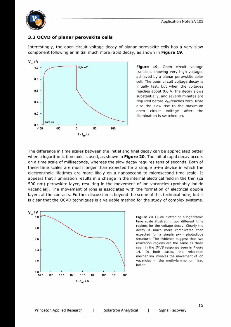
3.3 OCVD of planar perovskite cells
Interestingly, the open circuit voltage decay of planar perovskite cells has a very slow
component following an initial much more rapid decay, as shown in Figure 19.
Figure 19. Open circuit voltage
transient showing very high voltages
achieved by a planar perovskite solar
cell. The open circuit voltage decay is
initially fast, but when the voltages
reaches about 0.6 V, the decay slows
substantially, and several minutes are
required before Voc reaches zero. Note
also the slow rise to the maximum
open circuit voltage after the
illumination is switched on.
The difference in time scales between the initial and final decay can be appreciated better
when a logarithmic time axis is used, as shown in Figure 20. The initial rapid decay occurs
on a time scale of milliseconds, whereas the slow decay requires tens of seconds. Both of
these time scales are much longer than expected for a simple p-i-n device in which the
electron/hole lifetimes are more likely on a nanosecond to microsecond time scale. It
appears that illumination results in a change in the internal electrical field in the thin (ca
500 nm) perovskite layer, resulting in the movement of ion vacancies (probably iodide
vacancies). The movement of ions is associated with the formation of electrical double
layers at the contacts. Further discussion is beyond the scope of this technical note, but it
is clear that the OCVD techniques is a valuable method for the study of complex systems.
Figure 20. OCVD plotted on a logarithmic
time scale illustrating two different time
regions for the voltage decay. Clearly the
decay is much more complicated than
expected for a simple p-i-n photodiode
structure. The evidence suggest that two
relaxation regions are the same as those
seen in the IMVS response seen in Figure
14. In both cases, the relaxation
mechanism involves the movement of ion
vacancies in the methylammonium lead
iodide.

Application Note SA 105
16
Princeton Applied Research | Solartron Analytical | Signal Recovery
References
1. Mora-Sero, I.; Garcia-Belmonte, G. A.; Boix, P. P.; Vazquez, M. A.; Bisquert, J., Impedance Spectroscopy Characterisation of Highly Efficient Silicon Solar Cells under Different Light Illumination Intensities. Energy & Environmental Science 2009, 2, 678-686.
2. Friesen, G.; Dunlop, E. D.; Wendt, R., Investigation of Cdte Solar Cells Via Capacitance and Impedance Measurements. Thin Solid Films 2001, 387, 239-242.
3. O'Regan, B.; Grätzel, M., A Low-Cost, High-Efficiency Solar-Cell Based on Dye-Sensitized Colloidal Tio2 Films. Nature 1991, 353, 737-740.
4. Bach, U.; Lupo, D.; Comte, P.; Moser, J. E.; Weissortel, F.; Salbeck, J.; Spreitzer, H.; Grätzel, M., Solid-State Dye-Sensitized Mesoporous TiO2 Solar Cells with High Photon-to-Electron Conversion Efficiencies. Nature 1998, 395, 583-585.
5. Peter, L.M., "Sticky Electrons" Transport and Interfacial Transfer of Electrons in the Dye-
Sensitized Solar Cell. Acc Chem Res 2009, 42, 1839-47.
6. Peter, L. M., Characterization and Modeling of Dye-Sensitized Solar Cells. Journal of Physical Chemistry C 2007, 111, 6601-6612.
7. Peter, L. M., Dye-Sensitized Nanocrystalline Solar Cells. PCCP 2007, 9, 2630-2642.
8. Hagfeldt, A.; Peter, L. M., Characteriztion and Modeling of Dye-Sensitized Solar Cells: A Toolbox Approach. In Dye Sensitized Solar Cells, Kalyanasundaranam, K., Ed. EPFL Press: Lausanne, 2010; pp 457-554.
9. Bisquert, J.; Vikhrenko, V. S., Interpretation of the Time Constants Measured by Kinetic Techniques in Nanostructured Semiconductor Electrodes and Dye- Sensitized Solar Cells. J. Phys. Chem. B 2004, 108, 2313-2322.
10. Juarez-Perez, E. J.; Sanchez, R. S.; Badia, L.; Garcia-Belmonte, G.; Kang, Y. S.; Mora-Sero, I.; Bisquert, J., Photoinduced Giant Dielectric Constant in Lead Halide Perovskite Solar Cells. The Journal of Physical Chemistry Letters 2014, 5, 2390-2394.
11. Bag, M.; Renna, L. A.; Adhikari, R. Y.; Karak, S.; Liu, F.; Lahti, P. M.; Russell, T. P.; Tuominen,
M. T.; Venkataraman, D., Kinetics of Ion Transport in Perovskite Active Layers and Its
Implications for Active Layer Stability. J. Am. Chem. Soc. 2015, 137, 13130-13137.
12. Dloczik, L.; Ileperuma, O.; Lauermann, I.; Peter, L. M.; Ponomarev, E. A.; Redmond, G.; Shaw, N. J.; Uhlendorf, I., Dynamic Response of Dye-Sensitized Nanocrystalline Solar Cells: Characterization by Intensity-Modulated Photocurrent Spectroscopy. J. Phys. Chem. B 1997, 101, 10281-10289.
13. Fisher, A. C.; Peter, L. M.; Ponomarev, E. A.; Walker, A. B.; Wijayantha, K. G. U., Intensity Dependence of the Back Reaction and Transport of Electrons in Dye-Sensitized Nanacrystalline Tio2 Solar Cells. J. Phys. Chem. B 2000, 104, 949-958.
14. Ponomarev, E. A.; Peter, L. M., A Generalized Theory of Intensity-Modulated Photocurrent Spectroscopy (IMPS). J. Electroanal. Chem. 1995, 396, 219-226.
15. Ponomarev, E. A.; Peter, L. M., A Comparison of Intensity Modulated Photocurrent Spectroscopy and Photoelectrochemical Impedance Spectroscopy in a Study of
Photoelectrochemical Hydrogen Evolution at P-InP. J. Electroanal. Chem. 1995, 397, 45-52.
16. Peat, R.; Peter, L. M., Characterization of Semiconductor Electrodes by Intensity Modulated
Spectroscopy (IMPS). J. Electrochem. Soc. 1986, 133, C334.
17. Peter, L. M., Energetics and Kinetics of Light-Driven Oxygen Evolution at Semiconductor Electrodes: The Example of Hematite. J. Solid State Electrochem. 2013, 17, 315-326.
18. Jennings, J. R.; Ghicov, A.; Peter, L. M.; Schmuki, P.; Walker, A. B., Dye-Sensitized Solar Cells Based on Oriented Tio2 Nanotube Arrays: Transport, Trapping, and Transfer of Electrons.
J. Am. Chem. Soc. 2008, 130, 13364-13372.
19. Peter, L. M.; Vanmaekelbergh, D., Time and Frequency Resolved Studies of Photoelectrochemical Kinetics. In Adv. Electrochem. Sci. Eng., Alkire, R. C. and Kolb, D.M., Ed. Weinheim, 1999; Vol. 6, pp 77-163.

Application Note SA 105
17
Princeton Applied Research | Solartron Analytical | Signal Recovery
20. Peter, L. M., Tributsch, H., Experimental Techniques in Photoelectrochemistry. In Nanostructured and Photoelectrochemical Systems for Solar Photon Conversion, Archer, M. D. and Nozik, A.J, Ed. Imperial College Press: London, 2008; Vol. 3, pp 675-736.
21. Pockett, A. C., Cameron,P.J., Peter, L.M., Eperon, G.E., Snaith, H.J.. In Preparation. 2016.
22. Walker, A. B.; Peter, L. M.; Lobato, K.; Cameron, P. J., Analysis of Photovoltage Decay Transients in Dye-Sensitized Solar Cells. J. Phys. Chem. B 2006, 110, 25504-25507.
23. Duffy, N. W.; Peter, L. M.; Rajapakse, R. M. G.; Wijayantha, K. G. U., A Novel Charge Extraction Method for the Study of Electron Transport and Interfacial Transfer in Dye Sensitised Nanocrystalline Solar Cells. Electrochem. Commun. 2000, 2, 658-662.