Application Note: SY8286A
16
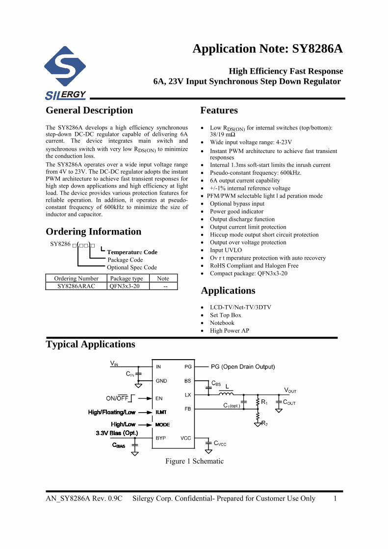
Application Note: SY8286A High Efficiency Fast Response 6A, 23V Input Synchronous Step Down Regulator General Description Features The SY8286A develops a high efficiency synchronous step-down DC-DC regulator capable of delivering 6A current. The device integrates main switch and synchronous switch with very low R DS(ON) to minimize the conduction loss. The SY8286A operates over a wide input voltage range from 4V to 23V. The DC-DC regulator adopts the instant PWM architecture to achieve fast transient responses for high step down applications and high efficiency at light load. The device provides various protection features for reliable operation. In addition, it operates at pseudo- constant frequency of 600kHz to minimize the size of inductor and capacitor. Ordering Information SY8286 □ ( □□ ) □ Temperature Code Package Code Optional Spec Code Ordering Number Package type Note SY8286ARAC QFN3x3-20 -- • Low R DS(ON) for internal switches (top/bottom): 38/19 mΩ • Wide input voltage range: 4-23V • Instant PWM architecture to achieve fast transient responses • Internal 1.3ms soft-start limits the inrush current • Pseudo-constant frequency: 600kHz. • 6A output current capability • +/-1% internal reference voltage • PFM/PWM selectable light l ad peration mode • Optional bypass input • Power good indicator • Output discharge function • Output current limit protection • Hiccup mode output short circuit protection • Output over voltage protection • Input UVLO • Ov r t mperature protection with auto recovery • RoHS Compliant and Halogen Free • Compact package: QFN3x3-20 Applications • LCD-TV/Net-TV/3DTV • Set Top Box • Notebook • High Power AP Typical Applications Figure 1 Schematic AN_SY8286A Rev. 0.9C Silergy Corp. Confidential- Prepared for Customer Use Only 1
-
Upload
khangminh22 -
Category
Documents
-
view
0 -
download
0
Transcript of Application Note: SY8286A
Application Note: SY8286A
High Efficiency Fast Response 6A, 23V Input Synchronous Step Down Regulator
General Description Features The SY8286A develops a high efficiency synchronous step-down DC-DC regulator capable of delivering 6A current. The device integrates main switch and synchronous switch with very low RDS(ON) to minimize the conduction loss. The SY8286A operates over a wide input voltage range from 4V to 23V. The DC-DC regulator adopts the instant PWM architecture to achieve fast transient responses for high step down applications and high efficiency at light load. The device provides various protection features for reliable operation. In addition, it operates at pseudo-constant frequency of 600kHz to minimize the size of inductor and capacitor. Ordering Information
SY8286 () Temperature Code Package Code Optional Spec Code
Ordering Number Package type Note SY8286ARAC QFN3x3-20 --
• Low RDS(ON) for internal switches (top/bottom):
38/19 mΩ • Wide input voltage range: 4-23V • Instant PWM architecture to achieve fast transient
responses • Internal 1.3ms soft-start limits the inrush current • Pseudo-constant frequency: 600kHz. • 6A output current capability • +/-1% internal reference voltage • PFM/PWM selectable light l ad peration mode • Optional bypass input • Power good indicator • Output discharge function • Output current limit protection • Hiccup mode output short circuit protection • Output over voltage protection • Input UVLO • Ov r t mperature protection with auto recovery • RoHS Compliant and Halogen Free • Compact package: QFN3x3-20 Applications • LCD-TV/Net-TV/3DTV • Set Top Box • Notebook • High Power AP
Typical Applications
Figure 1 Schematic AN_SY8286A Rev. 0.9C Silergy Corp. Confidential- Prepared for Customer Use Only 1
SY8286A
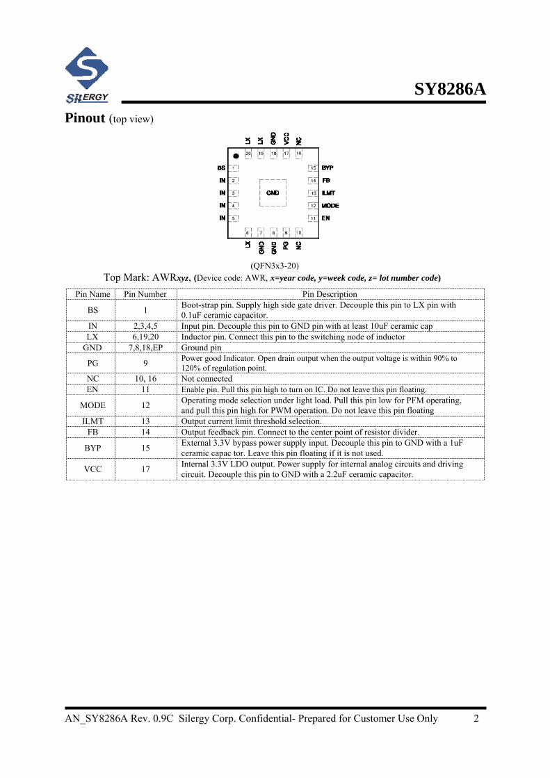
Pinout (top view)
(QFN3x3-20) Top Mark: AWRxyz, (Device code: AWR, x=year code, y=week code, z= lot number code)
Pin Name Pin Number Pin Description
BS 1 Boot-strap pin. Supply high side gate driver. Decouple this pin to LX pin with 0.1uF ceramic capacitor.
IN 2,3,4,5 Input pin. Decouple this pin to GND pin with at least 10uF ceramic cap LX 6,19,20 Inductor pin. Connect this pin to the switching node of inductor
GND 7,8,18,EP Ground pin
PG 9 Power good Indicator. Open drain output when the output voltage is within 90% to 120% of regulation point.
NC 10, 16 Not connected EN 11 Enable pin. Pull this pin high to turn on IC. Do not leave this pin floating.
MODE 12 Operating mode selection under light load. Pull this pin low for PFM operating, and pull this pin high for PWM operation. Do not leave this pin floating
ILMT 13 Output current limit threshold selection. FB 14 Output feedback pin. Connect to the center point of resistor divider.
BYP 15 External 3.3V bypass power supply input. Decouple this pin to GND with a 1uFceramic capac tor. Leave this pin floating if it is not used.
VCC 17 Internal 3.3V LDO output. Power supply for internal analog circuits and drivingcircuit. Decouple this pin to GND with a 2.2uF ceramic capacitor.
AN_SY8286A Rev. 0.9C Silergy Corp. Confidential- Prepared for Customer Use Only 2
SY8286A
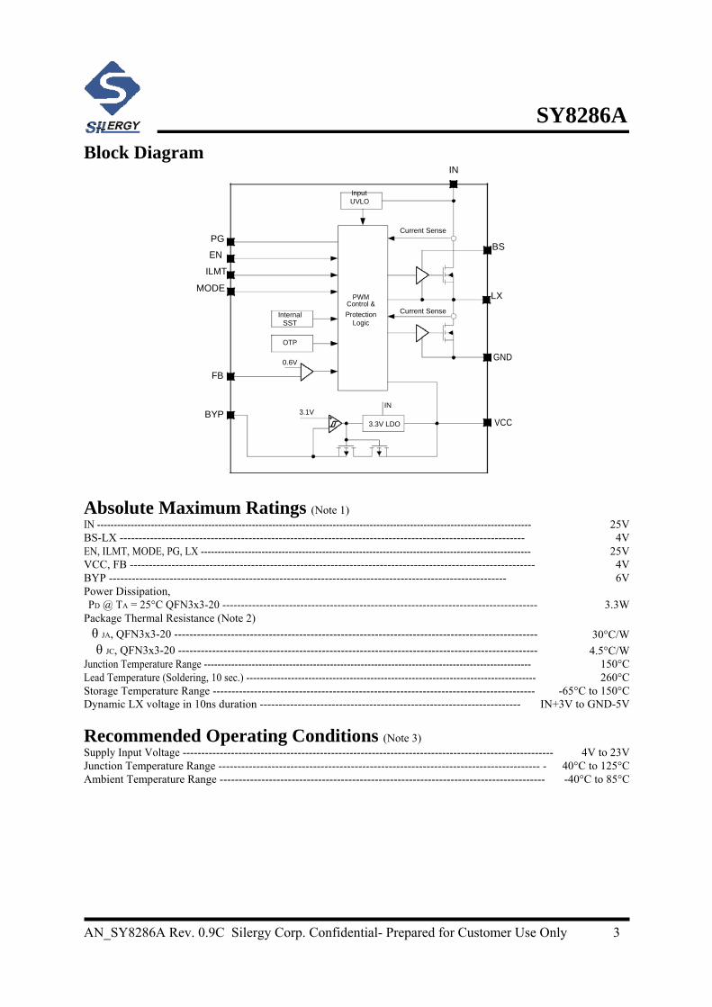
Block Diagram IN
Input UVLO
Current Sense PG
BS EN
ILMT MODE
PWM LX Control &
Current Sense Internal Protection SST Logic
OTP 0.6V
GND
FB
IN BYP 3.1V
VCC 3.3V LDO
Absolute Maximum Ratings (Note 1) IN --------------------------------------------------------------------------------------------------------------------------------- 25VBS-LX ----------------------------------------------------------------------------------------------------------- 4VEN, ILMT, MODE, PG, LX -------------------------------------------------------------------------------------------------- 25VVCC, FB ----------------------------------------------------------------------------------------------------------- 4VBYP --------------------------------------------------------------------------------------------------------- 6VPower Dissipation, PD @ TA = 25°C QFN3x3-20 ------------------------------------------------------------------------------------- 3.3W
Package Thermal Resistance (Note 2) θ JA, QFN3x3-20 ------------------------------------------------------------------------------------------------ 30°C/Wθ JC, QFN3x3-20 ----------------------------------------------------------------------------------------------- 4.5°C/W
Junction Temperature Range ------------------------------------------------------------------------------------------------ 150°CLead Temperature (Soldering, 10 sec.) ------------------------------------------------------------------------------------ 260°CStorage Temperature Range -------------------------------------------------------------------------------------- -65°C to 150°CDynamic LX voltage in 10ns duration --------------------------------------------------------------------- IN+3V to GND-5V
Recommended Operating Conditions (Note 3) Supply Input Voltage ---------------------------------------------------------------------------------------------------- 4V to 23VJunction Temperature Range ------------------------------------------------------------------------------------- - 40°C to 125°CAmbient Temperature Range -------------------------------------------------------------------------------------- -40°C to 85°C AN_SY8286A Rev. 0.9C Silergy Corp. Confidential- Prepared for Customer Use Only 3
SY8286A
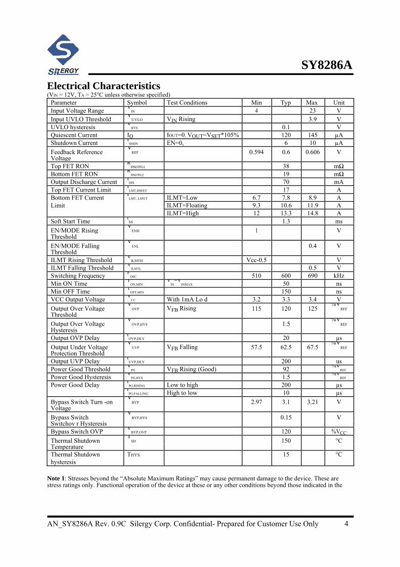
Electrical Characteristics (VIN = 12V, TA = 25°C unless otherwise specified)
Parameter Symbol Test Conditions Min Typ Max Unit Input Voltage Range V
IN 4 23 VInput UVLO Threshold
VUVLO VIN Rising 3.9 V
UVLO hysteresis VHYS 0.1 V
Quiescent Current IQ IOUT=0, VOUT=VSET*105% 120 145 µAShutdown Current I
SHDN EN=0, 6 10 µAFeedback Reference
VREF 0.594 0.6 0.606 V
Voltage Top FET RON R
DS(ON)1 38 mΩBottom FET RON R
DS(ON)2 19 mΩOutput Discharge Current I
DIS 70 mATop FET Current Limit I
LMT,HSFET 17 ABottom FET Current I
LMT, LSFET ILMT=Low 6.7 7.8 8.9 ALimit ILMT=Floating 9.3 10.6 11.9 A
ILMT=High 12 13.3 14.8 ASoft Start Time t
SS 1.3 msEN/MODE Rising
VENH 1 V
Threshold
EN/MODE Falling V
ENL 0.4 VThreshold ILMT Rising Threshold V
ILMTH Vcc-0.5 VILMT Falling Threshold V
ILMTL 0.5 VSwitching Frequency F
OSC 510 600 690 kHzMin ON Time T
ON,MIN V
IN=V
INMAX 50 nsMin OFF Time T
OFF,MIN 150 nsVCC Output Voltage V
CC With 1mA Lo d 3.2 3.3 3.4 VOutput Over Voltage
VOVP VFB Rising 115 120 125
%VREF
Threshold
Output Over Voltage V
OVP,HYS 1.5 %VREF
Hysteresis Output OVP Delay t
OVP,DLY 20 µsOutput Under Voltage
VUVP VFB Falling 57.5 62.5 67.5
%VREF
Protection Threshold Output UVP Delay t
UVP,DLY 200 usPower Good Threshold V
PG VFB Rising (Good) 92 %VREF
Power Good Hysteresis VPG,HYS 1.5 %V
REF
Power Good Delay tPG,RISING Low to high 200 µs
tPG,FALLING High to low 10 µs
Bypass Switch Turn -on V
BYP 2.97 3.1 3.21 VVoltage
Bypass Switch V
BYP,HYS 0.15 VSwitchov r Hysteresis Bypass Switch OVP V
BYP,OVP 120 %VCCThermal Shutdown
TSD 150 °C
Temperature Thermal Shutdown THYS 15 °Chysteresis
Note 1: Stresses beyond the “Absolute Maximum Ratings” may cause permanent damage to the device. These are stress ratings only. Functional operation of the device at these or any other conditions beyond those indicated in the AN_SY8286A Rev. 0.9C Silergy Corp. Confidential- Prepared for Customer Use Only 4
SY8286A operational sections of the specification is not implied. Exposure to absolute maximum rating conditions for extended periods may affect device reliability Note 2: Package thermal resistance is measured in the natural convection at TA = 25°C on a four-layer Silergy Evaluation Board. Note 3: The device is not guaranteed to function outside its operating conditions. AN_SY8286A Rev. 0.9C Silergy Corp. Confidential- Prepared for Customer Use Only 5
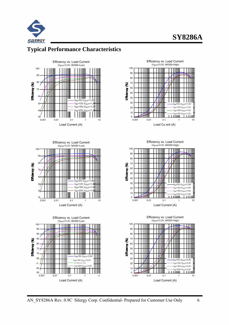
SY8286A Typical Performance Characteristics
Efficiency vs. Load Current
(VBYP=3.3V, MODE=Low) 100 90
80
70
60
VIN=5V,VOUT=1.2V 50 VIN=12V,VOUT=1.2V
VIN=19V,VOUT=1.2V 40 VIN=23V,VOUT=1.2V
30 0.001 0.01 0.1 1 10
Load Current (A)
Efficiency vs. Load Current (VBYP=3.3V, MODE=Low)
100
90
80 70
60 VIN=5V,VOUT=1.8V
50 VIN=12V,VOUT=1.8V VIN=19V,VOUT=1.8V
40 VIN=23V,VOUT=1.8V
30 0.001 0.01 0.1 1 10
Load Current (A)
Efficiency vs. Load Current (VBYP=3.3V, MODE=Low)
100 95 90 85 80 75 70
VIN=5V,VOUT=3.3V 65
VIN=12V,VOUT=3.3V 60 VIN=19V,VOUT=3.3V
VIN=23V,VOUT=3.3V 55 50
0.001 0.01 0.1 1 10 Load Current (A)
100 90 80 70 60 50 40 30 20 10 0
0.001 100 90 80 70 60 50 40 30 20 10 0
0.001 100 90 80 70 60 50 40 30 20 10 0
0.001
Efficiency vs. Load Current
(VBYP=3.3V, MODE=High)
VIN=5V,VOUT=1.2V VIN=12V,VOUT=1.2V VIN=19V,VOUT=1.2V VIN=23V,VOUT=1.2V
0.01 0.1 1 10
Load Cu ent (A) Efficiency vs. Load Current
(VBYP=3.3V, MODE=High)
VIN=5V,VOUT=1.8V VIN=12V,VOUT=1.8V VIN=19V,VOUT=1.8V VIN=23V,VOUT=1.8V
0.01 0.1 1 10
Load Current (A) Efficiency vs. Load Current
(VBYP=3.3V, MODE=High)
VIN=5V,VOUT=3.3V VIN=12V,VOUT=3.3V VIN=19V,VOUT=3.3V VIN=23V,VOUT=3.3V
0.01 0.1 1 10
Load Current (A) AN_SY8286A Rev. 0.9C Silergy Corp. Confidential- Prepared for Customer Use Only 6
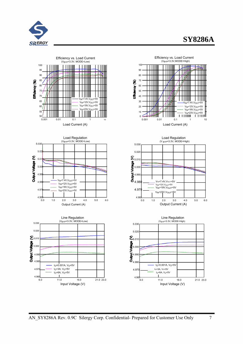
SY8286A
Efficiency vs. Load Current (VBYP=3.3V, MODE=Low)
100
95 90 85 80 75 70
VIN=7.4V,VOUT=5V 65 VIN=12V,VOUT=5V
60 VIN=19V,VOUT=5V
VIN=23V,VOUT=5V 55
50 0.001 0.01 0.1 1 10
Load Current (A)
Load Regulation (VBYP=3.3V, MODE=Low)
5.030
5.020
5.010
5.000
4.990
4.980 VIN=7.4V,VOUT=5V VIN=12V,VOUT=5V
VIN=19V,VOUT=5V 4.970 VIN=23V,VOUT=5V
4.960 0.0 1.0 2.0 3.0 4.0 5.0 6.0
Efficiency vs. Load Current
(VBYP=3.3V,MODE=High) 100
90 80 70 60 50 40 30 VIN=7.4V,VOUT=5V
20 VIN=12V,VOUT=5V VIN=19V,VOUT=5V
10 VIN=23V,VOUT=5V
0 0.001 0.01 0.1 1 10
Load Current (A)
Load Regulation (V BYP=3.3V, MODE=High)
5.030
5.020
5.010
5.000
4.990 4.980 VIN=7.4V,VOUT=5V
VIN=12V,VOUT=5V VIN=19V,VOUT=5V
4.970 VIN=23V,VOUT=5V
4.960 0.0 1.0 2.0 3.0 4.0 5.0 6.0
5.030
5.020
5.010
5.000
Output Current (A)
Line Regulation (VBYP=3.3V, MODE=Low)
Output Current (A)
Line Regulation (VBYP=3.3V, MODE=High)
5.030
5.020
5.010
5.000
4.990
4.980
IO=0.001A, VO=5V
4.970 IO=3A, VO=5V
IO=6A, VO=5V 4.960
23.0
6.0 11.0 16.0 21.0 Input Voltage (V)
4.990
4.980
IO=0.001A, VO=5V 4.970 IO=3A, VO=5V
IO=6A, VO=5V 4.960
6.0 11.0 16.0 21.0 23.0 Input Voltage (V)
AN_SY8286A Rev. 0.9C Silergy Corp. Confidential- Prepared for Customer Use Only 7
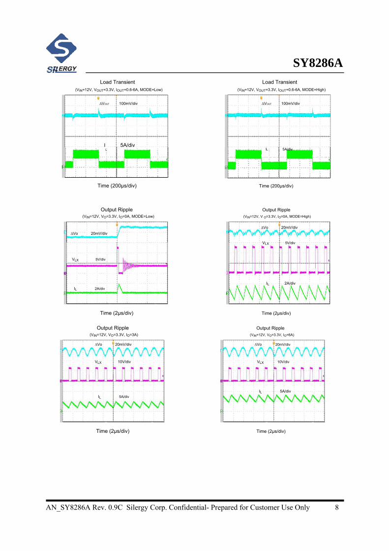
SY8286A
Load Transient Load Transient (VIN=12V, VOUT=3.3V, IOUT=0.6-6A, MODE=Low) (VIN=12V, VOUT=3.3V, IOUT=0.6-6A, MODE=High)
∆VOUT 100mV/div ∆VOUT 100mV/div
IL 5A/div IL 5A/div
Time (200µs/div) Time (200µs/div)
Output Ripple Output Ripple (VIN=12V, VO=3.3V, IO=0A, MODE=Low) (VIN=12V, V O=3.3V, IO=0A, MODE=High)
∆Vo 20mV/div
∆Vo 20mV/div VLX 5V/div
VLX 5V/div
IL 2A/div
IL 2A/div
Time (2µs/div) Time (2µs/div)
Output Ripple Output Ripple
(VIN=12V, VO=3.3V, IO=3A) (VIN=12V, VO=3.3V, IO=6A)
∆Vo 20mV/div ∆Vo 20mV/div
VLX 10V/div VLX 10V/div
IL 5A/div IL 5A/div
Time (2µs/div) Time (2µs/div) AN_SY8286A Rev. 0.9C Silergy Corp. Confidential- Prepared for Customer Use Only 8
SY8286A
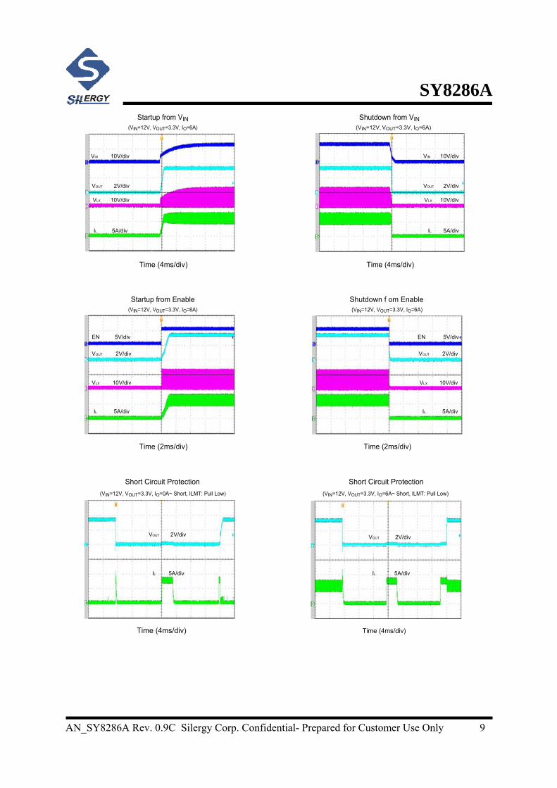
Startup from VIN Shutdown from VIN (VIN=12V, VOUT=3.3V, IO=6A) (VIN=12V, VOUT=3.3V, IO=6A)
VIN 10V/div VIN 10V/div
VOUT 2V/div VOUT 2V/div
VLX 10V/div VLX 10V/div
IL 5A/div IL 5A/div
Time (4ms/div) Time (4ms/div)
Startup from Enable Shutdown f om Enable (VIN=12V, VOUT=3.3V, IO=6A) (VIN=12V, VOUT=3.3V, IO=6A)
EN 5V/div EN 5V/div
VOUT 2V/div VOUT 2V/div
VLX 10V/div VLX 10V/div
IL 5A/div IL 5A/div
Time (2ms/div) Time (2ms/div)
Short Circuit Protection Short Circuit Protection (VIN=12V, VOUT=3.3V, IO=0A~ Short, ILMT: Pull Low) (VIN=12V, VOUT=3.3V, IO=6A~ Short, ILMT: Pull Low)
VOUT 2V/div VOUT 2V/div
IL 5A/div IL 5A/div
Time (4ms/div) Time (4ms/div) AN_SY8286A Rev. 0.9C Silergy Corp. Confidential- Prepared for Customer Use Only 9
SY8286A
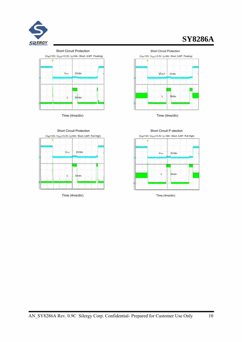
Short Circuit Protection Short Circuit Protection (VIN=12V, VOUT=3.3V, IO=0A~ Short, ILMT: Floating) (VIN=12V, VOUT=3.3V, IO=6A~ Short, ILMT: Floating)
VOUT 2V/div VOUT 2V/div
IL 5A/div IL 5A/div
Time (4ms/div) Time (4ms/div)
Short Circuit Protection Short Circuit P otection (VIN=12V, VOUT=3.3V, IO=0A~ Short, ILMT: Pull High) (VIN=12V, VOUT=3.3V, IO =6A~ Short, ILMT: Pull High)
VOUT 2V/div VOUT 2V/div
IL 5A/div
IL 5A/div
Time (4ms/div) Time (4ms/div) AN_SY8286A Rev. 0.9C Silergy Corp. Confidential- Prepared for Customer Use Only 10
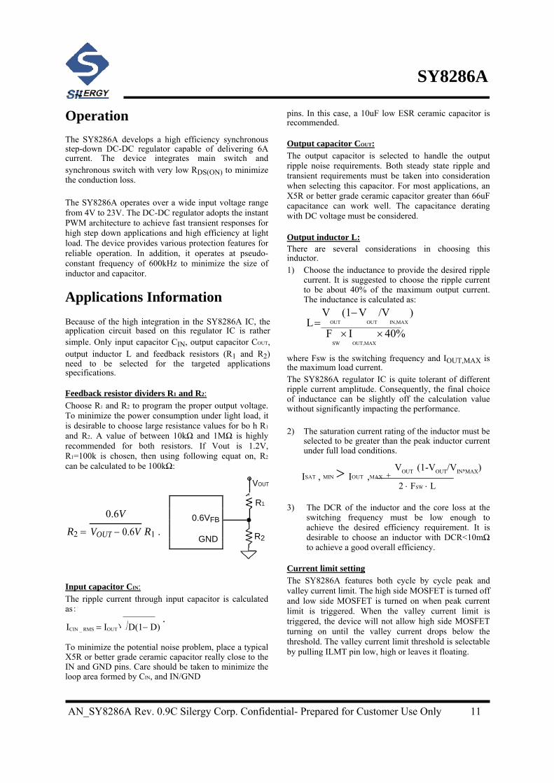
SY8286A Operation The SY8286A develops a high efficiency synchronous step-down DC-DC regulator capable of delivering 6A current. The device integrates main switch and synchronous switch with very low RDS(ON) to minimize the conduction loss. The SY8286A operates over a wide input voltage range from 4V to 23V. The DC-DC regulator adopts the instant PWM architecture to achieve fast transient responses for high step down applications and high efficiency at light load. The device provides various protection features for reliable operation. In addition, it operates at pseudo-constant frequency of 600kHz to minimize the size of inductor and capacitor. Applications Information Because of the high integration in the SY8286A IC, the application circuit based on this regulator IC is rather simple. Only input capacitor CIN, output capacitor COUT, output inductor L and feedback resistors (R1 and R2) need to be selected for the targeted applications specifications. Feedback resistor dividers R1 and R2: Choose R1 and R2 to program the proper output voltage. To minimize the power consumption under light load, it is desirable to choose large resistance values for bo h R1 and R2. A value of between 10kΩ and 1MΩ is highly recommended for both resistors. If Vout is 1.2V, R1=100k is chosen, then using following equat on, R2 can be calculated to be 100kΩ: VOUT
R1
R2 =
0.6V
R1 . 0.6VFB
VOUT − 0.6V GND
R2
Input capacitor CIN: The ripple current through input capacitor is calculated as: ICIN _ RMS = IOUT ⋅ D(1− D)
. To minimize the potential noise problem, place a typical X5R or better grade ceramic capacitor really close to the IN and GND pins. Care should be taken to minimize the loop area formed by CIN, and IN/GND
pins. In this case, a 10uF low ESR ceramic capacitor is recommended. Output capacitor COUT: The output capacitor is selected to handle the output ripple noise requirements. Both steady state ripple and transient requirements must be taken into consideration when selecting this capacitor. For most applications, an X5R or better grade ceramic capacitor greater than 66uF capacitance can work well. The capacitance derating with DC voltage must be considered. Output inductor L: There are several considerations in choosing this inductor. 1) Choose the inductance to provide the desired ripple
current. It is suggested to choose the ripple current to be about 40% of the maximum output current. The inductance is calculated as:
L = V
OUT (1−
V
OUT /V
IN,MAX )
FSW
× I
OUT,MAX ×
40%
where Fsw is the switching frequency and IOUT,MAX is the maximum load current. The SY8286A regulator IC is quite tolerant of different ripple current amplitude. Consequently, the final choice of inductance can be slightly off the calculation value without significantly impacting the performance. 2) The saturation current rating of the inductor must be
selected to be greater than the peak inductor current under full load conditions.
ISAT , MIN > IOUT ,MAX + VOUT (1-VOUT/VIN,MAX)
2 ⋅ FSW ⋅ L 3) The DCR of the inductor and the core loss at the
switching frequency must be low enough to achieve the desired efficiency requirement. It is desirable to choose an inductor with DCR<10mΩ to achieve a good overall efficiency.
Current limit setting The SY8286A features both cycle by cycle peak and valley current limit. The high side MOSFET is turned off and low side MOSFET is turned on when peak current limit is triggered. When the valley current limit is triggered, the device will not allow high side MOSFET turning on until the valley current drops below the threshold. The valley current limit threshold is selectable by pulling ILMT pin low, high or leaves it floating.
AN_SY8286A Rev. 0.9C Silergy Corp. Confidential- Prepared for Customer Use Only 11

SY8286A Soft-start The SY8286A has a built-in soft-start to control the output voltage ramp up speed during start up to limit the input inrush current. The typical soft-start time is 1.3ms. Enable Operation Pulling the EN pin low will shut down the device. During shutdown mode, the SY8286A shutdown current drops to lower than 10uA, Driving the EN pin high will turn on the IC again. External Bootstrap Cap This capacitor provides the gate driver voltage for internal high side MOSEFET. A 100nF low ESR ceramic capacitor connected between BS pin and LX pin is recommended.
BS CBS
100nF
LX
VCC LDO and BYP Input The 3.3V VCC LDO provides the power supply for internal control and drive circuit. Bypass this pin to ground with a 2.2uF ceramic capacitor. The control and drive circuit can also be powered by external 3.3V power supply. When a 3.3V external power supply is connected to the BYP pin, the VCC LDO is turned off and the switch between BYP and VCC is turn d on. The overall efficiency may be improved by connecting the BYP pin to external 3.3V switching power supply. Leave BYP pin floating if this feature is ot used.
. Power Good Indication PG is an open-drain output pin. This pin will pull to ground if output voltage is lower than 90% or higher than 120% of egulation voltage. Otherwise this pin will go to a high impedance state.
Light Load Operation Mode Selection PFM or PWM light load operation is selected by MODE pin. Pull MODE pin low for PFM operation, and pull this pin high for PWM operation. Load Transient Considerations: The SY8286A regulator IC adopts the instant PWM architecture to achieve good stability and fast transient responses. In applications with high step load current, adding an RC network RFF and CFF parallel with R1 may further speed up the load transient responses.
L1 VOUT
CFF R1
RFF COUT
(opt.)R2 FB
Layout Design: The layout design of SY8286A regulator is relatively simple. For the best efficiency and minimum noise promblem, we should place the following components close to the IC: CIN, CVCC, L, R1 and R2. 1) It is desirable to maximize the PCB copper area connecting to GND pin to achieve the best thermal and noise performance. If the board space allowed, a ground plane is highly desirable. 2) CIN must be close to Pins IN and GND. The loop area formed by CIN and GND must be minimized. 3) The PCB copper area associated with LX pin must be minimized to avoid the potential noise problem. 4) The components R1 and R2, and the trace connecting to the FB pin must NOT be adjacent to the LX net on the PCB layout to avoid the noise problem. 5) If the system chip interfacing with the EN pin has a high impedance state at shutdown mode and the IN pin is connected directly to a power source such as a Li-Ion battery. A 1MΩ pull down resistor should be placed between the enable pin and GND pins to prevent the noise from falsely turning on the regulator at shutdown mode.
AN_SY8286A Rev. 0.9C Silergy Corp. Confidential- Prepared for Customer Use Only 12
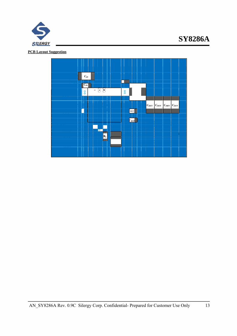
SY8286A PCB Layout Suggestion
AN_SY8286A Rev. 0.9C Silergy Corp. Confidential- Prepared for Customer Use Only 13
SY8286A
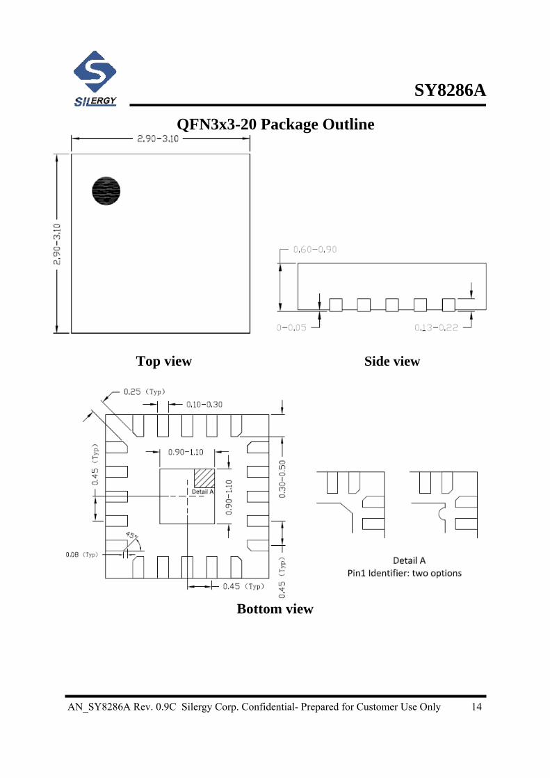
QFN3x3-20 Package Outline
Top view Side view
Bottom view AN_SY8286A Rev. 0.9C Silergy Corp. Confidential- Prepared for Customer Use Only 14
SY8286A
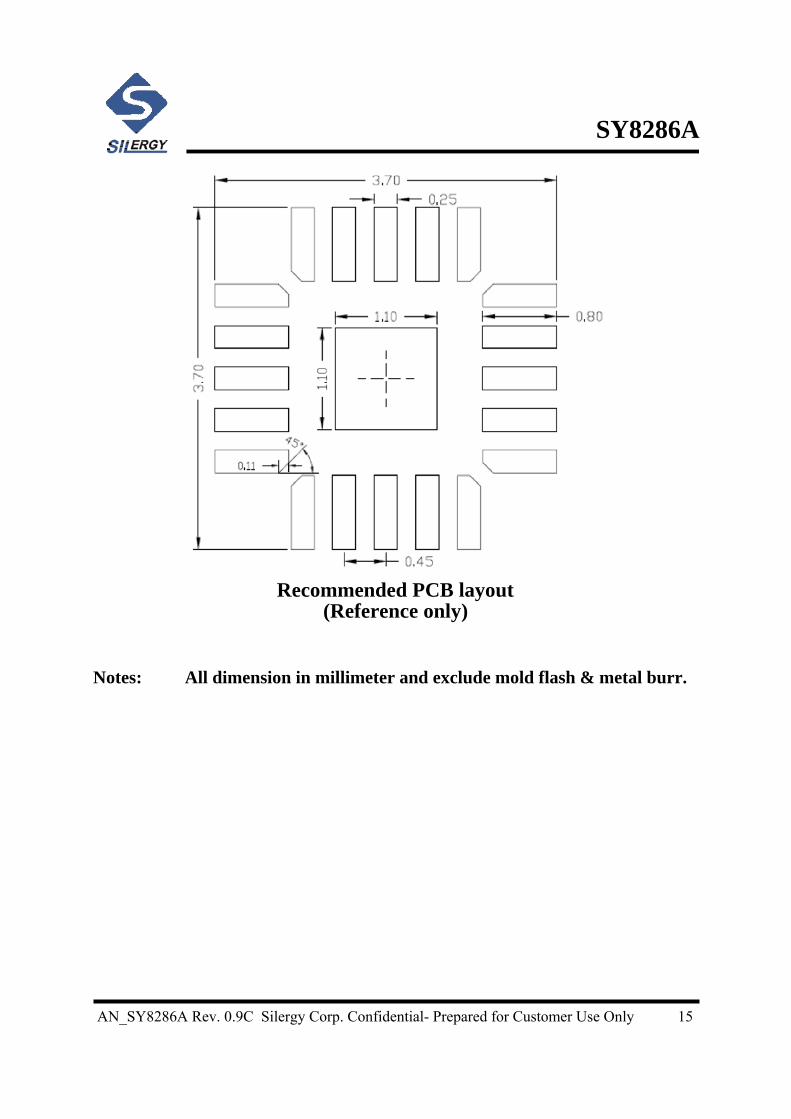
Recommended PCB layout (Reference only)
Notes: All dimension in millimeter and exclude mold flash & metal burr. AN_SY8286A Rev. 0.9C Silergy Corp. Confidential- Prepared for Customer Use Only 15

SY8286A
Taping & Reel Specification 1. QFN3x3-20 taping orientation
3.9/4.1 1.45/1.55
11.7
/12.
3
Feeding direction 2. Carrier Tape & Reel specification for packages
Reel Size
Package Tape width Pocket Reel size Trailer Leader length Qty per type (mm) pitch(mm) (Inch) length(mm) (mm) reel
QFN3x3 12 8 13" 400 400 5000
3. Others: NA
AN_SY8286A Rev. 0.9C Silergy Corp. Confidential- Prepared for Customer Use Only 16