Application Note
19
Application Note Light Emitting Diode 1/19 SP-QR-C2-191755-3 Mar. 1, 2022 This document contains tentative information, Nichia may change the contents without notice. The Nichia part numbers NJSx170x, NCSx170x, NC2x170x, NCSx131x, and NC2x131x within this document are merely Nichia’s part numbers for those Nichia products and are not related nor bear resemblance to any other company’s product that might bear a trademark. LED Mounting Process Techniques for the Nichia 170 or 131 Series LEDs Table of Contents 1. Overview ........................................................... 2 2. Applicable Part Numbers .................................. 2 3. Mounting Process Preparation .......................... 3 4. Solder Printing .................................................. 5 5. LED Mounting .................................................. 9 6. Reflow ............................................................. 15 7. Mounting Test ................................................. 16 8. Inspection ........................................................ 17 9. Summary ......................................................... 18
-
Upload
khangminh22 -
Category
Documents
-
view
1 -
download
0
Transcript of Application Note

Application Note Lig
ht E
mitting D
iod
e
1/19
SP-QR-C2-191755-3 Mar. 1, 2022
This document contains tentative information, Nichia may change the contents without notice.
The Nichia part numbers NJSx170x, NCSx170x, NC2x170x, NCSx131x, and NC2x131x within
this document are merely Nichia’s part numbers for those Nichia products and are not related nor
bear resemblance to any other company’s product that might bear a trademark.
LED Mounting Process Techniques
for the Nichia 170 or 131 Series LEDs
Table of Contents
1. Overview ........................................................... 2
2. Applicable Part Numbers .................................. 2
3. Mounting Process Preparation .......................... 3
4. Solder Printing .................................................. 5
5. LED Mounting .................................................. 9
6. Reflow ............................................................. 15
7. Mounting Test ................................................. 16
8. Inspection ........................................................ 17
9. Summary ......................................................... 18

Application Note Lig
ht E
mitting D
iod
e
2/19
SP-QR-C2-191755-3 Mar. 1, 2022
This document contains tentative information, Nichia may change the contents without notice.
1. Overview
Nichia’s surface-mount LEDs are designed to be mounted using a pick-and-place machine. However,
depending on the operation conditions set for the machine or how the LEDs are handled during the
mounting process, failures of the LEDs (i.e. damage to the LED, reliability issues, etc.) or mounting
errors may occur.
This application note provides considerations/precautions for the mounting process of the surface-
mount LEDs.
2. Applicable Part Numbers
This application note applies to the LEDs shown in Table 1.
Table 1. Applicable LED Part/Series Numbers
LED Series1
Part Number2
Note:
1 The electrode pattern on the back of the package for the Nichia 170 Series and Nichia 131 Series is different.
2 The x represents a letter that follows the alphanumeric code of the same LED type.
(Ex: NCSx170x → NCSW170C, NCSW170D, NCSW170D-PCA, NCSA170D, NCSW170F, NCSA170F, etc.)
Category
Part Number2 NJSx170x NCSx170x NC2x170x NCSx131x NC2x131x
NJSW170D NCSW170F NC2W170F NCSW131F NC2W131F
Package Size
(Unit: mm)1.6×1.2×0.75 1.8×1.45×0.75 3×1.6×0.75 1.8×1.45×0.75 3×1.6×0.75
Nichia 170 Series1
Nichia 131 Series1
Example of
Package
Appearance

Application Note Lig
ht E
mitting D
iod
e
3/19
SP-QR-C2-191755-3 Mar. 1, 2022
This document contains tentative information, Nichia may change the contents without notice.
3. Mounting Process Preparation
3.1 Reel and Embossed Carrier Tape Specifications
The LEDs are delivered in an embossed carrier tape and a reel as shown in Figure 1. The detailed
specifications of the embossed carrier tape are available in the applicable specification of the LED.
Figure 1. Reel and Embossed Carrier Tape (Example for the NC2x170x LED)
3.2 Prevention of Moisture Absorption
The reel of the LEDs is sealed in a moisture-proof aluminum bag as shown in Figure 2. If the
package absorbs moisture and is exposed to heat during soldering, it may cause the moisture to
vaporize and the package to expand and the resulting pressure may cause internal delamination. This
may cause the optical characteristics to degrade. To minimize moisture absorption in storage/transit,
moisture-proof aluminum bags are used for the LEDs with a silica gel packet to absorb any air
moisture in the bag.
PreparationSolder
PrintingMounting Reflow Inspection
Figure 2. Moisture-Proof Aluminum Bag Figure 3. Schematic Diagram of LED’s
Moisture Absorption and Vapor
Expansion of the Moisture

Application Note Lig
ht E
mitting D
iod
e
4/19
SP-QR-C2-191755-3 Mar. 1, 2022
This document contains tentative information, Nichia may change the contents without notice.
3.3 Storage of the LEDs
The storage/packaging requirements for the LEDs in the scope of this application note are
comparable to JEDEC Moisture Sensitivity Level (MSL) 3 or equivalent. Refer to Table 2 below for
the storage time. Once the moisture-proof aluminum bag is opened, ensure that the LED is soldered
to a PCB within the range of the conditions in Table 2. To store any remaining unused LEDs, use a
hermetically-sealed container with silica gel desiccants. Nichia recommends placing them back to
the original moisture-proof bag used for shipment and reseal it. If the “After Opening” storage time
has been exceeded or any pink silica gel beads are found, ensure that the LEDs are baked before use.
Baking should only be done once.
Table 2. Storage Time and Baking Conditions
If the LEDs are stored in a high temperature environment (≥70℃) for a long period of time, the
resin portion of the LED may stick to the top cover tape, causing pick-up errors; storing the LEDs
in this manner may also cause deformation of the embossed carrier tape. Ensure that the LEDs are
stored at room temperature (approximately 25℃).
If the LEDs are stored using a vacuum seal, there is a possibility that the reel and/or the embossed
carrier tape deform. The reel is more susceptible to warpage at the outer edge, and force can be
applied as shown in Figure 4. If the embossed carrier tape deforms, the LEDs inside the pockets of
the embossed carrier tape may tilt, causing damage to the LEDs and/or pick-up errors. Stacking
heavy objects onto the reel also causes force to be applied to the reel, which can result in the same
issues. Ensure that no force is applied to the reel.
Figure 4. Vacuum Storage and Deformation of Embossed Carrier Tape
Conditions Temperature Humidity Time
Storage Before Opening Aluminum Bag ≤30℃ ≤90%RH Within 1 Year from Delivery Date
After Opening Aluminum Bag ≤30℃ ≤70%RH ≤168 hours
Baking 65±5℃ - ≥24 hours
Reel Force
Deformation of Embossed Carrier Tape
Embossed Carrier Tape
Deformation Deformation
Tilted LED in Pocket Squashed Reel as a Result
of Vacuum Sealing

Application Note Lig
ht E
mitting D
iod
e
5/19
SP-QR-C2-191755-3 Mar. 1, 2022
This document contains tentative information, Nichia may change the contents without notice.
4. Solder Printing
If the LED is not mounted onto a PCB with an appropriate amount and shape of solder paste, the
expected characteristics of the LED may not be obtained. In order to maintain the amount/shape of
solder paste in the printing process, the soldering pad pattern and metal solder stencil aperture
pattern should be optimized as well as the printing conditions, and the solder paste must be prepared
properly prior to use.
4.1 Preparations for Solder Paste
Usually, the solder paste that is stored in a refrigerator cannot be used immediately and needs to be
stirred before use. The purpose of the stir is to restore the even distribution of solder particles and
flux that became uneven due to storage in the refrigerator. If the solder paste is not mixed evenly, it
interferes with the rolling performance, leading to an inappropriate amount/shape of the solder when
printed on the PCB.
The solder paste container should not be opened immediately after taken out from the refrigerator.
Otherwise the solder paste absorbs moisture due to condensation.
Leave the solder paste at room temperature for approximately 60 minutes after taking it out from
the refrigerator to ensure that it returns to room temperature before stirring. The temperature of the
solder paste will increase if it is stirred for a long time, which deteriorates the flux. Stirring for one
minute may be enough for some kinds of solder paste; determine the stirring duration based on the
solder paste manufacturer’s recommendation. If it is suspected that the temperature of the solder
paste increased in the container after stirring, the stirring duration may have been too long; shorten
the stirring duration.
PreparationSolder
PrintingMounting Reflow Inspection

Application Note Lig
ht E
mitting D
iod
e
6/19
SP-QR-C2-191755-3 Mar. 1, 2022
This document contains tentative information, Nichia may change the contents without notice.
4.2 Soldering Pad Pattern and Metal Solder Stencil Aperture Pattern
The figures below show the recommended soldering pad pattern and metal solder stencil aperture
pattern for the NCSx170x LEDs as examples of the patterns used to mount an LED onto a PCB. For
other LED part number patterns, refer to the applicable specification for each LED part number.
● Recommended Soldering Pad Pattern ● Recommended Metal Solder Stencil Aperture
Figure 5. Soldering Pad Pattern and Metal Solder Stencil Aperture Pattern
Recommended for the NCSx170x
4.3 Printing Condition Adjustment
Adjust the squeegee conditions and the metal solder stencil separation conditions to print with the
correct amount and shape. The speed, pressing pressure, and angle of the squeegee affect the amount
and condition of the solder paste filling the metal solder stencil aperture. Additionally, the speed of
the separation and the distance affects how the shape of the solder on the PCB stays consistent with
each use. These are also affected by the thickness of the metal solder stencil, the aperture pattern,
and the surface roughness of the aperture wall.
In order to prevent the occurrence of solder bridges, etc. and maintain optimal printing conditions,
adjust the cleaning method, conditions, and frequency of the metal solder stencil.
Adjust the printing conditions to obtain an appropriate solder shape (see Figures 6 and 7 for
examples). An appearance inspection after solder printing is recommended in order to check if the
solder paste has been printed appropriately.
If the solder printing process is carried out continuously for a long period of time, the viscosity of
the solder paste may increase, leading to printing failures due to clogging of the metal solder stencil
aperture and poor release of the solder paste. To maintain an appropriate solder shape during
continuous operation, it is important to check the solder stencil apertures for clogging and check the
viscosity of the solder paste whenever appropriate.
(単位 Unit: mm)
R0.075
1.6
0.43
1.21
1.7
0.3
1.34
R0.075
(Unit: mm)

Application Note Lig
ht E
mitting D
iod
e
7/19
SP-QR-C2-191755-3 Mar. 1, 2022
This document contains tentative information, Nichia may change the contents without notice.
Figure 6. Squeegee Speed and Solder Paste Filling in the Metal Solder Stencil Aperture
Figure 7. Speed of Solder Stencil Removal and Shape of the Solder Paste
4.4 LED Failures Related to Poor Solder Printing
If a metal solder stencil aperture is clogged and/or the conditions of the board separation is not
appropriate, a sufficient amount of the solder paste may not be applied to the PCB. This will lead to
insufficient heat dissipation of the LED causing the junction temperature (TJ) of the LED to
significantly increase, resulting in a reduction in the luminous flux and/or an adverse effect on the
reliability performance. In the worst case, this may cause the circuit to become open causing the
LED not to illuminate due to an electrical connection failure between the LED and the PCB or the
LED to be removed from the PCB. Figure 8 shows examples of the solder printing failures.
Figure 8. Examples of the Failures Caused by Insufficient Solder Amount
PCB
Printing
Insufficient Filling of Solder Paste
due to Fast Squeegee Speed
Good Filling of Solder Paste
under Appropriate Conditions
Printing Metal Stencil
Appropriate Speed Fast Stencil Removal Slow Stencil Removal
Open Circuit/LED Removal from the PCB
In some cases, the circuit may become open
or the LED could be removed from the PCB.
b) Solder Printing Failure Resulting in Open Circuit/LED Removal from the PCB
a) Solder Printing Failure Resulting in a Reduction in the Luminous Flux of the LED
Reduction in Luminous Flux
Caused by a significant increase in the TJ
due to insufficient heat dissipation
Correct
Correct

Application Note Lig
ht E
mitting D
iod
e
8/19
SP-QR-C2-191755-3 Mar. 1, 2022
This document contains tentative information, Nichia may change the contents without notice.
Nichia performed a verification test of how heat dissipation would affect the LEDs if the amount of
solder paste is insufficient. The following test results show that the smaller the amount of the solder
paste is, the higher the thermal resistance (RθJA) and TJ will be. Ensure that the appropriate amount
of the solder paste is applied to the soldering pads by conducting an appearance inspection after the
solder printing and/or an X-ray examination after the LED is mounted.
- LED Part No.: NC2W170D
- Test Method: Nichia evaluated the RθJA and TJ values with different solder volumes by covering
certain areas of the soldering pads with tape to apply the solder paste only to a
specified area (i.e. 25 to 100% of the whole area of the soldering pad).
Figure 9. How the Solder Paste was Applied to the Soldering Pads for the Evaluation
Figure 10. The RθJA and TJ Values Measured with Different Amounts of Solder Paste
a) Soldering Pad Pattern
Soldering Pads
c) 25% Solder Applied to the Soldering
Pads in Horizontal Direction
b) 25% Solder Applied to the Soldering
Pads in Vertical Direction
Solder Paste
(The solder was applied
only to the area that is
not covered with tape.)
6
7
8
9
10
11
12
0% 20% 40% 60% 80% 100% 120%
RJA
[℃/W
]
Percentage of the Soldered area to the
soldering pad area
Solder applied in Vertical directionSolder applied in Horizontal direction
60
65
70
75
80
85
90
95
0% 20% 40% 60% 80% 100% 120%
TJ[℃
]
Percentage of the Soldered area to the
soldering pad area
Solder applied in Vertical directionSolder applied in Horizontal direction
RθJA
(℃
/W)
TJ (℃
)

Application Note Lig
ht E
mitting D
iod
e
9/19
SP-QR-C2-191755-3 Mar. 1, 2022
This document contains tentative information, Nichia may change the contents without notice.
5. LED Mounting
If the parameter settings for the pick-and-place machine and the mounting conditions are
inappropriate, it may cause issues such as the LEDs falling out of the embossed carrier tape pocket
or sticking to the top cover tape, pick-up errors, poor precision of the placement position, and/or
damage to the LEDs. This section provides the precautions for the LED mounting process that uses
a pick-and-place machine and what measures to be taken when an LED pick-up/placement error
occurs.
5.1 Recommended Nozzle
If excessive force is applied to the emitting surface of the LED,
it may be damaged, which may affect the performance/reliability
of the LED. Nichia recommends using a nozzle specifically
designed for the LEDs. Additionally, if the tip of the nozzle has
burrs, chipping, or foreign substances, the emitting surface may
be damaged or contaminated. Ensure that the tip of the nozzle is
cleaned before starting the pick-and-place operations.
Vacuum pressure: ≤8N/cm2 (≤0.8kgf/cm2)
Placement pressure: ≤3.5N/mm2 max. force: 5N
5.2 Pick-up Position
When setting the LED pick-up position, ensure that the center of the nozzle and the center of the
emitting area of the LED are aligned. If the nozzle picks up the LED at an edge of the emitting area,
this may damage the emitting surface (i.e. chip, crack, etc.).
Figure 12. Nozzle Position for LED Pick-up
PreparationSolder
PrintingMounting Reflow Inspection
Unit: mm
Figure 11. Recommended Nozzle
NJSx170x NCSx170x, NCSx131x
NC2x170x, NC2x131x
CorrectCorrect
Correct
Incorrect Incorrect
Incorrect
Application Note Lig
ht E
mitting D
iod
e
10/19
SP-QR-C2-191755-3 Mar. 1, 2022
This document contains tentative information, Nichia may change the contents without notice.
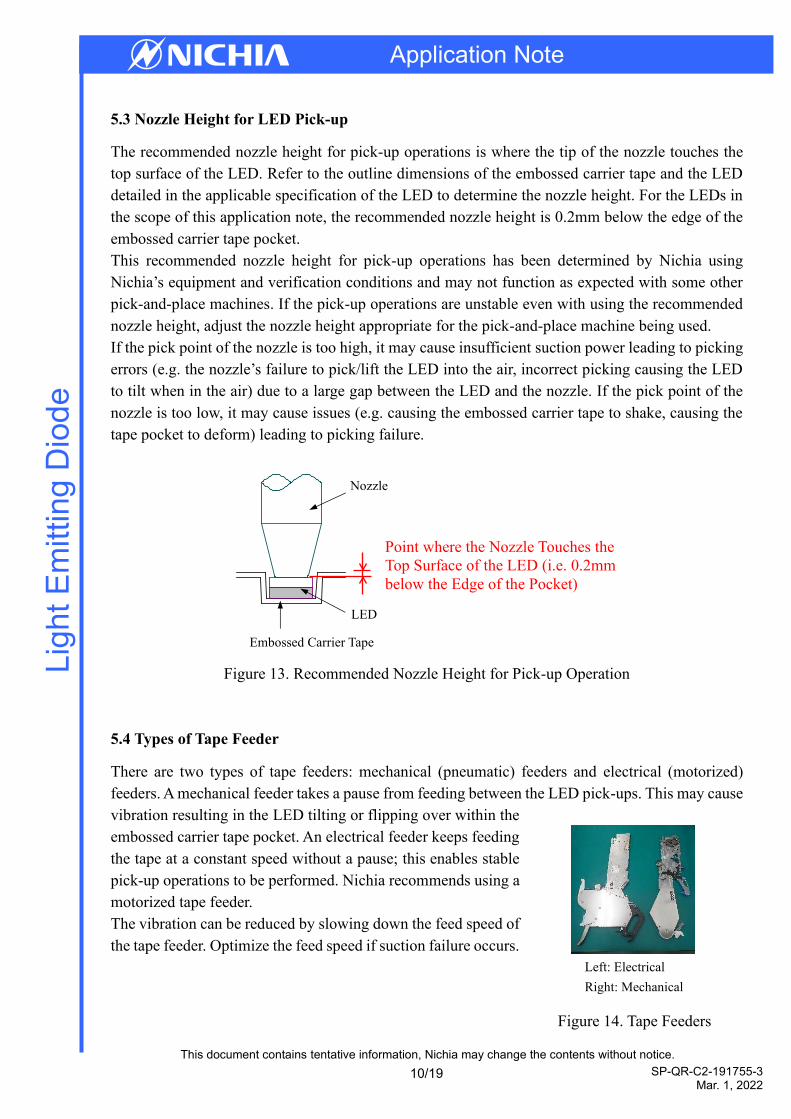
5.3 Nozzle Height for LED Pick-up
The recommended nozzle height for pick-up operations is where the tip of the nozzle touches the
top surface of the LED. Refer to the outline dimensions of the embossed carrier tape and the LED
detailed in the applicable specification of the LED to determine the nozzle height. For the LEDs in
the scope of this application note, the recommended nozzle height is 0.2mm below the edge of the
embossed carrier tape pocket.
This recommended nozzle height for pick-up operations has been determined by Nichia using
Nichia’s equipment and verification conditions and may not function as expected with some other
pick-and-place machines. If the pick-up operations are unstable even with using the recommended
nozzle height, adjust the nozzle height appropriate for the pick-and-place machine being used.
If the pick point of the nozzle is too high, it may cause insufficient suction power leading to picking
errors (e.g. the nozzle’s failure to pick/lift the LED into the air, incorrect picking causing the LED
to tilt when in the air) due to a large gap between the LED and the nozzle. If the pick point of the
nozzle is too low, it may cause issues (e.g. causing the embossed carrier tape to shake, causing the
tape pocket to deform) leading to picking failure.
Figure 13. Recommended Nozzle Height for Pick-up Operation
5.4 Types of Tape Feeder
There are two types of tape feeders: mechanical (pneumatic) feeders and electrical (motorized)
feeders. A mechanical feeder takes a pause from feeding between the LED pick-ups. This may cause
vibration resulting in the LED tilting or flipping over within the
embossed carrier tape pocket. An electrical feeder keeps feeding
the tape at a constant speed without a pause; this enables stable
pick-up operations to be performed. Nichia recommends using a
motorized tape feeder.
The vibration can be reduced by slowing down the feed speed of
the tape feeder. Optimize the feed speed if suction failure occurs.
Point where the Nozzle Touches the
Top Surface of the LED (i.e. 0.2mm
below the Edge of the Pocket)
Nozzle
LED
Embossed Carrier Tape
Left: Electrical
Right: Mechanical
Figure 14. Tape Feeders

Application Note Lig
ht E
mitting D
iod
e
11/19
SP-QR-C2-191755-3 Mar. 1, 2022
This document contains tentative information, Nichia may change the contents without notice.
5.5 Top Cover Tape Removal Position and LED Pick-up Position
If the top cover tape is removed early before LED pick-up, the LED may move within the embossed
carrier tape pocket and hit the feeder cover resulting in the emitting surface being damaged. Nichia
recommends removing the top cover tape immediately before LED pick-up.
Figure 15. Top cover Tape Removal Positions
5.6 Measures against Static Charges
If the pick-and-place operations are performed in environments
where static charges are likely to occur (e.g. low humidity
environment), the LEDs may stick to the top cover tape when
the top cover tape is removed due to static charges, leading to
pick-up errors. If a large amount of static charge is generated,
the LEDs may stick to the top cover tape successively as shown
in Figure 16. The following examples are recommended
measures to reduce the static charge:
a) Humidity Control
Controlling humidity in the operation environment is a
very effective measure against static charges. When the
humidity in the environment is greater than 50%RH, it can
largely reduce static charges that occur when removing the
top cover tape.
b) Early before Pick-up
Pick-up Position
Top Cover Tape Removal Position
a) Immediately before Pick-up (Recommended)
Pick-up Position
Top Cover Tape Removal Position
Feeder Cover
Top Cover Tape
Nozzle
0
50
100
150
200
250
300
350
400
60%RH 40%RH 30%RH 20%RH
帯電圧
[V]
湿度管理レベル
Figure 17. Humidity vs. Static Voltage
Sta
tic
Volt
age
(V)
Humidity Control Level
Figure 16. LED Sticking due to
Static Charge

Application Note Lig
ht E
mitting D
iod
e
12/19
SP-QR-C2-191755-3 Mar. 1, 2022
This document contains tentative information, Nichia may change the contents without notice.
b) Feed Speed of the Tape Feeder
If the movement of the LEDs within the embossed carrier tape pocket is reduced by slowing down
the feed speed of the tape feeder, the static charge may be reduced.
Figure 18. Feed Speed of the Tape Feeder
c) Magnet under the Embossed Carrier Tape
If a magnet is placed under the embossed carrier tape, it may prevent the LED from sticking to
the top cover tape due to the attraction generated between the magnet and the electrodes of the
LED. Use a magnet recommended for the pick-and-place machine being used.
Figure 19. Magnet under the Embossed Carrier Tape
d) Changing the Top Cover Tape Removal Position
If the top cover tape removal position is changed to early before where the LED is picked up, it
may prevent the LEDs from sticking to the top cover tape. However, this may lead to the LED
hitting the feeder cover; necessary measures (e.g. using a magnet, adjusting the feed speed) should
be taken to reduce the movement of the LED within the embossed carrier tape pocket.
The LED and the top cover tape
are attracted by a static charge
Magnet Magnetic Force between the Magnet and the LED Electrodes
Feeder Cover Nozzle
Top Cover Tape
LED
Embossed Carrier Tape
LED
Embossed Carrier Tape
Top Cover Tape
Feed speed is fast Feed speed is slow
Nozzle CorrectIncorrect

Application Note Lig
ht E
mitting D
iod
e
13/19
SP-QR-C2-191755-3 Mar. 1, 2022
This document contains tentative information, Nichia may change the contents without notice.
5.7 LED Placement
When placing the LED on the PCB, the nozzle should further press the LED 0.2mm onto the PCB
from the height where the LED first touches the solder paste. If the placement depth of the nozzle
is insufficient, the LED may float or shift after reflow. If the placement depth is too large, an
excessive pressure may be applied to the LED resulting in the emitting surface being damaged and/or
solder balls may occur.
The relationship between the placement depth and the placement speed determines the size of the
nozzle’s placement pressure on the LED. A large placement pressure may damage the emitting
surface and/or the package affecting the performance and/or the reliability of the LED. Ensure that
the placement pressure is ≤3.5N/mm2 and the
maximum force applied to the LED does not
exceed 5N. The placement pressure changes if
there is a warpage in the PCB; verify that the
operation conditions do not cause damage to the
LED in the actual mounting process before
starting the operation.
Examples of the Causes of the Placement Errors
a) Solder Printing Failures
If a solder printing failure (e.g. significantly
small amount of the solder paste printed on
the PCB) occurs or if the LED is placed on
the PCB after the solder paste is printed on it and left for a while, adhesion of the solder paste
may become insufficient causing placement errors (e.g. the LED to stick to the nozzle after
placement).
b) Foreign Substance on the Nozzle Tip
If a foreign substance is attached to the tip of the nozzle, the LED may stick to the nozzle and not
be released after placement. Ensure that the tip of the nozzle is not contaminated and/or has no
foreign substance before pick-and-place operations.
5.8 Rewinding of a Tape on a Reel
To rewind the embossed carrier tape when the operation is interrupted, the force applied must be
≤10N to the embossed carrier tape. Otherwise, the LED may stick to the top cover tape and/or the
embossed carrier tape pocket may be deformed resulting in the LED being damaged.
5.9 Check List for Pick-up/Placement Errors
Since the LEDs in the scope of this application note are small and lightweight, there is a possibility
that pick-up/placement errors may occur. Table 3 provides a check list to prevent the pick-
up/placement errors. Use the list as reference to prevent these errors.
Placement Depth:
0.2mm
Nozzle
Placement Pressure: ≤3.5N/mm2
Maximum Force: 5N
PCB
LED
Figure 20. Recommended Nozzle Height
for Placement Operation

Application Note Lig
ht E
mitting D
iod
e
14/19
SP-QR-C2-191755-3 Mar. 1, 2022
This document contains tentative information, Nichia may change the contents without notice.
Table 3. Check List to Prevent LED Pick-up/Placement Errors
If the answer to an item is “No”, refer to the applicable notes provided in Note column and take necessary measures.
Check Item Answer Note P
ick
-up
Is the feeder being used is an electrical
(motorized) feeder? Yes No
Mechanical feeders may cause frequent vibration; the
LED may move in the tape pocket causing pick-up
errors more likely to occur.
Is the top cover tape removed
immediately before the LED pick-up
position?
Yes No
If the top cover tape is removed early before LED pick-
up and that causes the emitting surface of the LED to be
damaged, change the top cover tape removal position to
immediately before pick-up. If removing the tape early
before pick-up is preferred in order to prevent static
charges, measures should be taken to reduce the
vibration as much as possible (e.g. slowing down the
feed speed).
Is a magnet placed under the tape
feeder? Yes No
Pick-up errors caused by static charges/vibration may
be reduced by using a magnet.
Pla
cem
ent
Is the nozzle being used specifically
designed for the LED according to the
size recommendations?
Yes No
If pick-up/placement errors occur or the emitting
surface of the LED is damaged, use a nozzle
specifically designed for the LED.
Are there any contamination/foreign
substances on the tip of the nozzle? Yes No
Contamination/foreign substances may cause the LED
to stick to the tip of the nozzle resulting in placement
errors.
Are there any burrs, chipping, or
scratches on the tip of the nozzle? Yes No
Burrs/chipping/scratches on the nozzle tip may damage
the emitting surface of the LED.
Has an LED placement with a slower
placement speed been tested? Yes No
If the placement speed is fast, the LED may not be
released from the nozzle (the nozzle may fail to mount
the LED).
Is the placement pressure ≤3.5N/mm2
and the maximum stress ≤5N? Yes No
If the placement speed is fast, the force (pressure)
applied to the LED increases, which may cause the
emitting surface of the LED to be damaged.
Is the pressing depth set 0.2mm? Yes No
If the pressing depth is too large, the force increases,
which may cause the emitting surface of the LED to be
damaged.
En
vir
on
men
t Is the storage temperature appropriate
(not too high)? Yes No
If the LEDs are stored under a high temperature for a
long time, they may stick to the top cover tape.
Is the humidity controlled in the
storage/operation environments to
reduce static charges?
Yes No Controlling the humidity can reduce the occurrence of
surge from static electricity and of static charges.
Oth
ers
Is the PCB flat (i.e. not bent/warped)? Yes No
If the PCB is severely warped or bent, the LED may not
touch the solder paste on the PCB properly, causing
placement errors.
Do the sizes of the metal solder stencil
apertures conform to the
recommendations?
Yes No If the solder amount is excessively small, it may cause
placement errors.
Is the amount of solder being printed
stable? Yes No
If the metal solder stencil cannot release the solder
paste properly, the amount of the solder paste left on the
PCB may be extremely small, causing placement errors.
Is the solder being used not
deteriorated? Yes No
If the solder printing operation continues for a long
period of time or if deteriorated solder paste is used, it
may cause printing failures and/or placement errors
(e.g. due to an insufficient adhesion of the solder paste).

Application Note Lig
ht E
mitting D
iod
e
15/19
SP-QR-C2-191755-3 Mar. 1, 2022
This document contains tentative information, Nichia may change the contents without notice.
6. Reflow
6.1 Reflow Conditions
Figure 21 shows the Nichia recommended reflow soldering conditions provided in the applicable
specification of the LED; use the recommended reflow conditions specified by the manufacturer of
the solder paste being used if it works better for the chosen application.
Additionally, Nichia recommends using a nitrogen reflow atmosphere (O2 concentration: <500ppm).
If the reflow is performed with an air atmosphere, the heat and atmosphere in the reflow oven may
cause the optical characteristics of the LED to degrade.
Note that reflow soldering must not be performed more than twice.
Figure 21. Reflow Soldering Condition (Lead-free Solder)
When cooling the LEDs from the peak temperature, a gradual cooling slope is recommended; do
not cool the LEDs rapidly. Use the cooling rate of 1.5 to 2℃/sec. for reference. If the components
mounted on the PCB are damaged and/or the solder joint strength is insufficient, the conditions
should be adjusted.
6.2 Considerations for the Transfer Board
When using a transfer board for machine mounting, the PCB is
placed on the transfer board (transfer jig) to move throughout
the mounting process; however, if the transfer board is warped,
mounting failures will occur. In addition, even if there is no
warpage in the transfer board in the early stages of production,
warpage may occur if the same transfer board is used for the
reflow process a few dozen times. It is recommended to make
sure that warping does not occur by passing the material that
would be used for the transfer board through the reflow process
a few dozen times before using it during actual production use.
PreparationSolder
PrintingMounting Reflow Inspection
Figure 22. Transfer Board
Application Note Lig
ht E
mitting D
iod
e
16/19
SP-QR-C2-191755-3 Mar. 1, 2022
This document contains tentative information, Nichia may change the contents without notice.
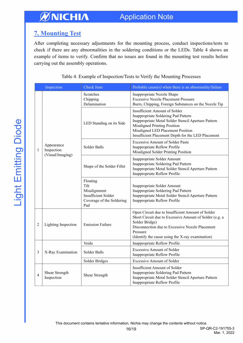
7. Mounting Test
After completing necessary adjustments for the mounting process, conduct inspections/tests to
check if there are any abnormalities in the soldering conditions or the LEDs. Table 4 shows an
example of items to verify. Confirm that no issues are found in the mounting test results before
carrying out the assembly operations.
Table 4. Example of Inspection/Tests to Verify the Mounting Processes
Inspection Check Item Probable cause(s) when there is an abnormality/failure
1
Appearance
Inspection
(Visual/Imaging)
Scratches
Chipping
Delamination
Inappropriate Nozzle Shape
Excessive Nozzle Placement Pressure
Burrs, Chipping, Foreign Substances on the Nozzle Tip
LED Standing on its Side
Insufficient Amount of Solder
Inappropriate Soldering Pad Pattern
Inappropriate Metal Solder Stencil Aperture Pattern
Misaligned Printing Position
Misaligned LED Placement Position
Insufficient Placement Depth for the LED Placement
Solder Balls
Excessive Amount of Solder Paste
Inappropriate Reflow Profile
Misaligned Solder Printing Position
Shape of the Solder Fillet
Inappropriate Solder Amount
Inappropriate Soldering Pad Pattern
Inappropriate Metal Solder Stencil Aperture Pattern
Inappropriate Reflow Profile
Floating
Tilt
Misalignment
Insufficient Solder
Coverage of the Soldering
Pad
Inappropriate Solder Amount
Inappropriate Soldering Pad Pattern
Inappropriate Metal Solder Stencil Aperture Pattern
Inappropriate Reflow Profile
2 Lighting Inspection Emission Failure
Open Circuit due to Insufficient Amount of Solder
Short Circuit due to Excessive Amount of Solder (e.g. a
Solder Bridge)
Disconnection due to Excessive Nozzle Placement
Pressure
(Identify the cause using the X-ray examination)
3 X-Ray Examination
Voids Inappropriate Reflow Profile
Solder Balls Excessive Amount of Solder
Inappropriate Reflow Profile
Solder Bridges Excessive Amount of Solder
4 Shear Strength
Inspection Shear Strength
Insufficient Amount of Solder
Inappropriate Soldering Pad Pattern
Inappropriate Metal Solder Stencil Aperture Pattern
Inappropriate Reflow Profile

Application Note Lig
ht E
mitting D
iod
e
17/19
SP-QR-C2-191755-3 Mar. 1, 2022
This document contains tentative information, Nichia may change the contents without notice.
Since the mounting status changes due to slight differences in setting conditions, as well as
differences in the solder paste, PCB, and mounting equipment/parts, etc.; always check and control
the soldering status after mounting. By using an automatic solder visual inspection system (i.e. one
that can provide an image where it is easy to judge if the image is good or if there is a defect), it is
possible to improve the efficiency of work and reduce the dependence on the operator’s skill
compared to visual inspection.
Figure 23. Example of the Inspection Using an Automatic Solder Visual Inspection System
8. Inspection
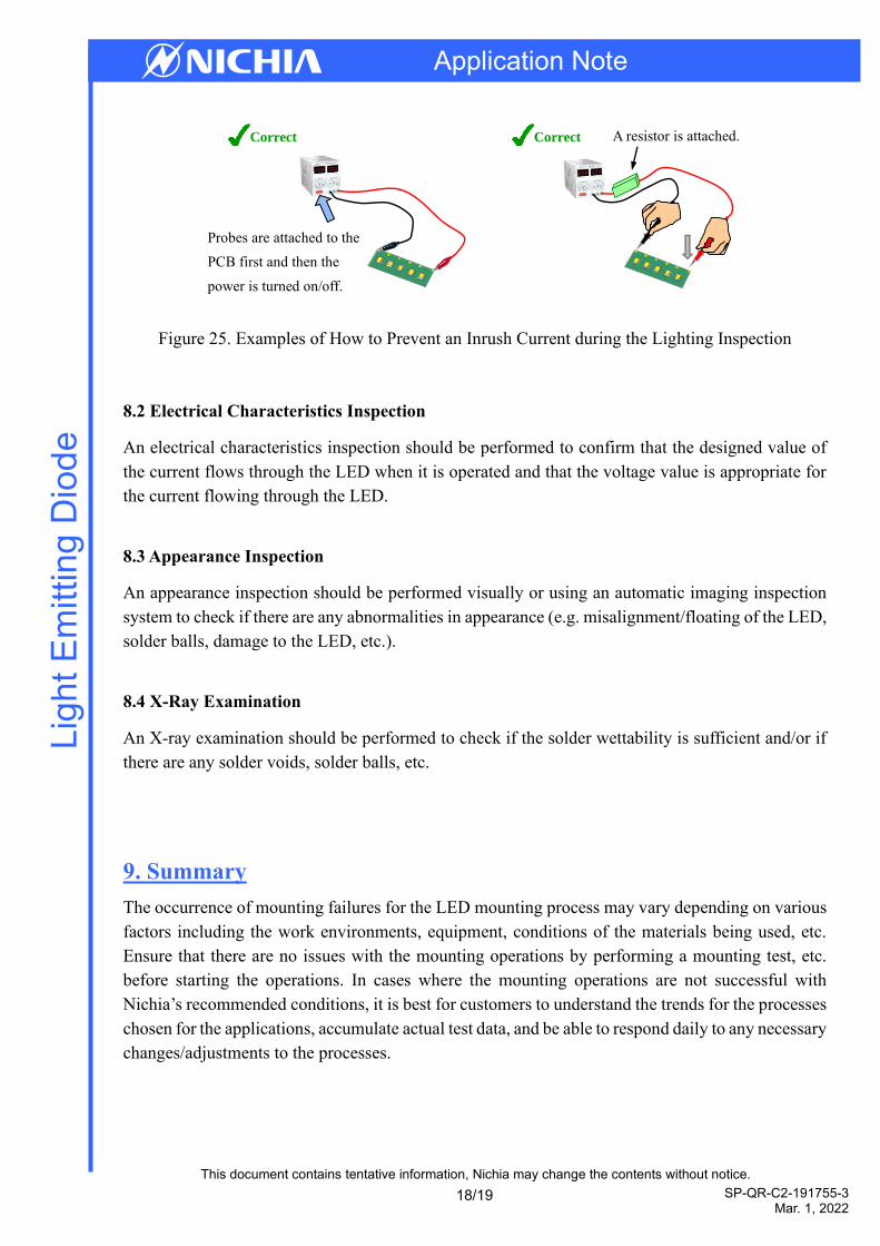
8.1 Lighting Inspection
The lighting inspection is performed either visually or using an automatic imaging inspection system
to check if all the LEDs emit light without issues. When a test voltage is applied to the PCB during
the lighting inspection, a large current exceeding the absolute maximum rating may temporarily
flow through the LED due to the inrush current; if the current is too large, the electrodes of the LED
may be damaged causing the LED not to emit light. Ensure that the inrush current will not flow to
the LED.
Figure 24. Example of an Inappropriate Lighting Inspection Causing an Inrush Current
PreparationSolder
PrintingMounting
FailureReflow Inspection
Probes are attached to
the PCB when the power
is on.
Damaged Electrodes of the LED
chip due to the Inrush Current.
Current
Peak Current
Inrush Current
Constant Current
Time
Incorrect
Application Note Lig
ht E
mitting D
iod
e
18/19
SP-QR-C2-191755-3 Mar. 1, 2022
This document contains tentative information, Nichia may change the contents without notice.
Figure 25. Examples of How to Prevent an Inrush Current during the Lighting Inspection
8.2 Electrical Characteristics Inspection
An electrical characteristics inspection should be performed to confirm that the designed value of
the current flows through the LED when it is operated and that the voltage value is appropriate for
the current flowing through the LED.
8.3 Appearance Inspection
An appearance inspection should be performed visually or using an automatic imaging inspection
system to check if there are any abnormalities in appearance (e.g. misalignment/floating of the LED,
solder balls, damage to the LED, etc.).
8.4 X-Ray Examination
An X-ray examination should be performed to check if the solder wettability is sufficient and/or if
there are any solder voids, solder balls, etc.
9. Summary
The occurrence of mounting failures for the LED mounting process may vary depending on various
factors including the work environments, equipment, conditions of the materials being used, etc.
Ensure that there are no issues with the mounting operations by performing a mounting test, etc.
before starting the operations. In cases where the mounting operations are not successful with
Nichia’s recommended conditions, it is best for customers to understand the trends for the processes
chosen for the applications, accumulate actual test data, and be able to respond daily to any necessary
changes/adjustments to the processes.
Probes are attached to the
PCB first and then the
power is turned on/off.
A resistor is attached. Correct Correct

Application Note Lig
ht E
mitting D
iod
e
19/19
SP-QR-C2-191755-3 Mar. 1, 2022
This document contains tentative information, Nichia may change the contents without notice.
Disclaimer
This application note is a controlled document of Nichia Corporation (Nichia) published to provide
technical information/data for reference purposes only. By using this application note, the user
agrees to the following:
・ This application note has been prepared solely for reference on the subject matters incorporated
within it and Nichia makes no guarantee that customers will see the same results for their chosen
application.
・ The information/data contained herein are only typical examples of performances and/or
applications for the product. Nichia does not provide any guarantees or grant any license under
or immunity from any intellectual property rights or other rights held by Nichia or third parties.
・ Nichia makes no representation or warranty, express or implied, as to the accuracy, completeness
or usefulness of any information contained herein. In addition, Nichia shall not be liable for any
damages or losses arising out of exploiting, using, or downloading or otherwise this document,
or any other acts associated with this document.
・ The content of this application note may be changed without any prior or subsequent notice.
・ Copyrights and all other rights regarding the content of this document are reserved by Nichia or
the right holders who have permitted Nichia to use the content. Without prior written consent of
Nichia, republication, reproduction, and/or redistribution of the content of this document in any
form or by any means, whether in whole or in part, including modifications or derivative works
hereof, is strictly prohibited.
NICHIA CORPORATION 491 Oka, Kaminaka-Cho, Anan-Shi,TOKUSHIMA 774-8601, JAPAN
Phone: +81-884-22-2311 Fax: +81-884-21-0148http://www.nichia.co.jp