ANEL Lab Manual.pdf - LNMIIT
60
The LNMIIT, Jaipur Electronics and Communication Department Analog Electronics Laboratory ANEL Lab File Experiment-1 Page 1 of 10 EXPERIMENT 1 Aim: This laboratory experiment explores few of the diode applications. The purpose of this laboratory experiment is to study the clipping and clamping functions found in circuits using diodes. The designs that are required to be implemented and built are the various diode clipper and clamper circuits. Apparatus / Components Used: 1) DSO 2) Function Generator 3) DC power Supply 4) DSO Probes 5) Diode 1N4007 6) Resistors 470 , 51 K 7) Capacitor (0.1 F ) Theory: Clipping Circuits: In electronic system design and application circuits, it is frequently necessary to modify the shape of various waveforms for use in instrumentation, controls, computation, and communications. There are a variety of diode networks which can be designed for different applications. Clipper circuits have the ability to clip-off / cut-off a portion of the input signal without distorting the remaining part of the input alternating waveform. Depending on the orientation of the diode, portion of the positive or negative region of the input alternating signal is “clipped / cut” off. Among different circuits available, there are two general categories of clippers: series and parallel. The series clipper configuration is defined as one where the diode is in series with the load, while the parallel clipper circuits use the diode in a branch parallel to the load. There are different cases that are explored in this laboratory experiment with respect to clipping. One of the case is when clipping occurs in the forward active region. For example, a diode’s threshold voltage value is 0.7V. If one apply alternating input voltage across the diode, the clipping would occur at 0.7V, since, that is its threshold voltage of the diode. By adding a battery in series, threshold voltage of the clipping circuit can be modified. Adding a 1V battery next to the diode will now create a total clipping threshold voltage of 1.7V. In such circuits, applying any alternating input voltage signal greater than 1.7V as would cause a clipping at 1.7V. Anything less than that threshold value will pass right through, thus resulting in no clipping of input signal. The clipping region and levels can be controlled by the direction of the diode used and the amount of biased voltage connected across the diode. Figure 1.1(a) and Figure 1.2(a) shows a biased series clipper circuit. Depending on the polarities of biased voltage connected, the output voltage of this circuit will have the portions of positive half-cycles or negative half-cycles will be clipped off. For a practical diode clipper circuits the output voltage is equal to VO. [VO = Voltage Output = Biased Voltage ± Threshold voltage (VTh)]. Where, VTh is the cut-in voltage of the diode. In many clippers, the load resistor, RL, is much larger than the series resistor, R (i.e., RL >> R). If RL and R are comparable, then the output voltage VO will be given by: V V . R L R R Where, Vp is peak magnitude of the input voltage. 0 p L Figure 1.1(b) and 1.2 (b) shows the expected waveforms of the output voltage VO.
-
Upload
khangminh22 -
Category
Documents
-
view
0 -
download
0
Transcript of ANEL Lab Manual.pdf - LNMIIT

The LNMIIT, Jaipur Electronics and Communication Department
Analog Electronics Laboratory
ANEL Lab File Experiment-1 Page 1 of 10
EXPERIMENT 1
Aim: This laboratory experiment explores few of the diode applications. The purpose of this laboratory experiment is to study the clipping and clamping functions found in circuits using diodes. The designs that are required to be implemented and built are the various diode clipper and clamper circuits.
Apparatus / Components Used:
1) DSO 2) Function Generator 3) DC power Supply 4) DSO Probes 5) Diode 1N4007 6) Resistors 470 , 51 K
7) Capacitor (0.1 F )
Theory:
Clipping Circuits: In electronic system design and application circuits, it is frequently necessary to modify the shape of various waveforms for use in instrumentation, controls, computation, and communications. There are a variety of diode networks which can be designed for different applications. Clipper circuits have the ability to clip-off / cut-off a portion of the input signal without distorting the remaining part of the input alternating waveform. Depending on the orientation of the diode, portion of the positive or negative region of the input alternating signal is “clipped / cut” off. Among different circuits available, there are two general categories of clippers: series and parallel. The series clipper configuration is defined as one where the diode is in series with the load, while the parallel clipper circuits use the diode in a branch parallel to the load.
There are different cases that are explored in this laboratory experiment with respect to clipping. One of the case is when clipping occurs in the forward active region. For example, a diode’s threshold voltage value is 0.7V. If one apply alternating input voltage across the diode, the clipping would occur at 0.7V, since, that is its threshold voltage of the diode. By adding a battery in series, threshold voltage of the clipping circuit can be modified. Adding a 1V battery next to the diode will now create a total clipping threshold voltage of 1.7V. In such circuits, applying any alternating input voltage signal greater than 1.7V as would cause a clipping at 1.7V. Anything less than that threshold value will pass right through, thus resulting in no clipping of input signal. The clipping region and levels can be controlled by the direction of the diode used and the amount of biased voltage connected across the diode.
Figure 1.1(a) and Figure 1.2(a) shows a biased series clipper circuit. Depending on the polarities of biased voltage connected, the output voltage of this circuit will have the portions of positive half-cycles or negative half-cycles will be clipped off. For a practical diode clipper circuits the output voltage is equal to VO. [VO = Voltage Output = Biased Voltage ± Threshold voltage (VTh)]. Where, VTh is the cut-in voltage of the diode. In many clippers, the load resistor, RL, is much larger than the series resistor, R (i.e., RL >> R). If RL and R are comparable, then the output voltage VO will be given by:
V V . RL
R R Where, Vp is peak magnitude of the input voltage.
0 p L
Figure 1.1(b) and 1.2 (b) shows the expected waveforms of the output voltage VO.

The LNMIIT, Jaipur Electronics and Communication Department
Analog Electronics Laboratory
ANEL Lab File Experiment-1 Page 2 of 10
Figure 1.4 (b)
Figure 1.4 (a)
Figure 1.3 (b)
Figure 1.3 (a)
Figure 1.3 (a) and 1.4 (a) shows the circuit of biased parallel clipper circuit. In this case the
working of the clipper circuit are just opposite to that of the circuits in Figure 1.1(a) and 1.2(a) respectively. Here the circuit shown in Figure 1.3(a) will clip a portion of positive half of the input signal, whereas the circuit in Figure 1.4 (a) will clip a portion of negative half of the input signal. Again, in these cases, level of clipping will depend on the polarities of the biasing voltage applied. Figure 1.3 (b) and 1.4 (b) shows expected output voltage waveforms from these clipper circuits.
Shown below in Figure 1.5 (a) and 1.5 (b) are the circuits and output waveforms of two level clipper circuit using two diodes. In this case, two different clippers with two different biasing level are connected together to clip portions of both positive and negative halves of the input waveform.
Figure 1.2 (b)
Figure 1.2 (a)
Figure 1.1 (b)
Figure 1.1 (a)

The LNMIIT, Jaipur Electronics and Communication Department
Analog Electronics Laboratory
ANEL Lab File Experiment-1 Page 3 of 10
Figure 1.5 (a)
Figure 1.5 (b)
*** Design and use a potential divider circuit using two 1 K resistors to generate 2.5 Volts in the
circuit shown in Figure 1.5 (a).
Clampers
The clamping network is one that will “clamp / shift” a signal to a different DC voltage level. The network must have a capacitor, a diode, and a resistive element, but it can also employ an independent DC supply (i.e., bias voltage) to introduce an additional shift. The magnitude of R and C must be chosen such
that the time constant τ = RC is large enough to ensure that the voltage across the capacitor does not discharge significantly during the interval the diode is non-conducting. Throughout the analysis we will assume that for all practical purposes the capacitor will remain fully charge or discharge in
ive time constants. In Figure 1.6 (a) a positive DC clamper is shown. Working of clamper circuit: During the negative half-cycle of the input voltage, the diode turns
‘ON’ and it behaves like a short circuit. In this case we are assuming diode to be an ideal diode with VTh = 0V. When the input signal reaches at its negative peak, the capacitor charges up to -VP and during this whole negative cycle the output voltage (VO) is zero. When the input signal starts to rise towards positive half, the capacitor acts as a battery which is fully charged up-to the level of -VP. Since the capacitor is acting like a battery of -VP volts, now when the input signal reaches positive peak VP, the overall output voltage reaches up-to +2VP. Similarly in Figure 1.7 (a), the output signal shifts towards negative side with an added negative DC to the input signal, causing the negative peak of the output signal to reach up-to -2VP. Expected output waveforms are shown in Figure 1.6 (b) and1.7 (b) respectively.
Figure 1.8 (a) and 1.9 (a) shows the circuit of clamper circuits with added bias voltages. The expected output waveforms of the circuits are shown below their respective circuits in Figure 1.8 (b) and 1.9 (b).

The LNMIIT, Jaipur Electronics and Communication Department
Analog Electronics Laboratory
ANEL Lab File Experiment-1 Page 4 of 10
Figure 1.9 (b)
Figure 1.9 (a)
Figure 1.8 (b)
Figure 1.8 (a)
Figure 1.7 (b)
Figure 1.7 (a)
Figure 1.6 (b)
Figure 1.6 (a)
The LNMIIT, Jaipur Electronics and Communication Department
Analog Electronics Laboratory
ANEL Lab File Experiment-1 Page 5 of 10
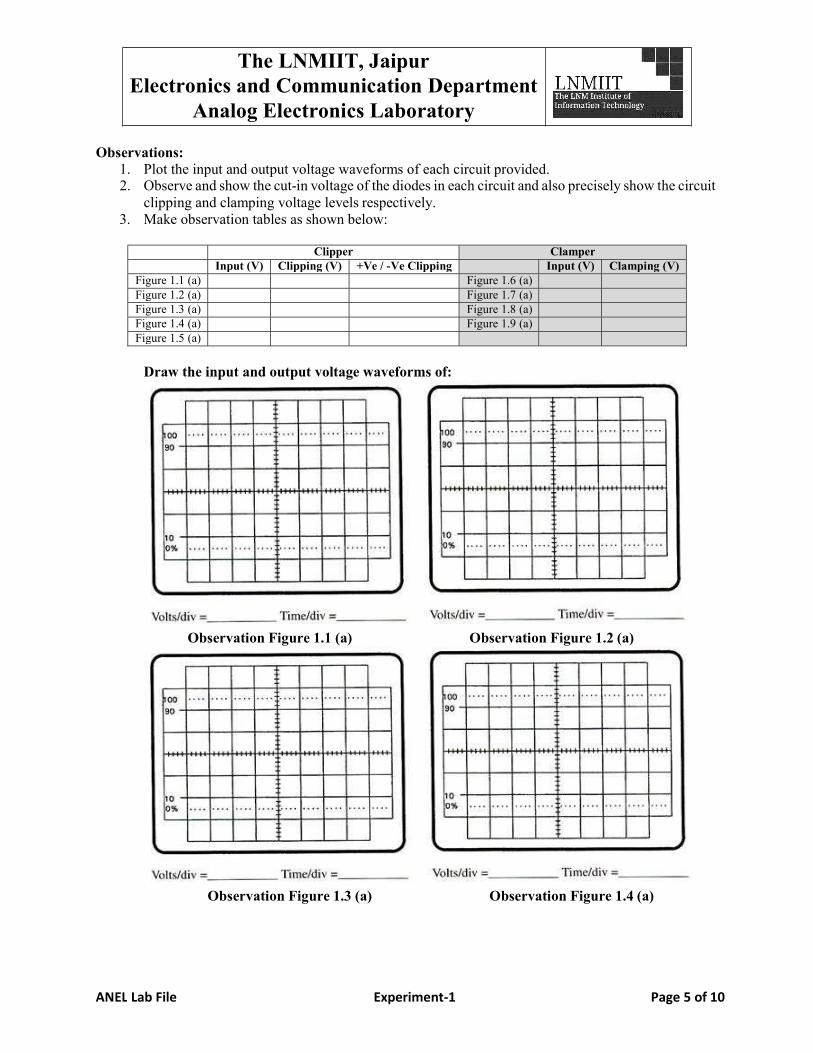
Observations: 1. Plot the input and output voltage waveforms of each circuit provided. 2. Observe and show the cut-in voltage of the diodes in each circuit and also precisely show the circuit
clipping and clamping voltage levels respectively. 3. Make observation tables as shown below:
Clipper Clamper Input (V) Clipping (V) +Ve / -Ve Clipping Input (V) Clamping (V)
Figure 1.1 (a) Figure 1.6 (a)
Figure 1.2 (a) Figure 1.7 (a)
Figure 1.3 (a) Figure 1.8 (a)
Figure 1.4 (a) Figure 1.9 (a)
Figure 1.5 (a)
Draw the input and output voltage waveforms of:
Observation Figure 1.1 (a) Observation Figure 1.2 (a)
Observation Figure 1.3 (a) Observation Figure 1.4 (a)
The LNMIIT, Jaipur Electronics and Communication Department
Analog Electronics Laboratory
ANEL Lab File Experiment-1 Page 6 of 10
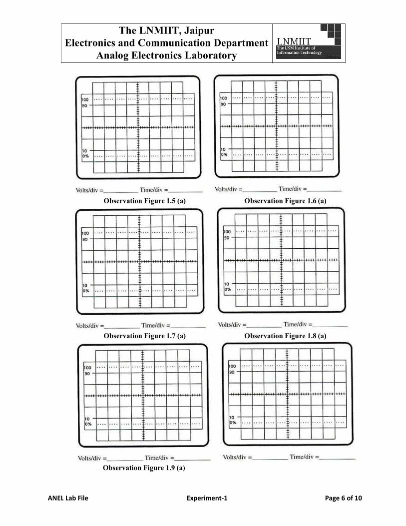
Observation Figure 1.5 (a) Observation Figure 1.6 (a)
Observation Figure 1.7 (a) Observation Figure 1.8 (a)
Observation Figure 1.9 (a)

The LNMIIT, Jaipur Electronics and Communication Department
Analog Electronics Laboratory
ANEL Lab File Experiment-1 Page 7 of 10
Precautions:
1. While doing the experiment do not exceed the readings of the diode. This may lead to damaging of the diode.
2. Connect voltmeter and ammeter in correct polarities as shown in the circuit diagram. 3. Do not switch ON the power supply unless you have checked the circuit connections as
per the circuit diagram. Viva Questions:
1. What are trivalent and pentavalent impurities? 2. How PN junction diode does acts as a switch? 3. What is diode current equation? 4. What is the value of VTh at room temperature? 5. Dynamic resistance expression?

The LNMIIT, Jaipur Electronics and Communication Department
Analog Electronics Laboratory
ANEL Lab File Experiment-1 Page 8 of 10
6. What is a semiconductor? 7. What is meant by intrinsic semiconductor? 8. What is the order of energy gap in a pure semiconductor? 9. What is an extrinsic semiconductor? 10. What is a doped semiconductor? 11. What is doping? 12. What are two different types of impurities? 13. To which group does a (i) p-type, (ii) n type impurity belong? 14. What are the charge carriers in a pure semiconductor? 15. What are the charge carriers in n-type semiconductor? 16. What is the effect of temperature on conductivity of a semiconductor? 17. What is junction diode? 18. What is meant by forward bias? 19. What is meant by reverse bias? 20. What is knee voltage? 21. What is reverse breakdown? 22. What are the semiconductor materials in use? 23. Why is Silicon used popularly compared to Germanium? 24. How many valence electrons are there in each atom of a semiconductor? 25. What are the p type doping materials and n type doping materials? 26. How many valence electrons are there in P type doping materials and in n type doping materials? 27. Draw the ideal, practical and piecewise linear characteristics of a PN junction diode. 28. What is the static resistance of a diode? 29. What is the dynamic resistance of a diode? 30. How PN junction diode does act as a switch? 31. What is cut-in voltage? What are its values for Si and Ge diodes? 32. Write the Diode current Equation.
Experiment Date
/ Student Task Max. Marks Graded Marks
Pre-Lab Preparation
Submission Date
/ Performance
Observation and Inference
Submission Delay
/ Completion of Experiments
Total
------------------------------------ Signature of Lab Instructor

The LNMIIT, Jaipur Electronics and Communication Department
Analog Electronics Laboratory
ANEL Lab File Experiment-1 Page 9 of 10
For Rough Works/other supporting Documents

The LNMIIT, Jaipur Electronics and Communication Department
Analog Electronics Laboratory
ANEL Lab File Experiment-1 Page 10 of 10
For Rough Works/other supporting Documents
The LNMIIT, Jaipur Electronics and Communication Department
Analog Electronics Laboratory
ANEL Lab File Experiment-2 Page 1 of 8
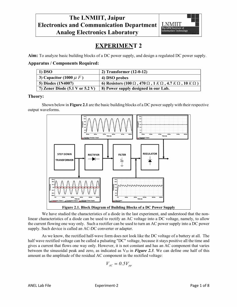
Figure 2.1. Block Diagram of Building Blocks of a DC Power Supply
EXPERIMENT 2
Aim: To analyze basic building blocks of a DC power supply, and design a regulated DC power supply.
Apparatus / Components Required:
1) DSO 2) Transformer (12-0-12) 3) Capacitor (1000 F ) 4) DSO probes 5) Diodes (1N4007) 6) Resistors (100 , 470 , 1 K , 4.7 K , 10 K ) 7) Zener Diode (5.1 V or 5.2 V) 8) Power supply designed in our Lab.
Theory:
Shown below in Figure 2.1 are the basic building blocks of a DC power supply with their respective output waveforms.
We have studied the characteristics of a diode in the last experiment, and understood that the non- linear characteristics of a diode can be used to rectify an AC voltage into a DC voltage, namely, to allow the current flowing one way only. Such a rectifier can be used to turn an AC power supply into a DC power supply. Such device is called an AC-DC converter or adapter.
As we know, the rectified half-wave form does not look like the DC voltage of a battery at all. The half wave rectified voltage can be called a pulsating "DC" voltage, because it stays positive all the time and gives a current that flows one way only. However, it is not constant and has an AC component that varies between the sinusoidal peak and zero, as indicated as VPP in Figure 2.3. We can define one half of this amount as the amplitude of the residual AC component in the rectified voltage:
VAC 0.5Vpp
The LNMIIT, Jaipur Electronics and Communication Department
Analog Electronics Laboratory
ANEL Lab File Experiment-2 Page 2 of 8
Figure 2.3 Figure 2.2
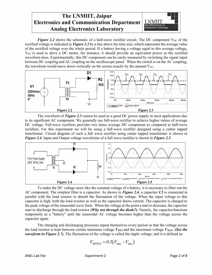
Figure 2.2 shows the schematic of a half-wave rectifier circuit. The DC component VDC of the rectified voltage is indicated in Figure 2.3 by a line above the time axis, which represents the average value of the rectified voltage over the whole period. If a battery having a voltage equal to this average voltage, VDC is used to drive a DC motor, for instance, it should provide an equivalent power as the rectified waveform does. Experimentally, this DC component can be easily measured by switching the signal input between DC coupling and AC coupling on the oscilloscope panel. When the switch is on the AC coupling, the waveform would move down vertically on the screen exactly by the amount VDC.
The waveform of Figure 2.3 cannot be used as a good DC power supply in most applications due to its significant AC component. We generally use full-wave rectifier to achieve higher values of average DC voltage. Full-wave rectifiers provides two times average DC component as compared to half-wave rectifiers. For this experiment we will be using a full-wave rectifier designed using a center tapped transformer. Circuit diagram of such a full wave rectifier using center tapped transformer is shown in Figure 2.4. Input and Output voltage waveforms of a full wave rectifier is shown in Figure 2.5.
To make the DC voltage more like the constant voltage of a battery, it is necessary to filter out the
AC component. The simplest filter is a capacitor. As shown in Figure 2.6, a capacitor C1 is connected in parallel with the load resistor to absorb the fluctuation of the voltage. When the input voltage to this capacitor is high, both the load resistor as well as the capacitor draws current. The capacitor is charged to the peak voltage of the sinusoidal wave form. When the voltage at the point a start to decrease, the capacitor start to discharge through the load resistor (Why not through the diode?). Namely, the capacitor functions temporarily as a "battery" until the sinusoidal AC voltage becomes higher than the voltage across the capacitor again.
The charging and discharging processes repeat themselves every period so that the voltage across the load resistor is kept between certain minimum voltage VMIN and the maximum voltage VMAX. (See the waveform in Figure 2.7). The fluctuation of the voltage is called the ripple voltage, and it is defined as:
VRIPPLE 0.5Vmax Vmin
Figure 2.5 Figure 2.4

The LNMIIT, Jaipur Electronics and Communication Department
Analog Electronics Laboratory
ANEL Lab File Experiment-2 Page 3 of 8
Figure 2.9 Figure 2.8
The smaller the ripple voltage, the better the DC power supplies. We can therefore define a parameter called the "ripple factor" as one of the criteria of the quality of the power supply:
Ripple _ Factor Vripple / VDC 100%
Apparently, the larger the capacitance, the smaller the ripple factor and the better the power supply. In order to keep the voltage almost constant, the product of the capacitance and the load resistance needs to be much greater than the period of the AC voltage. (Why?)
Finally to achieve a regulated DC voltage from the filtered output of a full-wave rectifier, we use regulators. Zener diodes are generally used to regulate the fluctuating DC voltages, but there are other ICs also available with different voltage output ratings. Zener diodes are still used in most of these regulator ICs. Regulator ICs vary according to their ability to generate a precise regulated DC output voltage and their ability to control current with varying output loads. Figure 2.8 shows a complete circuit of a basic DC power supply. Figure 2.9 shows the regulated DC voltage output from the power supply we designed. We can obtain different regulated VDC depending on the breakdown voltage of the Zener diode. Note that, the regulated output DC voltage can never be greater than the magnitude of fluctuating DC voltage obtained after filter circuit. Load regulation is a very important factor to decide the quality of a regulated DC power supply. Load regulation of a constant-voltage source is defined by the equation:
Load _ regulation Vmin_ load Vmax_ load 100% Vmax_ load
= VO Change in output voltageIL Change in load current
Where, Vmax_load is the voltage at maximum load. The maximum load is the one that draws the greatest current, i.e. the lowest specified load resistance (never short circuit). Vmin_load is the voltage at
Figure 2.7 Figure 2.6

The LNMIIT, Jaipur Electronics and Communication Department
Analog Electronics Laboratory
ANEL Lab File Experiment-2 Page 4 of 8
minimum load. The minimum load is the one that draws the least current, i.e. the highest specified load resistance (possibly open circuit for some types of linear supplies, usually limited by pass transistor minimum bias levels). Vnom_load is the voltage at the typical specified load.
Summary:
Almost every electronic circuit is designed to operate at a constant DC supply. A regulated power supply provides this constant DC output voltage and continuously holds
the output voltage at the design value regardless of changes in load current or input voltage. The power supply contains a transformer, rectifier, filter, and regulator. The rectifier changes the AC input voltage to pulsating DC voltage. The filter section removes the
ripple component and provides an unregulated DC voltage to the regulator section. The regulator is designed to deliver a constant voltage to the load under varying circuit conditions.
The two factors that can cause the voltage across the load to vary are fluctuations in input voltage and changes in load current. Load regulation is a measurement of power supply, showing its capacity to maintain a constant voltage across the load with changes in load current, whereas, line regulation is a measurement of power supply, showing its capacity to maintain a constant output voltage with changes in input voltage. Suggest
Procedure
Use the power designed in our institute to obtain the output from the secondary coil of the transformer. 1) Connect the circuit as sequentially as in Figure 2.4, 2.6 and 2.8 respectively. 2) Use CRO to observe the behavior of the input and output waveforms of each block of power supply
mentioned above.
Observations:
1) Calculate Load Regulation Observe the No load voltage and Full load voltage Calculate the load regulation.
Load
Resistance (RL)
Measured DC
Voltage
Measured Ripple
Voltage
Calculated % Ripple
Calculated DC
Current (mAmps)
VC VZ VRPP(C) VRPP(Out) % VRPP(C) % VRPP(Out) IR IZ IL
RL Removed
220Ω
1.0 KΩ
4.7 KΩ
10 KΩ
Where, VC = Voltage across capacitor (without Zener) VRPP(C) = Ripple Voltage across capacitor VZ = Voltage across Zener diode VRPP(Out) = Ripple Voltage across Zener diode IR = Current across resistor R IZ = Current across resistor Zener IL = Current across resistor Load Resistor RL
The LNMIIT, Jaipur Electronics and Communication Department
Analog Electronics Laboratory
ANEL Lab File Experiment-2 Page 5 of 8
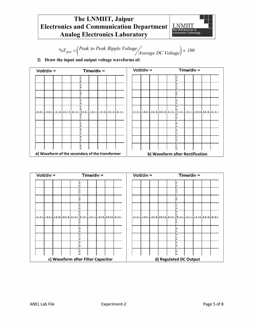
b) Waveform after Rectification a) Waveform of the secondary of the transformer
d) Regulated DC Output c) Waveform after Filter Capacitor
%VRPP Peak to Peak Ripple Voltage
Average DC Voltage 100
2) Draw the input and output voltage waveforms of:

The LNMIIT, Jaipur Electronics and Communication Department
Analog Electronics Laboratory
ANEL Lab File Experiment-2 Page 6 of 8
Precautions: 1. While doing the experiment do not exceed the readings of the diode. This may lead to damaging
of the diode. 2. Connect voltmeter and ammeter in correct polarities as shown in the circuit diagram. 3. Do not switch ON the power supply unless you have checked the circuit connections as per the
circuit diagram. 4. Take care of the polarities of electrolytic capacitors. Electrolytic capacitor can blast if connected
with wrong polarity. 5. Do not short circuit the outputs from the secondary coils of the transformer with ground.
Bread Board Connections:
Viva Questions:
1) Why is the ripple voltage larger at full load? 2) Under full load conditions, what is the power dissipated by the regulator IC? 3) Comment on the efficiency of the circuit for a minimum output voltage and a maximum output
voltage. 4) Explain what is Peak Inverse Voltage (PIV) of a diode in a rectifier circuit? 5) What modification needs to be done to obtain a variable output voltage? 6) Define: i) Ripple factor, ii) Load Regulation, iii) Line Regulation, and iv) Zener Breakdown
Experiment Date
/ Student Task Max. Marks Graded Marks
Pre-Lab Preparation
Submission Date
/ Performance
Observation and Inference
Submission Delay
/ Completion of Experiments
Total
------------------------------------ Signature of Lab Instructor

The LNMIIT, Jaipur Electronics and Communication Department
Analog Electronics Laboratory
ANEL Lab File Experiment-2 Page 7 of 8
For Rough Works/other supporting Documents

The LNMIIT, Jaipur Electronics and Communication Department
Analog Electronics Laboratory
ANEL Lab File Experiment-2 Page 8 of 8
For Rough Works/other supporting Documents

The LNMIIT, Jaipur Electronics and Communication Department
Analog Electronics Laboratory
ANEL Lab File Experiment-3 Page 1 of 6
Aim: EXPERIMENT 3
1) To measure the I-V characteristics of Red, Green and Blue light emitting diodes (LEDs). We will also observe the similarities and differences in the characteristics of LEDs and normal PN diodes.
2) To understand and measure some of the many important characteristics of the photodiode and Infrared LED.
Apparatus / Components Required: 1) DSO 2) DSO probes 3) Function Generator 4) Capacitor (1000 F ) 5) Resistors 100 , 10 K 6) LEDs (Green, Red, BLUE) / Multicolor LED 7) Photodiode 8) IR Pair
Theory:
Characteristics of LEDs:
Light Emitting Diodes (LEDs) are widely used in displays (including TVs, traffic lights and sign boards) and as light sources for optical communications, remote controls etc. All these LEDs with different colors have the same basis of operation, namely that of a p-n diode, and one can use the same characterization techniques learned in our previous experiment to characterize diodes. In the first part of this lab you will capture the forward bias I-V characteristics of three different LEDs.
We know that, when a p-n junction is forward biased, carriers (i.e. electron, holes) diffuse across the depletion region from the side with higher carrier density to the side with lower carrier density. Thus, one can say electrons will diffuse from the n-type side to the p-type side, while holes will diffuse in the opposite direction. Some carriers will make it past the edges of the depletion region; these are now minority carriers and can recombine with the local majority carriers. For semiconducting materials with an indirect bandgap, e.g. silicon, “non-radiative recombination” predominates, resulting in heating of the lattice, i.e. the PN junction gets hot. However, for direct bandgap materials – e.g. GaAs, AlGaAs, GaAsP, InP and GaN - the carriers can recombine by emitting energy in the form of visible light / photon.
This process is called “radiative recombination” and the diode produces light when the material is forward biased. This type of light production is called “injection electroluminescence”, since we are “injecting” carriers across the junction to undergo radiative recombination. The two recombination processes results in lowering of the carrier densities, which allow more diffusion of carriers from the source thus creating a current. The total diode current is the sum of two parts:
[1] A “radiative recombination” also known as a “diffusion” current (Id), and [2] A “non-radiative recombination” current (Inr). The non-radiative current is generated from
carriers that recombine at a surface. These carriers recombine without giving off a photon. The surface is usually at the edges of the p-n junction. The total diode current equation is:
q (VIRs ) q (VIRs )
I Id Inr Id .e kT Inr .e 2 KT (1)
Here, Rs is the device series resistance and Id’ and Inr’ are the saturation currents for the ‘diffusion’ and ‘non-radiative’ recombination currents, respectively. The light output is proportional to:
Id '.exp q V IRs / kBT (2)
At low bias voltage the ‘non-radiative’ current predominates and little light is emitted. With increasing bias voltage the proportion of ‘diffusion’ current becomes larger and when this term dominates

The LNMIIT, Jaipur Electronics and Communication Department
Analog Electronics Laboratory
ANEL Lab File Experiment-3 Page 2 of 6
Figure 3.1 Cross Sectional View of Multicolor LED
over the ‘non-radiative’ current the light output is proportional to the current. At high currents the series resistance term in Equation (1) has an important effect on the I-V characteristic, however the light versus current curve will remain linear so long as the diffusion current dominates. You will see that this is the case for our Infrared LED but not as well for our red and blue LEDs.
The most studied direct band-gap semiconductors are GaAs and InP, with band gaps at 1.424eV and 1.351eV, respectively. To be useful as an LED indicator the band gap of the semiconductor must be larger. Our Red LED is a GaAsP alloy with a peak wavelength of ~635 nm (1.953 eV).
The construction of a typical LED device is shown in the cross-sectional view in Figure 3.1. The LED chip is bonded to the bottom of the shallow reflector cup with conductive epoxy. A thin gold wire makes the contact between the second lead (on the right) and the top contact pad.
Characteristics of Photodiode (PD):
The current-voltage (I-V) characteristic of a photodiode is a set of curves relating the voltage across the junction to the current flowing through it. When the photodiode is forward biased, there is an exponential increase in the current similar to rectifier diode. When a reverse bias is applied, a small reverse saturation current appears. The forward diode current is given by:
qV ID Isat e kT 1 (3)
This is purely the diode equation. In the photoconductive mode (Equation (3)), the photo diode operates in the reverse bias mode. Hence the width of the potential barrier (depletion region) gets higher so that the p-n junction current Ipn will be governed by the thermal current Isat which flows through the diode in the absence of illumination. Hence the current through the illuminated photodiode is given by:
Where,
IPD I p I pn I p Isat I p
Ip = Photon current (Current due to illumination)
Isat = Reverse Saturation Current
(4)
Ipn = Current flowing across the junction due to minority carriers
Equation (4) shows that in the reverse bias case the conduction depends entirely on the illumination. Hence photo diode current is proportional to the incident light intensity. The photo diode current also follows the inverse square law and depends on the wavelength of the incident light. Hence there is no exact formula for estimating photo diode current in terms of an experimentally measureable quantity.
As the applied reverse bias voltage increases, there is a sharp increase in the photo current and the device will be damaged permanently. This voltage is called breakdown voltage. The magnitude of the breakdown voltage varies with the type of PD. It lies in the range 5 to 100V. Hence one should not apply too much reverse bias.

The LNMIIT, Jaipur Electronics and Communication Department
Analog Electronics Laboratory
ANEL Lab File Experiment-3 Page 3 of 6
Procedure
1) To analyze I-V characteristics of LEDs: Connect the circuit as shown in the Figure 3.2. Since most of our Function Generators (F.G) don’t have variable DC supply, therefore, we will be
using the DC offset property of the F.G to generate DC voltages required. Generate 1 KHz Sine wave from the F.G and connect it to the input of the circuit, to vary the
average DC voltage, use DC offset from the FG. Follow Table 3.1 and vary the average input DC offset to generate input DC voltages specified in
the table. Complete the Table 3.1 by measuring LED current and corresponding LED resistance according
to the input voltage applied.
2) To analyze characteristics of Photodiode: Connect the circuit as shown in the Figure 3.3. Keep the input voltage to the LEDs at 5 Volt (From F.G), and connect the photodiode in reverse
biased mode (Use 5V from power supply). Keep the photodiode facing towards the LED. Change the distance of the photodiode with respect the light sources (LEDs), and note the reverse
voltage drop across the photodiode for the LED provided to you. Follow the photodiode’s section in Table. 3.1, and according to the table vary the distance of the
photodiode from the LED. Complete the photodiode’s section in Table. 3.1 by measuring the reverse photodiode current and
corresponding change in photodiode reverse resistance with respect to distance. Replace the LED with Infrared LED and repeat the above steps to measure the reverse photodiode
current and corresponding change in photodiode reverse resistance. Fill the details in the IR pair section.
Figure 3.2 Schematic to Analyze LEDs
Figure 3.3 Schematic to Analyze Photodiode
The LNMIIT, Jaipur Electronics and Communication Department
Analog Electronics Laboratory
ANEL Lab File Experiment-3 Page 4 of 6
Figure 3.5 Distance Vs Photodiode Current Figure 3.4 I-V Characteristic of LEDs
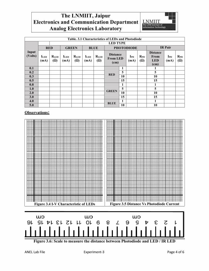
Table. 3.1 Characteristics of LEDs and Photodiode
Input (Volts)
LED TYPE
RED GREEN BLUE PHOTODIODE IR Pair
ILED
(mA)
RLED
(Ω)
ILED
(mA)
RLED
(Ω)
ILED
(mA)
RLED
(Ω)
Distance From LED
(cm)
IPD
(mA)
RPD
(Ω)
Distance From LED (cm)
IPD
(mA)
RPD
(Ω)
0.1
RED
1 1
0.2 5 5
0.3 10 10
0.5 15 15
0.8
GREEN
1 1
1.0 5 5
2.0 10 10
3.0 15 15
4.0 BLUE
1 1
5.0 10 10
Observations:
Figure 3.6: Scale to measure the distance between Photodiode and LED / IR LED

The LNMIIT, Jaipur Electronics and Communication Department
Analog Electronics Laboratory
ANEL Lab File Experiment-3 Page 5 of 6
Precautions: 1. While doing the experiment do not exceed the readings of the LEDs. This may lead to damaging
of the LEDs. 2. Do not switch ON the power supply unless you have checked the circuit connections as per the
circuit diagram. 3. Take care of the polarities of electrolytic capacitors. Electrolytic capacitor can blast if connected
with wrong polarity. 4. Use photodiode in reverse biased state only. Before making connections crosscheck the p-n pins
of photodiode. Bread Board Connections:
Viva Questions:
1. What is Light Emitting Diode (LED)? 2. How LED works? 3. In photoelectric effect, a suitable frequency of photon falls on electron in atom and ejects the
electron. In LED when electron hole recombination takes place a photon emits. How do you see these two phenomenon?
4. Which material we use in LED? 5. How photons emit from the LED and from which section of the LED? 6. How do you explain the working of LED by using the energy band diagram in forward biasing? 7. What happens when you provide the forward bias to the LED in terms of conduction band &
valence band in the depletion region? 8. Why do not LED starts to glow immediately when you provide the forwarding bias to that? 9. Explain the concept of threshold potential in semiconductor diode V-I Characteristics? 10. Why does Blue color LED stopping potential is greater than the Red color LED? 11. What symbol we use for the Light Emitting Diode? 12. What information we get from the Planck's constant, and how one can say that radiation is in
discrete form of energy?
Experiment Date
/ Student Task Max. Marks Graded Marks
Pre-Lab Preparation
Submission Date / Performance
Observation and Inference
Submission Delay / Completion of Experiments
Total
------------------------------------ Signature of Lab Instructor

The LNMIIT, Jaipur Electronics and Communication Department
Analog Electronics Laboratory
ANEL Lab File Experiment-3 Page 6 of 6
For Rough Works/other supporting Documents

The LNMIIT, Jaipur Electronics and Communication Department
Analog Electronics Laboratory
ANEL Lab File Experiment-4 Page 1 of 6
Aim:
EXPERIMENT 4
1) The objective of the following experiment is to find β (common emitter current gain) of a particular transistor by measuring different values of base current (IB) with the corresponding values of collector current (IC).
2) To design a basic switch and digital gates using BJT Apparatus / Components Required:
1) DSO 2) DSO probes 3) Power Supply 4) NPN Transistor BC-547 5) Resistors: 1 k , 4.7 k , 10 k , 47 k , 68 k , 100 k and 1 M 6) Digital Multi-meter
Theory:
Current gain β of any transistor
The Bipolar Junction Transistor (BJT) was invented at Bell Laboratories by William Shockley in 1948, the year after John Bardeen, and Walter Brattain invented the first working transistor (for which all three were awarded the 1956 Nobel Prize in Physics). BJT is constructed from a sandwich of three layers of doped semiconductor material, the thin middle layer being doped oppositely from the other two. Thus there exist two types of BJT: NPN and the PNP (whose schematic symbols are shown in Figure 4.1). The three layers are called the Emitter, Base, and Collector. Their identification with the three schematic device terminals is illustrated in the Figure 4.1 (note that the emitter is associated with the arrow in the schematic symbols). The base is the thin middle layer, and it forms one PN junction with the heavily-doped emitter and another with the moderately / lightly doped collector.
Figure 4.2 shows the schematic of Common Emitter (CE) amplifier. β is one of the most important parameters, which decides the total current gain in the CE amplifier. Larger values of β in a transistor allows it to produce higher current gains, resulting better current amplification abilities. For different transistors β varies between 50 and 1000. In this experiment we are going to practically calculate and analyze the behavior of β for different values of IB and IC.
We will use the basic relation between IB, IC and β given by: IC
IB
There are two different regions of operation for a transistor when it is ON. 1) Linear Region: In the linear region, the current that flows into the collector is proportional to the current
that flows into the base. Collector current in this state is given by:
IC IB .
Because the current that flows into the collector is negligible when the transistor is operating in the linear region, the current that flows out of the emitter is essentially equal to the current that flows into the collector, which is given by:
IE IB .
2) Saturation Region: Finally, the transistor maintains a fixed voltage between the base and the collector, given by:
VBE VB VE .
In general VBE ≈ 0.7V (Cut-in voltage of normal PN diode)
Transistor will not operate as described above if IB becomes too large. When this happens the transistor is said to be saturated and β is no longer constant. When the transistor is saturated the voltage difference between the collector and the emitter drops to:
VCE VC VE 0.1V 0.4V .
Figure 4.1. Schematic Symbols of NPN and PNP

The LNMIIT, Jaipur Electronics and Communication Department
Analog Electronics Laboratory
ANEL Lab File Experiment-4 Page 2 of 6
Figure 4.2. Schematic of CE amplifier to Calculate β
The experiment performed here will also provide a quantitative measure of how large IB can drive the transistor into saturation mode.
Procedure
1) To calculate β of the transistor.
*** Use digital multi-meter to measure β of the transistor provided to you, and note down the difference between the values of β measured experimentally and by the digital multi-meter.
a) The circuit used to determine β for the BC-547 transistor is shown in Figure 4.2. The base current
IB is controlled by the variable resistor RB2. Applying nodal equations at the input and output section (i.e., EB and CE section respectively.) of the circuit gives:
I 5 VB2
VB2 VB1 , and I
VCC VC 12Volt VC
B R R C R R B2 B1 C C
Using the above two equations complete the measurements and fill the Table 4.1. Observe how β changes w.r.t the change in IB and IC currents.
b) Figure 4.6 shows the output characteristics of transistor BC-547 in CE mode. Corresponding to different values of RB2 provided in the Table 4.1, mark the points for IC and IB achieved experimentally. Using the Figure 4.6, and experimentally obtained values of IC and IB, justify if the transistor is in Cut-Off (OFF) or saturation (ON).
c) Figure 4.7 shows the hfe (β) vs IC relationship of transistor BC-547. On the plot, mark the values of β experimentally obtained for different values of RB2.
2) Transistor as a Switch, and design an NAND gate using two BJT
Transistor as a Switch: Transistors can be used as a switch by operating them in saturation and cut-off mode alternately. In Figure 4.4, transistor is used in CE configuration. R2 is a protective resistor which limits the base current (IB). When the switch is closed, transistor is driven by a base current (IB) which is controlled by resistor R2, which ultimately drives the transistor to saturation with causing a very large collector current (IC). Then, because of the voltage drop in R1 and the saturation voltage VCE of the transistor, collector voltage VC will be just a few tenths of a volt. Whereas when the switch is open, transistor base current becomes zero, and hence the transistor is at cut-off (collector current (IC) is zero).
Figure 4.3. Pin Configuration of BC-547A

The LNMIIT, Jaipur Electronics and Communication Department
Analog Electronics Laboratory
ANEL Lab File Experiment-4 Page 3 of 6
** What is the use / role of resistor R1 in the circuit shown in Figure 4.4? ** Circuit shown in Figure 4.4 can be used as a NOT gate. Because when input at base is high,
output voltage at collector is low and vice-versa. How can we modify the circuit so that when base is high the LED goes ON and when base is low the LED goes OFF.
** Experimentally, how can we find the maximum switching rate of the transistor?
** After verification of circuit shown in Figure 4.5, try to design your own OR gate using two transistors and an LED.
By observing Figure 4.4, it is clear that when the transistor is ON (Saturated), majority of current passes through the transistor and it turns the LED OFF, and when the transistor is OFF (Cut-off), majority of current flows through LED which makes the LED ON.
NAND Gate Design Using Transistors: Circuit shown in Figure 4.5 is a very simple design to realize an NAND gate using two transistors. Verify the circuit by comparing the truth table of NAND gate and switching of the LED. At input side logic 0 is equivalent to 0 Volts at base, and logic 1 is equivalent to 5 Volts at the base. At the output end, you may consider the ON state of LED equivalent to high state and OFF state of the LED as low state.
Observations:
Table. 4.1. Theoretical Vs Practical Values of β
RB2 ( k )
Theoretical Measured Measured IC
(mA) IB
(mA) DC β (IC/IB)
IC
(mA) IB
(mA) DC β (IC/IB)
VC
Volts Transistor ON/OFF
1
10
47
68
100
330
1000
Precautions:
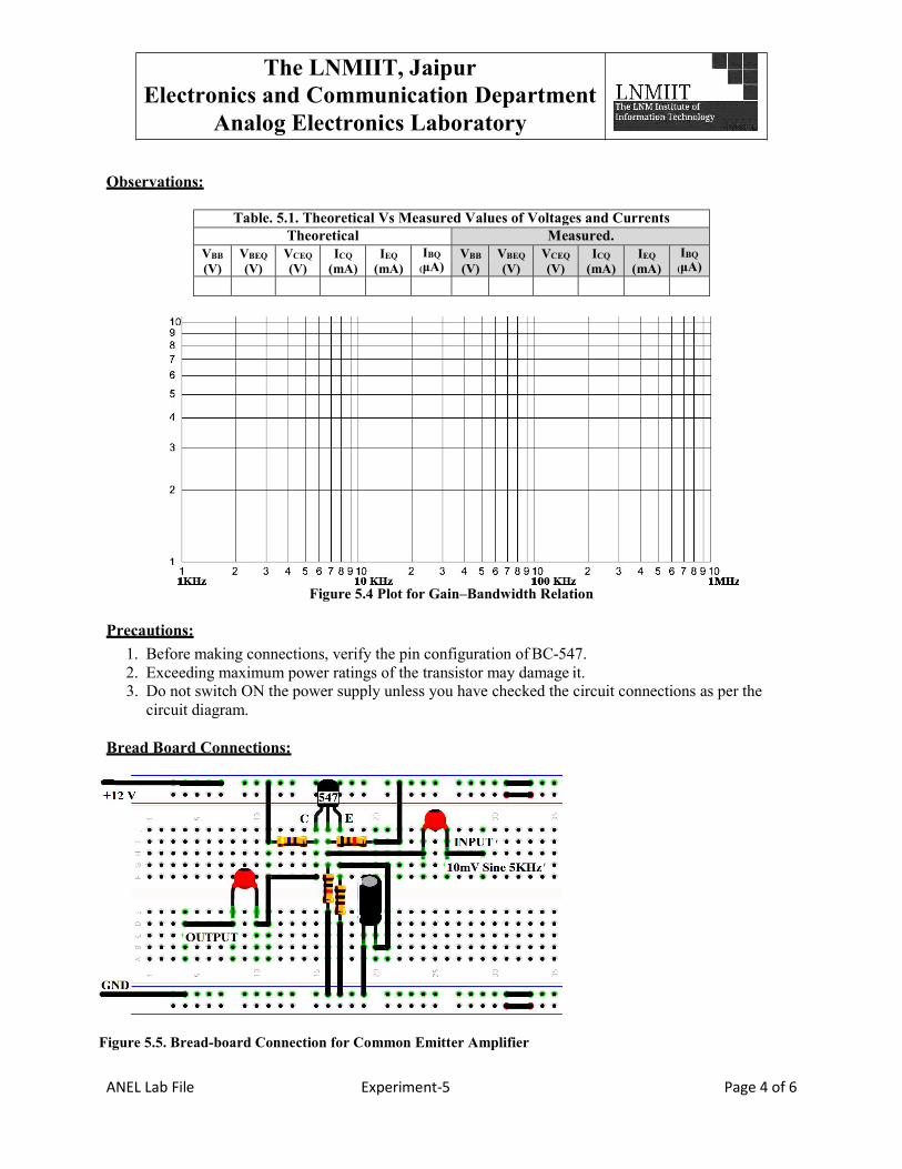
1. Before making connections, verify the pin configuration of BC-547 from Figure 4.3. 2. Exceeding maximum power ratings of the transistor may damage it.
Figure 4.5. NAND gate using BJT
Figure 4.4. Simple Switch using BJT

The LNMIIT, Jaipur Electronics and Communication Department
Analog Electronics Laboratory
ANEL Lab File Experiment-4 Page 4 of 6
3. Do not switch ON the power supply unless you have checked the circuit connections as per the circuit diagram.
Bread Board Connections:
Viva Questions:
Figure 4.8. Bread-board connection for β measurement
1. Why β of a transistor is important while designing an amplifier? 2. What is biasing and what are the various techniques available for biasing? 3. According to you which is the best biasing technique among all biasing technique? 4. Why biasing circuit is needed for amplifier? 5. What is Q-Point? What is the effect of input DC signal on Q-point? 6. Can DC signal be amplified by CE or CB amplifier? 7. What type of feedback is provided by RE in self biasing technique of CE configuration?
Experiment Date
/ Student Task Max. Marks Graded Marks
Pre-Lab Preparation
Submission Date / Performance
Observation and Inference
Submission Delay / Completion of Experiments
Total
------------------------------------ Signature of Lab Instructor
Figure 4.7. DC Current Gain Figure 4.6. Common Emitter Output Characteristics

The LNMIIT, Jaipur Electronics and Communication Department
Analog Electronics Laboratory
ANEL Lab File Experiment-4 Page 5 of 6
For Rough Works/other supporting Documents

The LNMIIT, Jaipur Electronics and Communication Department
Analog Electronics Laboratory
ANEL Lab File Experiment-4 Page 6 of 6
For Rough Works/other supporting Documents

The LNMIIT, Jaipur Electronics and Communication Department
Analog Electronics Laboratory
ANEL Lab File Experiment-5 Page 1 of 6
Aim:
EXPERIMENT 5
1) To design and analyze different aspects of a Self-Biased Common Emitter Amplifier using Bipolar Junction Transistor (BJT).
Apparatus / Components Required:
1) DSO 2) DSO probes 3) Power Supply 4) NPN Transistor BC-547 5) Resistors: 100 , 470 , 1 k , and 10 k . 6) Digital Multi-meter Capacitors: 0.1μF, 100μF.
Theory:
When we consider amplifiers, we are usually dealing with time varying signals. In general, an amplifier takes a small time-dependent signal as an input and at the output it delivers a faithfully amplified larger replica of the input signal. Establishing a constant DC bias point is the first step in designing an amplifier. These points consist DC voltages and currents that exist within the amplifier when no input signal is applied. When an input signal is applied to a properly biased amplifier, the internal voltage levels depart from their DC operating point. The variation from this DC level gives rise to the amplification process. To understand the above mentioned phenomenon, a simple single stage amplifier can be made from a BJT. We will first examine the DC characteristics of a BJT, and then investigate how the change from these DC conditions gives rise to amplification. To implement a single stage amplifier, we will use a general purpose NPN transistor (BC-547).
To function as an amplifier, the BJT is biased to operate in the forward active region. In the
forward active region, the base-emitter PN junction must be forward biased, while the base-collector junction must be reverse biased. For the biasing in forward active region you can consider a BJT to be a three-terminal device composed of a diode and a current controlled current source as shown in Figure 5.1.
Whenever we analyze or design circuits in this experiment, we will assume the equivalent circuit of BJT, and analysis will be performed by replacing the BJT circuit symbol on the left of Figure 5.1 with the equivalent circuit on the right of Figure 5.1.
BJT has three terminals, the base, collector and emitter, and thus three terminal currents, IB, IC,
and IE. In forward active mode IC .IB , where the current gain β is typically between 50 and 1000. For the theoretical calculation purposes, we will assume β equal to the value obtained from the multi- meter.
From Kirchhoff’s current law we have.
Substituting IC .IB we have
IE IC IB
IE (1 )IB

The LNMIIT, Jaipur Electronics and Communication Department
Analog Electronics Laboratory
ANEL Lab File Experiment-5 Page 2 of 6
The circuit shown in Figure 5.2 is a Common Emitter (CE) amplifier. As discussed above, with the common emitter amplifier, we first use resistors RC, RE, RB1, RB2, and capacitors CB, CE, CC to set up a DC operating point (Quiescent point / Q-Point) with input voltage VIN = 0V (i.e., with no input signal at base). The purpose of capacitor CB and CC is to isolate the DC operating point currents and voltages from the input and output signals, i.e., the signal source and the load. After establishing a proper Q point, an input signal is applied to the base of BJT via coupling capacitor CB. In accordance with the input signal, small changes in base current IB will result in variations in the bias conditions. The variation of bias conditions at the collector is then passed through the coupling capacitor CC, which is taken to be VOUT.
The small signal voltage gain is given by AV VOUT . VIN
For simple common emitter amplifiers, we have to first establish a proper DC bias condition and correspondingly a Q-point, which means that we have to choose bias resistors RC, RE, RB1 and RB2 that give us appropriate values for VC, VB and VE. The Q-point is usually established to allow for a large variation or swing in output voltage VOUT. In addition, VB and VE are chosen to be relatively small to make sure that VC > VB and the BJT does not enter the saturation region. (Saturation occurs when both the base-emitter and the base-collector junction are forward biased.) The bypass capacitor CE is used in the circuit to provide an AC ground. The AC signal will pass through the Capacitor CE and bypass the emitter resistor RE, making the RE apparent resistance zero.
If the values of RB1, RB2, RE, RC and VCC are already known, then the DC bias conditions can be
determined by first replacing the voltage divider at base of the BJT with its Thevenin equivalent, and then by directly applying nodal equations to the circuit while VIN = 0. To understand this concept, consider the circuit in Figure 5.3.
Figure 5.1: Large Signal Equivalent of BJT
Figure 5.3. Equivalent of Self-bias CE amplifier Figure 5.2. Self-bias CE amplifier
The LNMIIT, Jaipur Electronics and Communication Department
Analog Electronics Laboratory
ANEL Lab File Experiment-5 Page 3 of 6
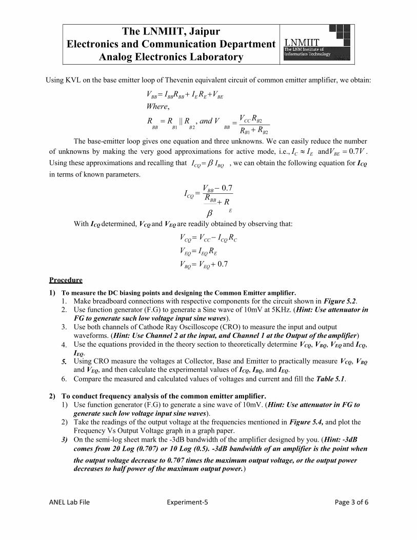
Using KVL on the base emitter loop of Thevenin equivalent circuit of common emitter amplifier, we obtain:
VBB IBBRBB IE RE VBE
Where,
R R
|| R
, and V VCC RB2
BB B1 B 2 B1 RB2
The base-emitter loop gives one equation and three unknowns. We can easily reduce the number of unknowns by making the very good approximations for active mode, i.e., IC IE andVBE 0.7V .
Using these approximations and recalling that
in terms of known parameters.
ICQ IBQ , we can obtain the following equation for ICQ
ICQ VBB 0.7 RBB R
E
With ICQ determined, VCQ and VEQ are readily obtained by observing that:
VCQ VCC ICQ RC
VEQ IEQ RE
VBQ VEQ 0.7
Procedure
1) To measure the DC biasing points and designing the Common Emitter amplifier. 1. Make breadboard connections with respective components for the circuit shown in Figure 5.2. 2. Use function generator (F.G) to generate a Sine wave of 10mV at 5KHz. (Hint: Use attenuator in
FG to generate such low voltage input sine waves). 3. Use both channels of Cathode Ray Oscilloscope (CRO) to measure the input and output
waveforms. (Hint: Use Channel 2 at the input, and Channel 1 at the Output of the amplifier) 4. Use the equations provided in the theory section to theoretically determine VCQ, VBQ, VEQ and ICQ,
IEQ. 5. Using CRO measure the voltages at Collector, Base and Emitter to practically measure VCQ, VBQ
and VEQ, and then calculate the experimental values of ICQ, IBQ, and IEQ. 6. Compare the measured and calculated values of voltages and current and fill the Table 5.1.
2) To conduct frequency analysis of the common emitter amplifier.
1) Use function generator (F.G) to generate a sine wave of 10mV. (Hint: Use attenuator in FG to generate such low voltage input sine waves).
2) Take the readings of the output voltage at the frequencies mentioned in Figure 5.4, and plot the Frequency Vs Output Voltage graph in a graph paper.
3) On the semi-log sheet mark the -3dB bandwidth of the amplifier designed by you. (Hint: -3dB comes from 20 Log (0.707) or 10 Log (0.5). -3dB bandwidth of an amplifier is the point when
the output voltage decrease to 0.707 times the maximum output voltage, or the output power decreases to half power of the maximum output power.)
R BB
The LNMIIT, Jaipur Electronics and Communication Department
Analog Electronics Laboratory
ANEL Lab File Experiment-5 Page 4 of 6
Observations:
Table. 5.1. Theoretical Vs Measured Values of Voltages and Currents
Theoretical Measured. VBB
(V) VBEQ
(V) VCEQ
(V) ICQ
(mA) IEQ
(mA) IBQ
(μA) VBB
(V) VBEQ
(V) VCEQ
(V) ICQ
(mA) IEQ
(mA) IBQ
(μA)
Figure 5.4 Plot for Gain–Bandwidth Relation Precautions:
1. Before making connections, verify the pin configuration of BC-547. 2. Exceeding maximum power ratings of the transistor may damage it. 3. Do not switch ON the power supply unless you have checked the circuit connections as per the
circuit diagram. Bread Board Connections:
Figure 5.5. Bread-board Connection for Common Emitter Amplifier
The LNMIIT, Jaipur Electronics and Communication Department
Analog Electronics Laboratory
ANEL Lab File Experiment-5 Page 5 of 6
Viva Questions:
1. Can BJT be replaced by two back to back connected diodes? 2. For amplification CE is preferred, why? 3. To operate a transistor as an amplifier, emitter junction is forward biased and collector junction is
reverse biased. Why? 4. Which transistor configuration provides a phase reversal between the input and output signals? 5. What is the range β of a BJT? 6. List the current components of BJT in CE configuration 7. What is Early Effect? 8. Why the doping of collector is less compared to emitter? 9. What affects the β? 10. What is the difference between CE and Emitter follower circuit? 11. What are the input and output impedances of CE configuration? 12. Identify various regions in the output characteristics (i.e., Cut-off, Active and Saturation)? 13. What is the relation between α, β and γ? 14. Define current gain in CE Vs CB Vs CC configuration? 15. Why CE configuration is preferred for amplification? 16. What is the phase relation between input and output? 17. With proper biasing voltages draw diagram of CE configuration for PNP transistor? 18. What is the power gain of CE configuration? 19. What are the applications of CE configuration?
Experiment Date
/ Student Task Max. Marks Graded Marks
Pre-Lab Preparation
Submission Date / Performance
Observation and Inference
Submission Delay / Completion of Experiments
Total
--------------------------------- Signature of Lab Instructor

The LNMIIT, Jaipur Electronics and Communication Department
Analog Electronics Laboratory
ANEL Lab File Experiment-5 Page 6 of 6
For Rough Works/other supporting Documents
The LNMIIT, Jaipur Electronics and Communication Department
Analog Electronics Laboratory
ANEL Lab File Experiment-6 Page 1 of 6
Aim:
EXPERIMENT 6
1. To calculate the voltage gain and frequency response of RC Coupled amplifier.
Apparatus / Components Required:
1) DSO 2) DSO probes 3) Power Supply 4) NPN Transistor BC-547 5) Resistors: 100 , 1 k , 1.5 k , and 10 k . 6) Digital Multi-meter Capacitors: 0.1μF, 100μF.
Theory:
In real life applications, single stage amplifier circuits, such as common emitter (CE), common base (CB) and common collector amplifiers are rarely used alone. For most of the practical applications at least two or more than two stages are connected in cascade combination. Cascading amplifiers means feeding (coupling) the output of one amplifier to the input of another amplifier. Cascaded amplifiers develop an output voltage larger than either stage alone. The overall gain of the cascaded amplifiers (called system gain) is the product of each individual stage gain. Coupling capacitor is used to connect output of first stage to input of second stage. Circuit shown in Figure 6.1 is an example of capacitor coupled CE cascade amplifier.
Resistances RB1, RB2, RE form biasing and stabilization network. Emitter bypass capacitor (CE1
and CE2) offers low reactance paths to AC signals, coupling capacitor (CS) transmits ac signal from one stage to another, and coupling capacitors (CB and CC) blocks DC voltage from input and output signals. Overall gain of two stage cascade amplifier is equal to:
AV AV 1 AV 2
Where, AV1 and AV2 are voltage gain of first and second stage of RC coupled amplifier.
Since the overall gain of cascaded amplifier system is very high, designers usually set individual stage gains relatively low to reduce signal distortion. Impedance matching between the output of one amplifier stage and input of another amplifier stage is one of the most important requirements to design a good cascaded amplifier system. Maximum power is transfer takes place when the output impedance of pervious stage properly matches with the input impedance of its next stage. One of the coupling methods to couple the two amplifier stages is RC-coupling. RC Coupling has the advantages of wide frequency response and relatively small cost and size.
When ac signal is applied to the base of the transistor, its amplified output appears across the
collector resistor RC. It is given to the base of second stage for further amplification and signal appears with more strength. Frequency response curve is obtained by plotting a graph between frequency and gain in dB. The gain is constant in mid frequency range and gain decreases on both sides of the mid frequency range. The gain decreases in the low frequency range due to coupling capacitors CB, CS and CC and at high frequencies due to internal junction capacitance Cbe of the transistor.

The LNMIIT, Jaipur Electronics and Communication Department
Analog Electronics Laboratory
ANEL Lab File Experiment-6 Page 2 of 6
Figure 6.3. Second stage CE amplifier
Procedure
a) To analyze individual stages of CE amplifier 1. Make circuits as shown in Figure 6.2 and Figure 6.3. 2. Measure the values of different Q points and fill the Table 6.1 for first and second stage of the CE
amplifier. (Do not connect capacitors to measure DC Q points of individual CE amplifiers). 3. Connect the capacitors and provide an input signal 10 mv Sine 10KHz individually to both first
and second stage and calculate the gain of both the amplifiers. (Note: CE amplifier at first stage has VCC=7V, whereas the second stage of CE amplifier has VCC=12 V)
4. Measure and fill Table 6.1 with the values of individual gains of the two CE amplifiers.
b) To analyze behavior of two stage RC coupled CE amplifier 1) Connect complete circuit of RC coupled CE amplifier as shown in Figure 6.1, i.e., the output
(Collector) of first stage to the input of second stage (Base) via coupling capacitor CS. 2) Provide input signal 10 mv Sine 10KHz to the RC coupled CE amplifier and measure the overall
gain of the amplifier AVTotal (dB)= 20log(Vo/Vin). Compare your measured gain with the theoretical gain of the two stage amplifier.
Figure 6.1. RC Coupled Common Emitter Amplifier
Figure 6.2. First stage CE amplifier

The LNMIIT, Jaipur Electronics and Communication Department
Analog Electronics Laboratory
ANEL Lab File Experiment-6 Page 3 of 6
3) Vary the frequency of the input signal and fill the Table 6.2. and obtain the -3dB bandwidth of the two stage RC coupled CE amplifier.
4) Draw the frequency response of the RC coupled CE amplifier in a semi-log sheet as shown in Figure 5.4.
Observations:
Table. 6.1. Theoretical Vs Measured Values of Voltages and Currents
First Stage Second Stage VBB
(V) VBEQ
(V) VCEQ
(V) ICQ
(mA) IEQ
(mA) IBQ
(μA) AV=VO/VI VBB
(V) VBEQ
(V) VCEQ
(V) ICQ
(mA) IEQ
(mA) IBQ
(μA) AV=VO/VI
Table 6.2. Frequency Vs Output Voltage Comparison for RC Coupled CE Amplifier
S. No Freq. VO
AV
(dB) S. No Freq. VO
AV
(dB) S. No Freq. VO
AV
(dB) S. No Freq. VO
AV
(dB) 1 100Hz 5 5KHz 9 300KHz 13 1.5MHz
2 500Hz 6 10KHz 10 500KHz 14 2MHz
3 1KHz 7 100KHz 11 800KHz 15 2.5MHz
4 3KHz 8 200KHz 12 1MHz 16 3MHz
Figure 5.4 Plot for Gain–Bandwidth Relation
Precautions:
1. Before making connections, verify the pin configuration of BC-547. 2. Exceeding maximum power ratings of the transistor may damage it. 3. Do not switch ON the power supply unless you have checked the circuit connections as per the
circuit diagram.
The LNMIIT, Jaipur Electronics and Communication Department
Analog Electronics Laboratory
ANEL Lab File Experiment-6 Page 4 of 6
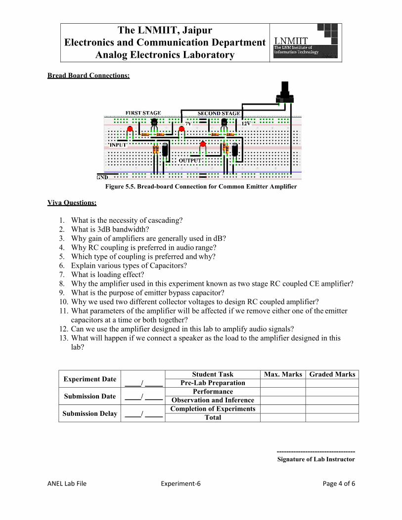
Bread Board Connections:
Figure 5.5. Bread-board Connection for Common Emitter Amplifier
Viva Questions:
1. What is the necessity of cascading? 2. What is 3dB bandwidth? 3. Why gain of amplifiers are generally used in dB? 4. Why RC coupling is preferred in audio range? 5. Which type of coupling is preferred and why? 6. Explain various types of Capacitors? 7. What is loading effect? 8. Why the amplifier used in this experiment known as two stage RC coupled CE amplifier? 9. What is the purpose of emitter bypass capacitor? 10. Why we used two different collector voltages to design RC coupled amplifier? 11. What parameters of the amplifier will be affected if we remove either one of the emitter
capacitors at a time or both together? 12. Can we use the amplifier designed in this lab to amplify audio signals? 13. What will happen if we connect a speaker as the load to the amplifier designed in this
lab?
Experiment Date
/ Student Task Max. Marks Graded Marks
Pre-Lab Preparation
Submission Date / Performance
Observation and Inference
Submission Delay / Completion of Experiments
Total
--------------------------------- Signature of Lab Instructor

The LNMIIT, Jaipur Electronics and Communication Department
Analog Electronics Laboratory
ANEL Lab File Experiment-6 Page 5 of 6
For Rough Works/other supporting Documents

The LNMIIT, Jaipur Electronics and Communication Department
Analog Electronics Laboratory
ANEL Lab File Experiment-6 Page 6 of 6
For Rough Works/other supporting Documents
The LNMIIT, Jaipur Electronics and Communication Department
Analog Electronics Laboratory
ANEL Lab File
Experiment-7 Page 1 of 6
V
Aim:
EXPERIMENT 7
1. To explore the basic concepts of oscillators and design of sine wave oscillators using transistor and Op-Amp.
2. To design Wien Bridge oscillator using Op-amp (741) and RC-Phase shift oscillator using bipolar junction transistor (BC-547).
Apparatus / Components Required:
1) DSO 2) DSO probes 3) Power Supply 4) NPN Transistor: BC-547 5) Capacitors: 0.1μF, 47μF/100μF. 6) Op-Amp (741) 7) Resistors: 470 , 1kΩ, 2.2kΩ, 10kΩ, 68kΩ 8) Potentiometer: 10kΩ
Theory: Oscillators are circuits that spontaneously generate a periodically changing output voltage due to positive feedback. In this lab we are going to study the fundamentals and working of two important types of oscillators: i) Wien-bridge, and ii) RC phase-shift oscillator. Any amplifier with high input impedance, large gain and positive feedback can be used to design oscillators. The positive feedback required for oscillation is specified by the Barkhausen criterion. According to this criterion, to generate oscillations, in an oscillator circuit, the total gain from input to output and back through the feedback circuitry must equal at least one, and the total phase-shift from input to output and back through the feedback circuitry must equal 0°, or a multiple of 360°.
Positive feedback
The basic block diagram for a positive feedback configuration to demonstrate Barkhausen criterion is depicted in Figure. 7.1. The gain of the feed forward network is A, and the gain of the feedback network is β.
Figure. 7.1. Block Diagram of Positive Feedback
Overall gain of the block diagram shown in Figure.7.1 is given by:
A VO
VS
A
1 A
Notice that, if the denominator can become zero, then the transfer function AV becomes infinite. Thus the system could have a non-zero output with zero amplitude input signal. In such a case, the system is said to be unstable. This occurs when the loop gain, AL, is:
AL A 1, which results AV

The LNMIIT, Jaipur Electronics and Communication Department
Analog Electronics Laboratory
ANEL Lab File
Experiment-7 Page 2 of 6
1
A.β product plays a key role in oscillator design and is called the loop gain. Since positive feedback causes causing instability, systems are generally designed to avoid positive feedback. But in the case of oscillators, unstable behavior is desired. In fact, a sine wave oscillator can be constructed by designing a circuit such that the loop gain (A.β) is unity. For oscillation to occur the magnitude of loop gain must be exactly one. Loop gain (A.β) is a function of frequency, therefore to make oscillations both the conditions given below should be fulfilled:
A. 1, and (A. ) 0 N360Both sine wave oscillators investigated in this experiment consist of two separable parts. Where:
1) ‘A’ network will be the amplifier part, and 2) The feedback network (β) will be the frequency determining part.
Phase Shift Oscillator: Circuit diagram of a phase shift oscillator using transistor is shown in Figure.7.2. In phase shift oscillators the output of an amplifier must be 1800 out of phase w.r.t input. Here we are using common emitter amplifier which produces 1800 phase shift between input and output. A phase shift network (usually a resistor-capacitor network) is used to produce an additional phase shift of 1800 at one particular frequency to develop the required positive feedback. Using the fundamentals of nodal or mesh analysis on the feedback network, we can find the feedback factor β as:
Feedback Voltage
VF
Output Voltage VO
Where, 1RC
1 5 2 j 6 a3
For the output of the feedback network to be 1800 out of phase w.r.t input:
6 a3 0, or 1
2 fRC
f 1
6 2 RC
At frequency ‘f’ the value of feedback factor is |β|=1/29=0.0345, and it is required that gain of the amplifier (A) must be at least 29 to satisfy oscillation condition as shown in Figure. 7.2. The RC
Figure 7.3. Wien-Bridge Oscillator Using Op-Amp Figure 7.2. RC Phase Shift Oscillator Using Transistor
6
,

The LNMIIT, Jaipur Electronics and Communication Department
Analog Electronics Laboratory
ANEL Lab File
Experiment-7 Page 3 of 6
R R
1
phase-shift oscillator is used to generate frequencies from several hertz to several kilohertz, therefore they are preferred in the range of audio frequencies. By this experiment you can also observe that the phase shift oscillator is not very suitable for generating variable frequency because the resistors and capacitors must be simultaneously changed to obtain the required frequency control over a wide range. Therefore RC phase-shift oscillator is used mostly in fixed frequency applications.
Wien Bridge Oscillator: Circuit of Wien-bridge oscillator is shown in Figure 7.3. A Wien‐bridge oscillator is an autonomous circuit that can derive a sinusoidal output waveform without any input. Wien‐bridge oscillator shown in Figure 7.3 consists of a feedback amplifier with an RC band‐pass filter connected in the positive feedback path, and a resistive potential divider connected in the negative feedback path. The RC network generates an attenuated and phase‐shifted version of VOUT to the non- inverting input terminal of Op-amp. Whereas, the inverting input terminal of Op-amp receives an attenuated but not phase‐shifted version of VOUT. Feedback loops can be designed to equalize the potentials of the non-inverting and inverting terminals, which in return produces the final oscillatory waveform at the output.
To understand the Wien‐bridge oscillator we can exploit the “virtual ground” property of Op- amp. Assume that the open‐loop gain of the Op-amp is very large, the voltage difference between the positive and negative terminals must be very small, and i.e., VNoninverting and VInverting are essentially at same potential. By using this property we can derive the equation given below:
V V sRC , and V
V R1
V
Noninverting OUT 1 3sRC s2 R2C2 Inverting OUT R R Noninverting
1 2
Here in our circuit for Wien-bridge oscillator, we have assumed R3=R4=R=10kΩ and C1=C2=C=0.1μF. Note that the transfer function of band-pass filter is real only when 1 RC , which yields
VNoninverting VOUT
which is given by:
3 . In turn, this leads to the following constraint for R3 and R4 to yield oscillation,
R4
3 4
where,
R4 1
1 RC
R3 2 Frequency of oscillation for the Wien-bridge oscillator can be determined by:
f 2 RC
Basically both the oscillators shown in Figure 7.2 and Figure 7.3 are following the Barkhausen criteria for oscillation. In Wien-bridge oscillator the bridge does not provide phase shift at oscillating frequency as one of in the input terminal consists of lead circuit and other input terminal consists of lag circuit. There is no need for the Op-amp to introduce any phase-shift in the circuit. Therefore, to design Wien- bridge oscillator non-inverting amplifier is used. Due to limitations of the op-amp, frequencies above few megahertz are not achievable.
sRC
1 3sRC s2 R2C 2

The LNMIIT, Jaipur Electronics and Communication Department
Analog Electronics Laboratory
ANEL Lab File
Experiment-7 Page 4 of 6
Procedure
1) To analyze the behavior of RC phase shift oscillator using BJT. Connect the circuit as shown in Figure7.2, and insert potentiometer of l0 kΩ in the feedback path. Vary the potentiometer to obtain sinusoidal oscillations at the output. Measure the frequency of oscillation ‘f’ and the amplitude of the output voltage. Measure and draw the waveforms of points VIN and VOUT. Vary the potentiometer and observe if the frequency or amplitude of the oscillating signal can be
varied.
2) To analyze and observe the behavior of Wien bridge oscillator using Op-amp. Connect the circuit as shown in Figure7.3, and insert potentiometer of l0 kΩ in the feedback path. Vary the potentiometer to obtain sinusoidal oscillations at the output. Measure the frequency of oscillation ‘f’ and the amplitude of the output voltage. Measure and draw the waveforms of points VIN and VOUT. Vary the potentiometer and observe if the frequency or amplitude of the oscillating signal can be
varied.
Observations:
S. No
RC-Phase Shift Oscillator Wien Bridge Oscillator (Frequency of Oscillation) (Frequency of Oscillation) Theoretical Measured Theoretical Measured
1
Precautions:
1. Before making connections, verify the pin configuration of BC-547. 2. Connect the proper polarities of bias voltages to Op-amp 741 (+12VPin-7, -12VPin-4). 3. Exceeding maximum power ratings of the transistor may damage it. 4. Do not switch ON the power supply unless you have checked the circuit connections as per the
circuit diagram.
Bread Board Connections:
Figure 7.4. Bread-board Connection for Common Emitter Amplifier

The LNMIIT, Jaipur Electronics and Communication Department
Analog Electronics Laboratory
ANEL Lab File
Experiment-7 Page 5 of 6
Viva Questions: 1. What is an oscillator? 2. What is Barkhausen criteria, and why is it important to design oscillators? 3. What is the application of an oscillator? 4. What is the working principle of an oscillator? 5. What are the two requirements for oscillation? 6. What is frequency stability? 7. What should be the total phase shift of an oscillator circuit to generate oscillations? 8. What are the conditions for the Wien bridge oscillator to stabilize? 9. What are the differences between RC-Phase shift oscillator and Wien-bridge oscillator? 10. Which type of feedback used in oscillator? 11. Why RC-Phase Shift oscillator and Wien-bridge oscillator are not good to design variable
frequency oscillators?
Experiment Date
/ Student Task Max. Marks Graded Marks
Pre-Lab Preparation
Submission Date / Performance
Observation and Inference
Submission Delay / Completion of Experiments
Total
--------------------------------- Signature of Lab Instructor

The LNMIIT, Jaipur Electronics and Communication Department
Analog Electronics Laboratory
ANEL Lab File
Experiment-7 Page 6 of 6
For Rough Works/other supporting Documents

The LNMIIT, Jaipur Electronics and Communication Department
Analog Electronics Laboratory
ANEL Lab File Experiment-8 Page 1 of 6
Aim:
EXPERIMENT 8
1. To study the astable and monostable modes of the 555 timer Integrated Circuit (IC). Apparatus / Components Required:
1. DSO 2. DSO probes 3. Power Supply 4. Timer IC: NE-555 5. Capacitors: 0.01μF, 0.1μF, 100μF. 6. Potentiometer: 10kΩ 7. Resistors: 1k , 6.8kΩ, 100kΩ, 8. Jumper wires
Theory: The 555 timer is a very popular IC. It was first introduced in 1972. Block diagram and pin diagram of 555 timer is shown in Figure 8.1, and Figure 8.2 respectively.
The 555 timer IC consists of:
i) Two voltage comparators (C1 and C2). ii) An R-S flip-flop. iii) A resistive voltage divider (R1, R2, R3). iv) An inverted output buffer. v) A discharge transistor Q.
The negative input of the voltage comparator C1 is internally connected to the resistive voltage divider,
and the voltage at the negative input is equal toV 2
V
, which is called the threshold level. The H 3 CC
positive input of the comparator C1 is connected to the external Threshold pin. The positive input of the
voltage comparator C2 is connected to V 1
V
, which is called the trigger level, while the negative L 3 CC
input is the external Trigger pin. The negative input of the voltage comparator C1 is called Control pin, which can be used for external adjustment of the threshold and trigger levels. The comparator C1 and C2 outputs are fed to the input of an RS flip-flop’s reset R and set S inputs respectively. When the Trigger input falls below the trigger level VL, the output of the voltage comparator C2 goes high and SET the flip- flop. If the Trigger input is above the trigger level, and the Threshold input is above the threshold level, the output of the voltage comparator C1 is high and the flip-flop is RESET. The output of flip-flop Q simultaneously drives the discharge transistor Q and an inverting output buffer. When the output of RS
Figure. 8.2. Pin diagram of 555 timer IC Figure. 8.1. Block Diagram of 555 timer IC

The LNMIIT, Jaipur Electronics and Communication Department
Analog Electronics Laboratory
ANEL Lab File Experiment-8 Page 2 of 6
flip-flop Q gets high, it turns ON the transistor Q and the voltage at the Output pin gets low. When the flip-flop output Q is low, Transistor Q is OFF and the Output pin gets high (≈VCC). The output driver is capable of sinking or sourcing current up to about 200mA. The collector of the discharge transistor Q is available at the Discharge pin. The active-low RESET input at pin 4 can be used to disable the timer operation and ensure that the OUTPUT stays at zero, regardless of the comparator outputs. The DC supply voltage can be between VCC = 5V - 15V.
555 Timer – Monostable Mode
Figure 8.3 shows a monostable multivibrator circuit using 555 timer IC. A monostable multivibrator is a pulse generating circuit having one stable and one quasi-stable state. Since there is only one stable state, the circuit is known as “monostable multivibrator”. The duration of the output pulse is determined by the RC network (i.e., in our circuit R1C1) connected externally to the 555 timer. The stable state output is generally 0 Volt (Low level state). An external trigger pulse forces the output of monostable circuit to become high (approximately equal to VCC). After a predetermined period, the output automatically switches back to the stable state and remains low until another trigger pulse is applied again. Monosta
ble multivibrator is also called “one-shot multivibrator”.
The voltage across the capacitor is used for the Threshold. When the Trigger arrives at trigger pin, the circuit produces an output high pulse at the output pin. Initially, if the output of the timer is low, that is, the circuit is in a stable state, transistor Q is ON and the external capacitor C1 is shorted to ground. Upon application of a low pulse to the trigger pin, transistor Q is turned OFF, which releases the short circuit across the capacitor and as a result, the output pin becomes high. The capacitor now starts charging up
towards VCC through R1. When the voltage across the capacitor equals 2
V , the output of first 3 CC
comparator switches from low to high, which in turn, makes the output pin low via the output of the flip- flop. Also, the output of the flip-flop turns transistor ON and hence the capacitor rapidly discharges through the transistor. The output of the monostable multivibrator remains low until another trigger pulse is applied again. Figure 8.4 shows the trigger input and corresponding output voltage, and capacitor
Figure 8.4. Output waveforms of monostable circuit Figure 8.3 Schematic for monostable circuit
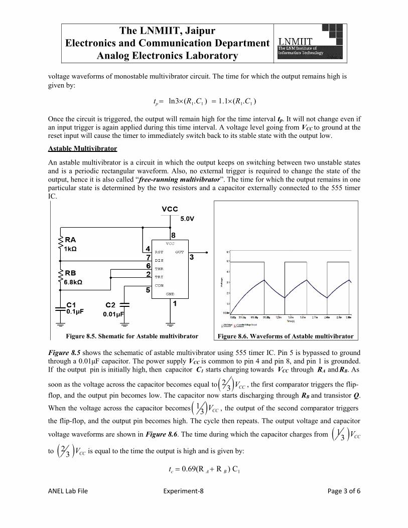
The LNMIIT, Jaipur Electronics and Communication Department
Analog Electronics Laboratory
ANEL Lab File Experiment-8 Page 3 of 6
voltage waveforms of monostable multivibrator circuit. The time for which the output remains high is given by:
tp ln 3(R1.C1 ) 1.1(R1.C1 )
Once the circuit is triggered, the output will remain high for the time interval tp. It will not change even if an input trigger is again applied during this time interval. A voltage level going from VCC to ground at the reset input will cause the timer to immediately switch back to its stable state with the output low.
Astable Multivibrator
An astable multivibrator is a circuit in which the output keeps on switching between two unstable states and is a periodic rectangular waveform. Also, no external trigger is required to change the state of the output, hence it is also called “free-running multivibrator”. The time for which the output remains in one particular state is determined by the two resistors and a capacitor externally connected to the 555 timer IC.
Figure 8.5 shows the schematic of astable multivibrator using 555 timer IC. Pin 5 is bypassed to ground through a 0.01μF capacitor. The power supply VCC is common to pin 4 and pin 8, and pin 1 is grounded. If the output pin is initially high, then capacitor C1 starts charging towards VCC through RA and RB. As
soon as the voltage across the capacitor becomes equal to 23 VCC , the first comparator triggers the flip-
flop, and the output pin becomes low. The capacitor now starts discharging through RB and transistor Q.
When the voltage across the capacitor becomes 13 VCC , the output of the second comparator triggers
the flip-flop, and the output pin becomes high. The cycle then repeats. The output voltage and capacitor
voltage waveforms are shown in Figure 8.6. The time during which the capacitor charges from 13 VCC
to 23 VCC is equal to the time the output is high and is given by:
tc 0.69(R A R B ) C1
Figure 8.6. Waveforms of Astable multivibrator Figure 8.5. Shematic for Astable multivibrator
The LNMIIT, Jaipur Electronics and Communication Department
Analog Electronics Laboratory
ANEL Lab File Experiment-8 Page 4 of 6
Similarly the time during which the capacitor discharges from 23 VCC
the output is low and given by:
to 13 VCC is equal to the time
td 0.69 R BC1
The total period of the output waveform is obtained by adding the time of charging and discharging of the capacitor.
T tc td 0.69(R A R B ) C1
Thus the frequency of the oscillation is:
f 1
T
1.45
(R A 2RB ) C1
Free running frequency f is independent of the supply voltage VCC.
Duty cycle is defined as the ratio of the time for which the output is high to the time period T. It is general expressed in percentage.
D tc 100
RA RB 100 %
Procedure
T RA 2RB
1) To analyze the behavior of monostable multivibrator using 555 timer IC. Connect the circuit of monostable circuit as shown in Figure 8.3. Using a jumper wire connect trigger input to ground momentarily to trigger the circuit.
Since T is high enough, on the CRO screen, you should be able to see the single pulse at the output pin. Try a few times until you see the whole pulse and measure the width.
Compute approximately the difference between the theoretical and measured time period of the multivibrator.
2) To design and analyze Astable Multivibrator using 555 timer IC.
Connect the circuit of astable multivibrator as shown in Figure 8.5. Measure and capture the waveforms of output pin and the voltage across the capacitor. Measure the time period and duty cycle of the output and compare them with the
theoretical values. Observations:
Table 8.1. Observations of multivibrator circuits
S. No
Monostable multivibrator Astable multivibrator Frequency Duty cycle Frequency Duty Cycle Theoretical Measured Theoretical Measured
1

The LNMIIT, Jaipur Electronics and Communication Department
Analog Electronics Laboratory
ANEL Lab File Experiment-8 Page 5 of 6
Precautions:
1. Before making connections, verify the pin configuration of NE-555 timer IC. 2. Be careful while connecting electrolytic capacitor. Connect electrolytic capacitor with proper
polarity, wrong connection may lead to explosion of the capacitor. 3. Do not switch ON the power supply unless you have thoroughly checked the circuit connections as
per the circuit diagrams provided in the experiment sheet. Bread Board Connections:
Figure 8.7. Bread-board Connection for monostable and astable circuits using 555 IC Viva Questions:
1. What are the other applications of 555 timer IC? 2. What is the function of the transistor present in 555 timer IC? 3. Explain why the control pin of 555 timer IC is connected to ground through 0.01μF bypass capacitor? 4. Explain the two basic modes in which the 555 timer IC operates. 5. What is the function of discharge pin? 6. What is the maximum frequency of operation for a 555 timer IC?
Experiment Date
/ Student Task Max. Marks Graded Marks
Pre-Lab Preparation
Submission Date / Performance
Observation and Inference
Submission Delay / Completion of Experiments
Total
--------------------------------- Signature of Lab Instructor

The LNMIIT, Jaipur Electronics and Communication Department
Analog Electronics Laboratory
ANEL Lab File Experiment-8 Page 6 of 6
For Rough Works/other supporting Documents
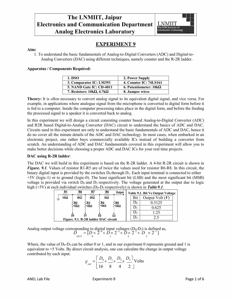
The LNMIIT, Jaipur Electronics and Communication Department
Analog Electronics Laboratory
ANEL Lab File Experiment-9 Page 1 of 6
Table 9.1. Bit Vs Output Voltage
Aim:
EXPERIMENT 9
1. To understand the basic fundamentals of Analog-to-Digital Converters (ADC) and Digital-to- Analog Converters (DAC) using different techniques, namely counter and the R-2R ladder.
Apparatus / Components Required:
1. DSO 2. Power Supply 3. Comparator IC: LM393 4. Counter IC: 74LS161 5. NAND Gate IC: CD-4011 6. Potentiometer: 10kΩ 7. Resistors: 10kΩ, 4.7kΩ 8. Jumper wires
Theory: It is often necessary to convert analog signal to its equivalent digital signal, and vice versa. For example, in applications where analogue signal from the microphone is converted to digital form before it is fed to a computer. Inside the computer processing takes place in the digital form, and before the feeding the processed signal to a speaker it is converted back to analog.
In this experiment we will design a circuit consisting counter based Analog-to-Digital Converter (ADC) and R2R based Digital-to-Analog Converter (DAC) circuit to understand the basics of ADC and DAC. Circuits used in this experiment are only to understand the basic fundamentals of ADC and DAC, hence it do no cover all the minute details of the ADC and DAC technology. In most cases, when embarked in an electronic project, one rather buys commercially available ICs instead of building a converter from scratch. An understanding of ADC and DAC fundamentals covered in this experiment will allow you to make better decisions while choosing a proper ADC and DAC ICs for your real time projects.
DAC using R-2R ladder:
The DAC we will build in this experiment is based on the R-2R ladder. A 4-bit R-2R circuit is shown in Figure. 9.1. Values of resistor R1-R5 are of twice the values used for resistor R6-R8. In this circuit, the binary digital input is provided by the switches D0 through D3. Each input terminal is connected to either +5V (logic-1) or to ground (logic-0). The least significant bit (LSB) and the most significant bit (MSB) voltage is provided via switch D0 and D3 respectively. The voltage generated at the output due to logic high (+5V) at each individual switches (D0-D3 respectively) is shown in Table 9.1.
Analog output voltage corresponding to digital input voltages (D0-D3) is defined as,
D [D 24 D 23 D 22 D 21 ] OUT 0 1 2 3
Where, the value of D0-D3 can be either 0 or 1, and in our experiment 0 represents ground and 1 is equivalent to +5 Volts. By direct circuit analysis, one can calculate the change in output voltage contributed by each input.
Vout
D0 D1
D2 D3 Volts
16 8 4 2
Bit Output Volt (V) D0 0.3125 D1 0.625 D2 1.25 D3 2.5
Figure. 9.1. R-2R ladder DAC circuit

The LNMIIT, Jaipur Electronics and Communication Department
Analog Electronics Laboratory
ANEL Lab File Experiment-9 Page 2 of 6
Table 9.2. Pin definition of IC-74LS161 Pin Definition PE Parallel Enable
A-B-C-D Parallel Inputs CEP Count Enable Parallel input CET Count Enable Trickle Input CP Clock MR Master Reset SR Synchronous Reset
QA-QB-QC-QD Parallel Outputs TC Terminal Count Output
Figure 9.2 b) Pin Diagram of IC-4011
Figure 9.2 a) Pin Diagram of IC-74LS161
ADC Using Counter: Pin diagram of IC 47LS161 and CD-4011 is shown in Figure 9.2 a) and Figure 9.2 b) respectively, and Table 9.2 shows the details of each pin in IC-47LS161.
Counter based ADC is one of the most basic ADC which is also known as the digital ramp type ADC or stair case approximation ADC. The complete circuit consisting BCD decade counter, R-2R DAC and comparator is shown below in Figure 9.3.
Ideal static characteristics of an ADC converter with unipolar input voltage range 0 < Vi < +5V is shown in Figure 9.4. Working of the circuit shown in Figure 9.3 is as follows:
Positive input terminal of the comparator is connected to the analog voltage to be converted to its equivalent digital value, whereas the negative input terminal of comparator is connected to the output of R-2R DAC.
Depending on the voltage at +ve and –ve terminal of comparator, the output voltage of the comparator will be high or low. If V+ve > V-ve then Vout = 5V, else Vout = 0.
Output of comparator is connected to one of the inputs of NAND gate, whereas the second input of the NAND gate is connected to a square wave at a defined frequency (1Hz in our experiment).
Output of the NAND gate will be a square wave if the voltage at +ve input of comparator is higher than –ve, and if the –ve input of comparator is greater than +ve then output of NAND gate
Figure 9.4 Output from R-2R DAC Figure 9.3 Schematic of ADC-DAC Combined

The LNMIIT, Jaipur Electronics and Communication Department
Analog Electronics Laboratory
ANEL Lab File Experiment-9 Page 3 of 6
will be always high (i.e., clock is stopped). Output of the NAND gate is connected to the clock input terminal of the counter IC. Depending
on the number of clock pulses received the output of the counter will increment the BCD count at its output.
Output of the counter IC is connected to the R-2R DAC, which further converts the 4 bit digital input in BCD form back to its equivalent analog output voltage.
The output of R-2R DAC is connected to negative terminal of the comparator IC. When the –ve input voltage of comparator IC rises above the +ve input voltage of the comparator IC the counter IC will stop incrementing its count.
Once the counter IC stops incrementing its count one can read the output pins (QA-QB-QC-QD) of the counter IC to decode the digital equivalent value for the analog input voltage at the +ve terminal of the comparator.
Procedure:
To analyze the behavior of R-2R DAC circuit.1. A premade R-2R ladder circuit is provided to you. Connect the Channel-1 of CRO at the output
of the R-2R circuit provided. Connect the input D0-D3 to either +5V or 0V by following the binary sequence to count from 0-15 (0000-1111).
2. Measure precisely the voltages at each increment of the count and fill the observation Table 9.3. 3. Measure the step size of R-2R DAC and fill the observation Table 9.3. (Step size of any DAC is
the difference between the voltages of two consecutive steps).
To analyze the behavior of complete ADC and DAC Circuit as shown in Figure 9.3.1. Connect the circuit as shown in Figure 9.3. Use function generator to generate a square wave of
5 Vp-p with frequency 100 Hz and 5 V DC-offset. 2. Connect the square wave generated to one of the input pins of NAND gate. 3. Connect a jumper wire from master reset pin (MR). 4. To start the ADC and DAC conversion, vary the potentiometer connected to comparator and
momentarily connect the jumper connected with the MR pin to ground. 5. Connect channel 2 of the CRO to the output of the R-2R Ladder DAC gate. Measure the voltage
at the output of the R-2R ladder (DAC) when the clock pulse form the NAND gate stop. 6. Also measure the corresponding values of QA-QB-QC-QD at the output of counter IC to
measure the approximate binary equivalent value of the analog DC voltage at the input of the comparator IC.
Precautions:
1. Before making connections, verify the pin configuration of all the ICs used in this circuit. 2. In this experiment variable resistor is used as a potentiometer, therefore make connections of
variable resistor accordingly. 3. Do not switch ON the power supply unless you have thoroughly checked the circuit connections as
per the circuit diagrams provided in the experiment sheet.

The LNMIIT, Jaipur Electronics and Communication Department
Analog Electronics Laboratory
ANEL Lab File Experiment-9 Page 4 of 6
Figure 9.5. Breadboard connection for Experiment-9
Observations:
Table 9.3. R-2R DAC Theoretical Vs Measured Output Voltages
Count
R-2R DAC Input (0 = 0V & 1 = 5V)
R-2R DAC Output (V) Count
R-2R DAC Input (0 = 0V & 1 = 5V)
R-2R DAC Output (V)
Theory Measured Theory Measured QA QB QC QD QA QB QC QD
0 0 0 0 0 8 1 0 0 0
1 0 0 0 1 9 1 0 0 1
2 0 0 1 0 10 1 0 1 0
3 0 0 1 1 11 1 0 1 1
4 0 1 0 0 12 1 1 0 0
5 0 1 0 1 13 1 1 0 1
6 0 1 1 0 14 1 1 1 0
7 0 1 1 1 15 1 1 1 1
Bread Board Connections:
Viva Questions: 1. A 4-bit R-2R digital-to-analog (DAC) converter has a reference of 5 volts. What is the analog
output for the input code 0101? 2. Define resolution of a digital-to-analog converter (DAC)? 3. What is monotonicity test? 4. What is the major advantage and disadvantage of the R-2R ladder digital-to-analog (DAC)
circuit? 5. What are the factors you consider for the selection of ADC?
Experiment Date
/ Student Task Max. Marks Graded Marks
Pre-Lab Preparation
Submission Date
/
Performance
Observation and Inference
Submission Delay
/
Completion of Experiments
Total
--------------------------------- Signature of Lab Instructor

The LNMIIT, Jaipur Electronics and Communication Department
Analog Electronics Laboratory
ANEL Lab File Experiment-9 Page 5 of 6
For Rough Works/other supporting Documents

The LNMIIT, Jaipur Electronics and Communication Department
Analog Electronics Laboratory
ANEL Lab File Experiment-9 Page 6 of 6
For Rough Works/other supporting Documents