and9962-d.pdf - onsemi
141
To learn more about onsemi™, please visit our website at www.onsemi.com ON Semiconductor Is Now onsemi and and other names, marks, and brands are registered and/or common law trademarks of Semiconductor Components Industries, LLC dba “onsemi ” or its affiliates and/or subsidiaries in the United States and/or other countries. onsemi owns the rights to a number of patents, trademarks, copyrights, trade secrets, and other intellectual property. A listing of onsemi product/patent coverage may be accessed at www.onsemi.com/site/pdf/Patent-Marking.pdf. onsemi reserves the right to make changes at any time to any products or information herein, without notice. The information herein is provided “as-is” and onsemi makes no warranty, representation or guarantee regarding the accuracy of the information, product features, availability, functionality, or suitability of its products for any particular purpose, nor does onsemi assume any liability arising out of the application or use of any product or circuit, and specifically disclaims any and all liability, including without limitation special, consequential or incidental damages. Buyer is responsible for its products and applications using onsemi products, including compliance with all laws, regulations and safety requirements or standards, regardless of any support or applications information provided by onsemi. “Typical” parameters which may be provided in onsemi data sheets and/ or specifications can and do vary in different applications and actual performance may vary over time. All operating parameters, including “Typicals” must be validated for each customer application by customer’s technical experts. onsemi does not convey any license under any of its intellectual property rights nor the rights of others. onsemi products are not designed, intended, or authorized for use as a critical component in life support systems or any FDA Class 3 medical devices or medical devices with a same or similar classification in a foreign jurisdiction or any devices intended for implantation in the human body. Should Buyer purchase or use onsemi products for any such unintended or unauthorized application, Buyer shall indemnify and hold onsemi and its officers, employees, subsidiaries, affiliates, and distributors harmless against all claims, costs, damages, and expenses, and reasonable attorney fees arising out of, directly or indirectly, any claim of personal injury or death associated with such unintended or unauthorized use, even if such claim alleges that onsemi was negligent regarding the design or manufacture of the part. onsemi is an Equal Opportunity/Affirmative Action Employer. This literature is subject to all applicable copyright laws and is not for resale in any manner. Other names and brands may be claimed as the property of others.
-
Upload
khangminh22 -
Category
Documents
-
view
1 -
download
0
Transcript of and9962-d.pdf - onsemi

To learn more about onsemi™, please visit our website at www.onsemi.com
ON Semiconductor
Is Now
onsemi and and other names, marks, and brands are registered and/or common law trademarks of Semiconductor Components Industries, LLC dba “onsemi” or its affiliates and/or subsidiaries in the United States and/or other countries. onsemi owns the rights to a number of patents, trademarks, copyrights, trade secrets, and other intellectual property. A listing of onsemi product/patent coverage may be accessed at www.onsemi.com/site/pdf/Patent-Marking.pdf. onsemi reserves the right to make changes at any time to any products or information herein, without notice. The information herein is provided “as-is” and onsemi makes no warranty, representation or guarantee regarding the accuracy of the information, product features, availability, functionality, or suitability of its products for any particular purpose, nor does onsemi assume any liability arising out of the application or use of any product or circuit, and specifically disclaims any and all liability, including without limitation special, consequential or incidental damages. Buyer is responsible for its products and applications using onsemi products, including compliance with all laws, regulations and safety requirements or standards, regardless of any support or applications information provided by onsemi. “Typical” parameters which may be provided in onsemi data sheets and/or specifications can and do vary in different applications and actual performance may vary over time. All operating parameters, including “Typicals” must be validated for each customer application by customer’s technical experts. onsemi does not convey any license under any of its intellectual property rights nor the rights of others. onsemi products are not designed, intended, or authorized for use as a critical component in life support systems or any FDA Class 3 medical devices or medical devices with a same or similar classification in a foreign jurisdiction or any devices intended for implantation in the human body. Should Buyer purchase or use onsemi products for any such unintended or unauthorized application, Buyer shall indemnify and hold onsemi and its officers, employees, subsidiaries, affiliates, and distributors harmless against all claims, costs, damages, and expenses, and reasonable attorney fees arising out of, directly or indirectly, any claim of personal injury or death associated with such unintended or unauthorized use, even if such claim alleges that onsemi was negligent regarding the design or manufacture of the part. onsemi is an Equal Opportunity/Affirmative Action Employer. This literature is subject to all applicable copyright laws and is not for resale in any manner. Other names and brands may be claimed as the property of others.

© Semiconductor Components Industries, LLC, 2016
October, 2019 − Rev. 01 Publication Order Number:
AND9962/D
AND9962
LC709301F User's Manual
OVERVIEW The LC709301F is an 8−bit microcontroller that, centered
around a CPU running at a minimum bus cycle time of 83.3ns, integrate on a single chip a number of hardware featuressuch as 8 Kbytes of flash ROM (onboard programmable),256 bytes of RAM, a sophisticated 16−bit timer/counter(may be divided into 8−bit timers), a 16−bit timer/counter(may be divided into 8−bit timers or 8−bit PWM modules),a 16−bit timer with a prescaler, a base timer serving as atime−of−day clock, an asynchronous/synchronous SIOinterface, an 8−channel A/D converter with a 12−/8−bitresolution selector, a 10x/20× amplifier, a reference voltagegenerator circuit(2 V/4 V) for an AD converter, acomparator, a 8/10−bit High−speed PWM(150 kHz), a12−bit PWM x 2ch, a temperature sensor, a system clockfrequency divider, an internal reset circuit, and 15−source10−vector interrupt feature.
FEATURES• Flash ROM
♦ Capable of On−board Programming with a WideRange of Supply Voltages: 2.2 to 5.5 V
♦ Block−erasable in 128 byte Units♦ Writes Data in 2−byte Units♦ 8192 × 8 bits
• RAM♦ 256 × 9 bits
• Bus Cycle Time♦ 83.3 ns (12 MHz, VDD = 2.7 V to 5.5 V,
Ta = −40°C to 85°C)♦ 125 ns
(8 MHz, VDD = 2.0 V to 5.5 V, Ta = −40° to 85°)♦ 250ns
(4 MHz, VDD = 1.8 V to 5.5 V, Ta = −40° to 85°)
NOTE: The Bus Cycle Time Here Refers to the ROMRead Speed.
• Minimum Instruction Cycle Time (tCYC)♦ 250 ns (12 MHz, VDD = 2.7 V to 5.5 V,
Ta = −40° to 85°)♦ 375 ns (8 MHz, VDD = 2.0 V to 5.5 V,
Ta = −40° to 85°)♦ 750 ns (4 MHz, VDD = 1.8 V to 5.5 V,
Ta = −40° to 85°)• Ports
♦ Normal Withstand Voltage I/O Ports Whose I/ODirection can be Designated in 1−bit Units18 (P0n, P1n, P24, P70, CF1)
♦ Reset Pins: 1(RES)♦ Power Supply Pins 3: (VSS1, VSS2, VDD1)♦ Reference Voltage Outputs: 1 (VREF)♦ Dedicated Debugger Port: 1 (OWP0)
• Timers♦ Timer 0: 16−bit Timer/Counter with 2 Capture
Registers.Mode 0: 8−bit Timer with an 8−bit ProgrammablePrescaler (with two 8−bit capture registers) × 2ChannelsMode 1: 8−bit Timer with an 8−bit ProgrammablePrescaler (with two 8−bit Capture Registers) + 8−bitCounter (with Two 8−bit Capture Registers)Mode 2: 16−bit Timer with an 8−bit ProgrammablePrescaler (with Two 16−bit Capture Registers)Mode 3: 16−bit Counter (with two 16−bit CaptureRegisters)
♦ Timer 1: 16−bit Timer/Counter that SupportsPWM/Toggle OutputsMode 0: 8−bit Timer with an 8−bit Prescaler (withToggle Outputs) + 8−bit Timer/Counter with an8−bit Prescaler (with Toggle Outputs)Mode 1: 8−bit PWM with an 8−bit Prescaler × 2ChannelsMode 2: 16−bit Timer/Counter with an 8−bitPrescaler (with Toggle Outputs) (Toggle Outputsalso Possible from Lower−order 8 Bits)Mode 3: 16−bit Timer with an 8−bit Prescaler (withToggle Outputs) (Lower−order 8 bits May be Usedas a PWM Output)
♦ Base Timer1. The Clock is Selectable from the Low Speed RC,
System Clock, and Timer 0 Prescaler Output2. With an 8−bit Programmable Prescaler3. Interrupts Programmable in 5 Different Time
Schemes
APPLICATION NOTE
www.onsemi.com

AND9962
www.onsemi.com2
Table of ContentsOverview 1. . . . . . . . . . . . . . . . . . . . . . . . . . . . . . . . . . . . . . . . . . . . . . . . . . . . . . . . . . . . . . . . . . . . . . . . . . . . . . . . . . . . . . . . . . . . . . .Internal Configuration 11. . . . . . . . . . . . . . . . . . . . . . . . . . . . . . . . . . . . . . . . . . . . . . . . . . . . . . . . . . . . . . . . . . . . . . . . . . . . . . . . . . .Peripheral System Configuration 21. . . . . . . . . . . . . . . . . . . . . . . . . . . . . . . . . . . . . . . . . . . . . . . . . . . . . . . . . . . . . . . . . . . . . . . . .Control Functions 93. . . . . . . . . . . . . . . . . . . . . . . . . . . . . . . . . . . . . . . . . . . . . . . . . . . . . . . . . . . . . . . . . . . . . . . . . . . . . . . . . . . . . .

AND9962
www.onsemi.com3
• SIO♦ SIO1: 8−bit asynchronous/synchronous serial interface
Mode 0: Synchronous 8−bit serial I/O (2− or 3−wire configuration, 2 to 512 tCYC transfer clocks)Mode 1: Asynchronous serial I/O (half−duplex, 8 data bits, 1 stop bit, 8 to 2048 tCYC baudrates)Mode 2: Bus mode 1 (start bit, 8 data bits, 2 to 512 tCYC transfer clocks)Mode 3: Bus mode 2 (start detect, 8 data bits, stop detect)
• AD Converter♦ AD converter input port with 10×/20× amplifier (1 channel)♦ AD converter input port (8 channel)♦ 12−/8−bit resolution selectable AD converter♦ Selectable reference voltage source for an AD converter (Selectable from VDD , Internal Reference Voltage
Generator Circuit(VREF))• Internal Reference Voltage Generator Circuit (VREF)
♦ Generates 2.0 V/4.0 V for AD converter• Comparator
Comparator input pin (1 channel)Comparator output pin (1 channel)Comparator output set high when (comparator input level) < 1.22 VComparator output set low when (comparator input level) > 1.22 V
• Clock Output Function♦ Generates clocks with a clock rate of 1/1, 1/2, 1/4, 1/8, 1/16, 1/32, or 1/64 of the source oscillation clock that is
selected as the system clock• Watchdog Timer
♦ Generates an internal reset on an overflow occurring in the timer running on the low−speed RC oscillator clock(approx. 30 kHz)
♦ Operating mode at standby is selectable from 3 modes (continue counting/suspend operation/suspend counting withthe count value retained)
• Interrupts♦ 15 sources, 10 vectors1. Provides three levels (low (L), high (H), and highest (X)) of multiplex interrupt control. Any interrupt requests of the
level equal to or lower than the current interrupt are not accepted.2. When interrupt requests to two or more vector addresses occur at the same time, the interrupt of the highest level
takes precedence over the other interrupts. For interrupts of the same level, the interrupt into the smallest vectoraddress is given priority
No. Vector Address Level Interrupt Source
1 00003H X or L INT0
2 0000BH X or L INT1
3 00013H H or L INT2/T0L/INT4
4 0001BH H or L INT3/BT
5 00023H H or L T0H
6 0002BH H or L T1L/T1H
7 00033H H or L HPWM2
8 0003BH H or L SIO1
9 00043H H or L ADC
10 0004BH H or L P0/VCPWM
1. Priority levels X > H > L2. Of interrupts of the same level, the one with the smallest vector address takes precedence.

AND9962
www.onsemi.com4
• Subroutine Stack Levels: Up to 128 levels (the stack is allocated in RAM)
• High−speed Multiplication/Division Instructions♦ 16 bits × 8 bits (5 tCYC execution time)♦ 24 bits × 16 bits (12 tCYC execution time)♦ 16 bits / 8 bits (8 tCYC execution time)♦ 24 bits / 16 bits (12 tCYC execution time)
• Oscillation Circuits♦ Internal oscillation circuits1. Low−speed RC oscillation circuit: For system clock (approx. 30 kHz)2. Medium−speed RC oscillation circuit: For system clock (1 MHz)3. Hi−speed RC oscillation circuit1: For system clock (8 MHz)4. Hi−speed RC oscillation circuit2: For High speed PWM (40 MHz)
• System Clock Divider Function♦ Can run on low consumption current♦ Minimum instruction cycle selectable from 375 ns, 750 ns, 1.5 �s, 3.0 �s, 6.0 �s, 12.0 �s, 24.0 �s, 48.0 �s, and
96.0 �s (at 8 MHz main clock)• Internal Reset Circuit
♦ Power−on reset (POR) function1. POR reset is generated only at power−on time2. The POR release level is 1.67 V♦ Low-voltage detection reset (LVD) function
1. LVD and POR functions are combined to generate resets when power is turned on and when power voltage fallsbelow a certain level
2. The use/disuse of the LVD function and the low voltage threshold level can be selected from 7 levels (1.91 V, 2.01 V,2.31 V, 2.51 V, 2.81 V, 3.79 V and 4.28 V) through option configuration
• Standby Function♦ HALT mode: Halts instruction execution while allowing the peripheral circuits to continue operation.
1. Oscillation is not halted automatically2. There are three ways of resetting the HALT mode
a. Setting the reset pin to the low levelb. Having the watchdog timer or LVD function generate a resetc. Having an interrupt generated
♦ HOLD mode: Suspends instruction execution and the operation of the peripheral circuits1. The low−speed, medium−speed, and high−speed RC oscillators automatically stop operation
NOTE: The low−speed RC oscillator is controlled directly by the watchdog timer; its oscillation in the standby mode isalso controlled by the watchdog timer
2. There are four ways of resetting the HOLD mode:a. Setting the reset pin to the lower levelb. Having the watchdog timer or LVD function generate a resetc. Having an interrupt source established at one of the INT0, INT1, INT2 and INT4 pins
*INT0 and INT1 can be used in the level sense mode onlyd. Having an interrupt source established at port 0
♦ X’tal HOLD mode: Suspends instruction execution and the operation of the peripheral circuits except the base timer(when low−speed RC oscillation is selected)
1. The low−speed, medium−speed, and high−speed RC oscillators automatically stop operation.
NOTES:The low−speed RC oscillator is controlled directly by the watchdog timer; its oscillation in the standby mode isalso controlled by the watchdog timer.If the base timer is run with low−speed RC oscillation selected as the base timer input clock source and the X’talHOLD mode is entered, the low−speed RC oscillator retains the state that is established when the X’tal HOLDmode is entered.

AND9962
www.onsemi.com5
2. There are five ways of resetting the X’tal HOLD modea. Setting the reset pin to the low levelb. Having the watchdog timer or LVD function generate a resetc. Having an interrupt source established at one of the INT0, INT1, INT2, and INT4 pins
*INT0 and INT1 can be used in the level sense mode onlyd. Having an interrupt source established at port 0e. Having an interrupt source established in the base timer circuit
• VCPWM: Frequency tunable 12−bit PWM × 2ch
• High speed PWM (HPWM2)8−/10− bits PWM × 1ch1. The PWM clock is selectable from system clock and Hi−speed RC2 (40 MHz)2. The PWM type is selectable from 8 bits(Normal mode) and 10 bits( additive pulse mode)
• Temperature sensor♦ Sensor voltage can be compared by the AD converter
• On−chip Debugger Function♦ Supports software debugging with the IC mounted on the target board♦ Provides 1 channel of on−chip debugger pin OWP0
• Data Security Function♦ Protects the program data stored in flash memory from unauthorized read or copy
NOTE: This data security function does not necessarily provide absolute data security
• Package Form♦ VCT24 (3.5×3.5): Lead−free and halogen−free type
• Development Tools♦ On−chip debugger: TCB87 Type C (1−wire interface cable) + LC709301F
• Programming Board
Package Programming Board
VCT24(3.5×3.5) W709301V−GMDT

AND9962
www.onsemi.com6
Pin Assignment
Figure 1. Pin Assignment
P05
/T1P
WM
L /C
KO
P06
/T1P
WM
H
OW
P0
P24
/AN
14
P70
/INT
0/T
0LC
P/A
N09
RE
S
VS
S2
P17
/BU
Z/IN
T1/
T0H
CP
/HP
WM
2
P16
/INT
2/T
0IN
/CP
OU
T/H
PW
M2
P15
/INT
3/T
0IN
/AN
5
P14
/INT
4/T
1IN
/AN
6
P13
/INT
4/T
1IN
/AN
7
1 2 3 4 5 6
18 17 16 15 14 13
VREF
P00/APIM
P01/APIP
P02/AN2/CPIM
P03/AN3/VCPWM0
P04/AN4/VCPWM1
9
8
7
P12/SCK1
P11/SI1/SB1
P10/SO1
VDD1
CF1/XT1
VSS1
19
20
21
22
23
24
12
11
10LC709301F
VCT24(3.5×3.5) “Lead−/Halogen−free Type”
Top View
VCT24 NAME VCT24 NAME
1 P05/T1PWML/CKO 13 P13/INT4/T1IN/AN7
2 P06/T1PWMH 14 P14/INT4/T1IN/AN6
3 OWP0 15 P15/INT3/T0IN/AN5
4 P24/AN14 16 P16/INT2/T0IN/CPOUT/HPWM2
5 P70/INT0/T0LCP/AN09 17 P17/BUZ/INT1/T0HCP/HPWM2
6 RES 18 VSS2
7 VSS1 19 VREF
8 CF1/XT1 20 P00/APIM
9 VDD1 21 P01/APIP
10 P10/SO1 22 P02/AN2/CPIM
11 P11/SI1/SB1 23 P03/AN3/VCPWM0
12 P12/SCK1 24 P04/AN4/VCPWM1

AND9962
www.onsemi.com7
System Block Diagram
Figure 2. System Block Diagram
Interrupt control
Standby control
IR PLA
Flash ROM
PC
Bus interface
Port 0
Port1
Timer 0
ADC
INT0− 4(INT3 with Noise filter)
ACC
B register
C register
PSW
RAR
RAM
Stack pointer
ALU
Reset circuit
WDT(low speed RC)
Res
et c
ontr
ol
Error!
10x/ 20 x amplifier(1 channel )
Vref
SIO1
Port7
Base timer
Timer1
Comparator
VCPWMHPWM2
Te
Port2
On −chip debugger
+−
Clo
ck G
ener
ator
Medium speed RC
High speed RC
Low speed RC
High speed R C2
(LVD/POR)

AND9962
www.onsemi.com8
Pin Description
PIN DESCRIPTION
Pin Name I/O Description Option
VSS1 − − power supply pin No
VDD1 − + power supply pin No
VSS2 − − power supply pin No
VREF I/O Reference voltage output(2.0 V/4.0 V) or External input No
OWP0 I/O On−chip debugger pin No
Port 0 I/O − 7−bit I/O port− I/O specifiable in 1−bit units.− Pull−up resistors can be turned on and off in 1−bit units.
− Pin functionsP00 (AN0), P01 (AN1): AD converter input port with 10x/20x operational amplifierP02: AD converter input port (AN2) / Comparator input (CPIM)P03: AD converter input port (AN3) / VCPWM0 outputP04: AD converter input port (AN4) / VCPWM1 outputP05: Timer 1 PWML output / System clock outputP06: Timer 1 PWMH outputP07: On−chip debugger pin (OWP0)
Yes
P00 to P06
Port 1 I/O − 8−bit I/O port− I/O specifiable in 1−bit units.− Pull−up resistors can be turned on and off in 1−bit units.
− Pin functionsP10: SIO1 data outputP11: SIO1 data input/bus input/outputP12: SIO1 clock input/outputP13: INT4 input/HOLD release input/timer 1 event input/timer 0L capture input/ timer 0H capture input/ AD converter input port (AN7)P14: INT4 input/HOLD release input/timer 1 event input/timer 0L capture input/ timer 0H capture input/ AD converter input port (AN6)P15: INT3 input(with noise filter)/timer 0 event input/timer 0H capture input/ AD converterinput port (AN5)P16: INT2 input/HOLD release input/timer 0 event input/ timer 0L capture input/HPWM2 outputP17: beeper output/INT1 input/HOLD release input/timer 0H capture input/HPWM2 output
Interrupt acknowledge type:
Yes
P10 to P15
Rising Falling Rising & Falling H level L level
INT1 enable enable disable enable enable
INT2 enable enable enable disable disable
INT3 enable enable enable disable disable
INT4 enable enable enable disable disable
Port 2 I/O − 1−bit I/O port− I/O specifiable− Pull−up resistors can be turned on and off
− Pin functionsP24 : AD converter input port (AN14)
Yes
P24

AND9962
www.onsemi.com9
PIN DESCRIPTION
Pin Name OptionDescriptionI/O
Port 7 I/O − 1−bit I/O port− I/O specifiable− Pull−up resistors can be turned on and off
− Pin functionsP70 : INT0 input/HOLD release input/timer 0L capture input/AD converter input port (AN9)
Interrupt acknowledge type:
No
P70
Rising Falling Rising & Falling H level L level
INT0 enable enable disable enable enable
RES I External reset input/internal reset output pin YesInternal pullup
ON/OFF
CF1/XT1 I/O − External system clock input Port− Pin functions
1−bit I/O portI/O specifiable (only Nch−open drain)
No
OWP0 I/O On−chip debugger pin No
On−chip Debugger Pin Connection RequirementsFor the treatment of the on−chip debugger pins, refer to the separately available documents entitled “Rd87 On−chip
Debugger Installation Manual”
RECOMMENDED UNUSED PIN CONNECTIONS
Port Name
Recommended Unused Pin Connections
Board Software
P00 to P07 Open Output low
P10 to P17 Open Output low
P24 Open Output low
P70 Open Output low
CF1/XT1 Open General I/O port output low
OWP0 Pulled low with a 100 kΩ resistor −
Port Output TypesThe table below lists the types of port outputs and the presence/absence of a pull−up resistor.Data can be read into any input port even if it is in the output mode.
PORT OUTPUT TYPES
Port Name Option Selected in Units of Option Type Output Type Pull−up Resistor
P00 to P06 1 bit 1 CMOS Programmable
2 Nch−open drain Programmable
P10 to P17 1 bit 1 CMOS Programmable
2 Nch−open drain Programmable
P24 1 bit 1 CMOS Programmable
2 Nch−open drain Programmable
CF1/XT1 − No Nch−open drain when general I/O port is selected
No
P70 − No Nch−open drain Programmable

AND9962
www.onsemi.com10
USER OPTION TABLE
Option Name Option Type Flash Version Option Selected in Units of Option Selection
Port output form P00 to P06 enable 1 bit CMOS
Nch−open drain
P10 to P17 enable 1 bit CMOS
Nch−open drain
P24 enable 1 bit CMOS
Nch−open drain
Program startaddress
− enable − 00000h or 01E00hWhen protected area 1) is selected
00000hWhen either of protected area 2), 3) or4) is selected
Protected area
(Note 3)
− enable − 1) 1800h−1FFFh
2) 0000h−1DFFh,1F00h−1FFFh
3) 0000h−1CFFh,1F00h−1FFFh
4) 0000h−1AFFh,1F00h−1FFFh
Reset pin Internal pullup ON/OFF enable − ON
OFF
Low−voltagedetection reset
function
Detect function enable − Enable: Use
Disable: Not Used
Detect level enable − 7−level
Power−on resetfunction
Power−On reset level enable − 1−level
3. Onboard programming inhibited address.
Power Pin Treatment Recommendations (VDD1, VSS1)Connect bypass capacitors that meet the following conditions between the VDD1 and VSS1 pins:
• Connect among the VDD1 and VSS1 pins and bypass capacitors C1 and C2 with the shortest possible heavy lead wires,making sure that the impedances between the both pins and the bypass capacitors are as equal as possible (L1 = L1’, L2 = L2’)
• Connect a large−capacity capacitor C1 and a small−capacity capacitor C2 in parallel.The capacitance of C2 should be approximately 0.1 μF
Figure 3.
VSS1
VDD1
L1’
L2’
L1
L2
C1 C2

AND9962
www.onsemi.com11
INTERNAL CONFIGURATION
Memory SpaceThis model has the following three types of memory space:1. Program memory space: 256 Kbytes (128 Kbytes × 2 banks)2. Internal data memory space: 64 Kbytes (0000H to FDFFH out of 0000H to FFFFH is shared with the stack area)3. External data memory space: 16 Mbytes
Figure 4. Types of Memory Space
Address3FFFFH
1FFFFH
00000H 000000H
ROM bank 1
128 KB
ROM bank 0
128 KB
AddressFFFFH
FF00HFEFFH
FE00HFDFFH
0000H
Reserved forsystem
SFR(8−bit)
(some 9−bit)
RAM/Stack64 KB
(9−bit config.)
RAM
16 MB
Intermal datamemory space
AddressFFFFFFH
External data memoryProgram memory
NOTE: SFR is the area in which special registers such as the accumulator are allocated (see Appendix−I).
Program Counter (PC)The program counter (PC) is made up of 17 bits and a bank flag BNK. The value of BNK determines the bank. The
lower−order 17 bits of the PC allows linear access to the 128 K ROM space in the current bank.Normally, the PC advances automatically in the current bank on each execution of an instruction. Bank switching is
accomplished by executing a Return instruction after pushing necessary addresses onto the stack. When executing a branchor subroutine instruction, when accepting an interrupt, or when a reset is generated, the value corresponding to each operationis loaded into the PC.
Table 1 lists the values that are loaded into the PC when the respective operations are performed.

AND9962
www.onsemi.com12
Table 1. VALUES LOADED IN THE PC
Operation PC value BNK value
Interrupt Reset 00000H 0
INT0 00003H 0
INT1 0000BH 0
INT2/T0L/INT4 00013H 0
INT3/BT 0001BH 0
T0H 00023H 0
T1L/T1H 0002BH 0
HPWM2 00033H 0
SIO1 0003BH 0
ADC 00043H 0
P0/VCPWM 0004BH 0
Unconditional branch instructions JUMP a17 PC = a17 Unchanged
BR r12 PC = PC + 2 + r12[−2048 to + 2047] Unchanged
Conditional branch instructions BE, BNE, DBNZ, DBZ, BZ, BNZ, BZW,BNZW, BP, BN, BPC
PC = PC + nb + r8[−128 to + 127]nb: Number of instruction bytes
Unchanged
Call instructions CALL a17 PC = a17 Unchanged
RCALL r12 PC = PC + 2 + r12[−2048 to + 2047] Unchanged
RCALLA PC = PC + 1 + Areg[0 to + 255] Unchanged
Return instructions RET, RETI PC16 to 08 = (SP)PC07 to 00 = (SP−1)
(SP) denotes the contents of RAMaddress designated by the value of the
stack pointer SP
BNK is set tobit 8 of(SP−1)
Standard instructions NOP, MOV, ADD, … PC = PC + nbnb: Number of instruction bytes
Unchanged
Program Memory (ROM)This model has a program memory space of 256 Kbytes but the size of the ROM that is actually incorporated in the
microcontroller varies with the series of the microcontroller. The ROM table lookup instruction (LDC) can be used to referall ROM data within the bank. Of the ROM space, the 256 bytes in ROM bank 0 (LC870A00 series: (1F00H to 1FFFH) arereserved as the option area. Consequently, this area is not available as a program area.

AND9962
www.onsemi.com13
Internal Data Memory (RAM)This model has an internal data memory space of 64 Kbytes but the size of the RAM that is actually incorporated in the
microcontroller varies with the series of the microcontroller. 9 bits are used to access addresses 0000H to FDFFH of the 128 KROM space and 8 or 9 bits are used to access addresses FE00H to FFFFH. The 9th bit of RAM is implemented by bit 1 of thePSW and can be read and written.
The 128 bytes of RAM from 0000H to 007FH are paired to form 64 2−byte and can also be used as 64 indirect addressregisters. The bit length of these indirect registers is normally 16 bits (8 bits × 2). When they are used by the ROM table lookupinstruction (LDCW), however, their bit length is set to 17 bits (9 higher−order bits + 8 lower−order bits).
As shown in Figure 5, the usable instructions vary depending on the address of RAM.The efficiency improvement of use ROM and execution speed can be attempted by using these instructions properly.
Figure 5. RAM Addressing Map
Non−bit instruction direct (short)
Bit instruction direct (long)
Bit instruction direct (short)
Non−bit instruction direct (long)/indirect,16−bit operation instruction direct/indirect
*Note: Some registers are 9−bit.
FFFFH
FF00HFEFFH
FE00HFDFFH
0000H
Reserved forsystem
SFR space
* 8−bit
00FFH0100H
01FFH0200H
RAM/
Stack space
9−bit1FFFH2000H
When the value of the PC is stored in RAM during the execution of a subroutine call instruction or interrupt, assuming thatSP represents the current value of the stack pointer, the value of BNK and the lower−order 8 bits of the (17−bit) PC are storedin RAM address SP+1 and the higher−order 9 bits in SP + 2, after which SP is set to SP + 2.
Accumulator/A Register (ACC/A)The accumulator (ACC), also called the A register, is an 8−bit register that is used for data computation, transfer, and I/O
processing. It is allocated to address FE00H in the internal data memory space and initialized to 00H on a reset.
Address Initial value R/W Name BIT7 BIT6 BIT5 BIT4 BIT3 BIT2 BIT1 BIT0
FE00 0000 0000 R/W AREG AREG7 AREG6 AREG5 AREG4 AREG3 AREG2 AREG1 AREG0

AND9962
www.onsemi.com14
B Register (B)The B register is combined with the ACC to form a 16−bit arithmetic register during the execution of a 16−bit arithmetic
instruction. During a multiplication or division instruction, the B register is used with the ACC and C register to store the resultsof computation. In addition, during an external memory access instruction (LDX or STX), the B register designates thehigher−order 8 bits of the 24−bit address.
The B register is allocated to address FE01H of the internal data memory space and initialized to 00H on a reset.
Address Initial value R/W Name BIT7 BIT6 BIT5 BIT4 BIT3 BIT2 BIT1 BIT0
FE01 0000 0000 R/W BREG BREG7 BREG6 BREG5 BREG4 BREG3 BREG2 BREG1 BREG0
C Register (C)The C register is used with the ACC and B register to store the results of computation during the execution of a multiplication
or division instruction. In addition, during a C register offset indirect instruction, the C register stores the offset data (−128 to+ 127) to the contents of an indirect register.
The C register is allocated to address FE02H of the internal data memory space and initialized to 00H on a reset.
Address Initial value R/W Name BIT7 BIT6 BIT5 BIT4 BIT3 BIT2 BIT1 BIT0
FE02 0000 0000 R/W CREG CREG7 CREG6 CREG5 CREG4 CREG3 CREG2 CREG1 CREG0
Program Status Word (PSW)The program status word (PSW) is made up of flags that indicate the status of computation results, a flag to access the 9th
bit of RAM, and a flag to designate the bank during the LDCW instruction. The PSW is allocated to address FE06H of theinternal data memory space and initialized to 00H on a reset.
Address Initial value R/W Name BIT7 BIT6 BIT5 BIT4 BIT3 BIT2 BIT1 BIT0
FE06 0000 0000 R/W PSW CY AC PSWB5 PSWB4 LDCBNK OV P1 PARITY
CY (bit 7): Carry FlagCY is set (to 1) when a carry occurs as the result of a computation and cleared (to 0) when no carry occurs. There are the
following types of carries:1. Carry resulting from an addition2. Borrow resulting from a subtraction3. Borrow resulting from a comparison4. Carry resulting from a rotation
There are some instructions that do not affect this flag at all.
AC (bit 6): Auxiliary Carry FlagAC is set (to 1) when a carry or borrow occurs in bit 3 (bit 3 of the higher−order byte during a 16−bit computation) as the
result of an addition or subtraction and cleared (to 0) otherwise.There are some instructions that do not affect this flag at all.
PSWB5, PSWB4 (Bits 5 and 4): User BitsThese bits can be read and written through instructions. They can be used by the user freely.
LDCBNK (Bit 3): Bank Flag for the Table Lookup Instruction (LDCW)This bit designates the ROM bank to be specified when reading the program ROM with a table lookup instruction.
(0: ROM−ADR = 0 to 1FFFF, 1: ROM−ADR = 20000 to 3FFFF)

AND9962
www.onsemi.com15
OV (Bit 2): Overflow FlagOV is set (to 1) when an overflow occurs as the result of an arithmetic operation and cleared (to 0) otherwise. An overflow
occurs in the following cases:1. When MSB is used as the sign bit and when the result of negative number + negative number or negative number
– positive number is a positive2. When MSB is used as the sign bit and when the result of positive number + positive number or positive number
– negative number is a negative number3. When the higher−order 8 bits of a 16 bits × 8 bits multiplication is nonzero4. When the higher−order 16 bits of a 24 bits × 16 bits multiplication is nonzero5. When the divisor of a division is 0
There are some instructions that do not affect this flag at all.
P1 (bit 1): RAM bit 8 data flagP1 is used to manipulate bit 8 of 9−bit internal data RAM (0000H to FDFFH). Its behavior varies depending on the instruction
executed. See Table 2 for details.
PARITY (Bit 0): Parity FlagThis bit shows the parity of the accumulator (A register). The parity flag is set (to 1) when there are an odd number of 1 s
in the A register. It is cleared (to 0) when there are an even number of 1s in the A register.
Stack Pointer (SP)This model can use RAM addresses 0000H to FDFFH as a stack area. The size of RAM, however, varies depending on the
model of the microcontroller. The SP is 16 bits long and made up of two registers: SPL (at address FE0AH) and SPH (at addressFE0BH). It is initialized to 0000H on a reset.
The SP is incremented by 1 before data is saved in stack memory and decremented by 1 after the data is restored from stackmemory.
Address Initial value R/W Name BIT7 BIT6 BIT5 BIT4 BIT3 BIT2 BIT1 BIT0
FE0A 0000 0000 R/W SPL SP7 SP6 SP5 SP4 SP3 SP2 SP1 SP0
FE0B 0000 0000 R/W SPH SP15 SP14 SP13 SP12 SP11 SP10 SP9 SP8
The value of the SP changes as follows:1. When the PUSH instruction is executed: SP = SP + 1, RAM (SP) = DATA2. When the CALL instruction is executed: SP = SP + 1, RAM (SP) = ROMBANK + ADL
SP = SP + 1, RAM (SP) = ADH3. When the POP instruction is executed: DATA = RAM (SP), SP = SP − 14. When the RET instruction is executed: ADH = RAM (SP), SP = SP − 1
ROM BANK + ADL = RAM(SP), SP = SP − 1

AND9962
www.onsemi.com16
Indirect Addressing RegistersThis model are provided with three addressing schemes ([Rn], [Rn + C], [off]) that use the contents of indirect registers
(indirect addressing modes). (See Addressing Modes section for the addressing modes.) Used for these addressing modes are64 2−byte indirect registers (R0 to R63) allocated to RAM addresses 0 to 7EH. The indirect registers can also be used asgeneral−purpose registers (e.g., for saving 2−byte data). Naturally, these addresses can be used as ordinary RAM (on a 1 byte(9 bits) basis) if they are not used as indirect registers. R0 to R63 are “system reserved words” to the assembler and need notbe defined by the user.
Figure 6. Allocation of Indirect Registers
RAM
R63(upper)
・
R63(lower)
・
・
R1(upper)
R1(lower)
R0(upper)
R0(lower)
Address
7EH
7FH
03H
02H
01H
00H
・
・
Reserved for system
R63 = 7EH
・
・
R1 = 02H
R0 = 00H
Addressing ModesThis model support the following seven addressing modes:1. Immediate (immediate data refers to data whose value has been established at program preparation (assembly) time)2. Indirect register (Rn) indirect (0 ≤ n ≤ 63)3. Indirect register (Rn) + C register indirect (0 ≤ n ≤ 63)4. Indirect register (R0) + Offset value indirect5. Direct6. ROM table look−up7. External data memory access
The rest of this section describes these addressing modes.
Immediate Addressing (#)The immediate addressing mode allows 8−bite (1−byte) or 16−bit (1−word) immediate data to be handled. Examples are
given below.
Examples:
L1: LD #12H; Loads the accumulator with byte data (12H)
LDW #1234H; Loads the BA register pair with word data (1234H)
PUSH #34H; Loads the stack with byte data (34H)
ADD #56H; Adds byte data (56H) to the accumulator
BE #78H, L1; Compares byte data (78H) with the accumulator for a branch

AND9962
www.onsemi.com17
Indirect Register Indirect Addressing ([Rn])In the indirect register indirect addressing mode, it is possible to select one of the indirect registers (R0 to R63) and use its
contents to designate an address in RAM or SFR. When the selected register contains, for example, “FE02H”, it designatesthe C register.
Examples: When R3 Contains “123H” (RAM Address 6: 23H, RAM Address 7: 01H)
L1: LD [R3]; Transfers the contents of RAM address 123H to the accumulator
STW [R3]; Transfers the contents of BA register pair to RAM address 123H
PUSH [R3]; Saves the contents of RAM address123H in the stack
SUB [R3]; Subtracts the contents of RAM address 123H from the accumulator
DBZ [R3], L1; Decrements the contents of RAM address 123H by 1 and causes a branch if zero
Indirect Register + C Register Indirect Addressing ([Rn, C])In the indirect register + C register indirect addressing mode, the result of adding the contents of one of the indirect registers
(R0 to R63) to the contents of the C register (−128 to + 127 with MSB being the sign bit) designates an address in RAM orSFR. For example, if the selected indirect register contains “FE02H” and the C register contains “FFH (−1)” ,the address “Bregister (FE02H + (−1) = FE01H” is designated.
Examples: When R3 Contains “123H” and the C Register Contains “02H”
L1: LD [R3, C]; Transfers the contents of RAM address 125H to the accumulator
STW [R3, C]; Transfers the contents of the BA register pair to RAM address 125H
PUSH [R3, C]; Saves the contents of 125H in the stack
SUB [R3, C]; Subtracts the contents of RAM address 125H from the accumulator
DBZ [R3, C], L1; Decrements the contents of RAM address 125H by 1 and causes a branch if zero
<Notes on this Addressing Mode >The internal data memory space is divided into three closed functional areas as explained in Section Memory Space, namely,
1) system reserved area (FF00H to FFFFH), 2) SFR area (FE00H to FEFFH), and 3) RAM/stack area (0000H to FDFFH).Consequently, it is disallowed to point to a different area using the value of the C register from the basic area designated bythe contents of Rn. For example, if the instruction “LD [R5,C]” is executed when R5 contains “0FDFFH” and the C registercontains “1,” since the basic area is 3) RAM/stack area (0000H to FDFFH), the intended address “0FDFFH + 1 = 0FE00H”lies outside the basic area and “0FFH” is consequently placed in the ACC. If the instruction “LD [R5,C]” is executed whenR5 contains “0FEFFH” and the C register contains “2,” since the basic area is 2) SFR area (FE00H to FEFFH), the intendedaddress “0FEFFH + 2 = 0FF01H” lies outside the basic area. In this case, since SFR is confined in an 8−bit address space, thepart of the address data addressing outside the 8−bit address space is ignored and the contents of 0FE01H (B register) are placedin the ACC as the result of the computation “0FF01H&0FFH + 0FE00H = 0FE01.”
Indirect Register (R0) + Offset Value indirect Addressing ([off])In this addressing mode, the results of adding the 7−bit signed offset data off (−64 to + 63) to the contents of the indirect
register R0 designate an address in RAM or SFR. If R0 contains ”FE02H” and off has a value of “7EH(−2),” for example, theA register (FE02H + (−2) = FE00H) is designated.
Examples: When R0 Contains ”123H” (RAM Address 0: 23H, RAM Address 1: 01H)
L1: LD [10H]; Transfers the contents of RAM address 133H to the accumulator
STW [10H]; Transfers the contents of the BA register pair to RAM address 133H
PUSH [10H]; Saves the contents of RAM address 133H in the stack
SUB [10H]; Subtracts the contents of RAM address 133H from the accumulator
DBZ [10H], L1; Decrements the contents of RAM address 133H by 1 and causes a branch if zero

AND9962
www.onsemi.com18
<Notes on this Addressing Mode>The internal data memory space is divided into three closed functional areas as explained in Section Memory Space, namely,
1) system reserved area (FF00H to FFFFH), 2) SFR area (FE00H to FEFFH), and 3) RAM/stack area (0000H to FDFFH).Consequently, it is disallowed to point to a different area using an offset value from the basic area designated by the contentsof R0. For example, if the instruction “LD [1]” is executed when R0 contains “0FDFFH,” since the basic area is 3) RAM/stackarea (0000H to FDFFH), the intended address “0FDFFH+1 = 0FE00H” lies outside the basic area and “0FFH” is placed in theACC as the results of LD. If the instruction “LD [2]” is executed when R0 contains “0FEFFH,” since the basic area is 2) SFR(FE00H to FEFFH), the intended address “0FEFFH + 2 = 0FF01H” lies outside the basic area. In this case, since SFR isconfined in an 8−bit address space, the part of the address data addressing outside the 8−bit address space is ignored and thecontents of ”0FE01H (B register) are placed in the ACC as the result of computation “0FF01H&0FFH + 0FE00H = 0FE01.”
Direct Addressing (dst)The direct addressing mode allows a RAM or SFR address to be specified directly in an operand. In this addressing mode,
the assembler automatically generates optimum instruction code from the address specified in the operand (the number ofinstruction bytes varies according to the address specified in the operand). Long (middle) range instructions (identified by an“L (M)” at the end of the mnemonic) are available to make the byte count of instructions constant (align instructions with thelongest one).
Examples:
L1: LD 123H; Transfers the contents of RAM address 123H to the accumulator (2−byte instruction)
LDL 123H; Transfers the contents of RAM address 123H to the accumulator (3−byte instruction)
STW 123H; Transfers the contents of the BA register pair to RAM address 123H
PUSH 123H; Saves the contents of RAM address 123H in the stack
SUB 123H; Subtracts the contents of RAM address 123H from the accumulator
DBZ 123H, L1; Decrements the contents of RAM address 123H by 1 and causes a branch if zero
ROM Table Look−up AddressingThis model can read 2−byte data into the BA register pair at once using the LDCW instruction. Three addressing modes [Rn],
[Rn, C], and [off] are available for this purpose. (In this case only, Rn are configured as 17−bit registers (128 Kbyte space)).For models with banked ROM, it is possible to reference the ROM data in the ROM bank (128 Kbytes) identified by the
LDCBNK flag (bit 3) in the PSW. Consequently, when looking into the ROM table on a series model with banked ROM,execute the LDCW instruction after switching the bank using the SET1 or CLR1 instruction so that the LDCBNK flagdesignates the ROM bank where the ROM table resides.
Examples:
TBL: DB 34H
DB 12H
DW 5678H
� �
� �
LDW #TBL; Loads the BA register pair with the TBL address
CHGP3 (TBL >> 17) & 1; Loads LDCBNK in PSW with bit 17 of the TBL address. (Note 4)
CHGP1 (TBL >> 16) & 1; Loads P1 in PSW with bit 16 of the TBL address
STW R0; Load indirect register R0 with the TBL address (bits 16 to 0)
LDCW [1]; Reads the ROM table (B = 78H, ACC = 12H)
MOV #1, C; Loads the C register with ”01H”
LDCW [R0, C]; Reads the ROM table (B = 78H, ACC = 12H)
INC C; Increments the C register by 1
LDCW [R0, C]; Reads the ROM table (B = 56H, ACC = 78H)
4. LDCBNK (bit 3) of PSW need to be set up only for models with banked ROM.

AND9962
www.onsemi.com19
External Data Memory AddressingThis model can access external data memory spaces of up to 16 Mbytes (24 bits) using the LDX and STX instructions. To
designate a 24−bit space, specify the contents of the B register (8 bits) as the highest−order byte of the address and the contents(16 bits) of (Rn), (Rn) + (C), or (R0) + off (either one) as the lower−order bytes of the address.
Examples:
LDW #3456H; Sets up the lower−order 16 bits
STW R5; Loads the indirect register R5 with the lower−order 16 bits of the address
MOV #12H, B; Sets up the higher−order 8 bits of the address
LDX [1]; Transfers the contents of external data memory (address 123456H) to the accumulator
Wait Sequence
Wait Sequence OccurrenceThis model does not have wait sequences that automatically suspend execution of instructions.
What Is a Wait Sequence?1. When a wait request occurs out of a factor explained in Subsection Wait Sequence Occurrence, the CPU suspends the
execution of the instruction for one cycle, during which transfers the required data. This is called a wait sequence2. The peripheral circuits such as timers and PWM continue processing during the wait sequence3. A wait sequence extends over no more than two cycles4. The microprocessor performs no wait sequence when it is in the HALT or HOLD mode5. Note that one cycle of discrepancy is introduced between the progresses of the program counter and time once a wait
sequence occurs

AND9962
www.onsemi.com20
Table 2. CHART OF STATE TRANSITIONS OF BIT 8 (RAM / SFR) AND P1
Instruction BIT8 (RAM/SFR) P1 (PSW BIT 1) Remarks
LD#/LDW# − −
LD − P1←REG8
LDW − P1←REGH8
ST REG8←P1 −
STW REGL8, REGH8←P1 −
MOV REG8←P1 −
PUSH# RAM8←P1 −
PUSH RAM8←REG8 P1←REG8
PUSHW RAMH8←REGH8, RAML8←REGL8 P1←REGH8
PUSH_P RAM8←Pl −
PUSH_BA RAMH8←P1, RAML8←P1 −
POP REG8←RAM8 P1←RAM8 P1←bit1 when PSW is popped
POPW REGH8←RAMH8, REGL8←RAML8 Pl←RAMH8 P1←bit1 when higher−order addressof PSW is popped
POP_P − P1←RAMl (bit l) BIT8 ignored
POP_BA − P1←RAMH8
XCH REG8C↔P1 Same as left
XCHW REGH8←P1, REGL8←Pl, P1←REGH8 Same as left
INC INC 9 bits P1←REG8 after computation INC 9 bits
INCW INC 17 bits, REGL8←lower byte of CY P1←REGH8 aftercomputation
INC 17 bits
DEC DEC 9 bits P1←REG8 after computation DEC 9 bits
DECW DEC 17 bits, REGL8←lower byte of CYinverted
P1←REGH8 aftercomputation
DEC 17 bits
DBNZ DEC 9 bits P1←REG8 DEC 9 bits, check lower−order 8 bits
DBZ DEC 9 bits P1←REG8 DEC 9 bits, check lower−order 8 bits
SET1 − −
NOT1 − −
CLR1 − −
BPC − −
BP − −
BN − −
MUL24/DIV24
RAM8←“1” − Bit 8 of RAM address for storing results is set to 1
FUNC − −
5. A “1” is read if the processing target is an 8−bit register (no bit 8).6. Legends:
REG8: Bit 8 of a RAM or SFR locationREGH8/REGL8: Bit 8 of the higher−order byte of a RAM location or SFR/bit 8 of the lower−order byteRAM8: Bit 8 of a RAM locationRAMH8/RAML8: Bit 8 of the higher−order byte of a RAM location/bit 8 of the lower−order byte

AND9962
www.onsemi.com21
PERIPHERAL SYSTEM CONFIGURATION This chapter describes the built−in functional blocks (peripheral system) of this series of microcontrollers except the CPU
core, RAM, and ROM.Port block diagrams are provided in Appendix−II for reference.
Port 0
OverviewPort 0 is an 7−bit I/O port equipped with programmable pull−up resistors. It is made up of a data latch, a data direction register,
and a control circuit. Control of the input/output signal direction is accomplished through the data direction register in 1−bitunits.
This port can also serve as a pin for external interrupts and can release the HOLD mode. As a user option, either CMOS outputwith a programmable pull−up resistor or N−channel open drain output with a programmable pull−up resistor can be selectedas the output type on a bit basis.
<Notes on the flash ROM Version>Do not apply a clock or low voltage level or any medium voltage level signal to the port OWP0.
For the treatment of the on−chip debugger pins, refer to the separately available documents entitled “RD87 On−chipDebugger Installation Manual” and “LC870000 Series On−chip Debugger Pin Processing.”
Functions1. Input/output port (7 bits: P00− P06)♦ The port output data is controlled by port 0 data latch (P0: FE40), and the I/O direction is controlled by the port 0
direction register (P0DDR: FE41)♦ Each port bit is provided with a programmable pull−up resistor2. Interrupt pin function
P0FLG (P0FCR: FE42, bit 5) is set when an input port is specified and 0 level data is input to one of port bits whosecorresponding bit in the port 0 data latch (P0: FE40) is set to 1.In this case, if P0IE (P0FCR: FE42, bit 4) is 1, the HOLD mode is released and an interrupt request to vector address004BH is generated
3. Multiplexed pinPin P06 also serves as the Timer1 PWMH output pin, pin P05 also serves as the system clock output pin /Timer1PWML output pin, pin P04 also serves as the VCPWM1 output pin, pin P03 also serves as the VCPWM0 output pin,pins P02 to P04 as the AD input channel pins AN2 to AN4, pin P02 also serves as the comparator output pin, andpins P00 and P01 as AD input pin with a 10×/20× operational amplifier
Address Initial value R/W Name BIT7 BIT6 BIT5 BIT4 BIT3 BIT2 BIT1 BIT0
FE40 0000 0000 R/W P0 FIX0 P06 P05 P04 P03 P02 P01 P00
FE41 0000 0000 R/W P0DDR FIX0 P06DDR P05DDR P04DDR P03DDR P02DDR P01DDR P00DDR
FE42 0000 0000 R/W P0FCR T1HPWMEN T1LPWMEN P0FLG P0IE CLKOEN CKODV2 CKODV1 CKODV0
Related Registers
Port 0 Data Latch (P0)1. The port 0 data latch is an 8−bit register for controlling port 0 output data and port 0 interrupts.
(Bit7 must always set to 0)2. When this register is read with an instruction, data at pins P00 to P06 is read in. If P0 (FE40) is manipulated with an
instruction NOT1, CLR1, SET1, DBZ, DBNZ, INC, or DEC, the contents of the register are referenced instead of thedata at port pins. (The value of bit7 should be ignored)
3. Port 0 data can always be read regardless of the I/O state of the port
Address Initial value R/W Name BIT7 BIT6 BIT5 BIT4 BIT3 BIT2 BIT1 BIT0
FE40 0000 0000 R/W P0 FIX0 P06 P05 P04 P03 P02 P01 P00

AND9962
www.onsemi.com22
Port 0 data direction register (P0DDR)1. The port 0 data direction register is an 8−bit register that controls the I/O direction of port 0 data in 1−bit units. A 1 in
bit P0nDDR places port P0n into the output mode, and a 0 places into the input mode. ( Bit7 must always set to 0)2. When bit P0nDDR is set to 0 and bit P0n of port 0 data latch is set to 1, the port P0n is an input with a pull−up
resistor3. P04DDR must be set to 0 for VCPWM1 output.
In this case, pin P04 can output a VCPWM1 output even if P04DDR is 04. P03DDR must be set to 0 for VCPWM0 output.
In this case, pin P03 can output a VCPWM0 output even if P03DDR is 0
Address Initial value R/W Name BIT7 BIT6 BIT5 BIT4 BIT3 BIT2 BIT1 BIT0
FE41 0000 0000 R/W P0DDR FIX0 P06DDR P05DDR P04DDR P03DDR P02DDR P01DDR P00DDR
Register Data Port P0n State
Internal Pull−up ResistorP0n P0nDDR Input Output
0 0 Enabled Open OFF
1 0 Enabled Internal pull−up resistor ON
0 1 Enabled Low OFF
1 1 Enabled High/open (CMOS/N−channel open drain) OFF
Port 0 Function Control Register (P0FCR)1. The port 0 function control register is a 8−bit register that controls the shared output of port 0
Address Initial value R/W Name BIT7 BIT6 BIT5 BIT4 BIT3 BIT2 BIT1 BIT0
FE42 0000 0000 R/W P0FCR T1HPWMEN T1LPWMEN P0FLG P0IE CLKOEN CKODV2 CKODV1 CKODV0
T1HPWMEN (bit 7): timer 1 PWMH output controlWhen P06 is placed in the output mode (P06DDR = 1), the EOR of (AND of this bit and timer 1 PWMH output) and the
port data latch is placed at pin P06.
T1HPWMEN P06 P06 Pin Data in Output Mode (P06DDR = 1)
0 – Value of port data latch (P06)
1 0 Timer 1 PWMH data
1 1 Inversion of the above
T1LPWMEN (bit 6): timer 1 PWML output controlWhen P05 is placed in the output mode (P05DDR = 1), the EOR of ( OR of (AND of this bit and timer 1 PWML output)
and the system clock) and port data latch is placed at pin P05.
T1LPWMEN CLKOEN P05 P05 Pin Data in Output Mode (P05DDR = 1)
0 0 – Value of port data latch (P05)
0 1 0 The system clock
0 1 1 Inversion of the above
1 0 0 Timer 1 PWML data
1 0 1 Inversion of the above
1 1 0 The OR of timer 1 PWML data and the system clock
1 1 1 Inversion of the above

AND9962
www.onsemi.com23
P0FLG (Bit 5): P0 Interrupt Source FlagThis flag is set when a low level is applied to a port 0 pin specified as input and the corresponding P0 (FE40) bit is set.A HOLD mode release signal and an interrupt request to vector address 004BH are generated when both this bit and the
interrupt request enable bit (P0IE) are set to 1.This bit must be cleared with an instruction as it is not cleared automatically.
P0IE (Bit 4): P0 Interrupt Request EnableSetting this bit and P0FLG to 1 generates a HOLD mode release signal and an interrupt request to vector address 004BH.
CLKOEN (Bit 3):This bit controls the output data of pin P05.This bit is disabled when P05 is in the input mode.When P05 is in the output mode, P05 outputs data as summarized in the above table.
CKODV2 (bit 2):
CKODV1 (bit 1):
CKODV0 (bit 0):These bits define the frequency of the system clock to be placed at P05.
• 000: Frequency of source oscillator selected as system clock
• 001: 1/2 of frequency of source oscillator selected as system clock
• 010: 1/4 of frequency of source oscillator selected as system clock
• 011: 1/8 of frequency of source oscillator selected as system clock
• 100: 1/16 of frequency of source oscillator selected as system clock
• 101: 1/32 of frequency of source oscillator selected as system clock
• 110: 1/64 of frequency of source oscillator selected as system clock
• 111: Frequency of source oscillator selected as subclock
<Notes on the Use of the Clock Output Feature>Take notes <1> to <3> given below when using the clock output feature. Anomalies may be observed in the waveform of
the port clock output if these notes are violated.1. Do not change the frequency of the clock output when CLKOEN (bit 3) is set to 1.
→ Do not change the settings of CKODV2 to CKODV0 (bits 2−0)2. Do not change the system clock selection when CLKOEN (bit 3) is set to 1
→ Do not change the settings of CLKCB5 and CLKCB4 (bits 5 and 4) of the OCR register3. CLKOEN will not go to 0 immediately even when the user executes an instruction that loads the P0FCR register with
such data that sets the state of CLKOEN from 1 to 0. CLKOEN is set to 0 at the end of the clock that is being output(on detection of a falling edge of the clock). Accordingly, when changing the clock divider setting or changing thesystem clock selection after setting CLKOEN to 0 with an instruction, be sure to read the CLKOEN value in advanceand make sure that it is 0
OptionsTwo user options are available.1. CMOS output (with a programmable pull−up resistor)2. N−channel open drain output (with a programmable pull−up resistor)
HALT and HOLD Mode OperationWhen in the HALT or HOLD mode, port 0 retains the state that is established when the HALT or HOLD mode is entered.

AND9962
www.onsemi.com24
Port 1
OverviewPort 1 is an 8−bit I/O port equipped with programmable pull−up resistors. It is made up of a data latch, a data direction register,
a function control register and a control circuit. Control of the input/output signal direction is accomplished by the datadirection register on a bit basis. Port 1 can also be used as a serial interface I/O port , a HPWM2 output port , or a comparatoroutput port by manipulating its function control register.
As a user option, either CMOS output with a programmable pull−up resistor or N−channel open drain output with aprogrammable pull−up resistor can be selected as the output type on a bit basis.
Functions1. I/O port (8 bits: P10 to P17)
♦ The port output data is controlled by the port 1 data latch (P1: FE44) and the I/O direction is controlled by theport 1 data direction register (P1DDR: FE45)
♦ Each port bit is provided with a programmable pull−up resistor2. Interrupt input pin function
♦ P17 is assigned to INT1 and used to detect the low level, high level, low edge, or high edge of the interruptsignal and sets the corresponding interrupt flag
♦ P16 and P15 are assigned to INT2 and INT3, respectively, and used to detect the low edge, high edge, or bothedges of the interrupt signal and set the corresponding interrupt flag
♦ A port (INT4) selected out of P13 and P14 are used to detect the low edge, high edge, or both edges of theinterrupt signal and sets the corresponding interrupt flag
3. Timer 0 count input functionA count signal is sent to timer 0 each time a signal change such that the interrupt flag is set is supplied to the portselected from P16 and P15
4. Timer 0L capture input functionA timer 0L capture signal is generated each time a signal change such that the interrupt flag is set is supplied to theport selected from P70, P16, P14, and P13.When a selected level of signal is input to P70 that is specified for level−triggered interrupts, a timer 0L capturesignal is generated at 1 cycle interval
5. Timer 0H capture input functionA timer 0H capture signal is generated each time a signal change such that the interrupt flag is set is supplied to theport selected from P17, P15, P14, and P13.When a selected level of signal is input to P17 that is specified for level−triggered interrupts, a timer 0H capturesignal is generated at 1 cycle interval. This continues while the input is present
6. Timer 1 count input functionA count signal is sent to timer 1 each time a signal change such that the interrupt flag is set is supplied to the portselected from P14 and P13
7. HOLD mode release function♦ When the interrupt flag and interrupt enable flag are set by INT0 (P70), INT1 (P17), INT2 (P16), or INT4 (P14
or P13), a HOLD mode release signal is generated, releasing the HOLD mode. The CPU then enters the HALTmode (main oscillation by CR). When the interrupt is accepted, the CPU switches from the HALT mode tonormal operating mode
♦ The interrupt flag cannot be set, however, by a rising edge occurring when INT2 (P16) data which is establishedwhen the HOLD mode is entered, is in the high state or by a falling edge occurring when P16 data which isestablished when the HOLD mode is entered, is in the low state. Consequently, to release the HOLD mode withP16, it is recommended that P16 be used in the double edge interrupt mode
8. Multiplexed pin functionP17 is also used as the HPWM2 or base timer buzzer output, P16 as the timer HPWM2 output or comparator output,pins P13 to P15 as AD input channel AN7 to AN5, and P12 to P10 for SIO1 I/O

AND9962
www.onsemi.com25
Input OutputInterrupt Input Signal
Detection Timer Count InputCapture
Input Hold Mode Release
P17 Withprogrammablepull−up resistor
CMOS/N−channelopen drain
L level, H level,L edge, H edge
− Timer 0H Enabled(Note 7)
P16 L edge, H edge,both edges
Timer 0 Timer 0L Enabled
P15 Timer 0 Timer 0H −
P14 Timer 1 Timer 0L,H Enabled
P13 Timer 1 Timer 0L,H Enabled
7. HOLD mode of P17 can be released only when it is set for level detection.
Address Initial value R/W Name BIT7 BIT6 BIT5 BIT4 BIT3 BIT2 BIT1 BIT0
FE44 0000 0000 R/W P1 P17 P16 P15 P14 P13 P12 P11 P10
FE45 0000 0000 R/W P1DDR P17DDR P16DDR P15DDR P14DDR P13DDR P12DDR P11DDR P10DDR
FE46 0000 0000 R/W P1FCR P17FCR P16FCR P15FCR P14FCR P13FCR P12FCR P11FCR P10FCR
FE47 0H0H HHH0 R/W P1TST FIX0 − FIX0 − − − − FIX0
FE4A 0000 0000 R/W I45CR INT5HEG INT5LEG INT5IF INT5IE INT4HEG INT4LEG INT4IF INT4IE
FE4B 0000 0000 R/W I45SL I5SL3 I5SL2 I5SL1 I5SL0 I4SL3 I4SL2 I4SL1 I4SL0
FE5D 0000 0000 R/W I01CR INT1LH INT1LV INT1IF INT1IE INT0LH INT0LV INT0IF INT0IE
FE5E 0000 0000 R/W I23CR INT3HEG INT3LEG INT3IF INT3IE INT2HEG INT2LEG INT2IF INT2IE
FE5F 0000 0000 R/W ISL ST0HCP ST0LCP BTIMC1 BTIMC0 BUZON NFSEL NFON ST0IN
Bit 7, bit 5, and bit 0 of P1TST (FE47) must always be set to 0.
Related Registers
Port 1 Data Latch (P1)1. The port 1 data latch is an 8−bit register for controlling port 1 output data and pull−up resistors.2. When this register is read with an instruction, data at pins P10 to P17 is read in. If P1 (FE44) is manipulated with an
instruction NOT1, CLR1, SET1, DBZ, DBNZ, INC, or DEC, the contents of the register are referenced instead of thedata at port pins
3. Port 1 data can always be read regardless of the I/O state of the port
Address Initial value R/W Name BIT7 BIT6 BIT5 BIT4 BIT3 BIT2 BIT1 BIT0
FE44 0000 0000 R/W P1 P17 P16 P15 P14 P13 P12 P11 P10
Port 1 Data Direction Register (P1DDR)1. The port 1 data direction register is an 8−bit register that controls the I/O direction of port 1 data on a bit basis. Port
P1n are placed in the output mode when bit P1nDDR is set to 1 and in the input mode when bit P1nDDR is set to 0.2. When bit P1nDDR is set to 0 and the bit P1n of the port 1 data latch is set to 1, port P1n becomes an input with a
pull−up resistor
Address Initial value R/W Name BIT7 BIT6 BIT5 BIT4 BIT3 BIT2 BIT1 BIT0
FE45 0000 0000 R/W P1DDR P17DDR P16DDR P15DDR P14DDR P13DDR P12DDR P11DDR P10DDR
Register Data Port P1n State
Built−in Pull−up ResistorP1n P1nDDR Input Output
0 0 Enabled Open OFF
1 0 Enabled Built−in pull−up resister ON
0 1 Enabled Low OFF
1 1 Enabled High/open (CMOS/N−channel open drain) OFF

AND9962
www.onsemi.com26
Port 1 Function Control Register (P1FCR)1. The port 1 function control register is an 8−bit register that controls the shared output of port 1
Address Initial value R/W Name BIT7 BIT6 BIT5 BIT4 BIT3 BIT2 BIT1 BIT0
FE46 0000 0000 R/W P1FCR P17FCR P16FCR P15FCR P14FCR P13FCR P12FCR P11FCR P10FCR
n P1nFCR P1n P1n Pin Data in Output Mode (P1nDDR = 1)
7 0 – Value of port data latch (P17)
1 0 HPWM2 data or base timer buzzer data
1 1 HPWM2 data or base timer buzzer inverted data
6 0 – Value of port data latch (P16)
1 0 AND of timer HPWM2 and comparator output
1 1 Inversion of (AND of the above → Inversion of the above)
5 0 – Value of port data latch (P15)
1 0 Low output
1 1 High output
4 0 – Value of port data latch (P14)
1 0 Low output
1 1 High output
3 0 – Value of port data latch (P13)
1 0 Low output
1 1 High output
2 0 – Value of port data latch (P12)
1 0 SIO1 clock output data
1 1 High output
1 0 – Value of port data latch (P11)
1 0 SIO1 output data
1 1 High output
0 0 – Value of port data latch (P10)
1 0 SIO1 output data
1 1 High output
The high data output pins P10 to P17 that are selected as N−channel open drain outputs (by user option) is represented byan open circuit.
P17FCR (bit 7): P17 function control (HPWM2 or base timer buzzer output control)This bit controls the output data at pin P17.When P17 is placed in the output mode (P17DDR = 1) and P17FCR is set to 1, the EOR of HPWM2 output or buzzer output
from the base timer and the port data latch is placed at pin 17.*The selection between HPWM2 and base timer buzzer output is accomplished by the P17H2ASL (HPWM2AL: FE8E, bit1)and the BUZSEL (ISL: FE5F, bit 3).
P17H2ASL(HPWM2AL bit1)
BUZON(ISL bit3) P17 P17 Pin Data in Output Mode (P17DDR = 1)
0 0 – Value of port data latch (P17)
0 1 0 Base timer buzzer output
0 1 1 Inversion of the above
1 – 0 HPWM2 data
1 – 1 Inversion of the above

AND9962
www.onsemi.com27
P16FCR (bit 6): P16 function control (HPWM2 output control)This bit controls the output data at pin P16.When P16 is placed in the output mode (P16DDR = 1) and P16FCR is set to 1, the EOR of (AND of HPWM2 output data
and comparator output) and the port data latch data is placed at pin 16.*The comparator output is set to 0 when CPON (VRCNT bit 5) is set to 1. Consequently, when P16 is placed in the output mode(P16DDR = 1) and P16FCR is set to 1, the EOR of the HPWM2 output and port data latch is placed at pin P16.
P16H2ASL(HPWM2AL bit0)
CPON(VRCNT bit5) P16 P16 Pin Data in Output Mode (P16DDR = 1)
0 X – Value of port data latch (P16)
1 0 0 HPWM2 data
1 0 1 Inversion of the above
1 1 0 AND of HPWM2 data and comparatpor output
1 1 1 Inversion of the above
P15FCR (bit 5): P15 function controlThis bit controls the output data at pin P15.When P15 is placed in the output mode (P15DDR = 1) and P15FCR is set to 1, the value of port data latch is placed at pin
15.
P14FCR (bit 4): P14 function controlThis bit controls the output data at pin P14.When P14 is placed in the output mode (P14DDR = 1) and P14FCR is set to 1, the value of port data latch is placed at pin
P14.
P13FCR (bit 3): P13 function controlThis bit controls the output data at pin P13.When P13 is placed in the output mode (P13DDR = 1) and P13FCR is set to 1, the value of port data latch is placed at pin
P13.
P12FCR (bit 2): P12 function control (SIO1 clock output control)This bit controls the output data at pin P12.When P12 is placed in the output mode (P12DDR = 1) and P12FCR is set to 1, the OR of the SIO1 clock output data and
the port data latch is placed at pin P12.
P11FCR (bit 1): P11 function control (SIO1 data output control)This bit controls the output data at pin P11.When P11 is placed in the output mode (P11DDR = 1) and P11FCR is set to 1, the OR of the SIO1 output data and the port
data latch is placed at pin P11.When the SIO1 is active, SIO1 input data is read from P11 regardless of the I/O state of P11.
P10FCR (bit 0): P10 function control (SIO0 data output control)This bit controls the output data at pin P10.When P10 is placed in the output mode (P10DDR = 1) and P10FCR is set to 1, the OR of the SIO1 output data and the port
data latch is placed at pin P10.
External Interrupt 4/5 Control Register (I45CR)1. The external interrupt 4/5 control register is an 8−bit register for controlling external interrupts 4 and 5
Address Initial value R/W Name BIT7 BIT6 BIT5 BIT4 BIT3 BIT2 BIT1 BIT0
FE4A 0000 0000 R/W I45CR INT5HEG INT5LEG INT5IF INT5IE INT4HEG INT4LEG INT4IF INT4IE
INT5HEG (bit 7) to INT5IE (bit 4): Must always be set to 0.
INT4HEG (bit 3): INT4 rising edge detection control
INT4LEG (bit 2): INT4 falling edge detection control

AND9962
www.onsemi.com28
INT4HEG INT4LEG INT4 Interrupt Conditions (Pin Data)
0 0 No edge detected
0 1 Falling edge detected
1 0 Rising edge detected
1 1 Both edges detected
INT4IF (bit 1): INT4 interrupt source flagThis bit is set when the conditions specified by INT4HEG and INT4LEG are satisfied.When this bit and the INT4 interrupt request enable bit (INT4IE) are set to 1, a HOLD mode reset signal and an interrupt
request to vector address 0013H are generated.The interrupt flag, however, cannot be set by a rising edge occurring when INT4 data which is established when the HOLD
mode is entered is in the high state or by a falling edge occurring when INT4 data which is established when the HOLD modeis entered is in the low state. Consequently, to release the HOLD mode with INT4, it is recommended that INT4 be used inthe double edge interrupt mode.
This bit must be cleared with an instruction as it is not cleared automatically.
INT4IE (bit 0): INT4 interrupt request enableWhen this bit and INT4IF are set to 1, a HOLD mode release signal and an interrupt request to vector address 0013H are
generated.
External Interrupt 4/5 Pin Select Register (I45SL)1. The external interrupt 4/5 pin select register is an 8−bit register used to select pins for the external interrupts 4 and 5
Address Initial value R/W Name BIT7 BIT6 BIT5 BIT4 BIT3 BIT2 BIT1 BIT0
FE4B 0000 0000 R/W I45SL I5SL3 I5SL2 I5SL1 I5SL0 I4SL3 I4SL2 I4SL1 I4SL0
I5SL3 (bit 7) to I5SL0 (bit4): Must always be set to 0
I4SL3 (bit 3): INT4 pin select
I4SL2 (bit 2): INT4 pin select
I4SL3 I4SL2 Pin Assigned to INT4
0 0 Port P13
0 1 Port P14
1 0 Inhibited
1 1 Inhibited
I4SL1 (bit 1): INT4 pin function select
I4SL0 (bit 0): INT4 pin function selectWhen the data change specified by the external interrupt 4/5 control register (I45CR) is given to the pin that is assigned to
INT4, timer 1 count clock input and timer 0 capture signal are generated.
I4SL1 I4SL0 Function other than INT4 Interrupt
0 0 None
0 1 Timer 1 count clock input
1 0 Timer 0L capture signal input
1 1 Timer 0H capture signal input
8. If the timer 0L or 0H capture signal input is specified together with port 7 for INT4, any signal from port 7 is ignored.9. If INT4 is specified for timer 1 count clock input and timer 0L or 0H capture signal input at the same time, both inputs are accepted.10. If timer 1 count clock input is specified for INT4, timer 1L serves as an event counter. If the timer 1 count clock input is not specified, timer
1L counts every 2Tcyc.

AND9962
www.onsemi.com29
External Interrupt 0/1 Control Register (I01CR)1. The external interrupt 0/1 control register is an 8−bit register for controlling external interrupts 0 and 1
Address Initial value R/W Name BIT7 BIT6 BIT5 BIT4 BIT3 BIT2 BIT1 BIT0
FE5D 0000 0000 R/W I01CR INT1LH INT1LV INT1IF INT1IE INT0LH INT0LV INT0IF INT0IE
INT1LH (Bit 7): INT1 Detection Polarity Select
INT1LV (Bit 6): INT1 Detection Level/Edge Select
INT1LH INT1LV INT1 Interrupt Conditions (P17 Pin Data)
0 0 Falling edge detected
0 1 Low level detected
1 0 Rising edge detected
1 1 High level detected
INT1IF (Bit 5): INT1 Interrupt Source FlagThis bit is set when the conditions specified by INT1LH and INT1LV are satisfied. When this bit and the INT1 interrupt
request enable bit (INT1IE) are set to 1, a HOLD mode release signal and an interrupt request to vector address 000BH aregenerated.
This bit must be cleared with an instruction as it is not cleared automatically.
INT1IE (Bit 4): INT1 Interrupt Request EnableWhen this bit and INT1IF are set to 1, a HOLD mode release signal and an interrupt request to vector address 000BH are
generated.
INT0LH (Bit 3): INT0 Detection Polarity Select
INT0LV (Bit 2): INT0 Detection Level/Edge Select
INT0LH INT0LV INT0 Interrupt Conditions (P70 Pin Data)
0 0 Falling edge detected
0 1 Low level detected
1 0 Rising edge detected
1 1 High level detected
INT0IF (Bit 1): INT0 Interrupt Source FlagThis bit is set when the conditions specified by INT0LH and INT0LV are satisfied. When this bit and the INT0 interrupt
request enable bit (INT0IE) are set to 1, a HOLD mode release signal and an interrupt request to vector address 0003H aregenerated.
This bit must be cleared with an instruction as it is not cleared automatically.
INT0IE (Bit 0): INT0 Interrupt Request EnableWhen this bit and INT0IF are set to 1, a HOLD mode release signal and an interrupt request to vector address 0003H are
generated.
External Interrupt 2/3 Control Register (I23CR)1. The external interrupt 2/3 control register is an 8 bit register for controlling external interrupts 2 and 3
Address Initial value R/W Name BIT7 BIT6 BIT5 BIT4 BIT3 BIT2 BIT1 BIT0
FE5E 0000 0000 R/W I23CR INT3HEG INT3LEG INT3IF INT3IE INT2HEG INT2LEG INT2IF INT2IE
INT3HEG (Bit 7): INT3 Rising Edge Detection Control
INT3LEG (Bit 6): INT3 Falling Edge Detection Control

AND9962
www.onsemi.com30
INT3HEG INT3LEG INT3 Interrupt Conditions (P15 Pin Data)
0 0 No edge detected
0 1 Falling edge detected
1 0 Rising edge detected
1 1 Both edges detected
INT3IF (Bit 5): INT3 Interrupt Source FlagThis bit is set when the conditions specified by INT3HEG and INT3LEG are satisfied. When this bit and the INT3 interrupt
request enable bit (INT3IE) are set to 1, an interrupt request to vector address 001BH are generated.This bit must be cleared with an instruction as it is not cleared automatically.
INT3IE (Bit 4): INT3 Interrupt Request EnableWhen this bit and INT3IF are set to 1, an interrupt request to vector address 001BH is generated.
INT2HEG (Bit 3): INT2 Rising Edge Detection Control
INT2LEG (Bit 2): INT2 Falling Edge Detection Control
INT2HEG INT2LEG INT2 Interrupt Conditions (P16 Pin Data)
0 0 No edge detected
0 1 Falling edge detected
1 0 Rising edge detected
1 1 Both edges detected
INT2IF (Bit 1): INT2 Interrupt Source FlagThis bit is set when the conditions specified by INT2HEG and INT2LEG are satisfied.When this bit and the INT2 interrupt request enable bit (INT2IE) are set to 1, a HOLD mode release signal and an interrupt
request to vector address 0013H are generated.The interrupt flag cannot be set, however, by a rising edge occurring when P16 data which is established when the HOLD
mode is entered is in the high state or by a falling edge occurring when P16 data which is established when the HOLD modeis entered is in the low state. Consequently, to release the HOLD mode with P16, it is recommended that P16 be used in thedouble edge interrupt mode.
This bit must be cleared with an instruction as it is not cleared automatically.
INT2IE (Bit 0): INT2 Interrupt Request EnableWhen this bit and INT2IF are set to 1, a HOLD mode release signal and an interrupt request to vector address 0013H are
generated.
Input Signal Select Register (ISL)1. The input signal select register is an 8−bit register that controls the timer 0 input, noise filter time constant, buzzer
output, and base timer clock
Address Initial value R/W Name BIT7 BIT6 BIT5 BIT4 BIT3 BIT2 BIT1 BIT0
FE5F 0000 0000 R/W ISL ST0HCP ST0LCP BTIMC1 BTIMC0 BUZON NFSEL NFON ST0IN
ST0HCP (Bit 7): Timer 0H Capture Signal Input Port SelectThis bit selects the timer 0H capture signal input port.When set to 1, a timer 0H capture signal is generated when an input that satisfies the INT1 interrupt detection conditions
is supplied to P17. If the INT1 interrupt detection mode is set to level detection, capture signals are generated at an intervalof 1 Tcyc as long as the detection level is present at P17.
When this bit is set to 0, a timer 0H capture signal is generated when an input that satisfies the INT3 interrupt detectionconditions is supplied to P15.
ST0LCP (Bit 6): Timer 0L Capture Signal Input Port SelectThis bit selects the timer 0L capture signal input port.

AND9962
www.onsemi.com31
When this bit is set to 1, a timer 0L capture signal is generated when an input that satisfies the INT0 interrupt detectionconditions is supplied to P70. If the INT0 interrupt detection mode is set to level detection, capture signals are generated atan interval of 1 Tcyc as long as the detection level is present at P70.
When this bit is set to 0, a timer 0L capture signal is generated when an input that satisfies the INT2 interrupt detectionconditions is supplied to P16.
BTIMC1 (Bit 5): Base Timer Clock Select
BTIMC0 (Bit 4): Base Timer Clock Select
BTIMC1 BTIMC0 Base Timer Input Clock
0 0 Subclock
0 1 Cycle clock
1 0 Internal low−speed RC
1 1 Timer/counter 0 prescaler output
BUZON (Bit 3): Buzzer Output/Timer 1 PWMH Output SelectWhen P17FCR (P1FCR, bit7) is set to 1, this bit selects the data (buzzer output or timer 1 PWMH) to be sent to port P17.When this bit is set to 1, the timer 1 PWMH output is always set high and port P17 is provided, as buzzer output, with the
signal that is generated by dividing the base timer clock.When this bit is set to 0, the buzzer output is always set high, in which case port 7 is provided with the timer 1 PWMH output
data.
NFSEL (Bit 2): Noise Filter Time Constant Select
NFON (Bit 1): Noise Filter Time Constant SelectA noise filter is connected to INT3.INT0, INT1, and INT4 do not have a noise filter.
NFSEL NFON Noise Filter Time Constant
0 0 1 Tcyc
0 1 128 Tcyc
1 0 1 Tcyc
1 1 32 Tcyc
ST0IN (Bit 0): Timer 0 Counter Clock Input Port SelectThis bit selects the timer 0 counter clock signal input port.When set to 1, a timer 0 count clock is generated when an input that satisfies the INT3 interrupt detection conditions is
supplied to P15.When this bit is set to 0, a timer 0 count clock is generated when an input that satisfies the INT2 interrupt detection conditions
is supplied to P16.
NOTE: If timer 0L capture signal input or timer 0H capture signal input is specified to both P70 and P14 at the sametime as an INT4, any signals from port 7and port 1 are ignored.
OptionsThe following two user options are available for P10 to P17.1. CMOS output (with a programmable pull−up resistor)2. N−channel open drain output (with a programmable pull−up resistor)
HALT and HOLD Mode OperationWhen in the HALT or HOLD mode, port 1 retains the state that is established when the HALT or HOLD mode is entered.

AND9962
www.onsemi.com32
Port 2
OverviewPort 2 is a 1−bit I/O port equipped with a programmable pull−up resistor. It is made up of a data control latch and a control
circuit. The input/output direction of port data can be controlled on a bit basis.As a user option, either CMOS output with a programmable pull−up resistor or N−channel open drain output with a
programmable pull−up resistor can be selected as the output type on a bit basis.
Functions1. I/O port (1 bits: P24)
• The port output data is controlled by the port 2 data latch (P2: FE48) and the I/O direction is controlled by the port 2data direction register (P2DDR: FE49)
• Each port bit is provided with a programmable pull−up resistor2. Multiplexed pins
Pin P24 also serves as the AD input channel pin AN14
Address Initial value R/W Name BIT7 BIT6 BIT5 BIT4 BIT3 BIT2 BIT1 BIT0
FE48 HH00 0000 R/W P2 − − P25 P24 P23 P22 P21 P20
FE49 HH00 0000 R/W P2DDR − − P25DDR P24DDR P23DDR P22DDR P21DDR P20DDR
Related Registers
Port 2 Data Latch (P2)1. The port 2 data latch is an 8−bit register for controlling port 2 output data2. When this register is read with an instruction, data at pins P24 is read in. If P2 (FE48) is manipulated with an
instruction NOT1, CLR1, SET1, DBZ, DBNZ, INC, or DEC, the contents of the register are referenced instead of thedata at port pins
3. Port 2 data can always be read regardless of the I/O state of the port
Address Initial value R/W Name BIT7 BIT6 BIT5 BIT4 BIT3 BIT2 BIT1 BIT0
FE48 HH00 0000 R/W P2 − − P25 P24 P23 P22 P21 P20
(Bits 7 to 6): These bits do not exist. They are always read as “1”
P25(bit5), P23(bit3), P22(bit2), P21(bit1), P20(bit0): Fixed bitMust always be set to 0.
Port 2 Data Direction Register (P2DDR)1. The port 2 data direction register is an 8−bit register that controls the I/O direction of port 2 data in 1−bit units.
A 1 in bit P24DDR places port P24 into the output mode, and a 0 places into the input mode2. When bit P24DDR is set to 0 and bit P24 of port 0 data latch is set to 1, the port P24 is an input with a pull−up
resistor
Address Initial value R/W Name BIT7 BIT6 BIT5 BIT4 BIT3 BIT2 BIT1 BIT0
FE49 HH00 0000 R/W P2DDR − − P25DDR P24DDR P23DDR P22DDR P21DDR P20DDR
Register Data Port P0n State
Internal Pull−up ResistorP24 P24DDR Input Output
0 0 Enabled Open OFF
1 0 Enabled Internal pull−up resistor ON
0 1 Enabled Low OFF
1 1 Enabled High/open (CMOS/N−channel open drain) OFF
(Bits 7 to 6): These bits do not exist. They are always read as “1.”
P25DDR(bit5), P23DDR(bit3), P22DDR(bit2), P21DDR(bit1), P20DDR(bit0): Fixed bitMust always be set to 1.

AND9962
www.onsemi.com33
OptionsTwo user options are available1. CMOS output (with a programmable pull−up resistor)2. N−channel open drain output (with a programmable pull−up resistor)
HALT and HOLD Mode OperationWhen in the HALT or HOLD mode, port 0 retains the state that is established when the HALT or HOLD mode is entered.
Port 7
OverviewPort 7 is a 1−bit I/O port equipped with a programmable pull−up resistor. It is made up of a data control latch and a control
circuit. The input/output direction of port data can be controlled on a bit basis.Port 7 can also serve as an input port for external interrupts. It can also be used as an input port for the capture signal input
and HOLD mode release signal input.There is no user option for this port.
Functions1. Input/output port (1 bit: P70)
♦ The bit 0 of the port 7 control register (P7: FE5C) is used to control the port output data and the bit 4 to controlthe I/O direction of port data
♦ P70 is of the N−channel open drain output type♦ Each port bit is provided with a programmable pull−up resistor
2. Interrupt input pin function♦ P70 is assigned to INT0, and used to detect a low or high level, or a low or high edge and set the interrupt flag
3. Timer 0L capture input functionA timer 0L capture signal is generated each time a signal change such that the interrupt flag is set is supplied to theport selected from P70 and P16When a selected level of signal is input to P70 that is specified for level−triggered interrupts, a timer 0L capturesignal is generated at 1 cycle interval. This continues while the input is present
4. HOLD mode release function♦ When the interrupt flag and interrupt enable flag are set by INT0, a HOLD mode release signal is generated,
releasing the HOLD mode. The CPU then enters the HALT mode (main oscillation by CR). When the interrupt isaccepted, the CPU switches from the HALT mode to normal operating mode
♦ When a signal change such that the interrupt flag is set is input to P70 that is specified for level−triggeredinterrupt in the HOLD mode, the interrupt flag is set. In this case, the HOLD mode is released if thecorresponding interrupt enable flag is set
5. Multiplexed pinsPin P70 also serves as the AD input channel pin AN9
Input Output
Interrupt InputSignal
DetectionTimer 0 Count
Input Capture InputHold Mode
Release
P70 With Programmablepull−up resistor
N−channel opendrain
L level, H level,L edge, H edge
– Timer 0L Enabled
Address Initial value R/W Name BIT7 BIT6 BIT5 BIT4 BIT3 BIT2 BIT1 BIT0
FE5C HHH0 HHH0 R/W P7 − − − P70DDR − − − P70DT
FE5D 0000 0000 R/W I01CR INT1LH INT1LV INT1IF INT1IE INT0LH INT0LV INT0IF INT0IE
FE5E 0000 0000 R/W I23CR INT3HEG INT3LEG INT3IF INT3IE INT2HEG INT2LEG INT2IF INT2IE
FE5F 0000 0000 R/W ISL ST0HCP ST0LCP BTIMC1 BTIMC0 BUZON NFSEL NFON ST0IN

AND9962
www.onsemi.com34
Related Registers
Port 7 Control Register (P7)1. The port 7 control register is a 2−bit register for controlling the I/O of port 7 data and pull−up resistors2. When this register is read with an instruction, data at pin P70 is read into bit 0. Bit 4 is loaded with bit 4 of register
P7. If P7 (FE5C) is manipulated with an instruction NOT1, CLR1, SET1, DBZ, DBNZ, INC, or DEC, the contents ofthe register are referenced as bit 0 instead of the data at port pin
3. Port 7 data can always be read regardless of the I/O state of the port
Address Initial value R/W Name BIT7 BIT6 BIT5 BIT4 BIT3 BIT2 BIT1 BIT0
FE5C HHH0 HHH0 R/W P7 − − − P70DDR − − − P70DT
Register Data Port P70 State
Built−in Pull−up ResistorP70 P70DDR Input Output
0 0 Enabled Open OFF
1 0 Enabled Built−in pull−up resistor ON
0 1 Enabled Low OFF
1 1 Enabled Open ON
(Bits 7 to 5): These bits do not exist. They are always read as “1.”
P70DDR (Bit 4): P70 I/O ControlA 1 or 0 in this bit controls the output (N−channel open drain) or input of pin P70.
(Bits 3 to 1): These bits do not exist. They are always read as “1.”
P70 (Bit 0): P70 DataThe value of this bit is output from pin P70 when P70DDR is set to 1. Since this bit is of N−channel open drain output type,
then is placed in the high−impedance state when P70 is set to 1.A value of 1 or 0 in this bit turns on and off the internal pull−up resistor for pin P70.
External Interrupt 0/1 Control Register (I01CR)See “External interrupt 0/1 control register (I01CR)”
External Interrupt 2/3 Control Register (I23CR)See “External interrupt 2/3 control register (I23CR).”
Input Signal Select Register (ISL)See “Input signal select register (ISL).”*The input transistor for the port 7 pin is always on.
Consequently, current will flow into the input transistor when the voltage level at the input pin reaches an intermediate level.
OptionsThere is no user option for this port.
HALT and HOLD Mode OperationThe pull−up resistor to P70 is turned off.

AND9962
www.onsemi.com35
Timer/Counter 0 (T0)
OverviewThe timer/counter 0 (T0) incorporated in this model is a 16−bit timer/counter that provides the following four functions:1. Mode 0: Two channels of 8−bit programmable timers with a programmable prescaler
(equipped with an 8−bit capture register)2. Mode 1: 8−bit programmable timer with a programmable prescaler (equipped with an 8−bit capture register) + 8−bit
programmable counter (equipped with an 8−bit capture register)3. Mode 2: 16−bit programmable timer with a programmable prescaler (equipped with a 16−bit capture register)4. Mode 3: 16−bit programmable counter (equipped with a 16−bit capture register)
Functions1. Mode 0:
Two−channels of 8−bit programmable timers with a programmable prescaler (equipped with an 8−bit capture register)♦ Two independent 8−bit programmable timers (T0L and T0H) run on the clock (with a period of 1 to 256 Tcyc)
from an 8−bit programmable prescaler.♦ The contents of T0L are captured into the capture register T0CAL on an external input detection signal from
P70/INT0/T0LCP, P16/INT2/T0IN, P13 and P14 timer 0L capture input pins.♦ The contents of T0H are captured into the capture register T0CAH on an external input detection signal from
P17/INT1/T0HCP, P15/INT3/T0IN, P13 and P14 timer 0H capture input pins.T0L period = (T0LR + 1) × (T0PRR + 1) × TcycT0H period = (T0HR + 1) × (T0PRR + 1) × TcycTcyc = Period of cycle clock
2. Mode 1: 8−bit programmable timer with a programmable prescaler (equipped with an 8−bit capture register) + 8−bitprogrammable counter (equipped with an 8−bit capture register)
♦ T0L serves as an 8−bit programmable counter that counts the number of external input detection signal from pinsP16/INT2/T0IN and P15/INT3/T0IN
♦ T0H serves as an 8−bit programmable timer that runs on the clock (with a period of 1 to 256 Tcyc) from an 8−bitprogrammable prescaler
♦ The contents of T0L are captured into the capture register T0CAL on an external input detection signal fromP70/INT0/T0LCP, P16/INT2/T0IN, P13 and P14 timer 0L capture input pins
♦ The contents of T0H are captured into the capture register T0CAH on an external input detection signal fromP17/INT1/T0HCP, P15/INT3/T0IN, and P13 and P14 timer 0H capture input pins.T0L period = (T0LR + 1)T0H period = (T0HR + 1) × (T0PRR + 1) × Tcyc
3. Mode 2: 16−bit programmable timer with a programmable prescaler (equipped with a 16−bit capture register)♦ In this mode, timer/counter 0 serves as a 16−bit programmable timer that runs on the clock (with a period of 1 to
256 Tcyc) from an 8−bit programmable prescaler♦ The contents of T0L and T0H are captured into the capture registers T0CAL and T0CAH at the same time on an
external input detection signal from P17/INT1/T0HCP, P15/INT3/T0IN, and P13 and P14 timer 0H capture inputpinsT0 period = ([T0HR, T0LR] + 1) × (T0PRR + 1) × Tcyc 16 bits
4. Mode 3: 16−bit programmable counter (equipped with a 16−bit capture register)♦ In this mode, timer/counter 0 serves as a 16−bit programmable counter that counts the number of external input
detection signal from pins P16/INT2/T0IN and P15/INT3/T0IN♦ The contents of T0L and T0H are captured into the capture registers T0CAL and T0CAH at the same time on an
external input detection signal from P17/INT1/T0HCP, P15/INT3/T0IN, P13 and P14 timer 0H capture inputpins.T0 period = [T0HR, T0LR] + 1 16 bits
5. Interrupt generationT0L or T0H interrupt requests are generated at the counter interval for timer/counter T0L or T0H if the interruptrequest enable bit is set
6. To control timer/counter 0 (T0), it is necessary to manipulate the following special function registers.♦ T0CNT, T0PRR, T0L, T0H, T0LR, T0HR♦ P1, P1DDR, P1FCR♦ P7, TSL, ISL, I01CR, I23CR♦ I45CR, I45SL

AND9962
www.onsemi.com36
AddressInitialvalue R/W Name BIT7 BIT6 BIT5 BIT4 BIT3 BIT2 BIT1 BIT0
FE10 0000 0000 R/W T0CNT T0HRUN T0LRUN T0LONG T0LEXT T0HCMP T0HIE T0LCMP T0LIE
FE11 0000 0000 R/W T0PRR T0PRR7 T0PRR6 T0PRR5 T0PRR4 T0PRR3 T0PRR2 T0PRR1 T0PRR0
FE12 0000 0000 R T0L T0L7 T0L6 T0L5 T0L4 T0L3 T0L2 T0L1 T0L0
FE13 0000 0000 R T0H T0H7 T0H6 T0H5 T0H4 T0H3 T0H2 T0H1 T0H0
FE14 0000 0000 R/W T0LR T0LR7 T0LR6 T0LR5 T0LR4 T0LR3 T0LR2 T0LR1 T0LR0
FE15 0000 0000 R/W T0HR T0HR7 T0HR6 T0HR5 T0HR4 T0HR3 T0HR2 T0HR1 T0HR0
FE16 XXXX XXXX R T0CAL T0CAL7 T0CAL6 T0CAL5 T0CAL4 T0CAL3 T0CAL2 T0CAL1 T0CAL0
FE17 XXXX XXXX R T0CAH T0CAH7 T0CAH6 T0CAH5 T0CAH4 T0CAH3 T0CAH2 T0CAH1 T0CAH0
Circuit Configuration
Timer/Counter 0 Control Register (T0CNT) (8−bit Register)1. This register controls the operation and interrupts of T0L and T0H
Programmable Prescaler Match Register (T0PRR) (8−bit Register)1. This register stores the match data for the programmable prescaler
Programmable Prescaler (8−bit Counter)1. Start/stop: This register runs in modes other than the HOLD mode2. Count clock: Cycle clock (period = 1 Tcyc)3. Match signal: A match signal is generated when the count value matches the value of register T0PRR
(period: 1 to 256 Tcyc)4. Reset: The counter starts counting from 0 when a match signal occurs or when data is written into T0PRR
Timer/Counter 0 Low Byte (T0L) (8−bit Counter)1. Start/stop: This counter is started and stopped by the 0/1 value of T0LRUN (timer 0 control register, bit 6)2. Count clock: Either prescaler’s match signal or external signal must be selected through the 0/1 value of T0LEXT
(timer 0 control register, bit 4)3. Match signal: A match signal is generated when the count value matches the value of the match buffer register
(16 bits of data need to match in the 16−bit mode)4. Reset: This counter is reset when it stops operation or a match signal is generated
Timer/Counter 0 High Byte (T0H) (8−bit Counter)1. Start/stop: This counter is started and stopped by the 0/1 value of T0HRUN (timer 0 control register, bit 7)2. Count clock: Either prescaler’s match signal or T0L match signal must be selected through the 0/1 value of T0LONG
(timer 0 control register, bit 5)3. Match signal: A match signal is generated when the count value matches the value of the match buffer register
(16 bits of data need to match in the 16−bit mode)4. Reset: This counter is reset when it stops operation or a match signal is generated
Timer/Counter 0 Match Data Register Low Byte (T0LR) (8−bit Register with a Match Buffer Register)1. This register is used to store the match data for T0L. It has an 8−bit match buffer register. A match signal is generated
when the value of this match buffer register coincides with the lower−order byte of timer/counter 0 (16 bits of data need to match in the 16−bit mode)
2. The match buffer register is updated as follows:♦ The match register matches T0LR when it is inactive (T0LRUN = 0)♦ When the match register is running (T0LRUN = 1), it is loaded with the contents of T0LR when a match signal
is generated

AND9962
www.onsemi.com37
Timer/Counter 0 Match Data Register High Byte (T0HR) (8−bit Register with a Match Buffer Register)1. This register is used to store the match data for T0H. It has an 8−bit match buffer register. A match signal is generated
when the value of this match buffer register coincides with the higher−order byte of timer/counter 0 (16 bits of dataneed to match in the 16−bit mode)
2. The match buffer register is updated as follows:♦ The match register matches T0HR when it is inactive (T0HRUN = 0)♦ When the match register is running (T0HRUN = 1), it is loaded with the contents of T0HR when a match signal
is generated
Timer/Counter 0 Capture Register Low Byte (T0CAL) (8−bit Register)1. Capture clock:
External input detection signal from the P70/INT0/T0LCP, P16/INT2/T0IN, P13 and P14 timer 0L capture input pinswhen T0LONG (timer 0 control register, bit 5) is set to 0.External input detection signal from the P17/INT1/T0HCP, P15/INT3/T0IN, P13 and P14 timer 0H capture input pinswhen T0LONG (timer 0 control register, bit 5) is set to 1
2. Capture data: Contents of timer/counter 0 low byte (T0L)
Timer/Counter 0 Capture Register High Byte (T0CAH) (8−bit Register)1. Capture clock:
External input detection signals from the P17/INT1/T0HCP, P15/INT3/T0IN, P13 and P14 timer 0H capture inputpins
2. Capture data: Contents of timer/counter 0 high byte (T0H)
TIMER 0 (T0H, T0L) COUNT CLOCKS
Mode T0LONG T0LEXT T0H Count Clock T0L Count Clock [T0H, T0L] Count Clock
0 0 0 T0PRR match signal T0PRR match signal –
1 0 1 T0PRR match signal External signal –
2 1 0 – – T0PRR match signal
3 1 1 – – External signal

AND9962
www.onsemi.com38
Figure 7. Mode 0 (T0LONG = 0, T0LEXT = 0) Block Diagram
TcycClock
Prescaler
Comparator
T0PRR
T0CAL
T0L
Comparator
Match buffer register
T0LR
Clock
Clear
Match
T0CAH
T0H
Comparator
Match buffer register
T0HR
Clock
Match
Clear
Reload
T0LCMPflag set
Match
Clear
Reload
T0HCMPflag set
Registers I01CR(FE5Dh),
I23CR(FE5Eh), and
ISL(FE5Fh)
need setting up .
Capture trigger
Capture Capture
8−bit programmable timer with
programmable prescaler
8−bit programmable timer with
programmable prescaler

AND9962
www.onsemi.com39
Figure 8. Mode 1 (T0LONG = 0, T0LEXT = 1) Block Diagram
Set inISL(FE5Fh)
Registers I01CR(FE5Dh),
I23CR(FE5Eh), and
ISL(FE5Fh)
need setting up .
Capture trigger TcycClock
Prescaler
Comparator
T0PRR
T0CAH
T0H
Comparator
Match buffer register
T0HR
Clock
Clear
Match
Match
Clear
Reload
T0HCMPflag set
Capture
T0CAL
T0L
Comparator
Match buffer register
T0LR
Clock
Match
Clear
Reload
T0LCMPflag set
CaptureExternalinput
8−bit programmable counter8−bit programmable timer with
programmable prescaler

AND9962
www.onsemi.com40
Figure 9. Mode 2 (T0LONG = 1, T0LEXT = 0) Block Diagram
Registers I01CR(FE5Dh),
I23CR(FE5Eh), and
ISL(FE5Fh)
need setting up .
Capture trigger
TcycClock Clear
Prescaler
Comparator
T0PRR
Match
Clock
T0CAL
T0L
Comparator
Match buffer register
T0LR
Match
Clear
Reload
T0LCMPT0HCMPflags set
Capture
T0CAH
T0H
T0HR
16−bit programmable timer with
programmable prescaler
Figure 10. Mode 3 (T0LONG = 1, T0LEXT = 1) Block Diagram
Set inISL(FE5Fh)
Clock
16−bit programmable counter
Externalinput
Registers I01CR(FE5Dh),I23CR(FE5Eh),andISL(FE5Fh)need setting up.
Capture triggerT0CAL
T0L
Comparator
Match buffer register
T0LR
Match
Clear
Reload
T0LCMPT0HCMPflags set
Capture
T0CAH
T0H
T0HR

AND9962
www.onsemi.com41
Related Registers
Timer/Counter 0 Control Register (T0CNT)1. This register is an 8−bit register that controls the operation and interrupts of T0L and T0H
Address Initial Value R/W Name BIT7 BIT6 BIT5 BIT4 BIT3 BIT2 BIT1 BIT0
FE10 0000 0000 R/W T0CNT T0HRUN T0LRUN T0LONG T0LEXT T0HCMP T0HIE T0LCMP T0LIE
T0HRUN (Bit 7): T0H Count ControlWhen this bit is set to 0, timer/counter 0 high byte (T0H) stops on a count value of 0. The match buffer register of T0H has
the same value as T0HR.When this bit is set to 1, timer/counter 0 high byte (T0H) performs the required counting operation. The match buffer register
of T0H is loaded with the contents of T0HR when a match signal is generated.
T0LRUN (Bit 6): T0L Count ControlWhen this bit is set to 0, timer/counter 0 low byte (T0L) stops on a count value of 0. The match buffer register of T0L has
the same value as T0LR.When this bit is set to 1, timer/counter 0 low byte (T0L) performs the required counting operation. The match buffer register
of T0L is loaded with the contents of T0LR when a match signal is generated.
T0LONG (Bit 5): Timer/Counter 0 bit Length SelectWhen this bit is set to 0, timer/counter 0’s higher− and lower−order bytes serve as independent 8−bit timers/counters.When this bit is set to 1, timer/counter 0 functions as a 16−bit timer/counter. A match signal is generated when the count value
of the 16−bit counter comprising T0H and T0L matches the contents of the match buffer register of T0H and T0L.
T0LEXT (Bit 4): T0L Input Clock SelectWhen this bit is set to 0, the count clock for T0L is the match signal for the prescaler.When this bit is set to 1, the count clock for T0L is an external input signal.
T0HCMP (Bit 3): T0H Match FlagThis bit is set when the value of T0H matches the value of the match buffer register for T0H while T0H is running
(T0HRUN = 1) and a match signal is generated. Its state does not change if no match signal is generated. Consequently, thisflag must be cleared with an instruction.
In the 16−bit mode (T0LONG = 1), a match needs to occur in all 16 bits of data for a match signal to generate.
T0HIE (Bit 2): T0H Interrupt Request Enable ControlWhen this bit and T0HCMP are set to 1, an interrupt request to vector address 0023H is generated.
T0LCMP (Bit 1): T0L Match FlagThis bit is set when the value of T0L matches the value of the match buffer register for T0L while T0L is running
(T0LRUN = 1) and a match signal is generated. Its state does not change if no match signal is generated. Consequently, thisflag must be cleared with an instruction.
In the 16−bit mode (T0LONG = 1), a match needs to occur in all 16 bits of data for a match signal to generate.
T0LIE (Bit 0): T0L Interrupt Request Enable ControlWhen this bit and T0LCMP are set to 1, an interrupt request to vector address 0013H is generated.
NOTES:� T0HCMP and T0LCMP must be cleared to 0 with an instruction� When the 16−bit mode is to be used, T0LRUN and T0HRUN must be set to the same value to control operation� T0LCMP and T0HCMP are set at the same time in the 16−bit mode
Timer 0 Programmable Prescaler Match Register (T0PRR)1. Timer 0 programmable prescaler match register is an 8−bit register that is used to define the clock period (Tpr) of
timer/counter 02. The count value of the prescaler starts at 0 when T0PRR is loaded with data3. Tpr = (T0PRR + 1) × Tcyc
Tcyc = Period of cycle clock
Address Initial value R/W Name BIT7 BIT6 BIT5 BIT4 BIT3 BIT2 BIT1 BIT0
FE11 0000 0000 R/W T0PRR T0PRR7 T0PRR6 T0PRR5 T0PRR4 T0PRR3 T0PRR2 T0PRR1 T0PRR0

AND9962
www.onsemi.com42
Timer/Counter 0 Low Byte (T0L)1. This is a read−only 8−bit timer/counter. It counts the number of match signals from the prescaler or external signals
Address Initial value R/W Name BIT7 BIT6 BIT5 BIT4 BIT3 BIT2 BIT1 BIT0
FE12 0000 0000 R T0L T0L7 T0L6 T0L5 T0L4 T0L3 T0L2 T0L1 T0L0
Timer/Counter 0 High Byte (T0H)1. This is a read−only 8−bit timer/counter. It counts the number of match signals from the prescaler or overflows
occurring T0L
Address Initial value R/W Name BIT7 BIT6 BIT5 BIT4 BIT3 BIT2 BIT1 BIT0
FE13 0000 0000 R T0H T0H7 T0H6 T0H5 T0H4 T0H3 T0H2 T0H1 T0H0
Timer/Counter 0 Match Data Register Low Byte (T0LR)1. This register is used to store the match data for T0L. It has an 8−bit match buffer register. A match signal is generated
when the value of this match buffer register coincides with the lower−order byte of timer/counter 0 (16 bits of dataneed match in the 16−bit mode)
2. The match buffer register is updated as follows:The match register matches T0LR when it is inactive (T0LRUN = 0). When the match register is running (T0LRUN = 1), it is loaded with the contents of T0LR when a match signal isgenerated
Address Initial value R/W Name BIT7 BIT6 BIT5 BIT4 BIT3 BIT2 BIT1 BIT0
FE14 0000 0000 R/W T0LR T0LR7 T0LR6 T0LR5 T0LR4 T0LR3 T0LR2 T0LR1 T0LR0
Timer/Counter 0 Match Data Register High Byte (T0HR)1. This register is used to store the match data for T0H. It has an 8−bit match buffer register. A match signal is generated
when the value of this match buffer register coincides with the higher−order byte of timer/counter 0 (16 bits of data need match in the 16−bit mode)
2. The match buffer register is updated as follows:The match register matches T0HR when it is inactive (T0HRUN = 0). When the match register is running (T0HRUN = 1), it is loaded with the contents of T0HR when a match signal isgenerated
Address Initial value R/W Name BIT7 BIT6 BIT5 BIT4 BIT3 BIT2 BIT1 BIT0
FE15 0000 0000 R/W T0HR T0HR7 T0HR6 T0HR5 T0HR4 T0HR3 T0HR2 T0HR1 T0HR0
Timer/Counter 0 Capture Register Low Byte (T0CAL)1. This register is a read−only 8−bit register used to capture the contents of timer/counter 0 low byte (T0L) on an
external input detection signal
Address Initial value R/W Name BIT7 BIT6 BIT5 BIT4 BIT3 BIT2 BIT1 BIT0
FE16 XXXX XXXX R T0CAL T0CAL7 T0CAL6 T0CAL5 T0CAL4 T0CAL3 T0CAL2 T0CAL1 T0CAL0
Timer/Counter 0 Capture Register High Byte (T0CAH)1. This register is a read−only 8−bit register used to capture the contents of timer/counter 0 high byte (T0H) on an
external input detection signal
Address Initial value R/W Name BIT7 BIT6 BIT5 BIT4 BIT3 BIT2 BIT1 BIT0
FE17 XXXX XXXX R T0CAH T0CAH7 T0CAH6 T0CAH5 T0CAH4 T0CAH3 T0CAH2 T0CAH1 T0CAH0

AND9962
www.onsemi.com43
Timer/Counter 1 (T1)
OverviewThe timer/counter 1 (T1) incorporated in this model is a 16−bit timer/counter with a prescaler that provides the following
four functions:1. Mode 0: 8−bit programmable timer with an 8−bit prescaler (with toggle output) + 8−bit programmable timer/counter
(with toggle output)2. Mode 1: Two channels of 8−bit PWM with an 8−bit prescaler3. Mode 2: 16−bit programmable timer/counter with an 8−bit prescaler (with toggle output) (the lower−order 8 bits may
be used as a timer/counter with toggle output)4. Mode 3: 16−bit programmable timer with an 8−bit prescaler (with toggle output) (the lower−order 8 bits may be used
as a PWM)
Functions1. Mode 0:
8−bit programmable timer with an 8−bit prescaler (with toggle output) + 8−bit programmable timer/counter (withtoggle output)
♦ T1L functions as an 8−bit programmable timer/counter that counts the number of signals obtained by dividingthe cycle clock by 2 or external events while T1H functions as an 8−bit programmable timer that counts thenumber of signals obtained by dividing the cycle clock by 2
♦ Two independent 8−bit programmable timers (T1L and T1H) run on a clock that is obtained by dividing thecycle clock by 2
♦ T1PWML and T1PWMH generate a signal that toggles at the interval of T1L and T1H period, respectively.(Note 1)T1L period = (T1LR + 1) × (T1LPRC count) × 2Tcyc or(T1LR + 1) × (T1LPRC count) events detectedT1PWML period = T1L period × 2T1H period = (T1HR+1) × (T1HPRC count) × 2TcycT1PWMH period = T1H period × 2
2. Mode 1:Two channels of 8−bit PWM with an 8−bit prescaler
♦ Two independent 8−bit PWMs (T1PWML and T1PWMH) run on the cycle clock.T1PWML period = 256 × (T1LPRC count) × TcycT1PWML low period = (T1LR+1) × (T1LPRC count) × TcycT1PWMH period = 256 × (T1HPRC count) × TcycT1PWMH low period = (T1HR+1) × (T1HPRC count) × Tcyc
3. Mode 2:16−bit programmable timer/counter with an 8−bit prescaler (with toggle output) (the lower−order 8 bits may be usedas a timer/counter with toggle output.)
♦ A 16−bit programmable timer/counter runs that counts the number of signals whose frequency is equal to that ofthe cycle clock divided by 2 or the number of external events. Since interrupts can occur from the lower−order8−bit timer (T1L) at the interval of T1L period, the lower−order 8 bits of this 16−bit programmable timer/countercan be used as the reference timer
♦ T1PWML and T1PWMH generate a signal that toggles at the interval of T1L and T1 periods, respectively. (Note1)T1L period = (T1LR+1) × (T1LPRC count) × 2Tcyc or(T1LR+1) × (T1LPRC count) events detectedT1PWML period = T1L period × 2T1 period = (T1HR+1) × (T1HPRC count) × T1L period or(T1HR +1) × (T1HPRC count) × (T1LR +1) × (T1LPRC count) events detectedT1PWMH period = T1 period × 2

AND9962
www.onsemi.com44
4. Mode 3:16−bit programmable timer with an 8−bit prescaler (with toggle output) (the lower−order 8 bits may be used as aPWM)
♦ A 16−bit programmable timer runs on the cycle clock♦ The lower−order 8 bits run as a PWM (T1PWML) having a period of 256 Tcyc♦ T1PWMH generates a signal that toggles at the interval of T1 period. (Note 1)
T1PWML period = 256 × (T1LPRC count) × TcycT1PWML low period = (T1LR+1) × (T1LPRC count) × TcycT1 period = (T1HR+1) × (T1HPRC count) × T1PWML period T1PWMH period = T1 period × 2
5. Interrupt generationT1L or T1H interrupt request is generated at the counter period of the T1L or T1H timer if the interrupt requestenable bit is set
6. To control timer 1 (T1), it is necessary to manipulate the following special function registers:♦ T1CNT, T1L, T1H, T1LR, T1HR, T1PRR,♦ P1, P1DDR, P1FCR♦ I45CR, I45SL
Address Initial Value R/W Name BIT7 BIT6 BIT5 BIT4 BIT3 BIT2 BIT1 BIT0
FE18 0000 0000 R/W T1CNT T1HRUN T1LRUN T1LONG T1PWM T1HCMP T1HIE T1LCMP T1LIE
FE1A 0000 0000 R T1L T1L7 T1L6 T1L5 T1L4 T1L3 T1L2 T1L1 T1L0
FE1B 0000 0000 R T1H T1H7 T1H6 T1H5 T1H4 T1H3 T1H2 T1H1 T1H0
FE1C 0000 0000 R/W T1LR T1LR7 T1LR6 T1LR5 T1LR4 T1LR3 T1LR2 T1LR1 T1LR0
FE1D 0000 0000 R/W T1HR T1HR7 T1HR6 T1HR5 T1HR4 T1HR3 T1HR2 T1HR1 T1HR0
FE19 0000 0000 R/W T1PRR T1HPRE T1HPRC2 T1HPRC1 T1HPRC0 T1LPRE T1LPRC2 T1LPRC1 T1LPRC0
11. The output of the T1PWML is fixed at the high level if the T1L is stopped. If the T1L is running, the output of the T1PWML is fixed at the lowlevel when T1LR = FFH. The output of T1PWMH is fixed at the high level if the T1H is stopped. If the T1H is running, the output of the T1PWMHis fixed at the low level when T1HR = FFH.
Circuit Configuration
Timer 1 Control Register (T1CNT) (8−bit Register)1. The timer 1 control register controls the operation and interrupts of the T1L and T1H.
Timer 1 Prescaler Control Register (T1PRR) (8−bit Counter)2. This register sets the clocks for T1L and T1H
Timer 1 Prescaler Low Byte (8−bit Counter)1. Start/Stop:
The start/stop of timer 1 prescaler low byte is controlled by the 0/1 value of T1LRUN (timer 1 control register, bit 6)2. Count Clock: Varies with the operating mode
Mode T1LONG T1PWM T1L Prescaler Count Clock
0 0 0 2 Tcyc/events (Note 12)
1 0 1 1 Tcyc (Note 13)
2 1 0 2 Tcyc/events (Note 12)
3 1 1 1 Tcyc (Note 13)
12.T1L serves as an event counter when INT4 is specified as the timer 1 count clock input in the external interrupt 4/5 pin select register (I45SL).It serves as a timer that runs using 2Tcyc as its count clock if INT4 is not specified as the timer 1 count clock input.
13.T1L will not run normally if INT4 is specified as the timer 1 count clock input when T1PWM = 1. When T1PWM = 1, do not specify INT4 asthe timer 1 count clock input.

AND9962
www.onsemi.com45
3. Prescaler count: Determined by the T1PRR value.The count clock for T1L is generated at the intervals determined by the prescaler count
T1LPRE T1LPRC2 T1LPRC1 T1LPRC0 T1L Prescaler Count
0 − − − 1
1 0 0 0 2
1 0 0 1 4
1 0 1 0 8
1 0 1 1 16
1 1 0 0 32
1 1 0 1 64
1 1 1 0 128
1 1 1 1 256
14.Reset: When the timer 1 stops operation or a T1L reset signal is generated.
Timer 1 prescaler high byte (8−bit counter)1. Start/stop: The start/stop of timer 1 prescaler high byte is controlled by the 0/1 value of T1HRUN (timer 1 control
register, bit 7)2. Count clock: Varies with the operating mode
Mode T1LONG T1PWM T1H Prescaler Count Clock
0 0 0 2 Tcyc
1 0 1 1 Tcyc
2 1 0 T1L match signal
3 1 1 256 × (T1LPRC count) × Tcyc
3. Prescaler count: Determined by the T1PRR value.The count clock for T1H is generated at the intervals determined by the prescaler count.
T1HPRE T1HPRC2 T1HPRC1 T1HPRC0 T1H Prescaler Count
0 − − − 1
1 0 0 0 2
1 0 0 1 4
1 0 1 0 8
1 0 1 1 16
1 1 0 0 32
1 1 0 1 64
1 1 1 0 128
1 1 1 1 256
4. Reset: When the timer 1 stops operation or a T1H reset signal is generated
Timer 1 Low Byte (T1L) (8−bit Counter)1. Start/stop: The start/stop of the timer 1 low byte is controlled by the 0/1 value of T1LRUN
(timer 1 control register, bit 6)2. Count clock: T1L prescaler output clock3. Match signal: A match signal is generated when the count value matches the value of the match buffer register4. Reset: The timer 1 low byte is reset when it stops operation or a match signal occurs on the mode 0, or 2 condition

AND9962
www.onsemi.com46
Timer 1 High Byte (T1H) (8−bit Counter)1. Start/stop: The start/stop of the timer 1 high byte is controlled by the 0/1 value of T1HRUN
(timer 1 control register, bit 7)2. Count clock: T1H prescaler output clock3. Match signal: A match signal is generated when the count value matches the value of the match buffer register4. Reset: The timer 1 high byte is reset when it stops operation or a match signal occurs on the mode 0, 2, or 3 condition
Timer 1 Match Data Register Low Byte (T1LR) (8−bit Register with a Match Buffer Register)1. This register is used to store the match data for T1L. It has an 8−bit match buffer register. A match signal is generated
when the value of this match buffer register coincides with that of timer 1 low byte (T1L)2. The match buffer register is updated as follows:
T1LR and the match register has the same value when in inactive state (T1LRUN = 0).If active (T1LRUN = 1), the match buffer register is loaded with the contents of T1LR when the value of T1L reaches 0
Timer 1 Match Data Register High Byte (T1HR) (8−bit Register with a Match Buffer Register)1. This register is used to store the match data for T1H. It has an 8−bit match buffer register. A match signal is generated
when the value of this match buffer register coincides with that of timer 1 high byte (T1H)2. The match buffer register is updated as follows:
T1HR and the match register have the same value when in inactive state (T1HRUN = 0)If active (T1HRUN = 1), the match buffer register is loaded with the contents of T1HR when the value of T1Hreaches 0
Timer 1 Low Byte Output (T1PWML)1. The T1PWML output is fixed at the high level when T1L is inactive. If T1L is active, the T1PWML output is fixed at
the low level when T1LR = FFH2. Timer 1 low byte output is a toggle output whose state changes on a T1L match signal when T1PWM
(timer 1 control register, bit 4) is set to 03. When T1PWM (timer 1 control register, bit 4) is set to 1, this PWM output is cleared on an T1L overflow and set on
a T1L match signal
Timer 1 High Byte Output (T1PWMH)1. The T1PWMH output is fixed at the high level when T1H is inactive. If T1H is active, the T1PWMH output is fixed
at the low level when T1HR = FFH2. The timer 1 high byte output is a toggle output whose state changes on a T1H match signal when T1PWM = 0 or
T1LONG = 13. When T1PWM = 1 and T1LONG = 0, this PWM output is cleared on a T1H overflow and set on a T1H match signal
Figure 11. Mode 0 (T1LONG = 0, T1PWM = 0) Block Diagram
8−bit programmable timer 8−bit programmable timer
Match Match
ClearT1L
Comparator
Match bufferregister
T1LR
Clock Clear
Reload
T1LCMPflag set
T1PWMLoutput
Invert
T1L prescaler2Tcycor
external eventsSet in
I45CR(FE4Ah)I45SL(FE4Bh)
registers
Clock
T1H
Comparator
Match bufferregister
T1HR
Clock
Reload
T1HCMPflag set
T1PWMHoutput
Invert
T1H prescaler2TcycClock

AND9962
www.onsemi.com47
Figure 12. Mode 1 (T1LONG = 0, T1PWM = 1) Block Diagram
Clock
T1HCMPflag set
8−bit PWM 8−bit PWM
T1L
Comparator
Match bufferregister
T1LR
Match
Overflow
Reload
T1LCMPflag set
T1PWMLoutput
Reset
Set
T1H
Comparator
Match bufferregister
T1HR
Match
Overflow
Reload
T1PWMHoutput
Reset
Set
Clock
T1L prescaler1TcycClock
T1H prescaler1TcycClock
Figure 13. Mode 2 (T1LONG = 1, T1PWM = 0) Block Diagram
16−bit programmable timer
T1L
Comparator
Match bufferregister
T1LR
Clock
Match
Clear
Reload
T1LCMPflag set
T1PWMLoutput
Invert
ClockT1H
Comparator
Match bufferregister
T1HR
Match
Clear
Reload
T1HCMPflag set
T1PWMHoutput
Invert
T1L prescaler2Tcycor
external eventsSet in
I45CR(FE4Ah)I45SL(FE4Bh)
registers
ClockT1H prescaler
Clock

AND9962
www.onsemi.com48
Figure 14. Mode 3 (T1LONG = 1, T1PWM = 1) Block Diagram
16 − bit programmable timer
T1L
Comparator
Match bufferregister
T1LR
Clock
Match
Overflow
Reload
T1LCMPflag set
Reset
Set
ClockT1H
Comparator
Match bufferregister
T1HR
Match
Clear
Reload
T1HCMPflag set
T1PWMHoutput
Invert
T1L prescaler1TcycClock
T1H prescalerClock
T1PWMLoutput
Related Registers
Timer 1 Control Register (T1CNT)1. Timer 1 control register is an 8−bit register that controls the operation and interrupts of T1L and T1H
Address Initial Value R/W Name BIT7 BIT6 BIT5 BIT4 BIT3 BIT2 BIT1 BIT0
FE18 0000 0000 R/W T1CNT T1HRUN T1LRUN T1LONG T1PWM T1HCMP T1HIE T1LCMP T1LIE
T1HRUN (Bit 7): T1H Count ControlWhen this bit is set to 0, timer 1 high byte (T1H) stops on a count value of 0. The match buffer register of T1H has the same
value as T1HR.When this bit is set to 1, timer 1 high byte (T1H) performs the required counting operation.
T1LRUN (Bit 6): T1L Count ControlWhen this bit is set to 0, timer 1 low byte (T1L) stops on a count value of 0. The match buffer register of T1L has the same
value as T1LR.When this bit is set to 1, timer 1 low byte (T1L) performs the required counting operation.
T1LONG (Bit 5): Timer 1 Bit Length SelectWhen this bit is set to 0, timer 1’s higher− and lower−order bytes serve as independent 8−bit timers.When this bit is set to 1, timer 1 serves as a 16−bit timer since the timer 1 high byte (T1H) counts up at the interval of the
timer 1 low byte (T1L).Independent match signals are generated from T1H and T1L when their count value matches the contents of the
corresponding match buffer register, regardless of the value of this bit.
T1PWM (Bit 4): T1 Output Mode SelectThis bit and T1LONG (bit 5) determine the output mode of T1 (T1PWMH and T1PWML) as summarized in Table 3.

AND9962
www.onsemi.com49
Table 3. TIMER 1 OUTPUT (T1PWMH, T1PWML)
Mode T1LONG T1PWM T1PWMH T1PWML
0 0 0 Toggleoutput
Period: (T1HR+1) × (T1HPRC count) × 4 × Tcyc
Toggleoutput
or
Period: (T1LR+1) × (T1LPRC count)× 4 × TcycPeriod: 2(T1LR+1) × (T1LPRC count) × events
1 0 1 PWMoutput
Period: 256 × (T1HPRC count) × Tcyc PWMoutput
Period: 256 × (T1LPRC count) ×Tcyc
2 1 0 Toggleoutput
or
Period: (T1HR+1) × (T1HPRC count) ×(T1PWML period)Period: 2(T1HR+1) × (T1HPRC count) ×(T1LR+1) × (T1LPRC count) × events
Toggleoutput
or
Period: (T1LR+1) × (T1LPRC count)× 4 × TcycPeriod: 2(T1LR+1) × (T1LPRC count) × events
3 1 1 Toggleoutput
Period: (T1HR+1) × (T1HPRC count) ×(T1PWML period) × 2
PWMoutput
Period: 256 × (T1LPRC count) ×Tcyc
T1HCMP (Bit 3): T1H Match FlagThis flag is set if T1H reaches 0 when T1H is active (T1HRUN = 1).This flag must be cleared with an instruction.
T1HIE (Bit 2): T1H Interrupt Request Enable ControlAn interrupt request is generated to vector address 002BH when this bit and T1HCMP are set to 1.
T1LCMP (Bit 1): T1L Match FlagThis flag is set if T1L reaches 0 when T1L is active (T1LRUN = 1).This flag must be cleared with an instruction.
T1LIE (Bit 0): T1L Interrupt Request Enable ControlAn interrupt request is generated to vector address 002BH when this bit and T1LCMP are set to 1.
NOTE: T1HCMP and T1LCMP must be cleared to 0 with an instruction.
Timer 1 Prescaler Control Register (T1PRR)1. This register sets up the count values for the timer 1 prescaler2. When the register value is changed while the timer is running, the change is reflected in the prescaler operation at the
same timing when the match buffer register for the timer (T1L, T1H) is updated
Address Initial Value R/W Name BIT7 BIT6 BIT5 BIT4 BIT3 BIT2 BIT1 BIT0
FE19 0000 0000 R/W T1PRR T1HPRE T1HPRC2 T1HPRC1 T1HPRC0 T1LPRE T1LPRC2 T1LPRC1 T1LPRC0
T1HPRE (Bit 7): Controls the Timer 1 Prescaler High Byte.T1HPRC2 (Bit 6): Controls the Timer 1 Prescaler High Byte.T1HPRC1 (Bit 5): Controls the Timer 1 Prescaler High Byte.T1HPRC0 (Bit 4): Controls the Timer 1 Prescaler High Byte.
T1HPRE T1HPRC2 T1HPRC1 T1HPRC0 T1H Prescaler Count
0 − − − 1
1 0 0 0 2
1 0 0 1 4
1 0 1 0 8
1 0 1 1 16
1 1 0 0 32
1 1 0 1 64
1 1 1 0 128
1 1 1 1 256

AND9962
www.onsemi.com50
T1LPRE (Bit 3): Controls the Timer 1 Prescaler Low Byte.T1LPRC2 (Bit 2): Controls the Timer 1 Prescaler Low Byte.T1LPRC1 (Bit 1): Controls the Timer 1 Prescaler Low Byte.T1LPRC0 (Bit 0): Controls the Timer 1 Prescaler Low Byte.
T1LPRE T1LPRC2 T1LPRC1 T1LPRC0 T1L Prescaler Count
0 − − − 1
1 0 0 0 2
1 0 0 1 4
1 0 1 0 8
1 0 1 1 16
1 1 0 0 32
1 1 0 1 64
1 1 1 0 128
1 1 1 1 256
Timer 1 Low Byte (T1L)1. This is a read−only 8−bit timer. It counts up on every T1L prescaler output clock
Address Initial Value R/W Name BIT7 BIT6 BIT5 BIT4 BIT3 BIT2 BIT1 BIT0
FE1A 0000 0000 R T1L T1L7 T1L6 T1L5 T1L4 T1L3 T1L2 T1L1 T1L0
Timer 1 High Byte (T1H)1. This is a read−only 8−bit timer. It counts up on every T1H prescaler output clock
Address Initial Value R/W Name BIT7 BIT6 BIT5 BIT4 BIT3 BIT2 BIT1 BIT0
FE1B 0000 0000 R T1H T1H7 T1H6 T1H5 T1H4 T1H3 T1H2 T1H1 T1H0
Timer 1 Match Data Register Low Byte (T1LR)1. This register is used to store the match data for T1L. It has an 8−bit match buffer register. A match signal is generated
when the value of this match buffer register coincides with the value of timer 1 low byte2. Match buffer register is updated as follows:
T1LR and the match register has the same value when in inactive (T1LRUN = 0).If active (T1LRUN = 1), the match buffer register is loaded with the contents of T1LR when the value of T1L reaches 0.
Address Initial Value R/W Name BIT7 BIT6 BIT5 BIT4 BIT3 BIT2 BIT1 BIT0
FE1C 0000 0000 R/W T1LR T1LR7 T1LR6 T1LR5 T1LR4 T1LR3 T1LR2 T1LR1 T1LR0
Timer 1 Match Data Register High Byte (T1HR)1. This register is used to store the match data for T1H. It has an 8−bit match buffer register. A match signal is generated
when the value of this match buffer register coincides with the value of timer 1 high byte2. The match buffer register is updated as follows:T1HR and the match register has the same value when in inactive (T1HRUN = 0)If active (T1HRUN = 1), the match buffer register is loaded with the contents of T1HR when the value of T1H reaches 0
Address Initial Value R/W Name BIT7 BIT6 BIT5 BIT4 BIT3 BIT2 BIT1 BIT0
FE1D 0000 0000 R/W T1HR T1HR7 T1HR6 T1HR5 T1HR4 T1HR3 T1HR2 T1HR1 T1HR0

AND9962
www.onsemi.com51
Figure 15. Mode 0, 2
Match buffer register value
T1L,T1H
Match signal
Interrupt flag set
T1PWML,T1PWMH
Figure 16. Mode 1
Counter value = FFH
T1L,T1H
Match signal
Counter value = FFH
Interrupt flag set
T1PWML,T1PWMH
Match
Figure 17. Mode 3L
Match buffer register value
T1H
Match signal
Interrupt flag set
T1PWMH

AND9962
www.onsemi.com52
Figure 18. Mode 3H
Counter value = FFH
T1L
Match signal
Counter value = FFH
Interrupt flag set
T1PWML
Match
Base Timer (BT)
OverviewThe base timer (BT) incorporated in this model is a 14−bit binary up−counter that provides the following five functions:1. Timer input clock source2. 14-bit binary up-counter (with a programmable prescaler)
3. High-speed mode (when used as a 6-bit base timer)
4. Buzzer output
5. X'tal Hold mode release
Functions1. Timer input clock source
One of the four clocks, namely, cycle clock, timer/counter 0 prescaler output, and low−speed RC oscillator clockmust be loaded in the input signal select register (ISL) as the base timer count clock
2. 14−bit binary up−counter (with a programmable prescaler)A 14−bit binary up−counter can be constructed using an 8−bit binary up−counter which runs on the clock output froman 8−bit programmable prescaler and a 6−bit binary up−counter. These counters can be cleared under program control
3. High speed mode (when used as a 6−bit base timer)When the base timer is used as a 6−bit timer, it can clock at intervals of approximately 2 ms if the low−speed RCoscillator clock is used as the count clock. The bit length of the base timer can be specified using the base timercontrol register (BTCR)
4. Buzzer output functionThe signal generated by frequency−dividing the output of a programmable prescaler by 8 can be used as the buzzersignal. The control mode of the buzzer output can be specified using the input signal select register (ISL). The buzzeroutput/HPWM2 shares an output pin and can be transmitted via pin 17.
5. Interrupt generationAn interrupt request to vector address 001BH is generated if an interrupt request is generated by the base timer whenthe interrupt request enable bit is set. The base timer can generate two types of interrupt requests: “base timerinterrupt 0” and “base timer interrupt 1”
6. X’tal HOLD mode operation and X’tal HOLD mode releasingThe base timer is enabled for operation in the X’tal HOLD mode by selecting the low−speed RC oscillator clock asthe base timer count clock source and setting bit 2 of the power control register (PCON). The X’tal HOLD mode canbe released by an interrupt from the base timer. This function allows the microcontroller to perform low−currentintermittent operations

AND9962
www.onsemi.com53
7. To control the base timer, it is necessary to manipulate the following special function registers:♦ BTCR, BTPRR, ISL, P1, P1DDR, P1FCR, HPWM2AL
Address Initial Value R/W Name BIT7 BIT6 BIT5 BIT4 BIT3 BIT2 BIT1 BIT0
FE7F 0000 0000 R/W BTCR BTFST BTON BTC11 BTC10 BTIF1 BTIE1 BTIF0 BTIE0
FE3D 0000 0000 R/W BTPRR BTPRR7 BTPRR6 BTPRR5 BTPRR4 BTPRR3 BTPRR2 BTPRR1 BTPRR0
FE5F 0000 0000 R/W ISL ST0HCP ST0LCP BTIMC1 BTIMC0 BUZON NFSEL NFON ST0IN
Circuit Configuration
8−bit Programmable Prescaler1. This prescaler is an 8−bit programmable prescaler that uses the signal selected by the input signal select register (ISL)
as its clock source. A match signal is generated when a match occurs between its output value and the value of theprogrammable prescaler match register (BTPRR). This match signal serves as the clock input to the binaryup−counter in the following stage
2. This counter is reset under the conditions: BTON (BTCR, bit 6) is set to 0 (stop base timer operation), a match signalis generated, data is loaded into the BTPRR, and the microcontroller is in HOLD mode
8−bit Binary Up−counter1. This counter is an 8−bit binary up−counter that uses, as its clock source, the match signal from the programmable
prescaler. Its output is used as the buzzer output signal or used to set the base timer interrupt 1 flag. The overflowoutput of this counter serves as the clock input to the 6−bit binary up−counter
2. This counter is reset under the conditions: BTON (BTCR, bit 6) is set to 0 (stop base timer operation), data is loadedinto the BTPRR, and the microcontroller is in HOLD mode
6−bit Binary Up-counter1. This counter is a 6−bit binary up−counter that uses, as its clock source, the match signal from the programmable
prescaler or overflow output from the 8−bit binary up−counter and generates set signals for base timer interrupts 0and 1. The switching of the input clock is accomplished by the base timer control register (BTCR)
2. This counter is reset under the conditions: BTON (BTCR, bit 6) is set to 0 (stop base timer operation), data is loadedinto the BTPRR, and the microcontroller is in HOLD mode
Base Timer Input Clock Source1. The clock input to the base timer can be selected via the input signal select register (ISL) from 3 clock sources, i.e.,
“cycle clock”, “timer/counter 0 prescaler output”, and “low−speed RC oscillator clock.”

AND9962
www.onsemi.com54
Figure 19. Base Timer Block Diagram
Sel
ecto
r
Low−speed RC OSC clock
Tcyc
Timer 0 prescaler
BTPRR
Comparator
Programmableprescaler
8−bitcounter
6−bitcounter
Sel
ecto
r
Sel
ecto
r2048/8tBST
512/2tBST
32tBST
128tBST
1tBST
256tBST
BTIF1 set
BTIF0 set16384/64tBST
8tBST
BTIMC1 −0
(ISL bits 5 −4)
BTFST
BTC11 −0
BUZON
(ISL bit 3)
Sel
ecto
r
Timer 1PWMH
To P17/BUZ
Match
Reset
BTONHOLD mode
Load BTPRR
Reset
Reset
*tBST: Base timer input clock period selected by (BTPRR set value + 1) × BTIMC1−0 (ISL bits 5−4)
Related Registers
Base Timer Control Register (BTCR)1. The base timer control register is an 8−bit register that controls the operation of the base timer
Address Initial Value R/W Name BIT7 BIT6 BIT5 BIT4 BIT3 BIT2 BIT1 BIT0
FE7F 0000 0000 R/W BTCR BTFST BTON BTC11 BTC10 BTIF1 BTIE1 BTIF0 BTIE0
BTFST (Bit 7): Base timer interrupt 0 period controlThis bit is used to select the interval at which base timer interrupt 0 is to occur. If this bit is set to 1, the base timer interrupt
0 flag is set when an overflow occurs in the 6−bit counter. The interval at which overflows occur is 64 tBST.If this bit is set to 0, the base timer interrupt 0 flag is set when an overflow occurs in the 14−bit counter. The interval at which
overflows occur is 16384 tBST.This bit must be set to 1 when the high speed mode is to be used.
tBST:Is the period of the input clock to the base timer that is selected by
(BTPRR set value+1) × BTIMC1-0(ISL, bits 5-4)
BTON (Bit 6): Base Timer Operation ControlWhen this bit is set to 0, the base timer stops operation when a count value of 0 is reached.When this bit is set to 1, the base timer continues operation.
BTC11 (Bit 5): Base Timer Interrupt 1 Period Control
BTC10 (Bit 4): Base Timer Interrupt 1 Period Control

AND9962
www.onsemi.com55
BTFST BTC11 BTC10 Base Timer Interrupt 0 Period Base Timer Interrupt 1 Period
0 0 0 16384 tBST 32 tBST
0 0 1 16384 tBST 128 tBST
0 1 0 16384 tBST 512 tBST
0 1 1 16384 tBST 2048 tBST
1 0 0 64 tBST 32 tBST
1 0 1 64 tBST 128 tBST
1 1 0 64 tBST 2 tBST
1 1 1 64 tBST 8 tBST
BTIF1 (Bit 3): Base Timer Interrupt 1 FlagThis flag is set at the interval equal to the base timer interrupt 1 period that is defined by BTFST, BTC11, and BTC10.This flag must be cleared with an instruction.
BTIE1 (Bit 2): Base Timer Interrupt 1 Request Enable ControlSetting this bit and BTIF1 to 1 generates ”X’tal HOLD release reset signal” and ”interrupt request to vector address 001BH”
conditions.
BTIF0 (Bit 1): Base Timer Interrupt 0 FlagThis flag is set at the interval equal to the base timer interrupt 0 period that is defined by BTFST.This flag must be cleared with an instruction.
BTIE0 (Bit 0): Base Timer Interrupt 0 Request Enable ControlSetting this bit and BTIF0 to 1 generates the “X’tal HOLD mode release signal” and “interrupt request to vector address
001BH.”
NOTES:� The base timer interrupt period must be set up as the conditions for setting the flags (BTIF1 and BTIF0) at every
base timer interrupt interval so that the cycle clock period (Tcyc) and the base timer interrupt period satisfy thefollowing relationship. Cycle clock period (Tcyc) � Base timer interrupt period / 2Since program processing (e.g., interrupt processing routine) is involved in practice, the time that is required toexecute such processing should be taken into consideration when setting up the optimum interrupt period
� There are cases in which BTIF1 is set to 1 if an attempt is made to rewrite BTC11 or BTC10 while the base timeris running
� Counting errors can occur in the base timer if the base timer clock source is changed (resetting ISL, bits 5 and 4)while the base timer is running. Be sure to stop the base timer in advance when changing the base timer clocksource
Base Timer Programmable Prescaler Match Register (BTPRR)1. This register is an 8−bit register that sets the clock period (tBST) of 8−bit/6−bit binary up−counter2. When BTPRR is loaded with data, the prescaler and the binary up−counter are reset to the count value “0”3. tBST = (BTPRR set value + 1) × Base timer input clock period
Address Initial Value R/W Name BIT7 BIT6 BIT5 BIT4 BIT3 BIT2 BIT1 BIT0
FE3D 0000 0000 R/W BTPRR BTPRR7 BTPRR6 BTPRR5 BTPRR4 BTPRR3 BTPRR2 BTPRR1 BTPRR0
Input Signal Select Register (ISL)1. This register is an 8−bit register that controls the timer 0 input, noise filter sampling clock selection, buzzer
output/timer 1 PWMH output selection, and base timer clock selection
Address Initial Value R/W Name BIT7 BIT6 BIT5 BIT4 BIT3 BIT2 BIT1 BIT0
FE5F 0000 0000 R/W ISL ST0HCP ST0LCP BTIMC1 BTIMC0 BUZON NFSEL NFON ST0IN

AND9962
www.onsemi.com56
ST0HCP (Bit 7): Timer 0H Capture Signal Input Port Select
ST0LCP (Bit 6): Timer 0L Capture Signal Input Port SelectThese 2 bits have nothing to do with the control function on the base timer.
BTIMC1 (Bit 5): Base Timer Clock Select
BTIMC0 (Bit 4): Base Timer Clock Select
BTIMC1 BTIMC0 Base Timer Input Clock
0 0 −
0 1 Cycle clock
1 0 Low−speed RC oscillation clock
1 1 Timer/counter 0 prescaler output
BUZON (Bit 3): Buzzer Output EnableThis bit enables data (buzzer output) to be transferred to port P17 when P17FCR (P1FCR, bit7) is set to 1 and P17H2ASL
(HPWM2AL bit 1) is set to 0.When this bit is set to 1, a signal that is obtained by dividing the base timer clock is sent to port P17 as buzzer output.When this bit is set to “0,” the buzzer output is held low, and it is sent to port P17.
NFSEL (Bit 2): Noise Filter Time Constant Select
NFON (Bit 1): Noise Filter Time Constant Select
ST0IN (Bit 0): Timer 0 Counter Clock Input Port SelectThese 3 bits have nothing to do with the control function on the base timer.

AND9962
www.onsemi.com57
Serial Interface 1 (SIO1)
OverviewThe serial interface SIO1 incorporated in this series of microcontrollers provides the following four functions:1. Mode 0: Synchronous 8−bit serial I/O (2− or 3−wire system, clock rates of 2 to 512 Tcyc)2. Mode 1: Asynchronous serial I/O (Half−duplex, 8 data bits, 1 stop bit, baud rates of 8 to 2048 Tcyc)3. Mode 2: Bus−master (start bit, 8 data bits, transfer clock of 2 to 512 Tcyc)4. Mode 3: Bus−slave (start detection, 8 data bits, stop detection)
Functions1. Mode 0: Synchronous 8−bit serial I/O
♦ Performs 2− or 3−wire synchronous serial communication. The clock may be an internal or external clock♦ The clock rate of the internal clock is programmable within the range of 2 to 512 Tcyc
2. Mode 1: Asynchronous serial (UART)♦ Performs half−duplex, 8 data bits/1 stop bit asynchronous serial communication♦ The baudrate is programmable within the range of 8 to 2048 Tcyc
3. Mode 2: Bus−master♦ SIO1 is used as a bus master controller♦ The start conditions are automatically generated but the stop conditions must be generated by manipulating ports♦ Clock synchronization is used. Since it is possible to verify the transfer−time bus data at the end of transfer, this
mode can be combined with mode 3 to provide support for multi−master configurations♦ The period of the output clock is programmable within the range of 2 to 512 Tcyc
4. Mode 3: Bus−slave♦ SIO1 is used as a slave device of the bus♦ Start/stop condition detection processing is performed but the detection of an address match condition and the
generation of an acknowledge require program intervention♦ SIO1 can generate an interrupt after automatically placing the clock line at the low level on the falling edge of
the eighth clock for recognition by a program5. Interrupt generation
An interrupt request is generated at the end of communication if the interrupt request enable flag is set6. To control serial interface 1 (SIO1), it is necessary to control the following special function registers
♦ SCON1, SBUF1, SBR1♦ P1, P1DDR, P1FCR
Address Initial Value R/W Name BIT8 BIT7 BIT6 BIT5 BIT4 BIT3 BIT2 BIT1 BIT0
FE34 0000 0000 R/W SCON1 − SI1M1 SI1M0 SI1RUN SI1REC SI1DIR SI1OVR SI1END SI1IE
FE35 00000 0000 R/W SBUF1 SBUF18 SBUF17 SBUF16 SBUF15 SBUF14 SBUF13 SBUF12 SBUF11 SBUF10
FE36 0000 0000 R/W SBR1 − SBRG17 SBRG16 SBRG15 SBRG14 SBRG13 SBRG12 SBRG11 SBRG10
Circuit Configuration
SIO1 Control Register (SCON1) (8−bit Register)1. The SIO1 control register controls the operation and interrupts of SIO1
SIO1 Shift Register (SIOSF1) (8−bit Shift Register)1. This register is a shift register used to transfer and receive SIO1 data2. This register cannot be accessed with an instruction. It is accessed via SBUF1
SIO1 Data Register (SBUF1) (9−bit Register)1. The lower−order 8 bits of SBUF1 are transferred to SIOSF1 at the beginning of data transfer2. At the end of data transfer, the contents of SIOSF1 are placed in the lower−order 8 bits of SBUF1. In modes 1, 2, and
3, since the 9th input data is placed in bit 8 of SBUF1, it is possible to check for a stop bit
SIO1 Baudrate Generator Register (SBR1) (8−bit Reload Counter)1. This is a reload counter to generate an internal clock2. The generator can generate clocks of 2 to 512 Tcyc in modes 0 and 2 and clocks of 8 to 2048 Tcyc in mode 1

AND9962
www.onsemi.com58
Table 4. SIO1 OPERATIONS AND OPERATING MODES
Synchronous (Mode 0) UART (Mode 1) Bus Master (Mode 2) Bus Slave (Mode 3)
TransmitSI1REC = 0
ReceiveSI1REC = 1
TransmitSI1REC = 0
ReceiveSI1REC = 1
TransmitSI1REC = 0
ReceiveSI1REC = 1
TransmitSI1REC = 0
ReceiveSI1REC = 1
Start bit None None Output (Low) Input (Low) See 1) and 2) below
Not required Not required See 2) below
Data output 8 (Shift data) 8 (All 1 s) 8 (Shift data) 8 (All 1 s) 8 (Shift data) 8 (All 1 s) 8 (Shift data) 8 (All 1 s)
Data input 8 (Input pin) ← 8 (Input pin) ← 8 (Input pin) ← 8 (Input pin) ←Stop bit None ← Output (High) Input (H/L) Input (H/L) Output
(SBUF1 bit8)Input (H/L) Output (L)
Clock 8 ← 9 (Internal) ← 9 ← Low output on falling edge of 8thclock
←
Operation start SI1RUN↑ ← 1) SI1RUN↑2) Start bit detected
Start bit detected
1) No start bit onfalling edge ofSI1END whenSI1RUN = 12) With start bit onrising edge ofSI1RUN whenSI1END = 0
1) On leftside
1) On right side 1) Clock releasedon falling edge ofSI1END whenSI1RUN = 1
2) Start bit detectedwhen SI1RUN = 0and SI1END = 0
Period 2 to 512 Tcyc ← 8 to 2048 Tcyc ← 2 to 512Tcyc ← 2 to 512Tcyc ←SI1RUN(bit 5)
Set Instruction ← 1) Instruction 2) Start bit detected
Start bit detected
Instruction Already set Already set Start bit detected
Clear End of processing
← End of stop bit ← 1) Stop condition detected
2) When arbitrationlost (Note 1)
← 1) Stop conditiondetected2) Ack = 1 detected
SI1END(bit 1)
Set End of processing
← End of stop bit ← 1) Rising edge of9th clock2) Stop conditiondetected
← 1) Falling edge of8th clock2) Stop conditiondetected
←
Clear Instruction ← Instruction ← Instruction ← Instruction ←SI1OVR(bit 2)
Set 1) Falling edge ofclock detectedwhen SI1RUN = 0
2) SI1END set con-ditions met whenSI1END = 1
← 1) Falling edge ofclock detectedwhen SI1RUN = 0
2) SI1END set con-ditions met whenSI1END = 1
← 1)SI1END set con-ditions met whenSI1END = 1
← 1) Falling edge ofclock detectedwhen SI1RUN = 02) SI1END set con-ditions met whenSI1END = 1
3) Start bit detected
←
Clear Instruction ← Instruction ← Instruction ← Instruction ←Shift data update SBUF1→
Shifter at beginningof operation
← SBUF1→Shifter at beginningof operation
← SBUF1→Shifter at beginningof operation
← SBUF1→Shifter at beginningof operation
←
Shift→SBUF1(bits 0 to 7)
Rising edge of 8thclock
← When 8 bit datatransferred
When 8−bitdata re-ceived
Rising edge of 8thclock
← Rising edge of 8thclock
←
Automatic update ofSBUF1 bit 8
None ← Input data read inon stop bit
← Input data read inon rising edge of9th clock
← Input data read inon rising edge of9th clock
←
15. If internal data output state = “H” and data port state = “L” conditions are detected at the rising edges of the first to 8th clocks, themicrocontroller recognizes a bus arbitration lost and clears SI1RUN (and also stops the generation of the clock immediately).

AND9962
www.onsemi.com59
Figure 20. SIO1 Mode 0: Synchronous 8−bit Serial I/O Block Diagram (SI1M1 = 0, SI1M0 = 0)
P10SIO1 output control
P10 port latchP10 output control
bit7 bit6 bit5 bit4 bit3 bit2 bit1 bit0
bit7 bit6 bit5 bit4 bit3 bit2 bit1 bit0
Clock generationcircuit
Baud rategenerator
SBR1 (FE36h)Serial transfer end flag
Overrun flag
MSB, LSB first control
SCON1 (FE34h)
Interrupt request
SBUF1 (FE35h)
Dataoutput
Clock
Data input
8−bit shift register (SIOSF1)
At timetransferends
At timeoperationstarts
P11SIO1 output controlP11 port latch
P11 output control
P12SIO1 output control
P12 port latchP12 output control
Clock

AND9962
www.onsemi.com60
Figure 21. SIO1 Mode 1: Asynchronous Serial [UART] Block Diagram (SI1M1 = 0, SI1M0 = 1)
P10SIO1 output control
P10 port latchP10 output control
P11SIO1 output controlP11 port latch
P11 output control
bit7 bit6 bit5 bit4 bit3 bit2 bit1 bit0
bit7 bit6 bit5 bit4 bit3 bit2 bit1 bit0
Clock generationcircuit
Baud rategenerator
SBR1 (FE36h)
SET SI1END whenstop bit data ends
Overrun flag
SCON1 (FE34h)
Interrupt request
SBUF1 (FE35h)
Shift input8−bit shift register (SIOSF1)
At time 8−bittransferends
At timeoperation starts
BUS
Start bitadditionalcircuit
bit8
Start, stop bitadditional circuit
LSB, MSBfirst control
Shift input
Shift clock
Stop bit data input
Stop bit input clock
SIO1 Transmission Examples
Synchronous Serial Transmission (Mode 0)1. Setting the clock
♦ Set up SBR1 when using an internal clock2. Setting the transmission mode
♦ Set as follows: SI1M0 = 0, SI1M1 = 0, SI1DIR, SI1IE = 13. Setting up the ports and SI1REC (BIT4)
Clock Port P12
Internal clock Output
External clock Input
Data Output Port P10 Data I/O Port P11 SI1REC
Data transmission only Output – 0
Data reception only – Input 1
Data transmission/reception (3−wire) Output Input 0
Data transmission/reception (2−wire) – N−channel open drain output 0

AND9962
www.onsemi.com61
4. Setting up output data♦ Write output data into SBUF1 in the data transmission mode (SI1REC = 0)
5. Starting operation♦ Set SI1RUN
6. Reading data (after an interrupt)♦ Read SBUF1 (SBUF1 has been loaded with serial data from the data I/O port even in the transmission mode)♦ Clear SI1END and exit interrupt processing♦ Return to step 4) when repeating processing
Asynchronous Serial Transmission (Mode 1)1. Setting the baudrate
♦ Set up SBR12. Setting the transmission mode
♦ Set as follows:SI1M0 = 1, SI1M1 = 0, SI1DIR, SI1IE = 1
3. Setting up the ports
Data Output Port P10 Data I/O Port P11
Data transmission/reception (2−wire) Output Input
Data transmission/reception (1−wire) – N−channel open drain output
4. Starting transmission♦ Set SI1REC to 0 and write output data into SBUF1♦ Set SI1RUN
NOTE: Use the SIO1 data I/O port (P11) when using the SIO1 transmission only in mode 1.In mode 1, transmission is automatically started when a falling edge of receive data is detected. While mode 1 ison, the falling edge of data is always detected at the data I/O port (P11). Consequently, if the transmit port isassigned to the data output port (P10), it is likely that data transmissions are started unexpectedly according tothe changes in the state of P11.
5. Starting receive operation♦ Set SI1REC to 1.
(Once SI1REC is set to 1, do not attempt to write data to the SCON1 register until the SI1END flag is set)♦ Detect the falling edge of receive data
6. Reading data (after an interrupt)♦ Read SBUF1. (SBUF1 has been loaded with serial data read from the data I/O port even in the transmission
mode. When SBUF1 is read in, the data about the position of the stop bit is read into bit 1 of the PSW)♦ Clear SI1END and exit interrupt processing♦ Return to step 4) when repeating processing
NOTE: Make sure that the following conditions are met when performing continuous mode reception processing withSIO1 in mode 1 (UART):
♦ The number of stop bits is set to 2 or greater.♦ Clearing of SI1END during interrupt processing terminates before the next start bit arrives.
Bus−master Mode (Mode 2)1. Setting the clock
♦ Set up SBR12. Setting the mode
♦ Set as follows:SI1M0 = 0, SI1M1 = 1, SI1DIR, SI1IE = 1, SI1REC = 0
3. Setting up the ports♦ Designate the clock and data ports as N−channel open drain output ports
4. Starting communication (sending an address)♦ Load SBUF1 with address data♦ Set SI1RUN (transfer a start bit + SBUF1 (8 bits) + stop bit (H))

AND9962
www.onsemi.com62
5. Checking for address data (after an interrupt)♦ Read SBUF1. (SBUF1 has been loaded with serial data from the data I/O port even in the transmission mode.
When SBUF1 is read in, the data about the position of the stop bit is read into bit 1 of the PSW)♦ Check for an acknowledge by reading bit 1 of the PSW♦ An interrupt does not occur when arbitration lost because SI1RUN is cleared. (Refer to the note of the
Table 4).When possibility of the arbitration lost exists, for example other device of the master mode is in thesystem, do the timeout processing using the timer module and detect the case of the arbitration lost
6. Sending data♦ Load SBUF1 with output data♦ Clear SI1END and exit interrupt processing (transfer SBUF1 (8 bits) + stop bit (H))
7. Checking sent data (after an interrupt)♦ Read SBUF1. (SBUF1 has been loaded with serial data from the data I/O port even in the transmission mode.
When SBUF1 is read in, the data about the position of the stop bit is read into bit 1 of the PSW)♦ Check for an acknowledge by reading bit 1 of the PSW♦ An interrupt does not occur when arbitration lost because SI1RUN is cleared. (Refer to the note of the
Table 4).When possibility of the arbitration lost exists, for example other device of the master mode is in thesystem, do the timeout processing using the timer module and detect the case of the arbitration lost
♦ Return to step 6) when continuing data transmission♦ Go to step 10) to terminate communication
8. Receiving data♦ Set SI1REC to 1♦ Clear SI1END and exit interrupt processing (receive (8bits) + SBUF1 bit 8 (acknowledge) output)
9. Reading received data (after an interrupt)♦ Read SBUF1♦ Return to step 8) to continue reception of data♦ Go to * in step 10) to terminate processing. At this moment, SBUF1 bit 8 data has already been presented as
acknowledge data and the clock for the master side has been released10. Terminating communication
♦ Manipulate the clock output port (P12FCR = 0, P12DDR = 1, P12 = 0) and set the clock output to 0♦ Manipulate the data output port (P11FCR = 0, P11DDR = 1, P11 = 0) and set the data output to 0♦ Restore the clock output port into the original state (P12FCR = 1, P12DDR = 1, P12 = 0) and release the clock
output♦ *Wait for all slaves to release the clock and the clock to be set to 1♦ Allow for a data setup time, then manipulate the data output port (P11FCR= 0, P11DDR = 1, P11 = 1) and set the
data output to 1. In this case, the SIO1 overrun flag (SI1OVR:FE34, bit 2) is set but this will exert no influenceon the operation of SIO1
♦ Restore the data output port into the original state (set P11FCR to 1, then P11DDR to 1 and P11 to 0).♦ Clear SI1END and SI1OVR, then exit interrupt processing.♦ Return to step 4) to repeat processing.
Bus−slave Mode (Mode 3)1. Setting the clock
♦ Set up SBR1 (to set the acknowledge data setup time)2. Setting the transmission mode
♦ Set as follows:SI1M0 = 1, SI1M1 = 1, SI1DIR, SI1IE = 1, SI1REC = 0
3. Setting up ports♦ Designate the clock and data ports as N−channel open drain output ports
4. Starting communication (waiting for an address)a. *Set SI1RECb. *SI1RUN is automatically set on detection of a start bit
♦ Perform receive processing (8 bits) and set the clock output to 0 on the falling edge of the 8th clock, whichgenerates an interrupt

AND9962
www.onsemi.com63
5. Checking address data (after an interrupt)♦ Detecting a start condition sets SI1OVR. Check SI1RUN = 1 and SI1OVR = 1 to determine if the address has
been received. (SI1OVR is not automatically cleared. Clear it by instruction)♦ Read SBUF1 and check the address♦ If no address match occurs, clear SI1RUN and SI1END and exit interrupt processing, then wait for a stop
condition detection at * of step 8)6. Receiving data
♦ *Clear SI1END and exit interrupt processing. (If a receive sequence has been performed, send an acknowledgeand release the clock port after the lapse of (SBR1 value + 1) × Tcyc)
♦ When a stop condition is detected, SI1RUN is automatically cleared and an interrupt is generated. Then, clearSI1END to exit interrupt processing and return to *2 in step 4)
♦ Perform a receive operation (8 bits), then set the clock output to 0 on the falling edge of the 8th clock, afterwhich an interrupt occurs. The clock counter will be cleared if a start condition is detected in the middle ofreceive processing. In such a case, another 8 clocks are required to generate an interrupt
♦ Read SBUF1 and store the read data
NOTE: Bit 8 of SBUF1 is not yet updated because the rising edge of 9th clock has not yet occurred.
♦ Return to * in step 6) to continue receive processing7. Sending data
♦ Clear SI1REC♦ Load SBUF1 with output data♦ Clear SI1END and exit interrupt processing. (Send an acknowledge for the preceding reception operation and
release the clock port after the lapse of (SBR1 value + 1) × Tcyc)a. *Perform a send operation (8 bits) and set the clock output to 0 on the falling edge of the 8th clock, after which
an interrupt occursb. *Go to *3 in step 7) if SI1RUN is set to 1
♦ If SI1RUN is set to 0, implying an interrupt from *4 in step 7), clear SI1END and SI1OVR and return to *1 instep 4)
c. *Read SBUF1 and check send data as required
NOTE: Bit 8 of SBUF1 is not yet updated because the rising edge of 9th clock has not yet occurred.
♦ Load SBUF1 with the next output data♦ Clear SI1END and exit interrupt processing. (Release the clock port after the lapse of (SBR1 value + 1) × Tcyc)♦ Return to *1 in step7) if an acknowledge from the master is present (L)♦ If there is no acknowledge presented from the master (H), SIO1, recognizing the end of data transmission,
automatically clears SI1RUN and release the data port*However, in a case that restart condition comes just after the event, SI1REC must be set to “1” before exiting theinterrupt (SI1REC is for detecting a start condition and is not set automatically). It may disturb the transmissionof address from the master if there is an unexpected restart just after slave’s transmission (when SI1REC is not set1 by instruction)
d. *When a stop condition is detected, an interrupt is generated and processing returns to *2 in step 7).8. Terminating communication
♦ Set SI1REC♦ Return to * in step 6) to cause communication to automatically terminate♦ To force communication to termination, clear SI1RUN and SI1END (release the clock port)♦ *An interrupt occurs when a stop condition is detected. Then, clear SI1END and SI1OVR and return to *2 in
step 4)

AND9962
www.onsemi.com64
Related Registers
SIO1 Control Register (SCON1)1. The SIO1 control register is an 8−bit register that controls the operation and interrupts of SIO1.
Address Initial Value R/W Name BIT8 BIT7 BIT6 BIT5 BIT4 BIT3 BIT2 BIT1 BIT0
FE34 0000 0000 R/W SCON1 − SI1M1 SI1M0 SI1RUN SI1REC SI1DIR SI1OVR SI1END SI1IE
SI1M1 (Bit 7): SIO1 Mode Control
SI1M0 (Bit 6): SIO1 Mode Control
SIO1 OPERATION MODES
Mode SI1M1 SI1M0 Operating Mode
0 0 0 Synchronous 8−bit SIO
1 0 1 UART (1 stop bit, no parity)
2 1 0 Bus master mode
3 1 1 Bus slave mode
SI1RUN (Bit 5): SIO1 Operation Flag1. A 1 in this bit indicates that SIO1 is running2. See Table 3−8.1 for the conditions for setting and clearing this bit
SI1REC (Bit 4): SIO1 Receive/Send Control1. Setting this bit to 1 places SIO1 into the receive mode2. Setting this bit to 0 places SIO1 into the send mode
SI1DIR (Bit 3): MSB/LSB First Select1. Setting this bit to 1 places SIO1 into the MSB first mode2. Setting this bit to 0 places SIO1 into the LSB first mode
SI1OVR (Bit 2): SIO1 Overrun Flag1. In mode 0, 1, 3, this bit is set when a falling edge of the input clock is detected with SI1RUN = 02. This bit is set if the conditions for setting SI1END are established when SI1END = 13. In modes 3 this bit is set when the start condition is detected4. This bit must be cleared with an instruction
SI1END (Bit 1): End of Serial Transmission Flag1. This bit is set when serial transmission terminates (see Table 4)2. This bit must be cleared with an instruction.
SI1IE (bit 0): SIO1 Interrupt Request Enable ControlWhen this bit and SI1END are set to 1, an interrupt request to vector address 003BH is generated.
Serial buffer 1 (SBUF1)1. Serial buffer 1 is a 9−bit register used to store data to be handled during SIO1 serial transmission2. The lower−order 8 bits of SBUF1 are transferred to the data shift register for data transmission/reception at the
beginning of transmission processing and the contents of the shift register are placed in the lower−order 8 bits ofSBUF1 when 8−bit data is transferred
3. In modes 1, 2, and 3, bit 8 of SBUF1 is loaded with the 9th data bit that is received (data about the position of thestop bit)
Address Initial Value R/W Name BIT8 BIT7 BIT6 BIT5 BIT4 BIT3 BIT2 BIT1 BIT0
FE35 00000 0000 R/W SBUF1 SBUF18 SBUF17 SBUF16 SBUF15 SBUF14 SBUF13 SBUF12 SBUF11 SBUF10

AND9962
www.onsemi.com65
Baudrate Generator Register (SBR1)1. The baudrate generator register is an 8−bit register that defines the baudrate of SIO12. Loading this register with data causes the baudrate generating counter to be initialized immediately3. The baudrate varies from mode to mode (the baudrate generator is disabled in mode 3).
Modes 0 and 2: TSBR1 = (SBR1 value + 1) × 2 Tcyc(Value range = 2 to 512 Tcyc)Mode 1: TSBR1 = (SBR1 value + 1) × 8Tcyc(Value range = 8 to 2048Tcyc)
Address Initial Value R/W Name BIT8 BIT7 BIT6 BIT5 BIT4 BIT3 BIT2 BIT1 BIT0
FE36 0000 0000 R/W SBR1 − SBRG17 SBRG16 SBRG15 SBRG14 SBRG13 SBRG12 SBRG11 SBRG10

AND9962
www.onsemi.com66
AD Converter (ADC12)
OverviewThis model incorporates a 12−bit resolution AD converter that has the features listed below. It allows the microcontroller
to take in analog signals easily.1. 12−bit resolution2. Successive approximation3. AD conversion mode select (resolution switching)4. Analog input (8−channel)/analog input (1−channel) with 10×/20× operational amplifier analog input(1−channel) for
VREF1.2 V, analog input(1−channel) for temperature sensor5. Conversion time select6. Reference−voltage automatic generation7. AD conversion reference−voltage source select
Functions1. Successive approximation
♦ The ADC has a resolution of 12 bits♦ It requires some conversion time after starting conversion processing♦ The conversion results are placed in the AD conversion results register (ADRLC, ADRHC)
2. AD conversion select (resolution switching)The AD converter supports two AD conversion modes: 12− and 8−bit conversion modes so that the appropriateconversion resolution can be selected according to the operating conditions of the application. Mode switching isaccomplished through the AD mode register (ADMRC)
3. Analog inputThe signal to be converted is selected using the AD control register (ADCRC) out of 10 types of analog signals thatare supplied from ports P02 toP04, P13 to P15, P24 and P70, the 10×/20× amplifier, VREF1.2 V, temperature sensor.See “Reference Voltage Generator Circuit(VREF)” for the control of the 10×/20× amplifier
4. Conversion time selectThe AD conversion time can be set to 1/1 to 1/128 (frequency division ratio). The AD mode register (ADMRC) andAD conversion result low byte register (ADRLC) are used to select the conversion time for appropriate ADconversion
5. Automatic reference voltage generation controlThe ADC incorporates a reference voltage generator that automatically generates the reference voltage when an ADconversion starts and stops the generation when the conversion ends. Accordingly, set/reset control of referencevoltage generation is not necessary. Also, there is no need to supply reference voltage externally
6. AD conversion reference−voltage source selectAD conversion reference−voltage source can be selected from VDD, internal−VREF, external voltage source.See “Reference Voltage Generator Circuit(VREF)” for the internal−VREF
7. It is necessary to manipulate the following special control registers to control the AD converter:♦ ADCRC, ADMRC, ADRLC, ADRHC
Address Initial value R/W Name BIT7 BIT6 BIT5 BIT4 BIT3 BIT2 BIT1 BIT0
FE58 0000 0000 R/W ADCRC ADCHSEL3 ADCHSEL2 ADCHSEL1 ADCHSEL0 ADCR3 ADSTART ADENDF ADIE
FE59 0000 0000 R/W ADMRC ADMD4 ADMD3 ADMD2 ADMD1 ADMD0 ADMR2 ADTM1 ADTM0
FE5A 0000 0000 R/W ADRLC DATAL3 DATAL2 DATAL1 DATAL0 ADRL3 ADRL2 ADRL1 ADTM2
FE5B 0000 0000 R/W ADRHC DATA7 DATA6 DATA5 DATA4 DATA3 DATA2 DATA1 DATA0

AND9962
www.onsemi.com67
Circuit Configuration
AD Conversion Control Circuit1. The AD conversion control circuit runs in two modes: 12− and 8−bit AD conversion modes
Comparator Circuit1. The comparator circuit consists of a comparator that compares the analog input with the reference voltage and a
control circuit that controls the reference voltage generator circuit and the conversion result. The end of conversionflag (ADENDF) of the AD control register (ADCRC) is set when an analog input channel is selected and the ADconversion terminates in the conversion time designated by the conversion time control register. The conversionresults are placed in the AD conversion results register (ADRHC, ADRLC)
Multiplexer 1 (MPX1)1. Multiplexer 1 is used to select the analog signal to be subject to AD conversion from 8 channels of analog signals
Automatic Reference Voltage Generator Circuit1. The reference voltage generator circuit consists of a network of ladder resistors and a multiplexer (MPX2) and
generates the reference voltage that is supplied to the comparator circuit. Generation of the reference voltage isautomatically started when an AD conversion starts and stopped when the conversion ends. The reference voltageoutput ranges from reference−voltage to VSS. AD conversion reference−voltage source can be selected from VDD,internal−VREF, external voltage source.See “Reference Voltage Generator Circuit(VREF)” for the internal−VREF
Related Registers
AD Converter Control Register (ADCRC)1. The AD converter control register is an 8−bit register that controls the operation of the AD converter
Address Initial value R/W Name BIT7 BIT6 BIT5 BIT4 BIT3 BIT2 BIT1 BIT0
FE58 0000 0000 R/W ADCRC ADCHSEL3 ADCHSEL2 ADCHSEL1 ADCHSEL0 ADCR3 ADSTART ADENDF ADIE
ADCHSEL3 (bit 7):
ADCHSEL2 (bit 6):
ADCHSEL1 (bit 5):
ADCHSEL0 (bit 4):These 4 bits are used to select the signal to be subject to AD conversion.
AD conversion input signal select
AD
CHSEL3
AD
CHSEL2
AD
CHSEL1
AD
CHSEL0Signal Input Pin
0 0 0 0 10×/20× amplifier
0 0 0 1 VREF1.2 V
0 0 1 0 P02/AN2
0 0 1 1 P03/AN3
0 1 0 0 P04/AN4
0 1 0 1 P15/AN5
0 1 1 0 P14/AN6
0 1 1 1 P13/AN7
1 0 0 1 P70/AN9
1 1 1 0 P24/AN14
1 1 1 1 Temperature sensor
ADCR3 (Bit 3): Fixed Bit

AND9962
www.onsemi.com68
Must always be set to 0.
ADSTART (Bit 2): AD Conversion ControlStarts (1) or stops (0) AD conversion processing. Setting this bit to 1 starts AD conversion. The bit is reset automatically
when the AD conversion ends. The time specified by the conversion time control register is required to complete theconversion. The conversion time is defined using three bits, i.e., the ADTM2 bit (bit 0) of the AD conversion result registerlow byte (ADRLC) and the ADTM1 (bit 1) and ADTM0 (bit 0) of the AD mode register (ADMRC).
Setting this bit to 0 stops the AD conversion. No correct conversion results can be obtained if this bit is cleared when ADconversion is in progress.
Never clear this bit while the AD conversion processing is in progress.
ADENDF (Bit 1): End of AD Conversion FlagThis bit identifies the end of an AD conversion operation. It is set when the AD conversion is finished. Then, an interrupt
request to vector address 0043H is generated if ADIE is set to 1. If ADENDF is set to 0, it indicates that no AD conversionoperation is in progress.
This flag must be cleared with an instruction.
ADIE (Bit 0): AD Conversion Interrupt Request Enable ControlAn interrupt request to vector address 0043H is generated when this bit and ADENDF are set to 1.
NOTES:� It is inhibited to set ADCHSEL3 to ADCHSEL0 to a value 1000 and from 1010 to 1101� Do not place the microprocessor in the HALT or HOLD mode with ADSTART set to 1. Make sure that ADSTART
is set to 0 before putting the microprocessor in the HALT or HOLD mode
AD Mode Register (ADMRC)1. The AD mode (selector) register is an 8−bit register that controls AD converter operation mode
Address Initial value R/W Name BIT7 BIT6 BIT5 BIT4 BIT3 BIT2 BIT1 BIT0
FE59 0000 0000 R/W ADMRC ADMD4 ADMD3 ADMD2 ADMD1 ADMD0 ADMR2 ADTM1 ADTM0
ADMD4 (Bit 7): Fixed BitMust always be set to 0.
ADMD3 (Bit 6): AD Conversion Mode Control (Resolution Switching)This bit selects the AD converter’s conversion mode between 12−bit AD conversion mode (0) and 8−bit AD conversion mode
(1).If this bit is set to 1, the AD converter serves as an 8−bit AD converter. The conversion results are placed only in the AD
conversion results high byte register (ADRHC); the contents of the AD conversion results low byte register (ADRLC) remainunchanged.
If this bit is set to 0, the AD converter serves as a 12−bit AD converter. The conversion results are placed in the AD conversionresults high byte register (ADRHC) and the higher−order 4 bits of AD conversion results low byte register (ADRLC).
ADMD2 (Bit 5): Fixed BitMust always be set to 0.
ADMD1 (Bit 4): Fixed BitMust always be set to 0.
ADMD0 (Bit 3): Fixed BitMust always be set to 0.
ADMR2 (Bit 2): Fixed BitMust always be set to 0.ADTM1 (bit 1):
ADTM0 (bit 0):AD conversion time control
These bits and ADTM2 bit (bit 0) of the AD conversion results low byte register (ADRLC) define the conversion time.

AND9962
www.onsemi.com69
ADRLCRegister ADMRC Register
AD Frequency Division RatioADTM2 ADTM1 ADTM0
0 0 0 1/1
0 0 1 1/2
0 1 0 1/4
0 1 1 1/8
1 0 0 1/16
1 0 1 1/32
1 1 0 1/64
1 1 1 1/128
Conversion Time Calculation Formulas• 12−bit AD conversion mode:
Conversion time = ((52/(AD division ratio)) + 2) × (1/3) × Tcyc
• 8−bit AD conversion mode:Conversion time = ((32/(AD division ratio)) + 2) × (1/3) × Tcyc
NOTES:� The conversion time is doubled in the following cases:1. The AD conversion is carried out in the 12−bit AD conversion mode for the first time after a system reset2. The AD conversion is carried out for the first time after the AD conversion mode is switched from 8−bit to
12−bit AD conversion mode� The conversion time determined by the above formula is taken in the second and subsequent conversions or in
the AD conversions that are carried out in the 8−bit AD conversion mode
AD Conversion Results Low Byte Register (ADRLC)1. The AD conversion results low byte register is used to hold the lower−order 4 bits of the results of an AD conversion
carried out in the 12−bit AD conversion mode and to control the conversion time2. Since the data in this register is not established during an AD conversion, the conversion results must be read out only
after the AD conversion is completed
Address Initial value R/W Name BIT7 BIT6 BIT5 BIT4 BIT3 BIT2 BIT1 BIT0
FE5A 0000 0000 R/W ADRLC DATAL3 DATAL2 DATAL1 DATAL0 ADRL3 ADRL2 ADRL1 ADTM2
AD conversion result lower−order 4 bits
DATAL3 (bit 7):
DATAL2 (bit 6):
DATAL1 (bit 5):
DATAL0 (bit 4):
ADRL3 (Bit 3): Fixed BitMust always be set to 0.
ADRL2 (Bit 2): Fixed BitMust always be set to 0.
ADRL1 (Bit 1): Fixed BitMust always be set to 0.
ADTM2 (Bit 0): AD Conversion Time ControlThis bit and AD mode register (ADMRC) bits ADTM1 (bit 1) and ADTM0 (bit 0) are used to control the conversion time.
See the subsection on the AD mode register for the procedure to set the conversion time.
NOTE:� The conversion results data contains some errors (quantization error � combination error). Be sure to use only
valid conversion results while referring to the latest “ON Semiconductors Data Sheet”.

AND9962
www.onsemi.com70
AD Conversion Results High Byte Register (ADRHC)1. The AD conversion results high byte register is used to hold the higher−order 8 bits of the results of an AD
conversion that is carried out in the 12−bit AD conversion mode. The register stores the whole 8 bits of an ADconversion that is carried out in the 8−bit AD conversion mode
2. Since the data in this register is not established during an AD conversion, the conversion results must be read out onlyafter the AD conversion is completed
Address Initial value R/W Name BIT7 BIT6 BIT5 BIT4 BIT3 BIT2 BIT1 BIT0
FE5B 0000 0000 R/W ADRHC DATA7 DATA6 DATA5 DATA4 DATA3 DATA2 DATA1 DATA0
ADC Conversion Example
12−bit AD Conversion Mode1. Setting up the 12−bit AD conversion mode
♦ Set the ADMD3 bit (bit 6) of the AD mode register (ADMRC) to 02. Setting up the conversion time
♦ To set the conversion time to 1/32, set the AD conversion results low byte register (ADRLC), bit 0 (ADTM2) to1 and the AD mode register (ADMRC), bit 1 (ADTM1) to 0 and bit 0 (ADTM0) to 1
3. Setting up the input channel♦ When using AD channel input AN5, set AD control register (ADCRC), bit 7 (ADCHSEL3) to 0, bit 6
(ADCHSEL2) to 1, bit 5 (ADCHSEL1) to 0, and bit 4 (ADCHSEL0) to 14. Starting AD conversion
♦ Set bit 2 (ADSTART) of the AD control register (ADCRC) to 1♦ The conversion time is doubled after a system reset and when the AD conversion is carried out for the first time
after the AD conversion mode is switched from 8−bit to 12−bit AD conversion mode. The conversion timedetermined by the formula is taken in the second and subsequent conversions
5. Testing the end of AD conversion flag♦ Monitor bit 1 (ADENDF) of the AD control register (ADCRC) until it is set to 1♦ Clear the end of conversion flag ADENDF to 0 after confirming that the ADENDF flag (bit 1) is set to 1
6. Reading in the AD conversion results♦ Read the AD conversion results high byte register (ADRHC) and AD conversion results low byte register
(ADRLC). Since the conversion results data contains some errors (quantization error + combination error), useonly the valid part of the conversion data selected according to the specifications given in the latest “ONSemiconductors Data Sheet”
♦ Pass the above read data to the application software processing♦ Return to step 4) to repeat the conversion processing

AND9962
www.onsemi.com71
Hints on the Use of the ADC1. The conversion time that the user can select varies depending on the frequency of the cycle clock. When preparing a
program, refer to the latest “ON Semiconductors Data Sheet” to select an appropriate conversion time2. Setting ADSTART to 0 while conversion is in progress will stop the conversion function3. Do not place the microcontroller in the HALT or HOLD mode while AD conversion processing is in progress. Make
sure that ADSTART is set to 0 before putting the microcontroller in the HALT or HOLD mode4. ADSTART is automatically reset and the AD converter stops operation if a reset is triggered while AD conversion
processing is in progress5. When conversion is finished, the end of AD conversion flag (ADENDF) is set and, at the same time, the AD
conversion operation control bit (ADSTART) is reset. The end of conversion condition can be identified bymonitoring ADENDF. Setting ADIE causes an interrupt request to vector address 0043H to be generated at the end ofconversion
6. The conversion time is doubled in the following cases:♦ The AD conversion is carried out in the 12−bit AD conversion mode for the first time after a system reset♦ The AD conversion is carried out for the first time after the AD conversion mode is switched from 8−bit to
12−bit AD conversion mode♦ The conversion time determined using the “conversion time calculation formula” is adopted in the second and
subsequent conversions or in the AD conversions that are carried out in the 8−bit AD conversion mode7. The conversion results data contains some errors (quantization error + combination error). Be sure to use only valid
conversion results while referring to the latest “ON Semiconductors Data Sheet.”8. Make sure that only input voltages that fall within the specified range are supplied to pins P00/APIM, P01/APIP,
P02/AN2 to P04/AN4, P15/AN5 to P13/AN7, P70/AN9 and P24/AN14. Application of a voltage greater than VDDor lower than VSS to an input pin may exert adverse influences on the converted value of the channel in question orother channels
9. Take the following preventive actions as countermeasures to keep the reduction in conversion accuracy due to noiseinterferences as low as possible:
♦ Be sure to add external bypass capacitors several �F and thousands pF near the VDD1 and VSS1 pins (as closeas possible, desirably 5 mm or less)
♦ Add external low−pass (RC) filters or capacitors, most suitable for noise reduction, immediately close to theanalog input pins. To avert the adverse coupling influences, use a ground that is free of noise interferences as theground for the capacitors (rough standard values are: R = less than 5 k�, C=1000 pF to 0.1 �F)
♦ Do not lay analog signal lines close to, in parallel with, or in a crossed arrangement with digital pulse signal linesor signal lines in which large current changes can occur. Shield both ends of analog signal lines with noise−freeground shields
♦ Make sure that no digital pulses are applied to or generated out of pins adjacent to the analog input pin that isbeing subject to conversion
♦ Correct conversion results may not be obtained because of noise interferences if the state of port outputs ischanging. To minimize the adverse influences of noise interferences, it is necessary to keep the line resistanceacross the power supply and the VDD pins of the microcontroller at minimum. This should be kept in mind whendesigning an application circuit
♦ Adjust the amplitudes of the voltage at the oscillator pin and the I/O voltages at the other pins so that they fallwithin the voltage range between VDD and VSS
10. To obtain valid conversion data, perform conversion operations on the input several times, discard the maximum andminimum values of the conversion results, and take an average of the remaining data

AND9962
www.onsemi.com72
Reference Voltage Generator Circuit
OverviewThe reference voltage generator circuit controls the operation (on/off) of the reference voltage (VREF2.0V/4.0V) generator,
adjusts the voltage level, and controls the operation of the operational amplifier with a gain of 10×/20×, operation thecomparator, and disable the digital input function of AD converter input ports.
Functions1. The VRCNT register is used to control the operation of the reference voltage (VREF2.0V/4.0V) generator and the
comparator2. The VR2AJ register is used to adjust the VREF2.0 V level3. The ANIEZ register is used to disable the digital input function of AD converter input ports4. The APCNT register is used to control the operation of the operational amplifier with a gain of 10×/20×5. The VR4AJ register is used to adjust the VREF4.0 V level
Address Initial value R/W Name BIT7 BIT6 BIT5 BIT4 BIT3 BIT2 BIT1 BIT0
FEC0 000H HH00 R/W VRCNT VR12ON VR24ON CPON − − − VRADSEL VR2SELZ
FEC1 XXXX XXXX R/W VR2AJ VR2AJ7 VR2AJ6 VR2AJ5 VR2AJ4 VR2AJ3 VR2AJ2 VR2AJ1 VR2AJ0
FEC2 0000 0000 R/W ANIEZ AN13IEZ AN12IEZ AN11IEZ AN10IEZ AN9IEZ AN7IEZ AN6IEZ AN5IEZ
FEC3 00H0_H000 R/W APCNT APON GAIN20 − FIX0 − APDIR APMD1 APMD0
FEC6 XXXX XXXX R/W VR4AJ VR4AJ7 VR4AJ6 VR4AJ5 VR4AJ4 VR4AJ3 VR4AJ2 VR4AJ1 VR4AJ0
Related Registers
Reference Voltage Control Register (VRCNT)1. The reference voltage control register is an 8−bit register that controls the generation of the reference voltage (VREF)
and the operation of the 10×/20× operational amplifier
Address Initial value R/W Name BIT7 BIT6 BIT5 BIT4 BIT3 BIT2 BIT1 BIT0
FEC0 000H HH00 R/W VRCNT VR12ON VR24ON CPON − − − VRADSEL VR2SELZ
VR12ON (Bit 7): VREF12 Operation ControlSetting VR12ON to 0 stops operation of “VREF12V” circuit block.Setting VR12ON to 1 starts operation of “VREF12V” circuit block.(See Fig 23 for “VREF12V” circuit block. )
VR24ON (Bit 6): 10x/20x Operational Amplifier Operation ControlSetting VR24ON to 0 stops operation of “VREF24V” circuit block.Setting VR24ON to 1 starts operation of “VREF24V” circuit block.(See Fig 23 for “VREF24V” circuit block. )
CPON (Bit 5): Comparator Operation ControlSetting CPON to 1 and VR12ON to 1 starts the operation of the comparator.When (voltage level at P02) < 1.22 V, comparator output = High levelWhen (voltage level at P02) > 1.22 V, comparator output = Low level
+
−
VREF12V output ( TYP1.22V)
P02
To P16 pin function
Comparator
Figure 22. Comparator

AND9962
www.onsemi.com73
VRADSEL (Bit 1): AD Converter Reference Voltage Select
VR2SELZ (Bit 0): VREF24 Output Voltage SelectThese bits control the AD converter reference voltage as the bellow table.
Register data VREF24
Circuit block VREF pin outputAD converter reference
voltageVR12ON VR24ON VRADSEL VR2SELZ
1 1 1 0 ON 2.0 V 2.0 V
1 1 1 1 ON 4.0 V 4.0 V
X X 0 X OFF Open VDD
0 X X X OFF Open VDD
1 0 1 X OFF Opem VREF pin(external voltage source)
Figure 23. VREF Related Circuit
VREF12
ON/OFF control
VREF24
2.0V/4.0V select
ON/OFF control
AD converter
AN0
VREF pin
VDD
2.0V/4.0V output1.22V output
10x/20x amplifier
ON/OFF control
Comparator
ON/OFF control
VR2SELZ
VR12ON
CPON
amplifier output
comparator outputto P16function
VRADSEL
VR24ON
APON
reference voltage input
reference voltage select
Reference Voltage 2.0 V Adjustment Register (VR2AJ)The reference voltage 2.0 V adjustment register is used to adjust the VREF2.0V level.
Address Initial value R/W Name BIT7 BIT6 BIT5 BIT4 BIT3 BIT2 BIT1 BIT0
FEC1 XXXX XXXX R/W VR2AJ VR2AJ7 VR2AJ6 VR2AJ5 VR2AJ4 VR2AJ3 VR2AJ2 VR2AJ1 VR2AJ0
No access must be made to this register.

AND9962
www.onsemi.com74
Analog Input Port Control Register (ANIEZ)The ANIEZ register is used to disable the digital input function of AD converter input ports.The leak current through the transistor of the digital input circuit of ports can be supressed, and AD conversion can be done
on less noise condition.
Address Initial value R/W Name BIT7 BIT6 BIT5 BIT4 BIT3 BIT2 BIT1 BIT0
FEC2 0000 0000 R/W ANIEZ AN13IEZ AN12IEZ AN11IEZ AN10IEZ AN9IEZ AN7IEZ AN6IEZ AN5IEZ
AN13IEZ (Bit 7): Test Bit. Must Always be Set to 0.
AN12IEZ (Bit 6): Test Bit. Must Always be Set to 0.
AN11IEZ (Bit 5): Test Bit. Must Always be Set to 0.
AN10IEZ (Bit 4): Test Bit. Must Always be Set to 0.
AN9IEZ (Bit 3): Analog Input (P70/AN9) Port Digital Input Function Disable ControlWhen P70/AN9 is used as an analog input, this bit should be set to 1.When P70/AN9 is not used as an analog input, this bit must be set to 0.
AN7IEZ (Bit 2): Analog Input (P13/AN7) Port Digital Input Function Disable ControlWhen P13/AN7 is used as an analog input, this bit should be set to 1.When P13/AN7 is not used as an analog input, this bit must be set to 0.
AN6IEZ (bit 1): Analog Input (P14/AN6) Port Digital Input Function Disable ControlWhen P14/AN6 is used as an analog input, this bit should be set to 1.When P14/AN6 is not used as an analog input, this bit must be set to 0.
AN5IEZ (bit 0): Analog Input (P15/AN5) Port Digital Input Function Disable ControlWhen P15/AN5 is used as an analog input, this bit should be set to 1.When P15/AN5 is not used as an analog input, this bit must be set to 0.
10x/20x Amplifier Control Register (APCNT)The APCNT register is used to control the operation of the operational amplifier with a gain of 10×/20×.
Address Initial value R/W Name BIT7 BIT6 BIT5 BIT4 BIT3 BIT2 BIT1 BIT0
FEC3 00H0_H000 R/W APCNT APON GAIN20 − FIX0 − APDIR APMD1 APMD0
APON (Bit 7): 10x/20x Operational Amplifier Operation ControlSetting APON to 1 and VR12ON to 1 starts the operation of the 10×/20× operational amplifier.The output voltage of the amplifier can be measured by performing AD conversion on ADconverter’s analog channel 0 (AN0) when the amplifier is running. Provided thatWhen (APDIR bit2) is set to 0, (Voltage level at P00) ≤ (Voltage level at P01)When (APDIR bit2) is set to 1, (Voltage level at P00) ≥ (Voltage level at P01)
GAIN20 (Bit 6): 10×/20× Operational Amplifier Gain ControlSetting this bit to 0 set the gain of operational amplifier 10x.Setting this bit to 1 set the gain of operational amplifier 20x.
(Bit 4): Test Bit. Must Always be Set to 0.
APDIR, APMD1, APMD0 (bit 2, 1, 0): 10×/20× Operational Amplifier Input Switch ControlThese bits are used to control the switches for the amplifier inputs, so that the AD converter can beused to measure the 10×/20× amplified voltage between pins P00 and P01 and the offset voltage of the amplifier itself.

AND9962
www.onsemi.com75
Register Data Amplifier Input Switch
Amplifier OutputAPDIR APMD1 APMD0 SW1 SW2 SW3 SW4
X 0 0 OFF OFF OFF OFF 1x voltage of VREF12
0 0 1 ON OFF ON OFF 10×/20× voltage between P00 and P01 including offset(Voltage level at P00) ≤ (Voltage level at P01)
1 0 1 OFF ON OFF ON 10x/20× voltage between P00 and P01 including offset(Voltage level at P00) ≥ (Voltage level at P01)
X 1 0 ON OFF OFF ON Amplifier’s offset voltage (when P00 is set to GND)
X 1 1 OFF ON ON OFF Amplifier’s offset voltage (when P01 is set to GND)
Figure 24.
+
−SW1
SW3
SW2
SW4
P00 (−side input)
P01 (+ side input)
SW5
To AD converter10x/20x amplifier
VREF12
Reference Voltage 4.0 V Adjustment Register (VR4AJ)The reference voltage 4.0 V adjustment register is used to adjust the VREF4.0V level.
Address Initial value R/W Name BIT7 BIT6 BIT5 BIT4 BIT3 BIT2 BIT1 BIT0
FEC6 XXXX XXXX R/W VR4AJ VR4AJ7 VR4AJ6 VR4AJ5 VR4AJ4 VR4AJ3 VR4AJ2 VR4AJ1 VR4AJ0
No access must be made to this register.
HALT and HOLD Time OperationIn the HALT or HOLD mode, the VREF and AMP circuits retain their state that is established when the microcontroller enters
the HALT or HOLD mode.
Reference Value for VDD MeasurementReference values are stored in internal data memory (RAM: 00FEh − 00FFh) for VDD measurement. Users should be careful
about the use area of RAM, not to accidentally delete the data.To measure VDD, it is necessary to manipulate the following special function registers and RAM:♦ [SFR] VRCNT, APCNT, ADCRC, ADMRC, ADRLC, ADRHC♦ [RAM] DVR12L, DVR12H
Address Initial value R/W Name BIT7 BIT6 BIT5 BIT4 BIT3 BIT2 BIT1 BIT0
00FE XXXX XXXX R/W DVR12L DVR12L7 DVR12L6 DVR12L5 DVR12L4 DVR12L3 DVR12L2 DVR12L1 DVR12L0
00FF 0000 XXXX R/W DVR12H DVR12H7 DVR12H6 DVR12H5 DVR12H4 DVR12H3 DVR12H2 DVR12H1 DVR12H0
DVR12L stores the lower 8 bits of the 12−bit AD conversion value of the reference voltage.DVR12H stores the upper 4 bits of the 12−bit AD conversion value of the reference voltage.
VDD Measurement Example1. Setting of the VREF and AMP
♦ Write 81h to VRCNT, and the operation of VREF12 starts♦ Write 80h to APCNT, and the operation of 10×/20× Amplifier starts
2. Setting of the AD converter♦ Write to ADMRC and ADRLC, setup the appropriate AD conversion time, start AD conversion
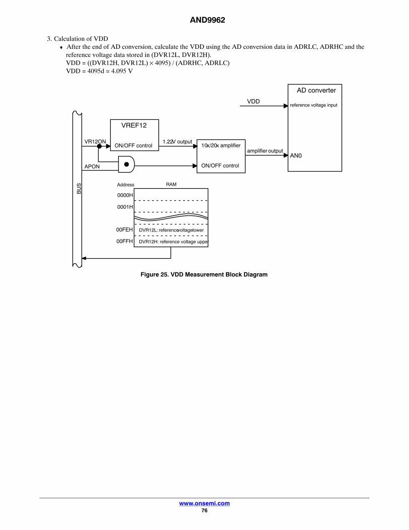
AND9962
www.onsemi.com76
3. Calculation of VDD♦ After the end of AD conversion, calculate the VDD using the AD conversion data in ADRLC, ADRHC and the
reference voltage data stored in (DVR12L, DVR12H).VDD = ((DVR12H, DVR12L) × 4095) / (ADRHC, ADRLC)VDD = 4095d = 4.095 V
Figure 25. VDD Measurement Block Diagram
DVR12H: reference voltage upper
DVR12L: referencevoltagelower
00FFH
00FEH
0001H
BU
S RAMAddress
0000H
VREF12
ON/OFF control 10x/20x amplifier
ON/OFF control
VR12ON 1.22V output
APON
AD converter
AN0amplifier output
VDDreference voltage input

AND9962
www.onsemi.com77
Voltage Control PWM (VCPWM0/VCPWM1)
OverviewThis model incorporates two 12−bit PWMs, named VCPWM0 and VCPWM1. Each PWM is made up of a PWM generator
circuit that generates multifrequency 8−bit fundamental PWM waves and a 4−bit additional pulse generator.
Functions1. VCPWM0: Fundamental PWM mode (register VCPWM0L = 0)
♦ Fundamental wave period = (16 to 256)/3 Tcyc (programmable in 16/3 Tcyc increments, common to VCPWM1)♦ High−level pulse width = 0 to Fundamental wave period – 1/3 Tcyc (programmable in 1/3 Tcyc increments)
2. VCPWM0: Fundamental wave + Additional pulse PWM mode♦ Fundamental wave period = (16 to 256)/3 Tcyc (programmable in 16/3 Tcyc increments, common to VCPWM1)♦ Overall period = Fundamental wave period × 16♦ High−level pulse width = 0 to Overall period – 1/3 Tcyc (programmable in 1/3 Tcyc increments)
3. VCPWM1: Fundamental wave PWM mode (register VCPWM1L = 0)♦ Fundamental wave period = (16 to 256)/3 Tcyc (programmable in 16/3 Tcyc increments, common to VCPWM0)♦ High−level pulse width = 0 to Fundamental wave period – 1/3 Tcyc (programmable in 1/3 Tcyc increments)
4. VCPWM1: Fundamental + Additional pulse PWM mode♦ Fundamental wave period = (16 to 256)/3 Tcyc (programmable in 16/3 Tcyc increments, common to VCPWM0)♦ Overall period = Fundamental wave period × 16♦ High−level pulse width = 0 to Overall period – 1/3 Tcyc (programmable in 1/3 Tcyc increments)
5. Interrupt generation♦ Interrupt requests are generated at the intervals equal to the overall PWM period if the interrupt request enable
bit is set6. Waveform selection
♦ VCPWM0/VCPWM1 can also generate waveform of (the PWM waves and the system clock)7. To control VCPWM0 and VCPWM1, it is necessary to manipulate the following special function registers:
♦ VCPWM0L, VCPWM0H, VCPWM1L, VCPWM1H, VCPWM0C, VCPWM01P
AddressInitialValue R/W Name BIT7 BIT6 BIT5 BIT4 BIT3 BIT2 BIT1 BIT0
FE80 0000HHHH
R/W VCPWM0L CPWM0L3 CPWM0L2 CPWM0L1 CPWM0L0 − − − −
FE81 00000000
R/W VCPWM0H CPWM0H7 CPWM0H6 CPWM0H5 CPWM0H4 CPWM0H3 CPWM0H2 CPWM0H1 CPWM0H0
FE82 0000HHHH
R/W VCPWM1L CPWM1L3 CPWM1L2 CPWM1L1 CPWM1L0 − − − −
FE83 00000000
R/W VCPWM1H CPWM1H7 CPWM1H6 CPWM1H5 CPWM1H4 CPWM1H3 CPWM1H2 CPWM1H1 CPWM1H0
FE84 00000000
R/W VCPWM0C CPWM0C7 CPWM0C6 CPWM0C5 CPWM0C4 ENCPWM1 ENCPWM0 CPWM00V CPWM01E
FE85 HHH00000
R/W VCPWM01P − − − CPWM01P2 CPWM1ECK CPWM0ECK FIX0 FIX0
Circuit Configuration
VCPWM0/VCPWM1 Control Register (VCPWM0C) (8−bit Register)1. The VCPWM0/VCPWM1 control register controls the operation and interrupts of VCPWM0 and VCPWM1
VCPWM0 Compare Register L (VCPWM0L) (4−bit Register)1. The VCPWM0 compare register L controls the additional pulses of VCPWM02. VCPWM0L is assigned bits 7 to 4 and all of its lower−order 4 bits are apparently set to “1” when it is read3. When the VCPWM0 control bit (VCPWM0C: FE84, bit 2) is set to “0,” the output of VCPWM0 (ternary) can be
controlled using bits 7 to 4 of VCPWM0L
VCPWM0 Compare Register H (VCPWM0H) (8−bit Register)1. The VCPWM0 compare register H controls the fundamental pulse width of VCPWM02. When bits 7 to 4 of VCPWM0L are all fixed at “0,” VCPWM0 can serve as period−programmable 8−bit PWM that is
controlled by VCPWM0H

AND9962
www.onsemi.com78
VCPWM1 Compare Register L (VCPWM1L) (4−bit Register)1. The VCPWM1 compare register L controls the additional pulses of VCPWM12. VCPWM1L is assigned bits 7 to 4 and all of its lower−order 4 bits are apparently set to “1” when it is read3. When the VCPWM1 control bit (VCPWM0C: FE84, bit 3) is set to “0”, the output of VCPWM1 (ternary) can be
controlled using bits 7 to 4 of VCPWM1L
VCPWM1 Compare Register H (VCPWM1H) (8−bit Register)1. The VCPWM1 compare register H controls the fundamental pulse width of VCPWM12. When bits 7 to 4 of VCPWM1L are all fixed at “0,” VCPWM1 can serve as period−programmable 8−bit PWM that is
controlled by VCPWM1H
VCPWM01 Port Input Register (VCPWM01P) (2−bit Register)1. This register controls the waveform and the output buffer of VCPWM02. This register controls the waveform and the output buffer of VCPWM1
Figure 26. VCPWM0 and VCPWM1 Block Diagram
VCPWM0/1
fundamental wave
period generation
System clockClock
Fundamental periodmatch data
(VCPWM0C7−4)
Match bufferregister
VCPWM0 compareregister H
(VCPWM0H)
VCPWM1 compareregister H
(VCPWM1H)
VCPWM0 compareregister L
(VCPWM0L)
VCPWM0/1additional pulses
generation counter
Match bufferregister
VCPWM1 compareregister L
(VCPWM1L)
Clear
Clock
ReloadReload
Match
VCPWM0 outputcontrol circuit
VCPWM1 outputcontrol circuit
MatchMatch
Match
Match
VCPWM0output
VCPWM1output
OverflowCPWM0OV set signal
(Occurs in every overall period)
Comparator Comparator Comparator
Comparator
Comparator

AND9962
www.onsemi.com79
Related Registers
VCPWM0/VCPWM1 Control Register (VCPWM0C)1. The VCPWM0/VCPWM1 control register controls the operation and interrupts of VCPWM0 and VCPWM1
Address Initial value R/W Name BIT7 BIT6 BIT5 BIT4 BIT3 BIT2 BIT1 BIT0
FE84 0000 0000 R/W VCPWM0C CPWM0C7 CPWM0C6 CPWM0C5 CPWM0C4 ENCPWM1 ENCPWM0 CPWM0OV CPWM0IE
CPWM0C7 to CPWM0C4 (Bits 7 to 4): VCPWM0/VCPWM1 Period Control• Fundamental wave period = (Value represented by (CPWM0C7 to CPWM0C4) + 1) × 16/3 Tcyc
• Overall period = Fundamental wave period × 16
ENCPWM1 (Bit 3): VCPWM1 Operation Control• When this bit is set to “1”, VCPWM1 is active
• When this bit is set to “0”, the VCPWM1 output (ternary) can be controlled using bits 7 to 4 of VCPWM1L
ENCPWM0 (Bit 2): VCPWM0 Operation Control• When this bit is set to “1”, VCPWM0 is active
• When this bit is set to “0”, the VCPWM0 output (ternary) can be controlled using bits 7 to 4 of VCPWM0L
CPWM0OV (Bit 1): VCPWM0/VCPWM1 Overflow Flag• This bit is set at the interval equal to the overall period of PWM
• This flag must be cleared with an instruction
CPWM0IE (Bit 0): VCPWM0/VCPWM1 Interrupt Request Enable ControlAn interrupt to vector addresses 004BH is generated when this bit and CPWM0OV are both set to “1”.
VCPWM0 Compare Register L (VCPWM0L)1. The VCPWM0 compare register L controls the additional pulses of VCPWM02. VCPWM0L is assigned bits 7 to 4 and all of its lower−order 4 bits are apparently set to “1” when it is read3. When the VCPWM0 control bit (VCPWM0C: FE84, bit 2) is set to “0”, the output of VCPWM0 (ternary) can be
controlled using bits 7 to 4 of VCPWM0L
Address Initial value R/W Name BIT7 BIT6 BIT5 BIT4 BIT3 BIT2 BIT1 BIT0
FE80 0000 HHHH R/W VCPWM0L CPWM0L3 CPWM0L2 CPWM0L1 CPWM0L0 − − − −
VCPWM0 Output
ENCPWM0
FE84−bit2
CPWM0L3
FE80−bit7
CPWM0L2
FE80−bit6
CPWM0L1, 0
FE80−bit5, 4
HI−Z 0 − 0 −
LOW 0 0 1 0, 0
HIGH 0 1 1 0, 0
VCPWM0 Compare Register H (VCPWM0H)1. The VCPWM0 compare register H controls the fundamental pulse width of VCPWM0.
Fundamental pulse width = (Value represented by CPWM0H7 to CPWM0H 0) × 1/3 Tcyc2. When bits 7 to 4 of VCPWM0L are all fixed at “0”, VCPWM0 can serve as period−programmable 8−bit PWM that is
controlled by VCPWM0H
Address Initialvalue
R/W Name BIT7 BIT6 BIT5 BIT4 BIT3 BIT2 BIT1 BIT0
FE81 00000000
R/W VCPWM0H CPWM0H7 CPWM0H6 CPWM0H5 CPWM0H4 CPWM0H3 CPWM0H2 CPWM0H1 CPWM0H0

AND9962
www.onsemi.com80
VCPWM1 Compare Register L (VCPWM1L)1. The VCPWM1 compare register L controls the additional pulses of VCPWM12. VCPWM1L is assigned bits 7 to 4 and all of its lower−order 4 bits are apparently set to “1” when it is read3. When the VCPWM1 control bit (VCPWM0C: FE84, bit 3) is set to “0,” the output of VCPWM1 (ternary) can be
controlled using bits 7 to 4 of VCPWM1L
Address Initial value R/W Name BIT7 BIT6 BIT5 BIT4 BIT3 BIT2 BIT1 BIT0
FE82 0000 HHHH R/W VCPWM1L CPWM1L3 CPWM1L2 CPWM1L1 CPWM1L0 − − − −
VCPWM1 Output
ENCPWM1
FE84−bit3
CPWM1L3
FE82−bit7
CPWM1L2
FE82−bit6
CPWM1L1, 0
FE82−bit5, 4
HI−Z 0 − 0 −
LOW 0 0 1 0, 0
HIGH 0 1 1 0, 0
VCPWM1 Compare Register H (VCPWM1H)1. The VCPWM1 compare register H controls the fundamental pulse width of VCPWM1.
Fundamental pulse width = (Value represented by CPWM1H7 to CPWM1H0) × 1/3 Tcyc2. When bits 7 to 4 of VCPWM1L are all fixed at “0”, VCPWM1 can serve as period−programmable 8−bit PWM that is
controlled by VCPWM1H
Address Initialvalue
R/W Name BIT7 BIT6 BIT5 BIT4 BIT3 BIT2 BIT1 BIT0
FE53 00000000
R/W VCPWM1H CPWM1H7 CPWM1H6 CPWM1H5 CPWM1H4 CPWM1H3 CPWM1H2 CPWM1H1 CPWM1H0
Figure 27.
PWM0H,PWM1Hでの��
E F 0 1 2 3 4��パルスカウンタ
��パルス
���カウンタ
��PWM��
Additional pulsecounterAdditional pulses
Fundamental pulsecounter
Fundamental PWMwaveform
PWM outputwaveform
PWM2H, PWM3H setting value
• The 12−bit PWM has the following waveform structure:♦ The overall period consists of 16 fundamental wave periods♦ A fundamental wave period is represented by an 8−bit PWM. (PWM compare register H) (PWMH)♦ 4 bits are used to designate the fundamental wave period to which additional pulses are to be added. (PWM compare
register L) (PWML) 12−bit register structure → (PWMH), (PWML) = XXXX XXXX, XXXX (12BIT)
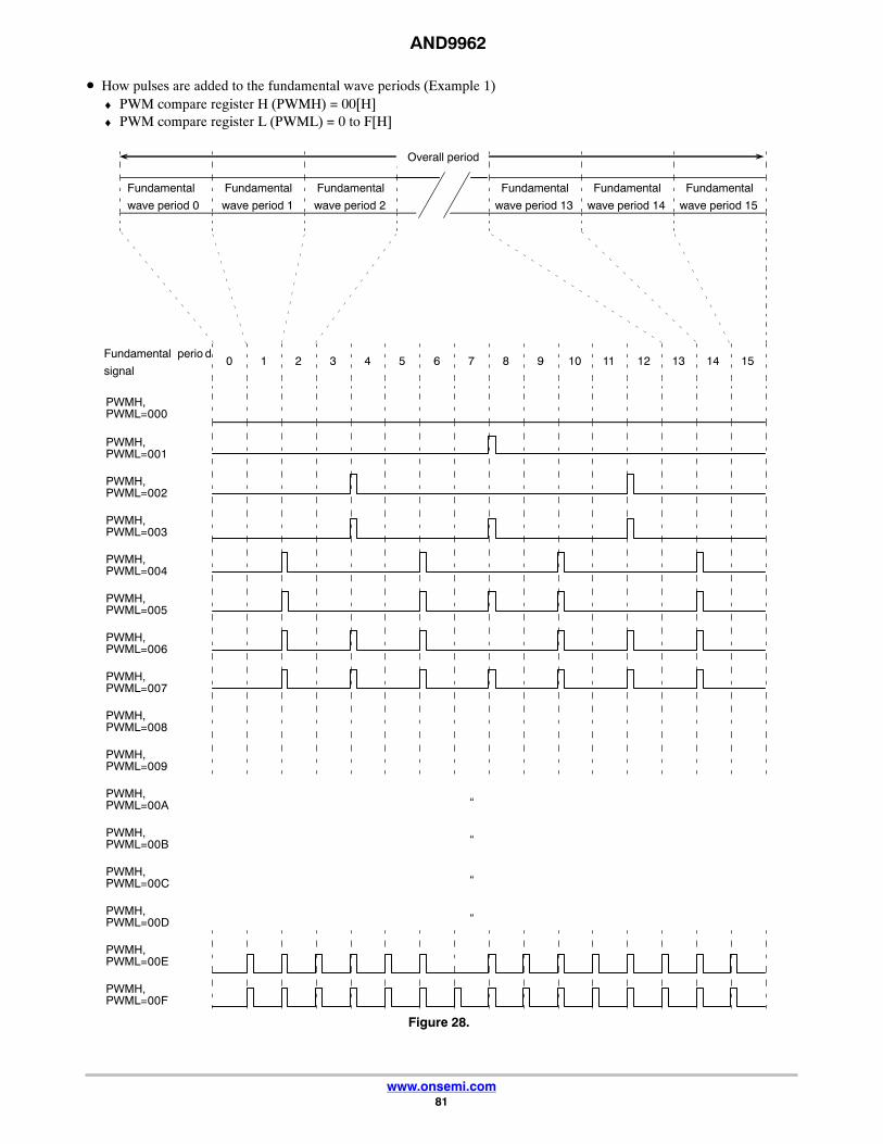
AND9962
www.onsemi.com81
• How pulses are added to the fundamental wave periods (Example 1)♦ PWM compare register H (PWMH) = 00[H]♦ PWM compare register L (PWML) = 0 to F[H]
Figure 28.
Fundamental
wave period 0
Fundamental
wave period 1
Fundamental
wave period 2
Fundamental
wave period 13
Fundamental
wave period 14
Fundamental
wave period 15
d
signal
Fundamental perio0 1 2 3 4 5 6 7 8 9 10 11 12 13 14
PWMH,PWML=000
15
PWMH,PWML=001
PWMH,PWML=002
PWMH,PWML=003
PWMH,PWML=004
PWMH,PWML=005
PWMH,PWML=006
PWMH,PWML=007
PWMH,PWML=008
PWMH,PWML=009
PWMH,PWML=00A
PWMH,PWML=00B
PWMH,PWML=00C
PWMH,PWML=00D
PWMH,PWML=00E
PWMH,PWML=00F
Overall period
“
“
“
“
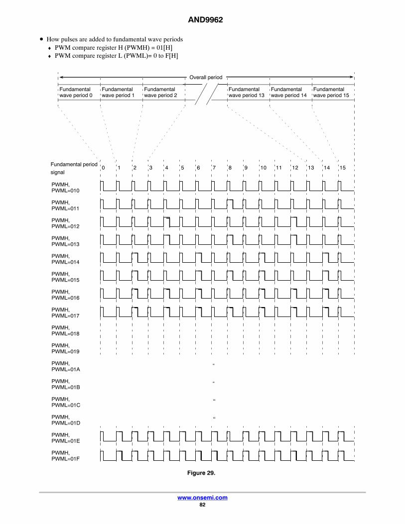
AND9962
www.onsemi.com82
• How pulses are added to fundamental wave periods♦ PWM compare register H (PWMH) = 01[H]♦ PWM compare register L (PWML)= 0 to F[H]
Figure 29.
Fundamentalwave period 0
Fundamentalwave period 1
Fundamentalwave period 2
Fundamentalwave period 13
Fundamentalwave period 14
Fundamentalwave period 15
Fundamental period
signal0 1 2 3 4 5 6 7 8 9 10 11 12 13 14 15
PWMH,PWML=010
PWMH,PWML=011
PWMH,PWML=012
PWMH,PWML=013
PWMH,PWML=014
PWMH,PWML=015
PWMH,PWML=016
PWMH,PWML=017
PWMH,PWML=018
PWMH,PWML=019
PWMH,PWML=01A
“
PWMH,PWML=01B
“
PWMH,PWML=01C
“
PWMH,PWML=01D
“
PWMH,PWML=01E
PWMH,PWML=01F
Overall period

AND9962
www.onsemi.com83
• The fundamental wave period is variable within the range of (16 to 256)/3 Tcyc.Fundamental wave period = (Value represented by CPWM0C7 to CPWM0C4 + 1) × 16/3 Tcyc♦ The overall period can be changed by changing the fundamental wave period♦ The overall period is made up of 16 fundamental wave periods
Examples:• Wave comparison when the 12−bit PWM contains 237[H].
12−bit register configuration → (PWMH), (PWML) = 237[H]1. Pulse added system (this series)
Figure 30.
Fundamental
period signal 0 1 2 3 4 5 6 7 8 9 10 11 12 13 14 15
PWMH,
PWML=237
Overall period
2. Ordinary systemSince the ripple component of the integral output in this system is greater than that of the pulse added system as seenfrom the figure below, the pulse added system is considered better for motor−controlling uses
Figure 31.
PWMH,
PWML=237
Ripple
Overall period
VCPWM01 Port Input Register (VCPWM01P)1. This register controls the waveform and the output buffer of VCPWM02. This register controls the waveform and the output buffer of VCPWM1
Address Initial value R/W Name BIT7 BIT6 BIT5 BIT4 BIT3 BIT2 BIT1 BIT0
FE85 HHH0 0000 R/W VCPWM01P − − − CPWM01P2 CPWM1ECK CPWM0ECK FIX0 FIX0
(Bits 7 to 5): Does not exist; always read as 1.
CPWM01P2 (Bit 4): Test bit. Must always be set to 0.
CPWM1ECK (Bit 3): When this bit is set to 1, VCPWM1 generates waveform of (the PWM waves and the system clock).
CPWM0ECK (Bit 2): When this bit is set to 1, VCPWM0 generates waveform of (the PWM waves and the system clock).
(Bits 1 to 0): Test bit. Must always be set to 0.

AND9962
www.onsemi.com84
High−speed PWM2 (HPWM2)
OverviewThis model incorporates high−speed 8−/12−bit PWM, named HPWM2. HPWM2 is made up of a PWM generator circuit that
generates multifrequency 8−bit fundamental PWM waves and a 2−bit additional pulse generator.
FunctionsHigh−speed 8−bit fundamental PWM mode.HPWM2 operates as an 8−bit PWM by a PWM generator circuit that generates multifrequency 8−bit fundamental PWM
waves• Fundamental wave period = 256 x (period set by HPWM2AC, bits 6 to 5)
• High−level pulse width = (data of HPWM2AH + 1) x (period set by HPWM2AC, bit6 to 5)
High−speed 10−bit fundamental + Additional pulse PWM modeHPWM2 operates as a 10−bit PWM by a PWM generator circuit that generates multifrequency 8−bit fundamental PWM
waves and a 2−bit additional pulse generator. (Note 1)• Fundamental wave period = 256 x (period set by HPWM2AC, bits 6 to 5)
• Overall period = Fundamental wave period × 4
• High−level pulse width = [HPWM2AH, HPWM2AL bits 7 to 6] x (period set by HPWM2AC, bit6 to 5)
Interrupt Generation• Interrupt request to vector address 0033H is generated at the intervals equal to the fundamental PWM period(8−bit
mode) or the overall PWM period(10−bit mode) if the interrupt request enable bit is set.
To control high−speed PWM2(HPWM2), it is necessary to manipulate the following special function registers:• HPWM2AC, HPWM2AL, HPWM2AH, P1, P1DDR, P1FCR
Address InitialValue
R/W Name BIT7 BIT6 BIT5 BIT4 BIT3 BIT2 BIT1 BIT0
FE8D 00000000 R/W HPWM2AC H2A40MON H2ACKDV H2ACKSL H2ABWSL H2ARUN H2ARLBSY H2AOVF H2AIE
FE8E 00HH HH00 R/W HPWM2AL HPWM2AL1 HPWM2AL0 − − − − P17H2ASL P16H2ASL
FE8F 00000000 R/W HPWM2AH HPWM2AH7 HPWM2AH6 HPWM2AH5 HPWM2AH4 HPWM2AH3 HPWM2AH2 HPWM2AH1 HPWM2AH0
1. When HPWM2 is not operating, HPWM2 output is fixed to high level. When HPWM2 is operating as the 8−bit PWM mode and the data of HPWM2AH is FFH, HPWM2 output is fixed to high level.When HPWM2 is operating as the 10−bit PWM mode and the data of [HPWM2AH, HPWM2AL bits 7 to 6] is 000H, HPWM2 output is fixedto low level.
Circuit Configuration
HPWM2 Control Register (HPWM2AC) (8−bit Register)1. The HPWM2 control register controls the operation of the internal high−speed RC and the operation and interrupts of
HPWM22. H2ARLBSY(HPWM2AC, bit2) is read only bit
HPWM2 Compare Register L (HPWM2AL) (4−bit Register)The HPWM2 compare register L controls the additional pulses of HPWM2 and the function outputs of P17 and P16.
HPWM2 Compare Register H (HPWM2AH) (8−bit Register)The HPWM2 compare register H controls the fundamental pulse width of HPWM2.
HPWM2 Compare Data Buffer Register (HPWM2BR) (10−bit Buffer Register)The HPWM2 compare data buffer register is used to store the setting data of the pulse width of HPWM2. The data of
[HPWM2AH, HPWM2AL bits 7 to 6] is stored to this register.The update of the buffer register is carried out as follows.
• When HPWM2 is not operating(H2ARUN = 0), the data of HPWM2BR will be equal to the data of [HPWM2AH,HPWM2AL bits 7 to 6]

AND9962
www.onsemi.com85
• When HPWM2 is operating(H2ARUN = 1), when HPWM2AH is written, reload−wait−flag (H2ARLBSY) is set andwriting to HPWM2AL bits 7 to 6 and HPWM2AH is inhibited. In this state, when an overflow signal of the next PWMperiod(fundamental period at 8−bit PWM mode, overall period at 10−bit mode) is generated, the data of [HPWM2AH,HPWM2AL bits 7 to 6] is reloaded to HPWM2BR, and H2ARLBSY is cleared. (Note 2)
2. HPWM2AH must be written finally in the data update process of the program because writing to HPWM2AH is the trigger of reload operation.
Figure 32. HPWM2 Block Diagram
H2ACKSL
the system clock
H2ACKDV
comparetor
HPWM2BR
additional
pulscounter
decorder
HPWM2BR
OVF OVF
H2ABWSL
set signal forH2AOVF
HPWM2ALbits 7 to 6
HPWM2AH
BUS
PWM wave
generate circuit
agreement
reload signal
generate circuit
write signal
reload reload
H2ABWSL
H2ARLBSYinhibit writing to
HPWM2AH/HPWM2ALbits 7 to 6.
P17H2ASL
Internal
high −speedRC(40MHz)
H2A40MO
T1PWMHor BUZ output
T1PWML output
P17 function output
P16 function output
HPWM2 output
oscillationcontrol
count clock
reset
add
set
comparator output
sele
ctor
divider
sele
ctor
fundamentalcounter(8bit)
sele
ctor
sele
ctor
sele
ctor
P16H2ASL
Figure 33. Examples of Waveform of the 8−bit PWM Mode (H2ABWSL = 0)
* fundamental period = 256 x ( period set by HPWM2AC bits 6 to 5 )high pulse with = ( value of HPWM2AH + 1 ) x ( period set by HPWM2AC bits 6 to 5 )
HPWM2AHValue = 00h
HPWM2AHValue = 01h
HPWM2AHValue = 02h
fundamental period fundamental period
HPWM2AHValue = FFh
*

AND9962
www.onsemi.com86
Figure 34. Examples of Waveform of the 10−bit PWM Mode (H2ABWSL = 1)
* fundamental period = 256 x ( period set by HPWM2AC bits 6 to 5 )
* overall period = fundamental period x 4
* high pulse with = [ HPWM2AH, HPWM2AL bits 7 to 6] x ( period set by HPWM2AC bits 6 to 5 )
fundamentalperiod
overall period overall period
fundamentalperiod
fundamentalperiod
fundamentalperiod
fundamentalperiod
fundamentalperiod
fundamentalperiod
fundamental
period[HPWM2AH,
HPWM2AL bits 7 to 6]Value = 000h
[HPWM2AH,HPWM2AL bits 7 to 6]
Value = 001h
[HPWM2AH,HPWM2AL bits 7 to 6]
Value = 002h
[HPWM2AH,HPWM2AL bits 7 to 6]
Value = 003h
[HPWM2AH,HPWM2AL bits 7 to 6]
Value = 004h
[HPWM2AH,HPWM2AL bits7 to 6]
Value = 007h
[HPWM2AH,HPWM2AL bits 7 to 6]
Value = 3FFh
[HPWM2AH,HPWM2AL bits 7 to 6]
Value = 005h
[HPWM2AH,HPWM2AL bits 7 to 6]
Value = 006h
Related Registers
HPWM2 Control Register (HPWM2AC)1. The HPWM2 control register controls the operation of the internal high−speed RC and the operation and interrupts of
HPWM22. H2ARLBSY(HPWM2AC, bit2) is read only bit
Address Initial value R/W Name BIT7 BIT6 BIT5 BIT4 BIT3 BIT2 BIT1 BIT0
FE8D 0000 0000 R/W HPWM2AC H2A40MON H2ACKDV H2ACKSL H2ABWSL H2ARUN H2ARLBSY H2AOVF H2AIE
H2A40MON (Bit 7): Internal High−speed RC(40MHz) Oscillation Control• Setting this bit to 0 stops the oscillation of the internal high−speed RC(40 MHz) oscillator circui
• Setting this bit to 1 starts the oscillation of the internal high−speed RC(40 MHz) oscillator circuit
H2ACKDV (Bit 6): HPWM2 Clock Divider Control• When this bit is set to 1, the 1/1 division of the clock selected by H2ACKSL is used
• When this bit is set to 0, the 1/2 division of the clock selected by H2ACKSL is used

AND9962
www.onsemi.com87
H2ACKSL (Bit 5): HPWM2 Clock Select
H2ACKSL HPWM2 Clock
0 Internal high−speed RC (40 MHz)
1 System−clock (fSCLK)
H2ABWSL (Bit 4): HPWM2 Resolution Select
H2ABWSL HPWM2 Resolution
0 8−bit (fundamental)
1 10−bit (fundamental + additional pulse)
H2ARUN (Bit 3): HPWM2 Operation Control• Setting this bit to 0 stops the operation of HPWM2
• Setting this bit to 1 starts the operation of HPWM2
H2ARLBSY (Bit 2): HPWM2 Reload Wait FlagWhen HPWM2 is operating(H2ARUN = 1), when HPWM2AH is written, reload−wait−flag (H2ARLBSY) is set and writing
to HPWM2AL bits 7 to 6 and HPWM2AH is inhibited.The conditions required to clear H2ARLBSY are:1. When HPWM2 is not operating(H2ARUN = 0)2. When an overflow signal of the next PWM period (fundamental period at 8−bit PWM mode, overall period at 10−bit
mode) is generated
H2AOVF (Bit 1): HPWM2 Period Overflow FlagWhen HPWM2 is operating(H2ARUN = 1), this bit is set whenever an overflow signal of the PWM period (fundamental
period at 8−bit PWM mode, overall period at 10−bit mode) is generated.This bit must be cleared with an instruction .
H2AIE (Bit 0): HPWM2 Interrupt Request EnableWhen this bit and H2AOVF are set to 1, an interrupt request to vector address 0033H are generated.
NOTES:� When the internal high−speed RC(40 MHz) is used for HPWM2 operation, an oscillation stabilization time of
about 10 uS after an oscillation start ( H2A40MON = 0(oscillation stop) � 1(oscillation start)) is requiredbefore HPWM2 starts operation
� When the internal high−speed RC(40 MHz) is operating, about an operating current of several mA is alwaysflowing in the IC
If it is required to reduce a current at the standby mode, the oscillation must be stopped (H2A40MON=0) before standbymode is entered
HPWM2 Compare Register L (HPWM2AL)1. The HPWM2 compare register L controls the additional pulses of HPWM2 and the function outputs of P17 and P16
Address Initial value R/W Name BIT7 BIT6 BIT5 BIT4 BIT3 BIT2 BIT1 BIT0
FE8E 00HH HH00 R/W HPWM2AL HPWM2AL1 HPWM2AL0 − − − − P17H2ASL P16H2ASL

AND9962
www.onsemi.com88
P17H2ASL (Bit 1): P17 Function Output Control• This bit and BUZON(ISL bit3) select the data transferred to P17 from the buzzer, timer 1 PWMH and HPWM2 output
NOTE: It is also required for the function output from P17 to setup P17(P1 bit7), P17DDR(P1DDR bit7) andP17FCR(P1FCR bit7).
P17H2ASL(HPWM2AL bit1)
BUZON(ISL bit3) P17 function output
0 0 Timer1 PWMH output
0 1 Basetimer BUZ output
1 − HPWM2 output
P16H2ASL (Bit 0): P16 Function Output Control• When this bit is set to 0, (AND of timer 1 PWML and the comparator output) is transferred to P16
• When this bit is set to 1, (AND of HPWM2 and the comparator output) is transferred to P16
NOTES:� The comparator output is fixed to high level when CPON(VRCNT, bit5) is set to 0� It is also required for the function output from P16 to setup P16(P1 bit6), P16DDR(P1DDR bit6) and
P16FCR(P1FCR bit6)
HPWM2 Compare Register H (HPWM2AH)1. The HPWM2 compare register H controls the fundamental pulse width of HPWM2
AddressInitialvalue R/W Name BIT7 BIT6 BIT5 BIT4 BIT3 BIT2 BIT1 BIT0
FE8F 0000 0000 R/W HPWM2AH HPWM2AH7 HPWM2AH6 HPWM2AH5 HPWM2AH4 HPWM2AH3 HPWM2AH2 HPWM2AH1 HPWM2AH0
The PWM period and high−level pulse width are set by HPWM2AH and HPWM2AL bits 7 to 6.as following.
< 8−bit PWM mode (H2ABWSL = 0) >• Fundamental wave period = 256 x (period set by HPWM2AC, bits 6 to 5)
• High−level pulse width = (data of HPWM2AH + 1) x (period set by HPWM2AC, bit6 to 5)
< 10−bit PWM mode (H2ABWSL = 1) >• Fundamental wave period = 256 x (period set by HPWM2AC, bits 6 to 5)
• Overall period = Fundamental wave period × 4
• High−level pulse width = [HPWM2AH, HPWM2AL bits 7 to 6] x (period set by HPWM2AC, bit6 to 5)
NOTE: When HPWM2 is operating in 8−bit PWM mode, setting of HPWM2AL bits 7 to 6 doesn’t affect HPWM2operation.See “HPWM2 compare data buffer register” for the detail reload operation of the compare data (HPWM2AH,HPWM2AL bits 7 to 6).

AND9962
www.onsemi.com89
Temperature Sensor (TEMPS)
OverviewThis model incorporates a simplified temperature sensor and microcontrollers can detect temperature changes using this
sensor.1. The output voltage level of the sensor varies according to temperature2. The output voltage level of the sensor can be monitored by the AD converter3. The result of AD conversion of a reference output voltage level of the sensor has been stored in SFR before
shipment/sorting of ICs
Functions1. Temperature sensor function
♦ The output voltage level of the sensor varies linearly according to temperature.♦ The lower temperature is, the higher the output voltage level of the sensor is.
(low−temperature ≥ room−temperature ≥ low−temperature)♦ The output of the sensor is connected to the AD converter input, so a temperature can be monitored by the AD
conversion of the output voltage level of the sensor2. Reference to reference voltage level of the temperature sensor
The result of AD conversion of the reference output voltage level of the sensor at about 60℃ has been stored in SFRbefore shipment/sorting of this series of microcontrollers, and it can be referred by program.
3. To control temperature sensor, it is necessary to manipulate the following special function registers:♦ TEMPS2CNT, ADCRC, ADMRC, ADRLC, ADRHC♦ D2TL, D2TH, D4TL, D4TH
Address Initial Value R/W Name BIT7 BIT6 BIT5 BIT4 BIT3 BIT2 BIT1 BIT0
FEDA 00HH HH00 R/W TEMPS2CNT TEMPS2ON FIX0 − − − − DIO2X FIX0
FEE0 XXXX XXXX R/W D2TL D2TL7 D2TL6 D2TL5 D2TL4 D2TL3 D2TL2 D2TL1 D2TL0
FEE1 0000 XXXX R/W D2TH D2TH7 D2TH6 D2TH5 D2TH4 D2TH3 D2TH2 D2TH1 D2TH0
FEE2 XXXX XXXX R/W D4TL D4TL7 D4TL6 D4TL5 D4TL4 D4TL3 D4TL2 D4TL1 D4TL0
FEE3 0000 XXXX R/W D4TH D4TH7 D4TH6 D4TH5 D4TH4 D4TH3 D4TH2 D4TH1 D4TH0

AND9962
www.onsemi.com90
Circuit Configuration
Temperature Sensor Control Register (TEMPS2CNT) (8−bit Register)The temperature sensor control register controls the operation of the temperature sensor.
Temperature Sensor 60�C 2−diodes Reference Register L (D2TL) (8−bit Register)The lower 8−bit of the result of 12−bit AD conversion (VREF2.0V) of the reference output voltage level of the
sensor(2−diodes) at about 60℃ is stored in this register.
Temperature Sensor 60℃ 2−diodes Reference Register H (D2TH) (8−bit Register)The upper 4−bit of the result of 12−bit AD conversion (VREF2.0V) of the reference output voltage level of the
sensor(2−diodes) at about 60℃ is stored in this register.
Temperature Sensor 60℃ 4−diodes Reference Register L (D4TL) (8−bit Register)The lower 8−bit of the result of 12−bit AD conversion(VREF4.0V) of the reference output voltage level of the
sensor(4−diodes) at about 60℃ is stored in this register.
Temperature Sensor 60℃ 4−diodes Reference Register H (D4TH) (8−bit Register)The upper 4−bit of the result of 12−bit AD conversion(VREF4.0V) of the reference output voltage level of the
sensor(4−diodes) at about 60℃ is stored in this register.
Temperature SensorThis is a temperature sensor whose output voltage level varies according to temperature.
Figure 35. Temperature Sensor Block Diagram
TEMPS2CNT
Temperature
SensorON/OFF
TEMPS2ON
AD Converter
60° 4−diodes reference upper
60° 4−diodes reference lower
60° 2−diodes reference upper
60° 2−diodes reference lower
D4TH
D4TL
D2TH
D2TL
ADC startAN15 selected
BU
S

AND9962
www.onsemi.com91
Related Registers
Temperature Sensor Control Register (TEMPS2CNT)The temperature sensor control register controls the operation of the temperature sensor.
Address Initial Value R/W Name BIT7 BIT6 BIT5 BIT4 BIT3 BIT2 BIT1 BIT0
FEDA 00HH HH00 R/W TEMPS2CNT TEMPS2ON FIX0 − − − − DIO2X FIX0
TEMPS2ON (bit 7): Temperature Sensor Operation Control (Manual)• Setting this bit to 0 stops the operation of the temperature sensor
• Setting this bit to 1 starts the operation of the temperature sensor
NOTE: When AN15 is selected as AD converter input and AD conversion starts, the operation of the temperature sensoris turned on automatically.And when AD conversion ends, the operation of the temperature sensor is turned off automatically.
(Bit 6): Test Bit. Must Always be set to 0.
DIO2X (Bit 1): Temperature Sensor Diode Number of Row Select• When this bit is set to 0, the temperature sensor is configured to 4−diodes mode
• When this bit is set to 1, the temperature sensor is configured to 2−diodes mode
(Bit 0): Test bit. Must always be set to 0.
NOTE: When the temperature sensor is operating(TEMPS2ON = 1), about an operating current of several hundreds �Ais always flowing in the IC.
In this state, when standby mode is entered, the temperature sensor keeps its operation.If it is required to reduce a current at the stanby mode, the operation of the temperature sensor must be stopped(TEMPS2ON = 0) before standby mode is entered.
Temperature Sensor 60℃ 2−diodes Reference Register L (D2TL) (8−bit Register)The lower 8−bit of the result of 12−bit AD conversion(VREF2.0V) of the reference output voltage level of the
sensor(2−diodes) at about 60℃ is stored in this register.
Address Initial Value R/W Name BIT7 BIT6 BIT5 BIT4 BIT3 BIT2 BIT1 BIT0
FEE0 XXXX XXXX R/W D2TL D2TL7 D2TL6 D2TL5 D2TL4 D2TL3 D2TL2 D2TL1 D2TL0
Temperature Sensor 60℃ 2−diodes Reference Register H (D2TH) (8−bit Register)The upper 4−bit of the result of 12−bit AD conversion(VREF2.0V) of the reference output voltage level of the
sensor(2−diodes) at about 60℃ is stored in this register.
Address Initial Value R/W Name BIT7 BIT6 BIT5 BIT4 BIT3 BIT2 BIT1 BIT0
FEE1 0000 XXXX R/W D2TH D2TH7 D2TH6 D2TH5 D2TH4 D2TH3 D2TH2 D2TH1 D2TH0
Temperature Sensor 60℃ 4−diodes Reference Register L (D4TL) (8−bit Register)The lower 8−bit of the result of 12−bit AD conversion(VREF4.0V) of the reference output voltage level of the
sensor(4−diodes) at about 60℃ is stored in this register.
Address Initial Value R/W Name BIT7 BIT6 BIT5 BIT4 BIT3 BIT2 BIT1 BIT0
FEE2 XXXX XXXX R/W D4TL D4TL7 D4TL6 D4TL5 D4TL4 D4TL3 D4TL2 D4TL1 D4TL0
Temperature Rensor 60℃ 4−diodes Reference Register H (D4TH) (8−bit Register)The upper 4−bit of the result of 12−bit AD conversion(VREF4.0V) of the reference output voltage level of the
sensor(4−diodes) at about 60℃ is stored in this register.
Address Initial Value R/W Name BIT7 BIT6 BIT5 BIT4 BIT3 BIT2 BIT1 BIT0
FEE3 0000 XXXX R/W D4TH D4TH7 D4TH6 D4TH5 D4TH4 D4TH3 D4TH2 D4TH1 D4TH0

AND9962
www.onsemi.com92
Example of Using Temperature Sensor1. Setting of the temperature sensor
♦ Write 80h to TEMPS2CNT, and the operation of temperature sensor starts.If the automatic turning on/off function of the temperature sensor is used, this writing is not necessary
2. Setting of the AD converter♦ Write to ADMRC and ADRLC, setup the appropriate AD conversion time♦ Write F4h/F5h(Interrupt request enable/disable) to ADCRC, connect the output of the temperature sensor to the
input of AD converter, start AD conversion3. Detection of the temperature
♦ After the end of AD conversion, calculate the temperature value using the AD conversion data in ADRLC,ADRHC and the reference temperature sensor data at 60℃ stored in (D2TL, D2TH, D4TL, D4TH)

AND9962
www.onsemi.com93
CONTROL FUNCTIONS
Interrupt Function
OverviewThis model has the capabilities to control three levels of multiple interrupts, i.e., low level (L), high level (H), and highest
level (X). The master interrupt enable resister and interrupt priority control register are used and enable or disable interruptsand determine the priority of interrupts.
Functions1. Interrupt processing
♦ Peripheral modules generate an interrupt request to the predetermined vector address when the interrupt requestand interrupt request enable flags are set to 1
♦ When the microcontroller receives an interrupt request from a peripheral module, it determines the level, priorityand interrupt enable status of the interrupt. If the interrupt request is legitimate for processing, themicrocontroller saves the value of PC in the stack and causes a branch to the predetermined vector address
♦ The return from the interrupt routine is accomplished by the RETI instruction, which restores the old state of thePC and interrupt level
2. Multilevel interrupt control♦ The interrupt function supports three levels of interrupts, that is, the low level (L), high level (H), and highest
level (X). The interrupt function will not accept any interrupt requests of the same level or lower than that of theinterrupt that is currently being processed
3. Interrupt priority♦ When interrupt requests to two or more vector addresses occur at the same time, the interrupt request of the
highest level takes precedence over the other interrupt requests. Among the interrupt requests of the same level,the one whose vector address is the smallest is prioritary
4. Interrupt request enable control♦ The master interrupt enable register can be used to control the enabling/disabling of H− and L−level interrupt
requests♦ Interrupt requests of the X level cannot be disabled
5. Interrupt disable period♦ Interrupts are held disabled for a period of 2Tcyc after a write operation is performed to the IE (FE08H) or IP
(FE09H) register, or the HOLD mode is released♦ No interrupt can occur during the interval between the execution of an instruction that loads the PCON (FE07H)
register and the execution of the next instruction♦ No interrupt can occur during the interval between the execution of a RETI instruction and the execution of the
next instruction6. Interrupt level control
♦ Interrupt levels can be selected on a vector address basis
TABLE OF INTERRUPTS
No. Vector Address Selectable Level Interrupt Sources
1 00003H X or L INT0
2 0000BH X or L INT1
3 00013H H or L INT2/ T0L /INT4
4 0001BH H or L INT3/Base timer
5 00023H H or L T0H
6 0002BH H or L T1L/T1H
7 00033H H or L HPWM2A
8 0003BH H or L SIO1
9 00043H H or L ADC
10 0004BH H or L Port0/VCPWM

AND9962
www.onsemi.com94
• Priority levels: X > H > L
• Of interrupts of the same level, the one with the smallest vectoraddress takes precedence
7. To enable interrupts and to specify their priority, it is necessary to manipulate the following special function registers:♦ IE, IP
Address Initial Value R/W Name BIT7 BIT6 BIT5 BIT4 BIT3 BIT2 BIT1 BIT0
FE08 0000 HH00 R/W IE IE7 XFLG HFLG LFLG − − XCNT1 XCNT0
FE09 0000 0000 R/W IP IP4B IP43 IP3B IP33 IP2B IP23 IP1B IP13
Circuit Configuration
Master Interrupt Enable Control Register (IE) (6−bit Register)1. The master interrupt enable control registers enables and disables H− and L−level interrupts2. The interrupt level flag of the register can be read3. The register selects the level (L or X) of interrupts to vector addresses 00003H and 0000BH
Interrupt Priority Control Register (IP) (8−bit Register)1. The interrupt priority control register selects the level (H or L) of interrupts to vector addresses 00013H to 0004BH
Related Registers
Master Interrupt Enable Control Register (IE)1. The master interrupt enable control register is a 6−bit register for controlling the interrupts. Bits 6 to 4 of this register
are read only
Address Initial Value R/W Name BIT7 BIT6 BIT5 BIT4 BIT3 BIT2 BIT1 BIT0
FE08 0000 HH00 R/W IE IE7 XFLG HFLG LFLG − − XCNT1 XCNT0
IE7 (Bit 7): H−/L−level Interrupt Enables/Disables Control• A 1 in this bit enables H− and L−level interrupt requests to be accepted
• A 0 in this bit disables H− and L−level interrupt requests to be accepted
• X−level interrupt requests are always enabled regardless of the state of this bit
XFLG (Bit 6): X-level Interrupt Flag (R/O)• This bit is set when an X−level interrupt is accepted and reset when execution returns from the processing of the
X−level interrupt
• This bit is read only. No instruction can rewrite the value of this bit directly
HFLG (Bit 5): H-level Interrupt Flag (R/O)• This bit is set when an H−level interrupt is accepted and reset when execution returns from the processing of the
H−level interrupt
• This bit is read only. No instruction can rewrite the value of this bit directly
LFLG (Bit 4): L-level Interrupt Flag (R/O)• This bit is set when an L−level interrupt is accepted and reset when execution returns from the processing of the L−level
interrupt
• This bit is read only. No instruction can rewrite the value of this bit directly
(Bits 3, 2): These bits do not exist. They are always read as “1”.
XCNT1 (Bit 1): 0000BH Interrupt Level Control Flag• A 1 in this bit sets all interrupts to vector address 0000BH to the L−level
• A 0 in this bit sets all interrupts to vector address 0000BH to the X−level

AND9962
www.onsemi.com95
XCNT0 (Bit 0): 00003H Interrupt Level Control Flag• A 1 in this bit sets all interrupts to vector address 00003H to the L−level
• A 0 in this bit sets all interrupts to vector address 00003H to the X−level
Interrupt Priority Control Register (IP)1. The interrupt priority control register is an 8−bit register that selects the interrupt level (H/L) of interrupts to vector
addresses 00013H to 0004BH
Address Initial Value R/W Name BIT7 BIT6 BIT5 BIT4 BIT3 BIT2 BIT1 BIT0
FE09 0000 0000 R/W IP IP4B IP43 IP3B IP33 IP2B IP23 IP1B IP13
Interrupt
IP Bit Interrupt LevelVector Address Value
7 0004BH IP4B 0 L
1 H
6 00043H IP43 0 L
1 H
5 0003BH IP3B 0 L
1 H
4 00033H IP33 0 L
1 H
3 0002BH IP2B 0 L
1 H
2 00023H IP23 0 L
1 H
1 0001BH IP1B 0 L
1 H
0 00013H IP13 0 L
1 H

AND9962
www.onsemi.com96
System Clock Generator Function
OverviewThis model incorporates five systems of oscillator circuits, i.e., the low−, medium−, and high−speed RC oscillators as system
clock generator circuits. The low−, medium−, and high−speed RC oscillator circuits have built−in resistors and capacitors, sothat no external circuits are required.
The system clock can be selected from these three types of clock sources under program control. It can also be used to inputan external system clock.
Functions1. System clock select
♦ Allows the system clock to be selected under program control from three types of clocks generated by the low−,medium, and high−speed RC oscillators
2. System clock frequency division♦ Divides frequency of the oscillator clock selected as the system clock and supplies the resultant clock to the
system as the system clock♦ The frequency divider circuit is made up of two stages:
The first stage allows the selection of division ratios of 1/1 and 1/2.The second stage allows the selection of division ratios of 1/1, 1/2, 1/4, 1/8, 1/16, 1/32, 1/64, and 1/128
3. Oscillator circuit control♦ Allows the start/stop control of the three systems of oscillators to be executed independently through
microcontroller instructions4. Multiplexed input/output pin function
♦ The CF1/XT1 pin can also be used as general−purpose input/output ports5. Oscillator circuit states and operating modes
Mode/Clock
Low−speed RC Oscillator
(Note 3)Medium−speed RC
OscillatorHigh−speed RC
Oscillator System Clock
Reset Stopped Running Stopped Medium−speed RCoscillator
Normal mode Programmable Programmable Programmable Programmable
HALT State established at entry time State established at entry time
State established at entry time
State established at entry time
HOLD Stopped Stopped Stopped Stopped
Immediately after exitfrom HOLD mode
Running (Note 2) Running (Note 2) Stopped Low− ormedium−speed RC
oscillator
X’tal HOLD Stopped (Note 3) Stopped Stopped Stopped
Immediately after exitfrom X’tal HOLD mode
State established at entry time State established at entry time
State established at entry time
State established at entry time
3. See Section “Standby Function”, for the procedures to enter and exit the microcontroller operating modes

AND9962
www.onsemi.com97
Figure 36.
Reset・Low−−speed RC oscillatorstopped
・Medium−speed RC oscillatorstarted
・High−speed RC oscillator stopped
Normal operating mode (Note 4)・Start/stop of oscillators
programmable
HALT mode (Note 4)・All oscillators retain the state
established when HALT mode isentered.
X’tal HOLD (Note 4)・low−, medium−, and high−speed
RC oscillators are stopped.(Note 6)
・Contents of OCR, and OCR3registers remain unchanged.・CPU enters this mode after
selecting subclock, low−,medium−, or high−speed RCoscillator as system clock source.
・When X’tal HOLD mode isreleased, the oscillators return tothe state established when theX’tal HOLD mode is entered.
HOLD mode (Note 4, 5)・All oscillators stopped.・If OCR3 register, bit 1 is set to 1,since OCR3 register, bit 0 is set,and OCR register, bits 4 and 5are cleared, the low−speed RCoscillator is activated anddesignated as system clock whenthe HOLD mode is released.・If OCR3 register, bit 1 is set to 0,since OCR register, bits 1, 4, and5 are cleared, the medium− speedRC oscillator is activated anddesignated as system clock whenthe HOLD mode is released.・Since OCR3 register bit 6 iscleared, the high−speed RCoscillator is stopped when theHOLD mode is released.
4. The oscillation of the low−speed RC oscillator circuit is controlled directly by the watchdog timer. Its oscillation is also controlled in thestandby mode. See Section “Watchdog Timer”, for details.
5. When the Hold mode is released, low−speed RC oscillator or medium−speed RC oscillator automatically resumes oscillation and isset to be the system clock according to the value of oscillation control register 3 (OCR3), bit 1 when the HOLD mode is entered.
6. If the X’tal HOLD mode is entered with the low−speed RC oscillator selected as the base timer input clock source, and the base timerhas been started, the low−speed RC oscillator circuit retains the state that is established when the X’tal HOLD mode is entered.
6. To control the system clock, it is necessary to manipulate the following special function registers:♦ PCON, CLKDIV, OCR, XT2PC, OCR3
Address Initial Value R/W Name BIT7 BIT6 BIT5 BIT4 BIT3 BIT2 BIT1 BIT0
FE07 HHHH H000 R/W PCON − − − − − XTIDLE PDN IDLE
FE0C HHHH H000 R/W CLKDIV − − − − − CLKDV2 CLKDV1 CLKDV0
FE0E 0000 XX00 R/W OCR CLKSGL EXTOSC CLKCB5 CLKCB4 XT2IN XT1IN RCSTOP CFSTOP
FE43 HH00 0000 R/W XT2PC − − XT1DR XT1DT XTCFSEL XT2CMOS XT2DR XT2DT
FE7C 0000 0000 R/W OCR3 FRCSEL FRCSTART OCR3B5 OCR3B4 OCR3B3 FIX0 SRCSEL SRCSTART
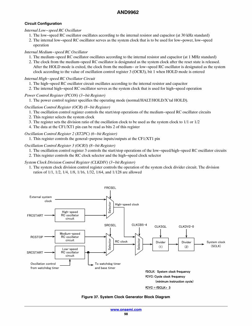
AND9962
www.onsemi.com98
Circuit Configuration
Internal Low−speed RC Oscillator1. The low−speed RC oscillator oscillates according to the internal resistor and capacitor (at 30 kHz standard)2. The internal low−speed RC oscillator serves as the system clock that is to be used for low−power, low−speed
operation
Internal Medium−speed RC Oscillator 1. The medium−speed RC oscillator oscillates according to the internal resistor and capacitor (at 1 MHz standard)2. The clock from the medium−speed RC oscillator is designated as the system clock after the reset state is released.
After the HOLD mode is exited, the clock from the medium− or low−speed RC oscillator is designated as the systemclock according to the value of oscillation control register 3 (OCR3), bit 1 when HOLD mode is entered
Internal High−speed RC Oscillator Circuit1. The high−speed RC oscillator circuit oscillates according to the internal resistor and capacitor2. The internal high−speed RC oscillator serves as the system clock that is used for high−speed operation
Power Control Register (PCON) (3−bit Register)1. The power control register specifies the operating mode (normal/HALT/HOLD/X’tal HOLD).
Oscillation Control Register (OCR) (8−bit Register)1. The oscillation control register controls the start/stop operations of the medium−speed RC oscillator circuits2. This register selects the system clock3. The register sets the division ratio of the oscillation clock to be used as the system clock to 1/1 or 1/24. The data at the CF1/XT1 pin can be read as bits 2 of this register
Oscillation Control Register 2 (XT2PC) (6−bit Register)1. This register controls the general−purpose inputs/outputs at the CF1/XT1 pin
Oscillation Control Register 3 (OCR3) (8−bit Register)1. The oscillation control register 3 controls the start/stop operations of the low−speed/high−speed RC oscillator circuits2. This register controls the RC clock selector and the high−speed clock selector
System Clock Division Control Register (CLKDIV) (3−bit Register)1. The system clock division control register controls the operation of the system clock divider circuit. The division
ratios of 1/1, 1/2, 1/4, 1/8, 1/16, 1/32, 1/64, and 1/128 are allowed
Figure 37. System Clock Generator Block Diagram
÷

AND9962
www.onsemi.com99
Related Registers
Power Control Register (PCON) (3−bit register)1. The power control register is a 3−bit register used to specify the operating mode (normal/HALT/ HOLD/X’tal
HOLD).See “ Standby Function” for the procedures to enter and exit the microcontroller operating modes
Address Initial Value R/W Name BIT7 BIT6 BIT5 BIT4 BIT3 BIT2 BIT1 BIT0
FE07 HHHH H000 R/W PCON − − − − − XTIDLE PDN IDLE
(bits 7to3): These bits do not exist. They are always read as 1.
XTIDLE (bit 2): X’tal HOLD mode setting flagPDN (bit 1): HOLD mode setting flag
XTIDLE PDN Operating mode
– 0 Normal or HALT mode
0 1 HOLD mode
1 1 X’tal HOLD mode

AND9962
www.onsemi.com100
1. These bits must be set with an instruction.♦ When the microcontroller enters the HOLD mode, all oscillations (low−/medium−/high−speed RC) are
suspended and the related registers are placed in the states described below.If OCR3 register, bit 1 is set to 1, OCR3 register, bit 0 is set and OCR register, bits 4 and 5 and OCR3 register,bit 6 are cleared.If OCR3 register, bit 1 is set to 0, OCR register, bits 1, 4, and 5 and OCR3 register, bit 6 are cleared.
♦ When the microcontroller returns from the HOLD mode, according to the values of OCR and OCR3 registers,the low− or medium−speed RC oscillator starts operation and is designated as the system clock source. Thehigh−speed RC oscillator is suspended.
♦ When the microcontroller enters the HOLD mode, all oscillations except low−/medium−/high−speed RC aresuspended, but the states of the OCR and OCR3 registers remain unchanged. If, however, the X’tal HOLD modeis entered with the low−speed RC oscillator selected as the base timer input clock source, and the base timer hasbeen started, the low−speed RC oscillator circuit retains the state that is established when the X’tal HOLD modeis entered.
♦ When the microcontroller returns from the X’tal HOLD mode, the system clock to be used when the X’talHOLD mode is entered needs to be set to either low−/medium−/high−speed RC.
♦ Since the X’tal HOLD mode is used usually for low−current clock counting, less current will be consumed if thesystem clock is switched to the low−speed RC and the medium−/high−speed RC oscillators are suspended beforethe X’tal HOLD mode is entered.
2. XTIDLE must be cleared with an instruction.3. PDN is cleared when a HOLD mode releasing signal (INT0, INT1, INT2, INT4, Port 0 interrupt, base timer interrupt,
or CVD interrupt) or a reset occurs.4. Bit 0 is automatically set when PDN is set.
IDLE (bit 0): HALT mode setting flag1. Setting this bit places the microcontroller into the HALT mode.2. This bit is automatically set whenever bit 1 is set.3. This bit is cleared on acceptance of an interrupt request or on receipt of a reset signal.
NOTE: The oscillation of the low−speed RC oscillator circuit is controlled directly by the watchdog timer. Its oscillationis also controlled in the standby mode. See Section 4.6, ”Watchdog Timer,” for details.
Oscillation Control Register (OCR) (8−bit register)1. The oscillation control register is an 8−bit register that selects the system clock division ratio, controls the operation
of the oscillator circuits, selects the system clock, and reads data from the CF1/XT1 pin. Except for read−only bits 3and 2, all bits of this register can be read or written.
Address Initial Value R/W Name BIT7 BIT6 BIT5 BIT4 BIT3 BIT2 BIT1 BIT0
FE0E 0000 XX00 R/W OCR CLKSGL EXTOSC CLKCB5 CLKCB4 XT2IN XT1IN RCSTOP CFSTOP
CLKSGL (bit 7): System clock division ratio select1. When this bit is set to 1, the clock selected by bits 4 and 5 is used as the system clock as is.
2. When this bit is set to 0, the clock having a clock rate of 2
1
of the clock selected by bits 4 and 5 is used as the systemclock.
EXTOSC (bit 6): CF1/XT1 function controlMust always be set to 0.When the OCR register is read in this case, bit 2 reads the data at the CF1/XT1 pin.
CLKCB5 (bit 5): System clock select
CLKCB4 (bit 4): System clock select1. CLKCB5 and CLKCB4 are used to select the system clock.2. CLKCB5 and CLKCB4 are cleared at reset time or when the HOLD mode is entered.

AND9962
www.onsemi.com101
CLKCB5 CLKCB4 System clock
0 0 RC clock
0 1 High−speed clock
1 0 −
1 1 High−speed clock
*See Figure 4.2.1 for details.
XT2IN (bit 3): Undefined value is read. (read−only)XT1IN (bit 2): CF1/XT1 data (read−only)
1. Data that can be read via XT1IN varies as shown in the table below according to the value of EXTOSC (bit 6).
EXTOSC XT2IN XT1IN
0 Undefined value CF1/XT1 pin data
1 Undefined value Read 0
RCSTOP (bit 1): Medium−speed RC oscillator circuit control1. Setting this bit to 1 stops the oscillation of the medium−speed RC oscillator circuit.2. Setting this bit to 0 starts the oscillation of the medium−speed RC oscillator circuit.3. When a reset occurs, this bit is cleared and the RC oscillator circuit is enabled for oscillation.4. When the microcontroller enters the HOLD mode, this bit is set as described below according to the value of bit 1 of
the OCR3 register.♦ If OCR3 register, bit 1 is set to 0, this bit is cleared and the oscillator starts oscillation and the medium−speed RC
oscillator is designated as the system clock source when the microcontroller exits the HOLD mode.♦ If OCR3 register, bit 1 is set to 1, the state of this bit remains unchanged.
CFSTOP (bit 0): CF oscillator circuit control1. When this bit is set to 1, CF1/XT1 pins serve as the general−purpose input and output pin.2. When this bit is set to 0, CF1/XT1 pins serve as the General−purpose input and external system clock input pin.3. When a reset occurs, this bit and XT2PC register bit 6 are cleared and the CF1/XT1 pin serve as the input pin.
OCR register XT2PC registerCF1/XT1 state
OCR register
EXTOSC CFSTOP XTCFSEL XT2IN XT1IN
0 0 0 General−purposeinput
Undefined value CF1/XT1pin data
0 1 0 General−purposeinput/output
Undefined value CF1/XT1pin data
Oscillation Control Register 2 (XT2PC) (6−bit register)1. The oscillation control register 2 is an 6−bit register that controls the operation of the oscillator circuits, controls the
general−purpose outputs of CF1/XT1(N−channel open drain) and reads data from the CF1 pin.
Address Initial Value R/W Name BIT7 BIT6 BIT5 BIT4 BIT3 BIT2 BIT1 BIT0
FE43 HH00 0000 R/W XT2PC − − XT1DR XT1DT XTCFSEL XT2CMOS XT2DR XT2DT
XT1DR (bit 5): CF1/XT1 data directionThis bit controls the CF1/XT1 input/output direction when OCR register sets CF1/XT1 to the general−purpose input/output
mode1. When this bit is set to 0, CF1/XT1 is set to the input mode.2. When this bit is set to 1, CF1/XT1 is set to the output mode(N−channel open drain)
XT1DT (bit 4): CF1/XT1 data latchThis bit controls the CF1/XT1 output data when OCR register sets CF1/XT1 to the general−purpose input/output mode

AND9962
www.onsemi.com102
Register Data CF1/XT1 State
XT1DT XT1DR Input Output
0 0 Enabled Open
1 0 Enabled Open
0 1 Enabled Low
1 1 Enabled Open
*When general−purpose input/output mode is selected. See Figure 4.2.4.2 Oscillation Control Register for details.
XTCFSEL (bit 3):Must always be set to 0.
XT2CMOS (bit 2):Must always be set to 1.
XT2DR (bit 1):Must always be set to 1.
XT2DT (bit 0):Must always be set to 0.
Oscillation Control Register 3 (OCR3) (8−bit register)1. The oscillation control register 3 is an 8−bit register that controls the operation of the low−speed RC oscillator circuit
and the high−speed RC oscillator circuit and selects the high−speed clock source and the RC clock source.
Address Initial Value R/W Name BIT7 BIT6 BIT5 BIT4 BIT3 BIT2 BIT1 BIT0
FE7C 0000 0000 R/W OCR3 FRCSEL FRCSTART OCR3B5 OCR3B4 OCR3B3 FIX0 SRCSEL SRCSTART
FRCSEL (bit 7): High−speed clock select1. When this bit is set to 0, the main clock is selected as the high−speed clock source.2. When this bit is set to 1, the high−speed RC oscillator clock is selected as the high−speed clock source.
* See Figure 4.2.1 for details.
FRCSTART (bit 6): High−speed RC oscillator circuit control1. Setting this bit to 0 stops the oscillation of the high−speed RC oscillator circuit.2. Setting this bit to 1 starts the oscillation of the high−speed RC oscillator circuit.3. When a reset occurs, this bit is cleared and the oscillator circuit is disabled for oscillation.4. When the microcontroller enters the HOLD mode, this bit is cleared and the oscillator circuit is disabled for
oscillation.
OCR3B5 to 3 (bits 5 to 3): General−purpose flagsThese bits can be used as general−purpose flag bits.Any manipulations of these bits exert no influence on the operation of this function block.
SRCSEL (bit 1): RC clock select1. When this bit is set to 0, the medium−speed RC oscillator clock is selected as the RC clock source.2. When this bit is set to 1, the low−speed RC oscillator clock is selected as the RC clock source.
* See Figure 4.2.1 for details.
SRCSTART (bit 0): Low−speed RC oscillator circuit control1. A 0 in this bit stops the low−speed RC oscillator circuit.2. A 1 in this bit starts the low−speed RC oscillator circuit.3. When a reset occurs, this bit is cleared and the oscillator circuit is disabled for oscillation.4. When the microcontroller enters the HOLD mode, this bit is set as described below according to the value of
SRCSEL.♦ If SRCSEL is set to 0, the state of this bit remains unchanged.♦ If SRCSEL is set to 1, this bit is set and the oscillator starts oscillation and the low−speed RC oscillator is
designated as the system clock source when the microcontroller returns from the HOLD mode.

AND9962
www.onsemi.com103
System clock divider control register (CLKDIV) (3−bit register)1. The system clock divider control register controls the frequency division processing of the system clock.
Address Initial Value R/W Name BIT7 BIT6 BIT5 BIT4 BIT3 BIT2 BIT1 BIT0
FE0C HHHH H000 R/W CLKDIV − − − − − CLKDV2 CLKDV1 CLKDV0
7. (Bits 7 to 3): These bits do not exist. They are always read as 1.
CLKDV2 (bit 2):
CLKDV1 (bit 1):
CLKDV0 (bit 0):
Define the division ratio of the system clock.
CLKDV2 CLKDV1 CLKDV0 Division Ratio
0 0 0 1/1
0 0 1 1/2
0 1 0 1/4
0 1 1 1/8
1 0 0 1/16
1 0 1 1/32
1 1 0 1/64
1 1 1 1/128
Standby Function
OverviewThis model supports three standby modes, called the HALT, HOLD, and X’tal HOLD modes, that are used to reduce current
consumption at power−failure time or in program standby mode. In a standby mode, the execution of all instructions issuspended.
Functions1. HALT mode
♦ The microcontroller suspends the execution of instructions but its peripheral circuits continue processing (certainserial transfer functions are stopped.) (Note 1)
♦ The HALT mode is entered by setting bit 0 of the PCON register to 1.♦ Bit 0 of the PCON register is cleared and the microcontroller returns to the normal operating mode when a reset
occurs or an interrupt request is accepted.2. HOLD mode
♦ All oscillations are suspended. The microcontroller suspends the execution of instructions and its peripheralcircuits stop processing. (Notes 1, 2)
♦ The HOLD mode is entered by setting bit 1 of the PCON register to 1 when bit 2 is set to 0. In this case, bit 0 ofthe PCON register (HALT mode flag) is automatically set.
♦ When a reset occurs or a HOLD mode release signal (INT0, INT1, INT2, INT4 and port 0 interrupt) occurs, bit 1of the PCON register is cleared and the microcontroller switches into the HALT mode.
3. X’tal HOLD mode♦ All clock oscillations are stopped. (If, however, the base timer has been started with low−speed RC oscillation
selected as the base timer input clock source, the low−speed RC oscillation circuit retains the state that isestablished when the X’tal HOLD mode is entered.) The execution of instructions and the operation of theperipheral circuits except the base timer are suspended (Notes 1 and 2).
♦ The X’tal HOLD mode is entered by setting bit 1 of the PCON register to 1 when bit 2 is set to 1. In this case, bit0 of the PCON register (HALT mode flag) is automatically set.

AND9962
www.onsemi.com104
♦ When a reset occurs or a HOLD mode release signal (INT0, INT1, INT2, INT4 and port 0 interrupt) occurs, bit 1of the PCON register is cleared and the microcontroller switches into the HALT mode.
NOTE:8. The oscillation of the low−speed RC oscillation circuit is controlled directly by the watchdog timer. Its oscillation is also controlled in the
standby mode. See Section “Watchdog Timer” for details.9. Do not allow the microcontroller to enter into the HOLD, or X’tal HOLD mode while AD conversion is in progress. Make sure that ADSTART
(ADCRC register bit 2) is set to 0 before placing the microcontroller into one of the above−mentioned standby modes.
Related Registers
Power Control Register (PCON) (3−bit Register)1. The power control register is a 3−bit register that specifies the operating mode (normal/HALT/ HOLD/X’tal HOLD)
Address Initial Value R/W Name BIT7 BIT6 BIT5 BIT4 BIT3 BIT2 BIT1 BIT0
FE07 HHHH H000 R/W PCON − − − − − XTIDLE PDN IDLE
10.See “Power control register (PCON).”

AND9962
www.onsemi.com105
STANDBY MODE OPERATIONSItem/mode Reset State HALT Mode HOLD Mode X’tal HOLD Mode
Entry conditions RES appliedReset by POR/LVDReset from watchdog timer
PCON registerBit 1 = 0Bit 0 = 1
PCON registerBit 2 = 0Bit 1 = 1
PCON registerBit 2 = 1Bit 1 = 1
Data changed on entry Initialized as shown in separate table.
(When watchdog timer reset:WDTCNT register, bit 7 isset)
WDTCNT, bit 5 is cleared ifWDTCNT register, bit 4 = 0and bit 3 =1
WDTCNT register, bit 5 iscleared if WDTCNT register,bit 4 = 0 and bit 3 = 1.
PCON register, bit 0 is set.
OCR 3 register, bit 6 iscleared.
OCR register, bits 5, 4, and 1 are cleared if OCR3register, bit 1 = 0.
OCR3 register, bit 0 is setand OCR register, bits 5 and 4 are cleared if OCR3register, bit 1 = 1.
WDTCNT register, bit 5 iscleared if WDTCNT register,bit 4 = 0 and bit 3 = 1.
PCON register, bit 0 is set.
Low−speed RC oscillation Stopped State established at entrytime (Note 11)
Stopped (Note 11) Stopped (Notes 11, 12)
Medium−speed RC oscillation
Running State established at entrytime
Stopped Stopped
High−speed RC oscillation Stopped State established at entrytime
Stopped Stopped
CPU Initialized Stopped Stopped Stopped
I/O pin state See next page ← ← ←
RAM RES: UnpredictableLVD: Unpredictable or datapreserved (depends on supply voltage)When watchdog timer reset:Data preserved
Data preserved Data preserved Data preserved
Base timer Stopped State established at entrytime
Stopped State established at entrytime
Peripheral modules except base timer
Stopped State established at entrytime (Note 13)
Stopped Stopped
Exit conditions Entry conditions canceled. Interrupt request accepted.
Reset/entry conditions established
Interrupt request from INT0,INT1, INT2, INT4 and port 0.
Reset/entry conditions es-tablished
Interrupt request from INT0,INT1, INT2, INT4, port 0 andbase timer.
Reset/entry conditions established
Returned mode Normal mode Normal mode (Note 14) HALT (Note 14) HALT (Note 14)
Data changed on exit None PCON register, bit 0 iscleared
PCON register, bit 1 iscleared
PCON register, bit 1 is cleared
11. The oscillation of the low−speed RC oscillation circuit is controlled directly by the watchdog timer. Its oscillation is also controlled in thestandby mode. See Section “Watchdog Timer”, for details.
12. If the X’tal HOLD mode is entered with the low−speed RC oscillation selected as the base timer input clock source, and the base timer hasbeen started, the low−speed RC oscillation circuit retains the state that is established when the X’tal HOLD mode is entered.
13.Certain serial transmission functions are stopped.14.The microcontroller switches into the reset state if it exits the current mode on the establishment of reset/entry conditions.

AND9962
www.onsemi.com106
PIN STATES AND OPERATING MODES (THIS SERIES)
PinName Reset Time Normal Mode HALT Mode HOLD Mode On Exit from HOLD
RES I/O pin ← ← ← ←
CF1/XT1 Input pin Input/output resistor controlled by a program
← ← ←
P00−P06 Input modePull−up resistor off
Input/output/pull−up resistor controlled by aprogram
← ← ←
P10−P17 Input modePull−up resistor off
Input/output/pull−up resistor/constant currentmode controlled by a program
← ← ←
P24 Input modePull−up resistor off
Input/output/pull−up resistor/constant currentmode controlled by a program
← ← ←
P70 Input modePull−up resistor off
Input/output/pull−up resistor controlled by aprogram
Input modePull−up resistor off
Normal operating mode
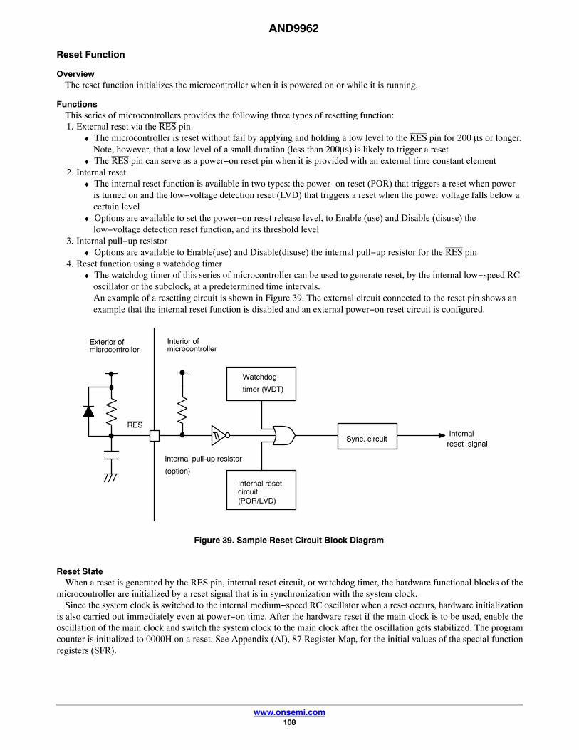
AND9962
www.onsemi.com108
Reset Function
OverviewThe reset function initializes the microcontroller when it is powered on or while it is running.
FunctionsThis series of microcontrollers provides the following three types of resetting function:1. External reset via the RES pin
♦ The microcontroller is reset without fail by applying and holding a low level to the RES pin for 200 μs or longer.Note, however, that a low level of a small duration (less than 200μs) is likely to trigger a reset
♦ The RES pin can serve as a power−on reset pin when it is provided with an external time constant element2. Internal reset
♦ The internal reset function is available in two types: the power−on reset (POR) that triggers a reset when poweris turned on and the low−voltage detection reset (LVD) that triggers a reset when the power voltage falls below acertain level
♦ Options are available to set the power−on reset release level, to Enable (use) and Disable (disuse) thelow−voltage detection reset function, and its threshold level
3. Internal pull−up resistor♦ Options are available to Enable(use) and Disable(disuse) the internal pull−up resistor for the RES pin
4. Reset function using a watchdog timer♦ The watchdog timer of this series of microcontroller can be used to generate reset, by the internal low−speed RC
oscillator or the subclock, at a predetermined time intervals. An example of a resetting circuit is shown in Figure 39. The external circuit connected to the reset pin shows anexample that the internal reset function is disabled and an external power−on reset circuit is configured.
Figure 39. Sample Reset Circuit Block Diagram
Internal resetcircuit
Interior ofmicrocontroller
Exterior ofmicrocontroller
Sync. circuitInternal
Watchdog
timer (WDT)
Internal pull−up resistor
(option)
RES
(POR/LVD)
reset signal
Reset StateWhen a reset is generated by the RES pin, internal reset circuit, or watchdog timer, the hardware functional blocks of the
microcontroller are initialized by a reset signal that is in synchronization with the system clock.Since the system clock is switched to the internal medium−speed RC oscillator when a reset occurs, hardware initialization
is also carried out immediately even at power−on time. After the hardware reset if the main clock is to be used, enable theoscillation of the main clock and switch the system clock to the main clock after the oscillation gets stabilized. The programcounter is initialized to 0000H on a reset. See Appendix (AI), 87 Register Map, for the initial values of the special functionregisters (SFR).

AND9962
www.onsemi.com109
<Notes and precautions>♦ The stack pointer is initialized to 0000H♦ Data RAM is never initialized by a reset. Consequently, the contents of RAM are unpredictable at power−on time♦ When using the internal reset function, it is necessary to implement and connect an external circuit to the reset pin
according to the user’s operating environment. Be sure to review and observe the operating specifications, circuitconfiguration, precautions, and considerations discussed in section “Internal Reset Function”
Watchdog Timer (WDT)
OverviewThis model is provided with a watchdog timer (WDT) that has the following features:1. Can generate an internal reset signal on an overflow occurring on a timer which runs on the internal low−speed RC
oscillator clock2. Three standby−mode−time operating modes (continue count operation, suspend operation, suspend count operation
while retaining the count value). *The primary function of the watchdog timer is to detect program runaway conditions. The use of the watchdog timeris highly recommended to enhance system reliability.
Functions1. Watchdog timer
♦ A 17−bit up−counter (WDTCT) runs on the WDT clock (the clock source is internal low−speed RC oscillationclock). A WDT reset (internal reset) signal is generated when the overflow time (selected out of 8 time values)that is selected by the watchdog timer control register (WDTCNT) expires. At this moment, the WDT resetdetection flag (WDTRSTF) is set. Since the WDTCT can be cleared by a program, it is necessary to code theprogram so that the WDTCT be cleared at regular intervals
♦ If the WDT operation is started with the internal low−speed RC oscillator clock selected as the WDT clocksource, the internal low−speed RC oscillation circuit is controlled by both of the oscillation control register 3(OCR3) and WDT. Since they control the oscillation independently of each other, even if the system clockhappens to be suspended by a program runaway condition, the WDT continues operation, so that it is possible todetect the runaway condition
2. Standby mode time operations♦ The action that the WDT takes in the standby mode can be selected from three operating modes, i.e., “continue
count operation, “suspend operation”, and suspend count operation while retaining the count value.” If theinternal low−speed RC oscillator clock is selected as the WDT clock source when the “continue count operation”is selected, an operating current of several μA is always flowing in the IC because the internal low−speed RCoscillation circuit is continuing oscillation. (For details, refer to the latest “ON Semiconductor Data Sheet”)
3. To control the watchdog timer (WDT), it is necessary to manipulate the following special function register:♦ WDTCNT
Address Initial Value R/W Name BIT7 BIT6 BIT5 BIT4 BIT3 BIT2 BIT1 BIT0
FE79 0000 0000 R/W WDTCNT WDTRSTF WDTCKSL WDTRUN IDLOP1 IDLOP0 WDTSL2 WDTSL1 WDTSL0

AND9962
www.onsemi.com110
Circuit Configuration
WDT control register (WDTCNT) (8−bit register)1. The WDT control register is used to manipulate the WDT reset detection flag, to select operations in the
standby−time mode, to select the overflow time, and to control the operation of WDT
NOTE:� The WDTCNT is initialized with “00H” when a low−level signal is applied to the external RES pin or a reset is
triggered by the internal reset (POR/LVD) function. Bit 6 and bits 4 to 0 of the WDTCNT are not initialized,however, when a WDT−triggered reset occurs.
� The WDTCNT is disabled for writes once the WDT is started (WDTRUN set to 1). If the instruction “MOV#55H, WDTCNT” is executed in this case, the WDTCT is cleared and count operation is restarted at a countvalue of 0 (the WDTCT is not cleared when it is loaded with 55H by any other instruction).
� The internal low−speed RC oscillator circuit is started by setting WDTCKSL (WDTCNT, bit 6) to 0 andWDTRUN (WDTCNT, bit 5) to 1. Once the oscillator starts oscillation, operating current of several �A flows.(For details, refer to the latest ”ON Semiconductor Data Sheet”) It is noted that the oscillation is also started bysetting SRCSTART (OCR3, bit 0) to 1
WDT Counter (WDTCT) (17−bit Counter)1. Operation start/stop: Places the CPU into the standby mode when WDTRUN is set to 1 and WDTRUN is set to 0, or
when WDTRUN is set to 1 and IDLOP1 and IDLOP0 (WDTCNT, bits 4 and 3) are set to 22. Count clock: WDT clock (the internal low−speed RC oscillation clock)3. Overflow: Generated when the WDTCT count value matches the count value designated by WDTSL2 through
WDTSL0 (WDTCNT, bits 2 to 0).*Generates the WDT reset signal, the WDTRUN clear signal, and WDTRSTF (WDTCNT, bit 7) set signal
4. Resetting: Setting WDTRUN to 0 or WDTRUN to 1 and executing “MOV #55H, WDTCNT” instruction.*See Figure 40 for details on the WDT operation.
Figure 40. Watchdog Timer Block Diagram
XTIDLE
(PCON bit2)
BTON
(BTCR bit6)
BTIMC1 - 0=2
(ISL bit5 -4)
PDN
(PCON bit1)
SRCSTART
(OCR3 bit0)
WDT counter
(WDTCT)Clock
Sel
ecto
r
WDTSL2 -0
WDT reset
generator
circuit
IDLOP1 - 0=2
Standby mode
IDLOP1 - 0=1
Enter standby mode
WDTRST=0
WDTRUN clear signal
SetWDTRUN clear signal
WDT resetWDTRSTF set signal
BUS
MOV #55H ,WDTCNT
w rite instruction
detector circuit
Write WDTCNT
WDTRST=1
WDTRUN
Reset
Internal
low −speed RC
oscillator circuit
OscillationcontrolWDT
internal RCoscillation
control circuit
WDTRUN
WDTCKSL
Enableoscillation
Low −speed RC oscillation clock
Stop oscillation
Stop clock
3
To system clock and base timer

AND9962
www.onsemi.com111
Figure 41. Sample Watchdog Timer Operation Waveforms
NOTE: Oscillation start/stop control for low−speed RC oscillator circuit is performed when WDTCKSL is set to 0.
WDTCT
WDT operation start (WDTRUN=1)Low−speed RC
Time set in WDTSL2 −0
”MOV #55H, WDTCNT ”
oscillator start (Note)
instruction executedWDT reset signal generated
(WDTCT cleared to 0)WDTRUN cleared to 0
WDTRSTF set to 1Low−speed RC oscillator stopped
*Operation performed when ID LOP1 −0 are set to 0 o r 3 (continue count operation )
(Note)
Count value 0
WDT SL 2−0 set c ount value
Overflow
WDTCT
WDT operation start (WDTRUN=1)Low−speed RC
WDTRUN cleared to 0
oscillator start (Note)
Low−speed RC
(Note)
*Operation performed when ID LOP1 −0 are set to 1 (suspend operation)
Count value 0
WDT SL 2−0 set count value
Standby mode entered
WDTCT
WD T operation start
oscillator stopped
(WDTRUN=1)Low−speed RC
Time set in WDT SL 2−0 + Standby mode time
WDT reset signal generated
oscillator start (Note)
WDTRUN cleared to 0WDTRSTF set to 1
Low−speed RC oscillator stopped
*Operation performed when ID LOP1 −0 are se t to 2 ( suspend count operation w hile retaining the count
Count value 0
−0
Overflow
(Note)
Low−speed RC oscillatorStandby mode exited
stopped (Note)Low−speed RC oscillator
started (Note)
Related Registers
WDT Control Register (WDTCNT)1. The WDT control register is used to manipulate the reset detection flag, to select the standby mode operation, to
select the overflow time, and to control the operation of the WDT
Address Initial Value R/W Name BIT7 BIT6 BIT5 BIT4 BIT3 BIT2 BIT1 BIT0
FE79 0000 0000 R/W WDTCNT WDTRSTF WDTCKSL WDTRUN IDLOP1 IDLOP0 WDTSL2 WDTSL1 WDTSL0
WDTRSTF (Bit 7): WDT Reset Detection FlagThis bit is cleared when a reset is effected by applying a low level to the external RES pin or using the internal reset
(POR/LVD) function.This bit is set when a WDT−triggered reset occurs.This flag can be rewritten an instruction.
WDTCKSL (Bit 6): WDTCT Input Clock Select
WDTCKSL WDTCT input clock
0 Internal low−speed RC oscillation clock
1 −
WDTRUN (Bit 5): WDT Operation ControlSetting this bit to 0 stops the WDT operation.Setting this bit to 1 starts the WDT operation.

AND9962
www.onsemi.com112
WDT standby mode operation selectionIDLOP1 (bit 4):
IDLOP0 (bit 3):
IDLOP1 IDLOP0 WDT Standby Mode Operation
0 0 Continue count operation
0 1 Suspend operation
1 0 Suspend count operation while retaining the count value
1 1 Continue count operation
* See Figure 42 for details of the WDT operating modes.
Overflow time select
WDTSL2 (bit 2):
WDTSL1 (bit 1):
WDTSL0 (bit 0):
WDTSL2 WDTSL1 WDTSL0
WDTCT set count number and overflow generation time example
Count number Low−speed RC clock
0 0 0 1024 34.13 ms
0 0 1 2048 68.26 ms
0 1 0 4096 136.5 ms
0 1 1 8192 273.0 ms
1 0 0 16384 546.1 ms
1 0 1 32768 1.092 ms
1 1 0 65536 2.184 ms
1 1 1 131072 4.368 s
*Time values in the Low−speed RC clock column of the table refer to the time for a WDTCT overflow to occur when the low−speed RC oscillationfrequency is 30 kHz (typical). The low−speed RC oscillation frequency varies from IC to IC. For details, refer to the latest “ON SemiconductorData Sheet.”
15.The WDTCNT is initialized with “00H” when a low−level signal is applied to the external RES pin or a reset is triggered by the internal reset(POR/LVD) function. Bit 6 and bits 4 to 0 of the WDTCNT are not initialized, however, when a WDT−triggered reset occurs.
16.The WDTCNT is disabled for write once the WDT starts operation (WDTRUN set to 1). If the instruction “MOV #55H, WDTCNT” is executedin this case, the WDTCT is cleared and count operation is restarted at a count value of 0 (the WDTCT is not cleared when it is loaded with55H with any other instruction).
17.The internal low−speed RC oscillator circuit is started by setting WDTCKSL to 0 and WDTRUN to 1. Once the oscillator starts oscillation,operating current of several �A flows. (For details, refer to the latest “ON Semiconductor Data Sheet.”) It is noted that the oscillation is alsostarted by setting SRCSTART (OCR3, bit 0) to 1.
Using the Watchdog TimerCode a program so that instructions for clearing the watchdog timer periodically are executed.1. Starting the watchdog timer
a. Set the time for a WDT reset to occur to WDTCKSL (WDTCNT, bit 6) and WDTSL 2 to 0 (WDTCNT, bits 2 to0)
b. Set the WDT standby mode operation (HALT/HOLD/X’tal HOLD) to IDLOP 1 to 0 (WDTCNT, bits 4 to 3)c. After (1) and (2), set WDTRUN (WDTCNT, bit 5) to 1.
The watchdog timer starts functioning when WDTRUN is set to 1. Once the watchdog timer starts operation,WDTCNT is disabled for write; it is allowed only to clear WDTCT and read WDTCNT. Consequently, thewatchdog timer can never be stopped with an instruction. The function of the watchdog timer is stopped onlywhen a low level is applied to the external reset pin, a reset by the internal reset function (POD/LVD) occurs, orthe standby mode is entered when IDLOP 1 to 0 are set to 1. In this case, WDTRUN is cleared
2. Clearing the watchdog timerWhen the watchdog timer starts operation, WDTCT counts up. When this WDTCT overflows, a WDT reset occurs.To run the program in the normal mode, it is necessary to periodically clear WDTCT before WDTCT overflows.Execute the following instruction to clear WDTCT while it is running: MOV #55H, WDTCNT

AND9962
www.onsemi.com113
3. Detecting a runaway conditionUnless the above−mentioned instruction is executed, WDTCT overflows because the watchdog timer is not cleared. Ifan overflow occurs, the watchdog timer considers that a program hangup has occurred and triggers a WDT reset. Inthis case, WDTRSTF (WDTCNT, bit 7) is set. After a WDT reset occurs, the program execution restarts at address0000H. (In the case of flash ROM version, the program execution restarts at address selected as an option)
Notes on the Use of the Watchdog Timer1. When the internal low−speed RC oscillation clock is selected as the WDT clock (WDTCKSL = 0)
♦ If the internal low−speed RC oscillation clock is not to be used as the system clock, set SRCSTART (OCR3, bit0) to 0 (the start/stop of the internal low−speed RC oscillator circuit is also controlled from the watchdog timerside). If SRCSTART (OCR3, bit 0) is set to1, the internal low−speed RC oscillator circuit continues oscillation inthe HALT mode even though the watchdog timer is running with IDLOP 1 and 0 set to 1 or 2
♦ To realize ultra−low−power operation using the HOLD mode, it is necessary to disable the watchdog timer fromrunning in the HOLD mode by setting IDLOP 1 and 0 to 1 or 2. When setting IDLOP 1 and 0 to 1 or 3, several�A of operating current flows at all times because the low−speed RC oscillator circuit continues oscillating evenin the HOLD mode
♦ If the standby mode is entered when the watchdog timer is running with IDLOP 1 and 0 set to 2, the internallow−speed RC oscillator circuit stops oscillation and the watchdog timer stops count operation and retains thecount value. When the CPU subsequently exits the standby mode, the low−speed RC oscillator circuit resumesoscillation and the watchdog timer starts count operation. If the period between the release of the standby modeto the next entry into a standby mode is less than “low−speed RC oscillation clock y 4”, however, the low−speedRC oscillator circuit may not stop oscillation when the CPU enters the standby mode. In such a case (the standbymode is on), several �A of operating current flows because the low−speed RC oscillator circuit is active thoughthe watchdog timer is inactive.To minimize the standby power requirement of the set, code the program so that an interval of “low−speed RCoscillator clock × 4” or longer be provided between release from a standby mode and entry into the next standbymode (Note that the oscillation frequency of the low−speed RC oscillator may fluctuate. For details, refer to thelatest “ON Semiconductor Data Sheet”)

AND9962
www.onsemi.com114
Internal Reset Function
OverviewThis model internal reset functions called the power−on reset (POR) and low voltage detection reset (LVD). The use of these
functions will contribute to the reduction in the number of externally required reset circuit components (reset IC, etc.).
Functions1. Power−on reset (POR) function
POR is a hardware feature that generates a reset to the microcontroller at power−on time. This function allows theuser to select the POR release level by option only when the disuse of the low voltage detection reset function isselected. It is necessary to use the undermentioned low voltage detection reset function together with this function, orconfigure an external reset circuit if there are possibilities that chatter can occur or a momentary power loss occur atpower−on time
2. Low voltage detection reset (LVD) functionThis function, when used together with the POR function, can generate a reset when power is turned on and when thepower level lowers. As a user option the use or disuse and the detection level of this function can be specified
Circuit ConfigurationThe internal reset circuit consists of POR, LVD, pulse stretcher circuit, capacitor CRES discharging transistor, external
capacitor CRES + pull−up resistor RRES or pull−up resistor RRES alone. The circuit diagram of the internal reset circuit is givenin Figure 42.• Pulse stretcher circuit
The pulse stretcher circuit stretches the POR and LVD reset signals. It is used to stretch the internal reset period anddischarge the external capacitor CRES connected to the RESET pin. The stretching time is from 30 �s to 100 �s
• Capacitor CRES discharging transistorThis is an N−channel transistor used to discharge the external capacitor CRES connected to the RESET pin. If thecapacitor CRES is not to be connected to the RESET pin, it is possible to monitor the internal reset signal by connectingonly the external pull−up resistor RRES.
• Option selector circuitThe option selector circuit is used to configure the LVD options. This circuit selects the enable or disable of LVD andits detection level. See Subsection Options
• External capacitor CRES + Pull−up resistor RRESAfter the reset signal from the internal reset circuit is released, the reset period is further stretched according to theexternal CR time constant. This enables the microcontroller to avoid the repetitive entries and releases of the reset statefrom occurring when the power−on chatter occurs. The circuit configuration shown in Figure 42 in which the capacitorCRES and pull−up resistor RRES are externally connected, is recommended when both POR and LVD functions are to beused. The recommended constant values are: CRES = 0.022 �F and RRES = 510 k�. When the disuse of the internalpull−up resistor function is selected by option, the external pull−up resistor RRES must always be installed even whenthe set’s specifications inhibit the installation of the external capacitor CRES

AND9962
www.onsemi.com115
Figure 42. Internal Reset Circuit Configuration
Power−on reset(POR)
Reset
Pulse stretcherLow voltage
detection reset(LVD)
Interior of microcontroller
Internal pull−up resistor(option)
RES
CRES = 0.022 �F
RRES = 510 k�
Options
OptionsThe POR and LVD options are available for the reset circuit.
1) LVD Reset Function Options
“Enable”: Use “Disable”: Disuse
2) LVD Reset Level Option 3) POR Release Level Option
Typical Value of Selected Option Min. Operating VDD Value (*)
Typical Value of Selected Option Min. Operating VDD Value (*)
− − “1.67 V” 1.8 V to
“1.91 V” 2.1 V to “1.97 V” −
“2.01 V” 2.2 V to “2.07 V” −
“2.31 V” 2.5 V to “2.37 V” −
“2.51 V” 2.7 V to “2.57 V” −
“2.81 V” 3.0 V to “2.87 V” −
“3.79 V” 4.0 V to “3.86 V” −
“4.28 V” 4.5 V to “4.35 V” −
*The minimum operating VDD value specifies the approximate lower limit value of the VDD value beyond which the selected POR release levelor LVD reset level can be effected without generating a reset.
1. LVD reset function optionWhen “Enable” is selected , a reset is generated at the voltage that is selected by the LVD reset level option.� Note 1: In this configuration, operating current of several �A always flows in all modes. No LVD reset is
generated when “Disable” is selected.� Note 2: In this configuration, no operating current will flow in all modes.
* See the sample operating waveforms of the reset circuit shown in Subsection Sample Operating Waveforms ofthe Internal Reset Circuit for details.
2. LVD reset level optionThe LVD reset level can be selected from 7 level values only when the LVD reset function is enabled. Select theoptimal detection level based on the actual operating conditions

AND9962
www.onsemi.com116
3. POR release level optionThe POR release level can be selected only when the LVD reset function is disabled. When not using the internalreset circuit, set the POR release level to the lowest level (1.67 V) that will not affect the minimum guaranteedoperating voltage.� Note 3: No operating current flows when the POR reset state is released� Note 4: See the notes in paragraph 2) of Subsection Notes on the Use of the Internal Reset Circuit when
selecting a POR release level that is lower than the minimum guaranteed operating voltage (1.67 V)• Selection example 1
Selecting the optimum LVD reset level to keep the microcontroller running without resetting it until VDD falls below2.7 V according to the set’s requirementsSet the LVD reset function option to “Enable” and select “2.51 V” as the LVD reset level
Figure 43.
LVD release voltage (LVDET+LVHYS)LVD reset voltage (LVDE = Typ. 2.51 V)
VDD= 2.7 V
Set operating range
• Selection example 2Selecting the optimum LVD reset level that meets the guaranteed operating conditions of VDD = 2.7 V/tCYC = 250 nsSet the LVD reset function option to “Enable” and select “2.81V” as the LVD reset level option.
Figure 44. Internal Reset Circuit Configuration
LVD reset voltage (LVDET=Typ. 2.81 V)LVD release voltage (LVDET+LVHYS)
Operation guarantee voltage
Microcontroller guaranteed operating range
• Selection example 3Disabling the internal reset circuit and using an external reset IC that can detect and react at 3.0 V (see also paragraph1) of Subsection Notes to be Taken When Not Using the Internal Reset Circuit)Set the LVD reset function option to “Disable” and select “1.67 V” as the POR release level option
Figure 45.
POR release voltage(PORRL=Typ. 1.67 V)
VDD= 3.1 VExternal 3.0 v detection circuit
� Note 5: The operation guarantee values (voltage/operating frequency) shown in the examples vary with themicrocontroller type. Be sure to see the latest “ON Semiconductor Data Sheet for details”

AND9962
www.onsemi.com117
Sample Operating Waveforms of the Internal Reset Circuit1. Waveform observed when only POR is used (LVD not used)
(RESET pin: Pull−up resistor RRES only)
Figure 46.
POR release voltage
(PORRL)
VDD
RES#
Unknown state(POUKS)
(a) (b)
Reset period Reset period100 �s or longer
♦ There exists an unknown−state (POUKS), before the POR transistor starts functioning normally♦ The POR function generates a reset only when power is turned on starting at the VSS level. The reset release
voltage in this case may have some range. Refer to the latest “ON Semiconductor Data Sheet” for details♦ No stable reset will be generated if power is turned on again when the power level does not go down to the VSS
level as shown in (a). If such a case is anticipated, use the LVD function together with the POR function asexplained in 2) or implement an external reset circuit
♦ A reset is generated only when the power level goes down to the VSS level as shown in (b) and power is turnedon again after this condition continues for 100 �s or longer
2. Waveform observed when both POR and LVD functions are used (RESET pin: Pull−up resistor RRES only)
Figure 47.
VDD
RES#
LVD hysteresis width
(LVHYS)
LVD reset voltage
(LVDET)
Unknown−state(LVUKS)
Reset period Reset period Reset period
LVD release voltage
(LVDET+LVHYS)
♦ There also exists an unknown−state (LVUKS), before the POR transistor starts functioning normally when bothPOR and LVD functions are used
♦ Resets are generated both when power is turned on and when the power level lowers. The reset release voltageand entry voltage in this case may have some range. Refer to the latest “ON Semiconductor Data Sheet” fordetails
♦ A hysteresis width (LVHYS) is provided to prevent the repetitions of reset release and entry cycles near thedetection level

AND9962
www.onsemi.com118
Notes on the Use of the Internal Reset Circuit1. When generating resets only with the POR function
When generating resets using only the POR function, do not short the RESET pin directly to VDD as when using itwith the LVD function. Be sure to use an external capacitor CRES of an appropriate capacitance. When the disuse ofthe internal pull−up resistor function is selected by option, be sure to use a pull−up resistor RRES. Test the circuitintensively under the anticipated power supply conditions to verify that resets are reliably generated.
Figure 48. Reset Circuit Configuration Using Only the Internal POR Function
Microcontroller
From POR
Internal pull−up resistor
RES
CRES
RRES
2. When selecting a release voltage level of 1.67 V only with the internal POR functionWhen selecting an internal POR release level of 1.67 V, connect the external capacitor CRES; furthermore when thedisuse of the internal pull−up resistor function is selected by option, connect the pull−up resistor RRES of the valuesthat match the power supply’s rise time to the RESET pin and make necessary adjustments so that the reset state isreleased after the release voltage exceeds the minimum guaranteed operating voltage. Or, set and hold the voltagelevel of the RESET pin at the low level until the release voltage exceeds the minimum guaranteed operating voltage.
Figure 49. Sample Release Level Waveform in Internal POR Only Configuration
VDD
RES
When POR releaselevel is 1.67 V
Unknown −state(LVUKS)
Min. guaranteed operatingvoltage
Reset VIH level
Reset period
3. When temporary power interruption or voltage fluctuations shorter than several hundreds μs are anticipatedThe response time measured from the time the LVD senses a power voltage drop at the option− selected level till itgenerates a reset signal is defined as the minimum low−voltage detection width TLVDW shown in Figure 50 (see “ONSemiconductor Data Sheet”). If temporary power interruption or power voltage fluctuations shorter than thisminimum low−voltage detection width are anticipated, be sure to take preventive measures shown in Figure 51 orother necessary measures.

AND9962
www.onsemi.com119
Figure 50. Example of Power Interruption or Voltage Fluctuation Waveform
VDD
LVD reset voltage
(LVDET)
TLVDW
VSS
LVD release voltage
LVDET −0.5 V
Figure 51. Example of Power Interruption/Voltage Fluctuation Countermeasures
Powersupply
VSS1
RES
VDD1
Microcontroller
Notes to be Taken When Not Using the Internal Reset Circuit1. When configuring an external reset IC without using the internal reset circuit
The POR function is activated and the capacitor CRES discharging N−channel transistor connected to the RESET pinturns on when power is turned on even if the internal reset circuit is not used. For this reason, when connecting anexternal reset IC, adopt the reset IC of a type whose detection level is not lower than the minimum guaranteedoperating voltage level and select the lowest POR release level (1.67 V) that does not affect the minimum guaranteedoperating voltage. The figures given below show sample reset circuit configurations that use reset ICs of N−channelopen drain and CMOS types, respectively.
Figure 52. Sample Reset Circuit Configuration Using an N−channel Open Drain Type Reset IC
N−channel open
drain type
Reset ICMicrocontroller
From POR
RESET
Severalhundreds Internal pull−up resistor
k� RES (option)

AND9962
www.onsemi.com120
Figure 53. Sample Reset Circuit Configuration Using an N−channel Open Drain Type Reset IC
RESET
CMOS type
Reset IC
Microcontroller
From POR
Insert a protective resistor ofseveral to scoresprevent through current.
Internal pull−up resistor
of k� to
(option)
2. When configuring the external POR circuit without using the internal reset circuitThe internal POR is active at power−on time even if the internal reset circuit is not used as in the case 1) inSubsection Notes to be Taken When Not Using the Internal Reset Circuit . When configuring an external POR circuitwith a CRES value of 0.1 �F or larger to obtain a longer reset period than with the internal POR, however, be sure toconnect an external diode DRES as shown in Figure 54.
Figure 54. Sample External POR Circuit Configuration
Microcontroller
From POR
RESET
RRES
CRES
DRES
Connect anexternal diode.
Internal pull−up resistor
RES(option)

AND9962
www.onsemi.com121
APPENDIXES
Appendix−I• Special Functions Register (SFR) Map
Appendix−II• Port 0 Block Diagram
• Port 1 Block Diagram
• Port 2 Block Diagram
• Port 7 Block Diagram
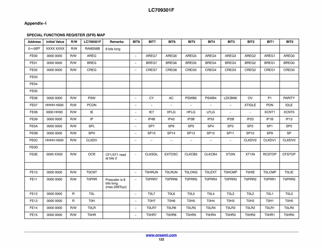
LC709301F
www.onsemi.com122
Appendix−I
SPECIAL FUNCTIONS REGISTER (SFR) MAP
Address Initial Value R/W LC709301F Remarks BIT8 BIT7 BIT6 BIT5 BIT4 BIT3 BIT2 BIT1 BIT0
0~00FF XXXX XXXX R/W RAM256B 9 bits long
FE00 0000 0000 R/W AREG − AREG7 AREG6 AREG5 AREG4 AREG3 AREG2 AREG1 AREG0
FE01 0000 0000 R/W BREG − BREG7 BREG6 BREG5 BREG4 BREG3 BREG2 BREG1 BREG0
FE02 0000 0000 R/W CREG − CREG7 CREG6 CREG5 CREG4 CREG3 CREG2 CREG1 CREG0
FE03
FE04
FE05
FE06 0000 0000 R/W PSW − CY AC PSWB5 PSWB4 LDCBNK OV P1 PARITY
FE07 HHHH H000 R/W PCON − − − − − − XTIDLE PDN IDLE
FE08 0000 HH00 R/W IE − IE7 XFLG HFLG LFLG − − XCNT1 XCNT0
FE09 0000 0000 R/W IP − IP4B IP43 IP3B IP33 IP2B IP23 IP1B IP13
FE0A 0000 0000 R/W SPL − SP7 SP6 SP5 SP4 SP3 SP2 SP1 SP0
FE0B 0000 0000 R/W SPH − SP15 SP14 SP13 SP12 SP11 SP10 SP9 SP
FE0C HHHH H000 R/W CLKDV − − − − − − CLKDV2 CLKDV1 CLKDV0
FE0D
FE0E 0000 XX00 R/W OCR CF1/XT1 readat bits 2
− CLKSGL EXTOSC CLKCB5 CLKCB4 XT2IN XT1IN RCSTOP CFSTOP
FE10 0000 0000 R/W T0CNT − T0HRUN T0LRUN T0LONG T0LEXT T0HCMP T0HIE T0LCMP T0LIE
FE11 0000 0000 R/W T0PRR Prescaler is 8bits long.(max.256Tcyc)
− T0PRR7 T0PRR6 T0PRR5 T0PRR4 T0PRR3 T0PRR2 T0PRR1 T0PRR0
FE12 0000 0000 R T0L − T0L7 T0L6 T0L5 T0L4 T0L3 T0L2 T0L1 T0L0
FE13 0000 0000 R T0H − T0H7 T0H6 T0H5 T0H4 T0H3 T0H2 T0H1 T0H0
FE14 0000 0000 R/W T0LR − T0LR7 T0LR6 T0LR5 T0LR4 T0LR3 T0LR2 T0LR1 T0LR0
FE15 0000 0000 R/W T0HR − T0HR7 T0HR6 T0HR5 T0HR4 T0HR3 T0HR2 T0HR1 T0HR0

LC709301F
www.onsemi.com123
SPECIAL FUNCTIONS REGISTER (SFR) MAP
Address BIT0BIT1BIT2BIT3BIT4BIT5BIT6BIT7BIT8RemarksLC709301FR/WInitial Value
FE16 XXXXXXXX
R T0CAL Timer 0 capture register L
− T0CAL7 T0CAL6 T0CAL5 T0CAL4 T0CAL3 T0CAL2 T0CAL1 T0CAL0
FE17 XXXXXXXX
R T0CAH Timer 0 capture register H
− T0CAH7 T0CAH6 T0CAH5 T0CAH4 T0CAH3 T0CAH2 T0CAH1 T0CAH0
FE18 0000 0000 R/W T1CNT − T1HRUN T1LRUN T1LONG T1PWM T1HCMP T1HIE T1LCMP T1LIE
FE19 0000 0000 R/W T1PRR − T1HPRE T1HPRC2
T1HPRC1
T1HPRC0
T1HCMP T1HIE T1LCMP T1LIE
FE1A 0000 0000 R T1L − T1L7 T1L6 T1L5 T1L4 T1L3 T1L2 T1L1 T1L0
FE1B 0000 0000 R T1H − T1H7 T1H6 T1H5 T1H4 T1H3 T1H2 T1H1 T1H0
FE1C 0000 0000 R/W T1LR − T1LR7 T1LR6 T1LR5 T1LR4 T1LR3 T1LR2 T1LR1 T1LR0
FE1D 0000 0000 R/W T1HR − T1HR7 T1HR6 T1HR5 T1HR4 T1HR3 T1HR2 T1HR1 T1HR0
FE1E
FE1F
FE20
FE21
FE22
FE23
FE24
FE25
FE26
FE27
FE28
FE29
FE2A
FE2B
FE2C
FE2D

LC709301F
www.onsemi.com124
SPECIAL FUNCTIONS REGISTER (SFR) MAP
Address BIT0BIT1BIT2BIT3BIT4BIT5BIT6BIT7BIT8RemarksLC709301FR/WInitial Value
FE2E
FE2F
FE30
FE31
FE32
FE33
FE34 0000 0000 R/W SCON1 − SI1M1 SI1M0 SI1RUN SI1REC SI1DIR SI1OVR SI1END SI1IE
FE35 00000 0000 R/W SBUF1 9bit REG SBUF18
SBUF17 SBUF16 SBUF15 SBUF14 SBUF13 SBUF12 SBUF11 SBUF10
FE36 0000 0000 R/W SBR1 − SBRG17 SBRG16 SBRG15 SBRG14 SBRG13 SBRG12 SBRG11 SBRG10
FE37
FE38
FE39
FE3A
FE3B
FE3C
FE3D 0000 0000 R/W BTPRR − BTPRR7 BTPRR6 BTPRR5 BTPRR4 BTPRR3 BTPRR2 BTPRR1 BTPRR0
FE3E
FE3F
FE40 0000 0000 R/W P0 − FIX0 P06 P05 P04 P03 P02 P01 P00
FE41 0000 0000 R/W P0DDR − FIX0 P06DDR P05DDR P04DDR P03DDR P02DDR P01DDR P00DDR
FE42 0000 0000 R/W P0FCR − T1HPWMEN
T1LPWMEN
P0FLG P0IE CLKOEN CLKODV2
CLKODV1
CLKODV0
FE43 HH00 0000 R/W XT2PC Oscillator pin/general−purpose portinput control
− − − XT1DR XT1DT XTCFSEL XT2CMOS
FIX0 FIX0
FE44 0000 0001 R/W P1 − P17 P16 P15 P14 P13 P12 P11 P10
FE45 0100 0011 R/W P1DDR − P17DDR P16DDR P15DDR P14DDR P13DDR P12DDR P11DDR P10DDR

LC709301F
www.onsemi.com125
SPECIAL FUNCTIONS REGISTER (SFR) MAP
Address BIT0BIT1BIT2BIT3BIT4BIT5BIT6BIT7BIT8RemarksLC709301FR/WInitial Value
FE46 0100 0000 R/W P1FCR − P17FCR P16FCR P15FCR P14FCR P13FCR P12FCR P11FCR P10FCR
FE47 0H0H HHH0 R/W P1TST − FIXO − FIX0 − − − − FIXO
FE48 HH00 0000 R/W P2 − − − P25 P24 P23 P22 P21 P20
FE49 HH00 0000 R/W P2DDR − − − P25DDR P24DDR P23DDR P22DDR P21DDR P20DDR
FE4A 0000 0000 R/W I45CR − INT5HEG INT5LEG INT5IF INT5IE INT4HEG INT4LEG INT4IF INT4IE
FE4B 0000 0000 R/W I45SL − I5SL3 I5SL2 I5SL1 I5SL0 I4SL3 I4SL2 I4SL1 I4SL0
FE4C − − − − − − − − −
FE4D − − − − − − − − −
FE4E
FE4F
FE50
FE51
FE52
FE53
FE54
FE55
FE56
FE57
FE58 0000 0000 R/W ADCRC 12-bit AD control
− ADCHSEL3
ADCHSEL2
ADCHSEL1
ADCHSEL0
ADCR3 ADSTART
ADENDF ADIE
FE59 0000 0000 R/W ADMRC 12-bit ADmode
− ADMD4 ADMD3 ADMD2 ADMD1 ADMD0 ADMR2 ADTM1 ADTM0
FE5A 0000 0000 R/W ADRLC 12-bit AD conversion result L
− DATAL3 DATAL2 DATAL1 DATAL0 ADRL3 ADRL2 ADRL1 ADTM2
FE5B 0000 0000 R/W ADRHC 12-bit AD conversion result H
− DATA7 DATA6 DATA5 DATA4 DATA3 DATA2 DATA1 DATA0

LC709301F
www.onsemi.com126
SPECIAL FUNCTIONS REGISTER (SFR) MAP
Address BIT0BIT1BIT2BIT3BIT4BIT5BIT6BIT7BIT8RemarksLC709301FR/WInitial Value
FE5C HHH0HHH0
R/W P7 1bit−IO (4:DDR0:DATA)
− − − − P70DDR − − − P70DT
FE5D 0000 0000 R/W I01CR − INT1LH INT1LV INT1IF INT1IE INT0LH INT0LV INT0IF INT0IE
FE5E 0000 0000 R/W I23CR − INT3HEG INT3LEG INT3IF INT3IE INT2HEG INT2LEG INT2IF INT2IE
FE5F 0000 0000 R/W ISL − ST0HCP ST0LCP BTIMC1 BTIMC0 BUZON NFSEL NFON ST0IN
FE60
FE61
FE62
FE63
FE64
FE65
FE66
FE67
FE68
FE69
FE6A
FE6B
FE6C
FE6D
FE6E
FE6F
FE70
FE71
FE72
FE73
FE74

LC709301F
www.onsemi.com127
SPECIAL FUNCTIONS REGISTER (SFR) MAP
Address BIT0BIT1BIT2BIT3BIT4BIT5BIT6BIT7BIT8RemarksLC709301FR/WInitial Value
FE75
FE76
FE77
FE78
FE79 0000 0000 R/W WDTCNT Timer typewatchdogtimer
− RSTFLG WDTCKSL
WDTRUN IDLOP1 IDLOP0 WDTSL2 WDTSL1 WDTSL0
FE7A
FE7B
FE7C 0000 0000 R/W OCR3 − FRCSEL FRCSTART
OCR3B5 OCR3B4 OCR3B3 OCR3B2 SRCSEL SRCSTART
FE7D
FE7E 0000 0000 R/W FSR0 FLASH control(bit 4 is R/0)
− FSR0B7Fix to 0
FSR0B6Fix to 0
FSAERR FSWOK INTHIGH FSLDAT FSPGL FSWREQ
FE7F 0000 0000 R/W BTCR Base timer control
− BTFST BTON BTC11 BTC10 BTIF1 BTIE1 BTIF0 BTIE0
FE80 0000 HHHH R/W VCPWM0L
Voltage control PWM
− CPWM0L3
CPWM0L2
CPWM0L1
CPWM0L0
− − − −
FE81 0000 0000 R/W VCPWM0H
Voltage control PWM
− CPWM0H7
CPWM0H6
CPWM0H5
CPWM0H4
CPWM0H3
CPWM0H2
CPWM0H1
CPWM0H0
FE82 0000 HHHH R/W VCPWM1L
Voltage control PWM
− CPWML3 CPWML2 CPWML1 CPWML0 − − − −
FE83 0000 0000 R/W VCPWM1H
Voltage control PWM
− CPWM1H7
CPWM1H6
CPWM1H5
CPWM1H4
CPWM1H3
CPWM1H2
CPWM1H1
CPWM1H0
FE84 0000 0000 R/W VCPWM0C
Voltage control PWM
− CPWM0C7
CPWM0C6
CPWM0C5
CPWM0C4
ENCPWM1
ENCPWM0
CPWM00V
CPWM01E
FE85 HHH0 0000 R/W VCPWM01P
Voltage control PWM
− − − − CPWM01P2
CPWM1ECK
CPWM0ECK
FIX0 FIX0
FE86
FE87
FE88

LC709301F
www.onsemi.com128
SPECIAL FUNCTIONS REGISTER (SFR) MAP
Address BIT0BIT1BIT2BIT3BIT4BIT5BIT6BIT7BIT8RemarksLC709301FR/WInitial Value
FE89
FE8A
FE8B
FE8C
FE8D 0000 0000 R/W HPWM2AC
High speedPWM
− H2A40MON
H2ACKDV
H2ACKSL
H2ABWSL
H2ARUN H2ARLBSY
H2AOVF H2AIE
FE8E 00HH HH00 R/W HPWM2AL
High speedPWM
− HPWM2AL1
HPWM2AL0
− − − − P17H2ASL
P16H2ASL
FE8F 0000 0000 R/W HPWM2AH
High speedPWM
− HPWM2AH7
HPWM2AH6
HPWM2AH5
HPWM2AH4
HPWM2AH3
HPWM2AH2
HPWM2AH1
HPWM2AH0
FE90
FE91
FE92
FE93
FE94
FE95
FE96
FE97
FE98
FE99
FE9A
FE9B
FE9C
FE9D
FE9E
FE9F
FEA0
FEA1

LC709301F
www.onsemi.com129
SPECIAL FUNCTIONS REGISTER (SFR) MAP
Address BIT0BIT1BIT2BIT3BIT4BIT5BIT6BIT7BIT8RemarksLC709301FR/WInitial Value
FEA2
FEA3
FEA4
FEA5
FEA6
FEA7 0000 0000 R/W RCTRMTST
Frequencycounter con-trol
− REFCKS1
REFCKS0
SELFRQ1
SELFRQ0
FRQTST1
FRQCTST
FRQCTEND
RCTRMTST0
FEA8
FEA9
FEAA
FEAB
FEAC
FEAD
FEAE
FEAF
FEB0
FEB1
FEB2
FEB3 XXXXXXXX
R/W (FRCTRM0)
High speedRC trimingregister 0
− FRCADJ7 FRCADJ6 FRCADJ5 FRCADJ4 FRCADJ3 FRCADJ2 FRCADJ1
FRCADJ0
FEB4 XXXXXXXX
R/W (FRCTRM1)
High speedRC trimingregister 1
− FRCFRQ1
FRCFRQ0
FRCTEMP2
FRCTEMP1
FRCTEMP0
BIT2 FRCADJ9
FRCADJ8
FEB5 X XXXXXXXX
R/W (SRCTRM)
Slow speedRC trimingregister
SRCSL30KZ
SRCRCB3
SRCRCB2
SRCRCB1
SRCRCB0
SRCFCB2
SRCFCB1
SRCFCB0
SRCDCB
FEB6
FEB7

LC709301F
www.onsemi.com130
SPECIAL FUNCTIONS REGISTER (SFR) MAP
Address BIT0BIT1BIT2BIT3BIT4BIT5BIT6BIT7BIT8RemarksLC709301FR/WInitial Value
FEB8
FEB9
FEBA
FEBB
FEBC
FEBD
FEBE
FEBF
FEC0 000H HH00 R/W VRCNT VREF control − VR12ON VR24ON CPON − − − VRADSEL
VR2SELZ
FEC1 XXXXXXXX
R/W VR2AJ VREF2V ad-just
− VR2AJ7 VR2AJ6 VR2AJ5 VR2AJ4 VR2AJ3 VR2AJ2 VR2AJ1 VR2AJ0
FEC2 0000 0000 R/W ANIEZ AD input portcontrol
− AN13IEZ AN12IEZ AN11IEZ AN10IEZ AN9IEZ AN7IEZ AN6IEZ AN5IEZ
FEC3 00H0 H000 R/W APCNT 10x/20x amplifier control
− APON GAIN20 − APTOE − APDIR APMD1 APMD0
FEC4 XXXXXXXX
R/W PWRCTRM0
PWM RC trimming register 0
− VMRCAD7
VMRCAD6
VMRCAD5
VMRCAD4
VMRCAD3
VMRCAD2
VMRCAD1
VMRCAD0
FEC5 XHHHHHXX
R/W PWRCTRM1
PWM RC trimming 1
− VMSL40M
− − − − − VMRCAD9
VMRCAD8
FEC6 XXXXXXXX
R/W VR4AJ VREF4V ad-just
− VR4AJ7 VR4AJ6 VR4AJ5 VR4AJ4 VR4AJ3 VR4AJ2 VR4AJ1 VR4AJ0
FEC7
FEC8
FEC9
FECA
FECB
FECC
FECD

LC709301F
www.onsemi.com131
SPECIAL FUNCTIONS REGISTER (SFR) MAP
Address BIT0BIT1BIT2BIT3BIT4BIT5BIT6BIT7BIT8RemarksLC709301FR/WInitial Value
FECE
FECF
FED0
FED1
FED2
FED3
FED4
FED5
FED6
FED7
FED8
FED9
FEDA 00HH HH00 R/W TEMPS2CNT
Temperaturesensor control
− TEMPS2ON
FIX0 − − − − DIO2X FIX0
FEDB
FEDC
FEDD
FEDE
FEDF
FEE0 XXXXXXXX
R/W D2TL 2−Diode 60Cdata L
− D2TL7 D2TL6 D2TL5 D2TL4 D2TL3 D2TL2 D2TL1 D2TL0
FEE1 XXXXXXXX
R/W D2TH 2−Diode 60Cdata H
− D2TH7 D2TH6 D2TH5 D2TH4 D2TH3 D2TH2 D2TH1 D2TH0
FEE2 XXXXXXXX
R/W D4TL 4−Diode 60Cdata L
− D4TL7 D4TL6 D4TL5 D4TL4 D4TL3 D4TL2 D4TL1 D4TL0
FEE3 XXXXXXXX
R/W D4TH 4−Diode 60Cdata H
− D4TH7 D4TH6 D4TH5 D4TH4 D4TH3 D4TH2 D4TH1 D4TH0
FEE4
FEE5

LC709301F
www.onsemi.com132
SPECIAL FUNCTIONS REGISTER (SFR) MAP
Address BIT0BIT1BIT2BIT3BIT4BIT5BIT6BIT7BIT8RemarksLC709301FR/WInitial Value
FEE6
FEE7
FEE8
FEE9
FEEA
FEEB
FEEC
FEED
FEEE
FEEF
FEF0
FEF1
FEF2
FEF3
FEF4
FEF5
FEF6
FEF7
FEF8
FEF9
FEFA
FEFB

LC709301F
www.onsemi.com133
Appendix−II
Figure 55. Port 0 Block Diagram ( P06,P05 ) Option: Output type (CMOS or N−channel OD) selectable on a bit basis.

LC709301F
www.onsemi.com134
Figure 56. Port 0 Block Diagram ( P04 to P00 ) Option: Output type (CMOS or N−channel OD) selectable on a bit basis.

LC709301F
www.onsemi.com136
Figure 58. Port 1 Block Diagram Option: Output type (CMOS or N−channel OD) selectable on a bit basis.

LC709301F
www.onsemi.com137
Figure 59. Ports 1 (Interrupt) Block Diagram
Figure 60. Port 2 Block Diagram ( P24 ) Option: Output type (CMOS or N−channel OD) selectable on a bit basis

LC709301F
www.onsemi.com139
Figure 62. Ports 1 and Port 7 (Interrupt) Block Diagram

LC709301F
www.onsemi.com140
ON Semiconductor and are trademarks of Semiconductor Components Industries, LLC dba ON Semiconductor or its subsidiaries in the United States and/or other countries.ON Semiconductor owns the rights to a number of patents, trademarks, copyrights, trade secrets, and other intellectual property. A listing of ON Semiconductor’s product/patentcoverage may be accessed at www.onsemi.com/site/pdf/Patent−Marking.pdf. ON Semiconductor reserves the right to make changes without further notice to any products herein.ON Semiconductor makes no warranty, representation or guarantee regarding the suitability of its products for any particular purpose, nor does ON Semiconductor assume any liabilityarising out of the application or use of any product or circuit, and specifically disclaims any and all liability, including without limitation special, consequential or incidental damages.Buyer is responsible for its products and applications using ON Semiconductor products, including compliance with all laws, regulations and safety requirements or standards,regardless of any support or applications information provided by ON Semiconductor. “Typical” parameters which may be provided in ON Semiconductor data sheets and/orspecifications can and do vary in different applications and actual performance may vary over time. All operating parameters, including “Typicals” must be validated for each customerapplication by customer’s technical experts. ON Semiconductor does not convey any license under its patent rights nor the rights of others. ON Semiconductor products are notdesigned, intended, or authorized for use as a critical component in life support systems or any FDA Class 3 medical devices or medical devices with a same or similar classificationin a foreign jurisdiction or any devices intended for implantation in the human body. Should Buyer purchase or use ON Semiconductor products for any such unintended or unauthorizedapplication, Buyer shall indemnify and hold ON Semiconductor and its officers, employees, subsidiaries, affiliates, and distributors harmless against all claims, costs, damages, andexpenses, and reasonable attorney fees arising out of, directly or indirectly, any claim of personal injury or death associated with such unintended or unauthorized use, even if suchclaim alleges that ON Semiconductor was negligent regarding the design or manufacture of the part. ON Semiconductor is an Equal Opportunity/Affirmative Action Employer. Thisliterature is subject to all applicable copyright laws and is not for resale in any manner.
PUBLICATION ORDERING INFORMATIONN. American Technical Support: 800−282−9855 Toll FreeUSA/Canada
Europe, Middle East and Africa Technical Support:Phone: 421 33 790 2910
AND9962/D
LITERATURE FULFILLMENT:Literature Distribution Center for ON Semiconductor19521 E. 32nd Pkwy, Aurora, Colorado 80011 USAPhone: 303−675−2175 or 800−344−3860 Toll Free USA/CanadaFax: 303−675−2176 or 800−344−3867 Toll Free USA/CanadaEmail: [email protected]
ON Semiconductor Website: www.onsemi.com
Order Literature: http://www.onsemi.com/orderlit
For additional information, please contact your localSales Representative
◊