Analytical Model for Metal Insulator Semiconductor High Electron Mobility Transistor (MISHEMT) for...
10
JOURNAL OF SEMICONDUCTOR TECHNOLOGY AND SCIENCE, VOL.6, NO.3, SEPTEMBER, 2006 189 Analytical Model for Metal Insulator Semiconductor High Electron Mobility Transistor (MISHEMT) for its High Frequency and High Power Applications Ritesh Gupta, Sandeep Kr Aggarwal, Mridula Gupta, and R. S. Gupta Abstract—A new analytical model has been proposed for predicting the sheet carrier density of Metal insulator Semiconductor High Electron Mobility Transistor (MISHEMT). The model takes into account the non-linear relationship between sheet carrier density and quasi Fermi energy level to consider the quantum effects and to validate it from subthreshold region to high conduction region. Then model has been formulated in such a way that it is applicable to MESFET/HEMT/MISFET with few adjustable parameters. The model can also be used to evaluate the characteristics for different gate insulator geometries like T-gate etc. The model has been extended to forecast the drain current, conductance and high frequency performance. The results so obtained from the analysis show excellent agreement with previous models and simulated results that proves the validity of our model. Index Terms—MISHEMT, HEMT, MESFET, MISF ET, Threshold voltage, Conductances. I. INTRODUCTION Manuscript received Apr. 4, 2006; revised Aug. 2, 2006. Semiconductor Device Research Laboratory Department of Electronic Science, University of Delhi South Campus New Delhi – 110 021, India E-mail : [email protected] High electron mobility transistors (HEMTs) play a vital role in optical fiber communication and millimeter wave applications due to higher transport properties and larger sheet carrier density in the two-dimensional quantum well. However, some analog applications of HEMTs are still limited by gate-drain breakdown mechanism as well as by forward bias current drawn by Schottky barrier gate [1-8]. Several approaches have been used to overcome this problem. A higher channel doping concentration results in larger drain current and low series resistance, desirable for higher output power. On the contrary, increasing channel doping concen tration decreases the breakdown voltage of the Schottky barrier gate. A deep gate recess combined with thick, lightly doped channel layer may achieve high I DS but the processing is made more difficult, and this design lowers the gate-drain avalanche breakdown voltage [9]. Device improvement can also be achieved by altering the doped layer concentration from uniformly doped to delta doped and eliminates some problems like reduced trapping effect, low breakdown voltage and high gate leakage current. Furthermore an introduction of Schottky layer between gate and doped layer provides high channel electron density, improved threshold voltage control, reduced parallel conduction at high gate-to-source voltage, and improved current drive capability and high transconductance which is due to high electron density and small gate-to-channel spacing. However, the resistivity of an undoped AlGaAs (InAlAs) layer is insufficient to achieve true MIS like gate characteristics, so a perfect insulator is clearly needed. Growing the insulator on AlGaAs/GaAs (InAlAs/InGaAs) heteros tructure improves the device performance further, as this device is attributed to MIS structure as well as hetero- structure. MISFET’s with different types of insulators layers (LT AlGaAs (InAlAs) layer on GaAs (InGaAs/ InP or InP) or MIS like structure [10-29]) have been fabricated and have shown some success [12] to improve
Transcript of Analytical Model for Metal Insulator Semiconductor High Electron Mobility Transistor (MISHEMT) for...
JOURNAL OF SEMICONDUCTOR TECHNOLOGY AND SCIENCE, VOL.6, NO.3, SEPTEMBER, 2006 189
Analytical Model for Metal Insulator Semiconductor High Electron Mobility Transistor (MISHEMT) for its
High Frequency and High Power Applications
Ritesh Gupta, Sandeep Kr Aggarwal, Mridula Gupta, and R. S. Gupta Abstract—A new analytical model has been proposed for predicting the sheet carrier density of Metal insulator Semiconductor High Electron Mobility Transistor (MISHEMT). The model takes into account the non-linear relationship between sheet carrier density and quasi Fermi energy level to consider the quantum effects and to validate it from subthreshold region to high conduction region. Then model has been formulated in such a way that it is applicable to MESFET/HEMT/MISFET with few adjustable parameters. The model can also be used to evaluate the characteristics for different gate insulator geometries like T-gate etc. The model has been extended to forecast the drain current, conductance and high frequency performance. The results so obtained from the analysis show excellent agreement with previous models and simulated results that proves the validity of our model. Index Terms—MISHEMT, HEMT, MESFET, MISF ET, Threshold voltage, Conductances.
I. INTRODUCTION
Manuscript received Apr. 4, 2006; revised Aug. 2, 2006. Semiconductor Device Research Laboratory Department of Electronic Science, University of Delhi South Campus New Delhi – 110 021, India E-mail : [email protected]
High electron mobility transistors (HEMTs) play a vital role in optical fiber communication and millimeter wave applications due to higher transport properties and larger sheet carrier density in the two-dimensional
quantum well. However, some analog applications of HEMTs are still limited by gate-drain breakdown mechanism as well as by forward bias current drawn by Schottky barrier gate [1-8]. Several approaches have been used to overcome this problem. A higher channel doping concentration results in larger drain current and low series resistance, desirable for higher output power. On the contrary, increasing channel doping concen tration decreases the breakdown voltage of the Schottky barrier gate. A deep gate recess combined with thick, lightly doped channel layer may achieve high IDS but the processing is made more difficult, and this design lowers the gate-drain avalanche breakdown voltage [9]. Device improvement can also be achieved by altering the doped layer concentration from uniformly doped to delta doped and eliminates some problems like reduced trapping effect, low breakdown voltage and high gate leakage current. Furthermore an introduction of Schottky layer between gate and doped layer provides high channel electron density, improved threshold voltage control, reduced parallel conduction at high gate-to-source voltage, and improved current drive capability and high transconductance which is due to high electron density and small gate-to-channel spacing. However, the resistivity of an undoped AlGaAs (InAlAs) layer is insufficient to achieve true MIS like gate characteristics, so a perfect insulator is clearly needed. Growing the insulator on AlGaAs/GaAs (InAlAs/InGaAs) heteros tructure improves the device performance further, as this device is attributed to MIS structure as well as hetero-structure. MISFET’s with different types of insulators layers (LT AlGaAs (InAlAs) layer on GaAs (InGaAs/ InP or InP) or MIS like structure [10-29]) have been fabricated and have shown some success [12] to improve
190 RITESH GUPTA et al : ANALYTICAL MODEL FOR METAL INSULATOR SEMICONDUCTOR HIGH ELECTRON MOBILITY…
the power performance of FET’s. Improved breakdown voltages and power capability have been demonstrated for these MISFET’s compared to conventional MES FET’s and HEMT’s.
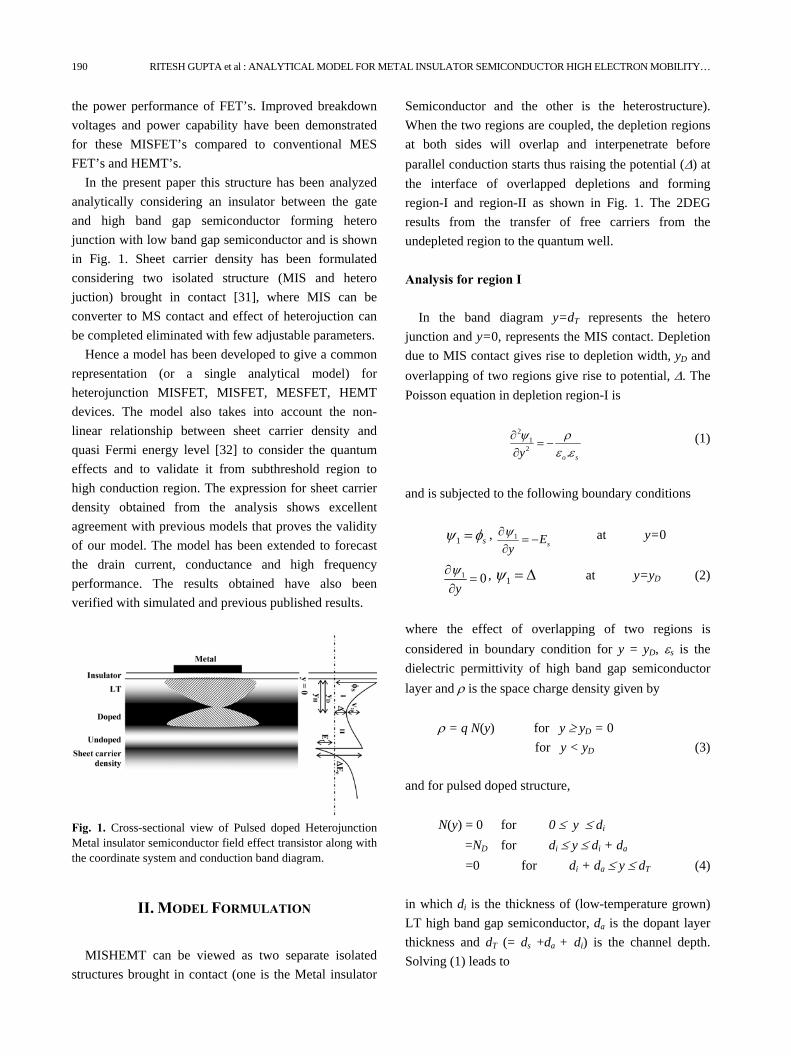
In the present paper this structure has been analyzed analytically considering an insulator between the gate and high band gap semiconductor forming hetero junction with low band gap semiconductor and is shown in Fig. 1. Sheet carrier density has been formulated considering two isolated structure (MIS and hetero juction) brought in contact [31], where MIS can be converter to MS contact and effect of heterojuction can be completed eliminated with few adjustable parameters.
Hence a model has been developed to give a common representation (or a single analytical model) for heterojunction MISFET, MISFET, MESFET, HEMT devices. The model also takes into account the non-linear relationship between sheet carrier density and quasi Fermi energy level [32] to consider the quantum effects and to validate it from subthreshold region to high conduction region. The expression for sheet carrier density obtained from the analysis shows excellent agreement with previous models that proves the validity of our model. The model has been extended to forecast the drain current, conductance and high frequency performance. The results obtained have also been verified with simulated and previous published results.
Fig. 1. Cross-sectional view of Pulsed doped Heterojunction Metal insulator semiconductor field effect transistor along with the coordinate system and conduction band diagram.
II. MODEL FORMULATION
MISHEMT can be viewed as two separate isolated structures brought in contact (one is the Metal insulator
Semiconductor and the other is the heterostructure). When the two regions are coupled, the depletion regions at both sides will overlap and interpenetrate before parallel conduction starts thus raising the potential (∆) at the interface of overlapped depletions and forming region-I and region-II as shown in Fig. 1. The 2DEG results from the transfer of free carriers from the undepleted region to the quantum well.
Analysis for region I
In the band diagram y=dT represents the hetero
junction and y=0, represents the MIS contact. Depletion due to MIS contact gives rise to depletion width, yD and overlapping of two regions give rise to potential, ∆. The Poisson equation in depletion region-I is
2
12 .o syψ ρ
ε ε∂
= −∂
(1)
and is subjected to the following boundary conditions
1 sψ φ= , 1sE
yψ∂
= −∂
at y=0
1 0yψ∂
=∂
, 1ψ = ∆ at y=yD (2)
where the effect of overlapping of two regions is considered in boundary condition for y = yD, εs is the dielectric permittivity of high band gap semiconductor layer and ρ is the space charge density given by
ρ = q N(y) for y ≥ yD = 0
for y < yD (3)
and for pulsed doped structure,
N(y) = 0 for 0 ≤ y ≤ di
=ND for di ≤ y ≤ di + da
=0 for di + da ≤ y ≤ dT (4)
in which di is the thickness of (low-temperature grown) LT high band gap semiconductor, da is the dopant layer thickness and dT (= ds +da + di) is the channel depth. Solving (1) leads to

JOURNAL OF SEMICONDUCTOR TECHNOLOGY AND SCIENCE, VOL.6, NO.3, SEPTEMBER, 2006 191
( )Ds D i
qNE y dε
= − −
( 2 2.2.
D )s D iq N y dφε
= ∆ + − + (5)
and from charge neutrality condition at the metal insulator semiconductor interface
s g msV VIφ φ= − − (6)
in which, 2g
ms m s n pEφ φ χ φ φ⎛ ⎞⎛ ⎞= − + − +⎜⎜ ⎟⎝⎝ ⎠
⎟⎠
is the work function
difference between bulk semiconductor and the gate
electrode, VI ( )D I D i
o I
qN t y dε ε
− −⎛=⎜⎝ ⎠
⎞⎟
is voltage across the
insulator, and . ln D
ni
Nk Tq n
φ⎛ ⎞
= ⎜⎝
⎟⎠ . Substituting the value of
φms, φn and VI in (6) and using (5) leads to
( )2
2. . 2. . . 2. . ..
s I s I s I i o sD i ms
I I I D
t t t dy d Vq N
ε ε ε ε ε φε ε ε
⎛ ⎞= − + + + + − + ∆⎜ ⎟
⎝ ⎠g
(7)
the free carrier density can be obtained as
( )s D i a Dn N d d y= + − (8)
these free carriers are transferred to the quantum well depending on the value of ∆ i.e., the free carrier density will be equal to 2DEG sheet carrier density before ∆=0. The rest of the free carriers will participate in conduction in high band gap semiconductor region (condition for parallel conduction). It can be noted here that (8) can be used for calculating the free carrier density of buried channel MISFET by substituting ∆=0 and the same expression can also be used for the analysis of MESFET by substituting tI = 0 for any arbitrary non zero value of εI.
Analysis for region II
At equilibrium, relation between ∆ and V20 can be
seen from Fig. 1 as
∆ + V20 = -∆Ec + Ef (9)
V20 is obtained by solving Poisson’s equation in the depletion region-II due to heterostructure and assuming the density of free carriers to be non zero in the undepleted region present after being depleted by the gate electrode, i.e., carriers obtained from region I are given by
N(y) = ND for yH ≤ y ≤ yH + ds
N(y) = 0 for yH + ds ≤ y ≤ dT (10)
in which yH is the depletion width formed by transfer of carriers to the quantum well. On solving the Poisson’s equation
2
22yψ ρ
ε∂
= −∂
(11)
for depletion region-II under the following boundary conditions
2 0yψ∂
=∂
, ψ2 = ∆ at y =yH
ψ2 = V20 + ∆ at y = dT (12)
we get, 2
20. . . . . .
2. . . .D a D a s D T
o s o s o s
qN d q N d d q N dVε ε ε ε ε ε
= − − +
( ) ( 2 2. .2. .
DH i H i
o s
q Ny d y dε ε
− + − + ) (13)
then from (9)
2 . . . . . .2. . . .
D a D a s D T
o s o s o s
qN d q N d d q N dε ε ε ε ε ε
∆ = + −
( ) ( ) (2 2. .2. .
D )H i H i co s
q Ny d y d E Eε ε
− − − + − ∆ − f (14)
where the above equation is valid before parallel conduction start, otherwise ∆ = 0. Before parallel conduction starts all the undepleted charges left out from metal-insulator-semiconductor contact are transfered to the quantum well, then yD and yH are the same. Substituting the value of ∆ in (7), for yD = yH we get

192 RITESH GUPTA et al : ANALYTICAL MODEL FOR METAL INSULATOR SEMICONDUCTOR HIGH ELECTRON MOBILITY…
( )2 . .. .. . 2 ..
o s g ms c fa s I iT i a s
I DD
s IT
I
V E Ed t dd d d d q Ny td
ε ε φεεε
ε
− + ∆ −+ + + −
=+
(15)
in which di is the Schottky layer thickness, then substituting the value of yD in (8), one can easily obtain the expression for sheet carrier density of heterojunction MISFET, and is given by
2. . . . .. . .. . 2. ..
o s D I a D as
s I o I o sT
I
q N t d q N dntq d
ε εε ε ε ε
ε
⎛= ⎜⎜⎛ ⎞ ⎝+⎜ ⎟
⎝ ⎠ε
+
2.. 1 ig ms c f
a
d V E Ed
φ⎞⎛ ⎞
+ + − + ∆ − ⎟⎜ ⎟ ⎟⎝ ⎠ ⎠
(16)
for tI = 0 (for HEMT) leads to
2. . . 2.. . 1. 2. .o s D a i
s g ms c fT o s a
q N d dn V E Eq d dε ε φ
ε ε⎛ ⎞⎛ ⎞
= + + − + ∆ −⎜ ⎟⎜ ⎟⎜ ⎟⎝ ⎠⎝ ⎠
which is found to be the same expression as reported earlier [33].
Threshold voltage
Channel is said to reach at threshold if free carriers are
zero i.e., depletion width due to metal-insulator-semi conductor contact is equal to di + da, and is obtained as
2
1. . 2. . . .12. . .
D a i D I aTH ms cHMISFET
o s a o I
q N d d q N t dV Ed
φε ε ε ε
⎛ ⎞= − ∆ − + − +⎜ ⎟
⎝ ⎠k
(17)
where k1 is resulted from variation of quasi Fermi level with 2DEG sheet carrier density to include subthreshold region. In the absence of heterostructure it is defined as
2. . 2. . . .1
2. . .D a i D I
TH msMISFETo s a o I
q N d d q N t dVd
φε ε ε ε
⎛ ⎞= − + −⎜ ⎟
⎝ ⎠a
(18)
Substituting tI = 0 in (17) leads to the expression of threshold voltage for HEMT, given by
2
1. . 2.12. .
D a iTH ms cHEMT
o s a
q N d dV Ed
φε ε
⎛ ⎞k= −∆ − + +⎜ ⎟
⎝ ⎠ (19)
which is found to be the same expression as reported earlier [33]. In the absence of heterostructure it is defined as
2. . 2.1
2. .D a
TH msMESFETo s a
q N d dVd
φε ε
⎛= − +⎜
⎝ ⎠i ⎞⎟ (20)
this shows that introduction of insulator between metal and semiconductor decreases the threshold voltage by an
amount equal to . . ..
D I a
o I
q N t dε ε
and the formation of
heterostructure increases the threshold voltage to an amount equal to ∆Ec – k1 in comparison to MESFET and MISFET, i.e.,
. . .
.D I a
TH THHMISFET HEMTo I
q N t dV Vε ε
= −
1TH TH cHMISFET MISFETV V E k= − ∆ +
1TH TH cHEMT MESFETV V E k= −∆ +
1. . .
.D I a
TH TH cHMISFET MESFETo I
q N t dV V Eε ε
k= − − ∆ +
(21)
III. DRAIN CURRENT AND CONDUCTANCES
The expression for drain current and conductances can easily be derived from the expression proposed in our earlier work [33] by replacing the expression of
threshold voltage with newer one and .
.o S
S IT
I
tq d
ε εβεε
=⎛ ⎞
+⎜ ⎟⎝ ⎠
.
IV. LT-MISHEMT AND PERFECT INSULATOR
MISHEMT
Threshold voltage of LT-MISFET is given by (18) whereas for perfect insulator MISHEMT (in which there is no LT layer, i.e. di = 0) it is given by
JOURNAL OF SEMICONDUCTOR TECHNOLOGY AND SCIENCE, VOL.6, NO.3, SEPTEMBER, 2006 193
2
1. . . . .2. . .
D a D I aTH ms cHMISFET
o s o I
q N d q N t dV E kφε ε ε ε
= −∆ − − +
(22) equating (18) and (22) gives the equivalence between LT-MISHEMT and MISHEMT, and is given by
i II
s
dt εε
= (23)
here it can be noted that the same equivalence can be established between the perfect insulator MISFET and the LT-MISFET.
V. RESULTS AND DISCUSSION
The model have been formulated to predict the sheet carrier density of Metal insulator heterojunction FET (MISHFET), MISFET, HEMT and MESFET and has been extended to evaluate drain current, conductance and cut-off frequency of the device. The parameters used for comparing the characteristics of these devices are of SiO2/InAlAs/InGaAs and are tabulated in Table. 1.
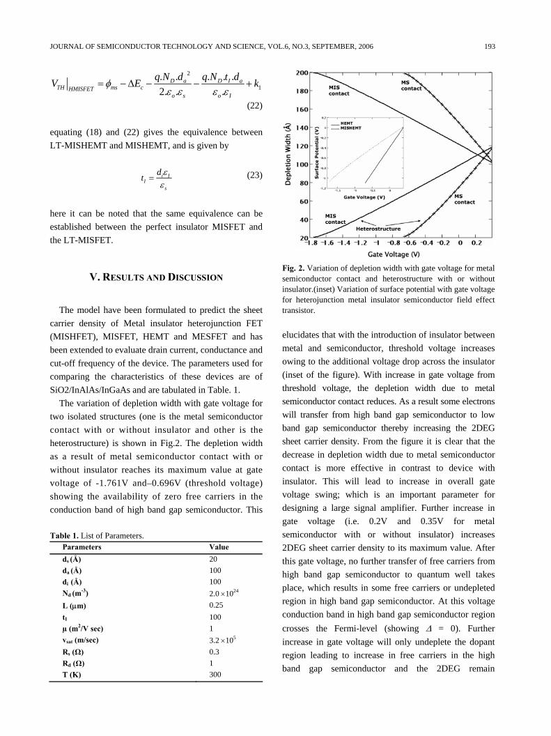
The variation of depletion width with gate voltage for two isolated structures (one is the metal semiconductor contact with or without insulator and other is the heterostructure) is shown in Fig.2. The depletion width as a result of metal semiconductor contact with or without insulator reaches its maximum value at gate voltage of -1.761V and–0.696V (threshold voltage) showing the availability of zero free carriers in the conduction band of high band gap semiconductor. This
Table 1. List of Parameters.
Parameters Value ds (Å) 20 da (Å) 100 di (Å) 100 Nd (m-3) 2.0 ×1024
L (µm) 0.25 tI 100 µ (m2/V sec) 1 vsat (m/sec) 3.2 ×10⁵
Rs (Ω) 0.3 Rd (Ω) 1 T (K) 300
Fig. 2. Variation of depletion width with gate voltage for metal semiconductor contact and heterostructure with or without insulator.(inset) Variation of surface potential with gate voltage for heterojunction metal insulator semiconductor field effect transistor. elucidates that with the introduction of insulator between metal and semiconductor, threshold voltage increases owing to the additional voltage drop across the insulator (inset of the figure). With increase in gate voltage from threshold voltage, the depletion width due to metal semiconductor contact reduces. As a result some electrons will transfer from high band gap semiconductor to low band gap semiconductor thereby increasing the 2DEG sheet carrier density. From the figure it is clear that the decrease in depletion width due to metal semiconductor contact is more effective in contrast to device with insulator. This will lead to increase in overall gate voltage swing; which is an important parameter for designing a large signal amplifier. Further increase in gate voltage (i.e. 0.2V and 0.35V for metal semiconductor with or without insulator) increases 2DEG sheet carrier density to its maximum value. After this gate voltage, no further transfer of free carriers from high band gap semiconductor to quantum well takes place, which results in some free carriers or undepleted region in high band gap semiconductor. At this voltage conduction band in high band gap semiconductor region crosses the Fermi-level (showing ∆ = 0). Further increase in gate voltage will only undeplete the dopant region leading to increase in free carriers in the high band gap semiconductor and the 2DEG remain
194 RITESH GUPTA et al : ANALYTICAL MODEL FOR METAL INSULATOR SEMICONDUCTOR HIGH ELECTRON MOBILITY…
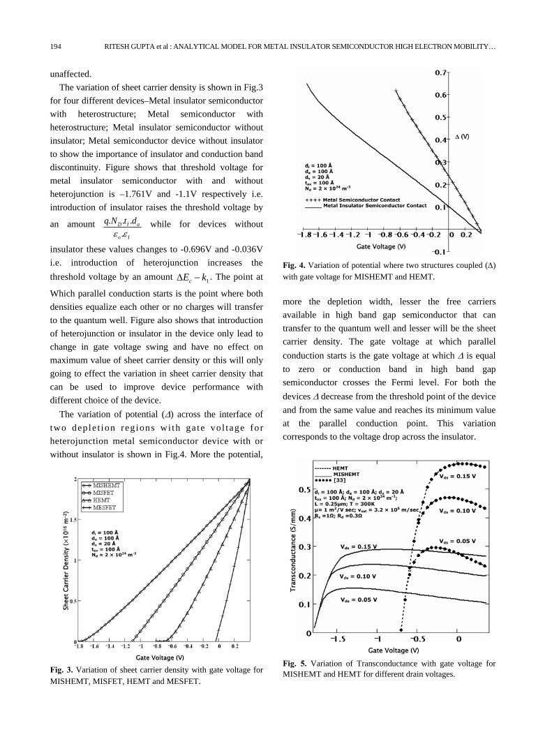
unaffected. The variation of sheet carrier density is shown in Fig.3
for four different devices–Metal insulator semiconductor with heterostructure; Metal semiconductor with heterostructure; Metal insulator semiconductor without insulator; Metal semiconductor device without insulator to show the importance of insulator and conduction band discontinuity. Figure shows that threshold voltage for metal insulator semiconductor with and without heterojunction is –1.761V and -1.1V respectively i.e. introduction of insulator raises the threshold voltage by
an amount . . ..
D I a
o I
q N t dε ε
while for devices without
insulator these values changes to -0.696V and -0.036V i.e. introduction of heterojunction increases the threshold voltage by an amount 1cE k∆ − . The point at
Which parallel conduction starts is the point where both densities equalize each other or no charges will transfer to the quantum well. Figure also shows that introduction of heterojunction or insulator in the device only lead to change in gate voltage swing and have no effect on maximum value of sheet carrier density or this will only going to effect the variation in sheet carrier density that can be used to improve device performance with different choice of the device.
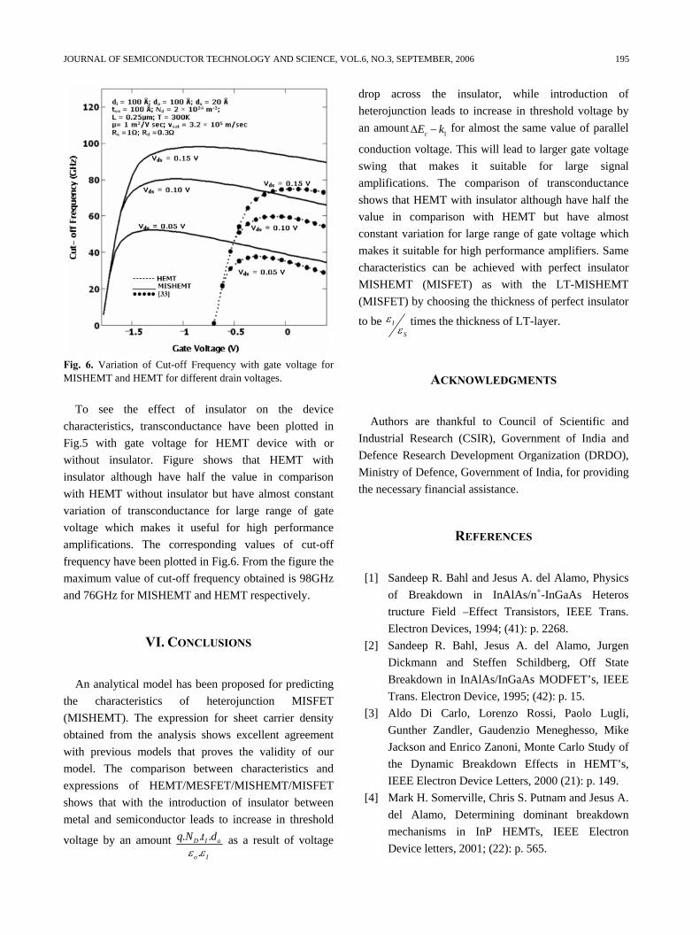
The variation of potential (∆) across the interface of two dep le t ion reg ions wi th ga te vo l tage for heterojunction metal semiconductor device with or without insulator is shown in Fig.4. More the potential,
Fig. 3. Variation of sheet carrier density with gate voltage for MISHEMT, MISFET, HEMT and MESFET.
Fig. 4. Variation of potential where two structures coupled (∆) with gate voltage for MISHEMT and HEMT. more the depletion width, lesser the free carriers available in high band gap semiconductor that can transfer to the quantum well and lesser will be the sheet carrier density. The gate voltage at which parallel conduction starts is the gate voltage at which ∆ is equal to zero or conduction band in high band gap semiconductor crosses the Fermi level. For both the devices ∆ decrease from the threshold point of the device and from the same value and reaches its minimum value at the parallel conduction point. This variation corresponds to the voltage drop across the insulator.
Fig. 5. Variation of Transconductance with gate voltage for MISHEMT and HEMT for different drain voltages.
JOURNAL OF SEMICONDUCTOR TECHNOLOGY AND SCIENCE, VOL.6, NO.3, SEPTEMBER, 2006 195
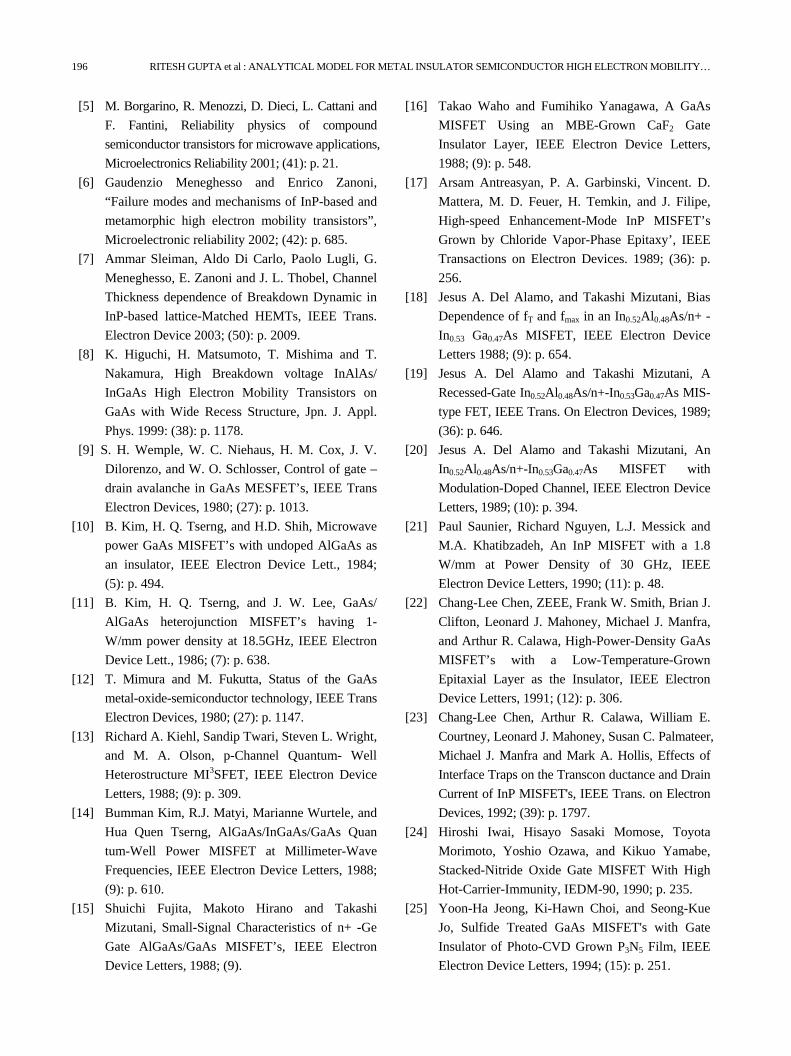
Fig. 6. Variation of Cut-off Frequency with gate voltage for MISHEMT and HEMT for different drain voltages.
To see the effect of insulator on the device
characteristics, transconductance have been plotted in Fig.5 with gate voltage for HEMT device with or without insulator. Figure shows that HEMT with insulator although have half the value in comparison with HEMT without insulator but have almost constant variation of transconductance for large range of gate voltage which makes it useful for high performance amplifications. The corresponding values of cut-off frequency have been plotted in Fig.6. From the figure the maximum value of cut-off frequency obtained is 98GHz and 76GHz for MISHEMT and HEMT respectively.
VI. CONCLUSIONS
An analytical model has been proposed for predicting the characteristics of heterojunction MISFET (MISHEMT). The expression for sheet carrier density obtained from the analysis shows excellent agreement with previous models that proves the validity of our model. The comparison between characteristics and expressions of HEMT/MESFET/MISHEMT/MISFET shows that with the introduction of insulator between metal and semiconductor leads to increase in threshold
voltage by an amount . . ..
D I a
o I
q N t dε ε
as a result of voltage
drop across the insulator, while introduction of heterojunction leads to increase in threshold voltage by an amount 1cE k∆ − for almost the same value of parallel
conduction voltage. This will lead to larger gate voltage swing that makes it suitable for large signal amplifications. The comparison of transconductance shows that HEMT with insulator although have half the value in comparison with HEMT but have almost constant variation for large range of gate voltage which makes it suitable for high performance amplifiers. Same characteristics can be achieved with perfect insulator MISHEMT (MISFET) as with the LT-MISHEMT (MISFET) by choosing the thickness of perfect insulator
to be I
S
εε
times the thickness of LT-layer.
ACKNOWLEDGMENTS
Authors are thankful to Council of Scientific and Industrial Research (CSIR), Government of India and Defence Research Development Organization (DRDO), Ministry of Defence, Government of India, for providing the necessary financial assistance.
REFERENCES
[1] Sandeep R. Bahl and Jesus A. del Alamo, Physics of Breakdown in InAlAs/n+-InGaAs Heteros tructure Field –Effect Transistors, IEEE Trans. Electron Devices, 1994; (41): p. 2268.
[2] Sandeep R. Bahl, Jesus A. del Alamo, Jurgen Dickmann and Steffen Schildberg, Off State Breakdown in InAlAs/InGaAs MODFET’s, IEEE Trans. Electron Device, 1995; (42): p. 15.
[3] Aldo Di Carlo, Lorenzo Rossi, Paolo Lugli, Gunther Zandler, Gaudenzio Meneghesso, Mike Jackson and Enrico Zanoni, Monte Carlo Study of the Dynamic Breakdown Effects in HEMT’s, IEEE Electron Device Letters, 2000 (21): p. 149.
[4] Mark H. Somerville, Chris S. Putnam and Jesus A. del Alamo, Determining dominant breakdown mechanisms in InP HEMTs, IEEE Electron Device letters, 2001; (22): p. 565.
196 RITESH GUPTA et al : ANALYTICAL MODEL FOR METAL INSULATOR SEMICONDUCTOR HIGH ELECTRON MOBILITY…
[5] M. Borgarino, R. Menozzi, D. Dieci, L. Cattani and F. Fantini, Reliability physics of compound semiconductor transistors for microwave applications, Microelectronics Reliability 2001; (41): p. 21.
[6] Gaudenzio Meneghesso and Enrico Zanoni, “Failure modes and mechanisms of InP-based and metamorphic high electron mobility transistors”, Microelectronic reliability 2002; (42): p. 685.
[7] Ammar Sleiman, Aldo Di Carlo, Paolo Lugli, G. Meneghesso, E. Zanoni and J. L. Thobel, Channel Thickness dependence of Breakdown Dynamic in InP-based lattice-Matched HEMTs, IEEE Trans. Electron Device 2003; (50): p. 2009.
[8] K. Higuchi, H. Matsumoto, T. Mishima and T. Nakamura, High Breakdown voltage InAlAs/ InGaAs High Electron Mobility Transistors on GaAs with Wide Recess Structure, Jpn. J. Appl. Phys. 1999: (38): p. 1178.
[9] S. H. Wemple, W. C. Niehaus, H. M. Cox, J. V. Dilorenzo, and W. O. Schlosser, Control of gate – drain avalanche in GaAs MESFET’s, IEEE Trans Electron Devices, 1980; (27): p. 1013.
[10] B. Kim, H. Q. Tserng, and H.D. Shih, Microwave power GaAs MISFET’s with undoped AlGaAs as an insulator, IEEE Electron Device Lett., 1984; (5): p. 494.
[11] B. Kim, H. Q. Tserng, and J. W. Lee, GaAs/ AlGaAs heterojunction MISFET’s having 1-W/mm power density at 18.5GHz, IEEE Electron Device Lett., 1986; (7): p. 638.
[12] T. Mimura and M. Fukutta, Status of the GaAs metal-oxide-semiconductor technology, IEEE Trans Electron Devices, 1980; (27): p. 1147.
[13] Richard A. Kiehl, Sandip Twari, Steven L. Wright, and M. A. Olson, p-Channel Quantum- Well Heterostructure MI3SFET, IEEE Electron Device Letters, 1988; (9): p. 309.
[14] Bumman Kim, R.J. Matyi, Marianne Wurtele, and Hua Quen Tserng, AlGaAs/InGaAs/GaAs Quan tum-Well Power MISFET at Millimeter-Wave Frequencies, IEEE Electron Device Letters, 1988; (9): p. 610.
[15] Shuichi Fujita, Makoto Hirano and Takashi Mizutani, Small-Signal Characteristics of n+ -Ge Gate AlGaAs/GaAs MISFET’s, IEEE Electron Device Letters, 1988; (9).
[16] Takao Waho and Fumihiko Yanagawa, A GaAs MISFET Using an MBE-Grown CaF2 Gate Insulator Layer, IEEE Electron Device Letters, 1988; (9): p. 548.
[17] Arsam Antreasyan, P. A. Garbinski, Vincent. D. Mattera, M. D. Feuer, H. Temkin, and J. Filipe, High-speed Enhancement-Mode InP MISFET’s Grown by Chloride Vapor-Phase Epitaxy’, IEEE Transactions on Electron Devices. 1989; (36): p. 256.
[18] Jesus A. Del Alamo, and Takashi Mizutani, Bias Dependence of fT and fmax in an In0.52Al0.48As/n+ -In0.53 Ga0.47As MISFET, IEEE Electron Device Letters 1988; (9): p. 654.
[19] Jesus A. Del Alamo and Takashi Mizutani, A Recessed-Gate In0.52Al0.48As/n+-In0.53Ga0.47As MIS-type FET, IEEE Trans. On Electron Devices, 1989; (36): p. 646.
[20] Jesus A. Del Alamo and Takashi Mizutani, An In0.52Al0.48As/n+-In0.53Ga0.47As MISFET with Modulation-Doped Channel, IEEE Electron Device Letters, 1989; (10): p. 394.
[21] Paul Saunier, Richard Nguyen, L.J. Messick and M.A. Khatibzadeh, An InP MISFET with a 1.8 W/mm at Power Density of 30 GHz, IEEE Electron Device Letters, 1990; (11): p. 48.
[22] Chang-Lee Chen, ZEEE, Frank W. Smith, Brian J. Clifton, Leonard J. Mahoney, Michael J. Manfra, and Arthur R. Calawa, High-Power-Density GaAs MISFET’s with a Low-Temperature-Grown Epitaxial Layer as the Insulator, IEEE Electron Device Letters, 1991; (12): p. 306.
[23] Chang-Lee Chen, Arthur R. Calawa, William E. Courtney, Leonard J. Mahoney, Susan C. Palmateer, Michael J. Manfra and Mark A. Hollis, Effects of Interface Traps on the Transcon ductance and Drain Current of InP MISFET's, IEEE Trans. on Electron Devices, 1992; (39): p. 1797.
[24] Hiroshi Iwai, Hisayo Sasaki Momose, Toyota Morimoto, Yoshio Ozawa, and Kikuo Yamabe, Stacked-Nitride Oxide Gate MISFET With High Hot-Carrier-Immunity, IEDM-90, 1990; p. 235.
[25] Yoon-Ha Jeong, Ki-Hawn Choi, and Seong-Kue Jo, Sulfide Treated GaAs MISFET's with Gate Insulator of Photo-CVD Grown P3N5 Film, IEEE Electron Device Letters, 1994; (15): p. 251.
JOURNAL OF SEMICONDUCTOR TECHNOLOGY AND SCIENCE, VOL.6, NO.3, SEPTEMBER, 2006 197
[26] Hisayo Sasaki Momose, Toyota Morimoto, Yoshio Ozawa, Kikuo Yamabe, and Hiroshi Iwai, An Improvement of Hot-Carrier Reliability in the Stacked Nitride-Oxide Gate n- and p-MISFET’s, IEEE Trans. on Electron Devices, 1995; (42): p. 704.
[27] C. L. Chen, L. J. Mahoney, K. B. Nichols, M. J. Manfra, B. F. Gramstorff, K. M. Molvar, R. A. Murphy, and E. R. Brown, Self-Aligned GaAs MISFET's with a Low-Temperature-Grown GaAs Gate Insulator, IEEE Electron Device Letters, 1995; (16): p. 109.
[28] C. L. Chen, L. J. Mahoney, K. B. Nichols, E. R. Brown, and B. F. Gramstorff, Self-Aligned p-Channel MISFET with a Low-Temperature-Grown GaAs Gate Insulator, IEEE Electron Device Letters, 1996; (17): p. 413.
[29] R.V.V.V.J. Rao, T.C. Chong, L.S. Tan, W.S.Lau and J.J. Liou, A Physical Analytical Model for LT-GaAs and LT-Al0.3Ga0.7As MISFET Devices, IEDM-99 1999; p. 134.
[30] Ritesh Gupta, Mridula Gupta and R. S. Gupta, A New Depletion dependent Analytical Model for Sheet Carrier density of InAlAs/InGaAs heteros tructure, InP based HEMT, Solid State Electronics 2003; (47): p. 33.
[31] Ritesh Gupta, Mridula Gupta and R. S Gupta, A New simplified Analytical Short-channel Thres hold Voltage Model for InAlAs/InGaAs Hetero structure InP based Pulsed Doped HEMT, Solid State Electronics 2004; (48), p. 437.
[32] N. DasGupta and A. DasGupta, An analytical expression for sheet carrier concentration versus gate voltage for HEMT modeling, Solid State Electron., 1993; (36): p. 201.
[33] “An Analytical Non-Linear Charge Control Parasitic Resistance Depending Model for InAlAs/InGaAs/InP HEMT Characteristics”, Ritesh Gupta, Abhinav Kranti, S Haldar, Mridula Gupta and R S Gupta, Microelectronics Engineering, Vol. 60, no. 3 – 4, pp. 323-337, 2002
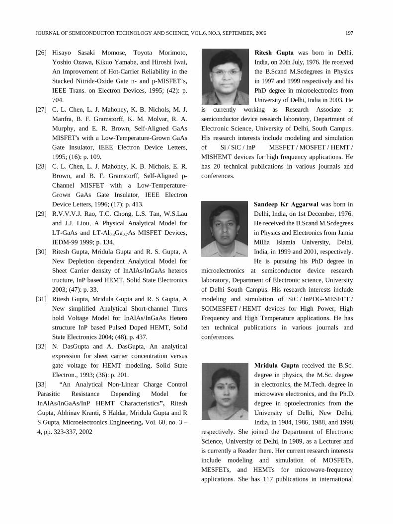
Ritesh Gupta was born in Delhi, India, on 20th July, 1976. He received the B.Scand M.Scdegrees in Physics in 1997 and 1999 respectively and his PhD degree in microelectronics from University of Delhi, India in 2003. He
is currently working as Research Associate at semiconductor device research laboratory, Department of Electronic Science, University of Delhi, South Campus. His research interests include modeling and simulation of Si / SiC / InP MESFET / MOSFET / HEMT / MISHEMT devices for high frequency applications. He has 20 technical publications in various journals and conferences.
Sandeep Kr Aggarwal was born in Delhi, India, on 1st December, 1976. He received the B.Scand M.Scdegrees in Physics and Electronics from Jamia Millia Islamia University, Delhi, India, in 1999 and 2001, respectively. He is pursuing his PhD degree in
microelectronics at semiconductor device research laboratory, Department of Electronic science, University of Delhi South Campus. His research interests include modeling and simulation of SiC / InPDG-MESFET / SOIMESFET / HEMT devices for High Power, High Frequency and High Temperature applications. He has ten technical publications in various journals and conferences.
Mridula Gupta received the B.Sc. degree in physics, the M.Sc. degree in electronics, the M.Tech. degree in microwave electronics, and the Ph.D. degree in optoelectronics from the University of Delhi, New Delhi, India, in 1984, 1986, 1988, and 1998,
respectively. She joined the Department of Electronic Science, University of Delhi, in 1989, as a Lecturer and is currently a Reader there. Her current research interests include modeling and simulation of MOSFETs, MESFETs, and HEMTs for microwave-frequency applications. She has 117 publications in international
198 RITESH GUPTA et al : ANALYTICAL MODEL FOR METAL INSULATOR SEMICONDUCTOR HIGH ELECTRON MOBILITY…
and national journals and conferences. She contributed one chapter entitled. “MOSFET Modeling” in the Encyclopedia on RF and Microwave Engineering (Wiley, 2005). Dr. Gupta is a Fellow of the Institution of Electronics and Telecommunication Engineers, India, and is a Life Member of the Semiconductor Society of India. She was the Secretary of the Asia Pacific Microwave Conference (APMC-2004) held in New Delhi, India, in December 2004.
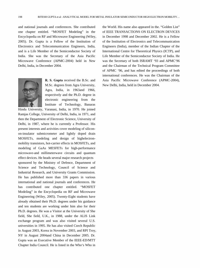
R. S. Gupta received the B.Sc. and M.Sc. degrees from Agra University, Agra, India, in 1963and 1966, respectively and the Ph.D. degree in electronic engineering from the Institute of Technology, Banaras
Hindu University, Varanasi, India, in 1970. He joined Ramjas College, University of Delhi, India, in 1971, and then the Department of Electronic Science, University of Delhi, in 1987, where he is currently a Professor. His present interests and activities cover modeling of silicon-on-insulator submicrometer and lightly doped drain MOSFETs, modeling and design of highelectron-mobility transistors, hot-carrier effects in MOSFETs, and modeling of GaAs MESFETs for high-performance microwave-and millimeterwave circuits and quantum effect devices. He heads several major research projects sponsored by the Ministry of Defence, Department of Science and Technology, Council of Science and Industrial Research, and University Grants Commission. He has published more than 336 papers in various international and national journals and conferences. He has contributed one chapter entitled. “MOSFET Modeling” in the Encyclopedia on RF and Microwave Engineering (Wiley, 2005). Twenty-Eight students have already obtained their Ph.D. degrees under his guidance and ten students are working under him also for their Ph.D. degrees. He was a Visitor at the University of She field, She field, U.K., in 1988, under the ALIS Link exchange program and was also visited several U.S. universities in 1995. He has also visited Czech Republic in August 2003, Korea in November 2003, and RPI Troy, NY in August 2004and China in December 2005. Dr. Gupta was an Executive Member of the IEEE-ED/MTT Chapter India Council. He is listed in the Who‘s Who in
the World. His name also appeared in the. “Golden List” of IEEE TRANSACTIONS ON ELECTRON DEVICES in December 1998 and December 2002. He is a Fellow of the Institution of Electronics and Telecommunication Engineers (India), member of the Indian Chapter of the International Centre for Theoretical Physics (ICTP), and Life Member of the Semiconductor Society of India. He was the Secretary of both ISRAMT ‘93 and APMC‘96 and the Chairman of the Technical Program Committee of APMC ‘96, and has edited the proceedings of both international conferences. He was the Chairman of the Asia Pacific Microwave Conference (APMC-2004), New Delhi, India, held in December 2004.