Analysis, Design, Optimization and Realization of Compact ...
149
Analysis, Design, Optimization and Realization of Compact High Performance Printed RF Filters Dissertation zur Erlangung des akademischen Grades Doktoringenieur (Dr.-Ing.) von M.Sc. Atallah Balalem geb. am 15. January 1978 in Nablus, Palestine genehmigt durch die Fakult¨ at f¨ ur Elektrotechnik und Informationstechnik der Otto-von-Guericke-Universit¨at Magdeburg Gutachter: Prof. Dr.-Ing Abbas S. Omar Prof. Dr.-Ing Marco Leone Prof. Ing Jan Machac, DrSc. Promotionskolloquium am: 15. M¨arz 2010
-
Upload
khangminh22 -
Category
Documents
-
view
0 -
download
0
Transcript of Analysis, Design, Optimization and Realization of Compact ...

Analysis, Design, Optimization and Realization of
Compact High Performance Printed RF Filters
Dissertationzur Erlangung des akademischen Grades
Doktoringenieur(Dr.-Ing.)
von M.Sc. Atallah Balalemgeb. am 15. January 1978 in Nablus, Palestine
genehmigt durch die Fakultat fur Elektrotechnik und Informationstechnikder Otto-von-Guericke-Universitat Magdeburg
Gutachter:Prof. Dr.-Ing Abbas S. OmarProf. Dr.-Ing Marco LeoneProf. Ing Jan Machac, DrSc.
Promotionskolloquium am: 15. Marz 2010


Dedications
This work is dedicated to my Father and to the memory ofmy Mother
Atallah
i


Acknowledgement
First of all, I would like to thank God, who gives us every thing and without him
nothing can be done.
First and foremost, I would like to thank my advisor, Professor Abbas S. Omar
for his constant help and advising me. His encouragement and insight were extremely
valuable throughout my graduate career. I would also like to thank Professor Jan
Machac from Czech Technical University for his cooperation and discussions, and
for allowing me to join his research group in Prague for six month. My thanks also
go to Professor Wolfgang Menzel from the University of Ulm for his cooperation,
discussions and for the fabrication of my structures at his department. I also thank
Professor Samin Amari from Royal Military Collage in Canada for his cooperation
and his discussions.
I would like to thank all of my colleagues and friends who have helped me through
the difficult task of creating this Thesis, namely: Ali R. Ali, Ihab Hamad, Abdallah
Fared, Julia Braun, Hasan Salem, Michael Maiwald, Mohammed Salah, Adel Abdel-
Rahman, Fawzy Abujarad and his wife Raesa.
Last not least it is my pleasure to thank my father, brothers and sisters for their
support, love, and their prayers. I should never forget to thank my wife Razan and
my doughter Samia for their love and patience.
iii


Kurzfassung
In der vorliegenden Arbeit wird ein modifizierter Querschnitt der mehrschichtigen
Koplanarleitung und seine Anwendung fuer Filterzwecke untersucht. Mit Hilfe dieses
Querschnittes wurde ein Tiefpass entworfen, der durch das Anbringen von breiten
Patches auf dem klassischen Koplanar Waveguide (CPW) Tiefpassfilter realisiert wird.
Die Patches sind auf der Ruckseite des Substrates und unter dem kapazitiven Streifen
angebracht. Weitere Filter mit Bandpasscharakteristik sind so aufgebaut, dass sie
Mikrostreifenleitung, CPW oder aus beiden beinhalten. Ein in der Mitte des Hohlleit-
ers angebrachtes Streifenleitungs-Ultrabreitband-Bandpassfilter mit einem breiten Sper-
rbereich basiert auf einem Tiefpassfilter, das mit Ein/Aus- Versorgungsleitungen ka-
pazitiv gekoppelt wird.
In dieser Arbeit wird auch ein interdigitaler Defected Ground Schlitz vorgestellt
und untersucht. Zwei Tiefpassfilter werden dargestellt, die diesen Schlitz benutzen
und dabei die Vorteile von kompakten Slots aufzeigen. Es wird eine Losung gezeigt,
die die Schwierigkeiten beim Aufbau von Gehausen reduziert, indem die Grundplatte
der Schaltung voll metallisiert wird und Schlitze auf dem Substrat geatzt werden.
Das Metall des Substrates ist mit der Grundplatte mit Hilfe von Durchganglochern
verbunden.
Es konnte ein erster Mikrostreifen-Resonators realisiert werden, der drei Reso-
nanzfrequenzen besitzt. Dieser Resonator ist so aufgebaut, dass eine zusatzliche
Maander-Mikrostreifenleitung von halber Wellenlange hinzugefugt wurde, die an den
zwei gegenuberliegenden Ecken des originalen quadratischen Mikrostreifen- Zweimod-
enresonators verbunden ist. Zwei Bandpassfilter wurden realisiert mit Hilfe dieses
Resonators, der erste mit einer Nullstelle in seinem Sperrbereich und der zweite mit
drei Nullstellen. Weiterhin wird auf der Basis von Streifenleitungen ein Hohlleiter-
Zweimodenresonator vorgestellt, es ist der erste Zweimodenresonator in dieser Tech-
nologie.
Zwei weitere kompakte Filter werden entworfen, gefertigt und getestet, die zwei
Durchlassbereiche besitzen und auf dem Einsatz eines Zweimodenresonators auf-
bauen. Der erster Filter ist ein Mikrostreifen- Filter, er wurde realisiert durch das
Einfugen von Nullstellen im Durchlassband eines Breitbandfilters durch die Benutzung
eines quadratische scheifen Zweimodenresonator. Der zweite Filter ist ein Filter mit
v

bereits vorher vorgestellten Hohlleiter-Streifenleitungen. Der Filter wurde realisiert
durch die Aufteilung der Moden von Zweimodenresonator in zwei Frequenzbander.
vi

Abstract
This thesis introduces and investigates different multilayer structures and their fil-
ter apllictions. Compact quasi-lumped filters are introduced using this technology.
Low-pass filter is designed using this structure by adding wide patches to the clas-
sical coplanar waveguide low-pass filter at the back side of the substrate and under
the capacitive lines. Bandpass filters are introduced, these filters are constructed
to be integrated with microstrip line, coplanar waveguide, and both. Moreover, a
suspended stripline ultra-wideband bandpass filter with very wide stopband is intro-
duced by coupling low-pass filter capacitively with the I/O feeding lines. The thesis
also introduces and investigates an interdigital defected ground slot. The slot is very
compact compared to the other known slots. Two low-pass filters are presented using
this slot showing advantages of the compact slot. Moreover, the thesis presents a
solution to reduce the packaging difficulties by keeping the ground plane of the cir-
cuit fully metallized and etching the slots on the superstrate, which is directly laying
on the top of the substrate. The metal of the superstrate is connected by via holes
to the ground plane. Further more, the thesis also introduces the first microstrip
realization of triple-mode resonator. This resonator was realized by adding an ad-
ditional meander half wavelength microstrip line connected to two opposite corners
of the original microstrip square-loop dual-mode resonator. Two bandpass filters are
realized using this resonator, the first one with a transmission zero in its stopband,
and the second one with three transmission zeroes in its stopband. Moreover, a real-
ization of suspended stripline dual-mode resonator is presented in this thesis, which
is the first dual-mode resonator for this technique. Very compact bandpass filters are
designed fabricated and tested using this resonator. Dual-band bandpass filters are
realized by using dual-mode resonators. The first filter is a microstrip one is realized
by introducing transmission zero in the passband of a broadband bandpass filter by
using square-loop dual-mode resonator. The second introduced filter is a suspended
stripline one. The filter is realized by splitting the modes of the dual-mode resonator
into two frequency bands.
vii


Table of Contents
Dedications i
Acknowledgement iii
Kurzfassung v
Abstract vii
Table of Contents vi
List of Figures viii
1 Introduction 1
1.1 Planar Resonators . . . . . . . . . . . . . . . . . . . . . . . . . . . . 3
1.2 Planar Lowpass Filters . . . . . . . . . . . . . . . . . . . . . . . . . . 5
1.3 Planar Bandpass Filters . . . . . . . . . . . . . . . . . . . . . . . . . 7
1.3.1 Narrowband and Wideband Bandpass Filters . . . . . . . . . 7
1.3.2 Ultra-Wideband Bandpass Filters . . . . . . . . . . . . . . . . 8
1.3.3 Dual-Band Bandpass Filters . . . . . . . . . . . . . . . . . . 9
1.4 Contributions and Thesis Organization . . . . . . . . . . . . . . . . . 9
2 Background 11
2.1 Filter Types . . . . . . . . . . . . . . . . . . . . . . . . . . . . . . . . 12
2.1.1 Butterworth Response . . . . . . . . . . . . . . . . . . . . . . 12
2.1.2 Chebyshev Response . . . . . . . . . . . . . . . . . . . . . . . 12
2.1.3 Elliptic Response . . . . . . . . . . . . . . . . . . . . . . . . . 13
2.2 Elements Realization for Lowpass Prototype Filters . . . . . . . . . . 13
2.2.1 Butterworth Lowpass Prototype Filters . . . . . . . . . . . . . 13
2.2.2 Chebyshev Lowpass Prototype Filters . . . . . . . . . . . . . . 14
2.2.3 Elliptic Lowpass Prototype Filters . . . . . . . . . . . . . . . . 15
2.2.4 Elements Transformations . . . . . . . . . . . . . . . . . . . . 16
2.3 Bandpass Transformation . . . . . . . . . . . . . . . . . . . . . . . . 17
2.4 Coupling Matrix and Cross Coupled Resonators . . . . . . . . . . . . 23
2.5 Planar Transmission Lines . . . . . . . . . . . . . . . . . . . . . . . . 26
2.5.1 Microstrip Line . . . . . . . . . . . . . . . . . . . . . . . . . . 26
vi

2.5.2 Coplanar Waveguide . . . . . . . . . . . . . . . . . . . . . . . 27
2.5.3 Suspended Stripline . . . . . . . . . . . . . . . . . . . . . . . . 28
2.5.4 Multilayer Transmission Lines . . . . . . . . . . . . . . . . . . 29
3 Multilayer Structures and Filter Applications 31
3.1 Multilayer Coplanar Line Cross Section . . . . . . . . . . . . . . . . . 31
3.2 Quasi-Lumped Elements . . . . . . . . . . . . . . . . . . . . . . . . . 34
3.3 Lowpass Filters . . . . . . . . . . . . . . . . . . . . . . . . . . . . . . 38
3.4 Microstrip Bandpass Filters Using Multilayer Line . . . . . . . . . . . 41
3.5 CPW Bandpass Filters Using Multilayer Line . . . . . . . . . . . . . 45
3.6 Bandpass Filter with Microstrip-CPW Feed Lines . . . . . . . . . . . 48
3.7 Suspended Stripline Ultra-Wideband Bandpass Filter . . . . . . . . . 50
4 Defected Ground Structures 57
4.1 Interdigital DGS Slot . . . . . . . . . . . . . . . . . . . . . . . . . . . 60
4.2 Quasi Elliptic Microstrip Lowpass Filters . . . . . . . . . . . . . . . . 65
4.3 Defected Ground Structure and Packaging . . . . . . . . . . . . . . . 66
5 Dual and Triple-Mode Resonators and Filters 73
5.1 Triple-Mode Microstrip Resonator . . . . . . . . . . . . . . . . . . . . 75
5.1.1 Resonator Topology . . . . . . . . . . . . . . . . . . . . . . . 75
5.1.2 Modes and Perturbations p, r . . . . . . . . . . . . . . . . . . 76
5.1.3 Triple-Mode Resonator and Filter Realization . . . . . . . . . 79
5.1.4 Broadband Equivalent Circuit . . . . . . . . . . . . . . . . . . 84
5.1.5 Experimental Results . . . . . . . . . . . . . . . . . . . . . . . 87
5.2 Dual-Mode Suspended Stripline Filters . . . . . . . . . . . . . . . . . 90
5.2.1 Quasi-Lumped Parallel Resonator . . . . . . . . . . . . . . . . 90
5.2.2 Open-Loop Resonator . . . . . . . . . . . . . . . . . . . . . . 90
5.2.3 Resonators Combination . . . . . . . . . . . . . . . . . . . . . 91
6 Dual-Band Bandpass Filters Using Dual-Mode Resonator 99
6.1 Dual-Band Microstrip Filter . . . . . . . . . . . . . . . . . . . . . . . 100
6.1.1 Filter Topology . . . . . . . . . . . . . . . . . . . . . . . . . . 100
6.1.2 Center Frequency and Bandwidth Control . . . . . . . . . . . 101
6.1.3 Experimental Results . . . . . . . . . . . . . . . . . . . . . . . 104
6.2 Dual-Band Suspended Stripline Filters Using Dual-Mode Resonator . 105
7 Conclusions and Future Work 111
7.1 Thesis Summary . . . . . . . . . . . . . . . . . . . . . . . . . . . . . 111
7.2 Suggestions for Future Work . . . . . . . . . . . . . . . . . . . . . . . 112
List of Publications 127
vii

List of Figures
1.1 Simplified schematic of a basic radio transmitter (up) and receiver
(down). . . . . . . . . . . . . . . . . . . . . . . . . . . . . . . . . . . 1
1.2 Simplified schematic of a doppler radar. . . . . . . . . . . . . . . . . . 1
1.3 Two possible shapes of open-loop resonator. . . . . . . . . . . . . . . 3
1.4 Dual-mode resonator fed by perpendicular feeding lines . . . . . . . . 4
1.5 Return loss of dual-mode bandpass filter using one dual-mode resonator. 4
1.6 Top layout of stepped impedance microstrip lowpass filter. . . . . . . 5
1.7 Low-pass filter structure (a) with quarter-wavelength stub, (b) with
stepped-impedance stub. . . . . . . . . . . . . . . . . . . . . . . . . . 6
1.8 Low-pass filter structure with extending the low-impedance line sec-
tions in parallel to the high-impedance section . . . . . . . . . . . . . 7
1.9 Layout of microstrip bandpass filter using half-wavelength end coupled
resonators [1]. . . . . . . . . . . . . . . . . . . . . . . . . . . . . . . . 7
1.10 Layout of microstrip bandpass filter using half-wavelength side coupled
resonators. . . . . . . . . . . . . . . . . . . . . . . . . . . . . . . . . . 8
2.1 Two forms of odd order lowpass prototype filter, inductance as first
element (up), capacitance as first element (down). . . . . . . . . . . . 14
2.2 Two forms of even order lowpass prototype filter, inductance as first
element (up), capacitance as first element (down). . . . . . . . . . . . 14
2.3 Elliptic lowpass prototype filter by using parallel resonators, even order
(up), odd order (down). . . . . . . . . . . . . . . . . . . . . . . . . . 16
2.4 Elliptic lowpass prototype filter by using series resonators, even order
(up), odd order (down). . . . . . . . . . . . . . . . . . . . . . . . . . 17
2.5 Bandpass filter prototype. . . . . . . . . . . . . . . . . . . . . . . . . 18
2.6 Admittance inverters used to convert a series inductance into its equiv-
alent circuit with shunt capacitance. . . . . . . . . . . . . . . . . . . 19
2.7 Admittance inverters used to convert a shunt capacitance into its equiv-
alent circuit with series inductance. . . . . . . . . . . . . . . . . . . . 19
2.8 Low-pass filter structure using impedance inverters. . . . . . . . . . . 20
2.9 Low-pass filter structure using admittance inverters . . . . . . . . . . 20
2.10 Bandpass filter built with impedance inverters and series resonators . 21
2.11 Bandpass filter built with admittance inverters and parallel resonators. 21
viii

2.12 Bandpass filter using distributed elements connected to impedance in-
verters. . . . . . . . . . . . . . . . . . . . . . . . . . . . . . . . . . . . 22
2.13 Bandpass filter using distributed elements connected to admittance
inverters. . . . . . . . . . . . . . . . . . . . . . . . . . . . . . . . . . . 23
2.14 n-coupled resonators [2]. . . . . . . . . . . . . . . . . . . . . . . . . . 23
2.15 Microstrip line cross section. . . . . . . . . . . . . . . . . . . . . . . . 26
2.16 Coplanar waveguide cross section. . . . . . . . . . . . . . . . . . . . . 27
2.17 Suspended stripline cross section. . . . . . . . . . . . . . . . . . . . . 28
3.1 (a) Cross section of MCL , (b) the MCL compatible with CPW , (c)
the MCL compatible with microstrip line . . . . . . . . . . . . . . . . 32
3.2 coupling two 50 Ω lines structure (a) microstrip-microstrip, (b) CPW-
CPW, and (c) CPW-slotted microstrip line. . . . . . . . . . . . . . . 33
3.3 Calculated capacitive coupling values between the two ends of 50 Ω
strips of particular lines: CPW- CPW, microstrip-microstrip (ML-
ML), and broadside coupling CPW-slotted microstrip line. . . . . . . 33
3.4 Characteristic impedance of slotted microstrip line as function of w for
different slot width s. . . . . . . . . . . . . . . . . . . . . . . . . . . . 34
3.5 Characteristic impedance of slotted microstrip line as function of the
width of the ground plane a. . . . . . . . . . . . . . . . . . . . . . . . 35
3.6 Layouts of shunt capacitance for (a) CPW , (b) microstrip. . . . . . . 36
3.7 3D view of suspended stripline shunt capacitance. . . . . . . . . . . . 36
3.8 Layouts of shunt inductance for (a) CPW , (b) microstrip. . . . . . . 36
3.9 3D view of suspended stripline shunt inductance. . . . . . . . . . . . 37
3.10 Layout of microstrip interdigital capacitance. . . . . . . . . . . . . . . 37
3.11 Top (up) and backside (down) layouts of a CPW lowpass filter, all
dimensions are in mm . . . . . . . . . . . . . . . . . . . . . . . . . . . 39
3.12 Insertion loss of CPW lowpass filter built on one layer of the substrate
and Insertion loss of CPW lowpass filter with wide patches under the
capacitive transmission line. . . . . . . . . . . . . . . . . . . . . . . . 40
3.13 Measured (solid) and simulated (dashed) insertion and return loss of a
CPW lowpass filter with patches. . . . . . . . . . . . . . . . . . . . . 40
3.14 Top (up) and backside (down) layout of the CPW lowpass filter with
additional stubs. . . . . . . . . . . . . . . . . . . . . . . . . . . . . . 41
3.15 Measured (solid) and simulated (dashed) insertion and return loss of a
CPW lowpass filter with two transmission zeros. . . . . . . . . . . . . 42
3.16 Topside (up), and backside (down) layout of an MCL bandpass filter
compatible with the microstrip line. . . . . . . . . . . . . . . . . . . . 43
3.17 Equivalent circuit model of the bandpass filter. . . . . . . . . . . . . . 43
3.18 Simulated return loss of the filter with inductive strip length l vary
from 4.7 to 0.6 mm. . . . . . . . . . . . . . . . . . . . . . . . . . . . . 44
ix

3.19 EM (solid) and Circuit (dashed) simulation of the insertion and return
loss of the filter and its equivalent circuit. . . . . . . . . . . . . . . . 44
3.20 Simulated and measured insertion and return loss of the ML bandpass
filter. . . . . . . . . . . . . . . . . . . . . . . . . . . . . . . . . . . . . 45
3.21 Topside (up), and backside (down) layout of an MCL bandpass filter
with additional capacitive coupling between the resonators. . . . . . . 46
3.22 Equivalent circuit model of the bandpass filter with additional capaci-
tive coupling between the resonators. . . . . . . . . . . . . . . . . . . 46
3.23 Measured (solid) and simulated (dashed) insertion and return loss of
the microstrip filter with additional transmission zero. . . . . . . . . . 47
3.24 Top (up) and backside layouts (down) of an MCL bandpass filter with
CPW feed lines,(all dimensions are in mm). . . . . . . . . . . . . . . 47
3.25 The equivalent circuit of the of CPW bandpass filter. . . . . . . . . . 48
3.26 Measured (solid) and simulated (dashed) insertion and return loss of
the CPW bandpass filter with transmission zero. . . . . . . . . . . . . 48
3.27 Top (up) and backside (down) layouts of a bandpass filter with microstrip-
CPW feeding lines. . . . . . . . . . . . . . . . . . . . . . . . . . . . . 49
3.28 Simulated insertion and return loss of the Microstrip- CPW filter. . . 50
3.29 Top layer CPW-microstrip filter connected to patch antenna. . . . . . 51
3.30 Return loss of the patch antenna itself and the patch antenna with the
filter. . . . . . . . . . . . . . . . . . . . . . . . . . . . . . . . . . . . . 51
3.31 Cross-section of SSL (a) used in simulation process, (b) realized in
practice. . . . . . . . . . . . . . . . . . . . . . . . . . . . . . . . . . . 52
3.32 Top (up), and backside (down) layouts of an SSL lowpass filter. . . . 53
3.33 Simulated insertion and return loss of a SSL lowpass filter. . . . . . . 54
3.34 Top (up) and backside (down) layouts of the SSL UWB filter using a
coupled lowpass filter. . . . . . . . . . . . . . . . . . . . . . . . . . . 54
3.35 Equivalent circuit of the ultra-wideband bandpass filter using a coupled
lowpass filter structure. . . . . . . . . . . . . . . . . . . . . . . . . . . 54
3.36 Photograph of the ultra-wideband bandpass filter with opened mount. 55
3.37 Simulated (dashed) and measured (solid) insertion and return loss of
the UWB filter. . . . . . . . . . . . . . . . . . . . . . . . . . . . . . . 55
3.38 Simulated and measured insertion loss at the passband of the UWB
filter. . . . . . . . . . . . . . . . . . . . . . . . . . . . . . . . . . . . 56
4.1 Layouts of defected ground slots, (a) dumb bell structure with square
head, (b) dumb bell structure with circular head, (c) U shape DGS
structure. . . . . . . . . . . . . . . . . . . . . . . . . . . . . . . . . . 58
4.2 Simulated insertion and return loss of a dumb-bell slot etched under
50-ohm transmission line. . . . . . . . . . . . . . . . . . . . . . . . . 58
4.3 quivalent circuit of a DGS slot etched under 50 Ω transmission line. . 58
x

4.4 Current density distribution on the slot metallization (a) at 2.5 GHz,
(b) at 9 GHz. . . . . . . . . . . . . . . . . . . . . . . . . . . . . . . . 59
4.5 Representation for the wave propagating on the slot metallization (a)
at frequency lower than the resonant frequency, (b) at frequency higher
than the resonant frequency. . . . . . . . . . . . . . . . . . . . . . . . 59
4.6 Backside layout of the interdigital slot. . . . . . . . . . . . . . . . . . 61
4.7 Equivalent circuit of the interdigital DGS slot etched under 50 Ω trans-
mission line. . . . . . . . . . . . . . . . . . . . . . . . . . . . . . . . . 61
4.8 Simulated insertion and return loss of the interdigital slot. . . . . . . 61
4.9 Current density distribution (a) at 1 GHz, (b) 9.5 GHz. . . . . . . . . 63
4.10 Relation between the interdigital slot resonant frequency and the length
of the metallic fingers. . . . . . . . . . . . . . . . . . . . . . . . . . . 63
4.11 Relation between the interdigital slot resonant frequency and the num-
ber of the metallic fingers. . . . . . . . . . . . . . . . . . . . . . . . . 64
4.12 Relation between the interdigital slot resonant frequency and the spac-
ing between metallic fingers. . . . . . . . . . . . . . . . . . . . . . . . 64
4.13 Top (above) and rear (below) layouts of a fifth order lowpass filter with
apertures under the high-impedance transmission lines. . . . . . . . . 67
4.14 backside Layout of a fifth order lowpass filter with one interdigital DGS
slot. . . . . . . . . . . . . . . . . . . . . . . . . . . . . . . . . . . . . 67
4.15 Simulated (dashed) and measured (solid) return and insertion loss of
a fifth order lowpass filter with one transmission zero. . . . . . . . . . 67
4.16 backside Layout of a fifth order lowpass filter with two interdigital DGS
slots. . . . . . . . . . . . . . . . . . . . . . . . . . . . . . . . . . . . . 68
4.17 Simulated (dashed) and measured (solid) return and insertion loss of
a fifth order lowpass filter with two transmission zeroes. . . . . . . . . 68
4.18 3D view of suspended DGS structure. . . . . . . . . . . . . . . . . . . 68
4.19 Calculated relation between the resonance frequency of the interdigital
slot and the depth of the recessed region under DGS. . . . . . . . . . 70
4.20 3D view of the proposed structure with an interdigital slot. . . . . . . 70
4.21 Simulated insertion and return loss of the proposed structure (solid)
in comparison with the standard DGS structure (dashed). . . . . . . 71
4.22 Top layout of a fifth order lowpass filter, the rear of the substrate is
fully metallized. . . . . . . . . . . . . . . . . . . . . . . . . . . . . . . 71
4.23 2 Metallization of the additional substrate, which contains two slots
with finger lengths 3.55, and 2.45 mm, and one aperture. . . . . . . . 71
4.24 Photograph of the fabricated lowpass filter. . . . . . . . . . . . . . . . 72
4.25 Simulated (dashed) and measured (solid) insertion and return loss of
a lowpass filter with the proposed DGS structure. . . . . . . . . . . . 72
xi
5.1 Dual-mode circular loop, patch resonator (a), square loop, patch res-
onator (b), square meander loop resonator (c). . . . . . . . . . . . . . 74
5.2 Dual-mode triangular patch resonator (a), triangular closed loop (b),
meander loop resonator (c). . . . . . . . . . . . . . . . . . . . . . . . 74
5.3 (a) Dual-mode filter with inner corner cut perturbation, (b) dual-mode
filter with inner corner patch perturbation, (c) dual-mode filter with
outer corner patch perturbation[3]. . . . . . . . . . . . . . . . . . . . 75
5.4 Layout of a microstrip (a)dual-mode resonator, (b) triple-mode res-
onator coupled by perpendicular feeding lines and perturbed by outer
patch. . . . . . . . . . . . . . . . . . . . . . . . . . . . . . . . . . . . 76
5.5 Reflection coefficient of un-perturbed resonator using perfect magnetic
wall at the symmetry plane. . . . . . . . . . . . . . . . . . . . . . . . 77
5.6 Reflection coefficient of un-perturbed resonator using perfect electric
wall at the symmetry plane. . . . . . . . . . . . . . . . . . . . . . . . 78
5.7 Reflection coefficient of un-perturbed resonator fed by two perpendic-
ular feeding lines. . . . . . . . . . . . . . . . . . . . . . . . . . . . . . 78
5.8 Relation between the size of the perturbation element p and the triple-
mode resonance frequencies, perturbation r is not presented (r=0). . 79
5.9 Relation between the size of the perturbation element r and the triple-
mode resonance frequencies, perturbation p is not presented (p=0). . 80
5.10 Coupling and routing scheme of the triple-mode filter. . . . . . . . . . 80
5.11 flow chart of the used optimization method. . . . . . . . . . . . . . . 82
5.12 EM simulation (solid) synthesized (dashed) reflection and transmission
coefficients of a triple-mode bandpass filter. . . . . . . . . . . . . . . 84
5.13 Transmission coefficient of a triple-mode bandpass filter with various
a values. . . . . . . . . . . . . . . . . . . . . . . . . . . . . . . . . . . 85
5.14 EM simulation (solid) synthesized (dashed) reflection and transmission
coefficients of triple-mode bandpass filter with three transmission zeros. 85
5.15 Broadband equivalent circuit of the triple- mode mictrostrip filter. The
inset shows the circuit used to determine Cs. . . . . . . . . . . . . . . 86
5.16 Transmission coefficient of the Broad-band equivalent circuit for dif-
ferent values of CPorts. . . . . . . . . . . . . . . . . . . . . . . . . . . 87
5.17 EM simulation (solid) and equivalent circuit simulation (dashed) when
CPorts=0.01 pF. . . . . . . . . . . . . . . . . . . . . . . . . . . . . . . 88
5.18 Photograph of a third order bandpass filter using the proposed triple-
mode resonator. . . . . . . . . . . . . . . . . . . . . . . . . . . . . . . 88
5.19 Simulated(dashed) and measured (solid) insertion and return loss of
trip-mode bandpass filter with one transmission zero. . . . . . . . . . 89
5.20 Simulated(dashed) and measured (solid) insertion and return loss of
trip-mode bandpass filter with three transmission zeroes . . . . . . . . 89
xii

5.21 (a) Layout of suspended stripline quasi-lumped resonator, (b) equiva-
lent circuit of the suspended stripline resonator . . . . . . . . . . . . . 91
5.22 Coupling structures for microstrip open-loop resonator (a) capacitive
coupling structure, (b) inductive coupling stricture, (c) mixed coupling
structure, (d) mixed coupling structure [4]. . . . . . . . . . . . . . . . 91
5.23 Suspended stripline open-loop resonator. . . . . . . . . . . . . . . . . 92
5.24 Suspended stripline open-loop resonator. . . . . . . . . . . . . . . . . 93
5.25 Simulated return loss of the dual-mode resonator (dashed) in compar-
ison with the return loss of the open-loop (solid). . . . . . . . . . . . 93
5.26 3D view of a second order bandpass filter using SSL dual-mode res-
onator intensively coupled with the feeding lines. . . . . . . . . . . . . 94
5.27 Simulated insertion and return loss of a second order bandpass filter
using SSL dual-mode resonator intensively coupled with the feeding
lines. . . . . . . . . . . . . . . . . . . . . . . . . . . . . . . . . . . . . 94
5.28 3D view of forth order bandpass filter using two dual-mode resonators. 95
5.29 Simulated insertion and return loss of a fourth order bandpass filter
using SSL dual-mode resonator. . . . . . . . . . . . . . . . . . . . . . 95
5.30 3D sketch of a fourth order SSL bandpass filter using two dual-mode
resonators with parallel inductive strips on one side. . . . . . . . . . . 96
5.31 Photograph of fourth order bandpass filter structure. . . . . . . . . . 96
5.32 Measured (solid) and simulated (dashed) return and insertion losses of
the fourth order bandpass filter with additional transmission zero. . . 97
6.1 Layout of the broadband bandpass filter using multiple-mode resonator
with a square-loop dual-mode resonator at the center of the filter. . . 100
6.2 Insertion loss of the broadband bandpass filter with lD = lT = 10 mm. 100
6.3 Layout of the dual-band bandpass filter using multiple-mode resonator
with a square-loop dual-mode resonator at the center of the filter. . . 101
6.4 Insertion loss on dual-band bandpass filter with dimensions lD = lT =
10 mm, the width of all transmission lines is 0.3 mm. . . . . . . . . . 101
6.5 Simulated return loss of a dual-band bandpass filter with lD = lT = 5,
10, 15 mm. . . . . . . . . . . . . . . . . . . . . . . . . . . . . . . . . 102
6.6 Simulated insertion loss of the dual-band bandpass filter with different
lT values, with lD = 10 mmm. . . . . . . . . . . . . . . . . . . . . . . 103
6.7 Simulated insertion loss of the dual-band bandpass filter with different
lD values with lT = 10 mm. . . . . . . . . . . . . . . . . . . . . . . . 103
6.8 Simulated insertion loss of the dual-band bandpass filter with different
p values, with lD= lT = 10 mm. . . . . . . . . . . . . . . . . . . . . . 104
6.9 Simulated and measured return and insertion loss of a dual-band band-
pass filter with dimensions lD= lT = 10 mm. . . . . . . . . . . . . . . 105
xiii

6.10 Top (up) and backside of dual-bandpass filter using splitted mode of
suspended stripline dual-mode resonator. . . . . . . . . . . . . . . . . 106
6.11 Insertion loss of the dual-band bandpass filter with deferent inductive
stripline widths (w). . . . . . . . . . . . . . . . . . . . . . . . . . . . 107
6.12 Insertion loss of the dual-band bandpass filter with deferent x dimen-
sion values. . . . . . . . . . . . . . . . . . . . . . . . . . . . . . . . . 107
6.13 Simulated (dashed) and measured (solid) Insertion loss and return loss
of the dual-band bandpass filter. . . . . . . . . . . . . . . . . . . . . . 108
6.14 Top (up) and backside (down) layouts of a suspended stripline filter
with inductive stripline at one side of the substrate. . . . . . . . . . . 109
6.15 Simulated (dashed) and measured (solid) insertion and return loss of
the dual-band bandpass filter with additional transmission zero. . . . 109
xiv


Chapter 1
Introduction
The increasing scale of modern wireless communication applications and radar sys-
tems in today’s technology has boosted the demand for RF and microwave filters;
as they are playing an essential role in Transmit-Receive systems. Such as radio
and television broadcasting, mobile communications, satellite communications, traf-
fic radar, air traffic radar, automotive radar, and synthetic aperture radar. Fig. 1.1
shows a simple scheme of the radio system, while Fig. 1.2 shows a simple scheme of
the doppler radar.
Modulator
AmplifierFilter
Mixer
Oscollator
Power
AmplifierFilter
Filter
Antenna
Antenna Demodulator
LNA
Mixer
FilterAmplifier
Source
Sink
Figure 1.1: Simplified schematic of a basic radio transmitter (up) and receiver (down).
Amplifier
Waveform
Generator
fLO
Display
Signal
Processor
Filter
Mixer
Circulator
Antenna
Figure 1.2: Simplified schematic of a doppler radar.
1

2
The microwave and RF filters are two-port frequency selective networks [1, 2, 5].
The main application of the filter is to reject the unwanted signal frequencies while
permitting a good transmission for the required frequencies. These networks are clas-
sified according to their application. There are four main filter classes . The first
class is lowpass filters which provide good transmission for low frequencies and reject
the high frequencies, this kind of filters are used to suppress harmonics and spuri-
ous, which is necessary in designing power amplifiers, mixers, and voltage-controlled
oscillators [1]. The second one is highpass filter which rejects the low frequency and
provides a good transmission for high frequency, this filter has many applications
such as removing the DC offsets and removal of low-frequency noise. The third one
is bandpass filter that provides good transmission for a certain frequency band and
rejects the lower and upper frequency bands, this kind of filters is used in many
applications to select certain frequency band. The forth and last common filters is
bandstop filter which provides rejection at certain frequency band and provides good
transmission at lower and upper frequency bands [1], [2] and [5].
Another application for filters is to separate between different frequency bands as
it is in the case of diplexers and multiplexers. which are multiple port components.
These components are realized by connecting two or more filters - each operates on
different frequency band - in parallel or in series, see e.g. [1], [6]. By using the
diplexers and multiplexers as multiple output and single input. It can also be used
for different application, which is summing the signals that have different frequency
bands, by using it as multiple input single output device .
RF and microwave filters are also classified by technology used for the filter re-
alization into active and passive filters. Active filters are realized by using active
elements such as transistors, diodes and amplifiers, in addition to the passive com-
ponents. These filters are simple to realize, they provide gain, high quality factor,
and can be easily integrated with the other system components. However, due to
the active elements used in the filter, the filter requires a power supply, which may
increase the complexity to the system. Moreover, the internal feedback is required,
that may increase the sensitivity of the filter [7].
Passive filters are realized by using passive elements such as capacitors and in-
ductors. This kind of filters has many advantages over active filters, they are more
stable than the active filters, no power supply is required, and less expensive.
For microwave range higher than 500 MHz, the passive filters are mostly realized
by using either planar transmission lines, or waveguides. Although waveguide com-
ponents have low losses, and can handle higher power than the planar transmission
lines, it is not preferable in new communications systems that require the mobility,
because of their large size and their heavy weight. Moreover, fabrication processes
of the waveguide components are more expensive than that for planar transmission
lines. Therefore, most of microwave filters are designed using the planar transmission
lines.

1.1. Planar Resonators 3
1.1 Planar Resonators
Modern systems require high performance filters with very low losses, small size, sharp
cut-off, and high rejection at the stopband. Thus, different resonators and techniques
have been introduced for RF and microwave filters to achieve different filters with
this performance using the planar transmission line. The main used resonators and
techniques are:
1. Folded Transmission Line Resonator : It is the simplest resonator, it is basically
a transmission line section that resonates when its length corresponds to half a
wavelength [1].
2. Stepped Impedance Resonators : This type of resonators consists of high and
low impedance sections, or in other words wide and narrow width transmission
lines. This resonator resonates when its length corresponds to half a wavelength
[1], [2],and [5].
3. Open-Loop Resonators : It is a modified version of folded transmission line res-
onator, it is also known as U-shaped resonator and hairpin resonator, it looks
like a loop which open from one side, see Fig. 1.3. This type of resonators has
great advantages in reducing filter size, in addition, it has different coupling
nature depending on the coupling sides [2], [4], and [8]. The main disadvantage
of these resonators is that the higher order harmonic does not allow for wide
stopband.
Figure 1.3: Two possible shapes of open-loop resonator.
4. Dual-Mode Resonators : This type of resonators is considered to be one of the
most compact resonators used for the filter design these days. This is because,
e.g., a second order filter can be realized by using a single resonator, in turn
the size of the filter can be reduced to the half of that in case of single res-
onance resonators, such as half-wavelength folded line resonator. In addition,
quasi-elliptic filter responses are easily achieved using such resonators without
main change on the filter structure [9], [10] and [11]. The traditional dual-mode

1.1. Planar Resonators 4
resonators are realized by using a square or circular desks or loops, these res-
onators are normally fed by perpendicular feeding lines, see Fig.1.4. Fig. 1.5
resemble two minima that corresponds to the resonance of the structure.
Figure 1.4: Dual-mode resonator fed by perpendicular feeding lines .
4 4.5 5 5.5 6−25
−20
−15
−10
−5
0
Frequency (GHz)
|S11
|, (d
B)
Figure 1.5: Return loss of dual-mode bandpass filter using one dual-mode resonator.
5. Multiple-Mode Resonators : This type of resonators has multiple resonance be-
havior in its passband. Many resonators of this type have been introduced. In
[12] a multiple-mode resonator was introduced by using half-wavelength trans-
mission line connected with pair of open end stubs, the resonator has been
modified in [13] by replacing the open-stubs by shunted stubs. A multiple-
mode resonator has been introduced by using pair of coupled rings with two
open stubs symmetrically tapped to the inner ring [14]. A simple resonator of

1.2. Planar Lowpass Filters 5
this type was realized by stepped-impedance transmission line with length of λ
at the center frequency in [15].
6. Defected Ground Resonators : It is a technique that has been recently introduced
for mirostrip and complanar waveguide. It simply introduces resonances by
etching slots in the ground plane of the mirostrip and complanar waveguide.
different slot shapes have been introduced for filter applications, such as square
head dumb-bell [16], rounded head dumb-bell [17], U-shape slots [18], and many
other slot shapes [19–23]. The main advantages of this technique are reducing
the size of the filter, increasing the degree of freedom since the resonator can be
built on ground plane. However, this technique enlarges the packaging efforts.
7. Quasi-Lumped Resonators : Quasi-lumped elements and resonators have been
introduced some years ago by using very small transmission line section [24–
27]. Since the filter is realized by short line sections, the over all filter structure
becomes small, and therefore the filters designed using quasi-lumped elements
have low losses and wide stopband. Different filters with different bandwidths
were introduced using the quasi-lumped elements technique [25–27].
1.2 Planar Lowpass Filters
Stepped impedance transmission lines have been first known structure for lowpass
filter design [1, 2, 5]. Lowpass filters are normally realized by cascading high and
low-impedance transmission lines. each of these lines must have very short length.
The number of the used line section represents the order of the filter [28]. Fig. 1.6
shows a seventh order stepped impedance microstrip lowpass filter. The rejection at
the stopband of such filters is not sufficient, and since most of the filter applications
require filters with sharper cut-off, many techniques have been introduced in order to
increase the rejection of the filter at the stopband.
Figure 1.6: Top layout of stepped impedance microstrip lowpass filter.
According to the basics of the filter, sharper cut-off slop and better rejection can
be obtained by increasing the order of the filter. However, the higher the filter order,
the higher the losses. Another way to increase the cut-off sharpness is introducing

1.2. Planar Lowpass Filters 6
transmission zeros at the stopband of the filter response, which can be done by two
approaches. The first approach is realized by introducing series resonator instead of
shunt capacitance. This approach can be achieved using the planar technology by
different ways. First one is done by implementing open-circuited quarter-wavelength
stubs instead of the low-impedance transmission line sections, e.g. [1, 2, 5], see Fig.
2.17a. The open stub act as a short circuit when its length corresponds to quarter a
wavelength, so a transmission zero can be introduced at that frequency. To reduce
the length of the stubs, stepped-impendence stubs have been introduced [29], [30],
see Fig. 2.17b.
4/l 4/l4/l
(a)
(b)
Figure 1.7: Low-pass filter structure (a) with quarter-wavelength stub, (b) withstepped-impedance stub.
The second approach is realized by introducing parallel resonators instead of series
inductance. In the planar techniques, this has been realized by increasing the coupling
between the low-impedance transmission line sections, by either extending the low-
impedance line sections in parallel to the high-impedance line section [31, 32], as
shown in Fig. 1.8, or by using snaked high impedance transmission line [33].
Transmission zeros can be easily introduced to the filter response without main
change on the filter structure, by using defected ground structure technique (DGS).
For lowpass filter, slots are mostly etched under the high impedance transmission
lines, to introduce series capacitance in parallel to the inductive transmission line,

1.3. Planar Bandpass Filters 7
Coupling Gaps
Figure 1.8: Low-pass filter structure with extending the low-impedance line sectionsin parallel to the high-impedance section .
which in turn introduces transmission zero. Normally the number of transmission
zeros introduced for the lowpass response is equal to the number of the slots etched
in ground plane, see [16], [17], [23], and [34–37].
1.3 Planar Bandpass Filters
Bandpass filters is one of the most important filters in the communication systems,
they are classified by their bandwidth to narrowband, wideband and ultra-wideband
filters. The main challenges that face the filter designers are to design a bandpass
filter with compact size, low losses, and wide stopband.
1.3.1 Narrowband and Wideband Bandpass Filters
The early efforts were introducing end-coupled transmission line resonators [38]. It
basically consists of transmission line sections having a length of half-wavelength at
the corresponding center frequency. These transmission lines are coupled to each other
by a small gap, as shown in Fig 1.9. The gap between the resonators is introducing
a capacitive coupling between the resonators, which can be represented by a series
capacitance [2].
2/l 2/l 2/l
Figure 1.9: Layout of microstrip bandpass filter using half-wavelength end coupledresonators [1].
Side coupled half-wavelength transmission lines filter is a another bandpass filter
structure [39]. The resonators are sidely coupled along of their length, as shown in

1.3. Planar Bandpass Filters 8
Fig. 1.10. Using this configuration, higher coupling is obtained and therefore wider
bandwidth can be achieved.
Figure 1.10: Layout of microstrip bandpass filter using half-wavelength side coupledresonators.
Many other filters and resonators have been introduced and designed, such as
stub type resonators. Filters of this type are designed using this resonator by ei-
ther shunt open-circuited half-wavelength stubs or shunt short-circuited quarter-
wavelength stubs[1, 2, 5]. A more compact bandpass filter is combline and quasi-
combline filters. these filters are realized be having array of coupled resonators. The
input and output are connected to the first and last array element which are not
considered to be resonators [2]. Another resonator is hairpin-resonator that is also
known as U-shape resonator,or open-loop resonator. It resonate at half-wavelength
of the corresponding frequency. This resonator is more compact than the previous
two resonators. Many other compact filters and resonators have been introduced in
the past. In the next chapters we will discuss some other resonator types that have
small size and high performance.
Wideband bandpass filters with fractional bandwidth greater than 25% are mostly
realized by increasing the coupling between the resonators. To increase the coupling
for the end-coupled resonators, multilayer structure has been used [40]. For the side-
coupled resonator filters, apertures have been opened under the coupling area [41].
1.3.2 Ultra-Wideband Bandpass Filters
Ultra-wideband systems are defined as those systems that operate with fractional
bandwidth greater than 40%. These systems have main advantages in transmitting
high data rate with low power. In the recent years, ultra-wideband communication
system specification has been defined for indoor applications, this system operates on
3.1-10.6 GHz [42]. For such systems, bandpass filters with fractional bandwidth of
110% is needed. The available filter theory however is not valid for this specification.
Furthermore, the available resonators have not succeeded in providing such band-
width. Therefore new resonator structures have been proposed, which is multiple-
mode resonator [15]. In order to let the resonator give such wide passband, the
coupling strength between the resonator and the feeding line has been increased by
using locating the feeding lines and the resonator on the opposite sides of the sub-
strate [43]. The main challenge for this class of resonators is to have wide stopband,

1.4. Contributions and Thesis Organization 9
therefore different modifications have been done on this resonator, such as using de-
fected ground structure under the resonator [44], the most successful one is done by
using stepped impedance [45]. However, with these modifications some of these filters
are suffering from bad matching the passband, some others suffer from high group
delay variations in the passband.
1.3.3 Dual-Band Bandpass Filters
Some of the modern multi functional communication systems work with signals spread
at the same time with several frequency bands, therefor these systems must incor-
porate dual-band, triple-band or multi-band filters. Thus, different efforts have been
made on designing filters with this specification. The most known dual-band filter
is realized by designing two individual bandpass filters, each operates on different
frequency band, and connecting both sides of these two filters together by two T-
junctions [46]. Using basic structure of bandstop filter with multiple shunt stubs
with unequal length introduces the dual-band performance with transmission zeros
[47], [48], stepped impedance resonator has been a successful approach [49–52], how-
ever it suffers from high losses, many other dual-band resonators and filter have been
introduced in the recent years, we will discuss about them in details in the next
chapters.
1.4 Contributions and Thesis Organization
The outlines of the thesis and authors contributions are organized as the following:
Chapter 2 consists of two parts, in the first part we are going to give a brief
introduction to filer design theory. Second part gives a brief introduction to the
different planar techniques.
Chapter 3 discusses quasi-lumped elements that are built on multilayer trans-
mission line, in the first section we will give a brief introduction about the multilayer
transmission lines, their characteristic impedance, and the capacitive coupling that
these transmission lines provide by making use of both sides of the substrate. The
second section discusses the realization of quasi-lumped elements and quasi-lumped
resonators using these multilayer transmission lines. Section 3.3 introduces a coplanar
waveguide lowpass filter using this technology, while section 3.4 introduces a compact
quasi-lumped microstrip bandpass filter using these transmission lines. The same
filter is reconstructed in section 3.5 to realize a coplanar waveguide bandpass filter.
In section 3.6 the same filter is used as microstrip-CPW transition in addition to its
filtering function. Section 3.7 introduces a simple ultra-wideband bandpass filter with
very wide stopband using suspended stripline.
Chapter 4 investigates defected ground structures (DGS) for microstrip line. At
the beginning of the chapter, an introduction to DGS is given. Section 4.1 introduces

1.4. Contributions and Thesis Organization 10
a compact DGS slot in the shape of interdigital element. Section 4.2 introduces
the interdigital slot for lowpass filter application. Section 4.3 investigates of the
integration and packaging difficulties of DGS components and proposes a solution for
that purpose.
Chapter 5 discusses the dual-mode and multiple-mode resonators and filters.
An introduction to the available planar dual-mode resonators is give in this chapter.
Section 5.1 introduces a microstrip triple-mode resonator, this resonator is used to
design quasi-elliptic bandpass filters with one and three transmission zeros, an equiv-
alent circuit is also proposed. Section 5.2 introduces a compact suspended stripline
dual-mode resonator by combining the open-loop resonator with the quasi-lumped
parallel resonator.
Chapter 6 investigates dual-band bandpass filters. A brief introduction is given
about the available dual-band filter structures in this chapter. Section 6.1 introduces
a dual-band bandpass filter by introducing transmission zeros in the passband of
broadband bandpass filter using dual-mode resonator. Section 6.2 introduces a sus-
pended stripline dual-band bandpass filter by splitting the modes of the dual-mode
resonator that is introduced in section 5.2.
Chapter 7 gives conclusions of this work in addition to some suggestions for
future work.

Chapter 2
Background
RF filters are two-port networks that provide frequency selectivity for the system.
This device is characterized by its amplitude-squared transfer function, which is de-
scribed mathematically as [1]
|s21(jω)|2 =1
1 + ε2F 2n(ω)
, (2.1)
where ε is a ripple constant, Fn(ω) represents the filtering or characteristic function.
It is to let ω represents the radian frequency variable of a lowpass filter that has a
cut-off frequency at ω = ωc for ω = 1 (rad/s)
Another important parameter that characterizes the two-port network, such as
filter, is called group delay, which is describes the actual delay between the input and
output signal, it is also called the envelop delay, which is mathematically defined as
[2]
τg =dφS21
dω, (2.2)
where
φS21 = ArgS21(jω) (2.3)
The locations of the poles and zeros at the complex s-plane are also considered
to be important. To be able to find that, we have to define the rational transfer
function, which for is defined linear time-invariant network, such as filters, as [2]
S21(s) =N(s)
D(s), (2.4)
where N(s) and D(s) are polynomials in the complex frequency variable s = σ + jω.
Where the roots of the numerator are usually the zeros of the transfer function, and
the roots of the denominator are the poles.
11

2.1. Filter Types 12
2.1 Filter Types
The filters are classified into different types depending on their filtering function
Fn(ω), which in turn affect the values of elements used in the filter structure to
achieve a certain filter response.
2.1.1 Butterworth Response
The frequency response of the Butterworth filter is maximally flat (has no ripples)
in the passband, and rolls off towards zero in the stopband. All poles are distributed
on a unity circuil on the complex s-plane.The amplitude-square transfer function of
filter is given by [2]
|s21(jω)|2 =1
1 + ω2n, (2.5)
where n is the degree (order) of the filter, which corresponds to the number of reactive
elements required in the lowpass prototype.Its all stopband zeros (transmission zeros)
located at infinity, and the poles are distributed in a circle. .
2.1.2 Chebyshev Response
Chebyshev response has steeper cut-off than that of the maximally flat response, since
it exhibits the equi-ripple in the passband. The amplitude-square transfer function
of the filter is given by [2]
|s21(jω)|2 =1
1 + ε2T 2n(ω)
, (2.6)
where the ripple constant ε is related to a given passband ripple LAr in dB by
ε =
√10
LAr10 − 1 (2.7)
Tn(ω) is the chebyshev function of order n and defined as
Tn(ω) =
cos (n cos−1 ω), |ω| ≤ 1cosh ( cosh−1 ω), |ω| ≥ 1
(2.8)
The same as in the case of butterworth, all transmission zeros are located at infinity,
while all poles are distributed on an ellipse in the complex s-plane. Because of the
passband ripple, the response of the filter has smoother response in the passband
than in the case of Butterworth.
Another filter response related to Chebyshev function is called Chebyshev Type II
Filter, also known as the Inverse Chebyshev Filter, the reason for naming it is called
like this because its response is the inverse of the Chebyshev filter response. The
amplitude-sqare transfer function is given as [53],
2.2. Elements Realization for Lowpass Prototype Filters 13
|s21(jω)|2 =1
1 + 1ε2T 2
n( 1ω
)
(2.9)
In contrary to the chebyshev filter, this response is maximally flat at passband
and exhibits equi-ripple at the stopband.
2.1.3 Elliptic Response
It is also called Chebyshev-Cauer response. This kind of filters has equi-ripple at
their passband and the stopband. The amplitude-squared transfer function is given
in (2.1). Where Fn(ω) is the filtering function and it is given as [1]
Fn(ω) =
M∏ n
2i=1(ω
2i−ω2)
∏ n2i=1(
ω2s
ω2i
−ω2), n = even
N∏ n−1
2i=1 (ω2
i−ω2)
∏ n−12
i=1 (ω2
sω2
i
−ω2), , n ≥ 3 (odd),
(2.10)
where ωs is the stopband frequency, which is greater than one, M and N are constants.
2.2 Elements Realization for Lowpass Prototype
Filters
The definition of the lowpass prototype filter is that filter whose elements are so
normalized to make the source impedance equal to one, that is denoted as go = 1,
and the cut-off frequency to be unity, which is denoted as ωc = 1(rad/s).
Fig. 2.1 shows two forms of lowpass prototype filter, each of the forms is dual
to each other and give the same response, therefore, both structures can be used. It
should be known that n is the order of the filter or the number of the reactive elements
in the filter structure, thus, go, gn+1 represent the source and load impedances. This
is also valid for even order filter form that is shown in Fig.2.2
These lowpass forms serve as a prototype for designing many practical filters with
their cut-off frequency and element transformations. Therefore, it is important to
study this prototype for the known filtering functions.
2.2.1 Butterworth Lowpass Prototype Filters
The values of electric elements of the butterworth response with cut-off frequency
ωc = 1 at insertion loss LAr = 3.01, can be easily done by applying [1]
go = gn+1 = 1, (2.11)
gi = 2 sin(π(2i−1)
2n
), for i = 1 to n, (2.12)

2.2. Elements Realization for Lowpass Prototype Filters 14
1g 3g
4g2g
ng
1+ng0g
1g3g
4g2g
ng 1+ng0g
Figure 2.1: Two forms of odd order lowpass prototype filter, inductance as firstelement (up), capacitance as first element (down).
3g1g
2gng 1+ng0g
2g ng
1g3g 1+ng0g
Figure 2.2: Two forms of even order lowpass prototype filter, inductance as firstelement (up), capacitance as first element (down).
From these two equations, we can notice that butterworth filter is always sym-
metrical network, which means that g1 = gn+1, g2 = gn and so on. The higher the
order of the filter is the higher the steepness of the cut-off slope, and the better the
rejection at the stopband is. Thus, increasing the order of the filter or the user re-
active elements would lead to better filter, the relation between n and the stopband
attenuation can be written as
n ≥ log(100.1LAS − 1)
2 log ωs
, (2.13)
where LAS is the stopband attenuation in dB at ωs .
2.2.2 Chebyshev Lowpass Prototype Filters
Similarly, chebyshev response can be easily realized by reactive elements by applying
the following equations [5].
go = 1, (2.14)

2.2. Elements Realization for Lowpass Prototype Filters 15
g1 =1
γsin
( π
2n
), (2.15)
gi = 1gi−1
4 sin(
π(2i−1)2n
)sin
(π(2i−3)
2n
)
γ2+sin2(
π(2i−1)n
) , for i = 2 to n, (2.16)
gn+1 =
1, n odd
coth2(
β4
), n even,
(2.17)
where,
β = ln(
coth( LAr
17.37
)), (2.18)
γ = sinh( β
2n
), (2.19)
The order of the filter can be simply calculated by applying the following equation
n ≥cosh−1
√100.1LAs−1100.1LAr−1
cosh−1(ωs), (2.20)
where LAs, LAr are the minimum stopband rejection and the various ripple at the
passband in dB, respectively.
2.2.3 Elliptic Lowpass Prototype Filters
Elliptic filters has equal-ripple at the passband and stopband, which means that this
filter has similar response at the passband that chebyshev has, therefore it is called
chebyshev- cauer filter. Elliptic lowpass prototype filter is realized by implementing
either parallel resonator instead of series inductor as it is shown in Fig. 2.3, or by
implementing series resonator instead of shunt capacitance as shown in Fig. 2.4.
Unfortunately, there is no simple equation to realize the values of the elliptic lowpass
filter elements as in the case of chebyshev and butterworth, but still there are some
tables of the normalized filter element values [1],[2].
A simple realization for similar response can be realized by computing the ele-
ments of chebyshev prototype for the desired cut-off. Then replacing either parallel
resonator instead of series resonator, or by implementing series resonator instead of
shunt capacitance. This response is called quasi-elliptic filter response. Now, the
values of the resonator elements can be calculated. For the first case where we have
implemented parallel resonator instead of series inductance, at the cut-off frequency,
the impedance of the resonator should be equal to the impedance of the original
inductance. While, at attenuation pole (transmission zero), the admittance of the
parallel resonator is equal to zero, which can be written as,

2.2. Elements Realization for Lowpass Prototype Filters 16
1
jωcCe + 1jωcLe
= jωcL, (2.21)
jωzCe +
1
jωzLe= 0, (2.22)
where Ce and Le are the capacitive and inductive values of the resonator, respectively,
ωz is the angular frequency at the desired transmission zero, ωc is the angular cut-off
frequency, and L is the inductive value of the original chebyshev element.
For the second case, where we have implemented a series resonator instead of
the shunt capacitance in the original chebyshev lowpass filter, similar to the first
realization the impedance of the resonator is equal to zero at the transmission zero
frequency, and the impedance of the resonator should be equal to the impedance of
the original shunt capacitance, which can be written as,
jωzLe +
1
jωzCe= 0, (2.23)
jωcLe +
1
jωcCe=
1
jωcC, (2.24)
where Ce and Le are the capacitive and inductive values of the resonator, respectively,
ωz is the angular frequency at the desired transmission zero, ωc is the angular cut-off
frequency, and C is the capacitive value of the original Chebyshev element.
1-ng2g
1g
ng
1+ng0g
1-ng2g
1gng 1+ng0g
Figure 2.3: Elliptic lowpass prototype filter by using parallel resonators, even order(up), odd order (down).
2.2.4 Elements Transformations
The actual value of the lowpass filter elements are depending on the source impedance,
cut-off frequency, and the normalized elements that have been described in this sec-
tion. Having all these parameters, the actual element values can be formed as [1]
Li =giZ0
ωc
, (2.25)

2.3. Bandpass Transformation 17
1g 1-ng
2g
ng 1+ng0g
1g
1-ng2g
ng
1+ng0g
Figure 2.4: Elliptic lowpass prototype filter by using series resonators, even order(up), odd order (down).
Ci =gi
Z0ωc
, (2.26)
where Ci and Li are the capacitive and inductive values of the lowpass filter, respec-
tively, Z0 is the source impedance, and ωc is the cut-off frequency.
For filters in microwave range the lumped elements are replaced by distributed
elements, where their values can only be approximated. For this reason the achieved
microwave filter responses do not fully agree with the prototype responses, therefor
these filters are called quasi-chebyshev, quasi-butterworth or quasi-elliptic responses.
2.3 Bandpass Transformation
Lowpass to bandpass transformation can be achieved by transforming ω to ω8, where
ω8 is defined as [54]
ω8 = α( ω
ω0
− ω0
ω
), (2.27)
where
α =1
FBW=
ω0
ω2 − ω1
, (2.28)
where FBW is the fractional bandwidth of the bandpass filter, ω2, ω1 are the upper
and lower edges of the bandpass filter, respectively, and ω0 is the center frequency of
the filter that is mathematically defined as [54]
ω0 =√
ω1ω2 (2.29)
Applying this transformation to the impedance Z of the series inductance L we
obtain [54]

2.3. Bandpass Transformation 18
Z = jLω =⇒ jLα( ω
ω0
− ω0
ω
)= j
(Lα
ω0
)ω − j
ω(
1Lαω0
) (2.30)
The resulting impedance is an impedance of a series resonator with inductive value
L′ =Lα
ω0
, (2.31)
and capacitive value
C ′ =1
Lαω0
(2.32)
Similarly, applying the same transformation for the admittance Y of shunt capac-
itance C, the resulting admittance is then an admittance of a parallel resonator with
inductive value [54]
L′ =1
Cαω0
(2.33)
and capacitive value
C ′ =Cα
ω0
(2.34)
The resulting bandpass structure is shown in Fig. 2.5
Figure 2.5: Bandpass filter prototype.
Due to the difficulty of achieving this bandpass filter prototype using the available
technologies, immittance inverters may be used to overcome this problem. Immit-
tance inverters are classified into either impedance or admittance inverter. An ideal
immittance inverter is a two-port network having a unique property at all frequen-
cies, so if an impedance Z2 terminates one port, the impedance Z1 seen looking at
the other port as [2]
Z1 =K2
Z2
, (2.35)
Where K is the characteristic impedance of the inverter.
The same is for the admittance inverter, so if an admittance Y2 is connected to
one port, the admittance Y1 seen looking at the other port as
Y1 =J2
Y2
, (2.36)

2.3. Bandpass Transformation 19
where J is the characteristic admittance of the inverter.
An important characteristic of the inverter is that it has a phase shift of ±90 and
its odd multiple [1].
To use these inverters in filter design we should know first that, a series inductance
with an inverter on each side looks like a shunt capacitance from the output side
as shown in Fig.2.6. Similarly, a shunt capacitance with an inverter on each side
looks like series inductance as shown in Fig.2.7. It should also be known that the
inverters have the ability to shift the impedance or the admittance depending on the
value of the K, J parameters. Using the knowledge of these parameters enables us
to convert a filter circuit to an equivalent form, which would be more convenient
for implementation with microwave filters especially for bandpass filters, since both
series and shunt resonators are not always available. A series resonator connected by
impedance inverters from both sides looks like shunt resonator, and a shunt resonator
connected by admittance inverters looks like series resonator
L
K K C
Figure 2.6: Admittance inverters used to convert a series inductance into its equivalentcircuit with shunt capacitance.
L
J JC
Figure 2.7: Admittance inverters used to convert a shunt capacitance into its equiv-alent circuit with series inductance.
To design a bandpass filter using the immittance inverters, it is effective to start
from the lowpass filter. Fig.2.8 shows a lowpass filter using impedance inverters,
similarly, Fig.2.9 shows a lowpass filter using admittance inverters. The values of the
inductive and capacitive values of the filter can be arbitrary chosen, and then the K,
J parameters are [2]
K0,1 =
√Z0Ls1
g0g1
, (2.37)
Ki,i+1 =√
LsiLsi1
gigi+1, for i = 1 to n− 1, (2.38)

2.3. Bandpass Transformation 20
Kn,n+1 =
√LsnZn+1
gngn+1
, (2.39)
J0,1 =
√Y0Cs1
g0g1
, (2.40)
Ji,i+1 =√
CsiCsi1
gigi+1, for i = 1 to n− 1, (2.41)
Jn,n+1 =
√CsnYn+1
gngn+1
, (2.42)
where gi are the values of the original prototype elements, Z0, Y0 are the generator
impedance and admittance, respectively, and Zn+1, Yn+1 are the load impedance and
admittance, respectively.
1sL
1,0K 2,1K
2sL
3,2K
snL
1, +nnK
Figure 2.8: Low-pass filter structure using impedance inverters.
1,0J 2,1J1sC 3,2J 1, +nnJ
snC2sC
Figure 2.9: Low-pass filter structure using admittance inverters .
Since the inverters are frequency invariant, the lowpass to bandpass transforma-
tion can be easily done using the element transform that is discussed above. Fig. 2.10
shows bandpass filters using the impedance inverters connected to series resonators,
while the filter shown in Fig. 2.11 consists of shunt resonators connected to admit-
tance inverters. Since source impedances are the same for filters mentioned in both
figures, there is no need for impedance scaling, the scaling factor is then γ = 1, and
now the inductance of the lowpass filter will be transformed to a series resonator,
then we obtain [54]:
Lai =( Ωc
FBWω0
)Lsi, (2.43)
Cai =1
ω20Lsi
(2.44)

2.3. Bandpass Transformation 21
Having transformed the series inductance into series resonator, we can easily trans-
form the K parameter by substituting the value of Ls, then we get [2]
K0,1 =
√Z0FBWLa1ω0
Ωcg0g1
, (2.45)
Ki,i+1 = FBWω0
Ωc
√LaiLa(i+1)
gigi+1, for i = 1 to n− 1, (2.46)
Kn,n+1 =
√Zn+1FBWLanω0
Ωcgngn+1
, (2.47)
1,0K 2,1K3,2K 1, +nnK
1âL 2aCanL anC
2aL 2aC
Figure 2.10: Bandpass filter built with impedance inverters and series resonators .
1,0J 2,1J1pC 3,2J
2p 1, +nnJpnC
Figure 2.11: Bandpass filter built with admittance inverters and parallel resonators.
Similarly, transformation of the lowpass filter to a bandpass filter using parallel
resonator connected to admittance inverters can be easily done in the same way, but
in this case, the lowpass filter to be transformed is the one with shunt capacitates
connected to admittance inverters, see Fig.2.9.
Cpi =( Ωc
FBWω0
)Csi, (2.48)
Lpi =1
ω20Cpi
(2.49)
Having transformed the shunt capacitance into parallel resonator, we can easily
transform the J parameter by substituting the value of Cp , then we get
J0,1 =
√Y0FBWCp1ω0
Ωcg0g1
, (2.50)
Ji,i+1 = FBWω0
Ωc
√CpiCp(i+1)
gigi+1, for i = 1 to n− 1, (2.51)

2.3. Bandpass Transformation 22
Jn,n+1 =
√Yn+1FBWCpnω0
Ωcgngn+1
(2.52)
Since most of the microwave filters are waveguide and planar based it is important
that these distributed elements or resonators have the same reactance or susceptance
equal to that for LC resonators. Thus, it is important that the reactance/susceptance
and the reactance/susceptance slope are equal to their corresponding lumped res-
onator value at the center frequency. This is however, convenient for narrow band
filters. Fig. 2.12 shows a bandpass filter using distributed elements connected to
impedance inverters, while, Fig. 2.13 shows a bandpass filter using distributed ele-
ments connected to admittance inverters. The reactance slope for a resonator having
zero at the center frequency is
x = ω0
2dXdω
, ω = ω0, (2.53)
where ω0 is the center frequency, and X(ω) is the reactance of the distributed res-
onator. It is known that in the ideal case, the reactive slop parameters of a series
resonator is ω0Lai, so by replacing this value by the xi parameters, we can define the
impedance inverter as [2]
K0,1 =
√Z0FBWx1ω0
Ωcg0g1
, (2.54)
Ki,i+1 = FBWΩc
√xixi+1
gigi+1, for i = 1 to n− 1, (2.55)
Kn,n+1 =
√Zn+1FBWxnω0
Ωcgngn+1
, (2.56)
1,0K 2,1K3,2K 1, +nnK
)(1 wX )(2 wX )(wnX
Figure 2.12: Bandpass filter using distributed elements connected to impedance in-verters.
The same is valid for the second structure (see Fig.2.13), the susceptance slope
parameters for a resonator having zero at the center frequency is
b = ω0
2dB(ω)
dω, ω = ω0, (2.57)
where ω0 is the center frequency, and B(ω) is the susceptance of the distributed
resonator. It is known that in the ideal case, the susceptance slope parameters of a
2.4. Coupling Matrix and Cross Coupled Resonators 23
1,0J 2,1J3,2J 1, +nnJ)(1 wB )(2 wB )(wnB
Figure 2.13: Bandpass filter using distributed elements connected to admittance in-verters.
parallel resonator is ω0Cp , so by replacing this value by bi, the admittance inverter
parameters we can define the as
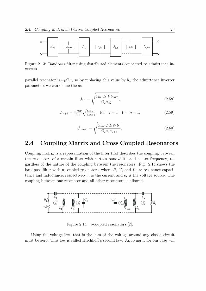
J0,1 =
√Y0FBWb1ω0
Ωcg0g1
, (2.58)
Ji,i+1 = FBWΩc
√bibi+1
gigi+1, for i = 1 to n− 1, (2.59)
Jn,n+1 =
√Yn+1FBWbn
Ωcgngn+1
. (2.60)
2.4 Coupling Matrix and Cross Coupled Resonators
Coupling matrix is a representation of the filter that describes the coupling between
the resonators of a certain filter with certain bandwidth and center frequency, re-
gardless of the nature of the coupling between the resonators. Fig. 2.14 shows the
bandpass filter with n-coupled resonators, where R, C, and L are resistance capaci-
tance and inductance, respectively. i is the current and es is the voltage source. The
coupling between one resonator and all other resonators is allowed.
Figure 2.14: n-coupled resonators [2].
Using the voltage law, that is the sum of the voltage around any closed circuit
must be zero. This low is called Kirchhoff’s second law. Applying it for our case will

2.4. Coupling Matrix and Cross Coupled Resonators 24
results with [2]
(R1 + jL1ω + 1jC1ω
)i1 − jL12i2.....− jL1nin = es
−jL21i1 + (jL2ω + 1jC2ω
)i2......− jL2nin = 0
.
.−jLn1in − jLn2in + ......(jLnω + 1
jCnω+ Rn)in = 0,
(2.61)
where Lij is the mutual coupling between the resonators. The resulting equations can
be written in matrix form as [2],
[z][i] = [e], (2.62)
where [z] is (N×N) impedance matrix, [i] is the current vector, and [e] is the voltage
vector. For this case, let us assume that all resonators have the same resonance
frequency, which means that the inductive and capacitive values of all resonators
have the same values, let it be L for the inductance and C for the capacitance. Now
the impedance matrix can be written as [2],
[z] = ω0LFBW [Z], (2.63)
where FBW is the fractional bandwidth and [Z] is the normalized impedance matrix,
which can be written as [2]
[Z] =
R1
ω0LFBW+ p −j ωL12
ω0L1
FBW... −j ωL1n
ω0L1
FBW
−j ωL21
ω0L1
FBWp ... −j ωL2n
ω0L1
FBW
. . . .
. . . .−j ωLn1
ω0L1
FBW−j ωLn2
ω0L1
FBW... Rn
ω0LFBW+ p
,
(2.64)
where,
p = j 1FBW
(ωω0− ω0
ω
), (2.65)
the external quality factor is defined as
Qei = ω0LRi
, (2.66)
where i = 1, ...., n, Defining the coupling coefficient as
Mij =Lij
L, (2.67)
and assuming ω/ω0 ≈ 1 for narrow band, we get
[Z] =
1qe1
+ p −jm12 ... −jm1n
−jm21 p ... −jm2n
. . . .
. . . .−jmn1 −jmn2 ... 1
qen+ p
,
(2.68)

2.4. Coupling Matrix and Cross Coupled Resonators 25
where qe1 and qen are the scaled external quality factors and defined as
qei = QeiFBW, (2.69)
and mij is the normalized coupling coefficient which is defined as
mij =Mij
FBW, (2.70)
S21 = b2a1|a2=0=
2√
R1Rnines
, (2.71)
S11 = b1a1|a2=0= 1− 2R1i1
es, (2.72)
where
i1 = es
ω0L.FBW¯[Z]−1
11 , (2.73)
in = es
ω0L.FBW¯[Z]−1
n1 , (2.74)
substituting (2.73) in (2.71) and (2.74) in (2.72) then
S21 =2√
qe1qen
¯[Z]−1
n1 (2.75)
and
S11 = 1− 2
qe1
¯[Z]−1
11 (2.76)
the coupling coefficients for coupling structure with resonators having different reso-
nant frequency are
Mij =Lij√LiLj
, i 6= j, (2.77)
which leads to
¯[Z] =
1qe1
+ p−m11 −jm12 ... −jm1n
−jm21 p−m22 ... −jm2n
. . . .
. . . .−jmn1 −jmn2 ... 1
qen+ p−mnn
(2.78)
The same can be applied for the case of capacitive coupling between the resonators,
but instead of using the impedance matrix [Z], the admittance matrix [Y] is used, we
will not go through the derivations, nevertheless, the transfer function and the return
loss can be written as
S21 =2√
qe1qen
¯[Y ]−1
n1 , (2.79)
and
S11 =2
qe1
¯[Y ]−1
11 − 1 (2.80)

2.5. Planar Transmission Lines 26
The most important point needed is that the formulation of the normalized impedance
matrix ¯[Z] to that of the normalized ¯[Y ]. So we can generalize coupling between the
resonators no matter what the coupling nature is, by
S21 =2√
qe1qen
[A]−1n1 , (2.81)
and
S11 = ±(2
qe1
[A]−111 − 1), (2.82)
where [A] is N ×N matrix and formed as
[A] = [q] + p[U ]− j[m], (2.83)
where [q] is (N ×N) matrix with all entries zeros except q11 = 1/qe1 and qnn = 1/qen,
[U ] is (N ×N) unit matrix, and [m] is (N ×N) coupling matrix
2.5 Planar Transmission Lines
A planar transmission line is a transmission line with multiple conducting metal
strips lying in parallel planes. These planes are mostly placed on dielectric material.
The most widely used transmission lines are microstrip line, coplanar waveguide, and
suspended stripline.
2.5.1 Microstrip Line
Microstrip line is a transmission line which consists of a conducting strip separated
from a ground plane by a dielectric layer. Fig.2.15 shows the cross section of the mi-
crostrip line. The main advantages of microstrip line are that it is suitable technique
for MICs, and the radiation that it provides can be used for antenna design. The
main disadvatage of this type of transmission lines is that via holes are necessary in
the case of shunt connections which is complex especially in the case of MMICs.
The characteristic impedance of the microstrip line is depending on the width of
the guided wave line, substrate thickness, and the effective dielectric constant of the
substrate εr. The effective dielectric constant is given in the following form [55–57]
w
h re
Figure 2.15: Microstrip line cross section.,

2.5. Planar Transmission Lines 27
εeff =εr + 1
2+
εr − 1
2√
1 + 10hw
, (2.84)
where εr and h are the permittivity and thickness of the substrate, respectively, and
w is the strip width, the characteristic impedance of the microstrip is given as
Zc =η
2π√
εeff
ln(Fw
h+
√1 + (
2w
h)2
), (2.85)
where η = 120πΩ, and
F = 6 + (2π + 6) exp(− (30.666w
h
)0.7528)
(2.86)
2.5.2 Coplanar Waveguide
Coplanar waveguide (CPW) is basically a single strip located between two ground
planes on the same side of the substrate, see Fig. 2.16. The main advantages for this
type of transmission lines is thae fact that it can be easily integrates with the MIC’s.
Furthermore shunt connections can be easily realized without the need of via holes.
in addition it is less sensitive to the substrate thickness than in the case of microstrip
[58]. However the losses in this transmission line are higher than that in the case
of microstrip lines. Both ground planes must be at the same potential, to avoid the
asymmetric, which may excites the slot mode. Therefore air bridges are used to keep
symmetrical potential at both ground planes.
Figure 2.16: Coplanar waveguide cross section.
The characteristic impedance of the coplanar waveguide with finite substrate
thickness is given by [58],
Zc =f(K)
4
õ0
ε0εeff
, (2.87)
where,
εeff ≈ 1 +εr − 1
2f(K1)f(K), (2.88)
K =w
w + 2s, (2.89)
K1 =
√1
1 + q, (2.90)

2.5. Planar Transmission Lines 28
q =
[sinh
(wπ4h
)]2
sinh(
sπ2h
)sinh
(π(w+s)2h
) , (2.91)
f(K) =
14ln
(2√K
), K ≤ 0.173
π
ln(2 1+
√K
1+√
K
) , K ≥ 0.173, (2.92)
where h is the substrate thickness, w is the width of the transmission line, and s is
the spacing between the transmission line and the ground planes.
2.5.3 Suspended Stripline
Suspended stripline (SSL) has been introduced as an alternative to coaxial line in
[59]. It is basically a substrate that is shielded inside a housing mount, as it is shown
in Fig. 2.17. Suspended stripline is also possible with multiple substrates [60–64].
The ground plane of this transmission line is the mount itself. Due to the existence
of the mount around the guided wave line, there is no radiation loss introduced by
this transmission line. SSL has another main advantage, which is due to the ability of
building the resonators on both sides of the substrate, it is the most suitable technique
for broadband circuits [24, 40, 65]. Due to the larger cross section with a considerable
amount of electromagnetic field in the air, the effective dielectric constant of the SSL
is rather low, and therefore the dielectric loss is very low in this transmission line.
w
h
re
Figure 2.17: Suspended stripline cross section.
Since most MICs are microstrip based, there might be a need to integrate the SSL
filters with microstrip components. That can be realized by having a grove under the
portion of the filter in the carrier block of the circuit and fixing a small cap over the
SSL filter to build the channel of the filter, see [66]. The characteristic impedance,
and the effective dielectric constant of the SSL are given as [67], [68],
• When 0 < w < a/2
Zc =η0
2π
[V + R ln
( 6
w/b+
√1 +
4
w/b
)], (2.93)

2.5. Planar Transmission Lines 29
εeff =1(
E − F ln wb
1√εr
)2 , (2.94)
where w is the width of the transmission line, a is the width of the mount, b is
the hight of the mount,
V = 1.7866 + 0.2035h
b+ 0.4750
a
b, (2.95)
R = 1.0835 + 0.1007h
b− 0.09457
a
b, (2.96)
E = 0.2077 + 1.2177h
b− 0.08364
a
b, (2.97)
F = 0.03451− 0.1031h
b+ 0.01742
a
b, (2.98)
• a2
< w < a
Zc = η0
(V +
Rwb
+ 1.393 + 0.6670 ln(
wb
+ 1.444)), (2.99)
εeff =1(
E − F ln wb
1√εr
)2 , (2.100)
where,
V = −0.6301− 0.07083h
b+ 0.247
a
b, (2.101)
R = 1.9492 + 0.1553h
b− 0.5123
a
b, (2.102)
E = 0.464 + 0.9647h
b− 0.2063
a
b, (2.103)
F = −0.1424 + 0.3017h
b− 0.02411
a
b(2.104)
2.5.4 Multilayer Transmission Lines
Multilayer transmission lines are mainly introduced for MMIC’s. It is basically a
combination of CPW and microstrip line, this structure is built on a thin film placed
on a thick substrate, fabrication, however, is very expensive since Si, Ge, or GaAs
is used. The main advantage of this techniques is that it can be easily integrated
with CPW and microstrip components. It also provide high coupling between the
resonators, which makes it useful for broadband components [40], [69–72].


Chapter 3
Multilayer Structures and FilterApplications
Multilayer structures represent a potential technology for MMIC and MIC circuits
[69–72] and [73]. These structures were introduced as a good candidate for filter appli-
cations in [70]. They offer a wider range for nearly constant characteristic impedance
and provide more effective capacitive coupling between the resonators by locating
them on the two sides of the substrate [70], [72].
Multilayer structures are normally used for coplanar waveguide (CPW), Microstrip
line (ML), and suspended stripline (SSL) techniques. They give the designer extra
degree of freedom in designing the microwave and millimeter wave components. The
multilayer structures for CPW are normally built on a thin film structure, where
the metallization strips and ground planes are etched [72]. In case of high frequency
components, the material that is used for the thin film is silicon dioxide SiO2 [74],
[75]. The thin film is then built over high resistivity silicon substrate. This process
is ,however, a complicated process rather expensive.
This chapter investigates the cross section of multilayer structure and introduces
different filters using this technology. Compact lowpass and bandpass filters are
designed using this technology showing the ability of these filters to be integrated
with ML, CPW, or both. The filter are designed using quasi-lumped elements. In the
last section an ultra-wideband suspended stripline filter is presented. The filter has
very wide stopband which is much wider than that for the other available structures,
in addition the filter has low group delay variation with the passband.
3.1 Multilayer Coplanar Line Cross Section
The multilayer coplanar line (MCL) of a modified cross section is investigated in this
section. Fig. 3.1 shows the cross section of the proposed MCL. Only one substrate is
used and the filter is built on both sides of it. Fig. 3.1a shows the MCL cross section
which is used in the case of broadside coupling, by this configuration high capacitive
31

3.1. Multilayer Coplanar Line Cross Section 32
coupling can be achieved, since it allows the overlapping between the metallization on
both sides of the substrate. This structure can be easily integrated with both CPW-
and microstrip-based circuits, depending on which side of the substrate these circuits
are built. This is not the case with the standard microstrip and CPW lines, as these
technologies need transition networks to be integrated together. Fig. 3.1b shows the
cross section of the MCL, which is designed to be integrated with the standard CPW.
Fig. 3.1c shows the cross section of the line that is compatible with the microstrip
line.
s sw
(a)
(b)
(c)s
w
a a
Figure 3.1: (a) Cross section of MCL , (b) the MCL compatible with CPW , (c) theMCL compatible with microstrip line .
A comparison is made on the capacitive coupling between 50 Ω microstrip line,
CPW, and MCL broadside coupling. The 50 Ω lines were built on a AR600 substrate
0.787 mm in thickness with relative permittivity εr of 6, as shown in Fig. 3.2. The
study is done on frequency band of 6 GHz. The capacitive values of these structures
are calculated in two steps. First, the reflection coefficient of the coupling structure
S11 were computed at certain frequencies. In the second step, the coupling structure
is considered equivalent to a series capacitance, whose reactance Xi can be calculated
from
S11 =jXi − Z0
jXi + Z0
, (3.1)
where zi is the input impedance - here the load is series capacitance- and Z0 is the
source impedance which is 50 Ω in our case. Having calculated the load impedance,
the capacitive value of the coupling structure can be easily calculated from
C =−1
Xiω, (3.2)

3.1. Multilayer Coplanar Line Cross Section 33
where w is the angular frequency.
Fig. 3.3 shows a comparison between the capacitive values of ML-ML, CPW-CPW
and broadside coupling structure as a function of the distance. As it can be clearly
seen, the broadside coupling structure provides higher capacitive coupling between
the two 50 Ω lines since it allows the overlapping between the metallization on both
sides of the substrate. These coupling structure can be used for broadband circuits
and filters.
d dBacksideTopsid
e
d
(a) (b) (c)
Figure 3.2: coupling two 50 Ω lines structure (a) microstrip-microstrip, (b) CPW-CPW, and (c) CPW-slotted microstrip line.
−1 −0.5 0 0.5 10
0.05
0.1
0.15
0.2
0.25
d (mm)
C (
pF)
ML−MLCPW−CPWCPW−SML
Figure 3.3: Calculated capacitive coupling values between the two ends of 50 Ωstrips of particular lines: CPW- CPW, microstrip-microstrip (ML-ML), and broadsidecoupling CPW-slotted microstrip line.
In addition to the high capacitive coupling that the MCL offers, it also provides
wide characteristic impedance range at the same frequency band. To show that, a
simple analysis is done by using the same substrate. The study has been done on

3.2. Quasi-Lumped Elements 34
the slotted microstrip line (see Fig. 3.1c). Fig. 3.4 shows the relation between the
characteristic impedance Z0 of the transmission line and the width of the transmission
line w for different slot widths s. As it is shown in the same Figure the impedance
Z0 can reach 135 Ω with transmission line width equals 0.5 mm and slot width of 4
mm, and 16.2 Ω with transmission line width of 6 mm and slot width of 1 mm.
Another study has been done on the impedance of the transmission line by chang-
ing the width of the ground planes a, and fixing both the width of the transmission
line w and the slot width s at 2.7 mm and 2.8 mm, respectively, (see Fig. 3.1c). Fig.
3.5 shows the relation between the impedance of the transmission line and the width
of the ground planes. From the figure, one can see that the width of the ground plane
has almost no effect on the characteristic impedance unless it is less than 2 mm. The
characteristic impedance of the transmission line starts increasing by decreasing the
width of the ground planes.
0 1 2 3 4 5 6 70
20
40
60
80
100
120
140
w (mm)
Zo
(Ohm
)
s=1mms=2mms=2.7mms=4mm
Figure 3.4: Characteristic impedance of slotted microstrip line as function of w fordifferent slot width s.
3.2 Quasi-Lumped Elements
The quasi-lumped elements are used in the microwave filters due to the advantages
they offer. Due to the short transmission line length that is used for quasi-lumped
elements, which must be much shorter than quarter-wavelength, the filters designed
using these elements have compact size, low losses, and wide stopband [24],[26], [27],
and [76–78].

3.2. Quasi-Lumped Elements 35
0 1 2 3 4 5 6 735
40
45
50
55
60
65
a (mm)
Z0 (
Ohm
)
Figure 3.5: Characteristic impedance of slotted microstrip line as function of thewidth of the ground plane a.
Since microwave filters require both series and shunt inductances and capacitances
and their combination to form either series or parallel resonators, it is necessary to
understand how to realize each element for the available transmission lines.
Wide microstrip line and wide CPW line sections with low characteristic impedance
already form shunt capacitances. Fig. 3.6 shows layouts of shunt CPW microstrip
line capacitances. In the case of suspended stripline, shunt capacitance is realized by
having additional metallization at the backside of the substrate which is connected
to the walls of the housing mount from both sides, in addition to the wide transmis-
sion line that lies on the topside of the substrate. Fig. 3.7 shows 3D view for shunt
suspended stripline capacitance.
Shunt inductor is realized by connecting a narrow stripline with circuit from one
side and to the ground from the other side. In the case of CPW, the ground planes are
located near the guided wave line, so realizing shunt inductance can be easily done.
It is the same in the case of suspended stripline, the narrow stripline can be shunted
by connecting it to the side wall of the housing mount. For microstrip and since the
ground plane and guided waveline are built on the opposite sides of the substrate,
the narrow stipline is shunted by using via hole, this process is more complicated
than in the case of CPW and suspended stripline. Fig. 3.8a, and Fig. 3.8b show the
CPW and microstrip shunt inductance, respectively, while Fig. 3.9 shows 3D view of
suspended stripline shunt inductance.
A narrow transmission line that is connected from both sides to the input and
output represents series inductance, this applies to CPW, microstrip, and suspended

3.2. Quasi-Lumped Elements 36
50 Ohm line 50 Ohm line50 Ohm line 50 Ohm line
Shunt
capacitanceShunt
capacitance
(a) (b)
Figure 3.6: Layouts of shunt capacitance for (a) CPW , (b) microstrip.
Figure 3.7: 3D view of suspended stripline shunt capacitance.
Via Hole
50 Ohm line50 Ohm line 50 Ohm line 50 Ohm line
Shunt inductive
lineShunt inductive
line
Figure 3.8: Layouts of shunt inductance for (a) CPW , (b) microstrip.

3.2. Quasi-Lumped Elements 37
Figure 3.9: 3D view of suspended stripline shunt inductance.
stripline. The inductive value of this line is depending on the characteristic impedance
of the transmission line, the length of the transmission line, and the effective dielectric
constant.
Series capacitance is realized by different coupling structures, the first structure
is end to end coupling structure [2]. However, the capacitive value that this structure
provides is very low for all transmission line techniques, (see Fig. 3.3, and [24]).
Another coupling structure that is used mainly for CPW, and microstrip line is the
interdigital coupling structure as shown in Fig. 3.10, [79], [80]. This structure consists
Figure 3.10: Layout of microstrip interdigital capacitance.
of metallic fingers intersect with each other. This structure provides tight capacitive
value, however, the losses of this structure are much higher than the first structure
due to the narrow strips used in realizing this structure. For suspended stripline
and for multilayer coplanar line, where it is allowed to build the resonators on both
sides of the substrate, broadside coupling structures are used. These structures allow
overlapping between the resonators, which increases the capacitive coupling between

3.3. Lowpass Filters 38
the resonators without increasing the losses on the structure.
3.3 Lowpass Filters
Microstrip lowpass filter using multilayer technique has been introduced earlier [73].
The filter was realized by opening apertures under the narrow transmission lines to
increase the inductive values of these transmission line sections. This section deals
with CPW lowpass filter built on the same technique, Fig. 3.1. The filter shows
a great advantage in minimizing the size of the filter, particularly the size of the
capacitive line sections. The filter is realized by implementing patches under the
capacitive transmission line sections of the classical CPW lowpass filter structure.
Since the wide patches increase the capacitive value of the capacitive transmission
line sections, shorter capacitive transmission line sections are used. To design a CPW
lowpass filter we have to go through two steps:
First, designing a lumped chebyshev lowpass filter, that requires knowing the
order, the cut-off frequency, and passband ripple of the filter as described in sec. 2.2.
Having the order, the cut-off frequency, and passband ripple, the lumped elements
of the chebyshev can be simply calculated. As an example, a fifth order chebyshev
filter with cut-off frequency of 4 GHz, and passband ripple of 0.1 dB. The normalized
elements for this filter are g0 = g6 = 1, g1 = g5 = 1.1468, g2 = g4 = 1.3712, and
g = 1.975. Where g0, and g6 represent the source and load impedances, respectively,
that is considered for our filter to be Z0 = 50Ω. Substituting these values in (2.25),
and (2.26), the actual filter element values can be calculated, which is for our filter
C1 = C5 = 0.92 pF, L2 = C4 = 2.73 nH, and C3 = 1.57 pF.
The second step is to realize the desired capacitive and inductive values of the filter
elements by the stubs of the high/low-impedance transmission line, the characteristic
impedance Z0 and the effective dielectric constant εeff of the used transmission lines
have to be determined. To determine this, a commercial MoM simulator [81] is used.
By assuming the transmission line lengths of the filter elements are much shorter than
the wavelength, the transmission line length can be calculated from
Ck =lk
Z0kvph,k
, (3.3)
Lj =ljZ0j
vph,j
, (3.4)
where the indices k and j correspond to elements with capacitive and inductive
character, respectively. Ck and Lj are the capacitance and inductance of the equiva-
lent circuit of the filter, respectively. The phase velocity vph is calculated by
vph,j =c√εeff
, (3.5)

3.3. Lowpass Filters 39
where c is the speed of light in the free space.
Having determined all transmission line lengths, these transmission line sections
can be combined to build the desired lowpass filter, however, some optimization is
needed to take into account the involved discontinuities and to achieve good matching
in the passband. The dimensions of the lowpass filter portion are given as part of the
overall filter in Fig. 3.11.
3.9 3.96.9
2 2
9
3.9 3.96.9
Figure 3.11: Top (up) and backside (down) layouts of a CPW lowpass filter, alldimensions are in mm .
A comparison between two filters with the same dimensions is made. The first one
is built on one side of the substrate, and the second one having wide patches at the
backside of the substrate, as it is shown Fig. 3.12 the cut-off frequency of the CPW
lowpass filter using MCL (with patches at the backside of the substrate) is much lower
than that for the CPW classical lowpass filter. That means that adding patches under
the capacitive transmission line sections decreases the size of the lowpass filter.
Fig. 3.13 shows the measured and insertion loss of the lowpass filter, the filter has
insertion loss at the passband is better than 0.7 dB, and group delay variation within
the passband is about 0.11 ns.
As it is shown in Fig. 3.13, the filter has flat cut-off and the rejection at the
stopband is about 23.4 dB, which is not sufficient for some applications. Therefore,
transmission zeros are needed to increase the rejection at the stopband and to enhance
the cut-off sharpness. In order to introduce transmission zeros, the side patches were
loaded by two half-wavelength stubs. These stubs are coupled capacitively to the
topside of the substrate. Since each of the additional stubs introduces a transmission
zero to the filter response at the corresponding frequency, two transmission zeros were
introduced by this configuration. Fig. 3.14 shows the top and backside layouts of
the CPW lowpass filter with the additional stubs. Fig. 3.15 shows the measured and

3.3. Lowpass Filters 40
0 2 4 6 8 10−30
−25
−20
−15
−10
−5
0
Frequency (GHz)
|S21
| (dB
)
one layerwith patchs
Figure 3.12: Insertion loss of CPW lowpass filter built on one layer of the substrateand Insertion loss of CPW lowpass filter with wide patches under the capacitivetransmission line.
2 4 6 8 10−50
−40
−30
−20
−10
0
Frequency (GHz)
|S11
|, |S
21| (
dB)
|S11
|
|S21
|
Figure 3.13: Measured (solid) and simulated (dashed) insertion and return loss of aCPW lowpass filter with patches.
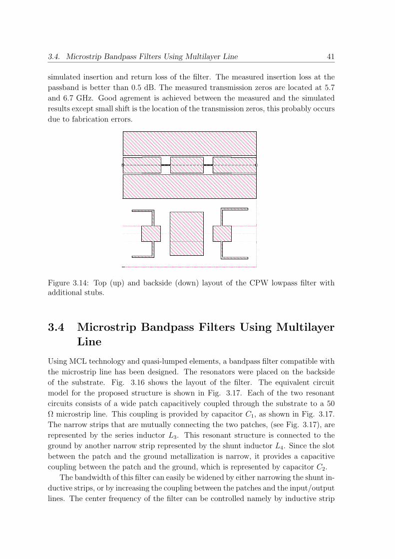
3.4. Microstrip Bandpass Filters Using Multilayer Line 41
simulated insertion and return loss of the filter. The measured insertion loss at the
passband is better than 0.5 dB. The measured transmission zeros are located at 5.7
and 6.7 GHz. Good agrement is achieved between the measured and the simulated
results except small shift is the location of the transmission zeros, this probably occurs
due to fabrication errors.
Figure 3.14: Top (up) and backside (down) layout of the CPW lowpass filter withadditional stubs.
3.4 Microstrip Bandpass Filters Using Multilayer
Line
Using MCL technology and quasi-lumped elements, a bandpass filter compatible with
the microstrip line has been designed. The resonators were placed on the backside
of the substrate. Fig. 3.16 shows the layout of the filter. The equivalent circuit
model for the proposed structure is shown in Fig. 3.17. Each of the two resonant
circuits consists of a wide patch capacitively coupled through the substrate to a 50
Ω microstrip line. This coupling is provided by capacitor C1, as shown in Fig. 3.17.
The narrow strips that are mutually connecting the two patches, (see Fig. 3.17), are
represented by the series inductor L3. This resonant structure is connected to the
ground by another narrow strip represented by the shunt inductor L4. Since the slot
between the patch and the ground metallization is narrow, it provides a capacitive
coupling between the patch and the ground, which is represented by capacitor C2.
The bandwidth of this filter can easily be widened by either narrowing the shunt in-
ductive strips, or by increasing the coupling between the patches and the input/output
lines. The center frequency of the filter can be controlled namely by inductive strip

3.4. Microstrip Bandpass Filters Using Multilayer Line 42
0 2 4 6 8 10−60
−50
−40
−30
−20
−10
0
Frequency (GHz)
|S11
|, |S
21| (
dB)
|S11
| |S21
|
Figure 3.15: Measured (solid) and simulated (dashed) insertion and return loss of aCPW lowpass filter with two transmission zeros.
length l, see Fig.3.16. This is documented by the results of a parametric study in
Fig.3.18, where the return loss of the filter for different l is plotted. Increasing l shifts
the center frequency of the filter to a lower frequency band, consequently, the band-
width of the filter is reduced. The structure has been simulated and optimized by the
commercial MoM simulator [81], and the circuit simulation has been performed on
the equivalent circuit using Microwave Office [82]. Using the circuit topology shown
in Fig.3.17 and the scattering parameters calculated by the EM simulator for the filter
with dimensions shown in Fig.3.16 , the circuit parameters were tuned till a sufficient
match between the circuit and the EM analyses was achieved. The resulting circuit
parameters are C1 = 0.119 pF, C2 = 0.105 pF, L1 = 2.72 nH, and L2 = 0.407 nH.
Fig.3.19 shows the EM and circuit simulations of the filter with dimension shown in
Fig.3.16. Fig.3.20 shows the simulated and measured insertion and return loss of the
filter. The filter has insertion loss at the passband better than 0.9 dB. Very good
agreement has been achieved between the EM, circuit simulations and measurement.
A transmission zero was introduced to the filter response by inserting a strong ca-
pacitive coupling between the patches. Fig. 3.21 shows the layout of the filter with
the transmission zero, while Fig. 3.22 shows the equivalent circuit model of this filter.
The capacitive coupling between the patches is due to an additional patch located
between the 50 Ω lines on the topside. The slot in this patch is etched to keep the
inductances of the strips on the backside at their original value. The patches on
the backside were simultaneously widened as it can be observed from a comparison
of Fig. 3.16 with Fig. 3.21. This coupling is represented in the equivalent circuit
by capacitor C3, Fig. 3.22. The structure was simulated, optimized and measured.

3.4. Microstrip Bandpass Filters Using Multilayer Line 43
6.25
2.6
7.1
3
2.052.7
l
Figure 3.16: Topside (up), and backside (down) layout of an MCL bandpass filtercompatible with the microstrip line.
L3 L3C1 C1
C2 C2L4
Figure 3.17: Equivalent circuit model of the bandpass filter.

3.4. Microstrip Bandpass Filters Using Multilayer Line 44
3 4 5 6 7 8 9-60
-50
-40
-30
-20
-10
0
data1
data2
data3
data4
data5
data6
data7
data8
l=4.7
l=3.6
l=2.8
l=2.1
l=1.8
l=1.5
l=1.2
l=0.6
Frequency (GHz)
|S| (
dB
)11
Figure 3.18: Simulated return loss of the filter with inductive strip length l vary from4.7 to 0.6 mm.
2 4 6 8 10−60
−50
−40
−30
−20
−10
0
Frequency (GHz)
|S11
|, |S
21| (
dB)
|S21
|
|S11
|
Figure 3.19: EM (solid) and Circuit (dashed) simulation of the insertion and returnloss of the filter and its equivalent circuit.

3.5. CPW Bandpass Filters Using Multilayer Line 45
2 4 6 8 10−50
−40
−30
−20
−10
0
Frequency (GHz)
|S11
|, |S
21| (
dB)
|S21
|
|S21
|
Figure 3.20: Simulated and measured insertion and return loss of the ML bandpassfilter.
The insertion and return losses for the filter are demonstrated in Fig. 3.23. The
transmission zero is introduced at about 7 GHz. The frequency shift between the
simulated and measured data is caused by the discrepancies between the dimensions
of the designed and fabricated filter layouts.
3.5 CPW Bandpass Filters Using Multilayer Line
In the previous section we have introduced microstrip bandpass filter using the MCL
technology. In this section we will introduce the same filter for CPW. To get such
a filter, the ground metallization was etched on the topside instead of the backside.
By this configuration the filter is now fed by the 50 Ω CPW. The structure of the
resonators was taken from the filter shown in Fig. 3.16. The shunt inductor is
now connected to the ground via additional patches, which are capacitively coupled
through the substrate with the ground planes, as shown in Fig. 3.24. These patches
are represented in the equivalent circuit of Fig. 3.25 by capacitor C4. Since a shunted
series resonator is used instead of the parallel inductance, the transmission zero is
generated.
The filter was optimized, fabricated and measured. The area occupied by this
filter is nearly the same as the area occupied by the filter shown in Fig.3.16. Fig.3.26
shows the simulated and measured insertion and return loss of the filter. The insertion
loss at the passband is better than 0.9 dB and the upper stopband rejection better
than 26 dB that reachs to higher than 14 GHz. Good agreement has been achieved

3.5. CPW Bandpass Filters Using Multilayer Line 46
Figure 3.21: Topside (up), and backside (down) layout of an MCL bandpass filterwith additional capacitive coupling between the resonators.
L3 L3C1 C1
C2 C2L4
C3
Figure 3.22: Equivalent circuit model of the bandpass filter with additional capacitivecoupling between the resonators.

3.5. CPW Bandpass Filters Using Multilayer Line 47
2 4 6 8 10−50
−40
−30
−20
−10
0
Frequency (GHz)
|S11
|, |S
21| (
dB)
|S21
|
|S11
|
Figure 3.23: Measured (solid) and simulated (dashed) insertion and return loss ofthe microstrip filter with additional transmission zero.
22
1.05 1.75
7
4.95
2
Figure 3.24: Top (up) and backside layouts (down) of an MCL bandpass filter withCPW feed lines,(all dimensions are in mm).

3.6. Bandpass Filter with Microstrip-CPW Feed Lines 48
C1
C2C2
L3 L3C1
L4
C4
Figure 3.25: The equivalent circuit of the of CPW bandpass filter.
between the simulated and measured results.
2 4 6 8 10 12 14−50
−40
−30
−20
−10
0
Frequency (GHz)
|S11
|,|S
21|(
dB) |S
21|
|S11
|
Figure 3.26: Measured (solid) and simulated (dashed) insertion and return loss of theCPW bandpass filter with transmission zero.
3.6 Bandpass Filter with Microstrip-CPW Feed
Lines
The bandpass filter introduced in sec.3.4 and shown in Fig.3.16 has been reconstructed
again to achieve a bandpass filter compatible with both CPW and microstrip feed
lines. The original filter consists of two wide patches coupled to the input/output 50
Ω slotted microstrip feed lines. The patches are interconnected by narrow inductive
strip, which is grounded at its center by shunt inductive strips. This filter recon-
structed to obtain the microstrip-CPW feeding lines. So the ground planes under
the original 50 Ω slotted microstrip feeding line were closed, so the slotted microstrip
line was thus replaced by a 50 Ω microstrip line coupled via a patch. The slotted
microstrip line from the other side of the filter was replaced by 50 Ω CPW line, and

3.6. Bandpass Filter with Microstrip-CPW Feed Lines 49
a small patch was added on the topside of the substrate to increase the capacitive
coupling between the CPW line and the filter itself. The layout of the modified filter
is shown in Fig. 3.27, while the simulated insertion and return loss of the filter over
wide frequency range are shown in Fig. 3.28. the filter has center frequency of 3.55
GHz.
Figure 3.27: Top (up) and backside (down) layouts of a bandpass filter withmicrostrip-CPW feeding lines.
The filter is designed as a microstrip-CPW transition in addition to its filtering
function. As an application to such structure, the filter can be attached to a microstrip
antenna that radiates at 3.55 GHz from the microstrip feeding line side. A simple
antenna was chosen for this work which is a rectangular patch antenna. The antenna
width is chosen to be 15 mm, the length of the antenna can be calculated from [83],
and [84]
L = Leff − 2∆L (3.6)
where Leff is the effective patch length and formed as
Leff =c
2f0√
εeff
(3.7)
where c is the speed of light in the free space and εeff is the effective dielectric
constant that can be calculated from (2.84). ∆L is the fringing patch length which
formed as [85]
∆L = 0.412h
((εeff + 0.3)(W
h+ 0.264)
(εeff − 0.258)(Wh
+ 0.8)
)(3.8)

3.7. Suspended Stripline Ultra-Wideband Bandpass Filter 50
0 2 4 6 8 10 12−90
−80
−70
−60
−50
−40
−30
−20
−10
0
Frequency (GHz)
|S11
|, |S
21| (
dB)
|S11
|
|S21
|
Figure 3.28: Simulated insertion and return loss of the Microstrip- CPW filter.
where h is the thikness of the substrate and W is the width of the antenna.
The antenna was connected to a microstrip feed line. The feeding line was ex-
tended inside the patch to archive the best matching. Finally, the antenna was
attached to the filter, however, some optimization took place to take in account the
involved discontinuity and to achieve best matching. The layout of the filter attached
to the antenna is shown in Fig. 3.29. The simulated return loss of the antenna, an-
tenna connected to the bandpass filter, and the measured return loss of the antenna
with the filter together are shown in Fig. 3.30. As it is shown in the figure, the
antenna has resonances at about 6.7, 7.9, and 10.1 GHz, which has been blocked by
the filter, in addition to that, the antenna can be now integrated with CPW system.
Good agreement has been achieved between the simulated and measured results ex-
cept a small frequency shift has occurred in measured return loss, this is normally
happens in the fabrication of narrow band filters and circuits especially when they
have small geometry.
3.7 Suspended Stripline Ultra-Wideband Bandpass
Filter
Suspended stripline (SSL) is considered as a multilayer structure [59], [69], [86], since
it is consisting of a substrate shielded by waveguide housing. over and below the
substrate there are two layers of air. The air layers are normally having the same
dimensions. Fig. 3.31 shows the cross-section of the suspended stripline with the
dimensions used in this section. Multi-substrates have also been proposed for such

3.7. Suspended Stripline Ultra-Wideband Bandpass Filter 51
17.4
15
1.1
8.4
Figure 3.29: Top layer CPW-microstrip filter connected to patch antenna.
2 4 6 8 10 12−35
−30
−25
−20
−15
−10
−5
0
5
Frequency (GHz)
|S11
| (dB
)
MwS antennaMeas. filter+ant.MwS filter+ant.
Figure 3.30: Return loss of the patch antenna itself and the patch antenna with thefilter.

3.7. Suspended Stripline Ultra-Wideband Bandpass Filter 52
structures in [87], and [88]. Due to the existence of the mount, the electromagnetic
field in SSL is concentrated in the air, therefore, the effective dielectric constant is
low compared to the other planar techniques, furthermore, due to same reason no
radiation loss, and the dielectric loss is very low in the SSL structure. On the other
(a) (b)
2 mm
2 mm
0.254 mm
er =2.22
5 mm
2 mm
2 mm
0.254 mm
er =2.22
5 mm
6 mm
Figure 3.31: Cross-section of SSL (a) used in simulation process, (b) realized inpractice.
hand the Federal Communications Commission (FCC) has released the unlicensed
use of ultra-wideband (UWB: 3.1 to 10.6 GHz) wireless systems in February 2002
[42]. Since then, the ultra-wideband wireless communication systems with such fre-
quency band have gained an increased interest, since they transmit higher data rates
with lower transmitted power. Various filter structures have been proposed in the
literature, e.g. [15], [43], and [89–92]. The combination of a lowpass filter with a
high-pass filter is a classical structure for such kind of filters [89], [90]. It occupies,
however, a large area, which may increase the losses, and the group delay variation of
the filter. In [91], an UWB filter was built by cascading various ring filters, while, in
[15], and [43], UWB filters were designed using multi-mode resonators. However, due
to the long transmission line sections used in these structures, higher order resonances
do not allow a wide stop band. An UWB filter introduced in [92] was designed by
employing quasi-lumped microstrip resonators built on both sides of the substrate.
The fabrication of this filter, however, is difficult due to the via holes necessary to
increase the stopband up to 16 GHz.
In this section, a simple ultra-wideband bandpass filter is presented, showing a
great simplicity of the design concept compared to earlier known structures. The filter
is realized by coupling an SSL quasi-lumped lowpass filter capacitively to the I/O
ports. A very wide stopband is obtained due to the short transmission line sections
used in the filter structure. The filter is built on an RT Duroid substrate with a
thickness of 0.254 mm and a relative dielectric constant εr of 2.22. The substrate is
shielded in a split-block mount with dimensions of 5 mm width and 2 mm height over
and below the substrate. The substrate is suspended in the mount by extending it 0.5
mm inside the mount from both edges (Fig.3.31). The additional substrate portion
within the clamping region is fully metallized to provide good connection between the
mount and the substrate. This is particularly important in case of shunt connections.

3.7. Suspended Stripline Ultra-Wideband Bandpass Filter 53
Due to the small dimensions of the housing mount, the waveguide cut-off frequency
is slightly above 20 GHz.
To design the ultra-wideband bandpass filter with a frequency range from 3.1 to
10.6 GHz using a lowpass filter, two steps are necessary:
We firstly design a lowpass filter with a cut-off frequency of 10.6 GHz. In general,
the cut-off frequency of the lowpass filter can be adjusted by setting proper values
of the lumped elements of the filter. The capacitive and inductive elements of the
filter are realized by short sections of high/low-impedance transmission lines. The
low impedance sections are implemented by adding a ground metallization at the
backside of the substrate [64], as it is descried in sec. 3.3.
Having determined all transmission line lengths the lowpass filter can be com-
bined, however, some optimization can be done to take into account the involved
discontinuities and to achieve good matching in the passband. Fig. 3.32 shows the
top and backside layouts of the SSL lowpass filter. Fig. 3.33 shows the simulated
insertion and return loss of the filter. The filter has a cut-off frequency of 10.6 GHz,
with very good matching at the passband. At about 16.5 GHz a transmission zero
occurred due to the short inductive transmission line sections that allow capacitive
coupling between the wide patches, and in parallel to inductances.
Figure 3.32: Top (up), and backside (down) layouts of an SSL lowpass filter.
Next, we must suppress transmission in the frequency band below 3.1 GHz. The
SSL technology provides strong broadside coupling between transmission lines on the
opposite sides of the substrate [40], [24]. By overlapping a section of the original
input and output lines of the lowpass filter with new input and output lines on the
other side of the substrate, capacitive highpass sections [64] are formed to shape the
lower filter edge. Fig. 3.34 shows the top and backside layouts of the filter, while Fig.
3.35 shows the equivalent circuit of the structure.
The proposed filter was optimized, fabricated, clamped into the mount, and sol-
dered to coaxial connectors fixed at the ends of the mount, see Fig. 3.36. Measure-
ments were done using a coaxial calibration, the transitions from SSL to coaxial line

3.7. Suspended Stripline Ultra-Wideband Bandpass Filter 54
0 5 10 15 20 25−90
−80
−70
−60
−50
−40
−30
−20
−10
0
Frequency (GHz)
|S11
|, |S
21| (
dB)
|S21
|
|S11
|
Figure 3.33: Simulated insertion and return loss of a SSL lowpass filter.
3.73.8
1 1.3
0.7 0.8
Figure 3.34: Top (up) and backside (down) layouts of the SSL UWB filter using acoupled lowpass filter.
Low-Pass Structure
Wide Patches
Figure 3.35: Equivalent circuit of the ultra-wideband bandpass filter using a coupledlowpass filter structure.

3.7. Suspended Stripline Ultra-Wideband Bandpass Filter 55
as well as some portion of SSL transmission line are included into the experimental
results. Fig. 3.37 shows the simulated and measured return and insertion loss of the
filter. As expected, the filter has a very wide stopband with a good rejection of better
than 40 dB up to 25 GHz. The insertion loss of the filter in the passband is better
than 0.5 dB as shown in Fig. 3.38. The group delay variation in the passband is
smaller than 0.19 ns.
Figure 3.36: Photograph of the ultra-wideband bandpass filter with opened mount.
0 5 10 15 20 25 30−80
−70
−60
−50
−40
−30
−20
−10
0
Frequency (GHz)
|S11
|, |S
21| (
dB)
|S11
|
|S21
|
Figure 3.37: Simulated (dashed) and measured (solid) insertion and return loss ofthe UWB filter.

3.7. Suspended Stripline Ultra-Wideband Bandpass Filter 56
2 4 6 8 10 12−1
−0.8
−0.6
−0.4
−0.2
0
Frequency (GHz)
|S21
| (dB
)
Measurement Simulation
Figure 3.38: Simulated and measured insertion loss at the passband of the UWBfilter.

Chapter 4
Defected Ground Structures
Defected ground structures have been introduced first in [16], they are known in the
literature as DGS. This technique is realized by etching slots in ground plane of the
microwave circuit and is namely applied for the microwave filters. This technique
is used for microstrip and coplanar waveguide transmission lines. These slots are
designed to achieve better performance for the microwave filters, such as increasing
steepness of the cut-off slop, and to increase the stopband range of the microwave
filters, moreover, compact filter can also be achieved using this technique. Many
slot shapes have been introduced for microstrip technology [16–23]. Increasing the
stopband of microstrip lowpass filter by introducing transmission zeroes have been
obtained by different slot shapes, e.g. [16],[17], [22], and [34–37]. Periodic structures,
e.g.[18], [21] and [93]. Even bandpass filters have been presented using this technique,
e.g. [19], [20],[22], and [94]. Fig 4.1 shows the backside of the substrate of three
different slots that have been introduced in [16–18].
A simple study is done on the square head dumbbell slot with dimensions a= 4
mm, S=0.25 mm and d=5 mm etched under 50 Ω line to show how this structure
behave over wide frequency band [16]. The insertion and return loss of the structure
are shown in Fig.4.2. It can be clearly seen that at 6.5 GHz a transmission zero
occurred. Basically, the reason behind this behavior is the increase of the inductance
of the transmission line and it introduces series capacitance which is in parallel to the
original inductance. Thus, the equivalent circuit of a 50 Ω line over a DGS slot can be
represented as a parallel resonator [18], see Fig. 4.3. The current density distribution
at the slot metallization is shown in Fig. 4.4. At frequencies lower than the resonant
frequency of the slot, the current density is concentrated around the slot metallization
as shown in Fig. 4.4a. At frequencies higher than the resonant frequency of the slot
(Fig.4.4b) one can see that the current density is concentrated at the slot center. Fig.
4.5 shows a representation of the wave propagating at frequencies lower and higher
than the resonant frequency.
To control the resonant frequency of the DGS slot, it is required to change the
dimensions of the area occupied by the slot [16–23],[34–37]. For example, to set the
57

58
a
a
d
s
d
r
sL
w
s
(a) (b) (c)
Figure 4.1: Layouts of defected ground slots, (a) dumb bell structure with squarehead, (b) dumb bell structure with circular head, (c) U shape DGS structure.
2 4 6 8 10 12−40
−35
−30
−25
−20
−15
−10
−5
0
Frequency (GHz)
|S11
|, |S
21|
(dB
)
|S11
|
|S21
|
Figure 4.2: Simulated insertion and return loss of a dumb-bell slot etched under50-ohm transmission line.
C
Lp
Figure 4.3: quivalent circuit of a DGS slot etched under 50 Ω transmission line.

59
(a) (b)
Figure 4.4: Current density distribution on the slot metallization (a) at 2.5 GHz, (b)at 9 GHz.
(a) (b)
Figure 4.5: Representation for the wave propagating on the slot metallization (a)at frequency lower than the resonant frequency, (b) at frequency higher than theresonant frequency.

4.1. Interdigital DGS Slot 60
resonant frequency of the square head dumbbell slot at low frequency it is required to
increase either the dimensions of square head (a), the length of the slot (d), or both
in most of the cases. Another parameter that can be set, is the spacing between the
both ends of the slots [19], see Fig. 4.1.
This chapter demonstrates a compact slot in form of interdigital microstrip capac-
itance. The resonant frequency of the line that is under-etched with this slot can be
controlled by adjusting the distance between the fingers of the slot without enlarging
the size of the slot. Using this slot two quasi-elliptic lowpass filters are designed. All
of these filters have been design and fabricated on a RO4003c substrate that has a
thickness of 0.831 and relative dielectric constant of 3.38. In addition, this chapter
demonstrates a solution for the packaging problem that may occur due to the defected
ground structure.
4.1 Interdigital DGS Slot
In this section, an interdigital DGS slot is proposed. The slot is shown in Fig. 4.6.
It is etched in the ground metallization under the microstrip line. This slot has a
major advantage in providing higher capacitive coupling to the line in comparison to
known microstrip DGS structures. Moreover, the resonant frequency of the structure
can be controlled by changing the distance between the metal fingers. The resonant
frequency of the slot can also be modified by changing the number of metal fingers,
so there is, in most cases, no need to enlarge the overall slot size.
The equivalent circuit of the proposed structure assuming lossless metal, illus-
trated in Fig. 4.7, is a combination of the interdigital capacitance equivalent circuit
[1] and the equivalent circuit of the DGS [16]. The series C Ls circuit represents
an equivalent circuit of the interdigital capacitance [1]. In the case of lossy metal, a
resistance R is replaced in the equivalent circuit instead of the series inductance Ls.
Fig. 4.8 shows the insertion loss of an interdigital slot in comparision with dumb-
bell slot. The interdigital slot has a length of 3.75 mm and a width of 4.9 mm. The
slot consists of six interdigital fingers each has 3.5 mm length and 0.3 mm width.
The dumb-bell slot has rectangular head with the dimensions a=4 mm and d= 5
mm. both slots have resonance at the same frequency. this shows how much is the
interdigital slot smaller than the earlier presented slot.
The current density distribution is calculated on the slot metallization at frequen-
cies lower and higher than the resonant frequency of the slot. The current density
is concentrated at the edges of the slot at frequencies lower than resonant frequency,
where, at frequencies higher than the resonant frequency of the slot it is concentrated
at the metallic fingers , as shown in Fig. 4.9.
Controlling the bandwidth of this slot can be done in three different ways:
1. Changing the length of the metallic fingers: The resonant frequency of the slot
strongly depends on the length of the metallic fingers. Basically, by changing the

4.1. Interdigital DGS Slot 61
Slot Width
Slot Length
0.3
l
Figure 4.6: Backside layout of the interdigital slot.
LsC
Lp
Figure 4.7: Equivalent circuit of the interdigital DGS slot etched under 50 Ω trans-mission line.
3 4 5 6 7 8−40
−35
−30
−25
−20
−15
−10
−5
0
Frequency (GHz)
|S21
|, (d
B)
Interdigital slotDumb−bell slot
Figure 4.8: Simulated insertion and return loss of the interdigital slot.

4.1. Interdigital DGS Slot 62
length of the fingers, the series capacitive value of the slot is changed. So increasing
the length of the fingers means increasing the capacitive value of the slot and vice
versa. A simple study is done on the relation between the length of the metallic
fingers and the resonant frequency of the slot. The dimensions of the used slot are
3.5 mm in length and 4.9 mm in width. The spacing between metallic fingers is 0.3
mm and the number of figures is 6. Fig. 4.10 shows the relation between the length
of the fingers and the resonant frequency of the slot.
2. Number of fingers: It is the second parameter that is not less important than
the first one. Increasing the number of metallic fingers increases the series capacitive
value that the slot provides, which shifts the resonant frequency of the slot to the
lower band. Decreasing the number of metallic fingers is responsible for shifting the
resonance frequency of the slot to a higher frequency band. A simple parametric study
was done to show the relation between the number of the fingers and the resonance
frequency of the slot. The slot used in the last study is used here, the length of the
used fingers is kept 3.5 mm. Fig. 4.11 shows the relation between the number of the
used metallic fingers and the resonant frequency of the slot. As shown in the fingers,
the resonant frequency of the slot varies between 6 GHz with 6 metallic fingers and
11 GHz with one finger.
3. Spacing between fingers: As it is well known, the spacing between the inter-
digital fingers is an important parameter that the capacitive value of the interdigital
capacitance depends on. To show that, a slot with three fingers was chosen. The
length of each of the fingers was chosen to be 3.5 mm. The distance between the
fingers varies between 0.2 to 1.4 mm, the other slot dimensions were kept as in the
last two studies. Fig. 4.12 shows the relation between the spacing between the fingers
and the resonant frequency of the slot.
The inductive and the capacitive values of the slot with the transmission line above
that is represented by the equivalent circuit shown in Fig. 4.7 can be approximated
as fowllows:
At the resonant frequency, the admittance of the equivalent circuit Ytotal is equal
to zero, where Ytotal can be written as
Ytotal =1
jωLp
+1
jωLs + 1jωC
(4.1)
At the resonant frequency1
jωLp
=−1
jωLs + 1jωC
(4.2)
where Lp, Ls, C are defined in Fig. 4.7.
The transmission coefficient of the of any tow-port network is given by [1]
s21 =2Z0
2Z0 + Ztotal
(4.3)

4.1. Interdigital DGS Slot 63
Figure 4.9: Current density distribution (a) at 1 GHz, (b) 9.5 GHz.
1 1.5 2 2.5 3 3.5 44
6
8
10
12
14
16
18
Metalic finger length (mm)
Fre
quen
cy (
GH
z)
Figure 4.10: Relation between the interdigital slot resonant frequency and the lengthof the metallic fingers.

4.1. Interdigital DGS Slot 64
0 1 2 3 4 5 6 75
6
7
8
9
10
11
12
Number of Fingers
Res
onan
ce F
requ
ency
(G
Hz)
Figure 4.11: Relation between the interdigital slot resonant frequency and the numberof the metallic fingers.
0.2 0.4 0.6 0.8 1 1.2 1.46
7
8
9
10
Spacing (mm)
Res
onan
ce F
requ
ency
(G
Hz)
Figure 4.12: Relation between the interdigital slot resonant frequency and the spacingbetween metallic fingers.

4.2. Quasi Elliptic Microstrip Lowpass Filters 65
Where Z0 is the input impedance and Ztotal is given as
Ztotal =jωLp
(1
jωC+ jωLs
)
1jωC
+ jωLs + jωLp
(4.4)
at the 3dB cut-off frequency the transmission coefficient equal to 1√2
this leads to
1√2
=2Z0
2Z0 +jωLp
(1
jωC+jωLs
)
1jωC
+jωLs+jωLp
(4.5)
Since the major changes in the interdigital slot is on the finger lengths, the parallel
inductance Lp remains unaffected. The inductive value of the inductance Lp can
be simply calculated by approximating the effective dielectric constant εeff and the
characteristic impedance Z0 of the transmission line with aperture under etched,
which can be easily done using [81]. having calculated εeff and Z0, the inductive
value of of the line can be calculated using (3.4).
4.2 Quasi Elliptic Microstrip Lowpass Filters
Quasi-elliptic filter responses are achieved by realizing equal-ripple in the passband
and transmission zeros in the stopband, which leads to sharper cutoff frequency than
in case of chebyshev and Butterworth filter responses, and higher rejection at the stop
band. Quasi-elliptic lowpass filters are normally realized by going through two steps.
First, designing a lumped chebyshev lowpass filter, that requires the order and the
cut-off frequency of the filter. Having the order, the cut-off frequency, and passband
ripple, the lumped elements of the chebyshev can be simply calculated. As an example
a fifth order chebyshev filter with cut-off frequency of 3 GHz and passband ripple of
0.1 dB. The normalized elements for this filter are g0 = g6 = 1, g1 = g5 = 1.1468,
g2 = g4 = 1.3712 , and g3 = 1.975 [1]. g0 and g6 represent the source and load
impedances, respectively, that is considered for our filters to be Z0= 50 Ω. The
proper lumped elements of the filter can be calculated by using equations (2.25), and
(2.26). Realizing these elements in microstrip transmission line can be easily done in
the same way described in sec. 3.3.
Using this way, a microstrip lowpass filter has been designed by opening apertures
under the high impedance transmission line, to increase the impedances of these lines,
which lead to higher inductive values for these lines that is for the classical inductive
microstrip line [73]. Fig. 4.13 shows the layout of a microstrip lowpass filter with
apertures under the high impedance transmission lines [73].
The response of this filter is however a chebyshev response. In other words, the
filter response has no resonance at the stopband, which may introduce a transmission
zero. Replacing the interdigital slot instead of the rectangular apertures will intreduce

4.3. Defected Ground Structure and Packaging 66
transmission zeros for the filter response. Since each slot introduces one transmission
zero, thus, the number of the introduced transmission zeros is equal to the number
of the replaced slots.
One transmission zero is introduced into the filter response by replacing the cen-
tral aperture by the interdigital slot structure. This slot, however, shifts the cut-off
frequency of the filter to a lower frequency band. To shift the cut-off frequency back,
it is necessary to reduce the inductance of the narrow stripline that is located over
the slot. This can be easily done by increasing the width of the strip. Fig. 4.14 shows
the backside layouts of the designed filter, where the top side is remained as shown in
Fig. 4.13. Fig. 4.15 shows the measured and simulated return and insertion loss of
the filter. A transmission zero, which improves the behavior of the filter stop band,
is observed at 6.32 GHz. The maximum insertion loss of the filter in the passband is
better than 0.4 dB. The measured group delay variation within the passband is less
than 0.275 ns.
Using two interdigital slots with different finger lengths inserted in the positions of
the side apertures instead of the central one introduce two transmission zeroes. Fig.
4.16 shows the top and backside layouts of the filter. Fig. 4.17 shows the simulated
and measured insertion and return loss of the filter. Two transmission zeros are
introduced to the filter response at about 6.45 GHz and 8.6 GHz. Consequently a
wide stopband was achieved. The maximum insertion loss in the passband is better
than 0.5 dB. The maximum group delay variation within the passband of this filter
is less than 0.26 ns.
4.3 Defected Ground Structure and Packaging
The defected ground structures for microstrip need much effort in packaging and in
integrating it with deferent elements that are printed on one side of the substrate.
Since it needs either to suspend the whole substrate by holders, such as screws , see
Fig. 4.18, or drilling channel inside the carrier block of the whole system. However,
the distance between the carrier block and the slot should be carefully calculated.
Since it has a significant effect on the resonant frequency of the slot, which may affect
the response of the filter. It may not have a large effect on the response of the lowpass
filter, but the effect will be significant on the narrow bandpass filter response.
To find the relation between the dimensions of the recessed region under the DGS
slot and its resonant frequency, a simple study has been done using an interdigital
slot that was introduced and studied in sec. 4.1. The DGS slot has dimensions of
3.75 mm in length, 4.9 mm in width, see Fig.4.6. The dimensions of the fingers are
3.55 mm length and 0.3 mm width, and six fingers have been used. The resonant
frequency of the slot is 5.95 GHz in case of free the space used under the slot. The
free space has been replaced by a metallic box with dimension of 10 mm length and
10 mm width. Fig.4.19 shows the relation between the resonant frequency of the slot

4.3. Defected Ground Structure and Packaging 67
Figure 4.13: Top (above) and rear (below) layouts of a fifth order lowpass filter withapertures under the high-impedance transmission lines.
Figure 4.14: backside Layout of a fifth order lowpass filter with one interdigital DGSslot.
2 4 6 8 10−70
−60
−50
−40
−30
−20
−10
0
Frequency (GHz)
|S11
|, | 21
| (dB
)
|S11
|
|S21
|
Figure 4.15: Simulated (dashed) and measured (solid) return and insertion loss of afifth order lowpass filter with one transmission zero.

4.3. Defected Ground Structure and Packaging 68
Figure 4.16: backside Layout of a fifth order lowpass filter with two interdigital DGSslots.
2 4 6 8 10−60
−50
−40
−30
−20
−10
0
Frequency (GHz)
|S11
|, |S
21|(
dB)
|S11
| |S21
|
Figure 4.17: Simulated (dashed) and measured (solid) return and insertion loss of afifth order lowpass filter with two transmission zeroes.
Carrier
block
Ground
Plane
Topside
Metallization
Substrate
holders
Figure 4.18: 3D view of suspended DGS structure.

4.3. Defected Ground Structure and Packaging 69
and the height of the metallic box. As it can be clearly seen from the figure, the slot
resonance changes dramatically by changing the hight the metallic box.
To reduce the packaging difficulties such as using a recessed area in the carrier
block, the original ground plane of the circuit is kept fully metallized, and the inter-
digital slot is etched on a superstrate, which is placed on the top of the substrate. The
ground plane of the substrate is connected with the metal on superstrate by via holes.
Fig. 4.20 shows a 3D view of the proposed structure. This structure has higher qual-
ity factor than that for the classical DGS structures, since it has narrower stopband.
Fig. 4.21 shows the simulated response of the proposed structure in comparison with
the standard structure described sec. 4.1. The interdigital slot dimensions are defined
in Fig.4.6. The resonant frequency of proposed structure is located around 5.65 GHz
which is lower than the resonant frequency of the standard DGS slot that is located
at about 5.95 GHz. Moreover, the proposed structure has narrower stopband than
the standard DGS.
Using this structure, a quasi-elliptic lowpass filter is designed by using two in-
terdigital DGS slots. The filter is etched on two substrates. The dielectric constant
of both substrates is 3.38, and each substrate has thickness of 0.813 mm. Since the
two substrates are placed over each other, and both of them has a fully metallized
ground plane, the effective dielectric constant increases, which decreases the charac-
teristic impedance of both high and low impedance transmission lines. Thus, the high
impedance line sections needed to design a lowpass filter with 3 GHz cut-off are longer
than those needed to design a lowpass filter with the same cut-off frequency using
the standard structure. While the opposite is correct in the case of low impedance
line sections, i.e., shorter low impedance line sections are needed to design a filter
for the same cut-off frequency, which compensates the increasing length of the induc-
tive transmission line. Fig. 4.22 shows the filter layout that is built on the topside
of the substrate, the backside of this substrate is fully metallized. Fig. 4.22 shows
the metallization layout on the superstrate consisting of two interdigital slots and
one aperture. The bachside of the superstrate is non-metallized. The slots that are
etched on second substrate are connected with the ground plane of the first substrate
by vias with diameter of 0.3 mm. After optimization the filter has been fabricated
and measured. Fig. 4.24 shows a photograph of the measured structure. Fig.4.25
shows measured and simulated insertion and return loss of the filter. The filter has
rejection at the stopband better than 23 dB up to 8 GHz, and has insertion loss
within the passband better than 0.4 dB. A good agreement between the measured
and simulated results is achieved.

4.3. Defected Ground Structure and Packaging 70
0 1 2 3 4 56
7
8
9
10
11
12
13
Hight of the Box (mm)
Res
onac
e R
eque
ncy
of th
e S
lot (
GH
z)
Figure 4.19: Calculated relation between the resonance frequency of the interdigitalslot and the depth of the recessed region under DGS.
Vias
Slot
Substrates
Ground
Plane
Feeding
Line
Figure 4.20: 3D view of the proposed structure with an interdigital slot.

4.3. Defected Ground Structure and Packaging 71
1 2 3 4 5 6 7 8−50
−40
−30
−20
−10
0
Frequency (GHz)
|S11
|, |S
21||(
dB)
|S21
|
|S11
|
Figure 4.21: Simulated insertion and return loss of the proposed structure (solid) incomparison with the standard DGS structure (dashed).
Figure 4.22: Top layout of a fifth order lowpass filter, the rear of the substrate isfully metallized.
Figure 4.23: 2 Metallization of the additional substrate, which contains two slotswith finger lengths 3.55, and 2.45 mm, and one aperture.

4.3. Defected Ground Structure and Packaging 72
Figure 4.24: Photograph of the fabricated lowpass filter.
2 4 6 8 10−50
−40
−30
−20
−10
0
Frequency (GHz)
|S11
|, |S
21|(
dB)
|S11
|
|S21
|
Figure 4.25: Simulated (dashed) and measured (solid) insertion and return loss of alowpass filter with the proposed DGS structure.

Chapter 5
Dual and Triple-Mode Resonatorsand Filters
The classical planar filters are mostly designed using single mode resonators. In the
recent years, dual-mode resonators have been increasingly used in wireless communi-
cation systems and other RF applications, since they can offer low-losses with compact
size, and high selectivity. In general, the dual-mode resonator must be built in such
a way that the fields are distributed symmetrically between the resonator and the
ground plane. Therefore most of the known dual-mode resonator structures are built
using microstrip technique. Many dual-mode resonators have been introduced using
this technique. Among these resonators are the square-loop dual mode resonators,
meander loop, triangular closed loop, and the hexagonal loop [9–11], and [95, 96].
The two resonance modes of the circular ring, square-loop, and hexagonal resonators
are excited and coupled to each other by perpendicular feed line and attaching a small
square patch at the corner of the resonator [9–11], Fig. 5.1 shows the topologies of
dual-mode resonators fed by perpendicular feeding lines. The closed loop resonators
have smaller size than the patch resonators. Therefore most of the research activities
nowadays are done on the loop resonators. Moreover, size reduction has been already
done for such resonators by extending the loop inside the resonator [97], or by con-
necting the original resonator by identical open-loop from the corner sides [98] and
[99]. Another class of this kind of resonators is fed by using parallel feed lines [95],
[100] and [101]. Fig. 5.2 shows dual mode triangular resonators as well as a meander
closed loop resonator.
The main advantage of the dual-mode patches and loops is that the degenerate
modes can be splitted by having a small patch attached to the resonator corner or by
having a square cut (perturbation element) in one of the resonator corners. Moreover,
the strength of the coupling between the degenerate modes depends on the size of the
perturbation element [102]. The nature of the coupling between the modes depends
on the shape of the perturbation element [3], so by having a cut at one corner of
the resonator, (see Fig. 5.3a), an inductive coupling between the modes is induced,
73

74
(a) (b) (c)
Figure 5.1: Dual-mode circular loop, patch resonator (a), square loop, patch resonator(b), square meander loop resonator (c).
(a)(b)
(c)
Figure 5.2: Dual-mode triangular patch resonator (a), triangular closed loop (b),meander loop resonator (c).
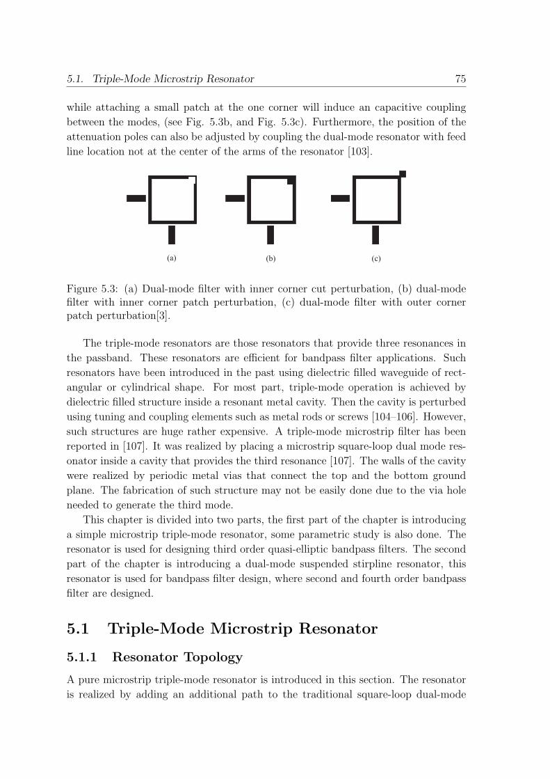
5.1. Triple-Mode Microstrip Resonator 75
while attaching a small patch at the one corner will induce an capacitive coupling
between the modes, (see Fig. 5.3b, and Fig. 5.3c). Furthermore, the position of the
attenuation poles can also be adjusted by coupling the dual-mode resonator with feed
line location not at the center of the arms of the resonator [103].
(a) (b) (c)
Figure 5.3: (a) Dual-mode filter with inner corner cut perturbation, (b) dual-modefilter with inner corner patch perturbation, (c) dual-mode filter with outer cornerpatch perturbation[3].
The triple-mode resonators are those resonators that provide three resonances in
the passband. These resonators are efficient for bandpass filter applications. Such
resonators have been introduced in the past using dielectric filled waveguide of rect-
angular or cylindrical shape. For most part, triple-mode operation is achieved by
dielectric filled structure inside a resonant metal cavity. Then the cavity is perturbed
using tuning and coupling elements such as metal rods or screws [104–106]. However,
such structures are huge rather expensive. A triple-mode microstrip filter has been
reported in [107]. It was realized by placing a microstrip square-loop dual mode res-
onator inside a cavity that provides the third resonance [107]. The walls of the cavity
were realized by periodic metal vias that connect the top and the bottom ground
plane. The fabrication of such structure may not be easily done due to the via hole
needed to generate the third mode.
This chapter is divided into two parts, the first part of the chapter is introducing
a simple microstrip triple-mode resonator, some parametric study is also done. The
resonator is used for designing third order quasi-elliptic bandpass filters. The second
part of the chapter is introducing a dual-mode suspended stirpline resonator, this
resonator is used for bandpass filter design, where second and fourth order bandpass
filter are designed.
5.1 Triple-Mode Microstrip Resonator
5.1.1 Resonator Topology
A pure microstrip triple-mode resonator is introduced in this section. The resonator
is realized by adding an additional path to the traditional square-loop dual-mode

5.1. Triple-Mode Microstrip Resonator 76
resonator. The additional path is realized by a meander half wavelength strip that is
connected to two opposite corners of the square-loop resonator. Fig. 5.4 shows the
layout of the triple-mode and dual-mode resonators coupled by perpendicular feeding
lines, and perturbed from one corner by an outer patch. Fig. 5.4a shows a second
L4
l»
p
p
rr
L4
l»
L
L
aL
-2
aL
+2
aL
-2
aL
+2
¢
d
w
p
p
L4
l@
L4
ë@
(a) (b)
Figure 5.4: Layout of a microstrip (a)dual-mode resonator, (b) triple-mode resonatorcoupled by perpendicular feeding lines and perturbed by outer patch.
order bandpass filter which consists of a square-loop dual-mode resonator [10]. It
consists of four identical arms of length L. To couple the two modes, a small square
is attached to the corner of the loop. The structure is coupled to the input and
output ports by two perpendicular lines. The fundamental resonances occur when L
is approximately equal to a quarter of a wavelength. The position and geometry of
the corner patch determine the nature of the coupling between the two modes [108].
A microstrip triple-mode resonator is created by adding an additional path to the
square-loop dual-mode resonator shown in Fig. 5.4a. This path is realized by etching
a meander stripline that is connected to two opposite corners of the main resonator.
The length of this stripline is one half of a wavelength. Fig. 5.4b shows the layout of
the resulting structure. The resonator resonates when the length of the arms is equal
to one quarter of a wavelength. This additional line is again loaded by a square patch
as a perturbation element with edges of length r.
5.1.2 Modes and Perturbations p, r
In the case of dual-mode resonators, the resonances are generated by a single even
mode and one odd mode. In the case of triple-mode resonator (see Fig. 5.4b) we
have two even mode and one odd mode. To justify that, we have placed a perfect
magnetic wall at the symmetry plane (A − A′), i.e. the symmetry plane acts as an
open circuit. Fig. 5.5 shows the reflection coefficient of the un-perturbed resonator.

5.1. Triple-Mode Microstrip Resonator 77
It is obvious that there are two resonances at 5.12 GHz, and 5.28 GHz, which gives
an indication that this resonator has two even mode resonances.
For the odd mode calculation, a perfect electric wall was placed at the symmetry
plane (A−A′), now the symmetry plane operates as short circuit. Fig. 5.6 shows the
reflection coefficient of the shorted un-perturbed resonator. From the Figure, it can
be clearly seen that the resonator has a single mode resonance at 4.95 GHz.
2 3 4 5 6 7 8−2.5
−2
−1.5
−1
−0.5
0
Frequency (GHz)
|S11
| (dB
)
Figure 5.5: Reflection coefficient of un-perturbed resonator using perfect magneticwall at the symmetry plane.
For un-perturbed resonator coupled to two perpendicular feeding lines, the filter
response shows two un-splitted mode resonances, while the third mode resonance is
located on a different frequency band, furthermore, the filter is not well matched
by using un-perturbed resonator. Fig. 5.7 shows the reflection coefficient of the
un-perturbed resonator fed by two perpendicular feeding lines.
In order to split the modes, two square patches are attached to two corners of
the triple-mode resonator, (see 5.4b), the dimensions of the resonator chosen for the
analysis are as the following, the length of each arm of the resonator L = 10 mm,
and the width of the arm strips are d = 0.3 mm. Fig. 5.8 shows the dependence
of mode resonances on the perturbation elements on p, where p is the length of the
square patch that is located at the outer side of the resonator, while keeping r = 0
mm, where r is the length of the inner square patch. From the figure it is clearly seen
that the resonance mode f03 is not affected by the perturbation element p, while the
modes f01, f02 start splitting when the dimension p > 0.2 mm.
Keeping the perturbation element un-presented (p = 0), and increasing the di-
mensions of the inner perturbation element r, see Fig.5.4b, the third-mode resonant
frequency f03 decreases, while the other two modes remain un-splitted. When the

5.1. Triple-Mode Microstrip Resonator 78
2 3 4 5 6 7 8−2.5
−2
−1.5
−1
−0.5
0
Frequency (GHz)
|s11
| (dB
)
Figure 5.6: Reflection coefficient of un-perturbed resonator using perfect electric wallat the symmetry plane.
4 4.5 5 5.5 6−10
−8
−6
−4
−2
0
Frequency (GHz)
|S11
| (dB
)
Figure 5.7: Reflection coefficient of un-perturbed resonator fed by two perpendicularfeeding lines.

5.1. Triple-Mode Microstrip Resonator 79
0 0.2 0.4 0.6 0.8 14.7
4.8
4.9
5
5.1
5.2
5.3
5.4
5.5
p (mm)
Fre
quen
cy (
GH
z)
f01
f02
f03
Figure 5.8: Relation between the size of the perturbation element p and the triple-mode resonance frequencies, perturbation r is not presented (r=0).
dimension r > 0.7 mm, all the modes share the same resonant frequency. Fig.5.9
shows the relation between the resonant frequencies and the size of the perturbation
element r.
5.1.3 Triple-Mode Resonator and Filter Realization
Based on the above information, a third order bandpass filter has been designed. The
dimensions of the filter were chosen as follows, L = 10 mm, d = 0.3 mm, p = 0.9 mm,
r = 0.2 mm, the spacing between the resonator and the stubs that are connected to
the feed lines is 0.2 mm. The filter has bandwidth of 0.3 GHz and centre frequency
about 5.06 GHz. The coupling coefficient between the modes should be computed
according to the theory of the coupled asynchronously tuned resonators as [2]
knm =(fsm
fsn
+fsn
fsm
)√(f 2om − f 2
0n
f 2om + f 2
0n
)2
−(f 2
sm − f 2sn
f 2sm + f 2
sn
)2
(5.1)
where fsm and fsn are the self-resonant frequencies of the resonator and f0m, f0n are
the mode splitting frequencies. From the simulated results, we denote that the self-
resonant frequencies are equal to the mode splitting frequencies. That leads to k=0
. Therefore, the filter has a transversal coupling scheme [109], This means that each
resonator is coupled with the source and the load in addition to the coupling between
the source and the load, Fig. 5.10 shows the transversal coupling scheme of the our
third order filter. The used coupling matrix for this analysis is (N + 2) × (N + 2),
which supports analysis of fully canonical filtering function, i.e. the number of the

5.1. Triple-Mode Microstrip Resonator 80
0 0.2 0.4 0.6 0.8 1
5.15
5.2
5.25
5.3
5.35
5.4
r (mm)
Fre
quen
cy (
GH
z)
f01
, f02
f03
Figure 5.9: Relation between the size of the perturbation element r and the triple-mode resonance frequencies, perturbation p is not presented (p=0).
finite transmission zeros equal to the order of the filter.
1
2
3
s l
slM
1sM1lM
3sM 3lM
2sM2lM
Figure 5.10: Coupling and routing scheme of the triple-mode filter.
The filtering function that characterizes the filter can be written as a rational
function
F (ω′) =P (ω′)D(ω′)
(5.2)
Where ω′ is the low-pass prototype frequency related to the actual frequency ω by
ω′ =ω0
∆ω
( ω
ω0
− ω0
ω
)(5.3)

5.1. Triple-Mode Microstrip Resonator 81
The polynomial P (ω′) is computed from a recursion method introduced in [110]
which is given as
PN+1(ω) = −PN−1(ω′)(1− ω′
ω′N
)2
(1− 1
ω′2N+1
)0.5
(1− 1
ω′2N
)0.5
+ PN(ω′)[ω′ − 1
ω′N+1
+(ω′ − 1
ω′N
)(1− 1
ω′2N+1
)0.5
(1− 1
ω′2N
)0.5
](5.4)
where ω′N is the position of the pre-defined attenuation pole, P0(ω′) = 1 and P1(ω
′) =
ω′ − 1ω′1
.
The Polynomial D(ω′) can be given as
D(ω′) =K∏
N=1
(1− ( ω′
ω′N
)), (5.5)
where ωN represents the N th attenuation pole. The transmission coefficient can be
expressed as
|S21(ω′)|2 =
1
1 + ε2F 2(ω′), (5.6)
where the parameter ε is a constant related to the passband return loss RL, it is
expressed by the following formula
ε =[10
RL10 − 1
]−0.5
(5.7)
The loop currents through the filter resonators can be grouped in a vector I and
given by the following matrix form [111]
[−jR + ω′W + M ]I = AI = −jE, (5.8)
where R is an (N + 2)× (N + 2) matrix with zeros entries except R1,1=RN+2,N+2=1,
W is an (N + 2) × (N + 2) diagonal matrix whose main diagonal elements are ones
except W1,1=WN+2,+2=0, M is the normalized coupling matrix, and E = [1, 0, ...., 0]
is the excitation vector. The transmission and reflection coefficients S11 and S21 are
given by
S12 = −2j[A−1]N+2,1 (5.9)
S11 = 1 + 2j[A−1]1,1 (5.10)
The synthesis problem can be formulated as follows. Looking for the suitable
coupling matrix M that minimizes a certain cost function C, so that the entries of
the optimization function are the non-zero elements of the coupling matrix with initial
guess. The cost function to be minimized can be expressed as

5.1. Triple-Mode Microstrip Resonator 82
C =K∑
i=1
| S11(ω′pi
) |2 +H∑
i=1
| S12(ω′tzi
) |2 +(| S11(ω′=∓1) | − ε√
1 + ε2
)2
(5.11)
where pi, tzi, and H are the positions of the poles (roots of P (ω′) ), the positions
of the attenuation poles, and the number of the attenuation poles, respectively. The
flow chart shown in Fig. 5.11 explains the optimization procedure used to synthesize
the filter response. The scheme starts by an initial guess of the coupling coefficients,
then calculates the matrices [A] and [A]−1 at the roots of the polynomials P (ω′) and
P (ω′). After that the const function is calculated and checked whether it satisfies a
predefined value, if not the scheme changes the initial values and calculates C again
until achieving the satisfied value.
Mij
Mij
[ ] [ ] 1,
-
AA
Mij
2111 , SS
( ) ( )',' wwNN
DP
d£CEnd &Return
Calculate
Calculate
Initial guss
Change
Calculate
Roots of
YN
C
Figure 5.11: flow chart of the used optimization method.
Due to the symmetry of the structure its modes exhibit either a magnetic wall
or an electric wall along the main diagonal. It is important to keep in mind that
these modes are determined with reference planes placed right at the coupling stubs
at the input and output. Under the lossless assumption, these modes are not coupled
to each other but are all coupled to the input and the output. Higher order modes,
including surface modes, contribute to a small direct coupling between the input and
the output. A narrowband equivalent circuit based on this coupling scheme is shown
in Fig. 5.10,which is a transversal coupling matrix [105]. The narrowband response
of this filter is, therefore, described by a coupling matrix of the form

5.1. Triple-Mode Microstrip Resonator 83
M =
0 Ms1 Ms2 Ms3 Msl
Ms1 M11 0 0 Ml1
Ms2 0 M22 0 Ml2
Ms3 0 0 M33 Ml3
Msl Ml1 Ml2 Ml3 0
(5.12)
Since there are two even modes and one odd mode in this third order structure
with a symmetry plane along the main diagonal. At the coupling matrix level, this
implies that one of the coupling coefficients to the ports is negative. This is taken as
the third resonance leading to the choice
Ms1 = Ml1, Ms2 = Ml2, Ms3 = −Ml3 (5.13)
The filter response is compared with a third order chebyshev response. However,
a disagreement between EM and the synthesized filter indicates that complex atten-
uation poles exist at the upper stopband. Therefore a filter has been synthesized as
transversal, assuming two attenuation poles on the real axis of the s-plane addition
to one transmission zero located at the lower stopband, which is laying on the imagi-
nary access of the s-plane. For given specifications, the entries of the coupling matrix
can be extracted analytically by following the presentation in [109]. For example,
for a third order filter with an in-band return loss of 20 dB, one attenuation pole at
s=-6.471j and a pair of complex transmission zeros at s=±2.25, we get the following
coupling matrix
M =
0.0000 0.6441 −0.5648 0.7152 −0.03070.64411 −1.4992 0.0000 0.0000 0.64411−0.5648 0.0000 1.4756 0.0000 −0.56480.7152 0.0000 0.0000 0.1061 −0.7152−0.0307 0.7152 −0.5648 −0.7152 0.0000
A filter was designed to implement this coupling matrix. Its response is shown in Fig.
5.12 along with that of this coupling matrix. Good agreement is achieved between
The EM simulation and the coupling matrix synthesized results .
Changes to the dimensions of perturbation elements p and r lead to changes in the
positions of the transmission zeros. These zeros can even be migrated in the complex
plane from the real axis to the imaginary axis, and vice versa [3], and [108]. The
positions of the transmission zeros can also be controlled by adjusting the electrical
length between the I/O feeding lines [103], [112]. Fig. 5.13 shows the insertion loss
of the filter with different feed line positions a, where a is the distance between the
feeding lines and the centre of the resonator arms, as shown in Fig. 5.4b. As can be
clearly seen, with the I/O feeding lines connected at the centre of the feeding stub
a = 0, the transmission zeros at the higher stopband disappear (i.e., the transmission
zeros are located on the real axis of the complex s-plane), and the attenuation pole
that is in the lower stopband is located at s = -6.346j. By increasing a, see Fig. 5.4b,

5.1. Triple-Mode Microstrip Resonator 84
4 4.5 5 5.5 6−60
−50
−40
−30
−20
−10
0
Frequency
|S11
|, |S
21|
|S21
|
|S11
|
Figure 5.12: EM simulation (solid) synthesized (dashed) reflection and transmissioncoefficients of a triple-mode bandpass filter.
the positions of the transmission zeros are moved, and are possibly transferred on to
the imaginary axis of the complex s-plane.
A triple-mode filter with the feed line located at a=1.35 mm was designed as
shown in the previous section. It has a centre frequency of 5.06 GHz, a bandwidth of
220 MHz, and three attenuation poles at s = -1.497j, 3.317j, and 7.86j, respectively.
The resulting coupling matrix of the coupling scheme shown in Fig. 5.10 is
M =
0.0000 0.4820 −0.3377 −0.7599 −0.02350.4820 −1.2827 0.0000 0.0000 0.4820−0.3377 0.0000 1.2083 0.0000 −0.3377−0.7599 0.0000 0.0000 0.2281 0.7599−0.0235 0.3377 −0.3377 0.7599 0.0000
The filter response based on this coupling matrix and compared with the EM
simulation is shown in Fig.5.14. Good agreement between the two results is achieved,
except at the stopbands, as the coupling matrix can only be applied in a narrowband
range.
5.1.4 Broadband Equivalent Circuit
The coupling matrix describes the filter behavior properly only in the close vicinity
of the passband, see Fig. 5.14. Consequently, some design tools working in a wider
frequency band are required. For this purpose, an equivalent circuit has been found
as a very effective way to analyze the filter. This circuit is shown in Fig. 5.15. It is
simply derived from the filter layout in Fig. 5.4b. This equivalent circuit is based on

5.1. Triple-Mode Microstrip Resonator 85
1 2 3 4 5 6 7 8 9−80
−70
−60
−50
−40
−30
−20
−10
0
Frequency (GHz)
|S21
| (dB
)
a =0.00 mm a = 0.55 mm a = 0.55 mm a = 1.25 mm a =1.35 mm a = 1.40 mm a = 1.45 mm
Figure 5.13: Transmission coefficient of a triple-mode bandpass filter with various avalues.
3 4 5 6 7 8−80
−70
−60
−50
−40
−30
−20
−10
0
Frequency (GHz)
|S11
|, |S
12| (
dB)
|S12
||S
11|
Figure 5.14: EM simulation (solid) synthesized (dashed) reflection and transmissioncoefficients of triple-mode bandpass filter with three transmission zeros.

5.1. Triple-Mode Microstrip Resonator 86
the representation of the microstrip line. The effective dielectric constant εeff , and
the characteristic impedance of this line is well defined in (2.84), (2.85).
LZ ,, 0b LZ ,, 0b
LZ ,, 0b LZ ,, 0b
xLZ ,, 0bxLZ ,, 0b
)22(,, 0 xLLZ -b
pC
rC
SCSC
PortsC
w
Figure 5.15: Broadband equivalent circuit of the triple- mode mictrostrip filter. Theinset shows the circuit used to determine Cs.
Having calculated εeff and Zc , the electrical length of each transmission line can
easily be calculated by
Θ = Lβ (5.14)
where L is the physical transmission line length and β is the propagation constant,
which is defined as
β =2π
λg
(5.15)
where
λg =λ√εeff
(5.16)
For our filter, which has dimensions L=10 mm and Lx = 3.4 mm, where Lx =
L− a, we obtained θ = 90o, 29o, respectively. The capacitances of the perturbation
elements can be approximated as in [3]
Ci =√
2C0, i = p, r (5.17)
where
C0 = ε0εrAi
h, i = p, r (5.18)
where Ai is the area of the perturbation elements, h is the thickness of the substrate,
εr is the relative dielectric constant of the substrate, and εr is the free-space dielectric
constant.

5.1. Triple-Mode Microstrip Resonator 87
Capacitance CS that is between the resonator and the stubs connected to the
feeding lines was determind by calculating the capacitance between the feeding line
terminated by the stub and its mirror image, as shown in the inset of Fig. 5.15.
Capacitance CPorts representing the direct coupling between the filter ports cannot
be simply and directly determined. Fig 5.16 shows the transmission characteristics
of the equivalent circuit from Fig. 5.15 calculated for selected values of CPorts, this
calculation has been done using a circuit simulator [113]. This capacitance is finally
determined by fitting these results to the characteristic obtained by the EM simula-
tion. The final fit using CPorts= 0.01 pF is shown in Fig. 5.17.
2 4 6 8 10−100
−80
−60
−40
−20
0
Frequency (GHz)
|S21
| (dB
)
CPorts
=0.002pF
CPorts
=0.006pF
CPorts
=0.01pF
CPorts
=0.014pF
CPorts
=0.02pF
CPorts
=0.024pF
Figure 5.16: Transmission coefficient of the Broad-band equivalent circuit for differentvalues of CPorts.
5.1.5 Experimental Results
The two triple-mode filters were designed using the proposed resonator. The first
filter has dimensions of L = 10 mm, d = 0.3 mm, p = 0.9 mm, r = 0.2 mm, and the
spacing between the resonator and the stubs connected to the feed lines is w = 0.2
mm. This filter has one transmission zeros in its lower stop band and two complex
attenuation pole. A photograph of the fabricated structure is shown in Fig.5.18. The
simulated and measured return and insertion loss of the filter are shown in Fig.5.19.
There is good agreement between the two results, apart from a small shift at the
lower cut-off frequency. The maximum return loss at the pass band is about 11 dB,
which can be attributed to fabrication errors. The insertion loss at the passband is
better than 2.9 dB; this relatively high magnitude of the insertion loss corresponds

5.1. Triple-Mode Microstrip Resonator 88
2 3 4 5 6 7 8−80
−70
−60
−50
−40
−30
−20
−10
0
Frequency (GHz)
|S11
|, |S
21| (
dB)
|S21
|
|S11
|
Figure 5.17: EM simulation (solid) and equivalent circuit simulation (dashed) whenCPorts=0.01 pF.
to the high return loss at the passband. The group delay variation in the passband
is smaller than 0.51 ns.
Figure 5.18: Photograph of a third order bandpass filter using the proposed triple-mode resonator.
The second filter is designed to have the same resonator dimensions; the only
change concerns the locations of the feeding lines. The feeding lines are located off-
center at a=1.35 mm, see Fig. 5.4b. The filter has three transmission zeros, one in
the lower stopband, and two in its upper stopband. Fig. 5.20 shows the simulated
and measured insertion and return loss of the filter. The two transmission zeros
in the upper stopband considerably improve the filter behavior in this stopband, in
comparison with the characteristics of the first filter version. The in-band insertion
loss is better than 2.3 dB. The group delay variation in the passband is smaller than
1.5 ns.

5.1. Triple-Mode Microstrip Resonator 89
1 2 3 4 5 6 7 8−50
−40
−30
−20
−10
0
Frequency (GHz)
|S11
|, |S
21| (
dB)
|S21
|
|S11
|
Figure 5.19: Simulated(dashed) and measured (solid) insertion and return loss oftrip-mode bandpass filter with one transmission zero.
2 4 6 8−80
−70
−60
−50
−40
−30
−20
−10
0
Frequency (GHz)
|S11
|,|S
21|
(dB
)
|S21
|
|S11
|
Figure 5.20: Simulated(dashed) and measured (solid) insertion and return loss oftrip-mode bandpass filter with three transmission zeroes .

5.2. Dual-Mode Suspended Stripline Filters 90
5.2 Dual-Mode Suspended Stripline Filters
Dual-mode resonators have not been introduced for suspended stripline technique
with their classical structure. Since they require increasing the cross section of sus-
pended stripline, that will increase the size of the overall filter structure. Due to
the large cross-section, the waveguide mode may not allow a wide stopband. Up to
now, the filters designed using suspended stripline are done using either the folded
transmission lines, or by using quasi-lumped elements.
In this section a dual-mode suspended stripline resonator is introduced. The res-
onator is realized by combining quasi-lumped suspended stripline parallel resonator
with open-loop resonator. These two resonators were chosen to be combined with
each other because they have nearly the same size at the corresponding resonance fre-
quency. A second order, and two fourth order filters are realized using this resonator.
The realized filters are very compact compared to those realized by quasi-lumped
resonators.
5.2.1 Quasi-Lumped Parallel Resonator
The parallel resonator has been introduced first in [114]. The resonator consists of a
narrow strip connected to the side wall of the metal housing and patch at the other
end, see Fig. 5.21a. The narrow stripline represents a shunt inductance, while the
coupling between the patch and the walls of the mount represents a shunt capacitance,
see Fig. 5.21b. The resonance frequency of the resonator can be controlled either by
changing the length of the narrow stripline, or by changing its width. The other pa-
rameter that plays a role in controlling the resonance frequency of the resonator is the
spacing between the patch and the housing mount. Locating the narrow stripline on
the same side induces an additional inductive coupling between the two resonators,
which in turn, introduces a transmission zero to the filter response [115]. The po-
sition of the transmission zero can be easily adjusted by increasing or decreasing
the distance between these strips. Different filter types, broadband bandpass filters,
wltra-wideband bandpass filters, and high-pass filters have been designed using this
resonator. [24], [90], and [115].
5.2.2 Open-Loop Resonator
Open-loop resonator also known in the literature as split-ring resonator. This res-
onator resonates when the length of the resonator corresponds to λ/2 [2], [4], and
[116–118]. The open end of resonator provides a capacitive coupling in parallel to the
main path that provides a transmission zero at the higher stopband [116]. Due to the
fact that the electric field at the open sides of the open-loop resonator is maximum at
the resonance frequency of the resonator, and the magnetic field is maximum at the
center of the resonator ; the coupling nature between two open-loop depends on the

5.2. Dual-Mode Suspended Stripline Filters 91
(a) (b)
Figure 5.21: (a) Layout of suspended stripline quasi-lumped resonator, (b) equivalentcircuit of the suspended stripline resonator .
neighboring sides [4]. Thus, by having the resonators coupled from the open-ends,
capacitive coupling is generated, see Fig. 5.22a, while having the resonators coupled
from the opposite sides, an inductive coupling is generated, see Fig. 5.22b. To gen-
erate a mixed coupling between the resonators, the resonators can be built keeping
open ends on one side, or by keeping the open ends antipodal, see Fig. 5.22c and
Fig. 5.22d. Size reduction has been already done by extending the loop in idle area
inside the resonator itself and by increasing the capacitive coupling between the open
ends [8]. The open-loop resonator can be easily realized using suspended stripline
technique, see Fig.5.23
(a) (b)
(c) (d)
Figure 5.22: Coupling structures for microstrip open-loop resonator (a) capacitivecoupling structure, (b) inductive coupling stricture, (c) mixed coupling structure, (d)mixed coupling structure [4].
5.2.3 Resonators Combination
Combining both quasi-lumped resonator with open-loop, an SSL dual mode resonator
can be realized. The new resonator is realized by adding a narrow stripline to the
open-loop resonator, as shown in Fig. 5.24. Using this configuration, the quasi-
lumped resonance in addition to the open-loop resonant mode is generated. Fig 5.25

5.2. Dual-Mode Suspended Stripline Filters 92
Figure 5.23: Suspended stripline open-loop resonator.
shows the return loss of the new resonator capacitively coupled to the feeding lines
in comparison with return loss of the open-loop resonator. Controlling the resonant
frequencies of the resonators must be done in such a way that it does not affect the size
or the shape of the resonator, because this will affect both resonances, which makes
it difficult to adjust the center frequency of the filter, and increases the difficulties in
achieving a good matching at the passband of the filter.
The parameters that control the resonance frequencies are:
1. The width of the narrow stripline w, see Fig. 5.24, which affects only the
quasi-lumped resonance without main change of the open-loop resonance, so by
increasing w, the inductive value of the stripline is decreased, that will shift the
quasi-lumped resonance to a higher frequency band, and vice versa.
2. The other parameters that mainly affect the open-loop resonance are, the spac-
ing between the open ends of the resonator s, and the width of the open ends x,
see Fig. 5.24. Decreasing s decreases the capacitive coupling between the open
ends of the resonator, which shifts the open-loop mode to a higher frequency,
and vise versa. On the other hand, increasing x increases the capacitive value
between the open ends which shifts the open-loop mode to lower frequency
band.
An easy way to design a filter using this resonator is to design two filters on the
same frequency band. The first one by quasi-lumped resonator, and the second by
open-loop. The size of the two resonators must be kept the same, in other words, the
size of the patch must be equal to the outer frame of the open-loop resonator.
Coupling between the two modes of the dual-mode resonator is the next step. For
this resonator the modes can be coupled by two ways. The first one is realized by
increasing external coupling, this can be easily done using suspended stripline, since
overlapping between the metallization on both sides of the substrate is allowed. A
second order bandpass filter has been designed by using one resonator on the backside
of the substrate coupled tightly with feeding lines that built on the topside of the
substrate, the cross section of the transmission line used for this filter is shown in

5.2. Dual-Mode Suspended Stripline Filters 93
w
x
s
Figure 5.24: Suspended stripline open-loop resonator.
0 5 10 15 20−30
−25
−20
−15
−10
−5
0
Frequency (GHz)
|S11
| (dB
)
Figure 5.25: Simulated return loss of the dual-mode resonator (dashed) in comparisonwith the return loss of the open-loop (solid).

5.2. Dual-Mode Suspended Stripline Filters 94
Fig.3.31. Fig. 5.26 shows a 3D view of the filter, while Fig. 5.27 shows the simulated
insertion and return loss of the filter.
Figure 5.26: 3D view of a second order bandpass filter using SSL dual-mode resonatorintensively coupled with the feeding lines.
2 4 6 8 10 12 14 16−50
−40
−30
−20
−10
0
Frequency (GHz)
|S11
|, |S
21| (
dB)
|S21
|
|S11
|
Figure 5.27: Simulated insertion and return loss of a second order bandpass filterusing SSL dual-mode resonator intensively coupled with the feeding lines.
The second parameter that increases the coupling between the resonator modes
is the position of the narrow stripline. Having asymmetry of the inductive strip, the
modes of the resonators will be coupled and matched better than implementing the
inductive strip at the center of the resonator. This principle is used to the design
of a fourth order bandpass filter. Two coupled SSL dual-mode resonators have been
implemented on the backside of the substrate. Each of these resonators is coupled
to the neighboring port, which is implemented on the topside of the substrate. The
parallel inductive strips are located on different sides of the substrate to avoid any

5.2. Dual-Mode Suspended Stripline Filters 95
inductive coupling between both resonators (see [24], [115]). Fig. 5.28 shows a 3D
view of the fourth order bandpass filter structure, the filter has a length of 7.25
mm, which is much smaller than the forth order that is designed using quasi-lumped
elements, see [24]. Fig. 5.29 shows the simulated return and insertion losses of the
filter. The four return-loss poles can be observed clearly. In addition, a transmission
zero occurs at about 14 GHz. This occurs due to the slot that is in parallel to the
narrow stripline at the other side of the resonator. The filter has a bandwidth of
about 2 GHz, and a center frequency of 10.8 GHz.
Figure 5.28: 3D view of forth order bandpass filter using two dual-mode resonators.
5 10 15 20−70
−60
−50
−40
−30
−20
−10
0
Frequency (GHz)
|S11
|, |S
21| (
dB)
|S21
||S
11|
Figure 5.29: Simulated insertion and return loss of a fourth order bandpass filterusing SSL dual-mode resonator.
As it has been already demonstrated in [24], [115], locating the parallel inductive
strips of two resonators on the same side of the substrate, introduces an inductive

5.2. Dual-Mode Suspended Stripline Filters 96
coupling in parallel to the original capacitive coupling. This causes an additional
transmission zero. The same principle has been transferred to our design. An addi-
tional transmission zero has been introduced below the passband. The transmission
zero which was introduced in the last structure is splitted now into two zeroes. Fig.
5.30 shows the simulated filter structure, while Fig. 5.31 shows a photograph of the
measured structure, the filter is 6.45 mm in length, Fig.5.32shows the simulated and
the measured return and insertion losses of this filter. The general behavior of the
insertion loss is well met. A slight frequency shift is due to the increased resonator
inductance caused by a groove in the mount clamping the substrate. The maximum
return loss is about 9 dB. This is due to fabrication errors, combined with the rela-
tively high sensitivity of this type of filters. The measured insertion loss is smaller
than 1.8 dB where most of this is caused by the problem in the return loss.
Figure 5.30: 3D sketch of a fourth order SSL bandpass filter using two dual-moderesonators with parallel inductive strips on one side.
Figure 5.31: Photograph of fourth order bandpass filter structure.

5.2. Dual-Mode Suspended Stripline Filters 97
5 10 15−80
−70
−60
−50
−40
−30
−20
−10
0
Frequency (GHz)
|S11
|, |S
21| (
dB)
|S21
|
|S11
|
Figure 5.32: Measured (solid) and simulated (dashed) return and insertion losses ofthe fourth order bandpass filter with additional transmission zero.


Chapter 6
Dual-Band Bandpass Filters UsingDual-Mode Resonator
Dual-band filters have gained much interest in the recent years. Deferent filter ap-
proaches have been introduced during the last ten years to meet the demand of the
modern wireless communication systems e.g., [46–52] and [119–125]. The classical
dual-band bandpass filter approach has been achieved by connecting two individual
bandpass filters with each other in parallel. However, such approach needs additional
matching network that increases the size of the overall filter structure [46], [123] and
[124]. Another approach using the dual-band stubs [47], however, due to the inductive
coupling between these stubs, the filter has also transmission at low frequency, and
attenuating lowpass band has not been reported so far. In [52] and [119–121], dual-
band filter structures have been introduced using stepped impedance resonator (SIR),
but due to the long transmission line sections used in this class of filters, the filter
response does not have wide upper stopband. In addition, high losses are introduced
to the filter response. Dual-band filter has been also achieved by using dual-mode
resonators. In [125] a CPW dual-band filter has been designed by using two dual-
mode resonators each of the resonators resonates at different frequency band. The
resonators have been built using back-to-back microstrip ring resonator, this filter has
a main advantage, which is the center frequency of each band is independent on the
other. Moreover, the filter has been modified by building the smaller resonator inside
the bigger one, by this configuration the filter has smaller volume. However, realizing
this structure in microstrip technology requires to have cuts at the feeding line sides
and to let the feeding lines pass the dual-mode resonators under air bridges [122].
By this configuration the coupling between the resonators and the feed lines can be
easily controlled, however, this will increase the fabrication cost and the fabrication
tolerance.
In this chapter, two simple, low-loss dual-band bandpass filters using the dual-
mode resonators are proposed. The first filter is a microstrip one, and it is design by
introducing transmission zeros inside the passband of broadband bandpass filter using
99

6.1. Dual-Band Microstrip Filter 100
dual-mode resonator. The second one is a suspended stripline filter, it is realized by
splitting the modes of the dual-mode resonator into two bands.
6.1 Dual-Band Microstrip Filter
6.1.1 Filter Topology
Broadband bandpass filter using square loop is shown in Fig. 6.1. It is basically
a form of multiple-mode resonator, which is coupled capacitively with input/output
ports [11]-[13]. The resonator consists of a square-loop dual-mode resonator with a
length of lD instead of the low-impedance transmission line section, connected from
both sides high transmission lines with the length of lT . These transmission lines are
coupled from the other side capacitively to two transmission lines having the same
length and connected to the input/output ports from the other side. Fig. 6.2 shows
the insertion loss of the filter.
lD
lD
lT lT
Figure 6.1: Layout of the broadband bandpass filter using multiple-mode resonatorwith a square-loop dual-mode resonator at the center of the filter.
2 4 6 8 10−80
−70
−60
−50
−40
−30
−20
−10
0
10
Frequency (GHz)
|S21
| (dB
)
Figure 6.2: Insertion loss of the broadband bandpass filter with lD = lT = 10 mm.
Rotating one of the high impedance transmission line sections with one of the
feeding lines 90o, as shown in Fig. 6.3, two transmission zeros are introduced in the

6.1. Dual-Band Microstrip Filter 101
passband of the broadband bandpass filter. These two transmission zeros are splitting
the passband of the filter into two passbands. Fig. 6.4 shows the insertion loss of the
dual-band bandpass filter using dual-mode resonator. In case lD is equal to lT then
the bandwidth of both bands is equal, since the transmission zeros are introduced in
the middle of the passband of the original broadband filter.
lT
LT
lD
lD
p
Figure 6.3: Layout of the dual-band bandpass filter using multiple-mode resonatorwith a square-loop dual-mode resonator at the center of the filter.
2 4 6 8 10−70
−60
−50
−40
−30
−20
−10
0
Frequency (GHz)
|S21
|(dB
)
Figure 6.4: Insertion loss on dual-band bandpass filter with dimensions lD = lT = 10mm, the width of all transmission lines is 0.3 mm.
6.1.2 Center Frequency and Bandwidth Control
The center frequencies of the filter can be easily shifted by changing the dimensions
of both transmission lines length lT and the length of dual-mode resonator arms lD

6.1. Dual-Band Microstrip Filter 102
with the same value, see Fig. 6.3. Fig. 6.5 demonstrates the relation of the insertion
loss of the filter by choosing lD = lT = 5 mm, 10 mm, and 15 mm, respectively, while
keeping the dimensions of the perturbation patch at p= 0.5 mm, and the width of the
attached transmission line and the arms of square-loop resonator at 0.3 mm fixed.
0 5 10 15−70
−60
−50
−40
−30
−20
−10
0
Frequency (GHz)
|S21
| (dB
)
lD
= lT = 15 mm
lD
= lT = 10 mm
lD
= lT = 5 mm
Figure 6.5: Simulated return loss of a dual-band bandpass filter with lD = lT = 5,10, 15 mm.
One of the main advantages of this filter is that the bandwidths of both bands
can be controlled by different parameters:
1. Bandwidth Control by Adjusting the Length of the Attached Transmission Lines
lT :
Changing the length of the attached transmission lines only affects the outer
cut-off frequencies of the filter, while the transmission zeros remain unaffected,
which leads to major effect on bandwidth of both bands. So by choosing lTlonger than the lD, the bandwidth of the lower band increases and that of the
higher band decreases. The opposite applies too, choosing the length of the
attached transmission line lT smaller than the length of arms of the dual-mode
resonator decreases the bandwidth of the lower band and increases that of the
higher band. This basically occurs due the transmission zeroes that remain
fixed. This can be clearly seen in Fig. 6.6, which shows the simulated insertion
loss of the filter for different transmission lines lengths lT and keeping lD = 10
mm.
2. Bandwidth Control by Adjusting the Length of the Square-Loop Resonator
Arms lD:

6.1. Dual-Band Microstrip Filter 103
2 4 6 8 10−120
−100
−80
−60
−40
−20
0
Frequency (GHz)
|S21
| (dB
)
lT = 8 mm
lT= 9 mm
lT= 10 mm
lT= 11 mm
lT= 12 mm
Figure 6.6: Simulated insertion loss of the dual-band bandpass filter with different lTvalues, with lD = 10 mmm.
2 4 6 8 10−140
−120
−100
−80
−60
−40
−20
0
Frequency (GHz)
|S21
| (dB
)
lD
= 8 mm
lD
= 9 mm
lD
= 10 mm
lD
= 11 mm
lD
= 12 mm
Figure 6.7: Simulated insertion loss of the dual-band bandpass filter with differentlD values with lT = 10 mm.

6.1. Dual-Band Microstrip Filter 104
2 4 6 8 10−140
−120
−100
−80
−60
−40
−20
0
Frequency (GHz)
|S21
| (dB
)
p= 0 mmp= 0.3 mmp=0.6 mmp= 0.8 mmp= 1.0 mm
Figure 6.8: Simulated insertion loss of the dual-band bandpass filter with different pvalues, with lD= lT = 10 mm.
Changing the length of the dual-mode resonator arms will basically influences
the position of the transmission zeroes. This in turn affects the bandwidth of the
both bands. Increasing the length lD, shifts the transmission zeroes to a lower
band, which leads to having a narrower bandwidth of the lower band and wider
bandwidth of the higher band. Shortening the arms shifts the transmission
zeroes to a higher frequency band, which increases the bandwidth of the lower
band and decreases that of the higher band. Fig. 6.7 shows the corresponding
insertion loss.
3. Splitting the transmission zeroes can be easily done by increasing the dimensions
of the square patch p attached to the inner side of the square-loop dual-mode
resonator. Fig. 6.8 shows the effect of the square patch dimensions and the
simulated insertion loss of the dual-band bandpass filter. It is clear from Fig.6.8
that the longer the patch dimensions p, the more the transmission zeroes are
splitted, which affects the sharpness of inner cut-off frequencies slops of both
bands, so by increasing the inner cut-off slops become sharper, that may affect
the bandwidth.
6.1.3 Experimental Results
A dual-band bandpass filter has been designed, fabricated and measured on RO4003c
substrate.It has a thickness of 0.813 mm and a relative dielectric constant of 3.38.
The width of the attached transmission line and the arms of the dual-mode resonator
were chosen to be each 0.3 mm. The lengths lT = lD = 10 mm, and the dimension p =
0.5 mm. Fig. 6.9 shows the simulated and measured return and insertion loss of the

6.2. Dual-Band Suspended Stripline Filters Using Dual-Mode Resonator 105
filter. The filter has center frequencies of 3.45 GHz, and 6.65 GHz, and bandwidths
of 0.5 GHz and 0.55 GHz, respectively. The insertion loss within the pass bands is
better than 0. 7 dB for the lower band, and is better than 1.2 dB for the higher band.
Good agreement between the measured and the simulated results is obtained.
2 4 6 8 10−70
−60
−50
−40
−30
−20
−10
0
Frequency (GHz)
|S11
|, |S
21| (
dB)
|S21
|
|S21
|
|S11
| |S11
|
Figure 6.9: Simulated and measured return and insertion loss of a dual-band bandpassfilter with dimensions lD= lT = 10 mm.
6.2 Dual-Band Suspended Stripline Filters Using
Dual-Mode Resonator
In this section the suspended stripline dual-mode resonator that has been introduced
in sec. 5.2 is used for dual-band filter realization. The modes of the resonator are
splitted into two frequency bands. As it has been mentioned, this resonator generates
two modes, the first one is quasi-lumped and the second one is open-loop mode. To
split these modes, we have to choose the resonator dimensions in such a way that
the quasi-lumped resonance is located at the lower frequency band and the open-loop
resonant mode is located at higher frequency band.
To be able to split the modes and to shift them to a lower frequency band, we
have used a housing mount with width of 10 mm. That gives us more space to enlarge
our resonator, which makes it easy to shift the modes. the other dimensions are kept
the same as in Fig. 3.31.
Many dimensions affect the resonant frequencies of the filter. However, changing
the outer dimensions of the resonator affects both mode resonances, which makes it
difficult to fix one band on a certain frequency and tune the other. In order to do so,
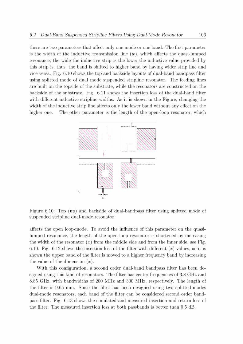
6.2. Dual-Band Suspended Stripline Filters Using Dual-Mode Resonator 106
there are two parameters that affect only one mode or one band. The first parameter
is the width of the inductive transmission line (w), which affects the quasi-lumped
resonance, the wide the inductive strip is the lower the inductive value provided by
this strip is, thus, the band is shifted to higher band by having wider strip line and
vice versa. Fig. 6.10 shows the top and backside layouts of dual-band bandpass filter
using splitted mode of dual mode suspended stripline resonator. The feeding lines
are built on the topside of the substrate, while the resonators are constructed on the
backside of the substrate. Fig. 6.11 shows the insertion loss of the dual-band filter
with different inductive stripline widths. As it is shown in the Figure, changing the
width of the inductive strip line affects only the lower band without any effect on the
higher one. The other parameter is the length of the open-loop resonator, which
w
x
Figure 6.10: Top (up) and backside of dual-bandpass filter using splitted mode ofsuspended stripline dual-mode resonator.
affects the open loop-mode. To avoid the influence of this parameter on the quasi-
lumped resonance, the length of the open-loop resonator is shortened by increasing
the width of the resonator (x) from the middle side and from the inner side, see Fig.
6.10. Fig. 6.12 shows the insertion loss of the filter with different (x) values, as it is
shown the upper band of the filter is moved to a higher frequency band by increasing
the value of the dimension (x).
With this configuration, a second order dual-band bandpass filter has been de-
signed using this kind of resonators. The filter has center frequencies of 3.8 GHz and
8.85 GHz, with bandwidths of 200 MHz and 300 MHz, respectively. The length of
the filter is 9.65 mm. Since the filter has been designed using two splitted-modes
dual-mode resonators, each band of the filter can be considered second order band-
pass filter. Fig. 6.13 shows the simulated and measured insertion and return loss of
the filter. The measured insertion loss at both passbands is better than 0.5 dB.

6.2. Dual-Band Suspended Stripline Filters Using Dual-Mode Resonator 107
3 4 5 6 7 8 9 10 11−80
−70
−60
−50
−40
−30
−20
−10
0
Frequency (GHz)
|S21
| (dB
)
w = 0.2 mmw = 1.0 mmw = 2.0 mmw = 3.5 mm
Figure 6.11: Insertion loss of the dual-band bandpass filter with deferent inductivestripline widths (w).
4 6 8 10 12−60
−50
−40
−30
−20
−10
0
Frequency (GHz)
|S21
| (dB
)
x = 1.0 mmx = 1.5 mmx = 2.0 mmx = 2.5 mmx = 3.0 mmx = 3.5 mmx = 4.0 mmx = 4.5 mm
Figure 6.12: Insertion loss of the dual-band bandpass filter with deferent x dimensionvalues.

6.2. Dual-Band Suspended Stripline Filters Using Dual-Mode Resonator 108
2 4 6 8 10 12−80
−70
−60
−50
−40
−30
−20
−10
0
Frequency (GHz)
|S11
|, |S
21| (
dB)
|S11
|
|S21
|
Figure 6.13: Simulated (dashed) and measured (solid) Insertion loss and return lossof the dual-band bandpass filter.
As it was shown in the same Figure, the stopband attenuation between the two
passbands is about 23 dB, this rejection might not be sufficient for some application.
Therefore transmission zeroes are needed between the passbands to improve the at-
tenuation between the passbands. A transmission zero can be introduced there by
applying additional inductive coupling between the resonators. This can be easily
done by flipping one resonator by 180o, see Fig. 6.14. By this arrangement, the par-
allel inductive strips are now located on one side of the mount. A transmission zero
is introduced at about 5.5 GHz. The measured and simulated return and insertion
losses are shown in Fig. 6.15. An excellent agreement between the experimental and
the theoretical results has been achieved.
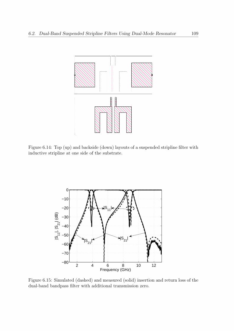
6.2. Dual-Band Suspended Stripline Filters Using Dual-Mode Resonator 109
Figure 6.14: Top (up) and backside (down) layouts of a suspended stripline filter withinductive stripline at one side of the substrate.
2 4 6 8 10 12−80
−70
−60
−50
−40
−30
−20
−10
0
Frequency (GHz)
|S11
|, |S
21| (
dB)
|S21
||S
21|
|S11
|
Figure 6.15: Simulated (dashed) and measured (solid) insertion and return loss of thedual-band bandpass filter with additional transmission zero.


Chapter 7
Conclusions and Future Work
7.1 Thesis Summary
The thesis has discussed and introduced different filter and resonator types. Chapter
three has investigated a modified cross-section of the multilayer coplanar line and
applied it for filter applications. The advantages of this modified multilayer coplanar
lines are the high capacitive coupling that it provides, furthermore it can easily in-
tegrated with CPW, microstrip line, or both. Compact filters have been introduced
using this cross-section. Low-pass filter has been introduced using this cross section
by adding wide patches to the classical CPW lowpass filter at the back side of the
substrate and under the capacitive lines different compact filters have been introduced
using this cross-section. Bandpass filters have been introduced using quasi-lumped
elements, these filters have been constructed to be integrated with microstrip line,
CPW, and both. Moreover, a suspended stripline UWB filter with a very wide stop-
band has been introduced by coupling lowpass filter capacitively with the I/O feeding
lines.
In chapter four an interdigital DGS slot has been introduced. The slot is very
compact compared to the other known slot structures, up to now. Controlling the
resonant frequency of the slot is done by changing the metallic finger lengths, spacing
between fingers, or by changing the number of the fingers. Two lowpass filters have
been presented using this slot showing the advantage of the compact slot. Moreover,
the chapter has discussed the packaging difficulties of this technique and presented
a solution to reduce the packaging difficulties by keeping the ground plane of the
circuit fully metallized and etching the slots on the superstrate, which is directly lain
on the top of the substrate. The metal of the superstrate is connected by via holes to
the ground plane. The structure has the great advantage in reducing the packaging
complexity, since it can be directly based on the carrier block without the need of
machining a recessed region in it.
Chapter five introduced the first microstrip realization of triple-mode resonator.
111

7.2. Suggestions for Future Work 112
This resonator was realized by adding an additional meander half wavelength mi-
crostrip line connected to two opposite corners of the original microstrip square-loop
dual-mode resonator. The resonator was coupled capacitively by two perpendicular
feeding lines. The position of the transmission zeros depends on the connection po-
sitions of the feeding lines. In the centered case, the filter shows one attenuation
pole and two complex transmission zeros. By introducing a non-symmetry into the
positions of the feeding lines, the transmission zeros are moved on to the imaginary
axis of the s-plane. Equivalent circuit and coupling scheme has been presented. Two
different third-order band pass filters were designed, fabricated, and measured. Good
agreement has been obtained between the measured and theoretical results. In the
same chapter, a realization suspended stripline dual-mode resonator has been intro-
duced, which is the first dual-mode resonator for this technique. The resonator was
realized by combining quasi-lumped parallel resonator with open-loop resonator. The
resonator was applied to filter design. Very compact bandpass filters have been de-
signed fabricated and tested. Transmission zeroes have been introduced to the filter
response by applying additional inductive coupling between the resonators.
In chapter six dual-band bandpass filters have been realized by using dual-mode
resonators. The first filter is a microstrip one, it has been realized by introducing
transmission zeros in the passband of a broadband bandpass filter by using square-
loop dual-mode resonator. controlling the center frequencies of both bands can be
done by changing the length of the attached transmission lines and the length of
the arms of the loop resonator equally. Controlling the bandwidth of both bands
can also be done by either by changing the length of the attached transmission lines
and fixing the length of the arms loop resonator, or by changing the length of the
arms of the loop resonator and keeping the attached transmission line lengths fixed.
The second introduced filter in this chapter was a suspended stripline one. the filter
was realized by splitting the modes of the dual-mode resonator that is introduced
in the last chapter into two frequency bands. transmission zero has been introduced
between the two frequency bands by applying additional inductive coupling between
the reosnotors.The dual-mode resonator has shown that it is an excellent resonator
for filter applications especially for dual-band bandpass filter application.
7.2 Suggestions for Future Work
This thesis has presented and investigated different filter topologies and responses for
different planar techniques. Since the development of the communication systems is
increasing rapidly, and since the filters are essential component in any communication
system, the author would like to suggest some ideas for future work.
1. For the DGS structure, it is an important issue to investigate broadband filters
using this technique. Moreover, the thesis have introduced a packaging solution

7.2. Suggestions for Future Work 113
for the DGS, it might be also important to introduce and investigate other
packaging solutions.
2. Quadra-mode bandpass resonator may be realized by adding an additional path
to the triple-mode resonator, which can decrease the size of the filter, and may
increase the number of transmission zeros introduced in the stopband of the
filter. For the suspended stripline, more investigation is needed on the triple-
mode resonators.
3. In the dual-band bandpass filters, it might be interesting to introduce and in-
vestigate new tunable dual-band filters. Moreover, it might also be interesting
to investigate a quadrable band diplexers using two dual-bandbandpass filters.


Bibliography
[1] G. Mahttei, L. Young, and E. M. T. Jones, Microwave Filters, Impedance
Matching Networks and Coupling Structures. Norwood, MA: Artech House,
1980.
[2] J. S. Hong and M. J. Lancaster, Microwave Filters for RF/Microwave Applica-
tions. New York: John Wiley& Sons, 2001.
[3] A. Gorur, “Description of coupling between degenerate modes of a dual-mode
microstrip loop resonator using a novel perturbation arrangement and its dual-
mode bandpass filter applications,” IEEE Trans. Microwave Theory Tech.,
vol. 52, no. 2, pp. 671–677, Feb. 2004.
[4] J. S. Hong and M. J. Lancaster, “Couplings of microstrip square open-loop
resonator for cross-coupling planar filters,” IEEE Trans. Microwave Theory
Tech., vol. 44, no. 12, pp. 2099–2109, Dec. 1996.
[5] R. E. Collin, Foundations for Microwave Engineering. New York: McGraw-
Hill, Inc., 1992.
[6] B. Strassner and K. Chang, “Wide low-loss high isolation microstrip periodic-
stub diplexer for multiple frequancy applications,” IEEE Trans. Microwave
Theory Tech., vol. 49, no. 10, pp. 1818–1820, Oct. 2001.
[7] W. Chen, The circuits and filters handbook. CRC Press, Inc.: Artech House,
1995.
[8] M. G. Banciu, R. Ramer, and A. Ioachim, “Compact microstrip resonators for
900 MHz frequency band,” IEEE Microwave Wireless Compon. Lett., vol. 13,
no. 5, pp. 175–177, May 2003.
[9] I. Wolf, “Microstrip bandpass filter using degenerate modes of ring resonator,”
Electronic Letters, vol. 8, no. 12, pp. 302–303, June 1972.
[10] J. S. Hong and M. J. Lancaster, “Bandpass characteristics of new dual-mode
microstrip square loop resonators,” Electronic Letters, vol. 31, no. 11, pp. 891–
892, May 1995.
115

BIBLIOGRAPHY 116
[11] ——, “Microstrip bandpass filter using degenerate modes of a novel meander
loop resonator,” IEEE Microwave Guided Wave Letters, vol. 5, no. 11, pp.
371–371, Nov. 1995.
[12] L. Zhu and W. Menzel, “Compact microstrip bandpass filter with two trans-
mission zeroes using a stub-tapped half-wavelength line resonator,” IEEE Mi-
crowave Wireless Compon. Lett., vol. 13, no. 1, pp. 16–18, Jan. 2003.
[13] M. H. Ren, D. Chen, and Chrng, “A novel wideband bandpass filter using
a cross-shaped multiple-mode resonator,” IEEE Microwave Wireless Compon.
Lett., vol. 18, no. 1, pp. 13–15, Jan. 2008.
[14] U. H. Lok, Y. C. Chiou, and J.-T. Kuo, “Quadruple-mode coupled-ring res-
onator bandpass filter with quasi-elliptic function passband,” IEEE Microwave
Wireless Compon. Lett., vol. 18, no. 3, pp. 179–181, Mar. 2008.
[15] L.Zhu, S. Sun, and W. Menzel, “Ultra-wideband (UWB) bandpass filters us-
ing multi-mode resonator,” IEEE Microwave Wireless Compon. Lett., vol. 15,
no. 11, pp. 796–798, Nov. 2005.
[16] D. Ahn, J. S. Seok, C. S. Kim, J.Kim, Y. Qian, and I. Itoh, “A design of low-
pass filter using the novel microstrip defected ground structure,” IEEE Trans.
Microwave Theory Tech., vol. 49, no. 1, pp. 86–93, Jan. 2001.
[17] A. B. Rahman, A. K. Verma, A. Boutejdar, and A. S. Omar, “Control of
bandstop response of hi-lo microstrip low-pass filter using slot in ground plane,”
IEEE Trans. Microwave Theory Tech., vol. 52, no. 3, pp. 1008–1013, Mar. 2004.
[18] D. J. Woo, T. K. Lee, j. W. Lee, C. S. Pyo, and W. K. Cho, “Novel U-slot and
V-slot dgss for bandstop filter improved Q factor,” IEEE Trans. Microwave
Theory Tech., vol. 54, no. 6, pp. 2840–2847, June 2006.
[19] J. S. Yun, G. Y. Kim, J. S. Park, D. Ahn, K. W. Kang, and J. B. Lim, “A design
of the novel coupled line bandpass filter using defected ground structure,” in
2000 IEEE MTT-S Int.Microw. Symp. Digest, 2000, pp. 327–330.
[20] C. S. Kim, J. S. Lim, J. H. Kim, and D. Ahn, “’a design of a miniaturized
2-pole bandpass filter by using slot and hair-pin line,” in 2006 IEEE MTT-S
Int.Microw. Symp. Digest, 2006, pp. 1983–1986.
[21] H. W. Liu, Z. F. Li, W. Sun, and J. F. Mao, “An improved 1-D periodic defected
ground structure for microstrip line,” IEEE Microwave Wireless Compon. Lett.,
vol. 14, no. 4, pp. 180–182, Apr. 2004.

BIBLIOGRAPHY 117
[22] S. W. Ting, K. W. Tam, and R. P. Martins, “Compact microstrip quasi-elliptic
bandpass filter using open-loop dumbbell shaped defected ground structure,”
in 2006 IEEE MTT-S Int.Microw. Symp. Digest, 2006, pp. 527–530.
[23] H. J. Chen, T. H. Huang, C. S. Chang, L. S. Chen, N. F. Wang, Y. H. Wang, and
M. P. Houng, “A novel cross-shap DGS appied to design ultra-wide stopband
low-pass filters,” IEEE Microwave Wireless Compon. Lett., vol. 16, no. 5, pp.
252–254, May 2006.
[24] W. Menzel and A. Balalem, “Quasi-lumped suspended stripline filters and
diplexers,” IEEE Trans. Microwave Theory Tech., vol. 53, no. 10, pp. 134–142,
Oct. 2005.
[25] S. S. Liao and J. T. Peng, “Compact planar microstrip branch-line couplers
using quasi-lumped elements approach with nonsymmetrical and symmetrical
T-shaped structure,” IEEE Trans. Microwave Theory Tech., vol. 54, no. 9, pp.
3508–3514, Sept. 2006.
[26] L. Zhu and K. Wu, “Accurate circuit model of interdigital capacitor and its
application to design of new quasi-lumped miniaturized filters with suppression
of harmonic resonance,” IEEE Trans. Microwave Theory Tech., vol. 48, no. 3,
pp. 347–356, Mar. 2000.
[27] S. C. Lin, C. H. Wang, and C. H. Chen, “Novel patch-via-spiral resonators
for the development of miniaturized bandpass filters with transmission zeros,”
IEEE Trans. Microwave Theory Tech., vol. 55, no. 1, pp. 137–146, Jan. 2007.
[28] L. Young, “Stepped-impedance transformations and filter prototypes,” IRE
Trans. Microwave Theory Tech., vol. 10, no. 5, pp. 339–359, Sept. 1962.
[29] G. T. Roan and K. A. Zaki, “Computer-aided design of microstrip filters by
iterated analysis,” IEEE Trans. Microwave Theory Tech., vol. 36, no. 11, pp.
1482–1487, Nov. 1988.
[30] R. N. Martins and H. Abdalla, “Design of low-pass microstrip filter with equal-
ripple passband and finite attenuation poles,” in 2001 SBMO/IEEE MTT-S
International, Aug. 2001, pp. 71–74.
[31] H. Hsieh and C. K, “Compact, broad-stopband elliptic-function lowpass filters
using microstrip stepped impedance hairpin resonators,” in 2003 IEEE MTT-S
Int.Microw. Symp. Digest, 2003, pp. 1775–1778.
[32] W. Menzel and A. Balalem, “Compact suspended stripline quasi-elliptic low-
pass filters,” in German Microwave Conf, Apr. 2005, pp. 61–64.

BIBLIOGRAPHY 118
[33] M. Miyazaki, H. Asao, and O. Ishida, “A broadband dielectric diplexer using a
snaked strip-line,” in 1991 IEEE MTT-S Int.Microw. Symp. Digest, 1991, pp.
551–554.
[34] W. H. Tu and K. Chang, “Microstrip elliptic-function low-pass filters using dis-
tributed elements or slotted ground structure,” IEEE Trans. Microwave Theory
Tech., vol. 54, no. 10, pp. 3786–3792, Oct. 2006.
[35] J. S. Lim, C. S. Kim, D. Ahn, Y. C. Jeong, and S. Nam, “Design of low-pass
filters using defected ground structure,” IEEE Trans. Microwave Theory Tech.,
vol. 53, no. 8, pp. 2539–2545, Aug. 2005.
[36] J. Yang and W. Wu, “Compact elliptic-function low-pass filter using defected
ground structure,” IEEE Microwave Wireless Compon. Lett., vol. 18, no. 9, pp.
578–580, Sept. 2008.
[37] J. S. Lim, C. S. Kim, D. Ahn, Y. C. Jeong, and S. Num, “Design of low-pass
filter using defected ground structure,” IEEE Trans. Microwave Theory Tech.,
vol. 53, no. 8, pp. 2539–2545, Aug. 2005.
[38] E. H. Bradley, “Design and development of strip-line filters,” IRE Trans. Mi-
crowave Theory Tech., vol. 4, no. 2, pp. 86–93, Apr. 1956.
[39] S. B. Cohn, “Parallel-coupled transmission-line-resonator filters,” IRE Trans.
Microwave Theory Tech., vol. 6, no. 2, pp. 223–231, Apr. 1958.
[40] W. Shwab, F. Boegelsack, and W. Menzel, “Multilayer suspended stripline and
coplanar line filters,” IEEE Trans. Microwave Theory Tech., vol. 46, no. 7, pp.
1403–1407, 1994.
[41] L. Zhu, H. Bu, and K. Wu, “Aperture compensation technique for innovative
design of ultra-broadband microstrip bandpass filter,” in 2000 IEEE MTT-S
Int.Microw. Symp. Digest, vol. 2, 2000, pp. 315–318.
[42] F. C. Commission, “Revision of part 15 of the commissions rules regarding
ultraudiband transmission systems,” in Tech. Rep. ET-Docket 98-153 FCC02-
48, Apr. 2002, pp. 98–153.
[43] L. Zhu and S. S. anf W. Menzel, “Ultra-wideband bandpass filter with hybrid
microstrip/CPW structure,” IEEE Microwave Wireless Compon. Lett., vol. 15,
no. 12, pp. 844–846, Dec. 2005.
[44] G. M. Yang, R.Jin, C. Vittaria, V. G. Harros, and N. X. Sun, “Small ultra-
wideband (UWB) bandpass filter with notched band,” IEEE Microwave Wire-
less Compon. Lett., vol. 18, no. 3, pp. 176–178, Mar. 2008.

BIBLIOGRAPHY 119
[45] S. W. Wong and L. Zhu, “EBG-embedded multiple-mode resonator for UWB
bandpass filter with improved upper-stopband performance,” IEEE Microwave
Wireless Compon. Lett., vol. 17, no. 6, pp. 421–423, June 2007.
[46] H. Miyake, S. Kitazawa, T. Ishizaki, T. Yamada, and Y. Nagatom, “A minia-
turized monolithic dual band filter using ceramic lamination technique for dual
mode portable telephones,” in 1997 IEEE MTT-S Int.Microw. Symp. Digest,
vol. 2, 1997, pp. 789–792.
[47] C. Quendo, E. Rius, and C. Person, “An original topology of dual-band fil-
ter with transmission zeros,” in 2003 IEEE MTT-S Int.Microw. Symp. Digest,
vol. 2, 2003, pp. 1093–1096.
[48] V. Palazzari, S. Pinel, J. Laskar, L. Roselli, and M. M. Tentzeris, “Design of an
asymmetrical dual-band wlan filter in liquid crystal polymer (LCP) systemon-
package technology,” IEEE Microwave Wireless Compon. Lett., vol. 15, no. 3,
pp. 165–167, Mar. 2005.
[49] S. F. Chang, J. L. Chen, and S. C. Chang, “New dual-band bandpass filters
with step-impedance resonators comb and hairpin structures,” in Asia Pacific
Microw. Conf, Dec. 2003, pp. 793–796.
[50] S. F. Chang, Y. H. Jeng, and J. L. Chen, “Dual-band step-impedance bandpass
filter for wireless LANs,” Electronic Letters, vol. 40, no. 1.
[51] H. M. Lee, C. R. Chen, and C. C. Tsa, “Dual-band coupling and feed structure
for microstrip filter design,” in 2004 IEEE MTT-S Int.Microw. Symp. Digest,
vol. 2, 2004, pp. 1971–1974.
[52] S. Sun and L. Zhu, “Compact dual-band microstrip bandpass filter without
external feeds,” IEEE Microwave Wireless Compon. Lett., vol. 15, no. 10, pp.
644–646, Oct. 2005.
[53] L. D. Paarmann, Design and Analysis of Analog Filters. Norwell: KLUWER
ACADEMIC PUBLISHERS, 2001.
[54] I. Hunter, Theory and Design of Microwave Filters. London: Institution of
Engineering and Technology IET , 2001.
[55] H. A. Wheeler, “Transmission-line properties of parallel wide strips by a confor-
mal mapping approximation,” IEEE Trans. Microwave Theory Tech., vol. 12,
no. 3, pp. 172–185, May 1964.
[56] ——, “Transmission-line properties of parallel strips separated by a dielectric
sheet,” IEEE Trans. Microwave Theory Tech., vol. 13, no. 2, pp. 1800–1805,
1965.

BIBLIOGRAPHY 120
[57] M. V. Schneider, “Microstrip lines for microwave integrated circuits,” Bell Syst.
Tech. Journal, vol. 48, pp. 1421–1444, May 1969.
[58] R. N. Simons, Coplanar Waveguide Circuits, Components, and Systems. New
York: John Willy & Sons, 2001.
[59] J. D. Rhodes, “Suspended substrates provide alternative to coax,” Microwave
Systems News, vol. 9, no. 8, pp. 134–143,, Aug. 1979.
[60] E. Yamasita, B. Y. Wang, and K. Atsuki, “Effects of side-wall grooves on
transmission characteristic of suspended strip lines,” in 1985 IEEE MTT-S
Int.Microw. Symp. Digest, 1985, pp. 145–147.
[61] ——, “Effects of side-wall grooves on transmission characteristic of suspended
strip lines,” IEEE Trans. Microwave Theory Tech., vol. 33, no. 12, pp. 323–1328,
Dec. 1985.
[62] E. Yamasita, M. Nakajima, and K. Atsuki, “Analysis method for generalized
suspended strip lines,” in 1986 IEEE MTT-S Int.Microw. Symp. Digest, 1986,
pp. 261–264.
[63] ——, “Analysis method for generalized suspended strip lines,” IEEE Trans.
Microwave Theory Tech., vol. 34, no. 12, pp. 3370–3374, Dec. 1986.
[64] W. Menzel, “Broadband filter circuits using an extended suspended substrate
transmission line configuration,” in 22nd European Microwave Conference, Oct.
1992, pp. 459–463.
[65] W. Menzel and F. Boegelsack, “Folded stubs for compact suspended stripline
circuits,” in 1993 IEEE MTT-S Int. Microwave Symp. Digest, 1993, pp. 593–
596.
[66] W. Menzel and M. S. Tito, “A miniaturized suspended stripline filters for in-
tegration into extended circuits,” in 36 European Microwave Conference, 2006,
pp. 909–912.
[67] L. C. A. Lehtovuori, Model for Shielded Suspended Substrate Microstrip Line.
Circuit Theory Laboratory Report Series: Helsinki University of Technology,
1998.
[68] S. Geelani, High Q-factor Metamaterial Duplex Filters in Suspended Stripline
Technology. Ph.D. Thesis: Erlangen-Nuernberg university, March,2009.
[69] S. Banba, T. Hasegawa, and H. Ogawa, “Multilayer MMIC branch-line hybrid
using thin dielectric layers,” IEEE Microwave Guided Wave Letters, vol. 1,
no. 11, pp. 346–347, Nov. 1991.
BIBLIOGRAPHY 121
[70] W. Menzel, W. Schwab, and G. Strauss, “Investigation of coupling structure for
coplanar bandpass filter,” in 1995 IEEE MTT-S Int. Microwave Symp. Digest,
June 1995, pp. 1407–1410.
[71] C. Warns, W. Menzel, and H. Schumacher, “Transmission lines and passive
elements for multilayer coplanar circuits on silicon,” IEEE Trans. Microwave
Theory Tech., vol. 46, no. 5, pp. 616–625, May 1998.
[72] H. Okazaki and T. Hirota, “Multilayer MMIC broad side coupler with a sym-
metric structure,” IEEE Microwave Guided Wave Letters, vol. 7, no. 6, pp.
145–146, June 1997.
[73] L. Zhu, H. Bu, and K. Wu, “Unifield CAD model of microstrip line with rear side
aperture for multilayer integrated circuits,” in 2000 IEEE MTT-S Int.Microw.
Symp. Digest, vol. 2, 2000, pp. 981–984.
[74] K. J. H. an T. A. Schwarz and L. P. B. Katehi, “Si micromachined coplanar
waveguides for use in high-frequency circuits,” IEEE Trans. Microwave Theory
Tech., vol. 46, no. 6, pp. 762–768, June 1998.
[75] J. Papapolymerou, F. Brauchler, J. East, and L. P. B. Katehi, “W-band finite
ground coplanar monolithic multipliers,” IEEE Trans. Microwave Theory Tech.,
vol. 47, no. 5, pp. 614–619, May 1999.
[76] H. Joshi and W. J. Chappell, “Dual-band lumped-element bandpass filter,”
IEEE Trans. Microwave Theory Tech., vol. 54, no. 12, pp. 4169–4177, Dec.
2006.
[77] M. S. W. S. G. Mao, “Design of artificial lumped-elements coplanar waveg-
iude filters with contrallable dual-passband responses,” IEEE Trans. Microwave
Theory Tech., vol. 56, no. 7, pp. 1684–1692, July 2008.
[78] A. Balalem, I. Hamad, J. Machac, and A. S. Omar, “Bandpass filters on a
modified multilayer coplanar line,” in 2006 IEEE MTT-S Int.Microw. Symp.
Digest, vol. 2, 2006, pp. 531–534.
[79] R. A. Pucel, “Design considerations for monolithic microwave circuits,” IEEE
Trans. Microwave Theory Tech., vol. 29, no. 6, pp. 513–534, June 1981.
[80] E. Pettenpaull, H. Kapusta, A. Weisgerber, H. Mampe, J. Luginsland, and
I. Wolff, “CAD models of lumped elements on gaas up 18 ghz,” IEEE Trans.
Microwave Theory Tech., vol. 36, no. 2, pp. 294–304, Feb. 1986.
[81] SONNET, Version 10.52. Sonnet Software Inc.: www.sonnetsoftware.com.
[82] M. O. 2002, version 5.53. Applied Wave Research, Inc.

BIBLIOGRAPHY 122
[83] C. A. Balalanis, Antenna Theory Analysis and Design. New York: John Wily
& Sons LTD, 1997.
[84] T. A. Milligan, Modern antenna design. New York: J. Wiley & Sons, 2005.
[85] E. O. Hammerstadt, “Equations for microstrip circuit design,” in 5th European
Microwave conf, 1975, pp. 268–272.
[86] C. I. Mobbs and J. D. Rhodes, “A generalized chebyshev suspended substrate
stripline bandpass filter,” IEEE Trans. Microwave Theory Tech., vol. 31, no. 5,
pp. 397–402, May 1983.
[87] E. Yamashita, B. Y. Wang, and K. Atsuki, “Effect of side-wall grooves on
transmission characteristics of suspended striplines,” in 1985 IEEE MTT-S
Int.Microw. Symp. Digest, vol. 2, 1985, pp. 145–148.
[88] E. Yamashita, M. Nakajima, and K. Atsuki, “Analysis method for generalized
suspended striplines,” IEEE Trans. Microwave Theory Tech., vol. 34, no. 12,
pp. 1457–1463, Dec. 1986.
[89] Y. S. Lin, W. C. Ku, C. H. Wang, and C. H. Chin, “Wideband coplanar-
waveguide bandpass filters with good stopband rejection,” IEEE Microwave
Wireless Compon. Lett., vol. 14, no. 9, pp. 422–424, Sept. 2008.
[90] W. Menzel, M. S. Tito, and L. Zhu, “Low-loss ultra-wideband (UWB) filters
using suspended stripline,” in Asia Pacific Microw. Conf, Dec. 2005, pp. 2148–
2151.
[91] H. Ishida and K. Araki, “Design and analysis of UWB bandpass filter with
ring filter,” in 2004 IEEE MTT-S Int.Microw. Symp. Digest, vol. 2, 2004, pp.
1307–1310.
[92] T. N. Kuo, S. C. Lin, and C. H. Chen, “Compact ultra-wideband bandpass
filters using composite microstrip-coplanar-waveguide structure,” IEEE Trans.
Microwave Theory Tech., vol. 54, no. 10, pp. 3772–2778, Oct. 2006.
[93] A. M. E. Safwat, F. Podevin, P. Ferrari, and A. Vilcot, “Tunable bandstop de-
fected ground structure resonator using reconfigurable dumbbell-shaped copla-
nar waveguide,” IEEE Trans. Microwave Theory Tech., vol. 54, no. 9, pp. 3559–
3564, Sept. 2006.
[94] A. R. Ali, A. Abdel-Rahman, A. Amari, and A. S. Omar, “Direct and cross-
coupled resonator filters using defected ground structure (DGS) resonators,” in
35th European Microwave conf, Oct. 2005, pp. 1275–1278.

BIBLIOGRAPHY 123
[95] C. Lugo and J. Papapolymerou, “Bandpass filter design using a microstrip
triangular loop resonator with dual-mode operation,” IEEE Microwave Wireless
Compon. Lett., vol. 15, no. 7, pp. 475–477, July 2005.
[96] R. J. Mao and X. H. Tang, “Novel dual mode bandpass filters using hexagonal
loop resonators,” IEEE Trans. Microwave Theory Tech., vol. 54, no. 9, pp.
3526–3533, Sept. 2006.
[97] M. H. Awida, A. M. safwat, and H. El-Hinnawy, “Dual-mode microstrip band-
pass filter using ring of arrows resonator,” Electronic Letters, vol. 41, no. 24,
pp. 1335–1336, Nov. 2005.
[98] A. Gorur, “A novel dual-mode bandpass filter with wide stopband using the
properties of microstrip open-loop resonator,” IEEE Microwave Wireless Com-
pon. Lett., vol. 12, no. 10, pp. 386–388, Oct. 2002.
[99] A. Gorur and C. Karpuz, “A reduction-size dual-mode bandpass filter with
capacitive loaded open-loop arms,” IEEE Microwave Wireless Compon. Lett.,
vol. 13, no. 9, pp. 386–387, Sept. 2003.
[100] ——, “Miniature dual-mode microstrip filter,” IEEE Microwave Wireless Com-
pon. Lett., vol. 17, no. 1, pp. 37–39, Jan. 2007.
[101] J. S. Hong and S. Li, “Theory and experiment of dual-mode microstrip triangu-
lar patch resonators and filters,” IEEE Trans. Microwave Theory Tech., vol. 52,
no. 4, pp. 1237–1243, Apr. 2004.
[102] R. R. Mansour, “Design of superconductive multiplexers using single-mode and
dual-mode filters,” IEEE Trans. Microwave Theory Tech., vol. 42, no. 7, pp.
1411–1418, July 1994.
[103] A. C. Kundu and I. Awai, “’control of attenuation pole frequency of a dual-
mode microstrip ring resonator bandpass filter,” IEEE Trans. Microwave The-
ory Tech., vol. 49, no. 6, pp. 1113–1117, June 2001.
[104] L. H. Chuna and D. Mirshekar, “Analysis of dielectric loaded cubical cavity for
triple-mode filter design,” in Proc. Inst. Eng. -Microwave, antenna, Propaga-
tion, vol. 151, Feb. 2004, pp. 61–66.
[105] J. Hattori, H. Wakamatsu, H. Kubo, and Y. Ishikawa, “2 GHz band triple mode
dielectric resonator duplexer for digital cellular base station,” in Asian Pacific
Microwave Conf.
[106] I. C. Hunter, J. D. Rhodes, and V. Dassonville, “Triple mode dielectric res-
onator hybrid reflection filters,” in Proc. Inst. Eng. -Microwave, antenna, and
Propagation, Aug. 1998, pp. 337–343.

BIBLIOGRAPHY 124
[107] C. Lugo and J. Papapolymerou, “Planar realization of a triple-mode bandpass
filter using a multilayer configuration,” IEEE Trans. Microwave Theory Tech.,
vol. 55, no. 2, pp. 296–301, Feb. 2007.
[108] S. Amari, “Comments on description of coupling between the degenerate modes
of a dual-mode microstrip loop resonator using a novel perturbation arrange-
ment and its dual-mode bandpass filter applications,” IEEE Trans. Microwave
Theory Tech., vol. 52, no. 9, pp. 2190–2192, Sept. 2004.
[109] R. Cameron, “Advanced coupling matrix synthesis techniques for microwave
filters,” IEEE Trans. Microwave Theory Tech., vol. 51, no. 1, pp. 1–10, Jan.
2003.
[110] S. Amari, “Synthesis of cross-coupled resonator filters using an analytical
gradient-based optimization technique,” IEEE Trans. Microwave Theory Tech.,
vol. 48, no. 9, pp. 1559–1564, Sept. 2000.
[111] S. Amari, U. Rosenberg, and J. Bornemann, “Adaptive synthesis and resonator
filters with source/load-multiresonator coupling,” IEEE Trans. Microwave The-
ory Tech., vol. 50, no. 8, pp. 1969–1978, Aug. 2002.
[112] I. Awai and T. Yamashita, “Two-stage bandpass filters based on rotated excita-
tion of circular dual mode resonators,” IEEE Microwave Guided Wave Letters,
vol. 7, no. 8, pp. 212–213, Aug. 1997.
[113] , Advanced Design System ADS. Agilent Technology.
[114] W. Menzel, “A novel miniature suspended stripline filter,” in 33ed European
Microwave conf, Oct. 2003, pp. 1047–1050.
[115] W. Menzel and M. Berry, “Quasi-lumped suspended stripline filters with ad-
justable zeroes,” in 2004 IEEE MTT-S Int.Microw. Symp. Digest, June 2004,
pp. 1601–1604.
[116] E. G. Cristal and S. Frankel, “Hairpin-line and hybrid hairpin-line/half-wave
parallel-coupled-line filters,” IEEE Trans. Microwave Theory Tech., vol. 20,
no. 11, pp. 719–728, Nov. 1972.
[117] M. Makimoto and M. Sagawa, “Varactor tuning bandpass filter using
microstrip-line ring resonator,” in 1986 IEEE MTT-S Int.Microw. Symp. Di-
gest, June 1986, pp. 411–414.
[118] K. Takahashi, M. Sagawa, and M. Makimoto, “Miniaturized hair-pin resonator
and their applications to receiver front-end MICs,” in 1989 IEEE MTT-S
Int.Microw. Symp. Digest, June 1989, pp. 667–670.
[119] J. T. Kuo, T. H. Yeh, and C. C. Yeh, “Design of microstrip bandpass filters
with a dual-passband response,” IEEE Trans. Microwave Theory Tech., vol. 53,
no. 4, pp. 1331–1337, Apr. 2005.
[120] H. M. Lee and C. M. Tsai, “Dual-band filer design with flexible passband
frequency and bandwidth selections,” IEEE Trans. Microwave Theory Tech.,
vol. 55, no. 5, pp. 1002–1009, Apr. 2007.
[121] Y. P. Zhang and M. sun, “Dual-band microstrip bandpass filter using stepped-
impedance resonators with new coupling schenes,” IEEE Trans. Microwave
Theory Tech., vol. 54, no. 10, pp. 3779–3785, Oct. 2006.
[122] A. Gorur and C. Karpuz, “Compact dual-band bandpass filter using dual-mode
resonators,” in 2007 IEEE MTT-S Int.Microw. Symp. Digest, vol. 2, 2007, pp.
905–908.
[123] C. Y. Chen, C. Y. Hsu, and H. R. Chuang, “Design of miniature planar dual-
band filter using dual-feeding structures and embedded resonators,” IEEE Mi-
crowave Wireless Compon. Lett., vol. 16, no. 12, pp. 669–671, Dec. 2006.
[124] C. Y. Chen and S. Y. Hsu, “A simple and effective method for microstrip dual-
band filters design,” IEEE Microwave Wireless Compon. Lett., vol. 16, no. 5,
pp. 246–248, May 2006.
[125] X. Y. Zhang and Q. Xue, “Novel dual-mode dual-band filters using coplanar
-waveguide-fed ring resonators,” IEEE Trans. Microwave Theory Tech., vol. 55,
no. 10, pp. 2183–2190, Oct. 2007.
125

Curriculum Vitae
Name: Atallah BalalemDate of Birth: January 15, 1978 in Nablus, PalestineNationality: PalestinianStatus: Married, 1 ChildAddress: Listemannstr. 18
39104 Magdeburg, GermanyE-mail: [email protected]
Education
• Since 06.2005: Working towards Ph.D. degree at the Institute for Electronics,
Signal Processing, and Comm., University of Magdeburg, Germany.
• 04.2002 - 02.2005: M.Sc. in Communication Technology, University of Ulm,
Ulm, Germany.
• 10.1996 - 06.2000: B.Sc. in Physics / Minor Electronics, An-najah National
University, Nablus, Palestine.
Work Experience
• 01.2004 - 03.2005: Testing and integrating mobile phone software on various
platforms, LogicaCMG Ulm, Ulm, Germany.
• 02.2003 - 08.2003: Thermal analysis with differential scanning calorimeter (DSC)
Dept. of Advanced Materials, University of Ulm, Ulm, Germany.
• 02.2003 - 08.2003: Assistant lecturers for maths and physics Der Sharaf Sec-
ondary School, Nablus, Palestine.
Memberships
• Editorial Board Member of IEEE Microwave and Wireless Components Letters.
• Editorial Board Member of Journal of Electromagnetic Waves and Applica-
tions.
126

List of Publications
Journal Papers:
1. Atallah Balalem, Jan Machac, and Abbas Omar, ”Dual-Band Bandpass
Filter Using the Microstrip Square-Loop Dual-Mode Resonator”, Mi-
crowave and Optical Technology Letters, Vol. 50, No. 6, pp. 1567-1570, June
2008.
2. Atallah Balalem, Wang Kim-Fai, Jan Machac, and Abbas Omar, ”Low-Loss
Doubly Metallized CPW Low-Pass Filters with Additional Transmis-
sion Zeroes”, Microwave and Optical Technology Letters, Vol. 50, No. 5, pp.
51-55, May 2008.
3. Atallah Balalem, Wolfgang Menzel, Jan Machac, and Abbas Omar, ”A Sim-
ple Ultra-Wideband Suspended Stripline Bandpass Filter with Very
Wide Stop-band”, IEEE Microwave and wireless components letters, Vol. 18,
No. 3, pp. 170-172, March 2008. (cited 5 times)
4. Atallah Balalem, Jan Machac, and Abbas Omar, ”Microstrip-CPW Band-
pass Filter for Antenna Application”, Microwave and Optical Technology
Letters, Vol. 50, No. 1, pp. 51-55, January 2008. (cited 2 times)
5. Atallah Balalem, Ali R. Ali, Jan Machac, and Abbas Omar, ”Quasi-Elliptic
Microstrip Low-Pass Filters Using an Interdigital DGS Slot”, IEEE
Microwave and wireless components letters, Vol. 17, No. 8, pp. 586-588, August
2007. (cited 8 times)
6. Wolfgang Menzel, Atallah Balalem, ”Quasi-Lumped Suspended Stripline
Filters and Diplexers”, IEEE Transactions on Microwave Theory and Tech-
niques , Vol. 53, No. 10, pp. 3230-3237, October 2005. (cited 9 times)
127

Conference Papers:
7. Adel Abdel-Rahmand, Atallah Balalem, Jan Machac, and Abbas Omar, ”UWB
Bandpass Filter with Wide Stopband Using Lumped Coupling Ca-
pacitors”, Asian Pacific Microwave Conf. 2009 (APMC 2009), Singapore,
December 2009.
8. Atallah Balalem, Ali R. Ali, Smain Amari, Jan Machac, and Abbas Omar,
”Realization of a Planar Triple-Mode Resonator Using a Square-Loop
Resonator”, 2009 IEEE MTT-S Int. Microwave symp. Digest, Boston, USA,
June 2009.
9. Atallah Balalem, Jan Machac, Abbas Omar, ”Inverted Defected Ground
Structure for Microstrip Lines Filters Reducing Packaging Complex-
ity”, Proc. Asian Pacific Microwave Conf. (APMC) 2008, Hong Kong, China,
December 2008.
10. Atallah Balalem, Ali R. Ali, Jan Machac, Abbas Omar, ”Compact Band-
stop Filters Using an Interdigital DGS Structure”, Proceedings of 14th
Microwave Techniques COMITE 2008, Prague, Czech Republic, pp. 175-178,
April 2008.
11. Ahmad Boutejdar, Adel Elsherbini, Atallah Balalem, Jan Machac and Ab-
bas. Omar, ”Design of New Hairpin Microstrip Bandpass Filter Using
Coupling Matrix Method and Befected Ground Struructure (DGS)”,
Progress in Electromagnatic Research Symposium 2007(PERS), Prague, Czech
Republic, pp. 261-265 August 2007. (cited 1 time)
12. Atallah Balalem, Jan Machac, Abbas Omar, ”Quasi-Lumped bandpass fil-
ters using Doubly Metalized Lines”, Proceedings of 17th International con-
ference Radioelectronica 2007, Berno, Czech Republic, April 2007.
13. Mohammed Awida, Atallah Balalem, Amr Safwat, Hadia El- Hinnawy, Abbas
S. Omar, ”Combined lowpass-Bandpass Filter Response Using Differ-
ent Shapes of Microstrip Dual-Mode Response”, In Proc. European
Mecrowave Asosiation EuMA, Vol. 2, Issue 4, pp. 326-332, Dec. 2006.
14. Atallah Balalem, Wolfgang Menzel , Abbas Omar, ”Quasi- Lumped- Open-
Loop Suspended Stripline Bandpass Filters”, European Microwave Conf.
2006, Manchester, UK, pp.568-571, September 2006.
15. Atallah Balalem, Ehab K. I. Hamad, Jan Machac, Abbas S. Omar, ”Bandpass
Filters on a Modified Multilayer Coplanar Line”, 2006 IEEE MTT-S Int.
Microwave symp. Digest, san fransisco, USA, pp.531-534, June 2006. (cited 1
time)
128

16. Mohammed Awida, Atallah Balalem, Amr Safwat, Hadia El- Hinnawy, and
Abbas S. Omar, ”Combined Low-Pass and Bandpass Response Using
Microstrip Dual- Mode Resonators”, 2006 IEEE MTT-S Int. Microwave
symp. Digest, san fransisco, USA, pp.701-704, June 2006.
17. Wolfgang Menzel, Atallah Balalem, ”Suspended Stripline Bandpass Fil-
ters with Inductive and Mixed Coupling”, in Proc. German Microwave
Conference GeMiC 2006, Karlsruhe, Germany, pp.28-30, April 2006.
18. Wolfgang Menzel, Atallah Balalem, ”Compact Suspended Stripline Quasi-
Elliptic Low-Pass Filters”, in Proc. German Microwave Conference GeMiC
2005, Ulm, Germany, pp.61-64, April 2005. (cited 2 times)
Atallah Balalem
30.10.2009, Magdeburg
129