AMD Geode™ GX Processors Data Book - Octopart
539
AMD Geode™ GX Processors Data Book AMD Geode™ GX Processors Data Book August 2005 Publication ID: 31505E
-
Upload
khangminh22 -
Category
Documents
-
view
5 -
download
0
Transcript of AMD Geode™ GX Processors Data Book - Octopart

AMD Geode™ GX ProcessorsData Book
August 2005Publication ID: 31505E
AMD Geode™ GX Processors Data Book

2 AMD Geode™ GX Processors Data Book
© 2005 Advanced Micro Devices, Inc. All rights reserved.The contents of this document are provided in connection with Advanced MicroDevices, Inc. (“AMD”) products. AMD makes no representations or warranties withrespect to the accuracy or completeness of the contents of this publication andreserves the right to make changes to specifications and product descriptions atany time without notice. No license, whether express, implied, arising by estoppelor otherwise, to any intellectual property rights is granted by this publication.Except as set forth in AMD’s Standard Terms and Conditions of Sale, AMDassumes no liability whatsoever, and disclaims any express or implied warranty,relating to its products including, but not limited to, the implied warranty of mer-chantability, fitness for a particular purpose, or infringement of any intellectualproperty right.
AMD’s products are not designed, intended, authorized or warranted for use ascomponents in systems intended for surgical implant into the body, or in otherapplications intended to support or sustain life, or in any other application in whichthe failure of AMD’s product could create a situation where personal injury, death,or severe property or environmental damage may occur. AMD reserves the right todiscontinue or make changes to its products at any time without notice.
Contacts
www.amd.com
Trademarks
AMD, the AMD Arrow logo, AMD Athlon, and combinations thereof, and 3DNow!, Geode, and GeodeLink, are trademarks of Advanced Micro Devices, Inc. AMD-K6 is a registered trademark of Advanced Micro Devices, Inc.
Microsoft and Windows are registered trademarks of Microsoft Corporation in the United States and/or other jurisdictions.
MMX and Pentium are registered trademarks of Intel Corporation in the U.S. and/or other jurisdictions.
Other product names used in this publication are for identification purposes only and may be trademarks of their respective companies.

Contents 31505E
Contents
List of Figures . . . . . . . . . . . . . . . . . . . . . . . . . . . . . . . . . . . . . . . . . . . . . . . . . . . . . . . . . . 5
List of Tables . . . . . . . . . . . . . . . . . . . . . . . . . . . . . . . . . . . . . . . . . . . . . . . . . . . . . . . . . . . 7
1.0 Overview . . . . . . . . . . . . . . . . . . . . . . . . . . . . . . . . . . . . . . . . . . . . . . . . . . . . . . . . . 111.1 General Description . . . . . . . . . . . . . . . . . . . . . . . . . . . . . . . . . . . . . . . . . . . . . . . . . . . . . . . . . . 111.2 Features . . . . . . . . . . . . . . . . . . . . . . . . . . . . . . . . . . . . . . . . . . . . . . . . . . . . . . . . . . . . . . . . . . . 12
2.0 Architecture Overview . . . . . . . . . . . . . . . . . . . . . . . . . . . . . . . . . . . . . . . . . . . . . . 152.1 CPU Core . . . . . . . . . . . . . . . . . . . . . . . . . . . . . . . . . . . . . . . . . . . . . . . . . . . . . . . . . . . . . . . . . 152.2 GeodeLink™ Control Processor . . . . . . . . . . . . . . . . . . . . . . . . . . . . . . . . . . . . . . . . . . . . . . . . 162.3 GeodeLink™ Interface Units . . . . . . . . . . . . . . . . . . . . . . . . . . . . . . . . . . . . . . . . . . . . . . . . . . . 162.4 GeodeLink™ Memory Controller . . . . . . . . . . . . . . . . . . . . . . . . . . . . . . . . . . . . . . . . . . . . . . . . 162.5 Graphics Processor . . . . . . . . . . . . . . . . . . . . . . . . . . . . . . . . . . . . . . . . . . . . . . . . . . . . . . . . . . 172.6 Display Controller . . . . . . . . . . . . . . . . . . . . . . . . . . . . . . . . . . . . . . . . . . . . . . . . . . . . . . . . . . . . 182.7 Video Processor . . . . . . . . . . . . . . . . . . . . . . . . . . . . . . . . . . . . . . . . . . . . . . . . . . . . . . . . . . . . 182.8 GeodeLink™ PCI Bridge . . . . . . . . . . . . . . . . . . . . . . . . . . . . . . . . . . . . . . . . . . . . . . . . . . . . . . 182.9 AMD Geode™ I/O Companion Device Interface . . . . . . . . . . . . . . . . . . . . . . . . . . . . . . . . . . . . 18
3.0 Signal Definitions . . . . . . . . . . . . . . . . . . . . . . . . . . . . . . . . . . . . . . . . . . . . . . . . . . 193.1 Ball Assignments . . . . . . . . . . . . . . . . . . . . . . . . . . . . . . . . . . . . . . . . . . . . . . . . . . . . . . . . . . . . 203.2 Signal Descriptions . . . . . . . . . . . . . . . . . . . . . . . . . . . . . . . . . . . . . . . . . . . . . . . . . . . . . . . . . . 40
4.0 GeodeLink™ Interface Unit . . . . . . . . . . . . . . . . . . . . . . . . . . . . . . . . . . . . . . . . . . 494.1 MSR Set . . . . . . . . . . . . . . . . . . . . . . . . . . . . . . . . . . . . . . . . . . . . . . . . . . . . . . . . . . . . . . . . . . 494.2 GeodeLink™ Inteface Unit Register Descriptions . . . . . . . . . . . . . . . . . . . . . . . . . . . . . . . . . . . 54
5.0 CPU Core . . . . . . . . . . . . . . . . . . . . . . . . . . . . . . . . . . . . . . . . . . . . . . . . . . . . . . . . 935.1 Core Processor Initialization . . . . . . . . . . . . . . . . . . . . . . . . . . . . . . . . . . . . . . . . . . . . . . . . . . . 935.2 Instruction Set Overview . . . . . . . . . . . . . . . . . . . . . . . . . . . . . . . . . . . . . . . . . . . . . . . . . . . . . . 945.3 Application Register Set . . . . . . . . . . . . . . . . . . . . . . . . . . . . . . . . . . . . . . . . . . . . . . . . . . . . . . 955.4 System Register Set . . . . . . . . . . . . . . . . . . . . . . . . . . . . . . . . . . . . . . . . . . . . . . . . . . . . . . . . . 985.5 CPU Core Register Descriptions . . . . . . . . . . . . . . . . . . . . . . . . . . . . . . . . . . . . . . . . . . . . . . . 103
AMD Geode™ GX Processors Data Book 3

Contents31505E
6.0 Integrated Functions . . . . . . . . . . . . . . . . . . . . . . . . . . . . . . . . . . . . . . . . . . . . . . 1876.1 GeodeLink™ Memory Controller . . . . . . . . . . . . . . . . . . . . . . . . . . . . . . . . . . . . . . . . . . . . . . . 1886.2 GeodeLink™ Memory Controller Register Descriptions . . . . . . . . . . . . . . . . . . . . . . . . . . . . . 1976.3 Graphics Processor . . . . . . . . . . . . . . . . . . . . . . . . . . . . . . . . . . . . . . . . . . . . . . . . . . . . . . . . . 2186.4 Graphics Processor Register Descriptions . . . . . . . . . . . . . . . . . . . . . . . . . . . . . . . . . . . . . . . 2286.5 Display Controller . . . . . . . . . . . . . . . . . . . . . . . . . . . . . . . . . . . . . . . . . . . . . . . . . . . . . . . . . . . 2466.6 Display Controller Register Descriptions . . . . . . . . . . . . . . . . . . . . . . . . . . . . . . . . . . . . . . . . . 2596.7 Video Processor . . . . . . . . . . . . . . . . . . . . . . . . . . . . . . . . . . . . . . . . . . . . . . . . . . . . . . . . . . . 3306.8 Video Processor Register Descriptions . . . . . . . . . . . . . . . . . . . . . . . . . . . . . . . . . . . . . . . . . . 3386.9 GeodeLink™ Control Processor . . . . . . . . . . . . . . . . . . . . . . . . . . . . . . . . . . . . . . . . . . . . . . . 3866.10 GeodeLink™ Control Processor Register Descriptions . . . . . . . . . . . . . . . . . . . . . . . . . . . . . . 3916.11 GeodeLink™ PCI Bridge . . . . . . . . . . . . . . . . . . . . . . . . . . . . . . . . . . . . . . . . . . . . . . . . . . . . . 4166.12 GeodeLink™ PCI Bridge Register Descriptions . . . . . . . . . . . . . . . . . . . . . . . . . . . . . . . . . . . 4276.13 AMD Geode™ I/O Companion Device Interface . . . . . . . . . . . . . . . . . . . . . . . . . . . . . . . . . . . 4516.14 Geode™ I/O Companion Device Interface Register Descriptions . . . . . . . . . . . . . . . . . . . . . . 454
7.0 Electrical Specifications . . . . . . . . . . . . . . . . . . . . . . . . . . . . . . . . . . . . . . . . . . . 4637.1 Electrical Connections . . . . . . . . . . . . . . . . . . . . . . . . . . . . . . . . . . . . . . . . . . . . . . . . . . . . . . . 4637.2 Absolute Maximum Ratings . . . . . . . . . . . . . . . . . . . . . . . . . . . . . . . . . . . . . . . . . . . . . . . . . . . 4637.3 Operating Conditions . . . . . . . . . . . . . . . . . . . . . . . . . . . . . . . . . . . . . . . . . . . . . . . . . . . . . . . . 4647.4 DC Current . . . . . . . . . . . . . . . . . . . . . . . . . . . . . . . . . . . . . . . . . . . . . . . . . . . . . . . . . . . . . . . . 4657.5 DC Characteristics . . . . . . . . . . . . . . . . . . . . . . . . . . . . . . . . . . . . . . . . . . . . . . . . . . . . . . . . . . 4687.6 AC Levels Characteristics . . . . . . . . . . . . . . . . . . . . . . . . . . . . . . . . . . . . . . . . . . . . . . . . . . . . 4717.7 AC Characteristics . . . . . . . . . . . . . . . . . . . . . . . . . . . . . . . . . . . . . . . . . . . . . . . . . . . . . . . . . . 473
8.0 Instruction Set . . . . . . . . . . . . . . . . . . . . . . . . . . . . . . . . . . . . . . . . . . . . . . . . . . . 4878.1 General Instruction Set Format . . . . . . . . . . . . . . . . . . . . . . . . . . . . . . . . . . . . . . . . . . . . . . . . 4878.2 CPUID Instruction Set . . . . . . . . . . . . . . . . . . . . . . . . . . . . . . . . . . . . . . . . . . . . . . . . . . . . . . . 4938.3 Processor Core Instruction Set . . . . . . . . . . . . . . . . . . . . . . . . . . . . . . . . . . . . . . . . . . . . . . . . 4998.4 MMX®, FPU, and 3DNow!™ Instructions Sets . . . . . . . . . . . . . . . . . . . . . . . . . . . . . . . . . . . . 512
9.0 Package Specifications . . . . . . . . . . . . . . . . . . . . . . . . . . . . . . . . . . . . . . . . . . . . 5299.1 Thermal Characteristics . . . . . . . . . . . . . . . . . . . . . . . . . . . . . . . . . . . . . . . . . . . . . . . . . . . . . . 5299.2 Physical Dimensions . . . . . . . . . . . . . . . . . . . . . . . . . . . . . . . . . . . . . . . . . . . . . . . . . . . . . . . . 529
Appendix A Support Documentation . . . . . . . . . . . . . . . . . . . . . . . . . . . . . . . . . . . . 535A.1 Order Information . . . . . . . . . . . . . . . . . . . . . . . . . . . . . . . . . . . . . . . . . . . . . . . . . . . . . . . . . . 535A.2 Data Book Revision History . . . . . . . . . . . . . . . . . . . . . . . . . . . . . . . . . . . . . . . . . . . . . . . . . . 537
4 AMD Geode™ GX Processors Data Book

List of Figures 31505E
List of Figures
Figure 1-1. Internal Block Diagram . . . . . . . . . . . . . . . . . . . . . . . . . . . . . . . . . . . . . . . . . . . . . . . . . . . . . . 11Figure 3-1. Signal Diagram . . . . . . . . . . . . . . . . . . . . . . . . . . . . . . . . . . . . . . . . . . . . . . . . . . . . . . . . . . . 19Figure 3-2. CRT BGD368 Ball Assignment Diagram (Top View) . . . . . . . . . . . . . . . . . . . . . . . . . . . . . . . 22Figure 3-3. TFT BGD368 Ball Assignment Diagram (Top View) . . . . . . . . . . . . . . . . . . . . . . . . . . . . . . . 28Figure 3-4. CRT/TFT BGU396 Ball Assignment Diagram (Top View) . . . . . . . . . . . . . . . . . . . . . . . . . . . 34Figure 4-1. GeodeLink™ Architecture . . . . . . . . . . . . . . . . . . . . . . . . . . . . . . . . . . . . . . . . . . . . . . . . . . . 50Figure 6-1. Integrated Functions of the AMD Geode™ GX Processor . . . . . . . . . . . . . . . . . . . . . . . . . 187Figure 6-2. GLMC Block Diagram . . . . . . . . . . . . . . . . . . . . . . . . . . . . . . . . . . . . . . . . . . . . . . . . . . . . . 188Figure 6-3. HOI Addressing Example . . . . . . . . . . . . . . . . . . . . . . . . . . . . . . . . . . . . . . . . . . . . . . . . . . . 189Figure 6-4. HOI Example . . . . . . . . . . . . . . . . . . . . . . . . . . . . . . . . . . . . . . . . . . . . . . . . . . . . . . . . . . . . 189Figure 6-5. LOI Addressing Example . . . . . . . . . . . . . . . . . . . . . . . . . . . . . . . . . . . . . . . . . . . . . . . . . . . 190Figure 6-6. LOI Example . . . . . . . . . . . . . . . . . . . . . . . . . . . . . . . . . . . . . . . . . . . . . . . . . . . . . . . . . . . . 190Figure 6-7. Request Pipeline . . . . . . . . . . . . . . . . . . . . . . . . . . . . . . . . . . . . . . . . . . . . . . . . . . . . . . . . . 193Figure 6-8. GLMC Delay Control . . . . . . . . . . . . . . . . . . . . . . . . . . . . . . . . . . . . . . . . . . . . . . . . . . . . . . 194Figure 6-9. DDR Reads . . . . . . . . . . . . . . . . . . . . . . . . . . . . . . . . . . . . . . . . . . . . . . . . . . . . . . . . . . . . . 195Figure 6-10. DDR Writes . . . . . . . . . . . . . . . . . . . . . . . . . . . . . . . . . . . . . . . . . . . . . . . . . . . . . . . . . . . . . 196Figure 6-11. Graphics Processor Block Diagram . . . . . . . . . . . . . . . . . . . . . . . . . . . . . . . . . . . . . . . . . . . 218Figure 6-12. Display Controller High-Level Block Diagram . . . . . . . . . . . . . . . . . . . . . . . . . . . . . . . . . . . 246Figure 6-13. GUI Block Diagram . . . . . . . . . . . . . . . . . . . . . . . . . . . . . . . . . . . . . . . . . . . . . . . . . . . . . . . 247Figure 6-14. VGA Block Diagram . . . . . . . . . . . . . . . . . . . . . . . . . . . . . . . . . . . . . . . . . . . . . . . . . . . . . . . 248Figure 6-15. VGA Frame Buffer Organization . . . . . . . . . . . . . . . . . . . . . . . . . . . . . . . . . . . . . . . . . . . . . 254Figure 6-16. Graphics Controller High-level Diagram . . . . . . . . . . . . . . . . . . . . . . . . . . . . . . . . . . . . . . . 255Figure 6-17. Write Mode Data Flow . . . . . . . . . . . . . . . . . . . . . . . . . . . . . . . . . . . . . . . . . . . . . . . . . . . . . 256Figure 6-18. Read Mode Data Flow . . . . . . . . . . . . . . . . . . . . . . . . . . . . . . . . . . . . . . . . . . . . . . . . . . . . . 257Figure 6-19. Color Compare Operation . . . . . . . . . . . . . . . . . . . . . . . . . . . . . . . . . . . . . . . . . . . . . . . . . . 258Figure 6-20. Graphics and Video Block Diagram . . . . . . . . . . . . . . . . . . . . . . . . . . . . . . . . . . . . . . . . . . . 330Figure 6-21. Video Processor Block Diagram . . . . . . . . . . . . . . . . . . . . . . . . . . . . . . . . . . . . . . . . . . . . . 331Figure 6-22. Downscaler Block Diagram . . . . . . . . . . . . . . . . . . . . . . . . . . . . . . . . . . . . . . . . . . . . . . . . . 333Figure 6-23. Linear Interpolation Calculation . . . . . . . . . . . . . . . . . . . . . . . . . . . . . . . . . . . . . . . . . . . . . . 334Figure 6-24. Mixer Block Diagram . . . . . . . . . . . . . . . . . . . . . . . . . . . . . . . . . . . . . . . . . . . . . . . . . . . . . . 335Figure 6-25. Color-Key and Alpha-Blending Logic . . . . . . . . . . . . . . . . . . . . . . . . . . . . . . . . . . . . . . . . . . 336Figure 6-26. GLCP Block Diagram . . . . . . . . . . . . . . . . . . . . . . . . . . . . . . . . . . . . . . . . . . . . . . . . . . . . . . 386Figure 6-27. Processor Clock Generation . . . . . . . . . . . . . . . . . . . . . . . . . . . . . . . . . . . . . . . . . . . . . . . . 388Figure 6-28. Processor Clock Control Modules . . . . . . . . . . . . . . . . . . . . . . . . . . . . . . . . . . . . . . . . . . . . 389Figure 6-29. GLPCI Block Diagram . . . . . . . . . . . . . . . . . . . . . . . . . . . . . . . . . . . . . . . . . . . . . . . . . . . . . 416Figure 6-30. Atomic MSR Accesses Across the PCI Bus . . . . . . . . . . . . . . . . . . . . . . . . . . . . . . . . . . . . 418Figure 6-31. PCI Arbiter Top Block Diagram . . . . . . . . . . . . . . . . . . . . . . . . . . . . . . . . . . . . . . . . . . . . . . 421Figure 6-32. PCI Arbiter Functional Block Diagram . . . . . . . . . . . . . . . . . . . . . . . . . . . . . . . . . . . . . . . . . 422Figure 6-33. Arbitration Priority Decision Tree . . . . . . . . . . . . . . . . . . . . . . . . . . . . . . . . . . . . . . . . . . . . . 423Figure 6-34. Arbitration Priority Rotation Scheme . . . . . . . . . . . . . . . . . . . . . . . . . . . . . . . . . . . . . . . . . . 423Figure 6-35. GIO Interface Block Diagram . . . . . . . . . . . . . . . . . . . . . . . . . . . . . . . . . . . . . . . . . . . . . . . . 451Figure 7-1. Drive Level and Measurement Points for Switching Characteristics . . . . . . . . . . . . . . . . . . 473Figure 7-2. System Interface Signals . . . . . . . . . . . . . . . . . . . . . . . . . . . . . . . . . . . . . . . . . . . . . . . . . . . 475Figure 7-3. PCI Interface Signals . . . . . . . . . . . . . . . . . . . . . . . . . . . . . . . . . . . . . . . . . . . . . . . . . . . . . . 476Figure 7-4. TFT Interface Signals . . . . . . . . . . . . . . . . . . . . . . . . . . . . . . . . . . . . . . . . . . . . . . . . . . . . . . 477
AMD Geode™ GX Processors Data Book 5

List of Figures31505E
Figure 7-5. Typical Video Connection Diagram . . . . . . . . . . . . . . . . . . . . . . . . . . . . . . . . . . . . . . . . . . . 480Figure 7-6. Typical System PLL Connection Diagram . . . . . . . . . . . . . . . . . . . . . . . . . . . . . . . . . . . . . . 481Figure 7-7. Typical DOTPLL Connection Diagram . . . . . . . . . . . . . . . . . . . . . . . . . . . . . . . . . . . . . . . . . 482Figure 7-8. DDR Write Timing Measurement Points . . . . . . . . . . . . . . . . . . . . . . . . . . . . . . . . . . . . . . . 484Figure 7-9. DDR Read Timing Measurement Points . . . . . . . . . . . . . . . . . . . . . . . . . . . . . . . . . . . . . . . 484Figure 9-1. BGD368 Top/Side View/Dimensions . . . . . . . . . . . . . . . . . . . . . . . . . . . . . . . . . . . . . . . . . . 530Figure 9-2. BGD368 Bottom View/Dimensions . . . . . . . . . . . . . . . . . . . . . . . . . . . . . . . . . . . . . . . . . . . 531Figure 9-3. BGU396 Top/Side View/Dimensions . . . . . . . . . . . . . . . . . . . . . . . . . . . . . . . . . . . . . . . . . . 532Figure 9-4. BGU396 Bottom View/Dimensions . . . . . . . . . . . . . . . . . . . . . . . . . . . . . . . . . . . . . . . . . . . 533Figure A-1. AMD Geode™ GX Processors OPN Example . . . . . . . . . . . . . . . . . . . . . . . . . . . . . . . . . . . 535
6 AMD Geode™ GX Processors Data Book

List of Tables 31505E
List of Tables
Table 2-1. Graphics Processors Feature Comparison . . . . . . . . . . . . . . . . . . . . . . . . . . . . . . . . . . . . . . 17Table 3-1. BGD368 Ball Assignment Differences . . . . . . . . . . . . . . . . . . . . . . . . . . . . . . . . . . . . . . . . . . 20Table 3-2. Ball Type Definitions . . . . . . . . . . . . . . . . . . . . . . . . . . . . . . . . . . . . . . . . . . . . . . . . . . . . . . . 20Table 3-3. Buffer Type Characteristics . . . . . . . . . . . . . . . . . . . . . . . . . . . . . . . . . . . . . . . . . . . . . . . . . . 21Table 3-4. CRT BGD368 Ball Assignment - Sorted by Ball Number . . . . . . . . . . . . . . . . . . . . . . . . . . . . 23Table 3-5. CRT BGD368 Ball Assignment - Sorted Alphabetically by Signal Name . . . . . . . . . . . . . . . . 26Table 3-6. TFT BGD368 Ball Assignment - Sorted by Ball Number . . . . . . . . . . . . . . . . . . . . . . . . . . . 29Table 3-7. TFT BGD368 Ball Assignment - Sorted Alphabetically by Signal Name . . . . . . . . . . . . . . . 32Table 3-8. CRT/TFT BGU396 Ball Assignment - Sorted by Ball Number . . . . . . . . . . . . . . . . . . . . . . . 35Table 3-9. CRT/TFT BGU396 Ball Assignment - Sorted Alphabetically by Signal Name . . . . . . . . . . . 38Table 4-1. MSR Addressing . . . . . . . . . . . . . . . . . . . . . . . . . . . . . . . . . . . . . . . . . . . . . . . . . . . . . . . . . . 51Table 4-2. GLIU Memory Descriptor Address Hit and Routing Description . . . . . . . . . . . . . . . . . . . . . . 52Table 4-3. GLIU I/O Descriptor Address Hit and Routing Description . . . . . . . . . . . . . . . . . . . . . . . . . . 53Table 4-4. Standard GeodeLink™ MSRs Summary . . . . . . . . . . . . . . . . . . . . . . . . . . . . . . . . . . . . . . . . 54Table 4-5. GLIU Specific MSRs Summary . . . . . . . . . . . . . . . . . . . . . . . . . . . . . . . . . . . . . . . . . . . . . . . 54Table 4-6. GLIU P2D Descriptor MSRs Summary . . . . . . . . . . . . . . . . . . . . . . . . . . . . . . . . . . . . . . . . . 57Table 4-7. GLIU IOD Descriptor MSRs Summary . . . . . . . . . . . . . . . . . . . . . . . . . . . . . . . . . . . . . . . . . . 58Table 4-8. GLIU Reserved MSRs Summary . . . . . . . . . . . . . . . . . . . . . . . . . . . . . . . . . . . . . . . . . . . . . . 58Table 5-1. Initialized Core Register Controls . . . . . . . . . . . . . . . . . . . . . . . . . . . . . . . . . . . . . . . . . . . . . 93Table 5-2. Application Register Set . . . . . . . . . . . . . . . . . . . . . . . . . . . . . . . . . . . . . . . . . . . . . . . . . . . . . 95Table 5-3. Segment Register Selection Rules . . . . . . . . . . . . . . . . . . . . . . . . . . . . . . . . . . . . . . . . . . . . 96Table 5-4. EFLAGS Register . . . . . . . . . . . . . . . . . . . . . . . . . . . . . . . . . . . . . . . . . . . . . . . . . . . . . . . . . 97Table 5-5. System Register Set . . . . . . . . . . . . . . . . . . . . . . . . . . . . . . . . . . . . . . . . . . . . . . . . . . . . . . . 98Table 5-6. Control Registers Map . . . . . . . . . . . . . . . . . . . . . . . . . . . . . . . . . . . . . . . . . . . . . . . . . . . . . . 99Table 5-7. CR4 Bit Descriptions . . . . . . . . . . . . . . . . . . . . . . . . . . . . . . . . . . . . . . . . . . . . . . . . . . . . . . 100Table 5-8. CR3 Bit Descriptions . . . . . . . . . . . . . . . . . . . . . . . . . . . . . . . . . . . . . . . . . . . . . . . . . . . . . . 100Table 5-9. CR2 Bit Descriptions . . . . . . . . . . . . . . . . . . . . . . . . . . . . . . . . . . . . . . . . . . . . . . . . . . . . . . 100Table 5-10. CR0 Bit Descriptions . . . . . . . . . . . . . . . . . . . . . . . . . . . . . . . . . . . . . . . . . . . . . . . . . . . . . . 100Table 5-11. Effects of Various Combinations of EM, TS, and MP Bits . . . . . . . . . . . . . . . . . . . . . . . . . . 102Table 5-12. Standard GeodeLink™ Device MSRs Summary . . . . . . . . . . . . . . . . . . . . . . . . . . . . . . . . . 103Table 5-13. CPU Core Specific MSRs Summary . . . . . . . . . . . . . . . . . . . . . . . . . . . . . . . . . . . . . . . . . . 103Table 5-14. XC History Exception Types . . . . . . . . . . . . . . . . . . . . . . . . . . . . . . . . . . . . . . . . . . . . . . . . 123Table 5-15. Data Memory Configuration Register Map . . . . . . . . . . . . . . . . . . . . . . . . . . . . . . . . . . . . . . 149Table 5-16. Region Properties Register Map . . . . . . . . . . . . . . . . . . . . . . . . . . . . . . . . . . . . . . . . . . . . . 158Table 5-17. Read Operations vs. Region Properties . . . . . . . . . . . . . . . . . . . . . . . . . . . . . . . . . . . . . . . 158Table 5-18. Write Operations vs. Region Properties . . . . . . . . . . . . . . . . . . . . . . . . . . . . . . . . . . . . . . . . 158Table 6-1. LOI - 2 DIMMs, Same Size, 1 DIMM Bank . . . . . . . . . . . . . . . . . . . . . . . . . . . . . . . . . . . . . 191Table 6-2. LOI - 2 DIMMs, Same Size, 2 DIMM Banks . . . . . . . . . . . . . . . . . . . . . . . . . . . . . . . . . . . . . 191Table 6-3. Non-Auto LOI - 1 or 2 DIMMs, Different Sizes, 1 DIMM Bank . . . . . . . . . . . . . . . . . . . . . . . 192Table 6-4. Non-Auto LOI - 1 or 2 DIMMs, Different Sizes, 2 DIMM Banks . . . . . . . . . . . . . . . . . . . . . . 192Table 6-5. 5-Bit Delay Settings . . . . . . . . . . . . . . . . . . . . . . . . . . . . . . . . . . . . . . . . . . . . . . . . . . . . . . . 195Table 6-6. 2-Bit Delay Settings . . . . . . . . . . . . . . . . . . . . . . . . . . . . . . . . . . . . . . . . . . . . . . . . . . . . . . . 195Table 6-7. Standard GeodeLink™ Device MSRs Summary . . . . . . . . . . . . . . . . . . . . . . . . . . . . . . . . . 197Table 6-8. GLMC Specific MSRs Summary . . . . . . . . . . . . . . . . . . . . . . . . . . . . . . . . . . . . . . . . . . . . . 197Table 6-9. Graphics Processors Feature Comparison . . . . . . . . . . . . . . . . . . . . . . . . . . . . . . . . . . . . . 219
AMD Geode™ GX Processors Data Book 7

List of Tables31505E
Table 6-10. Example of Monochrome Pattern . . . . . . . . . . . . . . . . . . . . . . . . . . . . . . . . . . . . . . . . . . . . 221Table 6-11. Example of 8-bit Color Pattern (3:3:2 Format) . . . . . . . . . . . . . . . . . . . . . . . . . . . . . . . . . . . 222Table 6-12. Example of 16-Bit Color Pattern (5:6:5 Format) . . . . . . . . . . . . . . . . . . . . . . . . . . . . . . . . . . 222Table 6-13. 32 bpp 8:8:8:8 Color Data Format . . . . . . . . . . . . . . . . . . . . . . . . . . . . . . . . . . . . . . . . . . . . 223Table 6-14. 16 bpp Color Data Format . . . . . . . . . . . . . . . . . . . . . . . . . . . . . . . . . . . . . . . . . . . . . . . . . . 223Table 6-15. 8 bpp 3:3:2 Color Data Format . . . . . . . . . . . . . . . . . . . . . . . . . . . . . . . . . . . . . . . . . . . . . . 223Table 6-16. Monochrome Data Format . . . . . . . . . . . . . . . . . . . . . . . . . . . . . . . . . . . . . . . . . . . . . . . . . . 223Table 6-17. Example of Byte-Packed Monochrome Source Data . . . . . . . . . . . . . . . . . . . . . . . . . . . . . . 224Table 6-18. Example of Unpacked Monochrome Source Data . . . . . . . . . . . . . . . . . . . . . . . . . . . . . . . . 224Table 6-19. GP_RASTER_MODE Bit Patterns . . . . . . . . . . . . . . . . . . . . . . . . . . . . . . . . . . . . . . . . . . . . 225Table 6-20. Common Raster Operations . . . . . . . . . . . . . . . . . . . . . . . . . . . . . . . . . . . . . . . . . . . . . . . . 225Table 6-21. Alpha Blending Modes . . . . . . . . . . . . . . . . . . . . . . . . . . . . . . . . . . . . . . . . . . . . . . . . . . . . . 226Table 6-22. Standard GeodeLink™ Device MSRs Summary . . . . . . . . . . . . . . . . . . . . . . . . . . . . . . . . . 228Table 6-23. Graphics Processor Configuration Registers Summary . . . . . . . . . . . . . . . . . . . . . . . . . . . 229Table 6-24. GLD_MSR_CONFIG Bit Descriptions . . . . . . . . . . . . . . . . . . . . . . . . . . . . . . . . . . . . . . . . . 230Table 6-25. PAT_COLOR Usage for Color Patterns . . . . . . . . . . . . . . . . . . . . . . . . . . . . . . . . . . . . . . . . 239Table 6-26. PAT_DATA Usage for Color Patterns . . . . . . . . . . . . . . . . . . . . . . . . . . . . . . . . . . . . . . . . . 240Table 6-27. Display Modes . . . . . . . . . . . . . . . . . . . . . . . . . . . . . . . . . . . . . . . . . . . . . . . . . . . . . . . . . . . 249Table 6-28. Cursor Display Encodings . . . . . . . . . . . . . . . . . . . . . . . . . . . . . . . . . . . . . . . . . . . . . . . . . . 250Table 6-29. Icon Display Encodings . . . . . . . . . . . . . . . . . . . . . . . . . . . . . . . . . . . . . . . . . . . . . . . . . . . . 250Table 6-30. Video Bandwidth . . . . . . . . . . . . . . . . . . . . . . . . . . . . . . . . . . . . . . . . . . . . . . . . . . . . . . . . . . . . . . . . . 252Table 6-31. YUV 4:2:0 Video Data Ordering . . . . . . . . . . . . . . . . . . . . . . . . . . . . . . . . . . . . . . . . . . . . . . 253Table 6-32. YUV 4:2:2 Video Data Ordering . . . . . . . . . . . . . . . . . . . . . . . . . . . . . . . . . . . . . . . . . . . . . . 253Table 6-33. VGA Text Modes . . . . . . . . . . . . . . . . . . . . . . . . . . . . . . . . . . . . . . . . . . . . . . . . . . . . . . . . . 253Table 6-34. Text Mode Attribute Byte Format . . . . . . . . . . . . . . . . . . . . . . . . . . . . . . . . . . . . . . . . . . . . . 253Table 6-35. VGA Graphics Modes . . . . . . . . . . . . . . . . . . . . . . . . . . . . . . . . . . . . . . . . . . . . . . . . . . . . . 254Table 6-36. Standard GeodeLink™ Device MSRs Summary . . . . . . . . . . . . . . . . . . . . . . . . . . . . . . . . . 259Table 6-37. DC Specific MSRs Summary . . . . . . . . . . . . . . . . . . . . . . . . . . . . . . . . . . . . . . . . . . . . . . . . 259Table 6-38. DC Configuration/Control Registers Summary . . . . . . . . . . . . . . . . . . . . . . . . . . . . . . . . . . 259Table 6-39. VGA Block Standard Register Summary . . . . . . . . . . . . . . . . . . . . . . . . . . . . . . . . . . . . . . . 261Table 6-40. VGA Block Extended Register Summary . . . . . . . . . . . . . . . . . . . . . . . . . . . . . . . . . . . . . . . 261Table 6-41. VGA Sequencer Registers Summary . . . . . . . . . . . . . . . . . . . . . . . . . . . . . . . . . . . . . . . . . 296Table 6-42. Character Map Select Register Bit Descriptions . . . . . . . . . . . . . . . . . . . . . . . . . . . . . . . . . 298Table 6-43. Font Table . . . . . . . . . . . . . . . . . . . . . . . . . . . . . . . . . . . . . . . . . . . . . . . . . . . . . . . . . . . . . . 298Table 6-44. CRTC Register Settings . . . . . . . . . . . . . . . . . . . . . . . . . . . . . . . . . . . . . . . . . . . . . . . . . . . . 300Table 6-45. CRTC Registers Summary . . . . . . . . . . . . . . . . . . . . . . . . . . . . . . . . . . . . . . . . . . . . . . . . . 301Table 6-46. CRTC Memory Addressing Modes . . . . . . . . . . . . . . . . . . . . . . . . . . . . . . . . . . . . . . . . . . . 311Table 6-47. VGA Graphics Controller Registers Summary . . . . . . . . . . . . . . . . . . . . . . . . . . . . . . . . . . . 313Table 6-48. Attribute Controller Registers Summary . . . . . . . . . . . . . . . . . . . . . . . . . . . . . . . . . . . . . . . 320Table 6-49. Video DAC Registers Overview . . . . . . . . . . . . . . . . . . . . . . . . . . . . . . . . . . . . . . . . . . . . . . 324Table 6-50. Extended Registers Summary . . . . . . . . . . . . . . . . . . . . . . . . . . . . . . . . . . . . . . . . . . . . . . . 326Table 6-51. Truth Table for Alpha-Blending . . . . . . . . . . . . . . . . . . . . . . . . . . . . . . . . . . . . . . . . . . . . . . 337Table 6-52. Standard GeodeLink™ Device MSRs Summary . . . . . . . . . . . . . . . . . . . . . . . . . . . . . . . . . 338Table 6-53. Video Processor Module Specific MSRs Summary . . . . . . . . . . . . . . . . . . . . . . . . . . . . . . . 338Table 6-54. Video Processor Module Configuration/Control Registers Summary . . . . . . . . . . . . . . . . . 338Table 6-55. Flat Panel Control Registers Summary . . . . . . . . . . . . . . . . . . . . . . . . . . . . . . . . . . . . . . . . 340Table 6-56. TAP Control Instructions (25-Bit IR) . . . . . . . . . . . . . . . . . . . . . . . . . . . . . . . . . . . . . . . . . . . 387Table 6-57. TAP Instruction Bits . . . . . . . . . . . . . . . . . . . . . . . . . . . . . . . . . . . . . . . . . . . . . . . . . . . . . . . 387Table 6-58. Standard GeodeLink™ Device MSRs Summary . . . . . . . . . . . . . . . . . . . . . . . . . . . . . . . . . 391Table 6-59. GLCP Specific MSRs Summary . . . . . . . . . . . . . . . . . . . . . . . . . . . . . . . . . . . . . . . . . . . . . 391Table 6-60. FBDIV Setting for Desired PLL Divider Results . . . . . . . . . . . . . . . . . . . . . . . . . . . . . . . . . . 409Table 6-61. FBDIV Setting to PLL Divide Mapping . . . . . . . . . . . . . . . . . . . . . . . . . . . . . . . . . . . . . . . . . 409Table 6-62. Format for Accessing the Internal PCI Configuration Registers . . . . . . . . . . . . . . . . . . . . . 419Table 6-63. PCI Device to AD Bus Mapping . . . . . . . . . . . . . . . . . . . . . . . . . . . . . . . . . . . . . . . . . . . . . . 419Table 6-64. Arbitration Priority Control . . . . . . . . . . . . . . . . . . . . . . . . . . . . . . . . . . . . . . . . . . . . . . . . . . 422
8 AMD Geode™ GX Processors Data Book

List of Tables 31505E
Table 6-65. Even Priority Setting . . . . . . . . . . . . . . . . . . . . . . . . . . . . . . . . . . . . . . . . . . . . . . . . . . . . . . 424Table 6-66. Example of ARB_PRIORITY . . . . . . . . . . . . . . . . . . . . . . . . . . . . . . . . . . . . . . . . . . . . . . . . 424Table 6-67. Example of MSR ARB Setting . . . . . . . . . . . . . . . . . . . . . . . . . . . . . . . . . . . . . . . . . . . . . . . 424Table 6-68. Standard GeodeLink™ Device MSRs Summary . . . . . . . . . . . . . . . . . . . . . . . . . . . . . . . . . 427Table 6-69. GLPCI Specific MSRs Summary . . . . . . . . . . . . . . . . . . . . . . . . . . . . . . . . . . . . . . . . . . . . . 427Table 6-70. Region Properties . . . . . . . . . . . . . . . . . . . . . . . . . . . . . . . . . . . . . . . . . . . . . . . . . . . . . . . . 441Table 6-71. GIO_PCI Outputs . . . . . . . . . . . . . . . . . . . . . . . . . . . . . . . . . . . . . . . . . . . . . . . . . . . . . . . . . 452Table 6-72. CIS Signaling Protocol . . . . . . . . . . . . . . . . . . . . . . . . . . . . . . . . . . . . . . . . . . . . . . . . . . . . . 452Table 6-73. Standard GeodeLink™ Device MSRs Summary . . . . . . . . . . . . . . . . . . . . . . . . . . . . . . . . . 454Table 6-74. GIO Specific MSRs Summary . . . . . . . . . . . . . . . . . . . . . . . . . . . . . . . . . . . . . . . . . . . . . . . 454Table 7-1. Absolute Maximum Ratings . . . . . . . . . . . . . . . . . . . . . . . . . . . . . . . . . . . . . . . . . . . . . . . . . 463Table 7-2. Operating Conditions . . . . . . . . . . . . . . . . . . . . . . . . . . . . . . . . . . . . . . . . . . . . . . . . . . . . . . 464Table 7-3. System Conditions for Measuring Processor Current Used During On State . . . . . . . . . . . 465Table 7-4. CRT DC Currents . . . . . . . . . . . . . . . . . . . . . . . . . . . . . . . . . . . . . . . . . . . . . . . . . . . . . . . . . 466Table 7-5. TFT DC Currents . . . . . . . . . . . . . . . . . . . . . . . . . . . . . . . . . . . . . . . . . . . . . . . . . . . . . . . . . 467Table 7-6. DC Characteristics . . . . . . . . . . . . . . . . . . . . . . . . . . . . . . . . . . . . . . . . . . . . . . . . . . . . . . . . 468Table 7-7. AC Levels Characteristics . . . . . . . . . . . . . . . . . . . . . . . . . . . . . . . . . . . . . . . . . . . . . . . . . . 471Table 7-8. System Interface Signals . . . . . . . . . . . . . . . . . . . . . . . . . . . . . . . . . . . . . . . . . . . . . . . . . . . 474Table 7-9. PCI Interface Signals . . . . . . . . . . . . . . . . . . . . . . . . . . . . . . . . . . . . . . . . . . . . . . . . . . . . . . 476Table 7-10. TFT Interface Signals . . . . . . . . . . . . . . . . . . . . . . . . . . . . . . . . . . . . . . . . . . . . . . . . . . . . . . 477Table 7-11. CRT Interface Signals . . . . . . . . . . . . . . . . . . . . . . . . . . . . . . . . . . . . . . . . . . . . . . . . . . . . . 478Table 7-12. CRT Display Recommended Operating Conditions . . . . . . . . . . . . . . . . . . . . . . . . . . . . . . . 478Table 7-13. CRT Display Analog (DAC) Characteristics . . . . . . . . . . . . . . . . . . . . . . . . . . . . . . . . . . . . . 479Table 7-14. SDRAM Interface Signals . . . . . . . . . . . . . . . . . . . . . . . . . . . . . . . . . . . . . . . . . . . . . . . . . . 483Table 7-15. JTAG Interface Signals . . . . . . . . . . . . . . . . . . . . . . . . . . . . . . . . . . . . . . . . . . . . . . . . . . . . 485Table 8-1. General Instruction Set Format . . . . . . . . . . . . . . . . . . . . . . . . . . . . . . . . . . . . . . . . . . . . . . 487Table 8-2. Instruction Fields . . . . . . . . . . . . . . . . . . . . . . . . . . . . . . . . . . . . . . . . . . . . . . . . . . . . . . . . . 488Table 8-3. Instruction Prefix Summary . . . . . . . . . . . . . . . . . . . . . . . . . . . . . . . . . . . . . . . . . . . . . . . . . 488Table 8-4. w Field Encoding . . . . . . . . . . . . . . . . . . . . . . . . . . . . . . . . . . . . . . . . . . . . . . . . . . . . . . . . . 489Table 8-5. d Field Encoding . . . . . . . . . . . . . . . . . . . . . . . . . . . . . . . . . . . . . . . . . . . . . . . . . . . . . . . . . 489Table 8-6. s Field Encoding . . . . . . . . . . . . . . . . . . . . . . . . . . . . . . . . . . . . . . . . . . . . . . . . . . . . . . . . . 489Table 8-7. eee Field Encoding . . . . . . . . . . . . . . . . . . . . . . . . . . . . . . . . . . . . . . . . . . . . . . . . . . . . . . . 489Table 8-8. mod r/m Field Encoding . . . . . . . . . . . . . . . . . . . . . . . . . . . . . . . . . . . . . . . . . . . . . . . . . . . . 490Table 8-9. General Registers Selected by mod r/m Fields and w Field . . . . . . . . . . . . . . . . . . . . . . . . 490Table 8-10. General Registers Selected by reg Field . . . . . . . . . . . . . . . . . . . . . . . . . . . . . . . . . . . . . . . 490Table 8-11. sreg2 Field Encoding . . . . . . . . . . . . . . . . . . . . . . . . . . . . . . . . . . . . . . . . . . . . . . . . . . . . . . 491Table 8-12. sreg3 Field Encoding . . . . . . . . . . . . . . . . . . . . . . . . . . . . . . . . . . . . . . . . . . . . . . . . . . . . . . 491Table 8-13. ss Field Encoding . . . . . . . . . . . . . . . . . . . . . . . . . . . . . . . . . . . . . . . . . . . . . . . . . . . . . . . . . 491Table 8-14. index Field Encoding . . . . . . . . . . . . . . . . . . . . . . . . . . . . . . . . . . . . . . . . . . . . . . . . . . . . . . 491Table 8-15. mod base Field Encoding . . . . . . . . . . . . . . . . . . . . . . . . . . . . . . . . . . . . . . . . . . . . . . . . . . 492Table 8-16. CPUID Instruction with EAX = 00000000h . . . . . . . . . . . . . . . . . . . . . . . . . . . . . . . . . . . . . 493Table 8-17. CPUID Instruction with EAX = 00000001h . . . . . . . . . . . . . . . . . . . . . . . . . . . . . . . . . . . . . 493Table 8-18. CPUID Instruction Codes with EAX = 00000001h . . . . . . . . . . . . . . . . . . . . . . . . . . . . . . . . 494Table 8-19. CPUID Instruction with EAX = 80000000h . . . . . . . . . . . . . . . . . . . . . . . . . . . . . . . . . . . . . 495Table 8-20. CPUID Instruction with EAX = 80000001h . . . . . . . . . . . . . . . . . . . . . . . . . . . . . . . . . . . . . 495Table 8-21. CPUID Instruction Codes with EAX = 80000001h . . . . . . . . . . . . . . . . . . . . . . . . . . . . . . . . 496Table 8-22. CPUID Instruction with EAX = 80000002h, 80000003h, or 80000004h . . . . . . . . . . . . . . . 497Table 8-23. CPUID Instruction with EAX = 80000005h . . . . . . . . . . . . . . . . . . . . . . . . . . . . . . . . . . . . . 498Table 8-24. CPUID Instruction with EAX = 80000006h . . . . . . . . . . . . . . . . . . . . . . . . . . . . . . . . . . . . . 498Table 8-25. Processor Core Instruction Set Table Legend . . . . . . . . . . . . . . . . . . . . . . . . . . . . . . . . . . . 499Table 8-26. Processor Core Instruction Set . . . . . . . . . . . . . . . . . . . . . . . . . . . . . . . . . . . . . . . . . . . . . . 500Table 8-27. MMX®, FPU, and 3DNow!™ Instruction Set Table Legend . . . . . . . . . . . . . . . . . . . . . . . . . 512Table 8-28. MMX® Instruction Set . . . . . . . . . . . . . . . . . . . . . . . . . . . . . . . . . . . . . . . . . . . . . . . . . . . . . 514Table 8-29. FPU Instruction Set . . . . . . . . . . . . . . . . . . . . . . . . . . . . . . . . . . . . . . . . . . . . . . . . . . . . . . . 521Table 8-30. 3DNow!™ Instruction Set . . . . . . . . . . . . . . . . . . . . . . . . . . . . . . . . . . . . . . . . . . . . . . . . . . . 525
AMD Geode™ GX Processors Data Book 9

List of Tables31505E
Table 9-1. Junction-to-Top Thermal Resistance . . . . . . . . . . . . . . . . . . . . . . . . . . . . . . . . . . . . . . . . . . 529Table A-1. Valid OPN Combinations . . . . . . . . . . . . . . . . . . . . . . . . . . . . . . . . . . . . . . . . . . . . . . . . . . . 536Table A-2. Revision History . . . . . . . . . . . . . . . . . . . . . . . . . . . . . . . . . . . . . . . . . . . . . . . . . . . . . . . . . . 537Table A-3. Edits to Current Revision . . . . . . . . . . . . . . . . . . . . . . . . . . . . . . . . . . . . . . . . . . . . . . . . . . . 538
10 AMD Geode™ GX Processors Data Book

AMD Geode™ GX Processors Data
Overview 31505E
*The AMD Geode GX [email protected] [email protected] processor operates at 333 MHz.
11.0Overview
1.1 General DescriptionThe AMD Geode™ GX [email protected] processor*, Geode [email protected] processor*, and Geode GX [email protected] pro-cessor* are x86 compatible integrated processors specifi-cally designed to power embedded devices forentertainment, education, and business. Serving the needsof consumers and business professionals alike, the GeodeGX processors are an excellent solution for embeddedapplications, such as thin clients, interactive set-top boxes,personal access devices (PADs), and industrial appli-ances.
Available with a core voltage of 1.5V, the Geode GX pro-cessors offer an extremely low typical power consumptionof 2.0W, leading to longer battery life and enabling smallform-factor, fanless designs.
While the CPU Core provides maximum compatibility withthe vast amount of Internet content available, the intelligentintegration of several other functions, including graphics(as illustrated in the block diagram in Figure 1-1), offers atrue system-level multimedia solution.
Figure 1-1. Internal Block Diagram
GeodeLink™ Interface Unit 0
GeodeLink™ Interface Unit 1GeodeLink™Control
Diagnostic
Test
Power Mgmnt
GeodeLink™SDCLKs
TLB
IntegerUnit
MMULoad/Store FPU
16 KB Dcache
16 KB Icache
Bus Controller Unit
CPU Core
Alpha Compositing
ROP Unit
BLT Engine
Graphics Processor (GP)
Timing
Palette RAM
Compression Buffer
Display Controller (DC)
Alpha Blender
Video Mixer
Video Scalar
Video Processor (VP)
TFTController
RGB YUV
HW VGA
(GLIU0)
(GLIU1)
Memory
Clock Module
DOTCLK PLL
System PLL
TFT
3x8-Bit DAC
CRT
GeodeLink™
PCI
AMD Geode™I/O Companion
AMD Geode™
SYSREF
DOTREF
Test/ResetInterface
Processor (GLCP)
PCI Bridge(GLPCI)
Controller (GLMC)
Device
CS5535/CS5536 Companion Device
Interface
64-bit DDR SDRAM64-Bit
DDR
(Flat Panel)
Book 11
r operates at 400 MHz, the AMD Geode GX [email protected] processor operates at 366 MHz, and the AMD Geode GX Model numbers reflect performance as described here: http://www.amd.com/connectivitysolutions/geodegxbenchmark.

Overview31505E
1.2 Features
General Features
Functional blocks include:— CPU Core— GeodeLink™ Control Processor— GeodeLink Interface Units— GeodeLink Memory Controller— Graphics Processor— Display Controller— Video Processor
– TFT Controller— GeodeLink PCI Bridge— Geode I/O Companion Device Interface
0.15 micron process
Packaging: — 368-terminal BGD (Ball Grid Array Cavity Down)
– CRT part supports CRT displays– TFT part supports TFT displays, digital RGB
output— 396-terminal BGU (Ball Grid Array Cavity Up)
– Supports both TFT and CRT modes via strap option
CPU Core
x86/x87-compatible CPU Core
Performance:— Processor Frequency: 333 to 400 MHz— Dhrystone 2.1 MIPs: 150 to 300— Fully pipelined FPU (Floating Point Unit),
4x improvement on single precision floating point for AC3 and matrix multiplies compared to AMD Geode™ GX1 processor
Single issue/eight stage integer pipeline
Split I/D cache/TLB (Translation Look-aside Buffer):— 16 KB/16 KB caches— Efficient Prefetch
Integrated FPU that supports the Intel MMX® and AMD 3DNow!™ instruction sets
Fully pipelined single precision hardware with microcode support for higher precisions
Branch performance enhanced with Branch Target Buffer (BTB) and Return Stack
GeodeLink™ Control Processor
JTAG interface:— ATPG, Full Scan, BIST on all arrays— 1149.1 Boundary Scan compliant
ICE (in-circuit emulator) interface
Reset and clock control
Designed for improved software debug methods and performance analysis
Power Management:— 3.3W max @ 333 MHz— Block level clock gating— Active hardware power management— Software power management— Lower power I/O
GeodeLink™ Interface Units
High bandwidth packetized uni-directional bus for internal peripherals
Standardized protocol to allow variants of products to be developed by adding or removing modules
GeodeLink™ Memory Controller
Integrated memory controller for low latency to CPU and on-chip peripherals
64-Bit wide SDRAM bus operating frequency:— 111 MHz, 222 MT/S for DDR (Double Data Rate)
Graphics Processor
High performance 2D graphics controller
Alpha BLT
Display Controller
Hardware frame buffer compression improves UMA (Unified Memory Architecture) memory efficiency
Supports up to 1600x1200x16 bpp and 1280x1024x24 bpp running at 85 Hz (CRT)
Hardware based VGA (Video Graphics Array)
Hardware video up/down scalar
Graphics/video alpha blending
Integrated Dot Clock PLL (Phase Lock Loop) — 230 MHz max
TFT Controller (TFT only)
TFT outputs
1280x1024 max resolution
CRT DACs (CRT only)
Integrated 3x8-bit DAC
12 AMD Geode™ GX Processors Data Book

Overview 31505E
Video Processor
Hardware video acceleration:— X and Y interpolation using three line buffers— YUV to RGB color space conversion— Horizontal filtering and downscaling
Graphics/video overlay and blending:— Overlay of true color video up to 24 bpp— Chroma key and color key for both graphics and
video— Alpha blending— Gamma correction
GeodeLink™ PCI Bridge
Industry standard PCI 2.2 specification compliant
32-Bit, 66 MHz PCI interface
Write gathering and write posting of in-bound write requests
Supports fast back-to-back transactions
Geode™ I/O Companion Device Interface
Designed to work in conjunction with either the AMD Geode™ CS5535 or CS5536 companion device
AMD Geode™ GX Processors Data Book 13

Overview31505E
14 AMD Geode™ GX Processors Data Book

AMD Geode™ GX Processors Data
Architecture Overview 31505E
22.0Architecture Overview
The CPU Core provides maximum compatibility with thevast amount of Internet content available while the intelli-gent integration of several other functions, including graph-ics, makes the Geode™ GX processor a true system-levelmultimedia solution.
The Geode GX processor can be divided into major func-tional blocks (as shown in Figure 1-1 on page 11):
• CPU Core• GeodeLink™ Control Processor (GLCP)• GeodeLink Interface Units (GLIU0, GLIU1)• GeodeLink Memory Controller (GLMC)• Graphics Processor (GP)• Display Controller (DC)• Video Processor (VP)
— TFT Controller• GeodeLink PCI Bridge (GLPCI)• Geode I/O Companion Device Interface (GIO)
Note: The Geode GX processors are not pin compatiblewith the GX1 processor.
2.1 CPU CoreThe x86 core consists of an Integer Unit, Memory Manage-ment Unit, Cache and TLB Subsystem, Bus Controller Unit,and an x87 compatible Floating Point Unit (FPU). The Inte-ger Unit contains the instruction pipeline and associatedlogic. The Cache and TLB Subsystem contains the instruc-tion and data caches, translation look-aside buffers (TLBs),and the interface to the GeodeLink Interface Units (GLIUs).
The instruction set supported by the core is a combinationof Intel’s Pentium®, the AMD-K6® microprocessor and theAthlon™ FPU, and the AMD Geode Castle processor spe-cific instructions. Specifically, it supports the Pentium, Pen-tium Pro, 3DNow! technology for the AMD-K6 and Athlonprocessors, and MMX® instructions for the Athlon proces-sor. It supports a subset of the specialized Geode Castleprocessor instructions including special SMM instructions.The CPU Core does not support the entire Katmai NewInstruction (KNI) set as implemented in the Pentium 3. Itdoes support the MMX instructions for the Athlon proces-sor, which are a subset of the Pentium 3 KNI instructions.
2.1.1 Integer UnitThe Integer Unit consists of a single issue 8-stage pipelineand all the necessary support hardware to keep the pipe-line running efficiently.
The instruction pipeline in the Integer Unit consists of eightstages:
1) Instruction Prefetch - Raw instruction data is fetchedfrom the instruction memory cache.
2) Instruction Pre-decode - Prefix bytes are extractedfrom raw instruction data. This decode looks-ahead tothe next instruction and the bubble can be squashed ifthe pipeline stalls down stream.
3) Instruction Decode - Performs full decode of instruc-tion data. Indicates instruction length back to thePrefetch Unit, allowing the Prefetch Unit to shift theappropriate number of bytes to the beginning of thenext instruction.
4) Instruction Queue - FIFO containing decoded x86instructions. Allows instruction decode to proceedeven if the pipeline is stalled downstream. Registerreads for data operand address calculations are per-formed during this stage.
5) Address Calculation #1 - Computes linear address ofoperand data (if required) and issues requests to theData Memory Cache. Microcode can take over thepipeline and inject a micro-box here if multi-boxinstructions require additional data operands.
6) Address Calculation #2 - Operand data (if required)is returned and sent to the Execution Unit with no bub-bles if there was a data cache hit. Segment limitchecking is performed on the data operand address.The µROM is read for setup to the Execution Unit.
7) Execution Unit - Register and/or data memory fetchfed through the Arithmetic Logic Unit (ALU) for arith-metic or logical operations. µROM always fires for thefirst instruction box down the pipeline. Microcode cantake over the pipeline and insert additional boxes hereif the instruction requires multiple Execution Unitstages to complete.
8) Writeback - Results of the Execution Unit stages arewritten to the register file or to data memory.
Book 15

Architecture Overview31505E
2.1.2 Memory Management UnitThe Memory Management Unit (MMU) translates the linearaddress supplied by the Integer Unit into a physicaladdress to be used by the Cache and TLB Subsystem andthe Bus Controller Unit. Memory management proceduresare x86-compatible, adhering to standard paging mecha-nisms.
The MMU also contains a load/store unit that is responsiblefor scheduling cache and external memory accesses. Theload/store unit incorporates two performance-enhancingfeatures:
• Load-store reordering that gives memory reads required by the integer unit a priority over writes to external memory.
• Memory-read bypassing that eliminates unnecessary memory reads by using valid data from the execution unit.
2.1.3 Cache and TLB SubsystemThe Cache and TLB (Transaction Look-aside Buffer)Sub-system of the CPU Core supplies the integer pipeline withinstructions, data, and translated addresses (when neces-sary). To support the efficient delivery of instructions, thesubsystem has a single clock access 16 KB 4-way setassociative instruction cache and an 8-entry fully associa-tive TLB. The TLB performs necessary address transla-tions when in protected mode. For data, there is a 16 KB 4-way set associative writeback cache, and an 8-entry fullyassociative TLB. When there is a miss to the instruction ordata TLBs, there is a second level unified (instruction anddata) 64-entry 2-way set associative TLB that takes anadditional clock to access. When there is a miss to theinstruction or data caches or the TLB, the access must goto the GeodeLink Memory Controller (GLMC) for process-ing. Having both an instruction and a data cache and theirassociated TLBs improves overall efficiency of the IntegerUnit by enabling simultaneous access to both caches.
2.1.4 Bus Controller UnitThe Bus Controller Unit provides a bridge from the GeodeGX processor to the GeodeLink Interface Unit. When exter-nal memory access is required, due to a cache miss, thephysical address is passed to the Bus Controller Unit,which translates the cycle to a GeodeLink cycle.
2.1.5 Floating Point UnitThe Floating Point Unit (FPU) is a pipelined arithmetic unitthat performs floating point operations as per the IEEE 754standard. The instruction sets supported are x87, MMX,and 3DNow! technology. The FPU is a pipelined machinewith dynamic scheduling of instructions to minimize stallsdue to data dependencies. It performs out of order execu-tion and register renaming. It is designed to support aninstruction issue rate of one per clock from the integer core.The datapath is optimized for single precision arithmetic.Extended precision instructions are handled in microcodeand require multiple passes through the pipeline. There is
an execution pipeline and a load/store pipeline. This allowsload/store operations to execute in parallel with arithmeticinstructions.
2.2 GeodeLink™ Control Processor The GeodeLink Control Processor (GLCP) is responsiblefor reset control, macro clock management, and debugsupport provided in the Geode GX processor. It containsthe JTAG interface and the scan chain control logic. It sup-ports chip reset, including initial PLL control and program-ming and runtime power management macro clock control.
The JTAG support includes a Tap Controller that is IEEE1149.1 compliant. CPU control can be obtained throughthe JTAG interface into the TAP Controller, and all internalregisters, including CPU Core registers, can be accessed.In-circuit emulation (ICE) capabilities are supportedthrough this JTAG and Tap Controller interface.
2.3 GeodeLink™ Interface UnitsTogether, the two GeodeLink Interface Units (GLIU0 andGLIU1) make up the internal bus derived from theGeodeLink architecture. GLIU0 connects six high speedmodules together with a seventh link to GLIU1 that con-nects to the three lower speed modules. (Refer to Figure 1-1 on page 11 for the internal signal connections.)
2.4 GeodeLink™ Memory ControllerThe GeodeLink Memory Controller (GLMC) is the memorysource for all memory needs in a typical Geode GX proces-sor-based system. The GLMC supports a memory databus width of 64 bits.
The GLMC supports up to 1 GB of memory:
• 111 MHz 222 MT/S for DDR (Double Data Rate)
The modules that need memory are the CPU Core, Graph-ics Processor, Display Controller, and TFT Controller.Because the GLMC supports memory needs for both theCPU Core and the display subsystem, the GLMC is classi-cally called a UMA (Unified Memory Architecture) memorysubsystem.
Up to four banks, with eight devices maximum in eachbank, of SDRAM are supported, with up to 256 MB in eachbank. Four banks means that one or two DIMM orSODIMM modules can be used in a Geode GX processor-based system. Some memory configurations have addi-tional restrictions on maximum device quantity.
16 AMD Geode™ GX Processors Data Book

Architecture Overview 31505E
2.5 Graphics ProcessorThe Graphics Processor is compatible with the graphicsprocessor used in the GX1 processor with additional func-tions and features to improve performance and ease ofuse. Like its predecessor, the Geode GX processor’sGraphics Processor is a BitBLT/vector engine that sup-ports pattern generation, source expansion, pattern/sourcetransparency, and 256 ternary raster operations. New fea-tures that have been added to the Graphics Processorinclude:
• A 32-bit datapath that can support 32-bit ARGB full color.
• Incorporated BLT FIFOs to replace the cache based BLT buffers used in the GX1 processor.
• Improved bus protocols to increase bandwidth to the memory controller.
• The ability to throttle BLTs according to video timing and VGA hardware.
Table 2-1 presents a feature comparison between theGeode GX1 and GX processor’s Graphics Processor.
Table 2-1. Graphics Processors Feature Comparison
Feature AMD Geode™ GX1 Processors
AMD Geode™ GX [email protected], GX [email protected], and GX [email protected]
Processors (Note 1)
Maximum Color Depth 16 bpp 32 bpp(24 plus 8 alpha blending)
ROPs 256 bpp 256 bpp
BLT Buffers In Cache Scratchpad RAM FIFOs in GP
BLT Splitting Required for BLT Buffer control Managed by hardware
Video Synchronized BLT/Vector No Throttle by VBLANK
Bresenham Lines Yes Yes
Screen to Screen BLT Yes Yes
Screen to Screen BLT w/ mono expansion
No Yes
Memory to Screen BLT Yes Yes (through CPU writes)
Accelerated Text Yes No
Pattern Size (Mono) 8x8 pixels 8x8 pixels
Pattern Size (Color) 8x1 pixels 8x1 (32 pixels), 8x2 (16 pixels), 8x4 (8 pixels)
Monochrome Pattern Yes Yes
Dithered Pattern (4 color) Yes No
Color Pattern 8,16 bpp 8, 16, 32 bpp
Transparent Pattern Monochrome Monochrome
Solid Fill Yes Yes
Pattern Fill Yes Yes
Transparent Source Monochrome Monochrome
Color Key Source Transparency Yes Yes with mask
Variable Source Stride No Yes
Variable Destination Stride No Yes
Destination Write Bursting No Yes
Selectable BLT Direction Vertical Vertical & Horizontal
Alpha BLT No Yes
VGA Support None Decodes VGA Registers
Note 1. The AMD Geode GX [email protected] processor operates at 400 MHz, the AMD Geode GX [email protected] processor op-erates at 366 MHz, and the AMD Geode GX [email protected] processor operates at 333 MHz. Model numbers reflectperformance as described here: http://www.amd.com/connectivitysolutions/geodegxbenchmark.
AMD Geode™ GX Processors Data Book 17

Architecture Overview31505E
2.6 Display ControllerThe Display Controller performs the following functions:
1) Retrieves graphics, video, and overlay streams fromthe frame buffer.
2) Serializes the streams.
3) Performs any necessary color lookups and output for-matting.
4) Interfaces to the display filter for driving the displaydevice(s).
The Display Controller consists of a GUI (Graphical UserInterface) and a VGA. The GUI corresponds to the DisplayController function found in the GX1 processor, while theVGA provides full hardware compatibility with the VGAgraphics standard. The GUI and the VGA share a singledisplay FIFO and display refresh memory interface to theGeodeLink Memory Controller (GLMC). The VGA passes8-bit pixels and syncs to the GUI, which expands the pixelsto 24 bpp via the color lookup table, and passes the infor-mation to the Video Processor. The Video Processor ulti-mately generates the digital red, green, and blue signalsand buffers the sync signals, that are then sent to theDACs or the flat panel interface.
2.7 Video ProcessorThe Video Processor mixes the graphics and videostreams, and outputs digital RGB data to the DACs (forCRT display) or the TFT Controller (for TFT displays).
The Video Processor is capable of delivering high-resolu-tion and true-color graphics. It can also overlay or blend ascaled true-color video image on the graphic background.
The Video Processor interfaces with the CPU Core via aGLIU master/slave interface. The Video Processor is aslave only, as it has no memory requirements.
2.7.1 TFT ControllerThe TFT Controller interfaces with the CPU Core via aGLIU master/slave interface. The TFT Controller is both aGLIU master and slave.
2.8 GeodeLink™ PCI BridgeThe GeodeLink PCI Bridge (GLPCI) contains all the neces-sary logic to support an external PCI interface. The PCIinterface is PCI 2.2 specification compliant. The logicincludes the PCI and GLIU interface control, read and writeFIFOs, and a PCI arbiter.
2.9 AMD Geode™ I/O Companion Device Interface
This module is connected to either the AMD Geode™CS5535 or CS5536 companion device. The module hasseveral unique signals to support the Geode GX proces-sor’s reset, interrupts, and system power management.
18 AMD Geode™ GX Processors Data Book

AMD Geode™ GX Processors Data
Signal Definitions 31505E
33.0Signal Definitions
This chapter defines the signals and describes the externalinterface of the Geode™ GX processor. Figure 3-1 showsthe pins organized by their functional groupings. Note thatboth the CRT and TFT display interface signals are
included in the figure, however, these options are pack-aged separately in the BGD368 (Ball Grid Array CavityDown, 368 balls) package.
Figure 3-1. Signal Diagram
RST#INTRIRQ13 (Strap)SMI#SUSP#SUSPA# (Strap)
SYSREF MD[63:0]MA[12:0]
BA[1:0]CS[3:0]#
RAS[1:0]#CAS[1:0]#WE[1:0]#CKE[1:0]
DQM[7:0]DQS[7:0]
SDCLK[5:0]SDCLK[5:0]#SD_FB_CLK
MVREF
SystemInterface
SignalsMemory InterfaceSYS_AVDD (Total of 1)
SYS_AVSS (Total of 1)SYS_VDD (Total of 1)SYS_VSS (Total of 1)
(Total of 20) VMEM
DOTREFDOTCLKDRGB[23:19]DRGB[15:10]DRGB[7:3]HSYNCVSYNCIOUTRIOUTGIOUTB
AVDD (Total of 4)AVSS (Total of 3)DOT_AVDD (Total of 1)DOT_AVSS (Total of 1)DOT_VDD (Total of 1)
SETRESVREF
DOTREFDOTCLKDRGB[23:0] (Note)HSYNCVSYNCDISP_ENFP_LDE_MOD
DOT_AVDD (Total of 1)DOT_AVSS (Total of 1)DOT_VDD (Total of 1)
FP_VDDEN
(Total of 27) VCORE (Total of 17) VIO (Total of 75) VSS
PLLTP2TDPTDN
TCLKTMSTDI
TDOTDBGI
TDBGO
CRTDisplay
InterfaceSignals
Flat PanelDisplay
InterfaceSignals
Power andGround
Internal TestandMeasurementSignals
AMD Geode™GX Processor
Signals
PCIInterfaceSignals
Connections
FRAME#IRDY#
TRDY#STOP#
AD[31:0]C/BE[3:0]#
PARDEVSEL#REQ[2:0]#
GNT[2:0]# (Straps)
(DDR)
FP/CRT# (BGU396 Package Only)
DisplayInterfaceSelection
Signal
Note: RED = DRGB[23:16], GREEN = DRGB[15:8], BLUE = DRGB[7:0].
Book 19

Signal Definitions31505E
3.1 Ball AssignmentsThe Geode GX processor is available with both the CRTand TFT options in the BGU396 (Ball Grid Array Cavity Up,396 balls) package. However, with the BGD368 package,the CRT and TFT options are packaged separately. Forquick reference, Table 3-1 summarizes the ball assignmentdifferences between the CRT and TFT BGD368 devices.
The GNT[2:0]# balls are used to select the initial GLIU,GLMC, and CPU Core dividers. These straps are read bysoftware and the dividers are then programmed. Since thestraps do not affect hardware directly, their definition canbe changed.
IRQ13 and SUSPA# are used to enable internal testmodes. Strap low with a 10 Kohm resistor for normal oper-ation.
The tables in this chapter use several common abbrevia-tions. Table 3-2 lists the mnemonics and their meanings.
Table 3-1. BGD368 Ball Assignment Differences
Ball # CRT TFT
A5 AVSS DRGB9
A6 AVDD DRGB2
A7 AVDD DRGB16
A8 AVSS FP_VDDEN
B5 VREF DRGB8
B6 IOUTR DRGB1
B7 IOUTG DRGB17
B8 IOUTB RSVD
C6 SETRES DRGB0
C7 AVSS DRGB18
C8 AVDD FP_LDE_MOD
C9 AVDD DISP_EN
Table 3-2. Ball Type Definitions
Mnemonic Definition
A Analog
AVSS Ground ball: Analog
AVDD Power ball: Analog
I Input ball
I/O Bidirectional ball
O Output ball
VCORE Power ball: 1.5V
VIO Power ball: 3.3V
VMEM Power ball: 2.5V
VSS Ground ball
# The “#” symbol at the end of a signal name indicates that the active, or asserted state, occurs when the sig-nal is at a low voltage level. When “#” is not present after the signal name, the signal is asserted when at a high voltage level.
20 AMD Geode™ GX Processors Data Book

Signal Definitions 31505E
3.1.1 Buffer TypesThe Ball Assignment tables starting on page 23 includes acolumn labeled “Buffer Type”. The details of each buffertype listed in this column are given in Table 3-3. The col-umn headings in Table 3-3 are identified as follows:
TS: Indicates whether the buffer may be put into the TRI-STATE mode. Note some pins that have buffer types thatallow TRI-STATE may never actually enter the TRI-STATEmode in practice, since they may be inputs or provide othersignals that are always driven. To determine if a particularsignal can be put in the TRI-STATE mode, consult the indi-vidual signal descriptions in Section 3.2 "Signal Descrip-tions" on page 40.
OD: Indicates if the buffer is open-drain, or not. Open-drainoutputs may be wire ORed together and require a discretepull-up resistor to operate properly.
5VT: Indicates if the buffer is 5-volt tolerant, or not. If it is 5-volt tolerant, then 5 volt TTL signals may be safely appliedto this pin.
PU/PD: Indicates if an internal, programmable pull-up orpull-down resistor may be present.
Current High/Low (mA): This column gives the currentsource/sink capacities when the voltage at the pin is high,and low. The high and low values are separated by a “/”and values given are in milli-amps (mA).
Rise/Fall @ Load: This column indicates the rise and falltimes for the different buffer types at the load capacitanceindicated. These measurements are given in two ways:rise/fall time between the 20%-80% voltage levels, or, therate of change the buffer is capable of, in volts-per-nano-second (V/ns). See Section 7.6 "AC Levels Characteristics"on page 471 for details.
Note the presence of “Wire” type buffer in this table. Sig-nals identified as a wire-type are not driven by a buffer,hence no rise/fall time or other measurements are given;these are marked “NA” in Table 3-3. The wire-type connec-tion indicates a direct connection to internal circuits suchas power, ground, and analog signals.
Table 3-3. Buffer Type Characteristics
Name TS OD 5VT PU/PD
Current High/Low
(mA) Rise/Fall @ Load
24/Q3 X X 24/24 3 ns @ 50 pF
24/Q5 X X 24/24 5 ns @ 50 pF
24/Q7 X X 24/24 7 ns @ 50 pF
5V/4 X X 16/16 1.25V/ns @ 40 pF
PCI X 0.5/1.5 1-4V/ns @ 10 pF
RST NA NA
SDCLK 2/2 13V/ns @ 50 pF
SDRAM 13.46V/ns @ 50 pF
Wire NA NA NA NA NA
AMD Geode™ GX Processors Data Book 21

Signal Definitions31505E
3.1.2 CRT BGD368 Ball Assignments
Figure 3-2. CRT BGD368 Ball Assignment Diagram (Top View)
Note: Signal names have been abbreviated in this figure due to space constraints. = GND terminal = PWR terminal = No Connection
1 2 3 4 5 6 7 8 9 10 11 12 13 14 15 16 17 18 19 20 21 22 23 24 25 26
A
B
C
D
E
F
G
H
J
K
L
M
N
P
R
T
U
V
W
Y
AA
AB
AC
AD
AE
AF
VSS VIO VSS VIO AVSS AVDD AVDD AVSS D_AVDD D_AVSS VIO TCLK SDFBCLK MVREF MD1 VSS SDCK5# MD7 VSS SDCK4 MD13 VSS CKE0 MD20 VMEM VSS
VIO VSS NC VSS VREF IOUTR IOUTG IOUTB TMS VSS D_VDD TDBGO VMEM VSS DQS0 VMEM SDCK5 MD3 VMEM SDCK4# DQS1 DQM1 CKE1 MD16 VSS VMEM
NC HSYNC VIO VSYNC NC SETRES AVSS AVDD AVDD PLLTP2 TDBGI TDI VSS MD0 MD4 VSS MD2 MD6 MD8 MD9 MD12 MD15 MD11 VMEM MD17 MD21
NC NC NC NC VIO VSS VCORE VSS VCORE VSS VCORE VSS TDO MD5 VSS VCORE DQM0 VSS VCORE VSS MD14 MD10 MA12 DQS2 DQM2 MA11
VSS VIO NC NC MD18 VSS VMEM MA9
NC NC MD22 MA7 MD23 MA8
DOTCLK NC NC NC MD19 MA6 MD24 MA5
VSS VIO NC VSS VCORE VSS VMEM VSS
NC NC IRQ13 VCORE VSS MD28 MD29 MD25
INTR VSS SUSP# SUSPA# DQS3 DQM3 MA3 MA4
VSS VCORE AD0 VCORE VCORE VSS VMEM VSS
AD2 SMI# AD1 VSS VSS MD26 MD31 MD27
TDP VSS TDN AD3 MD30 MA2 VSS MA0
AD5 VIO AD6 AD4 MA1 BA1 VMEM MA10
CBE0# AD7 AD8 VSS VSS MD32 MD33 MD36
VSS VIO AD9 VCORE VCORE VSS VMEM VSS
DOTREF VSS AD11 AD10 MD37 DQS4 SDCK3 SDCK3#
AD13 AD12 AD14 VCORE VSS MD34 MD38 DQM4
VSS VIO AD15 VSS VCORE VSS VMEM VSS
SYSREF VSS CBE1# STOP# BA0 MD39 SDCK2# SDCK2
DEVSEL# TRDY# PAR IRDY# MD35 MD44 RAS0# MD40
VSS VIO FRAME# CBE2# WE0# RAS1# VMEM VSS
AD16 AD17 AD18 AD20 CBE3# AD28 REQ0# VCORE VSS VCORE REQ1# VSS DQS7 MD56 VSS VCORE MD50 VSS VCORE MD52 MD47 DQS5 CAS0# MD41 WE1# MD45
AD19 AD21 VIO AD24 VSS AD31 REQ2# VSS RST# NC VSS GNT1# MD63 MD57 MD51 VSS MD55 DQM6 VSS MD53 MD43 VSS DQM5 VMEM CS1# CS0#
VIO VSS AD22 AD26 VCORE AD29 GNT2# VIO S_VSS S_AVSS VIO MD58 VMEM VSS MD60 SDCK0# DQS6 SDCK1# MD48 VSS
VSS VIO AD23 AD25 GNT0# VSS S_VDD S_AVDD VSS MD59 MD62 DQM7 MD61 SDCK0 MD54 SDCK1 MD49 MD46 CS2# CS3# VMEM VSS
1 2 3 4 5 6 7 8 9 10 11 12 13 14 15 16 17 18 19 20 21 22 23 24 25 26
A
B
C
D
E
F
G
H
J
K
L
M
N
P
R
T
U
V
W
Y
AA
AB
AC
AD
AE
AF
VSS VCORE VCORE VSS
VSS VSS
VCORE VCORE
VCORE VCORE
VSS VSS
VSS VCORE VCORE VSS
VMEM VMEM VMEM VMEM
VSSVSS
NCNC
MD42 CAS1#
AD27 AD30
CRTBGD368
22 AMD Geode™ GX Processors Data Book

Signal Definitions 31505E
Table 3-4. CRT BGD368 Ball Assignment - Sorted by Ball Number
BallNo. Signal Name Type
Buffer Type
A1 VSS GND ---
A2 VIO PWR ---
A3 VSS GND ---
A4 VIO PWR ---
A5 AVSS AGND ---
A6 AVDD APWR ---
A7 AVDD APWR ---
A8 AVSS AGND ---
A9 DOT_AVDD APWR ---
A10 DOT_AVSS AGND ---
A11 VIO PWR ---
A12 TCLK I 24/Q7
A13 SD_FB_CLK O SDRAM
A14 MVREF AI Wire
A15 MD1 I/O SDRAM
A16 VSS GND ---
A17 SDCLK5# O SDCLK
A18 MD7 I/O SDRAM
A19 VSS GND ---
A20 SDCLK4 O SDCLK
A21 MD13 I/O SDRAM
A22 VSS GND ---
A23 CKE0 O SDRAM
A24 MD20 I/O SDRAM
A25 VMEM PWR ---
A26 VSS GND ---
B1 VIO PWR ---
B2 VSS GND ---
B3 NC --- ---
B4 VSS GND ---
B5 VREF AI Wire
B6 IOUTR AO Wire
B7 IOUTG AO Wire
B8 IOUTB AO Wire
B9 TMS I 24/Q7
B10 VSS GND ---
B11 DOT_VDD PWR ---
B12 TDBGO O (PD) 24/Q3
B13 VMEM PWR ---
B14 VSS GND ---
B15 DQS0 I/O SDRAM
B16 VMEM PWR ---
B17 SDCLK5 O SDCLK
B18 MD3 I/O SDRAM
B19 VMEM PWR ---
B20 SDCLK4# O SDCLK
B21 DQS1 I/O SDRAM
B22 DQM1 O SDRAM
B23 CKE1 O SDRAM
B24 MD16 I/O SDRAM
B25 VSS GND ---
B26 VMEM PWR ---
C1 NC --- ---
C2 HSYNC O (PD) 5V/4
C3 VIO PWR ---
C4 VSYNC O (PD) 5V/4
C5 NC --- ---
C6 SETRES AO Wire
C7 AVSS AGND ---
C8 AVDD APWR ---
C9 AVDD APWR ---
C10 PLLTP2 AO Wire
C11 TDBGI I 24/Q7
C12 TDI I 24/Q7
C13 VSS GND ---
C14 MD0 I/O SDRAM
C15 MD4 I/O SDRAM
C16 VSS GND ---
C17 MD2 I/O SDRAM
C18 MD6 I/O SDRAM
C19 MD8 I/O SDRAM
C20 MD9 I/O SDRAM
C21 MD12 I/O SDRAM
C22 MD15 I/O SDRAM
C23 MD11 I/O SDRAM
C24 VMEM PWR ---
C25 MD17 I/O SDRAM
C26 MD21 I/O SDRAM
D1 NC --- ---
D2 NC --- ---
D3 NC --- ---
D4 NC --- ---
D5 VIO PWR ---
D6 VSS GND ---
D7 VCORE PWR ---
D8 VSS GND ---
D9 VCORE PWR ---
D10 VSS GND ---
D11 VCORE PWR ---
D12 VSS GND ---
D13 TDO O 24/Q5
D14 MD5 I/O SDRAM
D15 VSS GND ---
D16 VCORE PWR ---
D17 DQM0 O SDRAM
D18 VSS GND ---
D19 VCORE PWR ---
D20 VSS GND ---
D21 MD14 I/O SDRAM
D22 MD10 I/O SDRAM
BallNo. Signal Name Type
Buffer Type
D23 MA12 O SDRAM
D24 DQS2 I/O SDRAM
D25 DQM2 O SDRAM
D26 MA11 O SDRAM
E1 VSS GND ---
E2 VIO PWR ---
E3 NC --- ---
E4 NC --- ---
E10 VSS GND ---
E12 VCORE PWR ---
E15 VCORE PWR ---
E17 VSS GND ---
E23 MD18 I/O SDRAM
E24 VSS GND ---
E25 VMEM PWR ---
E26 MA9 O SDRAM
F1 NC --- ---
F2 NC --- ---
F3 NC --- ---
F4 NC --- ---
F23 MD22 I/O SDRAM
F24 MA7 O SDRAM
F25 MD23 I/O SDRAM
F26 MA8 O SDRAM
G1 DOTCLK O (PD) 24/Q3
G2 NC --- ---
G3 NC --- ---
G4 NC --- ---
G23 MD19 I/O SDRAM
G24 MA6 O SDRAM
G25 MD24 I/O SDRAM
G26 MA5 O SDRAM
H1 VSS GND ---
H2 VIO PWR ---
H3 NC --- ---
H4 VSS GND ---
H23 VCORE PWR ---
H24 VSS GND ---
H25 VMEM PWR ---
H26 VSS GND ---
J1 NC --- ---
J2 NC --- ---
J3 IRQ13 (Strap) I/O (PD) 24/Q5
J4 VCORE PWR ---
J23 VSS GND ---
J24 MD28 I/O SDRAM
J25 MD29 I/O SDRAM
J26 MD25 I/O SDRAM
K1 INTR I 24/Q7
K2 VSS GND ---
BallNo. Signal Name Type
Buffer Type
AMD Geode™ GX Processors Data Book 23

Signal Definitions31505E
K3 SUSP# I 24/Q7
K4 SUSPA# (Strap) I/O 24/Q5
K5 VSS GND ---
K22 VSS GND ---
K23 DQS3 I/O SDRAM
K24 DQM3 O SDRAM
K25 MA3 O SDRAM
K26 MA4 O SDRAM
L1 VSS GND ---
L2 VCORE PWR ---
L3 AD0 I/O PCI
L4 VCORE PWR ---
L23 VCORE PWR ---
L24 VSS GND ---
L25 VMEM PWR ---
L26 VSS GND ---
M1 AD2 I/O PCI
M2 SMI# I 24/Q7
M3 AD1 I/O PCI
M4 VSS GND ---
M5 VCORE PWR ---
M22 VCORE PWR ---
M23 VSS GND ---
M24 MD26 I/O SDRAM
M25 MD31 I/O SDRAM
M26 MD27 I/O SDRAM
N1 TDP AI Wire
N2 VSS GND ---
N3 TDN AO Wire
N4 AD3 I/O PCI
N23 MD30 I/O SDRAM
N24 MA2 O SDRAM
N25 VSS GND ---
N26 MA0 O SDRAM
P1 AD5 I/O PCI
P2 VIO PWR ---
P3 AD6 I/O PCI
P4 AD4 I/O PCI
P23 MA1 O SDRAM
P24 BA1 O SDRAM
P25 VMEM PWR ---
P26 MA10 O SDRAM
R1 C/BE0# I/O PCI
R2 AD7 I/O PCI
R3 AD8 I/O PCI
R4 VSS GND ---
R5 VCORE PWR ---
R22 VCORE PWR ---
R23 VSS GND ---
R24 MD32 I/O SDRAM
BallNo. Signal Name Type
Buffer Type
R25 MD33 I/O SDRAM
R26 MD36 I/O SDRAM
T1 VSS GND ---
T2 VIO PWR ---
T3 AD9 I/O PCI
T4 VCORE PWR ---
T23 VCORE PWR ---
T24 VSS GND ---
T25 VMEM PWR ---
T26 VSS GND ---
U1 DOTREF I 24/Q3
U2 VSS GND ---
U3 AD11 I/O PCI
U4 AD10 I/O PCI
U5 VSS GND ---
U22 VSS GND ---
U23 MD37 I/O SDRAM
U24 DQS4 I/O SDRAM
U25 SDCLK3 O SDCLK
U26 SDCLK3# O SDCLK
V1 AD13 I/O PCI
V2 AD12 I/O PCI
V3 AD14 I/O PCI
V4 VCORE PWR ---
V23 VSS GND ---
V24 MD34 I/O SDRAM
V25 MD38 I/O SDRAM
V26 DQM4 O SDRAM
W1 VSS GND ---
W2 VIO PWR ---
W3 AD15 I/O PCI
W4 VSS GND ---
W23 VCORE PWR ---
W24 VSS GND ---
W25 VMEM PWR ---
W26 VSS GND ---
Y1 SYSREF I 24/Q3
Y2 VSS GND ---
Y3 C/BE1# I/O PCI
Y4 STOP# I/O PCI
Y23 BA0 O SDRAM
Y24 MD39 I/O SDRAM
Y25 SDCLK2# O SDCLK
Y26 SDCLK2 O SDCLK
AA1 DEVSEL# I/O PCI
AA2 TRDY# I/O PCI
AA3 PAR I/O PCI
AA4 IRDY# I/O PCI
AA23 MD35 I/O SDRAM
AA24 MD44 I/O SDRAM
BallNo. Signal Name Type
Buffer Type
AA25 RAS0# O SDRAM
AA26 MD40 I/O SDRAM
AB1 VSS GND ---
AB2 VIO PWR ---
AB3 FRAME# I/O PCI
AB4 C/BE2# I/O PCI
AB10 VSS GND ---
AB12 VCORE PWR ---
AB15 VCORE PWR ---
AB17 VSS GND ---
AB23 WE0# O SDRAM
AB24 RAS1# O SDRAM
AB25 VMEM PWR ---
AB26 VSS GND ---
AC1 AD16 I/O PCI
AC2 AD17 I/O PCI
AC3 AD18 I/O PCI
AC4 AD20 I/O PCI
AC5 C/BE3# I/O PCI
AC6 AD28 I/O PCI
AC7 REQ0# I PCI
AC8 VCORE PWR ---
AC9 VSS GND ---
AC10 VCORE PWR ---
AC11 REQ1# I PCI
AC12 VSS GND ---
AC13 DQS7 I/O SDRAM
AC14 MD56 I/O SDRAM
AC15 VSS GND ---
AC16 VCORE PWR ---
AC17 MD50 I/O SDRAM
AC18 VSS GND ---
AC19 VCORE PWR ---
AC20 MD52 I/O SDRAM
AC21 MD47 I/O SDRAM
AC22 DQS5 I/O SDRAM
AC23 CAS0# O SDRAM
AC24 MD41 I/O SDRAM
AC25 WE1# O SDRAM
AC26 MD45 I/O SDRAM
AD1 AD19 I/O SDRAM
AD2 AD21 I/O PCI
AD3 VIO PWR ---
AD4 AD24 I/O PCI
AD5 VSS GND ---
AD6 AD31 I/O PCI
AD7 REQ2# I PCI
AD8 VSS GND ---
AD9 RST# I RST
AD10 NC --- ---
BallNo. Signal Name Type
Buffer Type
Table 3-4. CRT BGD368 Ball Assignment - Sorted by Ball Number (Continued)
24 AMD Geode™ GX Processors Data Book

Signal Definitions 31505E
AD11 VSS GND ---
AD12 GNT1# (Strap) I/O PCI
AD13 MD63 I/O SDRAM
AD14 MD57 I/O SDRAM
AD15 MD51 I/O SDRAM
AD16 VSS GND ---
AD17 MD55 I/O SDRAM
AD18 DQM6 O SDRAM
AD19 VSS GND ---
AD20 MD53 I/O SDRAM
AD21 MD43 I/O SDRAM
AD22 VSS GND ---
AD23 DQM5 O SDRAM
AD24 VMEM PWR ---
AD25 CS1# O SDRAM
AD26 CS0# O SDRAM
AE1 VIO PWR ---
AE2 VSS GND ---
AE3 AD22 I/O PCI
AE4 AD26 I/O PCI
AE5 VCORE PWR ---
AE6 AD29 I/O PCI
AE7 GNT2# (Strap) I/O PCI
AE8 VIO PWR ---
AE9 SYS_VSS GND ---
BallNo. Signal Name Type
Buffer Type
AE10 SYS_AVSS AGND ---
AE11 VIO PWR ---
AE12 MD58 I/O SDRAM
AE13 VMEM PWR ---
AE14 VSS GND ---
AE15 MD60 I/O SDRAM
AE16 VMEM PWR ---
AE17 SDCLK0# O SDCLK
AE18 DQS6 I/O SDRAM
AE19 VMEM PWR ---
AE20 SDCLK1# O SDCLK
AE21 MD48 I/O SDRAM
AE22 VMEM PWR ---
AE23 MD42 I/O SDRAM
AE24 CAS1# O SDRAM
AE25 VSS GND ---
AE26 VMEM PWR ---
AF1 VSS GND ---
AF2 VIO PWR ---
AF3 AD23 I/O PCI
AF4 AD25 I/O PCI
AF5 AD27 I/O PCI
AF6 AD30 I/O PCI
AF7 GNT0# (Strap) I/O PCI
AF8 VSS GND ---
BallNo. Signal Name Type
Buffer Type
AF9 SYS_VDD PWR ---
AF10 SYS_AVDD APWR ---
AF11 VSS GND ---
AF12 MD59 I/O SDRAM
AF13 MD62 I/O SDRAM
AF14 DQM7 O SDRAM
AF15 MD61 I/O SDRAM
AF16 VSS GND ---
AF17 SDCLK0 O SDCLK
AF18 MD54 I/O SDRAM
AF19 VSS GND ---
AF20 SDCLK1 O SDCLK
AF21 MD49 I/O SDRAM
AF22 MD46 I/O SDRAM
AF23 CS2# O SDRAM
AF24 CS3# O SDRAM
AF25 VMEM PWR ---
AF26 VSS GND ---
BallNo. Signal Name Type
Buffer Type
Table 3-4. CRT BGD368 Ball Assignment - Sorted by Ball Number (Continued)
AMD Geode™ GX Processors Data Book 25

Signal Definitions31505E
Table 3-5. CRT BGD368 Ball Assignment - Sorted Alphabetically by Signal Name
Signal NameBallNo.
AD0 L3
AD1 M3
AD2 M1
AD3 N4
AD4 P4
AD5 P1
AD6 P3
AD7 R2
AD8 R3
AD9 T3
AD10 U4
AD11 U3
AD12 V2
AD13 V1
AD14 V3
AD15 W3
AD16 AC1
AD17 AC2
AD18 AC3
AD19 AD1
AD20 AC4
AD21 AD2
AD22 AE3
AD23 AF3
AD24 AD4
AD25 AF4
AD26 AE4
AD27 AF5
AD28 AC6
AD29 AE6
AD30 AF6
AD31 AD6
AVDD A6
AVDD A7
AVDD C8
AVDD C9
AVSS A5
AVSS A8
AVSS C7
BA0 Y23
BA1 P24
C/BE0# R1
C/BE1# Y3
C/BE2# AB4
C/BE3# AC5
CAS0# AC23
CAS1# AE24
CKE0 A23
CKE1 B23
CS0# AD26
CS1# AD25
CS2# AF23
CS3# AF24
DEVSEL# AA1
DOT_AVDD A9
DOT_AVSS A10
DOT_VDD B11
DOTCLK G1
DOTREF U1
DQM0 D17
DQM1 B22
DQM2 D25
DQM3 K24
DQM4 V26
DQM5 AD23
DQM6 AD18
DQM7 AF14
DQS0 B15
DQS1 B21
DQS2 D24
DQS3 K23
DQS4 U24
DQS5 AC22
DQS6 AE18
DQS7 AC13
FRAME# AB3
GNT0# (Strap) AF7
GNT1# (Strap) AD12
GNT2# (Strap) AE7
HSYNC C2
INTR K1
IOUTB B8
IOUTG B7
IOUTR B6
IRDY# AA4
IRQ13 (Strap) J3
MA0 N26
MA1 P23
MA2 N24
MA3 K25
MA4 K26
MA5 G26
MA6 G24
MA7 F24
MA8 F26
MA9 E26
Signal NameBallNo.
MA10 P26
MA11 D26
MA12 D23
MD0 C14
MD1 A15
MD2 C17
MD3 B18
MD4 C15
MD5 D14
MD6 C18
MD7 A18
MD8 C19
MD9 C20
MD10 D22
MD11 C23
MD12 C21
MD13 A21
MD14 D21
MD15 C22
MD16 B24
MD17 C25
MD18 E23
MD19 G23
MD20 A24
MD21 C26
MD22 F23
MD23 F25
MD24 G25
MD25 J26
MD26 M24
MD27 M26
MD28 J24
MD29 J25
MD30 N23
MD31 M25
MD32 R24
MD33 R25
MD34 V24
MD35 AA23
MD36 R26
MD37 U23
MD38 V25
MD39 Y24
MD40 AA26
MD41 AC24
MD42 AE23
MD43 AD21
MD44 AA24
Signal NameBallNo.
MD45 AC26
MD46 AF22
MD47 AC21
MD48 AE21
MD49 AF21
MD50 AC17
MD51 AD15
MD52 AC20
MD53 AD20
MD54 AF18
MD55 AD17
MD56 AC14
MD57 AD14
MD58 AE12
MD59 AF12
MD60 AE15
MD61 AF15
MD62 AF13
MD63 AD13
MVREF A14
NC B3
NC C1
NC C5
NC D1
NC D2
NC D3
NC D4
NC E3
NC E4
NC F1
NC F2
NC F3
NC F4
NC G2
NC G3
NC G4
NC H3
NC J1
NC J2
NC AD10
PAR AA3
PLLTP2 C10
RAS0# AA25
RAS1# AB24
REQ0# AC7
REQ1# AC11
REQ2# AD7
RST# AD9
Signal NameBallNo.
SD_FB_CLK A13
SDCLK0 AF17
SDCLK0# AE17
SDCLK1 AF20
SDCLK1# AE20
SDCLK2 Y26
SDCLK2# Y25
SDCLK3 U25
SDCLK3# U26
SDCLK4 A20
SDCLK4# B20
SDCLK5 B17
SDCLK5# A17
SETRES C6
SMI# M2
STOP# Y4
SUSP# K3
SUSPA# (Strap) K4
SYS_AVDD AF10
SYS_AVSS AE10
SYS_VDD AF9
SYS_VSS AE9
SYSREF Y1
TCLK A12
TDBGI C11
TDBGO B12
TDI C12
TDN N3
TDO D13
TDP N1
TMS B9
TRDY# AA2
VCORE D7
VCORE D9
VCORE D11
VCORE D16
VCORE D19
VCORE E12
VCORE E15
VCORE H23
VCORE J4
VCORE L2
VCORE L4
VCORE L23
VCORE M5
VCORE M22
Signal NameBallNo.
26 AMD Geode™ GX Processors Data Book

Signal Definitions 31505E
VCORE R5
VCORE R22
VCORE T4
VCORE T23
VCORE V4
VCORE W23
VCORE AB12
VCORE AB15
VCORE AC8
VCORE AC10
VCORE AC16
VCORE AC19
VCORE AE5
VIO A2
VIO A4
VIO A11
VIO B1
VIO C3
VIO D5
VIO E2
VIO H2
VIO P2
VIO T2
VIO W2
VIO AB2
VIO AD3
VIO AE1
Signal NameBallNo.
VIO AE8
VIO AE11
VIO AF2
VMEM A25
VMEM B13
VMEM B16
VMEM B19
VMEM B26
VMEM C24
VMEM E25
VMEM H25
VMEM L25
VMEM P25
VMEM T25
VMEM W25
VMEM AB25
VMEM AD24
VMEM AE13
VMEM AE16
VMEM AE19
VMEM AE22
VMEM AE26
VMEM AF25
VREF B5
VSS A1
VSS A3
VSS A16
Signal NameBallNo.
VSS A19
VSS A22
VSS A26
VSS B2
VSS B4
VSS B10
VSS B14
VSS B25
VSS C13
VSS C16
VSS D6
VSS D8
VSS D10
VSS D12
VSS D15
VSS D18
VSS D20
VSS E1
VSS E10
VSS E17
VSS E24
VSS H1
VSS H4
VSS H24
VSS H26
VSS J23
VSS K2
Signal NameBallNo.
VSS K5
VSS K22
VSS L1
VSS L24
VSS L26
VSS M4
VSS M23
VSS N2
VSS N25
VSS R4
VSS R23
VSS T1
VSS T24
VSS T26
VSS U2
VSS U5
VSS U22
VSS V23
VSS W1
VSS W4
VSS W24
VSS W26
VSS Y2
VSS AB1
VSS AB10
VSS AB17
VSS AB26
Signal NameBallNo.
VSS AC9
VSS AC12
VSS AC15
VSS AC18
VSS AD5
VSS AD8
VSS AD11
VSS AD16
VSS AD19
VSS AD22
VSS AE2
VSS AE14
VSS AE25
VSS AF1
VSS AF8
VSS AF11
VSS AF16
VSS AF19
VSS AF26
VSYNC C4
WE0# AB23
WE1# AC25
Signal NameBallNo.
Table 3-5. CRT BGD368 Ball Assignment - Sorted Alphabetically by Signal Name (Continued)
AMD Geode™ GX Processors Data Book 27

Signal Definitions31505E
3.1.3 TFT BGD368 Ball Assignments
Figure 3-3. TFT BGD368 Ball Assignment Diagram (Top View)
Note: Signal names have been abbreviated in this figure due to space constraints. = GND terminal = PWR terminal = No Connection
1 2 3 4 5 6 7 8 9 10 11 12 13 14 15 16 17 18 19 20 21 22 23 24 25 26
A
B
C
D
E
F
G
H
J
K
L
M
N
P
R
T
U
V
W
Y
AA
AB
AC
AD
AE
AF
VSS VIO VSS VIO DRGB9 DRGB2 DRGB16 FPVDD D_AVDD D_AVSS VIO TCLK SDFBCLK MVREF MD1 VSS SDCK5# MD7 VSS SDCK4 MD13 VSS CKE0 MD20 VMEM VSS
VIO VSS NC VSS DRGB8 DRGB1 DRGB17 RSVD TMS VSS D_VDD TDBGO VMEM VSS DQS0 VMEM SDCK5 MD3 VMEM SDCK4# DQS1 DQM1 CKE1 MD16 VSS VMEM
HSYNC VIO VSYNC DRGB0 DRGB18 FPLDE DISP PLLTP2 TDBGI TDI MD0 MD4 VSS MD2 MD6 MD8 MD9 MD12 MD15 MD11 VMEM MD17 MD21
DRGB3 DRGB7 DRGB4 DRGB5 VIO VSS VCORE VSS VCORE VSS VCORE VSS TDO MD5 VSS VCORE DQM0 VSS VCORE VSS MD14 MD10 MA12 DQS2 DQM2 MA11
VSS VIO DRGB6 DRGB12 MD18 VSS VMEM MA9
DRGB15 DRGB11 MD22 MA7 MD23 MA8
DOTCLK DRGB23 DRGB10 DRGB21 MD19 MA6 MD24 MA5
VSS VIO DRGB22 VSS VCORE VSS VMEM VSS
DRGB20 DRGB19 IRQ13 VCORE VSS MD28 MD29 MD25
INTR VSS SUSP# SUSPA# DQS3 DQM3 MA3 MA4
VSS VCORE AD0 VCORE VCORE VSS VMEM VSS
AD2 SMI# AD1 VSS VSS MD26 MD31 MD27
TDP VSS TDN AD3 MD30 MA2 VSS MA0
AD5 VIO AD6 AD4 MA1 BA1 VMEM MA10
CBE0# AD7 AD8 VSS VSS MD32 MD33 MD36
VSS VIO AD9 VCORE VCORE VSS VMEM VSS
DOTREF VSS AD11 AD10 MD37 DQS4 SDCK3 SDCK3#
AD13 AD12 AD14 VCORE VSS MD34 MD38 DQM4
VSS VIO AD15 VSS VCORE VSS VMEM VSS
SYSREF VSS CBE1# STOP# BA0 MD39 SDCK2# SDCK2
DEVSEL# TRDY# PAR IRDY# MD35 MD44 RAS0# MD40
VSS VIO FRAME# CBE2# WE0# RAS1# VMEM VSS
AD16 AD17 AD18 AD20 CBE3# AD28 REQ0# VCORE VSS VCORE REQ1# VSS DQS7 MD56 VSS VCORE MD50 VSS VCORE MD52 MD47 DQS5 CAS0# MD41 WE1# MD45
AD19 AD21 VIO AD24 VSS AD31 REQ2# VSS RST# NC VSS GNT1# MD63 MD57 MD51 VSS MD55 DQM6 VSS MD53 MD43 VSS DQM5 VMEM CS1# CS0#
VIO VSS AD22 AD26 VCORE AD29 GNT2# VIO S_VSS S_AVSS VIO MD58 VMEM VSS MD60 SDCK0# DQS6 SDCK1# MD48 VSS
VSS VIO AD23 AD25 GNT0# VSS S_VDD S_AVDD VSS MD59 MD62 DQM7 MD61 SDCK0 MD54 SDCK1 MD49 MD46 CS2# CS3# VMEM VSS
1 2 3 4 5 6 7 8 9 10 11 12 13 14 15 16 17 18 19 20 21 22 23 24 25 26
A
B
C
D
E
F
G
H
J
K
L
M
N
P
R
T
U
V
W
Y
AA
AB
AC
AD
AE
AF
VSS VCORE VCORE VSS
VSS VSS
VCORE VCORE
VCORE VCORE
VSS VSS
VSS VCORE VCORE VSS
VMEM VMEM VMEM VMEM
VSSVSS
DRGB14DRGB13
MD42 CAS1#
AD27 AD30
EN
_MOD _ENNC NC VSS
TFTBGD368
28 AMD Geode™ GX Processors Data Book

Signal Definitions 31505E
Table 3-6. TFT BGD368 Ball Assignment - Sorted by Ball Number
BallNo. Signal Name
Type (PD)
Buffer Type
A1 VSS GND ---
A2 VIO PWR ---
A3 VSS GND ---
A4 VIO PWR ---
A5 DRGB9 O (PD) 24/Q5
A6 DRGB2 O (PD) 24/Q5
A7 DRGB16 O (PD) 24/Q5
A8 FP_VDDEN O (PD) 24/Q5
A9 DOT_AVDD APWR ---
A10 DOT_AVSS AGND ---
A11 VIO PWR ---
A12 TCLK I 24/Q7
A13 SD_FB_CLK O SDRAM
A14 MVREF AI Wire
A15 MD1 I/O SDRAM
A16 VSS GND ---
A17 SDCLK5# O SDCLK
A18 MD7 I/O SDRAM
A19 VSS GND ---
A20 SDCLK4 O SDCLK
A21 MD13 I/O SDRAM
A22 VSS GND ---
A23 CKE0 O SDRAM
A24 MD20 I/O SDRAM
A25 VMEM PWR ---
A26 VSS GND ---
B1 VIO PWR ---
B2 VSS GND ---
B3 NC --- ---
B4 VSS GND ---
B5 DRGB8 O (PD) 24/Q5
B6 DRGB1 O (PD) 24/Q5
B7 DRGB17 O (PD) 24/Q5
B8 RSVD --- ---
B9 TMS I 24/Q7
B10 VSS GND ---
B11 DOT_VDD PWR ---
B12 TDBGO O (PD) 24/Q3
B13 VMEM PWR ---
B14 VSS GND ---
B15 DQS0 I/O SDRAM
B16 VMEM PWR ---
B17 SDCLK5 O SDCLK
B18 MD3 I/O SDRAM
B19 VMEM PWR ---
B20 SDCLK4# O SDCLK
B21 DQS1 I/O SDRAM
B22 DQM1 O SDRAM
B23 CKE1 O SDRAM
B24 MD16 I/O SDRAM
B25 VSS GND ---
B26 VMEM PWR ---
C1 NC --- ---
C2 HSYNC O (PD) 5V/4
C3 VIO PWR ---
C4 VSYNC O (PD) 5V/4
C5 NC --- ---
C6 DRGB0 O (PD) 24/Q5
C7 DRGB18 O (PD) 24/Q5
C8 FP_LDE_MOD O (PD) 24/Q5
C9 DISP_EN O (PD) 24/Q5
C10 PLLTP2 AO Wire
C11 TDBGI I 24/Q7
C12 TDI I 24/Q7
C13 VSS GND ---
C14 MD0 I/O SDRAM
C15 MD4 I/O SDRAM
C16 VSS GND ---
C17 MD2 I/O SDRAM
C18 MD6 I/O SDRAM
C19 MD8 I/O SDRAM
C20 MD9 I/O SDRAM
C21 MD12 I/O SDRAM
C22 MD15 I/O SDRAM
C23 MD11 I/O SDRAM
C24 VMEM PWR ---
C25 MD17 I/O SDRAM
C26 MD21 I/O SDRAM
D1 DRGB3 O (PD) 24/Q5
D2 DRGB7 O (PD) 24/Q5
D3 DRGB4 O (PD) 24/Q5
D4 DRGB5 O (PD) 24/Q5
D5 VIO PWR ---
D6 VSS GND ---
D7 VCORE PWR ---
D8 VSS GND ---
D9 VCORE PWR ---
D10 VSS GND ---
D11 VCORE PWR ---
D12 VSS GND ---
D13 TDO O 24/Q5
D14 MD5 I/O SDRAM
D15 VSS GND ---
D16 VCORE PWR ---
D17 DQM0 O SDRAM
D18 VSS GND ---
D19 VCORE PWR ---
D20 VSS GND ---
D21 MD14 I/O SDRAM
D22 MD10 I/O SDRAM
BallNo. Signal Name
Type (PD)
Buffer Type
D23 MA12 O SDRAM
D24 DQS2 I/O SDRAM
D25 DQM2 O SDRAM
D26 MA11 O SDRAM
E1 VSS GND ---
E2 VIO PWR ---
E3 DRGB6 O (PD) 24/Q5
E4 DRGB12 O (PD) 24/Q5
E10 VSS GND ---
E12 VCORE PWR ---
E15 VCORE PWR ---
E17 VSS GND ---
E23 MD18 I/O SDRAM
E24 VSS GND ---
E25 VMEM PWR ---
E26 MA9 O SDRAM
F1 DRGB15 O (PD) 24/Q5
F2 DRGB11 O (PD) 24/Q5
F3 DRGB13 O (PD) 24/Q5
F4 DRGB14 O (PD) 24/Q5
F23 MD22 I/O SDRAM
F24 MA7 O SDRAM
F25 MD23 I/O SDRAM
F26 MA8 O SDRAM
G1 DOTCLK O (PD) 24/Q3
G2 DRGB23 O (PD) 24/Q5
G3 DRGB10 O (PD) 24/Q5
G4 DRGB21 O (PD) 24/Q5
G23 MD19 I/O SDRAM
G24 MA6 O SDRAM
G25 MD24 I/O SDRAM
G26 MA5 O SDRAM
H1 VSS GND ---
H2 VIO PWR ---
H3 DRGB22 O (PD) 24/Q5
H4 VSS GND ---
H23 VCORE PWR ---
H24 VSS GND ---
H25 VMEM PWR ---
H26 VSS GND ---
J1 DRGB20 O (PD) 24/Q5
J2 DRGB19 O (PD) 24/Q5
J3 IRQ13 (Strap) I/O (PD) 24/Q5
J4 VCORE PWR ---
J23 VSS GND ---
J24 MD28 I/O SDRAM
J25 MD29 I/O SDRAM
J26 MD25 I/O SDRAM
K1 INTR I 24/Q7
K2 VSS GND ---
BallNo. Signal Name
Type (PD)
Buffer Type
AMD Geode™ GX Processors Data Book 29

Signal Definitions31505E
K3 SUSP# I 24/Q7
K4 SUSPA# (Strap) I/O 24/Q5
K5 VSS GND ---
K22 VSS GND ---
K23 DQS3 I/O SDRAM
K24 DQM3 O SDRAM
K25 MA3 O SDRAM
K26 MA4 O SDRAM
L1 VSS GND ---
L2 VCORE PWR ---
L3 AD0 I/O PCI
L4 VCORE PWR ---
L23 VCORE PWR ---
L24 VSS GND ---
L25 VMEM PWR
L26 VSS GND ---
M1 AD2 I/O PCI
M2 SMI# I 24/Q7
M3 AD1 I/O PCI
M4 VSS GND ---
M5 VCORE PWR ---
M22 VCORE PWR ---
M23 VSS GND ---
M24 MD26 I/O SDRAM
M25 MD31 I/O SDRAM
M26 MD27 I/O SDRAM
N1 TDP AI Wire
N2 VSS GND ---
N3 TDN AO Wire
N4 AD3 I/O PCI
N23 MD30 I/O SDRAM
N24 MA2 O SDRAM
N25 VSS GND ---
N26 MA0 O SDRAM
P1 AD5 I/O PCI
P2 VIO PWR ---
P3 AD6 I/O PCI
P4 AD4 I/O PCI
P23 MA O SDRAM
P24 BA1 O SDRAM
P25 VMEM PWR ---
P26 MA10 O SDRAM
R1 C/BE0# I/O PCI
R2 AD7 I/O PCI
R3 AD8 I/O PCI
R4 VSS GND ---
R5 VCORE PWR ---
R22 VCORE PWR ---
R23 VSS GND ---
R24 MD32 I/O SDRAM
BallNo. Signal Name
Type (PD)
Buffer Type
R25 MD33 I/O SDRAM
R26 MD36 I/O SDRAM
T1 VSS GND ---
T2 VIO PWR ---
T3 AD9 I/O PCI
T4 VCORE PWR ---
T23 VCORE PWR ---
T24 VSS GND ---
T25 VMEM PWR ---
T26 VSS GND ---
U1 DOTREF I 24/Q3
U2 VSS GND ---
U3 AD11 I/O PCI
U4 AD10 I/O PCI
U5 VSS GND ---
U22 VSS GND ---
U23 MD37 I/O SDRAM
U24 DQS4 I/O SDRAM
U25 SDCLK3 O SDCLK
U26 SDCLK3# O SDCLK
V1 AD13 I/O PCI
V2 AD12 I/O PCI
V3 AD14 I/O PCI
V4 VCORE PWR ---
V23 VSS GND ---
V24 MD34 I/O SDRAM
V25 MD38 I/O SDRAM
V26 DQM4 O SDRAM
W1 VSS GND ---
W2 VIO PWR ---
W3 AD15 I/O PCI
W4 VSS GND ---
W23 VCORE PWR ---
W24 VSS GND ---
W25 VMEM PWR ---
W26 VSS GND ---
Y1 SYSREF I 24/Q3
Y2 VSS GND ---
Y3 C/BE1# I/O PCI
Y4 STOP# I/O PCI
Y23 BA0 O SDRAM
Y24 MD39 I/O SDRAM
Y25 SDCLK2# O SDCLK
Y26 SDCLK2 O SDCLK
AA1 DEVSEL# I/O PCI
AA2 TRDY# I/O PCI
AA3 PAR I/O PCI
AA4 IRDY# I/O PCI
AA23 MD35 I/O SDRAM
AA24 MD44 I/O SDRAM
BallNo. Signal Name
Type (PD)
Buffer Type
AA25 RAS0# O SDRAM
AA26 MD40 I/O SDRAM
AB1 VSS GND ---
AB2 VIO PWR ---
AB3 FRAME# I/O PCI
AB4 C/BE2# I/O PCI
AB10 VSS GND ---
AB12 VCORE PWR ---
AB15 VCORE PWR ---
AB17 VSS GND ---
AB23 WE0# O SDRAM
AB24 RAS1# O SDRAM
AB25 VMEM PWR ---
AB26 VSS GND ---
AC1 AD16 I/O PCI
AC2 AD17 I/O PCI
AC3 AD18 I/O PCI
AC4 AD20 I/O PCI
AC5 C/BE3# I/O PCI
AC6 AD28 I/O PCI
AC7 REQ0# I PCI
AC8 VCORE PWR ---
AC9 VSS GND ---
AC10 VCORE PWR ---
AC11 REQ1# I PCI
AC12 VSS GND ---
AC13 DQS7 I/O SDRAM
AC14 MD56 I/O SDRAM
AC15 VSS GND ---
AC16 VCORE PWR ---
AC17 MD50 I/O SDRAM
AC18 VSS GND ---
AC19 VCORE PWR ---
AC20 MD52 I/O SDRAM
AC21 MD47 I/O SDRAM
AC22 DQS5 I/O SDRAM
AC23 CAS0# O SDRAM
AC24 MD41 I/O SDRAM
AC25 WE1# O SDRAM
AC26 MD45 I/O SDRAM
AD1 AD19 I/O PCI
AD2 AD21 I/O PCI
AD3 VIO PWR ---
AD4 AD24 I/O PCI
AD5 VSS GND ---
AD6 AD31 I/O PCI
AD7 REQ2# I PCI
AD8 VSS GND ---
AD9 RST# I RST
AD10 NC --- ---
BallNo. Signal Name
Type (PD)
Buffer Type
Table 3-6. TFT BGD368 Ball Assignment - Sorted by Ball Number (Continued)
30 AMD Geode™ GX Processors Data Book

Signal Definitions 31505E
AD11 VSS GND ---
AD12 GNT1# (Strap) I/O PCI
AD13 MD63 I/O SDRAM
AD14 MD57 I/O SDRAM
AD15 MD51 I/O SDRAM
AD16 VSS GND ---
AD17 MD55 I/O SDRAM
AD18 DQM6 O SDRAM
AD19 VSS GND ---
AD20 MD53 I/O SDRAM
AD21 MD43 I/O SDRAM
AD22 VSS GND ---
AD23 DQM5 O SDRAM
AD24 VMEM PWR ---
AD25 CS1# O SDRAM
AD26 CS0# O SDRAM
AE1 VIO PWR ---
AE2 VSS GND ---
AE3 AD22 I/O PCI
AE4 AD26 I/O PCI
AE5 VCORE PWR ---
AE6 AD29 I/O PCI
AE7 GNT2# (Strap) I/O PCI
AE8 VIO PWR ---
BallNo. Signal Name
Type (PD)
Buffer Type
AE9 SYS_VSS GND ---
AE10 SYS_AVSS AGND ---
AE11 VIO PWR ---
AE12 MD58 I/O SDRAM
AE13 VMEM PWR ---
AE14 VSS GND ---
AE15 MD60 I/O SDRAM
AE16 VMEM PWR ---
AE17 SDCLK0# O SDCLK
AE18 DQS6 I/O SDRAM
AE19 VMEM PWR ---
AE20 SDCLK1# O SDCLK
AE21 MD48 I/O SDRAM
AE22 VMEM PWR ---
AE23 MD42 I/O SDRAM
AE24 CAS1# O SDRAM
AE25 VSS GND ---
AE26 VMEM PWR ---
AF1 VSS GND ---
AF2 VIO PWR ---
AF3 AD23 I/O PCI
AF4 AD25 I/O PCI
AF5 AD27 I/O PCI
AF6 AD30 I/O PCI
BallNo. Signal Name
Type (PD)
Buffer Type
AF7 GNT0# (Strap) I/O PCI
AF8 VSS GND ---
AF9 SYS_VDD PWR ---
AF10 SYS_AVDD APWR ---
AF11 VSS GND ---
AF12 MD59 I/O SDRAM
AF13 MD62 I/O SDRAM
AF14 DQM7 O SDRAM
AF15 MD61 I/O SDRAM
AF16 VSS GND ---
AF17 SDCLK0 O SDCLK
AF18 MD54 I/O SDRAM
AF19 VSS GND ---
AF20 SDCLK1 O SDCLK
AF21 MD49 I/O SDRAM
AF22 MD46 I/O SDRAM
AF23 CS2# O SDRAM
AF24 CS3# O SDRAM
AF25 VMEM PWR ---
AF26 VSS GND ---
BallNo. Signal Name
Type (PD)
Buffer Type
Table 3-6. TFT BGD368 Ball Assignment - Sorted by Ball Number (Continued)
AMD Geode™ GX Processors Data Book 31

Signal Definitions31505E
Table 3-7. TFT BGD368 Ball Assignment - Sorted Alphabetically by Signal Name
Signal NameBallNo.
AD0 L3
AD1 M3
AD2 M1
AD3 N4
AD4 P4
AD5 P1
AD6 P3
AD7 R2
AD8 R3
AD9 T3
AD10 U4
AD11 U3
AD12 V2
AD13 V1
AD14 V3
AD15 W3
AD16 AC1
AD17 AC2
AD18 AC3
AD19 AD1
AD20 AC4
AD21 AD2
AD22 AE3
AD23 AF3
AD24 AD4
AD25 AF4
AD26 AE4
AD27 AF5
AD28 AC6
AD29 AE6
AD30 AF6
AD31 AD6
BA0 Y23
BA1 P24
C/BE0# R1
C/BE1# Y3
C/BE2# AB4
C/BE3# AC5
CAS0# AC23
CAS1# AE24
CKE0 A23
CKE1 B23
CS0# AD26
CS1# AD25
CS2# AF23
CS3# AF24
DEVSEL# AA1
DISP_EN C9
DOT_AVDD A9
DOT_AVSS A10
DOT_VDD B11
DOTCLK G1
DOTREF U1
DQM0 D17
DQM1 B22
DQM2 D25
DQM3 K24
DQM4 V26
DQM5 AD23
DQM6 AD18
DQM7 AF14
DQS0 B15
DQS1 B21
DQS2 D24
DQS3 K23
DQS4 U24
DQS5 AC22
DQS6 AE18
DQS7 AC13
DRGB0 C6
DRGB1 B6
DRGB2 A6
DRGB3 D1
DRGB4 D3
DRGB5 D4
DRGB6 E3
DRGB7 D2
DRGB8 B5
DRGB9 A5
DRGB10 G3
DRGB11 F2
DRGB12 E4
DRGB13 F3
DRGB14 F4
DRGB15 F1
DRGB16 A7
DRGB17 B7
DRGB18 C7
DRGB19 J2
DRGB20 J1
DRGB21 G4
DRGB22 H3
DRGB23 G2
FP_LDE_MOD C8
FP_VDDEN A8
FRAME# AB3
Signal NameBallNo.
GNT0# (Strap) AF7
GNT1# (Strap) AD12
GNT2# (Strap) AE7
HSYNC C2
INTR K1
IRDY# AA4
IRQ13 (Strap) J3
MA0 N26
MA1 P23
MA2 N24
MA3 K25
MA4 K26
MA5 G26
MA6 G24
MA7 F24
MA8 F26
MA9 E26
MA10 P26
MA11 D26
MA12 D23
MD0 C14
MD1 A15
MD2 C17
MD3 B18
MD4 C15
MD5 D14
MD6 C18
MD7 A18
MD8 C19
MD9 C20
MD10 D22
MD11 C23
MD12 C21
MD13 A21
MD14 D21
MD15 C22
MD16 B24
MD17 C25
MD18 E23
MD19 G23
MD20 A24
MD21 C26
MD22 F23
MD23 F25
MD24 G25
MD25 J26
MD26 M24
MD27 M26
Signal NameBallNo.
MD28 J24
MD29 J25
MD30 N23
MD31 M25
MD32 R24
MD33 R25
MD34 V24
MD35 AA23
MD36 R26
MD37 U23
MD38 V25
MD39 Y24
MD40 AA26
MD41 AC24
MD42 AE23
MD43 AD21
MD44 AA24
MD45 AC26
MD46 AF22
MD47 AC21
MD48 AE21
MD49 AF21
MD50 AC17
MD51 AD15
MD52 AC20
MD53 AD20
MD54 AF18
MD55 AD17
MD56 AC14
MD57 AD14
MD58 AE12
MD59 AF12
MD60 AE15
MD61 AF15
MD62 AF13
MD63 AD13
MVREF A14
NC B3
NC C1
NC C5
NC AD10
PAR AA3
PLLTP2 C10
RAS0# AA25
RAS1# AB24
REQ0# AC7
REQ1# AC11
REQ2# AD7
Signal NameBallNo.
RST# AD9
RSVD B8
SD_FB_CLK A13
SDCLK0 AF17
SDCLK0# AE17
SDCLK1 AF20
SDCLK1# AE20
SDCLK2 Y26
SDCLK2# Y25
SDCLK3 U25
SDCLK3# U26
SDCLK4 A20
SDCLK4# B20
SDCLK5 B17
SDCLK5# A17
SMI# M2
STOP# Y4
SUSP# K3
SUSPA# (Strap) K4
SYS_AVDD AF10
SYS_AVSS AE10
SYS_VDD AF9
SYS_VSS AE9
SYSREF Y1
TCLK A12
TDBGI C11
TDBGO B12
TDI C12
TDN N3
TDO D13
TDP N1
TMS B9
TRDY# AA2
VCORE D7
VCORE D9
VCORE D11
VCORE D16
VCORE D19
VCORE E12
VCORE E15
VCORE H23
VCORE J4
VCORE L2
VCORE L4
VCORE L23
VCORE M5
Signal NameBallNo.
32 AMD Geode™ GX Processors Data Book

Signal Definitions 31505E
VCORE M22
VCORE R5
VCORE R22
VCORE T4
VCORE T23
VCORE V4
VCORE W23
VCORE AB12
VCORE AB15
VCORE AC8
VCORE AC10
VCORE AC16
VCORE AC19
VCORE AE5
VIO A2
VIO A4
VIO A11
VIO B1
VIO C3
VIO D5
VIO E2
VIO H2
VIO P2
VIO T2
VIO W2
VIO AB2
VIO AD3
VIO AE1
Signal NameBallNo.
VIO AE8
VIO AE11
VIO AF2
VMEM A25
VMEM B13
VMEM B16
VMEM B19
VMEM B26
VMEM C24
VMEM E25
VMEM H25
VMEM L25
VMEM P25
VMEM T25
VMEM W25
VMEM AB25
VMEM AD24
VMEM AE13
VMEM AE16
VMEM AE19
VMEM AE22
VMEM AE26
VMEM AF25
VSS A1
VSS A3
VSS A16
VSS A19
VSS A22
Signal NameBallNo.
VSS A26
VSS B2
VSS B4
VSS B10
VSS B14
VSS B25
VSS C13
VSS C16
VSS D6
VSS D8
VSS D10
VSS D12
VSS D15
VSS D18
VSS D20
VSS E1
VSS E10
VSS E17
VSS E24
VSS H1
VSS H4
VSS H24
VSS H26
VSS J23
VSS K2
VSS K5
VSS K22
VSS L1
Signal NameBallNo.
VSS L24
VSS L26
VSS M4
VSS M23
VSS N2
VSS N25
VSS R4
VSS R23
VSS T1
VSS T24
VSS T26
VSS U2
VSS U5
VSS U22
VSS V23
VSS W1
VSS W4
VSS W24
VSS W26
VSS Y2
VSS AB1
VSS AB10
VSS AB17
VSS AB26
VSS AC9
VSS AC12
VSS AC15
VSS AC18
Signal NameBallNo.
VSS AD5
VSS AD8
VSS AD11
VSS AD16
VSS AD19
VSS AD22
VSS AE2
VSS AE14
VSS AE25
VSS AF1
VSS AF8
VSS AF11
VSS AF16
VSS AF19
VSS AF26
VSYNC C4
WE0# AB23
WE1# AC25
Signal NameBallNo.
Table 3-7. TFT BGD368 Ball Assignment - Sorted Alphabetically by Signal Name (Continued)
AMD Geode™ GX Processors Data Book 33

Signal Definitions31505E
3.1.4 CRT/TFT BGU396 Ball Assignments
Figure 3-4. CRT/TFT BGU396 Ball Assignment Diagram (Top View)
Note: Signal names have been abbreviated in this figure due to space constraints. = GND terminal = PWR terminal
1 2 3 4 5 6 7 8 9 10 11 12 13 14 15 16 17 18 19 20 21 22 23 24 25 26
B
C
D
E
F
G
H
J
K
L
M
N
P
R
T
U
V
W
Y
AA
AB
AC
AD
AE
AF
VSS RAS1# MD44 VMEM MD39 MD38 DQM4 DQS4 MD36 MA1 MD31 MA2 MD26 MA4 DQS3 MD28 MD24 MA8 VMEM MA9 DQM2 VSS
CS0# WE1# MD40 VSS MD35 MD34 VSS MD37 MD33 VSS MA0 MD27 VSS MA3 MD25 VSS MA6 MD23 VSS MA11 DQS2 MD17 VMEM
CS1# VSS MD41 VMEM BA0 SCLK2 SCLK3# MD32 VMEM MD30 VMEM DQM3 MD29 VMEM MD19 MA7 VMEM MD18 MD21 VSS MD16 VSS
DQM5 CS3# CAS0# VMEM WE0# VSS RAS0# SCLK2# VSS SCLK3 VMEM VSS BA1 VMEM VSS VMEM MA5 VSS VMEM MD22 VSS MD12 VMEM MD20 MD11 CKE0
MD46 MD42 DQS5 CAS1# CKE1 MD10 MD15 MD14
VMEM VSS VSS VMEM VSS VMEM
MD48 MD47 MD43 CS2# VMEM DQM1 MD13 DQS1
MD53 MD49 MD52 VMEM SCLK4 SCLK4# MD12 MD9
DQM6 VSS VMEM VSS VSS VMEM VSS MD8
MD54 DQS6 SCLK1 SCLK1# VMEM MD6 MD3 MD7
MD51 MD55 MD50 VMEM SCLK5 SCLK5# MD2 DQM0
MD60 VSS VMEM VSS VSS VMEM VSS DQS0
MD56 MD61 SCLK0 SCLK0# MD4 MD1 MD5 MD0
MD57 DQM7 MD62 VMEM TDBGO TDI TDO MVREF
DQS7 VSS VMEM VSS VIO VSS SDFBCLK VSS
MD63 MD58 MD59 GNT1# DAVSS VSS TDBGI TCLK
REQ1# SAVDD SAVSS VSS TMS FP/CRT# VIO DAVDD
VSS SVDD VIO VSS VIO VSS VIO VSS
SVSS RST# GNT2# AD29 AVDD AVDD AVss AVDD
GNT0# REQ2# AD30 AD27 IOUTR AVDD IOUTG IOUTB
VSS REQ0# VIO VSS VSS VIO AVSS VSS
AD31 AD28 AD26 CBE3# RSVD FPVDD AVSS SETRES
AD25 AD24 AD23 AD21 AD17 VSS STOP# SYSREF VSS DOTREF CBE0# VIO AD3 INTR VIO RGB19 RGB23 VSS RGB14 RGB4 VSS RGB8 RGB18 LDMOD DISPEN VREF
VSS AD22 VSS CBE2# IRDY# VIO CBE1# AD14 VIO AD9 AD4 VSS TDN AD0 VSS RGB20 DTCLK VIO RGB13 RGB6 VIO VSYNC RGB0 VSS RGB16 VSS
AD20 VIO AD18 AD16 PAR DVSEL# AD15 AD13 AD11 AD8 AD6 VIO TDP AD2 VIO RGB22 RGB10 RGB3 RGB7 VIO
AD19 FRAME# AD12 AD10 VSS AD7 AD5 VSS AD1 SMI# VSS IRQ13 VSS RGB11 VSS RGB12 RGB5 VSS RGB2
1 2 3 4 5 6 7 8 9 10 11 12 13 14 15 16 17 18 19 20 21 22 23 24 25 26
A
B
C
D
E
F
G
H
J
K
L
M
N
P
R
T
U
V
W
Y
AA
AB
AC
AD
AE
AF
SUSPA# RGB21 HSYNC RGB17
RGB15SUSP#
VSSDRGB13
RGB9 RGB1
TRDY# VSS
VSS MD45 MA10
CRT/TFT
A
VMEM
VCORE VCORE VCORE VCORE
VCORE VCORE VCORE VCORE
VCORE
VCORE
VCORE
VCORE
VCORE
VCORE
VCORE
VCORE
VSS VSS VSS VSS VSS VSS
VSS VSS VSS VSS VSS VSS
VSS VSS VSS VSS VSS VSS
VSS VSS VSS VSS VSS VSS
VSS VSS VSS VSS VSS VSS
VSS VSS VSS VSS VSS VSS
VMEM
VSS
BGU396
34 AMD Geode™ GX Processors Data Book

Signal Definitions 31505E
Table 3-8. CRT/TFT BGU396 Ball Assignment - Sorted by Ball Number
Ball No. Signal Name Type
Buffer Type
A3 VSS GND --
A4 RAS1# O SDRAM
A5 MD44 I/O SDRAM
A6 VMEM PWR --
A7 MD39 I/O SDRAM
A8 MD38 I/O SDRAM
A9 DQM4 O SDRAM
A10 DQS4 I/O SDRAM
A11 MD36 I/O SDRAM
A12 MA1 O SDRAM
A13 MD31 I/O SDRAM
A14 MA2 O SDRAM
A15 MD26 I/O SDRAM
A16 MA4 O SDRAM
A17 DQS3 I/O SDRAM
A18 MD28 I/O SDRAM
A19 MD24 I/O SDRAM
A20 MA8 O SDRAM
A21 VMEM PWR --
A22 MA9 O SDRAM
A23 DQM2 O SDRAM
A24 VSS GND --
B2 VMEM PWR --
B3 CS0# O SDRAM
B4 WE1# O SDRAM
B5 MD40 I/O SDRAM
B6 VSS GND --
B7 MD35 I/O SDRAM
B8 MD34 I/O SDRAM
B9 VSS GND --
B10 MD37 I/O SDRAM
B11 MD33 I/O SDRAM
B12 VSS GND --
B13 MA0 O SDRAM
B14 MD27 I/O SDRAM
B15 VSS GND --
B16 MA3 O SDRAM
B17 MD25 I/O SDRAM
B18 VSS GND --
B19 MA6 O SDRAM
B20 MD23 I/O SDRAM
B21 VSS GND --
B22 MA11 O SDRAM
B23 DQS2 I/O SDRAM
B24 MD17 I/O SDRAM
B25 VMEM PWR --
C1 VSS GND --
C2 CS1# O SDRAM
C3 VSS GND --
C4 MD41 I/O SDRAM
C5 MD45 I/O SDRAM
C6 VMEM PWR --
C7 BA0 O SDRAM
C8 SDCLK2 O SDCLK
C9 VMEM PWR --
C10 SDCLK3# O SDCLK
C11 MD32 I/O SDRAM
C12 VMEM PWR --
C13 MA10 O SDRAM
C14 MD30 I/O SDRAM
C15 VMEM PWR --
C16 DQM3 O SDRAM
C17 MD29 I/O SDRAM
C18 VMEM PWR --
C19 MD19 I/O SDRAM
C20 MA7 O SDRAM
C21 VMEM PWR --
C22 MD18 I/O SDRAM
C23 MD21 I/O SDRAM
C24 VSS GND --
C25 MD16 I/O SDRAM
C26 VSS GND --
D1 DQM5 O SDRAM
D2 CS3# O SDRAM
D3 CAS0# O SDRAM
D4 VMEM PWR --
D5 WE0# O SDRAM
D6 VSS GND --
D7 RAS0# O SDRAM
D8 SDCLK2# O SDCLK
D9 VSS GND --
D10 SDCLK3 O SDCLK
D11 VMEM PWR --
D12 VSS GND --
D13 BA1 O SDRAM
D14 VMEM PWR --
D15 VSS GND --
D16 VMEM PWR --
D17 MA5 O SDRAM
D18 VSS GND --
D19 VMEM PWR --
D20 MD22 I/O SDRAM
D21 VSS GND --
D22 MA12 O SDRAM
D23 VMEM PWR --
D24 MD20 I/O SDRAM
D25 MD11 I/O SDRAM
D26 CKE0 O SDRAM
E1 MD46 I/O SDRAM
E2 MD42 I/O SDRAM
E3 DQS5 I/O SDRAM
Ball No. Signal Name Type
Buffer Type
E4 CAS1# O SDRAM
E23 CKE1 O SDRAM
E24 MD10 I/O SDRAM
E25 MD15 I/O SDRAM
E26 MD14 I/O SDRAM
F1 VMEM PWR --
F2 VSS GND --
F3 VMEM PWR --
F4 VSS GND --
F23 VSS GND --
F24 VMEM PWR --
F25 VSS GND --
F26 VMEM PWR --
G1 MD48 I/O SDRAM
G2 MD47 I/O SDRAM
G3 MD43 I/O SDRAM
G4 CS2# O SDRAM
G23 VMEM PWR --
G24 DQM1 O SDRAM
G25 MD13 I/O SDRAM
G26 DQS1 I/O SDRAM
H1 MD53 I/O SDRAM
H2 MD49 I/O SDRAM
H3 MD52 I/O SDRAM
H4 VMEM PWR --
H23 SDCLK4# O SDCLK
H24 SDCLK4 O SDCLK
H25 MD12 I/O SDRAM
H26 MD9 I/O SDRAM
J1 DQM6 O SDRAM
J2 VSS GND --
J3 VMEM PWR --
J4 VSS GND --
J23 VSS GND --
J24 VMEM PWR --
J25 VSS GND --
J26 MD8 I/O SDRAM
K1 MD54 I/O SDRAM
K2 DQS6 I/O SDRAM
K3 SDCLK1 O SDCLK
K4 SDCLK1# O SDCLK
K12 VCORE PWR --
K13 VCORE PWR --
K14 VCORE PWR --
K15 VCORE PWR --
K23 VMEM PWR --
K24 MD6 I/O SDRAM
K25 MD3 I/O SDRAM
K26 MD7 I/O SDRAM
L1 MD51 I/O SDRAM
Ball No. Signal Name Type
Buffer Type
AMD Geode™ GX Processors Data Book 35

Signal Definitions31505E
L2 MD55 I/O SDRAM
L3 MD50 I/O SDRAM
L4 VMEM PWR --
L11 VSS GND --
L12 VSS GND --
L13 VSS GND --
L14 VSS GND --
L15 VSS GND --
L16 VSS GND --
L23 SDCLK5 O SDCLK
L24 SDCLK5# O SDCLK
L25 MD2 I/O SDRAM
L26 DQM0 O SDRAM
M1 MD60 I/O SDRAM
M2 VSS GND --
M3 VMEM PWR --
M4 VSS GND --
M10 VCORE PWR --
M11 VSS GND --
M12 VSS GND --
M13 VSS GND --
M14 VSS GND --
M15 VSS GND --
M16 VSS GND --
M17 VCORE PWR --
M23 VSS GND --
M24 VMEM PWR --
M25 VSS GND --
M26 DQS0 I/O SDRAM
N1 MD56 I/O SDRAM
N2 MD61 I/O SDRAM
N3 SDCLK0 O SDCLK
N4 SDCLK0# O SDCLK
N10 VCORE PWR --
N11 VSS GND --
N12 VSS GND --
N13 VSS GND --
N14 VSS GND --
N15 VSS GND --
N16 VSS GND --
N17 VCORE PWR --
N23 MD4 I/O SDRAM
N24 MD1 I/O SDRAM
N25 MD5 I/O SDRAM
N26 MD0 I/O SDRAM
P1 MD57 I/O SDRAM
P2 DQM7 O SDRAM
P3 MD62 I/O SDRAM
P4 VMEM PWR --
Ball No. Signal Name Type
Buffer Type
P10 VCORE PWR --
P11 VSS GND --
P12 VSS GND --
P13 VSS GND --
P14 VSS GND --
P15 VSS GND --
P16 VSS GND --
P17 VCORE PWR --
P23 TDBGO O (PD) 24/Q3
P24 TDI I 24/Q7
P25 TDO O 24/Q5
P26 MVREF AI Wire
R1 DQS7 I/O SDRAM
R2 VSS GND --
R3 VMEM PWR --
R4 VSS GND --
R10 VCORE PWR --
R11 VSS GND --
R12 VSS GND --
R13 VSS GND --
R14 VSS GND --
R15 VSS GND --
R16 VSS GND --
R17 VCORE PWR --
R23 VIO PWR --
R24 VSS GND --
R25 SD_FB_CLK O (PD) SDRAM
R26 VSS GND --
T1 MD63 I/O SDRAM
T2 MD58 I/O SDRAM
T3 MD59 I/O SDRAM
T4 GNT1# (Strap) I/O PCI
T11 VSS GND --
T12 VSS GND --
T13 VSS GND --
T14 VSS GND --
T15 VSS GND --
T16 VSS GND --
T23 DOT_AVSS GND --
T24 DOTVDD PWR --
T25 TDBGI I 24/Q7
T26 TCLK I 24/Q7
U1 REQ1# O PCI
U2 SYS_AVDD PWR --
U3 SYS_AVSS GND --
U4 VSS GND --
U12 VCORE PWR --
U13 VCORE PWR --
Ball No. Signal Name Type
Buffer Type
U14 VCORE PWR --
U15 VCORE PWR --
U23 TMS I 24/Q7
U24 FP/CRT# (Strap) I 24/Q7
U25 VIO PWR --
U26 DOT_AVDD PWR --
V1 VSS GND --
V2 SYS_VDD PWR --
V3 VIO PWR --
V4 VSS GND --
V23 VIO PWR --
V24 VSS GND --
V25 VIO PWR --
V26 VSS GND --
W1 SYS_VSS GND --
W2 RST# I RST
W3 GNT2# (Strap) I/O PCI
W4 AD29 I/O PCI
W23 AVDD PWR --
W24 AVDD PWR --
W25 AVSS GND --
W26 AVDD PWR --
Y1 GNT0# (Strap) I/O PCI
Y2 REQ2# I PCI
Y3 AD30 I/O PCI
Y4 AD27 I/O PCI
Y23 IOUTR AO Wire
Y24 AVDD PWR --
Y25 IOUTG AO Wire
Y26 IOUTB AO Wire
AA1 VSS GND --
AA2 REQ0# I PCI
AA3 VIO PWR --
AA4 VSS GND --
AA23 VSS GND --
AA24 VIO PWR --
AA25 AVSS GND --
AA26 VSS GND --
AB1 AD31 I/O PCI
AB2 AD28 I/O PCI
AB3 AD26 I/O PCI
AB4 CBE3# I/O PCI
AB23 RSVD --- ---
AB24 FP_VDDEN O (PD) 24/Q5
AB25 AVSS GND --
AB26 SETRES AO Wire
AC1 AD25 I/O PCI
AC2 AD24 I/O PCI
AC3 AD23 I/O PCI
Ball No. Signal Name Type
Buffer Type
Table 3-8. CRT/TFT BGU396 Ball Assignment - Sorted by Ball Number (Continued)
36 AMD Geode™ GX Processors Data Book

Signal Definitions 31505E
AC4 AD21 I/O PCI
AC5 AD17 I/O PCI
AC6 VSS GND --
AC7 STOP# GND PCI
AC8 SYSREF I 24/Q3
AC9 VSS GND --
AC10 DOTREF I 24/Q3
AC11 CBE0# I/O PCI
AC12 VIO PWR
AC13 AD3 I/O PCI
AC14 INTR I 24/Q7
AC15 VIO PWR --
AC16 DRGB19 O (PD) 24/Q5
AC17 DRGB23 O (PD) 24/Q5
AC18 VSS GND --
AC19 DRGB14 O (PD) 24/Q5
AC20 DRGB4 O (PD) 24/Q5
AC21 VSS GND --
AC22 DRGB8 O (PD) 24/Q5
AC23 DRGB18 O (PD) 24/Q5
AC24 FP_LDE_MOD O (PD) 24/Q5
AC25 DISP_EN O (PD) 24/Q5
AC26 VREF AI Wire
AD1 VSS GND --
AD2 AD22 I/O PCI
AD3 VSS GND --
AD4 CBE2# I/O PCI
AD5 IRDY# I/O PCI
AD6 VIO PWR --
AD7 CBE1# I/O PCI
AD8 AD14 I/O PCI
AD9 VIO PWR --
AD10 AD9 I/O PCI
AD11 AD4 I/O PCI
AD12 VSS GND --
AD13 TDN AO Wire
AD14 AD0 I/O PCI
AD15 VSS GND --
AD16 DRGB20 O (PD) 24/Q5
AD17 DOTCLK O (PD) 24/Q3
AD18 VIO PWR --
AD19 DRGB13 O (PD) 24/Q5
AD20 DRGB6 O (PD) 24/Q5
Ball No. Signal Name Type
Buffer Type
AD21 VIO PWR --
AD22 VSYNC O 5V/4
AD23 DRGB0 O (PD) 24/Q5
AD24 VSS GND --
AD25 DRGB16 O (PD) 24/Q5
AD26 VSS GND --
AE1 AD20 I/O PCI
AE2 VIO PWR --
AE3 AD18 I/O PCI
AE4 AD16 I/O PCI
AE5 PAR I/O PCI
AE6 DEVSEL# I/O PCI
AE7 AD15 I/O PCI
AE8 AD13 I/O PCI
AE9 AD11 I/O PCI
AE10 AD8 I/O PCI
AE11 AD6 I/O PCI
AE12 VIO PWR --
AE13 TDP AI Wire
AE14 AD2 I/O PCI
AE15 VIO PWR --
AE16 SUSPA# (Strap) I/O 24/Q5
AE17 DRGB22 O (PD) 24/Q5
AE18 DRGB10 O (PD) 24/Q5
AE19 DRGB21 O (PD) 24/Q5
AE20 DRGB3 O (PD) 24/Q5
AE21 DRGB7 O (PD) 24/Q5
AE22 HSYNC O (PD) 5V/4
AE23 DRGB9 O (PD) 24/Q5
AE24 DRGB1 O (PD) 24/Q5
AE25 VIO PWR --
AE26 DRGB17 O (PD) 24/Q5
AF2 AD19 I/O PCI
AF3 VSS GND --
AF4 FRAME# I/O PCI
AF5 TRDY# I/O PCI
AF6 VSS GND --
AF7 AD12 I/O PCI
AF8 AD10 I/O PCI
AF9 VSS GND --
AF10 AD7 I/O PCI
AF11 AD5 I/O PCI
AF12 VSS GND --
Ball No. Signal Name Type
Buffer Type
AF13 AD1 I/O PCI
AF14 SMI# I 24/Q7
AF15 VSS GND --
AF16 SUSP# I 24/Q7
AF17 IRQ13 (Strap) 24/Q5
AF18 VSS GND --
AF19 DRGB15 O (PD) 24/Q5
AF20 DRGB11 O (PD) 24/Q5
AF21 VSS GND --
AF22 DRGB12 O (PD) 24/Q5
AF23 DRGB5 O (PD) 24/Q5
AF24 VSS GND --
AF25 DRGB2 O (PD) 24/Q5
Ball No. Signal Name Type
Buffer Type
Table 3-8. CRT/TFT BGU396 Ball Assignment - Sorted by Ball Number (Continued)
AMD Geode™ GX Processors Data Book 37

Signal Definitions31505E
Table 3-9. CRT/TFT BGU396 Ball Assignment - Sorted Alphabetically by Signal Name
Signal Name Ball No.
AD0 AD14
AD1 AF13
AD2 AE14
AD3 AC13
AD4 AD11
AD5 AF11
AD6 AE11
AD7 AF10
AD8 AE10
AD9 AD10
AD10 AF8
AD11 AE9
AD12 AF7
AD13 AE8
AD14 AD8
AD15 AE7
AD16 AE4
AD17 AC5
AD18 AE3
AD19 AF2
AD20 AE1
AD21 AC4
AD22 AD2
AD23 AC3
AD24 AC2
AD25 AC1
AD26 AB3
AD27 Y4
AD28 AB2
AD29 W4
AD30 Y3
AD31 AB1
AVDD W23
AVDD W24
AVDD W26
AVDD Y24
AVSS W25
AVSS AA25
AVSS AB25
BA0 C7
BA1 D13
CAS0# D3
CAS1# E4
CBE0# AC11
CBE1# AD7
CBE2# AD4
CBE3# AB4
CKE0 D26
CKE1 E23
CS0# B3
CS1# C2
CS2# G4
CS3# D2
DEVSEL# AE6
DISP_EN AC25
DOT_AVDD U26
DOT_AVSS T23
DOTCLK AD17
DOTREF AC10
DOTVDD T24
DQM0 L26
DQM1 G24
DQM2 A23
DQM3 C16
DQM4 A9
DQM5 D1
DQM6 J1
DQM7 P2
DQS0 M26
DQS1 G26
DQS2 B23
DQS3 A17
DQS4 A10
DQS5 E3
DQS6 K2
DQS7 R1
DRGB0 AD23
DRGB1 AE24
DRGB2 AF25
DRGB3 AE20
DRGB4 AC20
DRGB5 AF23
DRGB6 AD20
DRGB7 AE21
DRGB8 AC22
DRGB9 AE23
DRGB10 AE18
DRGB11 AF20
DRGB12 AF22
DRGB13 AD19
DRGB14 AC19
DRGB15 AF19
DRGB16 AD25
DRGB17 AE26
DRGB18 AC23
DRGB19 AC16
DRGB20 AD16
DRGB21 AE19
DRGB22 AE17
DRGB23 AC17
FP/CRT# (Strap) U24
FP_LDE_MOD AC24
RSVD AB23
FP_VDDEN AB24
FRAME# AF4
GNT0# (Strap) Y1
Signal Name Ball No.
GNT1# (Strap) T4
GNT2# (Strap) W3
HSYNC AE22
INTR AC14
IOUTB Y26
IOUTG Y25
IOUTR Y23
IRDY# AD5
IRQ13 (Strap) AF17
MA0 B13
MA1 A12
MA2 A14
MA3 B16
MA4 A16
MA5 D17
MA6 B19
MA7 C20
MA8 A20
MA9 A22
MA10 C13
MA11 B22
MA12 D22
MD0 N26
MD1 N24
MD2 L25
MD3 K25
MD4 N23
MD5 N25
MD6 K24
MD7 K26
MD8 J26
MD9 H26
MD10 E24
MD11 D25
MD12 H25
MD13 G25
MD14 E26
MD15 E25
MD16 C25
MD17 B24
MD18 C22
MD19 C19
MD20 D24
MD21 C23
MD22 D20
MD23 B20
MD24 A19
MD25 B17
MD26 A15
MD27 B14
MD28 A18
MD29 C17
MD30 C14
Signal Name Ball No.
MD31 A13
MD32 C11
MD33 B11
MD34 B8
MD35 B7
MD36 A11
MD37 B10
MD38 A8
MD39 A7
MD40 B5
MD41 C4
MD42 E2
MD43 G3
MD44 A5
MD45 C5
MD46 E1
MD47 G2
MD48 G1
MD49 H2
MD50 L3
MD51 L1
MD52 H3
MD53 H1
MD54 K1
MD55 L2
MD56 N1
MD57 P1
MD58 T2
MD59 T3
MD60 M1
MD61 N2
MD62 P3
MD63 T1
MVREF P26
PAR AE5
RAS0# D7
RAS1# A4
REQ0# AA2
REQ1# U1
REQ2# Y2
RST# W2
SD_FB_CLK R25
SDCLK0 N3
SDCLK0# N4
SDCLK1 K3
SDCLK1# K4
SDCLK2 C8
SDCLK2# D8
SDCLK3 D10
SDCLK3# C10
SDCLK4 H24
SDCLK4# H23
SDCLK5 L23
Signal Name Ball No.
38 AMD Geode™ GX Processors Data Book

Signal Definitions 31505E
SDCLK5# L24
SETRES AB26
SMI# AF14
STOP# AC7
SUSP# AF16
SUSPA# (Strap) AE16
SYS_AVSS U3
SYS_AVDD U2
SYS_VSS W1
SYS_VDD V2
SYSREF AC8
TCLK T26
TDBGI T25
TDBGO P23
TDI P24
TDN AD13
TDO P25
TDP AE13
TMS U23
TRDY# AF5
VCORE K12
VCORE K13
VCORE K14
VCORE K15
VCORE M10
VCORE M17
VCORE N10
VCORE N17
VCORE P10
VCORE P17
VCORE R10
VCORE R17
VCORE U12
VCORE U13
VCORE U14
VCORE U15
VIO R23
VIO U25
VIO V3
VIO V23
VIO V25
VIO AA3
VIO AA24
VIO AC12
VIO AC15
VIO AD6
VIO AD9
VIO AD18
VIO AD21
Signal Name Ball No.
VIO AE2
VIO AE12
VIO AE15
VIO AE25
VMEM A6
VMEM A21
VMEM B2
VMEM B25
VMEM C6
VMEM C9
VMEM C12
VMEM C15
VMEM C18
VMEM C21
VMEM D4
VMEM D11
VMEM D14
VMEM D16
VMEM D19
VMEM D23
VMEM F1
VMEM F3
VMEM F24
VMEM F26
VMEM G23
VMEM H4
VMEM J3
VMEM J24
VMEM K23
VMEM L4
VMEM M3
VMEM M24
VMEM P4
VMEM R3
VREF AC26
VSS A3
VSS A24
VSS B6
VSS B9
VSS B12
VSS B15
VSS B18
VSS B21
VSS C1
VSS C3
VSS C24
VSS C26
VSS D6
Signal Name Ball No.
VSS D9
VSS D12
VSS D15
VSS D18
VSS D21
VSS F2
VSS F4
VSS F23
VSS F25
VSS J2
VSS J4
VSS J23
VSS J25
VSS L11
VSS L12
VSS L13
VSS L14
VSS L15
VSS L16
VSS M2
VSS M4
VSS M11
VSS M12
VSS M13
VSS M14
VSS M15
VSS M16
VSS M23
VSS M25
VSS N11
VSS N12
VSS N13
VSS N14
VSS N15
VSS N16
VSS P11
VSS P12
VSS P13
VSS P14
VSS P15
VSS P16
VSS R2
VSS R4
VSS R11
VSS R12
VSS R13
VSS R14
VSS R15
Signal Name Ball No.
VSS R16
VSS R24
VSS R26
VSS T11
VSS T12
VSS T13
VSS T14
VSS T15
VSS T16
VSS U4
VSS V1
VSS V4
VSS V24
VSS V26
VSS AA1
VSS AA4
VSS AA23
VSS AA26
VSS AC6
VSS AC9
VSS AC18
VSS AC21
VSS AD1
VSS AD3
VSS AD12
VSS AD15
VSS AD24
VSS AD26
VSS AF3
VSS AF6
VSS AF9
VSS AF12
VSS AF15
VSS AF18
VSS AF21
VSS AF24
VSYNC AD22
WE0# D5
WE1# B4
Signal Name Ball No.
Table 3-9. CRT/TFT BGU396 Ball Assignment - Sorted Alphabetically by Signal Name (Continued)
AMD Geode™ GX Processors Data Book 39

Signal Definitions31505E
3.2 Signal Descriptions
3.2.1 System Interface Signals
Signal Name
Ball No.
Type DescriptionBGD368 BGU396
SYSREF Y1 AC8 I System Reference. PCI input clock; typically 33 or 66 MHz. See Figure 7-6 on page 481.
RST# AD9 W2 I PCI Reset. RST# aborts all operations in progress and places the GX processor into a reset state. RST# forces the CPU and peripheral functions to begin executing at a known state. All data in the on-chip cache is invalidated upon a reset.
RST# is an asynchronous input, but must meet specified setup and hold times to guarantee recognition at a partic-ular clock edge. This input is typically generated during the power-on-reset (POR) sequence.
INTR K1 AC14 I (Maskable) Interrupt Request. INTR is a level-sensitive input that causes the GX processor to suspend execution of the current instruction stream and begin execution of an interrupt service routine. The INTR input can be masked through the EFLAGS register IF bit.
IRQ13 J3(Strap)
AF17(Strap)
I/O(PD)
Interrupt Request Level 13. When a floating point error occurs, the GX processor asserts IRQ13. The floating point interrupt handler then performs an OUT instruction to I/O address F0h or F1h. The GX processor accepts either of these cycles and clears the IRQ13 pin.
IRQ13 is an output during normal operation. It is an input at reset and functions as a boot strap for internal test fea-tures. It must be pulled low with a 10 Kohm resistor for normal operation.
SMI# M2 AF14 I System Management Interrupt. SMI# is a level-sensitive interrupt. SMI# puts the GX processor into System Man-agement Mode (SMM).
SUSP# K3 AF16 I Suspend Request. This signal is used as a suspend request or as a serial input stream. See Section 6.14 "Geode™ I/O Companion Device Interface Register Descriptions" on page 454.
This signal is used to request that the GX processor enter Suspend mode. After recognition of an active SUSP# input, the processor completes execution of the current instruction, any pending decoded instructions, and associ-ated bus cycles. SUSP# is enabled by setting the SUSP bit (MSR 00001900h[12]), and is ignored following a reset.
Since the GX processor includes system logic functions as well as the CPU Core, there are special modes designed to support the different power management states associated with APM, ACPI, and portable designs. The part can be configured to stop only the CPU Core clocks, or all clocks. When all clocks are stopped, the external clock can also be stopped.
40 AMD Geode™ GX Processors Data Book

Signal Definitions 31505E
SUSPA# K4(Strap)
AE16(Strap)
I/O Suspend Acknowledge. Suspend Acknowledge indi-cates that the GX processor has entered low-power Sus-pend mode as a result of SUSP# assertion or execution of a HLT instruction. (The GX processor enters Suspend mode following execution of a HLT instruction if the SUSP_HLT bit, MSR 00001210h[0], is set.) SUSPA# floats following a reset and is enabled by setting the SUSP bit (MSR 00001900h[12]).
The SYSREF input may be stopped after SUSPA# has been asserted to further reduce power consumption if the system is configured for 3 Volt Suspend mode.
SUSPA# is an output during normal operation. It is an input at reset and functions as a boot strap for internal test features. It must be pulled low with a 10 Kohm resistor for normal operation.
SYS_AVDD AF10 U2 APWR System Analog Power. Connect to 3.3V. See Figure 7-6 "Typical System PLL Connection Diagram" on page 481.
SYS_AVSS AE10 U3 AGND System Analog Ground. Connect to ground. See Figure 7-6 "Typical System PLL Connection Diagram" on page 481.
SYS_VDD AF9 V2 PWR System Power. Connect to 3.3V. See Figure 7-6 "Typical System PLL Connection Diagram" on page 481.
SYS_VSS AE9 W1 GND System Ground. Connect to ground. See Figure 7-6 "Typical System PLL Connection Diagram" on page 481.
3.2.1 System Interface Signals (Continued)
Signal Name
Ball No.
Type DescriptionBGD368 BGU396
3.2.2 PCI Interface Signals
Signal Name
Ball No.
Type DescriptionBGD368 BGU396
FRAME# AB3 AF4 I/O Frame. FRAME# is driven by the current master to indi-cate the beginning and duration of an access. FRAME# is asserted to indicate a bus transaction is beginning. While FRAME# is asserted, data transfers continue. When FRAME# is de-asserted, the transaction is in the final data phase.
IRDY# AA4 AD5 I/O Initiator Ready. IRDY# is asserted to indicate that the bus master is able to complete the current data phase of the transaction. IRDY# is used in conjunction with TRDY#. A data phase is completed on any SYSREF in which both IRDY# and TRDY# are sampled asserted. During a write, IRDY# indicates valid data is present on AD[31:0]. During a read, it indicates the master is prepared to accept data. Wait cycles are inserted until both IRDY# and TRDY# are asserted together.
AMD Geode™ GX Processors Data Book 41

Signal Definitions31505E
TRDY# AA2 AF5 I/O Target Ready. TRDY# is asserted to indicate that the tar-get agent is able to complete the current data phase of the transaction. TRDY# is used in conjunction with IRDY#. A data phase is complete on any SYSREF in which both TRDY# and IRDY# are sampled asserted. During a read, TRDY# indicates that valid data is present on AD[31:0]. During a write, it indicates the target is prepared to accept data. Wait cycles are inserted until both IRDY# and TRDY# are asserted together.
STOP# Y4 AC7 I/O Target Stop. STOP# is asserted to indicate that the cur-rent target is requesting the master to stop the current transaction. This signal is used with DEVSEL# to indicate retry, disconnect, or target abort. If STOP# is sampled active while a master, FRAME# is be de-asserted and the cycle is stopped within three SYSREFs. STOP# can be asserted when the PCI write buffers are full or a previ-ously buffered cycle has not completed.
AD[31:0] CRT: See Table 3-5 on
page 26.
TFT: See Table 3-7 on
page 32.
See Table 3-9 on page 38.
I/O Multiplexed Address and Data. Addresses and data are multiplexed together on the same pins. A bus transaction consists of an address phase in the cycle in which FRAME# is asserted followed by one or more data phases. During the address phase, AD[31:0] contain a physical 32-bit address. During data phases, AD[7:0] con-tain the least significant byte (LSB) and AD[31:24] contain the most significant byte (MSB). Write data is stable and valid when IRDY# is asserted and read data is stable and valid when TRDY# is asserted. Data is transferred during the SYSREF when both IRDY# and TRDY# are asserted.
C/BE[3:0]# AC5, AB4, Y3, R1
AC11, AD7, AD4, AB4
I/O Multiplexed Command and Byte Enables. C/BE# are the bus commands and byte enables. They are multi-plexed together on the same PCI pins. During the address phase of a transaction when FRAME# is active, C/BE[3:0]# define the bus command. During the data phase C/BE[3:0]# are used as byte enables. The byte enables are valid for the entire data phase and determine which byte lanes carry meaningful data. C/BE0# applies to byte 0 (LSB) and C/BE3# applies to byte 3 (MSB). The command encoding and types are listed below:
0000: Interrupt Ack 1000: RSVD0001: Special Cycle 1001: RSVD0010: I/O Read 1010: Configuration Read0011: I/O Write 1011: Configuration Write0100: RSVD 1100: Memory Read Multiple0101: RSVD 1101: Dual Addr Cycle (RSVD)0110: Memory Read 1110: Memory Read Line0111: Memory Write 1111: Memory Write/Invalidate
3.2.2 PCI Interface Signals (Continued)
Signal Name
Ball No.
Type DescriptionBGD368 BGU396
42 AMD Geode™ GX Processors Data Book

Signal Definitions 31505E
PAR AA3 AE5 I/O Parity. PAR is used with AD[31:0] and C/BE[3:0]# to gen-erate even parity. Parity generation is required by all PCI agents: the master drives PAR for address and write-data phases and the target drives PAR for read-data phases.
For address phases, PAR is stable and valid one SYSREF after the address phase.
For data phases, PAR is stable and valid one SYSREF after either IRDY# is asserted on a write transaction or after TRDY# is asserted on a read transaction. Once PAR is valid, it remains valid until one SYSREF after the com-pletion of the data phase.
DEVSEL# AA1 AE6 I/O Device Select. DEVSEL# indicates that the driving device has decoded its address as the target of the current access. As an input, DEVSEL# indicates whether any device on the bus has been selected. DEVSEL# is also driven by any agent that has the ability to accept cycles on a subtractive decode basis. As a master, if no DEVSEL# is detected within and up to the subtractive decode clock, a master abort cycle results, except for special cycles that do not expect a DEVSEL# returned.
REQ0#,REQ1#,REQ2#
AC7,AC11,AD7
AA2,U1,Y2
I Request Lines. REQ# indicates to the arbiter that an agent desires use of the bus. Each master has its own REQ# line. REQ# priorities are based on the arbitration scheme chosen.
REQ2# is reserved for the interface with the Geode CS5535/CS5536 companion device.
GNT0#,GNT1#,GNT2#
AF7,AD12,AE7
(Straps)
Y1,T4,W3
(Straps)
I/O Grant Lines. GNT# indicates to the requesting master that it has been granted access to the bus. Each master has its own GNT# line. GNT# can be pulled away any time a higher REQ# is received or if the master does not begin a cycle within a set period of time.
In normal operation, the GNT# signals function as out-puts. However, multiplexed on the GNT# balls are strap options that are read at GLCP_SYS_RSTPLL (MSR 4C000014h). The intended use of these straps are for CPU Core clock and memory speed settings.
GNT2# is reserved for the interface with the Geode CS5535/CS5536 companion device.
3.2.2 PCI Interface Signals (Continued)
Signal Name
Ball No.
Type DescriptionBGD368 BGU396
3.2.3 Memory Interface (DDR) Signals
Signal Name
Ball No.
Type DescriptionBGD368 BGU396
MD[63:0] CRT: See Table 3-5 on
page 26.
TFT: See Table 3-7 on
page 32.
See Table 3-9 on page 38.
I/O Memory Data Bus. The data bus lines driven to/from sys-tem memory.
AMD Geode™ GX Processors Data Book 43

Signal Definitions31505E
MA[12:0] CRT: See Table 3-5 on
page 26.
TFT: See Table 3-7 on
page 32.
See Table 3-9 on page 38.
O Memory Address Bus. The multiplexed row/column address lines driven to the system memory.
Supports 256-Mbit SDRAM.
BA0, BA1
Y23, P24
C7D13
O Bank Address Bits. These bits are used to select the component bank within the SDRAM.
CS0#,CS1#,CS2#,CS3#
AD26,AD25,AF23, AF24
B3C2G4D2
O Chip Selects. The chip selects are used to select the module bank within the system memory. Each chip select corresponds to a specific module bank.
If CS# is high, the bank(s) do not respond to RAS#, CAS#, or WE# until the bank is selected again.
RAS0#, RAS1#
AA25,AB24
D7A4
O Row Address Strobe. RAS#, CAS#, WE#, and CKE are encoded to support the different SDRAM commands. RAS0# is used with CS0# and CS1#. RAS1# is used with CS2# and CS3#.
CAS0#,CAS1#
AC23,AE24
D3E4
O Column Address Strobe. RAS#, CAS#, WE#, and CKE are encoded to support the different SDRAM commands. CAS0# is used with CS0# and CS1#. CAS1# is used with CS2# and CS3#.
WE0#,WE1#
AB23,AC25
D5B4
O Write Enable. RAS#, CAS#, WE#, and CKE are encoded to support the different SDRAM commands. WE0# is used with CS0# and CS1#. WE1# is used with CS2# and CS3#.
CKE0,CKE1
A23,B23
D26E23
O Clock Enable. For normal operation, CKE is held high. CKE goes low during Suspend. CKE0 is used with CS0# and CS1#. CKE1 is used with CS2# and CS3#.
DQM0,DQM1,DQM2,DQM3,DQM4,DQM5,DQM6,DQM7
D17,B22,D25,K24,V26,
AD23,AD18,AF14
L26G24A23C16A9D1J1P2
O Data Mask Control Bits. During memory read cycles, these outputs control whether the SDRAM output buffers are driven on the MD bus or not. All DQM signals are asserted during read cycles.
During memory write cycles, these outputs control whether or not MD data is written into the SDRAM.
DQM[0] is associated with MD[7:0].DQM[7] is associated with MD[63:56].
DQS0,DQS1,DQS2,DQS3,DQS4,DQS5,DQS6,DQS7
B15,B21,D24,K23,U24,
AC22,AE18,AC13
M26G26B23A17A10E3K2R1
I/O DDR Lower Data Strobe.
3.2.3 Memory Interface (DDR) Signals (Continued)
Signal Name
Ball No.
Type DescriptionBGD368 BGU396
44 AMD Geode™ GX Processors Data Book

Signal Definitions 31505E
3.2.4 Display Interface
SDCLK0,SDCLK0#
SDCLK1,SDCLK1#
SDCLK2,SDCLK2#
SDCLK3,SDCLK3#
SDCLK4,SDCLK4#
SDCLK5SDCLK5#
AF17,AE17
AF20,AE20
Y26,Y25
U25,U26
A20,B20
B17,A17
N3N4
K3K4
C8D8
D10C10
H24H23
L23L24
O SDRAM Clock Differential Pairs. The SDRAM devices sample all the control, address, and data based on these clocks. All clocks are differential clock outputs.
MVREF A14 P26 AI Memory Voltage Reference. This input operates at half the VMEM voltage.
SD_FB_CLK A13 R25 O SDRAM Feedback Clock. Used for timing verification. See Section 7.7 "AC Characteristics" on page 473.
VMEM CRT: See Table 3-5 on
page 26.
TFT: See Table 3-7 on
page 32.
See Table 3-9 on page 38.
PWR Memory Power Connection. (BGD368 total of 20; BGU396 total of 30).
3.2.3 Memory Interface (DDR) Signals (Continued)
Signal Name
Ball No.
Type DescriptionBGD368 BGU396
3.2.4.1 BGU396 Display Interface Selection Signal
Signal Name
Ball No.
Type DescriptionBGD368 BGU396
FP/CRT# -- U24 I Flat Panel or CRT Display. Selects TFT or CRT mode. Tie to 0V or 3.3V and change with power off or during chip reset.
0 = CRT1 = TFT
AMD Geode™ GX Processors Data Book 45

Signal Definitions31505E
3.2.4.2 CRT Interface Signals
Signal Name
Ball No.
Type DescriptionBGD368 BGU396
HSYNC C2 AE22 O(PD)
Horizontal Sync. Horizontal Sync establishes the line rate and horizontal retrace interval for an attached CRT. The polarity is programmable.
VSYNC C4 AD22 O(PD)
Vertical Sync. Vertical Sync establishes the screen refresh rate and vertical retrace interval for an attached CRT. The polarity is programmable.
DOTCLK G1 AD17 O(PD)
Dot Clock. Output clock from DOTCLK PLL.
DOTREF U1 AC10 I Dot Clock Reference. Input clock for DOTCLK PLL.
DOT_AVDD A9 U26 APWR Dot Clock PLL Analog Power Connection. Connect to 3.3V. See Figure 7-7 "Typical DOTPLL Connection Dia-gram" on page 482.
DOT_AVSS A10 T23 AGND Dot Clock PLL Analog Ground Connection. Connect to ground. See Figure 7-7 "Typical DOTPLL Connection Dia-gram" on page 482.
DOT_VDD B11 T24 PWR Dot Clock PLL Power Connection. Connect to 3.3V. See Figure 7-7 "Typical DOTPLL Connection Diagram" on page 482.
SETRES C6 AB26 AO Video DAC Current Reference. Connect this pin through a 464 ohm resistor to ground. See Table 7-12 "CRT Dis-play Recommended Operating Conditions" on page 478.
VREF B5 AC26 AI Video DAC Voltage Reference. Connect this pin to a 1.235V voltage reference.
IOUTR(Video DAC)
B6 Y23 AO Red DAC Output. Red analog output.
IOUTG(Video DAC)
B7 Y25 AO Green DAC Output. Green analog output.
IOUTB(Video DAC)
B8 Y26 AO Blue DAC Output. Blue analog output.
AVDD A6, A7, C8, C9 W23, W24, W26, Y24
APWR Analog Power Connection.
AVSS A5, A8, C7 W25, AA25, AB25
AGND Analog Ground Connection.
NC G2, H3, G4, J1, J2, F1, F4, F3, E4, F2, G3
D2, E3, D4, D3, D1
--- --- No Connection (Total of 16.) Leave disconnected for normal operation.
46 AMD Geode™ GX Processors Data Book

Signal Definitions 31505E
3.2.4.3 TFT Interface Signals
Signal Name
Ball No.
Type DescriptionBGD368 BGU396
DRGB[23:0] See Table 3-7 on page 32.
See Table 3-9 on page 38.
O(PD)
Display Data Bus. If CRT mode is selected for the BGU396 package, then these signals become NCs (No Connects).
RED = DRGB[23:16], GREEN = DRGB[15:8], BLUE = DRBG[7:0]. If only 18 of the 24 bits are used, then do not connect the least two significant bits of each color.
HSYNC C2 AE22 O(PD)
Horizontal Sync Input. When the input data stream is in a horizontal blanking period, this output is asserted. It is a pulse used to synchronize display lines and to indicate when the pixel data stream is not valid due to blanking.
VSYNC C4 AD22 O(PD)
Flat Panel Vertical Sync Input. When the input data stream is in a vertical blanking period, this output is asserted. It is a pulse used to synchronize display frames and to indicate when the pixel data stream is not valid due to blanking.
DOTCLK G1 AD17 O(PD)
Dot Clock. Output clock from DOTCLK PLL.
DOTREF U1 AC10 I Dot Clock Reference. Input clock for DOTCLK PLL.
DOT_AVDD A9 U26 APWR Dot Clock PLL Analog Power Connection. Connect to 3.3V. See Figure 7-7 "Typical DOTPLL Connection Dia-gram" on page 482.
DOT_AVSS A10 T23 AGND Dot Clock PLL Analog Ground Connection. Connect to ground. See Figure 7-7 "Typical DOTPLL Connection Dia-gram" on page 482.
DOT_VDD B11 T24 PWR Dot Clock PLL Power Connection. Connect to 3.3V. See Figure 7-7 "Typical DOTPLL Connection Diagram" on page 482.
DISP_EN C9 AC25 O(PD)
Flat Panel Backlight Enable.
FP_LDE_MOD C8 AC24 O(PD)
Flat Panel Display Enable (TFT Panels).
RSVD B8 AB23 --- Reserved. Leave disconnected for normal operation.
FP_VDDEN A8 AB24 O(PD)
LCD VDD FET Control. When this output is asserted high, VDD voltage is applied to the panel. This signal is intended to control a power FET to the LCD panel. The FET may be internal to the panel or not, depending on the panel manufacturer.
AMD Geode™ GX Processors Data Book 47

Signal Definitions31505E
3.2.5 Power and Ground Signals
Signal Name(Note 1)
Ball No.
Type DescriptionBGD368 BGU396
VCORE CRT: See Table 3-5 on
page 26.
TFT: See Table 3-7 on
page 32.
See Table 3-9 on page 38.
PWR 1.5V (Nominal) Core Power Connection. (BGD368 total of 27; BGU396 total of 16.)
VIO PWR 3.3V (Nominal) I/O Power Connection. (BGD368 total of 17; BGU396 total of 17.)
VSS GND Ground Connection. (BGD368 total of 75; BGU396 total 97.)
Note 1. For module specific power and ground signals see:Section 3.2.1 "System Interface Signals" on page 40Section 3.2.3 "Memory Interface (DDR) Signals" on page 43Section 3.2.4.2 "CRT Interface Signals" on page 46 Section 3.2.4.3 "TFT Interface Signals" on page 47
3.2.6 Internal Test and Measurement Signals
Signal Name
Ball No.
Type DescriptionBGD368 BGU396
NC B3, C1, C5, --- I No Connection. These inputs are used for internal test-ing and are designated as NC (No Connection); leave dis-connected for normal operation.
PLLTP2 C10 --- AO PLL Test Pin. This output is used for internal testing and is designated as NC (No Connection); leave disconnected for normal operation.
TDP N1 AE13 AI Thermal Diode Positive (TDP). TDP is the positive termi-nal of the thermal diode on the die. The diode is used to do thermal characterization of the device in a system. This signal works in conjunction with TDN.
TDN N3 AD13 AO Thermal Diode Negative (TDN). TDN is the negative ter-minal of the thermal diode on the die. The diode is used to do thermal characterization of the device in a system. This signal works in conjunction with TDP.
TCLK A12 T26 I Test Clock. JTAG test clock.
TMS B9 U23 I Test Mode Select. JTAG test-mode select.
TDI C12 P24 I Test Data Input. JTAG serial test-data input.
TDO D13 P25 O Test Data Output. JTAG serial test-data output.
TDBGI C11 T25 I Test Debug Input.
TDBGO B12 P23 O(PD)
Test Debug Output.
48 AMD Geode™ GX Processors Data Book

AMD Geode™ GX Processors Data
GeodeLink™ Interface Unit 31505E
44.0GeodeLink™ Interface Unit
Many traditional architectures use buses to connect mod-ules together, which usually requires unique addressing foreach register in every module. This requires that some kindof house-keeping be done as new modules are designedand new devices are created from the module set. Usingmodule select signals to create the unique addresses canget cumbersome and requires that the module selects besourced from some centralized location.
To alleviate this issue, AMD developed an internal busarchitecture called GeodeLink™. The GeodeLink architec-ture connects the internal modules of a device using thedata channels provided by GeodeLink Interface Units(GLIUs). Using GLIUs, all internal module port addressesare derived from the distinct channel that the module isconnected to. In this way, a module’s Model Specific Reg-isters (MSRs) do not have unique addresses until a deviceis defined. Also, as defined by the GeodeLink architecture,a module’s port address depends on the location of themodule sourcing the cycle, or source module.
4.1 MSR SetThe Geode GX processor incorporates two GLIUs into itsdevice architecture. Except for the configuration registersthat are required for x86 compatibility, all internal registersare accessed through a Model Specific Register (MSR)set. MSRs have a 32-bit address space and a 64-bit dataspace. The full 64-bit data space is always read or writtenwhen accessed.
An MSR can be read using the RDMSR instruction, opcode0F32h. During an MSR read, the contents of the particularMSR, specified by the ECX register, are loaded into theEDX:EAX registers. An MSR can be written using theWRMSR instruction, opcode 0F30h. During an MSR write,the contents of EDX:EAX are loaded into the MSR speci-fied in the ECX register. The RDMSR and WRMSR instruc-tions are privileged instructions.
4.1.1 Port AddressEach GLIU has seven channels with Channel 0 being theGLIU itself and therefore not considered a physical chan-nel. Figure 4-1 on page 50 illustrates the GeodeLink archi-tecture in a Geode GX processor, showing how themodules are connected to the two GLIUs. GLIU0 has sixchannels connected, and GLIU1 has four channels con-nected. To get MSR address/data across the PCI bus, theGLPCI converts the MSR address into PCI cycles andback again.
An MSR address is parsed into two fields, the port address(18 bits) and the index (14 bits). The port address is furtherparsed into six 3-bit channel address fields. Each 3-bit fieldrepresents, from the perspective of the source module, theGLIU channels that are used to get to the destination mod-ule, starting from the closest GLIU to the source (left most3-bit field) to the farthest GLIU (right most 3-bit field).
In a Geode GX processor and CS5535 or CS5536 com-panion device based system, the Geode companion deviceis connected to the Geode GX processor via the PCI bus.The internal architecture of the Geode companion deviceuses the same GeodeLink architecture with one GLIUbeing in that device. Hence, in a Geode GX processor andGeode CS5535 or CS5536 companion device based sys-tem there are a total of three GLIUs: two in the Geode GXprocessor and one in the Geode companion device. There-fore at most, only the two left most 3-bit fields of the baseaddress field should be needed to access any module inthe system. There are exceptions that require more; seeSection 4.1.2 "Port Addressing Exceptions". For the CPUCore to access MSR Index 300h in the GeodeLink ControlProcessor module (GLCP), the address is010_011_000_000_000_000b (six channel fields of theport address) + 300h (Index), or 4C000300h. The 010bpoints to Channel 2 of GLIU0, which is the channel con-nected to GLIU1. The 011b points to the GLIU1 Channel 3,which is the channel to the GeodeLink Control Processor(GLCP) module. From this point on, the port address isabbreviated by noting each channel address followed by adot. From the above example, this is represented by2.3.0.0.0.0. It is important to repeat here that the portaddress is derived from the perspective of the source mod-ule.
For a module to access an MSR within itself, the portaddress is zero.
Book 49

GeodeLink™ Interface Unit31505E
Figure 4-1. GeodeLink™ Architecture
4.1.2 Port Addressing ExceptionsThere are some exceptions to the port addressing rules.
If a module accesses an MSR from within its closest GLIU(e.g., CPU Core accessing a GLIU0 MSR), then, by con-vention, the port address should be 0.0.0.0.0.0. But thisport address accesses an MSR within the source moduleand not the GLIU as desired. To get around this, if the portaddress contains a 0 in the first channel field and then con-tains a 1 in any of the other channel fields, the access goesto the GLIU nearest the module sourcing the cycle. By con-vention, set the MSB of the second channel field,0.4.0.0.0.0. If the MSR access is to a GLIU farther removedfrom the module sourcing the cycle, then there is no con-vention conflict, so no exception is required for that situa-tion.
If a module attempts to access an MSR to the channel thatit is connected to, a GLIU error results. This is called areflective address attempt. An example of this case is theCPU Core accessing 3.0.0.0.0.0. Since the CPU Core isconnected to Channel 3 of GLIU0, the access causes areflective address error. This exception is continued to thenext GLIU in the chain. The CPU Core accessing2.1.0.0.0.0 also causes a reflective address error.
To access modules in the Geode companion device, theport address must go through the GLPCI (PCI controller) inthe Geode GX processor and through the GLPCI in theGeode companion device. The port address of the MSRsin the Geode GX processor’s GLPCI when accessed fromthe CPU Core is 2.4.0.0.0.0. To get the port address to gothrough the GLPCI, the third field needs a non-zero value.By convention, this is a 2. We now have a port address of2.4.2.0.0.0. But this accesses the MSRs in the GLPCI inthe Geode companion device, so we must add the channelto be accessed in the fourth field, 2.4.2.5.0.0, to access theAC97 audio bus master, for example.
To access the GLIU in the Geode companion device, thesame addressing exception occurs as with GLIU0 due tothe GLPCI’s address. A port address of 2.4.2.0.0.0accesses the Geode companion device’s GLPCI, not theGLIU. To solve this, a non-zero value must be in at leastone of the two right-most channel fields. By convention, a 4in the left-most channel field is used. To access the Geodecompanion device’s GLIU from the CPU Core, the portaddress is 2.4.2.0.0.4.
GLMC
CPU Core
DC
GLIU1
VP
7
6
1
3
4
5
2
0
GLIU0
GP
GLIU0
1
2
3
5
4
6
7
0
GLIU1
GLPCI
GLPCI
PCI Bus
Not Used
GLCP
GIO
Not Used
Not Used
Not Used
50 AMD Geode™ GX Processors Data Book

GeodeLink™ Interface Unit 31505E
Table 4-1 shows the MSR port address to access all themodules in a Geode GX processor and Geode companiondevice system with the CPU Core as the source module.Included in the table is the MSR port address for moduleaccess using the GLCP and GLPCI as the source module.However, under normal operating conditions, accessingMSRs is from the CPU Core. Therefore, all MSRaddresses in the following chapters of this data book aredocumented using the CPU Core as the source.
4.1.3 Memory and I/O MappingThe GLIU decodes the destination ID of memory requestsusing a series of physical to device (P2D) descriptors.There can be up to 32 descriptors in each GLIU. The GLIUdecodes the destination ID of I/O requests using a series ofI/O descriptors (IOD).
4.1.3.1 Memory Routing and TranslationMemory addresses are routed and optionally translatedfrom physical space to device space. Physical space is the32-bit memory address space that is shared between allGeodeLink devices. Device space is the unique addressspace within a given device. For example, a memory con-troller may implement a 4M frame buffer region in the 12-16M range of main memory. However, the 4M region mayexist in the 4G region of physical space. The actual loca-tion of the frame buffer in the memory controller withrespect to itself is a device address, while the address thatall the devices see in the region of memory is in physicalspace.
Memory request routing and translation is performed with achoice of five descriptor types. Each GLIU may have anynumber of each descriptor type up to a total of 32. The P2Ddescriptor types satisfy different needs for various softwaremodels.
Each memory request is compared against all the P2Ddescriptors. If the memory request does not hit in any ofthe descriptors, the request is sent to the subtractive port. Ifthe memory requests hit more than one descriptor, theresults are undefined. The software must provide a consis-tent non-overlapping address map.
The way each descriptor checks if the request address hitsits descriptor and how to route the request address to thedevice address is described in Table 4-2.
P2D Base Mask Descriptor (P2D_BM)P2D_BM is the simplest descriptor. It usually maps apower of two size aligned region of memory to a destina-tion ID. P2D_BM performs no address translation.
P2D Base Mask Offset Descriptor (P2D_BMO)P2D_BMO has the same routing features as P2D_BM withthe addition of a 2s complement address translation to themost-significant bits of the address.
P2D Range Descriptor (P2D_R)P2D_R maps a range of addresses to a device that is NOTpower of 2 size aligned. There is no address translation(see Table 4-2 on page 52).
P2D Range Offset Descriptor (P2D_RO)P2D_RO has the same address routing as P2D_R with theaddition of address translation with a 2s complement off-set.
P2D Swiss Cheese Descriptor (P2D_SC)The P2D_SC maps a 256 KB region of memory in 16 KBchunks to a device or the subtractive decode port. Thedescriptor type is useful for legacy address mapping. TheSwiss cheese feature implies that the descriptor is used to“poke holes” in memory.
Note: Only one P2D can hit at a time for a given port. Ifthe P2D descriptors are overlapping, the resultsare undefined.
Table 4-1. MSR Addressing
Destination
Source (Note 1)
Note 1. The xxxx contains the lower two bits of the 18 bits fromthe channel fields plus the 14-bit MSR offset.
CPU Core GLCP GLPCI
CPU Core 0000xxxxh 2C00xxxxh 2C00xxxxh
GLIU0 1000xxxxh 2000xxxxh 2000xxxxh
GLMC 2000xxxxh 2400xxxxh 2400xxxxh
GLIU1 4000xxxxh 1000xxxxh 1000xxxxh
GLCP 4C00xxxxh 0000xxxxh 6000xxxxh
GLPCI 5000xxxxh 8000xxxxh 0000xxxxh
GIO 5400xxxxh A000xxxxh A000xxxxh
DC 8000xxxxh 3000xxxxh 3000xxxxh
GP A000xxxxh 3400xxxxh 3400xxxxh
VP C000xxxxh 3800xxxxh 3800xxxxh
CS5535 or CS5536
51Y0xxxxh (Note 2)
Note 2. Y is the hex value obtained from one bit (always a 0) plusthe channel number (#) of the six channel field address-es [0+#]. Example: # = 5, therefore the Y value is [0+101]which is 5h, thus the address = 5150xxxxh.
8ZK0xxxxh (Note 3)
Note 3. ZK are the hex values obtained from the concatenationof [10+#+000], where # is the channel number from thesix channel field address. Example # = 5, the ZK value is[10+101+000] which is [1010,1000]. In hex. it is A8h;thus the address is 8A80xxxxh.
NA
AMD Geode™ GX Processors Data Book 51

GeodeLink™ Interface Unit31505E
Table 4-2. GLIU Memory Descriptor Address Hit and Routing Description
Descriptor Function Description
P2D_BM, P2D_BMO
Checks that the physical address supplied by the device’s request on address bits [31:12] with a logical AND with PMASK bits of the descriptor register bits [19:0] are equal to the PBASE bits on the descriptor register (bits [39:20]).
Also checks that the BIZZARO bit of the request is equal to the PCMP_BIZ bit of the descriptor register bit [60].
If the above matches, then the descriptor has a hit condition and it routes the received address to the programmed destination PDID1 of the descriptor register (bits [63:61]).
For P2D_BM:DEVICE_ADDR = request address
For P2D_BMO:DEVICE_ADDR [31:12] = [request address [31:12] + descriptor POFFSET]DEVICE_ADDR [11:0] = request address [11:0]
P2D_R, P2D_RO
Checks that the physical address supplied by the device’s request on address bits [31:12] are within the range speci-fied by PMIN and PMASK field bits [39:20] and [19:0], respective of the descriptor register. PMIN is the minimum address range and PMAX is the maximum address range.The condition is: PMAX > physical address [31:12] > PMIN.
Also checks that the BIZZARO bit of the request is equal to the PCMP_BIZ bit of the descriptor register bit [60].
If the above matches, then the descriptor has a hit condition and routes the received address to the programmed des-tination ID, PDID1 of the descriptor register (bits [63:61]).
For P2D_R:DEVICE_ADDR = request address
For P2D_RO:DEVICE_ADDR [31:12] = [request address [31:12] + descriptor POFFSET]DEVICE_ADDR [11:0] = request address [11:0]
P2D_SC Checks that the physical address supplied by the device’s request on address bits [31:18] are equal to the PBASE field of descriptor register bits [13:0] and that the enable write or read conditions given by the descriptor register fields WEN and REN in bits [47:32] and [31:16], respectively matches the request type and enable fields given on the physical address bits [17:14] of the device’s request.
If the above matches, then the descriptor has a hit condition and routes the received address to the programmed des-tination ID, PDID1 field of the descriptor register bits [63:61].
DEVICE_ADDR = request address
52 AMD Geode™ GX Processors Data Book

GeodeLink™ Interface Unit 31505E
4.1.3.2 I/O Routing and TranslationI/O addresses are routed and are never translated. I/Orequest routing is performed with a choice of two descriptortypes. Each GLIU may have any number of each descriptortype. The IOD types satisfy different needs for various soft-ware models.
Each I/O request is compared against all the IOD. If the I/Orequest does not hit in any of the descriptors, the request issent to the subtractive port. If the I/O request hits morethan one descriptor, the results are undefined. Softwaremust provide a consistent non-overlapping I/O addressmap. The methods of check and routing are described inTable 4-3.
IOD Base Mask Descriptors (IOD_BM)IOD_BM is the simplest descriptor. It usually maps a powerof two size aligned region of I/O to a destination ID.
IOD Swiss Cheese Descriptors (IOD_SC)The IOD_SC maps an 8-byte region of memory in 1 bytechunks to one of two devices. The descriptor type is useful
for legacy address mapping. The Swiss cheese featureimplies that the descriptor is used to “poke holes” in I/O.
4.1.3.3 Special CyclesPCI special cycles are performed using I/O writes and set-ting the BIZARRO flag in the write request. The BIZARROflag is treated as an additional address bit, providingunaliased I/O address. The I/O descriptors are set up toroute the special cycles to the appropriate device (i.e.,GLCP, GLPCI, etc.). The I/O descriptors are configured todefault to the appropriate device on reset. The PCI specialcycles are mapped as:
Name BIZZARO AddressShutdown 1 00000000hHalt 1 00000001hx86 specific 1 00000002h0003h-FFFFh 1 00000002h-0000FFFFh
Table 4-3. GLIU I/O Descriptor Address Hit and Routing Description
Descriptor Function Description
IOD_BM Checks that the physical address supplied by the device on address bits [31:12] with a logic AND with PMASK bits of the register bits [19:0] are equal to the PBASE bits of the descriptor register bits [39:20].
Also checks that the BIZZARO bit of the request is equal to the PCMP_PIZ bit of the descriptor register bit [60].
If the above matches, then the descriptor has a hit condition and routes the received address to the programmed des-tination of the P2D_BM register bit [63:61].
DEVICE_ADDR = request address
IOD_SC Checks that the physical address supplied by the device’s request on address bits [31:18] are equal to the PBASE field of descriptor register bits [13:0] and that the enable write or read conditions given by the descriptor register fields WEN and REN in bits [47:32] and [31:16], respectively matches the request type and enable fields given on the physical address bits [17:14] of the device’s request.
If the above matches, then the descriptor has a hit condition and routes the received address to the programmed des-tination ID, PDID1 field of the descriptor register bits [63:61].
DEVICE_ADDR = request address
AMD Geode™ GX Processors Data Book 53

GeodeLink™ Inteface Unit Register Descriptions31505E
4.2 GeodeLink™ Inteface Unit Register DescriptionsAll GeodeLink Interface Unit (GLIU) registers are ModelSpecific Registers (MSRs) and are accessed through theRDMSR and WRMSR instructions.
The registers associated with the GLIU are the StandardGeodeLink Device (GLD) MSRs, GLIU Specific MSRs,P2D Descriptor MSRs, and I/O Descriptor MSRs. Thetables that follow are register summary tables that include
reset values and page references where the bit descrip-tions are provided.
Note: The MSR address is derived from the perspectiveof the CPU Core. See Section 4.1 "MSR Set" onpage 49 for more details on MSR addressing.
Reserved (RSVD) fields do not have any meaning-ful storage elements. They always return 0.
Table 4-4. Standard GeodeLink™ MSRs Summary
MSR Address Type Register Reset Value Reference
GLIU0: 10002000h GLIU1: 40002000h
RO GLD Capabilities MSR (GLD_MSR_CAP)
00000000_000010xxh Page 59
GLIU0: 10002001h GLIU1: 40002001h
R/W GLD Master Configuration MSR (GLD_MSR_CONFIG)
GLIU0: 00000000_00000002h GLIU1: 00000000_00000004h
Page 59
GLIU0: 10002002h GLIU1: 40002002h
R/W GLD SMI MSR (GLD_MSR_SMI) 00000000_00000001h Page 60
GLIU0: 10002003h GLIU1: 40002003h
R/W GLD Error MSR (GLD_MSR_ERROR)
00000000_00000001h Page 62
GLIU0: 10002004h GLIU1: 40002004h
R/W GLD Power Management MSR (GLD_MSR_PM)
00000000_00000000h Page 65
GLIU0: 10002005h GLIU1: 40002005h
R/W GLD Diagnostic MSR (GLD_MSR_DIAG)
00000000_00000000h Page 65
Table 4-5. GLIU Specific MSRs Summary
MSR Address Type Register Reset Value Reference
GLIU0: 10000080h GLIU1: 40000080h
R/W Coherency (COH) 00000000_00000000h Page 66
GLIU0: 10000081h GLIU1: 40000081h
R/W Port Active Enable (PAE) Boot Strap Dependent Page 67
GLIU0: 10000082h GLIU1: 40000082h
R/W Arbitration (ARB) 00000000_00000000h Page 68
GLIU0: 10000083h GLIU1: 40000083h
R/W Asynchronous SMI (ASMI) 00000000_00000000h Page 68
GLIU0: 10000084h GLIU1: 40000084h
R/W Asynchronous ERR (AERR) 00000000_00000000h Page 69
GLIU0: 10000085h GLIU1: 40000085h
R/W Debug (DEBUG) 00000000_00000000h Page 71
GLIU0: 10000086h GLIU1: 40000086h
RO Physical Capabilities (PHY_CAP) GLIU0: 22711830_010C1086h GLIU1: 22691830_01004009h
Page 71
GLIU0: 10000087h GLIU1: 40000087h
RO Number of Outstanding Responses (NOUT_RESP)
00000000_00000000h Page 72
GLIU0: 10000088h GLIU1: 40000088h
RO Number of Outstanding Write Data (NOUT_WDATA)
00000000_00000000h Page 73
GLIU0: 10000089h GLIU1: 40000089h
RO SLAVE_ONLY GLIU0: 00000000_00000002h GLIU1: 00000000_00000020h
Page 73
54 AMD Geode™ GX Processors Data Book

GeodeLink™ Inteface Unit Register Descriptions 31505E
GLIU0: 1000008AhGLIU1: 4000008Ah
RO Reserved --- ---
GLIU0: 1000008Bh GLIU1: 4000008Bh
RO WHO AM I (WHOAMI) Master Dependent Page 74
GLIU0: 1000008Ch GLIU1: 4000008Ch
R/W Slave Disable (SLV_DIS) 00000000_00000000h Page 75
GLIU0: 1000008Dh-1000008Fh
GLIU1: 4000008Dh-4000008Fh
--- Reserved --- ---
GLIU0: 100000A0h GLIU1: 400000A0h
WO Descriptor Statistic Counter (STATISTIC_CNT[0])
00000000_00000000h Page 76
GLIU0: 100000A1h GLIU1: 400000A1h
R/W Descriptor Statistic Mask (STATISTIC_MASK[0])
00000000_00000000h Page 77
GLIU0: 100000A2h GLIU1: 400000A2h
R/W Descriptor Statistic Action (STATISTIC_ACTION[0])
00000000_00000000h Page 78
GLIU0: 100000A3hGLIU1: 400000A3h
--- Reserved --- ---
GLIU0: 100000A4h GLIU1: 400000A4h
WO Descriptor Statistic Counter (STATISTIC_CNT[1])
00000000_00000000h Page 76
GLIU0: 100000A5h GLIU1: 400000A5h
R/W Descriptor Statistic Mask (STATISTIC_MASK[1])
00000000_00000000h Page 77
GLIU0: 100000A6h GLIU1: 400000A6h
R/W Descriptor Statistic Action (STATISTIC_ACTION[1])
00000000_00000000h Page 78
GLIU0: 100000A7hGLIU1: 400000A7h
--- Reserved --- ---
GLIU0: 100000A8h GLIU1: 400000A8h
WO Descriptor Statistic Counter (STATISTIC_CNT[2])
00000000_00000000h Page 76
GLIU0: 100000A9h GLIU1: 400000A9h
R/W Descriptor Statistic Mask (STATISTIC_MASK[2])
00000000_00000000h Page 77
GLIU0: 100000AAh GLIU1: 400000AAh
R/W Descriptor Statistic Action (STATISTIC_ACTION[2])
00000000_00000000h Page 78
GLIU0: 100000ABhGLIU1: 400000ABh
--- Reserved --- ---
GLIU0: 100000ACh GLIU1: 400000ACh
WO Descriptor Statistic Counter (STATISTIC_CNT[3])
00000000_00000000h Page 76
GLIU0: 100000ADh GLIU1: 400000ADh
R/W Descriptor Statistic Mask (STATISTIC_MASK[3])
00000000_00000000h Page 77
GLIU0: 100000AEh GLIU1: 400000AEh
R/W Descriptor Statistic Action (STATISTIC_ACTION[3])
00000000_00000000h Page 78
GLIU0: 100000AFh-100000BFh
GLIU1: 400000AFh-400000BFh
--- Reserved --- ---
GLIU0: 100000C0h GLIU1: 400000C0h
R/W Request Compare Value (RQ_COMPARE_VAL[0])
001FFFFF_FFFFFFFFh Page 79
GLIU0: 100000C1h GLIU1: 400000C1h
R/W Request Compare Mask (RQ_COMPARE_MASK[0])
00000000_00000000h Page 80
Table 4-5. GLIU Specific MSRs Summary (Continued)
MSR Address Type Register Reset Value Reference
AMD Geode™ GX Processors Data Book 55

GeodeLink™ Inteface Unit Register Descriptions31505E
GLIU0: 100000C2h GLIU1: 400000C2h
R/W Request Compare Value (RQ_COMPARE_VAL[1])
001FFFFF_FFFFFFFFh Page 79
GLIU0: 100000C3h GLIU1: 400000C3h
R/W Request Compare Mask (RQ_COMPARE_MASK[1])
00000000_00000000h Page 80
GLIU0: 100000C4h GLIU1: 400000C4h
R/W Request Compare Value (RQ_COMPARE_VAL[2])
001FFFFF_FFFFFFFFh Page 79
GLIU0: 100000C5h GLIU1: 400000C5h
R/W Request Compare Mask (RQ_COMPARE_MASK[2])
00000000_00000000h Page 80
GLIU0: 100000C6h GLIU1: 400000C6h
R/W Request Compare Value (RQ_COMPARE_VAL[3])
001FFFFF_FFFFFFFFh Page 79
GLIU0: 100000C7h GLIU1: 400000C7h
R/W Request Compare Mask (RQ_COMPARE_MASK[3])
00000000_00000000h Page 80
GLIU0: 100000C8h-100000CFh
GLIU1: 400000C8h-400000CFh
--- Reserved --- ---
GLIU0: 100000D0h GLIU1: 400000D0h
R/W Data Compare Value Low (DA_COMPARE_VAL_LO[0])
00001FFF_FFFFFFFFh Page 81
GLIU0: 100000D1h GLIU1: 400000D1h
R/W Data Compare Value High (DA_COMPARE_VAL_HI[0])
0000000F_FFFFFFFFh Page 82
GLIU0: 100000D2h GLIU1: 400000D2h
R/W Data Compare Mask Low (DA_COMPARE_MASK_LO[0])
00000000_00000000h Page 83
GLIU0: 100000D3h GLIU1: 400000D3h
R/W Data Compare Mask High (DA_COMPARE_MASK_HI[0])
00000000_00000000h Page 84
GLIU0: 100000D4h GLIU1: 400000D4h
R/W Data Compare Value Low (DA_COMPARE_VAL_LO[1])
00001FFF_FFFFFFFFh Page 81
GLIU0: 100000D5h GLIU1: 400000D5h
R/W Data Compare Value High (DA_COMPARE_VAL_HI[1])
0000000F_FFFFFFFFh Page 82
GLIU0: 100000D6h GLIU1: 400000D6h
R/W Data Compare Mask Low (DA_COMPARE_MASK_LO[1])
00000000_00000000h Page 83
GLIU0: 100000D7h GLIU1: 400000D7h
R/W Data Compare Mask High (DA_COMPARE_MASK_HI[1])
00000000_00000000h Page 84
GLIU0: 100000D8h GLIU1: 400000D8h
R/W Data Compare Value Low (DA_COMPARE_VAL_LO[2])
00001FFF_FFFFFFFFh Page 81
GLIU0: 100000D9h GLIU1: 400000D9h
R/W Data Compare Value High (DA_COMPARE_VAL_HI[2])
0000000F_FFFFFFFFh Page 82
GLIU0: 100000DAh GLIU1: 400000DAh
R/W Data Compare Mask Low (DA_COMPARE_MASK_LO[2])
00000000_00000000h Page 83
GLIU0: 100000DBh GLIU1: 400000DBh
R/W Data Compare Mask High (DA_COMPARE_MASK_HI[2])
00000000_00000000h Page 84
GLIU0: 100000DCh GLIU1: 400000DCh
R/W Data Compare Value Low (DA_COMPARE_VAL_LO[3])
00001FFF_FFFFFFFFh Page 81
GLIU0: 100000DDh GLIU1: 400000DDh
R/W Data Compare Value High (DA_COMPARE_VAL_HI[3])
0000000F_FFFFFFFFh Page 82
GLIU0: 100000DEh GLIU1: 400000DEh
R/W Data Compare Mask Low (DA_COMPARE_MASK_LO[3])
00000000_00000000h Page 83
Table 4-5. GLIU Specific MSRs Summary (Continued)
MSR Address Type Register Reset Value Reference
56 AMD Geode™ GX Processors Data Book

GeodeLink™ Inteface Unit Register Descriptions 31505E
GLIU0: 100000DFh GLIU1: 400000DFh
R/W Data Compare Mask High (DA_COMPARE_MASK_HI[3])
00000000_00000000h Page 84
Table 4-5. GLIU Specific MSRs Summary (Continued)
MSR Address Type Register Reset Value Reference
Table 4-6. GLIU P2D Descriptor MSRs Summary
MSR Address Type Register Reset Value Reference
GLIU0
10000020h-10000025h
R/W P2D Base Mask Descriptor (P2D_BM): P2D_BM[0:5]
000000FF_FFF00000h Page 85
10000026h-10000027h
R/W P2D Base Mask Offset Descriptor (P2D_BMO): P2D_BMO[0:1]
00000FF0_FFF00000h Page 86
10000028h R/W P2D Range Descriptor (P2D_R): P2D_R[0]
00000000_000FFFFFh Page 87
10000029h-1000002Bh
R/W P2D Range Offset Descriptor (P2D_RO): P2D_RO[0:2]
00000000_000FFFFFh Page 88
1000002Ch R/W P2D Swiss Cheese Descriptor (P2D_SC): P2D_SC[0]
00000000_00000000h Page 89
1000002Dh-1000003Fh
R/W P2D Reserved Descriptors --- ---
GLIU1
40000020h-40000028h
R/W P2D Base Mask Descriptor (P2D_BM): P2D_BM[0:8]
000000FF_FFF00000h Page 85
40000029h-4000002Ch
R/W P2D Range Descriptor (P2D_R): P2D_R[0:3]
00000000_000FFFFFh Page 87
4000002Dh R/W P2D Swiss Cheese Descriptor (P2D_SC): P2D_SC[0]
00000000_00000000h Page 89
4000002Eh-4000003Fh
R/W P2D Reserved Descriptor (P2D_RSVD)
00000000_00000000h ---
AMD Geode™ GX Processors Data Book 57

GeodeLink™ Inteface Unit Register Descriptions31505E
Table 4-7. GLIU IOD Descriptor MSRs Summary
MSR Address Type Register Reset Value Reference
GLIU0
100000E0h-100000E2h
R/W IOD Base Mask Descriptors (IOD_BM): IOD_BM[0:3]
000000FF_FFF00000h Page 90
100000E3h-100000E8h
R/W IOD Swiss Cheese Descriptors (IOD_SC): IOD_SC[0:5]
00000000_00000000h Page 91
100000E9h-100000FFh
R/W IOD Reserved Descriptors --- ---
GLIU1
400000E0h-400000E2h
R/W IOD Base Mask Descriptors (IOD_BM): IOD_BM[0:3]
000000FF_FFF00000h Page 90
400000E3h-400000E8h
R/W IOD Swiss Cheese Descriptors (IOD_SC): IOD_SC[0:5]
00000000_00000000h Page 91
400000E9h-400000FFh
R/W IOD Reserved Descriptors --- ---
Table 4-8. GLIU Reserved MSRs Summary
MSR Address Type Register Reset Value Reference
GLIU0: 10002006h-1000200Fh
GLIU1: 40002006h-4000200Fh
R/W Reserved for future use by AMD. 00000000_00000000h ---
GLIU0: 10000040h-1000004Fh
GLIU1: 40000040h-4000004Fh
R/W Reserved for future use by AMD. 00000000_00000000h ---
GLIU0: 10000050h-1000007Fh
GLIU1: 40000050h-4000007Fh
R/W Reserved for future use by AMD. 00000000_00000000h ---
58 AMD Geode™ GX Processors Data Book

GeodeLink™ Inteface Unit Register Descriptions 31505E
4.2.1 Standard GeodeLink™ Device MSRs
4.2.1.1 GLD Capabilities MSR (GLD_MSR_CAP)
4.2.1.2 GLD Master Configuration MSR (GLD_MSR_CONFIG)
MSR Address GLIU0: 10002000hGLIU1: 40002000h
Type ROReset Value 00000000_000010xxh
GLD_MSR_CAP Register Map
63 62 61 60 59 58 57 56 55 54 53 52 51 50 49 48 47 46 45 44 43 42 41 40 39 38 37 36 35 34 33 32
RSVD
31 30 29 28 27 26 25 24 23 22 21 20 19 18 17 16 15 14 13 12 11 10 9 8 7 6 5 4 3 2 1 0
RSVD DEV_ID REV_ID
GLD_MSR_CAP Bit Descriptions
Bit Name Description
63:24 RSVD Reserved. Reads as 0.
23:8 DEV_ID Device ID. Identifies device (0010h).
7:0 REV_ID Revision ID. Identifies device revision. See AMD Geode™ GX Processor Specification Update document for value.
MSR Address GLIU0: 10002001hGLIU1: 40002001h
Type R/WReset Value GLIU0: 00000000_00000002h
GLIU1: 00000000_00000004h
GLD_MSR_CONFIG Register Map
63 62 61 60 59 58 57 56 55 54 53 52 51 50 49 48 47 46 45 44 43 42 41 40 39 38 37 36 35 34 33 32
RSVD
31 30 29 28 27 26 25 24 23 22 21 20 19 18 17 16 15 14 13 12 11 10 9 8 7 6 5 4 3 2 1 0
RSVD SUBP
GLD_MSR_CONFIG Bit Descriptions
Bit Name Description
63:3 RSVD Reserved. Returns 0.
2:0 SUBP Subtractive Port. Subtractive port assignment for all negative decode requests.
000: Port 0 = GLIU0: GLIU GLIU1: GLIU001: Port 1 = GLIU0: GLMC GLIU1: Interface to GLIU0010: Port 2 = GLIU0: Interface to GLIU1 GLIU1: Not Used011: Port 3 = GLIU0: CPU Core GLIU1: GLCP100: Port 4 = GLIU0: DC GLIU1: GLPCI101: Port 5 = GLIU0: GP GLIU1: GIO110: Port 6 = GLIU0: VP GLIU1: Not Used111: Port 7 = GLIU0: Not Used GLIU1: Not Used
AMD Geode™ GX Processors Data Book 59

GeodeLink™ Inteface Unit Register Descriptions31505E
4.2.1.3 GLD SMI MSR (GLD_MSR_SMI)
The flags are set with internal conditions. The internal conditions are enabled if the corresponding EN bit is 0. If EN is 1, thecondition does not set the flag. Reading the FLAG bit returns the value; writing 1 clears the FLAG; writing 0 has no effect.
MSR Address GLIU0: 10002002hGLIU1: 40002002h
Type R/WReset Value 00000000_00000001h
GLD_MSR_SMI Register Map
63 62 61 60 59 58 57 56 55 54 53 52 51 50 49 48 47 46 45 44 43 42 41 40 39 38 37 36 35 34 33 32
RSVD
STA
TC
NT
3_A
SM
I_F
LAG
STA
TC
NT
2_A
SM
I_F
LAG
STA
TC
NT
1_A
SM
I_F
LAG
STA
TC
NT
0_A
SM
I_F
LAG
SS
MI_
FLA
G
31 30 29 28 27 26 25 24 23 22 21 20 19 18 17 16 15 14 13 12 11 10 9 8 7 6 5 4 3 2 1 0
RSVD
STA
TC
NT
3_A
SM
I_E
N
STA
TC
NT
2_A
SM
I_E
N
STA
TC
NT
1_A
SM
I_E
N
STA
TC
NT
0_A
SM
I_E
N
SS
MI_
EN
GLD_MSR_SMI Bit Descriptions
Bit Name Description
63:37 RSVD Reserved. Write as read.
36 STATCNT3_ASMI_FLAG
Statistic Counter 3 ASMI Flag. If high, records that an ASMI was generated due to a Statistic Counter 3 (GLIU0 MSR 100000ACh, GLIU1 MSR 400000ACh) event. Write 1 to clear; writing 0 has no effect. STATCNT3_ASMI_EN (bit 4) must be low to generate ASMI and set flag.
35 STATCNT2_ASMI_FLAG
Statistic Counter 2 ASMI Flag. If high, records that an ASMI was generated due to a Statistic Counter 2 (GLIU0 MSR 100000A8h, GLIU1 MSR 400000A8h) event. Write 1 to clear; writing 0 has no effect. STATCNT2_ASMI_EN (bit 3) must be low to generate ASMI and set flag.
34 STATCNT1_ASMI_FLAG
Statistic Counter 1 ASMI Flag. If high, records that an ASMI was generated due to a Statistic Counter 1 (GLIU0 MSR 100000A4h, GLIU1 MSR 400000A4h) event. Write 1 to clear; writing 0 has no effect. STATCNT1_ASMI_EN (bit 2) must be low to generate ASMI and set flag.
33 STATCNT0_ASMI_FLAG
Statistic Counter 0 ASMI Flag. If high, records that an ASMI was generated due to a Statistic Counter 0 (GLIU0 MSR 100000A0h, GLIU1 MSR 400000A0h) event. Write 1 to clear; writing 0 has no effect. STATCNT0_ASMI_EN (bit 1) must be low to generate ASMI and set flag.
60 AMD Geode™ GX Processors Data Book

GeodeLink™ Inteface Unit Register Descriptions 31505E
32 SSMI_FLAG SSMI Flag. If high, records that an SSMI was generated due to a received event. Event sources are:
• Illegal request type to GLIU (Port 0), meaning anything other than MSR read/write, debug request, and null.
• A self-referencing packet (i.e., a packet sent to the GLIU that finds its destination port is the source port).
• The destination of the packet is to a port where the GLIU slave for that port has been disabled.
• Trap on a descriptor with device port set to 0. This is the typical operational use of this bit. The data returned with such a trap is the value 0.
Write 1 to clear; writing 0 has no effect. SSMI_EN (bit 0) must be low to generate SSMI and set flag.
31:5 RSVD Reserved. Write as read.
4 STATCNT3_ASMI_EN
Statistic Counter 3 ASMI Enable. Write 0 to enable STATCNT3_ASMI_FLAG (bit 36) and to allow a Statistic Counter 3 (GLIU0 MSR 100000ACh, GLIU1 MSR 400000ACh) event to generate an ASMI.
3 STATCNT2_ASMI_EN
Statistic Counter 2 ASMI Enable. Write 0 to enable STATCNT2_ASMI_FLAG (bit 35) and to allow a Statistic Counter 2 (GLIU0 MSR 100000A8h, GLIU1 MSR 400000A8h) event to generate an ASMI.
2 STATCNT1_ASMI_EN
Statistic Counter 1 ASMI Enable. Write 0 to enable STATCNT1_ASMI_FLAG (bit 34) and to allow a Statistic Counter 1 (GLIU0 MSR 100000A4h, GLIU1 MSR 400000A4h) event to generate an ASMI.
1 STATCNT0_ASMI_EN
Statistic Counter 0 ASMI Enable. Write 0 to enable STATCNT0_ASMI_FLAG (bit 33) and to allow a Statistic Counter 0 (GLIU0 MSR 100000A0h, GLIU1 MSR 400000A0h) event to generate an ASMI.
0 SSMI_EN SSMI Enable. Write 0 to enable SSMI_FLAG (bit 32) and to allow a received SSMI event to generate an SSMI. (See bit 32 description for SSMI event sources.)
GLD_MSR_SMI Bit Descriptions (Continued)
Bit Name Description
AMD Geode™ GX Processors Data Book 61

GeodeLink™ Inteface Unit Register Descriptions31505E
4.2.1.4 GLD Error MSR (GLD_MSR_ERROR)
The flags are set with internal conditions. The internal conditions are enabled if the corresponding EN bit is 0. If EN is 1, thecondition does not set the flag. Reading the FLAG bit returns the value; writing 1 clears the FLAG; writing 0 has no effect.
MSR Address GLIU0: 10002003hGLIU1: 40002003h
Type R/WReset Value 00000000_00000001h
GLD_MSR_ERROR Register Map
63 62 61 60 59 58 57 56 55 54 53 52 51 50 49 48 47 46 45 44 43 42 41 40 39 38 37 36 35 34 33 32
RSVD
DA
CO
MP
3_E
RR
_FLA
G
DA
CO
MP
2_E
RR
_FLA
G
DA
CO
MP
1_E
RR
_FLA
G
DA
CO
MP
0_E
RR
_FLA
G
RQ
CO
MP
3_E
RR
_FLA
G
RQ
CO
MP
2_E
RR
_FLA
G
RQ
CO
MP
1_E
RR
_FLA
G
RQ
CO
MP
0_E
RR
_FLA
G
STA
TC
NT
3_E
RR
_FLA
G
STA
TC
NT
2_E
RR
_FLA
G
STA
TC
NT
1_E
RR
_FLA
G
STA
TC
NT
0_E
RR
_FLA
G
SS
MI_
ER
R_F
LAG
UN
EX
P_A
DD
R_E
RR
_FLA
G
UN
EX
P_T
YP
E_E
RR
_FLA
G
31 30 29 28 27 26 25 24 23 22 21 20 19 18 17 16 15 14 13 12 11 10 9 8 7 6 5 4 3 2 1 0
RSVDD
AC
OM
P3_
ER
R_E
N
DA
CO
MP
2_E
RR
_EN
DA
CO
MP
1_E
RR
_EN
DA
CO
MP
0_E
RR
_EN
RQ
CO
MP
3_E
RR
_EN
RQ
CO
MP
2_E
RR
_EN
RQ
CO
MP
1_E
RR
_EN
RQ
CO
MP
0_E
RR
_EN
STA
TC
NT
3_E
RR
_EN
STA
TC
NT
2_E
RR
_EN
STA
TC
NT
1_E
RR
_EN
STA
TC
NT
0_E
RR
_EN
SS
MI_
ER
R_E
N
UN
EX
P_A
DD
R_E
RR
_EN
UN
EX
P_T
YP
E_E
RR
_EN
GLD_MSR_ERROR Bit Descriptions
Bit Name Description
63:47 RSVD Reserved. Write as read.
46 DACOMP3_ERR_FLAG
Data Comparator 3 Error Flag. If high, records that an ERR was generated due to a Data Comparator 3 (DA_COMPARE_VAL_LO3/DA_COMPARE_VAL_HI3, GLIU0 MSR 100000DCh/100000DDh, GLIU1 MSR 400000DCh/400000DDh) event. Write 1 to clear; writing 0 has no effect. DACOMP3_ERR_EN (bit 14) must be low to generate ERR and set flag.
45 DACOMP2_ERR_FLAG
Data Comparator 2 Error Flag. If high, records that an ERR was generated due to a Data Comparator 2 (DA_COMPARE_VAL_LO2/DA_COMPARE_VAL_HI2, GLIU0 MSR 100000D8h/100000D9h, GLIU1 MSR 400000D8h/400000D9h) event. Write 1 to clear; writing 0 has no effect. DACOMP2_ERR_EN (bit 13) must be low to generate ERR and set flag.
44 DACOMP1_ERR_FLAG
Data Comparator 1 Error Flag. If high, records that an ERR was generated due to a Data Comparator 1 (DA_COMPARE_VAL_LO1/DA_COMPARE_VAL_HI1, GLIU0 MSR 100000D4h/100000D5h, GLIU1 MSR 400000D4h/400000D5h) event. Write 1 to clear; writing 0 has no effect. DACOMP1_ERR_EN (bit 12) must be low to generate ERR and set flag.
43 DACOMP0_ERR_FLAG
Data Comparator 0 Error Flag. If high, records that an ERR was generated due to a Data Comparator 0 (DA_COMPARE_VAL_LO0/DA_COMPARE_VAL_HI0, GLIU0 MSR 100000D0h/100000D1h, GLIU1 MSR 400000D0h/400000D1h) event. Write 1 to clear; writing 0 has no effect. DACOMP0_ERR_EN (bit 11) must be low to generate ERR and set flag.
62 AMD Geode™ GX Processors Data Book

GeodeLink™ Inteface Unit Register Descriptions 31505E
42 RQCOMP3_ERR_FLAG
Request Comparator 3 Error Flag. If high, records that an ERR was generated due to a Request Comparator 3 (RQ_COMPARE_VAL3, GLIU0 MSR 100000C6h, GLIU1 MSR 400000C6h) event. Write 1 to clear; writing 0 has no effect. RQCOMP3_ERR_EN (bit 10) must be low to generate ERR and set flag.
41 RQCOMP2_ERR_FLAG
Request Comparator 2 Error Flag. If high, records that an ERR was generated due to a Request Comparator 2 (RQ_COMPARE_VAL2, GLIU0 MSR 100000C4h, GLIU1 MSR 400000C4h) event. Write 1 to clear; writing 0 has no effect. RQCOMP2_ERR_EN (bit 9) must be low to generate ERR and set flag.
40 RQCOMP1_ERR_FLAG
Request Comparator 1 Error Flag. If high, records that an ERR was generated due to a Request Comparator 1 (RQ_COMPARE_VAL1, GLIU0 MSR 100000C2h, GLIU1 MSR 400000C2h) event. Write 1 to clear; writing 0 has no effect. RQCOMP1_ERR_EN (bit 8) must be low to generate ERR and set flag.
39 RQCOMP0_ERR_FLAG
Request Comparator 0 Error Flag. If high, records that an ERR was generated due to a Request Comparator 0 (RQ_COMPARE_VAL0, GLIU0 MSR 100000C0h, GLIU1 MSR 400000C0h) event. Write 1 to clear; writing 0 has no effect. RQCOMP0_ERR_EN (bit 7) must be low to generate ERR and set flag.
38 STATCNT3_ERR_FLAG
Statistic Counter 3 Error Flag. If high, records that an ERR was generated due to a Statistic Counter 3 (GLIU0 MSR 100000ACh, GLIU1 MSR 400000ACh) event. Write 1 to clear; writing 0 has no effect. STATCNT3_ERR_EN (bit 6) must be low to generate ERR and set flag.
37 STATCNT2_ERR_FLAG
Statistic Counter 2 Error Flag. If high, records that an ERR was generated due to a Statistic Counter 2 (GLIU0 MSR 100000A8h, GLIU1 MSR 400000A8h) event. Write 1 to clear; writing 0 has no effect. STATCNT2_ERR_EN (bit 5) must be low to generate ERR and set flag.
36 STATCNT1_ERR_FLAG
Statistic Counter 1 Error Flag. If high, records that an ERR was generated due to a Statistic Counter 1 (GLIU0 MSR 100000A4h, GLIU1 MSR 400000A4h) event. Write 1 to clear; writing 0 has no effect. STATCNT1_ERR_EN (bit 4) must be low to generate ERR and set flag.
35 STATCNT0_ERR_FLAG
Statistic Counter 0 Error Flag. If high, records that an ERR was generated due to a Statistic Counter 0 (GLIU0 MSR 100000A0h, GLIU1 MSR 400000A0h) event. Write 1 to clear; writing 0 has no effect. STATCNT0_ERR_EN (bit 3) must be low to generate ERR and set flag.
34 SSMI_ERR_FLAG
SSMI Error Flag. If high, records that an ERR was generated due an unhandled SSMI (synchronous error). Write 1 to clear; writing 0 has no effect. SSMI_ERR_EN (bit 2) must be low to generate ERR and set flag.
33 UNEXP_ADDR_ERR_FLAG
Unexpected Address Error Flag. If high, records that an ERR was generated due an unexpected address (synchronous error). Write 1 to clear; writing 0 has no effect. UNEXP_ADD_ERR_EN (bit 1) must be low to generate ERR and set flag.
32 UNEXP_TYPE_ERR_FLAG
Unexpected Type Error Flag. If high, records that an ERR was generated due an unex-pected type (synchronous error). Write 1 to clear; writing 0 has no effect. UNEXP_TYPE_ERR_EN (bit 0) must be low to generate ERR and set flag.
31:15 RSVD Reserved. Write as read.
14 DACOMP3_ERR_EN
Data Comparator 3 Error Enable. Write 0 to enable DACOMP3_ERR_FLAG (bit 46) and to allow a Data Comparator 3 (DA_COMPARE_VAL_LO3/DA_COMPARE_VAL_HI3, GLIU0 MSR 100000DCh/100000DDh, GLIU1 MSR 400000DCh/400000DDh) event to generate an ERR and set flag.
GLD_MSR_ERROR Bit Descriptions (Continued)
Bit Name Description
AMD Geode™ GX Processors Data Book 63

GeodeLink™ Inteface Unit Register Descriptions31505E
13 DACOMP2_ERR_EN
Data Comparator 2 Error Enable. Write 0 to enable DACOMP2_ERR_FLAG (bit 45) and to allow a Data Comparator 2 (DA_COMPARE_VAL_LO2/DA_COMPARE_VAL_HI2, GLIU0 MSR 100000D8h/100000D9h, GLIU1 MSR 400000D8h/400000D9h) event to generate an ERR and set flag.
12 DACOMP1_ERR_EN
Data Comparator 1 Error Enable. Write 0 to enable DACOMP1_ERR_FLAG (bit 44) and to allow a Data Comparator 1 (DA_COMPARE_VAL_LO1/DA_COMPARE_VAL_HI1, GLIU0 MSR 100000D4h/100000D5h, GLIU1 MSR 400000D4h/400000D5h) event to generate an ERR and set flag.
11 DACOMP0_ERR_EN
Data Comparator 0 Error Enable. Write 0 to enable DACOMP0_ERR_FLAG (bit 43) and to allow a Data Comparator 0 (DA_COMPARE_VAL_LO0/DA_COMPARE_VAL_HI0, GLIU0 MSR 100000D4h/100000D5h, GLIU1 MSR 400000D4h/400000D5h) event to generate an ERR and set flag.
10 RQCOMP3_ERR_EN
Request Comparator 3 Error Enable. Write 0 to enable RQCOMP3_ERR_FLAG (bit 42) and to allow a Request Comparator 3 (RQ_COMPARE_VAL3, GLIU0 MSR 100000C6h, GLIU1 MSR 400000C6h) event to generate an ERR.
9 RQCOMP2_ERR_EN
Request Comparator 2 Error Enable. Write 0 to enable RQCOMP2_ERR_FLAG (bit 41) and to allow a Request Comparator 2 (RQ_COMPARE_VAL2, GLIU0 MSR 100000C4h, GLIU1 MSR 400000C4h) event to generate an ERR.
8 RQCOMP1_ERR_EN
Request Comparator 1 Error Enable. Write 0 to enable RQCOMP1_ERR_FLAG (bit 40) and to allow a Request Comparator 1 (RQ_COMPARE_VAL1, GLIU0 MSR 100000C2h, GLIU1 MSR 400000C2h) event to generate an ERR.
7 RQCOMP0_ERR_EN
Request Comparator 0 Error Enable. Write 0 to enable RQCOMP0_ERR_FLAG (bit 39) and to allow a Request Comparator 0 (RQ_COMPARE_VAL0, GLIU0 MSR 100000C0h, GLIU1 MSR 400000C0h) event to generate an ERR.
6 STATCNT3_ERR_EN
Statistic Counter 3 Error Enable. Write 0 to enable STATCNT3_ERR_FLAG (bit 38) and to allow a Statistic Counter 3 (GLIU0 MSR 100000ACh, GLIU1 MSR 400000ACh) event to generate an ERR.
5 STATCNT2_ERR_EN
Statistic Counter 2 Error Enable. Write 0 to enable STATCNT2_ERR_FLAG (bit 37) and to allow a Statistic Counter 2 (GLIU0 MSR 100000A8h, GLIU1 MSR 400000A8h) event to generate an ERR.
4 STATCNT1_ERR_EN
Statistic Counter 1 Error Enable. Write 0 to enable STATCNT1_ERR_FLAG (bit 36) and to allow a Statistic Counter 1 (GLIU0 MSR 100000A4h, GLIU1 MSR 400000A4h) event to generate an ERR.
3 STATCNT0_ERR_EN
Statistic Counter 0 Error Enable. Write 0 to enable STATCNT0_ERR_FLAG (bit 35) and to allow a Statistic Counter 0 (GLIU0 MSR 100000A0h, GLIU1 MSR 400000A0h) event to generate an ERR.
2 SSMI_ERR_EN
SSMI Error Enable. Write 0 to enable SSMI_ERR_FLAG (bit 34) and to allow the unhan-dled SSMI (synchronous error) event to generate an ERR.
1 UNEXP_ADDR_ERR_EN
Unexpected Address Error Enable. Write 0 to enable UNEXP_ADD_ERR_FLAG (bit 33) and to allow the unexpected address (synchronous error) event to generate an ERR.
0 UNEXP_TYPE_ERR_EN
Unexpected Type Error Enable. Write 0 to enable UNEXP_TYPE_ERR_FLAG (bit 32) and to allow the unexpected type (synchronous error) event to generate an ERR.
GLD_MSR_ERROR Bit Descriptions (Continued)
Bit Name Description
64 AMD Geode™ GX Processors Data Book

GeodeLink™ Inteface Unit Register Descriptions 31505E
4.2.1.5 GLD Power Management MSR (GLD_MSR_PM)
4.2.1.6 GLD Diagnostic MSR (GLD_MSR_DIAG)
This register is reserved for internal use by AMD and should not be written to.
MSR Address GLIU0: 10002004hGLIU1: 40002004h
Type R/WReset Value 00000000_00000000h
GLD_MSR_PM Register Map
63 62 61 60 59 58 57 56 55 54 53 52 51 50 49 48 47 46 45 44 43 42 41 40 39 38 37 36 35 34 33 32
RSVD
31 30 29 28 27 26 25 24 23 22 21 20 19 18 17 16 15 14 13 12 11 10 9 8 7 6 5 4 3 2 1 0
RSVD
PM
OD
E1
PM
OD
E0
GLD_MSR_PM Bit Descriptions
Bit Name Description
63:34 RSVD Reserved. Write as read.
33:32 RSVD Reserved. Write as 0.
31:4 RSVD Reserved. Write as read.
3:2 PMODE1 Power Mode 1. Statistics and Time Slice Counters.
00: Disable clock gating. Clocks are always on.
01: Enable active hardware clock gating. Clock goes off whenever this module’s circuits are not busy.
10: Reserved.
11: Reserved.
1:0 PMODE0 Power Mode 0. Online GLIU logic.
00: Disable clock gating. Clocks are always on.
01: Enable active hardware clock gating. Clock goes off whenever this module’s circuits are not busy.
10: Reserved.
11: Reserved.
MSR Address GLIU0: 10002005hGLIU1: 40002005h
Type R/WReset Value 00000000_00000000h
AMD Geode™ GX Processors Data Book 65

GeodeLink™ Inteface Unit Register Descriptions31505E
4.2.2 GLIU Specific MSRs
4.2.2.1 Coherency (COH)MSR Address GLIU0: 10000080h
GLIU1: 40000080hType R/WReset Value 00000000_00000000h
COH Register Map
63 62 61 60 59 58 57 56 55 54 53 52 51 50 49 48 47 46 45 44 43 42 41 40 39 38 37 36 35 34 33 32
RSVD
31 30 29 28 27 26 25 24 23 22 21 20 19 18 17 16 15 14 13 12 11 10 9 8 7 6 5 4 3 2 1 0
RSVD COHP
COH Bit Descriptions
Bit Name Description
63:3 RSVD Reserved. Write as read.
2:0 COHP Coherent Device Port. The port that coherents snoops are routed to. If the coherent device is on the other side of a bridge, the COHP points to the bridge.
000: Port 0 = GLIU0: GLIU GLIU1: GLIU001: Port 1 = GLIU0: GLMC GLIU1: Interface to GLIU0010: Port 2 = GLIU0: Interface to GLIU1 GLIU1: Not Used011: Port 3 = GLIU0: CPU Core GLIU1: GLCP100: Port 4 = GLIU0: DC GLIU1: GLPCI101: Port 5 = GLIU0: GP GLIU1: GIO110: Port 6 = GLIU0: VP GLIU1: Not Used111: Port 7 = GLIU0: Not Used GLIU1: Not Used
66 AMD Geode™ GX Processors Data Book

GeodeLink™ Inteface Unit Register Descriptions 31505E
4.2.2.2 Port Active Enable (PAE)
Ports that are not implemented return 0 (RSVD). Ports that are slave only return 11. (See Section 4.2.2.10 "SLAVE_ONLY"on page 73 for slave only port status.) Master/slave ports return the values as stated.
MSR Address GLIU0: 10000081hGLIU1: 40000081h
Type R/WReset Value Boot Strap Dependent
PAE Register Map
63 62 61 60 59 58 57 56 55 54 53 52 51 50 49 48 47 46 45 44 43 42 41 40 39 38 37 36 35 34 33 32
RSVD
31 30 29 28 27 26 25 24 23 22 21 20 19 18 17 16 15 14 13 12 11 10 9 8 7 6 5 4 3 2 1 0
RSVD P0_PAE
P7_PAE
P6_PAE
P5_PAE
P4_PAE
P3_PAE
P2_PAE
P1_PAE
PAE Bit Descriptions
Bit Name Description
63:16 RSVD Reserved. Write as read.
15:14 P0_PAE Port 0 (GLIU0: GLIU; GLIU1: GLIU) Port Active Enable.
00: OFF - Master transactions are disabled.01: LOW - Master transactions limited to one outstanding transaction.10: Reserved.11: ON - Master transactions enabled with no limitations.
13:12 P7_PAE Port 7 (GLIU0: Not Used; GLIU1: Not Used) Port Active Enable. See bits [15:14] for decode.
11:10 P6_PAE Port 6 (GLIU0: VP; GLIU1: Not Used) Port Active Enable. See bits [15:14] for decode.
9:8 P5_PAE Port 5 (GLIU0: GP; GLIU1: GIO) Port Active Enable. See bits [15:14] for decode.
7:6 P4_PAE Port 4 GLIU0: DC; GLIU1: GLPCI) Port Active Enable. See bits [15:14] for decode.
5:4 P3_PAE Port 3 (GLIU0: CPU Core; GLIU1: GLCP) Port Active Enable. See bits [15:14] for decode.
3:2 P2_PAE Port 2 (GLIU0: Interface to GLIU1; GLIU1: Not Used) Port Active Enable. See bits [15:14] for decode.
1:0 P1_PAE Port 1 (GLIU0: GLMC; GLIU1: GLIU1: Not Used) Port Active Enable. See bits [15:14] for decode.
AMD Geode™ GX Processors Data Book 67

GeodeLink™ Inteface Unit Register Descriptions31505E
4.2.2.3 Arbitration (ARB)
4.2.2.4 Asynchronous SMI (ASMI)
ASMI is a condensed version of the Port ASMI signals. The EN bits ([15:8]) can be used to prevent a device from issuing anASMI. A write of 1 to the EN bit disables the device’s ASMI. The FLAG bits ([7:0]) are status bits; if 1, an ASMI was gener-ated due to the associated device.
MSR Address GLIU0: 10000082hGLIU1: 40000082h
Type R/WReset Value 00000000_00000000h
ARB Register Map
63 62 61 60 59 58 57 56 55 54 53 52 51 50 49 48 47 46 45 44 43 42 41 40 39 38 37 36 35 34 33 32
RS
VD
PIP
E_D
IS RSVD
31 30 29 28 27 26 25 24 23 22 21 20 19 18 17 16 15 14 13 12 11 10 9 8 7 6 5 4 3 2 1 0
RSVD
ARB Bit Descriptions
Bit Name Description
63 RSVD Reserved. Write as read.
62 PIPE_DIS Pipelined Arbitration Disabled.
0: Pipelined arbitration enabled and the GLIU is not limited to one outstanding transaction.1: Limit the entire GLIU to one outstanding transaction.
61:0 RSVD Reserved. Write as read.
MSR Address GLIU0: 10000083hGLIU1: 40000083h
Type R/WReset Value 00000000_00000000h
ASMI Register Map
63 62 61 60 59 58 57 56 55 54 53 52 51 50 49 48 47 46 45 44 43 42 41 40 39 38 37 36 35 34 33 32
RSVD
31 30 29 28 27 26 25 24 23 22 21 20 19 18 17 16 15 14 13 12 11 10 9 8 7 6 5 4 3 2 1 0
RSVD
P7_
AS
MI_
EN
P6_
AS
MI_
EN
P5_
AS
MI_
EN
P4_
AS
MI_
EN
P3_
AS
MI_
EN
P2_
AS
MI_
EN
P1_
AS
MI_
EN
P0_
AS
MI_
EN
P7_
AS
MI_
FLA
G
P6_
AS
MI_
FLA
G
P5_
AS
MI_
FLA
G
P4_
AS
MI_
FLA
G
P3_
AS
MI_
FLA
G
P2_
AS
MI_
FLA
G
P1_
AS
MI_
FLA
G
P0_
AS
MI_
FLA
G
68 AMD Geode™ GX Processors Data Book

GeodeLink™ Inteface Unit Register Descriptions 31505E
4.2.2.5 Asynchronous ERR (AERR)
AERR is a condensed version of the port ERR signals. The EN bits ([15:8]) can be used to prevent a device from issuing anAERR. A write of 1 to the EN bit disables the device’s AERR. The FLAG bits ([7:0]) are status bits. If high, an AERR wasgenerated due to the associated device.
ASMI Bit Descriptions
Bit Name Description
63:16 RSVD Reserved. Write as read.
15 P7_ASMI_EN Port 7 (GLIU0: Not Used; GLIU1: Not Used) Asynchronous SMI Enable. Write 0 to allow Port 7 to generate an ASMI. ASMI status is reported in bit 7.
14 P6_ASMI_EN Port 6 (GLIU0: VP; GLIU1: Not Used) Asynchronous SMI Enable. Write 0 to allow Port 6 to generate an ASMI. ASMI status is reported in bit 6.
13 P5_ASMI_EN Port 5 (GLIU0: GP; GLIU1: GIO) Asynchronous SMI Enable. Write 0 to allow Port 5 to generate an ASMI. ASMI status is reported in bit 5.
12 P4_ASMI_EN Port 4 (GLIU0: DC; GLIU1: GLPCI) Asynchronous SMI Enable. Write 0 to allow Port 4 to generate an ASMI. ASMI status is reported in bit 4.
11 P3_ASMI_EN Port 3 (GLIU0: CPU Core; GLIU1: GLCP) Asynchronous SMI Enable. Write 0 to allow Port 3 to generate an ASMI. ASMI status is reported in bit 3.
10 P2_ASMI_EN Port 2 (GLIU0: Interface to GLIU1; GLIU1: Not Used) Asynchronous SMI Enable. Write 0 to allow Port 2 to generate an ASMI. ASMI status is reported in bit 2.
9 P1_ASMI_EN Port 1 (GLIU0: GLMC; GLIU1: Interface to GLIU0) Asynchronous SMI Enable. Write 0 to allow Port 1 to generate an ASMI. ASMI status is reported in bit 1.
8 P0_ASMI_EN Port 0 (GLIU0: GLIU; GLIU1: GLIU) Asynchronous SMI Enable. Write 0 to allow Port 5 to generate an ASMI. ASMI status is reported in bit 0.
7 P7_ASMI_FLAG (RO)
Port 7 (GLIU0: Not Used; GLIU1: Not Used) Asynchronous SMI Flag (Read Only). If 1, indicates that an ASMI was generated by Port 0. Cleared by source.
6 P6_ASMI_FLAG (RO)
Port 6 (GLIU0: VP; GLIU1: Not Used) Asynchronous SMI Flag (Read Only). If 1, indi-cates that an ASMI was generated by Port 0. Cleared by source.
5 P5_ASMI_FLAG (RO)
Port 5 (GLIU0: GP; GLIU1: GIO) Asynchronous SMI Flag (Read Only). If 1, indicates that an ASMI was generated by Port 5. Cleared by source.
4 P4_ASMI_FLAG (RO)
Port 4 (GLIU0: DC; GLIU1: GLPCI) Asynchronous SMI Flag (Read Only). If 1, indi-cates that an ASMI was generated by Port 4. Cleared by source.
3 P3_ASMI_FLAG (RO)
Port 3 (GLIU0: CPU Core; GLIU1: GLCP) Asynchronous SMI Flag (Read Only). If 1, indicates that an ASMI was generated by Port 3. Cleared by source.
2 P2_ASMI_FLAG (RO)
Port 2 (GLIU0: Interface to GLIU1; GLIU1: Not Used) Asynchronous SMI Flag (Read Only). If 1, indicates that an ASMI was generated by Port 2. Cleared by source.
1 P1_ASMI_FLAG (RO)
Port 1 (GLIU0: GLMC; GLIU1: Interface to GLIU0) Asynchronous SMI Flag (Read Only). If 1, indicates that an ASMI was generated by Port 1. Cleared by source.
0 P0_ASMI_FLAG (RO)
Port 0 (GLIU0: GLIU; GLIU1: GLIU) Asynchronous SMI Flag (Read Only). If 1, indi-cates that an ASMI was generated by Port 1. Cleared by source.
MSR Address GLIU0: 10000084hGLIU1: 40000084h
Type R/WReset Value 00000000_00000000h
AMD Geode™ GX Processors Data Book 69

GeodeLink™ Inteface Unit Register Descriptions31505E
AERR Register Map
63 62 61 60 59 58 57 56 55 54 53 52 51 50 49 48 47 46 45 44 43 42 41 40 39 38 37 36 35 34 33 32
RSVD
31 30 29 28 27 26 25 24 23 22 21 20 19 18 17 16 15 14 13 12 11 10 9 8 7 6 5 4 3 2 1 0
RSVD
P7_
AE
RR
_EN
P6_
AE
RR
_EN
P5_
AE
RR
_EN
P4_
AE
RR
_EN
P3_
AE
RR
_EN
P2_
AE
RR
_EN
P1_
AE
RR
_EN
P0_
AE
RR
_EN
P7_
AE
RR
_FLA
G
P6_
AE
RR
_FLA
G
P5_
AE
RR
_FLA
G
P4_
AE
RR
_FLA
G
P3_
AE
RR
_FLA
G
P2_
AE
RR
_FLA
G
P1_
AE
RR
_FLA
G
P0_
AE
RR
_FLA
G
AERR Bit Descriptions
Bit Name Description
63:16 RSVD Reserved.
15 P7_AERR_EN Port 7 (GLIU0: Not Used; GLIU1: Not Used) Asynchronous Error Enable. Write 0 to allow Port 7 to generate an AERR. AERR status is reported in bit 7.
14 P6_AERR_EN Port 6 (GLIU0: VP; GLIU1: Not Used) Asynchronous Error Enable. Write 0 to allow Port 6 to generate an AERR. AERR status is reported in bit 6.
13 P5_AERR_EN Port 5 (GLIU0: GP; GLIU1: GIO) Asynchronous Error Enable. Write 0 to allow Port 5 to generate an AERR. AERR status is reported in bit 5.
12 P4_AERR_EN Port 4 (GLIU0: DC; GLIU1: GLPCI) Asynchronous Error Enable. Write 0 to allow Port 4 to generate an AERR. AERR status is reported in bit 4.
11 P3_AERR_EN Port 3 (GLIU0: CPU Core; GLIU1: GLCP) Asynchronous Error Enable. Write 0 to allow Port 3 to generate an AERR. AERR status is reported in bit 3.
10 P2_AERR_EN Port 2 (GLIU0: Interface to GLIU1; GLIU1: Not Used) Asynchronous Error Enable. Write 0 to allow Port 2 to generate an AERR. AERR status is reported in bit 2.
9 P1_AERR_EN Port 1 (GLIU0: GLMC; GLIU1: Interface to GLIU0) Asynchronous Error Enable. Write 0 to allow Port 1 to generate an AERR. AERR status is reported in bit 1.
8 P0_AERR_EN Port 0 (GLIU0: GLIU; GLIU1: GLIU) Asynchronous Error Enable. Write 0 to allow Port 0 to generate an AERR. AERR status is reported in bit 0.
7 P7_AERR_FLAG (RO)
Port 7 (GLIU0: Not Used; GLIU1: Not Used) Asynchronous Error Flag. If 1, indi-cates that an AERR was generated by Port 7. Cleared by source.
6 P6_AERR_FLAG (RO)
Port 6 (GLIU0: VP; GLIU1: Not Used) Asynchronous Error Flag (Read Only). If 1, indicates that an AERR was generated by Port 6. Cleared by source.
5 P5_AERR_FLAG (RO)
Port 5 (GLIU0: GP; GLIU1: GIO) Asynchronous Error Flag (Read Only). If 1, indi-cates that an AERR was generated by Port 5. Cleared by source.
4 P4_AERR_FLAG (RO)
Port 4 (GLIU0: DC; GLIU1: GLPCI) Asynchronous Error Flag (Read Only). If 1, indi-cates that an AERR was generated by Port 4. Cleared by source.
3 P3_AERR_FLAG (RO)
Port 3 (GLIU0: CPU Core; GLIU1: GLCP) Asynchronous Error Flag (Read Only). If 1, indicates that an AERR was generated by Port 3. Cleared by source.
2 P2_AERR_FLAG (RO)
Port 2 (GLIU0: Interface to GLIU1; GLIU1: Not Used) Asynchronous Error Flag (Read Only). If 1, indicates that an AERR was generated by Port 2. Cleared by source.
1 P1_AERR_FLAG (RO)
Port 1 (GLIU0: GLMC; GLIU1: Interface to GLIU0) Asynchronous Error Flag (Read Only). If 1, indicates that an AERR was generated by Port 1. Cleared by source.
0 P0_AERR_FLAG (RO)
Port 0 (GLIU0: GLIU; GLIU1: GLIU) Asynchronous Error Flag (Read Only). If 1, indicates that an AERR was generated by Port 0. Cleared by source.
70 AMD Geode™ GX Processors Data Book

GeodeLink™ Inteface Unit Register Descriptions 31505E
4.2.2.6 Debug (DEBUG)
4.2.2.7 Physical Capabilities (PHY_CAP)
MSR Address GLIU0: 10000085hGLIU1: 40000085h
Type R/WReset Value 00000000_00000000h
DEBUG Register Map
63 62 61 60 59 58 57 56 55 54 53 52 51 50 49 48 47 46 45 44 43 42 41 40 39 38 37 36 35 34 33 32
RSVD
31 30 29 28 27 26 25 24 23 22 21 20 19 18 17 16 15 14 13 12 11 10 9 8 7 6 5 4 3 2 1 0
RSVD
DEBUG Bit Descriptions
Bit Name Description
63:0 RSVD Reserved. Write as read.
MSR Address GLIU0: 10000086hGLIU1: 40000086h
Type ROReset Value GLIU0: 22711830_010C1086h
GLIU1: 22691830_01004009h
PHY_CAP Register Map
63 62 61 60 59 58 57 56 55 54 53 52 51 50 49 48 47 46 45 44 43 42 41 40 39 38 37 36 35 34 33 32
RS
VD NSTAT_
CNTNDBG_
DA_CMPNDBG_
RQ_CMPNPORTS NCOH NIOD_SC NIOD_BM NP2D_BMK
31 30 29 28 27 26 25 24 23 22 21 20 19 18 17 16 15 14 13 12 11 10 9 8 7 6 5 4 3 2 1 0
NP2D_BMK
NP2D_SC NP2D_RO NP2D_R NP2D_BMO NP2D_BM
PHY_CAP Bit Descriptions
Bit Name Description
63 RSVD Reserved. Write as read.
62:60 NSTAT_CNT Number of Statistic Counters.
59:57 NDBG_DA_CMP Number of Data Comparators.
56:54 NDBG_RQ_CMP Number of Request Comparators.
53:51 NPORTS Number of +Ports on the GLIU.
50:48 NCOH Number of Coherent Devices.
47:42 NIOD_SC Number of IOD_SC Descriptors.
41:36 NIOD_BM Number of IOD_BM Descriptors.
35:30 NP2D_BMK Number of P2D_BMK Descriptors.
29:24 NP2D_SC Number of P2D_SC Descriptors.
23:18 NP2D_RO Number of P2D_RO Descriptors.
17:12 NP2D_R Number of P2D_R Descriptors.
AMD Geode™ GX Processors Data Book 71

GeodeLink™ Inteface Unit Register Descriptions31505E
4.2.2.8 Number of Outstanding Responses (NOUT_RESP)
11:6 NP2D_BMO Number of P2D_BMO Descriptors.
5:0 NP2D_BM Number of P2D_BM Descriptors.
MSR Address GLIU0: 10000087hGLIU1: 40000087h
Type ROReset Value 00000000_00000000h
PHY_CAP Bit Descriptions (Continued)
Bit Name Description
NOUT_RESP Register Map
63 62 61 60 59 58 57 56 55 54 53 52 51 50 49 48 47 46 45 44 43 42 41 40 39 38 37 36 35 34 33 32
NOUT_RESP7 NOUT_RESP6 NOUT_RESP5 NOUT_RESP4
31 30 29 28 27 26 25 24 23 22 21 20 19 18 17 16 15 14 13 12 11 10 9 8 7 6 5 4 3 2 1 0
NOUT_RESP3 NOUT_RESP2 NOUT_RESP1 NOUT_RESP0
NOUT_RESP Bit Descriptions
Bit Name Description
63:56 NOUT_RESP7 Number of Outstanding Responses on Port 7 (GLIU0: Not Used; GLIU1: Not Used).
55:48 NOUT_RESP6 Number of Outstanding Responses on Port 6 (GLIU0: VP; GLIU1: Not Used).
47:40 NOUT_RESP5 Number of Outstanding Responses on Port 5 (GLIU0: GP; GLIU1: GIO).
39:32 NOUT_RESP4 Number of Outstanding Responses on Port 4 (GLIU0: DC; GLIU1: GLPCI).
31:24 NOUT_RESP3 Number of Outstanding Responses on Port 3 (GLIU0: CPU Core; GLIU1: GLCP).
23:16 NOUT_RESP2 Number of Outstanding Responses on Port 2 (GLIU0: Interface to GLIU1; GLIU1: Not Used).
15:8 NOUT_RESP1 Number of Outstanding Responses on Port 1 (GLIU0: GLMC; GLIU1: Interface to GLIU0).
7:0 NOUT_RESP0 Number of Outstanding Responses on Port 0 (GLIU0: GLIU; GLIU1: GLIU).
72 AMD Geode™ GX Processors Data Book

GeodeLink™ Inteface Unit Register Descriptions 31505E
4.2.2.9 Number of Outstanding Write Data (NOUT_WDATA)
4.2.2.10 SLAVE_ONLY
This read only register indicates whether the Port is a slave only port, or if it is a master/slave port. Unused ports return 0.
MSR Address GLIU0: 10000088hGLIU1: 40000088h
Type ROReset Value 00000000_00000000h
NOUT_WDATA Register Map
63 62 61 60 59 58 57 56 55 54 53 52 51 50 49 48 47 46 45 44 43 42 41 40 39 38 37 36 35 34 33 32
NOUT_WDATA7 NOUT_WDATA6 NOUT_WDATA5 NOUT_WDATA4
31 30 29 28 27 26 25 24 23 22 21 20 19 18 17 16 15 14 13 12 11 10 9 8 7 6 5 4 3 2 1 0
NOUT_WDATA3 NOUT_WDATA2 NOUT_WDATA1 NOUT_WDATA0
NOUT_WDATA Bit Descriptions
Bit Name Description
63:56 NOUT_WDATA7 Number of Outstanding Write Data on Port 7 (GLIU0: Not Used; GLIU1: Not Used).
55:48 NOUT_WDATA6 Number of Outstanding Write Data on Port 6 (GLIU0: VP; GLIU1: Not Used).
47:40 NOUT_WDATA5 Number of Outstanding Write Data on Port 5 (GLIU0: GP; GLIU1: GIO).
39:32 NOUT_WDATA4 Number of Outstanding Write Data on Port 4 (GLIU0: DC; GLIU1: GLPCI).
31:24 NOUT_WDATA3 Number of Outstanding Write Data on Port 3 (GLIU0: CPU Core; GLIU1: GLCP).
23:16 NOUT_WDATA2 Number of Outstanding Write Data on Port 2 (GLIU0: Interface to GLIU1; GLIU1: Not Used).
15:8 NOUT_WDATA1 Number of Outstanding Write Data on Port 1 (GLIU0: GLMC; GLIU1: Inter-face to GLIU0).
7:0 NOUT_WDATA0 Number of Outstanding Write Data on Port 0 (GLIU0: GLIU; GLIU1: GLIU).
MSR Address GLIU0: 10000089hGLIU1: 40000089h
Type ROReset Value GLIU0: 00000000_00000002h
GLIU1: 00000000_00000020h
SLAVE_ONLY Register Map
63 62 61 60 59 58 57 56 55 54 53 52 51 50 49 48 47 46 45 44 43 42 41 40 39 38 37 36 35 34 33 32
RSVD
31 30 29 28 27 26 25 24 23 22 21 20 19 18 17 16 15 14 13 12 11 10 9 8 7 6 5 4 3 2 1 0
RSVD
P0_
SLA
VE
_ON
LY
P7_
SLA
VE
_ON
LY
P6_
SLA
VE
_ON
LY
P5_
SLA
VE
_ON
LY
P4_
SLA
VE
_ON
LY
P3_
SLA
VE
_ON
LY
P2_
SLA
VE
_ON
LY
P1_
SLA
VE
_ON
LY
AMD Geode™ GX Processors Data Book 73

GeodeLink™ Inteface Unit Register Descriptions31505E
4.2.2.11 WHO AM I (WHOAMI)
SLAVE_ONLY Bit Descriptions
Bit Name Description
63:8 RSVD Reserved. Returns 0.
7 P0_SLAVE_ONLY
Port 0 (GLIU0: GLIU; GLIU1: GLIU) Slave Only. If low, indicates that Port 0 is a slave port. If high, Port 0 is a master/slave port.
6 P7_SLAVE_ONLY
Port 7 (GLIU0: Not Used; GLIU1: Not Used) Slave Only. If low, indicates that Port 7 is a slave port. If high, Port 7 is a master/slave port.
5 P6_SLAVE_ONLY
Port 6 (GLIU0: VP; GLIU1: Not Used) Slave Only. If low, indicates that Port 6 is a slave port. If high, Port 6 is a master/slave port.
4 P5_SLAVE_ONLY
Port 5 (GLIU0: GP; GLIU1: GIO) Slave Only. If low, indicates that Port 5 is a slave port. If high, Port 5 is a master/slave port.
3 P4_SLAVE_ONLY
Port 4 (GLIU0: DC; GLIU1: GLPCI) Slave Only. If low, indicates that Port 4 is a slave port. If high, Port 4 is a master/slave port.
2 P3_SLAVE_ONLY
Port 3 (GLIU0: CPU Core; GLIU1: GLCP) Slave Only. If low, indicates that Port 3 is a slave port. If high, Port 3 is a master/slave port.
1 P2_SLAVE_ONLY
Port 2 (GLIU0: Interface to GLIU1; GLIU1: Not Used) Slave Only. If low, indicates that Port 2 is a slave port. If high, Port 2 is a master/slave port.
0 P1_SLAVE_ONLY
Port 1 (GLIU0: GLMC; GLIU1: Interface to GLIU0) Slave Only. If low, indicates that Port 1 is a slave port. If high, Port 1 is a master/slave port.
MSR Address GLIU0: 1000008BhGLIU1: 4000008Bh
Type ROReset Value Master Dependent
WHOAMI Register Map
63 62 61 60 59 58 57 56 55 54 53 52 51 50 49 48 47 46 45 44 43 42 41 40 39 38 37 36 35 34 33 32
RSVD
31 30 29 28 27 26 25 24 23 22 21 20 19 18 17 16 15 14 13 12 11 10 9 8 7 6 5 4 3 2 1 0
RSVD DSID
WHOAMI Bit Descriptions
Bit Name Description
63:3 RSVD Reserved.
2:0 DSID Source ID of the Initiating Device. Used to prevent self referencing transactions.
000: Port 0 = GLIU0: GLIU GLIU1: GLIU001: Port 1 = GLIU0: GLMC GLIU1: Interface to GLIU0010: Port 2 = GLIU0: Interface to GLIU1 GLIU1: Not Used011: Port 3 = GLIU0: CPU Core GLIU1: GLCP100: Port 4 = GLIU0: DC GLIU1: GLPCI101: Port 5 = GLIU0: GP GLIU1: GIO110: Port 6 = GLIU0: VP GLIU1: Not Used111: Port 7 = GLIU0: Not Used GLIU1: Not Used
74 AMD Geode™ GX Processors Data Book

GeodeLink™ Inteface Unit Register Descriptions 31505E
4.2.2.12 Slave Disable (SLV_DIS)
The slave disable registers are available for the number of ports on the GLIU. Unused ports return 0.
MSR Address GLIU0: 1000008ChGLIU1: 4000008Ch
Type R/WReset Value 00000000_00000000h
SLV_DIS Register Map
63 62 61 60 59 58 57 56 55 54 53 52 51 50 49 48 47 46 45 44 43 42 41 40 39 38 37 36 35 34 33 32
RSVD
31 30 29 28 27 26 25 24 23 22 21 20 19 18 17 16 15 14 13 12 11 10 9 8 7 6 5 4 3 2 1 0
RSVD
P7_
SLA
VE
_DIS
P6_
SLA
VE
_DIS
P5_
SLA
VE
_DIS
P4_
SLA
VE
_DIS
P3_
SLA
VE
_DIS
P2_
SLA
VE
_DIS
P1_
SLA
VE
_DIS
P0_
SLA
VE
_DIS
SLV_DIS Bit Descriptions
Bit Name Description
63:8 RSVD Reserved. Write as read.
7 P7_SLAVE_DIS Port 7 (GLIU0: Not Used; GLIU1: Not Used) Slave Transactions. Write 1 to disable slave transactions to Port 7.
6 P6_SLAVE_DIS Port 6 (GLIU0: VP; GLIU1: Not Used) Slave Transactions. Write 1 to disable slave transactions to Port 6.
5 P5_SLAVE_DIS Port 5 (GLIU0: GP; GLIU1: GIO) Slave Transactions. Write 1 to disable slave trans-actions to Port 5.
4 P4_SLAVE_DIS Port 4 (GLIU0: DC; GLIU1: GLPCI) Slave Transactions. Write 1 to disable slave transactions to Port 4.
3 P3_SLAVE_DIS Port 3 (GLIU0: CPU Core; GLIU1: GLCP) Slave Transactions. Write 1 to disable slave transactions to Port 3.
2 P2_SLAVE_DIS Port 2 (GLIU0: Interface to GLIU1; GLIU1: Not Used) Slave Transactions. Write 1 to disable slave transactions to Port 2.
1 P1_SLAVE_DIS Port 1 (GLIU0: GLMC; GLIU1: Interface to GLIU0) Slave Transactions. Write 1 to disable slave transactions to Port 1.
0 P0_SLAVE_DIS Port 0 (GLIU0: GLIU; GLIU1: GLIU) Slave Transactions. Write 1 to disable slave transactions to Port 0.
AMD Geode™ GX Processors Data Book 75

GeodeLink™ Inteface Unit Register Descriptions31505E
4.2.2.13 Descriptor Statistic Counter (STATISTIC_CNT[0:3])
Descriptor Statistic Counter (STATISTIC_CNT[0])
Descriptor Statistic Counter (STATISTIC_CNT[1])
Descriptor Statistic Counter (STATISTIC_CNT[2])
Descriptor Statistic Counter (STATISTIC_CNT[3])
MSR Address GLIU0: 100000A0hGLIU1: 400000A0h
Type WO Reset Value 00000000_00000000h
MSR Address GLIU0: 100000A4hGLIU1: 400000A4h
Type WO Reset Value 00000000_00000000h
MSR Address GLIU0: 100000A8hGLIU1: 400000A8h
Type WO Reset Value 00000000_00000000h
MSR Address GLIU0: 100000AChGLIU1: 400000ACh
Type WO Reset Value 00000000_00000000h
STATISTIC_CNT[x] Registers Map
63 62 61 60 59 58 57 56 55 54 53 52 51 50 49 48 47 46 45 44 43 42 41 40 39 38 37 36 35 34 33 32
LOAD_VAL
31 30 29 28 27 26 25 24 23 22 21 20 19 18 17 16 15 14 13 12 11 10 9 8 7 6 5 4 3 2 1 0
CNT
STATISTIC_CNT[x] Bit Descriptions
Bit Name Description
63:32 LOAD_VAL Counter Load Value. The value loaded here is used as the initial Statistics Counter value when a LOAD action occurs or is commanded.
31:0 CNT Counter Value. These bits provide the current counter value when read.
76 AMD Geode™ GX Processors Data Book

GeodeLink™ Inteface Unit Register Descriptions 31505E
4.2.2.14 Descriptor Statistic Mask (STATISTIC_MASK[0:3]
Descriptor Statistic Mask (STATISTIC_MASK[0])
Descriptor Statistic Mask (STATISTIC_MASK[1])
Descriptor Statistic Mask (STATISTIC_MASK[2])
Descriptor Statistic Mask (STATISTIC_MASK[3])
MSR Address GLIU0: 100000A1hGLIU1: 400000A1h
Type R/WReset Value 00000000_00000000h
MSR Address GLIU0: 100000A5hGLIU1: 400000A5h
Type R/WReset Value 00000000_00000000h
MSR Address GLIU0: 100000A9hGLIU1: 400000A9h
Type R/WReset Value 00000000_00000000h
MSR Address GLIU0: 100000ADhGLIU1: 400000ADh
Type R/WReset Value 00000000_00000000h
STATISTIC_MASK[x] Register Map
63 62 61 60 59 58 57 56 55 54 53 52 51 50 49 48 47 46 45 44 43 42 41 40 39 38 37 36 35 34 33 32
IOD_MASK
31 30 29 28 27 26 25 24 23 22 21 20 19 18 17 16 15 14 13 12 11 10 9 8 7 6 5 4 3 2 1 0
P2D MASK
STATISTIC_MASK[x] Bit Descriptions
Bit Name Description
63:32 IOD_MASK Mask for Hits to each IOD. Hits are determined after the request is arbitrated.
A ‘hit’ is determined by the following logical equation:
hit = |(IOD_MASK[n-1:0] & RQ_DESC_HIT[n-1:0] && is_io) | |(P2D_MASK[n-1:0] & RQ_DESC_HIT[n-1:0] && is_mem).
31:0 P2D_MASK Mask for Hits to each P2D. A ‘hit’ is determined by the following logical equation:
hit = |(IOD_MASK[n-1:0] & RQ_DESC_HIT[n-1:0] && is_io) | |(P2D_MASK[n-1:0] & RQ_DESC_HIT[n-1:0] && is_mem).
AMD Geode™ GX Processors Data Book 77

GeodeLink™ Inteface Unit Register Descriptions31505E
4.2.2.15 Descriptor Statistic Action (STATISTIC_ACTION[0:3]
Descriptor Statistic Action (STATISTIC_ACTION[0])
Descriptor Statistic Action (STATISTIC_ACTION[1])
Descriptor Statistic Action (STATISTIC_ACTION[2])
Descriptor Statistic Action (STATISTIC_ACTION[3])
MSR Address GLIU0: 100000A2hGLIU1: 400000A2h
Type R/WReset Value 00000000_00000000h
MSR Address GLIU0: 100000A6hGLIU1: 400000A6h
Type R/WReset Value 00000000_00000000h
MSR Address GLIU0: 100000AAhGLIU1: 400000AAh
Type R/WReset Value 00000000_00000000h
MSR Address GLIU0: 100000AEhGLIU1: 400000AEh
Type R/WReset Value 00000000_00000000h
STATISTIC_ACTION[x] Register Map
63 62 61 60 59 58 57 56 55 54 53 52 51 50 49 48 47 46 45 44 43 42 41 40 39 38 37 36 35 34 33 32
RSVD
31 30 29 28 27 26 25 24 23 22 21 20 19 18 17 16 15 14 13 12 11 10 9 8 7 6 5 4 3 2 1 0
RSVD PREDIV
WR
AP
ZE
RO
_AE
RR
ZX
ER
O_A
SM
I
ALW
AYS
_DE
C
HIT
_AE
RR
HIT
_AS
MI
HIT
_DE
C
HIT
_LD
EN
STATISTIC_ACTION[x] Bit Descriptions
Bit Name Description
63:24 RSVD Reserved.
23:8 PREDIV Pre-divider used for ALWAYS_DEC. The pre-divider is free running and extends the depth of the counter.
7 WRAP Decrement Counter Beyond Zero and Wrap.
0: Disable wrap; counter stops when it reaches zero.1: Enable wrap; counter decrements through 0 to all ones.
6 ZERO_AERR Assert AERR on Cnt = 0. Assert AERR when STATISTIC_CNT[x] = 0.
0: Disable.1: Enable.
5 ZERO_ASMI Assert ASMI on Cnt = 0. Assert ASMI when STATISTIC_CNT[x] = 0.
0: Disable.1: Enable.
4 ALWAYS_DEC Always Decrement Counter. If enabled, the counter will decrement on every memory clock, subject to the prescaler value PREDIV (bits [23:8]). Decrementing will continue unless loading is occurring due to another action, or if the counter reaches zero and WRAP is disabled (bit 7).
0: Disable.1: Enable.
3 HIT_AERR Assert AERR on Descriptor Hit. The descriptor hits are ANDed with the masks and then all ORed together.
0: Disable.1: Enable.
78 AMD Geode™ GX Processors Data Book

GeodeLink™ Inteface Unit Register Descriptions 31505E
4.2.2.16 Request Compare Value (RQ_COMPARE_VAL[0:3])The Request Compare Value and the Request Compare Mask enable traps on specific transactions. A hit to the RequestCompare is determined by hit = (RQ_IN & RQ_COMPARE_MASK) == RQ_COMPARE_VAL). A hit can trigger theRQ_CMP error sources when they are enabled. The value is compared only after the packet is arbitrated.
Request Compare Value (RQ_COMPARE_VAL[0])
Request Compare Value (RQ_COMPARE_VAL[1])
Request Compare Value (RQ_COMPARE_VAL[2])
Request Compare Value (RQ_COMPARE_VAL[3])
2 HIT_ASMI Assert ASMI on Descriptor Hit. The descriptor hits are ANDed with the masks and then all ORed together.
0: Disable.1: Enable.
1 HIT_DEC Decrement Counter on Descriptor Hit. The descriptor hits are ANDed with the masks and then all ORed together.
0: Disable.1: Enable.
0 HIT_LDEN Load Counter on Descriptor Hit. The descriptor hits are ANDed with the masks and then all ORed together.
0: Disable.1: Enable.
STATISTIC_ACTION[x] Bit Descriptions (Continued)
Bit Name Description
MSR Address GLIU0: 100000C0hGLIU1: 400000C0h
Type R/WReset Value 001FFFFF_FFFFFFFFh
MSR Address GLIU0: 100000C2hGLIU1: 400000C2h
Type R/WReset Value 001FFFFF_FFFFFFFFh
MSR Address GLIU0: 100000C4hGLIU1: 400000C4h
Type R/WReset Value 001FFFFF_FFFFFFFFh
MSR Address GLIU0: 100000C6hGLIU1: 400000C6h
Type R/WReset Value 001FFFFF_FFFFFFFFh
RQ_COMPARE_VAL[x] Register Map
63 62 61 60 59 58 57 56 55 54 53 52 51 50 49 48 47 46 45 44 43 42 41 40 39 38 37 36 35 34 33 32
RSVD RQ_VAL
31 30 29 28 27 26 25 24 23 22 21 20 19 18 17 16 15 14 13 12 11 10 9 8 7 6 5 4 3 2 1 0
RQ_VAL
RQ_COMPARE_VAL[x] Bit Descriptions
Bit Name Description
63:53 RSVD Reserved. Write as read.
52:0 RQ_VAL Request Packet Value. This is the value compared against the logical bit-wise AND of the incoming request packet and the RQ_COMPMASK in order to determine a ‘hit’.
AMD Geode™ GX Processors Data Book 79

GeodeLink™ Inteface Unit Register Descriptions31505E
4.2.2.17 Request Compare Mask (RQ_COMPARE_MASK[0:3])The Request Compare Value and the Request Compare Mask enable traps on specific transactions. A hit to the RequestCompare is determined by hit = (RQ_IN & RQ_COMPARE_MASK) == RQ_COMPARE_VAL). A hit can trigger theRQ_CMP error sources when they are enabled. The value is compared only after the packet is arbitrated.
Request Compare Mask (RQ_COMPARE_MASK[0])
Request Compare Mask (RQ_COMPARE_MASK[1])
Request Compare Mask (RQ_COMPARE_MASK[2])
Request Compare Mask (RQ_COMPARE_MASK[3])
MSR Address GLIU0: 100000C1hGLIU1: 400000C1h
Type R/WReset Value 00000000_00000000h
MSR Address GLIU0: 100000C3hGLIU1: 400000C3h
Type R/WReset Value 00000000_00000000h
MSR Address GLIU0: 100000C5hGLIU1: 400000C5h
Type R/WReset Value 00000000_00000000h
MSR Address GLIU0: 100000C7hGLIU1: 400000C7h
Type R/WReset Value 00000000_00000000h
RQ_COMPARE_MASK[x] Register Map
63 62 61 60 59 58 57 56 55 54 53 52 51 50 49 48 47 46 45 44 43 42 41 40 39 38 37 36 35 34 33 32
RSVD RQ_MASK
31 30 29 28 27 26 25 24 23 22 21 20 19 18 17 16 15 14 13 12 11 10 9 8 7 6 5 4 3 2 1 0
RQ_MASK
RQ_COMPARE_MASK[x] Bit Descriptions
Bit Name Description
63:53 RSVD Reserved. Write as read.
52:0 RQ_MASK Request Packet Mask. This field is bit-wise logically ANDed with the incoming request packet before it is compared to the RQ_COMPVAL.
80 AMD Geode™ GX Processors Data Book

GeodeLink™ Inteface Unit Register Descriptions 31505E
4.2.2.18 Data Compare Value Low (DA_COMPARE_VAL_LO[0:3])The Data Compare Value and the Data Compare Mask enable traps on specific transactions. A hit to the Data Compare isdetermined by hit = (DA_IN & DA_COMPARE_MASK) == DA_COMPARE_VAL). A hit can trigger the DA_CMP errorsources when they are enabled. The value is compared only after the packet is arbitrated.
Data Compare Value Low (DA_COMPARE_VAL_LO[0])
Data Compare Value Low (DA_COMPARE_VAL_LO[1])
Data Compare Value Low (DA_COMPARE_VAL_LO[2])
Data Compare Value Low (DA_COMPARE_VAL_LO[3])
MSR Address GLIU0: 100000D0hGLIU1: 400000D0h
Type R/WReset Value 00001FFF_FFFFFFFFh
MSR Address GLIU0: 100000D4hGLIU1: 400000D4h
Type R/WReset Value 00001FFF_FFFFFFFFh
MSR Address GLIU0: 100000D8hGLIU1: 400000D8h
Type R/WReset Value 00001FFF_FFFFFFFFh
MSR Address GLIU0: 100000DChGLIU1: 400000DCh
Type R/WReset Value 00001FFF_FFFFFFFFh
DA_COMPARE_VAL_LO[x] Register Map
63 62 61 60 59 58 57 56 55 54 53 52 51 50 49 48 47 46 45 44 43 42 41 40 39 38 37 36 35 34 33 32
RSVD DALO_VAL
31 30 29 28 27 26 25 24 23 22 21 20 19 18 17 16 15 14 13 12 11 10 9 8 7 6 5 4 3 2 1 0
DALO_VAL
DA_COMPARE_VAL_LO[x] Bit Descriptions
Bit Name Description
63:45 RSVD Reserved. Write as read.
44:0 DALO_VAL Data Packet Compare Value [44:0]. This field forms the lower portion of the data value which is compared to the logical bit-wise AND of the incoming data value and the data value compare mask in order to determine a ‘hit’. The “HI” and “LO” portions of the incoming data, the compare value, and the compare mask, are assembled into complete bit patterns before these operations occur.
AMD Geode™ GX Processors Data Book 81

GeodeLink™ Inteface Unit Register Descriptions31505E
4.2.2.19 Data Compare Value High (DA_COMPARE_VAL_HI[0:3]The Data Compare Value and the Data Compare Mask enable traps on specific transactions. A hit to the Data Compare isdetermined by hit = (DA_IN & DA_COMPARE_MASK) == DA_COMPARE_VAL). A hit can trigger the DA_CMP errorsources when they are enabled. The value is compared only after the packet is arbitrated.
Data Compare Value High (DA_COMPARE_VAL_HI[0])
Data Compare Value High (DA_COMPARE_VAL_HI[1])
Data Compare Value High (DA_COMPARE_VAL_HI[2])
Data Compare Value High (DA_COMPARE_VAL_HI[3])
MSR Address GLIU0: 100000D1hGLIU1: 400000D1h
Type R/WReset Value 0000000F_FFFFFFFFh
MSR Address GLIU0: 100000D5hGLIU1: 400000D5h
Type R/WReset Value 0000000F_FFFFFFFFh
MSR Address GLIU0: 100000D9hGLIU1: 400000D9h
Type R/WReset Value 0000000F_FFFFFFFFh
MSR Address GLIU0: 100000DDhGLIU1: 400000DDh
Type R/WReset Value 0000000F_FFFFFFFFh
DA_COMPARE_VAL_HI[x] Register Map
63 62 61 60 59 58 57 56 55 54 53 52 51 50 49 48 47 46 45 44 43 42 41 40 39 38 37 36 35 34 33 32
RSVD DAHI_VAL
31 30 29 28 27 26 25 24 23 22 21 20 19 18 17 16 15 14 13 12 11 10 9 8 7 6 5 4 3 2 1 0
DAHI_VAL
DA_COMPARE_VAL_HI[x] Bit Descriptions
Bit Name Description
63:36 RSVD Reserved. Write as read.
35:0 DAHI_VAL Data Packet Compare Value [80:45]. This field forms the upper portion of the data value which is compared to the logical bit-wise AND of the incoming data value AND the data value compare mask in order to determine a ‘hit’. The “HI” and “LO” portions of the incoming data, the compare value, and the compare mask, are assembled into complete bit patterns before these operations occur.
82 AMD Geode™ GX Processors Data Book

GeodeLink™ Inteface Unit Register Descriptions 31505E
4.2.2.20 Data Compare Mask Low (DA_COMPARE_MASK_LO[0:3])The Data Compare Value and the Data Compare Mask enable traps on specific transactions. A hit to the Data Compare isdetermined by hit = (DA_IN & DA_COMPARE_MASK) == DA_COMPARE_VAL). A hit can trigger the DA_CMP errorsources when they are enabled. The value is compared only after the packet is arbitrated.
Data Compare Mask Low (DA_COMPARE_MASK_LO[0])
Data Compare Mask Low (DA_COMPARE_MASK_LO[1])
Data Compare Mask Low (DA_COMPARE_MASK_LO[2])
Data Compare Mask Low (DA_COMPARE_MASK_LO[3])
MSR Address GLIU0: 100000D2hGLIU1: 400000D2h
Type R/WReset Value 00000000_00000000h
MSR Address GLIU0: 100000D6hGLIU1: 400000D6h
Type R/WReset Value 00000000_00000000h
MSR Address GLIU0: 100000DAhGLIU1: 400000DAh
Type R/WReset Value 00000000_00000000h
MSR Address GLIU0: 100000DEhGLIU1: 400000DEh
Type R/WReset Value 00000000_00000000h
DA_COMPARE_MASK_LO[x] Register Map
63 62 61 60 59 58 57 56 55 54 53 52 51 50 49 48 47 46 45 44 43 42 41 40 39 38 37 36 35 34 33 32
RSVD DALO_MASK
31 30 29 28 27 26 25 24 23 22 21 20 19 18 17 16 15 14 13 12 11 10 9 8 7 6 5 4 3 2 1 0
DALO_MASK
DA_COMPARE_MASK_LO[x] Bit Descriptions
Bit Name Description
63:45 RSVD Reserved. Write as read.
44:0 DALO_MASK Data Packet Compare Value [44:0]. This field forms the lower portion of the data COMPMASK value, which is then bit-wise logically ANDed with the incoming data value before it is compared to the DA_COMPVAL. The “HI” and “LO” portions of the incoming data, the compare value, and the compare mask, are assembled into complete bit pat-terns before these operations occur.
AMD Geode™ GX Processors Data Book 83

GeodeLink™ Inteface Unit Register Descriptions31505E
4.2.2.21 Data Compare Mask High (DA_COMPARE_MASK_HI[0:3])
Data Compare Mask High (DA_COMPARE_MASK_HI[0])
Data Compare Mask High (DA_COMPARE_MASK_HI[1])
Data Compare Mask High (DA_COMPARE_MASK_HI[2])
Data Compare Mask High (DA_COMPARE_MASK_HI[3])
MSR Address GLIU0: 100000D3hGLIU1: 400000D3h
Type R/WReset Value 00000000_00000000h
MSR Address GLIU0: 100000D7hGLIU1: 400000D7h
Type R/WReset Value 00000000_00000000h
MSR Address GLIU0: 100000DBhGLIU1: 400000DBh
Type R/WReset Value 00000000_00000000h
MSR Address GLIU0: 100000DFhGLIU1: 400000DFh
Type R/WReset Value 00000000_00000000h
DA_COMPARE_MASK_HI[x] Register Map
63 62 61 60 59 58 57 56 55 54 53 52 51 50 49 48 47 46 45 44 43 42 41 40 39 38 37 36 35 34 33 32
RSVD DAHI_MASK
31 30 29 28 27 26 25 24 23 22 21 20 19 18 17 16 15 14 13 12 11 10 9 8 7 6 5 4 3 2 1 0
DAHI_MASK
DA_COMPARE_MASK_HI[x] Bit Descriptions
Bit Name Description
63:36 RSVD Reserved. Write as read.
35:0 DAHI_MASK Data Packet Compare Mask [80:45]. This field forms the upper portion of the data COMPMASK value, which is then bit-wise logically ANDed with the incoming data value before it is compared to the DA_COMPVAL.The “HI” and “LO” portions of the incoming data. the compare value, and the compare mask, are assembled into complete bit pat-terns before these operations occur.
84 AMD Geode™ GX Processors Data Book

GeodeLink™ Inteface Unit Register Descriptions 31505E
4.2.3 P2D Descriptor MSRsSee Section 4.1.3.1 "Memory Routing and Translation" on page 51 for further details on the descriptor usage.
4.2.3.1 P2D Base Mask Descriptor (P2D_BM)These registers set up the Physical-to-Device Base Mask descriptors for determining an address ‘hit’.
GLIU0 P2D_BM[0:5]MSR Address 10000020h-10000025hType R/WReset Value 000000FF_FFF00000h
GLIU1 P2D_BM[0:8]MSR Address 40000020h-40000028hType R/WReset Value 000000FF_FFF00000h
P2D_BM[x] Register Map
63 62 61 60 59 58 57 56 55 54 53 52 51 50 49 48 47 46 45 44 43 42 41 40 39 38 37 36 35 34 33 32
PDID1
PC
MP
_BIZ RSVD PBASE
31 30 29 28 27 26 25 24 23 22 21 20 19 18 17 16 15 14 13 12 11 10 9 8 7 6 5 4 3 2 1 0
PBASE PMASK
P2D_BM[x] Bit Descriptions
Bit Name Description
63:61 PDID1 Descriptor Destination ID. These bits define which Port to route the request to, if it is a ‘hit’ based on the other settings in this register.
000: Port 0 = GLIU0: GLIU GLIU1: GLIU001: Port 1 = GLIU0: GLMC GLIU1: Interface to GLIU0010: Port 2 = GLIU0: Interface to GLIU1 GLIU1: Not Used011: Port 3 = GLIU0: CPU Core GLIU1: GLCP100: Port 4 = GLIU0: DC GLIU1: GLPCI101: Port 5 = GLIU0: GP GLIU1: GIO110: Port 6 = GLIU0: VP GLIU1: Not Used111: Port 7 = GLIU0: Not Used GLIU1: Not Used
60 PCMP_BIZ Compare Bizarro Flag.
0: Consider only transactions whose Bizzaro flag is low as a potentially valid address hit. A low Bizarro flag indicates a normal transaction cycle such as a memory or I/O.
1: Consider only transactions whose Bizarro flag is high as a potentially valid address hit. A high Bizzaro flag indicates a ‘special’ transaction, such as a PCI Shutdown or Halt cycle.
59:40 RSVD Reserved. Write as read.
39:20 PBASE Physical Memory Address Base. These bits form the matching value against which the masked value of the physical address, bits [31:12] are directly compared. If a match is found, then a “hit’ is declared, depending on the setting of the Bizzaro flag comparator.
19:0 PMASK Physical Memory Address Mask. These bits are used to mask address bits [31:12] for the purposes of this ‘hit’ detection.
AMD Geode™ GX Processors Data Book 85

GeodeLink™ Inteface Unit Register Descriptions31505E
4.2.3.2 P2D Base Mask Offset Descriptor (P2D_BMO)GLIU0 P2D_BMO[0:1]MSR Address 10000026h-10000027hType R/WReset Value 00000FF0_FFF00000h
P2D_BMO[x] Register Map
63 62 61 60 59 58 57 56 55 54 53 52 51 50 49 48 47 46 45 44 43 42 41 40 39 38 37 36 35 34 33 32
PDID1
PC
MP
_BIZ POFFSET PBASE
31 30 29 28 27 26 25 24 23 22 21 20 19 18 17 16 15 14 13 12 11 10 9 8 7 6 5 4 3 2 1 0
PBASE PMASK
P2D_BMO[x] Bit Descriptions
Bit Name Description
63:61 PDID1 Descriptor Destination ID. These bits define which Port to route the request to, if it is a ‘hit’ based on the other settings in this register.
000: Port 0 = GLIU0: GLIU; GLIU1: GLIU001: Port 1 = GLIU0: GLMC; GLIU1: Interface to GLIU0010: Port 2 = GLIU0: Interface to GLIU1; GLIU1: Not Used011: Port 3 = GLIU0: CPU Core; GLIU1: GLCP100: Port 4 = GLIU0: DC; GLIU1: GLPCI101: Port 5 = GLIU0: GP; GLIU1: GIO110: Port 6 = GLIU0: VP; GLIU1: Not Used111: Port 7 = GLIU0: Not Used; GLIU1: Not Used
60 PCMP_BIZ Compare Bizzaro Flag.
0: Consider only transactions whose Bizzaro flag is low as a potentially valid address hit. A low Bizarro flag indicates a normal transaction cycle such as a memory or I/O.
1: Consider only transactions whose Bizarro flag is high as a potentially valid address hit. A high Bizzaro flag indicates a ‘special’ transaction, such as a PCI Shutdown or Halt cycle.
59:40 POFFSET Physical Memory Address 2s Comp Offset. 2s complement offset that is added to physical address on a hit.
39:20 PBASE Physical Memory Address Base. These bits form the matching value against which the masked value of the physical address, bits [31:12] are directly compared. If a match is found, then a “hit’ is declared, depending on the setting of the Bizzaro flag comparator
19:0 PMASK Physical Memory Address Mask. These bits are used to mask address bits [31:12] for the purposes of this ‘hit’ detection.
86 AMD Geode™ GX Processors Data Book

GeodeLink™ Inteface Unit Register Descriptions 31505E
4.2.3.3 P2D Range Descriptor (P2D_R) GLIU0 P2D_R[0]MSR Address 10000028hType R/WReset Value 00000000_000FFFFFh
GLIU1 P2D_R[0:3]MSR Address 40000029h-4000002ChType R/WReset Value 00000000_000FFFFFh
P2D_R[x] Register Map
63 62 61 60 59 58 57 56 55 54 53 52 51 50 49 48 47 46 45 44 43 42 41 40 39 38 37 36 35 34 33 32
PDID1
PC
MP
_BIZ RSVD PMAX
31 30 29 28 27 26 25 24 23 22 21 20 19 18 17 16 15 14 13 12 11 10 9 8 7 6 5 4 3 2 1 0
PMAX PMIN
P2D_R[x] Bit Descriptions
Bit Name Description
63:61 PDID1 Descriptor Destination ID. These bits define which Port to route the request to, if it is a ‘hit’ based on the other settings in this register.
000: Port 0 = GLIU0: GLIU; GLIU1: GLIU001: Port 1 = GLIU0: GLMC; GLIU1: Interface to GLIU0010: Port 2 = GLIU0: Interface to GLIU1; GLIU1: Not Used011: Port 3 = GLIU0: CPU Core; GLIU1: GLCP100: Port 4 = GLIU0: DC; GLIU1: GLPCI101: Port 5 = GLIU0: GP; GLIU1: GIO110: Port 6 = GLIU0: VP; GLIU1: Not Used111: Port 7 = GLIU0: Not Used; GLIU1: Not Used
60 PCMP_BIZ Compare Bizzaro Flag.
0: Consider only transactions whose Bizzaro flag is low as a potentially valid address hit. A low Bizarro flag indicates a normal transaction cycle such as a memory or I/O.
1: Consider only transactions whose Bizarro flag is high as a potentially valid address hit. A high Bizzaro flag indicates a ‘special’ transaction, such as a PCI Shutdown or Halt cycle.
59:40 RSVD Reserved.
39:20 PMAX Physical Memory Address Max. These bits form the value denoting the upper (ending) address of the physical memory, which is compared to determine a hit.
19:0 PMIN Physical Memory Address Min. These bits form the value denoting the lower (starting) address of the physical memory, which is compared to determine a hit. Hence, a hit occurs if the physical address [31:12] >= PMIN and <= PMAX.
AMD Geode™ GX Processors Data Book 87

GeodeLink™ Inteface Unit Register Descriptions31505E
4.2.3.4 P2D Range Offset Descriptor (P2D_RO) GLIU0 P2D_RO[0:2]MSR Address 10000029h-1000002BhType R/WReset Value 00000000_000FFFFFh
P2D_RO[x] Register Map
63 62 61 60 59 58 57 56 55 54 53 52 51 50 49 48 47 46 45 44 43 42 41 40 39 38 37 36 35 34 33 32
PDID1
PC
MP
_BIZ OFFSET PMAX
31 30 29 28 27 26 25 24 23 22 21 20 19 18 17 16 15 14 13 12 11 10 9 8 7 6 5 4 3 2 1 0
PMAX PMIN
P2D_RO[x] Bit Descriptions
Bit Name Description
63:61 PDID1 Descriptor Destination ID. These bits define which Port to route the request to, if it is a ‘hit’ based on the other settings in this register.
000: Port 0 = GLIU0: GLIU; GLIU1: GLIU001: Port 1 = GLIU0: GLMC; GLIU1: Interface to GLIU0010: Port 2 = GLIU0: Interface to GLIU1; GLIU1: Not Used011: Port 3 = GLIU0: CPU Core; GLIU1: GLCP100: Port 4 = GLIU0: DC; GLIU1: GLPCI101: Port 5 = GLIU0: GP; GLIU1: GIO110: Port 6 = GLIU0: VP; GLIU1: Not Used111: Port 7 = GLIU0: Not Used; GLIU1: Not Used
60 PCMP_BIZ Compare Bizzaro Flag.
0: Consider only transactions whose Bizzaro flag is low as a potentially valid address hit. A low Bizarro flag indicates a normal transaction cycle such as a memory or I/O.
1: Consider only transactions whose Bizarro flag is high as a potentially valid address hit. A high Bizzaro flag indicates a ‘special’ transaction, such as a PCI Shutdown or Halt cycle.
59:40 POFFSET Physical Memory Address 2s Comp Offset. 2s complement offset that is added to physical address on a hit.
39:20 PMAX Physical Memory Address Max. These bits form the value denoting the upper (ending) address of the physical memory, which is compared to determine a hit.
19:0 PMIN Physical Memory Address Min. These bits form the value denoting the lower (starting) address of the physical memory, which is compared to determine a hit. Hence, a hit occurs if the physical address [31:12] >= PMIN and <= PMAX.
88 AMD Geode™ GX Processors Data Book

GeodeLink™ Inteface Unit Register Descriptions 31505E
4.2.3.5 P2D Swiss Cheese Descriptor (P2D_SC) GLIU0 P2D_SC[0]MSR Address 1000002ChType R/WReset Value 00000000_00000000h
GLIU1 P2D_SC[0]MSR Address 4000002DhType R/WReset Value 00000000_00000000h
P2D_SC0 Register Map
63 62 61 60 59 58 57 56 55 54 53 52 51 50 49 48 47 46 45 44 43 42 41 40 39 38 37 36 35 34 33 32
PDID1
PC
MP
_BIZ RSVD WEN
31 30 29 28 27 26 25 24 23 22 21 20 19 18 17 16 15 14 13 12 11 10 9 8 7 6 5 4 3 2 1 0
REN RSVD PSCBASE
P2D_SC0 Bit Descriptions
Bit Name Description
63:61 PDID1 Descriptor Destination ID. These bits define which Port to route the request to, if it is a ‘hit’ based on the other settings in this register.
000: Port 0 = GLIU0: GLIU; GLIU1: GLIU001: Port 1 = GLIU0: GLMC; GLIU1: Interface to GLIU0010: Port 2 = GLIU0: Interface to GLIU1; GLIU1: Not Used011: Port 3 = GLIU0: CPU Core; GLIU1: GLCP100: Port 4 = GLIU0: DC; GLIU1: GLPCI101: Port 5 = GLIU0: GP; GLIU1: GIO110: Port 6 = GLIU0: VP; GLIU1: Not Used111: Port 7 = GLIU0: Not Used; GLIU1: Not Used
60 PCMP_BIZ Compare Bizzaro Flag.
0: Consider only transactions whose Bizzaro flag is low as a potentially valid address hit. A low Bizarro flag indicates a normal transaction cycle such as a memory or I/O.
1: Consider only transactions whose Bizarro flag is high as a potentially valid address hit. A high Bizzaro flag indicates a ‘special’ transaction, such as a PCI Shutdown or Halt cycle.
59:48 RSVD Reserved.
47:32 WEN Enable hits to the base for the ith 16K page for writes. When set to 1, causes the incoming request to be routed to the port specified in PDID1 if the incoming request is a write type.
31:16 REN Enable hits to the base for the ith 16K page for reads. When set to 1, causes the incoming request to be routed to the port specified in PDID1 if the incoming request is a read type.
15:14 RSVD Reserved.
13:0 PBASE Physical Memory Address Base for Hit. These bits form the basis of comparison with incoming checks that the physical address supplied by the device’s request on address bits [31:18] are equal to PBASE. Bits [17:14] of the physcial address are used to choose the ith 16K region of WEN/REN for a hit.
AMD Geode™ GX Processors Data Book 89

GeodeLink™ Inteface Unit Register Descriptions31505E
4.2.4 I/O Descriptor MSRsSee Section 4.1.3.2 "I/O Routing and Translation" on page 53 for further details on the descriptor usage.
4.2.4.1 IOD Base Mask Descriptors (IOD_BM) GLIU0 IOD_BM[0:3]MSR Address 100000E0h-100000E2hType R/WReset Value 000000FF_FFF00000h
GLIU1 IOD_BM[0:3]MSR Address 400000E0h-400000E2hType R/WReset Value 000000FF_FFF00000h
IOD_BM[x] Register Map
63 62 61 60 59 58 57 56 55 54 53 52 51 50 49 48 47 46 45 44 43 42 41 40 39 38 37 36 35 34 33 32
IDID
ICM
P_B
IZ RSVD IBASE
31 30 29 28 27 26 25 24 23 22 21 20 19 18 17 16 15 14 13 12 11 10 9 8 7 6 5 4 3 2 1 0
IBASE IMASK
IOD_BM[x] Bit Descriptions
Bit Name Description
63:61 IDID I/O Descriptor Destination ID. These bits define which Port to route the request to, if it is a ‘hit’ based the other settings in this register.
000: Port 0 = GLIU0: GLIU GLIU1: GLIU001: Port 1 = GLIU0: GLMC GLIU1: Interface to GLIU0010: Port 2 = GLIU0: Interface to GLIU1 GLIU1: Not Used011: Port 3 = GLIU0: CPU Core GLIU1: GLCP100: Port 4 = GLIU0: DC GLIU1: GLPCI101: Port 5 = GLIU0: GP GLIU1: GIO110: Port 6 = GLIU0: VP GLIU1: Not Used111: Port 7 = GLIU0: Not Used GLIU1: Not Used
60 ICMP_BIZ Compare Bizzaro Flag.
0: Consider only transactions whose Bizzaro flag is low as a potentially valid address hit. A low Bizarro flag indicates a normal transaction cycle such as a memory or I/O.
1: Consider only transactions whose Bizarro flag is high as a potentially valid address hit. A high Bizzaro flag indicates a ‘special’ transaction, such as a PCI Shutdown or Halt cycle.
59:40 RSVD Reserved. Write as read.
39:20 IBASE Physical I/O Address Base. These bits form the matching value against which the masked value of the physical address, bits [19:0] are directly compared. If a match is found, then a “hit’ is declared, depending on the setting of the Bizzaro flag comparator.
19:0 IMASK Physical I/O Address Mask. These bits are used to mask address bits [31:12] for the purposes of this ‘hit’ detection.
90 AMD Geode™ GX Processors Data Book

GeodeLink™ Inteface Unit Register Descriptions 31505E
4.2.4.2 IOD Swiss Cheese Descriptors (IOD_SC)GLIU0 IOD_SC[0:5]MSR Address 100000E3h-100000E8hType R/WReset Value 00000000_00000000h
GLIU1 IOD_SC[0:5]MSR Address 400000E3h-400000E8hType R/WReset Value 00000000_00000000h
IOD_SC[x] Register Map
63 62 61 60 59 58 57 56 55 54 53 52 51 50 49 48 47 46 45 44 43 42 41 40 39 38 37 36 35 34 33 32
IDID1
ICM
P_B
IZ RSVD
31 30 29 28 27 26 25 24 23 22 21 20 19 18 17 16 15 14 13 12 11 10 9 8 7 6 5 4 3 2 1 0
EN RSVDW
EN
RE
N IBASE RSVD
IOD_SC Bit Descriptions
Bit Name Description
63:61 IDID1 Descriptor Destination ID 1. Encoded port number of the destination of addresses which produce a ‘hit’ based on the other fields in this descriptor.
60 ICMP_BIZ Compare Bizzaro Flag. Used to check that the Bizzaro flag of the request is equal to the PICMP_BIZ_SC bit (this bit). If a match does not occur, then the incoming request cannot generate a hit. The Bizzaro flag, if set in the incoming request, signifies a “spe-cial’ cycle such as a PCI Shutdown or Halt.
59:32 RSVD Reserved. Write as read.
31:24 EN Enable for Hits to IDID1 or else SUBP. Setting these bits enables hits to IDID1. If not enabled, subtractive port is selected per GLD_MSR_CONFIG, bits [2:0] (MSR GLIU0: 10002001h; GLIU1: 40002001h). (See Section 4.2.1.2 "GLD Master Configuration MSR (GLD_MSR_CONFIG)" on page 59 for bit descriptions).
23:22 RSVD Reserved.
21 WEN Descriptor Hits IDID1 on Write Request Types else SUBP. If set, causes the incom-ing request to be routed to the port specified in IDID1 if the incoming request is a Write type. If not set, subtractive port is selected per GLD_MSR_CONFIG, bits [2:0] (MSR GLIU0: 10002001h; GLIU1: 40002001h). (See Section 4.2.1.2 "GLD Master Configura-tion MSR (GLD_MSR_CONFIG)" on page 59 for bit descriptions).
20 REN Descriptors Hit IDID1 on Read Request Types else SUBP. If set, causes the incom-ing request to be routed to the port specified in IDID1 if the incoming request is a Read type. If not set, subtractive port is selected per GLD_MSR_CONFIG, bits [2:0] (MSR GLIU0: 10002001h; GLIU1: 40002001h). (See Section 4.2.1.2 "GLD Master Configura-tion MSR (GLD_MSR_CONFIG)" on page 59 for bit descriptions).
19:3 IBASE I/O Memory Base. This field forms the basis of comparison with the incoming checks that the physical address supplied by the device’s request on address bits [31:18] are equal to the PBASE field of descriptor register bits [13:0].
2:0 RSVD Reserved. Write as read.
AMD Geode™ GX Processors Data Book 91

GeodeLink™ Inteface Unit Register Descriptions31505E
92 AMD Geode™ GX Processors Data Book

AMD Geode™ GX Processors Data
CPU Core 31505E
55.0CPU Core
This section describes the internal operations of theGeode™ GX processor’s CPU Core from a programmer’spoint of view. It includes a description of the traditional“core” processing and FPU operations. The integratedfunction registers are described in the next chapter.
The primary register sets within the processor core include:
• Application Register Set• System Register Set
5.1 Core Processor InitializationThe CPU Core is initialized when the RST# (Reset) signalis asserted. The CPU Core is placed in real mode and theregisters listed in Table 5-1 are set to their initialized val-ues. RST# invalidates and disables the CPU cache, and
turns off paging. When RST# is asserted, the CPU termi-nates all local bus activity and all internal execution. WhileRST# is asserted, the internal pipeline is flushed and noinstruction execution or bus activity occurs.
Approximately 150 to 250 external clock cycles after RST#is deasserted, the processor begins executing instructionsat the top of physical memory (address locationFFFFFFF0h). The actual number of clock cycles dependson the clock scaling in use. Also, before execution begins,an additional 220 clock cycles are needed when self-test isrequested.
Typically, an intersegment jump is placed at FFFFFFF0h.This instruction forces the processor to begin execution inthe lowest 1 MB of address space. Table 5-1 lists the CPUCore registers and illustrates how they are initialized.
Table 5-1. Initialized Core Register Controls
Register Register NameInitialized Contents
(Note 1) Comments
EAX Accumulator xxxxxxxxh 00000000h indicates self-test passed.
EBX Base xxxxxxxxh
ECX Count xxxxxxxxh
EDX Data xxxx 04 [DIR0]h DIR0 = Device ID
EBP Base Pointer xxxxxxxxh
ESI Source Index xxxxxxxxh
EDI Destination Index xxxxxxxxh
ESP Stack Pointer xxxxxxxxh
EFLAGS Extended Flags 00000002h See Table 5-4 on page 97 for bit definitions.
EIP Instruction Pointer 0000FFF0h
ES Extra Segment 0000h Base address set to 00000000h. Limit set to FFFFh.
CS Code Segment F000h Base address set to FFFF0000h. Limit set to FFFFh.
SS Stack Segment 0000h Base address set to 00000000h. Limit set to FFFFh.
DS Data Segment 0000h Base address set to 00000000h. Limit set to FFFFh.
FS Extra Segment 0000h Base address set to 00000000h. Limit set to FFFFh.
GS Extra Segment 0000h Base address set to 00000000h. Limit set to FFFFh.
IDTR Interrupt Descriptor Table Register Base = 0, Limit = 3FFh
GDTR Global Descriptor Table Register xxxxxxxxh
LDTR Local Descriptor Table Register xxxxh
TR Task Register xxxxh
CR0 Control Register 0 60000010h See Table 5-10 on page 100 for bit descriptions.
CR2 Control Register 2 xxxxxxxxh See Table 5-9 on page 100 for bit descriptions.
CR3 Control Register 3 xxxxxxxxh See Table 5-8 on page 100 for bit descriptions.
CR4 Control Register 4 00000000h See Table 5-7 on page 100 for bit descriptions.
Note 1. x = Undefined value.
Book 93

CPU Core31505E
5.2 Instruction Set OverviewThe CPU Core instruction set can be divided into ninetypes of operations:
• Arithmetic
• Bit Manipulation
• Shift/Rotate
• String Manipulation
• Control Transfer
• Data Transfer
• Floating Point
• High-Level Language Support
• Operating System Support
The instructions operate on as few as zero operands andas many as three operands. A NOP (no operation) instruc-tion is an example of a zero-operand instruction. Two-oper-and instructions allow the specification of an explicit sourceand destination pair as part of the instruction. These two-operand instructions can be divided into ten groups accord-ing to operand types:
• Register to Register
• Register to Memory
• Memory to Register
• Memory to Memory
• Register to I/O
• I/O to Register
• Memory to I/O
• I/O to Memory
• Immediate Data to Register
• Immediate Data to Memory
An operand can be held in the instruction itself (as in thecase of an immediate operand), in one of the processor’sregisters or I/O ports, or in memory. An immediate operandis fetched as part of the opcode for the instruction.
Operand lengths of 8, 16, 32 or 48 bits are supported aswell as 64 or 80 bits associated with floating-point instruc-tions. Operand lengths of 8 or 32 bits are generally usedwhen executing code written for 386- or 486-class (32-bitcode) processors. Operand lengths of 8 or 16 bits are gen-erally used when executing existing 8086 or 80286 code(16-bit code). The default length of an operand can beoverridden by placing one or more instruction prefixes infront of the opcode. For example, the use of prefixes allowsa 32-bit operand to be used with 16-bit code or a 16-bitoperand to be used with 32-bit code.
The Processor Core Instruction Set (see Table 8-26 onpage 500) contains the clock count table that lists eachinstruction in the CPU instruction set. Included in the tableare the associated opcodes, execution clock counts, andeffects on the EFLAGS register.
5.2.1 Lock PrefixThe LOCK prefix may be placed before certain instructionsthat read, modify, then write back to memory. The PCI willnot be granted access in the middle of locked instructions.The LOCK prefix can be used with the following instructionsonly when the result is a write operation to memory.
• Bit Test Instructions (BTS, BTR, BTC)
• Exchange Instructions (XADD, XCHG, CMPXCHG)
• One-Operand Arithmetic and Logical Instructions (DEC, INC, NEG, NOT)
• Two-Operand Arithmetic and Logical Instructions (ADC, ADD, AND, OR, SBB, SUB, XOR).
An invalid opcode exception is generated if the LOCK pre-fix is used with any other instruction or with one of theinstructions above when no write operation to memoryoccurs (for example, when the destination is a register).
5.2.2 Register SetsThe accessible registers in the processor are grouped intotwo sets:
1) The Application Register Set contains the registersfrequently used by application programmers. Table 5-2 on page 95 shows the General Purpose, Segment,Instruction Pointer and EFLAGS registers.
2) The System Register Set contains the registers typi-cally reserved for operating systems programmers:Control, System Address, Debug, Configuration, andTest registers. All accesses to the these registers usespecial CPU instructions.
Both of these register sets are discussed in detail in thesubsections that follow.
94 AMD Geode™ GX Processors Data Book

CPU Core 31505E
5.3 Application Register SetThe Application Register Set consists of the registers mostoften used by the applications programmer. These regis-ters are generally accessible, although some bits in theEFLAGS registers are protected.
The General Purpose register contents are frequentlymodified by instructions and typically contain arithmeticand logical instruction operands.
In real mode, Segment registers contain the baseaddress for each segment. In protected mode, the Seg-ment registers contain segment selectors. The segmentselectors provide indexing for tables (located in memory)
that contain the base address for each segment, as well asother memory addressing information.
The Instruction Pointer register points to the nextinstruction that the processor will execute. This register isautomatically incremented by the processor as executionprogresses.
The EFLAGS register contains control bits used to reflectthe status of previously executed instructions. This registeralso contains control bits that affect the operation of someinstructions.
Table 5-2. Application Register Set
31 30 29 28 27 26 25 24 23 22 21 20 19 18 17 16 15 14 13 12 11 10 9 8 7 6 5 4 3 2 1 0
General Purpose Registers
AX
AH AL
EAX (Extended A Register)
BX
BH BL
EBX (Extended B Register)
CX
CH CL
ECX (Extended C Register)
DX
DH DL
EDX (Extended D Register)
SI (Source Index)
ESI (Extended Source Index)
DI (Destination Index)
EDI (Extended Destination Index)
BP (Base Pointer)
EBP (Extended Base Pointer)
SP (Stack Pointer)
ESP (Extended Stack Pointer)
Segment (Selector) Registers
CS (Code Segment)
SS (Stack Segment)
DS (D Data Segment)
ES (E Data Segment)
FS (F Data Segment)
GS (G Data Segment)
Instruction Pointer and EFLAGS Registers
EIP (Extended Instruction Pointer)
ESP (Extended EFLAGS Register)
AMD Geode™ GX Processors Data Book 95

CPU Core31505E
5.3.1 General Purpose RegistersThe General Purpose registers are divided into four dataregisters, two pointer registers, and two index registers asshown in Table 5-2 on page 95.
The Data registers are used by the applications program-mer to manipulate data structures and to hold the results oflogical and arithmetic operations. Different portions of gen-eral data registers can be addressed by using differentnames.
An “E” prefix identifies the complete 32-bit register. An “X”suffix without the “E” prefix identifies the lower 16 bits ofthe register.
The lower two bytes of a data register are addressed withan “H” suffix (identifies the upper byte) or an “L” suffix (identi-fies the lower byte). These _L and _H portions of the dataregisters act as independent registers. For example, if theAH register is written to by an instruction, the AL registerbits remain unchanged.
The Pointer and Index registers are listed below.
SI or ESI Source IndexDI or EDI Destination IndexSP or ESP Stack PointerBP or EBP Base Pointer
These registers can be addressed as 16- or 32-bit registers,with the “E” prefix indicating 32 bits. The Pointer and Indexregisters can be used as general purpose registers; how-ever, some instructions use a fixed assignment of theseregisters. For example, repeated string operations alwaysuse ESI as the source pointer, EDI as the destinationpointer, and ECX as a counter. The instructions that usefixed registers include multiply and divide, I/O access,string operations, stack operations, loop, variable shift androtate, and translate instructions.
The CPU Core implements a stack using the ESP register.This stack is accessed during the PUSH and POP instruc-tions, procedure calls, procedure returns, interrupts, excep-tions, and interrupt/exception returns. The Geode GXprocessor automatically adjusts the value of the ESP dur-ing operations that result from these instructions.
The EBP register may be used to refer to data passed onthe stack during procedure calls. Local data may also beplaced on the stack and accessed with BP. This registerprovides a mechanism to access stack data in high-levellanguages.
5.3.2 Segment Registers The 16-bit Segment registers are part of the main memoryaddressing mechanism. The six segment registers are:CS - Code SegmentDS - Data SegmentSS - Stack SegmentES - Extra SegmentFS - Additional Data SegmentGS - Additional Data Segment
The Segment registers are used to select segments inmain memory. A segment acts as private memory for differ-ent elements of a program such as code space, data spaceand stack space. There are two segment mechanisms, onefor real and virtual 8086 operating modes and one for pro-tected mode.
The active Segment register is selected according to therules listed in Table 5-3 and the type of instruction beingcurrently processed. In general, the DS register selector isused for data references. Stack references use the SS reg-ister, and instruction fetches use the CS register. Whilesome selections may be overridden, instruction fetches,stack operations, and the destination write operation ofstring operations cannot be overridden. Special segment-override instruction prefixes allow the use of alternate seg-ment registers. These segment registers include the ES,FS, and GS registers.
5.3.3 Instruction Pointer RegisterThe Instruction Pointer (EIP) register contains the offsetinto the current code segment of the next instruction to beexecuted. The register is normally incremented by thelength of the current instruction with each instruction exe-cution unless it is implicitly modified through an interrupt,exception, or an instruction that changes the sequentialexecution flow (for example JMP and CALL).
Table 5-3. Segment Register Selection Rules
Type of Memory ReferenceImplied (Default)
SegmentSegment-Override Prefix
Code Fetch CS None
Destination of PUSH, PUSHF, INT, CALL, PUSHA instructions SS None
Source of POP, POPA, POPF, IRET, RET instructions SS None
Destination of STOS, MOVS, REP STOS, REP MOVS instructions ES None
Other data references with effective address using base registers of:EAX, EBX, ECX, EDX, ESI, EDI, EBP, ESP
DSSS
CS, ES, FS, GS, SSCS, DS, ES, FS, GS
96 AMD Geode™ GX Processors Data Book

CPU Core 31505E
5.3.4 EFLAGS RegisterThe EFLAGS register contains status information and con-trols certain operations on the Geode GX processor. The
lower 16 bits of this register are used when executing 8086or 80286 code. Table 5-4 gives the bit formats for theEFLAGS register.
Table 5-4. EFLAGS Register
Bit Name Flag Type Description
31:22 RSVD -- Reserved. Set to 0.
21 ID System Identification Bit. The ability to set and clear this bit indicates that the CPUID instruction is sup-ported. The ID can be modified only if the CPUID bit in CCR4 (Index E8h[7]) is set.
20:19 RSVD -- Reserved. Set to 0.
18 AC System Alignment Check Enable. In conjunction with the AM flag (bit 18) in CR0, the AC flag deter-mines whether or not misaligned accesses to memory cause a fault. If AC is set, alignment faults are enabled.
17 VM System Virtual 8086 Mode. If set while in protected mode, the processor switches to virtual 8086 oper-ation handling segment loads as the 8086 does, but generating exception 13 faults on privileged opcodes. The VM bit can be set by the IRET instruction (if current privilege level is 0) or by task switches at any privilege level.
16 RF Debug Resume Flag. Used in conjunction with debug register breakpoints. RF is checked at instruction boundaries before breakpoint exception processing. If set, any debug fault is ignored on the next instruction.
15 RSVD -- Reserved. Set to 0.
14 NT System Nested Task. While executing in protected mode, NT indicates that the execution of the current task is nested within another task.
13:12 IOPL System I/O Privilege Level. While executing in protected mode, IOPL indicates the maximum current privilege level (CPL) permitted to execute I/O instructions without generating an exception 13 fault or consulting the I/O permission bit map. IOPL also indicates the maximum CPL allowing alteration of the IF bit when new values are popped into the EFLAGS register.
11 OF Arithmetic Overflow Flag. Set if the operation resulted in a carry or borrow into the sign bit of the result but did not result in a carry or borrow out of the high-order bit. Also set if the operation resulted in a carry or borrow out of the high-order bit but did not result in a carry or borrow into the sign bit of the result.
10 DF Control Direction Flag. When cleared, DF causes string instructions to auto-increment (default) the appropriate index registers (ESI and/or EDI). Setting DF causes auto-decrement of the index registers to occur.
9 IF System Interrupt Enable Flag. When set, maskable interrupts (INTR input pin) are acknowledged and serviced by the CPU.
8 TF Debug Trap Enable Flag. Once set, a single-step interrupt occurs after the next instruction completes execution. TF is cleared by the single-step interrupt.
7 SF Arithmetic Sign Flag. Set equal to high-order bit of result (0 indicates positive, 1 indicates negative).
6 ZF Arithmetic Zero Flag. Set if result is zero; cleared otherwise.
5 RSVD -- Reserved. Set to 0.
4 AF Arithmetic Auxiliary Carry Flag. Set when a carry out of (addition) or borrow into (subtraction) bit position 3 of the result occurs; cleared otherwise.
3 RSVD -- Reserved. Set to 0.
2 PF Arithmetic Parity Flag. Set when the low-order 8 bits of the result contain an even number of ones; other-wise PF is cleared.
1 RSVD Reserved. Set to 1.
0 CF Arithmetic Carry Flag. Set when a carry out of (addition) or borrow into (subtraction) the most significant bit of the result occurs; cleared otherwise.
AMD Geode™ GX Processors Data Book 97

CPU Core31505E
5.4 System Register SetThe System Register Set, shown in Table 5-5, consists ofregisters not generally used by application programmers.These registers are either initialized by the system BIOS oremployed by system level programmers who generateoperating systems and memory management programs.Associated with the System Register Set are certain tablesand registers that are listed in Table 5-5.
The Control registers control certain aspects of the CPUCore such as paging, coprocessor functions, and segmentprotection.
The CPU Core Configuration registers are used to initial-ize, provide for, test or define most of the features of theCPU Core. The attributes of these registers include:
• CPU setup - Enable cache, features, operating modes.
• Debug support - Provide debugging facilities for the Geode GX processor and enable the use of data access breakpoints and code execution breakpoints.
• Built-in Self-test (BIST) support.
• Test - Support a mechanism to test the contents of the on-chip caches and the Translation Lookaside Buffers (TLBs).
• In-Circuit Emulation (ICE) - Provide for a alternative accessing path to support an ICE.
• CPU identification - Allow the BIOS and other software to identify the specific CPU and stepping.
• Power Management.
• Performance Monitoring - Enables test software to measure the performance of application software.
The Descriptor Table registers point to tables used tomanage memory segments and interrupts.
The Task State register points to the Task State Seg-ment, which is used to save and load the processor statewhen switching tasks.
Table 5-5 lists the System Register Sets along with theirsize and function.
Table 5-5. System Register Set
Group Name FunctionWidth(Bits)
ControlRegisters
CR0 System Control Register
32
CR2 Page Fault Linear Address Register
32
CR3 Page Directory Base Register
32
CR4 Feature Enables 32
CPU Core Configuration Registers
PLn Pipeline Control Registers
64
IMn Instruction Memory Control Registers
64
DMn Data Memory Con-trol Registers
64
BCn Bus Controller Con-trol Registers
64
FPUn Floating Point Unit Shadow Registers
64
DescriptorTableRegisters
GDTR GDT Register 32
IDTR IDT Register 32
LDTR LDT Register 16
Task Register TR Task Register 16
Performance Registers
PCRn Performance Control Registers
8
98 AMD Geode™ GX Processors Data Book

CPU Core 31505E
5.4.1 Control RegistersA map of the Control registers (CR0, CR1, CR2, CR3, andCR4) is shown in Table 5-6 and the bit descriptions are inthe tables that follow. (These registers should not be con-fused with the CRRn registers.) CR0 contains system con-trol bits that configure operating modes and indicate thegeneral state of the CPU. The lower 16 bits of CR0 arereferred to as the Machine Status Word (MSW).
When operating in real mode, any program can read andwrite the control registers. In protected mode, however,only privilege level 0 (most-privileged) programs can readand write these registers.
L1 Cache ControllerThe Geode GX processor contains an on-board 16 KB uni-fied data/instruction write-back L1 cache. With the memorycontroller on-board, the L1 cache requires no external logicto maintain coherency. All DMA cycles automatically snoopthe L1 cache.
The CD bit (Cache Disable, bit 30) in CR0 globally controlsthe operating mode of the L1 cache. LCD and LWT, LocalCache Disable and Local Write-through bits in the Transla-tion Lookaside Buffer, control the mode on a page-by-pagebasis. Additionally, memory configuration control can spec-ify certain memory regions as non-cacheable.
If the cache is disabled, no further cache line fills occur.However, data already present in the cache continues tobe used. For the cache to be completely disabled, thecache must be invalidated with a WBINVD instruction afterthe cache has been disabled.
Write-back caching improves performance by relievingcongestion on slower external buses.
The Geode GX processor caches SMM regions, reducingsystem management overhead to allow for hardware emu-lation such as VGA.
Table 5-6. Control Registers Map
31 30 29 28 27 26 25 24 23 22 21 20 19 18 17 16 15 14 13 12 11 10 9 8 7 6 5 4 3 2 1 0
CR4 Register: Control Register 4 (R/W)
RSVD
PC
E
PG
E RSVD
PS
E DE T
SC RSVD
CR3 Register: Control Register 3 (R/W)
PDBR (Page Directory Base Register) RSVD
CR2 Register: Control Register 2 (R/W)
PFLA (Page Fault Linear Address)
CR1 Register: Control Register 1 (R/W)
RSVD
CR0 Register: Control Register 0 (R/W)
PG
CD
NW
RSVD
AM
RS
VD
WP RSVD
NE
RS
VD
TS
EM
MP
PE
Machine Status Word (MSW)
AMD Geode™ GX Processors Data Book 99

CPU Core31505E
Table 5-7. CR4 Bit Descriptions
Bit Name Description
31:9 RSVD Reserved. Set to 0 (always returns 0 when read).
8 PCE Performance Counter Enable. Set PCE = 1 to make RDPMC available at nonzero priv-ilege levels.
7 PGE Page Global Enable. Set PGE = 1 to make global pages immune to INVLPG instruc-tions.
6:5 RSVD Reserved. Set to 0 (always returns 0 when read).
4 PSE Page Size Extensions. Set PSE = 1 to enable 4 MB pages.
3 DE Debug Extensions. Set DE = 1 to enable debug extensions (i.e., DR4, DR5, and I/O breakpoints).
2 TSC Time Stamp Counter Instruction.0: RDTSC instruction enabled for all CPL states.1: RDTSC instruction enabled for CPL = 0 only.
1:0 RSVD Reserved. Set to 0 (always returns 0 when read).
Table 5-8. CR3 Bit Descriptions
Bit Name Description
31:12 PDBR Page Directory Base Register. Identifies page directory base address on a 4 KB page boundary.
11:0 RSVD Reserved. Set to 0.
Table 5-9. CR2 Bit Descriptions
Bit Name Description
31:0 PFLA Page Fault Linear Address. With paging enabled and after a page fault, PFLA contains the linear address of the address that caused the page fault.
Table 5-10. CR0 Bit Descriptions
Bit Name Description
31 PG Paging Enable Bit. If PG = 1 and protected mode is enabled (PE = 1), paging is enabled. After changing the state of PG, software must execute an unconditional branch instruction (e.g., JMP, CALL) to have the change take effect.
100 AMD Geode™ GX Processors Data Book

CPU Core 31505E
30 CD Cache Disable/Not Write-Through (Snoop). Cache behavior is based on the CR0 CD and NW bits.
CD NW
0 0 Normal Cache operation, coherency maintained.Read hits access the cache,Write hits update the cache,Read/write misses may cause line allocations based on memoryregion configuration settings.
0 1 Invalid, causes a GPF (General Protection Fault).
1 0 Cache off, coherency maintained (i.e., snooping enabled).Read hits access the cache,Write hits update the cache,Read/write misses do not cause line allocations.
1 1 Cache off, coherency not maintained (i.e., snooping disabled).Read hits access the cache,Write hits update the cache,Read/write misses do not cause line allocations.
29 NW
28:19 RSVD Reserved.
18 AM Alignment Check Mask. If AM = 1, the AC bit in the EFLAGS register is unmasked and allowed to enable alignment check faults. Setting AM = 0 prevents AC faults from occur-ring.
17 RSVD Reserved
16 WP Write Protect. Protects read only pages from supervisor write access. WP = 0 allows a read only page to be written from privilege level 0-2. WP = 1 forces a fault on a write to a read only page from any privilege level.
15:6 RSVD Reserved.
5 NE Numerics Exception. NE = 1 to allow FPU exceptions to be handled by interrupt 16. NE = 0 if FPU exceptions are to be handled by external interrupts.
4 RSVD Reserved. Do not attempt to modify, always 1.
3 TS Task Switched. Set whenever a task switch operation is performed. Execution of a float-ing point instruction with TS = 1 causes a DNA (Device Not Available) fault. If MP = 1 and TS = 1, a WAIT instruction also causes a DNA fault. (Note 1)
2 EM Emulate Processor Extension. If EM = 1, all floating point instructions cause a DNA fault 7.
1 MP Monitor Processor Extension. If MP = 1 and TS = 1, a WAIT instruction causes DNA fault 7. The TS bit is set to 1 on task switches by the CPU. Floating point instructions are not affected by the state of the MP bit. The MP bit should be set to one during normal operations. (Note 1)
0 PE Protected Mode Enable. Enables the segment based protection mechanism. If PE = 1, protected mode is enabled. If PE = 0, the CPU operates in real mode and addresses are formed as in an 8086-style CPU.
Note 1. For effects of various combinations of the TS, EM, and MP bits, see Table 5-11 on page 102.
Table 5-10. CR0 Bit Descriptions (Continued)
Bit Name Description
AMD Geode™ GX Processors Data Book 101

CPU Core31505E
Table 5-11. Effects of Various Combinations of EM, TS, and MP Bits
CR0[3:1] Instruction Type
TS EM MP WAIT ESC
0 0 0 Execute Execute
0 0 1 Execute Execute
1 0 0 Execute Fault 7
1 0 1 Fault 7 Fault 7
0 1 0 Execute Fault 7
0 1 1 Execute Fault 7
1 1 0 Execute Fault 7
1 1 1 Fault 7 Fault 7
102 AMD Geode™ GX Processors Data Book

CPU Core Register Descriptions 31505E
5.5 CPU Core Register DescriptionsAll CPU Core registers are Model Specific Registers(MSRs) and are accessed via the RDMSR and WRMSRinstructions.
Each module inside the processor is assigned a 256 regis-ter section of the address space. The module responds toany reads or writes in that range. Unused addresses withina module’s address space are reserved, meaning the mod-ule returns zeroes on a read and ignores writes. Addressesthat are outside all the module address spaces are invalid,meaning a RDMSR/WRMSR instruction attempting to usethe address generates a General Protection Fault.
The registers associated with the CPU Core are the Stan-dard GeodeLink Device MSRs and CPU Core SpecificMSRs. Table 5-12 and Table 5-13 are register summarytables that include reset values and page references wherethe bit descriptions are provided. Note that the standardGLD MSRs for the CPU Core start at 00002000h.
Note: The MSR address is derived from the perspectiveof the CPU Core. See Section 4.1 "MSR Set" onpage 49 for more details on MSR addressing.
Table 5-12. Standard GeodeLink™ Device MSRs Summary
MSR Address Type Name Reset Value Reference
00002000h RO GLD Capabilities MSR (GLD_MSR_CAP) 00000000_000860xxh Page 110
00002001h R/W GLD Master Configuration MSR (GLD_MSR_CONFIG)
00000000_00000000h Page 110
00002002h R/W GLD SMI MSR (GLD_MSR_SMI) - Not Used 00000000_00000000h Page 111
00002003h R/W GLD Error MSR (GLD_MSR_ERROR) - Not Used 00000000_00000000h Page 111
00002004h R/W GLD Power Management MSR (GLD_MSR_PM) - Not Used
00000000_00000000h Page 111
00002005h R/W GLD Diagnostic Bus Control MSR (GLD_MSR_DIAG)
00000000_00000000h Page 111
Table 5-13. CPU Core Specific MSRs Summary
MSRAddress Type Name Reset Value Reference
x86 Compatible MSRs
00000010h R/W Time Stamp Counter Register 00000000_00000000h Page 112
000000C1h R/W Performance Event Counter 0 Register 00000000_00000000h Page 112
000000C2h R/W Performance Event Counter 1 Register 00000000_00000000h Page 113
00000174h R/W System Code Segment Selector Register 00000000_C0F30003h Page 113
00000175h R/W System Stack Pointer Selector Register 00000000_00000000h Page 114
00000176h R/W System Instruction Pointer Register 00000000_00000000h Page 114
00000186h R/W Performance Event Counter 0 Control Register 00000000_00000000h Page 115
00000187h R/W Performance Event Counter 1 Control Register 00000000_00000000h Page 115
CPU Core MSRs
00001100h R/W BTB Enable Register 00000000_00000000h Page 116
00001108h R/W BTB Address Test Register 00000000_00000000h Page 116
00001109h R/W BTB Data Test Register 0000xxxx_xxxxxxxxh Page 117
0000110Ah R/W Return Stack Address Test Register 00000000_00000xxxh Page 118
0000110Bh R/W Return Stack Data Test Register 0000000x_xxxxxxxxh Page 119
0000110Ch R/W BTB RAM BIST Test Register 00000000_0000xxxxh Page 119
AMD Geode™ GX Processors Data Book 103

CPU Core Register Descriptions31505E
00001210h R/W Suspend-On-Halt Register 00000000_00000000h Page 121
00001211h RO XC Mode Register 00000000_00000000h Page 122
00001212h RO XC History Register 00000000_00000000h Page 123
00001250h R/W Pipeline Control Register 00000000_00000000h Page 124
00001301h R/W SMI Control Register 00000000_00000000h Page 124
00001302h R/W DMI Control Register 00000000_00000000h Page 125
00001310h R/W Temp0 Register 00000000_0000FFF0h Page 127
00001311h R/W Temp1 Register 00000000_00000000h Page 127
00001312h R/W Temp2 Register 00000000_0000FFF0h Page 127
00001313h R/W Temp3 Register 00000000_00000000h Page 127
00001320h R/W ES Segment Selector Register 00000000_00920000h Page 128
00001321h R/W CS Segment Selector Register 00000000_0092F000h Page 128
00001322h R/W SS Segment Selector Register 00000000_00920000h Page 128
00001323h R/W DS Segment Selector Register 00000000_00920000h Page 128
00001324h R/W FS Segment Selector Register 00000000_00920000h Page 128
00001325h R/W GS Segment Selector Register 00000000_00920000h Page 128
00001326h R/W LDT Segment Selector Register 00000000_00820000h Page 128
00001327h R/W Temp Segment Selector Register 00000000_00810000h Page 128
00001328h R/W TSS Segment Selector Register 00000000_00810000h Page 128
00001329h R/W IDT Segment Selector Register 00000000_00920000h Page 128
0000132Ah R/W GDT Segment Selector Register 00000000_00920000h Page 128
0000132Bh R/W SMM Header Shadow Register 00000000_00000000h Page 129
0000132Ch R/W DMM Header Shadow Register 00000000_00000000h Page 129
00001330h R/W ES Base and Limit Register 0000FFFF_00000000h Page 130
00001331h R/W CS Base and Limit Register 0000FFFF_FFFF0000h Page 130
00001332h R/W SS Base and Limit Register 0000FFFF_00000000h Page 130
00001333h R/W DS Base and Limit Register 0000FFFF_00000000h Page 130
00001334h R/W FS Base and Limit Register 0000FFFF_00000000h Page 130
00001335h R/W GS Base and Limit Register 0000FFFF_00000000h Page 130
00001336h R/W LDT Base and Limit Register 0000FFFF_00000000h Page 130
00001337h R/W Temp Base and Limit Register 0000FFFF_00000000h Page 130
00001338h R/W TSS Base and Limit Register 0000FFFF_00000000h Page 130
00001339h R/W IDT Base and Limit Register 0000FFFF_00000000h Page 130
0000133Ah R/W GDT Base and Limit Register 0000FFFF_00000000h Page 130
0000133Bh R/W SMM Base and Limit Register 00000000_00000000h Page 130
0000133Ch R/W DMM Base and Limit Register 00000000_00000000h Page 130
00001340h R/W DR1 and DR0 Breakpoints Register 00000000_00000000h Page 131
00001341h R/W DR3 and DR2 Breakpoints Register 00000000_00000000h Page 131
00001343h R/W DR7 and DR6 Breakpoints Control and Status Register
00000400_FFFF0FF0h Page 132
Table 5-13. CPU Core Specific MSRs Summary (Continued)
MSRAddress Type Name Reset Value Reference
104 AMD Geode™ GX Processors Data Book

CPU Core Register Descriptions 31505E
00001350h R/W XDR1 and XDR0 Extended Breakpoints Register 00000000_00000000h Page 132
00001351h R/W XDR3 and XDR2 Extended Breakpoints Register 00000000_00000000h Page 133
00001352h R/W XDR5 and XDR4 Opcode Mask and Value 4 Reg-ister
FFFFFFFF_00000000h Page 133
00001353h R/W XDR7 and XDR6 Extended Breakpoint Control and Status Register
00000000_FFFFAFC0h Page 134
00001354h R/W XDR9 and XDR8 Opcode Mask and Value 5 Reg-ister
FFFFFFFF_00000000h Page 134
00001360h R/W EX Stage Instruction Pointer Register 00000000_00000000h Page 135
00001361h R/W WB Stage Instruction Pointer Register 00000000_00000000h Page 135
00001370h R/W FP Environment Code/Instruction Segment Selec-tor Register
00000000_00000000h Page 136
00001371h R/W FP Environment Code/Instruction Offset/Pointer Register
00000000_00000000h Page 136
00001372h R/W FP Environment Operand/Data Segment Selector Register
00000000_00000000h Page 137
00001373h R/W FP Environment Operand/Data Offset/Pointer Register
00000000_00000000h Page 137
00001374h R/W FP Environment Opcode Register 00000000_00000000h Page 138
00001408h R/W General Register EAX 00000000_00000000h Page 139
00001409h R/W General Register ECX 00000000_00000000h Page 139
0000140Ah R/W General Register EDX 00000000_00000000h Page 139
0000140Bh R/W General Register EBX 00000000_00000000h Page 139
0000140Ch R/W General Register ESP 00000000_00000000h Page 139
0000140Dh R/W General Register EBP 00000000_00000000h Page 139
0000140Eh R/W General Register ESI 00000000_00000000h Page 139
0000140Fh R/W General Register EDI 00000000_00000000h Page 139
00001410h R/W General Register Temp 0 00000000_00000000h Page 139
00001411h R/W General Register Temp 1 00000000_00000000h Page 139
00001412h R/W General Register Temp 2 00000000_00000000h Page 139
00001413h R/W General Register Temp 3 00000000_00000000h Page 139
00001414h R/W General Register Temp 4 00000000_00000000h Page 139
00001415h R/W General Register Temp 5 00000000_00000000h Page 139
00001416h R/W General Register Temp 6 00000000_00000000h Page 139
00001417h R/W General Register Temp 7 00000000_00000000h Page 139
00001418h R/W Extended Flags Register 00000000_00000002h Page 140
00001420h R/W Control Register 0 Shadow Register 00000000_60000010h Page 140
00001428h RO Microcode BIST Register 00000000_00000000h Page 141
00001700h R/W Instruction Memory Configuration Register 00000000_00000000h Page 141
00001710h R/W Instruction Cache Index Register 00000000_00000000h Page 143
00001711h R/W Instruction Cache Data Register xxxxxxxx_xxxxxxxxh Page 143
00001712h R/W Instruction Cache Read/Write Tag Register 00000000_00000000h Page 144
Table 5-13. CPU Core Specific MSRs Summary (Continued)
MSRAddress Type Name Reset Value Reference
AMD Geode™ GX Processors Data Book 105

CPU Core Register Descriptions31505E
00001713h R/W Instruction Cache Read/Write Tag w/INC Register 00000000_00000000h Page 145
00001720h R/W Instruction Memory TLB Index Register 00000000_00000000h Page 145
00001721h R/W Instruction Memory TLB MRU Register 00000000_00000000h Page 146
00001722h R/W Instruction Memory TLB Entry Register xxxxx000_xxxxx000h Page 147
00001723h R/W Instruction Memory TLB Entry w/INC Register 00000000_00000000h Page 148
00001730h RO Instruction Memory Tag BIST Register 00000000_00000000h Page 148
00001731h RO Instruction Memory Data BIST Register 00000000_00000000h Page 149
00001800h R/W Data Memory Configuration Register 00000000_00000000h Page 149
00001808h R/W Default Region Configuration Properties Register 01FFFFF0_10000001h Page 152
Warm Start Value = 04xxxxx0_1xxxxx01h
0000180Ah R/W Region Configuration Bypass Register 00000000_00000101h Page 153
Warm Start Value = 00000000_00000219h
0000180Bh R/W Region Configuration A0000-BFFFF Register 01010101_01010101h Page 153
Warm Start Value = 19191919_19191919h
0000180Ch R/W Region Configuration C0000-DFFFF Register 01010101_01010101h Page 154
Warm Start Value = 19191919_19191919h
0000180Dh R/W Region Configuration E0000-FFFFF Register 01010101_01010101h Page 154
Warm Start Value = 19191919_19191919h
0000180Eh R/W Region Configuration SMM Register 00000001_00000001h Page 155
Warm Start Value = xxxxx001_xxxxx005h
0000180Fh R/W Region Configuration DMM Register 00000001_00000001h Page 156
Warm Start Value = xxxxx001_xxxxx005h
00001810h R/W Region Configuration Range 0 Register 00000000_00000000h Page 157
Warm Start Value = xxxxx000_xxxxx0xxh
00001811h R/W Region Configuration Range 1 Register 00000000_00000000h Page 157
Warm Start Value = xxxxx000_xxxxx0xxh
00001812h R/W Region Configuration Range 2 Register 00000000_00000000h Page 157
Warm Start Value = xxxxx000_xxxxx0xxh
00001813h R/W Region Configuration Range 3 Register 00000000_00000000h Page 157
Warm Start Value = xxxxx000_xxxxx0xxh
00001814h R/W Region Configuration Range 4 Register 00000000_00000000h Page 157
Warm Start Value = xxxxx000_xxxxx0xxh
Table 5-13. CPU Core Specific MSRs Summary (Continued)
MSRAddress Type Name Reset Value Reference
106 AMD Geode™ GX Processors Data Book

CPU Core Register Descriptions 31505E
00001815h R/W Region Configuration Range 5 Register 00000000_00000000h Page 157
Warm Start Value = xxxxx000_xxxxx0xxh
00001816h R/W Region Configuration Range 6 Register 00000000_00000000h Page 157
Warm Start Value = xxxxx000_xxxxx0xxh
00001817h R/W Region Configuration Range 7 Register 00000000_00000000h Page 157
Warm Start Value = xxxxx000_xxxxx0xxh
00001881h R/W CR1 Copy Register 00000000_xxxxxxxxh Page 160
00001882h R/W CR2 Copy Register 00000000_xxxxxxxxh Page 160
00001883h R/W CR3 Copy Register 00000000_xxxxxxxxh Page 160
00001884h R/W CR4 Copy Register 00000000_xxxxxxxxh Page 160
00001890h R/W Data Cache Index Register 00000000_00000000h Page 161
00001891h R/W Data Cache Data Register 00000000_00000000h Page 161
00001892h R/W Data Cache Read/Write Tag Register 00000000_00000000h Page 162
00001893h R/W Data Cache Read/Write Tag w/INC Register 00000000_00000000h Page 163
00001894h WO Data/Instruction Cache Snoop Register 00000000_xxxxxxxxh Page 163
00001898h R/W L1 Data TLB Index Register 00000000_00000000h Page 164
00001899h R/W L1 Data TLB LRU Register 00000000_00000000h Page 164
0000189Ah R/W L1 Data TLB Entry Register 00000000_00000020h Page 165
0000189Bh R/W L1 Data TLB Entry w/INC Register 00000000_00000000h Page 167
0000189Ch R/W L2 TLB/DTE Index Register 00000000_00000000h Page 167
0000189Dh R/W L2 TLB/DTE LRU Register 00000000_00000000h Page 168
0000189Eh R/W L2 TLB/DTE Entry Register 00000000_00000020h Page 170
0000189Fh R/W L2 TLB/DTE Entry w/INC Register 00000000_00000000h Page 171
000018C0h R/W Data Memory BIST Register 00000000_00000000h Page 172
00001900h R/W Bus Controller Configuration 0 Register 00000000_00000111h Page 174
00001901h R/W Bus Controller Configuration 1 Register 00000000_00000000h Page 175
00001904h RO Reserved Register 00000000_00000000h Page 175
00001908h R/W MSR Lock Register 00000000_00000000h Page 176
00001910h R/W Real Time Stamp Counter Register 00000000_00000000h Page 177
00001911h RO TSC and RTSC Low DWORDs Register 00000000_00000000h Page 177
00001980h R/W Memory Subsystem Array Control Register 00000000_00000000h Page 178
FPU MSRs
00001A00h R/W FPU Operation Modes Register 00000000_00000000h Page 178
00001A03h R/W FPU BIST Register 00000000_00000000h Page 179
00001A10h R/W FPU x87 Control Word Register 00000000_00000040h Page 180
00001A11h R/W FPU x87 Status Word Register 00000000_00000000h Page 181
00001A12h R/W FPU x87 Tag Word Register 00000000_00000000h Page 182
00001A13h RO FPU Busy Register 00000000_00000000h Page 182
Table 5-13. CPU Core Specific MSRs Summary (Continued)
MSRAddress Type Name Reset Value Reference
AMD Geode™ GX Processors Data Book 107

CPU Core Register Descriptions31505E
00001A14h RO Reserved Register 00000000_76543210h Page 182
00001A40h R/W Mantissa of R0 Register xxxxxxxx_xxxxxxxxh Page 183
00001A41h R/W Exponent of R0 Register 00000000_0000xxxxh Page 184
00001A42h R/W Mantissa of R1 Register xxxxxxxx_xxxxxxxxh Page 183
00001A43h R/W Exponent of R1 Register 00000000_0000xxxxh Page 184
00001A44h R/W Mantissa of R2 Register xxxxxxxx_xxxxxxxxh Page 183
00001A45h R/W Exponent of R2 Register 00000000_0000xxxxh Page 184
00001A46h R/W Mantissa of R3 Register xxxxxxxx_xxxxxxxxh Page 183
00001A47h R/W Exponent of R3 Register 00000000_0000xxxxh Page 184
00001A48h R/W Mantissa of R4 Register xxxxxxxx_xxxxxxxxh Page 183
00001A49h R/W Exponent of R4 Register 00000000_0000xxxxh Page 184
00001A4Ah R/W Mantissa of R5 Register xxxxxxxx_xxxxxxxxh Page 183
00001A4Bh R/W Exponent of R5 Register 00000000_0000xxxxh Page 184
00001A4Ch R/W Mantissa of R6 Register xxxxxxxx_xxxxxxxxh Page 183
00001A4Dh R/W Exponent of R6 Register 00000000_0000xxxxh Page 184
00001A4Eh R/W Mantissa of R7 Register xxxxxxxx_xxxxxxxxh Page 183
00001A4Fh R/W Exponent of R7 Register 00000000_0000xxxxh Page 184
00001A50h R/W Mantissa of R8 Register xxxxxxxx_xxxxxxxxh Page 183
00001A51h R/W Exponent of R8 Register 00000000_0000xxxxh Page 184
00001A52h R/W Mantissa of R9 Register xxxxxxxx_xxxxxxxxh Page 183
00001A53h R/W Exponent of R9 Register 00000000_0000xxxxh Page 184
00001A54h R/W Mantissa of R10 Register xxxxxxxx_xxxxxxxxh Page 183
00001A55h R/W Exponent of R10 Register 00000000_0000xxxxh Page 184
00001A56h R/W Mantissa of R11 Register xxxxxxxx_xxxxxxxxh Page 183
00001A57h R/W Exponent of R11 Register 00000000_0000xxxxh Page 184
00001A58h R/W Mantissa of R12 Register xxxxxxxx_xxxxxxxxh Page 183
00001A59h R/W Exponent of R12 Register 00000000_0000xxxxh Page 184
00001A5Ah R/W Mantissa of R13 Register xxxxxxxx_xxxxxxxxh Page 183
00001A5Bh R/W Exponent of R13 Register 00000000_0000xxxxh Page 184
00001A5Ch R/W Mantissa of R14 Register xxxxxxxx_xxxxxxxxh Page 183
00001A5Dh R/W Exponent of R14 Register 00000000_0000xxxxh Page 184
00001A5Eh R/W Mantissa of R15 Register xxxxxxxx_xxxxxxxxh Page 183
00001A5Fh R/W Exponent of R15 Register 00000000_0000xxxxh Page 184
00001A60h-00001A6Fh
R/W FPU Reserved MSRs xxxxxxxx_xxxxxxxxh Page 185
CPU ID MSRs
00003000h R/W CPUID0 Register (Standard Levels/Vendor ID String 1)
646F6547_00000001h Page 185
00003001h R/W CPUID1 Register (Vendor ID Strings 2 and 3) 79622065_43534E20h Page 185
00003002h R/W CPUID2 Register (Type/Family/Model/Step) 00000000_0000055xh Page 185
Table 5-13. CPU Core Specific MSRs Summary (Continued)
MSRAddress Type Name Reset Value Reference
108 AMD Geode™ GX Processors Data Book

CPU Core Register Descriptions 31505E
00003003h R/W CPUID3 Register (Feature Flags) 0080A93D_00000000h Page 185
00003004h R/W CPUID4 Register (N/A) 00000000_00000000h Page 185
00003005h R/W CPUID5 Register (N/A) 00000000_00000000h Page 185
00003006h R/W CPUID6 Register (Max Extended Levels 1) 646F6547_80000006h Page 185
00003007h R/W CPUID7 Register (Max Extended Levels 2) 79622065_43534E20h Page 185
00003008h R/W CPUID8 Register (Extended Type/Fam-ily/Model/Stepping)
00000000_0000055xh Page 185
00003009h R/W CPUID9 Register (Extended Feature Flags) C0C0A13D_00000000h Page 185
0000300Ah R/W CPUIDA Register (CPU Marketing Name 1) 4D542865_646F6547h Page 185
0000300Bh R/W CPUIDB Register (CPU Marketing Name 2) 72676574_6E492029h Page 185
0000300Ch R/W CPUIDC Register (CPU Marketing Name 3) 6F725020_64657461h Page 185
0000300Dh R/W CPUIDD Register (CPU Marketing Name 4) 6220726F_73736563h Page 185
0000300Eh R/W CPUIDE Register (CPU Marketing Name 5) 6E6F6974_614E2079h Page 185
0000300Fh R/W CPUIDF Register (CPU Marketing Name 6) 00696D65_53206C61h Page 185
00003010h R/W CPUID10 Register (L1 TLB Information) FF08FF08_00000000h Page 185
00003011h R/W CPUID11 Register (L1 Cache Information) 10040120_10040120h Page 185
00003012h R/W CPUID12 Register (L2 TLB Information) 00002040_0000F004h Page 185
00003013h R/W CPUID13 Register (L2 Cache Information) 00000000_00000000h Page 185
Table 5-13. CPU Core Specific MSRs Summary (Continued)
MSRAddress Type Name Reset Value Reference
AMD Geode™ GX Processors Data Book 109

CPU Core Register Descriptions31505E
5.5.1 Standard GeodeLink™ Device MSRs
5.5.1.1 GLD Capabilities MSR (GLD_MSR_CAP)
5.5.1.2 GLD Master Configuration MSR (GLD_MSR_CONFIG)
MSR Address 00002000hType ROReset Value 00000000_000860xxh
GLD_MSR_CAP Register Map
63 62 61 60 59 58 57 56 55 54 53 52 51 50 49 48 47 46 45 44 43 42 41 40 39 38 37 36 35 34 33 32
RSVD
31 30 29 28 27 26 25 24 23 22 21 20 19 18 17 16 15 14 13 12 11 10 9 8 7 6 5 4 3 2 1 0
RSVD DEV_ID REV_ID
GLD_MSR_CAP Bit Descriptions
Bit Name Description
63:32 RSVD Reserved. Reads as 0.
23:8 DEV_ID Device ID. Identifies device (0860h).
7:0 REV_ID Revision ID. Identifies device revision. See AMD Geode™ GX Processor Specification Update document for value.
MSR Address 00002001hType R/WReset Value 00000000_00000000h
GLD_MSR_CONFIG Register Map
63 62 61 60 59 58 57 56 55 54 53 52 51 50 49 48 47 46 45 44 43 42 41 40 39 38 37 36 35 34 33 32
RSVD
31 30 29 28 27 26 25 24 23 22 21 20 19 18 17 16 15 14 13 12 11 10 9 8 7 6 5 4 3 2 1 0
RSVD PID
GLD_MSR_CONFIG Bit Descriptions
Bit Name Description
63:3 RSVD Reserved. Write as read.
2:0 PID Priority ID Value. Priority ID value used for CPU Core GLIU requests. Always write to 0.
110 AMD Geode™ GX Processors Data Book

CPU Core Register Descriptions 31505E
5.5.1.3 GLD SMI MSR (GLD_MSR_SMI)
This register is not used in the CPU Core module.
5.5.1.4 GLD Error MSR (GLD_MSR_ERROR)
This register is not used in the CPU Core module.
5.5.1.5 GLD Power Management MSR (GLD_MSR_PM)
This register is not used in the CPU Core module.
5.5.1.6 GLD Diagnostic Bus Control MSR (GLD_MSR_DIAG)
This register is reserved for internal use by AMD and should not be written to.
MSR Address 00002002hType R/WReset Value 00000000_00000000h
MSR Address 00002003hType R/WReset Value 00000000_00000000h
MSR Address 00002004hType R/WReset Value 00000000_00000000h
MSR Address 00002005hType R/WReset Value 00000000_00000000h
AMD Geode™ GX Processors Data Book 111

CPU Core Register Descriptions31505E
5.5.2 CPU Core Specific MSRs
5.5.2.1 Time Stamp Counter Register
5.5.2.2 Performance Event Counter 0 Register
MSR Address 00000010hType R/WReset Value 00000000_00000000h
Time Stamp Counter Register Map
63 62 61 60 59 58 57 56 55 54 53 52 51 50 49 48 47 46 45 44 43 42 41 40 39 38 37 36 35 34 33 32
TSC (High DWORD)
31 30 29 28 27 26 25 24 23 22 21 20 19 18 17 16 15 14 13 12 11 10 9 8 7 6 5 4 3 2 1 0
TSC (Low DWORD)
Time Stamp Counter Bit Descriptions
Bit Name Description
63:0 TSC Time Stamp Counter. This register is the 64-bit time stamp counter, also readable via the RDTSC instruction.
Bus Controller Configuration 0 Register (MSR 00001900h) contains configuration bits that determine if TSC counts during SMM, DMM, or Suspend modes.
Writes to this register clears the upper DWORD to 0 to be compatible with Intel’s imple-mentation. The lower DWORD is written normally.
MSR Address 000000C1hType R/WReset Value 00000000_00000000h
Performance Event Counter 0 Register Map
63 62 61 60 59 58 57 56 55 54 53 52 51 50 49 48 47 46 45 44 43 42 41 40 39 38 37 36 35 34 33 32
RSVD PERF_CNT0 (High Byte)
31 30 29 28 27 26 25 24 23 22 21 20 19 18 17 16 15 14 13 12 11 10 9 8 7 6 5 4 3 2 1 0
PERF_CNT0 (Low DWORD)
Performance Event Counter 0 Bit Descriptions
Bit Name Description
63:40 RSVD Reserved. Write as read.
39:0 PERF_CNT0 Performance Event Counter 0. This register is a 40-bit event counter used to count events or conditions inside of the CPU Core. This counter is controlled by Performance Counter 0 Control Register (MSR 00000186h).
112 AMD Geode™ GX Processors Data Book

CPU Core Register Descriptions 31505E
5.5.2.3 Performance Event Counter 1 Register
5.5.2.4 System Code Segment Selector Register
MSR Address 000000C2hType R/WReset Value 00000000_00000000h
Performance Event Counter 1 Register Map
63 62 61 60 59 58 57 56 55 54 53 52 51 50 49 48 47 46 45 44 43 42 41 40 39 38 37 36 35 34 33 32
RSVD PERF_CNT1 (High Byte)
31 30 29 28 27 26 25 24 23 22 21 20 19 18 17 16 15 14 13 12 11 10 9 8 7 6 5 4 3 2 1 0
PERF_CNT1 (Low DWORD)
Performance Event Counter 1 Bit Descriptions
Bit Name Description
63:40 RSVD Reserved. Write as read.
39:0 PERF_CNT1 Performance Event Counter 1. This register is a 40-bit event counter used to count events or conditions inside of the CPU Core. This counter is controlled by Performance Counter 1 Control Register (MSR 00000187h).
MSR Address 00000174hType R/WReset Value 00000000_C0F30003h
System Code Segment Selector Register Map
63 62 61 60 59 58 57 56 55 54 53 52 51 50 49 48 47 46 45 44 43 42 41 40 39 38 37 36 35 34 33 32
RSVD
31 30 29 28 27 26 25 24 23 22 21 20 19 18 17 16 15 14 13 12 11 10 9 8 7 6 5 4 3 2 1 0
S_CS
System Code Segment Selector Bit Descriptions
Bit Name Description
63:32 RSVD Reserved. Write as read.
31:0 S_CS System Code Segment Selector.
AMD Geode™ GX Processors Data Book 113

CPU Core Register Descriptions31505E
5.5.2.5 System Stack Pointer Selector Register
5.5.2.6 System Instruction Pointer Register
MSR Address 00000175hType R/WReset Value 00000000_00000000h
System Stack Pointer Register Map
63 62 61 60 59 58 57 56 55 54 53 52 51 50 49 48 47 46 45 44 43 42 41 40 39 38 37 36 35 34 33 32
RSVD
31 30 29 28 27 26 25 24 23 22 21 20 19 18 17 16 15 14 13 12 11 10 9 8 7 6 5 4 3 2 1 0
S_SS
System Stack Pointer Bit Descriptions
Bit Name Description
63:32 RSVD Reserved. Write as read.
31:0 S_SS System Stack Pointer.
MSR Address 00000176hType R/WReset Value 00000000_00000000h
System Instruction Pointer Register Map
63 62 61 60 59 58 57 56 55 54 53 52 51 50 49 48 47 46 45 44 43 42 41 40 39 38 37 36 35 34 33 32
RSVD
31 30 29 28 27 26 25 24 23 22 21 20 19 18 17 16 15 14 13 12 11 10 9 8 7 6 5 4 3 2 1 0
S_IP
System Instruction Pointer Bit Descriptions
Bit Name Description
63:32 RSVD Reserved. Write as read.
31:0 S_IP System Instruction Pointer.
114 AMD Geode™ GX Processors Data Book

CPU Core Register Descriptions 31505E
5.5.2.7 Performance Event Counter 0 Control Register
5.5.2.8 Performance Event Counter 1 Control Register
MSR Address 00000186hType R/WReset Value 00000000_00000000h
Performance Event Counter 0 Control Register Map
63 62 61 60 59 58 57 56 55 54 53 52 51 50 49 48 47 46 45 44 43 42 41 40 39 38 37 36 35 34 33 32
RSVD
31 30 29 28 27 26 25 24 23 22 21 20 19 18 17 16 15 14 13 12 11 10 9 8 7 6 5 4 3 2 1 0
RSVDP
C_E
N RSVD PC0_UMASK PC0_EVENT
Performance Event Counter 0 Control Bit Descriptions
Bit Name Description
63:23 RSVD Reserved. Write as read.
22 PC_EN Performance Counters 0 and 1 Enable.
0: Disable counters.
1: Enable counters.
21:16 RSVD Reserved. Write as read.
15:8 PC0_UMASK Performance Counter 0 Unit Mask. Selects sub-events.
00h: All sub-events counted.
7:0 PC0_EVENT Performance Counter 0 Event Select Value. See individual module chapters for perfor-mance events.
MSR Address 00000187hType R/WReset Value 00000000_00000000h
Performance Event Counter 1 Control Register Map
63 62 61 60 59 58 57 56 55 54 53 52 51 50 49 48 47 46 45 44 43 42 41 40 39 38 37 36 35 34 33 32
RSVD
31 30 29 28 27 26 25 24 23 22 21 20 19 18 17 16 15 14 13 12 11 10 9 8 7 6 5 4 3 2 1 0
RSVD PC1_UMASK PC1_EVENT
Performance Event Counter 1 Control Bit Descriptions
Bit Name Description
63:16 RSVD Reserved. Write as read.
15:8 PC1_UMASK Performance Counter 1 Unit Mask. Selects sub-events.
00h: All sub-events counted.
7:0 PC1_EVENT Performance Counter 1 Event Select Value. See individual module chapters for perfor-mance events.
AMD Geode™ GX Processors Data Book 115

CPU Core Register Descriptions31505E
5.5.2.9 BTB Enable Register
5.5.2.10 BTB Address Test Register
MSR Address 00001100hType R/WReset Value 00000000_00000000h
BTB Enable Register Map
63 62 61 60 59 58 57 56 55 54 53 52 51 50 49 48 47 46 45 44 43 42 41 40 39 38 37 36 35 34 33 32
RSVD
31 30 29 28 27 26 25 24 23 22 21 20 19 18 17 16 15 14 13 12 11 10 9 8 7 6 5 4 3 2 1 0
RSVD
HS
E RSVD
RS
E RSVD
BT
BE
BTB Enable Bit Descriptions
Bit Name Description
63:9 RSVD Reserved. Write as read.
8 HSE High Speculative Mode Enable. If two or more highly speculative branches are active in the integer pipeline, this mode, when enabled, stalls the Instruction Decode and Pre-Fetch stages in the pipeline until all but one of the branches resolve.
0: HSE disabled.
1: HSE enabled.
7:5 RSVD Reserved. Write as read.
4 RSE Return Stack Enable. Enables the near CALL instruction Return Stack of the BTB. For the Return Stack to function, bit 0 (BTBE) of this register must be enabled.
0: RSE disabled.
1: RSE enabled.
3:1 RSVD Reserved. Write as read.
0 BTBE Branch Target Buffer Enable. Enables the BTB.
0: BTBE disabled.
1: BTBE enabled.
MSR Address 00001108hType R/WReset Value 00000000_00000000h
BTB Address Test Register Map
63 62 61 60 59 58 57 56 55 54 53 52 51 50 49 48 47 46 45 44 43 42 41 40 39 38 37 36 35 34 33 32
RSVD
31 30 29 28 27 26 25 24 23 22 21 20 19 18 17 16 15 14 13 12 11 10 9 8 7 6 5 4 3 2 1 0
RSVD
BT
B_T
ST RSVD BTB_INDX
116 AMD Geode™ GX Processors Data Book

CPU Core Register Descriptions 31505E
5.5.2.11 BTB Data Test Register
BTB Address Test Bit Descriptions
Bit Name Description
63:17 RSVD Reserved. Write as read.
16 BTB_TST BTB Test Mode Enable. Enables test mode access to the BTB.
0: BTB_TST disable.
1: BTB_TST enable.
15:9 RSVD Reserved. Write as read.
8:0 BTB_INDX BTB Index. Address of one of the 512 BTB entries. The BTB_INDX auto-increments by one each time the BTB Data Test register is accessed (read or write), and wraps back to 000 after the value of 1FFh is reached.
MSR Address 00001109hType R/WReset Value 0000xxxx_xxxxxxxxh
BTB Data Test Register Map
63 62 61 60 59 58 57 56 55 54 53 52 51 50 49 48 47 46 45 44 43 42 41 40 39 38 37 36 35 34 33 32
RSVD
BT
B_L
RW
BT
B_V
AL BTB_CTAG
BT
B_A
LSB
BT
B_I
B_S
P
BT
B_B
P
31 30 29 28 27 26 25 24 23 22 21 20 19 18 17 16 15 14 13 12 11 10 9 8 7 6 5 4 3 2 1 0
BTB_TADD
BTB Data Test Bit Descriptions
Bit Name Description
63:48 RSVD Reserved. Write as read.
47 BTB_LRW (RO) BTB Least Recently Written Bit (Read Only). Stores the LRW flag for the tag RAM line containing the entry being accessed. It is set according to the LRW algorithm for write accesses.
0: Way 1 was last written.
1: Way 0 was last written.
46 BTB_VAL BTB Line Valid Bit.
0: BTB line is invalid.
1: BTB line is valid.
45:37 BTB_CTAG BTB Tag Compare Value. This value is used to determine a BTB hit for the entry. The bits correspond to bits [18:10] of the linear instruction pointer.
36:35 BTB_ALSB BTB Address LSBs. Stores the two LSBs of the instruction pointer. The BTB can only track one branch per four bytes. These bits are used to confirm that the instruction decoder of the integer pipeline saw the branch that the BTB identified.
34 BTB_IB_SP BTB Branch Instruction Spans Instruction Buffer Line Boundary. Determines if a branch instruction crosses the 8-byte instruction buffer line boundary.
0: BTB branch instruction does not cross the instruction buffer line boundary.
1: BTB branch instruction crosses the instruction buffer line boundary.
AMD Geode™ GX Processors Data Book 117

CPU Core Register Descriptions31505E
5.5.2.12 Return Stack Address Test Register
33:32 BTB_BP BTB_Branch Predictor. The predictor state for the branch.
00: Strongly not taken.01: Weakly not taken.10: Weakly taken.11: Strongly taken.
31:0 BTB_TADD BTB Target Address. The 32-bit linear branch target address.
BTB Data Test Bit Descriptions (Continued)
Bit Name Description
MSR Address 0000110AhType R/WReset Value 00000000_00000xxxh
Return Stack Address Test Register Map
63 62 61 60 59 58 57 56 55 54 53 52 51 50 49 48 47 46 45 44 43 42 41 40 39 38 37 36 35 34 33 32
RSVD
31 30 29 28 27 26 25 24 23 22 21 20 19 18 17 16 15 14 13 12 11 10 9 8 7 6 5 4 3 2 1 0
RSVD
RS
_PA RSVD RS_INDX
Return Stack Address Test Bit Descriptions
Bit Name Description
63:9 RSVD Reserved. Write as read.
8 RS_PA (RO) Return Stack Pointer Access (Read Only). Data in RS_DATA (MSR 0000110Bh[31:0]) is the Return Stack Target Address or Return Stack Pointer. After a read/write of the Return Stack Data register, the Return Stack Index (RS_INDX, bits [2:0]) auto-incre-ments. When the value of the index reaches 7h, it remains at this value for two read/write cycles. For the second read/write, RS_PA is a 1 so that the Return Stack Pointer can be read or write.
0: Data is Return Stack Target Address.
1: Data is Return Stack Pointer.
7:3 RSVD Reserved. Write as read.
2:0 RS_INDX Return Stack Index. Contains the address used to access the eight Return Stack entries and the Return Stack Pointer. This register auto-increments when the Return Stack Data register is read/write.
118 AMD Geode™ GX Processors Data Book

CPU Core Register Descriptions 31505E
5.5.2.13 Return Stack Data Test Register
5.5.2.14 BTB RAM BIST Test Register
MSR Address 0000110BhType R/WReset Value 0000000x_xxxxxxxxh
Return Stack Data Test Register Map
63 62 61 60 59 58 57 56 55 54 53 52 51 50 49 48 47 46 45 44 43 42 41 40 39 38 37 36 35 34 33 32
RSVD
RS
_VA
LID
31 30 29 28 27 26 25 24 23 22 21 20 19 18 17 16 15 14 13 12 11 10 9 8 7 6 5 4 3 2 1 0
RS_DATA
Return Stack Data Test Bit Descriptions
Bit Name Description
63:33 RSVD Reserved. Write as read.
32 RS_VALID Return Stack Valid Bit. If the RS_PA bit (MSR 0000110Ah[8]) is 0, then this bit indicates that the Return Stack Data (RS_DATA) is valid.
If = 0 and if RS_PA = 0: RS_DATA is invalid.
If = 1 and if RS_PA = 0: RS_DATA is valid.
If = 0 or 1 and if RS_PA = 1: RS_DATA = 0.
31:0 RS_DATA Return Stack Data. If the RS_PA bit (MSR 0000110Ah[8]) is 0, then this register con-tains the Return Stack Data pointed to by the Return Stack Index (RS_INDX). If the RS_PA bit = 1 then bits [31:3] = 0 and bits [2:0] contain the current Return Stack Pointer. The Return Stack Pointer indicates which entry is the top of the Return Stack.
MSR Address 0000110ChType R/WReset Value 00000000_0000xxxxh
BTB RAM BIST Test Register Map
63 62 61 60 59 58 57 56 55 54 53 52 51 50 49 48 47 46 45 44 43 42 41 40 39 38 37 36 35 34 33 32
RSVD
31 30 29 28 27 26 25 24 23 22 21 20 19 18 17 16 15 14 13 12 11 10 9 8 7 6 5 4 3 2 1 0
RSVD
BT
B_T
RC
S
BT
B_T
RG
O RSVD
BT
B_T
RR
E
BT
B_T
RB
E RSVD
BT
B_R
CS
BT
B_R
GO RSVD
BT
B_R
RE
BT
B_R
BE
AMD Geode™ GX Processors Data Book 119

CPU Core Register Descriptions31505E
BTB RAM BIST Test Bit Descriptions
Bit Name Description
63:14 RSVD Reserved. Write as read.
13 BTB_TRCS (RO)
BTB Tag RAM Compare Status (Read Only). The active high compare status value for the BTB Tag RAMs.
12 BTB_TRGO (RO)
BTB Tag RAM Go (Read Only). Pass/fail indication for the BTB Tag RAMs.
0: Fail.
1: Pass.
11:10 RSVD Reserved. Write as read.
9 BTB_TRRE BTB Tag RAM Retention Enable. Setting this bit enables the BTB Tag RAM retention test. The BTB_TRBE bit (bit 8) must also be set for the retention test to be preformed. After a write of a 1 to this register, any subsequent read clears this bit.
8 BTB_TRBE BTB Tag RAM BIST Enable. Setting this bit enables BTB Tag RAM Built-in Self-test (BIST). Setting this bit overrides the BTBE bit (bit 0) of the BTB Enable Register (MSR 00001100h) and performs BIST for the BTB Tag RAMs when this register is read. The bit is cleared after a read of this register.
7:6 RSVD Reserved. Write as read.
5 BTB_RCS (RO) BTB Target RAM Compare Status (Read Only). The active high compare status value for the BTB Target RAMs.
4 BTB_RGO (RO) BTB Target RAM Go (Read Only). Pass/fail indication for the BTB Target RAMs.
0: Fail.
1: Pass.
3:2 RSVD Reserved. Write as read.
1 BTB_RRE BTB Target RAM Retention Enable. Setting this bit enables the BTB Target RAM reten-tion test. The BTB_TRBE bit (bit 8) must also be set for the retention test to be pre-formed. After a write of a 1 to this register, any subsequent read clears this bit.
0 BTB_RBE BTB Target RAM BIST Enable. Setting this bit enables BTB Target RAM Built-in Self-test (BIST). Setting this bit overrides the BTBE bit (bit 0) of the BTB Enable register (MSR 00001100h) and performs BIST for the BTB Target RAMs when this register is read. The bit is cleared after a read of this register.
120 AMD Geode™ GX Processors Data Book

CPU Core Register Descriptions 31505E
5.5.2.15 Suspend-On-Halt Register MSR Address 00001210hType R/WReset Value 00000000_00000000h
Suspend-On-Halt Register Map
63 62 61 60 59 58 57 56 55 54 53 52 51 50 49 48 47 46 45 44 43 42 41 40 39 38 37 36 35 34 33 32
RSVD
31 30 29 28 27 26 25 24 23 22 21 20 19 18 17 16 15 14 13 12 11 10 9 8 7 6 5 4 3 2 1 0
RSVD
SU
SP
_HLT
Suspend-On-Halt Bit Descriptions
Bit Name Description
63:1 RSVD Reserved. Write as read.
0 SUSP_HLT Suspend-on-Halt. If enabled, the CPU Core enters the Suspend state after a HLT instruction has been executed.
0: Disable.
1: Enable.
AMD Geode™ GX Processors Data Book 121

CPU Core Register Descriptions31505E
5.5.2.16 XC Mode Register MSR Address 00001211hType ROReset Value 00000000_00000000h
XC Mode Register Map
63 62 61 60 59 58 57 56 55 54 53 52 51 50 49 48 47 46 45 44 43 42 41 40 39 38 37 36 35 34 33 32
RSVD
31 30 29 28 27 26 25 24 23 22 21 20 19 18 17 16 15 14 13 12 11 10 9 8 7 6 5 4 3 2 1 0
RSVD
WA
IT_F
PIN
TR
FLU
SH
ING
HA
LTE
D
SU
SP
EN
DE
D
NM
M_A
CT
IVE
DM
M_A
CT
IVE
SM
M_A
CT
IVE
XC Mode Bit Descriptions
Bit Name Description
63:7 RSVD Reserved (Read Only).
6 WAIT_FPINTR (RO)
Wait for Floating Point Interrupt (Read Only). Setting this bit to 1 indicates that the processor is waiting for an external maskable interrupt due to an floating point error (CR0 NE bit is set).
5 FLUSHING (RO) Flushing (Read Only). Setting this bit to 1 indicates that the processor is flushing the pipeline while waiting for DM to empty.
4 HALTED (RO) Halted (Read Only). Setting this bit to 1 indicates that the processor is halted.
3 SUSPENDED (RO)
Suspended (Read Only). Setting this bit to 1 indicates that the processor is in Suspend.
2 NMM_ACTIVE (RO)
NMI Management Mode Active (Read Only). Setting this bit to 1 indicates that the pro-cessor is in an NMI handler.
1 DMM_ACTIVE (RO)
Debug Management Mode Active (Read Only). Setting this bit to 1 indicates that the processor is in debug management mode.
0 SMM_ACTIVE (RO)
System Management Mode Active (Read Only). Setting this bit to 1 indicates that the processor is in system management mode.
122 AMD Geode™ GX Processors Data Book

CPU Core Register Descriptions 31505E
5.5.2.17 XC History Register MSR Address 00001212hType ROReset Value 00000000_00000000h
XC History Register Map
63 62 61 60 59 58 57 56 55 54 53 52 51 50 49 48 47 46 45 44 43 42 41 40 39 38 37 36 35 34 33 32
RSVD TYPE11 TYPE10 TYPE9 TYPE8 TYPE7 TYPE6[4:2]
31 30 29 28 27 26 25 24 23 22 21 20 19 18 17 16 15 14 13 12 11 10 9 8 7 6 5 4 3 2 1 0
TYPE6[1:0]
TYPE5 TYPE4 TYPE3 TYPE2 TYPE1 TYPE0
XC History Bit Descriptions
Bit Name Description (Note 1)
63:60 RSVD (RO) Reserved (Read Only).
59:55 TYPE11 (RO) Exception Type 11 (Read Only).
54:50 TYPE10 (RO) Exception Type 10 (Read Only).
49:45 TYPE9 (RO) Exception Type 9 (Read Only).
44:40 TYPE8 (RO) Exception Type 8 (Read Only).
39:35 TYPE7 (RO) Exception Type 7 (Read Only).
34:30 TYPE6 (RO) Exception Type 6 (Read Only).
29:25 TYPE5 (RO) Exception Type 5 (Read Only).
24:20 TYPE4 (RO) Exception Type 4 (Read Only).
19:15 TYPE3 (RO) Exception Type 3 (Read Only).
14:10 TYPE2 (RO) Exception Type 2 (Read Only).
9:5 TYPE1 (RO) Exception Type 1 (Read Only).
4:0 TYPE0 (RO) Exception Type 0 (Read Only).
Note 1. Table 5-14 shows the definition of the types in the XC_HIST MSR.
Table 5-14. XC History Exception Types
Value Description Value Description Value Description
00h Divide error 0Bh Segment not present 16h External system management
01h Debug 0Ch Stack fault 17h External system management during I/O instruction
02h External non-maskable interrupt 0Dh General protection fault 18h Init
03h Breakpoint 0Eh Page fault 19h Reset
04h Overflow 0Fh Reserved 1Ah Internal suspend/stall
05h Bound 10h FPU error trap 1Bh External suspend/stall
06h Invalid operation code 11h Alignment fault 1Ch Unsuspend/unstall
07h FPU unavailable 12h FPU error interrupt 1Dh Triple fault shutdown
08h Double fault 13h Internal debug management 1Eh External maskable interrupt
09h Reserved 14h External debug management 1Fh No exception
0Ah Invalid task-state segment 15h I/O-initiated system management -- --
AMD Geode™ GX Processors Data Book 123

CPU Core Register Descriptions31505E
5.5.2.18 Pipeline Control Register
5.5.2.19 SMI Control Register
MSR Address 00001250hType R/WReset Value 00000000_00000000h
Pipeline Control Register Map
63 62 61 60 59 58 57 56 55 54 53 52 51 50 49 48 47 46 45 44 43 42 41 40 39 38 37 36 35 34 33 32
RSVD
31 30 29 28 27 26 25 24 23 22 21 20 19 18 17 16 15 14 13 12 11 10 9 8 7 6 5 4 3 2 1 0
RSVD
INV
_3D
NO
W
PIP
E_S
ER
Pipeline Control Bit Descriptions
Bit Name Description
63:2 RSVD Reserved. Write as read.
1 INV_3DNOW Inverse 3DNow! Instructions. Enable/disable the PFRCPV and PFRSQRT inverse 3DNow! instructions.
0: Disable.
1: Enable.
0 PIPE_SER Serialize Integer Pipeline. Serialize the integer pipeline by only allowing one instruction down the pipeline at any given time. This is a debug feature. Normal operation is to not serialize.
0: Normal operation of the integer pipeline.
1: Serialize the integer pipeline.
MSR Address 00001301hType R/WReset Value 00000000_00000000h
SMI Control Register Map
63 62 61 60 59 58 57 56 55 54 53 52 51 50 49 48 47 46 45 44 43 42 41 40 39 38 37 36 35 34 33 32
RSVD
31 30 29 28 27 26 25 24 23 22 21 20 19 18 17 16 15 14 13 12 11 10 9 8 7 6 5 4 3 2 1 0
RSVD
SM
I_E
XT
L
SM
I_IO
SM
I_IN
ST
SM
M_N
ES
T
SM
M_S
US
P
SM
M_N
MI
124 AMD Geode™ GX Processors Data Book

CPU Core Register Descriptions 31505E
5.5.2.20 DMI Control Register
SMI Control Bit Descriptions
Bit Name Description
63:6 RSVD (RO) Reserved (Read Only).
5 SMI_EXTL Enable External SMI Pin. Enable SMIs caused by the SMI# pin (BGD368 ball M2; BGU396 ball AF14).
0: Disable.
1: Enable.
4 SMI_IO Enable I/O Generated SMI. Enable SMIs caused by an I/O instruction.
0: Disable.
1: Enable.
3 SMI_INST Enable SMI Instructions. Enable SMI instructions: SMINT, RSM, SVDC, RSDC, SVLDT, RSLDT, SVTS, RSTS. If not enabled, executing an SMI instruction causes an invalid operation fault.
0: Disable.
1: Enable.
2 SMM_NEST Enable SMI Nesting. Enable non-software SMIs during SMM mode.
0: Disable.
1: Enable.
1 SMM_SUSP Enable SUSP# during SMM. Enable SUSP# pin (BGD368 ball K3; BGU396 ball AF16) during SMM mode.
0: Disable.
1: Enable.
0 SMM_NMI Enable Non-Maskable Interrupts during SMM. Enable NMI during SMM mode.
0: Disable.
1: Enable.
MSR Address 00001302hType R/WReset Value 00000000_00000000h
DMI Control Register Map
63 62 61 60 59 58 57 56 55 54 53 52 51 50 49 48 47 46 45 44 43 42 41 40 39 38 37 36 35 34 33 32
RSVD
31 30 29 28 27 26 25 24 23 22 21 20 19 18 17 16 15 14 13 12 11 10 9 8 7 6 5 4 3 2 1 0
RSVD
DM
I_T
F
DM
I_S
TALL
DM
M_S
US
P
DM
I_T
SS
DM
M_C
AC
HE
DM
I_IC
EB
P
DM
I_D
BG
DM
I_E
XT
DM
I_G
PF
DM
I_IN
ST
AMD Geode™ GX Processors Data Book 125

CPU Core Register Descriptions31505E
DMI Control Register Bit Descriptions
Bit Name Description
63:10 RSVD Reserved. Write as read.
9 DMI_TF DMI Trap Flag.
0: Disable DMI single stepping.
1: If DMI_STALL (bit 8) is 0, DMI occurs after the successful execution of each instruc-tion. If DMI_STALL is 1, debug stall occurs after the successful execution of each instruction.
8 DMI_STALL DMI Stall.
0: If not in DMM, DMI conditions cause DMIs.
1: DMI conditions cause a debug stall.
7 DMM_SUSP Enable SUSP# during DMM. Enable SUSP# during DMM mode.
0: Disable.
1: Enable.
6 DMI_TSS Task Switch Debug Fault Control.
0: Task switch debug faults cause debug exceptions.
1: Task switch debug exceptions cause DMIs when not in DMM.
5 DMM_CACHE Cache Control during DMM.
0: Don’t change CR0 CD and NW bits when entering DMM.
1: Set CR0, CD and NW bits when entering DMM.
4 DMI_ICEBP Enable DMIs on ICEBP (F1) Instructions.
0: Disable.
1: Enable.
3 DMI_DBG Enable Replacing Debug Exceptions as DMIs.
0: Disable.
1: Enable.
2 DMI_EXT Enable External TDBGI Pin. Enable DMIs caused by the TDBGI pin (BGD368 ball C11; BGU396 ball T25) when not in DMM.
0: Disable.
1: Enable.
1 DMI_GPF Enable General Protection Fault Conditions causing DMIs. When enabled and not in DMM mode, allow general protection faults to generate DMIs.
0: Disable.
1: Enable.
0 DMI_INST Enable DMI Instructions. Enable DMI instructions DMINT and RDM. If not enabled, executing a DMI instruction generates an invalid operation fault.
0: Disable.
1: Enable.
126 AMD Geode™ GX Processors Data Book

CPU Core Register Descriptions 31505E
5.5.2.21 Temp[x] Registers
Temp0 Register
Temp1 Register
Temp2 Register
Temp3 Register
MSR Address 00001310hType R/WReset Value 00000000_0000FFF0h
MSR Address 00001311hType R/WReset Value 00000000_00000000h
MSR Address 00001312hType R/WReset Value 00000000_0000FFF0h
MSR Address 00001313hType R/WReset Value 00000000_00000000h
Temp[x] Register Map
63 62 61 60 59 58 57 56 55 54 53 52 51 50 49 48 47 46 45 44 43 42 41 40 39 38 37 36 35 34 33 32
RSVD
31 30 29 28 27 26 25 24 23 22 21 20 19 18 17 16 15 14 13 12 11 10 9 8 7 6 5 4 3 2 1 0
TEMP[x]
Temp[x] Register Bit Descriptions
Bit Name Description
63:32 RSVD Reserved. Write as read.
31:0 TEMP[x] Temp[x]. Used by microcode, usually for holding operands for address calculations.
AMD Geode™ GX Processors Data Book 127

CPU Core Register Descriptions31505E
5.5.2.22 Segment Selector RegistersThe Segment Selector MSRs provide access to the segment selector and segment flags parts of a segment register. Thecontents of segment registers should be accessed using MOV or SVDC/RSDC.
ES Segment Selector Register
CS Segment Selector Register
SS Segment Selector Register
DS Segment Selector Register
FS Segment Selector Register
GS Segment Selector Register
LDT Segment Selector Register
Temp Segment Selector Register
TSS Segment Selector Register
IDT Segment Selector Register
GDT Segment Selector Register
MSR Address 00001320hType R/WReset Value 00000000_00920000h
MSR Address 00001321hType R/WReset Value 00000000_0092F000h
MSR Address 00001322hType R/WReset Value 00000000_00920000h
MSR Address 00001323hType R/WReset Value 00000000_00920000h
MSR Address 00001324hType R/WReset Value 00000000_00920000h
MSR Address 00001325hType R/WReset Value 00000000_00920000h
MSR Address 00001326hType R/WReset Value 00000000_00820000h
MSR Address 00001327hType R/WReset Value 00000000_00810000h
MSR Address 00001328hType R/WReset Value 00000000_00810000h
MSR Address 00001329hType R/WReset Value 00000000_00920000h
MSR Address 0000132AhType R/WReset Value 00000000_00920000h
Segment Selector Register Map
63 62 61 60 59 58 57 56 55 54 53 52 51 50 49 48 47 46 45 44 43 42 41 40 39 38 37 36 35 34 33 32
RSVD
31 30 29 28 27 26 25 24 23 22 21 20 19 18 17 16 15 14 13 12 11 10 9 8 7 6 5 4 3 2 1 0
SS[x]
Segment Selector Bit Descriptions
Bit Name Description
63:32 RSVD Reserved. Write as read.
31:0 SS[x] Segment Selector and Descriptor Control Bits.
128 AMD Geode™ GX Processors Data Book

CPU Core Register Descriptions 31505E
5.5.2.23 SMM Header Shadow Register
5.5.2.24 DMM Header Shadow Register
MSR Address 0000132BhType R/WReset Value 00000000_00000000h
SMM Header Shadow Register Map
63 62 61 60 59 58 57 56 55 54 53 52 51 50 49 48 47 46 45 44 43 42 41 40 39 38 37 36 35 34 33 32
RSVD
31 30 29 28 27 26 25 24 23 22 21 20 19 18 17 16 15 14 13 12 11 10 9 8 7 6 5 4 3 2 1 0
SMHR
SMM Header Shadow Bit Descriptions
Bit Name Description
63:32 RSVD Reserved. Write as read.
31:0 SMHR SMM Header Shadow. Address is DWORD aligned and bits [1:0] are ignored.
MSR Address 0000132Ch Type R/WReset Value 00000000_00000000h
DMM Header Shadow Register Map
63 62 61 60 59 58 57 56 55 54 53 52 51 50 49 48 47 46 45 44 43 42 41 40 39 38 37 36 35 34 33 32
RSVD
31 30 29 28 27 26 25 24 23 22 21 20 19 18 17 16 15 14 13 12 11 10 9 8 7 6 5 4 3 2 1 0
DMHR
DMM Header Shadow Bit Descriptions
Bit Name Description
63:32 RSVD Reserved. Write as read.
31:0 DMHR DMM Header Shadow.
AMD Geode™ GX Processors Data Book 129

CPU Core Register Descriptions31505E
5.5.2.25 Base and Limit RegistersThe segment base/limit MSRs provide access to the segment limit and segment base parts of a segment register. The limitvalue is the true limit; it does not need to be altered based on the limit granularity bit. The contents of segment registersshould be accessed using MOV or SVDC/RSDC.
ES Base and Limit Register
CS Base and Limit Register
SS Base and Limit Register
DS Base and Limit Register
FS Base and Limit Register
GS Base and Limit Register
LDT Base and Limit Register
Temp Base and Limit Register
TSS Base and Limit Register
IDT Base and Limit Register
GDT Base and Limit Register
SMM Base and Limit Register
DMM Base and Limit Register
MSR Address 00001330hType R/WReset Value 0000FFFF_00000000h
MSR Address 00001331hType R/WReset Value 0000FFFF_FFFF0000h
MSR Address 00001332hType R/WReset Value 0000FFFF_00000000h
MSR Address 00001333hType R/WReset Value 0000FFFF_00000000h
MSR Address 00001334hType R/WReset Value 0000FFFF_00000000h
MSR Address 00001335hType R/WReset Value 0000FFFF_00000000h
MSR Address 00001336hType R/WReset Value 0000FFFF_00000000h
MSR Address 00001337hType R/WReset Value 0000FFFF_00000000h
MSR Address 00001338hType R/WReset Value 0000FFFF_00000000h
MSR Address 00001339hType R/WReset Value 0000FFFF_00000000h
MSR Address 0000133AhType R/WReset Value 0000FFFF_00000000h
MSR Address 0000133BhType R/WReset Value 00000000_00000000h
MSR Address 0000133Ch Type R/WReset Value 00000000_00000000h
Base and Limit Register Map
63 62 61 60 59 58 57 56 55 54 53 52 51 50 49 48 47 46 45 44 43 42 41 40 39 38 37 36 35 34 33 32
LIMIT
31 30 29 28 27 26 25 24 23 22 21 20 19 18 17 16 15 14 13 12 11 10 9 8 7 6 5 4 3 2 1 0
BASE
Base and Limit Bit Descriptions
Bit Name Description
63:32 LIMIT Limit.
31:0 BASE Base.
130 AMD Geode™ GX Processors Data Book

CPU Core Register Descriptions 31505E
5.5.2.26 DR1 and DR0 Breakpoints Register
The DR1/DR0 MSR provides access to Debug Register 1 (DR1) and Debug Register 0 (DR0). DR0 and DR1 each containeither an I/O port number or a linear address for use as a breakpoint. The contents of debug registers are more easilyaccessed using the MOV instruction.
5.5.2.27 DR3 and DR2 Breakpoints Register
The DR3/DR2 MSR provides access to Debug Register 3 (DR3) and Debug Register 2 (DR2). DR2 and DR3 each containeither an I/O port number or a linear address for use as a breakpoint. The contents of debug registers are more easily beaccessed using the MOV instruction.
MSR Address 00001340h Type R/WReset Value 00000000_00000000h
DR1 and DR0 Breakpoints Register Map
63 62 61 60 59 58 57 56 55 54 53 52 51 50 49 48 47 46 45 44 43 42 41 40 39 38 37 36 35 34 33 32
DR1
31 30 29 28 27 26 25 24 23 22 21 20 19 18 17 16 15 14 13 12 11 10 9 8 7 6 5 4 3 2 1 0
DR0
DR1 and DR0 Breakpoints Bit Descriptions
Bit Name Description
63:32 DR1 Breakpoint 1 I/O Port Number/Linear Address.
31:0 DR0 Breakpoint 0 I/O Port Number/Linear Address.
MSR Address 00001341h Type R/WReset Value 00000000_00000000h
DR3 and DR2 Breakpoints Register Map
63 62 61 60 59 58 57 56 55 54 53 52 51 50 49 48 47 46 45 44 43 42 41 40 39 38 37 36 35 34 33 32
DR3
31 30 29 28 27 26 25 24 23 22 21 20 19 18 17 16 15 14 13 12 11 10 9 8 7 6 5 4 3 2 1 0
DR2
DR3 and DR2 Breakpoints Bit Descriptions
Bit Name Description
63:32 DR3 Breakpoint 3 I/O Port Number/Linear Address.
31:0 DR2 Breakpoint 2 I/O Port Number/Linear Address.
AMD Geode™ GX Processors Data Book 131

CPU Core Register Descriptions31505E
5.5.2.28 DR7 and DR6 Breakpoints Control and Status Register
The DR7/DR6 MSR provides access to Debug Register 7 (DR7) and Debug Register 6 (DR6). DR6 contains status infor-mation about debug conditions that have occurred. DR7 contains debug condition enables, types, and lengths. The con-tents of debug registers are more easily be accessed using the MOV instruction.
5.5.2.29 XDR1 and XDR0 Extended Breakpoints Register
The XDR1/XDR0 MSR provides access to Extended Debug Register 1 (XDR1) and Extended Debug Register 0 (XDR0).XDR0 and XDR1 each contain either an I/O port number or a linear address for use as an extended breakpoint.
MSR Address 00001343h Type R/WReset Value 00000400_FFFF0FF0h
DR7 and DR6 Breakpoints Control and Status Register Map
63 62 61 60 59 58 57 56 55 54 53 52 51 50 49 48 47 46 45 44 43 42 41 40 39 38 37 36 35 34 33 32
DR7
31 30 29 28 27 26 25 24 23 22 21 20 19 18 17 16 15 14 13 12 11 10 9 8 7 6 5 4 3 2 1 0
DR6
DR7 and DR6 Breakpoints Control and Status Register Bit Descriptions
Bit Name Description
63:32 DR7 Breakpoint Control.
31:0 DR6 Breakpoint Status.
MSR Address 00001350h Type R/WReset Value 00000000_00000000h
XDR1 and XDR0 Extended Breakpoints Register Map
63 62 61 60 59 58 57 56 55 54 53 52 51 50 49 48 47 46 45 44 43 42 41 40 39 38 37 36 35 34 33 32
XDR1
31 30 29 28 27 26 25 24 23 22 21 20 19 18 17 16 15 14 13 12 11 10 9 8 7 6 5 4 3 2 1 0
XDR0
XDR1 and XDR0 Extended Breakpoints Bit Descriptions
Bit Name Description
63:32 XDR1 Extended Breakpoint 1 I/O Port Number/Linear Address.
31:0 XDR0 Extended Breakpoint 0 I/O Port Number/Linear Address.
132 AMD Geode™ GX Processors Data Book

CPU Core Register Descriptions 31505E
5.5.2.30 XDR3 and XDR2 Extended Breakpoints Register
The XDR3/XDR2 MSR provides access to Extended Debug Register 3 (XDR3) and Extended Debug Register 2 (XDR2).XDR2 and XDR3 each contain either an I/O port number or a linear address for use as an extended breakpoint.
5.5.2.31 XDR5 and XDR4 Opcode Mask and Value 4 Register
MSR Address 00001351h Type R/WReset Value 00000000_00000000h
XDR3 and XDR2 Extended Breakpoints Register Map
63 62 61 60 59 58 57 56 55 54 53 52 51 50 49 48 47 46 45 44 43 42 41 40 39 38 37 36 35 34 33 32
XDR3
31 30 29 28 27 26 25 24 23 22 21 20 19 18 17 16 15 14 13 12 11 10 9 8 7 6 5 4 3 2 1 0
XDR2
XDR3 and XDR2 Extended Breakpoints Bit Descriptions
Bit Name Description
63:32 XDR3 Extended Breakpoint 3 I/O Port Number/Linear Address.
31:0 XDR2 Extended Breakpoint 2 I/O Port Number/Linear Address.
MSR Address 00001352h Type R/WReset Value FFFFFFFF_00000000h
XDR5 and XDR4 Opcode Mask and Value 4 Register Map
63 62 61 60 59 58 57 56 55 54 53 52 51 50 49 48 47 46 45 44 43 42 41 40 39 38 37 36 35 34 33 32
XDR5
31 30 29 28 27 26 25 24 23 22 21 20 19 18 17 16 15 14 13 12 11 10 9 8 7 6 5 4 3 2 1 0
XDR4
XDR5 and XDR4 Opcode Mask and Value 4 Bit Descriptions
Bit Name Description
63:32 XDR5 Opcode Mask.
31:0 XDR4 Value 4.
AMD Geode™ GX Processors Data Book 133

CPU Core Register Descriptions31505E
5.5.2.32 XDR7 and XDR6 Extended Breakpoint Control and Status Register
5.5.2.33 XDR9 and XDR8 Opcode Mask and Value 5 Register
MSR Address 00001353h Type R/WReset Value 00000000_FFFFAFC0h
XDR7 and XDR6 Extended Breakpoint Control and Status Register Map
63 62 61 60 59 58 57 56 55 54 53 52 51 50 49 48 47 46 45 44 43 42 41 40 39 38 37 36 35 34 33 32
XDR7
31 30 29 28 27 26 25 24 23 22 21 20 19 18 17 16 15 14 13 12 11 10 9 8 7 6 5 4 3 2 1 0
XDR6
XDR7 and XDR6 Extended Breakpoint Control and Status Bit Descriptions
Bit Name Description
63:32 XDR7 Extended Breakpoint Control.
31:0 XDR6 Extended Breakpoint Status.
MSR Address 00001354h Type R/WReset Value FFFFFFFF_00000000h
XDR9 and XDR8 Opcode Mask and Value 5 Register Map
63 62 61 60 59 58 57 56 55 54 53 52 51 50 49 48 47 46 45 44 43 42 41 40 39 38 37 36 35 34 33 32
XDR9
31 30 29 28 27 26 25 24 23 22 21 20 19 18 17 16 15 14 13 12 11 10 9 8 7 6 5 4 3 2 1 0
XDR8
XDR9 and XDR8 Opcode Mask and Value 5 Bit Descriptions
Bit Name Description
63:32 XDR9 Opcode Mask.
31:0 XDR8 Value 5.
134 AMD Geode™ GX Processors Data Book

CPU Core Register Descriptions 31505E
5.5.2.34 EX Stage Instruction Pointer Register
5.5.2.35 WB Stage Instruction Pointer Register
MSR Address 00001360h Type R/WReset Value 00000000_00000000h
EX Stage Instruction Pointer Register Map
63 62 61 60 59 58 57 56 55 54 53 52 51 50 49 48 47 46 45 44 43 42 41 40 39 38 37 36 35 34 33 32
RSVD
31 30 29 28 27 26 25 24 23 22 21 20 19 18 17 16 15 14 13 12 11 10 9 8 7 6 5 4 3 2 1 0
EX_IP
EX Stage Instruction Pointer Bit Descriptions
Bit Name Description
63:32 RSVD Reserved. Write as read.
31:0 EX_IP EX Stage Instruction Pointer.
MSR Address 00001361h Type R/WReset Value 00000000_00000000h
WB Stage Instruction Pointer Register Map
63 62 61 60 59 58 57 56 55 54 53 52 51 50 49 48 47 46 45 44 43 42 41 40 39 38 37 36 35 34 33 32
RSVD
31 30 29 28 27 26 25 24 23 22 21 20 19 18 17 16 15 14 13 12 11 10 9 8 7 6 5 4 3 2 1 0
WP_IP
WB Stage Instruction Pointer Bit Descriptions
Bit Name Description
63:32 RSVD Reserved. Write as read.
31:0 WB_IP WB Stage Instruction Pointer.
AMD Geode™ GX Processors Data Book 135

CPU Core Register Descriptions31505E
5.5.2.36 FP Environment Code/Instruction Segment Selector Register
This MSR provides access to the floating point (FP) environment code segment. The floating point environment data ismore easily be accessed using the FLDENV/FSTENV and FSAVE/FRSTOR instructions.
5.5.2.37 FP Environment Code/Instruction Offset/Pointer Register
This MSR provides access to the floating point (FP) environment instruction pointer. The floating point environment data ismore easily be accessed using the FLDENV/FSTENV and FSAVE/FRSTOR instructions.
MSR Address 00001370h Type R/WReset Value 00000000_00000000h
FP Environment Code/Instruction Segment Selector Register Map
63 62 61 60 59 58 57 56 55 54 53 52 51 50 49 48 47 46 45 44 43 42 41 40 39 38 37 36 35 34 33 32
RSVD
31 30 29 28 27 26 25 24 23 22 21 20 19 18 17 16 15 14 13 12 11 10 9 8 7 6 5 4 3 2 1 0
FPENV_CS
FP Environment Code/Instruction Segment Selector Bit Descriptions
Bit Name Description
63:32 RSVD Reserved. Write as read.
31:0 FPENV_CS FP Environment Code/Instruction Segment Selector.
MSR Address 00001371h Type R/WReset Value 00000000_00000000h
FP Environment Code/Instruction Offset/Pointer Register Map
63 62 61 60 59 58 57 56 55 54 53 52 51 50 49 48 47 46 45 44 43 42 41 40 39 38 37 36 35 34 33 32
RSVD
31 30 29 28 27 26 25 24 23 22 21 20 19 18 17 16 15 14 13 12 11 10 9 8 7 6 5 4 3 2 1 0
FPENV_IP
FP Environment Code/Instruction Offset/Pointer Bit Descriptions
Bit Name Description
63:32 RSVD Reserved. Write as read.
31:0 FPENV_IP FP Environment Code/Instruction Offset/Pointer.
136 AMD Geode™ GX Processors Data Book

CPU Core Register Descriptions 31505E
5.5.2.38 FP Environment Operand/Data Segment Selector Register
This MSR provides access to the floating point (FP) environment data segment. The floating point environment data ismore easily be accessed using the FLDENV/FSTENV and FSAVE/FRSTOR instructions.
5.5.2.39 FP Environment Operand/Data Offset/Pointer Register
This MSR provides access to the floating point (FP) environment data pointer. The floating point environment data is moreeasily be accessed using the FLDENV/FSTENV and FSAVE/FRSTOR instructions.
MSR Address 00001372h Type R/WReset Value 00000000_00000000h
FP Environment Operand/Data Segment Selector Register Map
63 62 61 60 59 58 57 56 55 54 53 52 51 50 49 48 47 46 45 44 43 42 41 40 39 38 37 36 35 34 33 32
RSVD
31 30 29 28 27 26 25 24 23 22 21 20 19 18 17 16 15 14 13 12 11 10 9 8 7 6 5 4 3 2 1 0
FPENV_DS
FP Environment Operand/Data Segment Selector Bit Descriptions
Bit Name Description
63:32 RSVD Reserved. Write as read.
31:0 FPENV_DS FP Environment Operand/Data Segment Selector.
MSR Address 00001373h Type R/WReset Value 00000000_00000000h
FP Environment Operand/Data Offset/Pointer Register Map
63 62 61 60 59 58 57 56 55 54 53 52 51 50 49 48 47 46 45 44 43 42 41 40 39 38 37 36 35 34 33 32
RSVD
31 30 29 28 27 26 25 24 23 22 21 20 19 18 17 16 15 14 13 12 11 10 9 8 7 6 5 4 3 2 1 0
FPENV_DP
FP Environment Operand/Data Offset/Pointer Bit Descriptions
Bit Name Description
63:32 RSVD Reserved. Write as read.
31:0 FPENV_DP FP Environment Operand/Data Offset/Pointer.
AMD Geode™ GX Processors Data Book 137

CPU Core Register Descriptions31505E
5.5.2.40 FP Environment Opcode Register
This MSR provides access to the floating point (FP) environment opcode. The floating point environment data is more eas-ily be accessed using the FLDENV/FSTENV and FSAVE/FRSTOR instructions.
MSR Address 00001374h Type R/WReset Value 00000000_00000000h
FP Environment Opcode Register Map
63 62 61 60 59 58 57 56 55 54 53 52 51 50 49 48 47 46 45 44 43 42 41 40 39 38 37 36 35 34 33 32
RSVD
31 30 29 28 27 26 25 24 23 22 21 20 19 18 17 16 15 14 13 12 11 10 9 8 7 6 5 4 3 2 1 0
FPENV_OP
FP Environment Opcode Bit Descriptions
Bit Name Description
63:32 RSVD Reserved. Write as read.
31:0 FPENV_OP FP Environment Opcode.
138 AMD Geode™ GX Processors Data Book

CPU Core Register Descriptions 31505E
5.5.2.41 General Registers
General Register EAX
General Register ECX
General Register EDX
General Register EBX
General Register ESP
General Register EBP
General Register ESI
General Register EDI
General Register Temp 0
General Register Temp 1
General Register Temp 2
General Register Temp 3
General Register Temp 4
General Register Temp 5
General Register Temp 6
General Register Temp 7
MSR Address 00001408hType R/WReset Value 00000000_00000000h
MSR Address 00001409hType R/WReset Value 00000000_00000000h
MSR Address 0000140AhType R/WReset Value 00000000_00000000h
MSR Address 0000140BhType R/WReset Value 00000000_00000000h
MSR Address 0000140ChType R/WReset Value 00000000_00000000h
MSR Address 0000140DhType R/WReset Value 00000000_00000000h
MSR Address 0000140EhType R/WReset Value 00000000_00000000h
MSR Address 0000140FhType R/WReset Value 00000000_00000000h
MSR Address 00001410hType R/WReset Value 00000000_00000000h
MSR Address 00001411hType R/WReset Value 00000000_00000000h
MSR Address 00001412hType R/WReset Value 00000000_00000000h
MSR Address 00001413hType R/WReset Value 00000000_00000000h
MSR Address 00001414hType R/WReset Value 00000000_00000000h
MSR Address 00001415hType R/WReset Value 00000000_00000000h
MSR Address 00001416hType R/WReset Value 00000000_00000000h
MSR Address 00001417hType R/WReset Value 00000000_00000000h
General Registers Register Map
63 62 61 60 59 58 57 56 55 54 53 52 51 50 49 48 47 46 45 44 43 42 41 40 39 38 37 36 35 34 33 32
RSVD
31 30 29 28 27 26 25 24 23 22 21 20 19 18 17 16 15 14 13 12 11 10 9 8 7 6 5 4 3 2 1 0
GR_REG
General Registers Bit Descriptions
Bit Name Description
63:32 RSVD Reserved. Write as read.
31:0 GR_REG General Register.
AMD Geode™ GX Processors Data Book 139

CPU Core Register Descriptions31505E
5.5.2.42 Extended Flags Register
5.5.2.43 Control Register 0 Shadow Register
MSR Address 00001418hType R/WReset Value 00000000_00000002h
Extended Flags Register Map
63 62 61 60 59 58 57 56 55 54 53 52 51 50 49 48 47 46 45 44 43 42 41 40 39 38 37 36 35 34 33 32
RSVD
31 30 29 28 27 26 25 24 23 22 21 20 19 18 17 16 15 14 13 12 11 10 9 8 7 6 5 4 3 2 1 0
EFLAGS
Extended Flags Bit Descriptions
Bit Name Description
63:32 RSVD Reserved. (Default = 0)
31:0 EFLAGS Extended Flags. See Table 5-4 "EFLAGS Register" on page 97 for bit descriptions.
MSR Address 00001420hType R/WReset Value 00000000_60000010h
Control Register 0 Shadow Register Map
63 62 61 60 59 58 57 56 55 54 53 52 51 50 49 48 47 46 45 44 43 42 41 40 39 38 37 36 35 34 33 32
RSVD
31 30 29 28 27 26 25 24 23 22 21 20 19 18 17 16 15 14 13 12 11 10 9 8 7 6 5 4 3 2 1 0
CR0
Control Register 0 Shadow Register Bit Descriptions
Bit Name Description
63:32 RSVD Reserved. Write as read.
31:0 CR0 Control Register 0. See Table 5-10 "CR0 Bit Descriptions" on page 100 for bit descrip-tions.
140 AMD Geode™ GX Processors Data Book

CPU Core Register Descriptions 31505E
5.5.2.44 Microcode BIST Register
5.5.2.45 Instruction Memory Configuration Register
MSR Address 00001428hType ROReset Value 00000000_00000000h
Microcode BIST Register Map
63 62 61 60 59 58 57 56 55 54 53 52 51 50 49 48 47 46 45 44 43 42 41 40 39 38 37 36 35 34 33 32
RSVD
31 30 29 28 27 26 25 24 23 22 21 20 19 18 17 16 15 14 13 12 11 10 9 8 7 6 5 4 3 2 1 0
UBIST
Microcode BIST Register Bit Descriptions
Bit Name Description
63:32 RSVD Reserved. Write as read.
31:0 UBIST (RO) Enable Microcode BIST (Read Only). Reading this register enables the microcode BIST and returns the test results.
00000000h: Reserved00000001h: Pass00000002h: Fail00000003h >: Reserved
MSR Address 00001700hType R/WReset Value 00000000_00000000h
Instruction Memory Configuration Register Map
63 62 61 60 59 58 57 56 55 54 53 52 51 50 49 48 47 46 45 44 43 42 41 40 39 38 37 36 35 34 33 32
RSVD
31 30 29 28 27 26 25 24 23 22 21 20 19 18 17 16 15 14 13 12 11 10 9 8 7 6 5 4 3 2 1 0
RSVD
IM_Q
WT RSVD
IM_D
RT IM_LOCK RSVD
IM_C
E RSVD
IM_B
EN RSVD
IM_C
EN
Instruction Memory Configuration Bit Descriptions
Bit Name Description
63:21 RSVD Reserved. Write as read.
20 IM_QWT Enable QW Request Pacing when in Write Serialized Regions. When the write serial-ized attribute from the TLB is set for a request, the IM waits for the pipeline to empty before issuing the QW read request to BC. Note that speculative requests to write serial-ized pages are aborted.
0: Disable.
1: Enable.
19:17 RSVD Reserved. Write as read.
AMD Geode™ GX Processors Data Book 141

CPU Core Register Descriptions31505E
16 IM_DRT Dynamic Retention Test. Enable dynamic retention test for BIST of tag array.
0: Disable
1: Enable
15:12 IM_LOCK Lock Instruction Memory Cache. Locks Way of the IM cache from being allocated or replaced on an instruction cache miss. If all Ways are locked, bits [15:12] = 1111, the IM cache is effectively disabled.
0000: Way[3:0] enabled.
xxx1: At least Way0 disabled.
xx1x: At least Way1 disabled.
x1xx: At least Way2 disabled.
1xxx: At least Way3 disabled.
1111: Way[3:0] disabled.
11:9 RSVD Reserved. Write as read.
8 IM_CE Instruction Memory Cache Enable.
0: Enabled.
1: Disabled. Cache contents are modified.
7:5 RSVD Reserved. Write as read.
4 IM_BEN Overlapped Requests to Bus Controller Enable.
0: Disable overlapped requests to BC.
1: Enable overlapped requests to BC.
3:1 RSVD Reserved. Write as read.
0 IM_CEN Cache Reads During Cache Line Fills Enable.
0: Disable cache reads during line fills.
1: Enable cache reads during line fills.
Instruction Memory Configuration Bit Descriptions (Continued)
Bit Name Description
142 AMD Geode™ GX Processors Data Book

CPU Core Register Descriptions 31505E
5.5.2.46 Instruction Cache Index Register
5.5.2.47 Instruction Cache Data Register
MSR Address 00001710hType R/WReset Value 00000000_00000000h
Instruction Cache Index Register Map
63 62 61 60 59 58 57 56 55 54 53 52 51 50 49 48 47 46 45 44 43 42 41 40 39 38 37 36 35 34 33 32
RSVD
31 30 29 28 27 26 25 24 23 22 21 20 19 18 17 16 15 14 13 12 11 10 9 8 7 6 5 4 3 2 1 0
RSVD
IC_D
SE
L RSVD
IC_W
AY IC_LINE
Instruction Cache Index Bit Descriptions
Bit Name Description
63:18 RSVD Reserved. Write as read.
17:16 IC_DSEL Data QWORD Select. Determines which QWORD in a cache line is accessed by a read or a write to IC_DATA (MSR 00001711h). IC_DSEL increments on accesses to IC_DATA and resets to 0 on accesses to the Instruction Cache Read/Write Tag register or the Instruction Cache Read/Write Tag w/INC register (MSR 00001712h and 00001713h, respectively).
15:9 RSVD (RO) Reserved (Read Only).
8:7 IC_WAY Cache Way Select. Forms the high 2 bits of a 9-bit counter. IC_LINE (bits [6:0]) forms the low 7 bits of the counter. This field increments when the IC_LINE overflows on an access to the Instruction Cache Read/Write Tag w/INC register (MSR 00001713h).
6:0 IC_LINE Cache Line Select. Forms the low 7 bits of a 9-bit counter. IC_WAY (bits [8:7] forms the high 2 bits of the counter. This field post-increments on accesses to the Instruction Cache Read/Write Tag w/INC register (MSR 00001713h).
MSR Address 00001711hType R/WReset Value xxxxxxxx_xxxxxxxxh
Instruction Cache Data Register Map
63 62 61 60 59 58 57 56 55 54 53 52 51 50 49 48 47 46 45 44 43 42 41 40 39 38 37 36 35 34 33 32
IC_DATA
31 30 29 28 27 26 25 24 23 22 21 20 19 18 17 16 15 14 13 12 11 10 9 8 7 6 5 4 3 2 1 0
IC_DATA
Instruction Cache Data Bit Descriptions
Bit Name Description
63:0 IC_DATA Instruction Cache Data. QWORD read from or written to the instruction cache. The address to the QWORD is specified by the IC_LINE, IC_WAY, and IC_DSEL fields from the Instruction Cache Index register (MSR 00001710h). Each access to IC_DATA incre-ments IC_DSEL.
AMD Geode™ GX Processors Data Book 143

CPU Core Register Descriptions31505E
5.5.2.48 Instruction Cache Read/Write Tag Register MSR Address 00001712hType R/WReset Value 00000000_00000000h
Instruction Cache Read/Write Tag Register Map
63 62 61 60 59 58 57 56 55 54 53 52 51 50 49 48 47 46 45 44 43 42 41 40 39 38 37 36 35 34 33 32
RSVD
31 30 29 28 27 26 25 24 23 22 21 20 19 18 17 16 15 14 13 12 11 10 9 8 7 6 5 4 3 2 1 0
IC_TAG RSVD IC_LRU RSVD
IC_V
Instruction Cache Read/Write Tag Bit Descriptions
Bit Name Description
63:32 RSVD (RO) Reserved (Read Only). Reads back 0.
31:12 IC_TAG Instruction Cache Tag. Tag value for the way/line selected by IC_WAY and IC_LINE of the Instruction Cache Index register (MSR 00001710h bits [8:7] and [6:0], respectively).
11:7 RSVD (RO) Reserved (Read Only). Reads back 0.
6:4 IC_LRU Instruction Cache LRU. LRU value for the Way/Line selected by IC_WAY and IC_LINE of the Instruction Cache Index register (MSR 00001710h bits [8:7] and [6:0], respec-tively).
0xx: Way[1:0] more recent than Way[3:2].
1xx: Way[3:2] more recent than Way[1:0].
x0x: Way2 more recent than Way3.
x1x: Way3 more recent than Way2.
xx0: Way0 more recent than Way1.
xx1: Way1 more recent than Way0.
3:1 RSVD (RO) Reserved (Read Only). Reads back 0.
0 IC_V Instruction Cache Valid Bit. Valid value for the Way/Line selected by IC_WAY and IC_LINE of the Instruction Cache Index register (MSR 00001710h bit [8:7] and [6:0], respectively).
144 AMD Geode™ GX Processors Data Book

CPU Core Register Descriptions 31505E
5.5.2.49 Instruction Cache Read/Write Tag w/INC Register
5.5.2.50 Instruction Memory TLB Index Register
MSR Address 00001713hType R/WReset Value 00000000_00000000h
Instruction Cache Read/Write Tag w/INC Register Map
63 62 61 60 59 58 57 56 55 54 53 52 51 50 49 48 47 46 45 44 43 42 41 40 39 38 37 36 35 34 33 32
RSVD
31 30 29 28 27 26 25 24 23 22 21 20 19 18 17 16 15 14 13 12 11 10 9 8 7 6 5 4 3 2 1 0
IC_TAG RSVD IC_LRU RSVD
IC_V
Instruction Cache Read/Write Tag w/INC Bit Descriptions
Bit Name Description
63:0 --- Definition same as Instruction Cache Read/Write Tag Register (MSR 00001712h). Except read/write of this register causes an auto-increment on the Instruction Cache Index register (MSR 00001710h)
MSR Address 00001720hType R/WReset Value 00000000_00000000h
Instruction Memory TLB Index Register Map
63 62 61 60 59 58 57 56 55 54 53 52 51 50 49 48 47 46 45 44 43 42 41 40 39 38 37 36 35 34 33 32
RSVD
31 30 29 28 27 26 25 24 23 22 21 20 19 18 17 16 15 14 13 12 11 10 9 8 7 6 5 4 3 2 1 0
RSVD ITLB_INDX
Instruction Memory TLB Index Bit Descriptions
Bit Name Description
63:3 RSVD Reserved. Write as read.
2:0 ITLB_INDX Instruction Memory TLB Index. Determines which TLB entry in the Instruction Memory TLB Entry register (MSR 00001722h) or the Instruction Memory TLB Entry w/INC regis-ter (MSR 00001723h) is accessed. This register auto increments when the Instruction Memory TLB Entry w/INC register is accessed.
AMD Geode™ GX Processors Data Book 145

CPU Core Register Descriptions31505E
5.5.2.51 Instruction Memory TLB MRU Register MSR Address 00001721hType R/WReset Value 00000000_00000000h
Instruction Memory TLB MRU Register Map
63 62 61 60 59 58 57 56 55 54 53 52 51 50 49 48 47 46 45 44 43 42 41 40 39 38 37 36 35 34 33 32
RSVD
31 30 29 28 27 26 25 24 23 22 21 20 19 18 17 16 15 14 13 12 11 10 9 8 7 6 5 4 3 2 1 0
RSVD
ITLB
_MR
9
ITLB
_MR
8
ITLB
_MR
7
ITLB
_MR
6
ITLB
_MR
5
ITLB
_MR
4
ITLB
_MR
3
ITLB
_MR
2
ITLB
_MR
1
ITLB
_MR
0
Instruction Memory TLB MRU Bit Descriptions
Bit Name Description
63:10 RSVD (RO) Reserved (Read Only).
9 ITLB_MRU9 Most Recent Used 9.
0: Entry index 6/7 more recent than entry index 4/5.
1: Entry index 4/5 more recent than entry index 6/7.
8 ITLB_MRU8 Most Recent Used 8.
0: Entry index 6/7 more recent than entry index 2/3.
1: Entry index 2/3 more recent than entry index 6/7.
7 ITLB_MRU7 Most Recent Used 7.
0: Entry index 4/5 more recent than entry index 2/3.
1: Entry index 2/3 more recent than entry index 4/5.
6 ITLB_MRU6 Most Recent Used 6.
0: Entry index 6/7 more recent than entry index 0/1.
1: Entry index 0/1 more recent than entry index 6/7.
5 ITLB_MRU5 Most Recent Used 5.
0: Entry index 4/5 more recent than entry index 0/1.
1: Entry index 0/1 more recent than entry index 4/5.
4 ITLB_MRU4 Most Recent Used 4.
0: Entry index 2/3 more recent than entry index 0/1.
1: Entry index 0/1 more recent than entry index 2/3.
3 ITLB_MRU3 Most Recent Used 3.
0: Entry index 7 more recent than entry index 6.
1: Entry index 6 more recent than entry index 7.
2 ITLB_MRU2 Most Recent Used 2.
0: Entry index 5 more recent than entry index 4.
1: Entry index 4 more recent than entry index 5.
1 ITLB_MRU1 Most Recent Used 1.
0: Entry index 3 more recent than entry index 2.
1: Entry index 2 more recent than entry index 3.
146 AMD Geode™ GX Processors Data Book

CPU Core Register Descriptions 31505E
5.5.2.52 Instruction Memory TLB Entry Register
0 ITLB_MRU0 Most Recent Used 0.
0: Entry index 0 more recent than entry index 1.
1: Entry index 1 more recent than entry index 0.
Instruction Memory TLB MRU Bit Descriptions
Bit Name Description
MSR Address 00001722hType R/WReset Value xxxxx000_xxxxx000h
Instruction Memory TLB Entry Register Map
63 62 61 60 59 58 57 56 55 54 53 52 51 50 49 48 47 46 45 44 43 42 41 40 39 38 37 36 35 34 33 32
IM_TLB_LIN RSVD
31 30 29 28 27 26 25 24 23 22 21 20 19 18 17 16 15 14 13 12 11 10 9 8 7 6 5 4 3 2 1 0
IM_TLB_PHY RSVD
IM_T
LB_C
D
RS
VD
IM_T
LB_U
S
RS
VD
IM_T
AG
_V
Instruction Memory TLB Entry Bit Descriptions
Bit Name Description
63:44 IM_TLB_LIN TLB Linear Address.
43:32 RSVD (RO) Reserved (Read Only).
31:12 IM_TLB_PHY TLB Physical Address.
11:5 RSVD (RO) Reserved (Read Only).
4 IM_TLB_CD Cache Disable Flag. A 1 in this bit indicates that the page is uncacheable.
3 RSVD (RO) Reserved (Read Only).
2 IM_TLB_US User Access Privileges.
0: Supervisor.
1: User.
1 RSVD (RO) Reserved (Read Only).
0 IM_TAG_V Valid Bit. A 1 in this bit indicates that the entry in the TLB is valid.
AMD Geode™ GX Processors Data Book 147

CPU Core Register Descriptions31505E
5.5.2.53 Instruction Memory TLB Entry w/INC Register
5.5.2.54 Instruction Memory Tag BIST Register
MSR Address 00001723hType R/WReset Value 00000000_00000000h
Instruction Memory TLB Entry w/INC Register Map
63 62 61 60 59 58 57 56 55 54 53 52 51 50 49 48 47 46 45 44 43 42 41 40 39 38 37 36 35 34 33 32
IM_TLB_LIN RSVD
31 30 29 28 27 26 25 24 23 22 21 20 19 18 17 16 15 14 13 12 11 10 9 8 7 6 5 4 3 2 1 0
IM_TLB_PHY RSVD
IM_T
LB_C
D
RS
VD
IM_T
LB_U
S
RS
VD
IM_T
AG
_V
Instruction Memory TLB Entry w/INC Bit Descriptions
Bit Name Description
63:0 --- Definition same as Instruction Memory TLB Entry Register (MSR 00001722h). Except read/write of this register causes an auto-increment on the Instruction Memory TLB Index register.
MSR Address 00001730hType ROReset Value 00000000_00000000h
Instruction Memory Tag BIST Register Map
63 62 61 60 59 58 57 56 55 54 53 52 51 50 49 48 47 46 45 44 43 42 41 40 39 38 37 36 35 34 33 32
RSVD
31 30 29 28 27 26 25 24 23 22 21 20 19 18 17 16 15 14 13 12 11 10 9 8 7 6 5 4 3 2 1 0
RSVD
IM_C
MP
_B
IM_T
AG
_BInstruction Memory Tag BIST Bit Descriptions
Bit Name Description
63:2 RSVD (RO) Reserved (Read Only).
1 IM_CMP_B (RO)
Tag Compare Logic BIST (Read Only).
0: Fail.
1: Pass.
0 IM_TAG_B (RO) Valid and Tag Array Logic BIST (Read Only).
0: Fail.
1: Pass.
148 AMD Geode™ GX Processors Data Book

CPU Core Register Descriptions 31505E
5.5.2.55 Instruction Memory Data BIST Register
5.5.2.56 Data Memory Configuration Register
MSR Address 00001731hType ROReset Value 00000000_00000000h
Instruction Memory Data BIST Register Map
63 62 61 60 59 58 57 56 55 54 53 52 51 50 49 48 47 46 45 44 43 42 41 40 39 38 37 36 35 34 33 32
RSVD
31 30 29 28 27 26 25 24 23 22 21 20 19 18 17 16 15 14 13 12 11 10 9 8 7 6 5 4 3 2 1 0
RSVD
IM_L
RU
_B
IM_D
ATA
_B
Instruction Memory Data BIST Register Bit Descriptions
Bit Name Description
63:2 RSVD (RO) Reserved (Read Only).
1 IM_LRU_B (RO) LRU Array BIST (Read Only).
0: Fail.
1: Pass.
0 IM_DATA_B (RO)
Data Array BIST (Read Only).
0: Fail.
1: Pass.
MSR Address 00001800hType R/WReset Value 00000000_00000000h
Table 5-15. Data Memory Configuration Register Map
63 62 61 60 59 58 57 56 55 54 53 52 51 50 49 48 47 46 45 44 43 42 41 40 39 38 37 36 35 34 33 32
PFLOCKT2 PFLOCKT1 PFLOCKT0 PFLOCKNTA
RS
VD WSREQ
RS
VD WCTO
RS
VD WBTO RSVD
WB
DIS
31 30 29 28 27 26 25 24 23 22 21 20 19 18 17 16 15 14 13 12 11 10 9 8 7 6 5 4 3 2 1 0
RSVD LSLOCK RSVD
NO
FT
TB
RE
S
DT
CN
INV
P4M
DIS
DT
CD
IS
L2T
LBD
IS
DC
DIS
SP
CD
EC
WT
BR
ST
WB
INV
D
NO
SM
C
NO
FW
D
BLO
CK
C
MIS
SE
R
LDS
ER
Data Memory Configuration Bit Descriptions
Bit Name Description
63:60 PFLOCKT2 Prefetch Lockout of PREFETCHT2. Lock data cache ways (MSB = Way3, LSB = Way0) from allocating or replacing the data on a data prefetch miss from a PREFECTHT2 instruction. If all cache ways are locked then PREFECTHT2 is effectively disabled. Use this field to prevent data prefetch operations from thrashing too much of the cache.
AMD Geode™ GX Processors Data Book 149

CPU Core Register Descriptions31505E
59:56 PFLOCKT1 Prefetch Lockout of PREFETCHT1. Lock data cache ways (MSB = Way3, LSB = Way0) from allocating or replacing the data on a data prefetch miss from a PREFECTHT1 instruction. If all cache ways are locked then PREFECTHT1 is effectively disabled. Use this field to prevent data prefetch operations from thrashing too much of the cache.
55:52 PFLOCKT0 Prefetch Lockout of PREFETCHT0. Lock data cache ways (MSB = Way3, LSB = Way0) from allocating or replacing the data on a data prefetch miss from a PREFECTHT0 instruction. If all cache ways are locked then PREFECTHT0 is effectively disabled. Use this field to prevent data prefetch operations from thrashing too much of the cache.
51:48 PFLOCKNTA Prefetch Lockout of PREFETCHNTA. Lock data cache ways (MSB = Way3, LSB = Way0) from allocating or replacing the data on a data prefetch miss from a PRE-FECTHNTA instruction. If all cache ways are locked then PREFECTHNTA is effectively disabled. Use this field to prevent data prefetch operations from thrashing too much of the cache.
47 RSVD Reserved. Write as read.
46:44 WSREQ Write-Serialize Request. Number of outstanding write-serialize requests.
000: Unlimited.001-111:Binary Value.
43 RSVD Reserved. Write as read.
42:40 WCTO Write-Combine Timeout. Flushes write-combinable entry from write buffer if it has not been written for the specified number of clocks.
000: Disable timeout.
001-111:Flush after 2X clocks (where X = WCTO).
39 RSVD Reserved. Write as read.
38:36 WBTO Write-Burst Timeout. Flushes write-burstable entry from write buffer if it has not been written for the specified number of clocks.
000: Disable timeout.
001-111:Flush after 2X clocks (where X = WBTO).
35:33 RSVD Reserved. Write as read.
32 WBDIS Write Buffer Disable. Disabling the write buffer forces stores to be sent directly from the output of the store queue to the BC. Enabling the write buffer allows memory stores to be buffered, with or without the combining based on region properties.
0: Enable write buffer.
1: Disable write buffer.
31:20 RSVD Reserved. Write as read.
19:16 LSLOCK Load/Store Lockout. Lock data cache ways (MSB = Way3, LSB = Way0) from being allocated or replaced on a load or store miss.
15:14 RSVD Reserved. Write as read.
13 NOFTTBRES No Page Fault. Do not page fault if any reserved bits are set in the DTE (Directory Table Entries)/PTE (Page Table Entries).
0: Take the page fault.
1: Do not take the page fault.
12 DTCNINV Do Not Invalidate DTE Cache Entry. Do not invalidate DTE cache entry on INVLPG. Entire DTE cache is always flushed on a store into the directory page.
0: Invalidate DTE cache entry on INVLPG hit.
1: Do not invalidate DTE cache entry on INVLPG hit.
Data Memory Configuration Bit Descriptions (Continued)
Bit Name Description
150 AMD Geode™ GX Processors Data Book

CPU Core Register Descriptions 31505E
11 P4MDIS Disable 4M PTE Cache.
0: Enable 4M PTEs to be cached. Normal operation.
1: Prevent 4M PTEs from being cached and flush any existing entries.
10 DTCDIS Disable DTE Cache.
0: Enable DTE cache. Normal operation.
1: Disable DTE cache and flush any existing entries.
9 L2TLBDIS Disable L2 TLB. Contents are not modified.
0: Enable L2 TLB. Normal operation.
1: Disable L2 TLB.
8 DCDIS Disable Data Memory Cache. Contents are not modified.
0: Enable data memory cache and use standard x86 cacheablility rules. Normal opera-tion.
1: Disable data memory cache. Data cache always generates a miss.
7 SPCDEC Decrease Number of Speculative Reads of Data Cache.
0: Actively resync cache tag and data arrays so that loads can be speculatively handled in one clock if the MRU way is hit.
1: Do not attempt to resync cache tag and data arrays.
This is a performance optimization bit and the preferred value may have to be empirically determined. The cache tag and data arrays get “out of sync” when there is a miss to the MRU way or if the data array is busy with a store, line fill, or eviction. While the arrays are out of sync, all hits take two clocks. When they are in sync, hits to the MRU way take one clock, while hits to other ways take three.
6 WTBRST Write-Through Bursting.
0: Writes are sent unmodified to the bus on write-through operations.
1: Writes may be combined using write-burstable semantics on write-through opera-tions.
5 WBINVD Convert INVD to WBINVD.
0: INVD instruction invalidates cache without writeback.
1: INVD instruction writes back any dirty cache lines.
4 NOSMC Snoop Detecting on Self-Modified Code. Generates snoops on stores for detecting self-modified code.
0: Generate snoops.
1: Disable snoops.
3 NOFWD Forward Data from Bus Controller. Enable forwarding of data directly from BC if a new request hits a line fill in progress.
0: Forward data from BC if possible.
1: Wait for valid data in cache, then read cache array.
2 BLOCKC Blocking Cache.
0: New request overlapped with line fill.
1: Line fill must complete before starting new request.
Data Memory Configuration Bit Descriptions (Continued)
Bit Name Description
AMD Geode™ GX Processors Data Book 151

CPU Core Register Descriptions31505E
5.5.2.57 Default Region Configuration Properties Register
1 MISSER Serialize Load Misses. Stall everything but snoops on a load miss. If any part of the PCI space is marked as cacheable, set this bit. Data accesses are made from the cacheable space, and there is a PCI master device that must complete a master request before it completes a slave read.
0: Load misses are treated the same as load hits.
1: Load misses prevent non-snoop requests from being handled until the miss data is returned by the BC.
0 LDSER Serialize Loads vs Stores. All loads are serialized versus stores in the store queue, but a load that hits the DCache completes without affecting any pending stores in the write buffers.
0: Loads can bypass stores based on region properties.
1: All loads and stores are executed in program order.
MSR Address 00001808hType R/WReset Value 01FFFFF0_10000001hWarm Start Value 04xxxxx0_1xxxxx01h
Data Memory Configuration Bit Descriptions (Continued)
Bit Name Description
Default Region Configuration Properties Register Map
63 62 61 60 59 58 57 56 55 54 53 52 51 50 49 48 47 46 45 44 43 42 41 40 39 38 37 36 35 34 33 32
ROMRP ROMBASE DEVRP
31 30 29 28 27 26 25 24 23 22 21 20 19 18 17 16 15 14 13 12 11 10 9 8 7 6 5 4 3 2 1 0
DEVRP SYSTOP SYSRP
Default Region Configuration Properties Bit Descriptions
Bit Name Description
63:56 ROMRP ROM Region Properties. Region properties for addresses greater than ROMBASE (bits 55:36]).
55:36 ROMBASE ROM Base Address. Base address for boot ROM. This field represents A[32:12] of the memory address space, 4 KB granularity.
35:28 DEVRP SYSTOP to ROMBASE Region Properties. Region properties for addresses less than ROMBASE (bits 55:36]) and addresses greater than or equal to SYSTOP (bits [27:8]).
27:8 SYSTOP Top of System Memory. Top of system memory that is available for general processor use. The frame buffer and other private memory areas are located above SYSTOP.
7:0 SYSRP System Memory Region Properties. Region properties for addresses less than SYS-TOP (bits [27:8]). Note that Region Configuration 000A0000h-000FFFFFh takes prece-dence over SYSRP.
Note: Region Properties: Bits [7:6] = RSVD; Bit 5 = WS; Bit 4 = WC; Bit 3 = WT; Bit 2 = WP; Bit 1 = WA; Bit 0 = CD.See "Region Properties" on page 158 for further details.
152 AMD Geode™ GX Processors Data Book

CPU Core Register Descriptions 31505E
5.5.2.58 Region Configuration Bypass Register
5.5.2.59 Region Configuration A0000-BFFFF Register
MSR Address 0000180AhType R/WReset Value 00000000_00000101hWarm Start Value 00000000_00000219h
Region Configuration Bypass Register Map
63 62 61 60 59 58 57 56 55 54 53 52 51 50 49 48 47 46 45 44 43 42 41 40 39 38 37 36 35 34 33 32
RSVD
31 30 29 28 27 26 25 24 23 22 21 20 19 18 17 16 15 14 13 12 11 10 9 8 7 6 5 4 3 2 1 0
RSVD RPSMHDR RPTLB
Region Configuration Bypass Bit Descriptions
Bit Name Description
63:16 RSVD (RO) Reserved (Read Only).
15:8 RPSMHDR Region Properties during SMM/DMM. Region configuration properties used during SMM/DMM header accesses.
7:0 RPTLB Region Properties during Tablewalks.
Note: Region Properties: Bits [7:6] = RSVD; Bit 5 = WS; Bit 4 = WC; Bit 3 = WT; Bit 2 = WP; Bit 1 = WA; Bit 0 = CD.See "Region Properties" on page 158 for further details.
MSR Address 0000180BhType R/WReset Value 01010101_01010101hWarm Start Value 19191919_19191919h
Region Configuration A0000-BFFFF Register Map
63 62 61 60 59 58 57 56 55 54 53 52 51 50 49 48 47 46 45 44 43 42 41 40 39 38 37 36 35 34 33 32
RPBC RPB8 RPB4 RPB0
31 30 29 28 27 26 25 24 23 22 21 20 19 18 17 16 15 14 13 12 11 10 9 8 7 6 5 4 3 2 1 0
RPAC RPA8 RPA4 RPA0
Region Configuration A0000-BFFFF Bit Descriptions
Bit Name Description
63:56 RPBC Region Properties for 000BC000-000BFFFF.
55:48 RPB8 Region Properties for 000B8000-000BBFFF.
47:40 RPB4 Region Properties for 000B4000-000BAFFF.
39:32 RPB0 Region Properties for 000B0000-000B3FFF.
31:24 RPAC Region Properties for 000AC000-000AFFFF.
23:16 RPA8 Region Properties for 000A8000-000ABFFF.
15:8 RPA4 Region Properties for 000A4000-000A7FFF.
7:0 RPA0 Region Properties for 000A0000-000A3FFF.
Note: Region Properties: Bits [7:6] = RSVD; Bit 5 = WS; Bit 4 = WC; Bit 3 = WT; Bit 2 = WP; Bit 1 = WA; Bit 0 = CD.See "Region Properties" on page 158 for further details.
AMD Geode™ GX Processors Data Book 153

CPU Core Register Descriptions31505E
5.5.2.60 Region Configuration C0000-DFFFF Register
5.5.2.61 Region Configuration E0000-FFFFF Register
MSR Address 0000180ChType R/WReset Value 01010101_01010101hWarm Start Value 19191919_19191919h
Region Configuration C0000-DFFFF Register Map
63 62 61 60 59 58 57 56 55 54 53 52 51 50 49 48 47 46 45 44 43 42 41 40 39 38 37 36 35 34 33 32
RPDC RPD8 RPD4 RPD0
31 30 29 28 27 26 25 24 23 22 21 20 19 18 17 16 15 14 13 12 11 10 9 8 7 6 5 4 3 2 1 0
RPCC RPC8 RPC4 RPC0
Region Configuration C0000-DFFFF Bit Descriptions
Bit Name Description
63:56 RPDC Region Properties for 000DC000-000DFFFF.
55:48 RPD8 Region Properties for 000D8000-000DBFFF.
47:40 RPD4 Region Properties for 000D4000-000DAFFF.
39:32 RPD0 Region Properties for 000D0000-000D3FFF.
31:24 RPCC Region Properties for 000CC000-000CFFFF.
23:16 RPC8 Region Properties for 000C8000-000CBFFF.
15:8 RPC4 Region Properties for 000C4000-000C7FFF.
7:0 RPC0 Region Properties for 000C0000-000C3FFF.
Note: Region Properties: Bits [7:6] = RSVD; Bit 5 = WS; Bit 4 = WC; Bit 3 = WT; Bit 2 = WP; Bit 1 = WA; Bit 0 = CD.See "Region Properties" on page 158 for further details.
MSR Address 0000180DhType R/WReset Value 01010101_01010101hWarm Start Value 19191919_19191919h
Region Configuration E0000-FFFFF Register Map
63 62 61 60 59 58 57 56 55 54 53 52 51 50 49 48 47 46 45 44 43 42 41 40 39 38 37 36 35 34 33 32
RPFC RPF8 RPF4 RPF0
31 30 29 28 27 26 25 24 23 22 21 20 19 18 17 16 15 14 13 12 11 10 9 8 7 6 5 4 3 2 1 0
RPEC RPE8 RPE4 RPE0
154 AMD Geode™ GX Processors Data Book

CPU Core Register Descriptions 31505E
5.5.2.62 Region Configuration SMM Register
Region Configuration E0000-FFFFF Bit Descriptions
Bit Name Description
63:56 RPFC Region Properties for 000FC000-000FFFFF.
55:48 RPF8 Region Properties for 000F8000-000FBFFF.
47:40 RPF4 Region Properties for 000F4000-000FAFFF.
39:32 RPF0 Region Properties for 000F0000-000F3FFF.
31:24 RPEC Region Properties for 000EC000-000EFFFF.
23:16 RPE8 Region Properties for 000E8000-000EBFFF.
15:8 RPE4 Region proPerties for 000E4000-000E7FFF.
7:0 RPE0 Region Properties for 000E0000-000E3FFF.
Note: Region Properties: Bits [7:6] = RSVD; Bit 5 = WS; Bit 4 = WC; Bit 3 = WT; Bit 2 = WP; Bit 1 = WA; Bit 0 = CD.See "Region Properties" on page 158 for further details.
MSR Address 0000180EhType R/WReset Value 00000001_00000001hWarm Start Value xxxxx001_xxxxx005h
Region Configuration SMM Register Map
63 62 61 60 59 58 57 56 55 54 53 52 51 50 49 48 47 46 45 44 43 42 41 40 39 38 37 36 35 34 33 32
SMMTOP RSVD RPSMM
31 30 29 28 27 26 25 24 23 22 21 20 19 18 17 16 15 14 13 12 11 10 9 8 7 6 5 4 3 2 1 0
SMMBASE RSVD
RP
SM
M_E
N SMM_NORM
Region Configuration SMM Bit Descriptions
Bit Name Description
63:44 SMMTOP Top of SMM. Top of SMM region, 4 KB granularity inclusive.
43:40 RSVD (RO) Reserved (Read Only).
39:32 RPSMM Region Properties in SMM Region when SMM Active.
31:12 SMMBASE Start of SMM. Start of SMM region, 4 KB granularity inclusive
11:9 RSVD (RO) Reserved (Read Only).
8 RPSMM_EN SMM Properties Region Enable.
0: Disable.
1: Enable.
7:0 SMM_NORM Region Properties in SMM Region when SMM Inactive.
Note: Region Properties: Bits [7:6] = RSVD; Bit 5 = WS; Bit 4 = WC; Bit 3 = WT; Bit 2 = WP; Bit 1 = WA; Bit 0 = CD.See "Region Properties" on page 158 for further details.
AMD Geode™ GX Processors Data Book 155

CPU Core Register Descriptions31505E
5.5.2.63 Region Configuration DMM RegisterMSR Address 0000180FhType R/WReset Value 00000001_00000001hWarm Start Value xxxxx001_xxxxx005h
Region Configuration DMM Register Map
63 62 61 60 59 58 57 56 55 54 53 52 51 50 49 48 47 46 45 44 43 42 41 40 39 38 37 36 35 34 33 32
DMMTOP RSVD RPDMM
31 30 29 28 27 26 25 24 23 22 21 20 19 18 17 16 15 14 13 12 11 10 9 8 7 6 5 4 3 2 1 0
DMMBASE RSVD
RP
DM
M_E
N DMM_NORM
Region Configuration DMM Register Bit Descriptions
Bit Name Description
63:44 DMMTOP Top of DMM. Top of DMM region, 4 KB granularity inclusive.
43:40 RSVD (RO) Reserved (Read Only).
39:32 RPDMM Region Properties in DMM Region when DMM Active.
31:12 DMMBASE Start of DMM. Start of DMM region, 4 KB granularity inclusive
11:9 RSVD (RO) Reserved (Read Only).
8 RPDMM_EN DMM Properties Region Enable.
0: Disable.
1: Enable.
7:0 DMM_NORM Region Properties in DMM Region when DMM Inactive.
Note: Region Properties: Bits [7:6] = RSVD; Bit 5 = WS; Bit 4 = WC; Bit 3 = WT; Bit 2 = WP; Bit 1 = WA; Bit 0 = CD.See "Region Properties" on page 158 for further details.
156 AMD Geode™ GX Processors Data Book

CPU Core Register Descriptions 31505E
5.5.2.64 Region Configuration Range Registers
Region Configuration Range 0 Register
Region Configuration Range 1 Register
Region Configuration Range 2 Register
Region Configuration Range 3 Register
Region Configuration Range 4 Register
Region Configuration Range 5 Register
Region Configuration Range 6 Register
Region Configuration Range 7 Register
MSR Address 00001810hType R/WReset Value 00000000_00000000hWarm Start Value xxxxx000_xxxxx0xxh
MSR Address 00001811hType R/WReset Value 00000000_00000000hWarm Start Value xxxxx000_xxxxx0xxh
MSR Address 00001812hType R/WReset Value 00000000_00000000hWarm Start Value xxxxx000_xxxxx0xxh
MSR Address 00001813hType R/WReset Value 00000000_00000000hWarm Start Value xxxxx000_xxxxx0xxh
MSR Address 00001814hType R/WReset Value 00000000_00000000hWarm Start Value xxxxx000_xxxxx0xxh
MSR Address 00001815hType R/WReset Value 00000000_00000000hWarm Start Value xxxxx000_xxxxx0xxh
MSR Address 00001816hType R/WReset Value 00000000_00000000hWarm Start Value xxxxx000_xxxxx0xxh
MSR Address 00001817hType R/WReset Value 00000000_00000000hWarm Start Value xxxxx000_xxxxx0xxh
Region Configuration Range[x] Register Map
63 62 61 60 59 58 57 56 55 54 53 52 51 50 49 48 47 46 45 44 43 42 41 40 39 38 37 36 35 34 33 32
RPTOP RSVD
31 30 29 28 27 26 25 24 23 22 21 20 19 18 17 16 15 14 13 12 11 10 9 8 7 6 5 4 3 2 1 0
RPBASE RSVD
RP
EN RP
Region Configuration Range[x] Bit Descriptions
Bit Name Description
63:44 RPTOP Top of Range. 4 KB granularity, inclusive.
43:32 RSVD (RO) Reserved (Read Only). Reads back as 0.
31:12 RPBASE Start of Range. 4 KB granularity, inclusive.
11:9 RSVD (RO) Reserved (Read Only). Reads back as 0.
8 RPEN Enable Range.
0: Disable range.
1: Enable range.
7:0 RP Range Properties.
Note: Region Properties: Bits [7:6] = RSVD; Bit 5 = WS; Bit 4 = WC; Bit 3 = WT; Bit 2 = WP; Bit 1 = WA; Bit 0 = CD.See "Region Properties" on page 158 for further details.
AMD Geode™ GX Processors Data Book 157

CPU Core Register Descriptions31505E
Region PropertiesThe region properties consist of a 8-bit field as shown in Table 5-16. Table 5-17 and Table 5-18 describe how the variousregion properties effect on read and write operations. Note that the cache is always interrogated even in regions that arenot cacheable, and read hits are serviced from the cache while write hits update the cache and are sent to the bus usingthe region’s write semantics.
Table 5-16. Region Properties Register Map
7 6 5 4 3 2 1 0
(RSVD)Reserved
WS(Write-serialize)
WC (Write-combine)
WT (Write-through)
WP (Write-protect)
WA (Write-allocate)
CD (Cache Disable)
Table 5-17. Read Operations vs. Region Properties
WS WC WT WP WA CD Description
0 x x x x 0 Cacheable. Read misses cause a cache line to be allocated.
1 x x x x 0 Undefined State. Unpredictable behavior will occur.
x x x x x 1 Uncacheable. Reads are sent unmodified to the bus. Cache is still interro-gated and provides data for read hits. Used for accessing memory-mapped devices.
Note: “x” indicates setting or clearing this bit has no effect.
Table 5-18. Write Operations vs. Region Properties
WS WC WT WP WA CD Description
x x x 1 x x Write-protected. Writes to the region are discarded.
1 x x x x 0 Undefined State. Unpredictable behavior occurs.
x 1 x x x 0 Undefined State. Unpredictable behavior occurs.
x x x x 1 1 Undefined State. Unpredictable behavior occurs.
0 0 0 0 0 0 Write-back Cacheable. Write misses are sent to the bus, a cache line is not allocated on a write miss.
0 0 0 0 1 0 Write-back Cacheable/Write-allocate. Write misses allocate a line in the cache.
0 0 1 0 x 0 Write-through cacheable. Write misses do not allocate a line in the cache. Write hits update the cache but do not mark the line as dirty. All writes are sent to the bus.
0 0 0 0 0 1 Uncacheable. All writes are sent to the bus in strict program order without any combining. Write hits still update the cache. Traditionally used for accessing memory-mapped devices (but see write-burstable below).
1 0 0 0 0 1 Uncacheable. All writes are sent to the bus in strict program order without any combining. Write hits still update the cache. Traditionally used for accessing memory-mapped devices (but see write-burstable below).
Write-serialize. Limit the number of outstanding writes to the value of the WSREQ field in DM_CONFIG0_MSR (MSR 00001800h[46:44]).
0 1 0 0 0 1 Write-combined (uncacheable). Writes to the same cache line may be com-bined. Multiple writes to the same byte results in a single write with the last value specified. Write order is not preserved; ideal for use with frame buffers.
158 AMD Geode™ GX Processors Data Book

CPU Core Register Descriptions 31505E
If paging is enabled, the region properties can be further modified by the PCD and PWT flags in the page table entry. ThePCD flag is OR’d with the CD bit of the region properties, and the PWT bit is OR’d with the WT bit of the region properties.A similar combination is performed during tablewalks using the PCD/PWT bits from CR3 for the DTE access and thePCD/PWT bits from the DTE for the PTE access. The net effect is that the WC and WS flags may actually be used even fora region that is marked cacheable if a page table mapping later forces it to be uncacheable. For regions that are write-com-bined, the PWT flag in the page table can be used to force write-burstable properties for selected pages.
1 1 0 0 0 1 Write-combined (uncacheable). Writes to the same cache line may be com-bined. Multiple writes to the same byte results in a single write with the last value specified. Write order is not preserved; ideal for use with frame buffers.
Write-serialize. Limit the number of outstanding writes to the value of the WSREQ field in DM_CONFIG0_MSR (MSR 00001800h[46:44]).
0 1 1 0 0 1 Write-burstable (uncacheable). Writes to the same cache line are combined as long as they are to increasing addresses and do not access a previously written byte. Multiple writes to the same byte results in multiple bytes on the bus. The semantics match write bursting on PCI and should therefore be suit-able for accessing memory-mapped devices.
1 1 1 0 0 1 Write-burstable (uncacheable). Writes to the same cache line are combined as long as they are to increasing addresses and do not access a previously written byte. Multiple writes to the same byte results in multiple bytes on the bus. The semantics match write bursting on PCI and should therefore be suit-able for accessing memory-mapped devices.
Write-serialize. Limit the number of outstanding writes to the value of the WSREQ field in DM_CONFIG0_MSR (MSR 00001800h[46:44]).
Note: “x” indicates setting or clearing this bit has no effect.
Table 5-18. Write Operations vs. Region Properties (Continued)
WS WC WT WP WA CD Description
AMD Geode™ GX Processors Data Book 159

CPU Core Register Descriptions31505E
5.5.2.65 CR[x] Copy Registers These are the standard x86 Control Registers CR1, CR2, CR3, and CR4. CR0 is located at MSR 00001420h (see Section5.5.2.43 on page 140). The contents of CR0-CR4 should only be accessed using the MOV instruction. They are mentionedhere for completeness only.
CR1 Copy Register
CR2 Copy Register
CR3 Copy Register
CR4 Copy Register
MSR Address 00001881hType R/WReset Value 00000000_xxxxxxxxh
MSR Address 00001882hType R/WReset Value 00000000_xxxxxxxxh
MSR Address 00001883hType R/WReset Value 00000000_xxxxxxxxh
MSR Address 00001884hType R/WReset Value 00000000_xxxxxxxxh
CR[x] Copy Register Map
63 62 61 60 59 58 57 56 55 54 53 52 51 50 49 48 47 46 45 44 43 42 41 40 39 38 37 36 35 34 33 32
RSVD
31 30 29 28 27 26 25 24 23 22 21 20 19 18 17 16 15 14 13 12 11 10 9 8 7 6 5 4 3 2 1 0
CR[x]_COPY
CR[x] Copy Register
Bit Name Description
63:32 RSVD Reserved. Write as read.
31:0 CR[x]_COPY Copy of CR1. Refer to Table 5-6 "Control Registers Map" on page 99 (Reserved).
Copy of CR2. Refer to Table 5-9 "CR2 Bit Descriptions" on page 100.
Copy of CR3. Refer to Table 5-8 "CR3 Bit Descriptions" on page 100.
Copy of CR4. Refer to Table 5-7 "CR4 Bit Descriptions" on page 100.
160 AMD Geode™ GX Processors Data Book

CPU Core Register Descriptions 31505E
5.5.2.66 Data Cache Index Register
5.5.2.67 Data Cache Data Register
MSR Address 00001890hType R/WReset Value 00000000_00000000h
Data Cache Index Register Map
63 62 61 60 59 58 57 56 55 54 53 52 51 50 49 48 47 46 45 44 43 42 41 40 39 38 37 36 35 34 33 32
RSVD
31 30 29 28 27 26 25 24 23 22 21 20 19 18 17 16 15 14 13 12 11 10 9 8 7 6 5 4 3 2 1 0
RSVD
DC
_DS
EL RSVD DC_LINE
DC
_WAY
Data Cache Index Bit Descriptions
Bit Name Description
63:18 RSVD (RO) Reserved (Read Only).
17:16 DC_DSEL Data QWORD Select. Determines which QWORD in a cache line is accessed by a read or a write to DC_DATA (MSR 00001891h). DC_DSEL increments on accesses to DC_DATA and resets to 0 on accesses to the Data Cache Read/Write Tag register (MSR 00001892h) or the Data Cache Read/Write Tag w/INC register (MSR 00001893h).
15:9 RSVD (RO) Reserved (Read Only).
8:2 DC_LINE Cache Line Select. Forms the high 7 bits of a 9-bit counter. The DC_WAY field (bits [1:0]) forms the low 2 bits of the counter. This field increments when DC_WAY overflows on an access to the Data Cache Read/Write Tag w/INC register (MSR 00001893h).
1:0 DC_WAY Cache Way Select. Forms the low 2 bits of a 9-bit counter. The DC_LINE field (bits [8:2]) forms the high 7 bits of the counter. This field post-increments on accesses to the Data Cache Read/Write Tag w/INC register (MSR 00001893h).
MSR Address 00001891hType R/WReset Value 00000000_00000000h
Data Cache Data Register Map
63 62 61 60 59 58 57 56 55 54 53 52 51 50 49 48 47 46 45 44 43 42 41 40 39 38 37 36 35 34 33 32
DC_DATA
31 30 29 28 27 26 25 24 23 22 21 20 19 18 17 16 15 14 13 12 11 10 9 8 7 6 5 4 3 2 1 0
DC_DATA
AMD Geode™ GX Processors Data Book 161

CPU Core Register Descriptions31505E
5.5.2.68 Data Cache Read/Write Tag Register
Data Cache Data Bit Descriptions
Bit Name Description
63:0 DC_DATA Data Cache Data. QWORD data to read from or write to the cache line buffer. The buffer is filled from the cache data array on a read to Data Cache Read/Write Tag register (MSR 00001892h) or Data Cache Read/Write Tag w/INC register (MSR 00001893h), and the buffer is written to the cache data array on a write to the Data Cache Read/Write Tag or Data Cache Read/Write Tag w/INC registers. The DC_DSEL field in the Data Cache Index register (MSR 00001890h[17:16]) selects which QWORD in the buffer is accessed by DC_DATA, and each access to DC_DATA increments DC_DSEL.
MSR Address 00001892hType R/WReset Value 00000000_00000000h
Data Cache Read/Write Tag Register Map
63 62 61 60 59 58 57 56 55 54 53 52 51 50 49 48 47 46 45 44 43 42 41 40 39 38 37 36 35 34 33 32
RSVD
31 30 29 28 27 26 25 24 23 22 21 20 19 18 17 16 15 14 13 12 11 10 9 8 7 6 5 4 3 2 1 0
DC_TAG RSVD DC_LRU RSVD
DC
_DIR
TY
DC
_V
Data Cache Read/Write Tag Bit Descriptions
Bit Name Description
63:32 RSVD (RO) Reserved (Read Only).
31:12 DC_TAG Data Cache Tag. Tag value for the way/line selected by DC_WAY and DC_LINE of the Data Cache Index register (MSR 00001890h bits [1:0] and [8:2], respectively).
11:7 RSVD (RO) Reserved (Read Only).
6:4 DC_LRU Data Cache LRU. LRU value for the way/line selected by DC_WAY and DC_LINE of the Data Cache Index register (MSR 00001890h bits [1:0] and [8:2], respectively).
0xx: Way[1:0] more recent than Way[3:2].
1xx: Way[3:2] more recent than Way[1:0].
x0x: Way2 more recent than Way3.
x1x: Way3 more recent than Way2.
xx0: Way0 more recent than Way1.
xx1: Way1 more recent than Way0.
3:2 RSVD (RO) Reserved (Read Only).
1 DC_DIRTY Data Cache Dirty Bit. Dirty value for the line/way selected by DC_LINE and DC_WAY of the Data Cache Index register (MSR 00001890h bits [1:0] and [8:2], respectively).
Note: Operation is undefined if the DIRTY bit is set to 1 and the VALID bit is 0.
0 DC_V Data Cache Valid Bit. Valid value for the way/line selected by DC_WAY and DC_LINE of the Data Cache Index register (MSR 00001890h bits [1:0] and [8:2], respectively).
Note: Operation is undefined if the DIRTY bit is set to 1 and the VALID bit is 0.
162 AMD Geode™ GX Processors Data Book

CPU Core Register Descriptions 31505E
5.5.2.69 Data Cache Read/Write Tag w/INC Register
5.5.2.70 Data/Instruction Cache Snoop Register
MSR Address 00001893hType R/WReset Value 00000000_00000000h
Data Cache Read/Write Tag w/INC Register Map
63 62 61 60 59 58 57 56 55 54 53 52 51 50 49 48 47 46 45 44 43 42 41 40 39 38 37 36 35 34 33 32
RSVD
31 30 29 28 27 26 25 24 23 22 21 20 19 18 17 16 15 14 13 12 11 10 9 8 7 6 5 4 3 2 1 0
DC_TAG RSVD DC_LRU RSVD
DC
_DIR
TY
DC
_V
Data Cache Read/Write Tag w/INC Register
Bit Name Description
63:0 --- Definition same as Data Cache Read/Write Tag Register (MSR 00001892h). Except read/write of this register causes an auto-increment on the Data Cache Index register.
MSR Address 00001894hType WOReset Value 00000000_xxxxxxxxh
Data/Instruction Cache Snoop Register Map
63 62 61 60 59 58 57 56 55 54 53 52 51 50 49 48 47 46 45 44 43 42 41 40 39 38 37 36 35 34 33 32
RSVD
31 30 29 28 27 26 25 24 23 22 21 20 19 18 17 16 15 14 13 12 11 10 9 8 7 6 5 4 3 2 1 0
SNOOP_ADD
Data/Instruction Cache Snoop Bit Descriptions
Bit Name Description
63:32 RSVD (WO) Reserved (Write Only). Write as read.
31:0 SNOOP_ADD (WO)
Cache Snoop Address (Write Only). Physical address to snoop in the caches. A hit to a dirty line results in a writeback followed by an invalidation. A hit to a clean line results in an invalidation only. Both the data and instruction caches are snooped.
AMD Geode™ GX Processors Data Book 163

CPU Core Register Descriptions31505E
5.5.2.71 L1 Data TLB Index Register
5.5.2.72 L1 Data TLB LRU Register
MSR Address 00001898hType R/WReset Value 00000000_00000000h
L1 Data TLB Index Register Map
63 62 61 60 59 58 57 56 55 54 53 52 51 50 49 48 47 46 45 44 43 42 41 40 39 38 37 36 35 34 33 32
RSVD
31 30 29 28 27 26 25 24 23 22 21 20 19 18 17 16 15 14 13 12 11 10 9 8 7 6 5 4 3 2 1 0
RSVD L1TLB_INDX
L1 Data TLB Index Bit Descriptions
Bit Name Description
63:3 RSVD (RO) Reserved (Read Only).
2:0 L1TLB_INDX L1 TLB Index. Index of L1 TLB entry to access. Post increments on each access to L1 Data TLB Entry w/INC (MSR 0000189Bh).
MSR Address 00001899hType R/WReset Value 00000000_00000000h
L1 Data TLB LRU Register Map
63 62 61 60 59 58 57 56 55 54 53 52 51 50 49 48 47 46 45 44 43 42 41 40 39 38 37 36 35 34 33 32
RSVD
31 30 29 28 27 26 25 24 23 22 21 20 19 18 17 16 15 14 13 12 11 10 9 8 7 6 5 4 3 2 1 0
RSVD
L1D
TLB
_MR
9
L1D
TLB
_MR
8
L1D
TLB
_MR
7
L1D
TLB
_MR
6
L1D
TLB
_MR
5
L1D
TLB
_MR
4
L1D
TLB
_MR
3
L1D
TLB
_MR
2
L1D
TLB
_MR
1
L1D
TLB
_MR
0L1 Data TLB LRU Bit Descriptions
Bit Name Description
63:10 RSVD (RO) Reserved (Read Only).
9 L1DTLB_MRU9 Most Recent Used 9.
0: Entry index 6/7 more recent than entry index 4/5.
1: Entry index 4/5 more recent than entry index 6/7
8 L1DTLB_MRU8 Most Recent Used 8.
0: Entry index 6/7 more recent than entry index 2/3.
1: Entry index 2/3 more recent than entry index 6/7
7 L1DTLB_MRU7 Most Recent Used 7.
0: Entry index 4/5 more recent than entry index 2/3.
1: Entry index 2/3 more recent than entry index 4/5
164 AMD Geode™ GX Processors Data Book

CPU Core Register Descriptions 31505E
5.5.2.73 L1 Data TLB Entry Register
6 L1DTLB_MRU6 Most Recent Used 6.
0: Entry index 6/7 more recent than entry index 0/1.
1: Entry index 0/1 more recent than entry index 6/7
5 L1DTLB_MRU5 Most Recent Used 5.
0: Entry index 4/5 more recent than entry index 0/1.
1: Entry index 0/1 more recent than entry index 4/5
4 L1DTLB_MRU4 Most Recent Used 4.
0: Entry index 2/3 more recent than entry index 0/1.
1: Entry index 0/1 more recent than entry index 2/3
3 L1DTLB_MRU3 Most Recent Used 3.
0: Entry index 7 more recent than entry index 6.
1: Entry index 6 more recent than entry index 7
2 L1DTLB_MRU2 Most Recent Used 2.
0: Entry index 5 more recent than entry index 4.
1: Entry index 4 more recent than entry index 5
1 L1DTLB_MRU1 Most Recent Used 1.
0: Entry index 3 more recent than entry index 2.
1: Entry index 2 more recent than entry index 3
0 L1DTLB_MRU0 Most Recent Used 0.
0: Entry index 0 more recent than entry index 1.
1: Entry index 1 more recent than entry index 0
L1 Data TLB LRU Bit Descriptions (Continued)
Bit Name Description
MSR Address 0000189AhType R/WReset Value 00000000_00000020h
L1 Data TLB Entry Register Map
63 62 61 60 59 58 57 56 55 54 53 52 51 50 49 48 47 46 45 44 43 42 41 40 39 38 37 36 35 34 33 32
L1DTLB_LADD RSVD
L1D
TLB
_WP
L1D
TLB
_WA
_WS
L1D
TLB
_WC
31 30 29 28 27 26 25 24 23 22 21 20 19 18 17 16 15 14 13 12 11 10 9 8 7 6 5 4 3 2 1 0
L1DTLB_PADD RSVD
L1D
TLB
_D
L1D
TLB
_AC
C
L1D
TLB
_CD
L1D
TLB
_WT
_BR
L1D
TLB
_US
L1D
TLB
_WR
L1D
TLB
_V
AMD Geode™ GX Processors Data Book 165

CPU Core Register Descriptions31505E
L1 Data TLB Entry Bit Descriptions
Bit Name Description
63:44 L1DTLB_LADD Linear Address. Address [32:12].
43:35 RSVD (RO) Reserved (Read Only).
34 L1DTLB_WP Write Protect Flag.
0: Page can be written.
1: Page is write protected.
33 L1DTLB_WA_WS Write Allocateblock/Write Serialize Flag. If the page is cacheable, a 1 indicates the Write Allocate flag. If the page is non-cacheable, a 1 indicates the Write Serialize flag.
32 L1DTLB_WC Write Combine Flag. When this page marked as non-cacheable, a 1indicates that writes may be combined before being sent to the bus.
31:12 L1DTLB_PADD Physical Address. Address [32:12]
11:7 RSVD (RO) Reserved (Read Only).
6 L1DTLB_D Dirty Flag. A 1 indicates that the page has been written to.
5 L1DTLB_ACC Accessed Flag. A 1 indicates an entry in the TLB.
4 L1DTLB_CD Cache Disable Flag. A 1 indicates that the page is uncacheable.
3 L1DTLB_WT_BR Write-Through/Write Burst Flag. When the page is cacheable, a 1 indicates that the page is write-through. When the page is non-cacheable, a 1 indicates that the page allows write bursting.
2 L1DTLB_US User Access Privileges.
0: Supervisor.
1: User.
1 L1DTLB_WR Writable Flag.
0: Page can not be written.
1: Page can be written.
0 L1DTLB_V Valid Bit. A 1 indicates that the entry in the TLB is valid.
166 AMD Geode™ GX Processors Data Book

CPU Core Register Descriptions 31505E
5.5.2.74 L1 Data TLB Entry w/INC Register
5.5.2.75 L2 TLB/DTE Index Register
MSR Address 0000189BhType R/WReset Value 00000000_00000000h
L1 Data TLB Entry w/INC Register Map
63 62 61 60 59 58 57 56 55 54 53 52 51 50 49 48 47 46 45 44 43 42 41 40 39 38 37 36 35 34 33 32
L1DTLB_LADD RSVD
L1D
TLB
_WP
L1D
TLB
_WA
_WS
L1D
TLB
_WC
31 30 29 28 27 26 25 24 23 22 21 20 19 18 17 16 15 14 13 12 11 10 9 8 7 6 5 4 3 2 1 0
L1DTLB_PADD RSVD
L1D
TLB
_D
L1D
TLB
_AC
C
L1D
TLB
_CD
L1D
TLB
_WT
_BR
L1D
TLB
_US
L1D
TLB
_WR
L1D
TLB
_V
L1 Data TLB Entry w/INC Bit Descriptions
Bit Name Description
63:0 --- Definition same as L1 Data TLB Entry Register (MSR 0000189Ah). Except read/write of this register causes an auto increment on the L1 TLB Index register.
MSR Address 0000189ChType R/WReset Value 00000000_00000000h
L2 TLB/DTE Index Register Map
63 62 61 60 59 58 57 56 55 54 53 52 51 50 49 48 47 46 45 44 43 42 41 40 39 38 37 36 35 34 33 32
RSVD
31 30 29 28 27 26 25 24 23 22 21 20 19 18 17 16 15 14 13 12 11 10 9 8 7 6 5 4 3 2 1 0
RSVD
L2T
LB_S
EL
RSVD L2TLB_INDXL2
TLB
_WAY
RSVD
D_P
_TE
_IN
DX
AMD Geode™ GX Processors Data Book 167

CPU Core Register Descriptions31505E
5.5.2.76 L2 TLB/DTE LRU Register
L2 TLB/DTE Index Bit Descriptions
Bit Name Description
63:18 RSVD (RO) Reserved (Read Only).
17:16 L2TLB_SEL Cache Array Select.
0x: Select L2 TLB.10: Select DTE cache.11: Select 4M PTE cache.
15:6 RSVD (RO) Reserved (Read Only).
If L2TLB_SEL (bits [17:16]) = 0x:
5:1 L2TLB_INDX L2 TLB Index. Post increments on an access to L2 TLB/DTE Entry w/INC register (MSR 0000189Bh) when L2TLB_WAY (bit 0) = 1.
0 L2TLB_WAY Way Access. Toggles of each access to L2 TLB/DTE Entry w/INC register (MSR 0000189Bh).
If L2TLB_SEL (bits [17:16]) = 1x:
5:2 RSVD Reserved. Write as read.
1:0 D_P_TE_INDX DTE/PTE Index. Post increments on access to L2 TLB/DTE Entry w/INC register (MSR 0000189Bh).
MSR Address 0000189DhType R/WReset Value 00000000_00000000h
L1 TLB/DTE LRU Register Map
63 62 61 60 59 58 57 56 55 54 53 52 51 50 49 48 47 46 45 44 43 42 41 40 39 38 37 36 35 34 33 32
RSVD
31 30 29 28 27 26 25 24 23 22 21 20 19 18 17 16 15 14 13 12 11 10 9 8 7 6 5 4 3 2 1 0
RSVD
L2P
TE
_MR
U0
L2P
TE
_MR
U1
L2P
TE
_MR
U2
L2P
TE
_MR
U3
L2P
TE
_MR
U4
L2P
TE
_MR
U5 RSVD
L2D
TE
_MR
U0
L2P
TE
_MR
U1
L2P
TE
_MR
U2
L2P
TE
_MR
U3
L2P
TE
_MR
U4
L2P
TE
_MR
U5 RSVD
L2N
WR
L2 TLB/DTE LRU Bit Descriptions
Bit Name Description
63:22 RSVD (RO) Reserved (Read Only).
21 L2PTE_MRU0 Most Recent Used 0.
0: Entry 4MPTE index 1 more recent than entry index 0.
1: Entry 4MPTE index 0 more recent than entry index 1
20 L2PTE_MRU1 Most Recent Used 1.
0: Entry 4MPTE index 2 more recent than entry index 0.
1: Entry 4MPTE index 0 more recent than entry index 2
168 AMD Geode™ GX Processors Data Book

CPU Core Register Descriptions 31505E
19 L2PTE_MRU2 Most Recent Used 2.
0: Entry 4MPTE index 3 more recent than entry index 0.
1: Entry 4MPTE index 0 more recent than entry index 3
18 L2PTE_MRU3 Most Recent Used 3.
0: Entry 4MPTE index 2 more recent than entry index 1.
1: Entry 4MPTE index 1 more recent than entry index 2
17 L2PTE_MRU4 Most Recent Used 4.
0: Entry 4MPTE index 3 more recent than entry index 1.
1: Entry 4MPTE index 1 more recent than entry index 3
16 L2PTE_MRU5 Most Recent Used 5.
0: Entry 4MPTE index 3 more recent than entry index 2.
1: Entry 4MPTE index 2 more recent than entry index 3.
15:14 RSVD (RO) Reserved (Read Only).
13 L2DTE_MRU0 Most Recent Used 0.
0: Entry 4MDTE index 1 more recent than entry index 0.
1: Entry 4MDTE index 0 more recent than entry index 1.
12 L2DTE_MRU1 Most Recent Used 1.
0: Entry 4MDTE index 2 more recent than entry index 0.
1: Entry 4MDTE index 0 more recent than entry index 2.
11 L2DTE_MRU2 Most Recent Used 2.
0: Entry 4MDTE index 3 more recent than entry index 0.
1: Entry 4MDTE index 0 more recent than entry index 3.
10 L2DTE_MRU3 Most Recent Used 3.
0: Entry 4MDTE index 2 more recent than entry index 1.
1: Entry 4MDTE index 1 more recent than entry index 2.
9 L2DTE_MRU4 Most Recent Used 4.
0: Entry 4MDTE index 3 more recent than entry index 1.
1: Entry 4MDTE index 1 more recent than entry index 3.
8 L2DTE_MRU5 Most Recent Used 5.
0: Entry 4MDTE index 3 more recent than entry index 2.
1: Entry 4MDTE index 2 more recent than entry index 3.
7:1 RSVD (RO) Reserved (Read Only).
0 L2NWR L2 TLB Next Write. Next L2 TLB Way to write to if both Ways are valid.
0: Next write to Way0.
1: Next write to Way1.
L2 TLB/DTE LRU Bit Descriptions (Continued)
Bit Name Description
AMD Geode™ GX Processors Data Book 169

CPU Core Register Descriptions31505E
5.5.2.77 L2 TLB/DTE Entry RegisterMSR Address 0000189EhType R/WReset Value 00000000_00000020h
L2 TLB/DTE Entry Register Map
63 62 61 60 59 58 57 56 55 54 53 52 51 50 49 48 47 46 45 44 43 42 41 40 39 38 37 36 35 34 33 32
L2TLB_LADD RSVD
L2T
LB_W
P
L2T
LB_W
A_W
S
L2T
LB_W
C
L2DP_LADD RSVD
31 30 29 28 27 26 25 24 23 22 21 20 19 18 17 16 15 14 13 12 11 10 9 8 7 6 5 4 3 2 1 0
L2TLB_PADD RSVD
L2T
LB_G
BL
RS
VD
L2T
LB_D
L2T
LB_A
CC
L2T
LB_C
D
L2T
LB_W
T_B
R
L2T
LB_U
S
L2T
LB_W
R
L2T
LB_VL2DP_PADD
L2 TLB/DTE Entry Bit Descriptions
Bit Name Description
If L2TLB_SEL (MSR 0000189Ch[17:16]) = 0x:
63:44 L2TLB_LADD Linear Address. Address [31:12].
43:35 RSVD Reserved. Write as read.
34 L2TLB_WP Write Protect Flag.
0: Page can be written.
1: Page is write protected.
33 L2TLB_WA_WS Write Allocate/Write Serialize Flag. If the page is cacheable, a 1 indicates the Write Allocate flag. If the page is non-cacheable, a 1 indicates the Write Serialize flag.
32 L2TLB_WC Write Combine Flag. When this page marked as non-cacheable, a 1 indicates that writes may be combined before being sent to the bus.
31:12 L2TLB_PADD Physical Address. Address [31:12].
If L2TLB_SEL (MSR 0000189Ch[17:16]) = 1x:
63:54 L2DP_LADD Linear Address. Address [31:22].
53:32 RSVD Reserved. Write as read.
31:12 L2DP_PADD Physical Address.
If L2TLB_SEL = 10: Pointer to the page containing the PTE.
If L2TLB_SEL = 11: Bits [31:22] of this register equal 4MPTE physical address [31:22] and bits [21:12] are always 0.
If L2TLB_SEL (MSR 0000189Ch[17:16]) = xx:
11:9 RSVD Reserved. Write as read.
8 L2TLB_GBL Global Page Flag. A 1indicates that the OS will treat the page as a global page instead of a local application page.
7 RSVD Reserved. Write as read.
6 L2TLB_D Dirty Flag. A 1 indicates that a page has been written to.
170 AMD Geode™ GX Processors Data Book

CPU Core Register Descriptions 31505E
5.5.2.78 L2 TLB/DTE Entry w/INC Register
5 L2TLB_ACC Accessed Flag. A 1 indicates an entry in the TLB.
4 L2TLB_CD Cache Disable Flag. A 1 indicates that the page is non-cacheable.
3 L2TLB_WT_BR Write-Through/Write Burst Flag. When the page is cacheable, a 1indicates that the page is write-through. When the page is non-cacheable, a 1 indicates that the page allows write bursting.
2 L2TLB_US User Access Privileges.
0: Supervisor.
1: User.
1 L2TLB_WR Writable Flag.
0: Page can not be written.
1: Page can be written.
0 L2TLB_V Valid Bit. A 1indicates that the entry in the TLB is valid.
L2 TLB/DTE Entry Bit Descriptions (Continued)
Bit Name Description
MSR Address 0000189FhType R/WReset Value 00000000_00000000h
L2 TLB/DTE Entry w/INC Register Map
63 62 61 60 59 58 57 56 55 54 53 52 51 50 49 48 47 46 45 44 43 42 41 40 39 38 37 36 35 34 33 32
L2TLB_LADD RSVD
L2T
LB_W
P
L2T
LB_W
A_W
S
L2T
LB_W
C
L2DP_LADD RSVD
31 30 29 28 27 26 25 24 23 22 21 20 19 18 17 16 15 14 13 12 11 10 9 8 7 6 5 4 3 2 1 0
L2TLB_PADD RSVD
L2T
LB_G
BL
RS
VD
L2T
LB_D
L2T
LB_A
CC
L2T
LB_C
D
L2T
LB_W
T_B
R
L2T
LB_U
S
L2T
LB_W
R
L2T
LB_VL2DP_PADD
L2 TLB/DTE Entry w/INC Bit Descriptions
Bit Name Description
63:0 --- Definition same as L2 TLB/DTE Entry Register (MSR 0000189Eh). Except read/write of this register causes an auto-increment on the L2 TLB/DTE Index register.
AMD Geode™ GX Processors Data Book 171

CPU Core Register Descriptions31505E
5.5.2.79 Data Memory BIST RegisterMSR Address 000018C0hType R/WReset Value 00000000_00000000h
Data Memory BIST Register Map
63 62 61 60 59 58 57 56 55 54 53 52 51 50 49 48 47 46 45 44 43 42 41 40 39 38 37 36 35 34 33 32
RSVD
31 30 29 28 27 26 25 24 23 22 21 20 19 18 17 16 15 14 13 12 11 10 9 8 7 6 5 4 3 2 1 0
L2T
LBC
MP
1
L2T
LBC
MP
0
L2T
LBD
AT1
L2T
LBD
AT0
RSVD
DC
_DAT
A_L
RU
DC
_DAT
A
DC
_TA
GC
MP
3
DC
_TA
GC
MP
2
DC
_TA
GC
MP
1
DC
_TA
GC
MP
0
DC
_DAT
3
DC
_DAT
2
DC
_DAT
1
DC
_DAT
0
RSVD
L2T
LB_R
ET
EN
L2T
LB_R
UN
DC
_RE
TE
N
DC
_RU
N
DC
TAG
_RE
TE
N
DC
TAG
_RU
N
Data Memory BIST Bit Descriptions
Bit Name Description
63:32 RSVD (RO) Reserved (Read Only).
31 L2TLBCMP1 (RO)
BIST Results - L2 TLB Comparators for Way1 (Read Only).
0: Fail.
1: Pass.
30 L2TLBCMP0 (RO)
BIST Results - L2 TLB Comparators for Way0 (Read Only).
0: Fail.
1: Pass.
29 L2TLBDAT1 (RO)
BIST Results - L2 TLB Data Integrity for Way1 (Read Only).
0: Fail.
1: Pass.
28 L2TLBDAT0 (RO)
BIST Results - L2 TLB Data Integrity for Way0 (Read Only).
0: Fail.
1: Pass.
27:26 RSVD (RO) Reserved (Read Only).
25 DC_DATA_LRU (RO)
BIST Results for LRU Bits of Cache Data Array (Read Only).
0: Fail.
1: Pass
24 DC_DATA (RO) BIST Results - Data of Cache Data Array (Read Only).
0: Fail.
1: Pass.
Note: A DATA_LRU failure can easily lead to a DATA failure, even if the actual databits are functioning properly. This is because the DATA accesses use theREAD_MRU_WAY functionality of the array that can be affected by an LRU bitfailure.
23 DC_TAGCMP3(RO)
BIST Results - Data Cache Comparators for Way3 (Read Only).
0: Fail.
1: Pass.
172 AMD Geode™ GX Processors Data Book

CPU Core Register Descriptions 31505E
22 DC_TAGCMP2 (RO)
BIST Results - Data Cache Comparators for Way2 (Read Only).
0: Fail.
1: Pass.
21 DC_TAGCMP1 (RO)
BIST Results - Data Cache Comparators for Way1 (Read Only).
0: Fail.
1: Pass.
20 DC_TAGCMP0 (RO)
BIST Results - Data Cache Comparators for Way0 (Read Only).
0: Fail.
1: Pass.
19 DC_DAT3 (RO) BIST Results - Data Cache Data Integrity for Way3 (Read Only).
0: Fail.
1: Pass.
18 DC_DAT2 (RO) BIST Results - Data Cache Data Integrity for Way2 (Read Only).
0: Fail.
1: Pass.
17 DC_DAT1 (RO) BIST Results - Data Cache Data Integrity for Way1 (Read Only).
0: Fail.
1: Pass.
16 DC_DAT0 (RO) BIST Results - Data Cache Data Integrity for Way0 (Read Only).
0: Fail.
1: Pass.
15:6 RSVD (RO) Reserved (Read Only).
5 L2TLB_RETEN Enable L2 TLB BIST Retention Timer.
0: Disable.
1: Enable.
4 L2TLB_RUN Start BIST on Data Cache. Should always read a 0.
0: Do not start BIST.
1: Start BIST.
3 DC_RETEN Enable Data Cache Data BIST Retention Timer.
0: Disable.
1: Enable.
2 DC_RUN Start BIST on Data Cache. Should always read a 0.
0: Do not start BIST.
1: Start BIST.
1 DCTAG_RETEN Enable Data Cache Tag BIST Retention Timer.
0: Disable.
1: Enable.
0 DCTAG_RUN Start BIST on Data Cache Tag. Should always read a 0.
0: Do not start BIST.
1: Start BIST.
Data Memory BIST Bit Descriptions (Continued)
Bit Name Description
AMD Geode™ GX Processors Data Book 173

CPU Core Register Descriptions31505E
5.5.2.80 Bus Controller Configuration 0 RegisterMSR Address 00001900hType R/WReset Value 00000000_00000111h
Bus Controller Configuration 0 Register Map
63 62 61 60 59 58 57 56 55 54 53 52 51 50 49 48 47 46 45 44 43 42 41 40 39 38 37 36 35 34 33 32
RSVD
31 30 29 28 27 26 25 24 23 22 21 20 19 18 17 16 15 14 13 12 11 10 9 8 7 6 5 4 3 2 1 0
RSVD
GP
F_X
RSVD
BC
_PR
I_TO
RS
VD
FP
UO
N
CLK
_ON
S
SU
SP
RSVD
RT
SC
_SU
SP
RS
VD
TS
C_D
MM
TS
C_S
US
P
TS
C_S
MM RSVD
ISN
INV
SN
OO
P
Bus Controller Configuration 0 Bit Descriptions
Bit Name Description
63:21 RSVD Reserved. Write as read.
20 GPF_X General Protection Faults on EXCEPT Flags. Enable General Protection Faults on MSR accesses whose response packets have the EXCEPT flag set.
0: Disable.
1: Enable.
19:18 RSVD Reserved. Write as read.
17:16 BC_PRI_TO Priority Timeout. When the CPU Core makes a request to a GLIU, it starts a timer. If the maximum count is reached before a response is received, the CPU Core elevates the priority of the request by sending a NULL packet to the GLIU with a new priority level. The feature is intended to ensure that the CPU Core gets requests serviced during heavy traffic from other devices.
00: No reprioritization done, priority timeout disabled.01: Priority timeout after 256 clocks.10: Priority timeout after 512 clocks.11: Priority timeout after 1024 clocks.
15 RSVD Reserved. Write as read.
14 FPUON FPU Clocks on with IPIPE Clocks. Allow FPU clock gating to be enabled except during Suspend.
0: FPU clock off when FPU not active.
1: FPU clock always on except during Suspend.
13 CLK_ONS CPU Core Clocks On during Suspend.
0: All CPU Core clocks off during Suspend.
1: All CPU Core clocks on during Suspend.
12 SUSP SUSP# Active. Enable SUSP# input.
0: Ignore SUSP# input.
1: Enable SUSP# input.
11:9 RSVD Reserved. Write as read.
8 RTSC_SUSP Real Time Stamp Counter Counts during Suspend.
0: Disable.
1: Enable.
7 RSVD Reserved. Write as read.
174 AMD Geode™ GX Processors Data Book

CPU Core Register Descriptions 31505E
5.5.2.81 Bus Controller Configuration 1 Register
This register is reserved. Write as read.
5.5.2.82 Reserved Register
6 TSC_DMM Time Stamp Counter Counts during DMM.
0: Disable.
1: Enable.
5 TSC_SUSP Time Stamp Counter Counts during Suspend.
0: Disable.
1: Enable.
4 TSC_SMM Time Stamp Counter Counts during SMM.
0: Disable.
1: Enable.
3:2 RSVD Reserved. Write as read.
1 ISNINV Ignore Snoop Invalidate. Allow the CPU Core to ignore the INVALIDATE bit in the GLIU snoop packet. When a snoop hits to a dirty cache line it is evicted, regardless of the state of the INVALIDATE bit in the GLIU packet.
0: Process snoop packet.
1: Ignore snoop packet.
0 SNOOP Instruction Memory (IM) to Data Memory (DM) Snooping. Allow code fetch snoops from the IM to the DM cache.
0: Disable.
1: Enable.
MSR Address 00001901hType R/WReset Value 00000000_00000000h
Bus Controller Configuration 0 Bit Descriptions (Continued)
Bit Name Description
MSR Address 00001904hType ROReset Value 00000000_00000000h
AMD Geode™ GX Processors Data Book 175

CPU Core Register Descriptions31505E
5.5.2.83 MSR Lock RegisterMSR Address 00001908hType R/WReset Value 00000000_00000000h
MSR Lock Register Map
63 62 61 60 59 58 57 56 55 54 53 52 51 50 49 48 47 46 45 44 43 42 41 40 39 38 37 36 35 34 33 32
RSVD
31 30 29 28 27 26 25 24 23 22 21 20 19 18 17 16 15 14 13 12 11 10 9 8 7 6 5 4 3 2 1 0
RSVD
MS
R_L
OC
K
MSR Lock Bit Descriptions
Bit Name Description
63:1 RSVD Reserved. Write as read
0 MSR_LOCK Lock MSRs. The CPU Core MSRs above 0xFFF (with the exception of the MSR_LOCK register itself) are locked when this bit reads back as 1. To unlock these MSRs, write the value 45524F434C494156h to this register. Writing any other value locks the MSRs.
The lock only affects software access via the WRMSR and RDMSR instructions when the processor is NOT in SMM or DMM mode. MSRs are always writable and readable from the GLBus and when the processor is in SMM or DMM mode regardless of the state of the LOCK bit.
Note that a write or read to a locked MSR register causes a protection exception in the pipeline.
When MSRs are locked, no GLBus MSR transactions are generated (GLBus MSR addresses are above 0x3FFF).
176 AMD Geode™ GX Processors Data Book

CPU Core Register Descriptions 31505E
5.5.2.84 Real Time Stamp Counter Register
5.5.2.85 TSC and RTSC Low DWORDs Register
MSR Address 00001910hType R/WReset Value 00000000_00000000h
Real Time Stamp Counter Register Map
63 62 61 60 59 58 57 56 55 54 53 52 51 50 49 48 47 46 45 44 43 42 41 40 39 38 37 36 35 34 33 32
RTSC
31 30 29 28 27 26 25 24 23 22 21 20 19 18 17 16 15 14 13 12 11 10 9 8 7 6 5 4 3 2 1 0
RTSC
Real Time Stamp Counter Bit Descriptions
Bit Name Description
63:0 RTSC Real Time Stamp Counter. This register is the 64-bit secondary, or “real” time stamp counter. This counter allows software to configure the TSC not to include SMM or DMM time, and yet still have an accurate real time measurement that includes these times.
Bus Controller Configuration 0 Register (MSR 00001900h) contains configuration bits that determine if the RTSC counts during Suspend mode. It always counts during SMM and DMM modes.
All bits in this register are writable, unlike the TSC that clears the upper DWORD to 0 on writes.
MSR Address 00001911hType ROReset Value 00000000_00000000h
TSC and RTSC Low DWORDs Register Map
63 62 61 60 59 58 57 56 55 54 53 52 51 50 49 48 47 46 45 44 43 42 41 40 39 38 37 36 35 34 33 32
RTSC_LOW
31 30 29 28 27 26 25 24 23 22 21 20 19 18 17 16 15 14 13 12 11 10 9 8 7 6 5 4 3 2 1 0
TSC_LOW
TSC and RTSC Low DWORDs Bit Descriptions
Bit Name Description
63:32 RTSC_LOW (RO)
Real Time Stamp Counter Low DWORD (Read Only). This field provides a synchro-nized snapshot of the low DWORD of the RTSC register (MSR 00001910h).
31:0 TSC_LOW (RO) Time Stamp Counter Low DWORD (Read Only). This field provides a synchronized snapshot of the low DWORD of the TSC register (MSR 00000010h).
AMD Geode™ GX Processors Data Book 177

CPU Core Register Descriptions31505E
5.5.2.86 Memory Subsystem Array Control Register
5.5.2.87 FPU Operation Modes Register
MSR Address 00001980hType R/WReset Value 00000000_00000000h
Memory Subsystem Array Control Register Map
63 62 61 60 59 58 57 56 55 54 53 52 51 50 49 48 47 46 45 44 43 42 41 40 39 38 37 36 35 34 33 32
RSVD EN RSVD
31 30 29 28 27 26 25 24 23 22 21 20 19 18 17 16 15 14 13 12 11 10 9 8 7 6 5 4 3 2 1 0
RSVD
Memory Subsystem Array Control Bit Descriptions
Bit Name Description
63:57 RSVD Reserved. Write as read.
56 EN Enable. This bit provides alternate array delay control values for the MSS (Memory Sub-system) arrays. After a reset, the MSS clock modules provide JTAG-accessible controlvalues. This MSR can be used by software to override these values.
Enable the array control values in this register to be used instead of those provided by the clock modules.
0: Disable.
1: Enable.
55:0 RSVD Reserved. Write as read.
MSR Address 00001A00hType R/WReset Value 00000000_00000000h
FPU Operation Modes Register Map
63 62 61 60 59 58 57 56 55 54 53 52 51 50 49 48 47 46 45 44 43 42 41 40 39 38 37 36 35 34 33 32
RSVD
31 30 29 28 27 26 25 24 23 22 21 20 19 18 17 16 15 14 13 12 11 10 9 8 7 6 5 4 3 2 1 0
RSVD
FP
U_H
CM
FP
U_S
P
FP
U_I
PE
FPU Operation Modes Bit Descriptions
Bit Name Description
63:3 RSVD Reserved. Write as read.
2 FPU_HCM Half Clock Mode. EX pipeline runs at 1/2 the clock frequency. This may save power for certain applications, specifically x87 single precision streaming operations.
0: Disable.
1: Enable.
178 AMD Geode™ GX Processors Data Book

CPU Core Register Descriptions 31505E
5.5.2.88 FPU BIST Register
1 FPU_SP Limit Results to Single Precision. The FPU datapath is only single-precision width. Operations on single precision numbers can generally be completed in one cycle, but double or extended precision numbers takes many cycles. This bit overrides the preci-sion control bits in the x87 Mode Control register (of the FPU Instruction Set, see Table 8-29 on page 521), and causes the FPU to operate as if the precision control is set to sin-gle precision (00).
0: Disable.
1: Enable limit to single precision.
0 FPU_IPE Enable Force of Imprecise Exceptions. For precise exceptions, the FPU allows only one instruction to be in the pipeline at a time when any FPU exceptions are unmasked. This results in a huge performance penalty. To run the FPU at full speed, it is necessary to mask all exceptions in the FPU Control Word register (MSR 00001A10h[11:0]).
When this bit is set, the FPU is allowed to run at full speed even if there are unmasked exceptions in the FPU Control Word. With this bit set, exceptions will be generated, how-ever, there is no guarantee that the exception will occur on any particular instruction boundary.
It is known that setting this bit will cause some diagnostic software to fail. It is recom-mended to be set only when the FPU exception handler does not need to handle excep-tions on the specific instruction boundary.
0: Disable.
1: Enable.
FPU Operation Modes Bit Descriptions (Continued)
Bit Name Description
MSR Address 00001A03hType R/WReset Value 00000000_00000000h
FPU BIST Register Map
63 62 61 60 59 58 57 56 55 54 53 52 51 50 49 48 47 46 45 44 43 42 41 40 39 38 37 36 35 34 33 32
RSVD
31 30 29 28 27 26 25 24 23 22 21 20 19 18 17 16 15 14 13 12 11 10 9 8 7 6 5 4 3 2 1 0
RSVD
BIS
T_D
ON
E
SQ
BIS
T_P
AS
S
SE
ED
BIS
T_P
AS
S
SS
BIS
T_E
N
AB
IST
_DO
NE
AB
IST
_PA
SS
AR
ET
_EN
AB
IST
_EN
RS
VD
UB
IST
_DO
NE
UB
IST
_PA
SS
UB
IST
_EN
FPU BIST Bit Descriptions
Bit Name Description
63:12 RSVD Reserved. Write as read.
11 BIST_DONE (RO)
Seed/Square ROM BIST Done (Read Only). Indicates that the seed and square ROM BIST tests have completed.
0: Not Completed.
1: Completed.
AMD Geode™ GX Processors Data Book 179

CPU Core Register Descriptions31505E
5.5.2.89 FPU x87 Control Word Register
10 SQBIST_PASS (RO)
Square ROM BIST Pass (Read Only). Indicates pass/fail for the square ROM.
0: Fail.
1: Pass.
9 SEEDBIST_PASS (RO)
Seed ROM BIST Pass (Read Only). Indicates pass/fail for the seed ROM.
0: Fail.
1: Pass.
8 SSBIST_EN Seed/Square BIST Enable. Start BIST test for both the seed and square ROMs.
0: Disable.
1: Enable.
7 ABIST_DONE (RO)
Array BIST Done (Read Only). Indicates that the array BIST test has completed.
0: Not Completed.
1: Completed.
6 ABIST_PASS (RO)
Array BIST Pass (Read Only). Indicates pass/fail for the array BIST tests.
0: Fail.
1: Pass.
5 ARET_EN Array Retention Enable. Start BIST data retention test on the register array.
0: Disable.
1: Enable.
4 ABIST_EN Array BIST Enable. Start BIST test on the register array.
0: Disable.
1: Enable.
3 RSVD Reserved. Write as read.
2 UBIST_DONE (RO)
UROM BIST Done (Read Only). Indicates that the UROM BIST test has completed.
0: Not Completed.
1: Completed.
1 UBIST_PASS (RO)
UROM BIST Pass (Read Only). Indicates pass/fail for the UROM BIST.
0: Fail.
1: Pass.
0 UBIST_EN UROM BIST Enable. Start BIST ROM test on the microcode ROM.
0: Disable.
1: Enable.
FPU BIST Bit Descriptions (Continued)
Bit Name Description
MSR Address 00001A10hType R/WReset Value 00000000_00000040h
FPU x87 Control Word Register Map
63 62 61 60 59 58 57 56 55 54 53 52 51 50 49 48 47 46 45 44 43 42 41 40 39 38 37 36 35 34 33 32
RSVD
31 30 29 28 27 26 25 24 23 22 21 20 19 18 17 16 15 14 13 12 11 10 9 8 7 6 5 4 3 2 1 0
RSVD FPU_CW
180 AMD Geode™ GX Processors Data Book

CPU Core Register Descriptions 31505E
5.5.2.90 FPU x87 Status Word Register
FPU x87 Control Word Bit Descriptions
Bit Name Description
63:12 RSVD Reserved. Write as read.
11:0 FPU_CW FPU Control Word.
MSR Address 00001A11hType R/WReset Value 00000000_00000000h
FPU x87 Status Word Register Map
63 62 61 60 59 58 57 56 55 54 53 52 51 50 49 48 47 46 45 44 43 42 41 40 39 38 37 36 35 34 33 32
RSVD
31 30 29 28 27 26 25 24 23 22 21 20 19 18 17 16 15 14 13 12 11 10 9 8 7 6 5 4 3 2 1 0
RSVD FPU_SW
FPU x87 Status Word Bit Descriptions
Bit Name Description
63:16 RSVD Reserved. Write as read.
15:0 FPU_SW FPU Status Word.
AMD Geode™ GX Processors Data Book 181

CPU Core Register Descriptions31505E
5.5.2.91 FPU x87 Tag Word Register
5.5.2.92 FPU Busy Register
5.5.2.93 Reserved Register
MSR Address 00001A12hType R/WReset Value 00000000_00000000h
FPU x87 Tag Word Register Map
63 62 61 60 59 58 57 56 55 54 53 52 51 50 49 48 47 46 45 44 43 42 41 40 39 38 37 36 35 34 33 32
RSVD
31 30 29 28 27 26 25 24 23 22 21 20 19 18 17 16 15 14 13 12 11 10 9 8 7 6 5 4 3 2 1 0
RSVD FPU_TW
FPU x87 Tag Word Bit Descriptions
Bit Name Description
63:16 RSVD Reserved. Write as read.
15:0 FPU_TW FPU Tag Word.
MSR Address 00001A13hType ROReset Value 00000000_00000000h
FPU Busy Register Map
63 62 61 60 59 58 57 56 55 54 53 52 51 50 49 48 47 46 45 44 43 42 41 40 39 38 37 36 35 34 33 32
RSVD
31 30 29 28 27 26 25 24 23 22 21 20 19 18 17 16 15 14 13 12 11 10 9 8 7 6 5 4 3 2 1 0
RSVD
FP
U_B
US
Y
FPU Busy Bit Descriptions
Bit Name Description
63:1 RSVD (RO) Reserved (Read Only). Reads back as 0.
0 FPU_BUSY (RO)
FPU Busy (Read Only). Software must check that the FPU is Idle before accessing MSRs 00001A10h-00001A12h, 00001A40h-00001A6Fh
0: FPU Idle.
1: FPU Busy.
MSR Address 00001A14hType ROReset Value 00000000_76543210h
182 AMD Geode™ GX Processors Data Book

CPU Core Register Descriptions 31505E
5.5.2.94 Mantissa of R[x] Registers
Mantissa of R0 Register
Mantissa of R1 Register
Mantissa of R2 Register
Mantissa of R3 Register
Mantissa of R4 Register
Mantissa of R5 Register
Mantissa of R6 Register
Mantissa of R7 Register
Mantissa of R8 Register
Mantissa of R9 Register
Mantissa of R10 Register
Mantissa of R11 Register
Mantissa of R12 Register
Mantissa of R13 Register
Mantissa of R14 Register
Mantissa of R15 Register
MSR Address 00001A40hType R/WReset Value xxxxxxxx_xxxxxxxxh
MSR Address 00001A42hType R/WReset Value xxxxxxxx_xxxxxxxxh
MSR Address 00001A44hType R/WReset Value xxxxxxxx_xxxxxxxxh
MSR Address 00001A46hType R/WReset Value xxxxxxxx_xxxxxxxxh
MSR Address 00001A48hType R/WReset Value xxxxxxxx_xxxxxxxxh
MSR Address 00001A4AhType R/WReset Value xxxxxxxx_xxxxxxxxh
MSR Address 00001A4ChType R/WReset Value xxxxxxxx_xxxxxxxxh
MSR Address 00001A4EhType R/WReset Value xxxxxxxx_xxxxxxxxh
MSR Address 00001A50hType R/WReset Value xxxxxxxx_xxxxxxxxh
MSR Address 00001A52hType R/WReset Value xxxxxxxx_xxxxxxxxh
MSR Address 00001A54hType R/WReset Value xxxxxxxx_xxxxxxxxh
MSR Address 00001A56hType R/WReset Value xxxxxxxx_xxxxxxxxh
MSR Address 00001A58hType R/WReset Value xxxxxxxx_xxxxxxxxh
MSR Address 00001A5AhType R/WReset Value xxxxxxxx_xxxxxxxxh
MSR Address 00001A5ChType R/WReset Value xxxxxxxx_xxxxxxxxh
MSR Address 00001A5EhType R/WReset Value xxxxxxxx_xxxxxxxxh
Mantissa of R[x] Register Map
63 62 61 60 59 58 57 56 55 54 53 52 51 50 49 48 47 46 45 44 43 42 41 40 39 38 37 36 35 34 33 32
FPU_MR[x]
31 30 29 28 27 26 25 24 23 22 21 20 19 18 17 16 15 14 13 12 11 10 9 8 7 6 5 4 3 2 1 0
FPU_MR[x]
Mantissa of R[x] Bit Descriptions
Bit Name Description
63:0 FPU_MR[x] Mantissa of FPU Register R[x.]
AMD Geode™ GX Processors Data Book 183

CPU Core Register Descriptions31505E
5.5.2.95 Exponent of R[x] Registers
Exponent of R0 Register
Exponent of R1 Register
Exponent of R2 Register
Exponent of R3 Register
Exponent of R4 Register
Exponent of R5 Register
Exponent of R6 Register
Exponent of R7 Register
Exponent of R8 Register
Exponent of R9 Register
Exponent of R10 Register
Exponent of R11 Register
Exponent of R12 Register
Exponent of R13 Register
Exponent of R14 Register
Exponent of R15 Register
MSR Address 00001A41hType R/WReset Value 00000000_0000xxxxh
MSR Address 00001A43hType R/WReset Value 00000000_0000xxxxh
MSR Address 00001A45hType R/WReset Value 00000000_0000xxxxh
MSR Address 00001A47hType R/WReset Value 00000000_0000xxxxh
MSR Address 00001A49hType R/WReset Value 00000000_0000xxxxh
MSR Address 00001A4BhType R/WReset Value 00000000_0000xxxxh
MSR Address 00001A4DhType R/WReset Value 00000000_0000xxxxh
MSR Address 00001A4FhType R/WReset Value 00000000_0000xxxxh
MSR Address 00001A51hType R/WReset Value 00000000_0000xxxxh
MSR Address 00001A53hType R/WReset Value 00000000_0000xxxxh
MSR Address 00001A55hType R/WReset Value 00000000_0000xxxxh
MSR Address 00001A57hType R/WReset Value 00000000_0000xxxxh
MSR Address 00001A59hType R/WReset Value 00000000_0000xxxxh
MSR Address 00001A5BhType R/WReset Value 00000000_0000xxxxh
MSR Address 00001A5DhType R/WReset Value 00000000_0000xxxxh
MSR Address 00001A5FhType R/WReset Value 00000000_0000xxxxh
Exponent of R[x] Register Map
63 62 61 60 59 58 57 56 55 54 53 52 51 50 49 48 47 46 45 44 43 42 41 40 39 38 37 36 35 34 33 32
RSVD
31 30 29 28 27 26 25 24 23 22 21 20 19 18 17 16 15 14 13 12 11 10 9 8 7 6 5 4 3 2 1 0
FPU_ER[x]
Exponent of R[x] Bit Descriptions
Bit Name Description
63:16 RSVD Reserved. Write as read.
15:0 FPU_ER[x] Exponent of FPU Register R[x].
184 AMD Geode™ GX Processors Data Book

CPU Core Register Descriptions 31505E
5.5.2.96 FPU Reserved MSRsMSR addresses 00001A60h through 00001A6F are reserved for internal storage purposes and should not be written to.
5.5.2.97 CPU ID MSRs
CPUID0 Register (Standard Levels/Vendor ID String 1)
CPUID1 Register (Vendor ID Strings 2 and 3)
CPUID2 Register (Type/Family/Model/Step)
CPUID3 Register (Feature Flags)
CPUID4 Register (N/A)
CPUID5 Register (N/A)
CPUID6 Register (Max Extended Levels 1)
CPUID7 Register (Max Extended Levels 2)
CPUID8 Register (Extended Type/Family/Model/Stepping)
CPUID9 Register (Extended Feature Flags)
CPUIDA Register (CPU Marketing Name 1)
CPUIDB Register (CPU Marketing Name 2)
CPUIDC Register (CPU Marketing Name 3)
CPUIDD Register (CPU Marketing Name 4)
CPUIDE Register (CPU Marketing Name 5)
CPUIDF Register (CPU Marketing Name 6)
CPUID10 Register (L1 TLB Information)
CPUID11 Register (L1 Cache Information)
CPUID12 Register (L2 TLB Information)
CPUID13 Register (L2 Cache Information)
MSR Address 00003000hType R/WReset Value 646F6547_00000001h
MSR Address 00003001hType R/WReset Value 79622065_43534E20h
MSR Address 00003002hType R/WReset Value 00000000_0000055xh
MSR Address 00003003hType R/WReset Value 0080A93D_00000000h
MSR Address 00003004hType R/WReset Value 00000000_00000000h
MSR Address 00003005hType R/WReset Value 00000000_00000000h
MSR Address 00003006hType R/WReset Value 646F6547_80000006h
MSR Address 00003007hType R/WReset Value 79622065_43534E20h
MSR Address 00003008hType R/WReset Value 00000000_0000055xh
MSR Address 00003009hType R/WReset Value C0C0A13D_00000000h
MSR Address 0000300AhType R/WReset Value 4D542865_646F6547h
MSR Address 0000300BhType R/WReset Value 72676574_6E492029h
MSR Address 0000300ChType R/WReset Value 6F725020_64657461h
MSR Address 0000300DhType R/WReset Value 6220726F_73736563h
MSR Address 0000300EhType R/WReset Value 6E6F6974_614E2079h
MSR Address 0000300FhType R/WReset Value 00696D65_53206C61h
MSR Address 00003010hType R/WReset Value FF08FF08_00000000h
MSR Address 00003011hType R/WReset Value 10040120_10040120h
MSR Address 00003012hType R/WReset Value 00002040_0000F004h
MSR Address 00003013hType R/WReset Value 00000000_00000000h
AMD Geode™ GX Processors Data Book 185

CPU Core Register Descriptions31505E
CPUID[x] Register Map
63 62 61 60 59 58 57 56 55 54 53 52 51 50 49 48 47 46 45 44 43 42 41 40 39 38 37 36 35 34 33 32
CPUID[x]
31 30 29 28 27 26 25 24 23 22 21 20 19 18 17 16 15 14 13 12 11 10 9 8 7 6 5 4 3 2 1 0
CPUID[x]
CPUID[x] Bit Descriptions
Bit Name Description
63:0 CPUID0 Standard Levels and Vendor ID String 1. Same data as CPUID instruction [00000000] EBX/EAX. Section 8.2 "CPUID Instruction Set" on page 493 for more details.
63:0 CPUID1 Vendor ID Strings 2 and 3. Same data as CPUID instruction [00000000] EDX/ECX. See Section 8.2 "CPUID Instruction Set" on page 493 for more details.
63:0 CPUID2 Type/Family/Model/Step. Same data as CPUID instruction [00000001] EBX/EAX. See Section 8.2 "CPUID Instruction Set" on page 493 for more details.
63:0 CPUID3 Feature Flags. Same data as CPUID instruction [00000001] EDX/ECX. See Section 8.2 "CPUID Instruction Set" on page 493 for more details.
63:0 CPUID4 Reserved. This register is not used in the CPU Core module.
63:0 CPUID5 Reserved. This register is not used in the CPU Core module.
63:0 CPUID6 CPUID Max Extended Levels. Same data as CPUID instruction [80000000] EBX/EAX. See Section 8.2 "CPUID Instruction Set" on page 493 for more details.
63:0 CPUID7 CPUID Max Extended Levels. Same data as CPUID instruction [80000000] EDX/ECX. See Section 8.2 "CPUID Instruction Set" on page 493 for more details.
63:0 CPUID8 Extended Type/Family/Model/Stepping. Same data as CPUID instruction [80000001] EBX/EAX. See Section 8.2 "CPUID Instruction Set" on page 493 for more details.
63:0 CPUID9 Extended Feature Flags. Same data as CPUID instruction [80000001] EDX/ECX. See Section 8.2 "CPUID Instruction Set" on page 493 for more details
63:0 CPUIDA CPU Marketing Name 1. Same data as CPUID instruction [80000002] EBX/EAX. See Section 8.2 "CPUID Instruction Set" on page 493 for more details.
63:0 CPUIDB CPU Marketing Name 2. Same data as CPUID instruction [80000002] EDX/ECX. See Section 8.2 "CPUID Instruction Set" on page 493 for more details.
63:0 CPUIDC CPU Marketing Name 3. Same data as CPUID instruction [80000003] EBX/EAX. See Section 8.2 "CPUID Instruction Set" on page 493 for more details
63:0 CPUIDD CPU Marketing Name 4. Same data as CPUID instruction [80000003] EDX/ECX. See Section 8.2 "CPUID Instruction Set" on page 493 for more details
63:0 CPUIDE CPU Marketing Name 5. Same data as CPUID instruction [80000004] EBX/EAX. See Section 8.2 "CPUID Instruction Set" on page 493 for more details
63:0 CPUIDF CPU Marketing Name 6. Same data as CPUID instruction [80000004] EDX/ECX. See Section 8.2 "CPUID Instruction Set" on page 493 for more details
63:0 CPUID10 L1 TLB Information. Same data as CPUID instruction [80000005] EBX/EAX. See Sec-tion 8.2 "CPUID Instruction Set" on page 493 for more details
63:0 CPUID11 L1 Cache Information. Same data as CPUID instruction [80000005] EDX/ECX. See Section 8.2 "CPUID Instruction Set" on page 493 for more details
63:0 CPUID12 L2 TLB Information. Same data as CPUID instruction [80000006] EBX/EAX. See Sec-tion 8.2 "CPUID Instruction Set" on page 493 for more details
63:0 CPUID13 L2 Cache Information. Same data as CPUID instruction [80000006] EDX/ECX. See Section 8.2 "CPUID Instruction Set" on page 493 for more details
186 AMD Geode™ GX Processors Data Book

AMD Geode™ GX Processors Data
Integrated Functions 31505E
66.0Integrated Functions
The integrated functions of the Geode™ GX processor are:
• GeodeLink™ Memory Controller (GLMC)
• Graphics Processor
• Display Controller
• Video Processor
• GeodeLink Control Processor (GLCP)
• GeodeLink PCI Bridge (GLPCI)
• Geode I/O Companion Device Interface
These functions are GeodeLink devices. This section pro-vides a functional description of each module and itsrespective registers.
Figure 6-1. Integrated Functions of the AMD Geode™ GX Processor
GeodeLink™ Interface Unit 0
GeodeLink™ Interface Unit 1GeodeLink™Control
Diagnostic
Test
Power Mgmnt
GeodeLink™SDCLKs
TLB
IntegerUnit
MMULoad/Store FPU
16 KB Dcache
16 KB Icache
Bus Controller Unit
CPU Core
Alpha Compositing
ROP Unit
BLT Engine
Graphics Processor (GP)
Timing
Palette RAM
Compression Buffer
Display Controller (DC)
Alpha Blender
Video Mixer
Video Scalar
Video Processor (VP)
TFTController
RGB YUV
HW VGA
(GLIU0)
(GLIU1)
Memory
Clock Module
DOTCLK PLL
System PLL
TFT
3x8-Bit DAC
CRT
GeodeLink™
PCI
AMD Geode™I/O Companion
AMD Geode™
SYSREF
DOTREF
Test/ResetInterface
Processor (GLCP)
PCI Bridge(GLPCI)
Controller (GLMC)
Device
CS5535/CS5536 Companion Device
Interface
64-bit DDR SDRAM64-Bit
DDR
(Flat Panel)
Book 187

GeodeLink™ Memory Controller31505E
6.1 GeodeLink™ Memory ControllerThe GeodeLink™ Memory Controller (GLMC) module sup-ports the Unified Memory Architecture (UMA) of the GeodeGX processor and controls a 64-bit DDR SDRAM interfacewithout any external buffering. The internal block diagramof the GLMC is shown in Figure 6-2.
The SDRAM memory array contains both the main systemmemory and the graphics frame buffer. Up to four modulebanks of SDRAM are supported. Each module bank canhave two or four component banks depending on the mem-ory size and organization. The maximum configuration is
four module banks with four component banks, each pro-viding a total of 16 open banks with the maximum memorysize supported being 1 GB.
The GLMC handles multiple requests for memory datafrom the CPU Core, the Graphics Processor, the DisplayController, and the external PCI bus via the GeodeLinkInterface Units (GLIUs). The GLMC contains extensivebuffering logic that helps minimize contention for memorybandwidth between the various requests.
Figure 6-2. GLMC Block Diagram
Adrs/CtlGen
Req Req
Refresh
Arbiter
DataControl
SDRAM IF
MSRRegisters
WriteW_DATA
WriteResponse
MSRRd Resp
Data Path
RASCASWECKEMABACS
DQDQMDQS
Bank/PageLogic
Write
Buf Buf
Buf
Buf
R_DATA
MemRdResponse
GLUI0Request
Packet
GLUI0Write
Packet
GLUI0Response
Packet
188 AMD Geode™ GX Processors Data Book

GeodeLink™ Memory Controller 31505E
Features• Supports up to 222 MT/S (million transfers per second)
DDR SDRAMs
• Supports 64-bit data interface
• Supports unbuffered DIMMs and SODIMMs
• Can maintain up to 16 open banks at a time
• Can buffer up to two requests at a time
• Arbiter reorders requests from different sources to opti-mize data bus utilization
• Single and burst data phase optimization
• Programmable modes of high and low order address interleaving
• Queues up to eight refreshes
• Supports low power mode
• Highly configurable to obtain best performance for installed DRAM
6.1.1 Functional Hardware
6.1.1.1 Address TranslationThe GLMC module supports two address translationsdepending on the method used to interleave pages. Thehardware supports High Order Interleaving (HOI) or LowOrder Interleaving (LOI). Select the interleaving mode usedby programming the HOI_LOI bit of the MC_CF8F_DATAregister (MSR Address 20000019h[33]. See Section6.2.2.10 "Timing and Mode Program (MC_CF8F_DATA)"on page 208 for bit description.
High Order InterleavingHigh Order Interleaving (HOI) uses the most significantaddress bits to select which bank the page is located in.Figure 6-3 shows an example of how the Geode GX pro-cessor’s internal physical addresses are connected to thememory interface address lines.
This interleaving scheme works with any mixture of DIMMtypes. However, it spreads the pages over wide addressranges. For example, assume a 64 MB memory subsystemin which two 32 MB DIMMs are installed. Each DIMM has asingle module bank, and each module bank contains fourcomponent banks. This gives a total of eight componentbanks in this memory configuration. Each page in a com-ponent bank is separated from the next component bankpage by 8 MB. See Figure 6-4.
Figure 6-3. HOI Addressing Example
Figure 6-4. HOI Example
aaaaaaaaaaaaaaaaaaaaaaaaaa2222222221111111111000000087654321098765432109876543
BA[1:0]
MB[1]
RA[9:0]CA[7:0]
MB[0]RA[12:10]
InternalPhysicalAddress
CA are the CAS addresses on MA[7:0]RA are the RAS addresses on MA[12:0]
Module Bank
Component Banks
Bank3
Page 0
DIMM0 DIMM1
00000000h
00800000h
01000000h
01800000h 24M
Bank2
Page 0 16M
Bank1
Page 0 8M
Bank0
Page 0 0M
Module Bank
Component Banks
Bank3
Page 0
02000000h
02800000h
03000000h
03800000h 56M
Bank2
Page 0 48M
Bank1
Page 0 40M
Bank0
Page 0 32M
AMD Geode™ GX Processors Data Book 189

GeodeLink™ Memory Controller31505E
Auto Low Order InterleavingThe GLMC requires that module banks [0:1], if bothinstalled, be identical and module banks [2:3], if bothinstalled, be identical. Standard DIMMs and SODIMMs areconfigured this way. Because of this requirement, whenmodule banks [0:1] are installed or module banks [2:3] areinstalled, LOI is in effect, when enabled for those bankpairs. If all four module banks [0:3] are identical, then LOIis in effect across all four module banks.
LOI uses the least significant bits after the page bits toselect which bank the page is located in. An example isshown in Figure 6-5.
As stated previously, for LOI to be most effective, modulebanks [0:1] and module banks [2:3] must be of identicalconfiguration. LOI is least effective when only two modulebanks are installed and of different configuration. This canonly happen when one of the module banks is installed inmodule bank [0 or 1] and the second module bank isinstalled in module bank [2 or 3]. LOI has the advantage ofcreating an effective larger moving page throughout mem-ory. Using an example of four identical module banks, withfour component banks, and a 1 KB address (8 KB data)page, there would be an effective moving page of 64 KB ofdata (see Figure 6-6).
Physical Address to DRAM Address ConversionTables 6-1 and 6-2 on page 191 show Auto LOI addressconversion examples when two DIMMs of the same sizeare used in a system. Table 6-1 shows a one DIMM bankconversion example, while Table 6-2 shows a two DIMMbank example.
Tables 6-3 and 6-4 on page 192 show Non-Auto LOIaddress conversion examples when either one or twoDIMMs of different sizes are used in a system. Table 6-3shows a one DIMM bank address conversion example,while Table 6-4 shows a two DIMM bank example. Theaddresses are computed on a per DIMM basis.
Since the DRAM interface is 64 bits wide, the lower threebits of the physical address get mapped onto the DQM[7:0]lines. Thus, the address conversion tables (Tables 6-1through 6-4) show the physical address starting from A3.
Figure 6-5. LOI Addressing Example
Figure 6-6. LOI Example
aaaaaaaaaaaaaaaaaaaaaaaaaa2222222221111111111000000087654321098765432109876543
RA[12:0]MB[0]BA[1:0]CA[7:0]
MB[1]
InternalPhysicalAddress
CA are the CAS addresses on MA[7:0]RA are the RAS addresses on MA[12:0]
Module Bank0
Page 000000000h 00002000h 00004000h 00006000h
Component Banks
Page 0Address
Page 0Address
Page 0Address
Page 0Address
Bank1
Page 0
Bank2
Page 0
Bank 0
Bank3
Page 0
Module Bank0
Page 000008000h 0000A000h 0000C000h 0000E000h
Component Banks
Page 0Address
Page 0Address
Page 0Address
Page 0Address
Bank1
Page 0
Bank2
Page 0
Bank 1
Bank3
Page 0
Module Bank0
Page 000010000h 00012000h 00014000h 00016000h
Component Banks
Page 0Address
Page 0Address
Page 0Address
Page 0Address
Bank1
Page 0
Bank2
Page 0
Bank 2
Bank3
Page 0
Module Bank0
Page 000018000h 0001A000h 0001C000h 0001E000h
Component Banks
Page 0Address
Page 0Address
Page 0Address
Page 0Address
Bank1
Page 0
Bank2
Page 0
Bank 3
Bank3
Page 0
190 AMD Geode™ GX Processors Data Book

GeodeLink™ Memory Controller 31505E
Table 6-1. LOI - 2 DIMMs, Same Size, 1 DIMM Bank
1 KB Page Size 2 KB Page Size 4 KB Page Size 1 KB Page Size 2 KB Page Size 4 KB Page Size
Row Col Row Col Row Col Row Col Row Col Row Col
Address 2 Component Banks 4 Component Banks
MA12 A24 -- A25 -- A26 A25 -- A26 -- A27
MA11 A23 -- A24 -- A25 A24 -- A25 -- A26
MA10 A22 -- A23 -- A24 A23 -- A24 -- A25
MA9 A21 -- A22 -- A23 A22 -- A23 -- A24
MA8 A20 -- A21 -- A22 A11 A21 -- A22 -- A23 A11
MA7 A19 -- A20 A10 A21 A10 A20 -- A21 A10 A22 A10
MA6 A18 A9 A19 A9 A20 A9 A19 A9 A20 A9 A21 A9
MA5 A17 A8 A18 A8 A19 A8 A18 A8 A19 A8 A20 A8
MA4 A16 A7 A17 A7 A18 A7 A17 A7 A18 A7 A19 A7
MA3 A15 A6 A16 A6 A17 A6 A16 A6 A17 A6 A18 A6
MA2 A14 A5 A15 A5 A16 A5 A15 A5 A16 A5 A17 A5
MA1 A13 A4 A14 A4 A15 A4 A14 A4 A15 A4 A16 A4
MA0 A12 A3 A13 A3 A14 A3 A13 A3 A14 A3 A15 A3
CS0#/CS1# A11 A12 A13 A12 A13 A14
CS2#/CS3# -- -- -- -- -- --
BA0/BA1 A10 A11 A12 A11/A10 A12/A11 A13/A12
Table 6-2. LOI - 2 DIMMs, Same Size, 2 DIMM Banks
1 KB Page Size 2 KB Page Size 4 KB Page Size 1 KB Page Size 2 KB Page Size 4 KB Page Size
Row Col Row Col Row Col Row Col Row Col Row Col
Address 2 Component Banks 4 Component Banks
MA12 A25 -- A26 -- A27 A26 -- A27 -- A28 --
MA11 A24 -- A25 -- A26 A25 -- A26 -- A27 --
MA10 A23 -- A24 -- A25 A24 -- A25 -- A26 --
MA9 A22 -- A23 -- A24 A23 -- A24 -- A25 --
MA8 A21 -- A22 -- A23 A11 A22 -- A23 -- A24 A11
MA7 A20 -- A21 A10 A22 A10 A21 -- A22 A10 A23 A10
MA6 A19 A9 A20 A9 A21 A9 A20 A9 A21 A9 A22 A9
MA5 A18 A8 A19 A8 A20 A8 A19 A8 A20 A8 A21 A8
MA4 A17 A7 A18 A7 A19 A7 A18 A7 A19 A7 A20 A7
MA3 A16 A6 A17 A6 A18 A6 A17 A6 A18 A6 A19 A6
MA2 A15 A5 A16 A5 A17 A5 A16 A5 A17 A5 A18 A5
MA1 A14 A4 A15 A4 A16 A4 A15 A4 A16 A4 A17 A4
MA0 A13 A3 A14 A3 A15 A3 A14 A3 A15 A3 A16 A3
CS0#/CS1# A12 A13 A14 A13 A14 A15
CS2#/CS3# A11 A12 A13 A12 A13 A14
BA0/BA1 A10 A11 A12 A11/A10 A12/A11 A13/A12
AMD Geode™ GX Processors Data Book 191

GeodeLink™ Memory Controller31505E
Table 6-3. Non-Auto LOI - 1 or 2 DIMMs, Different Sizes, 1 DIMM Bank
1 KB Page Size 2 KB Page Size 4 KB Page Size 1 KB Page Size 2 KB Page Size 4 KB Page Size
Row Col Row Col Row Col Row Col Row Col Row Col
Address 2 Component Banks 4 Component Banks
MA12 A23 -- A24 -- A25 -- A24 -- A25 -- A26
MA11 A22 -- A23 -- A24 -- A23 -- A24 -- A25
MA10 A21 -- A22 -- A23 -- A22 -- A23 -- A24
MA9 A20 -- A21 -- A22 -- A21 -- A22 -- A23
MA8 A19 -- A20 -- A21 A11 A20 -- A21 -- A22 A11
MA7 A18 -- A19 A10 A20 A10 A19 -- A20 A10 A21 A10
MA6 A17 A9 A18 A9 A19 A9 A18 A9 A19 A9 A20 A9
MA5 A16 A8 A17 A8 A18 A8 A17 A8 A18 A8 A19 A8
MA4 A15 A7 A16 A7 A17 A7 A16 A7 A17 A7 A18 A7
MA3 A14 A6 A15 A6 A16 A6 A15 A6 A16 A6 A17 A6
MA2 A13 A5 A14 A5 A15 A5 A14 A5 A15 A5 A16 A5
MA1 A12 A4 A13 A4 A14 A4 A13 A4 A14 A4 A15 A4
MA0 A11 A3 A12 A3 A13 A3 A12 A3 A13 A3 A14 A3
CS0#/CS1# -- -- -- -- -- --
CS2#/CS3# -- -- -- -- -- --
BA0/BA1 A10 A11 A12 A11/A10 A12/A11 A13/A12
Table 6-4. Non-Auto LOI - 1 or 2 DIMMs, Different Sizes, 2 DIMM Banks
1 KB Page Size 2 KB Page Size 4 KB Page Size 1 KB Page Size 2 KB Page Size 4 KB Page Size
Row Col Row Col Row Col Row Col Row Col Row Col
Address 2 Component Banks 4 Component Banks
MA12 A24 -- A25 -- A26 -- A25 -- A26 -- A27 --
MA11 A23 -- A24 -- A25 -- A24 -- A25 -- A26 --
MA10 A22 -- A23 -- A24 -- A23 -- A24 -- A25 --
MA9 A21 -- A22 -- A23 -- A22 -- A23 -- A24 --
MA8 A20 -- A21 -- A22 A11 A21 -- A22 -- A23 A11
MA7 A19 -- A20 A10 A21 A10 A20 -- A21 A10 A22 A10
MA6 A18 A9 A19 A9 A20 A9 A19 A9 A20 A9 A21 A9
MA5 A17 A8 A18 A8 A19 A8 A18 A8 A19 A8 A20 A8
MA4 A16 A7 A17 A7 A18 A7 A17 A7 A18 A7 A19 A7
MA3 A15 A6 A16 A6 A17 A6 A16 A6 A17 A6 A18 A6
MA2 A14 A5 A15 A5 A16 A5 A15 A5 A16 A5 A17 A5
MA1 A13 A4 A14 A4 A15 A4 A14 A4 A15 A4 A16 A4
MA0 A12 A3 A13 A3 A14 A3 A13 A3 A14 A3 A15 A3
CS0#/CS1# A11 A12 A13 A12 A13 A14
CS2#/CS3# -- --
BA0/BA1 A10 A11 A12 A11/A10 A12/A11 A13/A12
192 AMD Geode™ GX Processors Data Book

GeodeLink™ Memory Controller 31505E
6.1.1.2 ArbitrationThe pipelining of the GLMC module requests consists ofthe GLIU0 interface request plus two request buffers: the C(closed) and O (open) slots (see Figure 6-7). A request isaccepted at the GLIU0 interface as long as there is a slotavailable. The C slot holds a request to a closed page, or arequest to an open page that matches a row address. TheO slot holds a request to an open page that matches a rowaddress.
Figure 6-7. Request Pipeline
Arbitration between the request at the GLIU0 interface, theC request, and the O request at the DRAM end, depend onselection factors that try to optimize DRAM bus utilizationand maximize throughput. This may involve reorderingtransactions as long as ordering rules and coherency aremaintained. Requests from the same GeodeLink devicesource are kept in order. Requests from different sourcesmay pass each other as long as the addresses do notmatch.
If reordering is allowable, requests may be reordered forthe following reasons:
• A request with a higher priority can pass a request in front of it with a lower priority, as long as the higher-priority request is ready to run and nothing else is already running. (Conversely, a request with a lower priority may not pass a request in front of it with greater or equal priority.)
• A write request still gathering its write data may be passed by a request behind it that is ready to run.
Writes and reads are clumped together by the GLMC tominimize bus turnarounds.
As mentioned, requests from the same source are run inorder. If an incoming request has a higher priority than arequest(s) in any or both of the request buffers, therequest(s) in the buffer(s) is (are) upgraded to the priority ofthe incoming request. This ensures order of completion ismaintained.
If no read or write requests are ready to run, the GLMCselects activate and precharge requests.
Typically, refresh requests are run when GLIU0 has indi-cated that a refresh can be initiated via a NULL refreshrequest transaction. The GLMC has a refresh counter that,once enabled and initialized with an interval count, freelycounts down to keep track of refresh intervals. Each timethis refresh counter times out, a refresh request is added tothe GLMC refresh queue, which can queue up to eightrefresh requests. Once a NULL refresh request is receivedfrom GLIU0, and there is at least one refresh request in therefresh queue, and all outstanding transactions are fin-ished in the GLMC, the GLMC deletes one request fromthe queue and performs one refresh cycle.
If GLIU0 fails to send a NULL request in a timely manner,and eight refreshes queue up without a NULL request fromGLIU0, the refresh request is upgraded to the highest prior-ity, and one refresh proceeds. Requests from the GLIU0interface will not be accepted until the high-priority refreshruns. Mode-register-set requests and low-power-entry arearbitrated at the same level as high priority refresh.
6.1.1.3 Data PathThe write datapath utilizes two write buffers to gather writedata within a burst, each one is 4-deep x 64 bits. Writes tothe buffers are alternated between the two buffers orwhichever one is empty.
GLIU0 clocks at twice the frequency of the SDRAM clock.Write data is written into and read out of the buffers withthe GLIU0 clock. The data strobes DQS signals areshipped out with each data beat, center-aligned with thedata to strobe the data into the DRAM. There is a writelatency (tDQSS) between the write command and the firstwrite data presented to DRAM.
The DQS strobes generated by the SDRAM are edge-aligned with the read data, and are used to register theread data. The clock ratio between the GLIU0 clock andGLMC clock is a synchronous 2:1. Since the arrival of thedata can vary by as much as one clock from byte-to-byte,and vary over time and temperature, the GLMC needs toconstantly recalibrate its synchronization logic so as tocapture the data correctly. To this end, the GLMC has twooptions to calibrate its resync logic: 1) dynamic calibrationat the beginning of each read burst or 2) using MSR pro-grammable override bits to manually set the calibration.
GLIU FF
Refresh/Low Power/Mode Set
C Slot FF
O Slot FFSD FF
GLIU0Req
AMD Geode™ GX Processors Data Book 193

GeodeLink™ Memory Controller31505E
The first method is the default method. For each read, itlooks at the arrival of the earliest byte of data and its datastrobe relative to the GLIU0 clock. With the window ofarrival unknown, the remaining bytes are clocked in withthe appropriate GLIU0 clock. The synchronization occurson each access.
The second method is a manual override of the first com-putation of signals used by the resync logic, programmable
via MC_CF_RDSYNC[59:36] (MSR Address 2000001Fh,see Section 6.2.2.16 on page 215 for bit descriptions).
Delays for the write and read mechanisms are also con-trolled by the GLCP_DELAY_CONTROLS register (MSRAddress 4C00000Fh, see Section 6.10.2.8 on page 401 forbit descriptions).
Figure 6-8 is a simplified diagram of the relevant GLMCsignals and the position of the delay lines controllable bythe GLCP_DELAY_CONTROLS register.
Figure 6-8. GLMC Delay Control
SDCLK
WRCLK
DQSWR
to GLIU0 syncanalysis
GLIU0
SDCLK
MA and other control signals
DQS
MD
DEL5
DEL5
DEL6
DEL4
DEL1 V DEL3
V
DEL2
V
V
Off-ChipAMD Geode™ GX Processor
Delay NameControl
Bits Description
DQS_CLK_OUT [1:0] Output position of memory data relative to DQS; provides data output hold time margin to memory.
DQS_CLK_IN [3:2] Delay sample point of incoming data relative to DQS; allows more memory data to DQS read skew.
MEM_ODDOUT 6 When set, delays only odd bits by 300 ps; allows improved EMI characteristics.
MEM_CTL [20:16] Delays control out; provides output hold margin to memory for control pins.
SDCLK_OUT [25:21] Delays SD_FB_CLK output, delays clock in chip for control pins; provides hold margin to memory for control pins.
SDCLK_IN [30:26] Special behavior: when set to 10101, the SD_WR_CLK for clocking control outputs comes from off-chip. With any other setting, this clock uses an on-chip bypass. Larger delays on this setting hold margin to memory for control.
194 AMD Geode™ GX Processors Data Book

GeodeLink™ Memory Controller 31505E
For the 5-bit delay lines, 10101 is a delay-bypass patternand provides the smallest delay setting. Then the delaysare lengthened with extra bits as shown in Table 6-5.
For the 2-bit delays (DQS), the delay line is neverbypassed, but has four delay settings as shown in Table 6-6.
MC_CF_RDSYNC (MSR Address 2000001Fh) allows foroverriding the auto-detect of DQS relative to the GLIU0clock. The register defaults to 00000000_00000000h(auto-detection). Setting this register to000FF110_00000000h samples the data well for slowerDDR rates. 00000310_00000000h samples the data later,which works well for faster DDR. (See Section 6.2.2.16 onpage 215 for MC_CF_RDSYNC register bit descriptions.)
6.1.1.4 Basic Timing DiagramsFigure 6-9 and Figure 6-10 illustrate timing waveforms forDDR reads and DDR writes.
Figure 6-9. DDR Reads
Table 6-5. 5-Bit Delay Settings
Delay Setting (5-Bit) Additional Delay
10101 0 ps
00000 300 ps
00001 500 ps
00011 700 ps
00111 900 ps
01111 1100 ps
11111 1300 ps
Table 6-6. 2-Bit Delay Settings
Delay Setting (2-Bit) Additional Delay
00 400 ps
01 700 ps
10 1100 ps
11 1400 ps
rd3rd1rd0 rd0
drdywx
m_sd_data
daout
drdyrx
clock
ds
r_data_sync
rd2
rd3rd1rd0 rd0rd2
r_data_padrd3rd1rd0 rd0rd2
AMD Geode™ GX Processors Data Book 195

GeodeLink™ Memory Controller31505E
Figure 6-10. DDR Writes
mph1
m_sd_data
drdyrx
rqin_ready
dain
rqin_take
wrx0 wrx1 wrx2 wrx3
drdywx
wry0
dain_ready
dain_take
rqinWRREQYWRREQX
wrx0 wrx1 wrx2 wrx3 wry0
w_databuf_out
daout wrrespx wrrespy
wrx1
m_sd_dqs
wrx0 wrx2 wrx3 wry0
wrx1wrx0 wrx2 wrx3 wry0w_dataf
196 AMD Geode™ GX Processors Data Book

GeodeLink™ Memory Controller Register Descriptions 31505E
6.2 GeodeLink™ Memory Controller Register DescriptionsAll GLMC registers are Model Specific Registers (MSRs)and are accessed via the RDMSR and WRMSR instruc-tions.
The registers associated with the GLMC are the StandardGeodeLink Device (GLD) MSRs and GLMC SpecificMSRs. Table 6-7 and Table 6-8 are register summary
tables that include reset values and page references wherethe bit descriptions are provided.
Note: MSR addresses are documented using the CPUCore as the source; refer to Table 4-1 "MSRAddressing" on page 51 for further details.
Table 6-7. Standard GeodeLink™ Device MSRs Summary
MSR Address Type Register Reset Value Reference
20002000h RO "GLD Capabilities MSR (GLD_MSR_CAP)" on page 198
00000000_000200xxh Page 198
4C002001h R/W GLD Master Configuration MSR (GLD_MSR_CONFIG) - Not used.
00000000_00000000h Page 198
20002002h R/W GLD SMI MSR (GLD_MSR_SMI) 00000000_00000000h Page 198
20002003h R/W GLD Error MSR (GLD_MSR_ERROR) 00000000_00000000h Page 199
20002004h R/W GLD Power Management MSR (GLD_MSR_PM)
00000000_00000000h Page 199
20002005h R/W GLD Diagnostic MSR (GLD_MSR_DIAG) 00000000_00000000h Page 200
Table 6-8. GLMC Specific MSRs Summary
MSR Address Type Register Reset Value Reference
20000010h RO Row Addresses Bank0 DIMM0, Bank1 DIMM0 (MC_CF_BANK01)
xxxxxxxx_xxxxxxxxh Page 201
20000011h RO Row Addresses Bank2 DIMM0, Bank3 DIMM0 (MC_CF_BANK23)
xxxxxxxx_xxxxxxxxh Page 201
20000012h RO Row Addresses Bank4 DIMM0, Bank5 DIMM0 (MC_CF_BANK45)
xxxxxxxx_xxxxxxxxh Page 202
20000013h RO Row Addresses Bank6 DIMM0, Bank7 DIMM0 (MC_CF_BANK67)
xxxxxxxx_xxxxxxxxh Page 202
20000014h RO Row Addresses Bank0 DIMM1, Bank1 DIMM0 (MC_CF_BANK89)
xxxxxxxx_xxxxxxxxh Page 203
20000015h RO Row Addresses Bank2 DIMM1, Bank3 DIMM1 (MC_CF_BANKAB)
xxxxxxxx_xxxxxxxxh Page 203
20000016h RO Row Addresses Bank4 DIMM1, Bank5 DIMM1 (MC_CF_BANKCD)
xxxxxxxx_xxxxxxxxh Page 204
20000017h RO Row Addresses Bank6 DIMM1, Bank7 DIMM1 (MC_CF_BANKEF)
xxxxxxxx_xxxxxxxxh Page 204
20000018h R/W Refresh and SDRAM Program (MC_CF07_DATA)
10071007_00000040h Page 205
20000019h R/W Timing and Mode Program (MC_CF8F_DATA) 18000008_287337A3h Page 208
2000001Ah R/W Feature Enables (MC_CF1017_DATA) 00000000_00000000h Page 210
2000001Bh RO Performance and Counters 1 (MC_CFPERF_CNT1)
00000000_00000000h Page 211
AMD Geode™ GX Processors Data Book 197

GeodeLink™ Memory Controller Register Descriptions31505E
6.2.1 Standard GeodeLink™ Device MSRs
6.2.1.1 GLD Capabilities MSR (GLD_MSR_CAP)
6.2.1.2 GLD Master Configuration MSR (GLD_MSR_CONFIG)
This register is not used in the GLMC module.
6.2.1.3 GLD SMI MSR (GLD_MSR_SMI)
This register is not used in the GLMC module.
2000001Ch R/W Performance and Counters 2 (MC_PERF_CNT2)
00000000_00FF00FFh Page 212
2000001Dh R/W Clocking and Debug (MC_CFCLK_DBUG) 00000000_00000300h Page 213
2000001Eh RO Page Open Status (MC_CF_PG_OPEN) 00000000_0000FFFFh Page 215
2000001Fh R/W Read Sync Control (MC_CF_RDSYNC) 00000000_00000000h Page 215
20000020h R/W PM Sensitivity Counters (MC_CF_PMCTR) 00000000_00000006h Page 215
Table 6-8. GLMC Specific MSRs Summary (Continued)
MSR Address Type Register Reset Value Reference
MSR Address 20002000hType ROReset Value 00000000_000200xxh
GLD_MSR_CAP Register Map63 62 61 60 59 58 57 56 55 54 53 52 51 50 49 48 47 46 45 44 43 42 41 40 39 38 37 36 35 34 33 32
RSVD
31 30 29 28 27 26 25 24 23 22 21 20 19 18 17 16 15 14 13 12 11 10 9 8 7 6 5 4 3 2 1 0
RSVD DEV_ID REV_ID
GLD_MSR_CAP Bit Descriptions
Bit Name Description
63:24 RSVD Reserved.
23:8 DEV_ID Device ID. Identifies device (0200h).
7:0 REV_ID Revision ID. Identifies device revision. See AMD Geode™ GX Processor Specification Update document for value.
MSR Address 4C002001hType R/WReset Value 00000000_00000000h
MSR Address 20002002hType R/WReset Value 00000000_00000000h
198 AMD Geode™ GX Processors Data Book

GeodeLink™ Memory Controller Register Descriptions 31505E
6.2.1.4 GLD Error MSR (GLD_MSR_ERROR)
6.2.1.5 GLD Power Management MSR (GLD_MSR_PM)
MSR Address 20002003hType R/WReset Value 00000000_00000000h
GLD_MSR_ERROR Register Map
63 62 61 60 59 58 57 56 55 54 53 52 51 50 49 48 47 46 45 44 43 42 41 40 39 38 37 36 35 34 33 32
RSVD
31 30 29 28 27 26 25 24 23 22 21 20 19 18 17 16 15 14 13 12 11 10 9 8 7 6 5 4 3 2 1 0
RSVD
UN
EX
P_T
YP
E_E
RR
_FLA
G RSVD
UN
EX
P_T
YP
E_E
RR
_EN
GLD_MSR_ERROR Bit Descriptions
Bit Name Description
63:32 RSVD Reserved. Write as read.
31:17 RSVD Reserved. Write as read.
16 UNEXP_TYPE_ERR_FLAG
Unexpected Type Error Flag. If high, records that an ERR was generated due to an unexpected type event (GLIU’s request type field is either an I/O type or snoop type.) Write 1 to clear; writing 0 has no effect. UNEXP_TYPE_ERR_EN (bit 0) must be low to generate ERR and set flag.
15:1 RSVD Reserved. Write as read.
0 UNEXP_TYPE_ERR_EN
Unexpected Type Error Enable. Write 0 to enable UNEXP_TYPE_ERR_FLAG (bit 16) and to allow the unexpected type event to generate an ERR and set flag.
MSR Address 20002004hType R/WReset Value 00000000_00000000h
GLD_MSR_PM Register Map
63 62 61 60 59 58 57 56 55 54 53 52 51 50 49 48 47 46 45 44 43 42 41 40 39 38 37 36 35 34 33 32
RSVD
31 30 29 28 27 26 25 24 23 22 21 20 19 18 17 16 15 14 13 12 11 10 9 8 7 6 5 4 3 2 1 0
RSVD
PM
OD
E1
PM
OD
E0
GLD_MSR_PM Bit Descriptions
Bit Name Description
63:34 RSVD Reserved. Write as read.
33:32 RSVD Reserved. Write as 0.
AMD Geode™ GX Processors Data Book 199

GeodeLink™ Memory Controller Register Descriptions31505E
6.2.1.6 GLD Diagnostic MSR (GLD_MSR_DIAG)
This register is reserved for internal use by AMD and should not be written to.
31:4 RSVD Reserved. Write as read.
3:2 PMODE1 Power Mode 1 (GLIU and GLMC Clocks). Clock gating for clock domains 0 (GLIU clock) and 1 (GLMC clock). Once the GLMC becomes idle, it enters PMODE1 by:
— Closing all banks with a ‘precharge all’ command to the DIMMs.— Issuing a self-refresh command.— Bringing CKE[1:0] signals low and placing the address and control signals into TRI-
STATE mode.— It then shuts off its GLIU and GLMC clocks on the next clock after the self-refresh.
The GLMC resumes to full power after any activity is detected (e.g., a GLIU request).
00: Disable clock gating. Clocks are always on. (Default)
01: Enable active hardware clock gating. Clock goes off whenever this module’s circuits are not busy.
10: Reserved.
11: Reserved.
1:0 PMODE0 Power Mode 0 (GLIU Clock). Clock gating for clock domain 0 (GLIU clock). Once the GLMC becomes idle, it enters PMODE0 by:
— Bringing CKE[1:0] signals low and placing the address and control signals into TRI-STATE mode.
— It then shuts off its GLIU clock on the next cycle. The GLMC clock remains on to maintain the refresh counters, as do the SDRAM clocks.
The GLMC resumes to full power either after any activity is detected, or when it needs to perform a refresh. The CKE[1:0] signals are brought back high one cycle before the GLIU clock is turned back on.
00: Disable clock gating. Clocks are always on. (Default)
01: Enable active hardware clock gating. Clock goes off whenever this module’s circuits are not busy.
10: Reserved.
11: Reserved.
MSR Address 20002005hType R/WReset Value 00000000_00000000h
GLD_MSR_PM Bit Descriptions (Continued)
Bit Name Description
200 AMD Geode™ GX Processors Data Book

GeodeLink™ Memory Controller Register Descriptions 31505E
6.2.2 GLMC Specific MSRs
6.2.2.1 Row Addresses Bank0 DIMM0, Bank1 DIMM0 (MC_CF_BANK01)
6.2.2.2 Row Addresses Bank2 DIMM0, Bank3 DIMM0 (MC_CF_BANK23)
MSR Address 20000010hType ROReset Value xxxxxxxx_xxxxxxxxh
MC_CF_BANK01 Register Map
63 62 61 60 59 58 57 56 55 54 53 52 51 50 49 48 47 46 45 44 43 42 41 40 39 38 37 36 35 34 33 32
RSVD MC_CF_BANK1
31 30 29 28 27 26 25 24 23 22 21 20 19 18 17 16 15 14 13 12 11 10 9 8 7 6 5 4 3 2 1 0
RSVD MC_CF_BANK0
MC_CF_BANK01 Bit Descriptions
Bit Name Description
63:54 RSVD Reserved. Reads as 0.
53:32 MC_CF_BANK1 Memory Configuration Bank1. Open row address (addr[31:10]) for Bank1, DIMM0.
31:22 RSVD Reserved. Reads as 0.
21:0 MC_CF_BANK0 Memory Configuration Bank0. Open row address (addr[31:10]) for Bank0, DIMM0.
MSR Address 20000011hType ROReset Value xxxxxxxx_xxxxxxxxh
MC_CF_BANK23 Register Map
63 62 61 60 59 58 57 56 55 54 53 52 51 50 49 48 47 46 45 44 43 42 41 40 39 38 37 36 35 34 33 32
RSVD MC_CF_BANK3
31 30 29 28 27 26 25 24 23 22 21 20 19 18 17 16 15 14 13 12 11 10 9 8 7 6 5 4 3 2 1 0
RSVD MC_CF_BANK2
GLMC_CF_BANK23 Bit Descriptions
Bit Name Description
63:54 RSVD Reserved. Reads as 0.
53:32 MC_CF_BANK3 Memory Controller Configuration Bank3. Open row address (addr[31:10]) for Bank3, DIMM0.
31:22 RSVD Reserved. Reads as 0.
21:0 MC_CF_BANK2 Memory Controller Configuration Bank2. Open row address (addr[31:10]) for Bank2, DIMM0.
AMD Geode™ GX Processors Data Book 201

GeodeLink™ Memory Controller Register Descriptions31505E
6.2.2.3 Row Addresses Bank4 DIMM0, Bank5 DIMM0 (MC_CF_BANK45)
6.2.2.4 Row Addresses Bank6 DIMM0, Bank7 DIMM0 (MC_CF_BANK67)
MSR Address 20000012hType ROReset Value xxxxxxxx_xxxxxxxxh
MC_CF_BANK45 Register Map
63 62 61 60 59 58 57 56 55 54 53 52 51 50 49 48 47 46 45 44 43 42 41 40 39 38 37 36 35 34 33 32
RSVD MC_CF_BANK5
31 30 29 28 27 26 25 24 23 22 21 20 19 18 17 16 15 14 13 12 11 10 9 8 7 6 5 4 3 2 1 0
RSVD MC_CF_BANK4
MC_CF_BANK45 Bit Descriptions
Bit Name Description
63:54 RSVD Reserved. Reads as 0.
53:32 MC_CF_BANK5 Memory Controller Configuration Bank5. Open row address (addr[31:10]) for Bank5, DIMM0.
31:22 RSVD Reserved. Reads as 0.
21:0 MC_CF_BANK4 Memory Controller Configuration Bank4. Open row address (addr[31:10]) for Bank4, DIMM0.
MSR Address 20000013hType ROReset Value xxxxxxxx_xxxxxxxxh
MC_CF_BANK67 Register Map
63 62 61 60 59 58 57 56 55 54 53 52 51 50 49 48 47 46 45 44 43 42 41 40 39 38 37 36 35 34 33 32
RSVD MC_CF_BANK7
31 30 29 28 27 26 25 24 23 22 21 20 19 18 17 16 15 14 13 12 11 10 9 8 7 6 5 4 3 2 1 0
RSVD MC_CF_BANK6
MC_CF_BANK67 Bit Descriptions
Bit Name Description
63:54 RSVD Reserved. Reads as 0.
53:32 MC_CF_BANK7 Memory Controller Configuration Bank7. Open row address (addr[31:10]) for Bank7, DIMM0.
31:22 RSVD Reserved. Reads as 0.
21:0 MC_CF_BANK6 Memory Controller Configuration Bank6. Open row address (addr[31:10]) for Bank6, DIMM0.
202 AMD Geode™ GX Processors Data Book

GeodeLink™ Memory Controller Register Descriptions 31505E
6.2.2.5 Row Addresses Bank0 DIMM1, Bank1 DIMM0 (MC_CF_BANK89)
6.2.2.6 Row Addresses Bank2 DIMM1, Bank3 DIMM1 (MC_CF_BANKAB)
MSR Address 20000014hType ROReset Value xxxxxxxx_xxxxxxxxh
MC_CF_BANK89 Register Map
63 62 61 60 59 58 57 56 55 54 53 52 51 50 49 48 47 46 45 44 43 42 41 40 39 38 37 36 35 34 33 32
RSVD MC_CF_BANK9
31 30 29 28 27 26 25 24 23 22 21 20 19 18 17 16 15 14 13 12 11 10 9 8 7 6 5 4 3 2 1 0
RSVD MC_CF_BANK8
MC_CF_BANK89 Bit Descriptions
Bit Name Description
63:54 RSVD Reserved. Reads as 0.
53:32 MC_CF_BANK9 Memory Controller Configuration Bank9. Open row address (addr[31:10]) for Bank1, DIMM0.
31:22 RSVD Reserved. Reads as 0.
21:0 MC_CF_BANK8 Memory Controller Configuration Bank8. Open row address (addr[31:10]) for Bank0, DIMM1.
MSR Address 20000015hType ROReset Value xxxxxxxx_xxxxxxxxh
MC_CF_BANKAB Register Map
63 62 61 60 59 58 57 56 55 54 53 52 51 50 49 48 47 46 45 44 43 42 41 40 39 38 37 36 35 34 33 32
RSVD MC_CF_BANKB
31 30 29 28 27 26 25 24 23 22 21 20 19 18 17 16 15 14 13 12 11 10 9 8 7 6 5 4 3 2 1 0
RSVD MC_CF_BANKA
MC_CF_BANKAB Bit Descriptions
Bit Name Description
63:54 RSVD Reserved. Reads as 0.
53:32 MC_CF_BANKB Memory Controller Configuration BankB. Open row address (addr[31:10]) for Bank3, DIMM1.
31:22 RSVD Reserved. Reads as 0.
21:0 MC_CF_BANKA Memory Controller Configuration BankA. Open row address (addr[31:10]) for Bank2, DIMM1.
AMD Geode™ GX Processors Data Book 203

GeodeLink™ Memory Controller Register Descriptions31505E
6.2.2.7 Row Addresses Bank4 DIMM1, Bank5 DIMM1 (MC_CF_BANKCD)
6.2.2.8 Row Addresses Bank6 DIMM1, Bank7 DIMM1 (MC_CF_BANKEF)
MSR Address 20000016hType ROReset Value xxxxxxxx_xxxxxxxxh
MC_CF_BANKCD Register Map
63 62 61 60 59 58 57 56 55 54 53 52 51 50 49 48 47 46 45 44 43 42 41 40 39 38 37 36 35 34 33 32
RSVD MC_CF_BANKD
31 30 29 28 27 26 25 24 23 22 21 20 19 18 17 16 15 14 13 12 11 10 9 8 7 6 5 4 3 2 1 0
RSVD MC_CF_BANKC
MC_CF_BANKCD Bit Descriptions
Bit Name Description
63:54 RSVD Reserved. Reads as 0.
53:32 MC_CF_BANKD Memory Controller Configuration BankC. Open row address (addr[31:10]) for Bank5, DIMM1.
31:22 RSVD Reserved. Reads as 0.
21:0 MC_CF_BANKC Memory Controller Configuration BankB. Open row address (addr[31:10]) for Bank4, DIMM1.
MSR Address 20000017hType ROReset Value xxxxxxxx_xxxxxxxxh
MC_CF_BANKEF Register Map
63 62 61 60 59 58 57 56 55 54 53 52 51 50 49 48 47 46 45 44 43 42 41 40 39 38 37 36 35 34 33 32
RSVD MC_CF_BANKF
31 30 29 28 27 26 25 24 23 22 21 20 19 18 17 16 15 14 13 12 11 10 9 8 7 6 5 4 3 2 1 0
RSVD MC_CF_BANKE
MC_CF_BANKEF Bit Descriptions
Bit Name Description
63:54 RSVD Reserved. Reads as 0.
53:32 MC_CF_BANKF Memory Controller Configuration BankF. Open row address (addr[31:10]) for Bank7, DIMM1.
31:22 RSVD Reserved. Reads as 0.
21:0 MC_CF_BANKE Memory Controller Configuration BankE. Open row address (addr[31:10]) for Bank6, DIMM1.
204 AMD Geode™ GX Processors Data Book

GeodeLink™ Memory Controller Register Descriptions 31505E
6.2.2.9 Refresh and SDRAM Program (MC_CF07_DATA)MSR Address 20000018hType R/WReset Value 10071007_00000040h
MC_CF07_DATA Register Map
63 62 61 60 59 58 57 56 55 54 53 52 51 50 49 48 47 46 45 44 43 42 41 40 39 38 37 36 35 34 33 32
D1_SZ RSVDD
1_M
B RSVD
D1_
CB
RS
VD D1_PSZ D0_SZ RSVD
D0_
MB RSVD
D0_
CB
RS
VD D0_PSZ
31 30 29 28 27 26 25 24 23 22 21 20 19 18 17 16 15 14 13 12 11 10 9 8 7 6 5 4 3 2 1 0
RSVD
EM
R_B
A1
EM
R_B
A0
RS
VD
EM
R_Q
FC
EM
R_D
RV
EM
R_D
LL
REF_INT
RE
F_S
TAG RSVD
RE
F_T
ST
RS
VD
SO
FT
_RS
T
PR
OG
_DR
AM
MC_CF07_DATA Bit Descriptions
Bit Name Description
63:60 D1_SZ DIMM1 Size.
0000: Reserved 0101: 128 MB0001: 8 MB (Default) 0110: 256 MB0010: 16 MB 0111: 512 MB0011: 32 MB 1xxx: Reserved0100: 64 MB
59:57 RSVD Reserved. Write as read.
56 D1_MB DIMM1 Module Banks. Number of module banks for DIMM1.
0: One module bank. (Default)1: Two module banks.
55:53 RSVD Reserved. Write as read.
52 D1_CB DIMM1 Component Banks. Number of component banks per module bank for DIMM1.
0: Two component banks. (Default)1: Four component banks.
51 RSVD Reserved. Write as read.
50:48 D1_PSZ DIMM1 Page Size.
000: 1 KB 100: 16 KB001: 2 KB 101: Reserved010: 4 KB 110: Reserved011: 8 KB 111: DIMM 1 Not Installed (Default)
47:44 D0_SZ DIMM0 Size.
0000: Reserved 0101: 128 MB0001: 8 MB (Default) 0110: 256 MB0010: 16 MB 0111: 512 MB0011: 32 MB 1xxxx: Reserved0100: 64 MB
43:41 RSVD Reserved. Write as read.
40 D0_MB DIMM0 Module Banks. Number of module banks for DIMM0.
0: One module bank. (Default)1: Two module banks.
39:37 RSVD Reserved. Write as read.
AMD Geode™ GX Processors Data Book 205

GeodeLink™ Memory Controller Register Descriptions31505E
36 D0_CB DIMM0 Component Banks. Number of component banks per module bank for DIMM0.
0: Two component banks. (Default)1: Four component banks.
35 RSVD Reserved. Write as read.
34:32 D0_PSZ DIMM0 Page Size.
000: 1 KB 100: 16 KB001: 2 KB 101: Reserved010: 4 KB 110: Reserved011: 8 KB 111: DIMM0 not installed (Default)
31:30 RSVD Reserved. Write as read.
29:28 EMR_BA[1:0] Mode Register Set Bank Address. These are the bank select bits used in DDR mode only for programming the DDR DIMM’s Extended Mode Register. These bits select whether the GLMC is programming the Mode Register or the Extended Mode Register.
00: Program the DIMM Mode Register. (Default)
01: Program the DIMM Extended Mode Register. Bits [26:24] determine the program data.
27 RSVD Reserved. Write as read.
26 EMR_QFC Extended Mode Register FET Control. This bit programs the DIMMs QFC# signal that provides control for FET switches that are used to isolate module loads from the system memory busy at times when the given module is not being accessed. Only pertains to x4 configurations.
0: Enable. (Default)1: Disable.
25 EMR_DRV Extended Mode Register Drive Strength Control. This bit selects either normal or reduced drive strength.
0: Normal. (Default)1: Reduced.
24 EMR_DLL Extended Mode Register DLL. This bit disables/enables the DLL.
0: Enable. (Default)1: Disable.
23:8 REF_INT Refresh Interval. This field determines the number of SDRAM clocks between refresh. This value multiplied by 16 is the average number of clocks between refresh. The value 0000h disables refresh. (Default: 0000h.)
7:6 REF_STAG Refresh Staggering. This field controls the number of clocks between REF commands to different banks during refresh cycles. Staggering is used to help reduce power spikes during refresh. Do not program 01 in two clock setup mode.
00: Four SDRAM clocks. 10: Two SDRAM clocks.01: One SDRAM clock. (Default) 11: Three SDRAM clocks.
5:4 RSVD Reserved. Write as read.
3 REF_TST Test Refresh. When set high, generates one refresh request that the GLMC queues in its refresh request queue. When read this bit always returns a 0. It is not necessary to clear this bit between each refresh request. Since the refresh queue is 8-deep, 8 sets/clears of this bit queues 8 refresh requests, thus forcing a refresh request out to DRAM. This bit should only be used for initialization and test.
0: Do not generate refresh request. (Default)1: Generate refresh request.
2 RSVD Reserved. Write as read.
MC_CF07_DATA Bit Descriptions (Continued)
Bit Name Description
206 AMD Geode™ GX Processors Data Book

GeodeLink™ Memory Controller Register Descriptions 31505E
1 SOFT_RST Software Reset. Puts the GLMC in a known state. Does not change configuration regis-ters. The recommended sequence to use is:
1) Make sure SDRAM interface has “been idle for a while”.
2) Set software reset, then clear software reset.
3) Do a refresh cycle.
Accesses to memory may resume as normal following this.
Note that configuration registers are not scannable. To reproduce a problem in simula-tion requires saving the configuration registers with software in silicon and reprogram-ming the values in simulation. (Default: 0.)
0 PROG_DRAM Program Mode Register in SDRAM. When this bit is set, the GLMC issues one Load Mode Register command to the DRAMs. It either programs the Mode Register (if EMR_BA[1:0] = 00, MSR 20000018h[29:28]), or the Extended Mode Register (if EMR_BA[1:0] = 01).
The Mode Register is programmed with CAS latency (see MSR 20000019h[30:28]), wrap type sequential, and a burst length of 4 for 64-bit datapath, or a burst length of 8 for 32-bit wide datapath.
The Extended Mode Register, applies only to DDR DIMMs, is programmed with the QFC#, drive strength and DLL disable bits per bits [26:24] (bits EMR_QFC, EMR_DRV, EMR_DLL). In DDR mode, the Extended Mode Register must be programmed first to enable the DLLs, then the Mode Register. This bit must be set and cleared for each Load Mode Register command. (Default: 0.)
MC_CF07_DATA Bit Descriptions (Continued)
Bit Name Description
AMD Geode™ GX Processors Data Book 207

GeodeLink™ Memory Controller Register Descriptions31505E
6.2.2.10 Timing and Mode Program (MC_CF8F_DATA)MSR Address 20000019hType R/WReset Value 18000008_287337A3h
MC_CF8F_DATA Register Map
63 62 61 60 59 58 57 56 55 54 53 52 51 50 49 48 47 46 45 44 43 42 41 40 39 38 37 36 35 34 33 32
STALE_REQ RSVD
XO
R_B
IT_S
EL
XO
R_M
B0
XO
R_B
A1
XO
R_B
A0
RSVD
AP
_B2B
AP
_EN
RS
VD
RS
VD
RS
VD
RS
VD
HO
I_LO
I
RS
VD
31 30 29 28 27 26 25 24 23 22 21 20 19 18 17 16 15 14 13 12 11 10 9 8 7 6 5 4 3 2 1 0
TH
Z_D
LY CAS_LAT REF2ACT ACT2PRER
SV
D PRE2ACT
RS
VD ACT2CMD ACT2ACT
DP
LWR
DP
LRD
RS
VD DAL
MC_CF8F_DATA Bit Descriptions
Bit Name Description
63:56 STALE_REQ GLIU Max Stale Request Count. Non-high priority requests (PRI = 0) are made high pri-ority requests when the request is not serviced within max stale request count clocks. (Default: 18h.)
55:53 RSVD Reserved. Write as read.
52:51 XOR_BIT_SEL XOR Bit Select. Selects which upper GLIU address bit to XOR with MB0, BA1 or BA0 (see LOI address interleaving, Figure 6-5 on page 190). Only applies to LOI mode.
00: Addr[18] (Default) 10: Addr[20]01: Addr[19] 11: Addr[21]
50 XOR_MB0 XOR MB0. Allows XORing of module bank select MB0 with upper GLIU address bit selected by XOR_BIT_SEL (bits [52:51]).
0: Disable. (Default)1: Enable.
49 XOR_BA1 XOR BA1. Allows XORing of component bank select BA1 with upper GLIU address bit selected by XOR_BIT_SEL (bits [52:51]).
0: Disable. (Default)1: Enable.
48 XOR_BA0 XOR BA0. Allows XORing of component bank select BA0 with upper GLIU address bit selected by XOR_BIT_SEL (bits [52:51]).
0: Disable. (Default)1: Enable.
47:40 RSVD Reserved. Write as read.
39 AP_B2B Autoprecharge Back-to-Back Command. Used with autoprecharge mode only. Enables back-to-back commands. For enabling back-to-back commands in all other modes including MTEST debug mode, see MC_CFCLK_DBUG[34] (MSR 2000001Dh).
0: Enable. (Default)1: Disable.
38 AP_EN Autoprecharge.
0: Enable. (Default)1: Disable.
37:36 RSVD Reserved. Write as 0.
208 AMD Geode™ GX Processors Data Book

GeodeLink™ Memory Controller Register Descriptions 31505E
35 RSVD (RO) Reserved.
34 RSVD Reserved. Write as read.
33 HOI_LOI High/Low Order Interleave Select (HOI/LOI). Selects the address interleaving mode. HOI uses fixed upper address bits to map the GLIU address to a component bank. LOI uses variable lower address bits depending on page size, number of module banks, and number of component banks of the DIMMs, plus an option to XOR with upper address bits.
0: LOI. (Default)1: HOI.
32 RSVD Reserved. Write as read.
31 THZ_DLY tHZ Delay. Add one extra clock on read-to-write turnarounds to satisfy DRAM parameter tHZ for higher frequencies.
0: No delay. (Default)1: Add one clock.
30:28 CAS_LAT Read CAS Latency. Number of clocks delayed between READ command and Data Valid. Note: In registered DIMM mode, add one more clock to latencies listed below.
DDR Mode:000: RSVD 010: 2 Clks (Default) 100: RSVD 110: 2.5 Clks001: RSVD 011: RSVD 101: 1.5 Clks 111: RSVD
27:24 REF2ACT REF to REF/ACT Period (tRC). Minimum number of SDRAM clocks between REF and REF/ACT commands. Default: 8h.
0000: RSVD 0100: 4 Clks 1000: 9 Clks (Default) 1100: 13 Clks0001: 1 Clks 0101: 5 Clks 1001: 10 Clks 1101: 14 Clks0010: 2 Clks 0110: 7 Clks 1010: 11 Clks 1110: 15 Clks0011: 3 Clks 0111: 8 Clks 1011: 12 Clks 1111: 16 Clks
23:20 ACT2PRE ACT to PRE Period (tRAS). Minimum number of clocks from ACT to PRE commands on the same component bank.
0000: RSVD 0100: 4 Clks 1000: 9 Clks 1100: 13 Clks0001: 1 Clks 0101: 5 Clks 1001: 10 Clks 1101: 14 Clks0010: 2 Clks 0110: 7 Clks 1010: 11 Clks 1110: 15 Clks0011: 3 Clks 0111: 8 Clks (Default) 1011: 12 Clks 1111: 16 Clks
19 RSVD Reserved. Write as read.
18:16 PRE2ACT PRE to ACT Period (tRP). Minimum number of SDRAM clocks between PRE and ACT commands.
000: RSVD 010: 2 Clks 100: 4 Clks 110: 6 Clks001: 1 Clk 011: 3 Clks (Default) 101: 5 Clks 111: 7 Clks
15 RSVD Reserved. Write as read.
14:12 ACT2CMD Delay Time from ACT to READ/WRITE (tRCD). Minimum number of SDRAM clocks between ACT and READ/WRITE commands.
000: RSVD 010: 2 Clks 100: 4 Clks 110: 6 Clks001: 1 Clks 011: 3 Clks (Default) 101: 5 Clks 111: RSVD
11:8 ACT2ACT ACT(0) to ACT(1) Period (tRRD). Minimum number of SDRAM clocks between ACT and ACT command to two different component banks within the same module bank.
000: RSVD 010: 2 Clks 100: 4 Clks 110: 6 Clks001: 1 Clks 011: 3 Clks 101: 5 Clks 111: 7 Clks (Default)
MC_CF8F_DATA Bit Descriptions (Continued)
Bit Name Description
AMD Geode™ GX Processors Data Book 209

GeodeLink™ Memory Controller Register Descriptions31505E
6.2.2.11 Feature Enables (MC_CF1017_DATA)
7:6 DPLWR Data-in to PRE Period (tDPLW). Minimum number of clocks from last write data to pre-charge command on the same component bank. This value is not pertinent for autopre-charge mode.
00: RSVD 01: 1 Clks 10: 2 Clks (Default) 11: 3 Clks
5:4 DPLRD Data-in to PRE Period (tDPLR). Minimum number of clocks from last read data to pre-charge command on the same component bank (3..1 valid). The count starts on the same clock that the last data would have been if the command was a write. This value is not pertinent for autoprecharge mode.
00: RSVD 01: 1 Clk 10: 2 Clks (Default) 11: 3 Clks
3 RSVD Reserved. Write as read.
2:0 DAL Data-in to ACT (REF) Period (tDAL). Minimum number of clocks from last write data to activate command on the same component bank. This value is only pertinent for autopre-charge mode and otherwise should be left at the default value.
000: RSVD 010: 2 Clks 100: 4 Clks 110: 6 Clks001: 1 Clk 011: 3 Clks (Default) 101: 5 Clks 111: 7 Clks
MC_CF8F_DATA Bit Descriptions (Continued)
Bit Name Description
MSR Address 2000001AhType R/WReset Value 00000000_00000000h
MC_CF1017_DATA Register Map
63 62 61 60 59 58 57 56 55 54 53 52 51 50 49 48 47 46 45 44 43 42 41 40 39 38 37 36 35 34 33 32
RSVD
31 30 29 28 27 26 25 24 23 22 21 20 19 18 17 16 15 14 13 12 11 10 9 8 7 6 5 4 3 2 1 0
RSVD
PM
1_U
P_D
LY RSVD WR2DAT
210 AMD Geode™ GX Processors Data Book

GeodeLink™ Memory Controller Register Descriptions 31505E
6.2.2.12 Performance and Counters 1 (MC_CFPERF_CNT1)
MC_CF1017_DATA Bit Descriptions
Bit Name Description
63:9 RSVD Reserved. Write as read.
8 PM1_UP_DLY PMode1 Up Delay. Enables a delay of 200 clocks upon exit from power mode 1 (PMODE1), that involves a self-refresh command to DRAM. This is to satisfy a 200-clock delay from self-refresh exit to first read command (although this bit delays all commands, read and write).
0: No delay. (Default)1: Enable delay.
7:3 RSVD Reserved.
2:0 WR2DAT Write Command to Data Latency. Used only in registered mode and DDR mode, where there is a write latency between the write command and the first data beat. Valid values are: [2,1,0] and must correspond to the installed DIMMs as follows:
00: Reserved. (Default)
01: Value when unbuffered DDR SDRAMs are used. (Only valid setting.)
10: Value when registered DDR SDRAMs are used. (Not supported.)
11: Reserved.
MSR Address 2000001BhType ROReset Value 00000000_00000000h
MC_CFPERF_CNT1 Register Map
63 62 61 60 59 58 57 56 55 54 53 52 51 50 49 48 47 46 45 44 43 42 41 40 39 38 37 36 35 34 33 32
CNT0
31 30 29 28 27 26 25 24 23 22 21 20 19 18 17 16 15 14 13 12 11 10 9 8 7 6 5 4 3 2 1 0
CNT1
MC_CFPERF_CNT1 Bit Descriptions
Bit Name Description
63:32 CNT0 Counter 0. Performance Counter 0 counts the occurrence of events at the GLIU inter-face. Events are specified in CNT0_DATA field (MSR 2000001Ch[7:0]). Reset and stop control on this counter is via the STOP_CNT0 and RST_CNT0 BITS (MSR 2000001Ch[33:32]). (Default: 0h.)
31:0 CNT1 Counter 1. Performance Counter 1 counts the occurrence of events at the GLIU inter-face. Events are specified in CNT1_DATA field (MSR 2000001Ch[23:16]). Reset and stop control on this counter is via the STOP_CNT1 and RST_CNT1 bits (MSR 2000001Ch[35:34]. (Default: 0h.)
AMD Geode™ GX Processors Data Book 211

GeodeLink™ Memory Controller Register Descriptions31505E
6.2.2.13 Performance and Counters 2 (MC_PERF_CNT2) MSR Address 2000001ChType R/WReset Value 00000000_00FF00FFh
MC_PERF_CNT2 Register Map
63 62 61 60 59 58 57 56 55 54 53 52 51 50 49 48 47 46 45 44 43 42 41 40 39 38 37 36 35 34 33 32
RSVD
STO
P_C
NT
1
RS
T_C
NT
1
STO
P_C
NT
0
RS
T_C
NT
0
31 30 29 28 27 26 25 24 23 22 21 20 19 18 17 16 15 14 13 12 11 10 9 8 7 6 5 4 3 2 1 0
CNT1_MASK CNT1_DATA CNT0_MASK CNT0_DATA
MC_PERF_CNT2 Bit Descriptions
Bit Name Description
63:36 RSVD Reserved. Write as read.
35 STOP_CNT1 Stop Counter 1.
0: Counter 1 counts. (Default)1: Stop Counter 1.
34 RST_CNT1 Reset Counter 1.
0: Do nothing. (Default)1: Reset Counter 1.
33 STOP_CNT0 Stop Counter 0.
0: Counter 0 counts. (Default)1: Stop Counter 0.
32 RST_CNT0 Reset Counter 0.
0: Do nothing. (Default)1: Reset Counter 0.
31:24 CNT1_MASK Counter 1 Mask. Bits in the data fields in CNT1_DATA (bits [23:16]) to mask. These bits are not used in the comparisons. Used with Counter 1. (Default: 00h - i.e., no masking.)
23:16 CNT1_DATA Counter 1 Data. The data value to compare with the GLMC’s requests. Used with Counter 1. (Default: FFh.)
15:8 CNT0_MASK Counter 0 Mask. Bits in the data fields in CNT0_DATA (bits 7:0) to mask. These bits are not used in the comparisons. Used with Counter 0. (Default: 00h - i.e., no masking.)
212 AMD Geode™ GX Processors Data Book

GeodeLink™ Memory Controller Register Descriptions 31505E
6.2.2.14 Clocking and Debug (MC_CFCLK_DBUG)
7:0 CNT0_DATA Counter 0 Data. The data value to compare with the GLMC’s requests. Used with Counter 0. (Default: FFh.)
Note that the above four bit fields control the incrementing of the two 32-bit performance counters CNT0 and CNT1 (MSR 2000001Bh[63:32] and [31:0], respectively). Specifi-cally, CNT0_DATA, CNT0_MASK control the CNT0 counter, and CNT1_DATA, CNT1_MASK control the CNT1 counter. The GLMC’s GLIU request port is compared with each of the mask/data compare register sets listed above. If the request matches, the counter is incremented by one.
The 8-bit data field compared at the GLMC request interface is: SRC, REQ, PRI, PGHT, Burst, Read.
• SRC is any valid SRC ID from 000..111b.
• REQ is a request accepted by the GLMC.
• PRI is high priority (i.e., PRI > 1).
• PGHT is page hit.
• Burst is burst - not single.
• Read is read - not write.
Any of the above data bits can be masked off via CNT0_MASK/CNT1_MASK to exclude them from the comparison.
MC_PERF_CNT2 Bit Descriptions (Continued)
Bit Name Description
MSR Address 2000001DhType R/WReset Value 00000000_00000300h
MC_CFCLK_DBUG Register Map
63 62 61 60 59 58 57 56 55 54 53 52 51 50 49 48 47 46 45 44 43 42 41 40 39 38 37 36 35 34 33 32
RSVD
B2B
_DIS
RS
VD
MT
ES
T_E
N31 30 29 28 27 26 25 24 23 22 21 20 19 18 17 16 15 14 13 12 11 10 9 8 7 6 5 4 3 2 1 0
RSVD
MA
SK
_CK
E1
MA
SK
_CK
E0
CN
TL_
MS
K1
CN
TL_
MS
K0
AD
RS
_MS
K RSVD
AMD Geode™ GX Processors Data Book 213

GeodeLink™ Memory Controller Register Descriptions31505E
MC_CFCLK_DBUG Bit Descriptions
Bit Name Description
63:35 RSVD Reserved. Write as read.
34 B2B_EN Back-to-back Command Enable. This bit enables/disables the issuing of DRAM com-mands within back-to-back cycles in both MTEST and normal functional mode. To maxi-mize performance, this feature should only be disabled in MTEST mode, where the cycle following the command cycle should be idle for the logic analyzer to be able to properly capture and interpret the MTEST data.
0: Enable. (Default)1: Disable.
33 RSVD Reserved. Always write 0.
32 MTEST_EN MTEST Enable. Enables MTEST debug mode, that multiplexes debug data onto the 13 DRAM address output balls one cycle after the command cycle.
0: Disable. (Default)1: Enable.
31:10 RSVD Reserved. Write as read.
9:8 MASK_CKE[1:0] CKE Mask. Mask output enables for CKE[1:0]. After power-up or warm reset, software can complete all necessary initialization tasks before clearing this mask to allow commu-nication with the DRAM. These bits can also be used to selectively mask off the CKE sig-nal of a DIMM that is not installed.
00: CKE1 and CKE0 unmasked.01: CKE1 unmasked, CKE0 masked.10: CKE1 masked, CKE0 unmasked.11: CKE1 and CKE0 masked. (Default)
7 CNTL_MSK1 Control Mask 1. Mask output enable bit for DIMM1’s CAS1#, RAS1#, WE1#, and CS[3:2]#.
0: Unmasked. (Default)1: Masked.
6 CNTL_MSK0 Control Mask 0. Mask output enable bit for DIMM0’s CAS0#, RAS0#, WE0#, and CS[1:0]#.
0: Unmasked. (Default)1: Masked.
5 ADRS_MSK Address Mask. Mask output enable bit for MA, BA.
0: Unmasked. (Default)1: Masked.
4:0 RSVD Reserved. Write as read.
214 AMD Geode™ GX Processors Data Book

GeodeLink™ Memory Controller Register Descriptions 31505E
6.2.2.15 Page Open Status (MC_CF_PG_OPEN)
6.2.2.16 Read Sync Control (MC_CF_RDSYNC)
MSR Address 2000001EhType ROReset Value 00000000_0000FFFFh
MC_CF_PG_OPEN Register Map
63 62 61 60 59 58 57 56 55 54 53 52 51 50 49 48 47 46 45 44 43 42 41 40 39 38 37 36 35 34 33 32
RSVD
31 30 29 28 27 26 25 24 23 22 21 20 19 18 17 16 15 14 13 12 11 10 9 8 7 6 5 4 3 2 1 0
RSVD PGOPEN1 PGOPEN0
MC_CF_PG_OPEN Bit Descriptions
Bit Name Description
63:16 RSVD Reserved. Reads as 0.
15:8 PGOPEN1 Page Open DIMM1. Page open indication of the second DIMM. Each bit position repre-sents a page and a 1 indicates an open page. All pages are initialized ‘open’. After reset, a ‘precharge all’ command closes all the banks.
7:0 PGOPEN0 Page Open DIMM0. Page open indication of the first DIMM. Each bit position represents a page and a 1 indicates an open page. All pages are initialized ‘open’. After reset, a ‘pre-charge all’ command closes all the banks.
MSR Address 2000001FhType R/WReset Value 00000000_00000000h
MC_CF_RDSYNC Register Map
63 62 61 60 59 58 57 56 55 54 53 52 51 50 49 48 47 46 45 44 43 42 41 40 39 38 37 36 35 34 33 32
RSVD RDSYNC_OLD RDSYNC_PASS RSVD
RD
SY
NC
_RLA
TE
RD
SY
NC
_LAT
E RSVDR
DS
YN
C_O
VR
D RSVD
TS
T_D
UM
31 30 29 28 27 26 25 24 23 22 21 20 19 18 17 16 15 14 13 12 11 10 9 8 7 6 5 4 3 2 1 0
RDSYNC_CNT
MC_CF_RDSYNC Bit Descriptions
Bit Name Description
63:60 RSVD Reserved. Write as read.
59:52 RDSYNC_OLD RDSYNC Old. Overrides the eight ‘old’ signals that are normally computed by the GLMC’s read sync logic for each byte of read data. A value of 1 indicates to the GLMC to use registered data for that byte. (Default: 00h)
51:44 RDSYNC_PASS RDSYNC Pass. Overrides the eight ‘pass’ signals that are normally computed by the GLMC’s read sync logic for each byte of read data. A value of 1 indicates to the GLMC to use unregistered data for that byte. (Default: 00h)
43:42 RSVD Reserved. Write as read.
AMD Geode™ GX Processors Data Book 215

GeodeLink™ Memory Controller Register Descriptions31505E
41 RDSYNC_RLATE RDSYNC RLate. Overrides the ‘DQ_REALLY_LATE’ signal that is normally computed by the GLMC’s read sync logic.
0: Normal. (Default)
1: Indicates to the GLMC that the read data arrives after the positive edge of the GLIU clock, and will require two extra GLIU clocks to sync.
40 RDSYNC_LATE RDSYNC Late. Overrides the ‘DQ_LATE signal’ that is normally computed by the GLMC’s read sync logic.
0: Normal. (Default)
1: If RDSYNC_RLATE = 0, indicates to the GLMC that the read data arrives too close to the next positive edge of the GLIU clock, and will require an extra GLIU clocks to sync.
39:37 RSVD Reserved. Write as read.
36 RDSYNC_OVRD RDSYNC Override. Overrides the calibration of the read sync logic through either the dummy read method or the normal sync method. This allows user-definable override values to the following calibration signals internal to the GLMC: DQ_LATE, DQ_REALLY_LATE, pass, and old. These override values are user-defined via RDSYNC_LATE, RDSYNC_RLATE, RDSYNC_PASS, and RDSYNC_OLD bits. If RDSYNC_LATE and RDSYNC_RLATE are both set to 0, it indicates to the GLMC that the read data arrives early enough that it can by synchronized on the next GLIU clock edge.
0: Do not override. (Default)1: Override.
35:33 RSVD Reserved. Write as read.
32 TST_DUM Dummy Read Test. Triggers one dummy read immediately, without waiting for idle or refresh cycles. This should only be used in debug, as it may disrupt the normal flow of requests through the GLMC if the GLMC is non-idle at the time of setting this bit.
0: Normal. (Default)1: Perform dummy read.
31:0 RDSYNC_CNT RDSYNC Counter. Counter that counts intervals between read commands. Used mainly in DDR mode if optional dummy reads are used to calibrate the read cap-ture/sync logic. A non-zero counter value enables the dummy read method of calibrat-ing the read sync logic (a zero counter value disables dummy reads). With the dummy read method, a timer timeout triggers a dummy read on the next refresh, using the address of the last read/write request. This toggles the DQS pins that come with the read data, and the GLMC’s read sync logic recalibrates data skews from byte by byte for the next read. If a memory read request arrives at the GLMC before the timer times out, the timer is reset to the max count without triggering a dummy read. (Default: 0000h - i.e., sync data without using dummy reads.)
MC_CF_RDSYNC Bit Descriptions (Continued)
Bit Name Description
216 AMD Geode™ GX Processors Data Book

GeodeLink™ Memory Controller Register Descriptions 31505E
6.2.2.17 PM Sensitivity Counters (MC_CF_PMCTR)MSR Address 20000020hType R/WReset Value 00000000_00000006h
MC_CF_PMCTR Register Map
63 62 61 60 59 58 57 56 55 54 53 52 51 50 49 48 47 46 45 44 43 42 41 40 39 38 37 36 35 34 33 32
PM1_SENS
31 30 29 28 27 26 25 24 23 22 21 20 19 18 17 16 15 14 13 12 11 10 9 8 7 6 5 4 3 2 1 0
PM0_SENS
MC_CF_PMCTR Bit Descriptions
Bit Name Description
63:32 PM1_SENS PMODE1 Sensitivity Counter. Counter that controls the GLMC’s sensitivity to entering PMODE1 power down mode. If PMODE1 is enabled, PM1_SENS starts counting down from its loaded value whenever the GLMC becomes idle. If it times out and the GLMC is still idle, the GLMC goes into PMODE1. If, however, the GLMC resumes activity before timeout, the counter is reset to its loaded value and PMODE1 is not entered. (Default: 00000000h.)
31:0 PM0_SENS PMODE0 Sensitivity Counter. Counter that controls the GLMC’s sensitivity to entering PMODE0 power down mode. If PMODE0 is enabled, PM0_SENS starts counting down from its loaded value whenever the GLMC becomes idle. If it times out and the GLMC is still idle, the GLMC goes into PMODE0. If, however, the GLMC resumes activity before timeout, the counter is reset to its loaded value and PMODE0 is not entered. (Default: 00000006h - i.e., to allow 32-bit bursts to finish.)
AMD Geode™ GX Processors Data Book 217

Graphics Processor31505E
6.3 Graphics ProcessorThe Graphics Processor (GP) module of the Geode GXprocessor incorporates many of the features of the GX1processor’s Graphics Processor while adding many newfeatures to improve the feature set, performance, and easeof use. The Geode GX processor’s Graphics Processormodule BitBLT/vector engine supports these GX1 Graph-ics Processor capabilities: pattern generation, sourceexpansion, pattern/source transparency, and 256 ternaryraster operations. The new added features include a 32-bit
datapath that can support 32-bit ARGB full color, alphablenders to support alpha-BLTs, Block Transfer (BLT)FIFOs and the ability to throttle BLTs according to videotiming. There is no reliance on the CPU Core’s L1 cache tosupport BLTs as was the case with the GX1 Graphics Pro-cessor. The block diagram of the Geode GX processor’sGraphics Processor is shown in Figure 6-11. Table 6-9 onpage 219 summarizes a feature comparison between theGeode GX1 and GX processor’s Graphics Processsor.
Figure 6-11. Graphics Processor Block Diagram
PatternRegisters
PatternExpansion
RasterSourceAligner &
ExpansionOperation
Source &DestinationRead FIFOs
AlphaBlendUnit
ControlRegistersand Logic
WriteAccumulation
FIFO
GeodeLink™ Interface Unit 0(GLIU0)
218 AMD Geode™ GX Processors Data Book

Graphics Processor 31505E
Table 6-9. Graphics Processors Feature Comparison
Feature AMD Geode™ GX1 Processors
AMD Geode™ GX [email protected], GX [email protected], and GX [email protected]
Processors (Note 1)
Maximum Color Depth 16 32 (24 plus 8 alpha blending)
ROPs 256 256
BLT Buffers In Cache Scratchpad RAM FIFOs in GP
BLT Splitting Required for BLT Buffer control Managed by hardware
Video Synchronized BLT/Vector No Throttle by VBLANK
Bresenham Lines Yes Yes
Screen to Screen BLT Yes Yes
Screen to Screen BLT w/ mono expansion
No Yes
Memory to Screen BLT Yes Yes (through CPU writes)
Accelerated Text Yes No
Pattern Size (Mono) 8x8 pixels 8x8 pixels
Pattern Size (Color) 8x1 pixels 8x1 (32 pixels), 8x2 (16 pixels), 8x4 (8 pixels)
Monochrome Pattern Yes Yes
Dithered Pattern (4 color) Yes No
Color Pattern 8,16 bpp 8, 16, 32 bpp
Transparent Pattern Monochrome Monochrome
Solid Fill Yes Yes
Pattern Fill Yes Yes
Transparent Source Monochrome Monochrome
Color Key Source Transparency Yes Yes with mask
Variable Source Stride No Yes
Variable Destination Stride No Yes
Destination Write Bursting No Yes
Selectable BLT Direction Vertical Vertical & Horizontal
Alpha BLT No Yes
VGA Support None Decodes VGA Registers
Note 1. The AMD Geode GX [email protected] processor operates at 400 MHz, the AMD Geode GX [email protected] processor op-erates at 366 MHz, and the AMD Geode GX [email protected] processor operates at 333 MHz. Model numbers reflectperformance as described here: http://www.amd.com/connectivitysolutions/geodegxbenchmark.
AMD Geode™ GX Processors Data Book 219

Graphics Processor31505E
6.3.1 BLT OperationTo perform a BLT, several registers must first be config-ured by the driver to specify the operation of the BLTengine. These registers specify the source and destinationoffsets into the frame buffer, the width and height of theBLT rectangle, and the raster mode or alpha blend mode.In addition, any source colors, pattern colors, and patterndata should be loaded before initiating a BLT.
BLTs are initiated by writing to the GP_BLT_MODE regis-ter (GP Memory Offset 40h). This register also indicatesthe need for source and destination data, and defines thetype of source data, and the direction in which the BLTshould proceed. Color BLTs may be performed from left toright or right to left, top to bottom or bottom to top. Thisallows data to be transferred within the screen space with-out corrupting the areas from where the data is being cop-ied. When monochrome source is used, however, the BLTmust be performed from left to right.
Instead of the BLT buffers (L1 cache) that were used in theGX1; Source Read, Destination Read, and DestinationWrite FIFOs are used to temporarily store the data thatflows through the Graphics Processor. Overflowing theFIFOs is not possible since the transfer is managed by thehardware anywhere within the 16 MB frame buffer memoryregion. At the start of a BLT, two cache lines of destinationdata and up to four cache lines of source data are fetched(if needed). Source data is fetched in groups of four cachelines, when possible.
Source data may either be read from within the framebuffer memory space or received from the CPU via writesto the GP_HST_SRC register (GP Memory Offset 48h). Ineither case, the data may be monochrome or color, asspecified in the GP_BLT_MODE register (GP Memory Off-set 40h). If no source color is specified, the contents of theGP_SRC_COLOR_FG register (GP Memory Offset 10h) isused as the default. For a solid fill, neither source, destina-tion, nor pattern are required and the resulting output pixelis derived from the contents of the GP_PAT_COLOR_0register (GP Memory Offset 18h). The destination of theBLT is always within the frame buffer memory region and isalways the specified color depth, never monochrome.
A bit is provided in the mode registers to allow BLTs andvectors to be throttled. When this bit is set for a particularoperation, that operation does not begin executing until thenext time the video timing enters vertical blank (VBLANK).This function can be used to improve 2D quality by mini-mizing tearing that occurs when writing to the frame bufferwhile the image is being drawn to the screen.
6.3.2 Vector OperationGenerating a vector requires a similar setup to a BLT. Reg-isters must be written to specify the X and Y offsets of thestarting position of the vector within the frame buffer, thevector length, and the three error terms required by theBresenham algorithm. In addition, any pattern colors andpattern data should be loaded before initiating the vector.Source data is not fetched when rendering vectors.Instead, the contents of the GP_SRC_COLOR_FG register(GP Memory Offset 10h) are used as the constant color forthe vector.
Vectors are initiated by writing to the GP_VECTOR_MODE(GP Memory Offset 3Ch) register. This register also indi-cates the need for destination data, and defines the majoraxis (X or Y) and the major and minor directions (incre-menting or decrementing) of the vector.
As in the BLT operation, vectors can be throttled by videotiming to prevent tearing. Setting the TH bit in theGP_VECTOR_MODE register causes the Graphics Pro-cessor to wait until the next time that video timing entersVBLANK before beginning to render the vector.
6.3.3 Pipelined OperationMost of the graphics registers are pipelined. When the reg-isters are programmed and the operation begins, the con-tents of the registers are moved from slave registers tomaster registers, leaving the slave registers available foranother operation. A second BLT or vector operation canthen be loaded into the slave registers while the first opera-tion is rendered. If a second BLT is pending in the slaveregisters, additional write operations to the graphics regis-ters will corrupt the register values of the pending BLT.Software must prevent this from happening by checkingthe “BLT Pending” bit in the GP_BLT_STATUS register(GP Memory Offset 44h).
The GP_PAT_COLOR_2 through GP_PAT_COLOR_5(GP Memory Offset 20h-2Ch) registers are not pipelined. Ifthey are used in a new graphics operation, they should notbe written when the “BLT Busy” bit is set and the “BLTPending” bit is not set in the GP_BLT_STATUS register,and the active operation is using these registers. Writing tothese registers when a BLT is active corrupts that opera-tion.
220 AMD Geode™ GX Processors Data Book

Graphics Processor 31505E
6.3.4 Pattern GenerationThe Graphics Processor contains hardware support for 8x8monochrome patterns (expanded to two colors), and colorpatterns. Color patterns can be 8x4 in 8-bpp mode, 8x2 in16-bpp mode, and 8x1 in 32-bpp mode. Pattern alignmentis based on the destination X and Y LSBs of the pixel beingdrawn, so software can perform pattern justifications byadjusting these two parameters. For solid fill primitives, thepattern hardware is disabled and the pattern color isalways sourced from the GP_PAT_COLOR_0 register (GPMemory Offset 18h).
6.3.4.1 Monochrome PatternsMonochrome patterns are enabled by selecting mono-chrome pattern mode in the GP_RASTER_MODE register(GP Memory Offset 38h). Pixels that correspond to a clearbit in the pattern are rendered using the color specified inthe GP_PAT_COLOR_0 (GP Memory Offset 18h) register,and pixels that correspond to a set bit in the pattern arerendered using the color specified in theGP_PAT_COLOR_1 register (GP Memory Offset 1Ch).
If the pattern transparency bit is set in theGP_RASTER_MODE register (GP Memory Offset 38h),those pixels corresponding to a clear bit in the pattern dataare not drawn, leaving the frame buffer pixels at these loca-tions untouched.
The pattern itself is loaded into the GP_PAT_DATA_0 andGP_PAT_DATA_1 registers, with row 0 loaded intoGP_PAT_DATA_0 (GP Memory Offset 30h[7:0] (bit 7being the leftmost pixel on the screen)), and row 7 loadedinto GP_PAT_DATA_1 (GP Memory Offset 34h[31:24](see Table 6-10)).
6.3.4.2 Color PatternsColor patterns are enabled by selecting the color patternmode in the GP_RASTER_MODE register (GP Memory
Offset 38h). In this mode, both of the GP_PAT_DATA reg-isters and all six of the GP_PAT_COLOR registers arecombined to provide a total of 256 bits of pattern. The num-ber of lines that the pattern can hold is dependent upon thenumber of bits per pixel. When performing a BLT thatneeds a deeper color pattern than is supported (such as8x8), software is responsible for breaking the BLT intoblocks such that the height of each block does not exceedthe depth of the pattern. After each block is completed,software must update the pattern registers before continu-ing with the next block of the BLT. As a result of having aprogrammable stride value, it is now possible to reduce thenumber of passes required to perform a BLT requiring acolor pattern by multiplying the stride value by the numberof passes that are required to perform the BLT. For exam-ple, in 8-bpp mode, where only an 8x4 pattern fits, thestride value could be doubled such that all of the even lineswould be BLTed during the first pass, and all of the oddlines during the second pass. The pattern registers shouldbe programmed with the even lines on the first pass andthe odd lines on the second pass, and the Y Offset valueshould be the start of the bitmap on the first pass and thestart of the second line of the bitmap on the second pass.The algorithm can be extended to handle 8x2 and 8x1 pat-terns in four and eight passes. This only works, however,when the source and destination are non-overlapping.When performing an overlapping BLT, it is necessary to fallback to breaking the BLT into four, two, or one consecutivelines and reprogramming the pattern registers betweeneach block.
Pattern transparency is not supported in color patternmode.
In 8-bpp mode, there is a total of four lines of pattern, eachline with eight pixels as illustrated in Table 6-11 on page222.
Table 6-10. Example of Monochrome Pattern
Bit 7 Bit 6 Bit 5 Bit 4 Bit 3 Bit 2 Bit 1 Bit 0
GP_PAT_DATA_0[7:0] - 14h
GP_PAT_DATA_0[15:8] - 22h
GP_PAT_DATA_0[23:16] - 41h
GP_PAT_DATA_0[31:24] - 80h
GP_PAT_DATA_1[7:0] - 41h
GP_PAT_DATA_1[15:8] - 22h
GP_PAT_DATA_1[23:16] - 14h
GP_PAT_DATA_1[31:24] - 08h
AMD Geode™ GX Processors Data Book 221

Graphics Processor31505E
In 16-bpp mode, there are a total of two lines of pattern, each line with eight pixels as illustrated in Table 6-12. In 32-bppmode, there is only one line of pattern with eight pixels. The ordering of the registers in the line from left to right is as fol-lows:
1) GP_PAT_COLOR_5
2) GP_PAT_COLOR_4
3) GP_PAT_COLOR_3
4) GP_PAT_COLOR_2
5) GP_PAT_COLOR_1
6) GP_PAT_COLOR_0
7) GP_PAT_DATA_1
GP_PAT_DATA_0..
Table 6-11. Example of 8-bit Color Pattern (3:3:2 Format)
Byte 7 Byte 6 Byte 5 Byte 4 Byte 3 Byte 2 Byte 1 Byte 0
GP_PAT_DATA_1 (02024002h)GP_PAT_DATA_0 (40024002h)
02 02 40 02 40 02 40 02
GP_PAT_COLOR_1 (0240E340h)GP_PAT_COLOR_0 (0240E340h)
02 40 E3 403 02 40 E3 40
GP_PAT_COLOR_3 (40E300E3h)GP_PAT_COLOR_2 (40E300E3h)
40 E3 00 E3 40 E3 00 E3
GP_PAT_COLOR_5 (0240E340h)GP_PAT_COLOR_4 (0240E340h)
02 40 E3 40 02 40 E3 40
Table 6-12. Example of 16-Bit Color Pattern (5:6:5 Format)
Byte 15:14
Byte 13:12
Byte 11:10
Byte 9:8
Byte 7:6
Byte 5:4
Byte 3:2
Byte 1:0
GP_PAT_COLOR_1 (00100010h)
GP_PAT_COLOR_0 (40000010h)
GP_PAT_DATA_1 (02028002h)
GP_PAT_DATA_0 (80028002h)
0010 0010 4000 0010 4000 0010 4000 0010
GP_PAT_COLOR_5 (00104000h)
GP_PAT_COLOR_4 (F81F4000h)
GP_PAT_COLOR_3 (0280E380h)
GP_PAT_COLOR_2 (0280E380h)
0010 4000 F81F 4000 0010 4000 F81F 4000
222 AMD Geode™ GX Processors Data Book

Graphics Processor 31505E
6.3.5 Source DataWhen called for by the raster operation or alpha blender,software should set the source required bits in theGP_BLT_MODE register (GP Memory Offset 40h) so thatsource data is fetched from the frame buffer memory orcan be written by the host to the GP_HST_SRC register(GP Memory Offset 48h). Regardless of its origination,source data can either be monochrome (expanded to twocolors) or color. The hardware aligns the incoming sourcedata to the appropriate pixel lanes for writing to the destina-tion. Source data is only used when in BLT mode. In vectormode, GP_SRC_COLOR_FG is forced onto the sourcechannel.
6.3.5.1 Source Data FormatsThe Graphics Processor expects to see the left-most pixelson the screen in the least significant bytes of the data wordand the right-most pixels in the most significant bytes. Formonochrome data within a byte, the left-most pixels are inthe most significant bits of the byte, and the right-most pix-els are in the least significant bits. These formats areshown more clearly in Table 6-13, Table 6-14, Table 6-15,and Table 6-16.
Table 6-13. 32 bpp 8:8:8:8 Color Data Format
Byte 3 Byte 2 Byte 1 Byte 0
Alpha/Unused Red Green Blue
Table 6-14. 16 bpp Color Data Format
Format
Byte 3 Byte 2 Byte 1 Byte 0
Right Pixel Data Left Pixel Data
5:6:5 Red Green Blue Red Green Blue
4:4:4:4 Alpha Red Green Blue Alpha Red Green Blue
1:5:5:5 A Red Green Blue A Red Green Blue
Table 6-15. 8 bpp 3:3:2 Color Data Format
Byte 3 Byte 2 Byte 1 Byte 0
Right Pixel Data (3:3:2) Pixel 2 Data Pixel 1 Data Left Pixel Data (3:3:2)
Table 6-16. Monochrome Data Format
Byte 3 Byte 2 Byte 1 Byte 0
0 1 2 3 4 5 6 7 0 1 2 3 4 5 6 7 0 1 2 3 4 5 6 7 0 1 2 3 4 5 6 7
24 25 26 27 28 29 30 31 16 17 18 19 20 21 22 23 8 9 10 11 12 13 14 15 0 1 2 3 4 5 6 7
Right Most Pixel Left Most Pixel
AMD Geode™ GX Processors Data Book 223

Graphics Processor31505E
6.3.5.2 Host SourceFor source data that is not already in the frame bufferregion of memory, software can use the GP_HST_SRCregister (GP Memory Offset 48h) for loading the data intothe Graphics Processor. This is achieved by selecting hostsource as the origination of the source data when settingup the BLT. After writing to the GP_BLT_MODE register(GP Memory Offset 40h) to initiate the BLT, software mustfirst check to make sure that the host source BLT is activeby checking that the BP bit of the GP_BLT_STATUS regis-ter (GP Memory Offset 44h) is not set before proceedingwith successive writes to the GP_HST_SRC register (GPMemory Offset 48h). Enough writes must be generated tocomplete the requested BLT operation. Any extra writes, orwrites when host source data is not required, are ignored,not saved, and will not be used for the next BLT. Writes tothis register are buffered into the source FIFO to decouplethe processor from the Graphics Processor. The sourceFIFO is currently two cache lines deep, allowing the pro-cessor to load up to 64 bytes of data. If more data isneeded, the driver can then poll the HE (Half Empty) bit ofthe status register. When this bit is set, the source FIFOcan accept at least one more cache line of data. Writing to
the Graphics Processor while the Host Source FIFO is fullcauses the Graphics Processor to drop the writes, whichmeans that the BLT is corrupt and most likely will not com-plete. Since there is not enough host source data left, theGraphics Processor hangs waiting for more source data.
The two LSBs of the source OFFSET are used to deter-mine the starting byte of the host source data and theXLSBs are used in the case of monochrome source data todetermine the starting bit. The starting pixel of the sourcedata is aligned to the starting pixel of the destination databy the hardware. In monochrome byte-packed mode, thehardware begins BLTing at the specified pixel, and afterWIDTH pixels have been transferred, skips the remainingbits in the byte plus the number specified in XLSBs, andbegins the next line at that location. In unpacked mono-chrome mode or color mode, the hardware discards anydata remaining in the DWORD after WIDTH pixels havebeen transferred and begins the next line at the byte speci-fied by the two LSBs of the offset in the next DWORDreceived. Examples of these two modes are shown inTable 6-17 and Table 6-18, with OFFSET set to 0h, XLSBsset to 2h, and WIDTH set to 8h.
Table 6-17. Example of Byte-Packed Monochrome Source Data
Byte 3 Byte 2 Byte 1 Byte 0
0 1 2 3 4 5 6 7 0 1 2 3 4 5 6 7 0 1 2 3 4 5 6 7 0 1 2 3 4 5 6 7
16 17 10 1 1 12 13 14 15 06 07 00 01 02 03 04 05
36 37 30 31 32 33 34 35 26 27 20 21 22 23 24 25
56 57 50 51 52 53 54 55 46 47 40 41 42 43 44 45
Skip specified by XLSBs
Trailing bits at end of line
Table 6-18. Example of Unpacked Monochrome Source Data
Byte 3 Byte 2 Byte 1 Byte 0
0 1 2 3 4 5 6 7 0 1 2 3 4 5 6 7 0 1 2 3 4 5 6 7 0 1 2 3 4 5 6 7
06 07 00 01 02 03 04 05
16 17 10 1 1 12 13 14 15
26 27 20 21 22 23 24 25
Skip specified by XLSBs
Trailing bits at end of line
224 AMD Geode™ GX Processors Data Book

Graphics Processor 31505E
6.3.5.3 Source ExpansionThe Graphics Processor contains hardware support forcolor expansion of monochrome source data. Those pixelscorresponding to a clear bit in the source data are renderedusing the color specified in the GP_SRC_COLOR_BG reg-ister (GP Memory Offset 14h), and the pixels that are set inthe source data are rendered using the color specified inthe GP_SRC_COLOR_FG register.
6.3.5.4 Source TransparencyIf the source transparency bit is set in theGP_RASTER_MODE register (GP Memory Offset 38h),not all source pixels result in a write to the frame buffer.
In monochrome mode, source pixels that are clear areinhibited from writing to the frame buffer, so only fore-ground colored pixels are written.
In color mode, the source pixel is compared to the valuestored in the GP_SRC_COLOR_FG register (GP MemoryOffset 10h). The resulting compare is masked by the valuein the GP_SRC_COLOR_BG register (GP Memory Offset14h), allowing color keying on specific channels within apixel. If all the bits that are not masked compare with theircorresponding bits in the GP_SRC_COLOR_FG register,then the pixel write is inhibited. For example, to make allblue pixels transparent in 8-bpp mode,GP_SRC_COLOR_FG is loaded with 03h (hardware
expands this into four blue pixels) andGP_SRC_COLOR_BG is loaded with FFh (perform com-pare on all bits). To make all pixels transparent that havemore than 50% in their alpha channel for 32-bpp data, loadGP_SRC_COLOR_FG with 80000000h andGP_SRC_COLOR_BG with 80000000h.
6.3.6 Destination DataWhen required by the raster operation or alpha blender,destination data is fetched from the frame buffer memory.This data is required to be in color at the depth specified (8-, 16-, or 32 bpp). Source or pattern transparent mode doesnot necessarily require destination data to be fetched,since transparent pixels are inhibited from being written tothe frame buffer rather than re-written with the destinationdata. Transparency is never keyed off of destination data.
6.3.7 Raster Operations (ROP)The GP_RASTER_MODE register (GP Memory Offset38h) specifies how the pattern data, source data, and des-tination data are combined to produce the output from theGraphics Processor. The definition of the ROP valuematches that of the Microsoft API. This allows Microsoft®
Windows® display drivers to load the raster operationdirectly into hardware. See Table 6-19 and Table 6-20 forthe definition of the ROP value.
Table 6-19. GP_RASTER_MODE Bit Patterns
Pattern (bit) Source (bit) Destination (bit) Output (bit)
0 0 0 ROP[0]
0 0 1 ROP[1]
0 1 0 ROP[2]
0 1 1 ROP[3]
1 0 0 ROP[4]
1 0 1 ROP[5]
1 1 0 ROP[6]
1 1 1 ROP[7]
Table 6-20. Common Raster Operations
ROP Description
F0h Output = Pattern
CCh Output = Source
5Ah Output = Pattern xor destination
66h Output = Source xor destination
55h Output = ~Destination
33h Output = ~Source
AMD Geode™ GX Processors Data Book 225

Graphics Processor31505E
6.3.8 Image Compositing Using AlphaWhereas the raster operation allows different streams ofdata to be logically combined, alpha channel compositionallows two streams of data to be mathematically combinedbased on the contents of their alpha channel, which is anadditional channel to the red, blue, and green data con-tained in the stream. The use of alpha channel compositionallows the streams of data to be combined in more com-plex functions than that available from the raster operation.
For example, assume that image A, containing a blue trian-gle, is to be combined with image B, containing a red trian-gle. These images can be combined such that image A sitson top of image B or vice versa. The alpha values in theseimages reflect the percentage of a given pixel that is cov-ered by the image. In image A, for instance, a pixel com-pletely within the triangle has an alpha value of 1, while apixel completely outside of the triangle has an alpha valueof 0. A pixel on the edge of the triangle has a valuebetween 0 and 1 depending on how much of it is coveredby the triangle. When combining these images such that Aappears over B, pixels within the blue triangle appear blue,pixels outside the blue triangle but within the red triangleappear red, and pixels entirely outside of both triangles areblack. Pixels on the edge of either triangle have their colorscaled by the percentage of the pixel that lies within the tri-angle.
When working with images using alpha channels, it isassumed that each pixel of the entire image is premulti-plied by the alpha values at that pixel. This is assumedsince every compositing operation on the data streamrequires this multiplication. If an image has not been pre-multiplied, the Graphics Processor can perform this multi-plication in a single pass prior to setting up the compositionoperation. By setting up the Graphics Processor to fetchdestination data, this operation can be done in-place with-out requiring a temporary storage location to hold the multi-plied image. Once the image is premultiplied, it can bemanipulated through alpha composition without ever hav-ing to perform this multiplication step again.
Table 6-21 describes the various ways that the two imagescan be composited using the alpha blender. For some ofthese cases, a third alpha value, in addition to the image
stream data alphas is needed. This alpha, αR, is specifiedin the GP_RASTER_MODE register (GP Memory Offset38h). The two channels specified, A and B, represent thetwo streams of image data being fetched by the GraphicsProcessor as source and destination data. Use the CS bitto select whether channel A gets source data or destinationdata. Channel B always gets the data not selected onchannel A. Note that if the combination of OS and AS bitsin the GP_RASTER_MODE register select data from onechannel and α from another, then both source and destina-tion data are required to correctly perform the BLT. It is upto software to assure that the appropriate controls are setin the GP_BLIT_MODE register (GP Memory Offset 40h)to fetch the required data. See Section 6.3.7 "Raster Oper-ations (ROP)" on page 225 for details on how to programthese functions.
Alpha blending is NOT supported for 8-bpp color depth.For 16 bpp and 32 bpp, the alpha unit supports all of theformats. Note that the 0:5:6:5 format does not support analpha channel with the data. When using 0:5:6:5, alphamust always be selected from the register or else it is theconstant 1 (100%) and selecting αA or αB yields indetermi-nate results.
To perform the premultiply of a given data stream, use the“A” operation in Table 6-21, but set the alpha select to αA (AS = 00) instead of 1. In this case, the enable bits shouldbe set so that the operation only applies to the RGB values(EN = 01).
The operation “A stop B” requires two passes through thealpha unit. The first pass creates an “A in B” image and thesecond pass uses this intermediate image and performs an“A over B” operation.
The operation “A xor B” requires three passes through thealpha unit. The first two perform “B held out by A” on eachimage independently, and the final pass adds the twoimages together using “A plus B.”
The result of an alpha calculation is clamped at the maxi-mum pixel value. Thus, if the result of A + (1-α)B (the onlycalculation that could possibly overflow) does overflow in agiven color channel, then the result for that channel is all1s.
Table 6-21. Alpha Blending Modes
Operation Diagram FA FB Description AS Bits OS Bits
CLEAR 0 0 Resulting image is clear.
A 1
(αΑ)
0 Display only one of the images (or multiply an image by its alpha).
011
(00)
00
(00)
226 AMD Geode™ GX Processors Data Book

Graphics Processor 31505E
A over B 1 1-αΑ Display image A on top of image B. Wherever image A is transpar-ent, display image B.
000 10
A in B αB 0 Use image B to mask image A. Wherever image B is non-trans-parent, display image A.
001 00
B held out by A
0 1-αA Use image A to mask image B. Wherever image A is transpar-ent, display image B.
000 01
A stop B αB 1-αA Use image B to mask image A. Display A if both images are non-transparent, otherwise display B.
001
000
00
10
A xor B 1-αB 1-αA Display images only where they do not overlap.
001
000
01
10
darken A αR 0 Multiply RGB channels of image A by specified value.
(Use enables to apply to RGB.)
010 00
opaque A αR 0 Multiply α channel of image A by a specified value.
(Use enables to apply to alpha.)
010 00
fade A αR 0 Multiply all channels of image A by a specified value.
010 00
fade A
plus
fade B
αR 1−αR Blend images A and B using αR to specify percentage of A and B in the resulting image.
010 11
A plus B 1 1 Add images A and B. 010 (α = 0) 10
Table 6-21. Alpha Blending Modes (Continued)
Operation Diagram FA FB Description AS Bits OS Bits
AMD Geode™ GX Processors Data Book 227

Graphics Processor Register Descriptions31505E
6.4 Graphics Processor Register DescriptionsThe registers associated with the Graphics Processor arethe Standard GeodeLink Device (GLD) MSRs and Graph-ics Processor Configuration registers. Table 6-22 andTable 6-23 are register summary tables that include resetvalues and page references where the bit descriptions areprovided.
The Standard GLD MSRs (accessed via the RDMSR andWRMSR instructions) control the Graphics Processor’sbehavior as a GLIU module. These registers should beprogrammed at configuration time and left alone thereafter.They do not need to be modified by software to set up anyof the graphics primitives. The MSRs are 64 bits wide,although not all bits are used in each register. Unused bitsmarked as “write as read” return the value that was lastwritten to them. All other unused bits return 0.
The Graphics Processor Configuration registers are acces-sible by the CPU through memory mapped reads andwrites on GLIU0. Note that due to the pipelining operationof the Graphics Processor, the value returned during aread is the value stored in the slave register, while the
value in the master register is the actual value being usedby an ongoing BLT or vector operation. Reserved bits thatare marked as “write as read,” indicate that there is a realregister backing those bits that may be used in some futureimplementation of the Graphics Processor. Reserved reg-ister bits that do not have a register backing them alwaysreturn a 0, regardless of what value software decides towrite into them.
The Graphics Processor register space occupies 4 KB ofthe memory map. Only the first 80 bytes are defined. Readaccesses of Graphics Processor space outside of the 80-byte range always returns the GP_BLT_STATUS register(GP Memory Offset 44h[0]). Write accesses outside of the80-byte range go into the bit bucket.
Note: The MSR address is derived from the perspectiveof the CPU Core. See Section 4.1 "MSR Set" onpage 49 for more details on MSR addressing.
For memory offset mapping details, see Section4.1.3 "Memory and I/O Mapping" on page 51.
Table 6-22. Standard GeodeLink™ Device MSRs Summary
MSR Address Type Register Reset Value Reference
A0002000h RO GLD Capabilities MSR (GLD_MSR_CAP) 00000000_0003D0xxh Page 230
A0002001h R/W GLD Master Configuration MSR (GLD_MSR_CONFIG)
00000000_00000010h Page 230
A0002002h R/W GLD SMI MSR (GLD_MSR_SMI) 00000000_00000000h Page 231
A0002003h R/W GLD Error MSR (GLD_MSR_ERROR) 00000000_00000000h Page 232
A0002004h R/W GLD Power Management MSR (GLD_MSR_PM)
00000000_00000000h Page 233
A0002005h R/W GLD Diagnostic MSR (GLD_MSR_DIAG) 00000000_00000000h Page 233
228 AMD Geode™ GX Processors Data Book

Graphics Processor Register Descriptions 31505E
Table 6-23. Graphics Processor Configuration Registers Summary
GP MemoryOffset Type
Config. Group Register Name Reset Value Reference
00h R/W Address Destination Offset (GP_DST_OFFSET) 00000000h Page 234
04h R/W Address Source Offset (GP_SRC_OFFSET) 00000000h Page 235
R/W Vector Vector Error (GP_VEC_ERR) 00000000h Page 235
08h R/W Address Stride (GP_STRIDE) 00000000h Page 236
0Ch R/W BLT BLT Width/Height (GP_WID_HEIGHT) 00000000h Page 236
Vector Vector Length (GP_VEC_LEN) 00000000h Page 237
10h R/W Color Source Color Foreground (GP_SRC_COLOR_FG)
00000000h Page 237
14h R/W Color Source Color Background (GP_SRC_COLOR_BG)
00000000h Page 238
18h R/W Pattern Pattern Color 0 (GP_PAT_COLOR_0) 00000000h Page 239
1Ch R/W Pattern Pattern Color 1 (GP_PAT_COLOR_1) 00000000h
20h R/W Pattern Pattern Color 2 (GP_PAT_COLOR_2) 00000000h
24h R/W Pattern Pattern Color 3 (GP_PAT_COLOR_3) 00000000h
28h R/W Pattern Pattern Color 4 (GP_PAT_COLOR_4) 00000000h
2Ch R/W Pattern Pattern Color 5 (GP_PAT_COLOR_5) 00000000h
30h R/W Pattern Pattern Data 0 (GP_PAT_DATA_0) 00000000h Page 240
34h R/W Pattern Pattern Data 0 (GP_PAT_DATA_1) 00000000h
38h R/W BLT Raster Mode (GP_RASTER_MODE) 00000000h Page 240
3Ch WO Vector Vector Mode (GP_VECTOR_MODE) 00000000h Page 242
40h WO BLT BLT Mode (GP_BLT_MODE) 00000000h Page 243
44h R/W BLT/Reset
Status and Reset (GP_BLT_STATUS, GP_RESET)
00000008h Page 244
48h WO BLT Data Host Source (GP_HST_SRC) xxxxxxxxh Page 245
4Ch R/W Address Base Offset (GP_BASE_OFFSET) 01000000h Page 245
AMD Geode™ GX Processors Data Book 229

Graphics Processor Register Descriptions31505E
6.4.1 Standard GeodeLink™ Device MSRs
6.4.1.1 GLD Capabilities MSR (GLD_MSR_CAP)
This MSR contains the revision and device IDs for the particular implementation of the Graphics Processor. This register isread only.
6.4.1.2 GLD Master Configuration MSR (GLD_MSR_CONFIG)
This MSR contains the GLIU priority domain bits and priority level bits that are sent to the GLIU on every GLIU transaction.
MSR Address A0002000hType ROReset Value 00000000_0003D0xxh
GLD_MSR_CAP Register Map63 62 61 60 59 58 57 56 55 54 53 52 51 50 49 48 47 46 45 44 43 42 41 40 39 38 37 36 35 34 33 32
RSVD
31 30 29 28 27 26 25 24 23 22 21 20 19 18 17 16 15 14 13 12 11 10 9 8 7 6 5 4 3 2 1 0
RSVD DEV_ID REV_ID
GLD_MSR_CAP Bit Descriptions
Bit Name Description
63:24 RSVD Reserved. Reads as 0.
23:8 DEV_ID Device ID. Identifies device (03D0h).
7:0 REV_ID Revision ID. Identifies device revision. See AMD Geode™ GX Processor Specification Update document for value.
MSR Address A0002001hType R/WReset Value 00000000_00000010h
GLD_MSR_CONFIG Register Map63 62 61 60 59 58 57 56 55 54 53 52 51 50 49 48 47 46 45 44 43 42 41 40 39 38 37 36 35 34 33 32
RSVD
31 30 29 28 27 26 25 24 23 22 21 20 19 18 17 16 15 14 13 12 11 10 9 8 7 6 5 4 3 2 1 0
RSVD PRI0
RS
VD PID
Table 6-24. GLD_MSR_CONFIG Bit Descriptions
Bit Name Description
63:7 RSVD Reserved. Write as read.
6:4 PRI0 Priority Level. Graphics Processor requests this priority for every GLIU transaction. The priority can be set from 0 to 3. 4 to 7 are reserved.
3 RSVD Reserved. Write as read.
2:0 PID Priority Domain. GLBus assigned priority ID value to be used for Graphics Processor GLIU requests.
230 AMD Geode™ GX Processors Data Book

Graphics Processor Register Descriptions 31505E
6.4.1.3 GLD SMI MSR (GLD_MSR_SMI)
This MSR contains the SMIs and SMI Enable bits for the Graphics Processor. An SMI is asserted whenever an illegaladdress or an illegal type is detected on the GLIU and the MASK bit is not set. This also causes the internal GP_P_ASMIoutput to be asserted. This signal remains asserted until the SMI is cleared or the EN bit is set. An illegal address is definedas a memory mapped access to an address offset greater than 07Fh or an MSR access to an address greater thanA0002007h. An illegal type is flagged if the Graphics Processor receives a transaction whose type is not one of the follow-ing: NCOH_READ, NCOH_WRITE, NCOH_READ_BEX, MSR_READ, MSR_WRITE, BEX, NULL.
MSR Address A0002002hType R/WReset Value 00000000_00000000h
GLD_MSR_SMI Register Map63 62 61 60 59 58 57 56 55 54 53 52 51 50 49 48 47 46 45 44 43 42 41 40 39 38 37 36 35 34 33 32
RSVD
UN
EX
P_A
DD
R_T
YP
E_S
SM
I_F
LAG
31 30 29 28 27 26 25 24 23 22 21 20 19 18 17 16 15 14 13 12 11 10 9 8 7 6 5 4 3 2 1 0
RSVD
UN
EX
P_A
DD
R_T
YP
E_S
SM
I_E
NGLD_MSR_SMI Bit Descriptions
Bit Name Description
63:33 RSVD Reserved. Read returns 0.
32 UNEXP_ADDR_TYPE_SSMI_FLAG
Unexpected Address or Type Synchronous SMI Flag. If high, records that an SSMI was generated due to an unexpected address or type event. Write 1 to clear; writing 0 has no effect. UNEXP_ADDR_TYPE_SSMI_EN (bit 0) must be low to generate SSMI and set flag.
31:1 RSVD Reserved. Read returns 0.
0 UNEXP_ADDR_TYPE_SSMI_EN
Unexpected Address or Type Synchronous SMI Enable. Write 0 to enable UNEXP_ADDR_TYPE_SSMI_FLAG (bit 32) and to allow the unexpected address or type event to generate an SSMI.
AMD Geode™ GX Processors Data Book 231

Graphics Processor Register Descriptions31505E
6.4.1.4 GLD Error MSR (GLD_MSR_ERROR)
This MSR contains the Error and Error Enable bits for the Graphics Processor. An ERR is asserted whenever an illegaladdress or an illegal type is detected on the GLIU and the Enable bit is not set. This also causes the internal gp_p_asmioutput to be asserted if the EN bit is not set. The ERR bits remain asserted until they are cleared. An illegal address isdefined as a memory mapped access to an address offset greater than 07Fh or an MSR access to an address greater thanA0002007h. An illegal type is flagged if the Graphics Processor receives a transaction whose type is not one of the follow-ing: NCOH_READ, NCOH_WRITE, NCOH_READ_BEX, MSR_READ, MSR_WRITE, BEX, NULL.
MSR Address A0002003hType R/WReset Value 00000000_00000000h
GLD_MSR_ERROR Register Map63 62 61 60 59 58 57 56 55 54 53 52 51 50 49 48 47 46 45 44 43 42 41 40 39 38 37 36 35 34 33 32
RSVD
31 30 29 28 27 26 25 24 23 22 21 20 19 18 17 16 15 14 13 12 11 10 9 8 7 6 5 4 3 2 1 0
RSVD
UN
EX
P_A
DD
R_E
RR
_FLA
G
UN
EX
P_T
YP
E_E
RR
_FLA
G RSVD
UN
EX
P_A
DD
R_E
RR
_EN
UN
EX
P_T
YP
E_E
RR
_EN
GLD_MSR_ERROR Bit Descriptions
Bit Name Description
63:18 RSVD Reserved. Read returns 0.
17 UNEXP_ADDR_ERR_FLAG
Unexpected Address Error Flag. If high, records that an ERR was generated due to an unexpected address event. Write 1 to clear; writing 0 has no effect. UNEXP_ADDR_ERR_EN (bit 1) must be low to generate ERR and set flag.
16 UNEXP_TYPE_ERR_FLAG
Unexpected Type Error. If high, records that an ERR was generated due to an unex-pected type event. Write 1 to clear; writing 0 has no effect. UNEXP_TYPE_ERR_EN (bit 0) must be low to generate ERR and set flag.
15:2 RSVD Reserved. Read returns 0.
1 UNEXP_ADDR_ERR_EN
Unexpected Address Error Enable. Write 0 to enable UNEXP_ADDR_ERR_FLAG (bit 17) and to allow the unexpected address event to generate an ERR.
0 UNEXP_TYPE_ERR_EN
Unexpected Type Error Enable. Write 0 to enable UNEXP_TYPE_ERR_FLAG (bit 16) and to allow the unexpected type event to generate an ERR.
232 AMD Geode™ GX Processors Data Book

Graphics Processor Register Descriptions 31505E
6.4.1.5 GLD Power Management MSR (GLD_MSR_PM)
This MSR contains the power management controls for the Graphics Processor. Since there is only one clock domainwithin the Graphics Processor, most bits in this register are unused.This register allows the Graphics Processor to beswitched off by disabling the clocks to this block. If hardware clock gating is enabled (bits [1:0] = 01), the Graphics Proces-sor turns off its clocks whenever there is no BLT Busy or Pending and no GLIU transactions destined for the Graphics Pro-cessor. A register or MSR write causes the Graphics Processor to wakeup temporarily to service the request, then return topower down. A write to the GP_BLT_MODE (GP Memory Offset 40h) or GP_VECTOR_MODE (GP Memory Offset 3Ch)registers causes the Graphics Processor to wakeup for the duration of the requested operation.
6.4.1.6 GLD Diagnostic MSR (GLD_MSR_DIAG)
This register is reserved for internal use by AMD and should not be written to.
MSR Address A0002004hType R/WReset Value 00000000_00000000h
GLD_MSR_PM Register Map63 62 61 60 59 58 57 56 55 54 53 52 51 50 49 48 47 46 45 44 43 42 41 40 39 38 37 36 35 34 33 32
RSVD
31 30 29 28 27 26 25 24 23 22 21 20 19 18 17 16 15 14 13 12 11 10 9 8 7 6 5 4 3 2 1 0
RSVD
PM
OD
E0
GLD_MSR_PM Bit Descriptions
Bit Name Description
63:33 RSVD Reserved. Write as read.
32 RSVD Reserved. Write as 0.
31:2 RSVD Reserved. Write as read.
1:0 PMODE0 Power Mode 0. Clock control mode.
00: Disable clock gating. Clocks are always on.
01: Enable active hardware clock gating. Clock goes off whenever this module’s circuits are not busy.
10: Reserved.
11: Reserved.
MSR Address A0002005hType R/WReset Value 00000000_00000000h
AMD Geode™ GX Processors Data Book 233

Graphics Processor Register Descriptions31505E
6.4.2 Graphics Processor Configuration Registers
6.4.2.1 Destination Offset (GP_DST_OFFSET)
GP_DST_OFFSET is used to give a starting location for the destination of a BLT or vector in the frame buffer space. It con-sists of three fields: the DST_OFFSET, DST_XLSBS, and DST_YLSBS. DST_OFFSET is a pointer, that when added tothe frame buffer base address, gives the memory address of the first byte of the BLT or vector. For a left-to-right directionBLT or a vector, the address should be aligned to the least significant byte of the first pixel, since this is the leftmost byte.For a right-to-left direction BLT, the address should be aligned to the most significant byte of the first pixel, since this is therightmost byte of the BLT. The address alignment must also be correct with respect to the pixel depth. In 32-bpp mode, theaddress specified must be aligned to the least significant or most significant byte of a DWORD, depending upon BLT direc-tion. Pixels may not straddle a DWORD boundary. In 16-bpp mode, the address specified must be aligned to a 16-bitboundary. DST_XLSBS and DST_YLSBS are used to inform the hardware of the location of the pixel within the patternmemory for pattern alignment.
GP Memory Offset 00hType R/WReset Value 00000000h
GP_DST_OFFSET Register Map
31 30 29 28 27 26 25 24 23 22 21 20 19 18 17 16 15 14 13 12 11 10 9 8 7 6 5 4 3 2 1 0
DST_YLSBS
DST_XLSBS
RSVD DST_OFFSET
GP_DST_OFFSET Bit Descriptions
Bit Name Description
31:29 DST_YLSBS Destination Y LSBs. Indicates Y coordinate of starting pixel within pattern memory.
28:26 DST_XLSBS Destination X LSBs. Indicates X coordinate of starting pixel within pattern memory.
25:24 RSVD Reserved. Write as read.
23:0 DST_OFFSET Destination Offset. Offset from the frame buffer base address to the first destination pixel.
234 AMD Geode™ GX Processors Data Book

Graphics Processor Register Descriptions 31505E
6.4.2.2 Source Offset (GP_SRC_OFFSET)
The GP_SRC_OFFSET is used during a BLT to give a starting location for the source in the frame buffer space. In thismode, the register consists of two fields: SRC_OFFSET and SRC_XLSBS. SRC_OFFSET is a pointer, that when added tothe frame buffer base address, gives the memory location of the byte containing the first pixel of the BLT. As in the destina-tion offset (GP_DST_OFFSET), this value must be aligned correctly for BLT direction and pixel depth. When host sourcedata is used, the two LSBs of SRC_OFFSET must still be initialized with the byte location of the first source pixel in the hostsource data stream. XLSBS is used when the source is monochrome to give an offset within the specified byte to the bitrepresenting the starting pixel. In byte-packed mode, SRC_XLSBS is used to index into the first byte of every new line ofsource data. In unpacked mode, both SRC_OFFSET and SRC_XLSBS are used to index into the first DWORD of everynew line of source data.
6.4.2.3 Vector Error (GP_VEC_ERR)
This register specifies the axial and diagonal error terms used by the Bresenham vector algorithm. GP_VEC_ERR sharesthe same storage space as GP_SRC_OFFSET and thus a write to one of these registers is reflected in both, since theyboth have the same offset. The name change is only for documentation purposes.
GP Memory Offset 04hType R/WReset Value 00000000h
GP_SCR_OFFSET Register Map
31 30 29 28 27 26 25 24 23 22 21 20 19 18 17 16 15 14 13 12 11 10 9 8 7 6 5 4 3 2 1 0
RSVD SCR_XLSBS
RSVD SCR_OFFSET
GP_SCR_OFFSET Bit Descriptions
Bit Name Description
31:29 RSVD Reserved. Write as read.
28:26 SCR_XLSBS Source X LSBs. Offset within byte to first monochrome pixel.
25:24 RSVD Reserved. Write as read.
23:0 SCR_OFFSET Source Offset. Offset from the frame buffer base address to the first destination pixel.
GP Memory Offset 04hType R/WReset Value 00000000h
GP_VEC_ERR Register Map
31 30 29 28 27 26 25 24 23 22 21 20 19 18 17 16 15 14 13 12 11 10 9 8 7 6 5 4 3 2 1 0
A_ERR D_ERR
GP_VEC_ERR Bit Descriptions
Bit Name Description
31:16 A_ERR Axial Error Term. 2s complement format.
15:0 D_ERR Diagonal Error Term. 2s complement format.
AMD Geode™ GX Processors Data Book 235

Graphics Processor Register Descriptions31505E
6.4.2.4 Stride (GP_STRIDE)
The GP_ STRIDE register is used to indicate the byte width of the destination and source images. Whenever the Y coordi-nate is incremented, this value is added to the previous start address to generate the start address for the next line. Stridevalues up to 64 KB minus one are supported. Adding the GP_STRIDE to the OFFSET gives the byte address for the firstpixel of the next line of a BLT. In the case of monochrome source, SRC_XLSBS specified in the GP_SRC_OFFSET (GPMemory Offset 04h) register is used to index into the first byte of every line to extract the first pixel.
Note that the Display Controllermodule may not support variable strides for on-screen space, especially when compressionis enabled. Display Controller restrictions do not apply to source stride.
When copying from on-screen frame buffer space (e.g., window move), the values of S_STRIDE and D_STRIDE shouldmatch. When copying from off-screen space, S_STRIDE should be the number of bytes to add to get from one line in thesource bitmap to the next. This allows software to linearly pack a bitmap into off-screen space (e.g., for an 800x600 mono-chrome bitmap packed linearly into off-screen space, bytes per line is 100, so S_STRIDE should be written with 100).
6.4.2.5 BLT Width/Height (GP_WID_HEIGHT)
This register is used to specify the width and the height of the BLT in pixels. Note that operations that extend beyond thebounds of the frame buffer space “wrap” into the other end of the frame buffer.
GP Memory Offset 08hType R/WReset Value 00000000h
GP_STRIDE Register Map
31 30 29 28 27 26 25 24 23 22 21 20 19 18 17 16 15 14 13 12 11 10 9 8 7 6 5 4 3 2 1 0
S_STRIDE D_STRIDE
GP_STRIDE Bit Descriptions
Bit Name Description
31:16 S_STRIDE Source Stride. Width of the source bitmap (in bytes).
15:0 D_STRIDE Destination Stride. Width of the destination scan line (in bytes).
GP Memory Offset 0ChType R/WReset Value 00000000h
GP_WID_HEIGHT Register Map
31 30 29 28 27 26 25 24 23 22 21 20 19 18 17 16 15 14 13 12 11 10 9 8 7 6 5 4 3 2 1 0
RSVD WID RSVD HI
GP_WID_HEIGHT Bit Descriptions
Bit Name Description
31:28 RSVD Reserved. Write as read.
27:16 WID Width. Width in pixels of the BLT operation.
15:12 RSVD Reserved. Write as read.
11:0 HI Height. Height in pixels of the BLT operation.
236 AMD Geode™ GX Processors Data Book

Graphics Processor Register Descriptions 31505E
6.4.2.6 Vector Length (GP_VEC_LEN)
This register is used to specify the length of the vector in pixels and the initial error term. Note that this is the same registeras GP_WID_HEIGHT, and that writing to one overwrites the other. They are just separated for documentation purposes. Aswith BLT operations, vectors that extend below or above the frame buffer space wrap to the other end of the frame buffer.
6.4.2.7 Source Color Foreground (GP_SRC_COLOR_FG)
When source data is monochrome, the contents of this register are used for expanding pixels that are set in the mono-chrome bitmap, thus replacing the monochrome bit with a color that is appropriately sized for the destination.
When source data is color, this register contains the color key for transparency. The value(s) in this register is XORed withthe color source data, after which the GP_SRC_COLOR_BG register (GP Memory Offset 14h[31:0]) is used to mask outbits that are don’t cares. If all bits of a pixel that are not masked off compare and source transparency is enabled, then thewrite of that pixel is inhibited and the frame buffer data remains unchanged. Otherwise, the frame buffer is written with thecolor data resulting from the raster operation.
If no source is required for a given BLT, the value of this register is used as the default source data into the raster opera-tion.
This register should only be written after setting the bpp field in the GP_RASTER_MODE register (GP Memory Offset38h[31:30]), since the value written is replicated as necessary to fill the register. Thus a write to this register in 8-bpp modetakes the least significant data byte and replicates it in the four bytes of the register. In 16-bpp mode, the least significanttwo bytes are replicated in the upper half of the register. A read returns the replicated data.
GP Memory Offset 0ChType R/WReset Value 00000000h
GP_VEC_LEN Register Map
31 30 29 28 27 26 25 24 23 22 21 20 19 18 17 16 15 14 13 12 11 10 9 8 7 6 5 4 3 2 1 0
RSVD LEN I_ERR
GP_VEC_LEN Bit Descriptions
Bit Name Description
31:28 RSVD Reserved. Write as read.
27:16 LEN Length. Length of the vector in pixels.
15:0 I_ERR Initial Error. Initial error for rendering a vector (2s complement format).
GP Memory Offset 10hType R/WReset Value 00000000h
GP_SRC_COLOR_FG Register Map
31 30 29 28 27 26 25 24 23 22 21 20 19 18 17 16 15 14 13 12 11 10 9 8 7 6 5 4 3 2 1 0
SCR_FG
GP_SRC_COLOR_FG Bit Descriptions
Bit Name Description
31:0 SCR_FG Source Foreground.
Mono source mode - Foreground source color.Color source mode - Color key for transparency.
AMD Geode™ GX Processors Data Book 237

Graphics Processor Register Descriptions31505E
6.4.2.8 Source Color Background (GP_SRC_COLOR_BG)
When source data is monochrome, the content of this register is used for expanding pixels that are clear in the mono-chrome bitmap, thus replacing the monochrome bit with a color that is appropriately sized for the destination.
When source data is color, this register contains the color key mask for transparency. The value(s) in this register isinverted and ORed with the result of the compare of the source data and the GP_SRC_COLOR_FG register (GP MemoryOffset 10h[31:0]). Thus, a bit that is clear implies that bit position is a don’t care for transparency and a bit that is set impliesthat bit position must match in both the source data and GP_SRC_COLOR_FG register. If the result of the OR produces allones for an entire pixel and transparency is enabled, then the write of that pixel is inhibited and the destination data isunchanged.
This register should only be written after setting the bpp field in the GP_RASTER_MODE register (GP Memory Offset38h[31:30]), since the value written is replicated as necessary to fill the register. Thus a write to this register in 8-bpp modetakes the least significant data byte and replicates it in all four bytes of the register. In 16-bpp mode, the least significanttwo bytes are replicated in the upper half of the register. A read returns the replicated data.
GP Memory Offset 14hType R/WReset Value 00000000h
GP_SRC_COLOR_BG Register Map
31 30 29 28 27 26 25 24 23 22 21 20 19 18 17 16 15 14 13 12 11 10 9 8 7 6 5 4 3 2 1 0
SCR_BG
GP_SRC_COLOR_BG Bit Descriptions
Bit Name Description
31:0 SCR_BG Source Background.
Mono source mode - Background source color.Color source mode - Color key mask for transparency.
238 AMD Geode™ GX Processors Data Book

Graphics Processor Register Descriptions 31505E
6.4.2.9 Pattern Color (GP_PAT_COLOR_x)
In solid pattern mode, the pattern hardware is disabled and GP_PAT_COLOR_0 is selected as the input to the raster oper-ation.
In monochrome pattern mode, GP_PAT_COLOR_0 and GP_PAT_COLOR_1 are used for expanding the monochromepattern into color. A clear bit in the pattern is replaced with the color stored in GP_PAT_COLOR_0 and a set bit in the pat-tern is replaced with the color stored in GP_PAT_COLOR_1.
In color pattern mode, these registers each hold part of the pattern according to the Table 6-25.
These registers should only be written after setting the bpp (bits [31:30]) and PM (bits in [9:8]) GP_RASTER_MODE (GPMemory Offset 38h), since the value written may be replicated if necessary to fill the register. If the pattern is color, no rep-lication is performed and the data is written to the registers exactly as it is received. If the pattern is monochrome, the writedata is expanded if the color depth is less than 32 bpp. Thus a write to these registers in 8-bpp monochrome pattern modetakes the least significant data byte and replicates it in the four bytes of the register. In 16-bpp monochrome pattern mode,the least significant two bytes are replicated in the upper half of the register. A read returns the replicated data.
GP Memory Offset 18h GP_PAT_COLOR_01Ch GP_PAT_COLOR_1 20h GP_PAT_COLOR_224h GP_PAT_COLOR_328h GP_PAT_COLOR_42Ch GP_PAT_COLOR_5
Type R/WReset Value 00000000h
Table 6-25. PAT_COLOR Usage for Color Patterns
Register 8-bpp Mode 16-bpp Mode 32-bpp Mode
GP_PAT_COLOR_0 Line 1, pixels 3-0 Line 0, pixels 5-4 Line 0, pixel 2
GP_PAT_COLOR_1 Line 1, pixels 7-4 Line 0, pixels 7-6 Line 0, pixel 3
GP_PAT_COLOR_2 Line 2, pixels 3-0 Line 1, pixels 1-0 Line 0, pixel 4
GP_PAT_COLOR_3 Line 2, pixels 7-4 Line 1, pixels 3-2 Line 0, pixel 5
GP_PAT_COLOR_4 Line 3, pixels 3-0 Line 1, pixels 5-4 Line 0, pixel 6
GP_PAT_COLOR_5 Line 3, pixels 7-4 Line 1, pixels 7-6 Line 0, pixel 7
GP_PAT_COLOR_x Register Map
31 30 29 28 27 26 25 24 23 22 21 20 19 18 17 16 15 14 13 12 11 10 9 8 7 6 5 4 3 2 1 0
PAT_COLOR_x
GP_PAT_COLOR_x Bit Descriptions
Bit Name Description
31:0 PAT_COLOR_x Pattern Color x.
Mono pattern mode - Pattern color for expansion.Color pattern mode - Color pattern.
Note: Registers GP_PAT_COLOR_2 - GP_PAT_COLOR_5 are not pipelined. They should not be written to when the"BLT Busy" bit is set in the GP_BLT_STATUS register (GP Memory Offset 44h[0]), which indicates that a BLT isin progress. Writing to these registers when a BLT is active or pending can corrupt that operation.
AMD Geode™ GX Processors Data Book 239

Graphics Processor Register Descriptions31505E
6.4.2.10 Pattern Data (GP_PAT_DATA_x)
In solid pattern mode, these registers are not used.
In monochrome pattern mode, GP_PAT_DATA_0 and GP_PAT_DATA_1 combine to hold the entire 8x8 pattern (64 bits).GP_PAT_DATA_0[7:0] is the first line of the pattern, with bit 7 corresponding to the leftmost pixel on the screen.GP_PAT_DATA_1[31:24] is the last line of the pattern.
In color pattern mode, these registers each hold part of the pattern according to Table 6-26.
6.4.2.11 Raster Mode (GP_RASTER_MODE)
This register controls the manipulation of the pixel data through the graphics pipeline. See Section 6.3.7 "Raster Operations(ROP)" on page 225 for more information on the functionality of the ROP and Section 6.3.8 "Image Compositing UsingAlpha" on page 226 for information on alpha blending and compositing. This register is byte writable to allow modification ofthe ROP and other control bits without having to rewrite the bpp and FMT every time.
GP Memory Offset 30h GP_PAT_DATA_034h GP_PAT_DATA_1
Type R/WReset Value 00000000h
Table 6-26. PAT_DATA Usage for Color Patterns
Register 8-bpp Mode 16-bpp Mode 32-bpp Mode
GP_PAT_DATA_0 Line 0, pixels 3-0 Line 0, pixels 1-0 Line 0, pixel 0
GP_PAT_DATA_1 Line 0, pixels 7-4 Line 0, pixels 3-2 Line 0, pixel 1
GP_PAT_DATA_x Register Map
31 30 29 28 27 26 25 24 23 22 21 20 19 18 17 16 15 14 13 12 11 10 9 8 7 6 5 4 3 2 1 0
PAT_DATA_x
GP_PAT_DATA_x Bit Descriptions
Bit Name Description
31:0 PAT_DATA_x Pattern Color x.
Mono pattern mode - Pattern data.Color pattern mode - Color pattern.
GP Memory Offset 38hType R/WReset Value 00000000h
GP_RASTER_MODE Register Map
31 30 29 28 27 26 25 24 23 22 21 20 19 18 17 16 15 14 13 12 11 10 9 8 7 6 5 4 3 2 1 0
BPP/FMT RSVD EN OS AS
CS RSVD ST
PT PM ROP/αR
240 AMD Geode™ GX Processors Data Book

Graphics Processor Register Descriptions 31505E
GP_RASTER_MODE Bit Descriptions
Bit Name Description
31:28 BPP/FMT Color Depth and Format.
0000: 8 bpp, 3:3:2 format.0100: 16 bpp, 4:4:4:4 format.0101: 16 bpp, 1:5:5:5 format.0110: 16 bpp, 0:5:6:5 format.1000: 32 bpp, 8:8:8:8 format.All Others: Undefined.
27:24 RSVD Reserved. Write as read
23:22 EN Alpha Enable Bits. Also used to select how to apply the specified operation.
00: Alpha disabled/ROP enabled.
01: Alpha operation applies to only the RGB values of the pixel. Output alpha is from channel B if the OS is 01; otherwise from channel A.
10: Alpha operation applies to only the alpha of the pixel. Output RGB is from channel B if the OS is 01; otherwise from channel A.
11: Alpha operation applies to all channels of the pixel (ARGB).
21:20 OS Alpha Operation Select. Determines the alpha operation to be performed if enabled.
00: α∗A.01: (1-α)*B.10: A + (1-α)*B.11: α∗A + (1-α)*B.
* Channel A is added in this case only if the selected α is also from channel A.
19:17 AS Alpha Select. Chooses which alpha value to use for the multiplication.
000: αA 100: ColorA001: αB 101: ColorB010: αR 110: αR
011: Constant 1 111: Constant 1
16 CS Channel Select. Determines which data stream gets put on which channel.
0: A is source, B is destination.1: A is destination, B is source.
15:13 RSVD Reserved. Write as read.
11 ST Source Transparency. Enables transparency for monochrome source data and color keying for color source data.
0: Disable.1: Enable.
10 PT Pattern Transparency. Enables transparency for monochrome pattern data.
0: Disable.1: Enable.
9:8 PM Pattern Mode. Specifies the format of the pattern data.
00: Solid pattern. Pattern data always sourced from GP_PAT_COLOR_0 (GP Memory Offset 18h).
01: Mono pattern.10: Color pattern.11: Undefined.
AMD Geode™ GX Processors Data Book 241

Graphics Processor Register Descriptions31505E
6.4.2.12 Vector Mode (GP_VECTOR_MODE)
Writing to this register configures the vector mode and initiates the rendering of the vector. If a BLT or vector operation isalready in progress when this register is written, the BLT pending bit in the GP_BLT_STATUS register (GP Memory Offset44h[2]) is set and the vector is queued to begin when the current operation is complete. Software should not write to anyregister (other than GP_HST_SRC (GP Memory Offset 48h) if required) while the BLT pending bit is set since it corruptsthe pending vector operation. Setting the TH bit causes the vector operation to wait until the next VBLANK before beginningrendering. Software may still queue another operation behind a throttled vector as long as the BLT pending bit is clear.
7:0 ROP/αR Raster Operations (ROP). Combination rule for source, pattern and destination when performing raster operations. (See Section 6.3.7 "Raster Operations (ROP)" on page 225.)
Alpha Value (αR). Alpha value that can be used for some of the alpha compositing oper-ations. (See Section 6.3.8 "Image Compositing Using Alpha" on page 226.)
GP_RASTER_MODE Bit Descriptions (Continued)
Bit Name Description
GP Memory Offset 3ChType WOReset Value 00000000h
GP_VECTOR_MODE Register Map
31 30 29 28 27 26 25 24 23 22 21 20 19 18 17 16 15 14 13 12 11 10 9 8 7 6 5 4 3 2 1 0
RSVD TH
DR
DN
DJ
YJ
GP_VECTOR_MODE Bit Descriptions
Bit Name Description
31:5 RSVD Reserved. Write to 0.
4 TH Throttle.
0: Operation begins immediately.1: Operation waits until next VBLANK before beginning.
3 DR Destination Required.
0: Destination data is not needed for operation.1: Destination data is needed from frame buffer.
2 DN Minor Direction.
0: Negative minor axis step.1: Positive minor axis step.
1 DJ Major Direction.
0: Negative major axis step.1: Positive major axis step
0 YJ Y Major.
0: X major vector.1: Y major vector.
242 AMD Geode™ GX Processors Data Book

Graphics Processor Register Descriptions 31505E
6.4.2.13 BLT Mode (GP_BLT_MODE)
Writing to this register configures the BLT mode and initiates the rendering of the BLT. If a BLT or vector operation isalready in progress when this register is written, the BLT pending bit in the GP_BLT_STATUS register (GP Memory Offset44h[2]) is set and the BLT is queued to begin when the current operation is complete. Software should not write to any reg-ister (other than GP_HST_SRC, GP Memory Offset 48h, if required) while the BLT pending bit is set since it corrupts thepending BLT. Setting the TH bit (bit 10) causes the BLT operation to wait until the next VBLANK before beginning. Softwaremay still queue another operation behind a throttled BLT as long as the BLT pending bit is clear.
GP Memory Offset 40hType WOReset Value 00000000h
GP_BLT_MODE Register Map
31 30 29 28 27 26 25 24 23 22 21 20 19 18 17 16 15 14 13 12 11 10 9 8 7 6 5 4 3 2 1 0
RSVD TH X Y SM RSVD
DR SR
GP_BLT_MODE Bit Descriptions
Bit Name Description
31:11 RSVD Reserved. Write 0.
10 TH Throttle. BLT does not begin until next VBLANK.
0: Disable.1: Enable.
9 X X Direction.
0: Indicates a positive increment for the X position.1: Indicates a negative increment for the X position.
8 Y Y Direction.
0: Indicates a positive increment for the Y position.1: Indicates a negative increment for the Y position.
7:6 SM Source Mode. Specifies the format of the source data.
00: Source is color bitmap.01: Source is unpacked monochrome.10: Source is byte-packed monochrome.11: Undefined.
5:3 RSVD Reserved. Write as read.
2 DR Destination Required.
0: No destination data is required.1: Indicates that destination data is needed from frame buffer.
1:0 SR Source Required.
00: No source data.01: Source from frame buffer.10: Source from GP_HST_SRC register (GP Memory Offset 48h).11: Undefined.
AMD Geode™ GX Processors Data Book 243

Graphics Processor Register Descriptions31505E
6.4.2.14 Status and Reset (GP_BLT_STATUS, GP_RESET)
This register is used to provide software with the current status of the Graphics Processor in regards to operations pendingand currently executing. A write to this register has no effect unless byte 3 is 69h, which causes a reset of the GraphicsProcessor, losing all state information and discarding any active or pending BLT or vector. This is only intended to be usedduring debug to restore the Graphics Processor in the event of a hang. It is not required as part of the initialization or poweron sequence for Graphics Processor.
GP Memory Offset 44hType R/WReset Value 00000008h
GP_BLT_STATUS, GP_RESET Register Map
31 30 29 28 27 26 25 24 23 22 21 20 19 18 17 16 15 14 13 12 11 10 9 8 7 6 5 4 3 2 1 0
GP_RESET RSVD
HE
BP
RS
VD
BB
GP_BLT_STATUS, GP_RESET Bit Descriptions
Bit Name Description
31:24 GP_RESET Graphics Pipeline Reset. If a value of 69h is written, the Graphics Processor resets. Debug feature.
23:4 RSVD (RO) Reserved (Read Only).
3 HE (RO) Half Empty (Read Only). Source FIFO can accept another cache line of host source data.
0: Source can not accept another cache line.1: Source can accept another cache line.
2 BP (RO) BLT Pending (Read Only). A second BLT or vector is in the queue behind currently exe-cuting operation.
0: BLT not pending.1: BLT pending.
1 R (RO) Reserved (Read Only). Read returns 0.
0 BB (RO) BLT Busy (Read Only). An operation is currently executing in the Graphics Processor.
0: BLT not busy.1: BLT busy.
244 AMD Geode™ GX Processors Data Book

Graphics Processor Register Descriptions 31505E
6.4.2.15 Host Source (GP_HST_SRC)
This register is used by software to load source data that is not originated in the frame buffer memory region. When per-forming a BLT that requires host source data, software should first set up all of the configuration registers that are requiredand initiate the BLT by writing to the GP_BLT_MODE register (GP Memory Offset 40h). This initiates the BLT in hardware,which then wait for writes to the GP_HST_SRC register. Software should then perform enough writes to this register tocomplete the BLT operation. Writes to this register are moved immediately into the source FIFO, allowing the CPU to per-form successive writes. The HE bit in the GP_BLT_STATUS register (GP Memory Offset 44h[3]) indicates that the Graph-ics Processor can accept another cache line (32 bytes) of data. The BB bit in the GP_BLT_STATUS register (GP MemoryOffset 44h[0]) does not clear until sufficient writes to this register have been received, which leaves the Graphics Processorin a pending state. This register is write only.
6.4.2.16 Base Offset (GP_BASE_OFFSET)
This register is used to define the physical base address of the frame buffer that is used for all subsequent Graphics Pro-cessor operations. The frame buffer is required to reside on a 16 MB boundary so only the top byte of the address is used.The other bytes of this register are RSVD and always return 0.
GP Memory Offset 48hType WOReset Value xxxxxxxxh
GP_HST_SRC Register Map
31 30 29 28 27 26 25 24 23 22 21 20 19 18 17 16 15 14 13 12 11 10 9 8 7 6 5 4 3 2 1 0
HST_SRC
GP_HST_SRC Bit Descriptions
Bit Name Description
31:0 HST_SRC Host Source Data. Data written into this register is used by BLT engine during BLT in host source mode
GP Memory Offset 4ChType R/WReset Value 01000000h
GP_BASE_OFFSET Register Map
31 30 29 28 27 26 25 24 23 22 21 20 19 18 17 16 15 14 13 12 11 10 9 8 7 6 5 4 3 2 1 0
GP_BSE RSVD
GP_BASE_OFFSET Bit Descriptions
Bit Name Description
31:24 GP_BASE Base Address. Base address of 16 MB frame buffer in physical memory.
23:0 RSVD Reserved. Write 0, read 0.
AMD Geode™ GX Processors Data Book 245

Display Controller31505E
6.5 Display ControllerThe Display Controller module retrieves graphics, video,and overlay streams from the frame buffer, serializes thestreams, performs any necessary color lookups and outputformatting, and interfaces to the display filter for driving thedisplay device.
Features
• 128x64-bit display FIFO
• 64x64x2-bit hardware cursor
• 64x vertical resolution x2-bit hardware icon overlay
• 3x261x8-bit palette/gamma RAM (including five exten-sion colors)
• Display refresh compression
• 64x64-bit compressed line buffer
• Flexible timing generator
• Flexible memory addressing
• Video overlay support
• Independent VGA block for complete hardware VGA implementation
• Dirty/Valid RAM and controller to monitor memory traffic in support of display refresh compression
The Display Controller module consists of a GUI (GraphicalUser Interface) block and a VGA block. The GUI is compat-ible with the Video Generator module found in the GX1 pro-cessor. The VGA block provides hardware compatibilitywith the VGA graphics standard. The GUI and VGA blocksshare a single display FIFO and display refresh memoryinterface to the memory controller. The VGA block passes8 bpp and syncs to the GUI, which expands the pixels to 24bpp via the CLUT (color lookup table). The VGA block alsopasses the information to the Display Filter.
Figure 6-12. Display Controller High-Level Block Diagram
VGA Block
Graphical User Interface Block
FIFO
Host I/F
FIFO
Pixel, Syncs, DISP_ENA
Display Memory I/F
Display RefreshMemory Control
8-Bit Pixel,Syncs, Display enable CTL
Dirty/Valid Flags
Video Data Output to Display Filter
Dirty/Valid RAMand Control
GLIU0 Port
GLIU0 Memory Port
GeodeLink™Interface
Unit 0(GLIU0)
246 AMD Geode™ GX Processors Data Book

Display Controller 31505E
The GUI block provides sophisticated graphics functionalitysuitable for a GUI environment such as Microsoft Windows,Microsoft Windows CE, or Linux. The GUI is optimized for
high resolution and high color depth display modes. Theblock diagram of the GUI is shown in Figure 6-13.
Figure 6-13. GUI Block Diagram
Compressed
Graphics
Decompressor
Cursor &
Display FIFO
Compressor
Video
Palette RAM
Graphics
Output Formatter
24
16 24
24
4
32
32
64
DC_DATA[63:0]
64
64
Display
DC_ADDR[27:3]
24
Display
CRT_HSYNC
CRT_VSYNC
ENA_DISP
Clock
DCLK PCLK
VID_CLK
VID_DATA[15:0] PIXEL[31:0]
3216
Video
VID_RDY VID_VALVP_VSYNC
TimingGenerator Control Control
DitherSerializer
AddressGenerator
Icon Overlay
(3x264x8-bit)
(64x64-bit)
Serializer
Line Buffer(64x64-bit)
Color LookUp Table(CLUT)
AMD Geode™ GX Processors Data Book 247

Display Controller31505E
The VGA block provides hardware support for a compatibleVGA solution. It consists of an independent CRT controllerand pixel formatting units. It also provides the standardVGA host memory data manipulation functions such as
color compare, set, reset, etc. This block provides com-plete support for all VGA text and graphics modes. A dia-gram of the VGA block is shown in Figure 6-14.
Figure 6-14. VGA Block Diagram
CRTC Pixel Formatter
Shared FIFO
FIFO Control
Syncs
DISP_ENA
Syncs
DISP_ENA
8-bit PixelClock Control
Display Memory I/F Control
Display Memory I/F Data
FIFO R/W Data
FIFO Control
FIFO Read Data
VGA DAC I/O Unit
Host Memory I/F Unit
Host CPU I/F GUI CLUT I/O Control
Host Memory I/F
248 AMD Geode™ GX Processors Data Book

Display Controller 31505E
6.5.1 GUI Functional Overview
6.5.1.1 Display Mode SupportThe display modes listed in Table 6-27 are supported bythe GUI block. 32- and 24-bpp display support is providedat up to 1280x1024 resolution. 16-bpp display support isprovided at up to 1600x1200 resolution. The DOT clocksource (DOTCLK) is provided by a PLL. Available memorybandwidth determines the resolutions and color depths thatwill function without display tearing. Memory controller con-figuration, GLIU0 frequency, and other demands on thememory controller set the available bandwidth. The GLIUfrequency determines the memory controller frequency.Other demands on the memory controller such as the CPUand bus masters affect on available bandwidth are difficultto predict. Use of the video overlay feature additionallydecreases the bandwidth available for screen refresh.
The Minimum GeodeLink Frequency criteria listed in Table6-27 must be met for quality operation of the display. ThisGeodeLink frequency provides sufficient memory band-width for the memory controller to maintain reliable displayrefresh under all operating conditions including the videooverlay. As a general rule, Table 6-27 indicates what theminimum relationship of DOTCLK to GeodeLink Frequencyshould be at the various color depths.
Bandwidth requirements for the VGA engine are not listedin this table. Most graphics modes require the same band-width as comparable 8-bpp Display Controller modes inTable 6-27. Text modes generally require higher band-width. Supported text modes require a GLIU0 clock fre-quency of 100 MHz or more to obtain the necessarymemory bandwidth.
Table 6-27. Display Modes
Resolution Color Depth (bpp) Refresh Rate (Hz) Dot Clock (MHz) Min. GeodeLink™ Frequency (MHz)
640 x 480 8, 16, or 24/32 60 25.175 75
8, 16, or 24/32 75 31.50 75
8, 16, or 24/32 85 36.00 75
800 x 600 8, 16, or 24/32 60 40.00 75
8, 16, or 24/32 75 49.50 75
8, 16, or 24/32 85 56.25 75
1024 x 768 8, 16 or 24/32 60 65.00 75
8 or 16 75 78.75 75
8 or 16 85 94.50 75
24/32 75 78.75 100
24/32 85 94.50 100
1280 x 1024 8 or 16 60 108.00 75
8 or 16 75 135.00 75
8 or 16 85 157.50 75
24/32 60 108.00 100
24/32 75 135.00 133
24/32 85 157.50 200
1600 x 1200 8 or 16 60 162.00 75
8 70 189.00 75
8 75 202.50 75
8 85 229.50 75
16 70 189.00 100
16 75 202.50 100
16 85 229.50 100
24/32 60 162.00 200
AMD Geode™ GX Processors Data Book 249

Display Controller31505E
6.5.1.2 Display FIFOThe Display Controller module incorporates a 128-entry x64-bit display FIFO that queues up all display data, includ-ing graphics frame buffer data, compressed display bufferdata, cursor and icon overlay data, and video overlay YUVdata. When the video output port is enabled, 32 slots of thedisplay FIFO are allocated for the video transfer buffer.
The DFHPSL (DC Memory Offset 04h [11:8]) and DFHPEL(DC Memory Offset 04h [15:12]) bits are used to set thethresholds for high-priority memory request assertion.These levels can be tuned for a particular display mode tooptimize memory bandwidth utilization.
6.5.1.3 Hardware Cursor and Icon OverlaysThe GUI supports a 64x64x2-bit hardware cursor overlay.The 2-bit codes are defined in Table 6-28.
A hardware icon overlay is also supported for applicationsthat require a fixed sprite overlay. This is particularly usefulin portable applications for display status indicators that areindependent of the application that is running. Whenenabled, the icon overlay is displayed on each active scan-line. The icon is 64 pixels wide and supports three colorsplus transparency as shown in Table 6-29.
The display of cursor and icon overlays is controlled byCURE (bit 1) and ICNE (bit 2) in DC_GENERAL_CFG (DCMemory Offset 04h), which take effect on the next verticalsync after the bits are programmed. The cursor is alwaysdisplayed on top of the icon if both are enabled.
The cursor and icon are inserted into the graphics streamprior to mixing the video overlay data. Since the back-ground color-keyed value generally does not match the
cursor or icon colors, the cursor and icon may be displayedon top of any active video. Note that the cursor and iconfeatures are not available in VGA modes.
Cursor/Icon Buffer FormatsThe cursor and icon buffers are stored as linear displaybuffers containing interleaved AND and XOR QWORDs (8-byte segments). Each QWORD contains the appropriatemask for 64 pixels. Even QWORDs contain the ANDmasks and odd QWORDs contain the XOR masks. Themasks are stored “in display order” with the leftmost pixelbeing most significant and the rightmost pixel being leastsignificant.
Both the cursor and icon buffers store 16 bytes of data perscanline (for 64 horizontal pixels). The cursor is always64x64, therefore the cursor buffer is always 1 KB in size.The size of the icon buffer depends upon the number ofactive vertical lines for the particular display modeselected.
6.5.1.4 Display Refresh CompressionTo reduce the system memory contention caused by thedisplay refresh, the GUI block contains compression anddecompression logic for compressing the frame bufferimage in real time as it is sent to the display. The DisplayController does not modify the standard frame buffer, butrather, it utilizes a separate compressed display buffer forupdating the display under certain conditions. This com-pressed display buffer can be allocated within the extra off-screen memory within the graphics memory region.
Table 6-28. Cursor Display Encodings
AND Mask XOR Mask Color Displayed
0 0 Cursor Color 0 - Palette Index 100h
0 1 Cursor Color 1 - Palette Index 101h
1 0 Transparent - Background Pixel
1 1 Inverted - Bitwise Inversion of Background Pixel
Table 6-29. Icon Display Encodings
AND Mask XOR Mask Color Displayed
0 0 Icon Color 0 - Palette Index 102h
0 1 Icon Color 1 - Palette Index 103h
1 0 Transparent - Background Pixel
1 1 Border Color - Palette Index 104h
250 AMD Geode™ GX Processors Data Book

Display Controller 31505E
Coherency of the compressed display buffer is maintainedby use of dirty and valid bits for each line. Whenever a linehas been successfully compressed, it is retrieved from thecompressed display buffer for all future accesses until theline becomes dirty again. Dirty lines are retrieved from thenormal uncompressed frame buffer.
The compression logic has the ability to insert a “static”frame every other display frame, during which time dirtybits are ignored and the valid bits are read to determinewhether a line should be retrieved from the frame buffer orcompressed display buffer. This allows a latency of oneframe between pixels actually being rendered and showingup on the display. This effect typically goes unnoticed fortraditional 2D applications but may result in increased tear-ing in single-buffered animation sequences. This featuremay be used to tune for maximum performance or optimaldisplay quality.
The compression algorithm used commonly achieves com-pression ratios between 10:1 and 50:1, depending on thenature of the display data. The compression algorithmemployed is lossless and therefore results in no loss ofvisual quality. This high level of compression provideshigher system performance by reducing typical latency fornormal system memory access, higher graphics perfor-mance by increasing available drawing bandwidth to thememory subsystem, and lower power consumption by sig-nificantly reducing the number of off-chip memoryaccesses required for refreshing the display. These advan-tages become more pronounced as display resolution,color depth, and refresh rate are increased, and as the sizeof the installed DRAM increases.
As uncompressed lines are fed to the display, they arecompressed and stored in an on-chip compressed linebuffer (64x64 bits). Lines will not be written back to thecompressed display buffer in the DRAM unless a success-ful compression has resulted, so there is no penalty forpathological frame buffer images where the compressionalgorithm is sub-optimal.
6.5.1.5 Dirty/Valid RAMThe Display Controller module incorporates the Dirty/ValidRAM (DVRAM) in the Display Controller module. TheDirty/Valid RAM controller directly snoops GLIU0 requestpackets on the memory data port.
The Dirty/Valid RAM may be used to monitor locations inmemory other than the frame buffer. (Compression anddecompression must be disabled in order for the DisplayController to continue to function properly.) This may beused for scenarios where software (or the Graphics Pro-cessor) must modify or re-render a frame whenever corre-sponding modifications occur in an offscreen graphicsbuffer. The “palletized” bit is set upon writes to the corre-sponding region of memory. However, it is up to softwareto clear the dirty bit by writing to the Dirty/Valid RAMAccess register (DC Memory Offset 8Ch).
6.5.1.6 Palette/Gamma RAMThe GUI block contains a 261x24 color lookup table RAMused for palettized display modes (Indexes 0-255), cursorcolors (Indexes 256-257), icon colors (Indexes 258-259),and the GUI mode border color (Index 260). This CLUT isalso used by the VGA block to map the 8-bit VGA pixels toa 24-bit RGB color value. In true color display modes (24bpp), the CLUT can be used as a gamma correction RAM.
6.5.1.7 Display Address GeneratorThe GUI block supports flexible address generation for theframe buffer, compressed display buffer, cursor and iconbuffers, and video buffers (YUV 4:2:2 or 4:2:0 format). Aseparate start offset register is provided for each displaybuffer. The start offset may be programmed to be relativeto frame buffer space (up to 16 MB).
6.5.1.8 Display Timing GeneratorThe GUI block includes a flexible timing generator capableof handling up to a 1600x1200 resolution display. Horizon-tal timings are programmable with 8-pixel granularity. Verti-cal timings are programmable with scanline granularity.The timing registers are master-slaved such that a new tim-ing set may be programmed while the working set is stillactive. The TRUP configuration bit (bit 6 inDC_DISPLAY_CFG, Memory Offset 08h) is used to allowthe new set of timings to take effect at the start of verticalsync. As long as the horizontal and vertical total counts donot change when a new timing set is loaded, the syncpulses should remain stable and the display should notglitch.
AMD Geode™ GX Processors Data Book 251

Display Controller31505E
6.5.1.9 Video Overlay SupportThe GUI block also supports a video overlay function. TheDisplay Controller has flexible addressing capability forYUV 4:2:2 and YUV 4:2:0 display surfaces. Video data isstored in a separate buffer within the off-screen framebuffer. Independent surface pitch control is provided for Yand U/V.
The Display Controller fetches the contents of the videoand transmits it to the Video Processor once per frame.The Video Processor utilizes 3x512x32-bit line buffers, hor-izontal and vertical upscaling up to 8x, with 2-tap, 8-phasebi-linear interpolation, YUV-RGB color-space-conversion,graphics/video color key-based mixing, and optional con-
trast/brightness/gamma-correction of the video stream.The Geode GX processor also integrates video DACs fordriving a CRT display directly.
The Video Processor provides enhanced scaling and filter-ing options.
The width of the video output port is 16 bits. This allows thedisplay of high-resolution video source material (up to 720horizontal pixels) mixed with high-resolution graphics data.
Table 6-30 illustrates the minimum video port bandwidthrequired for a number of different graphics display resolu-tions.
Table 6-30. Video Bandwidth
Resolution Refresh Rate (Hz)Line Rate
(KHz)Video Source
Size (B)Video Port Bandwidth
Required (MB/s)
640x480 60 31.5 1440 45.4
2160 68.0
85 43.3 1440 62.4
2160 93.5
800x600 60 37.9 1440 54.5
2160 81.9
85 53.7 1440 77.3
2160 116.0
1024x768 60 48.4 1440 69.7
2160 105
85 68.7 1440 98.9
2160 148.4
1280x1024 60 64.0 1440 92.2
2160 138
85 91.1 1440 131
2160 197
1600x1200 60 75.0 1440 108
2160 162
70 87.5 1440 126
2160 189
252 AMD Geode™ GX Processors Data Book

Display Controller 31505E
6.5.1.10 Output Formats
Video Output Data SequencingThe order that video data is transmitted from the DisplayController to the display filter depends on the format of thevideo data. For YUV 4:2:0 mode, the entire stream of Ydata is transmitted for a source line, followed by the entirestream of U data for the line, and finally, the entire streamof V data for the line. The size of the U and V streams arealways one-half the size of the Y stream. The data is notinterleaved as in the YUV 4:2:2 mode. The data ordering isshown in Table 6-31.
For YUV 4:2:2 mode, YUV data is interleaved in a singlestream, with a maximum size of 1440 bytes.
In YUV 4:2:2 mode, four orders of YUV data are supported.The data format is selectable via the Video Configurationregister in the Video Processor module.
Regardless of the video transfer mode, video data willalways be transferred from memory least significant bytefirst. That is, when an 8-bit VID_DATA bus is used, thedata is sent BYTE 0, BYTE 1, BYTE 2, BYTE 3, etc. Whena 16-bit VID_DATA bus is used, the data is sent WORD 0,WORD 1, WORD 2, WORD 3, etc. WORD 0 consists ofBYTE 1, BYTE 0 with BYTE 1 being transferred onPIXEL[23:16] and BYTE 0 being transferred onVID_DATA[7:0] (see Table 6-32).
6.5.2 VGA Block Functional OverviewThe VGA block provides full hardware support for a VGAgraphics subsystem. It is compatible with the IBM VGA asdefined in the IBM Video Subsystem Technical Referencemanual. This section provides an overview of VGA featuresand functions.
6.5.2.1 VGA ModesA VGA “mode” is a programmed VGA configuration definedby the VGA BIOS that produces a graphics frame bufferformat and a screen image with specific characteristics.The base VGA function provides coded text modes for text-based applications, and graphics modes for graphics-based applications. Many of these modes are compatiblewith older graphics adapter standards, such as mono-chrome display adapter, color graphics adapter, andenhanced graphics adapter.
Text ModesThere are five text modes defined by VGA BIOS as shownTable 6-33.
Each of the text modes provides a coded frame buffer con-sisting of a 16-bit value for each character. The low byte isthe ASCII character code for the character to display, andthe high byte is an attribute byte that determines how thecharacter is displayed (foreground, background colors,blink, underline, etc.). There are two formats defined byBIOS for the attribute byte: color and monochrome asshown in Table 6-34.
Graphics ModesThe graphics modes defined by VGA BIOS are shown inTable 6-35 on page 254.
Table 6-31. YUV 4:2:0 Video Data Ordering
Sequence Data Type Max Size (Bytes)
1 Y stream 720
2 U stream 360
3 V stream 360
Table 6-32. YUV 4:2:2 Video Data Ordering
Mode YUV Ordering (Note 1)
Note 1. U = Cb, V = Cr.
0 U Y0 V Y1
1 Y1 V Y0 U
2 Y0 U Y1 V
3 Y0 V Y1 U
Table 6-33. VGA Text Modes
BIOS Mode
#
Screen Size in
CharactersAttribute
TypeBuffer
Address Compatibility
0, 1 40 x 25 Color B8000h-BFFFFh
CGA
2, 3 80 x 25 Color B8000h-BFFFFh
EGA, VGA
7 80 x 25 Mono-chrome
B0000h-B7FFFh
MDA
Table 6-34. Text Mode Attribute Byte Format
Bit Color Definition Monochrome Definition
7 Blink Blink
6 Background Color (R) Background
5 Background Color (G) Background
4 Background Color (B) Background
3 Foreground Inten-sity/Font Select
Foreground Inten-sity/Font Select
2 Foreground Color (R) Foreground
1 Foreground Color (G) Foreground
0 Foreground Color (B) Underline
AMD Geode™ GX Processors Data Book 253

Display Controller31505E
6.5.2.2 VGA Block Operation
Frame BufferThe VGA frame buffer consists of 256 KB of memory orga-nized as 64 KB DWORDs. Each byte in the DWORD istreated as a separate map (i.e., bytes 0, 1, 2, and 3 aremaps 0, 1, 2, and 3, respectively as shown in Figure 6-15).In planar graphics modes, the maps correspond to the red,green, blue, and intensity color planes.
The CPU and the CRT refresh activity view the framebuffer in different ways depending on the setting of variousVGA control bits. These two views are independent of eachother. The CPU could be viewing the frame buffer in oneway, and the CRT in another. The video BIOS modes setthe two views to be consistent with each other, but it is pos-sible for software to program the two views in differentways.
Figure 6-15. VGA Frame Buffer Organization
Table 6-35. VGA Graphics Modes
BIOS Mode #Screen Size in
Pixels # of ColorsFrame Buffer
Format Buffer Address
4, 5 320 x 200 4 Packed Pixel B8000h-BFFFFh
6 640 x 200 2 Packed Pixel B8000h-BFFFFh
0xD 320 x 200 16 Planar A0000h-AFFFFh
0xE 640 x 200 16 Planar A0000h-AFFFFh
0xF 640 x 400 4 Planar A0000h-AFFFFh
0x10 640 x 350 16 Planar A0000h-AFFFFh
0x11 640 x 480 2 Planar A0000h-AFFFFh
0x12 640 x 480 16 Planar A0000h-AFFFFh
0x13 320 x 200 256 Packed Pixel A0000h-AFFFFh
3 2 1 0
Byte Byte Byte Byte64 KB
DWORDs
254 AMD Geode™ GX Processors Data Book

Display Controller 31505E
Graphics ControllerThe Graphics Controller manages the CPU interaction withvideo memory, and contains the video serializers that feedthe front end of the Attribute Controller. Several memory
read and write modes are supported that provide variousforms of acceleration for VGA graphics operations. A high-level diagram of the Graphics Controller is shown in Figure6-16.
Figure 6-16. Graphics Controller High-level Diagram
Memory Map 3 Data
Memory Map 2 Data
Memory Map 1 Data
Memory Map 0 Data
Write
Read MSerializers
CPU Data
PIX Out
Character Gen Data
Attribute Byte
Each bus is 8 bits except for PIX Out,
Video
Mode
Mode Latch UX
which is 4 bits.Note:
AMD Geode™ GX Processors Data Book 255

Display Controller31505E
Write ModesThere are four write modes supported by the GraphicsController (Mode 0, 1, 2, and 3). These write modes pro-
vide assistance to the CPU when the frame buffer is in aplanar graphics format. Figure 6-17 shows the data flowlogic that supports these modes.
Figure 6-17. Write Mode Data Flow
CPU Data [7:0]
RotatorData Rotate [2:0]
Set/Reset [3:0]3 2 1 0
3 2 1 0
BWriteMode2
BBBB
Enable Set/Reset [3:0]
3 2 1 0
Bit Mask [7:0]
-A/+A*BWrite Mode 3
A
Read Data Latch [31:0]
ALUFunction [1:0]
31:24 23:16 15:8 7:0
Map 3Write Data
Map 2Write Data
Map 1Write Data
Map 0Write Data
F
A B A B A B A B
A B A B A B A B
A B
D M S D M S D M S D M S
ND
Memory Maps
88 88
8888
8
8 8 8 8
8
256 AMD Geode™ GX Processors Data Book

Display Controller 31505E
Read ModesThere are two read modes provided to assist the CPU withgraphics operations in planar modes. Read mode 0 simplyreturns the frame buffer data. Read mode 1 allows the
CPU to do a single color compare across eight pixels. Fig-ure 6-18 shows the data flow for read modes. Figure 6-19on page 258 shows how the color compare logic works inFigure 6-17 on page 256.
Figure 6-18. Read Mode Data Flow
Memory Read Data [31:0]
Read Map Select [1:0]
Chain2
Chain4
CPU A[1:0]
Select ReadMap Logic
ReadMode1 B
CPU Read Data [7:0]
In [31:0]
Out [7:0]
Color Compare
In [31:0]
Out [7:0]
Color Compare [3:0]
Color Don’t Care [3:0]
A B
Logic
AMD Geode™ GX Processors Data Book 257

Display Controller31505E
Figure 6-19. Color Compare Operation
8x4 Input AND
Compare Result [7:0]
CC3 CC2 CC1 CC0
Memory Data [31:0]31:24 23:16 15:8 7:0
Color Compare [3:0]3 2 1 0
Color Don’t Care [3:0]3 2 1 0
D[7:0]
CXOR
ORCCx[7:0]
E
Color Compare Block Detail
E C D E C D E C D E C D
258 AMD Geode™ GX Processors Data Book

Display Controller Register Descriptions 31505E
6.6 Display Controller Register DescriptionsThis section provides information on the registers associ-ated with the Display Controller (i.e., GUI and VGA blocks),including the Standard GeodeLink Device (GLD) MSRsand the Display Controller Specific MSRs (accessed viathe RDMSR and WRMSR instructions). Table 6-36 throughTable 6-40 are register summary tables that include resetvalues and page references where the bit descriptions areprovided.
Note: The MSR address is derived from the perspectiveof the CPU Core. See Section 4.1 "MSR Set" onpage 49 for more details on MSR addressing.
For memory offset mapping details, see Section4.1.3 "Memory and I/O Mapping" on page 51.
Table 6-36. Standard GeodeLink™ Device MSRs Summary
MSR Address Type Register Reset Value Reference
80002000h RO GLD Capabilities MSR (GLD_MSR_CAP) 00000000_0003E0xxh Page 262
80002001h R/W GLD Configuration MSR (GLD_MSR_CONFIG) 00000000_00000000h Page 262
80002002h R/W GLD SMI MSR (GLD_MSR_SMI) 00000000_00000000h Page 263
80002003h R/W GLD Error MSR (GLD_MSR_ERROR) 00000000_00000000h Page 264
80002004h R/W GLD Power Management MSR (GLD_MSR_PM) 00000000_00000000h Page 265
80002005h R/W GLD Diagnostic MSR (GLD_MSR_DIAG) 00000000_00000000h Page 266
Table 6-37. DC Specific MSRs Summary
MSR Address Type Register Reset Value Reference
80002010h R/W BIST MSR (MSR_BIST) 00000000_00000000h Page 267
80002011h R/W Reserved (RSVD) 00000000_00000000h ---
80002012h R/W RAM Control MSR (MSR_RAM_CTL) 00000000_02020202h Page 268
Table 6-38. DC Configuration/Control Registers Summary
DC Memory Offset Type Register Reset Value Reference
Configuration and Status Registers
00h R/W DC Unlock (DC_UNLOCK) 00000000h Page 269
04h R/W DC General Configuration (DC_GENERAL_CFG) 00000000h Page 270
08h R/W DC Display Configuration (DC_DISPLAY_CFG) Cxxx00000h Page 272
0Ch R/W Reserved (RSVD) xxxxxxxxh Page 274
Memory Organization Registers
10h R/W DC Frame Buffer Start Address (DC_FB_ST_OFFSET) xxxxxxxxh Page 274
14h R/W DC Compression Buffer Start Address (DC_CB_ST_OFFSET)
xxxxxxxxh Page 275
18h R/W DC Cursor Buffer Start Address (DC_CURS_ST_OFFSET)
xxxxxxxxh Page 275
1Ch R/W DC Icon Buffer Start Address (DC_ICON_ST_OFFSET) xxxxxxxxh Page 276
AMD Geode™ GX Processors Data Book 259

Display Controller Register Descriptions31505E
20h R/W DC Video Y Buffer Start Address Offset (DC_VID_Y_ST_OFFSET)
00000000h Page 276
24h R/W DC Video U Buffer Start Address Offset (DC_VID_U_ST_OFFSET)
00000000h Page 277
28h R/W DC Video V Buffer Start Address Offset (DC_VID_V_ST_OFFSET)
00000000h Page 277
30h R/W DC Line Size (DC_LINE_SIZE) 00000000h Page 278
34h R/W DC Graphics Pitch (DC_GFX_PITCH) 00000000h Page 278
38h R/W DC Video YUV Pitch (DC_VID_YUV_PITCH) 00000000h Page 279
Timing Registers
40h R/W DC Horizontal and Total Timing (DC_H_ACTIVE_TIMING)
xxxxxxxxh Page 280
44h R/W DC CRT Horizontal Blanking Timing (DC_H_BLANK_TIMING)
xxxxxxxxh Page 281
48h R/W DC CRT Horizontal Sync Timing (DC_H_SYNC_TIMING)
xxxxxxxxh Page 281
4Ch -- Reserved -- --
50h R/W DC Vertical and Total Timing (DC_V_ACTIVE_TIMING) xxxxxxxxh Page 282
54h R/W DC CRT Vertical Blank Timing (DC_V_BLANK_TIMING) xxxxxxxxh Page 283
58h R/W DC CRT Vertical Sync Timing (DC_V_SYNC_TIMING) xxxxxxxxh Page 283
5Ch -- Reserved -- --
Cursor Position and Line Compare Registers
60h R/W DC Cursor X Position (DC_CURSOR_X) xxxxxxxxh Page 284
64h R/W DC Cursor Y Position (DC_CURSOR_Y) xxxxxxxxh Page 284
68h R/W DC Icon X Position (DC_ICON_X) xxxxxxxxh Page 285
6Ch R DC Line Count/Status (DC_LINE_CNT/STATUS) xxxxxxxxh Page 285
Palette Access and RAM Diagnostic Registers
70h R/W DC Palette Address (DC_PAL_ADDRESS) xxxxxxxxh Page 287
74h R/W DC Palette Data (DC_PAL_DATA) xxxxxxxxh Page 288
78h R/W DC Display FIFO Diagnostic (DC_DFIFO_DIAG) xxxxxxxxh Page 288
7Ch R/W DC Compression FIFO Diagnostic (DC_CFIFO_DIAG) xxxxxxxxh Page 289
Video Downscaling
80h R/W DC Video Downscaling Delta (DC_VID_DS_DELTA) xxxxxxxxh Page 290
GLIU Control Registers
84h R/W GLIU0 Memory Offset (GLIU0_MEM_OFFSET) 00000000h Page 291
8Ch R/W Dirty/Valid RAM Access (DV_ACC) xxxxxxxxh Page 291
VGA Block Configuration Registers
100h R/W VGA Configuration (VGA_CONFIG) 00000000h Page 292
104h RO Reserved (RSVD) 00000000h Page 292
Table 6-38. DC Configuration/Control Registers Summary (Continued)
DC Memory Offset Type Register Reset Value Reference
260 AMD Geode™ GX Processors Data Book

Display Controller Register Descriptions 31505E
Table 6-39. VGA Block Standard Register Summary
I/O Read Address
I/O Write Address Type Register/ Group Reset Value Reference
3CCh 3C2h (W) R/W Miscellaneous Output 02h Page 294
3C2h -- R/W Input Status Register 0 00h Page 294
3BAh or 3DAh (Note 1)
-- R/W Input Status Register 1 01h Page 295
3CAh 3BAh or 3DAh (Note 1)
R/W Feature Control xxh Page 295
3C4h R/W Sequencer Index 0xh Page 296
3C5h R/W Sequencer Data xxh Page 296
3B4h or 3D4h (Note 1) R/W CRTC Index 00h Page 302
3B5h or 3D5h (Note 1) R/W CRTC Data 00h Page 302
3CEh R/W Graphics Controller Index xxh Page 313
3CFh R/W Graphics Controller Data xxh Page 313
3C0h R/W Attribute Controller Index/Data xxh Page 320
3C1h (R) 3C0h (W) ---
3C8h 3C7h (Palette Read Mode)
RO Video DAC Palette Address 00h Page 324
3C8h (Palette Write Mode)
RO 00h
3C7h -- RO Video DAC State 00h Page 325
3C9h R/W Video DAC Palette Data 00h Page 325
3C6h R/W Video DAC Palette Mask 00h Page 325
Note 1. The I/O addresses are determined by bit 0 of the Miscellaneous Output Register. See Section 6.6.10.1 on page294 for more information.
Table 6-40. VGA Block Extended Register Summary
VGA CRTC Index Type Register Reset Value Reference
30h R/W ExtendedRegisterLock - Unlock code is 4Ch FFh Page 326
43h R/W(Note 1)
ExtendedModeControl 00h Page 327
44h ExtendedStartAddress 00h Page 327
47h WriteMemoryAperture 00h Page 328
48h ReadMemoryAperture 00h Page 328
60h BlinkCounterCtl 00h Page 328
61h BlinkCounter 00h Page 329
70h VGALatchSavRes 00h Page 329
71h DACIFSavRes 00h Page 329
Note 1. R/W when unlocked, RO otherwise (see Section 6.6.16.1 on page 326) for details.
AMD Geode™ GX Processors Data Book 261

Display Controller Register Descriptions31505E
6.6.1 Standard GeodeLink™ Device MSRs
6.6.1.1 GLD Capabilities MSR (GLD_MSR_CAP)
6.6.1.2 GLD Configuration MSR (GLD_MSR_CONFIG)
MSR Address 80002000hType ROReset Value 00000000_0003E0xxh
GLD_MSR_CAP Register Map
63 62 61 60 59 58 57 56 55 54 53 52 51 50 49 48 47 46 45 44 43 42 41 40 39 38 37 36 35 34 33 32
RSVD
31 30 29 28 27 26 25 24 23 22 21 20 19 18 17 16 15 14 13 12 11 10 9 8 7 6 5 4 3 2 1 0
RSVD DEV_ID REV_ID
GLD_MSR_CAP Bit Descriptions
Bit Name Description
63:24 RSVD Reserved.
23:8 DEV_ID Device ID. Identifies device (03E0h).
7:0 REV_ID Revision ID. Identifies device revision. See AMD Geode™ GX Processor Specification Update document for value.
MSR Address 80002001hType R/WReset Value 00000000_00000000h
GLD_MSR_CONFIG Register Map
63 62 61 60 59 58 57 56 55 54 53 52 51 50 49 48 47 46 45 44 43 42 41 40 39 38 37 36 35 34 33 32
RSVD
31 30 29 28 27 26 25 24 23 22 21 20 19 18 17 16 15 14 13 12 11 10 9 8 7 6 5 4 3 2 1 0
RSVD PRI1
RS
VD PRI0
RS
VD PID
GLD_MSR_CONFIG Bit Descriptions
Bit Name Description
63:11 RSVD Reserved. Write as 0.
10:8 PRI1 Secondary Priority Level. This value is the priority level the Display Controller uses when performing “high priority” GLIU accesses. This is the case when the FIFOs are nearly empty.
7 RSVD Reserved. Write as 0.
6:4 PRI0 Primary Priority Level. This value is the priority level the Display Controller uses for most accesses (i.e., when the display FIFO is not in danger of being emptied).
3 RSVD Reserved. Write as 0.
2:0 PID Priority ID. This value is the Priority ID (PID) value used when the Display Controller ini-tiates GLIU transactions.
262 AMD Geode™ GX Processors Data Book

Display Controller Register Descriptions 31505E
6.6.1.3 GLD SMI MSR (GLD_MSR_SMI)MSR Address 80002002hType R/WReset Value 00000000_00000000h
GLD_MSR_SMI Register Map
63 62 61 60 59 58 57 56 55 54 53 52 51 50 49 48 47 46 45 44 43 42 41 40 39 38 37 36 35 34 33 32
RSVD
CR
TC
IO_S
SM
I_F
LAG
VG
A_B
L_A
SM
I_F
LAG
ISR
0_S
SM
I_F
LAG
MIS
C_S
SM
I_F
LAG
DC
_BL_
AS
MI_
FLA
G
31 30 29 28 27 26 25 24 23 22 21 20 19 18 17 16 15 14 13 12 11 10 9 8 7 6 5 4 3 2 1 0
RSVD
CR
TC
IO_S
SM
I_E
N
VG
A_B
L_A
SM
I_E
N
ISR
0_S
SM
I_E
N
MIS
C_S
SM
I_E
N
DC
_BL_
AS
MI_
EN
GLD_MSR_SMI Bit Descriptions
Bit Name Description
63:37 RSVD Reserved. Write as 0.
36 CRTCIO_SSMI_FLAG
CRTC Invalid Register I/O Synchronous SMI Flag. If high, records that an SSMI was generated due to a read or write of a non-implemented VGA CRT Controller reg-ister (see Table 6-44 "CRTC Register Settings" on page 300 for a register list). Write 1 to clear; writing 0 has no effect. CRTCIO_SSMI_EN (bit 4) must be low to generate SSMI and set flag.
35 VGA_BL_ASMI_FLAG
VGA Vertical Blank Asynchronous SMI Flag. If high, records that the ASMI corre-sponding to VGA Vertical Blank has been triggered. Write 1 to clear (and deactivate the ASMI signal); writing 0 has no effect. VGA_BL_ASMI_EN (bit 3) must be low to generate ASMI and set flag.
34 ISR0_SSMI_FLAG Input Status Register 0 Synchronous SMI Flag. If high, records that an SSMI was generated due to a read of the VGA Input Status Register 0 (Read Address 3C2h). Write 1 to clear; writing 0 has no effect. IRS0_SSMI_EN (bit 2) must be low to gener-ate SSMI and set flag.
33 MISC_SSMI_FLAG Miscellaneous Output Register Synchronous SMI Flag. If high, records that an SSMI was generated due to a write to the Miscellaneous Output Register (Read Address 3CCh, Write Address 3C2h). Write 1 to clear; writing 0 has no effect. MISC_SSMI_EN (bit 1) must be low to generate SSMI and set flag.
32 DC_BL_ASMI_FLAG
DC Vertical Blank Asynchronous SMI Flag. If high, records that the ASMI corre-sponding to DC Vertical Blank has been triggered. Write 1 to clear (and deactivate ASMI signal); writing a 0 has no effect. DC_BL_ASMI_EN (bit 0) must be low to gen-erate ASMI and set flag.
31:5 RSVD Reserved. Write as 0.
4 CRTCIO_SSMI_EN CRTC Invalid Register I/O Synchronous SMI Enable. Write 0 to enable generation of an SSMI when a non-implemented VGA CRT Controller register is read or written and set flag (bit 36).
AMD Geode™ GX Processors Data Book 263

Display Controller Register Descriptions31505E
6.6.1.4 GLD Error MSR (GLD_MSR_ERROR)
3 VGA_BL_ASMI_EN VGA Vertical Blank Asynchronous SMI Enable. Write 0 to enable generation an ASMI due to a VGA Vertical Blank and set flag (bit 35).
2 ISR0_SSMI_EN Input Status Register 0 Synchronous SMI Enable. Write 0 to enable generation an SSMI due to a read of the VGA Input Status Register 0 and set flag (bit 34).
1 MISC_SSMI_EN Miscellaneous Output Register Synchronous SMI Enable. Write 0 to enable gen-eration an SSMI due to a write of the Miscellaneous Output Register and set flag (bit 33).
0 DC_BL_ASMI_EN DC Vertical Blank Asynchronous SMI Enable. Write 0 to enable generation of an ASMI due to a DC Vertical Blank and set flag (bit 32).
MSR Address 80002003hType R/WReset Value 00000000_00000000h
GLD_MSR_SMI Bit Descriptions (Continued)
Bit Name Description
GLD_MSR_ERROR Register Map
63 62 61 60 59 58 57 56 55 54 53 52 51 50 49 48 47 46 45 44 43 42 41 40 39 38 37 36 35 34 33 32
RSVD
DF
IFO
_ER
R_F
LAG
SM
I_E
RR
_FLA
G
UN
EX
P_A
DD
R_E
RR
_FLA
G
UN
EX
P_T
YP
E_E
RR
_FLA
G
31 30 29 28 27 26 25 24 23 22 21 20 19 18 17 16 15 14 13 12 11 10 9 8 7 6 5 4 3 2 1 0
RSVD
DF
IFO
_ER
R_E
N
SM
I_E
RR
_EN
UN
EX
P_A
DD
R_E
RR
_EN
UN
EX
P_T
YP
E_E
RR
_EN
GLD_MSR_ERROR Bit Descriptions
Bit Name Description
63:36 RSVD Reserved. Write as 0.
35 DFIFO_ERR_FLAG
Display FIFO Underrun Error Flag. If high, records that the ERR signal is being driven because the display FIFO has “run dry”. This implies that at least one frame of the display was corrupted. Write 1 to clear; writing 0 has no effect.
34 SMI_ERR_FLAG Uncleared SMI Error Flag. If high, records that the ERR signal is being driven because a second SMI occurred while the first SMI went unserviced. Write 1 to clear; writing 0 has no effect.
33 UNEXP_ADDR_ERR_FLAG
Unexpected Address Error Flag. If high, an ERR has occurred because the Display Controller received a GLIU transaction with the exception flag set. Write 1 to clear; writing 0 has no effect.
264 AMD Geode™ GX Processors Data Book

Display Controller Register Descriptions 31505E
6.6.1.5 GLD Power Management MSR (GLD_MSR_PM)
32 UNEXP_TYPE_ERR_FLAG
Unexpected Type Error Flag. If high, records that an ERR has occurred because the Display Controller received a GLIU transaction with an undefined or unexpected type. Write 1 to clear; writing 0 has no effect.
31:4 RSVD Reserved. Write as 0.
3 DFIFO_ERR_EN Display FIFO Underrun Error Enable. Write 0 to enable generation of the ERR sig-nal if the display FIFO runs dry. Error reported in bit 35.
2 SMI_ERR_EN Uncleared SMI Error Enable. Write 0 to enable generation of the ERR signal if a second SMI occurs before the first SMI is serviced. Error reported in (bit 34).
1 UNEXP_ADDR_ERR_EN
Unexpected Address Error Enable. Write 0 to enable generation of the ERR signal if the Display Controller receives a GLIU transaction with the exception flag set. Error reported in (bit 33).
0 UNEXP_TYPE_ERR_EN
Unexpected Type Error Enable. Write 0 to enable generation of the ERR signal if the Display Controller receives a GLIU transaction with an undefined or unexpected type and set flag (bit 32).
MSR Address 80002004hType R/WReset Value 00000000_00000000h
GLD_MSR_ERROR Bit Descriptions (Continued)
Bit Name Description
GLD_MSR_PM Register Map
63 62 61 60 59 58 57 56 55 54 53 52 51 50 49 48 47 46 45 44 43 42 41 40 39 38 37 36 35 34 33 32
RSVD
31 30 29 28 27 26 25 24 23 22 21 20 19 18 17 16 15 14 13 12 11 10 9 8 7 6 5 4 3 2 1 0
RSVDP
MO
DE
3
PM
OD
E2
PM
OD
E1
PM
OD
E0
GLD_MSR_PM Bit Descriptions
Bit Name Description
63:32 RSVD Reserved. Write as 0.
31:8 RSVD Reserved. Write as 0.
7:6 PMODE3 Power Mode 3 (VGA DOTCLK). This field controls the internal clock gating for the DOTCLK to the VGA block.
00: Disable clock gating. Clocks are always on.
01: Enable active hardware clock gating. Clock goes off whenever this module’s cir-cuits are not busy.
10: Reserved.
11: Reserved.
AMD Geode™ GX Processors Data Book 265

Display Controller Register Descriptions31505E
6.6.1.6 GLD Diagnostic MSR (GLD_MSR_DIAG)
This register is reserved for internal use by AMD and should not be written to.
5:4 PMODE2 Power Mode 2 (VGA GLIU Clock). This field controls the internal clock gating for the GLIU clock to the VGA block.
00: Disable clock gating. Clocks are always on.
01: Enable active hardware clock gating. Clock goes off whenever this module’s cir-cuits are not busy.
10: Reserved.
11: Reserved.
3:2 PMODE1 Power Mode 1 (DOTCLK). This field controls the internal clock gating for the DOTCLK to all logic other than the VGA block.
00: Disable clock gating. Clocks are always on.
01: Enable active hardware clock gating. Clock goes off whenever this module’s cir-cuits are not busy.
10: Reserved.
11: Reserved.
1:0 PMODE0 Power Mode 0 (GLIU Clock). This field controls the internal clock gating for the GLIU clock to all logic other than the VGA block.
00: Disable clock gating. Clocks are always on.
01: Enable active hardware clock gating. Clock goes off whenever this module’s cir-cuits are not busy.
10: Reserved.
11: Reserved.
MSR Address 80002005hType R/WReset Value 00000000_00000000h
GLD_MSR_PM Bit Descriptions (Continued)
Bit Name Description
266 AMD Geode™ GX Processors Data Book

Display Controller Register Descriptions 31505E
6.6.2 Display Controller Specific MSRs
6.6.2.1 BIST MSR (MSR_BIST)MSR Address 80002010hType R/WReset Value 00000000_00000000h
MSR_BIST Register Map
63 62 61 60 59 58 57 56 55 54 53 52 51 50 49 48 47 46 45 44 43 42 41 40 39 38 37 36 35 34 33 32
RSVD
31 30 29 28 27 26 25 24 23 22 21 20 19 18 17 16 15 14 13 12 11 10 9 8 7 6 5 4 3 2 1 0
RSVD
MB
IST
_EN
MB
IST
_DR
T_E
N RSVD
MB
IST
_DO
NE
MB
IST
_CM
P_S
TAT
MB
IST
_GO
MSR_BIST Bit Descriptions
Bit Name Description
63:10 RSVD Reserved. Write as 0.
9 MBIST_EN Memory Built-In Self Test Enable. Memory BIST enable (FIFO not available for other features during BIST testing). This bit is read/write.
8 MBIST_DRT_EN MBIST DRT Enable. Dynamic refresh pauses feature for memory BIST. This bit is read/write.
7:3 RSVD Reserved. Write as 0.
2 MBIST_DONE (RO) MBIST Done Status Indicator (Read Only). High when GLCP FIFO BIST is done. Read only, low during normal operation.
1 MBIST_CMP_STAT (RO)
MBIST Completion Status Indicator (Read Only). Low during compare failure of GLCP FIFO BIST. Under normal operation, this bit is set high.
0 MBIST_GO (RO) MBIST Error Indicator (Read Only). High when GLCP FIFO found no errors; low during normal operation.
AMD Geode™ GX Processors Data Book 267

Display Controller Register Descriptions31505E
6.6.2.2 RAM Control MSR (MSR_RAM_CTL)MSR Address 80002012hType R/WReset Value 00000000_02020202h
MSR_RAM_CTL Register Map
63 62 61 60 59 58 57 56 55 54 53 52 51 50 49 48 47 46 45 44 43 42 41 40 39 38 37 36 35 34 33 32
RSVD
31 30 29 28 27 26 25 24 23 22 21 20 19 18 17 16 15 14 13 12 11 10 9 8 7 6 5 4 3 2 1 0
RSVD
DF
IFO
_CT
L1 RSVD
DF
IFO
_CT
L0 RSVD
CF
IFO
_CT
L RSVD
DV
_RA
M_C
TL
MSR_RAM_CTL Bit Descriptions
Bit Name Description
63:27 RSVD Reserved. Write as read.
26:24 DFIFO_CTL1 DFIFO RAM 1 Delay Control. This bit determines the precharge delay for the DFIFO1 DFIFO0, CFIFO, or DV] RAM cell. (Recommended setting: 110.)
23:19 RSVD Reserved. Write as read.
18:16 DFIFO_CTL0 DFIFO RAM 0 Delay Control. This bit determines the precharge delay for the DFIFO0 RAM cell. (Recommended setting: 110.)
15:11 RSVD Reserved. Write as read.
10:8 CFIFO_CTL CFIFO RAM Delay Control. This bit determines the precharge delay for the CFIFO RAM cell.
7:3 RSVD Reserved. Write as read.
2:0 DV_RAM_CTL DV RAM Delay Control. This bit determines the precharge delay for the DV RAM cell.
268 AMD Geode™ GX Processors Data Book

Display Controller Register Descriptions 31505E
6.6.3 GUI Block Configuration and Status Registers
6.6.3.1 DC Unlock (DC_UNLOCK)
This register is provided to lock the most critical memory-mapped Display Controller registers to prevent unwanted modifi-cation (write operations). Read operations are always allowed.
DC Memory Offset 00hType R/WReset Value 00000000h
DC_UNLOCK Register Map
31 30 29 28 27 26 25 24 23 22 21 20 19 18 17 16 15 14 13 12 11 10 9 8 7 6 5 4 3 2 1 0
RSVD DC_UNLOCK
DC_UNLOCK Bit Descriptions
Bit Name Description
31:16 RSVD Reserved. Write as read.
15:0 DC_UNLOCK Unlock Code. This register must be written with the value 4758h in order to write to the protected registers. The following registers are protected by the locking mechanism.
DC_GENERAL_CFG (DC Memory Offset 04h) DC_DISPLAY_CFG (DC Memory Offset 08h)DC_FB_ST_OFFSET (DC Memory Offset 10h)DC_CB_ST_OFFSET (DC Memory Offset 14h)DC_CURS_ST_OFFSET (DC Memory Offset 18h)DC_ICON_ST_OFFSET (DC Memory Offset 1Ch)DC_VID_Y_ST_OFFSET (DC Memory Offset 20h)DC_VID_U_ST_OFFSET (DC Memory Offset 24h)DC_VID_V_ST_OFFSET (DC Memory Offset 28h)DC_LINE_SIZE (DC Memory Offset 30h)DC_GFX_PITCH (DC Memory Offset 34h)DC_VID_YUV_PITCH (DC Memory Offset 38h)DC_H_ACTIVE_TIMING (DC Memory Offset 40h)DC_H_BLANK_TIMING (DC Memory Offset 44h)DC_H_SYNC_TIMING (DC Memory Offset 48h)DC_V_ACTIVE_TIMING (DC Memory Offset 50h)DC_V_BLANK_TIMING (DC Memory Offset 54h)DC_V_SYNC_TIMING (DC Memory Offset 58h)GLIU_MEM_OFFSET (DC Memory Offset 84h)DV_CTL (DC Memory Offset 88h)
AMD Geode™ GX Processors Data Book 269

Display Controller Register Descriptions31505E
6.6.3.2 DC General Configuration (DC_GENERAL_CFG)
This register contains general control bits for the DC.
DC Memory Offset 04hType R/WReset Value 00000000h
DC_GENERAL_CFG Register Map
31 30 29 28 27 26 25 24 23 22 21 20 19 18 17 16 15 14 13 12 11 10 9 8 7 6 5 4 3 2 1 0
RS
VD
RS
VD
CF
RW
DIA
G
CR
C_M
OD
E
SG
FR
SG
RE
SIG
E
VF
SL
RSVD
YU
VM
VD
SE
VG
AF
T
FD
TY
ST
FM
DFHPEL DFHPSL
VG
AE
DE
CE
CM
PE
RS
VD
VID
E
ICN
E
CU
RE
DF
LE
DC_GENERAL_CFG Bit Descriptions
Bit Name Description
31 RSVD Reserved.
30 RSVD Reserved.
29 CFRW Compressed Line Buffer (CLB) Read/Write Select. Only has effect if in RAM diagnos-tic mode (bit 28 = 1).
0: Write address enabled to CLB in diagnostic mode.1: Read address enabled to CLB in diagnostic mode.
28 DIAG RAM Diagnostic Mode. Allows testability of the on-chip display FIFO and compressed line buffer via the diagnostic access registers. A low-to-high transition resets the display FIFO and compressed line buffer read and write pointers.
0: Normal operation.1: RAM diagnostic mode enabled.
27 CRC_MODE CRC Mode.
When cleared, the CRC algorithm used to compute the signature is the same as in GX1 and in Rev 1.0.:
nxt_crc[23:0] <= crc[22:0], (crc[23], crc[3], crc[2]) ^ data[23:0];
When set to 1, a different 32-bit CRC algorithm is used:
NXT_CRC = (reset) ? 32’h0 : crc[30:0], 1’b0 ^ ((crc[31]) ? 32’h04c11db7 : 0) ^ data;
26 SGFR Signature Free Run. When this bit is cleared, the signature accumulation stops at the end of the current frame.
0: Capture display signature for one frame.1: Capture display signature continuously for multiple frames.
25 SGRE Signature Read Enable. The palette address register contents are ignored in this case. Note that the automatic palette address increment mechanism continues to operate even though the address is ignored.
0: Reads to DC_PAL_DATA (DC Memory Offset 74h[23:0]) return palette data.1: Reads to DC_PAL_DATA (DC Memory Offset 74h[23:0]) return signature data.
24 SIGE Signature Enable. CRC logic captures the pixel data signature with each pixel clock beginning with the next leading edge of vertical blank. Note that the CRC logic treats each 24-bit pixel value as an autonomous 24-bit value (RGB color components are not captured separately in 8-bit signature registers).
0: CRC signature is reset to 000001h and held (no capture).1: CRC logic capture enabled.
270 AMD Geode™ GX Processors Data Book

Display Controller Register Descriptions 31505E
23 VFSL Video FIFO Select. This bit determines how the Display Controller's memory interface behaves when fetching video data. When 0, the Display Controller attempts to fetch video data whenever there is room for 32 bytes (one cacheline) of video data in the DFIFO. When set to 1, the Display Controller waits until 64 bytes of space is available.
22:21 RSVD Reserved.
20 YUVM YUV Mode. Selects YUV display mode.
0: YUV 4:2:2 display mode.1: YUV 4:2:0 display mode.
19 VDSE Video Downscale Enable.
0: Send all video lines to the display filter.
1: Use DC_VID_DS_DELTA (DC Memory Offset 80h[31:18]) as a DDA delta value to skip certain video lines to support downscaling in the display filter.
18 VGAFT VGA Fixed Timing. When in VGA mode (VGAE, bit 7 = 1), this bit indicates that the GUI block (DC) timing generator should provide the display timings. The VGA slaves its dis-play activity to the regular Display Controller sync and displays enable signals. The VGA can be made to center or scale its pixel output depending on a control bit in the VGA ExtendedModeControl register (CRTC Index 43h[3]). This is a writable bit.
0: VGA uses its own timer when it is enabled.1: The Display Controller's “default” timing generator is used to control the display of the screen image.
17 FDTY Frame Dirty Mode.
0: Frame buffer writes mark associated scan line dirty. Used when DC_GFX_PITCH (DC Memory Offset 34h[15:0]) is equal to 1 KB, 2 KB, or 4 KB.
1: Frame buffer writes mark entire frame as dirty. Used when DC_GFX_PITCH (DC Memory Offset 34h[15:0]) is not equal to 1 KB, 2 KB, or 4 KB.
16 STFM Static Frame Mode. If compression is enabled (CMPE, bit 5 = 1), this bit selects when to update dirty scan lines.
0: Update any dirty scan lines every frame when compression is enabled.1: Update any dirty scan lines every other frame when compression is enabled.
15:12 DFHPEL Display FIFO High Priority End Level. This field specifies the depth of the display FIFO (in 64-bit entries x 4) at which a high-priority request previously issued to the memory controller ends. The value is dependent upon display mode. This field should always be non-zero and should be larger than the start level.
11:8 DFHPSL Display FIFO High Priority Start Level. This field specifies the depth of the display FIFO (in 64-bit entries x 4) at which a high-priority request is sent to the memory control-ler to fill up the FIFO. The value is dependent upon display mode. This field should always be non-zero and should be less than the high-priority end level.
7 VGAE VGA Enable.
0: Normal Display Controller operation.
1: Allow the hardware VGA block use of the display FIFO and the memory request inter-face. The VGA hsync, vsync, blank, and pixel outputs are routed through the back end of the Display Controller pixel and sync pipeline and then to the I/O pads.
When changing the state of this bit, both Display Controller and VGA (which is part of the Display Controller) should be stopped, and not actively fetching and displaying data.
No other Display Controller features operate with the VGA pass-through feature enabled, with the exception of the CRC/signature feature and the timing generator (when VGA fixed timings are enabled, bit 18 = 0). All other features should be turned off to prevent interference with VGA operation.
DC_GENERAL_CFG Bit Descriptions (Continued)
Bit Name Description
AMD Geode™ GX Processors Data Book 271

Display Controller Register Descriptions31505E
6.6.3.3 DC Display Configuration (DC_DISPLAY_CFG)
This register contains configuration bits for controlling the various display functions of the Display Controller.
6 DECE Decompression Enable. Synchronized to start of next frame.
0: Disable display refresh decompression.1: Enable display refresh decompression.
5 CMPE Compression Enable. Effective immediately.
0: Disable display refresh compression.1: Enable display refresh compression.
4 RSVD Reserved.
3 VIDE Video Enable. Synchronized to start of next frame.
0: Disable video port/overlay.1: Enable video port/overlay.
2 ICNE Icon Enable. Synchronized to start of next frame.
0: Disable icon overlay.1: Enable icon overlay.
1 CURE Cursor Enable. Synchronized to start of next frame.
0: Disable hardware cursor.1: Enable hardware cursor.
0 DFLE Display-FIFO Load Enable. Setting this bit high initiates display refresh requests to the memory controller at the trailing edge of vertical sync.
0: Disable display FIFO.1: Enable display FIFO.
DC Memory Offset 08hType R/WReset Value Cxxx00000h
DC_GENERAL_CFG Bit Descriptions (Continued)
Bit Name Description
DC_DISPLAY_CFG Register Map
31 30 29 28 27 26 25 24 23 22 21 20 19 18 17 16 15 14 13 12 11 10 9 8 7 6 5 4 3 2 1 0
A20
M
A18
M
FR
SL
RS
VD
VIS
L
FR
LK
PALB
RSVD
DC
EN
RSVD
16B
PP
_MO
DE
DIS
P_M
OD
E
RS
VD
TR
UP
RS
VD
VD
EN
GD
EN
RSVD
TG
EN
DC_DISPLAY_CFG Bit Descriptions
Bit Name Description
31 A20M Address Bit 20 Unmask. When this bit is set, Address bit 20 operates normally. When this bit is cleared, Address bit 20 is set to 0 for all outgoing memory requests.
30 A18M Address Bit 18 Unmask. When this bit is set, Address bit 18 operates normally. When this bit is cleared, Address bit 18 is set to 0 for all outgoing memory requests.
29 FRSL Frame Dither Select. Setting this bit to 1 disables frame-based (temporal) dithering for 32-bpp modes. It has no effect in other modes.
28 RSVD Reserved. Write as read.
272 AMD Geode™ GX Processors Data Book

Display Controller Register Descriptions 31505E
27 VISL Vertical Interrupt Select.
0: SMI generated at start of vertical blank when VIEN is enabled (bit 5 = 1).1: SMI generated at end of vertical sync when VIEN is enabled (bit 5 = 1).
26 FRLK Frame Lock Mode.
0: Disable frame locking.1: Enable frame lock display timing generator to VIP vertical blank signal.
25 PALB PAL Bypass. (Only applicable in 24-bpp mode.)
0: Graphics data is routed through palette RAM in 24-bpp display mode (bits [9:8] = 10).1: Graphics data bypasses palette RAM in 24-bpp display mode (bits [9:8] = 10).
24:20 RSVD Reserved. Write as read.
19 DCEN Display Center.
0: Normal active portion of scan line is qualified with DISP_ENA.
1: Border and active portions of scan line are qualified with DISP_ENA. This enables centering the display for flat panels.
This signal can be used in CRT or flat panel, but is most useful in flat panel.
18:12 RSVD Reserved. Write as read.
11:10 16BPP_MODE 16-Bit Per Pixel Mode. 16-bpp display format.
00: 16 bpp (RGB 5:6:5).
01: 15 bpp (RGB 5:5:5).
10: XRGB (RGB 4:4:4).
11: Reserved.
9:8 DISP_MODE Display Mode. Bits per pixel.
00: 8 bpp (also used in VGA emulation; Display Mode bits must be set to 00 (8 bpp) while in VGA mode.)
01: 16 bpp.
10: 24 bpp (RGB 8:8:8).
11: Reserved.
7 RSVD Reserved. Always write 0.
6 TRUP Timing Register Update.
0: Prevent update of working timing registers. This bit should be set low when a new tim-ing set is being programmed, but the display is still running with the previously pro-grammed timing set.
1: Update working timing registers on next active edge of vertical sync.
5 RSVD Reserved. Write as read.
4 VDEN Video Data Enable. Set this bit to 1 to allow transfer of video data to the display filter.
3 GDEN Graphics Data Enable. Set this bit to 1 to allow transfer of graphics data through the dis-play pipe.
2:1 RSVD Reserved. Write as read.
0 TGEN Timing Generator Enable.
0: Disable timing generator.1: Enable timing generator.
DC_DISPLAY_CFG Bit Descriptions (Continued)
Bit Name Description
AMD Geode™ GX Processors Data Book 273

Display Controller Register Descriptions31505E
6.6.3.4 Reserved (RSVD)
6.6.4 Memory Organization RegistersThe graphics memory region is up to 16 MB in size. The graphics memory is made up of the normal uncompressed framebuffer, compressed display buffer, icon buffer, cursor buffer, and video buffer(s). Each buffer begins at a programmable off-set within the graphics memory region. The graphics memory region must be 16 MB aligned, but is not required to be 16MB in size.
The various memory buffers are arranged so as to efficiently pack the data within the graphics memory region. Thisrequires flexibility in the way that the buffers are arranged when different display modes are in use. The cursor and iconbuffers are linear blocks so addressing is straightforward. The frame buffer and compressed display buffer are arrangedbased upon scan lines. Each scan line has a maximum number of valid or active QWORDs and a pitch that, when added tothe previous line offset, points to the next line. In this way, the buffers may be stored as linear blocks or as rectangularblocks.
The various buffers’ addresses are all located within the same 16 MB aligned region. Thus, a separate register,GLIU0_MEM_OFFSET (DC Memory Offset 84h), is used to set a 16 MB aligned base address.
6.6.4.1 DC Frame Buffer Start Address (DC_FB_ST_OFFSET)
This register specifies the offset at which the frame buffer starts.
DC Memory Offset 0ChType R/WReset Value xxxxxxxxh
DC Memory Offset 10hType R/WReset Value xxxxxxxxh
DC_FB_ST_OFFSET Register Map
31 30 29 28 27 26 25 24 23 22 21 20 19 18 17 16 15 14 13 12 11 10 9 8 7 6 5 4 3 2 1 0
RSVD OFFSET
DC_FB_ST_OFFSET Bit Descriptions
Bit Name Description
31:28 RSVD Reserved. Write as read.
27:0 OFFSET Frame Buffer Start Offset. This value represents the byte offset of the starting location of the displayed frame buffer. This value may be changed to achieve panning across a virtual desktop or to allow multiple buffering.
When this register is programmed to a non-zero value, the compression logic should be disabled (DC Memory Offset 04h[5] = 1). The memory address defined by bits [27:3] takes effect at the start of the next frame scan. The pixel offset defined by bits [2:0] is latched at the end of vertical sync and added to the pixel panning offset to determine the actual panning value.
274 AMD Geode™ GX Processors Data Book

Display Controller Register Descriptions 31505E
6.6.4.2 DC Compression Buffer Start Address (DC_CB_ST_OFFSET)
This register specifies the offset at which the compressed display buffer starts.
6.6.4.3 DC Cursor Buffer Start Address (DC_CURS_ST_OFFSET)
This register specifies the offset at which the cursor memory buffer starts.
DC Memory Offset 14hType R/WReset Value xxxxxxxxh
DC_CB_ST_OFFSET Register Map
31 30 29 28 27 26 25 24 23 22 21 20 19 18 17 16 15 14 13 12 11 10 9 8 7 6 5 4 3 2 1 0
RSVD OFFSET 0h
DC_CB_ST_OFFSET Bit Descriptions
Bit Name Description
31:28 RSVD Reserved. Write as read.
27:0 OFFSET Compressed Display Buffer Start Offset. This value represents the byte offset of the starting location of the compressed display buffer. The lower four bits should always be programmed to zero so that the start offset is aligned to a 16-byte boundary (to optimize performance). This value should change only when a new display mode is set due to a change in size of the frame buffer.
DC Memory Offset 18hType R/WReset Value xxxxxxxxh
DC_CURS_ST_OFFSET Register Map
31 30 29 28 27 26 25 24 23 22 21 20 19 18 17 16 15 14 13 12 11 10 9 8 7 6 5 4 3 2 1 0
RSVD OFFSET 0h
DC_CURS_ST_OFFSET Bit Descriptions
Bit Name Description
31:28 RSVD Reserved. Write as read.
27:0 OFFSET Cursor Start Offset. This value represents the byte offset of the starting location of the cursor display pattern. The lower four bits should always be programmed to zero so that the start offset is 16-byte aligned (to optimize performance). Note that if there is a Y off-set for the cursor pattern, the cursor start offset should be set to point to the first dis-played line of the cursor pattern.
AMD Geode™ GX Processors Data Book 275

Display Controller Register Descriptions31505E
6.6.4.4 DC Icon Buffer Start Address (DC_ICON_ST_OFFSET)
This register specifies the offset at which the cursor memory buffer starts.
6.6.4.5 DC Video Y Buffer Start Address Offset (DC_VID_Y_ST_OFFSET)
This register specifies the offset at which the video Y (YUV 4:2:0) or YUV (YUV 4:2:2) buffer starts.
DC Memory Offset 1ChType R/WReset Value xxxxxxxxh
DC_ICON_ST_OFFSET Register Map
31 30 29 28 27 26 25 24 23 22 21 20 19 18 17 16 15 14 13 12 11 10 9 8 7 6 5 4 3 2 1 0
RSVD OFFSET 0h
DC_ICON_ST_OFFSET Bit Descriptions
Bit Name Description
31:28 RSVD Reserved. Write as read.
27:0 OFFSET Icon Start Offset. This value represents the byte offset of the starting location of the icon display pattern. The lower four bits should always be programmed to zero so that the start offset is 16-byte aligned (to optimize performance).
DC Memory Offset 20hType R/WReset Value 00000000h
DC_VID_Y_ST_OFFSET Register Map
31 30 29 28 27 26 25 24 23 22 21 20 19 18 17 16 15 14 13 12 11 10 9 8 7 6 5 4 3 2 1 0
RSVD OFFSET 0h
DC_VID_Y_ST_OFFSET Bit Descriptions
Bit Name Description
31:28 RSVD Reserved. Write as read.
27:0 OFFSET Video Y Buffer Start Offset. This value represents the starting location for video Y buffer. The lower four bits should always be programmed as zero so that the start offset is aligned to a 16-byte boundary (to optimize performance).
If YUV 4:2:2 mode is selected (DC Memory Offset 04h[20] = 0), the video Y buffer is used as a singular buffer holding interleaved Y, U, and V data.
If YUV 4:2:0 is selected (DC Memory Offset 04h[20] = 1), the video Y buffer is used to hold only Y data while U and V data are stored in separate buffers whose start offsets are represented in DC_VID_U_ST_OFFSET (DC Memory Offset 24h[27:0]) and DC_VID_V_ST_OFFSET (DC Memory Offset 28h[27:0]).
276 AMD Geode™ GX Processors Data Book

Display Controller Register Descriptions 31505E
6.6.4.6 DC Video U Buffer Start Address Offset (DC_VID_U_ST_OFFSET)
This register specifies the offset at which the video U (YUV 4:2:0) buffer starts.
6.6.4.7 DC Video V Buffer Start Address Offset (DC_VID_V_ST_OFFSET)
This register specifies the offset at which the video V (YUV 4:2:0) buffer starts.
DC Memory Offset 24hType R/WReset Value 00000000h
DC_VID_U_ST_OFFSET Register Map
31 30 29 28 27 26 25 24 23 22 21 20 19 18 17 16 15 14 13 12 11 10 9 8 7 6 5 4 3 2 1 0
RSVD OFFSET 0h
DC_VID_U_ST_OFFSET Bit Descriptions
Bit Name Description
31:28 RSVD Reserved. Write as read.
27:0 OFFSET Video U Buffer Start Offset. This value represents the starting location for the video U buffer. The lower three bits should always be programmed as zero so that the start offset is aligned to a QWORD boundary. A buffer for U data is only used if YUV 4:2:0 display mode is selected (DC Memory Offset 04h[20] = 1).
DC Memory Offset 28hType R/WReset Value 00000000h
DC_VID_V_ST_OFFSET Register Map
31 30 29 28 27 26 25 24 23 22 21 20 19 18 17 16 15 14 13 12 11 10 9 8 7 6 5 4 3 2 1 0
RSVD OFFSET 0h
DC_VID_V_ST_OFFSET Bit Descriptions
Bit Name Description
31:28 RSVD Reserved. Write as read.
27:0 OFFSET Video V Buffer Start Offset. This value represents the starting location for the video V buffer. The lower three bits should always be programmed as zero so that the start offset is aligned to a QWORD boundary. A buffer for V data is only used if YUV 4:2:0 display mode is selected (DC Memory Offset 04h[20] = 1).
AMD Geode™ GX Processors Data Book 277

Display Controller Register Descriptions31505E
6.6.4.8 DC Line Size (DC_LINE_SIZE)
This register specifies the number of bytes to transfer for a line of frame buffer, compression buffer, and video buffer data.The compressed line buffer is invalidated if it exceeds the CB_LINE_SIZE, bits [22:16].
6.6.4.9 DC Graphics Pitch (DC_GFX_PITCH)
This register stores the pitch for the graphics display buffers.
DC Memory Offset 30hType R/WReset Value 00000000h
DC_LINE_SIZE Register Map
31 30 29 28 27 26 25 24 23 22 21 20 19 18 17 16 15 14 13 12 11 10 9 8 7 6 5 4 3 2 1 0
VID_LINE_SIZE 0 CB_LINE_SIZE RSVD FB_LINE_SIZE
DC_LINE_SIZE Bit Descriptions
Bit Name Description
31:24 VID_LINE_SIZE Video Line Size. This value specifies the number of QWORDs (8-byte segments) to transfer for each source line from the video buffer in YUV 4:2:2 mode. In YUV 4:2:0 mode, it specifies the number of QWORDs to transfer for the U or V stream for a source line (2x this amount is transferred for the Y stream).
23 RSVD Reserved. Write as 0.
22:16 CB_LINE_SIZE Compressed Display Buffer Line Size. This value represents the number of QWORDs for a valid compressed line plus 1. It is used to detect an overflow of the compressed data FIFO. When the compression data for a line reaches CB_LINE_SIZE QWORDs, the line is deemed incompressible. Note that the Display Controller actually writes CB_LINE_SIZE+4 QWORDs to memory, so if X QWORDs are allocated for each com-pression line, then X-4+1 (or X-3) must be programmed into this register. Note also that the CB_LINE_SIZE field must never be larger than 65 (41h) since the maximum size of the compressed data FIFO is 64 QWORDs.
15:11 RSVD Reserved. Write as 0.
10:0 FB_LINE_SIZE Frame Buffer Line Size. This value specifies the number of QWORDs (8-byte seg-ments) to transfer for each display line from the frame buffer.
DC Memory Offset 34hType R/WReset Value 00000000h
DC_GFX_PITCH Register Map
31 30 29 28 27 26 25 24 23 22 21 20 19 18 17 16 15 14 13 12 11 10 9 8 7 6 5 4 3 2 1 0
CB_PITCH FB_PITCH
DC_GFX_PITCH Bit Descriptions
Bit Name Description
31:16 CB_PITCH Compressed Display Buffer Pitch. This value represents number of QWORDs between consecutive scan lines of compressed buffer data in memory.
15:0 FB_PITCH Frame Buffer Pitch. This value represents number of QWORDs between consecutive scan lines of frame buffer data in memory.
278 AMD Geode™ GX Processors Data Book

Display Controller Register Descriptions 31505E
6.6.4.10 DC Video YUV Pitch (DC_VID_YUV_PITCH)
This register stores the pitch for the video buffers.
DC Memory Offset 38hType R/WReset Value 00000000h
DC_VID_YUV_PITCH Register Map
31 30 29 28 27 26 25 24 23 22 21 20 19 18 17 16 15 14 13 12 11 10 9 8 7 6 5 4 3 2 1 0
UV_PITCH Y_PITCH
DC_VID_YUV_PITCH Bit Descriptions
Bit Name Description
31:16 UV_PITCH Video U and V Buffer Pitch. This value represents number of QWORDs between con-secutive scan lines of U or V buffer data in memory. (U and V video buffers are always the same pitch.) A pitch up to 512 KB is supported to allow for vertical decimation for downscaling.
15:0 Y_PITCH Video Y Buffer Pitch. This value represents number of QWORDs between consecutive scan lines of Y buffer data in memory. A pitch up to 512 KB is supported to allow for ver-tical decimation for downscaling.
AMD Geode™ GX Processors Data Book 279

Display Controller Register Descriptions31505E
6.6.5 Timing RegistersThe timing registers control the generation of sync, blanking, and active display regions. These registers are generally pro-grammed by the BIOS from an INT 10h call or by the extended mode driver from a display timing file. Note that the horizon-tal timing parameters are specified in character clocks, which actually means pixels divided by 8, since all characters are bitmapped.
6.6.5.1 DC Horizontal and Total Timing (DC_H_ACTIVE_TIMING)DC Memory Offset 40hType R/WReset Value xxxxxxxxh
DC_H_ACTIVE_TIMING Register Map
31 30 29 28 27 26 25 24 23 22 21 20 19 18 17 16 15 14 13 12 11 10 9 8 7 6 5 4 3 2 1 0
RSVD H_TOTAL RX RSVD H_ACTIVE RX
DC_H_ACTIVE_TIMING Bit Descriptions
Bit Name Description
31:28 RSVD Reserved. These bits should be programmed to zero.
27:19 H_TOTAL Horizontal Total. This field represents the total number of character clocks for a given scan line minus 1. Note that the value is necessarily greater than the H_ACTIVE field (bits [11:3]) because it includes border pixels and blanked pixels. For flat panels, this value never changes. The field [27:16] may be programmed with the pixel count minus 1, although bits [18:16] are ignored. The horizontal total is programmable on 8-pixel bound-aries only.
18:16 RX Reserved. These bits are readable and writable but have no effect. See H_TOTAL (bits [27:19]) description.
15:12 RSVD Reserved. These bits should be programmed to zero.
11:3 H_ACTIVE Horizontal Active. This field represents the total number of character clocks for the dis-played portion of a scan line minus 1. The field [11:0] may be programmed with the pixel count minus 1, although bits [2:0] are ignored. The active count is programmable on 8-pixel boundaries only. Note that for flat panels, if this value is less than the panel active horizontal resolution (H_PANEL; used in the equation below), the parameters H_BLK_START (DC Memory Offset 44h[11:3]), H_BLK_END (DC Memory Offset 44h[27:19]), H_SYNC_START (DC Memory Offset 48h[11:3]), and H_SYNC_END (DC Memory Offset 48h[27:19])should be reduced by the value of H_ADJUST (or the value of H_PANEL - H_ACTIVE/2) to achieve horizontal centering.
2:0 RX Reserved. These bits are readable and writable but have no effect. See H_ACTIVE (bits [11:3]) description.
280 AMD Geode™ GX Processors Data Book

Display Controller Register Descriptions 31505E
6.6.5.2 DC CRT Horizontal Blanking Timing (DC_H_BLANK_TIMING)
This register contains horizontal blank timing information.
Note: A minimum of four character clocks is required for the horizontal blanking portion of a line in order for the timinggenerator to function correctly.
6.6.5.3 DC CRT Horizontal Sync Timing (DC_H_SYNC_TIMING)
This register contains CRT horizontal sync timing information. Note, however, that this register should also be programmedappropriately for flat panel only display since the horizontal sync transition determines when to advance the verticalcounter.
DC Memory Offset 44hType R/WReset Value xxxxxxxxh
DC_H_BLANK_TIMING Register Map
31 30 29 28 27 26 25 24 23 22 21 20 19 18 17 16 15 14 13 12 11 10 9 8 7 6 5 4 3 2 1 0
RSVD H_BLK_END RX RSVD H_BLK_START RX
DC_H_BLANK_TIMING Bit Descriptions
Bit Name Description
31:28 RSVD Reserved. Write as 0.
27:19 H_BLK_END Horizontal Blank End. This field represents the character clock count at which the (internal) horizontal blanking signal becomes inactive minus 1. The field [27:16] may be programmed with the pixel count minus 1, although bits [18:16] are ignored. The blank end position is programmable on 8-pixel boundaries only.
18:16 RX Reserved. These bits are readable and writable but have no effect. See H_BLK_END (bits [27:19]) description.
15:12 RSVD Reserved. Write as 0.
11:3 H_BLK_START Horizontal Blank Start. This field represents the character clock count at which the hor-izontal blanking signal becomes active minus 1. The field [11:0] may be programmed with the pixel count minus 1, although bits [2:0] are ignored. The blank start position is programmable on 8-pixel boundaries only.
2:0 RX Reserved. These bits are readable and writable but have no effect. See H_BLK_START (bits [11:3]) description.
DC Memory Offset 48hType R/WReset Value xxxxxxxxh
DC_H_SYNC_TIMING Register Map
31 30 29 28 27 26 25 24 23 22 21 20 19 18 17 16 15 14 13 12 11 10 9 8 7 6 5 4 3 2 1 0
RSVD H_SYNC_END RX RSVD H_SYNC_ST RX
DC_H_SYNC_TIMING Bit Descriptions
Bit Name Description
31:28 RSVD Reserved. Write as 0.
AMD Geode™ GX Processors Data Book 281

Display Controller Register Descriptions31505E
6.6.5.4 DC Vertical and Total Timing (DC_V_ACTIVE_TIMING)
This register contains vertical active and total timing information. The parameters pertain to both CRT and flat panel dis-play. All values are specified in lines.
27:19 H_SYNC_END Horizontal Sync End. This field represents the character clock count at which the CRT horizontal sync signal becomes inactive minus 1. The field [27:16] may be programmed with the pixel count minus 1, although bits [18:16] are ignored. The sync end position is programmable on 8-pixel boundaries only.
18:16 RX Reserved. These bits are readable and writable but have no effect. See H_SYNC_END (bits [27:19]) description.
15:12 RSVD Reserved. Write as 0.
11:3 H_SYNC_ST Horizontal Sync Start. This field represents the character clock count at which the CRT horizontal sync signal becomes active minus 1. The field [11:0] may be programmed with the pixel count minus 1, although bits [2:0] are ignored. The sync start position is pro-grammable on 8-pixel boundaries only.
2:0 RX Reserved. These bits are readable and writable but have no effect. See H_SYNC_ST (bits [11:3]) description.
DC Memory Offset 50hType R/WReset Value xxxxxxxxh
DC_H_SYNC_TIMING Bit Descriptions (Continued)
Bit Name Description
DC_V_ACTIVE_TIMING Register Map
31 30 29 28 27 26 25 24 23 22 21 20 19 18 17 16 15 14 13 12 11 10 9 8 7 6 5 4 3 2 1 0
RSVD V_TOTAL RSVD V_ACTIVE
DC_V_ACTIVE_TIMING Bit Descriptions
Bit Name Description
31:27 RSVD Reserved. Write as 0.
26:16 V_TOTAL Vertical Total. This field represents the total number of lines for a given frame scan minus 1. Note that the value is necessarily greater than the V_ACTIVE field (bits 10:0]) because it includes border lines and blanked lines.
15:11 RSVD Reserved. Write as 0.
10:0 V_ACTIVE Vertical Active. This field represents the total number of lines for the displayed portion of a frame scan minus 1. Note that for flat panels, if this value is less than the panel active vertical resolution (V_PANEL; used in the equation below), the parameters V_BLANK_START (DC Memory Offset 54h[10:0]), V_BLANK_END (DC Memory Offset 54h[26:16]), V_SYNC_START (DC Memory Offset 58h[10:0]), and V_SYNC_END (DC Memory Offset 58h[26:16])should be reduced by the following value (V_ADJUST) to achieve vertical centering:
V_ADJUST = (V_PANEL - V_ACTIVE)/2
282 AMD Geode™ GX Processors Data Book

Display Controller Register Descriptions 31505E
6.6.5.5 DC CRT Vertical Blank Timing (DC_V_BLANK_TIMING)
This register contains vertical blank timing information. All values are specified in lines. For interlaced display, no border issupported, so blank timing is implied by the total/active timing.
6.6.5.6 DC CRT Vertical Sync Timing (DC_V_SYNC_TIMING)
This register contains vertical sync timing information. All values are specified in lines.
DC Memory Offset 54hType R/WReset Value xxxxxxxxh
DC_V_BLANK_TIMING Register Map
31 30 29 28 27 26 25 24 23 22 21 20 19 18 17 16 15 14 13 12 11 10 9 8 7 6 5 4 3 2 1 0
RSVD V_BLANK_END RSVD V_BLANK_ST
DC_V_BLANK_TIMING Bit Descriptions
Bit Name Description
31:27 RSVD Reserved. Write as 0.
26:16 V_BLANK_END Vertical Blank End. This field represents the line at which the vertical blanking signal becomes inactive minus 1. If the display is interlaced, no border is supported, so this value should be identical to V_TOTAL (DC Memory Offset 50h[26:16]).
15:11 RSVD Reserved. Write as 0.
10:0 V_BLANK_ST Vertical Blank Start. This field represents the line at which the vertical blanking signal becomes active minus 1. If the display is interlaced, this value should be programmed to V_ACTIVE (DC Memory Offset 50h[10:0])plus 1.
DC Memory Offset 58hType R/WReset Value xxxxxxxxh
DC_V_SYNC_TIMING Register Map
31 30 29 28 27 26 25 24 23 22 21 20 19 18 17 16 15 14 13 12 11 10 9 8 7 6 5 4 3 2 1 0
RSVD V_SYNC_END RSVD V_SYNC_ST
DC_V_SYNC_TIMING Bit Descriptions
Bit Name Description
31:27 RSVD Reserved. Write as 0.
26:16 V_SYNC_END Vertical Sync End. This field represents the line at which the CRT vertical sync signal becomes inactive minus 1.
15:11 RSVD Reserved. Write as 0.
10:0 V_SYNC_ST Vertical Sync Start. This field represents the line at which the CRT vertical sync signal becomes active minus 1. For interlaced display, note that the vertical counter is incre-mented twice during each line and since there is an odd number of lines, the vertical sync pulse triggers in the middle of a line for one field and at the end of a line for the subse-quent field.
AMD Geode™ GX Processors Data Book 283

Display Controller Register Descriptions31505E
6.6.6 Cursor Position and Line/Count Status RegistersThe cursor registers contain pixel coordinate information for the cursor. These values are not latched by the timing genera-tor until the start of the frame to avoid tearing artifacts when moving the cursor.
The DC_LINE_CNT/STATUS register contains status information for the current display state, including the current scanline for the display.
6.6.6.1 DC Cursor X Position (DC_CURSOR_X)
This register contains the X position information of the hardware cursor.
6.6.6.2 DC Cursor Y Position (DC_CURSOR_Y)
This register contains the Y position information of the hardware cursor.
DC Memory Offset 60hType R/WReset Value xxxxxxxxh
DC_CURSOR_X Register Map
31 30 29 28 27 26 25 24 23 22 21 20 19 18 17 16 15 14 13 12 11 10 9 8 7 6 5 4 3 2 1 0
RSVD X_OFFSET CURSOR_X
DC_CURSOR_X Bit Descriptions
Bit Name Description
31:17 RSVD Reserved. Write as read.
16:11 X_OFFSET X Offset. This field represents the X pixel offset within the 64x64 cursor pattern at which the displayed portion of the cursor is to begin. Normally, this value is set to zero to dis-play the entire cursor pattern, but for cursors for which the "hot spot" is not at the left edge of the pattern, it may be necessary to display the right-most pixels of the cursor only as the cursor moves close to the left edge of the display.
10:0 CURSOR_X Cursor X. This field represents the X coordinate of the pixel at which the upper left cor-ner of the cursor is to be displayed. This value is referenced to the screen origin (0,0) which is the pixel in the upper left corner of the screen.
DC Memory Offset 64hType R/WReset Value xxxxxxxxh
DC_CURSOR_Y Register Map
31 30 29 28 27 26 25 24 23 22 21 20 19 18 17 16 15 14 13 12 11 10 9 8 7 6 5 4 3 2 1 0
RSVD Y_OFFSET CURSOR_Y
DC_CURSOR_Y Bit Descriptions
Bit Name Description
31:17 RSVD Reserved. Write as read.
16:11 Y_OFFSET Y Offset. This field represents the Y line offset within the 64x64 cursor pattern at which the displayed portion of the cursor is to begin. Normally, this value is set to zero to dis-play the entire cursor pattern, but for cursors for which the "hot spot" is not at the top edge of the pattern, it may be necessary to display the bottom-most lines of the cursor only as the cursor moves close to the top edge of the display. Note that if this value is non-zero, the DC_CURS_ST_OFFSET must be set to point to the first cursor line to be displayed.
284 AMD Geode™ GX Processors Data Book

Display Controller Register Descriptions 31505E
6.6.6.3 DC Icon X Position (DC_ICON_X)
This register contains the X position information of the hardware cursor.
6.6.6.4 DC Line Count/Status (DC_LINE_CNT/STATUS)
This register contains status information for the current display state, including the current scan line for the display(V_LINE_CNT, bits [26:16]). This portion of the register is read only and is used by software to time update the frame bufferto avoid tearing artifacts. This scan line value is driven directly off of the DOTCLK, and consequently it is not synchronizedwith the CPU clock. Software should read this register twice and compare the result to ensure that the value is not transi-tioning.
This register also contains the line count at which the lower screen begins in a VGA split-screen mode (SS_LINE_CMP).When the internal line counter reaches this value, the frame buffer address is reset to 0. This function is enabled with theSSLC bit in the DC_DISPLAY_CFG register (DC Memory Offset 08h[13]).
Several additional read only display status bits are provided to allow software to properly time the programming of registersand to detect the source of display-generated interrupts.
10:0 CURSOR_Y Cursor Y. This field represents the Y coordinate of the line at which the upper left corner of the cursor is to be displayed. This value is referenced to the screen origin (0,0) which is the pixel in the upper left corner of the screen.
DC_CURSOR_Y Bit Descriptions (Continued)
Bit Name Description
DC Memory Offset 68hType R/WReset Value xxxxxxxxh
DC_ICON_X Register Map
31 30 29 28 27 26 25 24 23 22 21 20 19 18 17 16 15 14 13 12 11 10 9 8 7 6 5 4 3 2 1 0
RSVD ICON_X
DC_ICON_X Bit Descriptions
Bit Name Description
31:11 RSVD Reserved. Write as read.
10:0 ICON_X Icon X. This field represents the X coordinate of the pixel at which the upper left corner of the icon is to be displayed. This value is referenced to the screen origin (0,0) which is the pixel in the upper left corner of the screen. The full pattern of the icon must be displayed.
DC Memory Offset 6ChType RReset Value xxxxxxxxh
DC_LINE_CNT Register Map
31 30 29 28 27 26 25 24 23 22 21 20 19 18 17 16 15 14 13 12 11 10 9 8 7 6 5 4 3 2 1 0
DN
A
VN
A
VS
A
VIN
T
FLI
P V_LINE_CNT
VF
LIP
CR
CC RSVD
AMD Geode™ GX Processors Data Book 285

Display Controller Register Descriptions31505E
DC_LINE_CNT Bit Descriptions
Bit Name Description
31 DNA Display Not Active (Read Only).
0: Display active.1: Display not active (i.e., blanking or border).
30 VNA Vertical Not Active (Read Only).
0: Vertical display active.1: Vertical display not active (i.e., vertical blanking or border).
29 VSA Vertical Sync Active (Read Only).
0: Vertical sync not active.1: Vertical sync active.
28 VINT Vertical Interrupt (Read Only).
0: Vertical retrace interrupt not active.1: Vertical retrace interrupt has been issued.
Programming VIEN to 0 (DC Memory Offset 08h[5] = 0) clears the VINT flag.
27 FLIP Flip (Read Only).
0: Newly programmed DC_FB_ST_OFFSET (DC Memory Offset 10h[27:0]) has not been latched by display address generation hardware yet.
1: Previously programmed DC_FB_ST_OFFSET (DC Memory Offset 10h[27:0]) has been latched by display address generation hardware.
26:16 V_LINE_CNT Vertical Line Count. This value is the current scan line of the display.
15 VFLIP Video Flip (Read Only).
0: Newly programmed DC_VID_Y_ST_OFFSET (DC Memory Offset 20h[27:0]) has not been latched by display address generation hardware yet.
1: Previously programmed DC_VID_Y_ST_OFFSET (DC Memory Offset 20h[27:0]) has been latched by display address generation hardware.
14 SIGC Signature Complete (Read Only). A 1 in this bit indicates that the CRC signature oper-ation has completed and the resulting signature value may be safely read by software.
13:0 RSVD Reserved. Write as 0.
286 AMD Geode™ GX Processors Data Book

Display Controller Register Descriptions 31505E
6.6.7 Palette Access and FIFO Diagnostic RegistersThe palette access registers are used for accessing the internal palette RAM and extensions. In addition to the standard256 entries for color translation, the Display Controller palette has extensions for cursor and icon colors and overscan (bor-der) color.
The RAM diagnostic registers are provided to enable testability of the display FIFO RAM and the compressed line buffer(FIFO) RAM.
6.6.7.1 DC Palette Address (DC_PAL_ADDRESS)
This register should be written with the address (index) location to be used for the next access to the DC_PAL_DATA reg-ister (DC Memory Offset 74h[23:0]).
DC Memory Offset 70hType R/WReset Value xxxxxxxxh
DC_PAL_ADDRESS Register Map
31 30 29 28 27 26 25 24 23 22 21 20 19 18 17 16 15 14 13 12 11 10 9 8 7 6 5 4 3 2 1 0
RSVD PAL_ADDR
DC_PAL_ADDRESS Bit Descriptions
Bit Name Description
31:9 RSVD Reserved. Write as read.
8:0 PAL_ADDR PAL Address. This 9-bit field specifies the address to be used for the next access to the DC_PAL_DATA register (DC Memory Offset 74h[23:0]). Each access to the data register automatically increments the palette address register. If non-sequential access is made to the palette, the address register must be loaded between each non-sequential data block. The address ranges are as follows.
Address Color0h - FFh Standard Palette Colors100h Cursor Color 0101h Cursor Color 1102h Icon Color 0103h Icon Color 1104h Overscan Color105h - 1FFh Not Valid
Note that in general, 24-bit values are loaded for all color extensions. However, if 16-bpp mode is active, only the appropriate most significant bits are used (5:5:5 or 5:6:5).
AMD Geode™ GX Processors Data Book 287

Display Controller Register Descriptions31505E
6.6.7.2 DC Palette Data (DC_PAL_DATA)
This register contains the data for a palette access cycle. When a read or write to the palette RAM occurs, the previous out-put value is held for one additional DOTCLK period. This effect goes unnoticed and provides for sparkle-free update. Priorto a read or write to this register, the DC_PAL_ADDRESS register (DC Memory Offset 70h[8:0] must be loaded with theappropriate address. The address automatically increments after each access to this register, so for sequential access, theaddress register need only be loaded once.
If the SGRE bit in DC_GENERAL_CFG is set (DC Memory Offset 04h[25] = 1), this register reads back the state of thegraphics output pixel stream signature.
6.6.7.3 DC Display FIFO Diagnostic (DC_DFIFO_DIAG)
This register is provided to enable testability of the display FIFO RAM. Before it is accessed, the DIAG bit in theDC_GENERAL_CFG register should be set high (DC Memory Offset 04h[28] = 1) and the DFLE bit should be set low (DCMemory Offset 04h[0] = 0). Since each FIFO entry is 64 bits, an even number of write operations should be performed.Each pair of write operations causes the FIFO write pointer to increment automatically. After all write operations have beenperformed, a pair of reads of don't care data must be performed to load 64-bits of data into the output latch. Each subse-quent read contains the appropriate data that was previously written. Each pair of read operations causes the FIFO readpointer to increment automatically.
This register is also used for writing to the compressed line buffer. Each pair of writes to this register stores a 64-bit datavalue that is used for the next write to the compressed line buffer. The write pulse to the compressed line buffer is gener-ated by writing dummy data to the DC_PAL_DATA register (DC Memory Offset 74h[23:0]) while in DIAG mode.
DC Memory Offset 74hType R/WReset Value xxxxxxxxh
DC_PAL_DATA Register Map
31 30 29 28 27 26 25 24 23 22 21 20 19 18 17 16 15 14 13 12 11 10 9 8 7 6 5 4 3 2 1 0
RSVD PAL_DATA
DC_PAL_DATA Bit Descriptions
Bit Name Description
31:24 RSVD Reserved. Write as read.
23:0 PAL_DATA PAL Data. This 24-bit field contains the read or write data for a palette access. If the SGRE bit in DC_GENERAL_CFG is set (DC Memory Offset 04h[25] = 1), a read to this register reads back the state of the graphics output pixel stream signature.
DC Memory Offset 78hType R/WReset Value xxxxxxxxh
DC_DFIFO_DIAG Register Map
31 30 29 28 27 26 25 24 23 22 21 20 19 18 17 16 15 14 13 12 11 10 9 8 7 6 5 4 3 2 1 0
DFIFO_DATA
DC_DFIFO_DIAG Bit Descriptions
Bit Name Description
31:0 DFIFO_DATA Display FIFO Diagnostic Read or Write Data
288 AMD Geode™ GX Processors Data Book

Display Controller Register Descriptions 31505E
6.6.7.4 DC Compression FIFO Diagnostic (DC_CFIFO_DIAG)
This register is provided to enable testability of the compressed line buffer (FIFO) RAM. Before it is accessed, the DIAG bitin the DC_GENERAL_CFG register should be set high (DC Memory Offset 04h[28] = 1) and the DFLE bit should be set low(DC Memory Offset 04h[0] = 0). Also, the CFRW bit in DC_GENERAL_CFG (DC Memory Offset 04h[29]) should be setappropriately depending on whether a series of reads or writes is to be performed. After each write, the FIFO write pointerautomatically increments. After all write operations have been performed, set CFRW high to enable read addresses to theFIFO and then a pair of reads of don't care data must be performed to load 64-bits of data into the output latch. Each sub-sequent read contains the appropriate data that was previously written. After each pair of reads, the FIFO read pointerautomatically increments.
DC Memory Offset 7ChType R/WReset Value xxxxxxxxh
DC_CFIFO_DIAG Register Map
31 30 29 28 27 26 25 24 23 22 21 20 19 18 17 16 15 14 13 12 11 10 9 8 7 6 5 4 3 2 1 0
CFIFO_DATA
DC_CFIFO_DIAG Bit Descriptions
Bit Name Description
31:0 CFIFO_DATA Compressed Data FIFO Diagnostic Read or Write Data
AMD Geode™ GX Processors Data Book 289

Display Controller Register Descriptions31505E
6.6.7.5 DC Video Downscaling Delta (DC_VID_DS_DELTA)
These registers control various aspects of the interface within the Display Controller's internal (GeodeLink) interface. Oneregister (DC_VID_DS_DELTA) is provided to allow high-quality downscaling of the video overlay image by selective skip-ping of source lines. A Digital Differential Analyzer (DDA) engine is used to identify lines to be skipped according to the fol-lowing algorithm:
At vertical retrace: PHASE = 0; // clear PHASE initially skip_flag = 0; // never skip the first line linenum = 0; // point to first line
For each line of video: send_video_line(linenum); // send line to graphics companion linenum++; // move on to next line skip_flag, PHASE = PHASE + DELTA; // skip_flag is carry from add if (skip_flag) linenum++; // skip a line if flag was set
The value to program into DC_VID_DS_DELTA is calculated as follows:
parameters: DWORD ORIGINAL_LINES = full size image line countDWORD SCALED_LINES = line count of scaled image
equation: DWORD DC_VID_DS_DELTA = ((ORIGINAL_LINES << 14) / SCALED_LINES) << 18;
Note: The scaling algorithm is only intended to work for ratios from 1 down to 1/2. The equation above clips the value tothe 14 bits of accuracy in the hardware.
DC Memory Offset 80hType R/WReset Value xxxxxxxxh
DC_VID_DS_DELTA Register Map
31 30 29 28 27 26 25 24 23 22 21 20 19 18 17 16 15 14 13 12 11 10 9 8 7 6 5 4 3 2 1 0
DELTA RSVD
DC_VID_DS_DELTA Bit Descriptions
Bit Name Description
31:18 DELTA Delta. A 0.14 fixed-point fraction used as the delta value for the DDA engine that calcu-lates which video lines to skip for video downscaling. This register is enabled when the VDSE bit in DC_GENERAL_CFG is set (DC Memory Offset 04h[19] = 1).
17:0 RSVD Reserved. Write as read.
290 AMD Geode™ GX Processors Data Book

Display Controller Register Descriptions 31505E
6.6.8 GLIU Control RegistersThese registers control the GeodeLink interface and Dirty/Valid RAM in the Display Controller.
6.6.8.1 GLIU0 Memory Offset (GLIU0_MEM_OFFSET)
This register controls the Write Protect feature for the palette. The value in this register is added to all outgoing memoryaddresses. Because the base address must be aligned to a 16 MB region, only bits [31:24] of this register are used.
6.6.8.2 Dirty/Valid RAM Access (DV_ACC)
DC Memory Offset 84hType R/WReset Value 00000000h
GLIU0_MEM_OFFSET Register Map
31 30 29 28 27 26 25 24 23 22 21 20 19 18 17 16 15 14 13 12 11 10 9 8 7 6 5 4 3 2 1 0
GLIU0_MEM_OFFSET RSVD DV_RAM_AD
GLIU0_MEM_OFFSET Bit Descriptions
Bit Name Description
31:24 GLIU0_MEM_OFFSET
GLIU0 Memory Offset. Base address (16 MB aligned) for the graphics memory region. This value is added to all outgoing memory addresses.
23:11 RSVD Reserved. Write as 0.
10:0 DV_RAM_AD DV RAM Address. This value is used to allow direct software access to the Dirty/Valid (DV) RAM. The address must be written in this location before reading or writing the DV RAM Access register (DC Memory Offset 8Ch).
DC Memory Offset 8ChType R/WReset Value xxxxxxxxh
DV_ACCESS Register Map
31 30 29 28 27 26 25 24 23 22 21 20 19 18 17 16 15 14 13 12 11 10 9 8 7 6 5 4 3 2 1 0
RSVD
DV
_DIR
TY
DV
_VA
LID
DV_ACCESS Bit Descriptions
Bit Name Description
31:2 RSVD Reserved. Write as 0.
1 DV_DIRTY D/V Dirty. Writes to this register place the value of this bit into the “dirty” entry of the dirty/valid RAM. Reads return the value of the “dirty” entry. The D/V RAM Address is determined by the value in bits [10:0] in the GLIU0 Memory Offset register (GLIU MEM_OFFSET, DC Memory Offset 84h).
0 DV_VALID D/V Valid. Writes to this register place the value of this bit into the “valid” entry of the dirty/valid RAM. Reads return the value of the “valid” entry. The D/V RAM Address is determined by the value in bits [10:0] in the GLIU0 Memory Offset register (GLIU MEM_OFFSET, DC Memory Offset 84h).
AMD Geode™ GX Processors Data Book 291

Display Controller Register Descriptions31505E
6.6.9 VGA Block Configuration Registers
6.6.9.1 VGA Configuration (VGA_CONFIG)
This register enables writes to the palette.
DC Memory Offset 100hType R/WReset Value 00000000h
VGA_CONFIG Register Map
31 30 29 28 27 26 25 24 23 22 21 20 19 18 17 16 15 14 13 12 11 10 9 8 7 6 5 4 3 2 1 0
RSVD
DO
T_F
RE
Q
RS
VD
WP
PAL
VGA_CONFIG Bit Descriptions
Bit Name Description
31:4 RSVD Reserved. Write as 0.
3:2 DOT_FREQ DOTCLK Frequency. In standard VGA implementations, this field controls the DOTCLK rate. This functionality is not supported in the Geode GX processor. However, this field can be read and written to.
1 RSVD Reserved. Write as 0.
0 WPPAL Write Protect Palette. If set to 1, VGA palette write operations are NOT written to the palette RAMs. Palette writes behave normally, except that the data is discarded.
292 AMD Geode™ GX Processors Data Book

Display Controller Register Descriptions 31505E
6.6.9.2 Reserved (RSVD)
This register is reserved for AMD internal use only.
6.6.9.3 VGA Extended Start Offset
DC Memory Offset 104hType ROReset Value 00000000h
DC Memory Offset 108hType RWReset Value 00000000h
VGA Extended Start Offset Register Map
31 30 29 28 27 26 25 24 23 22 21 20 19 18 17 16 15 14 13 12 11 10 9 8 7 6 5 4 3 2 1 0
Reserved Extended Start Address
VGA Extended Start Offset Bit Descriptions
Bit Name Description
31:6 RSVD Reserved. Write as 0.
5:0 Extended Start Address
Start Address Register Bits [21:16]. These bits extend the VGA start address to 22 bits. Bits [15:8] are in Start Address Hi, and bits [7:0] are in Start Address Lo.
AMD Geode™ GX Processors Data Book 293

Display Controller Register Descriptions31505E
6.6.10 VGA Block Standard Registers
6.6.10.1 Miscellaneous Output
6.6.10.2 Input Status Register 0
Read Address 3CChWrite Address 3C2hType R/WReset Value 02h
Miscellaneous Output Register Bit Descriptions
Bit Name Description
7 VSYNC_POL Vertical Sync Polarity. VSYNC pulse detection selection.
0: Positive.1: Negative.
6 HSYNC_POL Horizontal Sync Polarity. HSYNC pulse detection selection.
0: Positive.1: Negative.
5 PAGE Page Bit. This bit is used to replace memory address bit A0 as the LSB when bit 1 of the graphics controller Miscellaneous register (GC Index 06h) is set to 1.
4 RSVD Reserved
3:2 CLK_SEL **Not Implemented** (Clock Select)
1 RAM_EN RAM Enable. Enables the video frame buffer address decode when set to 1.
0 ID_ADDR_SEL I/O Address Select. Determines the I/O address of the CRTC Index and Data registers (CRTC Index 3x4h and 3x5h, see Section 6.6.12.1 and Section 6.6.12.2 on page 302), Feature Control register (Address 3xAh, see Section 6.6.10.4 on page 295), and Input Status Register 1 (Address 3xAh, see Section 6.6.10.3 on page 295) as follows:
0: “x” translates to B (MDA I/O address emulation).1: ”x” translates to D (CGA address emulation).
Read Address 3C2hWrite Address --Type R/WReset Value 00h
Input Status Register 0 Bit Descriptions
Bit Name Description
7 CRTC_INT **Not Implemented** (CRTC Interrupt Pending)
6:5 RSVD Reserved. Reads as 0.
4 DISP_SEN **Not Implemented** (Display Sense)
3:0 RSVD Reserved. Reads as 0.
294 AMD Geode™ GX Processors Data Book

Display Controller Register Descriptions 31505E
6.6.10.3 Input Status Register 1
6.6.10.4 Feature Control
Read Address 3BAh or 3DAhWrite Address --Type R/WReset Value 01h
Input Status Register 1 Bit Descriptions
Bit Name Description
7:4 RSVD Reserved. Reads as 0.
3 VSYNC Vertical SYNC. When a 1, indicates that the VSYNC signal is active.
2:1 RSVD Reserved. Reads as 0.
0 DISP_EN Display Enable. Reads as a 0 when both horizontal and vertical display enable are active. Reads as a 1 when either display enable signal is inactive.
Read Address 3CAhWrite Address 3BAh or 3DAhType R/WReset Value xxh
Feature Control Register Bit Descriptions
Bit Name Description
7:2 RSVD Reserved. Write as read.
1:0 FC **Not Implemented** (Feature Controls)
AMD Geode™ GX Processors Data Book 295

Display Controller Register Descriptions31505E
6.6.11 VGA Sequencer RegistersThe Sequencer registers are accessed by writing an index value to the Sequencer Index register (3C4h) and reading orwriting the register using the Sequencer Data register (3C5h).
6.6.11.1 Sequencer Index
6.6.11.2 Sequencer Data
Table 6-41. VGA Sequencer Registers Summary
SQ Index Type Register Reset Value Reference
-- R/W Sequencer Index 0xh Page 296
-- R/W Sequencer Data xxh Page 296
00h R/W Reset 00h Page 297
01h R/W Clocking Mode 02h Page 297
02h R/W Map Mask 00h Page 297
03h R/W Character Map Select xxh Page 298
04h R/W Memory Mode 02h Page 299
Index Address 3C4hType R/WReset Value 0xh
Sequencer Index Register Bit Descriptions
Bit Name Description
7:3 RSVD Reserved. Write as read.
2:0 INDEX Index.
Data Address 3C5hType R/WReset Value xxh
Sequencer Data Register Bit Descriptions
Bit Name Description
7:0 DATA Data.
296 AMD Geode™ GX Processors Data Book

Display Controller Register Descriptions 31505E
6.6.11.3 Reset
6.6.11.4 Clocking Mode
6.6.11.5 Map Mask
The bits in this register enable writing to their corresponding bytes in each DWORD of the frame buffer (i.e., EM3 enablesbyte 3, EM2 enables byte 2, etc.). The four maps or planes correspond to the four bytes in each DWORD of the framebuffer. Reads to all maps are always enabled, and are unaffected by these bits.
SQ Index 00hType R/WReset Value 00h
Reset Register Bit Descriptions
Bit Name Description
7:2 RSVD Reserved. Write as read.
1:0 SEQ_RESET Enable Display. Both these bits should be set to 1 (value = 11) to enable display of the VGA screen image. If either of these bits are 0, the display is blanked. The VGA contin-ues to respond to I/O and memory accesses.
SQ Index 01hType R/WReset Value 02h
Clocking Mode Register Bit Descriptions
Bit Name Description
7:6 RSVD Reserved. Write as read.
5 SCREEN_OFF Screen Off. Setting this bit to a 1 blanks the screen while maintaining the HSYNC and VSYNC signals. This is intended to allow the CPU full access to the memory bandwidth. This bit must be 0 for the display image to be visible.
4 SHFT_4 **Not Supported ** (Shift4) Write as read.
3 DCLK_DIV2 DOTCLK Divide by 2. When set to 1, the incoming pixel clock is divided by 2 to form the actual DOTCLK. When 0, the incoming pixel clock is used unchanged.
2 SHFT_LD **Not Supported** (Shift Load) Write as read.
1 RSVD **Not Supported** Always returns 1 when read.
0 CHAR_WIDTH 8-Dot Character Width. When set to a 1, the character cells in text mode are eight pixels wide. When set to 0, the character cells are nine pixels wide. The 9th pixel is equal to the 8th pixel for character codes C0h-DFh (the line graphics character codes), and is 0 (background) for all other codes.
SQ Index 02hType R/WReset Value 00h
Map Mask Register Bit Descriptions
Bit Name Description
7:4 RSVD Reserved. Write as read.
AMD Geode™ GX Processors Data Book 297

Display Controller Register Descriptions31505E
6.6.11.6 Character Map Select
These fields determine which font tables (stored in the 64 KB in Map 2) are used when displaying a character in text mode.When the character’s attribute byte bit 3 = 1, Character Map A is used. When the character’s attribute byte bit 3 = 0, Char-acter Map B is used.
3 EM3 Enable Map 3. Allow writes to byte 3 in each DWORD of the frame buffer.
0: Disable.1: Enable.
2 EM2 Enable Map 2. Allow writes to byte 2 in each DWORD of the frame buffer.
0: Disable.1: Enable.
1 EM1 Enable Map 1. Allow writes to byte 1 in each DWORD of the frame buffer.
0: Disable.1: Enable.
0 EM0 Enable Map 0. Allow writes to byte 0 in each DWORD of the frame buffer.
0: Disable.1: Enable.
Map Mask Register Bit Descriptions (Continued)
Bit Name Description
SQ Index 03hType R/WReset Value xxh
Table 6-42. Character Map Select Register Bit Descriptions
Bit Name Description
7:6 RSVD Reserved. Write as read.
5 CHAR_AZ Character Map A bit 2.
4 CHAR_BZ Character Map B bit 2.
3:2 CHAR_A Character Map A bits 1:0.
1:0 CHAR_B Character Map B bits 1:0.
Table 6-43. Font Table
Code Font Table Location in Map 2 Code Font Table Location in Map 2
0 8 KB Block 0 4 8 KB Block 1
1 8 KB Block 2 5 8 KB Block 3
2 8 KB Block 4 6 8 KB Block 5
3 8 KB Block 6 7 8 KB Block 7
298 AMD Geode™ GX Processors Data Book

Display Controller Register Descriptions 31505E
6.6.11.7 Memory ModeSQ Index 04hType R/WReset Value 02h
Memory Mode Register Bit Descriptions
Bit Name Description
7:4 RSVD Reserved. Write as read.
3 CHAIN4 Chain4. When set to a 1, CPU address bits 1 and 0 are used to select the map or plane in the frame buffer DWORD. For example if CPU A1:A0 = 3, then Map 3 is selected. If CPU A1:A0 = 1, then Map 1 is selected. If Chain4 is 0, then the frame buffer addressing is controlled by CHAIN2, bit 2.
2 CHAIN2 Chain2. When set to a 0, CPU address bit 0 selects between frame buffer Maps 0 and 1, or Maps 2 and 3 depending on the value in the graphics controller Read Map Select field (GC Index 04h[1:0]). For example, if CPU A0 is 0, then Map 0 (or 2) is selected.
1 EXT_MEM Extended Memory. This bit should always be set to a 1. It is a throwback to EGA where the standard frame buffer size was 64 KB and was upgradeable to 256 KB. The VGA always has (at least) 256 KB.
0 RSVD Reserved. Write as read.
AMD Geode™ GX Processors Data Book 299

Display Controller Register Descriptions31505E
6.6.12 VGA CRT Controller RegistersThe CRTC registers are accessed by writing an index value to the CRTC Index register (Address 3B4h or 3D4h) and read-ing or writing the register using the CRTC Data register (Address 3B5h or 3D5h). See the description of the I/O AddressSelect bit (bit 0) in the Miscellaneous Output register (Section 6.6.10.1 on page 294) for more information on the I/Oaddress of the CRTC registers.
Note: The Extended VGA registers are accessed through the CRTC interface. However, this section only discusses thebase VGA registers. See Section 6.6.16 "VGA Block Extended Registers" on page 326 for more information on theextended registers.
Table 6-44. CRTC Register Settings
Index
VGA Mode
00 01 02 03 04 05 06 07 0D 0E 0F 10 11 12 13
0 2D 2D 5F 5F 2D 2D 5F 5F 2D 5F 5F 5F 5F 5F 5F
1 27 27 4F 4F 27 27 4F 4F 27 4F 4F 4F 4F 4F 4F
2 28 28 50 50 28 28 50 50 28 50 50 50 50 50 50
3 90 90 82 82 90 90 82 82 90 82 82 82 82 82 82
4 29 29 51 51 29 29 51 51 29 51 51 51 51 51 51
5 8E 8E 9E 9E 8E 8E 9E 9E 8E 9E 9E 9E 9E 9E 9E
6 BF BF BF BF BF BF BF BF BF BF BF BF 0B 0B BF
7 1F 1F 1F 1F 1F 1F 1F 1F 1F 1F 1F 1F 3E 3E 1F
8 00 00 00 00 00 00 00 00 00 00 00 00 00 00 00
9 4F 4F 4F 4F C1 C1 C1 4F C0 C0 40 40 40 40 41
A 0D 0D 0D 0D 00 00 00 0D 00 00 00 00 00 00 00
B 0E 0E 0E 0E 00 00 00 0E 00 00 00 00 00 00 00
C 00 00 00 00 00 00 00 00 00 00 00 00 00 00 00
D 00 00 00 00 00 00 00 00 00 00 00 00 00 00 00
E 00 00 00 00 00 00 00 00 00 00 00 00 00 00 00
F 00 00 00 00 00 00 00 00 00 00 00 00 00 00 00
10 9B 9B 9B 9B 9B 9B 9B 9B 9B 9B 83 83 E9 E9 9B
11 8D 8D 8D 8D 8D 8D 8D 8D 8D 8D 85 85 8B 8B 8D
12 8F 8F 8F 8F 8F 8F 8F 8F 8F 8F 5D 5D DF DF 8F
13 14 14 28 28 14 14 28 28 14 28 28 28 28 28 28
14 1F 1F 1F 1F 00 00 00 0F 00 00 0F 0F 00 00 40
15 97 97 97 97 97 97 97 97 97 97 65 65 E7 E7 98
16 B9 B9 B9 B9 B9 B9 B9 B9 B9 B9 B9 B9 04 04 B9
17 A3 A3 A3 A3 A2 A2 C2 A3 E3 E3 E3 E3 C3 E3 A3
18 FF FF FF FF FF FF FF FF FF FF FF FF FF FF FF
300 AMD Geode™ GX Processors Data Book

Display Controller Register Descriptions 31505E
Table 6-45. CRTC Registers Summary
CRTC Index Type Register Reset Value Reference
-- R/W CRTC Index 00h Page 302
-- R/W CRTC Data 00h Page 302
00h R/W Horizontal Total 00h Page 302
01h R/W Horizontal Display Enable End 00h Page 302
02h R/W Horizontal Blank Start 00h Page 303
03h R/W Horizontal Blank End 00h Page 303
04h R/W Horizontal Sync Start 00h Page 303
05h R/W Horizontal Sync End 00h Page 304
06h R/W Vertical Total 00h Page 304
07h R/W Overflow xxh Page 304
08h R/W Preset Row Scan 00h Page 305
09h R/W Maximum Scan Line 00h Page 305
0Ah R/W Cursor Start 00h Page 306
0Bh R/W Cursor End 00h Page 306
0Ch R/W Start Address High 00h Page 306
0Dh R/W Start Address Low 00h Page 307
0Eh R/W Cursor Location High 00h Page 307
0Fh R/W Cursor Location Low 00h Page 307
10h R/W Vertical Sync Start 00h Page 307
11h R/W Vertical Sync End 00h Page 308
12h R/W Vertical Display Enable End 00h Page 308
13h R/W Offset 00h Page 308
14h R/W Underline Location 00h Page 309
15h R/W Vertical Blank Start 00h Page 309
16h R/W Vertical Blank End 00h Page 309
17h R/W CRTC Mode Control 00h Page 310
18h R/W Line Compare 00h Page 311
22h R/W CPU Data Latch State 00h Page 312
24h R/W Attribute Index/Data FF State 00h Page 312
26h R/W Attribute Index State xxh Page 312
AMD Geode™ GX Processors Data Book 301

Display Controller Register Descriptions31505E
6.6.12.1 CRTC Index
6.6.12.2 CRTC Data
6.6.12.3 Horizontal Total
6.6.12.4 Horizontal Display Enable End
Index Address 3B4h or 3D4hType R/WReset Value 00h
CRTC Index Register Bit Descriptions
Bit Name Description
7 RSVD Reserved. Write as read.
6:0 INDEX Index.
Data Address 3B5h or 3D5hType R/WReset Value 00h
CRTC Data Register Bit Descriptions
Bit Name Description
7 RSVD Reserved. Write as read.
6:0 DATA Data.
CRTC Index 00hType R/WReset Value 00h
Horizontal Total Register Bit Descriptions
Bit Name Description
7:0 H_TOTAL Horizontal Total. This value specifies the number of character clocks per horizontal scan line minus 5. It determines the horizontal line rate/period.
CRTC Index 01hType R/WReset Value 00h
Horizontal Display Enable End Register Bit Descriptions
Bit Name Description
7:0 H_DISP_END Horizontal Display Enable End. This value specifies the number of displayed charac-ters minus 1. It determines the width of the (internal) horizontal display enable signal.
302 AMD Geode™ GX Processors Data Book

Display Controller Register Descriptions 31505E
6.6.12.5 Horizontal Blank Start
6.6.12.6 Horizontal Blank End
6.6.12.7 Horizontal Sync Start
CRTC Index 02hType R/WReset Value 00h
Horizontal Blank Start Register Bit Descriptions
Bit Name Description
7:0 H_BLANK_ST Horizontal Blank Start. This value specifies the character position on the line where the (internal) horizontal blanking signal goes active.
CRTC Index 03hType R/WReset Value 00h
Horizontal Blank End Register Bit Descriptions
Bit Name Description
7 RSVD Reserved. Set to 1.
6:5 DISPEN_SKEW Display Enable Skew Control. This value is a binary encoded value that specifies how many character clocks to skew the (internal) horizontal display enable signal by (0 char-acter clocks - 3 character clocks) before it is sent to the attribute controller. This field is used to accommodate differences in the length of the video pipeline (frame buffer to pixel output) in various text and graphics modes.
00: 0 character clock.01: 1 character clock.01: 2 character clocks.11: 3 character clocks.
4:0 H_BLANK_END Horizontal Blank End Register Bits [4:0]. This 6-bit value is a compare target for the character count where the (internal) horizontal blank signal ends. Bit 5 of this value is in the Horizontal Sync End register (CRTC Index 05h[7]). Note that not all horizontal counter bits are compared, which can create aliased compares depending upon the binary values involved in the count range and compare values.
CRTC Index 04hType R/WReset Value 00h
Horizontal Sync Start Register Bit Descriptions
Bit Name Description
7:0 H_SYNC_ST Horizontal Sync Start. This value specifies the character position where the horizontal sync (HSYNC) signal starts.
AMD Geode™ GX Processors Data Book 303

Display Controller Register Descriptions31505E
6.6.12.8 Horizontal Sync End
6.6.12.9 Vertical Total
6.6.12.10 Overflow
These are the high-order bits for several of the vertical programming values.
CRTC Index 05hType R/WReset Value 00h
Horizontal Sync End Register Bit Descriptions
Bit Name Description
7 H_BLANK_END5
Horizontal Blank End Bit 5. See H_BLANK_END bit description (CRTC Index 03h[4:0]).
6:5 H_SYNC_DLY **Not Implemented** (HSync Delay) (Write as read.)
4:0 H_SYNC_END Horizontal Sync End. These bits represent the low 5 bits of the character position where the Horizontal Sync (HSYNC) signal ends.
CRTC Index 06hType R/WReset Value 00h
Vertical Total Register Bit Descriptions
Bit Name Description
7:0 V_TOTAL[7:0] Vertical Total Register Bits [7:0]. These bits represent the low 8 bits of a value that specifies the total number of scan lines on the screen minus 2. This value includes the blanking area and determines the vertical refresh rate. The high 2 bits of this value are in the Overflow register (CRTC Index 07h[5,0]).
CRTC Index 07hType R/WReset Value xxh
Overflow Register Bit Descriptions
Bit Name Description
7 V_SYNC_ST9 Vertical Sync Start Bit 9. See VERT_SYNC_ST[7:0] (CRTC Index 10h[7:0]). V_SYNC_ST8 is located at bit 2.
6 V_DISP_EN_END9
Vertical Display Enable End Bit 9. See VERT_DISP_EN_END[7:0] (CRTC Index 12h[7:0]). V_DISP_EN_END* is located at bit 1.
5 V_TOTAL9 Vertical Total Bit 9. See V_TOTAL[7:0] (CRTC Index 06h[7:0]). V_TOTAL8 is located at bit 0.
4 LINE_COMP8 Line Compare Bit 8. See LINE_COMP[7:0] (CRTC Index 18h[7:0]).
3 V_BLANK_ST8 Vertical Blank Start Bit 8. See V_BLANK_ST[7:0] (CRTC Index 15h[7:0]).
2 V_SYNC_ST8 Vertical Sync Start Bit 8. See V_SYNC_ST[7:0] (CRTC Index 10h[7:0]).
1 V_DISP_EN_END8
Vertical Display Enable End Bit 8. See V_DISP_EN_END (CRTC Index 12h[7:0]).
0 V_TOTAL8 Vertical Total Bit 8. See V_TOTAL[7:0] (CRTC Index 06h[7:0]).
304 AMD Geode™ GX Processors Data Book

Display Controller Register Descriptions 31505E
6.6.12.11 Preset Row Scan
6.6.12.12 Maximum Scan Line
CRTC Index 08hType R/WReset Value 00h
Preset Row Scan Register Bit Descriptions
Bit Name Description
7 RSVD Reserved.
6:5 BYPE_PAN Byte Panning. This value causes the pixel data stream to be fetched 0, 1, 2, or 3 charac-ter positions early for use with pel panning in the attribute controller (see Section 6.6.14.6 "Horizontal Pel Panning" on page 323). This field is used when the video serializers are chained together (by 2 or by 4) (see Section 6.6.11.7 "Memory Mode" on page 299).
00: 0 character positions.01: 1 character positions.10: 2 character positions.11: 3 character positions.
4:0 ROW_SCAN Starting Row Scan. This specifies the value loaded into the row scan counter on the first text line of the screen. Changing this value in text modes allows the screen to be scrolled on a scan line basis rather than a text line basis. The starting row scan count for all sub-sequent scan lines is 0.
CRTC Index 09hType R/WReset Value 00h
Maximum Scan Line Register Bit Descriptions
Bit Name Description
7 DBL_SCAN Double Scan. When this bit is set to a 1, the row scan counter increments every other scan line. When this bit is cleared to 0, the row scan counter increments on every scan line. This bit is used to make 200 line text modes occupy 400 physical scan lines on the screen.
6 LINE_COMP9 Line Compare Register Bit 9. See LINE_COMP[7:0] (CRTC Index 18h[7:0]). LINE_COMP8 is located at CRTC Index 07h[4].
5 V_BLANK_ST9 Vertical Blank Start Register Bit 9. See V_BLANK_ST[7:0] (CRTC Index 15h[7:0]). V_BLANK_ST8 is located at CRTC Index 07h[3].
4:0 MAX_LINE Maximum Scan Line. This field specifies the number of scan lines per character row minus 1. The row scan counter counts up to this value then goes to 0 for the next charac-ter row.
AMD Geode™ GX Processors Data Book 305

Display Controller Register Descriptions31505E
6.6.12.13 Cursor Start
6.6.12.14 Cursor End
6.6.12.15 Start Address High
CRTC Index 0AhType R/WReset Value 00h
Cursor Start Register Bit Descriptions
Bit Name Description
7:6 RSVD Reserved.
5 CURS_OFF Cursor Off. When set to 1, the cursor is turned off and does not appear on the screen. When this bit is 0, the cursor is displayed. This bit is only applicable in text modes.
4:0 CURS_ST Cursor Start. This field specifies the first scan line in the character box where the cursor is displayed. If this value is greater than the Cursor End value (CRTC Index 0Bh[4:0]), then no cursor is displayed. If this value is equal to the Cursor End value, then the cursor occupies a single scan line.
CRTC Index 0BhType R/WReset Value 00h
Cursor End Register Bit Descriptions
Bit Name Description
7 RSVD Reserved.
6:5 CURS_SKEW Cursor Skew. This field allows the cursor to be skewed by 0, 1, 2, or 3 character posi-tions to the right.
00: 0 character positions.01: 1 character positions.01: 2 character positions.11: 3 character positions.
4:0 CURS_END Cursor End. This field specifies the last scan line in the character box where the cursor is displayed. See the description of the Cursor Start field (CRTC Index 0Ah[4:0]) for more information.
CRTC Index 0ChType R/WReset Value 00h
Start Address High Register Bit Descriptions
Bit Name Description
7:0 ST_ADDR_HI Start Address Register Bits [15:8]. Together with the Start Address Low register (CRTC Index 0Dh), this value specifies the frame buffer address used at the beginning of a screen refresh. It represents the upper left corner of the screen.
306 AMD Geode™ GX Processors Data Book

Display Controller Register Descriptions 31505E
6.6.12.16 Start Address Low
6.6.12.17 Cursor Location High
6.6.12.18 Cursor Location Low
6.6.12.19 Vertical Sync Start
CRTC Index 0DhType R/WReset Value 00h
Start Address Low Register Bit Descriptions
Bit Name Description
7:0 ST_ADDR_LOW
Start Address Register Bits [7:0]. Together with the Start Address High register (CRTC Index 0Ch), this value specifies the frame buffer address used at the beginning of a screen refresh. It represents the upper left corner of the screen.
CRTC Index 0EhType R/WReset Value 00h
Cursor Location High Register Bit Descriptions
Bit Name Description
7:0 CURS_HI Cursor Location Register Bits [15:8]. Together with the Cursor Location Low register (CRTC Index 0Fh), this value specifies the frame buffer address where the cursor is dis-played in text mode. The cursor appears at the character whose memory address corre-sponds to this value.
CRTC Index 0FhType R/WReset Value 00h
Cursor Location Low Register Bit Descriptions
Bit Name Description
7:0 CURS_LOW Cursor Location Register Bits [7:0]. Together with the Cursor Location High register (CRTC Index 0Eh), this value specifies the frame buffer address where the cursor is dis-played in text mode. The cursor appears at the character whose memory address corre-sponds to this value.
CRTC Index 10hType R/WReset Value 00h
Vertical Sync Start Register Bit Descriptions
Bit Name Description
7:0 V_SYNC_ST[7:0]
Vertical Sync Start Register Bits [7:0]. This value specifies the scan line number where the vertical sync signal goes active. This is a 10-bit value. Bits 9 and 8 are in the Overflow register (CRTC Index 07h[7,2]), see Section 6.6.12.10 "Overflow" on page 304.
AMD Geode™ GX Processors Data Book 307

Display Controller Register Descriptions31505E
6.6.12.20 Vertical Sync End
6.6.12.21 Vertical Display Enable End
6.6.12.22 Offset
CRTC Index 11hType R/WReset Value 00h
Vertical Sync End Register Bit Descriptions
Bit Name Description
7 WR_PROT Write-Protect Registers [7:0]. This bit is used to prevent old EGA programs from writing invalid values to the VGA horizontal timing registers. The Line Compare bit in the Over-flow register (CRTC Index 07h[4]) is not protected by this bit.
6 REF_CYC **Not Implemented** (Refresh Cycle Select) (Write as read).
5 EN_VI **Not Implemented** (Enable Vertical Interrupt) (Write as read).
4 CLR_VI **Not Implemented** (Clear Vertical Interrupt) (Write as read).
3:0 VERT_SYNC_END
Vertical Sync End Register Bits [3:0]. This field represents the low 4 bits of a compare value that specifies which scan line that the vertical sync signal goes inactive.
CRTC Index 12hType R/WReset Value 00h
Vertical Display Enable End Register Bit Descriptions
Bit Name Description
7:0 V_DISP_EN_END[7:0]
Vertical Display Enable End Register Bits [7:0]. This is a 10-bit value that specifies the scan line where the vertical display enable signal goes inactive. It represents the number of active scan lines minus 1. Bits 9 and 8 of this value are in the Overflow regis-ter (CRTC Index 07h[6,1]), see Section 6.6.12.10 "Overflow" on page 304.
CRTC Index 13hType R/WReset Value 00h
Offset Register Bit Descriptions
Bits Name Description
7:0 OFST Offset. This field specifies the logical line width of the screen. This value (multiplied by two or four depending on the CRTC clocking mode) is added to the starting address of the current scan line to get the starting address of the next scan line. CRTC Clocking Mode is programmed in the Sequencer's Clocking Mode register, described in Section 6.6.11.4 "Clocking Mode" on page 297. The bit in question is bit 3 of that register (DOT-CLK by two).
308 AMD Geode™ GX Processors Data Book

Display Controller Register Descriptions 31505E
6.6.12.23 Underline Location
6.6.12.24 Vertical Blank Start
6.6.12.25 Vertical Blank End
CRTC Index 14hType R/WReset Value 00h
Underline Location Register Bit Descriptions
Bit Name Description
7 RSVD Reserved. Write as read.
6 DW Doubleword Mode. When this bit is a 1, CRTC memory addresses are DWORD addresses, and the CRTC refresh counter effectively increments by 4. When this bit is a 0, the address increment is determined by the Byte Mode bit in the CRTC Mode Control register (CRTC Index 17h[6]), see Section 6.6.12.26 "CRTC Mode Control" on page 310.
5 CNT_4 **Not Implemented** (Count by 4) (Write as read).
4:0 UNDL_LOC Underline Location. This field specifies the row scan value where the underline appears in the character box in text modes.
CRTC Index 15hType R/WReset Value 00h
Vertical Blank Start Register Bit Descriptions
Bit Name Description
7:0 V_BLANK_ST[7:0]
Vertical Blank Start Register Bits [7:0]. These bits represents the low 8 bits of a value that specifies the starting scan line of the vertical blank signal. This is a 10-bit value. Bit 8 is in the Overflow register (CRTC Index 07h[3]), see Section 6.6.12.10 "Overflow" on page 304. Bit 9 is in the Maximum Scan Line register (CRTC Index 09h[5]), see Section 6.6.12.12 "Maximum Scan Line" on page 305.
CRTC Index 16hType R/WReset Value 00h
Vertical Blank End Register Bit Descriptions
Bit Name Description
7:0 VER_BL_END Vertical Blank End. This value specifies the low 8 bits of a compare value that repre-sents the scan line where the vertical blank signal goes inactive.
AMD Geode™ GX Processors Data Book 309

Display Controller Register Descriptions31505E
6.6.12.26 CRTC Mode Control
Table 6-46 on page 311 illustrates the various frame buffer addressing schemes. In the table, MA[x] represents the framebuffer memory address signals, A[x] represents the CRTC address counter signals, RS[x] represents row scan counter out-put bits. The binary value in the column headings is a concatenation of the Doubleword Mode and Byte Mode bits. (i.e.DoublewordMode, ByteMode in verilog.)
CRTC Index 17hType R/WReset Value 00h
CRTC Mode Control Register Bit Descriptions
Bit Name Description
7 ENSYNC Enable Syncs. When set to 1, this bit enables the horizontal and vertical sync (HSYNC and VSYNC) signals. When 0, this bit holds both sync flip-flops reset.
6 BTMD Byte Mode. If the Doubleword Mode bit in the Underline Location register (CRTC Index 14h[6]) is 0, then this bit configures the CRTC addresses for byte addresses (Byte Mode = 1) or word addresses (Byte Mode = 0). If the Doubleword Mode bit is a 1, then the Byte Mode bit is ignored. See Table 6-46 on page 311 for more information on the various CRTC addressing modes.
5 AW Address Wrap. When the CRTC is addressing the frame buffer in Word Mode (Byte Mode = 0 (bit 6), Doubleword Mode = 0 (CRTC Index 14h[6])) then this bit determines which address bit occupies the MA0 bit position of the address sent to the frame buffer memory. If Address Wrap = 0, CRTC address counter bit 13 occupies the MA0 position. If Address Wrap = 1, then CRTC address counter bit 15 is in the MA0 position. See Table 6-46 on page 311 for more information on the various CRTC addressing modes.
4 RSVD Reserved. Write as read.
3 RSVD **Not Implemented** (Count by 2) (Write as read).
2 VCKL_SL VCLK Select. This bit determines the clocking for the vertical portion of the CRTC. If this bit is 0, the horizontal sync signal clocks the vertical section. If this bit is 1, the horizontal sync divided by 2 clocks the vertical section.
1 SL_RSCBT Select Row Scan Bit. This bit determines which CRTC signal appears on the MA14 address bit sent to the frame buffer memory. If this bit is a 0, bit 1 of the Row Scan counter appears on MA14. If this bit is a 1, then CRTC address counter bit 14, 13, or 12 appears on MA14. See Table 6-46 on page 311 for more information.
0 SL_A13 Select A13. This bit determines which CRTC signal appears on the MA13 address bit sent to the frame buffer memory. If this bit is a 0, bit 0 of the Row Scan counter appears on MA13. If this bit is a 1, then CRTC address counter bit 13, 12, or 11 appear on MA13. See Table 6-46 on page 311 for more information.
310 AMD Geode™ GX Processors Data Book

Display Controller Register Descriptions 31505E
6.6.12.27 Line Compare
Table 6-46. CRTC Memory Addressing Modes
Frame Buffer Memory Address Bit BYTE Mode (01) WORD Mode (00) DWORD Mode (1X)
MA0 A0 A15 or A13 A12
MA1 A1 A0 A13
MA2 A2 A1 A0
MA3 A3 A2 A1
MA4 A4 A3 A2
MA5 A5 A4 A3
MA6 A6 A5 A4
MA7 A7 A6 A5
MA8 A8 A7 A6
MA9 A9 A8 A7
MA10 A10 A9 A8
MA11 A11 A10 A9
MA12 A12 A11 A10
MA13 A13 or RS0 A12 or RS0 A11 or RS0
MA14 A14 or RS1 A13 or RS1 A12 or RS1
MA15 A15 A14 A13
CRTC Index 18hType R/WReset Value 00h
Line Compare Register Bit Descriptions
Bit Name Description
7:0 LINE_COMP[7:0]
Line Compare Register Bits [7:0]. This value specifies the low 8 bits of a compare value that represents the scan line where the CRTC frame buffer address counter is reset to 0. This can be used to create a split screen by using the Start Address registers (CRTC Index 0Ch and 0Dh) to specify a non-zero location at which to begin the screen image. The lower portion of the screen (starting at frame buffer address 0) is immune to screen scrolling and pel panning as specified in the Attribute Mode Control register (AC Index 10h[5]).
Line Compare is a 10-bit value. Bit 8 is located in the Overflow register (CRTC Index 07h[4], see Section 6.6.12.10 "Overflow" on page 304) and bit 9 is in the Maximum Scan Line register (CRTC Index 09h[6], see Section 6.6.12.12 "Maximum Scan Line" on page 305).
AMD Geode™ GX Processors Data Book 311

Display Controller Register Descriptions31505E
6.6.12.28 CPU Data Latch State
6.6.12.29 Attribute Index/Data FF State
6.6.12.30 Attribute Index State
CRTC Index 22hType R/WReset Value 00h
CPU Data Latch State Register Bit Descriptions
Bit Name Description
7:0 DLV Data Latch Value. This read only field returns a byte of the CPU data latches and can be used in VGA save/restore operations. The graphics controller’s Read Map Select field (GC Index 04h[1:0], see Section 6.6.13.7 "Read Map Select" on page 316) specifies which byte/map (0-3) is returned.
CRTC Index 24hType R/WReset Value 00h
Attribute Index/Data FF State Register Bit Descriptions
Bit Name Description
7 FFST FF State. This read only bit indicates the state of the Attribute Controller Index/Data flip-flop. When this bit is 0, the next write to Address 3C0h writes an index value, when this bit is 1, the next write to Address 3C0h writes a data register value.
6:0 RSVD Reserved. Write as read.
CRTC Index 26hType R/WReset Value xxh
Attribute Index State Register Bit Descriptions
Bit Name Description
7:6 RSVD Reserved. Write as read.
5:0 ATT_IN_VA (RO)
Attribute Index Value. This read only value indicates the value of Attribute Controller Index/Data register bits [5:0] (Address 3C0h, see Section 6.6.14.1 "Attribute Controller Index/Data" on page 320).
312 AMD Geode™ GX Processors Data Book

Display Controller Register Descriptions 31505E
6.6.13 VGA Graphics Controller RegistersThe VGA Graphics Controller registers are accessed by writing an index value to the Graphics Controller Index register(3CEh) and reading or writing the register using the Graphics Controller Data register (3CFh).
6.6.13.1 Graphics Controller Index
6.6.13.2 Graphics Controller Data
Table 6-47. VGA Graphics Controller Registers Summary
GC Index Type Register Reset Value Reference
-- R/W Graphics Controller Index xxh Page 313
-- R/W Graphics Controller Data xxh Page 313
00h R/W Set/Reset xxh Page 314
01h R/W Enable Set/Reset xxh Page 315
02h R/W Color Compare xxh Page 315
03h R/W Data Rotate xxh Page 316
04h R/W Read Map Select xxh Page 316
05h R/W Graphics Mode xxh Page 317
06h R/W Miscellaneous xxh Page 318
07h R/W Color Don’t Care xxh Page 318
08h R/W Bit Mask xxh Page 319
Index Address 3CEhType R/WReset Value xxh
Graphics Controller Index Register Bit Descriptions
Bit Name Description
7:4 RSVD Reserved. Write as read.
3:0 INDEX Index.
Data Address 3CFhType R/WReset Value xxh
Graphics Controller Data Register Bit Descriptions
Bit Name Description
7:4 RSVD Reserved. Write as read.
3:0 DATA Data.
AMD Geode™ GX Processors Data Book 313

Display Controller Register Descriptions31505E
6.6.13.3 Set/Reset
Bits [3:0] allow bits in their respective maps to be set or reset through Write Mode 0 or Write Mode 3. See Section "WriteModes" on page 256 for more information.
GC Index 00hType R/WReset Value xxh
Set/Reset Register Bit Descriptions
Bit Name Description
7:4 RSVD Reserved.
3 SR_MP3 Set/Reset Map 3. Allows bits in Map 3 to be set/reset through Write Mode 0 or Write Mode 3 if EN_SR_MP3 = 0.
0: Enable1: Disable
2 SR_MP2 Set/Reset Map 2. Allows bits in Map 2 to be set/reset through Write Mode 0 or Write Mode 3 if EN_SR_MP2 = 0.
0: Enable1: Disable
1 SR_MP1 Set/Reset Map 1. Allows bits in Map 1 to be set/reset through Write Mode 0 or Write Mode 3 if EN_SR_MP1 = 0.
0: Enable1: Disable
0 SR_MP0 Set/Reset Map 0. Allows bits in Map 0 to be set/reset through Write Mode 0 or Write Mode 3 if EN_SR_MP0 = 0.
0: Enable1: Disable
314 AMD Geode™ GX Processors Data Book

Display Controller Register Descriptions 31505E
6.6.13.4 Enable Set/Reset
Bits [3:0] enable the set/reset function for their respective maps in Write Mode 0. See "Write Modes" on page 256 for moreinformation.
6.6.13.5 Color Compare
Bits [3:0] specify a compare value that allows the CPU to compare pixels in planar modes. Read Mode 1 performs a com-parison based on these bits combined with the Color Don’t Care bits (GC Index 07h[3:0]). Data returned contains a 1 ineach one of the eight pixel positions where a color match is found. See "Read Modes" on page 257 for more information.
GC Index 01hType R/WReset Value xxh
Enable Set/Reset Register Bit Descriptions
Bit Name Description
7:4 RSVD Reserved. Write as read.
3 EN_SR_MP3 Enable Set/Reset Map 3. When in Write Mode 0, this bit enables the set/reset function of Map 3.
0: Enable.1: Disable.
2 EN_SR_MP2 Enable Set/Reset Map 2. When in Write Mode 0, this bit enables the set/reset function of Map 3.
0: Enable.1: Disable.
1 EN_SR_MP1 Enable Set/Reset Map 1. When in Write Mode 0, this bit enables the set/reset function of Map 3.
0: Enable.1: Disable.
0 EN_SR_MP0 Enable Set/Reset Map 0. When in Write Mode 0, this bit enables the set/reset function of Map 3.
0: Enable.1: Disable.
GC Index 02hType R/WReset Value xxh
Color Compare Register Bit Descriptions
Bit Name Description
7:4 RSVD Reserved. Write as read.
3 CO_CM_MP3 Color Compare Map 3. This bit enables the color compare function for map 3. This func-tion is used in Read Mode 1 to allow the CPU to perform color comparisons.
2 CO_CM_MP2 Color Compare Map 2. This bit enables the color compare function for map 2. This func-tion is used in Read Mode 1 to allow the CPU to perform color comparisons.
1 CO_CM_MP1 Color Compare Map 1. This bit enables the color compare function for map 1. This func-tion is used in Read Mode 1 to allow the CPU to perform color comparisons.
0 CO_CM_MP0 Color Compare Map 0. This bit enables the color compare function for map 0. This func-tion is used in Read Mode 1 to allow the CPU to perform color comparisons.
AMD Geode™ GX Processors Data Book 315

Display Controller Register Descriptions31505E
6.6.13.6 Data Rotate
6.6.13.7 Read Map Select
GC Index 03hType R/WReset Value xxh
Data Rotate Register Bit Descriptions
Bit Name Description
7:5 RSVD Reserved. Write as read.
4:3 WROP Write Operation. Data written to the frame buffer by the CPU can be logically combined with data already in the CPU data latches.
00: Copy (CPU data written unmodified).01: CPU data ANDed with latched data.10: CPU data ORed with latched data.11: CPU data XORed with latched data.
See "Write Modes" on page 256 for more information.
2:0 ROTCNT Rotate Count. This value is used to rotate the CPU data before it is used in Write Mode 0 and Write Mode 3. The CPU data byte written is rotated right, with low bits wrapping to the high bit positions. See "Write Modes" on page 256 for more information.
GC Index 04hType R/WReset Value xxh
Read Map Select Register Bit Descriptions
Bit Name Description
7:2 RSVD Reserved. Write as read.
1:0 R_MP_SL Read Map Select. This field specifies which map CPU read data is taken from in Read Mode 0. In Odd/Even modes (specified by the Odd/Even bit in the Graphics Mode regis-ter, GC Index 05h[4]) bit 1 of this field specifies which pair of maps returns data.
When bit 1 is 0, data is returned from Maps 0 and 1. When bit 1 is 1, data is returned from Maps 2 and 3. The CPU read address bit A0 determines which byte is returned (low or high) in Odd/Even modes. In non-Odd/Even modes, these bits (both bits [1:0]) specify the map to read (Map 0, 1, 2, or 3) and the CPU accesses data sequentially within the specified map.
316 AMD Geode™ GX Processors Data Book

Display Controller Register Descriptions 31505E
6.6.13.8 Graphics Mode GC Index 05hType R/WReset Value xxh
Graphics Mode Register Bit Descriptions
Bit Name Description
7 RSVD Reserved
6 256_CM 256 Color Mode. When set to a 1, this bit configures the video serializers in the graphics controller for the 256 color mode (BIOS mode 13h). When this bit is 0, the Shift Register Mode bit (bit 5) controls the serializer configuration.
5 SH_R_MD Shift Register Mode. When set to a 1, this bit configures the video serializers for BIOS modes 4 and 5. When this bit is 0, the serializers are taken in parallel (i.e., configured for 4-bit planar mode operation).
Note that the serializers are also wired together serially so that Map 3 bit 7 feeds Map 2 bit 0, Map 2 bit 7 feeds Map 1 bit 0, and Map 1 bit 7 feeds Map 0 bit 0. This allows for a 32-pixel 1 bit-per-pixel serializer to be used. For this configuration, color planes 1, 2, and 3 should be masked off using the Color Plane Enable register (AC Index 12h[3:0]).
4 ODD_EVEN Odd/Even. When this bit is set to 1, CPU address bit A0 select between Maps 0 and 1 or Maps 2 and 3, depending on the state of the Read Map Select field (GC Index 04h[1:0]). When this bit is 0, the CPU accesses data sequentially within a map. This bit is equiva-lent to the Odd/Even bit in the Miscellaneous Register (GC Index 06h[1]), but is inverted in polarity from that bit.
3 RD_MD Read Mode. This bit determines what is returned to the CPU when it reads the frame buffer. When this bit is 1, the result of a color compare operation is returned. The 8 bits in the CPU read data contain a 1 in each pixel position where the color compare operation was true, and a 0 where the operation was false. When this bit is 0, frame buffer map data is returned.
0: Read Mode 0.1: Read Mode 1.
2 RSVD Reserved. Write as read.
1:0 WR_MD Write Mode. This field specifies how CPU data is written to the frame buffer. Note that the Write Operation field in the Data Rotate register (GC Index 03h[4:3]) specifies how CPU data is combined with data in the data latches for Write Mode 0, Write Mode 2, and Write Mode 3.
00: Write Mode 0: CPU data is rotated by the count in the Data Rotate register (GC Index 03h[4:3]). Each map enabled by the Map Mask Register (SQ 02h[3:0]) is writ-ten by the rotated CPU data combined with the latch data (if set/reset is NOT enabled for that map, GC Index 00h[3:0]) or by the map’s corresponding set/reset bit replicated across the 8-bit byte (if set/reset IS enabled for that map). The Bit Mask Register (GC Index 08h) is used to protect individual bits in each map from being updated.
01: Write Mode 1: Each map enabled by the Map Mask Register (SQ 02h[3:0]) is written with its corresponding byte in the data latches.
10: Write Mode 2: CPU data is replicated for each map and combined with the data latches and written to memory. The Bit Mask register (GC Index 08h) is used to pro-tect individual bits in each map from being updated.
11: Write Mode 3: Each map is written with its corresponding Set/Reset bit replicated through a byte (Enable Set/Reset is ignored, GC Index 02h[3:0]). The CPU data is rotated and ANDed with the Bit Mask register (GC Index 08h). The resulting mask is used to protect individual bits in each map.
AMD Geode™ GX Processors Data Book 317

Display Controller Register Descriptions31505E
6.6.13.9 Miscellaneous
6.6.13.10 Color Don’t Care
GC Index 06hType R/WReset Value xxh
Miscellaneous Register Bit Descriptions
Bit Name Description
7:4 RSVD Reserved.
3:2 MEM_MAP Memory Map. This field controls the address mapping of the frame buffer in the CPU memory space.
00: Memory Map 0: A0000 to BFFFF (128 KB).01: Memory Map 1: A0000 to AFFFF (64 KB).10: Memory Map 2: B0000 to B7FFF (32 KB).11: Memory Map 3: B8000 to BFFFF (32 KB).
1 ODD_EVEN Odd/Even. When set to 1, this bit replaces the CPU A0 address bit with a higher order bit when addressing the frame buffer. Odd maps are then selected when CPU A0 = 1, and even maps selected when CPU A0 = 0.
0 GPH_MD Graphics Mode.
0: Text mode operation.1: Graphics mode operation.
GC Index 07hType R/WReset Value xxh
Color Don’t Care Register Bit Descriptions
Bit Name Description
7:4 RSVD Reserved
3 CM_PR3 Compare Map 3. This bit enables or excludes Map 3 from participating in a color com-pare operation.
0: Exclude.1: Enable.
2 CM_PR2 Compare Map 2. This bit enables or excludes Map 2 from participating in a color com-pare operation.
0: Exclude.1: Enable.
1 CM_PR1 Compare Map 1. This bit enables or excludes Map 1 from participating in a color com-pare operation.
0: Exclude.1: Enable.
0 CM_PR0 Compare Map 0. This bit enables or excludes Map 0 from participating in a color com-pare operation.
0: Exclude.1: Enable.
318 AMD Geode™ GX Processors Data Book

Display Controller Register Descriptions 31505E
6.6.13.11 Bit MaskGC Index 08hType R/WReset Value xxh
Bit Mask Register Bit Descriptions
Bit Name Description
7:0 BT_MSK Bit Mask. Bit Mask is used to enable or disable writing to individual bits in each map. A 1 in the bit mask allows a bit to be updated, while a 0 in the bit mask writes the contents of the data latches back to memory, effectively protecting that bit from update. The data latches must be set by doing a frame buffer read in order for the masking operation to work properly. The bit mask is used in Write Mode 0, Write Mode 2, and Write Mode 3.
AMD Geode™ GX Processors Data Book 319

Display Controller Register Descriptions31505E
6.6.14 Attribute Controller RegistersIndex Register Address: 3C0hData Register Address: 3C0h (Write) 3C1h (Read)
The attribute controller registers are accessed by writing an index value to the Attribute Controller Index register (3C0h)and reading or writing the register using the Attribute Controller Data register (3C0h for writes, 3C1h for reads).
6.6.14.1 Attribute Controller Index/Data
The attribute controller registers do not have a separate address for writing index and data information. Instead, an internalflip-flop alternates between index and data registers. Reading Input Status Register 1 (Address 3BAh or 3DAh) clears theflip-flop to the index state. The first write to Address 3C0h following a read from Input Status Register 1 updates the indexregister. The next write updates the selected data register. The next write specifies a new index, etc. Reading this registeralso clears the state of the Attribute Controller's index/data select flip-flop.
Table 6-48. Attribute Controller Registers Summary
AC Index Type Register Reset Value Reference
-- R/W Attribute Controller Index/Data xxh Page 320
00h-0Fh R/W EGA Palette xxh Page 321
10h R/W Attribute Mode Control xxh Page 321
11h R/W Overscan Color xxh Page 322
12h R/W Color Plane Enable xxh Page 322
13h R/W Horizontal Pel Panning xxh Page 323
14h R/W Color Select xxh Page 323
Index Address 3C0hData Address 3C1h (R)
3C0h (W)Type R/WReset Value xxh
Attribute Controller Index/Data Register Bit Descriptions
Bit Name Description
7:6 RSVD Reserved. Write as read.
5 INT_PAL_AD Internal Palette Address. This bit determines whether the EGA palette is addressed by the video pixel stream (bit = 1) or by the Attribute Controller Index register (bit = 0). This bit should be set to 1 for normal VGA operation. CPU I/O accesses to the palette are dis-abled unless this bit is a 0.
4:0 DATA_RG_INX Data Register Index. This field addresses the individual palette and data registers.
320 AMD Geode™ GX Processors Data Book

Display Controller Register Descriptions 31505E
6.6.14.2 EGA Palette
6.6.14.3 Attribute Mode Control
AC Index 00h-0FhType R/WReset Value xxh
EGA Palette Registers Bit Descriptions
Bit Name Description
7:6 RSVD Reserved.
5:0 COL_VAL Color Value. Each of these 16 registers (AC Index 00h-00Fh) is used to expand the pixel value from the frame buffer (1, 2, or 4 bits wide) into a 6-bit color value that is sent the video DAC. The EGA palette is “programmed out of the way” in 256 color mode. These registers can only be read or written when the Internal Palette Address bit in the Index register (Address 3C0h[5]) is 0.
AC Index 10hType R/WReset Value xxh
Attribute Mode Control Register Bit Descriptions
Bit Name Description
7 P54_SEL P5:4 Select. When this bit is a 1, bits [5:4] of the 8-bit VGA pixel value are taken from bits [1:0] of the Color Select register (AC Index 14h). When a 0, bits [5:4] of the pixel are taken from bits [5:4] of the EGA palette output.
6 PEL_WIDTH Pel Width. This bit is used in 256 color mode to shift four pixels through the attribute controller for each character clock. Clearing this bit shifts eight pixels for each character clock.
5 PEL_PAN_COMP Pel Panning Compatibility. When this bit is a 1, the scan lines following a line compare are immune to the effects of the pel panning (see Section 6.6.14.6 "Horizontal Pel Pan-ning" on page 323). When this bit is a 0, the entire screen is affected by pel panning, regardless of the line compare operation.
4 RSVD Reserved. Write as read.
3 ENA_BLINK Enable Blink. When this bit is a 1, attribute bit 7 is used to cause a character to blink (bit 7 = 1) or not (bit 7 = 0). When this bit is 0, attribute bit 7 is used as a background intensity bit.
2 ENA_LGC Enable Line Graphics Codes. When this bit is 0, the 9th dot in 9-wide character modes is always set to the background color. When this bit is 1, the 9th dot is equal to the fore-ground color for character codes C0h-DFh, which are the line graphics character codes.
1 MONO_EMUL Monochrome Emulation. When this bit is a 1, the underline in 9-dot mode extends for all 9 dots and an underlined phrase has a continuous line under it. When this bit is 0, the underline is only active for 8 dots, and an underlined phrase has a broken line under it.
0 GFX_MODE Graphics Mode (R/W). When this bit is 1, graphics mode is selected (GC Index 06h[0] = 1) and pixel data from the frame buffer is used to produce the pixel stream. When this bit is 0, text mode is selected (GC Index 06h[0] = 0), and text attribute and font pattern information is used to produce the pixel stream.
AMD Geode™ GX Processors Data Book 321

Display Controller Register Descriptions31505E
6.6.14.4 Overscan Color
6.6.14.5 Color Plane Enable
AC Index 11hType R/WReset Value xxh
Overscan Color Register Bit Descriptions
Bit Name Description
7:0 OVERSCAN Overscan Color. This value is output as the pixel value to the video DAC when the (internal) Display Enable signal from the CRTC is inactive. This field is applicable in CRT and TFT modes.
AC Index 12hType R/WReset Value xxh
Color Plane Enable Register Bit Descriptions
Bit Name Description
7:4 RSVD Reserved.
3 EN_CO_PN3 Enable Color Plane 3. This bit enables color plane 3. It is ANDed with its corresponding pixel bit and the resulting 4-bit value is used as the address into the EGA palette.
2 EN_CO_PN2 Enable Color Plane 2. This bit enables color plane 2. It is ANDed with its corresponding pixel bit and the resulting 4-bit value is used as the address into the EGA palette.
1 EN_CO_PN1 Enable Color Plane 1. This bit enables color plane 1. It is ANDed with its corresponding pixel bit and the resulting 4-bit value is used as the address into the EGA palette.
0 EN_CO_PN0 Enable Color Plane 0. This bit enables color plane 0. It is ANDed with its corresponding pixel bit and the resulting 4-bit value is used as the address into the EGA palette.
322 AMD Geode™ GX Processors Data Book

Display Controller Register Descriptions 31505E
6.6.14.6 Horizontal Pel Panning
6.6.14.7 Color Select
AC Index 13hType R/WReset Value xxh
Horizontal Pel Panning Register Bit Descriptions
Bit Name Description
7:4 RSVD Reserved. Write as read.
3:0 Horizontal Pel Panning. This field specifies how many pixels the screen image should be shifted to the left by.
Bits [3:0]Mode 13h Panning
9-Wide Text Mode Panning
Panning for All Other Modes
0000 0 1 0
0001 -- 2 1
0010 1 3 2
0011 -- 4 3
0100 2 5 4
0101 -- 6 5
0110 3 7 6
0111 -- 8 7
1000 -- 0 -
1001 -- -- --
1010 -- -- --
1011 -- -- --
1100 -- -- --
1101 -- -- --
1110 -- -- --
1111 -- -- --
AC Index 14hType R/WReset Value xxh
Color Select Register Bit Descriptions
Bit Name Description
7:4 RSVD Reserved. Write as read.
3:2 P[7:6] P7 and P6. These bits are used to provide the upper two bits of the 8-bit pixel value sent to the video DAC in all modes except the 256 color mode (mode 13h).
1:0 P[5:4] P5 and P4. These bits are used to provide bits 5 and 4 of the 8-bit pixel value sent to the video DAC when the P5:4 Select bit is set in the Attribute Mode Control register (AC Index 10h[7]). In this case they replace bits [5:4] coming from the EGA palette.
AMD Geode™ GX Processors Data Book 323

Display Controller Register Descriptions31505E
6.6.15 Video DAC RegistersVideo DAC palette registers are accessed by writing the Palette Address register at the read or write address, then per-forming three reads or writes, one for each of the red, green, and blue color values. The video DAC provides an addressincrement feature that allows multiple sets of color triplets to be read or written without writing the Palette Address registeragain. To invoke this feature, simply follow the first triplet read/write with the next triplet read/write.
The original IBM video DAC behavior for read operations is:1) CPU initiates a palette read by writing INDEX to I/O address 3C7h.
2) Video DAC loads a temporary register with the value stored at palette[INDEX].
3) Video DAC increments INDEX (INDEX = INDEX + 1).
4) CPU reads red, green, blue color values from temporary register at I/O address 3C9h.
5) Loop to step 2.
The original IBM video DAC behavior for write operations is:1) CPU initiates a palette write by writing INDEX to I/O address 3C8h.
2) CPU writes red, green, blue color values to temporary DAC registers at I/O address 3C9h.
3) Video DAC stores the temporary register contents in palette[INDEX].
4) Video DAC increments INDEX (INDEX = INDEX + 1).
5) Loop to step 2.
6.6.15.1 Video DAC Palette Address
Table 6-49. Video DAC Registers Overview
Register Read/Write I/O Address
Palette Address (Write Mode) R/W 3C8h
Palette Address (Read Mode) W 3C7h
DAC State R 3C7h
Palette Data R/W 3C9h
Pel Mask R/W 3C6h
Read Address 3C8hWrite Address 3C7h (Palette Read Mode)
3C8h (Palette Write Mode)Type ROReset Value 00h
Video DAC Palette Address Register Bit Descriptions
Bit Name Description
7:0 ADDR Palette Address.
324 AMD Geode™ GX Processors Data Book

Display Controller Register Descriptions 31505E
6.6.15.2 Video DAC State
6.6.15.3 Video DAC Palette Data
6.6.15.4 Video DAC Palette Mask
Read Address 3C7hWrite Address --Type ROReset Value 00h
Video DAC State Register Bit Descriptions
Bit Name Description
7:2 RSVD Reserved. Write as read.
1:0 DAC_ST DAC State. This register returns the DAC state for save/restore operations. If the last palette address write was to Address 3C7h (read mode), both bits are 1 (value = 11). If the last palette address write was to Address 3C8h (write mode), both bits are 0 (value = 00).
Read Address 3C9hWrite Address 3C9hType R/WReset Value 00h
Video DAC Palette Data Register Bit Descriptions
Bit Name Description
7:6 RSVD Reserved. Write as read.
5:0 CO_CPN_VAL Color Component Value. This is a 6-bit color component value that drives the video DAC for the appropriate color component when the current palette write address is used to address the video DAC in the pixel stream.
Read Address 3C6hWrite Address 3C6hType R/WReset Value 00h
Video DAC Palette Mask Register Bit Descriptions
Bit Name Description
7:0 PAL_MSK Palette Mask. These bits enable their respective color bits between the final VGA 8-bit pixel output and the DAC palette. The bits are ANDed with the incoming VGA pixel value and the result is used to address the palette RAM.
AMD Geode™ GX Processors Data Book 325

Display Controller Register Descriptions31505E
6.6.16 VGA Block Extended RegistersThe Extended registers are accessed by writing an index value to the CRTC Index register (Address 3B4h or 3D4h) andreading or writing the register using the CRTC Data register (Address 3B5h or 3D5h). See the description of the I/OAddress Select (bit 0) in the Miscellaneous Output register (Table 6.6.10.1 "Miscellaneous Output" on page 294) for moreinformation on the I/O address of the CRTC registers.
6.6.16.1 ExtendedRegisterLock
Table 6-50. Extended Registers Summary
Index Type Register Reset Value Reference
30h R/W ExtendedRegisterLock FFh Page 326
43h R/W (Note 1) ExtendedModeControl 00h Page 327
44h ExtendedStartAddress 00h Page 327
47h WriteMemoryAperture 00h Page 328
48h ReadMemoryAperture 00h Page 328
60h BlinkCounterCtl (for Sim/Test) 00h Page 328
61h BlinkCounter (for Sim/Test) 00h Page 329
70h VGALatchSavRes 00h Page 329
71h DACIFSavRes 00h Page 329
Note 1. R/W when unlocked, RO otherwise (see Section 6.6.16.1 "ExtendedRegisterLock") for details.
CRTC Index 30hType R/WReset Value FFh
ExtendedRegisterLock Register Bit Descriptions
Bit Name Description
7:0 LOCK Lock. A value of 4Ch unlocks the extended registers. Any other value locks the extended registers so they are read only. If the extended registers are currently locked, a read to this register returns FFh. If they are unlocked, a read returns 00h.
326 AMD Geode™ GX Processors Data Book

Display Controller Register Descriptions 31505E
6.6.16.2 ExtendedModeControl
6.6.16.3 ExtendedStartAddress
CRTC Index 43hType R/WReset Value 00h
ExtendedModeControl Register Bit Descriptions
Bit Name Description
7:5 RSVD Reserved. Write as read.
4 FRC_8DCB Force 8-dot Character Width. When this bit is set, then the VGA block ignores the states of bit 2 (clock select) in the Miscellaneous Output register and bit 0 (8-dot charac-ter width) of the Clocking Mode register (SQ Index 01h), and force selection of the 25 MHz DOTCLK and 8-dot character width. This bit should be set for 640x480 flat panels.
3 FIX_TSE Fixed Timing Stretch Enable. When this bit is set and the VGAFT bit in the DC_GENERAL_CFG register is set (DC Memory Offset 04h[18] = 1), the VGA screen image is stretched to fill the screen image size determined by the GUI block timing regis-ters. If this bit is 0 when fixed timing is enabled, then the VGA screen image is centered on the screen. Fixed Timing is enabled via DC General CFG register, bit 18. This bit is described in Section 6.6.3.2 "DC General Configuration (DC_GENERAL_CFG)" on page 270.
2:1 VG_RG_MAP DC Register Mapping. These bits determine the Display Controller register visibility within the standard VGA memory space (A0000h-BFFFFh). The decode below shows the mapping. Note that the VGA address space control bits override this feature. If the Miscellaneous Output register RAM Enable bit is 0, all VGA memory space is disabled. Or if the Memory Map bits of the Graphics Miscellaneous register (GC Index 06h[3:2]) are set the same as these bits, then the VGA frame buffer memory appears in this space instead of the GUI registers.
00: Disabled.01: A0000h.10: B0000h.11: B8000h.
0 PACK_CH4 Packed Chain4. When this bit is set, the chain4 memory mapping does not skip DWORDs as in true VGA. Host reads and writes to frame buffer DWORDs are contigu-ous. When this bit is 0, host accesses behave normally and access 1 DWORD out of every 4. Note that this bit has no effect on the VGA display refresh activity. This bit is only intended to provide a front end for packed SVGA modes being displayed by the Display Controller.
CRTC Index 44hType WOReset Value 00h
ExtendedStartAddress Register Bit Descriptions
Bit Name Description
7:6 RSVD Reserved. Write as read.
5:0 ST_AD_RG[21:16]
Start Address Register Bits [21:16]. These bits extend the VGA start address to 22 bits. Bits [15:8] are in Start Address High (CTRC Index 0Ch), and bits [7:0] are in Start Address Low (CRTC Index 0Dh).
AMD Geode™ GX Processors Data Book 327

Display Controller Register Descriptions31505E
6.6.16.4 WriteMemoryAperture
6.6.16.5 ReadMemoryAperture
6.6.16.6 BlinkCounterCtl
This register is for simulation and test only.
CRTC Index 47hType R/WReset Value 00h
WriteMemoryAperture Register Bit Descriptions
Bit Name Description
7:0 WR_BASE WriteBase. Offset added to the graphics memory base to specify where VGA write oper-ations start. This value provides DWORD address bits [23:16] when mapping host VGA writes to graphics memory. This allows the VGA base address to start on any 64 KB boundary within the graphics memory.
CRTC Index 48hType R/WReset Value 00h
ReadMemoryAperture Register Bit Descriptions
Bit Name Description
7:0 RD_BASE ReadBase. Offset added to the graphics memory base to specify where VGA read oper-ations start. This value provides DWORD address bits [23:16] when mapping host VGA reads to graphics memory. This allows the VGA base address to start on any 64 KB boundary within the graphics memory.
CRTC Index 60hType R/WReset Value 00h
BlinkCounterCtl Register Bit Descriptions
Bit Name Description
7 HLD_CNT Hold Count. When set, prevents the blink counter from incrementing with each leading edge VSYNC.
6:5 RSVD Reserved. Write as read.
4:0 BLNK_CNT Blink Count. The blink counter is loaded with this value while the sequencer’s Reset register (SQ Index 00h) is in the reset state.
328 AMD Geode™ GX Processors Data Book

Display Controller Register Descriptions 31505E
6.6.16.7 BlinkCounter
This register is for simulation and test only.
6.6.16.8 VGALatchSavRes
6.6.16.9 DACIFSavRes
CRTC Index 61hType R/WReset Value 00h
BlinkCounter Register Bit Descriptions
Bit Name Description
7:5 RSVD Reserved. Write as read.
4:0 BLNK_CNT Blink Count. These bits provide a real-time blink counter value. This register is not syn-chronized to the system clock domain.
CRTC Index 70hType R/WReset Value 00h
VGALatchSavRes Register Bit Descriptions
Bit Name Description
7:0 VGA_LSR VGALatchSavRes. This register is used to save/restore the 32-bit VGA data latch. When the CRTC Index register (Address 3B4h or 3D4h) is written, an internal byte counter is cleared to 0. Four successive reads or writes to the CRTC Data register (Address 3B5h or 3D5h) at this index returns or writes bytes 0 (bits [7:0]), 1 (bits [15:8]), 2 (bits [23:16]), then 3 (bits [31:24]) in sequence.
CRTC Index 71hType R/WReset Value 00h
DACIFSavRes Register Bit Descriptions
Bit Name Description
7:0 DACIFSR DACIFSavRes. This register is used to save/restore the VGA palette interface logic state. When the CRTC Index register (Address 3B4h or 3D4h) is written, an internal byte counter is cleared to 0. Four successive reads or writes to the CRTC Data register (Address 3B5h or 3D5h) at this index returns or writes bytes 0 (bits [7:0]), 1 (bits [15:8]), 2 (bits [23:16]), then 3 (bits [31:24]) in sequence.
AMD Geode™ GX Processors Data Book 329

Video Processor31505E
6.7 Video ProcessorThe Video Processor (VP) module provides a high-perfor-mance, low-power CRT/TFT display interface. The scaling,filtering, and color space conversion algorithms imple-mented in the Video Processor are of much higher qualitythan those used in software-only video playback systems.The Video Processor is capable of delivering high-resolu-tion and true-color graphics. It can also overlay or blend ascaled true-color video image on the graphic background.For video input, integrated scaling, and X and Y interpola-tion, enable real-time motion video output. The video pathof the Video Processor also contains horizontal and verticalscaling hardware, and an optional YUV-to-RGB colorspace converter. This motion video acceleration circuitry isintegrated into the Video Processor to improve video play-back. By off-loading these arithmetic-intensive tasks fromthe processor, 30 frame-per-second playback can be eas-ily achieved, while keeping processor utilization to accept-able performance levels. The graphics and video path isillustrated in Figure 6-20.
General Features
• Hardware video acceleration
• Graphics/video overlay and blending
• Progressive video from the Display Controller module
• DOT Clocks up to 230 MHz
Hardware Video Acceleration
• Arbitrary X and Y interpolation using three line-buffers
• YUV-to-RGB color space conversion
• Horizontal filtering and downscaling
• Supports 4:2:2 and 4:2:0 YUV formats and RGB 5:6:5 format
Graphics-Video Overlay and Blending
• Overlay of true-color video up to 24 bpp
• Supports chroma key and color-key for both graphics and video streams
• Supports alpha-blending with up to three alpha windows that can overlap one another
• 8-bit alpha values with automatic increment or decre-ment on each frame
• Optional gamma correction for video or graphics
Compatibility
• Supports Microsoft’s Direct Draw/Direct Video and DCI (Display Controller Interface) v2.0 for full motion video playback acceleration
• Compatible with VESA, VGA, and DPMS standards for enhanced display control and power management
Display Modes
• Supports up to 16.8 million colors
• Supports the following resolutions in CRT only mode:— 640x480x24 bpp; up to 85 Hz vertical refresh rate— 800x600x24 bpp; up to 85 Hz vertical refresh rate— 1024x768x24 bpp; up to 85 Hz vertical refresh rate— 1280x1024x24 bpp; up to 85 Hz vertical refresh rate— 1600x1200x24 bpp; up to 85 Hz vertical refresh rate
Figure 6-20. Graphics and Video Block Diagram
GLBus
CRT DAC
Vid Back
Gfx Front
Gfx Back
Display Cntrl
Output
(Mux)
Format
Display
GeodeLink™
TFTPanel
(3x8 bit)
Vid FrontMaster/Slave
Interface
MemoryControllerSystem
DRAM
Video Data Cntrl
Video Data
Graphic Data
Controller(DC)
Video Processor
(VP)
GeodeLink™Interface
Unit (GLIU)
(GLMC)
3
2
16
24
31
330 AMD Geode™ GX Processors Data Book

Video Processor 31505E
6.7.1 Architecture OverviewThe Video Processor module contains the following func-tional blocks. (Figure 6-21 shows the relationshipsbetween these blocks):
• Video Data Interface— Video Formatter— Downscaler— 5 Line Buffers— Vertical Upscaler (Programmable up to x8)— Horizontal Upscaler (Programmable up to x8)
• Control Registers
• Mixer/Blender— Color Space Converter (CSC)— Gamma RAM— Color Keys— Alpha Blender
• CRT DACs
• TFT Interface
Figure 6-21. Video Processor Block Diagram
8
DAC
RGB
Downscaler Formatter
2-Tap VerticalInterpolating
16 Video
(3x360x32 bit)
DAC
DAC8
8 to CRT
Graphic
m m + 1
1 m + 1
or
(4:2:2 or 4:2:0)
4:4:4
24
Upscaler
2-Tap HorizontalInterpolating
Upscaler
YUV
Line Buffer 0
RGB
VideoFormatter
Mixer/Blender
(Overlay with Alpha-Blending,Color Space Converter, and
Gamma RAM)24
VideoData I/F
(YUV)
Data I/F(RGB)
24 RGBto TFT
Line Buffer 1
Line Buffer 2
Line Buffer 3
Line Buffer 4
24
2416
AMD Geode™ GX Processors Data Book 331

Video Processor31505E
6.7.2 Video FormatterThe Video Processor module accepts video data at a rateasynchronous to the graphics DOT clock rate. The byteorder of video input data can be configured using theVID_FMT bits in the Video Configuration register (VPMemory Offset 000h[3:2]).
Video input data can be in YUV 4:2:2, YUV 4:2:0, or RGB5:6:5 format. The video input data is packed into a 32-bitWORD and written to one of three on-chip line buffers tosignificantly reduce video bandwidth. Each line buffer is360x32 bits, and supports up to a maximum of 720 sourcevideo pixels.
6.7.2.1 YUV Video FormatsTwo different input data formats can be used by the videoformatter for overlay of video or graphics data:
1) 4:2:2 Video Format
Four different types of 4:2:2 formats may be used. Seethe VID_FMT bits in the Video Configuration register(VP Memory Offset 000h[3:2]) on page 347 for detailsabout these formats. Ensure that the selected formatis appropriate for the data source.
2) 4:2:0 Video Format
This format contains all Y data for each line followedby all U data and all V data. For example, for a linewith 720 pixels, 720 bytes of Y data is followed by 360bytes of U data and 360 bytes of V data for that line.This format is usually used for input from the proces-sor video buffer (i.e., generated by application soft-ware).
This format is selected when the EN_420 bit (VPMemory Offset 000h[28]) is set to 1. The followingpossible subformat types (described for four bytes ofdata) can be selected via the VID_FMT bits (VP Mem-ory Offset 000h[3:2]):
00: Y0 Y1 Y2 Y301: Y3 Y2 Y1 Y010: Y1 Y0 Y3 Y211: Y1 Y2 Y3 Y0
Note: The above formats describe Y data. U and Vdata have the same format (where “U” and “V” replacethe “Y” in this sample).
6.7.2.2 RGB Video FormatIn this format, each pixel is described by 16 bits:
Bits [15:11]: RedBits [10:5]: GreenBits [4:0]: Blue
This format can be used for a second graphics plane ifvideo mixing is not used.
Four subformats can be selected via the VID_FMT bits (VPMemory Offset 000h[3:2]):
00: P1L P1M P2L P2M01: P2M P2L P1M P1L10: P1M P1L P2M P2L11: P1M P2L P2M P1L
Notes:
1) P1M is the most significant byte (MSB) of pixel 1.
2) P1L is the least significant byte (LSB) of pixel 1.
3) P2M is the MSB of pixel 2.
4) P2L is the LSB of pixel 2.
5) Within each pixel (2 bytes) RGB ordering is constant.
6) This mode does not work if EN_420 is high (VP Mem-ory Offset 000h[28] = 1.
6.7.3 Downscaler with 4-Tap FilteringThe Video Processor module implements up to 8:1 hori-zontal downscaling with 4-tap filtering for horizontal inter-polation. Filtering is performed on video data input to theVideo Processor module. This data is fed to the filter andthen to the downscaler. There is a bypass path for both fil-tering and downscaling logic. If this bypass is enabled,video data is written directly into the line buffers.
6.7.3.1 FilteringThe video data input to the Video Processor module is for-matted to generate 8-bit video data before it is processedfor filtering. After filtering, the data is converted back to 32-bit YUV format.
There are four 8-bit coefficients that can have programmedvalues of 0 to 255. The filter coefficients can be pro-grammed via the Video Downscaler Coefficient register(VP Memory Offset 080h) to increase picture quality.
332 AMD Geode™ GX Processors Data Book

Video Processor 31505E
6.7.3.2 Horizontal DownscalingThe Video Processor module supports horizontal down-scaling (see Figure 6-22). The downscaler can be imple-mented in the Video Processor module to shrink the videowindow by a factor of up to 8:1, in one-pixel increments.The Downscaler Factor Select (m) is programmed in theVideo Downscaler Control register (VP Memory Offset078h[4:1]). If bit 0 (DCF) of this register is set to 0, thedownscaler logic is bypassed.
Note: Horizontal downscaling is supported in 4:2:2 YUVvideo format only, not 4:2:0 YUV or 5:6:5 RGB.
The downscaler supports up to 29 downscaler factors.There are two types of factors:
• Type A is (1/m+1). One pixel is retained, and m pixels are dropped. This enables downscaling factors of 1/8, 1/7, 1/6, 1/5, 1/4, 1/3, and 1/2.
• Type B is (m/m+1). m pixels are retained, and one pixel is dropped. This enables downscaling factors of 2/3, 3/4, 4/5, 5/6, 6/7, 7/8.
Bit 6 of the Video Downscaler Control register (VP MemoryOffset 078h) selects the type of downscaling factor to beused.
Note: There is no vertical downscaling in the Video Pro-cessor module.
Figure 6-22. Downscaler Block Diagram
Bypass
4-Tap Horizontal
4x8 Downscale
Filtering
Coefficients
Downscaler
Factors
To linebuffersVideo
Input
AMD Geode™ GX Processors Data Book 333

Video Processor31505E
6.7.4 X and Y UpscalerAfter the video data has been buffered, the upscaling algo-rithm is applied. The Video Processor module employs aDigital Differential Analyzer-style (DDA) algorithm for bothhorizontal and vertical upscaling. The scaling parametersare programmed via the Video Scale register (VP MemoryOffset 020h). The scalers support up to 8x scale factorsboth horizontally and vertically. The scaled video pixelstream is then passed through bi-linear interpolating filters(2-tap, 8-phase) to smooth the output video, significantlyenhancing the quality of the displayed image.
The X and Y Upscaler uses the DDA and linear interpolat-ing filter to calculate (via interpolation) the values of the pix-els to be generated. The interpolation formula uses Ai,j,Ai,j+1, Ai+1,j, and Ai+1,j+1 values to calculate the value ofintermediate points. The actual location of calculatedpoints is determined by the DDA algorithm.
The location of each intermediate point is one of eightphases between the original pixels (see Figure 6-23).
6.7.5 Color Space Converter (CSC)After scaling and filtering have been performed, YUV videodata is passed through the color space converter to obtain24-bit RGB video data.
Color space conversion equations are based on CCIRRecommendation 601-1 as follows:
R: 1.1640625(Y–16) + 1.59375(V-128)
G: 1.1640625(Y–16) – 0.8125(V-128) – 0.390625(U–128)
B: 1.1640625(Y–16) + 2.015625(U–128)
Y: 0.257R + 0.504G + 0.098B + 16
U: -0.148R - 0.291G + 0.439B + 128
V: 0.439R - 0.368G - 0.071B + 128
The color space converter clamps inputs to prevent themfrom exceeding acceptable limits.
The color space converter can be bypassed for overlaying16-bpp graphics data.
Figure 6-23. Linear Interpolation Calculation
b1 b2
x
z
y
Ai,j+1
Ai+1,j+1Ai+1,j
Ai,jNotes:
x and y are 0 - 7
b1 Ai j,( )8 y–8
------------ Ai 1 j,+( )y8---+=
b2 Ai j, 1+( )8 y–8
------------ Ai 1 j 1+,+( )y8---+=
z b1( )8 x–8
------------ b2( )x8---+=
334 AMD Geode™ GX Processors Data Book

Video Processor 31505E
6.7.6 Video OverlayVideo data is mixed with graphics data according to thevideo window position. The video window position is pro-grammable via the Video X Position (VP Memory Offset010h) and Video Y Position (VP Memory Offset 018h) reg-isters. A color-keying and alpha-blending mechanism isemployed to compare either the source (video) or destina-tion (graphics) color to the color-key programmed via theVideo Color-Key register (VP Memory Offset 028h), and toselect the appropriate bits in the Video Color Mask register(VP Memory Offset 030h). This mechanism greatlyreduces the software overhead for computing visible pix-els, and ensures that the video display window can be par-tially hidden by overlapping graphics data. See Figure 6-24.
The Video Processor module accepts graphics data at thegraphics DOT clock rate. The Video Processor module candisplay graphics resolutions up to 1600x1200 on CRT, atcolor depths up to 16 bpp while simultaneously overlayinga video window.
6.7.6.1 Alpha-BlendingAlpha-blending can be performed using RGB blending orYUV blending:
• For RGB blending, graphic data in RGB format and video data in RGB format (YUV to RGB conversion) are blended.
• YUV blending eliminates video de-interlacing and YUV to RGB conversion of video data. For YUV blending, the graphic data is converted to YUV and blended with video in YUV format.
Up to three alpha windows can be defined in the video win-dow. Alpha values for blending are defined in each of thesewindows. If alpha windows overlap, the alpha window withthe highest priority (programmable) is used (for the over-lapped area).
Alpha-blending is performed using the following formula:
alpha * G + (1 - alpha) * V
Where G is the graphic value and V is the video value ofthe current pixel.
Color-KeysA color-key mechanism is used with alpha-blending. Color-key values are defined for a cursor color-key and for a nor-mal color-key. The cursor color-key is compared to each24-bit value of graphic input data. If a match is found, theselected cursor color is displayed. Two possible cursor col-ors can be defined. The COLOR_REG_OFFSET field (inthe Cursor Color-Key register, VP Memory Offset 0A0h) isused to select the bit in the input graphic stream that deter-mines the cursor color to use. Each cursor color is stored ina separate cursor color register. Figure 6-25 on page 336illustrates the logic used to determine how to implementthe color-key and alpha-blending logic.
Figure 6-24. Mixer Block Diagram
CSC_for_VIDEO
Video YUV
Graphics
GV_PAL_BP
CRT
VG_CK
RGB
VSYNC
Current Pixel
Color-Keyand
BlendingLogic
Gamma
Optional
Alpha Color
Registers and CursorColor Values
CURSOR_COLOR_KEY
VID_CLR_KEY
DAC
Location
Correction RAM
CUR_COLOR_MASK
Compare
Compare
VID_CLR_MASK
1
0
0
1
0
1
CSCYUV toRGB
AMD Geode™ GX Processors Data Book 335

Video Processor31505E
Figure 6-25. Color-Key and Alpha-Blending Logic
No
Yes
Yes
No
Yes
No
No
Yes
No
Yes
Notes:
1) VG_CK: Video/Graphics color key select (VP MemoryOffset 008h[20]). Selects whether graphic data is usedfor color keying or video data is used for chroma keying.
2) GFX_INS_VIDEO: Graphics Window Inside Video Win-dow (VP Memory Offset 098h[8]). Graphics inside videoenable.
No
Yes
Yes
No
No
No YesYes
No
Start
Cursor Colorkey matches
graphics value?
Pixel insidethe videowindow?
Use selectedcursor color
for pixel.
Use graphics value for this
pixel.
Pixel insideAlpha window?
Graphics insidevideo is
enabled?
Video pixel
Blend graphicvalues and videovalues using theAlpha value for
this window
Replace the pixelwith the colorregister value
valuefor this pixel
Use video valuefor this pixel
Color register
pixelmatche/s Video pixel matches
VG_CK = 1? VG_CK = 1?
matches chroma
Graphics pixelmatches color
Color register
No
enabled for thiswindow?
Yes
Use video valuefor this pixel
No
Yes
Yes
color key? chroma key?
VG_CK = 1?
Use video valuefor this pixel
Yes
Nokey?
key?
Graphics
enabled for thiswindow?
Use graphicsvalue
for this pixel
Use graphics
336 AMD Geode™ GX Processors Data Book

Video Processor 31505E
Table 6-51 represents the same logic that is displayed in Figure 6-25 on page 336.
6.7.7 Gamma RAMEither the graphics or video stream can be routed throughan integrated palette RAM for gamma-correction of thedata stream or (for video data) contrast/brightness adjust-ments.
A bypass path is provided for either the graphics or videostream (depending on which is sent through the gammaRAM).
6.7.8 Video Processor Module Display Interface
The Video Processor module connects directly to either theinternal CRT DACs, or provides a standard digital TFTinterface.
Table 6-51. Truth Table for Alpha-Blending
Graphics Data Match
Cursor Color Key
Pixel Inside Video
Window
Pixel Inside Video
Window
Graphics Inside Video
Enabled VG_CK=1
Graphics Pixel
Matches Color Key
Video Pixel
Matches Chroma
Key
Alpha Color
Register Enabled Mixer Output
Y -- -- -- -- -- -- -- Cursor color
N N -- -- -- -- -- -- Graphics value
N Y Y -- Y -- Y N Graphics value
N Y Y -- Y -- Y Y Color register value
N Y Y -- Y -- N -- Alpha-blended Value
N Y Y -- N Y -- N Video Value
N Y Y -- N Y -- Y Color Register Value
N Y Y -- N N -- -- Alpha-blended Value
N Y N Y Y -- -- -- Graphic Value
N Y N Y N -- -- -- Video Value
N Y N N Y -- Y -- Graphics Value
N Y N N Y -- N -- Video Value
N Y N N N Y -- -- Video Value
N Y N N N N -- -- Graphics Value
AMD Geode™ GX Processors Data Book 337

Video Processor Register Descriptions31505E
6.8 Video Processor Register DescriptionsThis section provides information on the registers associ-ated with the Video Processor: Standard GeodeLinkDevice (GLD) and Video Processor Specific MSRs(accessed via the RDMSR and WRMSR instructions), andtwo blocks of functional memory mapped registers (VideoProcessor and Flat Panel).
Table 6-52 through Table 6-55 are register summary tablesthat include reset values and page references where the bitdescriptions are provided.
Note: The MSR address is derived from the perspectiveof the CPU Core. See Section 4.1 "MSR Set" onpage 49 for more details on MSR addressing.
For memory offset mapping details, see Section4.1.3 "Memory and I/O Mapping" on page 51.
Table 6-52. Standard GeodeLink™ Device MSRs Summary
MSR Address Type Register Reset Value Reference
C0002000h RO GLD Capabilities MSR (GLD_MSR_CAP) 00000000_0013F0xxh Page 341
C0002001h R/W GLD Master Configuration MSR (GLD_MSR_CONFIG)
00000000_00040Ex0h Page 341
C0002002h R/W GLD SMI MSR (GLD_MSR_SMI) 00000000_00000000h Page 342
C0002003h R/W GLD Error MSR (GLD_MSR_ERROR) 00000000_00000000h Page 343
C0002004h R/W GLD Power Management MSR (GLD_MSR_PM)
00000000_00000000h Page 344
C0002005h R/W GLD Diagnostic MSR (GLD_MSR_DIAG) 00000002_00000000h Page 345
Table 6-53. Video Processor Module Specific MSRs Summary
MSR Address Type Register Reset Value Reference
C0002010h R/W VP Diagnostic MSR (MSR_DIAG_VP) 00000000_00000000h Page 346
C0002011h R/W Pad Select MSR (MSR_PADSEL) 00000000_00000000h Page 346
Table 6-54. Video Processor Module Configuration/Control Registers Summary
VP Memory Offset Type Register Reset Value Reference
000h R/W Video Configuration (VCFG) 00000000_00000000h Page 347
008h R/W Display Configuration (DCFG) 00000000_00000000h Page 348
010h R/W Video X Position (VX) 00000000_00000000h Page 350
018h R/W Video Y Position (VY) 00000000_00000000h Page 351
020h R/W Video Scale (VS) 00000000_00000000h Page 351
028h R/W Video Color-key Register (VCK) 00000000_00000000h Page 352
030h R/W Video Color Mask (VCM) 00000000_00000000h Page 353
038h R/W Gamma Address (GAR) 00000000_000000xxh Page 354
040h R/W Gamma Data (GDR) 00000000_00xxxxxxh Page 354
048h -- Reserved (RSVD) -- --
050h R/W Miscellaneous (MISC) 00000000_00000C00h Page 355
338 AMD Geode™ GX Processors Data Book

Video Processor Register Descriptions 31505E
058h R/W CRT Clock Select (CCS) 00000000_00000000h Page 356
060h-070h -- Reserved (RSVD) -- --
078h R/W Video Downscaler Control (VDC) 00000000_00000000h Page 356
080h R/W Video Downscaler Coefficient (VCO) 00000000_00000000h Page 357
088h R/W CRC Signature (CRC) 00000000_00000100h Page 357
090h RO 32-Bit CRC Signature (CRC32) 00000000_00000001h Page 358
098h R/W Video De-Interlacing and Alpha Control (VDE)
00000000_00000400h Page 359
0A0h R/W Cursor Color-key (CCK) 00000000_00000000h Page 360
0A8h R/W Cursor Color Mask (CCM) 00000000_00000000h Page 361
0B0h R/W Cursor Color Register 1 (CC1) 00000000_00000000h Page 361
0B8h R/W Cursor Color Register 2 (CC2) 00000000_00000000h Page 362
0C0h R/W Alpha Window 1 X Position (A1X) 00000000_00000000h Page 362
0C8h R/W Alpha Window 1 Y Position (A1Y) 00000000_00000000h Page 363
0D0h R/W Alpha Window 1 Color (A1C) 00000000_00000000h Page 363
0D8h R/W Alpha Window 1 Control (A1T) 00000000_00000000h Page 364
0E0h R/W Alpha Window 2 X Position (A2X) 00000000_00000000h Page 365
0E8h R/W Alpha Window 2 Y Position (A2Y) 00000000_00000000h Page 366
0F0h R/W Alpha Window 2 Color (AC2) 00000000_00000000h Page 366
0F8h R/W Alpha Window 2 Control (A2T) 00000000_00000000h Page 367
100h R/W Alpha Window 3 X Position (A3X) 00000000_00000000h Page 368
108h R/W Alpha Window 3 Y Position (A3Y) 00000000_00000000h Page 368
110h R/W Alpha Window 3 Color (A3C) 00000000_00000000h Page 369
118h R/W Alpha Window 3 Control (A3T) 00000000_00000000h Page 370
120h R/W Video Request (VRR) 00000000_001B0017h Page 371
128h RO Alpha Watch (AWT) 00000000_00xxxxxxh Page 372
130h R/W Video Processor Test Mode (VTM) 00000000_00000000h Page 372
138h-3F8h -- Reserved (RSVD) --
Table 6-54. Video Processor Module Configuration/Control Registers Summary (Continued)
VP Memory Offset Type Register Reset Value Reference
AMD Geode™ GX Processors Data Book 339

Video Processor Register Descriptions31505E
Table 6-55. Flat Panel Control Registers Summary
FP Memory Offset Type Register Reset Value Reference
400h R/W Panel Timing Register 1 (PT1) 00000000_00000000h Page 373
408h R/W Panel Timing Register 2 (PT2) 00000000_00000000h Page 374
410h R/W Power Management (PM) 00000000_00000002h Page 377
418h R/W Dither and Frame Rate Control (DFC) 00000000_00000000h Page 379
420h R/W Blue LFSR Seed (BLFSR) 00000000_00000000h Page 380
428h R/W Red and Green LFSR Seed (RLFSR) 00000000_00000000h Page 381
430h R/W FRM Memory Index (FMI) 00000000_00000000h Page 381
438h R/W FRM Memory Data (FMD) 00000000_00000000h Page 382
440h -- Reserved (RSVD) -- --
448h R/W Dither RAM Control and Address (DCA) 00000000_00000000h Page 383
450h R/W Dither Memory Data (DMD) 00000000_00000000h Page 383
458h R/W Panel CRC Signature (CRC) 00000000_00000100h Page 384
460h R/W Frame Buffer Base Address (FBB) 00000000_xxxx0000h Page 385
468h RO 32-Bit Panel CRC (CRC32) 00000000_00000001h Page 385
340 AMD Geode™ GX Processors Data Book

Video Processor Register Descriptions 31505E
6.8.1 Standard GeodeLink™ Device MSRs
6.8.1.1 GLD Capabilities MSR (GLD_MSR_CAP)
6.8.1.2 GLD Master Configuration MSR (GLD_MSR_CONFIG)
MSR Address C0002000hType ROReset Value 00000000_0013F0xxh
GLD_MSR_CAP Register Map
63 62 61 60 59 58 57 56 55 54 53 52 51 50 49 48 47 46 45 44 43 42 41 40 39 38 37 36 35 34 33 32
RSVD
31 30 29 28 27 26 25 24 23 22 21 20 19 18 17 16 15 14 13 12 11 10 9 8 7 6 5 4 3 2 1 0
RSVD DEV_ID REV_ID
GLD_MSR_CAP Bit Descriptions
Bit Name Description
63:24 RSVD Reserved. Reads back as 0.
23:8 DEV_ID Device ID. Identifies device (13F0h).
7:0 REV_ID Revision ID. Identifies device revision. See AMD Geode™ GX Processor Specification Update document for value.
MSR Address C0002001hType R/WReset Value 00000000_00040Ex0h
GLD_MSR_CONFIG Register Map
63 62 61 60 59 58 57 56 55 54 53 52 51 50 49 48 47 46 45 44 43 42 41 40 39 38 37 36 35 34 33 32
RSVD
31 30 29 28 27 26 25 24 23 22 21 20 19 18 17 16 15 14 13 12 11 10 9 8 7 6 5 4 3 2 1 0
SP GPRI SP DIV DM FMT PID
GLD_MSR_CONFIG Bit Descriptions
Bit Name Description
63:32 RSVD (RO) Reserved (Read Only). Reads back as 0.
31:19 SP Spares. Bits are read/write, but have no function.
18:16 GPRI GLIU Master Priority. 000 in this field sets the Video Processor module at the lowest GLIU priority and 111 sets the Video Processor module at the highest GLIU priority.
15:14 SP Spares. Bits are read/write, but have no function.
13:8 DIV Clock Divider. GLIU clock divider to produce 14.3 MHz reference clock. Result must be equal to or less than 14.3 MHz. GLIU clock speed/DIV = reference clock. The reference clock is used for flat panel power up and down sequencing. See Section 6.8.4.3 "Power Management (PM)" on page 377 for more information on the Panel Power On bit (FP Memory Offset 410h[24]).
AMD Geode™ GX Processors Data Book 341

Video Processor Register Descriptions31505E
6.8.1.3 GLD SMI MSR (GLD_MSR_SMI)
This register is not used by the Video Processor module.
7:6 DM (RO) Display Mode (Read Only). Affects reset value.
00: Reserved.01: Reserved.10: CRT.11: Flat Panel.
Note: For the BGD368 package, these bits identify which BGD368 device is in the sys-tem (i.e., CRT or TFT). With respect to the BGU396 package, these bits are setby the FP/CRT# signal (BGU396 ball U24)
5:3 FMT VP Output Format Select. Video Processor module display outputs formatted for CRT or flat panel. Resets to CRT; software must change if a different mode is required.
000: CRT.001: Flat Panel.010: Reserved.011: Reserved.100: CRT Debug mode.101: Reserved.110: Reserved.111: Reserved.
2:0 PID VP Priority Domain. Video Processor module assigned priority domain identifier.
GLD_MSR_CONFIG Bit Descriptions (Continued)
Bit Name Description
MSR Address C0002002hType R/WReset Value 00000000_00000000h
342 AMD Geode™ GX Processors Data Book

Video Processor Register Descriptions 31505E
6.8.1.4 GLD Error MSR (GLD_MSR_ERROR)MSR Address C0002003hType R/WReset Value 00000000_00000000h
GLD_MSR_ERROR Register Map
63 62 61 60 59 58 57 56 55 54 53 52 51 50 49 48 47 46 45 44 43 42 41 40 39 38 37 36 35 34 33 32
RSVD
UN
EX
P_A
DD
R_E
RR
_FLA
G
31 30 29 28 27 26 25 24 23 22 21 20 19 18 17 16 15 14 13 12 11 10 9 8 7 6 5 4 3 2 1 0
RSVD
UN
EX
P_A
DD
R_E
RR
_EN
GLD_MSR_ERROR Bit Descriptions
Bit Name Description
63:33 RSVD (RO) Reserved (Read Only). Reads back as 0.
32 UNEXP_ADDR_ERR_FLAG
Unexpected Address Error Flag. If high, records that an ERR was generated due to an illegal address, such as an undefined Video Processor module GLIU register. Illegal GLIU cycle type accesses, such as an I/O access to the Video Processor module, also sets this bit. Write 1 to clear; writing 0 has no effect. UNEXP_ADDR_ERR_EN (bit 0) must be low to generate ERR and set flag.
31:1 RSVD (RO) Reserved (Read Only). Reads back as 0.
0 UNEXP_ADDR_ERR_EN
Unexpected Address Error Flag. Write 0 to enable UNEXP_ADDR_ERR_FLAG (bit 32) and to allow the unexpected address event to generate an ERR and set flag.
AMD Geode™ GX Processors Data Book 343

Video Processor Register Descriptions31505E
6.8.1.5 GLD Power Management MSR (GLD_MSR_PM)MSR Address C0002004hType R/WReset Value 00000000_00000000h
GLD_MSR_PM Register Map
63 62 61 60 59 58 57 56 55 54 53 52 51 50 49 48 47 46 45 44 43 42 41 40 39 38 37 36 35 34 33 32
RSVD
31 30 29 28 27 26 25 24 23 22 21 20 19 18 17 16 15 14 13 12 11 10 9 8 7 6 5 4 3 2 1 0
RSVD SP RSVD
PM
OD
E4
PM
OD
E3
PM
OD
E2
PM
OD
E1
PM
OD
E0
GLD_MSR_PM Bit Descriptions
Bit Name Description
63:37 RSVD (RO) Reserved (Read Only). Reads back as 0.
36:32 RSVD Reserved. Write as 0.
31:28 RSVD (RO) Reserved (Read Only). Reads back as 0.
27:24 SP Spare. Read/write; no function.
23:10 RSVD (RO) Reserved (Read Only). Reads back as 0.
9:8 PMODE4 Power Mode 4 (VP DOTCLK). This field controls the internal clock gating for the Video Processor module DOTCLK.
00: Disable clock gating. Clocks are always on.
01: Enable active hardware clock gating. Clock goes off whenever this module’s circuits are not busy.
10: Reserved.
11: Reserved.
Video Processor module video DOTCLK can be gated off if VID_EN (VP Memory Offset 000h[0]) is 0. If the clock is gated off, hardware momentarily turns it on for a GLIU access to the Video Processor module.
7:6 PMODE3 Power Mode 3 (FP DOTCLK). This field controls the internal clock gating for the FP DOTCLK.
00: Disable clock gating. Clocks are always on.
01: Enable active hardware clock gating. Clock goes off whenever this module’s circuits are not busy.
10: Reserved.
11: Reserved.
FP DOTCLK can be gated off in a FP if PANEL_OFF (FP Memory Offset 410h[1]) is 1. If the clock is gated off, hardware momentarily turns it on for a GLIU access to the Video Processor module.
5:4 PMODE2 Power Mode 2 (FP GLIU Clock). No FP GLIU clock control is implemented; the clock is always enabled in a FP. Write as 00.
344 AMD Geode™ GX Processors Data Book

Video Processor Register Descriptions 31505E
6.8.1.6 GLD Diagnostic MSR (GLD_MSR_DIAG)
This register is reserved for internal use by AMD and should not be written to.
3:2 PMODE1 Power Mode 1 (VP Graphics DOTCLK). This field controls the internal clock gating for the Video Processor DOTCLK graphics path.
00: Disable clock gating. Clocks are always on.
01: Enable active hardware clock gating. Clock goes off whenever this module’s circuits are not busy.
10: Reserved.
11: Reserved.
Video Processor DOTCLK can be gated off if CRT_EN (VP Memory Offset 008h[0]) is 0. If the clock is gated off, hardware momentarily turns it on for a GLIU access to the Video Processor module.
1:0 PMODE0 Power Mode 0 (VP GLIU Clock). No Video Processor module GLIU clock control is implemented, the clock is always enabled. Write as 00.
MSR Address C0002005hType R/WReset Value 00000002_00000000h
GLD_MSR_PM Bit Descriptions (Continued)
Bit Name Description
AMD Geode™ GX Processors Data Book 345

Video Processor Register Descriptions31505E
6.8.2 Video Processor Module Specific MSRs
6.8.2.1 VP Diagnostic MSR (MSR_DIAG_VP)
6.8.2.2 Pad Select MSR (MSR_PADSEL)
MSR Address C0002010hType R/WReset Value 00000000_00000000h
MSR_DIAG_VP Register Map
63 62 61 60 59 58 57 56 55 54 53 52 51 50 49 48 47 46 45 44 43 42 41 40 39 38 37 36 35 34 33 32
RSVD
31 30 29 28 27 26 25 24 23 22 21 20 19 18 17 16 15 14 13 12 11 10 9 8 7 6 5 4 3 2 1 0
CM
ND
M RSVD SP
MSR_DIAG_VP Bit Descriptions
Bit Name Description
63:32 RSVD (RO) Reserved (Read Only). Reads back as 0.
31 CM 32-Bit CRC Mode. Selects 32-bit CRC generation.
0: Disable. 1: Enable.
30 NDM New Dither Mode. Selects either the legacy dither mode, or new dither mode. The leg-acy dither mode has an errata with the first pixel. The new dither mode fixes this errata. This bit provides for backward compatibility.
0: Legacy dither mode.1: New dither mode.
29:16 RSVD Reserved. Reserved for diagnostics use.
15:0 SP Spares. Read/write; no function.
MSR Address C0002011hType R/WReset Value 00000000_00000000h
MSR_PADSEL Register Map
63 62 61 60 59 58 57 56 55 54 53 52 51 50 49 48 47 46 45 44 43 42 41 40 39 38 37 36 35 34 33 32
RSVD
31 30 29 28 27 26 25 24 23 22 21 20 19 18 17 16 15 14 13 12 11 10 9 8 7 6 5 4 3 2 1 0
RSVD RSVD
MSR_PADSEL Bit Descriptions
Bit Name Description
63:0 RSVD Reserved. This register is reserved for internal use by AMD. These bits should not be written to.
346 AMD Geode™ GX Processors Data Book

Video Processor Register Descriptions 31505E
6.8.3 Video Processor Module Configuration/Control Registers
6.8.3.1 Video Configuration (VCFG)VP Memory Offset 000hType R/WReset Value 00000000_00000000h
VCFG Register Map
63 62 61 60 59 58 57 56 55 54 53 52 51 50 49 48 47 46 45 44 43 42 41 40 39 38 37 36 35 34 33 32
RSVD
31 30 29 28 27 26 25 24 23 22 21 20 19 18 17 16 15 14 13 12 11 10 9 8 7 6 5 4 3 2 1 0
RSVD
EN
_420
BIT
_8_L
INE
_SIZ
E RSVD
INIT
_RD
_LN
_SIZ
E INIT_RD_ADDR VID_LIN_SIZ
YF
ILT
_EN
XF
ILT
_EN
RSVD
VID
_FM
T
RS
VD
VID
_EN
VCFG Bit Descriptions
Bit Name Description
63:29 RSVD (RO) Reserved (Read Only). Reads back as 0.
28 EN_420 Enable 4:2:0 Format.
0: Disable.1: Enable.
Note: When input video stream in RGB, this bit must be set to 0.
27 BIT_8_LINE_SIZE
Bit 8 Line Size. When enabled, this bit increases line size from VID_LIN_SIZ (bits [15:8]) DWORDs by adding 256 DWORDs.
0: Disable.1: Enable.
26:25 RSVD (RO) Reserved (Read Only). Reads back as 0.
24 INIT_RD_LN_SIZE
Increase Initial Buffer Read Address. Increases INIT_RD_ADDR (bits [23:16]) by add-ing 256 DWORDs to the initial buffer address. (Effectively INIT_RD_ADDR becomes 9 bits (bits [24:16]) to accommodate 720 pixels.)
0: Disable.1: Enable.
23:16 INIT_RD_ADDR Initial Buffer Read Address. This field preloads the starting read address for the line buffers at the beginning of each display line. It is used for hardware clipping of the video window at the left edge of the active display. It represents the DWORD address of the source pixel that is to be displayed first.
For an unclipped window, this value should be 0. For 420 mode, set bits [17:16] to 00.
15:8 VID_LIN_SIZ Video Line Size (in DWORDs). Represents the number of DWORDs that make up the horizontal size of the source video data.
7 YFILT_EN Y Filter Enable. Enables/disables the vertical filter.
0: Disable.1: Enable.
Note: This bit is used with Y upscaling logic, reset to 0 when not required.
AMD Geode™ GX Processors Data Book 347

Video Processor Register Descriptions31505E
6.8.3.2 Display Configuration (DCFG)
6 XFILT_EN X Filter Enable. Enables/disables the horizontal filter.
0: Disable.1: Enable.
Note: This bit is used with X upscaling logic, reset to 0 when not required.
5:4 RSVD (RO) Reserved (Read Only). Reads back as 0.
3:2 VID_FMT Video Format. Byte ordering of video data on the video input bus. The interpretation of these bits depends on the settings for bit 28 (EN_420) and bit 13 (GV_SEL) of the VDE register (VP Memory Offset 098h).
If GV_SEL and EN_420 are both set to 0 (4:2:2):00: Cb Y0 Cr Y1 01: Y1 Cr Y0 Cb10: Y0 Cb Y1 Cr11: Y0 Cr Y1 Cb
If GV_SEL is set to 0 and EN_420 is set to 1 (4:2:0):00: Y0 Y1 Y2 Y3 01: Y3 Y2 Y1 Y0 10: Y1 Y0 Y3 Y211: Y1 Y2 Y3 Y0
If GV_SEL is set to 1 and EN_420 is set to 0 (5:6:5):00: P1L P1M P2L P2M01: P2M P2L P1M P1L10: P1M P1L P2M P2L11: P1M P2L P2M P1L
Both RGB 5:6:5 and YUV 4:2:2 contain two pixels in each 32-bit DWORD. YUV 4:2:0 contains a stream of Y data for each line, followed by U and V data for that same line. Cb = u, Cr = v.
1 RSVD (RO) Reserved (Read Only). Reads back as 0.
0 VID_EN Video Enable. Enables video acceleration hardware.
0: Disable (reset) video module.1: Enable.
VCFG Bit Descriptions (Continued)
Bit Name Description
VP Memory Offset 008hType R/WReset Value 00000000_00000000h
DCFG Register Map
63 62 61 60 59 58 57 56 55 54 53 52 51 50 49 48 47 46 45 44 43 42 41 40 39 38 37 36 35 34 33 32
RSVD
31 30 29 28 27 26 25 24 23 22 21 20 19 18 17 16 15 14 13 12 11 10 9 8 7 6 5 4 3 2 1 0
SP
RS
VD
DA
C_V
RE
F
RSVD
GV
_GA
M
VG
_CK
RSVD
CR
T_S
YN
C_S
KW SP
CR
T_V
SY
NC
_PO
L
CR
T_H
SY
NC
_PO
L RSVD SP
DA
C_B
L_E
N
VS
YN
C_E
N
HS
YN
C_E
N
CR
T_E
N
348 AMD Geode™ GX Processors Data Book

Video Processor Register Descriptions 31505E
DCFG Bit Descriptions
Bit Name Description
63:32 RSVD (RO) Reserved (Read Only). Reads back as 0.
31:28 SP Spares. Bits are read/write, but have no function.
27 RSVD (RO) Reserved (Read Only). Reads back as 0.
26 DAC_VREF Select CRT DAC VREF. Allows use of an external voltage reference for CRT DAC. If set, an external voltage reference should be connected to the VREF signal (BGD368 CRT ball B5; BGU396 ball AC26).
0: Disable external VREF.1: Use external VREF.
25:22 RSVD (RO) Reserved (Read Only). Reads back as 0.
21 GV_GAM Graphics/Video Gamma. Selects whether the graphic or video data should pass through the Gamma Correction RAM.
0: Graphic data passes through the Gamma Correction RAM.1: Video data passes through the Gamma Correction RAM.
20 VG_CK Video/Graphics Color-key Select. Selects whether the graphic data is used for color-keying or the video data is used for chroma-keying.
0: Graphic data is compared to the color-key.1: Video data is compared to the chroma-key.
19:17 RSVD (RO) Reserved (Read Only). Reads back as 0.
16:14 CRT_SYNC_SKW
CRT Sync Skew. Represents the number of pixel clocks to skew the horizontal and ver-tical sync that are sent to the CRT. This field should be programmed to 100 (i.e., baseline sync is not moved) as the baseline. Via this register, the sync can be moved forward (later) or backward (earlier) relative to the pixel data. This register can be used to com-pensate for possible delay of pixel data being processed via the Video Processor.
000: Sync moved 4 clocks backward.001: Sync moved 3 clocks backward.010: Sync moved 2 clocks backward.011: Sync moved 1 clock backward.100: Baseline sync is not moved. (Default)101: Sync moved 1 clock forward.110: Sync moved 2 clocks forward.111: Sync moved 3 clocks forward.
13:10 SP Spares. Bits are read/write, but have no function.
9 CRT_VSYNC_POL
CRT Vertical Synchronization Polarity. Selects the polarity for CRT vertical sync.
0: CRT vertical sync is normally low and is set high during the sync interval.1: CRT vertical sync is normally high and is set low during the sync interval
8 CRT_HSYNC_POL
CRT Horizontal Synchronization Polarity. Selects the polarity for CRT horizontal sync.
0: CRT horizontal sync is normally low and is set high during sync interval.1: CRT horizontal sync is normally high and is set low during sync interval
7:6 RSVD (RO) Reserved (Read Only). Reads back as 0.
5:4 SP Spares. Bits are read/write, but have no function.
3 DAC_BL_EN DAC Blank Enable. Controls blanking of the CRT DACs.
0: DACs are constantly blanked.1: DACs are blanked normally (i.e., during horizontal and vertical blank).
AMD Geode™ GX Processors Data Book 349

Video Processor Register Descriptions31505E
6.8.3.3 Video X Position (VX)
2 VSYNC_EN CRT Vertical Sync Enable. Enables/disables CRT vertical sync (used for VESA DPMS support).
0: Disable.1: Enable.
1 HSYNC_EN CRT Horizontal Sync Enable. Enables/disables CRT horizontal sync (used for VESA DPMS support).
0: Disable.1: Enable.
0 CRT_EN CRT Enable. Enables the graphics display control logic. This bit is also used to reset the display logic.
0: Reset display control logic.1: Enable display control logic.
DCFG Bit Descriptions (Continued)
Bit Name Description
VP Memory Offset 010hType R/WReset Value 00000000_00000000h
VX Register Map
63 62 61 60 59 58 57 56 55 54 53 52 51 50 49 48 47 46 45 44 43 42 41 40 39 38 37 36 35 34 33 32
RSVD
31 30 29 28 27 26 25 24 23 22 21 20 19 18 17 16 15 14 13 12 11 10 9 8 7 6 5 4 3 2 1 0
RSVD VID_X_END RSVD VID_X_START
VX Bit Descriptions
Bit Name Description
63:28 RSVD (RO) Reserved (Read Only). Reads back as 0.
27:16 VID_X_END Video X End Position. Represents the horizontal end position of the video window. This register is programmed relative to CRT horizontal sync input (not the physical screen position). This value is calculated according to the following formula:Value = Desired screen position + (H_TOTAL – H_SYNC_END) – 13. (Note 1)
15:12 RSVD (RO) Reserved (Read Only). Reads back as 0.
11:0 VID_X_START Video X Start Position. Represents the horizontal start position of the video window. This value is calculated according to the following formula:Value = Desired screen position + (H_TOTAL – H_SYNC_END) – 14. (Note 1)
Note 1. H_TOTAL and H_SYNC_END are the values written in the Display Controller module registers.
350 AMD Geode™ GX Processors Data Book

Video Processor Register Descriptions 31505E
6.8.3.4 Video Y Position (VY)
6.8.3.5 Video Scale (VS)
VP Memory Offset 018hType R/WReset Value 00000000_00000000h
VY Register Map
63 62 61 60 59 58 57 56 55 54 53 52 51 50 49 48 47 46 45 44 43 42 41 40 39 38 37 36 35 34 33 32
RSVD
31 30 29 28 27 26 25 24 23 22 21 20 19 18 17 16 15 14 13 12 11 10 9 8 7 6 5 4 3 2 1 0
RSVD VID_Y_END RSVD VID_Y_START
VY Bit Descriptions
Bit Name Description
63:27 RSVD (RO) Reserved (Read Only). Reads back as 0.
26:16 VID_Y_END Video Y End Position. Represents the vertical end position of the video window. This value is calculated according to the following formula:Value = Desired screen position + (V_TOTAL – V_SYNC_END) + 2. (Note 1)
15:11 RSVD (RO) Reserved (Read Only). Reads back as 0.
10:0 VID_Y_START Video Y Start Position. Represents the vertical start position of the video window. This register is programmed relative to CRT Vertical sync input (not the physical screen posi-tion). This value is calculated according to the following formula:Value = Desired screen position + (V_TOTAL – V_SYNC_END) + 1. (Note 1)
Note 1. V_TOTAL and V_SYNC_END are the values written in the Display Controller module registers.
VP Memory Offset 020hType R/WReset Value 00000000_00000000h
VS Register Map
63 62 61 60 59 58 57 56 55 54 53 52 51 50 49 48 47 46 45 44 43 42 41 40 39 38 37 36 35 34 33 32
RSVD
31 30 29 28 27 26 25 24 23 22 21 20 19 18 17 16 15 14 13 12 11 10 9 8 7 6 5 4 3 2 1 0
RSVD VID_Y_SCL RSVD VID_X_SCL
AMD Geode™ GX Processors Data Book 351

Video Processor Register Descriptions31505E
6.8.3.6 Video Color-key Register (VCK)
VS Bit Descriptions
Bit Name Description
63:30 RSVD (RO) Reserved (Read Only). Reads back as 0.
29:16 VID_Y_SCL Video Y Scale Factor. Represents the vertical scale factor of the video window according to the following formula:
VID_Y_SCL = 8192 * (Ys - 1) / (Yd - 1)
Where:
Ys = Video source vertical size in pixelsYd = Video destination vertical size in pixels
Note: Upscale factor must be used. Yd is equal or bigger than Ys. If no scaling isintended, set to 2000h. The actual scale factor used is VID_Y_SCL/8192, but theformula above fits a given source number of lines into a destination window size.
15:14 RSVD (RO) Reserved (Read Only). Reads back as 0.
13:0 VID_X_SCL Video X Scale Factor. Represents horizontal scale factor of the video window according to the following formula:
VID_X_SCL = 8192 * (Xs - 1) / (Xd - 1)
Where:
Xs = Video source horizontal size in pixels
Xd = Video destination vertical size in pixels
Note: Upscale factor must be used. Xd is equal or bigger than Xs. If no scaling isintended, set to 2000h. The actual scale factor used is VID_X_SCL/8192, but theformula above fits a given source number of pixels into a destination window size.
VP Memory Offset 028hType R/WReset Value 00000000_00000000h
VCK Register Map
63 62 61 60 59 58 57 56 55 54 53 52 51 50 49 48 47 46 45 44 43 42 41 40 39 38 37 36 35 34 33 32
RSVD
31 30 29 28 27 26 25 24 23 22 21 20 19 18 17 16 15 14 13 12 11 10 9 8 7 6 5 4 3 2 1 0
RSVD VID_CLR_KEY
352 AMD Geode™ GX Processors Data Book

Video Processor Register Descriptions 31505E
6.8.3.7 Video Color Mask (VCM)
VCK Bit Descriptions
Bit Name Description
63:24 RSVD (RO) Reserved (Read Only). Reads back as 0.
23:0 VID_CLR_KEY Video Color-key. The video color-key is a 24-bit RGB or YUV value.
• If VG_CK (VP Memory Offset 008h[20]) is set to 0, the video pixel is selected within the target window if the corresponding graphics pixel matches the color-key. The color-key is an RGB value.
• If VG_CK (VP Memory Offset 008h[20]) is set to 1, the video pixel is selected within the target window only if it (the video pixel) does not match the color-key. The color-key is usually an RGB value. However, if both GV_SEL and CSC_VIDEO (VP Memory Offset 098h[13,10]) are set to 0, the color-key is a YUV value (i.e., video is not converted to RGB).
The graphics or video data being compared can be masked prior to the compare via the Video Color Mask register (described in Section 6.8.3.7 "Video Color Mask (VCM)" on page 353). The video color-key can be used to allow irregular shaped overlays of graph-ics onto video, or video onto graphics, within a scaled video window.
VP Memory Offset 030hType R/WReset Value 00000000_00000000h
VCM Register Map
63 62 61 60 59 58 57 56 55 54 53 52 51 50 49 48 47 46 45 44 43 42 41 40 39 38 37 36 35 34 33 32
RSVD
31 30 29 28 27 26 25 24 23 22 21 20 19 18 17 16 15 14 13 12 11 10 9 8 7 6 5 4 3 2 1 0
RSVD VID_CLR_MASK
VCM Bit Descriptions
Bit Name Description
63:24 RSVD (RO) Reserved (Read Only). Reads back as 0.
23:0 VID_CLR_MASK
Video Color Mask. This mask is a 24-bit RGB value. Zeros in the mask cause the corre-sponding bits in the graphics or video stream to be forced to match.
For example:
A mask of FFFFFFh causes all 24 bits to be compared (single color match).
A mask of 000000h causes none of the 24 bits to be compared (all colors match).
For more information about the color-key, see Section 6.8.3.6 "Video Color-key Register (VCK)" on page 352. The video color mask is used to mask bits of the graphics or video stream being compared to the color-key. It allows a range of values to be used as the color-key.
AMD Geode™ GX Processors Data Book 353

Video Processor Register Descriptions31505E
6.8.3.8 Gamma Address (GAR)
6.8.3.9 Gamma Data (GDR)
VP Memory Offset 038hType R/WReset Value 00000000_000000xxh
GAR Register Map
63 62 61 60 59 58 57 56 55 54 53 52 51 50 49 48 47 46 45 44 43 42 41 40 39 38 37 36 35 34 33 32
RSVD
31 30 29 28 27 26 25 24 23 22 21 20 19 18 17 16 15 14 13 12 11 10 9 8 7 6 5 4 3 2 1 0
RSVD GAM_ADDR
GAR Bit Descriptions
Bit Name Description
63:8 RSVD (RO) Reserved (Read Only). Reads back as 0.
7:0 GAM_ADDR Gamma Address. Specifies the address to be used for the next access to the Gamma Data register (VP Memory Offset 040h[23:0]). Each access to the Data register automat-ically increments the Gamma Address register. If non-sequential access is made to the Gamma, the Address register must be loaded between each non-sequential data block.
VP Memory Offset 040hType R/WReset Value 00000000_00xxxxxxh
GDR Register Map
63 62 61 60 59 58 57 56 55 54 53 52 51 50 49 48 47 46 45 44 43 42 41 40 39 38 37 36 35 34 33 32
RSVD
31 30 29 28 27 26 25 24 23 22 21 20 19 18 17 16 15 14 13 12 11 10 9 8 7 6 5 4 3 2 1 0
RSVD GAM_DATA
GDR Bit Descriptions
Bit Name Description
63:24 RSVD (RO) Reserved (Read Only). Reads back as 0.
23:0 GAM_DATA Gamma Data. Contains the read or write data for a Gamma Correction RAM.
Provides the Gamma data. The data can be read or written to the Gamma Correction RAM via this register. Prior to accessing this register, an appropriate address should be loaded to the Gamma Address register (VP Memory Offset 038h[7:0]). Subsequent accesses to the Gamma Data register cause the internal address counter to be incre-mented for the next cycle.
Note: When a read or write to the Gamma Correction RAM occurs, the previous outputvalue is held for one additional DOTCLK period. This effect should go unnoticedduring normal operation.
354 AMD Geode™ GX Processors Data Book

Video Processor Register Descriptions 31505E
6.8.3.10 Miscellaneous (MISC)VP Memory Offset 050hType R/WReset Value 00000000_00000C00h
MISC Register Map
63 62 61 60 59 58 57 56 55 54 53 52 51 50 49 48 47 46 45 44 43 42 41 40 39 38 37 36 35 34 33 32
RSVD
31 30 29 28 27 26 25 24 23 22 21 20 19 18 17 16 15 14 13 12 11 10 9 8 7 6 5 4 3 2 1 0
RSVD
SP
AP
WR
DN
DA
CP
WR
DN RSVD
BY
P_B
OT
H
MISC Bit Descriptions
Bit Name Description
63:13 RSVD (RO) Reserved (Read Only). Reads back as 0.
12 SP Spare. Read/write; no function.
11 APWRDN Analog Interface Power Down. Enables power down of the analog section of the inter-nal CRT DAC.
0: Normal.1: Power down.
10 DACPWRDN DAC Power Down. Enables power down of the digital section of the internal CRT DAC.
0: Normal.1: Power down.
9:1 RSVD (RO) Reserved (Read Only). Reads back as 0.
0 GAM_EN Gamma Enable. When enabled, graphics or video data is passed through the Gamma Correction RAM. Indicates if both graphics and video data should bypass gamma correc-tion RAM.
0: Enable. The stream selected by GV_GAM (bit 21) in the Display Configuration regis-ter (VP Memory Offset 008h) is passed through Gamma Correction RAM.
1: Disable.
AMD Geode™ GX Processors Data Book 355

Video Processor Register Descriptions31505E
6.8.3.11 CRT Clock Select (CCS)
This register is made up of read only reserved bits and spare bits with no functions. This register should not be written to.
6.8.3.12 Video Downscaler Control (VDC)
VP Memory Offset 058hType R/WReset Value 00000000_00000000h
VP Memory Offset 078hType R/WReset Value 00000000_00000000h
VDC Register Map
63 62 61 60 59 58 57 56 55 54 53 52 51 50 49 48 47 46 45 44 43 42 41 40 39 38 37 36 35 34 33 32
RSVD
31 30 29 28 27 26 25 24 23 22 21 20 19 18 17 16 15 14 13 12 11 10 9 8 7 6 5 4 3 2 1 0
RSVD
DT
S
RS
VD DFS
DC
F
VDC Bit Descriptions
Bit Name Description
63:7 RSVD (RO) Reserved (Read Only). Reads back as 0.
6 DTS Downscale Type Select.
0: Type A (downscale formula is 1/m + 1, m pixels are dropped, one pixel is kept).1: Type B (downscale formula is m/m + 1, m pixels are kept, one pixel is dropped).
5 RSVD (RO) Reserved (Read Only). Reads back as 0.
4:1 DFS Downscale Factor Select. Determines the downscale factor to be programmed into these bits, where m is used to derive the desired downscale factor depending on bit 6 (DTS). Only values up to 7 are valid.
0 DCF Downscaler and Filtering. Enables/disables downscaler and filtering logic.
0: Disable.1: Enable.
356 AMD Geode™ GX Processors Data Book

Video Processor Register Descriptions 31505E
6.8.3.13 Video Downscaler Coefficient (VCO)
6.8.3.14 CRC Signature (CRC)
VP Memory Offset 080hType R/WReset Value 00000000_00000000h
VCO Register Map
63 62 61 60 59 58 57 56 55 54 53 52 51 50 49 48 47 46 45 44 43 42 41 40 39 38 37 36 35 34 33 32
RSVD
31 30 29 28 27 26 25 24 23 22 21 20 19 18 17 16 15 14 13 12 11 10 9 8 7 6 5 4 3 2 1 0
RSVD FLT_CO_4 RSVD FLT_CO_3 RSVD FLT_CO_2 RSVD FLT_CO_1
VCO Bit Descriptions
Bit Name Description
63:28 RSVD (RO) Reserved (Read Only). Reads back as 0.
27:24 FLT_CO_4 Filter Coefficient 4. For the Tap-4 filter.
23:20 RSVD (RO) Reserved (Read Only). Reads back as 0.
19:16 FLT_CO_3 Filter Coefficient 3. For the Tap-3 filter.
15:12 RSVD (RO) Reserved (Read Only). Reads back as 0.
11:8 FLT_CO_2 Filter Coefficient 2. For the Tap-2 filter.
7:4 RSVD (RO) Reserved (Read Only). Reads back as 0.
3:0 FLT_CO_1 Filter Coefficient 1. For the Tap-1 filter.
VP Memory Offset 088hType R/WReset Value 00000000_00000100h
CRC Register Map
63 62 61 60 59 58 57 56 55 54 53 52 51 50 49 48 47 46 45 44 43 42 41 40 39 38 37 36 35 34 33 32
RSVD
31 30 29 28 27 26 25 24 23 22 21 20 19 18 17 16 15 14 13 12 11 10 9 8 7 6 5 4 3 2 1 0
SIG_VALUE RSVD
SIG
N_F
RE
E
RS
VD
SIG
N_E
N
CRC Bit Descriptions
Bit Name Description
63:32 RSVD (RO) Reserved (Read Only). Reads back as 0.
31:8 SIG_VALUE (RO)
Signature Value (Read Only). A 24-bit signature value is stored in this field that can be read at any time. The signature is produced from the RGB data before it is sent to the CRT DACs. This field is used for test purposes only. In 32-bit CRC mode, this field con-tains the lower 24 bits of the 32-bit CRC value. The full 32 bits can be read from the 32-Bit CRC Signature register (CRC32, VP Memory Offset 090h).
See SIGN_EN (bit 0) description for more information.
AMD Geode™ GX Processors Data Book 357

Video Processor Register Descriptions31505E
6.8.3.15 32-Bit CRC Signature (CRC32)
7:3 RSVD (RO) Reserved (Read Only). Reads back as 0.
2 SIGN_FREE Signature Free Run.
0: Disable (Default). If this bit was previously set to 1, the signature process stops at the end of the current frame (i.e., at the next falling edge of VSYNC).
1: Enable. If SIGN_EN (bit 0) is set to 1, the signature register captures data continu-ously across multiple frames.
1 RSVD (RO) Reserved (Read Only). Reads back as 0.
0 SIGN_EN Signature Enable.
0: Disable (Default). The SIG_VALUE (bits [31:8]) is reset to 000001h in 24-bit mode or 000000h in 32-bit mode and held (no capture).
1: Enable. When this bit is set to 1, the next falling edge of VSYNC is counted as the start of the frame to be used for CRC checking with each pixel clock beginning with the next VSYNC.
If SIGN_FREE (bit 2) is set to 1, the signature register captures the pixel data signa-ture continuously across multiple frames.
If SIGN_FREE (bit 2) is cleared to 0, a signature is captured one frame at a time, starting from the next falling VSYNC.
After a signature capture is complete, SIG_VALUE (bits [31:8]) can be read to determine the CRC check status. In 32-bit CRC mode, the full 32-bit signature can be read from the 32-Bit CRC Signature register (VP Memory Offset 090h). Then reset SIGN_EN to initial-ize the SIG_VALUE for the next round of CRC checks.
CRC Bit Descriptions (Continued)
Bit Name Description
VP Memory Offset 090hType ROReset Value 00000000_00000001h
CRC32 Register Map
63 62 61 60 59 58 57 56 55 54 53 52 51 50 49 48 47 46 45 44 43 42 41 40 39 38 37 36 35 34 33 32
RSVD
31 30 29 28 27 26 25 24 23 22 21 20 19 18 17 16 15 14 13 12 11 10 9 8 7 6 5 4 3 2 1 0
SIG_VALUE
CRC32 Bit Descriptions
Bit Name Description
63:32 RSVD (RO) Reserved (Read Only). Reads back as 0.
31:0 SIG_VALUE (RO)
Signature Value (Read Only). A 32-bit signature value is stored in this field when in 32-bit CRC mode and can be read at any time. The 32-bit CRC mode select bit is located in GLD_MSR_DIAG_VP (MSR C0002010h[31]). The signature is produced from the RGB data before it is sent to the CRT DACs. This field is used for test purposes only. In 24-bit CRC mode this field contains the 24-bit CRC value in bits [23:0]. The 24-bit CRC can also be read from the CRC Signature (CRC) register SIG_VALUE field (VP Memory Off-set 088h[31:8]).
See Section 6.8.3.14 "CRC Signature (CRC)" on page 357 for more information.
358 AMD Geode™ GX Processors Data Book

Video Processor Register Descriptions 31505E
6.8.3.16 Video De-Interlacing and Alpha Control (VDE)VP Memory Offset 098hType R/WReset Value 00000000_00000400h
VDE Register Map
63 62 61 60 59 58 57 56 55 54 53 52 51 50 49 48 47 46 45 44 43 42 41 40 39 38 37 36 35 34 33 32
RSVD
31 30 29 28 27 26 25 24 23 22 21 20 19 18 17 16 15 14 13 12 11 10 9 8 7 6 5 4 3 2 1 0
RSVD A3P A2P A1P RSVD
GV
_SE
L
SP
CS
C_V
IDE
O
SP
GF
X_I
NS
_VID
EO SP
RS
VD
SP
RS
VD
SP
VDE Bit Descriptions
Bit Name Description
63:22 RSVD (RO) Reserved (Read Only). Reads back as 0.
21:20 A3P Alpha Window 3 Priority. Indicates the priority of alpha window 3. A higher number indi-cates a higher priority. Priority is used to determine display order for overlapping alpha windows.
This field is reset by hardware to 00.
19:18 A2P Alpha Window 2 Priority. Indicates the priority of alpha window 2. A higher number indi-cates a higher priority. Priority is used to determine display order for overlapping alpha windows.
This field is reset by hardware to 00.
17:16 A1P Alpha Window 1 Priority. Indicates the priority of alpha window 1. A higher number indi-cates a higher priority. Priority is used to determine display order for overlapping alpha windows.
This field is reset by hardware to 00.
15:14 RSVD (RO) Reserved (Read Only). Reads back as 0.
13 GV_SEL Graphics Video Select. Selects input video format.
0: YUV format.1: RGB format
If this bit is set to 1, bit EN_420 (VP Memory Offset 000h[28]) must be set to 0.
12:11 SP Spares. Read/write; no function.
10 CSC_VIDEO Color Space Converter for Video. Determines whether or not the video stream from the video module is passed through the Color Space Converter (CSC).
0: Disable. The video stream is sent “as is” to the video mixer/blender.1: Enable. The video stream is passed through the CSC (for YUV to RGB conversion).
9 SP Spare. Read/write; no function.
8 GFX_INS_VIDEO
Graphics Window inside Video Window.
0: Disable. The video window is assumed to be inside the graphics window. Outside the alpha window, graphics or video is displayed, depending on the result of color-key comparison.
1: Enable. The graphics window is assumed to be inside the video window. Outside the alpha windows, video is displayed instead of graphics. Color key comparison is not performed outside the alpha window.
AMD Geode™ GX Processors Data Book 359

Video Processor Register Descriptions31505E
6.8.3.17 Cursor Color-key (CCK)
7:6 SP Spares. Read/write; no function.
5 RSVD (RO) Reserved (Read Only). Reads back as 0.
4 SP Spare. Read/write; no function.
3 RSVD (RO) Reserved (Read Only). Reads back as 0.
2:0 SP Spares. Read/write; no function.
VDE Bit Descriptions (Continued)
Bit Name Description
VP Memory Offset 0A0hType R/WReset Value 00000000_00000000h
CCK Register Map
63 62 61 60 59 58 57 56 55 54 53 52 51 50 49 48 47 46 45 44 43 42 41 40 39 38 37 36 35 34 33 32
RSVD
31 30 29 28 27 26 25 24 23 22 21 20 19 18 17 16 15 14 13 12 11 10 9 8 7 6 5 4 3 2 1 0
RSVD
CC
K_E
N COLOR_REG_OFFSET
CUR_COLOR_KEY
CCK Bit Descriptions
Bit Name Description
63:30 RSVD (RO) Reserved (Read Only). Reads back as 0.
29 CCK_EN Cursor Color-key Enable.
0: Disable cursor color-key.1: Enable cursor color-key.
28:24 COLOR_REG_OFFSET
Cursor Color Register Offset. This field indicates a bit in the incoming graphics stream that is used to indicate which of the two possible cursor color registers should be used for color-key matches for the bits in the graphics stream.
23:0 CUR_COLOR_KEY
Cursor Color-key. Specifies the 24-bit RGB value of the cursor color-key. The incoming graphics stream is compared with this value. If a match is detected, the pixel is replaced by a 24-bit value from one of the cursor color registers.
360 AMD Geode™ GX Processors Data Book

Video Processor Register Descriptions 31505E
6.8.3.18 Cursor Color Mask (CCM)
6.8.3.19 Cursor Color Register 1 (CC1)
VP Memory Offset 0A8hType R/WReset Value 00000000_00000000h
CCM Register Map
63 62 61 60 59 58 57 56 55 54 53 52 51 50 49 48 47 46 45 44 43 42 41 40 39 38 37 36 35 34 33 32
RSVD
31 30 29 28 27 26 25 24 23 22 21 20 19 18 17 16 15 14 13 12 11 10 9 8 7 6 5 4 3 2 1 0
RSVD CUR_COLOR_MASK
CCM Bit Descriptions
Bit Name Description
63:24 RSVD (RO) Reserved (Read Only). Reads back as 0.
23:0 CUR_COLOR_MASK
Cursor Color Mask. This mask is a 24-bit value. Zeroes in the mask cause the corre-sponding bits in the incoming graphics stream to be forced to match.
Example:A mask of FFFFFFh causes all 24 bits to be compared (single color match). A mask of 000000h causes none of the 24 bits to be compared (all colors match).
VP Memory Offset 0B0hType R/WReset Value 00000000_00000000h
CC1 Register Map
63 62 61 60 59 58 57 56 55 54 53 52 51 50 49 48 47 46 45 44 43 42 41 40 39 38 37 36 35 34 33 32
RSVD
31 30 29 28 27 26 25 24 23 22 21 20 19 18 17 16 15 14 13 12 11 10 9 8 7 6 5 4 3 2 1 0
RSVD CUR_COLOR_REG1
CC1 Bit Descriptions
Bit Name Description
63:24 RSVD (RO) Reserved (Read Only). Reads back as 0.
23:0 CUR_COLOR_REG1
Cursor Color Register 1. Specifies a 24-bit cursor color value. This is an RGB value (for RGB blending).
This is one of two possible cursor color values. COLOR_REG_OFFSET (VP Memory Offset 0A0h[28:24]) determine a bit of the graphics data that if even, selects this color to be used.
AMD Geode™ GX Processors Data Book 361
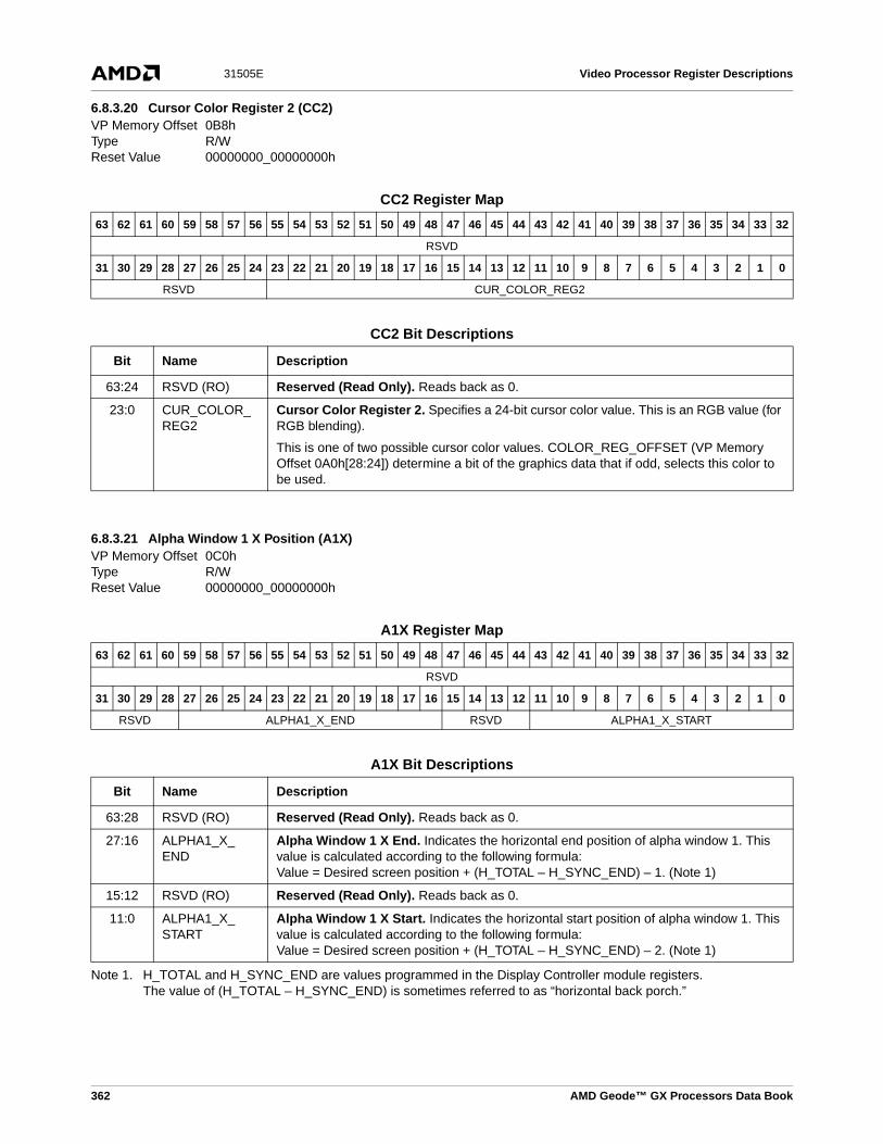
Video Processor Register Descriptions31505E
6.8.3.20 Cursor Color Register 2 (CC2)
6.8.3.21 Alpha Window 1 X Position (A1X)
VP Memory Offset 0B8hType R/WReset Value 00000000_00000000h
CC2 Register Map
63 62 61 60 59 58 57 56 55 54 53 52 51 50 49 48 47 46 45 44 43 42 41 40 39 38 37 36 35 34 33 32
RSVD
31 30 29 28 27 26 25 24 23 22 21 20 19 18 17 16 15 14 13 12 11 10 9 8 7 6 5 4 3 2 1 0
RSVD CUR_COLOR_REG2
CC2 Bit Descriptions
Bit Name Description
63:24 RSVD (RO) Reserved (Read Only). Reads back as 0.
23:0 CUR_COLOR_REG2
Cursor Color Register 2. Specifies a 24-bit cursor color value. This is an RGB value (for RGB blending).
This is one of two possible cursor color values. COLOR_REG_OFFSET (VP Memory Offset 0A0h[28:24]) determine a bit of the graphics data that if odd, selects this color to be used.
VP Memory Offset 0C0hType R/WReset Value 00000000_00000000h
A1X Register Map
63 62 61 60 59 58 57 56 55 54 53 52 51 50 49 48 47 46 45 44 43 42 41 40 39 38 37 36 35 34 33 32
RSVD
31 30 29 28 27 26 25 24 23 22 21 20 19 18 17 16 15 14 13 12 11 10 9 8 7 6 5 4 3 2 1 0
RSVD ALPHA1_X_END RSVD ALPHA1_X_START
A1X Bit Descriptions
Bit Name Description
63:28 RSVD (RO) Reserved (Read Only). Reads back as 0.
27:16 ALPHA1_X_END
Alpha Window 1 X End. Indicates the horizontal end position of alpha window 1. This value is calculated according to the following formula:Value = Desired screen position + (H_TOTAL – H_SYNC_END) – 1. (Note 1)
15:12 RSVD (RO) Reserved (Read Only). Reads back as 0.
11:0 ALPHA1_X_START
Alpha Window 1 X Start. Indicates the horizontal start position of alpha window 1. This value is calculated according to the following formula:Value = Desired screen position + (H_TOTAL – H_SYNC_END) – 2. (Note 1)
Note 1. H_TOTAL and H_SYNC_END are values programmed in the Display Controller module registers. The value of (H_TOTAL – H_SYNC_END) is sometimes referred to as “horizontal back porch.”
362 AMD Geode™ GX Processors Data Book

Video Processor Register Descriptions 31505E
6.8.3.22 Alpha Window 1 Y Position (A1Y)
6.8.3.23 Alpha Window 1 Color (A1C)
VP Memory Offset 0C8hType R/WReset Value 00000000_00000000h
A1Y Register Map
63 62 61 60 59 58 57 56 55 54 53 52 51 50 49 48 47 46 45 44 43 42 41 40 39 38 37 36 35 34 33 32
RSVD
31 30 29 28 27 26 25 24 23 22 21 20 19 18 17 16 15 14 13 12 11 10 9 8 7 6 5 4 3 2 1 0
RSVD ALPHA1_Y_END RSVD ALPHA1_Y_START
A1Y Bit Descriptions
Bit Name Description
63:27 RSVD (RO) Reserved (Read Only). Reads back as 0.
26:16 ALPHA1_Y_END
Alpha Window 1 Y End. Indicates the vertical end position of alpha window 1. This value is calculated according to the following formula:Value = Desired screen position + (V_TOTAL – V_SYNC_END) + 2. (Note 1)
15:11 RSVD (RO) Reserved (Read Only). Reads back as 0.
10:0 ALPHA1_Y_START
Alpha Window 1 Y Start. Indicates the vertical start position of alpha window 1. This value is calculated according to the following formula:Value = Desired screen position + (V_TOTAL – V_SYNC_END) + 1. (Note 1)
Note 1. V_TOTAL and V_SYNC_END are values programmed in the Display Controller module registers. The value of (V_TOTAL – V_SYNC_END) is sometimes referred to as “vertical back porch.”
VP Memory Offset 0D0hType R/WReset Value 00000000_00000000h
A1C Register Map
63 62 61 60 59 58 57 56 55 54 53 52 51 50 49 48 47 46 45 44 43 42 41 40 39 38 37 36 35 34 33 32
RSVD
31 30 29 28 27 26 25 24 23 22 21 20 19 18 17 16 15 14 13 12 11 10 9 8 7 6 5 4 3 2 1 0
RSVD
CO
LOR
_RE
G_E
N ALPHA1_COLOR_REG
AMD Geode™ GX Processors Data Book 363

Video Processor Register Descriptions31505E
6.8.3.24 Alpha Window 1 Control (A1T)
A1C Bit Descriptions
Bit Name Description
63:25 RSVD (RO) Reserved (Read Only). Reads back as 0.
24 ALPHA1_COLOR_REG_EN
Alpha Window 1 Color Register Enable. Enable bit for the color-key matching in alpha window 1.
0: Disable. If this bit is disabled, the alpha window is enabled, and VG_CK = 0 (VP Mem-ory Offset 008h[20]); then where there is a color-key match within the alpha window, video is displayed.
If this bit is disabled, the alpha window is enabled, and VG_CK = 1 (VP Memory Off-set 008h[20]); then where there is a chroma-key match within the alpha window, graphics are displayed. See Figure 6-25 on page 336.
1: Enable. If this bit is enabled and the alpha window is enabled, then where there is a color-key match within the alpha window; the color value in bits [23:0] is displayed.
23:0 ALPHA1_COLOR_REG
Alpha Window 1 Color Register. Specifies the color to be displayed inside the alpha window when there is a color-key match in the alpha window.
This color is only displayed if the alpha window is enabled and ALPHA1_COLOR_REG_EN (bit 24) is enabled.
VP Memory Offset 0D8hType R/WReset Value 00000000_00000000h
A1T Register Map
63 62 61 60 59 58 57 56 55 54 53 52 51 50 49 48 47 46 45 44 43 42 41 40 39 38 37 36 35 34 33 32
RSVD
31 30 29 28 27 26 25 24 23 22 21 20 19 18 17 16 15 14 13 12 11 10 9 8 7 6 5 4 3 2 1 0
RSVD
LOA
D_A
LPH
A
ALP
HA
1_W
IN_E
N ALPHA1_INC ALPHA1_VAL
364 AMD Geode™ GX Processors Data Book

Video Processor Register Descriptions 31505E
6.8.3.25 Alpha Window 2 X Position (A2X)
A1T Bit Descriptions
Bit Name Description
63:18 RSVD (RO) Reserved (Read Only). Reads back as 0.
17 LOAD_ALPHA (WO)
Load Alpha (Write Only). When set to 1, this bit causes the video processor to load the alpha value (bits [7:0]) at the start of the next frame. This bit is cleared by the de-asser-tion of VSYNC.
16 ALPHA1_WIN_EN
Alpha Window 1 Enable. Enable bit for alpha window 1.
0: Disable alpha window 1.1: Enable alpha window 1.
15:8 ALPHA1_INC Alpha Window 1 Increment. Specifies the alpha value increment/decrement. This is a signed 8-bit value that is added to the alpha value for each frame. The MSB (bit 15) indi-cates the sign (i.e., increment or decrement). When this value reaches either the maxi-mum or the minimum alpha value (255 or 0), it keeps that value (i.e., it is not incremented/decremented) until it is reloaded via bit 17.
7:0 ALPHA1_VAL Alpha Window 1 Value. Specifies the alpha value to be used for this window.
VP Memory Offset 0E0hType R/WReset Value 00000000_00000000h
A2X Register Map
63 62 61 60 59 58 57 56 55 54 53 52 51 50 49 48 47 46 45 44 43 42 41 40 39 38 37 36 35 34 33 32
RSVD
31 30 29 28 27 26 25 24 23 22 21 20 19 18 17 16 15 14 13 12 11 10 9 8 7 6 5 4 3 2 1 0
RSVD ALPHA2_X_END RSVD ALPHA2_X_START
A2X Bit Descriptions
Bit Name Description
63:28 RSVD (RO) Reserved (Read Only). Reads back as 0.
27:16 ALPHA2_X_END
Alpha Window 2 X End. Indicates the horizontal end position of alpha window 2. This value is calculated according to the following formula:Value = Desired screen position + (H_TOTAL – H_SYNC_END) – 1. (Note 1)
15:12 RSVD (RO) Reserved (Read Only). Reads back as 0.
11:0 ALPHA2_X_START
Alpha Window 2 X Start. Indicates the horizontal start position of alpha window 2. This value is calculated according to the following formula:Value = Desired screen position + (H_TOTAL – H_SYNC_END) – 2. (Note 1)
Note 1. H_TOTAL and H_SYNC_END are values programmed in the Display Controller module registers. The value of (H_TOTAL – H_SYNC_END) is sometimes referred to as “horizontal back porch.”
AMD Geode™ GX Processors Data Book 365

Video Processor Register Descriptions31505E
6.8.3.26 Alpha Window 2 Y Position (A2Y)
6.8.3.27 Alpha Window 2 Color (AC2)
VP Memory Offset 0E8hType R/WReset Value 00000000_00000000h
A2Y Register Map
63 62 61 60 59 58 57 56 55 54 53 52 51 50 49 48 47 46 45 44 43 42 41 40 39 38 37 36 35 34 33 32
RSVD
31 30 29 28 27 26 25 24 23 22 21 20 19 18 17 16 15 14 13 12 11 10 9 8 7 6 5 4 3 2 1 0
RSVD ALPHA2_Y_END RSVD ALPHA2_Y_START
A2Y Bit Descriptions
Bit Name Description
63:27 RSVD (RO) Reserved (Read Only). Reads back as 0.
26:16 ALPHA2_Y_END
Alpha Window 2 Y End. Indicates the vertical end position of alpha window 2. This value is calculated according to the following formula:Value = desired screen position + (V_TOTAL – V_SYNC_END) + 2. (Note 1)
15:11 RSVD (RO) Reserved (Read Only). Reads back as 0.
10:0 ALPHA2_Y_START
Alpha Window 2 Y Start. Indicates the vertical start position of alpha window 2. This value is calculated according to the following formula:Value = desired screen position + (V_TOTAL – V_SYNC_END) + 1. (Note 1)
Note 1. V_TOTAL and V_SYNC_END are values programmed in the Display Controller module registers. The value of (V_TOTAL – V_SYNC_END) is sometimes referred to as “vertical back porch.”
VP Memory Offset 0F0hType R/WReset Value 00000000_00000000h
A2C Register Map
63 62 61 60 59 58 57 56 55 54 53 52 51 50 49 48 47 46 45 44 43 42 41 40 39 38 37 36 35 34 33 32
RSVD
31 30 29 28 27 26 25 24 23 22 21 20 19 18 17 16 15 14 13 12 11 10 9 8 7 6 5 4 3 2 1 0
RSVD
CO
LOR
_RE
G_E
N ALPHA2_COLOR_REG
366 AMD Geode™ GX Processors Data Book

Video Processor Register Descriptions 31505E
6.8.3.28 Alpha Window 2 Control (A2T)
A2C Bit Descriptions
Bit Name Description
63:25 RSVD (RO) Reserved (Read Only). Reads back as 0.
24 ALPHA2_COLOR_REG_EN
Alpha Window 2 Color Register Enable. Enable bit for the color-key matching in alpha window 2.
0: Disable. If this bit is disabled, the alpha window is enabled, and VG_CK = 0 (VP Mem-ory Offset 008h[20]); then where there is a color-key match within the alpha window, video is displayed.
If this bit is disabled, the alpha window is enabled, and VG_CK = 1 (VP Memory Off-set 008h[20]); then where there is a chroma-key match within the alpha window, graphics are displayed. See Figure 6-25 on page 336.
1: Enable. If this bit is enabled and the alpha window is enabled, then where there is a color-key match within the alpha window; the color value in bits [23:0] is displayed.
23:0 ALPHA2_COLOR_REG
Alpha Window 2 Color Register. Specifies the color to be displayed inside the alpha window when there is a color-key match in the alpha window.
This color is only displayed if the alpha window is enabled and ALPHA2_COLOR_REG_EN (bit 24) is enabled.
VP Memory Offset 0F8hType R/WReset Value 00000000_00000000h
A2T Register Map
63 62 61 60 59 58 57 56 55 54 53 52 51 50 49 48 47 46 45 44 43 42 41 40 39 38 37 36 35 34 33 32
RSVD
31 30 29 28 27 26 25 24 23 22 21 20 19 18 17 16 15 14 13 12 11 10 9 8 7 6 5 4 3 2 1 0
RSVD
LOA
D_A
LPH
A
ALP
HA
2_W
IN_E
N ALPHA2_INC ALPHA2_VAL
A2T Bit Descriptions
Bit Name Description
63:18 RSVD (RO) Reserved (Read Only). Reads back as 0.
17 LOAD_ALPHA (WO)
Load Alpha (Write Only). When set to 1, this bit causes the Video Processor module to load ALPHA2_VAL (bits [7:0]) at the start of the next frame. This bit is cleared by the de-assertion of VSYNC.
16 ALPHA2_WIN_EN
Alpha Window 2 Enable. Enable bit for alpha window 2.
0: Disable alpha window 2.
1: Enable alpha window 2.
AMD Geode™ GX Processors Data Book 367

Video Processor Register Descriptions31505E
6.8.3.29 Alpha Window 3 X Position (A3X)
6.8.3.30 Alpha Window 3 Y Position (A3Y)
15:8 ALPHA2_INC Alpha Window 2 Increment. Specifies the alpha value increment/decrement. This is a signed 8-bit value that is added to the alpha value for each frame. The MSB (bit 15) indi-cates the sign (i.e., increment or decrement). When this value reaches either the maxi-mum or the minimum alpha value (255 or 0) it keeps that value (i.e., it is not incremented/decremented) until it is reloaded via bit 17.
7:0 ALPHA2_VAL Alpha Window 2 Value. Specifies the alpha value to be used for this window.
A2T Bit Descriptions (Continued)
Bit Name Description
VP Memory Offset 100hType R/WReset Value 00000000_00000000h
A3X Register Map
63 62 61 60 59 58 57 56 55 54 53 52 51 50 49 48 47 46 45 44 43 42 41 40 39 38 37 36 35 34 33 32
RSVD
31 30 29 28 27 26 25 24 23 22 21 20 19 18 17 16 15 14 13 12 11 10 9 8 7 6 5 4 3 2 1 0
RSVD ALPHA3_X_END RSVD ALPHA3_X_START
A3X Bit Descriptions
Bit Name Description
63:28 RSVD (RO) Reserved (Read Only). Reads back as 0.
27:16 ALPHA3_X_END
Alpha Window 3 X End. Indicates the horizontal end position of alpha window 3. This value is calculated according to the following formula:Value = Desired screen position + (H_TOTAL – H_SYNC_END) – 1. (Note 1)
15:12 RSVD (RO) Reserved (Read Only). Reads back as 0.
11:0 ALPHA3_X_START
Alpha Window 3 X Start. Indicates the horizontal start position of alpha window 3. This value is calculated according to the following formula:Value = Desired screen position + (H_TOTAL – H_SYNC_END) – 2. (Note 1)
Note 1. H_TOTAL and H_SYNC_END are values programmed in the Display Controller module registers. The value of (H_TOTAL – H_SYNC_END) is sometimes referred to as “horizontal back porch.”
VP Memory Offset 108hType R/WReset Value 00000000_00000000h
A3Y Register Map
63 62 61 60 59 58 57 56 55 54 53 52 51 50 49 48 47 46 45 44 43 42 41 40 39 38 37 36 35 34 33 32
RSVD
31 30 29 28 27 26 25 24 23 22 21 20 19 18 17 16 15 14 13 12 11 10 9 8 7 6 5 4 3 2 1 0
RSVD ALPHA3_Y_END RSVD ALPHA3_Y_START
368 AMD Geode™ GX Processors Data Book

Video Processor Register Descriptions 31505E
6.8.3.31 Alpha Window 3 Color (A3C)
A3Y Bit Descriptions
Bit Name Description
63:27 RSVD (RO) Reserved (Read Only). Reads back as 0.
26:16 ALPHA3_Y_END
Alpha Window 3 Y End. Indicates the vertical end position of alpha window 3. This value is calculated according to the following formula:Value = Desired screen position + (V_TOTAL – V_SYNC_END) + 2. (Note 1)
15:11 RSVD (RO) Reserved (Read Only). Reads back as 0.
10:0 ALPHA3_Y_START
Alpha Window 3 Y Start. Indicates the vertical start position of alpha window 3. This value is calculated according to the following formula:Value = Desired screen position + (V_TOTAL – V_SYNC_END) + 1. (Note 1)
Note 1. V_TOTAL and V_SYNC_END are values programmed in the Display Controller module. The value of (V_TOTAL – V_SYNC_END) is sometimes referred to as “vertical back porch.”
VP Memory Offset 110hType R/WReset Value 00000000_00000000h
A3C Register Map
63 62 61 60 59 58 57 56 55 54 53 52 51 50 49 48 47 46 45 44 43 42 41 40 39 38 37 36 35 34 33 32
RSVD
31 30 29 28 27 26 25 24 23 22 21 20 19 18 17 16 15 14 13 12 11 10 9 8 7 6 5 4 3 2 1 0
RSVD EN ALPHA3_COLOR_REG
A3C Bit Descriptions
Bit Name Description
63:25 RSVD (RO) Reserved (Read Only). Reads back as 0.
24 ALPHA3_COLOR_REG_EN
Alpha Window 3 Color Register Enable. Enable bit for the color-key matching in alpha window 3.
0: Disable. If this bit is disabled, the alpha window is enabled, and VG_CK = 0 (VP Mem-ory Offset 008h[20]); then where there is a color-key match within the alpha window, video is displayed.
If this bit is disabled, the alpha window is enabled, and VG_CK = 1 (VP Memory Off-set 008h[20]); then where there is a chroma-key match within the alpha window; graphics are displayed. See Figure 6-25 on page 336.
1: Enable. If this bit is enabled and the alpha window is enabled, then where there is a color-key match within the alpha window; the color value in bits [23:0] is displayed.
23:0 ALPHA3_COLOR_REG
Alpha Window 3 Color Register. Specifies the color to be displayed inside the alpha window when there is a color-key match in the alpha window.
This color is only displayed if the alpha window is enabled and the COLOR_REG_EN (bit 24) is enabled.
AMD Geode™ GX Processors Data Book 369

Video Processor Register Descriptions31505E
6.8.3.32 Alpha Window 3 Control (A3T)VP Memory Offset 118hType R/WReset Value 00000000_00000000h
A3T Register Map
63 62 61 60 59 58 57 56 55 54 53 52 51 50 49 48 47 46 45 44 43 42 41 40 39 38 37 36 35 34 33 32
RSVD
31 30 29 28 27 26 25 24 23 22 21 20 19 18 17 16 15 14 13 12 11 10 9 8 7 6 5 4 3 2 1 0
RSVD
LOA
D_A
LPH
A
ALP
HA
3_W
IN_E
N ALPHA3_INC ALPHA3_VAL
A3T Bit Descriptions
Bit Name Description
63:18 RSVD (RO) Reserved (Read Only). Reads back as 0.
17 LOAD_ALPHA (WO)
Load Alpha (Write Only). When set to 1, this bit causes the video processor to load the alpha value (in bits [7:0] of this register) at the start of the next frame. This bit is cleared by the de-assertion of VSYNC.
16 ALPHA3_WIN_EN
Alpha Window 3 Enable. Enable bit for alpha window 3.
0: Disable alpha window 3.1: Enable alpha window 3.
15:8 ALPHA3_INC Alpha Window 3 Increment. Specifies the alpha value increment/decrement. This is a signed 8-bit value that is added to the alpha value for each frame. The MSB (bit 15) indi-cates the sign (i.e., increment or decrement). When this value reaches either the maxi-mum or the minimum alpha value (255 or 0) it keeps that value (i.e., it is not incremented/decremented) until it is reloaded via bit 17.
7:0 ALPHA3_VAL Alpha Window 3 Value. Specifies the alpha value to be used for this window.
370 AMD Geode™ GX Processors Data Book

Video Processor Register Descriptions 31505E
6.8.3.33 Video Request (VRR) VP Memory Offset 120hType R/WReset Value 00000000_001B0017h
VRR Register Map
63 62 61 60 59 58 57 56 55 54 53 52 51 50 49 48 47 46 45 44 43 42 41 40 39 38 37 36 35 34 33 32
RSVD
31 30 29 28 27 26 25 24 23 22 21 20 19 18 17 16 15 14 13 12 11 10 9 8 7 6 5 4 3 2 1 0
WR
ITE
_AB
OR
T RSVD XRQ RSVD YRQ
VRR Bit Descriptions
Bit Name Description
63:32 RSVD (RO) Reserved (Read Only). Reads back as 0.
31 WRITE_ABORT Write Abort (Read Only). Status indicating the video data received from the Display Controller module was not able to stay ahead of the actual video displayed to the CRT screen. Software can use this status to adjust the X and Y request locations elsewhere in this register. This bit is cleared when read.
30:28 RSVD (RO) Reserved (Read Only). Reads back as 0.
27:16 XRQ Video X Request. Indicates the horizontal (pixel) location at which to start requesting video data.
15:11 RSVD (RO) Reserved (Read Only). Reads back as 0.
10:0 YRQ Video Y Request. Indicates the line number at which to start requesting video data.
AMD Geode™ GX Processors Data Book 371

Video Processor Register Descriptions31505E
6.8.3.34 Alpha Watch (AWT)
Alpha values may be automatically incremented/decremented for successive frames. This register can be used to readalpha values that are being used in the current frame.
6.8.3.35 Video Processor Test Mode (VTM)
VP Memory Offset 128hType ROReset Value 00000000_00xxxxxxh
AWT Register Map
63 62 61 60 59 58 57 56 55 54 53 52 51 50 49 48 47 46 45 44 43 42 41 40 39 38 37 36 35 34 33 32
RSVD
31 30 29 28 27 26 25 24 23 22 21 20 19 18 17 16 15 14 13 12 11 10 9 8 7 6 5 4 3 2 1 0
RSVD AW3 AW2 AW1
AWT Bit Descriptions
Bit Name Description
63:24 RSVD Reserved. Reads back as 0.
23:16 AW3 Alpha Value for Window 3.
15:8 AW2 Alpha Value for Window 2.
7:0 AW1 Alpha Value for Window 1.
VP Memory Offset 130hType R/WReset Value 00000000_00000000h
VTM Register Map
63 62 61 60 59 58 57 56 55 54 53 52 51 50 49 48 47 46 45 44 43 42 41 40 39 38 37 36 35 34 33 32
RSVD
31 30 29 28 27 26 25 24 23 22 21 20 19 18 17 16 15 14 13 12 11 10 9 8 7 6 5 4 3 2 1 0
SP RSVD SP
RS
VD
RT
E
RS
VD TEST_CHAN
VTM Bit Descriptions
Bit Name Description
63:32 RSVD (RO) Reserved (Read Only). Reads back as 0.
31 SP Spare. Read/write; no function.
30:11 RSVD (RO) Reserved (Read Only). Reads back as 0.
10:9 SP Spares. Read/write; no function.
8:7 RSVD (RO) Reserved (Read Only). Reads back as 0.
6 RSVD Reserved. Reserved for test purposes.
5:4 RSVD (RO) Reserved (Read Only). Reads back as 0.
3:0 RSVD Reserved. Reserved for test purposes.
372 AMD Geode™ GX Processors Data Book

Video Processor Register Descriptions 31505E
6.8.4 Flat Panel Display Control Registers
6.8.4.1 Panel Timing Register 1 (PT1)FP Memory Offset 400hType R/WReset Value 00000000_00000000h
PT1 Register Map
63 62 61 60 59 58 57 56 55 54 53 52 51 50 49 48 47 46 45 44 43 42 41 40 39 38 37 36 35 34 33 32
RSVD
31 30 29 28 27 26 25 24 23 22 21 20 19 18 17 16 15 14 13 12 11 10 9 8 7 6 5 4 3 2 1 0
RS
VD
FP
_VS
YN
C_P
OL
FP
_HS
YN
C_P
OL
RS
VD
HS
YN
C_S
RC
RSVD HSYNC_DELAY
HSYNC_PLS_WIDTH
PT1 Bit Descriptions
Bit Name Description
63:32 RSVD (RO) Reserved (Read Only). Reads back as 0.
31 RSVD Reserved. This bit is not defined.
30 FP_VSYNC_POL
FP_VSYNC Input Polarity. Selects positive or negative polarity of the FP_VSYNC input. Program this bit to match the polarity of the incoming FP_VSYNC signal. Note that FP Memory Offset 408h[23] controls the polarity of the output VSYNC.
0: FP_VSYNC is normally low, transitioning high during sync interval. (Default)1: FP_VSYNC is normally high, transitioning low during sync interval
29 FP_HSYNC_POL
FP_HSYNC Input Polarity. Selects positive or negative polarity of the FP_HSYNC input. Program this bit to match the polarity of the incoming FP_HSYNC signal. Note that FP Memory Offset 408h[22] controls the polarity of the output HSYNC.
0: FP_HSYNC is normally low, transitioning high during sync interval. (Default)1: FP_HSYNC is normally high, transitioning low during sync interval
28 RSVD Reserved. This bit is not defined.
27 HSYNC_SRC TFT Horizontal Sync Source. Selects a delayed or undelayed TFT horizontal sync out-put. This bit determines whether to use the HSYNC for the TFT panel without delaying the input HSYNC, or delay the HSYNC before sending it on to TFT. Bits [7:5] determine the amount of the delay.
0: Do not delay the input HSYNC before it is output onto the LP/HSYNC. (Default)1: Delay the input HSYNC before it is output onto the LP/HSYNC
26:8 RSVD Reserved. Write as read.
7:5 HSYNC_DELAY Horizontal Sync Delay. Selects the amount of delay in the output HSYNC pulse with respect to the input HSYNC pulse. The delay is programmable in steps of one DOTCLK. Bit 27 must be set in order for bits [7:5] to be recognized. Bits [7:5] are used only for TFT modes.
000: No delay from the input HSYNC. (Default)
001-111:Delay the HSYNC start by one to seven DOTCLKs.
AMD Geode™ GX Processors Data Book 373

Video Processor Register Descriptions31505E
6.8.4.2 Panel Timing Register 2 (PT2)
4:0 HSYNC_PLS_WIDTH
Horizontal Sync Pulse Width. Stretch the HSYNC pulse width by up to 31 DOTCLKs. The pulse width is programmable in steps of one DOTCLK. Bits [4:0] are used only for TFT modes.
00000: Does not generate the HSYNC pulse. The TFT panel uses the default input tim-ing, which is selected by keeping the HSYNC_SRC bit (bit 27) set to 0. (Default)
00001-11111: The HSYNC pulse width can be varied from one to 31 DOTCLKs.
PT1 Bit Descriptions (Continued)
Bit Name Description
FP Memory Offset 408hType R/WReset Value 00000000_00000000h
PT2 Register Map
63 62 61 60 59 58 57 56 55 54 53 52 51 50 49 48 47 46 45 44 43 42 41 40 39 38 37 36 35 34 33 32
RSVD
31 30 29 28 27 26 25 24 23 22 21 20 19 18 17 16 15 14 13 12 11 10 9 8 7 6 5 4 3 2 1 0
SP
TF
T_P
AS
S_T
HR
U
LPO
L
RS
VD
SC
RC
LHS
LMS
VF
S
VS
P
HS
P
PSEL
MC
S
PIXF RSVDC
LPRSVD
PT2 Bit Descriptions
Bit Name Description
63:32 RSVD (RO) Reserved (Read Only). Reads back as 0.
31 SP Spare. Bit is read/write, but has no function.
30 TFT_PASS_THRU
TFT Pass Through. Activates the TFT Pass Through mode. In TFT Pass Through mode, the input timing and the pixel data is passed directly on to the panel interface tim-ing and the panel data pins to drive the TFT panel. In Pass Through mode the internal FP TFT logic and timing is not used.
0: Normal mode; uses the TFT logic and timing from the FP.1: TFT Pass Through mode; FP TFT timing logic functions are not used.
29 LPOL Display Timing Strobe Polarity Select. Selects the polarity of the LDE/MOD pin. This can be used for panels that require an active low timing LDE interface signal.
0: LDE/MOD signal is active high. (Default)1: LDE/MOD signal is active low
28 RSVD Reserved. This bit is not defined.
27 SCRC Panel Shift Clock Retrace Activity Control. Programs the shift clock (SHFCLK) to be either free running, or active only during the display period. Some TFT panels recom-mend keeping the shift clock running during the retrace time.
0: Shift clock is active only during active display period.1: Shift clock is free running during the entire frame period.
374 AMD Geode™ GX Processors Data Book

Video Processor Register Descriptions 31505E
26 LHS LP/HSYNC Select. Selects the function of LP/HSYNC pin. Set this bit based on the panel type connected. For TFT panels, set this bit to 1.
0: Reserved.1: HSYNC (output for TFT panel).
25 LMS LDE/MOD Select. Selects the function of LDE/MOD pin. Set this bit based on the panel type connected. For TFT panels, set this bit to 1.
0: Reserved.1: LDE (output for TFT panel)
24 VFS FLM/VSYNC Select. Selects function of FLM/VSYNC pin. Set this bit based on the panel type connected. For TFT panels, set this bit to 1.
0: Reserved.1: VSYNC (output for TFT panel)
23 VSP Vertical Sync Output Polarity. Selects polarity of the output VSYNC signal. This bit is effective only for TFT panels; for this bit to function, bit 24 must be a 1. Note that Memory Offset 400h[30] selects the polarity of the input VSYNC.
0: VSYNC output is active high.1: VSYNC output is active low
22 HSP Horizontal Sync Output Polarity. Selects polarity of output HSYNC signal. This bit is effective only for TFT panels; for this bit to function, bit 26 must be a 1. Note that Memory Offset 400h[29] selects the polarity of the input HSYNC, and this bit controls the output polarity.
0: HSYNC output is active high.1: HSYNC output is active low
21:20 PSEL Panel Type Select. Selects panel type. The selection of the panel type in conjunction with the PIX_OUT(18:16) setting determines how pixel data is mapped on the output LD/UD pins. Panel Type Select also determines the selection of SHFCLK and other panel timing interface signals.
00: Reserved.01: TFT panel.10: Reserved.11: Reserved.
19 MCS Color/Mono Select. Selects color or monochrome LCD panel.
0: Color.1: Monochrome.
PT2 Bit Descriptions (Continued)
Bit Name Description
AMD Geode™ GX Processors Data Book 375

Video Processor Register Descriptions31505E
18:16 PIXF Pixel Output Format. These bits define the pixel output format. The selection of the pixel output format in conjunction with the panel type selection (bits [21:20]) and the color/monochrome selection (bit 19) determines how the pixel data is formatted before being sent on to the LD/UD pins. These settings also determine the SHFCLK frequency for the specific panel.
000: Up to 24-bit TFT panel with one pixel per clock.
Option1: Reserved.
Option2: Color TFT with one pixel per clock ([21:20] = 01 and [19] = 0)SHFCLK = DOTCLK.
001: 18/24-bit TFT XGA panel with two pixels per clock.
Option1: Reserved.
Option2: Reserved.
Option3: Color TFT with two pixels per clock ([21:20] = 01 and [19] = 0)SHFCLK = 1/2 of DOTCLK.
010: Reserved.
011: Reserved.
100, 101, 110, and 111: Reserved.
15:14 RSVD Reserved. These bits are not defined.
13 CLP Continuous Line Pulses. This bit selects whether line pulses are continuously output, or are output only during the active display time..
0: Continuous line pulses.1: Line pulses during the display time only.
12:0 RSVD Reserved. These bits are not defined.
PT2 Bit Descriptions (Continued)
Bit Name Description
376 AMD Geode™ GX Processors Data Book

Video Processor Register Descriptions 31505E
6.8.4.3 Power Management (PM)FP Memory Offset 410hType R/WReset Value 00000000_00000002h
PM Register Map
63 62 61 60 59 58 57 56 55 54 53 52 51 50 49 48 47 46 45 44 43 42 41 40 39 38 37 36 35 34 33 32
RSVD
31 30 29 28 27 26 25 24 23 22 21 20 19 18 17 16 15 14 13 12 11 10 9 8 7 6 5 4 3 2 1 0
SP
PW
R_S
EQ
_SE
L
RS
VD
D P
PU
B2
PU
B1
PU
B0
PD
2
PD
1
PD
0
HDEL VDEL
SIN
V
SP
PAN
EL_
PW
R_U
P
PAN
EL_
PW
R_D
OW
N
PAN
EL_
OF
F
PAN
EL_
ON
PM Bit Descriptions
Bit Name Description
63:32 RSVD (RO) Reserved (Read Only). Reads back as 0.
31:28 SP Spares. Read/write; no function.
27 PWR_SEQ_SEL Power Sequence Select. Selects whether to use internal or external power sequence. The power sequence controls the order in which FP_VDDEN, the data and control signals, and the backlight control signal DISP_EN become active during power up, and inactive during power down.
0: Use internal power sequencing (timing is controlled by bits [24:18]).1: Use external power sequencing
Must be written to 0.
26 RSVD Reserved. This bit should always be set to 0.
25 D Display Off Control Source. Selects how DISPOFF# is controlled. Independent con-trol may be used to disable the backlight to save power even if the panel is otherwise ON.
0: DISPOFF# is controlled by with the power up/down sequence.1: DISPOFF# is controlled independently of the power sequence.
24 P Panel Power On. Selects whether the panel is powered down or up following the power sequence mechanism.
0: Power down.1: Power up.
Panel power up and down phase timing is dependent upon a programmable reference clock. The reference clock is set to 14.3 MHz with the DIV field of the GLIU Device Master Configuration MSR to obtain 32 ms or 128 ms power sequence delays.
23 PUB2 Panel Power Up Phase Bit 2. Selects the amount of time from when VDD is enabled to when the panel data signals are enabled.
0: 32 ms1: 128 ms
22 PUB1 Panel Power Up Phase Bit 1. Selects the time amount of from when the panel data signals are enabled to when panel VEE is enabled.
0: 32 ms.1: 128 ms.
AMD Geode™ GX Processors Data Book 377

Video Processor Register Descriptions31505E
21 PUB0 Panel Power Up Phase Bit 0. Selects the amount of time from when panel VEE is enabled to when BKLTON is enabled.
0: 32 ms.1: 128 ms.
20 PD2 Panel Power Down Phase Bit 2. Selects the amount of time from when panel BKL-TON is disabled to when panel VEE is disabled.
0: 32 ms.1: 128 ms.
19 PD1 Panel Power Down Phase Bit 1. Selects the amount of time from when panel VEE is disabled to when the panel data signals are disabled.
0: 32 ms.1: 128 ms.
18 PD0 Panel Power Down Phase Bit 0. Selects the amount of time from when the panel data signals are disabled to when panel VDD is disabled.
0: 32 ms.1: 128 ms.
17:16 HDEL HSYNC Delay. Delays HSYNC 0 - 3 DOT clocks.
15:14 VDEL VSYNC Delay. Delays VSYNC 0 - 3 DOT clocks.
13 SINV SHFCLK Invert. Invert shfclk to panel.
12:4 SP Spares. Read/write; no function.
3 PANEL_PWR_UP Panel Power-Up Status (Read Only). Status bit indicating the flat panel is currently powering up.
2 PANEL_PWR_DOWN
Panel Power-Down Status (Read Only). Status bit indicating the flat panel is cur-rently powering down.
1 PANEL_OFF Panel OFF Status (Read Only). Status bit indicating the flat panel is currently fully off.
0 PANEL_ON Panel ON Status (Read Only). Status bit indicating the flat panel is currently fully on.
PM Bit Descriptions (Continued)
Bit Name Description
378 AMD Geode™ GX Processors Data Book

Video Processor Register Descriptions 31505E
6.8.4.4 Dither and Frame Rate Control (DFC)FP Memory Offset 418hType R/WReset Value 00000000_00000000h
DFC Register Map
63 62 61 60 59 58 57 56 55 54 53 52 51 50 49 48 47 46 45 44 43 42 41 40 39 38 37 36 35 34 33 32
RSVD
31 30 29 28 27 26 25 24 23 22 21 20 19 18 17 16 15 14 13 12 11 10 9 8 7 6 5 4 3 2 1 0
RSVD
RR
S
C2M
RV
RS RSVD NFI DBS
DE
NB
DFC Bit Descriptions
Bit Name Description
63:13 RSVD (RO) Reserved (Read Only). Reads back as 0.
12 RRS RAM or ROM Select. This bit selects either internal ROM or internal RAM as the source of the dither patterns.
0: Selects fixed (internal to FP) ROM for dither patterns. (Default)1: Selects programmable (internal to FP) RAM for dither patterns.
To update the dither RAM, this bit must = 1.
See FP Memory Offset 448h[6].
11 C2M Gray Scale Selection. This bit chooses two methods of converting an incoming color pixel stream to shades of gray for display on monochrome panels. This bit is ignored if Memory Off-set 408h[19] is set to 0 (color mode).
0: Green color only - Only the Green pixel data input is used to generate the gray shades.
1: NTSC weighting - Red, blue, and green pixel color inputs are used to generate the gray shades for the monochrome panel.
10 RVRS Negative Image. This converts the black to white and white to black and all colors in between to their logical inverse to provide a negative image of the original image. It acts as though the incoming data stream were logically inverted (1 becomes 0 and 0 becomes 1).
0: Normal display mode.1: Negative image display mode.
9:7 RSVD (RO) Reserved (Read Only). Reads back as 0.
6:4 NFI Number Of FRM Intensities. This field is used in conjunction with DBS (bit 3:1).
TFT Modes: The value in bits [6:4] sets the base color used prior to dithering. TFT panels do not use FRM. TFT definition:
000: Select 1 MSB for base color use prior to dithering.001: Select 2 MSB for base color use prior to dithering.010: Select 3 MSB for base color use prior to dithering.011: Select 4 MSB for base color use prior to dithering.100: Select 5 MSB for base color use prior to dithering.101: Select 6 MSB for base color use prior to dithering.110: Select 7 MSB for base color use prior to dithering.111: Select 8 MSB for base color, no dithering.
AMD Geode™ GX Processors Data Book 379

Video Processor Register Descriptions31505E
6.8.4.5 Blue LFSR Seed (BLFSR)
3:1 DBS Dithering Bits Select. This field is used to select the number of bits to be used for the dither-ing pattern. Dither bits are the least-significant bits of each pixel’s final color value; FRM bits are the most-significant bits.
000: Selects 6 bits as dither bits. 001: Selects 5 bits as dither bits. 010: Selects 4 bits as dither bits. 011: Selects 3 bits as dither bits. 100: Selects 2 bits as dither bits. 101: Selects 1 bit as dither bit. 110, 111: RSVD
0 DENB Dithering Enable. Enable/disable dithering. The dither bit must be enabled in order for dither RAM reads or writes to occur. When this bit is cleared, the internal dither RAM is powered down, which saves power.
0: Dither disable - The dithering function is turned off. When the dither is disabled the dither bits selection [3:1] do not have any effect and the dither RAM is not accessible.
1: Dither enable. The dither functions with the number of dither bits as set in [3:1].
DFC Bit Descriptions (Continued)
Bit Name Description
FP Memory Offset 420hType R/WReset Value 00000000_00000000h
BLFSR Register Map
63 62 61 60 59 58 57 56 55 54 53 52 51 50 49 48 47 46 45 44 43 42 41 40 39 38 37 36 35 34 33 32
RSVD
31 30 29 28 27 26 25 24 23 22 21 20 19 18 17 16 15 14 13 12 11 10 9 8 7 6 5 4 3 2 1 0
RSVD BLS
BLFSR Bit Descriptions
Bit Name Description
63:15 RSVD (RO) Reserved (Read Only). Reads back as 0.
14:0 BLS Blue LFSR Seed. 15-bit value that specifies the seed value for the FRM conversion of the Blue component of each pixel
380 AMD Geode™ GX Processors Data Book

Video Processor Register Descriptions 31505E
6.8.4.6 Red and Green LFSR Seed (RLFSR)
6.8.4.7 FRM Memory Index (FMI)
FP Memory Offset 428hType R/WReset Value 00000000_00000000h
RLFSR Register Map
63 62 61 60 59 58 57 56 55 54 53 52 51 50 49 48 47 46 45 44 43 42 41 40 39 38 37 36 35 34 33 32
RSVD
31 30 29 28 27 26 25 24 23 22 21 20 19 18 17 16 15 14 13 12 11 10 9 8 7 6 5 4 3 2 1 0
RS
VD GLS
RS
VD RLS
RLFSR Bit Descriptions
Bit Name Description
63:31 RSVD (RO) Reserved (Read Only). Reads back as 0.
30:16 GLS Green LFSR Seed. 15-bit value that specifies the seed value for the FRM conversion of the Green component of each pixel
15 RSVD (RO) Reserved (Read Only). Reads back as 0.
14:0 RLS Red LFSR Seed. 15-bit value that specifies the seed value for the FRM conversion of the Red component of each pixel
FP Memory Offset 430hType R/WReset Value 00000000_00000000h
FMI Register Map
63 62 61 60 59 58 57 56 55 54 53 52 51 50 49 48 47 46 45 44 43 42 41 40 39 38 37 36 35 34 33 32
RSVD
31 30 29 28 27 26 25 24 23 22 21 20 19 18 17 16 15 14 13 12 11 10 9 8 7 6 5 4 3 2 1 0
RSVD SEL RSVD RIN
AMD Geode™ GX Processors Data Book 381

Video Processor Register Descriptions31505E
6.8.4.8 FRM Memory Data (FMD)
FMI Bit Descriptions
Bit Name Description
63:10 RSVD (RO) Reserved (Read Only). Reads back as 0.
9:8 SEL RGB Memory (FRM RAM) Select. Allows reading or writing to individual R,G, and B memory FRM RAM locations or writing to all of them at the same time.
00: Read from R FRM RAM but write to RGB FRM RAM.01: Read or write to R FRM RAM.10: Read or write to G FRM RAM.11: Read or write to B FRM RAM.
7:6 RSVD (RO) Reserved (Read Only). Reads back as 0.
5:0 RIN FRM Memory Index. This represents the index to the FRM RAM; each RAM is config-ured as 32x64. It requires two index values to update each row of FRM RAM. For exam-ple, the 00h index value updates the 32-bit (of 64-bit WORD) LSB of row “0” FRM RAM. The 01h index value updates the 32-bit (of 64-bit WORD) MSB of row “0” FRM RAM. To update all the RAM locations the index is programmed only once with starting value, nor-mally “00”. This is used inside FP to auto increment the FRM RAM locations for every FRM RAM data access using the FP Memory Offset 438h[31:0].
FP Memory Offset 438hType R/WReset Value 00000000_00000000h
FMD Register Map
63 62 61 60 59 58 57 56 55 54 53 52 51 50 49 48 47 46 45 44 43 42 41 40 39 38 37 36 35 34 33 32
RSVD
31 30 29 28 27 26 25 24 23 22 21 20 19 18 17 16 15 14 13 12 11 10 9 8 7 6 5 4 3 2 1 0
RDAT
FMD Bit Descriptions
Bit Name Description
63:32 RSVD (RO) Reserved (Read Only). Reads back as 0.
31:0 RDAT RAM Data. This 32-bit data represents FRM RAM data in accordance to the RGB_SEL (FP Memory Offset 430h[9:8]) and the index value (FP Memory Offset 430h[5:0]).
Note: When programming the FRM RAM, data writes should always occur in pairs. TheRAM data logic accumulates two 32-bit writes, then commits the full 64 bits.Undefined results occur if this rule is not followed.
382 AMD Geode™ GX Processors Data Book
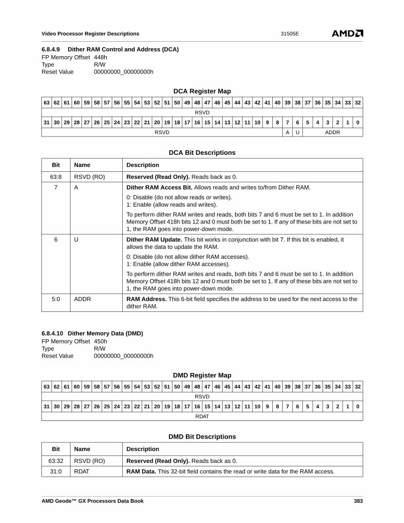
Video Processor Register Descriptions 31505E
6.8.4.9 Dither RAM Control and Address (DCA)
6.8.4.10 Dither Memory Data (DMD)
FP Memory Offset 448hType R/WReset Value 00000000_00000000h
DCA Register Map
63 62 61 60 59 58 57 56 55 54 53 52 51 50 49 48 47 46 45 44 43 42 41 40 39 38 37 36 35 34 33 32
RSVD
31 30 29 28 27 26 25 24 23 22 21 20 19 18 17 16 15 14 13 12 11 10 9 8 7 6 5 4 3 2 1 0
RSVD A U ADDR
DCA Bit Descriptions
Bit Name Description
63:8 RSVD (RO) Reserved (Read Only). Reads back as 0.
7 A Dither RAM Access Bit. Allows reads and writes to/from Dither RAM.
0: Disable (do not allow reads or writes).1: Enable (allow reads and writes).
To perform dither RAM writes and reads, both bits 7 and 6 must be set to 1. In addition Memory Offset 418h bits 12 and 0 must both be set to 1. If any of these bits are not set to 1, the RAM goes into power-down mode.
6 U Dither RAM Update. This bit works in conjunction with bit 7. If this bit is enabled, it allows the data to update the RAM.
0: Disable (do not allow dither RAM accesses).1: Enable (allow dither RAM accesses).
To perform dither RAM writes and reads, both bits 7 and 6 must be set to 1. In addition Memory Offset 418h bits 12 and 0 must both be set to 1. If any of these bits are not set to 1, the RAM goes into power-down mode.
5:0 ADDR RAM Address. This 6-bit field specifies the address to be used for the next access to the dither RAM.
FP Memory Offset 450hType R/WReset Value 00000000_00000000h
DMD Register Map
63 62 61 60 59 58 57 56 55 54 53 52 51 50 49 48 47 46 45 44 43 42 41 40 39 38 37 36 35 34 33 32
RSVD
31 30 29 28 27 26 25 24 23 22 21 20 19 18 17 16 15 14 13 12 11 10 9 8 7 6 5 4 3 2 1 0
RDAT
DMD Bit Descriptions
Bit Name Description
63:32 RSVD (RO) Reserved (Read Only). Reads back as 0.
31:0 RDAT RAM Data. This 32-bit field contains the read or write data for the RAM access.
AMD Geode™ GX Processors Data Book 383

Video Processor Register Descriptions31505E
6.8.4.11 Panel CRC Signature (CRC) FP Memory Offset 458hType R/WReset Value 00000000_00000100h
CRC Register Map
63 62 61 60 59 58 57 56 55 54 53 52 51 50 49 48 47 46 45 44 43 42 41 40 39 38 37 36 35 34 33 32
RSVD
31 30 29 28 27 26 25 24 23 22 21 20 19 18 17 16 15 14 13 12 11 10 9 8 7 6 5 4 3 2 1 0
SIGA FRCT
SF
R
SIG
E
CRC Bit Descriptions
Bit Name Description
63:32 RSVD (RO) Reserved (Read Only). Reads back as 0.
31:8 SIGA (RO) Signature Address (Read Only). 24-bit signature data for dither logic or FRM logic. In 32-bit CRC mode, this field contains the lower 24 bits of the 32-bit signature. The full 32-bit signature can be read from the 32-Bit Panel CRC register (CRC32, FP Memory Offset 468h[31:0]).
7:2 FRCT (RO) Frame Count (Read Only). Represents the frame count, which is an index for the gener-ated signature for that frame.
1 SFR Signature Free Run. If this bit is high, with signature enabled (bit 0 = 1), the signature generator captures data continuously across multiple frames. This bit may be set high when the signature is started, then later set low, which causes the signature generation process to stop at the end of the current frame.
0: Capture signature for only one frame.1: Free run across multiple frames.
0 SIGE Signature Enable. Enables/disables signature capture.
0: Disable signature capture.1: Enable signature capture.
384 AMD Geode™ GX Processors Data Book

Video Processor Register Descriptions 31505E
6.8.4.12 Frame Buffer Base Address (FBB)
6.8.5 32-Bit Panel CRC (CRC32)
FP Memory Offset 460hType R/WReset Value 00000000_xxxx0000h
FBB Register Map
63 62 61 60 59 58 57 56 55 54 53 52 51 50 49 48 47 46 45 44 43 42 41 40 39 38 37 36 35 34 33 32
RSVD
31 30 29 28 27 26 25 24 23 22 21 20 19 18 17 16 15 14 13 12 11 10 9 8 7 6 5 4 3 2 1 0
BAR RSVD
FBB Bit Descriptions
Bit Name Description
63:32 RSVD (RO) Reserved (Read Only). Reads back as 0.
31:19 BAR Frame Buffer Base Address. This 13-bit field contains the 512 KB frame buffer base address.
18:0 RSVD (RO) Reserved (Read Only). Reads back as 0.
FP Memory Offset 468hType ROReset Value 00000000_00000001h
CRC32 Register Map
63 62 61 60 59 58 57 56 55 54 53 52 51 50 49 48 47 46 45 44 43 42 41 40 39 38 37 36 35 34 33 32
RSVD
31 30 29 28 27 26 25 24 23 22 21 20 19 18 17 16 15 14 13 12 11 10 9 8 7 6 5 4 3 2 1 0
CRC
CRC32 Bit Descriptions
Bit Name Description
63:32 RSVD Reserved (Read Only). Reads back as 0.
31:0 CRC 32-Bit CRC. 32-Bit Signature when in 32-bit CRC mode. See FP Memory Offset 0458h for additional information.
AMD Geode™ GX Processors Data Book 385

GeodeLink™ Control Processor31505E
6.9 GeodeLink™ Control ProcessorThe GeodeLink Control Processor (GLCP) functionalitycovers these areas (see Figure 6-26):
• Scan chain control
• JTAG interface to boundary scan, BIST, GLIU1, and debug logic
• Power (clock) control
• Reset logic
• PLL control
6.9.1 TAP ControllerThe TAP controller is IEEE 1149.1 compliant. TMS, TDI,TCLK, and TDO are directly supported (TRST is availableas a bootstrap pin during reset, but is always inactive if thesystem reset is inactive). The instruction register (IR) is 25
bits wide. The meanings of the various instructions areshown in Table 6-56 on page 387 along with the length ofthe Data register that can be accessed once the instructionis entered. All Data registers shift in and out data, LSB first.The IR and all data registers are shift registers, so if morebits are shifted in than the register can hold, only the lastbits shifted in (the MSBs) are used.
The TAP controller has specific pre-assigned meanings tothe bits in the 25-bit register. The meanings are summa-rized in Table 6-57 on page 387. Note that the bits onlyaffect the chip once the “Update-IR” JTAG state occurs inthe JTAG controller; shifting through these bits does notchange the state of internal signals (for exampleTEST_MODE). For details on JTAG controller states, referto IEEE Standard 1149.1-1990.
Figure 6-26. GLCP Block Diagram
DebugControl
Scan, BIST,
TCLK
TMS
TDI
TDO
RQIN, RQOUT, DAIN, DAOUT
TAP Controller Clock and ResetScan and BIST
Serial-to-GLIU1
(TCLK Clock Freq.) Control(TCLK ClockFreq.)
Control(GLIU1 Clock Freq.)
Conversion(GLIU1 Clock Freq.)
GLIU1(GLIU1 Clock Freq.)
Clock, Reset Signals
386 AMD Geode™ GX Processors Data Book

GeodeLink™ Control Processor 31505E
EXTEST JTAG InstructionThe EXTEST instruction accesses the boundary scanchain around the chip and controls the pad logic such thatthe boundary scan data controls the data and enable sig-nals for the pads. IEEE 1149.1 requires that an all-zeroinstruction access the boundary scan chain; the controlleractually catches the all-zero condition during the “Update-IR” state and loads “1FFFFE8h” into the internal instructionregister. As seen by Table 6-57 on page 387, this selectOP = 000 (access boundary scan chain) and selectJta-gOut# is set active so that the boundary cells control thepads.
DELAY_CONTROLSThis chain controls the delay timing for the inputs and out-puts. This register can be overridden with an MSR write toGLCP_DELAY_CONTROLS if bit 63 of the MSR is sethigh. Bits [62:0] of this register have the same meaning asin the MSR description for GLCP_DELAY_CONTROLS.
REVIDThis 8-bit JTAG register can be reprogrammed with anymetal layer change to identify silicon changes. This registerhas the same value as GLCP_REVID (MSR4C002000h[7:0]).
Table 6-56. TAP Control Instructions (25-Bit IR)
InstructionDR
Length IR Name Description
0000000h and1FFFFE8h
409 EXTEST Boundary scan ring; IEEE 1149.1 spec compliant (mapped twice in IR address space)
11FFFFAh 63 DELAY_ CONTROLS Pad I/O delay controls
127FFFAh 8 REVID Should be 11h for initial Geode GX processor (upper nibble is major rev, lower nibble is minor) changes for each metal spin
1FFFEB0h 409 MULTISCAN Parallel scan (muxes scan outputs onto many chip pins)
1FFFFDFh 1 TRISTATE Put chip into TRI-STATE and comparison mode
1FFFFFFh 1 BYPASS Bypass; IEEE 1149.1 spec requires all 1s to be bypass
Table 6-57. TAP Instruction Bits
Bit Name Description
24 TAPSCAN# Also USER[6] in the design. This is a user bit added by AMD; low indicates that an inter-nal scan chain is accessed by the TAP.
23:18 USER[5:0] User bits used to identify an internal scan chain or, if bit 24 is high, to access a special internal DR, as shown in Table 6-56.
17:16 bistEnable[4:3] Bits 4 and 3 of the BIST enable for individual BIST chain access.
15:13 clkRatio[2:0]# Not used in Geode GX processor (bits should always be high); clock ratio controls for LogicBist.
12 freezeMode Not used in Geode GX processor (should always be high); another clock control signal.
11:10 setupMode[1:0]# Not used in Geode GX processor (should always be high); these are special BIST con-troller bits.
9:7 bistEnable[2:0] BIST[2:0] of BIST enable.
6 testMode# Active low TEST_MODE for entire chip. Puts internal logic into scan test mode.
5 forceDis# Active low bit TRI-STATEs all output pins.
4 selectJtagOut# Active low bit that allows boundary scan cells to control pads.
3 selectJtagIn# Active low bit that allows boundary scan cells to drive data into core logic of chip.
2:0 OP[2:0] Opcode that selects how the JTAG chains are wired together.
AMD Geode™ GX Processors Data Book 387

GeodeLink™ Control Processor31505E
MULTISCANDuring manufacturing test, multiple scan chains are avail-able on the signal pins. Table 6-56 on page 387 identifiesthe specific scan behaviors of various pins when in thismode. The Data register associated with this TAP instruc-tion is the boundary scan chain and the instruction bits con-figure the pads such that the boundary scan ring isproviding data into the core and the captured data on theboundary scan chain is the data coming from the core.
TRI-STATEThis instruction TRI-STATEs all of the signals. The Dataregister accessed is the Bypass register.
BYPASSAccording IEEE 1149.1, shifting all 1s into the IR must con-nect the 1-bit Bypass register. The register has no functionexcept as a storage flip-flop.
6.9.2 Reset LogicOne of the major functions of the GLCP is to control thereset of the Geode GX processor. There are two methodsto reset the Geode GX processor: either by hard resetusing the input signal RST#, or by a soft reset by writing toan internal MSR in the GLCP.
RST# is used for power-on reset. During power-on reset,all internal blocks are reset until the release of the RST#signal.
Soft reset is activated by writing to registerGLCP_SYSPLL_RST. Soft reset resets all the internalblocks to their initial status except the TAP controller. TAPreset is achieved by holding bootstrap[4] low during power-on reset.
6.9.3 Clock ControlThe clock control function controls the generation of theGeode GX processor internal clocks. For this purpose,there are two MSRs: GLCP_SYS_RSTPLL andGLCP_DOTPLL.
As shown in Figure 6-27, the internal clocks are generatedby SYSPLL and DOTPLL. In normal operation modeGLCP_SYS_RSTPLL[15] = 0 and GLCP_DOTPLL[15] = 0.The SYSPLL output clock drives the internal clocks of theCPU Core, the GeodeLink modules, and SDRAM asshown in Figure 6-28 on page 389. The output of DOTPLLdrives the DOTCLK, that in turn, drives the Video Proces-sor and Display Controller modules as shown in Figure 6-28.
In Bypass mode, when GLCP_SYS_RSTPLL[15] = 1, theDOTREF input clock drives the clocks of the CPU Core,GeodeLink modules, and SDRAM. Also, whenMSR_MCD_DOTPLL[15] = 1, the DOTREF input drivesthe DOTCLK.
Figure 6-27. Processor Clock Generation
SYSPLL
DOTPLLDOTREF
SYSREF
GLCP_DOTPLL[15]
GLCP_SYS_RSTPLL[15]
SDRAM Clocks
GL Clocks
CPU Core ClockSYSPLL Clock
DOTCLK
DOTPLL Clock
388 AMD Geode™ GX Processors Data Book

GeodeLink™ Control Processor 31505E
Figure 6-28. Processor Clock Control Modules
VideoGLMCGLIU0
CPU Core
AMD Geode™ GX Processor
Display
Graphics
PLLSelect
SYSPLL
DOTPLL
GL Clock Ctl
CPU Core Spine
Logic 0
MSS FPU IPIPE
dividersSYSREF
DOTREF
FPU2
DOT
DOT
DOT
BC
GLCP_SYS_RSTPLL[44:32]
GLBus
GLPCI
GLBus
GLIU1
GLCP
GIO I/F
Processor Processor
Controller
ControlLogic
GLCP Clock Ctl
DRAM Clock
GL Clock
CPU Core Clock
AMD Geode™ GX Processors Data Book 389

GeodeLink™ Control Processor31505E
6.9.4 Power ManagementThe GLCP controls the power management by controllingwhen to activate and deactivate the clocks of the differentmodules of the Geode GX processor. There are two modesfor controlling the power: software mode and hardwaremode.
Selection of software or hardware modes is done by pro-gramming the GLD_MSR_PM register of each module,and by setting the MSR_PRQ bit in the same register.When either software or hardware modes are activated,each module enters into power save mode when it is notbusy, and leaves power save mode if a new GeodeLinkrequest or external event is received.
Each module has a power management module calledclock control. Figure 6-28 on page 389 shows the GeodeGX processor clock control modules.
6.9.4.1 GLIU1 Power Management SupportThe GLCP is involved in power management of the proces-sor.The GLCP MSRs directly involved are:
• GLCP Clock Disable Delay Value (GLCP_CLK_DIS_DELAY)
• GLCP Global Power Management Controls (GLCP_GLB_PM)
• GLCP Clock Mask for Sleep Request (GLCP_PMCLKDISABLE)
• GLCP Clock Active Mask for Suspend Acknowledge (GLCP_CLK4ACK)
• GLCP Control (GLCP_CNT)
• GLCP Level 2 (GLCP_LVL2)
• GLCP Throttle or C2 Start Delay (GLCP_TH_SD)
• GLCP Scale Factor (GLCP_TH_SF)
• GLCP Processor Throttle Off Delay (GLCP_TH_OD)
390 AMD Geode™ GX Processors Data Book

GeodeLink™ Control Processor Register Descriptions 31505E
6.10 GeodeLink™ Control Processor Register DescriptionsAll GeodeLink Control Processor registers are Model Spe-cific Registers (MSRs) and are accessed via the RDMSRand WRMSR instructions.
The registers associated with the GLCP are the StandardGeodeLink™ Device (GLD) MSRs and GLCP SpecificMSRs. Table 6-58 and Table 6-59 are register summary
tables that include reset values and page references wherethe bit descriptions are provided.
Note: The MSR address is derived from the perspectiveof the CPU Core. See Section 4.1 "MSR Set" onpage 49 for more details on MSR addressing.
Table 6-58. Standard GeodeLink™ Device MSRs Summary
MSR Address Type Register Reset Value Reference
4C002000h RO GLD Capabilities MSR (GLD_MSR_CAP) 00000000_000020xxh Page 393
4C002001h R/W GLD Master Configuration MSR (GLD_MSR_CONFIG)
00000000_00000000h Page 393
4C002002h R/W GLD SMI MSR (GLD_MSR_SMI) 00000000_0000000Fh Page 394
4C002003h R/W GLD Error MSR (GLD_MSR_ERROR) 00000000_00000000h Page 395
4C002004h R/W GLD Power Management MSR (GLD_MSR_PM)
00000000_00000000h Page 396
4C002005h R/W GLD Diagnostic MSR (GLD_MSR_DIAG) 00000000_00000000h Page 397
Table 6-59. GLCP Specific MSRs Summary
MSR Address Type Register Reset Value Reference
GLCP Control MSRs
4C000008h R/W GLCP Clock Disable Delay Value (GLCP_CLK_DIS_DELAY)
00000000_00000000h Page 397
4C000009h R/W GLCP Clock Mask for Sleep Request (GLCP_PMCLKDISABLE)
00000000_00000000h Page 397
4C00000Ah RO Chip Fabrication Information (GLCP_FAB) 00000000_00000001h Page 398
4C00000Bh R/W GLCP Global Power Management Controls (GLCP_GLB_PM)
00000000_00000000h Page 398
4C00000Ch R/W GLCP Debug Output from Chip (GLCP_DBGOUT)
0000000000 00000000h Page 400
4C00000Dh R/W GLCP Processor Status (GLCP_PROCSTAT)
Bootstrap Dependant Page 400
4C00000Eh R/W GLCP DOWSER (GLCP_DOWSER) 00000000_00000000h Page 401
4C00000Fh R/W GLCP I/O Delay Controls (GLCP_DELAY_CONTROLS)
00000000_00000000h Page 401
4C000010h R/W GLCP Clock Control (GLCP_CLKOFF) 00000000_00000000h Page 403
4C000011h RO GLCP Clock Active (GLCP_CLKACTIVE) Input Determined Page 404
4C000012h R/W GLCP Clock Mask for Debug Clock Stop Action (GLCP_CLKDISABLE)
00000000_00000000h Page 404
4C000013h R/W GLCP Clock Active Mask for Suspend Acknowledge (GLCP_CLK4ACK)
00000000_00000000h Page 405
AMD Geode™ GX Processors Data Book 391

GeodeLink™ Control Processor Register Descriptions31505E
4C000014h R/W GLCP System Reset and PLL Control (GLCP_SYS_RSTPLL)
xxxxxxxx_00xxxxxxh Page 406
4C000015h R/W GLCP DOT Clock PLL Control (GLCP_DOTPLL)
000004A7_00008000h Page 410
4C000016h R/W GLCP Debug Clock Control (GLCP_DBGCLKCTL)
00000000_00000002h Page 411
4C000017h RO Chip Revision ID (GLCP_CHIP_REVID) 00000000_000000xxh Page 412
GLCP I/O Address MSRs
4C000018h R/W - I/O Offset 00h
GLCP Control (GLCP_CNT) 00000000_000000Fh Page 412
4C000019h R/W - I/O Offset 04h
GLCP Level 2 (GLCP_LVL2) 00000000_00000000h Page 413
4C00001Ah RO - I/O Offset 08h
Reserved 00000000_00000000h Page 413
4C00001Bh R/W - I/O NA
Reserved 00000000_00000000h Page 413
4C00001Ch R/W - I/O Offset 10h
GLCP Throttle or C2 Start Delay (GLCP_TH_SD)
00000000_00000000h Page 414
4C00001Dh R/W - I/O Offset 14h
GLCP Scale Factor (GLCP_TH_SF) 00000000_00000000h Page 414
4C00001Eh R/W - I/O Offset 18h
GLCP Processor Throttle Off Delay (GLCP_TH_OD)
00000000_00000000h Page 415
4C00001Eh R/W - I/O Offset 18h
GLCP Processor Throttle Off Delay (GLCP_TH_OD)
00000000_00000000h Page 415
4C00001Fh R/W - I/O NA
Reserved 00000000_00000000h ---
4C000020h through
4C0000FFh
R/W Reserved for future use. 00000000_00000000h ---
Table 6-59. GLCP Specific MSRs Summary (Continued)
MSR Address Type Register Reset Value Reference
392 AMD Geode™ GX Processors Data Book

GeodeLink™ Control Processor Register Descriptions 31505E
6.10.1 Standard GeodeLink™ Device MSRs
6.10.1.1 GLD Capabilities MSR (GLD_MSR_CAP)
6.10.1.2 GLD Master Configuration MSR (GLD_MSR_CONFIG)
MSR Address 4C002000hType ROReset Value 00000000_000020xxh
GLD_MSR_CAP Register Map
63 62 61 60 59 58 57 56 55 54 53 52 51 50 49 48 47 46 45 44 43 42 41 40 39 38 37 36 35 34 33 32
RSVD
31 30 29 28 27 26 25 24 23 22 21 20 19 18 17 16 15 14 13 12 11 10 9 8 7 6 5 4 3 2 1 0
RSVD DEV_ID REV_ID
GLD_MSR_CAP Bit Descriptions
Bit Name Description
63:24 RSVD Reserved. Reads as 0.
23:8 DEV_ID Device ID. Identifies device (0020h).
7:0 REV_ID Revision ID. Identifies device revision. See AMD Geode™ GX Processor Specification Update document for value.
MSR Address 4C002001hType R/WReset Value 00000000_00000000h
GLD_MSR_CONFIG Register Map
63 62 61 60 59 58 57 56 55 54 53 52 51 50 49 48 47 46 45 44 43 42 41 40 39 38 37 36 35 34 33 32
RSVD
31 30 29 28 27 26 25 24 23 22 21 20 19 18 17 16 15 14 13 12 11 10 9 8 7 6 5 4 3 2 1 0
RSVD PID
GLD_MSR_CONFIG Bit Descriptions
Bit Name Description
63:3 RSVD Reserved. Write as read.
2:0 PID Assigned Priority Domain. Unused by the GLCP.
AMD Geode™ GX Processors Data Book 393

GeodeLink™ Control Processor Register Descriptions31505E
6.10.1.3 GLD SMI MSR (GLD_MSR_SMI)MSR Address 4C002002hType R/WReset Value 00000000_0000000Fh
GLD_MSR_SMI Register Map
63 62 61 60 59 58 57 56 55 54 53 52 51 50 49 48 47 46 45 44 43 42 41 40 39 38 37 36 35 34 33 32
RSVD
31 30 29 28 27 26 25 24 23 22 21 20 19 18 17 16 15 14 13 12 11 10 9 8 7 6 5 4 3 2 1 0
RSVD
PM
L2_S
SM
I_F
LAG
PM
CN
T_S
SM
I_F
LAG
DB
G_A
SM
I_F
LAG
ER
R_A
SM
I_F
LAG RSVD
PM
L2_S
SM
I_E
N
PM
CN
T_S
SM
I_E
N
DB
G_A
SM
I_E
N
ER
R_A
SM
I_E
N
GLD_MSR_SMI Bit Descriptions
Bit Name Description
63:20 RSVD Reserved. Write as read.
19 PML2_SSMI_FLAG Power Management GLCP_LVL2 Synchronous SMI Flag. If high, records that an SSMI was generated due to a read of the GLCP_LVL2 register (MSR 4C000019h). Write 1 to clear; writing 0 has no effect. PML2_SSMI_EN (bit 3) must be low to generate SSMI and set flag.
18 PMCNT_SSMI_FLAG
Power Management GLCP_CNT Synchronous SMI Flag. If high, records that an SSMI was generated due to a write of the GLCP_CNT register (MSR 4C000018h). Write 1 to clear; writing 0 has no effect. Write 1 to clear; writing 0 has no effect. PMCNT_SSMI_EN (bit 2) must be low to generate SSMI and set flag.
17 DBG_ASMI_FLAG Debug Asynchronous SMI Flag. If high, records that an ASMI was generated due to a debug event or PROCSTAT access (MSR 4C00000Dh). Write 1 to clear; writ-ing 0 has no effect. DBG_ASMI_EN (bit 1) must be low to generate ASMI and set flag.
16 ERR_ASMI_FLAG Error Signal Asynchronous SMI Flag. If high, records that an ASMI was gener-ated due to the ERR signal. Write 1 to clear; writing 0 has no effect. ERR_ASMI_EN (bit 0) must be low to generate ASMI and set flag.
15:4 RSVD Reserved. Write as read.
3 PML2_SSMI_EN Power Management GLCP_LVL2 Synchronous SMI Enable. Write 0 to enable power management logic to generate an SSMI when the GLCP_LVL2 register (MSR 4C000019h) is read and to set flag (bit 19).
2 PMCNT_SSMI_EN Power Management GLCP_CNT Synchronous SMI Flag. Write 0 to enable power management logic to generate an SSMI when the GLCP_CNT register (MSR 4C000018h) is written and set flag (bit 18).
1 DBG_ASMI_EN Debug Asynchronous SMI Flag. Write 0 to enable the debug logic to generate an ASMI and set flag (bit 17).
0 ERR_ASMI_EN Error Signal Asynchronous SMI Flag. Write 0 to enable any GLIU1device ERR signal (including GLCP) to cause an ASMI and set flag (bit 16).
394 AMD Geode™ GX Processors Data Book

GeodeLink™ Control Processor Register Descriptions 31505E
6.10.1.4 GLD Error MSR (GLD_MSR_ERROR)MSR Address 4C002003hType R/WReset Value 00000000_00000000h
GLD_MSR_ERROR Register Map
63 62 61 60 59 58 57 56 55 54 53 52 51 50 49 48 47 46 45 44 43 42 41 40 39 38 37 36 35 34 33 32
RSVD
SY
SP
LL_E
RR
_FLA
G
DO
TP
LL_E
RR
_FLA
G
SIZ
E_E
RR
_FLA
G
UN
EX
P_T
YP
E_E
RR
_FLA
G
31 30 29 28 27 26 25 24 23 22 21 20 19 18 17 16 15 14 13 12 11 10 9 8 7 6 5 4 3 2 1 0
RSVD
SY
SP
LL_E
RR
_EN
DO
TP
LL_E
RR
_EN
SIZ
E_E
RR
_EN
UN
EX
P_T
YP
E_E
RR
_EN
GLD_MSR_ERROR Bit Descriptions
Bit Name Description
63:36 RSVD Reserved. Write as read.
35 SYSPLL_ERR_FLAG
System PLL Error Flag. If high, records that an ERR occurred due to the system PLL lock signal being active when POR was inactive. Write 1 to clear; writing 0 has no effect. SYSPLL_ERR_EN (bit 3) must be low to generate ERR and set flag.
34 DOTPLL_ERR_FLAG
Dot Clock PLL Error Flag. If high, records that an ERR occurred due to the DOT-CLK PLL lock signal being active when POR was inactive. Write 1 to clear; writing 0 has no effect. DOTPLL_ERR_EN (bit 2) must be low to generate ERR and set flag.
33 SIZE_ERR_FLAG Size Error Flag. If high, records that the GLIU1 interface detected a read or write of more than 1 data packet (size = 16 bytes or 32 bytes). If a response packet is expected, the EXCEPTION bit is set; in all cases the asynchronous error signal is set. Write 1 to clear; writing 0 has no effect. SIZE_ERR_EN (bit 1) must be low to generate ERR and set flag.
32 UNEXP_TYPE_ERR_FLAG
Unexpected Type Error Flag. An unexpected type was sent to the GLCP GLIU1 interface (start request with BEX type, snoop, PEEK_WRITE, DEBUG_REQ, or NULL type). If a response packet is expected, the EXCEPTION bit is set; in all cases the asynchronous error signal is set. Writing a 1 clears the error, writing a 0 leaves unchanged.
31:4 RSVD Reserved. Write as read.
3 SYSPLL_ERR_EN System PLL Error Enable. Write 0 to enable the ERR signal if the system PLL lock signal is active when POR is inactive and set flag (bit 35).
2 DOTPLL_ERR_EN Dot Clock PLL Error Enable. Write 0 to enable the ERR signal if the DOTCLK PLL lock signal is active when POR is inactive and set flag (bit 34)
1 SIZE_ERR_EN Size Error Enable. Write 0 to enable the ERR signal if the GLIU1 interface detects a read or write of more than 1 data packet and set flag (bit 33).
AMD Geode™ GX Processors Data Book 395

GeodeLink™ Control Processor Register Descriptions31505E
6.10.1.5 GLD Power Management MSR (GLD_MSR_PM)
The debug logic powers up selecting GLIU1 for its clock. Debug clock select is in GLCP_DBGCLKCTL (MSR4C000016h[2:0]).
0 TYPE_ERR_EN Type Error Enable. Write 0 to enable the ERR signal if an unexpected type was sent to the GLCP GLIU1 interface and set flag (bit 32).
MSR Address 4C002004hType R/WReset Value 00000000_00000000h
GLD_MSR_ERROR Bit Descriptions (Continued)
Bit Name Description
GLD_MSR_PM Register Map
63 62 61 60 59 58 57 56 55 54 53 52 51 50 49 48 47 46 45 44 43 42 41 40 39 38 37 36 35 34 33 32
RSVD
PR
Q1
PR
Q0
31 30 29 28 27 26 25 24 23 22 21 20 19 18 17 16 15 14 13 12 11 10 9 8 7 6 5 4 3 2 1 0
RSVD
PM
OD
E1
PM
OD
E0
GLD_MSR_PM Bit Descriptions
Bit Name Description
63:34 RSVD Reserved. Write as read.
33:32 RSVD Reserved. Write as 0.
31:4 RSVD Reserved. Write as read.
3:2 PMODE1 Power Mode 1 (GLCP Debug Clock). This field controls the internal clock gating for the GLCP Debug clock.
00: Disable clock gating. Clocks are always on.
01: Enable active hardware clock gating if debug inactive (i.e. GLCP_DBGCLKCTL = 0, MSR 4C000016h[2:0]).
10: Reserved.
11: Reserved.
1:0 PMODE0 Power Mode 0 (GLCP GLIU1 Clock). This field controls the internal clock gating for the GLCP GLIU1 clock.
00: Disable clock gating. Clocks are always on.
01: Enable active hardware clock gating. Clock goes off whenever this module’s cir-cuits are not busy.
10: Reserved.
11: Reserved.
396 AMD Geode™ GX Processors Data Book

GeodeLink™ Control Processor Register Descriptions 31505E
6.10.1.6 GLD Diagnostic MSR (GLD_MSR_DIAG)
This register is reserved for internal use by AMD and should not be written to.
6.10.2 GLCP Specific MSRs - GLCP Control MSRs
6.10.2.1 GLCP Clock Disable Delay Value (GLCP_CLK_DIS_DELAY)
6.10.2.2 GLCP Clock Mask for Sleep Request (GLCP_PMCLKDISABLE)
MSR Address 4C002005hType R/WReset Value 00000000_00000000h
MSR Address 4C000008hType R/WReset Value 00000000_00000000h
GLCP_CLK_DIS_DELAY Register Map
63 62 61 60 59 58 57 56 55 54 53 52 51 50 49 48 47 46 45 44 43 42 41 40 39 38 37 36 35 34 33 32
RSVD
31 30 29 28 27 26 25 24 23 22 21 20 19 18 17 16 15 14 13 12 11 10 9 8 7 6 5 4 3 2 1 0
RSVD CLK_DELAY
GLCP_CLK_DIS_DELAY Bit Descriptions
Bit Name Description
63:24 RSVD Reserved. Write as read.
23:0 CLK_DELAY Clock Disable Delay. If enabled in GLCP_GLB_PM (CLK_DLY_EN bit, MSR 4C00000Bh[4] = 1), indicates the period to wait from SLEEP_REQ before gating off clocks specified in GLCP_PMCLKDISABLE (MSR 4C000009h). If this delay is enabled, it overrides or disables the function of GLCP_CLK4ACK (MSR 4C000013h). If the CLK_DLY_EN bit is not set, but this register is non-zero, then this register serves as a timeout for the CLK4ACK behavior.
MSR Address 4C000009hType R/WReset Value 00000000_00000000h
GLCP_PMCLKDISABLE Register Map
63 62 61 60 59 58 57 56 55 54 53 52 51 50 49 48 47 46 45 44 43 42 41 40 39 38 37 36 35 34 33 32
RSVD
31 30 29 28 27 26 25 24 23 22 21 20 19 18 17 16 15 14 13 12 11 10 9 8 7 6 5 4 3 2 1 0
RSVD
GLC
PD
BG
GLC
PG
L
VP
DO
T2
VP
DO
T1
VP
DO
T0
VP
GL1
VP
GL0
GLP
CIP
CIF
GLP
CIP
CI
GL_
GLP
CI
GL1
_GLI
U1
GL0
_GLI
U1
GIO
PC
I
GIO
GL
DC
GL1
DC
GL0
DC
DO
T1
DC
DO
T0
GL1
_GLI
U0
GL0
_GLI
U0
GP
GL_
GLM
C
DR
AM
GL_
BC
CP
U_B
C
CP
U_M
SS
CP
U_I
PIP
E
FP
UFA
ST
FP
US
LOW
AMD Geode™ GX Processors Data Book 397

GeodeLink™ Control Processor Register Descriptions31505E
6.10.2.3 Chip Fabrication Information (GLCP_FAB)
This read only register is used to track various fab, process, and product family parameters. It is meant for AMD internaluse only. Reads return reset value.
6.10.2.4 GLCP Global Power Management Controls (GLCP_GLB_PM)
GLCP_PMCLKDISABLE Bit Descriptions
Bit Name Description
63:29 RSVD Reserved. Write as read.
28:0 PMCLKDISABLE Clock Mask for Sleep Request. These bits correspond to the Clock Off (CLKOFF) bits in GLCP_CLKOFF (MSR 4C000010h). If a bit in this field is set, then the corresponding CLK_OFF bit is set when the power management circuitry disables clocks when enter-ing Sleep.
MSR Address 4C00000AhType ROReset Value 00000000_00000001h
MSR Address 4C00000BhType R/WReset Value 00000000_00000000h
GLCP_GLB_PM Register Map
63 62 61 60 59 58 57 56 55 54 53 52 51 50 49 48 47 46 45 44 43 42 41 40 39 38 37 36 35 34 33 32
RSVD
31 30 29 28 27 26 25 24 23 22 21 20 19 18 17 16 15 14 13 12 11 10 9 8 7 6 5 4 3 2 1 0
RSVD
DO
TP
LL_E
N
SY
SP
LL_E
N RSVD
OU
T_V
P
OU
T_G
IO
OU
T_M
C
OU
T_P
CI
OU
T_O
TH
ER RSVD
CLK
_DLY
_EN
CLK
_DIS
_EN
RS
VD
RS
VD
TH
T_E
N
398 AMD Geode™ GX Processors Data Book

GeodeLink™ Control Processor Register Descriptions 31505E
GLCP_GLB_PM Bit Descriptions
Bit Name Description
63:18 RSVD Reserved. Write as read.
17 DOTPLL_EN Turn Off DOTCLK PLL during Sleep.
0: Disable.1: Enable. This bit must be set to 1 for normal operation.
16 SYSPLL_EN Turn Off System PLL during Sleep.
0: Disable.1: Enable. This bit must be set to 1 for normal operation.
15:13 RSVD Reserved. Write as read.
12 OUT_VP TRI-STATE VP Outputs during Sleep.
0: Disable.1: Enable.
11 OUT_GIO TRI-STATE GIO Outputs during Sleep.
0: Disable.1: Enable.
10 OUT_MC TRI-STATE GLMC Outputs during Sleep.
0: Disable.1: Enable.
9 OUT_PCI TRI-STATE GLPCI outputs during Sleep.
0: Disable.1: Enable.
8 OUT_OTHER TRI-STATE TDBGO and SUSPA# during Sleep.
0: Disable.1: Enable.
7:5 RSVD Reserved. Write as read.
4 CLK_DLY_EN Clock Delay Enable. Enables gating off clock enables from a delay rather than GLCP_CLK4ACK (MSR 4C000013h).
0: Disable.1: Enable.
3 CLK_DIS_EN Assert GLIU CLK_DIS_REQ during Sleep.
0: Disable.1: Enable.
2:1 RSVD Reserved. Write as read.
0 THT_EN Processor Throttling Functions Enable.
0: All the functions related to throttling are disabled (GLCP_TH_OD, GLCP_CNT, etc.).1: All the functions related to throttling are enabled (GLCP_TH_OD, GLCP_CNT, etc.).
AMD Geode™ GX Processors Data Book 399

GeodeLink™ Control Processor Register Descriptions31505E
6.10.2.5 GLCP Debug Output from Chip (GLCP_DBGOUT)
This register is revserved for internal use by AMD and should not be written to.
6.10.2.6 GLCP Processor Status (GLCP_PROCSTAT)
Note that the names of these bits have the read status data before the "_" and the write behavior after it.
MSR Address 4C00000ChType R/WReset Value 0000000000 00000000h
MSR Address 4C00000DhType R/WReset Value Bootstrap Dependant
GLCP_PROCSTAT Register Map
63 62 61 60 59 58 57 56 55 54 53 52 51 50 49 48 47 46 45 44 43 42 41 40 39 38 37 36 35 34 33 32
RSVD
31 30 29 28 27 26 25 24 23 22 21 20 19 18 17 16 15 14 13 12 11 10 9 8 7 6 5 4 3 2 1 0
RSVD
RE
SE
T_N
ON
E
STO
PC
LK_N
ON
E
GLA
CT
_UN
STA
LL
GLC
PS
TALL
_DM
I
STA
LL_S
MI
SU
SP
_STO
PC
LK
DM
I_S
TALL
GLCP_PROCSTAT Bit Descriptions
Bit Name Description
63:7 RSVD Reserved. Writing these bits have no effect.
6 RESET_NONE Reset Status. When read, this bit is high if a hard or soft reset to the Geode GX processor has occurred since this register was last read. Writing this bit has no effect.
5 STOPCLK_ NONE Stop Clock Status. When read, this bit is high if a GLCP stop clock action has occurred since this register was last read. Writing this bit has no effect.
4 GLACT_UNSTALL GLIU1 Debug Action Status. When read, this bit is high if the GLCP has triggered a GLIU1debug action since this register was last read. Writing this bit high unstalls the processor.
3 GLCPSTALL_ DMI GLCP Control Processor Stall Status. When read, this bit is high if the GLCP is stalling the CPU. Writing this bit high causes a GLCP DMI to the processor.
2 STALL_ SMI CPU Stall Status. When read, this bit is high if the CPU is stalled for any reason. Writing this bit high causes an GLCP SMI to the processor. Bit 1 of GLD_MSR_SMI (MSR 4C002002h) gets set by this SMI and an SMI is triggered, assuming appropriate SMI enable settings.
1 SUSP_ STOPCLK CPU Suspended Stop Clock Status. When read, this bit is high if the CPU has suspended execution for any reason since this register was last read. Writing this bit high causes the GLCP to stop all clocks identified in GLCP_CLKDISABLE (MSR 4C000012h).
0 DMI_STALL CPU DMI Stall Status. When read, this bit is high if the CPU is in DMI mode. Writ-ing this bit high causes the GLCP to “DEBUG_STALL” the processor.
400 AMD Geode™ GX Processors Data Book

GeodeLink™ Control Processor Register Descriptions 31505E
6.10.2.7 GLCP DOWSER (GLCP_DOWSER)
6.10.2.8 GLCP I/O Delay Controls (GLCP_DELAY_CONTROLS)
Note: This register should be initialized by boot software to: 830D415A_8EA0AD6Ah for DDR.
MSR Address 4C00000EhType R/WReset Value 00000000_00000000h
GLCP_DOWSER Register Map
63 62 61 60 59 58 57 56 55 54 53 52 51 50 49 48 47 46 45 44 43 42 41 40 39 38 37 36 35 34 33 32
SW Defined
31 30 29 28 27 26 25 24 23 22 21 20 19 18 17 16 15 14 13 12 11 10 9 8 7 6 5 4 3 2 1 0
SW Defined
GLCP_DOWSER Bit Descriptions
Bit Name Description
63:0 --- Software Defined. This 64-bit scratchpad register was specifically added for SWdebugger use (DOWSER). The register resets to zero with both hard and soft resets
MSR Address 4C00000FhType R/WReset Value 00000000_00000000h
GLCP_DELAY_CONTROLS Register Map
63 62 61 60 59 58 57 56 55 54 53 52 51 50 49 48 47 46 45 44 43 42 41 40 39 38 37 36 35 34 33 32
EN RSVD GIO PCI_IN PCI_OUT RSVD DOTCLK DRGB
31 30 29 28 27 26 25 24 23 22 21 20 19 18 17 16 15 14 13 12 11 10 9 8 7 6 5 4 3 2 1 0
DR
GB
SDCLK_IN SDCLK_OUT MEM_CTL RSVD
ME
M_O
DD
OU
T RSVD
DQ
S_C
LK_I
N
DQ
S_C
LK_O
UT
GLCP_DELAY_CONTROLS Bit Descriptions
Bit Name Description
63 EN Delay Settings Enable. Enable the delay settings in this MSR to override the 62-bit JTAG register.
0: Disable1: Enable
The JTAG register does not have this bit.
62:61 RSVD Reserved. Write as read.
60:56 GIO Delay Geode Companion Device. Add Delay to GIO input pads: 10101 is no delay, 00000 is shortest, 00001, 00011, ..., 11111. Higher delays increase the setup time required on INTR, SUSP#, and SMI# relative to SYSREF while decreasing the hold time required.
55:51 PCI_IN Delay PCI Inputs. Add delay to PCI inputs: 10101 is no delay, 00000 is shortest, 00001, 00011, ..., 11111. Higher delays increase setup time required and decrease hold time required on all PCI inputs (AD, REQ#, etc.) plus TDBGI.
AMD Geode™ GX Processors Data Book 401

GeodeLink™ Control Processor Register Descriptions31505E
50:46 PCI_OUT Delay PCI Outputs. Add delay to PCI outputs: 10101 is no delay, 00000 is shortest, 00001, 00011, ..., 11111. Higher delays increase the clock-to-Q output time for all PCI outputs (AD, GNT#, etc.) plus TDBGO, SUSPA#, and IRQ13. For special setting 00101, only the odd data bits are delayed, this could be useful for minimizing noise generated by the PCI signals.
45:41 RSVD Reserved. Write as read.
40:36 DOTCLK Delay Dot Clock. Add delay to DOTCLK output time: 10101 is no delay, 00000 is short-est, 00001, 00011, ..., 11111.
35:31 DRGB Delay Digital RGBs. Add delay to DRGBs clock-to-Q output time as well as HSYNC, VSYNC, FP_DISP_EN, FP_VDDEN, and FP_LDE_MOD: 10101 is no delay, 00000 is shortest, 00001, 00011, ..., 11111. For special setting 00101, only the odd data bits are delayed, this could be useful for minimizing noise generated by the DRGB signals.
30:26 SDCLK_IN Delay SDRAM Clock Input. Delay to SD_WR_CLK: 10101 is no delay; use SD_WR_CLK pad input, 00000 is shortest delay; use SD_FB_CLK internal bypass, 00001, 00011, ..., 11111. When not set to 10101, the internal clock that drives the SD_FP_CLK output pad is directly used, this allows delays that are shorter than a board trace would allow since the pad input and output times are avoided.
25:21 SDCLK_OUT Delay SDRAM Clock Output. Add delay to SD_FB_CLK and SDCLK[11:0] outputs: 10101 is no delay, 00000 is shortest, 00001, 00011, ..., 11111.
20:16 MEM_CTL Delay Memory Controls. Add delay to memory controls clock-to-Q output time: 10101 is no delay, 00000 is shortest, ..., 11111.
15:7 RSVD Reserved. Write as read.
6 MEM_ODDOUT Delay Odd Memory Data Output Bits. Add delay to memory data out on odd bits. High value adds a few hundred ps delay on odd memory bit output times. This could be useful for minimizing noise generated by the memory data output pins.
5:4 RSVD Reserved. Write as read.
3:2 DQS_CLK_IN Delay DQS Before Clocking Input. Delay for DQS before clocking input memory data: 00 shortest, 01,10,11. Higher delays allow more skew between DQS and input data from memory.
1:0 DQS_CLK_OUT Delay DQS Before Clocking Output. Delay for DQS before clocking memory data from core: 00 shortest, 01,10,11. Increasing this delay effectively increases the clock-to-Q out-put time of the memory data signals relative to the DQS output during a write.
GLCP_DELAY_CONTROLS Bit Descriptions (Continued)
Bit Name Description
402 AMD Geode™ GX Processors Data Book

GeodeLink™ Control Processor Register Descriptions 31505E
6.10.2.9 GLCP Clock Control (GLCP_CLKOFF)
This register has bits that, when set, force clocks off using GeodeLink Clock Control (GLCC)) logic in the system. This is fordebugging only, and should not be used for power management.
MSR Address 4C000010hType R/WReset Value 00000000_00000000h
GLCP_CLKOFF Register Map
63 62 61 60 59 58 57 56 55 54 53 52 51 50 49 48 47 46 45 44 43 42 41 40 39 38 37 36 35 34 33 32
RSVD
31 30 29 28 27 26 25 24 23 22 21 20 19 18 17 16 15 14 13 12 11 10 9 8 7 6 5 4 3 2 1 0
RSVD
GLC
PD
BG
GLC
PG
L
VP
DO
T2
VP
DO
T1
VP
DO
T0
VP
GL1
VP
GL0
GLP
CIP
CIF
GLP
CIP
CI
GL_
GLP
CI
GL1
_GLI
U1
GL0
_GLI
U1
GIO
PC
I
GIO
GL
DC
GL1
DC
GL0
DC
DO
T1
DC
DO
T0
GL1
_GLI
U0
GL0
_GLI
U0
GP
GL_
GLM
C
DR
AM
GL_
BC
CP
U_B
C
CP
U_M
SS
CP
U_I
PIP
E
FP
UFA
ST
FP
US
LOW
GLCP_CLKOFF Bit Descriptions
Bit Name Description
28 GLCPDBG GLCP Debug Clock Off. When set, disables GLCP DBG logic clock.
27 GLCPGL GLCP GeodeLink Clock Off. When set, disables GLCP GL clock.
26 VPDOT2 VP Dot Clock 2 Off. When set, disables VP DOTCLK 2 (VP_VID).
25 VPDOT1 VP Dot Clock 1 Off. When set, disables VP DOTCLK 1 (LCD_PIX).
24 VPDOT0 VP Dot Clock 0 Off. When set, disables VP DOTCLK 0 (VP_PIX).
23 VPGL1 VP GeodeLink Clock 1 Off. When set, disables VP GL clock 1 (LCD).
22 VPGL0 VP GeodeLink Clock 0 Off. When set, disables VP GL clock 0 (VP).
21 GLPCIPCIF GLPCI Fast-PCI Clock Off. When set, disables Fast-PCI clock inside GLPCI.
20 GLPCIPCI GLPCI PCI Clock Off. When set, disables normal PCI clock inside GLPCI.
19 GL_GLPCI GeodeLink Clock to GeodeLink PCI Bridge Clock Off. When set, disables GL clock from entering GLPCI.
18 GL1_GLIU1 GeodeLink Clock 1 to GLIU1 Off. When set, disables main GL clock to GLIU1.
17 GL0_GLIU1 GeodeLink Clock 0 to GLIU1 Off. When set, disables GL clock to timer logic of GLIU1.
16 GIOPCI GIO PCI Clock Off. When set, disables GIO PCI clock.
15 GIOGL GIO GL Clock Off. When set, disables GIO GL clock.
14 DCGL1 DC GeodeLink Clock 1 Off. When set, disables DC GL clock 1 (VGA).
13 DCGL0 DC GeodeLink Clock 0 Off. When set, disables DC GL clock 0 (VG).
12 DCDOT1 DC Dot Clock 1 Off. When set, disables DC DOTCLK 1 (VGA).
11 DCDOT0 DC Dot Clock 0 Off. When set, disables DC DOTCLK 0 (VG).
10 GL1_GLIU0 GeodeLink Clock 1 to GLIU0 Off. When set, disables main GL clock to GLIU0.
9 GL0_GLIU0 GeodeLink Clock 0 to GLIU0 Off. When set, disables GL clock to timer logic of GLIU0.
8 GP GP Clock Off. When set, disables GP clock.
7 GL_GLMC GeodeLink Clock to GeodeLink Memory Controller Off. When set, disables GL clock to GLMC.
6 DRAM DRAM Clocks Off. When set, disables external DRAM clocks (and, hence, feedback clocks).
AMD Geode™ GX Processors Data Book 403

GeodeLink™ Control Processor Register Descriptions31505E
6.10.2.10 GLCP Clock Active (GLCP_CLKACTIVE)
6.10.2.11 GLCP Clock Mask for Debug Clock Stop Action (GLCP_CLKDISABLE)
This register is reserved for internal testing only. These bits should not be written to
5 GL_BC GeodeLink Clock to Bus Controller Off. When set, disables GL clock to the BC block in the CPU Core.
4 CPU_BC CPU Core Clock to Bus Controller Off. When set, disables the CPU Core clock to the BC block in the CPU Core.
3 CPU_MSS CPU Core Clock to Memory Subsystem Off. When set, disables the CPU Core clock to MSS block in the CPU Core.
2 CPU_IPIPE CPU Core Clock to Instruction Pipeline Off. When set, disables the CPU Core clock to IPIPE block in the CPU Core.
1 FPUFAST Fast FPU Clock Off. When set, disables the “fast” FPU clock.
0 FPUSLOW Slow FPU Clock Off. When set, disables the “slow” CPU Core clock to FPU.
MSR Address 4C000011hType ROReset Value Input Determined
GLCP_CLKOFF Bit Descriptions (Continued)
Bit Name Description
GLCP_CLKACTIVE Register Map
63 62 61 60 59 58 57 56 55 54 53 52 51 50 49 48 47 46 45 44 43 42 41 40 39 38 37 36 35 34 33 32
RSVD
31 30 29 28 27 26 25 24 23 22 21 20 19 18 17 16 15 14 13 12 11 10 9 8 7 6 5 4 3 2 1 0
RSVD
GLC
PD
BG
GLC
PG
L
VP
DO
T2
VP
DO
T1
VP
DO
T0
VP
GL1
VP
GL0
GLP
CIP
CIF
GLP
CIP
CI
GL_
GLP
CI
GL1
_GLI
U1
GL0
_GLI
U1
GIO
PC
I
GIO
GL
DC
GL1
DC
GL0
DC
DO
T1
DC
DO
T0
GL1
_GLI
U0
GL0
_GLI
U0
GP
GL_
GLM
C
DR
AM
GL_
BC
CP
U_B
C
CP
U_M
SS
CP
U_I
PIP
E
FP
UFA
ST
FP
US
LOW
GLCP_CLKACTIVE Bit Descriptions
Bit Name Description
63:29 RSVD Reserved.
28:0 CLKACTIVE Clock Active. This register has bits that, when set, indicate that a block is internallyenabling its own clock. The clock inside a block can still be toggling even though theGLCP_CLKACTIVE bit is clear if the local clock gating MSR forces the clock to alwaysbe on. Also, the clock can be off even though the GLCP_CLKACTIVE bit is set, if theGLCP_CLKOFF bit is set in the GLCP_CLKCTL register.
MSR Address 4C000012hType R/WReset Value 00000000_00000000h
404 AMD Geode™ GX Processors Data Book

GeodeLink™ Control Processor Register Descriptions 31505E
6.10.2.12 GLCP Clock Active Mask for Suspend Acknowledge (GLCP_CLK4ACK) MSR Address 4C000013hType R/WReset Value 00000000_00000000h
GLCP_CLK4ACK Register Map
63 62 61 60 59 58 57 56 55 54 53 52 51 50 49 48 47 46 45 44 43 42 41 40 39 38 37 36 35 34 33 32
RSVD
31 30 29 28 27 26 25 24 23 22 21 20 19 18 17 16 15 14 13 12 11 10 9 8 7 6 5 4 3 2 1 0
RSVD
GLC
PD
BG
GLC
PG
L
VP
DO
T2
VP
DO
T1
VP
DO
T0
VP
GL1
VP
GL0
GLP
CIP
CIF
GLP
CIP
CI
GL_
GLP
CI
GL1
_GLI
U1
GL0
_GLI
U1
GIO
PC
I
GIO
GL
DC
GL1
DC
GL0
DC
DO
T1
DC
DO
T0
GL1
_GLI
U0
GL0
_GLI
U0
GP
GL_
GLM
C
DR
AM
GL_
BC
CP
U_B
C
CP
U_M
SS
CP
U_I
PIP
E
FP
UFA
ST
FP
US
LOW
GLCP_CLK4ACK Bit Descriptions
Bit Name Description
63:29 RSVD Reserved.
28:0 CLK4ACK Clock for Acknowledge. This register has bits that correspond to the Clock Off(CLKOFF) bits in GLCP_CLKOFF. If the bit in GLCP_CLK4ACK is set, then theSUSPA# signal does not go low unless the clock is inactive.
AMD Geode™ GX Processors Data Book 405

GeodeLink™ Control Processor Register Descriptions31505E
6.10.2.13 GLCP System Reset and PLL Control (GLCP_SYS_RSTPLL)
This register is initialized during POR, but otherwise is not itself reset by any “soft-reset” features. Note that although allPLL and timing control bits can be written and read back the last written data, none of the frequency control bit writes takeeffect on the system until CHIP_RESET (bit 0) is set (MDIV, VDIV, FBDIV, BYPASS, TST, DDRMODE,VA_SEMI_SYNC_MODE, PCI_SEMI_SYNC_MODE). Writing this register with the CHIP_RESET bit set never sends awrite-response over GLIU1. (This allows halting bus traffic before the reset occurs.) Writing to the PD or RESET bits has animmediate effect.
MSR Address 4C000014hType R/WReset Value xxxxxxxx_00xxxxxxh
GLCP_SYS_RSTPLL Register Map
63 62 61 60 59 58 57 56 55 54 53 52 51 50 49 48 47 46 45 44 43 42 41 40 39 38 37 36 35 34 33 32
RSVD MDIV VDIV FBDIV
31 30 29 28 27 26 25 24 23 22 21 20 19 18 17 16 15 14 13 12 11 10 9 8 7 6 5 4 3 2 1 0
SWFLAGS
LOC
K
LOC
KW
AIT
HOLD_COUNT
BY
PAS
S
PD
PLL
RE
SE
T
TST
DD
RM
OD
E
VA
_SE
MI_
SY
NC
_MO
DE
PC
I_S
EM
I_S
YN
C_M
OD
E
DS
TALL
BO
OT
ST
RA
P_S
TAT
DO
TP
OS
TD
IV3
DO
TP
RE
MU
LT2
DO
TP
RE
DIV
2
CH
IP_R
ES
ET
GLCP_SYS_RSTPLL Bit Descriptions
Bit Name Description
63:45 RSVD Reserved. Write as read.
44:41 MDIV GLIU1 Divisor. The divider for the GLIU1 clock.
0000: Divide by 2, ... , 1111: Divide by 17.
These bits are read/write but the actual clock divider control is only changed when CHIP_RESET (bit 0) is also set.
40:38 VDIV CPU Core Divisor. The divider setting for the CPU Core clock.
000: Divide by 2 (Default), ...,111: Divide by 9.
These bits are read/write but the actual clock divider control is only changed when CHIP_RESET (bit 0) is also set.
37:32 FBDIV Feedback Divisor. The feedback divider setting for the system PLL are pseudo-random due to the design of the high-speed PLL divider (see Table 6-60 "FBDIV Setting for Desired PLL Divider Results" on page 409 for decode). These bits are read/write but the actual PLL control is only changed when CHIP_RESET (bit 0) is also set.
31:26 SWFLAGS Software Flags. Flags that are reset only by the POR# signal, not the CHIP_RESET. They are reset to 0 and can be used as flags in the boot code that survive CHIP_RESET.
25 LOCK (RO) Lock (Read Only). Lock signal from the system PLL.
24 LOCKWAIT Lock Wait. Allow the chip to release reset when the PLL lock signal is set.
0: Disable (Default).1: Enable.
406 AMD Geode™ GX Processors Data Book

GeodeLink™ Control Processor Register Descriptions 31505E
23:16 HOLD_COUNT Hold Count. The number of PLL reference clock cycles (multiply by 16) that the PLL is powered down for and also the number before releasing CHIP_RESET (bit 0). (LOCK-WAIT can cause reset to release earlier, but this timeout allows the releasing of reset if lock is not achieved in a certain period).
00000000: Wait 0 clock cycles (Default). 00000001: Wait 1*16 clock cycles.... 11111111: Wait 16*255 clock cycles.
15 BYPASS PLL Bypass. The POR value in this register is undefined. After POR, DOTREF is used for the CPU Core clock and GLIU clock. For normal operation of the system PLL, this bit must be written to 0 before CHIP_RESET (bit 0) operation.
0: After CHIP_RESET is performed, the output of the system PLL is used for the CPU core clock and CLIU clock.
1: After CHIP_RESET is performed, DOTREF is used for the CPU Core clock and GLIU clock.
14 PD Power Down. This signal controls the power down mode of the system PLL. It is active high. It has an immediate effect, so it is not recommended unless either BYPASS (bit 15) is set or CHIP_RESET (bit 0) is set. This bit is always cleared by a CHIP_RESET.
13 RESETPLL PLL Reset. This signal resets the voltage control setting of the voltage-controlled oscilla-tor on the system PLL. This potentially allows lock to be acquired in the case that the PLL itself has intermittent behavior. It is active high. It has an immediate effect, so it is not rec-ommended unless either BYPASS (bit 15) is set or CHIP_RESET (bit 0) is set. This bit is always cleared by a CHIP_RESET.
12:11 RSVD Reserved.
10 DDRMODE DDR Mode.
0: The output pads of the GLMC are configured for DDR communication and the its con-trol logic is clocked with a clock running at half of the GLIU1 frequency. This bit is read/writable but the actual memory frequency is only changed when CHIP_RESET (bit 0) is also set.
1: Reserved.
9 VA_SEMI_ SYNC_MODE
Synchronous CPU Core and GLIU1. This bit controls whether the CPU Core processor uses a FIFO for interfacing with GLIU1 or not. If the bit is high, the CPU Core does not use the FIFO; it behaves as if the CPU Core and GLIU1 domains were synchronous. This bit can be set high as long as the CPU Core and GLIU1 frequencies are multiples of each other. The bit always resets low. This bit is read/writable but the actual signal to the CPU Core is only changed when CHIP_RESET (bit 0) is also set.
8 PCI_SEMI_ SYNC_MODE
Synchronous CPU Core and GLIU1. This bit controls whether the PCI uses the falling edges of MB_FUNC_CLK and PCI_FUNC_CLK for interfacing with GLIU1 or not. If the bit is high, PCI does not use falling clock edges; it behaves as if the CPU Core and GLIU1 domains were synchronous. This bit can be set high as long as the PCI and GLIU1 frequencies are multiples of each other. The bit always resets low. This bit is read/writable but the actual signal to the PCI block is only changed when CHIP_RESET (bit 0) is also set.
7 DSTALL (RO) Debug Stall (Read Only). A 1 indicates that the system booted up stalled. This register is initialized by IRQ13 strapping at POR. IRQ13 should be pulled low for normal opera-tion.
6:4 BOOTSTRAP_STAT (RO)
Bootstrap Status (Read Only). These bits are initialized by GNT[3:0]# respectively at POR. No additional hardware action occurs from the GNT# straps.
3 DOTPOSTDIV3 DOTPLL Post-Divide by 3. This read/writable bit has an immediate effect on the DOT-PLL behavior. It post-divides the PLL output frequency by three. Refer to the GLCP_DOTPLL register for details.
GLCP_SYS_RSTPLL Bit Descriptions (Continued)
Bit Name Description
AMD Geode™ GX Processors Data Book 407

GeodeLink™ Control Processor Register Descriptions31505E
2 DOTPREMULT2 DOTPLL Pre-Multiply by 2. This read/writable bit has an immediate effect on the DOT-PLL behavior. It pre-multiplies the PLL input frequency by two. Refer to the GLCP_DOTPLL register for details.
1 DOTPREDIV2 DOTPLL Pre-Divide by 2. This read/writable bit has an immediate effect on the DOTPLL behavior. It pre-divides the PLL input frequency by two. Refer to the GLCP_DOTPLL reg-ister for details.
0 CHIP_RESET Chip Reset. When written to a 1, the chip enters reset and does not come out of reset until the HOLD_COUNT is reached or until the PLL is locked if LOCKWAIT is set. This register and the JTAG logic are not reset by CHIP_RESET, but otherwise the entire chip is reset. (Default = 0.)
GLCP_SYS_RSTPLL Bit Descriptions (Continued)
Bit Name Description
408 AMD Geode™ GX Processors Data Book

GeodeLink™ Control Processor Register Descriptions 31505E
Table 6-60. FBDIV Setting for Desired PLL Divider Results
FBDIV PLL Divide FBDIV PLL Divide FBDIV PLL Divide FBDIV PLL Divide
59 Don’t use 48 49 26 33 10 17
55 Don’t use 33 48 52 32 21 16
47 Don’t use 2 47 41 31 42 15
30 Don’t use 5 46 18 30 20 14
60 61 11 45 36 29 40 13
57 60 23 44 8 28 16 12
51 59 46 43 17 27 32 11
39 58 28 42 34 26 0 10
14 57 56 41 4 25 1 9
29 56 49 40 9 24 3 8
58 55 35 39 19 23 7 7
53 54 6 38 38 22 15 6
43 53 13 37 12 21 31 Don’t use
22 52 27 36 25 20 62 Don’t use
44 51 54 35 50 19 61 Don’t use
24 50 45 34 37 18 63 Don’t use
Table 6-61. FBDIV Setting to PLL Divide Mapping
FBDIV PLL Divide FBDIV PLL Divide FBDIV PLL Divide FBDIV PLL Divide
63 Don’t use 47 Don’t use 31 Don’t use 15 6
62 Don’t use 46 43 30 Don’t use 14 57
61 Don’t use 45 34 29 56 13 37
60 61 44 51 28 42 12 21
59 Don’t use 43 53 27 36 11 45
58 55 42 15 26 33 10 17
57 60 41 31 25 20 9 24
56 41 40 13 24 50 8 28
55 Don’t use 39 58 23 44 7 7
54 35 38 22 22 52 6 38
53 54 37 18 21 16 5 46
52 32 36 29 20 14 4 25
51 59 35 39 19 23 3 8
50 19 34 26 18 30 2 47
49 40 33 48 17 27 1 9
48 49 32 11 16 12 0 10
AMD Geode™ GX Processors Data Book 409

GeodeLink™ Control Processor Register Descriptions31505E
6.10.2.14 GLCP DOT Clock PLL Control (GLCP_DOTPLL)
This register does not include hardware handshake controls like the GLCP_SYS_PLLRST register, so care should betaken when changing the settings. For example, to change the DIV settings: write the register with the RESET bit set andeither in the same write or another write change the DIV settings; read the register until LOCK (bit 25) goes active (or untila timeout occurs, if desired); write the register with the same DIV settings and with the RESET bit clear. The MDIV, NDIV,and PDIV (bits [44:32]) settings work in conjunction with the DOTPOSTDIV3, DOTPREMULT2, DOTPREDIV2 bits (MSR4C000014h[3:1]) to create the internal DOTCLK using this equation:
For example, with bits [44:32] in the GLCP_DOTPLL register set to 0x4A7 (default) and bit 3 in GLCP_SYS_RSTPLL set(not the default), the DOTCLK frequency that the Display Controller and Video Processor modules would run with wouldbe:
However, not all MDIV, NDIV, and PDIV settings lock and not all that lock have good long-term jitter characteristics.
The MDIV, NDIV, and PDIV in this register connect directly to the DOTPLL inputs.
MSR Address 4C000015hType R/WReset Value 000004A7_00008000h
Fout Fin NDIV 1+( ) 2DOTPREMULT2⋅
MDIV 1+( ) 2PDIV 2DOTPREDIV2 3DOTPOSTDIV3⋅ ⋅ ⋅-------------------------------------------------------------------------------------------------------------------------------------------------------------⋅=
Fout 14.318MHz 41 1+( ) 20⋅
2 1+( ) 23 20 31⋅ ⋅ ⋅----------------------------------------------------⋅ 8.35MHz= =
GLCP_DOTPLL Register Map
63 62 61 60 59 58 57 56 55 54 53 52 51 50 49 48 47 46 45 44 43 42 41 40 39 38 37 36 35 34 33 32
RSVD MDIV NDIV PDIV
31 30 29 28 27 26 25 24 23 22 21 20 19 18 17 16 15 14 13 12 11 10 9 8 7 6 5 4 3 2 1 0
SWFLAGS
LOC
K
RSVD
BY
PAS
S
PD
TST
IN27
MH
z RSVD
DO
TR
ES
ET
GLCP_DOTPLL Bit Descriptions
Bit Name Description
63:45 RSVD Reserved. Write as read.
44:41 MDIV Input Clock Divisor. The DOTPLL M setting (resets to VGA timing).
40:34 NDIV Dot Clock PLL Divisor. The DOTPLL N setting (resets to VGA timing).
33:32 PDIV Post Scaler Divisor. The DOTPLL P setting (resets to VGA timing).
31:26 SWFLAGS Software Flags. Unlike in the SYS_RSTPLL register, these bits are reset to 0 by a soft reset to the chip. These bits are otherwise read/writable by software. They are not reset by a DOTRESET.
25 LOCK (RO) Lock (Read Only). Lock signal from the DOTCLK PLL
24:16 RSVD Reserved. Write as read.
15 BYPASS Dot PLL Bypass. This signal controls the bypass mode of the DOTCLK PLL. If this bit is high, the DOTREF input clock directly drives the raw DOTCLK, bypassing the MDIV, NDIV, and PDIV logic.
14 PD Power Down. This bit controls the power down mode of the DOTCLK PLL. It is active high.
410 AMD Geode™ GX Processors Data Book

GeodeLink™ Control Processor Register Descriptions 31505E
6.10.2.15 GLCP Debug Clock Control (GLCP_DBGCLKCTL)
Note that after the mux to select the clock, a standard clock control gate exists. This register should never be changed fromone non-zero value to another. Always write this register to 0 when moving to an alternative debug clock.
13:11 TST Test. These bits control the test signals into the DOTCLK PLL in order to access internal test points.
10 IN27MHZ 27 MHz Input. Needs to be set by software if the input clock is 27 MHz instead of 14.318 MHz. Setting this bit allows VGA clock overrides to work correctly.
9:1 RSVD Reserved. Write as read.
0 DOTRESET Dot Clock Reset. The reset pin to the DOTCLK time blocks. The Dot reset is held active when CHIP_RESET is high, but this bit resets to 0. It is recommended that software set this bit when changing PLL settings and observe LOCK before releasing this reset. Unlike the SYS_RSTPLL register, this bit is not required to be set before the other bits in this register affect the PLL.
MSR Address 4C000016hType R/WReset Value 00000000_00000002h
GLCP_DOTPLL Bit Descriptions (Continued)
Bit Name Description
GLCP_DBGCLKCTL Register Map
63 62 61 60 59 58 57 56 55 54 53 52 51 50 49 48 47 46 45 44 43 42 41 40 39 38 37 36 35 34 33 32
RSVD
31 30 29 28 27 26 25 24 23 22 21 20 19 18 17 16 15 14 13 12 11 10 9 8 7 6 5 4 3 2 1 0
RSVD CLKSEL
GLCP_DBGCLKCTL Bit Descriptions
Bit Name Description
63:3 RSVD Reserved. Write as read.
2:0 CLKSEL Clock Select. Selects the clock to drive into the debug logic.
000: None.001: CPU Core clock.010: GLIU1 clock.011: DOTCLK.100: PCI clock.101-111: Reserved.
AMD Geode™ GX Processors Data Book 411

GeodeLink™ Control Processor Register Descriptions31505E
6.10.2.16 Chip Revision ID (GLCP_CHIP_REVID)
6.10.3 GLCP Specific MSRs - GLCP I/O Address MSRs
6.10.3.1 GLCP Control (GLCP_CNT)
This register is used in conjunction with GLIU1 Power Management (described in a separate chapter). I/O writes, whichinclude the lowest byte of this register may trigger an SMI if GLD_MSR_SMI is configured appropriately. MSR writes do notcause SMIs. The throttle sequence starts after the delay specified by GLCP_TH_SD, which can allow for SMI handling timeor any other preparations. Throttling is temporarily stopped in IRQ, SSMI, ASMI, or DMI. NMI and system sleep (C2)always clear THT_EN (bit 4).
MSR Address 4C000017hType ROReset Value 00000000_000000xxh
GLCP_CHIP_REVID Register Map
63 62 61 60 59 58 57 56 55 54 53 52 51 50 49 48 47 46 45 44 43 42 41 40 39 38 37 36 35 34 33 32
RSVD
31 30 29 28 27 26 25 24 23 22 21 20 19 18 17 16 15 14 13 12 11 10 9 8 7 6 5 4 3 2 1 0
RSVD MAJ MIN
GLCP_CHIP_REVID Bit Descriptions
Bit Name Description
63:8 RSVD Reserved. Reads as 0.
7:4 MAJ Major Revision. Identifies major silicon revision. See AMD Geode™ GX Processor Specification Update document for value.
3:0 MIN Minor Revision. Identifies minor silicon revision. See AMD Geode™ GX Processor Specification Update document for value.
MSR Address 4C000018hType R/W - I/O Offset 00hReset Value 00000000_000000Fh
GLCP_CNT Register Map
63 62 61 60 59 58 57 56 55 54 53 52 51 50 49 48 47 46 45 44 43 42 41 40 39 38 37 36 35 34 33 32
RSVD
31 30 29 28 27 26 25 24 23 22 21 20 19 18 17 16 15 14 13 12 11 10 9 8 7 6 5 4 3 2 1 0
RSVD
TH
T_E
N CLK_VAL
GLCP_CNT Bit Descriptions
Bit Name Description
63:5 RSVD Reserved. Write as read.
4 THT_EN Throttle Enable. When high, enables throttling of processor for power management. This bit is always cleared by an NMI to the processor or when system sleep initiates, it may clear from an SMI or IRQ depending on GLCP_TH_OD settings.
412 AMD Geode™ GX Processors Data Book

GeodeLink™ Control Processor Register Descriptions 31505E
6.10.3.2 GLCP Level 2 (GLCP_LVL2)
This register has no writable bits. I/O reads to the lower byte of this register (with or without reading the other three bytes)return 0 and cause the system to enter “C2 processor state” as defined by the GLIU1 power management spec; that is,suspend the processor. I/O reads to the lower byte of this register may trigger an SMI if GLD_MSR_SMI is configuredappropriately. Note that the suspend starts after a delay specified in GLCP_TH_SD (MSR 4C00001Ch), which can allow forSMI handling or any other preparations. P_LVL2_IN (MSR 4C00001Ch[12])can abort the suspend operation. MSR reads tothis register return 0 and performs no further action.
6.10.3.3 Reserved
This register is reserved for internal use by AMD.
6.10.3.4 Reserved
This register is reserved for internal use by AMD.
3:0 CLK_VAL Clock Throttling Value. The value 0000 is reserved and should not be used. The value 0001 yields the most throttling while the value 1111 has the effect of no throttling (1111 is the reset value). Reads return value written. THT_EN (bit 4) must be low to change the value of CLK_VAL. See also GLCP_TH_SF. During processor throttling, processor sus-pend is applied the amount of time of “(15-CLK_VAL)*GLCP_TH_SF” and then removed the amount of time of “CLK_VAL*GLCP_TH_SF”.
MSR Address 4C000019hType R/W - I/O Offset 04hReset Value 00000000_00000000h
MSR Address 4C00001AhType RO - I/O Offset 08hReset Value 00000000_00000000h
MSR Address 4C00001BhType R/W - I/O NAReset Value 00000000_00000000h
GLCP_CNT Bit Descriptions (Continued)
Bit Name Description
AMD Geode™ GX Processors Data Book 413

GeodeLink™ Control Processor Register Descriptions31505E
6.10.3.5 GLCP Throttle or C2 Start Delay (GLCP_TH_SD)
6.10.3.6 GLCP Scale Factor (GLCP_TH_SF)
MSR Address 4C00001ChType R/W - I/O Offset 10hReset Value 00000000_00000000h
GLCP_TH_SD Register Map
63 62 61 60 59 58 57 56 55 54 53 52 51 50 49 48 47 46 45 44 43 42 41 40 39 38 37 36 35 34 33 32
RSVD
31 30 29 28 27 26 25 24 23 22 21 20 19 18 17 16 15 14 13 12 11 10 9 8 7 6 5 4 3 2 1 0
RSVD
P_L
VL2
_IN THT_DELAY
GLCP_TH_SD Bit Descriptions
Bit Name Description
63:13 RSVD Reserved. By convention, always write zero.
12 P_LVL2_IN Enable Indicator. If P_LVL2 was read, then this bit reads high. If this bit is written to a one, the suspend is aborted. This bit is always cleared and Suspend de-asserted on NMI, IRQ, SSMI, ASMI, DMI, or system Sleep.
11:0 THT_DELAY Throttle Delay. Indicates how long to wait before beginning the processor throttling pro-cess as defined by GLCP_CNT. The delay setting is multiplied by 16 to get the number of PCI clock cycles to wait, thus setting THT_DELAY = 3 causes a wait of 48 PCI clock cycles.
MSR Address 4C00001DhType R/W - I/O Offset 14hReset Value 00000000_00000000h
GLCP_TH_SF Register Map
63 62 61 60 59 58 57 56 55 54 53 52 51 50 49 48 47 46 45 44 43 42 41 40 39 38 37 36 35 34 33 32
RSVD
31 30 29 28 27 26 25 24 23 22 21 20 19 18 17 16 15 14 13 12 11 10 9 8 7 6 5 4 3 2 1 0
RSVD SCALE
GLCP_TH_SF Bit Descriptions
Bit Name Description
63:8 RSVD Reserved. By convention, always write 0.
7:0 SCALE Scale Factor. This value is used in conjunction with CLK_VAL (MSR 4C000018h[3:0]). This value times CLK_VAL (or 15-CLK_VAL) indicates the number of PCI clock cycles to wait during processor active (or suspend) periods. The setting is multiplied by 16 to get the number of PCI clock cycles per period, thus SCALE = 3 and CLK_VAL = 5 will have the processor active for 240 PCI clocks and suspended for 480 PCI clocks.
414 AMD Geode™ GX Processors Data Book

GeodeLink™ Control Processor Register Descriptions 31505E
6.10.3.7 GLCP Processor Throttle Off Delay (GLCP_TH_OD)
Note: There is a bit in the CPU Core, that prevents or allows the CPU Core to Suspend during SMIs and DMIs (even syn-chronous ones). This bit may be useful for power management, but does not affect these registers.
MSR Address 4C00001EhType R/W - I/O Offset 18hReset Value 00000000_00000000h
GLCP_TH_OD Register Map
63 62 61 60 59 58 57 56 55 54 53 52 51 50 49 48 47 46 45 44 43 42 41 40 39 38 37 36 35 34 33 32
RSVD
31 30 29 28 27 26 25 24 23 22 21 20 19 18 17 16 15 14 13 12 11 10 9 8 7 6 5 4 3 2 1 0
RSVD
IRQ
_EN
SM
I_E
N OFF_DELAY
GLCP_TH_OD Bit Descriptions
Bit Name Description
63:16 RSVD Reserved. By convention, always write 0.
15 IRQ_EN Enable Throttling Restart after IRQ. If this bit is set and throttling is not disabled during the IRQ handling, throttling restarts after the period specified by OFF_DELAY (bits [13:0]). If this bit is clear, then an IRQ clears THT_EN (MSR 4C000018h[4]).
14 SMI_EN Enable Throttling Restart after SMI. If this bit is set and throttling is not disabled during the SMI handling, throttling restarts after the period specified by OFF_DELAY. If this bit is clear, then an ASMI clears THT_EN (MSR 4C000018h[4]).
13:0 OFF_DELAY Throttle Off Delay. Indicates the period to wait from receipt of IRQ or SMI before restart-ing throttle operation. This setting is multiplied by 16 to get the number of PCI clock cycles to wait.
AMD Geode™ GX Processors Data Book 415

GeodeLink™ PCI Bridge31505E
6.11 GeodeLink™ PCI BridgeThe GeodeLink™ PCI Bridge (GLPCI) module provides aPCI interface for GeodeLink Interface Unit-based designs.The GLPCI module is composed of six major blocks:
• GeodeLink Interface
• FIFO/Synchronization
• Transaction Forwarding
• PCI Bus Interface
• PCI Arbiter
The GLIU and PCI Bus Interface blocks provide adaptationto the respective buses. The Transaction Forwarding blockprovides bridging logic.
Features
• PCI Version 2.2 compliance
• 32-bit, 66 MHz PCI bus operation
• Target support for fast back-to-back transactions
• Arbiter support for three external PCI bus masters
• Write gathering and write posting for in-bound write requests
• Virtual PCI header support
• Delayed transactions for in-bound read requests
• Zero wait state operation within a PCI burst
• Dynamic clock stop/start support for GLIU and PCI clock domains (this is not CLKRUN support)
• Capable of handling out-bounds transactions immedi-ately after reset
Figure 6-29. GLPCI Block Diagram
PCI Bus Interface
PCI Bus
RequestRequest Data
PCIArbiter
REQ#/GNT#
MSR Transaction Forwarding
FIFOs/Synchronization
GeodeLink™ Interface
GeodeLink™ Interface Unit 1 (GLIU1)
Clock Control
Clock Control
Clock Control
416 AMD Geode™ GX Processors Data Book

GeodeLink™ PCI Bridge 31505E
6.11.1 GeodeLink™ Interface BlockThe GeodeLink Interface block provides a thin protocolconversion layer between the Transaction Forwardingblock and GeodeLink Interface Unit 1 (GLIU1). It is respon-sible for multiplexing in-bound write request data with out-bound read response data on the single GLIU1 data outbus.
6.11.2 FIFO/Synchronization BlockThe FIFO module consists of a collection of in-bound andout-bound FIFOs. Each FIFO provides simple, synchro-nous interfaces to read and write requests.
6.11.3 Transaction Forwarding BlockThe Transaction Forwarding block receives, processes,and forwards transaction requests and responses betweenthe GeodeLink Interface and PCI Bus Interface blocks. Itimplements the transaction ordering rules and performswrite gathering and read prefetching as needed. It also per-forms the necessary translation between GLIU1 and PCIcommands; except for the creation of PCI configurationcycles in response to I/O accesses of address 0CFCh. TheTransaction Forwarding block also handles the conversionbetween 64-bit GLIU1 data paths and 32-bit PCI datapaths.
Out-bound transactions are handled in a strongly orderedfashion. Some out-bound burst writes may be combinedinto a larger PCI transaction. This is accomplished bydynamically concatenating together contiguous bursts asthey are streamed out in a PCI bus transaction. Single 32-bit WORD accesses are not gathered. It is anticipated thatthe processor generates the majority of out-boundrequests. Out-bound memory writes will not be posted.Thus, any queued out-bound requests need NOT beflushed prior to handling an in-bound read request.
Dynamic concatenation of contiguous bursts may occurwhen reading the penultimate (next to last) data WORDfrom the out-bound write data FIFO. On that cycle, if a suit-able request is available at the head of the out-boundrequest FIFO, the PCI burst will be extended.
In-bound requests are handled using slightly relaxed order-ing. All in-bound writes are gathered as much as possible.Any partially gathered in-bound writes are flushed when acache line boundary is reached. All in-bound writes areposted. Thus, any queued in-bound write data MUST bewritten to system memory prior to the processor receivingdata for an out-bound read request. This is accomplishedby sorting out-bound read response data amongst in-bound write data. Thus, a pending out-bound read requestneed not be deferred while posted in-bound write data isflushed. The out-bound read request may be performed onthe PCI bus at the same time that the in-bound write data isflowing through GLIU1.
When handling an in-bound read request, the intended sizeof the transfer is unknown. In-bound read requests for non-prefetchable addresses only fetch the data explicitly indi-cated in the PCI transaction. Thus, all in-bound read
requests made to non-prefetchable addresses return atmost a single 32-bit WORD. In-bound read requests madeto prefetchable memory may cause more than a 32-bitWORD to be prefetched. The amount of data prefetched isconfigured via the read threshold fields of the CTRL (MSR50002010h). Multiple read requests may be generated tosatisfy the read threshold value.
In-bound read requests may pass posted in-bound writedata when there is no address collision between the readrequest and the address range of the posted write data (dif-ferent cache lines) and the read address is marked asbeing prefetchable.
6.11.3.1 Atomic External MSR AccessThe AMD Geode™ CS5536 companion device implementsa mailbox scheme similar to the Geode GX processor. Toaccess internal model specific registers on the GeodeCS5536 companion device’s GLIU it is necessary to per-form multiple PCI configuration cycles. The GLPCI moduleprovides a mechanism to give software atomic, transparentaccess to the Geode CS5536 companion device’s GLIUresident MSRs. It translates MSR read/writes receivedfrom the Geode GX processor’s GLIUs into the multiplePCI configuration needed to access the Geode CS5536companion device’s internal MSR. From software’s point ofview, the GLPCI module routes MSR read/write requestslike a GLIU. The GLPCI module terminates MSR accesseswhere the three most significant bits are zero. Otherwise ituses the same three MSBs as an index to look up a PCIdevice number and a PCI function number in EXTMSR(MSR 5000201Eh). This device number is then furthermapped onto AD[31:11] pins using the same mapping aswith software generated PCI configuration cycles. Next theGLPCI module performs three PCI configuration buscycles.
• Write MSR address to offset F4h
• Read/write MSR data to/from offset F8h
• Read/write MSR data to/from offset FCh
Note: The GLPCI module attempts to do a burst PCI con-figuration read or write. It is expected that the tar-get PCI device will typically cause this burst to getbroken up into two by performing a slave termina-tion after each DWORD of data is transferred.
The GLPCI module can address up to seven external PCIdevices in this manner.
AMD Geode™ GX Processors Data Book 417

GeodeLink™ PCI Bridge31505E
Figure 6-30. Atomic MSR Accesses Across the PCI Bus
MB1
Device-A Device-B
Device-C
PCI-device = 1
PCI-device = 15 PCI-device = 25 PCI-device = 30
2
4
3
6
5
1
2
7
3
AMD Geode™ GX Processor
2.4.1.3.6.x 2.4.2.5.1.x
2.4.3.2.7.3
EXTMSR configuration(MSR 5000201Eh):
GLIU-port1 -> pci-device-15GLIU-port2 -> pci-device-25GLIU-port3 -> pci-device-30
GLPCI
GLIU0
GLIU1
GLPCI
GLIU0
GLIU
GLPCI
GLIU0
GLIU1
GLIU2
GLPCI
GLIU0
CPU Core
418 AMD Geode™ GX Processors Data Book

GeodeLink™ PCI Bridge 31505E
6.11.4 PCI Bus Interface BlockThe PCI Bus Interface block is compliant to the PCI 2.2specification, except in the handling of SERR#/PERR# sig-nals. These signals are not available.
The PCI Bus Interface block provides a protocol conver-sion layer between the Transaction Forwarding block andthe PCI bus. The master and target portions of this blockoperate independently. Thus, out-bound write requests andin-bound read responses are effectively multiplexed ontothe PCI bus. It generates configuration cycles and softwaregenerated special cycles using the standard 0CF8/0CFCI/O address scheme. It includes address decoding logic torecognize distinct address regions for slave operation.Each address region is defined by a base address, a size,and some attached attributes (i.e., prefetchable, coherent).
This block is responsible for retrying out-bound requestswhen a slave termination without data is seen on the PCIbus. It must restart transactions on the PCI bus that areprematurely ended with a slave termination. This modulealways slave terminates in-bound read transactions issuedto non-prefetchable regions after a single WORD has beentransferred.
6.11.4.1 PCI Configuration and Virtual PCI Header Support
The PCI Bus Interface block implements the logic to gener-ate PCI configuration cycles. The standard mechanism forgenerating PCI configuration cycles (as described in thePCI 2.2 specification) is used.
To access the internal PCI configuration registers of theGeode GX processor, the Configuration Address register(CONFIG_ADDRESS) must be written as a DWORD usingthe format shown in Table 6-62. Any other size will be inter-preted as an I/O write to Port 0CF8h. Also, when entering
the Configuration Index, only the six most significant bits ofthe offset are used, and the two least significant bits mustbe 00b.
BYTE and WORD sized I/O accesses to 0CF8h passthrough the PCI Bus Interface block onto the PCI bus.Writes to the CONFIG_DATA register are translated intoPCI configuration write bus cycles. Reads to theCONFIG_DATA register are translated into PCI configura-tion read bus cycles. Bit-31 of the CONFIG_ADDRESSregister gates the translation of I/O accesses to 0CFCh intoPCI configuration cycles.
IDSEL assertions are realized where device numbers 1through 21 are mapped to the AD[11] through AD[31] pins.
In addition, support is included for virtualization of PCIbuses and secondary bus devices. When a device or bus isvirtualized, the PCI Bus Interface block generates a syn-chronous SMI for access to the CONFIG_DATA registerinstead of generating a configuration cycle on the PCI bus.See the PBUS register (MSR 50002012h[31:0]) for detailson virtual PCI header support.
The PCI Bus Interface block can be configured to acceptin-bound PCI configuration cycles. This is used as a debugmethod for indirectly accessing the internal model specificregister from the PCI bus. When this capability is enabled,the PCI Bus Interface block responds to in-bound PCI con-figuration cycles that make the PCI Bus Interface block’sIDSEL signal become asserted (expected to be device 1).In this case, the PCI Bus Interface block will ignore writesand return FFFFFFFFh for accesses to locations 00hthrough EFh of the PCI configuration space. This makesthe PCI Bus Interface block invisible to PCI Plug&Play soft-ware..
Table 6-62. Format for Accessing the Internal PCI Configuration Registers
31 30 29 28 27 26 25 24 23 22 21 20 19 18 17 16 15 14 13 12 11 10 9 8 7 6 5 4 3 2 1 0
1 Reserved 0 0 0 0 0 0 0 0 0 0 0 0 0 0 0 0 Configuration Index 0 0
Table 6-63. PCI Device to AD Bus Mapping
PCI Device AD Pin PCI Device AD Pin PCI Device AD Pin PCI Device AD Pin
0 N/A 8 18 16 26 24 N/A
1 11 9 19 17 27 25 N/A
2 12 10 20 18 28 26 N/A
3 13 11 21 19 29 27 N/A
4 14 12 22 20 30 28 N/A
5 15 13 23 21 31 29 N/A
6 16 14 24 22 N/A 30 N/A
7 17 15 25 23 N/A 31 N/A
AMD Geode™ GX Processors Data Book 419

GeodeLink™ PCI Bridge31505E
6.11.5 PCI ArbiterThe PCI Arbiter block determines which PCI master isgranted permission to initiate data transfer on the PCI bus.
6.11.5.1 OverviewThe PCI Arbiter block features are:
• Support for three external PCI masters and Host Bridge master.
• Request #2 is reserved for use by the South Bridge, which requires higher priority.
• Host Bridge master priority can be controlled via a programmable counter that allows 1-8 External PCI grants to occur before the CPU can regain top priority again.
• Support for fixed priority scheme, rotation priority scheme or hybrid of the two.
• A priority rotation method based on priority usage supporting 8 priority permutation to avoid “live-lock” conditions.
• Configurable request masking on all request lines in response to a retry termination. Note that request masking is automatically disabled whenever there is only one active request.
• Broken master disable (REQ#0,1).
• Parking Policy. When this function is enabled, the arbiter parks the PCI bus on the last granted master. Otherwise the arbiter always parks on Geode GX processor.
• Preemption. When this function is enabled, GNT# may be deasserted before REQ# is deasserted.
• Insert Idle. When this function is enabled, the arbiter always insert 1 clock idle cycle, that is all GNT# are high. This function may be desirable when implementing a slave arbiter.
Figure 6-31 on page 421 is a top block diagram for the PCIArbiter block. It shows how to enable/disable the arbiter.This function is controlled by the EA bit of the PCI ArbiterControl register (MSR 50002011h [2]). When this bit is setto 0 (default), request lines from masters are supplied tothe PCI Arbiter module. The arbiter then calculates andasserts grant lines according to priority. If this bit is set to 1,REQ#[2:1] are forced to be high internally, and REQ#[0]and GNT#[0] act as EXT_GNT# and EXT_REQ# respec-tively. The I/O cells for GNT#[2:1] are disabled (highimpedance). The next section describes in detail how toimplement an external arbiter.
Figure 6-32 on page 422 is a functional block diagram forthe PCI Arbiter module. The request lines come into thePCI Arbiter module. This request vector flows through therequest masking logic which is controlled by the RetryMasking Timer and the Broken Master Detection.
The masked request lines then get sorted into priority orderby the Request Priority Permuter, which has the currentrotation priority (ARB_Priority[2:0]) as control input. PRCM,FPVEC, CPCTR, and SBCTR (MSR Address50002011h[26:24, 18:16, 5:3, 11:9] respectively) controlthe Priority Rotation State Machine and output the currentrotation priority ARB_Priority[2:0]). The actual arbitration isperformed in the Arbitration Priority Selector, resulting inthe assertion of one of the grant outputs. The grant linesare then “sorted” by the Grant Priority Permuter to map theoutput of the Arbitration Priority Selector into the GrantOutput register and onto the correct PCI bus grant lines.
The Retry Masking Timer provides the ability to mask off agiven request line following a retry to that master for 8, 16,32 or 64 PCI clock cycles. There are individual maskingtimers for each request line and masking can be individu-ally programmed for each request line.
The Broken Master Detection watches the REQ#, GNT#line and PCI Bus status. When the granted PCI masterwaits 16 or more PCI clock cycles before assertingFRAME#, the arbiter masks off the request line from thatPCI master. This function can be disabled by setting theBMD bit (MSR 50002011h[1]). After the arbiter detects bro-ken master and masks off its request line, it can still becancelled by setting and clearing the BMD bit. This functionis not applied to the CPU (CPUREQ) and South Bridge(REQ2#).
The Request Priority Permuter and the Grant Priority Per-muter are based on the binary decision tree of Figure 6-33on page 423 in which each bit of the ARB_PRIORITY[2:0]vector controls one of the binary decisions of the tree. Notethat at the top of the tree, a decision between the CPU andthe external PCI masters as a group is being made. At firstglance, this may appear to give the CPU too high a priority,but by adjusting the algorithm by CPU Priority Counter,there is significant flexibility in setting the priority of theCPU request. REQ2#, intended for use by the SouthBridge, is set apart from the other two requests. TheSBCTR (MSR Address 50002011h[5:3]) specifically con-trols its priority relative to the other two requests(REQ[1:0]#. Table 6-64 on page 422 enumerates the prior-ity encoding defined by the decision tree.
420 AMD Geode™ GX Processors Data Book

GeodeLink™ PCI Bridge 31505E
The algorithm for cycling the values on theARB_PRIORITY[2:0] vector is priority based and changesthe value after every bus cycle initiation or no-activity time-out. Referring to the decision tree, at any moment in time,each of the bits of the control vector chooses one of thetwo paths in the tree (the one it determines to be the higherpriority path). Whenever a request is granted, causing atraversal down any higher priority paths, the correspondingcontrol bits for those paths are toggled. The control bitsassociated with lower priority paths traversed remainunchanged. Toggling the ARB_PRIORITY[0]/[1] vector isalso controlled by the expiration of special counters, theCPU priority counter, and the SB priority counter. Thesecounters are configured via the CPCTR bit (MSR50002011h [5:3]) and the SBCTR bit (MSR 50002011h[11:9]), respectively, and increment with each grant torequestor that is subordinate on the Arbitration PriorityDecision Tree (See Figure 6-33 on page 423). For exam-
ple, if the CPCTR is set to 2 and the SBCTR to 1, all fourrequestors have roughly equal access to the PCI bus. (SeeTable 6-65 on page 424)
The Priority Rotation Control Mask (PRCM) and Fixed Pri-ority Vector (FPVEC) (MSR 50002011h [26:24] and [18:16]respectively), allow a hybrid priority generation scheme. Ifthe bits of PRCM are set to 0, the corresponding bits ofARB_PRIORITY are allowed to rotate, otherwise, thesebits load the FPVEC value.
Example: If PRCM is 111 and FPVEC is 101,ARB_PRIORITY is 101. And if PRCM is 110 and FPVEC is101, ARB_PRIORITY changes between 101 and 100 byturns. (See Table 6-66 on page 424.)
Table 6-66 on page 424 shows examples of MSR.ARB set-tings.
Figure 6-31. PCI Arbiter Top Block Diagram
0 1 0 1 1 0
01
0 1
10
01
REQ#[2:1] GNT#[2:1] REQ#[0](EXT_GNT#)
GNT#[0]
EA
PCI Arbiter Block PCI Bus Interface Block
AMD Geode™ GX Processor
Note: MUXs in this diagram areall controlled by EA.(EXT_REQ#)
GLPCI
internal CPU GNT#
AP_GNT#(CPUGNT#)
PA_REQ#(CPUREQ#)
internalREQ#[0]
internalGNT#[2:1]
internalREQ#[2:1]
internal CPU REQ#
internalGNT#[0]
O_GNT#[0]I_REQ#[0]E_GNT#O_GNT#[2:1]
I_REQ#[2:1]
AMD Geode™ GX Processors Data Book 421

GeodeLink™ PCI Bridge31505E
Figure 6-32. PCI Arbiter Functional Block Diagram
CPUREQ# REQ#[2] REQ#[1] REQ#[0]
CPUREQ REQ[2] REQ[1] REQ[0]
CPUGNT# GNT#[2] GNT#[1] GNT#[0]
No ActivityCounter
Retry MaskingTimer
Broken MasterDetection
Request Vector Register
Request Masking
Request Priority Permuter
Arbitration Priority Selector
Grant Priority Permuter
Grant Output Register
Priority RotationState Machine
ARB_PRIORITY[2:0]
Time Out
retry
MSR_CRMEMSR_RME
MSR_BMD
MSR_RMT
MSR_PRCMMSR_FPVECMSR_CPCTR
PCI Bus IdleMSR_CPREMSR_PREMSR_IIE
MSR_PARK
new cycle
MSR_SBCTR
Table 6-64. Arbitration Priority Control
ARB_PRIORITY[2:0]
Arbitration Priority
0 (High) 1 2 3 (Low)
000 REQ2 REQ0 REQ1 CPUREQ
001 CPUREQ REQ2 REQ0 REQ1
010 REQ0 REQ1 REQ2 CPUREQ
011 CPUREQ REQ0 REQ1 REQ2
100 REQ2 REQ1 REQ0 CPUREQ
101 CPUREQ REQ2 REQ1 REQ0
110 REQ1 REQ0 REQ2 CPUREQ
111 CPUREQ REQ1 REQ0 REQ2
422 AMD Geode™ GX Processors Data Book

GeodeLink™ PCI Bridge 31505E
Figure 6-33. Arbitration Priority Decision Tree
Figure 6-34. Arbitration Priority Rotation Scheme
CPUREQ EXT PCI
REQ2REQ 0,1
REQ0 REQ1
ARB_PRIORITY[0]
ARB_PRIORITY[1]
ARB_PRIORITY[2]
1 0
1 0
0 1
Arbitration Priority
0 1
0 1
0 1
ARB_PRIORITY[0]
ARB_PRIORITY[1]
ARB_PRIORITY[2]
(GNT0 | GNT1 | GNT2) * CPU Priority Time Out
CPUGNT
GNT2
GNT0
GNT1
(GNT0 | GNT1) * SB Priority Time Out
AMD Geode™ GX Processors Data Book 423

GeodeLink™ PCI Bridge31505E
Table 6-65. Even Priority Setting
REQ#CPU,2,1,0
GNT#CPU,2,1,0
ARB_PRIORITY CPU Priority Counter SB Priority Counter
State Next State Next State Next
0110 0111 101 100 0 0 0 0
1110 1110 100 100 0 1 0 0
1001 1011 100 110 1 2 0 0
1101 1101 110 011 2 0 0 1
0110 0111 011 010 0 0 1 1
1010 1110 010 100 0 1 1 0
0001 1011 100 110 1 2 0 0
0101 1101 110 011 2 0 0 1
Table 6-66. Example of ARB_PRIORITY
Register Example 1 Example 2
Priority Rotation Control Mask (PRCM) 111 110
Fixed Priority Vector (FPVEC) 101 101
ARB_PRIORITY 101 101 <-> 100 (Change by turns)
Table 6-67. Example of MSR ARB Setting
Bit Name Example Description
49 BM1 R/O Broken Master 1
48 BM0 R/O Broken Master 0
47 CPRE 1 CPU Preemption Enable
To avoid monopolizing bus, master should be preempted.
42 PRE2 0 Preemption Enable 2
South Bridge should not be preempted.
41 PRE1 1 Preemption Enable 1
To avoid monopolizing bus, master should be preempted.
40 PRE0 1 Preemption Enable 0
To avoid monopolizing bus, master should be preempted.
39 CRME 1 CPU Retry Mask Enable
REQ line should be masked off for certain amount of time after retry.
34 RME2 1 Retry Mask Enable 2
REQ line should be masked off for certain amount of time after retry.
33 RME1 1 Retry Mask Enable 1
REQ line should be masked off for certain amount of time after retry.
32 RME0 1 Retry Mask Enable 0
REQ line should be masked off for certain amount of time after retry.
424 AMD Geode™ GX Processors Data Book

GeodeLink™ PCI Bridge 31505E
26:24 PRCM(Note 1)
010 Priority Rotation Control Mask
18:16 FPVEC (Note 1)
x0x Fixed Priority Vector
11:9 SBCTR(Note 1)
000 South Bridge Priority Counter
8 IIE 0 Insert Idle Enable
Assumes the system doesn’t contain cascade slave arbiter.
7:6 RMT xx Retry Mask Timer
5:3 CPCTR(Note 1)
000 CPU Priority Counter
2 EA 0 External Arbiter
Assume system doesn’t use external arbiter.
1 BMD 0 Broken Master Timer Disable
To avoid dead lock on PCI bus, arbiter use this timer as default.
0 PARK x Parking Policy
If arbiter park on the last granted master, this increase performance, but system can not turn off the clock of PCIF domain.
Note 1. In this setting (PRCM, FPVEC, SBCTR, CPCTR), REQ2 will get higher priority than REQ0.
Table 6-67. Example of MSR ARB Setting (Continued)
Bit Name Example Description
AMD Geode™ GX Processors Data Book 425

GeodeLink™ PCI Bridge31505E
6.11.6 Exception Handling
6.11.6.1 Out-Bound Write ExceptionsWhen performing an out-bound write on the PCI bus, twoerrors may occur: target-abort and PERR# assertion.When a target-abort occurs, the PCI Bus Interface blockmust flush any stored write data. It must then report theerror. The assertion of PERR# is handled generically. Thefailed transaction will not be retried.
6.11.6.2 Out-Bound Read ExceptionsWhen performing an out-bound read on the PCI bus, twoerrors may occur: target-abort and a detected parity error.When a target-abort occurs, the PCI Bus Interface blockmust return the expected amount of data with sufficienterror signals.
6.11.6.3 In-Bound Write ExceptionsWhen performing an in-bound write from the PCI bus, twoerrors may occur: a detected parity error and a GLIUexception. A GLIU exception cannot be relayed back to theoriginating PCI bus master because in-bound PCI writesare always posted. When a parity error is detected, thePERR# signal must be asserted by the PCI Bus Interfaceblock. However, the corrupted write data will be passedalong to the GLIU.
6.11.6.4 In-Bound Read ExceptionsWhen performing an in-bound read from the GLIU, theEXCEP flag may be set on any received bus-WORD ofdata. This may be due to an address configuration errorcaused by software or by an error reported by the source ofdata. The asynchronous ERR and/or SMI bit will be set bythe PCI Bus Interface block and the read data, valid or not,will be passed to the PCI Interface block along with theassociated exceptions. The PCI Bus Interface block shouldsimply pass the read response data along to the PCI bus.
426 AMD Geode™ GX Processors Data Book
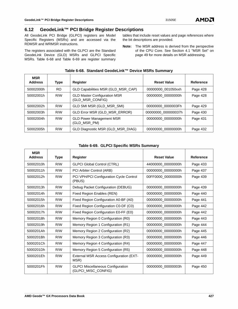
GeodeLink™ PCI Bridge Register Descriptions 31505E
6.12 GeodeLink™ PCI Bridge Register DescriptionsAll GeodeLink PCI Bridge (GLPCI) registers are ModelSpecific Registers (MSRs) and are accessed via theRDMSR and WRMSR instructions.
The registers associated with the GLPCI are the StandardGeodeLink Device (GLD) MSRs and GLPCI SpecificMSRs. Table 6-68 and Table 6-69 are register summary
tables that include reset values and page references wherethe bit descriptions are provided.
Note: The MSR address is derived from the perspectiveof the CPU Core. See Section 4.1 "MSR Set" onpage 49 for more details on MSR addressing.
Table 6-68. Standard GeodeLink™ Device MSRs Summary
MSR Address Type Register Reset Value Reference
50002000h RO GLD Capabilities MSR (GLD_MSR_CAP) 00000000_001050xxh Page 428
50002001h R/W GLD Master Configuration MSR (GLD_MSR_CONFIG)
00000000_00000000h Page 428
50002002h R/W GLD SMI MSR (GLD_MSR_SMI) 00000000_0000003Fh Page 429
50002003h R/W GLD Error MSR (GLD_MSR_ERROR) 00000000_000000037h Page 430
50002004h R/W GLD Power Management MSR (GLD_MSR_PM)
00000000_00000000h Page 431
50002005h R/W GLD Diagnostic MSR (GLD_MSR_DIAG) 00000000_00000000h Page 432
Table 6-69. GLPCI Specific MSRs Summary
MSR Address Type Register Reset Value Reference
50002010h R/W GLPCI Global Control (CTRL) 44000000_00000000h Page 433
50002011h R/W PCI Arbiter Control (ARB) 00000000_00000000h Page 437
50002012h R/W PCI VPH/PCI Configuration Cycle Control (PBUS)
00FF0000_00000000h Page 439
50002013h R/W Debug Packet Configuration (DEBUG) 00000000_00000000h Page 439
50002014h R/W Fixed Region Enables (REN) 00000000_00000000h Page 440
50002015h R/W Fixed Region Configuration A0-BF (A0) 00000000_00000000h Page 441
50002016h R/W Fixed Region Configuration C0-DF (C0) 00000000_00000000h Page 442
50002017h R/W Fixed Region Configuration E0-FF (E0) 00000000_00000000h Page 442
50002018h R/W Memory Region 0 Configuration (R0) 00000000_00000000h Page 443
50002019h R/W Memory Region 1 Configuration (R1) 00000000_00000000h Page 444
5000201Ah R/W Memory Region 2 Configuration (R2) 00000000_00000000h Page 445
5000201Bh R/W Memory Region 3 Configuration (R3) 00000000_00000000h Page 446
5000201Ch R/W Memory Region 4 Configuration (R4) 00000000_00000000h Page 447
5000201Dh R/W Memory Region 5 Configuration (R5) 00000000_00000000h Page 448
5000201Eh R/W External MSR Access Configuration (EXT-MSR)
00000000_00000000h Page 449
5000201Fh R/W GLPCI Miscellaneous Configuration (GLPCI_MISC_CONFIG)
00000000_00000003h Page 450
AMD Geode™ GX Processors Data Book 427

GeodeLink™ PCI Bridge Register Descriptions31505E
6.12.1 Standard GeodeLink™ Device MSRs
6.12.1.1 GLD Capabilities MSR (GLD_MSR_CAP)
6.12.1.2 GLD Master Configuration MSR (GLD_MSR_CONFIG)
MSR Address 50002000hType ROReset Value 00000000_001050xxh
GLD_MSR_CAP Register Map63 62 61 60 59 58 57 56 55 54 53 52 51 50 49 48 47 46 45 44 43 42 41 40 39 38 37 36 35 34 33 32
RSVD
31 30 29 28 27 26 25 24 23 22 21 20 19 18 17 16 15 14 13 12 11 10 9 8 7 6 5 4 3 2 1 0
RSVD DEV_ID REV_ID
GLD_MSR_CAP Bit Descriptions
Bit Name Description
63:24 RSVD Reserved. Reserved for future use.
23:8 DEV_ID Device ID. Identifies device (1050h).
7:0 REV_ID Revision ID. Identifies device revision. See AMD Geode™ GX Processor Specification Update document for value.
MSR Address 50002001hType R/WReset Value 00000000_00000000h
GLD_MSR_CONFIG Register Map
63 62 61 60 59 58 57 56 55 54 53 52 51 50 49 48 47 46 45 44 43 42 41 40 39 38 37 36 35 34 33 32
RSVD
31 30 29 28 27 26 25 24 23 22 21 20 19 18 17 16 15 14 13 12 11 10 9 8 7 6 5 4 3 2 1 0
RSVD PRIR
SV
D PID
GLD_MSR_CONFIG Bit Descriptions
Bit Name Description
63:7 RSVD (RO) Reserved (Read Only). Reserved for future use.
6:4 PRI Priority. Default priority.
3 RSVD (RO) Reserved (Read Only). Reserved for future use.
2:0 PID Priority ID. Assigned priority domain.
428 AMD Geode™ GX Processors Data Book

GeodeLink™ PCI Bridge Register Descriptions 31505E
6.12.1.3 GLD SMI MSR (GLD_MSR_SMI) MSR Address 50002002hType R/WReset Value 00000000_0000003Fh
GLD_MSR_SMI Register Map
63 62 61 60 59 58 57 56 55 54 53 52 51 50 49 48 47 46 45 44 43 42 41 40 39 38 37 36 35 34 33 32
RSVD
31 30 29 28 27 26 25 24 23 22 21 20 19 18 17 16 15 14 13 12 11 10 9 8 7 6 5 4 3 2 1 0
RSVD
PAR
E_A
SM
I_F
LAG
SY
SE
_AS
MI_
FLA
G
VP
HE
_SS
MI_
FLA
G
BM
E_A
SM
I_F
LAG
TAR
E_A
SM
I_F
LAG
MA
RE
_AS
MI_
FLA
G RSVD
PAR
E_A
SM
I_E
N
SY
SE
_AS
MI_
EN
VP
HE
_SS
MI_
EN
BM
E_A
SM
I_E
N
TAR
E_A
SM
I_E
N
MA
RE
_AS
MI_
EN
GLD_MSR_SMI Bit Descriptions
Bit Name Description
63:20 RSVD (RO) Reserved (Read Only). Reads return 0.
21 PARE_ASMI_FLAG
Parity Error Event Asynchronous SMI Flag. If high, records that an ASMI was gener-ated due to detection of a PCI bus parity error. Write 1 to clear; writing 0 has no effect. PARE_ASMI_EN (bit 5) must be low to generate ASMI and set flag. Additionally, the PS_ASMI_EN bit (MSR 50002010h[27]) must be set to enable this event.
20 SYSE_ASMI_FLAG
System Error Event Asynchronous SMI Flag. If high, records that an ASMI was gener-ated due to the detection of a PCI bus system error. Write 1 to clear; writing 0 has no effect. SYSE_ASMI_EN (bit 4) must be low to generate ASMI and set flag. Additionally, the PS_ASMI_EN bit MSR 50002010h[27]) must be set to enable this event.
19 VPHE_SSMI_FLAG
Virtual PCI Header Event Synchronous SMI Flag. If high, records that an SSMI was generated due to a flag being set by the Virtual PCI Header support logic. Write 1 to clear; writing 0 has no effect. VPHE_SSMI_EN (bit 3) must be low to generate SSMI and set flag.
18 BME_ASMI_FLAG
Broken Master Event Asynchronous SMI Flag. If high, records that an ASMI was gen-erated due to detection of a broken PCI bus master. Write 1 to clear; writing 0 has no effect. BM_EN (bit 2) must be low to generate ASMI and set flag. Additionally, the BM_ASMI_EN bit (MSR 50002010h[26]) must be set to enable this event.
17 TARE_ASMI_FLAG
Target Abort Received Event Asynchronous SMI Flag. If high, records that an ASMI was generated due to reception of a target abort on PCI. Write 1 to clear; writing 0 has no effect. TAR_EN (bit 1) must be low to generate ASMI and set flag. Additionally, the TAR_ASMI_EN bit (MSR 50002010h[25]) must be set to enable this event.
16 MARE_ASMI_FLAG
Master Abort Received Event (Read/Write-1-to-Clear). If high, records that an ASMI was generated due to reception of a master abort on PCI. Write 1 to clear; writing 0 has no effect. MAR_EN (bit 0) must be low to generate ASMI and set flag. Additionally, the MAR_ASMI bit (MSR 50002010h[24]) must be set to enable this event.
15:5 RSVD Reserved. Write as read.
5 PARE_ASMI_EN
Parity Error Event Asynchronous SMI Enable. Write 0 to enable a parity error event to generate an ASMI and to set flag (bit 21).
4 SYSE_ASMI_EN
System Error Event Asynchronous SMI Enable. Write 0 to enable a system error event to generate an ASMI and to set flag (bit 20).
AMD Geode™ GX Processors Data Book 429

GeodeLink™ PCI Bridge Register Descriptions31505E
6.12.1.4 GLD Error MSR (GLD_MSR_ERROR)
3 VPHE_SSMI_EN
Virtual PCI Header Event Synchronous SMI Enable. Write 0 to allow SSMI flag to be set in selected GLIU response packets. I/O reads and writes to location CFCh may cause an SSMI depending upon the configuration of this bit and the DEV bits in the PBUS reg-ister (MSR 50002012h[31:0]). Writing 0 also enables flag (bit 19) to be set upon event.
2 BME_ASMI_EN
Broken Master Event Asynchronous SMI Enable. Write 0 to enable a broken PCI bus master event to generate an ASMI and to set flag (bit 18).
1 TARE_ASMI_EN
Target Abort Received Event Asynchronous SMI Enable. Write 0 to enable a target abort received event to generate an ASMI and to set flag (bit 17).
0 MARE_ASMI_EN
Master Abort Received Event Asynchronous SMI Enable. Write 0 to enable a master abort received event to generate an ASMI and to set flag (bit 16).
MSR Address 50002003hType R/WReset Value 00000000_000000037h
GLD_MSR_SMI Bit Descriptions
Bit Name Description
GLD_MSR_ERROR Register Map
63 62 61 60 59 58 57 56 55 54 53 52 51 50 49 48 47 46 45 44 43 42 41 40 39 38 37 36 35 34 33 32
RSVD
31 30 29 28 27 26 25 24 23 22 21 20 19 18 17 16 15 14 13 12 11 10 9 8 7 6 5 4 3 2 1 0
RSVD
PAR
E_E
RR
_FLA
G
SY
SE
_ER
R_F
LAG
RS
VD
BM
E_E
RR
_FLA
G
TAR
E_E
RR
_FLA
G
MA
RE
_ER
R_F
LAG RSVD
PAR
E_E
RR
_EN
SY
SE
_ER
R_E
N
RS
VD
BM
E_E
RR
_EN
TAR
E_E
RR
_EN
MA
RE
_ER
R_E
N
GLD_MSR_ERROR Bit Descriptions
Bit Name Description
63:22 RSVD (RO) Reserved (Read Only). Reserved for future use.
21 PARE_ERR_FLAG
Parity Error Event Error Flag. If high, records an ERR occurred due to detection of a PCI bus parity error. Write 1 to clear; writing 0 has no effect. PARE_ERR_EN (bit 5) must be low to generate ERR and set flag. Additionally, the PS_ERR_EN bit (MSR 50002010h[31]) must be set to enable this event.
20 SYSE_ERR_FLAG
System Error Event Error Flag. If high, records an ERR occurred due to detection of a PCI bus system error. Write 1 to clear; writing 0 has no effect. SYSE_ERR_EN (bit 4) must be low to generate ERR and set flag. Additionally, the PS_ERR_EN bit (MSR 50002010h[31]) must be set to enable this event.
19 RSVD (RO) Reserved (Read Only). Reads return 0.
18 BME_ERR_FLAG
Broken Master Event Error Flag. If high, records an ERR occurred due to detection of a broken PCI bus master. Write 1 to clear; writing 0 has no effect. BME_ERR_EN (bit 2) must be low to generate ERR and set flag. Additionally, the BM_ERR_EN bit (MSR 50002010h[30]) must be set to enable this event.
17 TARE_ERR_FLAG
Target Abort Received Event Error Flag. If high, records an ERR occurred due to the reception of a target abort on PCI. Write 1 to clear; writing 0 has no effect. TARE_ERR_EN (bit 1) must be low to generate ERR and set flag. Additionally, the TAR_ERR_EN bit (MSR 50002010h[29]) must be set to enable this event.
430 AMD Geode™ GX Processors Data Book

GeodeLink™ PCI Bridge Register Descriptions 31505E
6.12.1.5 GLD Power Management MSR (GLD_MSR_PM)
16 MARE_ERR_FLAG
Master Abort Received Event Error Flag. If high, records an ERR occurred due to the reception of a master abort on PCI. Write 1 to clear; writing 0 has no effect. MAR_EN (bit 0) must be low to generate ERR and set flag. Additionally, the MAR_ERR bit (MSR 50002010h[28]) must be set to enable this event.
15:6 RSVD (RO) Reserved (Read Only). Reads return 0.
5 PARE_ERR_EN Parity Error Event Enable. Write 0 to enable a parity error event to generate an ERR and to set flag (bit 21).
4 SYSE_ERR_EN System Error Event Enable. Write 0 to enable a system error event to generate an ERR and to set flag (bit 20).
3 RSVD (RO) Reserved (Read Only). Reads return 0.
2 BME_ERR_EN Broken Master Event Enable. Write 0 to enable a broken PCI bus master event to gen-erate an ERR and to set flag (bit 18).
1 TARE_ERR_EN Target Abort Received Event Enable. Write 0 to enable a target abort received event to generate an ERR and to set flag (bit 17).
0 MARE_ERR_EN
Master Abort Received Event Enable. Write 0 to enable a master abort received event to generate an ERR and to set flag (bit 16).
MSR Address 50002004hType R/WReset Value 00000000_00000000h
GLD_MSR_ERROR Bit Descriptions
Bit Name Description
GLD_MSR_PM Register Map
63 62 61 60 59 58 57 56 55 54 53 52 51 50 49 48 47 46 45 44 43 42 41 40 39 38 37 36 35 34 33 32
RSVD
31 30 29 28 27 26 25 24 23 22 21 20 19 18 17 16 15 14 13 12 11 10 9 8 7 6 5 4 3 2 1 0
RSVDP
MO
DE
2
PM
OD
E1
PM
OD
E0
GLD_MSR_PM Bit Descriptions
Bit Name Description
63:35 RSVD (RO) Reserved (Read Only). Reads as 0.
34:32 RSVD Reserved. Reads as 0.
31:6 RSVD (RO) Reserved (Read Only). Reads as 0.
5:4 PMODE2 Power Mode 2 (Fast-PCI Clock). Power mode for Fast-PCI clock domain.
00: Disable clock gating. Clocks are always on.
01: Enable active hardware clock gating. Clock goes off whenever this module’s circuits are not busy.
10: Reserved.
11: Reserved.
AMD Geode™ GX Processors Data Book 431

GeodeLink™ PCI Bridge Register Descriptions31505E
6.12.1.6 GLD Diagnostic MSR (GLD_MSR_DIAG)
This register is reserved for internal use by AMD and should not be written to.
3:2 PMODE1 Power Mode 1 (PCI Clock). Power mode for PCI clock domain.
00: Disable clock gating. Clocks are always on.
01: Enable active hardware clock gating. Clock goes off whenever this module’s circuits are not busy.
10: Reserved.
11: Reserved.
1:0 PMODE0 Power Mode 0 (GLIU Clock). Power mode for GLIU clock domain.
00: Disable clock gating. Clocks are always on.
01: Enable active hardware clock gating. Clock goes off whenever this module’s circuits are not busy.
10: Reserved.
11: Reserved.
MSR Address 50002005hType R/WReset Value 00000000_00000000h
GLD_MSR_PM Bit Descriptions (Continued)
Bit Name Description
432 AMD Geode™ GX Processors Data Book

GeodeLink™ PCI Bridge Register Descriptions 31505E
6.12.2 GLPCI Specific MSRs
6.12.2.1 GLPCI Global Control (CTRL)MSR Address 50002010hType R/WReset Value 44000000_00000000h
CTRL Register Map
63 62 61 60 59 58 57 56 55 54 53 52 51 50 49 48 47 46 45 44 43 42 41 40 39 38 37 36 35 34 33 32
FTH RTH SBRTH RTL DTL WTO
SLT
O ILTO LAT 0
31 30 29 28 27 26 25 24 23 22 21 20 19 18 17 16 15 14 13 12 11 10 9 8 7 6 5 4 3 2 1 0
PS
_ER
R_E
N
BM
_ER
R_E
N
TAR
_ER
R_E
N
MA
R_E
RR
_EN
PS
_AS
MI_
EN
BM
_AS
MI_
EN
TAR
_AS
MI_
EN
MA
R_A
SM
I_E
N SUS IRFT IRFC IOD
ST
ER
RH
E
LDE
RU
PO
BZ NI
ISO
OW
C
IWC
RS
VD
IE ME
CTRL Bit Descriptions
Bit Name Description
63:60 FTH In-Bound Flush Threshold. Controls the timing for requesting new read data while con-currently flushing previously prefetched, stale read data. If the number of prefetched 64-bit WORDs reaches this level, then a pending request is made.
59:56 RTH In-Bound Read Threshold. Controls the timing for prefetching read data. If the number of prefetched 32-bit WORDs reaches this threshold, a subsequent GLIU request is gen-erated to fetch the next cache line of read data.
55:52 SBRTH Southbridge In-Bound Read Threshold. Controls the timing for prefetching read data for the Geode™ companion device. If the number of prefetched 32-bit WORDs reaches this threshold, a subsequent GLIU request is generated to fetch the next cache line of read data. The status of the companion device’s GNT# pin (GNT2#) is sampled to deter-mine when the companion device is generating an in-bound request. When configured to use an external arbiter the REQ2# pin is sampled as a discriminator.
51:49 RTL Retry Transaction Limit. Limits the number of out-bound retries. If a target signals retry indefinitely the PCI interface may be configured to abort the failing out-bound request.
000: No limit 100: 64 retries001: 8 retries 101: 128 retries010: 16 retries 110: 256 retries011: 32 retries 111: 512 retries
48:46 DTL Delayed Transaction Limit. Limits the duration of delayed transactions. Once a read transaction is delayed (retried before the first data phase has completed) all other in-bound transactions are rejected until the original request is satisfied. If the original master stops retrying a livelock condition may occur. If the number of rejected transactions reaches the limit defined by this field, then the delayed transaction is forgotten.
000: No limit 100: 16 rejections001: 2 rejections 101: 32 rejections010: 4 rejections 110: 64 rejections011: 8 rejections 111: 128 rejections
AMD Geode™ GX Processors Data Book 433

GeodeLink™ PCI Bridge Register Descriptions31505E
45:43 WTO In-Bound Write Timeout. Controls the flushing of in-bound posted write data. When an in-bound write has completed on the PCI bus an internal counter is loaded with a value derived from this field. It then counts down on each PCI clock edge. When the counter reaches 0, the posted write data is flushed to memory.
000: 4 PCI clock edge 100: 64 PCI clock edges001: 8 PCI clock edges 101: 128 PCI clock edges010: 16 PCI clock edges 110: 256 PCI clock edges011: 32 PCI clock edges 111: No timeout
42 SLTO Subsequent Latency Timeout Select. Specifies the subsequent target latency timeout limit. If, within a burst, the GLPCI module does not respond with the configured number of clock edges, the PCI interface terminates the PCI bus cycle.
0: 8 PCI clock edges1: 4 PCI clock edges
41:40 ILTO Initial Latency Timeout Select. Specifies the initial target latency timeout limit for the PCI interface. If the GLPCI module does not respond with the first data phase within the configured number of clock edges, the PCI interface terminates the PCI bus cycle.
AILTO (MSR 5000201Fh[6]) = 0:00: 32 PCI clock edges 10: 8 PCI clock edges01: 16 PCI clock edges 11: 4 PCI clock edges
AILTO (MSR 5000201Fh[6]) = 1:00: 64 PCI clock edges 10: 256 PCI clock edges01: 128 PCI clock edges 11: No timeout
39:35 LAT PCI Latency Timer. Latency timeout value for limiting bus tenure.
34:32 0 (RO) Constant 0 (Read Only). The three least significant bits of the PCI latency timer field are fixed as zeros. These bits are not used as part of the PCI latency timer comparison.
31 PS_ERR_EN Parity/System Error. Allow detection of either a parity error or a system error to be reported in the PARE_ERR_FLAG bit (MSR 50002003h[21]).
0: Disable.1: Enable.
30 BM_ERR_EN Broken Master Error. Allow detection of a broken PCI bus master to be reported in the BME_ERR_FLAG bit (MSR 50002003h[18]).
0: Disable.1: Enable.
29 TAR_ERR_EN Target Abort Received Error. Allow reception of a PCI bus target abort to be reported in the TARE_ERR_FLAG bit (MSR 50002003h[17]).
0: Disable.1: Enable.
28 MAR_ERR_EN Master Abort Received Error. Allow reception of a PCI bus master abort to be reported in the MARE_ERR_FLAG bit (MSR 50002003h[16]).
0: Disable.1: Enable.
27 PS_ASMI_EN Parity/System ASMI Enable. Allow detection of either a parity error or a system error to be reported in the PARE_ASMI_FLAG bit (MSR 50002002h[21]).
0: Disable.1: Enable.
26 BM_ASMI_EN Broken Master ASMI Enable. Allow detection of a broken PCI bus master to be reported in the BME_ASMI_FLAG bit (MSR 50002002h[18]).
0: Disable.1: Enable.
CTRL Bit Descriptions (Continued)
Bit Name Description
434 AMD Geode™ GX Processors Data Book

GeodeLink™ PCI Bridge Register Descriptions 31505E
25 TAR_ASMI_EN Target Abort Received ASMI Enable. Allow reception of a PCI bus target abort to be reported in the TARE_ASMI_FLAG bit (MSR 50002002h[17]).
0: Disable.1: Enable.
24 MAR_ASMI_EN Master Abort Receive Enable. Allow reception of a PCI bus master abort to be reported in the TARE_ASMI_FLAG bit (MSR 50002002h[17]).
0: Disable.1: Enable.
23:21 SUS Busy Sustain. Controls the sustain time for keeping the clocks running after the internal busy signals indicate that the clocks may be gated:
000: No sustain 100: 32 clock cycles001: 4 clock cycles 101: 64 clock cycles010: 8 clock cycles 110: 128 clock cycles011: 16 clock cycles 111: 256 clock cycles
20:18 IRFT In-Bound Read Flush Timeout. Controls the flushing of in-bound prefetch read data. When an in-bound read has completed on the PCI bus an internal counter is loaded with a value derived from this field. It then counts down on each PCI clock edge. When the counter reaches 0, any remaining prefetched data is flushed. The counter stops counting down if a subsequent in-bound read is received. It continues to count down through an in-bound write and through any out-bound traffic:
000: 4 PCI clock edge 100: 64 PCI clock edges001: 8 PCI clock edges 101: 128 PCI clock edges010: 16 PCI clock edges 110: 256 PCI clock edges011: 32 PCI clock edges 111: No timeout
17:16 IRFC In-Bound Read Flush Control. Controls the policy for discarding stale data from in-bound read data FIFO:
00: Discard at end of in-bound read PCI transaction.01: Discard upon timeout.10: Discard at start of out-bound write or upon timeout.11: Discard at start of out-bound write, at start of out-bound read or upon timeout.
In addition to these policies in-bound read data is discarded whenever a non-contiguous in-bound read is accepted or when an in-bound write is received that affects the prefetched memory.
15:13 IOD I/O Delay. Delay completion of out-bound I/O transactions for a configurable number of PCI clock cycles:
000: 0 PCI clock cycles 100: 8 PCI clock cycles001: 1 PCI clock cycles 101: 16 PCI clock cycles010: 2 PCI clock cycles 110: 32 PCI clock cycles011: 4 PCI clock cycles 111: 64 PCI clock cycles
12 ST Short Timer. When cleared to 0, delayed transactions are discarded after 215 PCI clock
cycles. When set to 1, delayed transactions are discarded after 25 PCI clock cycles. For normal operation this bit should be cleared.
11 ER Early Read. When cleared to 0, out-bound reads are stalled until there is enough FIFO space in the out-bound read FIFO to hold data for the entire transaction. When set to 1, out-bound reads start as soon as possible.
10 RHE Read Hints Enable. When set to 0, all out-bound reads use PCI CMD = 6. When set to 1, the PCI CMD provides a hint about the size of the read request.
6 = 1, 2, or 4 DWORDsE = 8 DWORDs
CTRL Bit Descriptions (Continued)
Bit Name Description
AMD Geode™ GX Processors Data Book 435

GeodeLink™ PCI Bridge Register Descriptions31505E
9 LDE Latency Disconnect Enable. When set to 1, causes the PCI interface to disconnect from a PCI bus master when a latency timer expiration occurs. This enforces the config-ured minimum latency upon PCI bus masters, where the GLPCI module is a target on the PCI bus. The latency timer must be greater than 0 when using this feature.
8 RUPO Relax Up-Stream Ordering. Removes ordering restrictions for out-bound read response data with respect to in-bound write data. Setting this bit also causes the GLPCI to clear the SEND_RESPONSE flag for in-bound GLIU request packets. This bit should be cleared for normal operation.
7 BZ Bizarro Flag. Bizarro flag configuration to use on in-bound I/O reads and writes. )
6 NI No Invalidate Flag. Force the INVALIDATE flag to be cleared for all in-bound writes.
5 ISO In-Bound Strong Ordering. Disables the ability of in-bound reads to coherently pass posted in-bound writes. When set to 1, a PCI read request received by the host bridge target is not forwarded to the GLIU until all posted write data has been flushed to mem-ory.
4 OWC Out-Bound Write Combining. Enables concatenation of out-bound write bursts into a larger PCI burst. Setting this bit does NOT add any additional latency to out-bound writes.
0: Disable.
1: Enable.
3 IWC In-Bound Write Combining. Enables combining of different in-bound PCI write transac-tions into a single GLIUhost write transaction. When cleared to 0, PCI write data received from the host bridge target is NOT held in the posted write buffer; a GLIU transaction is generated immediately.
2 RSVD Reserved. Always write 1.
1 IE I/O Enable. Enable handling of in-bound I/O transactions from the PCI. When set to 1, the PCI interface accepts all in-bound I/O transactions from the PCI. This mode is only intended for design verification purposes. When cleared to 0, no in-bound I/O transac-tions are accepted.
0 ME Memory Enable. Enable handling of in-bound memory access transaction from the PCI. When cleared to 0, the PCI interface does not accept any in-bound memory transactions from the PCI bus. The set to 1, the PCI interface accepts in-bound memory transactions for those address ranges defined in the region configuration registers.
CTRL Bit Descriptions (Continued)
Bit Name Description
436 AMD Geode™ GX Processors Data Book

GeodeLink™ PCI Bridge Register Descriptions 31505E
6.12.2.2 PCI Arbiter Control (ARB)MSR Address 50002011hType R/WReset Value 00000000_00000000h
ARB Register Map
63 62 61 60 59 58 57 56 55 54 53 52 51 50 49 48 47 46 45 44 43 42 41 40 39 38 37 36 35 34 33 32
RSVD
BM
1
BM
0
CP
RE RSVD
PR
E2
PR
E1
PR
E0
CR
ME RSVD
RM
E2
RM
E1
RM
E0
31 30 29 28 27 26 25 24 23 22 21 20 19 18 17 16 15 14 13 12 11 10 9 8 7 6 5 4 3 2 1 0
RSVD PRCM RSVD FPVEC RSVD SBCTR
IIE
RMT CPCTR
EA
BM
D
PAR
K
ARB Bit Definitions
Bit Name Description
63:50 RSVD (RO) Reserved (Read Only). Reads return 0.
49 BM1 (RO) Broken Master 1 (Read Only). Indicates when a broken master is attached to REQ1#. This bit is set when the arbiter detects that the PCI bus master attached to REQ1# has not asserted FRAME# within 16 PCI clock edges after being granted the PCI bus. This bit is cleared by setting BMD (bit 1) to 1.
48 BM0 (RO) Broken Master 0 (Read Only). Indicates when a broken master is attached to REQ[0]#. This bit is set when the arbiter detects that the PCI bus master attached to REQ[0]# has not asserted FRAME# within 16 PCI clock edges after being granted the PCI bus. This bit is cleared by setting BMD (bit 1) to 1.
47 CPRE CPU Preemption Enable. When set to 1, the CPU’s PCI grant may be de-asserted before the CPU’s request is de-asserted.
46:43 RSVD (RO) Reserved (Read Only). Reads return 0.
42 PRE2 Preemption Enable 2. When set to 1, GNT2# may be de-asserted before REQ2# is de-asserted.
41 PRE1 Preemption Enable 1. When set to 1, GNT1# may be de-asserted before REQ1# is de-asserted.
40 PRE0 Preemption Enable 0. When set to 1, GNT0# may be de-asserted before REQ0# is de-asserted.
39 CRME CPU Retry Mask Enable. When set to 1, CPU requests are masked following a retry ter-mination of a PCI bus cycle initiated by the host PCI bridge master.
38:35 RSVD (RO) Reserved (Read Only). Reads return 0.
34 RME2 Retry Mask Enable 2. When set to 1, REQ2# is masked following a retry termination of a cycle initiated by that master.
33 RME1 Retry Mask Enable 1. When set to 1, REQ1# is masked following a retry termination of a cycle initiated by that master.
32 RME0 Retry Mask Enable 0. When set to 1, REQ0# is masked following a retry termination of a cycle initiated by that master.
31:27 RSVD (RO) Reserved (Read Only). Reserved for future use.
26:24 PRCM Priority Rotation Control Mask. When these bits are set to 000, all of the arbiter priority vector bits are allowed to rotate. When these bits are set to 111, all of the arbiter priority vector bits are fixed to the values in the Fixed Priority Vector (FPVEC) field (bits 18:16]). Any other value results in a hybrid priority scheme, where the arbiter priority vector bits corresponding to the mask bits set to 1 are fixed to the values in the FPVEC and all other bits are allowed to rotate.
AMD Geode™ GX Processors Data Book 437

GeodeLink™ PCI Bridge Register Descriptions31505E
23:19 RSVD (RO) Reserved (Read Only). Reserved for future use.
18:16 FPVEC Fixed Priority Vector. This field is used to specify the fixed priority values for the PCI arbiter. This value is not used when the PRCM field (bits [26:24]) is cleared to 000.
15:9 RSVD (RO) Reserved (Read Only). Reserved for future use.
11:9 SBCTR South Bridge Priority Counter. Controls the frequency with which the south bridge is given top priority among the external PCI devices. This field specifies the number of external PCI grants that must occur before the south bridge is given top priority for the next arbitration cycle. Note that if this field is set to a value of N, N + 1 external PCI grants are allowed before the south bridge is given top priority.
8 IIE Insert Idle Enable. When set to 1, where all GNT# pins are high, at least one idle cycle is inserted between each switch of granted PCI masters. When cleared to 0, grant may be simultaneously removed from one PCI master and granted to another PCI master in the same cycle; where allowed by the PCI specification.
7:6 RMT Retry Mask Timer. Specifies the number of PCI clock edges that a master’s request line masks off from arbitration following a retry termination of a cycle initiated by that master.
00: Mask for 8 PCI clock edges 10: Mask for 32 PCI clock edges01: Mask for 16 PCI clock edges 11: Mask for 64 PCI clock edges
5:3 CPCTR CPU Priority Counter. Controls the frequency with which the CPU is given top priority in the PCI arbiter. This field specifies the number of external PCI grants that must occur before the CPU is given top priority for the next arbitration cycle. Note that if this field is set to a value of N, N + 1 external PCI grants are allowed before the CPU is given top pri-ority.
2 RSVD Reserved.
1 BMD Broken Master Timer Disable. Controls the operation of the broken master detector in the PCI arbiter. When set to 1, the arbiter does not recognize a broken master condition on the PCI bus. When cleared to 0, the arbiter detects a broken master condition when a granted PCI bus master takes 16 or more clock cycles before asserting FRAME#. The broken master is NOT allowed to gain access to the PCI bus. Software may restore any broken master’s permission to use the PCI bus by clearing this bit and, optionally, setting it again.
0 PARK Parking Policy. When cleared to 0, the arbiter always parks the PCI bus on the Geode GX processor. When set to 1, the arbiter parks the PCI bus on the last granted bus mas-ter. If this bit is set, the clock for the Fast-PCI clock domain should not be gated.
ARB Bit Definitions (Continued)
Bit Name Description
438 AMD Geode™ GX Processors Data Book

GeodeLink™ PCI Bridge Register Descriptions 31505E
6.12.2.3 PCI VPH/PCI Configuration Cycle Control (PBUS)
The PBUS MSR is used to control the way the GLPCI module generates (or does not generate) PCI configuration cyclesonto the PCI bus. The SEC field (bits [39:32]) should be configured with the PCI bus number for the locally attached PCIbus. The SUB field (bits [55:48] should be configured with the PCI bus number for the highest numbered PCI bus that isaccessible via this interface. The DEV field (bits [31:0]) should be configured to indicate which device’s numbers do NOTgenerate PCI configuration cycles on the PCI bus.
6.12.2.4 Debug Packet Configuration (DEBUG)
Debug register, AMD internal use only.
MSR Address 50002012hType R/WReset Value 00FF0000_00000000h
PBUS Register Map
63 62 61 60 59 58 57 56 55 54 53 52 51 50 49 48 47 46 45 44 43 42 41 40 39 38 37 36 35 34 33 32
RSVD SUB RSVD SEC
31 30 29 28 27 26 25 24 23 22 21 20 19 18 17 16 15 14 13 12 11 10 9 8 7 6 5 4 3 2 1 0
DEV
PBUS Bit Descriptions
Bit Name Description
63:56 RSVD (RO) Reserved (Read Only). Reads return 0.
55:48 SUB Subordinate Bus Number. Specifies the subordinate PCI bus number for all PCI buses reachable via this PCI interface.
47:40 RSVD (RO) Reserved (Read Only). Reads return 0.
39:32 SEC Secondary Bus Number. Specifies the secondary PCI bus number for this PCI inter-face.
31:0 DEV Device Bitmap. Specifies the virtualized PCI devices. Each bit position corresponds to a device number. A 0 instructs the GLPCI to allow PCI configuration cycles for the device to be generated on the PCI bus. A 1 tells the GLPCI to virtualize the device by generating an SSMI instead of a PCI configuration cycle.
MSR Address 50002013hType R/WReset Value 00000000_00000000h
DEBUG Register Map
63 62 61 60 59 58 57 56 55 54 53 52 51 50 49 48 47 46 45 44 43 42 41 40 39 38 37 36 35 34 33 32
RSVD
31 30 29 28 27 26 25 24 23 22 21 20 19 18 17 16 15 14 13 12 11 10 9 8 7 6 5 4 3 2 1 0
RSVD
DEBUG Bit Descriptions
Bit Name Description
63:0 RSVD Reserved. These bits are reserved for internal testing only. These bits should not be written to.
AMD Geode™ GX Processors Data Book 439

GeodeLink™ PCI Bridge Register Descriptions31505E
6.12.2.5 Fixed Region Enables (REN)MSR Address 50002014hType R/WReset Value 00000000_00000000h
REN Register Map
63 62 61 60 59 58 57 56 55 54 53 52 51 50 49 48 47 46 45 44 43 42 41 40 39 38 37 36 35 34 33 32
Spare
31 30 29 28 27 26 25 24 23 22 21 20 19 18 17 16 15 14 13 12 11 10 9 8 7 6 5 4 3 2 1 0
RSVD FC F8
F4
F0
EC
E8
E4
E0
DC
D8
D4
D0
CC
C8
C4
C0
BC
B8
B4
B0
AC A8
A4
A0
REN Bit Descriptions
Bit Name Description
63:32 Spare Spare Bits. Extra bits available for future use. These bits may be set and cleared, but do not control anything.
31:24 RSVD (RO) Reserved (Read Only). Reads return 0.
23 FC FC Enable. Enables memory access to FC000 through FFFFF from PCI.
22 F8 F8 Enable. Enables memory access to F8000 through FBFFF from PCI.
21 F4 F4 Enable. Enables memory access to F4000 through F7FFF from PCI.
20 F0 F0 Enable. Enables memory access to F0000 through F3FFF from PCI.
19 EC EC Enable. Enables memory access to EC000 through EFFFF from PCI.
18 E8 E8 Enable. Enables memory access to E8000 through EBFFF from PCI.
17 E4 E4 Enable. Enables memory access to E4000 through E7FFF from PCI.
16 E0 E0 Enable. Enables memory access to E0000 through E3FFF from PCI.
15 DC DC Enable. Enables memory access to DC000 through DFFFF from PCI.
14 D8 D8 Enable. Enables memory access to D8000 through DBFFF from PCI.
13 D4 D4 Enable. Enables memory access to D4000 through D7FFF from PCI.
12 D0 D0 Enable. Enables memory access to D0000 through D3FFF from PCI.
11 CC CC Enable. Enables memory access to CC000 through CFFFF from PCI.
10 C8 C8 Enable. Enables memory access to C8000 through CBFFF from PCI.
9 C4 C4 Enable. Enables memory access to C4000 through C7FFF from PCI.
8 C0 C0 Enable. Enables memory access to C0000 through C3FFF from PCI.
7 BC BC Enable. Enables memory access to BC000 through BFFFF from PCI.
6 B8 B8 Enable. Enables memory access to B8000 through BBFFF from PCI.
5 B4 B4 Enable. Enables memory access to B4000 through B7FFF from PCI.
4 B0 B0 Enable. Enables memory access to B0000 through B3FFF from PCI.
3 AC AC Enable. Enables memory access to AC000 through AFFFF from PCI.
2 A8 A8 Enable. Enables memory access to A8000 through ABFFF from PCI.
1 A4 A4 Enable. Enables memory access to A4000 through A7FFF from PCI.
0 A0 A0 Enable. Enables memory access to A0000 through A3FFF from PCI.
440 AMD Geode™ GX Processors Data Book

GeodeLink™ PCI Bridge Register Descriptions 31505E
6.12.2.6 Fixed Region Configuration A0-BF (A0)
Table 6-70. Region Properties
Bit Name Description
7:6 RSVD Reserved (Read Only). Reserved for future use.
5 PF Prefetchable. Reads to this region have no side-effects.
4 WC Write Combine. Writes to this region may be combined
3 RSVD (RO) Reserved (Read Only). Reserved for future use.
2 WP Write Protect. When set to 1, only read accesses are allowed. Write accesses are ignored (master abort).
1 RSVD Reserved. Reserved for internal AMD use. Always clear this bit to 0.
0 CD Cache Disable. When set to 1, accesses are marked as non-coherent. When cleared to 0, accesses are marked as coherent.
MSR Address 50002015hType R/WReset Value 00000000_00000000h
A0 Register Map
63 62 61 60 59 58 57 56 55 54 53 52 51 50 49 48 47 46 45 44 43 42 41 40 39 38 37 36 35 34 33 32
BC B8 B4 B0
31 30 29 28 27 26 25 24 23 22 21 20 19 18 17 16 15 14 13 12 11 10 9 8 7 6 5 4 3 2 1 0
AC A8 A4 A0
A0 Bit Descriptions
Bit Name Description (Note 1)
63:56 BC BC Properties. Region properties for BC000 through BFFFF.
55:48 B8 B8 Properties. Region properties for B8000 through BBFFF.
47:40 B4 B4 Properties. Region Properties for B4000 through B7FFF.
39:32 B0 B0 Properties. Region properties for B0000 through B3FFF.
31:24 AC AC Properties. Region properties for AC000 through AFFFF.
23:16 A8 A8 Properties. Region Properties for A8000 through ABFFF.
15:8 A4 A4 Properties. Region Properties for A4000 through A7FFF.
7:0 A0 A0 Properties. Region properties for A0000 through A3FFF.
Note 1. See Table 6-70 on page 441 for region properties bit decodes.
AMD Geode™ GX Processors Data Book 441

GeodeLink™ PCI Bridge Register Descriptions31505E
6.12.2.7 Fixed Region Configuration C0-DF (C0)
6.12.2.8 Fixed Region Configuration E0-FF (E0)
MSR Address 50002016hType R/WReset Value 00000000_00000000h
C0 Register Map
63 62 61 60 59 58 57 56 55 54 53 52 51 50 49 48 47 46 45 44 43 42 41 40 39 38 37 36 35 34 33 32
DC D8 D4 D0
31 30 29 28 27 26 25 24 23 22 21 20 19 18 17 16 15 14 13 12 11 10 9 8 7 6 5 4 3 2 1 0
CC C8 C4 C0
C0 Bit Descriptions
Bit Name Description (Note 1)
63:56 DC DC Properties. Region properties for DC000 through DFFFF.
55:48 D8 D8 Properties. Region properties for D8000 through DBFFF.
47:40 D4 D4 Properties. Region Properties for D4000 through D7FFF.
39:32 D0 D0 Properties. Region properties for D0000 through D3FFF.
31:24 CC CC Properties. Region properties for CC000 through CFFFF.
23:16 C8 C4 Properties. Region Properties for C8000 through CBFFF.
15:8 C4 C4 Properties. Region Properties for C4000 through C3FFF.
7:0 C0 C0 Properties. Region properties for C0000 through C3FFF.
Note 1. See Table 6-70 on page 441 for region properties bit decodes.
MSR Address 50002017hType R/WReset Value 00000000_00000000h
E0 Register Map
63 62 61 60 59 58 57 56 55 54 53 52 51 50 49 48 47 46 45 44 43 42 41 40 39 38 37 36 35 34 33 32
FC F8 F4 F0
31 30 29 28 27 26 25 24 23 22 21 20 19 18 17 16 15 14 13 12 11 10 9 8 7 6 5 4 3 2 1 0
EC E8 E4 E0
E0 Bit Descriptions
Bit Name Description (Note 1)
63:56 FC FC Properties. Region properties for FC000 through FFFFF.
55:48 F8 F8 Properties. Region properties for F8000 through FBFFF.
47:40 F4 F4 Properties. Region Properties for F4000 through F7FFF.
39:32 F0 F0 Properties. Region properties for F0000 through F3FFF.
31:24 EC EC Properties. Region properties for EC000 through EFFFF.
23:16 E8 E4 Properties. Region Properties for E8000 through EBFFF.
15:8 E4 E4 Properties. Region Properties for E4000 through E3FFF.
7:0 E0 E0 Properties. Region properties for E0000 through E3FFF.
Note 1. See Table 6-70 on page 441 for region properties bit decodes.
442 AMD Geode™ GX Processors Data Book

GeodeLink™ PCI Bridge Register Descriptions 31505E
6.12.2.9 Memory Region 0 Configuration (R0)MSR Address 50002018hType R/WReset Value 00000000_00000000h
R0 Register Map
63 62 61 60 59 58 57 56 55 54 53 52 51 50 49 48 47 46 45 44 43 42 41 40 39 38 37 36 35 34 33 32
TOP RSVD
31 30 29 28 27 26 25 24 23 22 21 20 19 18 17 16 15 14 13 12 11 10 9 8 7 6 5 4 3 2 1 0
BASE RSVD
EN RSVD
PF
WC
RS
VD
WP
RS
VD
CD
R0 Bit Descriptions
Bit Name Description
63:44 TOP Top of Region. 4 KB granularity, inclusive.
43:32 RSVD (RO) Reserved (Read Only). Reserved for future use.
31:12 BASE Base of Region. 4 KB granularity, inclusive.
11:9 RSVD (RO) Reserved (Read Only). Reserved for future use.
8 EN Region Enable. Set to 1 to enable access to this region.
7:6 RSVD (RO) Reserved (Read Only). Reserved for future use.
5 PF Prefetchable. Reads to this region have no side-effects.
4 WC Write Combine. Writes to this region may be combined.
3 RSVD (RO) Reserved (Read Only). Reserved for future use.
2 WP Write Protect. When set to 1, only read accesses are allowed. Write accesses are ignored (master abort).
1 RSVD Reserved. Reserved for AMD internal use. Always clear this bit to 0.
0 CD Cache Disable. When set to 1, accesses are marked as non-coherent. When cleared to 0, accesses are marked as coherent.
AMD Geode™ GX Processors Data Book 443

GeodeLink™ PCI Bridge Register Descriptions31505E
6.12.2.10 Memory Region 1 Configuration (R1)MSR Address 50002019hType R/WReset Value 00000000_00000000h
R1 Register Map
63 62 61 60 59 58 57 56 55 54 53 52 51 50 49 48 47 46 45 44 43 42 41 40 39 38 37 36 35 34 33 32
TOP RSVD
31 30 29 28 27 26 25 24 23 22 21 20 19 18 17 16 15 14 13 12 11 10 9 8 7 6 5 4 3 2 1 0
BASE RSVD
EN RSVD
PF
WC
RS
VD
WP
RS
VD
CD
R1 Bit Descriptions
Bit Name Description
63:44 TOP Top of Region. 4 KB granularity, inclusive.
43:32 RSVD (RO) Reserved (Read Only). Reserved for future use.
31:12 BASE Base of Region. 4 KB granularity, inclusive.
11:9 RSVD (RO) Reserved (Read Only). Reserved for future use.
8 EN Region Enable. Set to 1 to enable access to this region.
7:6 RSVD (RO) Reserved (Read Only). Reserved for future use.
5 PF Prefetchable. Reads to this region have no side-effects.
4 WC Write Combine. Writes to this region may be combined.
3 RSVD (RO) Reserved (Read Only). Reserved for future use.
2 WP Write Protect. When set to 1, only read accesses are allowed. Write accesses are ignored (master abort).
1 RSVD Reserved. Reserved for internal AMD use. Always clear this bit to 0.
0 CD Cache Disable. When set to 1, accesses are marked as non-coherent. When cleared to 0, accesses are marked as coherent.
444 AMD Geode™ GX Processors Data Book

GeodeLink™ PCI Bridge Register Descriptions 31505E
6.12.2.11 Memory Region 2 Configuration (R2)MSR Address 5000201AhType R/WReset Value 00000000_00000000h
R2 Register Map
63 62 61 60 59 58 57 56 55 54 53 52 51 50 49 48 47 46 45 44 43 42 41 40 39 38 37 36 35 34 33 32
TOP RSVD
31 30 29 28 27 26 25 24 23 22 21 20 19 18 17 16 15 14 13 12 11 10 9 8 7 6 5 4 3 2 1 0
BASE RSVD
EN RSVD
PF
WC
RS
VD
WP
RS
VD
CD
R2 Bit Descriptions
Bit Name Description
63:44 TOP Top of Region. 4 KB granularity, inclusive.
43:32 RSVD (RO) Reserved (Read Only). Reserved for future use.
31:12 BASE Base of Region. 4 KB granularity, inclusive.
11:9 RSVD (RO) Reserved (Read Only). Reserved for future use.
8 EN Region Enable. Set to 1 to enable access to this region.
7:6 RSVD (RO) Reserved (Read Only). Reserved for future use.
5 PF Prefetchable. Reads to this region have no side-effects.
4 WC Write Combine. Writes to this region may be combined.
3 RSVD (RO) Reserved (Read Only). Reserved for future use.
2 WP Write Protect. When set to 1, only read accesses are allowed. Write accesses are ignored (master abort).
1 RSVD Reserved. Reserved for internal AMD use. Always clear this bit to 0.
0 CD Cache Disable. When set to 1, accesses are marked as non-coherent. When cleared to 0, accesses are marked as coherent.
AMD Geode™ GX Processors Data Book 445

GeodeLink™ PCI Bridge Register Descriptions31505E
6.12.2.12 Memory Region 3 Configuration (R3)MSR Address 5000201BhType R/WReset Value 00000000_00000000h
R3 Register Map
63 62 61 60 59 58 57 56 55 54 53 52 51 50 49 48 47 46 45 44 43 42 41 40 39 38 37 36 35 34 33 32
TOP RSVD
31 30 29 28 27 26 25 24 23 22 21 20 19 18 17 16 15 14 13 12 11 10 9 8 7 6 5 4 3 2 1 0
BASE RSVD
EN RSVD
PF
WC
RS
VD
WP
RS
VD
CD
R3 Bit Descriptions
Bit Name Description
63:44 TOP Top of Region. 4 KB granularity, inclusive.
43:32 RSVD (RO) Reserved (Read Only). Reserved for future use.
31:12 BASE Base of Region. 4 KB granularity, inclusive.
11:9 RSVD (RO) Reserved (Read Only). Reserved for future use.
8 EN Region Enable. Set to 1 to enable access to this region.
7:6 RSVD (RO) Reserved (Read Only). Reserved for future use.
5 PF Prefetchable. Reads to this region have no side-effects.
4 WC Write Combine. Writes to this region may be combined.
3 RSVD (RO) Reserved (Read Only). Reserved for future use.
2 WP Write Protect. When set to 1, only read accesses are allowed. Write accesses are ignored (master abort).
1 RSVD Reserved. Reserved for internal AMD use. Always clear this bit to 0.
0 CD Cache Disable. When set to 1, accesses are marked as non-coherent. When cleared to 0, accesses are marked as coherent.
446 AMD Geode™ GX Processors Data Book

GeodeLink™ PCI Bridge Register Descriptions 31505E
6.12.2.13 Memory Region 4 Configuration (R4)MSR Address 5000201ChType R/WReset Value 00000000_00000000h
R4 Register Map
63 62 61 60 59 58 57 56 55 54 53 52 51 50 49 48 47 46 45 44 43 42 41 40 39 38 37 36 35 34 33 32
TOP RSVD
31 30 29 28 27 26 25 24 23 22 21 20 19 18 17 16 15 14 13 12 11 10 9 8 7 6 5 4 3 2 1 0
BASE RSVD
EN RSVD
PF
WC
RS
VD
WP
RS
VD
CD
R4 Bit Descriptions
Bit Name Description
63:44 TOP Top of Region. 4 KB granularity, inclusive.
43:32 RSVD (RO) Reserved (Read Only). Reserved for future use.
31:12 BASE Base of Region. 4 KB granularity, inclusive.
11:9 RSVD (RO) Reserved (Read Only). Reserved for future use.
8 EN Region Enable. Set to 1 to enable access to this region.
7:6 RSVD (RO) Reserved (Read Only). Reserved for future use.
5 PF Prefetchable. Reads to this region have no side-effects.
4 WC Write Combine. Writes to this region may be combined.
3 RSVD (RO) Reserved (Read Only). Reserved for future use.
2 WP Write Protect. When set to 1, only read accesses are allowed. Write accesses are ignored (master abort).
1 RSVD Reserved. Reserved for internal AMD use. Always clear this bit to 0.
0 CD Cache Disable. When set to 1, accesses are marked as non-coherent. When cleared to 0, accesses are marked as coherent.
AMD Geode™ GX Processors Data Book 447

GeodeLink™ PCI Bridge Register Descriptions31505E
6.12.2.14 Memory Region 5 Configuration (R5)MSR Address 5000201DhType R/WReset Value 00000000_00000000h
R5 Register Map
63 62 61 60 59 58 57 56 55 54 53 52 51 50 49 48 47 46 45 44 43 42 41 40 39 38 37 36 35 34 33 32
TOP RSVD
31 30 29 28 27 26 25 24 23 22 21 20 19 18 17 16 15 14 13 12 11 10 9 8 7 6 5 4 3 2 1 0
BASE RSVD
EN RSVD
PF
WC
RS
VD
WP
RS
VD
CD
R5 Bit Descriptions
Bit Name Description
63:44 TOP Top of Region. 4 KB granularity, inclusive.
43:32 RSVD (RO) Reserved (Read Only). Reserved for future use.
31:12 BASE Base of Region. 4 KB granularity, inclusive.
11:9 RSVD (RO) Reserved (Read Only). Reserved for future use.
8 EN Region Enable. Set to 1 to enable access to this region.
7:6 RSVD (RO) Reserved (Read Only). Reserved for future use.
5 PF Prefetchable. Reads to this region have no side-effects.
4 WC Write Combine. Writes to this region may be combined.
3 RSVD (RO) Reserved (Read Only). Reserved for future use.
2 WP Write Protect. When set to 1, only read accesses are allowed. Write accesses are ignored (master abort).
1 RSVD Reserved. Reserved for internal AMD use. Always clear this bit to 0.
0 CD Cache Disable. When set to 1, accesses are marked as non-coherent. When cleared to 0, accesses are marked as coherent.
448 AMD Geode™ GX Processors Data Book

GeodeLink™ PCI Bridge Register Descriptions 31505E
6.12.2.15 External MSR Access Configuration (EXTMSR)
Note that MSR accesses addressed to Port 0 are handled directly by the GLPCI module.
MSR Address 5000201EhType R/WReset Value 00000000_00000000h
EXTMSR Register Map
63 62 61 60 59 58 57 56 55 54 53 52 51 50 49 48 47 46 45 44 43 42 41 40 39 38 37 36 35 34 33 32
RSVD FUNC-7 DEVICE-7 FUNC-6 DEVICE-6 FUNC-5 DEVICE-5
31 30 29 28 27 26 25 24 23 22 21 20 19 18 17 16 15 14 13 12 11 10 9 8 7 6 5 4 3 2 1 0
FUNC-4 DEVICE-4 FUNC-3 DEVICE-3 FUNC-2 DEVICE-2 FUNC-1 DEVICE-1
EXTMSR Bit Descriptions
Bit Name Description
63:56 RSVD (RO) Reserved (Read Only). Reserved for future use.
55:53 FUNC-7 Function Number 7. PCI function number to use for MSR accesses addressed to Port 7.
52:48 DEVICE-7 Device Number 7. PCI device number to use for MSR accesses addressed to Port 7.
47:45 FUNC-6 Function Number 6. PCI function number to use for MSR accesses addressed to Port 6.
44:40 DEVICE-6 Device Number 6. PCI device number to use for MSR accesses addressed to Port 6.
39:37 FUNC-5 Function Number 5. PCI function number to use for MSR accesses addressed to Port 5.
36:32 DEVICE-5 Device Number 5. PCI device number to use for MSR accesses addressed to Port 5.
31:29 FUNC-4 Function Number 4. PCI function number to use for MSR accesses addressed to Port 4.
28:24 DEVICE-4 Device Number 4. PCI device number to use for MSR accesses addressed to Port 4.
23:21 FUNC-3 Function Number 3. PCI function number to use for MSR accesses addressed to Port 3.
20:16 DEVICE-3 Device Number 3. PCI device number to use for MSR accesses addressed to Port 3.
15:13 FUNC-2 Function Number 2. PCI function number to use for MSR accesses addressed to Port 2.
12:8 DEVICE-2 Device Number 2. PCI device number to use for MSR accesses addressed to Port 2.
7:5 FUNC-1 Function Number 1. PCI function number to use for MSR accesses addressed to Port 1.
4:0 DEVICE-1 Device Number 1. PCI device number to use for MSR accesses addressed to Port 1.
AMD Geode™ GX Processors Data Book 449

GeodeLink™ PCI Bridge Register Descriptions31505E
6.12.2.16 GLPCI Miscellaneous Configuration (GLPCI_MISC_CONFIG)MSR Address 5000201FhType R/WReset Value 00000000_00000003h
GLPCI_MISC_CONFIG Register Map
63 62 61 60 59 58 57 56 55 54 53 52 51 50 49 48 47 46 45 44 43 42 41 40 39 38 37 36 35 34 33 32
Spare
31 30 29 28 27 26 25 24 23 22 21 20 19 18 17 16 15 14 13 12 11 10 9 8 7 6 5 4 3 2 1 0
Spare
AIL
TO
PP
D
PP
C
MP
C
MM
E
NS
E
SU
PO
GLPCI_MISC_CONFIG Bit Descriptions
Bit Name Description
63:7 Spare Spare Bits. Extra bits available for future use. These bits may be set and cleared, but do not control anything.
6 AILTO Alternate Initial Latency Timeout. Enables use of alternate timeout values for initial latency timeouts. See the description of the ILTO bit field (MSR 50002010h[40:41]) for more information.
5 PPD Post PIO Data. Enables posting of I/O writes to addresses 170h and 1F0h.
0: Disable1: Enable
4 PPC Post PIO Control. Enables posting of I/O writes to addresses 171h, 172h, 173h, 174h, 175h, 176h, 177h, 1F1h, 1F2h, 1F3h, 1F4h, 1F5h, 1F6h, and 1F7h.
0: Disable1: Enable
3 MPC Maximum Posted Count. Controls the maximum number of PIO I/O writes that may be posted in the GLPCI.
0: One I/O write may be posted. 1: Two I/O writes may be posted.
2 MME Mask External MSR Exceptions: Set to 1 to force the GLIU’s synchronous exception flag to be cleared for all external MSR transactions.
1 NSE No Synchronous Exceptions. Controls when out-bound read data is written into the OBRD FIFO. When this bit is cleared, the GLPCI delays the writing of all out-bound read data into the FIFO by one clock cycle. This allows PCI transaction status to be sampled and included synchronously with the read data. When this bit is set, the GLPCI only delays read data for external MSR accesses and I/O read of the configuration data port (CFCh).
0 SUPO Strict Up-Stream Ordering. Controls how out-bound reads get sorted with in-bound writes. When this bit is set, the ordering rules are strictly applied; meaning that all GLIU write responses associated with an in-bound PCI write transaction must complete before data from a subsequent out-bound PCI read may be placed onto the GLIU. When this bit is cleared, the out-bound read data may be placed onto the GLIU after the in-bound write data has been placed onto the GLIU.
450 AMD Geode™ GX Processors Data Book

AMD Geode™ I/O Companion Device Interface 31505E
6.13 AMD Geode™ I/O Companion Device InterfaceThe Geode I/O companion device (GIO) interface providesthe system interface between the companion device andthe Geode GX processor. The GIO supports I/O compan-ion modes for current and future I/O companion needs.The major blocks of the GIO are:
• GIO_GLIU
• GIO_SYNC
• GIP_PCI
Features
• Provides support for the Geode CS5535 and Geode CS5536 companion devices:— Supports CPU Interface Serial (CIS) that mux'es
signals: INPUT_DISABLE, OUTPUT_DISABLE and Legacy (LGCY) signals: A20M, INIT, SUSP, NMI, INTR, SMI.
— System interface signals clocked on raw PCI input clock.
• Has no master capabilities.
6.13.1 GIO_GLIUThe GIO_GLIU interface module is responsible for all theGLIU slave functionality. The GIO_GLIU slave implementsa small MSR space consisting of the required standardGLIU device MSRs and the MSR controls for the I/O com-panion modes and the Legacy signals. The GIO_GLIUmust properly decode all possible GLIU transaction typesincluding the unexpected addresses, request types andsizes, and must return the proper number of responses. Inaddition, it provides error logic to detect unexpectedaddresses and types and implements the processor float-ing point exception handling logic.
6.13.2 GIO_SYNCThe GIO synchronization module, GIO_SYNC, handlessynchronization of all signals that cross from the GLIU toPCI domain or PCI to GLIU domain.
6.13.3 GIO_PCIThe GIO PCI module drives the values of the system inter-face signals. Table 6-71 shows the source of each outputsignal in each of the Geode companion device modes.
Figure 6-35. GIO Interface Block Diagram
GIO_GLIU GIO_SYNC
GIO_PCIGIO_A20MGIO_NMIGIO_SUSPGIO_INITGIO_INPUT_DISGIO_OUTPUT_DISGIO_INTR
GLCP_SUSPA
RQ
13S
US
PA#
SU
SP
# / C
IS
INT
RS
MI#
GLIU Slave I/F
IGN
NE
#
FE
RR
IRQ13_GL
SMI_GLLGCY_GLGL Clock
PCI_RAW_CLK
CLKControl
AMD Geode™ GX Processors Data Book 451

AMD Geode™ I/O Companion Device Interface31505E
6.13.3.1 GIO_PCI Serial ProtocolThe GIO can override the functionality of the SUSP# pin tocreate a serial bus called CPU Interface Serial (CIS). Thereset mode for this pin is the SUSP# function. When theMSR_IIOC is set to Geode CS5535/CS5536 companiondevice mode (MSR 54002010h bit[1:0] = 01), the SUSP#pin becomes the CIS function. Notice that all the input sig-nals are active low. They are all inverted inside the GIOand converted to active high signals. The protocol is shownin Table 6-72. The SUSP# pin must always be parked asinactive or 1.
Serial packets are expected whenever an I/O companionsignals transitions. Back to back serial packets can occuronce the entire serial packet has completed. Geode GXprocessor decoded signals are guaranteed to transitiononly after the entire completion of the packet, although theymay transition during the transmission of the packet.
6.13.3.2 SUSP#/CIS Pin InitializationThe SUSP#, SMI# and INTR pins must NOT be active untilthe initialization code can set the MSR_IIOC to determinethe correct I/O companion mode.
6.13.3.3 GIO_SMI SynchronizationIf the I/O companion generates a synchronous SMI inresponse to a specific CPU initiated instruction (I/O), theSMI# signal will be transmitted to the processor before thecompletion of the PCI cycle. Therefore, the I/O companionwill not complete read or write cycles until it has transmittedthe SMI. The design guarantees that if the PCI cycle com-pletes on the PCICLK after the SMI transmission, the SMIwill reach the processor before the I/O completionresponse. Therefore, the processor can handle the SMIbefore completing the instruction.
Table 6-71. GIO_PCI Outputs
GIO Output Mode A Mode B
GIO_A20M Internal MSR_A20M Internal MSR_A20M
GIO_INIT Internal MSR_INIT Internal MSR_INIT
GIO_SUSP SUSP# pin in serial mode SUSP# pin in serial mode
GIO_SUSPA SUSPA# pin SUSPA# pin
GIO_NMI SUSP# pin in serial mode SUSP# pin in serial mode
GIO_INPUT_DIS SUSP# pin in serial mode SUSP# pin in serial mode
GIO_OUTPUT_DIS SUSP# pin in serial mode SUSP# pin in serial mode
GIO_IRQ13 IRQ13 pin IRQ13 pin
GIO_INTR INTR pin SUSP# pin in serial mode
The INTR pin is disabled for INTR function
GIO_SMI SMI# pin SUSP# pin in serial mode
The SMI pin is disabled for SMI function
Table 6-72. CIS Signaling Protocol
Phase Mode B
0 (START) 0
1 (START) 0
2 RSVD
3 RSVD
4 SUSP#
5 NMI#
6 INPUT_DIS#
7 OUTPUT_DIS#
8 SMI#
9 INTR#
10 1
11 1
12 1
13 1
14 1
15 1
16 1
17 1
18 (END) 1
19 (END) 1
452 AMD Geode™ GX Processors Data Book

AMD Geode™ I/O Companion Device Interface 31505E
6.13.3.4 GIO_A20MGIO_A20M is emulated with an SMI. The processorreceives an SMI from the I/O companion on I/Os that mod-ify the state of A20M. The SMI handler must then write tothe MSR_A20M (MSR 54002011h) in the GIO to trigger areal A20M signal back to the processor. When the instruc-tion completes, A20M is asserted.
6.13.3.5 GIO_NMIThe GIO_NMI signal is the real NMI from the I/O compan-ion.
6.13.3.6 GIO_INPUT_DIS, GIO_OUTPUT_DISGIO_INPUT_DIS and GIO_OUTPUT_DIS are part of theGLIU power management. They are generic from the pro-cessor’s perspective, but are defined in the Geode I/Ocompanion device. Specifically, for the CS5536 they aredefined as SLEEP and DELAYED SLEEP. See the AMDGeode™ CS5535 or CS5536 Companion Device DataBook (publication ID 31506 and 33238, respectively) fordetails.
6.13.3.7 GIO_INITGIO_INIT is triggered via an MSR (MSR 54002013h) in theGIO (MSR_INT). INIT is used to reset the CPU. It is NOT aCPU soft reset.
AMD Geode™ GX Processors Data Book 453

Geode™ I/O Companion Device Interface Register Descriptions31505E
6.14 Geode™ I/O Companion Device Interface Register DescriptionsAll Geode companion device registers are Model SpecificRegisters (MSRs) and are accessed via the RDMSR andWRMSR instructions.
The registers associated with the GIO are the StandardGeodeLink Device (GLD) MSRs and GIO Specific MSRs.Table 6-73 and Table 6-74 are register summary tables
that include reset values and page references where the bitdescriptions are provided.
Note: The MSR address is derived from the perspectiveof the CPU Core. See Section 4.1 "MSR Set" onpage 49 for more details on MSR addressing.
Table 6-73. Standard GeodeLink™ Device MSRs Summary
MSR Address Type Register Reset Value Reference
54002000h RO GLD Capabilities MSR (GLD_MSR_CAP) 00000000_000F00xxh Page 455
54002001h R/W GLD Master Configuration MSR (GLD_MSR_CONFIG) - Not Used.
00000000_00000000h Page 455
54002002h R/W GLD SMI MSR (GLD_MSR_SMI) 00000000_00000000h Page 456
54002003h R/W GLD Error MSR (GLD_MSR_ERROR) 00000000_00000000h Page 457
54002004h R/W GLD Power Management MSR (GLD_MSR_PM)
00000000_00000000h Page 458
54002005h R/W GLD Diagnostic MSR (GLD_MSR_DIAG) 00000000_00000000h Page 458
Table 6-74. GIO Specific MSRs Summary
MSR Address Type Register Reset Value Reference
54002010h R/W Geode I/O Companion Device Selection (GIO_MSR_SEL)
00000000_00000000h Page 459
54002011h R/W MSR_A20M (GIO_MSR_A20M) 00000000_00000000h Page 460
54002012h R/W MSR_NMI (GIO_MSR_NMI) 00000000_00000000h Page 460
54002013h R/W MSR_INIT (GIO_MSR_INIT) 00000000_00000000h Page 461
54002014h R/W MSR_INP_DIS (GIO_MSR_INP_DIS) 00000000_00000000h Page 461
54002015h R/W MSR_OUT_DIS (GIO_MSR_OUT_DIS) 00000000_00000000h Page 462
454 AMD Geode™ GX Processors Data Book

Geode™ I/O Companion Device Interface Register Descriptions 31505E
6.14.1 Standard GeodeLink™ Device MSRs
6.14.1.1 GLD Capabilities MSR (GLD_MSR_CAP)
6.14.1.2 GLD Master Configuration MSR (GLD_MSR_CONFIG)
This register is not used in the GIO module.
MSR Address 54002000hType ROReset Value 00000000_000F00xxh
GLD_MSR_CAP Register Map
63 62 61 60 59 58 57 56 55 54 53 52 51 50 49 48 47 46 45 44 43 42 41 40 39 38 37 36 35 34 33 32
RSVD
31 30 29 28 27 26 25 24 23 22 21 20 19 18 17 16 15 14 13 12 11 10 9 8 7 6 5 4 3 2 1 0
RSVD DEV_ID REV_ID
GLD_MSR_CAP Register Bit Descriptions
Bit Name Description
63:24 RSVD Reserved.
23:8 DEV_ID Device ID. Identifies device (0F00h).
7:0 REV_ID Revision ID. Identifies device revision. See AMD Geode™ GX Processor Specification Update document for value.
MSR Address 54002001hType R/WReset Value 00000000_00000000h
AMD Geode™ GX Processors Data Book 455

Geode™ I/O Companion Device Interface Register Descriptions31505E
6.14.1.3 GLD SMI MSR (GLD_MSR_SMI)MSR Address 54002002hType R/WReset Value 00000000_00000000h
GLD_MSR_SMI Register Map
63 62 61 60 59 58 57 56 55 54 53 52 51 50 49 48 47 46 45 44 43 42 41 40 39 38 37 36 35 34 33 32
RSVD
GIO
_AS
MI_
FLA
G
UN
EX
P_T
YP
E_S
SM
I_F
LAG
31 30 29 28 27 26 25 24 23 22 21 20 19 18 17 16 15 14 13 12 11 10 9 8 7 6 5 4 3 2 1 0
RSVD
GIO
_AS
MI_
EN
UN
EX
P_T
YP
E_S
SM
I_E
N
GLD_MSR_SMI Register Bit Descriptions
Bit Name Description
63:34 RSVD Reserved. Write as read.
33 GIO_ASMI_FLAG
Geode Companion Device Asynchronous SMI Flag. If high, records that an ASMI was generated due to a Geode companion device event. Write 1 to clear; writing 0 has no effect. GIO_ASMI_EN (bit 1) must be low to generate ASMI and set flag.
32 UNEXP_TYPE_SSMI_FLAG
Unexpected Type Synchronous SMI Flag. If high, records that an SSMI was gener-ated due to an unexpected type event. Write 1 to clear; writing 0 has no effect. UNEXP_TYPE_SSMI_EN (bit 0) must be low to generate SSMI and set flag.
31:2 RSVD Reserved. Write as read.
1 GIO_ASMI_EN Geode Companion Device Asynchronous SMI Flag. Write 0 to allow a Geode com-panion device event to generate an ASMI and set flag (bit 33).
0 UNEXP_TYPE_SSMI_EN
Unexpected Type Synchronous SMI Flag. Write 0 to enable an unexpected type event to generate and SSMI and set flag (bit 32).
456 AMD Geode™ GX Processors Data Book

Geode™ I/O Companion Device Interface Register Descriptions 31505E
6.14.1.4 GLD Error MSR (GLD_MSR_ERROR)MSR Address 54002003hType R/WReset Value 00000000_00000000h
GLD_MSR_ERROR Register Map
63 62 61 60 59 58 57 56 55 54 53 52 51 50 49 48 47 46 45 44 43 42 41 40 39 38 37 36 35 34 33 32
RSVD
UN
EX
P_T
YP
E_E
RR
_FLA
G
31 30 29 28 27 26 25 24 23 22 21 20 19 18 17 16 15 14 13 12 11 10 9 8 7 6 5 4 3 2 1 0
RSVD
UN
EX
P_T
YP
E_E
RR
_EN
GLD_MSR_ERROR Register Bit Descriptions
Bit Name Description
63:33 RSVD Reserved. Write as read.
32 UNEXP_TYPE_ERR_FLAG
Unexpected Type Error Flag. If high, records that an ERR was generated due to an unexpected type event. Write 1 to clear; writing 0 has no effect. UNEXP_TYPE_ERR_EN (bit 0) must be low to generate ERR and set flag.
31:1 RSVD Reserved. Write as read.
0 UNEXP_TYPE_ERR_EN
Unexpected Type Error Enable. Write 0 to allow an ERR to be generated due to an unexpected type event and set flag (bit 32).
AMD Geode™ GX Processors Data Book 457

Geode™ I/O Companion Device Interface Register Descriptions31505E
6.14.1.5 GLD Power Management MSR (GLD_MSR_PM)
6.14.1.6 GLD Diagnostic MSR (GLD_MSR_DIAG)
This register is reserved for internal use by AMD and should not be written to.
MSR Address 54002004hType R/WReset Value 00000000_00000000h
GLD_MSR_PM Register Map
63 62 61 60 59 58 57 56 55 54 53 52 51 50 49 48 47 46 45 44 43 42 41 40 39 38 37 36 35 34 33 32
RSVD
31 30 29 28 27 26 25 24 23 22 21 20 19 18 17 16 15 14 13 12 11 10 9 8 7 6 5 4 3 2 1 0
RSVD
PM
OD
E_0
GLD_MSR_PM Register Bit Descriptions
Bit Name Description
63:33 RSVD Reserved. Write as read.
32 RSVD Reserved. Write as 0.
31:2 RSVD Reserved. Write as read.
1:0 PMODE_0 Power Mode 0. Online GLIU logic.
00: Disable clock gating. Clocks are always on.
01: Enable active hardware clock gating. Clock goes off whenever this module’s circuits are not busy.
10: Reserved.
11: Reserved.
MSR Address 54002005hType R/WReset Value 00000000_00000000h
458 AMD Geode™ GX Processors Data Book

Geode™ I/O Companion Device Interface Register Descriptions 31505E
6.14.2 GIO Specific MSRs
6.14.2.1 Geode I/O Companion Device Selection (GIO_MSR_SEL)MSR Address 54002010hType R/WReset Value 00000000_00000000h
GIO_MSR_SEL Register Map
63 62 61 60 59 58 57 56 55 54 53 52 51 50 49 48 47 46 45 44 43 42 41 40 39 38 37 36 35 34 33 32
RSVD
31 30 29 28 27 26 25 24 23 22 21 20 19 18 17 16 15 14 13 12 11 10 9 8 7 6 5 4 3 2 1 0
RSVD
MS
R_I
IOC
GIO_MSR_SEL Register Bit Descriptions
Bit Name Description
63:2 RSVD Reserved. Write as read.
1:0 MSR_IIOC IIOC Mode. Companion device mode.
00: Reserved.01: Geode CS5535 or CS5536 companion device.10: Reserved.11: Reserved for future expansion.
AMD Geode™ GX Processors Data Book 459

Geode™ I/O Companion Device Interface Register Descriptions31505E
6.14.2.2 MSR_A20M (GIO_MSR_A20M)
6.14.2.3 MSR_NMI (GIO_MSR_NMI)
MSR Address 54002011hType R/WReset Value 00000000_00000000h
GIO_MSR_A20M Register Map
63 62 61 60 59 58 57 56 55 54 53 52 51 50 49 48 47 46 45 44 43 42 41 40 39 38 37 36 35 34 33 32
RSVD
31 30 29 28 27 26 25 24 23 22 21 20 19 18 17 16 15 14 13 12 11 10 9 8 7 6 5 4 3 2 1 0
RSVD
MS
R_A
20M
GIO_MSR_A20M Register Bit Descriptions
Bit Name Description
63:1 RSVD Reserved. Write as read.
0 MSR_A20M Value of A20M.
MSR Address 54002012hType R/WReset Value 00000000_00000000h
GIO_MSR_NMI Register Map
63 62 61 60 59 58 57 56 55 54 53 52 51 50 49 48 47 46 45 44 43 42 41 40 39 38 37 36 35 34 33 32
RSVD
31 30 29 28 27 26 25 24 23 22 21 20 19 18 17 16 15 14 13 12 11 10 9 8 7 6 5 4 3 2 1 0
RSVD
MS
R_N
MI
GIO_MSR_NMI Register Bit Descriptions
Bit Name Description
63:1 RSVD Reserved. Write as read.
0 MSR_NMI Value of NMI.
460 AMD Geode™ GX Processors Data Book

Geode™ I/O Companion Device Interface Register Descriptions 31505E
6.14.2.4 MSR_INIT (GIO_MSR_INIT)
6.14.2.5 MSR_INP_DIS (GIO_MSR_INP_DIS)
MSR Address 54002013hType R/WReset Value 00000000_00000000h
GIO_MSR_INIT Register Map
63 62 61 60 59 58 57 56 55 54 53 52 51 50 49 48 47 46 45 44 43 42 41 40 39 38 37 36 35 34 33 32
RSVD
31 30 29 28 27 26 25 24 23 22 21 20 19 18 17 16 15 14 13 12 11 10 9 8 7 6 5 4 3 2 1 0
RSVD
MS
R_I
NIT
GIO_MSR_INIT Register Bit Descriptions
Bit Name Description
63:1 RSVD Reserved. Write as read.
0 MSR_INIT Value of INIT. When this bit is set to 1, activates a warm reset in the CPU Core.
MSR Address 54002014hType R/WReset Value 00000000_00000000h
GIO_MSR_INP_DIS Register Map
63 62 61 60 59 58 57 56 55 54 53 52 51 50 49 48 47 46 45 44 43 42 41 40 39 38 37 36 35 34 33 32
RSVD
31 30 29 28 27 26 25 24 23 22 21 20 19 18 17 16 15 14 13 12 11 10 9 8 7 6 5 4 3 2 1 0
RSVD
MS
R_I
NP
_DIS
GIO_MSR_INP_DIS Register Bit Descriptions
Bit Name Description
63:1 RSVD Reserved. Write as read.
0 MSR_INP_DIS Value of INPUT_DISABLE.
AMD Geode™ GX Processors Data Book 461

Geode™ I/O Companion Device Interface Register Descriptions31505E
6.14.2.6 MSR_OUT_DIS (GIO_MSR_OUT_DIS)MSR Address 54002015hType R/WReset Value 00000000_00000000h
GIO_MSR_OUT_DIS Register Map
63 62 61 60 59 58 57 56 55 54 53 52 51 50 49 48 47 46 45 44 43 42 41 40 39 38 37 36 35 34 33 32
RSVD
31 30 29 28 27 26 25 24 23 22 21 20 19 18 17 16 15 14 13 12 11 10 9 8 7 6 5 4 3 2 1 0
RSVD
MS
R_O
UT
_DIS
GIO_MSR_OUT_DIS Register Bit Descriptions
Bit Name Description
63:1 RSVD Reserved. Write as read.
0 MSR_OUT_DIS Value of OUTPUT_DISABLE.
462 AMD Geode™ GX Processors Data Book

AMD Geode™ GX Processors Data
Electrical Specifications 31505E
77.0Electrical Specifications
This section provides information on electrical connections,absolute maximum ratings, operating conditions, andDC/AC characteristics for the AMD Geode™ GX proces-sor. All voltage values in the electrical specifications arewith respect to VSS unless otherwise noted.
7.1 Electrical Connections
7.1.1 Power/Ground Connections and Decoupling
Testing and operating the Geode GX processor requiresthe use of standard high frequency techniques to reduceparasitic effects. When using this device, the effects can beminimized by filtering the DC power leads with low-induc-tance decoupling capacitors, using low-impedance wiring,and by connecting all VCORE, VIO, VMEM, and analog ballsto the appropriate voltage levels.
7.1.2 NC-Designated BallsBalls designated as NC (No Connection) must be left dis-connected. Connecting an NC ball to a pull-up/-down resis-tor, or an active signal could cause unexpected results andpossible circuit malfunctions.
7.1.3 Unused InputsAll inputs not used by the system designer must be kept ateither ground or VIO. To prevent possible spurious opera-tion, connect active-high inputs to ground through a 20 kΩ(±10%) pull-down resistor and active-low inputs to VIOthrough a 20 kΩ (±10%) pull-up resistor.
7.2 Absolute Maximum RatingsTable 7-1 lists absolute maximum ratings for the GeodeGX processor. Stresses beyond the listed ratings maycause permanent damage to the device. Exposure to con-ditions beyond these limits may (1) reduce device reliabilityand (2) result in premature failure even when there is noimmediately apparent sign of failure. Prolonged exposureto conditions at or near the absolute maximum ratings mayalso result in reduced useful life and reliability. These arestress ratings only and do not imply that operation underany conditions other than those listed in Table 7-2 "Operat-ing Conditions" is possible.
Table 7-1. Absolute Maximum Ratings
Symbol Parameter Min Max Unit Comments
TSTORAGE Storage Temperature -65 150 °C No Bias
VCORE Core Supply Voltage 1.6 V
VIO I/O Supply Voltage 3.6 V
VMEM Memory Supply Voltage 3.6 V
VMAX Voltage on any pin -0.5 3.6 V Except HSYNC, VSYNC
Voltage on HSYNC, VSYNC -0.5 5.5 V
ESD - Human Body Model 2000 V
ESD - Machine Model 200 V
Book 463

Electrical Specifications31505E
7.3 Operating ConditionsTable 7-2 lists the operating conditions for the Geode GX processor.
Table 7-2. Operating Conditions
Symbol Parameter Min Max Unit Comments
TC Operating Case Temperature 0 85 °C
VCORE Core Supply Voltage (1.5V Nominal)
1.42 1.58 V Note 1
Note 1. This parameter is specified as nominal ±5%.
VIO I/O Supply Voltage (3.3V Nominal)
3.14 3.46 V Filtered version of this supply also supplies PLL and DAC power. Note 1
VMEM DDR (2.5V) 2.38 2.62 V Note 1
MVREF DDR (1.25V Nominal) 1.19 1.31 V Note 1
464 AMD Geode™ GX Processors Data Book

Electrical Specifications 31505E
7.4 DC CurrentDC current is not a simple measurement. Three of theGeode GX processor’s power states (On, Active Idle, andSleep) were selected for measurement. For each powerstate measured, two functional characteristics (TypicalAverage and Absolute Maximum) are used to determinehow much current the Geode GX processor uses.
7.4.1 Power State Parameter DefinitionsThe DC current tables in this section list Core and I/O cur-rent for three of the power states.
• On (S0/C0): All internal and external clocks with respect to the Geode GX processor are running and all func-tional blocks (CPU Core, Memory Controller, Display Controller, etc.) are actively generating cycles. This is equivalent to the ACPI specification’s “S0/C0” state.
• Active Idle (S0/C1): The CPU Core has been halted, all other functional blocks (including the Display Controller for refreshing the display) are actively generating cycles. This state is entered when a HLT instruction is executed by the CPU Core. From a user’s perspective, this state is indistinguishable from the On state and is equivalent to the ACPI specification’s “S0/C1” state.
• Sleep (S1): This is the lowest power state the Geode GX processor can be in with voltage still applied to the device’s core and I/O supply pins. This is equivalent to the ACPI specification’s “S1” state.
7.4.2 Definition and Measurement Techniques of Current Parameters
The following two parameters describe the Geode GX pro-cessor current while in the On state:
Typical AverageTypical Average (Typ Avg) indicates the average currentused by the Geode GX processor while in the On state.
This is measured by running typical Microsoft Windowsapplications in a typical display mode with a background ofvertical stripes (4-pixel wide) alternating between black andwhite with power management disabled (to guarantee thatthe Geode GX processor never goes into the Active Idlestate). The resolution of 1024x768x16 bpp, 85 Hz refreshis used for CRT and 800x600x16 bpp, 60 Hz refresh isused for TFT. This number is provided for reference onlysince it can vary greatly depending on the usage model ofthe system.
Note: This Typ Avg should not be confused with the typi-cal power numbers. Typical power is based on acombination of On (Typ Avg) and Active Idlestates.
Absolute MaximumAbsolute Maximum (Abs Max) indicates the maximuminstantaneous current used by the Geode GX processor.CPU Core current is measured by running the LandmarkSpeed 200 benchmark test (with power management dis-abled) and measuring the peak current at any given instantduring the test. I/O current is measured by runningMicrosoft® Windows® 98 with a background image of verti-cal stripes (1-pixel wide) alternating between black andwhite. The resolution of 1600x1200x16 bpp, 85 Hz refreshis used for CRT and 1600x1200x16 bpp, 60 Hz refresh isused for TFT.
7.4.3 Definition of System Conditions for Measuring On Parameters
The Geode GX processor’s current is highly dependent ontwo functional characteristics, DOTCLK frequency andSDRAM frequency. Table 7-3 shows how these factors arecontrolled when measuring the Typ Avg and Abs Max pro-cessor current parameters.
Table 7-3. System Conditions for Measuring Processor Current Used During On State
CPU Current Measurement
VCORE(Note 1)
VIO(Note 1)
DOTCLK Freq.
(Note 2)
SDRAM Freq.
AMD Geode™ GX Processor (Note 3)
[email protected] [email protected] [email protected]
Typical Average CRT Nominal Nominal 94.5 MHz 133 MHz 122 MHz 133 MHz
Typical Average TFT 40 MHz
Absolute Maximum CRT Max Max 230 MHz
Absolute Maximum TFT 162 MHz
Note 1. See Table 7-2 "Operating Conditions" on page 464 for nominal and maximum voltages.Note 2. 1600x1200x16 bpp, 85 Hz refresh = 230 MHz DOTCLK, 1600x1200x16 bpp, 60 Hz refresh = 162 MHz DOTCLK,
1024x768x16 bpp, 85 Hz refresh = 94.5 MHz DOTCLK, 800x600x16 bpp, 60 Hz refresh = 40 MHz DOTCLK.Note 3. The AMD Geode GX [email protected] processor operates at 400 MHz, the AMD Geode GX [email protected] processor op-
erates at 366 MHz, and the AMD Geode GX [email protected] processor operates at 333 MHz. Model numbers reflect performance as described here: http://www.amd.com/connectivitysolutions/geodegxbenchmark.
AMD Geode™ GX Processors Data Book 465

Electrical Specifications31505E
7.4.4 DC Current MeasurementsTable 7-4 and Table 7-5 show the DC current measure-ments of the Geode GX processor. The Geode GX proces-sor supports CRT or TFT displays. Power consumed by theGeode GX processor varies depending on the display andSDRAM type.
The CRT DACs require current; while the TFT interface,even though it has no DAC to power, also draws currentwhile it is active. Therefore, the CRT DACs and the TFTinterface currents are specified in separate tables.
The data bus on the DDR SDRAM has a low voltage swingwhen actively terminated. Active termination supportshigher data transfer rates and is less constrained, but itconsumes more power. Many designs should be able to
operate reliably without active termination. The design con-straints are smaller memory subsystems and tight controlon routing. See the application note Geode GX Proces-sors/CS5535 Companion Device Layout Recommenda-tions (order number 31535) for more information.
When active termination is used, power delivered into theGeode GX processor’s VMEM pins is only partially con-sumed by the Geode GX processor. Most of the power isconsumed by the resistors used to create the low voltageswing active termination for the data bus. Calculationsshow that only ((IMEM x VMEM) - 75 mW) x 22% + 75 mWof the power delivered into the VMEM pins is consumed bythe Geode GX processor.
Table 7-4. CRT DC Currents
Symbol Parameter
AMD Geode™ GX Processor (Note 1)
Unit Comments
[email protected] [email protected] [email protected]
Typ Avg
Abs Max
Typ Avg
Abs Max
Typ Avg
Abs Max
ICC3ON Power State: On (S0/C0)
100 140 100 140 100 140 mA ICC for VIO
ICOREON 910 1650 1000 1780 1075 1900 mA ICC for VCORE
IMEMON 540 675 540 710 540 710 mA ICC for VMEM, VMEM = 2.5V, Note 2
ICC3IDLE Power State: Active Idle (S0/C1)
100 100 100 mA ICC for VIO, Note 3
ICOREIDLE 470 510 545 mA ICC for VCORE
IMEMIDLE 420 420 420 mA ICC for VMEM, VMEM = 2.5V, Note 2
ICC3SLP Power State: Sleep (S1)
TBD TBD TBD mA ICC for VIO
ICORESLP TBD TBD TBD mA ICC for VCORE
IMEMSLP TBD TBD TBD mA ICC for VMEM, VMEM = 2.5V, Note 2
Note 1. The AMD Geode GX [email protected] processor operates at 400 MHz, the AMD Geode GX [email protected] processor op-erates at 366 MHz, and the AMD Geode GX [email protected] processor operates at 333 MHz. Model numbers reflect performance as described here: http://www.amd.com/connectivitysolutions/geodegxbenchmark.
Note 2. Memory power consumption is split between the Geode GX processor and the memory interface. See last para-graph of Section 7.4.4 for an explanation.
Note 3. All inputs are at 0.2V or VIO – 0.2 (CMOS levels). All inputs are held static, and all outputs are unloaded (static IOUT = 0 mA).
466 AMD Geode™ GX Processors Data Book

Electrical Specifications 31505E
Table 7-5. TFT DC Currents
Symbol Parameter
AMD Geode™ GX Processor (Note 1)
Unit Comments
[email protected] [email protected] [email protected]
Typ Avg
Abs Max
Typ Avg
Abs Max
Typ Avg
Abs Max
ICC3ON Power State: On (S0/C0)
90 290 90 290 90 290 mA ICC for VIO
ICOREON 910 1600 1020 1720 1100 1850 mA ICC for VCORE
IMEMON 550 690 550 720 550 750 mA ICC for VMEM, VMEM = 2.5V, Note 2
ICC3IDLE Power State: Active Idle (S0/C1)
90 90 90 mA ICC for VIO, Note 3
ICOREIDLE 465 510 555 mA ICC for VCORE
IMEMIDLE 400 400 400 mA ICC for VMEM, VMEM = 2.5V, Note 2
ICC3SLP Power State: Sleep (S1)
TBD TBD TBD mA ICC for VIO
ICORESLP TBD TBD TBD mA ICC for VCORE
IMEMSLP TBD TBD TBD mA ICC for VMEM, VMEM = 2.5V, Note 2
Note 1. The AMD Geode GX [email protected] processor operates at 400 MHz, the AMD Geode GX [email protected] processor op-erates at 366 MHz, and the AMD Geode GX [email protected] processor operates at 333 MHz. Model numbers reflect performance as described here: http://www.amd.com/connectivitysolutions/geodegxbenchmark.
Note 2. Memory power consumption is split between the Geode GX processor and the memory interface. See last para-graph of Section 7.4.4 for an explanation.
Note 3. All inputs are at 0.2V or VIO – 0.2 (CMOS levels). All inputs are held static, and all outputs are unloaded (static IOUT = 0 mA).
AMD Geode™ GX Processors Data Book 467

Electrical Specifications31505E
7.5 DC CharacteristicsAll DC parameters and current specifications in this section are specified under the operating conditions listed in Table 7-2on page 464, unless otherwise noted.
Table 7-6. DC Characteristics
Symbol Parameter (Note 1) Min Max Units Comments
VIL Low Level Input Voltage
PCI -0.5 0.3*VIO V
RST -0.5 0.5 V
24/Q3 -0.5 0.3*VIO V
24/Q5 -0.5 0.3*VIO V
24/Q7 -0.5 0.3*VIO V
5V/4 -0.5 0.3*VIO V
SDRAM -0.3 MVREF-0.40 V
SDCLK N/A V
Wire N/A
VIH High Level Input Voltage
PCI 0.5*VIO VIO+0.5 V
RST 0.5*VIO VIO+0.5 V
24/Q3 0.7*VIO VIO+0.5 V
24/Q5 0.7*VIO VIO+0.5 V
24/Q7 0.7*VIO VIO+0.5 V
5V/4 0.7*VIO VIO+0.5 V
SDRAM MVREF+0.40 VMEM+0.3 V
SDCLK N/A V
Wire N/A V
VOL Low Level Output Voltage
PCI 0.1*VIO V
24/Q3 0.4 V
24/Q5 0.4 V
24/Q7 0.4 V
5V/4 0.4 V
SDRAM 0.35 V
SDCLK MVREF-0.4 V
Wire N/A V
468 AMD Geode™ GX Processors Data Book

Electrical Specifications 31505E
VOH High Level Output Voltage
PCI 0.8*VIO V
24/Q3 2.4 V
24/Q5 2.4 V
24/Q7 2.4 V
5V/4 2.4 V
SDRAM VMEM-0.43 V
SDCLK MVREF+0.4 V
Wire N/A V
ILEAK Input Leakage Current Including Hi-Z Output Leakage
PCI -3.0 3.0 µA
RST -3.0 3.0 µA
24/Q3 -3.0 3.0 µA
24/Q5 -3.0 3.0 µA
24/Q7 -3.0 3.0 µA
5V/4 -5.0 µA
SDRAM -3.0 3.0 µA
SDCLK -5.0 5.0 µA
Wire N/A µA
IPD Weak Pull-Down Current - These PDs are activated only during the power management sequence if they are configured to do so in MSR 4C00000Bh (see Section 6.10.2.4 on page 398).
PCI N/A µA
24/Q3 25 150 µA
24/Q5 25 150 µA
24/Q7 N/A N/A µA
5V/4 25 150 µA
SDRAM N/A µA
SDCLK N/A µA
Wire N/A µA
IOH Output High Current
PCI -12 mA VO = VOH (Min)
24/Q3 -24.0 mA
24/Q5 -24.0 mA
24/Q7 -24.0 mA
5V/4 -4.0 mA
SDRAM -15.2 mA
SDCLK -2.0 mA
Wire N/A mA
Table 7-6. DC Characteristics (Continued)
Symbol Parameter (Note 1) Min Max Units Comments
AMD Geode™ GX Processors Data Book 469

Electrical Specifications31505E
IOL Output Low Current
PCI 12 mA VO = VOL (Max)
24/Q3 24.0 mA
24/Q5 24.0 mA
24/Q7 24.0 mA
5V/4 4.0 mA
SDRAM 15.2 mA
SDCLK 2.0 mA
Wire N/A mA
CIN Input Capacitance
PCI 8.0 pF
RST 8.0 pF
24/Q3 8.0 pF
24/Q5 8.0 pF
24/Q7 8.0 pF
5V/4 8.0 pF
SDRAM 8.0 pF
SDCLK 8.0 pF
Wire N/A pF
COUT Output Capacitance
PCI 8.0 pF The tester used to verify these measurements presents a 50 pF load to all outputs.
24/Q3 8.0 pF
24/Q5 8.0 pF
24/Q7 8.0 pF
5V/4 8.0 pF
SDRAM 8.0 pF
SDCLK 8.0 pF
Wire N/A pF
Note 1. The Geode GX processor has seven buffer types. The signals associated with each type are listed in the Ball As-signment tables in Section 3.1 on page 20 starting on page 20. Note that a wire connection does not have an I/O buffer.
Table 7-6. DC Characteristics (Continued)
Symbol Parameter (Note 1) Min Max Units Comments
470 AMD Geode™ GX Processors Data Book

Electrical Specifications 31505E
7.6 AC Levels CharacteristicsThe AC Levels Characteristics are the voltage levels used to measure the AC timing parameters.These characteristics areshown in Table 7-7.
Table 7-7. AC Levels Characteristics
Symbol Parameter (Note 1) Value Units Comments
VILAC Low Level Input Voltage
PCI 0.3*VIO V
RST 0.6 V
24/Q3 0.3*VIO V
24/Q5 0.3*VIO V
24/Q7 0.3*VIO V
5V/4 0.3*VIO V
SDRAM MVREF-0.75 V
SDCLK N/A V
Wire N/A V
VIHAC High Level Input Voltage
PCI 0.5*VIO V
RST 0.5*VIO V
24/Q3 0.7*VIO V
24/Q5 0.7*VIO V
24/Q7 0.7*VIO V
5V/4 0.7*VIO V
SDRAM MVREF+0.75 V
SDCLK N/A V
Wire N/A V
VOLAC Low Level Output Voltage
PCI 0.1*VIO V
24/Q3 0.4 V
24/Q5 0.4 V
24/Q7 0.4 V
5V/4 0.4 V
SDRAM 0.35 V
SDCLK MVREF-0.4 V
Wire N/A V
AMD Geode™ GX Processors Data Book 471

Electrical Specifications31505E
VOHAC High Level Output Voltage
PCI 0.8*VIO V
24/Q3 2.4 V
24/Q5 2.4 V
24/Q7 2.4 V
5V/4 2.4 V
SDRAM VMEM-0.43 V
SDCLK MVREF+0.4 V
Wire N/A
Note 1. The Geode GX processor has seven buffer types. The signals associated with each type are listed in the Ball As-signment tables in Section 3.1 on page 20 starting on page 20. Note that a wire connection does not have an I/O buffer.
Table 7-7. AC Levels Characteristics (Continued)
Symbol Parameter (Note 1) Value Units Comments
472 AMD Geode™ GX Processors Data Book

Electrical Specifications 31505E
7.7 AC CharacteristicsThe following tables list the AC characteristics includingoutput delays, input setup requirements, input hold require-ments, and output float delays. The rising-clock-edge refer-ence level VREF, and other reference levels are shown inTable 7-8 on page 474. Input or output signals must crossthese levels during testing.
Input setup and hold times are specified minimums thatdefine the smallest acceptable sampling window for whicha synchronous input signal must be stable for correct opera-tion.
All AC tests are performed at the following parametersusing the timing diagram shown in Figure 7-1 unless other-wise specified:
VCORE: 1.42V to 1.58V (1.5V Nominal)VIO: 3.14V to 3.46V (3.3V Nominal)VMEM: 2.5V
MVREF: 1.25V (Nominal)TC: 0oC to 85oCRL: 50 ΩCL: 50 pF
While most minimum, maximum, and typical AC character-istics are only shown as a single value, they are tested andguaranteed across the entire processor core voltagerange. AC characteristics that are affected significantly bythe core voltage or speed grade are documented accord-ingly.
All AC timing measurements are taken at 50% crossingpoints for both input times and output times.
All AC timing specifications are tested with the recom-mended software boot values in MSR 4C0000Fh in theGLCP (see Section 6.10.2.8 "GLCP I/O Delay Controls(GLCP_DELAY_CONTROLS)" on page 401.
Figure 7-1. Drive Level and Measurement Points for Switching Characteristics
CLK
Outputs
Inputs
VIHD
VILD
VREF
Valid Input
Valid Output n+1Valid Output n
VREF
VREF
VILD
VIHD
Min
Max
Legend: A = Maximum Output or Float Delay SpecificationB = Minimum Output or Float Delay SpecificationC = Minimum Input Setup SpecificationD = Minimum Input Hold Specification
TX
BA
C D
AMD Geode™ GX Processors Data Book 473

Electrical Specifications31505E
Table 7-8. System Interface Signals
Symbol Parameter Min Max Unit Comments
tCK SYSREF Cycle Time 15.0 INF ns 66 MHz
tCH SYSREF High Time 6.0 ns
tCL SYSREF Low Time 6.0 ns
tSU1 RST# Setup Time to SYSREF 4.0 ns Note 1
tH1 RST# Hold Time from SYSREF 1.0 ns Note 1
tSU2 SMI#, SUSP#, INTR Setup Time to SYSREF 3.0 ns Note 1
tH2 SMI#, SUSP#, INTR Hold Time from SYSREF 0 ns Note 1
tVAL1 IRQ13 Valid Delay Time from SYSREF 2.0 6.0 ns
tVAL2 SUSPA# Valid Delay Time from SYSREF 2.0 6.0 ns
tON_CRT VIO power on after VCORE -100 100 ms Note 2
tOFF_CRT VIO power off before VCORE -100 100 ms
tON_FP VIO power on after VCORE 0 100 ms Note 2
tOFF_FP VIO power off before VCORE 0 100 ms
tMEM_ON VMEM power on after VCORE -100 100 ms
tMEM_OFF VMEM power off before VCORE -100 100 ms
tMEM_ON_STR
VMEM power on after VCORE for Save-to-RAM systems
0 100 ms
tMEM_OFF_
STR
VMEM power off before VCORE for Save-to-RAM systems
0 100 ms Note 3
tMVON MVREF power on after VMEM 0 100 ms
tMVOFF MVREF power off after VMEM 0 100 ms
tRST# Reset Active Time after SYSREF Clock Stable 50 µs For PLL lock
tZ Output Drive Delay after RST# Released 3.0 10 ns
Note 1. The system signals are asynchronous. The setup/hold times stated here are for testing purposes that require se-quential repeatability.
Note 2. For proper power-up of DRGB and flat panel controls, VIO must power up after VCORE. Otherwise, VCORE can be last.
Note 3. VMEM must be below MVREF before core power is removed or VMEM must be below 0.3V before core power is removed.
474 AMD Geode™ GX Processors Data Book

Electrical Specifications 31505E
Figure 7-2. System Interface Signals
SYSREF
Outputs
Inputs
50%
Valid Input
Valid Output n+1Valid Output n
50%
50%
tVAL1,2MintVAL1,2 Max
tSU1,2
tH1,2
tCK
tCHtCL
Drive Level and Measurement Points for Switching Characteristics
VCORE
VIO
RST#
SYSREF
SYSREFcycle time notto scale withother delaysin this figure.
Outputs
tON_CRT, tON_FP
tRST#
tZ
MVREF
tMVON
Power-Up Sequencing
tMEM_ON, tMEM_ON_STR
VMEM
tOFF_FP, tOFF_CRT
tMEM_OFF, tMEM_OFF_STR
tMVOFF
AMD Geode™ GX Processors Data Book 475

Electrical Specifications31505E
Figure 7-3. PCI Interface Signals
Table 7-9. PCI Interface Signals
Symbol Parameter Min Max Unit Comments
tSU1 Bused signals Input Setup Time to SYSREF 3.0 ns
tSU2 REQ[2:0]# Input Setup Time to SYSREF 4.5 ns
tH Input Hold Time from SYSREF for all PCI inputs 0 ns Note 1
tVAL1 Bused signals Valid Delay Time from SYSREF 2.0 6.0 ns Note 2
tVAL2 GNT[2:0]# Valid Delay Time from SYSREF 2.0 6.0 ns Note 1
Note 1. The GNT#, IRQ13, and SUSPA# signals are only inputs during RST# active. They must be stable between five and two PCI clocks before RST# inactive.
Note 2. Output delay includes TRSTATE-to-valid transitions and valid-to-TRISTATE timing.
SYSREF
Outputs
Inputs
50%
Valid Input
Valid Output n+1Valid Output n
50%
50%
tVAL1,2MintVAL1,2 Max
tSU1,2
tH1,2
476 AMD Geode™ GX Processors Data Book

Electrical Specifications 31505E
Figure 7-4. TFT Interface Signals
Table 7-10. TFT Interface Signals
Symbol Parameter Min Max Unit Comments
tCK DOTCLK Period 6 ns ns 167 MHz
DOTCLK Duty Cycle 45/55 %
DOTCLK Long Term Output Jitter 15% tCK
tVAL1 DRGB[23:0] Output Valid Delay Time from DOT-CLK
0.5 5.0 ns
tVAL2 FP_LDE_MOD Output Valid Delay Time from DOTCLK
0.1 5.0 ns
tVAL3 HSYNC and VSYNC Output Valid Delay Time from Falling Edge of DOTCLK
-2.0 2.0 ns
DOTCLK
Outputs
Inputs
50%
Valid Input
Valid Output n+1Valid Output n
50%
50%
tVAL1,2,3 MintVAL1,2,3 Max
tSU1,2
tH1,2
tCK
AMD Geode™ GX Processors Data Book 477

Electrical Specifications31505E
Table 7-11. CRT Interface Signals
Symbol Parameter Min Max Unit Comments
tCK DOTCLK Period 4.3 ns
DOTCLK Duty Cycle 45/55 %
DOTCLK Long Term Output Jitter 15% tCK
tskew Skew between RED, GREEN, BLUE Output Valid. 1.0 ns Between any two signals. Note 1
Note 1. HSYNC and VSYNC for CRT timing are generated from the same on-chip clock that is used to generate the RED, GREEN, and BLUE signals.
Table 7-12. CRT Display Recommended Operating Conditions
Symbol Parameter Min Typ Max Units Comments
AVDD Power Supply 3.14 3.3 3.46 V
RL Output Load on each of the pins RED, GREEN, and BLUE
37.5(Note 1)
Ω R1, R2, and R3 as shown in Figure 7-5 on page 480.
IOUT Output Current on each of the pins RED, GREEN, and BLUE
21 mA
RSET Value of the full-scale adjust resistor connecting to SETRES to ground
464 Ω This resistor must have a 1% tolerance.
VEXTREF External voltage reference con-nected to the VREF pin
1.235 V
Note 1. There is a 75Ω resistor on the motherboard and a 75Ω resistor in the CRT monitor to create the effective 37.5Ω typical resistance.
478 AMD Geode™ GX Processors Data Book

Electrical Specifications 31505E
Table 7-13. CRT Display Analog (DAC) Characteristics
Symbol Parameter Min Typ Max Units Comments
VOM Output Voltage 0.735 V
VOC Output Current 20 mA
INL Integral Linearity Error +/-1 LSB
DNL Differential Linearity Error +/-1 LSB
tFS Full Scale Settling Time 2.5 ns
-- DAC-to-DAC matching 5 %
-- Power Supply Rejection 0.7 % @ 1 kHz
tRISE Output Rise Time 3.8 ns Note 1 and Note 2
tFALL Output Fall Time 3.8 ns Note 1 and Note 3
Note 1. Timing measurements are made with a 75 Ω doubly-terminated load, with VEXTREF = 1.235V and RSET = 464 Ω.Note 2. 10% to 90% of full-scale transition.Note 3. Full-scale transition: time from output minimum to maximum, not including clock and data feedthrough.
AMD Geode™ GX Processors Data Book 479

Electrical Specifications31505E
Figure 7-5. Typical Video Connection Diagram
VIO
AVDD
SETRES
VREF
GREEN
RED
AVSS
AVSS
BLUE
AVSS
VDD
L4
RSET
VREF
One-point ground
To RGB
R1
R2
C8 C9
L3R3 C6
Video Connector
LegendPart Designator ValueR1-R3 75 Ω, 1%RSET 464 Ω, 1%C1-C6 4.7 pF CeramicC7 100 µFC8, C9 0.1 µF, CeramicL1-L3 22 nH InductorL4 600 Ω Ferrite Bead
C3
Note: RGB filters may change based on displayresolution requirements.
C7
L1C4C1
L2C5C2
480 AMD Geode™ GX Processors Data Book

Electrical Specifications 31505E
Figure 7-6. Typical System PLL Connection Diagram
VIO
SYS_VDD
SYSREF
R1
C2 C3C1
One-point
SYS_AVDD
SYS_VSS
SYS_AVSS
PCI Input CLK
LegendPart Designator Value
R1 4.7 Ω C1, C2 0.1 µF, CeramicC3 10 µF
ground
AMD Geode™ GX Processors Data Book 481

Electrical Specifications31505E
Figure 7-7. Typical DOTPLL Connection Diagram
DOT_VDD
DOT_AVDD
DOT_AVSS
DOTREF
C2C1
R1
VIO
DOTREF CLK input
LegendPart Designator Value
R1 5 ΩC1 0.1 µF, CeramicC2 10 µF
DOTCLK Output CLK
One-pointground
482 AMD Geode™ GX Processors Data Book

Electrical Specifications 31505E
Table 7-14. SDRAM Interface Signals
Symbol(Note 1) Parameter Min Max Unit Comments
tCK SD_FB_CLK Output Clock Period 7.5 ns
SD_FB_CLK Output Duty Cycle 45/55 %
SDCLK[5:0], SDCLK[5:0]# Period 7.5 ns Note 2
SDCLK[5:0], SDCLK[5:0]# Duty cycle 45/55 % Note 2
tSKEW1 SDCLK[n] to SDCLK[n]x Skew (n = 0.5) 0.1 ns Guaranteed by design
tDEL1 SDCLK[5:0], SDCLK[5:0]# Edge Delay from SD_FB_CLK
-0.7 0.5 ns Note 3, Note 4
DQS[7:0] Input and Output Period 7.5 ns
DQS[7:0] Input and Output Duty Cycle 45/55 %
tDQSCK DQS[7:0] Input Delay relative to SD_FB_CLK -2 4 ns
tSKEW2 DQS-to-DQS Input Skew 3 ns
tDEL2 DQS[7:0] Output Edge Delay from SD_FB_CLK -0.5 0.7 ns Note 5
tRPRE DQS Input Preamble before first DQS rising edge
0.5 tCK
tRPST DQS Input Postamble after last DQS 0.35 tCK
tWPRE DQS Output Write Preamble Valid Time before DQS rising edge
0.5*tCK-1.75 0.5*tCK+1 ns Note 6
tWPST DQS Output Write Postamble after last DQS fall-ing edge
0.5*tCK-1 0.5*tCK+1.75 ns Note 6
tDQSQs MD[63:0] Input Setup Time before DQS edge -1.0 ns Note 7
tDQSQh MD[63:0] Input Hold Time after DQS edge 0.25*tCK+0.35 ns , Note 7
tVAL1 MD[63:0], DQM[7:0] Output Data Valid Delay time from DQS rising or falling edge
0.9 0.5*tCK-1.25 ns Note 7
tVAL2 MA[12:0], BA[1:0], CAS[1:0]#, RAS[1:0]#, CKE[1:0], CS[3:0]#, WE[1:0] Output Valid Delay Time from SD_FB_CLK
1.0 4.5 ns Note 3, Note 4
Note 1. Refer to Figure 7-8 "DDR Write Timing Measurement Points" on page 484 and Figure 7-9 "DDR Read Timing Mea-surement Points" on page 484.
Note 2. The even and odd clocks are an inversion of each other (differential clocking).Note 3. 0.5 ns max tDEL1 does not occur under same conditions as 1 ns min tVAL2.Note 4. 1.3 ns < tVAL2 - tDEL1 < 4.5 nsNote 5. -0.7 ns < tDEL2 - tDEL1 < 0.7 nsNote 6. DQS output preamble and postamble timings are affected by the SD_FB_CLK duty cycle.Note 7. The MD timing relative to DQS are on a per-byte basis only. MD[7:0] and DQM[0] must be measured against
DQS[0], and MD[15:8] and DQM[1] must be measured against DQS[1], etc.
AMD Geode™ GX Processors Data Book 483

Electrical Specifications31505E
Figure 7-8. DDR Write Timing Measurement Points
Figure 7-9. DDR Read Timing Measurement Points
SDCLK[5:0]
Non-MD Outputs
VREF
Valid Output n+1Valid Output n VREF
tVAL2MintVAL2Max
DQS VREFOutput
DQS VREF
MD Outputs MD n+1MD n VREFMD n+2
SDCLK[5:0]# VREF
tSKEW1tSKEW1
tDEL2
SD_FB_CLK VREF
tDEL1
tVAL1MaxtVAL1Min
tWPSTtWPRE
MD Inputs
VREF
MDt+1 VREFMDt
SD_FB_CLK
DQS ‘Late’ Input VREF
other DQSInput
VREF
MDt+2 MDt+3
DQS[n] Input
VREF
tSKEW2
tDQSCKMax
DQS ‘Early’ Input VREF
tDQSCKMin
tSKEW2
tDQSQtDQSQ
associated with DQS[n]
tRPSTtRPRE
484 AMD Geode™ GX Processors Data Book

Electrical Specifications 31505E
Table 7-15. JTAG Interface Signals
Symbol Parameter Min Max Unit Comments
TCLK period - Boundary Scan 200 ns
TCLK period - Functional TC Note 1
TCLK Duty Cycle 40/60 %
TDI, TMS Setup Time to TCLK rising edge 1.0 ns
TMS Hold Time from TCLK rising edge 3.0 ns
TDI Hold Time from TCLK rising edge - Boundary Scan
60.0 ns
TDI Hold Time from TCLK rising edge - Functional 1/2 TC ns Note 1
TDO Output Valid Delay Time from TCLK falling edge when running Boundary Scan Test
3.0 20 ns
TDO Output Valid Delay Time from TCLK falling edge in normal functional mode
3.0 6.0 ns
All chip I/O Setup Time to TCLK rise - Boundary Scan
1.0 ns
All chip I/O Hold Time from TCLK rise - Boundary Scan
60 ns
All chip I/O Output Valid Delay Time from TCLK falling edge - Boundary Scan Test
2.0 40.0 ns
Note 1. TC = 4 SDCLK periods.
AMD Geode™ GX Processors Data Book 485

Electrical Specifications31505E
486 AMD Geode™ GX Processors Data Book

AMD Geode™ GX Processors Data
Instruction Set 31505E
88.0Instruction Set
This chapter provides the general instruction set format anddetailed information on the Geode™ GX processor’sinstructions/instruction encodings. The instruction set isdivided into three categories:
• CPUID Instruction Set - listed in Section 8.2 on page 493.
• Processor Core Instruction Set - listed in Section 8.3 on page 499.
• MMX®, FPU, and 3DNow!™ Instruction Sets (including extensions) - listed in Section 8.4 on page 512.
In the above listed sections are tables that provide informa-tion on the instruction encoding, and the instruction clockcounts for each instruction. The clock count values forthese tables are based on the following assumptions:
1) All clock counts refer to the internal processor coreclock frequency.
2) The instruction has been prefetched, decoded, and isready for execution.
3) Any needed memory operands are in the cache in thelast accessed way (i.e., Way0, Way1, Way2, orWay3). Add two clocks if not in last accessed way.
4) No exceptions are detected during instruction execu-tion.
5) If an effective address is calculated, it does not usetwo general register components. One register, scal-ing, and a displacement value can be used within theclock count shown. However, if the effective addresscalculation uses a base register, an index register, and
a displacement value, a cycle must be added to thecount.
6) All clock counts assume an 8-byte span of 32-bitmemory/IO operands.
7) If instructions access a 32-bit operand not within an 8-byte block, add one clock for read or write and add twoclocks for read and write.
8) For non-cached memory accesses, add severalclocks. Cache miss accesses are approximately anadditional 25 clocks, the exact number depends uponthe cycle/operation running.
9) Locked cycles are not cacheable. Therefore, using theLOCK prefix with an instruction adds additional clocksas specified in item 8 above.
8.1 General Instruction Set FormatDepending on the instruction, the Geode GX processorcore instructions follow the general instruction formatshown in Table 8-1. These instructions vary in length andcan start at any byte address. An instruction consists ofone or more bytes that can include prefix bytes, at leastone opcode byte, a mod r/m byte, an s-i-b byte, addressdisplacement, and immediate data. An instruction can be asshort as one byte and as long as 15 bytes. If there aremore than 15 bytes in the instruction, a general protectionfault (error code 0) is generated.
The fields in the general instruction format at the byte levelare summarized in Table 8-2 on page 488 and detailed inthe following subsections.
Table 8-1. General Instruction Set Format
Prefix (Optional) Opcode
Register and Address Mode Specifier
AddressDisplacement
Immediate Data
mod r/m Byte s-i-b Byte
mod reg r/m ss index base
0 or More Bytes 1 or 2 Bytes 7:6 5:3 2:0 7:6 5:3 2:0 0, 8, 16, or 32 Bits 0, 8, 16, or 32 Bits
Book 487

Instruction Set31505E
8.1.1 Prefix (Optional) Prefix bytes can be placed in front of any instruction tomodify the operation of that instruction. When more thanone prefix is used, the order is not important. There are fivetypes of prefixes that can be used:
1) Segment Override explicitly specifies which segmentregister the instruction will use for effective addresscalculation.
2) Address Size switches between 16-bit and 32-bitaddressing by selecting the non-default address size.
3) Operand Size switches between 16-bit and 32-bitoperand size by selecting the non-default operandsize.
4) Repeat is used with a string instruction to cause theinstruction to be repeated for each element of thestring.
Table 8-3 lists the encoding for different types of prefixbytes.
Table 8-2. Instruction Fields
Field Name Description
Prefix (optional) Prefix Field(s): One or more optional fields that are used to specify segment register over-ride, address and operand size, repeat elements in string instruction, and LOCK# assertion.
Opcode Opcode Field: Identifies instruction operation.
mod Address Mode Specifier: Used with the r/m field to select addressing mode.
reg General Register Specifier: Uses reg, sreg3, or sreg2 encoding depending on opcode field.
r/m Address Mode Specifier: Used with mod field to select addressing mode.
ss Scale factor: Determines scaled-index address mode.
index Index: Determines general register to be used as index register.
base Base: Determines general register to be used as base register.
Address Displacement Displacement: Determines address displacement.
Immediate Data Immediate Data: Immediate data operand used by instruction.
Table 8-3. Instruction Prefix Summary
Prefix Encoding Description
ES: 26h Override segment default, use ES for memory operand.
CS: 2Eh Override segment default, use CS for memory operand.
SS: 36h Override segment default, use SS for memory operand.
DS: 3Eh Override segment default, use DS for memory operand.
FS: 64h Override segment default, use FS for memory operand.
GS: 65h Override segment default, use GS for memory operand.
Operand Size
66h Make operand size attribute the inverse of the default.
Address Size
67h Make address size attribute the inverse of the default.
LOCK F0h Assert LOCK# hardware sig-nal.
REPNE F2h Repeat the following string instruction.
REP/REPE
F3h Repeat the following string instruction.
488 AMD Geode™ GX Processors Data Book

Instruction Set 31505E
8.1.2 OpcodeThe opcode field specifies the operation to be performedby the instruction. The opcode field is either one or twobytes in length and may be further defined by additionalbits in the mod r/m byte. Some operations have more thanone opcode, each specifying a different form of the opera-tion. Certain opcodes name instruction groups. For exam-ple, opcode 80h names a group of operations that have animmediate operand and a register or memory operand. Thereg field may appear in the second opcode byte or in themod r/m byte.
The opcode may contain w, d, s, and eee opcode fields, forexample, as shown in Table 8-26 on page 500.
8.1.2.1 w Field (Operand Size)When used, the 1-bit w field selects the operand size dur-ing 16-bit and 32-bit data operations. See Table 8-4.
8.1.2.2 d Field (Operand Direction)When used, the 1-bit d field determines which operand istaken as the source operand and which operand is takenas the destination. See Table 8-5.
8.1.2.3 s Field (Immediate Data Field Size)When used, the 1-bit s field determines the size of theimmediate data field. If the s bit is set, the immediate fieldof the opcode is 8 bits wide and is sign-extended to matchthe operand size of the opcode. See Table 8-6.
8.1.2.4 eee Field (MOV-Instruction RegisterSelection)
The eee field (bits [5:3]) is used to select the control,debug, and test registers in the MOV instructions. The typeof register and base registers selected by the eee field arelisted in Table 8-7. The values shown in Table 8-7 are theonly valid encodings for the eee bits.
Table 8-4. w Field Encoding
w Field
Operand Size
16-Bit Data Operations
32-Bit Data Operations
0 8 bits 8 bits
1 16 bits 32 bits
Table 8-5. d Field Encoding
d Field
Direction ofOperation
SourceOperand
DestinationOperand
0 Register-to-Register
or
Register-to-Memory
reg mod r/m or
mod ss-index-base
1 Register-to-Register
or
Memory-to-Register
mod r/m or
mod ss-index-base
reg
Table 8-6. s Field Encoding
s Field
Immediate Field Size
8-Bit Operand
Size
16-Bit Operand
Size
32-Bit Operand
Size
0 (or not present)
8 bits 16 bits 32 bits
1 8 bits 8 bits (sign-
extended)
8 bits (sign-
extended)
Table 8-7. eee Field Encoding
eee Field Register Type Base Register
000 Control Register CR0
010 Control Register CR2
011 Control Register CR3
100 Control Register CR4
000 Debug Register DR0
001 Debug Register DR1
010 Debug Register DR2
011 Debug Register DR3
110 Debug Register DR6
111 Debug Register DR7
000 Test Register TR0
001 Test Register TR1
010 Test Register TR2
011 Test Register TR3
100 Test Register TR4
101 Test Register TR5
110 Test Register TR6
111 Test Register TR7
AMD Geode™ GX Processors Data Book 489

Instruction Set31505E
8.1.3 mod and r/m Byte (Memory Addressing)The mod and r/m fields within the mod r/m byte select thetype of memory addressing to be used. Some instructionsuse a fixed addressing mode (e.g., PUSH or POP) andtherefore, these fields are not present. Table 8-8 lists theaddressing method when 16-bit addressing is used and amod r/m byte is present. Some mod r/m field encodings aredependent on the w field and are shown in Table 8-9 onpage 490.
8.1.4 reg FieldThe reg field (Table 8-10) determines which general regis-ters are to be used. The selected register is dependent onwhether a 16-bit or 32-bit operation is current and on thestatus of the w bit.
Table 8-8. mod r/m Field Encoding
modField
r/mField
16-Bit Address Mode with
mod r/m Byte (Note 1)
Note 1. d8 refers to 8-bit displacement, d16 refers to 16-bit dis-placement, and d32 refers to a 32-bit displacement.
32-Bit Address Mode with mod r/m Byte and No s-i-b
Byte Present (Note 1)
00 000 DS:[BX+SI] DS:[EAX]
00 001 DS:[BX+DI] DS:[ECX]
00 010 SS:[BP+SI] DS:[EDX]
00 011 SS:[BP+DI] DS:[EBX]
00 100 DS:[SI] s-i-b is present (See Table 8-15)
00 101 DS:[DI] DS:[d32]
00 110 DS:[d16] DS:[ESI]
00 111 DS:[BX] DS:[EDI]
01 000 DS:[BX+SI+d8] DS:[EAX+d8]
01 001 DS:[BX+DI+d8] DS:[ECX+d8]
01 010 SS:[BP+SI+d8] DS:[EDX+d8]
01 011 SS:[BP+DI+d8] DS:[EBX+d8]
01 100 DS:[SI+d8] s-i-b is present (See Table 8-15)
01 101 DS:[DI+d8] SS:[EBP+d8]
01 110 SS:[BP+d8] DS:[ESI+d8]
01 111 DS:[BX+d8] DS:[EDI+d8]
10 000 DS:[BX+SI+d16] DS:[EAX+d32]
10 001 DS:[BX+DI+d16] DS:[ECX+d32]
10 010 SS:[BP+SI+d16] DS:[EDX+d32]
10 011 SS:[BP+DI+d16] DS:[EBX+d32]
10 100 DS:[SI+d16] s-i-b is present (See Table 8-15)
10 101 DS:[DI+d16] SS:[EBP+d32]
10 110 SS:[BP+d16] DS:[ESI+d32]
10 111 DS:[BX+d16] DS:[EDI+d32]
11 xxx See Table 8-9. See Table 8-9
Table 8-9. General Registers Selected by mod r/m Fields and w Field
mod r/m
16-Bit Operation
32-Bit Operation
w = 0 w = 1 w = 0 w = 1
11 000 AL AX AL EAX
11 001 CL CX CL ECX
11 010 DL DX DL EDX
11 011 BL BX BL EBX
11 100 AH SP AH ESP
11 101 CH BP CH EBP
11 110 DH SI DH ESI
11 111 BH DI BH EDI
Table 8-10. General Registers Selected by reg Field
reg
16-BitOperation
32-BitOperation
w = 0 w = 1 w = 0 w = 1
000 AL AX AL EAX
001 CL CX CL ECX
010 DL DX DL EDX
011 BL BX BL EBX
100 AH SP AH ESP
101 CH BP CH EBP
110 DH SI DH ESI
111 BH DI BH EDI
490 AMD Geode™ GX Processors Data Book

Instruction Set 31505E
8.1.4.1 sreg2 Field (ES, CS, SS, DS Register Selection)
The sreg2 field (Table 8-11) is a 2-bit field that allows oneof the four 286-type segment registers to be specified.
8.1.4.2 sreg3 Field (FS and GS Segment Register Selection)
The sreg3 field (Table 8-12) is 3-bit field that is similar tothe sreg2 field, but allows use of the FS and GS segmentregisters.
8.1.5 s-i-b Byte (Scale, Indexing, Base)The s-i-b fields provide scale factor, indexing, and a basefield for address selection. The ss, index, and base fieldsare described next.
8.1.5.1 ss Field (Scale Selection)The ss field (Table 8-13) specifies the scale factor used inthe offset mechanism for address calculation. The scalefactor multiplies the index value to provide one of the com-ponents used to calculate the offset address.
8.1.5.2 Index Field (Index Selection)The index field (Table 8-14) specifies the index registerused by the offset mechanism for offset address calcula-tion. When no index register is used (index field = 100), thess value must be 00 or the effective address is undefined.
Table 8-11. sreg2 Field Encoding
sreg2 FieldSegment Register
Selected
00 ES
01 CS
10 SS
11 DS
Table 8-12. sreg3 Field Encoding
sreg3 FieldSegment Register
Selected
000 ES
001 CS
010 SS
011 DS
100 FS
101 GS
110 Undefined
111 Undefined
Table 8-13. ss Field Encoding
ss Field Scale Factor
00 x1
01 x2
01 x4
11 x8
Table 8-14. index Field Encoding
Index Field Index Register
000 EAX
001 ECX
010 EDX
011 EBX
100 none
101 EBP
110 ESI
111 EDI
AMD Geode™ GX Processors Data Book 491

Instruction Set31505E
8.1.5.3 Base Field (s-i-b Present)In Table 8-8, the note “s-i-b is present” for certain entriesforces the use of the mod and base field as listed in Table8-15. The first two digits in the first column of Table 8-15
identify the mod bits in the mod r/m byte. The last three dig-its in the second column of this table identify the base fieldsin the s-i-b byte.
Table 8-15. mod base Field Encoding
mod Field within mode/rm Byte (bits 7:6)
base Field within s-i-b Byte (bits 2:0)
32-Bit Address Mode with mod r/m and s-i-b Bytes Present
00 000 DS:[EAX+(scaled index)]
00 001 DS:[ECX+(scaled index)]
00 010 DS:[EDX+(scaled index)]
00 011 DS:[EBX+(scaled index)]
00 100 SS:[ESP+(scaled index)]
00 101 DS:[d32+(scaled index)]
00 110 DS:[ESI+(scaled index)]
00 111 DS:[EDI+(scaled index)]
01 000 DS:[EAX+(scaled index)+d8]
01 001 DS:[ECX+(scaled index)+d8]
01 010 DS:[EDX+(scaled index)+d8]
01 011 DS:[EBX+(scaled index)+d8]
01 100 SS:[ESP+(scaled index)+d8]
01 101 SS:[EBP+(scaled index)+d8]
01 110 DS:[ESI+(scaled index)+d8]
01 111 DS:[EDI+(scaled index)+d8]
10 000 DS:[EAX+(scaled index)+d32]
10 001 DS:[ECX+(scaled index)+d32]
10 010 DS:[EDX+(scaled index)+d32]
10 011 DS:[EBX+(scaled index)+d32]
10 100 SS:[ESP+(scaled index)+d32]
10 101 SS:[EBP+(scaled index)+d32]
10 110 DS:[ESI+(scaled index)+d32]
10 111 DS:[EDI+(scaled index)+d32]
492 AMD Geode™ GX Processors Data Book

Instruction Set 31505E
8.2 CPUID Instruction SetThe CPUID instruction (opcode 0FA2) allows software tomake processor inquiries as to the vendor, family, model,stepping, features, and specific cache organization infor-mation. The presence of support for the CPUID instructionis indicated by the ability to change the value of the ID flag,bit 21, in the EFLAGS register.
The CPUID level allows the CPUID instruction to return dif-ferent information in EAX, EBX, ECX, and EDX registers.The level is determined by the initialized value of the EAXregister prior to execution of the CPUID instruction.
8.2.1 Standard CPUID LevelsThe standard CPUID levels are part of the standard x86instruction set.
8.2.1.1 CPUID Instruction with EAX = 00000000hStandard function 00000000h (EAX = 00000000h) of theCPUID instruction returns the maximum standard CPUIDlevels, as well as the processor vendor string.
After the instruction is executed, the EAX register containsthe maximum standard CPUID levels supported. The maxi-mum standard CPUID level is the highest acceptable value
for the EAX register input. This does not include theextended CPUID levels.
The EBX through EDX registers contain the vendor stringof the processor as shown in Table 8-16.
8.2.1.2 CPUID Instruction with EAX = 00000001hStandard function 00000001h (EAX = 00000001h) of theCPUID instruction returns the processor type, family,model, stepping information in the EAX register, and thesupported standard feature flags in the EDX register. TheEBX and ECX registers are reserved. Table 8-17 providesa register map.
In the EDX register, each flag refers to a specific feature.Some of these features have protection control in CR4.Before using any of these features, the software shouldcheck the corresponding feature flag. Attempting to exe-cute an unavailable feature can cause exceptions andunexpected behavior. For example, software must checkEDX[4] before attempting to use the Time Stamp Counterinstruction.
Table 8-18 on page 494 shows the EAX and EDX bit fieldformats when EAX = 00000001h and indicates if a featureis not supported.
Table 8-16. CPUID Instruction with EAX = 00000000h
Register(Note 1) Returned Contents Description Comment
EAX 00000001h Maximum Standard Level
EBX 646F6547h doeG Vendor ID String 1
EDX 79622065h yb e Vendor ID String 2
ECX 43534E20h CSN Vendor ID String 3
Note 1. The “Register” column is intentionally out of order.
Table 8-17. CPUID Instruction with EAX = 00000001h
RegisterReturned Contents Description Comment
EAX 0000055xh Type/Family/Model/Step
EBX 00000000h Reserved
ECX 00000000h Reserved
EDX 0080A93Dh Standard Feature Flags
AMD Geode™ GX Processors Data Book 493

Instruction Set31505E
Table 8-18. CPUID Instruction Codes with EAX = 00000001h
RegisterResetValue Description Comment
EAX[31:16] 0x0000 Reserved
EAX[15:12] 0x0 Type
EAX[11:8] 0x5 Family
EAX[7:4] 0x5 Model
EAX[3:0] 0x1 Step May change with CPU revision
EDX[31:26] 000000 Reserved
EDX[25] 0 XMM. Streaming SIMD Extensions Not supported
EDX[24] 0 FXSR. Fast FP Save and Restore Not supported
EDX[23] 1 MMX. MMX Instruction Set and Architecture
EDX[22:19] 000 Reserved
EDX[18] 0 PN. 96-Bit Serial Number Feature Not supported
EDX[17] 0 PSE36. 36-Bit Page Size Extensions Not supported
EDX[16] 0 PAT. Page Attribute Table Not supported
EDX[15] 1 CMOV. Conditional Move Instruction
EDX[14] 0 MCA. Machine Check Architecture Not supported
EDX[13] 1 PGE. Page Global Enable Feature
EDX[12] 0 MTRR. Memory Type Range Registers Not supported
EDX[11] 1 SEP. Sysenter/Sysexit Instruction
EDX[10] 0 Reserved
EDX[9] 0 APIC. Advanced Programmable Interrupt Not supported
EDX[8] 1 CX8. Compare Exchange (CMPXCHG8B) Instruction
EDX[7] 0 MCE. Machine Check Exception Not supported
EDX[6] 0 PAE. Page Address Extension Not supported
EDX[5] 1 MSR. Model Specific Registers via RDMSR/WRMSR Instructions
EDX[4] 1 TSC. Time Stamp Counter and RDTSC Instruction
EDX[3] 1 PSE. 4 MB Page Size Extension
EDX[2] 1 DE. Debugging Extension
EDX[1] 0 VME. Virtual Interrupt Flag in VM86 Not supported
EDX[0] 1 FPU. Floating Point Unit On Chip
494 AMD Geode™ GX Processors Data Book

Instruction Set 31505E
8.2.2 Extended CPUID LevelsTesting for extended CPUID instruction support can beaccomplished by executing a CPUID instruction with theEAX register initialized to 80000000h. If a value greaterthan or equal to 80000000h is returned to the EAX registerby the CPUID instruction, the processor supports extendedCPUID levels.
8.2.2.1 CPUID Instruction with EAX = 80000000hExtended function 80000000h (EAX = 80000000h) of theCPUID instruction returns the maximum extended CPUIDsupported levels as well as the processor vendor string.
After the instruction is executed, the EAX register containsthe maximum extended CPUID levels supported. The max-imum extended standard CPUID level is the highestacceptable value for the EAX register input.
The EBX through EDX registers contain the vendor stringof the processor as shown in Table 8-19.
8.2.2.2 CPUID Instruction with EAX = 80000001hExtended function 80000001h (EAX = 80000001h) of theCPUID instruction returns the processor type, family,model, stepping information in the EAX register, and thesupported extended feature flags in the EDX register. TheEBX and ECX registers are reserved. Table 8-20 providesa register map.
In the EDX register, each flag refers to a specific extendedfeature. Some of these features have protection control inCR4. Before using any of these extended features, thesoftware should check the corresponding flag. Attemptingto execute an unavailable extended feature can causeexceptions and unexpected behavior.
Table 8-21 shows the EAX and EDX bit field formats whenEAX = 80000001h and indicates if a feature is not sup-ported.
.
Table 8-19. CPUID Instruction with EAX = 80000000h
Register(Note 1) Returned Contents Description Comment
EAX 80000006h Maximum Extended CPUID Level
EBX 646F6547h doeG Vendor ID String 1
EDX 79622065h yb e Vendor ID String 2
ECX 43534E20h CSN Vendor ID String 3
Note 1. The “Register” column is intentionally out of order.
Table 8-20. CPUID Instruction with EAX = 80000001h
RegisterReturned Contents Description Comment
EAX 0000055xh Type/Family/Model/Step
EBX 00000000h Reserved
ECX 00000000h Reserved
EDX 0080A93Dh Feature Flags
AMD Geode™ GX Processors Data Book 495

Instruction Set31505E
Table 8-21. CPUID Instruction Codes with EAX = 80000001h
Register Reset Value Description Comment
EAX[31:16] 0x0000 Reserved
EAX[15:12] 0x0 Type
EAX[11:8] 0x5 Family
EAX[7:4] 0x5 Model
EAX[3:0] 0x1 Step May change with CPU revision
EDX[31] 1 3DN. 3DNow!™ Technology Instruction Set
EDX[30] 1 3DE. 3DNow! Instruction Set Extension
EDX[29:25] 00000 Reserved
EDX[25] 0 XMM. Streaming SIMD Extensions Not supported
EDX[24] 0 FXSR/FXRSTOR. Fast FP Save and Restore Not supported
EDX[23] 1 MMX®. MMX Instruction Set and Architecture
EDX[22] 1 AMMX. AMD MMX Instruction Extension
EDX[21:18] 0000 Reserved
EDX[17] 0 PSE36. 36-Bit Page Size Extensions Not supported
EDX[16] 0 PAT. Page Attribute Table Not supported
EDX[15] 1 CMOV. Conditional Move Instruction (CMOV, FCMOV, FCOMI)
EDX[14] 0 MCA. Machine Check Architecture Not supported
EDX[13] 1 PGE. Page Global Enable Feature
EDX[12] 0 MTRR. Memory Type Range Registers Not supported
EDX[11] 0 ASEP. Syscall/Sysret Instruction
EDX[10] 0 Reserved
EDX[9] 0 APIC. Advanced Programmable Interrupt Control-ler
Not supported
EDX[8] 1 CX8. Compare Exchange (CMPXCHG8B) Instruction
EDX[7] 0 MCE. Machine Check Exception Not supported
EDX[6] 0 PAE. Page Address Extension Not supported
EDX[5] 1 MSR. Model Specific Registers via RDMSR/WRMSR Instructions
EDX[4] 1 TSC. Time Stamp Counter and RDTSC Instruction
EDX[3] 1 PSE. 4MB Page Size Extension
EDX[2] 1 DE. Debugging Extension
EDX[1] 0 VME. Virtual Interrupt Flag in VM86 Not supported
EDX[0] 1 FPU. Floating Point Unit On Chip
496 AMD Geode™ GX Processors Data Book

Instruction Set 31505E
8.2.2.3 CPUID Instruction with EAX = 80000002h, 80000003h, or 80000004h
Extended functions 80000002h through 80000004h (EAX= 80000002h, EAX = 80000003h, and EAX = 80000004h)of the CPUID instruction returns an ASCII string containingthe CPU marketing name, as shown in Table 8-22 on page497. These functions eliminate the need to look up the pro-
cessor name in a lookup table. Software can simply callthese functions to obtain the name of the processor. Thestring may be 48 ASCII characters long, and is returned inlittle endian format. If the name is shorter than 48 charac-ters long, the remaining bytes are filled with ASCII NULcharacters (00h).
Table 8-22. CPUID Instruction with EAX = 80000002h, 80000003h, or 80000004h
Register Returned Contents Description Comment
EAX = 80000002h
EAX 646F6547h doeG CPU Marketing Name 1a
EBX 4D542865h MT)e CPU Marketing Name 1b
ECX 6E492029 nI ( CPU Marketing Name 2a
EDX 72676574 rget CPU Marketing Name 2b
EAX = 80000003h
EAX 64657461h deta CPU Marketing Name 3a
EBX 6F725020h orP CPU Marketing Name 3b
ECX 73736563h ssec CPU Marketing Name 4a
EDX 6220726Fh b ro CPU Marketing Name 4b
EAX = 80000004h
EAX 614E2079h aN y CPU Marketing Name 5a
EBX 6E6F6974h noit CPU Marketing Name 5b
ECX 53206C61h S la CPU Marketing Name 6a
EDX 00696D65h ime CPU Marketing Name 6b
AMD Geode™ GX Processors Data Book 497

Instruction Set31505E
8.2.2.4 CPUID Instruction with EAX = 80000005hExtended function 80000005h (EAX = 80000005h) of theCPUID instruction returns information on the internal L1cache and TLB structures. They are used for reporting pur-poses only. See Table 8-23 for returned contents.
8.2.2.5 CPUID Instruction with EAX = 80000006hExtended function 80000006h (EAX = 80000006h) of theCPUID instruction returns information on the internal L2cache and TLB structures.
.
Table 8-23. CPUID Instruction with EAX = 80000005h
RegisterReturned Contents Description Comment
EAX 00000000h 4 MB L1 TLB Information Indicates no 4 MB L1 TLB.
EBX FF08FF08h 4 KB L1 TLB Information Decodes to eight fully associative code TLB and eight fully associative data TLB entries.
ECX 10040120h L1 Code Cache Information Indicates 16 KB four-way associative with 32-byte lines for code cache. These encodings follow the AMD report-ing method.
EDX 10040120h L1 Data Cache Information Indicates 16 KB four-way associative with 32-byte lines for data cache. These encodings follow the AMD report-ing method.
Table 8-24. CPUID Instruction with EAX = 80000006h
RegisterReturned Contents Description Comment
EAX 0000F004h L2 TLB Information Two-way associative 64 entry code and data combined TLB. EBX 00002040h L2 TLB Information
EDX 00000000h L2 Code Cache Information Indicates no L2 cache.
ECX 00000000h L2 Data Cache Information
498 AMD Geode™ GX Processors Data Book

Instruction Set 31505E
8.3 Processor Core Instruction SetThe instruction set for the Geode GX processor core issummarized in Table 8-26. The table uses several symbolsand abbreviations that are described next and listed inTable 8-25.
8.3.1 OpcodesOpcodes are given as hex values except when they appearwithin brackets as binary values.
8.3.2 Clock CountsThe clock counts listed in the instruction set summary table(Table 8-26) are grouped by operating mode (real and pro-
tected) and whether there is a register/cache hit or a cachemiss. In some cases, more than one clock count is shownin a column for a given instruction, or a variable is used inthe clock count.
8.3.3 FlagsThere are nine flags that are affected by the execution ofinstructions. The flag names have been abbreviated and variousconventions used to indicate what effect the instruction hason the particular flag.
Table 8-25. Processor Core Instruction Set Table Legend
Symbol or Abbreviation Description
Opcode
# Immediate 8-bit data.
## Immediate 16-bit data.
### Full immediate 32-bit data (8, 16, or 32 bits).
+ 8-bit signed displacement.
+++ Full signed displacement (16 or 32 bits).
Clock Count
/ Register operand/memory operand.
n Number of times operation is repeated.
L Level of the stack frame.
| Conditional jump taken | Conditional jump not taken. (e.g., “4|1” = four clocks if jump taken, one clock if jump not taken).
\ CPL ≤ IOPL \ CPL > IOPL (where CPL = Current Privilege Level, IOPL = I/O Privilege Level).
Flags
OF Overflow Flag.
DF Direction Flag.
IF Interrupt Enable Flag.
TF Trap Flag.
SF Sign Flag.
ZF Zero Flag.
AF Auxiliary Flag.
PF Parity Flag.
CF Carry Flag.
x Flag is modified by the instruction.
- Flag is not changed by the instruction.
0 Flag is reset to “0.”
1 Flag is set to “1.”
u Flag is undefined following execution of the instruction.
AMD Geode™ GX Processors Data Book 499

Instruction Set31505E
Table 8-26. Processor Core Instruction Set
Instruction Opcode
Clock Count (Reg/Cache Hit) Flags Notes
Real Mode
Prot’d Mode
O D I T S Z A P CF F F F F F F F F
Real Mode
Prot’d Mode
AAA ASCII Adjust AL after Addition 37 3 3 u - - - u u x u x
AAD ASCII Adjust AX before Divide D5 0A 4 4 u - - - x x u x u
AAM ASCII Adjust AX after Multiply D4 0A u - - - x x u x u
Divide by non-zero 15 15
Divide by zero 18 18
AAS ASCII Adjust AL after Subtract 3F 3 3 u - - - u u x u x
ADC Add with Carry x - - - x x x x x b h
Register to Register 1 [00dw] [11 reg r/m] 1 1
Register to Memory 1 [000w] [mod reg r/m] 1 1
Memory to Register 1 [001w] [mod reg r/m] 1 1
Immediate to Register/Memory 8 [00sw] [mod 010 r/m]### 1 1
Immediate to Accumulator 1 [010w] ### 1 1
ADD Integer Add x - - - x x x x x b h
Register to Register 0 [00dw] [11 reg r/m] 1 1
Register to Memory 0 [000w] [mod reg r/m] 1 1
Memory to Register 0 [001w] [mod reg r/m] 1 1
Immediate to Register/Memory 8 [00sw] [mod 000 r/m]### 1 1
Immediate to Accumulator 0 [010w] ### 1 1
AND Boolean AND 0 - - - x x u x 0 b h
Register to Register 2 [00dw] [11 reg r/m] 1 1
Register to Memory 2 [000w] [mod reg r/m] 1 1
Memory to Register 2 [001w] [mod reg r/m] 1 1
Immediate to Register/Memory 8 [00sw] [mod 100 r/m]### 1 1
Immediate to Accumulator 2 [010w] ### 1 1
ARPL Adjust Requested Privilege Level 63 [mod reg r/m] - - - - - x - - - a h
To Memory DST[1:0] < SRC[1:0] 6
To Memory DST[1:0] >= SRC[1:0] 4
To Register DST[1:0] < SRC[1:0] 4
To Register DST[1:0] >= SRC[1:0] 4
BOUND Check Array Boundaries 62 [mod reg r/m] - - - - - - - - - b, e g,h,j,k,rIf Below Range (Interrupt #5) 8+INT 8+INT
If Above Range (Interrupt #5) 8+INT 8+INT
If In Range 6 6
BSF Scan Bit Forward 0F BC [mod reg r/m] 2 2 - - - - - x - - - b h
Register, Register/Memory
BSR Scan Bit Reverse 0F BD [mod reg r/m] 2 2 - - - - - x - - - b h
Register, Register/Memory
BSWAP Byte Swap 0F C[1 reg] 1 1 - - - - - - - - -
BT Test Bit - - - - - - - - x b h
Register/Memory, Immediate 0F BA [mod 100 r/m]# 1 1
Register, Register 0F A3 [mod reg r/m] 1 1
Memory, Register 0F A3 [mod reg r/m] 7 7
BTC Test Bit and Complement - - - - - - - - x b h
Register/Memory, Immediate 0F BA [mod 111 r/m]# 2 2
Register, Register 0F BB [mod reg r/m] 2 2
Memory, Register 0F BB [mod reg r/m] 8 8
500 AMD Geode™ GX Processors Data Book

Instruction Set 31505E
BTR Test Bit and Reset - - - - - - - - x b h
Register/Memory, Immediate 0F BA [mod 110 r/m]# 2 2
Register, register 0F B3 [mod reg r/m] 2 2
Memory, Register 0F B3 [mod reg r/m 8 8
BTS Test Bit and Set - - - - - - - - x b h
Register/Memory, Immediate 0F BA [mod 101 r/m] # 2 2
Register, Register 0F AB [mod reg r/m] 2 2
Memory, Register 0F AB [mod reg r/m] 8 8
CALL Subroutine Call - - - - - - - - - b h,j,k,r
Direct Within Segment E8 +++ 2 2
Register/Memory Indirect Within Segment FF [mod 010 r/m] 2/4 2/4
Direct Intersegment-Call Gate to Same Privilege-Call Gate to Different Privilege No Pars-Call Gate to Different Privilege m Pars-16-bit Task to 16-bit TSS-16-bit Task to 32-bit TSS-16-bit Task to V86 Task-32-bit Task to 16-bit TSS-32-bit Task to 32-bit TSS-32-bit Task to V86 Task
9A [unsigned full offset, selector]
7 142445
51+2m183189123186192126
Indirect Intersegment-Call Gate to Same Privilege-Call Gate to Different Privilege No Pars-Call Gate to Different Privilege m Pars-16-bit Task to 16-bit TSS-16-bit Task to 32-bit TSS-16-bit Task to V86 Task-32-bit Task to 16-bit TSS-32-bit Task to 32-bit TSS-32-bit Task to V86 Task
FF [mod 011 r/m] 9 152546
52+2m184190124187193127
CBW Convert Byte to Word 98 1 1 - - - - - - - - -
CDQ Convert Doubleword to Quadword 99 2 2 - - - - - - - - -
CLC Clear Carry Flag F8 1 1 - - - - - - - - 0
CLD Clear Direction Flag FC 2 2 - 0 - - - - - - -
CLI Clear Interrupt Flag FA 4 4 - - 0 - - - - - - m
CLTS Clear Task Switched Flag 0F 06 3 3 - - - - - - - - - c l
CMC Complement the Carry Flag F5 2 2 - - - - - - - - x
CMOVA/CMOVNBE Move if Above/Not Below or Equal 1 1 - - - - - - - - - r
Register, Register/Memory 0F 47 [mod reg r/m]
CMOVBE/CMOVNA Move if Below or Equal/Not Above 1 1 - - - - - - - - - r
Register, Register/Memory 0F 46 [mod reg r/m]
CMOVAE/CMOVNB/CMOVNC Move if Above or Equal/Not Below/Not Carry 1 1 - - - - - - - - - r
Register, Register/Memory 0F 43 [mod reg r/m]
CMOVB/CMOVC/CMOVNAE Move if Below/Carry/Not Above or Equal 1 1 - - - - - - - - - r
Register, Register/Memory 0F 42 [mod reg r/m]
CMOVE/CMOVZ Move if Equal/Zero 1 1 - - - - - - - - - r
Register, Register/Memory 0F 44 [mod reg r/m]
CMOVNE/CMOVNZ Move if Not Equal/Not Zero 1 1 - - - - - - - - - r
Register, Register/Memory 0F 45 [mod reg r/m]
CMOVG/CMOVNLE Move if Greater/Not Less or Equal 1 1 - - - - - - - - - r
Register, Register/Memory 0F 4F [mod reg r/m]
CMOVLE/CMOVNG Move if Less or Equal/Not Greater 1 1 - - - - - - - - - r
Register, Register/Memory 0F 4E [mod reg r/m]
CMOVL/CMOVNGE Move if Less/Not Greater or Equal 1 1 - - - - - - - - - r
Register, Register/Memory 0F 4C [mod reg r/m]
Table 8-26. Processor Core Instruction Set (Continued)
Instruction Opcode
Clock Count (Reg/Cache Hit) Flags Notes
Real Mode
Prot’d Mode
O D I T S Z A P CF F F F F F F F F
Real Mode
Prot’d Mode
AMD Geode™ GX Processors Data Book 501

Instruction Set31505E
CMOVGE/CMOVNL Move if Greater or Equal/Not Less 1 1 - - - - - - - - - r
Register, Register/Memory 0F 4D [mod reg r/m]
CMOVO Move if Overflow 1 1 - - - - - - - - - r
Register, Register/Memory 0F 40 [mod reg r/m]
CMOVNO Move if No Overflow 0F 41 [mod reg r/m] 1 1 - - - - - - - - - r
Register, Register/Memory
CMOVP/CMOVPE Move if Parity/Parity Even 0F 4A [mod reg r/m] 1 1 - - - - - - - - - r
Register, Register/Memory
CMOVNP/CMOVPO Move if Not Parity/Parity Odd 0F 4B [mod reg r/m] 1 1 - - - - - - - - - r
Register, Register/Memory
CMOVS Move if Sign 0F 48 [mod reg r/m] 1 1 - - - - - - - - - r
Register, Register/Memory
CMOVNS Move if Not Sign 0F 49 [mod reg r/m] 1 1 - - - - - - - - - r
Register, Register/Memory
CMP Compare Integers x - - - x x x x x b h
Register to Register 3 [10dw] [11 reg r/m] 1 1
Register to Memory 3 [101w] [mod reg r/m] 1 1
Memory to Register 3 [100w] [mod reg r/m] 1 1
Immediate to Register/Memory 8 [00sw] [mod 111 r/m] ### 1 1
Immediate to Accumulator 3 [110w] ### 1 1
CMPS Compare String A [011w] 6 6 x - - - x x x x x b h
CMPXCHG Compare and Exchange x - - - x x x x x
Register1, Register2 0F B [000w] [11 reg2 reg1] 5 5
Memory, Register 0F B [000w] [mod reg r/m] 5 5
CMPXCHG8B Compare and Exchange 8 Bytes 0F C7 [mod 001 r/m] - - - - - - - - -
If EDX,EAX == DST 10 10
If EDX,EAX != DST 12 12
CPUID CPU Identification 0F A2 - - - - - - - - -
If EAX <= 1 13 13
If 1 < EAX < 231 10 10
If 231 <= EAX <= (231+6) 14 14
If EAX > (231+6) 11 11
CWD Convert Word to Doubleword 99 2 2 - - - - - - - - -
CWDE Convert Word to Doubleword Extended 98 3 3 - - - - - - - - -
DAA Decimal Adjust AL after Addition 27 2 2 - - - - x x x x x
DAS Decimal Adjust AL after Subtraction 2F 2 2 - - - - x x x x x
DEC Decrement by 1 x - - - x x x x - b h
Register/Memory Byte FE [mod 001 r/m] 1 1
Register/Memory Word/DWord FF [mod 001 r/m] 1 1
Register (short form) 4 [1 reg] 1 1
DIV Unsigned Divide - - - - x x u u -
Accumulator by Register/MemoryDivisor: Byte
WordDoubleword
F [011w] [mod 110 r/m]152339
152339
b,e e,h
DMINT Enter Debug Management Mode 0F 39 51-53 51-53 0 0 0 0 0 0 0 0 0 s s
ENTER Enter New Stack Frame C8 ##,# - - - - - - - - -
Level = 0 7 7 b h
Level = 1 13 13
Level (L) > 1 15+2*L
15+2*L
HLT Halt F4 13 13 - - - - - - - - - l
Table 8-26. Processor Core Instruction Set (Continued)
Instruction Opcode
Clock Count (Reg/Cache Hit) Flags Notes
Real Mode
Prot’d Mode
O D I T S Z A P CF F F F F F F F F
Real Mode
Prot’d Mode
502 AMD Geode™ GX Processors Data Book

Instruction Set 31505E
ICEBP Call Debug Exception Handler F1 30 45-82 - - x 0 - - - - -
IDIV Integer (Signed) Divide F [011w] [mod 111 r/m] - - - - x x u u - b,e e,h
Accumulator by Register/MemoryDivisor: Byte
WordDoubleword
162440
162440
IMUL Integer (Signed) Multiply x - - - x x u u x b h
Accumulator by Register/MemoryMultiplier: Byte
WordDoubleword
F [011w] [mod 101 r/m]347
347
Register with Register/MemoryMultiplier: Word
Doubleword
0F AF [mod reg r/m]47
47
Register/Memory with Immediate to Register2Multiplier: Byte
WordDoubleword
6 [10s1] [mod reg r/m] ###447
447
IN Input from I/O Port - - - - - - - - - m
Fixed Port E [010w] # 7 7/21
Variable Port E [110w] 7 7/21
INC Increment by 1 x - - - x x x x - b h
Register/Memory F [111w] [mod 000 r/m] 1 1
Register (short form) 4 [0 reg] 1 1
INS Input String from I/O Port 6 [110w] 10 10/24 - - - - - - - - - b h,m
INT i Software Interrupt CD # - - x 0 - - - - - b,e g,j,k,r
Protected Mode:-Interrupt or Trap to Same Privilege-Interrupt or Trap to Different Privilege-16-bit Task to 16-bit TSS by Task Gate-16-bit Task to 32-bit TSS by Task Gate-16-bit Task to V86 by Task Gate-16-bit Task to 16-bit TSS by Task Gate-32-bit Task to 32-bit TSS by Task Gate-32-bit Task to V86 by Task Gate-V86 to 16-bit TSS by Task Gate-V86 to 32-bit TSS by Task Gate-V86 to Privilege 0 by Trap Gate/Int Gate
23
335518419012418719312718719364
INT 3 Breakpoint Software Interrupt CC 21 37-215 b,c g,i,k,r
INTO Overflow Software InterruptIf OF==0If OF==1 (INT 4)
CE4
INT4
INT
b,c g,i,k,r
INVD Invalidate Cache 0F 08 10 10 - - - - - - - - - t t
INVLPG Invalidate TLB Entry 0F 01 [mod 111 r/m] 7 7 - - - - - - - - -
IRET Interrupt Return CF x x x x x x x x x
Real Mode 9 g,h,j,k,rProtected Mode:
-Within Task to Same Privilege-Within Task to Different Privilege-16-bit Task to 16-bit Task-16-bit Task to 32-bit TSS-16-bit Task to V86 Task-32-bit Task to 16-bit TSS-32-bit Task to 32-bit TSS-32-bit Task to V86 Task
2039169175109172178112
JB/JNAE/JC Jump on Below/Not Above or Equal/Carry - - - - - - - - - r
8-bit Displacement 72 + 1 1
Full Displacement 0F 82 +++ 1 1
Table 8-26. Processor Core Instruction Set (Continued)
Instruction Opcode
Clock Count (Reg/Cache Hit) Flags Notes
Real Mode
Prot’d Mode
O D I T S Z A P CF F F F F F F F F
Real Mode
Prot’d Mode
AMD Geode™ GX Processors Data Book 503

Instruction Set31505E
JBE/JNA Jump on Below or Equal/Not Above - - - - - - - - r
8-bit Displacement 76 + 1 1
Full Displacement 0F 86 +++ 1 1
JCXZ/JECXZ Jump on CX/ECX Zero E3 + 2 2 - - - - - - - - - r
JE/JZ Jump on Equal/Zero - - - - - - - - r
8-bit Displacement 74 + 1 1
Full Displacement 0F 84 +++ 1 1
JL/JNGE Jump on Less/Not Greater or Equal - - - - - - - - r
8-bit Displacement 7C + 1 1
Full Displacement 0F 8C +++ 1 1
JLE/JNG Jump on Less or Equal/Not Greater - - - - - - - - r
8-bit Displacement 7E + 1 1
Full Displacement 0F 8E +++ 1 1
JMP Unconditional Jump - - - - - - - - b h,j,k,r
8-bit Displacement EB + 1 1
Full Displacement E9 +++ 1 1
Register/Memory Indirect Within Segment FF [mod 100 r/m] 1/3 1/3
Direct Intersegment-Call Gate Same Privilege Level-16-bit Task to 16-bit TSS-16-bit Task to 32-bit TSS-16-bit Task to V86 Task-32-bit Task to 16-bit TSS-32-bit Task to 32-bit TSS-32-bit Task to V86 Task
EA [unsigned full offset, selector]
6 1222186192126189195129
Indirect Intersegment-Call Gate Same Privilege Level-16-bit Task to 16-bit TSS-16-bit Task to 32-bit TSS-16-bit Task to V86 Task-32-bit Task to 16-bit TSS-32-bit Task to 32-bit TSS-32-bit Task to V86 Task
FF [mod 101 r/m] 8 1323187193127190196130
JNB/JAE/JNC Jump on Not Below/Above or Equal/Not Carry - - - - - - - - r
8-bit Displacement 73 + 1 1
Full Displacement 0F 83 +++ 1 1
JNBE/JA Jump on Not Below or Equal/Above - - - - - - - - r
8-bit Displacement 77 + 1 1
Full Displacement 0F 87 +++ 1 1
JNE/JNZ Jump on Not Equal/Not Zero - - - - - - - - r
8-bit Displacement 75 + 1 1
Full Displacement 0F 85 +++ 1 1
JNL/JGE Jump on Not Less/Greater or Equal - - - - - - - - r
8-bit Displacement 7D + 1 1
Full Displacement 0F 8D +++ 1 1
JNLE/JG Jump on Not Less or Equal/Greater - - - - - - - - r
8-bit Displacement 7F + 1 1
Full Displacement 0F 8F +++ 1 1
JNO Jump on Not Overflow - - - - - - - - r
8-bit Displacement 71 + 1 1
Full Displacement 0F 81 +++ 1 1
JNP/JPO Jump on Not Parity/Parity Odd - - - - - - - - r
8-bit Displacement 7B + 1 1
Full Displacement 0F 8B +++ 1 1
Table 8-26. Processor Core Instruction Set (Continued)
Instruction Opcode
Clock Count (Reg/Cache Hit) Flags Notes
Real Mode
Prot’d Mode
O D I T S Z A P CF F F F F F F F F
Real Mode
Prot’d Mode
504 AMD Geode™ GX Processors Data Book

Instruction Set 31505E
JNS Jump on Not Sign - - - - - - - - r
8-bit Displacement 79 + 1 1
Full Displacement 0F 89 +++ 1 1
JO Jump on Overflow - - - - - - - - r
8-bit Displacement 70 + 1 1
Full Displacement 0F 80 +++ 1 1
JP/JPE Jump on Parity/Parity Even - - - - - - - - r
8-bit Displacement 7A + 1 1
Full Displacement 0F 8A +++ 1 1
JS Jump on Sign - - - - - - - - r
8-bit Displacement 78 + 1 1
Full Displacement 0F 88 +++ 1 1
LAHF Load AH with Flags 9F 2 2 - - - - - - - - -
LAR Load Access Rights 0F 02 [mod reg r/m] - - - - - x - - - a g,h,j,p
From Register/Memory 9
LDS Load Pointer to DS C5 [mod reg r/m] 4 9/15 - - - - - - - - - b h,i,j
LEA Load Effective Address - - - - - - - - -
No Index Register 8D [mod reg r/m] 1 1
With Index Register 1 1
LES Load Pointer to ES C4 [mod reg r/m] 4 9/15 - - - - - - - - - b h,i,j
LFS Load Pointer to FS 0F B4 [mod reg r/m] 4 9/15 - - - - - - - - - b h,i,j
LGDT Load GDT Register 0F 01 [mod 010 r/m] 8-9 8-9 - - - - - - - - - b,c h,l
LGS Load Pointer to GS 0F B5 [mod reg r/m] 4 9/15 - - - - - - - - - b h,i,j
LIDT Load IDT Register 0F 01 [mod 011 r/m] 8-9 8-9 - - - - - - - - - b,c h,l
LLDT Load LDT Register 0F 00 [mod 010 r/m] - - - - - - - - - a g,h,j,l
From Register/Memory 8
LMSW Load Machine Status Word - - - - - - - - -
From Register/Memory 0F 01 [mod 110 r/m] 8 8 b,c h,l
LODS Load String A [110 w] 2 2 - - - - - - - - - b h
LOOP Offset Loop/No Loop E2 + 2 2 - - - - - - - - - r
LOOPNZ/LOOPNE Offset E0 + 2 2 - - - - - - - - - r
LOOPZ/LOOPE Offset E1 + 2 2 - - - - - - - - - r
LSL Load Segment Limit - - - - - x - - -
From Register/Memory 0F 03 [mod reg r/m] 9 a g,h,j,p
LSS Load Pointer to SS 0F B2 [mod reg r/m] 4 10/15 - - - - - - - - - a h,i,j
LTR Load Task Register - - - - - - - - -
From Register/Memory 0F 00 [mod 011 r/m] 9 a g,h,j,l
LEAVE Leave Current Stack Frame C9 2 2 - - - - - - - - - b h
MOV Move Data - - - - - - - - - b h
Register to Register 8 [10dw] [11 reg r/m] 1 1
Register to Memory 8 [100w] [mod reg r/m] 1 1
Register/Memory to Register 8 [101w] [mod reg r/m] 1 1
Immediate to Register/Memory C [011w] [mod 000 r/m] ### 1 1
Immediate to Register (short form) B [w reg] ### 1 1
Memory to Accumulator (short form) A [000w] +++ 1 1
Accumulator to Memory (short form) A [001w] +++ 1 1
MOV Move to/from Segment Registers - - - - - - - - - i,j
Register/Memory to Segment Register 8E [mod sreg3 r/m] 1 7/13
Segment Register to Register/Memory 8C [mod sreg3 r/m] 1 1
Table 8-26. Processor Core Instruction Set (Continued)
Instruction Opcode
Clock Count (Reg/Cache Hit) Flags Notes
Real Mode
Prot’d Mode
O D I T S Z A P CF F F F F F F F F
Real Mode
Prot’d Mode
AMD Geode™ GX Processors Data Book 505

Instruction Set31505E
MOV Move to/from Control Registers - - - - - - - - - l
Register to CR 0F 22 [11 eee reg] 7-12 7-12
CR to Register 0F 20 [11 eee reg] 2-5 2-5
MOV Move To/From Debug Registers - - - - - - - - - l
Register to DR 0F 23 [11 eee reg] 8 8
DR to Register 0F 21 [11 eee reg] 5 5
MOV Move To/From Test Registers - - - - - - - - - l
Register to TR 0F 26 [11 eee reg] 2 2
TR to Register 0F 24 [11 eee reg] 3 3
MOVS Move String A [010w] 4 4 - - - - - - - - - b h
MOVSX Move with Sign Extension - - - - - - - - - b h
Register from Register/Memory 0F B[111w] [mod reg r/m] 1 1
MOVZX Move with Zero Extension - - - - - - - - - b h
Register from Register/Memory 0F B[011w] [mod reg r/m] 1 1
MUL Unsigned Multiply x - - - x x u u x b h
Accumulator with Register/MemoryMultiplier: Byte
WordDoubleword
F [011w] [mod 100 r/m]347
347
NEG Negate Integer F [011w] [mod 011 r/m] 1 1 x - - - x x x x x b h
NOP No Operation 90 1 1 - - - - - - - - -
NOT Boolean Complement F [011w] [mod 010 r/m] 1 1 - - - - - - - - - b h
OIO Official Invalid Opcode 0F FF 1 8-125 - - x 0 - - - - -
OR Boolean OR 0 - - - x x u x 0 b h
Register to Register 0 [10dw] [11 reg r/m] 1 1
Register to Memory 0 [100w] [mod reg r/m] 1 1
Memory to Register 0 [101w] [mod reg r/m] 1 1
Immediate to Register/Memory 8 [00sw] [mod 001 r/m] ### 1 1
Immediate to Accumulator 0 [110w] ### 1 1
OUT Output to Port - - - - - - - - - m
Fixed Port E [011w] # 12 14/28
Variable Port E [111w] 12 14/28
OUTS Output String 6 [111w] 13 15/29 - - - - - - - - - b h,m
POP Pop Value off Stack - - - - - - - - - b h,i,j
Register 8F [mod 000 r/m] 1 1
Memory 8F [mod 000 r/m] 3 3
Register (short form) 5 [1 reg] 1 1
DS 1F 1 6/13
ES 07 1 6/13
SS 17 1 8/13
FS 0F A1 1 6/13
GS 0F 9A 1 6/13
POPA Pop All General Registers 61 8 8 - - - - - - - - - b h
POPF Pop Stack into FLAGS 9D 2 2 x x x x x x x x x b h,n
Table 8-26. Processor Core Instruction Set (Continued)
Instruction Opcode
Clock Count (Reg/Cache Hit) Flags Notes
Real Mode
Prot’d Mode
O D I T S Z A P CF F F F F F F F F
Real Mode
Prot’d Mode
506 AMD Geode™ GX Processors Data Book

Instruction Set 31505E
PREFIX BYTES - - - - - - - - - m
Assert Hardware LOCK Prefix F0
Address Size Prefix 67
Operand Size Prefix 66
Segment Override Prefix-CS-DS-ES-FS-GS-SS
2E3E26646536
PUSH Push Value onto Stack - - - - - - - - - b h
Register/Memory FF [mod 110 r/m] 1/3 1/3
Register (short form) 5 [0 reg] 1 1
CS 0E 1 1
SS 16 1 1
DS 1E 1 1
ES 06 1 1
FS 0F A0 1 1
GS 0F A8 1 1
Immediate 6 [10s0] ### 1 1
PUSHA Push All General Registers 60 8 8 - - - - - - - - - b h
PUSHF Push FLAGS Register 9C 2 2 - - - - - - - - - b h
RCL Rotate Through Carry Left
Register/Memory by 1 D [000w] [mod 010 r/m] 2 2 x - - - - - - - x b h
Register/Memory by CL D [001w] [mod 010 r/m] 4-9 4-9 u - - - - - - - x
Register/Memory by Immediate C [000w] [mod 010 r/m] # 4-9 4-9 u - - - - - - - x
RCR Rotate Through Carry Right b h
Register/Memory by 1 D [000w] [mod 011 r/m] 3-5 305 x - - - - - - - x
Register/Memory by CL D [001w] [mod 011 r/m] 4-7 4-7 u - - - - - - - x
Register/Memory by Immediate C [000w] [mod 011 r/m] # 4-7 4-7 u - - - - - - - x
RDM Leave Debug Management Mode 0F 3A 36-44 36-44 x x x x x x x x x s s
RDMSR Read Tmodel Specific Register 0F 32 5+ 5+ - - - - - - - - -
RDTSC Read Time Stamp Counter 0F 31 5+ 5+ - - - - - - - - -
REP INS Input String F3 6[110w] 15+Cn 15+5n\30+5n
- - - - - - - - - b h,m
REP LODS Load String F3 A[110w] 8+2n 8+2n - - - - - - - - - b h
REP MOVS Move String F3 A[010w] 11+2n 11+2n - - - - - - - - - b h
REP OUTS Output String F3 6[111w] 16+10n
16+10n\
31+10n
- - - - - - - - - b h,m
REP STOS Store String F3 A[101w] 9+2n 9+2n - - - - - - - - - b h
REPE CMPS Compare String
Find non-match F3 A[011w] 11+4n 11+4n x - - - x x x x x b h
REPE SCAS Scan String
Find non-AL/AX/EAX F3 A[111w] 9+3n 9+3n x - - - x x x x x b h
REPNE CMPS Compare String
Find match F2 A[011w] 10+4n 10+4n x - - - x x x x x b h
REPNE SCAS Scan String
Find AL/AX/EAX F2 A[111w] 7+3n 7+3n x - - - x x x x x b h
Table 8-26. Processor Core Instruction Set (Continued)
Instruction Opcode
Clock Count (Reg/Cache Hit) Flags Notes
Real Mode
Prot’d Mode
O D I T S Z A P CF F F F F F F F F
Real Mode
Prot’d Mode
AMD Geode™ GX Processors Data Book 507

Instruction Set31505E
RET Return from Subroutine - - - - - - - - -
Within Segment C3 3 3 b g,h,j,k,rWithin Segment Adding Immediate to SP C2 ## 3 3
Intersegment CB 6 13
Intersegment Adding Immediate to SP CA ## 7 13
Protected Mode: Different Privilege Level-Intersegment-Intersegment Adding Immediate to SP
3535
ROL Rotate Left
Register/Memory by 1 D[000w] [mod 000 r/m] 2 2 x - - - - - - - x b h
Register/Memory by CL D[001w] [mod 000 r/m] 2 2 u - - - - - - - x
Register/Memory by Immediate C[000w] [mod 000 r/m] # 2 2 u - - - - - - - x
ROR Rotate Right
Register/Memory by 1 D[000w] [mod 001 r/m] 2 2 x - - - - - - - x b h
Register/Memory by CL D[001w] [mod 001 r/m] 2 2 u - - - - - - - x
Register/Memory by Immediate C[000w] [mod 001 r/m] # 2 2 u - - - - - - - x
RSDC Restore Segment Register and Descriptor 0F 79 [mod sreg3 r/m] 11 11 - - - - - - - - - s s
RSLDT Restore LDTR and Descriptor 0F 7B [mod 000 r/m] 9 9 - - - - - - - - - s s
RSTS Restore TSR and Descriptor 0F 7D [mod 000 r/m] 10 10 - - - - - - - - - s s
RSM Resume from SMM Mode 0F AA 36 36 x x x x x x x x x s s
SAHF Store AH in FLAGS 9E 1 1 - - - - x x x x x
SAL Shift Left Arithmetic b h
Register/Memory by 1 D[000w] [mod 100 r/m] 1 1 x - - - x x u x x
Register/Memory by CL D[001w] [mod 100 r/m] 2 2 u - - - x x u x x
Register/Memory by Immediate C[000w] [mod 100 r/m] # 1 1 u - - - x x u x x
SAR Shift Right Arithmetic b h
Register/Memory by 1 D[000w] [mod 111 r/m] 2 2 x - - - x x u x x
Register/Memory by CL D[001w] [mod 111 r/m] 2 2 u - - - x x u x x
Register/Memory by Immediate C[000w] [mod 111 r/m] # 2 2 u - - - x x u x x
SBB Integer Subtract with Borrow b h
Register to Register 1[10dw] [11 reg r/m] 1 1 x - - - x x x x x
Register to Memory 1[100w] [mod reg r/m] 1 1
Memory to Register 1[101w] [mod reg r/m] 1 1
Immediate to Register/Memory 8[00sw] [mod 011 r/m] ### 1 1
Immediate to Accumulator (short form) 1[110w] ### 1 1
SCAS Scan String A [111w] 2 2 x - - - x x x x x b h
SETB/SETNAE/SETC Set Byte on Below/Not Above or Equal/Carry - - - - - - - - - h
To Register/Memory 0F 92 [mod 000 r/m] 1 1
SETBE/SETNA Set Byte on Below or Equal/Not Above - - - - - - - - - h
To Register/Memory 0F 96 [mod 000 r/m] 1 1
SETE/SETZ Set Byte on Equal/Zero - - - - - - - - - h
To Register/Memory 0F 94 [mod 000 r/m] 1 1
SETL/SETNGE Set Byte on Less/Not Greater or Equal - - - - - - - - - h
To Register/Memory 0F 9C [mod 000 r/m] 1 1
SETLE/SETNG Set Byte on Less or Equal/Not Greater - - - - - - - - - h
To Register/Memory 0F 9E [mod 000 r/m] 1 1
SETNB/SETAE/SETNC Set Byte on Not Below/Above or Equal/Not Carry - - - - - - - - - h
To Register/Memory 0F 93 [mod 000 r/m] 1 1
SETNBE/SETA Set Byte on Not Below or Equal/Above - - - - - - - - - h
To Register/Memory 0F 97 [mod 000 r/m] 1 1
Table 8-26. Processor Core Instruction Set (Continued)
Instruction Opcode
Clock Count (Reg/Cache Hit) Flags Notes
Real Mode
Prot’d Mode
O D I T S Z A P CF F F F F F F F F
Real Mode
Prot’d Mode
508 AMD Geode™ GX Processors Data Book

Instruction Set 31505E
SETNE/SETNZ Set Byte on Not Equal/Not Zero - - - - - - - - - h
To Register/Memory 0F 95 [mod 000 r/m] 1 1
SETNL/SETGE Set Byte on Not Less/Greater or Equal - - - - - - - - - h
To Register/Memory 0F 9D [mod 000 r/m] 1 1
SETNLE/SETG Set Byte on Not Less or Equal/Greater - - - - - - - - - h
To Register/Memory 0F 9F [mod 000 r/m] 1 1
SETNO Set Byte on Not Overflow - - - - - - - - - h
To Register/Memory 0F 91 [mod 000 r/m] 1 1
SETNP/SETPO Set Byte on Not Parity/Parity Odd - - - - - - - - - h
To Register/Memory 0F 9B [mod 000 r/m] 1 1
SETNS Set Byte on Not Sign - - - - - - - - - h
To Register/Memory 0F 99 [mod 000 r/m] 1 1
SETO Set Byte on Overflow - - - - - - - - - h
To Register/Memory 0F 90 [mod 000 r/m] 1 1
SETP/SETPE Set Byte on Parity/Parity Even - - - - - - - - - h
To Register/Memory 0F 9A [mod 000 r/m] 1 1
SETS Set Byte on Sign h
To Register/Memory 0F 98 [mod 000 r/m] 1 1 - - - - - - - - -
SGDT Store GDT Register b,c h
To Register/Memory 0F 01 [mod 000 r/m] 6 6 - - - - - - - - -
SIDT Store IDT Register b,c h
To Register/Memory 0F 01 [mod 001 r/m] 6 6 - - - - - - - - -
SLDT Store LDT Register a h
To Register/Memory 0F 00 [mod 000 r/m] 1 - - - - - - - - -
STR Store Task Register a h
To Register/Memory 0F 00 [mod 001 r/m] 3 - - - - - - - - -
SMSW Store Machine Status Word 0F 01 [mod 100 r/m] 2 2 - - - - - - - - - b,c h
STOS Store String A [101w] 2 2 - - - - - - - - - b h
SHL Shift Left Logical b h
Register/Memory by 1 D [000w] [mod 100 r/m] 1 1 x - - - x x u x x
Register/Memory by CL D [001w] [mod 100 r/m] 2 2 u - - - x x u x x
Register/Memory by Immediate C [000w] [mod 100 r/m] # 1 1 u - - - x x u x x
SHLD Shift Left Double u - - - x x u x x b h
Register/Memory by Immediate 0F A4 [mod reg r/m] # 2 2
Register/Memory by CL 0F A5 [mod reg r/m] 2 2
SHR Shift Right Logical b h
Register/Memory by 1 D [000w] [mod 101 r/m] 2 2 x - - - x x u x x
Register/Memory by CL D [001w] [mod 101 r/m] 2 2 u - - - x x u x x
Register/Memory by Immediate C [000w] [mod 101 r/m] # 2 2 u - - - x x u x x
SHRD Shift Right Double u - - - x x u x x b h
Register/Memory by Immediate 0F AC [mod reg r/m] # 2 2
Register/Memory by CL 0F AD [mod reg r/m] 2 2
SMINT Software SMM Entry 0F 38 57-58 57-58 - - - - - - - - - s s
STC Set Carry Flag F9 1 1 - - - - - - - - 1
STD Set Direction Flag FD 2 2 - 1 - - - - - - -
STI Set Interrupt Flag FB 4 4 - - 1 - - - - - - m
Table 8-26. Processor Core Instruction Set (Continued)
Instruction Opcode
Clock Count (Reg/Cache Hit) Flags Notes
Real Mode
Prot’d Mode
O D I T S Z A P CF F F F F F F F F
Real Mode
Prot’d Mode
AMD Geode™ GX Processors Data Book 509

Instruction Set31505E
SUB Integer Subtract x - - - x x x x x b h
Register to Register 2 [10dw] [11 reg r/m] 1 1
Register to Memory 2 [100w] [mod reg r/m] 1 1
Memory to Register 2 [101w] [mod reg r/m] 1 1
Immediate to Register/Memory 8 [00sw] [mod 101 r/m] ### 1 1
Immediate to Accumulator (short form) 2 [110w] ### 1 1
SVDC Save Segment Register and Descriptor 0F 78 [mod sreg3 r/m] 7 7 - - - - - - - - - s s
SVLDT Save LDTR and Descriptor 0F 7A [mod 000 r/m] 7 7 - - - - - - - - - s s
SVTS Save TSR and Descriptor 0F 7C [mod 000 r/m] 8 8 - - - - - - - - - s s
SYSENTER Fast System Call Entry 0F 34 10 10 - - - - - - - - -
SYSEXIT Fast System Call Exit 0F 35 11 11 - - - - - - - - -
TEST Test Bits 0 - - - x x u x 0 b h
Register/Memory and Register 8 [010w] [mod reg r/m] 1 1
Immediate Data and Register/Memory F [011w] [mod 000 r/m] ### 1 1
Immediate Data and Accumulator A [100w] ### 1 1
VERR Verify Read Access - - - - - x - - - a g,h,j,p
To Register/Memory 0F 00 [mod 100 r/m] 8
VERW Verify Write Access - - - - - x - - - a g,h,j,p
To Register/Memory 0F 00 [mod 101 r/m] 8
WAIT Wait Until FPU Not Busy 9B 1 1 - - - - - - - - -
WBINVD Writeback and Invalidate Cache 0F 09 23 23 - - - - - - - - - t t
WRMSR Write to Model Specific Register 0F 30 10 10 - - - - - - - - -
XADD Exchange and Add x - - - x x x x x
Register1, Register2 0F C[000w] [11 reg2 reg1] 2 2
Memory, Register 0F C[000w] [mod reg r/m] 2 2
XCHG Exchange - - - - - - - - - b,f f,h
Register/Memory with Register 8[011w] [mod reg r/m] 2 2
Register with Accumulator 9[0 reg] 2 2
XLAT Translate Byte D7 4 4 - - - - - - - - - h
XOR Boolean Exclusive OR 0 - - - x x u x 0 b h
Register to Register 3 [00dw] [11 reg r/m] 1 1
Register to Memory 3 [000w] [mod reg r/m] 1 1
Memory to Register 3 [001w] [mod reg r/m] 1 1
Immediate to Register/Memory 8 [00sw] [mod 110 r/m] ### 1 1
Immediate to Accumulator (short form) 3 [010w] ### 1 1
Table 8-26. Processor Core Instruction Set (Continued)
Instruction Opcode
Clock Count (Reg/Cache Hit) Flags Notes
Real Mode
Prot’d Mode
O D I T S Z A P CF F F F F F F F F
Real Mode
Prot’d Mode
510 AMD Geode™ GX Processors Data Book

Instruction Set 31505E
Instruction Notes for Instruction Set SummaryNotes a through c apply to real address mode only:
a. This is a protected mode instruction. Attempted execu-tion in real mode results in exception 6 (invalidopcode).
b. Exception 13 fault (general protection) occurs in realmode if an operand reference is made that partially orfully extends beyond the maximum CS, DS, ES, FS, orGS segment limit. Exception 12 fault (stack segmentlimit violation or not present) occurs in real mode if anoperand reference is made that partially or fully extendsbeyond the maximum SS limit.
c. This instruction may be executed in real mode. In realmode, its purpose is primarily to initialize the CPU forprotected mode.
d. -
Notes e through g apply to real address mode and pro-tected virtual address mode:
e. An exception may occur, depending on the value ofthe operand.
f. LOCK# is automatically asserted, regardless of thepresence or absence of the LOCK prefix.
g. LOCK# is asserted during descriptor table accesses.
Notes h through r apply to protected virtual address modeonly:
h. Exception 13 fault occurs if the memory operand inCS, DS, ES, FS, or GS cannot be used due to either asegment limit violation or an access rights violation. Ifa stack limit is violated, an exception 12 occurs.
i. For segment load operations, the CPL, RPL, and DPLmust agree with the privilege rules to avoid an excep-tion 13 fault. The segment’s descriptor must indicate“present” or exception 11 (CS, DS, ES, FS, or GS notpresent). If the SS register is loaded, and a stacksegment not present is detected, an exception 12occurs.
j. All segment descriptor accesses in the GDT or LDTmade by this instruction automatically assert LOCK#to maintain descriptor integrity in multiprocessorsystems.
k. JMP, CALL, INT, RET, and IRET instructions referringto another code segment cause an exception 13, if anapplicable privilege rule is violated.
l. An exception 13 fault occurs if CPL is greater than 0 (0is the most privileged level).
m. An exception 13 fault occurs if CPL is greater thanIOPL.
n. The IF bit of the Flags register is not updated if CPL isgreater than IOPL. The IOPL and VM fields of theFlags register are updated only if CPL = 0.
o. The PE bit of the MSW (CR0) cannot be reset by thisinstruction. Use MOV into CR0 if you need to reset thePE bit.
p. Any violation of privilege rules as they apply to theselector operand do not cause a Protection exception;rather, the zero flag is cleared.
q. If the processor’s memory operand violates a segmentlimit or segment access rights, an exception 13 faultoccurs before the ESC instruction is executed. Anexception 12 fault occurs if the stack limit is violated bythe operand’s starting address.
r. The destination of a JMP, CALL, INT, RET, or IRETmust be in the defined limit of a code segment or anexception 13 fault occurs.
Issue s applies to AMD-specific SMM and DMM instruc-tions:
s. An invalid opcode exception 6 occurs unless thecurrent privilege level is zero (most privileged) andeither the instruction is enabled in SMM_CTL, theinstruction is enabled in DMM_CTL, the processor is insystem management mode, or the processor is indebug management mode.
Issue t applies to the cache invalidation instruction with thecache operating in writeback mode:
t. The total clock count is the clock count shown plus thenumber of clocks required to write all “modified” cachelines to external memory.
AMD Geode™ GX Processors Data Book 511

Instruction Set31505E
8.4 MMX®, FPU, and 3DNow!™ Instructions SetsThe CPU is functionally divided into the Floating Point Unit(FPU) and the Integer Unit. The FPU has been extended toprocess both MMX, 3DNow! technology, and floating pointinstructions in parallel with the Integer Unit.
When the Integer Unit detects an MMX instruction, theinstruction is passed to the FPU for execution. The IntegerUnit continues to execute instructions while the FPU exe-cutes the MMX instruction. If another MMX instruction isencountered, the second MMX instruction is placed in theMMX queue. Up to six MMX instructions can be queued.
When the Integer Unit detects a floating point instructionwithout memory operands, after two clock cycles theinstruction passes to the FPU for execution. The IntegerUnit continues to execute instructions while the FPU exe-cutes the floating point instruction. If another FPU instruc-
tion is encountered, the second FPU instruction is placedin the FPU queue. Up to four FPU instructions can bequeued. In the event of an FPU exception, while other FPUinstructions are queued, the state of the CPU is saved toensure recovery.
The MMX instruction set (including extensions) is summa-rized in Table 8-28. The FPU instruction set is summarizedin Table 8-29. The 3DNow! instruction set (including exten-sions) is summarized in Table 8-30. The abbreviationsused in the instruction sets are listed in Table 8-27.
Note: The following opcodes are reserved: D9D7, D9E2,D9E7, DDFC, DED8, DEDA, DEDC, DEDD,DEDE, and DFFC. If a reserved opcode is exe-cuted, unpredictable results may occur (exceptionsare not generated).
Table 8-27. MMX®, FPU, and 3DNow!™ Instruction Set Table Legend
Abbreviation Description
<--- Result written.
[11 mm reg] Binary or binary groups of digits.
mm One of eight 64-bit MMX registers.
reg A general purpose register.
<--- sat --- If required, the resultant data is saturated to remain in the associated data range.
<--- move --- Source data is moved to result location.
[byte] Eight 8-bit BYTEs are processed in parallel.
[word] Four 16-bit WORDs are processed in parallel.
[dword] Two 32-bit DWORDs are processed in parallel.
[qword] One 64-bit QWORD is processed.
[sign xxx] The BYTE, WORD, DWORD, or QWORD most significant bit is a sign bit.
mm1, mm2 MMX Register 1, MMX Register 2.
mod r/m Mod and r/m byte encoding (Table 8-8 on page 490).
pack Source data is truncated or saturated to next smaller data size, then concatenated.
packdw Pack two DWORDs from source and two DWORDs from destination into four WORDs in the Des-tination register.
packwb Pack four WORDs from source and four WORDs from destination into eight BYTEs in the Destina-tion register.
imm8 One-byte of immediate value.
memory64 64 bits in memory located in eight consecutive bytes.
memory32 32 bits in memory located in four consecutive bytes.
index 0 (imm8) The value imm8 [1:0] *16.
index 1 (imm8) The value imm8 [3:2] *16.
index 2 (imm8) The value imm8 [5:4] *16.
index 3 (imm8) The value imm8 [7:6] *16.
windex 0 (imm8) The range given by [index0 (imm8) + 15: index0 (imm8)].
windex 1 (imm8) The range given by [index1 (imm8) + 15: index1 (imm8)].
512 AMD Geode™ GX Processors Data Book

Instruction Set 31505E
windex 2 (imm8) The range given by [index2 (imm8) + 15: index2 (imm8)].
windex 3 (imm8) The range given by [index3 (imm8) r15: indes3 (imm8)].
windexall (imm8) The four different index # (imm8) ordered in the same way as word.
msb [bytes] The most significant bits of the different eight bytes in QWORD, ordered from higher to lower bytes.
msb [words] The most significant bits (sign bit) of the different four WORDs in a QWORD ordered from higher to lower.
trun If required, the resultant data is truncated to remain within the associated range.
n Stack register number.
TOS (Note 1) Top of stack register pointed to by SSS in the status register.
ST(1) (Note 1) FPU register next to TOS.
ST(n) (Note 1) A specific FPU register, relative to TOS.
M.WI 16-bit integer operand from memory.
M.SI 32-bit integer operand from memory.
M.LI 64-bit integer operand from memory.
M.SR 32-bit real operand from memory.
M.DR 64-bit real operand from memory.
M.XR 80-bit real operand from memory.
M.BCD 18-digit BCD integer operand from memory.
CC FPU condition code.
Env Regs Status, Mode Control and Tag registers, Instruction Pointer and Operand Pointer.
Note 1. All references to TOS and ST(n) refer to stack layout prior to execution. Values popped off the stack are discarded.A POP from the stack increments the top of the stack pointer. A PUSH to the stack decrements the top of the stackpointer.
Table 8-27. MMX®, FPU, and 3DNow!™ Instruction Set Table Legend (Continued)
Abbreviation Description
AMD Geode™ GX Processors Data Book 513

Instruction Set31505E
Table 8-28. MMX® Instruction Set
MMX® Instructions Opcode Operation Clock Ct Notes
EMMS Empty MMX State 0F77 Tag Word <--- FFFFh (empties the floating point tag word) 1 1
MASKMOVQ Streaming (Cache Bypass) Store Using Byte Mask (Using EDI Register) 2
MMX Register1with MMX Register2 0FF7 [11 mm1 mm2]
memory [edi] [byte] <--- MMX reg 2 [Sign byte] ? MMX reg 1 [byte] : memory [edi] [byte]
MOVD Move Doubleword
Register to MMX Register 0F6E [11 mm reg] MMX reg [qword] <--- zero extend --- reg [dword] 1
MMX Register to Register 0F7E [11 mm reg] reg [qword] <--- MMX reg [low dword] 1
Memory to MMX Register 0F6E [mod mm r/m] MMX regr [qword] <--- zero extend --- memory [dword] 1
MMX Register to Memory 0F7E [mod mm r/m] Memory [dword] <--- MMX reg [low dword] 1
MOVNTQ Streaming (Cache Bypass) Store 1
MMX Register to Memory64 0FE7 [mod mm r/m] Memory64 [qword] <--- MMX reg [qword]
MOVQ Move Quardword
MMX Register 2 to MMX Register 1 0F6F [11 mm1 mm2]
MMX reg 1 [qword] <--- MMX reg 2 [qword] 1
MMX Register 1 to MMX Register 2 0F7F [11 mm1 mm2]
MMX reg 2 [qword] <--- MMX reg 1 [qword] 1
Memory to MMX Register 0F6F [mod mm r/m] MMX reg [qword] <--- memory[qword] 1
MMX Register to Memory 0F7F [mod mm r/m] Memory [qword] <--- MMX reg [qword] 1
PACKSSDW Pack Dword with Signed Saturation
MMX Register 2 to MMX Register 1 0F6B [11 mm1 mm2]
MMX reg 1 [qword] <--- packdw, signed sat --- MMX reg 2, MMX reg 1
2
Memory to MMX Register 0F6B [mod mm r/m] MMX reg [qword] <--- packdw, signed sat --- memory, MMX reg
2
PACKSSWB Pack Word with Signed Saturation
MMX Register 2 to MMX Register 1 0F63 [11 mm1 mm2] MMX reg 1 [qword] <--- packwb, signed sat --- MMX reg 2, MMX reg 1
2
Memory to MMX Register 0F63 [mod mm r/m] MMX reg [qword] <--- packwb, signed sat --- memory, MMX reg
2
PACKUSWB Pack Word with Unsigned Saturation
MMX Register 2 to MMX Register 1 0F67 [11 mm1 mm2] MMX reg 1 [qword] <--- packwb, unsigned sat --- MMX reg 2, MMX reg 1
2
Memory to MMX Register 0F67 [mod mm r/m] MMX reg [qword] <--- packwb, unsigned sat --- memory, MMX reg
2
PADDB Packed Add Byte with Wrap-Around
MMX Register 2 to MMX Register 1 0FFC [11 mm1 mm2]
MMX reg 1 [byte] <--- MMX reg 1 [byte] + MMX reg 2 [byte] 2
Memory to MMX Register 0FFC [mod mm r/m] MMX reg[byte] <--- memory [byte] + MMX reg [byte] 2
PADDD Packed Add Dword with Wrap-Around
MMX Register 2 to MMX Register 1 0FFE [11 mm1 mm2]
MMX reg 1 [sign dword] <--- MMX reg 1 [sign dword] + MMX reg 2 [sign dword]
2
Memory to MMX Register 0FFE [mod mm r/m] MMX reg [sign dword] <--- memory [sign dword] + MMX reg [sign dword]
2
PADDSB Packed Add Signed Byte with Saturation
MMX Register 2 to MMX Register 1 0FEC [11 mm1 mm2]
MMX reg 1 [sign byte] <--- sat --- (MMX reg 1 [sign byte] + MMX reg 2 [sign byte])
2
Memory to Register 0FEC [mod mm r/m] MMX reg [sign byte] <--- sat --- (memory [sign byte] + MMX reg [sign byte])
2
PADDSW Packed Add Signed Word with Saturation
MMX Register 2 to MMX Register 1 0FED [11 mm1 mm2]
MMX reg 1 [sign word] <--- sat --- (MMX reg 1 [sign word] + MMX reg 2 [sign word])
2
Memory to Register 0FED [mod mm r/m] MMX reg [sign word] <--- sat --- (memory [sign word] + MMX reg [sign word])
2
PADDUSB Add Unsigned Byte with Saturation
MMX Register 2 to MMX Register 1 0FDC [11 mm1 mm2]
MMX reg 1 [byte] <--- sat --- (MMX reg 1 [byte] + MMX reg 2 [byte])
2
Memory to Register 0FDC [mod mm r/m] MMX reg [byte] <--- sat --- (memory [byte] + MMX reg [byte]) 2
514 AMD Geode™ GX Processors Data Book

Instruction Set 31505E
PADDUSW Add Unsigned Word with Saturation
MMX Register 2 to MMX Register 1 0FDD [11 mm1 mm2]
MMX reg 1 [word] <--- sat --- (MMX reg 1 [word] + MMX reg 2 [word])
2
Memory to Register 0FDD [mod mm r/m] MMX reg [word] <--- sat --- (memory [word] + MMX reg [word]) 2
PADDW Packed Add Word with Wrap-Around
MMX Register 2 to MMX Register 1 0FFD [11 mm1 mm2]
MMX reg 1 [word] <--- MMX reg 1 [word] + MMX reg 2 [word] 2
Memory to MMX Register 0FFD [mod mm r/m] MMX reg [word] <--- memory [word] + MMX reg [word] 2
PAND Bitwise Logical AND
MMX Register 2 to MMX Register 1 0FDB [11 mm1 mm2]
MMX reg 1 [qword] --- MMX reg 1 [qword], <--- logic AND ---MMX reg 2 [qword]
2
Memory to MMX Register 0FDB [mod mm r/m] MMX reg [qword] memory [qword], <--- logic AND --- MMX reg [qword]
2
PANDN Bitwise Logical AND NOT
MMX Register 2 to MMX Register 1 0FDF [11 mm1 mm2]
MMX reg 1 [qword] NOT (MMX reg 1 [qword], <--- logic AND --- MMX reg 2) [qword]
2
Memory to MMX Register 0FDF [mod mm r/m] MMX reg [qword] --- NOT (MMX reg [qword], <--- logic AND --- Memory [qword])
2
PAVGB Packed Average of Unsigned Byte
MMX Register 1 with MMX Register 2 0FE0 [11 mm1 mm2]
MMX reg 1 [byte] <--- round up --- (MMX reg 1 [byte] + MMX reg 2 [byte] + 01h)/2
2
MMX Register with Memory64 0FE0 [mod mm r/m] MMX reg 1 [byte] <--- round up --- (MMX reg 1 [byte] + Memory64 [byte] + 01h)/2
2
PAVGW Packed Average of Unsigned Word
MMX Register 1 with MMX Register 2 0FE3 [11 mm1 mm2]
MMX reg 1 [word] <--- round up --- (MMX reg 1[word] + MMX reg 2 [word] + 01h)/2
2
MMX Register with Memory 0FE3 [mod mm r/m] MMX reg 1[word] <--- round up --- (MMX reg, [word] + Memory64 [word] + 01h)/2
2
PCMPEQB Packed Byte Compare for Equality
MMX Register 2 with MMX Register 1 0F74 [11 mm1 mm2] MMX reg 1 [byte] <--- FFh --- if MMX reg 1 [byte] = MMX reg 2 [byte] MMX reg 1 [byte]<--- 00h --- if MMX reg 1 [byte] NOT = MMX reg 2 [byte]
2
Memory with MMX Register 0F74 [mod mm r/m] MMX reg [byte] <--- FFh --- if memory[byte] = MMX reg [byte] MMX reg [byte] <--- 00h --- if memory[byte] NOT = MMX reg [byte]
2
PCMPEQD Packed Dword Compare for Equality
MMX Register 2 with MMX Register 1 0F76 [11 mm1 mm2] MMX reg 1 [dword] <--- FFFF FFFFh --- if MMX reg 1 [dword] = MMX reg 2 [dword] MMX reg 1 [dword]<--- 0000 0000h ---if MMX reg 1[dword] NOT = MMX reg 2 [dword]
2
Memory with MMX Register 0F76 [mod mm r/m] MMX reg [dword] <--- FFFF FFFFh --- if memory[dword] = MMX reg [dword] MMX reg [dword] <--- 0000 0000h --- if memory[dword] NOT = MMX reg [dword]
2
PCMPEQW Packed Word Compare for Equality
MMX Register 2 with MMX Register 1 0F75 [11 mm1 mm2] MMX reg 1 [word] <--- FFFFh --- if MMX reg 1 [word] = MMX reg 2 [word] MMX reg 1 [word]<--- 0000h --- if MMX reg 1 [word] NOT = MMX reg 2 [word]
2
Memory with MMX Register 0F75 [mod mm r/m] MMX reg [word] <--- FFFFh --- if memory[word] = MMX reg [word] MMX reg [word] <--- 0000h --- if memory[word] NOT = MMX reg [word]
2
PCMPGTB Pack Compare Greater Than Byte
MMX Register 2 to MMX Register 1 0F64 [11 mm1 mm2] MMX reg 1 [byte] <--- FFh --- if MMX reg 1 [byte] > MMX reg 2 [byte] MMX reg 1 [byte]<--- 00h --- if MMX reg 1 [byte] NOT > MMX reg 2 [byte]
2
Memory with MMX Register 0F64 [mod mm r/m] MMX reg [byte] <--- FFh --- if memory[byte] > MMX reg [byte] MMX reg [byte] <--- 00h --- if memory[byte] NOT > MMX reg [byte]
2
Table 8-28. MMX® Instruction Set (Continued)
MMX® Instructions Opcode Operation Clock Ct Notes
AMD Geode™ GX Processors Data Book 515

Instruction Set31505E
PCMPGTD Pack Compare Greater Than Dword
MMX Register 2 to MMX Register 1 0F66 [11 mm1 mm2] MMX reg 1 [dword] <--- FFFF FFFFh --- if MMX reg 1 [dword] > MMX reg 2 [dword] MMX reg 1 [dword]<--- 0000 0000h ---if MMX reg 1 [dword]NOT > MMX reg 2 [dword]
2
Memory with MMX Register 0F66 [mod mm r/m] MMX reg [dword] <--- FFFF FFFFh --- if memory[dword] > MMX reg [dword] MMX reg [dword] <--- 0000 0000h --- if memory[dword] NOT > MMX reg [dword]
2
PCMPGTW Pack Compare Greater Than Word
MMX Register 2 to MMX Register 1 0F65 [11 mm1 mm2] MMX reg 1 [word] <--- FFFFh --- if MMX reg 1 [word] > MMX reg 2 [word] MMX reg 1 [word]<--- 0000h --- if MMX reg 1 [word] NOT > MMX reg 2 [word]
2
Memory with MMX Register 0F65 [mod mm r/m] MMX reg [word] <--- FFFFh --- if memory[word] > MMX reg [word] MMX reg [word] <--- 0000h --- if memory[word] NOT > MMX reg [word]
2
PEXTRW Extract Word into Integer Register 1
Register 32, MMX Register 2 imm8 0FC5 [11 reg mm] # Reg 32 [high word] <--- 0000reg32 [low word] <--- MMX reg [windex0 (imm8)]
PINSRW Insert Word from Integer Register
MMX Register, Register 32 imm8 0FC4 [11 mm1 reg] #
tmp1 <--- 0tmp1 [windex0 (imm8)] <--- reg 32 [low word]tmp2 <--- MMX regtmp2 [windex0 (imm8)] <--- 0 MMX reg <--- tmp 1 Logic OR tmp2
2
MMX Register, Memory 16, imm8 0FC4 [mod mm r/m] #
temp1 <--- 0 tmp1 [windex0 (imm8)] <--- Memory 16tmp2 <--- MMX regtmp2 [windex0 (imm8)] <--- 0 MMX reg <--- tmp1 Logic OR tmp2 [windex 0 (imm8)]
2
PMADDWD Packed Multiply and Add
MMX Register 2 to MMX Register 1 0FF5 [11 mm1 mm2]
MMX reg 1 [low dword] <--- (MMX reg 1 [low dword] * MMX reg 2 [low sign word] + (MMX reg 1 [low dword] * MMX reg2 [high sign word]MMX reg 1 [high dword] <--- (MMX reg 1 [high dword] * MMX reg 2 [low sign word] + (MMX reg 1 [high dword] * MMX reg2 [high sign word]
2
Memory to MMX Register 0FF5 [mod mm r/m] MMX reg 1 [low dword] <--- (memory [low dword] * MMX reg [low sign word] + (memory1 [low dword] * MMX reg [high sign word])MMX reg 1 [high dword] <--- (memory [higi dword] * MMX reg [low sign word] + (memory1 [high dword] * MMX reg [high sign word])
2
PMAXSW Packed Maximum Signed Word
MMX Register 1 with MMX Register 2 0FEE [11 mm1 mm2]
MMX reg 1 [word] <--- MMX reg 1 [word] --- if (MMX reg 1 [sign word] > MMX reg 2 [sign word])MMX reg 1 [word] <--- MMX reg 2 [word] --- if (MMX reg 1 [sign word] NOT > MMX reg 2 [sign word]
2
MMX Register with Memory64 0FEE [mod mm r/m] MMX reg [word] <--- MMX reg [word] --- if (MMX reg [sign word] > Memory64 [word]) MMX reg [word] <--- Memory64 [word] --- if (MMX reg [sign word] NOT > Memory64 [sign word]
2
PMAXUB Packed Maximum Unsigned Byte
MMX Register 1 with MMX Register 2 0FDE [11 mm1 mm2]
MMX reg 1 [byte] <--- MMX reg 1 [byte] --- if (MMX reg 1 [byte] > MMX reg 2 [byte]0MMX reg 1 [byte] <--- MMX reg 2 [byte] --- if (MMX reg 1 [byte] NOT > MMX reg 2 [byte])
2
MMX Register with Memory64 0FDE [mod mm r/m] MMX reg [byte] <--- MMX reg [byte] --- if (MMX reg [byte] > Memory64 [byte])MMX reg [byte] <--- Memory64 [byte] --- if (MMX reg [byte] NOT > Memory64 [byte])
2
PMINSW Packed Minimum Signed Word
MMX Register 1with MMX Register 2 0FEA [11 mm1 mm2]
MMX reg 1 [word] <--- MMX reg 1 [word] --- if (MMX reg 1 [sign word] < MMX reg 2 [sign word]) MMX reg 1 [word] <--- MMX reg 2 [word] --- if (MMX reg 1 [sign word] NOT < MMX reg 2 [sign word])
2
Table 8-28. MMX® Instruction Set (Continued)
MMX® Instructions Opcode Operation Clock Ct Notes
516 AMD Geode™ GX Processors Data Book

Instruction Set 31505E
MMX Register 1with Memory64 0FEA [mod mm r/m] MMX reg [word] <--- MMX reg 1 [word] --- if (MMX reg [sign word] < Memory64 [sign word]) MMX reg [word] <--- Memory64 [word] --- if (MMX reg [sign word] NOT < Memory64 [sign word])
2
PMINUB Packed Minimum Unsigned Byte
MMX Register 1with MMX Register 2 0FDA [11 mm1 mm2]
MMX reg 1 [byte] <--- MMX reg 1 [byte] --- if (MMX reg 1 [byte] < MMX reg 2 [byte])
2
MMX reg 1 [byte] <--- MMX reg 2 [byte] --- if (MMX reg 1 [byte] NOT < MMX reg 2 [byte])
2
MMX Register 1with Memory64 0FDA [mod mm r/m] MMX reg [byte] <--- MMX reg [byte] --- if (MMX reg [byte] < Memory64 [byte])
2
MMX reg [byte] <--- Memory64 [byte] --- if (MMX reg [byte] NOT < Memory64 [byte])
2
PMOVMSKB Move Byte Mask to Integer Register 1
Register 32 with MMX Register 0FD7 [11 reg mm] reg32 <--- zero extend, MSB [bytes]
PMULHRW Packed Multiply High with Rounding
MMX Register 2 to MMX Register 1 0FB7 [11 mm1 mm2]
Multiply the signed packed word in the MMX register/memory with the signed packed word in the MMX register. Round with 1/2 bit 15, and store bits 30 - 15 of result in the MMX register.
2
Memory to MMX Register 0FB7 [mod mm r/m] 2
PMULHUW Packed Multiply High Unsigned Word
MMX Register1 with MMX Register2 0FE4 [11 mm1 mm2]
MMX reg 1 [word] <--- high word --- (MMXreg 1[word] * MMX reg 2 [word])
2
MMX Register with Memory64 0FE4 [mod mm r/m] MMX reg [word] <--- high word --- (MMX reg [word] * Memory64 [word])
2
PMULHW Packed Multiply High
MMX Register 2 to MMX Register 1 0FE5 [11 mm1 mm2]
MMX reg 1 [word] <--- high word --- (MMX reg 1 [sign word] * MMX reg 2 [sign word])
2
Memory to MMX Register 0FE5 [mod mm r/m] MMX reg [word] <--- high word --- MMX reg [sign word] * Memory64 [sign word]
2
PMULLW Packed Multiply Low
MMX Register 2 to MMX Register 1 0FD5 [11 mm1 mm2]
MMX reg 1 [word] <--- low word --- (MMX reg 1 [sign word] * MMX reg 2 [sign word])
2
Memory to MMX Register 0FD5 [mod mm r/m] MMX reg 1 [word] <--- low word --- (MMX reg [sign word] * Memory64 [sign word])
2
POR Bitwise OR
MMX Register 2 to MMX Register 1 0FEB [11 mm1 mm2]
MMX reg 1 [qword] <--- MMX reg 1 [qword] logic OR MMX reg 2 [qword]
2
Memory to MMX Register 0FEB [mod mm r/m] MMX reg [qword] <--- MMX reg [qword] logic OR memory64 [qword]
2
PREFETCH NTA Move Data Closer to the Processor using the NTA Register
Memory8 0F18 [mod 000 r/m]
PREFETCH0 Move Data Closer to the Processor using the T0 Register
Memory8 0F18 [mod 001 r/m]
PREFETCH1 Move Data Closer to the Processor using the T1 Register
Memory8 0F18 [mod 010 r/m]
PREFETCH2 Move Data Closer to the Processor using the T2 Register
Memory8 0F18 [mod 011 r/m]
PSADBW Packed Sum of Absolute Byte Differences
MMX Register1 with MMX Register2 0FF6 [11 mm1 mm2]
MMX reg 1 [low word] <--- Sum --- (abs --- (MMXreg 1[byte] - MMX reg 2 [byte]))MMX reg 1 [upper three words] <--- 0
3
MMX Register with Memory64 0FF6 [mod mm r/m] MMX reg [low word] <--- Sum --- (abs --- (MMX reg [byte] - Memory64 [byte]))MMX reg [up three word] <--- 0
3
PSHUFW Packed Shuffle Word
MMX Register1, MMX Register2, imm8
0F70 [11 mm1 mm2] #
MMX reg 1 [word] <--- MMX reg 2 [windexall (imm8)] 2
MMX Register, Memory64, imm8 0F70 [mod mm r/m] #
MMX reg [word] <--- Memory64 [windexall (imm8)] 2
Table 8-28. MMX® Instruction Set (Continued)
MMX® Instructions Opcode Operation Clock Ct Notes
AMD Geode™ GX Processors Data Book 517

Instruction Set31505E
PSLLD Packed Shift Left Logical Dword
MMX Register 1 by MMX Register 2 0FF2 [11 mm1 mm2]
MMX reg 1 [dword] <--- MMX reg 1 [dword] shift left by MMX reg 2 [dword], shifting in zeroes
2
MMX Register by Memory 0FF2 [mod mm r/m] MMX reg [dword] <--- MMX reg [dword] shift left by memory [dword], shifting in zeroes
2
MMX Register by immediate 0F72 [11 110 mm] # MMX reg [dword] <--- MMX reg [dword] shift left by [im byte], shifting in zeroes
2
PSLLQ Packed Shift Left Logical Qword
MMX Register 1 by MMX Register 2 0FF3 [11 mm1 mm2]
MMX reg 1 [qword] <--- MMX reg 1 [qword] shift left by MMX reg 2 [qword], shifting in zeroes
2
MMX Register by Memory 0FF3 [mod mm r/m] MMX reg [qword] <--- MMX reg [qword] shift left by memory [qword], shifting in zeroes
2
MMX Register by immediate 0F73 [11 110 mm] # MMX reg [qword] <--- MMX reg [qword]shift left by [im byte], shifting in zeroes
2
PSLLW Packed Shift Left Logical Word
MMX Register 1 by MMX Register 2 0FF1 [11 mm1 mm2]
MMX reg 1 [word] <--- MMX reg 1 [word] shift left by MMX reg 2 [word], shifting in zeroes
2
MMX Register by Memory 0FF1 [mod mm r/m] MMX reg [word] <--- MMX reg [word] shift left by memory [word], shifting in zeroes
2
MMX Register by immediate 0F71 [11 110mm] # MMX reg [word] <--- MMX reg [word] shift left by [im byte], shifting in zeroes
2
PSRAD Packed Shift Right Arithmetic Dword
MMX Register 1 by MMX Register 2 0FE2 [11 mm1 mm2]
MMX reg 1 [dword] <--- MMX reg 1 [dword] shift right by MMX reg 2 [dword], shifting in sign bits
2
MMX Register by Memory 0FE2 [mod mm r/m] MMX reg [dword] <--- MMX reg [dword] shift right by memory [dword], shifting in sign bits
2
MMX Register by immediate 0F72 [11 100 mm] # MMX reg [dword] <--- MMX reg [dword] shift right by [im byte], shifting in sign bits
2
PSRAW Packed Shift Right Arithmetic Word
MMX Register 1 by MMX Register 2 0FE1 [11 mm1 mm2]
MMX reg 1 [word] <--- MMX reg 1 [word] shift right by MMX reg 2 [word], shifting in sign bits
2
MMX Register by Memory 0FE1 [mod mm r/m] MMX reg [word] <--- MMX reg [word] shift right by memory [word], shifting in sign bits
2
MMX Register by immediate 0F71 [11 100 mm] # MMX reg [word] <--- MMX reg [word] shift right by [im byte], shifting in sign bits
2
PSRLD Packed Shift Right Logical Dword
MMX Register 1 by MMX Register 2 0FD2 [11 mm1 mm2]
MMX reg 1 [dword] <--- MMX reg 1 [dword] shift right by MMX reg 2 [dword], shifting in zeroes
2
MMX Register by Memory 0FD2 [mod mm r/m] MMX reg [dword] <--- MMX reg [dword] shift right by mem-ory[dword], shifting in zeroes
2
MMX Register by immediate 0F72 [11 010 mm] # MMX reg [dword] <--- MMX reg [dword]shift right by [im byte], shifting in zeroes
2
PSRLQ Packed Shift Right Logical Qword
MMX Register 1 by MMX Register 2 0FD3 [11 mm1 mm2]
MMX reg 1 [qword] <--- MMX reg 1 [qword] shift right by MMX reg 2 [qword], shifting in zeroes
3
MMX Register by Memory 0FD3 [mod mm r/m] MMX reg [qword] <--- MMX reg [qword] shift right by memory [qword], shifting in zeroes
3
MMX Register by immediate 0F73 [11 010 mm] # MMX reg [qword] <--- MMX reg [qword] shift right by [im byte], shifting in zeroes
3
PSRLW Packed Shift Right Logical Word
MMX Register 1 by MMX Register 2 0FD1 [11 mm1 mm2]
MMX reg 1 [word] <--- MMX reg 1 [word] shift right by MMX reg 2 [word], shifting in zeroes
2
MMX Register by Memory 0FD1 [mod mm r/m] MMX reg [word] <--- MMX reg [word] shift right by memory [word], shifting in zeroes
2
MMX Register by immediate 0F71 [11 010 mm] # MMX reg [word] <--- MMX reg [word] shift right by imm [word], shifting in zeroes
2
PSUBB Subtract Byte With Wrap-Around
MMX Register 2 to MMX Register 1 0FF8 [11 mm1 mm2]
MMX reg 1 [byte] <--- MMX reg 1 [byte] - MMX reg 2 [byte] 2
Memory to MMX Register 0FF8 [mod mm r/m] MMX reg [byte] <--- MMX reg [byte] - memory [byte] 2
Table 8-28. MMX® Instruction Set (Continued)
MMX® Instructions Opcode Operation Clock Ct Notes
518 AMD Geode™ GX Processors Data Book

Instruction Set 31505E
PSUBD Subtract Dword With Wrap-Around
MMX Register 2 to MMX Register 1 0FFA [11 mm1 mm2]
MMX reg 1 [dword] <--- MMX reg 1 [dword] - MMX reg 2 [dword]
2
Memory to MMX Register 0FFA [mod mm r/m] MMX reg [dword] <--- MMX reg [dword] - memory64 [dword] 2
PSUBSB Subtract Byte Signed With Saturation
MMX Register 2 to MMX Register 1 0FE8 [11 mm1 mm2]
MMX reg 1 [sign byte] <--- sat -- (MMX reg 1 [sign byte] sub-tract MMX reg 2 [sign byte])
2
Memory to MMX Register 0FE8 [mod mm r/m] MMX reg [sign byte] <--- sat --- (MMX reg [sign byte] subtract memory64 [sign byte])
2
PSUBSW Subtract Word Signed With Saturation
MMX Register 2 to MMX Register 1 0FE9 [11 mm1 mm2]
MMX reg 1 [sign word] <--- sat --- (MMX reg 1 [sign word] - MMX reg 2 [sign word])
2
Memory to MMX Register 0FE9 [mod mm r/m] MMX reg [sign word] <--- sat --- (MMX reg [sign word] - memory64 [sign word])
2
PSUBUSB Subtract Byte Unsigned With Saturation
MMX Register 2 to MMX Register 1 0FD8 [11 mm1 mm2]
MMX reg 1 [byte] <--- sat --- (MMX reg 1 [byte] - MMX reg 2 [byte])
2
Memory to MMX Register 0FD8 [11 mm reg] MMX reg [byte] <--- sat --- (MMX reg [byte] - memory64 [byte]) 2
PSUBUSW Subtract Word Unsigned With Saturation
MMX Register 2 to MMX Register 1 0FD9 [11 mm1 mm2]
MMX reg 1 [word] <--- sat --- (MMX reg 1 [word] - MMX reg 2 [word])
2
Memory to MMX Register 0FD9 [11 mm reg] MMX reg [word] <--- sat --- (MMX reg [word] - memory64 [word])
2
PSUBW Subtract Word With Wrap-Around
MMX Register 2 to MMX Register 1 0FF9 [11 mm1 mm2]
MMX reg 1 [word] <--- (MMX reg 1 [word] - MMX reg 2 [word]) 2
Memory to MMX Register 0FF9 [mod mm r/m] MMX reg [word] <--- (MMX reg [word] - memory64 [word]) 2
PUNPCKHBW Unpack High Packed Byte, Data to Packed Words
MMX Register 2 to MMX Register 1 0F68 [11 mm1 mm2] MMX reg 1 [word] <--- MMX reg 1 [high byte], MMX reg 2 [high byte]
2
Memory to MMX Register 0F68 [11 mm reg] MMX reg [word] <--- memory64 [high byte], MMX reg [high byte]
2
PUNPCKHDQ Unpack High Packed Dword, Data to Qword
MMX Register 2 to MMX Register 1 0F6A [11 mm1 mm2]
MMX reg 1 <--- MMX reg 1 [high dword], MMX reg 2 [high dword]
2
Memory to MMX Register 0F6A [11 mm reg] MMX reg <--- memory64 [high dword], MMX reg [high dword]
2
PUNPCKHWD Unpack High Packed Word, Data to Packed Dwords
MMX Register 2 to MMX Register 1 0F69 [11 mm1 mm2] MMX reg 1 [dword] <--- MMX reg 1 [high word], MMX reg 2 [high word]
2
Memory to MMX Register 0F69 [11 mm reg] MMX reg [dword] <--- memory64 [high word], MMX reg [high word]
2
PUNPCKLBW Unpack Low Packed Byte, Data to Packed Words
MMX Register 2 to MMX Register 1 0F60 [11 mm1 mm2] MMX reg 1 [word] <--- MMX reg 1 [low byte], MMX reg 2 [low byte]
2
Memory to MMX Register 0F60 [11 mm reg] MMX reg [word] <--- memory64 [low byte], MMX reg [low byte] 2
PUNPCKLDQ Unpack Low Packed Dword, Data to Qword
MMX Register 2 to MMX Register 1 0F62 [11 mm1 mm2] MMX reg 1 <--- MMX reg 1 [low dword], MMX reg 2 [low dword]
2
Memory to MMX Register 0F62 [11 mm reg] MMX reg <--- memory64 [low dword], MMX reg [low dword] 2
PUNPCKLWD Unpack Low Packed Word, Data to Packed Dwords
MMX Register 2 to MMX Register 1 0F61 [11 mm1 mm2] MMX reg 1 [dword] <--- MMX reg 1 [low word], MMX reg 2 [low word]
2
Memory to MMX Register 0F61 [11 mm reg] MMX reg [dword] <--- memory64 [low word], MMX reg [low word]
2
Table 8-28. MMX® Instruction Set (Continued)
MMX® Instructions Opcode Operation Clock Ct Notes
AMD Geode™ GX Processors Data Book 519

Instruction Set31505E
1) This instruction must wait for the FPU pipeline to flush. Cycle count depends on what instructions are in the pipeline.
PXOR Bitwise XOR
MMX Register 2 to MMX Register 1 0FEF [11 mm1 mm2]
MMX reg 1 [qword] --- MMX reg 1 [qword], <--- logic exclusive OR MMX reg 2 [qword]
2
Memory to MMX Register 0FEF [11 mm reg] MMX reg [qword] --- memory64 [qword], <--- logic exclusive OR MMX reg [qword]
2
SFENCE Store Fence
0FAE [mod 111 r/m]
Table 8-28. MMX® Instruction Set (Continued)
MMX® Instructions Opcode Operation Clock Ct Notes
520 AMD Geode™ GX Processors Data Book

Instruction Set 31505E
Table 8-29. FPU Instruction Set
FPU Instruction Opcode Operation
Clock CtSngle/Dbl
(or extended) Notes
F2XM1 Function Evaluation 2x-1 D9 F0 TOS <--- 2TOS-1 145 - 166 2
FABS Floating Absolute Value D9 E1 TOS <--- | TOS | 1 3
FADD Floating Point Add
Top of Stack DC [1100 0 n] ST(n) <--- ST(n) + TOS 1/6
80-bit Register D8 [1100 0 n] TOS <--- TOS + ST(n) 1/6
64-bit Real DC [mod 000 r/m] TOS <--- TOS + M.DR 1/6
32-bit Real D8 [mod 000 r/m] TOS <--- TOS + M.SR 1/6
FADDP Floating Point Add, Pop DE [1100 0 n] ST(n) <--- ST(n) + TOS; then pop TOS 1/6
FIADD Floating Point Integer Add
32-bit integer DA [mod 000 r/m] TOS <--- TOS + M.SI 2/7
16-bit integer DE [mod 000 r/m] TOS <--- TOS + M.WI 2/7
FCHS Floating Change Sign D9 E0 TOS <--- - TOS 1
FCLEX Clear Exceptions (9B) DB E2 Wait then Clear Exceptions 1+ 2
FNCLEX Clear Exceptions DB E2 Clear Exceptions 1+ 2
FCMOVB Floating Point Conditional Move if Below DA [1100 0 n] If (CF=1) ST(0) <--- ST(n) 1 3
FCMOVE Floating Point Conditional Move if Equal DA [1100 1 n] If (ZF=1) ST(0) <--- ST(n) 1 3
FCMOVBE Floating Point Conditional Move if Below or Equal
DA [1101 0 n] If (CF=1 or ZF=1) ST(0) <--- ST(n) 1 3
FCMOVU Floating Point Conditional Move ifUnordered
DA [1101 1 n] If (PF=1) ST(0) <--- ST(n) 1 3
FCMOVNB Floating Point Conditional Move ifNot Below
DB [1100 0 n] If (CF=0) ST(0) <--- ST(n) 1 3
FCMOVNE Floating Point Conditional Move ifNot Equal
DB [1100 1 n] If (ZF=0) ST(0) <--- ST(n) 1 3
FCMOVNBE Floating Point Conditional Move ifNot Below or Equal
DB [1101 0 n] If (CF=0 and ZF=0) ST(0) <--- ST(n) 1 3
FCMOVNU Floating Point Conditional Move ifNot Unordered
DB [1101 1 n] If (PF=0) ST(0) <--- ST(n) 1 3
FCOM Floating Point Compare
80-bit Register D8 [1101 0 n] CC set by TOS - ST(n) 1/6
64-bit Real DC [mod 010 r/m] CC set by TOS - M.DR 1/6
32-bit Real D8 [mod 010 r/m] CC set by TOS - M.SR 1/6
FCOMP Floating Point Compare, Pop
80-bit Register D8 [1101 1 n] CC set by TOS - ST(n); then pop TOS 1/6
64-bit Real DC [mod 011 r/m] CC set by TOS - M.DR; then pop TOS 1/6
32-bit Real D8 [mod 011 r/m] CC set by TOS - M.SR; then pop TOS 1/6
FCOMPP Floating Point Compare, Pop Two Stack Elements
DE D9 CC set by TOS - ST(1); then pop TOS and ST(1) 1/6
FCOMI Floating Point Compare Real and Set EFLAGS
80-bit Register DB [1111 0 n] EFLAG set by TOS - ST(n) 1/6
FCOMIP Floating Point Compare Real and Set EFLAGS, Pop
80-bit Register DF [1111 0 n] EFLAG set by TOS - ST(n); then pop TOS 1/6
FUCOMI Floating Point Unordered Compare Real and Set EFLAGS
80-bit Integer DB [1110 1 n] EFLAG set by TOS - ST(n) 1/6
FUCOMIP Floating Point Unordered Compare Real and Set EFLAGS, Pop
80-bit Integer DF [1110 1 n] EFLAG set by TOS - ST(n); then pop TOS 1/6
FICOM Floating Point Integer Compare
32-bit integer DA [mod 010 r/m] CC set by TOS - M.WI 2/7
16-bit integer DE [mod 010 r/m] CC set by TOS - M.SI 2/7
FICOMP Floating Point Integer Compare, Pop
32-bit integer DA [mod 011 r/m] CC set by TOS - M.WI; then pop TOS 2/7
16-bit integer DE [mod 011 r/m CC set by TOS - M.SI; then pop TOS 2/7
FCOS Function Evaluation: Cos(x) D9 FF TOS <--- COS(TOS) 146 - 215 1
AMD Geode™ GX Processors Data Book 521

Instruction Set31505E
FDECSTP Decrement Stack pointer D9 F6 Decrement top of stack pointer 1 3
FDIV Floating Point Divide
Top of Stack DC [1111 1 n] ST(n) <--- ST(n) / TOS 12/47
80-bit Register D8 [1111 0 n] TOS <--- TOS / ST(n) 12/47
64-bit Real DC [mod 110 r/m] TOS <--- TOS / M.DR 12/47
32-bit Real D8 [mod 110 r/m] TOS <--- TOS / M.SR 12/47
FDIVP Floating Point Divide, Pop DE [1111 1 n] ST(n) <--- ST(n) / TOS; then pop TOS 12/47
FDIVR Floating Point Divide Reversed
Top of Stack DC [1111 0 n] TOS <--- ST(n) / TOS 12/47
80-bit Register D8 [1111 1 n] ST(n) <--- TOS / ST(n) 12/47
64-bit Real DC [mod 111 r/m] TOS <--- M.DR / TOS 12/47
32-bit Real D8 [mod 111 r/m] TOS <--- M.SR / TOS 12/47
FDIVRP Floating Point Divide Reversed, Pop DE [1111 0 n] ST(n) <--- TOS / ST(n); then pop TOS 12/47
FIDIV Floating Point Integer Divide
32-bit Integer DA [mod 110 r/m] TOS <--- TOS / M.SI 13/48
16-bit Integer DE [mod 110 r/m] TOS <--- TOS / M.WI 13/48
FIDIVR Floating Point Integer Divide Reversed
32-bit Integer DA [mod 111 r/m] TOS <--- M.SI / TOS 13/48
16-bit Integer DE [mod 111 r/m] TOS <--- M.WI / TOS 13/48
FFREE Free Floating Point Register DD [1100 0 n] TAG(n) <--- Empty 1 3
FINCSTP Increment Stack Pointer D9 F7 Increment top-of-stack pointer 1 3
FINIT Initialize FPU (9B)DB E3 Wait, then initialize 1 2
FNINIT Initialize FPU DB E3 Initialize 1 2
FLD Load Data to FPU Register
Top of Stack D9 [1100 0 n] Push ST(n) onto stack 1 3
80-bit Real DB [mod 101 /m] Push M.XR onto stack 1 3
64-bit Real DD [mod 000 r/m] Push M.DR onto stack 1 3
32-bit Real D9 [mod 000 r/m] Push M.SR onto stack 1 3
FBLD Load Packed BCD Data to FPU Register DF [mod 100 r/m] Push M.BCD onto stack 28
FILD Load Integer Data to FPU Register
64-bit Integer DF [mod 101 r/m] Push M.LI onto stack 4
32-bit Integer DB [mod 000 r/m] Push M.SI onto stack 1
16-bit Integer DF [mod 000 r/m] Push M.WI onto stack 1
FLD1 Load Floating Const.= 1.0 D9 E8 Push 1.0 onto stack 1 3
FLDCW Load FPU Mode Control Register D9 [mod 101 r/m] Ctl Word <--- Memory 1 3
FLDENV Load FPU Environment D9 [mod 100 r/m] Env Regs <--- Memory 1 3
FLDL2E Load Floating Const.= Log2(e) D9 EA Push Log2(e) onto stack 1 3
FLDL2T Load Floating Const.= Log2(10) D9 E9 Push Log2(10) onto stack 1 3
FLDLG2 Load Floating Const.= Log10(2) D9 EC Push Log10(2) onto stack 1 3
FLDLN2 Load Floating Const.= Ln(2) D9 ED Push Loge(2) onto stack 1 3
FLDPI Load Floating Const.= π D9 EB Push π onto stack 1 3
FLDZ Load Floating Const.= 0.0 D9 EE Push 0.0 onto stack 1 3
FMUL Floating Point Multiply
Top of Stack DC [1100 1 n] ST(n) <--- ST(n) × TOS 1/10
80-bit Register D8 [1100 1 n] TOS <--- TOS × ST(n) 1/10
64-bit Real DC [mod 001 r/m] TOS <--- TOS × M.DR 1/10
32-bit Real D8 [mod 001 r/m] TOS <--- TOS × M.SR 1/10
FMULP Floating Point Multiply & Pop DE [1100 1 n] ST(n) <--- ST(n) × TOS; then pop TOS 1/10
FIMUL Floating Point Integer Multiply
32-bit Integer DA [mod 001 r/m] TOS <--- TOS × M.SI 2/11
16-bit Integer DE [mod 001 r/m] TOS <--- TOS × M.WI 2/11
FNOP No Operation D9 D0 No Operation 1 3
Table 8-29. FPU Instruction Set (Continued)
FPU Instruction Opcode Operation
Clock CtSngle/Dbl
(or extended) Notes
522 AMD Geode™ GX Processors Data Book

Instruction Set 31505E
FPATAN Function Eval: Tan-1(y/x) D9 F3 ST(1) <--- ATAN[ST(1) / TOS]; then pop TOS 269 - 354 3
FPREM Floating Point Remainder D9 F8 TOS <--- Rem[TOS / ST(1)] 53 - 208
FPREM1 Floating Point Remainder IEEE D9 F5 TOS <--- Rem[TOS / ST(1)] 53 - 208
FPTAN Function Eval: Tan(x) D9 F2 TOS <--- TAN(TOS); then push 1.0 onto stack 217 - 232 1, 2
FRNDINT Round to Integer D9 FC TOS <--- Round(TOS) 12
FRSTOR Load FPU Environment and Register DD [mod 100 r/m] Restore state 19 2
FSAVE Save FPU Environment and Register (9B)DD [mod 110 r/m] Wait, then save state 19 2
FNSAVE Save FPU Environment and Register DD [mod 110 r/m] Save state 19 2
FSCALE Floating Multiply by 2n D9 FD TOS <--- TOS × 2(ST(1)) 3
FSIN Function Evaluation: Sin(x) D9 FE TOS <--- SIN(TOS) 130 - 215 1
FSINCOS Function Eval.: Sin(x)& Cos(x) D9 FB temp <--- TOS; TOS <--- SIN(temp); then push COS(temp) onto stack
345 - 374 1, 2
FSQRT Floating Point Square Root D9 FA TOS <--- Square Root of TOS 13/54
FST Store FPU Register
FPU Stack DD [1101 0 n] ST(n) <--- TOS 1 3
64-bit Real DD [mod 010 r/m] M.DR <--- TOS 6
32-bit Real D9 [mod 010 r/m] M.SR <--- TOS 1/4
FSTP Store FPU Register, Pop
FPU Stack DB [1101 1 n] ST(n) <--- TOS; then pop TOS 1 3
80-bit Real DB [mod 111 r/m] M.XR <--- TOS; then pop TOS 1 3
64-bit Real DD [mod 011 r/m] M.DR <--- TOS; then pop TOS 6
32-bit Real D9 [mod 011 r/m] M.SR <--- TOS; then pop TOS 1/4
FBSTP Store BCD Data, Pop DF [mod 110 r/m] M.BCD <--- TOS; then pop TOS 82
FIST Store Integer FPU Register
32-bit Integer DB [mod 010 r/m] M.SI <--- TOS 4
16-bit Integer DF [mod 010 r/m] M.WI <--- TOS 3
FISTP Store Integer FPU Register, Pop
64-bit Integer DF [mod 111 r/m] M.LI <--- TOS; then pop TOS 6
32-bit Integer DB [mod 011 r/m] M.SI <--- TOS; then pop TOS 4
16-bit Integer DF [mod 011 r/m] M.WI <--- TOS; then pop TOS 3
FSTCW Store FPU Mode Control Register (9B)D9 [mod 111 r/m] Wait Memory <--- Control Mode Register 1 2
FNSTCW Store FPU Mode Control Register D9 [mod 111 r/m] Memory <--- Control Mode Register 1 2
FSTENV Store FPU Environment (9B)D9 [mod 110 r/m] Wait Memory <--- Env. Registers 1 2
FNSTENV Store FPU Environment D9 [mod 110 r/m] Memory <--- Env. Registers 1 2
FSTSW Store FPU Status Register (9B)DD [mod 111 r/m] Wait Memory <--- Status Register 1 2
FNSTSW Store FPU Status Register DD [mod 111 r/m] Memory <--- Status Register 1 2
FSTSW AX Store FPU Status Register to AX (9B)DF E0 Wait AX <--- Status Register 1 2
FNSTSW AX Store FPU Status Register to AX DF E0 AX <--- Status Register 1 2
FSUB Floating Point Subtract
Top of Stack DC [1110 1 n] ST(n) <--- ST(n) - TOS 1/6
80-bit Register D8 [1110 0 n] TOS <--- TOS - ST(n 1/6
64-bit Real DC [mod 100 r/m] TOS <--- TOS - M.DR 1/6
32-bit Real D8 [mod 100 r/m] TOS <--- TOS - M.SR 1/6
FSUBP Floating Point Subtract, Pop DE [1110 1 n] ST(n) <--- ST(n) - TOS; then pop TOS 1/6
FSUBR Floating Point Subtract Reverse
Top of Stack DC [1110 0 n] TOS <--- ST(n) - TOS 1/6
80-bit Register D8 [1110 1 n] ST(n) <--- TOS - ST(n) 1/6
64-bit Real DC [mod 101 r/m] TOS <--- M.DR - TOS 1/6
32-bit Real D8 [mod 101 r/m] TOS <--- M.SR - TOS 1/6
FSUBRP Floating Point Subtract Reverse, Pop DE [1110 0 n] ST(n) <--- TOS - ST(n); then pop TOS 1/6
Table 8-29. FPU Instruction Set (Continued)
FPU Instruction Opcode Operation
Clock CtSngle/Dbl
(or extended) Notes
AMD Geode™ GX Processors Data Book 523

Instruction Set31505E
All references to TOS and ST(n) refer to stack layout priorto execution. Values popped off the stack are discarded. APOP from the stack increments the top of stack pointer. APUSH to the stack decrements the top of stack pointer.Issues:
1) For FCOS, FSIN, FSINCOS, and FPTAN, time shownis for the absolute value of TOS < π/4:
— If FSINCOS is outside this range, add two times the FPREM clock counts for argument reduction
— If FCOS, FSIN, or FPTAN is outside this range, add FPREM clock counts for argument reduction
2) These instructions must wait for the FPU pipeline toflush. Cycle count depends on what instructions are inthe pipeline.
3) These instructions are executed in a separate unit andexecute in parallel with other multicycle instructions.
4) Geode GX processor performs PFRCP and PFR-SQRT to 24-bit accuracy in one cycle, so theseinstructions are unnecessary. They are treated as amove.
5) 5. The following opcodes are reserved:D9D7, D9E2, D9E7, DDFC, DED8, DEDA, DEDC,DEDD, DEDE, and DFFC. If a reserved opcode is exe-cuted, unpredictable results may occur (exceptionsare not generated).
FISUB Floating Point Integer Subtract
32-bit Integer DA [mod 100 r/m] TOS <--- TOS - M.SI 2/7
16-bit Integer DE [mod 100 r/m] TOS <--- TOS - M.WI 2/7
FISUBR Floating Point Integer Subtract Reverse
32-bit Integer Reversed DA [mod 101 r/m] TOS <--- M.SI - TOS 2/7
16-bit Integer Reversed DE [mod 101 r/m] TOS <--- M.WI - TOS 2/7
FTST Test Top of Stack D9 E4 CC set by TOS - 0.0 1
FUCOM Unordered Compare DD [1110 0 n] CC set by TOS - ST(n) 1/6
FUCOMP Unordered Compare, Pop DD [1110 1 n] CC set by TOS - ST(n); then pop TOS 1/6
FUCOMPP Unordered Compare, Pop two elements
DA E9 CC set by TOS - ST(I); then pop TOS and ST(1) 1/6
FWAIT Wait 9B Wait for FPU not busy 1+ 2
FXAM Report Class of Operand D9 E5 CC <--- Class of TOS 1 3
FXCH Exchange Register with TOS D9 [1100 1 n] TOS <--> ST(n) Exchange 1 3
FXTRACT Extract Exponent D9 F4 temp <--- TOS;TOS <--- exponent (temp); thenpush significant (temp) onto stack
3/6
FLY2X Function Eval. y × Log2(x) D9 F1 ST(1) <--- ST(1) × Log2(TOS); then pop TOS 204 - 222
FLY2XP1 Function Eval. y × Log2(x+1) D9 F9 ST(1) <--- ST(1) × Log2(1+TOS); then pop TOS 220 4
Table 8-29. FPU Instruction Set (Continued)
FPU Instruction Opcode Operation
Clock CtSngle/Dbl
(or extended) Notes
524 AMD Geode™ GX Processors Data Book

Instruction Set 31505E
Table 8-30. 3DNow!™ Instruction Set
3DNow!™ Instructions Opcode/imm8 OperationClk Cnt Notes
FEMMS Faster Exit of the MMX or 3DNow! State
0F0E Tag Word <--- FFFFh (empties the floating point tag word)MMX registers <--- undefined value
1 1
PAVGUSB Average of Unsigned Packed 8-Bit Values 2
MMX Register 1 with MMX Register2 0F0F [11 mm1 mm2] BF
MMX reg1 [byte] <--- rounded up --- (MMX reg 1 [byte] + MMX reg 2 [byte] + 01h)/2
MMX Register with Memory64 0F0F [mod mm r/m] BF
MMX reg [byte] <--- rounded up --- (MMX reg 1 [byte] + Memory [byte] + 01h)/2
PF2ID Converts Packed Floating-Point Operand to Packed 32-Bit Integer 2
MMX Register 1 by MMX Register2 0F0F [11 mm1 mm2] 1D
MMX reg 1 [dword] <--- Sat integer --- MMX reg 2 [dword]
MMX Register 1 by Memory64 0F0F [mod mm r/m] 1D
MMX reg 1 [dword] <--- Sat integer --- Memory64 [dword]
PF2IW Packed Floating-Point to Integer Word Conversion with Sign Extend 2
MMX Register1 by MMX Register2 0F0F [11 mm1 mm2] 1C
MMX reg 1 [dword] <--- integer sign extended --- sat --- MMX reg 2 [dword]
MMX Register by Memory64 0F0F [mod mm r/m] 1C
MMX reg [dword] <--- integer sign extended --- sat --- Memory64 [dword]
PFACC Floating-Point Accumulate 2
MMX Register 1 with MMX Register2 0F0F [11 mm1 mm2] AE
MMX reg 1 [low dword] <--- MMX reg 1 [low dword] + MMX reg 1 [high dword]MMX reg 1 [high dword] <--- MMX reg 2 [low dword] + MMX reg 2 [high dword]
MMX Register 1 with Memory64 0F0F [mod mm r/m] AE
MMX reg 1 [low dword] <--- MMX reg 1[low dword] + MMX reg 1 [high dword] MMX reg 1 [high dword] <--- Memory64 [low dword] + Memory64 [high dword]
PFADD Packed Floating-Point Addition 2
MMX Register1 with MMX Register2 0F0F [11 mm1 mm2] 9E
MMX reg 1[dword] <--- MMX reg 1 [dword] + MMX reg 2 [dword]
MMX Register1 with Memory64 0F0F [mod mm r/m] 9E
MMX reg 1 [dword] <--- MMX reg 1 [dword] + Memory64 [dword]
PFCMPEQ Packed Floating-Point Comparison, Equal to 2
MMX Register 1with MMX Register 2 0F0F [11 mm1 mm2] B0
MMX reg 1 [dword] <--- FFFF FFFFh --- if (MMX reg 1 [dword] = MMX reg 2 [dword])MMX [dword] <--- 0000 0000 h --- if (MMX reg 1 [dword] NOT + MMX reg 2 [dword])
MMX Register with Memory64 0F0F [mod mm r/m] B0
MMX reg [dword] <--- FFFF FFFFh --- if (MMX reg [dword] = Memory64 [dword])MMX reg [dword] <---0000 0000h --- if (MMX reg [dword] NOT = Memory64 [dword])
PFCMPGE Packed Floating-Point Comparison, Greater Than or Equal to 2
MMX Register 1 with MMX Register2 0F0F [11 mm1 mm2] 90
MMX reg 1 [dword] <--- FFFF FFFFh --- if (MMX reg 1 [dword] > MMX reg 2 [dword])MMX reg 1 [dword] <---0000 0000h --- if (MMX reg 1 [dword] NOT > MMX reg 2 [dword])
MMX Register with Memory64 0F0F [mod mm r/m] 90
MMX reg 1 [dword] <--- FFFF FFFFh --- if (MMX reg 1[dword] > Memory64 [dword])MMX reg [dword] <--- 0000 0000h --- if (MMX reg [dword] NOT > Memory64 [dword])
PFCMPGT Packed Floating- Point Comparison, Greater Than 2
MMX Register1 with MMX Register2 0F0F [11 mm1 mm2] A0
MMX reg 1 [dword] <--- FFFF FFFFh --- if (MMX reg 1 [dword] > MMX reg 2 [dword])MMX reg 1 [dword] <---0000 0000h --- if (MMX reg 1 [dword] NOT > MMX reg 2 [dword])
MMX Register with Memory64 0F0F [mod mm r/m] A0
MMX reg [dword] <---FFFF FFFFh --- if (MMX reg [dword] > Memory64 [dword])MMX reg [dword] <--- 0000 0000h --- if (MMX reg [dword] NOT > Memory64 [dword])
AMD Geode™ GX Processors Data Book 525

Instruction Set31505E
PFMAX Packed Floating-Point MAXimum 2
MMX Register1 with MMX Register2 0F0F [11 mm1 mm2] A4
MMX reg 1[dword] <--- MMX reg 1 [dword] --- if (MMX reg 1 [dword] > MMX reg 2 [dword])MMX reg 1 [dword] <--- MMX reg 2 [dword] --- if (MMX reg 1 [dword] NOT > MMX reg 2 [dword])
MMX Register with Memory64 0F0F [mod mm r/m] A4
MMX reg [dword] <--- MMX reg [dword] --- if (MMX reg [dword] > Memory64 [dword])MMX reg [dword] <--- Memory [dword --- if (MMX reg [dword] NOT > Memory64 [dword])
PFMIN Packed Floating - Point MINimum 2
MMX Register 1 with MMX Register2 0F0F [11 mm1 mm2] 94
MMX reg 1 [dword] <--- MMX reg 1 [dword] --- if (MMX reg 1 [dword] < MMX reg 2 [dword])MMX reg 1 [dword] <--- MMX reg 1 [dword] --- if (MMX reg 1 [dword] NOT < MMX reg 2 [dword])
MMX register1 with Mwnory64 0F0F [mod mm r/m] 94
MMX reg [dword] <--- MMX reg [dword] --- if (MMX reg [dword] < Memory64 [dword])MMX reg [dword] <--- Memory64 [dword] --- if (MMX reg [dword] NOT < Memory64 [dword])
PFMUL Packed Floating-Point Multiplication 2
MMX Register 1 with MMX Register 2 0F0F [11 mm1 mm2] B4
MMX reg 1 [dword] <--- sat --- MMX reg 1 [dword] * MMX reg 2 [dword]
MMX Register with Memory64 0F0F [mod mm 2] B4
MMX reg [dword] <--- sat --- MMX reg [dword] * Memory64 [dword]
PFNACC Packed Floating-Point Negative Accumulate 2
MMX Register1 with MMX Register2 0F0F [11 mm1 mm2] 8A
MMX reg 1 [low dword] <--- (MMX reg 1 [low dword] - MMX reg 1 [high dword])MMX reg 1 [high dword] <--- (MMX reg 2 [low dword] - MMX reg 2 [high dword])
MMX Register with Memory64 0F0F [mod mm r/m] 8A
MMX reg [low dword] <--- (MMX reg [low dword] - MMX reg [high dword])MMX reg [high dword] <--- (Memory64 [low dword] - Memory64 [high dword])
PFPNACC Packed Floating-Point Mixed Positive-Negative Accumulate 2
MMX Register1 with MMX Register2 0F0F [11 mm1 mm2] 8E
MMX reg 1 [low dword] <--- (MMX reg 1 [low dword] - MMX reg 1 [high dword])MMX reg 1 [high dword] <--- (MMX reg 2 [low dword] + MMX reg 2 [high dword])
MMX Register with Memory64 0F0F [mod mm r/m] 8E
MMX reg [low dword] <--- (MMX reg [low dword] - MMX reg [low dword])MMX reg [high dword] <--- (Memory64 [low dword] - Memory64 [high dword])
PFRCP Floating-Point Reciprocal Approximation 2 1
MMX Register1 with MMX Register2 0F0F [11 mm1 mm2] 96
MMX reg 1 [low dword] <--- sat --- reciprocal --- MMX reg 2 [low dword]MMX reg 1 [high dword] <--- sat --- reciprocal --- MMX reg 2 [low dword]
MMX Register with Memory64 0F0F [mod mm r/m] 96
MMX reg [Low dword] <--- sat --- reciprocal --- Memory64 [low dword]MMX reg [high dword] <--- sat --- reciprocal --- Memory64 [low dword]
PFRCPV Floating-Point Reciprocal Vector 2
MMX Register1 with MMX Register 0F0F [11 mm1 mm2] 86
MMX reg 1 [low dword] <---sat --- reciprocal --- MMX reg 2 [low dword]MMX reg 1 [high dword] <--- sat --- reciprocal MMX reg 2 [high dword]
MMX Register with Memory64 0F0F [mod mm r/m] 86
MMX reg [low dword] <---sat --- reciprocal Value - Memory64 [low dword]MMX reg [high dword] <--- sat --- reciprocal value - Memory64 [high dword]
PFRCPIT1 Packed Floating-Point Reciprocal, First Iteration Step 1 1, 2
MMX Register1 with MMX Register 2 0F0F [11 mm1 mm2] A6
MMX reg 1 [dword] <--- move --- MMX reg 2 [dword]
MMX Register with Memory64 0F0F [mod mm r/m] A6
MMX reg [dword] <-- move --- Memory64 [dword]
PFRCPIT2 Packed Floating-Point Reciprocal/Reciprocal Square Root, Second Iteration Step 1 1, 2
MMX Register 1 with MMX Register 2 0FDF [11 mm1 mm2] B6
MMX reg 1 [dword] <--- move --- MMX reg 2 [dword]
MMX Register with Memory64 0FDF [mod mm r/m] B6
MMX reg [dword] <--- move --- Memory64 [dword]
Table 8-30. 3DNow!™ Instruction Set (Continued)
3DNow!™ Instructions Opcode/imm8 OperationClk Cnt Notes
526 AMD Geode™ GX Processors Data Book

Instruction Set 31505E
1) These instructions must wait for the FPU pipeline to flush. Cycle count depends on what instructions are in the pipe-line.
2) Geode GX processor performs PFRCP and PFRSQRT to 24-bit accuracy in one cycle, so these instructions areunnecessary. They are treated as a move.
PFSRQIT1 Packed Floating-Point Reciprocal Square Root, First Iteration Step 1 1, 2
MMX Register1 with MMX Register 2 0F0F [11 mm1 mm2] A7
MMX reg 1 [dword] <--- move --- MMX reg 2 [dword]
MMX Register with Memory64 0F0F [mod mm r/m] A7
MMX reg [dword] <--- move --- Memory64 [dword]
PFRSQRT Floating-Point Reciprocal Square Root 2
MMX Register 1 by MMX Register 2 0F0F [11 mm1 mm2] 97
MMX reg.1 [low dword] <--- reciprocal --- square root --- MMX reg 2 [low dword]MMX reg 2 [high dword] <--- reciprocal --- square root --- MMX reg 2 [low dword]
MMX Register by Memory64 0F0F [mod mm r/m] 97
MMX reg [low dword] <--- reciprocal --- square root --- Memory64 [low dword]MMX reg [high word] <--- reciprocal --- square root --- Memory64 [low dword]
PFRSQRTV Floating-Point Reciprocal Square Root Vector 2
MMX Register1 with MMX Register2 0F0F [11 mm1 mm2] 87
MMX reg 1 [low dword] <--- sat --- reciprocal --- square root --- MMX reg 2 [low dword]MMX reg 1 [high word] <--- sat --- reciprocal --- square root --- MMX reg 2 [high dword]
MMX Register with Memory64 0F0F [mod mm r/m] 87
MMX reg [low dword] <---sat --- reciprocal --- square root --- Memory64 [low dword]MMX reg [high dword] <--- sat --- reciprocal --- square root --- Memory64 [high dword]
PFSUB Packed Floating- Point Subtraction 2
MMX Register1 with MMX Register2 0F0F [11 mm1 mm2] 9A
MMX reg 1 [dword] <--- (MMX reg1 [dword] - MMX reg 2 [dword])
MMX Register with MMX Memory64 0F0F [mod mm r/m 9A
MMX reg [dword] <--- (MMX reg [dword] - Memory64 [dword])
PFSUBR Packed Floating-Point Reverse Subtraction 2
MMX Register1 with MMX Register2 0F0F [11mm1 mm2] AA
MMX reg 1 [dword] <---(MMX reg 2 [dword] - MMX reg [dword])
MMX Register with Memory64 0F0F [mod mm r/m] AA
MMX REG [dword] <--- (Memory64 [dword] - MMX reg [dword])
PI2FD Packed 32-Bit Integer to Floating-Point Conversion 2
MMX Register1 by MMX Regester2 0F0F [11 mm1 mm2] 0D
MMX reg 1 [dword] <--- trun --- float --- MMX reg 2 [dword]
MMX Register by Memory64 0F0F [mod mm r/m] 0D
MMX reg [dword] <--- trun --- float --- Memory64 [dword]
PIF2W Packed Integer Word to Floating-Point Conversion 2
MMX Register1 by MMX Register2 0F0F [11 mm1 mm2] 0C
MMX reg 1 [low dword] <--- float --- MMX reg 2 [low word (low dword)]MMX reg 1 [high dword] <--- float --- MMX reg 2 [low word (high dword)]
MMX Register by Memory64 0F0F [mod mm r/m] 0C
MMX reg [low dword] <--- float --- Memory64 [low word (low dword)]MMX reg [high dword] <--- float --- Memory64 [low dword (high dword)]
PMULHRW Multiply Signed Packed 16-bit Value with Rounding and Store the High 16 bits 2
MMX Register1 with MMX Register2 0F0F [11 mm1 mm2 B7
MMX reg 1 [word] <--- (MMX reg 1 [word] * MMX reg 2 [word]) + 8000h
MMX Register with Memory64 0F0F [mod mm r/m B7
MMX reg [word] <--- (MMX reg [word] * Memory64 [word]) + 8000h
PREFETCH/PREFETCHW Prefetch Cache Line into L1 Data Cache (Dcache)
Memory 8 0F0D
PSWAPD Packed Swap Doubleword 1
MMX Register1 by MMX Register2 0F0F [11 mm1 mm2] BB
MMX reg 1 [low dword] <--- MMX reg 2 [high dword]MMX reg 1 [high dword] <--- MMX reg 2 [low dword]
MMX Register by Memory64 0F0F [mod mm r/m] BB
MMX reg [low dword] <--- Memory64 [high dword] MMX reg [high dword] <--- Memory64 [low dword]
Table 8-30. 3DNow!™ Instruction Set (Continued)
3DNow!™ Instructions Opcode/imm8 OperationClk Cnt Notes
AMD Geode™ GX Processors Data Book 527

Instruction Set31505E
528 AMD Geode™ GX Processors Data Book

AMD Geode™ GX Processors Data
Package Specifications 31505E
99.0Package Specifications
The thermal characteristics and physical dimensions forthe Geode™ GX processor are provided in this section.
9.1 Thermal CharacteristicsTable 9-1 shows the junction-to-top thermal resistance ofthe BGD (Ball Grid Array Cavity Down) package and canbe used to calculate the junction (die) temperature underany given circumstance.
Note that there is no specification for maximum junctiontemperature given since the operation of BGD devices isguaranteed a temperature range of 0°C to 85°C (see Table7-2 "Operating Conditions" on page 464). As long as the
package top temperature of the device is maintained withinthis range, the junction temperature of the die is also main-tained within its allowable operating range. However, thedie (junction) temperature under a given operating condi-tion can be calculated by using the following equation:
TJ = TTOP + (P * θJTOP)
where:
TJ = Junction temperature (°C)
TTOP = Temperature at top center of package (°C)
P = Maximum power dissipation (W)
θJTOP = Junction-to-top thermal resistance (°C/W)
9.2 Physical Dimensions The figures in this section provide the mechanical packageoutline for the BGD368 (368-terminal Ball Grid Array CavityDown) and BGU396 (396-terminal Ball Grid Array CavityUp) packages.
Table 9-1. Junction-to-Top Thermal Resistance
Package θJTOP
BGD 3.8°C/W
Book 529

Package Specifications31505E
Figure 9-1. BGD368 Top/Side View/Dimensions
530 AMD Geode™ GX Processors Data Book

Package Specifications 31505E
Figure 9-2. BGD368 Bottom View/Dimensions
AMD Geode™ GX Processors Data Book 531

Package Specifications31505E
Figure 9-3. BGU396 Top/Side View/Dimensions
532 AMD Geode™ GX Processors Data Book

Package Specifications 31505E
Figure 9-4. BGU396 Bottom View/Dimensions
AMD Geode™ GX Processors Data Book 533

Package Specifications31505E
534 AMD Geode™ GX Processors Data Book

Appendix A: Support Documentation 31505E
AAppendix ASupport Documentation
A.1 Order InformationOrdering information for the AMD Geode™ GX processors is contained in this section. The Geode GX processors areavailable in a variety of operating ranges. The ordering part number (OPN) is formed by a combination of elements. Anexample of the OPN is shown in Figure A-1. Valid OPN combinations are provided in Table A-1 on page 536.
Figure A-1. AMD Geode™ GX Processors OPN Example
AGX D AA X F 0 C
System Bus Speed: D = 222 MHz GeodeLink™ Architecture (GX [email protected])
533
Cache Indicator: 0 = No L2 Cache
Operating Voltage: X = 1.5V
Performance Indicator: 533 operates at 400 MHz
Maximum Thermal Design Power (TDP): D = 4W
Family/Architecture: AGX = Low Power Geode™ GX processor
OPN (Note)
Note: Spaces are added to the ordering number shown above for viewing clarity only.
C
Case Temperature: C = 85°C CommercialCase Temperature: D = 85°C Commercial Pb-Free (Lead-Free)
Display Type: C = CRT, BGD368 package only
Performance Indicator: 500 operates at 366 MHzPerformance Indicator: 466 operates at 333 MHz
Display Type: T = TFT (Flat Panel), BGD368 package only
System Bus Speed: E = 244 MHz GeodeLink™ Architecture (GX [email protected])System Bus Speed: F = 266 MHz GeodeLink™ Architecture (GX [email protected])
(Note: TDP for all versions is below 3.5W)
Display Type: B = Both CRT and TFT (Flat Panel), BGU396 package only
Package Type: AA = BGD368 (aka EBGA) EE = BGU396 (aka TEPBGA)
AMD Geode™ GX Processors Data Book 535

Appendix A: Order Information31505E
Table A-1. Valid OPN Combinations
Family Architecture TDP
Performance Indicator
Package Type
Operating Voltage
System Bus Speed
Cache Indicator
DisplayType
Case Temperature
AGX D 533 AA X F 0 C C
C D
T C
T D
AGX D 533 EE X F 0 B C
B D
AGX D 500 AA X E 0 C C
C D
T C
T D
AGX D 500 EE X E 0 B C
B D
AGX D 466 AA X D 0 C C
C D
T C
T D
AGX D 466 EE X D 0 B C
B D
Note: Consult your local AMD sales office to confirm availability of specific valid combinations and to check on newly released combi-nations possibly not listed.
536 AMD Geode™ GX Processors Data Book

Appendix A: Data Book Revision History 31505E
A.2 Data Book Revision HistoryThis document is a report of the revision/creation process of the data book for the Geode™ GX processor. Any revisions(i.e., additions, deletions, parameter corrections, etc.) are recorded in the table(s) below.
Table A-2. Revision History
Revision # (PDF Date) Revisions / Comments
0.0 (2/16/01) Tech writer creation phase. Passed to TME for help/editing.
0.1 (5/2/01) TME/tech writer editing.
0.2 (5/15/01) First released version for posting on IA Group page.
0.3 (3/26/02) Updated version for posting on IA Group page. Added sections with Electrical Specifications and Package Specifications. Added Order Information.
0.4 (5/17/02) Updated version for posting on IA Group page. Added register information.
0.5 (6/24/02) Added instruction set. Cleaned up/expanded many bit descriptions. Modified Electrical Specifica-tions.
0.6 (8/16/02) Updated Electrical Specifications. See rev. 0.6 for details.
0.7 (10/10/02) The majority of changes were made to the GLIU Standard MSRs for consistency throughout the book. Technical changes include updating Electrical Specifications. See rev. 0.7 for details.
0.71 (10/18/02) The majority of changes were made to the Electrical Specifications. See rev. 0.71 for details.
0.8 (5/19/03) Changes to several sections; major edits include changing SYS_SETRES (ball AD10) to No Con-nect (affected several tables and figures), expanding GLIU register descriptions and modifica-tions to the Electrical Specifications. See Table A-2 in rev 0.8 for details.
0.81 (6/17/03) Added ESD ratings to Electrical Specifications plus other minor corrections and consistency edits.
A (5/24/04) Added several functional sections. Removed preliminary status. See revision A for details.
B (6/30/04) Added data for BGU396 and other engineering edits. See revision B for details.
C (10/05/04) Updated packaging section with new mechanicals, changed FP_VCONEN (BGD369 ball B8 and BGU396 ball AD23) to “Reserved, and assorted text enhancements. See revision C for details.
D (11/01/04) Updated Section A.1 "Order Information" on page 535:— Figure A-1 on page 535:
– Edited Note under Maximum Thermal Design Power to say that TDP for all versions is below (not above) 3.5W.
– Replaced D with F for system bus speed.– Added “Pb-Free” to denote lead-free.
— Table A-1 on page 536: – Added the EE package for GX [email protected] processor.
Changed “Castle” references to “GX” processor in Section 6.11 "GeodeLink™ PCI Bridge". (Error was introduced in revision C.)
E(08/05/05) • Updated to reference CS5536 (in addition to CS5535) and several minor corrections. See Table A-3 on page 538 for details.
AMD Geode™ GX Processors Data Book 537
Appendix A: Data Book Revision History31505E
Table A-3. Edits to Current Revision
Section Revision
All Sections • TCLK signal was incorrectly called TCK. Corrected this in all chapters.• Updated all CS5535 references to identify that the CS5536 may also be used (instead).
Section 3.0 "Signal Definitions"
• Figure 3-1 "Signal Diagram" on page 19:— Removed SD_WR_CLK (is a No Connect).— Added Note regarding how Red, Green, and Blue correspond to DRGB[23:0].
• Section 3.1 "Ball Assignments" on page 20:— Changed resistor value on IRQ13 and SUSPA# from 1.5 Kohm to 10 Kohm. (Third
paragraph.)
• Section 3.1.1 "Buffer Types" on page 21:— New section/table.
• Figure 3-4 "CRT/TFT BGU396 Ball Assignment Diagram (Top View)" on page 34:— Pin AA26 mistakenly called out as MD40. Corrected to VSS.
• Section 3.2.1 "System Interface Signals" on page 40:— Changed resistor value on IRQ13 and SUSPA# from 15 Kohm to 10 Kohm.
• Section 3.2.4.3 "TFT Interface Signals" on page 47:— Modified DRB[23:0] description. Added “RED = DRGB[23:16], GREEN = DRGB[15:8],
BLUE = DRBG[7:0]. If only 18 of the 24 bits are used, then do not connect the least two significant bits of each color.”
Section 4.0 "GeodeLink™ Inter-face Unit"
• Expanded P2D register bit descriptions.— Section 4.2.3.2 "P2D Base Mask Offset Descriptor (P2D_BMO)" on page 86.— Section 4.2.3.3 "P2D Range Descriptor (P2D_R)" on page 87.— Section 4.2.3.4 "P2D Range Offset Descriptor (P2D_RO)" on page 88.— Section 4.2.3.5 "P2D Swiss Cheese Descriptor (P2D_SC)" on page 89.
Section 5.0 "CPU Core"
• Section 5.4.1 "Control Registers" on page 99:— Changed description of CR0 bits [30:29] in Table 5-10 "CR0 Bit Descriptions" on page
100. Also bit 29 is now labeled NW (Not Write-Through), was SN (Snoop).
Section 6.8 "Video Processor Register Descriptions"
• Section 6.8.1.2 "GLD Master Configuration MSR (GLD_MSR_CONFIG)" on page 341:— Bits [7:6] - Corrected decode values/descriptions.
Section 6.13 "AMD Geode™ I/O Compan-ion Device Interface"
• Section 6.13.3.6 "GIO_INPUT_DIS, GIO_OUTPUT_DIS" and Section 6.13.3.7 "GIO_INIT" on page 453:— Modified text slightly (expanded).
Section 6.14 "Geode™ I/O Companion Device Interface Register Descriptions"
• Table 6-74 "GIO Specific MSRs Summary" on page 454:— Added MSRs 54002011h-54002015h.
• Table 6.14.2 "GIO Specific MSRs" on page 459:— Added MSRs 54002011h-54002015h.
Section 9.0 "Package Specifications"
• Table 9-1 "Junction-to-Top Thermal Resistance" on page 529:— Changed θJTOP from 2°C/W to 3.8°C/W.
538 AMD Geode™ GX Processors Data Book

One AMD Place • P.O. Box 3453 • Sunnyvale, CA 94088-3453 USA • Tel: 408-749-4000 or 800-538-8450 • TWX: 910-339-9280 • TELEX: 34-6306
www.amd.com