AGM CPLD DATASHEET - All Products
17
AGM – CPLD 1 AGM CPLD DATASHEET
-
Upload
khangminh22 -
Category
Documents
-
view
5 -
download
0
Transcript of AGM CPLD DATASHEET - All Products
AGM – CPLD
1
AGM CPLD
DATASHEET
AGM – CPLD
2
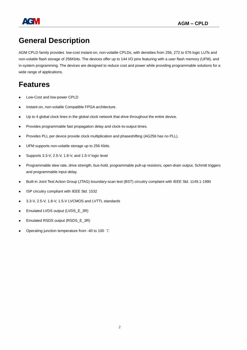
General Description
AGM CPLD family provides low-cost instant-on, non-volatile CPLDs, with densities from 256, 272 to 576 logic LUTs and
non-volatile flash storage of 256Kbits. The devices offer up to 144 I/O pins featuring with a user flash memory (UFM), and
in-system programming. The devices are designed to reduce cost and power while providing programmable solutions for a
wide range of applications.
Features
Low-Cost and low-power CPLD
Instant-on, non-volatile Compatible FPGA architecture.
Up to 4 global clock lines in the global clock network that drive throughout the entire device.
Provides programmable fast propagation delay and clock-to-output times.
Provides PLL per device provide clock multiplication and phaseshifting (AG256 has no PLL).
UFM supports non-volatile storage up to 256 Kbits.
Supports 3.3-V, 2.5-V, 1.8-V, and 1.5-V logic level
Programmable slew rate, drive strength, bus-hold, programmable pull-up resistors, open-drain output, Schmitt triggers
and programmable input delay.
Built-in Joint Test Action Group (JTAG) boundary-scan test (BST) circuitry complaint with IEEE Std. 1149.1-1990
ISP circuitry compliant with IEEE Std. 1532
3.3-V, 2.5-V, 1.8-V, 1.5-V LVCMOS and LVTTL standards
Emulated LVDS output (LVDS_E_3R)
Emulated RSDS output (RSDS_E_3R)
Operating junction temperature from -40 to 100 ℃
AGM – CPLD
3
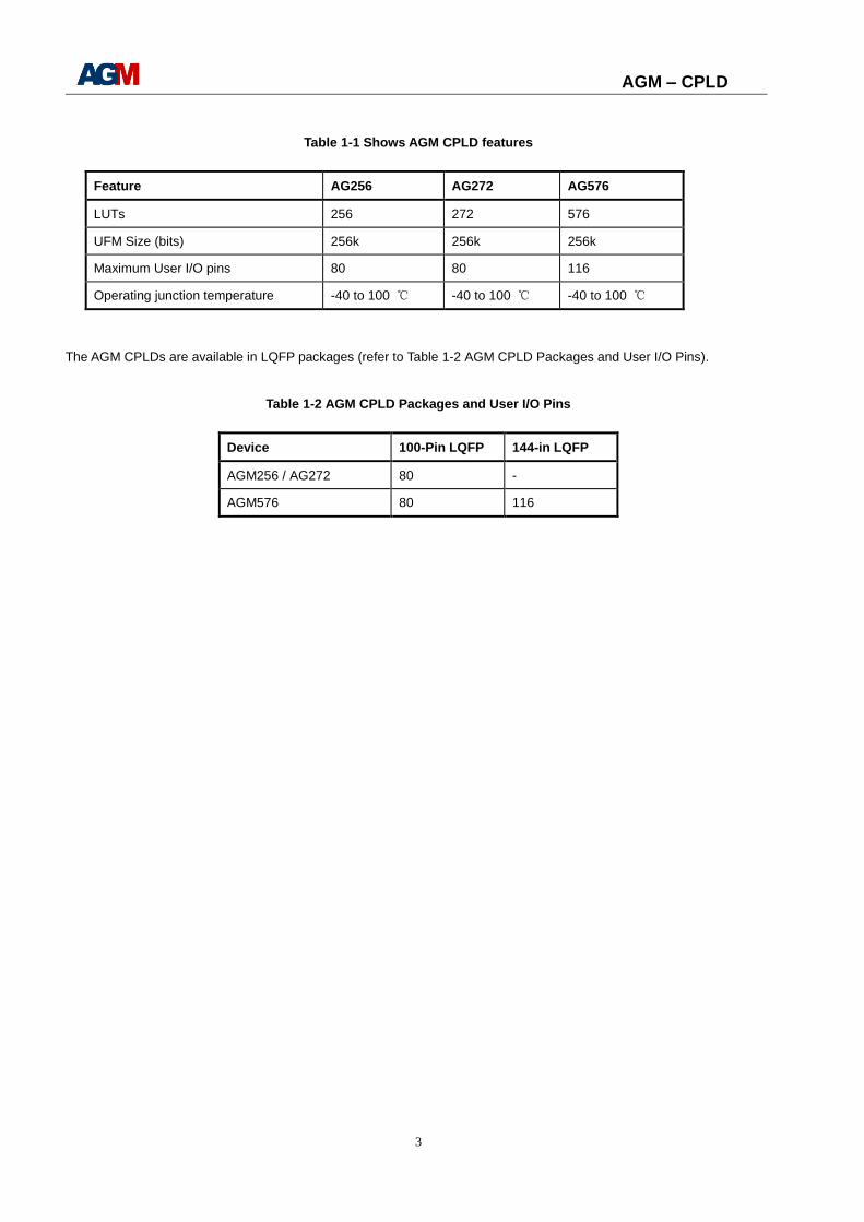
Table 1-1 Shows AGM CPLD features
Feature AG256 AG272 AG576
LUTs 256 272 576
UFM Size (bits) 256k 256k 256k
Maximum User I/O pins 80 80 116
Operating junction temperature -40 to 100 ℃ -40 to 100 ℃ -40 to 100 ℃
The AGM CPLDs are available in LQFP packages (refer to Table 1-2 AGM CPLD Packages and User I/O Pins).
Table 1-2 AGM CPLD Packages and User I/O Pins
Device 100-Pin LQFP 144-in LQFP
AGM256 / AG272 80 -
AGM576 80 116
AGM – CPLD
4
Content
GENERAL DESCRIPTION .............................................................................................................................................. 2
FEATURES ......................................................................................................................................................................... 2
CONTENT .......................................................................................................................................................................... 4
1. AGM ARCHITECTURE OVERVIEW ..................................................................................................................... 5
1.1. FUNCTIONAL DESCRIPTION .................................................................................................................................. 5
1.2. LOGIC ARRAY BLOCKS ......................................................................................................................................... 5
1.3. LOGIC ELEMENT ................................................................................................................................................... 5
1.4. FLEXTRACK INTERCONNECT ................................................................................................................................ 6
1.5. GLOBAL SIGNALS ................................................................................................................................................. 6
1.6. PHASE LOCKED LOOPS (PLLS) ............................................................................................................................. 6
1.7. USER FLASH MEMORY BLOCK ............................................................................................................................. 8
1.8. I/O PIN STRUCTURE .............................................................................................................................................. 8
2. JTAG AND IN-SYSTEM PROGRAMMING ........................................................................................................... 9
2.1. JTAG .................................................................................................................................................................... 9
2.2. IN-SYSTEM PROGRAMMING .................................................................................................................................. 9
3. POWER-ON RESET CIRCUITRY, ON-CHIP OSCILLATOR ........................................................................... 10
3.1. POWER-ON RESET CIRCUITRY ............................................................................................................................ 10
3.2. ON-CHIP OSCILLATOR ........................................................................................................................................ 10
4. TIMING CHARACTERISTICS .............................................................................................................................. 11
5. PIN-OUTS ................................................................................................................................................................ 12
6. REFERENCE AND ORDERING INFORMATION .............................................................................................. 17
6.1. SOFTWARE .......................................................................................................................................................... 17
6.2. ORDERING INFORMATION ................................................................................................................................... 17
7. REVISION HISTORY .............................................................................................................................................. 17
AGM – CPLD
5
1. AGM Architecture Overview
1.1. Functional Description
The AGM CPLD devices contain an industrial state-of-the art two-dimensional row- and column-based architecture to
implement custom logic. Column and row interconnects of varies speeds provide signal interconnects between logic blocks
(LBs) and IOs.
The logic array consists of LBs, with 16 logic slices (LS) in each LB. A slice is a small unit of logic providing efficient
implementation of user logic functions. LBs are grouped into rows and columns across the device. The CPLD devices’
density range is up to 576 slices.
The device global clock network consists of up to 4 global clock lines that drive through the entire device. The global clock
network can provide clocks for all resources within the device, such as input/output elements (IOEs), slices. The global
clock lines can also be used for other high fan-out signals.
Each device I/O pin is fed by an IOE located at the ends of LBrows and columns around the periphery of the device. I/O
pins support various single-ended standards. Each IOE contains a bidirectional I/O buffer.
Each device is embedded with a flash memory block. The big portion of this flash memory storage is used as dedicated
configuration flash memory (CFM) block. The CFM flash memory block provides the non-volatile storage for the all SRAM
configuration bits. The CFM automatically downloads and configures the logic blocks and IP during power-on, providing
instant-on sequence operation.
AGM CPLD device partitions 256k bits of flash memory as UFM (user flash memory) as general storage purposes. The
UFM provides programmable port connections to the logic array for reading and writing.
1.2. Logic Array Blocks
Each Logic Block consists of 16 slices, SLICE carry chains, SLICE control signals, a local interconnect, a look-up table
(LUT) chain, and register chain connection lines.
1.3. Logic Element
The smallest unit of logic in AGM architecture, the slice, is compact and provides advanced and flexible features with
efficient logic utilization. Each slice features:
A four-input look-up table (LUT4), which is a function generator that can implement any combinatorial logic function of
four inputs.
A programmable register

AGM – CPLD
6
Figure 1-1 AGM CPLD Logic SLICE
Each slice’s register has data, clock, clock enable, and clear inputs.
1.4. FlexTrack Interconnect
In AGM device architecture, FlexTrack interconnect consists of continuous, performance-optimized routing lines used for
inter- and intra- design block connectivity. The FlexTrack connects to LEs, the UFM, and IO pins with row and column
connection that span fixed distances.
1.5. Global Signals
Each device has four dual-purpose dedicated clock pins, two pins on the left side, and two pins on the right. The four global
clock lines drive throughout the entire device. The global clock network can provide clocks for all resources within the
device including Les, local interconnect. The global lines can be used for global signals distribution.
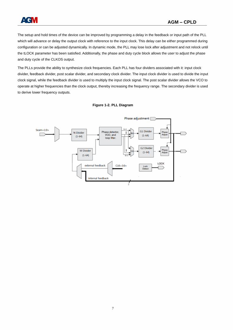
1.6. Phase Locked Loops (PLLs)
The AG272 and AG576 provide PLL support. The source of the PLL input divider can come from an external pin or from
internal routing. There are four sources of feedback signals to the feedback divider: from CLKINTFB (internal feedback
port), from the global clock nets, from the output of the post scalar divider, and from the routing (or from an external pin).
There is a PLL_LOCK signal to indicate that the PLL has locked on to the input clock signal. Figure 1-2 shows the PLL
diagram.
Shift Register
Input
ClkEnable
Carry Out
>
Data
Inputs
Clk
Synchronous
Reset
Enabl
e
Q
Lut
Output
Shift Register
Output
Reset
Asynchronous
Reset
Clk
Carry In
Synchronous &
Shift Control D
LUT4 &
Carry Chain
AGM – CPLD
7
The setup and hold times of the device can be improved by programming a delay in the feedback or input path of the PLL
which will advance or delay the output clock with reference to the input clock. This delay can be either programmed during
configuration or can be adjusted dynamically. In dynamic mode, the PLL may lose lock after adjustment and not relock until
the tLOCK parameter has been satisfied. Additionally, the phase and duty cycle block allows the user to adjust the phase
and duty cycle of the CLKOS output.
The PLLs provide the ability to synthesize clock frequencies. Each PLL has four dividers associated with it: input clock
divider, feedback divider, post scalar divider, and secondary clock divider. The input clock divider is used to divide the input
clock signal, while the feedback divider is used to multiply the input clock signal. The post scalar divider allows the VCO to
operate at higher frequencies than the clock output, thereby increasing the frequency range. The secondary divider is used
to derive lower frequency outputs.
Figure 1-2. PLL Diagram

AGM – CPLD
8
1.7. User Flash Memory Block
AGM CPLD device provides single UFM block for storing non-volatile information.
1.8. I/O Pin Structure
I/O supported features:
Supports 3.3-V, 2.5-V, 1.8-V, and 1.5-V logic levels
Programmable slew rate, drive strength, bus-hold, programmable pull-up resistors, open-drain output, Schmitt triggers
input and programmable input delay.
Built-in Joint Test Action Group (JTAG) boundary-scan test (BST) circuitry compliant with IEEE Std. 1149.1-1990
ISP circuitry compliant with IEEE Std. 1532
3.3-V , 2.5-V, 1.8-V, 1.5-V LVCMOS and LVTTL standards
Emulated LVDS output (LVDS_E_3R)
Emulated RSDS output (RSDS_E_3R)
AGM – CPLD
9
2. JTAG and In-System Programming
2.1. JTAG
AGM devices provide Built-in Joint Test Action Group (JTAG) boundary-scan test (BST) circuitry complaint with IEEE Std.
1149.1-1990. The JTAG pins support 1.5V, 1.8V, or 3.3V I/O standards
2.2. In-System Programming
AGM device supports in-system programming via the industry standard 4-pin IEEE Std. 1149.1 (JTAG) interface. JTAG and
ISP provide efficient iteration for design pattern written into the CFM’s non-volatile flash storage.
By default, during in-system programming, the I/O pins are tri-stated and weakly pulled-up to VCCIO. AGM CPLD device
also support real-time and clamp feature to allow user control of I/O state during in-system programming.
Real-time ISP allows user to program a CPLD while the device is still in operation. The newly programmed design will only
take effect when the device is power cycled. This allows in-filed updates to AGM CPLD at any time without interrupting the
whole system.
ISP clamp feature allow user to hold each I/O to a specific state during real-time ISP. Each I/O can be set to low, high,
tri-state, or hold the state when the device enters ISP clamp mode. After the device is successfully programmed the
clamped I/O pins will be released the function according to the new design.
AGM – CPLD
10
3. Power-On Reset Circuitry, On-Chip Oscillator
3.1. Power-On Reset Circuitry
When power is applied to AGM CPLD devices, the POR circuit monitors VCCINT and begins SRAM download at an
approximate voltage of 1.2V AGM devices.
Entry into user mode is gated by whether VCCIO bank1 are powered with sufficient operating voltage. If VCCINT and VCCIO are
powered simultaneously, the device enters user mode.
For CPLD when in user mode, the POR circuitry continues to monitor the VCCINT (but not VCCIO) voltage level to detect a
brown-out condition. If there is a VCCINT voltage sag at or below 1.0 V during user mode, the POR circuit resets the SRAM
and tri-states the I/O pins. Once VCCINT rises back to approximately 1.2V, the SRAM download restarts and the device begins
to operate.
3.2. On-Chip Oscillator
On-Chip oscillator is provided to support frequency to 9MHz(Min 7MHz, Max 11MHz).
AGM – CPLD
11
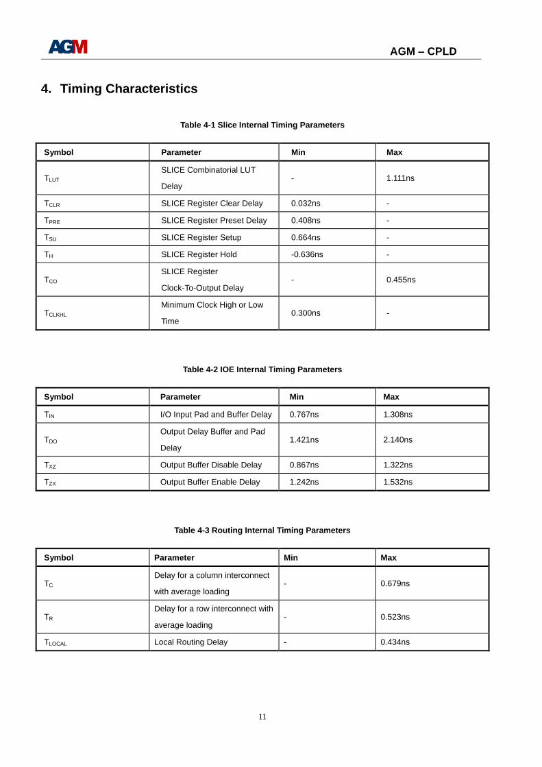
4. Timing Characteristics
Table 4-1 Slice Internal Timing Parameters
Symbol Parameter Min Max
TLUT SLICE Combinatorial LUT
Delay - 1.111ns
TCLR SLICE Register Clear Delay 0.032ns -
TPRE SLICE Register Preset Delay 0.408ns -
TSU SLICE Register Setup 0.664ns -
TH SLICE Register Hold -0.636ns -
TCO SLICE Register
Clock-To-Output Delay - 0.455ns
TCLKHL Minimum Clock High or Low
Time 0.300ns -
Table 4-2 IOE Internal Timing Parameters
Symbol Parameter Min Max
TIN I/O Input Pad and Buffer Delay 0.767ns 1.308ns
TDO Output Delay Buffer and Pad
Delay 1.421ns 2.140ns
TXZ Output Buffer Disable Delay 0.867ns 1.322ns
TZX Output Buffer Enable Delay 1.242ns 1.532ns
Table 4-3 Routing Internal Timing Parameters
Symbol Parameter Min Max
TC Delay for a column interconnect
with average loading - 0.679ns
TR Delay for a row interconnect with
average loading - 0.523ns
TLOCAL Local Routing Delay - 0.434ns
AGM – CPLD
12
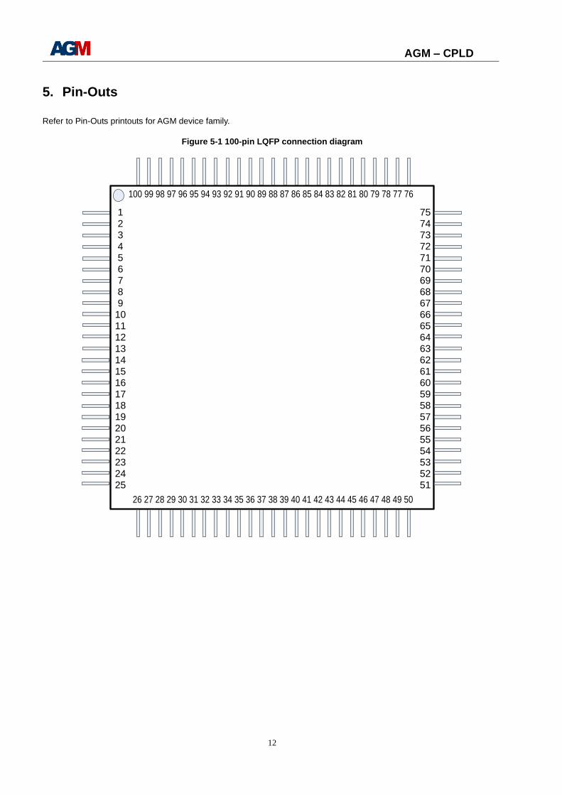
5. Pin-Outs
Refer to Pin-Outs printouts for AGM device family.
Figure 5-1 100-pin LQFP connection diagram
123456789
10111213141516171819202122232425
26 27 28 29 30 31 32 33 34 35 36 37 38 39 40 41 42 43 44 45 46 47 48 49 50
75747372717069686766656463626160595857565554535251
100 99 98 97 96 95 94 93 92 91 90 89 88 87 86 85 84 83 82 81 80 79 78 77 76

AGM – CPLD
13
Table 5-1 AG256 / AG272 100 pin out
Bank Pin
name
Finger
No. Bank
Pin
name
Finger
No. Bank
Pin
name
Finger
No. Bank
Pin
name
Finger
No.
4 I/O 1 2 I/O 26 2 I/O 51 4 I/O 76
1 I/O 2 2 I/O 27 3 I/O 52 4 I/O 77
1 I/O 3 2 I/O 28 3 I/O 53 4 I/O 78
1 I/O 4 2 I/O 29 3 I/O 54 4 GNDIO 79
1 I/O 5 2 I/O 30 3 I/O 55 4 VDDIO2 80
1 I/O 6 2 VDDF33 31 3 I/O 56 4 I/O 81
1 I/O 7 2 GNDIO 32 3 I/O 57 4 I/O 82
1 I/O 8 2 I/O 33 3 I/O 58 4 I/O 83
1 VDDIO1 9 2 I/O 34 3 VDDIO2 59 4 I/O 84
1 GNDIO 10 2 I/O 35 3 GNDIO 60 4 I/O 85
1 GNDC 11 2 I/O 36 3 I/O 61 4 I/O 86
1 I/O 12 2 I/O 37 3 I/O 62 4 I/O 87
1 VDDC 13 2 I/O 38 3 VDDC 63 4 I/O 88
1 I/O 14 2 I/O 39 3 I/O 64 4 I/O 89
1 I/O 15 2 I/O 40 3 GNDC 65 4 I/O 90
1 I/O 16 2 I/O 41 3 I/O 66 4 I/O 91
1 I/O 17 2 I/O 42 3 I/O 67 4 I/O 92
1 I/O 18 2 I/O 43 3 I/O 68 4 GNDIO 93
1 I/O 19 2 I/O 44 3 I/O 69 4 VDDIO2 94
1 I/O 20 2 VDDIO1 45 3 I/O 70 4 I/O 95
1 I/O 21 2 GNDIO 46 3 I/O 71 4 I/O 96
1 TMS 22 2 I/O 47 3 I/O 72 4 I/O 97
1 TDI 23 2 I/O 48 3 I/O 73 4 I/O 98
1 TCK 24 2 I/O 49 3 I/O 74 4 I/O 99
1 TDO 25 2 I/O 50 3 I/O 75 4 I/O 100
AGM – CPLD
14
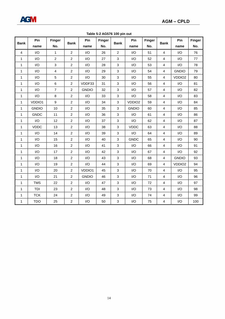
Table 5-2 AG576 100 pin out
Bank Pin
name
Finger
No. Bank
Pin
name
Finger
No. Bank
Pin
name
Finger
No. Bank
Pin
name
Finger
No.
4 I/O 1 2 I/O 26 2 I/O 51 4 I/O 76
1 I/O 2 2 I/O 27 3 I/O 52 4 I/O 77
1 I/O 3 2 I/O 28 3 I/O 53 4 I/O 78
1 I/O 4 2 I/O 29 3 I/O 54 4 GNDIO 79
1 I/O 5 2 I/O 30 3 I/O 55 4 VDDIO2 80
1 I/O 6 2 VDDF33 31 3 I/O 56 4 I/O 81
1 I/O 7 2 GNDIO 32 3 I/O 57 4 I/O 82
1 I/O 8 2 I/O 33 3 I/O 58 4 I/O 83
1 VDDIO1 9 2 I/O 34 3 VDDIO2 59 4 I/O 84
1 GNDIO 10 2 I/O 35 3 GNDIO 60 4 I/O 85
1 GNDC 11 2 I/O 36 3 I/O 61 4 I/O 86
1 I/O 12 2 I/O 37 3 I/O 62 4 I/O 87
1 VDDC 13 2 I/O 38 3 VDDC 63 4 I/O 88
1 I/O 14 2 I/O 39 3 I/O 64 4 I/O 89
1 I/O 15 2 I/O 40 3 GNDC 65 4 I/O 90
1 I/O 16 2 I/O 41 3 I/O 66 4 I/O 91
1 I/O 17 2 I/O 42 3 I/O 67 4 I/O 92
1 I/O 18 2 I/O 43 3 I/O 68 4 GNDIO 93
1 I/O 19 2 I/O 44 3 I/O 69 4 VDDIO2 94
1 I/O 20 2 VDDIO1 45 3 I/O 70 4 I/O 95
1 I/O 21 2 GNDIO 46 3 I/O 71 4 I/O 96
1 TMS 22 2 I/O 47 3 I/O 72 4 I/O 97
1 TDI 23 2 I/O 48 3 I/O 73 4 I/O 98
1 TCK 24 2 I/O 49 3 I/O 74 4 I/O 99
1 TDO 25 2 I/O 50 3 I/O 75 4 I/O 100

AGM – CPLD
15
Figure 5-2 144-pin LQFP connection diagram
123456789
101112131415161718192021222324252627282930313233343536
108107106105104103102101100999897969594939291908988878685848382818079787776757473
37 38 39 40 41 42 43 44 45 46 47 48 49 50 51 52 53 54 55 56 57 58 59 60 61 62 63 64 65 66 67 68 69 70 71 72
144 143 142 141 140 139 138 137 136 135 134 133 132 131 130 129 128 127 126 125 124 123 122 121 120 119 118 117 116 115 114 113 112 111 110 109

AGM – CPLD
16
Table 5-3 AG576 144 pin out
Bank Pin
name
Finger
No Bank
Pin
name
Finger
No Bank
Pin
name
Finger
No Bank
Pin
name
Finger
No
1 I/O 1 2 I/O 37 3 I/O 73 4 I/O 109
1 I/O 2 2 I/O 38 3 I/O 74 4 I/O 110
1 I/O 3 2 I/O 39 3 I/O 75 4 I/O 111
1 I/O 4 2 I/O 40 3 I/O 76 4 I/O 112
1 I/O 5 2 I/O 41 3 I/O 77 4 I/O 113
1 I/O 6 2 I/O 42 3 I/O 78 4 I/O 114
1 I/O 7 2 I/O 43 3 I/O 79 4 GNDIO 115
1 I/O 8 2 I/O 44 3 I/O 80 4 VDDIO2 116
1 VDDIO1 9 2 I/O 45 3 I/O 81 4 I/O 117
1 GNDIO 10 2 VDDF33 46 3 VDDIO2 82 4 I/O 118
1 I/O 11 2 GNDIO 47 3 GNDIO 83 4 I/O 119
1 I/O 12 2 I/O 48 3 I/O 84 4 I/O 120
1 I/O 13 2 I/O 49 3 I/O 85 4 I/O 121
1 I/O 14 2 I/O 50 3 I/O 86 4 I/O 122
1 I/O 15 2 I/O 51 3 I/O 87 4 I/O 123
1 I/O 16 2 I/O 52 3 I/O 88 4 I/O 124
1 GNDC 17 2 I/O 53 3 I/O 89 4 I/O 125
1 I/O 18 2 GNDC 54 3 VDDC 90 4 VDDC 126
1 VDDC 19 2 I/O 55 3 I/O 91 4 I/O 127
1 I/O 20 2 VDDC 56 3 GNDC 92 4 GNDC 128
1 I/O 21 2 I/O 57 3 I/O 93 4 I/O 129
1 I/O 22 2 I/O 58 3 I/O 94 4 I/O 130
1 I/O 23 2 I/O 59 3 I/O 95 4 I/O 131
1 I/O 24 2 I/O 60 3 I/O 96 4 I/O 132
1 VDDIO1 25 2 I/O 61 3 I/O 97 4 I/O 133
1 GNDIO 26 2 I/O 62 3 I/O 98 4 I/O 134
1 I/O 27 2 I/O 63 3 GNDIO 99 4 GNDIO 135
1 I/O 28 2 VDDIO1 64 3 VDDIO2 100 4 VDDIO2 136
1 I/O 29 2 GNDIO 65 3 I/O 101 4 I/O 137
1 I/O 30 2 I/O 66 3 I/O 102 4 I/O 138
1 I/O 31 2 I/O 67 3 I/O 103 4 I/O 139
1 I/O 32 2 I/O 68 3 I/O 104 4 I/O 140
1 TMS 33 2 I/O 69 3 I/O 105 4 I/O 141
1 TDI 34 2 I/O 70 3 I/O 106 4 I/O 142
1 TCK 35 2 I/O 71 3 I/O 107 4 I/O 143
1 TDO 36 2 I/O 72 3 I/O 108 4 I/O 144
AGM – CPLD
17
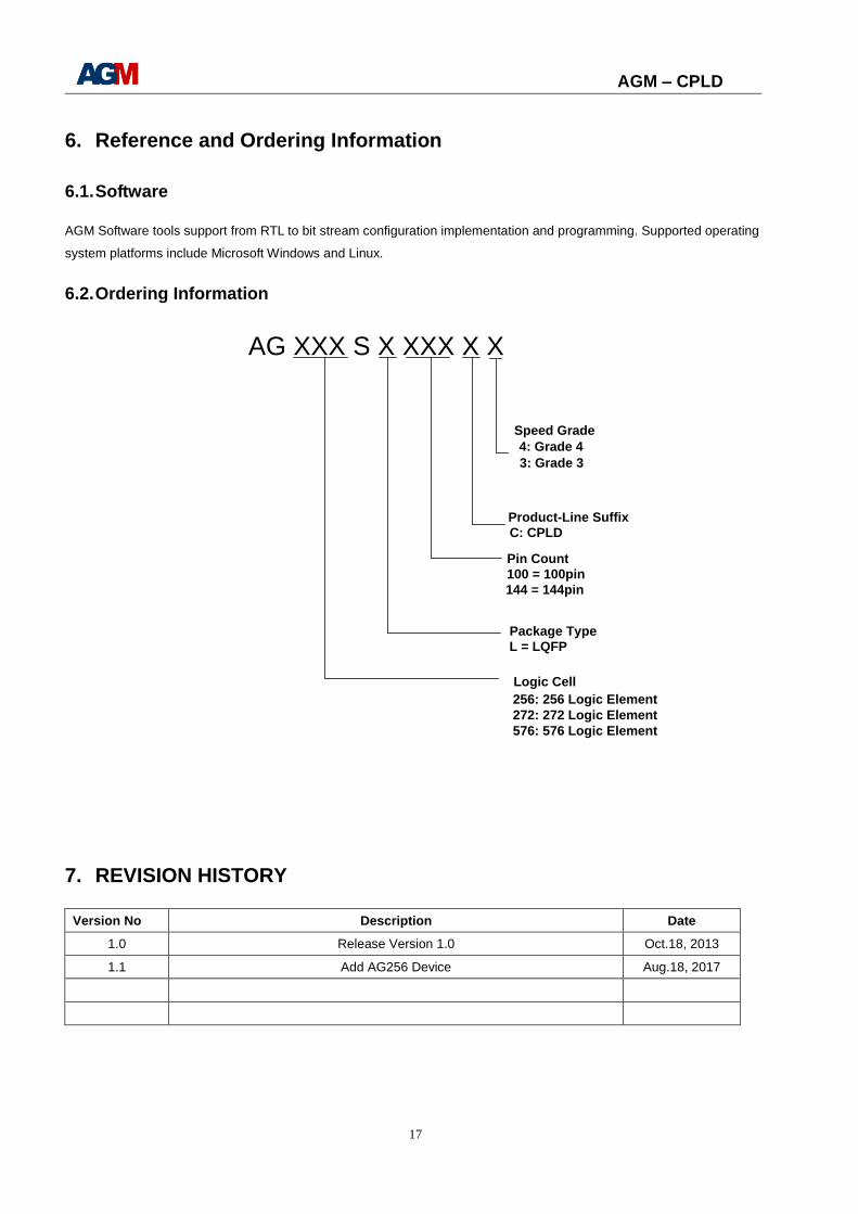
6. Reference and Ordering Information
6.1. Software
AGM Software tools support from RTL to bit stream configuration implementation and programming. Supported operating
system platforms include Microsoft Windows and Linux.
6.2. Ordering Information
7. REVISION HISTORY
Version No Description Date
1.0 Release Version 1.0 Oct.18, 2013
1.1 Add AG256 Device Aug.18, 2017
AG XXX S X XXX X X
Product-Line Suffix
C: CPLD
Package Type
Logic Cell
L = LQFP
Speed Grade
4: Grade 4
3: Grade 3
256: 256 Logic Element
272: 272 Logic Element
576: 576 Logic Element
Pin Count
144 = 144pin
100 = 100pin