A system to demonstrate the bistability in molecules for application in a molecular QCA cell
71
A SYSTEM TO DEMONSTATE THE BISTABILITY OF MOLECULES FOR APPLICATION IN A MOLECULAR QCA CELL A Thesis Submitted to the Graduate School of the University of Notre Dame in Partial Fulfillment of the Requirements for the Degree of Master of Science in Electrical Engineering by Robin A. Joyce Gregory L. Snider, Co-Director Alexei O. Orlov, Co-Director Graduate Program in Electrical Engineering Notre Dame, Indiana October 2008
Transcript of A system to demonstrate the bistability in molecules for application in a molecular QCA cell

A SYSTEM TO DEMONSTATE THE BISTABILITY OF MOLECULES FOR
APPLICATION IN A MOLECULAR QCA CELL
A Thesis
Submitted to the Graduate School
of the University of Notre Dame
in Partial Fulfillment of the Requirements
for the Degree of
Master of Science in Electrical Engineering
by
Robin A. Joyce
Gregory L. Snider, Co-Director
Alexei O. Orlov, Co-Director
Graduate Program in Electrical Engineering
Notre Dame, Indiana
October 2008

A SYSTEM TO DEMONSTATE THE BISTABILITY OF MOLECULES FOR
APPLICATION IN A MOLECULAR QCA CELL
Abstract
By
Robin A. Joyce
Quantum-dot Cellular Automata (QCA) provides a new paradigm for
computation and for the design of electronic devices [1]. The past 40 years have seen
great technological advancement brought about by the densification of transistor-
based circuitry. As transistors are reduced in size problems such as device density,
device interconnection and power dissipation become increasingly hard to overcome
and short-channel effects degrade device performance. In light of these problems, a
new architecture is needed to enable the shrinking of electronic devices down to
molecular sizes. QCA provides this new architecture by encoding binary information
in the bistable charge configuration of quantum-dot cells and by using the Coulomb
interaction to couple neighboring cells. QCA functionality has been demonstrated in
metal-dot systems at cryogenic temperatures [2], but a molecular sized QCA cell
would operate at room temperature. The two principle requirements for molecules
used in a QCA cell are bistability and ability to couple to neighboring cells [3].
Electric field-driven bistability has been demonstrated using a capacitive

Robin A. Joyce
measurement of a large number of silicon surface bound, vertically oriented
molecules over a large area using a dinuclear complex [4]. These molecules can be
bound to the surface of a chlorinated, <111> oriented, highly-doped p-type silicon
substrate and oxidized to become stable, biased mixed-valence complexes. We
present a system to test the bistability of individual molecules for application in a
QCA cell. The system presented consists of two polysilicon gate electrodes which sit
adjacent to two highly-doped windows of silicon to which the molecules can be
bound. To enable the detection of switching activity the two highly doped regions are
electrically connected to the island of a single-electron transistor (SET) which serves
as an electrometer. The molecules, bound to one of the two windows, are capacitively
coupled to the island of the SET. This design facilitates a differential measurement
approach where a single molecular switching event should be seen in the conductance
of the SET. The system to effect this test, broadly serving the role of electrometer, is
presented herein.

CONTENTS
FIGURES........................................................................................................................... iv
TABLES ............................................................................................................................ iv
ACKNOWLEDGMENTS ................................................................................................. ix
CHAPTER 1: INTRODUCTION....................................................................................... 1 1.1 Molecular Quantum-dot Cellular Automata ..................................................... 1 1.2 Single Electron Effects and the SET................................................................. 6
CHAPTER 2: DEVICE DESIGN ..................................................................................... 16 2.1 Overview......................................................................................................... 16 2.2 The Molecules................................................................................................. 17 2.3 The Gate Electrode ......................................................................................... 20 2.4 The SET as Electrometer ................................................................................ 22 2.5 Differential Measurement Design................................................................... 24
CHAPTER 3: DEVICE FABRICATION ......................................................................... 28 3.1 Overview......................................................................................................... 28 3.2 Optical Mask Set............................................................................................. 28 3.3 Thin Oxide Growth......................................................................................... 32
3.3.1 RCA Clean............................................................................................. 32 3.3.2 Thin Oxide Growth................................................................................ 33
3.4 Polysilicon Gate Formation ............................................................................ 34 3.4.1 Polysilicon Deposition ........................................................................... 34 3.4.2 Thin-oxide and Polysilicon Metrology .................................................. 35 3.4.3 Polysilicon Blanket Implant................................................................... 36 3.4.4 Polysilicon Implant Drive-In/Anneal..................................................... 37 3.4.5 Polysilicon Gate Electrode Lithography................................................ 37 3.4.6 Polysilicon Gate Electrode Etch ............................................................ 38
3.5 P+ Window...................................................................................................... 39 3.5.1 P+ Window Lithography ........................................................................ 39 3.5.2 Thermal Oxide Etch............................................................................... 39 3.5.3 P+ Window Implant and Anneal ........................................................... 39
3.6 Substrate Dicing.............................................................................................. 41 3.7 First-Layer Wire Formation............................................................................ 42
3.7.1 First-Layer Wire Lithography................................................................ 42
ii

3.7.2 First-Layer Wire Evaporation and Lift-Off ........................................... 43 3.8 Polysilion Gate Electrode Contact Anneal ..................................................... 44 3.9 Second-Layer Pad and Wire Formation.......................................................... 45
3.9.1 Second-Layer Pad and Wire Lithography.............................................. 45 3.9.2 Second-Layer Pad and Wire Evaporation and Lift-Off ......................... 45
3.10 Cleaving ........................................................................................................ 46 3.11 SET Formation.............................................................................................. 46
3.11.1 SET Lithography.................................................................................. 46 3.11.2 SET Evaporation and Junction Formation........................................... 47 3.11.3 SET Lift-Off......................................................................................... 48
3.12 Room-temperature Testing, Cleaving and Wire-bonding............................. 49
CHAPTER 4: MEASUREMENTS AND RESULTS ...................................................... 51 4.1 Helium Cryostat .............................................................................................. 51 4.2 Test Set-up ...................................................................................................... 51 4.3 The Stand-alone SET ...................................................................................... 52 4.4 The Integrated SET......................................................................................... 54
CHAPTER 5: SUMMARY AND FURTHER WORK.................................................... 56 5.1 Summary ......................................................................................................... 56 5.2 Attaching the Molecules ................................................................................. 57
BIBLIOGRAPHY............................................................................................................. 59
iii

FIGURES
Figure 1.1 The two polarizations of a four dot QCA cell. .................................................. 1
Figure 1.2 The cell-cell response function describes the polarization of neighboring four-dot QCA cells.......................................................................................................... 2
Figure 1.3 (a) A wire, (b) an inverter and (c) a majority gate realized using QCA cells. .. 4
Figure 1.4 The operation region for QCA architectures on a power-delay curve for various clocking schemes. Advanced transistor devices are oriented as a means of comparison [5]. ....................................................................................................... 5
Figure 1.5 A (a) graphic and (b) schematic representation of a single-electron transistor. 8
Figure 1.6 The electrostatic energy associated with N-1, N and N+1, etc. populations on the island of the SET. The gate voltage can change the electrostatic potential of each configuration. The charging energy is shown as the energy required to add or subtract an electron from the island. ....................................................................... 9
Figure 1.7 Oscillations in conductance as a function of gate voltage............................... 10
Figure 1.8 (a) Current is suppressed in the Coulomb blockade region. (b) When the gate is used to adjust the electrostatic potential of the island so the charging energy is no longer a barrier to tunneling, current will flow. The potential of the island changes from ΨN to ΨN+1 to ΨN ((b) to (c) to (b)) as the population of the island goes from N → N+1 → N, etc.............................................................................. 11
Figure 1.9 A theoretical Coulomb charging diagram for an SET operating at 0 K [8]. ... 12
Figure 1.10 (a) The band diagram and (b) the Coulomb charging diagram show that the charging energy can be determined from the length of the rhombic Coulomb blockade region in the Vds direction. .................................................................... 15
Figure 2.1 A top down view (top) and cross-sectional view (bottom) of the system. The polysilicon driving electrodes are shown in red, the self-aligned p+ windows in
iv

green, the thin oxide in blue, the SET in cross-hatch and the molecules in yellow................................................................................................................................ 17
Figure 2.2 The dinuclear complex can be bound to a chlorinated, heavily p-doped, (111) silicon surface and oxidized with ferrocenium ion to become a stable, biased, mixed-valence complex [4]................................................................................... 18
Figure 2.3 Applying a potential between the top mercury electrode and the silicon substrate results in the electron switching from the resting state to the switched state [4].................................................................................................................. 18
Figure 2.4 Capacitance (C) and differential capacitance (ΔC) as a function of mercury electrode voltage (VHg) [4].................................................................................... 19
Figure 2.5 The design of the device ensures the molecules will be positioned as closely as possible to the polysilicon driving electrode, shown here in red. The thin thermal oxide shown in blue and the self-aligned p+ window shown in green facilitate this close positioning. .................................................................................................. 21
Figure 2.6 The sum of Vg1 and Vg2 should be chosen to be on the steepest point of the Coulomb oscillation curve. In this way the conductance response is the most sensitive to changes in gate potential.................................................................... 23
Figure 2.7 Schematic of the SET in our system. The two adjacent polysilicon gates, Vg1 and Vg2, are capacitively coupled to the island of the SET through Cg1 and Cg2 and have an additive gating effect. .............................................................................. 24
Figure 2.8 A circuit schematic from one polysilicon gate to the other across the island of the SET (shown in red). Cg1 and Cg2 are the capacitances between the island and the two polysilicon gates and Cm is the molecular capacitance. C0 is the self-capacitance of the island. The capacitances of the tunnel junctions, C1 and C2, are not shown. ............................................................................................................. 25
Figure 2.9 (a) Linearly increasing positive bias applied to Vg1 and Vg2. The expected change in the conductance of the SET when (b) no molecules are present, as a control experiment and (c) when molecules are present and molecular switching is effected.................................................................................................................. 27
Figure 3.1 The optical mask set. ....................................................................................... 29
Figure 3.2 A close-up of one 20-pin pad frame. ............................................................... 30
Figure 3.3 A further close-up of the interior of one 20-pin pad frame. ............................ 31
v

Figure 3.4 A final close-up shows a single device............................................................ 32
Figure 3.5 A cross-sectional SEM image showing, from top to bottom, the deposited polysilicon, thermally grown oxide and substrate silicon layers. ......................... 36
Figure 3.6 Optical image of etched polysilicon gate features........................................... 39
Figure 3.7 Optical image of the p+ regions following implant and removal of the protective PMMA layer. The white implanted regions are visible due to the lattice damage induced during implantation; following the anneal step the p+ regions are no longer visible.................................................................................................... 41
Figure 3.8 The two metal layers are required to minimize the first-layer metal step height seen during the SET evaporation and to make the peripheral pads of sufficient thickness for wire bonding.................................................................................... 42
Figure 3.9 Optical image of the first-layer wires after lift-off. ......................................... 44
Figure 3.10 Optical image following second-layer pad and wire lift-off. ........................ 46
Figure 3.11 The double-angle evaporation technique forms a small metal-insulator-metal tunnel junction underneath the PMMA bridge. .................................................... 47
Figure 3.12 SEM image of an SET structure following lift-off. This device was fabricated on a sample without p+ windows. ......................................................................... 48
Figure 3.13 SEM image of an SET structure after lift-off with the layers color-coded to correspond to Figure 3.11 and the tunnel junctions marked................................. 49
Figure 4.1 Schematic of low temperature electrical test set-up. ....................................... 52
Figure 4.2 The charging diagram for an SET device showing a charging energy of EC = 0.75 mV................................................................................................................. 53
Figure 4.3 Coulomb oscillation peaks in current as a function of gate voltage for an integrated SET. ..................................................................................................... 54
Figure 5.1 An optical image of the complete system. Nine polysilicon electrodes can be seen, defining 8 devices. ....................................................................................... 57
vi

Figure 5.2 A close-up of one device with the polysilicon driving electrodes in red, the self-aligned p+ windows in purple and the SET structure in gray. The molecule window, also self-aligned, is shown in gold. ........................................................ 58
vii

TABLES
Table 1 Majority Gate Boolean Logic Table ..................................................................... 3
Table 2 Polysilicon Deposition Process Details .............................................................. 35
viii

ix
ACKNOWLEDGMENTS
I would like to acknowledge the guidance and support of my advisors, Dr. Greg
Snider and Dr. Alexei Orlov. I would also like to thank the current and past members of
our research group; Yong Tang, Hubert George, Aaron Prager, Vishwanath Joshi,
Yenchun Lee, Adams Tong, Zengxiao Jin and Hua Qi for their assistance with this work
along with the tireless staff of the Notre Dame Nanofabrication Facility; Mike Thomas,
Keith Darr and Mark Richmond. Finally, I would like to thank my parents who at various
stages through the years, on occasions more numerous to mention, have convinced me to
keep going.

CHAPTER 1:
INTRODUCTION
1.1 Molecular Quantum-dot Cellular Automata
Quantum-dot Cellular Automata is a novel approach to computing that seeks to
replace the current switch as a means of encoding binary information. Binary information
is, instead, encoded in the position of electrons in a quantum-dot cell. In doing this, the
QCA paradigm promises to greatly reduce the power consumption associated with high-
density computation and bypass the intensive interconnection issues faced by
conventional CMOS.
Figure 1.1 The two polarizations of a four dot QCA cell.
When quantum dots are arranged in the four dot cell of Figure 1.1 and coupled by
tunnel barriers, two bistable charge configurations arise. When two extra electrons are
added to the system the Coulombic repulsion causes them to occupy opposite corners of
the cell. If the position of one of the electrons in a four-dot cell is changed, which can be
1

done by using external electrodes, the other electron will respond by occupying the
corresponding opposite corner. These two polarizations, P = +1 and P = -1, can be used to
represent the binary “1” and “0”. This property of bistability is one of the two key
requirements for a QCA cell. The second requirement is the ability to couple to
neighboring cells [3]. Figure 1.2 shows the cell to cell response function for neighboring
QCA cells. The controlled polarization of one cell will effect the same polarization,
through Coulombic repulsion, in a neighboring cell, resulting in a highly non-linear
function.
Figure 1.2 The cell-cell response function describes the polarization of neighboring four-dot QCA cells.
Neighboring cells are coupled by the Coulomb interaction and various circuit
elements can be constructed in this paradigm. To illustrate this, Figure 1.3 shows QCA
cells arranged to form a wire, an inverter and a majority gate. In the QCA wire of Figure
2

1.3 (a) the polarization of the input cell is transmitted down the line of cells to the output
cell. In the QCA inverter of Figure 1.3 (b) the input signal is split into two wires and
inverted by bringing the two wires back together at a 45 ° angle. In the QCA majority
gate of Figure 1.3 (c) the three input signals “vote” to determine the polarization of the
center and output cells. Using one of the inputs of the majority gate as a programming
input results in AND and OR functionality from the remaining two inputs. This can be
seen clearly in Table 1, when any input is set to logic value “0” the remaining two inputs
follow OR functionality. When any input is set to logic value “1” the remaining two
inputs follow AND functionality.
TABLE 1
MAJORITY GATE BOOLEAN LOGIC TABLE
Input A Input B Input C Output X
0 0 0 00 0 1 00 1 0 00 1 1 11 0 0 01 0 1 11 1 0 11 1 1 1
The ability to generate AND, OR and NOT functionality ensures that the QCA
paradigm can provide the complete suite of Boolean logic functions.
3
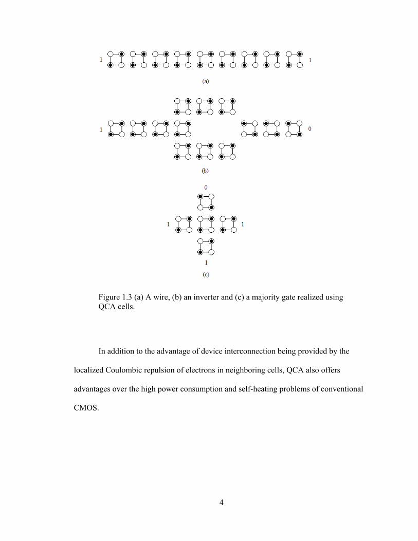
Figure 1.3 (a) A wire, (b) an inverter and (c) a majority gate realized using QCA cells.
In addition to the advantage of device interconnection being provided by the
localized Coulombic repulsion of electrons in neighboring cells, QCA also offers
advantages over the high power consumption and self-heating problems of conventional
CMOS.
4
Figure 1.4 The operation region for QCA architectures on a power-delay curve for various clocking schemes. Advanced transistor devices are oriented as a means of comparison [5].
The principle drawback to this paradigm is that, for a given polarization of an
input cell, a higher energy state, called a kink state, exists in the neighboring cell with an
energy difference called the kink energy. In a computational system, this energy can be
thought of as the energy required to make a mistake. As a result of the existence of this
higher-energy state, the thermal energy of the system becomes important and it is for this
reason that metal-dot QCA, which uses dots with capacitances of approximately 10 fF to
hold charge, has been confined to sub-1K operational temperatures.
The kink energy scales inversely with cell size and so it is desirable to decrease
the size of the QCA cell [1]. To realize large device densities, in any architecture, it is
necessary to shrink the size of each component device. In the current CMOS paradigm
this results in devices which struggle to contend with short-channel effects. Unlike
present system architectures, performance of a QCA system improves as the size of the
5

device is decreased. As the cell is shrunk in size, a pair of QCA dots begins to resemble a
mixed f
acy are bistability and the ability to couple to
neighb
es
discret
gh,
an be large enough to affect subsequent tunneling events [6]. This feedback
mechanism, resulting in increased resistance at small bias voltages, is called the Coulomb
valence complex molecule. QCA is a suitable paradigm for the implementation o
molecular electronics as it exploits the ability of molecules to hold charge and side-steps
the difficulties attendant to molecular interconnection. As we discussed above, the two
requirements for QCA cell candid
oring cells. To this end we plan to demonstrate the bistability of a mixed valence
complex for use in a molecular QCA cell and the system presented in this thesis will be
used to effect this demonstration.
1.2 Single Electron Effects and the SET
When electronic systems and devices are scaled to very small sizes the discrete
nature of charge becomes observable and will dominate the transport properties of such
systems. How small and cold a conductor needs to be before this quantization becom
important will be discussed here.
Imagine three electrodes, called a source, island and drain, separated by insulating
gaps. In this arrangement, shown in Figure 1.5 (a) the island is completely surrounded by
insulator. Electrons moving from source to drain, in response to an applied bias, can
traverse the insulating gaps by tunneling and will vary the charge of the island by the
e quantity e. In large systems the energy required to add this amount of charge to
the island is indiscernible at attainably low temperatures but if the island is small enou
and the associated capacitance is small enough, the energy associated with this change in
charge c
6
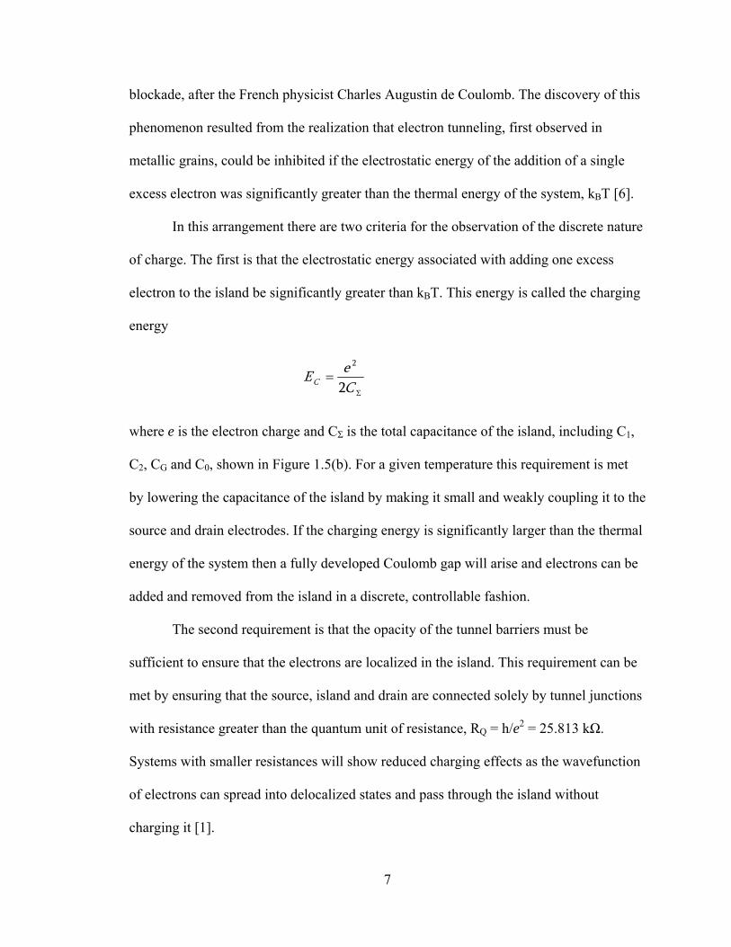
blockade, after the French physicist Charles Augustin de Coulomb. The discovery of this
phenomenon resulted from the realization that electron tunneling, first observed in
metallic grains, could be inhibited if the electrostatic energy of the addition of a single
excess electron was significantly greater than the thermal energy of the system, kBT [6].
In this arrangement there are two criteria for the observation of the discrete nature
of charge. The first is that the electrostatic energy associated with adding one excess
electron to the island be significantly greater than kBT. This energy is called the charging
energy
ΣCe
C 2
2
where e is the electron charge and CΣ is the total capacitance of the island, including C1,
C2, CG and C0, shown in Figure 1.5(b). For a given temperature this requirement is m
by lowering the capacitance of the island by making it small and weakly coupling it to the
source and drain electrodes. If the charging energy is significantly larger than the th
energy of the sy
=E
et
ermal
stem then a fully developed Coulomb gap will arise and electrons can be
added a
be
met by ensuring that the source, island and drain are connected solely by tunnel junctions
with resistance greater than the quantum unit of resistance, RQ = h/e2 = 25.813 kΩ.
Systems with smaller resistances will show reduced charging effects as the wavefunction
of electrons can spread into delocalized states and pass through the island without
charging it [1].
nd removed from the island in a discrete, controllable fashion.
The second requirement is that the opacity of the tunnel barriers must be
sufficient to ensure that the electrons are localized in the island. This requirement can
7

An SET is comprised of two low-capacitance tunnel junctions in series, defining a
source, island and drain. If the above requirements are met then Coulomb blockade will
be observable as electrons tunnel from the source to island and from island to drain.
Figure 1.5 A (a) graphic and (b) schematic representation of a single-electron transistor.
Additional gate electrodes, capacitively coupled to the island of the device, can
induce a charge on the island of the SET through the relationship
GGVCQ =
where CG is the capacitance between the island and the gate(s), VG is the potential on the
gate, and Q is the charge on the gate ca
pacitor, continuous even on the scale of the unit
charge, e. Multiple gates have additive effects. This “induced charge” will be
compensated for, at intervals, by the tunneling of discrete charges on and off the island
from the source and drain electrodes.
8

Figure 1.6 The electrostatic energy associated with N-1, N and N+1, etc. populations on the island of the SET. The gate voltage can change the electrostatic potential of each configuration. The charging energy is shown as the energy required to add or subtract an electron from the island.
Referring to Figure 1.6, as the electrostatic energy associated with each island
population is varied by the gate voltage, the point at which each parabola crosses its
neighbor is a point at which the N and N+1 (or N and N-1 state, etc.) are energetically
equivalent. At this point electrons will tunnel on and off the island, one at a time, via the
source and drain electrodes and current will flow through the device. At temperatures
above 0 K the ensemble electron energies of the system will make up a distribution
around the parabolas of Figure 1.6 and the region where current will flow, around
energetically equivalent points, will widen. The continuously induced charge on the gate
capacitor will be compensated by the tunneling of discrete charges on and off the island
having the effect that a measurement of the conductance will show peaks for a sweep of
the gate voltage and a fixed source drain bias. These peaks are referred to as Coulomb
blockade oscillations [7].
9

Figure 1.7 Oscillations in conductance as a function of gate voltage.
In the Coulomb blockade regions separating the Coulomb oscillation peaks, the
population of the island is fixed and no current flows. As the gate voltage increases and
moves through a region of higher conductance, electrons flow through the device and as
another Coulomb blockade region is entered the current stops and the electron population
of the island remains one greater than the previous configuration.
These effects can also be understood by looking at a band-diagram depiction of
the device, shown in Figure 1.8:
10

Figure 1.8 (a) Current is suppressed in the Coulomb blockade region. (b) When the gate is used to adjust the electrostatic potential of the island so the charging energy is no longer a barrier to tunneling, current will flow. The potential of the island changes from ΨN to ΨN+1 to ΨN ((b) to (c) to (b)) as the population of the island goes from N → N+1 → N, etc.
The source and drain of the device are “seas” of electrons, separated from the
island by insulating tunnel barriers and connected via the source-drain bias, Vds.
Tunneling on and off the island is suppressed by the charging energy as there is no
available “state” between the source and drain potential, depicted in Figure 1.8 (a). In
11

Figure 1.8 (b) the gate voltage has been used to change the electrostatic potential of the
island and tunneling is allowed on and off the island. In this arrangement current will
pass through the device and the population of the island will vary in sequence from N →
N+1 → N. The potential of the island will change from ΨN to ΨN+1 to ΨN, shown in
Figure 1.8 (b-c) as the Fermi level of the island jumps with the addition and subtraction
of each electron.
When the source-drain bias is varied along with the gate bias a Coulomb charging
diagram can be generated. This plot shows the regions of conductance for the SET as a
function of both source-drain bias (Vds) and the gate bias (Vg).
Figure 1.9 A theoretical Coulomb charging diagram for an SET operating at 0 K [8].
12

The rhombic regions in the Coulomb charging diagram of Figure 1.9 are labeled
with numbers denoting the population of electrons, above or below the starting
population of N, on the island of the SET. The conductance through the device is shown
in grayscale. Along the Vds = 0 axis there are a series of Coulomb blockade regions
shown in black, with N-2, N-1, 0 and N+1 electrons on the island. In these regions the
population of the island is fixed and no current flows. By moving along the Vds = 0 axis,
through the peaks in conductance where the points of the black rhombic regions meet, the
population of the island can be controlled with single-electron precision. In the higher-
order rhombic areas the device conducts, with the population of the island varying
between the two, or three, numbers shown. For example, for the region centered around
Vds = 0.05 V and Vg = 0.438 V, conductance occurs as the population of the island
changes from N to N+1 as one electron at a time tunnels from the source to the island and
from the island to the drain. As Vds is increased, more states are made available for
conduction and the gate no longer has the ability to controllably suppress the current.
The Coulomb charging diagram is important to the characterization of an SET as
it allows several device parameters to be calculated. Along the Vds = 0 axis, the period of
Coulomb oscillation peaks, where the rhombic regions meet, can be used to calculate the
gate capacitance through the relationship
gg V
eCΔ
=
where Cg is the gate capacitance, e is the elementary charge and ΔVg is the period in gate
voltage. Additionally, the slopes of the rhombic regions can be used to calculate the
capacitances of the junctions, C1 and C2 through the following relationships [9]:
13

)()(021 CCC
CCC
CVVS
G
GG
G
DS
++=⎟⎟
⎠
⎞⎜⎜⎝
⎛−
==Σ
++
)()(1C
CVVS G
G
DS −== −−
The self-capacitance, C0 is a figure which accounts for all the fringing fields
ending at infinity, or those field lines which do not end on an already-accounted-for area
of our device such as the gate and the source and drain leads. For our system this value is
negligible.
The charging energy of the device can be calculated from the length, in the Vds
direction, of the rhombic Coulomb blockade region. The explanation for this is that, when
positioned in the center of a rhombus-shaped Coulomb blockade region, we can enable
current to flow through the device by applying enough potential between the source and
drain to overcome the charging energy, EC. Assuming symmetric junction resistances, the
source-drain potential, Vds, will drop equally across each junction. To raise the source
potential enough to overcome the charging energy, from Vds = 0, we need to apply
eEV C
ds2
=Δ
This is clearly shown in Figure 1.10. For ease of calculation the total length of the
rhombic region is measured and divided by four to obtain the charging energy.
14

15
-0.06 -0.04 -0.02 0.00 0.02 0.04 0.06
-4
-2
0
2
4
SET 1-190
8.8E-9
1.76E-8
2.64E-8
3.52E-8
4.4E-8
5.28E-8
6.16E-8
7.04E-8
7.92E-8
8.8E-8
9.68E-8
1.056E-71.1E-7
SET 1-190
8.8E-9
1.76E-8
2.64E-8
3.52E-8
4.4E-8
5.28E-8
6.16E-8
7.04E-8
7.92E-8
8.8E-8
9.68E-8
1.056E-71.1E-7
ΔVds
(a) (b)
Vg, V
Vds
, mV
-0.06 -0.04 -0.02 0.00 0.02 0.04 0.06
-4
-2
0
2
4
ΔVds
(a) (b)
Vg, V
Vds
, mV
Figure 1.10 (a) The band diagram and (b) the Coulomb charging diagram show that the charging energy can be determined from the length of the rhombic Coulomb blockade region in the Vds direction.
Once we have experimentally determined values for the gate and junction
capacitances and the charging energy, we can determine the total capacitance from the
charging energy equation
CEeC
2
2
=Σ

CHAPTER 2:
DEVICE DESIGN
2.1 Overview
In this chapter we will discuss the principle elements of the system designed to
both drive and detect bistability in surface-bound molecules. The goal is to design a
system which will effect the switching of an electron within a surface-bound molecule
and be able to detect this switching event. As introduced above, the system is comprised
of a polysilicon driving electrode adjacent to a p+ window of silicon. This highly doped
region is electrically connected to the island of a single electron transistor (SET) which
serves as an electrometer.
16

Figure 2.1 A top down view (top) and cross-sectional view (bottom) of the system. The polysilicon driving electrodes are shown in red, the self-aligned p+ windows in green, the thin oxide in blue, the SET in cross-hatch and the molecules in yellow.
2.2 The Molecules
When scaled to the size of a molecule, a two-dot QCA cell can be approximated
by a mixed valence complex. The two principle requirements for molecules used in a
QCA cell are bistability and ability to couple to neighboring cells [3]. The molecules to
be used in this system are the dinuclear complex [trans-Ru(dppm)2(C≡CFc)(NCCH2-
CH2NH2)][PF6], developed by the Chemistry and Biochemistry department at the
University of Notre Dame. This complex can be bound to the surface of a chlorinated,
<111> oriented, highly p-type silicon substrate, forming Si – N surface-complex bonds.
Once oxidized with ferrocenium ion, this complex becomes a stable, biased FeIII – RuII
mixed-valence complex. Application of an electric field can drive the molecule from the
FeIII – RuII configuration to the FeII – RuIII configuration.
17

Figure 2.2 The dinuclear complex can be bound to a chlorinated, heavily p-doped, (111) silicon surface and oxidized with ferrocenium ion to become a stable, biased, mixed-valence complex [4].
Previous studies have demonstrated electric field-driven bi-stability in a silicon surface
bound array of vertically oriented molecules using the and a capacitive measurement [4].
This experiment was done over a large area of approximately 0.2 mm2 using a large
number of molecules and a mercury electrode.
Figure 2.3 Applying a potential between the top mercury electrode and the silicon substrate results in the electron switching from the resting state to the switched state [4].
The results of this capacitive measurement can be seen in Figure 2.3. The raw
capacitance data, plotted in red, has a constant background slope. This slope is due to
depletion in the p+ silicon surface as a result of the mercury electrode workfunction and
applied voltage. When this slope is removed by subtraction of the linear data, the
18

resulting data shows two peaks in capacitance. These peaks correspond to events where
the electron switches from the resting state near the Ruthenium atom to the switched state
near the Iron atom. The appearance of two peaks where one is expected is due to the fact
that there are different anions present [4]. The mixed valence complex with one anion
and the mixed valence complex with the other anion show switching at two distinct
potentials, resulting in the two capacitance peaks of Figure 2.4. Experiments using a
symmetric double-dot molecule have also been done which show only one peak [10].
Figure 2.4 Capacitance (C) and differential capacitance (ΔC) as a function of mercury electrode voltage (VHg) [4].
With the aim of application in a molecular QCA cell in mind we need to greatly
decrease the area and the number of molecules used in the experiment in the hopes of
observing a single molecule switching event. Using the reported molecular surface
density (~1012 - 1013 cm-2) and the designed surface binding area of 100 x 100 nm we can
estimate the number of molecular complexes bound to the surface of our system at
19

several hundred. Additionally, oxidation can be controlled such that approximately 10 -
20 % of the bound molecules become mixed-valence complexes. This brings the number
of molecules capable of demonstrating molecular switching down to below 100. Lastly,
since the molecules will be distributed homogenously across the area designated for
binding, the field seen by each molecule will vary as they are bound at different distances
from the driving electrode. The voltages can be controlled such that only those molecules
closest to the driving electrode will see the required field for molecular switching. This
brings the number of molecules down to below 10. With the highly sensitive SET
electrometer we hope to resolve single-molecule switching events.
2.3 The Gate Electrode
The previous experiments with molecular switching using this complex have
shown that the electric field strength required to effect molecular switching is below 4 x
106 V/cm [4] but experiments using a similar system to the one presented here have not
met this requirement due to the large separation between the metallic driving gate
electrode and the molecules [11]. This previous system, developed at the University of
Notre Dame, used metal gates which were lithographically situated near to the p+ binding
window. The distance between the metal gate and the molecules necessitated the use of
high voltages and no switching was observed.
To obtain the required electric field strength, and workably low voltages, the new
system incorporates a polysilicon gate electrode. This electrode is formed on a thin,
thermally grown oxide layer to minimize the vertical separation between the electrode
and the surface-bound molecules. Polysilicon is deposited via low pressure chemical
20

vapor deposition (LPCVD) to form the gate material and a blanket ion implantation is
done to make the layer electrically conductive. Following the lithography and etching of
the polysilicon gate electrode we use a self-aligned lithographic and implantation process
to define the highly doped 1 μm2 window to which the molecules will be bound. This
self-alignment, similar to the way in which source and drain regions are formed in self-
aligned CMOS processes, will serve to provide the minimum of separation between the
p+ regions and the polysilicon driving electrode. We intend to bind the molecules to the
p+ window through an opening in electron-beam resist. This resist opening, measuring
100 x 100 nm, also will be self-aligned to the polysilicon driving electrode to ensure that
the molecules end up as close as possible to the electrode.
Figure 2.5 The design of the device ensures the molecules will be positioned as closely as possible to the polysilicon driving electrode, shown here in red. The thin thermal oxide shown in blue and the self-aligned p+ window shown in green facilitate this close positioning.
100 nm
20 nm
21

2.4 The SET as Electrometer
In QCA architecture it is necessary to non-destructively read the output at the
edge of the array. In most practical cases this can be accomplished with the use of an SET
at the output to serve as an electrometer [2].
To detect the molecular switching activity we employ an SET as an electrometer.
An idealized molecular QCA cell would use a single molecule as a two-dot system and as
such the measurement device used to detect switching must have single-electron
sensitivity. The SET is the most sensitive electrometer available today. An SET can serve
as an electrometer by biasing the device, using the gate or gates, to a point on the rising
or falling edge of one of the Coulomb oscillation conductance peaks. In this configuration
a very small change in charge in the local environment has the same effect as a small
voltage change on the gate of the device and can effect a large and measurable change on
the conductance. This can be seen clearly in Figure 2.6, where the sum of the potentials
on gates Vg1 and Vg2 bias the conductance of the device to a point on the rising edge.
How small of a change in conductance, ΔG, is discernable will determine how small of a
change in charge is detectable and will depend on the specific noise and amplification
details of the measurement system. As Vg is a continuous variable, sensitivities greater
than 1 x 10⁻⁶ eHz-1/2 have been shown [12].
22

Figure 2.6 The sum of Vg1 and Vg2 should be chosen to be on the steepest point of the Coulomb oscillation curve. In this way the conductance response is the most sensitive to changes in gate potential.
To act as an electrometer in our system the island of the SET is electrically
connected to two highly doped p+ windows, one with bound molecules and one without,
having the effect that that these regions are an extension of the island. The molecules,
bound to one of the two windows, are therefore capacitively coupled to the island of the
SET. In our system there are two symmetric polysilicon gate electrodes capacitively
coupled to the SET but only one is adjacent to an “active window” – one containing
bound molecules. By using this design we hope to facilitate a differential measurement
approach where the effect of changing the gate bias is eliminated and the conductance
change due to molecular switching can be isolated and can be more clearly shown.
23

(a) (b)
Figure 2.7 Schematic of the SET in our system. The two adjacent polysilicon gates, Vg1 and Vg2, are capacitively coupled to the island of the SET through Cg1 and Cg2 and have an additive gating effect.
2.5 Differential Measurement Design
The symmetry of the differential measurement technique offers considerable
advantages to this experiment. The response to molecular switching which we are
seeking to discern appears in the conductance of the SET. To effect molecular switching
an increasing potential must be applied to the polysilicon gate electrode adjacent to the
molecules. In the absence of a second gate electrode this would also change the
conductance of the SET but with the back-gate we can keep the conductance of the
device approximately constant and attempt to discern the conductance change which
arises solely from a molecular switching event.
24

Figure 2.8 A circuit schematic from one polysilicon gate to the other across the island of the SET (shown in red). Cg1 and Cg2 are the capacitances between the island and the two polysilicon gates and Cm is the molecular capacitance. C0 is the self-capacitance of the island. The capacitances of the tunnel junctions, C1 and C2, are not shown.
By connecting the island of the SET to both p+ regions in a symmetric fashion we
ensure that the capacitances between each gate and the island of the device (Cg1 and Cg2
in Figure 2.8) will be structurally identical, and as such, equal and opposite potentials can
be applied which will greatly simplify the chosen testing scheme. The vertical size of the
surface-bound mixed-valence complex, normal to the silicon-surface, is given as 1.8 nm
by XRD [4] and as such the capacitance of Cg1, which will be much smaller, is expected
to dominate in the series connection of Cg1 and Cm and most of Vg1 will drop across Cg1.
An additional advantage of the differential measurement design is that it enables a
simple control experiment to be performed. Without molecules present in the system the
equal and opposite application of linearly increasing voltages to Vg1 and Vg2 should show
no response. This test will also provide insight into how stable the baseline conductance
of the SET will be in response to the gate voltage changes, and therefore how “sensitive”
our device will be to molecular switching events.
25

To measure molecular switching we will first bias the SET, using both gates, to a
point on the rising or falling edge of one of the Coulomb oscillation conductance peaks.
We will apply a linearly increasing positive voltage to one polysilicon gate and a linearly
increasing negative voltage to the other polysilicon gate. Due to the structurally
symmetric gate positioning and additive effect of these gate electrodes the conductance
through the SET should not change as these sweeps occur. When the local electrical field
seen by the molecules reaches approximately 4 x 10⁶ V/cm the molecules closest to the
driving electrode should begin to switch, marked by a change in the conductance of the
SET. Although there are many molecules bound to the surface of the silicon they are
spread over an area of approximately 100 x 100 nm and should experience slightly
different local potentials. As a result we may be able to discern conductance changes
corresponding to single molecular switching events. A graphical interpretation of this test
is shown in Figures 5.2 (a) – (c). Figure 5.2 (a) shows the equal and opposite potential
sweeps applied to the two polysilicon gate electrodes. The expected response when no
molecules are present, which is no observable change in conductance, is shown in Figure
5.2 (b) and this result will be used as a control. Lastly, with molecules present, we expect
to see the result shown in Figure 5.2 (c) where discernable changes in conductance arise
as single molecules switch.
26

27
t
Vg (V)Vg1
G (S)
t
Vg2
G (S)
t
(a)
(b)
(c)
Figure 2.9 (a) Linearly increasing positive bias applied to Vg1 and Vg2. The expected change in the conductance of the SET when (b) no molecules are present, as a control experiment and (c) when molecules are present and molecular switching is effected.

CHAPTER 3:
DEVICE FABRICATION
3.1 Overview
In this chapter we detail the process steps necessary to the formation of the
molecular QCA device. The process includes three optical lithography steps, for the
polysilicon gate electron, the first-layer wires and the second-layer pads and wires, and
two electron-beam lithography steps, for the p+ windows and the SETs.
3.2 Optical Mask Set
A new optical mask set was designed and fabricated for this process to increase
the batch size of each process. Figure 3.1 shows the optical mask design consisting of
three layers: Polysilicon in red, first-layer metal in blue and second-layer metal in gray.
The mask contains a total of 64 20-pin pad-frames, each containing 8 devices defined as
an SET attached to two p+ windows, adjacent to two polysilicon driving electrodes.
Figure 3.2 shows a close-up of one 20-pin pad-frame, again showing all three
lithographic layers in red, blue and gray.
Figure 3.3 shows a further close-up of the interior of one 20-pin pad-frame,
showing the edges of the first-layer wires in blue, the polysilicon driving electrodes in
red. The self-aligned p+ windows, defined by electron-beam lithography, are shown in
purple, overlapping the polysilicon driving electrodes.
28

Lastly, Figure 3.4 shows a final close up of one device with the polysilicon
driving electrodes in red, the self-aligned p+ windows in purple and the SET structure,
also formed by electron-beam lithography, in gray. The lateral extensions of the SET
structure, two on each side as a result of the double-angle evaporation process, are shown
connecting to the p+ windows. The molecules will be bound to one of the two p+
windows.
Figure 3.1 The optical mask set.
29

Figure 3.2 A close-up of one 20-pin pad frame.
30

Figure 3.3 A further close-up of the interior of one 20-pin pad frame.
31

Figure 3.4 A final close-up shows a single device.
3.3 Thin Oxide Growth
3.3.1 RCA Clean
The starting substrate is a 100 mm p-type boron-doped silicon wafer with <111>
orientation and a starting bulk resistivity in the range of 1 – 100 Ω-cm. We clean the
substrate with an RCA Clean process consisting of three chemical baths to remove
contaminants from the wafer surface. The first bath is a 30:1:1 DI:NH4OH:H2O2 mixture.
The bath is heated to 70 °C and the wafer is submerged for 10 minutes during which time
an N2 bubbler agitates the mixture. Following the first bath, and each subsequent bath, we
rinse the wafer for two cycles in a dump-rinser. The second bath is a 10:1:1 DI:HCl:H2O2
32

mixture. This bath is also heated to 70 °C and the wafer is submerged for 10 minutes
while the solution is agitated. The third bath is a 50:1 DI:HF mixture at room
temperature. The wafer is submerged in this bath for 20 seconds. Following the three
baths we dry the wafers in a spin-rinse dryer.
3.3.2 Thin Oxide Growth
The oxide is grown in a dry oxidation furnace and the target thickness is 200 Å.
The growth process consists of six steps. The wafer is slowly inserted into the quartz tube
at a standby temperature of 750 °C. The first step ramps the temperature of the tube up to
the growth temperature of 950 °C in an N2 ambient. The second step lasts for 3 minutes
at 950 °C with a flow of 3.00 lpm of dry O2. Dry O2 is used because it affords a slower,
more controllable growth rate than wet O2 and results in a higher quality oxide. The third
step adds trans-LC to the gas mixture and remains at 950 °C for 8 minutes. Trans-LC is a
vaporized solvent which provides chlorine to bond with mobile ionic impurities, forming
immobile chlorine compounds. Trans-LC improves the quality of the oxide by removing
the effect of these ionic impurities and by reducing the interface state charge. The fourth
step repeats the second. The fifth step is a 20 minute anneal at 950 °C in N2. The sixth
and final step lowers the temperature to 750 °C in an N2 ambient.
33

3.4 Polysilicon Gate Formation
3.4.1 Polysilicon Deposition
We deposit the polysilicon layer, which will be used as the gate material, in an
ASM low-pressure chemical vapor deposition (LPCVD) furnace. The target deposition
thickness is 5800 Å which is achieved by a 90 minute growth, at 625 °C, in a SiH4
ambient. The process details appear in Table 2.
34

TABLE 2
POLYSILICON DEPOSITION PROCESS DETAILS
Step Name Temperature (°C)
Time (minutes)
SiH4 Flow (sccm)
Pressure (mTorr)
Slow pump 200 5 - -Pump down 200 1 - -Leak check 200 1 - -Pump down 200 1 - -Ramp N2 200 2 - 0.34Flow N2 625 10 - 0.34Pump down 625 1 100 -Ramp SiH4 625 2 100 0.34Flow SiH4 625 90 100 0.34Pump down 200 1 1000 -Purge N2 200 15 200 -Pump down 200 1 - -Leak check 200 1 - -Back fill 150 10 - -
3.4.2 Thin-oxide and Polysilicon Metrology
The thicknesses of the polysilicon and thin-oxide layers are confirmed by
cleaving a sacrificial sample and looking at the cross-section in a S-4500 scanning
electron microscope (SEM).
35

Figure 3.5 A cross-sectional SEM image showing, from top to bottom, the deposited polysilicon, thermally grown oxide and substrate silicon layers.
3.4.3 Polysilicon Blanket Implant
To make the polysilicon gate material conductive we implant the sample with
11B+ ions at a dose of 5 x 1015 cm-2 and at an energy of 50 keV. This dose gives a boron
concentration of ~ 8 x 1019 cm-3. The aim of this implant is to make the polysilicon gate
material metallic, and to remain metallic at the testing temperatures below 1K. At lower
doping levels and very low temperatures carrier freeze out can occur because the thermal
energy of the system is no longer sufficient to ionize the impurity atoms. When the
impurity concentration exceeds ~ 1018 cm-3 the impurity levels broaden into bands and
the ionization energy approaches zero [13]. This high doping ensures that the polysilicon
will remain metallic even at sub-1K temperatures. This implant, as with all others in the
process, is out-sourced to Core Systems, Inc. of Sunnyvale, California.
36
3.4.4 Polysilicon Implant Drive-In/Anneal
Following the implantation we again clean the wafer with the RCA Clean process.
To diffuse the dopant ions, make them electrically active and repair any lattice damage
that occurred during the implantation we use a dry oxidation furnace. This drive-
in/anneal process consists of four steps. The wafer is slowly inserted into the quartz tube
at a standby temperature of 750 °C. The first step ramps the temperature of the tube up to
the growth temperature of 950 °C in an N2 ambient. The second step lasts for 10 minutes
at 950 °C with a flow of 3.00 lpm of dry O2. The fourth and final step lowers the
temperature to 750 °C in an N2 ambient. Following the drive-in/anneal process we
submerge the wafer in a 10:1 DI:Buffered HF bath to remove the oxide grown in the
drive-in/anneal step. A 5 minute etch at 10 Å/s removes all of the oxide grown. We rinse
the chip in DI and dry with with a dry-N2 gun.
3.4.5 Polysilicon Gate Electrode Lithography
Positive-tone Shipley 1813 photoresist is used for the gate electrode lithography.
First, we vapor-prime the substrate with Hexamethyldisilazane (HMDS) to improve
adhesion using a small vacuum chamber. We spin-coat the photoresist at a speed of 2500
rpm for 30 seconds and then bake at 90 °C for 1 minute. The optical lithography tool is a
GCA 6300 g-line wafer stepper. The wafer is exposed for 2 seconds at an intensity of
approximately 115 mW/cm2. Directly following the exposure we develop the image for
45 seconds using tetramethylammonium hydroxide photoresist developer, under the
brand name AZ917 MIF. We rinse the chip in DI and dry with N2. We then subject the
photoresist image to oxygen plasma for 30 seconds in the Drytek plasma etcher. This de-
scum step removes any photoresist residue remaining from the wet chemical
37

development. The de-scum step is followed by a hard-bake at 110 °C for 20 minutes.
This hard bake heats the photoresist, driving off any remaining solvent, and serves to
make the photoresist more etch resistant for the upcoming etch process.
3.4.6 Polysilicon Gate Electrode Etch
A 10 second dip in buffered hydrofluoric acid (BHF) is done to remove any oxide
on top of the polysilicon. It was found that the descum step of Section 3.4.5, which uses
an oxygen plasma used to remove remaining photoresist residue, was leaving oxide on
the polysilicon layer and retarding the etch process. The etch is done after cooling the
substrate to -120 °C using LN2 and consists of a single step. The RF power is 80 W and
the gas flows are set to 40 sccm and 5 sccm of SF6 and O2 respectively. The etch rate is
approximately 1200 Å/minute with a polysilicon to oxide selectivity of 20:1. A five
minute etch is done to completely remove the ~ 5800 Å of polysilicon.
38
Figure 3.6 Optical image of etched polysilicon gate features.

3.5 P+ Window
3.5.1 P+ Window Lithography
Positive-tone MicroChem PMMA electron-beam resist (950,000 amu
polymethylmethacrylate in chlorobenzene, 2 % by weight) is used for the p+ window
lithography. We spin-coat the resist at a speed of 4000 rpm for 30 seconds and follow
with a bake at 180 °C for 3 minutes. The electron-beam lithography tool is an Elionix
7700 EBL system. A dose of 800 μC/cm2 is used at a beam current of 50 pA. We develop
using methylisobutylketone (MIBK), isopropyl alcohol (IPA) and methylethylketone
(MEK) in a 3:1:1.5 % MIBK:IPA:MEK mixture. The development step lasts for 30
seconds, followed by 30 seconds in IPA and an N2 dry. Following the development we
perform a oxygen plasma de-scum step in a UVO plasma etcher, lasting 2 minutes.
3.5.2 Thermal Oxide Etch
To remove the thin thermal oxide grown in step 3.2.2. we submerge the substrate
in a 10:1 DI:Buffered HF bath for 22 seconds. This etch, at 10 Å/s, removes this oxide in
the p+ window openings defined by the electron beam lithography. We rinse the chip in
DI and dry with N2.
3.5.3 P+ Window Implant and Anneal
We implant the p+ window regions with BF2+ ions at a dose of 1 x 1015 cm-2 and
at an energy of 10 keV. The greater molecular weight of BF2+ ions, compared to 11B+
39

ions, results in a shallower implant with reduced straggle, which is required as the rest of
the device is only protected by the thin oxide and a layer of PMMA. In addition, while
we are attempting to position the molecules as closely as possible to the polysilion
driving electrode to maximize the electric field, it is also desireable to keep the
capacitance between the polysilicon driving electrode and the p+ region, which later
becomes part of the SET island, as small as possible. An increased gate capacitance (Cg)
can decrease the charging energy of the SET and make single-electron charging effects
more difficult to detect. The implantation is a self-aligned process. The window in the
PMMA and thin oxide, through which the ions are implanted, overlaps the polysilicon
gate and extends over two areas of silicon substrate approximately 1 μm2, either side of
the gate electrode. The polysilicon gate blocks the implanted ions resulting in two 1 μm2
areas of implanted silicon aligned adjacent to the polysilicon gate. The advantage
conferred by this approach comes in the relaxed alignment tolerance. If we were
attempting to align to 1 μm2 openings to the edge of the polysilicon gate the lithographic
alignment tolerance would be very small. With the self-aligned approach a larger
alignment tolerance can be allowed and the edge of the 1 μm2 regions will still be exactly
coincident with the edge of the polysilicon driving electrode.
Following the implantation process the wafer is annealed in a rapid thermal
processing (RTP) chamber. This step is done to anneal the damage done by the high dose
implantation and rapid thermal process is used to minimize the lateral diffusion of the p+
dopants. The first step of the process idles the chamber for 60 seconds in an inert
environment. The second step ramps the temperature to 1200 °C over 8 seconds and
40

holds for 15 seconds. Using this recipe the temperature of the substrate, measured via
thermocouple, reaches 1000 °C before the heat lamps turn off and the chamber cools.
Figure 3.7 Optical image of the p+ regions following implant and removal of the protective PMMA layer. The white implanted regions are visible due to the lattice damage induced during implantation; following the anneal step the p+ regions are no longer visible.
3.6 Substrate Dicing
Up to this point in the process we have been using whole 100 mm substrates to
enable batch processing and to produce many samples. The following steps have a higher
alignment tolerance, especially the formation of SETs, and so we divide the subtrates into
smaller “chips” using a Micro Model 1100 dicing saw. The previous lithography steps
have patterned 25 chips on the 100 mm substrate of which about 20 are useable due to
physical edge damage, photoresist uniformity and etch uniformity effects. To protect the
surface of the chips we spin coat 1813 photoresist using the procedure outlined in 3.4.5.
41

The wafer is diced into ~ 16 x 16 mm chips. After dicing we rinse the chip first in
acetone, then in IPA, then dry with N2.
3.7 First-Layer Wire Formation
3.7.1 First-Layer Wire Lithography
The first- and second-layer pads and wires are formed with an evaporation and
lift-off process. Two layers are required to provide a thick enough metal layer on the
periphery to permit wire bonding and a thin enough layer so that the SET wires do not
break when encountering the step height to contact the first-layer metal wires. This
scheme is illustrated in Figure 3.8.
Figure 3.8 The two metal layers are required to minimize the first-layer metal step height seen during the SET evaporation and to make the peripheral pads of sufficient thickness for wire bonding.
Traditionally, negative tone Shipley 5214 photoresist alone can be used for this
procedure but we encountered difficulty in creating the required re-entrant profile and so
42

a bi-layer resist process was used for process stability. Positive-tone Micro-Chem PMGI
(polymethylglutarimide) and negative-tone Shipley 5214 photoresists are used for the
first-layer metal lithography in this bi-layer resist scheme. We spin-coat the PMGI resist
at a speed of 2000 rpm for 60 seconds and follow with a bake at 150 °C for 1 minute. We
then spin-coat the 5214 resist at a speed of 4000 rpm for 60 seconds and follow with a
bake at 90 °C for 1 minute. The optical lithography tool is a GCA 6300 g-line wafer
stepper The wafer is exposed for 5 seconds at an intensity of approximately 115
mW/cm2. Following the exposure the resist is baked at 105 °C for 1 minute and flood-
exposed on a Cobilt contact-lithography tool for 60 seconds. These two steps change the
character of the 5214 photoresist from positive- to negative-tone. Directly following the
exposure we develop the image using AZ 917 MIF photoresist developer. This bi-layer
process results in an undercut in the PMGI layer which will be used for an evaporation
and lift-off process. We then subject the photoresist image to an oxygen plasma for 1
minute in the Drytek plasma etcher to remove any photoresist residue that was not
removed during development.
3.7.2 First-Layer Wire Evaporation and Lift-Off
We use a Airco Temescal FC1800 electron-beam evaporator to evaporate the
first-layer metal wires. First, we evaporate an adhesion layer of 50 Å of Titanium. This is
followed with an evaporation of 150 Å of Platinum, yielding a 200 Å Ti/Pt stack. We
place the chip in acetone to remove the 5214 and lift-off the unwanted evaporated metal.
The 5214 sometimes requires a brief sonication to facilitate lift-off. We rinse the chip in
IPA and dry with a dry-Nitrogen gun. The remaining PMGI is developed away using AZ
917 MIF developer. We rinse the chip in DI and dry with N2.
43

Figure 3.9 Optical image of the first-layer wires after lift-off.
3.8 Polysilion Gate Electrode Contact Anneal
To ensure a good connection between the first-layer metal pads and wires and the
polysilicon electrodes we anneal the chip in a RTP furnace. The chamber is ramped to
400 °C at a rate of ~30 °C/s . The anneal lasts for 25 seconds at a temperature of 400 °C
in an N2/H2 ambient. Before the anneal the room-temperature resistance of the test
polysilicon line, the horizontal line connecting two opposite metal pads in Figure 3.9,
ranged from a few hundred to a few thousand kΩ. Following the anneal, the resistances
dropped to a range of 2 – 4 kΩ or an average sheet resistance of 70 Ω/sq. as contact
between the polysilicon gate electrode and the metal contacts was improved. Assuming
that the resistivities of the first-layer and second-layer metals, which are Ti/Pt and Ti/Au
44
stacks respectively, are very high, the contact to contact resistance is dominated by the
polysilicon gate.
3.9 Second-Layer Pad and Wire Formation
3.9.1 Second-Layer Pad and Wire Lithography
For this lithography step we use the same resist-coat, exposure, and development
process outlined in section 3.7.1.
3.9.2 Second-Layer Pad and Wire Evaporation and Lift-Off
For this evaporation and lift-off step we use the procedure outlined in section
3.7.2. The first layer of the metal stack is 150 Å of Titanium followed by 1000 Å of
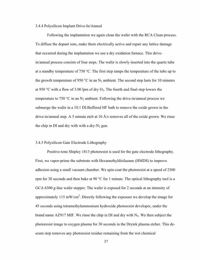
Platinum. This yields a 1150 Å Ti/Pt for the second-layer pads and wires.
45
Figure 3.10 Optical image following second-layer pad and wire lift-off.

3.10 Cleaving
Following the formation of the first-layer wires and second-layer pads and wires
the chips are cleaved into ~ 8 mm x 8 mm chips.
3.11 SET Formation
3.11.1 SET Lithography
Positive-tone Micro-Chem MMA (methylmethacrylate in methacrylic acid, 9 %
by weight) and positive-tone Micro-Chem PMMA (950,000 amu polymethylmethacrylate
in chlorobenzene, 2% by weight) electron-beam resists are used for the SET lithography
in a bi-layer resist scheme. We spin-coat the MMA resist at a speed of 4000 rpm for 30
seconds and follow with a bake at 180 °C for 2 minutes. The MMA is then flood-exposed
to 220 nm deep ultraviolet (DUV) radiation for 2 minutes. This step serves to make the
MMA completely soluble in developer and allows us to control the undercut of the bi-
layer resist process using development time alone. We then use the same conditions to
spin-coat the PMMA, ending with a 3 minute bake. We again use the Elionix EBL
system to expose the SET pattern. The remainder of the lithography process follows the
details given in section 3.4.1. The result of this bi-layer resist, exposure and development
process is an undercut in the MMA layer and, due to the exposure pattern, an over-
hanging PMMA bridge which is used in a double-angle evaporation process to form the
SET junctions, detailed in the following section.
46

3.11.2 SET Evaporation and Junction Formation
A two angle-evaporation process, using a Veeco thermal evaporator, forms the
SET. We first set-up the mechanical stage to switch between the two evaporation angles,
typically ± 8°, depending on the intended junction size. We reach a pressure of 8 x 10⁻⁷
Torr before evaporation is done. The evaporation metal is 99.999 % pure Aluminum and
we deposit 250 Å to form the first layer, using pellets to evaporate from a twisted
tungsten basket. To form the AlxOy junction dielectric we slowly bleed oxygen into the
chamber, maintaining a pressure of between 6 – 8 x 10⁻⁴ Torr for 60 minutes. The
evaporation angle is switched and we again evacuate the chamber to ~ 8 x 10⁻⁷ Torr and
evaporate 350 Å to form the second layer. As can be seen in Figure 3.11, this process
results in a small metal-insulator-metal tunnel junction being formed beneath the PMMA
resist bridge. In reality, multiple junctions are created in the surrounding wires but the
very small overlap and resulting large capacitance of the tunnel junction dominates the
series.
Figure 3.11 The double-angle evaporation technique forms a small metal-insulator-metal tunnel junction underneath the PMMA bridge.
47
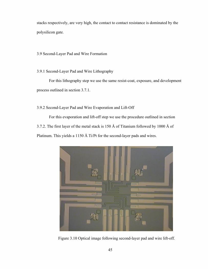
3.11.3 SET Lift-Off
After removal from the evaporation system, we place the chip in acetone to “lift-
off” the resist layers and leave the SET on the substrate. The lift-off can last from a few
minutes up to several hours depending on the tenacity of the resist. We rinse the chip in
IPA and dry with a dry-Nitrogen gun. The quality of the lift-off is determined by optical
inspection using a Zeiss Axiotron microscope.
Figure 3.12 SEM image of an SET structure following lift-off. This device was fabricated on a sample without p+ windows.
Figure 3.13 shows the same SEM image shown in Figure 3.12 but with the layers
color-coded to correspond to Figure 3.11. The tunnel junctions are also clearly marked.
48

The double-angle evaporation technique causes the lateral extension on either side of the
SET island to appear twice. This has the negative effect of increasing the self-
capacitance, C0, and, therefore, the total capacitance, CΣ which will decrease the charging
energy, EC. As a trade-off, since either or both of these lateral extensions can connect to
the p+ windows, enhanced alignment tolerance between the SET and the 1 μm2 p+
window is obtained.
Figure 3.13 SEM image of an SET structure after lift-off with the layers color-coded to correspond to Figure 3.11 and the tunnel junctions marked.
3.12 Room-temperature Testing, Cleaving and Wire-bonding
Following lift-off the SETs are checked by testing the resistance at room
temperature. Using a probe station and Stanford Reasearch Systems SR830 lock-in
amplifier an AC voltage of 1 mV, at a frequency of ~ 16 Hz, is applied between the
source and drain of each device and the resulting source-drain current is measured. As
mentioned in section 1.2, one condition for the observation of effects due to the discrete
49

nature of charge is the sufficient resistance of the tunnel junctions. The lower bound for
this junction resistance is the quantum resistance, h/e2. If the resistance of the SET falls
between 50 kΩ – 10 MΩ then the device shows promise for testing at low temperatures.
The chips are once again cleaved using a diamond scribe into ~ 4 x 4 mm chips. The chip
is glued into a 20-pin package and working SETs and polysilicon gate electrodes are
wire-bonded using a West Bond 7400 wire bonder.
50

CHAPTER 4:
MEASUREMENTS AND RESULTS
4.1 Helium Cryostat
After wire bonding the 20-pin test package is mounted onto the cold finger of an
insert for a 3He cryostat. The Oxford HelioxTM refrigerator used in this experiment has a
base temperature of around 300 mK.
4.2 Test Set-up
Once at low temperature, the SETs are tested using a Stanford Reasearch Systems
SR830 lock-in amplifier and standard AC lock-in techniques. The test set-up is detailed
in Figure 4.1. The lock-in amplifier provides the AC and DC excitation signals for the
drain-source biasing of the SET and the DC excitation signal for the polysilicon driving
electrode, the gate of the device. The source of the device is virtually grounded through
the pre-amplifier and a 1T magnetic field is applied to the system to suppress the
superconductivity that arises in Aluminum below 1.2 K. The conductance of the device
can be found from
INSET
FBOUT V
RRV ⎟⎟
⎠
⎞⎜⎜⎝
⎛−=
SETSET R
G 1=
51

⎟⎟⎠
⎞⎜⎜⎝
⎛×
−=INFB
OUTSET VR
VG
Figure 4.1 Schematic of low temperature electrical test set-up.
Data from the lock-in amplifier is collected through a GPIB and analyzed using a
PC and Data Acquisition and Analysis Software (DAAS), written by Drs. Gregory Bazan
and Alexei Orlov. DAAS is also used to control the voltages sent to the lock-in amplifier.
4.3 The Stand-alone SET
The process detailed in Section 3.10 yields stable SETs with charging energies on
the order of 1 meV. A Coulomb charging diagram for one such device is shown in Figure
4.2. The rhombic areas of Coulomb blockade can be clearly defined along with the
higher-order rhombic areas where conductance occurs.
52

-0.06 -0.04 -0.02 0.00 0.02 0.04 0.06
-4
-2
0
2
4
SET 1-19
Vg, V
Vds, m
V
0
8.8E-9
1.76E-8
2.64E-8
3.52E-8
4.4E-8
5.28E-8
6.16E-8
7.04E-8
7.92E-8
8.8E-8
9.68E-8
1.056E-71.1E-7
Figure 4.2 The charging diagram for an SET device showing a charging energy of EC = 0.75 mV.
Using the relationships detailed in Section 1.2 we can use Figure 4.2 to obtain
values for the gate and junction capacitances, Cg, C1 and C2, of this device. As there are
no fabricated p+ windows or polysilicon driving electrodes on this sample we used an
adjacent SET to provide the function of a gate. As such, the gate capacitance we obtain
from this charging diagram will be different from that of the full system. It is still useful
to obtain, however, as it will provide some insight into the reliability of our capacitance
model. The period of the Coulomb oscillations in Figure 4.2 is ΔVg = 43 mV giving a
gate capacitance of Cg = 3.72 aF.
The slopes of the rhombic regions are S+ = 0.0704 and S- = -0.0704 giving
junction capacitances of C1 = 52.8 aF and C2 = 49.12 aF, assuming that C0 ≈ 0. We
extract a total capacitance of CΣ = 106.8 aF from the charging energy equation, using a
53

measured charging energy of EC = 0.75 meV. Calculating the total capacitance from the
sum of the gate and junction capacitances gives a comparable value of CΣ = 105.64 aF.
4.4 The Integrated SET
When integrated into the system the SETs continue to show operation in the
Coulomb blockade regime. This can be seen in Figure 4.3 where Coulomb blockade
oscillations are measured for the SET device with integrated p+ windows and polysilicon
gates.
0
5
10
15
20
25
30
35
40
45
-5 -4 -3 -2 -1 0 1 2 3 4 5
Vg, mV
I, nA
Figure 4.3 Coulomb oscillation peaks in current as a function of gate voltage for an integrated SET.
The period of the Coulomb oscillations in Figure 4.3 is ΔVg = 3 mV giving a gate
capacitance of Cg = 53.4 aF. This is reasonable when we consider that the integrated SET
island is connected to the p+ windows and separated from the polysilicon driving
54
55
electrode by only 20 nm. Assuming that the other capacitances will be the same, the total
capacitance will be CΣ = 155.3 aF. This will give an estimated charging energy of EC =
0.52 meV which, at approximately 20 kBT at 300 mK, should be sufficient for our needs.
If the self-capacitance becomes a significant factor, which may occur due to the larger
size of the island when connected to the p+ windows, this charging energy will decrease.
However, an additional self-capacitance of up to 150 aF would still be manageable for a
charging energy of approximately 10 kBT at 300 mK. Colder temperatures, obtained in a
dilution refrigerator, are also available.
At the same time the integrated SET shows instability issues. Repeated scans of
the gate voltage give conductance peaks with positions on the Vg axis that shift in time.
The source of this instability may be a leaky dielectric or mobile charges at the
polysilicon-dielectric or dielectric-substrate interfaces. Process changes to investigate and
eliminate the source of this instability are being implemented. An additional annealing
step, in a forming gas ambient, is being implemented to tie-up any loose bonds at
interfaces within the system. Cleaner samples are also being prepared to attempt to
minimize background charge which may be positioned in defects between the polysilicon
driving electrode and the Aluminum SET island. These results are from the first
processing run of the complete system with an integrated SET. The evidence of Coulomb
oscillations combined with capacitance results which suggest a sufficient charging energy
is very encouraging.

CHAPTER 5:
SUMMARY AND FURTHER WORK
5.1 Summary
QCA is a paradigm which lends itself well to nanoelectronics, particularly the
nacent field of experimental molecular electronics. We have developed a system to
measure the bistability of a mixed-valence complex for application in a molecular QCA
cell. This system incorporates significant changes from previously designed systems
including a thin oxide, decreasing the vertical separation between the driving electrode
and the molecules, and polysilicon gate electrode, which enables self-aligned processes,
decreasing the horizontal separation between the driving electrode and the molecules. An
SET is capacitively coupled the the p+ silicon surface to which the molecules will be
bound and will serve as our electrometer. Lastly, a differential measurement design will
enable us to adopt a simple testing scheme and detect very small charge variations, with
the goal of detecting single-molecule switching events.
Currently, SETs integrated into the system have been operated in the Coulomb
blockade regime. Temporal instability, possibly resulting from background charge
fluctuations, has been noticed and work is ongoing to find the source of these fluctuations
and develop a more stable integrated device. Stable and controllable SET conductance
characteristics are critical if we hope to reliably detect molecular switching activity.
56

Figure 5.1 An optical image of the complete system. Nine polysilicon electrodes can be seen, defining 8 devices.
5.2 Attaching the Molecules
The process of adding the molecules to the system requires an additional electron-
beam lithography step and a series of chemical processes which will be discussed here.
The lithography step opens a smaller window, concentric with the p+ window and also
self-aligned to the polysilicon driving electrode. A BHF dip and DI rinse removes the
native oxide which has formed on the p+ silicon surface.
57

58
Figure 5.2 A close-up of one device with the polysilicon driving electrodes in red, the self-aligned p+ windows in purple and the SET structure in gray. The molecule window, also self-aligned, is shown in gold.
To attach the molecule complex to the p+ silicon surface the first step is to
chlorinate the surface. The sample is placed in a glass tube which is evacuated and
purged with an inert gas several times, ending with an evacuation. The glass tube is then
immersed in oil, heated to 80 °C, and exposed to a Cl2 ambient for 20 minutes. The
unreacted chlorine is purged with inert gas and absorbed by a sodium iodide bath. The
chlorinated surface is placed into a 1mM solution of 1[PF6] at room temperature for 30
hours or more in which time the molecules bind to the surface. The sample is then
sequentially rinsed with methylene chloride, acetone, ethanol and DI water. Following
the molecule deposition process the complex is oxidized by placing the sample in a
solution of FePF6 in methylene chloride for 80 minutes at room temperature. The sample
is rinsed with methylene chloride and kept in a glass tube in an inert environment until
testing.

BIBLIOGRAPHY
1. Lent, C.S. and P.D. Tougaw, A Device Architecture for Computing with Quantum Dots. Proceedings of the IEEE, 1997. 85(4): p. 541-557.
2. Orlov, A.O., et al., Realization of a Functional Cell for Quantum-Dot Cellular Automata. Science, 1997. 277: p. 928-930.
3. Lent, C.S., et al., Quantum Cellular Automata. Nanotechnology, 1993. 4: p. 49-57.
4. Qi, H., et al., Molecular Quantum Cellular Automata Cells. Electric Field Driven Switching of a Silicon Surface Bound Array of Vertically Oriented Two-Dot Molecular Quantum Cellular Automata. Journal of the American Chemical Society, 2003(125): p. 15250-15259.
5. Timler, J. and C.S. Lent, Power gain and dissipation in quantum-dot cellular automata. Journal of Applied Physics, 2002. 91(2): p. 823-831.
6. Devoret, M.H. and H. Grabert, Introduction to Single Charge Tunneling, in Single Charge Tunneling: Coulomb Blockade Phenomena in Nanostructures, M.H. Devoret and H. Grabert, Editors. 1992. p. 1-19.
7. Kouwenhoven, L.P., et al., Electron Transport in Quantum Dots, in Mesoscopic Electron Transport, L.L. Sohn, L.P. Kouwenhoven, and G. Schön, Editors. 1997.
8. Hadley, P., G. Lientschnig, and M. Lai. Single-Electron Transistors. 2002 [cited 2008 7 April]; Available from: http://qt.tn.tudelft.nl/publi/2002/ISCS/ISCS2002.html.
9. Tang, Y., Fabrication and Measurement of Aluminum and Carbon Nanotube Single
Electron Transistors for Radio Frequency Applications, in Department of Electrical Engineering. 2005, University of Notre Dame: Notre Dame.
10. Qi, H., et al., Dependence of Field Switched Ordered Arrays of Dinuclear Mixed-Valence Complexes on the Distance between the Redox Centers and the Size of the Counterions. Journal of the American Chemical Society, 2005(127): p. 15218 - 15227.
11. Jin, Z., Fabrication and Measurement of Molecular Quantum Cellular Automata (QCA) Device, in Department of Electrical Engineering. 2006, University of Notre Dame: Notre Dame.
59

60
12. Aassime, A., et al., Radio-frequency Single Electron Transistor: Toward the Shot-noise Limit. Applied Physics Letters, 2001. 79(24).
13. Tuar, Y. and T.H. Ning, Fundamentals of Modern VLSI Devices. 1998: Cambridge University Press.


![[2004] QCA 420 - SUPREME COURT OF QUEENSLAND](https://static.fdokumen.com/doc/165x107/631dbd5a85e2495e150f986f/2004-qca-420-supreme-court-of-queensland.jpg)