
A Review of Data Mining Applications in Semiconductor ...
38
processes Review A Review of Data Mining Applications in Semiconductor Manufacturing Pedro Espadinha-Cruz 1, * , Radu Godina 1, * and Eduardo M. G. Rodrigues 2, * Citation: Espadinha-Cruz, P.; Godina, R.; Rodrigues, E.M.G. A Review of Data Mining Applications in Semiconductor Manufacturing. Processes 2021, 9, 305. https:// doi.org/10.3390/pr9020305 Academic Editors: Marco S. Reis and Furong Gao Received: 31 December 2020 Accepted: 3 February 2021 Published: 6 February 2021 Publisher’s Note: MDPI stays neutral with regard to jurisdictional claims in published maps and institutional affil- iations. Copyright: © 2021 by the authors. Licensee MDPI, Basel, Switzerland. This article is an open access article distributed under the terms and conditions of the Creative Commons Attribution (CC BY) license (https:// creativecommons.org/licenses/by/ 4.0/). 1 UNIDEMI-Research and Development Unit in Mechanical and Industrial Engineering, Faculty of Science and Technology (FCT), Universidade NOVA de Lisboa, 2829-516 Almada, Portugal 2 Management and Production Technologies of Northern Aveiro—ESAN, Estrada do Cercal 449, Santiago de Riba-Ul, 3720-509 Oliveira de Azeméis, Portugal * Correspondence: [email protected] (P.E.-C.); [email protected] (R.G.); [email protected] (E.M.G.R.) Abstract: For decades, industrial companies have been collecting and storing high amounts of data with the aim of better controlling and managing their processes. However, this vast amount of information and hidden knowledge implicit in all of this data could be utilized more efficiently. With the help of data mining techniques unknown relationships can be systematically discovered. The production of semiconductors is a highly complex process, which entails several subprocesses that employ a diverse array of equipment. The size of the semiconductors signifies a high number of units can be produced, which require huge amounts of data in order to be able to control and improve the semiconductor manufacturing process. Therefore, in this paper a structured review is made through a sample of 137 papers of the published articles in the scientific community regarding data mining applications in semiconductor manufacturing. A detailed bibliometric analysis is also made. All data mining applications are classified in function of the application area. The results are then analyzed and conclusions are drawn. Keywords: data mining; semiconductor manufacturing; quality control; yield improvement; fault detection; process control 1. Introduction The last few decades have seen the birth of a great diversity of products and ser- vices associated with electrical and electronic equipment, and witnessed the presence of electronic and electrical equipment in a large number of products and services, which are subject to constant change [1]. During the last few years, since semiconductor man- ufacturing processes have gradually diminished in size, the number of transistors that can be fabricated on a sole silicon wafer can amount to a billion units [2]. In order to account for the dynamic evolution of production and distribution and the changes caused by technological advances and inventions, companies that operate in this field need to be flexible and to be able to adapt quickly to a constantly changing environment [3]. Semiconductor production is the process that creates integrated circuits, such as tran- sistors, LEDs, or diodes that can be found in electrical devices and consumer electronics. During the front-end process, the crystalline silicon ingot is produced and the wafers are cut, the electrical circuits are created by photolithography and other chemical processes and, finally, they are electronically tested. In the back-end process, the chunks are cut from the wafer, wired (glued), encapsulated, and tested [4]. The semiconductor manu- facturing industrial units (known also as fabs) are one of the highest capital-intensive and entirely automated production systems, in which agnate processes and equipment are utilized to manufacture integrated circuits through a wide range of extensive and complex processes with firmly controlled manufacturing processes, reentering process flows, advanced and complex equipment, and demanding deadlines for complying with constantly unpredictable demands of a constantly increasing product mix [5]. Processes 2021, 9, 305. https://doi.org/10.3390/pr9020305 https://www.mdpi.com/journal/processes
-
Upload
khangminh22 -
Category
Documents
-
view
0 -
download
0
Transcript of A Review of Data Mining Applications in Semiconductor ...
processes
Review
A Review of Data Mining Applications in SemiconductorManufacturing
Pedro Espadinha-Cruz 1,* , Radu Godina 1,* and Eduardo M. G. Rodrigues 2,*
�����������������
Citation: Espadinha-Cruz, P.;
Godina, R.; Rodrigues, E.M.G. A
Review of Data Mining Applications
in Semiconductor Manufacturing.
Processes 2021, 9, 305. https://
doi.org/10.3390/pr9020305
Academic Editors: Marco S. Reis and
Furong Gao
Received: 31 December 2020
Accepted: 3 February 2021
Published: 6 February 2021
Publisher’s Note: MDPI stays neutral
with regard to jurisdictional claims in
published maps and institutional affil-
iations.
Copyright: © 2021 by the authors.
Licensee MDPI, Basel, Switzerland.
This article is an open access article
distributed under the terms and
conditions of the Creative Commons
Attribution (CC BY) license (https://
creativecommons.org/licenses/by/
4.0/).
1 UNIDEMI-Research and Development Unit in Mechanical and Industrial Engineering, Faculty of Science andTechnology (FCT), Universidade NOVA de Lisboa, 2829-516 Almada, Portugal
2 Management and Production Technologies of Northern Aveiro—ESAN, Estrada do Cercal 449,Santiago de Riba-Ul, 3720-509 Oliveira de Azeméis, Portugal
* Correspondence: [email protected] (P.E.-C.); [email protected] (R.G.); [email protected] (E.M.G.R.)
Abstract: For decades, industrial companies have been collecting and storing high amounts of datawith the aim of better controlling and managing their processes. However, this vast amount ofinformation and hidden knowledge implicit in all of this data could be utilized more efficiently. Withthe help of data mining techniques unknown relationships can be systematically discovered. Theproduction of semiconductors is a highly complex process, which entails several subprocesses thatemploy a diverse array of equipment. The size of the semiconductors signifies a high number of unitscan be produced, which require huge amounts of data in order to be able to control and improve thesemiconductor manufacturing process. Therefore, in this paper a structured review is made througha sample of 137 papers of the published articles in the scientific community regarding data miningapplications in semiconductor manufacturing. A detailed bibliometric analysis is also made. All datamining applications are classified in function of the application area. The results are then analyzedand conclusions are drawn.
Keywords: data mining; semiconductor manufacturing; quality control; yield improvement; faultdetection; process control
1. Introduction
The last few decades have seen the birth of a great diversity of products and ser-vices associated with electrical and electronic equipment, and witnessed the presence ofelectronic and electrical equipment in a large number of products and services, whichare subject to constant change [1]. During the last few years, since semiconductor man-ufacturing processes have gradually diminished in size, the number of transistors thatcan be fabricated on a sole silicon wafer can amount to a billion units [2]. In order toaccount for the dynamic evolution of production and distribution and the changes causedby technological advances and inventions, companies that operate in this field need to beflexible and to be able to adapt quickly to a constantly changing environment [3].
Semiconductor production is the process that creates integrated circuits, such as tran-sistors, LEDs, or diodes that can be found in electrical devices and consumer electronics.During the front-end process, the crystalline silicon ingot is produced and the wafers arecut, the electrical circuits are created by photolithography and other chemical processesand, finally, they are electronically tested. In the back-end process, the chunks are cutfrom the wafer, wired (glued), encapsulated, and tested [4]. The semiconductor manu-facturing industrial units (known also as fabs) are one of the highest capital-intensiveand entirely automated production systems, in which agnate processes and equipmentare utilized to manufacture integrated circuits through a wide range of extensive andcomplex processes with firmly controlled manufacturing processes, reentering processflows, advanced and complex equipment, and demanding deadlines for complying withconstantly unpredictable demands of a constantly increasing product mix [5].
Processes 2021, 9, 305. https://doi.org/10.3390/pr9020305 https://www.mdpi.com/journal/processes
Processes 2021, 9, 305 2 of 38
The concept Industry 4.0 involves employing artificial intelligence technologies, datamining techniques, big data and deep learning analysis to the current industrial infras-tructure for the purpose of developing innovations that are disruptive [6]. The objectiveis to strive to put into practice this concept, which will allow flexible decision-makingand smart manufacturing systems, as anticipated by the Industry 4.0 concept. Therefore,by turning Industry 4.0 a reality, the role of the Internet of Things (IoT) and additionalemergent technologies will have a central role [7]. So far, the tendency to have unmannedoperations and increasing automation in semiconductor production systems, as in otherproduction technologies, is constantly growing [8].
Conventionally, semiconductor production systems are known for having a highlycomplex and lengthy manufacturing process. Typically, semiconductor wafers require anumber of process steps that could easily surmount half of a thousand to be produced [9,10].The level of complexity of every step is frequently equated to that of a medium-sized indus-trial unit, particularly in such areas such as logistics, planning, control, and data volume,among other steps. Consequently, growing requirements and pressure to perform with ahigh plant productivity pose a difficult challenge for companies operating in semiconductormanufacturing [1].
The ever-growing demand for integrated circuits that are able to deliver higher per-formances at lower costs is something semiconductor companies are well familiar with.Therefore, wafer metrology tools are employed for designing and producing semiconduc-tors, cautiously monitoring line widths, film properties, and possible defects in order toimprove the production process. Data mining techniques together with metrology toolsand wafer verification abilities guarantee a close desired result of the electrical and physicalproperties of produced semiconductors. Data mining with wafer metrology can accuratelyand quickly recognize surface pattern defects, particles, and additional conditions that arecapable of causing adverse effects on semiconductor performance [11].
Data mining is one of the areas of the knowledge data discovery process and iscapable of providing innovative avenues for interpreting data. Data mining comprisesthe extraction of significant and implicit, previously unidentified, and possibly valuableinformation from data. Data mining offers the ability to detect patterns that are hiddenamid a set of data. Data mining is the process of sorting and classifying data, then findinganomalies, patterns, and correlations in large data sets to predict outcomes. Employinga wide variety of techniques, companies can use this information for problem detection,quality control, increase revenue, cut costs, improve customer relationships, and reducerisk, among others [12]. Since modern semiconductor manufacturing processes suffer froma great degree of complexity, and the amount of data is overwhelming, it is still challengingto reach fast yield improvement by discovering manually useful patterns in raw data [11].
Throughout wafer manufacturing, equipment data, process data, and the historicdata will be semiautomatically or automatically collected and grouped in a database inorder to be able to diagnose faults, to monitor the process, and to effectively managethe production process. Nevertheless, in such advanced manufacturing units such assemiconductor production, numerous aspects and details are interconnected and havean effect on the yield of the produced wafers [13]. Therefore, data mining techniques area solution for a significant amount of challenges that the semiconductor manufacturingfaces, such as yield improvement [5,11], quality control [14], fault detection [15], predictivemaintenance [16], virtual metrology [17], scheduling [18], business improvement [19], andmarket forecasting [20], among others.
Despite the existence of a high number of studies regarding data mining applicationsin semiconductor manufacturing, a gap was identified in the literature, in which thenecessity to compile and analyze in a more comprehensive way through the compilation ina single paper every published study arose, and expressly perform it without restrictionson location or characteristics. With the intention of filling the identified gap in the research,the aim of this paper is to compile all the existing publications on this topic on Scopusand WoS and to classify and compare them. Therefore, one of the goals of this study is to
Processes 2021, 9, 305 3 of 38
understand the state of the art regarding data mining solution to existing challenges insemiconductor manufacturing. A bibliometric study is presented, in which are analyzedthe number of publications over time, the co-occurrence network, the most cited authors,the distribution of keywords by observed frequency, among other bibliometric metrics.This analysis, besides analyzing bibliometric indicators and making a comparison betweendistinct features, it also has the purpose to frame these indicators in distinct categories andhighlighting every case, not only to seek and detect future research pathways, but also tohave a better comprehension of data mining applications in semiconductor industry and toendorse it in order to disseminate its use.
This paper is organized as follows. In Section 2, a brief overview of the semiconductormanufacturing process is given. In Section 3, a structured bibliometric analysis is made.In Section 4, a qualitative organization and analysis data mining application studies insemiconductor manufacturing can be found. In Section 5, a brief result analysis anddiscussion is made. Finally, in Section 6, overall conclusions are given.
2. Bibliometric Analysis
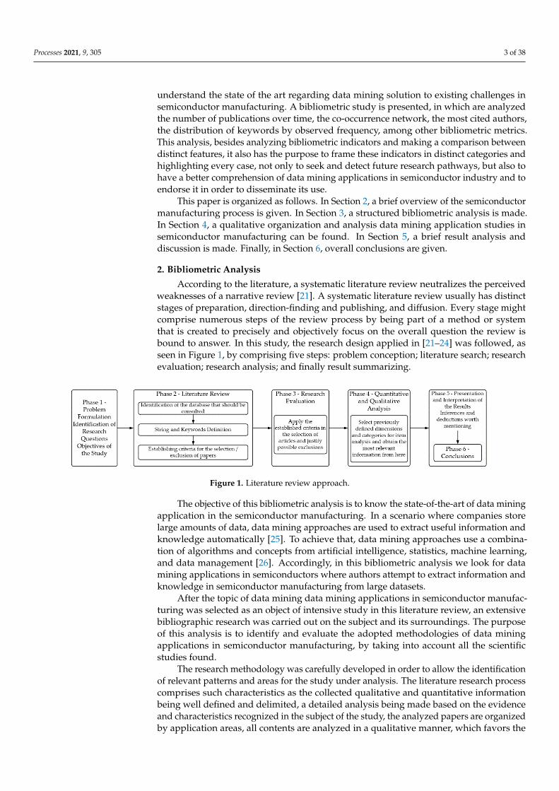
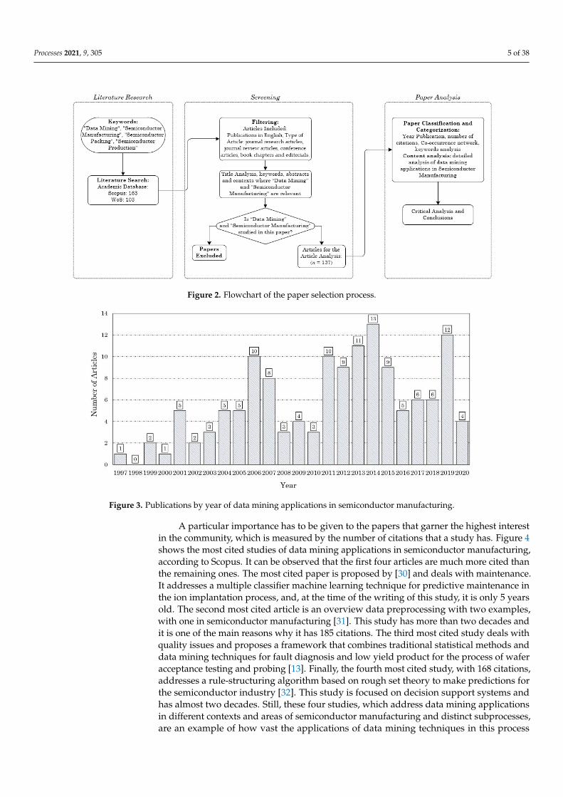
According to the literature, a systematic literature review neutralizes the perceivedweaknesses of a narrative review [21]. A systematic literature review usually has distinctstages of preparation, direction-finding and publishing, and diffusion. Every stage mightcomprise numerous steps of the review process by being part of a method or systemthat is created to precisely and objectively focus on the overall question the review isbound to answer. In this study, the research design applied in [21–24] was followed, asseen in Figure 1, by comprising five steps: problem conception; literature search; researchevaluation; research analysis; and finally result summarizing.
Processes 2021, 9, x FOR PEER REVIEW 3 of 38
necessity to compile and analyze in a more comprehensive way through the compilation
in a single paper every published study arose, and expressly perform it without re-
strictions on location or characteristics. With the intention of filling the identified gap in
the research, the aim of this paper is to compile all the existing publications on this topic
on Scopus and WoS and to classify and compare them. Therefore, one of the goals of this
study is to understand the state of the art regarding data mining solution to existing
challenges in semiconductor manufacturing. A bibliometric study is presented, in which
are analyzed the number of publications over time, the co-occurrence network, the most
cited authors, the distribution of keywords by observed frequency, among other biblio-
metric metrics. This analysis, besides analyzing bibliometric indicators and making a
comparison between distinct features, it also has the purpose to frame these indicators in
distinct categories and highlighting every case, not only to seek and detect future re-
search pathways, but also to have a better comprehension of data mining applications in
semiconductor industry and to endorse it in order to disseminate its use.
This paper is organized as follows. In Section 2, a brief overview of the semicon-
ductor manufacturing process is given. In Section 3, a structured bibliometric analysis is
made. In Section 4, a qualitative organization and analysis data mining application
studies in semiconductor manufacturing can be found. In Section 5, a brief result analysis
and discussion is made. Finally, in Section 6, overall conclusions are given.
2. Bibliometric Analysis
According to the literature, a systematic literature review neutralizes the perceived
weaknesses of a narrative review [21]. A systematic literature review usually has distinct
stages of preparation, direction-finding and publishing, and diffusion. Every stage might
comprise numerous steps of the review process by being part of a method or system that
is created to precisely and objectively focus on the overall question the review is bound to
answer. In this study, the research design applied in [21–24] was followed, as seen in
Figure 1, by comprising five steps: problem conception; literature search; research eval-
uation; research analysis; and finally result summarizing.
Figure 1. Literature review approach.
The objective of this bibliometric analysis is to know the state-of-the-art of data
mining application in the semiconductor manufacturing. In a scenario where companies
store large amounts of data, data mining approaches are used to extract useful infor-
mation and knowledge automatically [25]. To achieve that, data mining approaches use a
combination of algorithms and concepts from artificial intelligence, statistics, machine
learning, and data management [26]. Accordingly, in this bibliometric analysis we look
for data mining applications in semiconductors where authors attempt to extract infor-
mation and knowledge in semiconductor manufacturing from large datasets.
After the topic of data mining data mining applications in semiconductor manu-
facturing was selected as an object of intensive study in this literature review, an exten-
sive bibliographic research was carried out on the subject and its surroundings. The
purpose of this analysis is to identify and evaluate the adopted methodologies of data
mining applications in semiconductor manufacturing, by taking into account all the sci-
entific studies found.
Figure 1. Literature review approach.
The objective of this bibliometric analysis is to know the state-of-the-art of data miningapplication in the semiconductor manufacturing. In a scenario where companies storelarge amounts of data, data mining approaches are used to extract useful information andknowledge automatically [25]. To achieve that, data mining approaches use a combina-tion of algorithms and concepts from artificial intelligence, statistics, machine learning,and data management [26]. Accordingly, in this bibliometric analysis we look for datamining applications in semiconductors where authors attempt to extract information andknowledge in semiconductor manufacturing from large datasets.
After the topic of data mining data mining applications in semiconductor manufac-turing was selected as an object of intensive study in this literature review, an extensivebibliographic research was carried out on the subject and its surroundings. The purposeof this analysis is to identify and evaluate the adopted methodologies of data miningapplications in semiconductor manufacturing, by taking into account all the scientificstudies found.
The research methodology was carefully developed in order to allow the identificationof relevant patterns and areas for the study under analysis. The literature research processcomprises such characteristics as the collected qualitative and quantitative informationbeing well defined and delimited, a detailed analysis being made based on the evidenceand characteristics recognized in the subject of the study, the analyzed papers are organizedby application areas, all contents are analyzed in a qualitative manner, which favors the
Processes 2021, 9, 305 4 of 38
identification of important subthemes and the successful interpretation of results. Weconsidered papers that address the application of data mining to exploit data stored duringsemiconductor manufacturing processes. So, in the first step, the usefulness of each articlewas verified by reading its summary and introduction, so that those who seemed to beout of the review due to imprecision and a lack of details were excluded. Additionally,despite that some of the data mining algorithms and techniques may be applied by semi-conductor manufacturing authors, we excluded any papers that do not approach its use forinformation and knowledge extraction. After defining the aforementioned delimitations,a more detailed analysis was made on the articles that effectively added value in theirincorporation in the review article. The purpose of data mining application has beencarefully revised. This more detailed analysis includes: a selective reading and choice ofmaterial that suits the objectives and proposed theme; an analytical reading of the textsgrouping them by application areas; and concludes with the interpretative reading andwriting of the literature review body.
After the main elements of the research process have been well established, it becomesessential to adopt some essential assumptions for the accomplishment of this analysis.First, following the guidelines from [27], only indexed and peer-reviewed articles weretaken into account, and the indexing databases considered were Scopus and Web of Science(WoS). The keywords utilized were “Data Mining” and “Semiconductor Manufacturing”,which garnered the highest number of results. However, also, all the possible variants,such as “Semiconductor Fabrication”, “Semiconductor Production”, and “SemiconductorPackaging” were utilized in order to cover all the possible published papers through thiscombination. Table 1 shows the results from different combinations of keywords in thedatabase.
Table 1. Results from different combinations of keywords in the database.
Search StreamResults
Scopus WoS
“Data Mining” AND “Semiconductor Manufacturing” 142 87“Data Mining” AND “Semiconductor Fabrication” 11 9“Data Mining” AND “Semiconductor Production” 8 5“Data Mining” AND “Semiconductor Packaging” 2 2
The publications considered for this study were publications in English and the typeof articles were journal research articles, journal review articles, conference articles, bookchapters, and editorials. A few papers were found in Chinese and Polish, but were excludedfrom this study. In Figure 2 the flowchart of the paper selection process can be observed.In the end, a final sample of 137 papers was used for the article analysis. This samplecomprises almost all papers found with the keywords used.
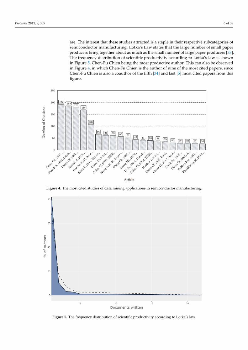
All the selected studies were classified by year and the result can be seen in Figure 3.Three waves can be seen, the first wave that comprises paper from 2004 to 2007 peakedin 2006 with 10 publications and then the interest waned. The second wave peaked in2014 and comprises the years 2011 until 2015. Finally, the last wave of interest in this topiccan be seen, peaking in 2019, with 12 publications. This wave is still ongoing. However,if divided by decades, one can notice that the decade 2010–2020 comprises 64% of allpublications, while the previous decade comprises only 33.5%. This interest reveals thegrowing scientific interest in this topic. This increase coincides with the overall interest indata mining applications for other industries [28,29].
Processes 2021, 9, 305 5 of 38Processes 2021, 9, x FOR PEER REVIEW 5 of 38
Figure 2. Flowchart of the paper selection process.
All the selected studies were classified by year and the result can be seen in Figure 3.
Three waves can be seen, the first wave that comprises paper from 2004 to 2007 peaked in
2006 with 10 publications and then the interest waned. The second wave peaked in 2014
and comprises the years 2011 until 2015. Finally, the last wave of interest in this topic can
be seen, peaking in 2019, with 12 publications. This wave is still ongoing. However, if
divided by decades, one can notice that the decade 2010–2020 comprises 64% of all pub-
lications, while the previous decade comprises only 33.5%. This interest reveals the
growing scientific interest in this topic. This increase coincides with the overall interest in
data mining applications for other industries [28,29].
Figure 3. Publications by year of data mining applications in semiconductor manufacturing.
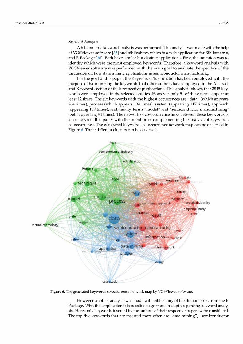
A particular importance has to be given to the papers that garner the highest interest
in the community, which is measured by the number of citations that a study has. Figure
4 shows the most cited studies of data mining applications in semiconductor manufac-
turing, according to Scopus. It can be observed that the first four articles are much more
cited than the remaining ones. The most cited paper is proposed by [30] and deals with
maintenance. It addresses a multiple classifier machine learning technique for predictive
maintenance in the ion implantation process, and, at the time of the writing of this study,
it is only 5 years old. The second most cited article is an overview data preprocessing
with two examples, with one in semiconductor manufacturing [31]. This study has more
Figure 2. Flowchart of the paper selection process.
Processes 2021, 9, x FOR PEER REVIEW 5 of 38
Figure 2. Flowchart of the paper selection process.
All the selected studies were classified by year and the result can be seen in Figure 3.
Three waves can be seen, the first wave that comprises paper from 2004 to 2007 peaked in
2006 with 10 publications and then the interest waned. The second wave peaked in 2014
and comprises the years 2011 until 2015. Finally, the last wave of interest in this topic can
be seen, peaking in 2019, with 12 publications. This wave is still ongoing. However, if
divided by decades, one can notice that the decade 2010–2020 comprises 64% of all pub-
lications, while the previous decade comprises only 33.5%. This interest reveals the
growing scientific interest in this topic. This increase coincides with the overall interest in
data mining applications for other industries [28,29].
Figure 3. Publications by year of data mining applications in semiconductor manufacturing.
A particular importance has to be given to the papers that garner the highest interest
in the community, which is measured by the number of citations that a study has. Figure
4 shows the most cited studies of data mining applications in semiconductor manufac-
turing, according to Scopus. It can be observed that the first four articles are much more
cited than the remaining ones. The most cited paper is proposed by [30] and deals with
maintenance. It addresses a multiple classifier machine learning technique for predictive
maintenance in the ion implantation process, and, at the time of the writing of this study,
it is only 5 years old. The second most cited article is an overview data preprocessing
with two examples, with one in semiconductor manufacturing [31]. This study has more
Figure 3. Publications by year of data mining applications in semiconductor manufacturing.
A particular importance has to be given to the papers that garner the highest interestin the community, which is measured by the number of citations that a study has. Figure 4shows the most cited studies of data mining applications in semiconductor manufacturing,according to Scopus. It can be observed that the first four articles are much more cited thanthe remaining ones. The most cited paper is proposed by [30] and deals with maintenance.It addresses a multiple classifier machine learning technique for predictive maintenance inthe ion implantation process, and, at the time of the writing of this study, it is only 5 yearsold. The second most cited article is an overview data preprocessing with two examples,with one in semiconductor manufacturing [31]. This study has more than two decades andit is one of the main reasons why it has 185 citations. The third most cited study deals withquality issues and proposes a framework that combines traditional statistical methods anddata mining techniques for fault diagnosis and low yield product for the process of waferacceptance testing and probing [13]. Finally, the fourth most cited study, with 168 citations,addresses a rule-structuring algorithm based on rough set theory to make predictions forthe semiconductor industry [32]. This study is focused on decision support systems andhas almost two decades. Still, these four studies, which address data mining applicationsin different contexts and areas of semiconductor manufacturing and distinct subprocesses,are an example of how vast the applications of data mining techniques in this process
Processes 2021, 9, 305 6 of 38
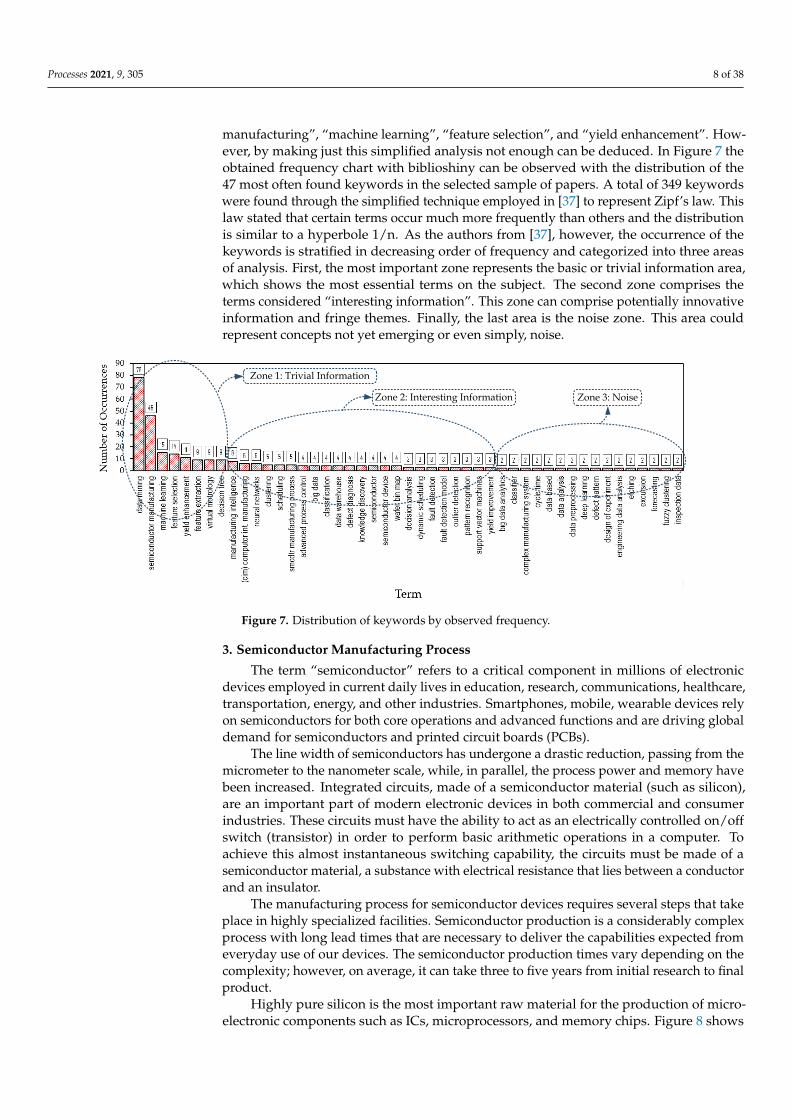
are. The interest that these studies attracted is a staple in their respective subcategories ofsemiconductor manufacturing. Lotka’s Law states that the large number of small paperproducers bring together about as much as the small number of large paper producers [33].The frequency distribution of scientific productivity according to Lotka’s law is shownin Figure 5, Chen-Fu Chien being the most productive author. This can also be observedin Figure 4, in which Chen-Fu Chien is the author of nine of the most cited papers, sinceChen-Fu Chien is also a coauthor of the fifth [34] and last [5] most cited papers from thisfigure.
Processes 2021, 9, x FOR PEER REVIEW 6 of 38
than two decades and it is one of the main reasons why it has 185 citations. The third
most cited study deals with quality issues and proposes a framework that combines tra-
ditional statistical methods and data mining techniques for fault diagnosis and low yield
product for the process of wafer acceptance testing and probing [13]. Finally, the fourth
most cited study, with 168 citations, addresses a rule-structuring algorithm based on
rough set theory to make predictions for the semiconductor industry [32]. This study is
focused on decision support systems and has almost two decades. Still, these four stud-
ies, which address data mining applications in different contexts and areas of semicon-
ductor manufacturing and distinct subprocesses, are an example of how vast the appli-
cations of data mining techniques in this process are. The interest that these studies at-
tracted is a staple in their respective subcategories of semiconductor manufacturing.
Lotka’s Law states that the large number of small paper producers bring together about
as much as the small number of large paper producers [33]. The frequency distribution of
scientific productivity according to Lotka’s law is shown in Figure 5, Chen-Fu Chien be-
ing the most productive author. This can also be observed in Figure 4, in which Chen-Fu
Chien is the author of nine of the most cited papers, since Chen-Fu Chien is also a coau-
thor of the fifth [34] and last [5] most cited papers from this figure.
Figure 4. The most cited studies of data mining applications in semiconductor manufacturing.
Figure 5. The frequency distribution of scientific productivity according to Lotka’s law.
Figure 4. The most cited studies of data mining applications in semiconductor manufacturing.
Processes 2021, 9, x FOR PEER REVIEW 6 of 38
than two decades and it is one of the main reasons why it has 185 citations. The third
most cited study deals with quality issues and proposes a framework that combines tra-
ditional statistical methods and data mining techniques for fault diagnosis and low yield
product for the process of wafer acceptance testing and probing [13]. Finally, the fourth
most cited study, with 168 citations, addresses a rule-structuring algorithm based on
rough set theory to make predictions for the semiconductor industry [32]. This study is
focused on decision support systems and has almost two decades. Still, these four stud-
ies, which address data mining applications in different contexts and areas of semicon-
ductor manufacturing and distinct subprocesses, are an example of how vast the appli-
cations of data mining techniques in this process are. The interest that these studies at-
tracted is a staple in their respective subcategories of semiconductor manufacturing.
Lotka’s Law states that the large number of small paper producers bring together about
as much as the small number of large paper producers [33]. The frequency distribution of
scientific productivity according to Lotka’s law is shown in Figure 5, Chen-Fu Chien be-
ing the most productive author. This can also be observed in Figure 4, in which Chen-Fu
Chien is the author of nine of the most cited papers, since Chen-Fu Chien is also a coau-
thor of the fifth [34] and last [5] most cited papers from this figure.
Figure 4. The most cited studies of data mining applications in semiconductor manufacturing.
Figure 5. The frequency distribution of scientific productivity according to Lotka’s law. Figure 5. The frequency distribution of scientific productivity according to Lotka’s law.
Processes 2021, 9, 305 7 of 38
Keyword Analysis
A bibliometric keyword analysis was performed. This analysis was made with the helpof VOSViewer software [35] and biblioshiny, which is a web application for Bibliometrix,and R Package [36]. Both have similar but distinct applications. First, the intention was toidentify which were the most employed keywords. Therefore, a keyword analysis withVOSViewer software was performed with the main goal to evaluate the specifics of thediscussion on how data mining applications in semiconductor manufacturing.
For the goal of this paper, the Keywords Plus function has been employed with thepurpose of harmonizing the keywords that other authors have employed in the Abstractand Keyword section of their respective publications. This analysis shows that 2845 key-words were employed in the selected studies. However, only 51 of these terms appear atleast 12 times. The six keywords with the highest occurrences are “data” (which appears264 times), process (which appears 134 times), system (appearing 117 times), approach(appearing 109 times), and, finally, terms “model” and “semiconductor manufacturing”(both appearing 94 times). The network of co-occurrence links between these keywords isalso shown in this paper with the intention of complementing the analysis of keywordsco-occurrence. The generated keywords co-occurrence network map can be observed inFigure 6. Three different clusters can be observed.
Processes 2021, 9, x FOR PEER REVIEW 7 of 38
Keyword Analysis
A bibliometric keyword analysis was performed. This analysis was made with the
help of VOSViewer software [35] and biblioshiny, which is a web application for Biblio-
metrix, and R Package [36]. Both have similar but distinct applications. First, the intention
was to identify which were the most employed keywords. Therefore, a keyword analysis
with VOSViewer software was performed with the main goal to evaluate the specifics of
the discussion on how data mining applications in semiconductor manufacturing.
For the goal of this paper, the Keywords Plus function has been employed with the
purpose of harmonizing the keywords that other authors have employed in the Abstract
and Keyword section of their respective publications. This analysis shows that 2845
keywords were employed in the selected studies. However, only 51 of these terms appear
at least 12 times. The six keywords with the highest occurrences are “data” (which ap-
pears 264 times), process (which appears 134 times), system (appearing 117 times), ap-
proach (appearing 109 times), and, finally, terms “model” and “semiconductor manu-
facturing” (both appearing 94 times). The network of co-occurrence links between these
keywords is also shown in this paper with the intention of complementing the analysis of
keywords co-occurrence. The generated keywords co-occurrence network map can be
observed in Figure 6. Three different clusters can be observed.
Figure 6. The generated keywords co-occurrence network map by VOSViewer software.
However, another analysis was made with biblioshiny of the Bibliometrix, from the
R Package. With this application it is possible to go more in-depth regarding keyword
analysis. Here, only keywords inserted by the authors of their respective papers were
considered. The top five keywords that are inserted more often are “data mining”,
“semiconductor manufacturing”, “machine learning”, “feature selection”, and “yield
Figure 6. The generated keywords co-occurrence network map by VOSViewer software.
However, another analysis was made with biblioshiny of the Bibliometrix, from the RPackage. With this application it is possible to go more in-depth regarding keyword analy-sis. Here, only keywords inserted by the authors of their respective papers were considered.The top five keywords that are inserted more often are “data mining”, “semiconductor
Processes 2021, 9, 305 8 of 38
manufacturing”, “machine learning”, “feature selection”, and “yield enhancement”. How-ever, by making just this simplified analysis not enough can be deduced. In Figure 7 theobtained frequency chart with biblioshiny can be observed with the distribution of the47 most often found keywords in the selected sample of papers. A total of 349 keywordswere found through the simplified technique employed in [37] to represent Zipf’s law. Thislaw stated that certain terms occur much more frequently than others and the distributionis similar to a hyperbole 1/n. As the authors from [37], however, the occurrence of thekeywords is stratified in decreasing order of frequency and categorized into three areasof analysis. First, the most important zone represents the basic or trivial information area,which shows the most essential terms on the subject. The second zone comprises theterms considered “interesting information”. This zone can comprise potentially innovativeinformation and fringe themes. Finally, the last area is the noise zone. This area couldrepresent concepts not yet emerging or even simply, noise.
Processes 2021, 9, x FOR PEER REVIEW 8 of 38
enhancement”. However, by making just this simplified analysis not enough can be de-
duced. In Figure 7 the obtained frequency chart with biblioshiny can be observed with
the distribution of the 47 most often found keywords in the selected sample of papers. A
total of 349 keywords were found through the simplified technique employed in [37] to
represent Zipf’s law. This law stated that certain terms occur much more frequently than
others and the distribution is similar to a hyperbole 1/n. As the authors from [37], how-
ever, the occurrence of the keywords is stratified in decreasing order of frequency and
categorized into three areas of analysis. First, the most important zone represents the
basic or trivial information area, which shows the most essential terms on the subject. The
second zone comprises the terms considered “interesting information”. This zone can
comprise potentially innovative information and fringe themes. Finally, the last area is
the noise zone. This area could represent concepts not yet emerging or even simply,
noise.
Figure 7. Distribution of keywords by observed frequency.
3. Semiconductor Manufacturing Process
The term “semiconductor” refers to a critical component in millions of electronic
devices employed in current daily lives in education, research, communications,
healthcare, transportation, energy, and other industries. Smartphones, mobile, wearable
devices rely on semiconductors for both core operations and advanced functions and are
driving global demand for semiconductors and printed circuit boards (PCBs).
The line width of semiconductors has undergone a drastic reduction, passing from
the micrometer to the nanometer scale, while, in parallel, the process power and memory
have been increased. Integrated circuits, made of a semiconductor material (such as sili-
con), are an important part of modern electronic devices in both commercial and con-
sumer industries. These circuits must have the ability to act as an electrically controlled
on/off switch (transistor) in order to perform basic arithmetic operations in a computer.
To achieve this almost instantaneous switching capability, the circuits must be made of a
semiconductor material, a substance with electrical resistance that lies between a con-
ductor and an insulator.
The manufacturing process for semiconductor devices requires several steps that
take place in highly specialized facilities. Semiconductor production is a considerably
complex process with long lead times that are necessary to deliver the capabilities ex-
pected from everyday use of our devices. The semiconductor production times vary de-
pending on the complexity; however, on average, it can take three to five years from ini-
tial research to final product.
Highly pure silicon is the most important raw material for the production of micro-
electronic components such as ICs, microprocessors, and memory chips. Figure 8 shows a
Zone 1: Trivial Information
Zone 2: Interesting Information Zone 3: Noise
Figure 7. Distribution of keywords by observed frequency.
3. Semiconductor Manufacturing Process
The term “semiconductor” refers to a critical component in millions of electronicdevices employed in current daily lives in education, research, communications, healthcare,transportation, energy, and other industries. Smartphones, mobile, wearable devices relyon semiconductors for both core operations and advanced functions and are driving globaldemand for semiconductors and printed circuit boards (PCBs).
The line width of semiconductors has undergone a drastic reduction, passing from themicrometer to the nanometer scale, while, in parallel, the process power and memory havebeen increased. Integrated circuits, made of a semiconductor material (such as silicon),are an important part of modern electronic devices in both commercial and consumerindustries. These circuits must have the ability to act as an electrically controlled on/offswitch (transistor) in order to perform basic arithmetic operations in a computer. Toachieve this almost instantaneous switching capability, the circuits must be made of asemiconductor material, a substance with electrical resistance that lies between a conductorand an insulator.
The manufacturing process for semiconductor devices requires several steps that takeplace in highly specialized facilities. Semiconductor production is a considerably complexprocess with long lead times that are necessary to deliver the capabilities expected fromeveryday use of our devices. The semiconductor production times vary depending on thecomplexity; however, on average, it can take three to five years from initial research to finalproduct.
Highly pure silicon is the most important raw material for the production of micro-electronic components such as ICs, microprocessors, and memory chips. Figure 8 shows
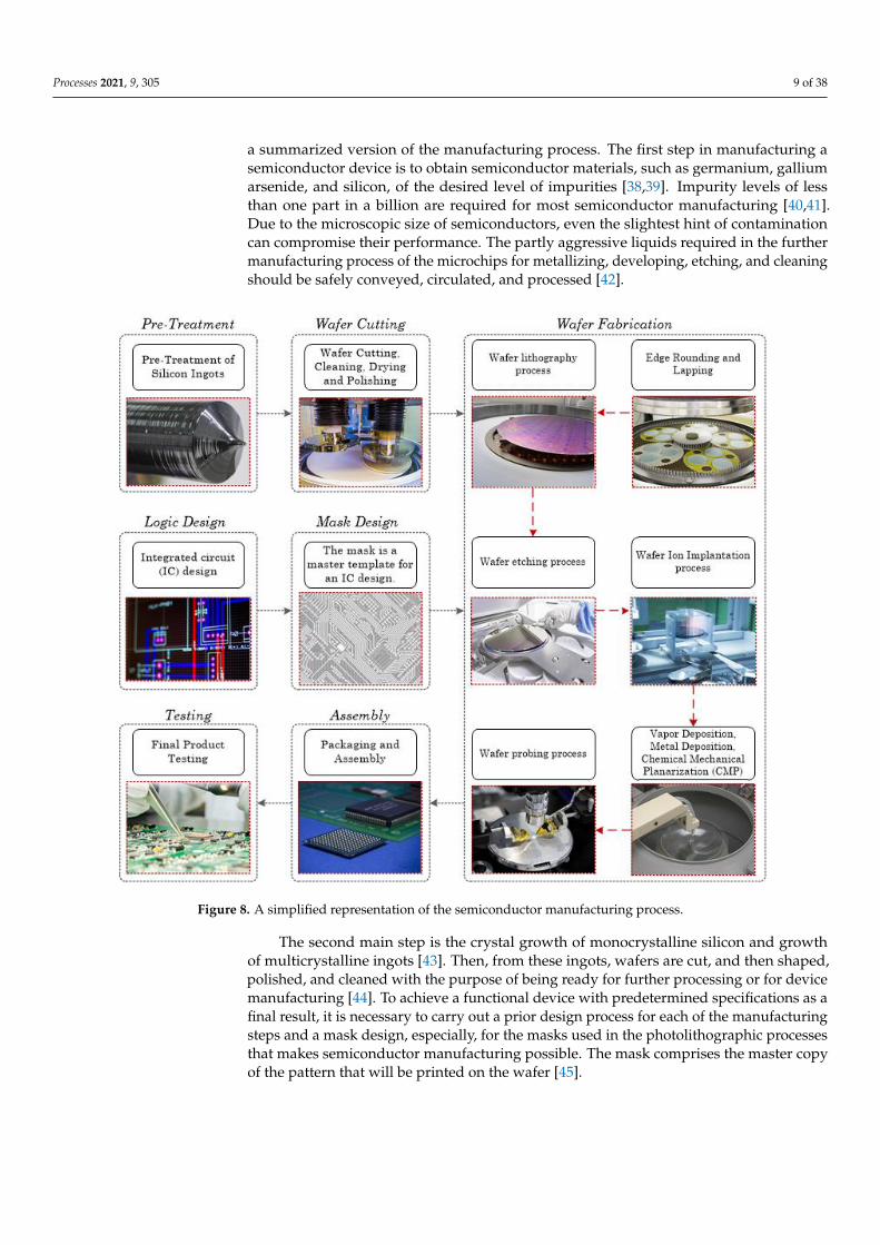
Processes 2021, 9, 305 9 of 38
a summarized version of the manufacturing process. The first step in manufacturing asemiconductor device is to obtain semiconductor materials, such as germanium, galliumarsenide, and silicon, of the desired level of impurities [38,39]. Impurity levels of lessthan one part in a billion are required for most semiconductor manufacturing [40,41].Due to the microscopic size of semiconductors, even the slightest hint of contaminationcan compromise their performance. The partly aggressive liquids required in the furthermanufacturing process of the microchips for metallizing, developing, etching, and cleaningshould be safely conveyed, circulated, and processed [42].
Processes 2021, 9, x FOR PEER REVIEW 9 of 38
summarized version of the manufacturing process. The first step in manufacturing a
semiconductor device is to obtain semiconductor materials, such as germanium, gallium
arsenide, and silicon, of the desired level of impurities [38,39]. Impurity levels of less than
one part in a billion are required for most semiconductor manufacturing [40,41]. Due to
the microscopic size of semiconductors, even the slightest hint of contamination can
compromise their performance. The partly aggressive liquids required in the further
manufacturing process of the microchips for metallizing, developing, etching, and
cleaning should be safely conveyed, circulated, and processed [42].
Figure 8. A simplified representation of the semiconductor manufacturing process.
The second main step is the crystal growth of monocrystalline silicon and growth of
multicrystalline ingots [43]. Then, from these ingots, wafers are cut, and then shaped,
polished, and cleaned with the purpose of being ready for further processing or for de-
vice manufacturing [44]. To achieve a functional device with predetermined specifica-
tions as a final result, it is necessary to carry out a prior design process for each of the
manufacturing steps and a mask design, especially, for the masks used in the photolith-
ographic processes that makes semiconductor manufacturing possible. The mask com-
prises the master copy of the pattern that will be printed on the wafer [45].
The next important step consists of chemical mechanical planarization or chemical
mechanical polishing (CMP) is a process in which topographical irregularities can be
removed from wafers with a combination of chemical and mechanical (or abrasive) pol-
ishing in order to obtain the smoothest surface possible [46,47]. The process is usually
used to planarize oxide, polysilicon, or metal layers in order to prepare them for the
Figure 8. A simplified representation of the semiconductor manufacturing process.
The second main step is the crystal growth of monocrystalline silicon and growthof multicrystalline ingots [43]. Then, from these ingots, wafers are cut, and then shaped,polished, and cleaned with the purpose of being ready for further processing or for devicemanufacturing [44]. To achieve a functional device with predetermined specifications as afinal result, it is necessary to carry out a prior design process for each of the manufacturingsteps and a mask design, especially, for the masks used in the photolithographic processesthat makes semiconductor manufacturing possible. The mask comprises the master copyof the pattern that will be printed on the wafer [45].
Processes 2021, 9, 305 10 of 38
The next important step consists of chemical mechanical planarization or chemicalmechanical polishing (CMP) is a process in which topographical irregularities can be re-moved from wafers with a combination of chemical and mechanical (or abrasive) polishingin order to obtain the smoothest surface possible [46,47]. The process is usually used toplanarize oxide, polysilicon, or metal layers in order to prepare them for the subsequentlithographic step [48,49]. During ion implantation, high-energy ions are shot onto thesubstrate to be doped by the doping agent. The distribution of the implanted atoms in thesemiconductor can be specifically influenced by the energy, the entry angle, and the useof masks. With multiple implants carried out one after the other, even complex dopingprofiles can be produced with good accuracy and replicability [50,51].
As seen in Figure 8, one of the most important steps in semiconductor manufacturingis extreme ultraviolet (EUV) lithography a process that allows carving more electricalcircuits in semiconductor silicon wafers. In a lithographic system, images are transferred tosilicon with light [52,53]. EUV lithography is considered to be essential to semiconductormanufacturing since it is able to produce a shorter wavelength that allows a greater quantityof electrical circuits to enter a chip [54]. Then, an important step is etching, which is utilizedin microfabrication to chemically eradicate layers of a material from the surface of a waferin order to create a pattern of that material on the substrate [55].
The following step is wafer probing, which is the procedure of electrically verifyingeach die on a wafer. This is accomplished by utilizing an automatic wafer probing sys-tem, which is actively searching for functional defects through by employing special testpatterns [56–58]. The next step, semiconductor packaging and assembly process, involvesenclosing ICs and encompasses from die-attach adhesives to liquid and film-shaped encap-sulation compounds, sealing, lead forming/trimming, deflash, wirebonding, lead finishto heat-conducting materials, and conductive and non-conductive adhesives for sensors,among others. The encapsulation technology protects the sensitive layers from externalinfluences and maintains their efficiency [59,60]. Finally, the final component is carefullytested in order to verify if it meets the requirements of standard specifications. The testingprocess is employed to test semiconductors in the context of design verification, specializedproduction, and quality assurance [61].
4. Data Mining Applications in Semiconductor Manufacturing
Data mining techniques can have a vast array of applications in the semiconductorindustry. The obtained articles were classified accordingly to areas of application. Fivemajor areas for data mining applications in semiconductor manufacturing emerged: qualitycontrol, maintenance, production, decision support systems, and finally, categorized asa whole, measurement, metrology, and instrumentation. However, other applicationsalso exist, such as for human resources and talent recruitment and retainment [62], patentanalysis [63], supply chain and inventory management [64], and stock market analysis [20],proving that data mining techniques can truly be employed for a wide range of applications.
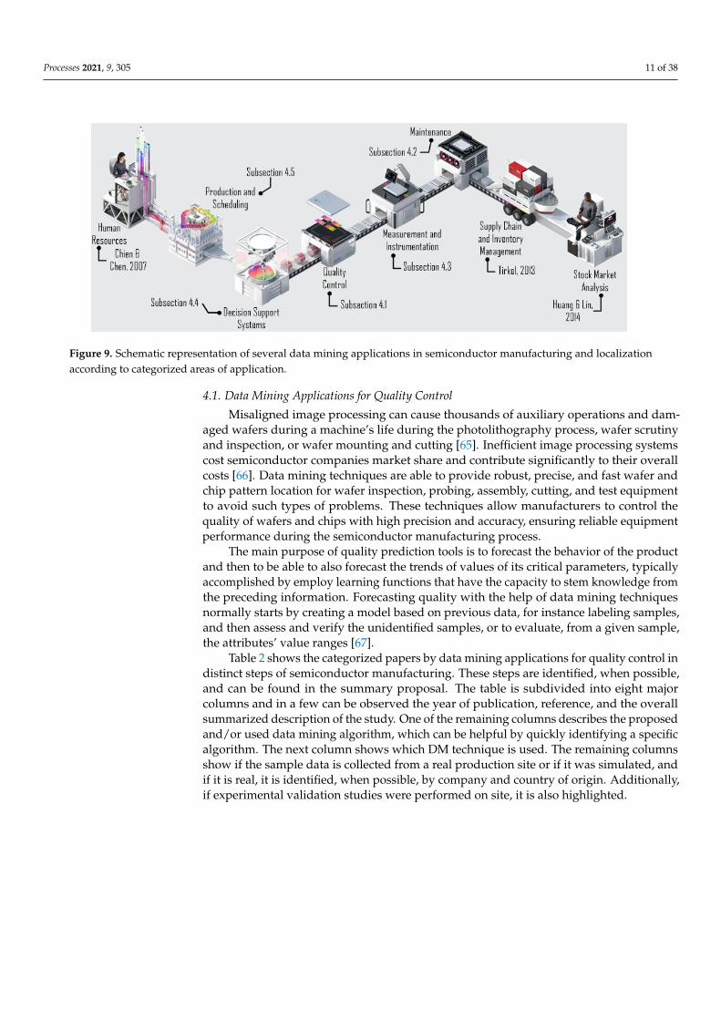
Figure 9 shows the schematic representation of these applications. In some cases, onlyone article exists, and as such the direct reference is provided. In other cases, the identifiedfive major areas are divided by subsections, in which a more detailed analysis is made.Additionally, this section is also useful for practicing engineers, since they can quickly findthe semiconductor process step or data mining model they are looking for. They can alsofind the study that has been implemented and validated in industrial setting and throughcorresponding references, access to it.
Processes 2021, 9, 305 11 of 38Processes 2021, 9, x FOR PEER REVIEW 11 of 38
Figure 9. Schematic representation of several data mining applications in semiconductor manufacturing and localization
according to categorized areas of application.
4.1. Data Mining Applications for Quality Control
Misaligned image processing can cause thousands of auxiliary operations and
damaged wafers during a machine’s life during the photolithography process, wafer
scrutiny and inspection, or wafer mounting and cutting [65]. Inefficient image processing
systems cost semiconductor companies market share and contribute significantly to their
overall costs [66]. Data mining techniques are able to provide robust, precise, and fast
wafer and chip pattern location for wafer inspection, probing, assembly, cutting, and test
equipment to avoid such types of problems. These techniques allow manufacturers to
control the quality of wafers and chips with high precision and accuracy, ensuring relia-
ble equipment performance during the semiconductor manufacturing process.
The main purpose of quality prediction tools is to forecast the behavior of the
product and then to be able to also forecast the trends of values of its critical parameters,
typically accomplished by employ learning functions that have the capacity to stem
knowledge from the preceding information. Forecasting quality with the help of data
mining techniques normally starts by creating a model based on previous data, for in-
stance labeling samples, and then assess and verify the unidentified samples, or to eval-
uate, from a given sample, the attributes’ value ranges [67].
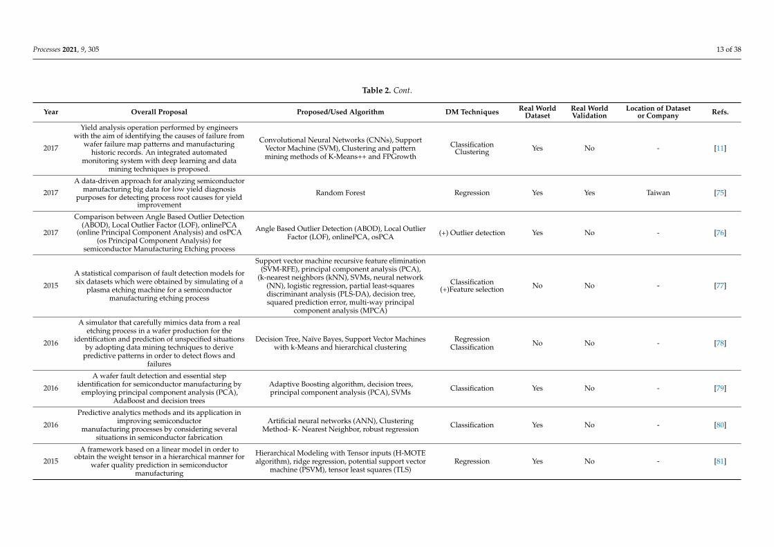
Table 2 shows the categorized papers by data mining applications for quality control
in distinct steps of semiconductor manufacturing. These steps are identified, when pos-
sible, and can be found in the summary proposal. The table is subdivided into eight ma-
jor columns and in a few can be observed the year of publication, reference, and the
overall summarized description of the study. One of the remaining columns describes the
proposed and/or used data mining algorithm, which can be helpful by quickly identify-
ing a specific algorithm. The next column shows which DM technique is used. The re-
maining columns show if the sample data is collected from a real production site or if it
was simulated, and if it is real, it is identified, when possible, by company and country of
origin. Additionally, if experimental validation studies were performed on site, it is also
highlighted.
Figure 9. Schematic representation of several data mining applications in semiconductor manufacturing and localizationaccording to categorized areas of application.
4.1. Data Mining Applications for Quality Control
Misaligned image processing can cause thousands of auxiliary operations and dam-aged wafers during a machine’s life during the photolithography process, wafer scrutinyand inspection, or wafer mounting and cutting [65]. Inefficient image processing systemscost semiconductor companies market share and contribute significantly to their overallcosts [66]. Data mining techniques are able to provide robust, precise, and fast wafer andchip pattern location for wafer inspection, probing, assembly, cutting, and test equipmentto avoid such types of problems. These techniques allow manufacturers to control thequality of wafers and chips with high precision and accuracy, ensuring reliable equipmentperformance during the semiconductor manufacturing process.
The main purpose of quality prediction tools is to forecast the behavior of the productand then to be able to also forecast the trends of values of its critical parameters, typicallyaccomplished by employ learning functions that have the capacity to stem knowledge fromthe preceding information. Forecasting quality with the help of data mining techniquesnormally starts by creating a model based on previous data, for instance labeling samples,and then assess and verify the unidentified samples, or to evaluate, from a given sample,the attributes’ value ranges [67].
Table 2 shows the categorized papers by data mining applications for quality control indistinct steps of semiconductor manufacturing. These steps are identified, when possible,and can be found in the summary proposal. The table is subdivided into eight majorcolumns and in a few can be observed the year of publication, reference, and the overallsummarized description of the study. One of the remaining columns describes the proposedand/or used data mining algorithm, which can be helpful by quickly identifying a specificalgorithm. The next column shows which DM technique is used. The remaining columnsshow if the sample data is collected from a real production site or if it was simulated, andif it is real, it is identified, when possible, by company and country of origin. Additionally,if experimental validation studies were performed on site, it is also highlighted.
Processes 2021, 9, 305 12 of 38
Table 2. Data mining applications for quality control in distinct steps of semiconductor manufacturing.
Year Overall Proposal Proposed/Used Algorithm DM Techniques Real WorldDataset
Real WorldValidation
Location of Datasetor Company Refs.
2020 A review of data mining applications for qualitycontrol of semiconductor manufacturing Several Several No No - [67]
2020Correctly identifying actual defective patterns in
Wafer Bin Maps (WBM) to support the improvementof production yield
Hybrid clustering algorithm that integrates clusteranalysis and spatial statistics Clustering Yes Yes - [68]
2020A new approach of measuring similarity of wafer binmaps in order to improve defect diagnosis and fault
detection
Mountain clustering algorithmWeighted Modified Hausdorff Distance (WMHD) Clustering Yes Yes Taiwan [10]
2020
An Expected Margin–based Pattern Selection model,that is able to select patterns based on an estimated
margin for Support Vector Machines (SVMs)classifiers for wafer quality classification in the
photolithography process
Expected Margin-based Pattern Selection (EMPS)Support Vector Machines (SVMs) Classification Yes Yes South Korea [69]
2019Fault detection and diagnosis model directly taken
from the variable-length status variablesidentification (SVID) in the etch process
Convolutional neural networks (CNNs) Classification Yes Yes South Korea [70]
2019 Clustering-based defect pattern detection andclassification framework for WBMs
Density-based spatial clustering of applications withnoise (DBSCAN) Clustering Yes No - [71]
2019
An yield prediction model based on the selectedcritical process steps by taking into account
difficulties such as imbalanced data, randomsampling, and missing values
Expectation maximization (EM), MeanDiff technique,Synthetic minority over-sampling technique
(SMOTE), decision tree, logistic regression, k-nearestneighbors (k-NN), and SVM
ClassificationRegression Yes No - [9]
2018A framework based on Bayesian inference and Gibbssampling to investigate the intricate semiconductor
manufacturing data for fault detection
Bayesian inference, Gibbs sampling, highdimensional linear regression, multivariate adaptiveregression spline (MARS), Cohen’s kappa statistics
Classification Yes No - [5]
2018 Process errors detection and practical processimprovement
Decision tree-based classificationC4.5 in KNIME Association rules Yes Yes France [19]
2018
A robust incremental on-line feature extractionmethod by ensuring the accuracy of data analysis
and by meeting real-time demands of semiconductormanufacturing process for product quality
supervision
PCA (Principal Component Analysis)RIPCA (RobustIncremental Principal Component Analysis)
CCIPCA (Covariance-Free Incremental PCA)
(+)Feature selec-tion/Dimensionality
reductionYes No - [72]
2018 Data mining applications semiconductormanufacturing process quality control
Fisher criterion algorithm, Support Vector Machines(SVMs) and Random Forest Classification Yes No Northern Ireland [73]
2018
A mutually-exclusive-and-collectively-exhaustivefeature selection framework applied to two cases of
datasets, one being from a real manufacturingprocess
Mutually-exclusive-and-collectively-exhaustive(MECE)
Two-phase clustering selection (TPS), stepwiseselection (SS)
Chi-Square Automatic Interaction Detector (CHAID)
(+)Feature selec-tion/Dimensionality
reductionYes No - [74]
Processes 2021, 9, 305 13 of 38
Table 2. Cont.
Year Overall Proposal Proposed/Used Algorithm DM Techniques Real WorldDataset
Real WorldValidation
Location of Datasetor Company Refs.
2017
Yield analysis operation performed by engineerswith the aim of identifying the causes of failure from
wafer failure map patterns and manufacturinghistoric records. An integrated automated
monitoring system with deep learning and datamining techniques is proposed.
Convolutional Neural Networks (CNNs), SupportVector Machine (SVM), Clustering and patternmining methods of K-Means++ and FPGrowth
ClassificationClustering Yes No - [11]
2017
A data-driven approach for analyzing semiconductormanufacturing big data for low yield diagnosis
purposes for detecting process root causes for yieldimprovement
Random Forest Regression Yes Yes Taiwan [75]
2017
Comparison between Angle Based Outlier Detection(ABOD), Local Outlier Factor (LOF), onlinePCA
(online Principal Component Analysis) and osPCA(os Principal Component Analysis) for
semiconductor Manufacturing Etching process
Angle Based Outlier Detection (ABOD), Local OutlierFactor (LOF), onlinePCA, osPCA (+) Outlier detection Yes No - [76]
2015
A statistical comparison of fault detection models forsix datasets which were obtained by simulating of a
plasma etching machine for a semiconductormanufacturing etching process
Support vector machine recursive feature elimination(SVM-RFE), principal component analysis (PCA),
(k-nearest neighbors (kNN), SVMs, neural network(NN), logistic regression, partial least-squaresdiscriminant analysis (PLS-DA), decision tree,squared prediction error, multi-way principal
component analysis (MPCA)
Classification(+)Feature selection No No - [77]
2016
A simulator that carefully mimics data from a realetching process in a wafer production for the
identification and prediction of unspecified situationsby adopting data mining techniques to derive
predictive patterns in order to detect flows andfailures
Decision Tree, Naïve Bayes, Support Vector Machineswith k-Means and hierarchical clustering
RegressionClassification No No - [78]
2016
A wafer fault detection and essential stepidentification for semiconductor manufacturing by
employing principal component analysis (PCA),AdaBoost and decision trees
Adaptive Boosting algorithm, decision trees,principal component analysis (PCA), SVMs Classification Yes No - [79]
2016
Predictive analytics methods and its application inimproving semiconductor
manufacturing processes by considering severalsituations in semiconductor fabrication
Artificial neural networks (ANN), ClusteringMethod- K- Nearest Neighbor, robust regression Classification Yes No - [80]
2015
A framework based on a linear model in order toobtain the weight tensor in a hierarchical manner for
wafer quality prediction in semiconductormanufacturing
Hierarchical Modeling with Tensor inputs (H-MOTEalgorithm), ridge regression, potential support vector
machine (PSVM), tensor least squares (TLS)Regression Yes No - [81]
Processes 2021, 9, 305 14 of 38
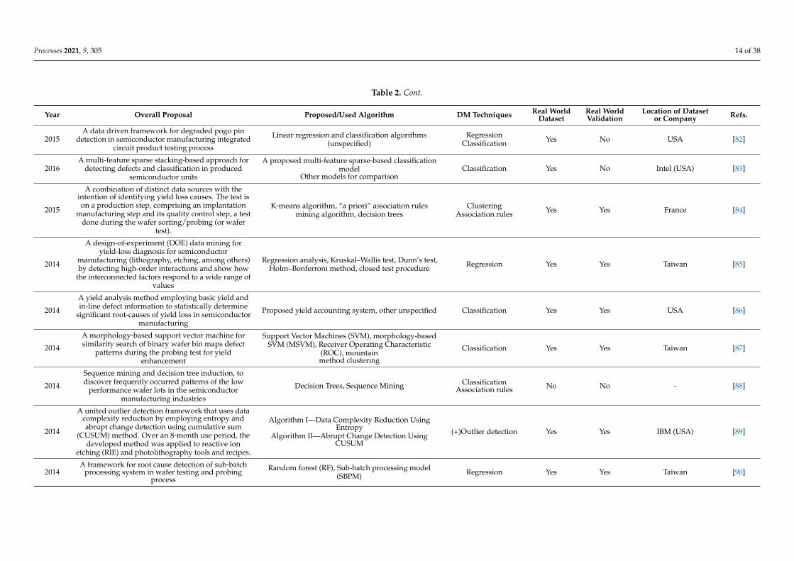
Table 2. Cont.
Year Overall Proposal Proposed/Used Algorithm DM Techniques Real WorldDataset
Real WorldValidation
Location of Datasetor Company Refs.
2015A data driven framework for degraded pogo pin
detection in semiconductor manufacturing integratedcircuit product testing process
Linear regression and classification algorithms(unspecified)
RegressionClassification Yes No USA [82]
2016A multi-feature sparse stacking-based approach for
detecting defects and classification in producedsemiconductor units
A proposed multi-feature sparse-based classificationmodel
Other models for comparisonClassification Yes No Intel (USA) [83]
2015
A combination of distinct data sources with theintention of identifying yield loss causes. The test ison a production step, comprising an implantation
manufacturing step and its quality control step, a testdone during the wafer sorting/probing (or wafer
test).
K-means algorithm, “a priori” association rulesmining algorithm, decision trees
ClusteringAssociation rules Yes Yes France [84]
2014
A design-of-experiment (DOE) data mining foryield-loss diagnosis for semiconductor
manufacturing (lithography, etching, among others)by detecting high-order interactions and show how
the interconnected factors respond to a wide range ofvalues
Regression analysis, Kruskal–Wallis test, Dunn’s test,Holm–Bonferroni method, closed test procedure Regression Yes Yes Taiwan [85]
2014
A yield analysis method employing basic yield andin-line defect information to statistically determine
significant root-causes of yield loss in semiconductormanufacturing
Proposed yield accounting system, other unspecified Classification Yes Yes USA [86]
2014
A morphology-based support vector machine forsimilarity search of binary wafer bin maps defect
patterns during the probing test for yieldenhancement
Support Vector Machines (SVM), morphology-basedSVM (MSVM), Receiver Operating Characteristic
(ROC), mountainmethod clustering
Classification Yes Yes Taiwan [87]
2014
Sequence mining and decision tree induction, todiscover frequently occurred patterns of the low
performance wafer lots in the semiconductormanufacturing industries
Decision Trees, Sequence Mining ClassificationAssociation rules No No - [88]
2014
A united outlier detection framework that uses datacomplexity reduction by employing entropy andabrupt change detection using cumulative sum
(CUSUM) method. Over an 8-month use period, thedeveloped method was applied to reactive ion
etching (RIE) and photolithography tools and recipes.
Algorithm I—Data Complexity Reduction UsingEntropy
Algorithm II—Abrupt Change Detection UsingCUSUM
(+)Outlier detection Yes Yes IBM (USA) [89]
2014A framework for root cause detection of sub-batch
processing system in wafer testing and probingprocess
Random forest (RF), Sub-batch processing model(SBPM) Regression Yes Yes Taiwan [90]
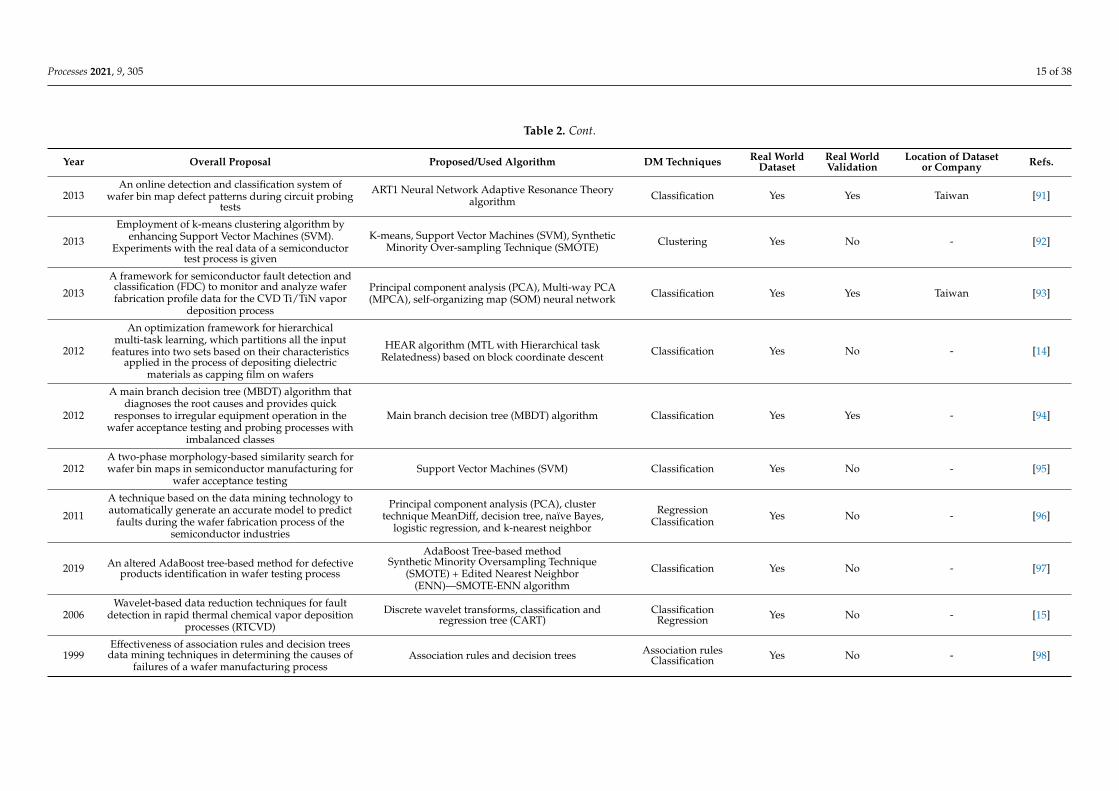
Processes 2021, 9, 305 15 of 38
Table 2. Cont.
Year Overall Proposal Proposed/Used Algorithm DM Techniques Real WorldDataset
Real WorldValidation
Location of Datasetor Company Refs.
2013An online detection and classification system of
wafer bin map defect patterns during circuit probingtests
ART1 Neural Network Adaptive Resonance Theoryalgorithm Classification Yes Yes Taiwan [91]
2013
Employment of k-means clustering algorithm byenhancing Support Vector Machines (SVM).
Experiments with the real data of a semiconductortest process is given
K-means, Support Vector Machines (SVM), SyntheticMinority Over-sampling Technique (SMOTE) Clustering Yes No - [92]
2013
A framework for semiconductor fault detection andclassification (FDC) to monitor and analyze waferfabrication profile data for the CVD Ti/TiN vapor
deposition process
Principal component analysis (PCA), Multi-way PCA(MPCA), self-organizing map (SOM) neural network Classification Yes Yes Taiwan [93]
2012
An optimization framework for hierarchicalmulti-task learning, which partitions all the input
features into two sets based on their characteristicsapplied in the process of depositing dielectric
materials as capping film on wafers
HEAR algorithm (MTL with Hierarchical taskRelatedness) based on block coordinate descent Classification Yes No - [14]
2012
A main branch decision tree (MBDT) algorithm thatdiagnoses the root causes and provides quick
responses to irregular equipment operation in thewafer acceptance testing and probing processes with
imbalanced classes
Main branch decision tree (MBDT) algorithm Classification Yes Yes - [94]
2012A two-phase morphology-based similarity search forwafer bin maps in semiconductor manufacturing for
wafer acceptance testingSupport Vector Machines (SVM) Classification Yes No - [95]
2011
A technique based on the data mining technology toautomatically generate an accurate model to predict
faults during the wafer fabrication process of thesemiconductor industries
Principal component analysis (PCA), clustertechnique MeanDiff, decision tree, naïve Bayes,
logistic regression, and k-nearest neighbor
RegressionClassification Yes No - [96]
2019 An altered AdaBoost tree-based method for defectiveproducts identification in wafer testing process
AdaBoost Tree-based methodSynthetic Minority Oversampling Technique
(SMOTE) + Edited Nearest Neighbor(ENN)—SMOTE-ENN algorithm
Classification Yes No - [97]
2006Wavelet-based data reduction techniques for fault
detection in rapid thermal chemical vapor depositionprocesses (RTCVD)
Discrete wavelet transforms, classification andregression tree (CART)
ClassificationRegression Yes No - [15]
1999Effectiveness of association rules and decision treesdata mining techniques in determining the causes of
failures of a wafer manufacturing processAssociation rules and decision trees Association rules
Classification Yes No - [98]
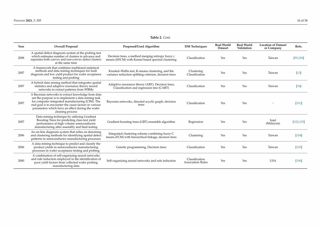
Processes 2021, 9, 305 16 of 38
Table 2. Cont.
Year Overall Proposal Proposed/Used Algorithm DM Techniques Real WorldDataset
Real WorldValidation
Location of Datasetor Company Refs.
2008
A spatial defect diagnosis system at the probing testwhich estimates number of clusters in advance and
separates both convex and non-convex defect clustersat the same time
Decision trees, a method merging entropy fuzzy cmeans (EFCM) with Kernel based spectral clustering Classification Yes Yes Taiwan [99,100]
2007
A framework that combines traditional statisticalmethods and data mining techniques for fault
diagnosis and low yield product for wafer acceptancetesting and probing
Kruskal–Wallis test, K-means clustering, and thevariance reduction splitting criterion, decision trees
ClusteringClassification Yes Yes Taiwan [13]
2007A hybrid data mining method that integrates spatial
statistics and adaptive resonance theory neuralnetworks to extract patterns from WBMs
Adaptive resonance theory (ART), Decision trees,Classification and regression tree (CART) Classification Yes Yes Taiwan [34]
2007
A Bayesian networks to extract knowledge from dataant the purpose is to implement a data mining taskfor computer integrated manufacturing (CIM). Theend goal is to encounter the cause factors in variousparameters which have an effect during the wafer
cleaning process
Bayesian networks, directed acyclic graph, decisiontrees Classification Yes Yes - [101]
2007
Data mining technique by utilizing GradientBoosting Trees for predicting class test yieldperformance at high volume semiconductor
manufacturing after assembly and final testing
Gradient boosting trees (GBT) ensemble algorithm Regression Yes Yes Intel(Malaysia) [102,103]
2006An on-line diagnosis system that relies on denoisingand clustering methods for identifying spatial defectpatterns in semiconductor manufacturing processes
Integrated clustering scheme combining fuzzy Cmeans (FCM) with hierarchical linkage, decision trees Clustering Yes Yes Taiwan [104]
2006A data mining technique to predict and classify the
product yields in semiconductor manufacturingprocesses in wafer acceptance testing and probing
Genetic programming, Decision trees Classification Yes Yes Taiwan [105]
2000
A combination of self-organizing neural networksand rule induction employed in the identification of
poor yield factors from collected wafer probingmanufacturing data
Self-organizing neural networks and rule induction ClassificationAssociation Rules Yes Yes USA [106]
Processes 2021, 9, 305 17 of 38
This topic is the most popular one, with 47 publications. By observing Table 2, itcan be seen that several applications are made in distinct subprocesses such as waferprobing and testing process, etching process, and photolithography, among others. Ahigh and varied number of algorithms are employed. The majority of articles addresschallenges of correctly identifying defective patterns in order to improve productionyield [68]. Yield is a quantitative measure of the quality of a semiconductor process. Itis measured as the number of functioning dies or chips on a wafer and can also be seenas the fraction of dies on the yielding wafers that are not rejected during the productionprocess [107]. However, other applications in quality control can also be found, such as astudy addressing a design-of-experiment (DOE) data mining for yield-loss diagnosis forsemiconductor manufacturing by detecting high-order interactions, for subprocesses suchas lithography and etching, among others [85]. These data mining technique are also usedwith statistical process control. Cumulative sum control charts, known as CUSUM, area special type of statistical process control tool that is used in [89] as part of and unifiedoutlier detection framework, which takes advantages of data complexity reduction byemploying entropy and sudden change detection through the use of CUSUM charts.
4.2. Data Mining Applications for Maintenance
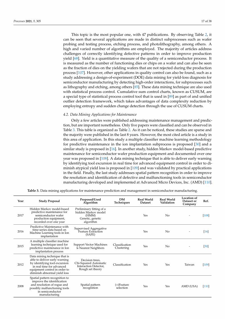
Only a few articles were published addressing maintenance management and predic-tion, but are important nonetheless. Only five papers were classified and can be observed inTable 3. This table is organized as Table 2. As it can be noticed, these studies are sparse andthe majority were published in the last 8 years. However, the most cited article is a study inthis area of application. In this study a multiple classifier machine learning methodologyfor predictive maintenance in the ion implantation subprocess is proposed [30] and asimilar study is proposed in [16]. In another study, hidden Markov model-based predictivemaintenance for semiconductor wafer production equipment and documented over oneyear was proposed in [108]. A data mining technique that is able to deliver early warningby identifying tool excursion in real time for advanced equipment control in order to di-minish atypical yield loss is proposed in [109] and was validated by practical applicationsin the field. Finally, the last study addresses spatial pattern recognition in order to improvethe resolution and identification of defective and malfunctioning tools in semiconductormanufacturing developed and implemented at Advanced Micro Devices, Inc. (AMD) [110].
Table 3. Data mining applications for maintenance prediction and management in semiconductor manufacturing.
Year Study Proposal Proposed/UsedAlgorithm
DMTechniques
Real WorldDataset
Real WorldValidation
Location ofDataset orCompany
Ref.
2017
Hidden Markov model-basedpredictive maintenance for
semiconductor waferproduction equipment,recorded over one year
Preliminary fitting of ahidden Markov model
(HMM)Genetic, genetic
algorithm
Yes No - [108]
2016
Predictive Maintenance withtime-series data based on
Machine Learning tools in Ionimplantation
Supervised AggregativeFeature Extraction
(SAFE)Yes No - [16]
2015
A multiple classifier machinelearning technique used for
predictive maintenance in Ionimplantation process
Support Vector Machinesk-Nearest Neighbors
ClassificationClustering Yes No - [30]
2012
Data mining technique that isable to deliver early warningby identifying tool excursion
in real time for advancedequipment control in order todiminish abnormal yield loss
Decision trees,Chi-Squared Automatic
Interaction Detector,Rough set theory
Classification Yes Yes Taiwan [109]
2008
Spatial pattern recognition toimprove the identification
and resolution of rogue andpossibly malfunctioning tools
in semiconductormanufacturing
Spatial patternrecognition
(+)Featureselection Yes Yes AMD (USA) [110]
Processes 2021, 9, 305 18 of 38
4.3. Data Mining Applications for Metrology, Measurement, and Instrumentation
The high necessity for always striving to make progress regarding the yield of currentsemiconductor production processes and decrease the time-to-market for more advanced,innovative, and gradually elaborate designs and processes demands for process tools andwafers to be examined and verified with up-to-date measurement systems and equipment.Several papers, namely 19, are categorized in this topic, as depicted in Table 4. This table isorganized as Table 2. The topics addressed in this section range from models comprising aprecise semiconductor photolithography process control method through virtual metrologyby employing significant correlations between focus measurement data encountered bydata mining and tool data [111].
In fact, virtual metrology is a recurring topic, and is defined as a set of methods thatallow predicting the properties of a wafer through sensor data and machine parameters inthe manufacturing equipment, thus avoiding the highly expensive physical measurementof the wafer properties [112–114]. Since machine data is typically sampled much moreoften when compared to metrology data, and since machine data becomes immediatelyavailable when compared to the delays that frequently occur with metrology tools, anaccurate virtual metrology is capable of meaningfully developing the process control andmonitoring performance through a constantly supply of real-time forecasted metrologydata. A few feature extraction methods for virtual metrology with multisensor data areproposed in [17,115,116].
However, other measurement and instrumentation were also proposed and classified.For instance, in [117] a real-time data mining solution with the segmentation, detection,and cluster-extraction (SDC) algorithm that can automatically and accurately extract defectclusters from raw wafer probe test production data is proposed. Additionally, a datamining that employs machine learning methods with the purpose of modeling unknownfunctional interrelations and to predict the thickness of dielectric layers deposited onto ametallization layer of the manufactured wafers is proposed in [118]. Finally, at IBM, a datamining technique with the purpose of automatically identifying and exploring correlationsbetween inline measurements and final test outcomes in analog and/or radio frequency(RF) devices and by integrating domain expert feedback into the algorithm in order toidentify and remove bogus autocorrelations [119]. Practical application and validation ofthis technique is made.
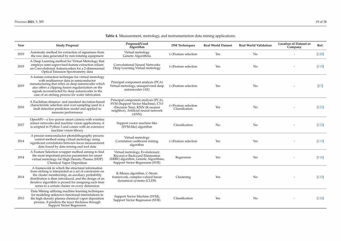
Processes 2021, 9, 305 19 of 38
Table 4. Measurement, metrology, and instrumentation data mining applications.
Year Study Proposal Proposed/UsedAlgorithm DM Techniques Real World Dataset Real World Validation Location of Dataset or
Company Ref.
2019 Automatic method for extraction of signatures fromthe raw data generated by non-rotating equipment
Virtual metrologyGenetic Algorithms (+)Feature selection Yes No - [120]
2019
A Deep Learning method for Virtual Metrology thatemploys semi-supervised feature extraction reliant
on Convolutional Autoencoders for a 2-dimensionalOptical Emission Spectrometry data
Convolutional Neural NetworksDeep Learning Virtual metrology (+)Feature selection Yes No - [115]
2019
A feature extraction technique for virtual metrologywith multisensor data in semiconductor
manufacturing that relies on deep autoencoder whichalso offers a clipping fusion regularization on thesignals reconstructed by deep autoencoder in thecase of an etching process for wafer fabrication
Principal component analysis (PCA)Virtual metrology, unsupervised deep
autoencoder (AE)(+)Feature selection Yes No - [17]
2016
A Euclidean distance- and standard deviation-basedcharacteristic selection and over-sampling used in a
fault detection prediction model and applied tomeasure performance
Principal component analysis (PCA),SVM (Support Vector Machine), C5.0
(Decision Tree), KNN (K-nearestneighbor), Artificial neural network
(ANN)
(+)Feature selectionClassification Yes No - [121]
2017
OpenMV—a low-power smart camera with wirelesssensor networks and machine vision applications, itis scripted in Python 3 and comes with an extensive
machine vision library
Support vector machine-like(SVM-like) algorithm Classification No No - [122]
2014
A precise semiconductor photolithography processcontrol method using virtual metrology using
significant correlations between focus measurementdata found by data mining and tool data
Virtual metrologyCorrelation coefficient mining
algorithm(+)Feature selection Yes Yes - [111]
2014
A Feature Selection wrapper method aiming to findthe most important process parameters for smartvirtual metrology for High Density Plasma (HDP)
Chemical Vapor Deposition
Virtual metrology, EvolutionaryRecursive Backward Elimination
(ERBE) algorithm, Genetic Algorithms,Support Vector Regression (SVR)
Regression Yes Yes - [116]
2014
A framework in which the structural informationfrom etching is interpreted as a set of constraints on
the cluster membership, an auxiliary probabilitydistribution is then introduced, and the design of aniterative algorithm is prosed for assigning each time
series to a certain cluster on every dimension
K-Means algorithm, C-Strutsframework, complex-valued linear
dynamical systems (CLDS)Clustering Yes No - [123]
2013
Data Mining utilizing machine learning techniquesfor modeling unknown functional interrelations inthe high-density plasma chemical vapor deposition
process. It predicts the layer thickness throughSupport Vector Regression
Support Vector Machine (SVM),Support Vector Regression (SVR) Classification Yes No - [124]
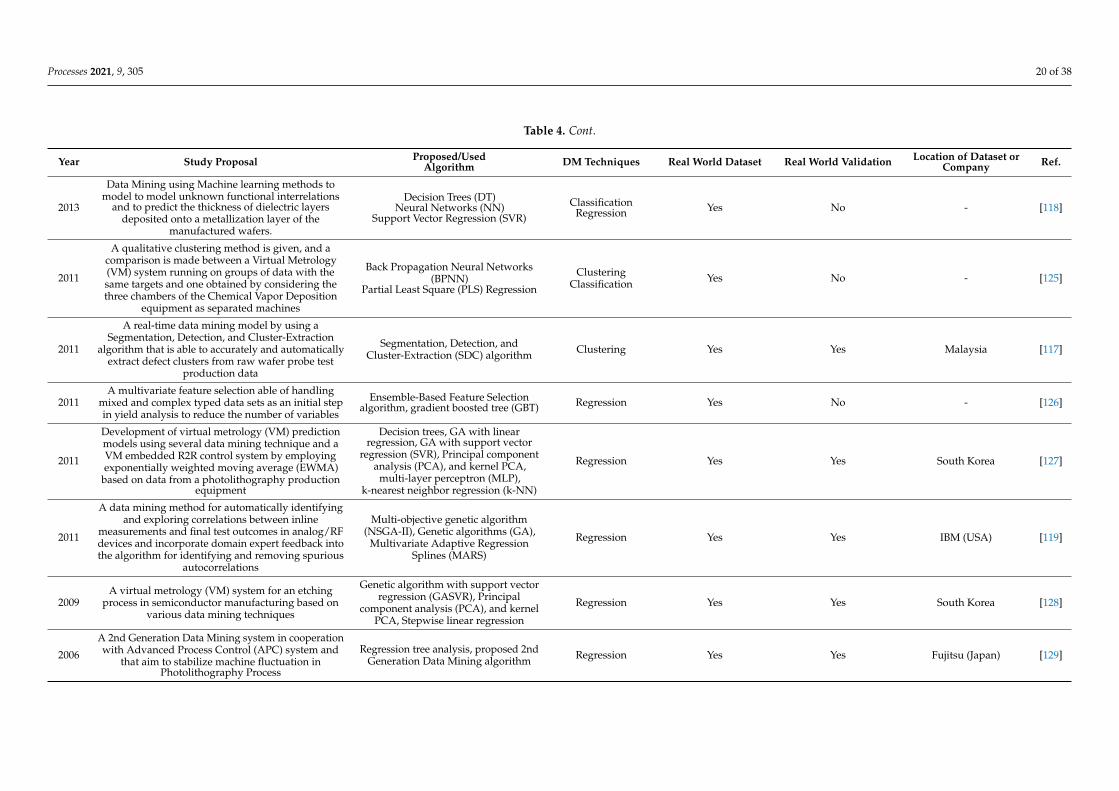
Processes 2021, 9, 305 20 of 38
Table 4. Cont.
Year Study Proposal Proposed/UsedAlgorithm DM Techniques Real World Dataset Real World Validation Location of Dataset or
Company Ref.
2013
Data Mining using Machine learning methods tomodel to model unknown functional interrelations
and to predict the thickness of dielectric layersdeposited onto a metallization layer of the
manufactured wafers.
Decision Trees (DT)Neural Networks (NN)
Support Vector Regression (SVR)Classification
Regression Yes No - [118]
2011
A qualitative clustering method is given, and acomparison is made between a Virtual Metrology(VM) system running on groups of data with thesame targets and one obtained by considering thethree chambers of the Chemical Vapor Deposition
equipment as separated machines
Back Propagation Neural Networks(BPNN)
Partial Least Square (PLS) Regression
ClusteringClassification Yes No - [125]
2011
A real-time data mining model by using aSegmentation, Detection, and Cluster-Extraction
algorithm that is able to accurately and automaticallyextract defect clusters from raw wafer probe test
production data
Segmentation, Detection, andCluster-Extraction (SDC) algorithm Clustering Yes Yes Malaysia [117]
2011A multivariate feature selection able of handling
mixed and complex typed data sets as an initial stepin yield analysis to reduce the number of variables
Ensemble-Based Feature Selectionalgorithm, gradient boosted tree (GBT) Regression Yes No - [126]
2011
Development of virtual metrology (VM) predictionmodels using several data mining technique and aVM embedded R2R control system by employingexponentially weighted moving average (EWMA)
based on data from a photolithography productionequipment
Decision trees, GA with linearregression, GA with support vector
regression (SVR), Principal componentanalysis (PCA), and kernel PCA,
multi-layer perceptron (MLP),k-nearest neighbor regression (k-NN)
Regression Yes Yes South Korea [127]
2011
A data mining method for automatically identifyingand exploring correlations between inline
measurements and final test outcomes in analog/RFdevices and incorporate domain expert feedback intothe algorithm for identifying and removing spurious
autocorrelations
Multi-objective genetic algorithm(NSGA-II), Genetic algorithms (GA),
Multivariate Adaptive RegressionSplines (MARS)
Regression Yes Yes IBM (USA) [119]
2009A virtual metrology (VM) system for an etching
process in semiconductor manufacturing based onvarious data mining techniques
Genetic algorithm with support vectorregression (GASVR), Principal
component analysis (PCA), and kernelPCA, Stepwise linear regression
Regression Yes Yes South Korea [128]
2006
A 2nd Generation Data Mining system in cooperationwith Advanced Process Control (APC) system and
that aim to stabilize machine fluctuation inPhotolithography Process
Regression tree analysis, proposed 2ndGeneration Data Mining algorithm Regression Yes Yes Fujitsu (Japan) [129]
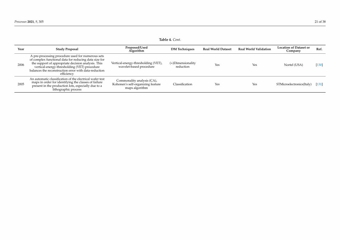
Processes 2021, 9, 305 21 of 38
Table 4. Cont.
Year Study Proposal Proposed/UsedAlgorithm DM Techniques Real World Dataset Real World Validation Location of Dataset or
Company Ref.
2006
A pre-processing procedure used for numerous setsof complex functional data for reducing data size for
the support of appropriate decision analysis. Thisvertical-energy-thresholding (VET) procedure
balances the reconstruction error with data-reductionefficiency
Vertical-energy-thresholding (VET),wavelet-based procedure
(+)Dimensionalityreduction Yes Yes Nortel (USA) [130]
2005
An automatic classification of the electrical wafer testmaps in order for identifying the classes of failurepresent in the production lots, especially due to a
lithographic process
Commonality analysis (CA),Kohonen’s self-organizing feature
maps algorithmClassification Yes Yes STMicroelectronics(Italy) [131]
Processes 2021, 9, 305 22 of 38
4.4. Decision Support Systems
Another trend in semiconductor manufacturing is the use of decision support systems(DSS). A DSS is a system designed to support in solving unstructured and semistructuredmanagerial problems, throughout all the decision process’ stages [132]. The DSS use in thisarea is not novel. Earliest publications in this area date to the 1990s (e.g., [133,134]). DSSsare used to support decision-making in activities like production scheduling, simulation,prediction, material selection, fault detection, quality, etc. DSSs may, sometimes, have aknowledge base, which requires artificial intelligence to provide knowledge to supportthe decision process. However, the earliest uses of DSS required knowledge modeling byknowledge engineers from documented and expert knowledge. Knowledge extractionfrom unprocessed data allowed one to discover hidden knowledge in large amounts ofdata. The use of data mining techniques to uncover knowledge to be modeled in DSS is atrend also present in semiconductor literature. Researchers apply data mining techniquesto find patterns and hidden relations that may help in semiconductor decision making.Usually, the goal is to determine links between control parameters and product quality,essentially in the form of decision rules [135].
In Table 5 the literature where data mining is used to support the decision-making pro-cess in semiconductors’ manufacturing is presented. Analyzing this table, one can see thatmost contributions address yield management and failure detection issues (see [135–145]).The authors from [146] aim at the same problem, but focus on the development of a com-puter integrated manufacturing (CIM) system to improve product yield. Other articlesprovide isolated contributions. In [147], the authors propose the application of data min-ing techniques to support decision-making in HR management of high-tech companies.In [148], the authors suggest the integration of data mining in semiconductor manufactur-ing execution systems (MES). Last, in [32] provides a multi-purpose data mining applicationfor predictions in semiconductor manufacturing.
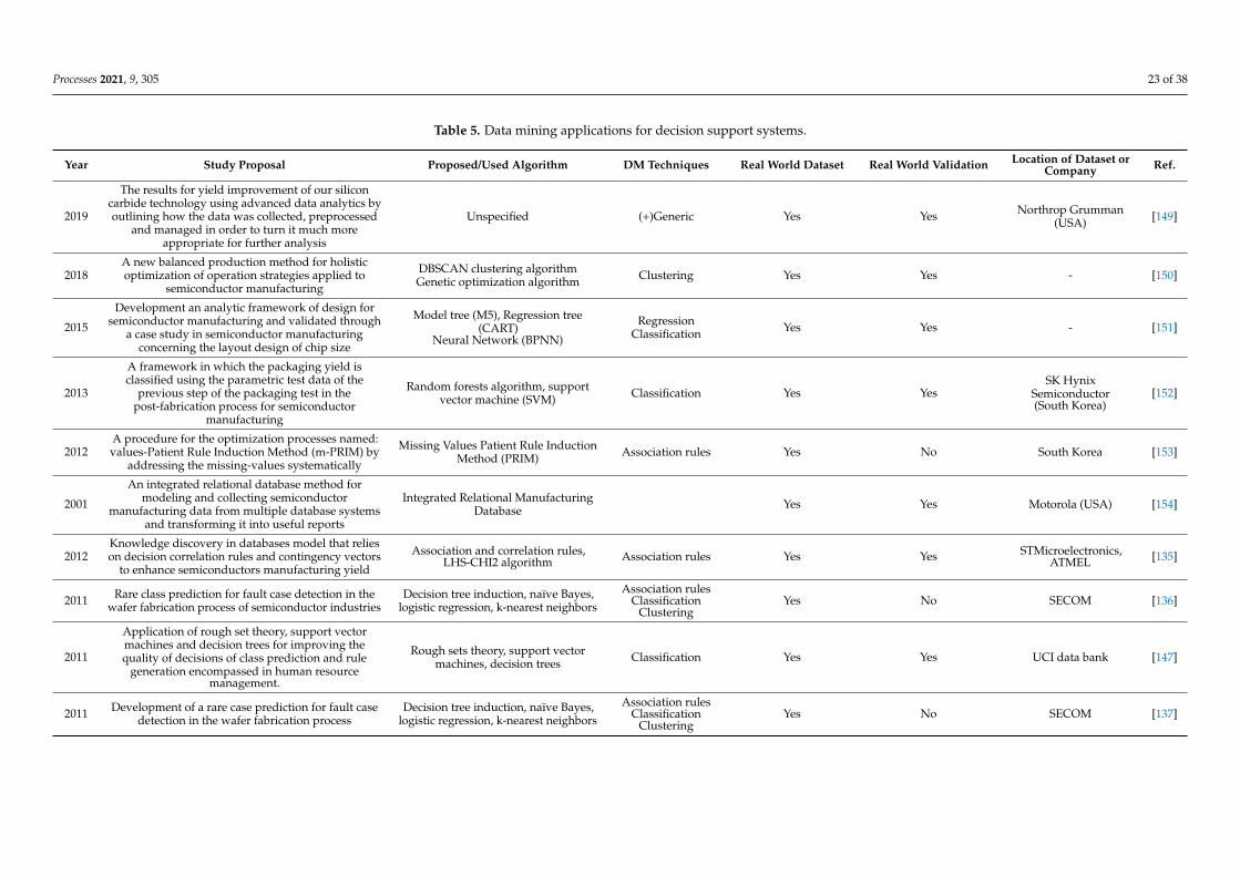
Processes 2021, 9, 305 23 of 38
Table 5. Data mining applications for decision support systems.
Year Study Proposal Proposed/Used Algorithm DM Techniques Real World Dataset Real World Validation Location of Dataset orCompany Ref.
2019
The results for yield improvement of our siliconcarbide technology using advanced data analytics byoutlining how the data was collected, preprocessed
and managed in order to turn it much moreappropriate for further analysis
Unspecified (+)Generic Yes Yes Northrop Grumman(USA) [149]
2018A new balanced production method for holisticoptimization of operation strategies applied to
semiconductor manufacturing
DBSCAN clustering algorithmGenetic optimization algorithm Clustering Yes Yes - [150]
2015
Development an analytic framework of design forsemiconductor manufacturing and validated through
a case study in semiconductor manufacturingconcerning the layout design of chip size
Model tree (M5), Regression tree(CART)
Neural Network (BPNN)
RegressionClassification Yes Yes - [151]
2013
A framework in which the packaging yield isclassified using the parametric test data of the
previous step of the packaging test in thepost-fabrication process for semiconductor
manufacturing
Random forests algorithm, supportvector machine (SVM) Classification Yes Yes
SK HynixSemiconductor(South Korea)
[152]
2012A procedure for the optimization processes named:values-Patient Rule Induction Method (m-PRIM) by
addressing the missing-values systematically
Missing Values Patient Rule InductionMethod (PRIM) Association rules Yes No South Korea [153]
2001
An integrated relational database method formodeling and collecting semiconductor
manufacturing data from multiple database systemsand transforming it into useful reports
Integrated Relational ManufacturingDatabase Yes Yes Motorola (USA) [154]
2012Knowledge discovery in databases model that relieson decision correlation rules and contingency vectors
to enhance semiconductors manufacturing yield
Association and correlation rules,LHS-CHI2 algorithm Association rules Yes Yes STMicroelectronics,
ATMEL [135]
2011 Rare class prediction for fault case detection in thewafer fabrication process of semiconductor industries
Decision tree induction, naïve Bayes,logistic regression, k-nearest neighbors
Association rulesClassification
ClusteringYes No SECOM [136]
2011
Application of rough set theory, support vectormachines and decision trees for improving thequality of decisions of class prediction and rule
generation encompassed in human resourcemanagement.
Rough sets theory, support vectormachines, decision trees Classification Yes Yes UCI data bank [147]
2011 Development of a rare case prediction for fault casedetection in the wafer fabrication process
Decision tree induction, naïve Bayes,logistic regression, k-nearest neighbors
Association rulesClassification
ClusteringYes No SECOM [137]
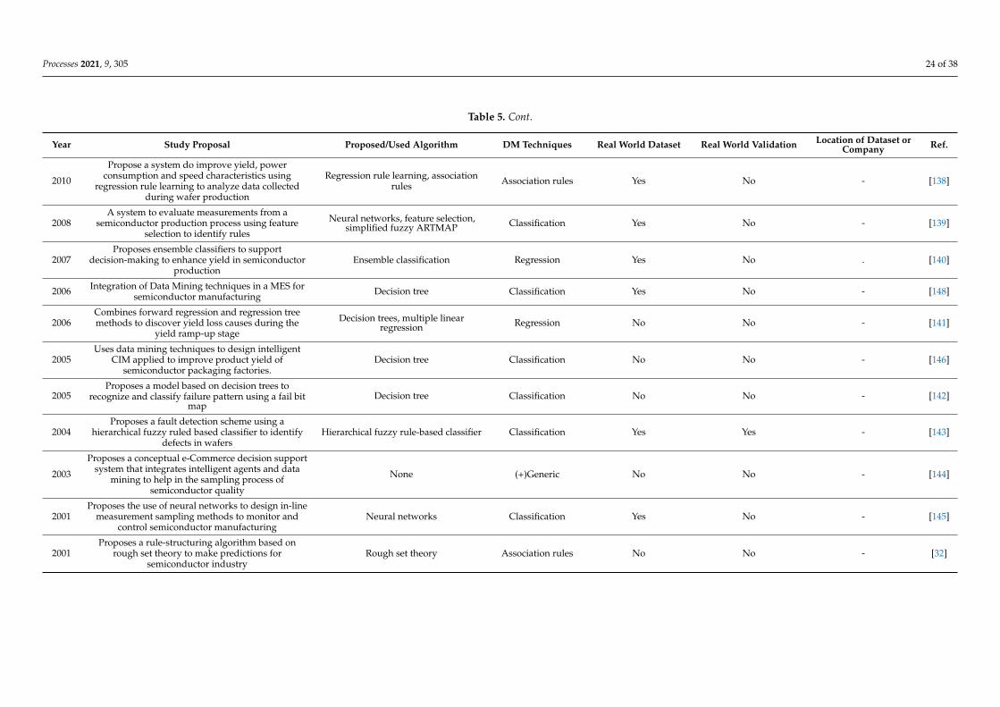
Processes 2021, 9, 305 24 of 38
Table 5. Cont.
Year Study Proposal Proposed/Used Algorithm DM Techniques Real World Dataset Real World Validation Location of Dataset orCompany Ref.
2010
Propose a system do improve yield, powerconsumption and speed characteristics using
regression rule learning to analyze data collectedduring wafer production
Regression rule learning, associationrules Association rules Yes No - [138]
2008A system to evaluate measurements from a
semiconductor production process using featureselection to identify rules
Neural networks, feature selection,simplified fuzzy ARTMAP Classification Yes No - [139]
2007Proposes ensemble classifiers to support
decision-making to enhance yield in semiconductorproduction
Ensemble classification Regression Yes No . [140]
2006 Integration of Data Mining techniques in a MES forsemiconductor manufacturing Decision tree Classification Yes No - [148]
2006Combines forward regression and regression treemethods to discover yield loss causes during the
yield ramp-up stage
Decision trees, multiple linearregression Regression No No - [141]
2005Uses data mining techniques to design intelligent
CIM applied to improve product yield ofsemiconductor packaging factories.
Decision tree Classification No No - [146]
2005Proposes a model based on decision trees to
recognize and classify failure pattern using a fail bitmap
Decision tree Classification No No - [142]
2004Proposes a fault detection scheme using a
hierarchical fuzzy ruled based classifier to identifydefects in wafers
Hierarchical fuzzy rule-based classifier Classification Yes Yes - [143]
2003
Proposes a conceptual e-Commerce decision supportsystem that integrates intelligent agents and data
mining to help in the sampling process ofsemiconductor quality
None (+)Generic No No - [144]
2001Proposes the use of neural networks to design in-line
measurement sampling methods to monitor andcontrol semiconductor manufacturing
Neural networks Classification Yes No - [145]
2001Proposes a rule-structuring algorithm based on
rough set theory to make predictions forsemiconductor industry
Rough set theory Association rules No No - [32]
Processes 2021, 9, 305 25 of 38
4.5. Data Mining Applications for Production and Production Scheduling
Traditional methods for production planning often require complex calculations anddo not always allow a prompt reaction to changes or short-term adjustments that mayarise. Given the size of the semiconductor production lines in a factory, sensors withinproduction equipment are capable of delivering enormous amounts of data. This data canbe, in turn, used not only for machine control, but also for production analysis purposes,especially real-time production planning. This has the potential to bring great advantages,especially in those industrial units in which the production is affected by frequent dynamicchanges in the orders to be processed or technical specifications. Additionally, machinelearning processes are able to recognize patterns and automatically learn and operationalizepractical forecast models from a wide variety of data sources and large amounts of data.Therefore, in the context of semiconductor manufacturing with its complex and numeroussubprocesses, numerous data mining applications are proposed for the production andproduction planning environment.
Table 6 depicts the articles addressing data mining applications for production insemiconductor manufacturing. A total of 16 papers were found in this category. This tableis structured as Table 2. It can be noticed that from 2009 until 2015 is when the bulk of thesestudies were published, then a four-year hiatus was observed. From 2019 can be noticedsome interest in the topic.
Many of the studies concerning production planning are focused on reducing cycletime. In [155], a new approach that is capable of integrating data mining that intends toforecast arrival rates and determining the allocation of interchangeable tool sets in orderto reduce the work in process (WIP) bubbles for cycle time reduction is proposed. Whilein another study [64], a cycle time forecasting model is developed by employing knowl-edge discovery in databases by following cross industry standards for data mining. Adata-mining approach for estimating the interval cycle time of each job in a semiconductormanufacturing system is proposed in [156] and a data mining methodology, which identi-fies key factors of the cycle time in a semiconductor manufacturing plant, which intends topredict its value is addressed in [157].
Scheduling is another concern in semiconductor manufacturing due to its vast numberof steps and jobs [158–160], confirmed by the majority of the identified studies in Table 6.Efficient order scheduling structures are required for balancing the production load andcapacity throughout all the production stages [161]. A data mining dynamic schedulingstrategy selection model that is able to respond to a constantly altering system statusfor a semiconductor manufacturing system is proposed in [18]. In [162] a data-drivenscheduling knowledge life-cycle management for an intelligent shop floor is proposedand validated through a simulation model of the semiconductor production line. As earlyas in 2004 scheduling challenges were a concern, evidenced by a study proposing anhierarchical clustering method in [163] that is able to discriminate groups according tothe similarity of the objects and used to schedule semiconductor manufacturing processes.In [164] a dynamic scheduling model, which is able to optimize the production featuressubset is proposed, and this model is capable of creating a SVM-based dynamic schedulingstrategy classification model for semiconductor manufacturing. A data-based schedulingframework and adaptive dispatching rule for semiconductor manufacturing is addressedin [165] by employing backward propagation neuronetworks (BPNNs). Finally, a shopfloor control system in semiconductor production by self-organizing map-based smartmulticontroller is given in [166]. This study, as all the scheduling studies, showed a bettersystem performance than the typical fixed decision scheduling rules.
Processes 2021, 9, 305 26 of 38
Table 6. Data mining applications for production in semiconductor manufacturing.
Year Study Proposal Proposed/Used Algorithm DMTechniques Real World Dataset Real World Validation Location of Dataset or
Company Refs.
2004
A decision tree algorithm and classification modelare proposed. Intelligent computer integrated
manufacturing (CIM) system is applied tosemiconductor packaging factories. The
manufacturing cycle time, the product yield, and thefrequency of holding lot were improved
Decision trees Classification Yes Yes - [167]
2020
A new approach that is able to integrate data miningthat intends to forecast arrival rates and determine
the allocation of interchangeable tool sets in order todecrease the work in process (WIP) bubbles for cycle
time reduction
Back-propagation neural network(BPNN) Classification Yes Yes Taiwan [155]
2019
A data-driven scheduling knowledge life-cyclemanagement for an intelligent shop floor andvalidated through a simulated model of the
semiconductor production line
Extreme learning machine (ELM),Online sequential extreme learning
machine (OS-ELM)Classification No No - [162]
2015
A data mining based dynamic scheduling strategyselection model which is able to respond to altering
system status in semiconductor manufacturingprocesses
genetic algorithmK-nearest neighbor algorithm Clustering Yes Yes - [18]
2015
A variation reduction of Turn Around Time (TAT) ina semiconductor manufacturing through a datamining-based technique for identifying the root
cause of TAT variation
Partial Least Squares Regression(PLSR) Regression No No - [168]
2014
A data mining framework that is capable ofintegrating fault detection and classification and
manufacturing execution system data for improvingthe overall usage effectiveness (OUE) for cost
reduction in a Chemical Mechanical Planarization(CMP) process
CHAID (Chi-Squared AutomaticInteraction
Detection) Decision TreesClassification Yes Yes Taiwan [169]
2014
A dynamic scheduling model which optimizesproduction features subset, and creates anSVM-based dynamic scheduling strategy
classification model for semiconductormanufacturing
Particle swarm optimization algorithm(BPSO), support vector machine (SVM) Classification Yes Yes China [164]
2013A noted cycle time forecasting model is developed by
employing knowledge discovery in databases byfollowing cross industry standards for data mining
Decision trees, Neural networks Classification Yes No - [64]
2013 A Data-based scheduling framework and adaptivedispatching rule for semiconductor manufacturing
Backward propagation neuro-network(BPNN), adaptive dispatching rule
(ADR)Classification Yes No - [165]
Processes 2021, 9, 305 27 of 38
Table 6. Cont.
Year Study Proposal Proposed/Used Algorithm DMTechniques Real World Dataset Real World Validation Location of Dataset or
Company Refs.
2011A cycle-time key factor identification and predictionin semiconductor manufacturing by employing data
mining and machine learning
Selective naive Bayesian classifier(SNBC) Conditional mutual
information maximization (CMIM)Classification No No - [170]
2012
A shop floor control system in semiconductorproduction by self-organizing map-based smartmulti-controller showing an improved system
performance than fixed decision scheduling rules
Self-organizing map (SOM) neuralnetwork Classification No No - [166]
2010
Gaussian Processes used for decentralizedscheduling with dispatching rule selection in
production scheduling for semiconductormanufacturing
Gaussian processes, neural networks Classification No No - [171]
2010
A machine learning algorithm capable ofimplementing an adaptive sequential (A-S) process
and accuracy guard band model for improved recipegeneration process development in the assembly
semiconductor manufacturing processes
Polynomial-based RSM ResponseSurface Methodology (RSM),
Adaptive-sequential (A-S) algorithmRegression Yes Yes Intel
(Malaysia) [172]
2009A data-mining approach for estimating the interval
cycle time of each job in a semiconductormanufacturing system
Look-ahead self-organization mapfuzzy-back-propagation network
(SOM-FBPN)Classification No No - [156,173]
2009
A data mining methodology which identifies keyfactors of the cycle time in a semiconductor
manufacturing plant which intends to predict itsvalue
Naïve Bayesian classifier (NBC),CRISP-DM (Cross-Industry Standard
Process for Data Mining)Classification No No - [157]
2004
A hierarchical clustering method that is able todiscriminate groups according to the similarity of the
objects and used to schedule semiconductormanufacturing processes
Agglomerative hierarchical clusteralgorithm Clustering No No - [163]
Processes 2021, 9, 305 28 of 38
5. Discussion
After analyzing all the studies collected in the sample, a few trends begin to be noticed.First, that studies regarding data mining applications in subprocesses such as ICs and maskdesign are very scarce. The same occurs with studies addressing wafer cutting, cleaningdrying, and polishing, while edge rounding and lapping subprocess has no dedicated study.This is better illustrated by Figure 10 in which a representation of several studies depictingdata mining applications in several subprocesses of semiconductor manufacturing can beseen. It is noticeable that the majority of studies are concentrated in 5–6 major steps. A fewstudies do not specify in which subprocess data mining techniques are applied, and theseare not represented in Figure 10.
Processes 2021, 9, x FOR PEER REVIEW 28 of 38
5. Discussion
After analyzing all the studies collected in the sample, a few trends begin to be no-
ticed. First, that studies regarding data mining applications in subprocesses such as ICs
and mask design are very scarce. The same occurs with studies addressing wafer cutting,
cleaning drying, and polishing, while edge rounding and lapping subprocess has no
dedicated study. This is better illustrated by Figure 10 in which a representation of sev-
eral studies depicting data mining applications in several subprocesses of semiconductor
manufacturing can be seen. It is noticeable that the majority of studies are concentrated in
5–6 major steps. A few studies do not specify in which subprocess data mining tech-
niques are applied, and these are not represented in Figure 10.
Figure 10. Representation of several studies depicting data mining applications in several subprocesses of semiconductor
manufacturing.
Another trend visible in the analyzed literature is the diverse use of data mining
techniques. The application of data mining in semiconductor manufacturing has a dif-
ferent focus depending on the subject areas concerning the manufacturing processes.
However, most articles address mainly the issues of quality control, maintenance, and
production. Predictive techniques, using algorithms as regression or decision trees, are
often used in semiconductor literature to estimate wafer quality [81], fault detection
[121,136], or cycle-time [170]. Classification techniques in quality control arise as a way to
classify defects [83], failures in bin maps [91], or production lots [131]. The exploration of
Figure 10. Representation of several studies depicting data mining applications in several subprocesses of semiconductormanufacturing.
Another trend visible in the analyzed literature is the diverse use of data miningtechniques. The application of data mining in semiconductor manufacturing has a differentfocus depending on the subject areas concerning the manufacturing processes. However,most articles address mainly the issues of quality control, maintenance, and production.Predictive techniques, using algorithms as regression or decision trees, are often used insemiconductor literature to estimate wafer quality [81], fault detection [121,136], or cycle-time [170]. Classification techniques in quality control arise as a way to classify defects [83],failures in bin maps [91], or production lots [131]. The exploration of yield loss causes [84]
Processes 2021, 9, 305 29 of 38
or failure diagnostics [98] is performed using techniques as rule induction, decision trees,and association rules.
Many opportunities and improvements can still be made. For example, the semicon-ductor companies could employ the internet of things and sensors to empower industrialunits with the capability of interpreting data and transmitting analytics, in real time, toan application that could provide insights and alerts to whom it may concern [174]. Thiswill allow these players to gather a high amount of data. However, even though internetof things and data mining applications represent a key opportunity for semiconductormanufacturing companies—one that they should start to pursue as soon as possible, whilethe use of data mining in the sector is still developing under the current upgrading envi-ronment. Nevertheless, the effectiveness and scale of the internet of things implementation,and with it a comprehensive use of data mining techniques, could depend on how fastindustry players can overcome some challenges [175]. In order to persevere and beingable to accompany the change speed and challenges, semiconductor companies are re-quired to adapt rapidly. Taking into account this dynamic, industrial units should embracedigitalization in an agile manner as well [176].
Limitations and Challenges
Even though employing data mining techniques has been very beneficial for thisindustry, as shown by all the studies used in this review, several disadvantages of datamining still exist and are as follows:
• Data mining systems can violate privacy. Absence of safety and security can be verydetrimental to its users and it can create miscommunication between employees, thusleading to genuine privacy concerns [177].
• Security is an important factor related to every data-oriented technology, and semicon-ductor manufacturing is not an exception. Data that is very critical might be a targetof malicious attacks [178].
• Too much and redundant information collection can be disadvantageous as irrelevantcollected information is a challenge [179,180].
• There is a possibility of information misuse through the mining process. Data miningsystem have to evolve in order to diminish the misuse of the information ratio [181].
• Accuracy of data mining techniques is another limitation [182]. Accuracy is an evalua-tion system of measurement on how well a data mining model can perform. Manycommon accuracy and error scores for regression and classification can occur. There-fore, improving accuracy becomes paramount.
• Several challenges of data integration and interoperability in data mining can occur.Data interoperability and data integration affect the performance of an organization.A comprehensive approach has to be made in order to address the challenges ininteroperability and integration [183,184].
• Missing and imbalanced data is a challenge in this industry. In cases in which datais imbalanced, the majority of classification algorithms have as a consequence aweak performance. Since wafer yield enhancement is a crucial performance index insemiconductor wafer manufacturing, key process steps must be cautiously selectedand managed [9].
• Data processing time is another limitation that has a significant impact on the availabletime since data preprocessing very often involves more than 50% of time and effort ofthe entire data analysis process [185].
This evolution of semiconductor manufacturing relies heavily on the big data ex-plosion in order to cope with the abovementioned data limitations and challenges of thesemiconductor industry. Especially, supporting greater volumes and lengthier archivesof data has allowed many solutions to correctly portray system dynamics, significantlysimplify intricate multivariate interactions of parameters, eliminate disturbances, and cleanand overcome data quality challenges. Data mining algorithms in such types of solutionsmust be rewritten in order to benefit from the parallel computation allowed by the high
Processes 2021, 9, 305 30 of 38
processing capacity and storage power with the purpose of processing data without con-suming too much time. However, an enormous amount of data and a wide range of datamining techniques does not mean necessarily more predictive capability and insights [186].Researchers and practitioners have to adapt data mining techniques in a manner so thatthese will be customized to specific applications in terms of data quality available data andobjective, among others.
Overall, through this review, some light was shed over the possible applications ofdata mining techniques in semiconductor manufacturing. Yet, given the sheer number ofsteps that this production process has, and due to its complexity, the number of studiesalready made is still scarce. Big data and data mining allowed for original and innovativeinsights through the analysis of large amounts of data and presenting correlations andopportunities that were not previously noticed. However, decision makers must decide andwhich data should be collected and employed and which questions must be answered [149].This signifies that the potential to apply these techniques in other subprocesses is enormousand is still left largely unexplored. Finally, by suffering constant and quick evolution, theneed to adapt these techniques to the newer processes in semiconductor manufacturing isanother opportunity to explore.
6. Conclusions
The production of semiconductors is a highly complex process, which entails severalsubprocesses that employ a diverse array of equipment. The size of the semiconductorssignifies a high number of units can be produced, which require huge amounts of datain order to be able to control and improve the semiconductor manufacturing process.Therefore, in this paper a structured review was made through a sample of 137 papersof the published articles in the scientific community regarding data mining applicationsin semiconductor manufacturing. A detailed bibliometric analysis was made. All datamining applications were classified in function of the application area. Five distinct areaswere identified: quality control, maintenance, production, decision support systems, andfinally, categorized as a whole, measurement, metrology, and instrumentation. Resultsshowed that quality was the most popular one, with 47 publications, making 34.3% of allpublications. Maintenance was an area in which only a few studies were made, highlightingthe gap and the opportunity for more studies to be made in this area.
The work performed in this study concerning data mining applications in semi-conductor manufacturing can have theoretical implications. The characterization andcategorization of several useful and successful cases can positively contribute to future re-search efforts of employing such a wide range of techniques with the purpose of increasingthe application and diffusion of data mining applications in semiconductor manufacturing.Knowledge of different models and algorithms could have positive implications for thedevelopment of theory, for understanding all the possible applications in different areas ofsemiconductor production, but also for the development of practice, since many of thesewere implemented and validated on the shop floor. However, as the literature review hasshown, many applications can still be made since several studies address only a specificstep of semiconductor manufacturing and documentation of real-life application are scarce.Additionally, recent data mining techniques and models have a great opportunity to beused since only a few studies exist. Finally, since the semiconductor manufacturing processis always evolving, the need to adapt these techniques to the newer process is anotherchallenge and opportunity to explore.
Overall, as seen from all the comprised studies from distinct steps of semiconductorproduction, the scope and functions of data mining techniques can be enhanced anddisseminated throughout the entire semiconductor manufacturing process in order toprovide, in real time, a proactive adjustment and advanced control decisions for the wholeprocess and the smart facilities. Therefore, more research should be made to employ andfacilitate smart production for Industry 4.0 in several industries for digital transformation
Processes 2021, 9, 305 31 of 38
and for upgrading existing manufacturing units. This will allow for an improving capabilityfor optimizing interrelated decisions and improving decision flexibility.
Author Contributions: Conceptualization and methodology, R.G. and P.E.-C.; software R.G.; vali-dation and investigation, R.G. and P.E.-C.; review and editing, E.M.G.R. All authors have read andagreed to the published version of the manuscript.
Funding: The authors acknowledge Fundação para a Ciência e a Tecnologia (FCT-MCTES) for itsfinancial support via the project UIDB/00667/2020 (UNIDEMI).
Institutional Review Board Statement: Not applicable.
Informed Consent Statement: Not applicable.
Data Availability Statement: Not applicable.
Conflicts of Interest: The authors declare no conflict of interest.
References1. Biebl, F.; Glawar, R.; Jalali, A.; Ansari, F.; Haslhofer, B.; de Boer, P.; Sihn, W. A Conceptual Model to Enable Prescriptive
Maintenance for Etching Equipment in Semiconductor Manufacturing. Proc. CIRP 2020, 88, 64–69. [CrossRef]2. Bui, P.-D.; Lee, C. Unified System Network Architecture: Flexible and Area-Efficient NoC Architecture with Multiple Ports and
Cores. Electronics 2020, 9, 1316. [CrossRef]3. Weber, A. Smart manufacturing in the semiconductor industry: An evolving nexus of business drivers, technologies, and
standards. In Smart Manufacturing; Soroush, M., Baldea, M., Edgar, T.F., Eds.; Elsevier: Amsterdam, The Netherlands, 2020;Chapter 3; pp. 59–105. ISBN 978-0-12-820028-5.
4. Hurtarte, J.S.; Wolsheimer, E.A.; Tafoya, L.M. Semiconductor Manufacturing Basics. In Understanding Fabless IC Technology;Newnes: Burlington, MA, USA, 2007; Chapter 4; pp. 41–45. ISBN 978-0-7506-7944-2.
5. Khakifirooz, M.; Chien, C.F.; Chen, Y.-J. Bayesian Inference for Mining Semiconductor Manufacturing Big Data for YieldEnhancement and Smart Production to Empower Industry 4.0. Appl. Soft Comput. 2018, 68, 990–999. [CrossRef]
6. Reis, M.S.; Gins, G. Industrial Process Monitoring in the Big Data/Industry 4.0 Era: From Detection, to Diagnosis, to Prognosis.Processes 2017, 5, 35. [CrossRef]
7. Lin, Y.-C.; Yeh, C.-C.; Chen, W.-H.; Hsu, K.-Y. Implementation Criteria for Intelligent Systems in Motor Production Line ProcessManagement. Processes 2020, 8, 537. [CrossRef]
8. Chen, T. Strengthening the Competitiveness and Sustainability of a Semiconductor Manufacturer with Cloud Manufacturing.Sustainability 2014, 6, 251–266. [CrossRef]
9. Lee, D.-H.; Yang, J.-K.; Lee, C.-H.; Kim, K.-J. A Data-Driven Approach to Selection of Critical Process Steps in the SemiconductorManufacturing Process Considering Missing and Imbalanced Data. J. Manuf. Syst. 2019, 52, 146–156. [CrossRef]
10. Hsu, C.-Y.; Chen, W.-J.; Chien, J.-C. Similarity Matching of Wafer Bin Maps for Manufacturing Intelligence to Empower Industry3.5 for Semiconductor Manufacturing. Comput. Ind. Eng. 2020, 142, 106358. [CrossRef]
11. Nakata, K.; Orihara, R.; Mizuoka, Y.; Takagi, K. A Comprehensive Big-Data-Based Monitoring System for Yield Enhancement inSemiconductor Manufacturing. IEEE Trans. Semicond. Manuf. 2017, 30, 339–344. [CrossRef]
12. Yang, X.-S. Data mining techniques. In Introduction to Algorithms for Data Mining and Machine Learning; Academic Press: London,UK, 2019; Chapter 6; pp. 109–128. ISBN 978-0-12-817216-2.
13. Chien, C.-F.; Wang, W.-C.; Cheng, J.-C. Data Mining for Yield Enhancement in Semiconductor Manufacturing and an EmpiricalStudy. Expert Syst. Appl. 2007, 33, 192–198. [CrossRef]
14. He, J.; Zhu, Y. Hierarchical Multi-Task Learning with Application to Wafer Quality Prediction. In Proceedings of the 2012 IEEE12th International Conference on Data Mining, Brussels, Belgium, 10–13 December 2012; pp. 290–298.
15. Jeong, M.K.; Lu, J.-C.; Huo, X.; Vidakovic, B.; Chen, D. Wavelet-Based Data Reduction Techniques for Process Fault Detection.Technometrics 2006, 48, 26–40. [CrossRef]
16. Susto, G.A.; Beghi, A. Dealing with Time-Series Data in Predictive Maintenance Problems. In Proceedings of the 2016 IEEE 21stInternational Conference on Emerging Technologies and Factory Automation (ETFA), Berlin, Germany, 6–9 September 2016;pp. 1–4.
17. Choi, J.; Jeong, M.K. Deep Autoencoder With Clipping Fusion Regularization on Multistep Process Signals for Virtual Metrology.IEEE Sens. Lett. 2019, 3, 1–4. [CrossRef]
18. Wenjing, W.; Yumin, M.; Fei, Q.; Xiang, G. Data Mining Based Dynamic Scheduling Approach for Semiconductor ManufacturingSystem. In Proceedings of the 2015 34th Chinese Control Conference (CCC), Hangzhou, China, 28–30 July 2015; pp. 2603–2608.
19. Khemiri, A.; Amine Hamri, M.E.; Frydman, C.; Pinaton, J. Improving Business Process in Semiconductor Manufacturingby Discovering Business Rules. In Proceedings of the 2018 Winter Simulation Conference (WSC ‘18), Gothenburg, Sweden,9–12 December 2018; pp. 3441–3448.
Processes 2021, 9, 305 32 of 38
20. Huang, C.-Y.; Lin, P.K.P. Application of Integrated Data Mining Techniques in Stock Market Forecasting. Cogent Econ. Financ.2014, 2, 929505. [CrossRef]
21. Tranfield, D.; Denyer, D.; Smart, P. Towards a Methodology for Developing Evidence-Informed Management Knowledge byMeans of Systematic Review. Br. J. Manag. 2003, 14, 207–222. [CrossRef]
22. Denyer, D.; Tranfield, D. Producing a systematic review. In The Sage Handbook of Organizational Research Methods; Buchanan, D.,Bryman, A., Eds.; Sage Publications Ltd.: London, UK, 2009; pp. 671–689.
23. Rousseau, D.M.; Manning, J.; Denyer, D. Evidence in Management and Organizational Science: Assembling the Field’s FullWeight of Scientific Knowledge Through Syntheses. Acad. Manag. Ann. 2008, 2, 475–515. [CrossRef]
24. Correia, E.; Carvalho, H.; Azevedo, S.G.; Govindan, K. Maturity Models in Supply Chain Sustainability: A Systematic LiteratureReview. Sustainability 2017, 9, 64. [CrossRef]
25. Wang, K. Applying Data Mining to Manufacturing: The Nature and Implications. J. Intell. Manuf. 2007, 18, 487–495. [CrossRef]26. Harding, J.A.; Shahbaz, M.; Kusiak, A. Data Mining in Manufacturing: A Review. J. Manuf. Sci. Eng. 2006, 128, 969–976.
[CrossRef]27. Buchanan, P.D.; Bryman, P.A. The Sage Handbook of Organizational Research Methods; Sage Publications Ltd.: London, UK, 2009;
ISBN 978-1-4462-4605-4.28. Yan, H.; Yang, N.; Peng, Y.; Ren, Y. Data Mining in the Construction Industry: Present Status, Opportunities, and Future Trends.
Autom. Constr. 2020, 119, 103331. [CrossRef]29. Galati, F.; Bigliardi, B. Industry 4.0: Emerging Themes and Future Research Avenues Using a Text Mining Approach. Comput. Ind.
2019, 109, 100–113. [CrossRef]30. Susto, G.A.; Schirru, A.; Pampuri, S.; McLoone, S.; Beghi, A. Machine Learning for Predictive Maintenance: A Multiple Classifier
Approach. IEEE Trans. Ind. Inform. 2015, 11, 812–820. [CrossRef]31. Famili, A.; Shen, W.-M.; Weber, R.; Simoudis, E. Data Preprocessing and Intelligent Data Analysis. IDA 1997, 1, 3–23. [CrossRef]32. Kusiak, A. Rough Set Theory: A Data Mining Tool for Semiconductor Manufacturing. IEEE Trans. Electron. Packag. Manufact.
2001, 24, 44–50. [CrossRef]33. Kumar, S.; Sharma, P.; Garg, K.C. Lotka’s Law and Institutional Productivity. Inf. Process. Manag. 1998, 34, 775–783. [CrossRef]34. Hsu, S.-C.; Chien, C.-F. Hybrid Data Mining Approach for Pattern Extraction from Wafer Bin Map to Improve Yield in Semicon-
ductor Manufacturing. Int. J. Prod. Econ. 2007, 107, 88–103. [CrossRef]35. Van Eck, N.J.; Waltman, L. Software Survey: VOSviewer, a Computer Program for Bibliometric Mapping. Scientometrics 2010, 84,
523–538. [CrossRef]36. Muñoz, J.A.M.; Viedma, E.H.; Espejo, A.L.S.; Cobo, M.J. Software Tools for Conducting Bibliometric Analysis in Science: An
up-to-Date Review. Prof. Inf. 2020, 29, 4.37. Sordan, J.E.; Oprime, P.C.; Pimenta, M.L.; Chiabert, P.; Lombardi, F. Lean Six Sigma in Manufacturing Process: A Bibliometric
Study and Research Agenda. TQM J. 2020, 32, 381–399. [CrossRef]38. Wellmann, P.J. Power Electronic Semiconductor Materials for Automotive and Energy Saving Applications—SiC, GaN, Ga2O3,
and Diamond. Z. Anorg. Allg. Chem. 2017, 643, 1312–1322. [CrossRef]39. Garlapati, S.K.; Divya, M.; Breitung, B.; Kruk, R.; Hahn, H.; Dasgupta, S. Printed Electronics Based on Inorganic Semiconductors:
From Processes and Materials to Devices. Adv. Mater. 2018, 30, 1707600. [CrossRef]40. Satpathy, R.; Pamuru, V. Silicon wafer manufacturing process. In Solar PV Power; Satpathy, R., Pamuru, V., Eds.; Academic Press:
London, UK, 2021; Chapter 3; pp. 53–70. ISBN 978-0-12-817626-9.41. Möller, H.J. Wafering of Silicon. In Semiconductors and Semimetals; Willeke, G.P., Weber, E.R., Eds.; Elsevier: Amsterdam,
The Netherlands, 2015; Volume 92, Chapter 2; pp. 63–109.42. Geng, N.; Jiang, Z. Capacity Planning for Semiconductor Wafer Fabrication with Uncertain Demand and Capacity. In Proceedings
of the 2007 IEEE International Conference on Automation Science and Engineering, Scottsdale, AZ, USA, 22–25 September 2007;pp. 100–105.
43. Satpathy, R.; Pamuru, V. Silicon crystal growth process. In Solar PV Power; Satpathy, R., Pamuru, V., Eds.; Academic Press: London,UK, 2021; Chapter 2; pp. 31–52. ISBN 978-0-12-817626-9. Available online: https://doi.org/10.1016/B978-0-12-817626-9.00002-2(accessed on 2 February 2021).
44. Tilli, M. Silicon wafers preparation and properties. In Handbook of Silicon Based MEMS Materials and Technologies, 3rd ed.; Tilli,M., Paulasto-Krockel, M., Petzold, M., Theuss, H., Motooka, T., Lindroos, V., Eds.; Elsevier: Amsterdam, The Netherlands, 2020;Chapter 4; pp. 93–110. ISBN 978-0-12-817786-0.
45. Gallagher, E.; Hibbs, M. Masks for micro- and nanolithography. In Nanolithography; Feldman, M., Ed.; Woodhead Publishing:Cambridge, UK, 2014; Chapter 5; pp. 158–178. ISBN 978-0-85709-500-8.
46. Cadien, K.C.; Nolan, L. Chapter 10—Chemical Mechanical Polishing Method and Practice. In Handbook of Thin Film Deposition,4th ed.; Seshan, K., Schepis, D., Eds.; William Andrew Publishing: Norwich, NY, USA, 2018; pp. 317–357. ISBN 978-0-12-812311-9.
47. Bao, H.; Chen, L.; Ren, B. A Study on the Pattern Effects of Chemical Mechanical Planarization with CNN-Based Models.Electronics 2020, 9, 1158. [CrossRef]
48. Zhang, Y.; Wagner, L.; Golbutsov, P. Importance of Wafer Flatness for CMP and Lithography. In Proceedings of the Metrology,Inspection, and Process Control for Microlithography XI, Santa Clara, CA, USA, 7 July 1997; International Society for Optics andPhotonics, 1997; Volume 3050, pp. 266–269. Available online: https://doi.org/10.1117/12.275916 (accessed on 2 February 2021).
Processes 2021, 9, 305 33 of 38
49. Ki, M.; Sungmin, K.; Taesung, K. Study on Effect of Back-Surface Treatment of Silicon Wafer in Photo Lithography Process afterCMP Process. In Proceedings of the 2015 International Conference on Planarization/CMP Technology (ICPT), Chandler, AZ,USA, 30 September–2 October 2015; pp. 1–3.
50. Jain, A. Ion Implantation for Semiconductor Processing. Radiat. Eff. 1982, 63, 39–46. [CrossRef]51. Zolper, J.C. Ion Implantation in Wide Bandgap Semiconductors. In Processing of Wide Band Gap Semiconductors; Pearton, S.J., Ed.;
William Andrew Publishing: Norwich, NY, USA, 2000; Chapter 7; pp. 300–353. ISBN 978-0-8155-1439-8.52. Rice, B.J. Extreme ultraviolet (EUV) lithography. In Nanolithography; Feldman, M., Ed.; Woodhead Publishing: Cambridge, UK,
2014; Chapter 2; pp. 42–79. ISBN 978-0-85709-500-8.53. Marconi, M.C.; Wachulak, P.W. Extreme Ultraviolet Lithography with Table Top Lasers. Prog. Quantum Electron. 2010, 34, 173–190.
[CrossRef]54. Buitrago, E.; Kulmala, T.S.; Fallica, R.; Ekinci, Y. EUV lithography process challenges. In Frontiers of Nanoscience; Robinson,
A., Lawson, R., Eds.; Materials and Processes for Next Generation Lithography; Elsevier: Amsterdam, The Netherlands, 2016;Chapter 4; Volume 11, pp. 135–176.
55. Kolasinski, K.W. Growth and Etching of Semiconductors. In Handbook of Surface Science; Hasselbrink, E., Lundqvist, B.I.,Eds.; Dynamics; North-Holland: Amsterdam, The Netherlands, 2008; Chapter 16; Volume 3, pp. 787–870. Available online:https://doi.org/10.1016/S1573-4331(08)00016-4 (accessed on 2 February 2021).
56. Chang, H.-Y.; Pan, W.-F.; Shih, M.-K.; Lai, Y.-S. Geometric Design for Ultra-Long Needle Probe Card for Digital Light ProcessingWafer Testing. Microelectron. Reliab. 2010, 50, 556–563. [CrossRef]
57. Sakamaki, R.; Horibe, M. Realization of Accurate On-Wafer Measurement Using Precision Probing Technique at Millimeter-WaveFrequency. IEEE Trans. Instrum. Meas. 2018, 67, 1940–1945. [CrossRef]
58. Sakamaki, R.; Horibe, M. Uncertainty Analysis Method Including Influence of Probe Alignment on On-Wafer Calibration Process.IEEE Trans. Instrum. Meas. 2019, 68, 1748–1755. [CrossRef]
59. Kuo, C.-H.; Hu, A.H.; Hung, L.H.; Yang, K.-T.; Wu, C.-H. Life Cycle Impact Assessment of Semiconductor Packaging Technologieswith Emphasis on Ball Grid Array. J. Clean. Prod. 2020, 276, 124301. [CrossRef]
60. Elshabini, A.A.; Barlow, F.; Wang, P.J. Electronic Packaging: Semiconductor Packages. In Reference Module in Materials Science andMaterials Engineering; Elsevier: Amsterdam, The Netherlands, 2017; ISBN 978-0-12-803581-8.
61. Sang, H.-Y.; Duan, P.-Y.; Li, J.-Q. An Effective Invasive Weed Optimization Algorithm for Scheduling Semiconductor Final TestingProblem. Swarm Evol. Comput. 2018, 38, 42–53. [CrossRef]
62. Chien, C.; Chen, L. Using Rough Set Theory to Recruit and Retain High-Potential Talents for Semiconductor Manufacturing.IEEE Trans. Semicond. Manuf. 2007, 20, 528–541. [CrossRef]
63. Geum, Y.; Jeon, J.; Seol, H. Identifying Technological Opportunities Using the Novelty Detection Technique: A Case of LaserTechnology in Semiconductor Manufacturing. Technol. Anal. Strateg. Manag. 2013, 25, 1–22. [CrossRef]
64. Tirkel, I. Forecasting Flow Time in Semiconductor Manufacturing Using Knowledge Discovery in Databases. Int. J. Prod. Res.2013, 51, 5536–5548. [CrossRef]
65. Han, H.; Gao, C.; Zhao, Y.; Liao, S.; Tang, L.; Li, X. Polycrystalline Silicon Wafer Defect Segmentation Based on Deep ConvolutionalNeural Networks. Pattern Recognit. Lett. 2020, 130, 234–241. [CrossRef]
66. Hsu, C.-Y.; Chiu, S.-C. A Two-Phase Non-Dominated Sorting Particle Swarm Optimization for Chip Feature Design to ImproveWafer Exposure Effectiveness. Comput. Ind. Eng. 2020, 147, 106669. [CrossRef]
67. Li, J.; Zhang, H.; Wang, Y.; Cui, H. A Review of the Applications of Data Mining for Semiconductor Quality Control. In Signal andInformation Processing, Networking and Computers; Wang, Y., Fu, M., Xu, L., Zou, J., Eds.; Lecture Notes in Electrical Engineering;Springer Singapore: Singapore, 2020; Volume 628, pp. 486–492. ISBN 9789811541629.
68. Gallo, C.; Capozzi, V. A Wafer Bin Map “Relaxed” Clustering Algorithm for Improving Semiconductor Production Yield. OpenComput. Sci. 2020, 10, 231–245. [CrossRef]
69. Kim, D.; Kang, S.; Cho, S. Expected Margin–Based Pattern Selection for Support Vector Machines. Expert Syst. Appl. 2020, 139,112865. [CrossRef]
70. Kim, E.; Cho, S.; Lee, B.; Cho, M. Fault Detection and Diagnosis Using Self-Attentive Convolutional Neural Networks forVariable-Length Sensor Data in Semiconductor Manufacturing. IEEE Trans. Semicond. Manuf. 2019, 32, 302–309. [CrossRef]
71. Jin, C.H.; Na, H.J.; Piao, M.; Pok, G.; Ryu, K.H. A Novel DBSCAN-Based Defect Pattern Detection and Classification Frameworkfor Wafer Bin Map. IEEE Trans. Semicond. Manuf. 2019, 32, 286–292. [CrossRef]
72. Kong, X.; Chang, J.; Niu, M.; Huang, X.; Wang, J.; Chang, S.I. Research on Real Time Feature Extraction Method for ComplexManufacturing Big Data. Int. J. Adv. Manuf. Technol. 2018, 99, 1101–1108. [CrossRef]
73. Tong, P.; Lu, J.; Yun, K. Fault Detection for Semiconductor Quality Control Based on Spark Using Data Mining Technology. InProceedings of the 2018 Chinese Control and Decision Conference (CCDC), Shenyang, China, 9–11 June 2018; pp. 4372–4377.
74. Lee, C.-Y.; Chen, B.-S. Mutually-Exclusive-and-Collectively-Exhaustive Feature Selection Scheme. Appl. Soft Comput. 2018, 68,961–971. [CrossRef]
75. Chien, C.-F.; Liu, C.-W.; Chuang, S.-C. Analysing Semiconductor Manufacturing Big Data for Root Cause Detection of Excursionfor Yield Enhancement. Int. J. Prod. Res. 2017, 55, 5095–5107. [CrossRef]
76. Susto, G.A.; Terzi, M.; Beghi, A. Anomaly Detection Approaches for Semiconductor Manufacturing. Proc. Manuf. 2017, 11,2018–2024. [CrossRef]
Processes 2021, 9, 305 34 of 38
77. Lee, T.; Kim, C.O. Statistical Comparison of Fault Detection Models for Semiconductor Manufacturing Processes. IEEE Trans.Semicond. Manuf. 2015, 28, 80–91. [CrossRef]
78. Sejdovic, S.; Hegenbarth, Y.; Ristow, G.H.; Schmidt, R. Proactive Disruption Management System: How Not to Be Surprised byUpcoming Situations. In Proceedings of the 10th ACM International Conference on Distributed and Event-based Systems, Irvine,CA, USA, 20–24 June 2016; Association for Computing Machinery: New York, NY, USA, 2016; pp. 281–288.
79. Fan, S.-K.S.; Lin, S.-C.; Tsai, P.-F. Wafer Fault Detection and Key Step Identification for Semiconductor Manufacturing UsingPrincipal Component Analysis, AdaBoost and Decision Tree. J. Ind. Prod. Eng. 2016, 33, 151–168. [CrossRef]
80. Butte, S.; Patil, S. Big Data and Predictive Analytics Methods for Modeling and Analysis of Semiconductor ManufacturingProcesses. In Proceedings of the 2016 IEEE Workshop on Microelectronics and Electron Devices (WMED), Boise, ID, USA, 15April 2016; pp. 1–5.
81. Zhu, Y.; He, J.; Lawrence, R.D. A General Framework for Predictive Tensor Modeling with Domain Knowledge. Data Min. Knowl.Disc. 2015, 29, 1709–1732. [CrossRef]
82. Aye, T.T.; Yang, F.; Wang, L.; Lee, G.K.K.; Li, X.; Hu, J.; Nguyen, M.C. Data Driven Framework for Degraded Pogo Pin Detectionin Semiconductor Manufacturing. In Proceedings of the 2015 IEEE 10th Conference on Industrial Electronics and Applications(ICIEA), Auckland, New Zealand, 15–17 June 2015; pp. 345–350.
83. Haddad, B.; Karam, L.; Ye, J.; Patel, N.; Braun, M. Multi-Feature Sparse-Based Defect Detection and Classification in Semicon-ductor Units. In Proceedings of the 2016 IEEE International Conference on Image Processing (ICIP), Phoenix, AZ, USA, 25–28September 2016; pp. 754–758.
84. Barkia, H.; Boucher, X.; Riche, R.L.; Beaune, P.; Girard, M.A.; Rozier, D. Semiconductor Yield Loss’ Causes Identification: AData Mining Approach. In Proceedings of the 2013 IEEE International Conference on Industrial Engineering and EngineeringManagement, Bangkok, Thailand, 10–13 December 2013; pp. 843–847.
85. Chien, C.-F.; Chang, K.-H.; Wang, W.-C. An Empirical Study of Design-of-Experiment Data Mining for Yield-Loss Diagnosis forSemiconductor Manufacturing. J. Intell. Manuf. 2014, 25, 961–972. [CrossRef]
86. Hessinger, U.; Chan, W.K.; Schafman, B.T. Data Mining for Significance in Yield-Defect Correlation Analysis. IEEE Trans. Semicond.Manuf. 2014, 27, 347–356. [CrossRef]
87. Liao, C.; Hsieh, T.; Huang, Y.; Chien, C. Similarity Searching for Defective Wafer Bin Maps in Semiconductor Manufacturing.IEEE Trans. Autom. Sci. Eng. 2014, 11, 953–960. [CrossRef]
88. Kerdprasop, K.; Kerdprasop, N. Tool Fault Analysis with Decision Tree Induction and Sequence Mining. AMM 2014, 548–549,703–707. [CrossRef]
89. Li, Z.; Baseman, R.J.; Zhu, Y.; Tipu, F.A.; Slonim, N.; Shpigelman, L. A Unified Framework for Outlier Detection in Trace DataAnalysis. IEEE Trans. Semicond. Manuf. 2014, 27, 95–103. [CrossRef]
90. Chien, C.; Chuang, S. A Framework for Root Cause Detection of Sub-Batch Processing System for Semiconductor ManufacturingBig Data Analytics. IEEE Trans. Semicond. Manuf. 2014, 27, 475–488. [CrossRef]
91. Chien, C.-F.; Hsu, S.-C.; Chen, Y.-J. A System for Online Detection and Classification of Wafer Bin Map Defect Patterns forManufacturing Intelligence. Int. J. Prod. Res. 2013, 51, 2324–2338. [CrossRef]
92. Park, E.; Lee, J.-H. Classifying Imbalanced Data Using an Svm Ensemble with K-Means Clustering in Semiconductor Test Process.In Proceedings of the Sixth International Conference on Machine Vision (ICMV 2013); International Society for Optics and Photonics:Bellingham, WA, USA, 2013; Volume 9067, p. 90672D.
93. Chien, C.-F.; Hsu, C.-Y.; Chen, P.-N. Semiconductor Fault Detection and Classification for Yield Enhancement and ManufacturingIntelligence. Flex. Serv. Manuf. J. 2013, 25, 367–388. [CrossRef]
94. Hsu, C.-Y.; Chien, C.-F.; Lai, Y.-C. Main Branch Decision Tree Algorithm for Yield Enhancement with Class Imbalance. InProceedings of the Intelligent Decision Technologies; Watada, J., Watanabe, T., Phillips-Wren, G., Howlett, R.J., Jain, L.C., Eds.;Springer: Berlin, Germany, 2012; pp. 235–244. Available online: https://doi.org/10.1007/978-3-642-29977-3_24 (accessed on 5February 2021).
95. Hsieh, T.; Liao, C.; Huang, Y.; Chien, C. A New Morphology-Based Approach for Similarity Searching on Wafer Bin Mapsin Semiconductor Manufacturing. In Proceedings of the 2012 IEEE 16th International Conference on Computer SupportedCooperative Work in Design (CSCWD), Wuhan, China, 23–25 May 2012; pp. 869–874.
96. Kerdprasop, K.; Kerdprasop, N. Feature Selection and Boosting Techniques to Improve Fault Detection Accuracy in the Semicon-ductor Manufacturing Process. In Proceedings of the IMECS—International Multi Conference Engineering Comput. Scientists,Hong Kong, China, 16–18 March 2011; Volume 1, pp. 398–403.
97. Zuo, L.; Liu, X.; He, J.; Wang, J.; Zheng, P.; Zhang, J. An Improved AdaBoost Tree-Based Method for Defective ProductsIdentification in Wafer Test. In Proceedings of the 2019 IEEE International Conference on Smart Manufacturing, IndustrialLogistics Engineering (SMILE), Hangzhou, China, 19–21 April 2019; pp. 64–68.
98. Bertino, E.; Catania, B.; Caglio, E. Applying Data Mining Techniques to Wafer Manufacturing. In Proceedings of the Principles ofData Mining and Knowledge Discovery; Zytkow, J.M., Rauch, J., Eds.; Springer: Berlin, Germany, 1999; pp. 41–50.
99. Wang, C.-H. Recognition of Semiconductor Defect Patterns Using Spatial Filtering and Spectral Clustering. Expert Syst. Appl.2008, 34, 1914–1923. [CrossRef]
100. Chih-Hsuan, W. Recognition of Semiconductor Defect Patterns Using Spectral Clustering. In Proceedings of the 2007 IEEEInternational Conference on Industrial Engineering and Engineering Management, Singapore, 2–5 December 2007; pp. 587–591.
Processes 2021, 9, 305 35 of 38
101. Chen, R.S.; Chang, C.C. Using Bayesian Networks to Build Data Mining Applications for a Semiconductor Cleaning Process.IJMPT 2007, 30, 386. [CrossRef]
102. Yip, W.; Law, K.; Lee, W. Forecasting Final/Class Yield Based on Fabrication Process E-Test and Sort Data. In Proceedings of the2007 IEEE International Conference on Automation Science and Engineering, Scottsdale, AZ, USA, 22-25 September 2007; pp.478–483.
103. Yip, W.K.; Lim, C.C.; Lee, W.J. Method for Proposing Sort Screen Thresholds Based on Modeling Etest/Sort-Class in SemiconductorManufacturing. In Proceedings of the 2008 IEEE International Conference on Automation Science and Engineering, Washington,DC, USA, 23–26 August 2008; pp. 236–241.
104. Wang, C.-H.; Wang, S.-J.; Lee, W.-D. Automatic Identification of Spatial Defect Patterns for Semiconductor Manufacturing. Int. J.Prod. Res. 2006, 44, 5169–5185. [CrossRef]
105. Li, T.-S.; Huang, C.-L.; Wu, Z.-Y. Data Mining Using Genetic Programming for Construction of a Semiconductor ManufacturingYield Rate Prediction System. J. Intell. Manuf. 2006, 17, 355–361. [CrossRef]
106. Gardner, R.M.; Bieker, J.; Elwell, S. Solving Tough Semiconductor Manufacturing Problems Using Data Mining. In Proceedings ofthe 2000 IEEE/SEMI Advanced Semiconductor Manufacturing Conference and Workshop. ASMC 2000 (Cat. No.00CH37072),Boston, MA, USA, 12–14 September 2000; pp. 46–55.
107. Gruber, H. The Yield Factor and the Learning Curve in Semiconductor Production. Appl. Econ. 1994, 26, 837–843. [CrossRef]108. Kinghorst, J.; Geramifard, O.; Luo, M.; Chan, H.-L.; Yong, K.; Folmer, J.; Zou, M.; Vogel-Heuser, B. Hidden Markov Model-Based
Predictive Maintenance in Semiconductor Manufacturing: A Genetic Algorithm Approach. In Proceedings of the 2017 13th IEEEConference on Automation Science and Engineering (CASE), Xi’an, China, 20–23 August 2017; pp. 1260–1267.
109. Hsu, C.-Y.; Chien, C.-F.; Chen, P.-N. Manufacturing Intelligence for Early Warning of Key Equipment Excursion for AdvancedEquipment Control in Semiconductor Manufacturing. J. Chin. Inst. Ind. Eng. 2012, 29, 303–313. [CrossRef]
110. Retersdorf, M.; Anand, A.; Drozda-Freeman, A.; McIntyre, M.; Song, X.; Wang, J. Use of Spatial Pattern Recognition (SPR) forEnhancing the Resolution and Identification of Rogue Tools in Manufacturing. In Proceedings of the 2008 IEEE/SEMI AdvancedSemiconductor Manufacturing Conference, Cambridge, MA, USA, 5–7 May 2008; pp. 200–205.
111. Tsuda, H.; Shirai, H.; Kawamura, E. A Precise Photolithography Process Control Method Using Virtual Metrology. Electron.Commun. Jpn. 2014, 97, 48–55. [CrossRef]
112. Chen, C.-H.; Zhao, W.-D.; Pang, T.; Lin, Y.-Z. Virtual Metrology of Semiconductor PVD Process Based on Combination ofTree-Based Ensemble Model. ISA Trans. 2020, 103, 192–202. [CrossRef] [PubMed]
113. Cai, H.; Feng, J.; Zhu, F.; Yang, Q.; Li, X.; Lee, J. Adaptive Virtual Metrology Method Based on Just-in-Time Reference and ParticleFilter for Semiconductor Manufacturing. Measurement 2021, 168, 108338. [CrossRef]
114. Park, C.; Kim, Y.; Park, Y.; Kim, S.B. Multitask Learning for Virtual Metrology in Semiconductor Manufacturing Systems. Comput.Ind. Eng. 2018, 123, 209–219. [CrossRef]
115. Maggipinto, M.; Beghi, A.; McLoone, S.; Susto, G.A. DeepVM: A Deep Learning-Based Approach with Automatic FeatureExtraction for 2D Input Data Virtual Metrology. J. Process. Control. 2019, 84, 24–34. [CrossRef]
116. Lenz, B.; Barak, B.; Leicht, C. Development of Smart Feature Selection for Advanced Virtual Metrology. In Proceedings of the 25thAnnual SEMI Advanced Semiconductor Manufacturing Conference (ASMC 2014), Saratoga Springs, NY, USA, 19–21 May 2014;pp. 145–150.
117. Ooi, M.P.; Joo, E.K.J.; Kuang, Y.C.; Demidenko, S.; Kleeman, L.; Chan, C.W.K. Getting More from the Semiconductor Test: DataMining With Defect-Cluster Extraction. IEEE Trans. Instrum. Meas. 2011, 60, 3300–3317. [CrossRef]
118. Lenz, B.; Barak, B.; Mührwald, J.; Leicht, C.; Lenz, B. Virtual Metrology in Semiconductor Manufacturing by Means of PredictiveMachine Learning Models. In Proceedings of the 2013 12th International Conference on Machine Learning and Applications,Washington, DC, USA, 4–7 December 2013; Volume 2, pp. 174–177.
119. Kupp, N.; Slamani, M.; Makris, Y. Correlating Inline Data with Final Test Outcomes in Analog/RF Devices. In Proceedings of the2011 Design, Automation Test in Europe, Grenoble, France, 14–18 March 2011; pp. 1–6.
120. Ul Haq, A.A.; Djurdjanovic, D. Dynamics-Inspired Feature Extraction in Semiconductor Manufacturing Processes. J. Ind. Inf.Integr. 2019, 13, 22–31. [CrossRef]
121. Kim, J.K.; Cho, K.C.; Lee, J.S.; Han, Y.S. Feature Selection Techniques for Improving Rare Class Classification in SemiconductorManufacturing Process. In Proceedings of the Big Data Technologies and Applications, Gwangju, Korea, 23–24 November 2017;Jung, J.J., Kim, P., Eds.; Springer International Publishing: Cham, Switzerland, 2017; pp. 40–47.
122. Abdelkader, I.; El-Sonbaty, Y.; El-Habrouk, M. Openmv: A Python Powered, Extensible Machine Vision Camera. arXiv 2017,arXiv:1711.10464.
123. Zhu, Y.; He, J. Co-Clustering Structural Temporal Data with Applications to Semiconductor Manufacturing. In Proceedings of the2014 IEEE International Conference on Data Mining, Shenzhen, China, 14–17 December 2014; pp. 1121–1126.
124. Lenz, B.; Barak, B. Data Mining and Support Vector Regression Machine Learning in Semiconductor Manufacturing to ImproveVirtual Metrology. In Proceedings of the 2013 46th Hawaii International Conference on System Sciences, Wailea, HI, USA, 7–10January 2013; pp. 3447–3456.
125. Susto, G.A.; Beghi, A.; Luca, C.D. A Virtual Metrology System for Predicting CVD Thickness with Equipment Variables andQualitative Clustering. In Proceedings of the ETFA 2011, Toulouse, France, 5–9 September 2011; pp. 1–4.
Processes 2021, 9, 305 36 of 38
126. St. Pierre, E.; Tuv, E. Robust, Non-Redundant Feature Selection for Yield Analysis in Semiconductor Manufacturing. In Proceedingsof the Advances in Data Mining. Applications and Theoretical Aspects; Perner, P., Ed.; Springer: Berlin, Germany, 2011; pp. 204–217.
127. Kang, P.; Kim, D.; Lee, H.; Doh, S.; Cho, S. Virtual Metrology for Run-to-Run Control in Semiconductor Manufacturing. ExpertSyst. Appl. 2011, 38, 2508–2522. [CrossRef]
128. Kang, P.; Lee, H.; Cho, S.; Kim, D.; Park, J.; Park, C.-K.; Doh, S. A Virtual Metrology System for Semiconductor Manufacturing.Expert Syst. Appl. 2009, 36, 12554–12561. [CrossRef]
129. Tsuda, H.; Shirai, H. Improvement of Photolithography Process by 2nd Generation Data Mining. In Proceedings of the 2006 IEEEInternational Symposium on Semiconductor Manufacturing, Tokyo, Japan, 25–27 September 2006; pp. 122–125.
130. Jung, U.; Jeong, M.K.; Lu, J.-A. Vertical-Energy-Thresholding Procedure for Data Reduction with Multiple Complex Curves. IEEETrans. Syst. Man Cybern. Part B 2006, 36, 1128–1138. [CrossRef] [PubMed]
131. Palma, F.D.; Nicolao, G.D.; Miraglia, G.; Donzelli, O.M. Process Diagnosis via Electrical-Wafer-Sorting Maps Classification.In Proceedings of the Fifth IEEE International Conference on Data Mining (ICDM’05), Houston, TX, USA, 27–30 November2005; p. 4.
132. Turban, E.; Aronson, J.; Liang, T.-P. Decision Support. Systems and Intelligent Systems, 7th ed. 2007. Available online: https://books.google.pt/books/about/Decision_Support_Systems_and_Intelligent.html?id=m0R5QgAACAAJ&redir_esc=y (accessedon 5 February 2021).
133. Hood, S.J. Detail vs. Simplifying Assumptions for Simulating Semiconductor Manufacturing Lines. In Proceedings of the NinthIEEE CHMT International Electronics Manufacturing Technology Symposium, Piscataway, NJ, USA, 12–17 February 1989; pp.103–108.
134. Narayanan, S.; Bodner, D.A.; Sreekanth, U.; Dilley, S.J.; Govindaraj, T.; McGinnis, L.F.; Mitchell, C.M. Object-Oriented Simulationto Support Operator Decision Making in Semiconductor Manufacturing. In Proceedings of the 1992 IEEE International Conferenceon Systems, Man, and Cybernetics, Chicago, IL, USA, 18–21 October 1992; pp. 1510–1515.
135. Casali, A.; Ernst, C. Discovering Correlated Parameters in Semiconductor Manufacturing Processes: A Data Mining Approach.IEEE Trans. Semicond. Manufact. 2012, 25, 118–127. [CrossRef]
136. Kerdprasop, K.; Kerdprasop, N. Data Preparation Techniques for Improving Rare Class Prediction. Available online: https://dl.acm.org/doi/10.5555/2039846.2039882 (accessed on 5 February 2021).
137. Kerdprasop, K.; Kerdprasop, N. A Data Mining Approach to Automate Fault Detection Model Development in the SemiconductorManufacturing Process. Int. J. Mech. 2011, 5, 10.
138. Weiss, S.M.; Baseman, R.J.; Tipu, F.; Collins, C.N.; Davies, W.A.; Singh, R.; Hopkins, J.W. Rule-Based Data Mining for YieldImprovement in Semiconductor Manufacturing. Appl. Intell. 2010, 33, 318–329. [CrossRef]
139. Sassenberg, C.; Weber, C.; Fathi, M.; Holland, A.; Montino, R. Feature Selection for Improving the Usability of ClassificationResults of High-Dimensional Data. DMIN 2008, 2, 197–201.
140. Braha, D.; Elovici, Y.; Last, M. Theory of Actionable Data Mining with Application to Semiconductor Manufacturing Control. Int.J. Prod. Res. 2007, 45, 3059–3084. [CrossRef]
141. Chen, A.; Hong, A.; Ho, O.; Liu, C.-W.; Huang, Y.-H. Sample Efficient Regression Trees (SERT) for Yield Loss Analysis. InProceedings of the 2006 IEEE International Symposium on Semiconductor Manufacturing, Tokyo, Japan, 25–27 September 2006;pp. 29–32.
142. Han, Y.; Kim, J.; Lee, C. Lecture Notes in Computer Science. Automatic Detection of Failure Patterns Using Data Mining. InKnowledge-Based Intelligent Information and Engineering Systems; Khosla, R., Howlett, R.J., Jain, L.C., Eds.; Springer: Berlin, Germany,2005; Volume 3682, pp. 1312–1316. ISBN 978-3-540-28895-4.
143. Lin, S.-Y.; Horng, S.-C.; Tsai, C.-H. Fault Detection of the Ion Implanter Using Classification Approach. In Proceedings of the 20045th Asian Control Conference, Melbourne, Australia, 20–23 July 2004; pp. 809–814.
144. Lee, J.H.; Park, S.C. Agent and Data Mining Based Decision Support System and Its Adaptation to a New Customer-CentricElectronic Commerce. Expert Syst. Appl. 2003, 25, 619–635. [CrossRef]
145. Jang, H.L.; Song, J.Y.; Sang, C.P. Design of Intelligent Data Sampling Methodology Based on Data Mining. IEEE Trans. Robot.Automat. 2001, 17, 637–649. [CrossRef]
146. Ruey-Shun, C.; Ruey-Chyi, W.; Chang, C.C. Using Data Mining Technology to Design an Intelligent CIM System for ICManufacturing. In Proceedings of the Sixth International Conference on Software Engineering, Artificial Intelligence, Towson,MD, USA, 23–25 May 2005; pp. 70–75.
147. Chen, L.-F.; Chien, C.-F. Manufacturing Intelligence for Class Prediction and Rule Generation to Support Human Capital Decisionsfor High-Tech Industries. Flex. Serv. Manuf. J. 2011, 23, 263–289. [CrossRef]
148. Chen, R.; Tsai, Y.; Chang, C. Design and Implementation of an Intelligent Manufacturing Execution System for SemiconductorManufacturing Industry. In Proceedings of the 2006 IEEE International Symposium on Industrial Electronics, Montreal, QC,Canada, 9–13 July 2006; pp. 2948–2953.
149. Anaya, A.; Henning, W.; Basantkumar, N.; Oliver, J. Yield Improvement Using Advanced Data Analytics. In Proceedings of the2019 30th Annual SEMI Advanced Semiconductor Manufacturing Conference (ASMC), Saratoga Springs, NY, USA, 6–9 May2019; pp. 1–5.
150. Mörzinger, B.; Loschan, C.; Kloibhofer, F.; Bleicher, F. A Modular, Holistic Optimization Approach for Industrial Appliances. Proc.CIRP 2019, 79, 551–556. [CrossRef]
Processes 2021, 9, 305 37 of 38
151. Hsu, C.-Y. An Analytic Framework of Design for Semiconductor Manufacturing. In Proceedings of the Asia Pacific BusinessProcess Management; Bae, J., Suriadi, S., Wen, L., Eds.; Springer International Publishing: Cham, Switzerland, 2015; pp. 128–137.
152. Park, S.H.; Park, C.; Kim, J.S.; Kim, S.; Baek, J.; An, D. Data Mining Approaches for Packaging Yield Prediction in the Post-Fabrication Process. In Proceedings of the 2013 IEEE International Congress on Big Data, Santa Clara, CA, USA, 27 June–2 July2013; pp. 363–368.
153. Kwak, D.-S.; Kim, K.-J. A Data Mining Approach Considering Missing Values for the Optimization of Semiconductor-Manufacturing Processes. Expert Syst. Appl. 2012, 39, 2590–2596. [CrossRef]
154. Dabbas, R.M.; Chen, H.-N. Mining Semiconductor Manufacturing Data for Productivity Improvement—An Integrated RelationalDatabase Approach. Comput. Ind. 2001, 45, 29–44. [CrossRef]
155. Chien, C.-F.; Kuo, C.-J.; Yu, C.-M. Tool Allocation to Smooth Work-in-Process for Cycle Time Reduction and an Empirical Study.Ann. Oper. Res. 2020, 290, 1009–1033. [CrossRef]
156. Lin, Y.C.; Chen, T.-C. Interval Cycle Time Estimation in a Semiconductor Manufacturing System with a Data-Mining Approach.Int. Rev. Comput. Softw. 2009, 4, 737–742.
157. Meidan, Y.; Lerner, B.; Hassoun, M.; Rabinowitz, G. Data Mining for Cycle Time Key Factor Identification and Prediction inSemiconductor Manufacturing. IFAC Proc. Vol. 2009, 42, 217–222. [CrossRef]
158. Pang, J.; Zhou, H.; Tsai, Y.-C.; Chou, F.-D. A Scatter Simulated Annealing Algorithm for the Bi-Objective Scheduling Problem forthe Wet Station of Semiconductor Manufacturing. Comput. Ind. Eng. 2018, 123, 54–66. [CrossRef]
159. Lee, Y.-H.; Chang, C.-T.; Wong, D.S.-H.; Jang, S.-S. Petri-Net Based Scheduling Strategy for Semiconductor ManufacturingProcesses. Chem. Eng. Res. Des. 2011, 89, 291–300. [CrossRef]
160. Chen, T. An Optimized Tailored Nonlinear Fluctuation Smoothing Rule for Scheduling a Semiconductor Manufacturing Factory.Comput. Ind. Eng. 2010, 58, 317–325. [CrossRef]
161. Wang, P.-S.; Yang, T.; Yu, L.-C. Lean-Pull Strategy for Order Scheduling Problem in a Multi-Site Semiconductor Crystal Ingot-Pulling Manufacturing Company. Comput. Ind. Eng. 2018, 125, 545–562. [CrossRef]
162. Ma, Y.; Lu, X.; Qiao, F. Data Driven Scheduling Knowledge Management for Smart Shop Floor. In Proceedings of the 2019 IEEE15th International Conference on Automation Science and Engineering (CASE), Vancouver, BC, Canada, 22–26 August 2019; pp.109–114.
163. Chun-Hai, H.; Shun-Feng, S. Hierarchical Clustering Methods for Semiconductor Manufacturing Data. In Proceedings of theIEEE International Conference on Networking, Sensing and Control, Taipei, Taiwan, 21–23 March 2004; Volume 2, pp. 1063–1068.
164. Ma, Y.; Chen, X.; Qiao, F.; Tian, K.; Lu, J. The Research and Application of a Dynamic Dispatching Strategy Selection ApproachBased on BPSO-SVM for Semiconductor Production Line. In Proceedings of the Proceedings of the 11th IEEE InternationalConference on Networking, Sensing and Control, Miami, FL, USA, 7–9 April 2014; pp. 74–79.
165. Li, L.; Zijin, S.; Jiacheng, N.; Fei, Q. Data-Based Scheduling Framework and Adaptive Dispatching Rule of Complex ManufacturingSystems. Int. J. Adv. Manuf. Technol. 2013, 66, 1891–1905. [CrossRef]
166. Shiue, Y.-R.; Guh, R.-S.; Tseng, T.-Y. Study on Shop Floor Control System in Semiconductor Fabrication by Self-OrganizingMap-Based Intelligent Multi-Controller. Comput. Ind. Eng. 2012, 62, 1119–1129. [CrossRef]
167. Wu, R.C.; Chen, R.S.; Fan, C.R. Design an Intelligent CIM System Based on Data Mining Technology for New ManufacturingProcesses. IJMPT 2004, 21, 487. [CrossRef]
168. Chong, I.-G.; Zhu, C.; Wu, Y. Data Mining Analysis of Turnaround Time Variation in a Semiconductor Manufacturing Line.ICORES 2015, 1, 185–189. [CrossRef]
169. Chien, C.-F.; Diaz, A.C.; Lan, Y.-B. A Data Mining Approach for Analyzing Semiconductor MES and FDC Data to Enhance OverallUsage Effectiveness (OUE). Int. J. Comput. Intell. Syst. 2014, 7, 52–65. [CrossRef]
170. Meidan, Y.; Lerner, B.; Rabinowitz, G.; Hassoun, M. Cycle-Time Key Factor Identification and Prediction in SemiconductorManufacturing Using Machine Learning and Data Mining. IEEE Trans. Semicond. Manuf. 2011, 24, 237–248. [CrossRef]
171. Scholz-Reiter, B.; Heger, J.; Hildebrandt, T. Gaussian Processes for Dispatching Rule Selection in Production Scheduling:Comparison of Learning Techniques. In Proceedings of the 2010 IEEE International Conference on Data Mining Workshops,Sydney, Australia, 13–17 December 2010; pp. 631–638.
172. Lee, W.; Soon-Chuan, O. Learning from Small Data Sets to Improve Assembly Semiconductor Manufacturing Processes. InProceedings of the 2010 The 2nd International Conference on Computer and Automation Engineering (ICCAE), Singapore,Singapore, 26–28 February 2010; Volume 2, pp. 50–54.
173. Chen, T. A Hybrid Look-Ahead SOM-FBPN and FIR System for Wafer-Lot-Output Time Prediction and Achievability Evaluation.Int. J. Adv. Manuf. Technol. 2007, 35, 575–586. [CrossRef]
174. Ciacchella, J.; Richard, C.; Zhang, N. IoT Opportunity in the World of Semiconductor Companies. 2018, pp. 1–31. Availableonline: https://www2.deloitte.com/content/dam/Deloitte/us/Documents/technology/us-semiconductor-internet-of-things.pdf (accessed on 5 February 2021).
175. Bauer, H.; Patel, M.; Veira, J. Internet of Things: Opportunities and Challenges for Semiconductor Companies. 2015. Availableonline: https://www.mckinsey.com/industries/semiconductors/our-insights/internet-of-things-opportunities-and-challenges-for-semiconductor-companies (accessed on 5 February 2021).
176. Misrudin, F.; Foong, L.C. Digitalization in Semiconductor Manufacturing- Simulation Forecaster Approach in Managing Manu-facturing Line Performance. Proc. Manuf. 2019, 38, 1330–1337. [CrossRef]
Processes 2021, 9, 305 38 of 38
177. Javid, T.; Gupta, M.K.; Gupta, A. A Hybrid-Security Model for Privacy-Enhanced Distributed Data Mining. J. King Saud Univ.Comput. Inf. Sci. 2020. [CrossRef]
178. Dogan, A.; Birant, D. Machine Learning and Data Mining in Manufacturing. Expert Syst. Appl. 2021, 166, 114060. [CrossRef]179. Hand, D.J.; Adams, N.M. Data Mining. In Wiley StatsRef: Statistics Reference Online; American Cancer Society: Atlanta, GA, USA,
2015; pp. 1–7. ISBN 978-1-118-44511-2.180. García, S.; Luengo, J.; Herrera, F. Data Preprocessing in Data Mining; Springer: New York, NY, USA, 2015; ISBN 978-3-319-10246-7.181. Silva, J.; Cubillos, J.; Villa, J.V.; Romero, L.; Solano, D.; Fernández, C. Preservation of Confidential Information Privacy and
Association Rule Hiding for Data Mining: A Bibliometric Review. Proc. Comput. Sci. 2019, 151, 1219–1224. [CrossRef]182. Galdi, P.; Tagliaferri, R. Data Mining: Accuracy and Error Measures for Classification and Prediction. In Encyclopedia of
Bioinformatics and Computational Biology; Ranganathan, S., Gribskov, M., Nakai, K., Schönbach, C., Eds.; Academic Press: Oxford,UK, 2019; pp. 431–436. ISBN 978-0-12-811432-2.
183. Da Silva Serapião Leal, G.; Guédria, W.; Panetto, H. Interoperability Assessment: A Systematic Literature Review. Comput. Ind.2019, 106, 111–132. [CrossRef]
184. Kadadi, A.; Agrawal, R.; Nyamful, C.; Atiq, R. Challenges of Data Integration and Interoperability in Big Data. In Proceedings ofthe 2014 IEEE International Conference on Big Data (Big Data), Washington, DC, USA, 27–30 October 2014; pp. 38–40.
185. Ramírez-Gallego, S.; Krawczyk, B.; García, S.; Wozniak, M.; Herrera, F. A Survey on Data Preprocessing for Data Stream Mining:Current Status and Future Directions. Neurocomputing 2017, 239, 39–57. [CrossRef]
186. Moyne, J.; Iskandar, J. Big Data Analytics for Smart Manufacturing: Case Studies in Semiconductor Manufacturing. Processes2017, 5, 39. [CrossRef]