A Programmable Frequency Divider Having a Wide Division ...
124
University of Tennessee, Knoxville University of Tennessee, Knoxville TRACE: Tennessee Research and Creative TRACE: Tennessee Research and Creative Exchange Exchange Doctoral Dissertations Graduate School 5-2007 A Programmable Frequency Divider Having a Wide Division Ratio A Programmable Frequency Divider Having a Wide Division Ratio Range, and Close-to-50% Output Duty-Cycle Range, and Close-to-50% Output Duty-Cycle Mo Zhang University of Tennessee - Knoxville Follow this and additional works at: https://trace.tennessee.edu/utk_graddiss Part of the Electrical and Computer Engineering Commons Recommended Citation Recommended Citation Zhang, Mo, "A Programmable Frequency Divider Having a Wide Division Ratio Range, and Close-to-50% Output Duty-Cycle. " PhD diss., University of Tennessee, 2007. https://trace.tennessee.edu/utk_graddiss/199 This Dissertation is brought to you for free and open access by the Graduate School at TRACE: Tennessee Research and Creative Exchange. It has been accepted for inclusion in Doctoral Dissertations by an authorized administrator of TRACE: Tennessee Research and Creative Exchange. For more information, please contact [email protected].
-
Upload
khangminh22 -
Category
Documents
-
view
2 -
download
0
Transcript of A Programmable Frequency Divider Having a Wide Division ...
University of Tennessee, Knoxville University of Tennessee, Knoxville
TRACE: Tennessee Research and Creative TRACE: Tennessee Research and Creative
Exchange Exchange
Doctoral Dissertations Graduate School
5-2007
A Programmable Frequency Divider Having a Wide Division Ratio A Programmable Frequency Divider Having a Wide Division Ratio
Range, and Close-to-50% Output Duty-Cycle Range, and Close-to-50% Output Duty-Cycle
Mo Zhang University of Tennessee - Knoxville
Follow this and additional works at: https://trace.tennessee.edu/utk_graddiss
Part of the Electrical and Computer Engineering Commons
Recommended Citation Recommended Citation Zhang, Mo, "A Programmable Frequency Divider Having a Wide Division Ratio Range, and Close-to-50% Output Duty-Cycle. " PhD diss., University of Tennessee, 2007. https://trace.tennessee.edu/utk_graddiss/199
This Dissertation is brought to you for free and open access by the Graduate School at TRACE: Tennessee Research and Creative Exchange. It has been accepted for inclusion in Doctoral Dissertations by an authorized administrator of TRACE: Tennessee Research and Creative Exchange. For more information, please contact [email protected].

To the Graduate Council:
I am submitting herewith a dissertation written by Mo Zhang entitled "A Programmable
Frequency Divider Having a Wide Division Ratio Range, and Close-to-50% Output Duty-Cycle." I
have examined the final electronic copy of this dissertation for form and content and
recommend that it be accepted in partial fulfillment of the requirements for the degree of Doctor
of Philosophy, with a major in Electrical Engineering.
Syed Kamrul Islam, Major Professor
We have read this dissertation and recommend its acceptance:
Benjamin J. Blalock, Charles L. Britton, Jr., Xiaobing Feng
Accepted for the Council:
Carolyn R. Hodges
Vice Provost and Dean of the Graduate School
(Original signatures are on file with official student records.)
To the Graduate Council: I am submitting herewith a dissertation written by Mo Zhang entitled “A Programmable
Frequency Divider Having a Wide Division Ratio Range, and Close-to-50% Output
Duty-Cycle.” I have examined the final electronic copy of this dissertation for form and
content and recommend that it be accepted in partial fulfillment of the requirements for
the degree of Doctor of Philosophy, with a major in Electrical Engineering.
Syed Kamrul Islam
Major Professor
We have read this dissertation and recommend its acceptance: Benjamin J. Blalock
Charles L. Britton, Jr.
Xiaobing Feng
Accepted for the Council:
Carolyn Hodges
Vice Provost and
Dean of the Graduate School
(Original signatures are on file with official student records.)
A Programmable Frequency Divider Having a Wide Division
Ratio Range, and Close-to-50% Output Duty-Cycle
A Dissertation Presented for the
Doctor of Philosophy Degree
The University of Tennessee, Knoxville
Mo Zhang May, 2007

ii
Acknowledgements
I would like to thank my major advisor, Dr. Syed Kamrul Islam, for providing me with
the opportunity to carry out this research project, which enabled me to gain invaluable
experiences in RF and mixed-signal integrated circuit design. I greatly appreciate his
guidance, encouragement and continuous support for this research projects during the
past six years. I would also like to thank my committee members: Dr. Benjamin J.
Blalock, Dr. Charles Britton, and Dr. Xiaobing Feng, for reviewing my dissertation and
providing helpful advice. Dr. Benjamin J. Blalock constantly helped me with analog
electronic circuit design and gave me endless encouragement. I thank Dr. Charles Britton
for teaching me the principles of RF integrated circuit design and providing me with
valuable advice related to the RF circuit design. I would also like to thank Dr. Xiaobing
Feng for giving me very helpful feedbacks about my dissertation.
I thank Dr. Donald W. Bouldin for teaching me four courses related to digital integrated
circuit design and helping me with my dissertation. I appreciate Dr. Aly Fathy for
teaching me microwave circuit theories and allowing me to use his laboratory facilities
for RF testing. I also thank Dr. Michael J. Roberts for teaching me very useful knowledge
about signal processing and random processes. In addition, I would like to acknowledge
MOSIS for providing the great opportunities for fabricating several integrated chips for
under MOSIS Educational Program (MEP). Without these opportunities, it would be
impossible for me to verify the proposed designs.

iii
I would like to thank my fellow graduate research assistant, Rajagopal Vijayaraghavan,
for his help in the research of RF integrated circuit. I learned many practical theories and
methods from him. I also learned a lot of valuable knowledge from Wenchao Qu, my
fellow graduate research assistant, during the past several years. I would also like to
thank Suheng Chen for his help with cadence usage and layout. Graduate assistants of Dr.
Aly Fathy, Cemin Zhang and Song Lin also gave me a lot of help during the testing.
Each student in my lab and Dr. Benjamin J. Blalock’s lab gave me a lot of help and
friendly support.
I am very grateful to have the opportunity to finish my Ph.D. program in ECE department
of the University of Tennessee. A number of professors in the department taught me
valuable knowledge. I thank all of the professors who have instructed me or helped me.
Finally, I would especially like to thank my husband, Minfang Tao, for his endless
support and encouragement. I also thank my family and many other friends for their
support and advice.
iv
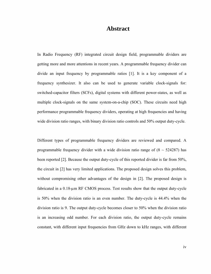
Abstract
In Radio Frequency (RF) integrated circuit design field, programmable dividers are
getting more and more attentions in recent years. A programmable frequency divider can
divide an input frequency by programmable ratios [1]. It is a key component of a
frequency synthesizer. It also can be used to generate variable clock-signals for:
switched-capacitor filters (SCFs), digital systems with different power-states, as well as
multiple clock-signals on the same system-on-a-chip (SOC). These circuits need high
performance programmable frequency dividers, operating at high frequencies and having
wide division ratio ranges, with binary division ratio controls and 50% output duty-cycle.
Different types of programmable frequency dividers are reviewed and compared. A
programmable frequency divider with a wide division ratio range of (8 ~ 524287) has
been reported [2]. Because the output duty-cycle of this reported divider is far from 50%,
the circuit in [2] has very limited applications. The proposed design solves this problem,
without compromising other advantages of the design in [2]. The proposed design is
fabricated in a 0.18-μm RF CMOS process. Test results show that the output duty-cycle
is 50% when the division ratio is an even number. The duty-cycle is 44.4% when the
division ratio is 9. The output duty-cycle becomes closer to 50% when the division ratio
is an increasing odd number. For each division ratio, the output duty-cycle remains
constant, with different input frequencies from GHz down to kHz ranges, with different
v
temperatures and power supply voltages. This thesis provides an explanation of the
design details and test results.
A Phase Locked-Loop (PLL) based frequency synthesizer can generate different output
frequencies. A programmable frequency divider is an important component of this type
of PLL. Since bandwidth is expensive, it is preferred to reduce the frequency channel
distance of a frequency synthesizer. Using a fractional programmable divider, the
frequency channel distance of a PLL can be reduced, without reducing the reference
frequency or increasing the settling time of the PLL. A frequency synthesizer with a
programmable fractional divider is designed and fabricated. A brief description of the
PLL design and test results are presented in this dissertation.
vi
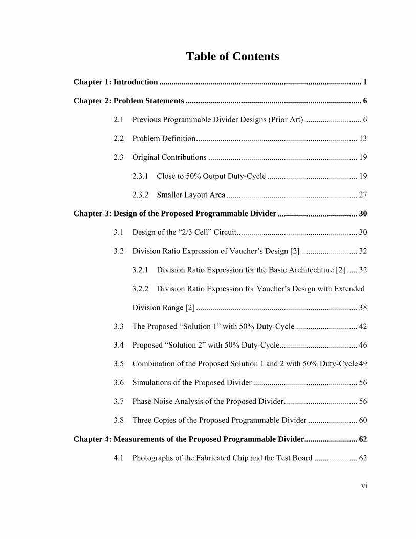
Table of Contents
Chapter 1: Introduction ................................................................................................... 1
Chapter 2: Problem Statements ...................................................................................... 6
2.1 Previous Programmable Divider Designs (Prior Art) ............................ 6
2.2 Problem Definition............................................................................... 13
2.3 Original Contributions ......................................................................... 19
2.3.1 Close to 50% Output Duty-Cycle ............................................ 19
2.3.2 Smaller Layout Area ................................................................ 27
Chapter 3: Design of the Proposed Programmable Divider ....................................... 30
3.1 Design of the “2/3 Cell” Circuit........................................................... 30
3.2 Division Ratio Expression of Vaucher’s Design [2]............................ 32
3.2.1 Division Ratio Expression for the Basic Architechture [2] ..... 32
3.2.2 Division Ratio Expression for Vaucher’s Design with Extended
Division Range [2] ............................................................................... 38
3.3 The Proposed “Solution 1” with 50% Duty-Cycle .............................. 42
3.4 Proposed “Solution 2” with 50% Duty-Cycle...................................... 46
3.5 Combination of the Proposed Solution 1 and 2 with 50% Duty-Cycle 49
3.6 Simulations of the Proposed Divider ................................................... 56
3.7 Phase Noise Analysis of the Proposed Divider.................................... 56
3.8 Three Copies of the Proposed Programmable Divider ........................ 60
Chapter 4: Measurements of the Proposed Programmable Divider.......................... 62
4.1 Photographs of the Fabricated Chip and the Test Board ..................... 62
vii
4.2 Test Results of the Proposed Divider................................................... 62
Chapter 5: A Fractional Programmable PLL.............................................................. 80
5.1 Introduction of the Programmable PLL ............................................... 80
5.2 A Fractional Programmable PLL......................................................... 85
5.2.1 A Fractional Programmable Frequency Divider ...................... 86
5.2.2 The LC VCO............................................................................ 88
5.2.3 The Loop Filter ........................................................................ 93
5.2.4 Test Results .............................................................................. 94
Chapter 6: Conclusions and Future Work ................................................................... 98
References...................................................................................................................... 101
Vita ................................................................................................................................. 108
viii
List of Tables
Table 1: Literature review of the published programmable frequency dividers...........7
Table 2: Performance of the proposed divider for various process-voltage-
temperature… ...............................................................................................57
Table 3: Comparison of the calculated and the measured results of the proposed
divider for the input frequency of 2.9 GHz...................................................68
Table 4: Comparison of the calculated and the measured results of the proposed
divider for the input frequency of 500 MHz.................................................68
Table 5: Comparison of the calculated and the measured results of the proposed
divider for the input frequency of 50 MHz...................................................69
Table 6: Comparison of the calculated and the measured results of the proposed
divider for the input frequency of 10 MHz...................................................69
Table 7: Comparison of the calculated and the measured results of the proposed
divider for the input frequency of 1 MHz.....................................................70
Table 8: Comparison of the calculated and the measured results of the proposed
divider for the input frequency of 100 kHz. .................................................70
Table 9: Comparison of the calculated and the measured results of the proposed
divider for the input frequency of 10 kHz. ...................................................71
Table 10: Comparison of the calculated and the measured results of the proposed
divider for the input frequency of 1 kHz. .....................................................71
ix
List of Figures
Figure 1: Fundamentals of frequency dividers: (a) function of a frequency divider, and
(b) classification of frequency dividers...........................................................2
Figure 2: An application of switched-capacitor filters (SCFs): (a) the corner frequency
of a SCF could be adjusted by changing the clock frequency, and (b) SCFs
could be used in equalizers for audio systems. ...............................................3
Figure 3: Clock and power control of digital systems....................................................5
Figure 4: System-on-a-chip (SOC) needs multiple clock signals in a wide frequency
range [3]. .........................................................................................................5
Figure 5: Schematics of a previously reported programmable counter [9]: (a) the top-
level block diagram, and (b) the end-of-count (EOC) detector. .....................9
Figure 6: The block diagram of a previously reported programmable divider with
division ratios N×P+S [4]. ..............................................................................9
Figure 7: A published programmable frequency divider [2]: (a) the block diagram of
the basic architecture (2n ≤ N ≤ 2n+1-1), where N is the division ratio, and (b)
the circuit diagram with extended division range (2min ≤ N ≤ 2max+1-1), (in
this figure max = n, min = n–2). ...................................................................11
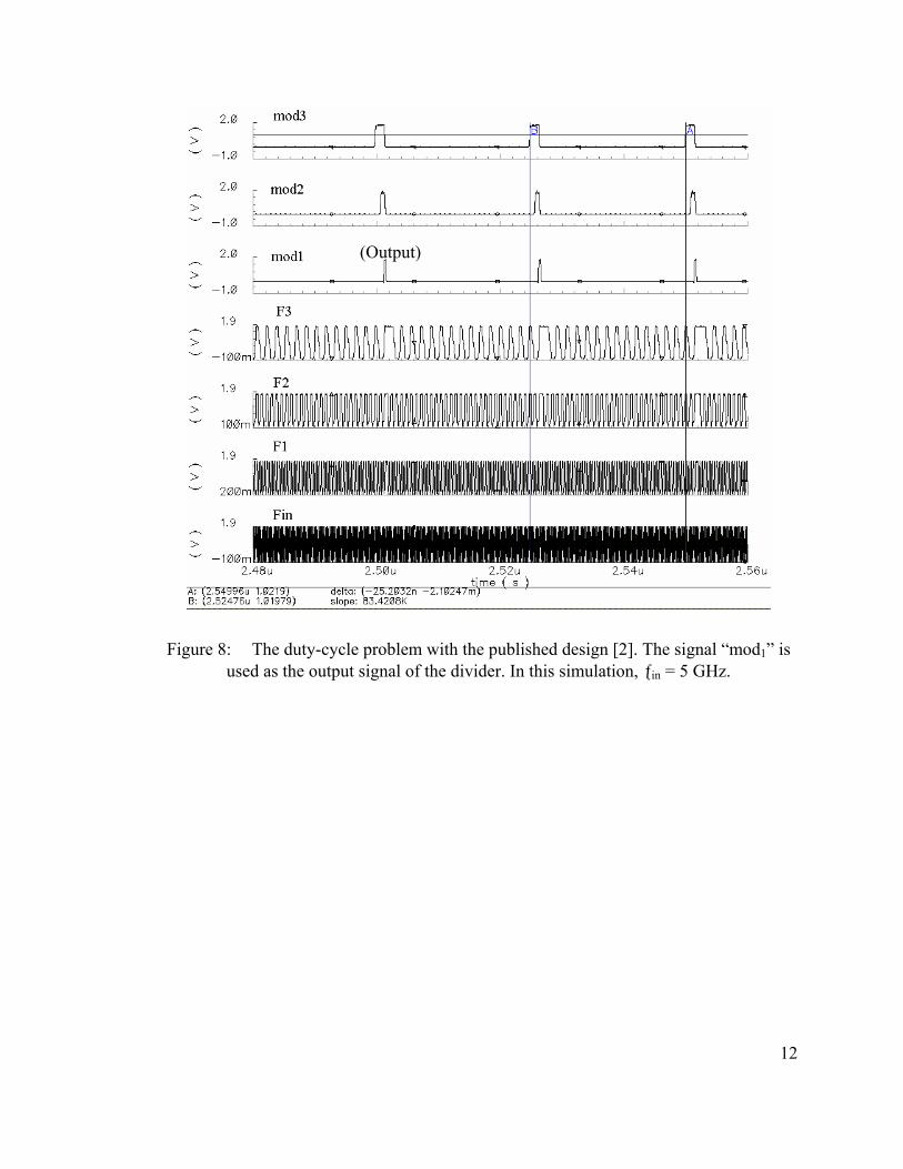
Figure 8: The duty-cycle problem with the published design [2]. The signal “mod1” is
used as the output signal of the divider. In this simulation, ƒin = 5 GHz......12
Figure 9: Vaucher’s design [2] has low capability to drive other circuits....................14
Figure 10: A standard master-slave D-Flip-Flop............................................................15
x
Figure 11: The maximum operating frequency of a master-slave DFF vs. duty-cycle of
the clock signal. ............................................................................................15
Figure 12: Comparison of the output duty-cycle of: (a) the prior art [2], and (b) the
proposed design. ...........................................................................................20
Figure 13: A switched capacitor viewed as a resistor: (a) the equivalent resistor, (b) a
switched capacitor, (c) the non-overlapping clock signal for the switched
capacitor, (d) when Φ1 is high, and (e) when Φ2 is high. .............................22
Figure 14: The principle of a switched capacitor filter (low-pass). ...............................23
Figure 15: The block diagram showing the development of multi-frequency clock
signals for SOCs, which needs multiple clocks and mostly with 50% duty-
cycle on the same chip. .................................................................................25
Figure 16: Block diagram of clock control and low power states for Intel® Pentium®
M Processor with 2-MB L2 cache and 533-MHz front side bus [23] for
wireless laptop computer. .............................................................................26
Figure 17: Comparison of the previous design [2] and the proposed design: schematics
of: (a) a “2/3 cell”, (b) previous “AND-latch”, (c) proposed “AND-latch” for
the first “2/3 cell” stage, (d) proposed “AND-latch” for the 2nd – the end
“2/3 cell” stages, and (e) proposed D-latch in the “2/3 cell”. .......................28
Figure 18: Schematics of the basic architecture of Vaucher’s programmable divider [2],
with the following number of the “2/3 cell” stages: (a) 1, (b) 2, and (c) n...33
Figure 19: Vaucher’s design with extended division range (2min ≤ N ≤ 2max+1-1) [2]....38
Figure 20: Schematic of the proposed “Solution 1” to generate output signal with 50%
duty-cycle......................................................................................................43
xi
Figure 21: Schematics of: (a) a 1-bit half adder, and (b) a 1-bit full adder....................43
Figure 22: Schematics of the proposed “Solution 2” for the division ratios of “2r - 1”
with 50% output duty-cycle: (a) top level scheme, (b) circuit to generate
“pulseout” in each “2/3 cell”, and (c) the “on edge” judgment circuit...........47
Figure 23: Combination of “Solution 1” and “Solution 2” in the proposed design. ......50
Figure 24: Division ratio judgment circuit. ....................................................................51
Figure 25: A more detailed schematic of the top-level proposed design. ......................55
Figure 26: Phase noise simulation of the proposed “2/3 cell”: (a) 1st stage, ƒin = 2.4
GHz, division ratio = 3, (b) the slow “2/3 cell”, ƒin = 100 MHz, division
ratio = 3. ........................................................................................................60
Figure 27: Schematic of the high frequency buffer: (a) one differential cell, (b) several
cells to convert a single-ended signal to differential output signals. ............61
Figure 28: Photograph of the proposed programmable divider after fabrication...........63
Figure 29: PCB test board for the proposed programmable frequency divider. ............63
Figure 30: Transient test results of the proposed design with a 2.9GHz input signal with
division ratios: (a) 127, (b) 254, (c) 255, and (d) 510...................................65
Figure 31: Output spectra of the proposed design with a 2.9GHz input signal with
division ratios: (a) 8, (b) 15, (c) 62, and (d) 240...........................................65
Figure 32: Transient test results of the proposed design with a 500 MHz input signal
with division ratios: (a) 15, (b) 16, (c) 251, and (d) 509...............................66
Figure 33: Transient test results of the proposed design with a 10 MHz input signal
with division ratios: (a) 8, (b) 29, (c) 59, and (d) 123...................................66
xii
Figure 34: Transient test results of the proposed design with a 1 kHz input signal with
division ratios: (a) 11, (b) 15, (c) 31, and (d) 67...........................................67
Figure 35: Maximum operating (input) frequency vs. temperature. ..............................73
Figure 36: The highest operating (input) frequency vs. VDD for two chips. The dots are
the experimental results. The lines are the best-fitting lines.........................73
Figure 37: The lowest necessary input power vs. operating frequencies. The dots are
the experimental results. The lines are the best-fitting lines.........................74
Figure 38: The phase noise of the proposed divider: (a) input phase noise of the 2.4
GHz signal generated by the signal generator, and (b) output phase noise of
the divider, 2.4 GHz / 240 = 10 MHz. ..........................................................74
Figure 39: The eye diagram measurement of the proposed divider: (a) zero-crossing
jitter of edge 1 = 5.6 ns, and ISI = 266 mV (b) zero-crossing jitter of edge 2
= 6 ns, and noise margin = 797 mV..............................................................76
Figure 40: Measurements of the proposed divider (division ratio is 255) used as the
clock signal for a SCF (MAX7413). The input frequencies of the filter are:
(a) 1 kHz, (b) 10 kHz, (c) 22 kHz, and (d) 36 kHz.......................................77
Figure 41: Measurements of the proposed divider (division ratio is 510) used as the
clock signal for a SCF (MAX7413). The input frequencies of the filter are:
(a) 1 kHz, (b) 6 kHz, (c) 11 kHz, and (d) 20 kHz.........................................78
Figure 42: Measurements of the proposed divider with a SCF. .....................................78
Figure 43: The block diagram of a programmable PLL.................................................80
Figure 44: More detailed schematic of a programmable PLL........................................82
Figure 45: The bode plot of a programmable PLL.........................................................83
xiii
Figure 46: Schematic of the proposed fractional programmable PLL. ..........................87
Figure 47: Schematic and the equivalent model of a first order Δ∑ modulator.............87
Figure 48: Schematic of the proposed fractional programmable frequency divider with
more details. ..................................................................................................89
Figure 49: Schematic of the LC VCO used in the PLL: (a) the top level schematic, (b)
the equivalent circuit of the LC tank, and (c) the equivalent one-side
circuit… ........................................................................................................90
Figure 50: Schematic of the active loop filter. ...............................................................93
Figure 51: Output spectra of the proposed fractional programmable PLL. The divider in
the PLL has division ratios of: (a) 240, and (b) 240.25. ...............................95
Figure 52: Phase-noise test results of the proposed fractional programmable PLL. The
divider in the PLL has division ratios of: (a) 240, (b) 240.25, (c) 240.5, and
(d) 176.25......................................................................................................96
Figure 53: A charge pump that can reduce jitters at the reference frequency. ...............99
1
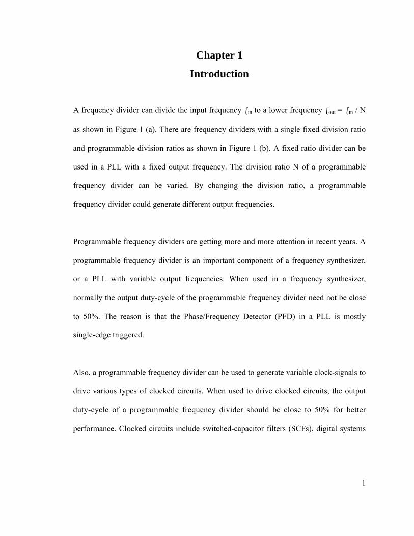
Chapter 1 Introduction
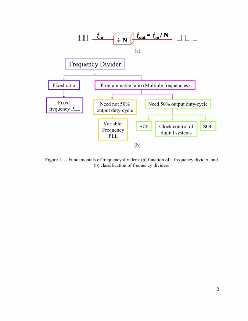
A frequency divider can divide the input frequency ƒin to a lower frequency ƒout = ƒin / N
as shown in Figure 1 (a). There are frequency dividers with a single fixed division ratio
and programmable division ratios as shown in Figure 1 (b). A fixed ratio divider can be
used in a PLL with a fixed output frequency. The division ratio N of a programmable
frequency divider can be varied. By changing the division ratio, a programmable
frequency divider could generate different output frequencies.
Programmable frequency dividers are getting more and more attention in recent years. A
programmable frequency divider is an important component of a frequency synthesizer,
or a PLL with variable output frequencies. When used in a frequency synthesizer,
normally the output duty-cycle of the programmable frequency divider need not be close
to 50%. The reason is that the Phase/Frequency Detector (PFD) in a PLL is mostly
single-edge triggered.
Also, a programmable frequency divider can be used to generate variable clock-signals to
drive various types of clocked circuits. When used to drive clocked circuits, the output
duty-cycle of a programmable frequency divider should be close to 50% for better
performance. Clocked circuits include switched-capacitor filters (SCFs), digital systems
2
(b)
(a)
÷Nƒin ƒout = ƒin / N÷Nƒin ƒout = ƒin / N
Frequency Divider
Fixed ratio Programmable ratio (Multiple frequencies)
Variable-Frequency
PLL
SCF Clock control of digital systems
SOC
Need not 50% output duty-cycle
Need 50% output duty-cycleFixed-frequency PLL
Figure 1: Fundamentals of frequency dividers: (a) function of a frequency divider, and (b) classification of frequency dividers
3
equalizer
PPIN
PPOUT
VV
−
−
,
,
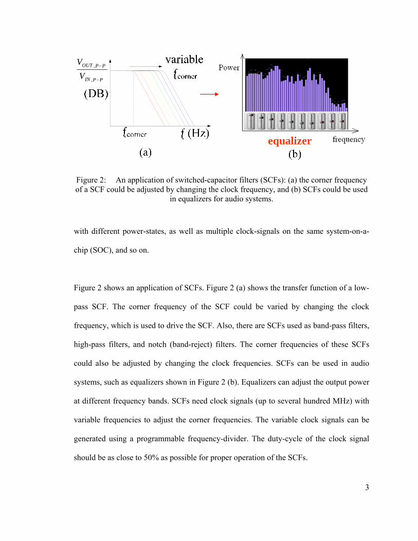
Figure 2: An application of switched-capacitor filters (SCFs): (a) the corner frequency of a SCF could be adjusted by changing the clock frequency, and (b) SCFs could be used
in equalizers for audio systems.
with different power-states, as well as multiple clock-signals on the same system-on-a-
chip (SOC), and so on.
Figure 2 shows an application of SCFs. Figure 2 (a) shows the transfer function of a low-
pass SCF. The corner frequency of the SCF could be varied by changing the clock
frequency, which is used to drive the SCF. Also, there are SCFs used as band-pass filters,
high-pass filters, and notch (band-reject) filters. The corner frequencies of these SCFs
could also be adjusted by changing the clock frequencies. SCFs can be used in audio
systems, such as equalizers shown in Figure 2 (b). Equalizers can adjust the output power
at different frequency bands. SCFs need clock signals (up to several hundred MHz) with
variable frequencies to adjust the corner frequencies. The variable clock signals can be
generated using a programmable frequency-divider. The duty-cycle of the clock signal
should be as close to 50% as possible for proper operation of the SCFs.

4
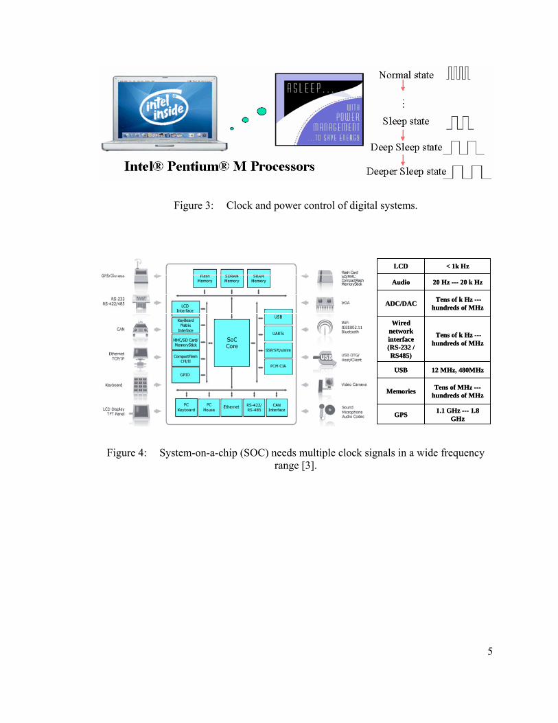
Figure 3 shows an example of the clock and power control of digital systems. Digital
systems can use different power states to save power. When the intensity of tasks is
lower, low power states could be used. Different power states can use different operating
frequencies generated from a programmable frequency divider to adjust the power
consumption. Lower operating frequencies can reduce the power consumption. A 50%
duty-cycle is important to give equal settling time to circuits when the clock signal is
high or low.
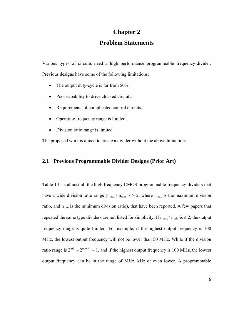
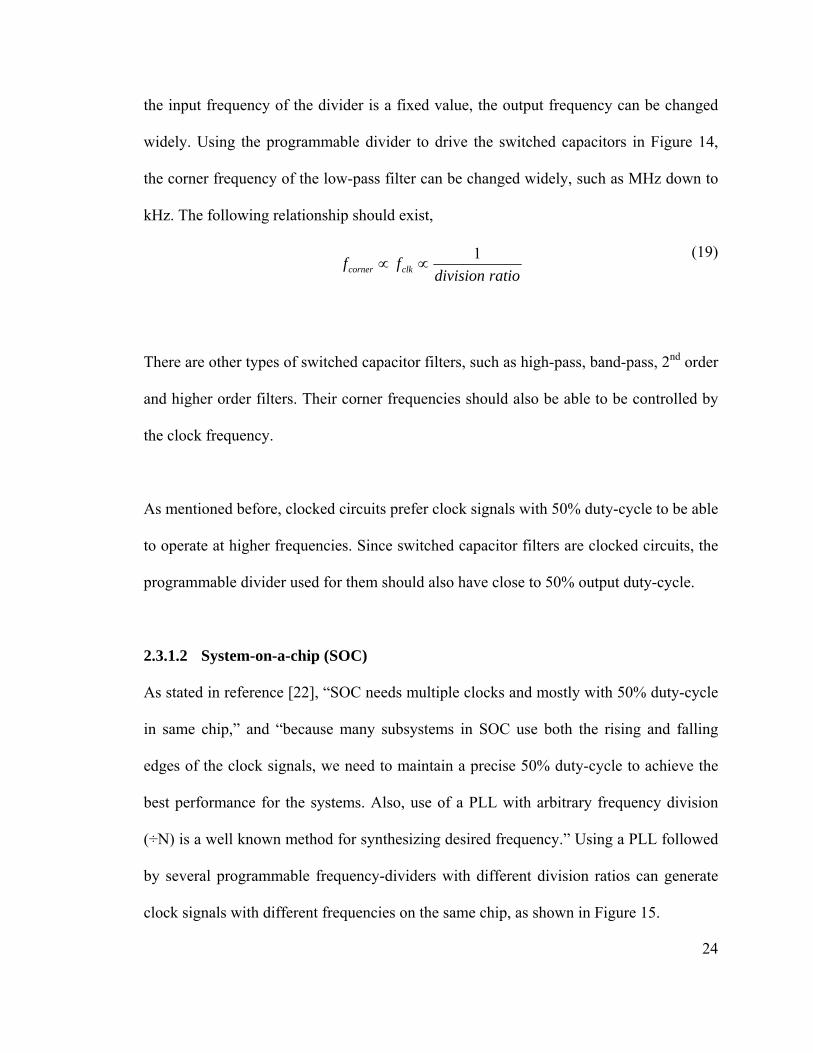
Figure 4 shows that the system-on-a-chip (SOC) needs multiple clock signals in a wide
frequency range. A PLL followed by several programmable frequency dividers can
generate different variable clock signals in a wide frequency range in a SOC. All the
digital circuits will have better performance when the duty-cycle of the clock signals is
closer to 50%.
These circuits need high performance programmable frequency dividers, operating at
high frequencies and having wide division ratio ranges, binary division ratio controls and
50% output duty-cycle. However, before this research work, none of the reported dividers
meet all the desirable characteristics. The proposed design is aimed to generate a
programmable frequency divider with all the above features.
5
Figure 3: Clock and power control of digital systems.
1.1 GHz --- 1.8 GHzGPS
Tens of MHz ---hundreds of MHzMemories
12 MHz, 480MHzUSB
Tens of k Hz ---hundreds of MHz
Wired network interface (RS-232 / RS485)
Tens of k Hz ---hundreds of MHzADC/DAC
20 Hz --- 20 k HzAudio
< 1k HzLCD
1.1 GHz --- 1.8 GHzGPS
Tens of MHz ---hundreds of MHzMemories
12 MHz, 480MHzUSB
Tens of k Hz ---hundreds of MHz
Wired network interface (RS-232 / RS485)
Tens of k Hz ---hundreds of MHzADC/DAC
20 Hz --- 20 k HzAudio
< 1k HzLCD
Figure 4: System-on-a-chip (SOC) needs multiple clock signals in a wide frequency range [3].
6
Chapter 2 Problem Statements
Various types of circuits need a high performance programmable frequency-divider.
Previous designs have some of the following limitations:
• The output duty-cycle is far from 50%,
• Poor capability to drive clocked circuits,
• Requirements of complicated control circuits,
• Operating frequency range is limited,
• Division ratio range is limited.
The proposed work is aimed to create a divider without the above limitations.
2.1 Previous Programmable Divider Designs (Prior Art)
Table 1 lists almost all the high frequency CMOS programmable frequency-dividers that
have a wide division ratio range (nmax / nmin is > 2, where nmax is the maximum division
ratio, and nmin is the minimum division ratio), that have been reported. A few papers that
repeated the same type dividers are not listed for simplicity. If nmax / nmin is ≤ 2, the output
frequency range is quite limited. For example, if the highest output frequency is 100
MHz, the lowest output frequency will not be lower than 50 MHz. While if the division
ratio range is 2min ~ 2max+1 – 1, and if the highest output frequency is 100 MHz, the lowest
output frequency can be in the range of MHz, kHz or even lower. A programmable
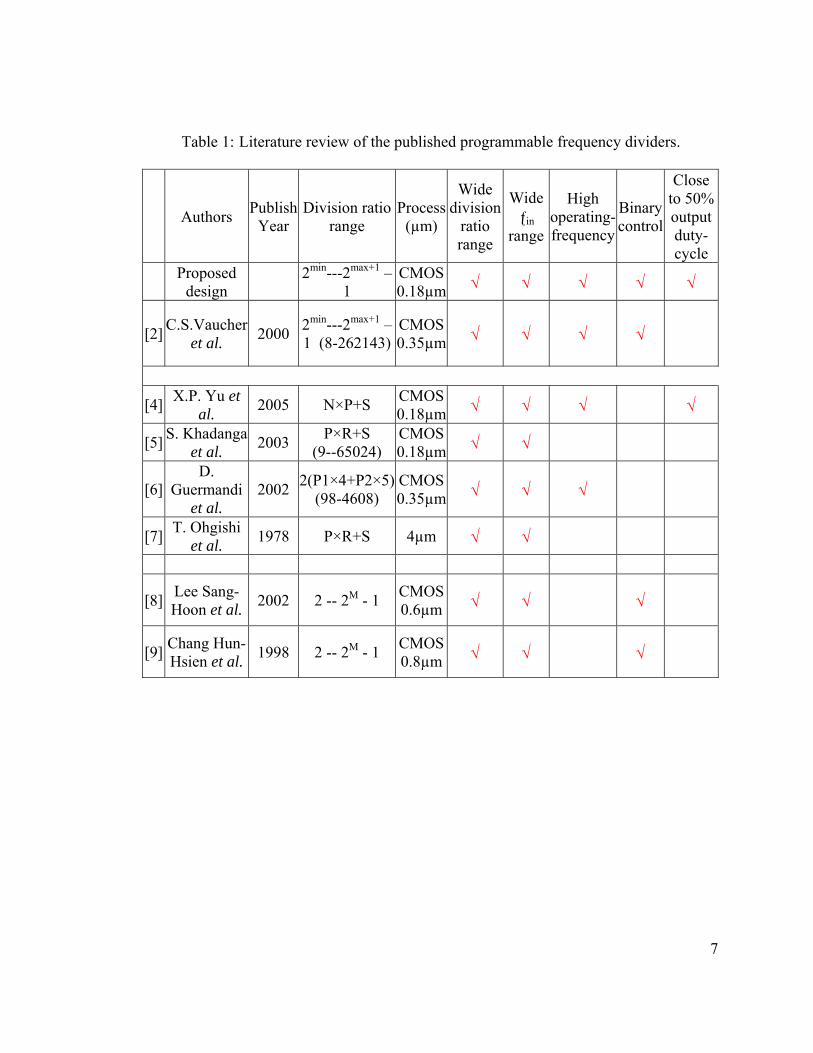
7
Table 1: Literature review of the published programmable frequency dividers.
Authors Publish Year
Division ratio range
Process (µm)
Wide division
ratio range
Wide ƒin
range
High operating-frequency
Binary control
Close to 50% output duty-cycle
Proposed design 2min---2max+1 –
1 CMOS 0.18µm √ √ √ √ √
[2] C.S.Vaucher et al. 2000 2min---2max+1 –
1 (8-262143)CMOS 0.35µm √ √ √ √
[4] X.P. Yu et al. 2005 N×P+S CMOS
0.18µm √ √ √ √
[5] S. Khadanga et al. 2003 P×R+S
(9--65024) CMOS 0.18µm √ √
[6] D.
Guermandi et al.
2002 2(P1×4+P2×5) (98-4608)
CMOS 0.35µm √ √ √
[7] T. Ohgishi et al. 1978 P×R+S 4µm √ √
[8] Lee Sang-Hoon et al. 2002 2 -- 2M - 1 CMOS
0.6µm √ √ √
[9] Chang Hun-Hsien et al. 1998 2 -- 2M - 1 CMOS
0.8µm √ √ √
8
frequency-divider with a wide output frequency range can have much more applications.
For example, it can offer clock signals for several digital circuits which need different
clock frequencies on the same chip and for switched capacitor circuits which need clock
signals with a wide adjustable frequency range.
It can be seen that there are only 3 types of high-frequency CMOS programmable
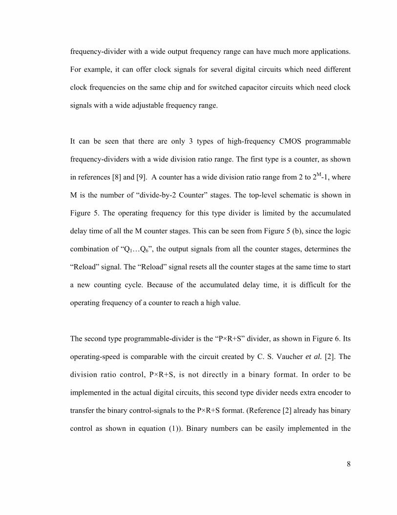
frequency-dividers with a wide division ratio range. The first type is a counter, as shown
in references [8] and [9]. A counter has a wide division ratio range from 2 to 2M-1, where
M is the number of “divide-by-2 Counter” stages. The top-level schematic is shown in
Figure 5. The operating frequency for this type divider is limited by the accumulated
delay time of all the M counter stages. This can be seen from Figure 5 (b), since the logic
combination of “Q1…Q6”, the output signals from all the counter stages, determines the
“Reload” signal. The “Reload” signal resets all the counter stages at the same time to start
a new counting cycle. Because of the accumulated delay time, it is difficult for the
operating frequency of a counter to reach a high value.
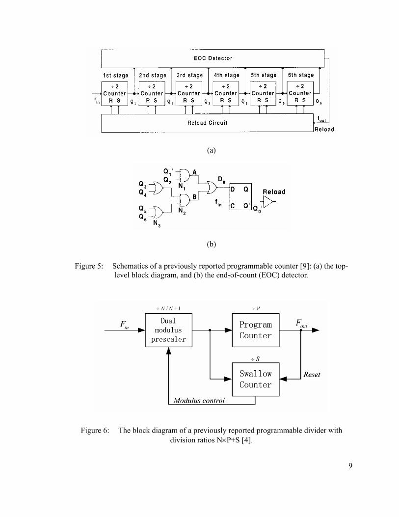
The second type programmable-divider is the “P×R+S” divider, as shown in Figure 6. Its
operating-speed is comparable with the circuit created by C. S. Vaucher et al. [2]. The
division ratio control, P×R+S, is not directly in a binary format. In order to be
implemented in the actual digital circuits, this second type divider needs extra encoder to
transfer the binary control-signals to the P×R+S format. (Reference [2] already has binary
control as shown in equation (1)). Binary numbers can be easily implemented in the
9
(a)
(b)
Figure 5: Schematics of a previously reported programmable counter [9]: (a) the top-level block diagram, and (b) the end-of-count (EOC) detector.
Figure 6: The block diagram of a previously reported programmable divider with division ratios N×P+S [4].
10
nnnPPPPratiodivision 22222 1
12
21
10
0 +⋅+⋅⋅⋅+⋅+⋅+⋅= −−
actual circuits, since “LOW” and “HIGH” are used to represent “0” and “1” in digital
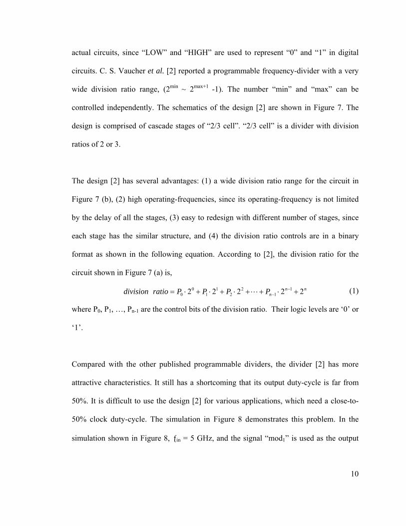
circuits. C. S. Vaucher et al. [2] reported a programmable frequency-divider with a very
wide division ratio range, (2min ~ 2max+1 -1). The number “min” and “max” can be
controlled independently. The schematics of the design [2] are shown in Figure 7. The
design is comprised of cascade stages of “2/3 cell”. “2/3 cell” is a divider with division
ratios of 2 or 3.
The design [2] has several advantages: (1) a wide division ratio range for the circuit in
Figure 7 (b), (2) high operating-frequencies, since its operating-frequency is not limited
by the delay of all the stages, (3) easy to redesign with different number of stages, since
each stage has the similar structure, and (4) the division ratio controls are in a binary
format as shown in the following equation. According to [2], the division ratio for the
circuit shown in Figure 7 (a) is,
(1)
where P0, P1, …, Pn-1 are the control bits of the division ratio. Their logic levels are ‘0’ or
‘1’.
Compared with the other published programmable dividers, the divider [2] has more
attractive characteristics. It still has a shortcoming that its output duty-cycle is far from
50%. It is difficult to use the design [2] for various applications, which need a close-to-
50% clock duty-cycle. The simulation in Figure 8 demonstrates this problem. In the
simulation shown in Figure 8, ƒin = 5 GHz, and the signal “mod1” is used as the output

11
Figure 7: A published programmable frequency divider [2]: (a) the block diagram of the basic architecture (2n ≤ N ≤ 2n+1-1), where N is the division ratio, and (b) the circuit
diagram with extended division range (2min ≤ N ≤ 2max+1-1), (in this figure max = n, min = n–2).
12
Figure 8: The duty-cycle problem with the published design [2]. The signal “mod1” is used as the output signal of the divider. In this simulation, ƒin = 5 GHz.
(Output)

13
signal of the divider. The pulse width of “mod1” is in the nanosecond range. It is difficult
to drive load capacitors by using this signal. Even inside a chip, parasitic capacitances
also exist, which can become load capacitors.
The capacitors connected to “mod1” terminal may not be able to be charged to the
expected voltage during the narrow pulses. The goal of the proposed design is to solve
this problem, while maintaining other advantages of the existing circuit [2].
2.2 Problem Definition
C. S. Vaucher et al. designed a programmable frequency divider with high operating
frequency and with a wide range of division ratios (2min ~ 2max+1-1) [2]. The designer can
specify the minimum power value “min” and the maximum power value “max”. Thus the
output frequency can be changed widely, such as 100MHz to 1MHz, and to 1kHz. The
circuit in [2] also can use binary controls to set the division ratios as shown in (1).
Vacucher’s divider [2] has a disadvantage that its output pulse width is only 2 or 3 times
of the input period. If the input frequency is 2 GHz, the output pulse width is only 1 ns or
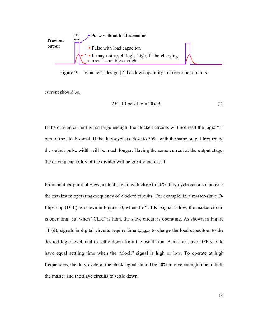
1.5 ns, as shown in Figure 9. The output pulse width does not change if the output
frequency is lower. It is difficult to drive large clocked systems by using these narrow
pulses, since the divider may not be able to charge the load capacitors to the correct logic
level of the clock signal. For example, if the capacitor load is 10 pF, and the supply
voltage is 2 V, in order to charge the capacitor from 0 V to 2 V in 1 ns, the driving
14
ns Pulse without load capacitor
Pulse with load capacitor. It may not reach logic high, if the charging
current is not big enough.
Previous output
ns Pulse without load capacitor
Pulse with load capacitor. It may not reach logic high, if the charging
current is not big enough.
Previous output
Figure 9: Vaucher’s design [2] has low capability to drive other circuits.
current should be,
mAnspFV 201/102 =× (2)
If the driving current is not large enough, the clocked circuits will not read the logic “1”
part of the clock signal. If the duty-cycle is close to 50%, with the same output frequency,
the output pulse width will be much longer. Having the same current at the output stage,
the driving capability of the divider will be greatly increased.
From another point of view, a clock signal with close to 50% duty-cycle can also increase
the maximum operating-frequency of clocked circuits. For example, in a master-slave D-
Flip-Flop (DFF) as shown in Figure 10, when the “CLK” signal is low, the master circuit
is operating; but when “CLK” is high, the slave circuit is operating. As shown in Figure
11 (d), signals in digital circuits require time trequired to charge the load capacitors to the
desired logic level, and to settle down from the oscillation. A master-slave DFF should
have equal settling time when the “clock” signal is high or low. To operate at high
frequencies, the duty-cycle of the clock signal should be 50% to give enough time to both
the master and the slave circuits to settle down.
15
Master Slave
Operate at CLK=0
Operate at CLK=1 Figure 10: A standard master-slave D-Flip-Flop.
thigh
T
CLK
tlow
Duty-Cycle ≥ 50%
thigh
T
CLK
tlow
Duty-Cycle ≥ 50%
thigh
T
CLK
tlow
Duty-Cycle ≤ 50%
thigh
T
CLK
tlow
Duty-Cycle ≤ 50%
trequiredtrequiredDuty-cycle of the clock signal
Maximum operating frequency
ƒmax
0% 50% 100%
Figure 11: The maximum operating frequency of a master-slave DFF vs. duty-cycle of
the clock signal.
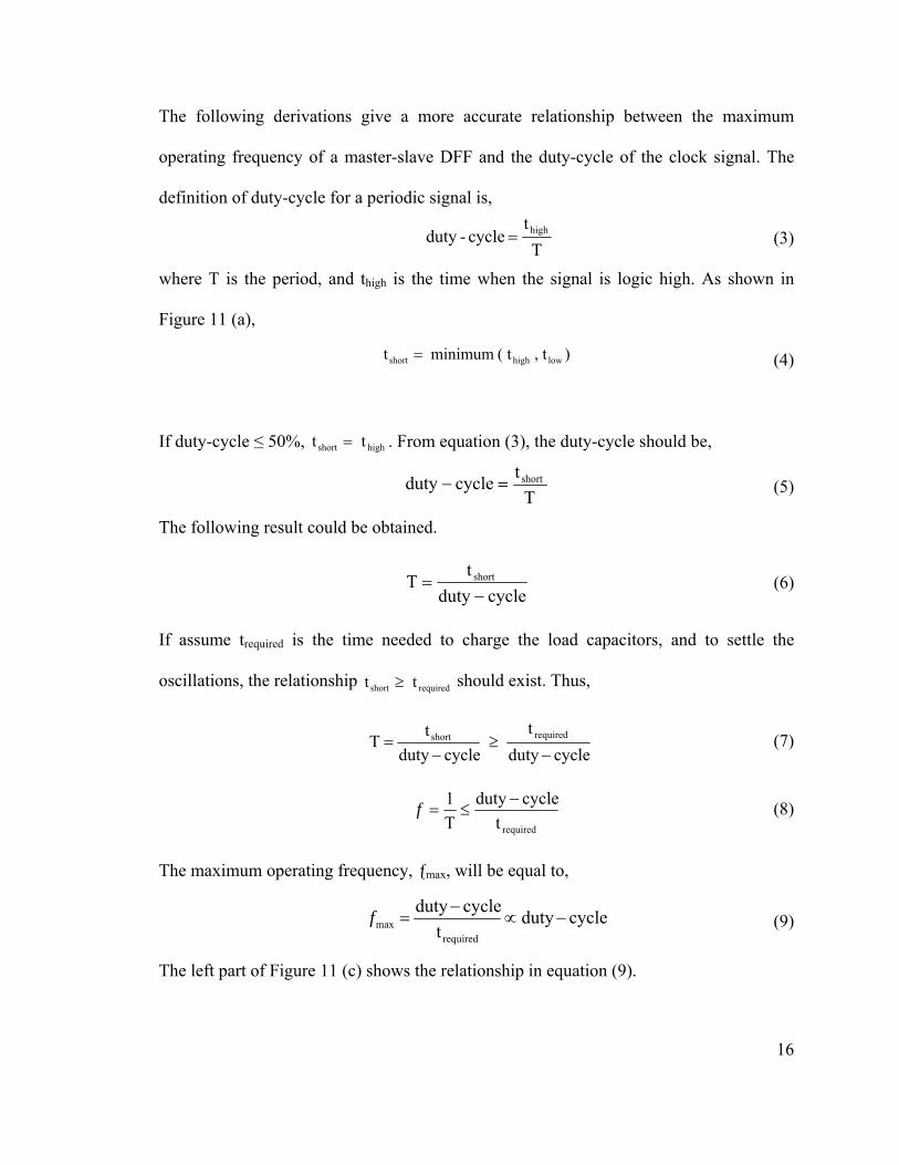
16
Ttcycleduty short=−
)t,t(minimum t lowhighshort =
Tt
cycle-duty high=
The following derivations give a more accurate relationship between the maximum
operating frequency of a master-slave DFF and the duty-cycle of the clock signal. The
definition of duty-cycle for a periodic signal is,
(3)
where T is the period, and thigh is the time when the signal is logic high. As shown in
Figure 11 (a),
(4)
If duty-cycle ≤ 50%, highshort tt = . From equation (3), the duty-cycle should be,
(5)
The following result could be obtained.
cycledutytT short
−= (6)
If assume trequired is the time needed to charge the load capacitors, and to settle the
oscillations, the relationship requiredshort tt ≥ should exist. Thus,
cycledutyt
cycledutytT requiredshort
−≥
−= (7)
requiredt
cycledutyT1 −≤=f (8)
The maximum operating frequency, ƒmax, will be equal to,
(9)
The left part of Figure 11 (c) shows the relationship in equation (9).
cycledutyt
cycleduty
requiredmax −∝
−=f
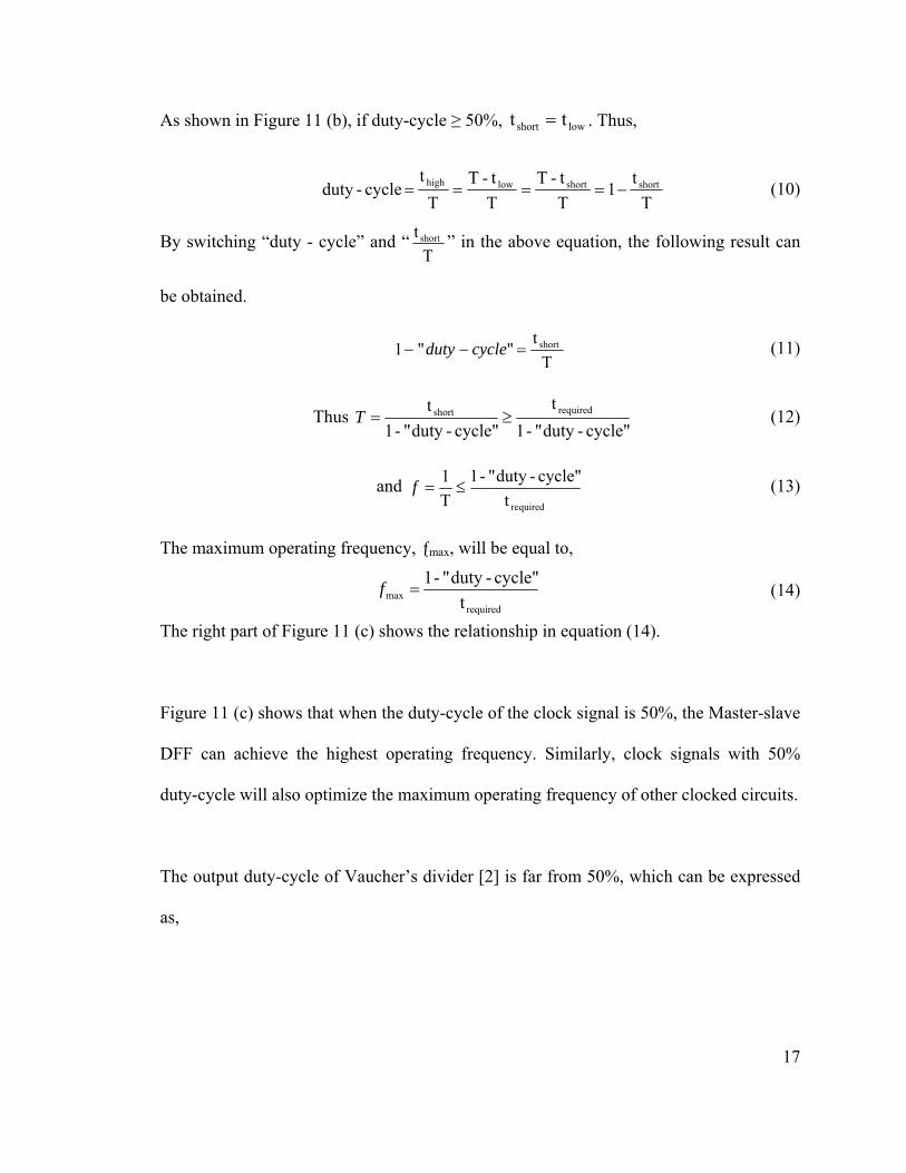
17
As shown in Figure 11 (b), if duty-cycle ≥ 50%, lowshort tt = . Thus,
Tt1
Tt-T
Tt-T
Tt
cycle-duty shortshortlowhigh −==== (10)
By switching “duty - cycle” and “T
t short ” in the above equation, the following result can
be obtained.
Tt
""1 short=−− cycleduty (11)
Thus cycle"-duty"-1
tcycle"-duty"-1
t requiredshort ≥=T (12)
and requiredt
cycle"-duty"-1T1≤=f (13)
The maximum operating frequency, ƒmax, will be equal to,
(14)
The right part of Figure 11 (c) shows the relationship in equation (14).
Figure 11 (c) shows that when the duty-cycle of the clock signal is 50%, the Master-slave
DFF can achieve the highest operating frequency. Similarly, clock signals with 50%
duty-cycle will also optimize the maximum operating frequency of other clocked circuits.
The output duty-cycle of Vaucher’s divider [2] is far from 50%, which can be expressed
as,
requiredmax t
cycle"-duty"-1=f

18
⎪⎪⎩
⎪⎪⎨
⎧
=
numberoddanisnwhen,n3
numberevenanisnwhen,n2
design previous of cycle Duty (15)
where n is the division ratio.
The output duty-cycle of [2] is < 10%, when n is > 20 and n is an even number. For
larger values of n, the duty-cycle becomes smaller. For example, if n = 10000, duty-cycle
= 0.02%. The small output duty-cycles will degrade the performance of clocked circuits,
or digital systems. A thorough review of relevant literatures indicates that no duty-cycle
corrector has been reported for the input duty-cycles less than 2% [10] - [17]. The
reported duty-cycle correctors could not resolve the duty-cycle problem in [2] when its
output duty-cycle is less than 2%.
The proposed design solved the problem of Vaucher’s design [2], without degrading its
other advantages. The output duty-cycle of the proposed design is very close to 50%
(within 44.4% ~ 50%). For each division ratio, the output duty-cycle remains constant,
with different input frequencies from GHz down to kHz range, at different temperatures
and with different power supply voltages. Test results corroborate the efficacy of the
proposed design.
19
⎪⎩
⎪⎨⎧
++
=12number oddan by divided when,
12
number,even an by divided when50% cycleDuty
kkk
2.3 Original Contributions
The achievement of the dissertation includes:
• The output signal of the proposed work has close to 50% duty-cycle (the duty-
cycle error is ≤ 5.6%)
• The step-size of the division ratios is kept to be 1.
• The output duty-cycle remains constant with PVT (Process-Voltage-Temperature)
changes and input frequency variations (GHz - kHz).
• A smaller layout area, because of the elimination of large resistors.
• Derivation of the expression for the programmable division ratio.
2.3.1 Close to 50% Output Duty-Cycle
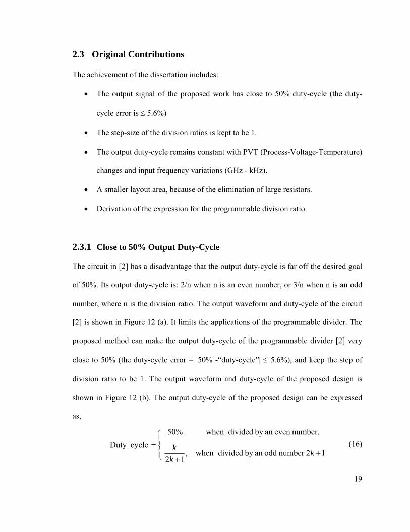
The circuit in [2] has a disadvantage that the output duty-cycle is far off the desired goal
of 50%. Its output duty-cycle is: 2/n when n is an even number, or 3/n when n is an odd
number, where n is the division ratio. The output waveform and duty-cycle of the circuit
[2] is shown in Figure 12 (a). It limits the applications of the programmable divider. The
proposed method can make the output duty-cycle of the programmable divider [2] very
close to 50% (the duty-cycle error = |50% -“duty-cycle”| ≤ 5.6%), and keep the step of
division ratio to be 1. The output waveform and duty-cycle of the proposed design is
shown in Figure 12 (b). The output duty-cycle of the proposed design can be expressed
as,
(16)
20
Figure 12: Comparison of the output duty-cycle of: (a) the prior art [2], and (b) the proposed design.

21
Since k is ≥ 4 (the minimum division ratio of the proposed design is 8), the duty-cycle
error is ≤ 5.6%. When the division ratio is > 50, the duty-cycle error is < 1%. A few
possible applications of the proposed programmable frequency divider with close to 50%
output duty-cycle are described in the following sections.
2.3.1.1 Switched-Capacitor Filters
Switched-capacitor filters (SCFs) are widely used in audio systems, since they have
advantages such as high accuracy and that varying the clock frequency can change the
corner frequencies of SCFs [18]. Some SCFs need high-frequencies clock signals such as
160MHz [19]. If the proposed wide division-ratio divider follows a PLL output signal to
generate the clock frequencies for the SCFs, the corner frequencies of the SCFs can be
varied widely from several hundred MHz to arbitrary low frequencies. SCFs need equal
and adequate time to settle when the clock signal is high or low. Thus the duty-cycle of
the clock signal for a SCF should be as close to 50% as possible. Otherwise, there could
be significant problems such as signal distortion, inaccurate filter response and signal
attenuation [21].
Figure 13 shows that a switched capacitor can be viewed as an equivalent resistor. A
switched capacitor (Figure 13 (b)) needs non-overlapping clock signals Φ1 and Φ2
(Figure 13 (c)), which can come from the output of a programmable divider. In Figure 13
(b), M1and M2 are connected to Φ1, and M3 and M4 are connected to Φ2. When Φ1 is high
(Figure 13 (d)), a charge CVVQ )( 21 −= will flow from node V1 to V2. When Φ2 is high
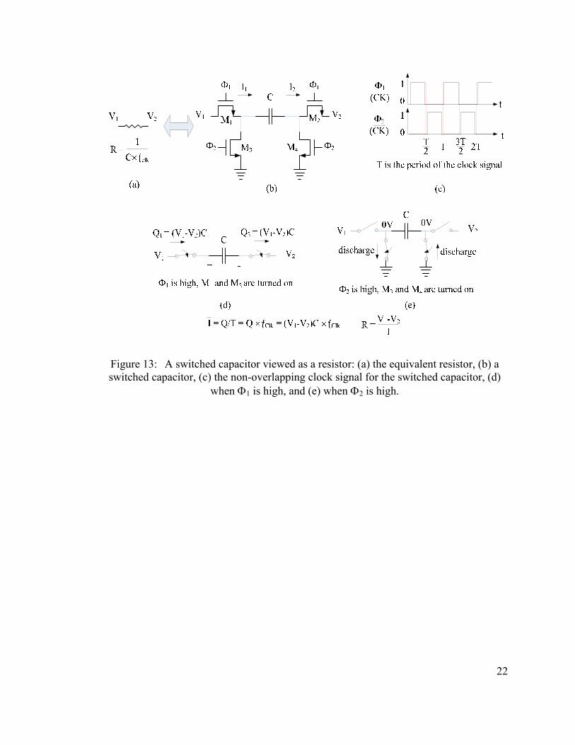
22
Figure 13: A switched capacitor viewed as a resistor: (a) the equivalent resistor, (b) a switched capacitor, (c) the non-overlapping clock signal for the switched capacitor, (d)
when Φ1 is high, and (e) when Φ2 is high.

23
1
3
13
13
12
13
2
13
2
132
312
1
1
1
1
1
)1(
1
)1(
CfC
CR
CRs
CR
sCR
R
sCR
RVV
sCR
VRV
III
clkp
in
out
outin
==
+
−=
+
−=
+
−=
+−=∴
+=
ω
Figure 14: The principle of a switched capacitor filter (low-pass).
(Figure 13 (e)), no charge will flow from node V1 to V2, but C will be discharged through
M3 and M4. During a full clock period, the average current flowing from V1 to V2 is,
clkclkclk
fCVVfQTQI ⋅−=⋅== )( 21 (17)
The equivalent resistor will be,
clkclk fCfCVVVV
IVVR
⋅=
⋅−−
=−
=1
)( 21
2121 (18)
Figure 14 shows an example of a switched capacitor filter, whose corner frequency can
be varied by the clock frequency. R2 and R3 are the equivalent resistances of the switch
capacitors C2 and C3 (not shown) using the schematic in Figure 13 (b). Through the
calculation in the right part of Figure 14, it can be shown that the circuit is a low-pass
filter. The corner frequency is proportional to ƒclk, which is the frequency of the clock
signal applied to the switched capacitors C2 and C3. Thus a programmable frequency
divider with a wide division ratio range is very useful for a switched capacitor filter. If
24
the input frequency of the divider is a fixed value, the output frequency can be changed
widely. Using the programmable divider to drive the switched capacitors in Figure 14,
the corner frequency of the low-pass filter can be changed widely, such as MHz down to
kHz. The following relationship should exist,
(19)
There are other types of switched capacitor filters, such as high-pass, band-pass, 2nd order
and higher order filters. Their corner frequencies should also be able to be controlled by
the clock frequency.
As mentioned before, clocked circuits prefer clock signals with 50% duty-cycle to be able
to operate at higher frequencies. Since switched capacitor filters are clocked circuits, the
programmable divider used for them should also have close to 50% output duty-cycle.
2.3.1.2 System-on-a-chip (SOC)
As stated in reference [22], “SOC needs multiple clocks and mostly with 50% duty-cycle
in same chip,” and “because many subsystems in SOC use both the rising and falling
edges of the clock signals, we need to maintain a precise 50% duty-cycle to achieve the
best performance for the systems. Also, use of a PLL with arbitrary frequency division
(÷N) is a well known method for synthesizing desired frequency.” Using a PLL followed
by several programmable frequency-dividers with different division ratios can generate
clock signals with different frequencies on the same chip, as shown in Figure 15.
ratiodivisionff clkcorner
1∝∝
25
Programmable divider 1 ƒo1
Programmable divider 2 ƒo2
Programmable divider n ƒon
. . .
PLLƒVCO
. . .
Programmable divider 1 ƒo1Programmable divider 1 ƒo1
Programmable divider 2 ƒo2Programmable divider 2 ƒo2
Programmable divider n ƒonProgrammable divider n ƒon
. . .
PLLƒVCO
. . .
Figure 15: The block diagram showing the development of multi-frequency clock signals for SOCs, which needs multiple clocks and mostly with 50% duty-cycle on the
same chip.
The proposed programmable frequency-divider has division ratios in a wide range and
close-to-50% output duty-cycle. Thus it could be used to generate multiple clock signals
for a SOC.
2.3.1.3 Variable Clock Signals for Different Power States of Digital Systems
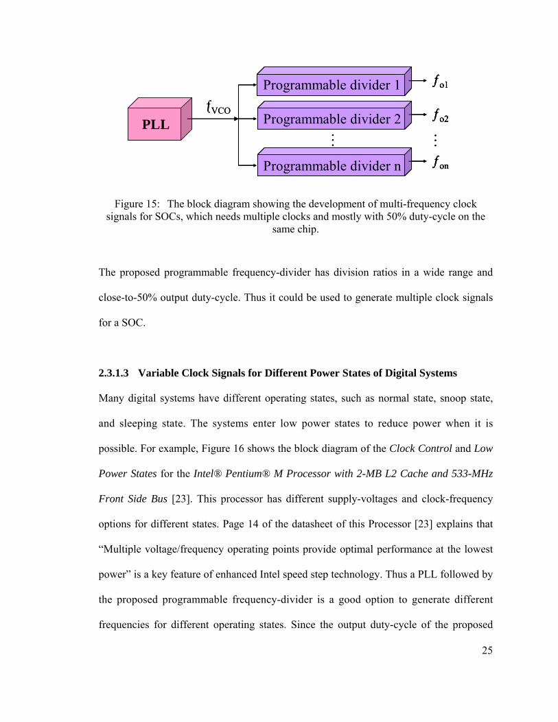
Many digital systems have different operating states, such as normal state, snoop state,
and sleeping state. The systems enter low power states to reduce power when it is
possible. For example, Figure 16 shows the block diagram of the Clock Control and Low
Power States for the Intel® Pentium® M Processor with 2-MB L2 Cache and 533-MHz
Front Side Bus [23]. This processor has different supply-voltages and clock-frequency
options for different states. Page 14 of the datasheet of this Processor [23] explains that
“Multiple voltage/frequency operating points provide optimal performance at the lowest
power” is a key feature of enhanced Intel speed step technology. Thus a PLL followed by
the proposed programmable frequency-divider is a good option to generate different
frequencies for different operating states. Since the output duty-cycle of the proposed
26
Figure 16: Block diagram of clock control and low power states for Intel® Pentium® M Processor with 2-MB L2 cache and 533-MHz front side bus [23] for wireless laptop
computer.
divider is very close to 50%, the performance of the digital systems will be optimized
[24] - [26].
There are other published literatures that state 50% duty-cycle is important for double
data rate (DDR) circuits. In the abstract of the paper [27], there is the following statement
“For those adopting double data rate (DDR) technology systems, the precise system
timing plays a crucial role since both rising and falling edges of the system clock signal
are used to sample the input data. Due to this requirement, it is necessary to accurately
maintain the duty-cycle of the clock signal at 50%.” The paper [28] states, “A duty cycle
corrector (DCC) is a very important circuit for dual edge triggering systems”. The
27
proposed design is also useful to generate clock signals with close to 50% duty-cycle for
DDR circuits.
As explained in all of the above references, 50% duty-cycle of a clock signal is important
for various implementations. It is easy to make the output duty-cycle of the
programmable frequency-divider to be exactly 50%, by adding a divide-by-2 divider at
the output stage. As stated in [29], the division ratio step will be 2 by using this method.
This will degrade the output-frequency resolution, since the output-frequency resolution
is the smallest variation of the output frequency. While the proposed design can make the
output duty-cycle very close to 50%, and maintain the division ratio step to be 1.
2.3.2 Smaller Layout Area
The “2/3 cell” is the basic component of the programmable frequency divider [2] as
shown in Figure 7. The schematic of the “2/3 cell” is shown in Figure 17 (a). It includes
three “AND-latch” gates and one “D-latch”. “AND-latch” is a source coupled logic
(SCL) implementation of an AND gate combined with a latch function. The circuit in
Figure 17 (b) shows the previous “AND-latch” design. The circuit in Figure 17 (c) shows
the proposed “AND-latch” design for the 1st “2/3 cell” stage, and Figure 17 (d) for the 2nd
to the end “2/3 cell” stages. Figure 17 (e) shows the proposed “D-latch” circuit used in
each “2/3 cell”.
The passive resistor loads in the previous “AND-latch” gate in Figure 17 (b) consume
much area. In “TABLE I” of [2], for the “2/3 cell” operated at 16 MHz, the load
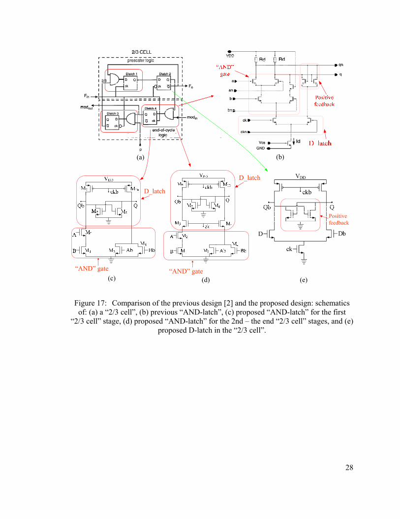
28
pffffp
ffp
ff
inoout
inoout
inoout
in
inooutin
+==⇒
⎪⎭
⎪⎬
⎫
⎪⎩
⎪⎨
⎧
==⇒=
==⇒=⇒=
==⇒=
2mod
2mod0
3mod1
1mod
2&0mod0mod
Positive feedback
(c) (d) (e)
(a) (b)
D_latch
“AND” gate
D_latch
“AND” gate
Figure 17: Comparison of the previous design [2] and the proposed design: schematics of: (a) a “2/3 cell”, (b) previous “AND-latch”, (c) proposed “AND-latch” for the first
“2/3 cell” stage, (d) proposed “AND-latch” for the 2nd – the end “2/3 cell” stages, and (e) proposed D-latch in the “2/3 cell”.
29
resistance should be 300 kΩ. In a known 0.18-µm process, the highest sheet resistance is
1006.9 ohm/square using poly resistor. Thus 300kΩ occupies about 300 unit squares. If 1
µm-wide poly is used, 3×2×300 = 1800 µm2 is needed for each “2/3 cell”, since each
“AND-latch” gate needs 2 resistances and each “2/3 cell” contains 3 “AND- latch” gates.
There are multiple “2/3 cell” in the entire divider. The proposed “AND-latch” gate as
shown in Figure 17 (c) and (d) removed the passive resistors. In this way, the proposed
design can significantly reduce the layout area.
30
Chapter 3 Design of the Proposed Programmable Divider
3.1 Design of the “2/3 Cell” Circuit
The “2/3 cell” is a divider with division ratio of 2 or 3. Through derivations, the division
ratio of the “2/3 cell” is determined by the following equation.
(20)
(21)
As shown in Figure 17 (a), the “2/3 cell” includes three “AND-latch” gates and one “D-
latch”. Figure 17 (e) shows the proposed “D-latch” circuit used in each “2/3 cell”. When
“ck” is high, if “D” is high and “Db” is low, “Qb” should be low and “Q” should be high.
The “positive feedback” is used to hold the output levels at “Q” and “Qb” when “ck” is
low.
The proposed “AND-latch” designs are shown in Figure 17 (c) and (d). The circuit in
Figure 17 (c) is used in the first “2/3 cell”, whereas the circuit in Figure 17 (d) is used for
the rest stages. In both Figure 17 (c) and (d), the “D-latch” part is used to allow the
outputs to change when the clock signal “ck” is high. Transistors M7 and M8 in both
circuits are used as positive feedback to hold the outputs “Q” and “Qb”. The difference
between Figure 17 (c) and (d) is stated as follows. The gates of M5 and M6 in Figure 17
pffffp
ffpin
oin
o
ino
+==⇒
⎪⎭
⎪⎬
⎫
⎪⎩
⎪⎨
⎧
==⇒=
==⇒==
2mod
2mod0
3mod1
1, mod If out
out
out
in
2&0mod 0, mod If outin
ino
ff ===
31
(d) are connected to the clock signal “ck”. While in Figure 17 (c), M5 and M6 are
removed, enabling the circuit to yield faster operation.
There are some concerns about the circuits in Figure 17 (c) and (d). The circuit in Figure
17 (c) is combined from the D-latch designs in the references [32]-[34] and an “AND”
gate. It can achieve faster operation than the circuit in Figure 17 (d). However at low
frequencies, the outputs of the circuit in Figure 17 (c) do not follow the “ck” signal well
(shown in Figure 7 of [32], the duty-cycle of the output is not 50%). The reason is that
without M5 and M6, even when “ck” is low, voltage at Q or Qb can still change. They
should change only when “ck” is high. The output signal “modout” of the first stage need
not drive a previous stage, since there is no previous stage. Thus it is appropriate to use
the circuit in Figure 17 (c) in the first stage. Simulation and test results also show that
using the circuit in Figure 17 (c) in the first stage does not violate the correct operation of
the entire divider. On the other hand, since the output signals “modout” of the 2nd – the
end stages need to drive the input signal “modin” of previous stages, their duty-cycle
should be 50% for correct operation. Thus the circuit in Figure 17 (d) is used in “2/3 cell”
of the 2nd – the end stages, since its output signals follow the “ck” correctly at lower
frequencies. Its output signals can only change when “ck” is high due to the existence of
M5, M6 and M9, M10. Therefore, using the circuit in Figure 17 (c) at the first “2/3 cell”
and the circuit in Figure 17 (d) at the rest cells can achieve fast and correct operation.

32
nnnPPPPratiodivision 22222 1
12
21
10
0 +⋅+⋅⋅⋅+⋅+⋅+⋅= −−
3.2 Division Ratio Expression of Vaucher’s Design [2]
3.2.1 Division Ratio Expression for the Basic Architechture [2]
With the time domain analysis of the “2/3 cell”, it is found that the period of the output
clock signal “ƒout” is equal to the period of “modout” signal. It is also found that the time
duration when the “modout” = 1 is always equal to,
(22)
where Tin is the period of the input signal “ƒin” of the “2/3 cell”. Equation (22) always
exists whether the division ratio control P, and “modin” of the “2/3 cell” is logic 0 or 1.
The time duration when the “modout” = 0 is equal to,
(23)
It is related to the logic level of the division ratio control P, and the modulus control
“modin”.
The induction method will be used to verify the division ratio (shown in equation (1)) for
the basic circuit in Figure 7 (a). Equation (1) is rewritten as follows,
(24)
The following verification includes three sections for the induction method. In the three
sections, the number of the “2/3 cell” stages will be (I) 1, (II) 2, and (III) n.
inout Tistime =)1(mod
ininout TPistime ⋅⋅+= )mod1()0(mod

33
2/3 cell1 stage
P0
mod1
P1
mod2
...
modn-1
Pn-1
VDD
mod0
Pn-2
modn-2
2/3 cell2 stage
2/3 celln-1 stage
2/3 celln stage
ƒin ƒ1 ƒ2 ƒn-2 ƒn-1 ƒn
modn
P0
mod1
VDD
mod0
2/3 cell1 stage
ƒin ƒout
(a)
2/3 cell1 stage
P0
mod1
P1
mod2
VDD
mod0
2/3 cell2 stage
ƒin ƒ1 ƒout
(b)
(c)
modinmodout modin
modout modinmodout
modinmodout modin
modoutmodin
modout modinmodout
Figure 18: Schematics of the basic architecture of Vaucher’s programmable divider [2], with the following number of the “2/3 cell” stages: (a) 1, (b) 2, and (c) n.
(I) Figure 18 (a) shows the circuit when there is only one “2/3 cell” in the entire divider.
The division ratio control P for the 1st “2/3 cell” is “P0”. According to equation (21), the
division ratio will be,
(25)
Equation (25) is compatible with equation (24), with n = 1.
(II) Figure 18 (b) shows the circuit when there are two “2/3 cell” stages in the entire
divider.
(Case 1) According to equation (22), the time duration when “mod1” is “1” will be,
10
00 222 +⋅=+= PPratiodivision
34
(26)
where Tin2 is the period of the input signal of the 2nd “2/3 cell”, which is also the period
of the output signal ƒout of the 1st “2/3 cell”, )( 1fT . Since the “modin” signal of the 1st
“2/3 cell” “mod1 = 1”, according to equation (21), the division ratio of the 1st “2/3 cell”
will be 02 P+ . The division ratio control P for the 1st “2/3 cell” is “P0”. The period of the
output signal ƒout of the 1st “2/3 cell”, )( 1fT will be,
(27)
where Tin is the period of the input signal of the entire divider.
By inserting equation (27) into equation (26), the following result could be obtained,
(28)
(Case 2) The division ratio control P for the 2nd “2/3 cell” is “P1”. According to equation
(23), the time duration when 0mod1 = will be,
(29)
Since “modin2”, the “modin” signal of the 2nd “2/3 cell” is connected to VDD, “modin2” = 1.
Thus equation (29) can be written as,
(30)
Since 0mod1 = , according to equation (20), the division ratio of the 1st “2/3 cell” will be
2. The period of the output signal ƒout of the 1st “2/3 cell”, )( 1fT will be,
)()1(mod 121 fTTistime in ==
inTPfT ⋅+= )2()( 01
2211 )mod1()0(mod inin TPistime ⋅⋅+=
inTPistime ⋅+= )2()1(mod 01
)()1()1()0(mod 11211 fTPTPistime in ⋅+=⋅+=
35
(31)
By inserting equation (31) into equation (30), the following result could be obtained.
(32)
For the 2nd (the end) “2/3 cell”, the period of the output clock signal “ƒout” is equal to the
period of the “mod1” signal. The period of the “mod1” signal will be the sum of the time
duration when “mod1” is 1 and the time duration when “mod1” is 0. Thus the output
period of the entire divider will be,
(33)
By inserting equation (28) and (32) into equation (33), the output period can be obtained
as follows.
(34)
(35)
Thus the division ratio of the entire divider will be,
(36)
Equation (36) is compatible with equation (24), with n = 2.
(III) Suppose the division ratio for a divider with n-1 stages of the “2/3 cell” is equal to
the following expression,
inTfT ⋅= 2)( 1
inin TPTPistime ⋅⋅+=⋅+⋅= )22()1(2)0(mod 111
)0(mod)1(mod 11 istimeistimeTout +=
ininout TPTPT ⋅⋅++⋅+= )22()2( 10
ininout TPPTPPT ⋅+⋅+⋅=⋅+⋅+= )222()42( 21
10
010
21
10
0 222 +⋅+⋅== PPTTratiodivision
in
out
36
(37)
If another stage is added after the existing n-1 stages, the new divider will have n stages.
(Case 1) According to equation (22), the time duration when “modn-1” is 1 will be,
(38)
where Tin,n is the period of the input signal of the nth “2/3 cell”, which is also the period
of the output signal ƒout of the (n-1)th “2/3 cell”, T(ƒn-1). According to equation (37), the
period of the output signal ƒout of the (n-1)th “2/3 cell”, T(ƒn-1) will be,
(39)
By inserting equation (39) into equation (38), the following result could be obtained,
(40)
(Case 2) According to equation (23), the time duration when 0mod1 = will be,
(41)
According to equation (20), if “modin” = 0, “modout” = 0. Since “modn-1” = 0, all of the
“modout” signals of the previous stages will be 0. Thus,
(42)
Thus the division ratio of the 1st – the (n-1)th “2/3 cell” will all be equal to 2. The period
of the output signal ƒout of the (n-1)th “2/3 cell”, )( 1−nfT will be,
12
11
10
0 22...22)1( −− +⋅++⋅+⋅=− n
nPPPstagesnratiodivision
)()1(mod 1,1 −− == nninn fTTistime
inn
nn TPPPfT ⋅+⋅++⋅+⋅= −−− )22...22()( 1
21
11
00
1
)()1()1()0(mod 11,11 −−−− ⋅+=⋅+= nnninnn fTPTPistime
inn
nn TPPPistime ⋅+⋅++⋅+⋅= −−− )22...22()1(mod 1
21
11
00
1
0mod,mod,...,mod,mod 0132 =−− nn
37
(43)
By inserting equation (43) into equation (41), the following result could be obtained,
(44)
For the nth (the end) “2/3 cell”, the period of the output clock signal is equal to the period
of the “modn-1” signal. The period of the “modn-1” signal will be the sum of the time
duration when “modn-1” is 1 and the time duration when “modn-1” is 0. Thus the output
period of the entire divider will be,
(45)
By inserting equation (40) and (44) into equation (45), the output period can be obtained
as follows.
(46)
(47)
Thus the division ratio of the entire n stage divider will be,
(48)
It is the same as equation (24). Thus the above derivations should prove the division ratio
expression of the basic architecture of Vaucher’s programmable divider [2].
inn
n TfT ⋅= −−
11 2)(
innnn
innn
n TPTPistime ⋅⋅+=⋅+⋅= −−−
−−
− )22()1(2)0(mod 111
11
1
)0(mod)1(mod 11 istimeistimeT nnout −− +=
innnn
inn
nout TPTPPPT ⋅⋅++⋅+⋅++⋅+⋅= −−−−
− )22()22...22( 1111
21
11
00
inn
nn
nout TPPPPT ⋅+⋅+⋅++⋅+⋅= −−
− )222...22( 11
21
11
00
nn
nn
in
out PPPPTTstagenratiodivision 222...22)( 1
12
11
10
0 +⋅+⋅++⋅+⋅== −−
−
38
2/3 divider1 stage
P0 P1
...
Pn-1
ƒn
VDD
2/3 divider2 stage
2/3 dividern-1 stage
2/3 dividern stage
Pn-2
ƒout
ƒn-1ƒn-2ƒin ƒ1 ƒ22/3 dividern-2 stage
Pn-3
ƒn-3
modinmodout modin
modout modinmodoutmodin
modoutmodinmodout
In
Out PnORn
ORn,b
INVn
ORn-1
ORn-1,b
INVn-1
Figure 19: Vaucher’s design with extended division range (2min ≤ N ≤ 2max+1-1) [2].
3.2.2 Division Ratio Expression for Vaucher’s Design with Extended
Division Range [2]
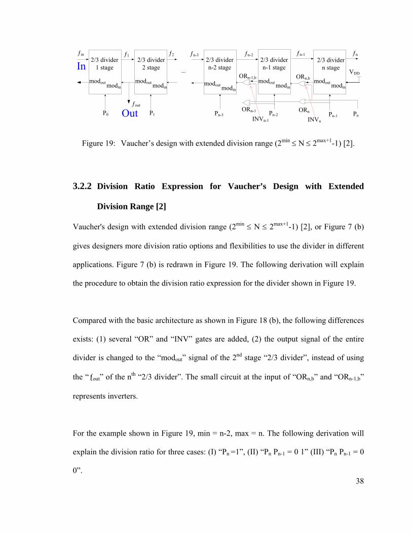
Vaucher's design with extended division range (2min ≤ N ≤ 2max+1-1) [2], or Figure 7 (b)
gives designers more division ratio options and flexibilities to use the divider in different
applications. Figure 7 (b) is redrawn in Figure 19. The following derivation will explain
the procedure to obtain the division ratio expression for the divider shown in Figure 19.
Compared with the basic architecture as shown in Figure 18 (b), the following differences
exists: (1) several “OR” and “INV” gates are added, (2) the output signal of the entire
divider is changed to the “modout” signal of the 2nd stage “2/3 divider”, instead of using
the “ƒout” of the nth “2/3 divider”. The small circuit at the input of “ORn,b” and “ORn-1,b”
represents inverters.
For the example shown in Figure 19, min = n-2, max = n. The following derivation will
explain the division ratio for three cases: (I) “Pn =1”, (II) “Pn Pn-1 = 0 1” (III) “Pn Pn-1 = 0
0”.
39
(I) “Pn Pn-1 Pn-2 …P1 P0 = 1 x x … x x ”. “Pn” is equal to logic 1, the output of “INVn”
will be 0. Since “Pn” is equal to logic 1, the output of the “ORn” will be 1. Thus the
output of “INVn-1” will be 0. Since the outputs of “INVn” and “INVn-1” are both 0, they
will not affect the outputs of “ORn,b” and “ORn-1,b”. The “modin” signal of the (n-1)th
stage will be equal to the “modout” of the nth stage. It seems like that the “modin” signal of
the (n-1)th stage is connected to the “modout” of the nth stage directly. For the same reason,
it should seem like that the “modin” signal of the (n-2)th stage is connected to the “modout”
of the (n-1)th stage directly. The division ratio of the entire divider will be the same as the
basic architecture as shown in Figure 18 (b) with n “2/3 cell” stages. Thus the division
ratio will be the same as shown in equation (48), which can be rewritten as follows.
(49)
If all of “Pn-1”, …, “P1” and “P0” are logic 1, the division ratio of the divider will be the
maximum value, which is 2n+1-1, or 2max+1-1 (max = n).
(II) “Pn Pn-1 Pn-2 …P1 P0 = 0 1 x … x x ”. “Pn” is equal to logic 0, the outputs of “INVn”
will be 1. The output of “ORn,b” will always be 1. Thus the “modin” signal of the (n-1)th
stage “2/3 cell” will always be 1. Since “Pn-1” is equal to logic 1, the output of “ORn” will
be 1. The “modin” signal of the (n-2)th stage will be equal to the “modout” of the (n-1)th
stage. The division ratio of the entire divider will be the same as the basic architecture as
shown in Figure 18 (b) with (n-1) “2/3 cell” stages. The division ratio when “Pn Pn-1 Pn-2
…P1 P0 = 0 1 x … x x ” can be written as follows.
(50)
nn
nn
nn
n PPPPPisPratiodivision ⋅+⋅+⋅++⋅+⋅= −−
−− 222...22)1( 1
12
21
10
0
12
21
10
01 22...22)"01""(" −
−−
− +⋅++⋅+⋅= nn
nnn PPPisPPratiodivision

40
Equation (50) can be rewritten as the following one.
(51)
If equation (49) and equation (51) are combined, the following result could be obtained.
If any of Pmin+1, Pmin+2, …, Pmax-1, Pmax = 1, or division ratio is ≥ 2min+1, (min = n-2, max =
n), the division ratio will be,
(52)
(III) “Pn Pn-1 Pn-2 …P1 P0 = 0 0 x … x x ”. Both “Pn” and “Pn-1” are equal to logic 0, the
output of “ORn” will be 0. The outputs of “INVn-1” will be 1. The output of “ORn-1,b” will
always be 1. Thus the “modin” signal of the (n-2)th stage “2/3 cell” will always be 1. The
output of “ORn-1” is not connected to anywhere. The division ratio of the entire divider
will be the same as the basic architecture as shown in Figure 18 (b) with (n-2) “2/3 cell”
stages. “Pn-2” has no effect in the division ratio. The corresponding division ratio could be
written as follows.
If all of Pmin+1, Pmin+2, …, Pmax-1, Pmax = 0, or division ratio is < 2min+1, (min = n-2, max =
n), the division ratio will be,
(53)
nn
nn
nn
nn PPPPPisPPratiodivision ⋅+⋅+⋅++⋅+⋅= −−
−−
− 222...22)"01"( 11
22
11
00
1
nn
nn
nn PPPPPratiodivision ⋅+⋅+⋅++⋅+⋅= −
−−
− 222...22 11
22
11
00
23
31
10
0 22...22 −−
− +⋅++⋅+⋅= nn
n PPPratiodivision
41
i
iiP
PPPPPPratiodivision
2
222222max
0
maxmax
1max1max
minmin
1min1min
11
00
⋅=
⋅+⋅+⋅⋅⋅+⋅+⋅+⋅⋅⋅+⋅+⋅=
∑=
−−
−−
minmin
1min1min
11
00 2222 ⋅+⋅+⋅⋅⋅+⋅+⋅= −
− PPPPratiodivision
If all of “Pn-3”, …, “P1” and “P0” are logic 0, the division ratio of the divider will be the
minimum value, which is 2n-2, or 2min (min = n-2).
For other “min” and “max” values, the division ratios can be obtained in a similar way.
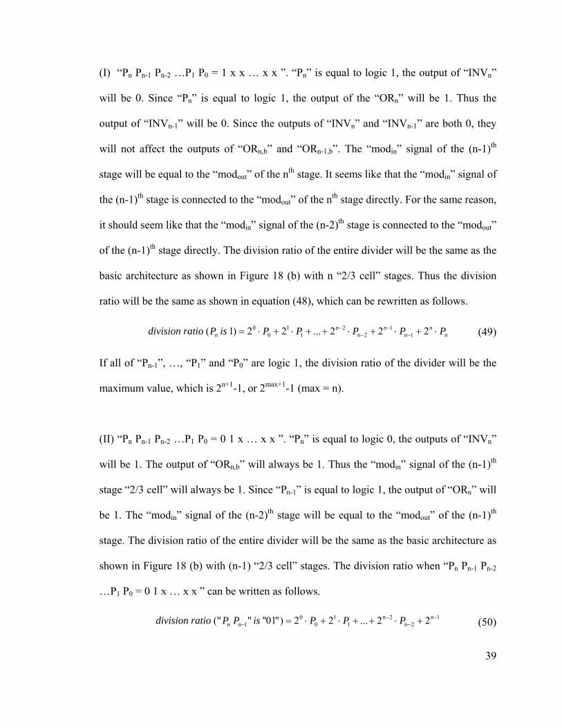
Thus the division ratio of Vaucher’s divider [2] shown in Figure 19 is obtained.
(a) If all of Pmin+1, Pmin+2, …, Pmax-1, Pmax = 0, or division ratio is < 2min+1,
(54)
(b) Other wise, if any of Pmin+1, Pmin+2, …, Pmax-1, Pmax = 1, or division ratio is ≥ 2min+1,
(55)
Both equation (54) and (55) are in binary format. The special case is that when the
division ratio is < 2min+1, the control signal Pmin has no effect.
When the division ratio is < 2min+1, Pmin is set to logic “1”, and then equation (54) can be
rewritten as,
(56)
Equation (56) is compatible with equation (55). Thus equation (57) alone can be used to
express the division ratio for all cases, with the following condition:
;22
2222
min1min
0
min1min1min
11
00
+⋅=
+⋅+⋅⋅⋅+⋅+⋅=
∑−
=
−−
i
iiP
PPPratiodivision

42
When the division ratio is < 2min+1, Pmin is set to logic “1”, then,
(57)
For the circuit shown in Figure 19, min = n-2, and max = n.
If the division ratio is < 2n-1, Pn-2 is set to logic “1”. The division ratio for Figure 19 will
be,
(58)
Equation (54) and (55) are quite complicated. For compactness, the following
calculations will use equation (58).
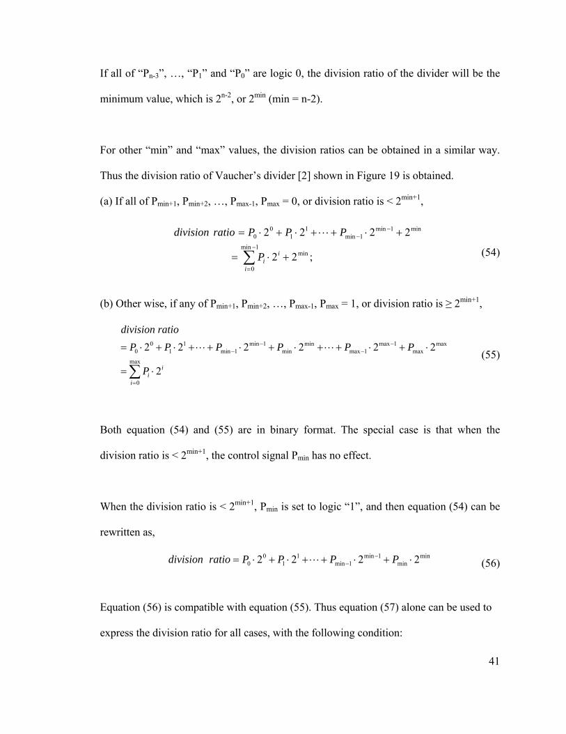
3.3 The Proposed “Solution 1” with 50% Duty-Cycle
The output pulse width of Vaucher’s divider [2] is very narrow. Thus it has poor
capability to drive other circuits. The circuit shown in Figure 20 can generate output
signals with very close to 50% duty-cycle, while retaining the same division ratios as 2min
to 2max+1-1.
In order to achieve 50% duty-cycle, a divide-by-2 divider, “Div2”, is added at the output
of “Div_n_vaucher” (shown in bottom-left part of Figure 19). An “AND” gate and an “n
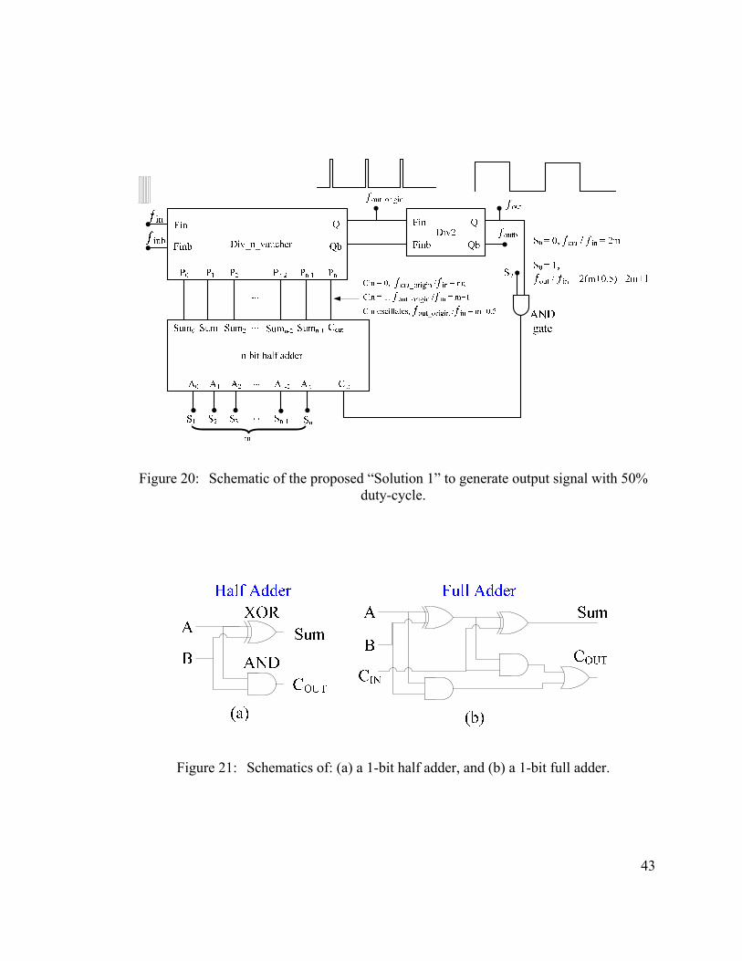
bit half adder” are also included in the feedback loop as shown in Figure 20. Figure 21
shows the schematics of a 1-bit half adder and a 1-bit full adder. The “n bit half adder”
includes n stages of “1-bit half adder” connected in series. The first stage is the least
maxmax
1max1max
minmin
1min1min
11
00 222222 ⋅+⋅+⋅⋅⋅+⋅+⋅+⋅⋅⋅+⋅+⋅= −
−−
− PPPPPPratiodivision
nn
nn PPPPPratiodivision 2222 1
12
21
10 ⋅+⋅+⋅⋅⋅+⋅+⋅+= −−
43
Figure 20: Schematic of the proposed “Solution 1” to generate output signal with 50% duty-cycle.
Figure 21: Schematics of: (a) a 1-bit half adder, and (b) a 1-bit full adder.

44
significant bit (LSB). The “B” input of each “1-bit half adder” (shown in Figure 21 (a))
should be conntected to the “Cout” of the previous stage. The “B” input of the first “1-bit
half adder” is used as “Cin” of the “n bit half adder” in Figure 20.
In Figure 20, the original output signal is “ƒout_origin” (top-middle part), whose duty cycle
is far-off 50%. The duty cycle of the proposed output, “ƒout” (top-right part), is very close
to 50%. This is because “ƒout” is the output of “Div2”, and the period of “ƒout_origin”
changes very little. S0, S1, …, Sn are the division ratio controls of the proposed divider.
“S0” is the LSB (Least Significant Bit). “ƒout” and “S0” are the inputs of the “AND”
gate.The output of the “AND” gate is fed to the Cin input of the “n bit half-adder”. The
outputs of the adder are used as the division ratio controls for “Div_n_vaucher”.
The binary combination of (S1, S2, …, Sn) is represented as “m”, thus,
(59)
For the “Div_n_vaucher” in Figure 19, Pmin = Pn-2, and Pmax = Pn as stated before.
Pn-2 or Sn-1 is set to logic “1” when the division ratio of “Div_n_vaucher” is < 2n-1 (or the
proposed division ratio is < 2n). Thus equation (58) can be used to represent the division
ratio of “Div_n_vaucher”.
If “S0” is 0, the binary combination of the adder outputs will be equal to “m”. The ratio of
“ƒin / ƒout_origin” will also be equal to “m”. After “Div2”, the ratio of “ƒin / ƒout” will be
equal to,
121
23
121 2222 −−
− ⋅+⋅+⋅⋅⋅+⋅+⋅+= nn
nn SSSSSm
45
nn
nn SSSSSSratiodivisionproposed 22222 1
13
32
21
10 ⋅+⋅+⋅⋅⋅+⋅+⋅+⋅+= −−
(60)
If “S0” is “1”, the signal at input “Cin” of the adder will oscillate between “0” and “1”,
with a close to 50% duty-cycle. The binary outputs of the adder (or the division ratio of
“Div_n_vaucher”) will have an average value of 0.5 + m. Thus the average ratio of “ƒin /
ƒout” will be equal to,
(61)
If equations (60) and (61) are combined, the division ratio can be written as follows,
(62)
The proposed division ratio expressed in equation (62) is the same as the original one in
equation (58) (except for that “P” is changed to “S”).
The output duty-cycle of the proposed design can be calculated as follows. When “S0” is
0, the division ratio is an even number as shown in equation (60). Since the adder outputs
or the division ratio of “Div_n_vaucher” do not change, neither ƒout_origin nor the period
Tout_origin changes. After “Dvi2”, the duty-cycle of ƒout will be exactly 50%. When “S0” is
1, the division ratio is an odd number as shown in equation (61). Since the adder outputs
or the division ratio of “Div_n_vaucher” changes between m and m+1, Tout_origin changes
between m × Tin and (m+1) × Tin, where Tin is the period of the input signal. The “on” and
“off” time of the proposed output signal ƒout will be m × Tin and (m+1) × Tin. Thus when
the division ratio is an odd number, the duty-cycle of the proposed output is m / (2m+1),
where 2m+1 is the division ratio. These results are compatible with equation (16).
nn
nn SSSSSm 2222202 1
13
32
21
1 ⋅+⋅+⋅⋅⋅+⋅+⋅+⋅+=× −−
nn
nn SSSSSm 222221)5.0(2 1
13
32
21
1 ⋅+⋅+⋅⋅⋅+⋅+⋅+⋅+=+× −−
46
According to the above analysis, the proposed circuit in Figure 20 generates an output
signal with close to 50% duty-cycle, also keeps the step size of the division ratio to be 1
(by changing the LSB control bit “S0”).
3.4 Proposed “Solution 2” with 50% Duty-Cycle
The above scheme, “Solution 1”, does not work for the isolated division ratios of 2r-1
(such as 15, 31, 63, 127), where “r” is a natural number. The proposed “Solution 2”
scheme shown in Figure 22 solved this problem. Figure 22 (a) shows the top level circuit
of Solution 2. Figure 22 (b) shows the revised “2/3 cell” for “Solution 2”. Figure 22 (c)
shows the circuit to judge the “0/1” edge of the control digits.
It is also important to keep the uniformity of the division ratio expression as shown in
equation (57). The same method could be used as in the proposed “Solution 1”. It is also
the requirement stated just above equation (57). When the division ratio is < 2min+1, “Pmin”
should be set to logic “1”.
As shown in Figure 22 (a), if a “2/3 cell” is connected to the first nonzero control-digit in
the MSB (most significant bit) part, this “2/3 cell” is “on edge”. For the particular
example shown at the bottom of Figure 22 (a), Pn-2 is the first nonzero control-digit
counting down from the MSB part. Thus the (n-1)th “2/3 cell” stage, which is connected
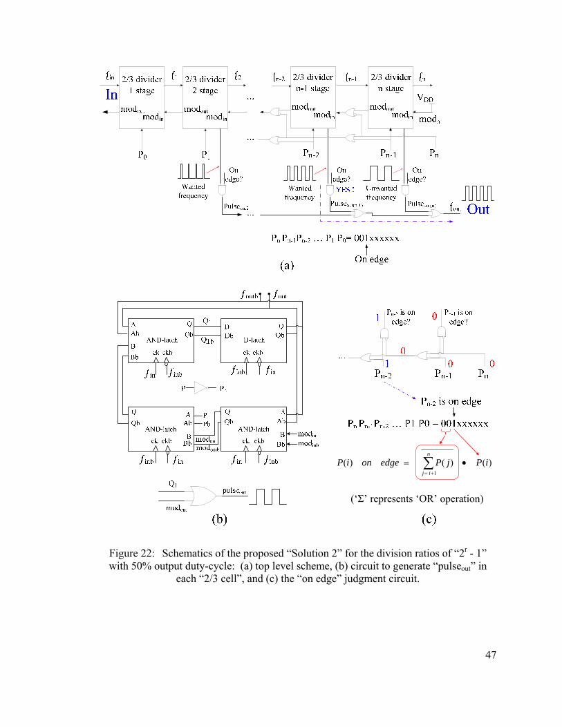
47
(‘Σ’ represents ‘OR’ operation)
)()()(1
iPjPedgeoniPn
ij•= ∑
+=
Figure 22: Schematics of the proposed “Solution 2” for the division ratios of “2r - 1” with 50% output duty-cycle: (a) top level scheme, (b) circuit to generate “pulseout” in
each “2/3 cell”, and (c) the “on edge” judgment circuit.
48
with Pn-2 signal, is “on edge”. The “pulseout” signals from the on-edge “2/3 cell” and the
previous cells have the desired output frequency, which is “ƒin / (the expected division
ratio)”. The “pulseout” signals from the latter “2/3 cell” have unwanted frequencies, which
are different from “ƒin / (the expected division ratio)”. Among the “pulseout” signals from
the on-edge “2/3 cell” and the previous cells, the signal from the on-edge cell has a duty-
cycle closest to 50%. Thus the “pulseout” signal from this on-edge cell will be used as the
output for the entire divider.
Figure 22 (b) shows the revised “2/3 cell”. It is drawn in a differential mode, for example
both “D” and “Db” are drawn in the “D-latch”. Actually, the only difference between the
revised “2/3 cell” and the one shown in Figure 17 (a) is that an “OR” gate is added in the
revised one to generate the “pulseout” signal. The signals “Q1” and “modout” are the inputs
of the “OR” gate. When the division ratio is a “2r - 1” number, the “pulseout” signal of the
“on-edge” “2/3 cell” has a duty-cycle of 12 +kk
, where 2k + 1 = 2r – 1 or the division ratio.
Since the division ratio “2r - 1” is an odd number, this duty-cycle is compatible with the
expression shown in equation (16).
Figure 22 (c) shows the circuit to judge the “0/1” edge of the control digits, or the first
nonzero control-digit in the MSB part. In the figure, the expressions have the following
meaning,
)()(...)()()( 121
1 nnj
n
ijj PORPORORPORPjP −+
+=+∑ = (63)
49
))(()(11
∑∑+=+=
=n
ij
n
ijjPNOTjP (64)
As the example shown in Figure 22 (c), if “PnPn-1Pn-2 = 001”, Pn-2 will be the first nonzero
control-digit counting down from the MSB part. If “OR” operations are applied to all the
MSB digits before Pn-2, the result will be 0. The inversion of this result 0 is 1. If “AND”
operation is applied to the inversion signal “1” and Pn-2, the result will be 1. Only when
Pn-2 is “on-edge”, the result will be 1. The results for other control digits will all be 0. By
implementing the combination of “OR”, “AND” and “inverter” logic gates, the “Pn-2 is on
edge?” signal will be high. Thus the circuit shown in Figure 22 (c) can judge the on-edge
cell automatically.
The proposed “Solution 2” shown in Figure 22 can solve the problem of the proposed
“Solution 1”. When the division ratio is “2r-1” number, the output duty-cycle of
“Solution 2” is 12 +k
k , where 2k + 1 is the division ratio.
3.5 Combination of the Proposed Solution 1 and 2 with 50% Duty-
Cycle
To obtain close-to-50% output duty-cycle for each division ratio, the proposed “Solution
1” and “Solution 2” are combined together, as shown in Figure 23. With the circuit
shown in Figure 24, the proposed divider will automatically judge if the division ratio has
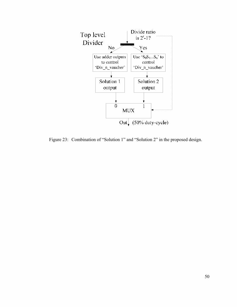
50
Figure 23: Combination of “Solution 1” and “Solution 2” in the proposed design.
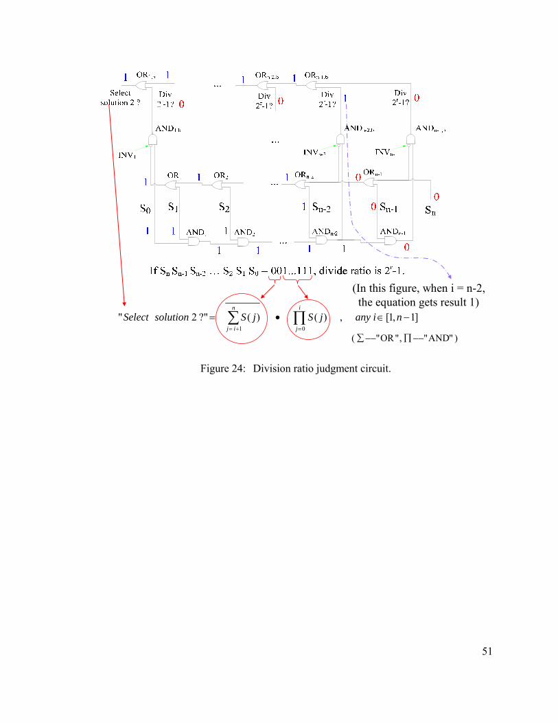
51
]1,1[,)()(?"2"01
−∈•= ∏∑=+=
nianyjSjSsolutionSelecti
j
n
ij
(In this figure, when i = n-2, the equation gets result 1)
)"AND","OR"( −−∏−−∑
Figure 24: Division ratio judgment circuit.

52
the “2r – 1” format. If the division ratio is not a “2r – 1” number, the control digits
“S0S1…Sn” will be assigned to the adder inputs and the AND gate input as shown in
Figure 20. Thus the adder outputs will be used to control the division ratio of
“Div_n_vaucher”. “Div2” output shown in Figure 20 is used as the final output.
Otherwise, if the division ratio is a “2r – 1” number, the control digits “S0S1…Sn” are
assigned directly to the controls “P0P1…Pn” of “Div_n_Vaucher”(the circuit shown in
Figure 22 (a)). The output shown in Figure 22 (a) is used as the final output. In order to
keep the uniformity of the division ratio expression, when the division ratio is < 2min+1,
Smin should be set to logic “1” similarly to equation (57). Here “S0S1…Sn” are the
division ratio controls of the top level design.
Figure 24 shows the circuit to judge if the division ratio is a “2r – 1” number. Some
expressions at the bottom of the Figure 24 have the following meaning,
)()(...)()()( 121
1 nnj
n
ijj SORSORORSORSjS −+
+=+∑ = (65)
)()(...)()()( 1100
ii
i
j
SANDSANDANDSANDSjS −=∏ = (66)
If a number has the “2r - 1” format, it should be able to be expressed in binary format as
“0…01...111”. Number iedge is used to represent the index of the first nonzero digit
counting down from the MSB (left) part. For the example shown in Figure 24, if Sn Sn-
1Sn-2 … S2 S1 S0 = 001...111, the division ratio is a “2r – 1” number, and r = n-1. The first
nonzero MSB control digit is Sn-2, so iedge = n-2. The MSB digits “Sn” and “Sn-1”, the
53
digits left to Sn-2, are all 0. If the logic “OR” operations are applied to all of the MSB
digits “Sn” and “Sn-1”,
10)(1
=⇒== ∑+=
AjSAn
ij
, here i = n-2. (67)
If the logic “AND” operations are applied to all of the LSB digits (including digit Sn-2),
“Sn-2 ”, …, “S2”, “S1”, “S0”, the following result will be obtained.
1)(0
==∏=
i
j
jSB , where i = n-2. (68)
Thus ∏∑=+=
=•=•i
j
n
ij
BAjSjS01
1)()( , where i = n-2. (69)
In the middle part of Figure 24, the gates “AND1”, “AND2”, …, “ANDn-1” are used to
realize the logic “AND” operations ∏=
=i
j
jSB0
)( in the circuit. The gates “OR1”, “OR2”, …,
“ORn-1” are used to realize the logic “OR” operations ∑+=
=n
ij
jSA1
)( . At the upper part of
Figure 24, the small circles “o” at the inputs of “AND1,b”, …, “ANDn-2,b”, “ANDn-1,b” are
inverters. They are applied to A to realize the logic “NOT” operation to obtain A . An
“AND” gate is used to apply the logic “AND” operation to A and B , to obtain BA ⋅ .
Thus each signal “Div 2r-1?” represents the result of ∏∑=+=
•=⋅i
j
n
ijjSjSBA
01)()( for the
corresponding i. For the above example, since Sn Sn-1 Sn-2 … S2 S1 S0 = 001...111,
∏∑=+=
=•i
j
n
ij
jSjS01
1)()( for i = n-2. (70)
54
Thus the signal “Div 2r-1?” above “ANDn-2,b” is “1”, where n-2 is iedge. If
∏∑=+=
=•i
j
n
ijjSjS
011)()( for any particular index ]1,1[ −∈ ni , the division ratio “Sn Sn-1 Sn-2 …
S2 S1 S0” should be a “2r – 1” number. This particular index i will be iedge, the index of the
first nonzero control digit counting down from the MSB part. At the top part of Figure
24, gates “OR1,b”, …, “ORn-2,b”, “ORn-1,b” are above the “Div 2r-1?” signals. If any “Div
2r-1?” signal is “1”, with the logic “OR” operations, the output signal “Select solution 2?”
will be “1”. Thus if the division ratio “Sn Sn-1Sn-2 … S2 S1 S0” is a “2r-1” number, for any
natural number “r ]1,1[ −∈ n ”, the circuit will select Solution 2.
Figure 25 shows a more detailed top-level schematic of the proposed design. The
“division ratio judgment circuit” used in Figure 25 at the left-bottom corner has been
shown in Figure 24. If the division ratio is a “2r – 1” number, the “division ratio judgment
circuit” in Figure 25 will give an output “1”. In this case, “Solution 2” will be used. The
“n+1 bit MUX” circuit in the middle of Figure 25 will be used to select signals to assign
the “P0P1…Pn” controls of “Div_n_vaucher”. If “Solution 2” is used, “S0S1…Sn” will be
selected and assigned to “P0P1…Pn” of “Div_n_vaucher”. If the division ratio is not a “2r
– 1” number, “Solution 1” will be used. The division ratio control digits “S0S1…Sn” will
be assigned to the inputs of the adder and the “AND” gate. The “n+1 bit MUX” circuit
will select adder outputs and assign them to the “P0P1…Pn” controls of “Div_n_vaucher”.
The “Div_n_vaucher” for the combined proposed divider is the entire circuit of “Solution
2” as shown in Figure 22 (a). The “MUX” circuit at the top of Figure 25 gives the final
output by selecting “Solution 1 output” or “Solution 2 output”.
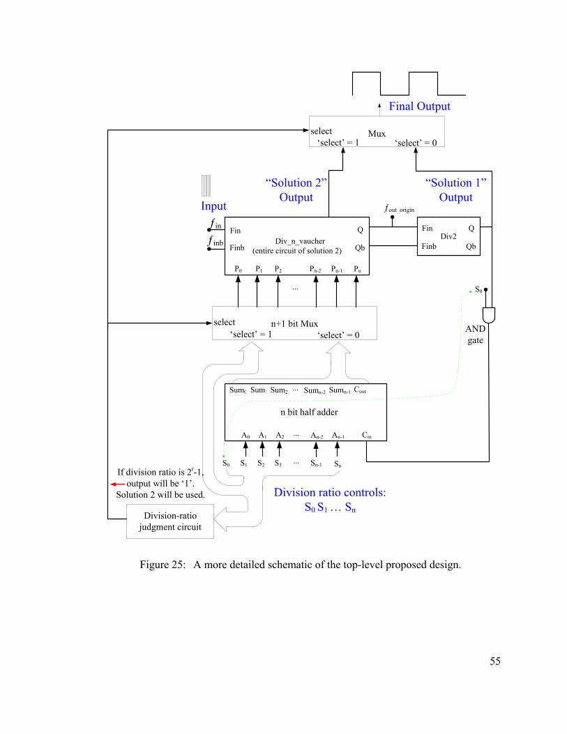
55
n+1 bit Muxselect
Div_n_vaucher (entire circuit of solution 2)
Fin
Finb
Q
Qb
P0
Fin
Finb
Q
QbDiv2
P1
...
PnP2
n bit half adder
Cin
Cout
A0 A1 A2 ...
Sum0 Sum1 Sum2 ...
...
An-1
Pn-1
ƒin
S1 S2 SnS3
ƒinb
ƒout_origin
S0
Input
“Solution 1” Output
ANDgate
Sumn-2
An-2
Pn-2
Sn-1
Sumn-1
Division-ratio judgment circuit
If division ratio is 2r-1, output will be ‘1’.
Solution 2 will be used.
‘select’ = 1 ‘select’ = 0
“Solution 2” Output
Muxselect
Final Output
‘select’ = 1 ‘select’ = 0
Division ratio controls:S0 S1 … Sn
S0
Figure 25: A more detailed schematic of the top-level proposed design.

56
Since all the additional circuits in the proposed design (for duty-cycle correction) operate
at relatively low frequencies, they only adds less than 10% power consumption penalty to
the original divider.
3.6 Simulations of the Proposed Divider
Simulations were performed for the proposed-design. They verify that the proposed
programmable divider realized the division ratios shown in equation (62) and has the
output duty-cycle very close to 50% as shown in equation (16). Table 2 shows the pre-
layout simulation results for the comparison of Process-Voltage-Temperature (PVT)
performance of the proposed design. When the temperature is lower or VDD is higher, or
with a faster process corner, the maximum operating-frequency is higher. For each
division ratio, the output duty-cycle of the proposed design remains constant with various
PVT, with various input frequencies, and with different chips.
3.7 Phase Noise Analysis of the Proposed Divider
A few references [35]-[36] state the noise analysis of frequency dividers. References [35]
carried out the noise analysis for dividers using CMOS transistors, which is similar to the
proposed divider.
Accorder to [35], for a synchronized frequency divider, the output phase noise is the
accumulation of the phase noise in each “2/3 cell” stage. In each “2/3 cell” stage, the
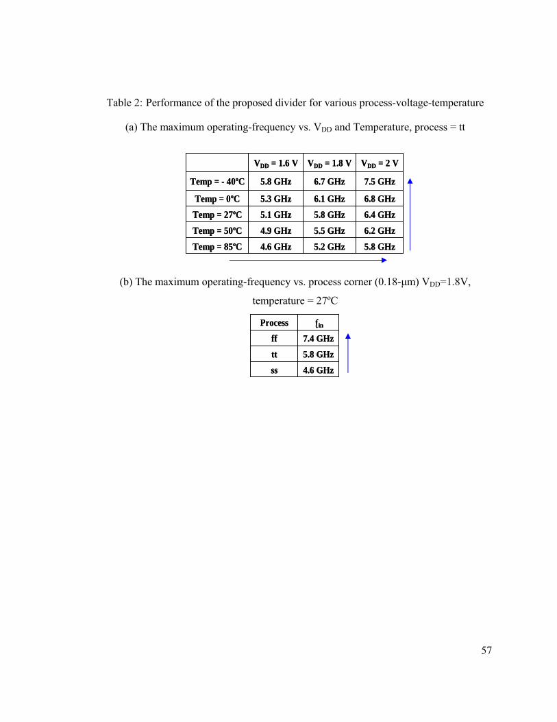
57
Table 2: Performance of the proposed divider for various process-voltage-temperature
(a) The maximum operating-frequency vs. VDD and Temperature, process = tt
5.8 GHz5.2 GHz4.6 GHzTemp = 85ºC
6.2 GHz5.5 GHz4.9 GHzTemp = 50ºC
6.4 GHz5.8 GHz5.1 GHzTemp = 27ºC6.8 GHz6.1 GHz5.3 GHzTemp = 0ºC
7.5 GHz6.7 GHz5.8 GHzTemp = - 40ºC
VDD = 2 VVDD = 1.8 VVDD = 1.6 V
5.8 GHz5.2 GHz4.6 GHzTemp = 85ºC
6.2 GHz5.5 GHz4.9 GHzTemp = 50ºC
6.4 GHz5.8 GHz5.1 GHzTemp = 27ºC6.8 GHz6.1 GHz5.3 GHzTemp = 0ºC
7.5 GHz6.7 GHz5.8 GHzTemp = - 40ºC
VDD = 2 VVDD = 1.8 VVDD = 1.6 V
(b) The maximum operating-frequency vs. process corner (0.18-μm) VDD=1.8V,
temperature = 27ºC
4.6 GHzss
5.8 GHztt
7.4 GHzffƒinProcess
4.6 GHzss
5.8 GHztt
7.4 GHzffƒinProcess
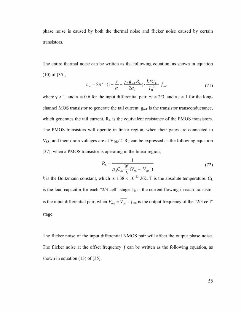
58
phase noise is caused by both the thermal noise and flicker noise caused by certain
transistors.
The entire thermal noise can be written as the following equation, as shown in equation
(10) of [35],
(71)
where γ ≅ 1, and α ≅ 0.6 for the input differential pair. γT ≅ 2/3, and αT ≅ 1 for the long-
channel MOS transistor to generate the tail current. gmT is the transistor transconductance,
which generates the tail current. RL is the equivalent resistance of the PMOS transistors.
The PMOS transistors will operate in linear region, when their gates are connected to
VSS, and their drain voltages are at VDD/2. RL can be expressed as the following equation
[37], when a PMOS transistor is operating in the linear region,
(72)
k is the Boltzmann constant, which is 1.38 × 10⁻²³ J/K. T is the absolute temperature. CL
is the load capacitor for each “2/3 cell” stage. IB is the current flowing in each transistor
is the input differential pair, when outout VV = . ƒout is the output frequency of the “2/3 cell”
stage.
The flicker noise of the input differential NMOS pair will affect the output phase noise.
The flicker noise at the offset frequency ƒ can be written as the following equation, as
shown in equation (13) of [35],
outB
L
T
LmTTw f
IkTCRgL ⋅⋅++⋅= 2
2 )2
1(8α
γαγπ
|)|(
1
thpSGoxp
L
VVL
WCR
−=μ
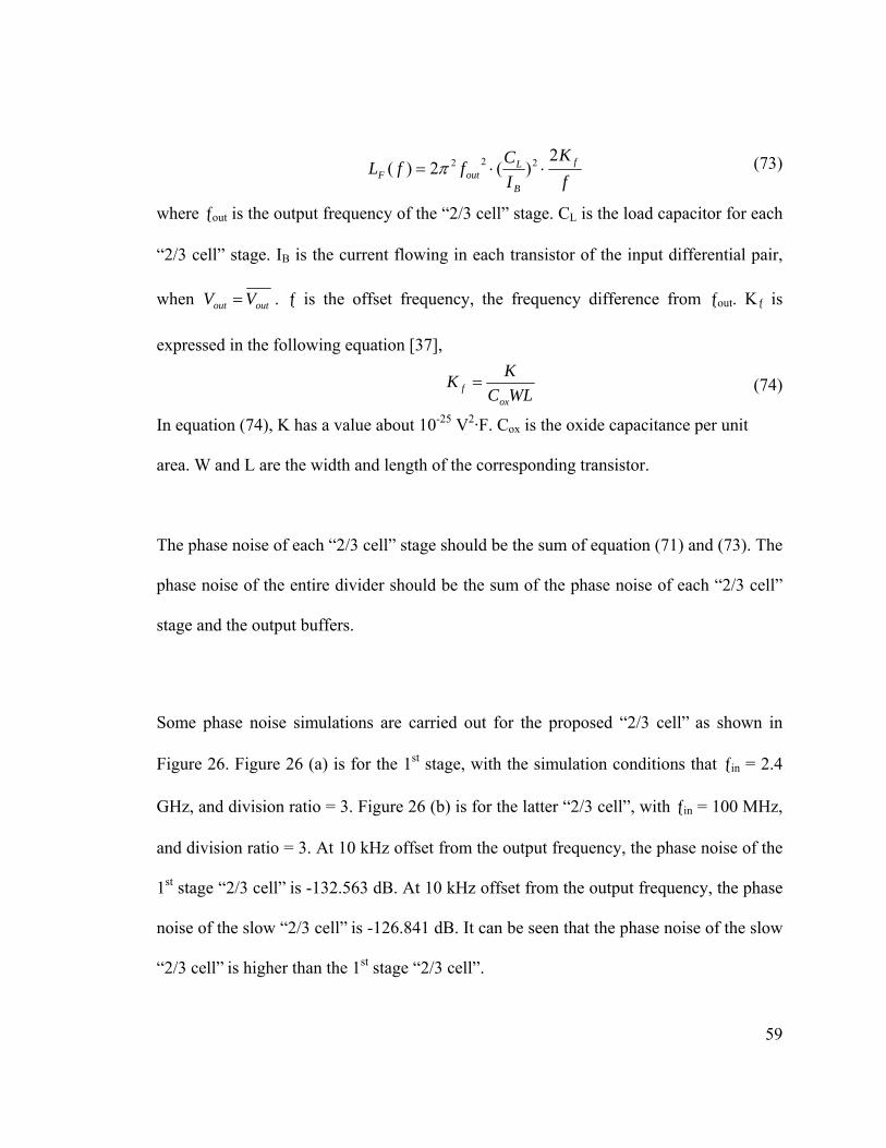
59
(73)
where ƒout is the output frequency of the “2/3 cell” stage. CL is the load capacitor for each
“2/3 cell” stage. IB is the current flowing in each transistor of the input differential pair,
when outout VV = . ƒ is the offset frequency, the frequency difference from ƒout. Kƒ is
expressed in the following equation [37],
(74)
In equation (74), K has a value about 10-25 V2·F. Cox is the oxide capacitance per unit
area. W and L are the width and length of the corresponding transistor.
The phase noise of each “2/3 cell” stage should be the sum of equation (71) and (73). The
phase noise of the entire divider should be the sum of the phase noise of each “2/3 cell”
stage and the output buffers.
Some phase noise simulations are carried out for the proposed “2/3 cell” as shown in
Figure 26. Figure 26 (a) is for the 1st stage, with the simulation conditions that ƒin = 2.4
GHz, and division ratio = 3. Figure 26 (b) is for the latter “2/3 cell”, with ƒin = 100 MHz,
and division ratio = 3. At 10 kHz offset from the output frequency, the phase noise of the
1st stage “2/3 cell” is -132.563 dB. At 10 kHz offset from the output frequency, the phase
noise of the slow “2/3 cell” is -126.841 dB. It can be seen that the phase noise of the slow
“2/3 cell” is higher than the 1st stage “2/3 cell”.
fK
ICffL f
B
LoutF
2)(2)( 222 ⋅⋅= π
WLCKK
oxf =
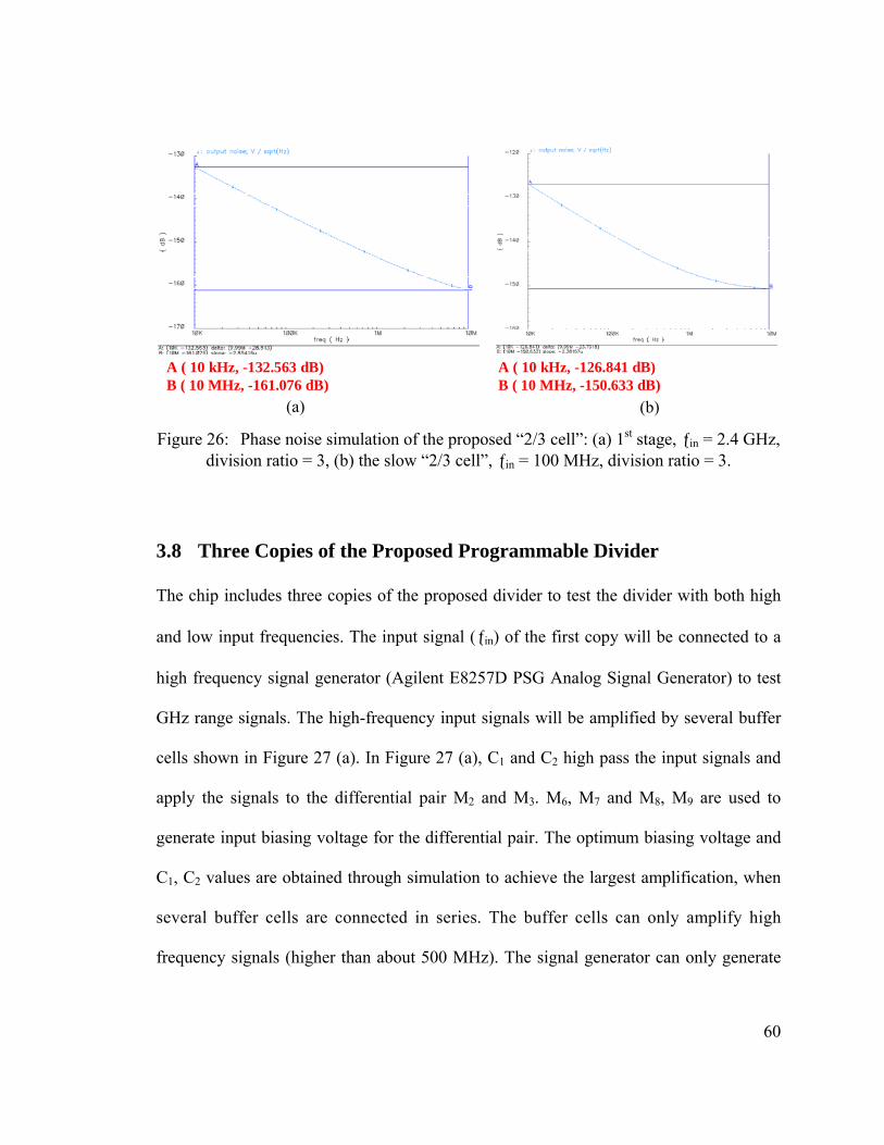
60
A ( 10 kHz, -132.563 dB)B ( 10 MHz, -161.076 dB)
A ( 10 kHz, -126.841 dB)B ( 10 MHz, -150.633 dB)
(b)(a) Figure 26: Phase noise simulation of the proposed “2/3 cell”: (a) 1st stage, ƒin = 2.4 GHz,
division ratio = 3, (b) the slow “2/3 cell”, ƒin = 100 MHz, division ratio = 3.
3.8 Three Copies of the Proposed Programmable Divider
The chip includes three copies of the proposed divider to test the divider with both high
and low input frequencies. The input signal (ƒin) of the first copy will be connected to a
high frequency signal generator (Agilent E8257D PSG Analog Signal Generator) to test
GHz range signals. The high-frequency input signals will be amplified by several buffer
cells shown in Figure 27 (a). In Figure 27 (a), C1 and C2 high pass the input signals and
apply the signals to the differential pair M2 and M3. M6, M7 and M8, M9 are used to
generate input biasing voltage for the differential pair. The optimum biasing voltage and
C1, C2 values are obtained through simulation to achieve the largest amplification, when
several buffer cells are connected in series. The buffer cells can only amplify high
frequency signals (higher than about 500 MHz). The signal generator can only generate
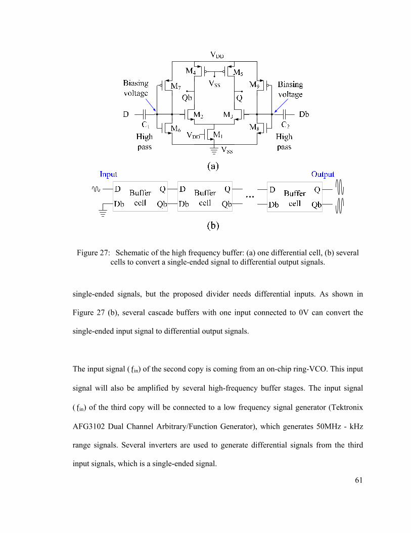
61
Figure 27: Schematic of the high frequency buffer: (a) one differential cell, (b) several cells to convert a single-ended signal to differential output signals.
single-ended signals, but the proposed divider needs differential inputs. As shown in
Figure 27 (b), several cascade buffers with one input connected to 0V can convert the
single-ended input signal to differential output signals.
The input signal (ƒin) of the second copy is coming from an on-chip ring-VCO. This input
signal will also be amplified by several high-frequency buffer stages. The input signal
(ƒin) of the third copy will be connected to a low frequency signal generator (Tektronix
AFG3102 Dual Channel Arbitrary/Function Generator), which generates 50MHz - kHz
range signals. Several inverters are used to generate differential signals from the third
input signals, which is a single-ended signal.

62
Chapter 4 Measurements of the Proposed Programmable Divider
4.1 Photographs of the Fabricated Chip and the Test Board
The chip was fabricated using a 0.18-μm RF CMOS process. Figure 28 shows the
photograph of the fabricated chip. The chip includes three copies of the proposed divider
to test the divider with both high and low input frequencies. Each copy consumes an area
of about 0.1 mm2. A RF (radio frequency) PCB (printed circuit board) is designed to test
the proposed divider and a fractional PLL including the proposed divider. The PLL
occupies and area of about 0.8 mm2 and it will be discussed in more details later.
Figure 29 shows the photograph of the PCB, which is a 4-layer board. Compared with a
2-layer PCB design, a 4-layer board has the following advantages. With the same total
thickness of all the layers, the distance between two nearby layers will be greatly
reduced. With a smaller distance between two layers, the 50 Ω transmission line drawn
on the board will have much smaller width. This is very helpful to layout the PCB
compactly.
4.2 Test Results of the Proposed Divider
The proposed programmable frequency-divider is tested using an oscilloscope to check
the output duty-cycle for both high frequency and low frequency input signals. Close-to-
50% output signals are obtained.
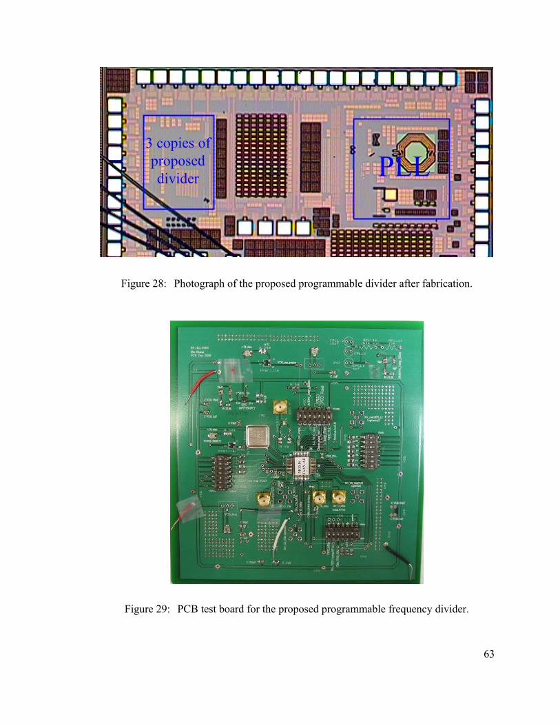
63
3 copies of proposed divider
Figure 28: Photograph of the proposed programmable divider after fabrication.
Figure 29: PCB test board for the proposed programmable frequency divider.
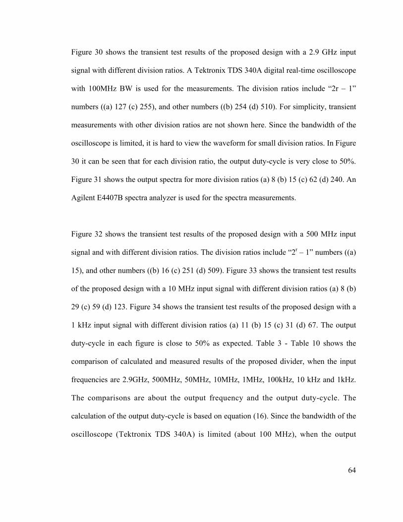
64
Figure 30 shows the transient test results of the proposed design with a 2.9 GHz input
signal with different division ratios. A Tektronix TDS 340A digital real-time oscilloscope
with 100MHz BW is used for the measurements. The division ratios include “2r – 1”
numbers ((a) 127 (c) 255), and other numbers ((b) 254 (d) 510). For simplicity, transient
measurements with other division ratios are not shown here. Since the bandwidth of the
oscilloscope is limited, it is hard to view the waveform for small division ratios. In Figure
30 it can be seen that for each division ratio, the output duty-cycle is very close to 50%.
Figure 31 shows the output spectra for more division ratios (a) 8 (b) 15 (c) 62 (d) 240. An
Agilent E4407B spectra analyzer is used for the spectra measurements.
Figure 32 shows the transient test results of the proposed design with a 500 MHz input
signal and with different division ratios. The division ratios include “2r – 1” numbers ((a)
15), and other numbers ((b) 16 (c) 251 (d) 509). Figure 33 shows the transient test results
of the proposed design with a 10 MHz input signal with different division ratios (a) 8 (b)
29 (c) 59 (d) 123. Figure 34 shows the transient test results of the proposed design with a
1 kHz input signal with different division ratios (a) 11 (b) 15 (c) 31 (d) 67. The output
duty-cycle in each figure is close to 50% as expected. Table 3 - Table 10 shows the
comparison of calculated and measured results of the proposed divider, when the input
frequencies are 2.9GHz, 500MHz, 50MHz, 10MHz, 1MHz, 100kHz, 10 kHz and 1kHz.
The comparisons are about the output frequency and the output duty-cycle. The
calculation of the output duty-cycle is based on equation (16). Since the bandwidth of the
oscilloscope (Tektronix TDS 340A) is limited (about 100 MHz), when the output
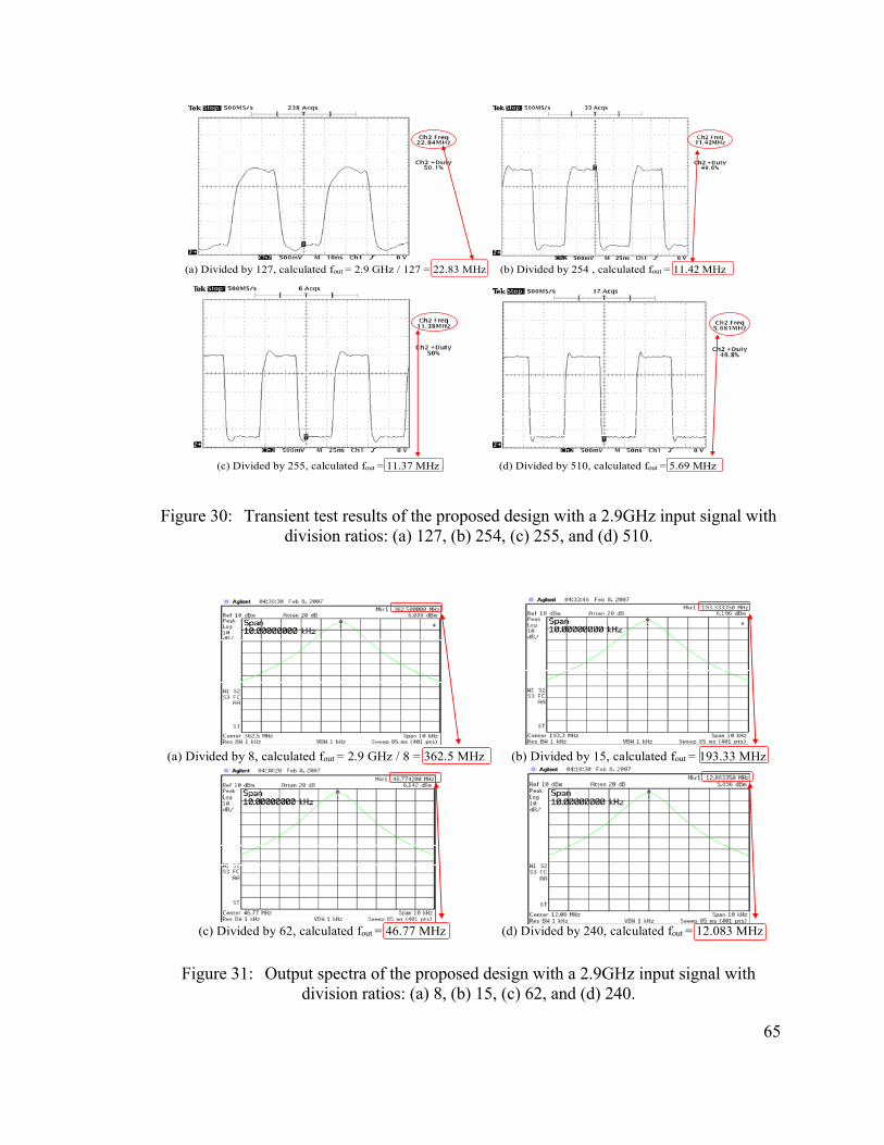
65
(d) Divided by 510, calculated fout = 5.69 MHz
(a) Divided by 127, calculated fout = 2.9 GHz / 127 = 22.83 MHz
(c) Divided by 255, calculated fout = 11.37 MHz
(b) Divided by 254 , calculated fout = 11.42 MHz
Figure 30: Transient test results of the proposed design with a 2.9GHz input signal with division ratios: (a) 127, (b) 254, (c) 255, and (d) 510.
(d) Divided by 240, calculated fout = 12.083 MHz
(a) Divided by 8, calculated fout = 2.9 GHz / 8 = 362.5 MHz
(c) Divided by 62, calculated fout = 46.77 MHz
(b) Divided by 15, calculated fout = 193.33 MHz
Figure 31: Output spectra of the proposed design with a 2.9GHz input signal with division ratios: (a) 8, (b) 15, (c) 62, and (d) 240.
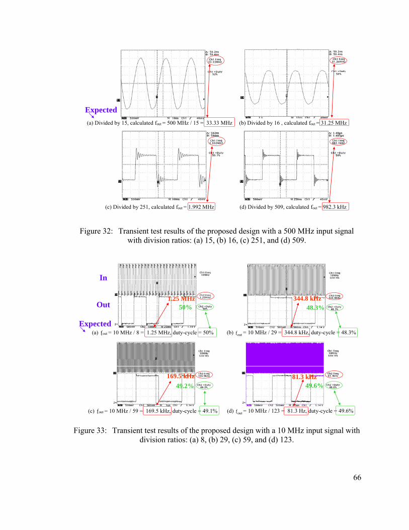
66
(d) Divided by 509, calculated fout = 982.3 kHz
(a) Divided by 15, calculated fout = 500 MHz / 15 = 33.33 MHz
(c) Divided by 251, calculated fout = 1.992 MHz
(b) Divided by 16 , calculated fout = 31.25 MHz
Expected
Figure 32: Transient test results of the proposed design with a 500 MHz input signal with division ratios: (a) 15, (b) 16, (c) 251, and (d) 509.
(a) ƒout = 10 MHz / 8 = 1.25 MHz, duty-cycle = 50% (b) ƒout = 10 MHz / 29 = 344.8 kHz, duty-cycle = 48.3%
1.25 MHz 344.8 kHz
169.5 kHz 81.3 kHz
In
Out 50%
Expected
48.3%
(c) ƒout = 10 MHz / 59 = 169.5 kHz, duty-cycle = 49.1% (d) ƒout = 10 MHz / 123 = 81.3 Hz, duty-cycle = 49.6%
49.2% 49.6%
Figure 33: Transient test results of the proposed design with a 10 MHz input signal with division ratios: (a) 8, (b) 29, (c) 59, and (d) 123.

67
(a) ƒout = 1 kHz / 11 = 90.91 Hz, duty-cycle = 5/11 = 45.5% (b) ƒout = 1 kHz / 15 = 66.67 Hz, duty-cycle = 46.7%
90.91 Hz 66.67 Hz
32.26 Hz 14.93 Hz
In
Out 45.5%
Expected
46.7%
(c) ƒout = 1 kHz / 31 = 32.26 Hz, duty-cycle = 48.4% (d) ƒout = 1 kHz / 67 = 14.93 Hz, duty-cycle = 49.3%
48.4% 49.3%
Figure 34: Transient test results of the proposed design with a 1 kHz input signal with division ratios: (a) 11, (b) 15, (c) 31, and (d) 67.
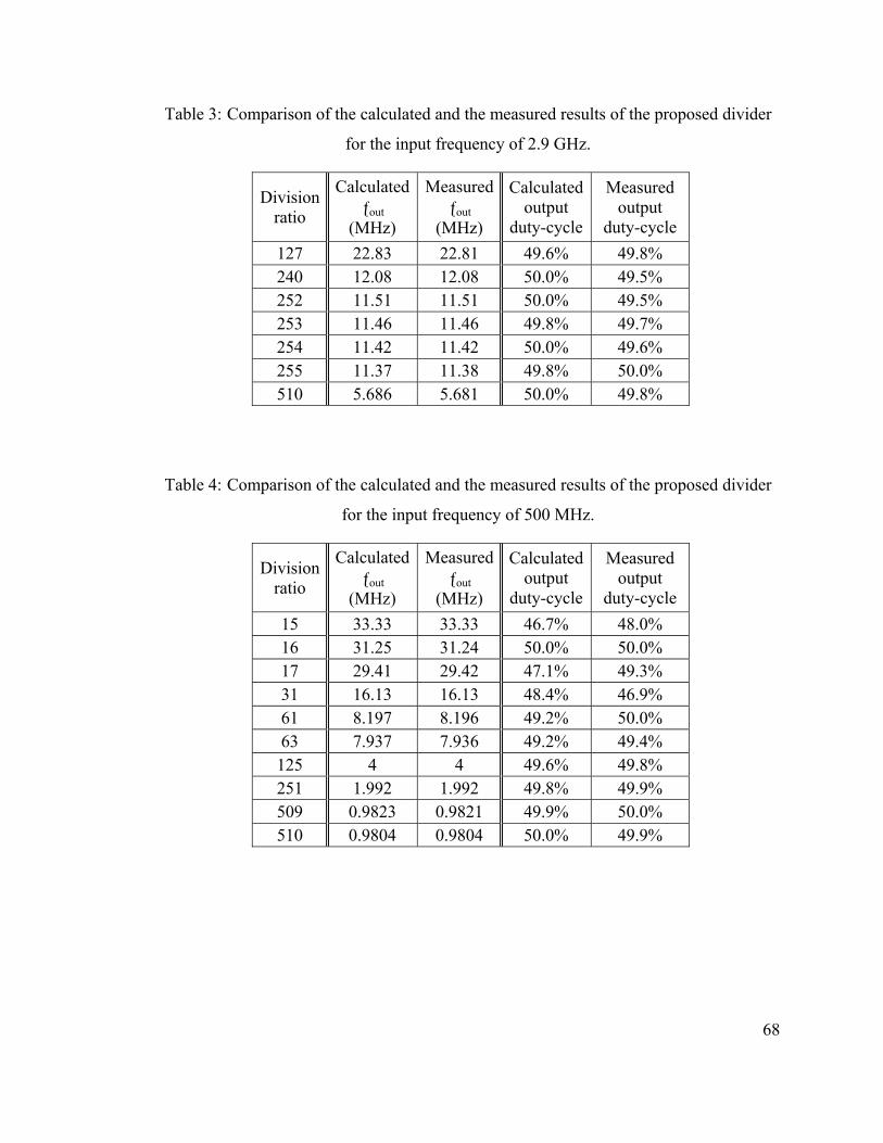
68
Table 3: Comparison of the calculated and the measured results of the proposed divider
for the input frequency of 2.9 GHz.
Division ratio
Calculated ƒout
(MHz)
Measured ƒout
(MHz)
Calculated output
duty-cycle
Measured output
duty-cycle 127 22.83 22.81 49.6% 49.8% 240 12.08 12.08 50.0% 49.5% 252 11.51 11.51 50.0% 49.5% 253 11.46 11.46 49.8% 49.7% 254 11.42 11.42 50.0% 49.6% 255 11.37 11.38 49.8% 50.0% 510 5.686 5.681 50.0% 49.8%
Table 4: Comparison of the calculated and the measured results of the proposed divider
for the input frequency of 500 MHz.
Division ratio
Calculated ƒout
(MHz)
Measured ƒout
(MHz)
Calculated output
duty-cycle
Measured output
duty-cycle 15 33.33 33.33 46.7% 48.0% 16 31.25 31.24 50.0% 50.0% 17 29.41 29.42 47.1% 49.3% 31 16.13 16.13 48.4% 46.9% 61 8.197 8.196 49.2% 50.0% 63 7.937 7.936 49.2% 49.4% 125 4 4 49.6% 49.8% 251 1.992 1.992 49.8% 49.9% 509 0.9823 0.9821 49.9% 50.0% 510 0.9804 0.9804 50.0% 49.9%

69
Table 5: Comparison of the calculated and the measured results of the proposed divider
for the input frequency of 50 MHz.
Division ratio
Calculated ƒout
(MHz)
Measured ƒout
(MHz)
Calculated output
duty-cycle
Measured output
duty-cycle 8 6.25 6.251 50.0% 49.9% 9 5.556 5.555 44.4% 44.1% 11 4.545 4.544 45.5% 45.3% 15 3.333 3.333 46.7% 46.7% 31 1.613 1.613 48.4% 48.3% 61 0.8197 0.8197 49.2% 49.2% 125 0.4 0.4 49.6% 49.6% 127 0.3937 0.3937 49.6% 49.6% 251 0.1992 0.1992 49.8% 49.8% 255 0.1961 0.1961 49.8% 49.8% 509 0.09823 0.09824 49.9% 49.9%
Table 6: Comparison of the calculated and the measured results of the proposed divider
for the input frequency of 10 MHz.
Division ratio
Calculated ƒout (kHz)
Measured ƒout (kHz)
Calculated output
duty-cycle
Measured output
duty-cycle
8 1250 1250 50.0% 50.0% 9 1111.1 1111.1 44.4% 44.4% 13 769.2 769/2 46.1% 46.2% 15 666.7 666.7 46.6% 46.6% 29 344.8 344.8 48.3% 48.3% 31 322.6 322.6 48.3% 48.3% 45 222.2 222.2 48.9% 48.9% 59 169.5 169.5 49.1% 49.2% 111 90.09 90.09 49.5% 49.5% 123 81.3 81.3 49.6% 49.6%
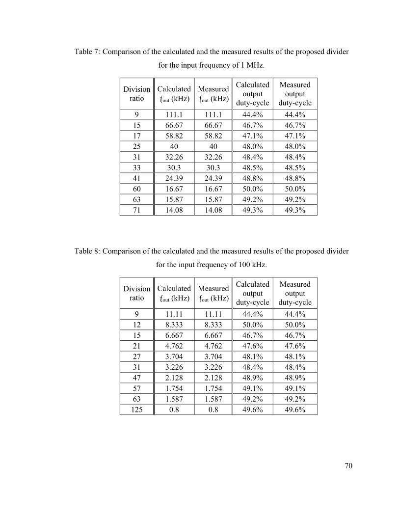
70
Table 7: Comparison of the calculated and the measured results of the proposed divider
for the input frequency of 1 MHz.
Division ratio
Calculated ƒout (kHz)
Measured ƒout (kHz)
Calculated output
duty-cycle
Measured output
duty-cycle 9 111.1 111.1 44.4% 44.4% 15 66.67 66.67 46.7% 46.7% 17 58.82 58.82 47.1% 47.1% 25 40 40 48.0% 48.0% 31 32.26 32.26 48.4% 48.4% 33 30.3 30.3 48.5% 48.5% 41 24.39 24.39 48.8% 48.8% 60 16.67 16.67 50.0% 50.0% 63 15.87 15.87 49.2% 49.2% 71 14.08 14.08 49.3% 49.3%
Table 8: Comparison of the calculated and the measured results of the proposed divider
for the input frequency of 100 kHz.
Division ratio
Calculated ƒout (kHz)
Measured ƒout (kHz)
Calculated output
duty-cycle
Measured output
duty-cycle 9 11.11 11.11 44.4% 44.4% 12 8.333 8.333 50.0% 50.0% 15 6.667 6.667 46.7% 46.7% 21 4.762 4.762 47.6% 47.6% 27 3.704 3.704 48.1% 48.1% 31 3.226 3.226 48.4% 48.4% 47 2.128 2.128 48.9% 48.9% 57 1.754 1.754 49.1% 49.1% 63 1.587 1.587 49.2% 49.2% 125 0.8 0.8 49.6% 49.6%
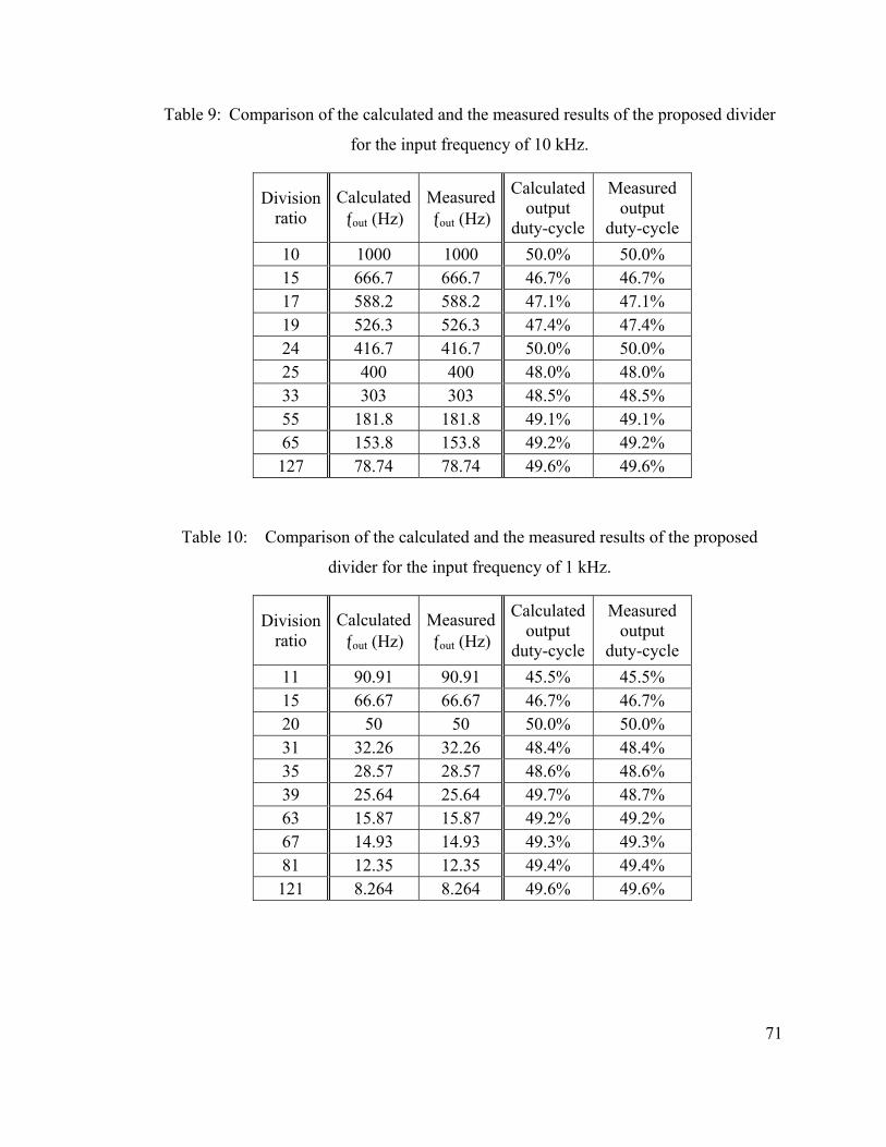
71
Table 9: Comparison of the calculated and the measured results of the proposed divider
for the input frequency of 10 kHz.
Division ratio
Calculated ƒout (Hz)
Measured ƒout (Hz)
Calculated output
duty-cycle
Measured output
duty-cycle 10 1000 1000 50.0% 50.0% 15 666.7 666.7 46.7% 46.7% 17 588.2 588.2 47.1% 47.1% 19 526.3 526.3 47.4% 47.4% 24 416.7 416.7 50.0% 50.0% 25 400 400 48.0% 48.0% 33 303 303 48.5% 48.5% 55 181.8 181.8 49.1% 49.1% 65 153.8 153.8 49.2% 49.2% 127 78.74 78.74 49.6% 49.6%
Table 10: Comparison of the calculated and the measured results of the proposed
divider for the input frequency of 1 kHz.
Division ratio
Calculated ƒout (Hz)
Measured ƒout (Hz)
Calculated output
duty-cycle
Measured output
duty-cycle 11 90.91 90.91 45.5% 45.5% 15 66.67 66.67 46.7% 46.7% 20 50 50 50.0% 50.0% 31 32.26 32.26 48.4% 48.4% 35 28.57 28.57 48.6% 48.6% 39 25.64 25.64 49.7% 48.7% 63 15.87 15.87 49.2% 49.2% 67 14.93 14.93 49.3% 49.3% 81 12.35 12.35 49.4% 49.4% 121 8.264 8.264 49.6% 49.6%
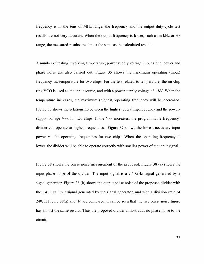
72
frequency is in the tens of MHz range, the frequency and the output duty-cycle test
results are not very accurate. When the output frequency is lower, such as in kHz or Hz
range, the measured results are almost the same as the calculated results.
A number of testing involving temperature, power supply voltage, input signal power and
phase noise are also carried out. Figure 35 shows the maximum operating (input)
frequency vs. temperature for two chips. For the test related to temperature, the on-chip
ring VCO is used as the input source, and with a power supply voltage of 1.8V. When the
temperature increases, the maximum (highest) operating frequency will be decreased.
Figure 36 shows the relationship between the highest operating-frequency and the power-
supply voltage VDD for two chips. If the VDD increases, the programmable frequency-
divider can operate at higher frequencies. Figure 37 shows the lowest necessary input
power vs. the operating frequencies for two chips. When the operating frequency is
lower, the divider will be able to operate correctly with smaller power of the input signal.
Figure 38 shows the phase noise measurement of the proposed. Figure 38 (a) shows the
input phase noise of the divider. The input signal is a 2.4 GHz signal generated by a
signal generator. Figure 38 (b) shows the output phase noise of the proposed divider with
the 2.4 GHz input signal generated by the signal generator, and with a division ratio of
240. If Figure 38(a) and (b) are compared, it can be seen that the two phase noise figure
has almost the same results. Thus the proposed divider almost adds no phase noise to the
circuit.

73
2.3
2.4
2.5
2.6
2.7
0 10 20 30 40 50 60 70
Temperature ( oC )
Hig
hest
inpu
t fre
quen
cy (G
Hz) chip 1 chip2
Figure 35: Maximum operating (input) frequency vs. temperature.
1.3
1.8
2.3
2.8
3.3
1.1 1.3 1.5 1.7 1.9 2.1 2.3 2.5
VDD (Volt)
Max
imum
f_in
(GH
z) chip1 chip2
Figure 36: The highest operating (input) frequency vs. VDD for two chips. The dots are the experimental results. The lines are the best-fitting lines.
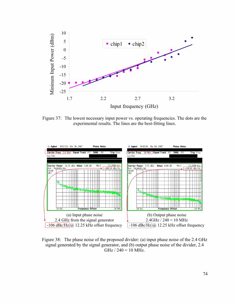
74
-25
-20
-15
-10
-5
0
5
10
1.7 2.2 2.7 3.2
Input frequency (GHz)
Min
inum
Inpu
t Pow
er (d
Bm
)chip1 chip2
Figure 37: The lowest necessary input power vs. operating frequencies. The dots are the
experimental results. The lines are the best-fitting lines.
(a) Input phase noise2.4 GHz from the signal generator
-106 dBc/Hz @ 12.25 kHz offset frequency
(b) Output phase noise 2.4GHz / 240 = 10 MHz
-106 dBc/Hz @ 12.25 kHz offset frequency
Figure 38: The phase noise of the proposed divider: (a) input phase noise of the 2.4 GHz signal generated by the signal generator, and (b) output phase noise of the divider, 2.4
GHz / 240 = 10 MHz.
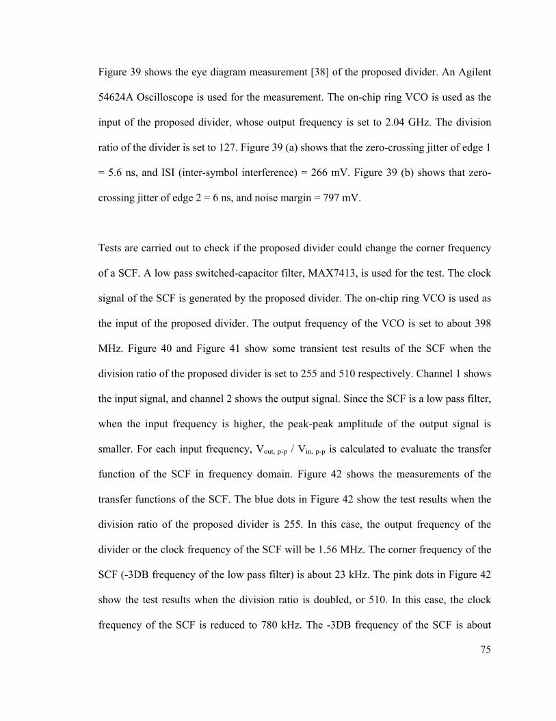
75
Figure 39 shows the eye diagram measurement [38] of the proposed divider. An Agilent
54624A Oscilloscope is used for the measurement. The on-chip ring VCO is used as the
input of the proposed divider, whose output frequency is set to 2.04 GHz. The division
ratio of the divider is set to 127. Figure 39 (a) shows that the zero-crossing jitter of edge 1
= 5.6 ns, and ISI (inter-symbol interference) = 266 mV. Figure 39 (b) shows that zero-
crossing jitter of edge 2 = 6 ns, and noise margin = 797 mV.
Tests are carried out to check if the proposed divider could change the corner frequency
of a SCF. A low pass switched-capacitor filter, MAX7413, is used for the test. The clock
signal of the SCF is generated by the proposed divider. The on-chip ring VCO is used as
the input of the proposed divider. The output frequency of the VCO is set to about 398
MHz. Figure 40 and Figure 41 show some transient test results of the SCF when the
division ratio of the proposed divider is set to 255 and 510 respectively. Channel 1 shows
the input signal, and channel 2 shows the output signal. Since the SCF is a low pass filter,
when the input frequency is higher, the peak-peak amplitude of the output signal is
smaller. For each input frequency, Vout, p-p / Vin, p-p is calculated to evaluate the transfer
function of the SCF in frequency domain. Figure 42 shows the measurements of the
transfer functions of the SCF. The blue dots in Figure 42 show the test results when the
division ratio of the proposed divider is 255. In this case, the output frequency of the
divider or the clock frequency of the SCF will be 1.56 MHz. The corner frequency of the
SCF (-3DB frequency of the low pass filter) is about 23 kHz. The pink dots in Figure 42
show the test results when the division ratio is doubled, or 510. In this case, the clock
frequency of the SCF is reduced to 780 kHz. The -3DB frequency of the SCF is about
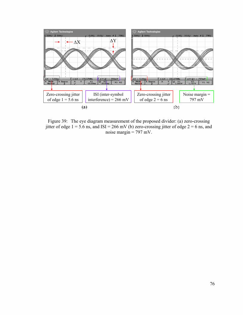
76
Zero-crossing jitter of edge 1 = 5.6 ns
ISI (inter-symbol interference) = 266 mV
Zero-crossing jitter of edge 2 = 6 ns
Noise margin = 797 mV
ΔX ΔY
Figure 39: The eye diagram measurement of the proposed divider: (a) zero-crossing jitter of edge 1 = 5.6 ns, and ISI = 266 mV (b) zero-crossing jitter of edge 2 = 6 ns, and
noise margin = 797 mV.
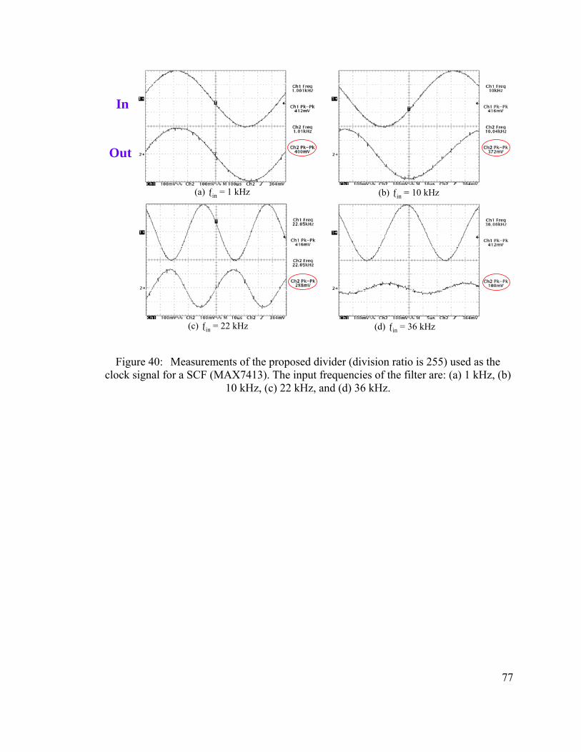
77
(a) ƒin = 1 kHz (b) ƒin = 10 kHz
(c) ƒin = 22 kHz (d) ƒin = 36 kHz
In
Out
Figure 40: Measurements of the proposed divider (division ratio is 255) used as the clock signal for a SCF (MAX7413). The input frequencies of the filter are: (a) 1 kHz, (b)
10 kHz, (c) 22 kHz, and (d) 36 kHz.
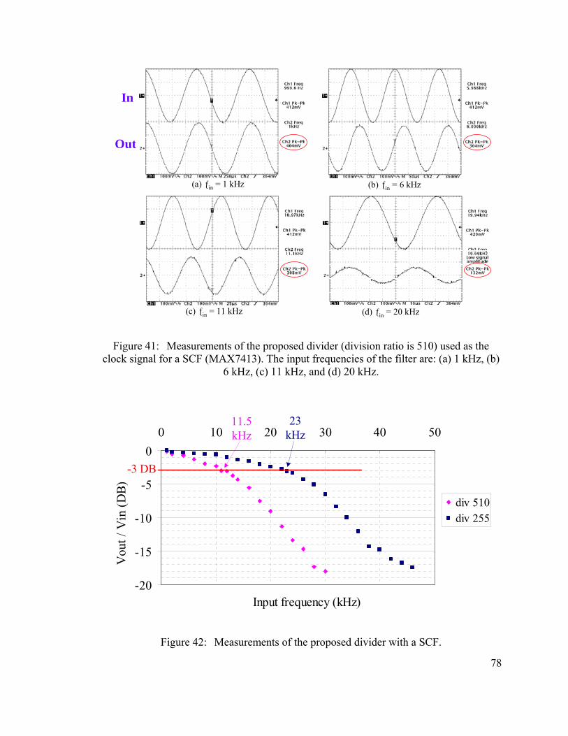
78
(a) ƒin = 1 kHz (b) ƒin = 6 kHz
(c) ƒin = 11 kHz (d) ƒin = 20 kHz
In
Out
Figure 41: Measurements of the proposed divider (division ratio is 510) used as the clock signal for a SCF (MAX7413). The input frequencies of the filter are: (a) 1 kHz, (b)
6 kHz, (c) 11 kHz, and (d) 20 kHz.
-20
-15
-10
-5
00 10 20 30 40 50
Input frequency (kHz)
Vou
t / V
in (D
B)
div 510div 255
-3 DB
11.5 kHz
23 kHz
Figure 42: Measurements of the proposed divider with a SCF.
79
255510
780kHz1.56MHz
11.5kHz23kHz
==
11.5 kHz. From the test results, the following equation could be obtained,
(75)
Equation (75) verifies the relationship shown in equation (19). Thus the corner frequency
of the SCF is proportional to ƒclk, which is reversely proportional to the division ratio of
the divider.
In general, the test results of the fabricated circuit verify the effectiveness of the proposed
programmable divider. It can generate very close-to-50% output duty-cycle, and with a
wide division ratio range for a very wide frequency range (GHz down to kHz). The phase
noise caused by the proposed divider is also very small.
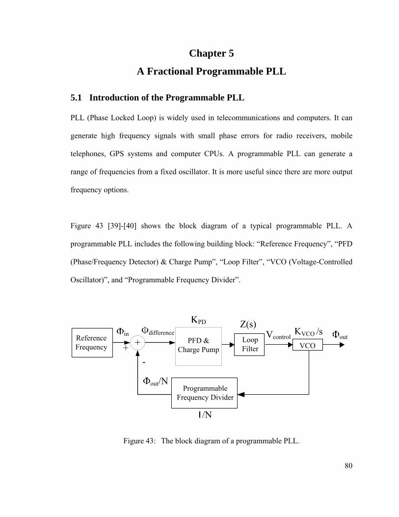
80
Chapter 5 A Fractional Programmable PLL
5.1 Introduction of the Programmable PLL
PLL (Phase Locked Loop) is widely used in telecommunications and computers. It can
generate high frequency signals with small phase errors for radio receivers, mobile
telephones, GPS systems and computer CPUs. A programmable PLL can generate a
range of frequencies from a fixed oscillator. It is more useful since there are more output
frequency options.
Figure 43 [39]-[40] shows the block diagram of a typical programmable PLL. A
programmable PLL includes the following building block: “Reference Frequency”, “PFD
(Phase/Frequency Detector) & Charge Pump”, “Loop Filter”, “VCO (Voltage-Controlled
Oscillator)”, and “Programmable Frequency Divider”.
PFD & Charge Pump
Loop Filter VCOLoop Filter VCOLoop Filter VCO
in+
-
Reference Frequency +
Programmable Frequency Divider
PD Z(s)VCO /s
/N
out
out/N
difference Vcontrol
Figure 43: The block diagram of a programmable PLL.
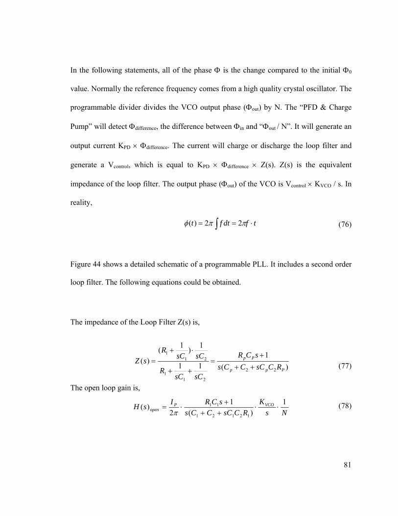
81
NsK
RCsCCCssCRIsH VCOP
open1
)(1
2)(
12121
11 ⋅⋅+++
⋅=π
In the following statements, all of the phase Φ is the change compared to the initial Φ0
value. Normally the reference frequency comes from a high quality crystal oscillator. The
programmable divider divides the VCO output phase (Φout) by N. The “PFD & Charge
Pump” will detect Φdifference, the difference between Φin and “Φout / N”. It will generate an
output current KPD × Φdifference. The current will charge or discharge the loop filter and
generate a Vcontrol, which is equal to KPD × Φdifference × Z(s). Z(s) is the equivalent
impedance of the loop filter. The output phase (Φout) of the VCO is Vcontrol × KVCO / s. In
reality,
(76)
Figure 44 shows a detailed schematic of a programmable PLL. It includes a second order
loop filter. The following equations could be obtained.
The impedance of the Loop Filter Z(s) is,
(77)
The open loop gain is,
(78)
tfdtft ⋅== ∫ ππφ 22)(
)(1
11
1)1()(
22
211
211
Ppp
Pp
RCsCCCssCR
sCsCR
sCsCR
sZ++
+=
++
⋅+=
82
π2P
PDIK =
sKVCO
)(sZ
Figure 44: More detailed schematic of a programmable PLL.
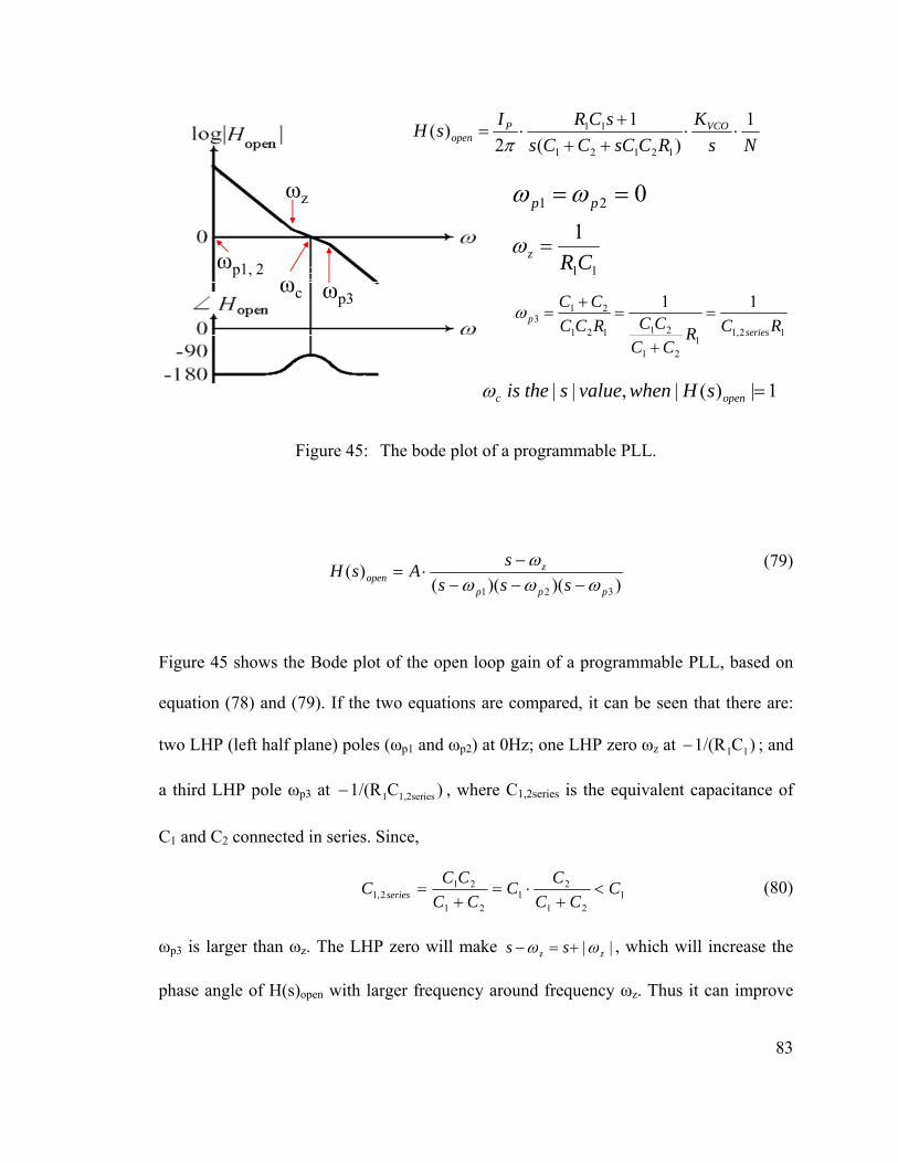
83
))()(()(
321 ppp
zopen sss
sAsHωωω
ω−−−
−⋅=
11
1CRz =ω
12,11
21
21121
213
11RCR
CCCCRCC
CC
seriesp =
+
=+
=ω
021 == pp ωω
ωp3
NsK
RCsCCCssCRIsH VCOP
open1
)(1
2)(
12121
11 ⋅⋅+++
⋅=π
ωc
ωz
1|)(|,|| =openc sHwhenvaluestheisω
ωp1, 2
Figure 45: The bode plot of a programmable PLL.
(79)
Figure 45 shows the Bode plot of the open loop gain of a programmable PLL, based on
equation (78) and (79). If the two equations are compared, it can be seen that there are:
two LHP (left half plane) poles (ωp1 and ωp2) at 0Hz; one LHP zero ωz at )C1/(R 11− ; and
a third LHP pole ωp3 at )C1/(R 1,2series1− , where C1,2series is the equivalent capacitance of
C1 and C2 connected in series. Since,
121
21
21
212,1 C
CCCC
CCCCC series <
+⋅=
+= (80)
ωp3 is larger than ωz. The LHP zero will make || zz ss ωω +=− , which will increase the
phase angle of H(s)open with larger frequency around frequency ωz. Thus it can improve
84
VCOPD
VCOPD
closed
KRCsCCC
sCRKN
s
KRCsCCC
sCRKsH
⋅++
+⋅⋅+
⋅++
+⋅=
)(11
)(1
)(
12121
112
12121
11
sKsZK
N
sKsZK
sHVCO
PD
VCOPD
in
outclosed
⋅⋅⋅+
⋅⋅==
)(11
)()(
φφ
the phase margin of H(s)open because of the ripple of the ∠Hopen curve shown in Figure
45. When the peak of the ripple happens at the crossover frequency ωc, the best phase
margin can be obtained. With a better phase margin, the negative feedback system will be
more stable.
Based on Figure 43 and Figure 44, the closed loop transfer function of the programmable
PLL could be obtained as follows,
(81)
By inserting the result of equation (77) into equation (81), the following result will be
obtained,
(82)
By multiplying s2 to both the numerator and the denominator of equation (82), the
following result could be obtained,
(83)
In equation (83), when 02 == fjs π ,
Hclosed(s) will be N. This means that at DC or steady state, the output phase Φout = N ×
Φin. According to equation (76), Φ ∝ ƒ, so ƒout = N × ƒin.
sK
RCsCCCssCRK
N
sK
RCsCCCssCRK
sHVCO
PD
VCOPD
closed
⋅+++⋅⋅+
⋅+++
⋅=
)(111
)(1
)(
12121
11
12121
11
85
5.2 A Fractional Programmable PLL
A frequency divider is an important component in a PLL. If the division ratio is N, and
the input reference frequency of a PLL is ƒin, the output frequency ƒo will be N⋅ƒin. In the
case of a PLL using a programmable divider, the frequency channel-distance of ƒo will be
ΔN⋅ƒin, where ΔN is the increasing step of the division ratios. Obviously, the smaller the
value of ΔN, the smaller is the channel distance. With a smaller channel distance and
limited entire bandwidth, there could be more channels. It is not always a good idea to
reduce ƒin, because it will make a PFD to wait longer to compare the reference frequency
with the signal out of the frequency divider. In that case, a longer settling time will be
induced to the PLL. If a fractional programmable divider is used, ΔN will be reduced.
Without decreasing ƒin, smaller channel distance still could be obtained. Since ƒin is not
reduced, the settling time of the PLL will not be longer.
Another advantage of fractional division ratios is stated bellow. The loop bandwidth of a
PLL should be set to lower than 1/10 of the reference frequency. At higher offset
frequencies, the VCO phase noise will be smaller. Since the VCO phase noise will be
high-passed to the output of the PLL, the VCO phase noise will be suppressed more with
a wider loop bandwidth or a higher reference frequency. Thus with the same frequency
resolution or output frequency channel distance, a fractional divider can use a higher
reference frequency, which can have a wider loop bandwidth and lower phase noise from
the VCO [30] [31].
86
sTTjTjTeez TjsT −=−≈−=== −−− 11)sin()cos(1 ωωωω
sTsTz =−−=−∴ − )1(11 1
5.2.1 A Fractional Programmable Frequency Divider
Figure 46 shows the schematic of the proposed fractional programmable PLL. The
difference between this PLL and the one shown in Figure 43 is that a Delta-Sigma (Δ∑)
modulator is added to control the division ratio of the integer divider. The output signal
of the Δ∑ modulator is changing between “0” and “1”. For the Δ∑ modulator, if the
fractional number at the input is “.f”, the time percentage when the output is “1” should
also be “.f”. The average value of the output of the Δ∑ modulator will be “.f”. Thus the
LSB division ratio control P0 will have an average value of “.f”. If use “m” to represent
the binary combination of the MSB controls “P1P2…Pn”, the entire division ratio will be
“m.f”. A fractional programmable division ratio is obtained and the output frequency ƒo
will be “m.f × ƒin”.
Figure 47 shows the schematic and the equivalent model of a first order Δ∑ modulator. It
is an accumulator as shown at the left part of Figure 47, which includes a multi-bit adder
and several DFFs.
If 1<<Tω , and T is the clock period for the accumulator,
(84)
(85)
From the equations shown in Figure 47 and equations (84) and (85), the following results
could be obtained,
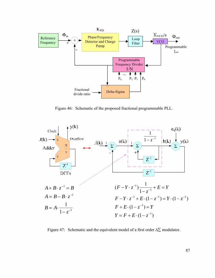
87
Phase/Frequency Detector and Charge
Pump
Loop Filter VCOLoop Filter VCOLoop Filter VCO
in+
-
Reference Frequency +
Programmable Frequency Divider
PD Z(s)VCO/s
/N
out
Programmableout
Fractional divide ratio
P0P1
...Pn P2
Delta-Sigma
Figure 46: Schematic of the proposed fractional programmable PLL.
1
1
1
11
−
−
−
−⋅=
⋅−=
=⋅+
zAB
zBBABzBA
)1()1(
)1()1(1
1)(
1
1
111
11
−
−
−−−
−−
−⋅+=
=−⋅+
−⋅=−⋅+⋅−
=+−
⋅−
zEFYYzEF
zYzEzYF
YEz
zYF
111
−− z
Figure 47: Schematic and the equivalent model of a first order Δ∑ modulator.

88
(86)
According to the result in equation (86), the output Y of the accumulator will high pass
the quantization error E. It means that when the frequency ƒ is higher, the output Y will
contain larger component coming from the quantization error E. Thus the phase noise of
Y will be higher at higher frequency ƒ.
Figure 48 shows the proposed fractional programmable divider with more details. An
accumulator or a ΔΣ modulator is inserted between the “ƒout_origin” and the “Cin” input of
the adder. The inputs of the accumulator are part of the division ratio controls. “S0” is the
LSB integer ratio control, while “Sf1” and “Sf2” are the MSB and LSB binary controls of
the fractional division ratio. The input clock signal of the accumulator is connected to the
original (Figure 7 (b)) integer divider output.
When the division ratio is < 2min+1, Smin is set to logic ‘1’. Thus the division ratio of the
fractional divider will be,
nn
nn SSSSSSSfSf
ratiodivision2222222 1
13
32
21
101
12
2 ⋅+⋅+⋅⋅⋅+⋅+⋅+⋅++⋅+⋅= −−
−− (87)
5.2.2 The LC VCO
Figure 49 shows the LC VCO used in the proposed PLL, which is similar to the circuit
used in [41]. Figure 49 (a) shows the top level schematic, (b) shows the equivalent circuit
of the LC tank, and (c) shows the equivalent one-side circuit. The advantage of this
circuit is the low power consumption and not too large output swing.
fjEFsTEFzEFY π2)1( 1 ⋅+=⋅+≈−⋅+= −
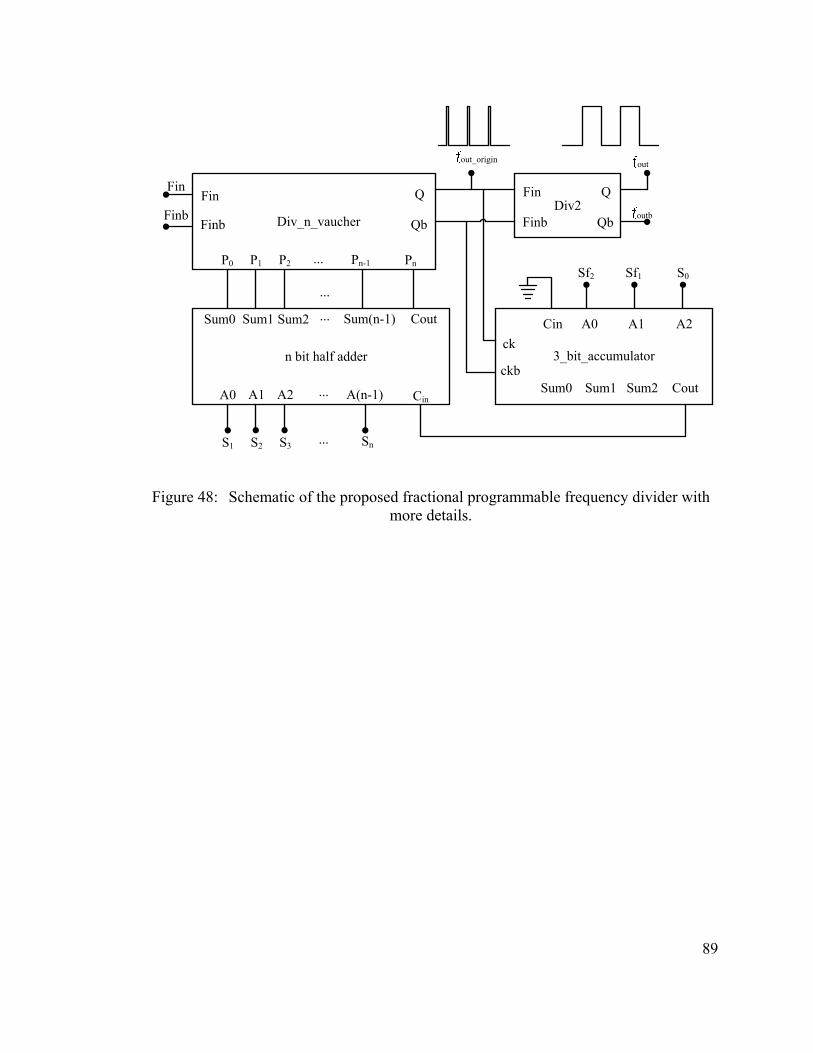
89
Div_n_vaucher
Fin
Finb
Q
Qb
Fin
P0
Fin
Finb
Q
QbDiv2
P1
...
PnP2
n bit half adder
Cout
A0 A1 A2 ...
Sum0 Sum1 Sum2 ...
Cin
S1 S2 SnS3 ...
Finb
out
outb
out_origin
A(n-1)
ck
ckb
A0 A1 A2Cin
3_bit_accumulator
Sum0 Sum1 Sum2 Cout
S0Sf1Sf2
Pn-1
Sum(n-1)
...
...
Figure 48: Schematic of the proposed fractional programmable frequency divider with more details.

90
Figure 49: Schematic of the LC VCO used in the PLL: (a) the top level schematic, (b) the equivalent circuit of the LC tank, and (c) the equivalent one-side circuit.
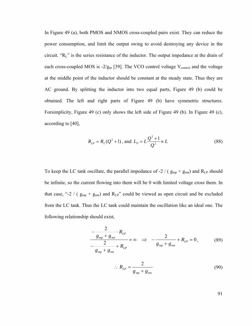
91
In Figure 49 (a), both PMOS and NMOS cross-coupled pairs exist. They can reduce the
power consumption, and limit the output swing to avoid destroying any device in the
circuit. “RL” is the series resistance of the inductor. The output impedance at the drain of
each cross-coupled MOS is -2/gm [39]. The VCO control voltage Vcontrol and the voltage
at the middle point of the inductor should be constant at the steady state. Thus they are
AC ground. By splitting the inductor into two equal parts, Figure 49 (b) could be
obtained. The left and right parts of Figure 49 (b) have symmetric structures.
Forsimplicity, Figure 49 (c) only shows the left side of Figure 49 (b). In Figure 49 (c),
according to [40],
)1( 2 += QRR LLP , and LQ
QLLP ≈+
= 2
2 1 (88)
To keep the LC tank oscillate, the parallel impedance of -2 / ( gmp + gmn) and RLP should
be infinite, so the current flowing into them will be 0 with limited voltage cross them. In
that case, “-2 / ( gmp + gmn) and RLP” could be viewed as open circuit and be excluded
from the LC tank. Thus the LC tank could maintain the oscillation like an ideal one. The
following relationship should exist,
022
2
=++
−⇒∞=+
+−
⋅+
−
LPmnmp
LPmnmp
LPmnmp R
ggRgg
Rgg
, (89)
mnmpLP gg
R+
=∴2
(90)
92
LPmnmp R
gg 2=+∴
(91)
Since Igm β2= , sufficient large current “I” has to be given in the circuit for sufficient
large mnmp gg + . Here gmp and gmn use the same dc current. There are other types of LC
VCOs [37], which only have one pair of cross-coupled MOS, such as only one pair of
cross-coupled NMOS. After the derivation similar to the above, the following
relationship will be obtained,
LPmn Rg /2= (92)
Only one item gmn appears on the left part of the equation. Thus for the same value of
RLP, more current is needed to obtain larger gmn, when compared with equation (91).
Another advantage of the VCO shown in Figure 49 (a) is that the output voltage will not
be higher than VDD. While for some other types of LC VCO [37], the output may be
higher than VDD, which may destroy some transistors connected to the VCO outputs. In
Figure 49 (a), when “Outp” is high, “Outn” should be low. Thus M4 is off and M3 is on.
When “Outp” is increased closed to VDD, M3 enters the linear region. The drain current of
M3 will be reduced. When “Outp” is increased to VDD, the drain current of M3 will be 0.
Thus the highest voltage of “Outp” will be VDD. Similarly, the highest voltage of “Outn”
will also be VDD. Using this VCO, the circuit can operate properly for a long time.
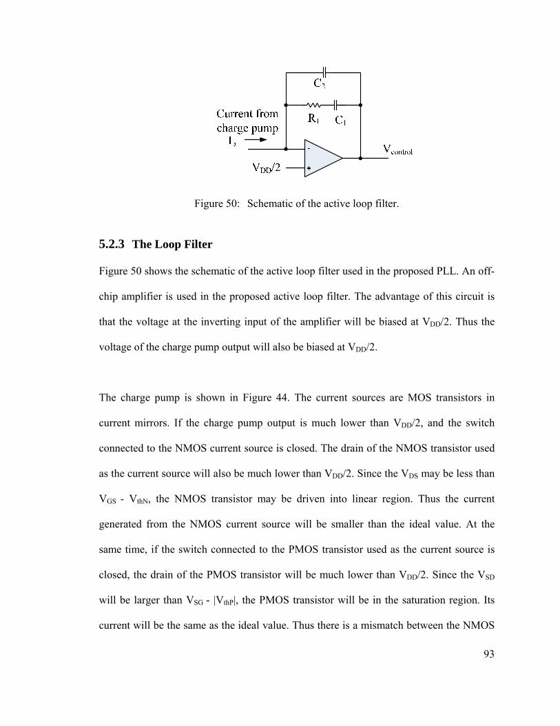
93
Figure 50: Schematic of the active loop filter.
5.2.3 The Loop Filter
Figure 50 shows the schematic of the active loop filter used in the proposed PLL. An off-
chip amplifier is used in the proposed active loop filter. The advantage of this circuit is
that the voltage at the inverting input of the amplifier will be biased at VDD/2. Thus the
voltage of the charge pump output will also be biased at VDD/2.
The charge pump is shown in Figure 44. The current sources are MOS transistors in
current mirrors. If the charge pump output is much lower than VDD/2, and the switch
connected to the NMOS current source is closed. The drain of the NMOS transistor used
as the current source will also be much lower than VDD/2. Since the VDS may be less than
VGS - VthN, the NMOS transistor may be driven into linear region. Thus the current
generated from the NMOS current source will be smaller than the ideal value. At the
same time, if the switch connected to the PMOS transistor used as the current source is
closed, the drain of the PMOS transistor will be much lower than VDD/2. Since the VSD
will be larger than VSG - |VthP|, the PMOS transistor will be in the saturation region. Its
current will be the same as the ideal value. Thus there is a mismatch between the NMOS
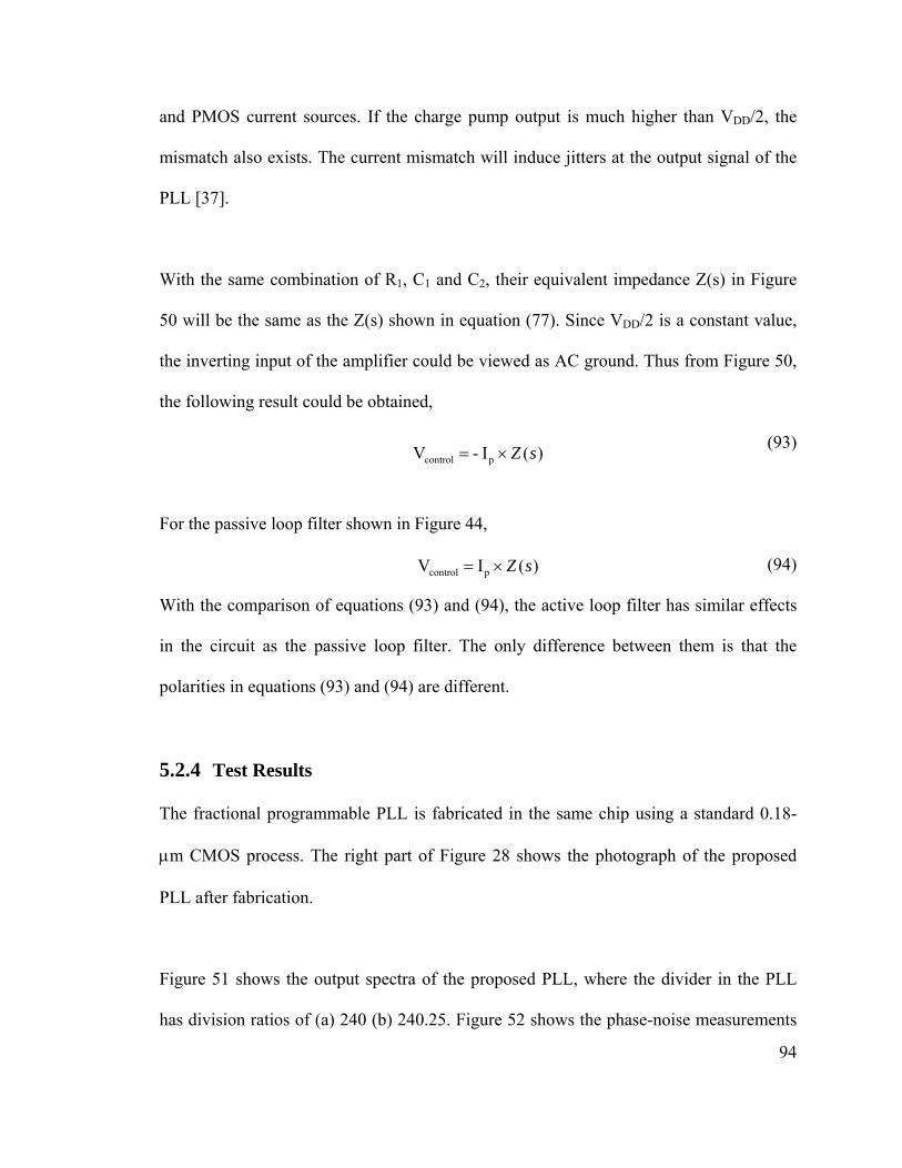
94
and PMOS current sources. If the charge pump output is much higher than VDD/2, the
mismatch also exists. The current mismatch will induce jitters at the output signal of the
PLL [37].
With the same combination of R1, C1 and C2, their equivalent impedance Z(s) in Figure
50 will be the same as the Z(s) shown in equation (77). Since VDD/2 is a constant value,
the inverting input of the amplifier could be viewed as AC ground. Thus from Figure 50,
the following result could be obtained,
(93)
For the passive loop filter shown in Figure 44,
(94)
With the comparison of equations (93) and (94), the active loop filter has similar effects
in the circuit as the passive loop filter. The only difference between them is that the
polarities in equations (93) and (94) are different.
5.2.4 Test Results
The fractional programmable PLL is fabricated in the same chip using a standard 0.18-
μm CMOS process. The right part of Figure 28 shows the photograph of the proposed
PLL after fabrication.
Figure 51 shows the output spectra of the proposed PLL, where the divider in the PLL
has division ratios of (a) 240 (b) 240.25. Figure 52 shows the phase-noise measurements
)( I - V pcontrol sZ×=
)( I V pcontrol sZ×=
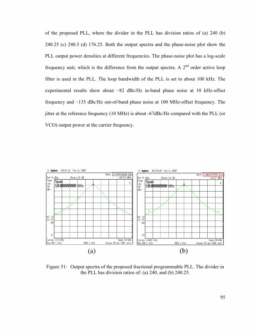
95
of the proposed PLL, where the divider in the PLL has division ratios of (a) 240 (b)
240.25 (c) 240.5 (d) 176.25. Both the output spectra and the phase-noise plot show the
PLL output power densities at different frequencies. The phase-noise plot has a log-scale
frequency unit, which is the difference from the output spectra. A 2nd order active loop
filter is used in the PLL. The loop bandwidth of the PLL is set to about 100 kHz. The
experimental results show about −82 dBc/Hz in-band phase noise at 10 kHz-offset
frequency and −135 dBc/Hz out-of-band phase noise at 100 MHz-offset frequency. The
jitter at the reference frequency (10 MHz) is about -67dBc/Hz compared with the PLL (or
VCO) output power at the carrier frequency.
Figure 51: Output spectra of the proposed fractional programmable PLL. The divider in the PLL has division ratios of: (a) 240, and (b) 240.25.
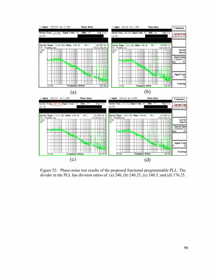
96
(a) (b)
(c) (d)
Figure 52: Phase-noise test results of the proposed fractional programmable PLL. The divider in the PLL has division ratios of: (a) 240, (b) 240.25, (c) 240.5, and (d) 176.25.
97
The fractional programmable PLL has an approximate frequency range of 1.7 - 2.5 GHz,
and a frequency resolution of 2.5 MHz. With a 1.8 volt power supply, the power
consumption is about 20 mW. The PLL can operate at 2.4 GHz with a power
consumption of only 10 mW with a 1.46 V power supply voltage.
98
Chapter 6 Conclusions and Future Work
A highly efficient programmable frequency-divider with a wide division ratio range and
close-to-50% output duty-cycle has been presented. The circuits are designed and
fabricated using a 0.18-μm RF CMOS process. The test results verify the effectiveness of
the proposed design. The output duty-cycle does not change with the input frequency (3.5
GHz down to 1 kHz), with temperature, with the voltage supply, or with different chips.
When the power supply is 1.8 V, the power consumption of the programmable
frequency-divider is about 15 mW.
A fractional programmable PLL is also presented. Test results show that the proposed
PLL has a frequency resolution of 2.5 MHz, and a minimum power consumption of 10
mW when operating at 2.4 GHz.
In the future, a fractional PLL with a multi-bit and higher order Δ∑ modulator can be
implemented for finer frequency resolution and lower phase noise. A charge pump [42]
shown in Figure 53 can be implemented in the PLL. It can reduce jitters of the PLL at the
reference frequency.
The charge pump shown in Figure 44 has a charge-sharing problem, which is stated in
section 15.3.1 of [37]. This problem occurs when the PFD compares the reference
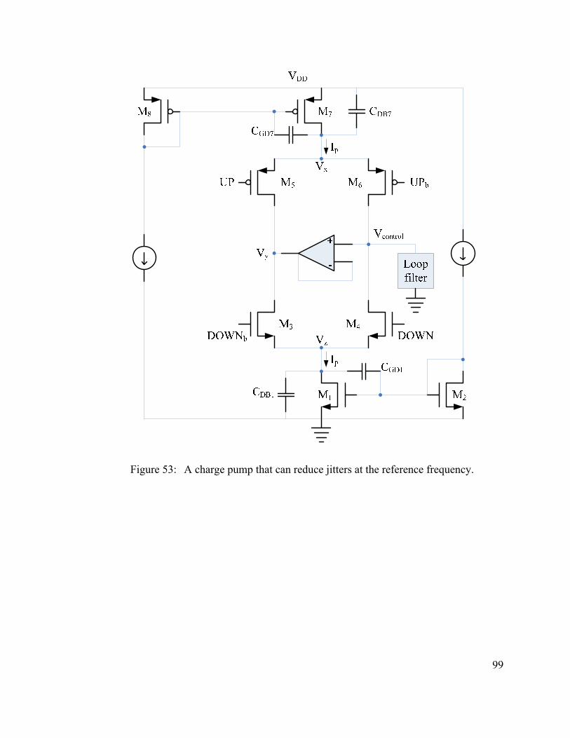
99
Figure 53: A charge pump that can reduce jitters at the reference frequency.
100
frequency and the divider output. Thus PLL output jitters will appear at the reference
frequency. The advantage of the charge pump shown in Figure 53 is stated as follows. M5
and M6 have the same size. M3 and M4 have the same size. When UP is high, M6 is on
and M5 is off. When UP changes from high to low, M6 turns off and M5 turns on. Vy
follows Vcontrol and is equal to Vcontrol. When UP changes from low back to high, M6 turns
on and M5 turns off. Since M5 and M6 have the same size, and Vy is equal to Vcontrol,
neither Id7 nor Vx (VD7) will change. Thus the charges on CDB7 and CGD7 will not change.
Since ID8 and VSG7 are constant, VG7 is ac ground. There is no current flowing into CDB7
and CGD7. Thus the current flowing into the loop filter will be exactly Ip. For DOWN part,
when DOWN changes from low to high, Vz (VD1) and the charges on CDB1 and CGD1 also
do not change. Thus the current flowing out of the loop filter will be exactly Ip. No (or
very little) current or charging disturbance occurs. Thus the PLL output jitters at the
reference frequency will be reduced.
Programmable frequency divider is an important component in the integrated high-speed
circuit. Any improvements of it will benefit in RF and digital design area. A
programmable PLL is also a very interesting and challenging work. Efforts to improve
each block in it will enhance the performance of the PLL, which may result more
applications.

101
References
102
[1] Roland E. Best, “Phase-Locked Loops Design, Simulation, and Applications,”
McGraw-Hill Professional Publishing, 4th edition, 1999.
[2] C. S. Vaucher, M. Locher, S. Sedvallson, U. Voegeli, and Z. Wang, “A Family of
Low-Power Truly Modular Programmable Dividers in Standard 0.35-μm CMOS
Technology,” IEEE Journal of Solid-State Circuits, vol. 35, pp. 1039-1045, July
2000.
[3] http://www.promwad.com/technology/soc_eng.html.
[4] X.P. Yu, M.A. Do, L. Jia, J.G. Ma, K.S. Yeo, “Design of a low power wide-band
high resolution programmable frequency divider,” IEEE Transactions on Very
Large Scale Integration (VLSI) Systems, vol. 13, Issue 9, pp.1098 – 1103,
September 2005.
[5] S. Khadanga, “Synchronous programmable divider design for PLL using 0.18 m
CMOS technology,” Proceedings of the 3rd IEEE International Workshop on
System-on-Chip for Real-Time Applications, pp. 281 – 286, 30 June - 2 July 2003.
[6] D. Guermandi, E. Franchi, A. Gnudi, G. Baccarani, “A CMOS programmable
divider for RF multistandard frequency synthesizers,” Proceedings of the 28th
European Solid-State Circuits Conference, pp. 843 – 846, September 2002.
[7] T. Ohgishi, A. Doi, T. Akiyama, N. Enomoto, “Molybdenum gate MOS applied
to an AM/FM digital frequency synthesizer,” IEEE Journal of Solid-State
Circuits, vol. 13, Issue 5, pp. 555 – 560, October 1978.
103
[8] S. Lee, and H. Park, “A CMOS high-speed wide-range programmable counter,”
IEEE Transactions on Circuits and Systems II: Analog and Digital Signal
Processing, [see also IEEE Transactions on Circuits and Systems II: Express
Briefs], vol. 49, Issue 9, pp. 638 – 642, September 2002.
[9] H. Chang, and J. Wu, “A 723-MHz 17.2-mW CMOS programmable counter,”
IEEE Journal of Solid-State Circuits, vol. 33, Issue 10, pp. 1572 – 1575, October
1998.
[10] Y. M. Wang, J. S. Wang, “An all-digital 50% duty-cycle corrector,” Proceedings
of the 2004 International Symposium on Circuits and Systems, vol. 2, pp. II - 925-
8, 23-26 May 2004.
[11] Y. C. Yang, S. A. Yu, T. Wang, S. S. Lu, “A dual-mode truly modular
programmable fractional divider based on a 1/1.5 divider cell,” IEEE Microwave
and Wireless Components Letters, [see also IEEE Microwave and Guided Wave
Letters], vol. 15, Issue 11, pp.754 – 756, November 2005.
[12] H. T. Bui, Y. Savaria, “High Speed Differential Pulse-Width Control Loop Based
on Frequency-to-Voltage Converters,” GLSVLSI’06, pp. 53-56, April 30–May 2,
2006.
[13] L. Li, J.H. Chen, R.C. Chang, “A low jitter delay-locked loop with a realignment
duty cycle corrector,” IEEE International SOC Conference Proceedings, pp. 73 –
76, 25-28 September 2005.
104
[14] T. Gawa, K. Taniguchi, “A 50% duty-cycle correction circuit for PLL output,”
IEEE International Symposium on Circuits and Systems, vol. 4, pp. IV-21 - IV-
24, May 2002.
[15] Y.C. Jang, S.J. Bae, H.J. Park, “CMOS digital duty cycle correction circuit for
multi-phase clock,” Electronics Letters, vol. 39, Issue 19, pp. 1383 – 1384, 18
September 2003.
[16] B. G. Kim, K. I. Oh, L. S. Kim, D. W. Lee, “A 500MHz DLL with second order
duty cycle corrector for low jitter,” Proceedings of the IEEE 2005 Custom
Integrated Circuits Conference, pp. 325 – 328, 18-21 Sept. 2005.
[17] N. Krishnapura, and P.R. Kinget, “A 5.3-GHz programmable divider for
HiPerLAN in 0.25-μm CMOS,” IEEE Journal of Solid-State Circuits, vol.
35, Issue 7, pp. 1019 – 1024, July 2000.
[18] P.J. Hurst, B.C. Rothenberg, “A programmable clock generator that uses noise
shaping and its application in switched-capacitor filters,” IEEE Journal of Solid-
State Circuits, vol. 30, Issue 4, pp. 403 – 411, April 1995.
[19] F. Rezzi, F. Montecchi, R. Castello, “A PLL-based frequency synthesizer for 160-
MHz double-sampled SC filters,” IEEE Journal of Solid-State Circuits, vol. 31,
Issue 10, pp. 1560 – 1564, October 1996.
[20] S. Karthikeyan, “Clock duty cycle adjuster circuit for switched capacitor circuits,”
Electronics Letters, vol. 38, Issue 18, pp. 1008 – 1009, 29 August 2002.
[21] http://www.maxim-ic.com/appnotes.cfm/appnote_number/724

105
[22] W. B. Yang, S. C. Kuo, Y. H. Chu, K. H. Cheng, “The new approach of
programmable pseudo fractional-N clock generator for GHz operation with 50%
duty cycle,” Proceedings of the 2005 European Conference on Circuit Theory
and Design, vol. 3, pp. III/193 - III/196, 28 August - 2 September 2005.
[23] ftp://download.intel.com/design/mobile/datashts/30526202.pdf
[24] V.V. Kaenel, D. Aebischer, C. Piguet, E. Dijkstra, “A 320 MHz, 1.5 [email protected] V
CMOS PLL for microprocessor clock generation,” IEEE Journal of Solid-State
Circuits, vol. 31, Issue 11, pp. 1715 – 1722, November 1996.
[25] C. Metra, T.M. Mak, D. Rossi, “Clock calibration faults and their impact on
quality of high performance microprocessors,” Proceedings of 18th IEEE
International Symposium on Defect and Fault Tolerance in VLSI Systems, pp.63 –
70, 3-5 November 2003.
[26] K. Nakamura, M. Fukaishi, Y. Hirota, Y. Nakazawa, M. Yotsuyanagi, “A CMOS
50% duty cycle repeater using complementary phase blending,” Digest of
Technical Papers of Symposium on VLSI Circuits, pp. 48 – 49, 15-17 June 2000.
[27] S. H. -L. Tu, “A Differential Pulsewidth Control Loop for High-Speed VLSI
Systems,” IEEE Transactions on Circuits and Systems II: Express Briefs:
Accepted for future publication Volume PP, Issue 99, pp. 417 – 421, 2006.
[28] S. J. Jang, Y. -H. Jun, J.-G. Lee, B.-S. Kon, “ASMD with duty cycle correction
scheme for high-speed DRAM,” Electronics Letters, vol. 37, Issue 16, pp. 1004 –
1006, 2 August 2001.
106
[29] C. -Y. Yao, J. -W. Tsai, “Programmable divide-by-N counter with 50% duty-
cycle output,” Electronics Letters, vol. 35, Issue 8, pp. 624 – 625, 15 April 1999.
[30] C.H. Heng, B.S. Song, “A 1.8-GHz CMOS fractional-N frequency synthesizer
with randomized multiphase VCO,” IEEE Journal of Solid-State Circuits, vol. 38,
Issue 6, pp. 848 – 854, June 2003.
[31] W.Z. Chen, J.T. Wu, “A 2-V, 1.8-GHz BJT phase-locked loop,” IEEE Journal of
Solid-State Circuits, vol. 34, Issue 6, pp. 784 – 789, June 1999.
[32] B. Razavi, K.F. Lee, and R.H. Yan, “Design of high-speed, low-power frequency
dividers and phase-locked loops in deep submicron CMOS,” IEEE Journal of
Solid-State Circuits, vol. 30, Issue 2, pp. 101 – 109, February 1995.
[33] B. Razavi, K.F. Lee, and R.H. Yan, “A 13.4-GHz CMOS frequency divider,”
IEEE International Solid-State Circuits Conference, Digest of Technical Papers,
41st ISSCC, pp. 176 – 177, February 1994.
[34] C. Lo, and H.C. Luong, “A 1.5-V 900-MHz monolithic CMOS fast-switching
frequency synthesizer for wireless applications,” IEEE Journal of Solid-State
Circuits, vol. 37, Issue 4, pp. 459 – 470, April 2002.
[35] S. Levantino, L. Romano, S. Pellerano, C. Samori, A.L.Lacaita, “Phase noise in
digital frequency dividers,” IEEE Journal of Solid-State Circuits, vol. 39, Issue 5,
pp.775 – 784, May 2004.
107
[36] W. F. Egan, “Modeling phase noise in frequency dividers,” IEEE Transactions on
Ultrasonics, Ferroelectrics and Frequency Control, vol. 37, pp. 307–315, July
1990.
[37] Behzad Razavi, “Design of Analog CMOS Integrated Circuits”, McGraw-Hill
Science / Engineering / Math, 2000.
[38] A. Bruce Carlson, Paul B. Crilly, Janet C. Rutledge, “Communication Systems”,
McGraw-Hill Science/Engineering/Math; 4th edition, 2001.
[39] B. Razavi, “RF Microelectronics”, Prentice Hall, 1st edition, 1997.
[40] Thomas H. Lee, “Design of CMOS Radio-Frequency Integrated Circuits,”
Cambridge University press, 2000.
[41] M. Tiebout, “Low-power low-phase-noise differentially tuned quadrature VCO
design in standard CMOS,” IEEE Journal of Solid-State Circuits, vol. 36, Issue 7,
pp. 1018 – 1024, July 2001.
[42] W. Rhee, “Design of high-performance CMOS charge pumps in phase-locked
loops,” Proceedings of the 1999 IEEE International Symposium on Circuits and
Systems, vol. 2, pp. 545 – 548, 30 May-2 June 1999.

108
Vita
Mo Zhang was born in Zhengzhou, Henan province, P. R. China in 1977. She
graduated from the Experimental Middle School of Henan Province in 1995. In 1995, she
entered Tsinghua University in Beijing, China. She received a Bachelor of Science
Degree in Electrical Engineering from Tsinghua University in 2000. She began her
graduate study at the University of Tennessee in Knoxville in August of 2001. Since then
she was a research assistant in Analog VLSI and Devices Laboratory. She received a
Master of Science degree in Electrical Engineering in May 2003. In summer of 2005, she
worked as an engineering intern in Maxim/Dallas Integrated Products, Inc. In summer of
2006, she had intern work in Invensys Controls, Robertshaw Industrial Products, Inc. Her
research interests include RF, mixed-signal, and analog IC design.