
A planar ion trap chip with integrated structures for an adjustable magnetic field gradient
10
A planar ion trap chip with integrated structures for an adjustable magnetic field gradient P. J. Kunert • D. Georgen • L. Bogunia • M. T. Baig • M. A. Baggash • M. Johanning • Ch. Wunderlich Received: 21 June 2013 / Accepted: 4 November 2013 / Published online: 1 December 2013 Ó Springer-Verlag Berlin Heidelberg 2013 Abstract We present the design, fabrication, and char- acterization of a segmented surface ion trap with integrated current-carrying structures. The latter produce a spatially varying magnetic field necessary for magnetic-gradient- induced coupling between ionic effective spins. We dem- onstrate trapping of strings of 172 Yb ? ions and characterize the performance of the trap and map magnetic fields by radio frequency-optical double-resonance spectroscopy. In addition, we apply and characterize the magnetic gradient and demonstrate individual addressing in a string of three ions using RF radiation. 1 Introduction Cold trapped ions have been established as a benchmark system in quantum information science and were used to show a variety of first proof-of-principle demonstrations [1, 2] in this field. When scaling up the number of qubits or ions, a widely favored solution to limit detrimental effects of decoherence is to split the entire quantum register into partitions of manageable size by using segmented traps featuring loading and processor zones [3, 4], and ion transfer between zones can be achieved in a fast diabatic manner optimized to reduce heating [5, 6]. When increas- ing the complexity of such traps, planar designs are often favored, as they benefit from elaborated micro-system fabrication techniques. These allow for very flexible designs [7, 8] (for a recent review see [9]) relevant for universal quantum computing, but also in the context of quantum simulations, where customized electrode shapes can be used to realize various lattice structures and inter- action types between trapped ions [10–12]. Ionic qubits can be manipulated with high fidelity using laser-based gates, whereas qubits encoded into hyperfine states can also be manipulated directly by radio frequency (RF) fields. One way to maintain the addressability of single ions despite their separation being orders of magnitude below the diffraction limit is the application of a static magnetic field gradient and exploiting an inhomogeneous Zeeman effect [13–17] which allows addressing in frequency space. In this way, low crosstalk can be achieved [16]. For addressing of individual ions, it has also been proposed [18] and demonstrated [19] to use inhomogeneous laser fields, and addressing has been demonstrated using oscil- lating microwave gradients [20]. Coupling between internal and motional states of trap- ped ions—needed for conditional quantum dynamics with several ions—is negligible in usual ion traps when RF radiation is applied. In the presence of a static [13, 15] or oscillating [21] magnetic field gradient, however, such coupling is induced. Also, coupling between spin states of different ions [14, 16, 17] arises in a spatially varying magnetic field and is thus termed magnetic-gradient- induced coupling (MAGIC). A static gradient can be generated by permanent mag- nets [15, 16] or by current loops that allow to introduce a time dependence. This was implemented into 3D ion trap P. J. Kunert D. Georgen L. Bogunia M. T. Baig M. A. Baggash M. Johanning Ch. Wunderlich (&) Department Physik, Naturwissenschaftlich-Technische Fakulta ¨t, Universita ¨t Siegen, 57068 Siegen, Germany e-mail: [email protected] Present Address: M. A. Baggash Max-Born-Institut fu ¨r Nichtlineare Optik und Kurzzeitspektroskopie, 12489 Berlin, Germany 123 Appl. Phys. B (2014) 114:27–36 DOI 10.1007/s00340-013-5722-9
Transcript of A planar ion trap chip with integrated structures for an adjustable magnetic field gradient
A planar ion trap chip with integrated structures for an adjustablemagnetic field gradient
P. J. Kunert • D. Georgen • L. Bogunia •
M. T. Baig • M. A. Baggash • M. Johanning •
Ch. Wunderlich
Received: 21 June 2013 / Accepted: 4 November 2013 / Published online: 1 December 2013
� Springer-Verlag Berlin Heidelberg 2013
Abstract We present the design, fabrication, and char-
acterization of a segmented surface ion trap with integrated
current-carrying structures. The latter produce a spatially
varying magnetic field necessary for magnetic-gradient-
induced coupling between ionic effective spins. We dem-
onstrate trapping of strings of 172Yb? ions and characterize
the performance of the trap and map magnetic fields by
radio frequency-optical double-resonance spectroscopy. In
addition, we apply and characterize the magnetic gradient
and demonstrate individual addressing in a string of three
ions using RF radiation.
1 Introduction
Cold trapped ions have been established as a benchmark
system in quantum information science and were used to
show a variety of first proof-of-principle demonstrations [1,
2] in this field. When scaling up the number of qubits or
ions, a widely favored solution to limit detrimental effects
of decoherence is to split the entire quantum register into
partitions of manageable size by using segmented traps
featuring loading and processor zones [3, 4], and ion
transfer between zones can be achieved in a fast diabatic
manner optimized to reduce heating [5, 6]. When increas-
ing the complexity of such traps, planar designs are often
favored, as they benefit from elaborated micro-system
fabrication techniques. These allow for very flexible
designs [7, 8] (for a recent review see [9]) relevant for
universal quantum computing, but also in the context of
quantum simulations, where customized electrode shapes
can be used to realize various lattice structures and inter-
action types between trapped ions [10–12].
Ionic qubits can be manipulated with high fidelity using
laser-based gates, whereas qubits encoded into hyperfine
states can also be manipulated directly by radio frequency
(RF) fields.
One way to maintain the addressability of single ions
despite their separation being orders of magnitude below
the diffraction limit is the application of a static magnetic
field gradient and exploiting an inhomogeneous Zeeman
effect [13–17] which allows addressing in frequency space.
In this way, low crosstalk can be achieved [16]. For
addressing of individual ions, it has also been proposed
[18] and demonstrated [19] to use inhomogeneous laser
fields, and addressing has been demonstrated using oscil-
lating microwave gradients [20].
Coupling between internal and motional states of trap-
ped ions—needed for conditional quantum dynamics with
several ions—is negligible in usual ion traps when RF
radiation is applied. In the presence of a static [13, 15] or
oscillating [21] magnetic field gradient, however, such
coupling is induced. Also, coupling between spin states of
different ions [14, 16, 17] arises in a spatially varying
magnetic field and is thus termed magnetic-gradient-
induced coupling (MAGIC).
A static gradient can be generated by permanent mag-
nets [15, 16] or by current loops that allow to introduce a
time dependence. This was implemented into 3D ion trap
P. J. Kunert � D. Georgen � L. Bogunia �M. T. Baig � M. A. Baggash � M. Johanning �Ch. Wunderlich (&)
Department Physik, Naturwissenschaftlich-Technische Fakultat,
Universitat Siegen, 57068 Siegen, Germany
e-mail: [email protected]
Present Address:
M. A. Baggash
Max-Born-Institut fur Nichtlineare Optik und
Kurzzeitspektroskopie, 12489 Berlin, Germany
123
Appl. Phys. B (2014) 114:27–36
DOI 10.1007/s00340-013-5722-9
designs [22], discussed for planar geometries [23], and
applied for addressing in frequency space using a laser
quadrupole transition [24]. The tailoring of the interactions
between ions can be achieved by shaping the axial elec-
trostatic trapping potential [14, 16, 25], but also by
changing the shape and direction of the magnetic field
gradient.
In what follows, we discuss design considerations and
fabrication details for a planar trap with integrated seg-
mented loops, which provide a magnetic field gradient
whose spatial dependence can be tailored. We present
experimental results with trapped ytterbium ions and
demonstrate for the first time the application of a magnetic
field gradient for RF addressing of ions in a planar trap.
2 Experimental setup
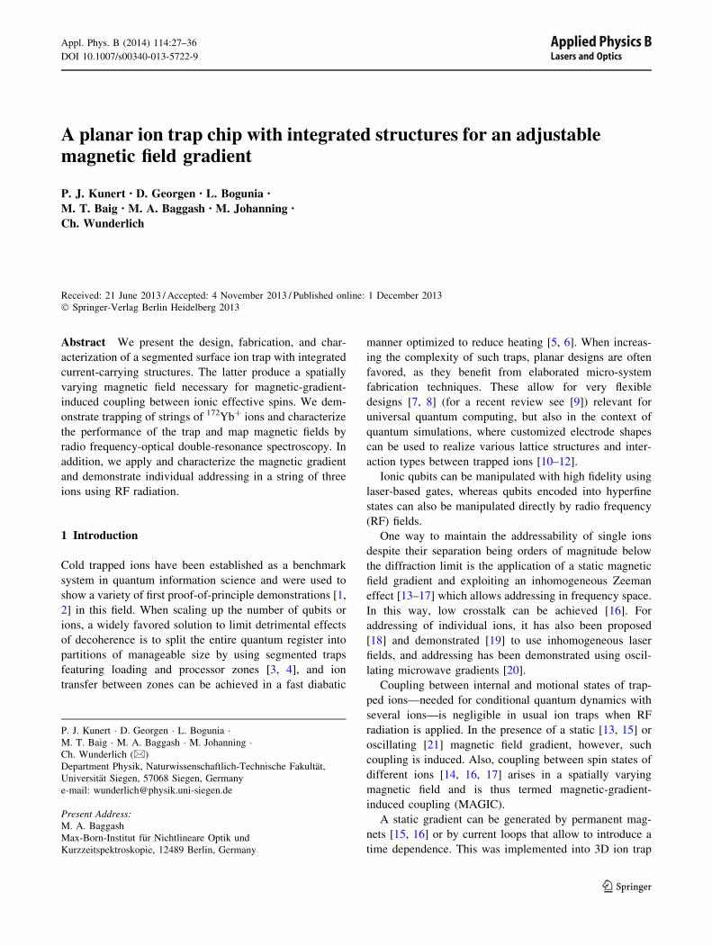
2.1 Trap design and fabrication
The trap presented here is a symmetric five-electrode pla-
nar trap design [26]. The outer dc electrodes are segmented
to provide axial confinement and allow for axial ion
transport. Numerical simulations based on the analytical
solutions for planar traps [27, 28] were carried out for
various electrode dimensions to maximize the trap depth at
given RF amplitude, and we choose the electrode width as
180 lm for the radio frequency electrodes and 150 lm for
the middle control electrode (see Fig. 1). Eleven dc elec-
trode pairs allow to transport ions over a range of several
millimeters and define several independent trapping
regions. In addition, we integrated current loops for the
creation of inhomogeneous fields to allow for MAGIC.
So far, approaches for integrated current loops for five-
electrode planar traps designs used a current through a
patterned center wire [23, 24] to create an inhomogeneous
magnetic field. In that case, the shape and the position of
the gradient are predetermined by the design of the elec-
trode/current loop. Here, we introduce a new approach
where several segmented dc electrodes are slotted.
Applying currents with individual magnitude and direction
through these micro-structured integrated current loops
provide a magnetic field gradient with a variable shape and
strength along the axial direction.
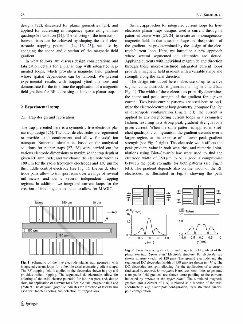
The design introduced here makes use of up to twelve
segmented dc electrodes to generate the magnetic field (see
Fig. 1). The width of these electrodes primarily determines
the shape and peak strength of the gradient for a given
current. Two basic current patterns are used here to opti-
mize the electrode/current loop geometry (compare Fig. 2):
in quadrupole configuration (Fig. 2 left), the current is
applied to any neighboring current loops in a symmetric
fashion, resulting in a strong peak gradient strength for a
given current. When the same pattern is applied in stret-
ched quadrupole configuration, the gradient extends over a
larger region, at the expense of a lower peak gradient
strength (see Fig. 2 right). The electrode width affects the
peak gradient value in both scenarios, and numerical sim-
ulations using Biot–Savart’s law were used to find the
electrode width of 350 lm to be a good a compromise
between the peak strengths for both patterns (see Fig. 3
left). The gradient depends also on the width of the RF
electrodes, as illustrated in Fig. 3, showing the peak
180 µm150 µm
350 µm 10 µm
y
x
laserslaser
Fig. 1 Schematic of the five-electrode planar trap geometry with
integrated current loops for a flexible axial magnetic gradient shape.
The RF trapping field is applied to the electrodes shown in gray and
provides radial trapping. The segmented dc electrodes allow for
tailoring of the axial electric potential for ion transport, and, due to
slots, for application of currents for a flexible axial magnetic field and
gradient. The diagonal gray line indicates the direction of laser beams
used for Doppler cooling and detection of trapped ions
-0.5 0.0 0.5y (mm)
0.0
1.0
d|B|dy
(T/Am)
-1.0 1.0 -0.5 0.0 0.5y (mm)
0.0
1.0
d|B|dy
(T/Am)
-1.0 1.0
y y
Fig. 2 Current-carrying structures and magnetic field gradient of the
planar ion trap. Upper panel Electrode structure. RF electrodes are
shown in gray (width of 120 lm). The ground electrode and the
segmented DC electrodes (width of 350 lm) are shown in white. The
DC electrodes are split allowing for the application of a current
(indicated by arrows). Lower panel Here, two possibilities to generate
a magnetic field gradient are shown corresponding to the currents
indicated by arrows in the upper panel. The simulated magnetic
gradient (for a current of 1 A) is plotted as a function of the axial
coordinate y. Left quadrupole configuration, right stretched quadru-
pole configuration
28 P. J. Kunert et. al.
123
gradient strength in quadrupole configuration for a dc
electrode width of 350 lm. A flexible shaping of the gra-
dient can be achieved as any current pattern with varying
current strength can be applied, resulting in the weighted
sum of the individual gradients.
The materials chosen for the trap chip were selected for
their compatibility with ultra-high-vacuum, high RF volt-
ages and high currents up to several Ampere to obtain large
trap depths and magnetic field gradients, low RF losses and
high thermal conductivity to remove heat intake efficiently.
The chip substrate is made of sapphire, as this material
allows for high RF amplitudes due to a high electrical
resistance and low absorption of RF power. Furthermore, a
good surface roughness of around 3 nm can be obtained.
The adhesion of the electrode material (in our case gold) is
essential and we improve it by an additional intermediate
adhesion layer of chromium. Any thermal load, either by
RF losses or from high currents required for large magnetic
gradients, is efficiently dissipated due to the large thermal
conductivity (45 W/mK) of sapphire.
The largest possible magnetic field gradient is given by
the damage threshold of the integrated coils due to ohmic
heating, so we aim to obtain a high damage threshold by
having a low resistivity (using thick electrodes made of
gold, which has a low specific resistivity) and by quickly
removing the heat by the good thermal conductivity of the
gold electrode and the sapphire substrate.
We create the trap electrodes by sputtering a 10 nm
chrome adhesion layer followed by a 50 nm gold seed
layer. Before every sputtering process, a physical etching
step cleans and smoothes the processed surface. The layer
thickness obtained by standard sputtering or evaporating
processes is usually limited to around 1 lm. Thicker
structures can be obtained by electroplating. The gaps
between the electrodes are defined by optical lithography
(Fig. 4a, b). In this process, the wafer is spin coated with
negative photo resist (AZ15nXT) with a height of 8.5 lm.
A baking step reduces the solvent before the resist is
covered with a photolithography mask and exposed with
UV light (i-line of Hg lamp). Another baking step cross-
links the resist. Then, after a chemical developer (AZ826)
has removed the exposed resist, a cleaning process with
oxygen plasma removes unintended residual resist. The
resist structure obtained in this process yields nearly ver-
tical edges and high aspect ratios (Fig. 4a, b). To determine
the quality of the resist structure, we removed a part of the
resist with an ion beam and visualized the structure under
100 200 300 4000
0.20.40.60.8
11.21.4
dc electrode width (µm)
grad
ient
(T
/Am
)
a
50 100 150 2000
1
2
3
4
rf electrode width (µm)
grad
ient
[T
/Am
]
cbd
Fig. 3 Simulated axial magnetic field gradient for varying electrode
widths. Left The gradient is shown as a function of the width of the
segmented dc electrode with fixed RF electrode width at 180 lm (a,
b) and 120 lm (c, d), respectively, for two different current
configurations: quadrupole (a, c) and stretched quadrupole (b, d) as
motivated in Fig. 2. For every fixed RF electrode width, a segmented
dc electrode width can be found which maximizes the gradient. Right
The gradient as a function of the RF electrode width (and in turn the
trapping height) is shown; here, segmented dc electrode width is fixed
at 350 lm. By reducing the trap dimension, gradients higher than 4
T/Am are predicted. The RF electrode widths presented in the left
part are marked by vertical lines in the right plot
Fig. 4 Focused ion beam imaging of the relevant production steps;
a Resist structure after photolithography that defines the gaps between
the electrodes in the following electroplating step. In this image, the
dark lines indicate resist structures that are elevated above the surface
of the substrate. b To determine the quality of the resist structure, we
removed a part of the resist with an ion beam and visualized the
structure under 52� relative to the substrate surface. In this way, the
resist thickness (8.6 lm) and the widths at the top (10 lm) and
bottom (9 lm) can be determined. c Electroplated electrodes. d Cut
through one electroplated electrode and measured gold height to
8.5 lm. e Structure after physical etching with a still existing chrome
layer (dark gray) between the gold electrodes (light gray). f A surface
roughness of 20–30 nm rms is measured with an AFM for different
chips and different positions on the chips. The figure shows one
sample for illustration
A planar ion trap chip with integrated structures 29
123
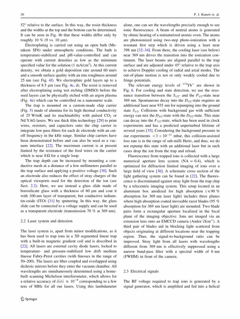
52� relative to the surface. In this way, the resist thickness
and the widths at the top and the bottom can be determined.
It can be seen in Fig. 4b that these widths differ only by
roughly 10 % (9 vs. 10 lm).
Electroplating is carried out using an open bath (Me-
takem SF6) under atmospheric conditions. The bath is
temperature-stabilized and pH-value-controlled and can
operate with current densities as low as the minimum
specified value for the solution (1 mA/cm2). At this current
density, we obtain a gold deposition rate around 60 nm/s
and a smooth surface quality with an rms roughness around
25 nm (see Fig. 4f). We electroplate gold layers up to a
thickness of 8.5 lm (see Fig. 4c, d). The resist is removed
after electroplating using wet etching (DMSO) before the
seed layers can be physically etched with an argon plasma
(Fig. 4e) which can be controlled on a nanometer scale.
The trap is mounted on a custom-made chip carrier
(Fig. 5) made of alumina for its high thermal conductivity
of 25 W/mK and its machinability with pulsed CO2 or
Nd:YAG lasers. We use thick film technology [29] to print
wires, resistors, and capacitors onto the chip carrier to
integrate low-pass filters for each dc electrode with an cut-
off frequency in the kHz range. Similar chip carriers have
been demonstrated before and can also be used as a vac-
uum interface [22]. The maximum current is at present
limited by the resistance of the feed wires on the carrier
which is near 8 X for a single loop.
The trap depth can be increased by mounting a con-
ductive mesh at a distance of a few millimeters parallel to
the trap surface and applying a positive voltage [30]. Such
an electrode also reduces the effect of stray charges of the
optical viewports used for the detection of the ion (see
Sect. 2.2). Here, we use instead a glass slide made of
borosilicate glass with a thickness of 60 lm and coat it
with 100-nm layer of transparent, but conductive indium-
tin-oxide (ITO) [31] by sputtering. In this way, the glass
slide can be connected to a voltage supply and can be used
as a transparent electrode (transmission 70 % at 369 nm).
2.2 Laser system and detection
The laser system is, apart from minor modifications, as it
has been used to trap ions in a 3D segmented linear trap
with a built-in magnetic gradient coil and is described in
[22]. All lasers are external cavity diode lasers, locked to
temperature- and pressure-stabilized low drift medium
finesse Fabry-Perot cavities (with finesses in the range of
50–200). The lasers are fiber coupled and overlapped using
dichroic mirrors before they enter the vacuum chamber. All
wavelengths are simultaneously determined using a home-
built scanning Michelson interferometer, which allows for
a relative accuracy of dk/k & 10-8 corresponding to a few
tens of MHz for all our lasers. Using this lambdameter
alone, one can set the wavelengths precisely enough to see
ionic fluorescence. A beam of neutral atoms is generated
by ohmic heating of a miniaturized atomic oven. The atoms
are photoionized using two-step photo-ionization with a
resonant first step which is driven using a laser near
398 nm [32–34]. From there, the cooling laser (see below)
near 369 nm drives the transition into the ionization con-
tinuum. The laser beams are aligned parallel to the trap
surface and are adjusted under 45� relative to the trap axis
to achieve Doppler cooling of radial and axial modes. The
out-of-plane motion is not or only weakly cooled due to
fringe potentials.
The relevant energy levels of 172Yb? are shown in
Fig. 6. For cooling and state detection, we use the reso-
nance transition between the S1/2- and the P1/2-state near
369 nm. Spontaneous decay into the D3/2-state requires an
additional laser near 935 nm for repumping into the ground
state S1/2. Collisions with background gas with sufficient
energy can mix the D3/2-state with the D5/2-state. This state
can decay into the F7/2-state, which has been used in clock
experiments and has a predicted unperturbed lifetime of
several years [35]. Considering the background pressure in
our experiments \3� 10�11 mbar, this collision-assisted
loss rate is in the range of sub-milli Hertz, and thus, we do
not repump this state with an additional laser but in such
cases drop the ion from the trap and reload.
Fluorescence from trapped ions is collected with a large
numerical aperture lens system (NA = 0.4), which is
optimized for diffraction limited imaging of ions over a
large field of view [36]. A schematic cross section of the
light gathering system can be found in [22]. The fluores-
cence is discriminated against stray light from the trap chip
by a telecentric imaging system. This setup located in an
aluminum box anodized for high absorption (&90 %
absorption for 369 nm laser light) includes three planes
where high absorption coated moveable razor blades (95 %
absorption for 369 nm laser light) are mounted. Two blade
pairs form a rectangular aperture localized in the focal
plane of the imaging objective. Ions are imaged via an
extension lens onto an EMCCD camera (Andor iXon?). A
third pair of blades aid in blocking light scattered from
objects originating at different locations near the trapping
region. Thus, the signal-to-background ratio can be
improved. Stray light from all lasers with wavelengths
different from 369 nm is effectively suppressed using a
narrow band-pass filter with a spectral width of 6 nm
(FWHM) in front of the camera.
2.3 Electrical signals
The RF voltage required to trap ions is generated by a
signal generator, which is amplified and fed into a helical
30 P. J. Kunert et. al.
123
resonator and the details of the setup are discussed in this
section. The helical resonator follows the general concept
reported in [37–39] and is designed as an autotransformer.
This approach yields lower insertion loss, but also results in
lower Q-factors compared to the approach described in
[40]. We carefully designed the resonator for mechanical
stability and wound the helix on a threaded low loss
dielectric tube (PTFE). The mechanical stability results in a
low drift of the resonance frequency of ±30 Hz over
several hours. This was measured using a capacitive load
(&30 pF), which is comparable to our trap including
connectors (&35 pF). The insertion point of the primary
coil, which is critical for impedance matching, is realized
as a slider which can be firmly fixed with a set screw with
good electrical contact, but, at the same time, can be moved
with little effort. The tube can be filled, also partially, by a
dielectric to tune the resonance frequency of the circuit.
The frequency tuning range is found to be on a percent
scale of the resonance frequency (for up to 80 % filling
with PTFE) and can alternatively be achieved by varying
the load, for instance, by a different length of the cable
connecting the resonator to the trap.
Even with a Q-factor near 80, we find that, due to low
insertion losses, the resonator can drive a trap like the one
described in [22] with a RF power of only 0.25 W, which is
readily delivered by the signal generator (as, for example, a
Rigol DG1012) and requires no further amplification. In
the experiments presented here, the RF amplitude is gen-
erated by a frequency generator (Hameg HM8032) and
amplified with a Kalmus 110C by 40 dB to a power of
approximately 0.4 W. The helical resonator boosts the
peak-to-peak voltage at the trap frequency of 14.7 MHz.
The voltage is fed into the trap and simultaneously moni-
tored via a 1 pF capacitance probe. The system is opti-
mized to avoid ground loops.
A system of DAC cards (Adwin Pro II) connected to
50 X drivers delivers 10 tunable voltages in the range
of ±10 V. Via jumpering (compare [22]) up to 75 poten-
tials can be routed to the trap electrodes via sub-d
connectors.
3 Trap characteristics
We demonstrate trapping 172Yb? ions in our planar trap
(Fig. 7). The storage time with laser cooling but without
repumping the F7/2-state is several hours for single ions and
several 10 minutes for ion chains up to 10 ions.
A measured trapping height of (160 ± 10) lm is in
agreement with the numerical simulation of the trapping
potential. The measured ion-ion distance for two ions is
10 lm (taking into account the independently determined
magnification of the detection system). Ions are stable for
RF peak-to-peak amplitudes between 150 Vpp and
400 Vpp. With a typical trapping amplitude of 250 Vpp and
a trap drive frequency of 14.7 MHz, the stability parameter
[26]
q ¼ 2QVrf
mX2r20
ð1Þ
is determined to be 0.22, with the charge Q, RF amplitude
Vrf = Vpp/2, trap drive frequency X and trap geometry
factor r0. The trap depth [26]
W0 ¼Q2V2
rf
4mX2r20
ð2Þ
is determined to be 73 meV.
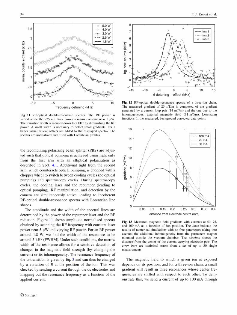
We measure trap frequencies by resonant heating, which
occurs, when the trap frequency coincides with the fre-
quency of a sinusoidal ’tickling’ signal applied to one dc
electrode. The motional frequencies are determined for the
axial direction in the range from 180 to 250 kHz (Fig. 8
left) and for the radial direction parallel to the trap surface
between 1.0 and 1.8 MHz (Fig. 8 right).
Stray fields may prevent the ion from being trapped at
the bottom of the effective potential, where the RF electric
field vanishes. In that case, the ion’s driven motion results
in sidebands in the absorption spectrum that are separated
from the carrier by multiples of the RF trap drive frequency
(Fig. 9 left). To detect and compensate this motion, the
dependence of the ion fluorescence intensity on the de-
tuning of the 935 nm laser is analyzed. By changing
potentials applied to the segmented dc electrodes, the ion
can be moved slightly along the radial direction toward the
RF minimum, where the sidebands are reduced and the
carrier dominates the absorption spectrum (Fig. 9 right).
Background light is reduced by a telecentric imaging
setup as described above. The signal-to-background ratio is
optimized starting with the blades initially fully open and
then closing them until the best ratio is achieved. For small
apertures, both signal and background depend approxi-
mately linearly on the area of the aperture and we use the
intersection of the tangent to the fluorescence rate with the
fluorescence rate that saturates for large apertures to find a
working point for the blade setting yielding a signal-to-
background ratio of 211 ± 9 compared to 54 ± 2 with
fully open blades.
4 RF-optical double-resonance spectroscopy
We demonstrate one of the two basic effects of an inho-
mogeneous magnetic field, the addressing of ions in fre-
quency space, using the Zeeman levels of the D3/2 manifold
(see Fig. 6). These levels have been previously used to
A planar ion trap chip with integrated structures 31
123
show addressability of ions using RF transitions in a
magnetic field gradient [15].
The metastable D3/2-state (lifetime of 52.2 ms [43]) is
populated by spontaneous decay from the P3/2-state with a
branching ratio of approximately 0.5 % [42]. Thus, optical
pumping into this level occurs on a microsecond time scale
into all Zeeman levels. In order to close the fluorescence
and cooling cycle, laser light near 935 nm is applied that
excites the ion to the [3/2]1/2-state which subsequently
decays to the ground electronic state. For cooling and
detection, the polarization of the 935 nm light has to
contain at least r? and r- components in order to prevent
optical pumping into any of the Zeeman states of the D3/2-
level. Light near 935 nm containing p, r?, and r-
components is achieved by using a linearly polarized light
beam incident on the ion at 45� relative to the quantization
axis. Thus, the population from all Zeeman substates is
pumped back to the ground electronic state. However, in
order to demonstrate individual addressing, we want to first
prepare an ion deterministically in one of the Zeeman
substates of the D3/2-level by optical pumping. This process
is described in what follows.
4.1 State initialization
When the repumper near 935 nm is linearly polarized and
its electric field is aligned parallel to the magnetic field that
determines the quantization axis, it will exclusively drive
p-transitions, which do not change the Zeeman quantum
number mJ. Thus, population accumulates in the Zeeman
states mJ = ±3/2 that are not coupled to the light field,
since the [3/2]1/2-state cannot be accessed from them by
p-transitions. Both levels mJ = ±3/2 are populated with
equal probability (assuming no imperfections in the
polarization state). Once the ion is optically pumped into
these two Zeeman states, fluorescence and cooling of the
ion stops. This initialization scheme requires an electric
field polarization parallel to the magnetic field, and thus a
propagation direction, indicated by the k-vector of the light
field, perpendicular to it.
1 mm
y x
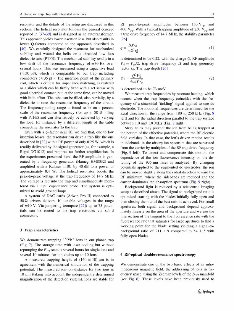
Fig. 5 Assembled electroplated ion trap chip with an edge length of
11 mm onto an alumina carrier with printed silver–palladium wires.
Every electrode is ball bonded six times with 50 lm gold wires to
gold-coated bond pads on the carrier
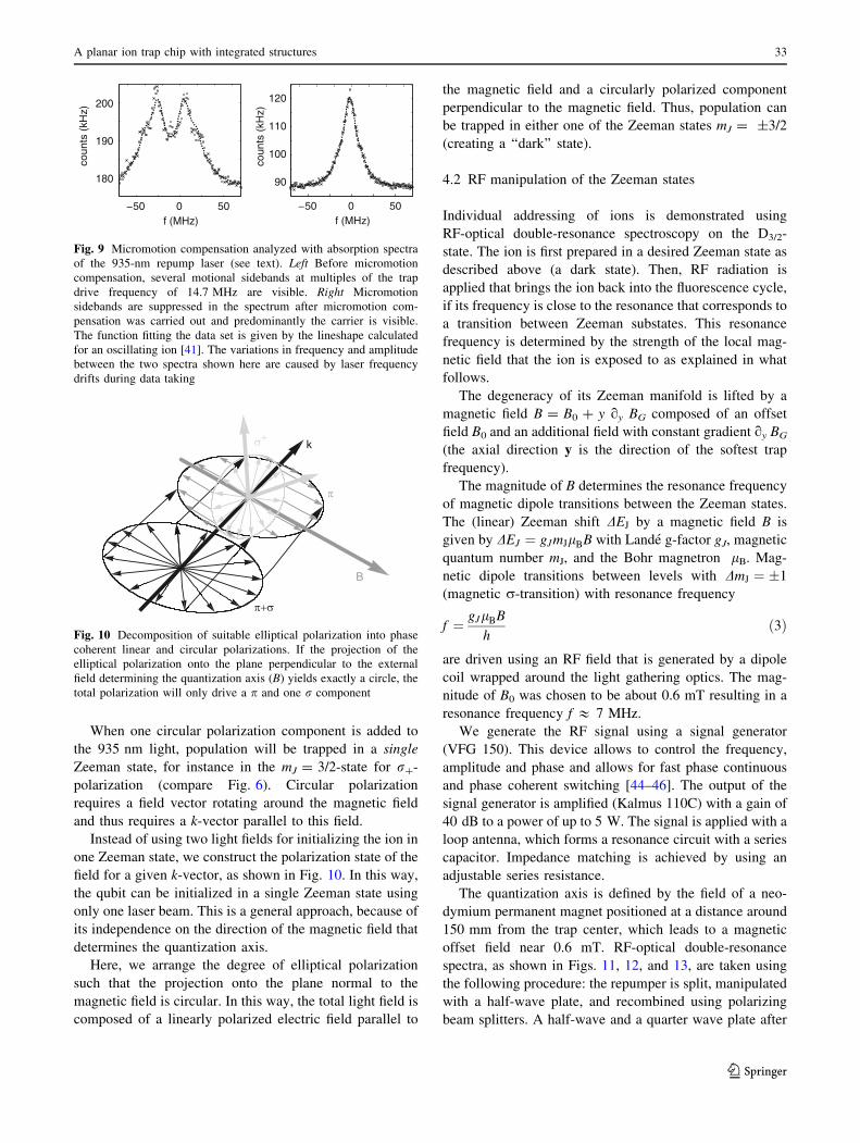
-3/2
D3/2
935 nm
3/2
1/2
-1/2ΩrfS1/2
P1/2
[3/2]1/2
D3/2
369 nm
935 nm
3/21/2
-1/2-3/2
mJ1/2
-1/2
Fig. 6 Relevant energy levels of 172Yb? (not to scale). Left The
electric dipole transition between the S1/2 ground state and the P1/2
excited state near 369 nm is used for Doppler cooling and state
selective detection by detecting resonance fluorescence with a
photomultiplier or an intensified CCD camera (termed ‘‘cooling
fluorescence’’). Laser light near 935 nm coupling the metastable state
D3/2-state to the [3/2]1/2 state allows for control of optical pumping
into the D3/2-state. Right RF radiation (Xrf ) couples the states
populated by optical pumping to those which are depopulated by the
repumping laser near 935 nm (see Sect. 4)
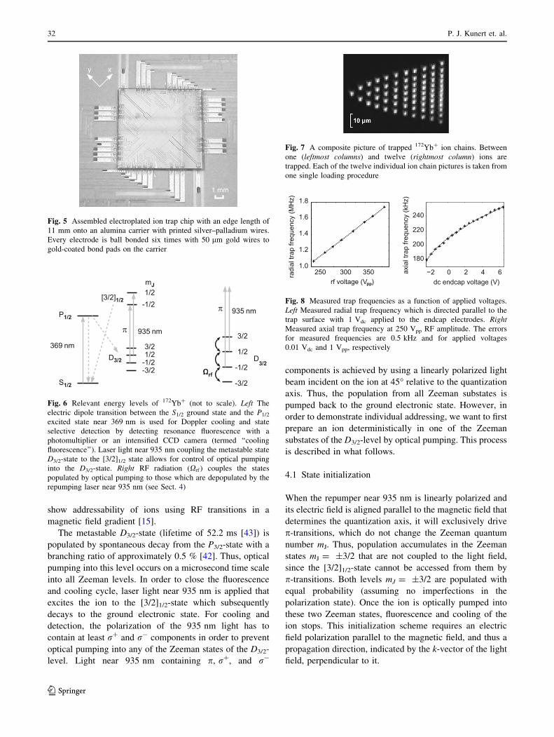
Fig. 7 A composite picture of trapped 172Yb? ion chains. Between
one (leftmost columns) and twelve (rightmost column) ions are
trapped. Each of the twelve individual ion chain pictures is taken from
one single loading procedure
−2 0 2 4 6
180
200
220
240
dc endcap voltage (V)
axia
l tra
p fre
quen
cy (k
Hz)
250 300 3501.0
1.2
1.4
1.6
1.8
rf voltage (V )ppra
dial
trap
freq
uenc
y (M
Hz)
Fig. 8 Measured trap frequencies as a function of applied voltages.
Left Measured radial trap frequency which is directed parallel to the
trap surface with 1 Vdc applied to the endcap electrodes. Right
Measured axial trap frequency at 250 Vpp RF amplitude. The errors
for measured frequencies are 0.5 kHz and for applied voltages
0.01 Vdc and 1 Vpp, respectively
32 P. J. Kunert et. al.
123
When one circular polarization component is added to
the 935 nm light, population will be trapped in a single
Zeeman state, for instance in the mJ = 3/2-state for r?-
polarization (compare Fig. 6). Circular polarization
requires a field vector rotating around the magnetic field
and thus requires a k-vector parallel to this field.
Instead of using two light fields for initializing the ion in
one Zeeman state, we construct the polarization state of the
field for a given k-vector, as shown in Fig. 10. In this way,
the qubit can be initialized in a single Zeeman state using
only one laser beam. This is a general approach, because of
its independence on the direction of the magnetic field that
determines the quantization axis.
Here, we arrange the degree of elliptical polarization
such that the projection onto the plane normal to the
magnetic field is circular. In this way, the total light field is
composed of a linearly polarized electric field parallel to
the magnetic field and a circularly polarized component
perpendicular to the magnetic field. Thus, population can
be trapped in either one of the Zeeman states mJ = ±3/2
(creating a ‘‘dark’’ state).
4.2 RF manipulation of the Zeeman states
Individual addressing of ions is demonstrated using
RF-optical double-resonance spectroscopy on the D3/2-
state. The ion is first prepared in a desired Zeeman state as
described above (a dark state). Then, RF radiation is
applied that brings the ion back into the fluorescence cycle,
if its frequency is close to the resonance that corresponds to
a transition between Zeeman substates. This resonance
frequency is determined by the strength of the local mag-
netic field that the ion is exposed to as explained in what
follows.
The degeneracy of its Zeeman manifold is lifted by a
magnetic field B = B0 ? y qy BG composed of an offset
field B0 and an additional field with constant gradient qy BG
(the axial direction y is the direction of the softest trap
frequency).
The magnitude of B determines the resonance frequency
of magnetic dipole transitions between the Zeeman states.
The (linear) Zeeman shift DEJ by a magnetic field B is
given by DEJ ¼ gJmJlBB with Lande g-factor gJ, magnetic
quantum number mJ, and the Bohr magnetron lB. Mag-
netic dipole transitions between levels with DmJ ¼ �1
(magnetic r-transition) with resonance frequency
f ¼ gJlBB
hð3Þ
are driven using an RF field that is generated by a dipole
coil wrapped around the light gathering optics. The mag-
nitude of B0 was chosen to be about 0.6 mT resulting in a
resonance frequency f & 7 MHz.
We generate the RF signal using a signal generator
(VFG 150). This device allows to control the frequency,
amplitude and phase and allows for fast phase continuous
and phase coherent switching [44–46]. The output of the
signal generator is amplified (Kalmus 110C) with a gain of
40 dB to a power of up to 5 W. The signal is applied with a
loop antenna, which forms a resonance circuit with a series
capacitor. Impedance matching is achieved by using an
adjustable series resistance.
The quantization axis is defined by the field of a neo-
dymium permanent magnet positioned at a distance around
150 mm from the trap center, which leads to a magnetic
offset field near 0.6 mT. RF-optical double-resonance
spectra, as shown in Figs. 11, 12, and 13, are taken using
the following procedure: the repumper is split, manipulated
with a half-wave plate, and recombined using polarizing
beam splitters. A half-wave and a quarter wave plate after
Fig. 10 Decomposition of suitable elliptical polarization into phase
coherent linear and circular polarizations. If the projection of the
elliptical polarization onto the plane perpendicular to the external
field determining the quantization axis (B) yields exactly a circle, the
total polarization will only drive a p and one r component
−50 0 50
180
190
200
f (MHz)
coun
ts (
kHz)
−50 0 50
90
100
110
120
f (MHz)
coun
ts (
kHz)
Fig. 9 Micromotion compensation analyzed with absorption spectra
of the 935-nm repump laser (see text). Left Before micromotion
compensation, several motional sidebands at multiples of the trap
drive frequency of 14.7 MHz are visible. Right Micromotion
sidebands are suppressed in the spectrum after micromotion com-
pensation was carried out and predominantly the carrier is visible.
The function fitting the data set is given by the lineshape calculated
for an oscillating ion [41]. The variations in frequency and amplitude
between the two spectra shown here are caused by laser frequency
drifts during data taking
A planar ion trap chip with integrated structures 33
123
the recombining polarizing beam splitter (PBS) are adjus-
ted such that optical pumping is achieved using light only
from the first arm with an elliptical polarization as
described in Sect. 4.1. Additional light from the second
arm, which counteracts optical pumping, is chopped with a
chopper wheel to switch between cooling cycles (no optical
pumping) and spectroscopy cycles. During spectroscopy
cycles, the cooling laser and the repumper (leading to
optical pumping), RF manipulation, and detection by the
camera are simultaneously active, leading to incoherent
RF-optical double-resonance spectra with Lorentzian line
shapes.
The amplitude and the width of the spectral lines are
determined by the power of the repumper laser and the RF
radiation. Figure 11 shows amplitude normalized spectra
obtained by scanning the RF frequency with constant laser
power near 5 lW and varying RF power. For an RF power
around 1.8 W, we find the width of the resonance to be
around 5 kHz (FWHM). Under such conditions, the narrow
width of the resonance allows for a sensitive detection of
changes in the magnetic field strength (by changing the
current) or its inhomogeneity. The resonance frequency of
the r-transition is given by Eq. 3 and can thus be changed
by a variation of B at the position of the ion. This was
checked by sending a current through the dc electrodes and
mapping out the resonance frequency as a function of the
applied current.
The magnetic field to which a given ion is exposed
depends on its position, and for a three-ion chain, a small
gradient will result in three resonances whose center fre-
quencies are shifted with respect to each other. To dem-
onstrate this, we send a current of up to 100 mA through
−10 −5 0 5 10
0
0.5
1
1.5
2
2.5
3
frequency detuning (kHz)
norm
. cou
nts
+ o
ffset
(kH
z)5.0 W4.0 W3.0 W2.5 W1.8 W
3.5
Fig. 11 RF-optical double-resonance spectra. The RF power is
varied while the 935 nm laser power remains constant near 5 lW.
The transition width is reduced down to 5 kHz by diminishing the RF
power. A small width is necessary to detect small gradients. For a
better visualization, offsets are added to the displayed spectra. The
spectra are normalized and fitted with Lorentzian profiles
−15 −10 −5 0 5 10 15−1
0
1
2
3
4
5
6
7
8
rf detuning + offset (kHz)
bg. c
orr.
coun
ts (
kHz)
ion 3ion 2ion 1
Fig. 12 RF-optical double-resonance spectra of a three-ion chain.
The measured gradient of 25 mT/m is composed of the gradient
generated by a current loop pair (14 mT/m) and the one due to the
inhomogeneous, external magnetic field (11 mT/m). Lorentzian
functions fit the measured, background corrected data points
0.05 0.1 0.15 0.2 0.25 0.3 0.35 0.40
2
4
6
8
10
12
14
16
distance from electrode centre (mm)
grad
ient
(m
T/m
)
100 mA75 mA50 mA
Fig. 13 Measured magnetic field gradients with currents at 50, 75,
and 100 mA as a function of ion position. The lines indicate the
results of numerical simulations with no free parameters taking into
account the additional inhomogeneity from the permanent magnet
mounted outside the vacuum chamber. The abscissa shows the
distance from the center of the current-carrying electrode pair. The
error bars are statistical errors from a set of up to 30 single
measurements
34 P. J. Kunert et. al.
123
two coils of the same segment and observe a splitting as
shown in Fig. 12. From this splitting and a measurement of
the ion separation, the gradient can be determined. The ion
separation is either directly determined from EMCCD
images and the calibrated magnification of the imaging
system or by measuring the axial trap frequency and using
the approximation for harmonic potentials
Dy2 ¼ffiffiffiffiffiffiffiffiffiffiffiffiffiffiffiffiffiffiffiffiffi
q2
2p�0mx2cm
3
s
Dy3 ¼ffiffiffi
5
8
3
r
Dy2 ð4Þ
(Dy2 being the separation between two ions in a two-ion
chain and Dy3 being the separation between two ions in a
three-ion chain with center-of-mass frequency xcm).
Numerical simulations with no free parameters and
currents of 50, 75 and 100 mA yield an expected
maximum gradient of 16 mT/m and agree well with the
measurements carried out as discussed here for various
currents and positions of the ion string (see Fig. 13).
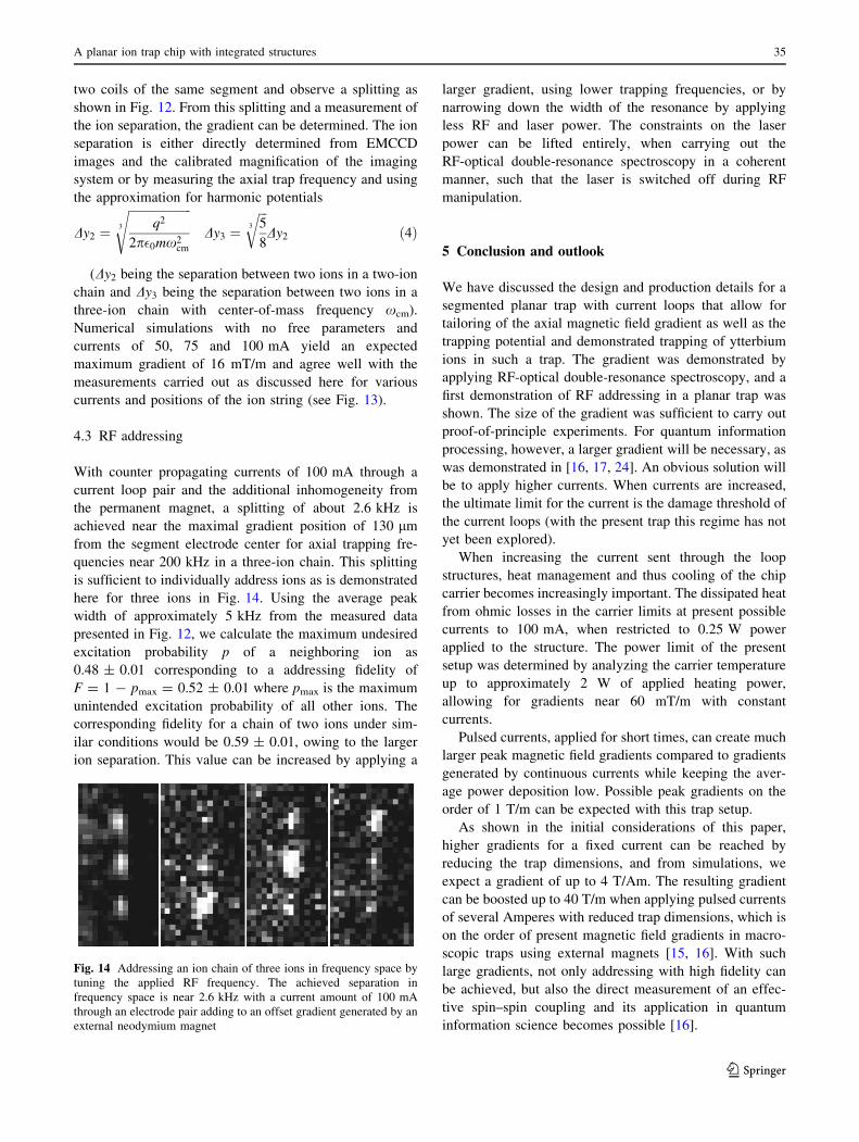
4.3 RF addressing
With counter propagating currents of 100 mA through a
current loop pair and the additional inhomogeneity from
the permanent magnet, a splitting of about 2.6 kHz is
achieved near the maximal gradient position of 130 lm
from the segment electrode center for axial trapping fre-
quencies near 200 kHz in a three-ion chain. This splitting
is sufficient to individually address ions as is demonstrated
here for three ions in Fig. 14. Using the average peak
width of approximately 5 kHz from the measured data
presented in Fig. 12, we calculate the maximum undesired
excitation probability p of a neighboring ion as
0.48 ± 0.01 corresponding to a addressing fidelity of
F = 1 - pmax = 0.52 ± 0.01 where pmax is the maximum
unintended excitation probability of all other ions. The
corresponding fidelity for a chain of two ions under sim-
ilar conditions would be 0.59 ± 0.01, owing to the larger
ion separation. This value can be increased by applying a
larger gradient, using lower trapping frequencies, or by
narrowing down the width of the resonance by applying
less RF and laser power. The constraints on the laser
power can be lifted entirely, when carrying out the
RF-optical double-resonance spectroscopy in a coherent
manner, such that the laser is switched off during RF
manipulation.
5 Conclusion and outlook
We have discussed the design and production details for a
segmented planar trap with current loops that allow for
tailoring of the axial magnetic field gradient as well as the
trapping potential and demonstrated trapping of ytterbium
ions in such a trap. The gradient was demonstrated by
applying RF-optical double-resonance spectroscopy, and a
first demonstration of RF addressing in a planar trap was
shown. The size of the gradient was sufficient to carry out
proof-of-principle experiments. For quantum information
processing, however, a larger gradient will be necessary, as
was demonstrated in [16, 17, 24]. An obvious solution will
be to apply higher currents. When currents are increased,
the ultimate limit for the current is the damage threshold of
the current loops (with the present trap this regime has not
yet been explored).
When increasing the current sent through the loop
structures, heat management and thus cooling of the chip
carrier becomes increasingly important. The dissipated heat
from ohmic losses in the carrier limits at present possible
currents to 100 mA, when restricted to 0.25 W power
applied to the structure. The power limit of the present
setup was determined by analyzing the carrier temperature
up to approximately 2 W of applied heating power,
allowing for gradients near 60 mT/m with constant
currents.
Pulsed currents, applied for short times, can create much
larger peak magnetic field gradients compared to gradients
generated by continuous currents while keeping the aver-
age power deposition low. Possible peak gradients on the
order of 1 T/m can be expected with this trap setup.
As shown in the initial considerations of this paper,
higher gradients for a fixed current can be reached by
reducing the trap dimensions, and from simulations, we
expect a gradient of up to 4 T/Am. The resulting gradient
can be boosted up to 40 T/m when applying pulsed currents
of several Amperes with reduced trap dimensions, which is
on the order of present magnetic field gradients in macro-
scopic traps using external magnets [15, 16]. With such
large gradients, not only addressing with high fidelity can
be achieved, but also the direct measurement of an effec-
tive spin–spin coupling and its application in quantum
information science becomes possible [16].
Fig. 14 Addressing an ion chain of three ions in frequency space by
tuning the applied RF frequency. The achieved separation in
frequency space is near 2.6 kHz with a current amount of 100 mA
through an electrode pair adding to an offset gradient generated by an
external neodymium magnet
A planar ion trap chip with integrated structures 35
123

Acknowledgments We would like to acknowledge M. Epping for
trap simulations, M. Bohm, D. Schafer-Stephani, K. Watty, A. Bab-
lich, P. Haring-Bolivar, H. Schafer, E. Ilichev, B. Ivanov, and S.
Zarazenkov for their support during chip production, D. Gebauer, D.
Junge, and A. H. Walenta for the production of the chip carrier, our
electrical and mechanical work shops, and especially S. Spitzer for his
support regarding all electronics, and T. Collath, T. F. Gloger, D.
Kaufmann, and P. Kaufmann for providing the laser system used in
this work. We acknowledge funding by the Bundesministerium fur
Bildung und Forschung (FK 01BQ1012), and from the European
Community’s Seventh Framework Programme (FP7/2007-2013)
under Grant Agreement No. 270843 (iQIT) and No. 249958 (PICC).
References
1. M.A. Nielsen, I.L. Chuang, Quantum Computation and Quantum
Information (Cambridge U.P., Cambridge, 2000)
2. R. Blatt, D.J. Wineland, Nature 45, 1008–1015 (2008)
3. D.J. Wineland, C. Monroe, W.M. Itano, D. Leibfried, B.E. King,
D.M. Meekhof, J. Res. NIST 103, 259 (1998)
4. D. Kielpinski, C. Monroe, D. Wineland, Nature 417, 709–712
(2002)
5. A. Walther, F. Ziesel, T. Ruster, S.T. Dawkins, K. Ott, M. Het-
trich, K. Singer, F. Schmidt-Kaler, U. Poschinger, Phys. Rev.
Lett. 109, 080501 (2012)
6. R. Bowler, J. Gaebler, Y. Lin, T.R. Tan, D. Hanneke, J.D. Jost,
J.P. Home, D. Leibfried, D.J. Wineland, Phys. Rev. Lett. 109,
080502 (2012)
7. S. Seidelin, J. Chiaverini, R. Reichle, J.J. Bollinger, D. Leibfried,
J. Britton, J.H. Wesenberg, R.B. Blakestad, R.J. Epstein, D.B.
Hume, W.M. Itano, J.D. Jost, C. Langer, R. Ozeri, N. Shiga, D.J.
Wineland, Phys. Rev. Lett. 96, 253003 (2006)
8. C. Pearson, D. Leibrandt, W. Bakr, W. Mallard, K. Brown, I.
Chuang, Phys. Rev. A 73, 032307 (2006)
9. M.D. Hughes, B. Lekitsch, J.A. Broersma, W.K. Hensinger,
Contemp. Phys. 52(6), 505–529 (2011)
10. J.H. Wesenberg, Phys. Rev. A 78, 063410 (2008)
11. R. Schmied, J.H. Wesenberg, D. Leibfried, Phys. Rev. Lett. 102,
233002 (2009)
12. J.D. Siverns, S. Weidt, K. Lake, B. Lekitsch, M.D. Hughes, W.K.
Hensinger, New J. Phys. 14, 085009 (2012)
13. F. Mintert, C. Wunderlich, Phys. Rev. Lett. 87, 25 (2001)
14. C. Wunderlich, Laser Physics at the Limit. (Springer, New York,
2002)
15. M. Johanning, A. Braun, N. Timoney, V. Elman, W. Neuhauser,
C. Wunderlich, Phys. Rev. Lett. 102, 073004 (2009)
16. A. Khromova, C. Piltz, B. Scharfenberger, T.F. Gloger, M. Jo-
hanning, A.F. Varon, C. Wunderlich, Phys. Rev. Lett. 108,
220502 (2012)
17. C. Piltz, B. Scharfenberger, A. Khromova, A.F. Varon, C.
Wunderlich, Phys. Rev. Lett. 110, 200501 (2013)
18. P. Staanum, M. Drewsen, Phys. Rev. A 66, 040302 (2002)
19. N. Navon, S. Kotler, N. Akerman, Y. Glickman, I. Almog, R.
Ozeri, Phys. Rev. Lett. 110, 073001 (2013)
20. U. Warring, C. Ospelkaus, Y. Colombe, R. Jordens, D. Leibfried,
D.J. Wineland, Phys. Rev. Lett. 110, 173002 (2013)
21. C. Ospelkaus, U. Warring, Y. Colombe, K.R. Brown, J.M. Amini,
D. Leibfried, D.J. Wineland, Nature 476, 181 (2011)
22. D. Kaufmann, T. Collath, M.T. Baig, P. Kaufmann, E. Asenwar,
M. Johanning, C. Wunderlich, Appl. Phys. B 107, 935–943
(2012)
23. J. Welzel, A. Bautista-Salvador, C. Abarbanel, V. Wineman-
Fisher, Ch. Wunderlich, R. Folman, F. Schmidt-Kaler, Eur. Phys.
J. D 65, 285–297 (2011)
24. S. Wang, J. Labaziewicz, Y. Ge, R. Shewmon, I. Chuang, Appl.
Phys. Lett. 94, 094103 (2009)
25. H. Wunderlich, C. Wunderlich, K. Singer, F. Schmidt-Kahler,
Phys. Rev. A 79, 052324 (2009)
26. J. Chiaverini, R. Blakestad, J. Britton, J. Jost, C. Langer, D.
Leibfried, R. Ozeri, D. Wineland, Quantum Inf. Comput. 65(6),
419–439 (2005)
27. M.H. Oliveira, J.A. Miranda, Eur. J. Phys. 21, 31 (2001)
28. M.G. House, Phys. Rev. A 78, 033402 (2008)
29. T.K. Gupta, Handbook of Thick- and Thin-Film Hybrid Micro-
electronics. (Wiley, New York, 2005)
30. K. Brown, R. Clark, J. Labaziewicz, P. Richerme, D. Leibrandt, I.
Chuang, Phys. Rev. A 75, 15401 (2007)
31. X. Yan, F. Mont, D. Poxson, M. Schubert, J. Kim, J. Cho, E.
Schubert, Jpn. J. Appl. Phys. 48, 120203 (2009)
32. C. Balzer, A. Braun, T. Hannemann, C. Paape, M. Ettler, W.
Neuhauser, C. Wunderlich, Phys. Rev. A 73, 041407 (Rapid
Comm.) (2006)
33. M. Johanning, A. Braun, D. Eiteneuer, C. Paape, C. Balzer, W.
Neuhauser, C. Wunderlich, Appl. Phys. B 103, 327–338 (2011)
34. Y. Onoda, K. Sugiyama, M. Ikeda, M. Kitano, Appl. Phys. B.
105, 729–740 (2011)
35. P.J. Blythe, S.A. Webster, H.S. Margolis, S.N. Lea, G. Huang,
S.K. Choi, W.R.C. Rowley, P. Gill, R.S. Windeler, Phys. Rev. A
67, 020501 (2003)
36. C. Schneider, Master Thesis, University of Siegen (2007)
37. W.W. Macalpine, R.O. Schildknecht, Proc. IRE 47, 2099–2105
(1959)
38. P. Vizmuller, RF Design Guide: Systems, Circuits, and Equa-
tions. (Artech House, Inc., London, 1995)
39. A.I. Zverev, Handbook of Filter Synthesis. (Wiley, New York,
1967)
40. J.D. Siverns, L.R. Simkins, S. Weidt, W.K. Hensinger, Appl.
Phys. B 107, 921–934 (2012)
41. D.J. Wineland, W.M. Itano, Phys. Rev. A 20, 1521 (1979)
42. S. Olmschenk, K.C. Younge, D.L. Moehring, D.N. Matsukevich,
P. Maunz, C. Monroe, Phys. Rev. A 76, 052314 (2007)
43. C. Gerz, J. Roths, F. Vedel, G. Werth, Z. Phys. D 8, 235 (1988)
44. C. Wunderlich, T. Hannemann, T. Korber, H. Haffner, C. Roos,
W. Hansel, R. Blatt, F. Schmidt-Kaler, J. Mod. Opt. 54, 1541
(2007). For technical specifications see http://www.physik.uni-
siegen.de/quantenoptik/forschung/vfg150/index.html.en?lang=en
45. N. Timoney, V. Elman, S. Glaser, C. Weiss, M. Johanning, W.
Neuhauser, C. Wunderlich, Phys. Rev. A 77, 052334 (2008)
46. N. Timoney, I. Baumgart, M. Johanning, A.F. Varon, M.B. Ple-
nio, A. Retzker, Ch. Wunderlich, Nature 476, 185–188 (2011)
36 P. J. Kunert et. al.
123