Electric field compensation and sensing with a single ion in a planar trap
11
arXiv:1106.2730v1 [physics.atom-ph] 10 Jun 2011 Electric field compensation and sensing with a single ion in a planar trap S. Narayanan 1,2 , N. Daniilidis 1,2 , S. A. M¨ oller 1,2,3 , R. Clark 2,4 , F. Ziesel 5 , K. Singer 5 , F. Schmidt-Kaler 5 , and H. H¨ affner 1,3 1 Dept. of Physics, University of California, Berkeley, CA 94720, USA 2 Institut f¨ ur Quantenoptik and Quanteninformation, Innsbruck, Austria 3 Materials Sciences Division, Lawrence Berkeley National Laboratory, Berkeley, CA 94720, USA 4 Center for Ultracold Atoms, Massachusetts Institute of Technology, Cambridge, MA, USA 5 Institut f¨ ur Physik, Universit¨at Mainz, Mainz, Germany E-mail: [email protected] Abstract. We use a single ion as an movable electric field sensor with accuracies on the order of a few V/m. For this, we compensate undesired static electric fields in a planar RF trap and characterize the static fields over an extended region along the trap axis. We observe a strong buildup of stray charges around the loading region on the trap resulting in an electric field of up to 1.3 kV/m at the ion position. We also find that the profile of the stray field remains constant over a time span of a few months. Introduction Laser cooled trapped ions offer a very high level of control, both of their motional and internal quantum states. At the same time, the large charge-to-mass ratio of ions makes their motion very sensitive to electric fields, both static and oscillatory. Thus, trapped ions recently emerged as a tool in small-force sensing [1, 2]. More common applications of trapped ions are in quantum information science [3, 4] and frequency metrology [5, 6]. All these applications can benefit from scalable ion-trap architectures based on microfabricated ion traps. In particular, a promising route to achieve scalable quantum information processing uses complex electrode structures [3, 7]. Considerable effort is made in developing microfabricated trap architectures on which all trap electrodes lie within one plane [8–15]. These so-called planar traps facilitate creation of complex electrode structures and are, in principle, scalable to large numbers of electrodes. Moreover, this approach makes use of mature microfabrication technologies and is ideally suited to approaches involving hybrid ion-trap or solid state systems [16,17].
-
Upload
independent -
Category
Documents
-
view
0 -
download
0
Transcript of Electric field compensation and sensing with a single ion in a planar trap

arX
iv:1
106.
2730
v1 [
phys
ics.
atom
-ph]
10
Jun
2011
Electric field compensation and sensing with a
single ion in a planar trap
S. Narayanan1,2, N. Daniilidis1,2, S. A. Moller1,2,3, R. Clark2,4, F.
Ziesel5, K. Singer5, F. Schmidt-Kaler5, and H. Haffner1,3
1 Dept. of Physics, University of California, Berkeley, CA 94720, USA2 Institut fur Quantenoptik and Quanteninformation, Innsbruck, Austria3 Materials Sciences Division, Lawrence Berkeley National Laboratory, Berkeley, CA
94720, USA4 Center for Ultracold Atoms, Massachusetts Institute of Technology, Cambridge,
MA, USA5 Institut fur Physik, Universitat Mainz, Mainz, Germany
E-mail: [email protected]
Abstract. We use a single ion as an movable electric field sensor with accuracies
on the order of a few V/m. For this, we compensate undesired static electric fields
in a planar RF trap and characterize the static fields over an extended region along
the trap axis. We observe a strong buildup of stray charges around the loading region
on the trap resulting in an electric field of up to 1.3 kV/m at the ion position. We
also find that the profile of the stray field remains constant over a time span of a few
months.
Introduction
Laser cooled trapped ions offer a very high level of control, both of their motional
and internal quantum states. At the same time, the large charge-to-mass ratio of ions
makes their motion very sensitive to electric fields, both static and oscillatory. Thus,
trapped ions recently emerged as a tool in small-force sensing [1, 2]. More common
applications of trapped ions are in quantum information science [3, 4] and frequency
metrology [5, 6]. All these applications can benefit from scalable ion-trap architectures
based on microfabricated ion traps.
In particular, a promising route to achieve scalable quantum information processing
uses complex electrode structures [3, 7]. Considerable effort is made in developing
microfabricated trap architectures on which all trap electrodes lie within one plane
[8–15]. These so-called planar traps facilitate creation of complex electrode structures
and are, in principle, scalable to large numbers of electrodes. Moreover, this approach
makes use of mature microfabrication technologies and is ideally suited to approaches
involving hybrid ion-trap or solid state systems [16, 17].
Electric field compensation and sensing with a single ion in a planar trap 2
Despite the advantages of planar trap architectures, a number of issues remain
unsolved. To achieve reasonably large trap frequencies, planar traps require shorter ion-
electrode distances than conventional three-dimensional traps [8]. This results in high
motional heating rates for the ions [18–20] and causes charge buildup via stray light
hitting the trap electrodes [21]. In addition, the proximity of the charges increases the
effect of charge buildup as compared to macroscopic three dimensional traps. Finally,
planar traps do not shield stray electrostatic fields from the environment surrounding
the trap as well as the three dimensional trap geometries tend to do. Combined, these
effects make the operation of planar traps much more sensitive to uncontrolled charging
effects.
To harness the full advantages of segmented ion traps, ion-string splitting and
ion shuttling operations are required [4, 22]. For the reliable performance of these
operations, control of the electrostatic environment over the full trapping region is
necessary. Typically one employs numerical electrostatic solvers to determine the
potential experienced by the ions and generates electrode voltage sequences that will
perform the desired ion shuttling [23, 24]. Stray electrostatic fields, however, displace
the ions from the RF-null of the trap and thus introduce so-called micromotion
[25] sometimes to the point where trapping is no longer feasible. Thus, precise
characterization and compensation of stray electric fields in the trapping region is
required.
Conventional methods to sense and compensate the electric stray fields cannot
easily be extended to planar traps because typically the stray fields are quantified via
the the Doppler shift induced by the micromotion. It is undesirable to scatter UV light
from the trap electrodes, and, thus, for planar traps, the detection laser typically does
not have a sizable projection on the motion perpendicular to the plane of the trap. We
address these issues by applying a new method to compensate for stray fields well suited
for planar trap geometries [26, 27].
Based on the voltages required to compensate the stray fields, we realize a single-
ion electric field sensor characterizing the electric stray fields along the trap axis. We
observe a strong buildup of stray charges around the loading region on the trap. We also
find that the profile of the stray field remains constant over a time span of a few months.
The strength of the electric stray fields and its position on the trap is correlated with
the high heating rates observed close to the loading region [20].
Experimental Setup
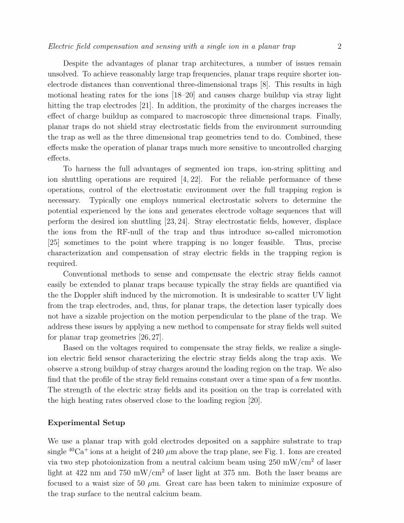
We use a planar trap with gold electrodes deposited on a sapphire substrate to trap
single 40Ca+ ions at a height of 240 µm above the trap plane, see Fig. 1. Ions are created
via two step photoionization from a neutral calcium beam using 250 mW/cm2 of laser
light at 422 nm and 750 mW/cm2 of laser light at 375 nm. Both the laser beams are
focused to a waist size of 50 µm. Great care has been taken to minimize exposure of
the trap surface to the neutral calcium beam.
Electric field compensation and sensing with a single ion in a planar trap 3
Figure 1. Schematic of the trap used for the measurements [20]. The DC electrodes
are drawn in blue, the RF electrode in orange, and the ground plane in gray. Details of
the bonding pads to the DC electrodes are not shown for simplicity. The axes indicate
the origin of the coordinate system. The green line along the z axis on the central DC
electrode indicates the range of axial positions in which the stray electric fields shown
in Fig. 3 were measured. The circular mark on this line indicates the location used as a
loading region, around which the highest increase in stray electric fields was observed.
The RF electrode is driven at a frequency Ω/2π ≈ 15 MHz, amplified to 100mW
and stepped up via a helical resonator in a quarter wave configuration to a voltage of
approximately 100 V amplitude. A 2:1 asymmetry in the width of the RF electrode
results in a tilt of the radio frequency quadrupole by approximately 16 in the XY
plane. The DC electrodes are used to move the ion along the axial direction and to
compensate the stray fields. The DC voltages used for trapping and compensation are
between -10 V and 15 V. Typical secular frequencies in this work were (fx′, fy′ , fz) ≈
(1.2, 1.4, 0.4) MHz where the primes refer to the frame of reference rotated by 16 .
For Doppler cooling and detecting the ions, we use a diode laser at 794 nm, which
is frequency doubled using a ring cavity to produce a wavelength of 397 nm. A second
diode laser at 866 nm is used as a repump. Both lasers are frequency locked to cavities
using the Pound-Drever-Hall method, and their frequencies can be varied by changing
the cavity lengths with piezoelectric elements. The intensity of the detection laser at
397 nm is adjusted to about 40mW/cm2 and the intensity of the repump laser at 866nm
is adjusted to approximately 120mW/cm2. The Doppler cooling and repump lasers are
overlapped and sent to the trap using a photonic crystal fiber. The laser beam is aligned
almost parallel to the surface of the trap and forms an angle of approximately 45 with
the X and Z axes. Ion fluorescence is collected perpendicular to the trap plane using a
lens system of NA = 0.29 and split between a PMT and CCD camera on a 90:10 beam
splitter.
Minimizing micromotion
In an ideal Paul trap the ion is confined to a position at which the electric field due
to the oscillating drive voltage on the RF electrodes is zero. Stray DC electric fields,
Electric field compensation and sensing with a single ion in a planar trap 4
however, push the ion off the RF node and the ion undergoes so-called micromotion
driven by the oscillating RF field [25]. This motion causes broadening of the electronic
transitions of the ion and, among other things, leads to a higher temperature limit for
Doppler cooling [3]. In addition, micromotion can lead to the heating of trapped ions
due to the noise present at the secular sidebands of the micromotion drive [22, 28]. In
order to position the ion on the RF node, the DC potential is carefully adjusted to
minimize micromotion. Crucial to all minimization schemes is the efficient detection of
micromotion in all three spatial directions.
Different techniques exist for fine-tuning the compensation of micromotion. The
photon correlation method [14,25] relies on correlating the ion fluorescence to the phase
of the RF field. In the resolved sideband method [24, 25], the sidebands of a narrow
atomic transition are compared with the carrier transition to estimate the modulation
index. Both methods are widely used to suppress micromotion in 3D traps. However,
neither method can be easily extended to surface Paul traps because they directly use
the Doppler shift induced by the ion motion. In the case of surface traps, the geometry
typically limits the laser alignment to be in the plane parallel to the trap surface resulting
in no Doppler shift associated with the oscillations perpendicular to the trap surface
unless one directs laser light onto the trap electrodes. However, it has been documented
that UV light hitting the trap surface can lead to dramatic charge buildup even to the
point where the trap becomes inoperable for days [21]. To circumvent this obstacle, the
infrared repump light in 40Ca+ has been used to detect the Doppler shift perpendicular
to the trapping plane for micromotion compensation [14]. However, many ion species
such as Mg+, Al+, Hg+, Cd+, Be+ do not have such transitions in the infrared and other
methods need to be employed.
Here we compensate the micromotion perpendicular to the trap plane with the
following method. When the ion is displaced from the RF node, any voltage applied on
the RF electrode creates an electric field at the ion position. If this voltage contains a
frequency component which is in resonance with one of the ion secular frequencies the
ion can get excited in the direction of the secular mode provided that the driving field
from the RF electrodes has some projection [22]. Experimentally we find that large
oscillation amplitudes of each of the three secular motions can be detected as a drop
in ion fluorescence. The dynamics of ion fluorescence in the presence of the cooling
laser and a resonant excitation are complex and go beyond the scope of this study [29].
Minimizing micromotion is achieved by shifting the ion position via DC potentials until
the ion is in the RF minimum and cannot be excited by driving the RF electrode at any
of the secular frequencies. This method is also being used by NIST [26] and Osaska [27]
ion trap groups.
Implementation
In order to implement this method, we first position the ion within 1 µm along the
X direction from the RF null using the CCD camera and varying the RF amplitude.
Electric field compensation and sensing with a single ion in a planar trap 5
(a)
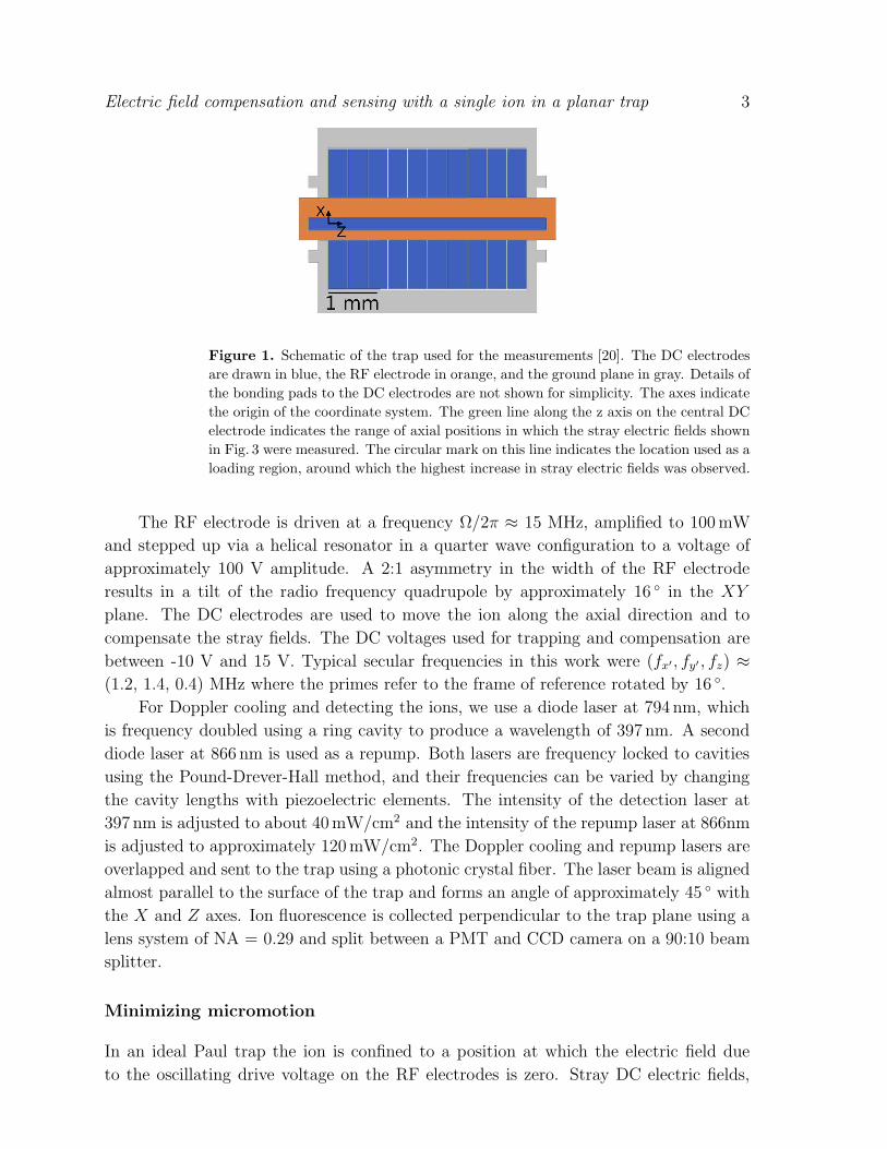
(b) (c) (d) (e)
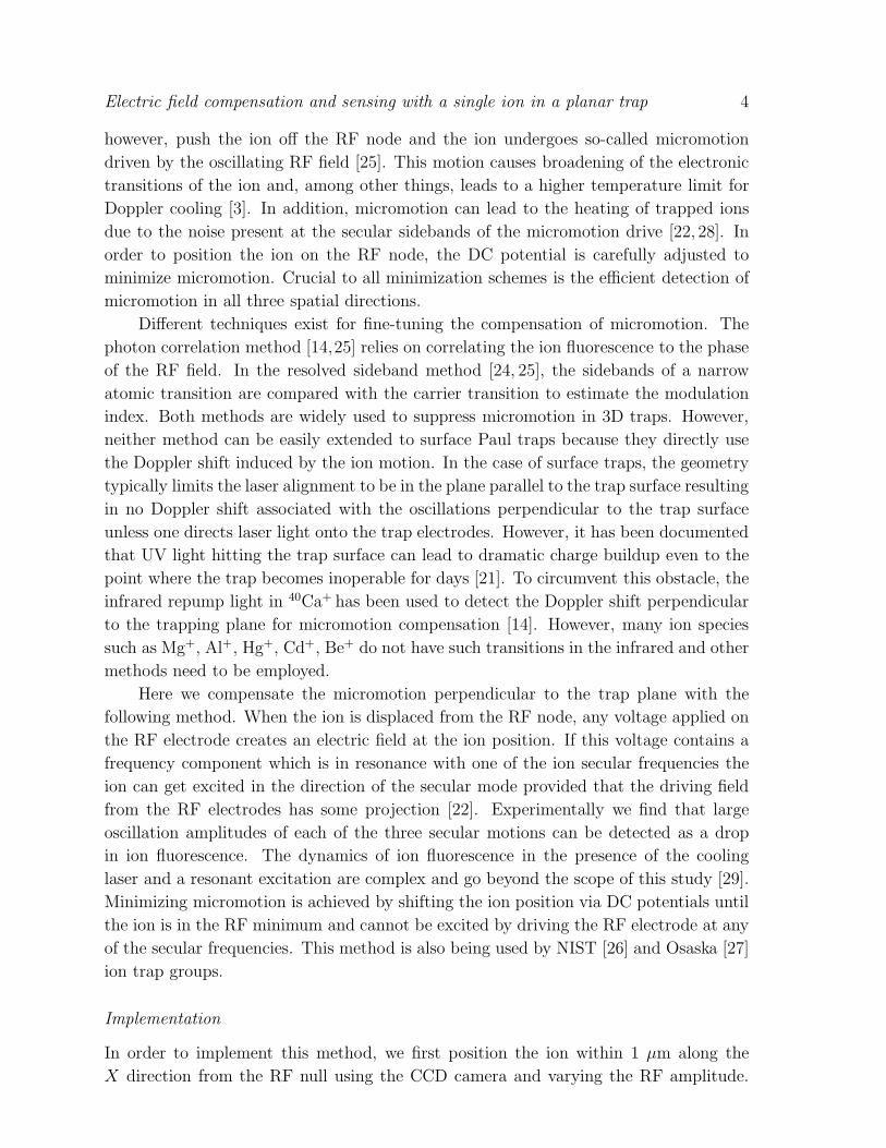
Figure 2. Micromotion compensation measurements. (a) Drop in ion fluorescence
when the frequency of the additional excitation is equal to one of the secular frequencies
of the ion, the data is fitted using A0(1−D)
(
e−[
(x−x0)2
a2 +(x−x0)4
b4]
)
for a good evaluation
of the dip-depth D, (b)&(c) Change in the dip depth for the X and Y sideband,
respectively, as a function of the ion position, (d)&(e) a cross section of (b)&(c)
respectively fitted with a parabola. Gray area in (b) is region without data since
the excitation might drive the ion out of trap. The darker the color the less excitation,
i.e. less dip-depth was observed.
Further compensation in the X direction is achieved by reducing the linewidth of the
S1/2-P1/2 transition. For this, the detection laser intensity is adjusted close to saturation
and red-detuned from the transition so that the fluorescence drops to half that of the
value at the resonance. Then compensation voltages are adjusted to minimize the
fluorescence. Both methods detect only micromotion along the X direction, i.e. the
direction which is parallel to the trap surface. For a very coarse compensation along
the Y direction (perpendicular to the trap surface), we keep the frequency of 397 nm
and 866 nm laser on resonance and maximize the ion fluorescence by adjusting the
compensation voltages.
Once a coarse compensation is achieved using the above methods, we proceed with
the method as outlined in the beginning of this section. Instead of exciting the secular
frequency ωi directly, we excite at a frequency Ω + ωi [22, 28]. To achieve this, the
excitation signal from a function generator is mixed with the trap drive Ω before it is
amplified and stepped up with a helical resonator, and scanned around Ω+ωi. When the
frequency of the excitation becomes resonant with Ω+ωi, the ion heats up resulting in a
decrease in fluorescence (see Fig. 2(a)), [22,27]. A crucial requirement is that the step-up
circuit which produces the high-voltage trap drive has a large enough bandwidth. The
bandwidth of the helical resonator in our experiment is 270 kHz and allows compensation
with excitation frequencies up to order Ω± 2π×2 MHz. The frequency of the Doppler
cooling laser was detuned between 1 and 5 MHz below the S1/2 − P1/2 transition to
maximize sensitivity of the ion fluorescence to the ion kinetic energy.

Electric field compensation and sensing with a single ion in a planar trap 6
For compensation of micromotion in the X direction, the excitation signal is
scanned repeatedly around Ω+ωx while adjusting the voltages on the DC electrodes such
that between successive scans the static electric field minimum moves predominantly
in the X direction. The compensated position is reached when resonance of the
excitation does not result in a decrease of fluorescence. The same process is repeated
for compensation in the Y direction. Results are shown in Fig. 2.
Fig. 2(b) and Fig. 2(c) show the change in the dip depth when the excitation
frequency is Ω + ωx and Ω + ωy, respectively, as a function of ion position along the X
and the Y direction. The gray area in Fig. 2(b) is the region were no data is acquired
since the excitation would drive the ion out of the trap. Fig. 2(d) and Fig. 2(e) show
cross sections of the 2D plots along the equilibrium positions of the ion when the DC
saddle point moves along the X and Y directions, respectively. The energy gain rate
of the ion Γ is expected to be Γ ∼ E2, where E is the strength of the exciting electric
field. We find that the data can be well fitted with a parabola suggesting that the dip
depth is linear in the ion energy for our experiments while the electric field E can be
described well as a quadrupolar field.
The accuracy of our measurements is estimated by calibrating the ion displacement
as a function of change in the DC voltages using the CCD camera in the X direction
and the detection laser in the Y direction. These values were verified by modeling the
displacement of the DC minimum with variation of the compensation voltages. By
translating the applied voltage into actual displacement, we determine an accuracy of
about 50 nm in the X direction and 300 nm in Y direction in positioning the ion at the
RF minimum. This corresponds to excess micromotion amplitudes of 6 nm and 40 nm
in these respective directions. The accuracies could be further improved by increasing
the excitation voltage and decreasing the frequency detuning of the detection laser from
resonance.
One concern with this method is that in practical situations the DC electrodes pick
RF voltage, the phase of which might be shifted, or which might depend on the RF
excitation frequency. The reason for this is that the DC electrodes may capacitively
couple to the RF electrode, with a frequency dependent coupling determined by the
filtering circuits connected to the DC electrodes. In our setup, we estimate the RF
pickup of the excitation at Ω+ωi on the DC electrodes to differ by less than 20 µV from
the pick up at Ω which would shift the RF-null by about 15 pm, and thus not limit the
accuracy.
Electric field sensing
It is instructive to extract the size and direction of the stray fields from the compensation
voltages along various trapping positions. We derive the stray field from the applied
compensation voltages via an accurate electrostatic model of the trapping fields. Thus
determining the stray fields over an extended region yields important information for
shuttling experiments or investigating the mechanism for charge buildup.
Electric field compensation and sensing with a single ion in a planar trap 7
We model the trap potentials using the boundary element method solver CPO [30].
Since the radial trap axes are tilted, we determine the radial secular frequencies from a
2-dimensional polynomial fit in the XY -plane. The agreement between experiment and
simulation is better than 4%, corresponding to a disagreement of less than 20 kHz for
axial secular frequency of 500 kHz, and 30 kHz for radial frequencies of between 1 and
2MHz. We attribute the disagreement to details of the trap electrode geometry which
were not included in the electrostatic simulation, as well as to the unknown spatial
inhomogeneity of the electrostatic stray fields. Only the spatially inhomogeneous part
of the stray field will contribute to the discrepancy between simulation and experiment,
since the electrostatic stray fields are compensated and included in the simulations, as
we now describe.
The essential part of the stray field determination is to perform micromotion
compensation as described above. After the compensation parameters have been
determined, we measure the ion position along the Z direction using the CCD imaging
system. The values of the DC voltages at the compensated configuration and the ion
position are then input to a minimization algorithm. The algorithm finds the stray field
which results in the observed compensation parameters and position.
The accuracy of our measurement scheme is limited by an estimated uncertainty
of ±2.5 µm in measuring the absolute ion position along the trap axis. This position
uncertainty arises from the imprecision of the alignment of the microscope objective
used for imaging with respect to the trap plane and from the size of trap features used
to determine the position along the trap axis. This results in a systematic error of the
electric field curves, mainly an offset of the entire curve. We find typical inaccuracies of
(δEx, δEy, δEz) = ±(5.5, 3, 15)V/m.
The precision in determining the electric field at each ion position is on the order
of a few V/m, and is limited by the precision to which the compensation parameters
and relative ion position are determined. The errors from imperfect compensation lead
to stray field imprecisions of ±0.4 V/m in the horizontal direction and ±2.5 V/m in the
vertical direction, where we assume that the precision is limited by the ion displacement
steps in Fig. 2.
The accuracy in determining the axial ion position at any given setting with respect
to its positions in neighboring settings is limited by aberrations in the imaging optics and
is estimated to be ±0.1µm. This limitation leads to an imprecision of ±(2, 4, 0.5)V/m
in the electric fields. The above limitations of the measurement leads to a total error
of ±(7, 10, 16)V/m, however, the limitations are of technical nature and can be further
improved.
We performed this type of analysis over an extensive part of the trap. Measurements
were performed during several months. The results obtained in the first weeks of trap
installation in vacuum and trap operation were significantly different than those obtained
later on. Initially, the magnitude of the stray electric fields in the radial directions
varied on a day-to-day basis with a mean of 47 V/m and a standard deviation of 52
V/m. Measurements during that time were carried out only for one isolated axial ion
Electric field compensation and sensing with a single ion in a planar trap 8
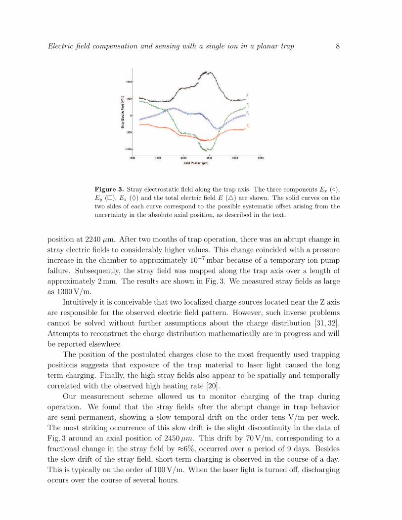
Figure 3. Stray electrostatic field along the trap axis. The three components Ex (),
Ey (), Ez (♦) and the total electric field E () are shown. The solid curves on the
two sides of each curve correspond to the possible systematic offset arising from the
uncertainty in the absolute axial position, as described in the text.
position at 2240 µm. After two months of trap operation, there was an abrupt change in
stray electric fields to considerably higher values. This change coincided with a pressure
increase in the chamber to approximately 10−7mbar because of a temporary ion pump
failure. Subsequently, the stray field was mapped along the trap axis over a length of
approximately 2mm. The results are shown in Fig. 3. We measured stray fields as large
as 1300V/m.
Intuitively it is conceivable that two localized charge sources located near the Z axis
are responsible for the observed electric field pattern. However, such inverse problems
cannot be solved without further assumptions about the charge distribution [31, 32].
Attempts to reconstruct the charge distribution mathematically are in progress and will
be reported elsewhere
The position of the postulated charges close to the most frequently used trapping
positions suggests that exposure of the trap material to laser light caused the long
term charging. Finally, the high stray fields also appear to be spatially and temporally
correlated with the observed high heating rate [20].
Our measurement scheme allowed us to monitor charging of the trap during
operation. We found that the stray fields after the abrupt change in trap behavior
are semi-permanent, showing a slow temporal drift on the order tens V/m per week.
The most striking occurrence of this slow drift is the slight discontinuity in the data of
Fig. 3 around an axial position of 2450µm. This drift by 70V/m, corresponding to a
fractional change in the stray field by ≈6%, occurred over a period of 9 days. Besides
the slow drift of the stray field, short-term charging is observed in the course of a day.
This is typically on the order of 100V/m. When the laser light is turned off, discharging
occurs over the course of several hours.

Electric field compensation and sensing with a single ion in a planar trap 9
Summary and Conclusions
In this article, we demonstrate a simple, yet efficient method of measuring stray electric
fields in planar ion traps. This method permits us to sense electric fields over an extended
region, thus providing insight into the undesired charging of ion traps. This ability to
characterize electric fields in the trapping region will be a valuable tool for evaluating
planar ion traps, for developing ion loading approaches that minimize stray charging,
and for compensating stray fields. We expect that this technique will be useful not only
for scalable quantum information processing, but also for precision frequency metrology
applications of trapped ions.
Acknowledgment
The experiments were supported by the Austrian Ministry of Sciences with a START
grant and by the Director, Office of Science, Office of Basic Energy Sciences, Materials
Sciences and Engineering Division, of the U.S. Department of Energy under Contract
no. DE-AC02-05CH11231. N. Daniilidis was supported by the European Union with a
Marie Curie fellowship. F. Schmidt-Kaler acknowledges support from the German-Israel
foundation and the EU network AQUTE.
References
[1] R Maiwald, D Leibfried, J Britton, J. C. Bergquist, G Leuchs, and D. J. Wineland. Stylus ion
trap for enhanced access and sensing. Nature Physics, 5(8):551–554, June 2009.
[2] M. J Biercuk, H Uys, J. W Britton, A. P. VanDevender, and J. J Bollinger. Ultrasensitive detection
of force and displacement using trapped ions. Nature nanotechnology, 5(9):646–50, September
2010.
[3] D J Wineland, C Monroe, W M Itano, D Leibfried, B E King, and D M Meekhof. Experimental
Issues in Coherent Quantum-State Manipulation of Trapped Atomic Ions. Journal of Research
of the National Institute for Standards and Technology, 103:259–328, 1998.
[4] J P Home, D Hanneke, J D Jost, J M Amini, D Leibfried, and D J Wineland. Complete Methods
Set for Scalable Ion Trap Quantum Information Processing. Science, 325:1227–1230, September
2009.
[5] P O Schmidt, T Rosenband, C Langer, WM Itano, J C Bergquist, and D JWineland. Spectroscopy
using quantum logic. Science, 309(5735):749–752, 2005.
[6] T Rosenband, D B Hume, P O Schmidt, C W Chou, a A, L Lorini, W H Oskay, R E Drullinger,
T M Fortier, J E Stalnaker, S a A, W C Swann, N R Newbury, W M Itano, D J Wineland, and
J C Bergquist. Frequency ratio of Al+ and Hg+ single-ion optical clocks; metrology at the 17th
decimal place. Science, 319(5871):1808–1812, 2008.
[7] D Kielpinski, C Monroe, and D J Wineland. Architecture for a large-scale ion-trap quantum
computer. Nature, 417(6890):709–711, 2002.
[8] J. Chiaverini, R. B. Blakestad, J. Britton, J. D. Jost, C. Langer, D. Leibfried, R. Ozeri, and
D. J. Wineland. Surface-electrode architecture for ion-trap quantum information processing.
Quantum Information and Computation, 5:419–439, 2005.
[9] S Seidelin, J Chiaverini, R Reichle, J J Bollinger, D Leibfried, J Britton, J H Wesenberg, R B
Blakestad, R J Epstein, D B Hume, W M Itano, J D Jost, C Langer, R Ozeri, N Shiga, and
Electric field compensation and sensing with a single ion in a planar trap 10
D J Wineland. Microfabricated surface-electrode ion trap for scalable quantum information
processing. Physical Review Letters, 96:253003, 2006.
[10] J Britton, D Leibfried, J Beall, R B Blakestad, J J Bollinger, J Chiaverini, R J Epstein, J D
Jost, D Kielpinski, C Langer, R Ozeri, R Reichle, S Seidelin, N Shiga, J H Wesenberg, and D J
Wineland. A microfabricated surface-electrode ion trap in silicon. arXiv:quant-ph/0605170,
2006.
[11] C E Pearson, D R Leibrandt, W S Bakr, W J Mallard, K R Brown, and I L Chuang. Experimental
investigation of planar ion traps. Physical ReviewA, 73:32307, 2006.
[12] J Labaziewicz, Y Ge, P Antohi, D Leibrandt, K R Brown, and I L Chuang. Suppression of Heating
Rates in Cryogenic Surface-Electrode Ion Traps. Physical Review Letters, 100:13001, 2008.
[13] D R Leibrandt, J Labaziewicz, R J Clark, I L Chuang, R Epstein, C Ospelkaus, J Wesenberg,
J Bollinger, D Leibfried, D Wineland, D Stick, J Sterk, C Monroe, C.-S. Pai, Y Low, R Frahm,
and R E Slusher. Demonstration of a scalable, multiplexed ion trap for quantum information
processing. Quantum Information and Computation, 9(11):0901, 2009.
[14] D T C Allcock, J a Sherman, D N Stacey, a H Burrell, M J Curtis, G Imreh, N M Linke, D J Szwer,
S C Webster, a M Steane, and D M Lucas. Implementation of a symmetric surface-electrode
ion trap with field compensation using a modulated Raman effect. New Journal of Physics,
12(5):053026, May 2010.
[15] J M Amini, H Uys, J H Wesenberg, S Seidelin, J Britton, J J Bollinger, D Leibfried, C Ospelkaus,
a P VanDevender, and D J Wineland. Toward scalable ion traps for quantum information
processing. New Journal of Physics, 12(3):033031, March 2010.
[16] L Tian, P Rabl, R Blatt, and P Zoller. Interfacing quantum-optical and solid-state qubits. Physical
Review Letters, 92(24):247902, June 2004.
[17] N Daniilidis, T Lee, R Clark, S Narayanan, and H Haffner. Wiring up trapped ions to study
aspects of quantum information. J. Phys. B, 42:154012, 2009.
[18] Q A Turchette, Kielpinski, B E King, D Leibfried, D M Meekhof, C J Myatt, M A Rowe, C A
Sackett, C S Wood, W M Itano, C Monroe, and D J Wineland. Heating of trapped ions from
the quantum ground state. Physical Review A, 61:63418, 2000.
[19] L Deslauriers, S Olmschenk, D Stick, W K Hensinger, J Sterk, and C Monroe. Scaling and
suppression of anomalous heating in ion traps. Phys. Rev. Lett., 97(10):103007, 2006.
[20] N Daniilidis, S Narayanan, S Moller, R Clark, T Lee, P Leek, A Wallraff, St Schulz, F Schmidt-
Kaler, and H Haffner. Fabrication and heating-rate study of microscopic surface electrode traps.
New J. Phys., 13:013032, 2011.
[21] M Harlander, M Brownnutt, W Hansel, and R Blatt. Trapped-ion probing of light-induced
charging effects on dielectrics. New Journal of Physics, 12(9):093035, September 2010.
[22] R. B. Blakestad, C. Ospelkaus, A. P. VanDevender, J. M. Amini, J. Britton, D. Leibfried, and
D. J. Wineland. High-Fidelity Transport of Trapped-Ion Qubits through an X-Junction Trap
Array. Phys. Rev. Lett., 102(15):153002, April 2009.
[23] S. Schulz, U. Poschinger, K. Singer, and F. Schmidt-Kaler. Optimization of segmented linear Paul
traps and transport of stored particles. Fortschr. Phys., 54:648, 2006.
[24] Schmidt-Kaler F Schulz S, Poschinger U, Ziesel F. Sideband cooling and coherent dynamics in a
microchip multi-segmented ion trap. New J. Phys., 10:045007, 2008.
[25] DJ Berkeland, JD Miller, JC Bergquist, WM Itano, and DJ Wineland. Minimization of ion
micromotion in a Paul trap. Journal of Applied Physics, 83(10):5025, 1998.
[26] T Rosenband. Private communication. Technical report, 2009.
[27] Y. Ibaraki, U. Tanaka, and S. Urabe. Detection of parametric resonance of trapped ions
formicromotion compensation. Applied Physics B, 0(1):1–3, March 2011.
[28] D.J. Wineland, C. Monroe, W.M. Itano, B.E. King, D. Leibfried, D.M. Meekhof, C. Myatt, and
C. Wood. Experimental Primer on the Trapped Ion Quantum Computer. Fortschritte der
Physik, 46(4-5):363–390, June 1998.
[29] N. Akerman, S. Kotler, Y. Glickman, Y. Dallal, a. Keselman, and R. Ozeri. Single-ion nonlinear

Electric field compensation and sensing with a single ion in a planar trap 11
mechanical oscillator. Physical Review A, 82(6):3–6, December 2010.
[30] CPO, see website www.electronoptics.com.
[31] B Bosco and T Sacchi, M. On the inversion problem in classical electrodynamics and the ”Casimir
theorem”. Annals of Physics, 12, 1981.
[32] T B Smith. Best-fit multipole expansions for fields from static currents. Inverse Problems,
1(2):173–179, May 1985.