Optimising camera trap height and model increases detection ...
Upload
independentCategory
view
1download
0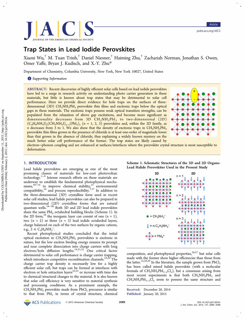
Trap States in Lead Iodide PerovskitesXiaoxi Wu,† M. Tuan Trinh,† Daniel Niesner,† Haiming Zhu,† Zachariah Norman, Jonathan S. Owen,Omer Yaffe, Bryan J. Kudisch, and X.-Y. Zhu*
Department of Chemistry, Columbia University, New York, New York 10027, United States
*S Supporting Information
ABSTRACT: Recent discoveries of highly efficient solar cells based on lead iodide perovskiteshave led to a surge in research activity on understanding photo carrier generation in thesematerials, but little is known about trap states that may be detrimental to solar cellperformance. Here we provide direct evidence for hole traps on the surfaces of three-dimensional (3D) CH3NH3PbI3 perovskite thin films and excitonic traps below the opticalgaps in these materials. The excitonic traps possess weak optical transition strengths, can bepopulated from the relaxation of above gap excitations, and become more significant asdimensionality decreases from 3D CH3NH3PbI3 to two-dimensional (2D)(C4H9NH3I)2(CH3NH3I)n−1(PbI2)n (n = 1, 2, 3) perovskites and, within the 2D family, asn decreases from 3 to 1. We also show that the density of excitonic traps in CH3NH3PbI3perovskite thin films grown in the presence of chloride is at least one-order of magnitude lowerthan that grown in the absence of chloride, thus explaining a widely known mystery on themuch better solar cell performance of the former. The trap states are likely caused byelectron−phonon coupling and are enhanced at surfaces/interfaces where the perovskite crystal structure is most susceptible todeformation.
1. INTRODUCTIONLead halide perovskites are emerging as one of the mostpromising classes of materials for low-cost photovoltaictechnology.1−9 Intense research efforts on these materials areunderway to establish the fundamental photophysical mecha-nisms,10−14 to improve chemical stability,15 environmentalcompatibility,16 and process reproducibility.7,17 In addition tothe three-dimensional (3D) crystalline form used in recentsolar cell studies, lead halide perovskites can also be prepared intwo-dimensional (2D) crystalline forms that are naturalquantum wells.18−20 Both 3D and 2D lead iodide perovskitesshare the same PbI6 octahedral building blocks (Scheme 1). Inthe 2D form,18 the inorganic layer can consist of one (n = 1),two (n = 2) or three (n = 3) lead iodide octahedral layers,charge balanced on each of the two surfaces by organic cations,e.g., 2 × C4H9NH3
+.Recent photophysical studies concluded that the initial
optical excitation in CH3NH3PbI3 perovskites is excitonic innature, but the low exciton binding energy ensures its promptand near complete dissociation into charge carriers with longelectron/hole diffusion lengths.14,21,22 One critical factordetrimental to solar cell performance is charge carrier trapping,which introduces competitive recombination channels.23,24 Thecharge carrier trap density is necessarily low for a highlyefficient solar cell, but traps can be formed at interfaces withelectron or hole extraction layers23,25 or increase with time dueto chemical/structural changes to the material. It is also knownthat solar cell efficiency is very sensitive to material synthesisand processing conditions. As a prominent example, theCH3NH3PbI3 perovskite made from PbCl2 precursor is similarto that from PbI2 in terms of crystal structure, chemical
composition, and photophysical properties,26,27 but solar cellsmade with the former show higher efficiencies than those fromthe latter.12,28,29 In the literature, the sample grown from PbCl2has been called mixed halide perovskite (with a molecularformula of CH3NH3PbI3−xClx), but a consensus arising frommost recent experiments is that both CH3NH3PbI3 andCH3NH3PbI3−xClx seem to possess the same structure and
Received: December 20, 2014Published: January 20, 2015
Scheme 1. Schematic Structures of the 3D and 2D Organo-Lead Halide Perovskites Used in the Present Study
Article
pubs.acs.org/JACS
© 2015 American Chemical Society 2089 DOI: 10.1021/ja512833nJ. Am. Chem. Soc. 2015, 137, 2089−2096
Dow
nloa
ded
by C
OL
UM
BIA
UN
IV o
n Se
ptem
ber
11, 2
015
| http
://pu
bs.a
cs.o
rg
Pub
licat
ion
Dat
e (W
eb):
Feb
ruar
y 2,
201
5 | d
oi: 1
0.10
21/ja
5128
33n
stoichiometry.26 In the following, we will use CH3NH3PbI3 torepresent 3D perovskites from both PbCl2 and PbI2 precursors.The exact difference between the two sample preparations isnot fully understood, but one reason might be a higher densityof trap states in CH3NH3PbI3 perovskites from PbI2 than thatfrom PbCl2.Most of the published literature on the photophysics of
perovskites focused on excitons in 2D crystals20,30,31 or carriergeneration in 3D crystals.10−14,21,22 There is very littleknowledge on the physical nature of trap states23,32,33 orstrategies to control or minimize them.34 Here we providedirect experimental probe of charge and exciton traps in both3D and 2D lead iodide perovskites. We suggest that these trapstates result from electron−phonon coupling and are stabilizedat surfaces/interfaces of perovskite crystallites.
2. EXPERIMENTAL SECTIONPreparation of 2D Perovskites. We followed the liquid phase
crystallization method reported before18 to produce the layeredlead(II) iodide crystals. Lead(II) iodide (99%), hydriodic acid (57 wt%, stabilizer free in water), n-butylamine (99.5%), and methylaminesolution (33 wt % in ethanol) were purchased from Sigma-Aldrich anddiethyl ether (BHT stabilized) was purchased from Fisher Scientific.All reagents were used without further purification. A minimumvolume of hydriodic acid was used to dissolve stoichiometric quantitiesof lead(II) iodide, n-butylamine, and methylammonium iodide at 110°C. To obtain the crystals, we slowly (∼2 °C/h) cooled the solution to−10 °C. After cooling, plate-like bright-colored crystals with a fewmm2 areas were obtained. These crystals were then filtered in colddiethyl ether and dried at 60 °C under vacuum for 24 h beforeexfoliation. The crystals were mechanical exfoliated and transferredonto isopropanol rinsed sapphire crystal (z-cut, 0001 orientation, MTIcooperation) for TA and PL measurements or fused silica for linearabsorption measurements.Preparation of 3D Perovskites from Vapor Deposition. We
followed the method of Liu et al. using dual-source thermalevaporation method to prepare CH3NH3PbI3 perovskite thin films.7
CH3NH3I powders were synthesized from hydriodic acid (57 wt %,stabilizer free in water, Sigma-Aldrich) and methylamine solution (33wt % in ethanol, Sigma-Aldrich). PbI2 and PbCl2 were purchased fromSigma-Aldrich and used as received. Sapphire crystals (z-cut, 0001orientation, MTI cooperation), silica plates, or native oxide terminatedsilicon wafers (highly doped, 111 orientation), were used as substratesand rinsed with isopropanol prior to use. For the preparation of so-called mixed halide perovskites, we evaporated CH3NH3I and PbCl2from separate crucibles in a high vacuum chamber (base pressure<10−7 mbar) with the ratio of deposition rates of ∼10:1, as monitoredby a quartz crystal microbalance (QCM) positioned next to the samplesubstrates. For the preparation of pure lead iodide perovskite, weevaporated CH3NH3I and PbI2 from separate crucibles with the ratioof deposition rates of ∼4:1. During the vapor-deposition process, thesubstrates were slowly rotated along the surface normal forhomogeneous film formation. The vapor pressure (mainly due toCH3NH3I) was ∼2 × 10⁻⁵ Torr during deposition. The obtainedperovskite films were annealed in the vacuum chamber inmethylammonium iodide atmosphere (2 × 10⁻⁵ mbar) or transferredinto a N2 filled glovebox and annealed at 100 °C for 40 min to removethe excess organic molecules and to facilitate further crystallization.Figure S1 shows photos of two typical CH3NH3PbI3 perovskite thinfilm samples on sapphire substrates.Transient Absorption (TA) Measurement. All samples were
mounted in a N2 filled sample cell for TA measurements at roomtemperature. In brief, the beam from a Ti:sapphire femtosecondregenerative amplifier at 800 nm wavelength and 1 kHz repetition ratewas split into two paths. The first path was directed into an opticalparametric amplifier to generate tunable pump laser (UV to near IR).The second path was focused onto a sapphire crystal to produce thewhite-light supercontinuum (visible: 450−830 nm, NIR: 850−1600
nm) as probe. The pump beam was lightly focused to 0.7 mm2 at 350nm pump or 3.3 mm2 at 420 nm pump and the probe beam to 0.09mm2; the probe spot was located within the pump spot on the samplesurface. The transmitted probe beam was focused onto a fiber coupledhigh-speed multichannel detector and collected by a high speedspectrometer (HELIOS, Ultrafast Systems).
Room Temperature Absorption and Photoluminescence(PL) Measurement. We recorded linear absorption spectra of 2Dperovskites on a LAMBDA 950 UV−vis−NIR Spectrophotometer(PerkinElmer) with an integrating sphere. In order to reducescattering background, we used a 10 cm focal lens to lightly focusthe white light onto the exfoliated 2D perovskites flakes. Thetransmitted light was collected by an integrating sphere with thecorrection of substrate absorption. We recorded the linear absorptionspectra of 3D perovskite samples on a Shimadzu UV-1800spectrophotomter without the use of an integrating sphere.
We used a Raman microscope (Renishaw InVia) in the photo-luminescence (PL) mode for the room temperature PL measurementson 2D perovskites. For n = 1 2D perovskites, 405 nm CW pump laserwas focused by a 10× objective and PL in the reflective direction wascollected; while for n = 2 and n = 3 2D perovskites, a 532 nm CWpump laser source and a 5× objective were used. The samples weremounted in a N2 filled sample cell and no photo damage was observedin all measurements.
Temperature Dependent Fluorescence Measurement. Fortemperature dependent fluorescence measurement, samples (2D n = 1sample and 3D lead iodide perovskites) on silica substrates weremounted in a cryostat (Janis ST-100) and cooled by liquid nitrogen.The samples were excited by 402 nm light generated by the doubledoutput of a regenerative amplifier (Coherent Mira seeded RegA, 250kHz, ∼100 fs). The excitation density on the sample was kept below 1μJ/cm2 per pulse. The fluorescence from each sample was collected bya liquid nitrogen cooled spectrometer (PyLon 400 with SP-2300spectrograph, Princeton Instruments).
Ultraviolet Photoelectron Spectroscopy (UPS) Measure-ments. We carried out UPS measurement in an ultrahigh vacuum(UHV) chamber with a base pressure <10−11 Torr using a Phoibos-100 electron analyzer (Specs GMBH) equipped with a delay linedetector for electron counting. The energy resolution was set to 100meV. Spectra were integrated over detection angles of ±7° aroundnormal emission. We used two UV sources. In the first set ofexperiment, a helium gas discharge lamp with photon energy of 21.2eV served as a UV source. In the second set of experiments, we used aUV laser light source. It consisted of a femtosecond fiber opticalamplifier operating at 1.03 μm, 250 fs pulse width, 1 MHz repetitionrate, and 10W power (Clark, Impluse) pumping a homemadenoncollinear optical parametric amplifier (NOPA) operating in thenear-IR region. The NOPA output was frequency quadrupled to giveUV light at hν = 5.79 eV, with pulse width ∼100 fs and average powerof ∼0.3 μW on the sample surface. The UV light was directed on thesample surface at 45° from surface normal to give a laser spot of ∼1mm2. The sample temperature was held at 200 K during UPSmeasurement. We used NH3CH3PbI3 perovskites thin films vapordeposited in a UHV chamber connected to the UHV analysis chamber.The perovskite thin films, on native SiO2 terminated Si(111), wereannealed in situ in methylammonium iodide atmosphere (2 × 10⁻⁵
mBar) at 400 K for 15 min before UPS measurement. The samesamples were also transferred out the vacuum and characterized byUV−vis spectroscopy and X-ray diffraction.
3. RESULTS AND DISCUSSIONCharge Carrier Traps on the Surface of 3D Perov-
skites. The first evidence of trap states comes from ultraviolatephotoemission spectroscopy (UPS). UPS is a surface sensitivetechnique and, thus, is particularly suited for probing thepreferential trapping of charge carriers on perovskites surfaces.We prepared thin film samples (∼30 nm thickness, seeSupporting Information, Figure S1 for optical images) onnative oxide terminated silicon using vapor phase deposition in
Journal of the American Chemical Society Article
DOI: 10.1021/ja512833nJ. Am. Chem. Soc. 2015, 137, 2089−2096
2090
Dow
nloa
ded
by C
OL
UM
BIA
UN
IV o
n Se
ptem
ber
11, 2
015
| http
://pu
bs.a
cs.o
rg
Pub
licat
ion
Dat
e (W
eb):
Feb
ruar
y 2,
201
5 | d
oi: 1
0.10
21/ja
5128
33n
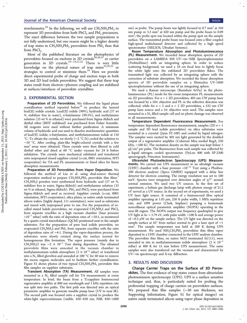
high vacuum from CH3NH3I and PbI2 or PbCl2 precursors (7).X-ray diffraction analysis (Supporting Information, Figure S2)confirmed the excellent crystalline quality of 3D CH3NH3Iperovskites and UV−vis absorption spectra (see Figure 2Abelow) were in agreement with published spectra. We show inFigure 1A UP spectra obtained with He−I UV source (hν =
21.2 eV) for the two 3D perovskite thin film samples obtainedfrom PbI2 (blue) and PbCl2 (red) precursors. Here, the binding
energy (BE) is referenced to the Fermi level. The two spectraare similar, both showing the valence band maxima (VBM) atBE = 1.4 eV, in agreement with recent work of Schultz et al.35
On the semilogarithmic scale, we can clearly see additionaldensity of states above the VBM, extending to the Fermi level.We assign these midgap states, with density approximately 2orders of magnitude lower than that of the valence band, tocharge carrier (hole) traps.To better resolve the trap states above the VBM, we use a
laser based UV source with hν = 5.79 eV. This lower photonenergy enhances the ionization cross section for the trap statesby almost 3 orders of magnitude as compared to that from theHe−I source. We can now clearly see the trap states extendingto the Fermi level in Figure 1B. The sharp peak at BE ≥ 1 eV isnear the threshold (zero) kinetic energy of emitted photo-electrons and originates both from the high energy tail of thevalence band and secondary electrons. The difference in theintensities of the threshold peak from the two samplepreparations can be attributed to small variations in work-function.The UPS results in Figure 1 establish the presence of a broad
distribution of hole traps on the surfaces of the CH3NH3PbI3perovskite thin films. Although not detectable by UPS, weexpect similarly trapped electrons below the conduction bandminimum. Supporting this, we show below the presence ofexcitonic traps: both an electron and a hole trapped locally withnonzero optical transition strength. Surprisingly, while the twosample preprations (from PbI2 and PbCl2 precursors) areknown to give very different solar cell efficiencies, the trap statedensities from UPS measurements are similar. Since UPS isonly surface sensistive, the results in Figure 1 suggest thatperovskite thin films from PbI2 and PbCl2 give similarlyexposed surfaces. We believe the different solar cell efficienciesof perovskites grown from PbI2 and PbCl2 likely come from
Figure 1. (A) Ultraviolet photoemission spectra obtained with hν =21.2 eV (He−I) for CH3NH3PbI3 thin films vapor deposited on nativeoxide terminated silicon from PbI2 (blue) and PbCl2 (red) precursors.(B) Ultraviolet photoemission spectrum obtained with hν = 5.79 eV(laser) of CH3NH3PbI3 thin films grown from PbI2 (blue) and PbCl2(red). The binding energy scale is referenced to the Fermi level.
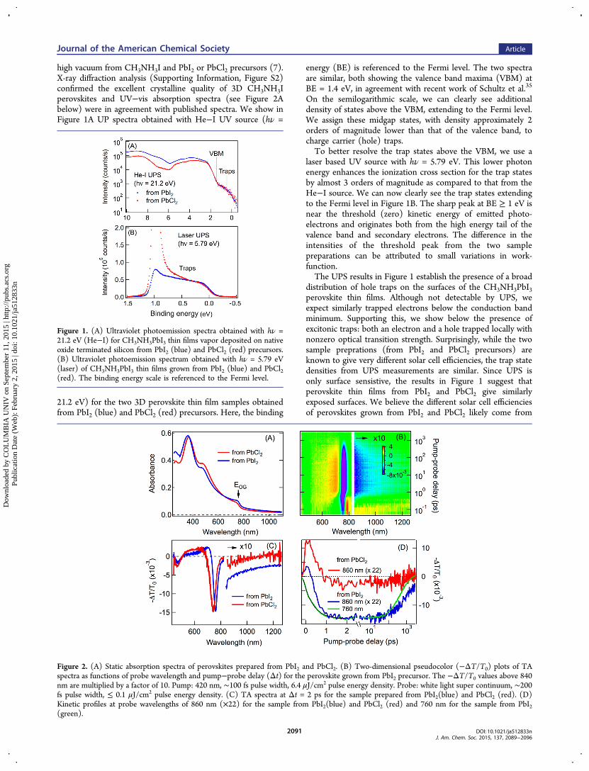
Figure 2. (A) Static absorption spectra of perovskites prepared from PbI2 and PbCl2. (B) Two-dimensional pseudocolor (−ΔT/T0) plots of TAspectra as functions of probe wavelength and pump−probe delay (Δt) for the perovskite grown from PbI2 precursor. The −ΔT/T0 values above 840nm are multiplied by a factor of 10. Pump: 420 nm, ∼100 fs pulse width, 6.4 μJ/cm2 pulse energy density. Probe: white light super continuum, ∼200fs pulse width, ≤ 0.1 μJ/cm2 pulse energy density. (C) TA spectra at Δt = 2 ps for the sample prepared from PbI2(blue) and PbCl2 (red). (D)Kinetic profiles at probe wavelengths of 860 nm (×22) for the sample from PbI2(blue) and PbCl2 (red) and 760 nm for the sample from PbI2(green).
Journal of the American Chemical Society Article
DOI: 10.1021/ja512833nJ. Am. Chem. Soc. 2015, 137, 2089−2096
2091
Dow
nloa
ded
by C
OL
UM
BIA
UN
IV o
n Se
ptem
ber
11, 2
015
| http
://pu
bs.a
cs.o
rg
Pub
licat
ion
Dat
e (W
eb):
Feb
ruar
y 2,
201
5 | d
oi: 1
0.10
21/ja
5128
33n
difference in the bulk, e.g., boundaries and interfaces betweencrystallites, as we show below with bulk sensitive opticalspectroscopies.Excitonic Traps in 3D Perovskites. Optical absorption
spectra (Figure 2A) of the 3D perovskite thin films (onsapphire) showed the optical gap (the first exciton transition,marked by an arrow) at 760 ± 5 nm (EOG = 1.63 ± 0.01 eV)and 750 ± 5 nm (1.65 ± 0.01 eV) for samples from the PbI2and PbCl2 precursors, respectively, in agreement with previousreports.3,10,14 However, the possible presence of trap statesbelow EOG cannot be judged from these static absorptionspectra due to unavoidable presence of scattering. We usetransient absorption (TA) spectroscopy to probe the trapstates. Each perovskite sample is photoexcited by a pump laserpulse above the bandgap at 420 nm and probed at a controlleddelay time by a probe pulse of white light continuum. Figure 2Bshows a pseudocolor representation of TA spectrum (−ΔT/T0) as functions of probe wavelength and pump−probe delaytime for the CH3NH3PbI3 sample grown from PbI2. ΔT is thechange in transmission with the pump pulse and T0 is thetransmission without pump pulse. The main feature in a broadtime window (Δt = 1 ps to 3 ns) is ground-state bleaching(GB) at the optical gap around 760 nm, attributed to state-filling, i.e., the presence of band gap carriers or excitons fromthe pump pulse blocking optical transition induced by theprobe pulse. At shorter times (Δt < 1 ps), we observe aderivative spectral profile around 760 nm, assigned to a red-shift of the band gap transition in the presence of hot carriers.Figure 2D shows −ΔT/T0 probed at 760 nm for the band-edgeexcitons (green), with growth in GB due to hot carrier coolingwell described by a single exponential lifetime of τ = 0.5 ± 0.1ps (black curve). The nanosecond decay time is shorter thanthose reported before10−12 and can be attributed to Augerrecombination at the high pump-power density (6.4 μJ/cm2,
see Supporting Information, Figure S3A and S3B, fordependence on pump power). The high pump intensity ischosen to clearly show the trap states with low absorption crosssections.Concurrent with the cooling of hot carriers, TA spectra in
Figure 2B show the appearance of a weak but clearly observablebleach signal below EOG (note that the −ΔT/T0 signal inFigure 2B is multiplied by a factor of 10 for probe wavelength≥840 nm). Horizontal cuts for Δt > 1 ps (blue curve in Figure2C for Δt = 2 ps) reveal the main bleach signal at 760 nm(EOG), and a broad and weak bleach feature below the opticalgap. The bleaching in the near-infrared reveals the excitonicnature of the traps: they process weak optical transitionstrength in the ground state and are populated from therelaxation of hot carriers, resulting in the blocking of the weaklyallowed transitions during the probe pulse. These excitonictraps are characterized by a broad distribution decaying awayfrom EOG. The trap state formation time increases withexcitation photon energy (Supporting Information, FigureS3D), as is expected from the transfer of excess carrier energyto phonons.We now compare the two 3D CH3NH3PbI3 perovskite thin
films grown from PbI2 and PbCl2 precursors, with the latterknown to give higher solar cell efficiency.10,12 Figure 2C showsTA spectra at Δt = 2 ps for CH3NH3PbI3 from PbI2 (blue) andPbCl2 (red) precursors. For the sample grown from PbCl2, themagnitude of bleaching attributed to traps is at least 1 order ofmagnitude lower than that grown from PbI2. The difference isevident throughout the time window in Figure 2D, whichcompares −ΔT/T0 probed at 860 nm. At this probewavelength, the −ΔT/T0 signal at Δt ≤ 1 ps contains excitedstate absorption of hot carriers as well as GB of below-gapstates; at Δt > 1 ps, GB of trap states dominates. The muchlower density of trap states in the 3D CH3NH3PbI3 perovskite
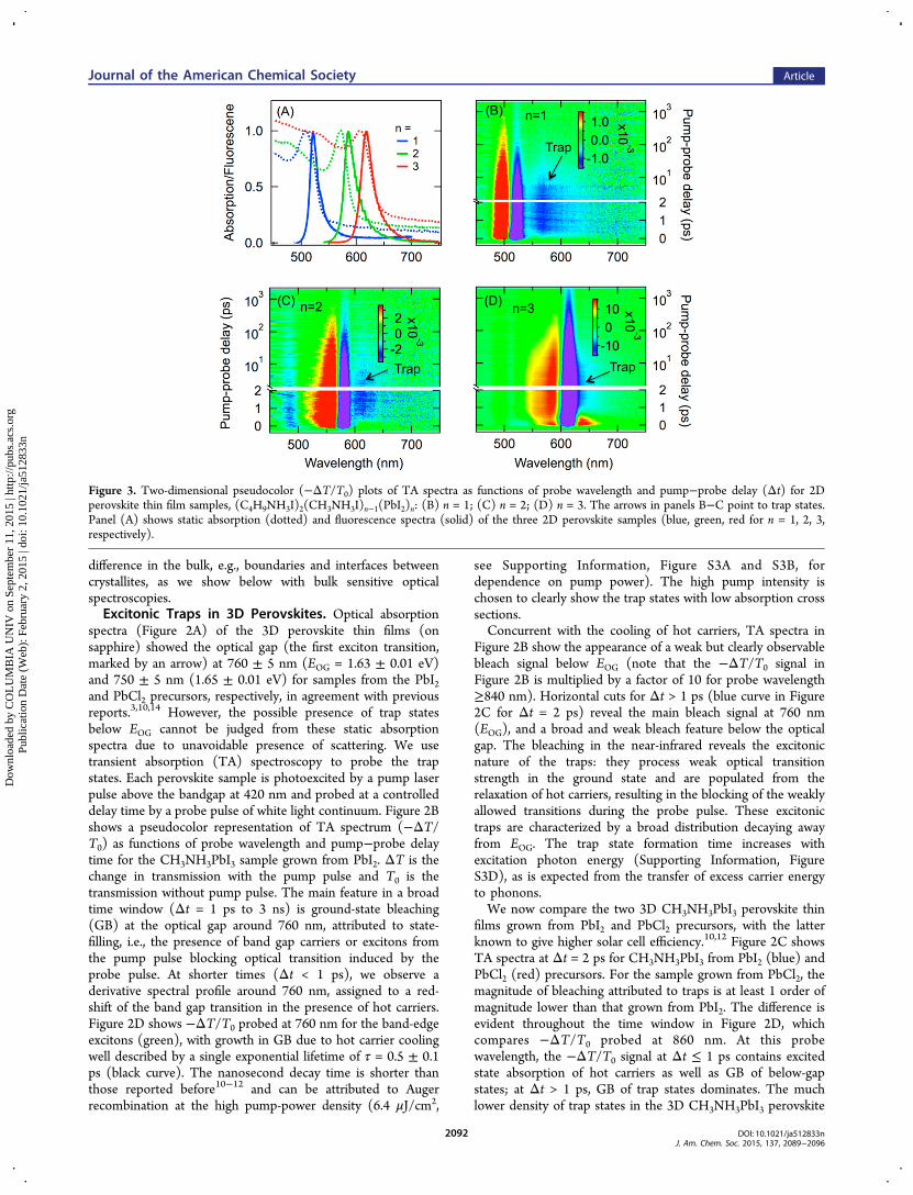
Figure 3. Two-dimensional pseudocolor (−ΔT/T0) plots of TA spectra as functions of probe wavelength and pump−probe delay (Δt) for 2Dperovskite thin film samples, (C4H9NH3I)2(CH3NH3I)n−1(PbI2)n: (B) n = 1; (C) n = 2; (D) n = 3. The arrows in panels B−C point to trap states.Panel (A) shows static absorption (dotted) and fluorescence spectra (solid) of the three 2D perovskite samples (blue, green, red for n = 1, 2, 3,respectively).
Journal of the American Chemical Society Article
DOI: 10.1021/ja512833nJ. Am. Chem. Soc. 2015, 137, 2089−2096
2092
Dow
nloa
ded
by C
OL
UM
BIA
UN
IV o
n Se
ptem
ber
11, 2
015
| http
://pu
bs.a
cs.o
rg
Pub
licat
ion
Dat
e (W
eb):
Feb
ruar
y 2,
201
5 | d
oi: 1
0.10
21/ja
5128
33n

grown from PbCl2 than that from PbI2 correlates with theslower decay (2.6 ns) of band gap excitation in the former thanthat (0.8 ns) in the latter (Supporting Information, FigureS3C). Compared to the band-edge excitons, the trappedexcitons possess higher binding energies and, thus, a lowerprobability of dissociation into charge carriers and a higherprobability of recombination.12 While we focus on 3Dperovskites obtained from vapor deposition, we also observesimilar below-gap trap states in solution processedCH3NH3PbI3 perovskite (Supporting Information, Figure S4).Our observation of much lower trap state density in
CH3NH3PbI3 perovskite from PbCl2 than that from PbI2 isconsistent not only with the better solar cell performance in theformer,12,28,29 but also with the different film morphologiesobserved in structural characterizations.27,36,37 Recent experi-ments have revealed the same crystalline structure and chemicalcomposition of CH3NH3PbI3 perovskites from both PbCl2 andPbI2 precursors, but different film morphology and crystallitesize/shape from the two preparations. The presence of chlorideions during growth has been shown to result in large andelongated crystallites with μm dimensions, while that in theabsence of chloride shows much smaller crystallites with 102
nm dimensions.27,36,37 Since smaller crystallites means largerinterfacial area, we hypothesize that the trap states are locatedat the crystallite surfaces/interface and this can explain thehigher density of trap states in the thin film from PbI2 than thatfrom PbCl2. The smaller crystals grown in the absence ofchloride ions lack well-defined facets and are randomlypacked;27,36 the interfaces between these poorly definedcrystallites are likely the locations of trap states. In contrast,the larger crystals grown in the presence of chloride ions featurewell-defined facets of low Miller indices27 and coherent long-range packing of the crystals in the film.36 A DFT calculation byHaruyama et al. suggested negligible trapping on low-indexcrystalline faces of the tetraganol perovskite crystal.38 Closeinteraction between the well-defined facets of neighboringcrystals in coherently packed film can also effectively heal the
trap states. In the following, we provide further evidence for thesurface/interface interpretation of trap states.
Excitonic Traps in 2D Perovskites. The excitonic trapsdiscovered above for the 3D perovskites are much enhanced inthe quantum-confined 2D perovskites. Figure 3A shows roomtemperature absorption and PL spectra of the three 2Dperovskite samples (n = 1, 2, 3). As the quantum well thicknessincreases from n = 1 to n = 2 and n = 3, the 1S excitontransition shifts from 508 to 571 and 608 nm, respectively. Thecorresponding PL peaks are at 521, 587, and 619 nm, for n = 1,2, and 3, respectively. Interestingly, each PL spectrum ischaracterized by an asymmetric line-shape, tailing to longerwavelength. As we show below, the lower energy PL tail comesfrom radiative recombination of trap states.Figure 3B−D shows pseudocolor representations of TA
spectra obtained from 2D perovskites with n = 1, 2, and 3,respectively. In each case, the sample is excited above the bandgap at 350 nm and probed by a white light continuum. Adetailed analysis of the linear power dependence is shown inSupporting Information (Figures S5 and S6). We observe twocommon features in all three samples. The first is a blue-shift inthe band-edge (1S) exciton energy, resulting in a derivativefeature with bleaching at or below the exciton transition andinduced absorption above. This is particularly evident for n = 1and 2 samples, where the positive signal and the negative signalcan be well described by blue-shifts of ∼4 nm (SupportingInformation, Figures S7 and S8). The second common featureis the broad and weak bleaching below the optical gap; similarto the situation for the 3D sample in Figure 2, the observationof bleaching reveals that these trap states are excitonic in naturesince they possess optical transition strength and the directoptical transition of these trap states can be blocked during theprobe pulse by those formed indirectly from the relaxation ofhot carriers/excitons.The transient absorption spectra in Figure 3 show that the
density of excitonic traps increases with quantum confinement.The relative magnitudes of peak bleaching signal from the trapstates (normalized to the peak of the blue-shifted bleaching
Figure 4. Temperature dependent fluorescence spectra from (A) 3D lead iodide perovskite thin film from PbCl2 precursor; (B) 3D lead iodideperovskite thin film from PbI2 precursor; (C) 2D n = 1 lead iodide perovskite, (C4H9NH3I)2(PbI2). (D) Ratio between PL emission from below-gaptraps and that from band gap excitons as a function of temperature for 2D n = 1 perovskite (triangle) and 3D perovskites from PbI2.
Journal of the American Chemical Society Article
DOI: 10.1021/ja512833nJ. Am. Chem. Soc. 2015, 137, 2089−2096
2093
Dow
nloa
ded
by C
OL
UM
BIA
UN
IV o
n Se
ptem
ber
11, 2
015
| http
://pu
bs.a
cs.o
rg
Pub
licat
ion
Dat
e (W
eb):
Feb
ruar
y 2,
201
5 | d
oi: 1
0.10
21/ja
5128
33n
signal of the band-edge 1S exciton) are γ = 0.077, 0.25, and 0.30for n = 3, 2, and 1, respectively (Supporting Information,section 4.3 and Figure S9). For comparison, we obtain γ =0.045 for 3D perovskite from the PbI2 precursor in Figure 2.The increase in trap density is correlated with the relative areaof the organic/inorganic interface, each consisting of a softbutylamine organic layer on a hard inorganic lead iodidequantum well. Such an interface is similar to an exposed surfaceof a 3D perovskite crystal, consisting of a methylamine organiclayer on the inorganic lead iodide crystal. Note that thepresence of the blue-shift of the band-gap exciton may beattributed to the band-gap renormalization resulting from theexciton-exciton interactions in quantum confined two-dimen-sional quantum wells (Supporting Information, section 4.2).Fluorescence Emission from Excitonic Traps. Further
evidence for the excitonic traps comes from temperaturedependent fluorescence emission. Figure 4 shows a set offluorescence spectra at different temperatures (room to liquidnitrogen) with excitation at 402 nm for three perovskitesamples: (A) 3D perovskite grown from PbCl2; (B) 3Dperovskite grown from PbI2; and (C) 2D perovskite (n = 1).For 3D perovskite grown from PbCl2 (Figure 4A), the sampleshows weak fluorescence (peak at ∼754 nm) at roomtemperature. The fluorescence intensity increases by morethan an order of magnitude as temperature decreases to ∼180K and this is accompanied by a red-shift in the peak position to∼768 nm. At T ≤ 150 K, a new fluorescence peak emerges at741 nm; this blue-shifted peak further grows with decreasing Tand becomes the dominant feature at the lowest temperatureprobed here T = 78 K. The evolution of fluorescence spectra in3D lead iodide perovskite with decreasing temperature can beattributed to a tetragonal-to-orthorhombic phase transition, asrevealed by previous optical absorption measurement.14 Theroom temperature tetragonal phase (denoted as H phase),which gives the fluorescence peak at 754−768 nm, correspondsto the collective rotation (around the c-axis) of each PbI6octahedron from its symmetric position in the simple cubicstructure, while the low temperature (L) phase, withfluorescence peak at ∼741 nm, corresponds to the tilting ofthe PbI6 octahedras out of the ab plane.14,39,40
For 3D perovskite from PbI2 (Figure 4B), the phasetransition process is similar to that from PbCl2: fluorescencefrom the H phase peaks at 759 nm at room temperature andred-shifts gradually to 782 nm as T decreases to 140 K. Belowthat, the L phase appears in the blue region. The H phaseemission is still intense even at 78K. The incomplete phasetransition has also been observed previously in lead iodideperovskite by Wehrenfennig et al., which presumably can beexplained by the strain effect imposed by the phase transition.40
The presence of the H phase at low temperatures is obscured inoptical absorption spectra14 but is dominant in fluorescencespectra in Figure 4B. The latter can be attributed to the efficientexcitonic energy transfer from the high-energy L phase to thelow-energy H phase. The most important result from Figure 4Bis the clear growth of below gap fluorescence with decreasingtemperature. At 78 K, the integrated fluorescence intensityfrom these trap states in the broad wavelength range of 800−950 nm is equal to the total band gap fluorescence from the twophases (H and L). The observation of trap state fluorescence in3D perovskites from the PbI2 precursor, but not in that fromPbCl2, is in perfect agreement with transient absorption resultsin Figure 2, which shows measurable optical transition strengthfor the trap states in the former, but not in the latter.
As we concluded earlier, the excitonic traps observed in 3Dperovskites are much enhanced in the quantum-confined 2Dperovskites. This trend is confirmed in fluorescence spectra, asshown for the n = 1 2D perovskite sample in Figure 4C. Atroom temperature, the n =1 2D perovskite exists as a singlephase (H) with the fluorescence peak at 521 nm. As Tdecreases (≤280 K), we see the appearance of the L phase18
with fluorescence peak at ∼496 nm and blue-shifting to ∼488nm at 78 K. Concurrent with the evolution of sharp band gaptransitions of both H and L phases is the growth of below-gapfluorescence: a relatively broad peak around 500 nm andanother broader emission ranging from ∼550 to 750 nm. The∼500 nm emission can be assigned to traps associated with theL phase while the broad peak 550−750 to traps associated withboth phases. The assignment of the ∼560 nm peak on top ofthe broad emission is unclear, but multiple below gap emissionpeaks have been observed previously in 2D lead perovskitesamples.30
Figure 4D plots the ratio, ρtrap/ρBG, of integrated trap stateemission to integrated band gap (BG) emission (from both Hand L phases) for the 2D (n = 1) and 3D (from PbI2)perovskites (see Supporting Information, Figure S10 fordetails). Consistent with findings from transient absorption,fluorescence emission from excitonic traps is much enhancedfrom 3D to 2D. The ρtrap/ρBG ratio from the 2D sample is 5×and 20× of that from the 3D sample at 78 and 100 K,respectively. For each sample, the ρtrap/ρBG ratio decreases withincreasing temperature, indicating that the trapped excitons canbe thermally activated into band gap excitons. Plot of ln(ρtrap/ρBG) vs 1/T do not show linear relationships (SupportingInformation, Figure S11), suggesting that the energetic gapsbetween trap states and band gap excitons are not constants, asexpected from the broad energetic distributions of trap states.The varying slope in ln(ρtrap/ρBG) vs 1/T gives phenomeno-logical free energy difference between band-edge excitons andtrapped excitons of −5 to −54 meV and −28 to −102 meV for2D (n = 1) and 3D (from PbI2) perovskites, respectively; theabsolute values of these numbers are smaller than those of themean trap energies (see next section), as expected from thesequential thermal activation within the trap state manifold and,finally, to the band gap excitons. A quantitative understandingof these temperature dependences would require a detailedunderstanding of the interconversion among the broaddistribution of trap states, the thermal activation of the trapstates into band gap excitons, and competing radiative andnonradiative recombination rates from these states.41 Furtherexperiments and modeling are underway to quantify the variousrates.
The Surface/Interface Origin of Trap States: AHypothesis. To understand the origins of trap states, wefirst summarize our findings presented above: (1) photo-emission measurements revealed similar hole traps on theexposed surfaces of 3D perovskites from both PbCl2 and PbI2;and (2) the density of excitonic traps is much increased whenwe go from 3D perovskites (from PbI2) to 2D perovskites and,within the 2D family, as the relative surface area increases. Thisis reflected semiquantitatively in the relative amplitude of trapstate bleaching to bandgap bleaching (γ): γ = 0.045 in 3Dperovskite from PbI2, γ = 0.077, 0.25, and 0.30 for 2Dperovskites with n = 3, 2, and 1, respectively. On the basis ofthis correlation between interfacial area and the density ofexcitonic traps, we hypothesize that the trap states are localized
Journal of the American Chemical Society Article
DOI: 10.1021/ja512833nJ. Am. Chem. Soc. 2015, 137, 2089−2096
2094
Dow
nloa
ded
by C
OL
UM
BIA
UN
IV o
n Se
ptem
ber
11, 2
015
| http
://pu
bs.a
cs.o
rg
Pub
licat
ion
Dat
e (W
eb):
Feb
ruar
y 2,
201
5 | d
oi: 1
0.10
21/ja
5128
33n
at the crystallite surfaces and interfaces where the bulkcrystalline symmetry is broken.We point out two key features of the excitonic traps. First,
both an electron and a hole can be trapped, resulting in anexcitonic trap possessing weak transition dipole in absorptionor emission. Second, the energetic distribution of traps is verybroad and located within ∼100−400 meV below the band gapexciton in each case. For the three QW samples, Figure 3 givesmean trap energies (referenced to EOG) of ⟨Etrap⟩ = −0.33 ±0.12, −0.17 ± 0.05, and −0.17 ± 0.07 eV for n = 1, 2, and 3respectively. Similar analysis from low-temperature fluorescencespectra in Figure 4 yields mean trap energies of ⟨Etrap⟩ = −0.38± 0.15 eV for the 2D (n = 1) sample and ⟨Etrap⟩ = −0.12 ± 0.05eV for the 3D sample. Both the broadness of the trap energiesand the relative, not absolute, energetic positions of excitonictraps referenced to different optical gaps suggest that theexcitonic traps unlikely originate from common chemicaldefects,33,34 but rather from the self-trapping of band-edgeexcitons.42 For a specific chemical defect, the trap state energyis expected to be well-defined, which is not the case here.The formation of a self-trapped exciton results from exciton−
phonon interaction, which is predicted to critically depend onthe dimensionality of a crystalline system.42 Lowering thedimension of a system lowers the deformation energy, thusmaking self-trapping easier.42 In the limit of one-dimensionalperovskites, all excitons are self-trapped with extraordinarilylarge Stokes shifts of ∼1 eV.43−45 There is usually a largepotential barrier for exciton self-trapping in 3D, while the 2Dsystem is a marginal case and possesses lower activation energyfor self-trapping.42 Our observations presented above areconsistent with this general principle. Strong electron−phononcoupling has been invoked to account for below-gap30 andwhite light emission46 in 2D layered perovskites. This couplinghas also been invoked to account for the homogeneousemission line broadening in 3D perovskites.47 For a 3Dperovskite crystallite, the terminal methylamine cations arefreer to move than their counter parts in the bulk, leading toeasier self-trapping on the surface, particularly when the surfacetermination deviates from the low-index crystalline planes.38
The self-trapped excitons on the surface can be formed fromdirect optical excitation due to the none-zero oscillator strengthor from the dynamic relaxation of the band-edge Mott−Wannier exciton or carriers. At room temperature, the self-trapped excitons, with average trapping energy of ⟨Etrap⟩ =−0.12 ± 0.05 eV, can effectively equilibrate with band-edgeexcitons/carriers given the large entropic driving from a surfacestate to bulk states. This equilibrium explains that the self-trapped exciton possesses similar lifetime as the band-edgeexciton/carriers, as seen in Figure 2D.
4. SUMMARYThe results presented here suggest an intrinsic origin of below-gap excitonic and carrier traps in lead iodide perovskites: thetrap states can result from electron−phonon coupling atsurfaces/interfaces of crystalline perovskites. In such aninterface/phonon interpretation of trap states, the surface of a3D perovskite film can be considered “entirely” as source forthe self-trapped charge (i.e., polaron) or self-trapped exciton.Charge carrier trapping at interfaces between the perovskitethin film and electron or hole transporting layers is believed toresult in faster recombination than that in bulk film25 and theseinterfacial traps have also been implicated for anomaloushysteresis in current/voltage curves in perovskite solar cells.23
Optical measurements revealed a much higher density ofexcitonic traps in the bulk of the perovskite thin film grown inthe absence of chloride than that with chloride, explaining thehigher solar cell efficiency in the latter. A comparison to recentstructural characterization of perovskite thin films from thesetwo sample preparations suggests that the trap states areassociated with interfaces of crystallites lacking well-definedfacets of low Miller indices.27 In addition to growth ofsufficiently large crystallites with low Miller indices, we mayenvision passivation of surfaces/interfaces traps with organicmolecules34 or a rigid termination layer, such as PbI2.
48 How tomanage or control surface and interface trapping may be key tothe stabilization of perovskite based solar cells.
■ ASSOCIATED CONTENT*S Supporting InformationMaterials and methods, additional results, and references. Thismaterial is available free of charge via the Internet at http://pubs.acs.org.
■ AUTHOR INFORMATIONCorresponding [email protected] Contributions†X.W., T.T., D.N., and H.Z. contributed equally.NotesThe authors declare no competing financial interest.
■ ACKNOWLEDGMENTSThe preparation of vapor-deposited perovskite samples, UPSmeasurements, and fluorescence measurements were supportedby the US Department of Energy under Grant No. ER46980.The transient absorption measurements were supported by theUS National Science Foundation under Grant Number DMR-1125845. Research carried out in part at the Center forFunctional Nanomaterials, Brookhaven National Laboratory,which is supported by the U.S. Department of Energy, Office ofBasic Energy Sciences, under Contract Number DE-AC02-98CH10886. D. N. acknowledges support by the DeutscheForschungsgemeinschaft (DFG Forschungsstipendium). Wethank Matthew Y. Sfeir for technical help with transientabsorption measurements, Joshua Choi for providing solutionbased 3D perovskite samples, and Prakriti Joshi for help withvapor deposition of 3D perovskite samples.
■ REFERENCES(1) Kojima, A.; Teshima, K.; Shirai, Y.; Miyasaka, T. J. Am. Chem. Soc.2009, 131, 6050.(2) Im, J.-H.; Lee, C.-R.; Lee, J.-W.; Park, S.-W.; Park, N.-G.Nanoscale 2011, 3, 4088.(3) Chung, I.; Lee, B.; He, J.; Chang, R. P. H.; Kanatzidis, M. G.Nature 2012, 485, 486.(4) Kim, H.-S.; Lee, C.-R.; Im, J.-H.; Lee, K.-B.; Moehl, T.;Marchioro, A.; Moon, S.-J.; Humphry-Baker, R.; Yum, J.-H.; Moser, J.E.; Gratzel, M.; Park, N.-G. Sci. Rep. 2012, 2, 591.(5) Lee, M. M.; Teuscher, J.; Miyasaka, T.; Murakami, T. N.; Snaith,H. J. Science 2012, 338, 643.(6) Etgar, L.; Gao, P.; Xue, Z.; Peng, Q.; Chandiran, A. K.; Liu, B.;Nazeeruddin, M. K.; Gratzel, M. J. Am. Chem. Soc. 2012, 134, 17396.(7) Liu, M.; Johnston, M. B.; Snaith, H. J. Nature 2013, 501, 395.(8) Burschka, J.; Pellet, N.; Moon, S.-J.; Humphry-Baker, R.; Gao, P.;Nazeeruddin, M. K.; Gratzel, M. Nature 2013, 499, 316.(9) Green, M. A.; Ho-Baillie, A.; Snaith, H. J. Nat. Photonics 2014, 8,506.
Journal of the American Chemical Society Article
DOI: 10.1021/ja512833nJ. Am. Chem. Soc. 2015, 137, 2089−2096
2095
Dow
nloa
ded
by C
OL
UM
BIA
UN
IV o
n Se
ptem
ber
11, 2
015
| http
://pu
bs.a
cs.o
rg
Pub
licat
ion
Dat
e (W
eb):
Feb
ruar
y 2,
201
5 | d
oi: 1
0.10
21/ja
5128
33n
(10) Stranks, S. D.; Eperon, G. E.; Grancini, G.; Menelaou, C.;Alcocer, M. J. P.; Leijtens, T.; Herz, L. M.; Petrozza, A.; Snaith, H. J.Science 2013, 342, 341.(11) Xing, G.; Mathews, N.; Sun, S.; Lim, S. S.; Lam, Y. M.; Gratzel,M.; Mhaisalkar, S.; Sum, T. C. Science 2013, 342, 344.(12) Wehrenfennig, C.; Eperon, G. E.; Johnston, M. B.; Snaith, H. J.;Herz, L. M. Adv. Mater. 2013, 26, 1584.(13) Marchioro, A.; Teuscher, J.; Friedrich, D.; Kunst, M.; van deKrol, R.; Moehl, T.; Gratzel, M.; Moser, J.-E. Nat. Photonics 2014, 8,250.(14) D’Innocenzo, V.; Grancini, G.; Alcocer, M. J. P.; Kandada, A. R.S.; Stranks, S. D.; Lee, M. M.; Lanzani, G.; Snaith, H. J.; Petrozza, A.Nat. Commun. 2014, 5, 3586.(15) Mei, A.; Li, X.; Liu, L.; Ku, Z.; Liu, T.; Rong, Y.; Xu, M.; Hu, M.;Chen, J.; Yang, Y.; Gratzel, M.; Han, H. Science 2014, 345, 295.(16) Hao, F.; Stoumpos, C. C.; Cao, D. H.; Chang, R. P. H.;Kanatzidis, M. G. Nat. Photonics 2014, 8, 489.(17) Zhou, H.; Chen, Q.; Li, G.; Luo, S.; Song, T. -b.; Duan, H.-S.;Hong, Z.; You, J.; Liu, Y.; Yang, Y. Science 2014, 345, 542.(18) Mitzi, D. B. In Progress in Inorganic Chemistry; John Wiley &Sons, Inc.: New York, 2007; pp 1−121.(19) Ishihara, T.; Takahashi, J.; Goto, T. Phys. Rev. B: Condens. MatterMater. Phys. 1990, 42, 11099.(20) Tanaka, K.; Kondo, T. Sci. Technol. Adv. Mater. 2003, 4, 599.(21) Ponseca, C. S.; Savenije, T. J.; Abdellah, M.; Zheng, K.; Yartsev,A.; Pascher, T.; Harlang, T.; Chabera, P.; Pullerits, T.; Stepanov, A.;Wolf, J.-P.; Sundstrom, V. J. Am. Chem. Soc. 2014, 136, 5189.(22) Manser, J. S.; Kamat, P. V. Nat. Photonics 2014, 8, 737.(23) Snaith, H. J.; Abate, A.; Ball, J. M.; Eperon, G. E.; Leijtens, T.;Noel, N. K.; Stranks, S. D.; Wang, J. T.-W.; Wojciechowski, K.; Zhang,W. J. Phys. Chem. Lett. 2014, 5, 1511.(24) Leijtens, T.; Stranks, S. D.; Eperon, G. E.; Lindblad, R.;Johansson, E. M. J.; McPherson, I. J.; Rensmo, H.; Ball, J. M.; Lee, M.M.; Snaith, H. J. ACS Nano 2014, 8, 7147.(25) Wang, L.; McCleese, C.; Kovalsky, A.; Zhao, Y.; Burda, C. J. Am.Chem. Soc. 2014, 136, 12205.(26) Gratzel, M. Nat. Mater. 2014, 13, 838.(27) Dar, M. I.; Arora, N.; Gao, P.; Ahmad, S.; Gratzel, M.;Nazeeruddin, M. K. Nano Lett. 2014, 14, 6991.(28) Colella, S.; Mosconi, E.; Fedeli, P.; Listorti, A.; Gazza, F.;Orlandi, F.; Ferro, P.; Besagni, T.; Rizzo, A.; Calestani, G.; Gigli, G.;De Angelis, F.; Mosca, R. Chem. Mater. 2013, 25, 4613.(29) Zhao, Y.; Zhu, K. J. Phys. Chem. C 2014, 118, 9412.(30) Gauthron, K.; Lauret, J.-S.; Doyennette, L.; Lanty, G.; AlChoueiry, A.; Zhang, S. J.; Brehier, A.; Largeau, L.; Mauguin, O.;Bloch, J.; Deleporte, E. Opt. Express 2010, 18, 5912.(31) Tanaka, K.; Takahashi, T.; Ban, T.; Kondo, T.; Uchida, K.;Miura, N. Solid State Commun. 2003, 127, 619.(32) Yin, W.-J.; Shi, T.; Yan, Y. Appl. Phys. Lett. 2014, 104, 063903.(33) Kim, J.; Lee, S.-H.; Lee, J. H.; Hong, K.-H. J. Phys. Chem. Lett.2014, 5, 1312.(34) Noel, N. K.; Abate, A.; Stranks, S. D.; Parrott, E.; Burlakov, V.;Goriely, A.; Snaith, H. J. ACS Nano 2014, 8, 9815.(35) Schulz, P.; Edri, E.; Kirmayer, S.; Hodes, G.; Cahen, D.; Kahn,A. Energy Environ. Sci. 2014, 7, 1377.(36) Williams, S. T.; Zuo, F.; Chueh, C.-C.; Liao, C.-Y.; Liang, P.-W.;Jen, A. K.-Y. ACS Nano 2014, 8, 10640.(37) Edri, E.; Kirmayer, S.; Henning, A.; Mukhopadhyay, S.;Gartsman, K.; Rosenwaks, Y.; Hodes, G.; Cahen, D. Nano Lett.2014, 14, 1000.(38) Haruyama, J.; Sodeyama, K.; Han, L.; Tateyama, Y. J. Phys.Chem. Lett. 2014, 5, 2903.(39) Kawamura, Y.; Mashiyama, H.; Hasebe, K. J. Phys. Soc. Jpn.2002, 71, 1694.(40) Wehrenfennig, C.; Liu, M.; Snaith, H. J.; Johnston, M. B.; Herz,L. M. APL Mater. 2014, 2, 081513.(41) Stranks, S. D.; Burlakov, V. M.; Leijtens, T.; Ball, J. M.; Goriely,A.; Snaith, H. J. Phys. Rev. Appl. 2014, 2, 034007.
(42) Song, K. S.; Williams, R. T. Self-Trapped Excitons; SpringerSeries in Solid-State Sciences; Springer: Berlin, 1993; Vol. 105.(43) Trigui, A.; Abid, H.; Mlayah, A.; Abid, Y. Synth. Met. 2012, 162,1731.(44) Tanaka, K.; Ozawa, R.; Umebayashi, T.; Asai, K.; Ema, K.;Kondo, T. Phys. E (Amsterdam, Neth.) 2005, 25, 378.(45) Tanino, H.; Ruhle, W.; Takahashi, K. Phys. Rev. B: Condens.Matter Mater. Phys. 1988, 38, 12716.(46) Dohner, E. R.; Jaffe, A.; Bradshaw, L. R.; Karunadasa, H. I. J. Am.Chem. Soc. 2014, 136, 13154.(47) Wehrenfennig, C.; Liu, M.; Snaith, H. J.; Johnston, M. B.; Herz,L. M. J. Phys. Chem. Lett. 2014, 5, 1300.(48) Chen, Q.; Zhou, H.; Song, T.-B.; Luo, S.; Hong, Z.; Duan, H.-S.;Dou, L.; Liu, Y.; Yang, Y. Nano Lett. 2014, 14, 4158.
Journal of the American Chemical Society Article
DOI: 10.1021/ja512833nJ. Am. Chem. Soc. 2015, 137, 2089−2096
2096
Dow
nloa
ded
by C
OL
UM
BIA
UN
IV o
n Se
ptem
ber
11, 2
015
| http
://pu
bs.a
cs.o
rg
Pub
licat
ion
Dat
e (W
eb):
Feb
ruar
y 2,
201
5 | d
oi: 1
0.10
21/ja
5128
33n
Copyright © 2022 FDOKUMEN