A Novel Reconfiguration Scheme in Quantum-Dot Cellular ...
98
University of Massachusetts Amherst University of Massachusetts Amherst ScholarWorks@UMass Amherst ScholarWorks@UMass Amherst Masters Theses 1911 - February 2014 2013 A Novel Reconfiguration Scheme in Quantum-Dot Cellular A Novel Reconfiguration Scheme in Quantum-Dot Cellular Automata for Energy Efficient Nanocomputing Automata for Energy Efficient Nanocomputing Madhusudan Chilakam University of Massachusetts Amherst Follow this and additional works at: https://scholarworks.umass.edu/theses Part of the Electronic Devices and Semiconductor Manufacturing Commons, Nanotechnology Fabrication Commons, Power and Energy Commons, and the VLSI and Circuits, Embedded and Hardware Systems Commons Chilakam, Madhusudan, "A Novel Reconfiguration Scheme in Quantum-Dot Cellular Automata for Energy Efficient Nanocomputing" (2013). Masters Theses 1911 - February 2014. 1028. Retrieved from https://scholarworks.umass.edu/theses/1028 This thesis is brought to you for free and open access by ScholarWorks@UMass Amherst. It has been accepted for inclusion in Masters Theses 1911 - February 2014 by an authorized administrator of ScholarWorks@UMass Amherst. For more information, please contact [email protected].
-
Upload
khangminh22 -
Category
Documents
-
view
0 -
download
0
Transcript of A Novel Reconfiguration Scheme in Quantum-Dot Cellular ...

University of Massachusetts Amherst University of Massachusetts Amherst
ScholarWorks@UMass Amherst ScholarWorks@UMass Amherst
Masters Theses 1911 - February 2014
2013
A Novel Reconfiguration Scheme in Quantum-Dot Cellular A Novel Reconfiguration Scheme in Quantum-Dot Cellular
Automata for Energy Efficient Nanocomputing Automata for Energy Efficient Nanocomputing
Madhusudan Chilakam University of Massachusetts Amherst
Follow this and additional works at: https://scholarworks.umass.edu/theses
Part of the Electronic Devices and Semiconductor Manufacturing Commons, Nanotechnology
Fabrication Commons, Power and Energy Commons, and the VLSI and Circuits, Embedded and Hardware
Systems Commons
Chilakam, Madhusudan, "A Novel Reconfiguration Scheme in Quantum-Dot Cellular Automata for Energy Efficient Nanocomputing" (2013). Masters Theses 1911 - February 2014. 1028. Retrieved from https://scholarworks.umass.edu/theses/1028
This thesis is brought to you for free and open access by ScholarWorks@UMass Amherst. It has been accepted for inclusion in Masters Theses 1911 - February 2014 by an authorized administrator of ScholarWorks@UMass Amherst. For more information, please contact [email protected].
A NOVEL RECONFIGURATION SCHEME INQUANTUM-DOT CELLULAR AUTOMATA FOR
ENERGY EFFICIENT NANOCOMPUTING
A Thesis Presented
by
MADHUSUDAN CHILAKAM
Submitted to the Graduate School of theUniversity of Massachusetts Amherst in partial fulfillment
of the requirements for the degree of
MASTER OF SCIENCE IN ELECTRICAL AND COMPUTER ENGINEERING
May 2013
Electrical and Computer Engineering

A NOVEL RECONFIGURATION SCHEME INQUANTUM-DOT CELLULAR AUTOMATA FOR
ENERGY EFFICIENT NANOCOMPUTING
A Thesis Presented
by
MADHUSUDAN CHILAKAM
Approved as to style and content by:
Neal G. Anderson, Chair
Russell Tessier, Member
Eric Polizzi, Member
C.V. Hollot, Department ChairElectrical and Computer Engineering
ABSTRACT
A NOVEL RECONFIGURATION SCHEME INQUANTUM-DOT CELLULAR AUTOMATA FOR
ENERGY EFFICIENT NANOCOMPUTING
MAY 2013
MADHUSUDAN CHILAKAM
B.Tech, VELLORE INSTITUTE OF TECHNOLOGY UNIVERSITY, VELLORE
M.S.E.C.E., UNIVERSITY OF MASSACHUSETTS AMHERST
Directed by: Professor Neal G. Anderson
Quantum-Dot Cellular Automata (QCA) is currently being investigated as an
alternative to CMOS technology. There has been extensive study on a wide range of
circuits from simple logical circuits such as adders to complex circuits such as 4-bit
processors. At the same time, little if any work has been done in considering the
possibility of reconfiguration to reduce power in QCA devices. This work presents
one of the first such efforts when considering reconfigurable QCA architectures which
are expected to be both robust and power efficient. We present a new reconfiguration
scheme which is highly robust and is expected to dissipate less power with respect to
conventional designs. An adder design based on the reconfiguration scheme will be
presented in this thesis, with a detailed power analysis and comparison with existing
designs. In order to overcome the problems of routing which comes with reconfigura-
bility, a new wire crossing mechanism is also presented as part of this thesis.
iii

TABLE OF CONTENTS
Page
ABSTRACT . . . . . . . . . . . . . . . . . . . . . . . . . . . . . . . . . . . . . . . . . . . . . . . . . . . . . . . . . . iii
LIST OF TABLES . . . . . . . . . . . . . . . . . . . . . . . . . . . . . . . . . . . . . . . . . . . . . . . . . . . . vi
LIST OF FIGURES . . . . . . . . . . . . . . . . . . . . . . . . . . . . . . . . . . . . . . . . . . . . . . . . . . vii
CHAPTER
1. INTRODUCTION AND MOTIVATION . . . . . . . . . . . . . . . . . . . . . . . . . . . 1
2. TECHNICAL BACKGROUND . . . . . . . . . . . . . . . . . . . . . . . . . . . . . . . . . . . . 5
2.1 QCA Basics . . . . . . . . . . . . . . . . . . . . . . . . . . . . . . . . . . . . . . . . . . . . . . . . . . . . . 52.2 Logical Devices in QCA . . . . . . . . . . . . . . . . . . . . . . . . . . . . . . . . . . . . . . . . . . . 8
2.2.1 Binary Wire . . . . . . . . . . . . . . . . . . . . . . . . . . . . . . . . . . . . . . . . . . . . . . . 82.2.2 Inverter . . . . . . . . . . . . . . . . . . . . . . . . . . . . . . . . . . . . . . . . . . . . . . . . . . . 92.2.3 Majority Gate Voter . . . . . . . . . . . . . . . . . . . . . . . . . . . . . . . . . . . . . . . . 9
2.3 Clocking in QCA . . . . . . . . . . . . . . . . . . . . . . . . . . . . . . . . . . . . . . . . . . . . . . . . 10
2.3.1 Landauer Clocking . . . . . . . . . . . . . . . . . . . . . . . . . . . . . . . . . . . . . . . . 152.3.2 Bennett Clocking . . . . . . . . . . . . . . . . . . . . . . . . . . . . . . . . . . . . . . . . . . 15
2.4 Wire Crossings in QCA . . . . . . . . . . . . . . . . . . . . . . . . . . . . . . . . . . . . . . . . . . 162.5 Reconfiguration in QCA . . . . . . . . . . . . . . . . . . . . . . . . . . . . . . . . . . . . . . . . . . 17
2.5.1 Reconfigurability and Nanocomputing . . . . . . . . . . . . . . . . . . . . . . . . 182.5.2 Application of Reconfiguration in QCA’s . . . . . . . . . . . . . . . . . . . . . 18
3. PROPOSED RECONFIGURATION SCHEME . . . . . . . . . . . . . . . . . . . 21
3.1 Majority Gate Voter Reconfiguration . . . . . . . . . . . . . . . . . . . . . . . . . . . . . . . 223.2 Wire Crossing Scheme based on Bennett Clocking . . . . . . . . . . . . . . . . . . . . 26
iv

4. POWER ANALYSIS AND METHODOLOGY . . . . . . . . . . . . . . . . . . . . 32
4.1 Upper Bound Power Dissipation Model . . . . . . . . . . . . . . . . . . . . . . . . . . . . . 334.2 Lower Bound Power Dissipation Model . . . . . . . . . . . . . . . . . . . . . . . . . . . . . 354.3 Power Analysis of Proposed Reconfiguration Scheme . . . . . . . . . . . . . . . . . 39
5. QCA ADDERS . . . . . . . . . . . . . . . . . . . . . . . . . . . . . . . . . . . . . . . . . . . . . . . . . . . 42
5.1 Background on QCA Adders . . . . . . . . . . . . . . . . . . . . . . . . . . . . . . . . . . . . . . 425.2 Proposed Adder Designs . . . . . . . . . . . . . . . . . . . . . . . . . . . . . . . . . . . . . . . . . . 43
5.2.1 Carry Ripple Adder . . . . . . . . . . . . . . . . . . . . . . . . . . . . . . . . . . . . . . . 445.2.2 Carry Look Ahead Adder . . . . . . . . . . . . . . . . . . . . . . . . . . . . . . . . . . 51
6. RESULTS AND COMPARATIVE ANALYSIS . . . . . . . . . . . . . . . . . . . . 57
6.1 Upper and Lower Bound Energy Dissipation . . . . . . . . . . . . . . . . . . . . . . . . 58
6.1.1 Analysis of Carry Ripple Adder . . . . . . . . . . . . . . . . . . . . . . . . . . . . . 586.1.2 Analysis of Carry Look Ahead Adder . . . . . . . . . . . . . . . . . . . . . . . . 616.1.3 Analysis of existing Adders . . . . . . . . . . . . . . . . . . . . . . . . . . . . . . . . . 62
6.2 Area and Cell Count . . . . . . . . . . . . . . . . . . . . . . . . . . . . . . . . . . . . . . . . . . . . . 646.3 Latency . . . . . . . . . . . . . . . . . . . . . . . . . . . . . . . . . . . . . . . . . . . . . . . . . . . . . . . . 656.4 Speed with respect to Area and Power (SwAP) Analysis . . . . . . . . . . . . . . 66
7. CONCLUSION AND FUTURE WORK . . . . . . . . . . . . . . . . . . . . . . . . . . 69
7.1 Summary . . . . . . . . . . . . . . . . . . . . . . . . . . . . . . . . . . . . . . . . . . . . . . . . . . . . . . . 707.2 Future Work . . . . . . . . . . . . . . . . . . . . . . . . . . . . . . . . . . . . . . . . . . . . . . . . . . . . 71
APPENDICES
A. RECONFIGURABILITY AND NANOCOMPUTING . . . . . . . . . . . . 72B. POWER DISSIPATION MODELS . . . . . . . . . . . . . . . . . . . . . . . . . . . . . . . . 77
BIBLIOGRAPHY . . . . . . . . . . . . . . . . . . . . . . . . . . . . . . . . . . . . . . . . . . . . . . . . . . . 82
v
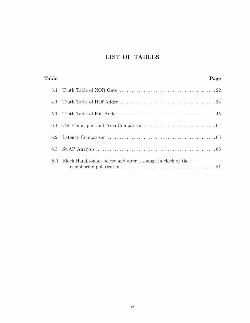
LIST OF TABLES
Table Page
3.1 Truth Table of XOR Gate . . . . . . . . . . . . . . . . . . . . . . . . . . . . . . . . . . . . . . . . 22
4.1 Truth Table of Half Adder . . . . . . . . . . . . . . . . . . . . . . . . . . . . . . . . . . . . . . . . 34
5.1 Truth Table of Full Adder . . . . . . . . . . . . . . . . . . . . . . . . . . . . . . . . . . . . . . . . 45
6.1 Cell Count per Unit Area Comparison . . . . . . . . . . . . . . . . . . . . . . . . . . . . . . 64
6.2 Latency Comparison . . . . . . . . . . . . . . . . . . . . . . . . . . . . . . . . . . . . . . . . . . . . . 65
6.3 SwAP Analysis . . . . . . . . . . . . . . . . . . . . . . . . . . . . . . . . . . . . . . . . . . . . . . . . . . 66
B.1 Bloch Hamiltonian before and after a change in clock or theneighboring polarization . . . . . . . . . . . . . . . . . . . . . . . . . . . . . . . . . . . . . . . 81
vi

LIST OF FIGURES
Figure Page
1.1 Performance Evaluation for Emerging Logic Device Technologies . . . . . . . . 3
2.1 Simple 4-dot Unpolarized QCA cell . . . . . . . . . . . . . . . . . . . . . . . . . . . . . . . . . 6
2.2 Polarization States of a 4-dot QCA cell . . . . . . . . . . . . . . . . . . . . . . . . . . . . . . 7
2.3 Transfer of Polarization between adjacent QCA cells . . . . . . . . . . . . . . . . . . 7
2.4 Binary Wire Representation in QCA . . . . . . . . . . . . . . . . . . . . . . . . . . . . . . . . 8
2.5 Inverter Representation in QCA . . . . . . . . . . . . . . . . . . . . . . . . . . . . . . . . . . . . 9
2.6 Majority Gate Voter Representation in QCA . . . . . . . . . . . . . . . . . . . . . . . . 10
2.7 The QCA clock, it’s stages and it’s effects on a cell’s energybarriers . . . . . . . . . . . . . . . . . . . . . . . . . . . . . . . . . . . . . . . . . . . . . . . . . . . . . 11
2.8 Example of QCA Clock Transitions . . . . . . . . . . . . . . . . . . . . . . . . . . . . . . . . 12
2.9 Landauer and Bennett clocking of QCA circuits . . . . . . . . . . . . . . . . . . . . . 14
2.10 Traditional Wire Crossing Model . . . . . . . . . . . . . . . . . . . . . . . . . . . . . . . . . . 16
2.11 p-QCA device structure: QCA layer with clocking circuitry. . . . . . . . . . . . 20
3.1 Schematic of XOR Gate . . . . . . . . . . . . . . . . . . . . . . . . . . . . . . . . . . . . . . . . . . 22
3.2 Conventional XOR Gate Design . . . . . . . . . . . . . . . . . . . . . . . . . . . . . . . . . . . 22
3.3 Proposed XOR Gate Design . . . . . . . . . . . . . . . . . . . . . . . . . . . . . . . . . . . . . . . 22
3.4 Clocking Scheme of Proposed XOR Gate Design . . . . . . . . . . . . . . . . . . . . . 24
3.5 Circuit Schematic of Boolean Function (A+B)+(B.C) . . . . . . . . . . . . . . . . 26
vii

3.6 QCA representation of Boolean Function (A+B)+(B.C) . . . . . . . . . . . . . . 27
3.7 Clocking Scheme of the Proposed Wire Crossing Technique . . . . . . . . . . . . 28
3.8 Timing Diagram of the Proposed Wire Crossing Technique . . . . . . . . . . . . 28
3.9 Implementation of the Proposed Wire Crossing Technique until thePipeline Zones . . . . . . . . . . . . . . . . . . . . . . . . . . . . . . . . . . . . . . . . . . . . . . . 29
3.10 Implementation of the Proposed Wire Crossing Technique within andafter the Pipeline Zones . . . . . . . . . . . . . . . . . . . . . . . . . . . . . . . . . . . . . . . 31
4.1 Schematic, QCA Layout and Clocking Scheme of a Half Adder . . . . . . . . . 32
4.2 Timing Diagram of the XOR gate based on proposed ReconfigurationScheme . . . . . . . . . . . . . . . . . . . . . . . . . . . . . . . . . . . . . . . . . . . . . . . . . . . . . . 41
4.3 Timing Diagram of the XOR gate based on conventional designmethodology . . . . . . . . . . . . . . . . . . . . . . . . . . . . . . . . . . . . . . . . . . . . . . . . . 41
5.1 Block Diagram of Full Adder . . . . . . . . . . . . . . . . . . . . . . . . . . . . . . . . . . . . . . 45
5.2 Block Diagram of Carry Ripple Adder . . . . . . . . . . . . . . . . . . . . . . . . . . . . . . 45
5.3 Block Diagram of Proposed Carry Ripple Adder . . . . . . . . . . . . . . . . . . . . . 46
5.4 QCA Representation of Proposed Carry Ripple Adder . . . . . . . . . . . . . . . . 47
5.5 Initial State of Proposed Carry Ripple Adder . . . . . . . . . . . . . . . . . . . . . . . . 47
5.6 Clocking Scheme of the Carry Ripple Adder until computation ofA⊗B. . . . . . . . . . . . . . . . . . . . . . . . . . . . . . . . . . . . . . . . . . . . . . . . . . . . . . . . 49
5.7 Clocking Scheme of the Carry Ripple Adder until computation ofSum . . . . . . . . . . . . . . . . . . . . . . . . . . . . . . . . . . . . . . . . . . . . . . . . . . . . . . . . 50
5.8 Block Diagram of Carry Look Ahead Adder . . . . . . . . . . . . . . . . . . . . . . . . . 51
5.9 Block Diagram of Proposed Carry Look Ahead Adder . . . . . . . . . . . . . . . . 52
5.10 QCA Representation of Proposed Carry Look Ahead Adder . . . . . . . . . . . 52
5.11 Initial State of Proposed Carry Look Ahead Adder . . . . . . . . . . . . . . . . . . . 52
viii

5.12 Clocking Scheme of the Carry Look Ahead Adder until computationof Propagate . . . . . . . . . . . . . . . . . . . . . . . . . . . . . . . . . . . . . . . . . . . . . . . . . 54
5.13 Clocking Scheme of the Carry Look Ahead Adder until computationof Sum . . . . . . . . . . . . . . . . . . . . . . . . . . . . . . . . . . . . . . . . . . . . . . . . . . . . . . 55
6.1 QCA representation of existing adders . . . . . . . . . . . . . . . . . . . . . . . . . . . . . . 57
6.2 Existing 4-bit adder . . . . . . . . . . . . . . . . . . . . . . . . . . . . . . . . . . . . . . . . . . . . . . 63
6.3 Graphs comparing the proposed adders with existing adders . . . . . . . . . . . 68
A.1 AND gate using reconfigurable CAEN grid . . . . . . . . . . . . . . . . . . . . . . . . . . 73
A.2 Typical NanoWire Crossbar Architecture . . . . . . . . . . . . . . . . . . . . . . . . . . . 74
A.3 Island Style FPGA Architecture . . . . . . . . . . . . . . . . . . . . . . . . . . . . . . . . . . . 76
ix

CHAPTER 1
INTRODUCTION AND MOTIVATION
It was as early as 1965 when Gordon Moore predicted that the number of transis-
tors that can be integrated on to a single chip will double every 18 months [46]. This
law put forth by Moore has been a benchmark for semiconductor scaling for more than
four decades. The IC industry which has been primarily driven by CMOS technology
scaling is now forced to look into other alternatives as the scaling is fast approaching
its fundamental limits. The International Technology Roadmap for Semiconductors
(ITRS) has predicted that size limit of CMOS technology will be limited to about
5 nm to 10 nm and believes this limit will be reached as early as 2017 [3]. Shrink-
ing transistors have been helpful in achieving high speed and low power circuits. As
the devices are exponentially scaled down various factors including power dissipation,
gate leakage current, interconnection noise (introduction of crosstalk and hot electron
effect) and stray capacitances have become potential bottlenecks that has led to the
degradation of circuit performance.
In the last few years as the technology has scaled down to sub 45nm, power
dissipation has been a major area of concern for researchers around the world. Fred
Pollack of Intel Corporation was one of the first to note the alarming rate at which
power density is increasing with the shrinking geometry [52]. Thus power management
is a critical issue which needs to addressed at the earliest.
Nanotechnology is touted to be the solution to the problem of device shrinking
where the performance is degraded due to increasing quantum effects and to over-
come the existing power dissipation. There are many possible candidates which are
1

being considered as a possible replacement to CMOS such as Quantum Dot Cellular
Automata [40], Silicon Nano-wires [18], Carbon Nanotubes based Transistors [5, 61],
Spin Wave Transistors [71, 54], Superconducting Electronics [66], Resonant Tunnel-
ing devices [45, 47] among others. Fig. 1.1 portrays a critical review of some these
emerging devices at the nanoscale level.
Quantum - Dot Cellular Automata (QCA) is one such nano computing paradigm
that exploits some of the unavoidable nanoscale issues such as quantum effects and
device integration for performing useful computation. Some of the potential advan-
tages of QCA include the lack of interconnects, high clock frequency, and since QCA
doesn’t involve transfer of electrons or flow of current, it has the potential to perform
low power computing. One of the most striking features of this emerging technology
is that it has the ability to dynamically reconfigure or redesign the functionality of
the system which makes the system more powerful and more efficient in terms of
computational speed and power dissipation.
Field Programmable Gate Arrays (FPGAs) have always been an attractive low
cost option for designers since it offers flexibility in terms of hardware. Researchers
have been very successful in establishing that FPGAs have outperformed the imple-
mentation of a number of real time applications in terms of computational perfor-
mance and cost [68]. Reconfigurability represents an attractive application of QCA
technology [21, 50]. With the help of reconfiguration, the inbuilt low power nature of
QCA can be exploited to design various low power circuits which are not only efficient
in terms of power but are also efficient in terms of area and computation.
In this thesis, we explore one possible approach to realize reconfigurability in
QCA that is based on the change in polarization of electrons in a QCA cell. This
novel reconfiguration scheme which is based on majority gate voter is best suited
for complex circuit design which have high fan-outs and require the intermediate
computation results. We introduce a new custom wire crossing technique which is
2
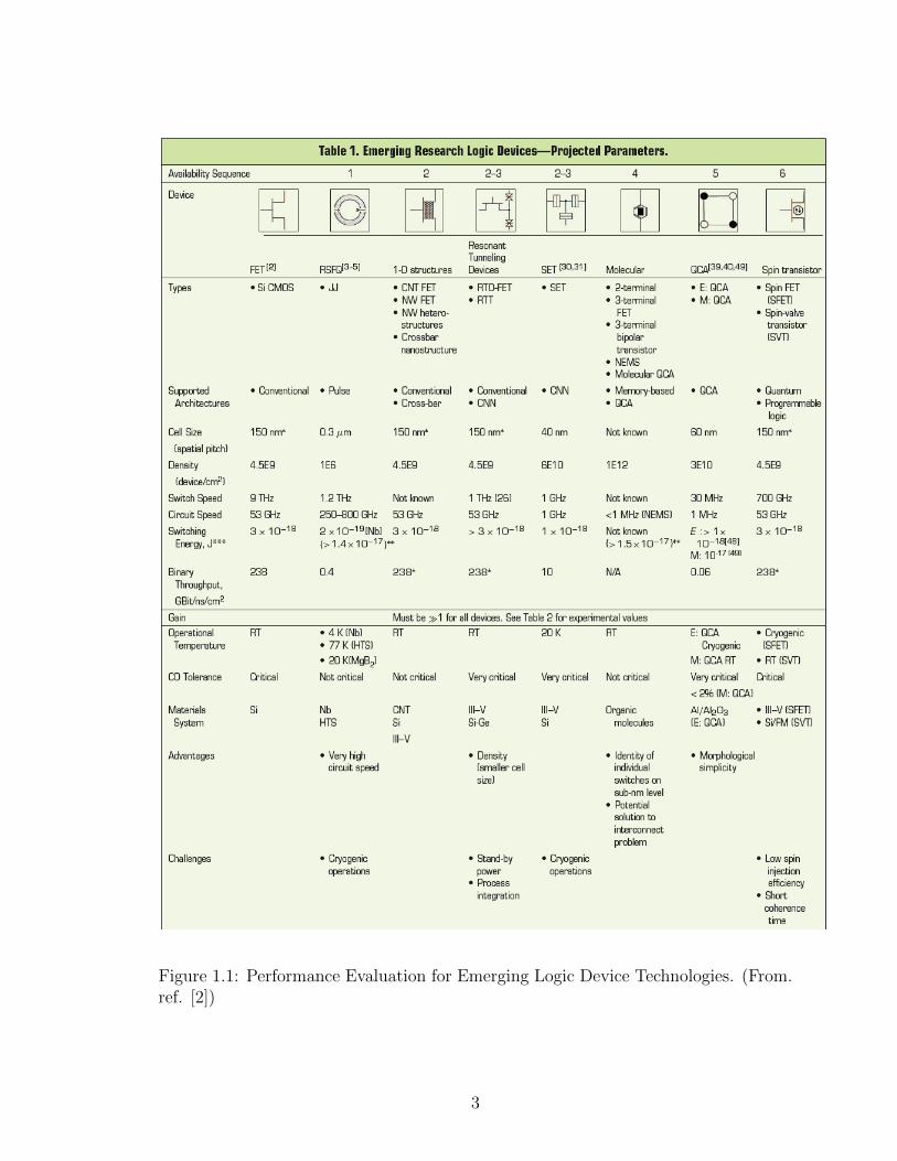
Figure 1.1: Performance Evaluation for Emerging Logic Device Technologies. (From.ref. [2])
3

used to overcome the traditional problems of routing in any reconfiguration based
design. The design exploits the inherent pipeline nature of QCA which can lead to an
enormous reduction in area since the entire computation can be computed in a single
block. One can design highly energy efficient circuits as QCA doesn’t involve the
physical movement of any charge particles. This design will be highly energy efficient
along with added advantages of pipelining and area.
The major contributions of this thesis are
• We present our vision for low power computation based on QCA.
• We introduce the concept of reconfigurability in QCA for constructing energy
efficient logic devices.
• Design of simple arithmetic circuits like full adders using the proposed recon-
figuration scheme.
• We address the problems in routing with a custom wire crossing technique.
• We evaluate benefits of our designs vs. existing designs.
The rest of the thesis is organized as follows: the background on QCA and recon-
figurability in nano computing and in particular in QCA are presented in Chapter 2.
The concept of proposed reconfiguration scheme along with the wire crossing tech-
niques are discussed in Chapter 3. Analysis of the proposed designs and the power
dissipation models considered in the design analysis is presented in Chapter 4. Chap-
ter 5 outlines the existing adder design and introduces the proposed adder design
based on the reconfiguration scheme. A detail analysis of the proposed adder de-
sign along with the comparative analysis is presented in Chapter 6 and the thesis is
concluded in Chapter 7.
4

CHAPTER 2
TECHNICAL BACKGROUND
Quantum Cellular Automata are models used in quantum computation which are
analogous to conventional models of cellular automata suggested by Von Neumann
[48]. The first step towards quantizing the existing models of cellular automata was
suggested by Richard Feynman [31, 30]. The word Quantum Cellular Automata
was defined by Gerhard Grossing and Anton Zeilinger to a model [34] which they
developed in the year 1988. However, the model proposed by them had little or
no relation to the concepts developed in quantum computation by David Deutsch,
hence their model has not been developed as a model of computation [22]. John
Watrous was the first to do an in-depth research on the models based on Quantum
Cellular Automata [70]. Craig Lent and Doug Tougaw proposed implementation of
systems based on the classical cellular automata designed using quantum dots [40] as
a replacement for the classical computation using CMOS. In order to differentiate this
proposal and the models of cellular automata which are used for performing quantum
computation, many authors refers to this subject as Quantum-dot Cellular Automata
(QCA).
2.1 QCA Basics
Quantum-dot Cellular Automata (QCA) is a new nano computing paradigm which
encodes binary information by charge configuration within a cell instead of the conven-
tional current switches. There is no current flow within the cells since the coulombic
5

interaction between the electrons is sufficient for computation. This paradigm pro-
vides one of many possible solutions for transistor-less computation at the nanoscale.
The standard QCA cells have four quantum dots and two electrons [64]. There
are various kinds of QCA cells proposed which include a six-dot QCA cell and an
eight-dot QCA cell. In a QCA Cell, two electrons occupy diagonally opposite dots in
the cell due to mutual repulsion of like charges. An example of a simple unpolarized
QCA cell consisting of four quantum dots arranged in a square is as shown in Fig.
2.1. Dots are simply places where a charge can be localized. There are two extra
electrons in the cell those are free to move between the four dots. Tunneling in or
out of a cell is suppressed.
UnpolarizedQCA Cell
Figure 2.2. An simple 4-dot unpolarized QCA cell
P = +1 P = - 1
Figure 2.3. Two polarized states of a 4-dot QCA cell
Where !i is the electronic charge in each dot of a four dot QCA cell. Once polarized,
a QCA cell can be in any one of the two possible states depending on the polarization of
charges in the cell. Because of coulumbic repulision, the two most likely polarization states
of QCA can be denoted as P = +1 and P = -1 as shown in Fig 2.3. The two states depicted
here are called ”most likely” and not the only two polarization states is because of the small
(almost negligible) likelihood of existance of an erroneous state.
In QCA architecture information is transferred between neighboring cells by mutual
interaction from cell to cell. Hence, if we change the polarization of the driver cell (left
most cell also know as input cell), first its nearest neighbor changes its polarization, then the
next neighbor and so on. Fig 2.4. depicts the transfer of polarization between neighboring
QCA cells. When the driver cell (input) is P = -1 (or P = +1), a linear transfer of information
amongst its neighboring cells leads to all of them being polarized to P=-1 (or P = +1).
15
Figure 2.1: Simple 4-dot Unpolarized QCA cell. (From. ref. [59])
The numbering of the dots in the cell goes clockwise starting from the dot on the
top right. A polarization P in a cell, that measures the extent to which the electronic
charge is distributed among the four dots, is therefore defined as:
P =(ρ1 + ρ3)− (ρ2 + ρ4)
ρ1 + ρ2 + ρ3 + ρ4
(2.1)
Where ρi is the electronic charge in each dot of a four dot QCA cell. Once polarized,
a QCA cell can be in any one of the two possible states depending on the polarization
of charges in the cell. Because of coulombic repulsion, the two most likely polarization
states of QCA can be denoted as P = +1 and P = -1 as shown in Fig. 2.2. The two
states depicted here are called most likely and not the only two polarization states
because of the small (almost negligible) likelihood of existence of an erroneous state.
6

UnpolarizedQCA Cell
Figure 2.2. An simple 4-dot unpolarized QCA cell
P = +1 P = - 1
Figure 2.3. Two polarized states of a 4-dot QCA cell
Where !i is the electronic charge in each dot of a four dot QCA cell. Once polarized,
a QCA cell can be in any one of the two possible states depending on the polarization of
charges in the cell. Because of coulumbic repulision, the two most likely polarization states
of QCA can be denoted as P = +1 and P = -1 as shown in Fig 2.3. The two states depicted
here are called ”most likely” and not the only two polarization states is because of the small
(almost negligible) likelihood of existance of an erroneous state.
In QCA architecture information is transferred between neighboring cells by mutual
interaction from cell to cell. Hence, if we change the polarization of the driver cell (left
most cell also know as input cell), first its nearest neighbor changes its polarization, then the
next neighbor and so on. Fig 2.4. depicts the transfer of polarization between neighboring
QCA cells. When the driver cell (input) is P = -1 (or P = +1), a linear transfer of information
amongst its neighboring cells leads to all of them being polarized to P=-1 (or P = +1).
15
Figure 2.2: Polarization States of a 4-dot QCA cell.(From. ref. [59])
In QCA architecture information is transferred between neighboring cells by mu-
tual interaction from cell to cell. Hence, if we change the polarization of the driver
cell (left most cell also know as input cell), first it’s nearest neighbor changes it’s
polarization, then the next neighbor and so on. Fig. 2.3 depicts the transfer of po-
larization between neighboring QCA cells. When the driver cell (input) is P = -1 (or
P = +1), a linear transfer of information amongst it’s neighboring cells leads to all
of them being polarized to P = -1 (or P = +1).
Figure 2.3: Transfer of Polarization between adjacent QCA cells when the polarizationchanges from P = +1 to P = -1. (From. ref. [59])
As we can see, a change in polarization of the driver cell prompts all the neigh-
boring cells to change polarization in order to attain the most stable configuration.
The example illustrated in Fig. 2.3 shows how information can be transferred in a
linear fashion over a line of QCA cells. Such a line of cells is used as interconnects
between various QCA logic components that we will see in the following section. The
7

speed of change in polarization of a QCA cell depends on a number of factors such as
temperature, kink energy which represents the energy required to place adjacent cells
in opposite polarization, clock energy which takes into account the energy from the
clock to the signal and vice versa, and the quantum relaxation time which refers the
minimum time required for the electrons to overlook their particular spin direction in
which they are oriented.
2.2 Logical Devices in QCA
As seen in the previous sections, the information in QCA cells is transferred due
to coulombic interactions between the neighboring QCA cells, the state of one cell
influences the state of the other. The basic logic devices in QCA are:
• Binary Wires.
• Inverter.
• Majority Gate Voter
2.2.1 Binary Wire
A binary wire can be viewed as a horizontal series of cells to transmit information
from one cell to another. An example of a QCA wire is as shown in Fig. 2.4. A binary
wire is typically divided into various clock zones, to ensure that the signal doesn’t
deteriorate as signals generally tend to degrade with a long chain of cells in the same
clocking zone.
1 1
(a)
1 1
(b)
1Input A
Input B
1
1
1
Device cell
Input COutput cell
A
B
C
M M(A,B,C)
(c)
Figure 1.2. Basic QCA devices. (a) A binary wire which propagates informationthrough the line; (b) An inverter which uses the interaction of diagonally alignedcells to invert bits; (c) A three input majority gate. The output is the majority voteof the three inputs.
4
Figure 2.4: A binary wire which propagates information through the line. (From. ref.[44])
8

2.2.2 Inverter
Two diagonally aligned cells will have the opposite polarization. Henceforth, in-
verters can be implemented with lines of diagonally aligned cells. An example of a
QCA Inverter is as shown in Fig. 2.5.
Figure 2.5: An inverter which uses the interaction of diagonally aligned cells to invertbits. (From. ref. [44])
From Fig. 2.5, we can clearly observe that the signal from a binary wire splits into
two parallel wires. The corner cells of the parallel wires are responsible for the change
in polarization of the cells diagonal to them in the opposite direction. This causes
the signal to be inverted. This anti-aligning behavior of standard cells in diagonal
orientation can be useful in the implementation of the large circuits where crossover
of wires is unavoidable. One can produce an inverted signal by placing a standard cell
and aligning it halfway between an even and odd numbered rotated cell while placing
it halfway between an odd and even numbered cell will lead to a buffered signal.
2.2.3 Majority Gate Voter
Majority Gate Voter (MV) is the fundamental logic block in any QCA design.
A majority gate can be built with the help of five cells. The top, left and bottom
cells are inputs. The device cell in the center interacts with the three inputs and its
result (the majority of the input bits) will be propagated to the cell on the right. An
example of an MV representation in QCA is as shown in Fig. 2.6. The logic function
implemented by the MV is
9
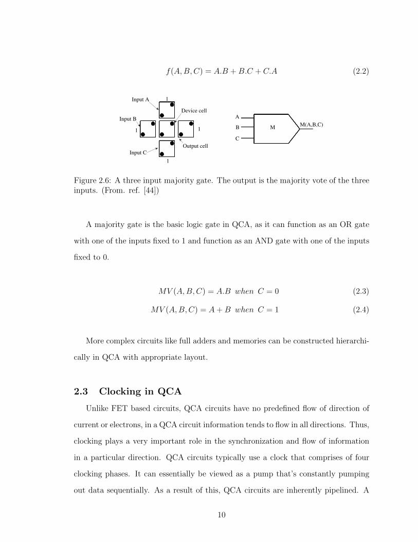
f(A,B,C) = A.B +B.C + C.A (2.2)
1 1
(a)
1 1
(b)
1Input A
Input B
1
1
1
Device cell
Input COutput cell
A
B
C
M M(A,B,C)
(c)
Figure 1.2. Basic QCA devices. (a) A binary wire which propagates informationthrough the line; (b) An inverter which uses the interaction of diagonally alignedcells to invert bits; (c) A three input majority gate. The output is the majority voteof the three inputs.
4
Figure 2.6: A three input majority gate. The output is the majority vote of the threeinputs. (From. ref. [44])
A majority gate is the basic logic gate in QCA, as it can function as an OR gate
with one of the inputs fixed to 1 and function as an AND gate with one of the inputs
fixed to 0.
MV (A,B,C) = A.B when C = 0 (2.3)
MV (A,B,C) = A+B when C = 1 (2.4)
More complex circuits like full adders and memories can be constructed hierarchi-
cally in QCA with appropriate layout.
2.3 Clocking in QCA
Unlike FET based circuits, QCA circuits have no predefined flow of direction of
current or electrons, in a QCA circuit information tends to flow in all directions. Thus,
clocking plays a very important role in the synchronization and flow of information
in a particular direction. QCA circuits typically use a clock that comprises of four
clocking phases. It can essentially be viewed as a pump that’s constantly pumping
out data sequentially. As a result of this, QCA circuits are inherently pipelined. A
10

QCA clock induces four phases in the tunneling barriers of the cells above it. In
the first phase, the switch phase, the tunneling barriers start to rise. The second
phase, the hold phase is reached when the tunneling barriers are high enough to
prevent electrons from tunneling. The third phase, release phase occurs when the
high barrier starts to lower, and finally, in the fourth phase, the relax phase, the
tunneling barriers allow electrons to freely tunnel again. In simple words, when the
clock signal is high, electrons are free to tunnel. When the clock signal is low, the
cell becomes latched.
Figure 2.7: The QCA clock, it’s stages and it’s effects on a cell’s energy barriers(From.ref. [1])
Fig. 2.7 shows a clock signal with it’s four phases and the effects on a cell at
each clock phase. A typical QCA design requires four clock phases, each of which is
cyclically 90 degrees out of phase with the prior clock phase. The first pair of cells
will stay latched until the second pair of cells gets latched and so forth. In this way,
data flow direction is controllable through clock phases.
In order, to understand the actual working of a QCA clock, consider the example
as shown in Fig. 2.8 where a value is being transmitted across a QCA wire. Initially,
let’s assume that a frozen input cell polarization with P = -1 is to be propagated
through the length of the wire. Such a propagation would take place as follows where
in the cells to the left of the input cell (clocking zone 1) would be in the switch phase
in the first time step. As seen earlier, in this phase, the tunneling barrier will be
11

raised and the cells will be polarized in accordance to the driver cell, here in this
case, it’s the input cell with polarization P=-1.
Switch
Hold
Release
Relax
Switch
Hold Switch
Release Hold Switch
Switch Relax Release Hold Switch
Relax
Relax
Relax
Relax
Release
Release
Release
Hold
Hold
Switch
Time Step1
Time Step2
Time Step3
Time Step4
Time Step5
Clocking Zone 1 Clocking Zone 2 Clocking Zone 3 Clocking Zone 4 Clocking Zone 5
The clock phases in time step 1 appearing to the right of the darkline represent the clock phases that clocking zones 2, 3, 4, and 5must be started in to ensure that a signal propagates through thedesign correctly.
The clock phases in thisshaded region represent thetransitions that will be taken to arriveat the desired clock phase at thedesired time.
The clock phases to the left of the dark line show the propagation of a binary 0 (polarization P = -1)(assumed to come from an input cell with frozen polarization).
Figure 2.12. An example of QCA clock transitions.
steps. Third, the state transitions for cells that make up the wire are illustrated for
each time step and are based on what clocking zone the particular cell is a part of.
Fourth, this figure is divided into 2 parts by a thick black line. Only cells to the left
of the black line will have a meaningful change of state during a given time step.
Nevertheless, cells to the right of the black line still ”exist” as they are part of the
wire.
They also illustrate that clocking zones must be ”initialized”. What is meant
by this? Clocking zones must traverse through the four phases as follows. From
switch, the zone transitions to hold. From hold, the zone transitions to release.
From release, the zone transitions to relax. Finally, from relax, the zone transitions
19
Figure 2.8: Example of QCA Clock Transitions (From. ref. [49])
As we step in to the second time step, we can see a changeover of the phases in
the clocking zones. Clocking zone 1 will have a phase change from the switch phase
to the hold phase while clocking zone 2 would change over to the switch phase. Once
in the hold phase, the tunneling barriers are held high and thus clocking zone 1 will
serve as input to clocking zone 2, as a result of which the cells in clocking zone 2 will
be polarized in accordance to the cells in clocking zone 1.
In the third time step, the passage of the phases continues and now the clocking
zone 1 will be in release phase, clocking zone 2 in hold phase and finally clocking zone
3 in the switch phase. Once in the release phase, the tunneling barrier is lowered for
cells in clocking zone 1 and will be in a neutral state while clocking zones 2 and 3
12

interact with each other in the same manner as clocking zone 1 and 2 in the previous
time step.
And in the fourth time step, clocking zone 1 would have witnessed a transition
from the release phase to the relax phase, clocking zone 2 to the release phase and
clocking zone 3 to the hold phase. The switch phase doesn’t follow the release phase
instead follows the relax phase due to the fact that the switch phase could affect the
cell polarizations of the release phase. Finally, in the fifth time step, the clocking
zone 1 returns to the switch phase and re-polarizes such that a new transmission
could occur across the wire. At this point we can safely conclude that there is some
inherent pipelining built into the QCA technology. After every 4 time steps, it is
possible to put a new value onto a QCA wire [49].
There are basically two different clocking mechanism in QCA namely Landauer
and Bennett clocking [7, 38, 43, 8]. Fig. 2.9 illustrates Landauer and Bennett clocking
of QCA circuits. The figure shows a QCA shift register, implemented by a single line
of cells, and a three-input majority gate. The left column (L1)→(L5) represents
snapshots of the circuit at different times as it is clocked using the Landauer clocking
scheme and the right column (B1)→(B7) shows snapshots using the Bennett clocking
scheme. It is assumed that the input signals come from other QCA circuitry to the
left of the circuit shown and that the output signals are transported to the right to
other QCA circuits [41].
Bit erasure is the simplest logically irreversible process. It is logically irreversible,
in that it requires a one bit input and always returns the null state as the output,
so it is impossible to recover the input value from just the output value. It has been
experimentally proved that during bit erasure one needs to dissipate some amount of
energy to the surroundings, and in case of an irreversible bit erasure where information
is lost, then the amount of energy dissipated to the environment is always considerably
larger than kBT ln(2) [63].
13

Bennett clocking of quantum-dot cellular automata and the limits to binary logic scaling
polarization can then be defined in terms of the expectationvalue of a particular generator.
Pj = !Tr(! j "7) = !"( j)7 . (5)
The Hamiltonian determines the eight-dimensional real vectorwith components
#( j)k = Tr(H ( j)"k), (6)
and the 8 " 8 matrix
$( j)mn =
!
p
fmpn#( j)p (7)
where fmpn are the structure constants for SU (3) defined bythe relation
4i fmpn = Tr["m , "p] ! "n. (8)
In isolation from the environment the unitary evolution of thedensity matrix can be expressed as the equation of motion forthe coherence vector.
%
%t"&( j)
(t) = $( j)(t)"&( j)
(t). (9)
Equation (9) represents a set of coupled first-order differentialequations for the motion of the coherence vectors of eachof the cells. If each cell were in a pure state, it would beequivalent to the Schrodinger equation. For mixed states (9)is equivalent to the quantum Liouville equation. The Coulombinteraction between the cells is included in a mean-fieldHartree approximation through (2).
The description can now be enlarged to include contactwith a thermal environment and dissipation (following [22]and [23]). The density matrix for the j th cell in thermalequilibrium with its environment at temperature T is
!th(t) = e!H ( j)(t)/kBT
Tre!H ( j)(t)/kBT . (10)
The associated equilibrium coherence vector is
["&( j)th (t)]k = Tr!ss(t)"k. (11)
Dissipation can be expressed using an energy relaxation timeapproximation. The non-equilibrium equation of motion forthe j th cell in contact with the thermal environment is then
%
%t"&( j)
(t) = $( j)(t)"&( j)
(t) ! 1'
["&( j)(t) ! "
&th(t)]. (12)
The coherence vector is driven by the Hamiltonian forcingterms, and relaxes to the instantaneous thermal equilibriumvalue. The energy relaxation time ' characterizes thedissipative coupling between the system and the environment.Because for QCA the quantum phase difference between cellsis irrelevant, we need not include a separate phase relaxationtime (using QCA for quantum computing has been exploredin [21]).
The non-equilibrium equation of motion (12) representsa set of coupled first-order differential equations for thecoherence vectors of QCA cells in contact with the thermalenvironment. As above the cell-to-cell coupling is treated ina mean-field approach ([20] extends this treatment beyond themean field). Coupling with the environment allows thermalfluctuations to excite the cells, and for cells to dissipate energyirreversibly to the environment. All the essential elements tostudy the thermodynamics of computation in an open quantumsystem are present in this description.
L1 )
L4 )
L3 )
L2 )
L5 )
B1 )
B4 )
B3 )
B2 )
B5 )
B6 )
B7 )
=
=
=
“1”
“0”
“null”
Figure 7. Landauer and Bennett clocking of QCA circuits. Eachfigure represents a snapshot in time as the clocking fields moveinformation across the circuit. The left column (L1)–(L5) representsLandauer clocking. A wave of activity sweeps across the circuit asthe clocking field causes different cells to switch from null to active.The circuit shown includes a shift register on top and a three-inputmajority gate on the bottom. The right column (B1)–(B7) representsBennett clocking for a computational block. Here as thecomputational edge moves across the circuit intermediate results areheld in place. When the computation is complete (B4), the activitysweeps backwards, undoing the effect of the computation. Thisapproach yield the minimum energy dissipation.
4. Landauer and Bennett clocking of QCA
Figure 7 illustrates Landauer and Bennett clocking of QCAcircuits. The figure shows a QCA shift register, implementedby a single line of cells, and a three-input majority gate. Theleft column (L1–L5) represents snapshots of the circuit atdifferent times as it is clocked using the Landauer clockingscheme and the right column (B1–B7) shows snapshots usingthe Bennett clocking scheme. It is assumed that the inputsignals come from other QCA circuitry to the left of the circuitshown and that the output signals are transported to the right toother QCA circuits.
4245
Figure 2.9: Landauer and Bennett clocking of QCA circuits. Each figure represents asnapshot in time as the clocking fields move information across the circuit. The leftcolumn (L1)→(L5) represents Landauer clocking. We can clearly observe the flowof information across the circuit as the clocking field causes different cells to switchfrom null to active. The circuit shown includes a shift register on top and a three-input majority gate on the bottom. The right column (B1)→(B7) represents Bennettclocking for a computational block. Here as the computational edge moves acrossthe circuit intermediate results are held in place. When the computation is complete(B4), there is back tracking of information, undoing the effect of the computation.This approach yield the minimum energy dissipation. (From. ref. [41])
14
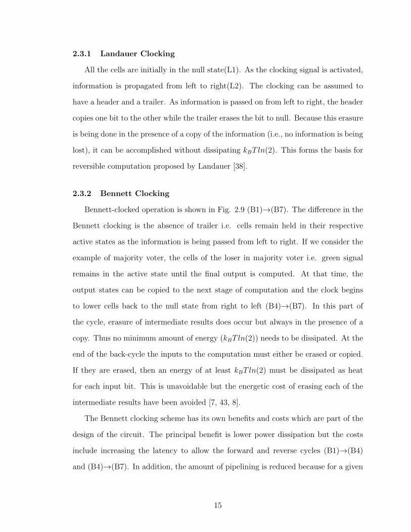
2.3.1 Landauer Clocking
All the cells are initially in the null state(L1). As the clocking signal is activated,
information is propagated from left to right(L2). The clocking can be assumed to
have a header and a trailer. As information is passed on from left to right, the header
copies one bit to the other while the trailer erases the bit to null. Because this erasure
is being done in the presence of a copy of the information (i.e., no information is being
lost), it can be accomplished without dissipating kBT ln(2). This forms the basis for
reversible computation proposed by Landauer [38].
2.3.2 Bennett Clocking
Bennett-clocked operation is shown in Fig. 2.9 (B1)→(B7). The difference in the
Bennett clocking is the absence of trailer i.e. cells remain held in their respective
active states as the information is being passed from left to right. If we consider the
example of majority voter, the cells of the loser in majority voter i.e. green signal
remains in the active state until the final output is computed. At that time, the
output states can be copied to the next stage of computation and the clock begins
to lower cells back to the null state from right to left (B4)→(B7). In this part of
the cycle, erasure of intermediate results does occur but always in the presence of a
copy. Thus no minimum amount of energy (kBT ln(2)) needs to be dissipated. At the
end of the back-cycle the inputs to the computation must either be erased or copied.
If they are erased, then an energy of at least kBT ln(2) must be dissipated as heat
for each input bit. This is unavoidable but the energetic cost of erasing each of the
intermediate results have been avoided [7, 43, 8].
The Bennett clocking scheme has its own benefits and costs which are part of the
design of the circuit. The principal benefit is lower power dissipation but the costs
include increasing the latency to allow the forward and reverse cycles (B1)→(B4)
and (B4)→(B7). In addition, the amount of pipelining is reduced because for a given
15
block of computation only one computational edge at a time can be moving across
the circuit. In Landauer clocking, by contrast, several computational waves can be
traversing the same block at the same time. Finally, the circuitry that provides the
clocking signal has to be somewhat more complex to handle the forward and the
backward clocking of the cells [41].
2.4 Wire Crossings in QCA
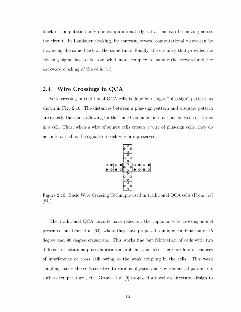
Wire-crossing in traditional QCA cells is done by using a ”plus-sign” pattern, as
shown in Fig. 2.10. The distances between a plus-sign pattern and a square pattern
are exactly the same, allowing for the same Coulombic interactions between electrons
in a cell. Thus, when a wire of square cells crosses a wire of plus-sign cells, they do
not interact, thus the signals on each wire are preserved.
Figure 2.10: Basic Wire Crossing Technique used in traditional QCA cells (From. ref[64])
The traditional QCA circuits have relied on the coplanar wire crossing model
presented but Lent et al [64], where they have proposed a unique combination of 45
degree and 90 degree crossovers. This works fine but fabrication of cells with two
different orientations poses fabrication problems and also there are lots of chances
of interference or cross talk owing to the weak coupling in the cells. This weak
coupling makes the cells sensitive to various physical and environmental parameters
such as temperature , etc. Ottavi et al [9] proposed a novel architectural design to
16

overcome the problems posed by this weak coupling such as temperature by coming
out with a more thermally robust design. They came up with three designs based
on orientation of the cells, the majority gate voting and the interaction between
the cells. Even though these proposed techniques was able to solve some of the
design issues, there were overheads in area associated with it which is generally not
preferred in a computing paradigm tipped to replace CMOS which had an efficient
usage of area. Rajeswari et al tried to minimize the area overhead introduced by
those complex design flows and presented the first clocking based wire crossings [23]
based only on one type of cell. Even though they were successful in implementing
their proposed methodology, there were few constraints with regard to the timing,
where they proposed a custom eight zones based clocking scheme which reduces the
computational speed.
2.5 Reconfiguration in QCA
Reconfigurable computing is a computer paradigm which bridges general purpose
microprocessors and application specific integrated circuits with mix of both hardware
and software. It uses runtime reconfiguration to perform the intended function. This
allows us to configure a hardware system to implement a particular circuit. The under-
lying hardware functions like an application specific hardware, thereby providing the
computational performance of custom hardware. However, since the reconfiguration
happens at runtime, reconfigurable computing provides the capability to re-program
the underlying hardware to implement different circuits and hence approaches the
flexibility of a general purpose microprocessor. This property has been exploited to
rake in better performance and lower power dissipation. Before we get into the details
of reconfiguration in QCA, we look into reconfiguration in nano computing and how
it could help us build energy efficient systems.
17

2.5.1 Reconfigurability and Nanocomputing
As physical limitations of feature size reduction and heat dissipation in CMOS
are reached, nanotechnology provides an approach to overcome these limitation. It
has been further envisioned that the amount of power dissipated in a given computa-
tional cycle will reduce drastically as we operate our circuits in the nano region. We
can exploit this feature of nano-computing to come up with better energy efficient
systems. Because nanotechnology could lead to inexpensive production of highly re-
configurable computer hardware, it is natural to exploit the current framework to this
emerging technology. Research strongly suggests that reconfigurable architectures, if
efficient, will provide a better fit and thus improved performance for general pur-
pose computation [16, 6]. We discuss the various post CMOS and nano - computing
paradigms which have been successfully implemented as a programmable device and
the outcome of such an implementation in Appendix A.
2.5.2 Application of Reconfiguration in QCA’s
From the previous subsection, we have seen that use of programmable logic and
reconfigurability in the nano scale level has led to the design of various low power
and energy efficient systems which is the need of the hour. Before we get into the
application of reconfiguration in QCA, we need to understand what an FPGA is and
why it is easier to implement an FPGA in QCA when compared to other nanoscale
devices.
FPGA’s can be in general classified as a system consisting of a logic functions
which are arranged in a well defined interconnect network. A typical CMOS inter-
connection scheme involves signals entering an FPGA circuit via some input buffers
which are then transferred to horizontal wires. These horizontal wires cross with
vertical wires throughout the FPGA and programmable connections can usually be
made at crossings to facilitate data routing. While long wires work well in CMOS,
18

the nature of the clock makes them a much more difficult task in QCA. Unlike the
standard CMOS clock, the QCA clock is not a signal with a high or low phase which
has been discussed in detail in the earlier sections.
Niemer et al [50] have presented a FPGA based on QCA’s where in they have tried
to adhere to the design of a CMOS FPGA and tried implementing it in QCA’s. They
have built a logic block based on the NAND gate based Majority voter design and
used a programmable multiplexor design for the interconnects instead of the common
SRAM based design in CMOS. The basic problem which has been addressed is the
complex routing of the clock signals involved in QCA. But this work just presents a
simple implementation of QCA FPGA on the lines of CMOS FPGA. Jazbec et al [37]
improved the routing and the interconnect network by proposing a Programmable
Switching Matrix based on the crossing of the QCA Binary wires. There has been
considerable work also done on implementing various QCA based configurable logic
blocks which are based on SRAM design, Multiplexor design etc [4, 39]. They have
made use of the clocking phase to their advantage to enable the crossing of two QCA
binary wires. Recently Devadoss et al [24] have come up with a programmable tile
based architecture based on the clocking mechanism. Simple tiles were proposed as
the building blocks of this programmable QCA (p-QCA) architecture where in they
have retained the 3-input majority gate as the primary logic element unlike existing
architectures, which typically use 2-input NAND gates. Any part of the proposed
p-QCA device can be programmed to function as a logic element, a routing element,
or a memory element. A simple p - QCA device structure is as shown in Fig. 2.11
Thus, we have seen a detailed survey about the different aspects of reconfiguration
which has been extended to nano computing in this section and in particular to QCA’s
which is the filed of interest with regard to this thesis. While we find that most of
the work has been targeted on implementing a programmable design, but very few
researchers have stressed upon the aspect of saving power through reconfiguration
19

Figure 2.11: p-QCA device structure: QCA layer with clocking circuitry. (From. ref.[24])
which forms the basis for our research. Some of the work that focussed on saving
power [12, 10] and increasing computational speed through reconfiguration in nano
- computing has clearly shown that power dissipation can be considerably reduced
and there are many avenues available for power saving in reconfiguration. Previous
work in QCA have focussed on implementing a FPGA design for QCA but significant
amount of work has not been done on exploiting the clocking mechanism or the
cell configuration for reconfiguration which could open up several avenues for power
savings in QCA.
20

CHAPTER 3
PROPOSED RECONFIGURATION SCHEME
As seen towards the end of the previous chapter, the number of researchers who
have stressed upon the usage of reconfiguration for energy efficient computing are
very few but the research that has been carried out by them have given a clear
indication that there are avenues for power savings. Our aim is to come upon with
a reconfigurable architecture using QCA which makes use of the majority gate logic
and the clocking mechanism which reduces the power considerably in comparison to
the existing architectures. The major driving force behind the idea of coming up
with a reconfigurable architecture in QCA is that it’s a relatively unexplored topic,
there are strong possibilities that a reconfigurable QCA can lead to even lesser power
dissipation since both reduced power dissipation and dynamic reconfigurability is a
natural phenomenon that is observed in QCA. Therefore we can quantify the power
dissipated during the process of reconfiguration in QCA easily when compared to
other paradigms.
As seen earlier, it’s feasible to achieve substantially lower power dissipation with
the help of reconfigurability in QCA cells. In this chapter, we introduce a custom
QCA design based on reconfiguration where we can reconfigure the majority gate
voter to perform the functionality of more than one gate i.e. by changing the polarity
of the majority gate voter, the same gate can be used either as an AND gate or as an
OR gate. If successful, this research could pave way for custom circuit designs which
were not feasible in other computing technologies.
21
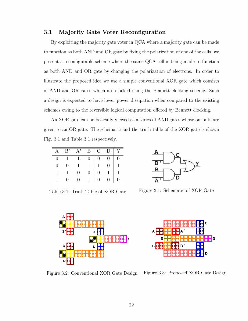
3.1 Majority Gate Voter Reconfiguration
By exploiting the majority gate voter in QCA where a majority gate can be made
to function as both AND and OR gate by fixing the polarization of one of the cells, we
present a reconfigurable scheme where the same QCA cell is being made to function
as both AND and OR gate by changing the polarization of electrons. In order to
illustrate the proposed idea we use a simple conventional XOR gate which consists
of AND and OR gates which are clocked using the Bennett clocking scheme. Such
a design is expected to have lower power dissipation when compared to the existing
schemes owing to the reversible logical computation offered by Bennett clocking.
An XOR gate can be basically viewed as a series of AND gates whose outputs are
given to an OR gate. The schematic and the truth table of the XOR gate is shown
Fig. 3.1 and Table 3.1 respectively.
A B’ A’ B C D Y
0 1 1 0 0 0 0
0 0 1 1 1 0 1
1 1 0 0 0 1 1
1 0 0 1 0 0 0
Table 3.1: Truth Table of XOR Gate Figure 3.1: Schematic of XOR Gate
Figure 3.2: Conventional XOR Gate Design Figure 3.3: Proposed XOR Gate Design
22

QCA implementation of a standard XOR gate is presented in Fig. 3.2. In our
proposed methodology (Fig. 3.3), we find that we have only one majority gate as
opposed to three majority gates in the conventional approach (Fig. 3.2). The polar-
ization of one the inputs of the majority gate (X) can be switched from +1 to -1 and
vice versa in order to switch between an AND and OR gate. The QCA representation
of the proposed architecture is as shown in Fig. 3.3.
In our proposed methodology, a single majority gate voter is made to behave as
both AND and OR gate. This is achieved by changing the polarity of one of the
input cells to +1/-1. We compute the result of the first AND operation (i.e., C is
computed as shown in the Fig. 3.4(2)) and store the intermediate results. Once
the de-computation of this AND operation is completed, the second AND (i.e., D is
computed as shown in the Fig. 3.4(3)) operation is performed whose intermediate
results are also stored. Thus the intermediate results are stored in the series of cells
forming a shift registers before the output cell Y.
During the de-computation cycle, we activate the feedback path on to the inputs
and polarization of the majority gate voter is reversed in order for it to behave as
an OR gate(Fig. 3.4(4)). Finally, we start output computation, along with the de-
computation of the feedback path. Thus we find that, we have a stored value of the
intermediate AND results which can be used as inputs as part of a large and complex
circuitries along with the final XOR result (Fig. 3.4(5)).
The Bennett clocking scheme of our proposed reconfiguration design is clearly
indicated in Fig. 3.4. The figure represents the final state of the cells where the
colors are used to indicate the presence of data in a given cell. Different colors are
used for inputs, the shift registers, the majority gates, output and data propagation.
The initial state of cells is assumed to be in Null state (Fig. 3.4(1)) and it’s assumed
that the inputs (both true and complementary form) are available and initially the
majority gate voter is polarized to perform AND operation. As the computation
23
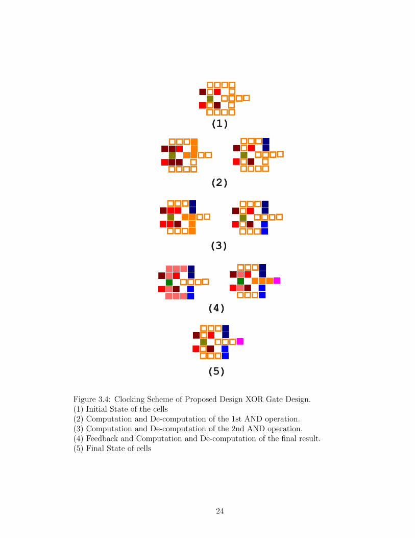
Figure 3.4: Clocking Scheme of Proposed Design XOR Gate Design.(1) Initial State of the cells(2) Computation and De-computation of the 1st AND operation.(3) Computation and De-computation of the 2nd AND operation.(4) Feedback and Computation and De-computation of the final result.(5) Final State of cells
24

begins the true form of input A and the complementary form of input B is fed into
the cell.
As the computation progresses, the output is stored in the shift registers. During
the de-computation, the inputs are restored and just the outputs are stored in the
shift register whereby there is no power dissipation (Fig. 3.4(2)). Once the de-
computation is completed we repeat the same procedure but with the true form
of B and the complementary from of A as the inputs. If one takes a closer look
at the proposed design, one can clearly find that true and complementary form of
inputs are being written into the same cell. This implies that, there won’t be any
power dissipation since at any given point of time, we write into the input cell in the
presence of a copy. At the end of computation and de-computation cycle the outputs
are stored in the bottom shift register as shown in Fig. 3.4(3). Finally during the
de-computation cycle, we change the polarization of the majority gate voter so that
it can perform as an OR gate now instead of an AND gate. Also, the outputs are
fed back as inputs.(Fig. 3.4(4)). During this computation, there is power dissipation
when we tend to write the feedback data as inputs and also when we try to change
the polarization of the majority gate voter. Finally, we compute the XOR output by
computing the OR function of the intermediate results. Thus we find that we have
the final output along with the intermediate results which can be used as fan-in to
some other circuits when they are part of a large complex circuit as shown in Fig.
3.4(5).
The fundamental assumption in any reconfigurable implementation is the fact
that, we have the ability to clock the cells individually. But, keeping in mind the
practical constraints of such an assumption we are assuming that we can dynamically
cut off the clocking to the feedback path during computation and activate it during
the de-computation cycle i.e. we have restricted control over a group of cells and
25

not over individual cells. Future research in this direction could pave way for more
realistic and feasible designs.
3.2 Wire Crossing Scheme based on Bennett Clocking
The previous section has established the proposed reconfiguration approach but in
any reconfigurable system, routing is a major problem. In a QCA based reconfigurable
design also, coplanar wire crossings is an area of major concern since it requires more
than one cell. We have discussed in detail with regard to the drawbacks of traditional
wire crossing designs in the previous chapter. In this work, we propose coplanar wire
crossings based on only one type of QCA cells by taking advantage of dead time
during the de-computation cycle of Bennett clocking scheme.
In our proposed clocking scheme, we try to take advantage of the dead time during
the de-computation cycle of Bennett Clocking. We propose to break down the entire
circuit into different pipeline zones [51]. The pipeline zones are under the control of
the designer and may be used only where is wire crossing taking place. One of the
fundamental assumptions in our design is the flow of information in both the vertical
and the horizontal direction. For simplicity, let us consider a simple design which
consist of AND and OR gates as shown in Fig. 3.5.
Figure 3.5: A simple circuit that implements the Boolean equation (A+B)+(B.C)
From the circuit, we can see that input B is being fed into both the AND and OR
gate. This is a simple wire crossing problem in QCA. A QCA representation of the
same circuit is shown in Fig. 3.6. From the figure, we can clearly see that input B
26
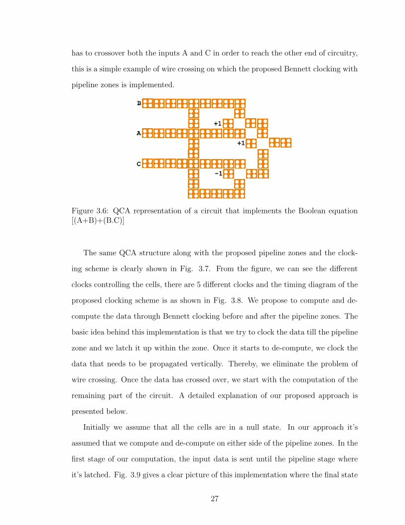
has to crossover both the inputs A and C in order to reach the other end of circuitry,
this is a simple example of wire crossing on which the proposed Bennett clocking with
pipeline zones is implemented.
Figure 3.6: QCA representation of a circuit that implements the Boolean equation[(A+B)+(B.C)]
The same QCA structure along with the proposed pipeline zones and the clock-
ing scheme is clearly shown in Fig. 3.7. From the figure, we can see the different
clocks controlling the cells, there are 5 different clocks and the timing diagram of the
proposed clocking scheme is as shown in Fig. 3.8. We propose to compute and de-
compute the data through Bennett clocking before and after the pipeline zones. The
basic idea behind this implementation is that we try to clock the data till the pipeline
zone and we latch it up within the zone. Once it starts to de-compute, we clock the
data that needs to be propagated vertically. Thereby, we eliminate the problem of
wire crossing. Once the data has crossed over, we start with the computation of the
remaining part of the circuit. A detailed explanation of our proposed approach is
presented below.
Initially we assume that all the cells are in a null state. In our approach it’s
assumed that we compute and de-compute on either side of the pipeline zones. In the
first stage of our computation, the input data is sent until the pipeline stage where
it’s latched. Fig. 3.9 gives a clear picture of this implementation where the final state
27

Figure 3.7: Clocking Scheme of the Proposed Wire Crossing Technique
Figure 3.8: Timing Diagram of the Proposed Wire Crossing Technique
28

Figure 3.9: Implementation of the Proposed Wire Crossing Technique until thePipeline Zones
of the cells is shown at the end of every clock cycle while the colors in the figure
represent the propagation of data through various cells.
Initially, all the three inputs namely A, B and C are propagated until the pipeline
zone which is clearly illustrated in Fig. 3.9(a) and (b). Then the input B which
needs to cross over is sent through vertically as shown in Fig. 3.9(d) while the de-
computation of inputs takes place (Fig. 3.9(c)). From the Fig. 3.9 we can see
that 3.9(c) and 3.9(d) happen simultaneously. Once the input data are latched on
in the pipeline zones, the input B begins to propagate in the vertical direction i.e.
computation begins along the 2nd clock zone (Clock zones are indicated in Fig. 3.7
and Fig. 3.8). During this computation, the de-computation of the inputs takes place
29

since the inputs are already latched on in the pipeline zone which is represented by
Fig. 3.9(c) and Fig. 3.9(d). Its assumed that the time taken for the computation of
Input B along the vertical direction is less than or equal to the de-computation of the
remaining inputs since vertical direction flow is the natural directional flow of data.
In case the computation time is more than the de-computation time, then we need
to wait until the computation gets over in order to start the next set of computation
on the other side of the pipeline zones which are illustrated in Fig. 3.10.
Fig. 3.10 gives us a clear picture about the computation and de-computation that
takes place within the proposed pipeline zone and after the proposed pipeline zone
until the output. At first, the data that latched in the pipeline zone is propagated
till the majority gate voting. Simultaneously the data within the pipeline zone is
being de-computed as shown in Fig. 3.10(a) and Fig. 3.10(b). The computation of
the data continues till the output after the intermediate results have been computed.
Computation of output is done when the de-computation within the pipeline zone
is in progress. Thus we have the computed output by the time, the pipeline zone
has been de-computed as illustrated in Fig. 3.10(c). Finally, the new input starts
propagating towards the pipeline zone while de-computation from the output until
the pipeline zone starts. By the time we have latched the new data in the pipeline
zone, de-computation would be complete and the next phase of computation beyond
the pipeline zone can take place (Fig. 3.10(d)).
30
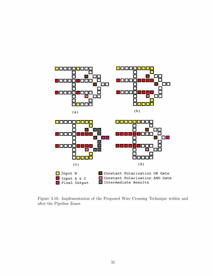
Figure 3.10: Implementation of the Proposed Wire Crossing Technique within andafter the Pipeline Zones
31

CHAPTER 4
POWER ANALYSIS AND METHODOLOGY
In this chapter, we present a detailed power analysis of our proposed approach and
compare it with the results obtained for the existing designs. We have considered both
the upper bound and lower bound limits of power in order to capture the advantages
posed by our approach more accurately. Before we get ahead with the comparison of
the proposed approach with the existing designs, we need to understand the upper
and lower bound limits of power. The fundamental limits of upper and lower bounds
of power are explained by taking an example of Bennett clocking based half adder
(Fig. 4.1).
Figure 4.1: A Schematic of Half Adder along with it’s QCA implementation. Therequired clocking signals for Bennett Clocking are shown in the graph. (From. ref[29])
32

4.1 Upper Bound Power Dissipation Model
In thermodynamics, adiabatic process refers to a process in which there is no
net transfer of heat to or from the environment. Earlier researchers considered the
clocking switching activity to be a quasi-adiabatic process where in a system goes
through a sequence of events that are infinitesimally slow such that the entire process
is reversible.
Timer et al have proposed a power dissipation model [62, 63] in general to estimate
power dissipation in case of a quasi adiabatic switching event. They have presented
a detailed quantum mechanical power model, where in they have showed that the
power dissipation can be made as low as possible when the clock changes are nearly
adiabatic. They identified three components of power: clock power, cell to cell power
gain and power dissipation. Even though this model gives us a detailed physical
estimates, it’s computationally very intensive and difficult to calculate. The power
dissipation for a QCA circuit can expressed as the sum of power estimates computed
on a per-cell basis. Each cell in a QCA circuit sees three types of events: (i) clock
going from low to high i.e. depolarization of the cell, (ii) input or cells in previous
clock zone switching states, and (iii) clock changing from high to low, latching and
holding the cell state to the new state.
The fundamental power dissipation model which computes the upper bound is
based on this quantum mechanical model [58, 57]. Such upper bound represents the
worst case power dissipation, which happens in the presence of non-adiabatic clocking.
The authors have developed a probabilistic Bayesian model where the probabilities
directly maps on to the quantum - mechanical steady state probabilities which are
nothing but the density matrix and the cell polarizations.
33

The fundamental upper bound is given by:
Ediss <h
2
−→Γ +.
(−−→Γ +
|−→Γ +|
tanh
(h|−→Γ +|kBT
)+
−→Γ −
|−→Γ −|
tanh
(h|−→Γ −|kBT
))(4.1)
where−→Γ is the Hamiltonian vector, kB is Boltzmann Constant, h represent the
Planck Constant and T is the temperature.
The entire dissipation bound model has been derived in Appendix B.
Now consider the half adder circuit shown in Fig. 4.1. Since it undergoes reversible
computation through Bennett clocking, the information lost in the circuit is only
during the switching of inputs. Consider the truth table of the half adder shown in
Table. 4.1.
Table 4.1: Truth Table of Half Adder
A B S C
0 1 0 0
0 0 1 0
1 1 1 0
1 0 0 1
Now, from the above derivation we find that, the energy dissipated whenever there
is a change in inputs is Ediss if there is no copy available. The power dissipation occurs
only when we try to rewrite the input cells with the next set of inputs. From the truth
table, we find that the power dissipation owing to the switching of inputs is 4Ediss.
This is obtained from the fact that the there are 4 sets of inputs possible namely
[00, 01, 10, 11]. The values are rewritten as inputs four times while implementing the
34

truth table as shown in Table. 4.1 while the rest of the times, the previous data
already exists in the input registers and we don’t rewrite. i.e. if there is switching
from 1 to 0 or from 0 to 1, then there is power dissipation but it’s not the case when
there is switching from 1 to 1 or from 0 to 0. Thus we find that the upper bound of
Energy Dissipation for the implementation of the presented truth table is 4Ediss.
4.2 Lower Bound Power Dissipation Model
Lower bound power is the minimum amount of power that is dissipated when-
ever there is a computation taking place in a circuit. There are mainly two types of
computation namely reversible and irreversible computation. Lower bound will dif-
fer based on the type of computation that is taking place. Any logically irreversible
computation such as erasure and rewriting of inputs will have to dissipate certain
amount of power. The methodology followed for the estimation of this lower bound
is as suggested by Ercan and Anderson[28, 29]. The proposed methodology assumes
the circuit to be an ideal circuit and heat dissipation is estimated using the physi-
cal information theoretic analysis. The fundamental lower bounds is ideally a four
step process which consist of physical decomposition, process abstraction, operational
decomposition and cost analysis.
The basic principle behind the computation of the bounds is to decompose the
given circuitry and it’s surroundings into key circuit elements which consist of informa-
tion with regard to their physical states as well as their relevant external subsystems.
Once the decomposition of the circuit is done, it requires the identification of the
circuit states i.e. the circuit elements and the external subsystems, which interact
with one another during the computational cycle.
The next step in the process is the process abstraction where we identify the
control and the restoration processes. Control processes are those which forces the
circuit to change in to a new state leading to an interaction between the circuit and
35

the bath during a well defined time interval. While restoration process restores the
heat bath to its original form after the control process.
The third step is the operational decomposition where the computational cycles
and the driving force behind these cycles are defined. The computational cycle is the
process of computing the outputs for a set of inputs. Since the computational steps
depend on the clocking of the circuit, it automatically becomes the driving force.
Now in order to estimate the lower bound, we break down the circuit into data
zones and find the information lost in each zone by applying physical information
theoretic analysis. The summation of results from each zone will give the total infor-
mation lost. Data zones are defined by data sub-zones, the inputs to the sub-zones,
and the outputs of the sub-zones. Data sub-zones are areas within a single clocking
zone where irreversible computing happens. The outputs and inputs to a sub-zone
may be in a different clocking zone so data zones may span multiple clocking zones.
Once we have broken down the entire circuit into data zones and sub-zones, we can
apply information theory to determine how much information is lost within each sub-
zone which can be used to find the data lost in each data zone, which gives the total
information lost in the entire circuit. This is done by finding the Shannon entropy
at both the input and the output of a sub-zone and taking the difference which gives
the information lost in the sub-zone.
Consider two random variables X and Y to be the input and output to a data
sub-zone respectively. X can be any value in the set a1, ......, am with probability
P (X = ai) = pi where i is an integer from 1 to m. Y can be any value in the
set b1, ......, bm with probability P (X = bi) = qi where i is an integer from 1 to
n. If we consider an example of an AND gate. It has two binary inputs and one
binary output. We can define the AND gate to be a data sub-zone. Since it has two
binary inputs, we have m=4 and we can define the set of values that X can take as
00, 01, 10, 11. Now assuming that both the inputs are equally probable, we have
36

p1 = p2 = p3 = p4 = 1/4. The output of an AND gate can either be a 1 or 0, which
means that the set of value that Y can take is 0, 1. Three of the inputs will result
in Y = 0 while the other input results in Y = 1. Hence we can find probability of the
outputs by adding the probability of inputs. Therefore q0 = p1 + p2 + p3 = 3/4 and
q1 = p4 = 1/4.
Shannon entropy is the measure of the uncertainty associated with a random
variable [55]. This tells us the expected value of the information per generated value
within the set. In the case of the random variable X , the input of a sub-zone, the
Shannon entropy is defined as:
H(X) = −m∑i=1
pi log2(pi) (4.2)
The Shannon entropy for the random variable Y, the output of a sub-zone, is:
H(Y ) = −n∑j=1
qj log2(qj) (4.3)
The information lost from the input to the output of the sub-zone can then be found
by
−∆I = H(X|Y ) = H(X)−H(Y ) (4.4)
which is measured in bits.
Now applying the above approach to the AND gate we have the input entropy as
H(X) = −[
1
4log2
(1
4
)+
1
4log2
(1
4
)+
1
4log2
(1
4
)+
1
4log2
(1
4
)]= 2 (4.5)
and output entropy as
H(X) = −[
3
4log2
(3
4
)+
1
4log2
(1
4
)]= 0.811 (4.6)
Thus the total information lost −∆I = 2− 0.811 = 1.189bits
37

Finally a space time decomposition all the computational steps involved in the
circuit operation is performed. In order to get the bounds, a summation of the bounds
of the individual computational steps, which follows from the physical information
theoretic analyses of the circuit state changes required. The bound thus obtained
will be regarded as the fundamental lower bound since it represents the minimum
physical cost required for the circuit to achieve it’s computational ends. However,
these bounds are specific to a given circuit structure and the mode of operation.
In order to understand the bounds better consider the Bennett clocking based
half adder circuit presented in Fig. 4.1. The first step in the process is the physical
decomposition of the circuit. By looking at the circuit one can identify the circuit
which are contained within the box while the ones outside the box represent the
external subsystems. Cells A and B are the input registers while S and C are the
output registers. We can define the rest of the system as the thermal bath and rest
of the universe. From the circuit clocking, we can clearly see that the switch or relax
phases of adiabatic clocking leads to a change in state of the cell. Hence they are the
control processes. While the relax or hold phases restores the state of the cell. As
shown in Fig. 4.1 the clocking of the circuit is defined by the clocking zones which
are separated by different colors which represents the clocking signals. The clock
signals which define the computational step is shown by the gray lines in the clocking
diagram of Fig. 4.1. All these computational steps make up one computational cycle.
Now, if we consider the half adder circuit, we can clearly see that the only infor-
mation loss occurs only when the inputs of the circuit, A and B changes its value at
the beginning of new computation. So, consider the inputs to the circuit as a data
zone, the output of data zone will be current inputs of the circuit, and the input to
the data zone will be the next inputs to the circuit. Since, the next set of inputs are
independent of the previous set of inputs, we have H(X|Y ) = H(X). Therefore, the
information lost is solely dependent only on the next set of inputs. Let’s assume that
38

all the possible inputs i.e. [00, 01, 10, 11] are equally probable. This implies that we
will have H(X) = 2 which means that −∆I = 2bits will be lost for the entire circuit.
This is the amount of information that is lost on average for a given computational
cycle in the Bennett clocked half adder circuit. We can now find the total heat dissi-
pated into the bath by the circuit by using Landauers Principle which states that at
least kBT ln(2) must be dissipated when a bit of information is lost from the system.
Since we know the circuit loses on average 2 bits, the fundamental lower bound of
heat dissipation will be 2kBT ln(2)joules for the Bennett clocked half adder in QCA.
4.3 Power Analysis of Proposed Reconfiguration Scheme
A detailed analysis of the proposed scheme and the existing conventional scheme
based on the power bound models is presented in this section. We try to compute
the upper and lower bounds for both the schemes and compare the results for power
efficiency. In the previous chapter, we have understood the working of the proposed
scheme. The proposed scheme can be understood from Fig. 3.4. Initially let’s com-
pute the upper bound power, as shown in the previous section, the energy dissipated
whenever there is a change in inputs is Ediss if there is no copy available. From the
proposed design (Fig. 3.2), we find that since the true and complementary form of
the inputs are being given to the same input cell, there is no power dissipation due
to the change in inputs. The power dissipation occurs only when we try to rewrite
the input cells with the feedback results and when we switch the polarization of the
cell from -1 to +1 and vice versa in order for the majority gate to function as either
AND or OR.
From the truth table (Table. 3.1), we find that the power dissipation owing to
the switching of inputs due to feedback is 4Ediss and we add another 2Ediss owing to
the change in polarity. This is obtained from the fact that the feedback results are
rewritten as inputs four times while implementing the truth table as shown in Table
39

II while the rest of the times, the previous data already exist in the shift registers and
we don’t rewrite. i.e. if there is switching from 1 to 0 or from 0 to 1, then there is
power dissipation but it’s not the case when there is switching from 1 to 1 or from 0
to 0. Thus we find that the upper bound of energy dissipation for the implementation
of the presented truth table is 6Ediss.
If we consider the conventional implementation both the true and complementary
form of inputs are being fed as inputs to two different majority voter gates, as a
result of this, there is power dissipation every time we switch the inputs. As a result
of this, we find that the total energy dissipated when executing the given truth table
is 14Ediss.
Till now, we formulated the upper bound for both the proposed and the conven-
tional implementation of the XOR gate. Now, let’s consider the lower bound which
tells us the minimum amount of power dissipated by the circuit. For the calculation of
the lower bound, we follow the procedure highlighted in the previous section. As seen
in the previous section, we have identified the control and the restoration processes
and have clearly defined the computational steps. Now we define the data zones and
the sub-zones. During the calculation of the upper bound, we have clearly seen that
there is no power dissipation due to change of inputs. However, there is power dissi-
pation when the feedback is being fed as inputs. Thus the total energy dissipated will
be equal to the sum of the energies dissipated in the two feedback paths. Let us define
the feedback paths to be the data zone. Since the next set of inputs is independent
of the previous inputs we have H(X|Y ) = H(X). Therefore, the information lost is
solely dependent only on the next set of inputs. Let’s assume that all the possible
inputs i.e. [00, 01, 10] are equally probable. We have only 3 sets of inputs for the
feedback path since the input [11] is never encountered as seen from Table. 3.1. This
implies that we will have H(X) = ln(3) which means that −∆I = 1.098bits will
be lost for the entire circuit. Since we know the circuit loses on average 1.098 bits,
40

the fundamental lower bound of heat dissipation will be 1.098kBT ln(2)joules for the
Bennett clocked proposed XOR gate in QCA. A similar calculation was performed
for the conventional implementation and the regions of irreversible computation in
this case was the switching of the inputs. As a result of this, the minimum power
dissipated is given by 2kBT ln(2).
Figure 4.2: Timing Diagram of the XOR gatebased on proposed Reconfiguration Scheme
Figure 4.3: Timing Diagram of the XORgate based on conventional design method-ology
Timing diagram for the proposed scheme and the standard design is presented in
Fig. 4.2 and Fig. 4.3. From these two figures, we can see that output is available at
the end of 6th cycle in case of the standard design while it’s not available until the
12th cycle in the proposed scheme. Thus, computation time is the trade-off in order
to achieve low power but the advantage of the proposed scheme can be clearly seen
in the reduction in area and also we can feed in the next set of inputs as early as the
12th cycle, while the next set of inputs can start computation in case of the standard
design in the 10th cycle. Even though there is a difference of 2 cycles with regard to
the latency, in complex circuits we can pipeline data and achieve better results.
41

CHAPTER 5
QCA ADDERS
In this chapter, we present the work that’s being carried out as part of this thesis.
Addition is a basic and a fundamental operation involved in any digital logic design or
a control system design. The performance of any digital system is characterized and
heavily influenced by the performance of the adders in that design. Various designs of
fast adders have been proposed by various authors in every possible technology start-
ing from CMOS to nanoscale implementations such as spin wave functions, QCA’s
to name a few. In this work, we intend to present an adder design based on the
reconfiguration scheme presented in the previous chapter which will be robust and
power efficient in comparison to the existing designs. Before we get into details of
the proposed adder and the metrics to be used for comparison, we will get an insight
into the existing adder designs based on QCA.
5.1 Background on QCA Adders
It was as early as 1994, when Lent and co [64] came up with a set of logical de-
vices based on QCA and adder was one of them. They built a full adder based on
five majority gates and three inverters. A carry look ahead adder was realized by
connecting n such one - bit QCA full adders [67]. Such a design was possible because
in a QCA based design, the carry is generated before the sum. The above mentioned
adder design were improvised by Wang et al [69] who designed one-bit QCA adder
based on only three majority gates and two inverters. A bit serial adder which uses a
carry feedback which also uses only three majority gates and two inverters was pro-
42

posed by Fijany et al [32] but it came with a complex clocking scheme. Srivastava [59]
studied full adders based on Bayesian probabilistic modeling while Cho et al proposed
modular adder and multiplier design based on QCA architecture and did a thorough
analysis of the same [13, 14]. The scheme proposed by Cho was further improvised
by Bruschi et al [11] who exploited minority gates in addition to majority ones. A
minority based full-adder is presented in [53], but it is not modular. Walus et al
proposed a modular ripple carry structure for adders. Modular designs of conditional
sum adder was studied in detail in [15] while probabilistic analysis of molecular QCA
based adders was presented in [27].
5.2 Proposed Adder Designs
From the above section, we find that there are numerous adder designs which
have been presented by researchers around the world. Zhang et al [73] did a thorough
comparative study on the performance of QCA based adders and found that QCA
ripple-carry adder and bit-serial adder designs actually outperforms carry-look-ahead
and carry-select adder designs. Hence we present a 1-bit carry ripple adder and a
1-bit carry look ahead adder based on the proposed reconfiguration scheme which
can be extended to n-bits. While most of the work concentrated on improving the
performance, the work done so far on reducing the power dissipation is negligible.
Hanninen et al [36] were one of the first people to do a power analysis on adders
based on QCA. They have evaluated the general heat densities and expected logic for
various arithmetic circuits based on Launder’s principle. Srivastava et al [59] studied
the upper bound power dissipation impacts on various adders and have given a heat
dissipation chart for each cell.
Thus, we have clearly seen that there is very little or no work done with regard to
estimation and reduction of power dissipation in adders. From the previous chapters,
we have clearly seen that built in dynamic reconfigurability of QCA’s have not been
43
exploited properly in designing adders which can prove to be highly power efficient.
Hence our research will pave way for more adder design which will be power efficient.
In this section, we propose the design of a 1-bit Ripple Carry Adder and 1-bit
Carry Look Ahead Adder based on the proposed reconfiguration scheme and extend
it to 4-bits. The benefit of such a design is that, the design is inherently pipelined
and doesn’t require the duplication of the 1-bit adder to build a 4-bit adder. A 1-bit
adder design will be capable of performing the operations of a 4-bit adder. One of the
major reasons for choosing a ripple carry adder is the fact that one needs to pipeline
n-1-bit adders in order to get an n-bit adder, since our design is inherently pipelined
and one need not have n-1-bit adders for n-bit additions, which is power efficient and
could pave way for more designs in future which could adopt this scheme.
Reconfigurability adds another dimension to the adders since the design can be
reused in future which can prove to be effective in terms of cost cutting. The proposed
adder design is expected to have very low power dissipation and a significant reduction
in area with a slight overhead in the form of latency. The overhead in the form of
latency will become significantly less and will become negligible as we scale the adder
design from 1-bit to n-bits.
Thus, we intend to use the inbuilt dynamic reconfigurability and exploit the clock-
ing schemes to come up with a more robust, area and power efficient design which
will be could lead to inexpensive hardware in the near future.
5.2.1 Carry Ripple Adder
A full adder is an arithmetic circuit which is used for adding binary numbers.
A one bit full adder adds three one bit numbers to produce two one bit outputs
namely sum and carry. A full adder could be implemented in many ways, one such
implementation is the computation of sum using the 3-bit XOR of the inputs and
the computation of carry using a 3-bit majority gate function of the inputs. The one
44

bit full adder’s truth table and block diagram is as shown in Table. 5.1 and Fig. 5.1
respectively.
A B Cin S Cout
0 0 0 0 0
0 0 1 1 0
0 1 0 1 0
0 1 1 0 1
1 0 0 1 0
1 0 1 0 1
1 1 0 0 1
1 1 1 1 1
Table 5.1: Truth Table of Full Adder Figure 5.1: Block Diagram of Full Adder
In order to create a logical circuit capable of adding N-bit numbers one can stack
a series of N 1-bit full adders where the carry out of the previous adder becomes the
carry in of the current adder. This kind of adder is known as a carry ripple adder
since each carry bit ripples into the next adder. A block diagram of such an adder is
as shown in Fig. 5.2.
Figure 5.2: Block Diagram of Carry Ripple Adder
Even though the design of carry ripple adder is quite simple, it’s relatively slow
since it has to wait for the carry bit to be calculated from the previous adder before
which it can’t proceed any further in the computation. Our proposed design takes
care of this problem where the carry is computed in a separate block and is available
for the computation of the next set of bits as soon as the next set of bits becomes
45

available. The block diagram of our proposed carry ripple adder is as shown in Fig.
5.3.
Figure 5.3: Block Diagram of Proposed Carry Ripple Adder
Our proposed design consists of three blocks which operate asynchronously with
respect to one another. All of them perform their own operations and clocking has
been designed in such a way that they don’t have to wait for data from other blocks.
The carry out is generated by the majority voter design block (MVB) while the sum
is computed using the two custom reconfigurable XOR blocks (CRXB). The proposed
1-bit Carry Ripple Adder based on the custom reconfiguration scheme is as shown in
Fig. 5.4.
The working of the carry ripple adder is quite simple and it’s just an extension
of the custom reconfiguration scheme where in we have an additional majority gate
voter in the design. Therefore as seen from Fig. 5.3 and Fig. 5.4 we can clearly see
that we have two blocks of CRXB and a block of MVB. Initially let’s assume that all
the cells are unpolarized except for the majority gate voter cells and the inputs are
readily available as shown in Fig. 5.5
Once the inputs are readily available, the inputs propagate through to the first
CRXB block and the MVB block (Fig. 5.6(a)). In the CRXB block, the computa-
tion proceeds in the exact same way as the computation of XOR shown in previous
46

Figure 5.4: QCA Representation of Proposed Carry Ripple Adder
Figure 5.5: Initial State of Proposed Carry Ripple Adder
47
chapters. It begins with the computation of the first AND operation followed by
the computation of the second AND operation once the de-computation of first AND
finishes. Finally we propagate the data through the feedback path and change the
polarity of the majority gate voter in order to compute the final output of the CRXB
block which is sum of the inputs from the feedback (Fig. 5.6(b) - (f)). One can easily
observe that Fig. 3.4 and Fig. 5.6 are exactly the same with regard to the CRXB
block. One additional computation that is taking place in this case is the computa-
tion and de-computation of the MVB block along with the back propagation of the
carry which serves one of the input in the next computation cycle.
Once we have computed the first XOR output i.e. A⊗B, we proceed into the
computation of the next CRXB block which computes the sum. One can see that by
the end of the 6th clock cycle, the initial set of inputs have been de-computed back
and the next set of inputs can be fed in and the inputs for the second CRXB block
is also readily available (Fig. 5.6(f)). Thus so far we have seen the computation of
data in the first CRXB and MVB blocks, now let’s take a look at the computation in
the second CRXB block (Fig. 5.7).
The computation of the second CRXB block proceeds in the exact same way as
that of the first CRXB block, just that the inputs are P and C computed from the
first CRXB block and MVB block respectively. If one takes a closer look at Figs. 5.6
and 5.7, the computation of data in the first CRXB and MVB blocks are exactly the
same, just that we have new set of inputs after every 6 clock cycles (Fig. 5.6(f) and
Fig. 5.7(a)). We can clearly find that the sum output is available in the 12th clock
cycle or more precisely at the end of the 11th clock cycle. If we pipeline the data
through the adder, we can clearly see that the sum for the second set of inputs will
be available at the end of the 17th clock cycle or in the 18th clock cycle.
Thus, from Figs. 5.6 and 5.7 we can clearly see that if we pipeline data into the
adder, we get the first output in the 12th clock cycle and successive outputs every
48
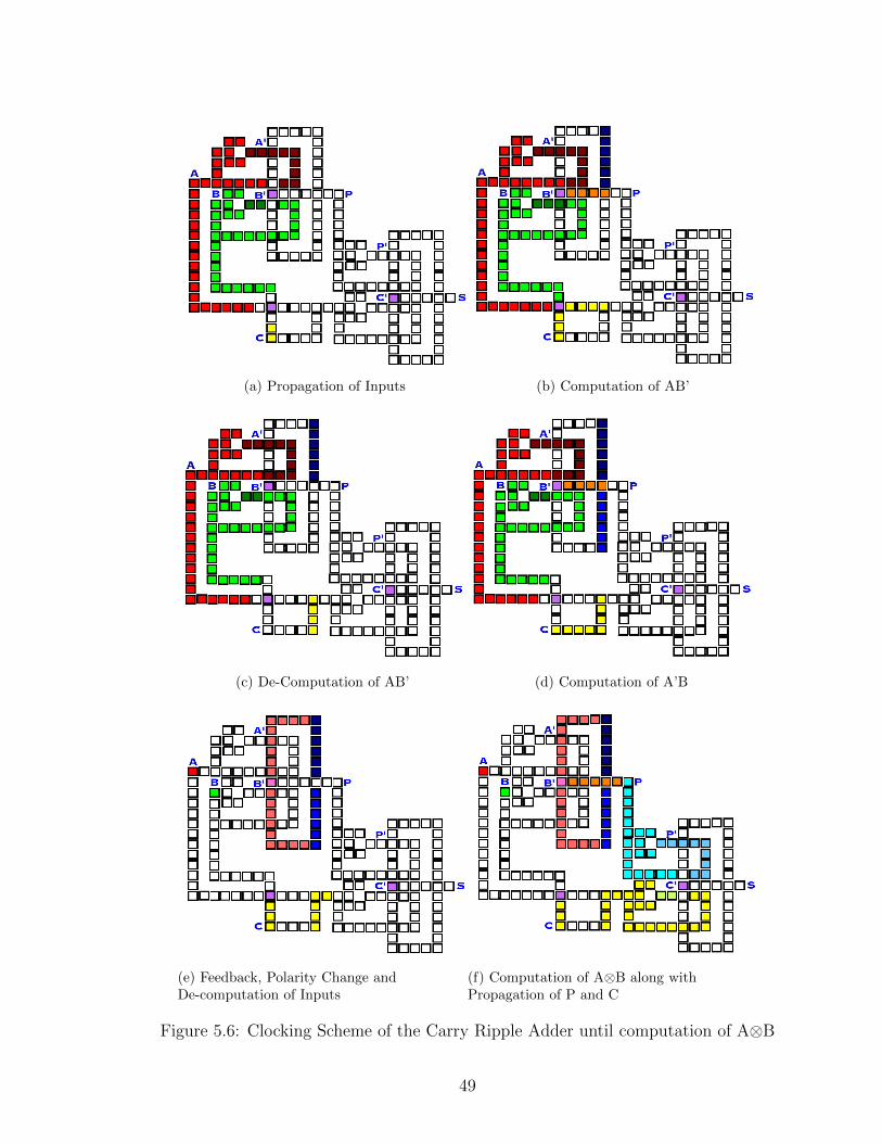
(a) Propagation of Inputs (b) Computation of AB’
(c) De-Computation of AB’ (d) Computation of A’B
(e) Feedback, Polarity Change andDe-computation of Inputs
(f) Computation of A⊗B along withPropagation of P and C
Figure 5.6: Clocking Scheme of the Carry Ripple Adder until computation of A⊗B
49

(a) Computation of PC’ (b) De-Computation of PC’
(c) Computation of P’C (d) Feedback, Polarity Change andDe-computation of Inputs
(e) Computation of Sum (f) Cycle repeats for next set of inputs
Figure 5.7: Clocking Scheme of the Carry Ripple Adder until computation of Sum
50

6 cycles. Therefore, a single bit adder can perform 4-bit addition which saves a lot
of area. If we were to perform n-bit addition using this adder, we would get the nth
output in [12+((n-1)*6)] clock cycles or at the end of [11+((n-1)*5)]th clock cycle.
5.2.2 Carry Look Ahead Adder
Carry look ahead adders were designed in order to reduce the computation time.
Two signals Propagate (P) and Generate(G) was created exclusively for the purpose
reducing the amount of time required to determine the carry bits. P and G is based
on whether the carry is being propagated from a least significant bit position (at least
one input is ’1’), generated in that bit position (both inputs are ’1’) or killed in that
bit position (both inputs are ’0’). In general one can conclude that P is sum of the
half adder which is nothing but A⊗B while generate is the carry out which is A.B.
The block diagram of the carry look ahead adder is as shown in Fig. 5.8.
Figure 5.8: Block Diagram of Carry Look Ahead Adder
Our proposed carry look ahead adder is not different from the carry ripple adder,
just that MVB block is replaced by the propagate generate block (PGB). Our design
inherently calculates the propagate (P) since it’s the output of the first CRXB block.
The block diagram of our proposed carry look ahead adder is as shown in Fig. 5.9.
The working of the proposed carry look ahead adder is quite simple and similar
to the working of the carry ripple adder seen in the previous section. The proposed
carry look ahead adder is as shown in Fig. 5.10. Therefore as seen from Fig. 5.9 and
51

Figure 5.9: Block Diagram of Proposed Carry Look Ahead Adder
Fig. 5.10 we can clearly see that we have two blocks of CRXB and a block of PGB.
Initially let’s assume that all the cells are unpolarized except for the majority gate
voter cells and the inputs are readily available as shown in Fig. 5.11.
Figure 5.10: QCA Representation of Proposed Carry Look Ahead Adder
Figure 5.11: Initial State of Proposed Carry Look Ahead Adder
Once the inputs are readily available, the inputs propagate through to the first
CRXB block. Then the computation of first AND operation of the CRXB begins.
This can be clearly observed in Fig. 5.12(a) and (b). As seen in the previous sections,
52

we can clearly observe the availability of both the true and complementary form of
the inputs in the CRXB block similar to the carry ripple adder design.
The computation proceeds exactly in the same way as the computation of XOR
in CRXB as shown in Fig. 5.12(c) and (d). One can easily observe that Fig. 5.6 and
Fig. 5.12 are exactly the same with regard to the CRXB block until the 4th clock
cycle. In the 5th clock cycle instead of propagating the feedback and changing the
polarity, we just de-compute and proceed to the computation of generate (G) this is
nothing but A.B in the 6th clock cycle as seen in Fig. 5.12(e) and (f). One should
also note that while computation of generate is going on the inputs are de-computed
so that the next set of inputs can be fed in. Then we proceed with the polarity change
and de-computation and finally proceed to the computation of first XOR output i.e.
A⊗B similar to the carry ripple adder design as shown in Fig. 5.12(g,h). Thus at
the end of the 8th clock cycle, we have both the propagate and the generate which
serves as input to the PGB block which computes the next carry. Simultaneously we
proceed to compute the sum output in the second CRXB block.
Thus so far we have seen the computation of data in the first CRXB block, now
let’s take a look at the computation in the second CRXB block and PGB block (Fig.
5.13). The computation in the PGB block is quite straightforward, it’s just an OR
operation of the two inputs namely P and G which gives the carry out for the next set
of inputs. The computation of the second CRXB block proceeds in the exact same
way as that of the first CRXB block, just that the inputs are P and C computed from
the first CRXB block. One should note that, the input C is fed in for the first bit
while it comes from the PGB block for the next set of inputs.
If one takes a closer look at Figs. 5.12 and 5.13, one can clearly notice that the
computation of data in the first CRXB block is exactly the same just that we have
new set of inputs after every 8 clock cycles (Fig. 5.12(f) and Fig. 5.7(a)). We can
clearly find that the sum output is available in the 14th clock cycle or more precisely
53

(a) Propagation of Inputs (b) Computation of AB’
(c) De-Computation of AB’ (d) Computation of A’B
(e) De-Computation of A’B (f) Computation of Generate (G) i.e. AB along withback propagation
(g) De-Computation and Polarity Change (h) Computation of A⊗B along with Propagation ofP and C
Figure 5.12: Clocking Scheme of the Carry Look Ahead Adder until computation ofPropagate
54

(a) Computation of P’C (b) De-Computation of P’C
(c) Computation of PC’ (d) Feedback, Polarity Change and De-computationof Inputs
(e) Computation of Sum (f) Cycle repeats for next set of inputs
Figure 5.13: Clocking Scheme of the Carry Look Ahead Adder until computation ofSum
55

at the end of the 13th clock cycle. If we pipeline the data through the adder, we can
clearly see that the sum for the second set of inputs will be available at the end of the
19th clock cycle or in the 20th clock cycle. Thus, from Figs. 5.12 and 5.13 we can
clearly see that if we pipeline data into the adder, we get the first output in the 13th
clock cycle and successive outputs every 6 cycles. Therefore, a single bit adder can
perform 4-bit addition which saves a lot of area. If we were to perform n-bit addition
using this adder, we would get the nth output in [14+((n-1)*6)] clock cycles or at the
end of [13+((n-1)*5)]th clock cycle.
Thus in this chapter we have understood the working of our proposed adders. We
will look into the advantages of this adder and how it compares with the existing
adders in the next chapter.
56
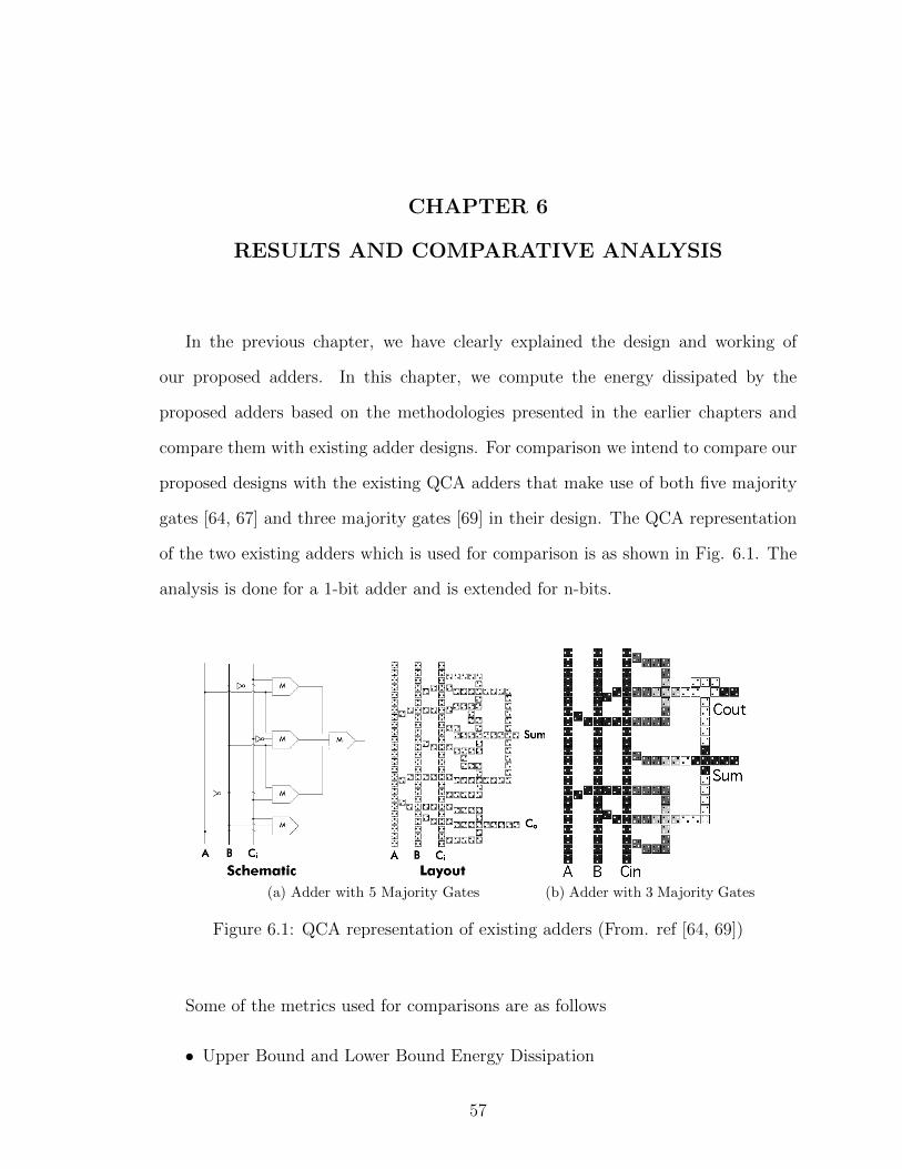
CHAPTER 6
RESULTS AND COMPARATIVE ANALYSIS
In the previous chapter, we have clearly explained the design and working of
our proposed adders. In this chapter, we compute the energy dissipated by the
proposed adders based on the methodologies presented in the earlier chapters and
compare them with existing adder designs. For comparison we intend to compare our
proposed designs with the existing QCA adders that make use of both five majority
gates [64, 67] and three majority gates [69] in their design. The QCA representation
of the two existing adders which is used for comparison is as shown in Fig. 6.1. The
analysis is done for a 1-bit adder and is extended for n-bits.
(a) Adder with 5 Majority Gates (b) Adder with 3 Majority Gates
Figure 6.1: QCA representation of existing adders (From. ref [64, 69])
Some of the metrics used for comparisons are as follows
• Upper Bound and Lower Bound Energy Dissipation
57
• Area and Cell Count
• Latency
• Speed with respect to Area and Power (SwAP) Analysis
6.1 Upper and Lower Bound Energy Dissipation
As seen from chapter 4, we have clearly established that the upper bound energy
dissipated in a single QCA cell in the case of irreversible computation is given by Ediss.
Similarly, we compute the lower bound based on the methodology discussed earlier
where in we divide the circuit into data zones and data sub-zones and computing
the information lost as the sum of the information lost in individual data zones. As
seen in the previous chapters, we can clearly observe the availability of both the
true and complementary form of the inputs in the CRXB block. It must be noted
that while the true form of the input is being fed into the input cell of the majority
gate of the CRXB block, the complementary form of the same input is being held
in the hold phase. The result of such a configuration is that we can feed both the
true and complementary form of inputs into the same cell without any loss of energy
since at any given point of time there is a copy available. Since our designs can be
viewed as three separate blocks, we can compute the energy dissipated in each block
and summation of all the energies will give the net energy dissipated. The energy
dissipation is based on the giving inputs in the same order as seen in truth table of
adder (Table. 5.1).
6.1.1 Analysis of Carry Ripple Adder
The proposed carry ripple adder can be subdivided into three zones namely the
two CRXB blocks and one MVB block (Fig. 5.3 and Fig. 5.4). Now let’s compute
the energy dissipated in the CRXB block. In the CRXB block, the energy dissipation
occurs every time we switch the polarity of the majority gate voter to perform both
58

AND and OR operation. Thus, the energy dissipated will be equal to 2Ediss. Other
loss occurs whenever the inputs are being fed into the input cell via the feedback
path. Thus the energy loss will be 4Ediss which can be inferred from the truth table
(Table. 3.1) since there is dissipation occurring only when we switch inputs from 1
to 0 and vice versa and not from 0 to 0 or 1 to 1. Thus total energy dissipated in
the CRXB block is equal to 6Ediss. Now let’s compute the energy dissipated in the
MVB block. If we consider the MVB block there is energy dissipation only when
the inputs switch. There is no other loss of energy. One should note that one of
inputs C is being fed only once while the subsequent cycles it’s being produced by
the MVB block itself which implies that Ediss is dissipated when we feed input C the
very first time. Therefore if we consider the truth table of a 1-bit full adder as shown
in Table. 5.1, we can find that energy dissipation for switching inputs A and B will
be 6Ediss. Thus the total energy dissipated in entire carry ripple adder is given by
energy dissipated in the CRXB block + energy dissipated in the MVB block.
ECRAUB= ECRXB1 + EMVB + ECRXB2 + Einputs
= 6Ediss + 0 + 6Ediss + 7Ediss
ECRAUB≤ 19Ediss (6.1)
If we consider an n-bit adder, the energy dissipated in the CRXB and MVB blocks
remains the same, the only change will be the energy dissipated by the inputs which
is nothing but the switching of inputs. Therefore, in an n-bit adder if we have k input
transitions from 0 to 1 or from 1 to 0 we get the total energy dissipated as
ECRAUBn= ECRXB1 + EMVB + ECRXB2 + Einputs
= 6Ediss + 0 + 6Ediss + (k + 1)Ediss
ECRAUBn≤ (k + 13)Ediss (6.2)
59

Till now, we formulated the upper bound energy, now let’s compute the lower bound
energy based on physical information theory. The control and restoration process
are the same as that of proposed XOR gate design seen in chapter 5. Now, if we
consider the adder circuit, the information loss is due to inputs and due to the CRXB
blocks. So, consider the inputs to the circuit as a data zone, the output of data zone
will be current inputs of the circuit, and the input to the data zone will be the next
inputs to the circuit. Since, the next set of inputs are independent of the previous
set of inputs, we have H(X|Y ) = H(X). Therefore, the information lost is solely
dependent only on the next set of inputs. Let’s assume that all the possible inputs
i.e. [00, 01, 10, 11] are equally probable. This implies that we will have H(X) = 2
which means that −∆I = 2bits will be lost. Let us define the feedback paths to be
another data zone. Since the next set of inputs is independent of the previous inputs
we have H(X|Y ) = H(X). Therefore, the information lost is solely dependent only
on the next set of inputs. Let’s assume that all the possible inputs i.e. [00, 01, 10]
are equally probable. We have only 3 sets of inputs for the feedback path since the
input [11] is never encountered as seen from Table. 3.1. This implies that we will
have H(X) = ln(3) which means that −∆I = 1.098bits will be lost. An additional
2bits of information is lost due to the changing of polarity. There is no information
lost in the MVB block.
ITotal = ICRXB1 + IMVB + ICRXB2 + IInputs
= 3.098 + 0 + 3.098 + 2
ITotal ≥ 8.196bits (6.3)
Since we know the circuit loses on average 8.196 bits, the fundamental lower bound of
heat dissipation will be 8.196kBT ln(2)joules for the Bennett clocked proposed adder
in QCA.
60
If we consider an n-bit adder, the energy dissipated remains the same since we
performing a single n-bit computation in the same circuit and not by a series of n
1-bit adders. But the lower bound will change if we try to perform multiple n-bit
computations again and again. For example if we perform a 4-bit computation then
the information lost will be just 2bits and the energy dissipated will be equal to
8.196kBT ln(2)joules, but if we perform 2 consecutive 4-bit operations then we lose
4bits of information in the input cycle. This is due to the fact that we are inputting
a new set of data into the adder. Hence, the energy dissipated depends on the
kind of addition one is performing as a 1-bit addition followed by 4-bit addition will
give a different result compared to a 4-bit addition followed by another 4-bit addition.
Therefore, it’s under the discretion of the designer and the energy dissipation depends
on the usage of the adder. Therefore, to generalize it and put it in simpler terms we
assume that we just perform only one computation i.e. an n-bit adder performs one
n-bit addition, we get the total energy dissipated as
ECRALBn≥ 8.196kBT ln(2)joules (6.4)
6.1.2 Analysis of Carry Look Ahead Adder
The proposed carry look ahead adder can be subdivided into three zones similar
to the carry ripple adder namely the two CRXB blocks and one PGB block (Fig.
5.3 and Fig. 5.4). In the analysis of carry ripple adder, we have clearly seen the
energy dissipated in the CRXB block which is equal to 6Ediss. Now let’s compute
the energy dissipated in the PGB block. If we consider the PGB block there is no
energy dissipation since inputs are nothing but the outputs of the previous stage.
Thus the energy dissipated is equal to 0. Now let’s consider the energy dissipated
when we switch the inputs A and B. This is also exactly the same calculation as seen
in carry ripple adder which is equal to 7Ediss. Thus the total energy dissipated in
61

entire carry look ahead adder is given by energy dissipated in the CRXB block +
energy dissipated in the PGB block + energy dissipated due to switching of inputs.
ECLAUB= ECRXB1 + EPGB + ECRXB2 + Einputs
= 6Ediss + 0 + 6Ediss + 7Ediss
ECLAUB≤ 19Ediss (6.5)
ECLAUBn≤ (k + 13)Ediss (6.6)
Similarly the lower bound dissipation can also be calculated by finding out the infor-
mation lost in the circuit which is nothing but the loss in the CRXB and PGB blocks
along with the loss in the inputs.
ITotal = ICRXB1 + IPGB + ICRXB2 + IInputs
= 3.098 + 0 + 3.098 + 2
ITotal ≥ 8.196bits (6.7)
Hence the total energy dissipated is given by
ECLALBn≥ 8.196kBT ln(2)joules (6.8)
From equations 6.2, 6.4, 6.6 and 6.8 it’s clearly visible that the energy dissipated
in both the adders is exactly the same which is as expected since both the adders
perform the same function and both use the same set of blocks, just that both have
different implementations where one uses a majority gate voter design while the other
uses an OR gate for computation.
6.1.3 Analysis of existing Adders
The adders which are being considered for comparative analysis are as shown in
Fig. 6.1. For the purpose of uniformity, we assume that the adders are clocked using
62
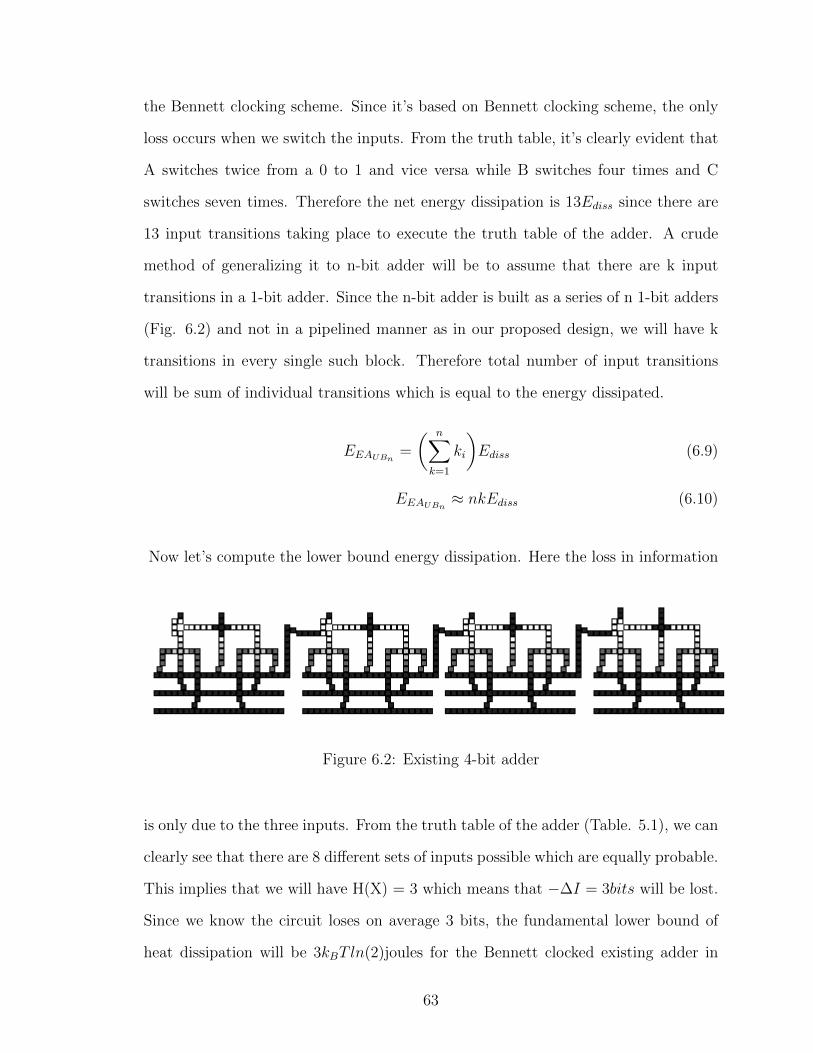
the Bennett clocking scheme. Since it’s based on Bennett clocking scheme, the only
loss occurs when we switch the inputs. From the truth table, it’s clearly evident that
A switches twice from a 0 to 1 and vice versa while B switches four times and C
switches seven times. Therefore the net energy dissipation is 13Ediss since there are
13 input transitions taking place to execute the truth table of the adder. A crude
method of generalizing it to n-bit adder will be to assume that there are k input
transitions in a 1-bit adder. Since the n-bit adder is built as a series of n 1-bit adders
(Fig. 6.2) and not in a pipelined manner as in our proposed design, we will have k
transitions in every single such block. Therefore total number of input transitions
will be sum of individual transitions which is equal to the energy dissipated.
EEAUBn=
( n∑k=1
ki
)Ediss (6.9)
EEAUBn≈ nkEdiss (6.10)
Now let’s compute the lower bound energy dissipation. Here the loss in information
Figure 6.2: Existing 4-bit adder
is only due to the three inputs. From the truth table of the adder (Table. 5.1), we can
clearly see that there are 8 different sets of inputs possible which are equally probable.
This implies that we will have H(X) = 3 which means that −∆I = 3bits will be lost.
Since we know the circuit loses on average 3 bits, the fundamental lower bound of
heat dissipation will be 3kBT ln(2)joules for the Bennett clocked existing adder in
63

QCA. If we extrapolate it to n-bit adder, we will find that 3kBT ln(2)joules will be
lost in the 1st adder in series while the remaining n-1 adders will lose 2kBT ln(2)joules
since the carry gets propagated as a 3rd input from the previous adders. Therefore,
the total energy dissipated will be equal to
EEALBn≥ 3kBT ln(2) + (n− 1) ∗ 2kBT ln(2)joules
EEALBn≥ (2n+ 1)kBT ln(2)joules (6.11)
6.2 Area and Cell Count
In the past few sections, we have clearly explained how the proposed 1-bit adder
performs n-bit computation without the need for the stacking of n 1-bit adders in
the traditional adders. This gives us an enormous advantage with regard to area as
the number of QCA cells remains the same. For our proposed carry ripple adder
and carry look ahead adder the number of cells is approximately 200 and 185 cells
respectively. QCA cells are extremely area efficient for digital circuits. It typically
has an area of 100nm2 with a cell dimension of 10nm. A table depicting the area
advantage posed by our design in comparison to existing adder is as shown in Table.
6.1.
Table 6.1: Cell Count per Unit Area Comparison
64

6.3 Latency
In this section, we try to compare the time taken for the first output to be available
along with the time taken for the next set of inputs to be fed into the circuit. Since
the proposed designed in a pipelined manner, the next set of inputs can be fed in
even before the first output is available. This is an added advantage since the next
set of outputs will be available in successive time intervals. A table depicting the
advantages of our proposed design is as shown in Table. 6.2. The advantage of the
proposed adder is clearly visible as the number of bits is scaled linearly. For example,
let’s consider a 16-bit adder, even though we get the first 16bits of output as early
as 64th cycle in the existing when compared to 86th or 88th cycle in the proposed
adders, we find that, to get the second set of outputs we need to wait until the 192nd
cycle whereas we get the output as early as 166th or 168th cycle in our proposed
adders. The major reason for such long delays in the existing adders is that, the cells
needs to be de-computed before the next set of inputs can be fed into the circuit. As
a result of this even though the first set of outputs are available in the 64th cycle, one
can’t feed the next set of inputs until the 128th cycle whereas in our proposed adders
we feed the next set of inputs even before the first set of outputs have arrived.
Table 6.2: Latency Comparison
65

6.4 Speed with respect to Area and Power (SwAP) Analysis
Using the results from the previous sections such as performance, speed, area and
energy, one single cost comparison can be generated. This is done by combining all
the parameters into a single figure of merit. This parameter becomes a measure of
operations per cycle per power area. This is basically taking the operations per cycle,
this is nothing but the time taken to compute an output for a given set of inputs
divided by the minimum power dissipated across the entire circuit and divided by the
total area. Minimum power dissipated is nothing but the amount of energy dissipated
per unit time. We call this figure of merit as SwAP. SwAP is just a set of bounds
which are used for comparison.
SwAP =(Ops/Sec)
Power ∗ Area
=(Ops/Sec)
(Energy/Sec) ∗ Area
=Ops
Energy ∗ Area(6.12)
Table 6.3: SwAP Analysis
The SwAP Analysis for the various adders is as shown in Table. 6.3. From
Table. 6.3 it’s clearly evident that the SwAP remains a constant for the proposed
adders since the energy dissipated and the area remains a constant due to it’s inbuilt
pipelined nature. If we compare with the existing adders, we can find that SwAP
66

are quadruple times higher than proposed adders for a 1-bit adder, but as we scale
the number of bits it’s clearly visible that for a 2-bit adder it’s just marginally higher
and is comparable to the proposed adders. But after 2bits SwAP is very less as the
number of bits increases. For example, when we consider a 64-bit adder we can find
that the SwAP for the proposed adders is almost 70times better and efficient than
the existing adders which is a considerable gain. Even though the latency varies for
different adders as seen in previous section, the SwAP for the proposed adders remain
a constant because as the computational throughput changes, the power dissipated
also changes by the same factor with both energy and area being a constant.
Thus, from the above mentioned sections we have clearly established the advan-
tages of the proposed adders over the existing adders. If we take a look at the existing
adders, if it has advantage in terms of power and latency, it loses in terms of area.
Similarly if it has area and latency advantage, it loses out on power. So it doesn’t
have a clear advantage in all the three areas put together for an n-bit adder designs
for n values greater than 4 which have been thoroughly established by the SwAP
analysis. A graph depicting this comparison is as shown in Fig. 6.3.
67

(a) Cell Count Comparison (b) Area Comparison
(c) Latency Comparison (d) SWAP Comparison
Figure 6.3: Graphs comparing the proposed adders with existing adders
68

CHAPTER 7
CONCLUSION AND FUTURE WORK
The goal of this work was to exploit the inbuilt reconfigurable nature of QCAs
and design energy efficient circuits. During the initial phase of this research, a cus-
tom reconfigurable technique based on switching the polarity of the majority gates
was established. The efficiency and the gains provided by the custom technique was
demonstrated with the help of an XOR gate designed based on the custom reconfig-
urable technique and compared with existing designs. During the next phase, it was
decided to design larger circuits and figure out how such a design could be helpful. It
started with the designs of a 1-bit carry ripple adder and 1-bit carry look ahead adder.
During the final phase, the design was extended to n-bit adders and was compared
with existing adders for efficiency in terms of energy and area. A broad conclusion
that can be drawn from this work is that reconfigurability does offer a lot of savings
in terms of power and area. But if one takes a closer look at the results, it can be
said that reconfigurability in QCA adds a new dimension to designing of circuits as
the area and power are reduced considerably and it could pave for smaller and power
efficient circuit designs in future with a no impact on the computational throughput.
The designs considered here may not be practically feasible, unless the underlying
clocking network allows control individual cells or small group of cells, it opens up
various avenues for further research in reconfigurable QCA. A Summary of the work
presented in this thesis is detailed in the undermentioned section.
69

7.1 Summary
The first chapter gave an insight into what was the major driving force in taking up
this thesis and gives an idea to the readers on what to look out for in this thesis. The
second chapter gave a detailed technical background on QCA’s beginning with the
origin of QCA’s to existing work on reconfigurability in QCA’s. Some of the intricate
details such as clocking and wire crossings in QCA was explained in this chapter. The
proposed reconfiguration scheme along with the custom wire crossing technique was
established in chapter three with supporting figures and timing diagrams. Once the
proposed design methodology was clearly established in the third chapter, the power
estimation methodologies along with the analysis of the proposed design was explained
in the fourth chapter. The fifth chapter consisted of the existing background work on
QCA adders and introduces the proposed adder designs based on the reconfiguration
scheme established in the previous chapters. The set of metrics used for comparison
of the proposed adders and existing adders along with the comparison results was
clearly detailed in sixth chapter. Finally the thesis was concluded with future work
suggestions in the last chapter.
Some of the main contributions of this work are as follows:
• A novel design technique for low power computation based on reconfiguration
in QCA’s.
• Routing issues in complex designs addressed through the custom wire crossing
technique.
• Design of simple arithmetic circuits like full adders using the proposed recon-
figuration scheme.
70

7.2 Future Work
Even though we have taken a big step forward in the design of energy efficient
circuits there are still many open ended questions which needs to be answered. One
interesting future work will be to design the underlying clocking network.
Some of the other areas where one can focus their research include the combining
of two 32-bit adders to design a single 64-bit adder and compare it with both the
existing designs and the designs proposed as part of this thesis.
Research is also needed for using the proposed custom wire crossing techniques
in more complex circuits and the principal of using the dead computation time in
Bennett clocking scheme should be exploited.
Circuits that make use of both Laundeur and Bennett clocking scheme can be
designed and tested for efficiency in terms of power and performance.
71

APPENDIX A
RECONFIGURABILITY AND NANOCOMPUTING
A.1 Single Electron Transistor
Uchida et al [65] proposed the very first programmable Single Electron Transistor
(SET) logic which had a non-volatile memory function. The logic was able to perform
different functions based on the status of the memory. A few years later, Hai et al [35]
proposed the reconfigurable logic gates based on the single electron spin transistors.
This method was further improvised by Sui et al [12] who proposed the reconfigurable
SET based on SET inverters without the need for the non-volatile memory function.
A thorough investigation of the reconfigurable logic cells based on SET and MOS-
FET hybrid circuits have been done by the same authors where in Depending upon
the configuration of the device, it can perform reconfigurable NAND/NOR cell, a
reconfigurable NAND/XNOR cell or a reconfigurable XNOR/XOR cell. A compara-
tive study of the proposed reconfigurable SET design with the traditional MOSFET
circuits with regard to power and performance has also been presented in their work
where in they have clearly shown the power savings in the reconfigurable design.
A.2 Chemically Assembled Electronic Nanotechnology
Chemically Assembled Electronic Nanotechnology (CAEN) is a promising tech-
nology, which uses self-alignment to construct electronic circuits from nano scale
devices that takes advantage of quantum mechanical effects. It uses chemical syn-
thesis techniques to construct molecular-sized circuitry elements such as, resistors,
transistors, diodes, resonant tunneling diodes (RTDs), and reconfigurable switches.
72

The basic block of this reconfigurable interconnect grid is a molecular diode which
can be configured off or on. The following diagram (Fig. A.1) shows how a 3x3 grid
is configured to implement an AND gate [33]. A serious drawback to CAEN is the
inability to include three-terminal devices (e.g., transistors) in circuits.
216
are synthesized and connected together through chemical process of self assembly. In the next step, two
planes of aligned wires are combined to form a two dimensional grid with configurable molecular switches
at the cross points. These grids will be of the order of few microns. A separate process will then create a
silicon based die providing power, clock lines, I/O interface and other support logics necessary. The grids are
placed and aligned into the groves inside the die [8]. The molecular logic array portion of a nano block is
composed of two orthogonal sets of wires. At each intersection of two connectors is a configurable molecular
switch. The main element at the intersection of the grid will be a reconfigurable molecular switch, which can
be configured ‘off’ or ‘on’. The following diagram(Fig.2) shows how a 3x3 grid is configured to implement
an AND gate.
Figure 2. AND gate using reconfigurable CAEN grid
The nondeterministic nature of self-assembly will give rise to high degree of defects. Instead of
eliminating these defects totally, we can perform some post-fabrication steps as done as in Teramac, to
perform a self-diagnosis. The result of the self-diagnosis brings up a defect-map and the map can be used to
configure the desired functions around the defects [9]. Such a system is dynamic, adaptable and evolving.
And the paradigm that matches most is the open and reconfigurable mode of computing.
4.1. Defect Tolerant Hardware Every nano fabric built into the system will have to be defect tolerant because they are regular, highly
configurable, fine grained and has rich inter connect. The regularity of the defect allows us to choose where a
particular function is to be implemented. The configurability allows us to pick which nano wires, blocks or
parts of a nano block will implement a particular circuit. The fine grained nature of the device along with the
local nature of the interconnect, reduces the impact of a defect to minimal. And finally the rich interconnect
allows us to choose among many paths in implementing a circuit. Thus with defect map in hand we can
realize and adapt function circuits. The defect discovery relies on the fact that we can configure the nano
fabric to implement any circuit, by testing its own resources [10].
The key difficulty in testing the nano fabric is that it is impossible to test the individual elements in
isolation. Hence, these will have to be tested in conjunction with an outside host(preferably a CMOS tester)
as achieved in the case of Teramac. As the host gains knowledge of the fault-free regions of the fabric, it replaces more and more of the tester region with that of the nano fabric. Once a sufficient number of
resources have been discovered by the host, these tested areas act as the host for the remainder of the fabric.
Once the defect map has been generated we can use the nano blocks to implement necessary circuits. Though the molecules are expected to be robust over time, new defects that are inevitable might occur over time.
This will not be as complex as the initial fault mapping [11]. Though the various demonstration system of
this area, had their limitations, it is possible to build a computer that contains novel methods of detecting defects, like built-in ones and coupled with self-configuration mechanism the nano architecture can scale to
new heights of computation.
4.2. Dynamic Reconfiguration Reconfigurability is a key component to a nano architecture. The nano fabric uses runtime
reconfiguration for defect testing and to perform its desired functions. The time that the fabric takes to
configure depends on two factors: viz., first, the time it takes to download a configuration to the nano fabric
and secondly, the time taken to distribute the configuration bits to the different regions of the fabric. [12].
Figure A.1: AND gate using reconfigurable CAEN grid (From. ref. [33])
A.3 Nanowire and Carbon Nano Tubes
As VLSI technology continues to scale beyond the end of the roadmap for sili-
con based technologies, VLSI design is expected to be based on non-silicon nanoscale
devices, e.g., carbon nanotubes (CNTs). Such nanoscale devices are expected to be
manufactured based on bottom-up self-assembly processes, rather than the traditional
top-down lithography based VLSI manufacturing processes [60]. Thus, unconven-
tional architectures are often desirable. Lieber et al have proposed programmable
nanowire circuits for nano processors where in they have defined the logic tile consist-
ing of 2 interconnected arrays with 496 functional configuration FET Nodes. With
the help of active reprogramming of the nodes, they were able to make the same
circuitry work as Full Adder, Multiplexor, De-multiplexor among others [72]. DeHon
et. al. [19, 20] have shown how to organize the CNTs, SiNWs and molecular-scale
devices that are now being developed into an operational reconfigurable computing
73

system which is commonly referred to as NanoPLA. The molecular-scale wires can
be arranged into interconnected, crossed arrays with switching devices at their cross
points. A typical Nano wire crossbar architecture is as shown in Fig. A.2 Goldstein et
al [17] proposed a similar homogenous reconfigurable architecture known as NanoFab-
ric which makes use of CAEN as discussed earlier. Lieber research group of Harvard
University refer to such computing paradigms as the Universal Computing Architec-
ture (UCA). Such nanoscale computer architectures share common characteristics -
they support unconventional nanoscale manufacturing paradigm via simple homoge-
neous periodic structures and reconfigurability for post-fabrication design mapping.
In general, nanowire-based reconfigurable systems based on the UCA concept are re-
ferred to as the Nanowire Reconfigurable Crossbar Architecture (NRCA). Wu et al
have proposed an asynchronous nano - architecture which is based on the delay insen-
sitive data encoding and self timed logic known as the Null Convention Logic (NCL),
this makes the design totally clock free. In the previous mentioned synchronous de-
sign, there is a huge manufacturing difficulty owing to the complex clock distribution
schemes which has been overcome in this design which saves on circuit area since we
can remove all the hardware components related to the clock.
#FXCPEGUKP0CPQYKTG$CUGF%QORWVKPI#TEJKVGEVWTGU
DV\QFKURQRXVQDQRDUFKLWHFWXUHLVEDVHGRQGHOD\LQVHQVLWLYHGDWDHQFRGLQJDQGVHOIWLPHGORJLF UHIHUUHG WR DV WKH1XOO &RQYHQWLRQ /RJLF 1&/ ²PDNLQJ LW WRWDOO\ FORFNIUHH 7KHSRWHQWLDOEHQHILWVFDQEHVXPPDUL]HGDVIROORZV 0DQXIDFWXUDELOLW\ 'LVWULEXWLQJ WKH FORFN VLJQDO LV QRW QHHGHG $OO FORFNLQJUHODWHGKDUGZDUH FRPSRQHQWV FDQ EH UHPRYHG IURP WKH RYHUDOO KDUGZDUH GHVLJQ 7KLV QRW RQO\VDYHVRQFLUFXLWDUHDEXWDOVRIDFLOLWDWHVWKHKRPRJHQHLW\RIWKHV\VWHP²DQLPSRUWDQWLVVXHIRUPDQXIDFWXULQJEDVHGRQPROHFXODUVHOIDVVHPEO\ 6FDODELOLW\ 7KH RYHUDOO FLUFXLW LV VHOIWLPHG ² PHDQLQJ WKDW DOO WLPLQJ LQIRUPDWLRQ LVHPEHGGHG LQ WKHHQFRGLQJ7KLVXQLTXHDVSHFWRI WKHSURSRVHGDV\QFKURQRXVDUFKLWHFWXUHSURYLGHVEHWWHUVFDODELOLW\WKDQLWVFORFNHGFRXQWHUSDUWVVLQFHWKHWLPLQJLVORFDOO\KDQGOHG7KHWLPLQJFRPSOH[LW\UHPDLQVWKHVDPHHYHQWKRXJKWKHVL]HRIWKHFLUFXLWJHWVODUJHU5REXVWQHVV'XH WRQRQGHWHUPLQLVPRI WKHGLUHFWHG VHOIDVVHPEO\SDUDGLJPQDQRZLUHFURVVEDUFLUFXLWVDUHDQWLFLSDWHGWRH[KLELWODUJHYDULDWLRQVLQSK\VLFDOSDUDPHWHUV6LQFHDQ\SK\VLFDOYDULDWLRQLQDQHOHFWULFDOSDUDPHWHUPD\KDYHLWVRZQQHJDWLYHHIIHFWRQWKHWLPLQJEHKDYLRURIWKHFLUFXLWEHLQJDEOHWRGHVLJQGHOD\LQVHQVLWLYHFLUFXLWVLHFRUUHFWRSHUDWLRQRI WKHFLUFXLW LV LQGHSHQGHQWRI WKH WLPLQJ LV D VLJQLILFDQW FDSDELOLW\DQG LWZRXOGJUHDWO\LQFUHDVHWKHUREXVWQHVVRIWKHFLUFXLWWRGHVLJQSDUDPHWHUYDULDWLRQV 0RGXODULW\ $V\QFKURQRXV FLUFXLWV FDQ EH GLYLGHG LQWR PRGXOHV WKDW DUH GHVLJQHGZLWKRXW FRQVLGHULQJ RWKHU PRGXOHV HVSHFLDOO\ ZLWK UHVSHFW WR WLPLQJ UHODWLRQVKLSV0RGXODULW\IDFLOLWDWHVFRQILJXUDELOLW\RIFLUFXLWV'HIHFWDQG)DXOW7ROHUDQFH,QDGGLWLRQWRWKHFRPSOHWHUHPRYDORIPDQ\WLPLQJUHODWHGIDLOXUHPRGHVWHVWLQJFRPSOH[LW\LVUHGXFHGLQWKDWVWXFNDWIDXOWVVLPSO\KDOWWKHFLUFXLW$OVRLQFDVHRIGXDOUDLOHQFRGLQJLVFRQVLGHUHGDVDQLQYDOLGFRGH6RDQ\SHUPDQHQWRUWUDQVLHQWIDXOWWKDWUHVXOWVLQWKLVLQYDOLGFRGHZRUGFDQEHHYHQWXDOO\GHWHFWHG2QO\VWXFNDWIDXOWVDQGVRPHRWKHUWUDQVLHQWIDXOWVQHHGWREHH[HUFLVHGZLWKDSSOLHGSDWWHUQV'HVLJQWLPHDQGULVNDVZHOODVFLUFXLWWHVWLQJUHTXLUHPHQWVDUHH[SHFWHGWREHGHFUHDVHGEHFDXVHRIHOLPLQDWLRQRIFRPSOH[LW\RIFORFNDQGLWVDVVRFLDWHGFULWLFDOWLPLQJLVVXHV,QRUGHUWREHDYLDEOHQDQRWHFKQRORJ\WKHQDQRZLUHFURVVEDUEDVHV\VWHPVVKRXOGEH 6WUXFWXUDOO\ VLPSOH DQG VFDODEOH HQRXJK WR EH IDEULFDWHG E\ ERWWRPXSPDQXIDFWXULQJWHFKQLTXH5REXVWHQRXJKWRWROHUDWHH[WUHPHSDUDPHWULFYDULDWLRQV'HIHFWDQGIDXOWWROHUDQWHQRXJKWRRYHUFRPHWKHH[WUHPHGHIHFWGHQVLWLHVDJLQJIDFWRUVDQGWUDQVLHQWIDXOWV$EOHWRVXSSRUWDWVSHHGYHULILFDWLRQDQGUHFRQILJXUDWLRQ
0CPQUECNG&GXKEGUCPF%QORWVKPI#TEJKVGEVWTG
%06CPF5K09%TQUUDCT$CUGF0CPQUECNG&GXKEGU8QOLNH&026FKHPLFDOO\DVVHPEOHGQDQRVFDOHFRPSRQHQWVVXFKDV&17VDQG6L1:VDUHXQOLNHO\ WR EH XVHG WR FRQVWUXFW FRPSOH[ DSHULRGLF VWUXFWXUHV *ROGVWHLQ HW DO *ROGVWHLQ HW DO 0LVKUD HW DO 7KXV XQFRQYHQWLRQDO DUFKLWHFWXUHV DUH RIWHQGHVLUDEOH2QHRIWKHPRVWSURPLVLQJFRPSXWDWLRQDOQDQRWHFKQRORJLHVLVWKHFURVVEDUEDVHGDUFKLWHFWXUH .XHNHVHW DO .XHNHVHWDO &KHQHW DO =LHJOHU HW DO 6WDQ HW DO D WZRGLPHQVLRQDO DUUD\ QDQRDUUD\ IRUPHG E\ WKH LQWHUVHFWLRQ RI WZRRUWKRJRQDO VHWV RI SDUDOOHO DQG XQLIRUPO\VSDFHG QDQRPHWHUVFDOH ZLUHV VXFK DV FDUERQQDQRWXEHV&17VDQGVLOLFRQQDQRZLUHV6L1:V$W\SLFDOQDQRVFDOHFURVVEDUVWUXFWXUHLV
VKRZQ LQ )LJ ([SHULPHQWV KDYH VKRZQ WKDW VXFK QDQRVFDOH ZLUHV FDQ EH DOLJQHG WRFRQVWUXFW DQ DUUD\ ZLWK QDQRPHWHUVFDOH VSDFLQJ XVLQJ D IRUP RI GLUHFWHG VHOIDVVHPEO\1LFHZDUQHUHWDO+XDQJHWDO&XLHWDO0LUNLQHWDO
)LJ7\SLFDOQDQRZLUHFURVVEDUDUFKLWHFWXUH2QHRUPRUHFURVVSRLQWVFDQEHJURXSHGWRJHWKHUWRIRUPDPHPRU\RUORJLFGHYLFH/LHEHUUHVHDUFK JURXS KDYH VKRZQ HOHFWURPHFKDQLFDO VZLWFKLQJ GHYLFHV XVLQJ VXVSHQGHGQDQRWXEHV 5XHFNHV HW DO 7KH 1717 MXQFWLRQ LV ELVWDEOH ZLWK DQ HQHUJ\ EDUULHUEHWZHHQWKHWZRVWDWHV6L1:VFDQEHVXEVWLWXWHGIRUWKHORZHUZLUHDQGWKHVHMXQFWLRQVFDQUHFWLI\LQJ VXFK WKDW WKH FRQQHFWHG VWDWH H[KLELWV SQGLRGH UHFWLILFDWLRQ EHKDYLRU 7KXVGLRGHUHVLVWRU ORJLF FDQ EH UHDOL]HG LQ QDQRVFDOH 'RSHG 6L1:V H[KLELW )(7 )LHOG (IIHFW7UDQVLVWRU EHKDYLRU +XDQJ HW DO 7KDW LV R[LGH FDQ EH JURZQ RYHU WKH 6L1: WRSUHYHQWGLUHFWHOHFWULFDOFRQWDFWRIDFURVVHGFRQGXFWRU7KHHOHFWULFDO ILHOGRIRQHZLUHFDQWKHQEHXVHG WR JDWH WKH RWKHUZLUH E\ ORFDOO\ HYDFXDWLQJ D UHJLRQRI WKHGRSHG6L1:RIFDUULHUVWRSUHYHQWFRQGXFWLRQ,QRWKHUZRUGVDVWKHJDWHYROWDJHLVFKDQJHGFRQGXFWDQFHLQFUHDVHVRUGHFUHDVHVEHWZHHQWKHVRXUFHDQGGUDLQ&17VDOVRGHPRQVWUDWH)(7EHKDYLRU%DFKWROGHWDO'HU\FNHHWDO6RKHWDODQGFDQEHDOVRXVHGDVPHPRU\GHYLFHV)LQNHOVWHLQHWDO5XHFNHVHWDORULQWHUFRQQHFWV'HNNHUHWDO0ROHFXODU UHVRQDQW WXQQHOLQJ GLRGHV RIWHQ FDOOHG QHJDWLYH GLIIHUHQWLDO UHVLVWRUV 1'5VKDYHDOVREHHQUHDOL]HG%KDWWDFKDU\DHWDO&KHQ-HWDO&KHQ-(WDO<XHW DO 'HYLFHV ZLWK XVHIXO SHDNWRYDOOH\ UDWLR KDYH EHHQ PHDVXUHG DW URRPWHPSHUDWXUH&KHQ-HWDO7KHVHPROHFXOHVFDQEHXVHGDVWKHEDVLVRIORJLFIDPLOLHV&KHQ-HWDORUDVWKHFRUHRIDPROHFXODUODWFKZKLFKDOVRSURYLGHVVLJQDOUHVWRUDWLRQDQG,2LVRODWLRQ*ROGVWHLQHWDO
0CPQUECNG7PKXGTUCN%QORWVKPI#TEJKVGEVWTG'H+RQHWDOKVKRZQKRZWRRUJDQL]HWKH&17V6L1:VDQGPROHFXODUVFDOHGHYLFHVWKDWDUHQRZEHLQJGHYHORSHGLQWRDQRSHUDWLRQDOUHFRQILJXUDEOHFRPSXWLQJV\VWHPUHIHUUHGWRDVWKH1DQR3/$'HKRQHWDO1DHLPL'HKRQHWDO7KHPROHFXODUVFDOHZLUHVFDQ EH DUUDQJHG LQWR LQWHUFRQQHFWHG FURVVHG DUUD\V ZLWK VZLWFKLQJ GHYLFHV DW WKHLUFURVVSRLQWV 6LPLODU QDQRVFDOH UHFRQILJXUDEOH KRPRJHQHRXV DUFKLWHFWXUH QDPHO\ 1DQR)DEULFKDVEHHQDOVRSURSRVHGE\*ROGVWHLQHWDO*ROGVWHLQHWDO/LHEHUUHVHDUFKJURXS UHIHUUHG WR VXFK D QDQRVFDOH UHFRQILJXUDEOH KRPRJHQHRXV VWUXFWXUDO SDUDGLJP IRU
Figure A.2: Typical NanoWire Crossbar Architecture (From. ref. [20])
74

A.4 Complementary Nano Electromechanical Switch
Bhunia et al [10] have proposed a reconfigurable logic based upon the complemen-
tary Nano Electromechanical Switch (CNEMS). The basic structure of these devices
consists of three co-planar carbon nanotubes arranged so that the central nanotube
can touch the two side carbon nanotubes upon application of a voltage pulse between
them. These devices have very low leakage current, low operation voltages, and have
built-in energy storage to reduce computation power, resulting in very low overall
power dissipation. Once configured in a certain way, the switch remains in the same
state until an opposite electric field is applied to reconfigure the switch. Due to this
latching mechanism, each switch works as a non-volatile memory element.Therefore,
CNEMS is a good candidate for memory implementation and can potentially replace
conventional charge-based CMOS static and dynamic RAM since it’s immune to soft
errors. It has been proposed that CNEMS be used in the conventional FPGA based
look up Tables for storing data and these switches can be dynamically reconfigured.
A.5 CMOL
A promising cell based digital logic architecture which has caught the eye of many
researchers around the world is the CMOL architecture [42] which combine a semicon-
ductor transistor (CMOS) stack and two levels of parallel nano wires, with molecular-
scale nano devices formed between the nano wires at every crosspoint. Since this
architecture is very similar to the cell based FPGA, the authors have proposed a re-
configurable architecture different from the conventional ones. A field-programmable
nanowire interconnect (FPNI) improves on a field-programmable gate array (FPGA)
architecture [56] by lifting the configuration bit and associated components out of
the semiconductor plane and replacing them in the interconnect with nonvolatile
switches, which decreases both the area and power consumption of the circuit. This
FPNI architecture has been successfully tested in HP labs. Dong et al [25] proposed a
75

novel reconfigurable architecture 3D nFPGA based on CMOS hybrid circuits and the
3D integration techniques. They also have proposed a dense 2D FPGA architecture
based on carbon nanotubes known as FPCNA [26]. Both of these architectures are
derived from the popular island-style FPGA architecture. In island-style FPGAs,
reprogrammable devices are arranged in regular tiles, where each tile contains one
configurable logic block (CLB), two connection blocks (CBs), and one programmable
switch block (SB), as shown in Fig. A.3.connect the BLEs to each other. The SBs and CBs are used to provide global routing for connection paths between CLBs.
Figure 1. Island-style FPGA Architecture
The rest of this paper is organized as follows: In Section II we describe the 3D nFPGA architecture, introducing new progress on stacking with 3D nFPGA2. The FPCNA architecture is discussed in Section III. In Section IV, we evaluate the area and performance of the two architectures and compare them to a conventional CMOS FPGA. Section V concludes this paper.
II. 3D nFPGA2
To explore the future potential of nanotechnology and CMOS, we introduced a nanomaterial-based three-dimensional FPGA in [8]. This architecture, called 3D nFPGA, efficiently distributed the components of a 2D FPGA into a 3½-layer structure. CMOS-based logic devices, nanowire-based memory/routing elements, post-silicon block memories, and CNT-based vias were all integrated in the design. As shown in [8], 3D nFPGA achieved a 4x footprint reduction and a 2.6x performance over a traditional CMOS-based 2D FPGA.
In this work, we introduce a new 1½–layer structure called 3D nFPGA2. Unlike the original 3D nFPGA design, this design can be easily stacked. In a stacked design, connections are made through the substrate using through-silicon vias (TSVs). In the 1½-layer structure, these TSVs only have to connect through one layer of silicon substrate, as opposed to three in the 3½-layer design. This feature makes multi-stacking much more feasible. 3D nFPGA2 also improves upon the initial design by replacing the nanowire and molecular-switch routing elements with routing based on metal interconnect and solid-electrolyte switches. These solid-electrolyte switches offer better compatibility with the CMOS fabrication process and a higher reliability than nanowire/molecular switches [19].
(a) (b)
Figure 2. (a) 2D baseline FPGA becomes (b) 1½ layer 3D nFPGA2.
As shown in Fig. 2, the 1½-layer architecture consists of a CMOS layer and nanoswitch crossbar half-layer. Since active devices can only be created in the CMOS layer, we use it for the BLE logic and the active routing elements. The crossbar layer, on the other hand, contains the CLB local routing,
connection blocks, and distributed memories used in the switch block. We consider this to be a half layer because it connects to the top of the interconnect metallization and does not need a substrate. Global routing is done on the CMOS layer using CNT bundle interconnect. In addition, large CNT-bundle thermal vias are inserted through the design for effective thermal dissipation, as shown in Fig. 2(b).
A. Layer Design The inputs of a CLB are routed to different BLE inputs
through local routing elements such as MUXs. If the routing is fully connected such that any BLE inputs can be connected to any CLB inputs, the local routing area is significant (for example, 65% of a CLB) [20]. This motivates us to replace the CMOS-based routing elements with crossbars and programmable solid electrolyte switches. By programming the solid electrolyte switches on/off at the crosspoints of the crossbar array, a CLB input can be routed to any BLE. By implementing this routing in the crossbar layer, the CLB footprint in the CMOS layer can be significantly reduced.
In a traditional 2D FPGA, the global routing structure consists of connection blocks and switch blocks, which together take up a significant amount of the overall footprint. For instance, if the CLB size N is 10 and BLE size K is 4 (popular parameters for commercial FPGA products), the global routing area is 57.4%, and the total CLB area is 42.6% [1][20]. Global routing area is thus very critical for footprint reduction for our 3D FPGA.
We apply two techniques to aggressively reduce the global routing area. First, we move most of the connection block components to the crossbar layer. Second, we move the switch block programmable SRAM cells to the crossbar layer, implementing them in crossbar memory. Therefore, the only routing elements on the CMOS layer are switch blocks without SRAM cells, and driving buffers in the connection blocks which connect to wire tracks.
SB
CLB
CB
CBCLB
Routing
Distributed
MemoryCB
Local Feedback
BLE Output
CLB Input
Global CNT
Interconnect
Figure 3. CMOS Layer and Crossbar Layer
A 3D view of the overall organization is shown in Fig. 3. This architecture can handle any reasonable number of CLB and BLE sizes. The figure illustrates how signals can be routed. CLB inputs on the crossbar layer are connected down to the CLB logic through global interconnect vias. Local routing is done on the crossbar layer, so a local feedback signal will travel up to crossbar layer as a BLE output, route to the target via through the CLB routing crossbar, and travel back down to
Figure A.3: Island Style FPGA Architecture (From. ref. [26])
76
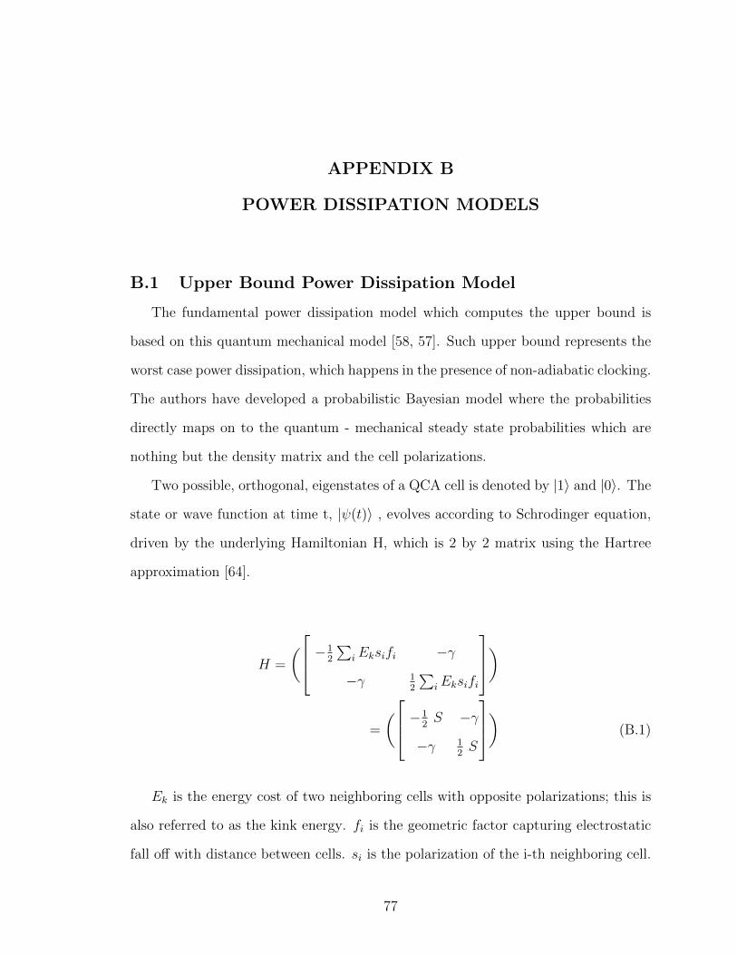
APPENDIX B
POWER DISSIPATION MODELS
B.1 Upper Bound Power Dissipation Model
The fundamental power dissipation model which computes the upper bound is
based on this quantum mechanical model [58, 57]. Such upper bound represents the
worst case power dissipation, which happens in the presence of non-adiabatic clocking.
The authors have developed a probabilistic Bayesian model where the probabilities
directly maps on to the quantum - mechanical steady state probabilities which are
nothing but the density matrix and the cell polarizations.
Two possible, orthogonal, eigenstates of a QCA cell is denoted by |1〉 and |0〉. The
state or wave function at time t, |ψ(t)〉 , evolves according to Schrodinger equation,
driven by the underlying Hamiltonian H, which is 2 by 2 matrix using the Hartree
approximation [64].
H =
( −12
∑iEksifi −γ
−γ 12
∑iEksifi
)
=
( −12S −γ
−γ 12S
) (B.1)
Ek is the energy cost of two neighboring cells with opposite polarizations; this is
also referred to as the kink energy. fi is the geometric factor capturing electrostatic
fall off with distance between cells. si is the polarization of the i-th neighboring cell.
77
The tunneling energy between the two states of a cell, which is controlled by the
clocking mechanism, is denoted by γ. For notational simplification, we will use S to
denote the total kink energy due to the polarized neighbors.
The expected value of any observable, 〈A(t)〉, can be expressed in terms of the
wave function as 〈A〉 = 〈ψ(t)|A(t)|ψ(t)〉 or equivalently as Tr[A(t)|ψ〉(t)〈ψ(t)|], where
Tr denotes the trace operation, Tr[...] = 〈1|...|1〉+〈0|...|0〉. The term |ψ(t)〉〈ψ(t)| is
known as the density operator, ρ(t). Expected value of any observable of a quantum
system can be computed if ρ(t) is known.
Energy (and power) can be estimated by computing the expected Hamiltonian
using this density matrix. However, for compact mathematical representation of
power dissipation the Bloch formulation of the Schrodinger equation, which expresses
the evolution of quantum systems in operator spaces, is used. In this formulation,
the expected value of cell energy 〈H〉 at any time is given by:
E = 〈H〉 =2
−→Γ .−→λ (B.2)
where−→Γ and
−→λ are the Hamiltonian and coherence (state) vectors respectively.
These are arrived at by expressing the density operator as a linear combination of
the Paulis spin operator σi : ρ(t) =∑3
i=1 λiσi, where λi = Trρσi. The two state
Schrodinger Hamiltonian can be projected onto the Pauli basis of generators to form
a real three-dimensional energy vector−→Γ , whose components are Γi = TrHσi
. The
explicit form of the Hamiltonian vector corresponding to Hamiltonian is:
−→Γ =
1
[−2γ, 0, EkS] (B.3)
where S is the sum of neighboring polarizations. The Bloch equation governing
the evolution of the coherence vector can be derived from the Liouville equation to
be:
78

d
dt
−→λ =
−→Γ ×
−→λ (B.4)
This formulation does not account for the effect of dissipative coupling with heat
bath. One reasonable approximation is to add an inhomogeneous linear term to this
equation to account for damping.
d
dt
−→λ =
−→Γ ×
−→λ + ξ
−→λ +−→η (B.5)
The parameters ξ and η are chosen so that they represent inelastic dissipative
heat bath coupling (open world), with the system moving towards the ground state.
−→η =1
τ
−→λ ss (B.6)
ξ = −
1τ
0 0
0 1τ
0
0 0 1τ
(B.7)
where−→λ ss is the steady-state coherence vector and τ is the energy relaxation
time. If τ → ∞, it represents the absence of any dissipation. Lower the value of τ ,
faster the heat dissipation away from the cell. The steady-state coherence vector can
be derived from the steady-state density matrix at thermal equilibrium.
ρss =e−H/kBT
Tr[e−H/kBT ](B.8)
where kB is the Boltzmann constant and T is the temperature. The corresponding
steady state coherence vector is given by
−→λ ss = Trρssσ = −
−→Γ
|−→Γ |
tanh ∆ (B.9)
where ∆ = ΩkBT
, is the thermal ratio, with Ω =√
4γ2 + S2, the energy term (also
known as Rabi frequency).
79

The instantaneous power dissipation in a single QCA cell is:
P =dE
dt=
2
[d−→Γ
dt.−→λ
]+
2
[−→Γ .d−→λ
dt
]= P1 + P2 (B.10)
The term P1 includes power from clock introduced into the cell Pclock and power
gain from input to output (Pin − Pout) [6]. We are concerned with P2 = Pdiss which
represents the instantaneous dissipated power given by
Pdiss(t) =h
2
−→Γ (t).
(d
dt
−→λ (t)
)(B.11)
Coupling the expression for power dissipation with the damped Bloch equation
we see that
Pdiss(t) = − h
2τ
−→Γ (t).
(−→λ (t)−
−→λ ss(t)
)(B.12)
If the instantaneous coherence vector tracks the steady state coherence vector for
that time instant, i.e.,−→λ (t) ≈
−→λ ss(t) then the power dissipated is very low.
High dissipation situation arises when−→λ (t) lags the changing
−→λ ss(t) . From Eq.
10 we see that−→λ ss(t) changes whenever the underlying Hamiltonian changes, which
happens when (i) clock goes from low to high (γL → γH) so as to depolarize a cell, (ii)
input or cells in previous clock zone switches states(S− → S+),and (iii) clock changes
from high to low (γH → γL), latching and holding the cell state to the new state.
The energy dissipated is expressed by integrating Pdiss over time.
Ediss =2
∫ ∞0
−→Γ .
−→dλ
dt.dt (B.13)
On modeling the above equations using the delta function and integrating them
over the above period we can get:
80

Ediss =h
2
(−→Γ +.−→λ + −
−→Γ −.−→λ − −
∫ −→λ .d−→Γ
dtdt
)(B.14)
Ediss <h
2
−→Γ +.
(−→λ ss
+ −−→λ ss−)
(B.15)
Ediss <h
2
−→Γ +.
(−−→Γ +
|−→Γ +|
tanh
(h|−→Γ +|kBT
)+
−→Γ −
|−→Γ −|
tanh
(h|−→Γ −|kBT
))(B.16)
Table B.1: Bloch Hamiltonian before and after a change in clock or the neighboringpolarization
Clock Up Driver Polarization Clock Down(γL → γH) (S− → S+) (γH → γL)
−→Γ − = 1
h[−2γL, 0, S−] 1
h[−2γH , 0, S−] 1
h[−2γH , 0, S+]
−→Γ + = 1
h[−2γH , 0, S−] 1
h[−2γH , 0, S+] 1
h[−2γL, 0, S+]
Table B.1 summarizes the Bloch Hamiltonian before and after a change in clock or
the neighboring polarization. With the help of this data, one could get the accurate
values of the energy dissipated per unit time.
81
BIBLIOGRAPHY
[1] Quantum dot cellular automaton. en.wikipedia.org/wiki/.
[2] International technology road map for semiconductors. http://www.itrs.net/,2005.
[3] International technology road map for semiconductors. http://www.itrs.net/,2011.
[4] Amiri, M. A, Mahdavi, M., and Mirzakuchaki, S. QCA implementation of aMUX-Based FPGA CLB. In International Conference on Nanoscience and Nan-otechnology, 2008. ICONN 2008 (Feb. 2008), IEEE, pp. 141–144.
[5] Bachtold, Adrian, Hadley, Peter, Nakanishi, Takeshi, and Dekker, Cees. Logiccircuits with carbon nanotube transistors. Science 294, 5545 (Nov. 2001), 1317–1320.
[6] Beckett, Paul, and Jennings, Andrew. Towards nanocomputer architecture. Aust.Comput. Sci. Commun. 24, 3 (Jan. 2002), 141–150.
[7] Bennett, C. H. Logical reversibility of computation. IBM Journal of Researchand Development 17, 6 (Nov. 1973), 525–532.
[8] Bennett, Charles H. Time/Space Trade-Offs for reversible computation. SIAMJournal on Computing 18, 4 (1989), 766.
[9] Bhanja, Sanjukta, Ottavi, Marco, Lombardi, Fabrizio, and Pontarelli, Salvatore.Novel designs for thermally robust coplanar crossing in QCA. In Proceedingsof the conference on Design, automation and test in Europe: Proceedings (3001Leuven, Belgium, Belgium, 2006), DATE ’06, European Design and AutomationAssociation, pp. 786–791.
[10] Bhunia, S., Tabib-Azar, M., and Saab, D. Ultralow-Power reconfigurable com-puting with complementary Nano-Electromechanical carbon nanotube switches.In Design Automation Conference, 2007. ASP-DAC ’07. Asia and South Pacific(Jan. 2007), IEEE, pp. 86–91.
[11] Bruschi, F., Perini, F., Rana, V., and Sciuto, D. An efficient Quantum-Dotcellular automata adder. In Design, Automation Test in Europe ConferenceExhibition (DATE), 2011 (Mar. 2011), pp. 1 –4.
82

[12] cai Sui, Bing, qing Chi, Ya, liang Zhou, Hai, cheng Xing, Zuo, and Fang, Liang.Reconfigurable single-electron transistor logic gates. In 9th International Confer-ence on Solid-State and Integrated-Circuit Technology, 2008. ICSICT 2008 (Oct.2008), IEEE, pp. 567–570.
[13] Cho, H., and Swartzlander, E.E. Adder designs and analyses for Quantum-Dotcellular automata. Nanotechnology, IEEE Transactions on 6, 3 (May 2007), 374–383.
[14] Cho, H., and Swartzlander, E.E. Adder and multiplier design in Quantum-Dotcellular automata. Computers, IEEE Transactions on 58, 6 (June 2009), 721–727.
[15] Cho, Heumpil, and Swartzlander, E.E. Modular design of conditional sum addersusing quantum-dot cellular automata. In Nanotechnology, 2006. IEEE-NANO2006. Sixth IEEE Conference on (June 2006), vol. 1, pp. 363 – 366.
[16] Compton, Katherine, and Hauck, Scott. Reconfigurable computing: a survey ofsystems and software. ACM Comput. Surv. 34, 2 (June 2002), 171–210.
[17] Copen Goldstein, S., and Budiu, M. NanoFabrics: spatial computing usingmolecular electronics. In 28th Annual International Symposium on ComputerArchitecture, 2001. Proceedings (2001), IEEE, pp. 178–189.
[18] Cui, Yi, and Lieber, Charles M. Functional nanoscale electronic devices as-sembled using silicon nanowire building blocks. Science 291, 5505 (Feb. 2001),851–853.
[19] DeHon, A. Array-based architecture for FET-based, nanoscale electronics. IEEETransactions on Nanotechnology 2, 1 (Mar. 2003), 23– 32.
[20] Dehon, Andre. Nanowire-based programmable architectures. J. Emerg. Technol.Comput. Syst. 1, 2 (July 2005), 109–162.
[21] DeHon, Andre, and Wawrzynek, John. Reconfigurable computing: what, why,and implications for design automation. In Proceedings of the 36th annualACM/IEEE Design Automation Conference (New York, NY, USA, 1999), DAC’99, ACM, pp. 610–615.
[22] Deutsch, D. Quantum theory, the Church-Turing principle and the universalquantum computer. Proceedings of the Royal Society of London. A. Mathematicaland Physical Sciences 400, 1818 (July 1985), 97–117.
[23] Devadoss, Rajeswari, Paul, Kolin, and Balakrishnan, M. Clocking-Based copla-nar wire crossing scheme for QCA. In Proceedings of the 2010 23rd InternationalConference on VLSI Design (Washington, DC, USA, 2010), VLSID ’10, IEEEComputer Society, pp. 339–344.
83
[24] Devadoss, Rajeswari, Paul, Kolin, and Balakrishnan, M. p-QCA: a tiled pro-grammable fabric architecture using molecular Quantum-Dot cellular automata.J. Emerg. Technol. Comput. Syst. 7, 3 (Aug. 2011), 13:1–13:20.
[25] Dong, Chen, Chen, Deming, Tanachutiwat, S., and Wang, Wei. Performance andpower evaluation of a 3D CMOS/nanomaterial reconfigurable architecture. InIEEE/ACM International Conference on Computer-Aided Design, 2007. ICCAD2007 (Nov. 2007), IEEE, pp. 758–764.
[26] Dong, Chen, Chilstedt, Scott, and Chen, Deming. FPCNA: a field programmablecarbon nanotube array. In Proceedings of the ACM/SIGDA international sym-posium on Field programmable gate arrays (New York, NY, USA, 2009), FPGA’09, ACM, pp. 161–170.
[27] Dysart, T.J., and Kogge, P.M. Probabilistic analysis of a molecular Quantum-Dot cellular automata adder. In Defect and Fault-Tolerance in VLSI Systems,2007. DFT ’07. 22nd IEEE International Symposium on (Sept. 2007), pp. 478–486.
[28] Ercan, I., Rahman, M., and Anderson, N. G. Determining fundamen-tal heat dissipation bounds for transistor-based nanocomputing paradigms.In 2011 IEEE/ACM International Symposium on Nanoscale Architectures(NANOARCH) (June 2011), IEEE, pp. 169–174.
[29] Ercan, Ilke, and Anderson, Neal G. Heat dissipation bounds for nanocomputing:Theory and application to QCA. In 2011 11th IEEE Conference on Nanotech-nology (IEEE-NANO) (Aug. 2011), IEEE, pp. 1289–1294.
[30] Feynman, Richard. Simulating physics with computers. International Journalof Theoretical Physics 21, 6 (1982), 467–488.
[31] Feynman, Richard. Quantum mechanical computers. Foundations of Physics 16,6 (1986), 507–531.
[32] Fijany, Amir, Toomarian, Nikzad, Modarress, Katayoon, and Spotnitz, Mathew.Bit-Serial adder based on quantum dots. NASA Technical Report, 2003. A pro-posed integrated circuit based on quantum-dot cellular automata (QCA) wouldfunction as a bit-serial adder.
[33] Goldstein, S. C, and Rosewater, D. Digital logic using molecular electronics. InSolid-State Circuits Conference, 2002. Digest of Technical Papers. ISSCC. 2002IEEE International (2002), vol. 1, IEEE, pp. 204–459 vol.1.
[34] Grossing, Gerhard, and Zeilinger, Anton. Structures in quantum cellular au-tomata. Physica B+C 151, 1–2 (July 1988), 366–369.
[35] Hai, Pham Nam, Sugahara, Satoshi, and Tanaka, Masaaki. Reconfigurable logicgates using Single-Electron spin transistors. Japanese Journal of Applied Physics46, 10A (2007), 6579–6585.
84

[36] Hanninen, Ismo, and Takala, Jarmo. Binary adders on Quantum-Dot cellularautomata. Journal of Signal Processing Systems 58, 1 (2010), 87–103.
[37] Jazbec, A., Zimic, N., Bajec, I.L., Pecar, P., and Mraz, M. Quantum-dot fieldprogrammable gate array: enhanced routing. In Optoelectronic and Microelec-tronic Materials and Devices, 2006 Conference on (2006), pp. 121–124.
[38] Landauer, R. Irreversibility and heat generation in the computing process. IBMJournal of Research and Development 5, 3 (July 1961), 183–191.
[39] Lantz, Timothy, and Peskin, Eric. A QCA implementation of a configurablelogic block for an FPGA. In IEEE International Conference on ReconfigurableComputing and FPGA’s, 2006. ReConFig 2006 (Sept. 2006), IEEE, pp. 1–10.
[40] Lent, C S, Tougaw, P D, Porod, W, and Bernstein, G H. Quantum cellularautomata. Nanotechnology 4, 1 (Jan. 1993), 49–57.
[41] Lent, Craig S, Liu, Mo, and Lu, Yuhui. Bennett clocking of quantum-dot cellularautomata and the limits to binary logic scaling. Nanotechnology 17, 16 (Aug.2006), 4240–4251.
[42] Likharev, K. K. CMOL: possible hybrid semiconductor/nanodevice circuits. InProceedings of the 2005 European Conference on Circuit Theory and Design,2005 (Sept. 2005), vol. 2, IEEE.
[43] Liu, M., and Lent, C. S. Bennett and landauer clocking in quantum-dot cellularautomata. In 10th International Workshop on Computational Electronics, 2004.IWCE-10 2004. Abstracts (Oct. 2004), IEEE, pp. 120– 121.
[44] Liu, Mo. Robustness and Power Dissipation in Quantum-Dot Cellular Automata.PhD thesis, University of Notre Dame, March 2006.
[45] Mazumder, P., Kulkarni, S., Bhattacharya, M., Sun, Jian Ping, and Haddad,G.I. Digital circuit applications of resonant tunneling devices. Proceedings of theIEEE 86, 4 (Apr. 1998), 664 –686.
[46] Moore, Gordon E. Cramming more components onto integrated circuits,reprinted from electronics, volume 38, number 8, april 19, 1965, pp.114 ff. Solid-State Circuits Newsletter, IEEE 11, 5 (Sept. 2006), 33 –35.
[47] Nahory, R. E., and Tabatabaie, N. Resonant tunneling devices. Le Journal dePhysique Colloques 48, C5 (Nov. 1987), C5–585–C5–588.
[48] Neumann, John Von/Burks. Theory of Self-Reproducing automata.
[49] Niemier, Michael Thaddeus. Desiging digital systems in Quantum Cellular Au-tomata. PhD thesis, University of Notre Dame, 2004.
85

[50] Niemier, Michael Thaddeus, Rodrigues, Arun Francis, and Kogge, Peter M. A po-tentially implementable FPGA for quantum dot cellular automata. Automata”,1st Workshop on Non-Silicon Computation (NSC-1 69 (2002), 38—45.
[51] Ottavi, Marco, Pontarelli, Salvatore, DeBenedictis, Erik, Salsano, Adelio, Kogge,Peter, and Lombardi, Fabrizio. High throughput and low power dissipation inQCA pipelines using bennett clocking. In Proceedings of the 2010 IEEE/ACM In-ternational Symposium on Nanoscale Architectures (2010), Nanoarch ’10, IEEEPress, pp. 17–22.
[52] Pollack, Fred J. New microarchitecture challenges in the coming generationsof CMOS process technologies (keynote address)(abstract only). In Proceedingsof the 32nd annual ACM/IEEE international symposium on Microarchitecture(Washington, DC, USA, 1999), MICRO 32, IEEE Computer Society, pp. 2–.
[53] Roy, Samir, and Saha, Biswajit. Minority gate oriented logic design withquantum-dot cellular automata. In Proceedings of the 7th international con-ference on Cellular Automata for Research and Industry (Berlin, Heidelberg,2006), ACRI’06, Springer-Verlag, pp. 646–656.
[54] Shabadi, P., and Moritz, C.A. Post-CMOS hybrid spin-charge nanofabrics. InNanotechnology (IEEE-NANO), 2011 11th IEEE Conference on (Aug. 2011),pp. 1399 –1402.
[55] Shannon, C. E. A mathematical theory of communication. The Bell SystemTechnical Journal 27 (October 1948), 623–656.
[56] Snider, Gregory S, and Williams, R Stanley. Nano/CMOS architectures usinga field-programmable nanowire interconnect. Nanotechnology 18, 3 (Jan. 2007),035204.
[57] Srivastava, S., Sarkar, S., and Bhanja, S. Power dissipation bounds and mod-els for quantum-dot cellular automata circuits. In Sixth IEEE Conference onNanotechnology, 2006. IEEE-NANO 2006 (June 2006), vol. 1, IEEE, pp. 375–378.
[58] Srivastava, S., Sarkar, S., and Bhanja, S. Estimation of upper bound of powerdissipation in QCA circuits. IEEE Transactions on Nanotechnology 8, 1 (Jan.2009), 116–127.
[59] Srivastava, Saket. Probabilistic Modeling of Quantum-Dot Cellular Automata.PhD thesis, University of South Florida, December 2007.
[60] Stan, M. R, Franzon, P. D, Goldstein, S. C, Lach, J. C, and Ziegler, M. M.Molecular electronics: from devices and interconnect to circuits and architecture.Proceedings of the IEEE 91, 11 (Nov. 2003), 1940– 1957.
86
[61] Tans, Sander J., Verschueren, Alwin R. M., and Dekker, Cees. Room-temperature transistor based on a single carbon nanotube. Nature 393, 6680(May 1998), 49–52.
[62] Timler, John, and Lent, Craig S. Power gain and dissipation in quantum-dotcellular automata. Journal of Applied Physics 91, 2 (Jan. 2002), 823–831.
[63] Timler, John, and Lent, Craig S. Maxwell’s demon and quantum-dot cellularautomata. Journal of Applied Physics 94, 2 (July 2003), 1050–1060.
[64] Tougaw, P. Douglas, and Lent, Craig S. Logical devices implemented usingquantum cellular automata. Journal of Applied Physics 75, 3 (1994), 1818.
[65] Uchida, K., Koga, J., Ohba, R., and Toriumi, A. Programmable single-electron transistor logic for future low-power intelligent LSI: proposal and room-temperature operation. IEEE Transactions on Electron Devices 50, 7 (July2003), 1623– 1630.
[66] van Duzer, T. Superconductor electronics, 1986-1996. Applied Superconductivity,IEEE Transactions on 7, 2 (June 1997), 98 –111.
[67] Vetteth, A., Walus, K., S., Dimitrov V., and Jullien, G. A. Quantum-dot cel-lular automata carry-look-ahead adder and barrel shifter. In IEEE EmergingTelecommunications Technology Conference (2002).
[68] Vuillemin, J.E., Bertin, P., Roncin, D., Shand, M., Touati, H.H., and Boucard,P. Programmable active memories: reconfigurable systems come of age. VeryLarge Scale Integration (VLSI) Systems, IEEE Transactions on 4, 1 (Mar. 1996),56 –69.
[69] Wang, Wei, Walus, K., and Jullien, G.A. Quantum-dot cellular automata adders.In Nanotechnology, 2003. IEEE-NANO 2003. 2003 Third IEEE Conference on(Aug. 2003), vol. 1, pp. 461 – 464 vol.2.
[70] Watrous, J. On one-dimensional quantum cellular automata. In Foundations ofComputer Science, 1995. Proceedings., 36th Annual Symposium on (Oct. 1995),pp. 528 –537.
[71] Wolf, S. A, Awschalom, D. D, Buhrman, R. A, Daughton, J. M, Von Molnar, S.,Roukes, M. L, Chtchelkanova, A. Y, and Treger, D. M. Spintronics: A Spin-Basedelectronics vision for the future. Science 294, 5546 (Nov. 2001), 1488–1495.
[72] Yan, Hao, Choe, Hwan Sung, Nam, SungWoo, Hu, Yongjie, Das, Shamik,Klemic, James F, Ellenbogen, James C, and Lieber, Charles M. Programmablenanowire circuits for nanoprocessors. Nature 470, 7333 (Feb. 2011), 240–244.PMID: 21307937.
87

[73] Zhang, Rumi, Walus, K., Wang, Wei, and Jullien, G.A. Performance comparisonof quantum-dot cellular automata adders. In Circuits and Systems, 2005. ISCAS2005. IEEE International Symposium on (May 2005), pp. 2522 – 2526 Vol. 3.
88