A Serial Memory by Quantum-Dot Cellular Automata (QCA
13
A Serial Memory by Quantum-Dot Cellular Automata (QCA) Vamsi Vankamamidi, Marco Ottavi, Member, IEEE, and Fabrizio Lombardi, Senior Member, IEEE Abstract—Quantum-dot Cellular Automata (QCA) has been widely advocated as a new device architecture for nanotechnology. QCA systems require extremely low power, together with the potential for high density and regularity. These features make QCA an attractive technology for manufacturing memories in which the paradigm of memory-in-motion can be fully exploited. This paper proposes a novel serial memory architecture for QCA implementation. This architecture is based on utilizing new building blocks (referred to as tiles) in the storage and input/output circuitry of the memory. The QCA paradigm of memory-in-motion is accomplished using a novel arrangement in the storage loop and timing/clocking; a three-zone memory tile is proposed by which information is moved across a concatenation of tiles by utilizing a two-level clocking mechanism. Clocking zones are shared between memory cells and the length of the QCA line of a clocking zone is independent of the word size. QCA circuits for address decoding and input/output for simplification of the Read/Write operations are discussed in detail. An extensive comparison of the proposed architecture and previous QCA serial memories is pursued in terms of latency, timing, clocking requirements, and hardware complexity. Index Terms—QCA, memory architecture, emerging technologies. Ç 1 INTRODUCTION I N the past few decades, the exponential scaling in feature size and increase in processing power have been successfully achieved by CMOS as the most popular technology for VLSI; however, there is substantial evidence [13] that emerging technologies (mostly based at nanoscale ranges) will be required to supersede the fundamental physical limits of CMOS devices. Among these new technologies, Quantum-dot Cellular Automata (QCA) gives a solution at nanoscale and also offers a new method of computation and information transformation using new paradigms. For example, interconnections for signal transfer are used for logic computation and manipulation by which the so-called processing-in-wire paradigm is accomplished. Orlov et al. [12] reported an experimental demonstration of a metallic QCA cell; such a device is composed of four metal dots, connected with tunnel junctions and capacitors. Microsized QCA devices have been fabricated with metal cells that operate at 50 mK [12] (that is, cryogenic). Experiments have confirmed that the switching of a single electron in a double-dot cell can control the position of a single electron in another double-dot cell. The basic logic behavior with these cells has been demonstrated in [10], using its basic block as a majority voter (MV). It has been reported [7] that room temperature operation requires QCA cells to be fabricated in the range of 1-5 nm in size. Even though the manufacturing of nanometer-scale QCA cells is still being investigated, Lieberman et al. [7] have proposed some possible realizations of molecular QCA; it describes the progress toward making QCA molecules and establish- ing the attachment chemistry for a substrate compatible with QCA. There is strong evidence that QCA readily adapts to assembly and molecular growth for self-assembly at an extremely small cell size. Many works have been reported on the system-level features of QCA. Different devices and circuits have been proposed for QCA implementation. These include a carry look-ahead adder, a barrel shifter, microprocessors, and FPGAs [6], [14], [15], [11]. A fundamental issue that must be addressed when designing QCA circuits is timing and clocking. Signal propagation in QCA systems can be accomplished along serial timing zones using the one- dimensional technique in [1]. This one-dimensional ar- rangement results from the four phases required for correctly operating the QCA cells by pipelining. Long vertical lines consisting of many QCA cells are commonly required to route signals, thus imposing stringent timing constraints on the pipelining process. Moreover, correct switching among cells (that is, kink-free operation) in a timing zone is affected by thermal fluctuations. A trapezoid clocking scheme has been proposed in [2] to provide feedback paths while generating additional processing-in- wire capabilities in QCA designs. QCA have many desirable features for processing [1]; for example, clocking and timing can be adjusted as a function of the cells in a Cartesian layout. Low power consumption (power gain has been demonstrated by the clocking of the cells), high density, and regularity are readily applicable to QCA; therefore, memory is well suited for implementation using this technology. However, large memory designs in QCA present unique characteristics due to their architec- tural structure (such as the tournament bracket in cell 606 IEEE TRANSACTIONS ON COMPUTERS, VOL. 57, NO. 5, MAY 2008 . V. Vankamamidi and F. Lombardi are with the Electrical and Computer Engineering Department, Northeastern University, 360 Huntington Avenue, Boston, MA 02115. E-mail: {vvankama, lombardi}@ece.neu.edu. . M. Ottavi is with Advanced Micro Devices Inc., Boston Design Center, 90 Central Street, Boxborough, MA 01719. E-mail: [email protected]. Manuscript received 7 July 2005; revised 15 Jan. 2007; accepted 15 June 2007; published online 26 Sept. 2007. Recommended for acceptance by T. Brun. For information on obtaining reprints of this article, please send e-mail to: [email protected], and reference IEEECS Log Number TC-7-25-2005. Digital Object Identifier no. 10.1109/TC.2007.70831. 0018-9340/08/$25.00 ß 2008 IEEE Published by the IEEE Computer Society
Transcript of A Serial Memory by Quantum-Dot Cellular Automata (QCA
A Serial Memory byQuantum-Dot Cellular Automata (QCA)
Vamsi Vankamamidi, Marco Ottavi, Member, IEEE, and Fabrizio Lombardi, Senior Member, IEEE
Abstract—Quantum-dot Cellular Automata (QCA) has been widely advocated as a new device architecture for nanotechnology. QCA
systems require extremely low power, together with the potential for high density and regularity. These features make QCA an
attractive technology for manufacturing memories in which the paradigm of memory-in-motion can be fully exploited. This paper
proposes a novel serial memory architecture for QCA implementation. This architecture is based on utilizing new building blocks
(referred to as tiles) in the storage and input/output circuitry of the memory. The QCA paradigm of memory-in-motion is accomplished
using a novel arrangement in the storage loop and timing/clocking; a three-zone memory tile is proposed by which information is
moved across a concatenation of tiles by utilizing a two-level clocking mechanism. Clocking zones are shared between memory cells
and the length of the QCA line of a clocking zone is independent of the word size. QCA circuits for address decoding and input/output
for simplification of the Read/Write operations are discussed in detail. An extensive comparison of the proposed architecture and
previous QCA serial memories is pursued in terms of latency, timing, clocking requirements, and hardware complexity.
Index Terms—QCA, memory architecture, emerging technologies.
Ç
1 INTRODUCTION
IN the past few decades, the exponential scaling in featuresize and increase in processing power have been
successfully achieved by CMOS as the most populartechnology for VLSI; however, there is substantial evidence[13] that emerging technologies (mostly based at nanoscaleranges) will be required to supersede the fundamentalphysical limits of CMOS devices. Among these newtechnologies, Quantum-dot Cellular Automata (QCA) gives asolution at nanoscale and also offers a new method ofcomputation and information transformation using newparadigms. For example, interconnections for signal transferare used for logic computation and manipulation by whichthe so-called processing-in-wire paradigm is accomplished.
Orlov et al. [12] reported an experimental demonstrationof a metallic QCA cell; such a device is composed of fourmetal dots, connected with tunnel junctions and capacitors.Microsized QCA devices have been fabricated with metalcells that operate at 50 mK [12] (that is, cryogenic).Experiments have confirmed that the switching of a singleelectron in a double-dot cell can control the position of asingle electron in another double-dot cell. The basic logicbehavior with these cells has been demonstrated in [10],using its basic block as a majority voter (MV). It has beenreported [7] that room temperature operation requires QCAcells to be fabricated in the range of 1-5 nm in size. Even
though the manufacturing of nanometer-scale QCA cells isstill being investigated, Lieberman et al. [7] have proposedsome possible realizations of molecular QCA; it describesthe progress toward making QCA molecules and establish-ing the attachment chemistry for a substrate compatiblewith QCA. There is strong evidence that QCA readilyadapts to assembly and molecular growth for self-assemblyat an extremely small cell size.
Many works have been reported on the system-levelfeatures of QCA. Different devices and circuits have beenproposed for QCA implementation. These include a carrylook-ahead adder, a barrel shifter, microprocessors, andFPGAs [6], [14], [15], [11]. A fundamental issue that must beaddressed when designing QCA circuits is timing andclocking. Signal propagation in QCA systems can beaccomplished along serial timing zones using the one-dimensional technique in [1]. This one-dimensional ar-rangement results from the four phases required forcorrectly operating the QCA cells by pipelining. Longvertical lines consisting of many QCA cells are commonlyrequired to route signals, thus imposing stringent timingconstraints on the pipelining process. Moreover, correctswitching among cells (that is, kink-free operation) in atiming zone is affected by thermal fluctuations. A trapezoidclocking scheme has been proposed in [2] to providefeedback paths while generating additional processing-in-wire capabilities in QCA designs.
QCA have many desirable features for processing [1]; forexample, clocking and timing can be adjusted as a functionof the cells in a Cartesian layout. Low power consumption(power gain has been demonstrated by the clocking of thecells), high density, and regularity are readily applicable toQCA; therefore, memory is well suited for implementationusing this technology. However, large memory designs inQCA present unique characteristics due to their architec-tural structure (such as the tournament bracket in cell
606 IEEE TRANSACTIONS ON COMPUTERS, VOL. 57, NO. 5, MAY 2008
. V. Vankamamidi and F. Lombardi are with the Electrical and ComputerEngineering Department, Northeastern University, 360 HuntingtonAvenue, Boston, MA 02115.E-mail: {vvankama, lombardi}@ece.neu.edu.
. M. Ottavi is with Advanced Micro Devices Inc., Boston Design Center, 90Central Street, Boxborough, MA 01719. E-mail: [email protected].
Manuscript received 7 July 2005; revised 15 Jan. 2007; accepted 15 June 2007;published online 26 Sept. 2007.Recommended for acceptance by T. Brun.For information on obtaining reprints of this article, please send e-mail to:[email protected], and reference IEEECS Log Number TC-7-25-2005.Digital Object Identifier no. 10.1109/TC.2007.70831.
0018-9340/08/$25.00 � 2008 IEEE Published by the IEEE Computer Society
placement). Moreover, sequential circuits and memoryelements cannot be directly mapped into QCA using thesame criteria as conventional CMOS technology. Forstorage, QCA utilizes the so-called paradigm of memory-in-motion, that is, the state of a memory must be kept inmovement in the QCA cells.
The objective of this paper is to present a new serialmemory architecture for QCA implementation. The designof this memory is based on the utilization of basic buildingblocks referred to as tiles. Tiles are used in the memory cellto construct a loop for moving the memory state in differentQCA circuits (memory-in-motion), as well as input/outputcapabilities for the Read/Write operations. The combina-tion of tile-based design and memory-in-motion by statelooping results in a novel timing/clocking arrangement bywhich semi-adiabatic switching can be implemented usingtwo additional signals within a two-stage operational cycle.The serial memory proposed in this paper uses differenttiles to allow bidirectional signal propagation. The closedQCA loop, which is required to store data, is formed byusing a pair of parallel wires connected together at bothends. The resulting rectangular-shaped loop is partitionedinto multiple columns of tiles. Each tile alternates betweenone of the two stages in the operational cycle, Hold andSwitch; adjacent tiles are always in different stages, so, atany given time, half of the tiles are in the Hold stage and theother half are in the Switch stage. When a tile is in the Holdstage, it holds 2 bits of data, one for each horizontal wire,and, when it is in the Switch stage, it holds no data.
This paper is organized as follows: Section 2 presents abrief review of QCA. In Section 3, the different QCAmemory designs [5], [3], [4] that have appeared in thetechnical literature are discussed. In Section 4, the basicprinciples of tiling for the proposed memory architectureare outlined. Section 5 describes the clocking mechanismand timing requirements for the proposed serial memory.Section 6 presents in detail the operations of the differenttiles. Section 7 presents the evaluation of the proposedmemory cell by simulation using QCADesigner. A compar-ison between the proposed memory architecture and otherserial designs found in the technical literature is pursued inSection 8. Sections 9 and 10 analyze memory latency andaddress decoding complexity as further figures of merit.Memory density is addressed in Section 11.
2 REVIEW OF QCA
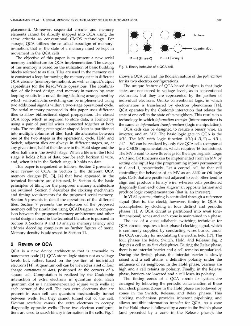
QCA is a new device architecture that is amenable tonanometer scale [1]. QCA stores logic states not as voltagelevels but, rather, based on the position of individualelectrons [14]. A quantum cell can be viewed as a set of fourcharge containers or dots, positioned at the corners of asquare cell. Computation is realized by the Coulombicinteraction of extra electrons in quantum dots. Eachquantum dot is a nanometer-scaled square with wells ateach corner of the cell. The two extra electrons that arepresent in each cell can quantum mechanically tunnelbetween wells, but they cannot tunnel out of the cell.Electron repulsion causes the extra electrons to occupydiagonally opposite wells. These two electron configura-tions are used to encode binary information in the cells. Fig. 1
shows a QCA cell and the Boolean nature of the polarizationfor its two electron configurations.
The unique feature of QCA-based designs is that logicstates are not stored in voltage levels, as in conventionalelectronics, but they are represented by the position ofindividual electrons. Unlike conventional logic, in whichinformation is transferred by electron phenomena [14],QCA operates by the Coulomb interaction that relates thestate of one cell to the state of its neighbors. This results in atechnology in which information transfer (interconnection) isthe same as information transformation (logic manipulation).
QCA cells can be designed to realize a binary wire, aninverter, and an MV . The basic logic gate in QCA is theMV . The MV with logic function MV ðA;B;CÞ ¼ ABþAC þBC can be realized by only five QCA cells (comparedto a CMOS implementation, which requires 16 transistors).The MV is said to have three legs for the input signals. LogicAND and OR functions can be implemented from an MV bysetting one input leg (the programming input) permanentlyto 0 and 1, respectively. Let a control cell be that cellcontrolling the behavior of an MV as an AND or OR logicgate. Cells that are positioned adjacent to each other tend toalign and produce a binary wire, whereas cells positioneddiagonally from each other align in an opposite fashion andproduce logic complementation (that is, an inverter).
In VLSI systems, timing is controlled through a referencesignal (that is, the clock); however, timing in QCA isaccomplished by clocking in four distinct and periodicphases [1]. A QCA circuit is partitioned into serial (one-dimensional) zones and each zone is maintained in a phase.
The use of a quasi-adiabatic switching technique forQCA circuits requires a four-phased clocking signal, whichis commonly supplied by conducting wires buried underthe QCA circuitry for modulating the electric field [17]. Thefour phases are Relax, Switch, Hold, and Release. Fig. 2depicts a cell in its four clock phases. During the Relax phase,there is no interdot barrier and a cell remains unpolarized.During the Switch phase, the interdot barrier is slowlyraised and a cell attains a definitive polarity under theinfluence of its neighbors. In the Hold phase, barriers arehigh and a cell retains its polarity. Finally, in the Releasephase, barriers are lowered and a cell loses its polarity.
The timing zones of a QCA circuit or system arearranged by following the periodic concatenation of thesefour clock phases. Zones in the Hold phase are followed byzones in the Switch, Release, and Relax phases. Thisclocking mechanism provides inherent pipelining andallows multibit information transfer for QCA. As a zonein the Hold phase is followed by a zone in the Switch phase(and preceded by a zone in the Release phase), the
VANKAMAMIDI ET AL.: A SERIAL MEMORY BY QUANTUM-DOT CELLULAR AUTOMATA (QCA) 607
Fig. 1. Binary behavior of a QCA cell.
computation in QCA is strictly one-dimensional (that is,unidirectional and consistent with signal propagation).
Currently, QCA circuits and systems follow the clockingzone partition scheme in [1]. Designs are partitioned intomultiple clocking zones only along one dimension (say, thex-axis), thus effectively creating columns (as zones). Clockingand pipelining require designs to maintain sets of fouradjacent zones at any time (as according to the four phases,that is, Switch, Hold, Release, and Relax). For the fourphases, clocking to a zone (and the design as a whole) isapplied through an underlying clocking circuitry by asignal, as shown in Fig. 3 [9]. Such a signal generates therequired electric field to modulate the tunneling barrier ofall cells in the zone (adiabatic switching). To maintain zonesin sets of four phases, four conducting wires (carrying thesignal in Fig. 3) are required. Each clock has a phase that isshifted by �
2 .
3 QCA AND MEMORIES
As a nanotechnology, QCA has been advocated for high-density memories. QCA offers many features for designingmemories, such as regularity, fast switching, and lowpower. A straightforward approach to implement amemory by QCA is to maintain a cell (or a clocking zone)in the Hold phase as long as its value must be retained forstorage. The main problem with this approach is therequirement of an explicit control of the clock signal fromthe memory decoder (which is implemented in QCA). Thisis not viable because it causes problems in timing and asignificant increase in the complexity of the underlyingcircuitry (as interface to CMOS). For a truly QCA-basedimplementation, it is well known that memory must be keptin motion, that is, the memory state has to be continuouslymoved through a set of QCA cells (such as those connectedin a loop).
Traditionally, it is possible to distinguish two types ofmemory architectures: parallel and serial architectures.Table 1 summarizes the comparison of parallel and serialQCA memory architectures. For a parallel architecture, theone-bit-per-memory cell feature reduces latency, but theduplication of the Read/Write circuitry for each memorybit, the higher counts (QCA cell, Control cell, and Clocking
zone), and the more complex clocking circuitry result in afaster operation at a reduced density.
The most obvious advantage of a serial over a parallelarchitecture is with respect to hardware; in a parallelarchitecture, each bit stored in the memory requires aseparate Read/Write circuitry. In QCA, the Read/Writecircuitry is more complex (requiring multiple logic gates)than a QCA wire loop (for actually storing the data bit).Therefore, compared to a serial design in which a singleRead/Write circuit is shared between multiple bits of data(as stored in each QCA loop), a parallel design requires ahigher number of QCA and control cells. Moreover, theRead/Write circuitry must be partitioned into multipleclocking zones, which causes the number of clocking zonesand the complexity of the underlying clocking circuitry toincrease. Parallel designs also encounter problems withsynchronization and coordination of the clock phases ofdifferent Read/Write circuits with the Control/Selectsignals that are transferred to a common QCA line.
Many QCA memory designs have been proposed in thetechnical literature. Researchers at Notre Dame Universityhave introduced the H-Memory architecture [4], whosemain objectives are high density and uniform access time.The H-Memory is a complete binary tree structure withcontrol circuitry at each node. As the memory spirals at theleaf nodes, an integration of logic and memory is accom-plished in the layout, even though, logically (as encoun-tered in conventional designs), control circuitry and storageare separate. Fig. 4a shows this spiral architecture. How-ever, unlike conventional designs, the control and data bitsare serialized. The bitstream enters the memory structure atthe root node and traverses down the tree by utilizing onecontrol bit for routing at every node in the path. Thearchitectural choice of dealing with serial bitstreams alsoresults in a complex control logic. The router at eachinternal node has 10 gates and six feedback loops; each looprequires four clocking zones for its implementation. Thecircuitry at the leaf nodes (that is, the memory cells)requires 11 gates per node. Also, the memory cell at eachleaf node is a spiral, allowing the storage of several bits
608 IEEE TRANSACTIONS ON COMPUTERS, VOL. 57, NO. 5, MAY 2008
Fig. 2. QCA clock phases.
Fig. 3. Four-phased signal for clocking zones in QCA, adiabatic
switching.
TABLE 1Comparison of Parallel and Serial QCA Memory Architectures

while sharing clocking zones between multiple concentricloops. In this design, the memory size and the cell count ateach spiral do not have a linear relationship; each outer loophas an increasing diameter, thus requiring more cells toimplement (although its storage capacity remains constant).
Berzon and Fountain [3] made an early attempt to designa QCA memory using the so-called SQUARES formalism.The basic principle of this technique is to define a set ofequally sized blocks, each performing a basic function inQCA (such as logic or interconnect). The basic blocks canthen be tiled together to design more complex QCA circuits.The obvious advantage of this technique is the ease in thegeometric layout; also, such formalism allows a design to bemodular such that the tiles (blocks) are effectively con-sidered as black boxes. However, as all blocks are of thesame size (in SQUARES, a 5� 5 grid), an unutilized areaappears in each block, thus causing spatial redundancy andlower density in the overall design. This results in a serialmemory architecture (shown in Fig. 4b) in which eachmemory cell consists of a QCA wire connected as a loop.The wire is divided into clocking zones whose number isfour times the number of bits stored in the loop. Even for amodest memory size, this results in a large number ofzones, thus requiring a considerable amount of clockingcircuitry for the signals. Finally, additional control circuitry(such as comparators) must be utilized to make the memorybit addressable. This results in a quite high hardwareoverhead per memory cell.
Walus et al. [5] proposed a conventional parallel memoryarchitecture (such as that encountered in CMOS-basedRAM design) for QCA, that is, by storing 1 bit at eachmemory cell. The single-bit memory cells allow the designof a simple Read/Write circuitry; each memory cell isimplemented using 158 QCA cells and the Select signals areseparately generated using decoders. This approach has thesame disadvantage as in [3]; as data in each memory cell isstored using a closed QCA wire loop partitioned into fourclocking zones, it needs a large number of clocking zones,thus complicating the underlying circuitry for clocking (thedimensions of the clocking zones for the memory loop aresmall, that is, a QCA wire with fewer than 10 cells).
However, the dimensions of the conducting wire distribut-ing the clock is at least an order of magnitude higher, thusmaking the clocking of such small zones very difficult if notinfeasible. Also, this memory architecture does not exploitfull parallelism in its operation: Unlike CMOS designs, theSelect signal in QCA takes multiple clock cycles to propagateand does not simultaneously reach all cells in a row, that is,bits in the same row are read at different clock cycles.
In the single-bit memory design introduced in [18], eachQCA line for a memory cell spans three clocking zones, asrequired to retain its memory value. By increasing thelength of the QCA wire over a number of zones (in anumber given by a multiple of three), more than 1 bit ofdata can be stored in the wire. The principle of memory-in-motion is kept within a single-bit design by transferring thestored value back and forth within the clocking zones.During the Read cycle, multiple bits in a line must betransferred to one end of the wire for output; however,there is no feedback loop to transfer the bits back to thebeginning of the wire; consequently, they can be lost.Therefore, a serial architecture that stores multiple bits ateach memory cell must have a feedback path (such as acontinuous loop).
4 MEMORY DESIGN BY TILING
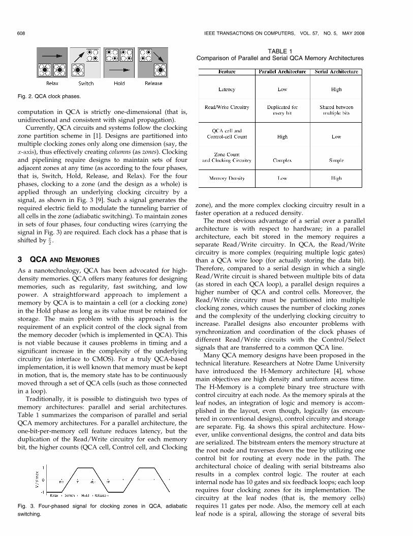
In this section, the basic principles of a novel architecturefor a serial QCA memory are presented. The proposedarchitecture still utilizes the concept of memory-in-motionwithin a QCA loop. Some of the advantages of the proposedserial architecture are the novel QCA design for storing thememory bits and the associated Read/Write controlcircuitry. The proposed design is independent of theaddress decoding logic and can be used with the decodingcircuits proposed for other QCA memory architectures [3],[4], [5]. QCA cells are arranged into simple basic QCAblocks referred to as tiles. Three types of tiles are utilized:1) Internal memory tile (shown in Fig. 5), 2) Output tile(shown in Fig. 6), and 3) Input tile (shown in Fig. 7).
Tiles are connected in a loop using two horizontal wires(referred to as the upper and lower wires) (Fig. 8). Thememory cell in the proposed serial architecture consists oftwo long horizontal QCA wires connected at both of theirends by two short vertical wires, which create a loop for thememory-in-motion implementation. The Input and Outputtiles and related circuits (for the Read and Write operations)are located at opposite sides of the horizontal wires. TheInternal memory tiles are located between the Input andOutput tiles. In this architecture, the loops are stacked, thus
VANKAMAMIDI ET AL.: A SERIAL MEMORY BY QUANTUM-DOT CELLULAR AUTOMATA (QCA) 609
Fig. 4. Serial memory cell architectures. (a) Memory spiral architecture
presented by Frost et al. (b) Memory loop architecture used by Berzon
and Fountain.
Fig. 5. QCA implementation of the Internal memory tile.
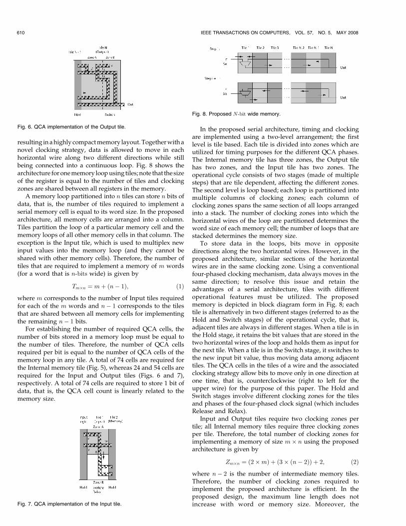
resulting in a highly compact memory layout. Together with anovel clocking strategy, data is allowed to move in eachhorizontal wire along two different directions while stillbeing connected into a continuous loop. Fig. 8 shows thearchitecture for one memory loop using tiles; note that the sizeof the register is equal to the number of tiles and clockingzones are shared between all registers in the memory.
A memory loop partitioned into n tiles can store n bits ofdata, that is, the number of tiles required to implement aserial memory cell is equal to its word size. In the proposedarchitecture, all memory cells are arranged into a column.Tiles partition the loop of a particular memory cell and thememory loops of all other memory cells in that column. Theexception is the Input tile, which is used to multiplex newinput values into the memory loop (and they cannot beshared with other memory cells). Therefore, the number oftiles that are required to implement a memory of m words(for a word that is n-bits wide) is given by
Tm�n ¼ mþ ðn� 1Þ; ð1Þ
where m corresponds to the number of Input tiles requiredfor each of the m words and n� 1 corresponds to the tilesthat are shared between all memory cells for implementingthe remaining n� 1 bits.
For establishing the number of required QCA cells, thenumber of bits stored in a memory loop must be equal tothe number of tiles. Therefore, the number of QCA cellsrequired per bit is equal to the number of QCA cells of thememory loop in any tile. A total of 74 cells are required forthe Internal memory tile (Fig. 5), whereas 24 and 54 cells arerequired for the Input and Output tiles (Figs. 6 and 7),respectively. A total of 74 cells are required to store 1 bit ofdata, that is, the QCA cell count is linearly related to thememory size.
In the proposed serial architecture, timing and clockingare implemented using a two-level arrangement; the firstlevel is tile based. Each tile is divided into zones which areutilized for timing purposes for the different QCA phases.The Internal memory tile has three zones, the Output tilehas two zones, and the Input tile has two zones. Theoperational cycle consists of two stages (made of multiplesteps) that are tile dependent, affecting the different zones.The second level is loop based; each loop is partitioned intomultiple columns of clocking zones; each column ofclocking zones spans the same section of all loops arrangedinto a stack. The number of clocking zones into which thehorizontal wires of the loop are partitioned determines theword size of each memory cell; the number of loops that arestacked determines the memory size.
To store data in the loops, bits move in oppositedirections along the two horizontal wires. However, in theproposed architecture, similar sections of the horizontalwires are in the same clocking zone. Using a conventionalfour-phased clocking mechanism, data always moves in thesame direction; to resolve this issue and retain theadvantages of a serial architecture, tiles with differentoperational features must be utilized. The proposedmemory is depicted in block diagram form in Fig. 8; eachtile is alternatively in two different stages (referred to as theHold and Switch stages) of the operational cycle, that is,adjacent tiles are always in different stages. When a tile is inthe Hold stage, it retains the bit values that are stored in thetwo horizontal wires of the loop and holds them as input forthe next tile. When a tile is in the Switch stage, it switches tothe new input bit value, thus moving data among adjacenttiles. The QCA cells in the tiles of a wire and the associatedclocking strategy allow bits to move only in one direction atone time, that is, counterclockwise (right to left for theupper wire) for the purpose of this paper. The Hold andSwitch stages involve different clocking zones for the tilesand phases of the four-phased clock signal (which includesRelease and Relax).
Input and Output tiles require two clocking zones pertile; all Internal memory tiles require three clocking zonesper tile. Therefore, the total number of clocking zones forimplementing a memory of size m� n using the proposedarchitecture is given by
Zm�n ¼ ð2�mÞ þ ð3� ðn� 2ÞÞ þ 2; ð2Þ
where n� 2 is the number of intermediate memory tiles.Therefore, the number of clocking zones required toimplement the proposed architecture is efficient. In theproposed design, the maximum line length does notincrease with word or memory size. Moreover, the
610 IEEE TRANSACTIONS ON COMPUTERS, VOL. 57, NO. 5, MAY 2008
Fig. 6. QCA implementation of the Output tile.
Fig. 7. QCA implementation of the Input tile.
Fig. 8. Proposed N-bit wide memory.
proposed architecture retains the advantages of single-bitmemory design, whereas clocking zones between allmemory cells are shared, thus reducing the complexity ofthe control circuitry. A serial design has a single Read/Write logic for multiple bits in each memory cell, so, whenthe number of bits per cell increases, the hardwareoverhead per bit is also reduced.
5 CLOCKING AND TIMING
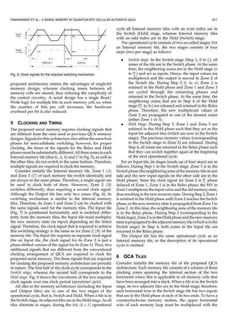
The proposed serial memory requires clocking signals thatare different from the ones used in previous QCA memorydesigns. Signals for this architecture also utilize the same fourphases for semi-adiabatic switching; however, for properclocking, the times of the signals for the Relax and Holdphases must be substantially different. All three zones in eachInternal memory tile (that is,A,B, and C in Fig. 5), as well asthe other tiles, do not switch in the same fashion. Therefore,multiple signals are required to clock the memory.
Consider initially the Internal memory tile. Zone 1 ðAÞand Zone 3 ðCÞ of each memory tile switch identically andare always in the same phase. Therefore, a single signal canbe used to clock both of them. However, Zone 2 ðBÞswitches differently, thus requiring a second clock signal.Although the Output tile has only two zones (Fig. 6), itsswitching mechanism is similar to the Internal memorytiles. Therefore, its Zone 1 and Zone 2 can be clocked withthe same signals used for the memory tiles. The Input tile(Fig. 7) is partitioned horizontally and is switched differ-ently from the memory tiles; the Input tile must multiplexthe new memory state (as input) depending on the Selectsignal. Therefore, the clock signal that is required to achievethis switching strategy is the same as for Zone 2 ðBÞ of thememory tile. The Input tile requires no separate clock signal(for an Input tile, the clock signal for its Zone 2 is just aphase-shifted version of the signal for its Zone 1). Thus, twoadditional signals that are different from the conventionalclocking arrangement of QCA are required to clock theproposed serial memory. The three signals that are requiredfor clocking the proposed memory architecture are periodicin nature. The first half of the clock cycle corresponds to theSwitch stage, whereas the second half corresponds to theHold stage. Fig. 9 shows the waveforms of the two requiredclock signals over one clock period (operational cycle).
All tiles in the memory architecture (including the Inputand Output tiles) are in one of the two stages of theoperational cycle, that is, Switch and Hold. When a tile is inthe Switch stage, its adjacent tiles are in the Hold stage. As alltiles alternate in stages, during the kth ðkþ 1Þ operational
cycle all Internal memory tiles with an even index are inthe Switch (Hold) stage, whereas Internal memory tileswith an odd index are in the Hold (Switch) stage.
The operational cycle consists of two so-called stages. Foran Internal memory tile, the two stages consists of foursteps (two per stage) as follows:
. Switch stage. In the Switch stage (Step 1, 0 to �5 ), all
zones of the tile are in the Switch phase. At the sametime, the neighboring zones are in the Hold stage (�to 6�
5 ) and act as inputs. Hence, the input values aremultiplexed and the output is moved to Zone 2 ofthe Switch tile. During Step 2 (�5 to �), Zone 2 isretained in the Hold phase and Zone 1 and Zone 3are cycled through the remaining phases andreturned to the Switch phase. At the same time, theneighboring zones that are in Step 4 of the Holdstage (6�
5 to 2�) are released and retained in the Relaxphase. Therefore, the new multiplexed values ofZone 2 are propagated to one of the desired zones(either Zone 1 or 3).
. Hold Stage. During Step 3, Zone 1 and Zone 3 areretained in the Hold phase such that they act as theinput for adjacent tiles (which are now in the Switchstage). The previous memory values (correspondingto the Switch stage in Zone 2) are released. DuringStep 4, all zones are returned to the Relax phase suchthat they can switch together again at the beginningof the next operational cycle.
For an Input tile, its stages (made up of four steps) are asfollows: During Step 1 in the Switch stage, Zone 1 is in theSwitch phase (the neighboring zone of the memory tile on oneside and the new input signals on the other side are in theHold phase). Since the clock signal for Zone 2 is 3�
5 phasedelayed of Zone 1, Zone 1 is in the Relax phase; the MV inZone 1 multiplexes the input value and the old memory state,thus resulting in the new memory state. During Step 2, Zone 1is retained in the Hold phase until Zone 2 reaches the Switchphase, so the new memory state is propagated from Zone 1 toZone 2. At this time, the neighboring zone of the memory tileis in the Relax phase. During Step 3 (corresponding to theHold stage), Zone 2 is in the Hold phase and the new memorystate is propagated to the adjacent memory tile (which is in theSwitch stage). In Step 4, both zones in the Input tile arereturned to the Relax phase.
The Output tile has the same operational cycle as anInternal memory tile, so the description of its operationalcycle is omitted.
6 QCA TILES
Consider initially the memory tile of the proposed QCAarchitecture. Each memory tile consists of a column of threeclocking zones spanning the internal section of the twohorizontal wires; this is applicable to all memory cells thathave been arranged into a stack. When a tile is in the Switchstage, its two adjacent tiles are in the Hold stage; therefore,each horizontal wire in the Switch stage tile has two inputsthat are in the Hold phase at each of its two ends. To have acounterclockwise memory motion, the upper horizontalwire of each memory loop must be multiplexed with the
VANKAMAMIDI ET AL.: A SERIAL MEMORY BY QUANTUM-DOT CELLULAR AUTOMATA (QCA) 611
Fig. 9. Clock signals for the required switching mechanism.

two inputs, so it transfers the input from the previous tile(on the right) to the next tile (on the left). As the lowerhorizontal wire is multiplexed, it transfers the input fromthe tile on the left to the tile on the right. This switchingmechanism can be achieved through an MV that function-ally acts as a diode (that is, blocking the movement of data)using the clocking zones available in each tile. This MV isplaced in the clocking zone near the input whose valuemust be dominated (masked) to obtain the unidirectionalmemory motion. The input whose value must be trans-ferred is duplicated and connected to two inputs of the MV,whereas the input whose value must be blocked isconnected to the third input only. Therefore, the two inputvalues are multiplexed by the MV and the output is thedesired value. Using the MV, this new output is forced backto the wire whose input value was blocked. At thebeginning of the Switch stage, the horizontal wires of amemory loop have the two inputs at both ends; however, atthe end of the Switch stage, the wire has only the value ofthe required input.
Fig. 5 shows the QCA circuitry in a memory tile (referredto as the Internal tile or tile i) for the two horizontal wires ofa memory loop. This tile operates over an operational cyclemade up of two steps:
. Step 1. All three clocking zones (A, B, and C) ofmemory tile i in the Switch stage are in the Switchphase, whereas clocking zones of adjacent tiles (i� 1and iþ 1) are in the Hold phase. Therefore, thedesired input that is duplicated and connected totwo inputs of the MV (that is, x and y) is moved tothe output ðz0Þ.
. Step 2. The middle clocking zone of tile i (that is,zone B) of the Switch stage is kept in the Hold phase,whereas the other two zones (A and C) are cycledthrough their phases and returned to the Switchphase. At the same time, the adjacent two tiles (i� 1and iþ 1) are relaxed from their Hold phase.Therefore, the direction of signal propagationchanges; a wire that was previously an output forthe MV now becomes an input and vice versa.However, two wires still remain as inputs to the MV;as the three inputs of the MV have the same signal,the output follows this value. The output is fan out,that is, this signal is duplicated and propagated tothe next tile during the subsequent operational cycle.
By the end of Step 2, all cells of the upper horizontal wirealign to the input from the tile on the right while blockingthe input of the left tile; the lower horizontal wire aligns tothe input from the left tile while blocking the input from theright tile. Thus, in one operational cycle, data in the memoryloop moves by one tile in a counterclockwise direction(right to left). In the next operational cycle, the tile that wasin the Switch stage with new data on the horizontal wires ischanged to the Hold stage and the two adjacent tiles (whichwere in the Hold stage) are changed to the Switch stage,thus enabling further motion of data.
Two additional tiles are required for the input/output ofthe memory loop, as well as connecting the upper andlower horizontal wires.
. The Output tile. The Output tile propagates data in thelower horizontal wire to the output read logic. It alsohas a vertical QCA wire to transfer data to the upperhorizontal wire such that the loop is established.However, when the Output tile switches to accepta signal from the lower horizontal wire (which is inthe Hold stage), the upper horizontal wire is alsoin the Hold stage. Therefore, duplication of thelower horizontal wire (to dominate the upper wire)and an appropriate switching strategy for thememory tiles are required. As the Output tileperforms only one transfer (that is, from the lowerto the upper horizontal wires), it only requires twoclocking zones and one MV.
Fig. 6 shows the QCA implementation of theOutput tile; the operational cycle of the Output tile isthe same as that of the internal memory tile. In Step 1,the MV is switched and, due to the duplication, thesignal of the lower horizontal line dominates and istransferred to the output. In Step 2, the previousoutput line acts as an input and transfers the signalto the upper horizontal wire. Having aligned thesignal on the lower horizontal wire, in the nextoperational cycle, the Output tile alternates to theHold stage and loops the signal to the upperhorizontal wire.
. The Input tile. The Input tile has a vertical wire toconnect the two horizontal wires; this transfers thesignal between them such that the memory loop isconstructed at the other end too. However, it isdifferent from the Output tile because, prior totransferring data, the old memory state has to bemultiplexed with the input data based on the Writecontrol signal for acquiring the new memory state.Multiplexing is achieved through an MV, as shownpreviously. However, the Input tile can be affected ifno horizontal partitioning is implemented for tim-ing. The implementation of the Input tile is shown inFig. 7. Since the tile is horizontally partitioned intotwo clocking zones (upper and lower), they cannotbe shared with other memory loops. The function-ality of the Input tile over one operational cycle isalso given by a two-step process:
1. Step 1. The lower clocking zone of the Input tileis in the Relax phase; the upper clocking zone isin the Switch phase. Its two inputs (from thememory tile on one side and the Write circuitryon the other side) are in the Hold phase. Hence,the output of the MV in the top zone switches tothe new memory state as input value.
2. Step 2. The upper clocking zone is kept in theHold phase and the lower zone is in the Switchphase (while keeping the adjacent memory tilein the Relax phase). Therefore, the new memoryvalue is propagated to the QCA wire connectedto the lower horizontal wire. In the nextoperational cycle, the Input tile is in the Holdstage and the new memory value is moved backto the memory tile, which is changed to theSwitch stage.
612 IEEE TRANSACTIONS ON COMPUTERS, VOL. 57, NO. 5, MAY 2008
As an Input tile must implement the logic to
multiplex between the old memory value and the
new input value, it requires two separate clocking
zones.
7 SIMULATION
QCADesigner [16] provides a design and simulation
environment for QCA circuits; it has multiple simulation
engines and CAD capabilities. This tool has been used to
verify the design of the proposed QCA memory cell. A
QCA memory loop that consists of an Input tile, one
Internal memory tile (1 bit), and an Output tile (Fig. 10) was
assembled. As the Input and Output tiles store 1 bit each
and the Internal memory tile stores 2 bits, the size of the
memory cell in Fig. 10 is 4 bits. Simulation has been
performed using the bistable engine of QCADesigner with a
cell dimension of 18 nm and a dot size of 5 nm. However,
QCADesigner does not support the clocking scheme and
clock zone partitioning of the proposed memory cell;
therefore, minor adjustments (mostly of a functional nature)
were implemented to establish compatibility with this CAD
tool. The proposed QCA memory cell has been evaluated
and simulated for logic and clocking (timing) verification.
In both cases, minor modifications were required; these
modifications are introduced only for compatibility with
QCADesigner, that is, the modified memory circuit/clock-
ing is isomorphic to the proposed circuit/clocking scheme,
as presented in the previous sections.For logic verification, Fig. 11 shows the simulation results
for the memory cell; the phase of the output waveform is
shifted by two clock cycles with wraparound (that is, the
output waveform for clock cycles 7 and 8 is shown in clock
cycles 1 and 2 too). During the first four clock cycles, the
output is determined only by the two inputs that are
connected to the two legs of the MV in the Input tile; the
third leg of this MV is not connected because it takes four
cycles for the first bit to loop through the memory cell.
Therefore, during this period the MV behaves as an AND
gate. For the next four clock cycles (labeled five through
eight in the waveform diagrams), all three legs of the MV
are connected (active) and the MV inputs are 000, 010, 100,
and 111. Hence, this will result in a majority function with
an output of the same value as during the first four clock
cycles. As observed in the simulation results, the QCA
circuit behaves as expected, that is, data is looped in a
correct manner through the tiles.
For the timing verification of the QCA memory cell, aslight modification to the clocking strategy must beperformed because QCADesigner only provides the cap-ability of clocking circuits using a conventional four-phasedclock signal, as shown previously in Fig. 3. This limitingfeature is also found in other CAD tools for QCA, such asAQUINAS [17]. In the proposed clocking strategy, theclocking zones next to a zone in the Switch phase must be inthe Hold phase so that all three legs of the MV can bedriven. To simulate this feature, the arrangement shown inFig. 12 was utilized. The third leg of each MV in the Internalmemory and Output tiles is permanently set to a value andplaced in the same clock phase as the other two legs of theMV. The value of this third leg is dominated by theduplicated value on the other two legs and the resultingoutput of the MV is propagated through the memory loop.Thus, the counterclockwise motion of data as required bythe proposed clocking strategy is still achieved within thememory loop. This modified memory cell has beensimulated using QCADesigner with the above-mentionedconfiguration; the resulting waveforms are the same as thememory cell design (shown previously in Figs. 10 and 11).
8 COMPARISON
In this section, an analysis is pursued to compare theproposed serial memory with other serial memories foundin the technical literature [3], [4]. The serial QCA memoryarchitecture in [4] uses a spiral (squared shaped) that loopsback to itself for storing data. The main advantage of aspiral over a loop is that the sections of each layer of thespiral can be in the same clocking zone. Even though theword size of each memory cell is increased by adding extralayers, the number of clocking zones is not increased. As
VANKAMAMIDI ET AL.: A SERIAL MEMORY BY QUANTUM-DOT CELLULAR AUTOMATA (QCA) 613
Fig. 10. Design of the proposed memory cell for a simulation by
QCADesigner (logic verification).
Fig. 11. Simulation waveforms for the proposed memory cell (logic and
timing verification).
Fig. 12. Design of the proposed memory cell for simulation by
QCADesigner (timing verification).

clocking zones span multiple layers, their dimensions aresufficiently large to be clocked by the underlying wires.However, the spiral architecture in [4] has some inherentdrawbacks. As the word size at each memory cell isincreased by adding layers, the number of QCA cells forimplementing them increases, that is, the number of QCAcells required per data bit is not constant and depends onthe word size at each memory cell.
The problem of increasing the QCA cell count foradditional layers leads to another drawback, that is, thenumber of clocking zones into which the memory spiral ispartitioned is constant. Therefore, as the dimensions of eachadditional layer increases, their length in some clockingzones (corners) also increases. This could be a significantproblem because the probability of kink occurrence in-creases with the maximum line length of a clocking zone. Toavoid kinks, the switching frequency must be reduced tooto ensure that the QCA cells remain in the ground state.
The first significant difference between the memoryspiral [4] and the tile-based memory proposed in this paperis that the memory spiral shares clocking zones within amemory cell and, hence, it is independent of word size. Inthe memory presented in this paper, clocking zones areshared between different memory cells, so this scheme isindependent of memory size (that is, the number of words),but it depends on the word size. As the number of memorycells is usually much larger than the number of bits in eachcell, then the proposed architecture provides a betterarrangement for the number of clocking zones required fortiming a QCA memory. The SQUARES technique in [3] is alsoevaluated and compared. The modular design of thistechnique is different from the tiling proposed in this paper;the basic block in [3] is designed to improve different QCAfunctionalities. In SQUARES, the number of clocking zones isfour times the number of bits stored in memory and thenumber of QCA cells (per bit) to implement the loop is 20. Thedensity is low because of the complex decoding and controlcircuitry, as well as the low area utilization due to theSQUARES formalism. The tiles of the proposed approach aretailored to memory design and its performance.
Fig. 13 shows the cell count versus word size for the QCAmemories proposed in [4] (Mem Spiral) and [3] (Mem Loop),as well as the design in this paper (Mem Tiles). The linearity ofboth the proposed approach and [3] is evident even though
the Memory Loop [3] requires a small number of cells. Acomparison is also performed with respect to clocking zonecount. Fig. 14 shows the relationship between the clockingzone count and the memory size for the same three QCAarchitectures. In this case, [3] requires the largest number ofzones, thus reducing the switching speed of the QCAmemory, whereas the proposed scheme needs the least.
For QCA designs, the logic-level effects caused by theinterference of the electric field from adjacent clocking wiresare a significant issue because QCA cells that are located atthe boundary must be in a clocking zone. This depends onthe strength of the electric field in the adjacent clockingwires [9]. In [9], wave clocking was first introduced suchthat circuits can be designed with QCA cells at clockingzone boundaries with no modification in logic functionality;these cells must belong to either of the clocking zones totolerate the interference in the electric fields [19].
9 LATENCY CONSIDERATIONS
By the memory-in-motion paradigm, storage is implemen-ted in QCA by continuously moving bits in a loop. In serialarchitectures, multiple bits are stored in each loop. Eachmemory loop is associated with a single Read/Write logiccircuitry. When the first bit of a memory word reaches thiscircuitry, the memory operation can be performed, that is,bits in the loop can be read and transferred to an output lineor new input bits can be written into the loop. However, ifthe first bit passes the Read/Write circuitry, then a delay isincurred to account for cycling through the loop andreturning it back to the Read/Write circuitry. On average,this delay (generally referred to as memory latency) is equalto half the time required to complete one revolutionthrough the loop. However, the time required to passthrough the loop depends on the loop size, which is afunction of the number of stored bits (that is, the word size).Therefore, the word size of a memory cell must be small toreduce latency.
The serial architecture presented in this paper is only wordaddressable (although, with additional circuitry, the indivi-dual bits of a word in each memory loop could also be madeaddressable). Memory latency is incurred only for the first bitof the word, that is, all subsequent bits are accessed insuccessive clock cycles with no latency. However, the serial
614 IEEE TRANSACTIONS ON COMPUTERS, VOL. 57, NO. 5, MAY 2008
Fig. 13. QCA cell count versus word size. Fig. 14. Clocking zone count versus memory size.
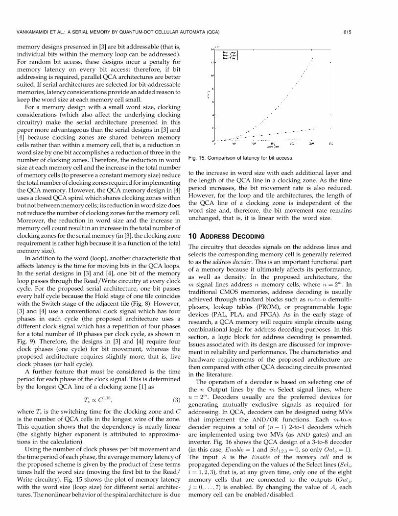
memory designs presented in [3] are bit addressable (that is,individual bits within the memory loop can be addressed).For random bit access, these designs incur a penalty formemory latency on every bit access; therefore, if bitaddressing is required, parallel QCA architectures are bettersuited. If serial architectures are selected for bit-addressablememories, latency considerations provide an added reason tokeep the word size at each memory cell small.
For a memory design with a small word size, clockingconsiderations (which also affect the underlying clockingcircuitry) make the serial architecture presented in thispaper more advantageous than the serial designs in [3] and[4] because clocking zones are shared between memorycells rather than within a memory cell, that is, a reduction inword size by one bit accomplishes a reduction of three in thenumber of clocking zones. Therefore, the reduction in wordsize at each memory cell and the increase in the total numberof memory cells (to preserve a constant memory size) reducethe total number of clocking zones required for implementingthe QCA memory. However, the QCA memory design in [4]uses a closed QCA spiral which shares clocking zones withinbut not between memory cells; its reduction in word size doesnot reduce the number of clocking zones for the memory cell.Moreover, the reduction in word size and the increase inmemory cell count result in an increase in the total number ofclocking zones for the serial memory (in [3], the clocking zonerequirement is rather high because it is a function of the totalmemory size).
In addition to the word (loop), another characteristic thataffects latency is the time for moving bits in the QCA loops.In the serial designs in [3] and [4], one bit of the memoryloop passes through the Read/Write circuitry at every clockcycle. For the proposed serial architecture, one bit passesevery half cycle because the Hold stage of one tile coincideswith the Switch stage of the adjacent tile (Fig. 8). However,[3] and [4] use a conventional clock signal which has fourphases in each cycle (the proposed architecture uses adifferent clock signal which has a repetition of four phasesfor a total number of 10 phases per clock cycle, as shown inFig. 9). Therefore, the designs in [3] and [4] require fourclock phases (one cycle) for bit movement, whereas theproposed architecture requires slightly more, that is, fiveclock phases (or half cycle).
A further feature that must be considered is the timeperiod for each phase of the clock signal. This is determinedby the longest QCA line of a clocking zone [1] as
Ts / C1:16; ð3Þ
where Ts is the switching time for the clocking zone and Cis the number of QCA cells in the longest wire of the zone.This equation shows that the dependency is nearly linear(the slightly higher exponent is attributed to approxima-tions in the calculation).
Using the number of clock phases per bit movement andthe time period of each phase, the average memory latency ofthe proposed scheme is given by the product of these termstimes half the word size (moving the first bit to the Read/Write circuitry). Fig. 15 shows the plot of memory latencywith the word size (loop size) for different serial architec-tures. The nonlinear behavior of the spiral architecture is due
to the increase in word size with each additional layer andthe length of the QCA line in a clocking zone. As the timeperiod increases, the bit movement rate is also reduced.However, for the loop and tile architectures, the length ofthe QCA line of a clocking zone is independent of theword size and, therefore, the bit movement rate remainsunchanged, that is, it is linear with the word size.
10 ADDRESS DECODING
The circuitry that decodes signals on the address lines andselects the corresponding memory cell is generally referredto as the address decoder. This is an important functional partof a memory because it ultimately affects its performance,as well as density. In the proposed architecture, them signal lines address n memory cells, where n ¼ 2m. Intraditional CMOS memories, address decoding is usuallyachieved through standard blocks such as m-to-n demulti-plexers, lookup tables (PROM), or programmable logicdevices (PAL, PLA, and FPGA). As in the early stage ofresearch, a QCA memory will require simple circuits usingcombinational logic for address decoding purposes. In thissection, a logic block for address decoding is presented.Issues associated with its design are discussed for improve-ment in reliability and performance. The characteristics andhardware requirements of the proposed architecture arethen compared with other QCA decoding circuits presentedin the literature.
The operation of a decoder is based on selecting one ofthe n Output lines by the m Select signal lines, wheren ¼ 2m. Decoders usually are the preferred devices forgenerating mutually exclusive signals as required foraddressing. In QCA, decoders can be designed using MVsthat implement the AND/OR functions. Each m-to-ndecoder requires a total of ðn� 1Þ 2-to-1 decoders whichare implemented using two MVs (as AND gates) and aninverter. Fig. 16 shows the QCA design of a 3-to-8 decoder(in this case, Enable ¼ 1 and Sel1;2;3 ¼ 0, so only Outo ¼ 1).The input A is the Enable of the memory cell and ispropagated depending on the values of the Select lines (Seli,i ¼ 1; 2; 3), that is, at any given time, only one of the eightmemory cells that are connected to the outputs (Outj,j ¼ 0; . . . ; 7) is enabled. By changing the value of A, eachmemory cell can be enabled/disabled.
VANKAMAMIDI ET AL.: A SERIAL MEMORY BY QUANTUM-DOT CELLULAR AUTOMATA (QCA) 615
Fig. 15. Comparison of latency for bit access.

A further issue that must be considered for addressdecoding is the synchronization between accessing the
memory cell and the operational cycle. The memory cyclefor parallel and serial designs consists of multiple conven-
tional (four-phased, equally timed) QCA clocking cycles.Although the operational cycle of a parallel architectureconsists of two QCA clocking cycles, for a serial architec-
ture, the operational cycle is made of multiple QCAclocking cycles depending on the number of bits stored in
each memory cell.The Control signals for the cells must be asserted and valid
during the first clock cycle of the operational cycle of the
memory when the bit (which is stored in the memory cell)reaches the input clocking zone. For a serial architecture, theControl signals must only be asserted during the first clock
cycle, when the start bit reaches the Input tile. If the signals areasserted in the middle of the memory cycle, the value on the
input line could be written at an arbitrary position of the loop,thus corrupting the data in the memory cell.
Using address decoders, synchronization can be accom-
plished with relative ease by using a counter at its input. Ifthe input of the decoder is enabled, then the Control signalsto the addressed memory cell are effectively asserted; if the
input is disabled, the Control signals to all memory cells(including the addressed cell) are not asserted. A counter
(with a count equal to the number of QCA clocking cycles inthe operational cycle of the memory) can be used to enable
the decoder input at the correct time, that is, the signals atthe memory cell are asserted only at the beginning of thememory cycle. Thus, only a single counter is required to
maintain synchronization for all memory cells.The proposed circuitry can be compared with previous
works. Walus et al. [5], for example, use separate decoding
logic for each row of the memory cells in a row-addressedtwo-dimensional architecture. A memory with N rows that
is addressed by M (where M ¼ log2N) address lines wouldtherefore require N M-to-1 decoders. As each decoderrequires M � 1 two-input gates (for AND and OR), the total
number of QCA gates (or MV) required to address theN locations using this decoding scheme is
GM�to�1 ¼ N � ðM � 1Þ ¼ 2M � ðM � 1Þ: ð4Þ
The use of separate decoding to address each location(row) has an advantage in terms of latency. As it involvesN M-to-1 decoders (connected in parallel), the latency inaddress decoding is only equal to that of an M-to-1 decoder(which requires signal propagation through log2M levels oftwo-input gates). So,
LM�to�1 ¼ log2M: ð5Þ
The decoding logic presented in this paper uses a singleM-to-N decoder that propagates the Select signal to one ofthe N locations (based on the signals in the M addresslines). The hardware requirements for this architecture areconsiderably lower than that in [5], which uses a separatecircuit for each of the N locations. The total number of two-input QCA gates (or MVs) required for the proposeddecoding scheme is
GM�to�N ¼ 2Mþ1 � 2: ð6Þ
However, as a single block is used for decoding theaddresses of all N memory locations, the latency is alsoincreased. As latency is related to the number of levels oftwo-input QCA gates (required for signal propagation tocomplete the decoding process by using the M-to-Ndecoder), the latency is given by
LM�to�N ¼M: ð7Þ
Therefore, the proposed decoding circuit requires sig-nificantly less hardware for implementation, thus accom-plishing a higher density (albeit requiring additional clockcycles).
For comparison, consider next the memory architecturein [4]. The H-memory structure in [4] uses a differentapproach for QCA signal propagation because it exploitsmicrolevel pipelining in QCA wires. In previously pre-sented designs, each bit of the memory address space istransferred through a different QCA line, similarly toCMOS designs. Therefore, the decoding circuits of CMOScan be readily adapted to QCA. In the H-memory, theaddress and data bits are serialized and transferred througha single QCA wire; hence, the decoding circuitry issubstantially different. The H-memory is a complete binarytree, with memory cells at the leaf nodes and decoding logicat the root and all other internal nodes. As the address anddata bits enter the structure at the root node and dependingon the address value, data bits are routed to a particularmemory cell; therefore, one address bit is needed formaking a decision at each node.
In another serial architecture, the decoding circuitryeffectively implements a binary tree with simple QCA logicgates at each node, that is, one two-input gate in the case ofthe M-to-1 decoder [5] and two gates for the M-to-Ndecoder. In the H-memory, as the address is serialized, theQCA circuitry at each node is complicated; a total of sixQCA gates are required with multiple feedback loops.Therefore, the number of QCA gates (that is, MVs) requiredfor decoding the M-bit address for the N memory cell spaceis given by
GM�to�N ¼ 6� ð2M � 1Þ: ð8Þ
616 IEEE TRANSACTIONS ON COMPUTERS, VOL. 57, NO. 5, MAY 2008
Fig. 16. The 3-to-8 QCA decoder under the one-dimensional clocking
scheme.

Latency in decoding is also increased: Although thenumber of levels of the nodes is the same as in previousdecoding designs, the complexity and computation at eachnode are high (in previous designs, the signal must passthrough a single QCA gate at each level). Therefore, thelatency in memory address decoding is also high.
11 MEMORY DENSITY
Fig. 17 shows the projected memory densities for DRAMusing CMOS technology and for serial memory architec-tures using QCA technology. DRAM density projections areobtained from [13]. When calculating QCA memorydensities, cell sizes in the range of 1 nm up to 10 nm areassumed (through either molecular or metallic implementa-tions). The memory spiral architecture in [4] requires anarea of 15d� 15d QCA cells per memory cell, whereas thearchitecture proposed in this paper takes an area of 18:5d�18:5d QCA cells (where d is the interdot distance). The arearequirements per bit are calculated for a memory of size 256with 12-bit words (inclusive of input/output and decodingcircuitry). For decoding, the spiral memory architecture usesrouter cells [4], whereas the proposed tile-based architectureuses the decoder presented in a previous section.
The memory architecture designed using the SQUARESformalism [5] exhibits a relatively low density. It requires anarea of 32d� 32d QCA cells. This low density occursbecause, even though the number of QCA cells forimplementing the memory loop is small, there is still asubstantial amount of wasted area (the goal of SQUARES isto simplify the engineering design process using uniformlysized logic blocks; it has been shown that, in each block, thewasted area accounts for more than 50 percent); moreover,the feature of making data in each loop bit addressableresults in complex control and decoding circuits.
In Fig. 17, it can be observed that the proposed serialQCA memory architecture, even with metal-dot implemen-tations (at a cell size of 10 nm), allows memory densitiesthat can only be matched after some years by usingconventional CMOS technology. For molecular implemen-tations (at a 1 nm range), QCA memory architectures offerincredible densities, placing them well above the range ofCMOS technology.
12 CONCLUSIONS
This paper has proposed a novel serial memory architecture
for QCA implementation. This architecture is based on
utilizing new building blocks (referred to as tiles) in the
storage and input/output circuitry of the memory. The
QCA paradigm of memory-in-motion has been accom-
plished using a novel arrangement in the storage loop and
timing/clocking; a three-zone memory tile has been
proposed by which information is moved across a con-
catenation of tiles by utilizing a two-level clocking
mechanism. In the proposed memory, clocking zones are
shared between memory cells and the length of the QCA
line of a clocking zone is independent of the word size.
QCA circuits for address decoding and input/output for
simplification of the Read/Write operations have been
discussed in detail. An extensive comparison of the
proposed architecture and previous QCA serial memories
has been pursued in terms of latency, timing, clocking
requirements, and hardware complexity. This analysis has
shown that the proposed memory architecture is readily
applicable to QCA implementation and provides excellent
figures of merit compared with other QCA-based serial
memories.
REFERENCES
[1] C.S. Lent and P.D. Tougaw, “A Device Architecture for Comput-ing with Quantum Dots,” Proc. IEEE, vol. 85, pp. 541-557, 1997.
[2] M.T. Niemier and P.M. Kogge, “Problems in Designing withQCAs: Layout=Timing,” Int’l J. Circuit Theory and Applications,vol. 29, no. 1, pp. 49-62, 2001.
[3] D. Berzon and T.J. Fountain, “A Memory Design in QCAs Usingthe SQUARES Formalism,” Proc. Ninth Great Lakes Symp. VLSI,pp. 168-172, 1999.
[4] S.E. Frost, A.F. Rodrigues, A.W. Janiszewski, R.T. Rausch, andP.M. Kogge, “Memory in Motion: A Study of Storage Structures inQCA,” Proc. First Workshop Non-Silicon Computation, 2002.
[5] K. Walus, A. Vetteth, G.A. Jullien, and V.S. Dimitrov, “RAMDesign Using Quantum-Dot Cellular Automata,” Technical Proc.Nanotechnology Conf. and Trade Show, vol. 2, pp. 160-163, 2003.
[6] M.T. Niemier, A.F. Rodrigues, and P.M. Kogge, “A PotentiallyImplementable FPGA for Quantum Dot Cellular Automata,” Proc.First Workshop Non-Silicon Computation, 2002.
[7] M. Lieberman, S. Chellamma, B. Varughese, Y. Wang, C.S. Lent,G.H. Bernstein, G. Snider, and F. Peiris, “Quantum-Dot CellularAutomata at a Molecular Scale,” Annals of the New York Academy ofSciences, vol. 960, pp. 225-239, 2002.
[8] C.S. Lent, P.D. Tougaw, and W. Porod, “Quantum CellularAutomata: The Physics of Computing with Arrays of QuantumDot Molecules,” Proc. Workshop Physics and Computation, 1994.
[9] K. Hennessy and C.S. Lent, “Clocking of Molecular Quantum-DotCellular Automata,” J. Vacuum Science and Technology B, vol. 19,no. 5, pp. 1752-1755, 2001.
[10] I. Amlani, A.O. Orlov, G. Toth, C.S. Lent, G.H. Bernstein, and G.L.Snider, “Digital Logic Gate Using Quantum-Dot Cellular Auto-mata,” Science, vol. 284, no. 5412, pp. 289-291.
[11] S.E. Frost, A.F. Rodrigues, A.W. Janiszewski, R.T. Rausch, andP.M. Kogge, “Memory in Motion: A Study of Storage Structures inQCA,” Proc. First Workshop Non-Silicon Computation, 2002.
[12] A.O. Orlov, I. Amlani, G.H. Bernstein, C.S. Lent, and G.L. Snider,“Realization of a Functional Cell for Quantum-Dot CellularAutomata,” Science, vol. 277, pp. 928-930, 1997.
[13] R. Compano, L. Molenkamp, and D.J. Paul, “Technology Road-map for Nanoelectronics,” European Commission IST Programme,Future and Emerging Technologies, 2000.
[14] P.D. Tougaw and C.S. Lent, “Logical Devices Implemented UsingQuantum Cellular Automata,” J. Applied Physics, vol. 75, no. 3,pp. 1818-1825, 1994.
VANKAMAMIDI ET AL.: A SERIAL MEMORY BY QUANTUM-DOT CELLULAR AUTOMATA (QCA) 617
Fig. 17. Density comparisons of CMOS/QCA serial memory architec-
tures (projected).
[15] K. Walus, A. Vetteth, G.A. Jullien, and V.S. Dimitrov, “RAMDesign Using Quantum-Dot Cellular Automata,” Technical Proc.Nanotechnology Conf. and Trade Show, vol. 2, pp. 160-163, 2003.
[16] K. Walus QCADesigner Homepage, ATIPS Laboratory, Univ. ofCalgary, Canada, http://www.qcadesigner.ca/index.html, 2004.
[17] E.P. Blair and C.S. Lent, “An Architecture for MolecularComputing Using Quantum-Dot Cellular Automata,” Proc. ThirdIEEE Conf. Nanotechnology, vol. 1, pp. 12-14, 2003.
[18] V. Vankamamidi, M. Ottavi, and F. Lombardi, “A Line-BasedParallel Memory for QCA Implementation,” IEEE Trans. Nano-technology, vol. 4, no. 6, pp. 690-698, Nov. 2005.
[19] V. Vankamamidi, M. Ottavi, and F. Lombardi, “Clocking and CellPlacement for QCA,” Proc. Sixth IEEE Conf. Nanotechnology, vol. 1,pp. 343-346, June 2006.
Vamsi Vankamamidi received the BS degree incomputer engineering from the University ofMumbai, India, in 2000 and the MS degree inelectrical engineering and computer sciencefrom the University of Toledo, Ohio, in 2001.He is currently working toward the PhD degreein computer engineering at Northeastern Uni-versity, Boston. As part of his dissertation, he isworking on quantum-dot cellular automata(QCA), a nanoscale device architecture to
supersede conventional silicon-based technology. His research inter-ests include the design of nanoscale circuits and systems, electronicdesign automation, defect tolerance, and reliability.
Marco Ottavi received the Laurea degree inelectronic engineering from the University ofRome “La Sapienza,” Rome, in 1999 and thePhD degree in microelectronic and telecommu-nications engineering from the University ofRome “Tor Vergata,” Rome, in 2004. In 2000,he was with the ULISSE Consortium, Rome, asa designer engineer of digital systems for spaceapplications. In 2003, he was a visiting researchassistant with the Electrical and Computer
Engineering Department at Northeastern University, Boston. From2004 to 2007, he was a postdoctoral research associate at NortheasternUniversity and, in 2006, he was a visiting research scholar at SandiaNational Laboratories, Albuquerque, New Mexico. He is currently asenior design engineer with Advanced Micro Devices, Boxborough,Massachusetts. His research interests include yield and reliabilitymodeling, fault-tolerant architectures, and online testing and design ofnanoscale circuits and systems. He is a member of the IEEE.
Fabrizio Lombardi received the BSc (Hons.)degree in electronic engineering from the Uni-versity of Essex, United Kingdom, in 1977 andthe master’s degree in microwaves and modernoptics in 1978, the diploma in microwaveengineering in 1978, and the PhD degree in1982 from University College London, Universityof London. He joined the Microwave ResearchUnit at the University College London in 1977.He is currently the holder of the International
Test Conference (ITC) Endowed Chair Professorship at NortheasternUniversity, Boston. At the same institution, during the period 1998-2004,he served as the chair of the Department of Electrical and ComputerEngineering. Prior to joining Northeastern University, he was a facultymember at Texas Tech University, the University of Colorado, Boulder,and Texas A&M University. His research interests are bio-inspirednanomanufacturing/nanocomputing, VLSI design, testing, and fault/defect tolerance of digital systems. He has extensively published inthese areas and coauthored/edited seven books. Since 1 January 2007,he has been the editor-in-chief of the IEEE Transactions on Computers.He is also an associate editor of IEEE Design and Test magazine andthe ACM Journal of Emerging Technology in Computing Systems. Hehas been the chair of the Committee on “Nanotechnology Devices andSystems” of the Test Technology Technical Council of the IEEE since2003. He was an associate editor from 1996 to 2000 and an associateeditor-in-chief from 2000 to 2006 of the IEEE Transactions onComputers. He was a guest editor of special issues in archival journalsand magazines such as the IEEE Transactions on Computers, IEEETransactions on Instrumentation and Measurement, IEEE Transactionson VLSI, IEEE Micro magazine, and IEEE Design and Test magazine.He has been involved in organizing many international symposia,conferences, and workshops sponsored by professional organizations.He is the founding general chair of the IEEE Symposium on NetworkComputing and Applications. He was a Distinguished Visitor of the IEEEComputer Society twice (1990-1993 and 2001-2004). He has receivedmany professional awards, including the Visiting Fellowship at theBritish Columbia Advanced System Institute, University of Victoria,Canada (1988), two Texas Experimental Engineering Station ResearchFellowships (1991-1992 and 1997-1998), the Halliburton Professorship(1995), the Outstanding Engineering Research Award at NortheasternUniversity (2004), and an International Research Award from theMinistry of Science and Education of Japan (1993-1999). He was therecipient of the 1985/86 Research Initiation Award from the IEEE/Engineering Foundation and a Silver Quill Award from Motorola-Austin(1996). He is a senior member of the IEEE and a member of the IEEEComputer Society.
. For more information on this or any other computing topic,please visit our Digital Library at www.computer.org/publications/dlib.
618 IEEE TRANSACTIONS ON COMPUTERS, VOL. 57, NO. 5, MAY 2008


![[2010] QCA 46 - SUPREME COURT OF QUEENSLAND](https://static.fdokumen.com/doc/165x107/633e96155b37c4f187067990/2010-qca-46-supreme-court-of-queensland.jpg)