
A Low-Power 32 bit Datapath Design - DSpace@MIT
98
A Low-Power 32 bit Datapath Design by Seongmoo Heo Submitted to the Department of Electrical Engineering and Computer Science in partial fulfillment of the requirements for the degree of Master of Science in Electrical Engineering and Computer Science at the MASSACHUSETTS INSTITUTE OF TECHNOLOGY August 2000 @2000 Massachusetts Institute of Technology All rights reserved. Author ....... ,. .................................................. Department of Electrical Engineering and Computer Science August 15, 2000 Certified by ........ .. . ' . ' - - Krste Asanovid Assistant Professor Thesis Supervisor Accepted by .............. ... . .. . ....... ......... . .r C. ....... Arthur C. Smith Chairman, Department Committee on Graduate Students MASSACHUSETTS INSTITUTE OF TECHNOLOGY BARKER OCT 2 3 2000 LIBRARIES
-
Upload
khangminh22 -
Category
Documents
-
view
0 -
download
0
Transcript of A Low-Power 32 bit Datapath Design - DSpace@MIT

A Low-Power 32 bit Datapath Design
by
Seongmoo Heo
Submitted to the Department of Electrical Engineering and Computer Sciencein partial fulfillment of the requirements for the degree of
Master of Science in Electrical Engineering and Computer Science
at the
MASSACHUSETTS INSTITUTE OF TECHNOLOGY
August 2000
@2000 Massachusetts Institute of TechnologyAll rights reserved.
Author ....... ,. ..................................................Department of Electrical Engineering and Computer Science
August 15, 2000
Certified by ........ .. .' . ' - -Krste Asanovid
Assistant ProfessorThesis Supervisor
Accepted by .............. ... . . . . . . . . . . . ......... . .r C. . . . . . . .
Arthur C. SmithChairman, Department Committee on Graduate Students
MASSACHUSETTS INSTITUTEOF TECHNOLOGY
BARKEROCT 2 3 2000
LIBRARIES

2

A Low-Power 32 bit Datapath Design
by
Seongmoo Heo
Submitted to the Department of Electrical Engineering and Computer Scienceon August 15, 2000, in partial fulfillment of the
requirements for the degree ofMaster of Science in Electrical Engineering and Computer Science
Abstract
In this thesis, we design a low-power 32 bit datapath with a five-stage pipeline for a single-issueMIPS RISC microprocessor. We compare various designs of flipflops, latches, and muxesin terms of power, delay, and PDP (Power-Delay Product) since they are the most commonbuilding blocks in the datapath. We develop new precise analytic energy models for flipflops,latches, and muxes.
We develop a new simulation-based energy model, the net-transition energy model, tocalculate energy consumption quickly and accurately. The energy model combines effectivecapacitance values extracted from layout and transition counts obtained from a simulator toestimate energy dissipation. We build a capacitance merging method to extract precise effectivecapacitance values from layouts. Also, we model the short-circuit energy for an inverter.
We custom-design the prototype datapath for a 0.25 pm TSMC process. We show designdecisions on metal allocation, floor planning, and an adder - one of the most important blocksin the datapath. We develop an area-efficient logic unit design. Also, we explore shifter designs- a simple but essential block in the datapath - including our new shifter design, a split logshifter using SPECint95 and Dhrystone benchmarks. We find that the barrel shifter is a betterchoice than any log shifter.
Finally, we analyze the datapath energy consumption using our energy model. We showenergy breakdowns by components and functional blocks. We develop a novel method thatchooses better designs of flipflops and latches in different places of the datapath, based on thedata and clock activities. We also examine the effect of clock gating.
Thesis Supervisor: Krste AsanovidTitle: Assistant Professor
3

4

Acknowledgments
First of all, I'd like to thank my great advisor, Krste Asanovih, deeply for his inspiring advice
and guidance and also for spending a great deal of time and energy for this thesis. He let me
realize how fun research is. I truly thank him for giving me chance to work with him.
I also thank my awesome group mates: Ronny Krashinsky, Mike Zhang, Jessica Tseng,
Mark Hampton, Albert Ma, Luis Villa, and Serhii Zhak for helpful discussions and for helping
with my thesis. In particular, I give special thanks to Ronny Krashinsky for helping me with
English writing. He willingly spent lots of time and energy and made my thesis readable.
I want to thank my sweetheart and also my best buddy, Jieun Yoo, very much for her loving
care. She gave me the boundless encouragement and motivation and led me to finish this thesis.
Finally, I want to thank my wonderful parents and my cute sister for all the support and for
believing in me.
I should point out that much of energy modeling (Chapter 3) was co-work with Ronny
Krashinsky and Mike Zhang. In particular, Mike Zhang developed a custom tool, mergecap
and Ronny Krashinsky built the SyCHOSys cycle-accurate simulator. Also, Jessica Tseng
provided her register file design.
Life is good!
5

6

Contents
1 Introduction
2 Flipflop, Latch, and Mux
2 1 OimIlatinn Test Be nch
2.2 Flipflop
2.2.1
2.2.2
2.2.3
2.3 Latch
2.3.1
2.3.2
2.3.3
2.4 Mux
D
P
P
D
P
P
elay.......
ower.......
DP. ........
elay .......
ower . . . . . .
DP . . . . . . .
3 Energy Modeling
Sources of Power Dissipation in Digital
Previous Energy Models . . . . . . .
Node-Transition Energy Model . . . .
3.3.1 Transition Counts Gathering
3.3.2 Capacitance Merging Method
CMOS Circuits . . . . . . . . 35
. . . . . . . . 36
. . . . . . . . 38
. . . . . . . . 38
. . . . . . . . 40
Calibrating Effective Gate and Drain Capacitance
Energy Calculation . . . . . . . . . . . . . . . .
Evaluation of Our Energy Model . . . . . . . . .
7
15
19
20
20
21
22
25
26
27
28
29
30
35
3.1
3.2
3.3
3.3.3
3.3.4
3.3.5
43
48
50
.

3.4 Short-Circuit Energy Modeling of an Inverter . . . . . . . . . . . . . . . . . .1
4 Datapath Design 57
4.1 VLSI Design . . . . . . . . . . . . . . . . . . . . . . . . . . . . . . . . . . . 59
4.1.1 Full-custom Design . . . . . . . . . . . . . . . . . . . . . . . . . . . . 59
4.1.2 Metal Allocation . . . . . . . . . . . . . . . . . . . . . . . . . . . . . 59
4.2 Floor planning . . . . . . . . . . . . . . . . . . . . . . . . . . . . . . . . . . . 61
4.3 ALU .. . . . . . . . . . .. . .. . . .. . .. . . . . . . . . . . . . . . . . . 62
4.3.1 Adder Design . . . . . . . . . . . . . . . . . . . . . . . . . . . . . . . 62
4.3.2 Logic Unit and Branch Checker Design . . . . . . . . . . . . . . . . . 65
4.4 Shifter . . . . . . . . . . . . . . . . . . . . . . . . . . . . . . . . . . . . . . . 66
4.4.1 Types of Shifters . . . . . . . . . . . . . . . . . . . . . . . . . . . . . 67
4.4.2 Analysis of Shift Instructions . . . . . . . . . . . . . . . . . . . . . . 68
4.4.3 Comparison of Shifters . . . . . . . . . . . . . . . . . . . . . . . . . . 69
4.5 Clock Gating . . . . . . . . . . . . . . . . . . . . . . . . . . . . . . . . . . . 76
5 Analysis of Datapath Energy 79
5.1 Benchmarks . . . . . . . . . . . . . . . . . . . . . . . . . . . . . . . . . . . . 79
5.2 Energy Breakdown . . . . . . . . . . . . . . . . . . . . . . . . . . . . . . . . 80
5.2.1 Energy Breakdown By Component Type . . . . . . . . . . . . . . . . 80
5.2.2 Functional Energy Breakdown . . . . . . . . . . . . . . . . . . . . . . 81
5.3 Selection of Flipflops and Latches . . . . . . . . . . . . . . . . . . . . . . . . 84
5.3.1 Data Activity . . . . . . . . . . . . . . . . . . . . . . . . . . . . . . . 84
5.3.2 Clock Activity . . . . . . . . . . . . . . . . . . . . . . . . . . . . . . 85
5.3.3 Power and PDP Curves for Flipflop and Latch Selection . . . . . . . . 86
5.4 Effect of Clock Gating . . . . . . . . . . . . . . . . . . . . . . . . . . . . . . 89
6 Conclusion 93
8
51

List of Figures
1-1 Our approach to low-power datapath design.
2-1
2-2
2-3
2-4
2-5
2-6
2-7
2-8
2-9
2-10
2-11
2-12
2-13
2-14
2-15
Test bench for flipflops, latches, and muxes. . .
Modified PowerPC flipflop. . . . . . . . . . .
HL flipflop. . . . . . . . . . . . . . . . . . .
StrongArm 110 flipflop. . . . . . . . . . . . .
Transmission-gate flipflop. . . . . . . . . . .
Power dissipation of flipflops (clock activity= 1).
Power dissipation of modified PowerPC flipflop.
PDP graphs of flipflops. . . . . . . . . . . . .
PDP of flipflops when clock activity rate is fixed.
PowerPC 603 MS latch. . . . . . . . . . . . .
Pass-transistor latch. . . . . . . . . . . . . .
PDP of latches. . . . . . . . . . . . . . . . .
PDP of latches when clock activity is fixed. . .
Transmission-gate mux. . . . . . . . . . . . .
Pass-transistor mux. . . . . . . . . . . . . . .
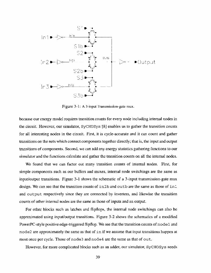
3-1 A 3-input Transmission-gate mux. . . . . . . . . . . . . . . .
3-2 A PowerPC-style flipflop. . . . . . . . . . . . . . . . . . . .
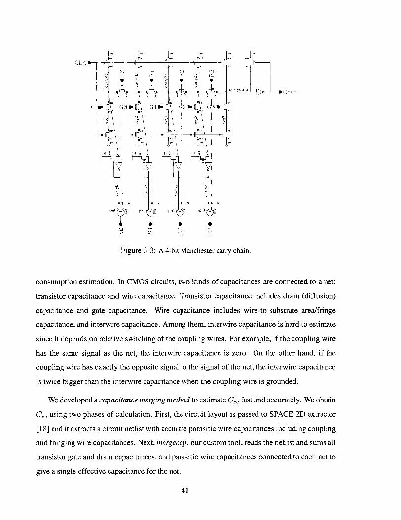
3-3 A 4-bit Manchester carry chain. . . . . . . . . . . . . . . . .
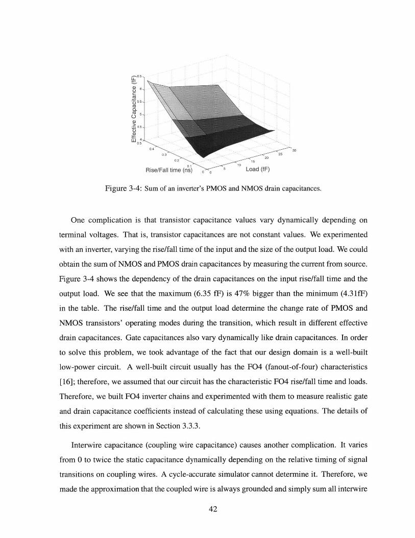
3-4 Sum of an inverter's PMOS and NMOS drain capacitances. . . .
3-5 Schematic of cascaded inverters and the capacitances
internal-node............................
. . . . . . . . 20
. . . . . . . . 21
. . . . . . . . 21
. . . . . . . . 22
. . . . . . . . 23
. . . . . . . . 25
. . . . . . . . 26
. . . . . . . . 27
. . . . . . . . 28
. . . . . . . . 29
. . . . . . . . 29
. . . . . . . . 30
. . . . . . . . 31
. . . . . . . . 32
. . . . . . . . 32
. . . . . . . . . . . 39
. . . . . . . . . . . 40
. . . . . . . . . . . 4 1
. . . . . . . . . . . 42
connected to the
43
9
16

3-6 Layout of cascaded inverters. . . . . . . . . . . . . . . . . . . . . . . . . . . . .
3-7 The netlist and the capacitance file of a cascaded two inverters. . . . . . . . . . . . .
3-8 Two F04 inverter chains. . . . . . . . . . . . . . . . . . . . . . . . . . . . . . .
3-9 Gray inverter. . . . . . . . . . . . . . . . . . . . . . . . . . . . . . . . . . . . .
3-10 Deriving gp, dp, gn and dn from measurements. . . . . . . . . . . . . . . . . . . .
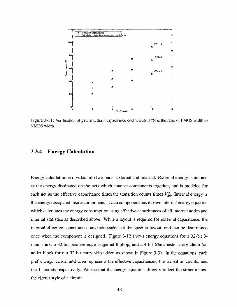
3-11 Verification of gate and drain capacitance coefficients. P/N is the ratio of PMOS width
to NMOS width. . . . . . . . . . . . . . . . . . . . . . . . . . . . . . . . . . .
3-12 Energy equations of N bit 3-input mux, N-bit positive flipflop, and 4-bit Manchester
carry chain. . . . . . . . . . . . . . . . . . . . . . . . . . . . . . . . . . . . . .
3-13 Mux, latch, flipflop and mux-latch: measured energy vs. estimated energy. Ideally, all
points should fall on the line. . . . . . . . . . . . . . . . . . . . . . . . . . . . .
Two kinds of short circuit current. . . . . . . . . . . . . . . . . . . . .
Measurements of fall short-circuit energy for various inverters. . . . . . .
Measurements of rise short-circuit energy for various inverters. . . . . . .
Error between the measured average short-circuit energy and the calculated
table lookup. . . . . . . . . . . . . . . . . . . . . . . . . . . . . . .
Pipeline diagram for datapath. . . . . . . . . . . .
Layout of the datapath. . . . . . . . . . . . . . . .
Metal allocation. . . . . . . . . . . . . . . . . . . .
Floorplan of datapath (except coprocessor 0). . . .
Floorplan of coprocessor 0. . . . . . . . . . . . . . .
Modified propagate(P) and generate(G) circuit for ALU.
A barrel shifter. . . . . . . . . . . . . . . . . . . . .
Logarithmic shifters. . . . . . . . . . . . . . . . . .
Shift instructions. . . . . . . . . . . . . . . . . . . .
Left shift amounts. . . . . . . . . . . . . . . . . . .
Right shift amounts. . . . . . . . . . . . . . . . . . .
Average energy of left shifters. . . . . . . . . . . . .
Average energy of right shifters. . . . . . . . . . . . .
. . . . . . 52
. . . . . . 53
. . . . . . 54
one using
. . 55
. . . . . . . . . . . . . . . 5 8
. . . . . . . . . . . . . . . 60
. . . . . . . . . . . . . . . 6 1
. . . . . . . . . . . . . . . 6 3
. . . . . . . . . . . . . . . 64
. . . . . . . . . . . . . . . 6 6
. . . . . . . . . . . . . . . 6 7
. . . . . . . . . . . . . . . 6 8
. . . . . . . . . . . . . . . 6 9
. . . . . . . . . . . . . . . 7 0
. . . . . . . . . . . . . . . 7 1
. . . . . . . . . . . . . . . 7 3
. . . . . . . . . . . . . . . 7 4
10
43
44
45
46
47
48
49
50
3-14
3-15
3-16
3-17
4-1
4-2
4-3
4-4
4-5
4-6
4-7
4-8
4-9
4-10
4-11
4-12
4-13

4-14 Energy-delay product of left shifters. . . . . . . . . . . . . . . . . . . . . . . . . 75
4-15 Energy-delay product of right shifters. . . . . . . . . . . . . . . . . . . . . . . . . 76
4-16 Clock gating circuit. . . . . . . . . . . . . . . . . . . . . . . . . . . . . . . . . 77
5-1 Average energy breakdown by component type. . . . . . . . . . . . . . . . . . . . 80
5-2 Average functional energy breakdown. . . . . . . . . . . . . . . . . . . . . . . . . 82
5-3 Average more detailed functional energy breakdown. . . . . . . . . . . . . . . . . . 83
5-4 Input data activity of flipflops in the datapath. . . . . . . . . . . . . . . . . . . . . 85
5-5 Input data activity of latches in the datapath. . . . . . . . . . . . . . . . . . . . . . 86
5-6 Clock and data activities for various flipflops. A solid curve is a PDP curve and a
dashed curve is a power curve. . . . . . . . . . . . . . . . . . . . . . . . . . . . 87
5-7 Clock and data activities for various latches. A solid curve is a PDP curve and a dashed
curve is a power curve. . . . . . . . . . . . . . . . . . . . . . . . . . . . . . . . 88
5-8 The effect of clock gating in terms of components. . . . . . . . . . . . . . . . . . . 89
5-9 The effect of clock gating in terms of functional blocks. . . . . . . . . . . . . . . . 90
5-10 The effect of clock gating in terms of sub-functional blocks. . . . . . . . . . . . . . 91
11

12

MOS model parameters and conditions. . . . . . . . . . . . . . . . . . . . . . . . 19
Minimum D-Q delay measurements of flipflops. . . . . . . . . . . . . . . . . . . . 22
Power measurements of flipflops (clock activity=1). . . . . . . . . . . . . . . . . . 24
Power measurements of flipflops (clock activity=O). . . . . . . . . . . . . . . . . . 24
PDP of flipflops (clock activity=1). . . . . . . . . . . . . . . . . . . . . . . . . . 24
PDP of flipflops (clock activity=O). . . . . . . . . . . . . . . . . . . . . . . . . . 25
D-Q delay measurements of latches. . . . . . . . . . . . . . . . . . . . . . . . . . 27
Power and PDP measurements of latches (clock activity=1). . . . . . . . . . . . . . 28
Power and PDP measurements of latches (clock activity=0). . . . . . . . . . . . . . 29
Delays and energy consumptions measurements of muxes. . . . . . . . . . . . . . . 32
Average energy consumptions and EDP (Energy-Delay Product) of muxes. . . . . . . 33
3.1 Short-circuit energy calculation table for an inverter. Average short-circuit energy is
the average of fall and rise short-circuit energy. . . . . . . . . . . . . . . . . . .
Various adder designs. . . . . . . . . . . . . . . . . . . . . . . . . . . . . . . .
Control signals for logic operation. . . . . . . . . . . . . . . . . . . . . . . . . .
Worst case delay of shifters. (The barrel shifter delay includes the worst case decoder
delay, 0.37 ns.) . . . . . . . . . . . . . . . . . . . . . . . . . . . . . . . . . . .
Benchmarks used .. . . . . . . . . . . . . . . . . . . . . . . . . . . . . . . . . .
Energy breakdown by component type (pJ/cycle (%)). . . . . . . . . . . . . . . . .
Functional energy breakdown (pJ/cycle (%)). . . . . . . . . . . . . . . . . . . . .
More detailed functional energy breakdown (pJ/cycle). . . . . . . . . . . . . . . . .
54
64
65
72
79
81
84
84
13
List of Tables
2.1
2.2
2.3
2.4
2.5
2.6
2.7
2.8
2.9
2.10
2.11
4.1
4.2
4.3
5.1
5.2
5.3
5.4

14

Chapter 1
Introduction
As portability and embedibility become increasingly crucial for all kinds of electronic devices,
the demand for low-power microprocessors is exploding. Building low-power microprocessors
is challenging because performance must be maintained while lowering energy consumption.
There has been tremendous research effort in this field and, as a result, many low-power
microprocessors with remarkable performance have been produced. However, although low-
power techniques for designing memory blocks such as RAMs or basic blocks such as an adder
have been studied intensively, little work has been done in systematic design of a complete
low-power datapath design - the core of the microprocessor. Accordingly, there is little
understanding of why and how energy is consumed in a microprocessor datapath.
The main goal of our research is to design a prototype low-power datapath and analyze
the energy consumption of the datapath. Of particular hindrance to low-power design of a
datapath is its intrinsic complexity. Datapaths are collections of numerous irregular blocks
which perform various functions. They have complex interconnect structures, a wide variety
of circuit types, and a rich set of activation patterns [8]. This complexity makes both the
analysis of datapath energy consumption and the application of low-power techniques difficult.
Therefore, we restrict our research to a simple datapath - a MIPS-II single-issue five-stage
pipelined RISC datapath. The MIPS architecture is one of the simplest RISC instruction
set architectures (ISAs) [6]. The main blocks of the datapath are a register file, an ALU, a
shifter, a multiplier/divider, and aligners/sign-extenders for load and store instructions. Also,
the datapath includes a program counter (PC) generation block and a system coprocessor block.
15

Energy Analysis of Datapath
ALU and Shifter Design
Basic Building Blocks Design(Flipflops, latches, and muxes) Energy Estimation Model
Figure 1-1: Our approach to low-power datapath design.
We believe that this research can be a base for future studies of more complicated low-power
datapath designs which issue multiple instructions at the same time and which have more
pipeline stages.
We approach our low-power datapath design problem in a bottom-up fashion (Figure 1-
1). First, we notice that flipflops, latches, and muxes are the most common and frequently-
used building blocks in the datapath. Accordingly, their power consumption accounts for a
significant portion of total power consumption. Therefore, we believe that a crucial first step
when building a low-power system is to find flipflops, latches, and muxes which have good
power and delay properties. In Chapter 2, we compare various flipflops, latches, and muxes
intensively in terms of power and delay. We find that the traditional energy measurements of
flipflops and latches which assume random input and un-gated clock are misleading especially
for the datapath flipflops and latches, because the datapath gives a wide variety of data and
clock activities to flipflops and latches. We develop analytic energy models for flipflops and
latches which present energy dissipation of flipflops and latches as a two-variable function of
input data and clock activities, and thus show dynamic features of energy dissipation. As for
muxes, we develop an analytical energy comparison method.
For the detailed energy analysis of the datapath, we require a fast and accurate energy
estimation tool, since circuit simulators are too slow to use for large systems such as our
16

datapath. However, we find that existing energy estimation tools cannot satisfy both speed
and accuracy requirements. They sacrifice one criterion or the other. Therefore, we decided
to develop a new simulation-based energy estimation technique, the net-transition energy
model, described in Chapter 3. The basic idea of this technique is to calculate energy
dissipation by using effective capacitance values and transition counts for each node. We
can get accurate transition counts from a simulator. The accuracy of this method depends
mainly on that of the effective capacitance values. In order to calculate these precisely,
we develop a capacitance merging method, which calculates transistor capacitances using
empirical equations and merges them along with parasitic wire capacitances into one single
effective capacitance for each node in the circuit. In Chapter 3, we present results from our
evaluation that show close agreement (<8% error) with Hspice measurements for various basic
circuit blocks and a 32-bit GCD (Greatest Common Divisor) circuit, which can be regarded as
a small version of a datapath. One limitation of our energy modeling is that it ignores the
short-circuit energy which accounts for a significant portion (5-10%) of energy consumption
in digital CMOS circuitry. We observe that most of short-circuit energy in the datapath is due to
inverters, therefore, we try to characterize the short-circuit energy of an inverter with a model
which is within 8% error compared to Hspice measurements.
Chapter 4 describes the custom-design of a prototype datapath for a 0.25 Am five metal
process (from TSMC). We detail the VLSI design style and the floor planning of the datapath.
Apart from the flipflops, latches, and muxes, the ALU block is one of main components of the
datapath. We discuss our decision of the adder design and develop an area-efficient logic unit
design. Also, we explore shifter designs because a shifter is an essential block in a datapath and
its simple structure makes energy investigation easy. First, we study dynamic instruction traces
to get a better understanding of the role of a shifter in a datapath. Then, we compare a barrel
shifter and various logarithmic shifters including our new shifter design, a split shifter, in terms
of delay and power. We use benchmarks to get more realistic activation patterns for energy
analysis. We show that the barrel shifter is a better choice than any log shifter. We include the
register file in our energy breakdowns, but the design is taken from earlier work [17].
Finally, in Chapter 5, we analyze the datapath energy using our energy model and
benchmarks. We perform energy breakdown by components and show that basic building
17

blocks such as flipflops, latches, and muxes, account for over half the total energy (56%). We
also try energy breakdown by functional blocks and reveal that register file read, bypassing,
and the PC generation account for significant portions of the total energy (20%, 22%, and 19%
respectively). Also, we develop a novel method that chooses better designs of flipflops and
latches in different places of the datapath, based on the data and clock activities. Also, we
examine the effect of clock gating and show 25.1% energy reduction by thorough clock gating.
Chapter 6 concludes and summarizes the work herein.
18

Chapter 2
Flipflop, Latch, and Mux
Flipflops, latches, and muxes are the most common blocks in the datapath. Accordingly, their
power consumption accounts for a significant portion of total power dissipation. In particular,
latches and flipflops have local clocks which burn power every cycle if they are not gated.
Therefore, a crucial first-step when we build a low power system is to find flipflops, latches,
and muxes which have good energy-delay products. Before building the datapath, we carefully
compared various possible design candidates of flipflops, latches, and muxes.
This chapter begins by describing our simulation test bench. Comparisons of flipflops,
latches, and muxes in terms of delay, power, and PDP (Power-Delay Product) or EDP (Energy-
Delay Product) follow. Stojanovic at al. [15] established a set of rules for consistent estimation
of the real performance and power features of the different flipflop structures for fair and
realistic comparison. We extend their work to latches and muxes and also introduce new,
precise energy comparison methods for flipflops, latches, and muxes.
Technology: TSMC 0.25 pim processMOSFET Model: Level 49 BSIM3 Ver3.1Conditions: Vdd=2.5V, T=250 C
Table 2.1: MOS model parameters and conditions.
19
Input Supply Internal Supply
4- y T T - - --.T0.2 ns
Flipflop,Latch,
or Mlux 3 fW
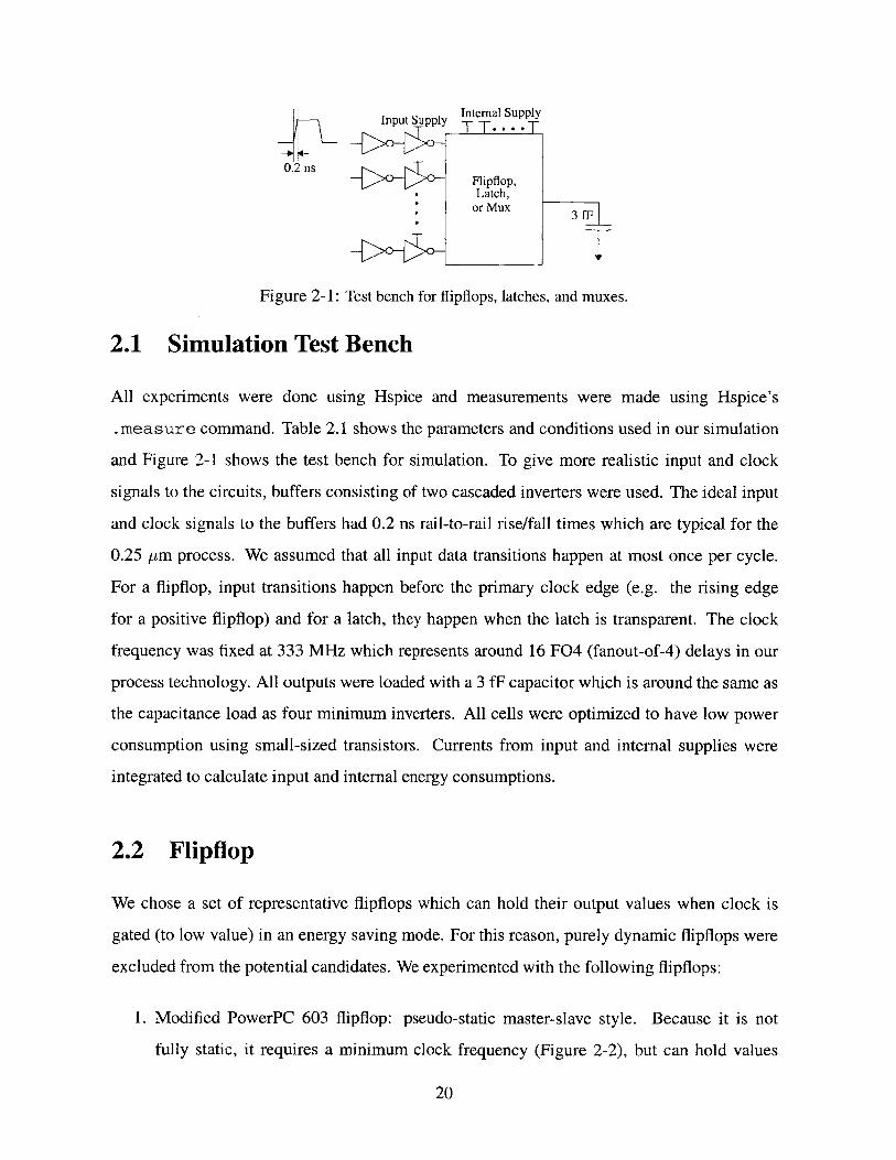
Figure 2-1: Test bench for flipflops, latches, and muxes.
2.1 Simulation Test Bench
All experiments were done using Hspice and measurements were made using Hspice's
.measure command. Table 2.1 shows the parameters and conditions used in our simulation
and Figure 2-1 shows the test bench for simulation. To give more realistic input and clock
signals to the circuits, buffers consisting of two cascaded inverters were used. The ideal input
and clock signals to the buffers had 0.2 ns rail-to-rail rise/fall times which are typical for the
0.25 pm process. We assumed that all input data transitions happen at most once per cycle.
For a flipflop, input transitions happen before the primary clock edge (e.g. the rising edge
for a positive flipflop) and for a latch, they happen when the latch is transparent. The clock
frequency was fixed at 333 MHz which represents around 16 F04 (fanout-of-4) delays in our
process technology. All outputs were loaded with a 3 fF capacitor which is around the same as
the capacitance load as four minimum inverters. All cells were optimized to have low power
consumption using small-sized transistors. Currents from input and internal supplies were
integrated to calculate input and internal energy consumptions.
2.2 Flipflop
We chose a set of representative flipflops which can hold their output values when clock is
gated (to low value) in an energy saving mode. For this reason, purely dynamic flipflops were
excluded from the potential candidates. We experimented with the following flipflops:
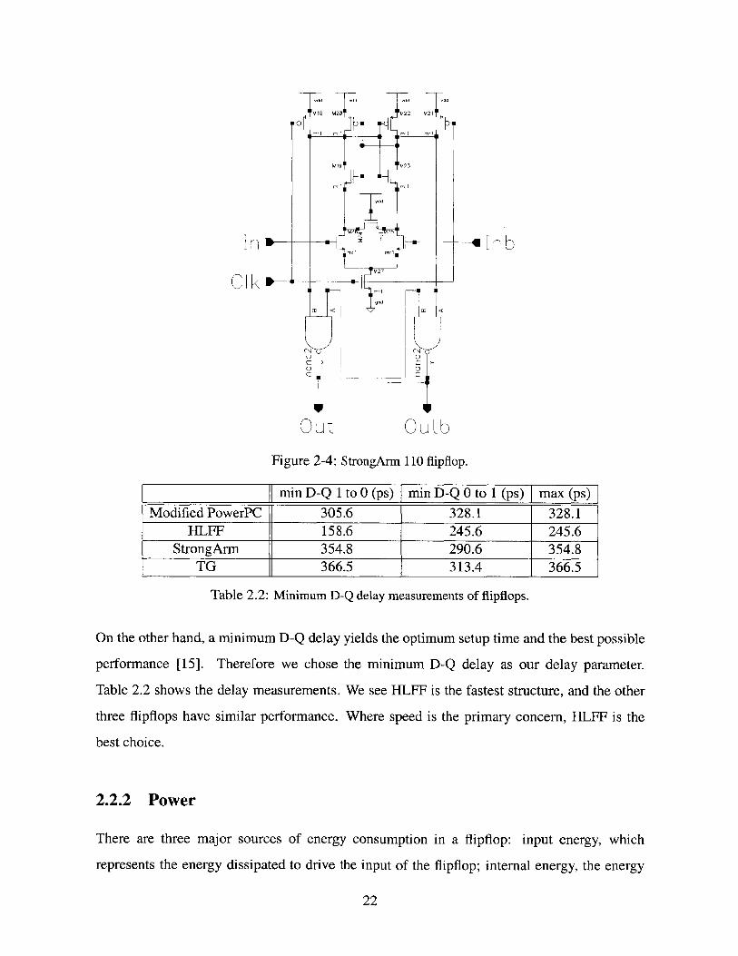
1. Modified PowerPC 603 flipflop: pseudo-static master-slave style. Because it is not
fully static, it requires a minimum clock frequency (Figure 2-2), but can hold values
20
-> 0 ut
dd
M10
Figure 2-2: Modified PowerPC flipflop.
vdd vdd vdd vdd
M1 M12 M13 M14 oK
mM'0M2M16
Mil M17
m~l m l
gnd gnd
Figure 2-3: HL flipflop.
indefinitely when clock is gated.
2. HLFF flipflop: hybrid style (Figure 2-3).
3. StrongArm 110 flipflop: differential sense-amplifier based style (Figure 2-4).
4. Transmission-gate flipflop: pseudo-static master-slave style with a cross coupled inverter
pair to store the output. This also requires a minimum clock frequency (Figure 2-5).
2.2.1 Delay
There are many important timing parameters in the flipflop such as Clk-Q delay, D-Q delay,
setup time, and hold time. As described in Stojavnovic's paper [15], Clk-Q delay (which is
commonly used as a relevant performance parameter) doesn't include setup time, and suffers
from the fact that the last transition of input (before the clock) affects Clk-Q delay significantly.
21
C k W-C->O-
In
Ck
d - dd d VddM18 M20 M22 M21
M19 M23
dd
M2z 25
rn:1 m:1
M27
Il m:1
D < Mgn
cut Cu
Out. Outb
e-t nb
Figure 2-4: StrongArm 110 flipflop.
min D-Q I to 0 (ps) min D-Q 0 to 1 (ps) max (ps)
Modified PowerPC 305.6 328.1 328.1HLFF 158.6 245.6 245.6
StrongArm 354.8 290.6 354.8TG 366.5 313.4 366.5
Table 2.2: Minimum D-Q delay measurements of flipflops.
On the other hand, a minimum D-Q delay yields the optimum setup time and the best possible
performance [15]. Therefore we chose the minimum D-Q delay as our delay parameter.
Table 2.2 shows the delay measurements. We see HLFF is the fastest structure, and the other
three flipflops have similar performance. Where speed is the primary concern, HLFF is the
best choice.
2.2.2 Power
There are three major sources of energy consumption in a flipflop: input energy, which
represents the energy dissipated to drive the input of the flipflop; internal energy, the energy
22
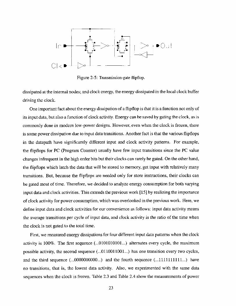
In Out
C I kFigure 2-5: Transmission-gate flipflop.
dissipated at the internal nodes; and clock energy, the energy dissipated in the local clock buffer
driving the clock.
One important fact about the energy dissipation of a flipflop is that it is a function not only of
its input data, but also a function of clock activity. Energy can be saved by gating the clock, as is
commonly done in modern low-power designs. However, even when the clock is frozen, there
is some power dissipation due to input data transitions. Another fact is that the various flipflops
in the datapath have significantly different input and clock activity patterns. For example,
the flipflops for PC (Program Counter) usually have few input transitions since the PC value
changes infrequent in the high order bits but their clocks can rarely be gated. On the other hand,
the flipflops which latch the data that will be stored to memory, get input with relatively many
transitions. But, because the flipflops are needed only for store instructions, their clocks can
be gated most of time. Therefore, we decided to analyze energy consumption for both varying
input data and clock activities. This extends the previous work [15] by realizing the importance
of clock activity for power consumption, which was overlooked in the previous work. Here, we
define input data and clock activities for our convenience as follows: input data activity means
the average transitions per cycle of input data, and clock activity is the ratio of the time when
the clock is not gated to the total time.
First, we measured energy dissipations for four different input data patterns when the clock
activity is 100%. The first sequence (...0101010101...) alternates every cycle, the maximum
possible activity, the second sequence (...0110011001...) has one transition every two cycles,
and the third sequence (...0000000000...) and the fourth sequence (...1111111111...) have
no transitions, that is, the lowest data activity. Also, we experimented with the same data
sequences when the clock is frozen. Table 2.3 and Table 2.4 show the measurements of power
23
Power(uW)Input data sequence Modified PowerPC HLFF StrongArm TG
...0000000000... 52.6 111.4 78.9 43.5
...1111111111... 52.9 230.0 81.2 41.9
...0101010101... 117.5 304.1 141.6 126.8
...0011001100... 84.4 238.8 112.5 84.8
Table 2.3: Power measurements of flipflops (clock activity=1).
Power(uW)Input data sequence Modified PowerPC HLFF StrongArm TG
...0000000000... 0.0 0.0 0.0 0.0
...1111111111... 0.0 0.0 0.0 0.0
...0101010101... 25.4 15.5 17.9 28.2
...0011001100... 11.5 5.8 10.2 12.2
Table 2.4: Power measurements of flipflops (clock activity=0).
dissipation. Table 2.5 and Table 2.6 show the corresponding PDPs for flipflops.
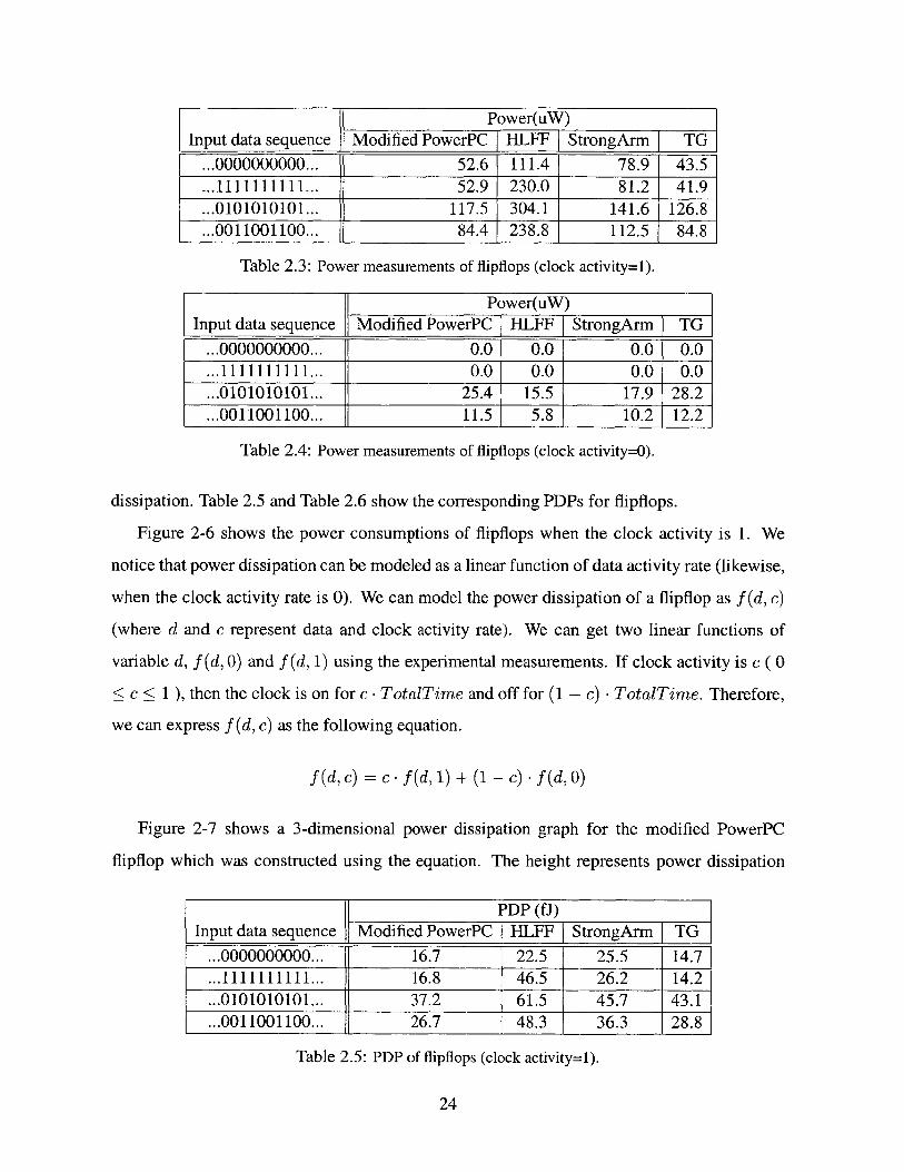
Figure 2-6 shows the power consumptions of flipflops when the clock activity is 1. We
notice that power dissipation can be modeled as a linear function of data activity rate (likewise,
when the clock activity rate is 0). We can model the power dissipation of a flipflop as f(d, c)
(where d and c represent data and clock activity rate). We can get two linear functions of
variable d, f (d, 0) and f (d, 1) using the experimental measurements. If clock activity is c ( 0
< c < 1 ), then the clock is on for c - TotalTime and off for (1 - c) -TotalTime. Therefore,
we can express f(d, c) as the following equation.
f(d, c) = c- f(d, 1) + (1 - c) -f(d, 0)
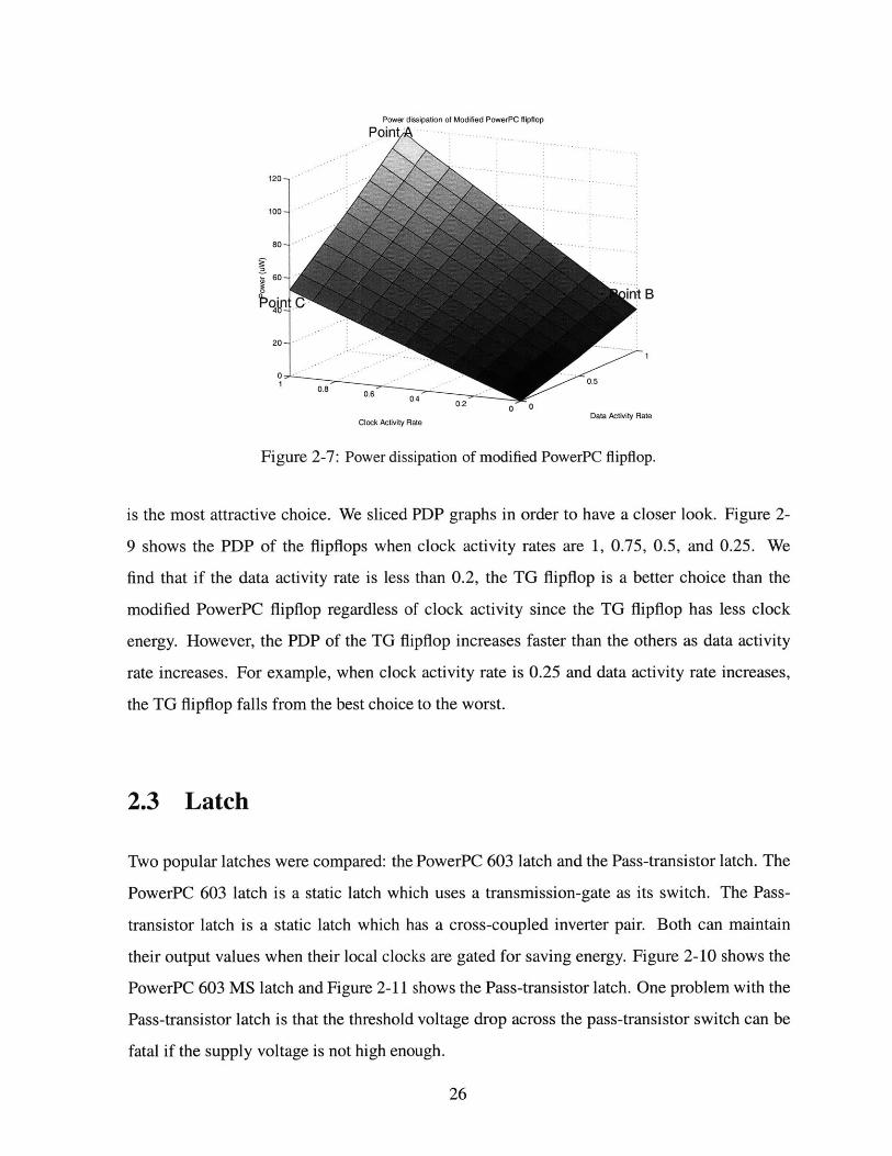
Figure 2-7 shows a 3-dimensional power dissipation graph for the modified PowerPC
flipflop which was constructed using the equation. The height represents power dissipation
PDP (fJ)Input data sequence Modified PowerPC HLFF StrongArm TG
...0000000000... 16.7 22.5 25.5 14.7
...1111111111... 16.8 46.5 26.2 14.2
...0101010101... 37.2 61.5 45.7 43.1
...0011001100... 26.7 48.3 36.3 28.8
Table 2.5: PDP of flipflops (clock activity=1).
24

PDP (fJ)Input data sequence Modified PowerPC HLFF I StrongArm TG
...0000000000... 0.0 0.0 0.0 0.0
...1111111111... 0.0 0.0 0.0 0.0
...0101010101... 8.1 3.1 5.8 9.6
...0011001100... 3.6 1.2 3.3 4.2
Table 2.6: PDP of flipflops (clock activity=0).
Power consumptions of Flipf lops
250
2002
0150a-
100
50
0 0.1 0.2 0.3 0.4 0.5 0.6 0.7 0.8 0.9 1Data Activity Rate (avg. transition per cycle) when clock activity rate is 1
Figure 2-6: Power dissipation of flipflops (clock activity=1).
while the x axis is data activity and the y axis is clock activity. We see it spends the maximum
power (Point A) when data and clock activity are both maximum (c = d = 1). Also, as we
expected, we notice that there is non-trivial power dissipation if the data activity is high even
when the clock is frozen. For example, if data alternates every cycle (d = 1) when clock is off
(c = 0), the flipflop spends around 25% of the maximum power (Point B). On the other hand,
the flipflop spends over 50% of the maximum power (Point C) even when there is no transition
in input data if the clock is left un-gated.
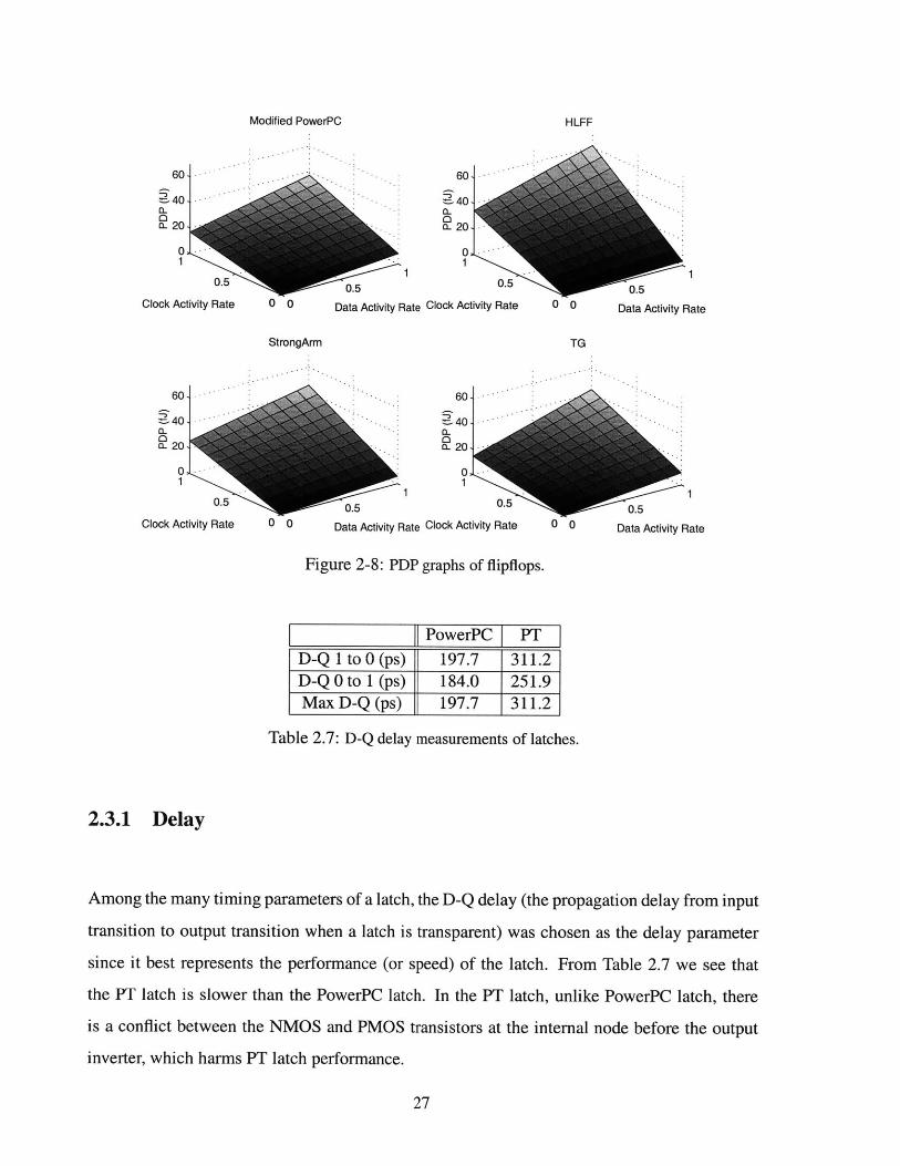
2.2.3 PDP
Figure 2-8 shows PDP graphs for the flipflops. We can see that the modified PowerPC flipflop
has the best power-delay product among the various candidates for most of the clock and data
patterns. Especially when clock and data activities are both high, the modified PowerPC flipflop
25
HLFF
TG
StrongArm
-/Modified PowerPC
3001-
120 - -
100 -. -. ..
80---
0 ent B
20-
10
1 0.8 0.6 0. 02 0
~0.2
Clock Activity Rate Data Activity Rate
Figure 2-7: Power dissipation of modified PowerPC flipflop.
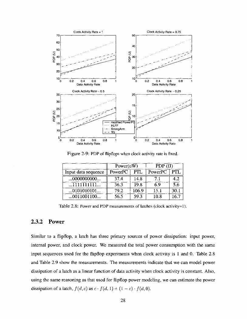
is the most attractive choice. We sliced PDP graphs in order to have a closer look. Figure 2-
9 shows the PDP of the flipflops when clock activity rates are 1, 0.75, 0.5, and 0.25. We
find that if the data activity rate is less than 0.2, the TG flipflop is a better choice than the
modified PowerPC flipflop regardless of clock activity since the TG flipflop has less clock
energy. However, the PDP of the TG flipflop increases faster than the others as data activity
rate increases. For example, when clock activity rate is 0.25 and data activity rate increases,
the TG flipflop falls from the best choice to the worst.
2.3 Latch
Two popular latches were compared: the PowerPC 603 latch and the Pass-transistor latch. The
PowerPC 603 latch is a static latch which uses a transmission-gate as its switch. The Pass-
transistor latch is a static latch which has a cross-coupled inverter pair. Both can maintain
their output values when their local clocks are gated for saving energy. Figure 2-10 shows the
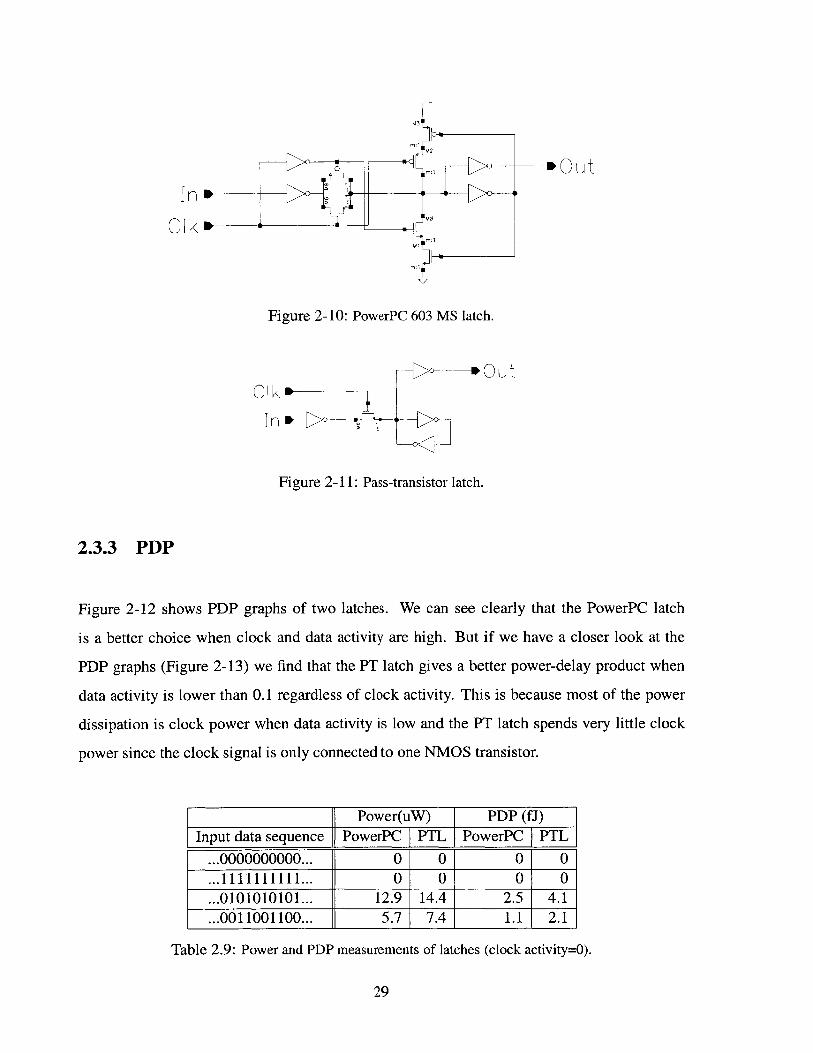
PowerPC 603 MS latch and Figure 2-11 shows the Pass-transistor latch. One problem with the
Pass-transistor latch is that the threshold voltage drop across the pass-transistor switch can be
fatal if the supply voltage is not high enough.
26
Modified PowerPC
C i1 R
Clock Activity Rate 0 0 Data Activity Rate
HLFF
60,
40
0L-20
0'.
0.5
Clock Activity Rate
StrongArm
0 00.5
Data Activity Rate
TG
60
$- 40=0-
00- 20
0
1 0.5
Clock Activity Rate 0 00.5
Data Activity Rate
60]
40 -
0- 20
0
0.5
Clock Activity Rate 0 00.5
Data Activity Rate
Figure 2-8: PDP graphs of flipflops.
TPowerPCI PT]D-Q I to (ps) 197.7 311.2D-Q 0 to 1 (ps) 184.0 251.9Max D-Q (ps) 197.7 311.2
Table 2.7: D-Q delay measurements of latches.
2.3.1 Delay
Among the many timing parameters of a latch, the D-Q delay (the propagation delay from input
transition to output transition when a latch is transparent) was chosen as the delay parameter
since it best represents the performance (or speed) of the latch. From Table 2.7 we see that
the PT latch is slower than the PowerPC latch. In the PT latch, unlike PowerPC latch, there
is a conflict between the NMOS and PMOS transistors at the internal node before the output
inverter, which harms PT latch performance.
27
70
60
50
0. 400a.
30
20
10
35
30
25
20
15
10
5
Clock Activity Rate = 0.75
0 0.2 0.4 0.6 0.8Data Activity Rate
Clock Activity Rate = 0.5
50
40
0. 30
20
100
20
15
.-- a.10- -- modified PowerPG
-...- HLFF- StrongArm
-- TG
00 0.2 0.4 0.6 0.8 1
Data Activity Rate
Clock Activity Rate =1
0.2 0.4 0.6 0.8Data Activity Rate
Clock Activity Rate = 0.25
0 0.2 0.4 0.6 0.8Data Activity Rate
Figure 2-9: PDP of flipflops when clock activity rate is fixed.
Power(uW) PDP (fJ)
Input data sequence PowerPC PTL PowerPC PTL
...0000000000... 37.4 14.8 7.1 4.2
...1111111111... 36.3 19.8 6.9 5.6
...0101010101... 79.2 106.9 15.1 30.1
...0011001100... 56.5 59.3 10.8 16.7
Table 2.8: Power and PDP measurements of latches (clock activity=1).
2.3.2 Power
Similar to a flipflop, a latch has three primary sources of power dissipation: input power,
internal power, and clock power. We measured the total power consumption with the same
input sequences used for the flipflop experiments when clock activity is 1 and 0. Table 2.8
and Table 2.9 show the measurements. The measurements indicate that we can model power
dissipation of a latch as a linear function of data activity when clock activity is constant. Also,
using the same reasoning as that used for flipflop power modeling, we can estimate the power
dissipation of a latch, f (d, c) as c - f (d, 1) + (1 - c) - f (d, 0).
28
0.2 0.4 0.6 0.
-
1 1
1
V3V
In
m:1
Figure 2-10: PowerPC 603 MS latch.
C I ki
Figure 2-11: Pass-transistor latch.
2.3.3 PDP
Figure 2-12 shows PDP graphs of two latches. We can see clearly that the PowerPC latch
is a better choice when clock and data activity are high. But if we have a closer look at the
PDP graphs (Figure 2-13) we find that the PT latch gives a better power-delay product when
data activity is lower than 0.1 regardless of clock activity. This is because most of the power
dissipation is clock power when data activity is low and the PT latch spends very little clock
power since the clock signal is only connected to one NMOS transistor.
Power(uW) PDP (fJ)
Input data sequence PowerPC PTL PowerPC PTL
...0000000000... 0 0 0 0
...1111111111... 0 0 0 0
...0101010101... 12.9 14.4 2.5 4.1
...0011001100... 5.7 7.4 1.1 2.1
Table 2.9: Power and PDP measurements of latches (clock activity=0).
29

PowerPC Latch
30,3
S20, 10
CL 10, 0
11
Clock Activity Rate 0 0 Data Activity Rate Clock Activity Rate 0 0 Data Activity F
Figure 2-12: PDP of latches.
2.4 Mux
We have experimented with two different muxes: a Transmission-gate (TG) mux, shown in
Figure 2-14, and a Pass-transistor (PT) mux, shown in Figure 2-15. The PT mux uses one
NMOS pass transistor as a selection switch. Thus, it can't charge up the internal node before
the output inverter to Vdd. Accordingly, a small PMOS keeper whose gate is connected to the
output and whose drain is connected to the internal node, is needed for full charge.
There are two important timing parameters in a mux design: the D-Q delay and the S-Q
delay. The D-Q delay is defined as the propagation delay from the input transition to the
resulting output transition while the control signals remain unchanged. The S-Q delay is
defined as the propagation delay from the change of the control signals to the resulting output
transition while the inputs stay the same.
We identified three main sources of energy dissipation in a mux: pass energy, non-pass
energy, and control energy. We define pass energy as the total energy consumption when one
input transition goes through a mux and makes an output transition while other inputs and
select signals stay the same. Non-pass energy is defined as the energy consumption due to
one transition of a not-chosen input. We define control energy as the energy consumption by
control signal drivers when there is a change of control signals (while inputs stay the same).
Using these components, we can model the average total energy consumption of an N-input
mux using the following equation.
30
PT Latch

Clock Activity Rate = 0.75
0- . . . .
35
30
25
p.20
0 15
10
5
00 0.2 0.4 0.6 0.8
Data Activity Rate
Clock Activity Rate = 0.5
0 0.2 0.4 0.6 0.8Data Activity Rate
- PowerPC 25PT
20
:3 15
10
0 5
n
12
10
8
6a..
4
2
0 0.2 0.4 0.6 0.8Data Activity Rate
Clock Activity Rate = 0.25
0 0.2 0.4 0.6 0.8Data Activity Rate
Figure 2-13: PDP of latches when clock activity is fixed.
Average Energy Consumption per cycle =
a * Pass Energy + 3 * (N-1) * Non-pass Energy + -y * Control Energy
In the equation, a is the average switching rate of the chosen input, # is that of all the non-
chosen inputs and -y is the probability that the mux selects a different input from the previous.
We made the following preliminary assumptions for comparison purpose. We assumed that
a mux chooses an input randomly every cycle. Then -y is (N-l)/N. Also, we assumed that all
input data are random but change at most once per cycle. Therefore, a and 3 are 0.5.
Table 2.10 shows the experimental measurements. First, we notice that the TG mux has
less delay and pass energy. The PT mux has a fight between NMOS and PMOS transistors,
which the TG mux doesn't have, when discharging the internal node before the output inverter.
This harms performance significantly and also results in a fair amount of short-circuit energy
loss, which contributes to the larger pass energy. Next, we see that the control energy of the TG
mux is around two times bigger than that of the PT mux because the TG mux has an additional
PMOS transistor per switch. However, we see that they dissipate similar amounts of non-pass
31
0 0.2 0.4 0.6 0.8
20
15
10a-
5
. . . .
Clock Activity Rate = 1
1 1
1 1

In 1 e
S Ib W-TS2
In2
S2 b .
InS
S 3 b W-'T
- utput
Figure 2-14: Transmission-gate mux.
S I-1
S2
In 2
Output
Figure 2-15: Pass-transistor mux.
power.
Table 2.11 shows average energy consumption and energy-delay products (EDP) for 2 to 5
input muxes which are typical in the datapath. The average of D-Q delay and S-Q delay was
used as delay parameter when we calculated energy-delay products. First, we notice that if the
number of inputs are larger than 3, the PT mux consumes less power. As the number of inputs
(N) increases from 2 to 5, a and 3 remain unchanged, but 7 gets larger since there is more
11 PT Mux TG Mux
D to Q delay (ns) 0.277 0.257S to Q delay (ns) 0.253 0.200Pass Energy (fJ) 110.5 77.3
Non-pass Energy (fJ) 22.3 23.2Control Energy (fJ) 19.2 41.6
Table 2.10: Delays and energy consumptions measurements of muxes.
32
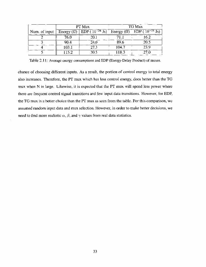
PT Mux TG MuxNum. of input Energy (fJ) EDP ( 104 Js) Energy (fJ) EDP ( 10-24 Js)
2 76.0 20.1 71.1 16.23 90.4 24.0 89.6 20.54 103.1 27.3 104.7 23.95 115.2 30.5 118.3 27.0
Table 2.11: Average energy consumptions and EDP (Energy-Delay Product) of muxes.
chance of choosing different inputs. As a result, the portion of control energy to total energy
also increases. Therefore, the PT mux which has less control energy, does better than the TG
mux when N is large. Likewise, it is expected that the PT mux will spend less power where
there are frequent control signal transitions and few input data transitions. However, for EDP,
the TG mux is a better choice than the PT mux as seen from the table. For this comparison, we
assumed random input data and mux selection. However, in order to make better decisions, we
need to find more realistic a, /, and -y values from real data statistics.
33

34
Chapter 3
Energy Modeling
This chapter begins by identifying major sources of energy consumption in modem digital
CMOS circuits. It is necessary to understand the energy consumption behavior of a circuit
before applying low-power techniques. Building a fast and accurate energy estimation model is
the first step for low-power design because it allows us to experiment with and evaluate various
low-power techniques. We discuss problems of previous energy models and then present and
evaluate our energy estimation model, net-transition energy model. We describe a short-circuit
energy model for an inverter at the end of this chapter.
3.1 Sources of Power Dissipation in Digital CMOS Circuits
There are three major sources of power dissipation in a digital CMOS circuit: dynamic
switching power due to charging and discharging circuit capacitances, leakage current power
including sub-threshold leakage and reverse-biased diode conduction leakage, and short-circuit
current power due to finite signal rise/fall times.
Dynamic switching power is the primary source of power dissipation in a digital CMOS
circuit; usually it accounts for around 90% of the total power dissipation. It can be modeled as
the following equation [4].
P = a -c - Vswing - Vd - f
(a - switching activity, c - effective load capacitance, Vswing - voltage change,
Vdd - source voltage, f - clock frequency)
35
Vdd and f can be regarded as constant numbers. Vswing is equal to Vdd in most cases
where complementary or dynamic CMOS circuit design styles are used. The other terms are
not as easy to quantify: c varies according to terminal voltages, rise/fall time, and coupling
effects while a is most likely not random in the datapath, and has strong correlations with input
vectors.
Short-circuit currents occur because the rise/fall time of input signals are not zero. During
the finite rise/fall time, both PMOS and NMOS transistors are turned on, the path between Vdd
and GND is connected, and current flows. Usually the short-circuit power dissipation accounts
for approximately 5-10% of total power [2].
Leakage current power is significantly smaller than the other sources of power dissipation
in normal operation mode, but it can be the dominant component in standby mode. Over
time, the threshold voltage in process has been lowered to allow for lower Vdd for less power
consumption. As a result, the sub-threshold current, the main component of leakage current,
has been increasing rapidly. It is certain that the leakage current power will get more attention
in the near future.
3.2 Previous Energy Models
Circuit simulators such as Hspice [11] or Powermill [5] can be used to estimate energy usage.
The main advantages of circuit-level simulation are its accuracy and generality [13]. It can
estimate the energy consumption of any circuit very precisely regardless of technology, design
style, functionality, and architecture. However, it is computationally very expensive and too
slow to use for large systems such as our target microprocessor datapath. Therefore, a fast
energy estimation model with accuracy comparable to the circuit simulators is needed for
research in the design of large low-power systems.
Many approaches have been tried to model energy consumption quickly and accurately.
These approaches can be classified into three broad categories: statistical/empirical techniques,
probabilistic techniques, and simulation-based techniques [9].
The statistical technique simulates the circuit and measures the power consumption
repeatedly with circuit simulators using short random input patterns. When the average of
36

power measurements converges to a specific value, the simulation stops and the convergence
point indicates the average power. This technique was found to be accurate for some logic
gates [13]. However, the average power consumption derived from repeated simulations with
random sample input patterns, is not meaningful for strongly input-dependent circuits such as
a microprocessor. Additionally, the simulation of small input patterns with circuit simulators
may take a long time for large systems.
The probabilistic technique is based on the propagation of probabilities. The user provides
signal probabilities at the primary inputs and these are propagated into the circuit using Boolean
arithmetic and probability theory [13]. Using the probabilities of each node, the average power
of the circuit is estimated. It is fast and independent of input data. However, the accuracy
of this method is limited by the quality of the input signal probabilities specification and the
spatial and temporal correlation model between internal node values.
The simulation-based technique uses high-level simulators such as RTL (Register-Transfer
Level) simulators to count circuit node transitions, and calculates energy dissipation from
these. It is far more accurate than the previous methods since it is input-dependent and
also transition-sensitive. Its accuracy is almost comparable to that of a circuit-level simulator
while its speed is 5-7 orders of magnitude faster than that of circuit simulators [8]. However,
compared to previous energy models, it is still slower. By developing a fast high-level simulator
and trading off the simulation time and accuracy wisely, we can mitigate this disadvantage.
Additionally, this technique can provide detailed energy analysis such as spatial and temporal
energy breakdowns for real input loads such as SPECint benchmarks easily since it uses a
high-level simulator. Therefore we determined that the simulation-based technique is the
most appropriate for the study of microprocessor datapath energy consumption. It can give
us sufficient accuracy and enough information on many respects of energy consumption.
The most important part of the simulation-based energy model is to get the necessary
switching activities. However, getting switching activities is only the first part in the
simulation-based technique. The next part is converting them to energy consumption. One
possible solution is to make an energy calculation table for each module [19]. Basic blocks
are simulated using a circuit simulator for every possible input and internal-state combination,
energy consumption is measured, and then the table is constructed. After building an energy
37

table for every block of the system, we can calculate energy consumption by looking up pre-
computed values in the energy tables. This is accurate because it uses the energy measured from
a transistor-level simulator, but it has three obvious disadvantages. First of all, building energy
tables is not cheap. It is labor-intensive and time-consuming since we need to simulate every
module using every possible input and internal state combination. Second, it is not flexible.
If we need to change some features of a circuit block, for example, resizing transistors, we
can't help but repeat the whole simulation of that block again in order to update the energy
lookup table of the block. Lastly, the table size (accordingly, the simulation time) grows
exponentially with the size of the input vector (for example, a 32 bit adder requires 24 table
entries.) Clustering algorithms can be used to decrease the size of the energy tables, but they
lose a large amount of accuracy (up to 30% [10]).
3.3 Node-Transition Energy Model
We developed a new simulation-based energy model, the Node-Transition Energy Model,
based on a capacitance merging method. The basic idea of our method is simple: If we get
the effective, equivalent capacitance, Ceq and the 0-to-i transition counts of every node, we
can calculate the dynamic energy consumption of each node by using the following simple
equation. The total energy of a circuit is the sum of the energy dissipation of every node.
Energy Consumption of a node = 0-to-I Transition Counts * Ceq * Vdd 2
In the following subsections, we first show how we gather transitions counts for all nets.
Next, we show how we calculate the accurate, effective capacitance for each net using our
capacitance merging method. Then, we show how we calculate energy consumption with the
transition counts and the effective capacitance using energy equations. Lastly, we evaluate our
energy model with sample circuit blocks.
3.3.1 Transition Counts Gathering
An important measurement for our energy model is the transition count. A conventional RTL
simulator only counts transitions at registers - not intermediate nodes. This is a limitation
38
ml'Inib E
S I bS 2
Outb
In2 OutputIMbE
Sn3b--
Figure 3-1: A 3-input Transmission-gate mux.
because our energy model requires transition counts for every node including internal nodes in
the circuit. However, our simulator, SyCHOSys [8] enables us to gather the transition counts
for all interesting nodes in the circuit. First, it is cycle-accurate and it can count and gather
transitions on the nets which connect components together directly; that is, the input and output
transitions of components. Second, we can add any energy statistics gathering functions to our
simulator and the functions calculate and gather the transition counts on all the internal nodes.
We found that we can factor out many transition counts of internal nodes. First, for
simple components such as our buffers and muxes, internal node switchings are the same as
input/output transitions. Figure 3-1 shows the schematic of a 3-input transmission-gate mux
design. We can see that the transition counts of inIb and outb are the same as those of in1
and output respectively since they are connected by inverters, and likewise the transition
counts of other internal nodes are the same as those of inputs and an output.
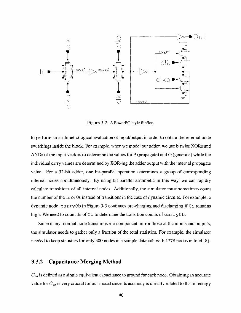
For other blocks such as latches and flipflops, the internal node switchings can also be
approximated using input/output transitions. Figure 3-2 shows the schematics of a modified
PowerPC-style positive edge-triggered flipflop. We see that the transition counts of node 1 and
node2 are approximately the same as that of in if we assume that input transitions happen at
most once per cycle. Those of node3 and node4 are the same as that of out.
However, for more complicated blocks such as an adder, our simulator, SyCHOSys needs
39
U U
In ~nodel node2 E
_ UU
vdd
node4 4tbP
M4
nd:
M0
1p141bFM5
9nd
node3
Figure 3-2: A PowerPC-style flipflop.
to perform an arithmetic/logical evaluation of input/output in order to obtain the internal node
switchings inside the block. For example, when we model our adder, we use bitwise XORs and
ANDs of the input vectors to determine the values for P (propagate) and G (generate) while the
individual carry values are determined by XOR-ing the adder output with the internal propagate
value. For a 32-bit adder, one bit-parallel operation determines a group of corresponding
internal nodes simultaneously. By using bit-parallel arithmetic in this way, we can rapidly
calculate transitions of all internal nodes. Additionally, the simulator must sometimes count
the number of the is or Os instead of transitions in the case of dynamic circuits. For example, a
dynamic node, carry0b in Figure 3-3 continues pre-charging and discharging if Ci remains
high. We need to count Is of Ci to determine the transition counts of carry0b.
Since many internal node transitions in a component mirror those of the inputs and outputs,
the simulator needs to gather only a fraction of the total statistics. For example, the simulator
needed to keep statistics for only 300 nodes in a sample datapath with 1278 nodes in total [8].
3.3.2 Capacitance Merging Method
Ceq is defined as a single equivalent capacitance to ground for each node. Obtaining an accurate
value for Ceq is very crucial for our model since its accuracy is directly related to that of energy
40
CLK
CE E 2 E a
[ 00e [\ 1 2 [
- b p2\ l~
U)
pb2
pb pb3
Figure 3-3: A 4-bit Manchester carry chain.
consumption estimation. In CMOS circuits, two kinds of capacitances are connected to a net:
transistor capacitance and wire capacitance. Transistor capacitance includes drain (diffusion)
capacitance and gate capacitance. Wire capacitance includes wire-to-substrate area/fringe
capacitance, and interwire capacitance. Among them, interwire capacitance is hard to estimate
since it depends on relative switching of the coupling wires. For example, if the coupling wire
has the same signal as the net, the interwire capacitance is zero. On the other hand, if the
coupling wire has exactly the opposite signal to the signal of the net, the interwire capacitance
is twice bigger than the interwire capacitance when the coupling wire is grounded.
We developed a capacitance merging method to estimate Ceq fast and accurately. We obtain
Ceq using two phases of calculation. First, the circuit layout is passed to SPACE 2D extractor
[18] and it extracts a circuit netlist with accurate parasitic wire capacitances including coupling
and fringing wire capacitances. Next, mergecap, our custom tool, reads the netlist and sums all
transistor gate and drain capacitances, and parasitic wire capacitances connected to each net to
give a single effective capacitance for the net.
41
j --
-- corryoutb 0UtE
G33[
.d
a6C-
C.1) 5,5
CO ,
0.4.5
0.5
0.4 -30
0.3 25
02 150.1 10
Rise/Fall time (ns) 0 0 Load (f F)
Figure 3-4: Sum of an inverter's PMOS and NMOS drain capacitances.
One complication is that transistor capacitance values vary dynamically depending on
terminal voltages. That is, transistor capacitances are not constant values. We experimented
with an inverter, varying the rise/fall time of the input and the size of the output load. We could
obtain the sum of NMOS and PMOS drain capacitances by measuring the current from source.
Figure 3-4 shows the dependency of the drain capacitances on the input rise/fall time and the
output load. We see that the maximum (6.35 f) is 47% bigger than the minimum (4.31fF)
in the table. The rise/fall time and the output load determine the change rate of PMOS and
NMOS transistors' operating modes during the transition, which result in different effective
drain capacitances. Gate capacitances also vary dynamically like drain capacitances. In order
to solve this problem, we took advantage of the fact that our design domain is a well-built
low-power circuit. A well-built circuit usually has the F04 (fanout-of-four) characteristics
[16]; therefore, we assumed that our circuit has the characteristic F04 rise/fall time and loads.
Therefore, we built F04 inverter chains and experimented with them to measure realistic gate
and drain capacitance coefficients instead of calculating these using equations. The details of
this experiment are shown in Section 3.3.3.
Interwire capacitance (coupling wire capacitance) causes another complication. It varies
from 0 to twice the static capacitance dynamically depending on the relative timing of signal
transitions on coupling wires. A cycle-accurate simulator cannot determine it. Therefore, we
made the approximation that the coupled wire is always grounded and simply sum all interwire
42
Neighborwire
ICcoupling
Cdrain2 C gate
Input Outputterna .node
C drain. N gateN
Figure 3-5: Schematic of cascaded inverters and the capacitances connected to the internaLnode.
Figure 3-6: Layout of cascaded inverters.
capacitances into a single equivalent capacitance to ground.
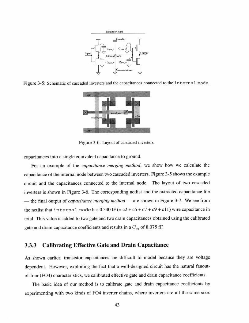
For an example of the capacitance merging method, we show how we calculate the
capacitance of the internal node between two cascaded inverters. Figure 3-5 shows the example
circuit and the capacitances connected to the internal node. The layout of two cascaded
inverters is shown in Figure 3-6. The corresponding netlist and the extracted capacitance file
- the final output of capacitance merging method - are shown in Figure 3-7. We see from
the netlist that int ernal-node has 0.340 fF (= c2 + c5 + c7 + c9 + c11) wire capacitance in
total. This value is added to two gate and two drain capacitances obtained using the calibrated
gate and drain capacitance coefficients and results in a Ceq of 8.075 fF.
3.3.3 Calibrating Effective Gate and Drain Capacitance
As shown earlier, transistor capacitances are difficult to model because they are voltage
dependent. However, exploiting the fact that a well-designed circuit has the natural fanout-
of-four (F04) characteristics, we calibrated effective gate and drain capacitance coefficients.
The basic idea of our method is to calibrate gate and drain capacitance coefficients by
experimenting with two kinds of F04 inverter chains, where inverters are all the same-size:
43
kvnAnodr

NETLIST :
ml Vddl input internalnode Vddl PMOS
+ w=600n l=240n ad=432f as=360f pd=2.04u ps=1.8um2 GND1 input internalnode GND NMOS
+ w=600n 1=240n ad=432f as=360f pd=2.04u ps=1.8um3 output internalnode Vddl Vddl PMOS
+ w=600n l=240n ad=360f as=432f pd=1.8u ps=2.04um4 GND1 internalnode output GND NMOS
+ w=600n 1=240n ad=432f as=360f pd=2.04u ps=1.8uci GND1 output 34.99428e-18
c2 GND1 internalnode 44.83748e-18
c3 GND1 neighborwire 62.31828e-18
c4 GND1 Vddl 63.218e-18
c5 input internalnode 73.79929e-18
c6 input neighborwire 43.82269e-18
c7 neighborwire internalnode 121.0628e-18
c8 neighborwire Vddl 62.31828e-18
c9 output internalnode 55.8099e-18
c1O output Vddl 34.99428e-18
c1l Vddi internalnode 44.83748e-18
CAPACITANCE FILE :
capinput 3.203 fF
cap_internalnode 8.075 fF
capoutput 4.775 fF
capneighborwire 0.290 fF
Figure 3-7: The netlist and the capacitance file of a cascaded two inverters.
44
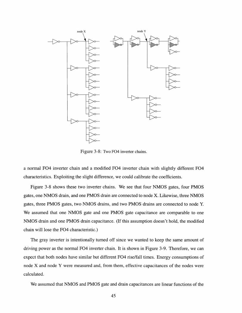
node X
->O-
L>O-
->C---[>0--
->O-
19::
L>O-- >-
->O--
Figure 3-8: Two F04 inverter chains.
a normal F04 inverter chain and a modified F04 inverter chain with slightly different F04
characteristics. Exploiting the slight difference, we could calibrate the coefficients.
Figure 3-8 shows these two inverter chains. We see that four NMOS gates, four PMOS
gates, one NMOS drain, and one PMOS drain are connected to node X. Likewise, three NMOS
gates, three PMOS gates, two NMOS drains, and two PMOS drains are connected to node Y.
We assumed that one NMOS gate and one PMOS gate capacitance are comparable to one
NMOS drain and one PMOS drain capacitance. (If this assumption doesn't hold, the modified
chain will lose the F04 characteristic.)
The gray inverter is intentionally turned off since we wanted to keep the same amount of
driving power as the normal F04 inverter chain. It is shown in Figure 3-9. Therefore, we can
expect that both nodes have similar but different F04 rise/fall times. Energy consumptions of
node X and node Y were measured and, from them, effective capacitances of the nodes were
calculated.
We assumed that NMOS and PMOS gate and drain capacitances are linear functions of the
45
node Y
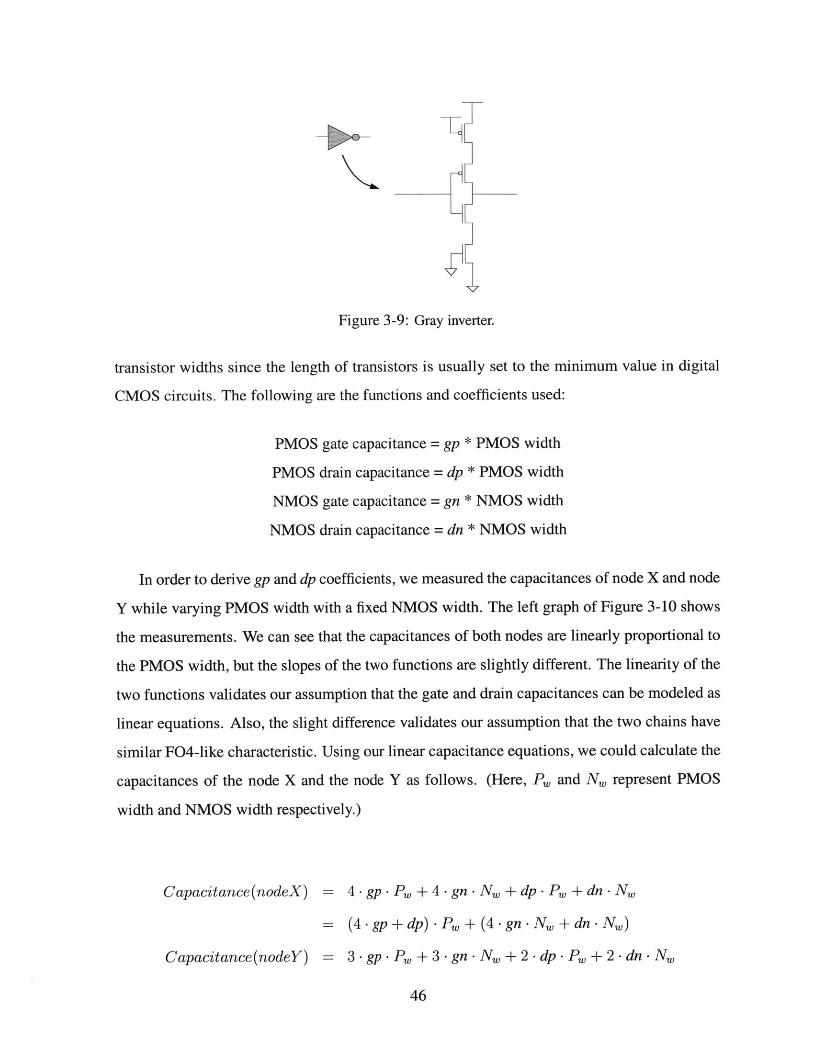
Figure 3-9: Gray inverter.
transistor widths since the length of transistors is usually set to the minimum value in digital
CMOS circuits. The following are the functions and coefficients used:
PMOS gate capacitance = gp * PMOS width
PMOS drain capacitance = dp * PMOS width
NMOS gate capacitance = gn * NMOS width
NMOS drain capacitance = dn * NMOS width
In order to derive gp and dp coefficients, we measured the capacitances of node X and node
Y while varying PMOS width with a fixed NMOS width. The left graph of Figure 3-10 shows
the measurements. We can see that the capacitances of both nodes are linearly proportional to
the PMOS width, but the slopes of the two functions are slightly different. The linearity of the
two functions validates our assumption that the gate and drain capacitances can be modeled as
linear equations. Also, the slight difference validates our assumption that the two chains have
similar F04-like characteristic. Using our linear capacitance equations, we could calculate the
capacitances of the node X and the node Y as follows. (Here, P" and N" represent PMOS
width and NMOS width respectively.)
Capacitance(nodeX) = 4 -gp - P+ 4 -gn . Nw+ dp -Pw + dn -Nw
= (4-gp+dp)-Pw+(4-gn-Nw+dn-Nw)
Capacitance(nodeY) = 3.gp.Pw+3-gn.Nw+2.dp.Pw+2.dn-Nw
46
NMOS width is fixed as 6 lambda PMOS width is fixed as 36 lambda1 160r
10 20 30 40PMOS width
140 -
120-
S1008C3LWQ
gp = 0.207 fF / lambda
dp = 0.554 fF / lambda
00
00 x
0 x- 0 0 x
node X 0 x node Y0 x
- oO x
Ox- 5
gn =0.41l fF /lambda *
dn = 0.376 IF / lambda * +
* +
* +
no * +od
* +
* +
noeXn+e* +
0 10 20 30NMOS width
+
40
Figure 3-10: Deriving gp, dp, gn and dn from measurements.
= (3-gp+2-dp)-Pw+(3-gn.Nw+2-dn.Nw)
Since the NMOS width is
node Y plot is 3 -gp + 2 - dp.
measurements, we can derive
the left Figure 3-10.
fixed, the slope of the node X plot is 4 -gp + dp and that of the
After getting the slopes using the linear-square method from the
gp and dp by solving linear equations. The results are shown in
In the same way, we can derive gn and dn using the measurements where PMOS width is
fixed, as shown in the right graph of Figure 3-10. In order to verify the derived capacitance
coefficients, we calculated the capacitance of node X for different PMOS and NMOS widths
and compared these values with the empirically measured capacitances obtained using Hspice.
Figure 3-11 shows that the calculated capacitances match the measured ones well. The relative
error is within 5% for 18 different NMOS and PMOS widths.
The entire measuring process is done automatically and only needs to be done once for a
given process technology.
47
140
120
100
S80
60
40
20
0
80
60
40
120* Measured capacitanceo Calculated capacitance using our coeffic ents
100- P/N = 3
80-P/N =2
60-e P/N =1
co
40-
20j
0 6 9 12 15 18NMOS width
Figure 3-11: Verification of gate and drain capacitance coefficients. P/N is the ratio of PMOS width toNMOS width.
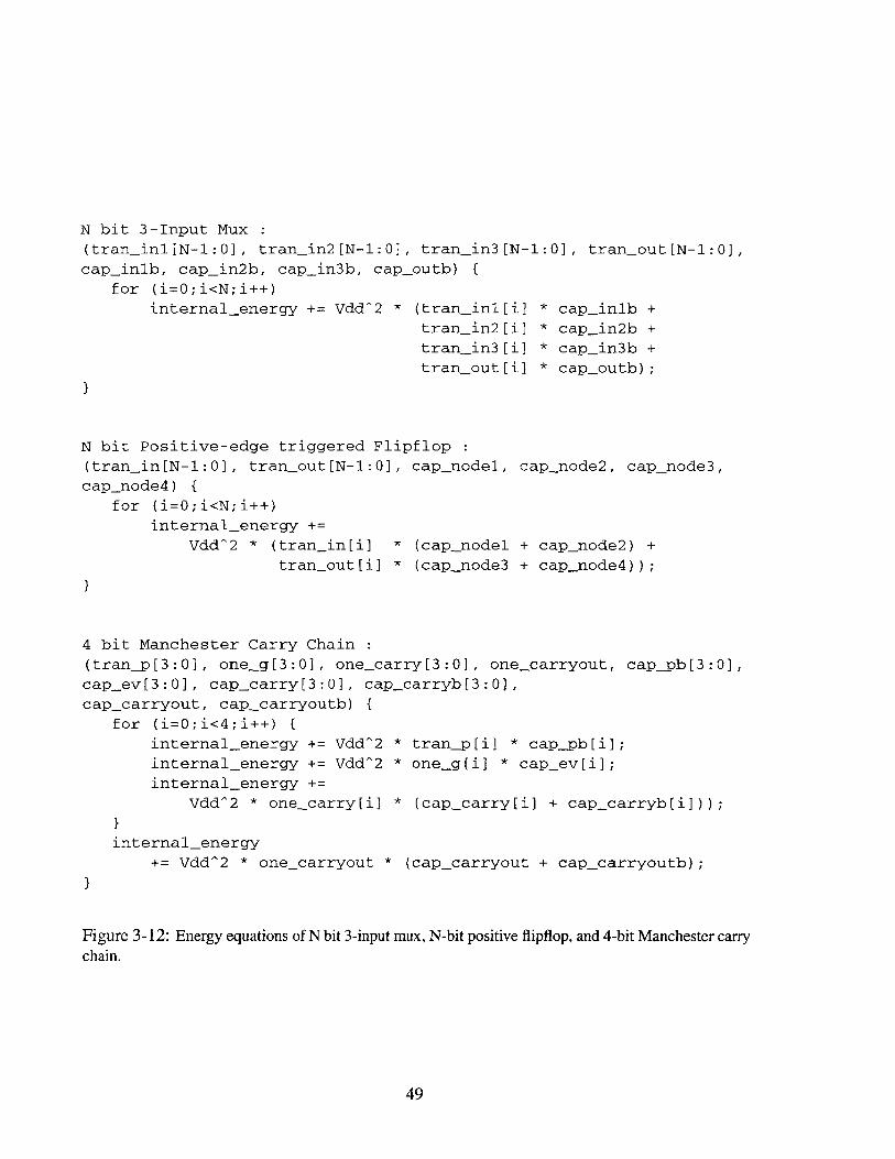
3.3.4 Energy Calculation
Energy calculation is divided into two parts: external and internal. External energy is defined
as the energy dissipated on the nets which connect components together, and is modeled for
each net as the effective capacitance times the transition counts times V. Internal energy is
the energy dissipated inside components. Each component has its own internal energy equation
which calculates the energy consumption using effective capacitances of all internal nodes and
internal statistics as described above. While a layout is required for external capacitance, the
internal effective capacitances are independent of the specific layout, and can be determined
once when the component is designed. Figure 3-12 shows energy equations for a 32-bit 3-
input mux, a 32-bit positive-edge triggered flipflop, and a 4-bit Manchester carry chain (an
adder block for our 32-bit carry skip adder, as shown in Figure 3-3). In the equations, each
prefix cap, tran, and one represents the effective capacitances, the transition counts, and
the Is counts respectively. We see that the energy equations directly reflect the structure and
the circuit style of a circuit.
48
N bit 3-Input Mux :(tran-inl[N-1:0], tran-in2[N-1:0], tran_in3[N-1:0], tran-out[N-1:0],
capjin1b, cap_in2b, capjin3b, cap-outb)
for (i=0;i<N;i++)
internalenergy += Vdd^2 * (traninl[i] * capin1b +
tranin2[i] * capin2b +tranin3[i] * cap_in3b +
tranout[i] * capoutb);
}
N bit Positive-edge triggered Flipflop
(tranin[N-1:0], tranout[N-1:0], capnodel, capnode2, cap_node3,
capnode4) {
for (i=0;i<N;i++)
internalenergy +=
Vdd^2 * (tranin[i] * (cap-nodel + capnode2) +
tranout[i] * (cap-node3 + cap-node4));
}
4 bit Manchester Carry Chain
(tranp[3:0], one-g[3:0], onecarry[3:0], one_carryout, cappb[3:0],
capev[3:0], cap-carry[3:0], cap-carryb[3:0],
cap-carryout, cap_carryoutb) {for (i=0;i<4;i++) {
internalenergy += Vdd^2 * tranp[i] * cappb[i];
internalenergy += Vdd^2 * one-g[i] * cap-ev[i];
internalenergy +=
Vdd^2 * onecarry[i] * (capcarry[i] + capcarryb[i]));
}internalenergy
+= Vdd^2 * one-carryout * (capcarryout + cap-carryoutb);
}
Figure 3-12: Energy equations of N bit 3-input mux, N-bit positive flipflop, and 4-bit Manchester carrychain.
49

3 input Transmission-gate Mux Powerpc-style Flipflop5 ~12
4 - 10
W W
c3 -
D102
16-
00 1 2 3 4 5 44 6 8 10 12Estimated Energy Consumption (pJ) Estimated Energy Consumption (pJ)
Powerpc-style Latch Mux-Latch28 :20 .
.27 . 18-
o6 -S16 -
05 014
a ~1204
3D '010-
aU a8
2 4 6 8 8 10 12 14 16 18 20Estimated Energy Consumption (pJ) Estimated Energy Consumption (pJ)
Figure 3-13: Mux, latch, flipflop and mux-latch: measured energy vs. estimated energy. Ideally, all
points should fall on the line.
3.3.5 Evaluation of Our Energy Model
We first evaluated our energy model using small circuit examples. Figure 3-13 shows the
estimated energy consumption using the net-transition energy model (X-axis) versus the
measured energy consumption using Hspice (Y-axis) for a mux, a latch, a flipflop, and a mux-
latch circuit, where the output of the mux is connected to the latch input.
We used the typical F04 rise and fall times and output load for the simulation. We chose
5 random input patterns for each circuit. We found that the maximum relative errors are
4.76%, 2.36%, 8.02%, and 4.32% for the mux, the latch, the flipflop and the mux-latch circuits
respectively. We see that the errors are of the same order of magnitude as those of the gate and
drain capacitance coefficients.
For a larger example, we used the 32-bit GCD (Greatest Common Divisor) circuit. The
circuit implements Euclid's GCD algorithm. The GCD circuit is a small version of a CPU
datapath in the sense that it has muxes, latches, flipflops and an adder. Our energy model could
estimate energy dissipations within 7% error compared to Hspice simulation for 7 different
input test vectors [8].
Our method has three advantages over other simulation-based energy estimation tools.
First, it is fast. The total time needed for energy calculation depends mainly on the running time
50
of the cycle-accurate simulator (with statistics gathering code). The time needed for merging
capacitances and calculating energy equations are very little compared to the simulation time.
Our simulator, SyCHOSys [8] was fast enough to simulate a billion cycles of benchmark
programs per day. Second, it is flexible. For example, if we change a mux design, we need
to do only two things. We need to get the capacitance values from the layout of the new mux
design, which can be done automatically after the layout is ready, and we need to modify
the energy equation if the internal structure of the new mux is different from the old. Third,
it is accurate. A cycle-accurate simulation-based technique is the most accurate of the three
categories of energy estimation techniques. Additionally, our detailed energy equations and
realistic effective capacitance values guarantee the accurate energy estimation. The verification
of our method with some examples will be shown in section 3.3.5.
One limitation of our method is that it can't model glitch power since it is only cycle-
accurate. But, we can assume that for a well-built low-power circuit, glitches are rare and
small. Another limitation is that it deals with only dynamic switching energy, but ignores
short-circuit and leakage energy. Lastly, if we substitute a block with another block which
executes the same function, but requires different internal statistics from a simulator, we have
to re-simulate.
3.4 Short-Circuit Energy Modeling of an Inverter
Short-circuit energy accounts for a significant portion (5-10%) of the total power consumption
in CMOS circuits. However, our energy model, the Net-Transition Energy Model, did not
include the short-circuit energy. Therefore, we tried to model the short-circuit energy to be
included in the next version of the net-transition energy model.
Short-circuit energy is difficult to model in general since it varies dynamically depending
on the on-time of the transistors and their operating modes. Also, the relative switching time
of multiple inputs to a logic gate further complicates the problem. However, we observed that
most of the short-circuit power in our design is consumed in inverters since they are the most
common components in complementary static CMOS circuits (transmission-gate and dynamic
circuits don't dissipate short-circuit power). For example, our latches, buffers, muxes, and
51

_IDFall short-circuit energy Rise short-circuit energy
Figure 3-14: Two kinds of short circuit current.
flipflops dissipate short-circuit power only in their inverters. Modeling the short-circuit energy
of an inverter is relatively easy since it has only one input and no internal nodes. In addition,
the inverter is most likely to have the short-circuit current (every transition), compared to more
complex gates such as three-input NANDs. Thus, if we can calibrate the short-circuit energy
loss per transition for a given inverter strength, transition counts are enough to calculate the
total short-circuit energy of inverters.
The basic intuition of our model is that if all transistors scale the same, then the rise/fall time
remains constant since strength of the transistors and the load capacitance scale proportionally
to the transistor sizes. Short-circuit current is proportional to the rise/fall time and the the
strength of the transistors. Therefore, the average short-circuit power scales linearly with the
transistor size. Using this intuition, when the ratio of PMOS width to NMOS width (P/N) is
fixed, the short-circuit energy of an inverter can be modeled as a linear function of NMOS
width.
Short-circuit energy per transition = Ratio constant * NMOS width + Base energy
(P/N is fixed)
We define two kinds of short-circuit energy for inverters: Rise short-circuit energy and fall
short-circuit energy (Figure 3-14). Rise short-circuit energy is the energy dissipation due to
the current from output to GND when the output goes from low to high and fall short-circuit
energy is the energy dissipation due to the current from Vdd to output when there is an output
transition from high to low.
For our test bench, we used an F04 inverter chain whose inverters are all the same size, in
order to represent the typical F04 environment of a well-built low-power datapath. We used
52
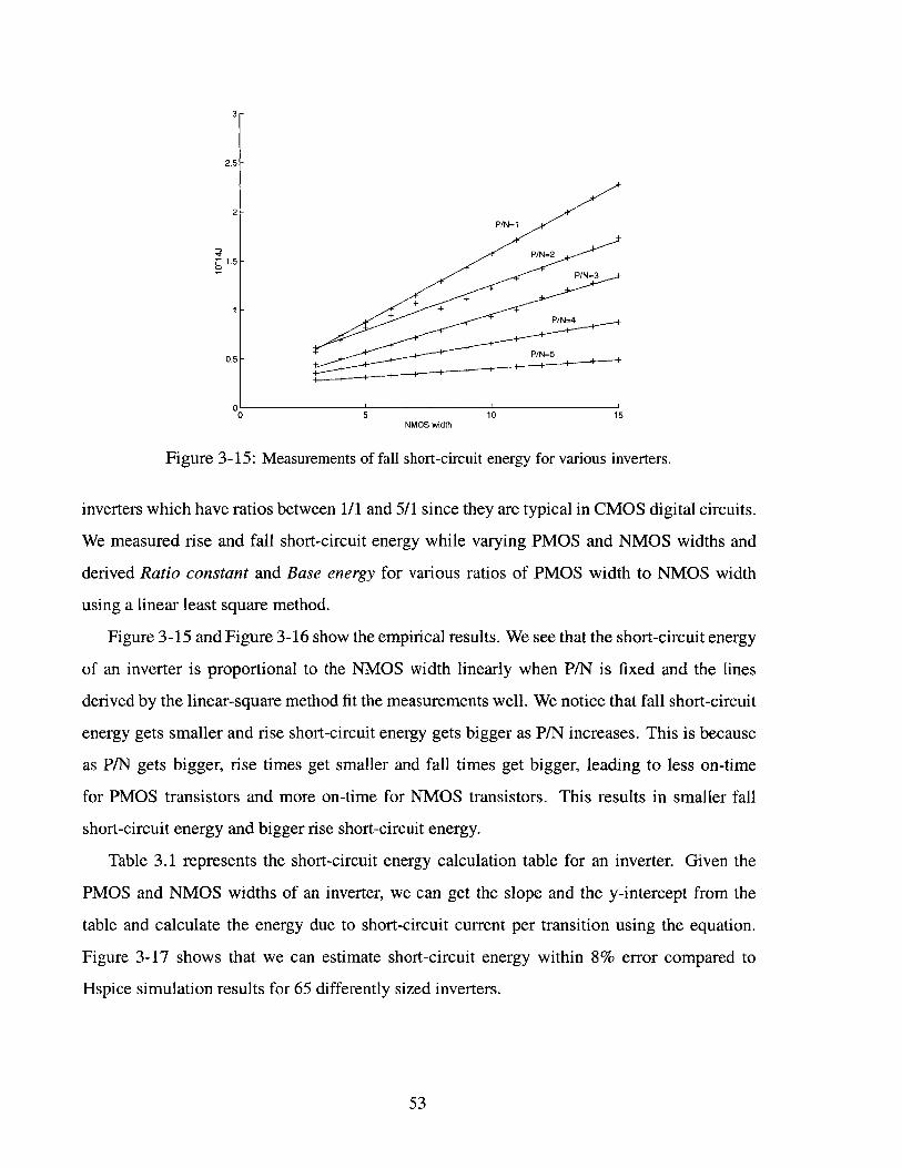
3
2.5-
2-P/N=1
1.5 -P/N=2
P/N=3
P/N=-4
0.5- P/N=5
01
0.5-
0 5 10 15NMOS width
Figure 3-15: Measurements of fall short-circuit energy for various inverters.
inverters which have ratios between 1/1 and 5/1 since they are typical in CMOS digital circuits.
We measured rise and fall short-circuit energy while varying PMOS and NMOS widths and
derived Ratio constant and Base energy for various ratios of PMOS width to NMOS width
using a linear least square method.
Figure 3-15 and Figure 3-16 show the empirical results. We see that the short-circuit energy
of an inverter is proportional to the NMOS width linearly when P/N is fixed and the lines
derived by the linear-square method fit the measurements well. We notice that fall short-circuit
energy gets smaller and rise short-circuit energy gets bigger as P/N increases. This is because
as P/N gets bigger, rise times get smaller and fall times get bigger, leading to less on-time
for PMOS transistors and more on-time for NMOS transistors. This results in smaller fall
short-circuit energy and bigger rise short-circuit energy.
Table 3.1 represents the short-circuit energy calculation table for an inverter. Given the
PMOS and NMOS widths of an inverter, we can get the slope and the y-intercept from the
table and calculate the energy due to short-circuit current per transition using the equation.
Figure 3-17 shows that we can estimate short-circuit energy within 8% error compared to
Hspice simulation results for 65 differently sized inverters.
53

31
2.5
2
7 1.5
0.5 -
P/N=5
P/N=4
P/N=3
/N=2
0NMOS width
10 15
Figure 3-16: Measurements of rise short-circuit energy for various inverters.
Fall short-circuit energy Rise short-circuit energy Avg. short-circuit energyP/N Ratio constant Base Energy Ratio constant Base Energy Ratio constant Base Energy1 0.1399 0.1783 0.0118 0.2035 0.07935 0.19092 0.0915 0.3372 0.0348 0.2034 0.0631 0.27033 0.0772 0.1832 0.0512 0.1175 0.0642 0.15034 0.0441 0.2210 0.1178 0.0244 0.0809 0.12275 0.0177 0.2242 0.1678 0.0841 0.0927 0.1542
Table 3.1: Short-circuit energy calculation table for an
average of fall and rise short-circuit energy.
inverter. Average short-circuit energy is the
54
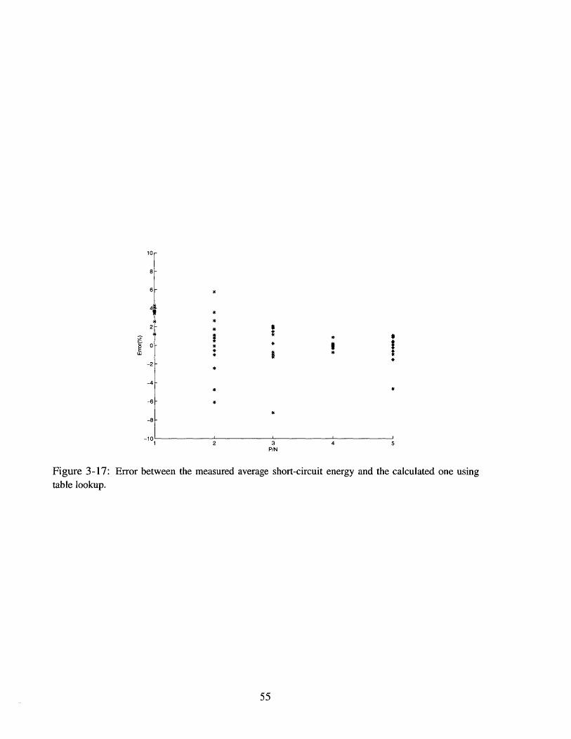
10-
8-
6 -
4j
0-*2 -
W -2-
-4-
-8-
-101 2 3 4 5
P/N
Figure 3-17: Error between the measured average short-circuit energy and the calculated one using
table lookup.
55

56
Chapter 4
Datapath Design
The low-power datapath design presented here is a part of the Vanilla Pekoe microprocessor
developed by the SCALE research group at the MIT Laboratory for Computer Science. Vanilla
Pekoe (VP) is a 32-bit single-issue low-power MIPS-compatible RISC microprocessor. VP has
an integer CPU, instruction and data caches, an external SDRAM interface, and a byte serial
host interface. The VP CPU can execute all integer instructions of the MIPS-II ISA except trap
instructions, misaligned load/stores, and multiprocessor instructions [6].
The datapath is fully pipelined and completes up to one instruction per cycle. The datapath
consists of a register file, an ALU, a shifter, a hardware multiplier/divider, a program counter,
and a system coprocessor. Instructions are executed in a five stage pipeline: instruction
fetch (F), instruction decode (D), execute (X), memory access (M), and result writeback (W).
Additionally, program counter generation (P) is considered to be a stage before the F stage.
The pipeline diagram of the datapath is shown in Figure 4-1. Suffices h and 1 represent clock
high and clock low respectively.
This chapter begins by elaborating on the VLSI design of the datapath. Next, we deal with
floorplaning of the datapath. Then we detail the low-power design of two execution blocks:
the ALU and the shifter. We describe a clock-gating scheme at the end of this chapter.
57
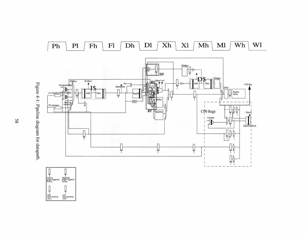
Ph P1 Fh F1 Dh Dl Xh Xl Mh Ml Wh WI
Addr DataCPBu
)ext CO:u
Regffe
C 0 Regs E-qual(
Counter
EquafityPeck
z1
CD
9.PO
00
itive Negativeede-triggered ed triggered
kensiive level-sensitivelatch latch
ux I$ Miss? akn? ovf
P~plus4AInstru tion
<<2 ignxtB c AderAddr Data
---------- -fter
PCcatenator ex
Mul/Div
ri riy y

4.1 VLSI Design
We implemented the datapath in a 0.25 pm CMOS process from TSMC with five aluminum
metal layers. We used the MOSIS SCMOSDEEP (A = 0.12pm) design rules for layout.
Figure 4-2 shows the layout of the entire datapath. The total size is 0.27 mm x 1.40 mm (=
0.378 mm 2 ). The supply voltage range is from 2.5 V down to 1.0 V. The circuit design style
used throughout the datapath is based on static/pseudo-static circuits that can maintain output
values even when the clock stops in a power-saving mode. Thus, when we use dynamic circuits,
leakage currents of dynamic nodes are protected by keepers.
4.1.1 Full-custom Design
We chose a full-custom VLSI design style. Custom design has proven to be better than a
standard cell approach in terms of important criteria such as power, speed and area. For
example, the M*CORE design achieved a 40% power reduction and 175% area reduction in
going from a synthesized to a custom 32-bit adder. Although custom design usually takes more
time, the regularity in most of the datapath makes custom design efficient in design time.
4.1.2 Metal Allocation
We used a regular, area-efficient metal allocation. The first three layers of metal are allocated
to intra-datapath wiring while metals 4 and 5 are used for global routing, the power grid, and
clock distribution. Metal 1 is used for local interconnect and Metal 2 is used for Vdd/GND and
control signals. Data buses use metal 3. Metal 3 and 5 are laid out horizontally along the bit
slice of the datapath, and metal 2 and 4 are laid out vertically. The datapath has a bit pitch of
54 lambda (6.48 pum), sufficient for six metal 3 buses across each bit slice. The bottommost
metal 3 bus track is reserved for strapping metal 2 power rails across datapath columns and the
other five metal 3 tracks are used for datapath buses. The bottommost metal 3 track is GND in
even bit slices and Vdd in odd bit slices. All bus tracks run over the top of datapath leaf cells;
this allows us to make a very tight datapath.
Figure 4-3 shows an example of metal allocation. (Metal 4 and 5 are excluded from the
layout for clarity purposes.) We see five vertical metal 2 wires (Vddl, GND1, clk, GND2, and
59
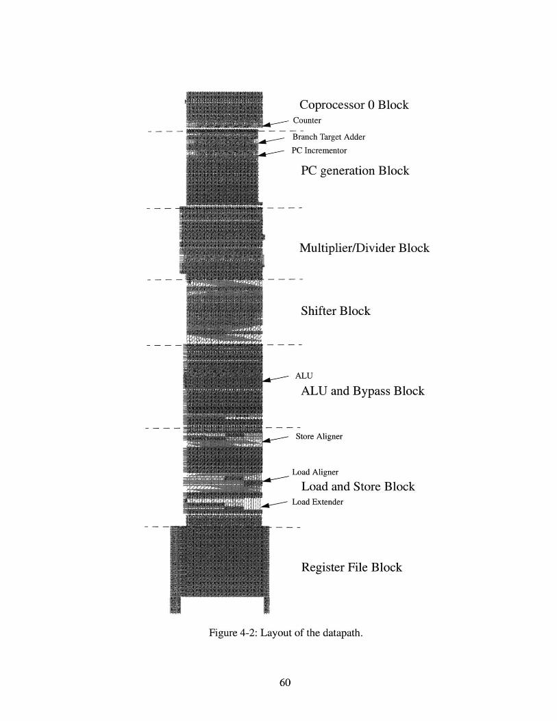
Coprocessor 0 BlockCounter
Branch Target Adder
PC Incrementor
PC generation Block
Multiplier/Divider Block
Shifter Block
ALU
ALU and Bypass Block
Store Aligner
Load Aligner
Load and Store BlockLoad Extender
Register File Block
Figure 4-2: Layout of the datapath.
60
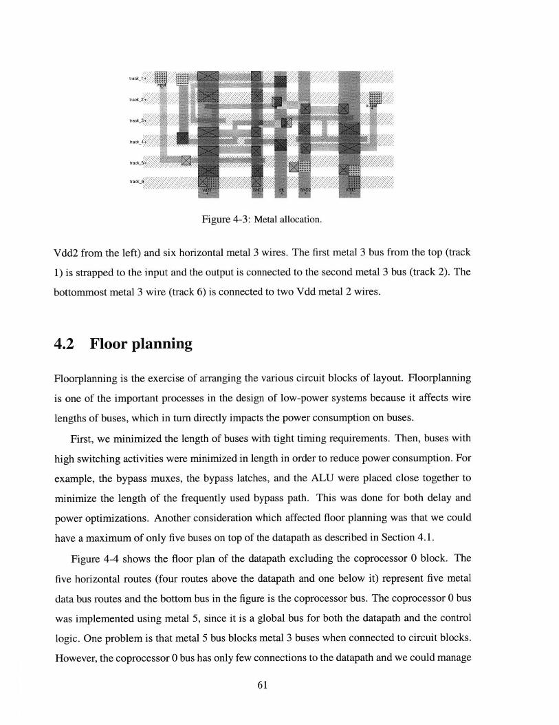
Figure 4-3: Metal allocation.
Vdd2 from the left) and six horizontal metal 3 wires. The first metal 3 bus from the top (track
1) is strapped to the input and the output is connected to the second metal 3 bus (track 2). The
bottommost metal 3 wire (track 6) is connected to two Vdd metal 2 wires.
4.2 Floor planning
Floorplanning is the exercise of arranging the various circuit blocks of layout. Floorplanning
is one of the important processes in the design of low-power systems because it affects wire
lengths of buses, which in turn directly impacts the power consumption on buses.
First, we minimized the length of buses with tight timing requirements. Then, buses with
high switching activities were minimized in length in order to reduce power consumption. For
example, the bypass muxes, the bypass latches, and the ALU were placed close together to
minimize the length of the frequently used bypass path. This was done for both delay and
power optimizations. Another consideration which affected floor planning was that we could
have a maximum of only five buses on top of the datapath as described in Section 4.1.
Figure 4-4 shows the floor plan of the datapath excluding the coprocessor 0 block. The
five horizontal routes (four routes above the datapath and one below it) represent five metal
data bus routes and the bottom bus in the figure is the coprocessor bus. The coprocessor 0 bus
was implemented using metal 5, since it is a global bus for both the datapath and the control
logic. One problem is that metal 5 bus blocks metal 3 buses when connected to circuit blocks.
However, the coprocessor 0 bus has only few connections to the datapath and we could manage
61

to make the connections through unused metal 3 tracks. The coprocessor 0 block is shown in
Figure 4-5.
The register file uses metal 3 for its local interconnect as an exception to the wiring
conventions. As a result, data buses are not allowed to cross it, and it resides at the leftmost end
of the floor plan. The Load and Store block which consists of load sign-extender, load aligner,
and store aligner follow the register file. Next, from left to right, there are the ALU and bypass
block, Shifter and Multiplier/Divider block, Program counter block, and coprocessor 0 block.
4.3 ALU
The ALU is arguably the most important block in the datapath. It performs arithmetic
operations like addition and subtraction, load and store address calculation, and logical
operations such as XOR, OR, AND, and NOR. SPECint95 benchmarks results indicate that
over 70% of instructions use the ALU block [17]. Therefore, the ALU is one of the hottest
spots in the datapath. However, applying low-power techniques to the ALU is not straight-
forward since it is also one of the main speed bottlenecks in the datapath. For this project,
we chose an adder design which consumes the least power while satisfying speed and area
constraints.
4.3.1 Adder Design
Because the adder is the most frequently used block in the datapath, a lot of research effort has
gone into its design. As a result, there are a myriad of adder designs; for example, the ripple
carry adder, carry select adder, carry skip adder, and carry save adder.
A ripple carry adder was ruled out since it is too slow for 32-bit addition (O(N)). A carry
select adder shows good performance (O(VN7)), but its power consumption is more than twice
that of a ripple carry adder. This is because it requires two carry chains which execute at the
same time and an additional N-bit output mux which chooses between the two adder outputs.
A carry lookahead adder has a dramatic speed advantage (especially for large adders) since
it has a logarithmic propagation delay (O(lg N)); but, a 32-bit carry lookahead adder requires
over 5 times more area and power than a ripple carry (32 bit) [12]. A carry save adder has a
62
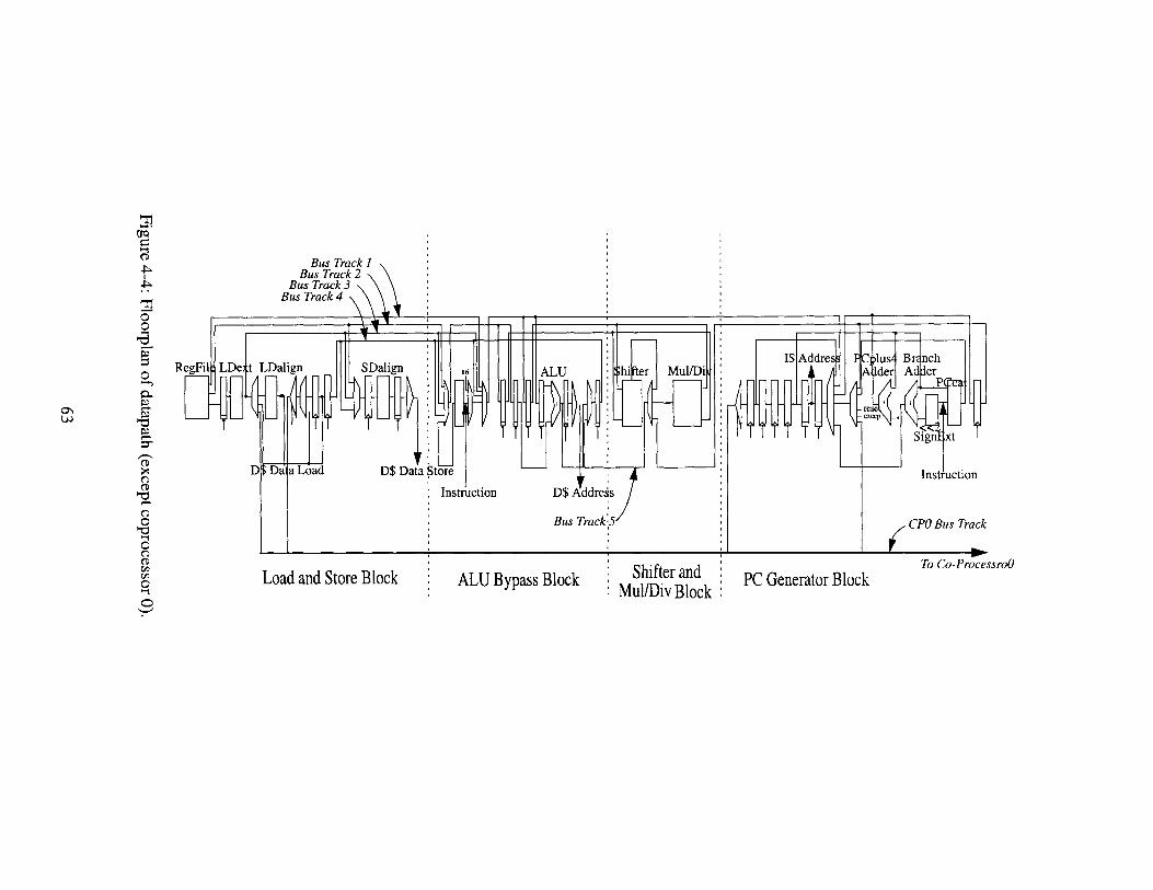
Bus Track I
Bus rTrack 2Bus Track 4
RegFil LDext LDalign SDalign 16 ALU hi ter Mul/Di
D Da a Lo ad D$ Data Store
Instruction D$ Addregs
Bus Track:51
J
0
ALU Bypass Block Shifter andMut/Div Block
1$ Addre I Cplus Bra nchC us Ter
W T VSign xt
Instfuction
CPO Bus Track
PC Generator BlockLoad and Store BlockTo Co-ProcessroO
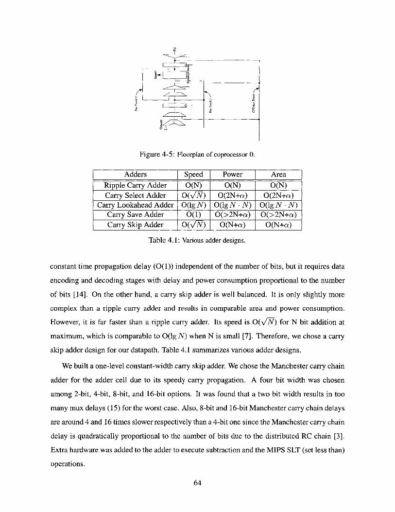
Figure 4-5: Floorplan of coprocessor 0.
Adders Speed Power AreaRipple Carry Adder O(N) O(N) O(N)Carry Select Adder 0(v'N) O(2N+a) 0(2N+a)
Carry Lookahead Adder O(lg N) O(lg N - N) O(lg N - N)Carry Save Adder O(1) 0(>2N+a) 0(>2N+a)Carry Skip Adder O(v'H) O(N+a) O(N+a)
Table 4.1: Various adder designs.
constant time propagation delay (0(1)) independent of the number of bits, but it requires data
encoding and decoding stages with delay and power consumption proportional to the number
of bits [14]. On the other hand, a carry skip adder is well balanced. It is only slightly more
complex than a ripple carry adder and results in comparable area and power consumption.
However, it is far faster than a ripple carry adder. Its speed is O(V/N) for N bit addition at
maximum, which is comparable to O(lg N) when N is small [7]. Therefore, we chose a carry
skip adder design for our datapath. Table 4.1 summarizes various adder designs.
We built a one-level constant-width carry skip adder. We chose the Manchester carry chain
adder for the adder cell due to its speedy carry propagation. A four bit width was chosen
among 2-bit, 4-bit, 8-bit, and 16-bit options. It was found that a two bit width results in too
many mux delays (15) for the worst case. Also, 8-bit and 16-bit Manchester carry chain delays
are around 4 and 16 times slower respectively than a 4-bit one since the Manchester carry chain
delay is quadratically proportional to the number of bits due to the distributed RC chain [3].
Extra hardware was added to the adder to execute subtraction and the MIPS SLT (set less than)
operations.
64

LOGIC I Sell1 Sel2 Sel3
XOR 1 0 1AND 0 1 1NOR 1 1 0OR 1 1 1
OFF 0 0 1
Table 4.2: Control signals for logic operation.
4.3.2 Logic Unit and Branch Checker Design
We observed that we can use the adder's P (propagate) and G (generate) signals (which were
originally generated for addition/subtraction) for logic operations since P is the bitwise XOR
of the two inputs and G is the bitwise AND of them. Also, we can perform the OR operation by
OR-ing P and G, and inverting the OR signal makes the NOR signal. Figure 4-6 and Table 4.2
show how we execute the XOR, AND, OR and NOR operations by making use of P and G and
three control signals. OFF control signals turns off the logic unit and prevents spurious data
transitions.
The main advantage of this scheme is area reduction due to the reuse of already existing
signals. Another advantage is the reduction of the bypass muxes' output loads since they no
longer need to drive the logic unit in addition to the adder. The output nodes of the bypass
muxes are among the most frequently-used nodes, so the reduced load capacitance results in
large energy savings and an important delay reduction. This scheme slows down the adder's P
and G signals, yet usually the delay of an adder is not determined by the P and G delay but by
carry chain delay. However, this scheme increases the internal energy dissipation of the adder
itself because of the additional gate caps on P and G.
Another observation is that we may use P to test the equality of two inputs (for branch
condition checking) since the XOR indicates when two inputs are different. We built a dynamic
equality checking circuit by adding one additional NMOS transistor as shown in Figure 4-6.
The precharge line in Figure 4-6 stretches across the bit-slices of the adder, and is precharged
every cycle. If any of the 32 P bits becomes one (two inputs are different), the NMOS transistor
whose gate is connected to the P bit, starts discharging and the precharge line discharges. If all
Ps are zero (two inputs are the same), the precharge line remains charged during the evaluation
65
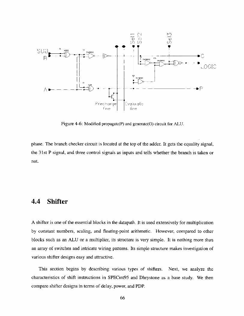
SUB~ 1 XOR2
Am
132frNAND
XOR
QD U9 G)C
LOGIC
21nNAND
Prechargeine
Evciuiateline
Figure 4-6: Modified propagate(P) and generate(G) circuit for ALU.
phase. The branch checker circuit is located at the top of the adder. It gets the equality signal,
the 31st P signal, and three control signals as inputs and tells whether the branch is taken or
not.
4.4 Shifter
A shifter is one of the essential blocks in the datapath. It is used extensively for multiplication
by constant numbers, scaling, and floating-point arithmetic. However, compared to other
blocks such as an ALU or a multiplier, its structure is very simple. It is nothing more than
an array of switches and intricate wiring patterns. Its simple structure makes investigation of
various shifter designs easy and attractive.
This section begins by describing various types of shifters. Next, we analyze the
characteristics of shift instructions in SPECint95 and Dhrystone as a base study. We then
compare shifter designs in terms of delay, power, and PDP.
66
PWr

out 3* solid connection in 3o switch out 2
in2:GND out 1in 1
in 00
Ish 3 Ish 2 Ish 1 Ish 0
Figure 4-7: A barrel shifter.
4.4.1 Types of Shifters
There are two kinds of shifts: left and right. To deal with both shifts, we may build both a left
shifter and a right shifter, or a bidirectional shifter. We decided to have two unidirectional (left
and right) shifters. There is no advantage to unifying the two shifters into a bidirectional shifter
if area is not a main concern of the design. A bidirectional shifter has around twice the wire
capacitance at the internal nodes compared to a unidirectional shifter. This results in slower
speed and also more power dissipation than a dual shifters scheme, provided that we turn off
the unused unidirectional shifter in the dual shifters scheme.
There are two commonly used shifter structures: a barrel shifter and a logarithmic shifter
[14]. The barrel shifter is an array of switches which connect input and output. By turning on
the switches which connect the m-th input and the (m+n)-th output, an n-bit left shift is done.
Figure 4-7 shows a 4-bit left barrel shifter. For example, if Ish 1 goes high and the switches
connected to it are turned on, out[n+1] is connected to in[n] (0 < n < 2) and out[0] becomes
zero; this results in a 1-bit left shift. The primary advantage of this shifter is that the signal
goes through only one switch from input to output, which results in high speed. However, it
has the major disadvantage that it needs an extra decoder for the control signals. For example,
it needs a 5-to-32 decoder for a 32-bit shifter.
A log shifter, on the other hand, is divided into stages which consist of muxes. For example,
a 32-bit log-2 shifter has five stages: 1 bit, 2 bit, 4 bit, 8 bit, and 16 bit. Figure 4-8(a) shows an
example of a log-2 shifter. As it goes through the stages, input data is either shifted or passed
through. Unlike the barrel shifter, a log shifter doesn't need much extra hardware for decoding.
In particular, a log-2 shifter doesn't need any extra hardware.
67
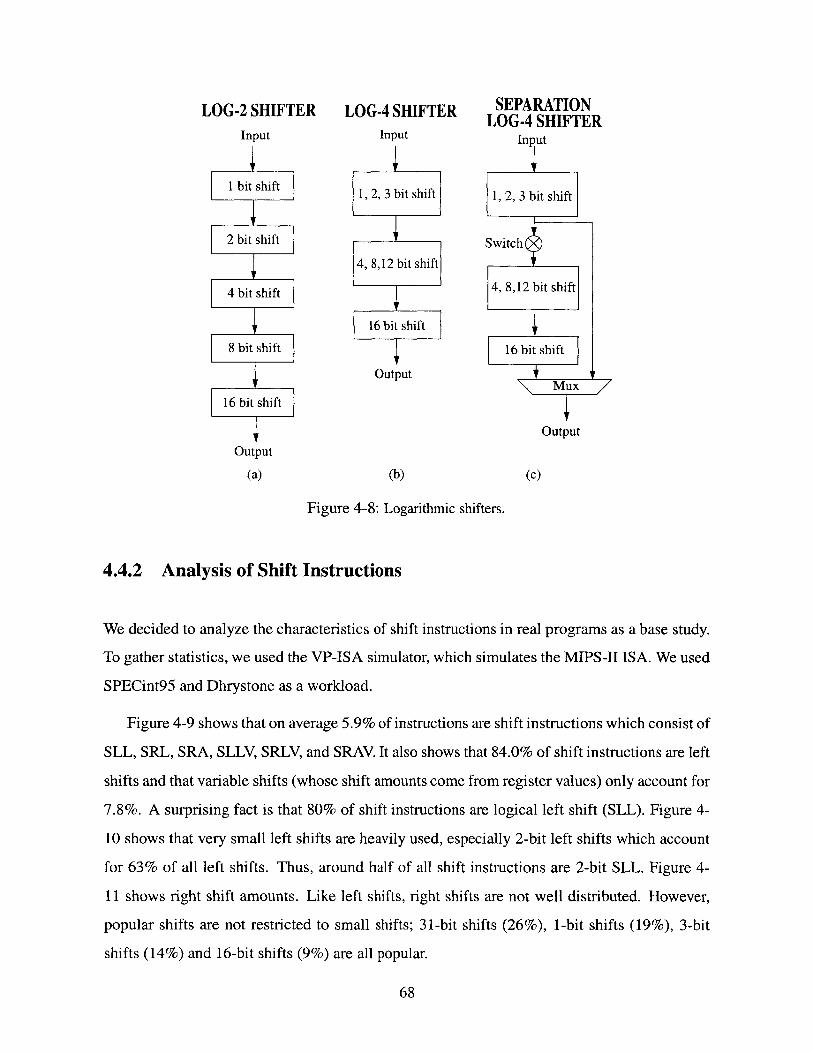
LOG-2 SHIFTERInput
1 bit shift
2 bit shift
4 bit shift
8 bit shift
16 bit shift
Output
(a)
LOG-4 SHIFTERInput
1, 2, 3 bit shift
4, 8,12 bit shift
16 bit shift
Output
(b)
SEPARATIONLOG-4 SHIFTER
Input
1, 2, 3 bit shift
Switch
4, 8,12 bit shift
16 bit shift
Mux/
Output
(c)
Figure 4-8: Logarithmic shifters.
4.4.2 Analysis of Shift Instructions
We decided to analyze the characteristics of shift instructions in real programs as a base study.
To gather statistics, we used the VP-ISA simulator, which simulates the MIPS-II ISA. We used
SPECint95 and Dhrystone as a workload.
Figure 4-9 shows that on average 5.9% of instructions are shift instructions which consist of
SLL, SRL, SRA, SLLV, SRLV, and SRAV. It also shows that 84.0% of shift instructions are left
shifts and that variable shifts (whose shift amounts come from register values) only account for
7.8%. A surprising fact is that 80% of shift instructions are logical left shift (SLL). Figure 4-
10 shows that very small left shifts are heavily used, especially 2-bit left shifts which account
for 63% of all left shifts. Thus, around half of all shift instructions are 2-bit SLL. Figure 4-
11 shows right shift amounts. Like left shifts, right shifts are not well distributed. However,
popular shifts are not restricted to small shifts; 31-bit shifts (26%), 1-bit shifts (19%), 3-bit
shifts (14%) and 16-bit shifts (9%) are all popular.
68
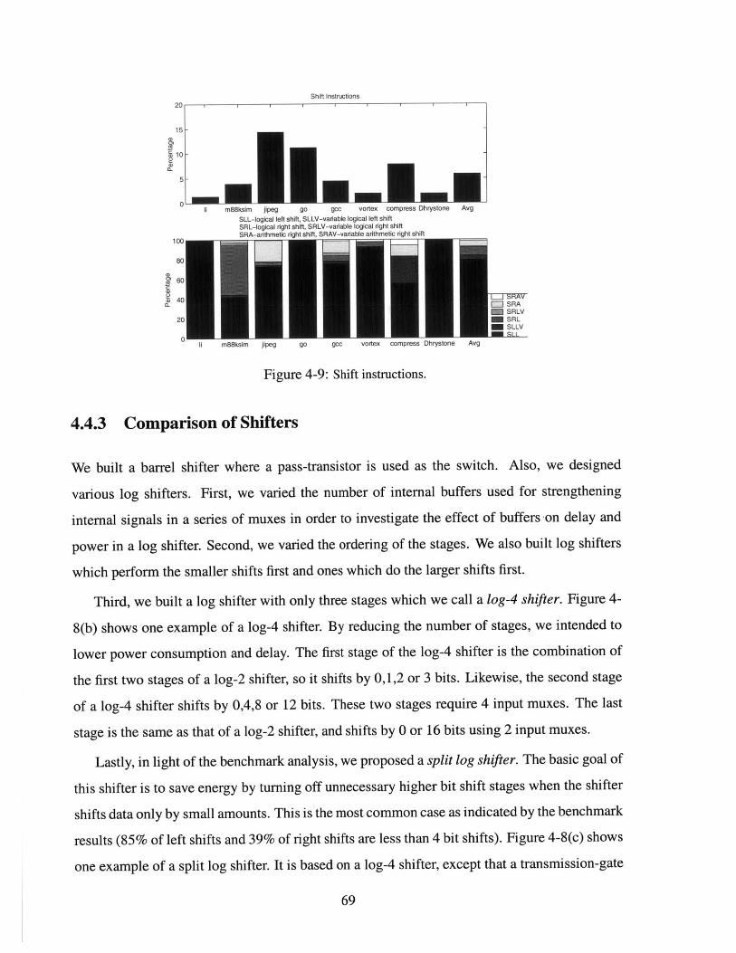
0~
2a)
Shift Instructions
20 - r i I e I I I I
15 -
10-
5-
0 LIi m88ksim jipeg go gcc vortex compress Dhrystone
SILL-logicsl left shift, SLLV-varisble logical left shiftSRL-logical right shift, SRLV-varible logical right shift
100 SRA-arthmetic right shift, SRAV-variable arithmetic right shift
80
60
40
20
01111Ii m88ksim jipeg
Avg
e Avg
J SRASRLVSRL
M SLLVJMESLL_
Figure 4-9: Shift instructions.
4.4.3 Comparison of Shifters
We built a barrel shifter where a pass-transistor is used as the switch. Also, we designed
various log shifters. First, we varied the number of internal buffers used for strengthening
internal signals in a series of muxes in order to investigate the effect of buffers on delay and
power in a log shifter. Second, we varied the ordering of the stages. We also built log shifters
which perform the smaller shifts first and ones which do the larger shifts first.
Third, we built a log shifter with only three stages which we call a log-4 shifter. Figure 4-
8(b) shows one example of a log-4 shifter. By reducing the number of stages, we intended to
lower power consumption and delay. The first stage of the log-4 shifter is the combination of
the first two stages of a log-2 shifter, so it shifts by 0,1,2 or 3 bits. Likewise, the second stage
of a log-4 shifter shifts by 0,4,8 or 12 bits. These two stages require 4 input muxes. The last
stage is the same as that of a log-2 shifter, and shifts by 0 or 16 bits using 2 input muxes.
Lastly, in light of the benchmark analysis, we proposed a split log shifter. The basic goal of
this shifter is to save energy by turning off unnecessary higher bit shift stages when the shifter
shifts data only by small amounts. This is the most common case as indicated by the benchmark
results (85% of left shifts and 39% of right shifts are less than 4 bit shifts). Figure 4-8(c) shows
one example of a split log shifter. It is based on a log-4 shifter, except that a transmission-gate
69
'
compress Dhrystongo gut; vunRx

li-ref100
50
50
0 10 20 30
go-ref
E
50
0 10 20 30corn-ret
100
50
0 10 20 30
m88-ref100
50
0 10 20 30gcc-ref
100
50
00 10 20 30
dhr100
50
00 10 20 30
bits
sij-ref100
50
vo-ref
501
0 10 20 30tot
100 t
50
0~0 10 20 30
Figure 4-10: Left shift amounts.
switch is located between the low bit shift stages and the high bit shift stages and a new output
mux is introduced. When the shift amount is small (less than 4), the shifter is separated by
turning off the switch and the high bit shift stages become inactive. The low bit shift signal is
chosen by the output mux. On the other hand, when the shift amount is greater than or equal
to 4, the switch is closed and the shifter operates like a normal log-4 shifter.
A transmission-gate mux was used for all log shifters. All designs were laid out by hand
using Magic and optimized for area. We compared a barrel shifter and various log shifters
including a log-4 shifter and a split log shifter in terms of delay, energy, and EDP for left and
right shifts.
A. Delay
As a delay parameter, we used the worst case delay. It is the propagation delay from bit
0 of input to bit 31 of output or that from bit 31 input to bit 0 of output for log shifters. But,
the worst case delay of a barrel shifter should include the decoder delay. This is because shift
amounts must be decoded to appropriate control signals first before the data propagates, when
the shift amounts are values of registers.
We extracted the layouts using SPACE 2D [18], simulated the extracted netlists and
70
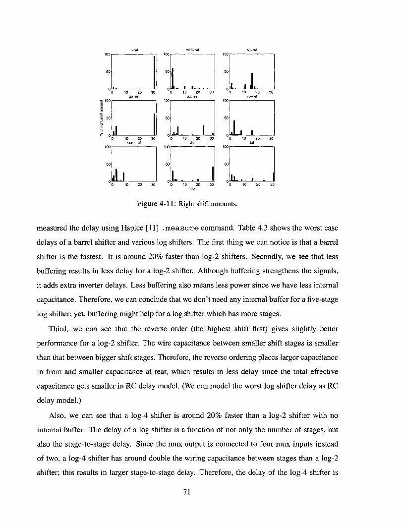
li-ref m88-ref sij-ref100 100 100
50 50 50
0, 01 0 "L0 10 20 30 0 10 20 30 0 10 20 30
go-ref gcc-ref vo-refZ 100 100 100
0
. 50 50 50
00 10 20 30 00 10 20 30 00 10 20 30corn-ref dhr tot
100 - 100 100
50 50 50
0 0 L00 10 20 30 0 10 20 30 0 10 20 30
bits
Figure 4-11: Right shift amounts.
measured the delay using Hspice [11] .measure command. Table 4.3 shows the worst case
delays of a barrel shifter and various log shifters. The first thing we can notice is that a barrel
shifter is the fastest. It is around 20% faster than log-2 shifters. Secondly, we see that less
buffering results in less delay for a log-2 shifter. Although buffering strengthens the signals,
it adds extra inverter delays. Less buffering also means less power since we have less internal
capacitance. Therefore, we can conclude that we don't need any internal buffer for a five-stage
log shifter; yet, buffering might help for a log shifter which has more stages.
Third, we can see that the reverse order (the highest shift first) gives slightly better
performance for a log-2 shifter. The wire capacitance between smaller shift stages is smaller
than that between bigger shift stages. Therefore, the reverse ordering places larger capacitance
in front and smaller capacitance at rear, which results in less delay since the total effective
capacitance gets smaller in RC delay model. (We can model the worst log shifter delay as RC
delay model.)
Also, we can see that a log-4 shifter is around 20% faster than a log-2 shifter with no
internal buffer. The delay of a log shifter is a function of not only the number of stages, but
also the stage-to-stage delay. Since the mux output is connected to four mux inputs instead
of two, a log-4 shifter has around double the wiring capacitance between stages than a log-2
shifter; this results in larger stage-to-stage delay. Therefore, the delay of the log-4 shifter is
71

Delay(ns) Barrel Log-2(4 but)
0-to-I delay 0.67 1.201-to-0 delay 0.90 1.31
Maximum delay 0.90 1.31
Table 4.3: Worst case delay of shifters. (0.37 ns.)
Log-2(2 but)
1.011.051.05
The barrel
Log-2 Log-2-rev Log-4(0 buf (0 buf (0 buf)
0.92 0.91 0.751.11 1.10 0.901.11 1.10 0.90
shifter delay includes the worst case
Log-4-split(0 but)
1.051.181.18
decoder del
larger than 3/5 (the ratio of the number of the stages in a log-4 shifter to that in a log-2 shifter)
of the log-2 shifter delay.
Lastly, we can see the delay penalty of a split log shifter. We see around 40% slow down
compared to a log-4 shifter due to the extra delays added by the switch and the output mux,
which results in slower speed than a log-2 shifter (with no internal buffer).
B. Energy
As an energy parameter, we used the average energy consumption per shift operation.
We calculated the average energy consumption using our energy estimation model, which is
explained in detail in Chapter 2. As the simulator for the energy model, the TO-ISA simulator
was used. As a workload, the SPECint 95 reference programs (li-ref, m88ksim-ref, sijpeg-ref,
go-ref, gcc-ref, vortex-ref, and compress-ref) and Dhrystone were used.
Figure 4-12 and Figure 4-13 show average energy consumption of left shifters and right
shifters. We compared four different shifters; a normal-order log-2 shifter (log-2), a reverse-
order log-2 shifter (log-2rev), a log-4 shifter (log-4), and a split log-4 shifter (log-4split). All
shifters have no internal buffer because, as shown before, internal buffers slow down the shift
and also dissipate additional energy.
There are two main sources of energy consumption in shifters. One is due to transitions
on internal nodes, internal energy, and the other is due to transitions on control signal wires,
control energy. From the figures, we notice that control energy is comparable to internal energy
for most of the cases except for left shifters in li, go, and vortex.
First, we notice that right shift instructions consume more energy per operation than left
shift instructions for most of benchmarks and shifters. Compared to left shifts, a wider variety
72
.1
ay,
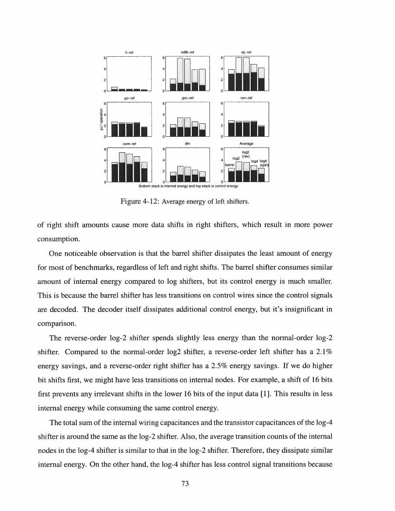
li-ref m88-ref sij-ref
6 66
4 4 4
2 2 2
0 " " " 0 0go-ref gcc-ref vor-ref
6 6 6
4 4 4
-22 2 2
0 0 J 0-acom-ref dhr Average
6 6 6og2
44 fog2 (rev) log4 fog4barrel (split
2 sfak2si f 0 e o n
Bottom stack is internal energy and top stack is control energy
Figure 4-12: Average energy of left shifters.
of right shift amounts cause more data shifts in right shifters, which result in more power
consumption.
One noticeable observation is that the barrel shifter dissipates the least amount of energy
for most of benchmarks, regardless of left and right shifts. The barrel shifter consumes similar
amount of internal energy compared to log shifters, but its control energy is much smaller.
This is because the barrel shifter has less transitions on control wires since the control signals
are decoded. The decoder itself dissipates additional control energy, but it's insignificant in
comparison.
The reverse-order log-2 shifter spends slightly less energy than the normal-order log-2
shifter. Compared to the normal-order log2 shifter, a reverse-order left shifter has a 2.1%
energy savings, and a reverse-order right shifter has a 2.5% energy savings. If we do higher
bit shifts first, we might have less transitions on internal nodes. For example, a shift of 16 bits
first prevents any irrelevant shifts in the lower 16 bits of the input data [1]. This results in less
internal energy while consuming the same control energy.
The total sum of the internal wiring capacitances and the transistor capacitances of the log-4
shifter is around the same as the log-2 shifter. Also, the average transition counts of the internal
nodes in the log-4 shifter is similar to that in the log-2 shifter. Therefore, they dissipate similar
internal energy. On the other hand, the log-4 shifter has less control signal transitions because
73
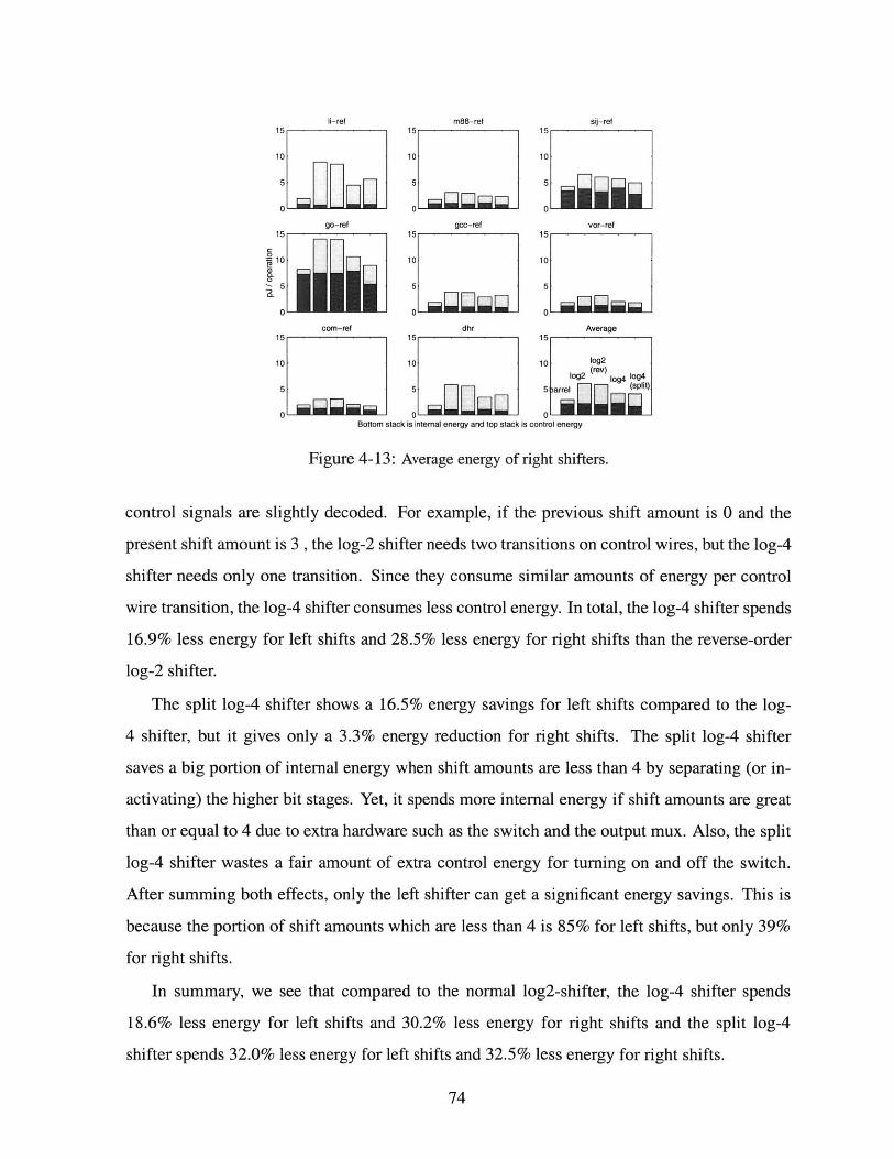
li-ref m88-ref sij-ref15 15 15
10 10 10
5 5 5
0 0 r1 0
go-ref gcc-ref vor-ref15 15 15
10 10 10
25 5 5 tre sltcorn-ref dhr Average
15 15 15
0,10 10 1
1og2 1
Iog2 (revlog4 9
Boto stc 5 arrl i)
S0 0Bottom stack is internal energy and top stack is control energy
Figure 4-13: Average energy of right shifters.
control signals are slightly decoded. For example, if the previous shift amount is 0 and the
present shift amount is 3 , the log-2 shifter needs two transitions on control wires, but the log-4
shifter needs only one transition. Since they consume similar amounts of energy per control
wire transition, the log-4 shifter consumes less control energy. In total, the log-4 shifter spends
16.9% less energy for left shifts and 28.5% less energy for right shifts than the reverse-order
log-2 shifter.
The split log-4 shifter shows a 16.5% energy savings for left shifts compared to the log-
4 shifter, but it gives only a 3.3% energy reduction for right shifts. The split log-4 shifter
saves a big portion of internal energy when shift amounts are less than 4 by separating (or in-
activating) the higher bit stages. Yet, it spends more internal energy if shift amounts are great
than or equal to 4 due to extra hardware such as the switch and the output mux. Also, the split
log-4 shifter wastes a fair amount of extra control energy for turning on and off the switch.
After summing both effects, only the left shifter can get a significant energy savings. This is
because the portion of shift amounts which are less than 4 is 85% for left shifts, but only 39%
for right shifts.
In summary, we see that compared to the normal log2-shifter, the log-4 shifter spends
18.6% less energy for left shifts and 30.2% less energy for right shifts and the split log-4
shifter spends 32.0% less energy for left shifts and 32.5% less energy for right shifts.
74
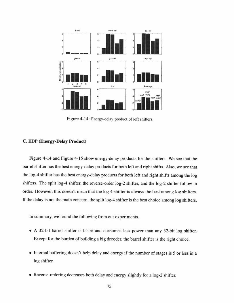
li-ref6
4
2
0 _MMMMM.-go-ref
6
4
com-ref6
4
2
m88-ref6
4
2I
gcc-ref6
4
Adhr
6
4
:.hi
sij-ref6
4
2
vor-ref6
4
Average
log24 2 (rev) fog4
barrel
Figure 4-14: Energy-delay product of left shifters.
C. EDP (Energy-Delay Product)
Figure 4-14 and Figure 4-15 show energy-delay products for the shifters. We see that the
barrel shifter has the best energy-delay products for both left and right shifts. Also, we see that
the log-4 shifter has the best energy-delay products for both left and right shifts among the log
shifters. The split log-4 shifter, the reverse-order log-2 shifter, and the log-2 shifter follow in
order. However, this doesn't mean that the log-4 shifter is always the best among log shifters.
If the delay is not the main concern, the split log-4 shifter is the best choice among log shifters.
In summary, we found the following from our experiments.
" A 32-bit barrel shifter is faster and consumes less power than any 32-bit log shifter.
Except for the burden of building a big decoder, the barrel shifter is the right choice.
" Internal buffering doesn't help delay and energy if the number of stages is 5 or less in a
log shifter.
* Reverse-ordering decreases both delay and energy slightly for a log-2 shifter.
75
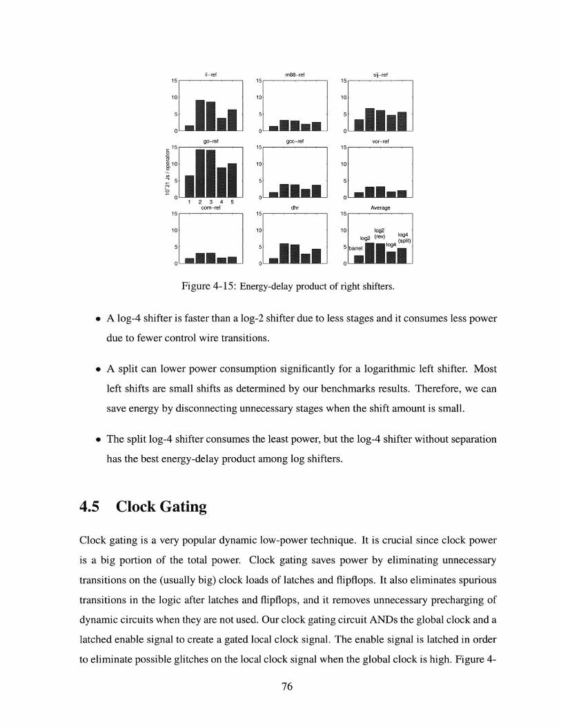
li-ref15
10
5
0 igo-ref
10
0
1 12corn-ref45
10
510,
m88-ref15
10
5
0gcc-ref
15
10
5
dhr15
10
sij-ref15
10
5
0Avor-ref
15
10
5
0-I.-Average
10 log2log2 (rev) (slt)
5 arrel 0 (
0- N S
Figure 4-15: Energy-delay product of right shifters.
" A log-4 shifter is faster than a log-2 shifter due to less stages and it consumes less power
due to fewer control wire transitions.
" A split can lower power consumption significantly for a logarithmic left shifter. Most
left shifts are small shifts as determined by our benchmarks results. Therefore, we can
save energy by disconnecting unnecessary stages when the shift amount is small.
" The split log-4 shifter consumes the least power, but the log-4 shifter without separation
has the best energy-delay product among log shifters.
4.5 Clock Gating
Clock gating is a very popular dynamic low-power technique. It is crucial since clock power
is a big portion of the total power. Clock gating saves power by eliminating unnecessary
transitions on the (usually big) clock loads of latches and flipflops. It also eliminates spurious
transitions in the logic after latches and flipflops, and it removes unnecessary precharging of
dynamic circuits when they are not used. Our clock gating circuit ANDs the global clock and a
latched enable signal to create a gated local clock signal. The enable signal is latched in order
to eliminate possible glitches on the local clock signal when the global clock is high. Figure 4-
76
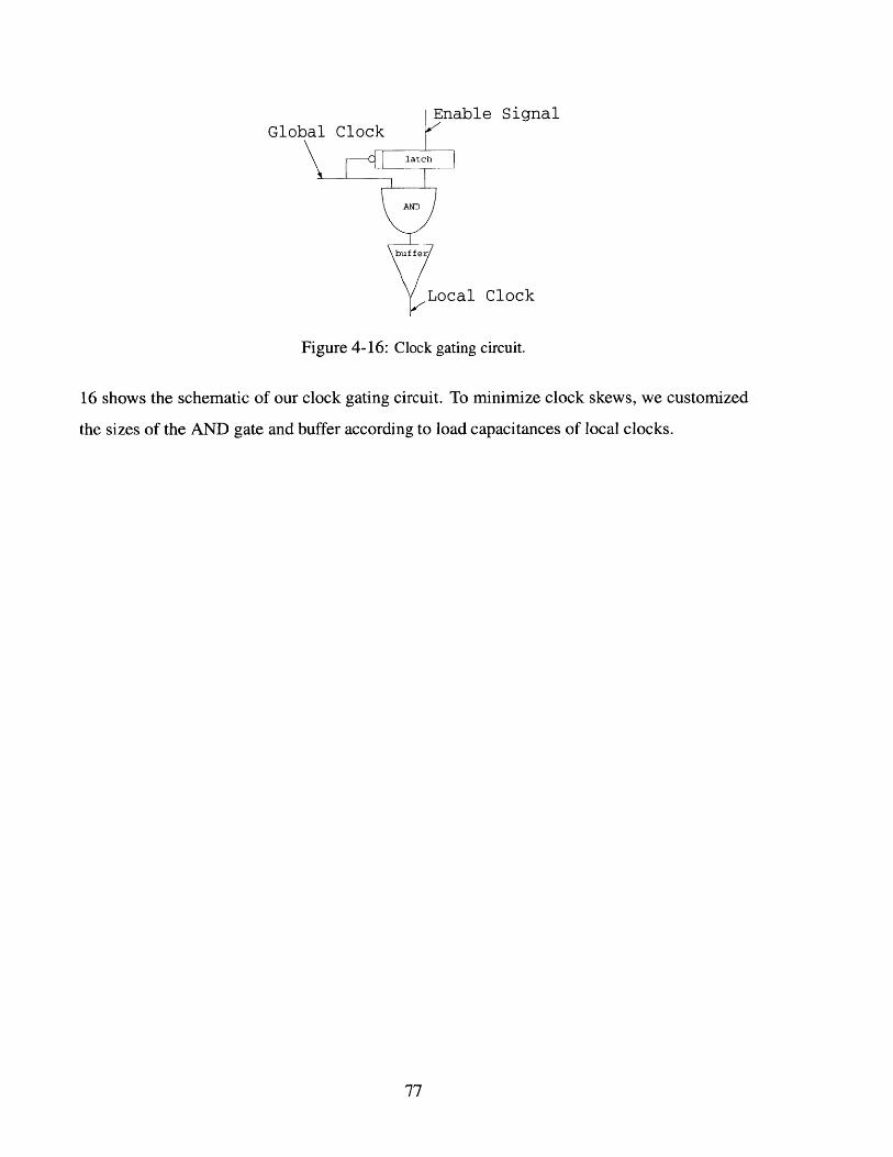
Enable SignalGlobal Clock
latch
ANDl
buffer
Local Clock
Figure 4-16: Clock gating circuit.
16 shows the schematic of our clock gating circuit. To minimize clock skews, we customized
the sizes of the AND gate and buffer according to load capacitances of local clocks.
77

78
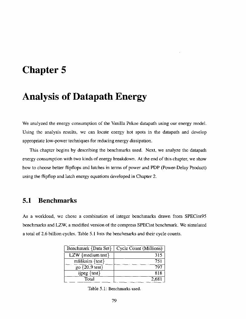
Chapter 5
Analysis of Datapath Energy
We analyzed the energy consumption of the Vanilla Pekoe datapath using our energy model.
Using the analysis results, we can locate energy hot spots in the datapath and develop
appropriate low-power techniques for reducing energy dissipation.
This chapter begins by describing the benchmarks used. Next, we analyze the datapath
energy consumption with two kinds of energy breakdown. At the end of this chapter, we show
how to choose better flipflops and latches in terms of power and PDP (Power-Delay Product)
using the flipflop and latch energy equations developed in Chapter 2.
5.1 Benchmarks
As a workload, we chose a combination of integer benchmarks drawn from SPECint95
benchmarks and LZW, a modified version of the compress SPECint benchmark. We simulated
a total of 2.6 billion cycles. Table 5.1 lists the benchmarks and their cycle counts.
Benchmark {Data Set} Cycle Count (Millions)
LZW {medium test} 315m88ksim {test} 751go {20_9 test} 797
ijpeg {test} 818Total 2,681
Table 5.1: Benchmarks used.
79

EqualCheck Buffer4.5 pJ/cycle (3%) 0.9 pJ/cycle (<1%) 3.9 p cycle (2%)
AdderFlipflop 11. 1 pJ/cycle (7%)
36.6 pJ/cycle (23%ALU
12.3 pJ/cycle (8%)
RegFile
Latch 37.2 pJ/cycle (23%)
36.6 pJ/cycle (23%)
Mux16.8 pJ/cycle (10%)
Figure 5-1: Average energy breakdown by component type.
5.2 Energy Breakdown
We excluded the energy consumption of the multiplier/divider unit. However, we believe that
its contribution to energy consumption is insignificant because it is rarely used (although it
requires multiple clock cycles for computation). For example, multiplication and division
instructions in MIPS SPECint95 benchmarks comprise less than 1% of all instructions [17].
We haven't yet implemented clock gating control logic, but we plan to add thorough clock
gating based on these preliminary results. Supply voltage was 2.5 V for the energy analysis
presented here.
5.2.1 Energy Breakdown By Component Type
We decided to study what portion of energy is consumed by each component. We classified
the datapath components as flipflops, latches, muxes, a register file, an ALU, adders, a shifter,
buffers, and an equality checker. Incrementors are classified as adders, and tri-state buffers as
buffers.
Table 5.2 shows the energy breakdown by component type for each benchmark. Figure 5-1
shows the average energy breakdown. First, we notice that flipflops, latches, and muxes - the
blocks that glue a datapath together - consume over half the total energy (56%). They are the
80

Benchmark Flipflop ] Latch Mux RegFile ALU Adder Shifter [ Buffer [ EqualCheck
LZW 34.8 (22%) 37.2(23%) 19.2 (12%) 37.5 (23%) 12.0(7%) 10.5 (6%) 4.5 (3%) 1.5 (<1%) 4.5 (3%)m88ksim 36.6(23%) 35.7 (23%) 15.0(10%) 36.0(23%) 12.6 (8%) 11.4(7%) 3.0(2%) 0.6 (<1%) 4.5 (3%)
go 35.7 (23%) 34.6(23%) 13.8 (9%) 36.6 (24%) 10.8(7%) 11.1 (7%) 4.2(3%) 0.9 (<1%) 4.5 (3%)
ijpeg 38.1 (22%) 38.7 (23%) 20.1 (12%) 38.4(23%) 13.2 (8%) 11.4(7%) 4.2(2%) 1.2 (<1%) 4.5 (3%)Average 36.6(23%) 36.6(23%) 16.8 (10%) 37.2(23%) 12.3 (8%) 11.1 (7%) 3.9(2%) 0.9 (<1%) 4.5(3%)
Table 5.2: Energy breakdown by component type (pJ/cycle (%)).
most numerous components and these results also demonstrate that they are among the most
energy-consuming. We see that a careful low-power design of these blocks can lower the total
power significantly. Also, for flipflops and latches, we see that clock gating can potentially
lower the total power.
We also see that the register file is one of the largest consumers of datapath power (23%).
We can expect that a power-efficient register file design will lower datapath power significantly
[17]. On the other hand, the major execution blocks such as the ALU, the shifter, and the
adders account for only 17% in total. In particular, the shifter consumes only 2% of the total
energy.
5.2.2 Functional Energy Breakdown
We decided to obtain a functional energy breakdown as follows.
" Decode: this block fetches data from the register file and prepares inputs for the
execution blocks. It consists of the register file read, bypass muxes, bypass latches,
and bypass flipflops.
" Execute: this block computes operations. It consists of an ALU and a shifter.
" LoadStore: this block processes load and store data. It consists of the load
aligner/extender, the store aligner, latches, and flipflops.
" WriteBack: this block takes the output of the execute block and writes back to the register
file. It consists of the register file write, muxes, latches, and flipflops.
" PC generation: this block generates the next PC (Program Counter). It consists of muxes,
an incrementor, an adder, latches, and flipflops.
81
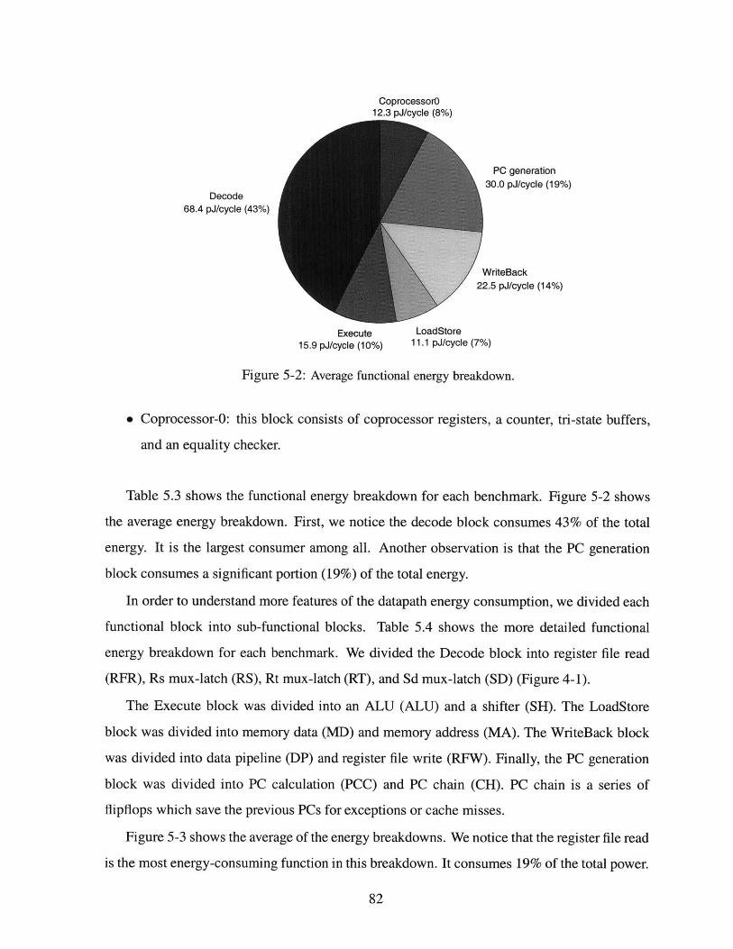
CoprocessorO12.3 pJ/cycle (8%)
PC generation30.0 pJ/cycle (19%)
Decode68.4 pJ/cycle (43%)
WriteBack22.5 pJ/cycle (14%)
Execute LoadStore15.9 pJ/cycle (10%) 11.1 pJ/cycle (7%)
Figure 5-2: Average functional energy breakdown.
* Coprocessor-0: this block consists of coprocessor registers, a counter, tri-state buffers,
and an equality checker.
Table 5.3 shows the functional energy breakdown for each benchmark. Figure 5-2 shows
the average energy breakdown. First, we notice the decode block consumes 43% of the total
energy. It is the largest consumer among all. Another observation is that the PC generation
block consumes a significant portion (19%) of the total energy.
In order to understand more features of the datapath energy consumption, we divided each
functional block into sub-functional blocks. Table 5.4 shows the more detailed functional
energy breakdown for each benchmark. We divided the Decode block into register file read
(RFR), Rs mux-latch (RS), Rt mux-latch (RT), and Sd mux-latch (SD) (Figure 4-1).
The Execute block was divided into an ALU (ALU) and a shifter (SH). The LoadStore
block was divided into memory data (MD) and memory address (MA). The WriteBack block
was divided into data pipeline (DP) and register file write (RFW). Finally, the PC generation
block was divided into PC calculation (PCC) and PC chain (CH). PC chain is a series of
flipflops which save the previous PCs for exceptions or cache misses.
Figure 5-3 shows the average of the energy breakdowns. We notice that the register file read
is the most energy-consuming function in this breakdown. It consumes 19% of the total power.
82

CoprocessorO ,
12.3 pJ/cycle (8%),'RegFile-Read
31.8 pJ/cycle (20%) chain10.5 pJ/cycle (6%)
PC calculation
Bypass-Rs 19.8 pJ/cycle (12%)19.8 pJ/cycle (12%)
RegiRe-WAriteBypass-Rt 5.4 pJ/cycle (3j*/)
9.6 pJ/cycle (6%)
Bypass-Sd 17.1 pJ/cycle (11%)6.9 pJ/cycle (4%), Address
' ALU 6.3 04/cycle (4%),1'2.3 pJ/cycle (8%)
Shifter Data3.9 pJ/cycle (2%) 4.8 pJ/cycle (3%)
Figure 5-3: Average more detailed functional energy breakdown.
On the other hand, the register file write consumes only 3%. Differences in the number of read
and write ports, the circuit style (the dynamic read ports were required for the register file, but
we could construct the write port with static circuits), and the input/output data transitions (the
write port has fewer transitions than read) all contribute to this significant difference.
Also, we notice that the Rs mux-latch energy is around twice as big as the Rt or Sd mux-
and-latch energy, even though they consist of the same hardware. The register file precharges
the Rx port high, while precharging the Ry port low because of its intrinsic hardware structure.
Since operands from the register file usually have more zeros than ones, the Rx port has more
data transitions than the Ry port [17]. This explains the discrepancy.
As expected, most of the execute energy is spent by the ALU. More instructions use the
ALU and the ALU spends more power per operation than the shifter. Two main contributors
of the PC generation energy are the adders that calculate the next PC and the PC chain which
saves the previous PCs for setting the exception PCs and handling cache misses. We see that
the PC chain spends around a third of the total PC generation energy.
83

Benchmark Decode Execute LoadStore WriteBack PCgen CPOLZW 72.6 (45%) 16.5 (10%) 11.1 (7%) 21.9 (14%) 27.3 (17%) 12.6 (8%)
m88ksim 65.1 (42%) 15.6 (10%) 10.8 (7%) 21.9 (14%) 31.5 (20%) 12.0 (8%)go 65.4 (43%) 15.0 (10%) 10.2 (7%) 20.7 (13%) 29.1 (19%) 12.6 (8%)
ijpeg 73.2 (43%) 17.4 (10%) 12.0 (7%) 24.9 (15%) 30.9 (18%) 12.6 (7%)Average 68.4(43%) 15.9 (10%) 11.1 (7%) 22.5 (14%) 30.0(19%) 12.3 (8%)
Table 5.3: Functional energy breakdown (pJ/cycle (%)).
Benchmark RFR RS I RT I SD I ALU I SH MA I MD DP I RFW I PCC CH CPO |LZW 32.1 22.2 9.9 7.8 12.0 4.5 5.1 6.0 16.8 5.1 18.9 8.4 12.6
m88ksim 31.2 18.3 9.0 6.3 12.6 3.0 4.5 6.3 16.8 5.1 20.7 10.5 12.0go 32.1 16.8 9.6 6.6 10.8 4.2 4.5 5.7 15.9 4.5 18.6 10.8 12.6
ijpeg 32.1 23.4 10.2 7.5 13.2 4.2 5.4 6.6 18.6 6.3 20.4 10.5 12.6Average 31.8 19.8 9.6 6.9 12.3 3.9 4.8 6.3 17.1 5.4 19.8 10.5 12.3
Average(%) 20% 12% 6% 4% 8% 2% 3% 4% 11% 3% 12% 6% 8%
Table 5.4: More detailed functional energy breakdown (pJ/cycle).
5.3 Selection of Flipflops and Latches
As we found in the previous section, flipflops and latches consume around half the entire
datapath power. Therefore, it is important to select the lowest power-consuming flipflops and
latches while meeting the delay requirements. However, as shown in Chapter 2, there is no
universally superior power-efficient flipflop or latch. The one with the lowest power or PDP
varies according to input data and clock activities.
In this section, we look at various input data and clock signals of flipflops and latches in
the datapath, and we show how to choose the optimal design.
5.3.1 Data Activity
Figure 5-4 and Figure 5-5 show average bitwise data activities of data signals in the datapath.
As in Chapter 2, we define data activity as the ratio of the number of data transitions to total
clock cycles. All these data signals are input to flipflops or latches in the datapath.
First, we notice that data activities vary distinctly depending on signals and bits. This
means that data signals in the datapath are far from stochastic, and we see that assuming
uniform random statistics is not appropriate for datapath energy analysis. Second, the data
signals related to the PC (ppcplus4p, f -pcmnp, and d.epc-np in Figure 5-4, as well
as, p-nextpcp and p-pc-pn in Figure 5-5) have interesting characteristics. Most of time
84
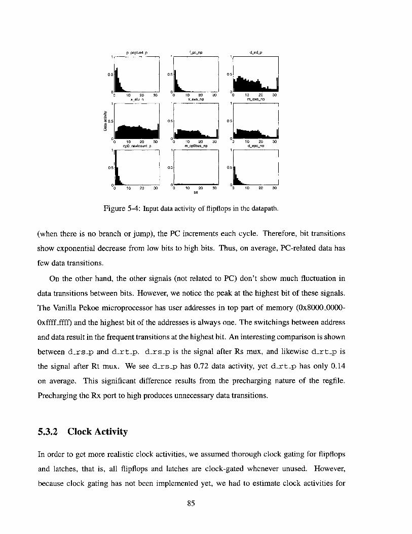
ppcp1us4_p
0.5
0
0 10 20 30
cpnextcontp3
0.5
0 -I-z0 10 20 30
f-pc-np
0.5
0 10 20 30xexenp
0.5
0 1 20 31 cp0busnp
0.5
00 10 20 30
bit
d-sd-p
0.5
0 10~x 20 30
0
0 10 20 30
d-exenp
0.5
00 10 20 30
Figure 5-4: Input data activity of flipflops in the datapath.
(when there is no branch or jump), the PC increments each cycle. Therefore, bit transitions
show exponential decrease from low bits to high bits. Thus, on average, PC-related data has
few data transitions.
On the other hand, the other signals (not related to PC) don't show much fluctuation in
data transitions between bits. However, we notice the peak at the highest bit of these signals.
The Vanilla Pekoe microprocessor has user addresses in top part of memory (0x8000.0000-
Oxffff-ffff) and the highest bit of the addresses is always one. The switchings between address
and data result in the frequent transitions at the highest bit. An interesting comparison is shown
between d-rs-p and d-rt-p. d-rs-p is the signal after Rs mux, and likewise d-rt-p is
the signal after Rt mux. We see d-rs-p has 0.72 data activity, yet d.rt-p has only 0.14
on average. This significant difference results from the precharging nature of the regfile.
Precharging the Rx port to high produces unnecessary data transitions.
5.3.2 Clock Activity
In order to get more realistic clock activities, we assumed thorough clock gating for flipflops
and latches, that is, all flipflops and latches are clock-gated whenever unused. However,
because clock gating has not been implemented yet, we had to estimate clock activities for
85
p-nextpcp ppcpn drs-p11 1
0.5 0.5 0.5
0 0 00 10 20 30 0 10 20 30 0 10 20 30
drt-p x-exe.n x-sdalign
0.5 05
0
0 10 20 30bit
Figure 5-5: Input data activity of latches in the datapath.
some non-clock-gated flipflops and latches. We can calculate the clock activities based on
the instruction mix. For example, the flipflop which latches the data address for load/store
instructions can be clock-gated when there is no load/store instruction. If load/store instructions
account for 32% of the total instructions, then the clock activity for the flipflop is 0.32. For the
instruction mix, we used the instruction mix of SPECint95 [17].
One complication about estimating clock activities is that clock gating affects the data
activity of the output. Therefore, when we estimated the clock activity of a flipflop/latch, we
didn't include (for our analysis) the flipflops/latches whose inputs are related to the output of
the flipflop/latch. This is because these flipflops/latches would get different inputs with lower
data activities if the previous flipflop/latch were clock-gated.
We didn't allow the possibility of having more than one clock for a N-bit flipflop/latch.
That is, all N flipflops/latches in an N-bit flipflop/latch have the same clock activity rate.
5.3.3 Power and PDP Curves for Flipflop and Latch Selection
Figure 5-6 shows data and clock activities for various flipflops in the datapath. Each *,+, or o
stands for the input and clock activities of a 1-bit flipflop.
We picked two types of flipflops from our candidates in Chapter 2: a Modified PowerPC
86

Flipflop1 i O*+*+ *+ *+ + * + + *
0.9 * ** * *
0.8-
0.74 M *# ** * *
0.6-
0.5 -
0.4 -
0.3 -OO O +: Flipflop Ao: Flipflop B
0.2* : Other Flipflops
0.1 - * * * .*m* *
0.1 0.2 0.3 0.4 0.5 0.6 0.7 0.8 0.9 1Data Acbvity
Figure 5-6: Clock and data activities for various flipflops. A solid curve is a PDP curve and a dashedcurve is a power curve.
(MPC) flipflop and a Transmission-gate (TG) flipflop. Using the energy equations derived in
Chapter 2, we constructed two curves: a power curve (dashed) and a PDP curve (solid). The
left side of the solid curve is the region where a TG flipflop is better in terms of PDP (Power-
Delay Product). On the other hand, the right side of the solid curve represents the region where
a MPC flipflop is better. The dashed curve divides the region in terms of power. If delay is not
a concern, we should make decisions based on this curve. In the same way as the solid curve,
at the left side of the dashed curve, a TG flipflop is better and at the right side, a MPC is the
right choice.
First, we see that if data activity is larger than 0.5, an MPC flipflop is the better choice
in terms of both power and PDP regardless of clock activity, since it consumes less input and
internal energy than a TG flipflop. If data activity is close to zero, most of energy is consumed
by clock. Therefore, a TG flipflop which consumes less clock energy, is a better choice in
terms of both power and PDP when the input has few transitions.
The flipflop A, expressed as + in Figure 5-6, represents a 30-bit flipflop which latches PC.
We see that the data activities between bits vary from around 0.7 (bit 0) to 0 (bit 29). For this
flipflop, we can conclude that MPC flipflops are appropriate for low bits (bit 0,1,2) and TG
flipflops for high bits (larger than 2). The flipflop B, expressed as o in Figure 5-6, represents a
87
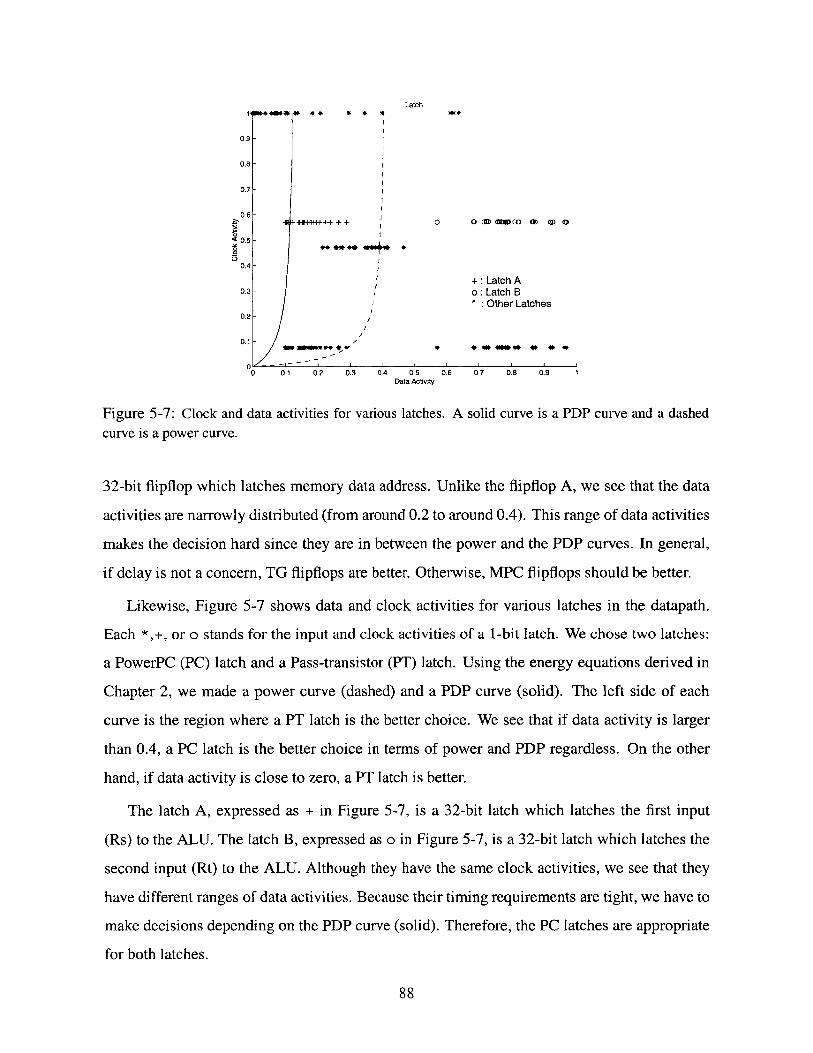
Latch14 ** ** * * *
0.9-
0.8-
0.7-
0.6- +-H+++ + + 0 O CCO GD CD 0 0
0.5 -
0.4-
+: Latch A0.3 -o: Latch B
* :Other Latches0.2 -
0.1 -aw**ow* *W 40 -t -0 V
00 0.1 0.2 0.3 0.4 0.5 0.6 0.7 0.8 0.9 1
Data Activity
Figure 5-7: Clock and data activities for various latches. A solid curve is a PDP curve and a dashed
curve is a power curve.
32-bit flipflop which latches memory data address. Unlike the flipflop A, we see that the data
activities are narrowly distributed (from around 0.2 to around 0.4). This range of data activities
makes the decision hard since they are in between the power and the PDP curves. In general,
if delay is not a concern, TG flipflops are better. Otherwise, MPC flipflops should be better.
Likewise, Figure 5-7 shows data and clock activities for various latches in the datapath.
Each *,+, or o stands for the input and clock activities of a 1-bit latch. We chose two latches:
a PowerPC (PC) latch and a Pass-transistor (PT) latch. Using the energy equations derived in
Chapter 2, we made a power curve (dashed) and a PDP curve (solid). The left side of each
curve is the region where a PT latch is the better choice. We see that if data activity is larger
than 0.4, a PC latch is the better choice in terms of power and PDP regardless. On the other
hand, if data activity is close to zero, a PT latch is better.
The latch A, expressed as + in Figure 5-7, is a 32-bit latch which latches the first input
(Rs) to the ALU. The latch B, expressed as o in Figure 5-7, is a 32-bit latch which latches the
second input (Rt) to the ALU. Although they have the same clock activities, we see that they
have different ranges of data activities. Because their timing requirements are tight, we have to
make decisions depending on the PDP curve (solid). Therefore, the PC latches are appropriate
for both latches.
88
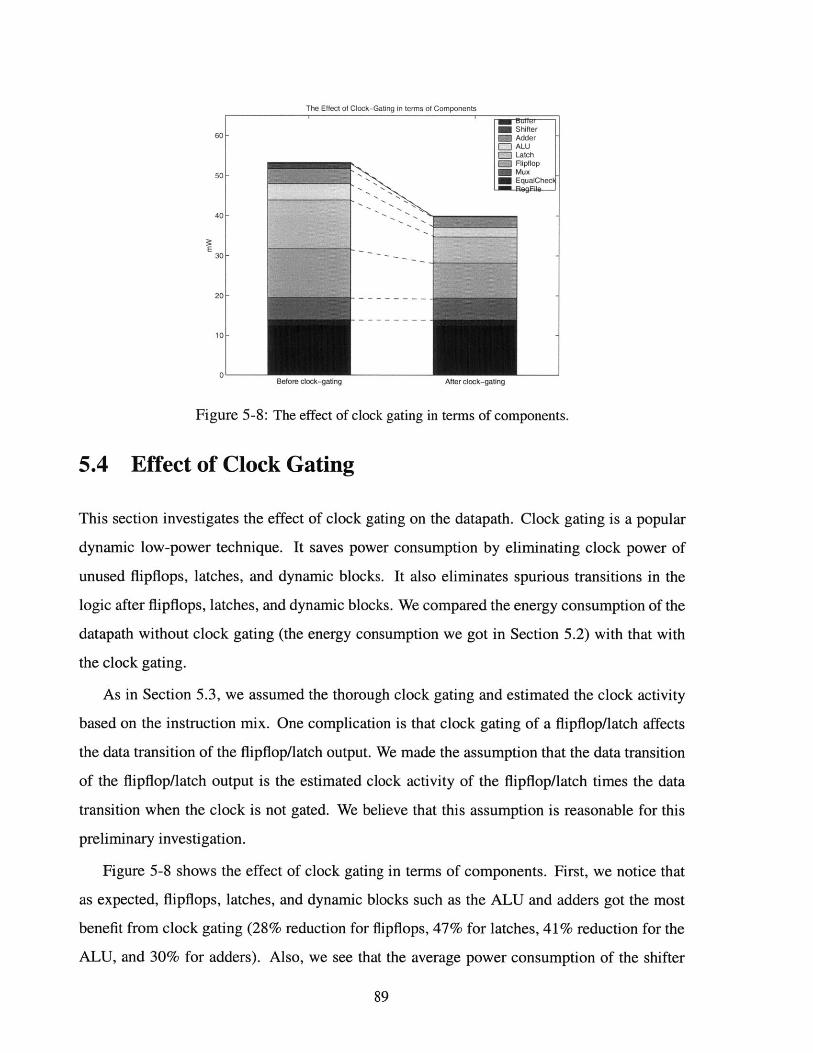
The Effect of Clock-Gating in terms of Components
60 - Adder
Latch
50- u h
20-
10-
0Before clock-gating After clock-gating
Figure 5-8: The effect of clock gating in terms of components.
5.4 Effect of Clock Gating
This section investigates the effect of clock gating on the datapath. Clock gating is a popular
dynamic low-power technique. It saves power consumption by eliminating clock power of
unused flipflops, latches, and dynamic blocks. It also eliminates spurious transitions in the
logic after flipflops, latches, and dynamic blocks. We compared the energy consumption of the
datapath without clock gating (the energy consumption we got in Section 5.2) with that with
the clock gating.
As in Section 5.3, we assumed the thorough clock gating and estimated the clock activity
based on the instruction mix. One complication is that clock gating of a flipflop/latch affects
the data transition of the flipflop/latch output. We made the assumption that the data transition
of the flipflop/latch output is the estimated clock activity of the flipflop/latch times the data
transition when the clock is not gated. We believe that this assumption is reasonable for this
preliminary investigation.
Figure 5-8 shows the effect of clock gating in terms of components. First, we notice that
as expected, flipflops, latches, and dynamic blocks such as the ALU and adders got the most
benefit from clock gating (28% reduction for flipflops, 47% for latches, 41% reduction for the
ALU, and 30% for adders). Also, we see that the average power consumption of the shifter
89
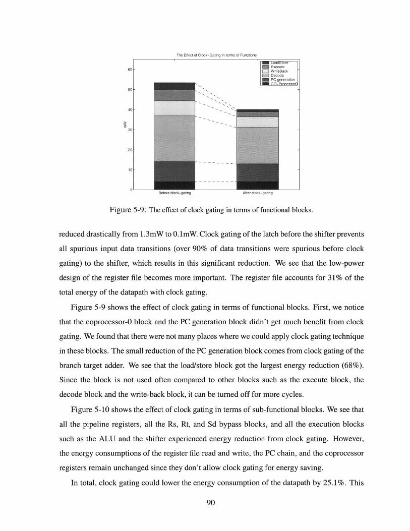
The Effect of Clock-Gating in terms of Functions
60- xct60 - teBack
50-
40-
30 - -
20 -
10-
Before clock-gating After clock-gating
Figure 5-9: The effect of clock gating in terms of functional blocks.
reduced drastically from 1.3mW to 0. 1mW. Clock gating of the latch before the shifter prevents
all spurious input data transitions (over 90% of data transitions were spurious before clock
gating) to the shifter, which results in this significant reduction. We see that the low-power
design of the register file becomes more important. The register file accounts for 31% of the
total energy of the datapath with clock gating.
Figure 5-9 shows the effect of clock gating in terms of functional blocks. First, we notice
that the coprocessor-0 block and the PC generation block didn't get much benefit from clock
gating. We found that there were not many places where we could apply clock gating technique
in these blocks. The small reduction of the PC generation block comes from clock gating of the
branch target adder. We see that the load/store block got the largest energy reduction (68%).
Since the block is not used often compared to other blocks such as the execute block, the
decode block and the write-back block, it can be turned off for more cycles.
Figure 5-10 shows the effect of clock gating in terms of sub-functional blocks. We see that
all the pipeline registers, all the Rs, Rt, and Sd bypass blocks, and all the execution blocks
such as the ALU and the shifter experienced energy reduction from clock gating. However,
the energy consumptions of the register file read and write, the PC chain, and the coprocessor
registers remain unchanged since they don't allow clock gating for energy saving.
In total, clock gating could lower the energy consumption of the datapath by 25.1%. This
90
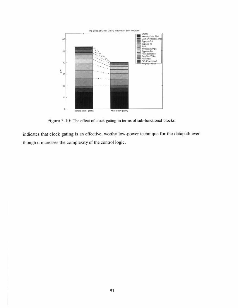
The Effect of Clock-Gating in terms of Sub-functions
M MemoryData PipeMemoryAddress PipBypass-SdBypass-Rt
SALUSWriteBack Pipe
C Bypass-RsPC calculationRegFile-Write
M PC chainCO-ProcessorO
Figure 5-10: The effect of clock gating in terms of sub-functional blocks.
indicates that clock gating is an effective, worthy low-power technique for the datapath even
though it increases the complexity of the control logic.
91
60
50
40
30
20
10
0Before clock-gating After clock-gating

92
Chapter 6
Conclusion
In this thesis, we approached a low-power datapath design problem in a bottom-up fashion.
First, we studied flipflops, latches, and muxes - the most common and frequently-used blocks in
the datapath. For flipflops and latches, we proposed that energy dissipation should be modeled
as a two-variable function of data and clock activities. We found that power dissipation is
linearly proportional to data activity when clock activity is fixed. We built two linear functions
with measurements when clock activity is 100% and 0% and using these, we constructed the
two-variable energy function. The graph of this energy function showed more dynamic features
of energy dissipation than traditional measurements which assume random input and un-gated
clock. For example, we found that a Modified PowerPC flipflop and a PowerPC latch have
the best PDP (Power-Delay Product) for most cases, but when data activity is low (<10%), a
Transmission-gate flipflop and a Pass-transistor latch are better in terms of PDP. We compared
two representative mux designs: a Transmission-gate (TG) mux and a Pass-transistor (PT) mux.
We identified three main energy sources: pass energy, non-pass energy, and control energy. We
found that a TG mux has less pass energy, but more control energy while they have similar non-
pass energy. We made an analytic equation which calculates total energy consumption using
these. Assuming the random input and control signals, we found that PT mux spends slightly
less energy if the number of inputs is 4 or more. However, in terms of EDP (Energy-Delay
Product), a TG mux was found to be better than a PT mux if the number of inputs is in the
range of 2-5.
Second, we built a new simulation-based energy estimation model, the net-transition energy
93

model. The energy model combines effective capacitance values and statistics from a simulator
to calculate energy dissipation. In order to obtain accurate effective capacitances, we developed
a capacitance merging method. This method calculates transistor capacitances using empirical
equations and merges them with parasitic wire capacitances into a single effective capacitance
for each node. We experimented with two slightly different F04 (fanout-of-four) inverter
chains and derived the empirical equations. We showed the calculated capacitances using the
equations match the measured ones (with Hspice) within 5% error. Our energy model showed
close agreement (<8% error) with Hspice measurements for various basic circuit blocks and a
32-bit GCD (Greatest Common Divisor) circuit, which can be regarded as a small version of
a datapath. Also, we modeled short-circuit energy for an inverter. We revealed that the short-
circuit energy is linearly proportional to a transistor width, when the ratio of PMOS and NMOS
widths is fixed in a typical F04 (fanout-of-four) environment. We developed a table lookup
method based on this observation. We showed this method can estimate the short-circuit energy
with 8% error at maximum.
Third, we custom-designed a prototype datapath for a 0.25 Am five metal process (from
TSMC). Our metal allocation scheme resulted in a very tight datapath (2270 x 11640 A2 = 0.27
mm x 1.40 mm = 0.38 mm 2). Also, we showed design decisions on floor planning, an adder,
and clock gating. We explored shifter designs - one of the essential blocks in the datapath, but
a relatively simple structure - intensively. We found 84% of shifts are left shifts and 85% of
left shifts are less than 4 bit shifts for SPECint 95 and Dhrystone benchmarks. We developed a
new shifter design, split log-4 shifter. The split log-4 shifter takes advantage of the fact derived
from the benchmarks that most shifts are small. It deactivates unnecessary stages to save power
when the shift amount is less than 4. We found that the barrel shifter is better than any other
log shifters in terms of both delay and energy. Among log shifters, we found that the split log-4
shifter consumes the least energy (32% energy saving compared to a log-2 shifter), although it
had a significant delay penalty when the shift amount is 4 or more. The log-4 shifter showed
the best EDP among log shifters. Also, we found reverse ordering helps for both delay and
power but internal buffering is not worth for log shifters, if the number of stages is 5 or less.
Finally, we analyzed the energy consumption of the prototype datapath using our energy
estimation tool. From the energy breakdown by components, we revealed the basic blocks
94

such as flipflops, latches, and muxes account for over half the total energy (56%). On the
other hand, we found that the execution components such as the ALU, adders, and the shifter
consume only 17% of the total energy. From the energy breakdown by functional blocks,
we revealed the decode functions such as register file read, bypassing, and PC generation,
account for significant portions of the total energy (20%, 22%, and 19% respectively). Also,
we showed how to choose the optimal design between two choices of flipflops/latches using the
power curve and the PDP curve, based on the clock and data activities in the datapath. Then,
we investigated the effect of thorough clock gating. We found that clock gating is an effective
low-power technique. Clock gating resulted in 25.1% energy reduction in total.
95

96
Bibliography
[1] K. Acken, M. Irwin, and R. Owens. Power comparisons for barrel shifters. In Proceedings
ISLPED, pages 209-212, Monterey, CA, 1996.
[2] Tom Burd. Low-power cmos library design methodology. Master's thesis, University of
California at Berkeley, 1994.
[3] P. K. Chan and M. D. F. Schlag. Analysis and design of cmos manchester adders with
variable carry-skip. IEEE Transactions on Circuits and Systems, 39(8):983-992, August
1990.
[4] A. P. Chandrakasan, S. Sheng, and R. W. Brodersen. Low-power cmos digital design.
IEEE Journal of Solid-State Circuits, 27(4):473-484, April 1992.
[5] C. X. Huang, B. Zhang, A.-C. Deng, and B. Swirski. The design and implementation
of PowerMill. In Proceedings of the IEEE Symposium on Low Power Electronics, pages
105-111, October 1995.
[6] G. Kane and J. Heinrich. MIPS RISC Architecture (R2000/R3000). Prentice Hall, 1992.
[7] V. Kantabutra. Designing optimum one-level carry-skip adders. IEEE Transactions on
Computers, 42(6):759-764, June 1993.
[8] R. Krashinsky, S. Heo, M. Zhang, and K. Asanovi6. SyCHOSys: Compiled energy-
performance cycle simulation. In Workshop on Complexity-Effective Design, 27th ISCA,
Vancouver, Canada, June 2000.
97
[9] J. Lee, B. Vinnakota, and L. Lucke. Power estimation using input/output transition
analysis (iota). In International Symposium on Circuits and Systems, volume 6, pages
49-52, June 1998.
[10] H. Mehta, R. M. Owens, and M. J. Irwin. Energy characterization based on clustering. In
DAC, pages 702-707, Las Vegas, NV, June 1996.
[11] L. Nagel. SPICE2. Technical Report ERL-M520, ERL Technical Memo, University of
California, Berkeley, 1975.
[12] C. Nagendra, M. J. Irwin, and R. M. Owens. Area-time-power tradeoffs in parallel adders.
IEEE Transactions on Circuits and Systems, 43(10):689-702, October 1996.
[13] F. N. Najm. A survey of power estimation techniques in vlsi circuits. IEEE Transactions
on VLSI Systems, 2(4):446-455, December 1994.
[14] J. Rabaey. Digital Integrated Circuites. Prentice Hall, 1996.
[15] V. Stojanovic and V. G. Oklobdzija. Comparative analysis of master-slave latches and flip-
flops for high-performance and low-power system. IEEE Journal of Solid-State Circuits,
34(4):536-548, April 1999.
[16] I. Sutherland, B. Sproull, and D. Harris. Logical Effort. Morgan Kaufmann, 1999.
[17] J. Tseng. Energy-efficient register file design. Master's thesis, Massachusetts Institute of
Technology, December 1999.
[18] N.P. van der Meijs and A.J. van Genderen. SPACE Tutorial. Technical Report ET-NT
92.22, Technical Report, Delft University of Technology, Netherlands, 1992.
[19] N. Vijaykrishnan, M. Kandemir, M. J. Irwin, H. S. Kim, and W. Ye. A unified
energy framework with integrated hardware-software optimizations. In ISCA, Vancouver,
Canada, June 2000.
98