A Linear Microwave Plasma Source Using a Circular ... - MDPI
20
applied sciences Article A Linear Microwave Plasma Source Using a Circular Waveguide Filled with a Relatively High-Permittivity Dielectric: Comparison with a Conventional Quasi-Coaxial Line Waveguide Ju-Hong Cha, Sang-Woo Kim and Ho-Jun Lee * Citation: Cha, J.-H.; Kim, S.-W.; Lee, H.-J. A Linear Microwave Plasma Source Using a Circular Waveguide Filled with a Relatively High-Permittivity Dielectric: Comparison with a Conventional Quasi-Coaxial Line Waveguide. Appl. Sci. 2021, 11, 5358. https://doi.org/ 10.3390/app11125358 Academic Editor: Mohammed Koubiti Received: 8 May 2021 Accepted: 3 June 2021 Published: 9 June 2021 Publisher’s Note: MDPI stays neutral with regard to jurisdictional claims in published maps and institutional affil- iations. Copyright: © 2021 by the authors. Licensee MDPI, Basel, Switzerland. This article is an open access article distributed under the terms and conditions of the Creative Commons Attribution (CC BY) license (https:// creativecommons.org/licenses/by/ 4.0/). Department of Electrical Engineering, Pusan National University, Busan 46241, Korea; [email protected] (J.-H.C.); [email protected] (S.-W.K.) * Correspondence: [email protected] Abstract: For a conventional linear microwave plasma source (LMPS) with a quasi-coaxial line transverse electromagnetic (TEM) waveguide, a linearly extended plasma is sustained by the surface wave outside the tube. Due to the characteristics of the quasi-coaxial line MPS, it is easy to generate a uniform plasma with radially omnidirectional surfaces, but it is difficult to maximize the electron density in a curved selected region. For the purpose of concentrating the plasma density in the deposition area, a novel LMPS which is suitable for curved structure deposition has been developed and compared with the conventional LMPS. As the shape of a circular waveguide, it is filled with relatively high-permittivity dielectric instead of a quasi-coaxial line waveguide. Microwave power at 2.45 GHz is transferred to the plasma through the continuous cylindrical-slotted line antenna, and the radiated electric field in the radial direction is made almost parallel to the tangential plane of the window surface. This research includes the advanced 3D numerical analysis and compares the results with the experiment. It shows that the electron density in the deposition area is higher than that of the conventional quasi-coaxial line plasma MPS. Keywords: microwave plasma; linear microwave plasma source; three-dimensional plasma fluid simulation 1. Introduction Microwave plasma sources (MPSs) are driven by applied frequencies of 1–100 GHz and lead to electron heating and excitation of a discharge from the electromagnetic waves that either penetrate the plasma or exist along the surface [1,2]. With weakly ionized MPS used for material processing, waves are important to transfer energy from the excited surface of the waveguiding structure to the bulk plasma, where the wave energy is absorbed [3]. The main element of the MPS, for material processing, is the microwave-to-plasma applicator because it determines the structure of the electromagnetic field in the plasma as well as the absorption energy efficiency of plasma [4]. The structure of the electromagnetic field in plasma is determined by the correlation of the internal plasma parameters (electron density, plasma frequency, etc.) and the external source parameters (waveguide structure, size of source, frequency, etc.). The energy absorption efficiency of MPS is determined by the wave penetration depth in the plasma, wave field strength at the plasma surface, and waveguiding structure. Among the MPS for material processing, the sources generally have a form in which waves propagate along the transmission lines. The plasma is generated by the waves emitted from the dielectric surface which replaces a part of the waveguiding structure. Depending on the size and structure of the dielectric surface, plasma sources using the transmission line field can be classified in the following ways: (i) plasma is a part of the waveguiding structure (transmission line applicators) and (ii) plasma is sustained Appl. Sci. 2021, 11, 5358. https://doi.org/10.3390/app11125358 https://www.mdpi.com/journal/applsci
-
Upload
khangminh22 -
Category
Documents
-
view
6 -
download
0
Transcript of A Linear Microwave Plasma Source Using a Circular ... - MDPI

applied sciences
Article
A Linear Microwave Plasma Source Using a Circular WaveguideFilled with a Relatively High-Permittivity Dielectric:Comparison with a Conventional Quasi-CoaxialLine Waveguide
Ju-Hong Cha, Sang-Woo Kim and Ho-Jun Lee *
�����������������
Citation: Cha, J.-H.; Kim, S.-W.; Lee,
H.-J. A Linear Microwave Plasma
Source Using a Circular Waveguide
Filled with a Relatively
High-Permittivity Dielectric:
Comparison with a Conventional
Quasi-Coaxial Line Waveguide. Appl.
Sci. 2021, 11, 5358. https://doi.org/
10.3390/app11125358
Academic Editor:
Mohammed Koubiti
Received: 8 May 2021
Accepted: 3 June 2021
Published: 9 June 2021
Publisher’s Note: MDPI stays neutral
with regard to jurisdictional claims in
published maps and institutional affil-
iations.
Copyright: © 2021 by the authors.
Licensee MDPI, Basel, Switzerland.
This article is an open access article
distributed under the terms and
conditions of the Creative Commons
Attribution (CC BY) license (https://
creativecommons.org/licenses/by/
4.0/).
Department of Electrical Engineering, Pusan National University, Busan 46241, Korea;[email protected] (J.-H.C.); [email protected] (S.-W.K.)* Correspondence: [email protected]
Abstract: For a conventional linear microwave plasma source (LMPS) with a quasi-coaxial linetransverse electromagnetic (TEM) waveguide, a linearly extended plasma is sustained by the surfacewave outside the tube. Due to the characteristics of the quasi-coaxial line MPS, it is easy to generate auniform plasma with radially omnidirectional surfaces, but it is difficult to maximize the electrondensity in a curved selected region. For the purpose of concentrating the plasma density in thedeposition area, a novel LMPS which is suitable for curved structure deposition has been developedand compared with the conventional LMPS. As the shape of a circular waveguide, it is filled withrelatively high-permittivity dielectric instead of a quasi-coaxial line waveguide. Microwave power at2.45 GHz is transferred to the plasma through the continuous cylindrical-slotted line antenna, andthe radiated electric field in the radial direction is made almost parallel to the tangential plane ofthe window surface. This research includes the advanced 3D numerical analysis and compares theresults with the experiment. It shows that the electron density in the deposition area is higher thanthat of the conventional quasi-coaxial line plasma MPS.
Keywords: microwave plasma; linear microwave plasma source; three-dimensional plasma fluidsimulation
1. Introduction
Microwave plasma sources (MPSs) are driven by applied frequencies of 1–100 GHz andlead to electron heating and excitation of a discharge from the electromagnetic waves thateither penetrate the plasma or exist along the surface [1,2]. With weakly ionized MPS usedfor material processing, waves are important to transfer energy from the excited surface ofthe waveguiding structure to the bulk plasma, where the wave energy is absorbed [3]. Themain element of the MPS, for material processing, is the microwave-to-plasma applicatorbecause it determines the structure of the electromagnetic field in the plasma as well asthe absorption energy efficiency of plasma [4]. The structure of the electromagnetic fieldin plasma is determined by the correlation of the internal plasma parameters (electrondensity, plasma frequency, etc.) and the external source parameters (waveguide structure,size of source, frequency, etc.). The energy absorption efficiency of MPS is determined bythe wave penetration depth in the plasma, wave field strength at the plasma surface, andwaveguiding structure.
Among the MPS for material processing, the sources generally have a form in whichwaves propagate along the transmission lines. The plasma is generated by the wavesemitted from the dielectric surface which replaces a part of the waveguiding structure.Depending on the size and structure of the dielectric surface, plasma sources using thetransmission line field can be classified in the following ways: (i) plasma is a part ofthe waveguiding structure (transmission line applicators) and (ii) plasma is sustained
Appl. Sci. 2021, 11, 5358. https://doi.org/10.3390/app11125358 https://www.mdpi.com/journal/applsci

Appl. Sci. 2021, 11, 5358 2 of 20
by the field leaking out of the structure (antenna applicators) [5]. For the transmissionline applicator, the cross section of the plasma–dielectric contact is wide, whereas for theantenna applicator, the plasma–dielectric contact cross section is narrow. So, in the caseof antenna applicator, the process stability is high since the wave propagation mode andthe resonant cavity in the waveguiding structure are less affected by plasma generation.Hence, in material processing, which requires stable plasma operation, antenna applicatortype MPSs are preferred.
Among the antenna apllicator type MPS, LMPSs are mainly used for large areaprocessing [6]. Erstwhile LMPS models [7] were either in the form of discharge tubesplaced inside the guiding structure or in the form of discharge tubes across the widewaveguide wall parallel to the electric field [8,9]. However, in terms of productivityimprovement and large area material processing, the shape of the discharge tubes insidethe guiding structure is not suited for the application, so the shape of the discharge outsidethe guiding structure is demanded. A SW sustained source called the duo-plasma linesource, which uses the quasi-coaxial line TEM wave mode, was invented according tothe shape of the discharge outside the tube with a waveguiding structure [10,11]. Due tothe high scalability with a large processing area [12,13], duo-plasma line source has beenapplied to many plasma enhanced chemical vapor deposition (PECVD) processes such ashard coating, thin film, synthesis of graphene, and display panels, which require a largearea, an operation pressure of 0.2~3 Torr, and high speed processes [14–17].
In the quasi-coaxial line TEM wave mode, the isotropically emitted transverse wavefield from the inner conductor is perpendicular to the tangential plane of the windowsurface in all radial directions, and the dielectric surface in all radial directions is exposedto interact with the plasma generation. Therefore, it is easy to generate a uniform plasma inthe radially omnidirectional plasma–dielectric window surfaces. However, it is difficult tomaximize the process productivity by concentrating the plasma density in a one-directionalselected deposition region. In this study, for the purpose of concentrating the plasmadensity in the selective area, a cylindrical slotted LMPS that had a high electron density ina specific deposition region was proposed and was compared with the quasi-coaxial LMPS.The shape of the discharge outside the guiding structure [18–20], cylindrical-slotted LMPSwas excited by feeding power in the circular TE11 mode.
2. Plasma Source Overview
Both quasi-coaxial line TEM and circular TE11 LMPSs were fabricated to comparethe characteristics of plasma generation according to the waveguiding structure and thewave field direction. The circular TE11 wave mode was compared with quasi-coaxial lineTEM mode, as shown in Figure 1. In the figure, the dashed and straight lines represent themagnetic and electric fields, respectively.
Appl. Sci. 2021, 11, x FOR PEER REVIEW 2 of 20
transmission line field can be classified in the following ways: (i) plasma is a part of the waveguiding structure (transmission line applicators) and (ii) plasma is sustained by the field leaking out of the structure (antenna applicators) [5]. For the transmission line applicator, the cross section of the plasma–dielectric contact is wide, whereas for the antenna applicator, the plasma–dielectric contact cross section is narrow. So, in the case of antenna applicator, the process stability is high since the wave propagation mode and the resonant cavity in the waveguiding structure are less affected by plasma generation. Hence, in material processing, which requires stable plasma operation, antenna applicator type MPSs are preferred.
Among the antenna apllicator type MPS, LMPSs are mainly used for large area processing [6]. Erstwhile LMPS models [7] were either in the form of discharge tubes placed inside the guiding structure or in the form of discharge tubes across the wide waveguide wall parallel to the electric field [8,9]. However, in terms of productivity improvement and large area material processing, the shape of the discharge tubes inside the guiding structure is not suited for the application, so the shape of the discharge outside the guiding structure is demanded. A SW sustained source called the duo-plasma line source, which uses the quasi-coaxial line TEM wave mode, was invented according to the shape of the discharge outside the tube with a waveguiding structure [10,11]. Due to the high scalability with a large processing area [12,13], duo-plasma line source has been applied to many plasma enhanced chemical vapor deposition (PECVD) processes such as hard coating, thin film, synthesis of graphene, and display panels, which require a large area, an operation pressure of 0.2~3Torr, and high speed processes [14–17].
In the quasi-coaxial line TEM wave mode, the isotropically emitted transverse wave field from the inner conductor is perpendicular to the tangential plane of the window surface in all radial directions, and the dielectric surface in all radial directions is exposed to interact with the plasma generation. Therefore, it is easy to generate a uniform plasma in the radially omnidirectional plasma–dielectric window surfaces. However, it is difficult to maximize the process productivity by concentrating the plasma density in a one-directional selected deposition region. In this study, for the purpose of concentrating the plasma density in the selective area, a cylindrical slotted LMPS that had a high electron density in a specific deposition region was proposed and was compared with the quasi-coaxial LMPS. The shape of the discharge outside the guiding structure [18–20], cylindrical-slotted LMPS was excited by feeding power in the circular TE11 mode.
2. Plasma Source Overview
Both quasi-coaxial line TEM and circular TE11 LMPSs were fabricated to compare the characteristics of plasma generation according to the waveguiding structure and the wave field direction. The circular TE11 wave mode was compared with quasi-coaxial line TEM mode, as shown in Figure 1. In the figure, the dashed and straight lines represent the magnetic and electric fields, respectively.
Figure 1. Field lines at radial cross-section for quasi-coaxial TEM and circular TE11 waveguiding structure. (a) Quasi-coaxial TEM linear MWP and (b) circular TE11 waveguiding structure.
Figure 1. Field lines at radial cross-section for quasi-coaxial TEM and circular TE11 waveguidingstructure. (a) Quasi-coaxial TEM linear MWP and (b) circular TE11 waveguiding structure.
In the circular waveguide, with the diameter determined, the wave frequency mustexceed the cut-off frequency of propagation. Among the lower order modes of circularwaveguides, there are the TE11 and TE01 wave modes, in which the transverse electric field

Appl. Sci. 2021, 11, 5358 3 of 20
direction is formed parallel to the quartz window surface. In the circular waveguide of thesame specification, the cut-off frequency of TE01 is twice more than that of the TE11 wavemode. Therefore, it is easier to use the TE11 mode with a lower cut-off frequency when thefrequency is fixed at 2.45 GHz and the waveguide radius is low [1].
3. ExperimentExperiment Setup
Based on the correlations with the plasma characteristics [21], the geometry parametersfor the waveguiding structure were set to improve the power transfer efficiency from thewave generator to the plasma region. In the quasi-coaxial line TEM waveguiding structure,microwave power was delivered through a TE/TEM coupler which was bent at 90◦, asshown in Figure 2a.
Appl. Sci. 2021, 11, x FOR PEER REVIEW 3 of 20
In the circular waveguide, with the diameter determined, the wave frequency must exceed the cut-off frequency of propagation. Among the lower order modes of circular waveguides, there are the TE11 and TE01 wave modes, in which the transverse electric field direction is formed parallel to the quartz window surface. In the circular waveguide of the same specification, the cut-off frequency of TE01 is twice more than that of the TE11 wave mode. Therefore, it is easier to use the TE11 mode with a lower cut-off frequency when the frequency is fixed at 2.45 GHz and the waveguide radius is low [1].
3. Experiment Experiment Setup
Based on the correlations with the plasma characteristics [21], the geometry parameters for the waveguiding structure were set to improve the power transfer efficiency from the wave generator to the plasma region. In the quasi-coaxial line TEM waveguiding structure, microwave power was delivered through a TE/TEM coupler which was bent at 90°, as shown in Figure 2a.
Figure 2. Schematic diagram of microwave plasma source. (a) Quasi-coaxial TEM linear MWP and (b) circular TE11 waveguiding structure.
To maximize the power transfer ratio when converting from a rectangular TE10 to a quasi-coaxial line TEM waveguiding structure, a rod-shaped antenna was placed in the field concentration region. The rod-shaped antenna was made of copper as an inner conductor. The diameter of the inner conductor was 9 mm, and the axial length was 600 mm. The microwave propagated mainly in the space between the inner rod and the quartz tube. The space between the inner conductor and the quartz tube was filled with atmospheric pressure for the device cooling by the flow of compressed air [10]. Inside the plasma chamber, quartz window was placed to separate the field generator and plasma excitation region which is filled with argon gas at low pressure. The quartz window 𝜖 =4 was designed with an inner diameter of 32 mm, a thickness of 2 mm, and a total length of 550 mm in the axial direction. The compressive strength of the quartz window was 117,000 kg/cm2, the Young modulus was 73,900 kg/mm2, and the tensile strength was 510 kg/cm2, which could sustain the mechanical load without deformation in the corresponding axial length. The plasma was ignited by the excitation of a discharge from the electromagnetic waves that penetrate or exist along the quartz window surface.
The propagation wave mode was converted from the rectangular TE10 wave mode to the circular TE11 wave mode as shown in Figure 2b. In the circular TE11 waveguiding structure, microwave power was transferred to the plasma through the continuous cylindrical slot antenna along the wave propagation direction. The circular waveguide was made of copper material with an inner diameter of 30 mm and a thickness of 1 mm. In the cylindrical slotted waveguiding structure, the cut surface of the circular TE11 waveguide was cut to a radial thickness of 10 mm along with an axial length of 500 mm from the entrance of the plasma chamber to the end of the continuous axis. The quartz
Figure 2. Schematic diagram of microwave plasma source. (a) Quasi-coaxial TEM linear MWP and(b) circular TE11 waveguiding structure.
To maximize the power transfer ratio when converting from a rectangular TE10 toa quasi-coaxial line TEM waveguiding structure, a rod-shaped antenna was placed inthe field concentration region. The rod-shaped antenna was made of copper as an innerconductor. The diameter of the inner conductor was 9 mm, and the axial length was600 mm. The microwave propagated mainly in the space between the inner rod and thequartz tube. The space between the inner conductor and the quartz tube was filled withatmospheric pressure for the device cooling by the flow of compressed air [10]. Inside theplasma chamber, quartz window was placed to separate the field generator and plasmaexcitation region which is filled with argon gas at low pressure. The quartz windowεr = 4 was designed with an inner diameter of 32 mm, a thickness of 2 mm, and a totallength of 550 mm in the axial direction. The compressive strength of the quartz windowwas 117,000 kg/cm2, the Young modulus was 73,900 kg/mm2, and the tensile strengthwas 510 kg/cm2, which could sustain the mechanical load without deformation in thecorresponding axial length. The plasma was ignited by the excitation of a discharge fromthe electromagnetic waves that penetrate or exist along the quartz window surface.
The propagation wave mode was converted from the rectangular TE10 wave modeto the circular TE11 wave mode as shown in Figure 2b. In the circular TE11 waveguidingstructure, microwave power was transferred to the plasma through the continuous cylin-drical slot antenna along the wave propagation direction. The circular waveguide wasmade of copper material with an inner diameter of 30 mm and a thickness of 1 mm. In thecylindrical slotted waveguiding structure, the cut surface of the circular TE11 waveguidewas cut to a radial thickness of 10 mm along with an axial length of 500 mm from theentrance of the plasma chamber to the end of the continuous axis. The quartz windowand plasma generation process were set to be the same as in Figure 2a. When the innerdiameter of the circular waveguide was 30 mm and was filled with free space materialcharacteristics, the cut-off frequency in the circular waveguide was approximately 5.9 GHz.For the circular waveguide of 30 mm diameter, it was necessary to lower the cut-off fre-

Appl. Sci. 2021, 11, 5358 4 of 20
quency below 2.45 GHz for the wave propagation in the applied frequency. Accordingly, arod type (diameter = 30 mm, εr = 9) alumina was inserted inside the circular waveguidingstructure, and the cut-off frequency was reduced to a third of 5.9 GHz.
To compare the source characteristics, experiments were conducted under 500 mTorrAr plasma condition where 0.6 kW microwave power was applied. The experimental sys-tem used for this study is shown in Figure 3. Continuous wave (CW) power at 2.45 GHz wastransmitted from a magnetron (ASTEX MKS Fl20608-3kW Mag Head, ASTEX Smart MatchFl20606-3kW) to the waveguide mode converter by a rectangular TE10 wave mode throughthe WR340 waveguide. The power supply (MKS Smart Power generator Fl20160-1-3kW)was connected to a three-phase line and outputted 300–3000 W. As shown in Figure 3, the mi-crowave transmission line from the generator to the plasma includes a WR340 3-Stub tuner,dummy load (Fl20164), and circulator (AX3161) as the product of National Electronics.
Appl. Sci. 2021, 11, x FOR PEER REVIEW 4 of 20
window and plasma generation process were set to be the same as in Figure 2a. When the inner diameter of the circular waveguide was 30 mm and was filled with free space material characteristics, the cut-off frequency in the circular waveguide was approximately 5.9 GHz. For the circular waveguide of 30 mm diameter, it was necessary to lower the cut-off frequency below 2.45 GHz for the wave propagation in the applied frequency. Accordingly, a rod type (diameter = 30 mm, 𝜖 = 9) alumina was inserted inside the circular waveguiding structure, and the cut-off frequency was reduced to a third of 5.9 GHz.
To compare the source characteristics, experiments were conducted under 500mTorr Ar plasma condition where 0.6 kW microwave power was applied. The experimental system used for this study is shown in Figure 3. Continuous wave (CW) power at 2.45 GHz was transmitted from a magnetron (ASTEX MKS Fl20608-3kW Mag Head, ASTEX Smart Match Fl20606-3kW) to the waveguide mode converter by a rectangular TE10 wave mode through the WR340 waveguide. The power supply (MKS Smart Power generator Fl20160-1-3kW) was connected to a three-phase line and outputted 300–3000 W. As shown in Figure 3, the microwave transmission line from the generator to the plasma includes a WR340 3-Stub tuner, dummy load (Fl20164), and circulator (AX3161) as the product of National Electronics.
Figure 3. Schematic of the experimental system showing the microwave coupling arrangement. (a) Quasi-coaxial TEM linear MWP and (b) circular TE11 waveguiding structure.
In the circular TE11 LMPS, the microwave transmission line from the power generator to the waveguide mode converter was same as that of the quasi-coaxial waveguiding structure, as shown in Figure 3. In the circular waveguiding structure, WR340 twisted waveguide was used to set the electric field in the required direction because the plasma interacting surface typically faced the deposition region, and the waveguiding structure was changed from a rectangular WR340 waveguide to a circular waveguiding structure through a homemade rectangular to a circular waveguide converter.
For the experiment with the linear MWP source, a cylindrical chamber with a diameter of 500 mm and a height of 150 mm was fabricated, as shown in Figure 4a,b. The microwave power was designed to propagate along the straight line in the quartz tube. To increase the spatial uniformity of the gas flow, a showerhead type gas inlet structure was used, which was located opposite to the deposition region, 40 mm away from the quartz window surface. The images of the plasma generated near the window surface were taken, as shown in Figure 4b. It represents the images of the MWP plasma optical emission patterns along the linear direction from the front side and right side views. The
Figure 3. Schematic of the experimental system showing the microwave coupling arrangement. (a) Quasi-coaxial TEMlinear MWP and (b) circular TE11 waveguiding structure.
In the circular TE11 LMPS, the microwave transmission line from the power generatorto the waveguide mode converter was same as that of the quasi-coaxial waveguidingstructure, as shown in Figure 3. In the circular waveguiding structure, WR340 twistedwaveguide was used to set the electric field in the required direction because the plasmainteracting surface typically faced the deposition region, and the waveguiding structurewas changed from a rectangular WR340 waveguide to a circular waveguiding structurethrough a homemade rectangular to a circular waveguide converter.
For the experiment with the linear MWP source, a cylindrical chamber with a diameterof 500 mm and a height of 150 mm was fabricated, as shown in Figure 4a,b. The microwavepower was designed to propagate along the straight line in the quartz tube. To increasethe spatial uniformity of the gas flow, a showerhead type gas inlet structure was used,which was located opposite to the deposition region, 40 mm away from the quartz windowsurface. The images of the plasma generated near the window surface were taken, asshown in Figure 4b. It represents the images of the MWP plasma optical emission patternsalong the linear direction from the front side and right side views. The mounting positionof the camera in the plasma chamber is shown in Figure 4b as the front and side views. Theequipment used to record the shape of plasma was a cylindrical camera (model: MicrosoftLife Cam Studio) suitable for the rounded type chamber flange. The brightness of theemitted light was slightly distorted because the plasma shape was captured by a cameraequipped with a neutral density(ND) filter (product of HORUSBENNU, 49 mm), whichwas used to reduce the brightness to 1/400.

Appl. Sci. 2021, 11, 5358 5 of 20
Appl. Sci. 2021, 11, x FOR PEER REVIEW 5 of 20
mounting position of the camera in the plasma chamber is shown in Figure 4b as the front and side views. The equipment used to record the shape of plasma was a cylindrical camera (model: Microsoft Life Cam Studio) suitable for the rounded type chamber flange. The brightness of the emitted light was slightly distorted because the plasma shape was captured by a camera equipped with a neutral density(ND) filter (product of HORUSBENNU, 49 mm), which was used to reduce the brightness to 1/400.
Figure 4. Front (a) and top (b) views of the experimental and diagnostic setup diagram.
Figure 5 shows the plasma diagnostics using a homemade single Langmuir probe(LP) in the deposition region. The deposition process is usually carried out 20–25 mm away from the window surface. Hence, the diagnosis was performed in the deposition area at five points (20–25 mm away from the window surface) at 20 mm intervals from the center, as shown in Figure 5. The tip of the LP was made of a 100µm diameter tungsten wire (10 mm in length), which was designed to satisfy the collisionless thin sheath condition [22].
Figure 5. Diagnostic setup in the deposition region.
The electron energy distribution function (EEDF) was obtained by calculating the second derivative of the measured I–V curve [23,24]. The second derivative of the measured current with respect to the probe bias voltage, 𝐼” , was proportional to the electron energy probability function (EEPF) 𝑓 (𝜀), which was related to the EEDF as 𝑔 (𝜀) = 𝜀 / 𝑓 (𝜀). The electron density is calculated by integrating the EEDF, and the electron temperature was measured as an effective electron temperature 𝑇 , which corresponds to a mean electron energy from the integrals of the EEDF [23,24].
Figure 4. Front (a) and top (b) views of the experimental and diagnostic setup diagram.
Figure 5 shows the plasma diagnostics using a homemade single Langmuir probe(LP)in the deposition region. The deposition process is usually carried out 20–25 mm awayfrom the window surface. Hence, the diagnosis was performed in the deposition area atfive points (20–25 mm away from the window surface) at 20 mm intervals from the center,as shown in Figure 5. The tip of the LP was made of a 100 µm diameter tungsten wire(10 mm in length), which was designed to satisfy the collisionless thin sheath condition [22].
Appl. Sci. 2021, 11, x FOR PEER REVIEW 5 of 20
mounting position of the camera in the plasma chamber is shown in Figure 4b as the front and side views. The equipment used to record the shape of plasma was a cylindrical camera (model: Microsoft Life Cam Studio) suitable for the rounded type chamber flange. The brightness of the emitted light was slightly distorted because the plasma shape was captured by a camera equipped with a neutral density(ND) filter (product of HORUSBENNU, 49 mm), which was used to reduce the brightness to 1/400.
Figure 4. Front (a) and top (b) views of the experimental and diagnostic setup diagram.
Figure 5 shows the plasma diagnostics using a homemade single Langmuir probe(LP) in the deposition region. The deposition process is usually carried out 20–25 mm away from the window surface. Hence, the diagnosis was performed in the deposition area at five points (20–25 mm away from the window surface) at 20 mm intervals from the center, as shown in Figure 5. The tip of the LP was made of a 100µm diameter tungsten wire (10 mm in length), which was designed to satisfy the collisionless thin sheath condition [22].
Figure 5. Diagnostic setup in the deposition region.
The electron energy distribution function (EEDF) was obtained by calculating the second derivative of the measured I–V curve [23,24]. The second derivative of the measured current with respect to the probe bias voltage, 𝐼” , was proportional to the electron energy probability function (EEPF) 𝑓 (𝜀), which was related to the EEDF as 𝑔 (𝜀) = 𝜀 / 𝑓 (𝜀). The electron density is calculated by integrating the EEDF, and the electron temperature was measured as an effective electron temperature 𝑇 , which corresponds to a mean electron energy from the integrals of the EEDF [23,24].
Figure 5. Diagnostic setup in the deposition region.
The electron energy distribution function (EEDF) was obtained by calculating thesecond derivative of the measured I–V curve [23,24]. The second derivative of the measuredcurrent with respect to the probe bias voltage, I ′′e , was proportional to the electron energyprobability function (EEPF) fe(ε), which was related to the EEDF as ge(ε) = ε1/2 fe(ε). Theelectron density is calculated by integrating the EEDF, and the electron temperature wasmeasured as an effective electron temperature Te f f , which corresponds to a mean electronenergy from the integrals of the EEDF [23,24].
4. Simulation4.1. Simulation Methods
Conventionally, analyses of long linear microwave sources reveal limitations to solvingthe transmission model self-consistently [25–27]. Self-consistency requires that the wavefield and continuity equations be solved simultaneously to account for the effects ofthe plasma radial and axial inhomogeneities. The plasma spatial inhomogeneity can becalculated by using numerical methods [28–34].
Based on numerical methods, in this study, a fluid plasma simulation model(usingCOMSOL Multiphysics) in the 3-D domain was presented to solve the plasma and waveequations self-consistently [35]. The spatially self-consistent description of the transmis-

Appl. Sci. 2021, 11, 5358 6 of 20
sion line could be achieved because the plasma fluid simulation could solve the waveand plasma equations simultaneously in 3-D space. The correlation between the plasmageneration, longitudinal power absorption, and sustaining the electric field generated fromelectromagnetic waves could be calculated.
In Figure 6, the simulation geometry was designed in the same way as in the Figure 2(experiment). The height and the diameter of the chamber were designed the same asthe experiment. The parts of the power applicator and structures in the simulation weredesigned, as shown in the upper parts or panels of the figure. In the case of the quasi-coaxialTEM LMPS, shown in Figure 6a, wave excitation was applied at one side (power feedingport) of the WR340 waveguide structure as the rectangular TE10 mode. The rectangularTE10 wave was converted to a quasi-coaxial TEM mode through a rod-shaped antenna atthe location 3/4× λwr340 (λwr340: WR340 guide wavelength, 14.36 cm in 2.45 GHz) awayfrom the power input port where the electric field was maximized. On the other hand, inthe circular TE11 mode, shown in Figure 6b, the WR340 waveguide and the converter ofthe rectangular to circular waveguiding structure was omitted to reduce the computationalloads. As the wave mode was conserved from the rectangular TE10 to the circular TE11 [1],the power applicator was designed to be simplified by applying a cylindrical TE11 wavepower directly to one side of the cylindrical alumina surface (power feeding port), asshown in Figure 6b. In the electromagnetic wave model in COMSOL Multiphysics [35],power application method could be selected so that the input power of the active port isfully deposited on the conductive material [36]. In both the cases of this study, this powerapplication model was selected to reduce the calculation time. 500 mTorr Ar plasma with2.45 GHz and 0.6 kW microwave power was applied. The background gas temperature wasset to 300 K, and the neutral gas density was assumed to be uniform and was calculatedunder the assumption of an ideal gas. The velocity of the electron was assumed to have aMaxwellian distribution.
Appl. Sci. 2021, 11, x FOR PEER REVIEW 6 of 20
4. Simulation 4.1. Simulation Methods
Conventionally, analyses of long linear microwave sources reveal limitations to solving the transmission model self-consistently [25–27]. Self-consistency requires that the wave field and continuity equations be solved simultaneously to account for the effects of the plasma radial and axial inhomogeneities. The plasma spatial inhomogeneity can be calculated by using numerical methods [28–34].
Based on numerical methods, in this study, a fluid plasma simulation model(using COMSOL Multiphysics) in the 3-D domain was presented to solve the plasma and wave equations self-consistently [35]. The spatially self-consistent description of the transmission line could be achieved because the plasma fluid simulation could solve the wave and plasma equations simultaneously in 3-D space. The correlation between the plasma generation, longitudinal power absorption, and sustaining the electric field generated from electromagnetic waves could be calculated.
In Figure 6, the simulation geometry was designed in the same way as in the Figure 2 (experiment). The height and the diameter of the chamber were designed the same as the experiment. The parts of the power applicator and structures in the simulation were designed, as shown in the upper parts or panels of the figure. In the case of the quasi-coaxial TEM LMPS, shown in Figure 6a, wave excitation was applied at one side (power feeding port) of the WR340 waveguide structure as the rectangular TE10 mode. The rectangular TE10 wave was converted to a quasi-coaxial TEM mode through a rod-shaped antenna at the location 3 4⁄ × λ (λ : WR340 guide wavelength, 14.36 cm in 2.45 GHz) away from the power input port where the electric field was maximized. On the other hand, in the circular TE11 mode, shown in Figure 6b, the WR340 waveguide and the converter of the rectangular to circular waveguiding structure was omitted to reduce the computational loads. As the wave mode was conserved from the rectangular TE10 to the circular TE11 [1], the power applicator was designed to be simplified by applying a cylindrical TE11 wave power directly to one side of the cylindrical alumina surface (power feeding port), as shown in Figure 6b. In the electromagnetic wave model in COMSOL Multiphysics [35], power application method could be selected so that the input power of the active port is fully deposited on the conductive material [36]. In both the cases of this study, this power application model was selected to reduce the calculation time. 500 mTorr Ar plasma with 2.45 GHz and 0.6 kW microwave power was applied. The background gas temperature was set to 300 K, and the neutral gas density was assumed to be uniform and was calculated under the assumption of an ideal gas. The velocity of the electron was assumed to have a Maxwellian distribution.
Figure 6. Geometry of MWP 3-D simulation (a) quasi-coaxial TEM linear MWP and (b) circular TE11 waveguiding structure.
Table 1 lists the Ar chemical reaction set used in the simulation. In this simulation, electrons, Ar+ ions, and Ar* (first Ar metastable species) were considered [37–40]. In
Figure 6. Geometry of MWP 3-D simulation (a) quasi-coaxial TEM linear MWP and (b) circular TE11
waveguiding structure.
Table 1 lists the Ar chemical reaction set used in the simulation. In this simulation,electrons, Ar+ ions, and Ar* (first Ar metastable species) were considered [37–40]. Inparticular, the reaction set containing the Ar excited states and step-ionization was selectedto increase the accuracy of the calculations in the pressure regime [36–42]. The crosssections are given for the charged particle reaction sets, and the rate coefficients are givenfor the reactions of quenching and ionization by atomic collisions.

Appl. Sci. 2021, 11, 5358 7 of 20
Table 1. Selected reaction for Argon discharges (∆ε: threshold energy, σc: cross-section, k f : ratecoefficient (m3/s)) [38–41].
Reaction Formula Type ∆ε (eV) σc,kf
e + Ar→ e + Ar Elastic scattering - [38]
e + Ar→ e + Ar* Excitation 11.55 [38]
e + Ar*→ e + e + Ar+ Step-ionization 4.16 [39]
e + Ar→ e + e + Ar+ Direct-ionization 15.76 [38]
Ar + Ar+ → Ar + Ar+ Scattering - [40]
Ar + Ar+ → Ar + Ar+ Charge exchange - [40]
e + Ar*→ e + Ar Quenching - [41]
Ar + Ar*→ Ar + Ar Quenching - [41]
Ar* + Ar*→ e + Ar+ + Ar Ionization - [41]
4.2. The Computational Mesh & Geometry
To generate the 3-D meshes based on the advancing-front method (AFM) meshingalgorithm, tetrahedral meshes were used for the discretization in 3-D geometry models.The mesh in the quasi-coaxial TEM model consists of approximately 8.7× 10⁵ elements andthe mesh in the circular TE11 model consists of approximately 7.5× 10⁵ domain elements.The meshes used in these models were set finer (0.1~1.2 mm) near the quartz windowsurface than those in the rest of the discharge chamber (10 mm in maximum).
4.3. Governing Equations
The 3-D simulation model in this work coupled two physical models, namely theelectromagnetic field and plasma models. The continuous 2.45 GHz electromagnetic wavefield (sinusoidal) was considered time-harmonic with amplitude E [34]. The frequencyanalysis calculated the sinusoidal response for one period and deduced average rms loads.It applied those to the transients in the plasma model with boundary conditions dependingon the time t.
4.3.1. The Electromagnetic Field Model
The electric field in the microwave model satisfied the following equation deducedfrom the Maxwell’s equations. The wave equation for this case assumed that the timevariation of the electric and magnetic field components was harmonic and the mediumwas non-magnetic [43].
∇× [µ−1r (∇× E)]−
(ω2ε0εr − jωσ ) E = 0 (1)
This Helmholtz equation for the electric field was solved simultaneously in the waveg-uiding structure and in the plasma chamber. Here, E denotes the electric field(HF field), k0 isthe wave number in free space (k0 = ω
√µ0ε0), ω is the angular frequency (2π× 2.45 GHz),
ε0 and µ0 are the free space permittivity(8.854× 10⁻¹² [F/m]
)and free space permeability
(4π × 10−7 [N/A2]), j is imaginary unit, σ is conductivity, respectively. εr is the relativepermittivity depending on the property of the materials. As the material property, therelative permittivity of the quartz window is ε
qr = 4. The alumina used in TE11 mode had
a relative permittivity of εalr = 9, the relative permittivity of copper is εco
r = 1, the relativepermittivity of air is εair
r = 1, and the relative permittivity of plasma is expressed as εpr in
the following equations.
εpr = 1−
ω2pe
ω(ω− iven), (2)

Appl. Sci. 2021, 11, 5358 8 of 20
ωpe =
√neq2
meε0, (3)
where q is the elementary charge and me is the mass of an electron. ωpe denotes the plasmafrequency that depends on the electron density ne, and the ven is the electron-neutralcollision frequency for momentum transfer [44].
ven = ktotAr(ε)·nAr (4)
ven is expressed as a function of mean electron energy ε and the number of neutralparticles densities [34,45]. The expression ktot
i is the total collision rate of neutral speciesi. By calculating the mean electron energy (ε) with a Maxwell distribution function andsubstituting it into the first moment Boltzmann equation, σp (plasma conductivity) can beobtained as a function of the plasma parameter.
σp =neq2
me(ven + jω)(5)
The unmagnetized plasma conductivity σp is expressed as a function of ne, ven, and ω.The conductivity of copper is 6 × 10⁷ S/m. Both quartz and air are set to non-conductivematerials (σq = σair = 0) and non-magnetic materials (µq
r = µairr = 1). For non-magnetized
high frequency plasmas, the relative permeability µpr = 1. The density of the abosrbed
power from the electromagnetic is calculated as in the following equation [1,46–49].
Qh =12
Re(σE·E∗) (6)
Qh [44] is the density of the absorbed microwave power, Re denotes the real part ofthe corresponding expression, and E∗ is the complex conjugate of E.
4.3.2. Plasma Model
Normally, it is known that the gas flow and the temperature highly affect the spatialspreading of neutral gases [43]. However, in this model, the neutral fluid velocity was setto 0 and the neutral gas temperature was set to 300 K to simplify the model in the 3-Ddomain. Hence, the equations used in this simulation and the terms related to the neutralfluid velocity were omitted.
∂
∂t(ne) +∇·Γe = Re (7)
Γe = −(µe·E )ne−(De·∇ne) (8)
µe=q
meνen, De=
kBTe
meνen(9)
The continuity equation for the electron density is given as above. Here, E denotesthe electric field(DC field), ne is the electron density and Re is electron production rate. Inthis simulation, the mobility of electrons was calculated as a function of the electron energyby using BOLSIG+ [50], and the diffusivity was determined from Einstein’s relation. Inthis model, the electron mobility used to calculate the electron transport properties wastaken from the electron impact reactions set to ven. Here, µe is the electron mobility, and Deis the electron diffusivity [49–53].
∂
∂t(nε) +∇·Γε + E·Γe = Sen+Qh/q (10)
Γε = −(µε·E )nε −∇(Dεnε) (11)
µε =(53)µe, Dε =µεTe (12)

Appl. Sci. 2021, 11, 5358 9 of 20
The conservation equation for the electron energy density is given by the aforemen-tioned equations, where, nε is the electron energy density, Sen is the energy loss/gain fromthe collisions, and Qh is the heat source for plasma model absorbed from the electromag-netic wave power. In addition, Te is the electron temperature, µε is the electron energymobility, and Dε is the electron energy diffusivity [51–54]. Both µε and Dε are calculatedfrom the electron mobility µe, using the Einstein relation.
ρ∂
∂t(wk) = ∇·jk + Rk (13)
jk = ρwkvk (14)
vk = Dk∇ωkωk− zkµkE (15)
As aforementioned, for non-electron species (neutral, excited species, and ions), theequation is solved for the mass fraction of each species. This is the simplified form of theMaxwell-Stefan equation, which makes it computationally less expensive in solving thetransport equations. Here, wk is the mass fraction of the kth species, jk is the diffusive fluxvector, and Rk is the rate coefficient for species k. The rate coefficients of electron-heavyparticle reactions are calculated from the cross-section of the corresponding reaction σ asa mean value [34]. In addition, ρ is the density of the mixture, vk is the diffusion velocityfor species k, Dk is the diffusion coefficient (diffusion coefficient of Ar: DAr is 0.01 m2/s,which is same for Ar∗ and Ar+), zk is the charge number of species k, and µk is the mobilityfor species k [55–59].
E = −∇V, ∇(ε0εrE
)= ρ (16)
ρ = q
(N
∑k=1
zknk − ne
)(17)
As aforementioned, the electrostatic field can be calculated using Poisson’s equation.The space charge density, ρ, is computed based on the plasma chemistry (electron densityand ion density) [35]. V is the electric potential and nk is the number density of species k.
The boundary conditions of the waveguiding structure power input ports were used tosupply electromagnetic waves (input power) in the active ports. At metallic boundaries, theperfect electric conductor (PEC) boundary condition was used, except for the copper mate-rial region where the antenna rod was in the quasi-coaxial MWP and the cylindrical guidingstructure was in the circular guiding structure MWP. The PEC boundary condition sets thetangential component of the electric field to 0 [35]. The wall boundary condition used tocalculate the transport equation was the inhomogeneous Neumann boundary condition.The value of the normal flux to the boundary is described by following equation [34]:
n·Γk = (1/4)· γknkvk, (18)
where n denotes the unit vector normal to the boundary and vk is the velocity magnitude(thermal velocity for neutrals and Bohm velocity for ions), nk is the density of the k species,and γk is the sticking coefficient. In this study, the sticking coefficient of each species at thewall boundary was set to 1.
The wall boundary condition [60] in the electron energy equation, which is the homo-geneous Neumann condition, were used to set the normal flux of the energy density to 0.The electron energy settings in the metallic material wall boundary conditions were set to0, the electron reflection coefficient at the wall was set to 0, and the walls in contact withthe plasma were set to have a ground potential (V = 0).
In most cases, when calculating the microwave plasma by using the numerical meth-ods, numerical problems arose with regions where ne (electron density) values were closeto ncr (critical density). To avoid this, COMSOL Multiphysics provides a method usinga “Doppler broadening parameter” which allows for convergence [49]. However, in this

Appl. Sci. 2021, 11, 5358 10 of 20
model, the use of this method was limited to prevent the deterioration of the computa-tional accuracy.
5. Results and Discussion
Normally, the generation of optical emission is associated with the Ar* excitationstate species, which means electron heating occurs. The electron heating mechanism isbased on the electric field profiles, and in this study, the wave field was fed by a wavelauncher from the end of the tube. In the linear MWP, which applied power to one sideport, electron density attenuation appeared along the linear axis due to the difference in thepower absorption along the wave propagation direction, which could result in a specificelectron density distribution. Moreover, if the reflection of the waves was made at theopposite boundary, the formation of a standing wave occurred. A standing wave formedin the antenna structure and made inhomogeneous line strengths of an electric field, whichcaused a spatial difference in the plasma power absorption along the axial direction.
Figure 7 shows that the microwave power is applied from the left side in the frontview and the right side in the side view. For TE11 wave mode, as shown in Figure 7a, thebrightness of the emitted light is higher at the beginning of wave propagation, and the faintpattern becomes clearer towards the end. From Figure 7b, we see that from the right-sideview the optical emission pattern can be observed more clearly. In the quasi-coaxial lineTEM wave mode, the same optical emission pattern and the decrease in brightness alongthe axial directions are observed as in the TE11 mode. On the other hand, emitted lightpattern in the TEM structure was different in the intensity of the emitted light brightnessalong the axial line and the wavelength of the emitted light wave pattern. In the TEMstructure, emitted light brightness concentrated at the beginning of the axial line wasrelatively lesser and was evenly distributed, as shown in Figure 7c. The wavelength of theemitted light pattern was longer than that of the TE11 mode. The half wavelength observedon the optical emission pattern was measured to be 23 mm in TE11 and 47 mm in TEM.
Appl. Sci. 2021, 11, x FOR PEER REVIEW 10 of 20
to 0. The electron energy settings in the metallic material wall boundary conditions were set to 0, the electron reflection coefficient at the wall was set to 0, and the walls in contact with the plasma were set to have a ground potential (V = 0).
In most cases, when calculating the microwave plasma by using the numerical methods, numerical problems arose with regions where 𝑛 (electron density) values were close to 𝑛 (critical density). To avoid this, COMSOL Multiphysics provides a method using a “Doppler broadening parameter” which allows for convergence [49]. However, in this model, the use of this method was limited to prevent the deterioration of the computational accuracy.
5. Results and Discussion Normally, the generation of optical emission is associated with the Ar* excitation
state species, which means electron heating occurs. The electron heating mechanism is based on the electric field profiles, and in this study, the wave field was fed by a wave launcher from the end of the tube. In the linear MWP, which applied power to one side port, electron density attenuation appeared along the linear axis due to the difference in the power absorption along the wave propagation direction, which could result in a specific electron density distribution. Moreover, if the reflection of the waves was made at the opposite boundary, the formation of a standing wave occurred. A standing wave formed in the antenna structure and made inhomogeneous line strengths of an electric field, which caused a spatial difference in the plasma power absorption along the axial direction.
Figure 7 shows that the microwave power is applied from the left side in the front view and the right side in the side view. For TE11 wave mode, as shown in Figure 7a, the brightness of the emitted light is higher at the beginning of wave propagation, and the faint pattern becomes clearer towards the end. From Figure 7b, we see that from the right-side view the optical emission pattern can be observed more clearly. In the quasi-coaxial line TEM wave mode, the same optical emission pattern and the decrease in brightness along the axial directions are observed as in the TE11 mode. On the other hand, emitted light pattern in the TEM structure was different in the intensity of the emitted light brightness along the axial line and the wavelength of the emitted light wave pattern. In the TEM structure, emitted light brightness concentrated at the beginning of the axial line was relatively lesser and was evenly distributed, as shown in Figure 7c. The wavelength of the emitted light pattern was longer than that of the TE11 mode. The half wavelength observed on the optical emission pattern was measured to be 23 mm in TE11 and 47 mm in TEM.
Figure 7. Images of MWP plasma optical emission patterns of Ar circular TE11 waveguiding structure. (a) Front view, (b) right side view, quasi-coaxial TEM, (c) front view, and (d) right side view.
Figures 8–10 show the simulation results of the spatial profiles of the electric field, electron density, and electron temperature, respectively, for each source along the axial
Figure 7. Images of MWP plasma optical emission patterns of Ar circular TE11 waveguiding structure.(a) Front view, (b) right side view, quasi-coaxial TEM, (c) front view, and (d) right side view.
Figures 8–10 show the simulation results of the spatial profiles of the electric field,electron density, and electron temperature, respectively, for each source along the axialand radial directions. Figure 8b shows that the coordinate direction is based on the centerof the waveguide, and the X-axis is directed perpendicular (radial direction, θ = 0◦) fromthe waveguide to the plasma column; the Y-axis (radial direction, θ = 90◦) is the directionof the height, and the Z-axis is the wave propagation direction (axial direction) in thewaveguiding structure.

Appl. Sci. 2021, 11, 5358 11 of 20
Appl. Sci. 2021, 11, x FOR PEER REVIEW 11 of 20
and radial directions. Figure 8b shows that the coordinate direction is based on the center of the waveguide, and the X-axis is directed perpendicular (radial direction, θ = 0°) from the waveguide to the plasma column; the Y-axis (radial direction, θ = 90°) is the direction of the height, and the Z-axis is the wave propagation direction (axial direction) in the waveguiding structure.
In Figure 8, the E-field profile (norm |𝑬| (E-field amplitude, 𝐸 + 𝐸 +𝐸 )) is calculated in the 3-D domain. In Figure 8, at TEM wave mode, the direction of the radially emitted wave electric field is perpendicular to the tangential plane of the quartz window surface in the XY plane. In the radial direction, the electric field strength was maximum at the copper antenna surface (inner conductor) and decreased as it was emitted in all directions of plasma–dielectric contact window surfaces [10].
Figure 8. Electric field norm |𝐸| (E-field amplitude, 𝐸 + 𝐸 +𝐸 ) simulation results. (a) TEM mode of quasi-coaxial
linear MWP and (b) circular TE11 mode waveguiding structure MWP.
Figure 9. Electron density profile at 500 mTorr MWP. (a) TEM mode of quasi-coaxial linear MWP and (b) circular TE11 mode waveguiding structure MWP.
Figure 8. Electric field norm |E| (E-field amplitude,√
E2x + E2
y + E2z ) simulation results. (a) TEM mode of quasi-coaxial
linear MWP and (b) circular TE11 mode waveguiding structure MWP.
Appl. Sci. 2021, 11, x FOR PEER REVIEW 11 of 20
and radial directions. Figure 8b shows that the coordinate direction is based on the center of the waveguide, and the X-axis is directed perpendicular (radial direction, θ = 0°) from the waveguide to the plasma column; the Y-axis (radial direction, θ = 90°) is the direction of the height, and the Z-axis is the wave propagation direction (axial direction) in the waveguiding structure.
In Figure 8, the E-field profile (norm |𝑬| (E-field amplitude, 𝐸 + 𝐸 +𝐸 )) is calculated in the 3-D domain. In Figure 8, at TEM wave mode, the direction of the radially emitted wave electric field is perpendicular to the tangential plane of the quartz window surface in the XY plane. In the radial direction, the electric field strength was maximum at the copper antenna surface (inner conductor) and decreased as it was emitted in all directions of plasma–dielectric contact window surfaces [10].
Figure 8. Electric field norm |𝐸| (E-field amplitude, 𝐸 + 𝐸 +𝐸 ) simulation results. (a) TEM mode of quasi-coaxial
linear MWP and (b) circular TE11 mode waveguiding structure MWP.
Figure 9. Electron density profile at 500 mTorr MWP. (a) TEM mode of quasi-coaxial linear MWP and (b) circular TE11 mode waveguiding structure MWP. Figure 9. Electron density profile at 500 mTorr MWP. (a) TEM mode of quasi-coaxial linear MWP and (b) circular TE11
mode waveguiding structure MWP.
Appl. Sci. 2021, 11, x FOR PEER REVIEW 12 of 20
Figure 10. Electron temperature at 500 [mTorr] MWP. (a) TEM mode of quasi-coaxial linear MWP (b) circular TE11 mode waveguiding structure MWP.
On the other hand, in the TE11 mode, the electric field radiated locally in the radial direction from the continuous line slot antenna, and the radially radiated electric field was parallel to the tangential plane of the quartz window surface. In the radial direction, the electric field strength was maximal at the dielectric surface (alumina), which contacted a slot surface of the cylindrical waveguiding structure and it decreased with radial emission.
In the standing waveform, the half-wavelength of the propagating quasi-coaxial line TEM mode through the coaxial line was approximately 48 mm. In the TE11 mode, the half wavelength of the wave propagating through the dielectric was 22 mm, which was approximately 2.1 times smaller. The calculated wavelength by the simulation corresponded to the experimental results, which affected the electron density distribution along the Z-direction.
The electric field attenuation in the axial direction had a considerable influence on the axial distribution of the inhomogeneous plasma. Figure 11 shows the simulation of the attenuation of the normalized E-field amplitude along the wave propagation direction. In general, the rate of attenuation of the wave propagating to the lossy media (X-direction) is expressed as a value proportional to e (α : attenuation coefficient) [1].
Figure 11. Attenuation of electric field norm |𝐸| along Z-direction.
The attenuation rate of the electric field intensity (standing wave amplitude) along the wave propagation (Z-direction) could also be represented by the attenuation coefficient α. In the presence of the lossy media, the power absorption was concentrated at the beginning of the applied power [25]. The attenuation coefficient α was affected by the wavelength of the standing wave. In this simulation, the value of the coefficient was
Figure 10. Electron temperature at 500 [mTorr] MWP. (a) TEM mode of quasi-coaxial linear MWP (b) circular TE11 modewaveguiding structure MWP.
In Figure 8, the E-field profile (norm |E| (E-field amplitude,√
E2x + E2
y + E2z )) is cal-
culated in the 3-D domain. In Figure 8, at TEM wave mode, the direction of the radiallyemitted wave electric field is perpendicular to the tangential plane of the quartz window

Appl. Sci. 2021, 11, 5358 12 of 20
surface in the XY plane. In the radial direction, the electric field strength was maximumat the copper antenna surface (inner conductor) and decreased as it was emitted in alldirections of plasma–dielectric contact window surfaces [10].
On the other hand, in the TE11 mode, the electric field radiated locally in the radialdirection from the continuous line slot antenna, and the radially radiated electric field wasparallel to the tangential plane of the quartz window surface. In the radial direction, theelectric field strength was maximal at the dielectric surface (alumina), which contacted aslot surface of the cylindrical waveguiding structure and it decreased with radial emission.
In the standing waveform, the half-wavelength of the propagating quasi-coaxial lineTEM mode through the coaxial line was approximately 48 mm. In the TE11 mode, the halfwavelength of the wave propagating through the dielectric was 22 mm, which was approxi-mately 2.1 times smaller. The calculated wavelength by the simulation corresponded to theexperimental results, which affected the electron density distribution along the Z-direction.
The electric field attenuation in the axial direction had a considerable influence on theaxial distribution of the inhomogeneous plasma. Figure 11 shows the simulation of theattenuation of the normalized E-field amplitude along the wave propagation direction. Ingeneral, the rate of attenuation of the wave propagating to the lossy media (X-direction) isexpressed as a value proportional to e−αx(α: attenuation coefficient) [1].
Appl. Sci. 2021, 11, x FOR PEER REVIEW 12 of 20
Figure 10. Electron temperature at 500 [mTorr] MWP. (a) TEM mode of quasi-coaxial linear MWP (b) circular TE11 mode waveguiding structure MWP.
On the other hand, in the TE11 mode, the electric field radiated locally in the radial direction from the continuous line slot antenna, and the radially radiated electric field was parallel to the tangential plane of the quartz window surface. In the radial direction, the electric field strength was maximal at the dielectric surface (alumina), which contacted a slot surface of the cylindrical waveguiding structure and it decreased with radial emission.
In the standing waveform, the half-wavelength of the propagating quasi-coaxial line TEM mode through the coaxial line was approximately 48 mm. In the TE11 mode, the half wavelength of the wave propagating through the dielectric was 22 mm, which was approximately 2.1 times smaller. The calculated wavelength by the simulation corresponded to the experimental results, which affected the electron density distribution along the Z-direction.
The electric field attenuation in the axial direction had a considerable influence on the axial distribution of the inhomogeneous plasma. Figure 11 shows the simulation of the attenuation of the normalized E-field amplitude along the wave propagation direction. In general, the rate of attenuation of the wave propagating to the lossy media (X-direction) is expressed as a value proportional to e (α : attenuation coefficient) [1].
Figure 11. Attenuation of electric field norm |𝐸| along Z-direction.
The attenuation rate of the electric field intensity (standing wave amplitude) along the wave propagation (Z-direction) could also be represented by the attenuation coefficient α. In the presence of the lossy media, the power absorption was concentrated at the beginning of the applied power [25]. The attenuation coefficient α was affected by the wavelength of the standing wave. In this simulation, the value of the coefficient was
Figure 11. Attenuation of electric field norm |E| along Z-direction.
The attenuation rate of the electric field intensity (standing wave amplitude) alongthe wave propagation (Z-direction) could also be represented by the attenuation coefficientα. In the presence of the lossy media, the power absorption was concentrated at thebeginning of the applied power [25]. The attenuation coefficient α was affected by thewavelength of the standing wave. In this simulation, the value of the coefficient wasrepresented by 5 in the quasi-coaxial line TEM and 10 in the circular TE11. The value wasinversely proportional to the wavelength. In the circular TE11 wave mode with a shortwavelength (which propagated in dielectric space), the power absorption was higher thanthe quasi-coaxial line TEM at the beginning of wave propagation.
In the linear microwave source, from a macroscopic point of view, two factors affectedthe spatial distribution of the electron density significantly, namely, the attenuation of thefield strength along the wave propagation direction (axial direction) and the coupled fieldprofile at the window surface (radial direction).
First, the electron density distribution along the wave propagation direction wasproportional to the attenuation of the electric field strength. As mentioned in the previoussection, power absorption mechanism in the plasma was related to the heat source fromthe electromagnetic wave power. The absorbed power was represented as a function ofthe variable E. Thus, the Re(J·E) of the power dissipation in the plasma chamber followedthe E field profile. In both the cases of LMPS, power dissipation in the axial direction wasconcentrated at the surface of dielectric near field region.
Appl. Sci. 2021, 11, 5358 13 of 20
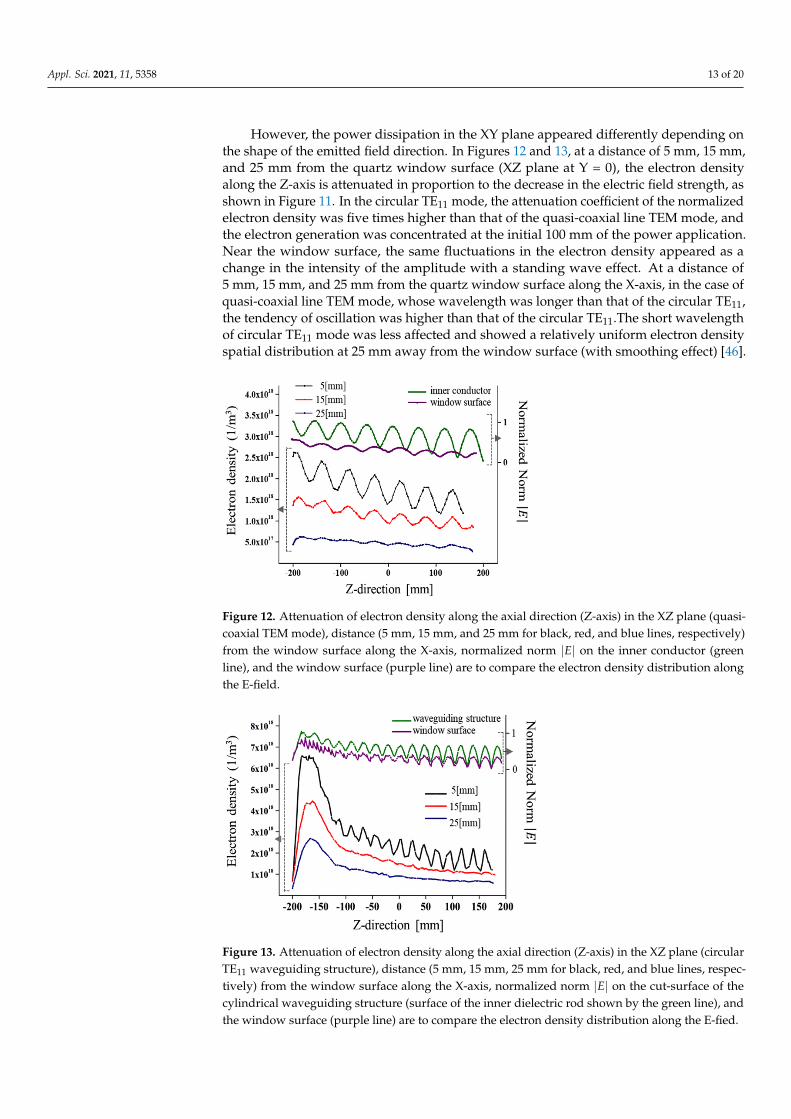
However, the power dissipation in the XY plane appeared differently depending onthe shape of the emitted field direction. In Figures 12 and 13, at a distance of 5 mm, 15 mm,and 25 mm from the quartz window surface (XZ plane at Y = 0), the electron densityalong the Z-axis is attenuated in proportion to the decrease in the electric field strength, asshown in Figure 11. In the circular TE11 mode, the attenuation coefficient of the normalizedelectron density was five times higher than that of the quasi-coaxial line TEM mode, andthe electron generation was concentrated at the initial 100 mm of the power application.Near the window surface, the same fluctuations in the electron density appeared as achange in the intensity of the amplitude with a standing wave effect. At a distance of5 mm, 15 mm, and 25 mm from the quartz window surface along the X-axis, in the case ofquasi-coaxial line TEM mode, whose wavelength was longer than that of the circular TE11,the tendency of oscillation was higher than that of the circular TE11.The short wavelengthof circular TE11 mode was less affected and showed a relatively uniform electron densityspatial distribution at 25 mm away from the window surface (with smoothing effect) [46].
Appl. Sci. 2021, 11, x FOR PEER REVIEW 13 of 20
represented by 5 in the quasi-coaxial line TEM and 10 in the circular TE11. The value was inversely proportional to the wavelength. In the circular TE11 wave mode with a short wavelength (which propagated in dielectric space), the power absorption was higher than the quasi-coaxial line TEM at the beginning of wave propagation.
In the linear microwave source, from a macroscopic point of view, two factors affected the spatial distribution of the electron density significantly, namely, the attenuation of the field strength along the wave propagation direction (axial direction) and the coupled field profile at the window surface (radial direction).
First, the electron density distribution along the wave propagation direction was proportional to the attenuation of the electric field strength. As mentioned in the previous section, power absorption mechanism in the plasma was related to the heat source from the electromagnetic wave power. The absorbed power was represented as a function of the variable 𝑬. Thus, the Re(J·E) of the power dissipation in the plasma chamber followed the 𝑬 field profile. In both the cases of LMPS, power dissipation in the axial direction was concentrated at the surface of dielectric near field region.
However, the power dissipation in the XY plane appeared differently depending on the shape of the emitted field direction. In Figures 12 and 13, at a distance of 5 mm, 15 mm, and 25 mm from the quartz window surface (XZ plane at Y = 0), the electron density along the Z-axis is attenuated in proportion to the decrease in the electric field strength, as shown in Figure 11. In the circular TE11 mode, the attenuation coefficient of the normalized electron density was five times higher than that of the quasi-coaxial line TEM mode, and the electron generation was concentrated at the initial 100 mm of the power application. Near the window surface, the same fluctuations in the electron density appeared as a change in the intensity of the amplitude with a standing wave effect. At a distance of 5 mm, 15 mm, and 25 mm from the quartz window surface along the X-axis, in the case of quasi-coaxial line TEM mode, whose wavelength was longer than that of the circular TE11, the tendency of oscillation was higher than that of the circular TE11.The short wavelength of circular TE11 mode was less affected and showed a relatively uniform electron density spatial distribution at 25 mm away from the window surface (with smoothing effect) [46].
Although the generation of electrons in the circular TE11 mode was concentrated at the initial 100 mm of wave propagation, the electron density (X = 5, 15, and 25 mm) at Z > 100 mm was 1.5 to 2 times higher than the quasi-coaxial TEM. In the TE11 mode, the electron density spatial distribution was formed close to the planar type. The waveguiding structure and the emitted field direction affected the attenuation of the electron density along the radial distance, the ratio of the electron density of 5–25 mm in the X-axis (at Z = 0) was 20% in the quasi-coaxial TEM mode and 33% in the circular TE11 mode.
Figure 12. Attenuation of electron density along the axial direction (Z-axis) in the XZ plane (quasi-coaxial TEM mode), distance (5 mm, 15 mm, and 25 mm for black, red, and blue lines, respectively)from the window surface along the X-axis, normalized norm |E| on the inner conductor (greenline), and the window surface (purple line) are to compare the electron density distribution alongthe E-field.
Appl. Sci. 2021, 11, x FOR PEER REVIEW 14 of 20
Figure 12. Attenuation of electron density along the axial direction (Z-axis) in the XZ plane (quasi-coaxial TEM mode), distance (5 mm, 15 mm, and 25 mm for black, red, and blue lines, respectively) from the window surface along the X-axis, normalized norm |𝐸| on the inner conductor (green line), and the window surface (purple line) are to compare the electron density distribution along the E-field.
Figure 13. Attenuation of electron density along the axial direction (Z-axis) in the XZ plane (circular TE11 waveguiding structure), distance (5 mm, 15 mm, 25 mm for black, red, and blue lines, respectively) from the window surface along the X-axis, normalized norm |𝐸| on the cut-surface of the cylindrical waveguiding structure (surface of the inner dielectric rod shown by the green line), and the window surface (purple line) are to compare the electron density distribution along the E-fied.
When the same power per unit volume was applied to the plasma generation in the simulation, the number of electrons generated in the total volume was 2.8 × 10¹⁵ m−3 in the quasi-coaxial line TEM mode and 2.3 × 10¹⁵ m−3 in the circular TE11 mode. Although the number of electrons produced in the entire volume was 20% higher in the quasi-coaxial line TEM mode than that in the circular TE11, the number of electrons generated in the actual deposition region was 50% higher in the circular TE11 mode than that in the quasi-coaxial TEM mode.
In Figure 10, the spatial profiles of the electron temperature for each source are represented in the axial and radial directions. For the axial direction (XZ plane, Y = 0), the electron temperature was nearly constant along the axial distance. For radial distances in the XZ plane (Y = 0), near the window surface, the electron temperature was relatively high with a value of 3.5 eV while in the case of radial distances > 10 mm from the quartz window surface, the electron temperature with the value of 0.8~1.3 eV weakly depended on the radial distance. In Figure 10, the electron temperature distribution of the XY plane in each source varied depending on the shape of the emitted field profile such as the electron density distribution. The electron density and the electron temperature near the substrate surface (z = 20 and 25 mm) measured by a single LP are compared with the simulation results in Figures 14 and 15. The results of the experimental diagnosis show that the tendency is consistent with the simulation results. The experimental results in Figure 14a shows that the tendency of the electron density distribution along the Z-axis is consistent with the simulation result in Figure 14b. The electron density decreased along the wave propagation direction, and the attenuation ratio was higher in the circular TE11 mode. The electron density fluctuations due to the standing wave effect were prominent in the quasi-coaxial TEM mode, and the effect decreased along the X-axis. When comparing the electron density according to the wave mode, in both cases, the electron density near the substrate was measured to be approximately 1.5~2 times higher in the circular TE11 mode than that in the quasi-coaxial line TEM mode. In the experiment, the rate of increase in density was 2, which was more than the simulation value of 1.5. This is
Figure 13. Attenuation of electron density along the axial direction (Z-axis) in the XZ plane (circularTE11 waveguiding structure), distance (5 mm, 15 mm, 25 mm for black, red, and blue lines, respec-tively) from the window surface along the X-axis, normalized norm |E| on the cut-surface of thecylindrical waveguiding structure (surface of the inner dielectric rod shown by the green line), andthe window surface (purple line) are to compare the electron density distribution along the E-fied.

Appl. Sci. 2021, 11, 5358 14 of 20
Although the generation of electrons in the circular TE11 mode was concentrated atthe initial 100 mm of wave propagation, the electron density (X = 5, 15, and 25 mm) atZ > 100 mm was 1.5 to 2 times higher than the quasi-coaxial TEM. In the TE11 mode, theelectron density spatial distribution was formed close to the planar type. The waveguidingstructure and the emitted field direction affected the attenuation of the electron densityalong the radial distance, the ratio of the electron density of 5–25 mm in the X-axis (at Z = 0)was 20% in the quasi-coaxial TEM mode and 33% in the circular TE11 mode.
When the same power per unit volume was applied to the plasma generation in thesimulation, the number of electrons generated in the total volume was 2.8× 10¹⁵ m−3 in thequasi-coaxial line TEM mode and 2.3 × 10¹⁵ m−3 in the circular TE11 mode. Although thenumber of electrons produced in the entire volume was 20% higher in the quasi-coaxial lineTEM mode than that in the circular TE11, the number of electrons generated in the actualdeposition region was 50% higher in the circular TE11 mode than that in the quasi-coaxialTEM mode.
In Figure 10, the spatial profiles of the electron temperature for each source arerepresented in the axial and radial directions. For the axial direction (XZ plane, Y = 0), theelectron temperature was nearly constant along the axial distance. For radial distances inthe XZ plane (Y = 0), near the window surface, the electron temperature was relativelyhigh with a value of 3.5 eV while in the case of radial distances > 10 mm from the quartzwindow surface, the electron temperature with the value of 0.8~1.3 eV weakly dependedon the radial distance. In Figure 10, the electron temperature distribution of the XY planein each source varied depending on the shape of the emitted field profile such as theelectron density distribution. The electron density and the electron temperature near thesubstrate surface (z = 20 and 25 mm) measured by a single LP are compared with thesimulation results in Figures 14 and 15. The results of the experimental diagnosis showthat the tendency is consistent with the simulation results. The experimental results inFigure 14a shows that the tendency of the electron density distribution along the Z-axis isconsistent with the simulation result in Figure 14b. The electron density decreased alongthe wave propagation direction, and the attenuation ratio was higher in the circular TE11mode. The electron density fluctuations due to the standing wave effect were prominent inthe quasi-coaxial TEM mode, and the effect decreased along the X-axis. When comparingthe electron density according to the wave mode, in both cases, the electron density nearthe substrate was measured to be approximately 1.5~2 times higher in the circular TE11mode than that in the quasi-coaxial line TEM mode. In the experiment, the rate of increasein density was 2, which was more than the simulation value of 1.5. This is because theelectron loss from the quartz window surface along the direction of the electric field wasnot considered in detail in this simulation model.
Appl. Sci. 2021, 11, x FOR PEER REVIEW 15 of 20
because the electron loss from the quartz window surface along the direction of the electric field was not considered in detail in this simulation model.
In the experiment, the energy distribution function of electrons of radial distance ≥ 20 mm followed the Maxwell distribution function. The electron temperature profile shown in Figure 15a is consistent with the simulation results in Figure 15b, which shows that when the radial distances > 20 mm from the quartz window surface, the electron temperature is weakly dependent on the radial distance.
To consider each source and the plasma characteristics more deeply, it was necessary to consider the effects by resolving the electric field into the radial and axial direction electric field components. The material properties of plasma act like a lossy medium, which cause not only the transverse field components but also the axial field components to exist [16,17]. The presence of an axial component of the wave electric field in the quasi-coaxial line source was detailed by H. Nowakowska et al. [61]. In the presence of the axial component of the wave field, in the high electron density region (ne > 1018), internal wave was represented by a wave that propagated near the window surfaces along the axial direction. Power dissipation in the plasma chamber is concentrated near the dielectric window surface region, so the presence of an internal wave is important as a component that affects the electron heating in the axial direction.
(a) (b)
Figure 14. (a) Electron density at the substrate (Experiment) and (b) electron density at the substrate (Simulation).
(a) (b)
Figure 15. (a) Electron temperature at the substrate (Experiment) and (b) electron temperature at the substrate (Simulation).
In Figure 12, a normalized norm |𝐸| of the inner conductor (green line) and the window surface (purple line) in the quasi-coaxial TEM source are set to compare with the electron density distribution along the axial direction (Z-axis) in the XZ plane. Normalized norm |𝐸| was expressed as the RSS (Root Sum Square: ∑ 𝜎 ) of the axial and radial
Figure 14. (a) Electron density at the substrate (Experiment) and (b) electron density at the substrate (Simulation).

Appl. Sci. 2021, 11, 5358 15 of 20
Appl. Sci. 2021, 11, x FOR PEER REVIEW 15 of 20
because the electron loss from the quartz window surface along the direction of the electric field was not considered in detail in this simulation model.
In the experiment, the energy distribution function of electrons of radial distance ≥ 20 mm followed the Maxwell distribution function. The electron temperature profile shown in Figure 15a is consistent with the simulation results in Figure 15b, which shows that when the radial distances > 20 mm from the quartz window surface, the electron temperature is weakly dependent on the radial distance.
To consider each source and the plasma characteristics more deeply, it was necessary to consider the effects by resolving the electric field into the radial and axial direction electric field components. The material properties of plasma act like a lossy medium, which cause not only the transverse field components but also the axial field components to exist [16,17]. The presence of an axial component of the wave electric field in the quasi-coaxial line source was detailed by H. Nowakowska et al. [61]. In the presence of the axial component of the wave field, in the high electron density region (ne > 1018), internal wave was represented by a wave that propagated near the window surfaces along the axial direction. Power dissipation in the plasma chamber is concentrated near the dielectric window surface region, so the presence of an internal wave is important as a component that affects the electron heating in the axial direction.
(a) (b)
Figure 14. (a) Electron density at the substrate (Experiment) and (b) electron density at the substrate (Simulation).
(a) (b)
Figure 15. (a) Electron temperature at the substrate (Experiment) and (b) electron temperature at the substrate (Simulation).
In Figure 12, a normalized norm |𝐸| of the inner conductor (green line) and the window surface (purple line) in the quasi-coaxial TEM source are set to compare with the electron density distribution along the axial direction (Z-axis) in the XZ plane. Normalized norm |𝐸| was expressed as the RSS (Root Sum Square: ∑ 𝜎 ) of the axial and radial
Figure 15. (a) Electron temperature at the substrate (Experiment) and (b) electron temperature at the substrate (Simulation).
In the experiment, the energy distribution function of electrons of radial distance≥20 mm followed the Maxwell distribution function. The electron temperature profileshown in Figure 15a is consistent with the simulation results in Figure 15b, which showsthat when the radial distances >20 mm from the quartz window surface, the electrontemperature is weakly dependent on the radial distance.
To consider each source and the plasma characteristics more deeply, it was necessary toconsider the effects by resolving the electric field into the radial and axial direction electricfield components. The material properties of plasma act like a lossy medium, which causenot only the transverse field components but also the axial field components to exist [16,17].The presence of an axial component of the wave electric field in the quasi-coaxial line sourcewas detailed by H. Nowakowska et al. [61]. In the presence of the axial component of thewave field, in the high electron density region (ne > 1018), internal wave was representedby a wave that propagated near the window surfaces along the axial direction. Powerdissipation in the plasma chamber is concentrated near the dielectric window surfaceregion, so the presence of an internal wave is important as a component that affects theelectron heating in the axial direction.
In Figure 12, a normalized norm |E| of the inner conductor (green line) and thewindow surface (purple line) in the quasi-coaxial TEM source are set to compare with theelectron density distribution along the axial direction (Z-axis) in the XZ plane. Normalized
norm |E| was expressed as the RSS (Root Sum Square:
√n∑
i=1σ2
i ) of the axial and radial
components of the electric field. Figure 12 shows that the electron density distributionalong the axial direction in the XZ plane follows the norm |E| profile in the window surfacerather than the profile of the norm |E| in the inner conductor surface. This result is dueto the axial field formed near the window surface region, and it can be observed in moredetail in Figure 16. Figure 16 shows the distribution of the power dissipation, and theelectron density distributions according to the electric field components in the axial andradial directions.

Appl. Sci. 2021, 11, 5358 16 of 20
Appl. Sci. 2021, 11, x FOR PEER REVIEW 16 of 20
components of the electric field. Figure 12 shows that the electron density distribution along the axial direction in the XZ plane follows the norm |𝐸| profile in the window surface rather than the profile of the norm |𝐸| in the inner conductor surface. This result is due to the axial field formed near the window surface region, and it can be observed in more detail in Figure 16. Figure 16 shows the distribution of the power dissipation, and the electron density distributions according to the electric field components in the axial and radial directions.
In the TEM wave mode, because the radially radiated electric field was directed in all directions with the same value, Ex (= Ey) represented the component of the radial field, and Ez represented the component of the axial field. In the case of the axial electric field Ez, the field strength is the highest at 4 × 10³ V/m for the window surface, and for the radial
electric field Ex, the field strength is the highest at 3 × 10⁴ V/m for the inner conductor surface. In Figure 16a,c, it is possible to compare the spatial distribution of the electron density according to each electric field component. Similar to Figure 12, it can be seen that the electron density distribution on the XZ plane follows the axial field component and not the radial field component. In Figure 16b,d, the spatial distribution characteristics of the power dissipation deposited in the plasma can be seen along each component of the electric field. In the figures, the maximum strength of the radial field is 3 × 10⁴ V/m and has a value greater than 4 × 10³ V/m of the axial field, while the maximum value of the power dissipation along the radial field near the surface region is 1 × 10⁵ W/m3, which is lower than 4 × 10⁵ W/m3 of the axial field. When the power dissipation value deposited in the plasma discharge in the plasma chamber was volume-integrated according to the radial and axial fields, in the quasi-coaxial TEM MWP, the power dissipation value by the axial field ≈ 400 W, and the power consumption by the radial field ≈ 200 W. In this simulation model, the power application method that inputted 600 W was fully deposited to the conductive material, and the plasma was applied. The power consumed by the conductive material, including the inner copper antenna, was less than 0.1 W. Therefore, when the total power of 600 W was applied to generate the plasma, power dissipation by the axial field was doubled compared to the radial field. Thus, in the quasi-coaxial TEM MWP sources, it was observed that axial field components in a horizontal form on the window surface compared to radial field components in a perpendicular form on the window surface (electron losses occur at the wall boundary) dominantly affected the electron heating in the plasma discharge.
Figure 16. Electron density and power dissipation Qh,z (=Re ( 1
2 σ·Ez·E∗z )) distributions according to the |Ez| profile, electrondensity and power dissipation Qh,x (=Re ( 1
2 σ·Ex·E∗x)) distributions according to the |Ex| profile in the XZ plane of quasico-axial line TEM waveguiding structure. (a) Electron density distribution according to the profile of |Ez|, (b) the distributionof power dissipation value Qh,z according to the profile of |Ez|, (c) electron density distribution according to the profile of|Ex|, and (d) the distribution of power dissipation value Qh,x according to the |Ex| profile.
In the TEM wave mode, because the radially radiated electric field was directed inall directions with the same value, Ex (= Ey) represented the component of the radial field,and Ez represented the component of the axial field. In the case of the axial electric field Ez,the field strength is the highest at 4 × 10³ V/m for the window surface, and for the radialelectric field Ex, the field strength is the highest at 3 × 10⁴ V/m for the inner conductorsurface. In Figure 16a,c, it is possible to compare the spatial distribution of the electrondensity according to each electric field component. Similar to Figure 12, it can be seen thatthe electron density distribution on the XZ plane follows the axial field component andnot the radial field component. In Figure 16b,d, the spatial distribution characteristics ofthe power dissipation deposited in the plasma can be seen along each component of theelectric field. In the figures, the maximum strength of the radial field is 3 × 10⁴ V/m andhas a value greater than 4 × 10³ V/m of the axial field, while the maximum value of thepower dissipation along the radial field near the surface region is 1 × 10⁵ W/m3, which islower than 4 × 10⁵ W/m3 of the axial field. When the power dissipation value depositedin the plasma discharge in the plasma chamber was volume-integrated according to theradial and axial fields, in the quasi-coaxial TEM MWP, the power dissipation value bythe axial field ≈ 400 W, and the power consumption by the radial field ≈ 200 W. In thissimulation model, the power application method that inputted 600 W was fully depositedto the conductive material, and the plasma was applied. The power consumed by theconductive material, including the inner copper antenna, was less than 0.1 W. Therefore,when the total power of 600 W was applied to generate the plasma, power dissipationby the axial field was doubled compared to the radial field. Thus, in the quasi-coaxialTEM MWP sources, it was observed that axial field components in a horizontal form onthe window surface compared to radial field components in a perpendicular form onthe window surface (electron losses occur at the wall boundary) dominantly affected theelectron heating in the plasma discharge.
In Figure 13, normalized norm |E| on the cut surface of the cylindrical waveguidingstructure (green line) and window surface (purple line) in the circular TE11 wave MWPsource are set to compare with the electron density distribution along the axial direction(Z-axis) in the XZ plane. Unlike the result of Figure 12, Figure 13 shows that electron

Appl. Sci. 2021, 11, 5358 17 of 20
density distribution along the axial direction in the XZ plane simultaneously follows thenorm |E| profile in the cut surface of the cylindrical waveguiding structure and also inthe window surface. This was because the axial field had a small effect on the electrongeneration in the spatial distribution. It represented that electron generation was mainlyaffected by the distribution of the radial direction the electric field component. Whenthe volume-integrated power dissipation value deposited on the plasma discharge in theplasma chamber was expressed as components of the radial and axial fields, in the circularTE11 wave MWP, the power dissipation value by the axial field ≈ 40 W, and the powerdissipation by the radial field ≈ 560 W. In this numerical model, the power applicationmethod in the circular TE11 source was applied in the same way as in the quasi-coaxialTEM source, and the power consumed by the conductive material was also less than 0.1 W.Therefore, it can be seen that when a total of 600 W was applied to generate the plasma,the dissipation of power by the radial field was more dominant than that of the axialfield component.
In Figure 17, the spatial distribution of the power dissipation and electron densitydistributions are represented according to the electric field components, which are indicatedby resolving the radial fields into the Ex and Ey components. In the case of Ex, the fieldstrength was the highest for 6 × 10³ V/m near the window surface, and the field directionwas perpendicular to the window surface. Similarly, for the case of Ey, the field strengthwas the highest for 1.5 × 10⁴ V/m, and the field direction was parallel to the windowsurface. In both these cases, as shown in Figure 17, the spatial distributions of the electrongeneration and power dissipation coincided with the electric field concentrated region.When the volume-integrated power dissipation value deposited for plasma generation wascalculated by resolving into the Ex and Ey field components, the power dissipation valueEx ≈ 300 W and Ey ≈ 260 W. Among the radial field components involved in the plasmadischarge, a dominant component was Ex, which was due to the field emitted geometrycharacteristics of the waveguiding structure.
Appl. Sci. 2021, 11, x FOR PEER REVIEW 18 of 20
Figure 17. Electron density and power dissipation 𝑄 , (= Re ( 𝜎·𝐸 · 𝐸∗)) distributions according to the |𝐸 | profile, electron density and power dissipation 𝑄 , (= Re ( 𝜎·𝐸 · 𝐸∗)) distributions according to the 𝐸 profile in the XZ plane of circular TE11 waveguiding structure. (a) Electron density distribution according to the profile of |𝐸 |, (b) the distribution of power dissipation value 𝑄 , according to the profile of |𝐸 |, (c) electron density distribution according to the profile of 𝐸 , and (d) the distribution of power dissipation value 𝑄 , according to the 𝐸 profile.
6. Conclusions A conventional quasi co-axial TEM waveguiding structure and a newly developed
circular TE11 waveguiding structure sources are presented to compare the plasma characteristics along the waveguiding structure. To compare the source characteristics, experiments were conducted under 500mTorr Ar plasma condition, where 0.6 kW microwave power was applied. The characteristics of the plasma was diagnosed by a single LP and analyzed by the numerical 3-D model using plasma fluid simulation. Attenuation of the electric field strength along the wave propagation direction and the coupled field profile at the window surface affected the spatial distribution of the electron density significantly. In the TE11 mode, the attenuation coefficient of the normalized electron density was 4.8 times higher than that of the TEM mode. The field direction affected the attenuation of the electron density along the radial distance, and the electron-density reduction rate along the radial direction was higher in the TEM mode than that in the TE11 mode. The plasma characteristics of each plasma source were considered by resolving the wave electric field into the radial and axial field components. The influence of the axial electric field component was more dominant in the quasi-coaxial TEM MWP source. The number of electrons produced in the entire volume was 20% higher in the TEM mode than that in the TE11 mode, but the number of electrons generated in the actual deposition region was 50% higher in the TE11 mode than that in the TEM mode.
Author Contributions: Conceptualization, J.-H.C. and H.-J.L.; methodology, J.-H.C. and H.-J.L.; software, J.-H.C.; validation, J.-H.C., S.-W.K. and H.-J.L.; formal analysis, J.-H.C. and S.-W.K.; investigation, J.-H.C. and S.-W.K.; resources, J.-H.C.; data curation, J.-H.C.; writing—original draft preparation, J.-H.C.; writing—review and editing, J.-H.C.; visualization, J.-H.C.; supervision, H.-J.L.; project administration, H.-J.L.; funding acquisition, H.-J.L. All authors have read and agreed to the published version of the manuscript.
Funding: Please add: This research was supported by Korea Institute for Advancement of Technology(KIAT) grant funded by the Korea Government(MOTIE) (P0012451, The Competency Development Program for Industry Specialist).
Figure 17. Electron density and power dissipation Qh,x (=Re ( 12 σ·Ex·E∗x)) distributions according to the |Ex| profile, electron
density and power dissipation Qh,y(=Re ( 12 σ·Ey·E∗y)) distributions according to the
∣∣Ey∣∣ profile in the XZ plane of circular
TE11 waveguiding structure. (a) Electron density distribution according to the profile of |Ex|, (b) the distribution of powerdissipation value Qh,x according to the profile of |Ex|, (c) electron density distribution according to the profile of
∣∣Ey∣∣, and
(d) the distribution of power dissipation value Qh,y according to the∣∣Ey∣∣ profile.

Appl. Sci. 2021, 11, 5358 18 of 20
6. Conclusions
A conventional quasi co-axial TEM waveguiding structure and a newly developedcircular TE11 waveguiding structure sources are presented to compare the plasma character-istics along the waveguiding structure. To compare the source characteristics, experimentswere conducted under 500mTorr Ar plasma condition, where 0.6 kW microwave powerwas applied. The characteristics of the plasma was diagnosed by a single LP and analyzedby the numerical 3-D model using plasma fluid simulation. Attenuation of the electric fieldstrength along the wave propagation direction and the coupled field profile at the windowsurface affected the spatial distribution of the electron density significantly. In the TE11mode, the attenuation coefficient of the normalized electron density was 4.8 times higherthan that of the TEM mode. The field direction affected the attenuation of the electrondensity along the radial distance, and the electron-density reduction rate along the radialdirection was higher in the TEM mode than that in the TE11 mode. The plasma character-istics of each plasma source were considered by resolving the wave electric field into theradial and axial field components. The influence of the axial electric field component wasmore dominant in the quasi-coaxial TEM MWP source. The number of electrons producedin the entire volume was 20% higher in the TEM mode than that in the TE11 mode, but thenumber of electrons generated in the actual deposition region was 50% higher in the TE11mode than that in the TEM mode.
Author Contributions: Conceptualization, J.-H.C. and H.-J.L.; methodology, J.-H.C. and H.-J.L.;software, J.-H.C.; validation, J.-H.C., S.-W.K. and H.-J.L.; formal analysis, J.-H.C. and S.-W.K.; in-vestigation, J.-H.C. and S.-W.K.; resources, J.-H.C.; data curation, J.-H.C.; writing—original draftpreparation, J.-H.C.; writing—review and editing, J.-H.C.; visualization, J.-H.C.; supervision, H.-J.L.;project administration, H.-J.L.; funding acquisition, H.-J.L. All authors have read and agreed to thepublished version of the manuscript.
Funding: This research was supported by Korea Institute for Advancement of Technology(KIAT)grant funded by the Korea Government(MOTIE) (P0012451, The Competency Development Programfor Industry Specialist).
Institutional Review Board Statement: Not applicable.
Informed Consent Statement: Not applicable.
Data Availability Statement: Data sharing is not applicable to this article.
Acknowledgments: The authors would like to acknowledge the support of Korea Institute forAdvancement of Technology(KIAT) grant funded by the Korea Government(MOTIE) (P0012451, TheCompetency Development Program for Industry Specialist).
Conflicts of Interest: The authors declare no conflict of interest.
References1. Pozar, D.M. Microwave Engineering, 4th ed.; John Wiley & Sons: New Jersey, NJ, USA, 2011.2. Collin, R.E. Foundations for Microwave Engineering, 2nd ed.; McGraw Hill: New York, NY, USA, 1992.3. Ferreira, C.M.; Moisan, M. 1993 Microwave Discharges Fundamentals and Applications; Springer: New York, NY, USA, 1993.4. Lebedev, Y.A. Microwave discharges at low pressures and peculiarities of the processes in strongly non-uniform plasma. Plasma
Sources Sci. Technol. 2015, 24, 053001. [CrossRef]5. Zakrzewski, Z.; Moisan, M. Plasma Sources using long linear microwave field applicators: Main features, classification and
modeling. Plasma Sources Sci. Technol. 1995, 4, 379–397. [CrossRef]6. Kromka, A.; Babchenko, O.; Izak, T.; Hruska, K.; Rezek, B. Linear antenna microwave plasma CVD deposition of diamond films
over large areas. Vacuum 2012, 86, 776–779. [CrossRef]7. Moisan, M.; Zakrzewski, Z. Plasma sources based on the propagation of electromagnetic surface waves. J. Phys. D Appl. Phys.
1991, 24, 1025. [CrossRef]8. Kiyokawa, K.; Sugiyama, K.; Tomimatsu, M.; Kurokawa, H.; Miura, H. Microwave-included non-equilibrium plasma by insertino
of substrate at low and atmospheric pressures. Appl. Surf. Sci. 2001, 169, 599. [CrossRef]9. Jauberteau, I.; Jauberteau, J.L.; Goudeau, P.; Soulestin, B.; Marteau, M.; Cahoreau, M.; Aubreton, J. Investigation on a nitriding
process of molybdenum thin films exposed to (Ar-N2-H2) expanding microwave plasma. Surf. Coat. Technol. 2009, 203, 1127.[CrossRef]

Appl. Sci. 2021, 11, 5358 19 of 20
10. Rauchle, E. Duo-plasmaline, a surface wave sustained linearly extended discharge. J. Phys. IV 1998, 8, Pr7-99–Pr7-108. [CrossRef]11. Petasch, W.; Rauchle, E.; Muegge, H.; Muegge, K. Duo-Plasmaline a linearly extended homogeneous low pressure plasma source.
Surf. Coat. Technol. 1997, 93, 112. [CrossRef]12. Liehr, M.; Wieder, S.; Dieguez-Campo, M. Large area microwave coating technology. Thin Solid Films 2006, 502, 9. [CrossRef]13. Liehr, M.; Dieguez-Campo, M. Microwave PECVD for large area coating. Surf. Coat. Technol. 2005, 200, 21–25. [CrossRef]14. Han, M.K.; Cha, J.H.; Lee, H.J.; Chang, C.J.; Jeon, C.Y. The Effects of CF4 Partial Pressure on the Hydrophobic Thin Film Formation
on Carbon Steel by Surface Treatment and Coating Method with Linear Microwave Ar/CH4/CF4 Plasma. J. Electr. Eng. Technol.2017, 12, 2007–2013.
15. Neykova, N.; Kozak, H.; Ledinsky, M.; Kromka, A. Novel plasma treatment in linear antenna microwave PECVD system. Vacuum2012, 86, 603–607. [CrossRef]
16. Sahu, B.B.; Joga, S.; Toyoda, H.; Han, J.G. Development and plasma characterization of an 850 MHz surface-wave plasma source.AIP Adv. 2017, 7, 105213. [CrossRef]
17. Yamada, T.; Kim, J.H.; Ishihara, M.; Hasegawa, M. Low-temperature graphene synthesis using microwave plasma CVD. J. Phys.D Appl. Phys. 2013, 46, 063001. [CrossRef]
18. Tarey, R.D.; Jarwal, R.K.; Ganguli, A.; Akhtar, M.K. High-density plasma production using a slotted helical antenna at highmicrowave power. Plasma Sources Sci. Technol. 1997, 6, 189. [CrossRef]
19. Suetsugu, Y.; Kawai, Y. Temporal Behaviour of ECR Plasmas Produced by a Lisitano Coil. Jpn. J. Appl. Phys. 1984, 23, 237.[CrossRef]
20. Kaswai, Y.; Sakamoto, K. Production of a large diameter hot-electron plasma by electron cyclotron resonance heating. Rev. Sci.Instrum. 1982, 53, 606. [CrossRef]
21. Latrasse, L.; Radoiu, M.; Lo, J.; Guillot, P. 2.45-GHz microwave plasma sources using solid-state microwave generators. ECR-typeplasma source. J. Microw. Power Electromagn. Energy 2016, 50, 308–321. [CrossRef]
22. Ruzic, D.N. Electric Probes for Low Temperature Plasmas; American Vacuum Society: New York, NY, USA, 1994.23. Godyak, V.A.; Piejak, R.B.; Alexandrovich, B.M. Measurements of electron energy distribution in low-pressure RF discharges.
Plasma Sources Sci. Technol. 1992, 1, 36. [CrossRef]24. Kim, J.Y.; Choe, W.H.; Dang, J.J.; Chung, K.J.; Hwang, Y.S. Characterization of electron kinetics regime with electron energy
probability functions in inductively coupled hydrogen plasmas. Phys. Plasmas 2016, 23, 023511. [CrossRef]25. Ghanashev, I.; Nagatsu, M.; Xu, G.; Sugai, H. Mode Jumps and Hysteresis in Surface-Wave Sustained Microwave Discharges. Jpn.
J. Appl. Phys. 1997, 36, 4704–4710. [CrossRef]26. Ferreira, C.M. A basic self-contained model of a plasma column sustained by a weakly damped surface wave. J. Phys. D Appl.
Phys. 1988, 22, 705–708. [CrossRef]27. Granier, A.; Boisse-Laporte, C.; Leprince, P.; Marec, J.; Nghiem, P. Wave propagation and diagnostics in argon surface-wave
discharges up to 100 Torr. J. Phys. D Appl. Phys. 1986, 20, 204–209. [CrossRef]28. Sugai, H. Observation of Collisionless electron-cycltron damping in a plasma. Phys. Rev. A 1981, 24, 1571. [CrossRef]29. Kousaka, H.; Ono, K. Fine structure of the electromagnetic fields formed by backward surface waves in an azimuthally symmetric
surface wave-excited plasma source. Plasma Sour. Sci. Technol. 2003, 12, 273. [CrossRef]30. Gordiets, B.; Pinheiro, M.; Tatarova, E.; Dias, F.M.; Ferreira, C.M.; Ricard, A. A traveling wave sustained hydrogen discharge:
Modeling and experiment. Plasma Sour. Sci. Technol. 2000, 9, 295. [CrossRef]31. Paunska, T.; Schluter, H.; Shivarova, A.; Tarnev, K. Surface-wave produced discharges in hydrogen: II. Modifications of the
discharge structure for varying gas-discharge conditions. Plasma Sour. Sci. Technol. 2003, 12, 608. [CrossRef]32. Ferreira, C.M.; Tatarova, E.; Guerra, V.; Gordiets, B.F.; Henriques, J.; Dias, F.M.; Pinheiro, M. Modeling of Wave Driven
Molecular(H2, N2, N2-Ar) Discharges as Atomic Sources. IEEE Trans. Plasma. Sci. 2003, 31, 4. [CrossRef]33. Rahimi, S.; Jimenez-Diaz, M.; Hubner, S.; Kemaneci, E.H.; Vander Mullen, J.J.A.M.; Dijk, J.V. A two-dimensional modelling study
of a coaxial plasma waveguide. J. Phys. D Appl. Phys. 2014, 47, 125204. [CrossRef]34. Obrusnik, A.; Bonaventura, Z. Studying a low-pressure microwave coaxial discharge in hydrogen using a mixed 2D/3D fluid
model. J. Phys. D Appl. Phys. 2015, 48, 065201. [CrossRef]35. COMSOL Plasma Module User’s Guide (COMSOL Multiphysics); COMSOL: Massachusetts, MA, USA, 2019.36. Ganguli, A.; Akhtar, M.K.; Tarey, R.D.; Jarwal, R.K. Absorption of left-polarized microwaves in electron cyclotron resonance
plasmas. Phys. Lett. A 1998, 250, 137. [CrossRef]37. Lymberopoulos, D.P.; Economou, D.J. Fluid simulation of glow discharges:Effect of metastable atoms in argon. J. Appl. Phys. 1993,
73, 3668. [CrossRef]38. Yamabe, C.; Buckman, S.J.; Phelps, A.V. Measurement of free-free emission from low-energy-electron collisions with Ar. Phys.
Rev. A 2008, 27, 1345. [CrossRef]39. Ali, M.A.; Stone, P.M. Electron impact ionization of metastable rare gases: He, Ne and Ar. Int. J. Mass Spectrom. 2008, 271, 51.
[CrossRef]40. Cramer, W.H. Elastic and Inelastic scattering of Low-Velocity Ions: Ne+ in A, A+ in Ne and A+ in A. J. Chem. Phys. 1959, 30, 641.
[CrossRef]41. Kim, J.S.; Hur, M.Y.; Kim, H.J.; Lee, H.J. Advanced PIC-MCC simulation for the investigation of step-ionization effect in
intermediate-pressure capacitively coupled plasmas. J. Phys. D Appl. Phys. 2018, 51, 104004. [CrossRef]

Appl. Sci. 2021, 11, 5358 20 of 20
42. Ostmark, H.; Roman, N. Laser ignition of pyrotechnic mixtures: Igniation mechanisms. J. Appl. Phys. 1993, 73, 1993. [CrossRef]43. Mcvey, B.; Scharer, J. Measurement of Collisionless Electron-Cyclotron Damping along a Weak Magnetic Beach. Phys. Rev. Lett.
1973, 31, 14. [CrossRef]44. Kawai, Y.; Uchino, K.; Muta, H.; Kawai, S.; Rowf, T. Development of large diameter ECR plasma source. Vacuum 2010, 84, 1381.
[CrossRef]45. Verma, A.; Singh, P.; Narayanan, R.; Sahu, D.; Kar, S.; Ganguli, A.; Tarey, R.D. Investigations on argon and hydrogen plasmas
produced by compact ECR plasma source. Plasma Res. Express 2019, 1, 035012. [CrossRef]46. Musil, J. Development of a new microwave plasma torch and its application to diamond synthesis. Vacuum 1986, 36, 161.
[CrossRef]47. Popov, O.A. Effects of magnetic field and microwave power on electron cyclotron resonance type plasma characteristics. J. Vac.
Sci. Technol. 1991, 9, 711. [CrossRef]48. Ganguli, A.; Tarey, R.D.; Arora, N.; Narayanan, R. Development and Studies on a compact electron cyclotron resonance plasma
source. Plasma Sour. Sci. Technol. 2016, 25, 025026. [CrossRef]49. Lucovsky, G.; Tsu, D.V. Plasma enhanced chemical vapor deposition:Differences between direct and remote plasma excitation. J.
Vac. Sci. Technol. A 1987, 5, 2231. [CrossRef]50. Hagelaar, C.J.M.; Pitchford, L.C. Solving the Boltzmann equation to obtain electron transport coefficients and rate coefficients for
fluid models. Plasma Sour. Sci. Technol. 2005, 14, 722–733. [CrossRef]51. Gogolides, E.; Sawin, H.H. Continuum modeling of radio-frequency glow discharges. I. Theory and results for electropositive
and electronegative gases. J. Appl. Phys. 1992, 72, 3971. [CrossRef]52. Gogolides, E.; Sawin, H.H. Continuum modeling of radio-frequency glow discharges. II. Parametric stuides ans sensitivity
analysis. J. Appl. Phys. 1992, 72, 3988. [CrossRef]53. Passchier, J.D.P.; Goedheer, W.J. A two-dimensinal fluid model for and argon rf discharge. J. Appl. Phys. 1993, 74, 3744. [CrossRef]54. Richards, A.D.; Thompson, B.E.; Sawin, H.H. Continuum modeling of argon radio frequency glow discharges. Appl. Phys. Lett.
1987, 50, 492. [CrossRef]55. Ferreira, C.M. Modelling of a low-pressure plasma column sustained by a surface wave. J. Phys. D Appl. Phys. 1983, 16, 1673.
[CrossRef]56. Suzuki, H.; Nakano, S.; Itoh, H.; Sekine, M.; Hori, M.; Toyoda, H. Characteristics of an atmospheric-pressure line plasma excited
by 2.45 GHz microwave travelling wave. Jpn. J. Appl. Phys. 2016, 55, 01AH09. [CrossRef]57. Ellis, H.W.; Mcdaniel, E.W.; Albritton, D.L.; Viehland, L.A.; Lin, S.L.; Mason, E.A. Transport properties of gaseous ions over a
wide energy range. Part II. Atomic Datat Nucl. Data Tables 1978, 17, 177–210. [CrossRef]58. Bird, R.B.; Stewart, W.E.; Lightfoot, E.N. Transport Phenomena; John Wiley & Sons: Hoboken, NJ, USA, 2002.59. Brokaw, R.S. Predicting Transport Properties of Dilute Gases. Ind. Eng. Process Des. Dev. 1969, 8, 240–253. [CrossRef]60. Cha, J.H.; Seo, K.S.; Jeong, J.H.; Lee, H.J. Two-dimensional fluid simulation of pulsed-power inductively coupled Ar/H2 discharge.
J. Phys. D Appl. Phys 2021, 54, 16205. [CrossRef]61. Ganguli, A.; Akhtar, K.; Tarey, R.D. Absorption of high-frequency guided waves in a plasma-loaded waveguide. Phys. Plasmas
2007, 14, 102107. [CrossRef]