A debug scheme to improve the error identification in post ...
15
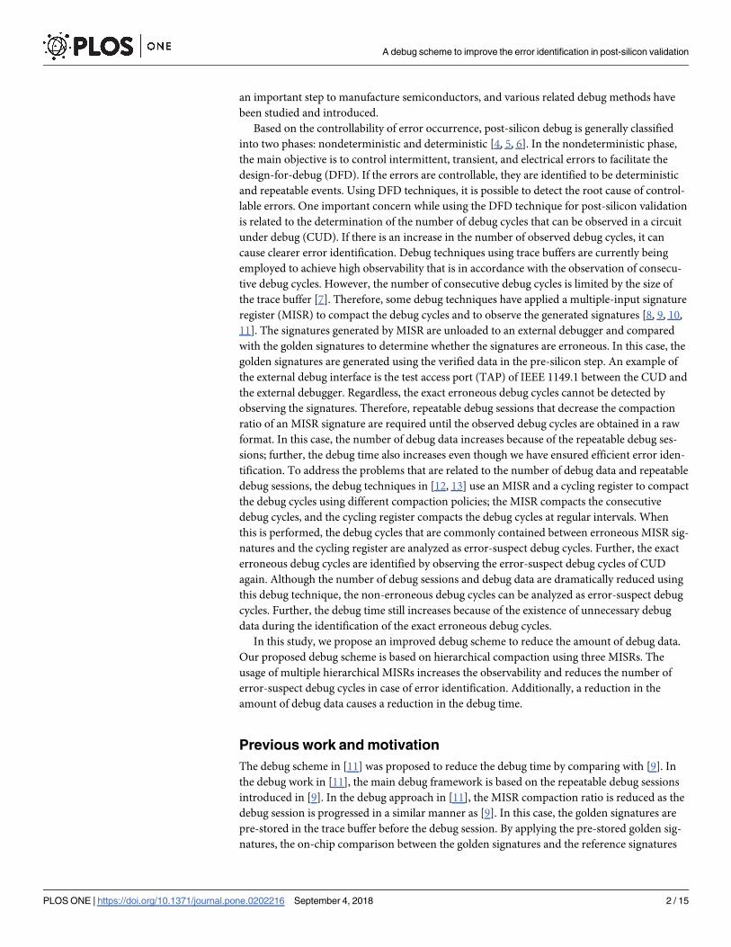
RESEARCH ARTICLE A debug scheme to improve the error identification in post-silicon validation Inhyuk Choi ¤ , Won Jung ¤ , Hyunggoy Oh ¤ , Sungho Kang ¤ * Department of Electrical and Electronic Engineering, Yonsei University, Seoul, Korea ¤ Current address: Dept. of Electrical and Electronic Engineering, Yonsei University, Seodaemoon-Gu, Seoul, Korea * [email protected] Abstract While developing semiconductors, post-silicon validation is an important step to identify the errors that are not detected during the pre-silicon verification and manufacturing testing phases. When the design complexity increases, the required debug time also increases because additional debug data are required to identify the errors. In this study, we present a debug scheme that improves the error identification capability. The proposed debug approach concurrently generates three types of signatures using hierarchical multiple-input signature registers (MISRs). The error-suspect debug cycles are determined by analyzing the debug cycles that are commonly contained in the erroneous signatures of the three MISRs. To reduce the amount of debug data, we compare the high-level MISR signatures in real time with the golden signatures; further, we handle the remaining two MISRs based on the tag bits that are obtained from the results of the high-level MISR. The experimental results prove that the proposed debug structure can significantly improve the error identifica- tion capability using less debug data than that used in previous debug structure. Introduction Recent advances in semiconductor manufacturing technologies have caused the development of improved designs that contain faster and more diverse functions. However, these develop- ments have also enabled the creation of more complex designs that require additional logic. To produce these complex designs, an additional effort is required on the part of the designers [1]. The incorporation of simulation models into the design process is becoming increasingly insufficient to perform error detection because both the size and the complexity of the inte- grated circuit designs have increased [2]. Errors that were not detected during the pre-silicon verification stage or the manufacturing testing stage will appear in the first silicon. To elimi- nate these errors, designers attempt to rapidly identify these errors and apply solutions, such as software changes, engineering change orders, and the usage of spare cells [3]. If design modifi- cations are required to solve various problems, this process should be completed before re- spinning the silicon. However, silicon re-spinning causes an increase in the production costs and impacts the time-to-market [2]. Therefore, post-silicon validation has been recognized as PLOS ONE | https://doi.org/10.1371/journal.pone.0202216 September 4, 2018 1 / 15 a1111111111 a1111111111 a1111111111 a1111111111 a1111111111 OPEN ACCESS Citation: Choi I, Jung W, Oh H, Kang S (2018) A debug scheme to improve the error identification in post-silicon validation. PLoS ONE 13(9): e0202216. https://doi.org/10.1371/journal. pone.0202216 Editor: Vivek Maheshwari, University of Waterloo, CANADA Received: April 9, 2018 Accepted: July 30, 2018 Published: September 4, 2018 Copyright: © 2018 Choi et al. This is an open access article distributed under the terms of the Creative Commons Attribution License, which permits unrestricted use, distribution, and reproduction in any medium, provided the original author and source are credited. Data Availability Statement: All relevant data are within the paper. Funding: This research was supported by the MOTIE (Ministry of Trade, Industry & Energy) (10067813) and KSRC (Korea Semiconductor Research Consortium) support program for the development of the future semiconductor device. Competing interests: The authors have declared that no competing interests exist.
-
Upload
khangminh22 -
Category
Documents
-
view
3 -
download
0
Transcript of A debug scheme to improve the error identification in post ...
RESEARCH ARTICLE
A debug scheme to improve the error
identification in post-silicon validation
Inhyuk Choi¤, Won Jung¤, Hyunggoy Oh¤, Sungho Kang¤*
Department of Electrical and Electronic Engineering, Yonsei University, Seoul, Korea
¤ Current address: Dept. of Electrical and Electronic Engineering, Yonsei University, Seodaemoon-Gu,
Seoul, Korea
Abstract
While developing semiconductors, post-silicon validation is an important step to identify the
errors that are not detected during the pre-silicon verification and manufacturing testing
phases. When the design complexity increases, the required debug time also increases
because additional debug data are required to identify the errors. In this study, we present a
debug scheme that improves the error identification capability. The proposed debug
approach concurrently generates three types of signatures using hierarchical multiple-input
signature registers (MISRs). The error-suspect debug cycles are determined by analyzing
the debug cycles that are commonly contained in the erroneous signatures of the three
MISRs. To reduce the amount of debug data, we compare the high-level MISR signatures in
real time with the golden signatures; further, we handle the remaining two MISRs based on
the tag bits that are obtained from the results of the high-level MISR. The experimental
results prove that the proposed debug structure can significantly improve the error identifica-
tion capability using less debug data than that used in previous debug structure.
Introduction
Recent advances in semiconductor manufacturing technologies have caused the development
of improved designs that contain faster and more diverse functions. However, these develop-
ments have also enabled the creation of more complex designs that require additional logic. To
produce these complex designs, an additional effort is required on the part of the designers [1].
The incorporation of simulation models into the design process is becoming increasingly
insufficient to perform error detection because both the size and the complexity of the inte-
grated circuit designs have increased [2]. Errors that were not detected during the pre-silicon
verification stage or the manufacturing testing stage will appear in the first silicon. To elimi-
nate these errors, designers attempt to rapidly identify these errors and apply solutions, such as
software changes, engineering change orders, and the usage of spare cells [3]. If design modifi-
cations are required to solve various problems, this process should be completed before re-
spinning the silicon. However, silicon re-spinning causes an increase in the production costs
and impacts the time-to-market [2]. Therefore, post-silicon validation has been recognized as
PLOS ONE | https://doi.org/10.1371/journal.pone.0202216 September 4, 2018 1 / 15
a1111111111
a1111111111
a1111111111
a1111111111
a1111111111
OPENACCESS
Citation: Choi I, Jung W, Oh H, Kang S (2018) A
debug scheme to improve the error identification in
post-silicon validation. PLoS ONE 13(9):
e0202216. https://doi.org/10.1371/journal.
pone.0202216
Editor: Vivek Maheshwari, University of Waterloo,
CANADA
Received: April 9, 2018
Accepted: July 30, 2018
Published: September 4, 2018
Copyright: © 2018 Choi et al. This is an open
access article distributed under the terms of the
Creative Commons Attribution License, which
permits unrestricted use, distribution, and
reproduction in any medium, provided the original
author and source are credited.
Data Availability Statement: All relevant data are
within the paper.
Funding: This research was supported by the
MOTIE (Ministry of Trade, Industry & Energy)
(10067813) and KSRC (Korea Semiconductor
Research Consortium) support program for the
development of the future semiconductor device.
Competing interests: The authors have declared
that no competing interests exist.
an important step to manufacture semiconductors, and various related debug methods have
been studied and introduced.
Based on the controllability of error occurrence, post-silicon debug is generally classified
into two phases: nondeterministic and deterministic [4, 5, 6]. In the nondeterministic phase,
the main objective is to control intermittent, transient, and electrical errors to facilitate the
design-for-debug (DFD). If the errors are controllable, they are identified to be deterministic
and repeatable events. Using DFD techniques, it is possible to detect the root cause of control-
lable errors. One important concern while using the DFD technique for post-silicon validation
is related to the determination of the number of debug cycles that can be observed in a circuit
under debug (CUD). If there is an increase in the number of observed debug cycles, it can
cause clearer error identification. Debug techniques using trace buffers are currently being
employed to achieve high observability that is in accordance with the observation of consecu-
tive debug cycles. However, the number of consecutive debug cycles is limited by the size of
the trace buffer [7]. Therefore, some debug techniques have applied a multiple-input signature
register (MISR) to compact the debug cycles and to observe the generated signatures [8, 9, 10,
11]. The signatures generated by MISR are unloaded to an external debugger and compared
with the golden signatures to determine whether the signatures are erroneous. In this case, the
golden signatures are generated using the verified data in the pre-silicon step. An example of
the external debug interface is the test access port (TAP) of IEEE 1149.1 between the CUD and
the external debugger. Regardless, the exact erroneous debug cycles cannot be detected by
observing the signatures. Therefore, repeatable debug sessions that decrease the compaction
ratio of an MISR signature are required until the observed debug cycles are obtained in a raw
format. In this case, the number of debug data increases because of the repeatable debug ses-
sions; further, the debug time also increases even though we have ensured efficient error iden-
tification. To address the problems that are related to the number of debug data and repeatable
debug sessions, the debug techniques in [12, 13] use an MISR and a cycling register to compact
the debug cycles using different compaction policies; the MISR compacts the consecutive
debug cycles, and the cycling register compacts the debug cycles at regular intervals. When
this is performed, the debug cycles that are commonly contained between erroneous MISR sig-
natures and the cycling register are analyzed as error-suspect debug cycles. Further, the exact
erroneous debug cycles are identified by observing the error-suspect debug cycles of CUD
again. Although the number of debug sessions and debug data are dramatically reduced using
this debug technique, the non-erroneous debug cycles can be analyzed as error-suspect debug
cycles. Further, the debug time still increases because of the existence of unnecessary debug
data during the identification of the exact erroneous debug cycles.
In this study, we propose an improved debug scheme to reduce the amount of debug data.
Our proposed debug scheme is based on hierarchical compaction using three MISRs. The
usage of multiple hierarchical MISRs increases the observability and reduces the number of
error-suspect debug cycles in case of error identification. Additionally, a reduction in the
amount of debug data causes a reduction in the debug time.
Previous work and motivation
The debug scheme in [11] was proposed to reduce the debug time by comparing with [9]. In
the debug work in [11], the main debug framework is based on the repeatable debug sessions
introduced in [9]. In the debug approach in [11], the MISR compaction ratio is reduced as the
debug session is progressed in a similar manner as [9]. In this case, the golden signatures are
pre-stored in the trace buffer before the debug session. By applying the pre-stored golden sig-
natures, the on-chip comparison between the golden signatures and the reference signatures
A debug scheme to improve the error identification in post-silicon validation
PLOS ONE | https://doi.org/10.1371/journal.pone.0202216 September 4, 2018 2 / 15
generated by the MISR is facilitated. The area which the pre-stored golden signatures are
located is empty after the on-chip comparison. At the same time, the additional MISR com-
pacts the trace cycles by the segmented compaction ratio. If the result of the on-chip compari-
son denotes that the generated MISR signature is error-suspected, the segmented MISR
signatures by the additional MISR compaction are stored in the empty area of the trace buffer.
Therefore, the consecutive debug sessions are performed simultaneously, then the overall
debug time can be reduced by comparing with [9]. Nevertheless, the debug approaches in [9,
11] are unsuitable for nondeterministic debug phase because a number of repeatable debug
sessions are required to observe the error-suspect interval. For this reason, these debug
approaches focus on only the deterministic debug phase and the cycle-accurate error
occurrence.
To reduce the amount of debug data, the debug method proposed in [12] reduces the
repeatable debug sessions and analyzes the error-suspect debug cycles using the MISR and the
cycling register. In this technique, the signatures generated by the MISR and the cycling regis-
ter are captured in the trace buffer and are unloaded to the external debugger; further, the gen-
erated signatures are compared with the golden signatures. The signatures generated by the
MISR are used to compact the consecutive debug cycles, whereas the signatures generated by
the cycling register are used to compact the debug cycles at regular intervals. The erroneous
signatures of the MISR and the cycling register are sorted by comparing with the golden signa-
tures. It is not possible to detect the exact erroneous debug cycles by observing the erroneous
signatures; therefore, the error-suspect debug cycles that simultaneously affect the corruption
of the signatures generated by the MISR and the cycling register has to be analyzed. In this
case, the error-suspect debug cycles are determined to be the commonly contained debug
cycles in both the MISR signatures and the cycling register. After analyzing the error-suspect
debug cycles, the debug session is repeated to capture the error-suspect debug cycles in a raw
format into the trace buffer. To selectively capture the error-suspect debug cycles, tag bits that
provide the positions of the error-suspect debug cycles are generated with lossy compression
and are uploaded to the trace buffer. The error-suspect debug cycles are captured based on the
tag bits. To analyze the exact number of erroneous debug cycles, the captured error-suspect
debug cycles are unloaded to the external debugger and are compared with the golden debug
cycles. The debug technique proposed in [12] is insufficient to efficiently filter out the error-
free debug cycles in the error-suspect debug cycles as the length of the observation window is
widen. Therefore, the debug data, such as the error-suspect debug cycles and tag bits, are
increased to identify the exact erroneous debug cycles. Increment in the debug data causes
increment in debug time because the debug data are transferred via external debug interfaces
that are operated at low operational frequencies. Additionally, a number of tag bits are
required to capture the error-suspect debug cycles in a raw format because of the usage of
lossy compression. Therefore, many debug cycles should be analyzed in order to pinpoint the
exact erroneous cycles, and this increases the debug time.
The debug technique in [13] is proposed to reduce the quantity of debug data by comparing
with [12]. In the debug work in [13], the tag map is applied to reduce the number of tag bits
without lossy compression. Nevertheless, the MISR and the cycling register compact the debug
cycles similar with the debug technique in [12]. In this case, reduction of the number of
required debug data to identify the erroneous cycles is limited. Additionally, the length of
observation window is also restricted though the number of tag bits is reduced. Therefore, the
effect of reduction in debug time is insignificant by applying the debug approach in [13].
Fig 1 summarizes the previous debug techniques in [9, 11, 12, 13] in accordance with the
usage of the signatures and the identification of the error-suspect debug cycles.
A debug scheme to improve the error identification in post-silicon validation
PLOS ONE | https://doi.org/10.1371/journal.pone.0202216 September 4, 2018 3 / 15
Fig 1. The previous debug techniques: (a) debug technique in [9]; (b) debug technique in [11]; (c) debug technique in [12]; (d)
debug technique in [13].
https://doi.org/10.1371/journal.pone.0202216.g001
A debug scheme to improve the error identification in post-silicon validation
PLOS ONE | https://doi.org/10.1371/journal.pone.0202216 September 4, 2018 4 / 15
We propose a debug scheme that applies hierarchical compaction using multiple MISRs
and that improves the error identification capability in comparison with that used in the previ-
ous techniques. In order to tackle the results of the previous works, the proposed debug
scheme supports not only the deterministic debug phase but also the nondeterministic debug
phase. Because the error occurrence can be varied during multiple debug runs in the nondeter-
ministic environment, reducing the debug runs is efficient to adapt the nondeterministic envi-
ronment. In the proposed debug scheme, the error-suspect debug cycles are identified after
the first debug run. On the contrary, repeatable debug runs are required to observe the error-
suspect interval for the identification of the error-suspect debug cycles in the debug techniques
in [9, 11]. In this case, the hit rate in the variation of the error occurrence is improved in the
proposed debug scheme compared with [9, 11]. At the same time, the number of required
debug data to identify the erroneous cycles is also reduced to contribute for the reduction of
debug time compared with [12, 13].
In the proposed debug scheme, the high-level MISR signatures are compared with the
golden signatures in the trace buffer using an on-chip comparator to predecide the error-sus-
pect debug intervals. The remaining two low-level MISRs are used to selectively compact the
debug cycles based on the result of predecision in the high-level MISR. The commonly con-
tained debug cycles among the low-level MISR signatures are determined as the error-suspect
debug cycles. In this case, the number of commonly contained debug cycles can be reduced
because the length of the error-suspect intervals to generate the low-level MISR signatures is
reduced by the on-chip comparison using high-level MISR structure. Thus, we can effectively
reduce the number of unnecessary error-suspect debug cycles that are required to identify the
erroneous debug cycles. At the same time, the required number of debug sessions to observe
the error-suspect intervals is reduced in the overall debug operation. For this reason, the pro-
posed debug scheme can be adapted to the variation of the nondeterministic error occurrence
during the debug operation. Additionally, we apply a tag map to reduce the number of tag bits
in the proposed debug scheme. Therefore, the debug time also decreases because the amount
of debug data required for error identification is less than that required in case of the previous
debug techniques.
Proposed debug scheme
Starting with the overall debug process, this section presents the proposed debug scheme in
detail. The proposed debug scheme contains the debug operation and the debug structure.
Concept of the proposed debug process
Fig 2 depicts the operational flow of our proposed debug scheme. The scheme includes an
external debugger, an external debug interface, and on-chip debug module operations. In the
external debugger, the golden signatures for the high-level MISR are generated by presimulat-
ing CUD (1). In this state, we determine the size of the observation window, i.e., the number
of debug cycles to be observed. Further, we upload the golden signatures to the on-chip trace
buffer via the external debug interface (2). The uploaded golden signatures are compared with
the high-level MISR signatures that are generated during the real-time tracing of the debug
cycles. Low-level MISR signatures are also generated simultaneously (3). By comparing the
high-level MISR signatures and the golden signatures (4), the parent tag bit is generated (5).
The parent tag bit is unloaded to the external debugger to notify the existence of the erroneous
high-level MISR signature (6–1). At the same time, the low-level MISR signatures are stored in
the trace-buffer (6–2). Further, the stored signatures are unloaded to the external debugger by
referring to the values of the parent tag bit (7). After the observation of the overall debug cycles
A debug scheme to improve the error identification in post-silicon validation
PLOS ONE | https://doi.org/10.1371/journal.pone.0202216 September 4, 2018 5 / 15
is completed, the error-suspect debug cycles are analyzed in the external debugger (8). After
completing the analysis, we generate a tag map to selectively capture the error-suspect debug
cycles (9). Further, the tag map is uploaded to the trace buffer (10), and the error-suspect
debug cycles are selectively captured in the trace buffer based on the tag map (11). In this case,
the error-suspect debug cycles can be observed until the trace buffer is full. After capturing the
error-suspect debug cycles, the captured debug cycles are unloaded via the external debug
Fig 2. Operational flow of the proposed debug scheme.
https://doi.org/10.1371/journal.pone.0202216.g002
A debug scheme to improve the error identification in post-silicon validation
PLOS ONE | https://doi.org/10.1371/journal.pone.0202216 September 4, 2018 6 / 15
interface (12). The unloaded error-suspect debug cycles are compared with the golden debug
cycles. Thus, we can identify the exact erroneous debug cycles (13).
Hierarchical MISR operation
The proposed scheme comprises three MISRs as described in the previous section. The high-
level MISR is used to directly compact the overall debug cycles. In this case, the consecutive
debug cycles are compacted by the high-level MISR with the compaction ratio computed as
the number of overall debug cycles divided by the trace buffer depth. In the proposed debug
scheme, three types of signatures are generated by a hierarchical MISR. The concept of hierar-
chical MISR structure can be similar with the MISR composition in [11]. In the debug tech-
nique in [11], the two MISRs sample the consecutive debug cycles in different compaction
ratios. And the segmented MISR signatures are only stored in the trace buffer. In our proposed
debug scheme, the high-level MISR signatures are compared with the golden signatures that
are prestored in the trace buffer by performing on-chip comparison. At the same time, the
low-level MISRs generate the signatures newly by sampling the debug cycles which compose
the error-suspect signature detected by on-chip comparison. We analyze the error-suspect
debug cycles using only the low-level MISR signatures. This reduced the number of debug
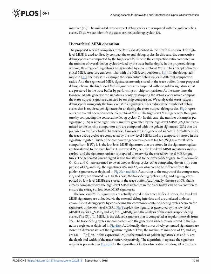
cycles that is required per signature for analyzing the error-suspect debug cycles. Fig 3 repre-
sents the overall operation of the hierarchical MISR. The high-level MISR generates the signa-
ture by compacting the consecutive debug cycles (Ci). In this case, the number of samples per
signature (SPS) is set to eight. The signatures generated by the high-level MISR (XSk) are trans-
mitted to the on-chip comparator and are compared with the golden signatures (GSk) that are
prepared in the trace buffer. In this case, k means the k-th generated signature. Simultaneously,
the trace debug cycles are compacted by the low-level MISRs and are temporarily stored in the
signature register. Further, the comparator generates a parent tag bit (PTk) as a result of the
comparison. If PTk is 1, the low-level MISR signatures that are stored in the signature register
are transferred to the trace buffer. However, if PTk is 0, the low-level MISR signatures are dis-
carded, and the signature register is prepared to overwrite the stored low-level MISR signa-
tures. The generated parent tag bit is also transferred to the external debugger. In this example,
C3, C19, and C21 are assumed to be erroneous debug cycles. After completing the on-chip com-
parison of XSk and GSk, the signatures XS1 and XS3 are observed to be different from the
golden signatures, as depicted in Fig 3(a) and 3(c). According to the outputs of the comparator,
PT1 and PT3 are denoted by 1. In this case, the trace debug cycles, C1-C8, and C17-C24, com-
pacted by low-level MISRs are stored in the trace buffer. Additionally, the area of GSk that is
already compared with the high-level MISR signature in the trace buffer can be overwritten to
ensure the storage of low-level MISR signatures.
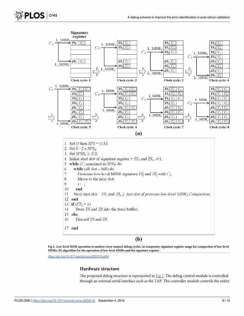
The low-level MISR signatures are actually stored in the trace buffer. Further, the low-level
MISR signatures are unloaded via the external debug interface and are analyzed to detect
error-suspect debug cycles by considering the commonly contained debug cycles between the
signatures of the low-level MISRs. Fig 4 depicts the signatures generated by the low-level
MISRs (YSj for L_MISR1 and ZSj for L_MISR2) and the analysis of the error-suspect debug
cycles. The ZSj of L_MISR2 is the delayed signature that is compacted at regular intervals from
YSj. The trace debug cycles are compacted, and the generated signatures are stored in the sig-
nature register, as depicted in Fig 4(a). Additionally, the consecutively generated signatures are
stored in different slots of the signature register. Thus, the maximum numbers of YSj and ZSj
are (M � dNGSW eÞ=2. In this expression, NGS is the number of golden signatures. M and W are
the depth and width of the trace buffer, respectively. The algorithm to operate the signature
register is presented in Fig 4(b). In the algorithm, O is the observation window, M is the trace
A debug scheme to improve the error identification in post-silicon validation
PLOS ONE | https://doi.org/10.1371/journal.pone.0202216 September 4, 2018 7 / 15
buffer depth, S is the size of signature register, SPS is the number of samples per high-level
MISR signature, and SPSS is the number of samples per low-level MISR signature, respectively.
In this operation, we generate ZSj using L_MISR2 as a complicated compaction. When the
slots of the signature register are completely filled with the generated signatures, the slots are
repeatedly filled with a new starting point. In this case, the starting slot points of ZSj are differ-
ent from those of YSj.
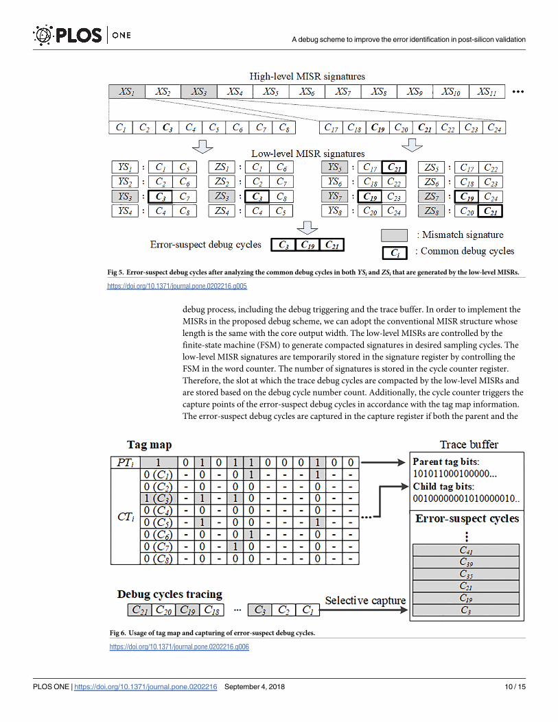
After the stored low-level MISR signatures are unloaded to the external debugger, the
unloaded signatures are analyzed to identify the error-suspect debug cycles. Fig 5 depicts an
analysis of the error-suspect debug cycles based on the flow of the debug process from the
high-level MISR operation to the low-level MISR operation. A comparison of XSk and GSk
depicts that there are two unmatched high-level MISR signatures, XS1 and XS3. After the low-
level MISR signatures are unloaded, the unloaded YSi and ZSi are compared with the golden
YSi and ZSi generated off-chip, and the erroneous signatures are classified. The erroneous YSi
and ZSi are analyzed to determine the common debug cycles that are contained in both the
erroneous YSi and ZSi. In this example, the erroneous signatures are YS3, YS5, YS7, ZS3, ZS7,
and ZS8, and the final error-suspect debug cycles that are identified to be C3, C19, and C21 are
the common denominators of erroneous signatures.
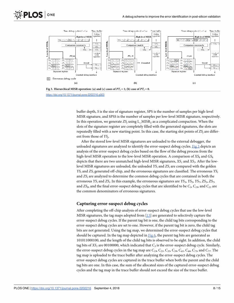
Capturing error-suspect debug cycles
After completing the off-chip analysis of error-suspect debug cycles that use the low-level
MISR signatures, the tag maps adopted from [13] are generated to selectively capture the
error-suspect debug cycles. If the parent tag bit is one, the child tag bits corresponding to the
error-suspect debug cycles are set to one. However, if the parent tag bit is zero, the child tag
bits are not generated. Using the tag map, we determined the error-suspect debug cycles that
should be captured. In the tag map depicted in Fig 6, the parent tag bits are generated as
101011000100, and the length of the child tag bits is observed to be eight. In addition, the child
tag bits of XS1 are 00100000, which indicated that C3 is the error-suspect debug cycle. Similarly,
the error-suspect debug cycles in the tag map are C19, C21, C35, C39, C41, C46, C73, and C77. The
tag map is uploaded to the trace buffer after analyzing the error-suspect debug cycles. The
error-suspect debug cycles are captured in the trace buffer when both the parent and the child
tag bits are one. In this case, the sum of the allocated sizes of the captured error-suspect debug
cycles and the tag map in the trace buffer should not exceed the size of the trace buffer.
Fig 3. Hierarchical MISR operation: (a) and (c) cases of PTi = 1; (b) case of PTi = 0.
https://doi.org/10.1371/journal.pone.0202216.g003
A debug scheme to improve the error identification in post-silicon validation
PLOS ONE | https://doi.org/10.1371/journal.pone.0202216 September 4, 2018 8 / 15
Hardware structure
The proposed debug structure is represented in Fig 7. The debug control module is controlled
through an external serial interface such as the TAP. The controller module controls the entire
Fig 4. Low-level MISR operation to analyze error-suspect debug cycles: (a) temporary signature register usage for compaction of low-level
MISRs; (b) algorithm for the operation of low-level MISRs and the signature register.
https://doi.org/10.1371/journal.pone.0202216.g004
A debug scheme to improve the error identification in post-silicon validation
PLOS ONE | https://doi.org/10.1371/journal.pone.0202216 September 4, 2018 9 / 15
debug process, including the debug triggering and the trace buffer. In order to implement the
MISRs in the proposed debug scheme, we can adopt the conventional MISR structure whose
length is the same with the core output width. The low-level MISRs are controlled by the
finite-state machine (FSM) to generate compacted signatures in desired sampling cycles. The
low-level MISR signatures are temporarily stored in the signature register by controlling the
FSM in the word counter. The number of signatures is stored in the cycle counter register.
Therefore, the slot at which the trace debug cycles are compacted by the low-level MISRs and
are stored based on the debug cycle number count. Additionally, the cycle counter triggers the
capture points of the error-suspect debug cycles in accordance with the tag map information.
The error-suspect debug cycles are captured in the capture register if both the parent and the
Fig 5. Error-suspect debug cycles after analyzing the common debug cycles in both YSi and ZSi that are generated by the low-level MISRs.
https://doi.org/10.1371/journal.pone.0202216.g005
Fig 6. Usage of tag map and capturing of error-suspect debug cycles.
https://doi.org/10.1371/journal.pone.0202216.g006
A debug scheme to improve the error identification in post-silicon validation
PLOS ONE | https://doi.org/10.1371/journal.pone.0202216 September 4, 2018 10 / 15
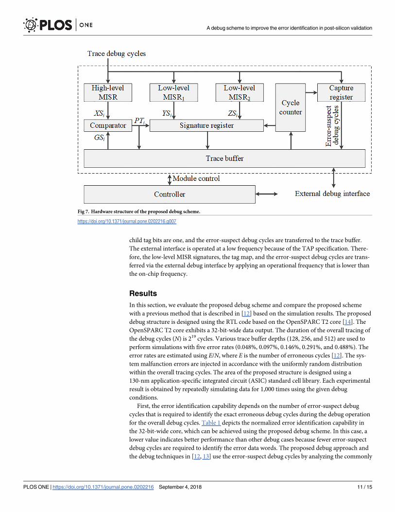
child tag bits are one, and the error-suspect debug cycles are transferred to the trace buffer.
The external interface is operated at a low frequency because of the TAP specification. There-
fore, the low-level MISR signatures, the tag map, and the error-suspect debug cycles are trans-
ferred via the external debug interface by applying an operational frequency that is lower than
the on-chip frequency.
Results
In this section, we evaluate the proposed debug scheme and compare the proposed scheme
with a previous method that is described in [12] based on the simulation results. The proposed
debug structure is designed using the RTL code based on the OpenSPARC T2 core [14]. The
OpenSPARC T2 core exhibits a 32-bit-wide data output. The duration of the overall tracing of
the debug cycles (N) is 219 cycles. Various trace buffer depths (128, 256, and 512) are used to
perform simulations with five error rates (0.048%, 0.097%, 0.146%, 0.291%, and 0.488%). The
error rates are estimated using E/N, where E is the number of erroneous cycles [12]. The sys-
tem malfunction errors are injected in accordance with the uniformly random distribution
within the overall tracing cycles. The area of the proposed structure is designed using a
130-nm application-specific integrated circuit (ASIC) standard cell library. Each experimental
result is obtained by repeatedly simulating data for 1,000 times using the given debug
conditions.
First, the error identification capability depends on the number of error-suspect debug
cycles that is required to identify the exact erroneous debug cycles during the debug operation
for the overall debug cycles. Table 1 depicts the normalized error identification capability in
the 32-bit-wide core, which can be achieved using the proposed debug scheme. In this case, a
lower value indicates better performance than other debug cases because fewer error-suspect
debug cycles are required to identify the error data words. The proposed debug approach and
the debug techniques in [12, 13] use the error-suspect debug cycles by analyzing the commonly
Fig 7. Hardware structure of the proposed debug scheme.
https://doi.org/10.1371/journal.pone.0202216.g007
A debug scheme to improve the error identification in post-silicon validation
PLOS ONE | https://doi.org/10.1371/journal.pone.0202216 September 4, 2018 11 / 15
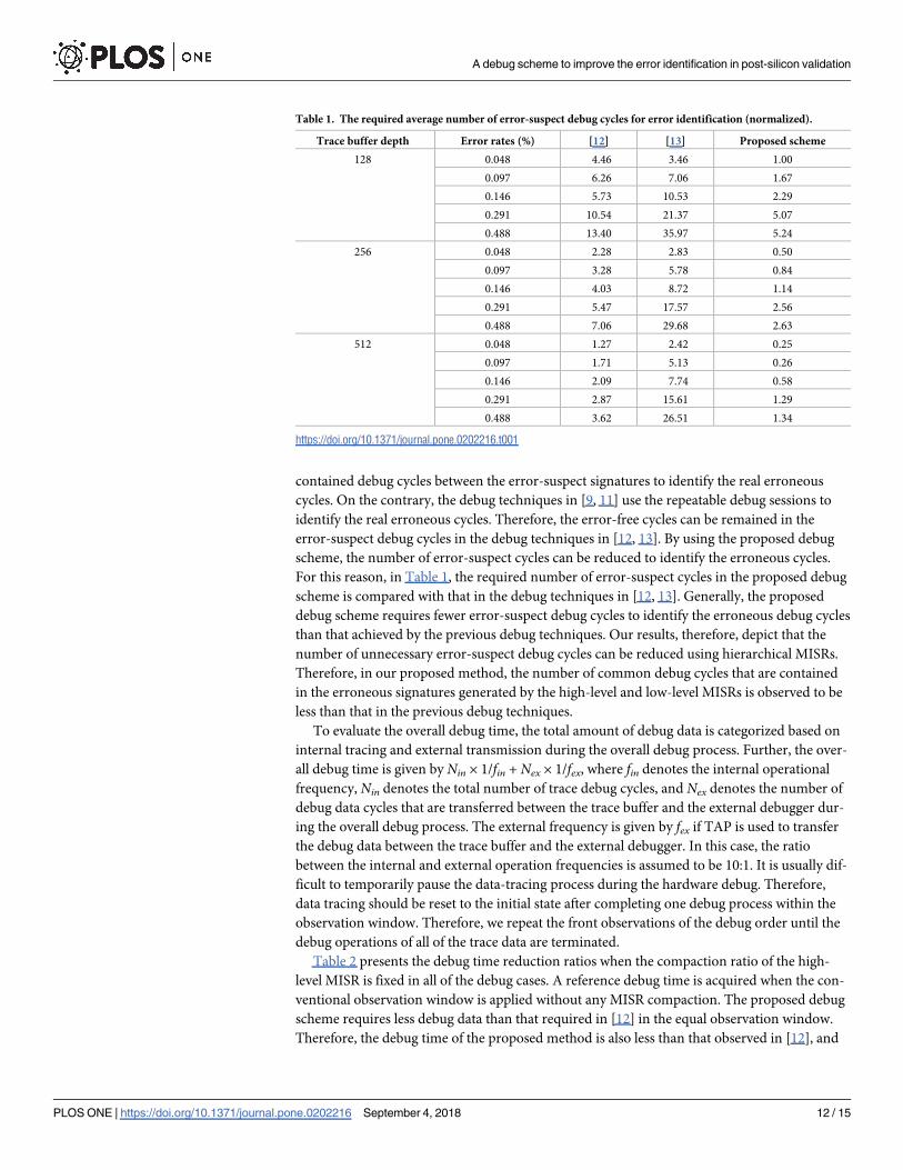
contained debug cycles between the error-suspect signatures to identify the real erroneous
cycles. On the contrary, the debug techniques in [9, 11] use the repeatable debug sessions to
identify the real erroneous cycles. Therefore, the error-free cycles can be remained in the
error-suspect debug cycles in the debug techniques in [12, 13]. By using the proposed debug
scheme, the number of error-suspect cycles can be reduced to identify the erroneous cycles.
For this reason, in Table 1, the required number of error-suspect cycles in the proposed debug
scheme is compared with that in the debug techniques in [12, 13]. Generally, the proposed
debug scheme requires fewer error-suspect debug cycles to identify the erroneous debug cycles
than that achieved by the previous debug techniques. Our results, therefore, depict that the
number of unnecessary error-suspect debug cycles can be reduced using hierarchical MISRs.
Therefore, in our proposed method, the number of common debug cycles that are contained
in the erroneous signatures generated by the high-level and low-level MISRs is observed to be
less than that in the previous debug techniques.
To evaluate the overall debug time, the total amount of debug data is categorized based on
internal tracing and external transmission during the overall debug process. Further, the over-
all debug time is given by Nin × 1/fin + Nex × 1/fex, where fin denotes the internal operational
frequency, Nin denotes the total number of trace debug cycles, and Nex denotes the number of
debug data cycles that are transferred between the trace buffer and the external debugger dur-
ing the overall debug process. The external frequency is given by fex if TAP is used to transfer
the debug data between the trace buffer and the external debugger. In this case, the ratio
between the internal and external operation frequencies is assumed to be 10:1. It is usually dif-
ficult to temporarily pause the data-tracing process during the hardware debug. Therefore,
data tracing should be reset to the initial state after completing one debug process within the
observation window. Therefore, we repeat the front observations of the debug order until the
debug operations of all of the trace data are terminated.
Table 2 presents the debug time reduction ratios when the compaction ratio of the high-
level MISR is fixed in all of the debug cases. A reference debug time is acquired when the con-
ventional observation window is applied without any MISR compaction. The proposed debug
scheme requires less debug data than that required in [12] in the equal observation window.
Therefore, the debug time of the proposed method is also less than that observed in [12], and
Table 1. The required average number of error-suspect debug cycles for error identification (normalized).
Trace buffer depth Error rates (%) [12] [13] Proposed scheme
128 0.048 4.46 3.46 1.00
0.097 6.26 7.06 1.67
0.146 5.73 10.53 2.29
0.291 10.54 21.37 5.07
0.488 13.40 35.97 5.24
256 0.048 2.28 2.83 0.50
0.097 3.28 5.78 0.84
0.146 4.03 8.72 1.14
0.291 5.47 17.57 2.56
0.488 7.06 29.68 2.63
512 0.048 1.27 2.42 0.25
0.097 1.71 5.13 0.26
0.146 2.09 7.74 0.58
0.291 2.87 15.61 1.29
0.488 3.62 26.51 1.34
https://doi.org/10.1371/journal.pone.0202216.t001
A debug scheme to improve the error identification in post-silicon validation
PLOS ONE | https://doi.org/10.1371/journal.pone.0202216 September 4, 2018 12 / 15
the debug time reduction ratio of the proposed method is higher than that observed in [12]. If
the error rate is increased, more debug data are required to identify the erroneous debug
cycles. This reduces the reduction ratio. However, if the trace buffer depth is increased, the
number of repeatable debug segments and the debug time is also reduced.
Table 2 also shows the experimental result for the comparison of the debug time reduction
ratio of the proposed debug scheme to the debug techniques in [9, 11, 13]. While the small
trace buffer depth is used to get the result of the debug experiment, the debug time reduction
ratio of the debug technique in [11] is larger than that of other debug techniques. In this case,
the SPSS of the proposed debug approach is relatively higher than that of [11] as the debug
operation is progressed. For this reason, the debug time reduction ratio of the proposed debug
scheme is less than that of [11] in small buffer size. On the contrary, the debug time reduction
ratio of the proposed debug scheme is larger than that of other debug techniques as the trace
buffer size increases. In this case, the trace buffer size in the proposed debug scheme is suffi-
cient to generate the low-level MISR signatures. For example, the number of error-suspect
debug cycles in the proposed debug scheme is less than that in the debug techniques in [9, 11]
when 512-depth buffer is applied to the debug operation. For this reason, the debug time
reduction ratio is reduced in the large trace buffer usage due to longer transferring time of
debug data via the external debug interface.
Table 3 presents the hardware area overheads in terms of the two-input NAND equivalent
gates. This table depicts a comparison between the previous debug technique and our
Table 2. Debug time reduction ratio in the same observation window.
Trace buffer depth Error rates (%) Reduction ratio (Tconv/Tprop(prev))
[9] [11] [12] [13] Proposed scheme
128 0.048 39.71 59.94 8.30 8.44 43.44
0.097 32.77 46.18 7.09 6.33 33.94
0.146 23.36 37.41 6.62 5.01 28.25
0.291 14.92 24.91 5.73 2.97 19.63
0.488 11.90 18.00 4.57 1.95 15.05
256 0.048 26.48 32.87 8.49 9.34 45.46
0.097 20.88 33.44 8.26 7.76 40.26
0.146 15.69 25.21 8.04 6.57 34.23
0.291 9.25 11.65 7.04 4.45 25.43
0.488 6.64 6.15 6.59 3.09 21.49
512 0.048 24.98 25.88 9.45 10.03 76.49
0.097 20.16 25.83 8.90 8.54 36.05
0.146 14.38 25.83 8.37 7.84 33.97
0.291 9.40 17.35 7.96 5.74 27.27
0.488 6.45 13.11 7.16 4.31 23.08
https://doi.org/10.1371/journal.pone.0202216.t002
Table 3. Hardware area overhead.
Design OpenSPARC T2 Debug module Overhead (%)
[9] 595,738 2,037 0.34
[11] 3,450 0.58
[12] 9,124 1.53
[13] 10,783 1.81
Proposed 11,395 1.91
https://doi.org/10.1371/journal.pone.0202216.t003
A debug scheme to improve the error identification in post-silicon validation
PLOS ONE | https://doi.org/10.1371/journal.pone.0202216 September 4, 2018 13 / 15
proposed debug structure applied to the OpenSPARC T2 core. In this case, the area overheads
of the debug modules are only included in the results because the trace buffer size applied in
the proposed debug approach is the same as that of previous works. The hardware area over-
head of the proposed debug structure is 1.91% of that of the OpenSPARC T2 core. The hard-
ware area overheads for the debug techniques in [9, 11, 13] also have been evaluated. As shown
in Table 3, the hardware area overhead of the proposed debug scheme is larger than that of
other debug techniques. In this case, the number of MISR and the size of the signature register
affect the hardware area overhead of the proposed debug scheme. However, the hardware area
overhead of the proposed debug scheme is still much less than the processing core.
Conclusions
In this study, we propose a debug scheme that can reduce the amount of debug data that is
required to identify the erroneous debug cycles. We can obtain a better error identification
capability using hierarchical MISRs for decreasing the commonly contained error-suspect
debug data from among the generated MISR signatures. Therefore, we can decrease the unnec-
essary debug data transfer from debug operations. All these factors reduces the debug time,
and the proposed debug scheme accelerates the post-silicon validation.
Acknowledgments
This research was supported by the MOTIE (Ministry of Trade, Industry & Energy)
(10067813) and KSRC (Korea Semiconductor Research Consortium) support program for the
development of the future semiconductor device.
Author Contributions
Conceptualization: Inhyuk Choi, Sungho Kang.
Data curation: Hyunggoy Oh.
Formal analysis: Inhyuk Choi, Sungho Kang.
Funding acquisition: Sungho Kang.
Investigation: Won Jung.
Methodology: Won Jung.
Supervision: Sungho Kang.
Validation: Hyunggoy Oh.
References1. Vermeulen B, Goel SK. Design for debug: catching design errors in digital chips. IEEE Design & Test of
Computers. 2002; 19(3): 35–43. https://doi.org/10.1109/MDT.2002.1003792
2. Abramovici M, Bradley P, Dwarakanath K, Levin P, Memmi G, Miller D. A reconfigurable design for
debug infrastructure for SoCs. In: Design Automation Conference (DAC). ACM/IEEE; 2006. p. 7–12.
3. Chang KH, Markov IL, Bertacco V. Automating post-silicon debug and repair. In: International Confer-
ence on Computer Aided Design (ICCAD). IEEE/ACM; 2007. p. 91–98.
4. Ko HF, Nicolici N. Combining scan and trace buffers for enhancing real-time observability in post-silicon
debug. In: European Test Symposium (ETS). IEEE; 2010. p. 62–67.
5. Saragi S, Greskamp B, Torrellas J. CADRE: cycle-accurate deterministic replay for hardware debug. In:
International Conference on Dependable Systems and Networks (IDSN), IEEE; 2006. p. 301–312.
A debug scheme to improve the error identification in post-silicon validation
PLOS ONE | https://doi.org/10.1371/journal.pone.0202216 September 4, 2018 14 / 15
6. Oh H, Choi I, Kang S. DRAM-based error detection method to reduce the post-silicon debug time for
multiple identical cores. IEEE Transactions on Computers. 2017; 66(9): 1504–1507. https://doi.org/10.
1109/TC.2017.2678504
7. Abramovici M. In-system silicon validation and debug. IEEE Design & Test of Computers. 2008; 25(3):
216–223. https://doi.org/10.1109/MDT.2008.77
8. Ko HF, Kinsman A, Nicolici N. Design-for-debug architecture for distributed embedded logic analysis.
IEEE Transactions on Very Large Scale Integration (VLSI) Systems. 2011; 19(8): 1380–1393. https://
doi.org/10.1109/TVLSI.2010.2050501
9. Daoud EA, Nicolici N. On using lossy compression for repeatable experiments during silicon debug.
IEEE Transactions on Computers. 2011; 60(7): 937–950. https://doi.org/10.1109/TC.2010.122
10. Deutsch S, Chakrabarty K. Massive signal tracing using on-chip DRAM for in-system silicon debug. In:
International Test Conference (ITC), IEEE; 2014. p. 1–10.
11. Oh H, Han T, Choi I, Kang S. An on-chip error detection method to reduce the post-silicon debug time.
IEEE Transactions on Computers. 2017; 66(1): 38–44. https://doi.org/10.1109/TC.2016.2561920
12. Yang JS, Touba N. Improved trace buffer observation via selective data capture using 2-D compaction
for post-silicon debug. IEEE Transactions on Very Large Scale Integration (VLSI) Systems. 2013; 21
(2): 320–328. https://doi.org/10.1109/TVLSI.2012.2183399
13. Jung W, Oh H, Kang D, Kang S. A 2-D compaction method using macro block for post-silicon validation.
In: International SoC Design Conference (ISOCC), IEEE/IEIE; 2015. p. 41–42.
14. OpenSPARC-based SoC; 2011. http://opencores.org/project/sparc64soc
A debug scheme to improve the error identification in post-silicon validation
PLOS ONE | https://doi.org/10.1371/journal.pone.0202216 September 4, 2018 15 / 15